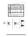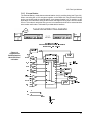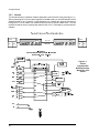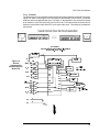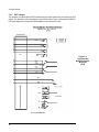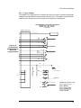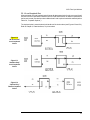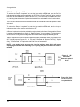
1
Modems Canoga Perkins 2270 Fiber Optic Modem User Manual Canoga Perkins Notice! Canoga Perkins has prepared this manual for use by customers and Canoga Perkins personnel as a guide for the proper installation, operation and/or maintenance of Canoga Perkins equipment. The drawings, specifications and information contained in this document are the property of Canoga Perkins and any unauthorized use or disclosure of such drawings, specifications and information is prohibited. Canoga Perkins reserves the right to change or update the contents of this manual and to change the specifications of its products at any time without prior notification. Every effort has been made to keep the information in this document current and accurate as of the date of publication or revision. However, no guarantee is given or implied that the document is error free or that it is accurate with regard to any specification. Canoga Perkins Corporation An Inductotherm Company 20600 Prairie Street Chatsworth, CA 91311-6008 (818) 718-6300 FAX: (818) 718-6312 Web Site: www.canoga.com e-mail: [email protected] Copyright 1988, 1990, 1991, 1992, 1996, 1998 Canoga Perkins All Rights Reserved 2270 Fiber Optic Modem 6910321 Rev. D 5/98 2 2270 Fiber Optic Modem Caution! This product may contain a laser diode emitter operating at a wavelength of 1300 nm - 1600 nm. Use of optical instruments (for example: collimating optics) with this product may increase eye hazard. Use of controls or adjustments or performing procedures other than those specified herein may result in hazardous radiation exposure. Under normal conditions, the radiation levels emitted by this product are under the Class 1 limits in 21 CFR Chapter 1, Subchapter J. Notice! This device contains static sensitive components. It should be handled only with proper Electrostatic Discharge (ESD) grounding procedures. 3 Canoga Perkins Table of Contents Chapter 1 - General ..........................................................................................8 1.1 Equipment Description ................................................................................... 8 1.2 Functions, LEDs and Switches ....................................................................... 8 1.3 2201 Rack Chassis ....................................................................................... 10 1.4 2202 Modem Shelf ........................................................................................ 10 1.5 2200R Redundant Modem Card Set ........................................................... 10 1.6 ................................................................ Fiber Optic Versions 10 1.7 Loss Budget .................................................................................................. 11 1.8 Optical Bandwidth ......................................................................................... 11 1.9 General Installation ...................................................................................... 11 1.9.1 Fiber Optic Cable and Connectors ................................................................... 11 1.9.2 Initial Unit Testing ............................................................................................. 11 1.10 Sensitivity and Optical Power Switches (HP Laser Version Only) 12 1.10.1 Optical Power Switch (HP Laser Version Only) ............................................ 12 1.10.2 Sensitivity Switch (HP Laser Version Only .................................................... 12 1.10.3 Optical Switch Settings (HP Laser Version Only) .......................................... 12 1.11 Switch and Jumper Settings ............................................................................... 13 1.12 Mean Time Between Failures (MTBF) ............................................................. 13 Chapter 2 - Installation ................................................................................ 16 2.1 2.2 2.3 2.4 2.5 2.6 2.7 Unpacking the Unit ....................................................................................... 16 Standalone Modem Installation ................................................................... 16 2202 Modem Shelf Installation .................................................................... 16 Fiber Cable and Connectors ......................................................................... 17 DC Power ...................................................................................................... 17 Rack Chassis Installation ............................................................................ 18 Mode and Rate Selection ............................................................................. 18 2.7.1 2.7.2 2.7.3 2.7.4 2.7.5 2.7.6 External Clock Operation ................................................................................. 18 Internal Clock Operation .................................................................................. 18 Asynchronous Operation .................................................................................. 20 Data Rates ........................................................................................................ 20 Data Rate vs. Module Frequency .................................................................... 20 Slave Clock Operation ...................................................................................... 20 2.7.7 Consideration of Propagation Delays ....................................................... 20 Chapter 3 - Data Interfaces ........................................................................... 23 3.1 Electrical Data Interfaces ............................................................................ 23 3.2 RS-232C/423 Interface Model -32 .............................................................. 23 3.3 RS-449/422 Interfaces .................................................................................. 23 3.3.1 Model -22 ................................................................................................... 25 3.3.2 Model -H22 ................................................................................................ 25 3.3.3 Model -R2R ............................................................................................... 25 3.4 RS-530 Interface Model -R30 ..................................................................... 26 3.5 T1/E1 Interfaces ........................................................................................... 28 3.5.1 Transparent Bipolar Models -B1, -B2, -B3 ....................................................... 28 4 2270 Fiber Optic Modem 3.5.2 DS1 / T1 Model -T1 ......................................................................................... 30 3.6 TTL/BNC Interface Model -BN .................................................................. 30 3.8 .................... Programmable Buffered Interface Model P53 32 3.8.1 3.8.2 3.8.3 3.8.4 3.8.5 3.8.6 Generic Interface .............................................................................................. 36 External Station ............................................................................................... 37 Internal ............................................................................................................. 38 External ........................................................................................................... 39 DTE Adapter ................................................................................................... 40 Legacy Adapter ............................................................................................... 41 3.9.1 3.9.2 3.9.3 3.9.4 3.9.5 3.9.6 Model -TW ....................................................................................................... 43 Model -TW8 ..................................................................................................... 44 Model -T22 ....................................................................................................... 44 Model -T88 ....................................................................................................... 44 Model -D22 ....................................................................................................... 44 Model -D88 ....................................................................................................... 44 3.9 High-Speed RS-422/Mil-Std 188-114C Interfaces ...................................... 42 3.10 Interface Reconfiguration .......................................................................... 46 3.11 Standalone Reconfiguration ....................................................................... 46 Chapter 4 - Modem Operation ................................................................... 47 4.1 4.2 4.3 4.4 4.5 4.6 4.7 4.8 Modem Operation ........................................................................................ 47 Fiber Optics ................................................................................................... 47 Transmit Section ........................................................................................... 48 Receive Section ............................................................................................ 48 Full Rate Agility ............................................................................................ 48 Bit Count Integrity ........................................................................................ 49 Duty Cycle Tolerance ................................................................................... 49 Control Signals .............................................................................................. 49 4.8.1 Flow Control ..................................................................................................... 50 Chapter 5 - Troubleshooting ......................................................................... 51 5.1 Diagnostic Procedures .................................................................................. 51 5.2 System Test ................................................................................................... 51 5.2.1 Local Loopback Test ........................................................................................ 53 5.2.2 Remote Loopback Test ..................................................................................... 54 5.2.3 System Loopback Test ..................................................................................... 55 Chapter 6 - Diagnostic Procedures ............................................................ 56 6.1 2270/2201 Diagnostic Procedures ................................................................ 56 6.2 System Test Diagnostic Procedure .............................................................. 56 Chapter 7 - Specifications ............................................................................. 58 7.1 7.2 7.3 7.4 7.5 Diagnostic Indicators and Controls ............................................................. 58 Optical Interface ........................................................................................... 58 System Electrical .......................................................................................... 59 Physical Dimensions ..................................................................................... 59 2270 Fiber Optic Modem Configurations .................................................... 60 Appendix A ..................................................................................................... 61 A.1 Customer Service Department Repair ....................................................... 61 Warranty .............................................................................................................. 61 A.2 Return Policy ................................................................................................ 61 5 Canoga Perkins A.3 Advance Replacement Policy ...................................................................... 61 A.4 Warranty ....................................................................................................... 62 Electronic Products ..................................................................................................... 62 Cable Products ........................................................................................................... 62 Limitations ................................................................................................................... 62 List of Figures Figure Page 1-1 Front Panel Mode/Rate Switch ........................................................................................... 9 1-2 Locations of Various Switches ......................................................................................... 13 2-1 Model 2202 Standalone Modem Shelf .............................................................................. 16 2-2 2201 Rack Chassis Front View with Modems Installed ..................................................19 3-1 2270 Interchangeable Interfaces ..................................................................................... 23 3-2 Transparent Bipolar Interface Connectors ...................................................................... 29 3-3 Available Strapping Options for Programmable Buffered Interface ................................33 3-4 Board Layout and Modules for Programmable Buffered Interface ................................. 34 3-5 Programmable Buffered Interface, Model P53, DCE RS-530 ......................................... 36 3-6 Programmable Buffered Interface, Model P53, External Station .................................... 37 3-7 Internal Programmable Buffered Interface, Model P53, RS-530 .................................... 38 3-8 External Programmable Buffered Interface, Model P53 ................................................. 39 3-9 Programmable Buffered Interface, Model P53 [DTE] ...................................................... 40 3-10 Programmable Buffered Interface, Model P53 [Legacy Adapter] ................................. 41 3-11 BNC and Four TwinAx Connectors (BJ-77 Type) .......................................................... 44 3-12 Five TwinAx Connectors (BJ-77 Type) ........................................................................... 45 3-13 Interface Card Installation ............................................................................................. 46 4-1 2270 Circuit Block Diagram ........................................................................................... 47 4-2 Typical High Speed 2270 Modem Application .................................................................. 48 4-3 Data Organization with PWM Optics .............................................................................. 49 5-1 System Loopback Test Example From User-End of Fiber Link ........................................ 51 5-2 Bi-Directional Local Loopback Active ......................................................................... 53 5-3 Interface Only Local Loopback Active ......................................................................... 53 5-4 Optical Only Remote Loopback Active ......................................................................... 53 5-5 Bi-Directional Only Remote Loopback Active ............................................................. 54 5-6 Optical at Local End Loopback Active ..........................................................................54 6 2270 Fiber Optic Modem List of Tables 1-A 1-B 1-C 1-D Table Page Available Modem Controls ............................................................................................................. 8 Guaranteed Loss Budgets .............................................................................................................10 2270 Switch Functions ..................................................................................................................14 2270 Jumper Functions ................................................................................................................15 2-A Operating Mode Selections ...........................................................................................................19 2-B Data Rate Switch Position vs. Oscillator Part Number ................................................................21 3-A 3-B 3-C 3-D 3-E 3-F 3-G 3-H 3-I 3-J 3-K 3-L 3-M 3-N 5-A RS-232C/423 Signals and Pin Assignments ...............................................................................24 Available Models of RS-449/422 Interfaces .................................................................................24 RS-449 (RS-422) Signals and Pin Assignments ..........................................................................25 RS-530 Signals and Pin Assignments ..........................................................................................26 RS-530 Jumper Options ...............................................................................................................27 Transparent Bipolar Line Interfaces ............................................................................................28 Line Build Out Settings ................................................................................................................29 CCITT V.35 Digital Interface and Pin Assignments ....................................................................31 Delay Times for Programmable Buffered Interface .....................................................................34 Strap Configurations for Programmable Buffered Interface .......................................................35 TwinAx and BNC Supported Signals ............................................................................................42 Model Characteristics ..................................................................................................................42 Jumper Strap Options ...................................................................................................................43 Models D22 and D88 Connector Pin Assignments ......................................................................45 Loopback Options ..........................................................................................................................52 7 Canoga Perkins Chapter 1 - General 1.1 Equipment Description The 2270 is a high-speed modem for full-duplex operation over fiber optic cable. It operates synchronously up to 20 Mbps, and asynchronously up to 5 Mbps in the sample-data mode with a 25% jitter limit. The 2270 is available in rack-mount and standalone configurations. Both are intended to operate with a variety of electrical interfaces (refer to Section 7.5, 2270 Fiber Optic Modem Configurations, for a listing of the interface options for the 2270). Refer to Section 3 for detailed descriptions of available I/O interfaces. The 2270 has integral System Test and loopback diagnostic modes for performance monitoring. Various 2270 configurations provide local modem controls, including those listed in Table 1-A. A limited form of end-to-end control lead operation is also available (refer to Section 4.8). 1.2 Functions, LEDs and Switches The 2270 standalone modems do not have an on/off switch, since they power up when plugged in. For 2270 Rack-Mount configurations, a power supply on/off switch is located at the rear of each power supply assembly on the 2201 Rack Chassis. An eight-section switch bank, located on the front panel of the 2270 (see Figure 1-1), controls all operating modes and internal clock rates. Switch positions 1, 2 and 3 select the internal clock operating rates. Refer to Table 2-B for data rate switch settings. The rates depend on the crystal option installed. Refer to Section 7.5 for a list of crystal options available. The -08 crystal is installed as the factory default crystal unless an alternate crystal is ordered. Table 1-A. Available Modem Controls 8 DATA/CLOCK CONTROLS TRANSMIT DATA RECEIVE DATA TRANSMIT CLOCK RECEIVE CLOCK REQUEST TO SEND CLEAR TO SEND DATA CARRIER READY DATA SET READY 2270 Fiber Optic Modem Figure 1-1. Front Panel Mode/Rate Switch Ref. Pg 52 The rate setting determines what rate the modem will operate at if set to the Internal Clocking Mode or the rate used when a modem set to the Slave Clocking Mode is set for local loopback. The modes are: External Clock Internal Clock Slave Clock Flow Control Alternate Loopback Functions Switch positions 4, 5 and 6 select the clocking mode for the modem as described in Section 2.7 and shown in Table 2-A. Switch position 7 selects whether the RTS input controls flow control through the modem (Open = no flow control, Closed = flow control enabled). Refer to Section 4.8.1. Switch position 8 selects the normal or alternate loopback mode as shown in Table 5-A of the Troubleshooting section. Indicator lights are provided for Power On, Optical Receive and Transmit data activity, Interface Receive and Transmit data activity, and for Loopback On. All of these indicators are located on the front panel, for both standalone and rack-mount versions. The loopback switch on the front panel is used to activate the built-in system test or to select either a Local or Remote loopback function. Use of this switch is outlined in Chapter 5, Troubleshooting. The electrical interface connection and fiber optic connections are made at the rear of the modem. The HI/LO optical power switch is also located there. There is also a HI/LO switch for the optical receiver, used to select its sensitivity. Operating this switch in the LO position may be necessary under certain low-loss conditions (refer to Section 1.9). 9 Canoga Perkins 1.3 2201 Rack Chassis The 2201 Rack Chassis is designed to accommodate up to ten 2200 series modems. It offers a variety of features, including local audible/visible and remote power failure alarms, optional redundant power supply, and the ability to allow modem removal from the chassis without powering down the entire system. Refer to the 2201 Rack Chassis / 2200R Redundant Modem Card User Manual for more details. 1.4 2202 Modem Shelf The 2202 Modem Shelf accommodates one or two standalone 2200-series modems. It is designed to fit easily into a 19-inch equipment rack. The modems can be secured side-by-side in the shelf. Refer to the 2202 Modem Shelf User Manual for more details. 1.5 2200R Redundant Modem Card Set A redundant board set, consisting of two 2270 Modems and a 2200R Modem Card, uses three slots of the 2201 Rack Chassis. It enables a user to incorporate a fully redundant fiber optic link with 2270 Modems. The combination of the three boards provides redundant operation for data rates up to 20 Mbps. Redundancy is not available for standalone models. The 2200R provides the redundancy controller and signal switch for a redundant board set. The 2200R is equipped with keyed-ribbon cables and a modem interface (RPB) extender for easy installation. Refer to the 2201 Rack Chassis / 2200R Redundant Modem Card User Manual for more details. 1.6 Fiber Optic Versions Three fiber optic versions provide solutions to virtually any fiber-optic plant, including 50/125 or 62.5/125 multimode and 8-10/125 single mode. Table 1-B summarizes the three fiber-optic versions. Table 1-B. Guaranteed Loss Budgets Fiber Size Optics Option 8/10 SM 50 MM 62.5 MM Min. Launch Power dBm 850 nm LED N/A 2 6 -14 1310 nm LP Laser 10 10 10 -8 1310 nm HP Laser 15 15 15 -6 N/A = Not Applicable 10 [Typical loss budgets are 2 dB higher] 2270 Fiber Optic Modem 1.7 Loss Budget The maximum possible distances with either standard or long distance versions is dependent on the overall power loss over the fiber optic link. This is called the link loss. The launch power for the modem is compared with receiver sensitivity. The determination of the difference is the loss budget (refer to Table 1-B). To insure normal operation over a long term, the link loss should be at least 3 dB less than the loss budget for the modem. For example, consider a data link 7 kilometers long using 50/125 optical fiber that has a measured power loss of 9 dB, and a patch panel connector loss of 3 dB, for a total link loss of 12 dB. The minimum launch power of the 2270 High Power (HP) laser version is -6 dBm in high-power mode, and the worst-case receiver sensitivity is -21 dBm. The guaranteed loss budget is 15 dB. Subtracting the link loss (12 dB) from the loss budget (15 dB) leaves a margin of 3 dB -- is within the suggested limit. NOTE: Optical power measurements for the 2270 are sensitive to the data rate. All measurements quoted are for a 20 Mbps data rate. 1.8 Optical Bandwidth The 2270 requires nearly 70 MHz of optical bandwidth. As a result, the specified fiber optic cable must provide this bandwidth at the required distance. For example, if 500 MHz/km fiber is used, this bandwidth requirement will limit the end-to-end distance to 7 km (70 MHz multiplied by 7 km = 490 MHz). 1.9 General Installation 1.9.1 Fiber Optic Cable and Connectors The 2270 can be used with virtually any size of multimode or single mode fiber optic cable including 50/125, 62.5/125 and 8-10/125. The proposed fiber optic cable must provide adequate bandwidth and power loss characteristics for the intended modem link. Fiber optic connectors terminated on the cable must match those terminated on the modem. CAUTION: It is important to keep all connectors free of water, dust, dirt, etc. When not in use, the connectors should be covered with protective plastic caps. 1.9.2 Initial Unit Testing The following is a basic list of check points to consider: • • Have you set your optical power and receiver sensitivity switches correctly for the loss of the fiber optic link? Are the fiber optic cables marked correctly? Connect the Tx cable to the Tx connector, the Rx cable to the Rx connector. If System Test fails, try swapping cables at one end of the link. 11 Canoga Perkins • Are you using the correct clock mode (internal/external) for synchronous transmission? Have the modems mode and rate switches been set properly? (The 2270 is set to the external clock mode at the factory.) If you have problems after carefully checking these items, turn to Chapter 5, Troubleshooting. • • 1.10 Sensitivity and Optical Power Switches (HP Laser Version Only) A dual-section switch block is located between the transmit and receive optical connectors (see Figure 1-3). The section nearest the transmit connector controls the optical transmit power level. The section nearest the receiver controls the receiver sensitivity. For both switch functions, ON selects HI and OFF selects LO. For standalone modems, ON = UP and LO = DOWN; for rack mount modems, ON = RIGHT and LO = LEFT. This feature is only required for the HP laser fiberoptic version. These switches are not provided in the other fiber-optic versions. 1.10.1 Optical Power Switch (HP Laser Version Only) The Optical Power Switch (TX POWER) provides two settings for optical transmission levels. The LO switch setting is intended for use with short fiber optic lengths, i.e., a cable and connector power loss total of less than 10 dB. The HI switch setting is intended for longer cable runs, up to the maximum power loss budget. 1.10.2 Sensitivity Switch (HP Laser Version Only The Sensitivity Switch (RX SENS) provides two settings for optical receiver sensitivity. The LO switch setting is intended for short fiber lengths in conjunction with LO optical power at the other end. The LO setting must be used with a fiber link loss of 5 dB or less. 1.10.3 Optical Switch Settings (HP Laser Version Only) The proper setting of the Optical Transmit Power and Optical Receive Sensitivity Switches are based on the loss measured on the fiber at a wavelength of 1300 nm. The 2270 should be used as an optical power source when performing these measurements. The loss on the fiber link determines the setting of the Tx Power Switch at the transmitting end and the Rx Sensitivity Switch at the receiving end. It is important to remember that the switch settings are determined separately for each fiber in the pair. When operating the modem at rates above 6 Mbps, the HI/HI setting can always be used. HI/HI refers to HI Tx power and HI Rx sensitivity. If the modem is to be operated below 6 Mbps, or if the application requires full rate agility (without changing switch configuration) that extends below 6 Mbps, then the settings listed below should be followed. TX PWR LO LO HI HI 12 RX SENS LO HI LO HI MIN LOSS 0 5 10 13 MAX LOSS 5 10 13 15 2270 Fiber Optic Modem These settings give minimum and maximum losses for each of the four possible switch combinations. There is overlap between these ranges that is guaranteed to meet or exceed ±1.0 dB from the transition points. The performance of every modem is guaranteed to fit the parameters given above. Some modems may significantly exceed these performance limits, but reliable operation and unit interchangeability is not guaranteed outside of these limits. 1.11 Switch and Jumper Settings See Figure 1-2 for the location of specific switches and jumpers. Tables 1-C and 1-D summarize the functions of the 2270s switches and jumpers. 1.12 Mean Time Between Failures (MTBF) The 2270s Mean Time Between Failures (MTBF) figure, 62,500 hours (calculated) has been determined from calculations that are similar to MIL-217E. It assumes a Ground Benign environment and excludes failures which are not service-affecting. This MTBF figure is for a Rack-Mount 2270 with a MIL-STD 188-114C interface (Model 2270-R-TW8-11-08-0). Figure 1-2. Locations of Various Switches 13 Canoga Perkins Table 1-C. 2270 Switch Functions LOOP TEST switch on Front Panel (described in Section 5, Troubleshooting). LOC position will activate a local interface loopback. REM position will activate a System Test and control the state of the far-end loopback. OFF position is for normal transmission. TRANSMIT OPTIC POWER switch on Rear Panel (described in Section 1.9). HI position is used for link losses from approximately 10 dB and greater. LO position is used for link losses below 10 dB. RECEIVER SENSITIVITY switch on Rear Panel (described in Section 1.9). See NOTE 1 The position of this switch is dependent on both the loss of the Rx link and the position of the Tx optical power switch on the modem at the other end. CLOCK RATE switches on Front Panel (described in Section 2). Switches 1-3 control both the internal clock rate and the System Test rate. The rate is also dependent on the frequency of the installed oscillator. CLOCK MODE switches on Front Panel (described in Section 2). Switches 4-6 control the transmitter clock mode (external/slave/internal). Switch 7 controls the transmitter sensitivity to RTS used for flow control. Switch 8 enables selecting an alternate loopback method (refer to Section 5 for Loopback options). NOTE 1: Power should be cycled after changing switch. The unit must be powered down whenever a setting is changed. 14 2270 Fiber Optic Modem Table 1-D. 2270 Jumper Functions W2 W3 W16 W6/8 SIGNAL GROUND controls connecting circuit ground to the chassis. CHASSIS connects them together. FLOAT isolates the two grounds. Factory Setting = FLOAT See page 27 note SCT POLARITY controls the transmit clock output. NORM is always used for low data rates for proper clock phasing. INV may be needed for internal clock or slave clock modes operating high data rates if the DTE loop has long delays. Factory Setting = NORM TEST controls the built-in test pattern checker. ON allows System Test loopback to be activated and Remote Loopback control. OFF defeats pattern loopback for System Test and disables any Remote Loopbacks. Factory Setting = ON ALT A and ALT B allow alternate loopback methods to be selected. If the front panel alternate loopback switch is also considered, there are eight possible loopback responses for each end of the link. ALT A affects Local Loopback, depending on the ALT loopback switch. Factory Setting = OFF ALT B affects Remote Loopback, depending on the ALT loopback switch. Factory Setting = OFF W20 EIADSR allows a proper DSR signal to connect to the interface. ON connects the signal through interface. OFF disconnects the signal from the interface. Only the DS1/T1 interface requires this selection. Factory Setting = ON 15 Canoga Perkins Chapter 2 - Installation 2.1 Unpacking the Unit Each 2200 Series Modem is shipped factory tested, and packed in a protective carton. Unpack the unit and retain the shipping carton and protective packing for reuse in the event it is necessary to return the modem to the factory. To assure proper operation of the modem, please inspect it and its shipping carton carefully for damage. If damage is sustained to the unit, immediately file a liability claim with the freight carrier. Canoga Perkins is not liable for damage in shipment 2.2 Standalone Modem Installation Installing the standalone version of the 2270 is straightforward. It should be located conveniently to the operator. The electrical and optical cables should be isolated from foot traffic to prevent possible damage. For AC-powered units, the attached power supply for the standalone is a wall-type transformer. It should be plugged into a standard AC wall outlet that incorporates a ground line. A POWER ON switch is not provided as the modem is powered when the unit is plugged in. 2.3 2202 Modem Shelf Installation Two 2270 standalone modems may be installed in an equipment rack when using the 2202 Modem Shelf. The modems may be placed side-by-side on the shelf after the shelf is mounted in the equipment rack (see Figure 2-1). For a more secure assembly, two screws are provided to secure the modems to the shelf prior to installing the shelf in the rack. First, on the modem that will be mounted on the left side of the shelf, remove and discard the center cover attachment screw on the left side. Position the modem so that the empty hole lines up with the one on the left side of the shelf. Next, using one of the longer screws provided, mount the modem from the outside by threading the screw through the 2202 shelf and into the cover screw hole in the modem. Figure 2-1. Model 2202 Standalone Modem Shelf 16 2270 Fiber Optic Modem Repeat this procedure for the second modem using the center cover retaining screw on the right side of the modem. After the modems are secure, you can mount the shelf into the equipment rack. NOTE: Depending on accessibility, it may be necessary to connect the fiber cables and interface cables before mounting the 2202 shelf in the equipment rack. NOTE: The modem must always be removed from the 2202 shelf, and its top cover removed, to access any switches inside the case. 2.4 Fiber Cable and Connectors The proposed fiber optic cable must provide adequate bandwidth and power loss characteristics for the intended modem link. Furthermore, the terminated cable must match the connectors on the modems: typically, ST. The connectors on the fiber optic cable, when supplied by Canoga Perkins, are marked Tx and Rx, and should be connected to matching connectors on the modem. That is, Tx to Tx, and Rx to Rx. This will link the Rx of the local modem to the Tx of the remote modem, and the Tx of the local modem to the Rx of the remote modem. The connectors are clearly marked as to their function, either Transmit (Tx) or Receive (Rx), on the rear panel of the 2270 standalone units, and on the rear of the 2201 Rack Chassis. NOTE: Keep all connectors free of water, dust and dirt. Cover them and the cable ends with plastic caps when they are not mated. The 2270 can be used with most popular sizes of multimode and single mode optic cable, including 8-10/125, 50/125 and 62.5/125. NOTE: When using 85/125 or 100/140 micron fiber optic cable, an in-line attenuator may need to be installed between the 2270 and the Receive (Rx) fiber optic cable for proper modem operation on short links. 2.5 DC Power A DC-powered version is available for use with a nominal ±48 VDC source (±36 to ±72 VDC @ .5A). Units are supplied with a 5-foot, three-wire cable terminated with a three-pin Molex connector (Part Number [P/N] 19-09-1036; female pins P/N 02-09-1119). The mating connector is Molex P/N 19-09-2036 (with male pins P/N 02-09-2118). Power input pin designations are: Pin # Signal 1 (odd shape) +Vin (RED) 2 Chassis (EARTH) Ground (WHITE) 3 -Vin (BLACK) The DC/DC converters isolate input and output so that either polarity DC input can be used. Normally, Pin 2 (Chassis Ground) is connected to one of the two voltage pins. Protection diodes on the converter board prevent damage from input polarity reversal. Fuses are soldered in place to protect the modem from excessive voltage inputs. 17 Canoga Perkins The outside case of the DC-powered modems will run warmer to the touch than the corresponding AC-powered units. This is because the cover is used as a heat sink for the DC/DC converter. 2.6 Rack Chassis Installation The 2201 Rack Chassis is designed to accommodate up to ten 2270 modems; see Figure 2-2. The 2201 will fit into a standard 19-inch equipment rack. Tabs are provided on each side of the unit and are predrilled for standard spacing. For further details, refer to the 2201 Rack Chassis / 2200R Redundant Modem Card User Manual. 2.7 Mode and Rate Selection NOTE: The switch notation standard for mode and rate is the following: Closed = ON, Open = OFF. The 2270 has three basic clock operating modes: External, Internal and Slave. These allow the modem, in combination with the Internal Polarity Option jumper, to be configure for a wide range of applications. Asynchronous operation is accomplished by setting the modem to Internal Mode and oversampling the data (refer to Section 2.7.2, Internal Clock Operation). The operating mode is selected by setting positions 4, 5 and 6 of the eight-section switch bank on the front panel. Table 2-A lists the modes and the switch positions. The switch positions are numbered from left to right (1 to 8). 2.7.1 External Clock Operation The modem can be set to accept an external clock by closing switch position 4 of the switch block on the front panel. Leaving switch positions 5 and 6 open will ensure that the transmit clock output is clamped. 2.7.2 Internal Clock Operation The modem can be set to provide an oscillator-derived clock to the DTE by closing switch position 6 of the eight-section switch bank on the front panel. Switch position 5 must be left open. Refer to Section 2.7.4 for information on Data Rates. Refer to Section 2.7.7 regarding switch position 4. NOTE: For SCT Polarity, refer to Figure 1-3 and Table 1-E; refer to Section 2.7.7 for Consideration of Propagation Delays. 18 2270 Fiber Optic Modem Figure 2-2. 2201 Rack Chassis Front View with Modems Installed Table 2-A. Operating Mode Selections Internal SCT Polarity Jumper DIP Switches (C) Closed (O) Open 4 5 6 NORM C O O External Clock Mode (SCT suppressed) NORM O C X Slave Clock Mode (SCT=Receive Clock) X=DIP switch position 6 is dont care INV O C X Slave Clock Mode (SCT=Receive Clock Inverted) NORM C C X Slave Clock Mode (SCT returned on Ext Clk leads) NORM O O C Internal Clock Mode Mode (SCT=Internal Clock) INV O O C Internal Clock Mode Mode (SCT=Internal Clock Inverted) DIP switch position 5 must be Open NORM C O C Internal Clock Mode Mode (SCT returned on Ext Clk leads) Operating Mode 19 Canoga Perkins 2.7.3 Asynchronous Operation The 2270 can operate in the data-only asynchronous mode by setting the Clock Mode to INTERNAL and the Clock Rate to the highest frequency setting (switch positions 1-3 all closed). This allows for a maximum asynchronous rate of one-quarter of the internal clock frequency. For example, if a 2200-C-08 oscillator is used, the maximum frequency is 20 Mbps, and the highest asynchronous data rate would be 5 Mbps. This maximum is based on the assumption that a maximum of 25% peak-to-peak jitter is allowable in the received data signal. This particular configuration is called Sampled Asynchronous Transmission. It requires configuring the modem for internal clock and connecting data signals to the normal data input/output pins. 2.7.4 Data Rates The maximum data rate permissible depends on the type of interface used. Only the special highspeed interfaces can be operated above 10 Mbps. Data rate selection for the 2270 Modem is accomplished by using the front panel switches (see Figure 1-1). Table 2-B provides a data rate table for use in selecting a specific rate in relation to the crystal oscillator factory-installed in the modem. The oscillator frequency is marked on the case of the crystal. Special oscillator frequencies may be requested, if needed. 2.7.5 Data Rate vs. Module Frequency If a high-speed interface is exchanged for a low-speed version, or vice versa, it may be necessary to make an oscillator change on the main modem circuit board. Table 2-B lists the standard oscillators, or you may contact the factory for application assistance. 2.7.6 Slave Clock Operation The slave clock mode may be selected by closing switch position 5 on the front panel eightsection switch bank. This will use the 2270s optical received clock as its transmit clock output. The setting of switch position 6 has no effect. Refer to Section 2.7.7.2 regarding switch position 4. The System Test feature will function with a modem configured for slave clock operation. However, the user must be aware of the following limitation: If the System Test is enabled, a modem configured for slave clock will provide the System Test timing to the user as receive and transmit clock. This could cause a potential problem, since the System Test timing may not be at the correct data rate for the user device. A solution to this problem is selecting an oscillator module which allows selecting Internal/Test clock equal to the data rate of the user devices. NOTE: The 2270 Modem will not pass data with an external optical loopback when configured for slave clock operation. 2.7.7 Consideration of Propagation Delays Whenever the modem is sending a transmit clock to the DTE, it is important to understand the effect of the time required for that clock to propagate from the modem to the DTE. Clock-to-Data phasing is particularly important in any synchronous data link. The modem expects the data to be valid (unchanging) at the point in time when the clock transitions to clock the data. 20 2270 Fiber Optic Modem When the modem is the source of the transmit clock, there is a finite time delay before that clock arrives at the DTE to clock its transmitter. There is another time delay before the data from the DTE arrives back at the modem. Since the modem uses its own clock signal to align the data, there is a potential for these delays to make the data invalid at the point of realignment. This problem only occurs at high data rates and if the cable to the DTE is very long or has high capacitance. There are two methods used to compensate for this possible misalignment between the clock and data. First, the SCT clock may be inverted (refer to Section 2.7.7.1) or the SCT clock may be returned on the external clock leads (refer to Section 2.7.7.2). 2.7.7.1 Clock Polarity Option The modem supplies clock to the DTE on the SCT interface line. Due to transmission and DTE data delays, this clock may not be properly phased to the transmit data. If the DTE cannot return this clock back toward the modem on the SCTE or equivalent leads, then the polarity of the SCT clock may be inverted to compensate for the delay. Table 2-B. Data Rate Switch Position vs. Oscillator Part Number Oscillator Part Numbers Switch Setting 1 2 3 (C) losed (O) pen 2200-C-01 2200-C-02 2200-C-03 2200-C-04 2200-C-05 2200-C-06 C C C C O O O O 10.752M 5.376M 2.688M 1.344M 448.0K 224.0K 112.0K 56.00K 12.352M 6.176M 3.088M 1.544M 514.7K 257.3K 128.7K 64.33K 8.192M 4.096M 2.048M 1.024M 341.3K 170.7K 85.33K 42.67K 12.624M 6.312M 3.156M 1.578M 526.0K 263.0K 131.5K 65.75K 6.912M 3.456M 1.728M 864.0K 288.0K 144.0K 72.00K 36.00K 460.8K 230.4K 115.2K 57.60K 19.20K 9.600K 4.800K 2.400K 21.504M 24.704M 16.384M 25.248M 13.824M 921.6K Switch Setting 1 2 3 2200-C-07 2200-C-08 2200-C-09 2200-C-10 2200-C-11 C C C C O O O O 3.686M 1.843M 921.6K 460.8K 153.6K 76.80K 38.40K 19.20K 20.00M 10.00M 5.000M 2.500M 833.3K 416.7K 208.3K 104.2K 6.464M 3.232.M 1.616M 808.0K 269.3K 134.6K 67.33K 33.67K 3.072M 1.536M 768.0K 384.0K 128.0K 64.00K 32.00K 16.00K 12.928M 6.464M 3.232M 1.616M 538.7K 269.3K 134.7K 67.33K 115.2K 57.60K 28.80K 14.40K 4.800K 2.400K 1.200K 0.600K 12.288M 6.144M 3.072M 1.536M 512.0K 256.0K 128.0K 64.0K 7.373M 40.00M 12.928M 6.144M 25.856M 230.4K 24.576M C C O O C C O O C O C O C O C O OSCILLATOR FREQUENCY C C O O C C O O C O C O C O C O OSCILLATOR FREQUENCY M = megabits K = kilobits 2200-C-12 2200-C-13 21 Canoga Perkins To accomplish this, the SCT POL jumper needs to be changed. The position set at the factory is NORM, which assumes a negligible delay in the cable and DTE user device. The INV position can improve performance if that delay is an odd-multiple of one-half a clock period. Using an oscilloscope, the SCT and TXD A-lead waveforms can be examined to confirm that the falling edge of the clock does not occur close to the changes in TXD. If this edge is too close to the data transitions, the INV position must be used. NOTE: This will not change the SCT to TXD phase relationship viewed on the interface, but will compensate for the phasing problem. 2.7.7.2 SCT Returned On External Clock Leads If the DTE is capable of returning the transmit clock (supplied by the modem) back to the modem on the SCTE leads as an external transmit clock, better clock data phasing can be achieved at the transmitter. This can result in a significant improvement at higher data rates. Close switch position 4 on the front panel for the modem to use the incoming clock for the transmitter and check the cables to be sure they support SCTE. 22 2270 Fiber Optic Modem Chapter 3 - Data Interfaces 3.1 Electrical Data Interfaces A variety of interfaces are available with the 2270 Modem. Each is designed to conform with existing standards. Refer to Section 7, Specifications, for applicable configurations, standards and physical connector types. Figure 3-1. 2270 Interchangeable Interfaces PHOTO 3.2 RS-232C/423 Interface Model -32 This interface is electrically compatible with EIA RS-423A. It will also operate with RS-232C systems when adhering to the more limiting RS-232C specifications (50-foot distance and 20-kbps data rate). EIA standard RS-423 does not reference physical connector type or pinouts. This RS-423 interface uses the physical connector type and pinouts specified in RS-232C (refer to Table 3-A). The RS-232C/423 interface uses a 25-pin female D-type connector for the physical connection. NOTE: The control leads support only a local handshake. 3.3 RS-449/422 Interfaces The RS-449/422 interface is available in several models to suit a wide range of user requirements. Table 3-B lists the standard models. This interface is compatible with EIA Standard RS-449. It uses a standard 37-position, female D-type connector (DC-37). Pin assignments for each of the models are outlined in Table 3-C. Only a local handshake is supported for the control leads. The maximum data rate specified is 10 Mbps. 23 Canoga Perkins Table 3-A. RS-232C/423 Signals and Pin Assignments RS-232C pin mnem signal name 1 2 3 4 5 6 7 8 112 15 17 182 24 Frame Ground Transmit Data Receive Data Request To Send Clear To Send Data Set Ready Signal Ground Data Carrier Detect Local Loopback Test Serial Clock Transmit Serial Clock Receive Remote System Test Tx External Clock FG TXD RXD RTS1 CTS1 DSR SG DCD1 LT SCT SCR RT SCTE RS-423/CCITT mnem FG SD RD RS CS DM SG RR 101 103 104 105 106 107 102 109 ST RT 114 115 TT 113 signal direction n.a. to modem from modem to modem from modem from modem signal ground from modem to modem from modem from modem to modem to modem 1 - Only Local Handshake is supported 2 - The 2270 Modem includes a built-in Loopback Test feature. Two normally undefined lines (RS-232C pins 11 and 18) are used for interface control of these system test functions. Refer to Chapter 5, Troubleshooting, for a more thorough description of this feature. Table 3-B. Available Models of RS-449/422 Interfaces 24 Model Description -22 -H22 -R2R RS-449/422 (RS low) RS-449/422 (RS high) RS-449/422 (balanced CTS, RS low) 2270 Fiber Optic Modem Table 3-C. RS-499 (RS-422) Signals and Pin Assignments pin EIA signal name CCITT signal direction 1 19 4/22 5/23 6/24 7/25 8/26 9/27 10 13/31 FG SG SD ST/SCT RD RS/RTS (b,c,d,e) RT/SCR CS/CTS (d,e) LL/LT (a) RR/DCD (e) 101 102 103 114 104 105 115 106 141 frame ground signal ground to modem from modem from modem to modem from modem from modem to modem 14 17/35 11/29 RL/RT (a) TT/SCTE DM/DSR Frame Ground Signal Ground Send Data Send Timing Receive Data Request To Send Receive Timing Clear To Send Local Loopback Test Receiver Ready / Data Carrier Detect Remote System Test Terminal Timing Data Mode/Data Set Ready 109 140 113 from modem to modem to modem 107 a. The 2270 Modem includes a built-in Loopback Test feature. Two normal test lines (RS-422 pins 10 and 14) are used for this interface loop. Refer to Chapter 5, Troubleshooting, for a more thorough description of this feature. b. Model -22: Request To Send is held low when there is no connection or the interface connection is removed. c. Model -H22: Request To Send is held high when the users device does not supply an RS input or the interface connection is removed. d. Model - R2R: Request To Send is held low as with the -22. Clear To Send is provided as a balanced output. e. Only local handshake is supported. 3.3.1 Model -22 The RS input control is biased to the OFF (negative voltage) state. If a connection is not made to this line, the CS control output from the modem will drive to the OFF state. 3.3.2 Model -H22 The specific difference between the -H22 model and the standard -22 model is that the RS input control is biased to the ON (positive voltage) state. If a connection is not made to this line, the CS control output from the modem will drive to the ON state. 3.3.3 Model -R2R The RS input control is biased to the OFF (negative voltage) state. If a connection is not made to this line, the CS control output from the modem will drive to the OFF state. This interface provides the Clear to Send (CS) control as balanced output (using two leads). 25 Canoga Perkins 3.4 RS-530 Interface Model -R30 The EIA RS-530 interface uses RS-422 (balanced) electrical signals for all interface circuits (data, clock and control), except for the loopback (local/remote), and test mode pins which use RS-423 (unbalanced bipolar) electrical signals. The DB-25 pin assignments and signals supported are detailed in Table 3-D. Jumper options are detailed in Table 3-E. Normally, the control leads RTS, CTS, DSR and TM are supported locally (i.e., no end-to-end connectivity). RTS can be used to control DCD at the far-end if the 2270 is set for flow control. NOTE: DTR to RI is not supported on the 2270. A 3.5 mm stereo phone jack is provided for an alarm contact output for 2270 applications. This contact is controlled by the presence of CD (Optical Receive Carrier Detect). If CD is not valid or power is lost, the relay is in the alarm state. A jumper (RLY) controls the selection of either the open or closed state. This is a three-contact jack. The alarm circuit is present between the tip and sleeve contacts. The contact rating is 24VAC or 24VDC at 0.5A. Table 3-D. RS-530 Signals and Pin Assignments Pin FG TD RD RTS CTS DSR SG DCD SCR SCT SCTE DTR LL RL TM # 01 02/14 03/16 04/19 05/13 06/22 07 08/10 17/09 15/12 24/11 20/23 18* 21* 25 Signal Name Direction Frame Ground Transmit Data Receive Data Request to Send Clear to Send Data Set Ready Signal Ground Data Carrier Detect Receive Clock Transmit Clock External Tx Clock Data Terminal Ready Local Loopback Remote Loopback Test Mode to modem from modem to modem from modem from modem from modem from modem from modem to modem to modem Loopback Loopback from modem * These signals are single ended and activate a modems system test. All other signals are balanced. "Cross-over" Cable for a CP to "standalone" CP fiber modem connection (Used when another f/o IFL is needed to extend the current link) Signal Tip/Ring to Tip/Ring Signal TD 2/14 3/16 RD RD 3/16 2/14 TD TC RC 26 24/11 17/9 17/9 24/11 RC TC 2270 Fiber Optic Modem Table 3-E. RS-530 Jumper Options Jumper Options W2 W?? W16 W?? W17 W?? CHASSIS GND Jumper (*) 100 Ohm position: Connects chassis ground to signal ground through 100 ohm resistor. SHORT position: Connects chassis ground directly to signal ground. Factory Setting = 100 OHM RLY Jumper NC position: CD (Carrier Detect) alarm relay contact closes on alarm condition or power loss. NO position: Opposite state of relay contact. Factory Setting = NC DSR Jumper TEST position: DSR (Data Set Ready) is asserted whenever a Test or Loopback condition is not present. EIA: DSR is asserted in Test or Loopback condition only if testing is being conducted through the interface. Factory Setting = TEST CTS GATE Jumper ON position: CTS (Clear to Send) is asserted after a delay from RTS (Request to Send). CD position: CTS also needs the presence of the valid optical receive Carrier Detect (CD) Factory Setting = ON RTS BIAS Jumper OFF position: RTS (Request to Send) input is detected as an OFF (negated) condition if input signal is not provided. ON position: ON (asserted) state of RTS if input signal is not provided. Factory Setting = OFF CTS Out Jumper CTS CTS Output = Local CTS function (see also CTS GATE Jumper above) (Must be set to CTS on 2270, RI not supported.) Factory Setting = CTS * If modem has a jumper to connect Chassis Ground and Signal Ground, it must be left in the OPEN or FLOAT position for interface jumpers to work correctly. 27 Canoga Perkins 3.5 T1/E1 Interfaces There are only two versions of T1/E1 interfaces available. The Transparent Bipolar models -B1, B2 and B3 are compatible with any bipolar line coded T1/E1 data and the DS1/T1 Model -T1 is for T1 only. 3.5.1 Transparent Bipolar Models -B1, -B2, -B3 This interface is compatible with any bipolar line coded T1/E1 data (1.544 Mbps/2.048 Mbps). All types of codes, including AMI, B8ZS, B7S or HDB3, will be accurately transmitted/received (refer to Table 3-F). Line Build Out settings for T1 are given in Table 3-G. NOTE: Do not use the first switch setting for T1. It is reserved for E1 only. NOTE: This interface passes all bipolar violations without correction. If AMI/T1 coding is used, and correction is desired, the DS1/T1 interface must be used. NOTE: This interface is not compatible with any other type of interface. If compatibility with either DS1/T1 interfaces or clock and data interfaces is necessary, the DS1/T1 must be used. There are three different types of interface connectors indicated by the number at the end of the interface code. The connectors are female DA-15 (B1); a four-position terminal block (B2); or two female BNC (B3). Figure 3-2 shows how the input and output pairs are wired to these connectors. This interface performs jitter attenuation of the transmit line input signal. It is also designed to propagate an all 1s AMI stream if the end-to-end line is interrupted. NOTE: When using this interface, the modem must be configured for external clock. Table 3-F. Transparent Bipolar Line Interfaces 28 Model # Interface Connector Type Speed B1 B2 B3 DA 15 Terminal Block BNC 1.544 Mhz T1 or 2.048 MHz E1 1.544 Mhz T1 or 2.048 Mhz E1 1.544 Mhz T1 or 2.048 Mhz E1 2270 Fiber Optic Modem Table 3-G. Line Build Out Settings Switch Positions for 4Bx 1 2 3 4 5 E1 T1 LEN0 LEN2 LEN1 MODE OF OPERATION ON OFF ON ON ON E1 CCITT OFF DSX-1 OFF ABAM OFF & PIC OFF OFF ON ON ON ON ON OFF ON OFF ON OFF ON OFF OFF OFF OFF OFF ON ON OFF OFF 0-133 FT 133-266 FT 266-399 FT 399-533 FT 533-655 FT CSU ON ON ON OFF ON ON OFF OFF PART 68 OPT. A T1C1.2 E1 OFF OFF These interfaces are fully transparent to line codes such as B8ZS or HDB3. Three DIP switches (3, 4 and 5) are provided for selecting various line buildout settings. Standard factory settings are T1 at 0-133 feet for all three models. Two DIP switches (1 and 2) are provided to select CCITT speed (2.048 Mhz X 3) or T1 speed (1.544 Mhz X 3). Figure 3-2. Transparent Bipolar Interface Connectors 29 Canoga Perkins 3.5.2 DS1 / T1 Model -T1 This interface is compatible with AMI-coded T1 data only. If line coding is other than AMI, such as B8ZS, then a model B type interface must be used. NOTE: This interface corrects bipolar violations. If these violations must pass through for fault detection, a model B type interface must be used. NOTE: This interface is compatible with clock and data transmission. The other end of the link can have a variety of interfaces (e.g., -32, -22, -35, etc.), if required. A special four-position feed-through terminal block is provided for connecting the T1 twisted pairs to the 2270 modem. The standalone version has the terminal positions marked on the rear of the unit. The DS1/T1 rack-mount versions do not have any external indication as to which pair should be connected to which terminals; however, these positions are indicated on the circuit board. When viewing the 2201 Rack Chassis from the rear, the upper two terminals are for the transmit pair and the lower two are for the receive pair. The T1 interface wires are secured by inserting them into the square aperture under the terminal screw. Tightening the terminal screw, clamps the wire in position. An access hole for a diagnostic probe is provided above the clamping screw. NOTE: clock. When using the DS1/T1 interface, the modem must be configured for external 3.6 TTL/BNC Interface Model -BN This model uses BNC (bayonet) connectors for the physical interface. The electrical signal characteristics are unbalanced TTL levels, with only the clock and data circuits supported. Four BNC connectors are supplied for connection to a DTE device. High speeds and long distances (clock and data only) can be achieved using this interface. This interface version has a switchable dual purpose port for the Send Timing (SCT) and Terminal Timing (SCTE) clock signals. A two-position slide switch (S1) on the interface card controls the port direction. When the switch is set towards the BNC connectors, the port is configured as an input (for the SCTE clock). Sliding the switch away from the BNC connectors configures the port as an output (for the SCT clock). (See Figure 3-6 for connectors and refer to Table 3-K for signals supported.) NOTE: When setting up the clock select, the proper main circuit board clock mode must be set correctly, i.e., external for the SCTE clock input, slave or internal for the SCT clock output. 30 2270 Fiber Optic Modem 3.7 CCITT V.35 Interface Model -35 This interface is compatible with CCITT recommendation V.35 Appendix II (electrical characteristics for balanced double-current interchange circuits). The RTS control input is biased to the OFF state. If a connection is not made to this line, the CTS control output will drive to the OFF (negative voltage) state. Recommended cable is a twisted multi-pair type with a characteristic impedance of 80-120 ohms at the operating data rate. The balanced line receivers are terminated at 100 ohms. The V.35 interface uses a standard 34-position, M-series (MRAC-34S) Winchester connector. The terminal or computer interface must be configured as Data Terminal Equipment (DTE) for proper communications handshake (refer to Table 3-H for pinouts). NOTE: Only local controls are supported. Table 3-H. CCITT V.35 Digital Interface and Pin Assignments pin a/b A B C D E F R/T V/X Y/AA P/S U/W CC (*) HH (*) mnem signal name CCITT signal direction FG SG RTS CTS DSR DCD RXD SCR SCT TXD SCTE RL/RT LL/LT Frame Ground Signal Ground Request To Send Clear To Send Data Set Ready Data Carrier Detect Receive Data Serial Clock Receive Serial Clock Transmit Transmit Data External Transmit Clock Remote System Test Local Loopback Test 101 102 105 106 107 109 104 115 114 103 113 140 142 n.a. n.a. to modem from modem from modem from modem from modem from modem from modem to modem to modem to modem to modem n.a. = not applicable (*) = The 2270 Modem includes a built-in System Test feature. Two normal test lines (CCITT V.35 pins CC and HH) are used for this interface loop. Refer to Chapter 5, Troubleshooting, for a more thorough description of this feature. 31 Canoga Perkins 3.8 Programmable Buffered Interface Model P53 The Model P53 Interface Module employs an RS-422 electrical interface with a DB-25 interface connector (RS-530). It also employs an 8-bit elastic buffer. A combination of FIFO (First In, First Out), Delay Line and Inverter circuitry allows you to customize the configuration for a variety of standard and nonstandard synchronous clocking arrangements. Interface configuration is accomplished via an on-card wire wrap header (J3) and a four-position DIP switch. This interface offers flexible control configurations as well as clock and data. The standard configuration for this interface is DCE with DB-25S connector. Two connector adapters are provided with each interface. The DCE/DTE adapter converts the physical interface to DTE with DB-25P. The Legacy adapter converts the interface from DCE to the pinout of the original P2 interface product. Figure 3-3 illustrates the resources available for configuring via the J3 wire wrap header. A wide variety of configurations are possible to satisfy many requirements. This interface is typically used to interface with encryption devices on the BLACK side where the modems act as the network and supply clocking in a synchronous configuration, or to interface to the RED (clear) side of data encryption (KG) equipment. In the RED application, the interface acts as a tail-circuit adapter device. This configuration allows the modem to accept two synchronous clock (typically, DCE devices only accept one): one for transmit (external clock) and one for receive (FIFO input clock). Another common application is with systems that communicate over geosynchronous satellites. In this application, the FIFO is used to make up for clock drift (doppler shift) caused by the satellites elliptical orbit around the Earth. Figure 3-4 illustrates the location of the J3 programming header, the DIP switches used for setting the delay line parameter, the interface connectors, the KG Resync control output setting jumpers and all factory default jumper settings. The FIFO allows the user to recondition either the received or transmitted data (not both). The Delay Line, in conjunction with a four-position DIP switch, provides an option for fine-tuning the relationship between clock and data timing. Table 3-I defines the delay times versus switch settings for Model P53. 32 2270 Fiber Optic Modem Figure 3-3. Available Strapping Options for Programmable Buffered Interface 33 Canoga Perkins W16 Test W17 RTS Bias ON Figure 3-4. Board Layout for Programmable Buffered Interface W19 KG W5/6 NO jumper W13 +/-6V W1 100ohm (Default setting) W11 KG Out NORM W7,8 & 9 NO jumper Table 3-I. Delay Times for Programmable Buffered Interface SW1 Position (O)pen (C)losed 1 2 3 4 C O C O C O C O C O C O C O C O 34 C C O O C C O O C C O O C C O O C C C C O O O O C C C C O O O O C C C C C C C C O O O O O O O O Delay Time P53 20 ns 30 ns 40 ns 50 ns 60 ns 70 ns 80 ns 90 ns 100 ns 110 ns 120 ns 130 ns 140 ns 150 ns 160 ns 170 ns 2270 Fiber Optic Modem This interface has strap option jumpers to configure the RLSD Output at J1-8/10 (DB-25) to support the KG-194 Resync functionality. Jumper straps W10/W11 (adjacent to U11) and W12/W13/ W14 (adjacent to U8) implement this function (refer to Table 3-J). Jumper straps W10/W11 control the ON/OFF level and W12/W13/W14 configure the RLSD Output to Bipolar (+6 V and -6 V) or single-ended (+6 and 0 or -6 and 0). The W1/W1 strap connects chassis ground to signal ground (W2 position), connects chassis ground through 100 ohms to signal ground (W1 position), or isolates chassis ground from signal ground (jumper out). The W5, W6 and W7 jumpers, when installed, ground the midpoints of the 100 ohm termination resistances of the FIFOCLK, SCTE and TxD line receivers. These jumpers may provide improved performance in cases where the RS-422 inputs are bipolar rather than the more common unipolar types. The W8, W9 and W15/W16 jumpers are used for converting to the Legacy configuration (see Figure 3-10). Table 3-J. Strap Configurations for Programmable Buffered Interface STRAP CONFIGURATIONS W11 and W14 W11 and W12 W11 and W13 W10 and W14 W10 and W12 W10 and W13 CD OUTPUT (AT J1-6) VOLTAGE LEVEL ±1 V ON/OFF +6/-6 +6/0 0/-6 -6/+6 0/+6 -6/0 35 Canoga Perkins 3.8.1 Generic Interface This interface (see Figure 3-5) conforms to the EIA RS-530 pinout and signal flow for a DCE device. Figure 3-5. Programmable Buffered Interface, Model P53, DCE RS-530 WIREWRAP JUMPERS: 09 - 19 06 - 13 13 - 14 07 - 17 08 - 18 36 2270 Fiber Optic Modem 3.8.2 External Station The External Station is used when an external station clock is providing timing (see Figure 3-6). When connecting KG or KIV encryptors together on the Black side, using an external timing device you should install the external station clock strapped header in the J3 position. In this application, the modems are acting as the network, although the timing input is from an outside source. The modem in which the timing source is connected should be set for external and the other modem set for slave. This header is provided with the interface. (;7(51$/67$7,21 352*5$00$%/(%8))(5(',17(5)$&( 02'(/3'&(56 . *6 : ,1 * -80 3(5 6 Figure 3-6. Programmable Buffered Interface, Model P53, External Station : ),) 2 02'(0 ' $7$2 8 7' $7$,1 $/$50 : 5 /6 ' 5[' 6 &5 6 +,) 72 876 + ,)7,1 ),%(5 &,5&8,76 5[&/2&. ,1 6 &7 )520 5['$7$ ,19(57(5 287 ,1 /,1( ),) 2 & /2 &. '(/$< 287 ,17(51$/ &/2&.)520 6 & 7( 6* )* 02'(0 7[& /2 &. 7[' $7$ 72 ),%(5 5 [' &,5&8,76 37 Canoga Perkins 3.8.3 Internal The internal function is used when network equipment is set for Eternal Timing (see Figure 3-7). When connecting KG or KIV encryptors together on the Black side, you should install the internal strapped header in the J3 position. In this application, the modems are acting as the network timing source. In most cases, both modems should be set for internal master clock. The rate switches should be set to the appropriate speed for the circuit. This header is provided with the interface. ,17(51$/ 352*5$00$%/(%8))(5(',17(5)$&( 02'(/3'&(56 . * 6 : ,1 * - 8 0 3(5 6 : ),) 2 02'(0 ' $7$2 8 7' $7$,1 $/$50 : 5 /6 ' 5 [' 6 + ,) 72 8 76+ ,) 7,1 6&5 )520 ),%(5 5[&/2&. &,5&8,76 ,1 6& 7 5['$7$ ,1 ,19(57(5 287 '(/$< 287 /,1( ),) 2 & /2 & . 6 & 7( &/2&.)520 02'(0 5 [' 6* )* 7[&/ 2 & . 72 ),%(5 7['$7$ 38 ,17(51$/ &,5&8,76 Figure 3-7. Internal Programmable Buffered Interface, Model P53, DCE RS-530 2270 Fiber Optic Modem 3.8.4 External The External function is used when network equipment is set for Network or Internal Timing (see Figure 3-8). When connecting KG or KIV encryptors on the Red side to a DTE device, you should install the external strapped header in the J3 position. In this application, the modems are acting as an extension of the Red side cable in a true tail circuit. The modem at the Red end is set for external clock and the modem at the DTE end is set for slave clock. This header is provided with the interface. (;7(51$/ 352*5$00$%/(%8))(5(',17(5)$&( 02'(/3'&(56 .*6:,1* -803(56 : Figure 3-8. External Programmable Buffered Interface, Model P53 02'(0 ),) 2 $/$50 ' $7$2 8 7' $7$,1 : 5 /6 ' 5[' 6 + ,) 72 8 76+ ,) 7,1 6&5 6&7 ),%(5 &,5&8,76 ,1 287 ,19(57(5 )520 5['$7$ 5[&/2&. ,1 '(/$< 287 /,1( ),) 2 & /2 & . ,17(51$/ &/2&.)520 6 & 7( 02'(0 7[& /2 & . 5 [' 6* )* 72 ),%(5 7[' $7$ &,5&8,76 39 Canoga Perkins 3.8.5 DTE Adapter This adapter is supplied with the P53 interface and should be used when connecting to a DCE device. This allows the use of a straight-through RS-530 cable. Figure 3-9 illustrates the DCE to DTE pin assignments. The gender of this adapter on the user side is male. Figure 3-9. Programmable Buffered Interface, Model P53 [DTE] 40 2270 Fiber Optic Modem 3.8.6 Legacy Adapter This adapter is provided with the P53 interface and should be used if preexisting cabling was installed for use with Model P2 interface cards (see Figure 3-10). This adapter converts the standard RS-530 pin assignment on the P53 back to the original P2 pin assignments. Figure 3-10. Programmable Buffered Interface, Model P53 [Legacy Adapter] 41 Canoga Perkins 3.9 High-Speed RS-422/Mil-Std 188-114C Interfaces There are three High-Speed RS-422 interface models (-TW, -T22 and -D22) and three High-Speed Mil-Std 188-114C interface models (-TW8, -T88 and -D88) available. All can operate up to 20 Mbps. All support only clock and data signals as shown in Table 3-K. Both the RS-422A and Mil-Std 188-114C are balanced differential electrical signals. The RS-422A operates between +1 and +4 volts whereas the Mil-Std 188-114C swings between ±3 volts. The termination impedances vary slightly as illustrated in Table 3-L. The two interface types will communicate with each other but center tap ground jumpers E2 and E3 must be removed from a Mil-Std 188-114C interface (refer to Table 3-M). The basic differences between the models is the type of physical connectors used for the interface. Table 3-L lists the six interface models with the corresponding source and termination impedances and physical connectors. Table 3-M shows the jumper options available and the factory default settings for the jumpers. Table 3-K. TwinAx and BNC Supported Signals Signal TxD RxD SCR SCT SCTE Full Name Direction Transmit Data Receive Data Serial Clock Receive Serial Clock Transmit External Clock Transmit To Modem From Modem From Modem From Modem To Modem Table 3-L. Model Characteristics 42 Model Electrical Interface Type Physical Interface Type Driver Impedance Figure / Table Driver Impedance Termination Impedance TW RS-422A 4 TwinAx Fig. 3-6 <100 Ohms 100 Ohms ±10% TW8 Mil-Std 118-114C 4 TwinAx Fig. 3-6 <100 Ohms 78 Ohms ±10% T22 RS-422A 5 TwinAx Fig. 3-7 <100 Ohms 100 Ohms ±10% T88 Mil-Std 188-114C 5 TwinAx Fig. 3-7 <100 Ohms 78 Ohms ±10% D22 RS-422A DC-37 Tbl. 3-N <100 Ohms 100 Ohms ±10% D88 Mil-Std 188-114C DC-37 Tbl. 3-N <100 Ohms 124 Ohms ±10% 2270 Fiber Optic Modem Table 3-M. Jumper Strap Options JUMPER ID DESCRIPTION FACTORY CONFIGURATION TW TW8 T22 T88 D22 D88 W1/W2 Defines whether alarm relay contact is normally open (W2) or normally closed (W1) W2 W2 N/A N/A N/A N/A W3/W4* W3=VCO disabled W4=VCO enabled W4 W4 W4 W4 W4 W4 W5/W6 W6=Normal SCT W5=Inverted SCT W6 W6 W6 W6 W6 W6 W7/W8 W7=Shield connected toW7 chassis ground W8=Shield connected to signal ground W7 W7 W7 W7 W7 W7 W9/W10 W9=Chassis ground connected to signal ground W10=Not connected W10 W10 W10 W10 W10 W10 E2 TxD RCV termination resistor center tap to shield ground N/A IN N/A IN N/A IN E3 SCTE RCV termination resistor N/A center tap to shield ground IN N/A IN N/A IN * W3/W4 jumper option may not exist on some older versions. It is only required when performing Local loopbacks. The W4 position corrects the duty cycle of External Clock above 9 Mbps. 3.9.1 Model -TW The signaling used on this interface is RS-422A. Four TwinAx connectors (BJ-77 type) are used for the physical connection (see Figure 3-11). A switch is provided to select whether the fourth TwinAx (SCT/SCTE) is to be used as an output (SCT) or as an input (SCTE). By setting the switch to the SCT position, the port becomes an output providing the clock to the connected device. When set for SCTE, the port becomes an input and will accept a clock from the connected device. SCT should be selected if the modem is set for Internal or Slave Clock mode. SCTE should be selected if the modem is set for External Clock mode. NOTE: The SCT output cannot be returned on the SCTE leads to eliminate propagation delay problems with this interface. 43 Canoga Perkins Figure 3-11. BNC and Four TwinAx Connectors (BJ-77 Type) 3.9.2 Model -TW8 The signaling used on this interface is Mil-Std 188-114C. Four TwinAx connectors (BJ-77 type) are used for the physical connection (see Figure 3-11). A switch is provided to select whether the fourth TwinAx (SCT/SCTE) is to be used as an output (SCT) or as an input (SCTE). By setting the switch to the SCT position, the port becomes an output providing the clock to the connected device. When set for SCTE, the port becomes an input and will accept a clock from the connected device. SCT should be selected if the modem is set for Internal or Slave Clock mode. SCTE should be selected if the modem is set for External Clock mode. NOTE: The SCT output cannot be returned on the SCTE leads to eliminate propagation delay problems with this interface. 3.9.3 Model -T22 The signaling used on this interface is RS-422A. Five TwinAx connectors (BJ-77 type) are used for the physical connections (see Figure 3-12). 3.9.4 Model -T88 The signaling used on this interface is Mil-Std 188-114C. Five TwinAx connectors (BJ-77 type) are used for the physical connections (see Figure 3-12). 3.9.5 Model -D22 The signaling used on this interface is RS-422A. A standard 37-position, D-type female connector (DC-37) is used as the physical connections (refer to Table 3-N). 3.9.6 Model -D88 The signaling used on this interface is Mil-Std 188-114C. A standard 37-position, D-type female connector (DC-37) is used as the physical connections (refer to Table 3-N). 44 2270 Fiber Optic Modem Figure 3-12. Five TwinAx Connectors (BJ-77 Type) Table 3-N. Models D22 and D88 Connector Pin Assignments 45 Canoga Perkins 3.10 Interface Reconfiguration Figure 3-13 shows how the interface circuit board fits into the larger main modem board opening. A header-type connector is provided to connect the two circuit boards together. The interface board may be removed by loosening the two retaining screws and nuts, then pulling the board outward from its connector. Once a replacement board is in position, the two flanged lock nuts and bolts are secured with built-in flat washers above and below the board junctures. It may be desirable to select a new data rate at this time using the front panel switch. Figure 3-13. Inteface Card Installation 3.11 Standalone Reconfiguration To access the circuit board on a standalone unit, the enclosure cover must first be removed by loosening the six screws on the sides of the unit. Next, unplug the power supply connector from the PC board, and remove the two screws holding the rear panel in place. The entire circuit board may now be removed by loosening the eight mounting screws. The interface board may now be changed as outlined in Section 3.10, "Interface Reconfiguration." The rear panel supplied with the new interface must also be exchanged with the original rear panel. Simply slip the power cord strain relief grommet out of its mounting slot and fit it to the new rear panel. The unit may then be assembled in the reverse order of the disassembly. 46 2270 Fiber Optic Modem Chapter 4 - Modem Operation 4.1 Modem Operation Though the actual electronic connection between the data equipment interface and a 2270 Modem differs from model to model, the electronic conversion from voltage level to optical level is similar in all applications. Figure 4-1 provides a functional block diagram of a typical 2270 Modem. (For simplicity, the test circuits are not shown.) The internal clock is shown with a broken line. The modem is shipped from the factory set to use the external clock. The optional clock may be selected via front panel switches at the time of installation. Figure 4-1. 2270 Circuit Board Diagram 4.2 Fiber Optics Since light is the transmission medium being used between modems, there are other advantages over conventional copper wire. In effect, most problems normally associated with large, multiconductor cables are eliminated. These include not only interface distance, but also grounding problems, Electromagnetic Interference (EMI), Radio Frequency Interference (RFI), and signal radiation. This latter factor is of particular importance where security of the system is important, and for compliance with FCC compatibility regulations. 47 Canoga Perkins Figure 4-2. Typical High Speed 2270 Modem Application 4.3 Transmit Section The data and clock signals input to the interface are converted to 5V logic signals for use by the modem circuit. These signals then pass through the loopback and test pattern selectors to be processed by the clock-correction circuit. Above 9 Mbps, the duty cycle of any transmit clock is corrected to approximately 50%. The logic signals are then converted to the ECL signals used for modulation. This modulation uses a proprietary pulse width (PWM) encoding scheme. This signal drives the laser modulator to generate the optical signal for transmission over the fiber optic cable. This optical signal, and the standard A-Lead interface voltage signals, can be seen in Figure 4-3. Note how the pulsed light transitions relate directly to the actual data being transmitted, and to the clock input from the modem. The fast modulation used in the 2270 provides short 6-18 nanosecond pulses. These pulses are realized on every clock edge, and the pulse width is dependent on the actual data being transmitted. The time between these pulses is appropriate to the speed at which the data is being transmitted. Below 9 Mbps the pulse positions are also sensitive to the duty cycle of the transmit clock. 4.4 Receive Section The duty cycle of the optical signal is close to 50% only at 20 Mbps. It reduces proportionally with the data rate such that it is only 0.0025% at 1 kbps. A special optical receiver circuit converts the incoming signal to ECL level for demodulation. The clock is extracted by a very simple method which ensures a good Bit Count Integrity (BCI). The data is dependent on sampling the width of each pulse. These are converted to 5V logic levels which are passed through the loopback and test pattern detect circuits before connecting to the interface. 4.5 Full Rate Agility The 2270 operates to full specifications over a range of rates from 1 kbps to 20 Mbps. Changing data rates does not require resetting switches or jumpers, except to set the clocking modes and the speed of the internal or self-test rate clock. 48 2270 Fiber Optic Modem 4.6 Bit Count Integrity The 2270s design enables a much better integrity for the clock than the data. The data Bit Error Rate (BER) can be summarized as, no more than one bit error in 1011 bits. The Bit Count Integrity (BCI) can be summarized as, no more than one count missed in 1400 hours. Figure 4-3. Data Organization with PWM Optics 4.7 Duty Cycle Tolerance The 2270 will accept any clock input duty cycle between 30% and 70%. Above data rates of 9 Mbps, any asymmetrical clock input is corrected to approximately 50% duty cycle. Below this rate, the duty cycle offset of the input is reproduced at the output. Below 6.5 Mbps, duty cycles from 25% to 75% can be tolerated. The 2270 may cause the receive clock duty cycle to be inverted relative to the input clock, but the clock-to-data phasing will still be correct. This is an artifact of the design method used to ensure the high BCI. The 2270s design stresses integrity of clock reproduction. This accounts for the exceedingly high BCI of less than one error in 1014 clock cycles at 20 Mbps. 4.8 Control Signals The 2270 interfaces support limited control signal functions. If Data Set Ready (DSR) is present as an interface output, it is asserted when the modem is powered and is not in any test or loopback mode. This standard DSR response functions as a Test Mode indication. Some interfaces support both DSR and Test Mode (TM). A different DSR signal is made available to them. Its response complies with EIA and other standards by allowing only one condition for OFF that is, only if the modem has received and responded to the command to turn on a remote loopback. 49 Canoga Perkins If Data Carrier Detect (DCD) is present as an interface output, it is asserted if the remote modem is sending valid optical carrier to the local modem. If the interface is looped back for testing, DCD is asserted regardless of the state of optical carrier. However, when Flow Control Mode is active, the loopback forces DCD to follow the Request To Send (RTS) signal. Clear To Send (CTS) is handled entirely by the interface card. Typically, CTS will follow the state of RTS with some delay between the time RTS turns on and CTS turns on. Some interfaces may interlock CTS with the presence of receive optical carrier through the DCD signal. 4.8.1 Flow Control The only form of end-to-end flow control available will allow RTS at the near end to control DCD on the far end. This feature is enabled by the selection of Flow Control Mode. (Closing switch position 7 of the eight-section switch bank on the front panel selects Flow Control Mode.) Once enabled, this flow control will also stop any data transmission in the direction of the signaling if the RTS lead is in the off state. Even in loopback, the data will not flow unless RTS is asserted. 50 2270 Fiber Optic Modem Chapter 5 - Troubleshooting 5.1 Diagnostic Procedures The following procedures are intended for use in the event of a system failure, not during the initial installation of a 2270 optical link. For initial installation checkout, refer to Chapters 1 and 2. 5.2 System Test All 2270 Modems have built-in local loopback and system test features. These tests can be used to verify the basic operation of a 2270 system. See Figure 5-1 for an illustration of system test loopback. NOTE: Interface control of the loopback tests is only supported on the following modular interfaces: RS-423/RS-232C, RS-422, P53 and V.35. The test modes can be activated by setting the Loop switch on the front panel or by turning on the Local Loopback or Remote Loopback control leads in the electrical interface (supported interfaces only). NOTE: Test activation will disrupt normal data flow through the modems. Figure 5-1. System Test Example From User-End of Fiber Link All of the test options are summarized in Table 5-A and described in detail in the following sections. The ALT A and B option jumpers allow the user to select several different Local and Remote testing options. Front panel switch 8 (Alternate Loopback Functions) allows selection of various combinations of Local and Remote Test options. 51 Canoga Perkins Table 5-A. Loopback Options Jumpers Local Modem Alt B Alt A Normal Mode *1 OFF OFF Bi-Directional *3 OFF ON ON ON Alternate Mode *2 Remote Modem Normal Mode *1 Alternate Mode *2 Interface Only *4 Optical Only *5 Bi-Directional *6 Interface Only *4 Bi-Directional *3 Optical Only *5 Bi-Directional *6 OFF Bi-Directional *3 Interface Only *4 Sys Test Only *7 Sys Test Only *7 ON Interface Only *4 Bi-Directional *3 Optical at Local End *8 Optical at Local End *8 *1 Alternate Loopback Mode switch (Front Panel position 8) set to Normal (Open). *2 Alternate Loopback Mode switch (Front Panel position 8) set to Alternate (Closed). This DIP sw is normally in the OPEN position. Ref. Pg 9 *3 Setting Loop switch on local modem to Loc causes local modem to enter loopback as in Figure 5-2. Local modems Loop On indicator = ON. Setting Loop switch on local modem to OFF returns it to normal operation. *4 Setting Loop switch on local modem to Loc causes local modem to enter loopback as in Figure 5-3. Local modems Loop On indicator = ON. Setting Loop switch on local modem to OFF returns it to normal operation. *5 Step #1 Setting Loop switch on local modem to Rem causes modems to enter System Test Mode as in Figure 5-1. Local modems Loop On indicator = ON, Data Rx = Blinking. Remote modems Loop On indicator = ON, Data Rx = Blinking. Step #2 Setting Loop switch on local modem to OFF causes the remote modem to enter loopback as in Figure 5-4. Local modems Loop On indicator = ON. Remote modems Loop On indicator = Blinking. Step #3 Setting Loop switch on local modem to Rem causes both interfaces to loopback. Local modems Loop On indicator = Blinking. Remote modems Data Rx = Blinking. Step #4 Setting Loop switch on local modem to OFF returns it to normal operation. *6 Step #1 Setting Loop switch on local modem to Rem causes the modems to enter System Test Mode as in Figure 5-1. Local modems Loop On indicator = ON, Data Rx = Blinking. Remote modems Loop On indicator = ON, Data Rx = Blinking. Step #2 Setting Loop switch on local modem to OFF causes remote modem to enter loopback as in Figure 5-5. Local modems Loop On indicator = ON. Remote modems Loop On indicator = Blinking. Step #3 Setting Loop switch on local modem to Rem causes both interfaces to loopback. Local modems Loop On indicator = Blinking. Remote modems Data Rx indicator = Blinking. Step #4 Setting Loop switch on local modem to OFF returns it to normal operation. *7 Step #1 Setting Loop switch on local modem to Rem causes modems to enter System Test Mode as in Figure 5-1. Local modems Loop On indicator = ON, Data Rx = Blinking. Remote modems Loop On indicator = ON, Data Rx = Blinking. Step #2 Setting Loop switch on local modem to OFF returns it to normal operation. *8 Step #1 Setting Loop switch on local modem to Rem causes the local modem to enter loopback as in Figure 5-6. Step #2 Setting Loop switch on local modem to OFF returns it to normal operation. 52 2270 Fiber Optic Modem 5.2.1 Local Loopback Test When activated, the local loopback test will cause all data transmission from the near-end (local) user device to be looped back toward the receive of that same device. No data is looped back to the far-end (remote) user device unless a bidirectional Local Loopback method is selected (refer to Table 5-A, Loopback Options ). The loopback point is set at the electrical interface of the local modem (see Figures 5-2 and 5-3). Refer to Chapter 3, Data Interfaces, for pin numbers. Figure 5-2. Bi-Directional Local Loopback Active Figure 5-3. Interface Only Local Loopback Active Figure 5-4. Optical Only Remote Loopback Active 53 Canoga Perkins 5.2.2 Remote Loopback Test To activate the Remote Loopback Test, set the Loop switch to REM and, after the Rx Data Indicator begins to flash, set the switch back to OFF. For the System Test Only option, retain the test switch in the REM position (refer to Section 5.2.3). The Local Loop On indicator will remain on, indicating that the Remote Loopback has latched to the active state in the far-end modem. The Loop On Indicator at the far-end modem will flash to indicate that a remote loopback is active at that end. To release the Remote Loopback Test, set the Loop switch to REM and, after the Loop On indicator begins to flash, set the switch back to OFF. A Remote Loopback can also be activated through the electrical interface if it supports the Remote Loopback control lead (refer to Section 3, Data Interfaces, for pin numbers). This lead must be driven to the ACTIVE (positive voltage) state and released after an appropriate delay period. Table 5-A defines the types of Remote loopbacks that are possible with each configuration of the ALT A and B jumpers. Figures 5-1, 5-4, 5-5 and 5-6 illustrate the System Test Only, Optical Only, Bi-Directional and Optical at Local End forms of remote tests. NOTE: If any modem locks up where the Loop On indicator stays ON, it will require unplugging the modem and reinserting it, or recycling the power off and on to reset the modem. Figure 5-5. BiDirectional Remote Loopback Active Figure 5-6. Optical at Local End Loopback Active 54 2270 Fiber Optic Modem 5.2.3 System Loopback Test This section describes the System Test Remote Loopback test feature in detail. See Figure 5-1 for an illustration of System Test. The System Test provides a simple way to verify most of the components in a 2270 link without any special test equipment: 1. Both optical transmitters 2. Both optical receivers 3. Both transmit and receive optical fibers 4. The far-end electrical interface and user device (via the far-end local loopback) 5. The near-end electrical interface and user device (via the near-end local loopback) Three loopback points are set in the system during the System Loopback test. One is set at the far-end modem electrical interface, another at the far-end modem optical interface and another at the near-end electrical interface (see Figure 5-1). To activate the System Loopback test, set the Loop switch to REM or drive the electrical interface Remote Loopback control lead in the electrical interface to the ACTIVE (positive voltage ) state. Refer to Section 3, Data Interfaces, for pin numbers. When activated, the near-end modem will begin transmitting a test pattern to the far-end modem and the Loop On indicator will light. When the far-end modem detects the test pattern presence, the Loop On indicator will light and the Rx Data indicator will blink. This means that the test pattern was properly received and that the System Test optical loopback has activated. The far-end modem will then return the test pattern back to the near-end modem. Also, all data transmission from the far-end user device will be looped back toward the receive of that same device. When the near-end modem detects the presence of the returned test pattern, the Rx Data indicator will blink. This indicates that the test pattern was properly received at both ends of the link. NOTE: When a System Test is successful, both Rx indicators should be blinking approximately twice per second and both Loop On indicators should be solidly lit. If the Rx indicators do not blink at a steady rate, or if the Loop On indicators do not solidly light, the System Test is failing (or intermittent) and the link requires repair. The data rate of the System Test pattern generator is set by selecting the internal clock rate as given in Table 2-B. NOTE: The pattern used is a 220-1 pseudorandom pattern. Do not use this pattern for checking through the interfaces unless the data checker is disabled by the TST OFF jumper or by selecting a remote test option from Table 5-A which excludes the System Test feature. 55 Canoga Perkins Chapter 6 - Diagnostic Procedures 6.1 2270/2201 Diagnostic Procedures The following diagnostic procedures should be followed to test the 2270 system, troubleshoot a defective link or detect a defective fiber optic cable, connector, modem or power supply. NOTE: Refer to the 2201 Rack Chassis / 2200R Redundant Modem Card User Manual for diagnostic procedures for the 2201 Rack Chassis and power supplies. Required Equipment 1) Multimeter - for AC voltage, resistance and continuity tests 2) Fiber Optic Power Meter - should be calibrated at the correct optical wave length (1300 nm) withthe appropriate optical connectors 3) A short (one meter or less) 62.5 µM fiber optic jumper cable, terminated with the appropriate connectors 4) A Bit Error Rate Tester (BERT) with the appropriate electrical interface and cable Step Symptom Possible Cause(s) Action 1 No power indicator on front panel(s); No AC power Check AC power source 2 No power indicator on front panel(s); Defective modem Replace Modem NOTE: Once any power system problems have been corrected, continue the system checkout after the System Test Diagnostic Procedure. 6.2 System Test Diagnostic Procedure Step Symptom Possible Cause(s) Action 1 No data transmission between modems Defective fiber optic modem(s), cable(s) or connectors Set the System Loopback switch on one modem. Verify the proper operation of the test (refer to Chapter 5). If the test is successful, proceed to Step 5. If the test fails, continue to the next step. 2 Verify the optical cable loss. Remove the Tx fiber from the modem. Use the optical power meter and fiber optic jumper cable to determine the optical launch power for this modem. Reconnect the Tx fiber to the modem. Remove the Rx fiber from the modem and determine the optical receive power into this modem. Reconnect the Rx fiber to the modem. Repeat these steps for the modem at the other end and record both optical power levels. NOTE: Optical power readings are dependent on data rate. To make accurate optical power measurements, use a 20 Mbps data rate. If the modem is normally operating at a rate other than 20 Mbps, use the internal clock mode to obtain the maximum operating speed (refer to Section 2.7.2). The standard Internal Clock Oscillator (-08) with a rate switch setting of CCC results in an operating speed of 20 Mbps. Use this mode and speed for making optical power measurements. 56 2270 Fiber Optic Modem Step Symptom Possible Cause(s) Action 2 (cont.) Perform the following optical loss calculation: • Local Receiver level minus remote Transmit level = near-end link loss figure • Remote Receive level minus local Transmit level = far-end link loss figure Check the optical cable loss figure against the optical link loss budget specified in Table 1-B for the specific fiber-optic modem. For the HP Laser version, check that the Tx PWR and Rs SENS switches are set according to Section 1.10.3. If the actual cable loss still exceeds the loss budget for the modem, go to Step 3. If the cable loss is within the specified loss budget for the modem, go to Step 5. NOTE: The link loss should be at least 3 dB lower than the loss budget specified for the modem. This design margin will compensate for LED/Laser aging and small changes in the actual link loss. 3 Cable loss exceeds modem loss budget Defective F/O cable Repolish or replace defective connectors 4 Cable loss exceeds modem loss budget Defective F/O connectors Repair or replace defective cable 5 Set up BERT for the proper clocking, data rate and format as used with the circuit. Use the existing interface cables if possible. Connect the BERT in place of the local user device. Connect a data clock loopback connector in place of the remote user device. Run the BERT test and go to the next step. 6 System loopback test passes but modems will not pass data Modem not configured properly Verify/correct switch and strap settings on modem and devices 7 System loopback test passes but modems will not pass data Interface cables damage or miswired Repair damaged or miswired cables Optically loopback each modem and repeat BERT test as detailed in Step 5 8 Modem fails BERT test when optically looped back to itself Defective modem or electrical interface Replace defective modem 57 Canoga Perkins Chapter 7 - Specifications 7.1 Diagnostic Indicators and Controls System Test, Optical Power, Rx/Tx, Power On, Power Alarms (2201) 7.2 Optical Interface Composite Error Rate 1 in 1010 or better Fiber Optic Cable Compatibility 50 to 62.5 micron multimode or 8 to 10 micron single mode fiber Transmitter Type LED (850 nm) Laser diode (1310 nm) HI/LO Optical Power Switch (HP Laser Model Only) Reduces Peak Modulation Intensity by at least 3 dB Wavelength 850 nm (LED Model) 1310 nm (Laser Models) Fiber Optic Connectors ST or FC type Fiber Optic Receiver PIN diode Transmission Code Pulse Width Coding Fiber Optic Transmission Specifications (All powers are measured at 20 Mbps unless noted) Optical Launch Power High Power (HP) Laser > -6 dBm HI Tx (at 20 Mbps) -11 to -8 dBm LO Tx (at 20 Mbps) Low Power (LP) Laser > -8 dBm (at 20 Mbps) 850 LED > -14 dBm (at 20 Mbps) Fiber Optic Link Loss Budget 58 850 nm LED >6 dB (62.5/125 MM fiber) 1310 nm HP Laser >15 dB (SM or MM fiber) 1310 nm LP Laser >10 dB (SM or MM fiber) 2270 Fiber Optic Modem 7.3 System Electrical Interfaces Supported RS-232C/RS-423, RS-422, V.35, DS1/T1, TTL/BNC, Programmable Buffered RS-530, Mil Std-188-114C, RS-530, Transparent T1/E1 Duty Cycle for Clock Input 50% ±20% 6.5 Mbps to 20 Mbps 50% ±25% less than 6.5 Mbps Interface Type RS-232C/423, Programmable RS-530, RS-530 RS-422/Mil Std-188-114C CCITT V.35 DS1/T1, B2 TTL/BNC Interface Connector female DB-25 female DC-37 female 34-pin Winchester four-position barrier strip four male BNC coaxial connec tors four or five male twinaxial connectors (BJ-74) female DA-15 two male BNC connectors RS-422/Mil Std 188-114C B1 B3 Power Requirement Standalone Standard Optional Optional 115 VAC ±10% @ 0.22 Amps (max.) 230 VAC @ 0.11 Amps optional (max.) 47 to 63 Hz (both) 48 VDC (nom) @ .5 Amps 7.4 Physical Dimensions Standalone 8.50 W x 12.8 D x 2.5 H inches 2201 Rack Chassis 19.0 W x 8.75 D x 12.0 H inches 2202 Modem Shelf 19.0 W x 12.75 D x 3.5 H inches Rack-Mount PC Card Unit Weights (shipping) 2270 Standalone 2200R Main PC Card 2201 Power Supply Monitor Card 2201 AC Power Supply 2201 DC Power Supply 2201 Rack Chassis 2202 Modem Shelf 2200-I Interface PC Card 7.8 W x 12.50 D x 1.0 H inches 3.63 pounds 0.75 pounds without interface 0.50 pounds 9.0 pounds each 3.0 pounds each 7.70 pounds 3.0 pounds 0.16 pounds 59 Canoga Perkins Operating Environment Temperature Humidity 0 to 50°C 0 to 95% (non-condensing) MTBF 62,500 hours (calculated) 7.5 2270 Fiber Optic Modem Configurations 2270-S-XXX-XX-XX-X 2270-R-XXX-XX-XX-0 S = STANDALONE R = RACK-MOUNT * POWER OPTIONS 0- N/A 1- 115 VAC 2- 115/230 VAC IN-LINE 3- -48 VDC * CRYSTAL OPTIONS 00- NO CRYSTAL 01- 21.504M 02- 24.704M 03- 16.384M 04- 25.248M 05- 13.824M 06- 921.6K 07- 7.373M 08- 40.00M (DEFAULT CRYSTAL) 09- 12.928M 10- 6.144M 11- 25.856M 12- 230.4K 13- 24.576M * FIBER OPTIONS MULTIMODE 01- 850 nm ST/FC 11- 1310 nm ST 13- 1310 nm FC SINGLE MODE 11- 1310 nm ST 13- 1310 nm FC ** ** ** ** *INTERFACE OPTIONS -22 RS-422/RTS LOW/DC37 -32 RS-232/DB25 -35 V.35/MRC34 -D22 HIGH-SPEED (20Mb) RS422/DC37 -D88 MIL 188-114/DC37 -H22 RS-422/RTS HI/DC37 -ECL PROGRAMMABLE BUFFERED ECL; HSSI COMPATIBLE TO 20 Mbps; DB25 -L25 LARGE PROGRAMMABLE 256-BIT BUFFER; (EXTERNAL CLOCK) RS422; DB25 -LB1 LARGE PROGRAMMABLE 256-BIT BUFFER; (INTERNAL CLOCK) RS422; DB25 -LB4 LARGE PROGRAMMABLE 256-BIT BUFFER; (STATION CLOCK) RS422; DB25 -P53 PROGRAMMABLE 8-BIT BUFFER; (EXTERNAL CLOCK) RS422; DB25 -R2R RS-422/BAL CTS/DC37 -R30 RS-530/DB25 -RPB REDUNDANT PADDLE BOARD (RACK MOUNT ONLY) -TW 422/TWINAX -TW8 MIL 188-114/TWINAX -T22 422/5 CONN TWINAX -T88 MIL 188-114/5 CONN TWINAX 000 NO INTERFACE ** CONSULT FACTORY TO CONFIRM CONFIGURATION 60 2270 Fiber Optic Modem Appendix A A.1 Customer Service Department Repair Warranty Repairs performed by the Canoga Perkins Customer Service Department are warranted to be free from defects in material and workmanship for a period of 90 DAYS from the date of shipment of the repaired product, or until the expiration of the original factory warranty, whichever is longer. Shipping charges to and from Canoga Perkins will be at the customer's expense. Units will be shipped F.O.B. Origin. Repaired units will be returned to the customer by standard ground shipment unless otherwise specified, with any additional costs for customer specified overnight or second day deliveries a the customer's expense. A.2 Return Policy RETURN MATERIAL AUTHORIZATION (RMA) You must obtain an RMA number from the Customer Service Department, (818) 718-6300, before you return a Canoga Perkins product for service or repair. If the products warranty has expired, you will need to provide the Canoga Perkins Customer Service representative with a purchase order number to authorize the repair. Products should be returned with the original shipping carton/packing, whenever possible. A description of operation failure and results of any diagnostic tests should be included. A.3 Advance Replacement Policy Canoga Perkins will ship a replacement unit for most standard products, overnight delivery, anywhere in the US for a flat rate. Please call the Customer Service Department at (818) 718-6300 for a current list of product repair charges. All returned equipment, with RMA number, should be sent to: CANOGA PERKINS CORPORATION Customer Service Department 20600 Prairie Street Chatsworth, California 91311-6008 Business (818) 718-6300 (Monday through Friday 7 a.m. - 3:30 p.m. Pacific Time) FAX (818) 718-6312 (24 hrs.) 24 Hour Emergency Repair Hot Line (800) 360-6642 61 Canoga Perkins A.4 Warranty Electronic Products Canoga Perkins warrants to the Customer that all goods sold to the Buyer will perform in accordance with the applicable data sheets, drawings or written specifications, and at the time of sale will be free of defects in material and workmanship. The warranty period for the WA4 and WA-8 Wave Division Multiplexing Products and OSP test equipment will be ONE (1) year from the date of shipment. The warranty period for all other data communications equipment will be THREE (3) YEARS from the date of shipment. This warranty will apply unless goods have been subject to lightning damage or other Acts of Nature, misuse, neglect, accident, damage, improper installation or maintenance, or alteration or repair by anyone other than Seller or its authorized representative. Buyer should notify Canoga Perkins promptly in writing of any claim based on warranty, and Canoga Perkins, at its option, may first inspect such goods at the premises of Buyer, or may give written authorization to Buyer to return the goods to Canoga Perkins, transportation charges prepaid, for examination by Canoga Perkins. Canoga Perkins will not be liable for any inspection, packing or labor costs in connection with return of goods. In the event that Canoga Perkins breaches its obligation of warranty, the sole and exclusive remedy of Buyer is limited to replacement, repair or credit of the purchase price, at Canoga Perkins option. Cable Products Carefully inspect the cable upon receipt. If the cable is defective, contact the Canoga Perkins Customer Service Department within ten (10) working days of receipt to obtain a Return Material Authorization (RMA) number before reshipping to Canoga Perkins. If defective, the cable will be repaired or replaced in accordance with the warranty of the cable manufacturer, which is the sole warranty. Unless the customer order specifies that Canoga Perkins shall install or supervise installation of the cable, Canoga Perkins assumes no responsibility for the installation. Canoga Perkins shall not be liable for defective cable, cost of removing defective cable, or cost of installing replacement cable. Limitations OTHER THAN THOSE EXPRESSLY STATED HEREIN, THERE ARE NO OTHER WARRANTIES OF ANY KIND, EXPRESS OR IMPLIED, AND SPECIFICALLY EXCLUDED BUT NOT BY WAY OF LIMITATION, ARE THE IMPLIED WARRANTIES OF FITNESS FOR A PARTICULAR PURPOSE AND MERCHANTABILITY. IT IS UNDERSTOOD AND AGREED THE SELLERS LIABILITY WHETHER IN CONTRACT, IN TORT, UNDER ANY WARRANTY, IN NEGLIGENCE OR OTHERWISE SHALL NOT EXCEED THE AMOUNT OF THE PURCHASE PRICE PAID BY THE PURCHASER AND UNDER NO CIRCUMSTANCES SHALL SELLER BE LIABLE FOR SPECIAL, INDIRECT, INCIDENTAL OR CONSEQUENTIAL DAMAGES. THE PRICE STATED FOR THE EQUIPMENT IS A CONSIDERATION IN LIMITING SELLERS LIABILITY. NO ACTION, REGARDLESS OF FORM, ARISING OUT OF THE TRANSACTIONS OF THIS AGREEMENT MAY BE BROUGHT BY PURCHASER MORE THAN ONE YEAR AFTER THE CAUSE OF ACTION HAS ACCRUED. SELLERS MAXIMUM LIABILITY SHALL NOT EXCEED AND BUYERS REMEDY IS LIMITED TO EITHER (i) REPAIR OR REPLACEMENT OF THE DEFECTIVE PART OF PRODUCT, OR AT SELLERS OPTION (ii) RETURN OF THE PRODUCT AND REFUND OF THE PURCHASE PRICE, AND SUCH REMEDY SHALL BE BUYERS ENTIRE AND EXCLUSIVE REMEDY. 62