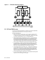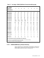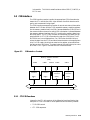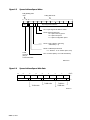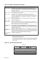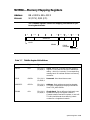
1
AlphaServer 8200/8400
System Technical Manual
Order Number EK–T8030–TM. A01
The Digital AlphaServer 8200 and 8400 systems are designed around the
DECchip 21164 CPU. The TLSB is the system bus that supports nine nodes in
the 8400 system and five nodes in the 8200 system. The AlphaServer 8400 can
be configured with up to six single or dual processor CPU modules (KN7CC),
seven memory modules (MS7CC), and three I/O modules (KFTHA and
KFTIA). One slot is dedicated to I/O and is normally occupied by the integrated I/O module (KFTIA) that supports PCI bus, XMI, and Futurebus+
adapters. All other nodes can be interchangeably configured for CPU or memory modules. The AlphaServer 8200 can be configured with up to three CPU
modules, three memory modules, and three I/O modules.
digital equipment corporation
maynard, massachusetts
First Printing, May 1995
The information in this document is subject to change without notice and should not be construed as a commitment by Digital Equipment Corporation.
Digital Equipment Corporation assumes no responsibility for any errors that may appear in this document.
The software, if any, described in this document is furnished under a license and may be used or copied only
in accordance with the terms of such license. No responsibility is assumed for the use or reliability of software or equipment that is not supplied by Digital Equipment Corporation or its affiliated companies.
Copyright © 1995 by Digital Equipment Corporation.
All Rights Reserved.
Printed in U.S.A.
The following are trademarks of Digital Equipment Corporation: AlphaGeneration, AlphaServer, DEC,
DECchip, DEC LANcontroller, OpenVMS, StorageWorks, VAX, the AlphaGeneration logo, and the DIGITAL
logo.
OSF/1 is a registered trademark of the Open Software Foundation, Inc. Prestoserve is a trademark of Legato
Systems, Inc. UNIX is a registered trademark in the U.S. and other countries, licensed exclusively through
X/Open Company Ltd.
FCC NOTICE: The equipment described in this manual generates, uses, and may emit radio frequency energy. The equipment has been type tested and found to comply with the limits for a Class A computing device pursuant to Subpart J of Part 15 of FCC Rules, which are designed to provide reasonable protection
against such radio frequency interference when operated in a commercial environment. Operation of this
equipment in a residential area may cause interference, in which case the user at his own expense may be
required to take measures to correct the interference.
Contents
Preface ............................................................................................................................................ xv
Chapter 1
1.1
1.2
1.3
1.3.1
1.3.2
1.3.3
1.3.4
1.4
1.5
1.6
1.6.1
1.6.2
1.6.3
1.6.4
1.6.4.1
1.6.4.2
1.6.4.3
Configuration ................................................................................................................ 1-1
Bus Architecture ........................................................................................................... 1-2
CPU Module .................................................................................................................. 1-3
DECchip 21164 ...................................................................................................... 1-3
Backup Cache ......................................................................................................... 1-4
TLSB Interface ....................................................................................................... 1-4
Console Support Hardware .................................................................................... 1-4
Memory Module ............................................................................................................ 1-4
I/O Architecture ............................................................................................................ 1-5
Software ......................................................................................................................... 1-6
Console .................................................................................................................... 1-6
OpenVMS Alpha ..................................................................................................... 1-7
Digital UNIX ........................................................................................................... 1-7
Diagnostics .............................................................................................................. 1-7
ROM-Based Diagnostics .................................................................................. 1-7
Loadable Diagnostic Execution Environment ............................................... 1-8
Online Exercisers ............................................................................................. 1-8
Chapter 2
2.1
2.1.1
2.1.2
2.1.3
2.1.4
2.1.5
2.2
2.2.1
2.2.2
2.2.3
2.2.3.1
2.2.3.2
2.2.3.3
2.2.3.4
2.2.3.5
2.2.4
2.2.4.1
2.2.4.2
Overview
TLSB Bus
Overview ........................................................................................................................ 2-1
Transactions ........................................................................................................... 2-2
Arbitration .............................................................................................................. 2-2
Cache Coherency Protocol ...................................................................................... 2-2
Error Handling ....................................................................................................... 2-2
TLSB Signal List .................................................................................................... 2-3
Operation ....................................................................................................................... 2-5
Physical Node ID .................................................................................................... 2-5
Virtual Node Identification .................................................................................... 2-6
Address Bus Concepts ............................................................................................ 2-6
Memory Bank Addressing Scheme ................................................................. 2-8
CSR Addressing Scheme .................................................................................. 2-8
Memory Bank Address Decoding .................................................................... 2-9
Bank Available Status ................................................................................... 2-11
Address Bus Sequencing ................................................................................ 2-11
Address Bus Arbitration ...................................................................................... 2-12
Initiating Transactions .................................................................................. 2-12
Distributed Arbitration .................................................................................. 2-12
iii
2.2.4.3
Address Bus Transactions ............................................................................. 2-12
2.2.4.4
Module Transactions ...................................................................................... 2-12
2.2.4.5
Address Bus Priority ...................................................................................... 2-12
2.2.4.6
Address Bus Request ..................................................................................... 2-13
2.2.4.7
Asserting Request .......................................................................................... 2-13
2.2.4.8
Early Arbitration ........................................................................................... 2-13
2.2.4.9
False Arbitration Effect on Priority .............................................................. 2-14
2.2.4.10
Look-Back-Two ............................................................................................... 2-14
2.2.4.11
Bank Available Transition ............................................................................ 2-14
2.2.4.12
Bank Collision ................................................................................................ 2-15
2.2.4.13
Bank Lock and Unlock ................................................................................... 2-15
2.2.4.14
CSR Bank Contention .................................................................................... 2-15
2.2.4.15
Command Acknowledge ................................................................................. 2-16
2.2.4.16
Arbitration Suppress ..................................................................................... 2-16
2.2.5
Address Bus Cycles .............................................................................................. 2-16
2.2.6
Address Bus Commands ...................................................................................... 2-17
2.2.7
Data Bus Concepts ............................................................................................... 2-18
2.2.7.1
Data Bus Sequencing ..................................................................................... 2-18
2.2.7.2
Hold ................................................................................................................. 2-18
2.2.7.3
Back-to-Back Return Data ............................................................................ 2-19
2.2.7.4
Back-to-Back Return with HOLD ................................................................. 2-19
2.2.7.5
CSR Data Sequencing .................................................................................... 2-19
2.2.8
Data Bus Functions .............................................................................................. 2-19
2.2.8.1
Data Return Format ...................................................................................... 2-19
2.2.8.2
Sequence Numbers ......................................................................................... 2-20
2.2.8.3
Sequence Number Errors .............................................................................. 2-20
2.2.8.4
Data Field ....................................................................................................... 2-20
2.2.8.5
Data Wrapping ............................................................................................... 2-20
2.2.8.6
ECC Coding .................................................................................................... 2-21
2.2.8.7
ECC Error Handling ...................................................................................... 2-22
2.2.8.8
TLSB_DATA_VALID ..................................................................................... 2-22
2.2.8.9
TLSB_SHARED ............................................................................................. 2-22
2.2.8.10
TLSB_DIRTY ................................................................................................. 2-23
2.2.8.11
TLSB_STATCHK ........................................................................................... 2-23
2.2.9
Miscellaneous Bus Signals ................................................................................... 2-24
2.3
CSR Addressing .......................................................................................................... 2-25
2.3.1
CSR Address Space Regions ................................................................................ 2-26
2.3.2
TLSB Mailboxes .................................................................................................... 2-30
2.3.3
Window Space I/O ................................................................................................. 2-32
2.3.3.1
CSR Write Transactions to Remote I/O Window Space ............................... 2-32
2.3.3.2
CSR Read Transactions to Remote I/O Window Space ................................ 2-32
2.4
TLSB Errors ................................................................................................................ 2-33
2.4.1
Error Categories ................................................................................................... 2-34
2.4.1.1
Hardware Recovered Soft Errors ................................................................. 2-34
2.4.1.2
Software Recovered Soft Errors .................................................................... 2-34
2.4.1.3
Hard Errors .................................................................................................... 2-34
2.4.1.4
System Fatal Errors ....................................................................................... 2-34
2.4.2
Error Signals ......................................................................................................... 2-35
2.4.3
Address Bus Errors .............................................................................................. 2-35
2.4.3.1
Transmit Check Errors .................................................................................. 2-35
2.4.3.2
Command Field Parity Errors ....................................................................... 2-36
2.4.3.3
No Acknowledge Errors ................................................................................. 2-36
2.4.3.4
Unexpected Acknowledge .............................................................................. 2-37
2.4.3.5
Bank Lock Error ............................................................................................. 2-37
2.4.3.6
Bank Available Violation Error ..................................................................... 2-37
2.4.3.7
Memory Mapping Register Error .................................................................. 2-38
iv
2.4.3.8
2.4.3.9
2.4.4
2.4.4.1
2.4.4.2
2.4.4.3
2.4.4.4
2.4.4.5
2.4.4.6
2.4.4.7
2.4.4.8
2.4.5
2.4.6
2.4.6.1
2.4.6.2
Multiple Address Bus Errors ......................................................................... 2-38
Summary of Address Bus Errors .................................................................. 2-38
Data Bus Errors .................................................................................................... 2-39
Single-Bit ECC Errors ................................................................................... 2-40
Double-Bit ECC Errors .................................................................................. 2-40
Illegal Sequence Errors .................................................................................. 2-40
SEND_DATA Timeout Errors ....................................................................... 2-40
Data Status Errors ......................................................................................... 2-41
Transmit Check Errors .................................................................................. 2-41
Multiple Data Bus Errors .............................................................................. 2-41
Summary of Data Bus Errors ........................................................................ 2-42
Additional Status .................................................................................................. 2-42
Error Recovery ...................................................................................................... 2-43
Read Errors .................................................................................................... 2-43
Write Errors ................................................................................................... 2-45
Chapter 3
3.1
3.1.1
3.1.2
3.1.3
3.1.4
3.1.5
3.2
3.2.1
3.2.2
3.3
3.3.1
3.3.2
3.3.2.1
3.3.2.2
3.3.2.3
3.4
3.4.1
3.4.2
3.4.3
3.4.4
3.4.4.1
3.4.4.2
3.5
3.5.1
3.5.1.1
3.5.1.2
3.5.1.3
3.5.1.4
3.5.2
3.5.2.1
3.5.2.2
3.5.2.3
3.5.2.4
3.5.2.5
3.5.3
3.5.4
CPU Module
Major Components ........................................................................................................ 3-1
DECchip 21164 Processor ...................................................................................... 3-2
MMG ...................................................................................................................... 3-3
ADG ........................................................................................................................ 3-3
DIGA ...................................................................................................................... 3-3
B-Cache .................................................................................................................. 3-4
Console ........................................................................................................................... 3-4
Serial ROM Port ..................................................................................................... 3-5
Directly Addressable Console Hardware .............................................................. 3-5
CPU Module Address Space ......................................................................................... 3-6
Memory Space ......................................................................................................... 3-7
I/O Space ................................................................................................................. 3-8
I/O Window Space ............................................................................................ 3-8
TLSB CSR Space ............................................................................................. 3-8
Gbus Space ....................................................................................................... 3-9
CPU Module Window Space Support ......................................................................... 3-10
Window Space Reads ............................................................................................ 3-10
Window Space Writes ........................................................................................... 3-10
Flow Control ......................................................................................................... 3-10
PCI Accesses ......................................................................................................... 3-11
Sparse Space Reads and Writes .................................................................... 3-12
Dense Space Reads and Writes ..................................................................... 3-13
CPU Module Errors ................................................................................................... 3-14
Error Categories ................................................................................................... 3-14
Soft Errors ...................................................................................................... 3-14
Hard Errors .................................................................................................... 3-14
Faults .............................................................................................................. 3-15
Nonacknowledged CSR Reads ....................................................................... 3-16
Address Bus Errors ............................................................................................. 3-16
Transmit Check Errors .................................................................................. 3-17
Command Field Parity Errors ....................................................................... 3-17
No Acknowledge Errors ................................................................................. 3-18
Unexpected Acknowledge Error .................................................................... 3-18
Memory Mapping Register Error .................................................................. 3-18
Data Bus Errors .................................................................................................... 3-18
Multiple Errors ..................................................................................................... 3-19
v
Chapter 4
4.1
4.1.1
4.1.2
4.1.3
4.2
4.2.1
4.2.2
4.2.3
4.2.4
4.2.5
4.2.6
4.2.7
4.2.8
4.2.9
4.2.10
4.3
4.3.1
4.3.1.1
4.3.1.2
4.3.1.3
4.3.2
4.3.3
4.3.4
4.3.5
4.3.6
4.3.6.1
4.3.6.2
4.3.6.3
4.3.6.4
Internal Cache ............................................................................................................... 4-1
Instruction Cache ................................................................................................... 4-1
Data Cache .............................................................................................................. 4-1
Second-Level Cache ................................................................................................ 4-2
Backup Cache ................................................................................................................ 4-2
Cache Coherency .................................................................................................... 4-2
B-Cache Tags .......................................................................................................... 4-3
Updates and Invalidates ........................................................................................ 4-4
Duplicate Tags ........................................................................................................ 4-4
B-Cache States ........................................................................................................ 4-4
B-Cache State Changes ......................................................................................... 4-5
Victim Buffers ......................................................................................................... 4-6
Lock Registers ......................................................................................................... 4-6
Cache Coherency on Processor Writes .................................................................. 4-8
Memory Barriers .................................................................................................... 4-9
Main Memory ................................................................................................................ 4-9
Major Sections ...................................................................................................... 4-10
Control Address Interface ............................................................................. 4-11
Memory Data Interface ................................................................................. 4-11
DRAM Arrays ................................................................................................. 4-12
Memory Organization .......................................................................................... 4-13
Refresh .................................................................................................................. 4-16
Transactions ......................................................................................................... 4-16
ECC Protection ....................................................................................................... 2-2
Self-Test ................................................................................................................ 4-16
Self-Test Modes .............................................................................................. 4-17
Self-Test Error Reporting .............................................................................. 4-18
Self-Test Operation ........................................................................................ 4-18
Self-Test Performance .................................................................................... 4-19
Chapter 5
5.1
5.1.1
5.1.1.1
5.1.1.2
5.1.1.3
5.1.1.4
5.1.1.5
5.1.1.6
5.1.1.7
5.1.1.8
5.1.1.9
5.1.2
5.1.3
5.1.3.1
5.1.3.2
5.1.3.3
5.2
5.2.1
5.2.2
5.2.2.1
5.2.2.2
vi
Memory Subsystem
Memory Interface
Control Address Interface ............................................................................................. 5-1
TLSB Control .......................................................................................................... 5-1
Memory Bank State Machine ........................................................................ 2-11
CSR State Machine ........................................................................................ 2-12
TLSB Input Latches ......................................................................................... 2-5
TLSB Bus Monitor ........................................................................................... 2-6
TLSB Command Decode .................................................................................. 2-6
TLSB Bank Match Logic .................................................................................. 2-8
TLSB Parity Check .......................................................................................... 2-8
TLSB Sequence Control ................................................................................... 2-9
TLSB Bank Available Flags .......................................................................... 2-11
DRAM Control ...................................................................................................... 2-12
Address/RAS Decode Logic .................................................................................. 2-12
128MB/512MB Memory Module Addressing ................................................ 2-12
256MB/1024MB Memory Module Addressing .............................................. 2-13
512MB/2048MB Memory Module Addressing .............................................. 2-13
Memory Data Interface ................................................................................................. 5-9
Data Path Logic .................................................................................................... 2-14
Write Data Input Logic ........................................................................................ 2-14
Write Data Buffer ............................................................................................ 5-9
Write Data Path ECC Algorithm .................................................................. 2-15
5.2.2.3
5.2.2.4
5.2.2.5
5.2.3
5.2.3.1
5.2.3.2
5.2.3.3
5.2.4
5.3
5.3.1
5.3.1.1
5.3.1.2
5.3.1.3
5.3.1.4
5.3.2
5.3.2.1
5.3.2.2
5.3.2.3
5.3.2.4
CSR Write Data ECC Check ......................................................................... 5-10
Forcing Write Errors for Diagnostics ............................................................ 2-15
Write Data Out Selection .............................................................................. 2-15
Read Data Output Logic ....................................................................................... 2-16
Read Data Buffers .......................................................................................... 2-16
Read Data Path ECC Algorithm ................................................................... 5-11
CSR Read Data ECC ...................................................................................... 2-17
MDI Error Detection and Correction Logic ......................................................... 2-17
CSR Interface .............................................................................................................. 5-13
CTL CSR Functions .............................................................................................. 2-18
TLSB CSR Control ......................................................................................... 2-18
MAI CSR Sequencer ............................................................................... 5-15
CSR Multiplexing ........................................................................................... 2-19
CSRCA Parity ................................................................................................ 2-19
MDI CSR Functions ............................................................................................. 2-19
MDI CSR Sequencer ...................................................................................... 2-19
Merge Register ............................................................................................... 2-20
CSR Multiplexing ........................................................................................... 2-20
CSRCA Parity ................................................................................................ 2-20
Chapter 6
6.1
6.2
6.3
6.3.1
6.3.2
6.3.2.1
6.3.2.2
6.3.3
6.3.3.1
6.3.3.2
6.3.4
6.3.5
6.3.6
6.3.6.1
6.3.6.2
6.3.7
6.4
6.4.1
6.4.2
6.4.2.1
6.4.2.2
6.4.3
6.5
6.5.1
6.5.1.1
6.5.1.2
6.5.1.3
6.5.2
6.5.2.1
6.5.2.2
6.5.2.3
6.5.2.4
6.5.2.5
I/O Port
Configuration ................................................................................................................ 6-2
I/O Port Main Components ........................................................................................... 6-2
I/O Port Transactions ................................................................................................... 6-3
Mailbox Transactions ............................................................................................. 6-5
I/O Window Space Transactions ............................................................................ 6-7
CSR Write Transactions to I/O Window Space .............................................. 6-7
CSR Read Transactions to I/O Window Space ............................................... 6-8
Interrupt Transactions ........................................................................................... 6-8
Remote Bus Interrupts .................................................................................... 6-8
I/O Port Generated Error Interrupts .............................................................. 6-9
DMA Read Transactions ...................................................................................... 6-10
DMA Interlock Read Transactions ...................................................................... 6-10
DMA Write Transactions ..................................................................................... 6-11
DMA Unmasked Write .................................................................................. 6-12
DMA Masked Write Request to Memory ...................................................... 6-12
Extended NVRAM Write Transactions ............................................................... 6-13
Addressing ................................................................................................................... 6-14
Accessing Remote I/O Node CSRs Through Mailboxes ...................................... 6-14
Accessing Remote I/O Node CSRs Through Direct I/O Window Space ............. 6-15
Sparse Address Space Reads ......................................................................... 6-15
Sparse Address Space Writes ........................................................................ 6-17
Dense Address Space Transactions ..................................................................... 6-20
TLSB Interface ............................................................................................................ 6-23
Transactions ......................................................................................................... 6-23
DMA Transactions ......................................................................................... 6-24
Interrupt Transactions ................................................................................. 6-26
CSR Transactions .......................................................................................... 6-28
TLSB Arbitration .................................................................................................. 6-30
Node 8 I/O Port Arbitration Mode Selection ................................................. 6-31
Read-Modify-Write ......................................................................................... 6-33
Bank Collision Effect on Priority .................................................................. 6-34
Look-Back-Two ............................................................................................... 6-34
Arbitration Suppress ..................................................................................... 6-34
vii
6.5.3
Error Detection Schemes ..................................................................................... 6-34
6.6
Hose Interface ............................................................................................................. 6-35
6.6.1
Hose Protocol ....................................................................................................... 6-35
6.6.2
Window Space Mapping ....................................................................................... 6-36
6.6.2.1
Sparse Address Mapping ............................................................................... 6-37
6.6.2.2
Dense Address Mapping ................................................................................ 6-37
6.6.3
Hose Signals ......................................................................................................... 6-37
6.6.4
Hose Packet Specifications ................................................................................... 6-39
6.6.4.1
Down Hose Packet Specifications ................................................................. 6-39
6.6.4.2
Up Hose Packet Specifications ...................................................................... 6-52
6.6.5
Hose Errors ........................................................................................................... 6-65
6.7
I/O Port Error Handling ............................................................................................. 6-66
6.7.1
Soft TLSB Errors Recovered by Hardware ......................................................... 6-66
6.7.2
Hard TLSB Errors ................................................................................................ 6-66
6.7.3
System Fatal Errors ............................................................................................. 6-66
6.7.4
Hard Internal I/O Port Errors ............................................................................. 6-66
6.7.5
Error Reporting .................................................................................................... 6-67
6.7.5.1
TLSB_DATA_ERROR .................................................................................... 6-67
6.7.5.2
TLSB_FAULT ................................................................................................ 6-68
6.7.6
IPL 17 Error Interrupts ....................................................................................... 6-69
6.7.7
Address Bus Errors .............................................................................................. 6-70
6.7.7.1
TLSB Address Transmit Check Errors ......................................................... 6-70
6.7.7.2
Address Bus Parity Errors ............................................................................ 6-71
6.7.7.3
No Acknowledge Errors ................................................................................. 6-71
6.7.7.4
Unexpected Acknowledge .............................................................................. 6-71
6.7.7.5
Bank Busy Violation ...................................................................................... 6-71
6.7.7.6
Memory Mapping Register Error .................................................................. 6-71
6.7.8
Data Bus Errors .................................................................................................... 6-72
6.7.8.1
Single-Bit ECC Errors ................................................................................... 6-72
6.7.8.2
Double-Bit ECC Errors .................................................................................. 6-72
6.7.8.3
Illegal Sequence Errors .................................................................................. 6-73
6.7.8.4
SEND_DATA Timeout Errors ....................................................................... 6-73
6.7.8.5
Data Status Errors ......................................................................................... 6-73
6.7.8.6
Transmit Check Errors .................................................................................. 6-74
6.7.8.7
Multiple Data Bus Errors .............................................................................. 6-74
6.7.9
Additional TLSB Status ....................................................................................... 6-74
6.7.10
Hard I/O Port Errors ............................................................................................ 6-75
6.7.10.1
Up Hose Errors............................................................................................... 6-75
6.7.10.2
Up Turbo Vortex Errors ................................................................................ 6-75
6.7.10.3
Down Turbo Vortex Errors ............................................................................ 6-76
6.7.11
Miscellaneous I/O Port Errors ............................................................................. 6-77
6.7.11.1
CSR Bus Parity Errors .................................................................................. 6-77
6.7.11.2
Unexpected Mailbox Status Packet .............................................................. 6-77
6.7.11.3
ICR and IDR Internal Illogical Errors .......................................................... 6-77
6.7.11.4
Hose Status Change Errors ........................................................................... 6-78
6.8
KFTIA Overview ......................................................................................................... 6-78
6.8.1
Integrated I/O Section ......................................................................................... 6-80
6.8.1.1
PCI Interface .................................................................................................. 6-81
6.8.1.2
SCSI Ports ..................................................................................................... 6-82
6.8.1.3
Ethernet Ports ................................................................................................ 6-83
6.8.1.4
Optional NVRAM Daughter Card ................................................................ 6-83
6.8.2
Integrated I/O Section Transactions ................................................................... 6-83
6.8.2.1
DMA Transactions ......................................................................................... 6-83
6.8.2.2
Mailbox Transaction ...................................................................................... 6-84
6.8.2.3
CSR Transactions ......................................................................................... 6-84
6.8.2.4
Interrupt Transactions .................................................................................. 6-84
viii
Chapter 7
7.1
7.2
7.3
7.4
7.5
System Registers
Register Conventions .................................................................................................... 7-1
Register Address Mapping ........................................................................................... 7-2
TLSB Registers ............................................................................................................. 7-4
TLDEV—Device Register ...................................................................................... 7-5
TLBER—Bus Error Register ................................................................................. 7-7
TLCNR—Configuration Register ........................................................................ 7-14
TLVID—Virtual ID Register ............................................................................... 7-19
TLMMRn—Memory Mapping Registers ............................................................ 7-21
TLFADRn—Failing Address Registers .............................................................. 7-24
TLESRn—Error Syndrome Registers ................................................................ 7-26
TLILIDn—Interrupt Level IDENT Registers .................................................... 7-30
TLCPUMASK—CPU Interrupt Mask Register ................................................. 7-31
TLMBPR—Mailbox Pointer Registers ................................................................ 7-32
TLIPINTR—Interprocessor Interrupt Register .................................................. 7-35
TLIOINTRn—I/O Interrupt Registers ............................................................... 7-36
TLWSDQR4-8—Window Space Decr Queue Counter Registers ....................... 7-38
TLRMDQRX—Memory Channel Decr Queue Counter Register X ................... 7-39
TLRMDQR8—Memory Channel Decr Queue Counter Register 8 .................... 7-40
TLRDRD—CSR Read Data Return Data Register ............................................. 7-41
TLRDRE—CSR Read Data Return Error Register ........................................... 7-42
TLMCR—Memory Control Register .................................................................... 7-43
CPU Module Registers ................................................................................................ 7-44
TLDIAG—Diagnostic Setup Register ................................................................. 7-47
TLDTAGDATA—DTag Data Register ................................................................ 7-50
TLDTAGSTAT—DTag Status Register .............................................................. 7-51
TLMODCONFIG—CPU Module Configuration Register ................................. 7-52
TLEPAERR— ADG Error Register .................................................................... 7-54
TLEPDERR—DIGA Error Register ................................................................... 7-57
TLEPMERR—MMG Error Register ................................................................... 7-59
TLEP_VMG—Voltage Margining Register ......................................................... 7-62
TLINTRMASK0–1—Interrupt Mask Registers ................................................. 7-63
TLINTRSUM0–1—Interrupt Source Registers ................................................. 7-65
TLCON00,01,10,11—Console Communications Regs ........................................ 7-68
TLCON0A,0B,0C,1A,1B,1C—DIGA Comm. Test Regs ...................................... 7-69
RM_RANGE_nA,B—Memory Channel Range Regs ........................................... 7-70
TLDMCMD—Data Mover Command Register ................................................... 7-72
TLDMADRA—Data Mover Source Address Register ........................................ 7-75
TLDMADRB—Data Mover Destination Address Reg ....................................... 7-76
GBUS$WHAMI ..................................................................................................... 7-77
GBUS$LED0,1,2 ................................................................................................... 7-78
GBUS$MISCR ...................................................................................................... 7-79
GBUS$MISCW ..................................................................................................... 7-81
GBUS$TLSBRST .................................................................................................. 7-82
GBUS$SERNUM .................................................................................................. 7-83
Memory-Specific Registers ......................................................................................... 7-85
SECR—Serial EEPROM Control/Data Register ............................................... 7-86
MIR—Memory Interleave Register .................................................................... 7-87
MCR—Memory Configuration Register .............................................................. 7-89
STAIR—Self-Test Address Isolation Register ................................................... 2-24
STER—Self-Test Error Register .......................................................................... 2-24
MER—Memory Error Register ............................................................................ 7-97
MDRA—Memory Diagnostic Register A ............................................................ 2-26
MDRB—Memory Diagnostic Register B ........................................................... 7-102
STDERA,B,C,D,E—Self-Test Data Error Registers ........................................ 7-103
ix
7.6
7.7
DDR0:3—Data Diagnostic Registers ................................................................ 7-106
I/O Port-Specific Registers ........................................................................................ 7-109
RMRR0-1—Memory Channel Range Registers ................................................ 7-110
ICCMSR—I/O Control Chip Mode Select Register ........................................... 7-112
ICCNSE—I/O Control Chip Node-Specific Error Reg ...................................... 7-117
ICCDR—I/O Control Chip Diagnostic Register ................................................ 7-122
ICCMTR—I/O Control Chip Mailbox Transaction Reg .................................... 7-125
ICCWTR—I/O Control Chip Window Transaction Reg .................................... 7-127
IDPNSE0–3—I/O Data Path Node-Specific Error Regs .................................. 7-128
IDPDRn—I/O Data Path Diagnostic Registers ................................................. 7-133
IDPVR—I/O Data Path Vector Register .......................................................... 7-137
IDPMSR—I/O Data Path Mode Select Register ............................................... 7-138
IBR—Information Base Repair Register ........................................................... 7-140
KFTIA Specific Registers .......................................................................................... 7-142
Chapter 8
8.1
8.1.1
8.1.2
8.1.3
8.2
8.3
8.3.1
8.3.1.1
8.3.1.2
8.3.1.3
8.3.1.4
8.3.2
8.3.3
8.3.4
8.3.5
Interrupts
Vectored Interrupts ....................................................................................................... 8-1
I/O Port Interrupt Rules ......................................................................................... 8-1
CPU Interrupt Rules .............................................................................................. 8-2
I/O Port Interrupt Operation ................................................................................. 8-2
Nonvectored Interrupts ................................................................................................ 8-3
I/O Interrupt Mechanism ............................................................................................. 8-3
TLSB Principles for Interrupts .............................................................................. 8-3
Virtual Node Identification - TLVID ............................................................... 8-4
Directing Interrupts - TLCPUMASK .............................................................. 8-4
Directing Interrupts - TLINTRMASK ............................................................ 8-4
Interrupt Registers - TLIOINTR4–8 ............................................................... 8-4
Generating Interrupts ............................................................................................ 8-5
Servicing Interrupts ............................................................................................... 8-5
Interprocessor Interrupts ....................................................................................... 8-5
Module-Level Interrupts ........................................................................................ 8-6
Glossary
Figures
1-1
2-1
2-2
2-3
2-4
2-5
2-6
2-7
3-1
3-2
3-3
3-4
3-5
4-1
4-2
x
AlphaServer 8400 System Block Diagram .............................................................. 1-2
TLSB Memory Address Bit Mapping ...................................................................... 2-7
Address Decode ....................................................................................................... 2-10
64-Bit ECC Coding Scheme ................................................................................... 2-21
TLSB CSR Address Bit Mapping .......................................................................... 2-26
TLSB CSR Space Map ............................................................................................ 2-27
Mailbox Data Structure ......................................................................................... 2-30
TLRDRD Register .................................................................................................. 2-33
CPU Module Simple Block Diagram ....................................................................... 3-2
Physical Address Space Map ................................................................................... 3-6
TLSB CSR Space Map .............................................................................................. 3-8
Gbus Map .................................................................................................................. 3-9
PCI Programmer’s Address .................................................................................... 3-11
Cache Index and Tag Mapping to Block Address (4MB) ........................................ 4-3
Cache Index and Tag Mapping to Block Address (1MB) ........................................ 4-3
4-3
4-4
4-5
4-6
4-7
5-1
5-2
5-3
6-1
6-2
6-3
6-4
6-5
6-6
6-7
6-8
6-9
6-10
6-11
6-12
6-13
6-14
6-15
6-16
6-17
6-18
6-19
6-20
6-21
6-22
6-23
6-24
6-25
6-26
6-27
6-28
6-29
6-30
6-31
6-32
6-33
6-34
6-35
7-1
Cache Index and Tag Mapping to Block Address (16MB) ...................................... 4-4
Memory Module Block Diagram ............................................................................ 4-10
Two-Way Interleave of a 128-Mbyte DRAM Array .............................................. 4-14
Interleaving Different Size Memory Modules ....................................................... 4-14
Eight-Way System Interleave of Four 128-Mbyte Memory Modules .................. 4-15
64-Bit ECC Coding Scheme ................................................................................... 5-10
CSR Interface Context ........................................................................................... 5-13
CSRCA Encoding .................................................................................................... 5-14
I/O Subsystem Block Diagram ................................................................................. 6-1
I/O Port Block Diagram ............................................................................................ 6-3
Sparse Address Space Reads ................................................................................. 6-16
Sparse Window Read Data as Presented on the TLSB ........................................ 6-16
Sparse Address Space Writes ................................................................................ 6-18
Sparse Address Space Write Data ......................................................................... 6-18
Dense Address Space Transactions ....................................................................... 6-20
Dense Address Space Write Data .......................................................................... 6-22
Dense Window Read Data as Presented on the TLSB ......................................... 6-22
Write CSR (Interrupt) Data Format ................................................................... 6-27
Minimum Latency Mode ...................................................................................... 6-32
Minimum Latency Mode Timing Example ......................................................... 6-32
Toggle 50% High/50% Low Mode ......................................................................... 6-33
Mailbox Command Packet ................................................................................... 6-41
DMA Read Data Return Packet .......................................................................... 6-42
DMA Read Data Return Packet with Error ........................................................ 6-44
INTR/IDENT Status Return Packet ................................................................... 6-45
Sparse Window Read Command Packet ............................................................. 6-45
Sparse Window Write Command Packet ............................................................ 6-47
Dense Window Read Command Packet .............................................................. 6-48
Dense Window Write Command Packet ............................................................. 6-50
Byte Mask Field .................................................................................................... 6-51
Memory Channel Write Packet ........................................................................... 6-52
Mailbox Status Return Packet ............................................................................. 6-53
DMA Read Packet ................................................................................................ 6-54
Interlock Read Packet .......................................................................................... 6-56
DMA Masked Write Packet ................................................................................. 6-57
DMA Unmasked Write Packet ............................................................................ 6-59
INTR/IDENT Status Return Packet ................................................................... 6-60
Sparse Window Read Data Return Packet ......................................................... 6-61
Dense Window Read Data Return Packet .......................................................... 6-63
Window Write Status Return Packet .................................................................. 6-64
KFTIA Connections .............................................................................................. 6-78
KFTIA Block Diagram ......................................................................................... 6-79
Integrated I/O Section of the KFTIA ................................................................... 6-81
Mailbox Data Structure ......................................................................................... 7-33
Tables
1
2
2-1
2-2
2-3
2-4
2-5
2-6
Digital AlphaServer 8200/8400 Documentation ......................................................... xvii
Related Documents ....................................................................................................... xix
TLSB Bus Signals ......................................................................................................... 2-3
TLSB Physical Node Identification .............................................................................. 2-5
Interleave Field Values for Two-Bank Memory Modules ........................................... 2-9
TLSB Address Bus Commands .................................................................................. 2-17
TLSB Data Wrapping ................................................................................................. 2-21
CSR Address Space Regions ....................................................................................... 2-26
xi
2-7
2-8
2-9
2-10
2-11
2-12
3-1
3-2
3-3
3-4
3-5
3-6
4-1
4-2
4-3
4-4
4-5
4-6
4-7
4-8
5-1
5-2
5-3
5-4
5-5
5-6
5-7
6-1
6-2
6-3
6-4
6-5
6-6
6-7
6-8
6-9
6-10
6-11
6-12
6-13
6-14
6-15
6-16
6-17
6-18
6-19
6-20
6-21
6-22
6-23
6-24
6-25
6-26
6-27
6-28
6-29
xii
TLSB Node Base Addresses ....................................................................................... 2-28
TLSB CSR Address Mapping ..................................................................................... 2-29
Mailbox Data Structure .............................................................................................. 2-31
Address Bus Error Summary ..................................................................................... 2-39
Signals Covered by TLESRn Registers ...................................................................... 2-39
Data Bus Error Summary .......................................................................................... 2-42
Directly Addressable Console Hardware ..................................................................... 3-6
TLSB Wrapping ........................................................................................................... 3-7
CPU Module Wrapping ................................................................................................ 3-7
Decrement Queue Counter Address Assignments .................................................... 3-11
PCI Address Bit Descriptions ..................................................................................... 3-12
Valid Values for Address Bits <6:5> .......................................................................... 3-13
B-Cache States .............................................................................................................. 4-5
State Transition Due to Processor Activity ................................................................. 4-7
State Transition Due to TLSB Activity ....................................................................... 4-8
CPU Module Response to Lock Register and Victim Buffer Address Hits ................ 4-8
Memory Array Capacity ............................................................................................. 4-13
Self-Test Error Registers ............................................................................................ 4-18
Self-Test Times: Normal Mode ................................................................................... 4-19
Self-Test Times: Moving Inversion, No Errors Found .............................................. 4-20
TLSB Command Encoding ........................................................................................... 5-3
Two Strings—128MB/512MB Row/Column Address Bit Swapping ........................... 5-6
Four Strings—256MB/1024MB Row/Column Address Bit Swapping ........................ 5-7
Eight Strings—512MB/2048MB Row/Column Address Bit Swapping ...................... 5-8
Error Conditions Monitored by the MDIs .................................................................. 5-12
CSRCA Addressing ..................................................................................................... 5-15
CSRCA Data Bus Master ........................................................................................... 5-17
I/O Port Transaction Types .......................................................................................... 6-5
TLMBPR Register Map .............................................................................................. 6-15
Sparse Address Space Read Field Descriptions ........................................................ 6-17
Sparse Address Space Write Field Descriptions ....................................................... 6-19
Sparse Address Write Length Encoding .................................................................... 6-20
Dense Address Space Transaction Field Descriptions .............................................. 6-21
Transaction Types Supported by the I/O Port ........................................................... 6-24
Wrapped Reads ........................................................................................................... 6-25
I/O Adapter to Memory Write Types .......................................................................... 6-26
Down Hose Signals ..................................................................................................... 6-38
Up Hose Signals .......................................................................................................... 6-38
UPCTL<3:0> Encoding ............................................................................................... 6-39
Hose Status Signals .................................................................................................... 6-40
Down Hose Packet Type Codes .................................................................................. 6-40
Mailbox Command Packet Description ...................................................................... 6-42
DMA Read Data Return Packet Description ............................................................. 6-43
DMA Read Data Return Packet with Error Description .......................................... 6-44
INTR/IDENT Status Return Packet Description ...................................................... 6-45
Sparse Window Read Command Packet Description ................................................ 6-46
Sparse Window Write Command Packet Description ............................................... 6-48
Dense Window Read Command Packet Description ................................................. 6-49
Dense Window Write Command Packet Description ................................................ 6-51
Memory Channel Write Packet Description .............................................................. 6-53
Mailbox Status Return Packet Description ............................................................... 6-54
DMA Read Packet Description ................................................................................... 6-55
DMA Read Packet Sizes ............................................................................................. 6-55
Interlock Read Packet Description ............................................................................. 6-56
Interlock Read Packet Size ......................................................................................... 6-56
DMA Masked Write Packet Description .................................................................... 6-58
6-30
6-31
6-32
6-33
6-34
6-35
6-36
7-1
7-2
7-3
7-4
7-5
7-6
7-7
7-8
7-9
7-10
7-11
7-12
7-13
7-14
7-15
7-16
7-17
7-18
7-19
7-20
7-21
7-22
7-23
7-24
7-25
7-26
7-27
7-28
7-29
7-30
7-31
7-32
7-33
7-34
7-35
7-36
7-37
7-38
7-39
7-40
7-41
7-42
7-43
7-44
7-45
7-46
7-47
7-48
7-49
DMA Masked Write Packet Sizes .............................................................................. 6-58
DMA Unmasked Write Packet Description ............................................................... 6-60
INTR/IDENT Status Return Packet Description ...................................................... 6-61
Sparse Window Read Data Return Packet Description ............................................ 6-62
Dense Window Read Data Return Packet Description ............................................. 6-63
Window Write Status Return Packet Description .................................................... 6-64
PCI 0 and PCI 1 Interrupt Priority ............................................................................ 6-85
TLSB Node Space Base Addresses ............................................................................... 7-3
TLSB Registers ............................................................................................................. 7-4
TLDEV Register Bit Definitions .................................................................................. 7-5
TLBER Register Bit Definitions ................................................................................... 7-8
TLCNR Register Bit Definitions ................................................................................ 7-15
TLVID Register Bit Definitions ................................................................................. 7-20
TLMMRn Register Bit Definitions ............................................................................. 7-21
Interleave Field Values for Two-Bank Memory Modules ......................................... 7-22
Address Ranges Selected by ADRMASK Field Values ............................................. 7-23
TLFADRn Register Bit Definitions ............................................................................ 7-24
TLESRn Register Bit Definitions ............................................................................... 7-26
TLILIDn Register Bit Definitions .............................................................................. 7-30
TLCPUMASK Register Bit Definitions ..................................................................... 7-31
TLMBPR Register Bit Definitions ............................................................................. 7-32
Mailbox Data Structure Description .......................................................................... 7-33
TLIPINTR Register Bit Definitions ........................................................................... 7-35
TLI/OINTR Register Bit Definitions .......................................................................... 7-36
TLRDRD Register Bit Definitions .............................................................................. 7-41
TLMCR Register Bit Definitions ................................................................................ 7-43
CPU Module Registers ................................................................................................ 7-45
Gbus Registers ............................................................................................................ 7-46
TLDIAG Register Bit Definitions ............................................................................... 7-47
TLDTAGDATA Register Bit Definitions ................................................................... 7-50
TLDTAGSTAT Register Bit Definitions .................................................................... 7-51
TLMODCONFIG Register Bit Definitions ................................................................ 7-52
TLEPAERR Register Bit Definitions ......................................................................... 7-55
TLEPDERR Register Bit Definitions ......................................................................... 7-58
TLEPMERR Register Bit Definitions ........................................................................ 7-60
TLEP_VMG Register Bit Definitions ......................................................................... 7-62
TLEPDERR Register Bit Definitions ......................................................................... 7-64
TLINTRSUM Register Bit Definitions ...................................................................... 7-66
Memory Channel Range Register Bit Definitions ..................................................... 7-71
TLDMCMD Register Bit Definitions ......................................................................... 7-73
TLDMADRA Register Bit Definitions ........................................................................ 7-75
TLDMADRB Register Bit Definitions ........................................................................ 7-76
GBUS$WHAMI Register Bit Definitions ................................................................... 7-77
GBUS$MISCR Register Bit Definitions .................................................................... 7-80
GBUS$MISCW Register Bit Definitions ................................................................... 7-81
GBUS$SERNUM Register Bit Definitions ................................................................ 7-83
Memory-Specific Registers ......................................................................................... 7-85
SECR Register Bit Definitions ................................................................................... 7-86
MIR Register Bit Definitions ...................................................................................... 7-88
MCR Register Bit Definitions ..................................................................................... 7-90
STAIR Register Bit Definitions .................................................................................. 7-93
STAIR Register Bit Correspondence of Memory Address Segments ....................... 7-94
STER Register Bit Definitions ................................................................................... 7-96
MER Register Bit Definitions ..................................................................................... 7-97
MDRA Register Bit Definitions .................................................................................. 7-98
MDRB Register Bit Definitions ................................................................................ 7-102
xiii
7-50
7-51
7-52
7-53
7-54
7-55
7-56
7-57
7-58
7-59
7-60
7-61
7-62
7-63
7-64
7-65
8-1
xiv
STDER A, B, C, D Register Bit Definitions ............................................................. 7-104
STDERE Register Bit Definitions ............................................................................ 7-105
DDRn Register Bit Definitions ................................................................................. 7-106
I/O Port-Specifc Registers ......................................................................................... 7-109
RMRR0-1 Register Bit Definitions ........................................................................... 7-111
ICCMSR Register Bit Definitions ............................................................................ 7-112
ICCNSE Register Bit Definitions ............................................................................. 7-118
ICCDR Register Bit Definitions ............................................................................... 7-123
ICCMTR Register Bit Definitions ............................................................................ 7-126
ICCWTR Register Bit Definitions ............................................................................ 7-127
IDPNSE0–3 Register Bit Definitions ....................................................................... 7-129
IDPDR0–3 Register Bit Definitions ......................................................................... 7-134
Error Matrix for Force Error Bits ............................................................................ 7-136
IDPVR Register Bit Definitions ............................................................................... 7-137
IDPMSR Register Bit Definitions ............................................................................ 7-139
IBR Register Bit Definitions .................................................................................... 7-141
CPU Module Interrupts ................................................................................................ 8-6
Preface
Intended Audience
This manual is intended for developers of system software and for service
personnel. It discusses the AlphaServer 8200/8400 systems that are designed around the DECchip 21164 CPU and use the TLSB bus as the main
communication path between all the system modules. The manual describes the operations of all components of the system: the TLSB bus,
CPU modules, memory modules, and the I/O modules. It discusses in detail the functions of all registers in the system. When necessary, the manual refers the reader to other documents for more elaborate discussions or
for specific information. Thus, the manual does not give the register files
of PCI bus devices but indicates sources where information can be found.
The manual assumes programming knowledge at machine language level
and familiarity with the OpenVMS Alpha and Digital UNIX (formerly
DEC OSF/1) operating systems.
Document Structure
The material is presented in eight chapters.
Chapter 1, Overview, presents an overall introduction to the server system.
Chapter 2, TLSB Bus, describes the main communication path of the system. It discusses the operations of the address bus and the data bus, CSR
addressing, and errors that can occur during bus transactions.
Chapter 3, CPU Module, describes the major components and operations
of the CPU module. It explains the CPU module’s memory and I/O address
spaces, and gives a summary of the errors detected by the CPU module.
Chapter 4, Memory Subsystem, describes the structure of the memory
hierarchy from the system perspective. The memory hierarchy comprises
the DECchip 21164 internal cache, the second-level cache implemented on
the CPU chip, the backup cache implemented on the CPU module, and the
main memory that is implemented as a separate module and forms a node
on the TLSB bus. The chapter provides a discussion of the various ways
main memory can be organized to optimize access time.
Chapter 5, Memory Interface, describes the various components of the
memory module, the memory data interface, and how the CSR interface
manages the transfer of information between the TLSB bus and the TLSB
accessible memory module registers.
Chapter 6, I/O Port, describes the configuration of the I/O port and the
main components of the I/O subsystem (KFTHA and KFTIA modules). It
discusses addressing of memory and I/O devices and accessing of remote
I/O node CSRs through mailboxes and direct I/O window space. The
xv
KFTIA and KFTHA support the PCI bus, XMI bus, and the Futurebus+,
depending on the system in which they are used. The chapter describes
the transaction types on the TLSB interface and the hose interface. It presents a brief survey of the integrated I/O port (KFTIA). The survey focuses
mainly on the integrated I/O section of the module, which provides two PCI
buses that support ports for PCI devices such as Ethernet, SCSI, FDDI,
and NVRAM. The chapter also discusses the types of errors that affect the
hoses and how the I/O port handles errors.
Chapter 7, System Registers, describes in detail the functions of the system registers, which include the TLSB bus registers, CPU module registers, memory module registers, and I/O port registers. For KFTIA registers and device registers supported by the integrated I/O port, the reader is
referred to source material. This chapter is the only place where functions
of all registers are discussed fully at the bit level.
Chapter 8, Interrupts, gives an overview of various interrupts within the
system. It discusses vectored and nonvectored interrupts, interrupt rules,
mechanisms, and service.
Terminology
Results of operations termed Unpredictable may vary from moment to
moment, implementation to implementation, and instruction to instruction
within implementations. Software must never use Unpredictable results.
Operations termed Undefined may vary from moment to moment, implementation to implementation, and instruction to instruction within implementations. Undefined operations may halt the processor or cause it to
lose information. However, they do not cause the processor to hang; that
is, reach a state from which there is no transition to a normal state of instruction execution. Nonprivileged software cannot invoke Undefined operations.
Documentation Titles
Table 1 lists the books in the Digital AlphaServer 8200 and 8400 documentation set.
xvi
Table 1 Digital AlphaServer 8200/8400 Documentation
Title
Order Number
Hardware User Information and Installation
Operations Manual
EK–T8030–OP
Site Preparation Guide
EK–T8030–SP
AlphaServer 8200 Installation Guide
EK–T8230–IN
AlphaServer 8400 Installation Guide
EK–T8430–IN
Service Information Kit
QZ–00RAC–GC
Service Manual (hard copy)
EK–T8030–SV
Service Manual (diskette)
AK–QKNFA–CA
Reference Manuals
System Technical Manual
EK–T8030–TM
DWLPA PCI Adapter Technical Manual
EK–DWLPA–TM
Upgrade Manuals for Both Systems
KN7CC CPU Module Installation Card
EK–KN7CC–IN
MS7CC Memory Installation Card
EK–MS7CC–IN
KFTHA System I/O Module Installation Guide
EK–KFTHA–IN
KFTIA Integrated I/O Module Installation Guide
EK–KFTIA–IN
Upgrade Manuals: 8400 System Only
AlphaServer 8400 Upgrade Manual
EK–T8430–UI
BA654 DSSI Disk PIU Installation Guide
EK–BA654–IN
BA655 SCSI Disk and Tape PIU Installation Guide
EK–BA655–IN
DWLAA Futurebus+ PIU Installation Guide
EK–DWLAA–IN
DWLMA XMI PIU Installation Guide
EK–DWLMA–IN
DWLPA PCI PIU Installation Guide
EK–DWL84–IN
H7237 Battery PIU Installation Guide
EK–H7237–IN
H7263 Power Regulator Installation Card
EK–H7263–IN
H9F00 Power Upgrade Manual
EK–H8463–UI
KFMSB Adapter Installation Guide
EK–KFMSB–IN
xvii
Table 1 Digital AlphaServer 8200/8400 Documentation (Continued)
Title
Order Number
KZMSA Adapter Installation Guide
EK–KXMSX–IN
RRDCD Installation Guide
EK–RRDRX–IN
Upgrade Manuals: 8200 System Only
DWLPA PCI Shelf Installation Guide
EK–DWL82–IN
H7266 Power Regulator Installation Card
EK–H7266–IN
H7267 Battery Backup Installation Card
EK–H7267–IN
xviii
Table 2 Related Documents
Title
Order Number
General Site Preparation
Site Environmental Preparation Guide
EK–CSEPG–MA
System I/O Options
BA350 Modular Storage Shelf Subsystem
Configuration Guide
EK–BA350–CG
BA350 Modular Storage Shelf Subsystem
User’s Guide
EK–BA350–UG
BA350-LA Modular Storage Shelf User’s Guide
EK–350LA–UG
CIXCD Interface User Guide
EK–CIXCD–UG
DEC FDDIcontroller 400 Installation/Problem Solving
EK–DEMFA–IP
DEC FDDIcontroller/Futurebus+ Installation Guide
EK–DEFAA–IN
DEC FDDIcontroller/PCI User Information
EK–DEFPA–IN
DEC LANcontroller 400 Installation Guide
EK–DEMNA–IN
DSSI VAXcluster Installation/Troubleshooting Manual
EK–410AA–MG
EtherWORKS Turbo PCI User Information
EK–DE435–OM
KZPSA PCI to SCSI User’s Guide
EK–KZPSA–UG
RF Series Integrated Storage Element User Guide
EK–RF72D–UG
StorageWorks RAID Array 200 Subsystem Family
Installation and Configuration Guide
EK–SWRA2–IG
StorageWorks RAID Array 200 Subsystem Family
Software User’s Guide for OpenVMS AXP
AA–Q6WVA–TE
StorageWorks RAID Array 200 Subsystem Family
Software User’s Guide for DEC OSF/1
AA–Q6TGA–TE
Operating System Manuals
Alpha Architecture Reference Manual
EY–L520E–DP
DEC OSF/1 Guide to System Administration
AA–PJU7A–TE
Guide to Installing DEC OSF/1
AA–PS2DE–TE
OpenVMS Alpha Version 6.2 Upgrade and Installation Manual
AA–PV6XC–TE
Engineering Specifications
TurboLaser System Bus (TLSB) Specification
TurboLaser EV5 Dual-Processor Module Specification
DECchip 21164 Functional Specification
DC287 Ethernet Controller 21040 Engineering Specification
21041-AA Integrated FDDI Controller Advanced Information
PCI NVRAM Engineering Specification
NCR 53C810 PCI–SCSI I/O Processor Data Manual
xix
Chapter 1
Overview
The computer system is an AlphaGeneration server very similar to but
with twice the performance of DEC 7000/10000 systems. It is built around
the TLSB bus and supports the OpenVMS Alpha and Digital UNIX operating systems. It is manufactured in two models: AlphaServer 8200 and AlphaServer 8400. The AlphaServer 8400 features nine nodes, while AlphaServer 8200 supports only five nodes.
The system uses three types of modules:
•
CPU modules, each containing one or two DECchip 21164 CPUs
•
Memory modules
•
I/O ports that interface to other I/O buses (XMI, Futurebus+,and PCI)
NOTE: Unless otherwise specified, all discussions in this manual apply to both AlphaServer systems.
1.1 Configuration
The system provides a wide range of configuration flexibility:
•
A 9-slot system centerplane bus that supports up to nine CPU, memory, or I/O nodes, and can operate at speeds ranging from 10 ns (100
MHz) to 30 ns (33.33 MHz).
•
The system supports from one to 12 DECchip 21164 CPUs. Each CPU
has a 4-Mbyte backup cache. The CPU module design supports a range
of processor clocks from 7.0 ns (142.9 MHz) to 2.8 ns (357 MHz).
•
The system supports a range of memory sizes from 128 Mbytes to 14
Gbytes. Memory is expandable using 128-Mbyte, 256-Mbyte, 512Mbyte, 1-Gbyte, and 2-Gbyte modules.
•
The system supports up to three I/O ports, providing up to 12 I/O channels. Each I/O channel connects to one of the following:
— XMI, for attaching legacy XMI I/O devices for high performance
— Futurebus+, for attaching high-performance third-party peripherals
— PCI, for attaching low-cost, industry-standard peripherals, and for
compatibility with other DECchip 21164 platforms offered by Digital
•
The system supports an integrated I/O port providing direct access to
two twisted-pair (10BaseT) Ethernet ports, one FDDI port, and four
SCSI ports. The integrated I/O port can also connect to one XMI,
Overview 1-1
Futurebus+, or PCI bus. The local I/O options on the integrated I/O
port appear to software as a PCI bus connected to a hose.
Figure 1-1 shows a block diagram of the 8400 system.
Figure 1-1
AlphaServer 8400 System Block Diagram
CPU,
MEM, or
I/O Module
TLSB I/O
Port
Module
CPU,
CPU,
CPU,
MEM, or
MEM, or
MEM, or
I/O Module I/O Module I/O Module
TLSB Bus; 40-bit address path, 256-bit data path
CPU or
MEM
Module
CPU or
MEM
Module
XMI
Interface
To/from XMI
FBUS+
Interface
To/from Futurebus+
XMI
Interface
To/from XMI
PCI
Interface
To/from PCI
CPU or
MEM
Module
CPU or
MEM
Module
BXB0813.AI
1.2 Bus Architecture
The system bus, the TLSB, is a limited length, nonpended, pipelined synchronous bus with separate 40-bit address and 256-bit data buses. The
TLSB supports a range of cycle times, from 10 to 30 ns. At 10 ns, the
maximum bandwidth available is 2.1 Gbytes/sec.
The TLSB runs synchronously with the CPU clock, and its cycle time is an
integer multiple of the CPU clock. Memory DRAM cycle time is not synchronous with the TLSB clock. This permits memory access times to be
adjusted as the CPU clock is adjusted.
The TLSB supports nine nodes. One node (slot 8) is dedicated to I/O. This
node has special arbitration request lines that permit the node to always
arbitrate as the highest priority or the lowest priority device. This scheme
guarantees the node a maximum upper bound on memory latency. Any of
the other eight nodes can be a CPU or memory node. Four of these remaining nodes can be I/O ports.
Access to the address bus is controlled by a distributed arbitration scheme
implemented by all nodes on the bus. Access to the data bus is governed
by the order in which address bus transactions occur. Address and data
1-2 Overview
bus transactions may be overlapped, and these transactions may be overlapped with bus arbitration. Arbitration priority rotates in a round-robin
scheme among the nodes. A node in the slot dedicated to I/O follows a special arbitration algorithm so that it cannot consume more than a certain
fraction of the bus bandwidth.
The TLSB supports a conditional write-update cache protocol. This protocol allows a node to implement a write-back cache while also offering a
very efficient method for sharing writable data. All bus data transfers are
naturally aligned, 64-byte blocks.
With this protocol, a CPU cache retains the only up-to-date copy of data.
When this data is requested, the CPU with the most recent copy returns it.
Memory ignores the transaction. Special TLSB signal lines coordinate this
operation.
The TLSB uses parity protection on the address bus. One parity bit protects the address, and one bit protects the command and other associated
fields.
The data bus is protected by ECC. An 8-bit ECC check code protects each
64 bits of data. The generator and ultimate user of the data calculate ECC
check codes, report, and correct any errors detected. TLSB bus interfaces
check (but do not correct) ECC to aid in error isolation. For example, an
I/O device calculates ECC when DMA data is written to memory. When a
CPU reads this data, the TLSB interface on the CPU module checks and
notes any errors, but the DECchip 21164 actually corrects the data prior to
using it.
The ECC check code corrects single-bit errors. It detects double-bit errors,
and some 4-bit errors, in each 64-bit unit of data.
1.3 CPU Module
The CPU module contains one or two DECchip 21164 microprocessors. In
dual-processor modules, each processor operates independently and has
its own backup cache. A single interface to the TLSB is shared by both
CPU chips. The interface to console support hardware on the CPU module
is also shared by both microprocessors. The main sections of the CPU
module are:
•
DECchip 21164
•
Backup cache
•
TLSB interface
•
Console support hardware
A simple block diagram of the CPU module is given in Chapter 3.
1.3.1 DECchip 21164
The DECchip 21164 microprocessor is a CMOS-5 (0.5 micron) superscalar,
superpipelined implementation of the Alpha architecture. A brief listing of
the DECchip 21164 features is given in Chapter 3. DECchip 21164 implements the Alpha architecture together with its associated PALcode. Refer
Overview 1-3
to the DECchip 21164 Functional Specification for a complete description
of the DECchip 21164 and PALcode.
1.3.2 Backup Cache
Each backup cache (B-cache) is four Mbytes in size. In a dual-processor
module there are two independent backup caches, one for each CPU. Each
B-cache is physically addressed, direct-mapped with a 64-byte block and
fill size. The B-cache is under the direct control of the DECchip 21164.
The B-cache conforms to the conditional write-update cache coherency protocol as defined in the TurboLaser System Bus Specification.
The CPU module contains a duplicate copy of each B-cache tag store used
to maintain systemwide cache coherency. The module checks the duplicate
tag store on every TLSB transaction and communicates any required
changes in B-cache state to the DECchip 21164.
The CPU module also maintains a victim buffer for each B-cache. When
the DECchip 21164 evicts a cache block from the B-cache, the victim buffer
holds it. The DECchip 21164 writes the block to memory as soon as possible.
1.3.3 TLSB Interface
The CPU module uses six gate arrays to interface to the TLSB. The MMG
gate array orders requests from both DECchip 21164 processors. The ADG
gate array contains the TLSB interface control logic. It handles TLSB arbitration and control, monitors TLSB transactions, and schedules data movements with either processor as necessary to maintain cache coherency.
Four identical DIGA gate arrays interface between the 256-bit TLSB data
bus and the 128-bit DECchip 21164 processors. See Chapter 3 for brief
discussions of the gate arrays.
1.3.4 Console Support Hardware
The CPU module console support hardware consists of:
•
Two Mbytes of flash EEPROM used to store console and diagnostics
software. A portion of this EEPROM is used to store module and system parameters and error log information.
•
One UART used to communicate with the user and power supplies.
•
Battery-powered time-of-year (TOY) clock.
•
One green LED to indicate CPU module self-test status.
•
A second console UART for each processor, for engineering and manufacturing debug use.
An 8-bit Gbus, controlled by the ADG gate array, is provided to access the
console support hardware.
1.4 Memory Module
Memory modules are available in the following sizes: 128 Mbytes, 256
Mbytes, 512 Mbytes, 1 Gbyte, and 2 Gbytes. Sizes up to 1 Gbyte are sup-
1-4 Overview
ported by a single motherboard design. The 2-Gbyte memory option uses
a different motherboard and SIMM design.
A maximum of seven memory modules may be configured on the TLSB (in
a system with one CPU module and one I/O module). Thus, the maximum
memory size is 14 Gbytes, using 2-Gbyte modules.
Memory operates within the 10–30 ns TLSB cycle time range. To keep
memory latency low, the memory module supports three different DRAM
cycle times. As TLSB cycle time is decreased (slowed down), the memory
module cycle time can be increased (sped up) to ensure that data latency
remains relatively constant, independent of TLSB cycle time.
Each memory module is organized into two banks of independently accessible random memory. Bank interleaving occurs on 64-byte boundaries,
which is the TLSB data transfer size.
Different size memory modules can be interleaved together. For example,
four 128-Mbyte modules can be combined to appear as a single 512-Mbyte
module, and this set can be interleaved with a 512-Mbyte module. In this
case, the five modules are four-way interleaved.
Memory is protected by a 64-bit ECC algorithm. An 8-bit ECC check code
protects each 64 bits of data. This algorithm allows correction of single-bit
failures and the detection of double-bit and some nibble failures. The same
algorithm is used to protect data across the TLSB and within the CPU
module caches. ECC is checked by the memory when data is read out of
memory. It is also checked when data is received from the TLSB, prior to
writing data into the memory. Memory is designed so that a single failing
DRAM cannot cause an uncorrectable memory error.
The memory module does not correct ECC errors. If a data block containing a single-bit ECC error is written by a CPU or I/O device to memory, the
memory checks the ECC and signals a correctable error, but it does not
correct the data. The data is written to the DRAMs with the bad ECC
code. Only CPU and I/O port modules correct single-bit ECC errors.
Refer to Chapters 4 and 5 for a thorough discussion of the memory module.
1.5 I/O Architecture
The I/O system components consist of:
•
I/O port module (KFTHA)
•
Integrated I/O port module (KFTIA)
•
XMI bus adapter (DWLMA)
•
Futurebus+ adapter (DWLAA)
•
PCI bus adapter (DWLPA)
•
Memory Channel interface (RM in register mnemonics)
The KFTHA and KFTIA modules reside on the TLSB and provide the interface between the TLSB and optional I/O subsystems.
The KFTHA provides connections for up to four optional XMI, Futurebus+,
or PCI buses, in any combination, through a cable called a hose.
The KFTIA provides a connection to one optional XMI, Futurebus+, or PCI
bus through a hose. It also contains an on-module PCI bus with connec-
Overview 1-5
tion to two 10BaseT Ethernet ports, one FDDI port, and three FWD and
one single-ended SCSI ports.
The DWLMA is the interface between a hose and a 14-slot XMI bus. It
manages data transfer between XMI adapters and the I/O port.
The DWLAA is the interface between a hose and a 10-slot Futurebus+ card
cage. It manages data transfer between Futurebus+ adapters and the I/O
port.
The DWLPA is the interface between a hose and a 12-slot, 32-bit PCI bus.
It manages data transfer between PCI adapters and the I/O port. The PCI
is physically implemented as three 4-slot PCI buses, but these appear logically to software as one 12-slot PCI bus. The PCI also supports the EISA
bus.
The Memory Channel interface connects a hose to a 100 MB/sec Memory
Channel bus. This bus is a memory-to-memory computer system interconnect, and supports up to 8 nodes. With appropriate fiber optic bridges, this
can be expanded to 64 nodes.
The TLSB supports up to three I/O ports of either type. The first (or only)
I/O port in the system is installed in the dedicated I/O TLSB slot (slot 8).
Any latency-sensitive devices should be configured to this I/O port. The
second I/O port, if present, should be installed in the highest number slot
accommodating an I/O port.
The I/O port uses mailbox operations to access CSR locations on the remote
I/O bus. Mailbox operations are defined in the Alpha System Reference
Manual. For PCI buses, direct-mapped I/O operations are also supported.
1.6 Software
The system software consists of the following components:
•
Console
•
OpenVMS Alpha operating system
•
Digital UNIX operating system
•
Diagnostics
The following subsections provide brief overviews of the system software
components.
1.6.1 Console
The console firmware supports the two operating systems as well as the
following system hardware:
•
DECchip 21164 processor
•
One or two processors per CPU module and up to 12 processors per
system
•
Multiple I/O ports per system
•
PCI I/O bus and peripherals
•
Memory Channel
The console supports boot devices on the following I/O port adapters:
1-6 Overview
•
KDM70 – XMI to SI disk/tape
•
KZMSA – XMI to SCSI disk/tape
•
KFMSB – XMI to DSSI disk/tape and OpenVMS clusters
•
CIXCD-AC – XMI to CI HSC disk/tape and OpenVMS clusters
•
DEMNA – XMI to Ethernet networks and OpenVMS clusters
•
DEMFA – XMI to FDDI networks and OpenVMS clusters
•
DEFAA – Futurebus+ to FDDI networks and OpenVMS clusters
Booting is suported from PCI SCSI disk, Ethernet, and FDDI devices.
1.6.2 OpenVMS Alpha
OpenVMS Alpha fully supports the system. Symmetrical multiprocessing,
OpenVMS clusters, and all other OpenVMS Alpha features are available
on the system. OpenVMS Alpha is released only on CD-ROM, which is
supported for initial system load through a SCSI device.
1.6.3 Digital UNIX
The system fully supports the Digital UNIX operating system, which is released only on CD-ROM. CD-ROM is supported for initial system load
through a SCSI device.
1.6.4 Diagnostics
The system diagnostic software is composed of:
1.6.4.1
•
ROM-based diagnostics
•
The loadable diagnostic execution environment
•
Online exercisers
ROM-Based Diagnostics
CPU module ROMs contain a complete set of diagnostics for the base system components. These diagnostics include CPU, memory, I/O port, and
generic exercisers for multiprocessing, memory, and disks.
The following diagnostics are included in the CPU module ROMs:
•
CPU module self-test
•
CPU/memory interaction tests
•
Multiprocessor tests
•
I/O port tests
•
DWLMA tests
•
DWLAA tests
•
Futurebus+ bus exerciser (FBE) tests
•
System kernel and I/O exerciser script
— Floating-point exerciser
Overview 1-7
— Cache/memory exerciser
— I/O port/DWLMA loopback exerciser
— Disk/tape device exerciser
— Network exerciser
— FBE exerciser
— XCT (XMI bus exerciser) exerciser
•
Manual tests
A subset of these diagnostics is invoked at system power-up. Optionally,
they may be invoked on every system boot. The subset can also be invoked
by the user through console command.
Note that any of the diagnostics listed above can be individually invoked
by the user through console command.
1.6.4.2
Loadable Diagnostic Execution Environment
The loadable diagnostic executive is essentially a loadable version of the
ROM-based diagnostic executive. It supports loading from any device for
which a console boot driver exists. Once loaded, diagnostics are run and
monitored using the same commands as for the ROM-based diagnostics.
The LFU firmware update utility is a loadable program. This utility updates CPU console and diagnostic firmware, and firmware on I/O adapters.
1.6.4.3
Online Exercisers
The VET online exerciser tool is available for the systems. This tool provides a unified exercising environment for the operating systems. This exerciser is on each operating system kit. It is invoked as a user-mode program.
The following VET exercisers are available:
1-8 Overview
•
Load
•
File
•
Raw disk
•
Tape
•
Memory
•
Network
Chapter 2
TLSB Bus
This chapter provides a brief overview of the TLSB bus. For more detailed
discussions and timing diagrams for the various bus cycles, refer to the
TurboLaser System Bus Specification.
2.1 Overview
The TLSB bus is a limited length, nonpended, synchronous bus with a
separate address and data path. Ownership of the address bus is determined using a distributed arbitration protocol. The data bus does not require an arbitration scheme. The data bus transfers data in the sequence
order in which command/addresses occur. The combination of separate address and data paths with an aggressive arbitration scheme permits a low
latency protocol to be implemented.
Because the address and data buses are separate, there is maximum overlap between command issues and data return. The TLSB also assumes
that the CPU nodes run the module internal clock synchronous to the bus
clock, eliminating synchronizers in the bus interface and their associated
latency penalties. The TLSB provides control signals to permit nodes to
control address and data flow and minimize buffering.
The TLSB operates over a range of 10 to 30 ns clock cycles. This corresponds to a maximum bandwidth of 2.1 Gbytes/sec and a projected minimum latency of 170 ns with a 10 ns clock cycle. Memory latency is reduced
by improving the DRAM access time. Because the address bus and data
bus are separate entities, the slot for passing data on the data bus is variable and directly affected by the DRAM access time. Therefore, any decrease in DRAM access time is reflected in a decrease in memory latency.
The AlphaServer 8400 has nine physical nodes on the TLSB centerplane,
numbered 0–8. CPU and memory modules are restricted to nodes 0–7. I/O
ports are restricted to nodes 4–8. These five nodes are on the back side of
the centerplane. AlphaServer 8200 supports the five backplane nodes
only. I/O modules are restricted to nodes 6, 7, and 8. Node 8 in both models is dedicated to the I/O module and has the special property of both high
and low priority arbitration request lines that are used to guarantee that
memory latency is no worse than 1.7 µs. An I/O port in any other node
uses the standard arbitration scheme, and no maximum latency is specified.
TLSB Bus 2-1
2.1.1 Transactions
A transaction couples a commander node that issues the request and a
slave node that sequences the data bus to transfer data. This rule applies
to all transactions except CSR broadcast space writes. In these transactions, the commander is responsible for sequencing the data bus. CPUs
and I/O nodes are always the commander on memory transactions and can
be either the commander or the slave on CSR transactions. Memory nodes
are slaves in all transactions.
Address bus transactions take place in sequence as determined by the winner of the address bus arbitration. Data bus transactions take place in the
sequence in which the commands appear on the address bus. All nodes internally tag the command with a four-bit sequence number. The number
increments as each command is acknowledged. To return data, the slave
node sequences the bus to start the transfer.
2.1.2 Arbitration
The address bus protocol allows aggressive arbitration where devices can
speculatively arbitrate for the bus and where the winner can no-op out the
command if the bus is not needed. The bus provides eight request lines for
the nodes that permit normal arbitration. Node 8 has high and low arbitration request lines that permit an I/O port to limit maximum read latency.
2.1.3 Cache Coherency Protocol
The TLSB supports a conditional write-update protocol that permits the
use of a write-back cache policy, while providing efficient handling of
shared data across the caches within the system.
2.1.4 Error Handling
The TLSB implements error detection and, where possible, error correction. Transaction retry is permitted as an implementation-specific option.
Four classes of errors are handled:
2-2 TLSB Bus
•
Soft errors, hardware corrected, transparent to software (for example,
single-bit ECC errors).
•
Soft errors requiring PALcode/software support to correct (for example,
cache tag parity errors, which can be recovered by PALcode copying
the duplicate tag to the main tag).
•
Hard errors restricted to the failing transaction (for example, a doublebit error in a memory location in a user’s process. This would result in
the process being aborted and the page being marked as bad). The system can continue operation.
•
System fatal hard errors. The system integrity has been compromised
and continued system operation cannot be guaranteed (for example,
bus sequence error). All outstanding transactions are aborted, and the
state of the system is unknown. When a system fatal error occurs, the
bus attempts to reset to a known state to permit machine check handling to save the system state.
The TLSB implements parity checking on all address and command fields
on the address bus, ECC protection on the data field, and protocol sequence checking on the control signals across both buses.
2.1.5 TLSB Signal List
Table 2-1 lists the signals on the TLSB. Signal name, function, and default state are given. After initialization, the bus drives the default value
when idle.
Table 2-1
TLSB Bus Signals
Signal Name
TLSB_D<255:0>
TLSB_ECC<31:0>
TLSB_DATA_VALID<3:0>
TLSB_ADR<39:3>
TLSB_ADR_PAR
TLSB_CMD<2:0>
TLSB_CMD_PAR
TLSB_BANK_NUM<3:0>
TLSB_REQ8_HIGH
TLSB_REQ8_LOW
TLSB_REQ<7:0>
TLSB_HOLD
TLSB_DATA_ERROR
TLSB_FAULT
TLSB_SHARED
TLSB_DIRTY
TLSB_STATCHK
TLSB_CMD_ACK
TLSB_ARB_SUP
TLSB_SEND_DATA
TLSB_SEQ<3:0>
TLSB_BANK_AVL<15:0>
TLSB_LOCKOUT
TLSB_PH0
TLSB_NID<2:0>
TLSB_RSVD_NID<3>
TLSB_RESET
CCL_RESET L
TLSB_BAD L
TLSB_LOC_RX L
TLSB_LOC_TX L
TLSB_PS_RX L
Default
State
L
L
L
L
L
L
L
L
L
L
L
L
L
L
L
L
L
L
L
L
L
L
L
L
H
H
H
H
H
Function
256-bit wide data bus
Quadword ECC protection bits
Data valid masks
Physical memory address
Address parity
Command field
Command and bank number parity
Encoded bank number
Slot 8 high priority bus request
Slot 8 low priority bus request
Normal bus requests
Data bus stall
Data bus error detected
Bus fault detected
Cache block is shared
Cache block is dirty
Check bit for shared and dirty
Command acknowledge
Arbitration disable
Send data
Sequence number
Bank available lines
Lockout
Clock
Node identification
Spare node identification
Bus reset
CCL reset
Self-test not successful
Local console receive data
Local console transmit data
Power supply receive status
TLSB Bus 2-3
Table 2-1 TLSB Bus Signals (Continued)
Signal Name
TLSB_PS_TX L
TLSB_EXP_SEL<1:0> L
TLSB_SECURE L
LDC_PWR_OK L
PIU_A_OK L
PIU_B_OK L
TLSB_RUN L
TLSB_CON_WIN L
ON_CMD
SEQ_DCOK
TLSB_DCOK L
EXT_VM_ENB
VM3
VM5
V3_OUT
V5_OUT
GB2CCLSPA
MFG_MODE L
SER_NUM_CLK
SER_NUM_DAT
2-4 TLSB Bus
Default
State
H
H
L
L
L
L
H
H
L
Function
Power supply transmit status
Expander select
Secure console
Local disk converter
I/O unit A power OK
I/O unit B power OK
System run indicator
Console win status
DC-DC converter power on enable
Module power OK
Driver output enable
Voltage margin control
Voltage margin control
Voltage margin control
Voltage margin control
Voltage margin control
CCL spare
Manufacturing test
Serial number access
Serial number access
2.2 Operation
This section offers an overview of the TLSB bus operations. Topics include:
•
Physical node identification
•
Virtual node identification
•
Address bus concepts
•
Address bus arbitration
•
Address bus cycles
•
Address bus commands
•
Data bus concepts
•
Data bus functions
•
Miscellaneous bus signals
The reader is referred to the engineering specification for more detail on
the topics covered in this chapter.
2.2.1 Physical Node ID
The AlphaServer 8400 features nine nodes (corresponding to the nine
physical connectors) on the TLSB. Each CPU, memory, or I/O port module
receives signals TLSB_NID<2:0> to identify its node number. The
TLSB_NID<2:0> signals are selectively grounded and are pulled up on the
module. Node 0 and node 8 receive TLSB_NID<2:0> equal to zero. Since
an I/O port module is not permitted in node 0 and is the only module type
permitted in node 8, an I/O adapter that receives TLSB_NID<2:0> equal to
zero knows it is in node 8. Table 2-2 identifies the nodes on the TLSB.
The AlphaServer 8200 has nodes 4 to 8 only. Node 4 must be a CPU module. Node 8 is dedicated to an I/O module.
Table 2-2
TLSB Physical Node Identification
TLSB_NID<2:0>
Node/Slot
Number
Description
000
001
010
011
100
101
110
111
000
0
1
2
3
4
5
6
7
8
CPU or memory module
CPU or memory module
CPU or memory module
CPU or memory module
CPU, memory or I/O module
CPU, memory, or I/O module
CPU, memory, or I/O module
CPU, memory, or I/O module
I/O module
TLSB Bus 2-5
2.2.2 Virtual Node Identification
TLSB system operation requires that certain functional units can be identified uniquely, independent of their physical location. Specifically, individual memory banks and CPUs must be uniquely addressable entities at the
system level. As multiple memory banks and CPUs are implemented on
single modules, a physical node ID is insufficient to uniquely address each
bank or each CPU. The AlphaServer 8400/8200 systems, therefore, employ
virtual node IDs, software-generated, dynamically stored IDs, to identify
its functional units. Note that CSR addresses are still managed on a node
basis within the system and are keyed off the physical node ID.
Virtual node IDs are set by writing the TLVID register fields with the
value required. The console is responsible for initializing the values at
power-up. A module can have multiple virtual node IDs associated with it;
for example, dual CPUs or memory controllers with multiple memory
banks. The maximum number of virtual IDs per TLSB module is eight.
The unused ID fields are not implemented, and a CSR read must return 0
in the unused fields. Virtual node IDs are identified by the type of module
they reside on. They are:
•
CPUID, range 0–15
•
MEMID, range 0–15. This corresponds to the memory bank number
MEM_BANKn (n = 0 to 15).
2.2.3 Address Bus Concepts
The TLSB implements separate address and data buses. The purpose of
the address bus is to signal a bus node (usually memory) with an address
so that it can transfer data as soon as possible. The TLSB uses the memory bank to control flow of addresses on the bus. Once a bank has been
addressed and it is busy, no other commander can use that bank until it
becomes free. An analysis of memory latency showed that the following
actions in the address propagation path directly contribute to latency:
•
Cache tag lookup and compare
•
Check for bank busy
•
Bus arbitration
•
Address bank decode in the memory
The TLSB attempts to address these issues to create a low latency system.
All memory is divided into banks. A bank is addressed by a unique 4-bit
bank number transmitted on the TLSB address bus. The CPU always has
to perform a bank decode to decide if it can issue the request. Therefore,
the CPU transmits the bank number along with the address and command
on the address bus. A compare of the bank’s virtual ID to the transmitted
bank number is performed in the memory bank controller. This simplifies
the memory address decoding and permits fast memory addressing.
On a TLSB CPU module a tag lookup and compare is permitted to take
place in parallel with bus arbitration. When the CPU performs a tag
probe, it passes a valid signal to the CPU memory interface to indicate
that the current address is being used in a cache lookup. This valid signal
can be used to initiate a bus request and gain early access to the address
bus. This means that a cache tag lookup that hits in the cache can potentially perform a request and win the bus. By the time the CPU has to
2-6 TLSB Bus
drive the address and command, the outcome of the tag lookup can be
evaluated by the bus interface. If the lookup is a hit, then the CPU bus
interface nulls the TLSB command field and cancels the request. Although
this consumes potentially needed address bus slots, the address bus requires two cycles to initiate a command and the data bus requires three cycles per transaction. This means that there are surplus address bus slots
beyond the number required to keep the data bus busy. Therefore, the
penalty of a false arbitration on data bus bandwidth is minimized. The
pipelined nature of the bus means that there are potential bank conflicts
that can only be resolved by nulling the address command. The bank decode can also be hidden under the request and arbitration cycles.
Bus arbitration by the CPU under these aggressive conditions is called
"early arbitration." When the request has to be nulled due to bank conflict
or a cache hit, it is called "false arbitration."
All address bus commands (except nulled commands) require acknowledgment two cycles after the issue of the bank address on the bus, or no data
is transferred. This mechanism permits the commander node to determine
if a slave node will respond. On a normal transaction when a commander
issues a request, the sequencing of the data bus is the responsibility of the
slave node. All nodes must look for the acknowledgment; only acknowledged commands sequence the data bus.
The address bus permits flow control by use of the signal TLSB_ARB_SUP.
This signal permits commander nodes to stop address bus arbitration, thus
preventing further addresses from propagating to the bus.
All TLSB memory transactions take place on a cache block boundary (64
bytes). Memory is accessed with signals TLSB_ADR<39:5> on the address
bus. TLSB_ADR<39:6> addresses one block. TLSB_ADR<5> specifies the
first 32-byte subblock to be returned (wrapped). Use of TLSB_ADR<4:3>
is implementation specific. Figure 2-1 shows mapping of physical addresses to the address bus.
Figure 2-1
TLSB Memory Address Bit Mapping
6 5 4
39
0
Processor Byte Address
Wrap
64-Byte Block Address
39
6 5
Address
Bus
Field
BXB0828.AI
Two special address bus commands permit an I/O device to perform atomic
transactions on sizes under 64 bytes. The first command permits a 64-byte
read to put a special lock on a bank, and the second command permits the
subsequent write to unlock the bank. Because a busy bank cannot be accessed by another node, this command pair guarantees atomic access to
the cache block that needs to be modified.
TLSB Bus 2-7
2.2.3.1
Memory Bank Addressing Scheme
The TLSB supports one terabyte of physical memory. The memory address space is accessed by a 40-bit byte address. The granularity of accesses on the TLSB is a 64-byte cache block. I/O adapters that need to manipulate data on boundaries less than 64 bytes require the commander
node to perform an atomic Read-Modify-Write transaction.
Physical memory on the TLSB is broken into banks. The commander decodes the 40-bit physical address into a memory bank number. TLSB supports a maximum of 16 memory banks in the system. Each commander
node contains eight memory mapping registers. Each mapping register
can decode two bank numbers.
A memory module can have multiple physical banks. Each bank is assigned a virtual bank number. The bank number is written in the TLVID
register. This register contains support for up to eight virtual IDs. For a
memory module these fields are named virtual bank numbers
MEM_BANKn, where n is in the range 0–15. This scheme, combined with
the address decoding scheme, permits flexible memory interleaving. When
an address is transmitted on the TLSB, the bank controllers on memory
nodes only need to perform a four-bit compare with the virtual ID to determine if the bank is being addressed. This decode is much quicker than a
full address decode. The address is propagated before the DRAM bank is
determined and RAS is asserted to the proper bank.
2.2.3.2
CSR Addressing Scheme
CSRs are accessed using two special command codes on the address bus.
Both local and remote CSRs can be accessed. Local CSRs exist on TLSB
nodes and can be directly accessed through the physical node ID. Remote
CSRs exist on I/O devices connected to I/O buses on I/O adapter nodes, and
must be accessed through the I/O node using its physical node ID. CSR
write commands can also be broadcast to all TLSB nodes in a single bus
transaction.
CSRs are accessed by the 37-bit address on the address bus. CSR accesses
to nonexistent nodes are not acknowledged. CSR accesses to a node that is
present in the system are always acknowledged on the address bus even if
the CSR does not exist. The node that acknowledges the address is responsible for sequencing the data bus where 64 bytes of data are transferred. If
a read is performed to a valid node, but to a CSR that is not implemented,
the return data is Unpredictable.
CSR write commands addressing broadcast space are acknowledged by the
commander. If the commander acknowledges the command, it also sequences the data bus and transmits data. All receiving nodes optionally
implement the write command. If the CSR does not exist, then the broadcast write is ignored. Receiving nodes may take action based on the broadcast space address even if the command is not acknowledged, if no data is
needed (for example, a decrement counter operation). A read in broadcast
space is illegal, and the commander should not issue such a command. If a
broadcast space CSR read is detected on the bus, all nodes ignore the command.
2-8 TLSB Bus
2.2.3.3
Memory Bank Address Decoding
The minimum bank size for the TLSB address decode scheme is 64
Mbytes.
To address memory, a CPU or I/O node must perform a memory bank decode to test the status of the bank. The memory modules transmit the
status of each bank on the 16 TLSB_BANK_AVL lines. This permits a
node to sense the state of the bank from the bus. The TLSB early arbitration scheme allows a node to request the bus before the bank decode takes
place. If the bank is busy, or the previous address bus command made the
bank busy, the command will be nulled if the address bus is granted. If
the requester does not win the arbitration, the request is dropped. On the
TLSB the CPU or I/O node must decode the bank address prior to issuing
the command.
Each address bus commander (CPU or I/O) must implement the eight
memory mapping registers named TLMMRn, where n is in the range 0–7.
Each register decodes the bank number n, and may optionally decode the
bank number n+8. A total of 16 bank numbers can be decoded using these
eight registers. The bank decode registers are loaded by the console at
power-up after the memory configuration has been determined. See Chapter 7 for the description of the TLMMRn registers.
Since each memory module contains two banks, a single TLMMRn register
can be used for decoding bank numbers. Table 2-3 shows the values for
SBANK, INTMASK, and INTLV fields of the TLMMRn register.
Table 2-3
Interleave Field Values for Two-Bank Memory Modules
Interleave
Level
Number of
Modules
Interleaved
TLMMRn
<SBANK>
TLMMRn
<INTMASK>
TLMMRn
<INTLV>
Bank n
Bank n+8
2-way
4-way
8-way
16-way
1
2
4
8
0
0
0
0
0
1
2
3
Not applicable
<0:1>
<0:3>
<0:7>
ADR<6>=0
ADR<7>=0
ADR<8>=0
ADR<9>=0
ADR<6>=1
ADR<7>=1
ADR<8>=1
ADR<9>=1
Figure 2-2 shows the address decode process.
TLSB Bus 2-9
Figure 2-2
Address Decode
39
26
25
Physical Address
ADRMASK
12
ADDRESS
Decode and Mask
Decode and Mask
Compare
8
6
PHAdr
0 10
1
8
Address Hit
INTMASK INTLV
Mask
Mask
Compare
Interleave Hit
Valid
AND
Bank Hit
BXB0830.AI
When a physical address is presented to the bank decode logic, all valid address bits, as determined by the ADRMASK field, are compared with their
corresponding physical address bits. A match between all address bits and
their corresponding physical address bits indicates an address space hit.
All valid interleave bits, as determined by the INTMASK field, are compared with their corresponding physical address bits. A match between all
INTLV bits and their corresponding physical address bits indicates an interleave hit. If the compares of both address space and interleave result in
hits, and the Valid bit is set, then the bank associated with this register is
being addressed. The resulting bank hit signal is encoded into a 4-bit
TLSB bank number from the register number, or register number + 8.
For every physical memory bank, a memory bank number is set by the
console in the corresponding virtual node ID field in a node’s Virtual ID
register (TLVID). The console sets up the corresponding memory mapping
register TLMMRn in the commander nodes. If a bank number is generated for which no virtual memory ID exists, the operation will never complete.
NOTE: If two TLMMRn registers generate a bank hit while decoding an address,
the resulting bank number is Unpredictable. This is the result of improperly initialized registers and is considered a software error. Unexpected or
inconsistent behavior may result.
2-10 TLSB Bus
2.2.3.4
Bank Available Status
TLSB_BANK_AVL indicates that a bank is available for use. When not
asserted, no requests except Write Bank Unlock can be issued to that
bank.
Each memory bank has one of the TLSB_BANK_AVL<15:0> signals assigned to it by the console. The number of the TLSB_BANK_AVL bit corresponds to the bank number assigned to that bank. TLSB_BANK_AVL is
deasserted two cycles after the command is driven on the bus, and is asserted four cycles before the bank is available to accept new commands.
The earliest the TLSB_BANK_AVL bit can be asserted is two cycles following the time when the shared and dirty status is available on the bus (that
is, TLSB_HOLD is deasserted). This is required so that CPUs have time
to update the tag status of the block before another command can be targeted at that block.
I/O devices can use bus commands Read Bank Lock and Write Bank Unlock to guarantee atomic Read-Modify-Write access to a block. The
TLSB_BANK_AVL bit is deasserted in response to a Read Bank Lock and
remains deasserted until a Write Bank Unlock is issued. An I/O device can
arbitrate for a busy bank, but only when the bank is busy because of a
Read Bank Lock that it issued. The I/O device must control the sequence
as follows:
2.2.3.5
•
Read Bank Lock must be followed by a Write Bank Unlock as the next
operation to that bank.
•
The earliest the I/O device can request the bus for the Write Bank Unlock command is two cycles following the time when the shared and
dirty status for the Read Bank Lock command is available on the bus
(that is, TLSB_HOLD is deasserted).
•
The Write Bank Unlock must be issued as soon as possible after the
data from the Read Bank Lock command is received.
•
Intervening commands to other banks may be issued.
Address Bus Sequencing
For the data bus to return data in order, each valid bus command must be
tagged in the slave and commander TLSB interface with a sequence number. A maximum of 16 outstanding transactions are allowed on the bus at
any one time. This requires a wrapping 4-bit count. The first command following a reset sequence must be tagged with a sequence number of zero.
When a command is acknowledged, the sequence number is held by the
slave and commander. When the data bus sequence counter matches the
tagged sequence, the data transfer takes place.
All nodes increment their address bus sequence counters on the receipt of
a command acknowledge. When a command is nulled (for example, due to
false arbitration or bank conflict), the sequence number is not incremented.
All nodes watch the data bus sequence. If a transaction is lost or incorrectly sequenced, the TLSB node interfaces will detect an illegal sequence.
Sequence errors are regarded as system fatal.
TLSB Bus 2-11
2.2.4 Address Bus Arbitration
The TLSB bus has demultiplexed address and data buses. These buses operate independently and are related only in as much as a valid command
on the address bus will result in a data transfer on the data bus at some
later time.
2.2.4.1
Initiating Transactions
To initiate a bus transaction, a module must request the bus and arbitrate
for access to the bus with other requesting modules. Only when it wins arbitration can a device drive the command, address, and memory bank
number onto the bus. Only CPUs and I/O modules can initiate transactions.
2.2.4.2
Distributed Arbitration
The TLSB uses a distributed arbitration scheme. Ten request lines
TLSB_REQ8_HIGH, TLSB_REQ8_LOW, and TLSB_REQ<7:0> are driven
by the CPU or I/O modules that wish to use the bus. All modules independently monitor the request lines to determine whether a transaction
has been requested, and if so, which module wins the right to send a command cycle. Request lines are assigned to each node. Nodes 7–0 are assigned TLSB_REQ<7:0>, respectively. Node 8, the dedicated I/O port
node, is assigned TLSB_REQ8_HIGH and TLSB_REQ8_LOW. At powerup, or following a reset sequence, the relative priority of each of the request lines TLSB_REQ<7:0> is initialized to the device’s node ID. Node 7
has the highest relative priority and node 0 the lowest.
2.2.4.3
Address Bus Transactions
CPU and I/O modules can only perform transfers to or from memory banks
that are not currently in use, plus one transfer to or from a CSR. The
maximum number of memory banks in a system is 16. Consequently, the
maximum number of outstanding transactions possible on the bus at one
time is 17. However, due to the size of the sequence number tagged to
each transaction, a limit of 16 outstanding transactions must be enforced.
All CPU and I/O modules are required to assert TLSB_ARB_SUP to prevent arbitration for a 17th command. Individual modules may limit the
number of transactions on the bus to a lower number.
2.2.4.4
Module Transactions
There is no limit to the number of transactions that can be issued by one
module as long as each of the transactions meets the requirements of targeting a nonbusy bank and of requesting the bus separately for each transaction.
2.2.4.5
Address Bus Priority
Each commander node keeps track of the relative priorities of the request
lines TLSB_REQ<7:0>. When a device wins the bus and issues a data
transfer command, it becomes the lowest priority device. Any device whose
priority is below that of the winning device has its priority incremented.
2-12 TLSB Bus
Consequently, the priority of any device will eventually bubble up to the
highest level. The no-op command is the only non-data transfer command;
it does not affect priorities.
TLSB_REQ8_HIGH and TLSB_REQ8_LOW are assigned to the I/O module in node 8. These lines represent the highest and the lowest arbitration
priorities. The I/O port uses the high-priority line to guarantee a worstcase latency. I/O ports residing in any node other than node 8 do not have
a guaranteed latency and arbitrate in the same manner as CPU modules,
using the request line assigned to that node.
2.2.4.6
Address Bus Request
A module may request the bus during any cycle. The mechanism for
granting the bus is pipelined. The request cycle is followed by an arbitration cycle and then by a cycle where the command, address, and bank
number are driven on the bus. A new command and address can be driven
in every second cycle.
Idle, request, and arbitration cycles differ as follows. An idle cycle is one
in which no request line is asserted and no arbitration is taking place. A
request cycle is the first one in which a request is asserted, and every second bus cycle after that in which a request is asserted until the bus returns to an idle state. An arbitration cycle is defined as the cycle following
a request cycle.
A device requests the bus by asserting its request line. In the next cycle
all devices arbitrate to see which wins the bus. The winner drives its command type, address, and bank number onto the bus and deasserts the request. The targeted memory module responds by asserting TLSB_CMD_
ACK and by deasserting the TLSB_BANK_AVL line for the targeted bank.
When a module wins arbitration for the bus, whether for real arbitration
or as a result of a false arbitration, it deasserts its request line in the following cycle even if the module has another outstanding transaction.
2.2.4.7
Asserting Request
On a busy bus, every second cycle is considered a request cycle. Request
lines asserted in nonrequest cycles are not considered until the next request cycle (one bus cycle later). Request lines asserted in nonrequest cycles do not get any priority over lines asserted in the request cycle.
When more than one device requests the bus simultaneously, the device
with the highest priority wins the bus. Note that a new address can be
driven only once every two bus cycles.
2.2.4.8
Early Arbitration
CPU modules on the TLSB are allowed to arbitrate for the bus in anticipation of requiring it. This mechanism is referred to as "early arbitration"
and is used to minimize memory latency. The bus protocol provides a
mechanism for a CPU to request the bus, win it, and subsequently issue a
no-op command. This mechanism is referred to as "false arbitration."
A device that implements early arbitration can assert its request line before it requires the bus. If it happens that the bus is not required, the device can deassert its request line at any time. If a request line is asserted
TLSB Bus 2-13
in a request cycle, that CPU must take part in the following arbitration cycle even if the bus is no longer required. If the device wins the bus, it asserts a no-op on the bus command lines.
I/O devices in the dedicated I/O port node cannot use early arbitration.
2.2.4.9
False Arbitration Effect on Priority
Relative bus priorities are only updated when a data transfer command is
asserted on the bus. If a device false arbitrates and drives a no-op on the
bus, the bus priorities are not updated.
2.2.4.10 Look-Back-Two
To avoid the possibility of a low-priority device being held off the bus by
high-priority devices false arbitrating, a mechanism is provided that assigns a higher priority to requests that have been continuously asserted for
more than two cycles. This is referred to as the "look-back-two" mechanism.
A request line continuously asserted for more than two cycles must be a
real request (that is, not early, not false). Since bank decode and cache
miss are resolved after two cycles, real requests must be serviced before
newer, potentially false requests. When one or more requests have been
asserted continuously for more than two cycles, these requests have
higher priority than newer requests, and the arbiters consider only requests falling into that category. If the new requests are kept asserted for
longer than two cycles, they are included in the arbitration. The effects of
early arbitration, therefore, are noticed only on buses that are not continuously busy. Busy buses tend to have a queue of outstanding requests waiting to get the bus granted. Requests due to early arbitration are at a lower
priority and are not granted the bus.
If two devices request the bus at the same time, the higher priority device
wins the bus. If the losing device keeps its request line asserted, this is
understood to be a real request, and the device is assigned a higher priority than any newer (potentially false) requests. Note that only a device
continuously asserting its request line for more than two bus cycles is
treated in this manner. Devices must deassert their request line for at
least one cycle between consecutive requests.
NOTE: The I/O port request line TLSB_REQ8_HIGH always has the highest priority, even in the look-back-two situation.
2.2.4.11 Bank Available Transition
A device can only arbitrate for a bank that is not currently in use. The
TLSB_BANK_AVL<15:0> signals are used to indicate the busy state of the
16 memory banks. TLSB_BANK_AVL lines will be assigned in the memory by the virtual ID loaded by console software at power-up or after system reset. When a bank becomes free, the TLSB_BANK_AVL line associated with it is asserted. There is a window of time after the command is
asserted on the bus before the memory can respond by deasserting the
TLSB_BANK_AVL signal. Consequently, devices must monitor the bus to
determine when a bank becomes busy.
2-14 TLSB Bus
CPUs can request the bus without first checking that the bank is busy. If
the bank does turn out to be busy, this is considered a false arbitration,
and the command is a no-op. The device can request the bus again when
the bank is free. To prevent lockout of devices that might have been waiting for the bank, CPUs early arbitrating for the bus cannot issue the command if they request in the cycle when <TLSB_BANK_AVL> asserts on
the bus, or in the subsequent cycle. If a CPU requests a bank before
<TLSB_BANK_AVL> is asserted, it drives a no-op.
2.2.4.12 Bank Collision
If two CPUs request the bus for access to the same bank, the higher priority device is granted the bus and drives the command, address, and bank
number. The lower priority device deasserts its request when it receives
the command and bank number. But if the request cannot be withdrawn
before it gets granted the bus, it must drive a no-op and request again
when the bank becomes free. This conflict is referred to as "bank collision."
Relative bus priorities are only updated when a valid data transfer command is asserted on the bus. If a bank collision occurs, the bus priorities
are not updated as a result of the no-op cycle.
2.2.4.13 Bank Lock and Unlock
I/O ports must merge I/O data into full memory blocks. Commands are
provided on the bus to allow the I/O port to read the block from memory,
merge the I/O data, and write the block back to memory as an atomic
transaction. These commands are the Read Bank Lock and Write Bank
Unlock. In response to a Read Bank Lock, memory deasserts
TLSB_BANK_AVL for that bank and keeps it deasserted until the I/O port
issues a Write Bank Unlock. This effectively denies any other device access to the same block as the bank appears busy.
2.2.4.14 CSR Bank Contention
Nodes arbitrate for CSR accesses in the same manner as they do for memory accesses. CSR accesses must follow the rules relating to early arbitration and look-back-two.
The TLSB protocol allows only one CSR access at a time. There is no explicit CSR bank busy line. Modules must monitor all transactions on the
bus to set an internal CSR busy status and check sequence numbers on return data to clear the CSR busy status. The duration of a CSR access is
from the assertion of the command on the bus to initiate the transaction
until two cycles following the time when the shared and dirty status is
available on the bus (that is, TLSB_HOLD is deasserted). A new request
can be asserted one cycle later. If the command is not acknowledged, the
CSR access ends two cycles after TLSB_CMD_ACK should have appeared
on the bus. A new request can be asserted one cycle later.
If two devices arbitrate for the bus for CSR accesses, the winner drives the
bus. If the second device cannot deassert its request line in time and wins
the bus, it drives a no-op and requests the bus again at a later time.
In the case of a write, a module may be busy writing the data into its CSR
registers after the data transaction on the bus. If this module is involved
TLSB Bus 2-15
in subsequent CSR accesses, and it is not ready to source or accept data, it
can delay asserting TLSB_SEND_DATA, or it can assert TLSB_HOLD on
the bus.
2.2.4.15 Command Acknowledge
When a device asserts an address, bank number, and a valid data transfer
command on the bus, the targeted device responds two cycles later by asserting TLSB_CMD_ACK. This indicates that the command has been received and that the targeted address is valid. In the case of CSR broadcast
space writes, where there may be multiple targeted devices, the bus commander asserts TLSB_CMD_ACK.
If an acknowledge is not received, the data bus is not cycled for this command (that is, treated as a no-op). Two cases exist where no acknowledge
is not an error condition: (1) An I/O port does not respond to a CSR access
to a mailbox pointer register. This indicates that the mailbox pointer register is full and that the access should be retried later; (2) A broadcast
space register write, where the act of writing an address is meaningful, but
no data needs to be transmitted.
2.2.4.16 Arbitration Suppress
The commander module asserts TLSB_ARB_SUP to limit the number of
outstanding transactions on the bus to 16. This signal must be asserted in
the cycle following an arbitration cycle, that is in the cycle in which a command, address, and bank number are driven. TLSB_ARB_SUP is asserted
for one cycle, then deasserted for one cycle. This two-cycle sequence is repeated until arbitration can be permitted again. Multiple nodes may assert TLSB_ARB_SUP the first time and the same or fewer nodes may assert it every two cycles thereafter until finally it is not asserted. The cycle
in which it is not asserted is the next request cycle if any device request
signals are asserted at that time; otherwise it is an idle cycle.
Nodes must disregard the value of TLSB_ARB_SUP received during the
second of each two-cycle sequence, as it is Unpredictable. An assertion of
TLSB_ARB_SUP should be converted internally to look like a two-cycle assertion and ignore the value received in the second cycle. This entire sequence repeats every two cycles until it is received deasserted.
Modules may assert requests while TLSB_ARB_SUP is asserted, but no
arbitration is allowed. Priority of devices does not change while
TLSB_ARB_SUP is inhibiting arbitration cycles. Arbitration, when it resumes, follows the normal rules for priority levels and look-back-two.
TLSB_ARB_SUP may also be asserted in response to TLSB_FAULT.
2.2.5 Address Bus Cycles
A TLSB address bus cycle is the time occupied by two cycles of the TLSB
clocks. During the first clock cycle the address, bank, and command bus
signals are driven by the commanding node. The second clock cycle is used
for a dead cycle. This leads to a simpler electrical interface design and the
lowest achievable clock cycle time. There are two types of legal address
bus cycles:
•
2-16 TLSB Bus
Data transfer command cycles
•
No-op command cycles
Two signals are used to provide parity protection on the address bus during all command cycles. TLSB_CMD_PAR is asserted to generate odd parity for the signals TLSB_CMD<2:0>, TLSB_BANK_NUM<3:0>,
TLSB_ADR<39:31>, and TLSB_ADR<4:3>. TLSB_ADR_PAR is asserted
to generate odd parity for the signals TLSB_ADR<30:5>.
When not in use, idle address bus cycles have a predictable value, called
the default bus value. The default value is given in Table 2-1.
2.2.6 Address Bus Commands
Table 2-4 lists the commands used by the TLSB.
Table 2-4
TLSB Address Bus Commands
TLSB_CMD
<2:0>
Command
Description
000
001
010
011
100
101
110
111
No-op
Victim
Read
Write
Read Bank Lock
Write Bank Unlock
CSR Read
CSR Write
Nulled command
Victim eviction
Memory read
Memory write, or write update
Read memory bank, lock
Write memory bank, unlock
Read CSR data
Write CSR data
No-op
The device that won arbitration has decided to null the command. No action is taken. Priority is not updated. The command is not acknowledged,
and the bus sequence number is not incremented. TLSB_ADR<39:5> and
TLSB_BANK_NUM<3:0> are not used and their contents are Unpredictable.
Victim
Write the block specified by the address and bank number into memory
only. Nonmemory devices do not need to do coherency checks.
Read
Read the block specified by the address and bank number and return that
data over the bus.
Write
Write the block specified by the address and the bank number. Any CPU
containing that block can take an update or an invalidate based on that
CPU’s update protocol.
Read Bank Lock
Used by an I/O port to do a Read-Modify-Write. Locks access to the bank
until followed by a Write Bank Unlock. This command reads the block
specified by the address and bank number, and locks the bank.
TLSB Bus 2-17
Write Bank Unlock
Used by the I/O port to complete a Read-Modify-Write. Writes the data
specified by the address and bank number and unlocks the bank.
CSR Read
Read the CSR location specified by the address. Bank number specifies a
CPU virtual ID.
CSR Write
Write the CSR location specified by the address. Bank number specifies a
CPU virtual ID.
2.2.7 Data Bus Concepts
The TLSB transfers data in the sequence order that valid address bus commands are issued. The rule for gaining access to the data bus is as follows.
When the sequence count reaches the sequence number for which a slave
interface wishes to transfer data, the data bus belongs to the slave. The
sequencing of the data bus is controlled by the slave node that was addressed in the address bus command. The exception to this rule is the
CSR broadcast write, where the commander is responsible for data bus sequencing.
To cycle the bus through a data sequence, the slave node drives the control signals and monitors the shared and dirty status lines. The shared
and dirty status lines are driven by the CPU nodes. Shared and dirty permit all nodes to perceive the state of the cache block that is being transferred. Section 2.2.8.9 and Section 2.2.8.10 describe the effects of shared
and dirty on data transfers. Depending on the transaction type and the
status of dirty, either a CPU, the transaction commander, or the slave
drives data on the bus. Table 4-3 describes the TLSB actions in detail.
Moving shared and dirty status to the data bus sequence decreases the
load on a critical timing path. The path to look up the cache Duplicate Tag
Store (DTag) and have status ready still has conditions under which CPUs
might not be ready to return status when the slave node is ready for data
transfer. In addition, once the data transaction starts it cannot be halted
and the receiving node must consume the data. The protocol provides a
flow control mechanism to permit the bus to be held pending all nodes being ready to transmit valid cache block status and to drive or receive the
data.
2.2.7.1
Data Bus Sequencing
Data bus transfers take place in the sequence that the address bus commands were issued. When a valid data transfer command is issued, the
commander and slave nodes tag the current sequence count and pass the
sequence number to the data bus interface.
2.2.7.2
Hold
If a device is not ready to respond to the assertion of TLSB_SEND_DATA,
either because it does not yet know the shared and dirty state of the block
in its cache, or because data buffers are not available to receive or send the
data, it drives TLSB_HOLD to stall the transaction.
2-18 TLSB Bus
2.2.7.3
Back-to-Back Return Data
Two memory read transactions are returned back to back as follows.
TLSB_SEND_DATA for the first transaction is asserted, and the shared
and dirty state is driven to the bus. Three cycles after the first
TLSB_SEND_DATA assertion, the second memory initiates its transfer.
The two transfers proceed normally, piped three cycles apart.
2.2.7.4
Back-to-Back Return with HOLD
TLSB_HOLD is asserted in response to the first TLSB_SEND_DATA. The
timing of TLSB_HOLD is such that there is no time to prevent the second
TLSB_SEND_DATA from being sent. The second device keeps asserting
TLSB_SEND_DATA through the no-Hold cycle. TLSB_SEND_DATA is ignored in any two-cycle period in which TLSB_HOLD is asserted and in the
no-Hold cycle.
2.2.7.5
CSR Data Sequencing
CSR data sequencing is similar to memory data sequencing except the
TLSB_SHARED and TLSB_DIRTY status signals are ignored. For normal
CSR transactions the slave node is responsible for data bus sequencing.
For CSR broadcast space writes the commanding node sequences the data
bus.
On CSR data transfers, the data bus transfers 32 bytes of CSR data in
each of two consecutive data cycles, beginning three cycles after the time
when TLSB_HOLD is not asserted. The timing is identical to memory
data transfers.
2.2.8 Data Bus Functions
The data bus consists of the returned data, the associated ECC bits, and
some control signals.
A TLSB data bus cycle is the time occupied by three cycles of the TLSB
clock. During the first two clock cycles the data bus signals are driven
with data. The third clock cycle is used for a tristate dead cycle. This
leads to a simpler electrical interface design and the lowest achievable
clock cycle time. There is only one cycle type on the data bus and it is the
data cycle.
2.2.8.1
Data Return Format
When a slave node is ready to transfer data, and it is its turn to use the
data bus, the device drives TLSB_SEND_DATA on the bus. Devices have
one cycle, or more than one cycle if TLSB_HOLD is asserted, to respond
with the shared and dirty state of the block.
For read transactions, if a CPU indicates that the block is dirty in its
cache, that CPU drives the data to the bus. In all other cases the slave
node drives the data. If a CPU has not yet determined the shared or dirty
state of the block in its cache, or if it knows that it is not ready to take part
in the data transfer, the CPU can drive TLSB_HOLD. TLSB_HOLD acts
as a transaction stall.
TLSB Bus 2-19
If one CPU drives TLSB_HOLD while another drives TLSB_SHARED or
TLSB_DIRTY, the second keeps driving TLSB_SHARED and
TLSB_DIRTY. TLSB_HOLD, TLSB_SHARED, and TLSB_DIRTY are asserted for one cycle and deasserted in the next cycle. This two-cycle sequence repeats until TLSB_HOLD is not reasserted (the no-Hold cycle).
Receivers internally convert TLSB_HOLD to appear asserted in both cycles. The value received from the bus in the second cycle is Unpredictable.
Three cycles after the no-Hold cycle data is driven on the bus.
Another slave device could drive its TLSB_SEND_DATA as TLSB_HOLD
is being asserted for the previous transaction. TLSB_SEND_DATA assertions when TLSB_HOLD is asserted are ignored. The slave device must
keep driving TLSB_SEND_DATA.
2.2.8.2
Sequence Numbers
As TLSB_SEND_DATA is being driven, the slave device also drives
TLSB_SEQ<3:0> to indicate the sequence number of the request being
serviced. All commanders check the sequence number against the sequence number they expect next. A sequence number of zero is always expected with the first assertion of TLSB_SEND_DATA after a reset sequence. The sequence number increments in a wrapping 16 count manner
for each subsequent assertion of TLSB_SEND_DATA.
2.2.8.3
Sequence Number Errors
If the sequence numbers of data bus transactions do not match the expected sequence number, then an out-of-sequence-fault has occurred.
<SEQE> sets in the TLBER register. This is a system fatal error. All outstanding requests are aborted and the system attempts to crash.
2.2.8.4
Data Field
The data field (data bus) is 256 bits wide. A 64-byte block is returned from
memory in two bus cycles. A third cycle is added during which no data is
driven to allow the bus to return to an idle state.
2.2.8.5
Data Wrapping
Data wrapping is supported for memory access commands. The address
driven during the command/address cycle represents bits <39:5> of the 40bit physical byte address. Address bits <4:3> appear on the bus but are
ignored. TLSB_ADR<39:6> uniquely specify the 64-byte cache block to be
transferred. TLSB_ADR<5> specifies the 32-byte wrapping as shown in
Table 2-5. Data cycle 0 refers to the first transfer; data cycle 1 to the second. TLSB_ADR<5> is valid for all memory access transactions; both
reads and writes are wrapped.
2-20 TLSB Bus
Table 2-5
2.2.8.6
TLSB Data Wrapping
TLSB_ADR<5>
Data Cycle
Data Bytes
0
0
0–31
0
1
32–63
1
0
32–63
1
1
0–31
ECC Coding
Data is protected using quadword ECC. The 256-bit data bus is divided
into four quadwords. Protection is allocated as follows:
•
TLSB_D<63:0> is protected by TLSB_ECC<7:0>
•
TLSB_D<127:64> is protected by TLSB_ECC<15:8>
•
TLSB_D<191:128> is protected by TLSB_ECC<23:16>
•
TLSB_D<255:192> is protected by TLSB_ECC<31:24>
Figure 2-3 shows the ECC coding scheme for TLSB_D<63:0> and
TLSB_ECC<7:0>. The same coding scheme is used for each of the other
three quadwords, and again for the four quadwords in the second data cycle.
Figure 2-3
64-Bit ECC Coding Scheme
DATA
BITS
6666
3210
5555
9876
5555
5432
5544
1098
4444
7654
4444
3210
3333
9786
3333
5432
3322
1098
2222
7654
2222
3210
1111
9876
1111
5432
11
1098
7654 3210
XOR S7
XOR S6
XOR S5
XOR S4
0000
1111
1111
1100
0000
1111
1111
0000
1111
0000
0000
1111
1111
0000
0000
1100
1111
0000
1111
1100
1111
0000
1111
0000
0000
1111
0000
1111
0000
1111
1111
1100
1111
1111
1111
1100
1111
1111
1111
0000
0000
0000
0000
1111
0000
0000
0000
1100
0000
0000
1111
1100
0000
0000
1111
0000
1111
1111
0000
1111
1111
1111
0000
1100
XNOR S3
XNOR S2
XOR S1
XOR S0
0011
1010
0001
1011
1000
01100101
0100
1110
1001
0101
1101
0011
1001
0111
0001
0011
1010
0001
1011
1000
0110
0101
0100
1110
1001
0101
1101
0011
1001
0111
0001
0011
1010
0001
0100
1000
0110
0101
1011
1110
1001
0101
0010
0011
1001
0111
1110
0011
1010
0001
0100
1000
0110
0101
1011
1110
1001
0101
0010
0011
1001
0111
1110
HEX
SYNDROME
7766 6666
50DB 8742
CHECK
BITS
7654
3210
XOR S7
XOR S6
XOR S5
XOR S4
1000
0100
0010
0001
0000
0000
0000
0000
XNOR S3
XNOR S2
XOR S1
XOR S0
0000
0000
0000
0000
1000
0100
0010
0001
HEX
SYNDROME
8421
0000
0000
8421
9999 9988 BBAA AAAA 5555 5544
DB87 42AF 50DB 8742 DB87 42AF
FFEE EEEE 1111 1100 3322 2222
41CA 9653 CA96 53BE 41CA 9653
DDDD DDCC
CA98 53BE
BXB0824.AI
TLSB Bus 2-21
Check bits are computed by XORing all data bits corresponding to columns
containing a one in the upper table and inverting bits <3:2>. These check
bits are transmitted on the TLSB_ECC lines.
An error syndrome is computed by XORing all data and check bits corresponding to columns containing a one in both tables and inverting bits
<3:2>. A syndrome equal to zero means no error. A syndrome equal to one
of the hex syndromes in the tables indicates the data or check bit in error.
Any other syndrome value indicates multiple bits in error and is
uncorrectable.
2.2.8.7
ECC Error Handling
Single-bit errors are detected by the transmitter and all receivers of data
and result in setting an error bit in the TLBER register. <CWDE> sets
during memory write commands, and <CRDE> sets during memory read
commands. The TLSB_DATA_ERROR signal is also asserted, informing
all nodes that an error has been detected. The node that transmitted the
data sets <DTDE> in its TLBER register so the transmitter can be identified. All participating nodes preserve the command code, bank number,
and syndrome. The memory node preserves the address.
Memory nodes do not correct single-bit errors. So it is possible for data
containing single-bit errors to be written to the bus. The source of the error can be determined by checking the nodes that detected the error, the
type of command, and the node type that transmitted the data.
Double-bit errors and some multiple-bit data errors are detected by the
transmitter and all receivers of data, and result in setting <UDE> in the
TLBER register. Double-bit errors are not correctable.
Some nodes are not able to correct single-bit errors in CSR data transfers.
If such a node receives CSR data with a single-bit error, it sets <UDE> in
its TLBER register.
2.2.8.8
TLSB_DATA_VALID
The TLSB_DATA_VALID<3:0> signals are additional data values transmitted with data in each data cycle. The use of these signals is implementation specific.
2.2.8.9
TLSB_SHARED
The TLSB_SHARED signal is used by CPU nodes to indicate that the
block being accessed has significance to the CPU. It must be asserted if
the block is valid and is to remain valid in a CPU’s cache. A CPU does not
drive TLSB_SHARED in response to commands it initiates.
TLSB_SHARED is asserted two cycles after TLSB_SEND_DATA. If any
node asserts TLSB_HOLD at this time, TLSB_SHARED is asserted again
two cycles later.
Note that multiple nodes can drive the TLSB_SHARED wire at one time.
All nodes must assert the signal in the same cycle and deassert it in the
following cycle.
If the TLSB_SHARED state of the data is not available as a response to
TLSB_SEND_DATA, TLSB_HOLD must be asserted until the state is
available.
2-22 TLSB Bus
TLSB_SHARED is valid when driven in response to Read, Read Bank
Lock, Write, and Write Bank Unlock commands. Nodes may, therefore,
drive TLSB_SHARED in response to any command; the value of
TLSB_SHARED is only guaranteed to be accurate when TLSB_SHARED
is asserted in response to the commands named above.
2.2.8.10 TLSB_DIRTY
The TLSB_DIRTY signal is used to indicate that the block being accessed
is valid in a CPU’s cache, and that the copy there is more recent than the
copy in memory. TLSB_DIRTY is valid only when driven in response to
Read and Read Bank Lock commands. Nodes may, therefore, drive
TLSB_DIRTY in response to any command; the value of TLSB_DIRTY is
only guaranteed to be accurate when TLSB_DIRTY is asserted in response
to Read and Read Bank Lock commands. On the bus, TLSB_DIRTY indicates that memory should not drive the data. TLSB_DIRTY is asserted
two cycles after TLSB_SEND_DATA. If any device asserts TLSB_HOLD
at this time, TLSB_DIRTY is asserted again two cycles later.
The cache protocol ensures that at most one node can drive TLSB_DIRTY
at a time in response to a Read or Read Bank Lock command. Multiple
nodes may drive TLSB_DIRTY in response to other commands. All nodes
must assert TLSB_DIRTY in the same cycle and deassert it in the following cycle.
If the TLSB_DIRTY state of the data is not available as a response to
TLSB_SEND_DATA, then TLSB_HOLD must be asserted until the state is
available.
2.2.8.11 TLSB_STATCHK
TLSB_STATCHK is an assertion check signal for TLSB_SHARED and
TLSB_DIRTY. These two signals present cache status to other nodes.
They are similar to data in that there is no way to predict their values or
otherwise verify they are functioning properly. TLSB_SHARED is particularly vulnerable because no bus-detected error results if a node receives a
wrong value of this signal (due to a hardware fault in a node). Yet data
integrity may be lost if two nodes update that data block. A failure of
TLSB_DIRTY leads to the wrong number of nodes driving data and error
bits are set indicating data errors.
TLSB_STATCHK is asserted by a node whenever the node is asserting
TLSB_SHARED or TLSB_DIRTY. All nodes participating in a data transfer compare the values received from TLSB_SHARED and TLSB_DIRTY
to TLSB_STATCHK. This compare is performed whenever
TLSB_SHARED, TLSB_DIRTY, or TLSB_HOLD is asserted on the bus in
all data bus transactions, even if the values of TLSB_SHARED or
TLSB_DIRTY are not valid because of the command code. Specifically, the
compare is performed two cycles after the assertion of TLSB_SEND_DATA
and every two cycles after TLSB_HOLD is asserted. If a node finds
TLSB_SHARED or TLSB_DIRTY asserted while TLSB_STATCHK is
deasserted, or finds TLSB_STATCHK asserted while both TLSB_SHARED
and TLSB_DIRTY are deasserted, <DSE> is set in the TLBER register and
TLSB_FAULT is asserted. This is a system fatal error. All outstanding
requests are aborted and the system attempts to crash.
TLSB Bus 2-23
2.2.9 Miscellaneous Bus Signals
Several signals are required for correct system operation. They are:
•
TLSB_DATA_ERROR — A hard or soft data error has occurred on the
data bus.
•
TLSB_FAULT — A system fatal event has occurred.
•
TLSB_RESET — Reset the system and initialize.
•
TLSB_LOCKOUT — Lockout request to break deadlock.
TLSB_DATA_ERROR
The TLSB_DATA_ERROR signal is used to broadcast the detection of hard
and soft data errors on the data bus to other nodes.
In general, TLSB_DATA_ERROR is asserted for all data errors detected by
any node participating in the data transaction. The assertion of
TLSB_DATA_ERROR on correctable data errors can be disabled by setting
the interrupt disable bits in the TLCNR register of all nodes.
All nodes participating in a data transfer monitor TLSB_DATA_ERROR.
The <DTDE> status bit in the TLBER register is set by the node that
transmitted the data that resulted in TLSB_DATA_ERROR being asserted. These participating nodes must also latch the command and bank
number in the TLFADRn registers; the address should be latched if possible (required of memory nodes).
TLSB_FAULT
The TLSB_FAULT signal is used to broadcast the detection of a system fatal error condition that prevents continued reliable system operation. The
assumption is that the underlying protocol of the bus has failed and that
all nodes must reset to a known state to permit the operating software to
attempt to save state and save the memory image.
All nodes monitor TLSB_FAULT and immediately abort all outstanding
transactions and reset to a known state. All bus signals are deasserted.
All interrupt and sequence counters are reset. Timeout counters are canceled. All node priorities are reset. Status registers are not cleared. Also
not cleared are the contents of cache and memory.
TLSB_RESET
TLSB_RESET causes a systemwide reset. All nodes begin self-test. All
state prior to the reset is lost.
TLSB_LOCKOUT
TLSB_LOCKOUT may be used by CPU nodes to avoid certain deadlock
scenarios that might otherwise occur. The use of TLSB_LOCKOUT is implementation dependent.
CPU and I/O nodes monitor the TLSB_LOCKOUT signal and delay new
outgoing requests until TLSB_LOCKOUT is deasserted. I/O port nodes issuing a Read Bank Lock command must not delay the corresponding Write
Bank Unlock command. The delay of new requests reduces bus activity
2-24 TLSB Bus
and allows the CPUs asserting TLSB_LOCKOUT to complete their bus access without interference.
TLSB_LOCKOUT is asserted for one cycle then deasserted for one cycle.
This two-cycle sequence may be repeated until the device is ready to
deassert TLSB_LOCKOUT. Multiple devices may assert this signal in any
of these two-cycle sequences.
Devices must disregard the value of TLSB_LOCKOUT received during the
second of each two-cycle sequence, as it is Unpredictable. An assertion of
TLSB_LOCKOUT should be converted internally to look like a two-cycle
assertion and ignore the actual value received in the second cycle. This entire sequence repeats every two cycles until it is received deasserted.
TLSB_LOCKOUT must be initially asserted in the cycle following an arbitration cycle, that is, at the same time that a command and address are
valid. Continued assertions must follow in successive two-cycle sequences,
independent of any additional arbitration cycles. Before asserting
TLSB_LOCKOUT, a device must check whether the signal is already being
asserted by another node and synchronize with the existing two-cycle sequence.
2.3 CSR Addressing
Two types of control and status registers (CSRs) can be accessed on the
TLSB. Local CSRs are implemented in the TLSB nodes in the system. Remote CSRs exist on I/O devices connected to I/O buses. They are accessed
through I/O nodes in the system.
There are two ways to access remote CSRs:
•
Mailbox
•
Window space
Mailbox access allows full software control of the communication with the
remote I/O device. Window space CSR access maps physical addresses to
registers in a remote I/O device. Window space access eliminates the need
for software to manipulate mailboxes and allows a single I/O space reference to read or write a remote CSR.
Two command codes are used on the system for CSR accesses: CSR write
and CSR read. The use of these special command codes allows full use of
the address and bank number fields on the address bus.
Figure 2-4 shows the address bit mapping of the TLSB CSRs.
TLSB Bus 2-25
Figure 2-4
TLSB CSR Address Bit Mapping
39
3 2
0
Processor Byte Address
39
3
CSR Address
Address
Bus
Field
BXB0827.AI
2.3.1 CSR Address Space Regions
A total of 1 terabyte of physical address space can be mapped directly to
the TLSB. Physical address bit <39> normally indicates an I/O space reference from the CPU, so the first 512 Gbytes are reserved, and all address
bits can be mapped directly to the TLSB address bus. Physical address
bits <2:0> do not appear on the bus.
The CSR address space is divided into regions using address bits <39:36>
as shown in Table 2-6.
Regions 8 through C access an I/O node by the physical node ID 4 through
8, respectively. The node must be occupied to acknowledge this address.
The mapping within each region to individual remote CSRs is implementation specific.
Table 2-6
CSR Address Space Regions
TLSB_ADR
<39:36>
Address Range
Access
0–7
8
9
A
B
C
D–E
F
Reserved
Remote CSR Window Space on Node 4
Remote CSR Window Space on Node 5
Remote CSR Window Space on Node 6
Remote CSR Window Space on Node 7
Remote CSR Window Space on Node 8
Reserved
Local TLSB Node CSRs
00 0000 0000 – 7F FFFF FFF8
80 0000 0000 – 8F FFFF FFF8
90 0000 0000 – 9F FFFF FFF8
A0 0000 0000 – AF FFFF FFF8
B0 0000 0000 – BF FFFF FFF8
C0 0000 0000 – CF FFFF FFF8
D0 0000 0000 – EF FFFF FFF8
F0 0000 0000 – FF FFFF FFF8
Local CSRs are accessed within region F of the CSR address space. Local
CSRs are aligned on 64-byte boundaries. Bits TLSB_ADR<35:6> of the address field in a CSR read or write command are used to specify all local
CSR accesses. TLSB_ADR<5:3> are zero during local CSR commands and
should be ignored by all nodes receiving this address. Figure 2-5 shows
the TLSB CSR space map.
2-26 TLSB Bus
Figure 2-5
TLSB CSR Space Map
Byte Address
F0 0000 0000
FF 87FF FFC0
FF 8800 0000
FF 883F FFC0
FF 8840 0000
FF 887F FFC0
. . .
Reserved
Node 0 CSRs: 64K CSR Locations
Node 1 CSRs: 64K CSR Locations
. . .
FF 8A00 0000
Node 8 CSRs: 64K CSR Locations
FF 8A3F FFC0
FF 8A40 0000
FF 8DFF FFC0
FF 8E00 0000
Reserved
Broadcast Space: 64K CSR Locations
FF 8E3F FFC0
FF 8E40 0000
Reserved
FF FFFF FFC0
BXB-0780A-94
All TLSB node CSRs are 32 bits wide, except the TLMBPR and TLRDRD
registers, which are wider. Data is always right justified on the data bus,
with bit <0> of the register transmitted on TLSB_D<0> in the first data
cycle. All bits above the defined register width must be considered Unpredictable.
Node private space is reserved for local use on each module. Nodes may
allocate additional reserved address space for local use. References to reserved addresses are serviced by resources local to a module.
Broadcast space is for write-only registers that are written in all nodes by
a single bus transaction. Broadcast space is used to implement vectored
and interprocessor interrupts.
Broadcast space register 0 (TLPRIVATE) is reserved for private transactions. Data written to this register is ignored by other nodes. Any data
values may be written.
Table 2-7 gives the TLSB node base addresses (BB) and shows what kind
of module can be in the slot.
TLSB Bus 2-27
Table 2-7
TLSB Node Base Addresses
Node Number
BB Address <39:0>
Module
0
1
2
3
4
5
6
7
8
FF 8800 0000
FF 8840 0000
FF 8880 0000
FF 88C0 0000
FF 8900 0000
FF 8940 0000
FF 8980 0000
FF 89C0 0000
FF 8A00 0000
CPU, Memory
CPU, Memory
CPU, Memory
CPU, Memory
CPU, Memory, I/O
CPU, Memory, I/O
CPU, Memory, I/O
CPU, Memory, I/O
I/O
Table 2-8 shows the mapping of CSRs to node space and broadcast space
locations. Locations are given as offsets to a node base address, and the
broadcast space base address (BSB), which is FF 8E00 0000.
2-28 TLSB Bus
Table 2-8
TLSB CSR Address Mapping
Address
Name
Mnemonic
Modules That
Implement
BB+000
BB+040
BB+080
BB+0C0
BB+200
BB+240
BB+280
BB+2C0
BB+300
BB+340
BB+380
BB+3C0
BB+600
BB+640
BB+680
BB+6C0
BB+700
BB+740
BB+A00
BB+A40
BB+A80
BB+AC0
BB+B00
BB+C001
BSB+000
BSB+040
BSB+100
BSB+140
BSB+180
BSB+1C0
BSB+200
BSB+400
BSB+440
BSB+480
BSB+4C0
BSB+500
BSB+600
BSB+640
BSB+800
BSB+840
BSB+1880
Device Register
Bus Error Register
Configuration Register
Virtual ID Register
Memory Mapping Register
Memory Mapping Register
Memory Mapping Register
Memory Mapping Register
Memory Mapping Register
Memory Mapping Register
Memory Mapping Register
Memory Mapping Register
TLSB Failing Address Register 0
TLSB Failing Address Register 1
TLSB Error Syndrome Register 0
TLSB Error Syndrome Register 1
TLSB Error Syndrome Register 2
TLSB Error Syndrome Register 3
Interrupt Level0 IDENT Register
Interrupt Level1 IDENT Register
Interrupt Level2 IDENT Register
Interrupt Level3 IDENT Register
CPU Interrupt Mask Register
Mailbox Pointer Register
Reserved for private transactions
IP Interrupt Register
I/O Interrupt Register
I/O Interrupt Register
I/O Interrupt Register
I/O Interrupt Register
I/O Interrupt Register
Window Space Decr Queue Counter Reg 4
Window Space Decr Queue Counter Reg 5
Window Space Decr Queue Counter Reg 6
Window Space Decr Queue Counter Reg 7
Window Space Decr Queue Counter Reg 8
Reflective Mem Decr Queue Counter Reg X
Reflective Mem Decr Queue Counter Reg 8
CSR Read Data Return Data Register
CSR Read Data Return Error Register
Memory Control Register
TLDEV
TLBER
TLCNR
TLVID
TLMMR0
TLMMR1
TLMMR2
TLMMR3
TLMMR4
TLMMR5
TLMMR6
TLMMR7
TLFADR0
TLFADR1
TLESR0
TLESR1
TLESR2
TLESR3
TLILID0
TLILID1
TLILID2
TLILID3
TLCPUMASK
TLMBPR
TLPRIVATE
TLIPINTR
TLIOINTR4
TLIOINTR5
TLIOINTR6
TLIOINTR7
TLIOINTR8
TLWSDQR4
TLWSDQR5
TLWSDQR6
TLWSDQR7
TLWSDQR8
TLRMDQRX
TLRMDQR8
TLRDRD
TLRDRE
TLMCR
CPU, Memory, I/O
CPU, Memory, I/O
CPU, Memory, I/O
CPU, Memory
CPU, I/O
CPU, I/O
CPU, I/O
CPU, I/O
CPU, I/O
CPU, I/O
CPU, I/O
CPU, I/O
CPU, Memory, I/O
CPU, Memory, I/O
CPU, Memory, I/O
CPU, Memory, I/O
CPU, Memory, I/O
CPU, Memory, I/O
I/O
I/O
I/O
I/O
I/O
I/O
None2
CPU
CPU
CPU
CPU
CPU
CPU
CPU
CPU
CPU
CPU
CPU
CPU, I/O
CPU, I/O
CPU
CPU
Memory
1 Virtual CPU ID asserted on TLSB_BANK_NUM<3:0> to select one of 16 registers.
2 Data not to be recorded by another node.
TLSB Bus 2-29
2.3.2 TLSB Mailboxes
CSRs that exist on external I/O buses connected to an I/O port (or another
I/O module implementing mailbox register access) are accessed through
mailbox structures that exist in main memory. Read requests are posted
in mailboxes, and data and status are returned in the mailbox. Mailboxes
are allocated and managed by operating system software (successive operations must not overwrite data that is still in use).
The I/O module services mailbox requests through a mailbox pointer CSR
(TLMBPR) located in the I/O module’s node space. When the CPU writes
this CSR, it must assert its virtual ID on TLSB_BANK_NUM<3:0>. The
I/O module provides a separate register for each CPU.
Software sees a single TLMBPR address with the CPU virtual ID selecting
one of the 16 registers. If all 16 TLMBPRs are implemented, one register
is accessed for each address. If the eight optional registers are not implemented, the I/O module must ignore TLSB_BANK_NUM<3> and access
one of the eight implemented registers.
Implementation of eight TLMBPRs implies that eight CPUs can uniquely
access remote CSRs. This implementation is sufficient to handle up to four
CPU nodes on the TLSB bus where each CPU node may be a dual CPU.
The way I/O modules map the 16 virtual IDs to the eight TLMBPRs allows
flexibility in CPU virtual ID assignments, that is, virtual IDs 8–15 can be
used provided each CPU maps to a unique TLMBPR. With more than
eight CPUs, registers are shared, with up to two CPUs accessing one register.
If a TLMBPR is in use when it is written to, the I/O module does not acknowledge it (TLSB_CMD_ACK is not asserted). Processors use the lack
of TLSB_CMD_ACK assertion on writes to the TLMBPR to indicate a busy
status. The write must be reissued at a later point. The mailbox pointer
CSR is described in Chapter 7.
TLMBPR points to a naturally aligned 64-byte data structure in memory
that is constructed by software as shown in Figure 2-6.
Figure 2-6
Mailbox Data Structure
63
QW 0
56
MBZ
55
HOSE
48 47
40 39
MBZ
32 31
30
29
MASK W B
QW 1
RBADR <63:0>
QW 2
WDATA <63:0>
QW 3
UNPREDICTABLE
QW 4
RDATA <63:0>
QW 5
STATUS
QW 6
UNPREDICTABLE
QW 7
UNPREDICTABLE
2
1
0
E
R
R
D
O
N
CMD
BXB-0174 C-94
2-30 TLSB Bus
Table 2-9 describes the mailbox data structure.
Table 2-9
Mailbox Data Structure
QW
Bit(s)
Name
Description
0
<29:0>
CMD
Remote Bus Command. Controls the remote bus operation and can include fields such as address only, address
width, and data width. See Alpha SRM.
<30>
B
Remote Bridge Access. If set, the command is a special
or diagnostic command directed to the remote side. See Alpha SRM.
<31>
W
Write Access. If set, the remote bus operation is a write.
<39:32>
MASK
Disable Byte Mask. Disables bytes within the remote bus
address. Mask bit <i> set causes the byte to be disabled;
for example, data byte <i> will NOT be written to the remote address. See Alpha SRM.
<47:40>
MBZ
Must be zero.
<55:48>
HOSE
Hose. Specifies the remote bus to be accessed. Bridges can
connect to a maximum of 256 remote buses.
<63:56>
MBZ
Must be zero.
1
<63:0>
RBADR
Remote Bus Address. Contains the target address of the
device on the remote bus. See Alpha SRM.
2
<63:0>
WDATA
Write Data. For write commands, contains the data to be
written. For read commands, the field is not used by the
bridge.
3
<63:0>
4
<63:0>
RDATA
Read Data. For read commands, contains the data returned. Unpredictable for write data commands.
5
<0>
DON
Done. For read commands, indicates that the <ERR>,
<STATUS>, and <RDATA> fields are valid. For all commands, indicates that the mailbox structure may be safely
modified by host software.
<1>
ERR
Error. If set on a read command, indicates that an error
was encountered. Valid only on read commands and when
<DON> is set. This field is Unpredictable on write commands. See Alpha SRM.
<63:2>
STATUS
Operation Completion Status. Contains information
specific to the bridge implementation. Valid only on read
commands and when <DON> is set. This field is Unpredictable on write commands.
Unpredictable.
6
<63:0>
Unpredictable.
7
<63:0>
Unpredictable.
The mailbox address is a 64-byte aligned memory location. The I/O module is required to update only the RDATA and STATUS fields in this
TLSB Bus 2-31
structure. Software may choose to reuse mailboxes (for example, multiple
reads from the same CSR), or it may maintain templates that are copied to
the mailbox.
Byte masks may be needed by some hardware devices for correct operation
of a CSR read as well as a CSR write. A bit is set in the mailbox MASK
field to disable the corresponding byte location to be read or written. See
the Alpha SRM for more details on the use of the mailbox.
2.3.3 Window Space I/O
CSR read and write commands directed at addresses in regions 8 through
C of the TLSB CSR address space provide direct access to remote CSRs in
devices attached to I/O subsystems through the I/O nodes on the TLSB.
This is an alternate method of accessing remote CSRs.
Each I/O node determines if it should respond to a window space CSR access by comparing the CSR address space region to its physical node ID.
The I/O node acknowledges all addresses within the region, whether or not
the remote register exists. A CSR write command is a request to write the
remote CSR. A CSR read command is a request to read the remote CSR.
Mapping of the address to a remote CSR is implementation specific.
2.3.3.1
CSR Write Transactions to Remote I/O Window Space
A CSR write command to node 4 to 8 I/O window space causes the addressed I/O module to initiate a write to a remote CSR. The CPU can consider the write operation complete as soon as the write data is transferred
on the TLSB to the I/O node.
As soon as the I/O node consumes the address and data and can free the
buffer, it issues a CSR write command to a Window Space DECR Queue
Counter (TLWSDQRn) register in local CSR broadcast space, where n is
the physical node number of the I/O node. The I/O node is then ready to
receive another window space request. If the I/O node acknowledges the
CSR write command, it must also cycle the data bus and provide data with
good ECC. The data should be considered Unpredictable as the value has
no significance. The I/O node may choose not to acknowledge the command and save data bus cycles.
If the I/O node detects an error while writing the remote CSR, it sets a
node-specific error bit and generates an IPL17 interrupt to the TLSB.
2.3.3.2
CSR Read Transactions to Remote I/O Window Space
A CSR read command to node 4 to 8 I/O window space causes the addressed I/O module to initiate a read of a remote CSR. The virtual ID of
the CPU initiating the read transaction must be asserted in the bank number field on the address bus. Unpredictable data is returned by the I/O
node.
As soon as the I/O node consumes the address and can free the buffer, it
issues a CSR write command to a TLWSDQRn register in local CSR broadcast space, where n is the physical node number of the I/O node. The I/O
node is then ready to receive another window space request. If the I/O
node acknowledges the CSR write command, it must also cycle the data
bus and provide data with good ECC. The data should be considered Un-
2-32 TLSB Bus
predictable as the value has no significance. The I/O node may choose not
to acknowledge the command and save data bus cycles.
The I/O node proceeds to read the selected remote CSR. When the data is
available and there are no errors reading the data, the I/O node issues a
CSR write command to a CSR Read Data Return Data (TLRDRD) Register
in local CSR broadcast space. During this transaction it asserts the virtual
ID of the CPU that initiated the read transaction in the bank number field
and returns the read data. The TLRDRD register format is shown in Figure 2-7. The size and format of the data is implementation specific.
Figure 2-7
TLRDRD Register
511
0
READ_DATA (64 Bytes)
BXB-0541h-94
If an error is detected reading the remote CSR, the I/O node issues a CSR
write command to a CSR Read Data Return Error (TLRDRE) Register in
local CSR broadcast space. During this transaction it asserts the virtual
ID of the CPU that originated the read transaction in the bank number
field and returns Unpredictable data.
A single CPU may not have more than one outstanding window space CSR
read transaction pending at any given time. The only identification that is
returned with the read data is the CPU virtual ID. Data for outstanding
read commands may be returned in any order.
If the read transaction fails to complete after several seconds, the CPU
aborts the transaction through an implementation-specific timeout mechanism.
2.4 TLSB Errors
The TLSB is designed to provide a high reliability electrical environment
for system bus operation. Consequently, error handling is biased toward
detection rather than correction. An attempt is made to retain state for
either PALcode or system software to determine the severity level and
recoverability of any error, and for hardware fault isolation to one module.
However, due to the deep pipelined nature of the protocol, the amount of
state saved is limited.
If there is any probability that the integrity of the system may have been
compromised, the bus interfaces immediately flag the processor to effect an
ordered crash, if possible. At any stage the bus error detection logic attempts to identify any single failure event that would otherwise go unnoticed and result in erroneous continued system operation.
The system is not designed to detect multiple error occurrences. The only
exception is the data bus ECC, which permits single-bit, double-bit, and
some multiple-bit error detection in the DRAM memory, data bus, and
cache subsystems.
TLSB Bus 2-33
2.4.1 Error Categories
Error occurrences can be categorized into four groups:
2.4.1.1
•
Hardware recovered soft errors
•
Software recovered soft errors
•
Hard errors
•
System fatal errors
Hardware Recovered Soft Errors
Soft errors of this class are recoverable and the system continues operation. When an error occurs, a soft error interrupt is generated to inform
the operating system of the error. An example of this class of error is a
single-bit error in a data field that is ECC protected. The ECC correction
logic recovers the error without any software intervention.
2.4.1.2
Software Recovered Soft Errors
Soft errors of this class are recoverable and the system continues operation. When the error occurs, a soft error interrupt is generated to inform
the PALcode of the error. Software determines the severity of the error
and, if recovery is possible, fixes the problem and dispatches a soft error
interrupt. An example of this class of error is a tag store parity error that
required PALcode intervention to restore the tag field from the duplicate
tag store.
2.4.1.3
Hard Errors
A hard error occurs when the system detects a hard error that does not
compromise the integrity of the system bus or other transactions. An example is an ECC double-bit error. While this error results in a hard error
interrupt to the operating system, it does not impact other transactions
taking place on the bus. The action taken on this error is determined by
the operating system.
2.4.1.4
System Fatal Errors
A system fatal error occurs when a hard error takes place that cannot be
fixed by the commanding node and would result in a hung bus or loss of
system integrity. An example of this error is a node sequence error. In this
case one of the bus interfaces is out of sync with the other interfaces. This
means that the system can no longer continue operation. The bus will
hang at some point, and it is impossible for the failure to be circumvented
while not affecting other outstanding transactions. When an error of this
type is encountered, the node detecting the error asserts TLSB_FAULT.
This signal causes all bus interfaces to reset to a known state and abort all
outstanding transactions. Because outstanding transactions are lost, the
system integrity has been compromised and state is unknown. However,
all other hardware state including the error state within the interfaces is
preserved. The intent following the deassertion of TLSB_FAULT is to permit the operating software to save state in memory and crash, saving the
memory image.
2-34 TLSB Bus
2.4.2 Error Signals
The TLSB provides two signals for broadcasting the detection of an error to
other nodes. All nodes monitor the error signals, TLSB_DATA_ERROR
and TLSB_FAULT (Section 2.2.9) , to latch status relative to the error.
Except for system fatal errors, only the commander (CPU or I/O node)
checks whether a command completes with or without errors. The commander monitors the error signals to determine if any error was detected
by another node. A commander node that cannot handle an error condition
alone (for example, an I/O node) is expected to use some other means of informing the responder CPU node of the error condition.
Error status is latched to allow software to collect state information and
determine a response. The CPU generates an appropriate interrupt to activate the status collection software. The software is responsible for clearing the error status in each node before the next error if the system is to
continue operating. Should a second error occur before previous status is
cleared, some status from the previous error may be overwritten. Multiple
errors are not handled. In such an occurrence, information may be lost.
2.4.3 Address Bus Errors
The TLSB address bus uses parity protection. All drivers on the TLSB
check the data received from the bus against the expected data driven on
the bus. This combination assures a high level of error detection.
All nodes monitor the address bus command fields during valid transactions. The state of the command fields during idle bus cycles is Undefined.
Good parity is not guaranteed.
Proper operation of the address bus is critical for ensuring system integrity. Distributed arbitration relies on all nodes seeing the same control
signals and commands to update node priorities and associate the commands with their respective data bus cycles. Consequently, most errors
detected on the address bus are system fatal.
2.4.3.1
Transmit Check Errors
A node must check that its bus assertions get onto the bus properly by
reading from the bus and comparing it to what was driven. A mismatch
can occur because of a hardware error on the bus, or if two nodes attempt
to drive the fields in the same cycle. A mismatch results in the setting of a
bit in the TLBER register and possibly the assertion of TLSB_FAULT.
There are two types of transmit checks:
•
Level transmit checks are used when signals are driven by a single
node in specific cycles. The assertion or deassertion of each signal is
compared to the level driven. Any signal not matching the level driven
is in error. Level transmit checks are performed in specific cycles. For
example, TLSB_CMD<2:0> is level-checked when a node is transmitting a command on the bus. The value on all three signal wires should
be received exactly as transmitted.
•
Assertion transmit checks are used on signals that may be driven by
multiple nodes or when the assertion of a signal is used to determine
timing. An error is declared only when a node receives a deasserted
value and an asserted value was driven. These checks are performed
TLSB Bus 2-35
every cycle, enabled solely by the driven assertion value. For example,
TLSB_CMD_ACK is assertion checked to verify that if this node attempts to assert it, the signal is received asserted. If this node is not
asserting TLSB_CMD_ACK, possibly some other node is asserting it.
The following fields are level-checked only when the commander has won
the bus and is asserting a command and address:
•
TLSB_ADR<39:3>
•
TLSB_ADR_PAR
•
TLSB_CMD<2:0>
•
TLSB_CMD_PAR
•
TLSB_BANK_NUM<3:0>
A mismatch sets <ATCE> and asserts TLSB_FAULT six cycles after the
command and address. Nodes must latch the address, command, and bank
number received in the TLFADRn registers upon setting this error.
The request signals driven by the node (as determined from
TLSB_NID<2:0>) are level-checked every bus cycle. A mismatch sets
<RTCE> and asserts TLSB_FAULT four cycles after the incorrect assertion.
TLSB_CMD_ACK is checked only when it is being asserted by the node. A
mismatch sets <ACKTCE> and asserts TLSB_FAULT four cycles after
TLSB_CMD_ACK should have asserted.
TLSB_ARB_SUP and TLSB_LOCKOUT are checked only when being asserted by the node. A mismatch sets <ABTCE> and asserts TLSB_FAULT
four cycles after the signal should have asserted.
The TLSB_BANK_AVL<15:0> signals driven by a memory node (as determined by virtual ID) are level-checked every bus cycle. A mismatch sets
<ABTCE> and asserts TLSB_FAULT four cycles after the incorrect assertion.
2.4.3.2
Command Field Parity Errors
Command field parity errors result in a system fatal error and the assertion of TLSB_FAULT six cycles after the command. Parity errors can result from a hardware error on the bus, a hardware error in the node sending the command, from no node sending a command, or from two nodes
sending commands in the same cycle. <APE> is set in the TLBER register
if even parity is detected on the TLSB_ADR<30:5> and TLSB_ADR_PAR
signals, or if even parity is detected on the TLSB_CMD<2:0>,
TLSB_BANK_NUM<3:0>, TLSB_ADR<39:31>, TLSB_ADR<4:3>, and
TLSB_CMD_PAR signals.
Nodes latch the address, command, and bank number in the TLFARn registers upon setting this error.
2.4.3.3
No Acknowledge Errors
A commander node normally expects to receive acknowledgment to all
commands it sends on the address bus. The acknowledgment is the assertion of TLSB_CMD_ACK by a slave node. There are conditions, however,
where no acknowledgment must be handled.
2-36 TLSB Bus
When a commander node issues a CSR access command but does not receive acknowledgment, it sets <NAE> in the TLBER register. Only the
commander that issues the command detects this error and sets <NAE>.
The error is not broadcast and handling is node specific. The exception to
this rule is a CSR write to a Mailbox Pointer Register; no acknowledgment
is not regarded as an error and handling is node specific.
When a commander node issues a memory access command but does not
receive acknowledgment, it sets <FNAE> in the TLBER register. Only the
commander that issues the command detects this error and sets <FNAE>.
This is a system fatal error and results in TLSB_FAULT being asserted six
cycles after the command.
The commander latches the address, command, and bank number in the
TLFADRn registers upon setting either <NAE> or <FNAE>. <ATDE> is
also set.
All nodes must monitor TLSB_CMD_ACK. A data bus transaction follows
every acknowledged command. A node does not expect acknowledgment to
no-op commands.
2.4.3.4
Unexpected Acknowledge
Every node monitors TLSB_CMD_ACK every cycle and sets <UACKE> if
it detects TLSB_CMD_ACK asserted when it is not expected. This error
causes TLSB_FAULT to be asserted four cycles after TLSB_CMD_ACK.
A node expects TLSB_CMD_ACK only in a valid address bus sequence.
TLSB_CMD_ACK is not expected:
2.4.3.5
•
When not in a valid address bus sequence
•
In response to a no-op command
Bank Lock Error
When a Read Bank Lock command is issued to a memory bank, the memory initiates a counter to timeout the bank lock condition. The counter
starts when the read data is driven onto the bus, that is, after
TLSB_SEND_DATA is issued and TLSB_HOLD is deasserted. Each clock
cycle is counted except for each two-cycle sequence where TLSB_ARB_SUP
asserts. The count is 256 cycles. If the timeout expires before a Write
Bank Unlock command is received, the bank unlocks and the node sets
<LKTO>. The error is not broadcast. It is assumed this condition is the
result of an error in the node that issued the Read Bank Lock command.
This timeout can be disabled by software. TLCNR<LKTOD> prevents
<LKTO> from setting. It will not clear <LKTO> if already set.
2.4.3.6
Bank Available Violation Error
If a memory bank receives a memory access command while the bank is
not available, the memory node sets TLBER<BAE> and asserts
TLSB_FAULT six cycles after the command. The memory node sets TLBER<BAE> if a new command appears on the bus while TLSB_BANK_
AVL is deasserted for the bank or during the first four cycles when
TLSB_BANK_AVL is asserted. One exception is a Write Bank Unlock
command that can be issued while TLSB_BANK_AVL is deasserted; TL-
TLSB Bus 2-37
BER<BAE> is set if the Write Bank Unlock command appears on the bus
before the second data cycle of the preceding Read Bank Lock command.
If any node receives a CSR access command (to any address) while a CSR
command is in progress, the node sets TLBER<BAE> and asserts
TLSB_FAULT six cycles after the command. A node sets TLBER<BAE> if
a new CSR command appears on the bus in or prior to the second data cycle of the preceding CSR command. A node also sets TLBER<BAE> if a
new CSR command appears on the bus sooner than seven cycles after a
previous CSR command that was not acknowledged.
Nodes latch the address, command, and bank number in the TLFADRn
registers upon setting this error.
2.4.3.7
Memory Mapping Register Error
A commander node translates a memory address to a bank number before
issuing every command. This translation is performed by examining the
contents of the TLMMRn registers in the node. The <MMRE> error bit is
set if no bank number can be determined from the memory address.
This error is not broadcast. Handling of the error within the commander is
implementation specific. If the address is issued on the bus, the command
must be no-op.
2.4.3.8
Multiple Address Bus Errors
Address bus errors are cumulative. Should a second error condition occur,
TLSB_FAULT may be asserted a second time. If the error is of a different
type than the first, an additional error bit sets in the TLBER register.
Software must ensure that no error bits are set after the receipt of
TLSB_FAULT by resetting all logic immediately.
2.4.3.9
Summary of Address Bus Errors
Table 2-10 shows all the address bus errors, which nodes are responsible
for detecting the errors, and what error signals are asserted.
2-38 TLSB Bus
Table 2-10 Address Bus Error Summary
Error
Description
Who Detects
Signal
ATCE
Address Transmit Check Error
Commander
TLSB_FAULT
APE
Address Parity Error
All
TLSB_FAULT
1
BBE
Bank Busy Violation Error
All
LKTO
Bank Lock Timeout
Memory
None
NAE
No Acknowledge to CSR Access
Commander
None
FNAE
No Acknowledge to Memory Access
Commander
TLSB_FAULT
RTCE
Request Transmit Check Error
Commander
TLSB_FAULT
ACKTCE
Acknowledge Transmit Check Error
Slave
TLSB_FAULT
MMRE
Memory Mapping Register Error
Commander
None
UACKE
Unexpected Acknowledge
All
TLSB_FAULT
ABTCE
Address Bus Transmit Check Error
All
TLSB_FAULT
REQDE
Request Deassertion Error
Commander
TLSB_FAULT
TLSB_FAULT
1 All nodes set BBE for a CSR busy violation; only memory nodes set BBE for memory bank busy violations.
2.4.4 Data Bus Errors
Data bus errors are either ECC-detected errors or control errors. In addition, all drivers of the TLSB check the data received from the bus against
the expected data driven on the bus.
The TLSB_D<255:0>, TLSB_ECC<31:0>, and TLSB_DATA_VALID<3:0>
signals are sliced into four parts, each containing 64 bits of data, 8 bits of
ECC, and one valid bit. Error detection on these signals is handled independently in each slice, setting error bits in a corresponding TLESRn register as shown in Table 2-11.
Table 2-11 Signals Covered by TLESRn Registers
Register
TLSB_D
TLSB_ECC
TLSB_DATA_VALID
TLESR0
<63:0>
<7:0>
<0>
TLESR1
<127:64>
<15:8>
<1>
TLESR2
<191:128>
<23:16>
<2>
TLESR3
<255:192>
<31:24>
<3>
The contents of the four TLESRn registers is summarized in the TLBER
register. The most significant error type can be determined from the TLBER register. Broadcasting of the error and latching the TLFADRn registers are determined from the TLBER register.
TLSB Bus 2-39
2.4.4.1
Single-Bit ECC Errors
A single-bit error on a memory data transfer is detected by a node’s ECC
checking logic. The decision to correct the data or not is implementation
specific. If a node detects a single-bit ECC error, it logs the error in the
TLESRn register by setting either <CRECC> or <CWECC>, depending on
whether a read or write command failed. If a memory node detects an ECC
error in a memory lookup, the memory flags the error by also setting
<CRECC>.
A single-bit error on a CSR data transfer is treated the same way except
when the data is being written into a register and the node has no way to
correct the data. In this case, the <UECC> error bit is set.
A CRECC error sets <CRDE> in the TLBER register. A CWECC error sets
<CWDE> in the TLBER register.
When a node detects a single-bit data error, it asserts TLSB_DATA_ ERROR to signal the other nodes of the error. The signaling is disabled if the
interrupt disable bit is set in the TLCNR register. Two interrupt disable
bits are used, allowing independent control of the signaling for read and
write commands.
2.4.4.2
Double-Bit ECC Errors
A double-bit error on a data transfer is detected by a node’s ECC checking
logic. The error is logged in the TLESRn register by setting <UECC>. If a
memory node detects a double-bit error in a memory lookup, the memory
passes the data and ECC directly to the bus. It sets its own <UECC> error
bit to reflect the error. A UECC error sets TLBER<UDE> and the node
asserts TLSB_DATA_ERROR.
2.4.4.3
Illegal Sequence Errors
An illegal sequence error occurs when the bus sequence value that is received with TLSB_SEND_DATA is different from the expected sequence
number. The occurrence of this error is system fatal and the
TLSB_FAULT signal is asserted four cycles after TLSB_SEND_DATA.
The <SEQE> bit is set in the TLBER register.
2.4.4.4
SEND_DATA Timeout Errors
When a data bus sequence slot is reached and a slave is expected to sequence the data bus, a timeout count begins. If TLSB_SEND_DATA has
not been received for 256 cycles, then a DTO error is logged in the TLBER
of the commanding node. This results in the assertion of TLSB_FAULT.
The commander node must activate the timer while waiting for
TLSB_SEND_DATA. Other nodes are not required to activate a timer, but
may do so.
It is the responsibility of the slave node to assure that the data bus is sequenced before the 256 cycle timeout. A node may assert
TLSB_SEND_DATA and then assert TLSB_HOLD if a longer time is
needed.
2-40 TLSB Bus
This timeout can be disabled by software. The <DTOD> bit in the TLCNR
register prevents <DTO> from setting. It does not clear <DTO> if already
set.
2.4.4.5
Data Status Errors
The TLSB_STATCHK signal is used as a check on TLSB_SHARED and
TLSB_DIRTY. When TLSB_SHARED and TLSB_DIRTY are expected to
be valid on the bus, TLSB_STATCHK is read and compared with them. If
either TLSB_SHARED or TLSB_DIRTY are received asserted while
TLSB_STATCHK is deasserted or if TLSB_STATCHK is asserted while
TLSB_SHARED and TLSB_DIRTY are both deasserted, <DSE> is set in
the TLBER register and TLSB_FAULT is asserted four cycles after the incorrect signals.
2.4.4.6
Transmit Check Errors
All drivers on the TLSB check the data received from the bus against the
expected data driven on the bus. If there is a discrepancy between the
driven and received data, a transmit check error is logged in the TLBER.
Two types of transmit checks are used. They are described in Section
2.4.3.1.
The TLSB_D<255:0> and TLSB_ECC<31:0> fields are level-checked when
a node is driving data on the bus. A mismatch results in setting <TCE> in
a TLESRn register. Since ECC is checked on the data received from the
bus, a TCE error may also result in one of <UECC>, <CWECC>, or
<CRECC> bits being set. If <TCE> should set without any other error bit
(a case where other nodes receive this data and assume it is good), <FDTCE> sets in the TLBER register and the node asserts TLSB_FAULT ten
cycles after the second of the two data cycles in error.
TLSB_DATA_VALID<3:0> are level-checked when a node is driving data
on the bus. A mismatch results in setting <DVTCE> in a TLESRn register. The use of these signals is implementation specific and the error is
considered a soft error, allowing the implementation to provide data correction. Setting <DVTCE> in a TLESRn register results in either <CRDE>
or <CWDE> (depending on command code) being set in the TLBER register.
TLSB_SEND_DATA, TLSB_SHARED, TLSB_DIRTY, TLSB_HOLD,
TLSB_STATCHK, and TLSB_DATA_ERROR are checked only when each
is being asserted by the node. A mismatch sets <DCTCE> in the TLBER
register and asserts TLSB_FAULT four cycles after the signal should have
asserted.
TLSB_SEQ<3:0> are level-checked whenever a node asserts
TLSB_SEND_DATA. A mismatch sets <DCTCE> and asserts
TLSB_FAULT four cycles after the incorrect assertion.
2.4.4.7
Multiple Data Bus Errors
Hard and soft data bus errors are cumulative. Should a second error occur, TLSB_DATA_ERROR is asserted a second time. If the error is of a
different type than the first, an additional error bit is set in the TLBER
register.
TLSB Bus 2-41
System fatal data bus errors are cumulative. Should a second system fatal
error occur, TLSB_FAULT is asserted a second time. If a fatal error is of a
different type than the first, an additional error is set in the TLBER register.
2.4.4.8
Summary of Data Bus Errors
Table 2-12 shows all the data bus errors, which nodes are responsible for
detecting the errors, and what error signals are asserted.
Table 2-12 Data Bus Error Summary
Error
Description
Who Detects
Signal
UDE
Uncorrectable Data Error
All participants
TLSB_DATA_ERROR
CWDE
Correctable Write Data Error
All participants
TLSB_DATA_ERROR
CRDE
Correctable Read Data Error
All participants
TLSB_DATA_ERROR
FDTCE
Fatal Data Transmit Check Error
Transmitter
TLSB_FAULT
DCTCE
Data Control Transmit Check Error
All participants
TLSB_FAULT
SEQE
Sequence Error
All nodes
TLSB_FAULT
DSE
Data Status Error
All participants
TLSB_FAULT
DTO
Data Timeout
Commander
TLSB_FAULT
2.4.5 Additional Status
In addition to the error bits in the TLBER and TLESRn registers, additional status is preserved on detection of errors.
•
The TLESRn registers record an error syndrome (SYNDn) and
whether the node transmitted the data that was read with errors
(TDE).
•
The TLBER register records which TLESRn registers contain error
status corresponding to a specific error occurrence (DSn).
•
The TLBER register records which nodes detected errors on commands
issued by that node (ATDE).
•
The TLBER register records which node transmitted the data that resulted in assertion of TLSB_DATA_ERROR (DTDE). Software must
poll all nodes to find it.
•
The TLFADRn registers record the address, command, and bank number from the command. Software must poll all nodes to find the recorded data.
These registers can only hold information relative to one error. It is, therefore, the responsibility of software to read and clear all error bits and
status. Even when errors occur infrequently there is a chance that a second error can occur before software clears all status from a previous error.
The error register descriptions specify the behavior of a node when multiple errors occur.
2-42 TLSB Bus
Some errors are more important to software than others. For example,
should two correctable data errors occur, one during a write to memory
and the other during a read from memory, the error during the write
would be more important. The software can do no more than log the read
error as it should be corrected by hardware. But the memory location is
written with a single-bit data error. Software may rewrite that memory
location so every read of that location will not report an error in the future.
The priority of errors follows:
•
<FNAE>, <APE>, <ATCE>, or <BAE> error bits in TLBER register —
highest priority
•
<UDE> or <NAE> error bits in TLBER register
•
<CWDE> error bit in TLBER register
•
<CRDE> error bit in TLBER register
•
Node-specific conditions — lowest priority
Status registers are overwritten with data only if a higher priority data error occurs. If software finds multiple data error bits set, the information in
the status registers reflects status for the highest priority error. If multiple errors of the same priority occur, the information is the status registers
reflects the first of the errors.
The node-specific conditions include, but are not limited to, receipt of
TLSB_DATA_ERROR when the node participates in the data transfer (as
commander or a slave).
2.4.6 Error Recovery
The behavior of a module, in response to detection of bits set in the TLBER
register, is largely module specific. Memory modules generally take no action. Processors take some appropriate action which may vary depending
on the type of processor and operating system, and so on.
The following subsections describe possible node behaviors and should not
be construed as requirements.
2.4.6.1
Read Errors
Read data operations involve up to three nodes. The commander issues
the command and receives the data. A memory node acknowledges as the
slave and prepares to read the data from storage and drive it on the bus.
The memory also provides the timing for the data transaction. All other
nodes check to see if the data is dirty in their cache. Only one node can
have dirty data. That node becomes the third node involved in the data
transfer by asserting TLSB_DIRTY and driving the data.
The commander knows if the data arrives with errors because error bits
are set in its TLBER register. If the data can be corrected, it is passed to
the requester. If the data cannot be corrected, the requester must be notified of the error. The CPU can determine the appropriate action to
uncorrectable read data by the mode in which the read was requested:
•
A read in kernel mode results in crashing the system.
•
A read in user mode results in the user’s process being killed.
TLSB Bus 2-43
The CSR registers contain information about the error. The commander’s
TLBER register contains either correctable or uncorrectable error status,
and the TLFADRn registers contain the command code, bank number, and
possibly the address. If TLSB_DATA_ERROR asserted, the node that
transmitted the data will have set the <DTDE>. If <DTDE> is set in a
memory node, there were only two nodes involved in the data transfer. If
<DTDE> is set in a node with cache, this is the third node that transmitted dirty data. In this case <DTDE> is not set in the memory node. Error
bits in the node that transmitted the data will provide information about
where the error originated.
1.
If the transmitting node has no error bits set, the data became corrupted either in the commander’s receivers or on the bus between the
two nodes.
2.
If the transmitting node has CRDE (correctable read data error) or
UDE (uncorrectable data error) set in the TLBER register, the data
was corrupted at the transmitting node; but analysis of the TLESRn
registers is necessary to learn more. Which of the four TLESRn registers to look at can be determined by which DSn bits are set in the TLBER register. If <TCE> is set, the node failed while writing the data
to the bus. This is most likely a hardware failure on the module, but
could also be the result of another node driving data at the same time
or a bus failure.
3.
If the transmitting node has <CRDE> or <UDE> set in the TLBER
register but not <TCE> in the TLESRn register, the data is most likely
corrupted in storage (cache or memory). If the transmitting node is a
memory, the address is definitely latched in the node’s TLFADRn registers and that physical address could be tested and possibly mapped
as bad and not used again.
Correctable read data error interrupts may be disabled. This is usually
done after the system has logged a number of these errors and may discontinue logging, but software prefers to continue collecting error information.
The system can continue to operate reliably while software polls for error
information because the data will be corrected and multiple-bit errors will
still cause interrupts. Excessive single-bit read data errors usually indicates a failing memory, which should eventually be replaced. The system
has probably already logged enough errors to identify the faulty memory
module.
Disabling correctable read data errors involves setting <CRDD> in the TLCNR register of all nodes in the system. The <CRDD> bit tells all nodes to
disable asserting TLSB_DATA_ERROR on correctable read data errors.
Commander nodes must also provide a means to disable any other actions
they would normally take to inform the data requester of the error, which
is usually an interrupt to a CPU.
Error detection is not disabled. Error bits will still set in the CSR registers
of all nodes that detect a correctable read data error. Memory nodes will
still latch the address of the first such error in the TLFADRn registers. A
CPU may poll these CSR registers to see if the errors are still occurring. If
a correctable data error occurs on a write, or any uncorrectable data error
occurs, the status registers are overwritten and the requester gets interrupted.
Double-bit error interrupts cannot be disabled.
2-44 TLSB Bus
2.4.6.2
Write Errors
Write data operations involve a minimum of two nodes. The commander
issues the command and transmits the data. A memory node acknowledges as the slave, provides the timing for the data transaction, and receives the data. All other nodes check to see if their cache is sharing the
data and may assert TLSB_SHARED. Nodes that assert TLSB_SHARED
may also receive the data and check it for errors, or they may invalidate
the block in their cache.
Uncorrectable write errors are usually fatal to a CPU and result in a crash.
By the time the CPU learns of the write error, it has lost the context of
where the data came from. When a CPU writes data, the data is written
into cache. Sometime later the data gets evicted from the cache because
the cache block is needed for another address.
Correctable write errors should cause no harm to the system. But leaving a
memory location written with a single-bit error may result in an unknown
number of correctable read errors depending on how many times the location is read before it is written again. A CPU will most likely read and rewrite this data location to correct the data in memory. If write errors are
corrected, read errors from memory can be treated as memory failures.
A commander does not always set error bits due to a write error. The commander receives the TLSB_DATA_ERROR signal from one or more nodes
that received the data with errors. The assertion of TLSB_DATA_ERROR
tells the commander to set <DTDE> in its TLBER register, indicating that
it transmitted the data, and takes any other appropriate action to inform
the requester (for example, CPU). The error registers in all nodes must be
examined to determine the extent of the error.
1.
If the commander has <CWDE> or <UDE> set in the TLBER register,
analysis of the TLESRn registers is necessary to learn more. Which of
the four TLESRn registers to look at can be determined by which DSn
bits are set in the TLBER register. If <TCE> is set, the commander
failed while writing the data to the bus. This is most likely a failure
on the module, but could also be the result of another node driving
data at the same time or a bus failure. If <TCE> is not set, the data
corruption happened in the commander node.
2.
If no error bits are set in the commander, the transmit checks passed
on the data and check bits. This is a good indication that data corruption occurred somewhere on the bus or in a receiving node.
3.
Each receiving node with <CWDE> set received the data with a singlebit error. A memory node wrote the data into storage and also latched
the address in the TLFADRn registers. The data can be rewritten. If
the commander has no error bits set, the receiving node most likely
has receiver problems.
4.
Each receiving node with <UDE> set received the data with multiple
bit errors. A memory node wrote the data into storage and also
latched the address in the TLFADRn registers. If the commander has
no error bits set, the receiving node most likely has receiver problems.
Correctable write data error interrupts may be disabled. This is usually
done after the system has logged a number of these errors and may discontinue logging, but software prefers to continue collecting error information.
The system can continue to operate reliably while software polls for error
information because the data will be corrected and multiple bit errors will
TLSB Bus 2-45
still cause interrupts. Interrupts for correctable read data errors should
also be disabled, as read errors will result from not correcting the singlebit errors in data that gets written into memory.
Disabling correctable write data errors involves setting <CWDD> in the
TLCNR register of all nodes in the system. The <CWDD> bit tells all
nodes to disable asserting TLSB_DATA_ERROR on correctable write data
errors. Commander nodes must also provide a means to disable any other
actions they would normally take to inform the data requester of the error,
which is usually an interrupt to a CPU.
Error detection is not disabled. Error bits will still set in the CSR registers
of all nodes that detect correctable data errors. A CPU may poll these CSR
registers to see if the errors are still occurring. If an uncorrectable data
error occurs, the status registers are overwritten and the requester gets interrupted.
Double-bit error interrupts cannot be disabled.
2-46 TLSB Bus
Chapter 3
CPU Module
The CPU module is a DECchip 21164 based dual-processor CPU module.
Each CPU chip has a dedicated 4-Mbyte module-level cache (B-cache) and
a shared interface to memory and I/O devices through the TLSB bus.
3.1 Major Components
The major components of the CPU module are:
•
DECchip 21164 — One or two per module
•
MMG — Address multiplexing gate array
•
ADG — Address gate array
•
DIGA — Data interface gate array
•
B-cache — Backup cache
•
Gbus — General purpose bus shared by both CPUs on a module
•
DTag — Duplicate tag store
Figure 3-1 shows a simple block diagram of the CPU module.
CPU Module 3-1
Figure 3-1
CPU Module Simple Block Diagram
21164A
21164A
Data Buffer
DIGA
DIGA
CMD/Addr
CMD/Addr
MMG
Cache
Data Bus
B-Cache Addr
B-Cache Addr
Data Bus
Cache
Data Buffer
ADG
DIGA
DIGA
TLSB Bus
BXB0825.AI
3.1.1 DECchip 21164 Processor
The DECchip 21164 microprocessor is a CMOS-5 (0.5 micron) superscalar,
superpipelined implementation of the Alpha architecture.
DECchip 21164 features:
3-2 CPU Module
•
Alpha instructions to support byte, word, longword, quadword, DEC
F_floating, G_floating, and IEEE S_floating and T_floating data types.
It provides limited support for DEC D_floating operations.
•
Demand-paged memory mangement unit which, in conjunction with
PALcode, fully implements the Alpha memory management architecture appropriate to the operating system running on the processor.
The translation buffer can be used with alternative PALcode to implement a variety of page table structures and translation algorithms.
•
On-chip 48-entry I-stream translation buffer and 64-entry D-stream
translation buffer in which each entry maps one 8-Kbyte page or a
group of 8, 64, or 512 8-Kbyte pages, with the size of each translation
buffer entry’s group specified by hint bits stored in the entry.
•
Low average cycles per instruction (CPI). The DECchip 21164 can issue four Alpha instructions in a single cycle, thereby minimizing the
average CPI. A number of low-latency and/or high-throughput features in the instruction issue unit and the on-chip components of the
memory subsystem further reduce the average CPI.
•
On-chip high-throughput floating-point units capable of executing both
Digital and IEEE floating-point data types.
•
On-chip 8-Kbyte virtual instruction cache with seven-bit ASNs
(MAX_ASN=127).
•
On-chip dual-read-ported 8-Kbyte data cache (implemented as two 8Kbyte data caches containing identical data).
•
On-chip write buffer with six 32-bit entries.
•
On-chip 96-Kbyte 3-way set associative writeback second-level cache.
•
Bus interface unit that contains logic to access an optional third-level
writeback cache without CPU module action. The size and access time
of the third-level cache are programmable.
•
On-chip performance counters to measure and analyze CPU and system performance.
•
An instruction cache diagnostic interface to support chip and modulelevel testing.
At reset, the contents of a console FEPROM are loaded serially into the
DECchip 21164 I-cache to initiate module self-test and first-level bootstrap. The remaining boot and test code can be accessed from the Gbus.
Refer to the DECchip 21164 Functional Specification for a detailed discussion of the DECchip 21164 functions and the PALcode.
3.1.2 MMG
The MMG gate array time-multiplexes the addresses to and from both
DECchip 21164s to the interface control chip (ADG). Two half-width (18bit) bidirectional address paths connect the MMG to the ADG. Two fullwidth (36-bit) bidirectional paths connect the MMG to the DECchip
21164s. In addition, the MMG supplies write data for the duplicate tag
store and is used to perform some Gbus addressing and sequencing functions.
3.1.3 ADG
The ADG, together with the DIGA, interfaces the CPU module to the
TLSB bus. The ADG gate array contains the interface control logic for
DECchip 21164, MMG, TLSB, and DIGA. Addresses are passed by the
MMG to the ADG. Commands are communicated directly between the
DECchip 21164s and the ADG. The ADG also handles coherency checks
required by the cache coherency protocol and schedules data movement as
required to maintain coherency.
3.1.4 DIGA
The DIGA consists of four identical chips, DIGA0 to DIGA3. The DIGA
chips, together with the ADG, interface the CPU module to the TLSB bus.
The TLSB data bus is 256 bits wide with 32 associated ECC bits calculated
on a quadword basis. The DECchip 21164 interfaces support 128 bits of
data plus ECC. The DIGA supplies the 128 bits required by the cache and
CPU from the 256-bit TLSB transfer. On outgoing data moves, the DIGA
assembles the 256 bits of TLSB data. The DIGA also provides buffering
for incoming and outgoing data transfers as well as victim storage.
CPU Module 3-3
To facilitate the multiplexing of the 256 bits of TLSB data to the 128 bits
required by the DECchip 21164 interface, longwords (0,4), (1,5), (2,6) and
(3,7) are paired together. This pairing is achieved by "criss-crossing" the
signals coming from the TLSB connector to the DIGA pins.
The DIGA transfers CSR data to/from the ADG and data path. It contains
registers to support I/O and interprocessor interrupts, and diagnostic functions. The DIGA also provides an access path to the Gbus logic and the
MMG.
3.1.5 B-Cache
The B-cache is a 4-Mbyte nonpipelined cache using 256Kx4 SRAMs.
Cache operations required to support bus activity are directed through the
DECchip 21164. The B-cache block size is 64 bytes. Each entry in the Bcache has an associated tag entry that contains the identification tag for
the block in the cache as well as the block’s status as required by the TLSB
cache coherency protocol.
A duplicate copy of the tag store is maintained to allow for TLSB coherency
checks. This is referred to as the DTag and is controlled by the ADG.
The B-cache cycle time from the DECchip 21164 is 6 CPU cycles. At a
clock rate of 3.3 ns, this translates to a 19.8 ns access time.
3.2 Console
The system console is the combined hardware/software subsystem that
controls the system at power-up or when a CPU is halted or reset. The
system console consists of the following components:
•
The console program that resides and executes on each CPU module
•
Console terminal
•
A control panel with switches, indicators, and connectors
•
Cabinet control logic that resides on its own module
•
Console hardware that resides on each CPU module
Users can access the console through the local console terminal.
This section provides an overview of the console hardware that resides on
the CPU module. The console software user interface is described in detail
in the CPU Module Console Specification. The control panel and the cabinet control logic are described in detail in the CCL Specification.
Each CPU module provides console hardware for use by the console program. Major components of the console hardware include:
3-4 CPU Module
•
An area of FEPROM accessed as a serial ROM shared between both
DECchip 21164s
•
A shared set of FEPROMs for second-level console program storage
and miscellaneous parameter/log storage
•
A shared set of UARTs that allow the console program to communicate
serially with a console terminal and the system power supplies
•
A watch chip that provides the time of year (TOY) and the interval
timer needed by the console program and operating system software
•
A set of module-level parallel I/O ports for functions such as LED
status indicators and node identification
•
Two serial I/O ports connected to the serial ROM I/O of the DECchip
21164’s for manufacturing diagnostic use
•
Support for serial number loading
Communications to the UARTs, FEPROMs, watch chip, LED control registers, and other registers are accomplished over the 8-bit wide Gbus.
3.2.1 Serial ROM Port
Each DECchip 21164 chip provides a serial interface that allows the internal I-cache to be loaded serially from FEPROM following a reset. This allows bootstrap code to execute before anything else on the module is tested
or required. Both DECchip 21164s are loaded from a common area of
FEPROM in parallel. The MMG sequences FEPROM accesses and performs parallel to serial conversion of the FEPROM data.
Each DECchip 21164 has its I-cache loaded with a section of console code
that allows for DECchip 21164 testing and initialization and provides a
means to cause the balance of diagnostic and console code to be loaded
from the FEPROMs over the Gbus.
The DECchip 21164 also provides bits in the internal processor registers
(IPRs) that allow this serial interface to be used as a general purpose 1-bit
wide I/O port. A simple UART or more elaborate interface can be configured, all under software control.
3.2.2 Directly Addressable Console Hardware
Table 3-1 summarizes the implementation of the directly addressable
hardware in the processor’s Gbus space. Refer to the TurboLaser EV5
Dual-Processor Module Specification for a detailed discussion of the console hardware and the operation of its various components.
CPU Module 3-5
Table 3-1
Directly Addressable Console Hardware
Console Hardware
Address
FEPROM
FEPROM
Reserved
Reserved
UART chip
Watch chip
GBUS$WHAMI
GBUS$LED0
GBUS$LED1
GBUS$LED2
GBUS$MISCR
GBUS$MISCW
GBUS$TLSBRST
GBUS$SERNUM
GBUS$TEST
FF 9000 0000 - FF 93FF FFC0
FF 9400 0000 - FF 97FF FFC0
FF 9800 0000 - FF 9BFF FFC0
FF 9C00 0000 - FF 9FFF FFC0
FF A000 0000 - FF A100 00C0
FF B000 0000 - FF B000 0FC0
FF C000 0000
FF C100 0000
FF C200 0000
FF C300 0000
FF C400 0000
FF C500 0000
FF C600 0000
FF C700 0000
FF C800 0000
3.3 CPU Module Address Space
DECchip 21164 supports one terabyte (40 bits) of address space divided
into two equal portions: memory space and I/O space. Figure 3-2 shows the
physical address space map of the CPU module.
Figure 3-2
Physical Address Space Map
Byte Address
00 0000 0000
7F FFFF FFC0
80 0000 0000
DF FFFF FFC0
E0 0000 0000
FF 7FFF FFC0
FF 8000 0000
FF 8FFF FFC0
FF 9000 0000
Memory Space
I/O Window Space
Reserved
TLSB CSR Space
CPU Module Gbus Space
FF EFFF FFC0
FF F000 0000
FF FFEF FFC0
FF FFF0 0000
Reserved
DECchip 21164A Private CSR Space
FF FFFF FFC0
BXB-0781A-94
DECchip 21164 drives a physical address over ADDR<39:4>. Bit <5>
specifies the first 32-byte subblock to be returned to the DECchip 21164
3-6 CPU Module
from cache or the TLSB as shown in Table 3-2. Bit <4> specifies which
16-byte portion of the 32-byte subblock is returned first from the DIGA or
cache. Bits <3:0> specify the byte being accessed.
Table 3-2
TLSB Wrapping
TLSB_ADR<5>
Data Return Order
0
Data returned in order
Data Cycle 0 -> Hexword 0
Data Cycle 1 -> Hexword 1
1
Data returned out of order
Data Cycle 0 -> Hexword 1
Data Cycle 1 -> Hexword 0
Table 3-3
CPU Module Wrapping
DECchip 21164
ADDR<5:4>
Data Return Order from Cache
00
Fill Cycle 0 -> Octaword 0
Fill Cycle 1 -> Octaword 1
Fill Cycle 2 -> Octaword 2
Fill Cycle 3 -> Octaword 3
01
Fill Cycle 0 -> Octaword 1
Fill Cycle 1 -> Octaword 0
Fill Cycle 2 -> Octaword 3
Fill Cycle 3 -> Octaword 2
10
Fill Cycle 0 -> Octaword 2
Fill Cycle 1 -> Octaword 3
Fill Cycle 2 -> Octaword 0
Fill Cycle 3 -> Octaword 1
11
Fill Cycle 0 -> Octaword 3
Fill Cycle 1 -> Octaword 2
Fill Cycle 2 -> Octaword 1
Fill Cycle 3 -> Octaword 0
3.3.1 Memory Space
Bit <39> differentiates between cacheable and noncacheable address
spaces. If bit <39> is zero, the access is to memory space; if it is one, the
access is to I/O space.
CPU Module 3-7
3.3.2 I/O Space
The I/O space contains the I/O window space, TLSB CSR space, module
Gbus space, and DECchip 21164 private CSR space. It is selected when bit
<39> is one.
3.3.2.1
I/O Window Space
This space, defined by addresses in the range 80 0000 0000 to DF FFFF
FFC0 is used for PCI bus addressing. I/O window space support is discussed in Section 3.4.
3.3.2.2
TLSB CSR Space
All TLSB CSR registers (except TLMBPRx) are 32 bits wide and aligned
on 64-byte boundaries. (TLMBPR registers are 38 bits wide.) System visible registers are accessed using CSR read and write commands on the
bus.
Figure 3-3 shows how TLSB CSR space is divided.
Figure 3-3
TLSB CSR Space Map
Byte Address
FF 8000 0000
FF 87FF FFC0
FF 8800 0000
FF 883F FFC0
FF 8840 0000
FF 887F FFC0
Reserved
Node 0 CSRs: 64K CSR Locations
Node 1 CSRs: 64K CSR Locations
. . .
FF 8A00 0000
Node 8 CSRs: 64K CSR Locations
FF 8A3F FFC0
FF 8A40 0000
FF 8DFF FFC0
FF 8E00 0000
Reserved
Broadcast Space: 64K CSR Locations
FF 8E3F FFC0
FF 8E40 0000
Reserved
FF 8FFF FFC0
BXB-0780-94
Each CPU module on the TLSB is assigned 64K CSR locations to implement the TLSB required registers (errors registers, configuration registers,
and so on). In addition, a 64K broadcast region is defined, where all modules accept writes without regard to module number.
3-8 CPU Module
3.3.2.3
Gbus Space
The Gbus is the collective term for the FEPROMs, console UARTs, watch
chip, and module registers. All Gbus registers are 1-byte wide, addressed
on 64-bytes boundaries. Figure 3-4 shows how local Gbus space registers
are assigned.
Figure 3-4
Gbus Map
Byte Address
FF 9000 0000
FF 93FF FFC0
FF 9400 0000
FPROM0: 1 MB Locations
FPROM1: 1 MB Locations
FF 97FF FFC0
FF 9800 0000
RSVD
FF 9BFF FFC0
FF 9C00 0000
RSVD
FF 9FFF FFC0
FF A000 0000
DUART0: 16 Locations
FF A000 03C0
FF A100 0000
DUART1: 16 Locations
FF A100 03C0
FF B000 0000
WATCH: 64 Locations
FF B000 0FC0
FF C000 0000
GBUS$WHAMI: 1 Location
FF C100 0000
GBUS$LEDS0: 1 Location
FF C200 0000
GBUS$LEDS1: 1 Location
FF C300 0000
GBUS$LEDS2: 1 Location
FF C400 0000
GBUS$MISCR: 1 Location
FF C500 0000
GBUS$MISCW: 1 Location
FF C600 0000
GBUS$TLSBRST: 1 Location
FF C700 0000
GBUS$SERNUM: 1 Location
FF C800 0000
GBUS$TEST: 1 Location
BXB-0778-94
NOTE: Each DECchip 21164 uses a 1-Mbyte address range from FF FFF0 0000 to
FF FFFF FFFF to access internal CSRs. These addresses are not used externally to the DECchip 21164, so there is no address conflict between the
two DECchip 21164s.
CPU Module 3-9
3.4 CPU Module Window Space Support
CSRs that exist on some external I/O buses are accessed through window
space transactions. Rather than issuing a read command and waiting for
data to be returned to the CPU module from an external I/O bus, the CPU
module and I/O port have a protocol to permit disconnected reads. This allows a CPU module to access external I/O CSRs without holding the bus
for long periods of time.
To read or write a window space location, a CPU issues a read or write
command to a CSR space address.
3.4.1 Window Space Reads
When a CPU module issues a CSR read to window space, a CPU module
asserts the VID (virtual ID) value of the CPU involved in the transfer onto
the TLSB_BANK_NUM lines. The targeted I/O port latches the address
and the VID value. The I/O port cycles the data bus as if it were returning
data (the data returned at this stage is Unpredictable), allowing the data
bus to proceed. The CPU module ignores this returned data and waits for
a write to the CSR Read Data Return Data Register by the I/O port.
Upon receipt of a CSR read command to window space, the I/O port creates
a window read command packet and sends this down a hose to an external
I/O bus. Sometime later, when data is returned to the I/O port up the
hose, the I/O port issues a CSR write to the CSR Read Data Return Data
Register (BSB+800). The I/O port asserts the VID of the initiating CPU on
the TLSB_BANK_NUM lines. The write data associated with this CSR
write is the fill data that the CPU module requested. The CPU module
recognizes its data return packet based on the VID issued by the I/O port.
It then accepts the data as though it were CSR read data and completes
the fill to the CPU.
3.4.2 Window Space Writes
CSR writes to window space function like nonwindow space CSR reads.
Each time the DECchip 21164 issues a CSR write, it transfers 32 bytes accompanied by INT4_DATA_VALID bits that indicate which of the eight
longwords have been modified. The CPU module drives the 32 bytes of
data onto the TLSB in the first data cycle of its TLSB data transfer. It
drives the data valid bits in the second data cycle. The I/O port uses these
bits to assemble an appropriate Down Hose packet.
3.4.3 Flow Control
The I/O port has sufficient buffering to store up to four I/O window transactions. Flow control is maintained using the I/O window space queue
counters in the CPU module. Each CPU module increments its associated
I/O queue counter whenever it sees an I/O window space transaction on the
TLSB. When the I/O port empties a window write command packet from
its buffers to the hose (in the event of a write), it issues a CSR write command to its assigned Window Space Decrement Queue Counter register, as
shown in Table 3-4.
3-10 CPU Module
Table 3-4
Decrement Queue Counter Address Assignments
I/O Port Slot
Address
Designation
4
5
6
7
8
BSB+400
BSB+440
BSB+480
BSB+4C0
BSB+500
TLWSDQR4 - Window Space DECR Queue Counter for slot 4
TLWSDQR5 - Window Space DECR Queue Counter for slot 5
TLWSDQR6 - Window Space DECR Queue Counter for slot 6
TLWSDQR7 - Window Space DECR Queue Counter for slot 7
TLWSDQR8 - Window Space DECR Queue Counter for slot 8
For window space reads, the I/O port issues the write to the Decrement
Queue Counter as soon as it has issued the window command read packet
down the hose.
CSR writes to the Decrement Queue Counter registers cause all CPU modules to decrement the associated counter. Note that the CSR write by the
I/O port to decrement its counters is not acknowledged and no data transfer takes place. No error is reported as a result of the unacknowledged
write.
3.4.4 PCI Accesses
The PCI bus is accessed through window space. Figure 3-5 shows the
physical address of a PCI device as seen by the programmer. Table 3-5
gives the description of the physical address.
Figure 3-5
PCI Programmer’s Address
39 38
0
36 35 34 33 32 31
ADDRESS<31:0>
PCI_SPACE_TYP
HOSE
IOP_SEL
IO_SPACE
BXB-0783-94
CPU Module 3-11
Table 3-5
PCI Address Bit Descriptions
Name
Bit(s)
Function
IO_SPACE
<39>
DECchip 21164 I/O space if set to 1.
IOP_SEL
<38:36>
Selects address space as follows:
Bits <38:36>
Selected Space
000
001
010
011
100
Node 4
Node 5
Node 6
Node 7
Node 8
HOSE
<35:34>
Selects hose number on that module
PCI_SPACE_TYP
<33:32>
Selects PCI address space type as follows:
Bits <33:32>
PCI Address Space Selected
00
01
10
11
Dense memory address space
Sparse I/O space address
Sparse I/O space address
Configuration space address
ADDRESS
<31:05>
PCI address.
ADDRESS
<4:3>
PCI address. When bits <33:32> = 01 or 10, the length
decode is as follows:
Bits <4:3>
Length
00
01
10
11
Byte
Word
Tribyte
Longword or quadword
Otherwise bits <4:3> are part of the longword address.
3.4.4.1
Sparse Space Reads and Writes
In PCI sparse space, 128 bytes of address are mapped to one longword of
data. Data is accessible as bytes, words, tribytes, longwords, or
quadwords.
Bits <4:3> of the address do not appear on the DECchip 21164 address
bus. They must be inferred from the state of the INT4 mask bits. For
sparse reads the CPU module generates and transmits the appropriate
bits <4:3> on the TLSB_ADR bus. For writes, the entire 32-byte block of
3-12 CPU Module
data issued by DECchip 21164 is transmitted on the TLSB, along with all
the INT4 mask bits. The I/O port pulls the appropriate longword out of the
32-byte block and packages it, along with address bits <4:3>, into a Down
Hose packet. Note that on sparse writes, the I/O port generates the <4:3>
value. These bits are driven as 00 by the CPU module.
The appropriate longword is selected by the state of bits <4:3>. If 00, the
first longword; if 01, the third longword; if 10, the fifth longword; if 11, the
seventh longword (counting from 1). This is a result of how DECchip
21164 merges the writes into its 32-byte merge buffer and of the address
bits chosen. Note that if multiple writes are done to the same PCI byte
address but with different length encodings, the largest length encoding
will be used.
For reads, the address is transmitted to the I/O port in the same way. The
I/O port creates a read Down Hose packet, sending down bits <4:3> of the
address. The PCI interface performs the transaction and returns the requested data to the I/O port. The I/O port aligns the data into the proper
longword using bits <4:3>. The I/O port then does a CSR write to its data
return register and returns the data.
Sparse addresses must be natually aligned according to TLSB_ADR<6:5>.
Valid values for address bits <6:5> and corresponding data lengths accessed are given in Table 3-6.
Table 3-6
3.4.4.2
Valid Values for Address Bits <6:5>
TLSB_ADR<6:5> Value
Accessed Data Length
0, 1, 2, 3
0, 2
0, 1
0
3
Byte
Word
Tribyte
Longword
Quadword
Dense Space Reads and Writes
The entire 32-byte block is sent, along with the 32-byte aligned address, to
the I/O port. The eight INT4 mask bits are also transmitted with the data.
The I/O port converts this data into a Down Hose packet. The eight INT4
mask bits are converted into 32-byte enable bits and are included in the
packet. When the I/O port has successfully transmitted the packet down
the hose, the I/O port does a broadcast space write to its TLWSDQRn register. This frees the CPU module to do another write.
For reads, the 32-byte aligned address is transmitted to the I/O port, which
sends it down the hose. There are no mask bits needed in this case. The
PCI interface reads 32 bytes of data from the targeted device and sends it
back up the hose. The I/O port does a broadcast space write to a special
address (the same as for the sparse space read case above). The CPU module retrieves the data from the TLSB and presents it to the DECchip
21164. Note that the DECchip 21164 may have merged more than one
read before emitting the read command, so all 32 bytes of data must be
presented to DECchip 21164. DECchip 21164 sorts out which data to keep
and which to discard.
CPU Module 3-13
Dense PCI memory space is longword addressable only. You cannot write
to individual bytes. You must do longword writes. You can do quadword
writes using the STQ instructions, if you want. To get at individual bytes,
you must use the sparse space access method.
Writes to dense PCI memory space will be merged up to 32 bytes and performed in one PCI transaction to the extent that the PCI target device can
deal with writes of this size.
Noncontiguous writes to longwords within the same 32-byte block will be
merged by DECchip 21164, and the longword valid bits issued by DECchip
21164 will be used to provide the corresponding PCI byte valid bits. Note
that this merging can be avoided as necessary by use of the MB or WMB
instructions.
Reads are done in 32-byte blocks and only the longword or quadword desired by DECchip 21164 is used; the rest of the data is ignored. No caching
of this extra data is done anywhere, either within DECchip 21164, the
CPU module, the I/O port, or the PCI interface.
3.5 CPU Module Errors
The CPU module detects and reacts to both TLSB specified and CPU specific errors.
3.5.1 Error Categories
CPU-detected errors fall into four categories:
3.5.1.1
•
Soft errors
•
Hard errors
•
Faults
•
Nonacknowledged CSR reads
Soft Errors
This class of errors includes recoverable errors that allow for continued operation of both the TLSB and CPU module. Soft errors are reported to the
DECchip 21164 through a soft error interrupt (IPL 14 hex - IRQ0). The
interrupt causes the DECchip 21164 to vector to the SCB system
correctable machine check entry point (offset 620 hex) when the DECchip
21164’s IPL drops below 14 hex.
On the CPU module, all errors in this class are data related. When a CPU
detects a soft error, it asserts TLSB_DATA_ERROR.
Soft errors include:
3.5.1.2
•
Correctable Write Data Error (CWDE)
•
Correctable Read Data Error (CRDE)
Hard Errors
This class of errors includes hard failures that compromise system results
or coherency, but allow for continued CPU/TLSB operation. Hard errors
3-14 CPU Module
are reported to DECchip 21164 through system machine check interrupts
(IPL 1F hex - SYS_MCH_CHK_IRQ). The interrupt causes the DECchip
21164 to vector to the SCB system machine check entry point (offset 660
hex) when DECchip 21164’s IPL drops below 1F hex and DECchip 21164 is
not in PAL mode.
Hard errors may be either data or address related. The detection of data
related hard errors causes the CPU module to assert TLSB_DATA_ERROR. The detection of the other hard errors has no effect on TLSB_DATA_ERROR.
Hard errors include:
3.5.1.3
•
Uncorrectable Data Error (UDE)
•
No Acknowledge Error (NAE)
•
System Address Error (SYSAERR)
•
System Data Error (SYSDERR)
•
Duplicate Tag Data Parity Error (DTDPE)
•
Duplicate Tag Status Parity Error (DTSPE)
•
ADG to DIGA CSR Parity Error (A2DCPE)
•
DIGA to ADG CSR Parity Error (D2ACPE)
•
DIGA to DIGA CSR Parity Error #0 (D2DCPE0)
•
DIGA to DIGA CSR Parity Error #1 (D2DCPE1)
•
DIGA to DIGA CSR Parity Error #2 (D2DCPE2)
•
DIGA to DIGA CSR Parity Error #3 (D2DCPE3)
•
DIGA to MMG CSR Parity Error (D2MCPE)
•
ADG to MMG Address Parity Error (A2MAPE)
•
Gbus Timeout (GBTO)
Faults
This class of errors includes hard failures that compromise the operation of
a CPU module or the TLSB and preclude either a CPU module or the
TLSB from continuing operation. In the event of a fault class error, either
the DECchip 21164 or the TLSB may be incapable of completing commands issued from DECchip 21164, causing DECchip 21164 and/or the
TLSB to hang. The response to a fault must, therefore, reset all TLSB
nodes and CPU DECchip 21164s to an extent that allows the DECchip
21164s to attempt an error log and orderly crash.
When a CPU module detects a fault class error, it asserts TLSB_FAULT.
In response to any assertion of TLSB_FAULT (including its own), the CPU
module reports an error to the DECchip 21164 through the CFAIL wire
(when CFAIL is asserted without CACK, DECchip 21164 interprets CFAIL
as an unmasked machine check flag). A CFAIL machine check causes the
DECchip 21164 to reset much of its cache subsystem and external interface and vector to the SCB system machine check entry point (offset 660
hex) immediately, regardless of the DECchip 21164’s current IPL.
Faults include:
CPU Module 3-15
3.5.1.4
•
Data Timeout Error (DTO)
•
Data Status Error (DSE)
•
Sequence Error (SEQE)
•
Data Control Transmit Check Error (DCTCE)
•
Address Bus Transmit Check Error (ABTCE)
•
Unexpected Acknowledge Error (UACKE)
•
Memory Mapping Register Error (MMRE)
•
Bank Busy Error (BBE)
•
Request Transmit Check Error (RTCE)
•
Fatal No Acknowledge Error (FNAE)
•
Address Bus Parity Error (APE)
•
Address Transmit Check Error (ATCE)
•
Fatal Data Transmit Check Error (FDTCE)
•
Acknowledge Transmit Check Error (ACKTCE)
•
DECchip 21164 to MMG Address Parity Error (E2MAPE)
•
MMG to ADG Address Parity Error (M2AAPE)
Nonacknowledged CSR Reads
Nonacknowledged CSR read commands (NXM) are in a special class of errors. NXMs are used by the console and the operating system to size the
TLSB. In such applications, it is important that the nonacknowledged
read error be reported to the DECchip 21164 synchronous to the issuance
of the offending DECchip 21164 Read_Block command and in an unmasked fashion. Further, it is important that the NXM not result in a
fault that would cause much of the system to reset.
When a CPU module detects a nonacknowledged CSR read, it reports the
error to the DECchip 21164 through the FILL_ERROR signal. Specifically, the CPU lets the DECchip 21164 finish the fill cycle, but asserts
FILL_ERROR. This causes the DECchip 21164 to vector to the SCB system machine check entry point (offset 660 hex), regardless of the DECchip
21164’s current IPL.
3.5.2 Address Bus Errors
The following errors detected by the CPU module are related to the address bus:
3-16 CPU Module
•
Transmit check errors
•
Command field parity errors
•
No acknowledge errors
•
Unexpected Acknowledge Error (UACKE)
•
Memory Mapping Register Error (MMRE)
3.5.2.1
Transmit Check Errors
A node must check that its bus assertions get onto the bus properly by
reading from the bus and comparing it to what was driven. A mismatch
can occur because of a hardware error on the bus, or if two nodes attempt
to drive the fields in the same cycle. A mismatch results in the setting of a
bit in the TLBER register and the assertion of TLSB_FAULT.
There are two types of transmit checks:
•
Level transmit checks are used when signals are driven by a single
node in specific cycles. The assertion or deassertion of each signal is
compared to the level driven. Any signal not matching the level driven
is in error. Level transmit checks are performed in cycles that are
clearly specified in the description.
•
Assertion transmit checks are used on signals that may be driven by
multiple nodes or when the assertion of a signal is used to determine
timing. An error is declared only when a node receives a deasserted
value and an asserted value was driven. These checks are performed
every cycle, enabled solely by the driven assertion value.
The following fields are level-checked only when the commander has won
the bus and is asserting a command and address. A mismatch sets
<ATCE> and asserts TLSB_FAULT.
•
TLSB_ADR<39:3>
•
TLSB_ADR_PAR
•
TLSB_CMD<2:0>
•
TLSB_CMD_PAR
•
TLSB_BANK_NUM<3:0>
The request signals (TLSB_REQ<7:0>) driven by the node (as determined
from TLSB_NID<2:0>) are level-checked every bus cycle. A mismatch sets
RTCE and causes TLSB_FAULT assertion.
TLSB_CMD_ACK is checked only when it is being asserted by the node. A
mismatch sets <ACKTCE>. This error is not broadcast.
TLSB_ARB_SUP is checked only when it is being asserted by the node. A
mismatch sets <ABTCE> and asserts TLSB_FAULT.
The TLSB_BANK_AVL<15:0> signals driven by a memory node (as determined by virtual ID) are level-checked every bus cycle. A mismatch sets
<ABTCE> and asserts TLSB_FAULT.
3.5.2.2
Command Field Parity Errors
Command field parity errors result in a hard error and the assertion of
TLSB_FAULT. Parity errors can result from a hardware error on the bus,
a hardware error in the node sending the command, or from two nodes
sending commands in the same cycle. <APE> is set in the TLBER register
if even parity is detected on the TLSB_ADR<30:5> and TLSB_ADR_PAR
signals, or if even parity is detected on the TLSB_ADR<39:31,4:3>,
TLSB_CMD<2:0>, TLSB_BANK_NUM<3:0>, and TLSB_CMD_PAR signals.
CPU Module 3-17
3.5.2.3
No Acknowledge Errors
Whenever a commander node expects but does not receive an acknowledgment of its address transmission as an assertion of TLSB_CMD_ACK, it
sets an error bit in its TLBER register. For memory space accesses that
are not acknowledged, <FNAE> is set: for CSR accesses, <NAE> is set.
The exception to this rule is a CSR write to I/O mailbox registers; no acknowledgment is not regarded as an error. No acknowledgment of memory
space addresses is regarded as a fatal error and causes TLSB_FAULT to
be asserted. No acknowledgment of CSR reads causes a dummy fill to be
performed with the FILL_ERROR signal set to the DECchip 21164, and inititates the DECchip 21164 error handler.
I/O module generated broadcast writes to the counter decrement registers
for Memory Channel and window space accesses are not acknowledged.
These writes should not cause errors.
All nodes monitor TLSB_CMD_ACK. A data bus transaction follows every
acknowledged command.
3.5.2.4
Unexpected Acknowledge Error
Every node monitors TLSB_CMD_ACK every cycle and sets <UACKE> if
it detects an unexpected assertion of TLSB_CMD_ACK. This error results
in the assertion of TLSB_FAULT.
A node expects TLSB_CMD_ACK only in a valid address bus sequence
with no errors. TLSB_CMD_ACK is not expected:
3.5.2.5
•
When not in a valid address bus sequence
•
In response to a no-op command
Memory Mapping Register Error
A commander node translates a memory address to a bank number before
issuing every command. This translation is performed by examining the
contents of the TLMMRn registers in the node. The <MMRE> error bit is
set if no bank number can be determined from the memory address.
This error is not broadcast. A machine check is generated by the ADG. If
the address is issued on the bus, the command is a no-op.
3.5.3 Data Bus Errors
Data bus errors are either ECC-detected errors on data transfers or control
errors on the data bus. In addition, all drivers of the TLSB check the data
received from the bus against the expected data driven on the bus.
The TLSB_D<255:0> and TLSB_ECC<31:0> signals are sliced into four
parts, each containing 64 bits of data and 8 bits of ECC. Error detection on
these signals is handled independently in each slice, setting error bits in a
corresponding TLESRn register. The contents of the four TLESRn registers are summarized in the TLBER register. The most significant error
type can be determined from the TLBER register.
3-18 CPU Module
3.5.4 Multiple Errors
The error registers can only hold information relative to one error. It is
the responsibility of software to read and clear all error bits and status.
Even when errors occur infrequently there is a chance that a second error
can occur before software clears all status from a previous error. The error
register descriptions specify the behavior of a node when multiple errors
occur.
Some errors are more important to software than others. For example,
should two correctable data errors occur, one during a write to memory
and the other during a read from memory, the error during the write
would be more important. The software can do no more than log the read
error as it should be corrected by hardware. But the memory location is
written with a single-bit data error. Software may rewrite that memory
location so every read of that location does not report an error in the future.
The following priority rules apply to multiple errors:
1.
<FNAE>, <APE>, <ATCE>, or <BAE> error bits in TLBER register —
highest priority
2.
<UDE> and NAE error bits in TLBER register
3.
<CWDE> error bit in TLBER register
4.
<CRDE> error bit in TLBER register
5.
Node-specific conditions — lowest priority
Status registers are overwritten with data only if a higher priority data error occurs. If software finds multiple data error bits set, the information in
the status registers reflects status for the highest priority error. If multiple errors of the same priority occur, the information in the status registers reflects the first of the errors.
The address bus interface sets hard error bits only for the first address bus
sequence in error. Should a subsequent address bus sequence result in additional errors, the <AE2> bit is set but other bits are unchanged. This
should help to isolate the root cause of an error from propagating errors.
The error bits that are preserved in this case are <ATCE>, <APE>, TLBER<BAE>, <LKTO>, <FNAE>, <NAE>, <RTCE>, <ACKTCE>, and
<MMRE>.
System fatal address bus errors are cumulative. Should a second system
fatal error condition occur, TLSB_FAULT is asserted a second time. If the
fatal error is of a different type than the first, an additional error bit sets
in the TLBER register.
CPU Module 3-19
Chapter 4
Memory Subsystem
The memory subsystem consists of hierarchically accessed levels that reside in different locations in the system. The memory hierarchy consists of
three main parts:
•
Internal Caches - These caches reside on the DECchip 21164.
•
Backup Cache - This cache is external to the DECchip 21164 and resides on the CPU module.
•
Main Memory - Consists of one or more memory modules.
4.1 Internal Cache
The DECchip 21164 contains three on-chip caches:
•
Instruction cache
•
Data cache
•
Second-level cache
4.1.1 Instruction Cache
The instruction cache (I-cache) is a virtually addressed direct-mapped
cache. I-cache blocks contain 32 bytes of instruction stream data, associated predecode data, the corresponding tag, a 7-bit ASN (Address Space
Number) field (MAX_ASN=127), a 1-bit ASM (Address Space Match) field,
and a 1-bit PALcode instruction per block. The virtual instruction cache is
kept coherent with memory through the IMB PAL call, as specified in the
Alpha SRM.
4.1.2 Data Cache
The data cache (D-cache) is a dual-ported cache implemented as two 8Kbyte banks. It is a write through, read allocate direct-mapped physically
addressed cache with 32-byte blocks. The two cache banks contain identical data. The DECchip 21164 maintains the coherency of the D-cache and
keeps it a subset of the S-cache (second-level cache).
A load that misses the D-cache results in a D-cache fill. The two banks are
filled simultaneously with the same data.
Memory Subsystem 4-1
4.1.3 Second-Level Cache
The second-level cache (S-cache) is a 96-Kbyte, 3-way set associative,
physically addressed, write-back, write-allocate cache with 32- or 64-byte
blocks (configured by SC_CTL<SC_BLK_SIZE>; see DECchip 21164 Functional Specification). It is a mixed data and instruction cache. The Scache is fully pipelined.
If the S-cache block size is configured to 32 blocks, the S-cache is organized
as three sets of 512 blocks where each block consists of two 32-byte
subblocks. Otherwise, the S-cache is three sets of 512 64-byte blocks.
The S-cache tags contain the following special bits for each 32-byte
subblock: one dirty bit, one shared bit, two INT16 modified bits, and one
valid bit. Dirty and shared are the coherence state of the subblock required for the cache coherence protocol. The modified bits are used to prevent unnecessary writebacks from the S-cache to the B-cache. The valid
bit indicates that the subblock is valid. In 64-byte block mode, the valid,
shared, and dirty bits in one subblock match the corresponding bits in the
other subblock.
The S-cache tag compare logic contains extra logic to check for blocks in
the S-cache that map to the same B-cache block as a new reference. This
allows the S-cache block to be moved to the B-cache (if dirty) before the
block is evicted because of the new reference missing in the B-cache.
The S-cache supports write broadcast by merging write data with S-cache
data in preparation for a write broadcast as required by the coherence protocol.
4.2 Backup Cache
The baseline design of the system supports two 4-Mbyte physically addressed direct-mapped B-caches per CPU module, one for each processor.
The B-cache is a superset of the DECchip 21164’s D-cache and S-cache. Icache coherency is handled by software.
4.2.1 Cache Coherency
TLSB supports a conditional write update protocol. If a block is resident in
more than one module’s cache (or in both caches on one module), the block
is said to be "shared." If a block has been updated more recently than the
copy in memory, the block is said to be "dirty." If a location in the directmapped cache is currently occupied, the block is said to be "valid." The
Shared, Dirty, and Valid bits are stored (together with odd parity) in the
tag status RAMs.
The DECchip 21164 supports a write invalidate protocol that is a subset of
the conditional write update protocol. A read to a block currently in another CPU’s cache causes the block to be marked shared in both caches. A
write to a block currently in the cache of two or more CPUs causes the data
to be written to memory and the block to be invalidated in all caches except in the cache of the CPU issuing the write.
4-2 Memory Subsystem
4.2.2 B-Cache Tags
Many locations in memory space can map onto one index in the cache. To
identify which of these memory locations is currently stored in the B-cache,
a tag for each block is stored in the tag address RAMs. This tag together
with the B-cache index uniquely identifies the stored block. The tag address is stored in the tag RAMs with odd parity. Figure 4-1 shows the
mapping of block address to B-cache index (used to address the cache
RAMs) and B-cache tag (stored to identify which block is valid at that address). For comparison, Figure 4-2 and Figure 4-3 show the mapping for 1Mbyte and 16-Mbyte configurations.
Figure 4-1
Cache Index and Tag Mapping to Block Address (4MB)
39 38
6 5 4
Processor Byte Address
0
22 21
38
Tag<38:22>
6
B-Cache Index<21:6>
Wrap Order
BXB0826.AI
Figure 4-2
Cache Index and Tag Mapping to Block Address (1MB)
39 38
6 5 4
Processor Byte Address
0
20 19
38
Tag<38:20>
6
B-Cache Index<19:6>
Wrap Order
BXB0823.AI
Memory Subsystem 4-3
Figure 4-3
Cache Index and Tag Mapping to Block Address (16MB)
39 38
6 5 4
Processor Byte Address
0
24 23
38
Tag<38:24>
6
B-Cache Index<23:6>
Wrap Order
BXB0822.AI
4.2.3 Updates and Invalidates
If a block is shared, and a CPU wants to write it, the write must be issued
on the TLSB. Writes of a shared block cause the block to be invalidated in
the cache of all CPUs other than the one that issued the write.
4.2.4 Duplicate Tags
To determine whether a block is resident in a CPU’s cache, each TLSB address must be compared against the tag address of the block at that address. Checking the address in the B-cache tag stores would be inefficient
as it would interfere with DECchip 21164 access to the B-cache. To facilitate the check without penalizing DECchip 21164 cache access, a duplicate
tag store, called the DTag, is maintained.
The DTag contains copies of both tag stores on the module. Lookups in the
DTag are done over two successive cycles, the first for CPU0, the second
for CPU1. The results of the two lookups can be different (and in general
will be) as the two B-caches are totally independent.
4.2.5 B-Cache States
The B-cache state is defined by the three status bits: Valid, Shared, and
Dirty. Table 4-1 shows the legal combinations of the status bits.
From the perspective of the DECchip 21164, a tag probe for a read is successful if the tag matches the address and the V bit is set. A tag probe for
a write is successful if the tag matches the address, the V bit is set, and
the S bit is clear.
4-4 Memory Subsystem
Table 4-1
V
B-Stat
S D
B-Cache States
State of Cache Line Assuming Tag Match
0 X
X
Cache miss. The block is not present in the cache.
1 0
0
Valid for read or write. This cache line contains the only cached copy of the
block. The copy in memory is identical to this block.
1 0
1
Valid for read or write. This cache line contains the only cached copy of the
block. The contents of the block have been modified more recently than the
copy in memory.
1
1
0
Valid block. Writes must be broadcast on the bus. This cache block may also
be present in the cache of another CPU. The copy in memory is identical to
this block.
1
1
1
Valid block. Writes must be broadcast on the bus. This cache line may also be
present in the cache of another CPU. The contents of the block have been
modified more recently than the copy in memory.
A block becomes valid when the block is allocated during a fill. A block becomes invalid when it is invalidated due to a write on the bus by some
other processor.
A block becomes shared when a DTag lookup (due to a TLSB read)
matches. The ADG informs the appropriate DECchip 21164 to set the Bcache tag Shared bit. A block becomes unshared when a Write Block is issued by the DECchip 21164. TLSB writes always leave the block valid, not
shared, not dirty in the cache of the originator, and invalid in all other
caches. In the event of a write to Memory Channel space that gets returned a shared status, the CPU module initiating the write causes the
block to transition back to the Shared state in the initiating CPU’s cache
and in the DTag.
A block becomes dirty when DECchip 21164 writes an unshared block. A
block becomes clean when that data is written back to memory. TLSB
memory accepts updates on writes or victims, but not on reads, so reads do
not cause the dirty bit to be cleared.
If a block is dirty, and is being evicted (because another block is being
read in to the same B-cache index), the swapped out block is referred to as
a victim. The CPU module allows for one victim at a time from each of the
two CPUs.
4.2.6 B-Cache State Changes
The state of any given cache line in the B-cache is affected by both processor actions and actions of other nodes on the TLSB.
•
State transition due to processor activity
Table 4-2 shows the processor and bus actions taken in response to a
processor B-cache tag probe. Match indicates that the tag address comparison indicated a match.
Memory Subsystem 4-5
•
State transition due to TLSB activity
Table 4-3 shows how the cache state can change due to bus activity.
TLSB writes always clean (make nondirty) the cache line in both the
initiating node and all nodes that choose to take the update. They also
update the appropriate location in main memory. TLSB reads do not
affect the state of the Dirty bit, because the block must still be written
to memory to ensure that memory has the correct version of the block.
4.2.7 Victim Buffers
The B-cache is a direct-mapped cache. This means that the block at a certain physical address can exist in only one location in the cache. On a read
miss, if the location is occupied by another block (with the same B-cache
index, but a different tag address) and the block is dirty (that is, the copy
in the B-cache is more up-to-date than the copy in memory), that block
must be written back to memory. The block being written back is referred
to as a "victim."
When a dirty block is evicted from the B-cache, the block is stored in a victim buffer until it can be written to memory. The victim buffer is a oneblock secondary set of the B-cache. Bus activity directed at the block
stored in the victim buffer must give the correct results. Reads hitting in
the victim buffer must be supplied with the victim data. Writes targeted
at the victim buffer must force the buffer to be invalidated.
Victims are retired from the buffer to memory at the earliest opportunity,
but always after the read miss that caused the victim. One victim buffer is
supported per CPU. If the victim buffer for the CPU is full, further reads
are not acknowledged until the buffer is free.
4.2.8 Lock Registers
To provide processor visibility of a block locked for a LDxL/STxC (load
lock/store conditional), a lock register is maintained in the CPU module.
The lock register is loaded by an explicit command from the DECchip
21164. TLSB addresses are compared against this lock register address.
One lock register is maintained for each CPU. In the event of a lock register match on a bus write, the lock bit for that CPU is cleared and the subsequent STxC from the processor fails.
If a TLSB address matches the address in the lock register, the module responds with its Shared bit set. This ensures that even if the locked block
is evicted from the cache, write traffic to the block will be forced onto the
TLSB and, in the event of a match, will cause the lock register bit to be
cleared.
4-6 Memory Subsystem
Table 4-2
State Transition Due to Processor Activity
Processor
Request
Tag Probe Result
Action on TLSB
TLSB
Response
Next Cache
State
Read
Invalid
Read
______
Shared
Read
Invalid
Read
Write2
Invalid
Read
Shared
______
Shared
Write2
Invalid
Read
Shared
______ _____
Shared, Dirty
_____
Shared, Dirty
______
Shared, Dirty
_____
Shared, Dirty
Read
______
Shared
Read
Read
Write2
Write2
1
_____
_____
Match AND Dirty
_____
_____
Match AND Dirty
_____
_____
Match AND Dirty
_____
_____
Match AND Dirty
Read
Shared
______
Shared
Read
Shared
Read, Victim
______
Shared
Read
Write2
_____
Match AND Dirty
_____
Match AND Dirty
_____
Match AND Dirty
_____
Match AND Dirty
Read
Match
None
None
Write
______
Match AND Shared
None
Write
Match AND Shared
Write
None
______
Shared
Write
Match AND Shared
Write
Shared3
Read
Read
Write2
Read, Victim
Shared
______
Shared
Read, Victim
Shared
Read, Victim
______ _____
Shared, Dirty
_____
Shared, Dirty
______
Shared, Dirty
_____
Shared, Dirty
______ _____
Shared, Dirty
_____
Shared, Dirty
______
Shared, Dirty
_____
Shared, Dirty
No change
______
Shared, Dirty
______ _____
Shared, Dirty
_____
Shared, Dirty
______
1 An overscore on a cache block status bit indicates the complement of the state. For example, Shared = Not Shared.
2 The cache is read-allocate. Writes that miss in the cache are issued as read miss modifies or read miss STxC to the
system.
3 The DECchip 21164 presumes that writes invalidate the block in all caches in the system. For Memory Channel
writes, the CPU module forces the block back to the shared state. The cache remaining in the shared state is a function of the fact that this was a Memory Channel operation (that is, the address fell in the space defined for Memory
Channel), NOT due to the shared response on the bus. A shared response on the bus to a write to memory space not
within Memory Channel will not keep the block in the shared state.
Memory Subsystem 4-7
Table 4-3
TLSB
Operation
State Transition Due to TLSB Activity
Tag Probe Result
Module
Response
Read
_____
Match OR Invalid
_____
Match OR Invalid
_____
Match AND Dirty
______ _____
Shared, Dirty
______ _____
Shared, Dirty
_____
Shared, Dirty
Read
Match AND Dirty
Shared, Dirty
Shared, Dirty
Write
Match
______ _____
Shared, Dirty
Invalid
Read
Write
1
Next Cache
State
Comment
No change
No change
_____
Shared, Dirty
This module must
supply the data.
______
1 An overscore on a cache block status bit indicates the complement of the state. For example, Shared = Not Shared.
Table 4-4 shows how the CPU module responds to bus activity directed at
these addresses that hit in the victim buffers or lock register.
Table 4-4
CPU Module Response to Lock Register and Victim Buffer Address Hits
TLSB
Operation
Address Matched
Module Response
Action
Read
Lock register
No action
Write
Lock register
Shared, Dirty
______ _____
Shared, Dirty
Read
Victim buffer
Supply data from victim buffer
Write
Victim buffer
Shared, Dirty
______ _____
Shared, Dirty
Clear Lock bit, invalidate
Invalidate victim buffer
______
1 An overscore on a cache block status bit indicates the complement of the state. For example, Shared = Not Shared.
4.2.9 Cache Coherency on Processor Writes
The DTag is selected as the CPU module point of coherency. This is done
because:
•
The DTag is logically near to the TLSB.
•
Only one activity can be scheduled through the DTag at a time.
•
The correct response sequence to bus and module requests can be guaranteed.
When a DECchip 21164 wants to write a private, clean block in its Scache, it issues a Set Dirty request. This request sets the Dirty bit for that
cache line in the DTag, unless a bus access is currently in the internal sequencers that will transition the block to the shared state. In such a case
4-8 Memory Subsystem
the write must be reissued by the DECchip 21164 to the TLSB as a Write
Block.
In the case that the Set Dirty bit is held off by an invalidate to the block,
the Set Dirty request is reissued as a Read-Miss-Modify.
To perform a write to a shared block, DECchip 21164 issues a Write Block
request. The CPU module arbitrates for and acquires the bus before acknowledging the Write Block. By acquiring the TLSB before acknowledging the Write Block command, the write is guaranteed to be completed in
order.
To do STxC to a shared location, the DECchip 21164 issues a Write Block
Lock request. This command is not acknowledged until the CPU module
receives TLSB_CMD_ACK indicating that the write will be accepted.
Writes to TLMBPRx are not ACKed in the event that the I/O cannot accept
a new I/O request, and the lack of TLSB_CMD_ACK must cause the STxC
to fail and be retried again later. The retry mechanism is under software
control. The failure is communicated to the DECchip 21164 through the
signal CFAIL.
4.2.10 Memory Barriers
Memory barriers issued by the DECchip 21164 cause an entry in the CPU
module cache control queue of events to the DECchip 21164 to be tagged
with a memory barrier indicator. The DECchip 21164 is not acknowledged
until this indicator has reached the top of the queue and indicates that all
events that occurred prior to the memory barrier have completed.
4.3 Main Memory
The TLSB memory module provides up to 2 Gbytes of dynamic random access memory (DRAM) to the CPU. A subsystem with seven memory modules provides a total of 14 Gbytes of memory. The TLSB memory subsystem features the following:
•
128-Mbyte to 2-Gbyte memory capacity per module
•
Incremental configuration to a maximum of seven modules implemented on extended-hex +1" size boards in a dual-processor AlphaServer 8400 system
•
2-, 4-, and 8-way interleaving
•
64-byte block transfers, executed in two 32-byte transfers over two contiguous data cycles
•
Memory modules with DRAM arrays of 1M x 4 or 4M x 4 components
•
Read and write data wrapping on 32-byte naturally aligned boundaries
•
Quadword ECC protection that allows detection of single-bit, 2-bit, and
complete 4-bit DRAM failures.
TLSB memory modules run synchronous with the TLSB. Memory transactions are initiated by commanders on the command/address bus. Memory
data transfers are initiated over a separate 256-bit data bus. All transactions on the data bus are retired in the order in which they were received
on the command/address bus.
Memory Subsystem 4-9
During memory writes, TLSB memory modules store write data and ECC
check bits as they are received off the TLSB. A minor modification of the
ECC check bits is done before they are written to the DRAMs to allow for
the addition of a row parity bit and a column parity bit to provide additional data integrity protection. During memory reads, memory modules
strip off the encoded Row/Col parity bits from the ECC check bits prior to
asserting the read data and check bits onto the TLSB.
4.3.1 Major Sections
A TLSB memory module consists of three major sections:
•
Control address interface (CTL)
•
Memory data interface (MDI)
•
DRAM arrays
The major sections communicate with each other through internal buses.
Figure 4-4 shows a simple block diagram of a memory module.
Figure 4-4
Memory Module Block Diagram
Memory DRAM Bank 1
(144 DRAMs/string)
0 - 4 strings
Memory DRAM Bank 0
(144 DRAMs/string)
1 - 4 strings
D<143:0>
D<431:288>
ADR
D<575:432>
MDI
3
Control/
Address
Buffers
MDI
2
D<287:144>
DRAM
Control
CTL
MDI
1
MDI
0
TLSB Bus
BXB0798.AI
4-10 Memory Subsystem
4.3.1.1
Control Address Interface
The control address interface (CTL) is a single gate array. It provides the
interface to the TLSB, controls DRAM timing and refresh, runs memory
self-test, and contains some of the TLSB and memory-specific registers.
CTL decodes the TLSB command and memory bank in the case of memory
reads and writes, or the TLSB address during CSR operations to determine if it is selected for this transaction. In addition, command/address
parity is checked to determine if a command/address parity error has occurred.
CTL contains the TLSB control sequencers responsible for the TLSB protocol.
CTL provides separate copies of Row/Column address, RAS, CAS, and WE
signals for each of the two DRAM banks.
CTL controls the operation of the serial EEPROM on the memory module.
The EEPROM contains the following information:
•
The serial number of the module. This is entered into the EEPROM by
manufacturing during module build.
•
The module revision. This is entered into the EEPROM by manufacturing during module build. It is updated, as appropriate, anytime
the module’s revision changes.
•
Self-test failures. If self-test fails, the console logs self-test failure data
in the EEPROM.
•
Memory module error logging data. This information is used to help
diagnose and isolate failures on modules returned to a repair depot.
CTL interfaces to the TLSB command/address bus, which is independent
from the data bus.
Internally, CTL consists of the following major functional areas:
4.3.1.2
•
TLSB interface logic—command/address decode
•
DRAM address generation logic, bank 0
•
DRAM address generation logic, bank 1
•
DRAM control signal timing logic, bank 0
•
DRAM control signal timing logic, bank 1
•
DRAM refresh control logic for both banks
•
CSRs
•
Self-test address generation logic
•
TLSB state machine control logic
•
EEPROM control logic
•
Control interface to the four MDI ASICs
Memory Data Interface
Each memory module has four memory data interface (MDI) ASICs. Each
MDI has a 72-bit interface to the TLSB and a 144-bit data interface to the
Memory Subsystem 4-11
DRAM arrays. The MDI includes data buffers, ECC checking logic, selftest data generation and checking logic, and CSRs.
MDI concatenates two 72-bit TLSB transfers into one 144-bit transfer to
the DRAMs during memory writes. During memory reads, 144-bit reads
from the DRAMs are issued onto the TLSB via two 72-bit consecutive
transfers.
During memory writes, each MDI contains two 144-bit write data buffers
that are used to:
•
Temporarily store the first data cycle (72 bits) from the TLSB until the
second arrives and the write can be completed.
•
Store all 144 bits, so that write data can be accepted off the TLSB independent of refresh or read operations to the other bank which may result in delaying the completion of the write from the memory’s perspective.
•
Unwrap wrapped write transactions before write data is written to the
DRAM array.
During memory reads, each MDI contains a read buffer for DRAM bank0
and DRAM bank1. Each read buffer can store 144 bits of read data. The
read buffer performs several functions:
•
Temporarily stores the second TLSB data cycle, while the first is being
output onto the TLSB bus.
•
Stores either one or two banks worth of read data, which is necessary if
TLSB_HOLD is asserted, or if TLSB is very busy. Once RAS is asserted, the transaction MUST be completed.
•
Wraps read data when TLSB_ADR<5> is asserted on the TLSB during
a memory read command/address cycle.
•
Contains "data-muxing" used to select between memory "fast-path"
data, read buffer data, or CSR read data.
MDI contains the ECC checking logic that is used to check memory write
data and memory read data to aid in system fault isolation. The ECC
check bits are slightly modified before that data is written into the DRAMs
by the addition of a Row and a Col parity bit. The purpose is to boost system data integrity in case of a single-bit Row or Col address failure. During memory reads, the modified ECC check bits are stripped of the
Row/Col parity bits before data and check bits are driven onto the TLSB.
4.3.1.3
DRAM Arrays
The DRAM arrays consist of DRAMs, control signal, and address buffer
components. The MS7CC memory modules can use DRAM sizes of 1M x 4
bits or 4M x 4 bits. The DRAM arrays are organized into 2 to 8 strings.
Each string requires 144 DRAMs (using DRAMs with quadword ECC), regardless of the DRAM type. The DRAM array on each memory module is
configured with two independently accessible banks. To support two
banks, a minimum of two strings (128 Mbytes) is required.
Interleaving of DRAM banks increases memory bandwith. Each memory
module supports 2-way interleaving when configured with a minimum of
two strings. Interleaving occurs between the two independently accessible
banks within a module. A memory configuration on the TLSB consisting of
4-12 Memory Subsystem
four memory modules, with at least two strings each, supports a maximum
of 8-way interleaving.
4.3.2 Memory Organization
The physical memory composed of a single or multiple memory modules
can be organized in various ways to optimize memory access.
Memory can be configured with MS7CC modules of various capacities,
from 128 Mbytes to 2 Gbytes. The DRAM arrays consist of DRAMs, control signals, and address buffer components. The memory modules can use
DRAM sizes of 4 Mbits or 16 Mbits. The DRAM arrays are organized into
1 to 8 strings. Each string requires 144 DRAMs (using 1M x 4 or 4M x 4
DRAMs). Table 4-5 lists array capacities that can be configured based
upon the number of strings on a module and the DRAM type.
Table 4-5
Memory Array Capacity
DRAM Type
(Mbits)
4
4
4
16
16
Number of
Strings
2
4
8
4
8
Memory Capacity
(Mbytes)
128
256
512
1024
2048
DRAM arrays on all memory modules containing more than one string are
organized as two banks, Bank 0 and Bank 1. A bank is a grouping of one
or more strings that share a common address path. Each bank has its own
set of control, address, and timing signals and is accessible independently.
This arrangement prevents memory idling by allowing access to the second
bank while the first bank is busy.
Memory performance is improved by interleaving the physical memory.
Interleaving can be done at two levels: module and system.
Each memory module supports 2-way interleaving. Figure 4-5 shows a 2way interleaved, 2-string memory module.
Memory Subsystem 4-13
Figure 4-5
Two-Way Interleave of a 128-Mbyte DRAM Array
Bank 0
Bank 1
0000 0000 0000 0040
0000 0080 0000 00C0
64 Mbytes
64 Mbytes
07FF FF80 07FF FFC0
Block size
= 64 Bytes
DRAM size
= 4 Mbits
Memory Capacity = 128 Mbytes
BXB-0307A-92
Memory modules of different capacities can be interleaved as a set with
modules of another capacity. For example, two 128-Mbyte modules can be
interleaved with a single 256-Mbyte module as one set that is 4-way interleaved. This type of configuration yields 2-way module interleaving and 4way system-level interleaving as shown in Figure 4-6. This same set can
also be interleaved into a "pseudo 8-way" interleave set that will further
boost system performance.
NOTE: For such a memory module set, the console configures memory to the
"pseudo 8-way" interleave.
Figure 4-6
Interleaving Different Size Memory Modules
Noninterleaved
128
Mbytes
Interleaved
128
Mbytes
256
Mbytes
128
Mbytes
256
Mbytes
128
Mbytes
BXB-0389A-92
Interleaving of memory modules is set up by initialization software
through mapping registers in TLSB commanders and in each memory
module.
When memory modules are interleaved, each interleaved set is addressed
on a 64-byte block boundary. In multiple interleaved modules, each consecutive 64-byte address targets the next memory module in the interleaved set. This is done because accessing multiple banks in one memory
4-14 Memory Subsystem
module can result in reduced system throughput due to common data path
contention between the two banks.
At the module level, the DRAM arrays can be interleaved on 64-byte block
boundaries. The DRAM array in a 2-string MS7CC memory module is always interleaved.
In multimodule memory subsystems, three modes of interleave are possible at the system level: default, explicit, and none. The interleave mode
selection parameters are stored in the console FEPROM and can be modified through the console program. Initialization software uses registers in
TLSB commanders and each memory module to configure the memory interleave as specified by the FEPROM parameters. A memory configuration consisting of four memory modules supports a maximum of 8-way interleaving when each of the four modules is 2-way interleaved. The three
additional modules (modules 5 to 7), if present, can be configured into the
system as two modules 4-way interleaved and 1 module 2-way interleaved.
Figure 4-7 shows four memory modules in an 8-way interleaved organization.
Figure 4-7
Eight-Way System Interleave of Four 128-Mbyte Memory Modules
2-Way Module Interleave; No System Interleave
Bank 0
1
2
3
4
5
6
7
0000 0000 0000 0040
0000 0080 0000 00C0
0800 0000 0800 0040
0800 0080 0800 00C0
1000 0000 1000 0040
1000 0080 1000 00C0
1800 0000 1800 0040
1800 0080 1800 00C0
07FF FF80 07FF FFC0
0FFF FF80 0FFF FFC0
17FF FF80 17FF FFCO
IFFF FF80 IFFF FFC0
2-Way Module Interleave; 8-Way System Interleave
Bank 0
1
2
3
0000 0000 0000 0100
0000 0200 0000 02FF
0000 0040 0000 0140
0000 0240 0000 033F
1FFF FE00 1FFF FF00
1FFF FE40 1FFF FF40
Block size
= 64 Bytes
DRAM size
= 4 Mbits
Memory Capacity = 512 Mbytes
4
5
0000 0080 0000 0180
0000 0280 0000 037F
1FFF FE80 1FFF FF80
6
7
0000 00C0 0000 01C0
0000 02C0 0000 03BF
1FFF FEC0 1FFF FFC0
BXB-0307-92
If the FEPROM specifies default interleave, the console attempts to form
interleave sets so that the largest interleave factor is obtained for each
Memory Subsystem 4-15
group of DRAM arrays. The default mode optimizes interleaving of memory in any arrangement of memory modules.
If the FEPROM specifies explicit interleave sets, the console then interleaves the arrays as requested. In a noninterleave mode, the console configures arrays in order, by node number, with the lowest numbered array
at the lowest physical address.
4.3.3 Refresh
Each module implements CBR (CAS Before Ras) DRAM refresh. All memory modules refresh at the same time providing that a module is not servicing a TLSB memory transaction at the time when a refresh is requested. If
a refresh request is asserted after a TLSB transaction has begun in a given
memory bank, the TLSB transaction is completed and is followed immediately by the refresh operation.
Module refresh is initiated under two different circumstances: power-up
and system reset. Upon the deassertion of TLSB_RESET, all array modules initiate a start-up procedure that consists of:
•
At least eight DRAM refresh cycles to initialize the DRAMS.
•
All CSRs and required internal logic are set to a known initialized
state.
•
Self-test is initiated and run to completion.
4.3.4 Transactions
Memory responds to but cannot initiate TLSB transactions. It responds to
accesses to the memory space and to its own TLSB node space.
Memory modules run synchronously with the TLSB. Memory transfers
consist of two contiguous, 32-byte data cycles, for a total of 64 bytes per
transaction. Read and write data wrapping is supported on 32-byte naturally aligned boundaries.
4.3.5 ECC Protection
During memory writes, memory modules store write data and ECC check
bits as they are received off the TLSB. A minor modification of the ECC
check bits is done before they are written to the DRAMs to allow for the
addition of a Row parity bit and a Col parity bit to provide additional data
integrity protection. During memory reads, memory modules strip off the
encoded Row/Col parity bits from the ECC check bits prior to asserting the
read data and check bits onto the TLSB.
Since x4 DRAMS are used, each of the 4 bits in a single DRAM is protected
by a different check bit field. This structure ensures that a single failing
DRAM is incapable of generating an uncorrectable ECC error.
4.3.6 Self-Test
Each module implements a built-in self-test to test the DRAM array and
initialize the DRAMs with good ECC. Self-test’s objectives during system
operation are to initialize the array into a known state and, by flagging
bad segments of memory, reduce the amount of time necessary for the con-
4-16 Memory Subsystem
sole to locate and map out bad areas of physical address space. Self-test is
invoked during system power-up, when a TLSB reset occurs, or by writing
to the appropriate CSRs.
Two versions of self-test are supported. A normal self-test that runs upon
power-up/reset and tests the module rapidly and completely with "pseudorandom" data and address patterns. The test ensures detection of failures
prior to booting an operating system. In summary, pseudo-random selftest leaves memory in the following states depending upon whether errors
were detected:
•
No errors detected
— Memory initializes all locations with proper ECC.
— The STF bit(s) are cleared and the LED is lit.
•
Errors detected
— Location(s) in error are written to an all ones pattern with
uncorrectable ECC errors in the check field bits.
— Error isolation information is logged into specific error registers.
— The STF bit(s) are cleared and the LED is lit.
The second version of self-test, which is selected through diagnostic CSR
writes, uses the moving inversion algorithm to detect DRAM sensitivity
problems. This test (normally run in manufacturing only) is used to isolate
DRAM sensitivity failures by using a test pattern (floating zeros) known to
detect this class of failures. It executes 50 times slower than normal selftest due to the massive number of patterns and iterations that must be
performed on each memory location.
4.3.6.1
Self-Test Modes
Self-test can be executed in three modes selectable through the MDRA register and the DDRn registers:
•
Normal
•
Pause on error (POEM)
•
Free run (FRUN)
In a system environment, normal mode, test address and data patterns are
generated in a pseudo-random fashion accessing all of memory space using
the same primitive polynomials. TLSB self-test logic is partitioned into
five gate arrays and uses four 72-bit test pattern generators.
Within POEM and FRUN, address and data can be generated pseudorandomly, or with a moving inversion algorithm. Self-test Data Error registers (STDERn) in the MDI chips are used together with the Self-Test Error Register (STER) in the CTL to isolate down to the failing data bit during POEM mode testing.
Unlike normal mode, which stops after testing the entire array and clears
the execute self-test bit, POEM and FRUN automatically loop on self-test
until the operator clears MDRA<EXST>. When this occurs, self-test continues until the current loop is complete.
Memory Subsystem 4-17
To exercise the array at its maximum operating speed, banks 0 and 1 are
always interleaved during self-test if the module contains more than one
string of DRAMs.
NOTE: Bank 0 contains the even numbered strings; Bank 1 contains the odd numbered strings.
4.3.6.2
Self-Test Error Reporting
Self-test uses three registers to report errors. Table 4-6 shows which registers function in each test mode.
Table 4-6
Self-Test Error Registers
Register
STAIR
STER
STDER
Normal
On1
Off2
On
Test Mode
Pause on Error
On
On
On
Free Run
On
Off
On
1 The register is on during this mode of operation and must be verified for proper operation.
2 No activity during this mode of operation.
During normal mode, errors are logged by flagging the segment of address
space that contains the error. Any segment of memory that has one or
more bad locations is indicated as such in the STAIR register. Errors are
accumulated in the STDER register simply as a convenience.
During POEM mode, the STER and STDER registers are used to capture
the failing string, MDI chip, and data bit(s) to isolate down to the failing
chip during any DRAM failure. Although not necessary for chip isolation,
the STAIR register operates as in normal mode.
During FRUN mode, the errors are accumulated in the STDER register.
The STAIR register operates as in normal mode.
NOTE: The STDER registers are useless during FRUN mode if the pseudo-random
pattern is selected. This is because if an error is detected in pass one of testing, an incorrect data pattern is intentionally written back to that location,
which causes all bits to fail in pass two. Therefore, all STDER registers in
that MDI will be saturated.
4.3.6.3
Self-Test Operation
Self-test is initiated whenever MDR<EXST> is set or a TLSB reset occurs.
The DRAM state machine ignores requests for access to array space from
the TLSB for the duration of testing. However, I/O registers may be accessed.
Self-test clears <EXST> upon completion. It also clears MCR<STF> upon
successful completion.
4-18 Memory Subsystem
NOTE: Successful execution is not a measure of the array integrity. It indicates that
every location in memory space has been tested and written with good or
bad ECC.
If node reset occurs during self-test, the array will be left in an unknown
state. Unlike TLSB reset, node reset does not initiate self-test.
4.3.6.4
Self-Test Performance
The memory module’s test time depends on the following parameters:
•
DRAM size
•
DRAM speed
•
Memory array capacity
•
Memory array architecture
•
Clock speed
The self-test time is determined largely by the memory module’s capacity.
Tables 4-7 and 4-8 list the expected self-test times of various memory capacities based on a 10 ns bus clock. Test times during system power-up or
TLSB reset are directly proportional to bus clock speed, because the optimum DRAM timing rate has not been loaded into the configuration register yet. Therefore, modules installed in a system with a 15 ns clock would
take approximately 50 percent longer to test. If self-test is invoked with
CSR commands after the console has selected the timing rate, test times
should match the values given in Table 4-7 regardless of bus speed.
Table 4-7
Self-Test Times: Normal Mode
Module Capacity
(Mbytes)
128
256
512
1024
2048
Test Time (seconds)
4 Mbit DRAM
16 Mbit DRAM
.8
1.5
2.9
N/A
N/A
N/A1
1.5
2.9
5.8
11.5
1 NA = Not applicable
Memory Subsystem 4-19
Table 4-8
Self-Test Times: Moving Inversion, No Errors Found
Module Capacity
(Mbytes)
128
256
512
1024
2048
1 NA = Not applicable
4-20 Memory Subsystem
Test Time (minutes)
4 Mbit DRAM
16 Mbit DRAM
.7
1.4
2.7
N/A
N/A
N/A1
1.4
2.7
5.3
10.6
Chapter 5
Memory Interface
The memory interface to the TLSB consists of three parts:
•
Control address interface
•
Memory data interface
•
CSR interface
5.1 Control Address Interface
The control address interface (CTL) is the primary controller chip for the
TLSB memory. It receives the address and control signals from the TLSB
and generates the DRAM address and control signals in response to them.
The CTL contains the major functions of:
•
TLSB control (through the TLSB state machines)
•
DRAM control (through the DRAM state machines)
•
Command/address/RAS decode logic
•
Self-test address and control logic
This chapter discusses the first three items. The self-test address and control logic is described in Chapter 4.
5.1.1 TLSB Control
The TLSB memory control structure consists of the following functional
blocks:
•
Bank 0 state machine (TLSM)
•
Bank 1 state machine (TLSM)
•
CSR state machine (TLSM)
•
TLSB input latches
•
TLSB bus monitor
•
TLSB command decode
•
TLSB bank match logic
•
TLSB address, command, and bank number parity checkers
•
TLSB sequence control
•
TLSB bank available flags
Memory Interface 5-1
5.1.1.1
Memory Bank State Machine
The CTL contains two TLSB control state machines, one for each memory
bank. The state machines receive/generate information from/to the TLSB
bus as well as other TLSB support logic and DRAM control logic. Each
state machine begins operation when a valid TLSB transaction request
destined for the particular memory bank that it supports is received. Each
state machine has two basic flows, one for memory reads and one for memory writes. The following sections list the major functions performed by the
TLSB memory bank state machine (TLSM).
5.1.1.2
CSR State Machine
The CSR TLSM is similar to the memory bank TLSM. The major difference is that the CSR TLSM shares control of the transaction with the
memory address interface (MAI) CSR sequencer rather than the DRAM
control sequencer. The CSR TLSM initiates either a CSR read or write operation by starting the MAI CSR sequencer. Similar to the memory bank
TLSM, the CSR TLSM handles proper sequencing to the TLSB bus. It issues TLSB_SEND_DATA and SEQ, and monitors for TLSB_HOLD
(TLSB_DIRTY is ignored for CSR read operations). It also issues the necessary control to the MDI chip for proper loading and unloading of CSR
data onto the TLSB.
5.1.1.3
TLSB Input Latches
The CTL contains three sets of TLSB input latches, one for bank 0, one for
bank 1, and one for CSR operations. The input latches store the TLSB address and command information necessary to process bus transaction requests. If a particular bank is not busy and a TLSB command/address cycle is determined to be destined for that bank, then the address and
command information will be held in the bank latches until the transaction is processed.
5.1.1.4
TLSB Bus Monitor
The TLSB bus monitor is a simple sequencer that monitors the TLSB request lines to detect the occurrence of a command cycle. During a command cycle, the TLSB latches are opened and subsequently closed on the
following cycle. This allows the command cycle as well as the following cycle to perform the necessary decode on the TLSB transaction request. If
the transaction was destined for that particular memory bank or CSR,
then the latches remain closed for the duration of the transaction.
The TLSB is in an idle state until a request is posted. The following cycle
is an arbitration cycle in which the commander nodes (CPU, I/O port) arbitrate for the TLSB. The command cycle follows the arbitration cycle. This
is the cycle during which the memory adapter opens the input latches of
any nonbusy bank. Note that the command cycle can also be a request cycle if any requests are posted.
5.1.1.5
TLSB Command Decode
The commands received from the TLSB are decoded to determine the type
of transaction being requested. Whether the command received is a valid
5-2 Memory Interface
command is one of the factors in determining if the command is acknowledged (TLSB_CMD_ACK) by this node. Table 5-1 shows the encoding of
TLSB commands.
Table 5-1
5.1.1.6
TLSB Command Encoding
Command
Code
Description
No-op
Victim
Read
Write
Read Bank Lock
Write Bank Unlock
CSR Read
CSR Write
000
001
010
011
100
101
110
111
No operation
Victim eviction (as memory write)
Memory read
Memory write
Read memory bank, lock
Write memory bank, unlock
Read CSR data
Write CSR data
TLSB Bank Match Logic
The bank match logic compares the bank number received from the TLSB
to the virtual ID numbers located in the TLSB Virtual ID register (TLVID). Virtual ID A corresponds to bank 0 and Virtual ID B corresponds to
bank 1. Having a match on one of the two banks is another factor that determines if the TLSB command is to be acknowledged (TLSB_CMD_ ACK)
by this node.
5.1.1.7
TLSB Parity Check
Parity is checked on the following TLSB signals:
5.1.1.8
•
ADR<30:5>, covered by ADR_PAR, which is odd parity covering all 26
bits.
•
CMD<3:0>, BANK_NUM<3:0>, and ADR<39:31> are covered by
CMD_BANK_PAR, which is odd parity covering all 17 bits.
TLSB Sequence Control
TLSB data bus transactions take place in the order in which the commands are posted on the TLSB bus. Therefore, for every command/address
transaction there is an associated 4-bit sequence number that is maintained internally in the CTL. The node that receives a command/address
destined for it tags that transaction with the appropriate sequence number. When that tagged sequence is next on the data bus, the node issues a
TLSB_SEND_DATA indication with the sequence number on the TLSB,
TLSB_SEQ<3:0>.
The CTL keeps two sets of counters, one for address bus sequencing (incoming commands) and one for data bus sequencing (data return). The address bus counter is initialized to a value of zero; therefore, the first command/address request on the TLSB will have a sequence number of zero
associated with it. This count is incremented every time a command acknowledge (TLSB_CMD_ACK) is received from the TLSB bus. The data
bus sequence counter is incremented each time a TLSB_SEND_DATA is
Memory Interface 5-3
received from the TLSB bus. TLSB_SEND_DATA is also used to check for
proper bus sequencing. Note that the TLSB_CMD_ACK and TLSB_SEND
_DATA may be issued simultaneously for write transactions by the memory module on an idle TLSB bus.
The CTL maintains sequence number registers for each memory bank as
well as for CSR transactions. Whenever a command/address request is received, the corresponding address sequence number is stored in the register allocated to the particular bank along with a valid bit. This tagged
value is used to identify the proper time slot for the return data to be issued on the TLSB bus. Whenever the data bus sequencing register is equal
to a bank sequence register with the corresponding valid bit being set,
then the transaction requested of that bank is the next data to be returned
on the TLSB bus.
5.1.1.9
TLSB Bank Available Flags
The CTL has two bank available flags, one for each memory bank. Depending on the virtual ID of each bank, VID A and VID B in the TLVID
register, each of the bank available flags will correspond to one of the
TLSB BANK_AVL lines. If either of the bank available flags is clear, all
TLSB commander nodes are blocked from requesting a transaction from
that particular bank.
The bank available flag becomes clear in the same cycle the command requesting the transaction of that bank is acknowledged (CMD_ACK). The
bank available flag then remains clear until the memory module is able to
receive another command from the TLSB for that particular bank. For
memory write operations the DRAM control sequencer sets the appropriate
bank available flag. For memory read operations, excluding Read Bank
Lock, the state machine sets the appropriate bank available flag. The
bank available flag remains clear after the completion of a Read Bank
Lock command until the completion of a Write Bank Unlock to the same
memory bank. The Write Bank Unlock command may be requested on the
TLSB bus after the hold window for the return of read data for the Read
Lock command has passed.
5.1.2 DRAM Control
The DRAM array control and address generation is handled entirely
within the CTL chip. The only external components in the address/control
path to the DRAMs are buffers for fanout.
Then DRAM control structure consists of the following functional blocks:
•
Bank 0 DRAM state machine (DSM0)
•
Bank 1 DRAM state machine (DSM1)
•
Address/RAS decode logic
The DRAM state machine is the controlling element for a bank (a bank of
memory is a group of 144, 288, or 576 DRAMs that share a common set of
row/column address resources from the CTL) of dynamic memory. As a
controller for DRAMs, it has three classes of operations to perform and a
unique control flow associated with each operation. These operations are:
•
5-4 Memory Interface
Read
•
Write
•
Refresh
The TLSB memory is designed to operate within the following TLSB clock
cycle times:
•
10.0 to 11.299 ns
•
11.3 to 12.999 ns
•
13.0 to 15.0 ns (Memory can operate at cycle times as slow as 30 ns using power-up default settings without violating the DRAM refresh requirements.)
To support operating at multiple cycle times while maintaining low latency
and high bandwidth, the DSMs are designed as variable-length state machines with multiple taps for controlling external events. To keep DRAM
cycle times to a minimum, the primary DRAM control signal timing has
selectable timing edges that follow the selection of the TLSB clock cycle.
Another attribute of the CTL is that there are three copies of address and
control for each memory bank to keep delays and skews to a minimum.
5.1.3 Address/RAS Decode Logic
The address/RAS decode logic determines the allocation of TLSB addresses
to DRAM row and column addresses. It also handles the module selection
process when system-level interleaving is invoked.
5.1.3.1
128MB/512MB Memory Module Addressing
Table 5-2 shows how the TLSB addresses are allocated for a two-string
memory module. As shown, RAS_SEL<1:0> is not affected by addresses in
this case since there is only one string per bank (it is always 00).
Memory Interface 5-5
Table 5-2
Two Strings—128MB/512MB Row/Column Address Bit Swapping
DRAM Type
No. of Banks
Interleaved
4 Mbit
4
16 Mbit
1
2
8
1
2
4
Row_Adr<0>
Row_Adr<0>
Row_Adr<0>
Row_Adr<0>
Row_Adr<0>
Row_Adr<0>
Row_Adr<0>
Row_Adr<0>
Row_Adr<0>
Row_Adr<0>
Row_Adr<0>
Row_Adr<0>
7
8
9
10
11
12
13
14
15
16
x(21)
x(22)
7
8
9
10
11
12
13
14
15
16
x(21)
x(22)
7
8
9
10
11
12
13
14
15
16
x(21)
x(22)
7
8
9
10
11
12
13
14
15
16
x(21)
x(22)
Col_Adr<0>
Col_Adr<0>
Col_Adr<0>
Col_Adr<0>
Col_Adr<0>
Col_Adr<0>
Col_Adr<0>
Col_Adr<0>
Col_Adr<0>
Col_Adr<0>
21
2
3
4
5
6
17
18
19
20
21
22
3
4
5
6
17
18
19
20
21
22
23
4
5
6
17
18
19
20
Mod_Sel<0>
Mod_Sel<0>
Mod_Sel<0>
x
x
x
1
x
x
Bank_Sel<0>
1
Ras_Sel<0>
Ras_Sel<1>
"0"
"0"
8
7
8
9
10
11
12
13
14
15
16
21
22
7
8
9
10
11
12
13
14
15
16
21
22
7
8
9
10
11
12
13
14
15
16
21
22
7
8
9
10
11
12
13
14
15
16
21
22
21
22
23
24
5
6
17
18
19
20
23
2
3
4
5
6
17
18
19
20
23
24
3
4
5
6
17
18
19
20
23
24
25
4
5
6
17
18
19
20
23
24
25
26
5
6
17
18
19
20
1
2
x
1
2
3
x
x
x
1
x
x
1
2
x
1
2
3
2
3
4
1
2
3
4
"0"
"0"
"0"
"0"
"0"
"0"
"0"
"0"
"0"
"0"
"0"
"0"
"0"
"0"
DRAM Address
Key to 4M DRAM Unused Row Addresses/Ras_Sel and Mod_Sel:
x(n) : Don’t Care. (n) is the address bit driven even though it is not used by the DRAMs.
x : Don’t Care. No address bits are involved in this decision.
"0" : Always 0. This signal is always held deasserted.
5.1.3.2
256MB/1024MB Memory Module Addressing
Table 5-3 shows how the TLSB addresses are allocated for a four-string
memory module. As shown, Ras_Sel<0> is now affected by addresses since
we need to select one of the two strings per bank (Ras_Sel<1> defaults to a
zero).
5-6 Memory Interface
Table 5-3
Four Strings—256MB/1024MB Row/Column Address Bit Swapping
DRAM Type
No. of Banks
Interleaved
4 Mbit
4
16 Mbit
1
2
8
1
2
4
Row_Adr<0>
Row_Adr<0>
Row_Adr<0>
Row_Adr<0>
Row_Adr<0>
Row_Adr<0>
Row_Adr<0>
Row_Adr<0>
Row_Adr<0>
Row_Adr<0>
Row_Adr<0>
Row_Adr<0>
7
8
9
10
11
12
13
14
15
16
x(21)
x(22)
7
8
9
10
11
12
13
14
15
16
x(21)
x(22)
7
8
9
10
11
12
13
14
15
16
x(21)
x(22)
7
8
9
10
11
12
13
14
15
16
x(21)
x(22)
Col_Adr<0>
Col_Adr<0>
Col_Adr<0>
Col_Adr<0>
Col_Adr<0>
Col_Adr<0>
Col_Adr<0>
Col_Adr<0>
Col_Adr<0>
Col_Adr<0>
21
22
3
4
5
6
17
18
19
20
21
22
23
4
5
6
17
18
19
20
21
22
23
24
5
6
17
18
19
20
Mod_Sel<0>
Mod_Sel<0>
Mod_Sel<0>
x
x
x
1
x
x
Bank_Sel<0>
1
Ras_Sel<0>
Ras_Sel<1>
2
"0"
8
7
8
9
10
11
12
13
14
15
16
21
22
7
8
9
10
11
12
13
14
15
16
21
22
7
8
9
10
11
12
13
14
15
16
21
22
7
8
9
10
11
12
13
14
15
16
21
22
21
22
23
24
25
6
17
18
19
20
23
24
3
4
5
6
17
18
19
20
23
24
25
4
5
6
17
18
19
20
23
24
25
26
5
6
17
18
19
20
23
24
25
26
27
6
17
18
19
20
1
2
x
1
2
3
x
x
x
1
x
x
1
2
x
1
2
3
2
3
4
1
2
3
4
3
"0"
4
"0"
5
"0"
2
"0"
3
"0"
4
"0"
5
"0"
DRAM Address
Key to 4M DRAM Unused Row Addresses/Ras_Sel and Mod_Sel:
x(n) : Don’t Care. (n) is the address bit driven even though it is not used by the DRAMs.
x : Don’t Care. No address bits are involved in this decision.
"0" : Always 0. This signal is always held deasserted.
5.1.3.3
512MB/2048MB Memory Module Addressing
Table 5-4 shows how the TLSB addresses are allocated for an eight-string
memory module. As shown, Ras_Sel<1:0> are now affected by addresses
since we need to select one of the four strings per bank.
Memory Interface 5-7
Table 5-4
Eight Strings—512MB/2048MB Row/Column Address Bit Swapping
DRAM Type
No. of Banks
Interleaved
4 Mbit
4
16 Mbit
1
2
8
1
2
4
Row_Adr<0>
Row_Adr<0>
Row_Adr<0>
Row_Adr<0>
Row_Adr<0>
Row_Adr<0>
Row_Adr<0>
Row_Adr<0>
Row_Adr<0>
Row_Adr<0>
Row_Adr<0>
Row_Adr<0>
7
8
9
10
11
12
13
14
15
16
x(21)
x(22)
7
8
9
10
11
12
13
14
15
16
x(21)
x(22)
7
8
9
10
11
12
13
14
15
16
x(21)
x(22)
7
8
9
10
11
12
13
14
15
16
x(21)
x(22)
Col_Adr<0>
Col_Adr<0>
Col_Adr<0>
Col_Adr<0>
Col_Adr<0>
Col_Adr<0>
Col_Adr<0>
Col_Adr<0>
Col_Adr<0>
Col_Adr<0>
21
22
3
4
5
6
17
18
19
20
21
22
23
24
5
6
17
18
19
20
21
22
23
24
25
6
17
18
19
20
Mod_Sel<0>
Mod_Sel<0>
Mod_Sel<0>
x
x
x
1
x
x
Bank_Sel<0>
1
Ras_Sel<0>
Ras_Sel<1>
2
3
8
7
8
9
10
11
12
13
14
15
16
21
22
7
8
9
10
11
12
13
14
15
16
21
22
7
8
9
10
11
12
13
14
15
16
21
22
7
8
9
10
11
12
13
14
15
16
21
22
21
22
23
24
25
26
17
18
19
20
23
24
25
4
5
6
17
18
19
20
23
24
25
26
5
6
17
18
19
20
23
24
25
26
27
6
17
18
19
20
23
24
25
26
27
28
17
18
19
20
1
2
x
1
2
3
x
x
x
1
x
x
1
2
x
1
2
3
2
3
4
1
2
3
4
3
4
4
5
5
6
2
3
3
4
4
5
5
6
DRAM Address
Key to 4M DRAM Unused Row Addresses/Ras_Sel and Mod_Sel:
x(n) : Don’t Care. (n) is the address bit driven even though it is not used by the DRAMs.
x : Don’t Care. No address bits are involved in this decision.
5-8 Memory Interface
5.2 Memory Data Interface
The memory data interface (MDI) is comprised of four chips connected to
the DRAM array on one side and to the TLSB bus on the other. The MDI
contains the following logic elements:
•
Data path logic
•
Write data input logic
•
Read data output logic
•
Error detection and correction logic
5.2.1 Data Path Logic
The MDI data path provides an interface between the TLSB data path and
the DRAM array tri-state bus. Its primary parts are a write path that receives data from the TLSB data path and transmits it onto the DRAM array bus, and a read path that receives data from the DRAM array bus and
then transmits the data onto the TLSB data path. The integrity of the
data read from the DRAMs is checked by means of a single error correcting
double error detecting (SECDED) ECC code. Any detected error is logged
in CSRs.
The data path logic also provides a path to and from the CSRs. The path
from the TLSB to the CSRs includes ECC checking on received data while
the path from the CSRs to the TLSB includes check bit generation. The
error correcting code is the same as that used to protect memory data.
5.2.2 Write Data Input Logic
The write data input logic receives data from the TLSB and transmits it
onto the DRAM array bus at the appropriate time in the DRAM write cycle. Temporary storage is provided for the received data, so that it can be
held long enough to satisfy the DRAM write cycle timing requirements. A
path is also provided to the CSR Merge Register.
5.2.2.1
Write Data Buffer
The write data buffer in each MDI consists of four 72-bit data storage elements. Each of these quadword data buffers consists of eight bytes of data
and eight associated ECC bits. These buffers must receive data from the
TLSB and hold it long enough for it to be driven onto the DRAM array bus
and written into the DRAMs. Since write data for the second memory
bank could be received as soon as three TLSB cycles after data for the first
bank, separate buffer latches must be provided for each bank.
5.2.2.2
Write Data Path ECC Algorithm
The data is stored in the DRAMS protected by the same ECC code that
was used to protect the data on the TLSB. Thus, ECC bits do not have to
be generated on the received data. However, address parity is incorporated into the ECC prior to the data being written. The data and ECC bits
are latched as received from the TLSB, modified to include address parity
and then written to the DRAMS. Figure 5-1 shows the details of the ECC
code.
Memory Interface 5-9
Figure 5-1
64-Bit ECC Coding Scheme
DATA
BITS
6666
3210
5555
9876
XOR S7
XOR S6
XOR S5
XOR S4
0000
1111
1111
1100
0000
1111
1111
0000
1111
0000
0000
1111
1111
0000
0000
1100
1111
0000
1111
1100
1111
0000
1111
0000
XNOR S3
XNOR S2
XOR S1
XOR S0
0011
1010
0001
1011
1000
01100101
0100
1110
1001
0101
1101
0011
1001
0111
0001
0011
1010
0001
1011
1000
0110
0101
0100
HEX
SYNDROME
7766 6666
50DB 8742
CHECK
BITS
7654
3210
XOR S7
XOR S6
XOR S5
XOR S4
1000
0100
0010
0001
0000
0000
0000
0000
XNOR S3
XNOR S2
XOR S1
XOR S0
0000
0000
0000
0000
1000
0100
0010
0001
HEX
SYNDROME
8421
0000
0000
8421
5555
5432
5544
1098
4444
7654
4444
3210
3333
5432
3322
1098
2222
7654
2222
3210
1111
9876
1111
5432
11
1098
7654 3210
0000
1111
0000
1111
0000
1111
1111
1100
1111
1111
1111
1100
1111
1111
1111
0000
0000
0000
0000
1111
0000
0000
0000
1100
0000
0000
1111
1100
0000
0000
1111
0000
1111
1111
0000
1111
1111
1111
0000
1100
1110
1001
0101
1101
0011
1001
0111
0001
0011
1010
0001
0100
1000
0110
0101
1011
1110
1001
0101
0010
0011
1001
0111
1110
0011
1010
0001
0100
1000
0110
0101
1011
1110
1001
0101
0010
0011
1001
0111
1110
3333
9786
9999 9988 BBAA AAAA 5555 5544
DB87 42AF 50DB 8742 DB87 42AF
FFEE EEEE 1111 1100 3322 2222
41CA 9653 CA96 53BE 41CA 9653
DDDD DDCC
CA98 53BE
BXB0824.AI
The received write data is checked for ECC errors. Any detected error is
logged as appropriate in the TLESRn error register. No correction is made
even though a single-bit error is detected. The data is written to the
DRAMs such that each of the four bits stored in each DRAM is protected
by a different set of ECC bits. Thus, when a whole chip DRAM failure occurs, the failure results in single-bit errors in four different quadwords
rather than one or more uncorrectable error(s).
5.2.2.3
CSR Write Data ECC Check
CSR data transfers are protected by the same ECC code as memory data
transfers. However, single-bit errors detected on CSR writes are not corrected by the memory. The detection of any data error on CSR writes to
memory causes the write to be aborted and the error to be logged in the
MDI TLESR as an uncorrectable ECC error.
5.2.2.4
Forcing Write Errors for Diagnostics
The write data path includes the means of inverting any one of the received data bits and/or any one of the received check bits. The inversion
takes place between the time the data is received from the TLSB and its
being written to memory. Thus, good data can be received from the TLSB
and written to memory with a single- or double-bit error forced. This corruption of write data occurs only when the TLSB write address matches
the address in the CTL MDRB register. It is controlled by the MDI DDR
register.
5-10 Memory Interface
5.2.2.5
Write Data Out Selection
A 2:1 multipexer and a tristate enable capability are provided for interfacing the write data buffers to the DRAM array bus. The multiplexer allows
the selection of data from either the bank 0 or the bank 1 buffers. The tristate enable capability allows the write data output to the DRAM array
bus to be disabled so that it may be used for receiving read data.
5.2.3 Read Data Output Logic
The read data output logic receives data from the DRAM array or the
CSRs and transmits it onto the TLSB at the appropriate time. Temporary
storage is provided for the DRAM read data, so that the DRAM cycle may
complete even though the TLSB is not yet ready to receive the read data.
5.2.3.1
Read Data Buffers
The read data buffer in each MDI consists of four 72-bit data storage elements, two dedicated to each bank. Each of these quadword data buffers
consists of 8 bytes of data and the 8 ECC bits associated with them. Each
MDI receives 144 bits of read data from the DRAM array each time a bank
is read. The lower half of these is loaded into that bank’s quadword 0
buffer while the upper half is loaded into the quadword 1 buffer. Each
buffer temporarily stores the data read until the TLSB is ready to return it
to the requesting node.
5.2.3.2
Read Data Path ECC Algorithm
The read data and ECC bits are read from the DRAMs in the format to be
transmitted onto the TLSB except for the inclusion of address parity in the
stored ECC bits. The effects of address parity are removed from the ECC
bits before the transmission of data onto the TLSB. The integrity of the
data is also checked by verification of the ECC bits to aid in error isolation,
even though no corrective action is taken when an error is detected. This
ECC check on read data is implemented after the data has been driven
onto the TLSB, so that the same ECC logic can be used that is used to
check for write ECC errors. The implication of this implementation is that
there must be no transmit check error (TCE) for the logged correctable or
uncorrectable read ECC error to be attributed to the memory. If a TCE is
logged by the memory along with a read ECC error, then the ECC error
must be assumed to be due to corruption of the data on the TLSB. Syndromes and error indicators are logged in their TLESRn register.
Since address parity was encoded in the ECC bits prior to their storage in
the DRAMs, it must be removed before the ECC bits can be transmitted
onto the TLSB. To facilitate the removal of address parity, row and column parity bits must be generated by the CTL for each received read command and transmitted to MDI. MDI latches both row and column parity
bits for each bank as they are received with the assertion of
DSM_LD_DRAM_DATA.
5.2.3.3
CSR Read Data ECC
CSR data is transmitted onto the TLSB protected by the same ECC code as
that for memory data transfers. Zeros are transmitted on TLSB_D<63:32>
Memory Interface 5-11
on all CSR reads from memory. The ECC bits are generated across bits
<63:0> and transmitted on TLSB_ECC<7:0>.
5.2.4 MDI Error Detection and Correction Logic
The four MDIs monitor the data received from the TLSB for write data errors. They also monitor read data for ECC errors after it has been transmitted onto the TLSB. Table 5-5 summarizes the errors detected by each
of the four MDIs.
Table 5-5
Error Conditions Monitored by the MDIs
5-12 Memory Interface
Error
CSR
Description
CRECC
CWECC
UECC
TCE
TDE
SYND1
SYND0
TLESRn<21>
TLESRn<20>
TLESRn<19>
TLESRn<17>
TLESRn<16>
TLESRn<15:8>
TLESRn<7:0>
Correctable read ECC error
Correctable write ECC error
Uncorrectable ECC error
Data transmit check error
Data transmitter during error
Data 1 error syndromes
Data 0 error syndromes
•
Correctable Read ECC Error
This bit is asserted when a correctable ECC error is detected during
memory read data cycles.
•
Correctable Write ECC Error
This bit is asserted when a correctable ECC error is detected during
memory write data cycles.
•
Uncorrectable ECC Error
This bit is asserted when an uncorrectable ECC error is detected during any memory data cycle.
•
Transmit Check Error
Each TLSB node is required to compare the data that it transmitted
onto the TLSB when it is the selected transmitter with the data that
actually appeared on the bus. This check is accomplished by storing
the data just prior to driving it onto the TLSB and comparing it with
the data received in the bus receiver latches on the next clock tick.
Each MDI performs the comparison on its quadword of TLSB data. If
the data in the receiver latches does not match that transmitted, the
Transmit Check Error bit in that MDI’s Bus Error Syndrome Register
is asserted.
•
Transmitter During Error
This bit is asserted when an ECC error is detected during bus cycles
when this node was the source of the TLSB data.
•
Syndrome1
When an ECC error is detected in data word 1, the syndrome is latched
in these bits. This field is undefined when either CRECC, CWECC, or
UECC is zero.
•
Syndrome0
When an ECC error is detected in data word 0, the syndrome is latched
in these bits. This field is undefined when either CRECC, CWECC, or
ECC is zero.
5.3 CSR Interface
The CSR interface, used to transfer the appropriate CSR information between the CTL and the four MDI chips consists of an 8-bit data bus with
parity and a command timing signal.
The CSR interface manages the transfer of control and status information
between the TLSB bus and the TLSB accessible memory module registers.
On the memory module itself, the CSR Command/Address (CSRCA) bus is
the communications channel on which CSR information is passed between
the memory address interface chip (CTL) and the four memory data interface chips (MDI). The CTL chip initiates all commands to transfer the appropriate MDI or CTL CSR information through the CSRCA bus. The 8bit CSRCA bus is a multiplexed bus. For CSR writes the MDI0 chip receives the data from the TLSB and distributes the data to the appropriate
chip. For CSR reads, the chip that contains the register to be read drives
the data on the CSRCA bus. The data is stored in the MDI0 chip for transfer to the TLSB. Figure 5-2 shows the CSR interface context.
Figure 5-2
CSR Interface Context
Memory Address Interface
(MAI)
CMD0
CMD1
CSRCA
CMD2
CMD3
Memory Data
Interface
Memory Data
Interface
Memory Data
Interface
Memory Data
Interface
(MDI)
0
(MDI)
1
(MDI)
2
(MDI)
3
TLSB Bus
BXB0806A.AI
5.3.1 CTL CSR Functions
Internally, the CTL chip consists of the following functional blocks that
take part in TLSB CSR read or write operations of the memory module:
•
TLSB CSR control
•
CTL CSR sequencer
Memory Interface 5-13
5.3.1.1
•
Multiplexing of local CTL CSRs and the data bytes within them
•
Byte-wide parity generation and checking of the CSRCA bus
TLSB CSR Control
The TLSB CSR control monitors the TLSB bus for either a CSR read or a
CSR write command destined for that particular node. The TLSB CSR
TLSM sequences the TLSB bus by issuing the TLSB_CMD_ACK,
TLSB_SEND_DATA, and sequence number at the appropriate time. It is
similar to the memory bank state machines. There are two parallel decode
operations that take place during reception of a TLSB command cycle.
•
Command decode—Decode the TLSB command for either CSR read or
CSR write command.
•
Address decode—Decode the TLSB address to determine if the operation is for this particular node. Refer to Table 2-7 for the TLSB node
number base address assignments.
If a CSR read or CSR write command is decoded and the address decode
indicates that the request is for this TLSB node, then a CMD_ACK is sent
to the TLSB. At the same time the TLSB command and address information is encoded into the CSRCA format for transmission to the MDI chips
and an indication is sent to the MAI CSR sequencer to start the operation.
Figure 5-3 and Table 5-6 summarize the CSRCA encoding information.
Figure 5-3
CSRCA Encoding
7
4
3
ADS AD2 AD1 AD0 RD
2
0
CS2 CS1 CS0
<2:0> Chip Select
1XX - MAI
011 - MDI3
010 - MDI2
001 - MDI1
000 - MDI0
<3> Read/Write
0 - Write
1 - Read
<7:4> Register Address
BXB0807.AI
For a CSR write transaction, transmission of the TLSB_CMD_ACK to the
TLSB is followed by TLSB_SEND_DATA. After the TLSB hold period has
passed, the MAI CSR sequencer starts a write process. For a CSR read
transaction, the MAI CSR sequencer is started at the assertion of
TLSB_CMD_ACK and some number of cycles later the
TLSB_SEND_DATA signal is issued on the TLSB.
5-14 Memory Interface
The memory adapter supports TLSB broadcast writes to its MCR register
at address location BSB+1880 (byte address). This allows for the DRAM
timing rates, accessed through the MCR register to be written simultaneously, thereby ensuring simultaneous refresh of all memory modules.
Since the commander initiating the broadcast write issues both the
TLSB_CMD_ACK and TLSB_SEND_DATA for the transaction, this is the
only transaction for which the memory adapter may issue TLSB_HOLD.
A TLSB CSR access to an existent node but nonexistent, nonbroadcast register is followed by a TLSB_CMD_ACK and TLSB_SEND_DATA sequence,
but no data is written to any internal CSR for writes and Unpredictable
data is returned for reads.
5.3.1.2
MAI CSR Sequencer
The MAI CSR sequencer is the control mechanism that sequences the CTL
chip through a CSR read or a CSR write. Upon receiving an indication
from the TLSM CSR control, the CSR sequencer issues the command cycle
onto the CSRCA bus for two cycles. During the second cycle, the
CSR_CMD timing signal is asserted indicating to the MDI chips that a
valid command is present on the CSRCA bus. The third cycle is a dead cycle used for tristate overlap.
Table 5-6
CSRCA Addressing
Chip
Register
CSRCA Address
CTL
TLDEV
TLBER
TLCNR
TLVID
TLFADR0
TLFADR1
0000
0001
0010
0011
0100
0101
SECR
MIR
MCR
STAIR
STER
MER
MDRA
MDRB
1000
1001
1010
1011
1100
1101
1110
1111
TLESR
0000
STDERA
STDERB
STDERC
STDERD
STDERE
DDR
1000
1001
1010
1011
1100
1101
MDIs
The following nine cycles are used to transfer the appropriate data from
chip to chip. One of the chips drives the CSRCA bus, based on the command issued, and the other chips all receive. The CTL only drives data
Memory Interface 5-15
onto the CSRCA bus during a read of one of its internal CSRs. During a
write command to one of the CTL’s CSRs, a LD_EN signal from the sequencer is used to enable data from the CSRCA bus into the proper CSR.
Note that the LD_EN signal occurs on the last cycle of each of the four
data byte transfers.
5.3.1.3
CSR Multiplexing
The CTL contains two MUXes used to multiplex the appropriate CSR data
onto the CSRCA bus during a CSR read of an internal register. One MUX
is used to select the appropriate register currently being read. The select
for this MUX is determined by the CSRCA address, shown in Table 5-6.
The second MUX is used to select the appropriate byte of the 32-bit register to be selected. This MUX is controlled by the MAI CSR sequencer.
5.3.1.4
CSRCA Parity
The CSRCA bus is protected by byte-wide odd parity. All data transmitted
through this bus is accompanied by a valid parity bit (CSRCA<8>) to be
checked against the data by all chips. Parity errors on the CSRCA bus
during CSR read transactions cause Unpredictable data to be returned to
the TLSB bus. Receiving data with bad ECC from the TLSB on CSR write
transactions causes the CSRCA parity bit to be inverted, forcing bad parity. Any parity error that occurs on the CSRCA bus during a write disables that particular data byte from being written. Note that other data
bytes of the same register may have already been written.
5.3.2 MDI CSR Functions
Internally, each of the MDI chips consists of the following functional blocks
that take part in a TLSB CSR read or write operation of the memory module:
5.3.2.1
•
MDI CSR sequencer
•
Merge register
•
Multiplexing of local MDI CSRs and the data bytes within them
•
Byte-wide parity generation and checking of the CSRCA bus
MDI CSR Sequencer
The MDI CSR sequencer is the control mechanism that sequences the MDI
chip through a CSR read or a CSR write. Upon receiving a command from
the CTL, the MDI latches the command/address information into a register. The reception of a command is the trigger for the MDI CSR sequencer
to begin its operation. Based on the command received on the CSRCA, one
of the chips drives the appropriate data onto the CSRCA bus. All four MDI
chips sequence through the nine clock cycles necessary to transfer four
data bytes across the CSRCA bus. Table 5-7 gives the criteria for which of
the chips drives the CSRCA bus during the nine data transfer cycles.
5-16 Memory Interface
Table 5-7
CSRCA Data Bus Master
Chip Select
Read/Write
CSRCA Driver
1XX - CTL
011 - MDI3
010 - MDI2
001 - MDI1
000 - MDI0
1XX - CTL
011 - MDI3
010 - MDI2
001 - MDI1
000 - MDI0
Read
Read
Read
Read
Read
Write
Write
Write
Write
Write
CTL
MD13
MD12
MD11
MD10
MD10
MD10
MD10
MD10
MD130
For a read command, the selected chip drives the appropriate data on the
CSRCA bus. Each of the MDI chips receives the data and loads it into its
Merge register. On a read, when the loading of the Merge register is complete, MDI0 transfers the data onto the TLSB. For a write command, the
data to be written is received by MDI0 from the TLSB and loaded into its
Merge register. MDI0 then drives the data onto the CSRCA bus. The data
is received by all chips but only deposited into a register by the selected
chip at the selected address. Note that this scenario is true also for a write
to MDI0 itself. As was the case with the CTL sequencer, the MDI sequencer issues a LD_EN timing signal used to qualify when the data is
valid on the CSRCA bus.
5.3.2.2
Merge Register
The MDI Merge register temporarily stores CSR data to be either read or
written. For a write command, the lower 32 bits of data from the TLSB
data transfer is written into the Merge register. This data is then posted
on the CSRCA bus by MDI0, one byte at a time. For a read command, the
chip containing the register to be read drives the contents of that register
onto the CSRCA bus, one byte at a time. Each of the four bytes is loaded
into the MDI Merge registers for transfer onto the TLSB bus by MDI0.
5.3.2.3
CSR Multiplexing
The MDI contains two MUXes used to multiplex the appropriate CSR data
onto the CSRCA bus during a CSR read of an internal register. One MUX
is used to select the register currently being read. The select for this MUX
is determined by the CSRCA address. The second MUX is used to select
the appropriate byte of the 32-bit register to be selected. This MUX is controlled by the MDI CSR sequencer.
The MDI also uses MUXes for selecting which data is to be written into the
Merge register. For a write command, the lower data portion of the TLSB
data is to be written into the Merge register. For a read command, each
data byte received from the CSRCA bus is loaded into the appropriate portion of the Merge register.
Memory Interface 5-17
5.3.2.4
CSRCA Parity
The CSRCA bus is protected by byte-wide odd parity. All data transmitted
over this bus is accompanied by a valid parity bit (CSRCA<8>) to be
checked against the data by all chips. Parity errors on the CSRCA bus
during CSR read transactions cause Unpredictable data to be returned to
the TLSB bus. Receiving data with bad ECC from the TLSB on CSR write
transactions causes the CSRCA parity bit to be inverted, forcing bad parity. Any parity error that occurs on the CSRCA bus during a write disables that particular data byte from being written. Note that other data
bytes of the same register may have already been written.
5-18 Memory Interface
Chapter 6
I/O Port
The I/O port is the interface of the I/O subsystem to the TLSB bus. Two
modules can be used for I/O operations: KFTHA and KFTIA (integrated
I/O port). Figure 6-1 shows the I/O subsystem block diagram with a
KFTHA module.
NOTE: The term "I/O port" applies to both modules, KFTHA and KFTIA. A specific I/O module is referred to by its name.
Figure 6-1
I/O Subsystem Block Diagram
TLSB I/O Port
Module
(KFTHA)
Hose 0
I/O Bus
Adapter
I/O Bus 0
Hose 1
I/O Bus
Adapter
I/O Bus 1
Hose 2 XMI or FBUS+
Adapter
I/O Bus 2
Hose 3 XMI, FBUS+,
or PCI Adapter
I/O Bus 3
TLSB Bus
BXB0799.AI
The integrated I/O port (KFTIA) provides a PCI interface on the device
side. An overview of the KFTIA module is given at the end of this chapter.
The system supports up to three I/O ports. The interface path between the
I/O port and an individual I/O bus adapter module is known as the hose. A
single hose consists of two unidirectional cables, physically bundled together, up to 10 feet in length. One half of the cable (Down Hose) transmits data and control information from the I/O port to the I/O bus adapter
module. The other half of the cable (Up Hose) transmits data and control
information from the I/O bus adapter module to the I/O port. The hose
data path is 32 bits wide in each direction. Transfers across the hose are
full duplex.
I/O Port 6-1
The I/O port interfaces the TLSB bus to up to four different I/O buses
through separate I/O bus adapter modules. Digital provides three types of
I/O adapters:
•
XMI bus adapter—DWLMA
•
Futurebus+ adapter—DWLAA
•
PCI bus adapter—DWLPA (EISA bus through a bridge on the PCI bus)
6.1 Configuration
Node 8 of the TLSB is dedicated to the I/O port. Nodes 4, 5, 6, and 7 can
also be configured for I/O. The I/O port at node 8 arbitrates for the TLSB
bus using a dedicated high/low priority protocol. The I/O port usually arbitrates for the TLSB at the highest priority. If the I/O port requests backto-back transactions to the same memory bank, however, it will arbitrate
the second transaction on the lowest priority. This guarantees that other
nodes will never be locked out from winning a specific memory bank.
I/O ports at nodes 4, 5, 6, or 7 arbitrate for the TLSB bus in the normal
distributed arbitration scheme as do all other nodes, except for node 8.
The I/O port at node 8 has the highest priority and, thus, the lowest latency. Therefore, all latency-sensitive I/O devices should be connected to
the TLSB bus through this I/O port.
6.2 I/O Port Main Components
The I/O port contains nine gate arrays:
•
Four IDRs (I/O data path chip)
•
One ICR (I/O control chip)
•
Four HDRs (hose to I/O data path chip)
The four IDRs are identical arrays. IDR-0 interfaces the low-order
quadword of the 256-bit TLSB data path to the I/O port. It also houses
some of the I/O port’s CSR registers. IDR-1, IDR-2, and IDR-3 interface
the second, third, and fourth quadwords, respectively, of the data path to
the I/O port. The IDR arrays also interface to the HDR arrays through the
internal Turbo Vortex bus (see Figure 6-2). The sole purpose of this bus is
to function as an interconnect between the IDRs, ICR, and the HDRs.
The ICR array houses the primary control logic for the TLSB interface. It
performs the following functions:
•
Interface to the TLSB address and control signals
•
Interface to the HDR array control signals through the Turbo Vortex
bus
•
Control of the clocking of data through the IDR gate arrays
•
Housing for many of the I/O port’s CSR registers
Although the four HDR arrays are identical, each array functions differently, depending on where it is installed on the module. Two HDR arrays
are required to interface to a hose. One of the HDR arrays functions as an
Up Hose interface for two hoses, and the other functions as a Down Hose
interface for the same two hoses.
6-2 I/O Port
The two Up Hose HDRs receive packets from the four Up Hoses (two
hoses per HDR) and transmit them to the IDRs through the Turbo Vortex
bus. The other two Down Hose HDRs receive packets from the IDRs
through the Turbo Vortex bus and transmit them to the four Down Hoses
(two hoses per HDR).
Figure 6-2 shows the major blocks of the KFTHA module.
Figure 6-2
I/O Port Block Diagram
TLSB Bus
KFTHA Module
IDR_3
16
Down
HDR
IDR_2
IDR_1
16
64
Down
HDR
64
Up
HDR
ABT244
128
LSB
Up
HDR
ABT244
16
Turbo Vortex Bus A
ICR
Turbo Vortex Bus B
ADDR
CNTL
16
64
ABT244
16
ABT244
128
MSB
64
Hose 3
Hose 2
32
32
Hose 3 32
Hose 2 32
Hose 1 32
Hose 0
32
Hose 1 32
Hose 0 32
16
IDR_0
16
DC/DC
Converter
BXB0795.AI
6.3 I/O Port Transactions
The I/O port, together with the I/O adapter modules, provides the interface
path between the TLSB and the I/O devices. The I/O port transfers infor-
I/O Port 6-3
mation between the TLSB and I/O adapter modules by transmitting and
receiving packets across the hose(s). Mailbox, I/O window, device interrupt, DMA read/IREAD, and NVRAM write transactions (see following
subsections) consist of packet pairs: a command packet and a status return packet.
•
The mailbox transaction consists of a Mailbox Command packet and a
Mailbox Status Return packet.
•
Window read transactions are made up of window read command packets followed by window read data return packets.
•
Window write transactions are made up of window write command
packets followed by window write status return packets.
•
Device interrupt transactions consist of an INTR/IDENT command
packet followed by an INTR/IDENT status return packet.
•
The DMA read/IREAD transactions are made up of a DMA
read/IREAD request packet followed by a DMA read data return
packet.
•
DMA write/Wmask transactions are "disconnected" (that is, write-andrun) and therefore have no return status packet.
•
An extended NVRAM write transaction consists of a Memory Channel
write packet followed by a window write status return packet.
Some transactions occur local to the I/O port and do not involve hose packets. These transactions include CSR reads/writes and error interrupts. All
I/O port CSRs are accessible from the TLSB through the CSR read and
CSR write commands. Error interrupts are generated to the CPU(s) if an
error is detected internal to the I/O port. As a result, the interrupt transaction is generated and ended entirely within the I/O port. No Interrupt
packet is received on the Up Hose, and no INTR/IDENT status return
packet is sent back on the Down Hose.
Table 6-1 summarizes the various transaction types supported by the I/O
port and indicates the hose packets required to implement each transaction.
The I/O port can pipeline up to two DMA transactions at a time. This allows the I/O port to achieve a throughput of 500 Mbytes/sec of raw data.
The CSR data size on the TLSB is a hexword (256 bits). Valid bits on the
second data cycle of CSR writes define which longword(s) of the hexword
are valid.
6-4 I/O Port
Table 6-1
I/O Port Transaction Types
Transaction
Initiator
TLSB Commands
Hose Packets
CSR read
CPU
CSR read
None - local I/O port registers
CSR write
CPU
CSR write
None - local I/O port registers
Window read
CPU
CSR read, CSR write
Window read cmd, win rd data ret
Window write
CPU
CSR write
Window wr cmd, win wr status ret
Mailbox
CPU
CSR write, read, write
Mailbox cmd, Mailbox status ret
DMA read
I/O device
Read
DMA read, DMA read data return
I/O device
Write
DMA unmasked write
1
I/O device
Read Bank Lock,
Write Bank Unlock
DMA IREAD, DMA read data ret
DMA masked
write1
I/O device
Read Bank Lock,
Write Bank Unlock
DMA masked write cmd
Device interrupt
I/O device
CSR write, CSR read
INTR/IDENT cmd, INTR/IDENT
status return
Error interrupt
I/O port
CSR write, CSR read
None - local to I/O port
Extended
NVRAM write
CPU
CSR write
Memory Channel write, window
write status return
DMA write
DMA IREAD
1 Since DMA IREADs and DMA masked writes are not defined TLSB commands, the I/O port implements their equivalent functionality using TLSB Read Bank Lock and Write Bank Unlock commands to perform atomic Read-ModifyWrite sequences. This allows the I/O port to emulate an IREAD or a masked write.
6.3.1 Mailbox Transactions
Some systems provide access to CSRs on external I/O buses (I/O devices)
indirectly, through a mailbox structure built by the CPU in main memory.
The I/O port reads and writes to this data structure, which maps almost
directly to a hose packet. Two such external I/O buses are:
•
XMI
•
Futurebus+
When a CPU chip wants to read or write a CSR on one of the external I/O
buses, it builds a mailbox structure and loads the Mailbox Pointer Register
(TLMBPR) in the I/O port. This causes the I/O port to fetch the mailbox
structure from TLSB memory into the mailbox buffer and build a Mailbox
Command packet for transmission across one of the four Down Hoses.
There are four separate TLMBPR register pairs visible to the hardware.
This allows up to eight CPU chips to each have its own private TLMBPR
register. Each CPU chip can have up to two mailboxes pending at a given
time within its own TLMBPR register pair. Thus, each I/O port can have
up to eight Mailbox Command packets pending at a time in its TLMBPR
register pairs. However, the I/O port can process only one Mailbox Command packet at a time.
I/O Port 6-5
The I/O port can support up to 16 CPU chips. However, if more than four
CPU chips are present, any additional CPU chip must share a TLMBPR
register pair with another CPU chip.
CAUTION: If two CPUs are sharing a common TLMBPR, there is a slight possibility
that one of the CPUs could continually win access to that TLMBPR, thus
causing the other CPU to be locked out of ever gaining access to it.
The Mailbox Command packet contains the I/O command, I/O target address, and data/mask to be written if the command is a write. If the command is not a write, the data/mask field is I/O adapter implementation dependent (that is, XMI or Futurebus+). The actual command (for example,
CSR write, CSR read) is contained in the CMD<31:0> field of the packet.
After the Mailbox Command packet is sent down the hose, the I/O bus
adapter module executes the decoded mailbox command over the target I/O
bus (XMI or Futurebus+). Status for the successful or unsuccessful
mailbox command is returned to the I/O port through a Mailbox Status Return packet.
Upon receiving the Mailbox Status Return packet from the I/O adapter
module, the I/O port executes a Read-Modify-Write operation on the TLSB
bus to fetch the mailbox structure, merge the information from the
Mailbox Status Return packet, and write the results back to main memory.
The Read-Modify-Write operation requires one TLSB bus Read Bank Lock
transaction followed by one TLSB bus Write Bank Unlock transaction.
First, the I/O port executes a Read Bank Lock to the mailbox structure in
TLSB memory. When the mailbox data is returned, it is merged with the
information from the Mailbox Status Return packet and written back to
memory.
The information from the Mailbox Status Return packet that is merged
into the mailbox structure includes return data (if the mailbox transaction
was a read), a device specific field, an error bit if an error was detected,
and a done bit. If the mailbox transaction was not a read, the return data
field is Unpredictable.
If the I/O port is node 8, the data is written back immediately using the
highest priority arbitration ID (TLSB_REQ8_HIGH) to minimize latency.
If the I/O port is not node 8, it uses TLSB_REQ<n>, where n is the node
number. Atomicity is guaranteed by the Read Bank Lock/Write Bank Unlock TLSB commands.
If an error is detected by the I/O adapter module during a mailbox transaction, the Mailbox Status Return packet on the Up Hose will have the error
bit set. If the error occurred during a mailbox transaction that was a
write, the I/O adapter module may also send an INTR/IDENT packet over
the Up Hose to notify the appropriate CPU(s). If the error occurred during
a mailbox transaction that was a read, the I/O adapter module may return
an error code in the device specific field. The I/O port merges this data
back into the mailbox structure in TLSB memory, and the CPU reads the
mailbox structure to detect the error. The read return data is Unpredictable.
NOTE: The specific response of the I/O adapter is implementation dependent.
If the I/O port detects an error during a mailbox transaction, it logs the error and generates an error interrupt to the appropriate CPU(s).
6-6 I/O Port
6.3.2 I/O Window Space Transactions
CSRs that exist on some external I/O buses are accessed through I/O window space transactions. One such external I/O bus is the PCI.
NOTE: Refer to the DWLPA PCI Adapter Technical Manual for further discussion of transactions on the PCI bus and addressing of PCI devices.
When a CPU chip wants to read or write a location on one of these external
I/O buses, it issues a CSR read command or a CSR write command on the
TLSB, along with the address of the target location. The CPU chip also
asserts the data on the TLSB if the transaction is a write.
There are two types of direct I/O window space transactions:
•
Sparse address space
•
Dense address space
Sparse address space transactions are used for byte size to quadword size
data transfers. The length of the transfer is controlled by a field in the
packet. Dense address space transactions are used for hexword size data
transfers only. Dense reads must always transfer eight longwords
(hexwords). Dense writes also transfer eight longwords, but include a
mask of valid longwords within the transfer.
The mapping between TLSB addresses and I/O bus addresses is dependent
on the I/O bus adapter. The hose protocol provides a packet field that can
be used to target different address spaces on the remote bus. This is used,
for example, on the PCI adapter to distinguish between PCI I/O, memory,
and configuration spaces.
Window space transactions need not be synchronous. The hose protocol
provides a flow control mechanism that prevents the I/O port from initiating more CSR protocol exchanges on the hose than the I/O bus adapter can
buffer. The I/O port has sufficient buffering to store up to four I/O window
transactions.
6.3.2.1
CSR Write Transactions to I/O Window Space
A CSR write command to node 4 through 8 I/O window space causes an
I/O port installed in that node to assemble a window write command
packet (sparse or dense, depending on the type of transaction) and transmit it on the Down Hose. Flow control is maintained by Window Space
Decrement Queue Counter registers (TLWSDQRn) in each CPU node.
Each CPU node increments its associated I/O Queue Counter register
whenever it detects an I/O window transaction on the TLSB.
When the I/O port empties the window write command packet from its internal buffer, it issues a CSR write command to the TLWSDQR register in
CSR broadcast space. This causes each CPU node to decrement its associated TLWSDQR register. The I/O port does not ACK the write broadcast
nor generate the associated data cycles. The I/O port then transmits the
window write command packet on the Down Hose and increments its remote adapter node buffer counters.
When the I/O port receives a window CSR Write Status Return packet on
the Up Hose, it decrements its remote adapter node buffer counters and
discards the packet.
I/O Port 6-7
6.3.2.2
CSR Read Transactions to I/O Window Space
A CSR read command to node 4 through 8 I/O window space causes an I/O
port installed in that node to assemble a window read command packet
(sparse or dense, depending on the type of transaction) and transmit it on
the Down Hose. The I/O port returns Unpredictable data to the TLSB
commander node.
As soon as the I/O port empties the window read command packet from its
internal buffer, it issues a CSR write command to the Window Space Decrement Queue Counter Register (TLWSDQRn) in CSR broadcast space.
The I/O port does not ACK the write broadcast transaction nor does it generate the associated data cycles. The I/O port then transmits a window
read command packet on the Down Hose and decrements its remote
adapter node buffer counters.
When the I/O port receives an error-free window Read Data Return packet
(sparse or dense, depending on the type of transaction) on the Up Hose, it
issues a CSR write command to the CSR Read Return Data register in
CSR broadcast space. During this transaction it asserts the VID of the
commander node onto the TLSB_BANK_NUM<3:0> field and returns the
read data on the first data cycle of the CSR write to broadcast space. It
also decrements the appropriate remote adapter node buffer counter.
If the window Read Data Return packet is in error, the I/O port issues a
CSR write command to the CSR Read Return Error register in broadcast
space. During this transaction it asserts the VID of the commander node
onto the TLSB_BANK_NUM<3:0> field and returns Unpredictable data on
the first data cycle of the CSR write to broadcast space.
If the read transaction fails to complete after n seconds, the CPU aborts
the transaction.
The CPUs keep track of the number of outstanding CSR transactions issued and guarantee that no more than four uncompleted CSR transactions
to a single I/O port node are pending at a given time. A transaction is considered complete only after the I/O port has issued its corresponding CSR
write to the WSDQRn register in broadcast space.
In addition, a single CPU may not have more than one outstanding CSR
read transaction pending at a given time.
6.3.3 Interrupt Transactions
The I/O port generates two types of interrupts on the TLSB:
6.3.3.1
•
Remote bus interrupts, which originate from a remote node and are
received by the I/O port on the Up Hose
•
I/O port generated error interrupts, which originate within the I/O port
as a result of an internally detected error condition
Remote Bus Interrupts
When an I/O interrupt is posted to a CPU, the CPU reads the vector from
the appropriate I/O port. This means that the INTR/IDENT packet generated by an I/O adapter module must already contain the vector so that the
I/O port can load it into one of its Interrupt Levelx IDENT registers (TLILIDx) and have it ready to return to the CPU.
6-8 I/O Port
Therefore, when an interrupt occurs on an I/O bus (that is, XMI, Futurebus+, or PCI), the I/O bus adapter must first acquire the interrupt vector
for that interrupt. On the Futurebus+ and the PCI, the vector is acquired
as part of the INTR transaction. On the XMI bus, the vector is acquired
using an IDENT transaction. If the interrupt was a WE (write error)
IVINTR, the XMI adapter module uses a predefined vector instead of executing an IDENT.
Once the I/O bus adapter acquires the IDENT vector from the interrupting
I/O device, it sends an INTR/IDENT packet to the I/O port over the Up
Hose. The INTR/IDENT packet includes the vector and IPL of the interrupt.
Only one interrupt at a time may be posted by an I/O bus adapter at a
given IPL from a single hose interconnect.
The I/O port loads the vector into the appropriate TLILIDx register and
generates an interrupt to one or more CPUs by writing to the appropriate
I/O interrupt register (TLIOINTRx) in TLSB broadcast space. The I/O port
selects the appropriate TLIOINTRx based on its node ID. For example an
I/O port as node 8 writes to TLIOINTR8, node 7 to TLIOINTR7, and so on.
The CPU(s) targeted for the interrupt are determined from the CPU Interrupt Mask Register (TLCPUMASK) in the I/O port. The IPL received
from the hose interconnect and the 16-bit CPU mask field of the TLCPUMASK register are written to the CPU’s TLIOINTRx register. This allows
interrupts to be targeted to any or all of the CPUs.
Upon receiving the interrupt request, one of the targeted CPUs reads the
appropriate I/O port’s Interrupt Levelx IDENT register (TLILIDx) corresponding to the I/O port that requested the interrupt and the requested
IPL level, causing the appropriate I/O port to return the vector for the
posted interrupt. Other targeted CPUs may either notice the relevant
read to that I/O port’s TLILIDx register and take a passive release or may
execute their own read of TLILIDx. If another interrupt at the relevant
level is pending, the additional CPU read of TLILIDx returns that IDENT
vector. If no other interrupts are pending at the given level, the I/O port
returns zeros, forcing the CPU to take a passive release.
After one of the CPUs targeted by the interrupt reads the appropriate I/O
port’s TLILIDx register, that I/O port sends an INTR/IDENT Status Return packet to the I/O bus adapter module over the Down Hose. The arrival of the INTR/IDENT Status Return packet at the I/O bus adapter tells
it that it can service another interrupt at that IPL, thus providing interrupt transaction flow control.
6.3.3.2
I/O Port Generated Error Interrupts
The I/O port generates an interrupt when it detects an error condition.
Possible errors include Up Hose parity, packet content, and packet length.
The I/O port also detects and reports violations of the hose flow control
(that is, buffer count overflows or underflows). The I/O port also reports
errors related to accessing the TLSB.
I/O port generated error interrupts work in the same manner as remote
bus interrupts with the following exceptions:
•
I/O port generated error interrupts always interrupt on IPL 17.
I/O Port 6-9
•
I/O port generated error interrupts transmit a special vector on the
TLSB, which must be preloaded by system software into the I/O port
Interrupt Vector Register (TIVR) at system initialization.
•
The I/O port has a special I/O port interrupt mask bit, <INTR_NSES>,
that must be loaded by software at system initialization.
<INTR_NSES> causes all I/O port specific generated error interrupts
to be enabled/disabled (for example, TLSB ECC error, hose parity error, and so on).
•
I/O port generated error interrupts do not return an interrupt status
packet to the Down Hose.
It should also be noted that, due to the extra I/O port generated error interrupt, as many as five interrupts could be pending on IPL 17 at any
given time, one I/O port generated error interrupt and four remote node interrupts received by the I/O port from the Up Hose.
6.3.4 DMA Read Transactions
I/O modules transfer large blocks of data directly to and from memory using DMA transactions. When an I/O device requests its local I/O bus for a
DMA read transaction, the I/O bus adapter acknowledges the read transaction and, if the bus supports it, pends the transaction. This frees the I/O
bus for other bus traffic. The I/O bus adapter then transmits a DMA read
request packet to the I/O port on the Up Hose. Included in the DMA read
request packet is the target TLSB address, a tag field to allow the I/O bus
adapter to associate the DMA read request with the DMA return data
packet, and the length code indicating the amount of data requested.
Upon receiving the DMA read request packet, the I/O port generates a
TLSB system bus read transaction. If the read is successful, the I/O port
transmits a DMA read data return packet to the I/O bus adapter on the
Down Hose. The DMA read data return packet includes the tag from the
corresponding DMA read request packet, the length code, an error bit indicating whether or not the DMA read request was successful, and the requested data. The I/O bus adapter then transmits the data across the I/O
bus to the appropriate I/O device.
If the read is unsuccessful, the I/O port generates an error interrupt and
transmits a DMA read data return packet with the error bit set to the I/O
bus adapter over the Down Hose. The I/O bus adapter then takes the appropriate action on the I/O bus for read errors.
6.3.5 DMA Interlock Read Transactions
The TLSB memory system does not support XMI style hardware memory
locks; that is, no IREAD/UWMASK instruction pair equivalence exists on
the TLSB. VAX CI-port architecture devices, however, require this type of
hardware memory lock. Therefore, to support these devices on the TLSB
platform, the I/O port utilizes TLSB memory bank lock commands to accomplish an atomic memory Read-Modify-Write function that closely resembles an IREAD instruction. This function is implemented only for XMIbased nodes.
VAX CI-port architecture devices acquire hardware memory locks using
DMA IREAD transactions. All DMA IREAD transactions are quadword in
length and quadword-aligned. When an I/O device on the XMI issues a
6-10 I/O Port
DMA IREAD command, the XMI I/O adapter acknowledges the IREAD
and pends the transaction. This frees the XMI for other bus traffic. The
XMI I/O adapter then transmits a quadword-aligned DMA IREAD request
packet to the I/O port on the Up Hose. Included in the DMA IREAD request packet is the target TLSB address, a tag field to allow the XMI I/O
adapter to associate the DMA IREAD request with the DMA return data
packet, and the length code indicating the amount of data requested.
After receiving the quadword-aligned DMA IREAD request packet, the I/O
port executes a Read Bank Lock command to TLSB memory at the target
address. This causes the TLSB memory to deassert and hold its
TLSB_BANK_AVL signal and return the requested data to the I/O port.
After the I/O port receives the read data from TLSB memory, it sets the
low-order bit of the addressed quadword and writes it back to memory using a Write Bank Unlock command. The Write Bank Unlock command
causes TLSB memory to assert its TLSB_BANK_AVL signal.
If this I/O port is node 8, the data is written back immediately using the
highest priority arbitration ID (TLSB_REQ8_HIGH) to minimize latency.
If not node 8, the I/O port uses TLSB_REQn, where n is the node number.
Atomicity is guaranteed by the Read Bank Lock/Write Bank Unlock TLSB
commands. The low-order bit of the addressed quadword indicates the
Lock status of the location. One equals Locked, zero equals Unlocked.
During the Write Bank Unlock cycle, the I/O port forces the low-order bit
of the addressed quadword to a one regardless of its original value.
If the Read-Modify-Write executed without errors, the I/O port transmits a
DMA read data return packet to the XMI adapter on the Down Hose. The
DMA read data return packet includes the tag from the corresponding
DMA IREAD request packet, the length code, an error bit indicating
whether or not the DMA IREAD request was successful, and the requested
data. Note that the I/O port returns the read data to the XMI I/O adapter
unmodified, even though it wrote the data back to memory with the loworder bit forced to a one. That is, if the low-order bit was read as zero,
then it returns a zero. If the low-order bit was read as one, then it returns
a one. The XMI I/O adapter then transmits the data across the XMI to the
appropriate I/O device.
If no errors were detected, the DMA IREAD request transaction is complete. If an error is detected on the Up Hose (for example, parity error or
sequence error), or if the TLSB bus Read-Modify-Write operation is unsuccessful, the I/O port logs the error and generates an error interrupt to the
CPU(s).
Note that there is no special DMA write unlock request packet. The XMI
I/O device simply writes the low-order bit of the location to zero through a
generic DMA masked write request packet when it is ready to release the
lock.
6.3.6 DMA Write Transactions
When an I/O device requests a local I/O bus for a DMA write to memory,
the I/O bus adapter transmits a DMA write request packet to the I/O port
over the Up Hose. There are two types of DMA write request packets:
masked write and unmasked write. The main difference is that DMA
masked write packets require a Read-Modify-Write (one Read Bank Lock
and one Write Bank Unlock) operation on the TLSB bus and can be byte
masked by the I/O adapter, whereas a DMA unmasked write packet only
I/O Port 6-11
requires a single TLSB bus write transaction and is always a double
hexword.
A DMA write request packet is executed as a disconnected (write-and-run)
operation and therefore has no status return packet associated with it.
Once the I/O bus adapter transmits the DMA write request packet over the
Up Hose, the transaction is complete.
6.3.6.1
DMA Unmasked Write
The DMA unmasked write packet is the most efficient DMA write that the
I/O port supports. It has two major advantages over the DMA masked
write packet. First, it only requires a single write on the TLSB bus,
whereas a DMA masked write packet requires a Read-Modify-Write operation on the TLSB bus. Second, the data length of a DMA unmasked write
packet is a double hexword in length, whereas a DMA masked write
packet can be as small as a byte of valid data (but will usually match the
size of the DMA write on the I/O bus). On the XMI this will probably
equate to octaword writes. If so, it would require four Read-Modify-Write
operations on the TLSB bus to match just one unmasked double hexword
write. The DMA write performance increases dramatically whenever a
DMA unmasked write packet is used in place of a DMA masked write
packet.
Generally speaking, an I/O adapter module should be able to utilize the
speed of a DMA unmasked write packet by using a protocol that appends
the smaller size writes on the I/O bus into a double hexword and shipping
them across the Up Hose as a DMA unmasked write packet. The XMI I/O
module uses the XMI MORE protocol to accomplish this task.
The DMA unmasked write packet includes the TLSB target address for the
data and a double hexword of write data.
After receiving the DMA unmasked write packet, the I/O port executes the
write to memory over the TLSB bus. If no errors are detected, the DMA
write transaction is complete. If an error is detected on the Up Hose (for
example, a parity error or sequence error), or if the TLSB bus write is unsuccessful, the I/O port logs the error and generates an error interrupt to
the CPU(s).
6.3.6.2
DMA Masked Write Request to Memory
The DMA masked write packet includes the target address for the data,
the length code to allow for sequence checking, mask bits in the UPCTL
field, and the amount of data required for the DMA masked write.
After receiving the DMA masked write packet, the I/O port executes a
Read Bank Lock to TLSB memory at the target address. This causes the
TLSB memory to deassert and hold its TLSB_BANK_AVL signal until it
receives a Write Bank Unlock command. When the data is returned from
TLSB memory, the I/O port merges the DMA write data (using the mask
bits from the DMA write packet) and writes it back to memory using a
Write Bank Unlock command. If this I/O port is node 8, the data is written
back immediately using the highest priority arbitration ID (TLSB_REQ8_
HIGH) to minimize latency. If the I/O port is not node 8, the I/O port uses
TLSB_REQn, where n is the node number. Atomicity is guaranteed by the
Read Bank Lock/Write Bank Unlock TLSB commands. If no errors were
detected, the DMA masked write transaction is complete. If an error is
6-12 I/O Port
detected on the Up Hose (for example, a parity error or sequence error), or
if the TLSB bus Read-Modify-Write operation is unsuccessful, the I/O port
logs the error and generates an error interrupt to the CPU(s).
6.3.7 Extended NVRAM Write Transactions
The Memory Channel write transaction is used to deliver a block of data,
along with its TLSB physical address, to the remote I/O bus. This transaction is used to support Prestoserve NVRAM writes.
Prestoserve NVRAM writes operate in an enhanced performance mode. A
section in TLSB memory may be designated as an extended NVRAM write
region.
The I/O port houses two Down Hose range register pairs. These register
pairs must be configured at system initialization. The I/O port compares
all extended NVRAM writes targeted to it against its Down Hose Range
registers. If a match occurs, the I/O port assembles the Memory Channel
write packet and transmits it to a remote I/O adapter on the targeted
Down Hose.
The Memory Channel write packet contains up to a 40-bit TLSB address
plus either 32 bytes (hexword) or 64 bytes (double hexword) of data. All
the data is written. The mapping between the TLSB address in the packet
and an address on the remote I/O bus is dependent on the I/O bus adapter.
Flow control is maintained by a pair of Memory Channel queue counters in
each TLSB commander node. Each commander node increments its associated queue counters whenever it detects a memory write on the TLSB with
TLSB_ADR<4:3> being a nonzero value.
The Memory Channel queue counters for each commander node are incremented as follows:
For node 8: Increment for TLSB_ADR<3> = 1
For node 4,5,6 or 7: Increment for TLSB_ADR<4> = 1
When the I/O port empties the extended NVRAM write from its internal
buffer, it uses a CSR write command to the Memory Channel Decr Queue
Counter Register (TLRMDQRx) in the CSR broadcast space. The I/O port
does not ACK the write broadcast nor does it generate the associated Memory Channel queue counter.
For I/O Port in node 8:
TLRMDQR8 = BSB + 640
For I/O Port in node 4,5,6 or 7: TLRMDQRx = BSB + 600
The I/O port then transmits a Memory Channel write packet on the associated Down Hose if the targeted remote I/O adapter has an available buffer
to receive the packet.
The threshold of the Memory Channel queue counters is set at five. All
commander nodes must not transmit Memory Channel writes on the TLSB
if either Memory Channel queue counter exceeds a count of five. (Note
that this is an OR condition of the two counters.)
The I/O bus adapter acknowledges each Down Hose write packet with a
window write status return packet. This packet indicates the success or
failure of the write and provides flow control.
I/O Port 6-13
When an I/O port receives a window write status return packet on the Up
Hose, it decrements its remote adapter node buffer counters and discards
the packet.
If the Memory Channel write address range does not fall within the range
of an associated valid outgoing Down Hose Range register, the I/O port discards the transaction and sets ICCNSE<3> (Memory Channel nonexistent
memory error). The I/O port then generates an interrupt on IPL 17, if the
ICCNSE<31> (interrupt enable) is set and ICCMSR<5> is clear.
6.4 Addressing
The I/O port supports the full address space of the TLSB, that is, one terabyte of memory. This memory space is accessed through a 40-bit memory
address on the TLSB address bus.
The TLSB address bus is byte aligned. TLSB_ADR<39:5> on the TLSB addresses a specific hexword within the one terabyte of memory space. This
permits access to the 40-bit processor byte address.
The I/O port accesses all of memory as 64-byte blocks, using bits
TLSB_ADR<39:5> of the address bus as the memory address.
CSR registers on the I/O port module are aligned on 64-byte boundaries
and are accessed by other nodes through TLSB_ADR<27:6>.
The I/O port accesses the I/O Interrupt and I/O Window Control registers
in broadcast space through TLSB_ADR<27:6> of the address bus.
CSRs on remote I/O bus nodes are accessed by one of two methods:
•
TLSB mailbox protocol - to access nodes on the XMI I/O adapter and
the Futurebus+ adapter
•
TLSB I/O window space - to access nodes on the PCI adapter
If a nonexistent register within the I/O port’s node space is read, the I/O
port ACKs the transaction and returns Unpredictable data to the requesting node.
If a nonexistent register within the I/O port’s node space is written, the
I/O port ACKs the transaction and ignores the data. None of the I/O port’s
internal registers are written.
The first two Mbytes of CSR locations of TLSB CSR space are reserved for
local use on each module. References to this region are serviced by resources local to a module and therefore are never asserted on the TLSB.
The I/O port does not implement any CSRs in the reserved portions of CSR
space.
Broadcast space is used for write-only registers that are written in all
nodes. The I/O port uses this region to send interrupts to CPUs and to
control the flow of window space transactions.
6.4.1 Accessing Remote I/O Node CSRs Through Mailboxes
CSR requests are posted in a mailbox through software. The I/O port
reads the mailbox and passes it as a packet to the appropriate bus adapter.
When the bus adapter responds with a return status packet, the I/O port
returns the status and CSR read data to the mailbox in memory. Software
6-14 I/O Port
must not overwrite a mailbox that is still in use (<DONE> not set by the
I/O port).
The I/O system architecture requires that there be only a single softwarevisible mailbox pointer CSR (TLMBPR) address. Once the software has
built a mailbox structure in main memory, it loads the I/O port’s TLMBPR
register with the double hexword aligned address of the mailbox.
There are eight TLMBPR registers in the I/O port supporting four CPU
chips. A CPU node inserts the least significant bits of its virtual ID into
TLSB_BANK_NUM<1:0> during a CSR write to the TLMBPR register so
the I/O port can determine which two of the eight TLMBPR registers form
the pair that it should use. Table 6-2 shows the values inserted in
TLSB_BANK_NUM<1:0> by the CPUs. This allows a single CPU to have
up to two mailboxes pending within the I/O port at any given time. If
there are four or less CPU chips in the system, each CPU chip can have its
own pair of dedicated TLMBPR registers. Additional CPUs have to share
a TLMBPR register pair.
Table 6-2
TLMBPR Register Map
TLSB_BANK_NUM<1:0>
CPU Virtual ID
TLMBPR Register Pair
00
01
10
11
0, 4, 8, or C
1, 5, 9, or D
2, 6, A, or E
3, 7, B, or F
TLMBPR0
TLMBPR1
TLMBPR2
TLMBPR3
Mailbox pointers are managed by the I/O port hardware. If one or more
CPUs write the TLMBPR register such that two mailbox transactions are
pending for the same CPU virtual ID, additional CSR write transactions to
the TLMBPR register using the same virtual ID result in the TLSB write
transaction not receiving acknowledgment (TLSB_CMD_ACK not asserted). Processors use the lack of TLSB_CMD_ACK assertion on writes to
the mailbox pointer CSR to indicate a busy status. The write must be reissued at a later point in time (through software).
The I/O port transmits the mailbox packets to the Down Hoses as though
all the TLMBPR registers constituted an eight-deep FIFO.
6.4.2 Accessing Remote I/O Node CSRs Through Direct I/O Window Space
There are two types of direct I/O window space structures: sparse address
space and dense address space.
NOTE: The TLSB address protocol is slightly different for sparse address space
reads and sparse address space writes. Therefore, these transactions are
described under separate subsections.
6.4.2.1
Sparse Address Space Reads
Figure 6-3 illustrates the TLSB address bus protocol for sparse address
space reads. Table 6-3 describes the sparse address space read protocol.
I/O Port 6-15
Figure 6-3
Sparse Address Space Reads
TLSB_BANK_NUM
<3:0>
3 2 1 0
VID
TLSB_ADR<39:0>
39 38 37 36 35 34 33 32 31 30 29 28 27 26 25 24 23 22 21 2019 18 17 16 15 14 13 12 11 10 9 8 7 6 5 4 3 2 1 0
1
0
Byte-Aligned I/O Address
<4:3> Byte Length Field
<31:5> Byte-Aligned I/O Address <26:0>
<33:32> Space Select Field
01 = Sparse memory space
10 = Sparse I/O space
11 = Sparse configuration space
<35:34> Hose number in port being
addressed (0 - 3)
<38:36> TLSB Responder Node
0 - 4 Nodes 4 - 8 I/O window space, resp.
TLSB
Virtual ID
(VID) of
Commander Node
<39> I/O Select (always 1 for CSR transaction)
BXB0829.AI
The returned quadword data for a sparse window read command is replicated four times on the first data word of the CSR write to broadcast space.
Figure 6-4 shows the positions within the TLSB data word in which the
sparse read data is returned.
Figure 6-4
Sparse Window Read Data as Presented on the TLSB
256
LW 1
224
192
: LW 0
160
LW 1
128
: LW 0
96
LW 1
64
: LW 0
32
LW 1
0
CYC
: LW 0
Second data cycle is undefined
2
BXB0819.AI
6-16 I/O Port
1
Table 6-3
Sparse Address Space Read Field Descriptions
Field
Description
TLSB_BANK_NUM<3:0>
Contains the TLSB commander virtual ID (VID).
TLSB_ADR<39>
Indicates the address is an I/O address space reference. It will always be a one if the reference is in I/O address space.
TLSB_ADR<38:36>
Defines the responder TLSB node as follows:
TLSB_ADR<38:36>
Node Defined
0
1
2
3
4
Node 4 I/O window space
Node 5 I/O window space
Node 6 I/O window space
Node 7 I/O window space
Node 8 I/O window space
TLSB_ADR<35:34>
Defines the hose number within the I/O port that is being addressed.
TLSB_ADR<33:32>
The Space Select field. Defines the type of PCI I/O transaction. It
is transmitted on the hose as SPC<1:0>.
TLSB_ADR<33:32>
Node Defined
1
2
3
Sparse memory space
Sparse I/O space
Sparse configuration space
TLSB_ADR<31:5>
This field is the byte-aligned 128-Mbyte target address. It maps to
ADR<26:0> on the remote I/O target bus. ADR<31:27> on the remote I/O target bus is transmitted on the hose as zero.
TLSB_ADR<4:3>
This field is the byte-length code that defines the size of the requested block. The byte-length code is transmitted on the hose as
LEN<1:0>. Its decode is specific to the remote I/O bus adapter.
TLSB_ADR<2:0>
The three least significant bits of the address bus are always zero.
6.4.2.2
Sparse Address Space Writes
Figure 6-5 illustrates the TLSB address bus protocol for sparse address
space writes. Table 6-4 describes the sparse address space write protocol.
The data appears on the first data cycle of the TLSB data bus. Four Valid
bits appear on the second cycle of the TLSB data bus, one for each
quadword, in the positions shown in Figure 6-6.
I/O Port 6-17
Figure 6-5
Sparse Address Space Writes
TLSB_BANK_NUM
<3:0>
3 2 1 0
VID
TLSB_ADR<39:0>
39 38 37 36 35 34 33 32 31 30 29 28 27 26 25 24 23 22 21 2019 18 17 16 15 14 13 12 11 10 9 8 7 6 5 4 3 2 1 0
1
Byte-Aligned I/O Address
0
<31:5> Byte-Aligned I/O Address <26:0>
<33:32> Space Select Field
01 = Sparse memory space
10 = Sparse I/O space
11 = Sparse configuration space
<35:34> Hose number in port being
addressed (0 - 3)
<38:36> TLSB Responder Node
0 - 4 Nodes 4 - 8 I/O window space, resp.
TLSB
Virtual ID
(VID) of
Commander Node
<39> I/O Select (always 1 for CSR transaction)
BXB0797.AI
Figure 6-6
Sparse Address Space Write Data
256
LW 7
224
192
LW 6
160
LW 5
128
LW 4
V6
96
LW 3
64
LW 2
LW 1
0
LW 0
V2
V4
TLSB<128>
TLSB<192>
32
V0
CYC
1
2
TLSB<0>
TLSB<64>
BXB0820.AI
6-18 I/O Port
Table 6-4
Sparse Address Space Write Field Descriptions
Field
Description
TLSB_BANK_NUM<3:0>
Contains the TLSB commander virtual ID (VID).
TLSB_ADR<39>
Indicates the address is an I/O address space reference. It will always be one if the reference is in I/O address space.
TLSB_ADR<38:36>
Defines the responder TLSB node as follows:
TLSB_ADR<38:36>
Node Defined
0
1
2
3
4
Node 4 I/O window space
Node 5 I/O window space
Node 6 I/O window space
Node 7 I/O window space
Node 8 I/O window space
TLSB_ADR<35:34>
Defines the hose number within the I/O port that is being addressed.
TLSB_ADR<33:32>
The Space Select field. Defines the type of PCI I/O transaction.
It is transmitted on the hose as SPC<1:0>.
TLSB_ADR<33:32>
Node Defined
1
2
3
Sparse memory space
Sparse I/O space
Sparse configuration space
TLSB_ADR<31:5>
This field is the byte-aligned 128-Mbyte target address. It maps
to ADR<26:0> on the remote I/O target bus. ADR<31:27> on the
remote I/O target bus is transmitted on the hose as zero.
TLSB_ADR<4:0>
The five least significant bits of the address bus are always zero.
Note that the CSR data size on the TLSB is always a hexword. Valid bits
on the second data cycle of CSR writes define which longwords of the
hexword are valid.
The I/O port transmits the correct quadword data and byte length code on
the hose to the remote I/O target node as shown in Table 6-5.
I/O Port 6-19
Table 6-5
Sparse Address Write Length Encoding
Valid Bits
<6,4,2,0>
Length
<1:0>
TLSB Quadword Transmit on Hose
0001
001X
01XX
1XXX
00
01
10
11
63–0 (QW 0)
127–64 (QW 1)
191–128 (QW 2)
192–255 (QW 3)
NOTE: The byte-length code is transmitted on the hose as LEN<1:0>. The Length
field is equivalent to TLSB_ADR<4:3> for sparse address space reads.
6.4.3 Dense Address Space Transactions
The TLSB protocol is the same for dense address space reads and dense
address space writes. Figure 6-7 illustrates the TLSB address bus protocol
for dense address space reads and writes.
Figure 6-7
Dense Address Space Transactions
TLSB_BANK_NUM
<3:0>
3 2 1 0
VID
TLSB_ADR<39:0>
39 38 37 36 35 34 33 32 31 30 29 28 27 26 25 24 23 22 21 2019 18 17 16 15 14 13 12 11 10 9 8 7 6 5 4 3 2 1 0
1
Byte-Aligned I/O Address
0
<31:0> Byte-Aligned I/O Address
<33:32> Space Select Field
01 = Sparse memory space
10 = Sparse I/O space
11 = Sparse configuration space
<35:34> Hose number in port being
addressed (0 - 3)
<38:36> TLSB Responder Node
0 - 4 Nodes 4 - 8 I/O window space, resp.
TLSB
Virtual ID
(VID) of
Commander Node
<39> I/O Select (always 1 for CSR transaction)
BXB0796.AI
Table 6-6 describes the dense address space read/write protocol.
6-20 I/O Port
Table 6-6
Dense Address Space Transaction Field Descriptions
Field
Description
TLSB_BANK_NUM<<3:0>
Contains the TLSB commander virtual ID (VID).
TLSB_ADR<39>
Indicates the address is an I/O address space reference. It will
always be one if the reference is in I/O address space.
TLSB_ADR<38:36>
Defines the responder TLSB node as follows:
TLSB_ADR<38:36>
Node Defined
0
1
2
3
4
Node 4 I/O window space
Node 5 I/O window space
Node 6 I/O window space
Node 7 I/O window space
Node 8 I/O window space
TLSB_ADR<35:34>
Defines the hose number within the I/O port that is being addressed.
TLSB_ADR<33:32>
The Space Select field defines the type of PCI I/O transaction as
follows. It is transmitted on the hose as SPC<1:0>.
TLSB_ADR<31:0>
TLSB_ADR<33:32>
Node Defined
0
Dense memory space
This field is the byte remote I/O bus target address. It maps to
ADR<31:0> on the remote I/O target bus. TLSB_ADR<4:0> are
always transmitted as zero.
The data appears on the first data cycle of the TLSB data bus. Eight Valid
bits appear on the second cycle of the TLSB data bus, one for each
longword, in the positions shown in Figure 6-8. The I/O port transmits all
the data to the PCI adapter.
I/O Port 6-21
Figure 6-8
256
Dense Address Space Write Data
224
LW 7
192
LW 6
160
LW 5
V6
V7
128
LW 4
96
LW 3
V4
V5
64
LW 2
32
LW 1
V2
V3
CYC
0
LW 0
V1
1
V0
2
TLSB_D<0>
TLSB_D<32>
TLSB_D<64>
TLSB_D<96>
TLSB_D<128>
TLSB_D<160>
TLSB_D<192>
TLSB_D<224>
BXB0821.AI
The returned hexword data for a dense window read command is asserted
on the first data word of the CSR write to broadcast space. Figure 6-9
shows the position within the TLSB data word in which the dense read
data is returned.
Figure 6-9
256
LW 1
Dense Window Read Data as Presented on the TLSB
224
192
LW 0
160
LW 1
128
LW 0
96
LW 1
64
LW 0
Second data cycle is undefined
32
LW 1
0
LW 0
CYC
1
2
BXB0818.AI
6-22 I/O Port
6.5 TLSB Interface
All TLSB bus transactions consist of one command/address cycle on the address bus and two data cycles on the data bus. The TLSB bus implements
separate address and data buses to reduce memory latency, to allow the
TLSB to adapt to different speed memories, and a range of bus cycle times
(10 to 30 ns).
To create a low latency system, memory is addressed by a unique 4-bit
bank number transmitted on the TLSB address bus. The I/O port performs a bank decode to decide if it can issue the request. Therefore, the
I/O port transmits the bank number along with the address and command
field on the address bus. This simplifies the memory address decoding and
permits fast memory addressing.
The address bus allows flow control by the use of the TLSB_ARB_SUP signal. This tells the commander nodes to stop arbitrating for the bus and
prevents further addresses from going out on the address bus.
Data bus sequencing is controlled by the slave node, which waits until the
sequence count reaches the correct count for that transaction, then takes
control of the data bus and asserts TLSB_SEND_DATA and
TLSB_SEQ<3:0> five cycles (assuming TLSB_HOLD is not asserted) before transferring data through the data bus. The sequence count guarantees that data is driven onto the data bus in the same order as command/addresses are driven onto the address bus. For CSR broadcast
writes it is the commander’s responsibility to sequence the data bus.
In an I/O port transaction, the request is asserted (for at least one cycle)
followed by the command/address/bank number. Two cycles after the C/A
cycle, the TLSB_CMD_ACK is given. When the slave node is ready to
transfer on the data bus, it asserts TLSB_SEND_DATA and TLSB_SEQ<3:0>. Five cycles later (assuming TLSB_HOLD is not asserted), the data
bus transfer takes place.
TLSB_SEND_DATA must be handled in a special way if two memory read
transactions are retired back-to-back and TLSB_HOLD is asserted in response to the first TLSB_SEND_DATA. The timing of TLSB_HOLD is
such that there is no time to prevent the second TLSB_SEND_DATA being
sent. The second TLSB_SEND_DATA must be held asserted until
TLSB_HOLD is released. TLSB_SEND_DATA is ignored in any cycle in
which TLSB_HOLD is asserted and for the first cycle after TLSB_HOLD
deassertion.
6.5.1 Transactions
Table 6-7 summarizes the TLSB transaction types that the I/O port initiates and responds to.
I/O Port 6-23
Table 6-7
Transaction Types Supported by the I/O Port
TLSB_CMD<2:0>
Initiates
Responds to
Command
0
1
2
3
4
5
6
7
Yes
No
Yes
Yes
Yes
Yes
No1
Yes2
No
No
No
No
No
No
Yes
Yes
No-op
Victim
Read
Write
Read Bank Lock
Write Bank Unlock
CSR Read
CSR Write
1 If the I/O port is in debug mode, it can initiate CSR reads and writes.
2 The I/O port initiates Write Broadcast CSR transactions only (unless in debug mode).
The I/O port performs three primary functions on the TLSB:
•
DMA transactions
•
Interrupt transactions
•
CSR transactions
The I/O port uses the mailbox structure to access the XMI I/O bus and the
Futurebus+. It uses the I/O window space to access the PCI bus.
The I/O port can pipeline up to two transactions at a time. Transactions
are serviced on a first in, first out basis regardless of their source or destination. This applies to both CPU-initiated transactions and I/O DMA or
interrupt traffic.
6.5.1.1
DMA Transactions
DMA transactions transfer data between memory and an I/O device. They
are of the following types:
•
Read transactions
•
Interlocked Read/Unlock Write transactions
•
Unmasked Write transactions
•
Masked Write transactions
DMA Read Transactions
The I/O port supports octaword, hexword, and double hexword reads from
memory. However, reads of all lengths look like double hexword reads on
the TLSB.
Wrapped reads on hexword boundaries are permitted on the TLSB. The
I/O port uses wrapped reads on the TLSB when doing so will decrease the
latency perceived by the I/O device that is requesting the data. Whenever
an I/O bus adapter requests an octaword or hexword of data from an address with bit <5> asserted, the I/O port issues a wrapped read on the
TLSB. Table 6-8 shows the hose transaction lengths and memory addresses for which the I/O port uses a wrapped read.
6-24 I/O Port
Table 6-8
Wrapped Reads
Transaction Length
Octaword
Octaword
Hexword
Hexword
Double hexword
Byte Address
<5:0->
1
0XXXXX
1XXXXX
0XXXXX
1XXXXX
XXXXXX
Wrapped
No
Yes
No
Yes
No
1 X = Don’t care.
Interlocked Read/Unlock Write Transactions
VAX CI-port architecture (VAXport) devices require Interlocked Read
(IREAD) and Unlock Write (UWMask) transactions to access shared software data structures. On the XMI, an I/O device initiates an IREAD
transaction to request exclusive access to a hardware-controlled primary
lock variable which, when acquired, allows the I/O device to modify a secondary lock variable. This primary lock is a mechanism to ensure that only
one device has access to the secondary lock at any given time.
There is no corresponding primary hardware lock in the system. However,
the I/O port, in conjunction with the XMI I/O adapter, provides the support
necessary for these VAXport devices to function in the system.
To accomplish this, a hardware protocol has been defined to handle the
locking and unlocking of a software data structure in memory. These data
structures are typically headers of queues that are shared by multiple devices. Bit <0> of a memory quadword is defined as the "lock bit." An asserted state of the lock bit indicates that the quadword is currently owned
by some device.
When the I/O port receives an IREAD command from the XMI I/O adapter,
it performs an atomic Read-Modify-Write of the corresponding hexword address (a wrapped read occurs if appropriate). Since there can be multiple
I/O ports on the TLSB, and the second I/O port (not in slot 8) has only one
request level, a new method is required for Read-Modify-Write transactions. First a Read Bank Lock command is issued (this prevents access to
the bank). When the read data is returned by the memory or CPU cache,
the I/O port sends the requested quadword to the XMI I/O adapter. Note
that IREADs are naturally aligned on quadword boundaries. The I/O port
also sets the lock bit (bit <0>) in the quadword of interest and completes
the atomic operation with a Write Bank Unlock back to memory (this frees
up the bank).
The reason the I/O port can "blindly" set the lock bit is as follows: if the
bit was previously set by another device, then setting it again would have
no effect. If the bit was not set previously, then the bit will now be set and
the I/O device that initiated this IREAD will own the quadword in memory. In either case, the I/O device will see the previous state of the lock bit
and know whether it did or did not get ownership of the quadword.
The I/O port does not have to perform any special functions to support the
relinquishing of the lock variable by the I/O device. A generic quadword
masked write on the XMI is converted to a generic octaword masked write
packet by the XMI I/O adapter, and the I/O port executes a standard Read-
I/O Port 6-25
Modify-Write on the TLSB. The quadword of data that the I/O device
sends in the masked write command contains the original data with the
correct state of the lock bit, that is, bit <0> is clear.
NOTE: There is no support for interlocked commands on the Futurebus+.
DMA Unmasked Write Transactions
The I/O port supports unmasked double hexword writes to memory. Unmasked writes map directly to block (64-byte) writes on the TLSB.
DMA Masked Write Transactions
The I/O port supports masked octaword, masked hexword, and masked
double hexword writes to memory. The Read-Modify-Write sequence executed by the I/O port for DMA masked write transactions is an atomic operation between the I/O port and TLSB memory.
This operation is guaranteed to be atomic due to the TLSB memory architecture and two new TLSB bus commands. The Read Bank Lock command
prevents access to the memory bank until the Write Bank Unlock command is issued to put the modified data back in memory. It is impossible
for another node (that is, a CPU or another I/O port) to access that memory
bank anytime between the I/O port’s Read Bank Lock of the memory location and the completion of the Write Bank Unlock back to memory. The
Read Bank Lock command locks the bank by causing the memory to keep
TLSB_BANK_AVL<n> deasserted for that bank until the Write Bank Unlock command is completed.
Table 6-9 summarizes the types of writes from the I/O bus adapters supported by the I/O port and the corresponding TLSB transaction(s) performed in response to the hose write packet.
Table 6-9
I/O Adapter to Memory Write Types
Transaction Length
Type
TLSB Transaction(s)
Octaword
Hexword
Double hexword
Double hexword
Masked
Masked
Masked
Unmasked
Read Bank Lock (modify) then Write Bank Unlock
Read Bank Lock (modify) then Write Bank Unlock
Read Bank Lock (modify) then Write Bank Unlock
Write
6.5.1.2
Interrupt Transactions
The I/O port uses CSR write transactions to perform the interrupt function. First, the I/O port looks up the CPU interrupt mask bits stored in the
TLCPUMASK register. By taking the CPU interrupt mask bits and the
IPL level of the interrupt to be posted, the data to be used for the CSR
write transaction is generated. The I/O port arbitrates for access to the
TLSB, then drives the interrupt destination mask and IPL (CPU mask and
interrupt level) onto the data bus for the first data cycle of the CSR write
transaction in broadcast space. This data is written into the TLIOINTRx
register. Which TLIOINTRx register is written is determined by the node
number of the I/O port module. A node 4 module writes to TLIOINTR4,
6-26 I/O Port
and so on. Figure 6-10 shows the format of the data used by the I/O port in
the CSR write (interrupt) transaction.
Figure 6-10
Write CSR (Interrupt) Data Format
31 30 29 28 27 26 25 24 23 22 21 20 19 18 17 16 15 14 13 12 11 10
RSVD
IPL
<17:14>
9
8
7
6
5
4
3
2
1
0
CPU Mask
BXB0814.AI
Only one CSR transaction may be active at a time. Note that there is no
TLSB_BANK_AVL signal for CSRs, as it is implied and does not appear on
the TLSB bus.
CPUs monitor CSR write transactions to the TLIOINTRx to detect when
they have been targeted by an interrupt. The I/O port may send up to 4
interrupts at IPL 14-16 (one per hose) and 5 interrupts at IPL 17 (one from
each hose and one for I/O port internal errors) to a given CPU. These interrupts, at the same IPL for one CPU, would occur over separate writes
to the TLIOINTR register. When the CPU is ready to service the interrupt, it performs a CSR read of the TLILIDx register in the I/O port. The
I/O port returns the contents of the appropriate TLILIDx register.
NOTE: The "x" in TLILIDx corresponds to the register number that serves a given
interrupt priority level (IPL). TLILID0 holds the IDENT vectors for IPL 14
interrupts, TLILID1 holds the IDENT vectors for IPL 15 interrupts, and so
forth.
The hose ID can be included in bits <14:15> of the interrupt vector if desired. This optional mode of operation is enabled by setting bit <4> of the
IDPMSR register to one.
From the I/O port’s perspective, there are two classes of interrupts. The
first class consists of interrupts generated by devices external to the I/O
port, that is through I/O devices on the XMI bus, Futurebus+, or PCI bus.
The second class consists of interrupts generated by the I/O port itself. Interrupts of the latter class serve to indicate error conditions detected by
the I/O port.
The TLILID0, TLILID1, and TLILID2 registers are each a queue of four
possible pending interrupts at IPL 14, IPL 15, and IPL 16, respectively
(one interrupt per hose per IPL). The vectors are returned to the CPUs in
the order in which the interrupts have arrived. The TLILID3 register
queue is five deep, one IPL 17 interrupt per hose plus one internally generated I/O port IPL 17 error interrupt.
The I/O port generates a high-level interrupt (IPL 17) when it detects an
error condition. This interrupt may be either enabled or disabled by setting or clearing ICCNSE<INTR_NSES>. The I/O port’s interrupt is the
most important possible within the I/O system and therefore takes precedence over other IPL 17 interrupts. This is implemented by having the I/O
port always return its IDENT vector first when a CPU reads the TLILID3
register, even though there may be IPL 17 pending interrupts.
It should be noted that at IPL 14, IPL 15, and IPL 16 the I/O port will
never post more than four interrupts to the CPUs at a given IPL (one per
I/O Port 6-27
hose). The I/O port, however, could post up to five interrupts to the CPUs
at IPL 17 (one per hose plus one I/O port generated error interrupt).
When a CPU reads a specific TLILIDx register that contains a valid vector,
the I/O port builds an interrupt status return packet and returns it on the
appropriate Down Hose to the I/O adapter module. The one exception to
this rule is an I/O port internally generated error interrupt for which no
interrupt status return packet is required.
When a CPU reads a specific TLILIDx register that does not contain a
valid vector, the I/O port returns zero to the CPU and takes no further action.
The I/O port drives TLSB_HOLD to handle interrupt status return buffer
overflows and certain error conditions. TLSB_HOLD is asserted to stall
the data bus transaction (for example, when a CPU does not yet know the
shared and dirty state of a block in its cache).
The TLSB_HOLD signal is asserted for one cycle and deasserted for one
cycle. This two-cycle sequence can be repeated until the device is ready to
proceed with the data transaction. Devices must disregard the value of
TLSB_HOLD received during the second cycle of each two-cycle sequence,
as it is Unpredictable. An assertion of TLSB_HOLD is converted internally to look like a two-cycle assertion.
Shared and Dirty are valid in the No_Hold cycle, which is the cycle where
Hold could not be asserted, but the bus is not held by any device. Data is
driven three cycles later (assuming TLSB_HOLD is not reasserted).
6.5.1.3
CSR Transactions
CPUs can access the I/O port’s internal registers through CSR read and
write transactions. The I/O port’s responder logic uses the transaction address to select the appropriate register. The TLSB command determines
whether data is written into the selected register or the register’s contents
are queued for return to the CPU that made the request.
A special class of transactions is initiated when the CPU issues a CSR
write command with the I/O port’s Mailbox Pointer Register (TLMBPR) as
the destination. This operation initiates a mailbox transaction with an I/O
device on the XMI bus or the Futurebus+. I/O window space transactions
with a device on the PCI bus are initiated by TLSB CSR reads and writes
to I/O window space.
Mailbox Transactions
When a CPU successfully writes to the I/O port’s TLMBPR register using a
write CSR command, the I/O port begins a mailbox transaction. The first
32 bytes of data are written by the CPU to inform the I/O port which I/O
bus is to be the recipient of the mailbox command, and to tell the remote
bus adapter what transaction is to be performed and what the write data
is, if any. The second 32 bytes of data are reserved for the completion
status of the mailbox transaction. Read data, if any, is deposited back into
memory, as are an error indication, a "done" flag, and device dependent
completion codes. The I/O port serves as an intermediary and forwards
the request to the target I/O bus.
The I/O port implements the mailbox pointer as a set of eight registers,
two per CPU. The registers that comprise the mailbox pointer are serviced
6-28 I/O Port
in strict first-come, first-served order. Any other writes to the TLMBPR
register by a CPU that already has two mailbox transactions pending is
NO ACKed. A further constraint is that only one mailbox transaction can
be processed by the I/O port at any time. All further mailbox transactions
in the TLMBPR queue are put on hold until the previous mailbox transaction completes. Completion of a transaction is signaled by a mailbox
status packet returned to the I/O port by an I/O bus adapter.
When a CPU loads a TLMBPR register in the I/O port, the I/O port reads
the mailbox structure from memory, loads it into the read/merge buffer,
and transmits it on the Down Hose as a Mailbox Command packet.
Note that the I/O port forces bits <13> and <12> of the mailbox command
field to 10 binary, which is the hose code for a Mailbox Command packet.
Therefore, these bits have no meaning to software. This is the only modification the I/O port makes to the Mailbox Command packet before transmitting it on the Down Hose.
Eventually, the I/O port should receive a Mailbox Status Return packet on
the targeted Up Hose, which indicates that the Mailbox Command packet
has completed. Upon receiving the Mailbox Status Return packet, the I/O
port does a Read-Modify-Write operation to merge the Mailbox Status Return packet into the mailbox structure fetched from memory and writes
the results back to memory.
I/O Window Space Write Transactions
TLSB CSR writes mapped into the I/O port’s I/O window space are translated into I/O window write command packets that are sent to the specified
Down Hose. This allows CSR and memory writes to occur on a remote bus
(that is, the PCI bus).
Once the window write command packet is sent down Turbo Vortex A (or
B) bus, the I/O port does a TLSB CSR broadcast write to the Window
Space Decrement Queue Counter Register (WSDQRn) and deallocates the
I/O window buffer that was used. This signals the other commanders on
the TLSB that an I/O window buffer has freed up and that the I/O port can
accept another I/O window space transaction command.
I/O Window Space Read Transactions
TLSB CSR reads mapped into the I/O port’s I/O window space are translated into I/O window read command packets that are sent to the specified
Down Hose. This allows CSR and memory reads to occur on a remote bus
(that is, the PCI bus).
When the window read command packet is sent down the Turbo Vortex A
(or B) bus, the I/O port does a TLSB CSR broadcast write to the Window
Space Decrement Queue Counter Register (WSDQRn) and deallocates the
I/O window buffer that was used. This signals the other commanders on
the TLSB that an I/O window buffer has freed up and that the I/O port can
accept another I/O window space transaction command.
When the I/O port has been loaded with an error free window Read Data
Return packet from the Up Hose, the I/O port generates a TLSB CSR
(broadcast) write to the CSR Read Data Return Data Register in CSR
broadcast space. This returns the data for the I/O window read transaction.
I/O Port 6-29
If the Error bit is set in the window Read Data Return packet, the I/O port
generates a TLSB CSR (broadcast) write to the CSR Read Data Return Error Register in CSR broadcast space. Data written is Unpredictable. The
flow is the same as in the normal case.
Extended NVRAM Write Transactions
The I/O port compares all extended NVRAM writes targeted to it against
its Down Hose Range registers. If a match occurs, the I/O port assembles a
Memory Channel write packet and transmits it to a remote I/O adapter on
the targeted Down Hose.
The Memory Channel write transaction is used to deliver a block of data,
along with its TLSB physical address, to the remote I/O bus. This transaction is used to support Prestoserve NVRAM writes.
Flow control is maintained by a pair of Memory Channel queue counters in
each TLSB commander node. Each commander node increments its associated Memory Channel queue counters whenever it detects a memory write
on the TLSB with TLSB_ADR<4:3> having a nonzero value.
When the I/O port empties the extended NVRAM write from its internal
buffer, it issues a CSR write command to the Memory Channel Decrement
Queue Counter Register (TLRMDQRn) in CSR broadcast space. The I/O
port does not ACK the write broadcast nor does it generate the associated
data cycle. This causes each commander node to decrement its associated
Memory Channel queue counter. The I/O bus adapter acknowledges each
Memory Channel write packet with a window write status return packet.
The packet provides flow control.
When the I/O port receives a window Write Status Return packet on the
Up Hose, it decrements its remote adapter node buffer counters and discards the packet.
If the Memory Channel write address range does not fall within the range
of an associated valid outgoing Down Hose Range register, the I/O port discards the transaction and sets ICCNSE<3> (RMNXM). The I/O port then
generates an interrupt on IPL 17, if ICCNSE<31> (INTR_NSES) is set and
ICCMSR<5> (RMNXM_DSBL) is clear.
6.5.2 TLSB Arbitration
TLSB arbitration is performed over a set of ten priority lines. TLSB_ REQ
<7:0> are variable-priority lines that are assigned to nodes 7–0, respectively. TLSB_REQ8_HIGH and TLSB_REQ8_LOW are fixed priority lines
that are assigned to node 8. Fairness among the commanders in nodes 0–7
is achieved through dynamic reallocation of priority levels of each request
line. At power-up, or following a reset sequence, the relative priority of
TLSB_REQ<7:0> is initialized according to the device’s node ID.
Node 8 (I/O port specific) uses a different scheme from the other nodes.
The node 8 I/O port has available to it both the lowest (TLSB_REQ8_LOW)
and the highest (TLSB_REQ8_HIGH) priority levels. The I/O port in node
8 has four arbitration modes. These modes are described in the following
section.
6-30 I/O Port
6.5.2.1
Node 8 I/O Port Arbitration Mode Selection
Several mode-selectable lockout avoidance algorithms are implemented to
guarantee that the node 8 I/O port will eventually allow other nodes to access a given memory bank on the TLSB while allowing software to finetune I/O performance. A commander node is deemed "locked out" if it cannot access a given memory bank for a long period of time. The default
"minimum latency" mode guarantees correct TLSB operation with optimal
node 8 I/O port performance. Selection of the various arbitration modes is
made through the ICCMSR register.
Minimum Latency Mode
This mode allows an I/O port in node 8 to gain access to the TLSB as
quickly as possible. Minimum latency is obtained by normally using
TLSB_REQ8_HIGH to arbitrate for the TLSB bus and only toggling between TLSB_REQ8_HIGH and TLSB_REQ8_LOW when requesting backto-back transactions to the same bank. This guarantees that the I/O port
cannot cause a bank lockout while allowing the I/O port to arbitrate
mainly at TLSB_REQ8_HIGH.
There are 16 flops, one for each bank, that are used to determine if the I/O
port should arbitrate for the target bank at TLSB_REQ8_HIGH or
TLSB_REQ8_LOW. When the I/O port wins the bus for a given bank, it
toggles the corresponding flop so that the next arbitration for that bank
will be performed at the alternate request level.
If the I/O port loses arbitration, or if a potential request cycle for a given
bank is seen, the I/O port switches to TLSB_REQ8_HIGH. A potential request cycle is any TLSB cycle in which TLSB_ARB_SUP and TLSB_REQ8
_HIGH are deasserted, and TLSB_BANK_AVL<n> is asserted. Also, the
cycle is not an arbitration cycle. There will be a minimum of four cycles
before the I/O port switches to TLSB_REQ8_HIGH to allow the look-backtwo logic to resolve any "false" arbitrations that may have delayed a "real"
arbitration from getting the bus.
The I/O port always uses TLSB_REQ8_HIGH when arbitrating for the
Write Bank Unlock portion of a Read-Modify-Write operation. Figure 6-11
shows the flow for this arbitration.
The example timing diagram in Figure 6-12 shows the I/O port requesting
the TLSB for the second transaction of back-to-back transactions to the
same bank. Since the first transaction (not shown in the diagram) was requested using TLSB_REQ8_HIGH, the second transaction is requested in
cycles 3–6 using TLSB_REQ8_LOW. If the I/O port has not won the bus
by cycle 7, it switches to TLSB_REQ8_HIGH.
I/O Port 6-31
Figure 6-11
Minimum Latency Mode
RESET
REQ8_HIGH
WIN or LOSE
or PREQ<n>
ELSE
WIN
Notes:
WIN = (GRANT* - NOP)
LOSE = (REQ8_LOW * PREQ<n>*-WIN)
REQ8_LOW
ELSE
PREQ<n>(potential request) =
(-ARB_SUPPRESS*
-BANK_AVL<n>*
-REQ8_HIGH*
-ARB_CYCLE)
BXB0811.AI
Note that NEXT_REQ_HI<n> would have become asserted in cycle 6 even
if the I/O port did not request the bus in cycles 3–6. This happens because
cycle 3 was considered a "potential request" cycle whether a TLSB node asserted its request in cycle 3 or not. As a result, if the I/O port were not to
request the TLSB until cycle 7 or later, it would be done using
TLSB_REQ8_HIGH.
Figure 6-12
Minimum Latency Mode Timing Example
1
2
3
4
5
6
7
8
9
BANK _AVL <n>
REQ8_LOW
REQ8_HIGH
NEXT_REQ_HI<n>
(toggle flop)
BXB0800.AI
Toggle 50% High/50% Low Mode
This mode allows an I/O port in node 8 to toggle between TLSB_REQ8_
HIGH and TLSB_REQ8_LOW when arbitrating for the TLSB. When the
I/O port wins the bus for a given bank, it toggles the corresponding flop so
that the next arbitration for that bank is performed at the alternate request level. If the I/O port loses arbitration while using TLSB_REQ8_
LOW to vie for the TLSB bus, the I/O port switches to TLSB_REQ8_
HIGH. There is a minimum of four cycles before the I/O port switches to
TLSB_REQ8_HIGH to allow the look-back-two logic to resolve any "false"
arbitrations that may have delayed a "real" arbitration from getting the
bus. The I/O port always uses TLSB_REQ8_ HIGH when arbitrating for
6-32 I/O Port
the Write Bank Unlock portion of a Read-Modify-Write operation. Figure
6-13 shows the flow for this arbitration mode.
Figure 6-13
Toggle 50% High/50% Low Mode
RESET
Notes:
WIN = (GRANT* - NOP)
REQ8_HIGH
LOSE = (REQ8_LOW * PREQ<n>*-WIN)
WIN or LOSE
WIN
ELSE
PREQ<n>(potential request) =
(-ARB_SUPPRESS*
-BANK_AVL<n>*
-REQ8_HIGH*
-ARB_CYCLE)
REQ8_LOW
ELSE
BXB0810.AI
Fixed Low Mode
This mode causes an I/O port in node 8 to use TLSB_REQ8_LOW when requesting the TLSB except when arbitrating for the Write Bank Unlock portion of a Read-Modify-Write operation which is always done using
TLSB_REQ8_HIGH. This mode is not recommended for normal operation
as other TLSB nodes could potentially lock out the I/O port from gaining
access to the TLSB.
Fixed High Mode
This mode causes an I/O port in node 8 to always use TLSB_REQ8_HIGH
when arbitrating for the TLSB. This mode is not recommended for normal
operation as the I/O port could potentially lock out other nodes from accessing memory.
6.5.2.2
Read-Modify-Write
The Write Bank Unlock portion of a slot 8 I/O port Read-Modify-Write operation is always performed at high priority to guarantee minimum latency for the node 8 I/O port. The Read Bank Lock/Write Bank Unlock
command pair is used to guarantee atomicity for Read-Modify-Write operations for I/O ports in any slot. The other ICCMSR selectable arbitration
modes permit fine-tuning of the node 8 I/O port performance relative to
other bus traffic. There is also a fixed high-priority mode. The node 8 I/O
port does not normally operate in this fixed high-priority mode unless the
system software explicitly programs the node 8 I/O port to do so through
ICCMSR<0>.
NOTE: The second I/O port, if present, always uses the single request line that is
associated with the slot it occupies (TLSB_REQ<7:4>).
In general, Read-Modify-Writes are costly operations to perform and require attention to be paid to cache coherency. This is why the Bank Lock
I/O Port 6-33
commands are necessary to ensure an atomic operation and maintain
cache coherency.
6.5.2.3
Bank Collision Effect on Priority
A bank collision occurs when two commanders request the same bank, the
first one wins, the second one gets the bus 2 cycles later and finds that it is
not allowed to access that bank. Since it is too late to withdraw the request, a no-op command must be placed on the address bus. Any time a
no-op is put on the bus the arbitration is considered false. Because relative
bus priorities are updated only when a real command is acknowledged on
the bus, the false arbitration does not cause that node to lose priority.
6.5.2.4
Look-Back-Two
The look-back-two mechanism is needed to prevent a low-priority device
from being held off by higher priority devices that are false (or early) arbitrating. This is done by assigning a higher priority to requests that have
been continuously asserted for more than two cycles (real requests).
6.5.2.5
Arbitration Suppress
To limit the number of outstanding transactions on the bus, a module can
assert ARB_SUP. This prevents devices from arbitrating for the address
bus until ARB_SUP is deasserted. If ARB_SUP is asserted during an arbitration cycle, the arbitration is allowed to complete and any further arbitrations are suppressed. This has an adverse impact on the minimum latency requirement for the node 8 I/O port.
The number of outstanding transactions is selected by setting the ICCMSR<SUP_CTL> bits. This causes the I/O port to assert TLSB_ARB_SUP
after 2, 4, 8, or 16 (default) outstanding transactions.
6.5.3 Error Detection Schemes
The TLSB uses ECC protection for all memory and CSR data cycles, odd
parity protection on all command/address cycles, and transmit check logic
by all nodes that are responsible for driving the bus.
All command/address cycles are protected by two odd parity bits.
TLSB_ADR<30:5> are protected by the first parity bit.
TLSB_ADR<39:31>, TLSB_ADR<4:3>, TLSB_CMD<2:0>, and
TLSB_BANK_NUM<3:0> are protected by the second parity bit.
6-34 I/O Port
6.6 Hose Interface
The I/O port communicates with the I/O bus adapters over dual-cable
buses. These buses are called hoses. The I/O subsystem architecture supports four separate I/O bus adapters, as shown in Figure 6-1.
Each hose consists of two separate unidirectional interconnects: a Down
Hose, which transmits command/address and data from the I/O port to the
I/O bus adapter module; and an Up Hose, which transmits command/address and data from the I/O bus adapter module to the I/O port.
Both the Up Hose and the Down Hose use clock forwarding. That is, the
clock is transmitted on the hose at the data source end and is used to
strobe the data into a receiving register at the receiving end.
The Down Hose implements a 32-bit parity protected data bus. The Up
Hose implements a 36-bit parity protected data/control bus.
The I/O port supports three types of I/O bus adapter modules:
•
XMI adapter (DWLMA) module – 32 ns clock cycle time
•
Futurebus+ adapter (DWLAA) module – 25 ns clock cycle time
•
PCI bus adapter (DWLPA) module – 30 ns clock cycle time
The I/O port derives the Down Hose clock from the Up Hose clock. Thus,
both the Down Hose clock and the Up Hose clock run at the same frequency (although they are asynchronously skewed).
6.6.1 Hose Protocol
The I/O port and the I/O bus adapter map transactions on their respective
buses into hose protocol packets. The protocol includes operations for
mailbox I/O, window I/O (direct CSR access), device interrupts, and DMA.
Five packet types are transmitted on the Down Hose:
•
Mailbox Command packets
•
Window Read/Write Command packets
•
DMA Read Data Return packets
•
INTR/IDENT Status Return packets
•
Memory Channel Write packets
Mailbox Command packets are generated as a result of a CPU action. The
I/O port must assure that only one Mailbox Command packet is issued on
the Down Hose at a time. The I/O port must receive a Mailbox Status Return packet on the Up Hose before it will issue another Mailbox Command
packet. Therefore, as long as the I/O adapter reserves space in its Down
Hose FIFO to store at least one Mailbox Command packet, its Down Hose
mailbox FIFO will never overflow.
Window Read/Write Command packets result from CPU accesses. The I/O
bus adapter informs the I/O port of the number of outstanding Window
Read/Write Command packets it can accept without overflowing (up to 15).
This limit (that is, the total number of buffers) is passed in each windowrelated Up Hose packet. The I/O port maintains a counter for each hose.
Each time the I/O port transmits a Window Read/Write Command packet
on the Down Hose, it increments that hose’s counter. Each time the I/O
I/O Port 6-35
port receives a Window Status Return packet on the Up Hose, it decrements that hose’s counter. The I/O port does not transmit window
read/write command packets on the Down Hose when that hose’s counter
equals zero. Thus, the I/O adapter’s Down Hose window FIFO never overflows.
DMA Read Data Return packets are a result of DMA read packets transmitted by the I/O adapter on the Up Hose. Therefore, if the I/O adapter
always reserves a Down Hose FIFO to receive the resulting DMA Read
Data Return packet for every DMA read packet it transmits on the Up
Hose, its Down Hose FIFO will never overflow.
INTR/IDENT Status Return packets are a result of INTR/IDENT packets
transmitted by the I/O adapter on the Up Hose. Therefore, if the I/O
adapter always reserves a Down Hose FIFO to receive the resulting INTR/
IDENT Status Return packet for every INTR/IDENT packet it transmits
on the Up Hose, its Down Hose FIFO will never overflow.
The advantage of this Down Hose protocol is that the I/O port can transmit
packets on the Down Hose as fast as it is capable, thus maximizing the
overall Down Hose performance.
The Up Hose is flow controlled through the DECPKTCNT (Decrement
Packet Count) signal. The I/O bus adapter module keeps count of how
many packets it has transmitted across the Up Hose at any given time.
The I/O bus adapter must know how many packets it can send before the
I/O port’s buffers are filled. All I/O bus adapters allow this limit to be programmable.
Each time the I/O port removes an Up Hose packet from its buffer, it asserts DECPKTCNT for one Down Hose cycle. The I/O adapter module uses
this signal to decrement its packet counter so that it can keep a running
count of how many free buffers there are in the I/O port at any given time.
As long as the count is less than the limit, the I/O bus adapter module can
transmit an Up Hose packet.
The advantage of this Up Hose protocol is that it avoids the round trip delay of acknowledeging each packet before the next one can be sent.
On both the Up Hose and the Down Hose, once a packet transmission is
started, longwords must be transmitted over the hose contiguously, until
the last longword of the packet has been transmitted. Deassertion of the
Data Valid signal marks the end of the packet. Idle cycles or any interruption of the data flow that occurs before the end of the packet results in a
sequence error for that packet.
6.6.2 Window Space Mapping
The hose provides two sets of protocol packets to support direct CPU access
to I/O bus address space. The concept of sparse and dense address
mappings is used in the hose protocol to accommodate the PCI bus, which
supports byte and word accesses, and multiple distinct address spaces.
The additional protocol provides the CPU with multiple windows into the
PCI address spaces, using sparse and dense type protocol packets as appropriate.
Three windows are defined for a sparse mapping, and one window for
dense mapping.
6-36 I/O Port
6.6.2.1
Sparse Address Mapping
A sparse address space uses low-order TLSB address bits to encode the
size of the access and its byte offset. The I/O port interprets an Alpha
physical address in the window space as:
•
PA<xx:5> - byte-aligned remote I/O bus address
•
PA<4:3> - length of the transaction
•
PA<2:0> - ignored
The interpretation of the length field and the number of significant address bits are I/O bus adapter and I/O port dependent. However, the
sparse space packets provide only 27 bits to hold the remote I/O bus address. A sparse space packet can contain up to one quadword of data.
6.6.2.2
Dense Address Mapping
A dense address space supports access only to longword-aligned locations.
Since low-order TLSB address bits are treated normally, addresses that
are contiguous on the remote I/O bus are contiguous in TLSB space. This
allows CPU read and write merge buffers to accumulate multiple longword
accesses before passing them to the I/O port. The dense space hose packets
can therefore accommodate up to eight longwords of data, with mask bits
to indicate which bytes are valid. The dense space packets support up to
32 bits of remote I/O bus address.
6.6.3 Hose Signals
Tables 6-10 and 6-11 list the signals of the Up Hose and the Down Hose,
respectively. The description of the hose signals follows the usual convention:
•
High true signal
1=asserted=true=high= +5 V
•
Low true signal
1=asserted=true=lo= 0 V
I/O Port 6-37
Table 6-10 Down Hose Signals
Signal
Description
DND<31:0> L
Down Data Lines. Asserted by the I/O port. Carry command/address,
data, or transaction status information.
DNP L
Down Parity. Carry odd parity across DND<31:0>.
DNDATAVAL L
Down Data Valid. This line is asserted by the I/O port for each valid
cycle of a Down Hose packet.
DNCLK H
Down Clock. The clock signal sent by the I/O port to the I/O bus
adapter.
DECPKTCNT L
Decrement Packet Count. Asserted by the I/O port to the I/O bus
adapter to indicate that an Up Hose packet has been removed from the
I/O port’s buffer.
DNRST L
Down Reset. Asserted by the I/O port for at least 128 nanoseconds to
reset the logic of the I/O bus adapter.
ERROR L
Error. Used with CBLOK and PWROK to indicate the status of the
hose (see Table 6-13).
Table 6-11 Up Hose Signals
Signal
Description
UPD<31:0> L
Up Data Lines. Asserted by the I/O port. Carry command/address,
data, or transaction status information.
UPCLK H
Up Clock. The clock signal sent by the I/O bus adapter to the I/O port.
UPCTL<3:0> L
Up Control Lines. Indicate the packet type during the first hose cycle
of a packet and the mask bits during data cycles of a DMA masked write
packet. The codes for the packet types and mask bits are given in Table
6-12.
UPDATAVAL L
Up Data Valid. Asserted by the I/O adapter for each valid cycle of an
Up Hose packet.
UPP L
Up Parity. Carries odd parity parity across UPD<31:0> and UPCTL<3:0>.
UPRST L
Up Reset. If asserted by the I/O bus adapter, causes CCL RESET to be
cycled, thus causing the entire system to be reset. This allows remote
boot capability.
CBLOK L
Cable OK. Used with ERROR and PWROK to indicate the status of the
hose (see Table 6-13).
PWROK H
I/O Adapter Power OK. Used with CBLOK and ERROR to indicate
the status of the hose (see Table 6-13).
Table 6-12 shows the UPCTL<3:0> L encoding.
6-38 I/O Port
Table 6-12 UPCTL<3:0> Encoding
UPCTL<3:0>
Meaning
First Hose Cycle of a Packet
Packet Type1
0001
0010
0100
0101
0111
1000
1100
1101
1110
DMA Read
IREAD
Mailbox Status Return
DMA Unmasked Write W/Data
DMA Masked Write W/Data
INTR/IDENT
Window Write Status
Dense Window Read Return
Sparse Window Read Return
Data Cycles of a DMA Masked Write Packet
Mask2
0001
0010
0100
1000
1111
UPD<7:0> are valid
UPD<15:8> are valid
UPD<23:16> are valid
UPD<31:24> are valid
UPD<31:0> are valid
1 All other UPCTL<3:0> packet type codes are reserved and will cause an Illegal Packet
Error when detected by the I/O port.
2 Any combination of mask bits can be used. The table simply attempts to show the relationship between UPCTL<3:0> lines and the bytes they mask.
Table 6-13 shows the information given by the hose status signals.
6.6.4 Hose Packet Specifications
The packet types are different for each hose because the nature of information sent through the Up Hose (from I/O to CPU or memory) differs
from the one sent through the Down Hose (from CPU or memory to I/O).
Most of the data transferred by I/O to and from memory is actual data
such as disk blocks and messages from terminals. Most of the data transferred by CPUs to and from I/O devices is control and status information.
6.6.4.1
Down Hose Packet Specifications
During the first cycle of a Down Hose packet, a packet type command field
is encoded into DND<15:11> by the I/O port. These bits indicate the type
of packet being transmitted across the Down Hose. The codes for the
packet types are given in Table 6-14.
I/O Port 6-39
Table 6-13 Hose Status Signals
Signals
Meaning
I/O port interrupts the CPU(s) on the indicated transitions, if interrupts are enabled
CBLOK L
PWROK H
ERROR L
X
L -> H
X
I/O adapter just finished powering up - Adapter ready
to receive and process packets. I/O port generates interrupt to CPU(s) on transition of PWROK.
X
H -> L
X
I/O adapter detected power failure. I/O port generates
interrupt to CPU(s) on transition of PWROK.
L
H
H -> L
I/O adapter detected a fatal error. I/O adapter enters
quiescent state and ignores further hose traffic. I/O
port generates interrupt to CPU(s) on high-to-low transition of ERROR.
Meaning of hose signals when read through the I/O port’s status register
CBLOK L
PWROK H
ERROR L
L
H
H
I/O adapter ready - Adapter ready to receive and process packets.
H
X
X
Hose cable is disconnected or bad, or I/O adapter is not
plugged in.
L
L
X
Hose cable OK - No power on I/O adapter module.
L
H
L
I/O adapter detected a fatal error or I/O port is in internal diagnostic loopback mode.
Table 6-14 Down Hose Packet Type Codes
1
2
DND<15:11>
DND<1:0>
Packet Type
00000
00010
XX10X
00110
01110
00110
01110
11110
XX
XX
XX
00
00
01, 10, 11
01, 10, 11
XX
INTR/IDENT Status Return
DMA Read Data Return
Mailbox Command
Dense Window Read Command
Dense Window Write Command
Sparse Window Read Command
Sparse Window Write Command
Memory Channel Write
1 Encoding during first cycle of Down Hose packet.
2 The SPC<1:0> field ( DND<1:0> ) of the first cycle of a window command packet determine whether it is dense or sparse. If this field is 00, then it is dense. If this field is not
00, then it is sparse.
6-40 I/O Port
Mailbox Command Packet
The Mailbox Command packet is used by processors to access control and
status registers in adapters on the XMI and Futurebus+.
Status for the Mailbox Command packet is returned in a separate packet
on the Up Hose called a Mailbox Status Return packet.
Only one Mailbox Command packet can be issued at a time by the I/O port,
regardless of the Down Hose for which it is destined. A Mailbox Status
Return packet must be sent on the Up Hose (for the currently outstanding
Mailbox Command packet) before the I/O port can issue another Mailbox
Command packet down any hose.
All Mailbox Command packets that are writes can be byte masked. Any
combination of mask bits is allowed by the Down Hose. However, the I/O
bus adapter may or may not support this capability. The mask bits are
Mask Disable bits as defined in the Alpha SRM and, therefore, writing
them to a 1 disables the byte from being written. Refer to the Alpha SRM
for more information on the mailbox structure in memory.
The Mailbox Command packet is supported by the Mailbox Only, I/O Window, Full, and Memory Channel variants of the hose protocol.
Figure 6-14 shows the Mailbox Command packet.
Figure 6-14
Mailbox Command Packet
Clock
DND<31:0>
31 30 29 28 27 26 25 24 23 22 21 20 19 18 17 16 15 14 13 12 11 10
1
2
CMD<31:14>
Bus (Hose number)
10
MBZ
3
I/O Target Address <31:0>
4
I/O Target Address <63:32>
5
Write Data <31:0>
6
Write Data <63:32>
7
MBZ
8
MBZ
9
8
7
6
5
4
3
2
1
0
CMD<11:0>
Mask
BXB0809.AI
Table 6-15 gives the description of the Mailbox Command packet.
I/O Port 6-41
Table 6-15 Mailbox Command Packet Description
Field
Description
Clock 1, <31:14>
Command <31:14> is specific to the remote bus (for example, XMI or
Futurebus+) rather than the I/O port, and contains the remote bus operation. It can include fields such as read/write, address only, address width,
data width, and so on.
Clock 1, <13:12>
Command <13:12> bits are forced by the I/O port to indicate a mailbox command packet (for example, 10 bin).
Clock 1, <11:0>
Command<11:0> is specific to the remote bus (for example, XMI or
Futurebus+), rather than the I/O port, and contains the remote bus operation. It can include fields such as read/write, address only, address width,
data width, and so on.
Clock 2, <31:24>
The hose number indicates to which Down Hose the Mailbox Command
packet is transmitted.
Clock 2, <23:8>
These bits are always zero.
Clock 2, <7:0>
MASK. Provides the mask bits for the write data when the Mailbox Command packet is a write. For Mailbox Command packets that are reads, the
MASK and Write Data fields are Unpredictable.
Clock 3 through
4, <63:0>
Address <63:0> of the I/O target address field. The I/O address to be written is located in the I/O target address fields. Sixty-four bits of address are
supported by the Down Hose. However, the I/O bus adapter may or may not
support this address range.
Clock 5 through
6, <63:0>
Write Data <63:0> of the Write Data Field. The Mailbox Command packet
supports a quadword data length write in the Write Data field, but the I/O
bus adapter module might elect to use only the lower longword (Write Data
<31:0>) if it only supports longword access to CSR space.
Clock 7 through
8, <63:0>
These bits are always zero.
DMA Read Data Return Packet
The DMA Read Data Return packet returns data previously requested by
an Up Hose DMA read packet. Figure 6-15 shows the DMA Read Data
Return packet.
Figure 6-15
DMA Read Data Return Packet
DND <31:0>
Clock cycle
31
24 23 22
TAG <7:0>
14 13 12 11 10
E 0 0 0 0 0 0 0 0 0 0 1 0
8
7
0
LEN 0 0 0 0 0 0 0 0
LWDATA1 <31:0>
LWDATA2 <31:0>
LWDATA15 <31:0>
LWDATA16 <31:0>
BXB-0641-93
6-42 I/O Port
The DMA Read Data Return packet is supported by the Mailbox Only, I/O
Window, Full, and Memory Channel variants of the hose protocol.
Table 6-16 gives the description of the DMA Read Data Return packet.
Table 6-16 DMA Read Data Return Packet Description
Field
Description
Clock 1, <31:24>
Tag <7:0> associates the DMA read data return with the corresponding
DMA Read packet on the Up Hose. The tag is generated by the I/O bus
adapter and sent to the I/O port as part of a DMA Read packet.
Clock 1, <23>
The Error bit. Set if an error has been detected on this packet.
Clock 1, <22:14>
These bits are always zero.
Clock 1, <13:12>
DND<13:12> of the first cycle of a DMA Read Data Return packet is driven
with a 01 by the I/O port to indicate the packet type to the I/O adapter.
Clock 1, <11>
Is always zero.
Clock 1, <10:8>
The length field indicates the length of this packet. A DMA Read Data Return packet has three packet lengths: octaword, hexword, and double
hexword. However, the length code for the octaword packet may indicate
that only a longword or quadword of data is needed. This length code is
looped back from the initiating DMA read packet and allows the I/O bus
adapter to use the length code to extract the correct amount of information
from the octaword DMA Read Data Return packet.
Length
Code
001
010
011
000
100
Packet Data Length
Data Valid in
Packet
Number of Down
Hose Cycles
Required
Octaword1
Octaword1
Octaword
Hexword
Double hexword
Longword
Quadword
Octaword
Hexword
Double hexword
5
5
5
9
17
1 Even though the length code in an octaword packet may be for a longword or quadword,
the parity across the hose must be good for all cycles of the DMA Read Data Return packet.
Clock 1, <7:0>
Are always zero.
Clock 2 through
17, <31:0>
Return data longwords 0 through 15 (1 to 16), respectively.
DMA Read Data Return Packet with Error
If the I/O port detects an error while trying to process a DMA read packet,
it logs the error and generates an error interrupt to the CPU(s), if interrupts are enabled. A DMA Read Data Return packet with the error bit set
is sent across the Down Hose if not prohibited by the error condition. The
packet is one hose cycle long. It is shown in Figure 6-16. Any Up Hose or
Turbo Vortex errors detected by the I/O port prevent the I/O port from returning a DMA Read Data Return packet. If an error occurs after the
DMA Read packet has successfully made it to the IDR and ICR chips, a
I/O Port 6-43
DMA Read Data Return packet with the error bit set is returned across the
Down Hose.
Figure 6-16
DMA Read Data Return Packet with Error
DND <31:0>
Clock cycle
31
1
24 23 22
TAG <7:0>
14 13 12 11 10
E 0 0 0 0 0 0 0 0 0 0 1 0
8
7
0
LEN 0 0 0 0 0 0 0 0
BXB-0642-93
Table 6-17 gives the description of the DMA Read Data Return packet with
error.
Table 6-17 DMA Read Data Return Packet with Error Description
Field
Description
Clock 1, <31:24>
The TAG<7:0> associates the DMA Read Data Return with the corresponding DMA Read packet on the Up Hose. The tag is generated by the I/O bus
adapter and sent to the I/O port as part of a DMA Read packet.
Clock 1, <23>
The Error bit. Set if an error has been detected on this packet.
Clock 1, <22:14>
Are always zero.
Clock 1, <13:12>
DND<13:12> of the first cycle of a DMA Read Data Return packet is driven
with a 01 binary by the I/O port to indicate the packet type to the I/O
adapter.
Clock 1, <11>
Is always zero.
Clock 1, <10:8>
The length field indicates the length of an error free DMA Read Data Return packet. It has no meaning for this packet.
Clock 1, <7:0>
Are always zero.
INTR/IDENT Status Return Packet
The INTR/IDENT Status Return packet returns the status for an
INTR/IDENT packet previously transmitted on the Up Hose. The
INTR/IDENT Status Return packet is a flow control message. Receipt of
an INTR/IDENT Status Return packet by an I/O bus adapter allows the
I/O bus adapter to issue another INTR/IDENT packet to the I/O port at
the IPL returned in the INTR/IDENT Status Return packet.
If the I/O port detects an error while trying to process an INTR/IDENT
packet, it logs the error and generates an error interrupt to the CPU. An
INTR/IDENT Status Return packet is sent across the Down Hose so the
I/O bus adapter can still clear its INTR pending bit, if not prohibited by
the error condition. Any hose or Turbo Vortex errors detected by the I/O
port prevents the I/O port from returning an INTR/IDENT Status Return
packet. If the CSR write to the TLIOINTR register in TLSB broadcast
space (to post the interrupt to the CPU) fails, or if the C/A cycle of the CPU
read of the I/O port’s TLILID register has a parity error, the I/O port does
6-44 I/O Port
not return an INTR/IDENT Status Return packet. Figure 6-17 shows the
INTR/IDENT Status Return packet.
Figure 6-17
INTR/IDENT Status Return Packet
DND <31:0>
Clock cycle
31
20
0 0 0 0 0 0 0 0 0 0 0
1
19
16
IPL
15
0
0 0 0 0 0 0 00 0 0 0 0 0 0 0 0
BXB-0643-93
Table 6-18 gives the description of the INTR/IDENT Status Return packet.
Table 6-18 INTR/IDENT Status Return Packet Description
Field
Description
Clock 1, <31:20>
Are always zero.
Clock 1, <19:16>
Interrupt priority level of the interrupt request. Bits <19:16> correspond
to IPL17 to IPL14, respectively. Only one IPL bit will be set per packet.
Clock 1, <15:14>
Are always zero.
Clock 1, <13:12>
The I/O port drives DND<13:12> of a INTR/IDENT Status Return packet
with 00 to indicate the packet type to the I/O adapter.
Clock 1, <11:0>
Are always zero.
Sparse Window Read Command Packet
The Sparse Window Read Command packet is used by processors to read
control and status registers in adapters on remote I/O buses that support
direct I/O window space.
The data for a Sparse Window Read Command packet is returned to the
I/O port on the Up Hose through a Sparse Window Read Data Return
packet. Figure 6-18 shows the Sparse Window Read Command packet.
Figure 6-18
Sparse Window Read Command Packet
DND <31:0>
Clock cycle
31 30 29
1
2
0 0
27 26 25
VID
Zero
15 14 13 12 11
Zero
0 1 1
4
Zero
3
2
1
0
LEN SPC
Byte Aligned Address <26:0>
BXB-0571-94
Table 6-19 gives the description of the Sparse Window Read Command
packet.
I/O Port 6-45
Table 6-19 Sparse Window Read Command Packet Description
Field
Description
Clock 1, <31:30>
Are always zero.
Clock 1, <29:26>
Virtual ID of the TLSB commanding node. The VID indicates which CPU
is requesting the data. The VID is returned on the Up Hose in all window
return data/status packets so that the I/O port can target the requesting
commanding node with the data or status of the transaction.
Clock 1, <25:15>
Are always zero.
Clock 1, <14>
Indicates read/write: 0 is read, 1 is write. For this packet bit <14> is always zero.
Clock 1, <13:12>
Command field. The field value is 11 for all window command packets.
Clock 1, <11:4>
Are always zero.
Clock 1, <3:2>
Byte length field, LEN<1:0>. The Length field decode is specific to the targeted remote I/O adapter.
Clock 1, <1:0>
SPC<1:0> field. The space field indicates which PCI address space is in
use as follows:
SPC<1:0>
PCI Address Space
00
01
10
11
Dense memory space (not used with this packet)
Sparse memory space
Sparse I/O space
Sparse configuration space
Clock 2, <31:27>
Byte-aligned address for the targeted remote I/O adapter. Bits <31:27>
are always zero.
Clock 2, <26:0>
Byte-aligned address <26:0> for the targeted remote I/O adapter.
Sparse Window Write Command Packet
The Sparse Window Write command packet is used by processors to write
control and status registers in adapters on remote I/O buses that support
direct I/O window space.
A Sparse Window Write command packet must be acknowledged by a Window Write Status Return packet to the I/O port on the Up Hose. This
packet is supported by the I/O Window, Full, and Memory Channel variants of the hose protocol.
Figure 6-19 shows the Sparse Window Write Command packet.
6-46 I/O Port
Figure 6-19
Sparse Window Write Command Packet
Clock cycle
DND <31:0>
31 30 29
1
0 0
26 25
VID
15 14 13 12 11
Zero
1 1 1
2
Byte Aligned Address <31:0>
3
Data Longword 0
4
Data Longword 1
4
Zero
3
2
1
0
LEN SPC
BXB-0570-94
Table 6-20 gives the description of the Sparse Window Write Command
packet.
Dense Window Read Command Packet
The Dense Window Read Command packet is used by processors to read
memory space in adapters on remote I/O buses that support direct I/O
window space.
The data for a Dense Window Read Command packet is returned to the I/O
port on the Up Hose through a Dense Window Read Data Return packet.
Figure 6-20 shows the Dense Window Read Command packet.
Dense Window Write Command Packet
The Dense Window Write Command packet is used by processors to write
memory space in adapters on remote I/O buses that support direct I/O
window space.
A Dense Window Write Command packet must be acknowledged by a Window Write Status Return packet to the I/O port on the Up Hose. Figure
6-21 shows the Dense Window Write Command packet.
I/O Port 6-47
Table 6-20 Sparse Window Write Command Packet Description
Field
Description
Clock 1, <31:30>
Are always zero.
Clock 1, <29:26>
Virtual ID of the TLSB commanding node. The VID indicates which CPU
is requesting the data. The VID indicates which CPU is requesting the
data. The VID is returned on the Up Hose in all window return
data/status packets so that the I/O port can target the requesting commanding node with the data or status of the transaction.
Clock 1, <25:15>
Are always zero.
Clock 1, <14>
Indicates read/write: 0 is read, 1 is write. For this packet bit <14> is always one.
Clock 1, <13:12>
Command field. The field value is 11 for all window command packets.
Clock 1, <11:4>
Are always zero.
Clock 1, <3:2>
Byte length field, LEN<1:0>. The Length field decode is specific to the targeted remote I/O adapter.
Clock 1, <1:0>
SPC<1:0> field. The space field indicates which PCI address space is in
use as follows:
SPC<1:0>
PCI Address Space
00
01
10
11
Dense memory space (not used with this packet)
Sparse memory space
Sparse I/O space
Sparse configuration space
Clock 2, <31:27>
Byte-aligned address for the targeted remote I/O adapter. Bits <31:27>
are always zero.
Clock 2, <26:0>
Byte-aligned address <26:0> for the targeted remote I/O adapter.
Clock 3 and 4
<31:0>
Data longword 0 and 1, respectively, to be written to the targeted remote
I/O bus.
Figure 6-20
Dense Window Read Command Packet
Clock cycle
DND <31:0>
31 30 29
1
2
0 0
26 25
VID
15 14 13 12 11
Zero
0 1 1
2
Zero
1
0
SPC
Byte Aligned Address <31:0>
BXB-0569-94
Table 6-21 gives the description of the Dense Window Read Command
packet.
6-48 I/O Port
Table 6-21 Dense Window Read Command Packet Description
Field
Description
Clock 1, <31:30>
Are always zero.
Clock 1, <29:26>
Virtual ID of the TLSB commanding node. The VID indicates which CPU
is requesting the data. The VID is returned on the Up Hose in all window
return data/status packets so that the I/O port can target the requesting
commanding node with the data or status of the transaction.
Clock 1, <25:15>
Are always zero.
Clock 1, <14>
Indicates read/write: 0 is read, 1 is write. For this packet bit <14> is always zero.
Clock 1, <13:12>
Command field. The field value is 11 for all window command packets.
Clock 1, <11:2>
Are always zero.
Clock 1, <1:0>
SPC<1:0> field. The space field indicates which PCI address space is in
use as follows:
Clock 2, <31:0>
SPC<1:0>
PCI Address Space
00
01
10
11
Dense memory space
Sparse memory space (not used with this packet)
Sparse I/O space (not used with this packet)
Sparse configuration space (not used with this packet)
Byte-aligned address for the targeted remote I/O adapter.
I/O Port 6-49
Figure 6-21
Dense Window Write Command Packet
Clock cycle
DND <31:0>
31 30 29
1
0 0
26 25
VID
15 14 13 12 11
Zero
1 1 1
2
Byte Aligned Address <31:0>
3
Byte Mask Bits <31:0>
4
Data Longword 0
5
Data Longword 1
6
Data Longword 2
7
Data Longword 3
8
Data Longword 4
9
Data Longword 5
10
Data Longword 6
11
Data Longword 7
2
Zero
1
0
SPC
BXB-0568-94
Table 6-22 gives the description of the Dense Window Write Command
packet.
6-50 I/O Port
Table 6-22 Dense Window Write Command Packet Description
Field
Description
Clock 1, <31:30>
Are always zero.
Clock 1, <29:26>
Virtual ID of the TLSB commanding node. The VID indicates which CPU
is requesting the data. The VID is returned on the Up Hose in all window
return data/status packets so that the I/O port can target the requesting
commanding node with the data or status of the transaction.
Clock 1, <25:15>
Are always zero.
Clock 1, <14>
Indicates read/write: 0 is read, 1 is write. For this packet bit <14> is always one.
Clock 1, <13:12>
Command field. The field value is 11 for all window command packets.
Clock 1, <11:2>
Are always zero.
Clock 1, <1:0>
SPC<1:0> field. The space field indicates which PCI address space is in
use as follows:
SPC<1:0>
PCI Address Space
00
01
10
11
Dense memory space
Sparse memory space (not used with this packet)
Sparse I/O space (not used with this packet)
Sparse configuration space (not used with this packet)
Clock 2, <31:0>
Byte aligned address for the targeted remote I/O adapter. Bits <31:27>
are always zero.
Clock 3, <31:0>
Data mask bits. The I/O port generates the byte mask bits from the valid
bits received on the second TLSB data cycle. The I/O port replicates each
longword valid bit it receives from the TLSB into 4-byte enables as shown
in Figure 6-22. All bytes of each valid longword will always be one.
Clock 4 through
11, <31:0>
Data longword 0 through 7, respectively, to be written to the targeted remote I/O bus.
Figure 6-22
Byte Mask Field
LW7 LW6 LW5 LW4 LW3 LW2 LW1 LW0
1111 1111 1111 1111 1111 1111 1111 1111
BXB0801.AI
Memory Chanel Write Packet
The Memory Channel Write packet is used by the I/O port to reflect a
TLSB memory space write to the remote I/O bus. When the hose is in normal mode, a Memory Channel Write packet must be acknowledged by a
Window Write Status Return packet (see Figure 6-22) to the I/O port on
the Up Hose. The Memory Channel Write packet is shown in Figure 6-23.
I/O Port 6-51
Figure 6-23
Memory Channel Write Packet
Clock cycle
DND <31:0>
31 30 29
1
0 E
16 15 14 13 12 11 10
11110
Zero
LEN
2
Byte Aligned Address <31:0>
3
Data Longword 0
4
Data Longword 1
5
Data Longword 2
6
Data Longword 3
7
.
.
Data Longword 4
16
Data Longword 13
17
Data Longword 14
18
Data Longword 15
8
0
7
ADR<39:32>
.
.
BXB-0831-94
Table 6-23 gives the description of the Memory Channel Write packet.
6.6.4.2
Up Hose Packet Specifications
For Up Hose packets the command field is asserted on the UPCTL<3:0>
lines (Table 6-12) instead of the first cycle of DATA<31:0> as it is with
Down Hose packets.
Mailbox Status Return
The Mailbox Status Return packet returns the status for a previously issued Down Hose Mailbox Command packet.
The Mailbox Status Return packet is used by the I/O port to flow control
Mailbox Command packets. The I/O port must receive a Mailbox Status
Return packet across the Up Hose before it issues the next Mailbox Command packet across a Down Hose.
Figure 6-24 shows the Mailbox Status Return packet.
6-52 I/O Port
Table 6-23 Memory Channel Write Packet Description
Field
Description
Clock 1, <31>
Always zero.
Clock 1, <30>
Error. Always sent as zero by the I/O port.
Clock 1, <29:16>
Are always zero.
Clock 1, <15:11>
Command field. It is always set to a code of 11110 by the I/O port to indicate a Memory Channel Write packet. For this packet bit <14> is always
one.
Clock 1, <10:8>
Length field. A Memory Channel Write packet can have two possible
lengths encoded as follows:
Bits <10:8>
Length
000
100
Hexword (32 bytes)
Double hexword (64 bytes) packet
Clock 1, <7:0>
Upper portion (bits <39:32>) of the TLSB address.
Clock 2, <31:0>
Lower portion (bits <31:0>) of the TLSB address.
Clock 3 through
10, <31:0>
Data longwords 0 through 7 to be written to the remote I/O bus.
Clock 11 through
18, <31:0>
Data longwords 8 through 15 to be written to the remote I/O bus. Clocks
11 through 18 are only transmitted if the length field indicates a double
hexword packet.
Figure 6-24
Mailbox Status Return Packet
UPD <31:0>
UPCTL
31
2 1 0
3
0
1*
Return Data <31:0>
0 1 0 0
2
Return Data <63:32>
x x x x
3
Device-Specific Status <29:0>
Device-Specific Status <61:30>
4
* = hose cycle
ED
x x x x
x x x x
BXB-0644-93
Table 6-24 gives the description of the Mailbox Status Return packet.
I/O Port 6-53
Table 6-24 Mailbox Status Return Packet Description
Field
Description
Clock 1 and 2,
<31:0>
The return data longword 0 and 1 fields, respectively. The return data
fields contain read data in response to Mailbox Command packets that
were reads. This data is Unpredictable when responding to Mailbox Command packets that were writes.
Clock 3, <31:2>
Device specific field <29:0>. The device specific field contains operation
completion status. The interpretation of this field is defined by the I/O bus
adapter module.
Clock 3, <1>
The Error bit. If an error was detected by the I/O adapter, the Error bit
will be set.
Clock 3, <0>
The Done bit. This bit is always set in a mailbox return packet.
Clock 4, <31:0>
Device specific field <61:30>. The device specific field contains operation
completion status. The interpretation of this field is defined by the I/O bus
adapter.
DMA Read
The DMA Read packet is a request on the Up Hose from the I/O bus
adapter to the I/O port for a data read transaction on the TLSB bus.
The requested data for a DMA Read packet is returned on the Down Hose
with a DMA Read Data Return packet. Figure 6-25 shows the DMA Read
packet.
Figure 6-25
DMA Read Packet
UPD <31:0>
31
1*
UPCTL
24 23
TAG<7:0>
11 10
0
8
LEN
7
0
ADR <39:32>
ADR <31:0>
2
* = hose cycle
Table 6-24 gives the description of the DMA Read packet.
6-54 I/O Port
3
0
0 0 0 1
x x x x
BXB-0278-92
Table 6-25 DMA Read Packet Description
Field
Description
Clock 1, <31:24>
The TAG<7:0> field allows the subsequent DMA Read Data Return packet
on the Down Hose to be associated with a DMA Read Data packet on the
Up Hose. The tag is generated by the I/O bus adapter.
Clock 1, <23:11>
Are always zero.
Clock 1, <10:8>
The length field indicates the length of the DMA read packet. A DMA
read packet has three possible packet lengths: octaword, hexword, and
double hexword. However, the length code for the octaword packet may
indicate that only a longword or quadword of data is requested. This
length code is looped back through the DMA Read Data Return packet and
allows the I/O bus adapter to use the length code to extract the correct
amount of information from the octaword DMA Read Data Return packet.
See Table 6-26 for DMA read packet sizes.
Clock 1, <7:0>
ADR<39:32> of the target address. See definition below.
Clock 2, <31:0>
ADR<31:0> of the target address. See definition below.
ADR<39:0> is the target address for the TLSB memory read. It must be
naturally aligned to length (LEN) code of the data being requested.
Table 6-26 DMA Read Packet Sizes
Length
Code
Packet Data
Length
Significant
1
Address Bits
Wrapped TLSB
Read
Data
Requested
001
010
011
000
100
Octaword
Octaword
Octaword
Hexword
Double hexword
ADR<39:4>
ADR<39:4>
ADR<39:4>
ADR<39:5>
ADR<39:6>
Yes, if ADR<5>=1
Yes, if ADR<5>=1
Yes, if ADR<5>=1
Yes, if ADR<5>=1
No
Longword
Quadword
Octaword
Hexword
Double hexword
1 ADR<3:0> are ignored by the I/O port.
Interlock Read
The interlock read (IREAD) packet is a request on the Up Hose from the
I/O bus adapter to the I/O port for a quadword data read transaction on
the TLSB bus. The transaction is similar to a normal DMA read except
the I/O port performs an atomic Read-Modify-Write operation to read the
data, set bit <0> of the target quadword, and write it back to TLSB memory. This hardware assist helps software obtain an interlock on the
quadword location. The unaltered read data is returned across the Down
Hose using a DMA Read Data Return packet as it would be for a normal
read.
This packet is supported by the Mailbox Only, I/O Window, Full, and Memory Channel variants of the hose protocol. Figure 6-26 shows the IREAD
packet.
I/O Port 6-55
Figure 6-26
Interlock Read Packet
UPD <31:0>
UPCTL
31
24 23
TAG<7:0>
1*
11 10
0
8
LEN
7
0
ADR <39:32>
ADR <31:0>
2
3
0
0 0 1 0
x x x x
* = hose cycle
BXB-0640-93
Table 6-27 gives the description of the IREAD packet.
Table 6-27 Interlock Read Packet Description
Field
Description
Clock 1, <31:24>
The TAG<7:0> field allows the subsequent DMA Read Data Return packet
on the Down Hose to be associated with an IREAD packet on the Up Hose.
The tag is generated by the I/O bus adapter.
Clock 1, <23:11>
Are always zero.
Clock 1, <10:8>
The length field indicates the length of the DMA Read packet. The packet
data length of an IREAD packet is always an octaword and the length code
for the octaword packet indicates that only a quadword of data is requested. This length code is looped back through the DMA Read Data Return packet and allows the I/O bus adapter to use the length code to extract the correct quadword from the octaword DMA Read Data Return
packet. See Table 6-28 for the IREAD packet size.
NOTE: All IREADs from the XMI must be naturally aligned quadwords.
Therefore, the I/O port ignores the length field and assumes a quadword
length whenever it receives an IREAD command on the Up Hose.
Clock 1, <7:0>
ADR<39:32> of the target address. See definition below.
Clock 2, <31:0>
ADR<31:0> of the target address. See definition below.
ADR<39:0> is the target address for the TLSB memory read. It must be
naturally aligned to length (LEN) code of the data being requested.
NOTE: All IREADs must be naturally aligned quadwords. Therefore, the I/O port
ignores the length field and treats it as a quadword whenever it receives an
IREAD command on the Up Hose.
Table 6-28 Interlock Read Packet Size
Length
Code
Packet Data
Length
Significant
1
Address Bits
Data
Requested
010
Octaword
ADR<39:3>
Quadword
1 ADR<2:0> are ignored by the I/O port.
6-56 I/O Port
DMA Masked Write with Data
The DMA Masked Write Packet is a request on the Up Hose from the I/O
bus adapter to the I/O port for a TLSB data write transaction.
Any combination of mask bits is allowed. However, the I/O bus adapter
may or may not support this capability. A mask bit is set to write the corresponding byte of data.
This packet is supported by the Mailbox Only, I/O Window, Full, and Memory Channel variants of the hose protocol. Figure 6-27 shows the DMA
Masked Write packet.
Figure 6-27
DMA Masked Write Packet
DND <31:0>
31
1*
UPCTL
24 23
xxxx
11 10
0 0 0 0 0 0 0 0 0 0 0 0 0
8
LEN
7
0
ADR <39:32>
3
0
0 1 1 1
2
ADDRESS <31:0>
x x x x
3
LWDATA1 <31:0>
M<3:0>
4
LWDATA2 <31:0>
M<3:0>
17
LWDATA15 <31:0>
M<3:0>
18
LWDATA16 <31:0>
M<3:0>
* = Clock cycle
BXB-0645-93
Table 6-29 gives the description of the DMA Masked Write packet.
I/O Port 6-57
Table 6-29 DMA Masked Write Packet Description
Field
Description
Clock 1, <31:24>
Don’t Care. These bits, which normally form the TAG field, are don’t
care, since DMA Masked Write packets are disconnected and have no
corresponding return packet.
Clock 1, <23:11>
Are always zero.
Clock 1, <10:8>
The length field indicates the length of the packet. A DMA Masked
Write packet has three possible packet lengths: octaword, hexword, and
double hexword. However, the length code for the octaword packet may
be a longword code (001) or a quadword code (010). The length code is
defined this way to maintain consistency with the length code of the
DMA Read packet. Even though the length code may indicate a
longword or quadword, the I/O port treats the packet as a normal
octaword masked write packet and performs a masked write using an
octaword of data. The actual bytes of data in an octaword masked write
packet that get written to memory are selected by the byte mask bits and
not by the quadword or longword length code.
Therefore, when performing a longword or quadword transfer using an
octaword masked write packet, the I/O bus adapter must set the proper
mask bits to select the longword or quadword within the octaword that
will be written to memory. The I/O bus adapter must clear the remaining mask bits of the octaword masked write packet to prevent the unused bytes of the octaword packet from being written to memory. See
Table 6-30 for DMA masked write packet sizes.
NOTE: Even though the mask bits may "mask out" a particular longword
of the packet, the parity across the hose must be good for all cycles of the
DMA Masked Write packet.
Clock 1, <7:0>
ADR<39:32> of the target address. See definition below.
Clock 2, <31:0>
ADR<31:0> of the target address. See definition below.
Clocks 3 through 18
Data. One longword on each clock.
ADR<39:0> is the target address for the DMA masked write and must be
naturally aligned to length (LEN) of the DMA masked write.
Table 6-30 DMA Masked Write Packet Sizes
6-58 I/O Port
Length
Code
Packet Data
Length
Data Valid in
Packet
Up Hose Cycles
Required
001
010
011
000
100
Octaword
Octaword
Octaword
Hexword
Double hexword
Longword
Quadword
Octaword
Hexword
Double hexword
6
6
6
10
18
DMA Unmasked Write with Data
The DMA Unmasked Write packet is a request on the Up Hose from the
I/O bus adapter to the I/O port for a TLSB data write transaction. The
data length of the unmasked write is always a double hexword and the
LEN code must indicate a double hexword (100).
This packet is supported by the Mailbox Only, I/O Window, Full, and Memory Channel variants of the hose protocol. Figure 6-28 shows the DMA
Unmasked Write packet.
Figure 6-28
DMA Unmasked Write Packet
DND <31:0>
UPCTL
31
1*
24 23
xxxx
11 10
8
0 0 0 0 0 0 0 0 0 0 0 0 0 1 0 0
7
0
ADR <39:32>
3
0
0 1 0 1
2
ADDRESS <31:0>
x x x x
3
LWDATA1 <31:0>
x x x x
4
LWDATA2 <31:0>
x x x x
17
LWDATA15 <31:0>
x x x x
18
LWDATA16 <31:0>
x x x x
* = Clock cycle
BXB-0786-94
Table 6-31 gives the description of the DMA Unmasked Write packet.
I/O Port 6-59
Table 6-31 DMA Unmasked Write Packet Description
Field
Description
Clock 1, <31:24>
Don’t Care. These bits, which normally form the TAG field, are don’t
care, since DMA Unmasked Write packets are disconnected and have no
corresponding return packet.
Clock 1, <23:11>
Are always zero.
Clock 1, <10:8>
The length field indicates the length of the packet. It must have the
value of 100 (double hexword).
Note: The DMA Unmasked Write packet is the most efficient DMA write
because it only requires a single write on the TLSB bus, whereas a DMA
Masked Write packet requires a Read-Modify-Write operation. Generally
speaking, an I/O bus adapter should be able to exploit the DMA Unmasked Write packet whenever an I/O device is using a More type protocol.
Clock 1, <7:0>
ADR<39:32> of the target address. See definition below.
Clock 2, <31:0>
ADR<31:0> of the target address. See definition below.
Clocks 3 through 18
Data. One longword on each clock.
ADR<39:0> is the target address for the memory write and must be naturally aligned to a double hexword boundary.
INTR/IDENT
The INTR/IDENT packet is the combined IDENT vector and IPL for an interrupt on the I/O bus. The status of the interrupt transaction on the
TLSB bus is returned on the Down Hose with a INTR/IDENT Status Return packet.
This packet is supported by the Mailbox Only, I/O Window, Full, and Memory Channel variants of the hose protocol. Figure 6-29 shows the
INTR/IDENT Status Return packet.
Figure 6-29
INTR/IDENT Status Return Packet
UPD <31:0>
31
1*
UPCTL
24 23
xxxx
20 19
0 0 0 0
16 15
IPL
Vector <15 :0>
Don't Care
2
* = Clock cycle
0
3
0
1 0 0 0
x x x x
BXB-0647-93
Table 6-32 gives the description of the INTR/IDENT Status Return packet.
6-60 I/O Port
Table 6-32 INTR/IDENT Status Return Packet Description
Field
Description
Clock 1, <31:24>
Don’t Care. These bits, which normally form the TAG field, are don’t care,
since only one interrupt per IPL can be pending at a time and the corresponding INTR/IDENT Status Return packet can be easily identified by
the IPL field.
Clock 1, <23:20>
Are always zero.
Clock 1, <19:16>
The IPL field is the interrupt priority level of the interrupt request. Bits
<19:16> correspond to IPL 17 to IPL 14, respectively. Only one IPL bit
should be set per packet. If more than one IPL bit is set, the I/O port concatenates the IPL bits with the TLCPUMASK and uses the result as the
data to be written to the TLIOINTR register in the CPUs. This could
cause interrupts to be simultaneously posted at different levels for each
IPL bit that was set. The vector that was in the packet will be returned
for each of the interrupts that are serviced by the CPUs. An
INTR/IDENT Status Return packet is returned across the Down Hose for
each interrupt serviced.
If no IPL bits are set in the INTR/IDENT packet, the I/O port still performs a CSR write to the TLIOINTR register in the CPUs, but none of the
IPL bits is set, so no interrupt is posted. As a result, no INTR/IDENT
Status Return packet is returned across the Down Hose.
Clock 1, <15:0>
VECTOR<15:0> is the vector of the interrupt service routine.
Clock 2, <31:0>
Don’t care.
Sparse Window Read Data Return Packet
The Sparse Window Read Data return packet is used by adapters on remote buses that support I/O window space packets to return data requested by a previous Sparse Window Read Command packet. The command field of the Sparse Window Read Data Return packet is E (hex).
Figure 6-30 shows the Sparse Window Read Data Return packet.
Figure 6-30
Sparse Window Read Data Return Packet
UPD <31:0>
UPCTL
31 30 29 28 27 26 25
1* 0 E
VID
10
Zero
9
6 5
Count
0
Zero
3
0
1 1 1 0
2
Data Longword 0
x x x x
3
Data Longword 1
x x x x
* = clock cycle
BXB-0788-94
Table 6-33 gives the description of the Sparse Window Read Data Return
packet.
I/O Port 6-61
Table 6-33 Sparse Window Read Data Return Packet Description
Field
Description
Clock 1, <31>
Is always zero.
Clock 1, <30>
Error. Set by the remote I/O bus adapter if any errors were detected on
the transfer.
Clock 1, <29:26>
Virtual ID of the TLSB commander node. This enables the I/O port to associate the packet with the originating commander node of the transaction. This field is the same as the VID field in the Down Hose Sparse Window Read Command packet being acknowledged.
Clock 1, <25:10>
Are always zero.
Clock 1, <9:6>
Count field. Used by the I/O port to obtain the maximum number of window transactions the remote I/O bus adapter is capable of queueing. The
value in this field should always be the same for a specific remote bus I/O
adapter. The I/O port keeps track of the number of buffers that have been
filled.
NOTE: The I/O port sets the value of its remote adapter node buffer count
field to one at power-up or system initialization. The I/O port sets its remote adapter node buffer count field to the value in this count field upon
receiving a sparse window read data return packet.
Clock 1, <5:0>
Are always zero.
Clocks 2 and 3,
<31:0>
Bits <31:0> are return data longword 0 and 1, respectively, of the sparse
read.
Dense Window Read Data Return Packet
The Dense Window Read Data Return packet is used by adapters on remote buses that support I/O window space packets to return data requested by a previous dense window read command packet. The command field value of the Dense Window Read Data Return packet is D
(hex).
This packet is supported by the Mailbox Only, I/O Window, Full, and Memory Channel variants of the hose protocol. Figure 6-31 shows the Dense
Window Read Data Return packet.
6-62 I/O Port
Figure 6-31
Dense Window Read Data Return Packet
UPD <31:0>
UPCTL
31 30 29 28 27 26 25
1* 0 E
VID
10
Zero
9
6 5
Count
0
Zero
3
0
1 1 0 1
2
Data Longword 0
x x x x
3
Data Longword 1
x x x x
4
Data Longword 2
x x x x
5
Data Longword 3
x x x x
6
Data Longword 4
x x x x
7
Data Longword 5
x x x x
8
Data Longword 6
x x x x
9
Data Longword 7
x x x x
* = clock cycle
BXB-0787-94
Table 6-34 gives the description of the dense window read data return
packet.
Table 6-34 Dense Window Read Data Return Packet Description
Field
Description
Clock 1, <31>
Is always zero.
Clock 1, <30>
Error. Set by the remote I/O bus adapter if any errors were detected on
the transfer.
Clock 1, <29:26>
Virtual ID of the TLSB commander node. This enables the I/O port to associate the packet with the originating commander node of the transaction. This field is the same as the VID field in the Down Hose Dense Window Read Command packet being acknowledged.
Clock 1, <25:10>
Are always zero.
Clock 1, <9:6>
Count field. Used by the I/O port to obtain the maximum number of window transactions the remote I/O bus adapter is capable of queueing. The
value in this field should always be the same for a specific remote bus I/O
adapter. The I/O port keeps track of the number of buffers that have been
filled.
NOTE: The I/O port sets the value of its remote adapter node buffer count
field to one at power-up or system initialization. The I/O port sets its remote adapter node buffer count field to the value in this count field upon
receiving a Dense Window Read Data Return packet.
Clock 1, <5:0>
Are always zero.
Clocks 2 through
9, <31:0>
Bits <31:0> are return data longword 0 through 7, respectively, of the
dense read.
I/O Port 6-63
Window Write Status Return Packet
The Window Write Status Return packet is used by adapters on remote
buses that support I/O window space packets to return the completion
status of a previously issued dense/sparse window write command packet.
The command field value of the Window Write Status Return packet is C
(hex).
This packet is supported by the Mailbox Only, I/O Window, Full, and Memory Channel variants of the hose protocol. Figure 6-32 shows the Window
Write Status Return packet.
Figure 6-32
Window Write Status Return Packet
UPD <31:0>
UPCTL
31 30 29 28 27 26 25
1* O E
VID
10
Zero
9
6 5
Count
* = clock cycle
0
Zero
3
0
1 1 0 0
BXB-0565-94
Table 6-35 gives the description of the Window Write Status Return
packet.
Table 6-35 Window Write Status Return Packet Description
Field
Description
Clock 1, <31>
Is always zero.
Clock 1, <30>
Error. Set by the remote I/O bus adapter if any errors were detected on
the transfer.
NOTE: Bit <30> is ignored by the I/O port.
Clock 1, <29:26>
Virtual ID of the TLSB commander node.
NOTE: This field is not used by the I/O port.
Clock 1, <25:10>
Are always zero.
Clock 1, <9:6>
Count field. Used by the I/O port to obtain the maximum number of window transactions the remote I/O bus adapter is capable of queueing. The
value in this field should always be the same for a specific remote bus I/O
adapter. The I/O port keeps track of the number of buffers that have been
filled.
NOTE: The I/O port sets the value of its remote adapter node buffer count
field to one at power-up or system initialization. The I/O port sets its remote adapter node buffer count field to the value in this count field upon
receiving a Window Write Status Return packet.
Clock 1, <5:0>
6-64 I/O Port
Are always zero.
6.6.5 Hose Errors
Four types of errors affect the hoses:
•
Parity errors on the transmitted data/control information
•
Illegal packet errors
•
FIFO overflow errors
•
I/O port internal errors
Parity errors are detected on all Up Hoses and have corresponding CSR error bits to indicate the failure to the system. Parity errors cause the I/O
port to generate an error interrupt to the appropriate CPU(s) if interrupts
are enabled.
Illegal packet errors indicate that the UPCTL<3:0> field or some other
field in the packet did not contain a valid code for that field even though
UPDATAVAL was asserted and there were no parity errors. An illegal
packet error occurs under the following conditions:
•
UPCTL<3:0> contains an illegal packet type code
•
Incorrect number of hose cycles occurs for the packet type received.
This is a sequence error.
•
Length code for DMA read packets or DMA write packets is illegal.
Overflow errors occur if the I/O port receives a packet across the Up Hose
and the I/O port’s HDR buffers are already full.
I/O port internal errors occur if the I/O port receives a valid packet across
the Up Hose, but the I/O port detects a failure when trying to process the
packet. Internal errors include illegal I/O port controller states and
underflow/overflow of packet counters.
I/O Port 6-65
6.7 I/O Port Error Handling
The I/O port provides a high reliability electrical environment. Consequently, error handling is biased toward detection rather than correction.
The I/O port attempts to retain state for system software to determine the
severity level and recoverability of any error. However, due to the deep
pipelined nature of the protocol, the amount of state saved is limited.
The I/O port does not detect errors due to multiple error occurrences. The
only exception is the data bus ECC. The I/O port corrects single-bit errors,
and detects double-bit and some multiple-bit errors.
For error handling, the I/O port divides errors into four categories:
•
Soft TLSB errors (recovered by hardware)
•
Hard TLSB errors
•
System fatal errors
•
Hard internal I/O port errors
6.7.1 Soft TLSB Errors Recovered by Hardware
The I/O port can recover from this class of errors. The I/O port posts an
error interrupt to the processor(s) to inform the operating system of the error, if soft error reporting is enabled. An example of this class of errors is a
single-bit error in a data field that is ECC protected. The I/O port hardware recovers from this type of error by ECC correction logic.
6.7.2 Hard TLSB Errors
This class of errors occurs when the I/O port detects a hard TLSB error
and the error does not compromise the integrity of the system bus or other
transactions. An example is an ECC double-bit error. This error does not
impact other transactions taking place on the bus. The I/O port posts an
error interrupt to the processor(s) to inform the operating system of the error. The action taken on this type of error is determined by the operating
system.
6.7.3 System Fatal Errors
This class of errors occurs when the I/O port detects a hard TLSB error
that cannot be fixed by the I/O port hardware and results in a hung bus or
loss of system bus integrity, such as a sequence error. When the I/O port
detects an error of this type it asserts TLSB_FAULT. This signal causes
all bus interfaces to reset to a known state and abort all outstanding transactions. Because outstanding transactions are lost, the system integrity
has been compromised. However, the I/O port preserves all CSRs.
6.7.4 Hard Internal I/O Port Errors
This class of errors occurs when the I/O port detects a hard error internal
to the I/O port and the error does not compromise the integrity of the system bus or other transactions. An example is an up HDR internal error.
This error does not impact transactions taking place on the TLSB bus.
6-66 I/O Port
If the I/O port detects a hard internal error. it sets the appropriate error
bit in either the ICCNSE register or one of the IDPNSEn registers, whichever is applicable. The I/O port then posts an IPL 17 error interrupt to the
processor(s) to inform the operating system of the error if interrupts are
enabled (ICCNSE<INTR_NSES> set). The action taken on this type of error is determined by the operating system.
The following errors leave the I/O port in an Unpredictable state. If any of
these errors occurs, the I/O port should be reset (node reset) to initialize it
to a predictable state.
ICCNSE<UP_HDR_IE>
ICCNSE<ICR_UP_VRTX_ERROR>
ICCNSE<DN_VRTX_ERROR>
IDPNSE<IDR_UP_VRTX_ERROR>
6.7.5 Error Reporting
The I/O port uses two methods to report errors to the system.
All nonfatal errors detected by the I/O port are reported to the system by
an IPL 17 interrupt, that is, by a CSR write to broadcast space. Error reporting by this method can be enabled by software writing to ICCNSE<INTR_NSES>. Fatal errors are reported to the system by the assertion of TLSB_FAULT.
Most TLSB-detected errors are also broadcast onto the TLSB through one
of the two TLSB error signals, TLSB_DATA_ERROR and TLSB_FAULT.
Reporting of soft TLSB errors, CWECC and CRECC, can be disabled by
software writing to TLCNR<CWDD> and TLCNR<CRDD>, respectively.
Broadcasting of hard and fatal TLSB errors cannot be disabled.
The I/O port monitors the error signals to latch status relative to the error
and to determine if any error was detected by another node. If the I/O port
detects an error, it asserts the appropriate TLSB error signal to notify
other nodes monitoring the TLSB that it has detected an error.
6.7.5.1
TLSB_DATA_ERROR
The I/O port uses the TLSB_DATA_ERROR signal to broadcast the detection of the following error conditions on the TLSB data bus.
•
Correctable Read ECC Error
•
Correctable Write ECC Error
•
Uncorrectable ECC Error
Details of these error conditions are given in the description of the
TLESRn registers.
The assertion of TLSB_DATA_ERROR on correctable ECC errors, CRECC
and CWECC, can be disabled by setting TLCNR<CRDD> and TLCNR<CWDD>, respectively. The assertion of TLSB_DATA_ERROR for
uncorrectable ECC errors cannot be disabled.
The I/O port only checks the data bus for correctness when it is a participant in the transaction, either as a transmitter of data or a receiver of
data.
I/O Port 6-67
Each IDR on the I/O port receives 64 data bits and 8 ECC bits from the
TLSB. Error checking is performed and if a data error is detected, the
IDR(s) set the appropriate error bit in the TLESRn register. The IDR(s)
also informs the ICR that a data error, either hard or soft, has been detected. The ICR asserts TLSB_DATA_ERROR on the TLSB to inform
other nodes monitoring the bus that a data error was detected. This assertion of TLSB_DATA_ERROR occurs ten cycles after the first of the two
data cycles for the data transaction. TLSB_DATA_ERROR is only asserted for one cycle, and it is always the tenth cycle after hexword zero
(HW0). Therefore, the assertion of TLSB_DATA_ERROR itself cannot be
used to determine which data cycle(s) were in error. Nor can TLSB_
DATA_ERROR be used to determine the severity of the error.
The I/O port monitors the TLSB_DATA_ERROR signal and sets TLBER<DTDE> if it was the transmitter of the data for which TLSB_DATA_
ERROR was asserted. Note that monitoring TLSB_DATA_ERROR signal
to set TLBER<DTDE> is independent of the error checking logic to assert
TLSB_DATA_ERROR. In other words, if another node detects an error on
data supplied by the I/O port, but the I/O port does not detect an error, the
I/O port still sets <DTDE> in response to the assertion of TLSB_DATA_
ERROR.
6.7.5.2
TLSB_FAULT
The I/O port drives the TLSB_FAULT signal to broadcast the detection of
the following fatal error conditions:
TLBER<DTO> - Data TimeOut
TLBER<DSE> - Data Status Error
TLBER<SEQE> - Sequence Error
TLBER<DCTCE> - Data Control Transmit Check Error
TLBER<ABTCE> - Address Bus Transmit Check Error
TLBER<UACKE> - Unexpected Acknowledge Error
TLBER<FDTCE> - Fatal Data Transmit Check Error
TLBER<REQDE> - Request Deassertion Error
TLBER<FNAE> - Fatal No Acknowledge Error
TLBER<ACKTCE> - Acknowledge Transmit Check Error
TLBER<RTCE> - Request Transmit Check Error
TLBER<BAE> - Bank Busy Violation
TLBER<APE> - Address Parity Error
TLBER<ATCE> - Address Transmit Check Error
TLBER<BAE> - Bank Busy Violation
ICCNSE<TLSB_RM_OFLO> - TLSB Mem. Channel Buffer Overflow
ICCNSE<TLSB_WND_OFLO> - TLSB Window Overflow
ICCNSE<ICR_IE> - ICR Internal Error
IDPNSE<IDR_IE> - IDR Internal Error
IDPNSE<IDR_CMD_PE> - IDR Command Parity Error
Details of these error conditions are given in the descriptions of the TLBER and IDPNSEn registers.
Since the assertion of TLSB_FAULT signals a system fatal error, it must
never be be disabled unless for diagnostics.
Unlike TLSB_DATA_ERROR, which is asserted for one cycle only,
TLSB_FAULT is required to be asserted for two cycles and only two cycles. Since TLSB_FAULT can be asserted in any cycle, the I/O port, like
all nodes, must monitor the TLSB_FAULT signal for prior assertion by
6-68 I/O Port
another node and ensure that TLSB_FAULT is only asserted for two cycles.
When the I/O port detects assertion of TLSB_FAULT on the TLSB, it immediately aborts all outstanding transactions and resets to a known state.
The I/O port deasserts its REQUEST signal no later than two cycles from
the assertion of TLSB_FAULT. All other TLSB bus signals that the I/O
port may have been driving are deasserted within 16 cycles from the assertion of TLSB_FAULT. The I/O port will be capable of responding to new
TLSB transactions 32 cycles after the assertion of TLSB_FAULT, and will
not request the bus sooner than 32 cycles after the assertion of
TLSB_FAULT. At this point the I/O port will be fully resynchronizeded to
the TLSB.
6.7.6 IPL 17 Error Interrupts
In addition to the capability of driving the TLSB error signals, the I/O port
can also post an IPL 17 interrupt to let the CPUs know that the I/O port
has detected an error.
Listed below are the I/O port error conditions that cause the I/O port to
post an IPL 17 error interrupt, if enabled by software.
TLBER<CRDE> - Correctable Read Data Error (Does not interrupt if
<CRDD>=1)
TLBER<CWDE> - Correctable Write Data Error (Does not interrupt if
<CWDD>=1)
TLBER<UDE> - Uncorrectable Data Error
TLBER<MMRE> - Memory Mapping Register Error
TLBER<NAE> - No Acknowledge Error
ICCNSE<ICR_CSR_BUS_PE> - ICR CSR Bus Parity Error
ICCNSE<ICR_UP_VRTX_ERROR> - ICR Up Turbo Vortex Error
ICCNSE<DN_VRTX_ERROR> - Down Turbo Vortex Error
ICCNSE<MULT_INTR_ERROR - Multiple Interrupt Error
ICCNSE<UP_HDR_IE> - Up HDR Internal Error
ICCNSE<UP_HOSE_PAR_ERROR> - Up Hose Parity Error
ICCNSE<UP_HOSE_PKT_ERROR> - Up Hose Packet Error
ICCNSE<UP_HOSE_OFLO> - Up Hose FIFO Overflow
ICCNSE<UN_MBX_STAT> - Unexpected Mailbox Status Packet Rcvd
ICCNSE<RMNXM> - Memory Channel Nonexistent Memory Error
(Does not interrupt if <RMNXM_DSBL>=1)
ICCNSE<ACK_DROPPED> - RM Ack Packet Dropped (Does not
interrupt if <ACKDROP_DSBL>=1)
IDPNSE<IDR_CSR_BUS_PE> - IDR CSR Bus Parity Error
IDPNSE<IDR_UP_VRTX_ERROR> - IDR Up Turbo Vortex Error
IDPNSE<RM_MASK_ERROR> - RM Mask Error (Does not interrupt if
<RM_MASK_ERROR_DSBL>=1)
IDPNSE<HOSEn_SOFT_ERROR> - Hose Soft Error (<HOSEn_
SOFT_ERROR_EN> must be set)
IDPNSE<HOSEn_PWROK_TRAN> - Hose PWROK Transitioned
IDPNSE<HOSEn_ERROR> - Hose Error
Details of these error conditions are given in the descriptions of the TLBER, ICCNSE, and IDPNSEn registers.
I/O Port 6-69
Hose PWROK Transitioned and Hose Error are technically hose errors,
not internal I/O port errors. However, they are handled by the I/O port in
the same manner as internal errors.
The posting of IPL 17 error interrupts are enabled by software by setting
ICCNSE<INTR_NSES> after a unique interrupt vector for the I/O port
has been loaded into the IDR Vector Register. Once enabled, the I/O port
posts an IPL 17 interrupt when one of the above error conditions is detected. However, the I/O port does not issue any further IPL 17 error interrupts until all the error bits listed above are clear.
It is important to note that reads to the TLILID3 register return the vector
from the the IDPVR register ahead of any posted IPL 17 device interrupts
vectors, regardless of the order in which the interrupts were posted.
6.7.7 Address Bus Errors
The TLSB address bus uses parity protection across the command, bank
number, and address fields. Additionally, all drivers on the TLSB check
the data received from the bus against the expected data driven on the
bus. This combination of parity and transmit/receive checking ensures a
high level of error detection.
6.7.7.1
TLSB Address Transmit Check Errors
The I/O port checks that its TLSB bus assertions get onto the bus properly
by receiving a signal back from the bus and comparing it to what was
driven. A mismatch can occur because of a hardware error on the bus, or
if two nodes attempt to drive the fields in the same cycle. If a mismatch
occurs, the I/O port sets a bit in the TLBER register and asserts
TLSB_FAULT.
The I/O port supports two types of transmit checks:
•
Level Transmit Checks are used when signals are driven by a single
node in specific cycles. The assertion or deassertion of each signal is
compared to the level driven. Any signal not matching the level driven
is in error.
•
Assertion Transmit Checks are used on signals that may be driven by
multiple nodes or when the assertion of a signal is used to determine
timing. An error is declared only when a node receives a deasserted
value, and an asserted value was driven. These checks are performed
whenever the I/O port is driving the signal with the asserted value.
The I/O port level checks the following address bus fields when it has won
the bus and has driven a command/address cycle. If the I/O port detects a
mismatch, it sets <ATCE> and asserts TLSB_FAULT.
•
TLSB_ADR<39:5>
•
TLSB_ADR_PAR<1:0>
•
TLSB_CMD<2:0>
•
TLSB_BANK_NUM<3:0>
The I/O port level checks the request signals (as determined from
TLSB_NID<2:0>) every bus cycle. If it detects a mismatch, it sets <RTCE>
and asserts TLSB_FAULT.
6-70 I/O Port
The I/O port assertion checks TLSB_CMD_ACK only when it is being asserted by the the I/O port. If the I/O port detects a mismatch, it sets
<ACKTCE> and asserts TLSB_FAULT.
The I/O port assertion checks TLSB_ARB_SUP only when it is being asserted by the I/O port. If the I/O port detects a mismatch, it sets <ABTCE> and asserts TLSB_FAULT.
6.7.7.2
Address Bus Parity Errors
The I/O port monitors the address bus command, bank number, and address fields for correct parity during valid transactions. If a parity error is
detected by the I/O port, the I/O port sets TLBER<APE>, latches the received command, address and bank number information in the TLFADRn
registers, and asserts TLSB_FAULT. If the I/O port was the transmitter
during the error, <ATDE> is also set.
The state of the address bus fields during idle bus cycles is Undefined; parity checking during those cycles is disabled.
6.7.7.3
No Acknowledge Errors
Two cycles after transmitting a regular command (not a no-op) on the
TLSB, the I/O port expects TLSB_CMD_ACK. If TLSB_CMD_ACK is not
received for a memory transaction, the I/O port sets TLBER<FNAE> and
asserts TLSB_FAULT. If TLSB_CMD_ACK is not received for a CSR
transaction, the I/O port sets TLBER<NAE> and posts an IPL 17 interrupt
to report the error. In addition to setting <NAE>, the I/O port transmits a
TLSB hard error code across its internal command bus to each IDR, effectively aborting the transaction.
6.7.7.4
Unexpected Acknowledge
The I/O port monitors TLSB_CMD_ACK every cycle and sets <UACKE> if
it detects TLSB_CMD_ACK asserted when not expected. The I/O port also
asserts TLSB_FAULT on this error.
The I/O port only expects TLSB_CMD_ACK two cycles after a nonno-op
command is driven onto the TLSB. An unexpected acknowledge condition
is detected when TLSB_CMD_ACK is asserted and two cycles before was
either a no-op command or an idle cycle.
6.7.7.5
Bank Busy Violation
If the I/O port decodes a CSR command (to any address) while a CSR command is in progress, it sets its TLBER<BAE> and asserts TLSB_FAULT.
Additionally, the I/O port latches the address, command, and bank number
in its TLFADRn registers. If the I/O port was the transmitter during the
error, <ATDE> is also set.
6.7.7.6
Memory Mapping Register Error
The I/O port translates a memory address to a bank number before issuing
a command. This translation is performed by examining the contents of
its TLMMRn registers. The I/O port sets its TLBER<MMRE> if it cannot
determine a bank number from the memory address. If this error is de-
I/O Port 6-71
tected, the I/O port does not issue the transaction on the TLSB. It simply
aborts that transaction by transmitting a UTV_ERROR_A (or B) code
across its internal TL_CMD bus to each IDR. The I/O port then posts an
IPL 17 interrupt on the TLSB, if enabled by ICCNSE<INTR_NSES>.
6.7.8 Data Bus Errors
Data bus errors are either ECC-detected errors on data transfers or control
errors on the data bus. In addition, all I/O port transceivers on the TLSB
check the data received from the bus against the expected data driven on
the bus.
The I/O port slices the TLSB_D<255:0> and TLSB_ECC<31:0> signals into
four parts, each containing 64 bits of data and 8 bits of ECC as follows:
•
TLSB_D<63:0> and TLSB_ECC<7:0> are handled by the IDR_0 gate
array
•
TLSB_D<127:64> and TLSB_ECC<15:8> are handled by the IDR_1
gate array
•
TLSB_D<191:128> and TLSB_ECC<23:16> are handled by the IDR_2
gate array
•
TSB_D<255:192> and TLSB_ECC<31:24> are handled by the IDR_3
gate array
The I/O port handles error detection on these signals independently in
each slice, setting error bits in a corresponding TLESRn register. The contents of the four TLESRn registers is summarized in the TLBER register.
Broadcasting of the error is determined by the error type and whether or
not broadcasting of the error type is enabled.
6.7.8.1
Single-Bit ECC Errors
A single bit error on a memory data transfer is detected by the I/O port’s
ECC checking logic. The I/O port both checks and corrects the data. If the
I/O port detects a single-bit ECC error, it logs the error in its TLESRn register by setting either <CRECC> or <CWECC>, depending on whether a
read or write command failed. If the error was detected on data that the
I/O port was writing to memory, then the TLESR<TDE> and TLBER<DTDE> bits are also set.
A CRECC error sets <CRDE> in the I/O port’s TLBER register. A CWECC
error sets <CWDE> in the I/O port’s TLBER register.
When the I/O port detects a single-bit data error, it asserts TLSB_DATA_
ERROR to signal the other nodes of the error. If correctable error interrupts are not disabled by TLCNR<CWDD> and TLCNR<CRDD>, and ICCNSE<INTR_NSES> is set, an IPL 17 interrupt is posted to the processor(s).
The I/O port also latches the failing syndrome in the TLESRn registers, indicating which cycle(s) failed during the transaction.
6.7.8.2
Double-Bit ECC Errors
A double-bit error on a data transfer is detected by the I/O port’s ECC
checking logic. The I/O port logs the error in its TLESRn register by set-
6-72 I/O Port
ting <UECC>. A UECC error causes the I/O port to set TLBER<UDE>
and assert TLSB_DATA_ERROR. An IPL 17 is also posted, if enabled by
software.
If the error was detected on data that the I/O port was writing to memory,
then TLESR<TDE> and TLBER<DTDE> bits are also set.
If the error is detected on a read type instruction, a down Turbo Vortex
read return data packet is sent to the HDR. However, each IDR that detected an error asserts the down Turbo Vortex RER signal to the HDR for
the duration of the packet. The down HDR detects the assertion of the
RER signal and creates a one cycle DMA read data with error packet to be
sent down the target hose. The assertion of RER on the down Turbo Vortex is valid for any DMA read data packets, whether they result from a
DMA read or a DMA IREAD.
If the uncorrectable error is detected on read lock data, the failing
quadword(s) are tagged as bad when loaded into the Memory Channel
buffers in the IDRs. The I/O port issues the Write Unlock command to
free the memory bank. However, because the integrity of the data has
been lost, the data cannot be written back to memory. Each IDR on the
I/O port has the capability of not driving (that is, defaulting) the TLSB
data bus, in the event that the data had been tagged as bad. Note that
while this action does result in a second uncorrectable ECC error being detected, it has the desirable feature of unlocking the memory bank.
6.7.8.3
Illegal Sequence Errors
An illegal sequence error occurs when the bus sequence value that is transmitted with TLSB_SEND_DATA is different from the expected sequence
number. The I/O port sets TLBER<SEQE> and asserts the TLSB_FAULT
signal. The I/O port also detects an illegal sequence error if TLSB_SEND_
DATA is received and there was no outstanding TLSB command.
6.7.8.4
SEND_DATA Timeout Errors
The I/O port begins a timeout count when a data bus sequence slot is
reached and the I/O port is expecting a slave to return data. If the I/O port
does not receive TLSB_SEND_DATA for 256 cycles, it logs a DTO error in
its TLBER register and asserts TLSB_FAULT. Note that if TLSB_HOLD
is asserted during this transaction, the timeout counter is not incremented.
As a result the timeout count is effectively extended by the number of Hold
cycles (that is, the timeout count equals 256 plus the number of Hold cycles).
6.7.8.5
Data Status Errors
The TLSB_STATCHK signal is used as a check on the logical OR of
TLSB_SHARED and TLSB_DIRTY. Two cycles after TLSB_SEND_DATA
is seen on the TLSB, and every two cycles thereafter if TLSB_HOLD is asserted, the I/O port checks these signals. If, during this check, the I/O port
receives either TLSB_SHARED or TLSB_DIRTY asserted while TLSB_
STATCHK is deasserted, or if TLSB_STATCHK is asserted while TLSB_
SHARED and TLSB_DIRTY are both deasserted, the I/O port sets its TLBER<DSE> and asserts TLSB_FAULT.
I/O Port 6-73
6.7.8.6
Transmit Check Errors
The I/O port level checks the TLSB_D<255:0> and TLSB_ECC<31:0>
fields when it is driving data on the TLSB bus. The I/O port sets <TCE> in
its TLESRn register if it detects a mismatch. Since ECC is checked on the
data received from the bus, a TCE error usually causes the I/O port to set
one of <UECC>, <CWECC>, or <CRECC>. If <TCE> should set without
any other error bit, a case where other nodes will receive this data and
think it is good, the I/O port sets <FDTCE> in its TLBER register and asserts TLSB_FAULT.
The I/O port level checks TLSB_SEQ<3:0> whenever it asserts
TLSB_SEND_DATA. If it detects a mismatch, it sets <DCTCE> and asserts TLSB_FAULT.
The I/O port assertion checks TLSB_SEND_DATA only when it is being
asserted by the I/O port. If the I/O port detects a mismatch, it sets <DCTCE> in its TLBER register and asserts TLSB_FAULT.
The I/O port assertion checks TLSB_HOLD only when it is being asserted
by the I/O port. If the I/O port detects a mismatch, it sets <DCTCE> in its
TLBER register and asserts TLSB_FAULT.
The I/O port assertion checks TLSB_DATA_ERROR only when it is being
asserted by the I/O port. If the I/O port detects a mismatch, it sets <DCTCE> in its TLBER register and asserts TLSB_FAULT.
The I/O port level checks TLSB_DATA_VALID when it is driving data on
the TLSB. If it detects a mismatch, it sets <DVTCE>, which results in
<CRDE> or <CWDE> (depending on the TLSB command) being set in its
TLBER register. This causes the I/O port to issue an IPL 17 interrupt if
interrupts are enabled.
NOTE: TLSB_SHARED, TLSB_DIRTY, and TLSB_STATCHK are never asserted
by the I/O port; therefore, no transmit checking for these signals is implemented on the I/O port.
6.7.8.7
Multiple Data Bus Errors
Hard and soft data bus errors are cumulative. Should a second error condition occur, the I/O port asserts TLSB_DATA_ERROR a second time. If
the error is of a different type than the first, the I/O port sets an additional
error bit in its TLBER register.
System fatal data bus errors are cumulative. Should a second system fatal
error condition occur, the I/O port asserts TLSB_FAULT a second time. If
a fatal error is of a different type than the first, the I/O port sets an additional error bit in its TLBER register.
6.7.9 Additional TLSB Status
In addition to the error bits in the TLBER and TLESRn registers, the I/O
port preserves additional status on detection of errors.
6-74 I/O Port
•
The TLESRn registers contain syndrome fields that are latched on the
detection of ECC errors with the failing syndrome.
•
The TLBER register (<DS0-3>) records which TLESRn register contains error status corresponding to the most significant error condition
detected for which additional error status has been saved.
•
The TLFADRn registers record the address, command, and bank number from the command.
These registers can only hold information relative to one error. It is the
responsibility of software to read and clear all error bits and status. Even
when errors occur infrequently, there is a chance that a second error can
occur before software clears all status from a previous error. The error
register descriptions specify the behavior of the I/O port when multiple errors occur.
The errors are prioritized as follows:
1.
FNAE, APE, BBE, or ATCE in TLBER register
2.
NAE in TLBER register
The I/O port overwrites status registers with data only if a higher priority
data error occurs. If software finds multiple data error bits set, the information in the status registers reflects status for the highest priority error.
If multiple errors of the same priority occur, the information in the status
registers reflects the first error.
6.7.10 Hard I/O Port Errors
In addition to the error detection points already described, a number of
others have been implemented to provide a high degree of error detection
capability. These detection points consist primarily of the Up Hose interface, the up and down Turbo Vortex interfaces, and the I/O port’s internal
CSR data path bus between the gate arrays. The following sections document the action taken by the I/O port in the presence of each group of errors.
6.7.10.1 Up Hose Errors
If one of the up HDRs detects an error on an Up Hose packet, it discards
the packet and notifies the ICR chip that an error was detected. Additionally, the up HDR toggles the hose decrement packet signal to indicate to
the I/O adapter that processing of the packet has been completed.
There is an error interface between the HDRs and the ICR. This interface
is used to notify the ICR chip that one of the following errors has occurred:
•
Parity error
•
Packet error
•
Overflow error
•
Internal error
Reporting of Up Hose detected errors can be enabled by setting ICCNSE<INTR_NSES>, which results in the I/O port posting an IPL 17 interrupt.
6.7.10.2 Up Turbo Vortex Errors
Error checking is implemented on the up Turbo Vortex interface in the
ICR gate array as well as the IDR gate array. Errors that are detected by
the ICR gate array prevent the transaction from being issued on the TLSB.
I/O Port 6-75
The ICR up Turbo Vortex interface checks for the following types of errors:
•
Parity errors
•
Sequence errors
•
Buffer overflow errors
•
Illegal command errors
Reporting of up Turbo Vortex detected errors can be enabled by setting
ICCNSE<INTR_NSES>, which results in the I/O port posting an IPL 17
interrupt. In addition to posting an interrupt, the ICR transmits a
UTV_ERROR_A (or B) command across the I/O port’s internal command
bus to each of the IDRs. This causes the buffer pointers for the up Turbo
Vortex transaction buffers to be incremented to the next buffer. Once the
processing of the transaction has been completed, a DECR_PKT signal is
asserted from the ICR to the HDR, keeping the buffer counters in sync between the two chips.
The IDR up Turbo Vortex interface checks for the following types of errors:
•
Parity errors
•
Overflow errors
•
Sequence errors
The detection of up Turbo Vortex errors by the IDRs is logged by setting
IDPNSE<IDR_UP_VRTX_ERROR>. If the error is detected by IDR1 on
the first up Turbo Vortex cycle, then the transaction is not initiated.
If the up Turbo Vortex error is detected by IDR0, IPD2, or IDR3, or if the
error is detected on the second or subsequent cycle by IDR1, then the data
is tagged as bad and the transaction is initiated. When the tagged data is
to be written to the TLSB, the bus is defaulted instead. Note that this results in an uncorrectable ECC error on the TLSB, with the I/O port as the
transmitter during error. This is in addition to the up Turbo Vortex error
indication in the IDPNSEn register.
6.7.10.3 Down Turbo Vortex Errors
Error checking is implemented on the down Turbo Vortex interface in the
HDR gate array. Handling of errors by the down HDR is packet dependent. If the error is detected on a Mailbox Command packet, interrupt
status packet, or an unknown packet type, the packet is discarded. If the
error is detected on a packet that is determined to be DMA read return
data, then a DMA read return with error packet is sent down the hose.
The following down Turbo Vortex errors can be detected by the HDR:
•
Parity errors
•
Sequence errors
•
Buffer overflow errors
•
Internal HDR errors
Reporting of down Turbo Vortex errors is accomplished through the assertion of a down Turbo Vortex error signal from the HDR to the ICR. The
6-76 I/O Port
assertion of this signal causes ICCNSE<DN_VRTX_ERRORn> to set. An
IPL 17 interrupt will also be posted if ICCNSE<INTR_NSES> is set.
When the down HDR completes processing of the failing packet, it attempts to assert DECR_PKT<n> to the ICR gate array. DECR_PKT<n> is
only asserted if a packet was sent down the hose (for example, DMA read
return with error packet). This keeps the buffer counters in sync across
the two chips.
If the down Turbo Vortex packet contains an error that causes the down
HDR to discard the packet, then DECR_PKT<n> is not sent to the ICR. In
this case, a node reset (TLCNR<NRST>) is needed to resynchronize the
ICR and down HDR chips.
6.7.11 Miscellaneous I/O Port Errors
6.7.11.1 CSR Bus Parity Errors
The I/O port’s internal CSR data path bus between IDR0 and the other
IDR and ICR gate arrays is protected by parity.
On CSR writes to I/O port registers, TLSB ECC is checked in IDR0. IDR0
also generates parity on the data to be transferred onto the I/O port’s CSR
data bus. If the TLSB ECC check is without errors, then good parity is
generated for transmission onto the I/O port’s CSR data bus. However, if
an uncorrectable ECC error is detected on the TLSB data, then bad parity
is transmitted onto the I/O port’s CSR data bus. This results in one of the
IDPNSE<IDR_CSR_BUS_PE> or ICCNSE<ICR_CSR_BUS_PE> bits being
set, depending on whether the CSR to be written was in IDR1, IDR2,
IDR3, or ICR. The actual write of the CSR is blocked if an error is detected on the write data.
On CSR reads of I/O port registers that are resident in either the ICR or
IDR1:3 parity is checked by IDR0. If no error is detected, then ECC is generated, and the data and ECC are transmitted onto the TLSB. However, if
a parity error is detected on the I/O port’s CSR data bus, the CSR data cycle is defaulted on the TLSB. This action results in TLBER-<DTDE>,
TLESR<PAR>, TLESR<TDE>, and IDPNSE0<IDR_CSR_BUS_PE> being
set.
6.7.11.2 Unexpected Mailbox Status Packet
This error typically indicates that the ICCNSE<MBX_TIP> bits were
cleared prior to a mailbox transaction reaching its timeout limit. When
this error condition is detected, the I/O port sets ICCNSE <UN_MBX_
STATn> and posts an IPL 17 interrupt if ICCNSE<INTR_NSES> is set.
Additionally, the ICR transmits a UTV_ERROR_A (or B) command across
the I/O port’s internal command bus, which causes the up Turbo Vortex
transaction buffer pointers to be incremented to the next buffer.
6.7.11.3 ICR and IDR Internal Illogical Errors
If a catastrophic failure occurs within one of the gate arrays, an illogical
state may be encountered. If possible, either ICCNSE<ICR_IE> or IDPNSE<IDR_IE> is set to indicate the error. Additionally, the I/O port as-
I/O Port 6-77
serts TLSB_FAULT. The catastrophic failure requires a reset of the I/O
port to return the I/O port to a known state.
6.7.11.4 Hose Status Change Errors
The IDPNSEn registers contain status information relating to the ability
of the I/O adapter to receive commands and data from the Down Hose.
These bits are <HOSEn_ERROR> and <HOSEn_PWROK>.
Either a high-to-low or a low-to-high transition of HOSEn_PWROK causes
an IPL 17 interrupt to be posted, if ICCNSE<INTR_NSES> is set. The
same is true for the assertion of HOSEn_ERROR. The assertion of
HOEn_ERROR indicates that the I/O adapter cannot receive or process
commands and must be reset through a Down Hose reset.
6.8 KFTIA Overview
The KFTIA is an integrated I/O port module. Up to three KFTIA/KFTHA
modules can be used in a system in any combination. In a system of mixed
KFTIA/KFTHA modules, slot 8 is always occupied by a KFTIA. Figure
6-33 shows the connections of the integrated I/O port.
Figure 6-33
KFTIA Connections
External
Hose
TLSB Bus
Integrated TLSB
I/O Port Module
I/O Bus
Adapter
I/O Bus:
- XMI
- Futurebus+
- PCI
SCSI 0
SCSI 1
SCSI 2
(Fast, 16-bit, differential)
SCSI 3
(Fast, 8-bit, single-ended)
Ethernet 1 (10 BaseT)
Ethernet 0 (10 BaseT)
FDDI
Card
FDDI (Multimode or UTP)
NVRAM
Card
BXB0794.AI
The integrated I/O port connects directly or supports the following components:
6-78 I/O Port
•
One 8-bit single-ended SCSI port (ISP 1020)
•
Three 16-bit fast differential SCSI ports (ISP 1020)
•
Two twisted-pair Ethernet ports (TULIP chip)
•
One external hose connection
•
Optional multimode FDDI daughter card or UTP FDDI daughter card
•
Optional 4-Mbyte NVRAM daughter card
•
Onboard 128-Kbyte map RAM
The integrated I/O port is comprised of two sections, as shown in Figure
6-34.
Figure 6-34
•
TLSB bus interface
•
Integrated I/O section
KFTIA Block Diagram
TLSB Bus
IDR_3
128
Integrated I/O
Section
16
16
NVRAM
Card
16
FDDI
Card
MSB
IDR_2
FNS
FWD
FWD
FWD
10BaseT
10BaseT
Multimode
or UTP
SCSI 3
SCSI 2
SCSI 1
SCSI 0
Ethernet 1
Ethernet 0
FDDI
16
Address
Control
ICR
16
64
Down
HDR
ABT
244
Down
Hose 1
32
Up
Hose 1
IDR_1
128
16
64
Up
HDR
ABT
574
32
16
LSB
DC/DC
Converter
IDR_0
16
Turbo Vortex Bus A
BXB0793.AI
The TLSB bus interface contains all the hardware necessary to interface
the system bus to the internal and external hose buses. This section is
nearly identical to the KFTHA, except that the integrated I/O port only
I/O Port 6-79
supports one Turbo Vortex bus (Turbo Vortex Bus A) and two hose buses:
internal hose (Hose 0) and external hose (Hose 1).
The integrated I/O section contains all the hardware that connects from
the internal hose, including the two HPC (hose to PCI) gate arrays, to all
the SCSI, Ethernet, and FDDI and NVRAM daughter cards (Figure 6-35).
The integrated I/O section is a logically separate I/O subsystem connected
to the integrated I/O port interface through the internal hose.
The KFTIA is compatible in architecture to other PCI I/O allowing software drivers to run with no modifications. The KFTIA supports a 32Kentry scatter/gather address map that is used to translate PCI memory addresses into main memory addresses. To improve the individual DMA
transaction performance, the KFTIA implements an on-chip scatter/gather
cache, and reads of a full host memory block. To improve overall DMA
throughput, the KFTIA implements two physically separate PCI buses and
allows a DMA operation to be pending simultaneously for each bus.
KFTIA also supports the protocol required to receive Memory Channel
writes. This allows NVRAM on the PCI to be kept consistent with main
memory. The integrated I/O port supports Memory Channel writes down
the Down Hose.
The KFTIA interfaces the TLSB bus to any one of three different I/O bus
adapter modules through the external hose. The three I/O adapter modules are the XMI adapter (DWLMA), the Futurebus+ adapter (DWLAA),
and the PCI bus adapter (DWLPA).
The integrated I/O section is connected to the TLSB bus interface by the
internal hose (Hose 0). The internal hose is identical in operation and protocol to the external hose. It is different electrically, as there are no drivers and receivers needed to drive and receive the hose cable.
6.8.1 Integrated I/O Section
The integrated I/O section communicates with the integrated I/O port
through Hose 0 (the internal hose). Refer to the documents listed below for
detailed description and discussions of the various components of the integrated I/O section.
•
DWLPA PCI Adapter Technical Manual: Describes the hose to PCI
(HPC) gate array and related hardware. The hose to PCI interface
that is implemented on the integrated I/O port is a subset of what is
implemented on the DWLPA.
•
Ethernet Controller 21040 (TULIP) Engineering Specification: Describes the Ethernet chip. Consult also the DEC 21040 Typical
Motherboard Implementation.
•
ISP 1020 Intelligent SCSI Processor Technical Manual
•
DEFPZ Hardware Specification
•
ITIOP (KFTIA) NVRAM Specification
Figure 6-35 shows a block diagram of the integrated I/O section of the
KFTIA.
6-80 I/O Port
Figure 6-35
Integrated I/O Section of the KFTIA
PCI 1
Down
Hose
Interface
HPC 1
DC287
Up
10BaseT
QLogic
ISP 1020
FNS
QLogic
ISP 1020
FWD
Ethernet 1
SCSI 3
SCSI 2
NVRAM
Card
PCI 1
PCI 0
FDDI
Card
HPC 0
DC287
Control
and
Map RAM
PCI 0
6.8.1.1
Multimode
or UTP
FDDI
10BaseT
Ethernet 0
QLogic
ISP 1020
FWD
SCSI 1
QLogic
ISP 1020
FWD
SCSI 0
BXB0792.AI
PCI Interface
The PCI interface provides a host bridge to two physical PCI buses. Each
bus operates at 33 MHz, and supports a 32-bit data path and 32-bit address, for a raw bus bandwidth of 120 Mbytes/sec. The two buses appear
as physically separate, but share a common address space as viewed from
the host.
The integrated I/O port contains two hose to PCI bus interface gate arrays
(HPC). Each HPC controls one of the PCI buses. Down Hose 0 data from
the down HDR is sent to each of the HPCs in parallel. Up Hose data is
driven by each HPC on to the Up Hose 0 bus to the up HDR. Each HPC
arbitrates for the use of the Up Hose when sending packets over the Up
Hose or accessing the scatter/gather map RAM. Each HPC receives interrupts from the embedded I/O devices, which it prioritizes and sends to the
TLSB bus interface section. Each HPC monitors Up Hose transactions to
maintain a consistent count of the number of transactions that the integrated I/O section has outstanding.
I/O Port 6-81
The PCI interface consists of the following sections:
•
Two HPC (hose to PCI) gate arrays
•
Map RAM
•
Up Hose control logic
These sections are discussed below.
HPC Gate Arrays
Each HPC provides the connection between the internal hose and each
PCI bus (PCI0 and PCI1).
The HPCs provide access to all three PCI address spaces: memory space,
I/O space, and configuration space. All three are accessible using sparse
address mapping that allows for individual byte access. PCI memory space
is also accessible through dense mapping, which supports cache block-sized
bursts. PCI memory and I/O space each appear as a contiguous 32-bit address space across both PCI buses. Accesses to these address spaces are
sent to both buses. PCI configuration space is contiguous across both
buses but accesses are only sent to one bus.
Map RAM
The integrated I/O port supports 128 Kbytes of scatter/gather (32K-entry)
map RAM. The map RAM, when enabled, is used to store the page entry
used to form the 40-bit system memory address. The map RAM is accessible through the HPC gate array.
NOTE: All Map RAM locations must be written to before reading to set correct parity.
Control Logic
The hose control logic consists of:
6.8.1.2
•
Up Hose control PAL
•
Map RAM control PAL
SCSI Ports
The KFTIA module supports:
•
One 8-bit single-ended SCSI port
•
Three 16-bit differential SCSI ports
The single-ended SCSI port supports the fast synchronous transfer mode
with a bandwidth of 10 Mbyte/sec, and the differential SCSI ports support
the fast synchronous transfer mode with a bandwidth of 20 Mbyte/sec. The
single-ended SCSI port uses the SCSI-2 50-pin high-density connector and
is optionally (software controlled) terminated internally on the integrated
I/O port using an active SCSI terminator. The differential ports use the
68-pin high-density connector and are not terminated internally on the integrated I/O port. Two of the SCSI ports are on PCI0, and the other two
are on PCI1.
6-82 I/O Port
6.8.1.3
Ethernet Ports
The integrated I/O port supports two Ethernet ports and uses the twistedpair (10baseT) connection. The Ethernet port can sustain reception of
back-to-back packets at full line speed with a 9.6 µs IPG (interpacket gap),
or to transmit such back-to-back packets, due to its on-chip dual 256-byte
FIFOs.
6.8.1.4
Optional NVRAM Daughter Card
NVRAM is a memory module (DJ-ML300-BA) used on the PCI local bus,
which provides for the retention of data in the event of system failure. The
caching software can use the NVRAM module to enhance the performance
of applications in synchronous disk I/O. The integrated I/O port NVRAM
daughter card has a capacity of 4 Mbytes.
6.8.2 Integrated I/O Section Transactions
The HPC gate array communicates over the internal hose (hose 0) interface using four types of transactions:
6.8.2.1
•
DMA
•
Mailbox
•
CSR
•
Interrupt
DMA Transactions
All PCI DMA transactions access the HPC as a PCI target. PCI memory
transactions are forwarded to the Up Hose if they access one of the address
ranges specified by a set of DMA window registers. If required, the PCI
DMA address is translated to a system memory address through a scatter/gather address map. The HPC can generate DMA read and masked/
unmasked write transactions to the Up Hose. The HPC generates an interlocked read transaction to the Up Hose in response to a PCI DMA read
with PCI lock asserted.
DMA write transactions are received from the PCI bus in a store and forward manner. The HPC generates masked octaword or hexword writes, or
unmasked double hexword writes to the HDR gate array. Each HPC contains two PCI DMA write buffers allowing one transaction’s write data to
be transferred over the Up Hose while another PCI DMA command is being received from the PCI bus. All DMA read transactions are the size of
the system memory block, which is 64 bytes. DMA read commands sent to
the HDR are tagged with an HPC ID code. Read return data received over
the Down Hose bus is identified by its tag and buffered by the appropriate
HPC. Each HPC contains one 64-byte read return buffer. The buffer is
filled from the Down Hose until a cut-through threshold is reached, at
which point the HPC begins transferring data on the PCI. The PCI transfer proceeds in parallel with the remainder of the hose transfer.
I/O Port 6-83
6.8.2.2
Mailbox Transaction
All mailbox transactions are executed by the HPC as a PCI master.
Mailbox transactions forwarded from the HDR can access a PCI I/O device
through the PCI bus, an HPC CSR, or the map RAM. Mailbox transactions to PCI memory or I/O space on the PCI bus are sent to both PCI
buses. However, only one bus responds to the transaction.
Mailbox transactions are byte, word, tribyte, longword, or quadword in
length. A Mailbox Command packet is received by the HPC on the Down
Hose. Each of the HPCs independently decodes the command, although
only one executes it. After executing the mailbox read or write command
to the appropiate destination, the executing HPC returns a mailbox status
packet to the HDR over the Up Hose. Data is included in the Up Hose
packet if the command was a mailbox read.
Mailbox transactions are used for diagnostics and initialization. Although
the HPC can buffer up to four mailbox transactions, it executes only one
transaction at a time. The HDR sends one mailbox transaction at a time
to the HPC.
6.8.2.3
CSR Transactions
All CSR transactions are executed by the HPC as a PCI master. CSR
transactions generated by the HDR can access a location on the PCI bus,
an HPC CSR, or the map RAM and flash ROM. CSR transactions to PCI
memory or I/O space on the PCI bus are sent to both PCI buses, with only
one bus actually responding to the transaction.
CSR transactions are byte, word, tribyte, longword, quadword, or hexword
in length. Byte, word, tribyte, longword, and quadword transfers are supported through a sparse CPU-to-PCI address mapping. Byte, word,
tribyte, and longword transfers result in a PCI length burst of one.
Quadword transfers result in a PCI burst length of two. Hexword transfers result in a PCI length burst of eight.
Each HPC independently decodes the CSR command, although only one
HPC executes it. After executing the CSR read or write command to the
appropriate destination, the executing HPC returns a CSR status packet to
the HDR over the Up Hose. Data is included in the Up Hose packet if the
command was a CSR read.
The HPC can buffer up to four CSR transactions, thus reducing the wait
time between the end of one transaction on the PCI bus and the start of
the next transaction on the PCI bus.
Memory Channel writes received from the HDR are handled in the same
manner as CSR transactions.
6.8.2.4
Interrupt Transactions
Each HPC accepts the PCI device interrupts from the bus it interfaces to.
Each HPC contains 17 interrupt vector registers that are programmable by
software. Sixteen of the registers hold hardware device interrupt vectors,
and one register holds an error interrupt vector.
The interrupts are latched and prioritized in the HPC. The HPC generates
an INTR/IDENT by accessing the CSR that contains the selected inter-
6-84 I/O Port
rupt’s vector and merging it with a programmable device IPL. The
INTR/IDENT is then sent to the HDR over the Up Hose.
Because the interrupt request lines of the devices are connected to more
than one of the HPC’s 16 interrupt request input pins, software controls
the interrupt priority of the devices on each PCI bus. See Table 6-36.
Table 6-36 PCI 0 and PCI 1 Interrupt Priority
PCI 0 INT<15:0>L
Device
PCI 1 INT<15:0>L
Device
PCI 0 INT<0>L
PCI 0 INT<1>L
PCI 0 INT<2>L
PCI 0 INT<3>L
PCI 0 INT<4>L
PCI 0 INT<5>L
PCI 0 INT<6>L
PCI 0 INT<7>L
PCI 0 INT<8>L
PCI 0 INT<9>L
PCI 0 INT<10>L
PCI 0 INT<11>L
PCI 0 INT<12>L
PCI 0 INT<13>L
PCI 0 INT<14>L
PCI 0 INT<15>L
SCSI 0
SCSI 1
Ethernet 0
FDDI
SCSI 1
Ethernet 0
FDDI
SCSI 0
Ethernet 0
FDDI
SCSI 0
SCSI 1
FDDI
SCSI 0
SCSI1
Ethernet 0
PCI 1 INT<0>L
PCI 1 INT<1>L
PCI 1 INT<2>L
PCI 1 INT<3>L
PCI 1 INT<4>L
PCI 1 INT<5>L
PCI 1 INT<6>L
PCI 1 INT<7>L
PCI 1 INT<8>L
PCI 1 INT<9>L
PCI 1 INT<10>L
PCI 1 INT<11>L
PCI 1 INT<12>L
PCI 1 INT<13>L
PCI 1 INT<14>L
PCI 1 INT<15>L
SCSI 2
SCSI 3
Ethernet 1
NVRAM
SCSI 3
Ethernet 1
NVRAM
SCSI 2
Ethernet 1
NVRAM
SCSI 2
SCSI 3
NVRAM
SCSI 2
SCSI 3
Ethernet 1
All PCI device interrupts are issued as INTR/IDENTs at the same interrupt priority level. No prioritization is provided between interrupts generated on different PCI buses. Normal Up Hose arbitration is used to select
the order in which HPCs issue INTR/IDENTs to the Up Hose. All HPCs
monitor the outstanding INTR/IDENTs and inhibit issuing INTR/IDENTs
at the outstanding IPLs until an interrupt status packet for that IPL is returned on the Down Hose.
I/O Port 6-85
Chapter 7
System Registers
The system registers are divided into two main groups:
•
TLSB registers
•
Node-specific registers
TLSB registers are used for internode communications and transactions
over the TLSB bus. Node-specific registers implement functions related to
the operation of the module.
Each node implements some TLSB required registers as well as nodespecific registers. All system registers are located in node spaces and are
accessed using CSR read or write commands. Nodes respond to all addresses within the node space. If a read is performed to a valid node, but
to a CSR that is not implemented, the return data is Unpredictable.
This chapter discusses the system registers in four sections as follows:
•
TLSB registers
•
CPU module-specific registers
•
Memory module-specific registers
•
I/O port-specific registers
The discussions proceed as follows: Section 7.3 describes all the registers
required to implement the system platform. Sections 7.4, 7.5, and 7.6 list
registers on CPU, memory, and I/O ports, respectively, but describe only
module-specific registers.
7.1 Register Conventions
Certain conventions are followed in register descriptions and in references
to bits and bit fields:
•
Registers are referred to by their mnemonics, such as TLCNR register. The full name of a register (for example, Memory Configuration Register) is spelled out only at the top of the register description
page, or when the register is first introduced.
•
Bits and fields are enclosed in angle brackets. For example, bit <31>
and bits <31:16>. For clarity of reference, bits are usually specified by
their numbers or names enclosed in angle brackets adjacent to the register mnemonic, such as TLBER<16> or TLBER<UDE>, which are
equivalent designations.
System Registers 7-1
•
When the value of a bit position is given explicitly in a register diagram, the information conveyed is as follows:
Bit Value
Designation
Meaning
0
Reads as zero; ignored on writes.
1
Reads as one; ignored on writes.
X
Does not exist in hardware. The value of the
bit is Unpredictable on reads and ignored on
writes.
•
The entry in the type column of a register description table may include the initialization value of the bits. For example, entry "R/W, 0"
indicates a read/write bit that is initialized to 0.
•
Acronyms are used throughout register descriptions to indicate the access type of the bit(s) as follows:
Acronym
Access Type
R
Read only; writes ignored.
R0
Read as zero.
R/W
Read/write.
U
Undefined
W
Write only.
W1C
Read/write one to clear; unaltered by a write of zero.
W1S
Write one to set; self-cleared; cannot be cleared by a
write of zero.
7.2 Register Address Mapping
CSRs are mapped to a node space as offsets from a base address that is
assigned to the node (slot on the TLSB backplane). The base address is
implemented in hardware and depends on the node ID of the module,
which is determined by the TLSB slot occupied by the module.
Table 7-1 gives the physical base addresses of nodes on the TLSB bus.
Some registers are mapped to the broadcast space. The broadcast space
base address (BSB) is common to all nodes and is FF 8E00 0000.
7-2 System Registers
Table 7-1
TLSB Node Space Base Addresses
Node
‘
0
1
2
3
4
5
6
7
8
Module
Physical Base Address (BB)
Address Field <39:0>
34-Bit Range
CPU, Memory
CPU, Memory
CPU, Memory
CPU, Memory
CPU, Memory, I/O
CPU, Memory, I/O
CPU, Memory, I/O
CPU, Memory, I/O
I/O
FF 8800 0000
FF 8840 0000
FF 8880 0000
FF 88C0 0000
FF 8900 0000
FF 8940 0000
FF 8980 0000
FF 89C0 0000
FF 8A00 0000
System Registers 7-3
7.3 TLSB Registers
Table 7-2 lists the TLSB registers. Descriptions of registers follow.
Table 7-2
TLSB Registers
Mnemonic
Name
Address
Modules That
Implement
TLDEV
TLBER
TLCNR
TLVID
TLMMR0
TLMMR1
TLMMR2
TLMMR3
TLMMR4
TLMMR5
TLMMR6
TLMMR7
TLFADR0
TLFADR1
TLESR0
TLESR1
TLESR2
TLESR3
TLILID0
TLILID1
TLILID2
TLILID3
TLCPUMASK
TLMBPR
TLPRIVATE
TLIPINTR
TLIOINTR4
TLIOINTR5
TLIOINTR6
TLIOINTR7
TLIOINTR8
TLWSDQR4
TLWSDQR5
TLWSDQR6
TLWSDQR7
TLWSDQR8
TLRMDQRX
TLRMDQR8
TLRDRD
TLRDRE
TLMCR
Device Register
Bus Error Register
Configuration Register
Virtual ID Register
Memory Mapping Register
Memory Mapping Register
Memory Mapping Register
Memory Mapping Register
Memory Mapping Register
Memory Mapping Register
Memory Mapping Register
Memory Mapping Register
TLSB Failing Address Register 0
TLSB Failing Address Register 1
TLSB Error Syndrome Register 0
TLSB Error Syndrome Register 1
TLSB Error Syndrome Register 2
TLSB Error Syndrome Register 3
Interrupt Level0 IDENT Register
Interrupt Level1 IDENT Register
Interrupt Level2 IDENT Register
Interrupt Level3 IDENT Register
CPU Interrupt Mask Register
Mailbox Pointer Register
Reserved for private transactions
Interprocessor Interrupt Register
I/O Interrupt Register 4
I/O Interrupt Register 5
I/O Interrupt Register 6
I/O Interrupt Register 7
I/O Interrupt Register 8
Window Space Decr Queue Counter Reg 4
Window Space Decr Queue Counter Reg 5
Window Space Decr Queue Counter Reg 6
Window Space Decr Queue Counter Reg 7
Window Space Decr Queue Counter Reg 8
Mem Channel Decr Queue Counter Reg X
Mem Channel Decr Queue Counter Reg 8
CSR Read Data Return Data Register
CSR Read Data Return Error Register
Memory Control Register
BB+0000
BB+0040
BB+0080
BB+00C0
BB+0200
BB+0240
BB+0280
BB+02C0
BB+0300
BB+0340
BB+0380
BB+03C0
BB+0600
BB+0640
BB+0680
BB+06C0
BB+0700
BB+0740
BB+0A00
BB+0A40
BB+0A80
BB+0AC0
BB+0B00
BB+0C001
BSB+0000
BSB+0040
BSB+0100
BSB+0140
BSB+0180
BSB+01C0
BSB+0200
BSB+0400
BSB+0440
BSB+0480
BSB+04C0
BSB+0500
BSB+0600
BSB+0640
BSB+0800
BSB+0840
BSB+1880
CPU, Mem, I/O
CPU, Mem, I/O
CPU, Mem, I/O
CPU, Mem
CPU, I/O
CPU, I/O
CPU, I/O
CPU, I/O
CPU, I/O
CPU, I/O
CPU, I/O
CPU, I/O
Mem, I/O
Mem, I/O
CPU, Mem, I/O
CPU, Mem, I/O
CPU, Mem, I/O
CPU, Mem, I/O
I/O
I/O
I/O
I/O
I/O
I/O
None2
CPU
CPU
CPU
CPU
CPU
CPU
CPU
CPU
CPU
CPU
CPU
CPU, I/O
CPU, I/O
CPU
CPU
Memory
1 Virtual CPU ID asserted on TLSB_BANK_NUM<3:0> to select one of 16 actual registers.
2 Data not to be recorded by another node.
7-4 System Registers
TLDEV—Device Register
BB + 0000
R/W
Address
Access
The TLDEV register is loaded during initialization with information that identifies a node. A zero value indicates an uninitialized
node.
31
24 23
HWREV
16 15
SWREV
0
DTYPE
BXB-0491-93
Table 7-3
TLDEV Register Bit Definitions
Name
Bit(s)
Type
Function
HWREV
<31:24>
R/W, 0
Hardware Revision. Identifies the hardware
revision level of a TLSB node. The value will be
loaded by hardware or self-test firmware during
node self-test. Bits <31:28> specify a major revision number and bits <27:24> specify a minor revision number to be displayed by the console in
the format 0.0 through 15.15.
SWREV
<23:16>
R/W, 0
Software Revision. Identifies the software (or
firmware) revision level of a TLSB node. The
value will be loaded by hardware or self-test
firmware during node self-test. Bits <23:20>
specify a major revision number and bits
<19:16> specify a minor revision number to be
displayed by the console in the format 0.0
through 15.15. These bits shall be zero if a software revision level is not applicable to this node.
System Registers 7-5
Table 7-3 TLDEV Register Bit Definitions (Continued)
Name
Bit(s)
Type
Function
DTYPE
<15:0>
R/W, 0
Device Type. Identifies the type of node as follows: bit <15> specifies a CPU node; bit <14>
specifies a memory node; bit <13> specifies an
I/O node. Bits <7:0> specify the ID of a node
type. The following table defines the current
TLSB device types.
7-6 System Registers
Device
<DTYPE>
(Hex)
Module
KFTHA
2000
I/O port
KFTIA
2020
I/O port
MS7CC
5000
Memory
Single DECchip 21164
processor,
4-Mbyte cache
8011
CPU
Single DECchip 21164
processor,
16-Mbyte cache
8012
CPU
Dual DECchip 21164
processor, 4-Mbyte
cache
8014
CPU
Dual DECchip 21164
processor, 16-Mbyte
cache
8015
CPU
TLBER—Bus Error Register
Address
Access
BB + 0040
R/W
The TLBER register contains bits that are set when a TLSB node
detects errors in the TLSB system. The entire register is locked
when the first error bit gets set in this register if TLCNR<LOFE> is
set. All bits except the four DSn bits cause the register to be
locked. When the register is locked, no bits change value until all
bits are cleared by software or TLCNR<LOFE> is cleared. Locking
the register is intended only for diagnostics. Not intended for use
in normal operation.
31 30 29 28 27 26 25 24 23 22 21 20 19 18 17 16 15
11 10
9
8
7
6
5
4
3
2
1
0
RSVD
Data Errors
UDE:
Uncorrectable
CWDE:
Correctable Write
CRDE:
Correctable Read
CWDE2
Status
DS0: Data Synd 0
DS1: Data Synd 1
DS2: Data Synd 2
DS3: Data Synd 3
DTDE: Data Transmitter
During Error
ATDE: Address
Transmitter During Err
Fatal Data Errors
FDTCE: Fatal Data Transmit Ck Err
DCTCE: Data Control Transmit Ck Err
SEQE: Sequence Err
DSE: Data Status Err
DTO: Data Timeout
Address Errors
ATCE: Addr Transmit
Ck Err
APE: Addr Parity Err
BAE: Bank Avail
Violation Err
LKTO: Bank Lock Timeout
NAE: NO ACK Err
RTCE: Read Transmit Ck Err
ACKTCE: ACK Transmit Ck Err
MMRE: Memory Mapping Reg Err
FNAE: Fatal No ACK Err
REQDE: Request Deassertion Err
UACKE: Unexpected ACK Err
ABTCE: Addr Bus Transmit Ck Err
BXB-0508-93
System Registers 7-7
Table 7-4
TLBER Register Bit Definitions
Name
Bit(s)
Type
Function
DTO
<31>
W1C, 0
Data Timeout. Set when a commanding node
times out waiting for a slave to assert
TLSB_SEND_DATA. This is a system fatal error that asserts TLSB_FAULT. This error is disabled if TLCNR<DTOD> is set.
Memory: Not implemented.
DSE
<30>
W1C, 0
Data Status Error. Set when
TLSB_STATCHK does not match the logical OR
of TLSB_SHARED and TLSB_DIRTY. This is a
system fatal error that asserts TLSB_FAULT.
SEQE
<29>
W1C, 0
Sequence Error. Set when an unexpected
value of TLSB_SEQ<3:0> is received. This is a
system fatal error that asserts TLSB_FAULT.
DCTCE
<28>
W1C, 0
Data Control Transmit Check Error. Set
when a transmit check error is detected on
TLSB_SEND_DATA, TLSB_SEQ<3:0>,
TLSB_SHARED, TLSB_DIRTY, TLSB_HOLD,
TLSB_STATCHK, or TLSB_DATA_ERROR signals. This is a system fatal error that asserts
TLSB_FAULT.
I/O: Does not drive TLSB_SHARED,
TLSB_DIRTY, and TLSBSTACHK.
ABTCE
<27>
W1C, 0
Address Bus Transmit Check Error. Set
when a transmit check error is detected on
TLSB_ARB_SUP, TLSB_LOCKOUT, or
TLSB_BANK_AVL<15:0> signals. This is a system fatal error that asserts TLSB_FAULT.
I/O: Does not drive TLSB_LOCKOUT or
TLSB_BANK_AVL<15:0>.
UACKE
<26>
W1C, 0
Unexpected Acknowledge. Set if a node receives unexpected TLSB_CMD_ACK. This is a
system fatal error that asserts TLSB_FAULT.
FDTCE
<25>
W1C, 0
Fatal Data Transmit Check Error. Set when
a node detects a data transmit check error and
does NOT detect any ECC error. This is a system fatal error that asserts TLSB_FAULT.
DTDE
<24>
7-8 System Registers
Data Transmitter During Error. A status bit
set on receipt of TLSB_DATA_ERROR if node
was the transmitter of the data during data bus
transaction.
Table 7-4 TLBER Register Bit Definitions (Continued)
Name
Bit(s)
Type
Function
DS3
<23>
R, U
Data Syndrome 3. A status bit set when the
TLESR3 register contains status relative to the
current data error. This bit is undefined when
CRDE, CWDE, and UDE are zero. It is overwritten on a second error of higher significance.
DS2
<22>
R, U
Data Syndrome 2. A status bit set when the
TLESR2 register contains status relative to the
current data error. This bit is undefined when
CRDE, CWDE, and UDE are zero. It is overwritten on a second error of higher significance.
DS1
<21>
R, U
Data Syndrome 1. A status bit set when the
TLESR1 register contains status relative to the
current data error. This bit is undefined when
CRDE, CWDE, and UDE are zero. It is overwritten on a second error of higher significance.
DS0
<20>
R, U
Data Syndrome 0. A status bit set when the
TLESR0 register contains status relative to the
current data error. This bit is undefined when
CRDE, CWDE and UDE are zero. It is overwritten on a second error of higher significance.
CWDE2
<19>
W1C, 0
Second Correctable Write Data Error. Set
when a second CWDE error is received when
<CWDE> is still set from the first error.
CRDE
<18>
W1C, 0
Correctable Read Data Error. Set when a
CRECC error is set in any TLESRn register.
This is a soft error that asserts TLSB_DATA_
ERROR if CRDD is not set in the TLCNR register.
I/O: Posts an IPL 17 error interrupt after asserting TLSB_DATA_ERROR if interrupts are
enabled.
CWDE
<17>
W1C, 0
Correctable Write Data Error. Set when a
CWECC error is set in any TLESRn register.
This is a soft error that asserts TLSB_DATA_
ERROR if CWDD is not set in the TLCNR register.
I/O: Posts an IPL 17 error interrupt after asserting TLSB_DATA_ERROR if interrupts are
enabled.
System Registers 7-9
Table 7-4 TLBER Register Bit Definitions (Continued)
Name
Bit(s)
Type
Function
UDE
<16>
W1C, 0
Uncorrectable Data Error. Set when
<UECC> is set in any TLESRn register. This is
a hard error that asserts TLSB_DATA_ ERROR.
CPU: Set when <UECC> is set in any TLESRn
register.
I/O: Posts an IPL 17 error interrupt if interrupts are enabled.
RSVD
<15:11>
R, 0
Reserved. Read as zeros.
ATDE
<10>
W1C, 0
Address Transmitter During Error. A status
bit set when FNAE, NAE, APE, or ATCE errors
are detected if node was the transmitter of the
command, address, and bank number during the
address bus sequence.
Memory: Not implemented.
I/O: <ATDE> is set also on BAE error.
REQDE
<9>
W1C, 0
Request Deassertion Error. Set when a request signal is not deasserted by a node that has
won address bus arbitration. This is a system
fatal error that asserts TLSB_FAULT.
Memory: Not implemented.
FNAE
<8>
W1C, 0
Fatal No Acknowledge Error. Set when a
commander fails to receive a TLSB_CMD_ACK
response for a memory access command. This is
a system fatal error that asserts TLSB_FAULT.
Memory: Not implemented.
MMRE
<7>
W1C, 0
Memory Mapping Register Error. Set when
a commander node detects an error translating a
physical address to a bank number. An improperly initialized TLMMRn register will normally
be the cause. This bit will be set when no bank
number is found. This is a commander specific
error and handling of the error is node specific.
If the address is issued on the bus, the command
must be no-op.
Memory: Not implemented.
I/O: Does not issue address on the bus and
posts IPL 17 interrupt if interrupts are enabled.
7-10 System Registers
Table 7-4 TLBER Register Bit Definitions (Continued)
Name
Bit(s)
Type
Function
ACKTCE
<6>
W1C, 0
Acknowledge Transmit Check Error. Set
when a transmit check error is detected on the
TLSB_CMD_ACK signal. This is a system fatal
error that asserts TLSB_FAULT.
I/O: Also sets <NAE> if I/O port was commander of transaction.
RTCE
<5>
W1C, 0
Request Transmit Check Error. Set when a
transmit check error is detected on a request signal: TLSB_REQ<7:0>, TLSB_REQ8_HIGH,
TLSB_REQ8_LOW. This is a system fatal error
that asserts TLSB_FAULT.
Memory: Not implemented.
NAE
<4>
W1C, 0
No Acknowledge Error. Set when a commander fails to receive an expected
TLSB_CMD_ACK in response to a CSR command.
CPU: This is a fatal error when the CSR operation is a write to other than one of the TLMBPR
registers. In this case, <CSR_NXM_WR> in the
TLEPAERR register also sets. When the operation is a CSR read, bogus data is cycled back to
DECchip 21164 and FILL_ERROR is asserted to
the DECchip 21164.
Memory: Not implemented.
I/O: When set, I/O port posts an IPL 17 interrupt if interrupts are enabled.
LKTO
<3>
W1C, 0
Bank Lock Timeout. Set when a memory node
times out waiting for a Write Bank Unlock command after processing a Read Bank Lock command. This is a hard error. The memory node
asserts TLSB_BANK_AVL upon setting
<LKTO>. This error is disabled if LKTOD is set
in the TLCNR register.
CPU: Not used.
I/O: Not implemented.
System Registers 7-11
Table 7-4 TLBER Register Bit Definitions (Continued)
Name
Bit(s)
Type
Function
BAE
<2>
W1C, 0
Bank Available Violation Error. Set when a
memory bank is addressed by a memory access
command while the memory bank is busy. Also
set when any node detects a CSR access command while a CSR command is already in progress. This is a system fatal error that asserts
TLSB_FAULT.
I/O: Also sets <ADTE>.
APE
<1>
W1C, 0
Address Parity Error.
CPU: Set when a node detects even parity on
the TLSB_ADR<30:5> and TLSB_ADR_PAR signals, or on the TLSB_ADR<39:31>,
TLSB_ADR<4:3>, TLSB_BANK_NUM<3:0>,
TLSB_CMD<2:0>, and TLSB_CMD_PAR signals. This is a system fatal error that asserts
TLSB_FAULT. When this bit is set, <ATDE> is
also set.
Memory: Set when a node detects even parity on
the TLSB_ADR<30:5> and TLSB_ADR_PAR signals, or on the TLSB_ADR<39:31>,
TLSB_ADR<4:3>, TLSB_BANK_NUM<3:0>,
TLSB_CMD<2:0>, and TLSB_CMD_PAR signals. This is a system fatal error that asserts
TLSB_FAULT. When this bit is set, <ATDE> is
also set.
I/O: Set when I/O port detects even parity on
the TLSB_ADR<30:5> and TLSB_ADR_PAR<0>
signals, or on the TLSB_ADR<39:31>,
TLSB_BANK_NUM<3:0>, TLSB_CMD<2:0>,
and TLSB_CMD_PAR<1> signals. This is a system fatal error that asserts TLSB_FAULT.
When this bit is set, <ATDE> is also set.
7-12 System Registers
Table 7-4 TLBER Register Bit Definitions (Continued)
Name
Bit(s)
Type
Function
ATCE
<0>
W1C, 0
Address Transmit Check Error.
CPU: Set when a transmit check error is detected on the TLSB_ADR<39:3>,
TLSB_ADR_PAR, TLSB_BANK_NUM<3:0>,
TLSB_CMD<2:0>, or TLSB_CMD_PAR signals.
This is a system fatal error that asserts
TLSB_FAULT. When this bit is set, <ATDE> is
also set.
Memory: Not implemented.
I/O: Set when a transmit check error is detected on the TLSB_ADR<39:5>,
TLSB_ADR_PAR, TLSB_BANK_NUM<3:0>,
TLSB_CMD<2:0>, or TLSB_CMD_PAR signals.
This is a system fatal error that asserts
TLSB_FAULT. When this bit is set, <ATDE> is
also set.
System Registers 7-13
TLCNR—Configuration Register
Address
Access
BB + 0080
R/W
The TLCNR register contains the TLSB system configuration setup
and status information. Node-specific configuration information
exists in node-specific registers.
31 30 29 28 27
22 21 20 19
RSVD
14 13 12 11
RSVD
HALT_A
HALT_B
RSTSTAT
RSVD
NRST: Node Reset
LOFE: Lock on First Error
8
7
4
3
2
1
0
VCNT NODE_ID
STF_A:
Self-Test Fail A
STF_B:
Self-Test Fail B
DTOD: Data Timeout Dis
LKTOD: Bank Lock Timeout Dis
CRDD: Corr Read Data Err INTR Dis
CWDD: Corr Write Data Err INTR Dis
BXB-0492A-93
7-14 System Registers
Table 7-5
TLCNR Register Bit Definitions
Name
Bit(s)
Type
Function
LOFE
<31>
R/W, 0
Lock on First Error. If set, the node locks the
TLBER and TLFADR registers when the first error bit is set in the TLBER register.
NRST
<30>
W, 0
Node Reset. When set, the node undergoes a
reset sequence. The behavior of a node during
reset is implementation specific.
CPU: Starts self-test. Caches and CSRs are initialized.
Memory: Self-test halts if running and does not
restart.
I/O: All logic except TLSB interface logic is reset. All internal registers are reset to their default values. Conditionally, attached I/O bus
adapters are reset through the hose signal, DNRST<3:0>, if DPDRn<DIS_DN_HOSE_RESET>
is not set. If DPDRn<DIS_DN_HOSE_RESET>
is set, the corresponding I/O bus adapter will not
be reset.
RSVD
<29:22>
R/W, 0
Reserved. Read as zero.
RSTSTAT
<28>
W1C, 0
Reset Status. Set when <NRST> is set.
Cleared by writing 1 to it, system power-up reset, or assertion of TLSB_RESET L.
RSVD
<27:22>
R/W, 0
Reserved. Read as zero.
HALT_B
<21>
R/W, 0
Halt CPU1. When set, CPU1 enters console
mode if the halt is enabled in the TLINTRMASK
register. Cleared by writing TLINTRSUM1<HALT> to zero.
Memory: Not implemented.
I/O: Not implemented.
HALT_A
<20>
R/W, 0
Halt CPU0. When set, CPU0 enters console
mode if the halt is enabled in the TLINTRMASK
register. Cleared by writing TLINTRSUM0<HALT> to zero.
Memory: Not implemented.
I/O: Not implemented.
RSVD
<19:14>
R0
Reserved. Read as zero.
System Registers 7-15
Table 7-5 TLCNR Register Bit Definitions (Continued)
Name
Bit(s)
Type
Function
STF_B
<13>
R/W, 1
Self-Test Fail B. When set, indicates that unit
has not yet passed self-test.
CPU: When set, indicates that CPU1 has not yet
passed self-test. Initialized to zero for uniprocessor module.
Memory: When set, indicates that memory has
not yet completed self-test. Memory clears this
bit if self-test executes to completion regardless
of whether or not errors were found within
the DRAM array. When this bit is clear, the
self-test LED will be lit, indicating that the module completed the self-test. <STF_B> and
<STF_A> are set and cleared simultaneously.
I/O: Not implemented.
STF_A
<12>
R/W, 1
Self-Test Fail A. When set, indicates that unit
has not yet passed self-test.
CPU: When set, indicates that CPU0 has not yet
passed self-test.
Memory: When set, indicates that memory has
not yet completed self-test. Memory clears this
bit if self-test executes to completion regardless
of errors (if any) found within the DRAM
array. When this bit is clear, the self-test LED
will be lit, indicating that the module completed
the self-test. <STF_A> and <STF_B> are set
and cleared simultaneously.
I/O: When set, indicates that I/O port has not
yet passed self-test. There is no on-board selftest for the I/O port. The self-test is performed
by the CPUs. If self-test is successful, primary
CPU clears this bit.
The state of this bit also affects the I/O port’s
green LED. When this bit is set, the LED will
not be lit. When this bit is clear, the LED will be
lit.
7-16 System Registers
Table 7-5 TLCNR Register Bit Definitions (Continued)
Name
Bit(s)
Type
Function
VCNT
<11:8>
R/W, 0
Virtual Unit Count. This field indicates the
number of virtual units contained in this module.
CPU: Self-test firmware loads this field with a
value of 1 on all uniprocessor modules and 2 on
all dual-processor modules.
Memory: Memory hardware loads this field with
a value of 1 on all single-bank modules, and 2 on
all two-bank modules.
I/O: I/O port hardware loads a value of 1 to this
field.
NODE_ID
<7:4>
R, ID
Node ID. This field reflects the physical node
ID as presented to the node by TLSB_NID<2:0>.
I/O: An I/O node presented with
TLSB_NID<2:0> equal to zero presents a hex
value of 8 in the NODE_ID field.
DTOD
<3>
R/W, 0
Data Timeout Disable. When set, a node
(CPU or I/O) disables the timeout counter for
TLSB_SEND_DATA. The error bit TLBER<DTO> does not set.
Memory: Reserved. Reads as zero.
LKTOD
<2>
R/W, 0
Bank Lock Timeout Disable. When set, a
memory node disables the timeout counter waiting for a Bank Unlock Write command after
processing a Read Bank Lock command. The
<LKTO> error bit in the TLBER register will not
set.
CPU: Reserved. Reads as zero.
I/O: Reserved. Reads as zero.
System Registers 7-17
Table 7-5 TLCNR Register Bit Definitions (Continued)
Name
Bit(s)
Type
Function
CRDD
<1>
R/W, 0
Correctable Read Data Error Interrupt Disable. When set, TLSB_DATA_ERROR is not
asserted on detection of a single-bit data error
during a read command. Setting CRDD in all
nodes disables correctable read data error interrupts.
CWDD
<0>
R/W, 0
Correctable Write Data Error Interrupt
Disable. When set, TLSB_DATA_ERROR is not
asserted on detection of a single-bit data error
during a write command. Setting CWDD in all
nodes disables correctable write data error interrupts.
Each node on the TLSB can contain up to two individually addressable
units. These units can be CPUs or memory banks and are physically addressed as A and B. The number of these units is presented in <VCNT>.
These units are also addressed using virtual IDs that are assigned by writing to the TLVID register.
A failure in the node’s self-test may declare individual units unusable or
the entire node unusable. If individual units fail self-test but the remainder of the node is deemed usable, the self-test fail bits for the usable units
are cleared. An entire node is unusable if all implemented self-test fail
bits remain set or if the <VCNT> field contains a zero.
Unimplemented Halt and Self-Test Fail bits read zero.
7-18 System Registers
TLVID—Virtual ID Register
BB + 00C0
R/W
Address
Access
The TLVID register contains the TLSB virtual identifiers assigned
to a physical node. The virtual units can be CPUs or memory
banks. The number of these units is presented in TLCNR<VCNT>.
The units are addressed using virtual IDs that are assigned by
writing the TLVID register.
31
8
RSVD
7
4
VID_B
3
0
VID_A
BXB-0493-93
System Registers 7-19
Table 7-6
TLVID Register Bit Definitions
Name
Bit(s)
Type
Function
RSVD
<31:8>
R/W, 0
Reserved. Must be written as zero.
VID_B
<7:4>
R/W, 0
Virtual ID B. Contains the virtual ID for unit
B in this node. Reads zero if unimplemented.
CPU: Contains the virtual ID for CPU1. Initializes to TLSB_NID<2:0> shifted left filled with
one. A read of this register reads the hardwired
value. However, the register must be written to
update the DIGA VID field.
Memory: Contains the virtual ID number for
memory bank 1. Console loads this field at initialization time. The contents of this register are
compared to TLSB_BANK_NUM<3:0> during a
memory space command/address cycle to determine if bank 1 of this module is selected.
VID_A
<3:0>
R/W, 0
Virtual ID A. Contains the virtual ID for unit
A in this node.
CPU: Contains the virtual ID for CPU0. Initializes to TLSB_NID<2:0> shifted left filled with
zero. A read of this register reads the hardwired
value. However, the register must be written to
update the DIGA VID field.
Memory: Contains the virtual ID number for
memory bank 0. Console loads this field at initialization time. The contents of this register are
compared to TLSB_BANK_NUM<3:0> during a
memory space command/address cycle to determine if bank 0 of this module is selected.
7-20 System Registers
TLMMRn—Memory Mapping Registers
BB + 0200 to BB + 03C0
W (CPU), R/W (I/O)
Address
Access
The TLMMRn registers contain the mapping information for performing bank decode.
31
26 25
30
12 11 10 9
RSVD
7
6
5
4
3
2
1
0
INTLV ADRMSK
ADDRESS
VALID
8
SBANK
RSVD
INTMASK
BXB-0757-93
Table 7-7
TLMMRn Register Bit Definitions
Name
Bit(s)
Type
Function
VALID
<31>
CPU, W, 0
I/O, R/W, 0
Valid. When set, indicates that the mapping
register is valid and can be used in address decoding. <VALID> is set only if a corresponding
memory bank ID has been written to a memory
controller.
RSVD
<30:26>
CPU, W, 0
I/O, R/W, 0
Reserved. Must be written as zero.
ADDRESS
<25:12>
CPU, W, 0
I/O, R/W, 0
Address. Bank address range to be decoded.
This field is compared to the physical address
lines TLSB_ADR<39:26>.
SBANK
<11>
CPU, W, 0
I/O, R/W, 0
Single Bank. Set to define a single bank number determined by the register number n.
Cleared to define two bank numbers, n and n+8.
This bit should be set when defining a bank
number for a single-bank module.
System Registers 7-21
Table 7-7 TLMMRn Register Bit Definitions (Continued)
Name
Bit(s)
Type
Function
INTLV
<10:8>
CPU, W, 0
I/O, R/W, 0
Interleave. Lower address bits used in interleaving. This field is compared to physical address lines TLSB_ADR<8:6>. Table 7-8 gives
<INTLV> values for various interleave levels.
ADRMASK
<7:4>
CPU, W, 0
I/O, R/W, 0
Address Mask. Indicates the number of address bits not used in the address comparison.
This field allows physical memory sizes from 64
Mbytes through 1 terabyte to be mapped. Address ranges indicated by various values of
<ADRMASK> are given in Table 7-9.
RSVD
<3:2>
CPU, W, 0
I/O, R/W, 0
Reserved. Must be written as zero.
INTMASK
<1:0>
CPU, W, 0
I/O, R/W, 0
Interleave Mask. Indicates how many bits are
valid in the interleave field. This permits 1, 2, 4,
and 8-way interleaving when <SBANK> is set,
or 2, 4, 8, and 16-way interleaving when
<SBANK> is clear. Table 7-8 gives <INTMASK>
values for various interleave levels.
Table 7-8
Interleave Field Values for Two-Bank Memory Modules
Interleave
Level
Modules
Interleaved
<SBANK>
<INTMASK>
<INTLV>
Bank n
Bank n+8
2-way
4-way
8-way
16-way
1
2
4
8
0
0
0
0
0
1
2
3
N/A
0:1
0:3
0:7
ADR<6>=0
ADR<7>=0
ADR<8>=0
ADR<9>=0
ADR<6>=1
ADR<7>=1
ADR<8>=1
ADR<9>=1
7-22 System Registers
Table 7-9
Address Ranges Selected by ADRMASK Field Values
<ADRMASK>
0
1
2
3
4
5
6
7
8
9
A
B
C
D
E
F (reserved)
Address
Range
TLSB_ADR Bits
Compared
TLSB_ADR Bits
Masked
64 Mbytes
128 Mbytes
256 Mbytes
512 Mbytes
1 Gbyte
2 Gbytes
4 Gbytes
8 Gbytes
16 Gbytes
32 Gbytes
64 Gbytes
128 Gbytes
256 Gbytes
512 Gbytes
1 Tbyte
<39:26>
<39:27>
<39:28>
<39:29>
<39:30>
<39:31>
<39:32>
<39:33>
<39:34>
<39:35>
<39:36>
<39:37>
<39:38>
<39>
-----
---<26>
<27:26>
<28:26>
<29:26>
<30:26>
<31:26>
<32:26>
<33:26>
<34:26>
<35:26>
<36:26>
<37:26>
<38:26>
<39:26>
System Registers 7-23
TLFADRn—Failing Address Registers
BB + 0600, 0640
R/W
Address
Access
The TLFADRn registers contain status information associated with
an error condition. Some nodes may not preserve this information
for all error types. Therefore, field valid bits are used to indicate
which fields contain data.
31 30 29 28 27 26 25 24
23 22 21 20
19 18 17 16
15 14 13 12
11 10 9 8
7 6
5
4
RSVD
FCMD
1
0
RSVD TLFADR0
FADR<31:3>
FBANK
3 2
FADR<39:32>
TLFADR1
ADRV
CMDV
BANKV
BXB-0733-94
Table 7-10 TLFADRn Register Bit Definitions
Name
Bit(s)
Type
Function
FADR
<31:3>
R, U
Failing Address<31:3>. The address field from
the command that resulted in an error. This
field is Undefined when <ADRV> is zero.
RSVD
<2:0>
R/W, 0
Reserved. Must be zero.
RSVD
<31:27>
R/W, 0
Reserved. Must be zero.
BANKV
<26>
W1C, 0
Bank Valid. Set when <FBANK> contains a
valid bank number from a bus transaction.
CMDV
<25>
TLFADR0
TLFADR1
7-24 System Registers
Command Valid. Set when <FCMD> contains
a valid command code from a bus transaction.
Table 7-10 TLFADRn Register Bit Definitions (Continued)
Name
Bit(s)
Type
Function
ADRV
<24>
W1C, 0
Address Valid. Set when <FADR> contains a valid
address from a bus transaction.
FBANK
<23:20>
R, U
Failing Bank Number. The bank number field
from the command that resulted in an error. This
field is Undefined when <BANKV> is zero.
RSVD
<19>
R0
Reserved. Reads as zero.
FCMD
<18:16>
R, U
Failing Command Code. The command code field
from the command that resulted in an error. This
field is Undefined when <CMDV> is zero.
RSVD
<15:8>
R0
Reserved. Read as zeros.
FADR
<7:0>
R, U
Failing Address<39:32>. The high-order address
field bits from the command that resulted in an error. This field is Undefined when <ADRV> is zero.
TLFADR1
The TLFADRn registers are updated on the following conditions, listed in
decreasing priority:
1.
<FNAE>, <APE>, <ATCE>, or TLBER<BAE> set in TLBER register
2.
<UDE> or <NAE> sets in TLBER register
3.
<CWDE> sets in TLBER register
4.
<CRDE> sets in TLBER register
5.
Node-specific conditions
If any of the bits <ADRV>, <CMDV>, or <BANKV> are set, the registers
are considered to be latched. A second occurrence of the same update condition does not overwrite latched status. However, latched status is overwritten if an update condition of higher priority occurs. The priority of
each update condition is denoted by the number in the above list. A priority of 1 is the highest priority. When latched status is overwritten by a
higher priority condition, all fields are updated, even if the update results
in clearing <ADRV>, <CMDV>, or <BANKV>.
Software may unlatch the status by writing ones to the <ADRV>,
<CMDV>, and <BANKV> bits to clear them.
The node-specific conditions include, but are not limited to, receipt of
TLSB_DATA_ERROR when the node is participating in the data transfer
(as commander or a slave). Nodes are encouraged to latch status on additional error conditions.
All nodes must latch the command and bank number for all conditions
listed above. All nodes must latch the address on address bus errors (that
is, <NAE>, <FNAE>, <APE>, <ATCE>, and TLBER<BAE>). Memory
nodes must latch the address on data bus errors.
System Registers 7-25
TLESRn—Error Syndrome Registers
BB + 0680 through 0740
R/W
Address
Access
The TLESRn registers contain the status information on a data error within a 64-bit slice of the data.
TLESR0 contains the error syndrome and status derived from
TLSB_D<63:0>, TLSB_ECC<7:0>, and TLSB_DATA_VALID<0>.
TLESR1 contains the error syndrome and status derived from
TLSB_D<127:64>, TLSB_ECC<15:8>, and TLSB_DATA_VALID<1>.
TLESR2 contains the error syndrome and status derived from
TLSB_D<191:128>, TLSB_ECC<23:16>, and TLSB_DATA_VALID<2>.
TLESR3 contains the error syndrome and status derived from
TLSB_D<255:192>, TLSB_ECC<31:24>, and TLSB_DATA_VALID<3>.
24 23 22 21 20 19 18 17 16 15
31 30
RSVD
8
SYND1
CPU1
LOFSYN CPU0
CRECC: Correctable
Read ECC Error
CWECC: Correctable
Write ECC Error
7
0
SYND0
TDE: Transmitter During Error
TCE: Transmitter Check Error
CPU and I/O: DVTCE; MEM: RSVD
UECC: Uncorrectable ECC Error
BXB-0784C-94
Table 7-11 TLESRn Register Bit Definitions
Name
Bit(s)
Type
Function
LOFSYN
<31>
R/W, 0
Lock on First Syndrome. When set, the TLESR
register locks on the first error.
RSVD
<30:24>
R/W, 0
Reserved. Must be written as zero.
7-26 System Registers
Table 7-11 TLESRn Register Bit Definitions (Continued)
Name
Bit(s)
Type
Function
CPU1
<23>
RO, 0
CPU 1. When set together with <TDE>, indicates
that CPU1 was involved with sourcing the data error. This bit is Unpredictable when <TDE> is clear
and also when CRECC, CWECC, and UCE are zero.
RSVD
R0
Memory: Reserved. Reads as zero.
RSVD
R0
I/O: Reserved. Reads as zero.
RO, 0
CPU 0. When set together with <TDE>, indicates
that CPU0 was involved with sourcing the data error. This bit is Unpredictable when <TDE> is clear
and also when CRECC, CWECC, and UCE are zero.
CPU0
<22>
Memory: Reserved. Reads as zero.
I/O: Reserved. Reads as zero.
CRECC
<21>
W1C, 0
Correctable Read ECC Error. Set when an error
occurs during a read command. This is a soft error.
CWECC
<20>
W1C, 0
Correctable Write ECC Error. Set when an error
occurs during a write command. This is a soft error.
UECC
<19>
W1C, 0
Uncorrectable ECC Error. Set when an uncorrectable syndrome is detected, or if a correctable syndrome is detected on receipt of CSR data which the
node is unable to correct. This is a hard error.
DVTCE
<18>
W1C, 0
I/O, CPU: Data Valid Transmit Check Error.
Set when a transmit check error is detected on the
TLSB_DATA_VALID signal covered by this register.
This is a soft error.
R0
Memory: Reserved. Reads as zero.
W1C, 0
Transmit Check Error. Set when a transmit
check error is detected on the TLSB_D or
TLSB_ECC signals covered by the TLESRn register.
This is a system fatal error if not accompanied by a
CRECC, CWECC, or UECC (I/O port only) error in
the same data cycle.
RSVD
TCE
<17>
System Registers 7-27
Table 7-11 TLESRn Register Bit Definitions (Continued)
Name
Bit(s)
Type
Function
TDE
<16>
W1C, 0
Transmitter During Error. A status bit set when
data transmitted by a node results in error. This bit
is Undefined when <CRECC>, <CWECC>, and
<UECC> are zero.
SYND1
<15:8>
R, U
Syndrome 1. Latched error syndrome from second
data cycle. This field is Undefined when <CRECC>,
<CWECC>, and <UECC> are zero.
SYND0
<7:0>
R, U
Syndrome 0. Latched error syndrome from first
data cycle. This field is Undefined when <CRECC>,
<CWECC>, and <UECC> are zero.
The four TLESRn registers are independent of each other. Each register
displays error and status information on one 64-bit slice of data. Two consecutive data cycles of the 64-bit data slice constitute one data transaction.
When an error is detected on the data bus, error bits may set in one or
more TLESRn registers.
Multiple error bits may be set from a single data transaction. For example, <TCE> and <UECC> may both set at the same time. If <LOFSYN> is
not set, multiple error occurrences cumulatively set error bits. The <TDE>,
<SYND0>, and <SYND1> status bits present information from one data
transaction. The data transaction for which status is presented is the first
transaction that resulted in the most significant error type. The error
types, in order of significance, are:
1.
UECC—Hard error
2.
CWECC—Soft error during write command
3.
CRECC—Soft error during read command
If a CRECC error occurs in one data transaction, then a CWECC error in
a later data transaction (and <LOFSYN> is not set), the <TDE>,
<SYND0>, and <SYND1> fields change to reflect the status at the time of
the CWECC error. If UECC is set, the status is latched and will not be
changed no matter how many other error bits set later. Software must
clear the error bits after each error to ensure proper reporting of the next
error.
The <TDE>, <SYND0>, and <SYND1> fields are not latched due to TCE or
DVTCE errors.
A zero syndrome is the expected no error condition. A nonzero ECC syndrome may indicate a single-bit or a multiple-bit error. A multiple-bit error syndrome results in a UECC error. A single-bit error syndrome results
in a CRECC or CWECC error (depending on command) for memory data.
Single-bit errors on memory data are soft errors and correctable. Not all
nodes, however, have the capability of correcting single-bit errors on CSR
data. If a node receives CSR data with a single-bit error syndrome and it
is not capable of correcting the data, a UECC error results.
7-28 System Registers
Four error bits in the TLBER register will set as a result of the five error
bits in this register.
•
CRECC sets TLBER<CRDE>
•
CWECC sets TLBER<CWDE>
•
UECC sets TLBER<UDE>
•
TCE, when no ECC error detected, sets TLBER<FDTCE>
•
DVTCE sets TLBER<CRDE> during a read command
•
DVTCE sets TLBER<CWDE> during a write command
If multiple error bits set in one TLESRn register during a single data
transaction, for UECC in one data cycle and CRECC in the other, the most
significant corresponding error bit in the TLBER register (<UDE>) must
set. It is not necessary that two bits set in the TLBER register. This is
implementation dependent.
If error bits set in two TLESRn registers during a single data transaction,
for example, <UECC> in TLESR0 and <CRECC> in TLESR1, the most significant corresponding error bit in the TLBER register (<UDE>) must set.
It is not necessary that two bits set in the TLBER register. This is implementation dependent.
The TLBER register also records which TLESRn registers contain status
for the most significant error by setting the <DSn> bits accordingly. All
<DSn> bits are overwritten when an error of higher significance occurs.
<DSn> bits are set only for the TLESRn registers that detect the error of
highest significance. If <UECC> is set in TLESR0 and <CRECC> in
TLESR1, only <DS0> sets in the TLBER register. Should a UECC error be
detected later in the TLESR1 register, <SYND0> and <SYND1> are overwritten and no longer correspond to the first occurrence of CRECC in the
TLBER register.
This register is locked when the first error bit gets set in this register if
<LOFSYN> is set. The error bits <CRECC>, <CWECC>, <UECC>,
<DVTCE>, and <TCE> cause the register to be locked. When the register
is locked, no bits change value until all error bits are cleared by software
or <LOFSYN> is cleared. Locking the register is intended only for diagnostics. It is not intended for use in normal operation.
System Registers 7-29
TLILIDn—Interrupt Level IDENT Registers
BB + 0A00 through 0AC0
R/W
Address
Access
Each of the four TLILIDn registers is the topmost (oldest) entry in
a queue of the interrupts for that IPL. A read from this register
sends the "oldest" interrupt IDENT to the CPU that requests it.
When all active interrupts have been read, the TLILIDn register
returns zeros. This forces a passive release at the processor.
31
16 15
RSVD
0
IDENT <15:0>
BXB-0495-93
Table 7-12 TLILIDn Register Bit Definitions
Name
Bit(s)
Type
Function
RSVD
<31:16>
R/W, 0
Reserved. Must be zero.
IDENT
<15:0>
R/W, 0
Identification Vector. The offset vector supplied
by the original I/O device/adapter that posted the
interrupt.
NOTE: An internally generated I/O port error interrupt takes priority over device
interrupts. A read of TLILID3 returns the IDENT for an internal error before all pending device interrupt IDENTs.
7-30 System Registers
TLCPUMASK—CPU Interrupt Mask Register
BB + 0B00
R/W
Address
Access
The TLCPUMASK register is used to determine which CPUs are to
service interrupts. The contents of this register is combined with
the interrupt level to form the data to be written to the
TLI/OINTRn register.
The TLCPUMASK register is loaded at system initialization time
(before I/O interrupts are enabled). This register must not be
changed while I/O interrupts are enabled.
31
16 15
0
CPU_MASK
RSVD
BXB-0776-93
Table 7-13 TLCPUMASK Register Bit Definitions
Name
Bit(s)
Type
Function
RSVD
<31:16>
R/W, 0
Reserved. Must be zero.
CPU_MASK
<15:0>
R/W, 0
CPU Mask. When a bit is set in this field, all interrupts received from the I/O system by the I/O
port are posted to interrupt the corresponding
CPU. CPUs are selected by virtual node ID.
System Registers 7-31
TLMBPR—Mailbox Pointer Registers
BB + 0C00
W
Address
Access
The TLMBPR register posts mailbox requests in an I/O port for access to a CSR on an external I/O bus. Software access to this register is through the single address BB+0C00. CPU hardware selects
one of the 16 registers by asserting the value of the CPU’s virtual
ID on TLSB_BANK_NUM<3:0>.
6
3
4 3
0 9
0 0
6 5
RSVD
MBX_ADR <39:6>
0
0
MBZ
BXB-0499-93
Table 7-14 TLMBPR Register Bit Definitions
Name
Bit(s)
Type
Function
RSVD
<63:40>
W, 0
Reserved. Must be zero.
MBX_ADR
<39:6>
W, 0
Mailbox Address. Contains the 64-byte aligned
physical address of the mailbox data structure in
memory where the I/O port can find information to
complete the required operation.
MBZ
<5:0>
W, 0
Reserved. Must be zero.
Figure 7-1 shows the mailbox data structure.
7-32 System Registers
Figure 7-1
Mailbox Data Structure
63
QW 0
56
MBZ
48 47
55
HOSE
40 39
MBZ
32 31
30
29
MASK W B
QW 1
RBADR <63:0>
QW 2
WDATA <63:0>
QW 3
UNPREDICTABLE
QW 4
RDATA <63:0>
QW 5
STATUS
QW 6
UNPREDICTABLE
QW 7
UNPREDICTABLE
2
1
0
E
R
R
D
O
N
CMD
BXB-0174 C-94
Table 7-15 gives the description of the mailbox data structure fields.
Table 7-15 Mailbox Data Structure Description
QW
Bit(s)
Name
Description
0
<29:0>
CMD
Remote Bus Command. Controls the remote bus operation
and can include fields such as address only, address width, and
data width. See Alpha SRM.
<30>
B
Remote Bridge Access. If set, the command is a special or
diagnostic command directed to the remote side. See Alpha
SRM.
<31>
W
Write Access. If set, the remote bus operation is a write.
<39:32>
MASK
Disable Byte Mask. Disables bytes within the remote bus address. Mask bit <i> set causes the corresponding byte to be disabled. For example, data byte 1 will NOT be written to the remote address if MASK bit <33> is set. See Alpha SRM.
<55:48>
HOSE
Hose. Specifies the remote bus to be accessed. Bridges can
connect to up to 256 remote buses.
1
<63:0>
RBADR
Remote Bus Address. Contains the target address of the device on the remote bus. See Alpha SRM.
2
<63:0>
WDATA
Write Data. For write commands, contains the data to be
written. For read commands, the field is not used by the
bridge.
System Registers 7-33
Table 7-15 Mailbox Data Structure Description (Continued)
QW
Bit(s)
Name
Description
4
<63:0>
RDATA
Read Data. For read commands, contains the data returned.
For write data commands, the field is Unpredictable.
5
<0>
DON
Done. For read commands, indicates that the <ERR>,
<STATUS>, and <RDATA> fields are valid. For all commands,
indicates that the mailbox structure may be safely modified by
host software.
<1>
ERR
Error. If set on a read command, indicates that an error was
encountered. Valid only on read commands and when <DON>
is set. This field is Unpredictable on write commands. See Alpha SRM.
<63:2>
STATUS
Operation Completion Status. Contains information specific
to the bridge implementation. Valid only on read commands
and when <DON> is set. This field is Unpredictable on write
commands.
7-34 System Registers
TLIPINTR—Interprocessor Interrupt Register
BSB + 0040
W
Address
Access
The TLIPINTR register is used by CPU nodes to signal interprocessor interrupts.
31
16 15
RSVD
0
MASK
BXB-0497-93
Table 7-16 TLIPINTR Register Bit Definitions
Name
Bit(s)
Type
Function
RSVD
<31:16>
W, 0
Reserved. Must be zero.
MASK
<15:0>
W1S, 0
Interprocessor Interrupt Mask. When a given
bit is set, an interprocessor interrupt is posted to
the corresponding CPU. Bit <0> posts an interrupt to the CPU with VID0, bit <1> posts an interrupt to the CPU with VID1, and so on. A bit in the
<MASK> field is cleared by a write to the appropriate TLINTRSUM<IP_INTR>.
To post an interprocessor interrupt to another processor, a processor sets
the relevant bit in the TLIPINTR register. The bits are write one to set.
An interprocessor interrupt can be cleared by writing <IP_INTR> in the
appropriate TLINTRSUM register.
System Registers 7-35
TLIOINTRn—I/O Interrupt Registers
BSB + 0100 through 0200
W
Address
Access
The TLIOINTRn registers are used by the I/O nodes to signal interrupts from the TLSB I/O system to processors.
20 19 18 17 16 15
31
RSVD
0
VID_MASK
IPL 14 INTR
IPL 15 INTR
IPL 16 INTR
IPL 17 INTR
BXB-0498-93
Table 7-17 TLI/OINTR Register Bit Definitions
Name
Bit(s)
Type
Function
RSVD
<31:20>
R/W, 0
Reserved. Must be zero.
INTL
<19:16>
W1S, 0
Interrupt Level. When a bit is set in this field,
an interrupt is posted at the corresponding level.
VID_MASK
<15:0>
W1S, 0
INTL Bit
IPL
<19>
<18>
<17>
<16>
17
16
15
14
Virtual ID Mask. When a bit is set in this field,
an interrupt is posted in a corresponding CPU.
Specific CPUs are selected by virtual ID.
To post an interrupt, the I/O port writes the TLI/OINTR register appropriate for its node with the desired IPL(s) and the targeted CPUs.
These registers appear in TLSB broadcast space. Writes that address
these locations are accepted without regard to receiver node ID. This
7-36 System Registers
means that all CPUs accept writes to these registers. Multiple writes to a
register post multiple interrupts. Reads to these locations produce Unpredictable results.
A CPU receiving one of the four bits set in its target assignment is expected to respond by reading a TLILIDn register in the I/O node and dispatch an interrupt based on the IDENT vector. The four bits determine
the specific TLILIDn register to be read as follows:
•
TLILID0 is read if <IPL 14 INTR> is set
•
TLILID1 is read if <IPL 15 INTR> is set
•
TLILID2 is read if <IPL 16 INTR> is set
•
TLILID3 is read if <IPL 17 INTR> is set
System Registers 7-37
TLWSDQR4-8—Window Space Decr Queue Counter
Registers
BSB + 0400 through 0500
R/W
Address
Access
The TLWSDQRn registers are used by an I/O node to inform CPU
nodes when a window space address register becomes available.
One register is assigned to each I/O node by physical node ID (for
example, TLWSDQR5 to node 5). If the I/O node acknowledges the
CSR write command, it must cycle the data bus and provide data
with good ECC. The data is considered Unpredictable and is not
used by the receiver. The receiving node must decrement the
counter whether the command is acknowledged or not.
31
0
Unpredictable
BXB-0541V-93
7-38 System Registers
TLRMDQRX—Memory Channel Decr Queue Counter
Register X
BSB + 0600
R/W
Address
Access
The TLRMDQR register X is used by an I/O node to inform all
nodes when a Memory Channel address register becomes available. One I/O port in physical nodes 4 through 7 that is enabled to
handle Memory Channel transactions issues writes to this register.
If the I/O node acknowledges the CSR write command, it must cycle the data bus and provide data with good ECC. The data is considered Unpredictable and is not used by the receiver. The receiving nodes must decrement the counter whether the command is
acknowledged or not.
31
0
Unpredictable
BXB-0541V-93
System Registers 7-39
TLRMDQR8—Memory Channel Decr Queue Counter
Register 8
BSB + 0640
R/W
Address
Access
The TLRMDQR register 8 is used by an I/O node to inform all nodes
when a Memory Channel address register becomes available. An
I/O port in physical node 8 issues writes to this register. If the I/O
node acknowledges the CSR write command, it must cycle the data
bus and provide data with good ECC. The data is considered Unpredictable and is not used by the receiver. The receiving nodes
must decrement the counter whether the command is acknowledged or not.
31
0
Unpredictable
BXB-0541V-93
7-40 System Registers
TLRDRD—CSR Read Data Return Data Register
BSB + 0800
W
Address
Access
The TLRDRD register is used by I/O nodes to return data read
from a remote CSR window space read command and complete the
remote CSR read command. The CPU virtual ID is asserted on the
TLSB_BANK_NUM<3:0> signals when this command is issued. The
CPU virtual ID came from the CPU during the CSR window space
read command.
511
0
READ_DATA (64 Bytes)
BXB-0541V1-93
Table 7-18 TLRDRD Register Bit Definitions
Name
Bit(s)
Type
Function
READ_DATA
<511:0>
W, 0
Data Read from Remote CSR. Size and format
of the data are implementation specific.
System Registers 7-41
TLRDRE—CSR Read Data Return Error Register
BSB + 0840
W
Address
Access
The TLRDRE register is used by I/O nodes to signal an error during a remote CSR window space read command and complete the
remote CSR read command. The data returned is Unpredictable.
The CPU virtual ID is asserted on the TLSB_BANK_NUM<3:0> signals when this command is issued. The CPU virtual ID came from
the CPU during the CSR window space read command.
31
0
Unpredictable
BXB-0541V-93
7-42 System Registers
TLMCR—Memory Control Register
BSB + 1880
W
Address
Access
The TLMCR register is used by memory nodes to set DRAM timing
rates. DRAM timing is dependent on bus cycle time and must be
written into each memory node to ensure the most efficient memory operation. DRAM timing affects the memory’s refresh rate. To
allow memory nodes to refresh simultaneously, this register sets
DRAM timing in all memory nodes in the system.
31
6
RSVD
5
4
3
0
DTR RSVD
BXB-0760-93
Table 7-19 TLMCR Register Bit Definitions
Name
Bit(s)
Type
Function
RSVD
<31:6>
W, 0
Reserved. Must be zero.
DTR
<5:4>
W, 0
DRAM Timing Rate. Contents of this field are
memory node implementation specific.
RSVD
<3:0>
W, 0
Reserved. Must be zero.
System Registers 7-43
7.4 CPU Module Registers
CPU module registers are divided into four groups:
•
Module-specific registers
•
CPU0-specific registers
•
CPU1-specific registers
•
Gbus registers
The first three groups of registers are implemented in TLSB node space for
visibility. Gbus registers reside in the node private space.
NOTE: Accesses by a CPU to its own Gbus registers are treated as private accesses
and are performed through the TLPRIVATE location in broadcast space
(BSB + 0000).
Module-specific registers support module diagnostics, console operations.
or module functions that are CPU independent. CPU0 and CPU1 specific
registers are identical registers dedicated to a particular CPU. These registers provide the interrupt masking, identification, and communications
for each CPU. Gbus registers implement console/diagnostic/interrupt related functions. Table 7-20 lists the CPU module registers. Table 7-21
lists the Gbus registers.
Refer to Table 7-2 for the TLSB required registers implemented on the
CPU module.
7-44 System Registers
Table 7-20 CPU Module Registers
Mnemonic
Name
Address
Diagnostic Setup Register
DTag Data Register
DTag Status Register
CPU Module Configuration Register
Console Communications Register 0 for CPU0
DIGA Communications Test Register 0 for DIGA1
DIGA Communications Test Register 0 for DIGA2
DIGA Communications Test Register 0 for DIGA3
Console Communications Register 0 for CPU1
DIGA Communications Test Register 1 for DIGA1
DIGA Communications Test Register 1 for DIGA2
DIGA Communications Test Register 1 for DIGA3
Console Communications Register 1 for CPU0
Console Communications Register 1 for CPU1
ADG Error Register
DIGA Error Register
MMG Error Register
Voltage Margining Register
Data Mover Command Register
Data Mover Source Address Register
Data Mover Destination Address Register
Performance Monitor Command Register1
Total number of cycles since start bit was set1
Total average read latency seen by EV5 (DECchip 21164)
Average latency for individual reads1
Number of cycles for which system owned the add/cmd bus1
Command Silo Register1
Number of lock commands acknowledged1
Number of memory barriers acknowledged1
Number of set Dirtys issued by DECchip 211641
Number of those set Dirtys that were acknowledged1
Number of CSR read commands1
Number of memory space read miss commands1
Number of read miss mod commands1
Number of read miss STxC commands1
Number of B-cache victims1
Number of CSR write commands1
Number of write block commands acknowledged1
Number of write block lock commands acknowledged1
Number of invalidates from system1
Number of set Shared bits from system1
Number of read Dirty bits from system1
Address Silo Register1
BB+1000
BB+1040
BB+1080
BB+10C0
BB+1200
BB+1240
BB+1280
BB+12C0
BB+1300
BB+1340
BB+1380
BB+13C0
BB+1400
BB+1440
BB+1500
BB+1540
BB+1580
BB+15C0
BB+1600
BB+1680
BB+16C0
BB+1800
BB+1840
BB+1880
BB+18C0
BB+1900
BB+1940
BB+1980
BB+19C0
BB+1A00
BB+1A40
BB+1A80
BB+1AC0
BB+1B00
BB+1B40
BB+1B80
BB+1BC0
BB+1C00
BB+1C40
BB+1C80
BB+1CC0
BB+1D00
BB+1D40
Module Registers
TLDIAG
TLDTAGDATA
TLDTAGSTAT
TLMODCONFIG
TLCON00
TLCON0A
TLCON0B
TLCON0C
TLCON10
TLCON1A
TLCON1B
TLCON1C
TLCON01
TLCON11
TLEPAERR
TLEPDERR
TLEPMERR
TLEP_VMG
TLDMCMD
TLDMADRA
TLDMADRB
TLPM_CMD
TLPM_TOT_CYC
TLPM_EV5_LAT
TLPM_RD_LAT
TLPM_SYS_OWN
TLPM_CMD_SILO
TLPM_LOCK
TLPM_MB
TLPM_SD_TOTAL
TLPM_SD_ACKED
TLPM_RD_CSR
TLPM_RD
TLPM_RD_MOD
TLPM_RD_STC
TLPM_VICTIM
TLPM_WR_CSR
TLPM_WR
TLPM_WR_LOCK
TLPM_INVAL
TLPM_SET_SHRD
TLPM_RD_DIRTY
TLPM_ADR_SILO
1 This register is used by performance analysts to monitor the overall performance of the CPU module.
System Registers 7-45
Table 7-20 CPU Module Registers (Continued)
Mnemonic
Name
Address
Memory Channel Range Register for channel 0
Memory Channel Range Register for channel 0
Memory Channel Range Register for channel 1
Memory Channel Range Register for channel 1
BB+1E00
BB+1E40
BB+1E80
BB+1EC0
Interrupt Mask Register for CPU0
Interrupt Mask Register for CPU1
Interrupt Source Register for CPU0
Interrupt Source Register for CPU1
BB+1100
BB+1140
BB+1180
BB+11C0
Module Registers
RM_RANGE_0A
RM_RANGE_0B
RM_RANGE_1A
RM_RANGE_1B
CPU Chip Registers
TLINTRMASK0
TLINTRMASK1
TLINTRSUM0
TLINTRSUM1
Table 7-21 Gbus Registers
Register
Address
GBUS$WHAMI
GBUS$LED0
GBUS$LED1
GBUS$LED2
GBUS$MISCR
GBUS$MISCW
GBUS$TLSBRST
GBUS$SERNUM
GBUS$TEST
FF C000 0000
FF C100 0000
FF C200 0000
FF C300 0000
FF C400 0000
FF C500 0000
FF C600 0000
FF C700 0000
FF C800 0000
7-46 System Registers
TLDIAG—Diagnostic Setup Register
BB + 1000
R/W
Address
Access
The TLDIAG register is used to configure the module for the various diagnostic modes required for a complete module-level selftest. Only one diagnostic setup register is specified, shared between the two CPUs.
31
16 15 14 13 12 11 10
9
8
7
6
4
3
2
1
0
RSVD
RSVD
GSLOW
QWVAL_EN: Quadword Valid Enable
ASSRT_FLT: Assert Fault
RSVD
FDE3:
FDE2:
FDE1:
FDE0:
Force Data Error
Force Data Error
Force Data Error
Force Data Error
FDBE: Force Double-Bit Error
DTCP: Dtag CPU
DTRD: Dtag Read
DTWR: Dtag Write
FRIGN: Force Ignore
BXB-0500-93
Table 7-22 TLDIAG Register Bit Definitions
Name
Bit(s)
Type
Function
RSVD
<31:16>
R/W, 0
Reserved. Must be written as zeros.
GSLOW
<15>
R/W, 0
Gbus Slow. When set, causes the Gbus clock to run at
TLSB_clk/12 instead of TLSB_clk/6.
QWVAL_EN
<14>
R/W, 0
Quadword Valid Enable. When set, enables the generation of quadword data valid bit to the bus, instead of
octaword data valid bits.
System Registers 7-47
Table 7-22 TLDIAG Register Bit Definitions (Continued)
Name
Bit(s)
Type
Function
ASRT_FLT
<13>
R/W, 0
Assert Fault. When set, clearing <FRIGN> causes
TLSB_FAULT to be asserted to the bus. On power-up reset, this bit is clear, as TLSB_FAULT should not be asserted. On node reset, self-test code sets <ASRT_FLT> to
force TLSB_FAULT assertion when <FRIGN> is cleared.
RSVD
<12>
R/W, 0
Reserved. Must be written as zeros.
FDE<3:0>
<11:8>
R/W, 0
Force Data Error. One bit assigned for each quadword.
ECC is written with a single-bit error if <FDBE> is
clear, and with a double-bit error if <FDBE> is set.
<FDE> forces an error on data being moved into the buffers. These bits are provided so that the ECC error checkers can be tested by module diagnostics. Bad ECC is
written to the transmit buffer. Subsequent reads of this
data should detect the error. Errors are forced for as long
as the bit is set.
FDBE
<7>
R/W, 0
Force Double-Bit Error. When one of the <FDE> bits
is set and this bit is clear, a single-bit error is forced onto
data transmitted to a memory space address. If this bit
is set together with one or more of the <FDE> bits,
double-bit errors are forced onto the transmitted data.
RSVD
<6:4>
R/W, 0
Reserved. Must be written as zeros.
DTCP
<3>
R/W, 0
DTag CPU. Used in conjunction with <DTWR> or
<DTRD> to specify which CPU’s DTag entry is to be
tested. When DTCP is clear, DTag tests are directed at
CPU0. When DTCP is set, they are directed at CPU1.
DTRD
<2>
W, 0
DTag Read. When set, causes the DTag entry associated with the next memory space read to be moved into
the TLDTAGDATA and TLDTAGSTAT registers. Valid
only when <FRIGN> is set.
DTWR
<1>
W, 0
DTag Write. When set, causes the DTag entry at the index specified by the next memory space read to be written with the value in the TLDTAGDATA and TLDTAGSTAT registers. The entry is written to the CPU specified
by <DTCP>. Valid only when <FRIGN> is set.
FRIGN
<0>
R/W, 1
Force Ignore. When set, causes all TLSB transactions
to be ignored and disallows transactions from this module to go to the TLSB. Causes the module to drop out of
the distributed arbitration scheme. <FRIGN> causes
transactions from this module to be bypassed to the bus
interface inputs without going to the bus. Note that although this bit can be read, the value is read from the
copy in the DIGA chip (CPU module). Several copies of
<FRIGN> are distributed to all the control arrays.
7-48 System Registers
Table 7-22 TLDIAG Register Bit Definitions (Continued)
Name
Bit(s)
Type
Function
DTWR
<1>
W, 0
DTag Write. When set, causes the DTag entry at the index specified by the next memory space read to be written with the value in the TLDTAGDATA and TLDTAGSTAT registers. The entry is written to the CPU specified
by <DTCP>. Valid only when <FRIGN> is set.
FRIGN
<0>
R/W, 1
Force Ignore. When set, causes all TLSB transactions
to be ignored and disallows transactions from this module to go to the TLSB. Causes the module to drop out of
the distributed arbitration scheme. <FRIGN> causes
transactions from this module to be bypassed to the bus
interface inputs without going to the bus. Note that although this bit can be read, the value is read from the
copy in the DIGA chip (CPU module). Several copies of
<FRIGN> are distributed to all the control arrays.
System Registers 7-49
TLDTAGDATA—DTag Data Register
BB + 1040
R/W
Address
Access
Diagnostics test the DTag RAMs by writing a value to the DTag
and reading the value back to check that the two match. On diagnostic DTag writes, the TLDTAGDATA register is used to set up the
DTag data to be written. On diagnostic DTag reads, the TLDTAGDATA register is used to report the DTag data read from the DTag.
The TLDTAGDATA register also covers the DTag Data Parity bit.
Parity is not generated on the data written to the DTag, but is
checked on subsequent reads.
31
20
1
19
0
DTAG_DATA<38:20>
RSVD
DTAG_DAT_PAR
BXB-0755-93
Table 7-23 TLDTAGDATA Register Bit Definitions
Name
Bit(s)
Type
Function
RSVD
<31:20>
R/W, 0
Reserved. Must be written as zeros.
DTAG_DATA<38:20>
<19:1>
R/W, 0
DTag Data Entry. Data read from the DTag
entry associated with <DTCP>. When <DTRD>
is set, data is read at the index specified by the
DTag index of the next memory read. Valid only
when <FRIGN> is set.
If <DTWR> is set, the entry currently in this register is written to the DTag entry subject to the
above qualifiers.
DTAG_DAT_PAR
7-50 System Registers
<0>
R/W, 0
DTag Data Parity. Subject to all the qualifiers
above, this is the data parity. Parity errors are
reported using the normal mechanism. Bad parity can be written as this data does not go
through the DTag data parity generator.
TLDTAGSTAT—DTag Status Register
BB + 1080
R/W
Address
Access
Diagnostics test the DTag status RAMs by writing a value to
<DT_STAT> and reading the value back to check that the two
match. On diagnostic DTag writes, the TLDTAGSTAT register is
used to set up the <DT_STAT> value to be written. On diagnostic
DTag reads, the TLDTAGSTAT register is used to report the
<DT_STAT> value read from the DTag. This register also has a
DTag Status Parity bit. Parity is not generated on data written to
the DTag, but is checked on subsequent reads.
4
31
3
2
1
0
RSVD
DT_STAT_V
DT_STAT_S
DT_STAT_D
DT_STAT_PAR
BXB-0777-93
Table 7-24 TLDTAGSTAT Register Bit Definitions
Name
Bit(s)
Type
Function
RSVD
<31:4>
R/W, 0
Reserved. Must be written as zeros.
DT_STAT_(V,S,D)
<3:1>
R/W, 0
DTag Status (Valid, Shared, Dirty). Status
read from the DTag entry associated with <DTCP>,
when <DTRD> is set at the index specified by the
DTag index of a memory read, when <FRIGN> is
set and is loaded into the appropriate bits in this
register. If <DTWR> is set, then the entry currently in this register is written to <DTAG_STAT
(V,S,D)> subject to the above qualifiers.
DT_STAT_PAR
<0>
R/W, 0
DTag Status Parity. Subject to all the qualifiers
above, this is the <DTAG_STAT> parity. Parity errors are reported using the normal mechanism unless the latter is disabled. Bad parity can be written because this data does not go through the
<DTAG_STAT> parity generator.
System Registers 7-51
TLMODCONFIG—CPU Module Configuration Register
BB + 10C0
R/W
Address
Access
The TLMODCONFIG register is set by console code to show the
module configuration.
31
19 18 17 16 15 14 13 12
RSVD
11 10 9
8
7
6
5
4
3
2
1 0
1
FAULT_DIS
CPU_PIPE_DIS
SYS_PIPE_DIS
BQ_MAX_ENT
CQ_MAX_ENT
BCIDLETIM: BC Idle Time
RM_SIZE
LOCKOUT_EN
BCACHE_SIZE
CPU1_DIS
CPU0_DIS
BXB-0785-93
Table 7-25 TLMODCONFIG Register Bit Definitions
Name
Bit(s)
Type
Function
RSVD
<31:20>
R/W, 0
Reserved. Must be written as zeros.
RSVD
<19>
R/W, 1
Reserved. Must be written as one.
FAULT_DIS
<18>
R/W, 0
Fault Disable. When set, disables the CPU module
from asserting TLSB_FAULT.
CPU_PIPE_DIS
<17>
R/W, 0
CPU Pipe Disable. When set, disables the piping of
commands to the system from the CPUs.
SYS_PIPE_DIS
<16>
R/W, 0
System Pipe Disable. When set, disables the piping
of commands to the CPUs from the system. Debug option only.
7-52 System Registers
Table 7-25 TLMODCONFIG Register Bit Definitions (Continued)
Name
Bit(s)
Type
Function
BQ_MAX_ENT
<15:13>
R/W, 4
Bus Queue Maximum Entries. Indicates the maximum number of bus queue entries supported. Not all
values are supported.
CQ_MAX_ENT
<12:10>
R/W, 4
Cache Queue Maximum Entries. Indicates the
maximum number of cache queue entries supported.
Not all values are supported.
BCIDLETIM
<9:6>
R/W, F
B-Cache Idle Time. Time that BC_IDLE must be asserted before fill data can be returned. Value indicates
the number of sysclock cycles. The default is set to the
highest value. Legal values are 2 to F. Set the value
to the desired number of cycles of BC_IDLE assertion
plus 2. (If 7 cycles of the BC_IDLE assertion are required, then set this field to 9.) The appropriate value
should be written here for optimum system performance.
RM_SIZE
<5>
R/W, F
Memory Channel Size. When set, the CPU module
sets Memory Channel threshold at five buffers; when
clear, threshold is three.
LOCKOUT_EN
<4>
R/W, 1
Lockout Enable. When set, enables lockouts. Initialized to 1.
BCACHE_SIZE
<3:2>
R/W, 0
B-Cache Size. Value is read by console from
GBUS$MISCR and loaded in this field. May also be
changed for prototype debug. Indicates B-cache sizes
as follows:
<BCACHE_SIZE>
Cache Size per CPU
00
01
10
11
Reserved
4 Mbytes
16 Mbytes
Reserved
CPU1_DIS
<1>
R/W, 0
CPU1 Disable. Can be set to cause service requests
from the DECchip 21164 to be ignored.
CPU0_DIS
<0>
R/W, 0
CPU0 Disable. Can be set to cause service requests
from the DECchip 21164 to be ignored.
NOTE: A write to the TLMODCONFIG register must be followed by a MEMB. The
acknowledge of this MEMB will be held off until the module is reconfigured. The TLMODCONFIG register should only be written when
TLDIAG<FRIGN> is set.
System Registers 7-53
TLEPAERR— ADG Error Register
BB + 1500
R/W
Address
Access
The ADG Error Register contains CPU module error bits. These
bits are set as a result of errors detected in the ADG.
17
31
16 15 14 13 12 11 10
9
8
7
6
5
4
3
2
1
0
RSVD
NO_ACK
CSR_WR_NXM
WSPC_RD_PEND <1:0>
IBOXTO: IBOX_Timeout <1:0>
WSPC_RD_ERR<1:0>
SYSFAULT
SYSDERR: System Data Error
D2ACPE: DIGA0 to ADG CSR Parity Error
DTSPE: Duplicate Tag Status Parity Error
DTDPE: Duplicate Tag Data Parity Error
M2AAPE1: MMG to ADG Address Parity Error #1
M2AAPE0: MMG to ADG Address Parity Error #0
E2MAPE1: EV5 to MMG Address Parity Error #1
E2MAPE0: EV5 to MMG Address Parity Error #0
BXB-0511-93
7-54 System Registers
Table 7-26 TLEPAERR Register Bit Definitions
Name
Bit(s)
Type
Function
RSVD
<31:18>
R/W, 0
Reserved. Must be written as zeros.
NO_ACK
<17:16>
W1C, 0
No Acknowledgment. No acknowledgment from
one of the DECchip 21164 processors. Bit <16> applies to CPU0; bit <17> to CPU1.
CSR_WR_NXM
<15>
R, 0
CSR Write Not Transmitted. CSR write to other
than the TLMBPR register was not acknowledged.
WSPC_RD_PEND
<14:13>
R, 0
Window Space Read Pending. Set when a window space read is pending in the corresponding
CPU. Bit <13> applies to CPU0; bit <14> to CPU1.
IBOXTO
<12:11>
W1C, 0
Ibox Timeout. When set, indicates that the
DECchip 21164 Ibox timers have fired. Bit <11>
applies to CPU0; bit <12> to CPU1.
WSPC_RD_ERR
<10:9>
W1C, 0
Window Space Read Error. When set, indicates
a window space read error. Bit <9> applies to
CPU0; bit <10> to CPU1.
SYSFAULT
<8>
W1C, 0
System Fault. When set, indicates that
TLSB_FAULT is asserted, but not by this module.
SYSDERR
<7>
W1C, 0
System Data Error. Set as a result of the assertion of TLSB_DATA_ERROR. If <SYSDERR> is
set and no TLBER bits are set, then <SYSDERR> is
indicative of a TLSB data error detected on a module other than TLEP, but not detected on TLEP.
D2ACPE
<6>
W1C, 0
DIGA0 to ADG CSR Parity Error. Set when the
ADG detects a parity error on CSR data transmitted from DIGA0 to the ADG. This error can occur
when a CSR in the ADG is being written. This error indicates that CSR data has been corrupted.
This is a hard error.
DTSPE
<5>
W1C, 0
DTag Status Parity Error. Set when the ADG
detects a parity error on duplicate tag store status
data. This error can be detected as a result of any
duplicate tag read, including DTag lookups and diagnostic DTag reads. This error indicates corrupted
system coherency. This is a hard error and causes
a machine check.
DTDPE
<4>
W1C, 0
DTag Data Parity Error. Set when the ADG detects a parity error on duplicate tag store tag data.
This error can be detected as a result of any duplicate tag read, including DTag lookups and diagnostic DTag reads. This error indicates corrupted system coherency. This is a hard error and causes a
machine check.
System Registers 7-55
Table 7-26 TLEPAERR Register Bit Definitions (Continued)
Name
Bit(s)
Type
Function
M2AAPE1
<3>
W1C, 0
MMG to ADG Address Parity Error #1. Set when
the ADG detects a parity error on the address bus between CPU1 MMG and the ADG. A parity check is
performed after the ADG has assembled the CPU address and cmd/addr parity, as piped from the MMG,
and combined it with the CPU command sent directly
from the CPU. This error can occur at any time when
CPU1 is driving CPU1 ADDR<39:4>, CMD<3:0>, and
ADDR_CMD_PAR. This is a hard error.
M2AAPE0
<2>
W1C, 0
MMG to ADG Address Parity Error #0. Set when
the ADG detects a parity error on the address bus between CPU0 MMG and the ADG. A parity check is
performed after the ADG has assembled the CPU address and cmd/addr parity, as piped from the MMG,
and combined it with the CPU command sent directly
from the CPU. This error can occur at any time when
CPU0 is driving CPU0 ADDR<39:4>, CMD<3:0>, and
ADDR_CMD_PAR. This is a hard error.
E2MAPE1
<1>
W1C, 0
CPU to MMG Address Parity Error #1. Set when
the ADG detects a parity error on the address bus between CPU1 and the MMG. The parity check for this
error is done in the MMG. The results are piped to the
ADG. This error can only occur when CPU1 is driving
CPU1 ADDR<39:4>, CMD<3:0>, and
ADDR_CMD_PAR. This is a hard error.
E2MAPE0
<0>
W1C, 0
CPU to MMG Address Parity Error #0. Set when
the ADG detects a parity error on the address bus between CPU0 and the MMG. The parity check for this
error is done in the MMG. The results are piped to the
ADG. This error can only occur when CPU0 is driving
CPU0 ADDR<39:4>, CMD<3:0>, and
ADDR_CMD_PAR. This is a hard error.
7-56 System Registers
TLEPDERR—DIGA Error Register
BB + 1540
R/W
Address
Access
The TLEPDERR register contains CPU module error bits. These
bits are set as a result of errors detected in the MMG or any of the
DIGA chips. This register resides in DIGA0.
31
3
2
1
0
RSVD
GBTO: Gbus Timeout Error
D2DCPE0: DIGA to DIGA CSR Parity Error #0
A2DCPE: ADG to DIGA CSR Parity Error
BXB-0503-93
System Registers 7-57
Table 7-27 TLEPDERR Register Bit Definitions
Name
Bit(s)
Type
Function
RSVD
<31:3>
R/W, 0
Reserved. Must be written as zeros.
GBTO
<2>
W1C, 0
Gbus Timeout Error. Set when DIGA0 issues a
Gbus read and fails to receive Gbus Acknowledge
within the Gbus timeout period. This error indicates
that the CPU module is unable to access some Gbus resource. This error also results in a TLSB data timeout
error and causes assertion of TLSB_FAULT (unless
<FRIGN> is asserted). The CPU module treats this as
an error by asserting a machine check interrupt.
DECchip 21164 treats this as a synchronous error, entering a machine check handler when its internal read
counter times out. This is a system fatal error.
D2DCPE0
<1>
W1C, 0
DIGA to DIGA CSR Parity Error #0. Set when
DIGA0 detects a parity error on the DIGA to DIGA
CSR bus. This error can occur when a CSR in DIGA0
is being written or read. This error can be detected on
either CSR data or CSR command/address information, but only when the DIGA0’s DCSR valid bit is asserted, or during a DIGA0 to DIGA0 data movement.
This error indicates that CSR data has been corrupted.
This is a hard error and causes a machine check.
A2DCPE
<0>
W1C, 0
ADG to DIGA CSR Parity Error. Set when DIGA0
detects a parity error on the ADG to DIGA CSR bus.
This error can occur when any CPU module CSR is being read or written to. This error can be detected on
either CSR data or CSR command/address information, but only when the ADG is driving the ACSR bus.
This error indicates that CSR data has been corrupted.
This is a hard error and causes a machine check.
7-58 System Registers
TLEPMERR—MMG Error Register
BB + 1580
R/W
Address
Access
The TLEPMERR register contains CPU module error bits. These
bits are set as a result of errors detected in the MMG. This register also contains the node reset status bit.
31
8
7
6
5
4
3
2
1
0
RSVD
RSTSTAT
D2DCPE3: DIGA to DIGA CSR Parity Error #3
D2DCPE2: DIGA to DIGA CSR Parity Error #2
D2DCPE1: DIGA to DIGA CSR Parity Error #1
D2MCPE: DIGA to MMG CSR Parity Error
A2MAPE1: ADG to MMG Address Parity Error #1
A2MAPE0: ADG to MMG Address Parity Error #0
BXB-0502-93
System Registers 7-59
Table 7-28 TLEPMERR Register Bit Definitions
Name
Bit(s)
Type
Function
RSVD
<31:7>
R/W, 0
Reserved. Must be written as zeros.
RSTSTAT
<6>
W1C, 0
Node Reset Status. When set, indicates that the
node was reset by writing 1 to TLCNR<NRST>.
D2DCPE3
<5>
W1C, 0
DIGA to DIGA CSR Parity Error #3. Set when
DIGA3 detects a parity error on the DIGA to DIGA
CSR bus. This error can occur when a CSR in DIGA3 is
being written or read. This error can be detected on
either CSR data or CSR command/address information, but only when DIGA3’s DCSR valid bit is asserted, or during a DIGA0 to DIGA3 data movement.
This error indicates that CSR data has been corrupted.
This is a hard error and causes a machine check.
D2DCPE2
<4>
W1C, 0
DIGA to DIGA CSR Parity Error #2. Set when
DIGA2 detects a parity error on the DIGA to DIGA
CSR bus. This error can occur when a CSR in DIGA2
is being written or read. This error can be detected on
either CSR data or CSR command/address information, but only when DIGA2’s DCSR valid bit is asserted, or during a DIGA0 to DIGA2 data movement.
This error indicates that CSR data has been corrupted.
This is a hard error and causes a machine check.
D2DCPE1
<3>
W1C, 0
DIGA to DIGA CSR Parity Error #1. Set when
DIGA1 detects a parity error on the DIGA to DIGA
CSR bus. This error can occur when a CSR in DIGA1
is being written or read. This error can be detected on
either CSR data or CSR command/address information, but only when DIGA1’s DCSR valid bit is asserted, or during a DIGA0 to DIGA1 data movement.
This error indicates that CSR data has been corrupted.
This is a hard error and causes a machine check.
7-60 System Registers
Table 7-28 TLEPMERR Register Bit Definitions (Continued)
Name
Bit(s)
Type
Function
D2MCPE
<2>
W1C, 0
DIGA to MMG CSR Parity Error. Set when the
MMG detects a parity error on the DIGA to DIGA CSR
bus. This error can occur when a CSR in the MMG is
being written or read. This error can be detected on
either CSR data or CSR command/address information, but only when MMG’s DCSR valid bit is asserted,
or during a DIGA0 to MMG data movement. This error
indicates that CSR data has been corrupted. This is a
hard error and causes a machine check.
A2MAPE1
<1>
W1C, 0
ADG to MMG Address Parity Error #1. Set when
the MMG detects a parity error on the ADG to
MMG/CPU1 address bus. This error can only occur
when ADG is driving the CPU1 CMD<3:0> wires and
the MMG ADDR<17:0>. This error causes the CPU
module to assert a machine check interrupt to
DECchip 21164 (both). In general, however, the CPU1
detects this error on chip as well. This error renders
CPU1 incapable of servicing the system command that
generated the error. This in turn could result in a
TLSB DTO error and cause the assertion of
TLSB_FAULT. This is a system fatal error.
A2MAPE0
<0>
W1C, 0
ADG to MMG Address Parity Error #0. Set when
the MMG detects a parity error on the ADG to
MMG/CPU0 address bus. This error can only occur
when ADG is driving the CPU0 CMD<3:0> wires and
the MMG ADDR<17:0>. This error causes the CPU
module to assert a machine check interrupt to
DECchip 21164 (both). In general, however, the CPU0
detects this error on chip as well. This error renders
CPU0 incapable of servicing the system command that
generated the error. This in turn could result in a
TLSB DTO error and cause assertion of
TLSB_FAULT. This is a system fatal error.
System Registers 7-61
TLEP_VMG—Voltage Margining Register
BB + 15C0
R/W
Address
Access
The TLEP_VMG register is implemented in DIGA1. It drives the
voltage margining circuit on the CPU module to vary the 5 V and
3.3 V supplies. The otherwise unused (on DIGA1) interrupt lines
are used for this function. Any value written into this register is
cleared on reset.
31
4
3
2
1
0
RSVD
3V - 5%
3V + 5%
5V - 5%
5V + 5%
BXB-0502V-93
Table 7-29 TLEP_VMG Register Bit Definitions
Name
Bit(s)
Type
Function
RSVD
<31:4>
R/W, 0
Reserved. Must be written as zeros.
3 V -5%
<3>
R/W, 0
Set 3.3 V Down 5%.
3 V +5%
<2>
R/W, 0
Set 3.3 V Up 5%.
5 V -5%
<1>
R/W, 0
Set 5 V Down 5%.
5 V +5%
<0>
R/W, 0
Set 5 V Up 5%.
7-62 System Registers
TLINTRMASK0–1—Interrupt Mask Registers
BB + 1100, BB + 1140
R/W
Address
Access
The TLINTRMASK0–1 registers are used to enable interrupts to
the CPUs. TLINTRMASK0 controls interrupts on CPU0 and TLINTRMASK1 on CPU1.
31
9
8
7
6
5
4
3
2
1
0
RSVD
Ctrl/P HALT ENA
HALT ENA
INTIM_ENA
IP_ENA
IPL17_ENA
IPL16_ENA
IPL15_ENA
IPL14_ENA
DUART0_ENA
BXB-0770-93
System Registers 7-63
Table 7-30 TLEPDERR Register Bit Definitions
Name
Bit(s)
Type
Function
RSVD
<31:9>
R/W, 0
Reserved. Must be written as zeros.
Ctrl/P_HALT_ENA
<8>
R/W, 0
Ctrl/P Halt Enable. Enables halt through ^P if
<TLSB_SECURE> of GBUS$MISCR is not set,
and if a ^P Halt interrupt is received from the
Gbus.
HALT_ENA
<7>
R/W, 0
CPU Halt Enable. Enables halts by writes to
TLCNR<HALT> for this CPU.
INTIM_ENA
<6>
R/W, 0
Interval Timer Interrupt Enable. The interval timer can be set to interrupt or to be polled. If
the timer is set to interrupt, the interrupts can be
directed to either CPU or to both.
IP_ENA
<5>
R/W, 0
Interprocessor Interrupt Enable. When set,
enables interprocessor interrupts to this register’s
associated CPU.
IPL17_ENA
<4>
R/W, 0
IPL17 Interrupt Enable. If set, IPL17 interrupts from the I/O port or other TLSB I/O devices
are enabled to this register’s associated CPU.
IPL16_ENA
<3>
R/W, 0
IPL16 Interrupt Enable. If set, IPL16 interrupts from the I/O port or other TLSB I/O devices
are enabled to this register’s associated CPU.
IPL15_ENA
<2>
R/W, 0
IPL15 Interrupt Enable. If set, IPL15 interrupts from the I/O port or other TLSB I/O devices
are enabled to this register’s associated CPU.
IPL14_ENA
<1>
R/W, 0
IPL14 Interrupt Enable. If set, IPL14 interrupts from the I/O port or other TLSB I/O devices
are enabled to this register’s associated CPU.
DUART0_ENA
<0>
R/W, 0
DUART0 Interrupt Enable. If set, enables
DUART interrupts from DUART0 to this register’s associated CPU.
7-64 System Registers
TLINTRSUM0–1—Interrupt Source Registers
BB + 1180, BB + 11C0
R/W
Address
Access
The DECchip 21164 has seven interrupt lines. They are as follows:
1.
2.
3.
4.
IRQ<3:0> - Interrupt request lines mapping to IPL17:IPL14
SYS_MCH_CHK_IRQ - Machine check interrupt request
MCH_HLT_IRQ - Machine halt interrupt request
PWR_FAIL_IRQ - Power fail interrupt request
Multiple interrupts from different devices may be targeted at the
same interrupt request pin of the CPU. For example, two I/O devices
may request service at IPL14, while an on-module DUART interrupt
may occur at the same time. All these interrupts would be targeted
to the IRQ<0> pin of the CPU.
DECchip 21164 PALcode reads the TLINTRSUM register to determine the source of any outstanding interrupts.
31
29 28 27 26
22 21
ILP17
17 16 15 14 13 12
IPL16
Ctrl/P HALT
HALT
Node 8
Node 7
Node 6
Node 5
Node 4
IPL 15
11
7
6
5
4
3
2
1
0
IPL14
INTIM_INTR
IP_INTR
IPL17_INTR
IPL16 _INTR
IPL15_INTR
IPL14 _INTR
DUART0_INTR
BXB-0510-93
System Registers 7-65
Table 7-31 TLINTRSUM Register Bit Definitions
Name
Bit(s)
Type
Function
RSVD
<31:29>
R/W, 0
Reserved. Must be written as zeros.
HALT
<28>
R, 0
Halt. CPU halt was written in TLCNR<HALT_x>
(this CPU) and TLINTR<HALT_ENA> is set.
Ctrl/P_HALT
<27>
W1C, 0
Ctrl/P Halt. Ctrl/P_HALT has been received for this
CPU. Cleared with a write of 1.
IPL17_INTR
<26:22>
R, 0
IPL17 Interrupts. Indicator of outstanding interrupts at IPL17. If a bit is set in this field, it indicates
that there is at least one interrupt outstanding at
IPL17 from the node number associated with the bit.
IPL16_INTR
IPL15_INTR
<21:17>
<16:12>
7-66 System Registers
R, 0
R, 0
IPL17_INTR Bit
Node Number
<26>
<25>
<24>
<23>
<22>
8
7
6
5
4
IPL16 Interrupts. Indicator of outstanding interrupts at IPL16. If a bit is set in this field, it indicates
that there is at least one interrupt outstanding at
IPL17 from the node number associated with the bit.
IPL16_INTR Bit
Node Number
<21>
<20>
<19>
<18>
<17>
8
7
6
5
4
IPL15 Interrupts. Indicator of outstanding interrupts at IPL15. If a bit is set in this field, it indicates
that there is at least one interrupt outstanding at
IPL17 from the node number associated with the bit.
IPL15_INTR Bit
Node Number
<16>
<15>
<14>
<13>
<12>
8
7
6
5
4
Table 7-31 TLINTRSUM Register Bit Definitions (Continued)
Name
Bit(s)
Type
Function
IPL14_INTR
<11:7>
R, 0
IPL14 Interrupts. Indicator of outstanding interrupts at IPL14. If a bit is set in this field, it indicates
that there is at least one interrupt outstanding at
IPL17 from the node number associated with the bit.
IPL14_INTR Bit
Node Number
<11>
<10>
<9>
<8>
<7>
8
7
6
5
4
INTIM_INTR
<6>
W1C, 0
Interval Timer Interrupt. The interval timer can be
set to interrupt or to be polled. If the timer is set to
interrupt, the interrupts can be directed to either CPU
or to both. The interval timer interrupt period is the
same for both CPUs. The interrupt line from the watch
chip is cleared by reading the CSRC register in the
watch chip. The interrupt in the TLINTRSUM register is latched and is a W1C bit. This enables both
CPUs to have interval timer interrupts enabled, and
provides a means for both CPUs to have visibility of
the interrupt source.
IP_INTR
<5>
W1C, 0
Interprocessor Interrupt. A write of this register
with this bit set causes the interprocessor interrupt to
be cleared.
IPL17_INTR
<4>
R, 0
IPL17 Interrupt. Logical OR of all the IPL17 bits.
IPL16_INTR
<3>
R, 0
IPL16 Interrupt. Logical OR of all the IPL16 bits.
IPL15_INTR
<2>
R, 0
IPL15 Interrupt. Logical OR of all the IPL15 bits.
IPL14_INTR
<1>
R, 0
IPL14 Interrupt. Logical OR of all the IPL14 bits.
DUART0_INTR
<0>
W1C, 0
DUART0 Interrupt.
System Registers 7-67
TLCON00,01,10,11—Console Communications Regs
BB + 1200 & 1400; BB + 1300 & 1440
R/W
Address
Access
Two 32-bit wide register scratch pads are provided for each CPU
on a module for communications between CPUs. Bits in these two
registers are not allocated to any particular function and are under software control. These registers could be used to provide a
lock mechanism for access to module-level devices, to pass diagnostic information, arbitration for module control, and so on.
NOTE: These registers are for console and diagnostic use only.
31
0
Console Communications Data 0
Console Communications Data 1
BXB-0723-94
7-68 System Registers
TLCON0A,0B,0C,1A,1B,1C—DIGA Comm. Test Regs
BB + 1240, 1280, & 12C0; BB + 1340, 1380, & 13C0
R
Address
Access
DIGA Communications Test registers are used by diagnostic selftest code only.
31
0
DIGA Communications Test Reg 0
DIGA Communications Test Reg 1
BXB-0724-94
The Console Communications registers are implemented in DIGA0. The
same registers exist in DIGA1,2,3. To facilitate individual loads of
DIGA1,2,3, the Console Communications registers are used as scratchpad
areas. Each CPU is allocated its own pair of registers. A write to TLCON00 updates TLCON00, 0A, 0B, and 0C. A write to TLCON10 updates
TLCON10, 1A, 1B, and 1C. A read of any of these registers returns the
value stored in it. Writes targeted at 0A, 0B, 0C, 1A, 1B, or 1C are handled as writes to nonexistent CSRs.
System Registers 7-69
RM_RANGE_nA,B—Memory Channel Range Regs
BB + 1E00 through 1EC0
R/W
Address
Access
The Memory Channel Range registers define the two separate
memory ranges to be set up on the CPU module.
31 30
28 2 7 2 6
8
7
5
RSVD
BASE_ADR_A <39:20>
RSVD
RSVD
BASE_ADR_B <39:20>
RSVD
VALID
4
3
0
INTLV_EN
EXT_MASK
BXB-0782-93
7-70 System Registers
Table 7-32 Memory Channel Range Register Bit Definitions
Name
Bit(s)
Type
Function
VALID
<31>
R/W, 0
Valid. When set, the contents of this register
are valid.
RSVD
<30:27>
R/W, 0
Reserved. Read as zeros.
BASE_ADR<38:20>
<26:8>
R/W, 0
Base Address <38:20>. The address of Memory Channel region. Aligned to the extent size.
RSVD
<7:5>
R/W, 0
Reserved. Read as zeros.
INTLV_EN
<4>
R/W, 0
RM Interleave Enable. If set, the address
range for RM_RANGE_0 can only match if address bit <6> is clear. The address range for
RM_RANGE_1 can only match if address bit
<6> is set. The range registers for channel 0
and channel 1 should be set to the same values.
ADR_EXTENT
<3:0>
R/W, 0
Address Extent. Address extent for Memory
Channel region.
<ADR_EXTENT>
Memory Region Off Base
Address Enabled
0
1
2
3
4
5
6
7
8
9
A
B
C
D
E
F
1 Mbyte
2 Mbytes
4 Mbytes
8 Mbytes
16 Mbytes
32 Mbytes
64 Mbytes
128 Mbytes
256 Mbytes
512 Mbytes
1 Gbyte
2 Gbytes
4 Gbytes
8 Gbytes
16 Gbytes
32 Gbytes
System Registers 7-71
TLDMCMD—Data Mover Command Register
BB + 1600
R/W
Address
Access
The TLDMCMD register controls the data mover transactions.
31 30 29
17 16 15 14 13 12 11 10
RSVD
IN_PROG
DM_DONE
CPU_ID
RSVD
RM_INTLV
RM_4
RM_3
DM_CMD_VALID
RSVD
DC_CMD
9
8
7
6
5
4
3
2
1
0
RSVD
DM_8KB
DM_4KB
DM_2KB
DM_1KB
DM_512B
BXB-0773-93
7-72 System Registers
Table 7-33 TLDMCMD Register Bit Definitions
Name
Bit(s)
Type
Function
DM_DONE
<31>
W1C, 0
Data Movement Done. When set, indicates that
the required function has been completed and that
the data mover is idle. This bit clears when the
CPU that initiated the data mover transaction
writes one to it. Note that when this bit is set, only
the CPU identified in TLDMCMD<CPU_ID> can
change any value in this register. Reads of this bit
by other than the CPU identified in <CPU_ID> return zero.
IN_PROG
<30>
R, 0
Data Movement in Progress. Set when a CPU
does a write to the TLDMCMD register in which
TLDMCD0<DM_CMD_VALID> is written to a one.
Clears when the data mover has completed the
transaction specified in the register write that set
the bit. Note that if <IN_PROG> is set, reads from
the CPU that did not set TLDMCMD<IN_PROG>
receive zero response for <IN_PROG>.
RSVD
<29:17>
R/W, 0
Reserved. Must be written as zeros.
CPU_ID
<16>
R, 0
CPU Identification. Identifies which of the two
CPUs on the module initiated the data mover transaction. Set for CPU1; clear for CPU0.
RSVD
<15>
R/W, 0
Reserved. Must be written as zeros.
RM_INTLV
<14>
R/W, 0
Memory Channel Interleave. When set, Memory Channel 0 is targeted (TLSB_ADR<3>), if address bit <6> is set. When clear, Memory Channel
1 is targeted (TLSB_ADR<4>), if address bit <6> is
clear.
RM_4
<13>
R/W, 0
Memory Channel Operation TLSB_ADR<4>.
When set, the normal mechanism that asserts
TLSB_ADR<4> or TLSB_ADR<3> is bypassed by
the data mover mechanism. To make data movement visible to Memory Channel interfaces, one or
both of bits <13:12> of this register must be set, or
bit <14> must be set if Memory Channel interleaving is enabled.
RM_3
<12>
R/W, 0
Memory Channel Operation TLSB_ADR<3>.
When set, the normal mechanism that asserts
TLSB_ADR<4> or TLSB_ADR<3> is bypassed by
the data mover mechanism. To make data movement visible to Memory Channel interfaces, one or
both of bits <13:12> of this register must be set, or
bit <14> must be set if Memory Channel interleaving is enabled.
DM_CMD_VALID
<11>
RTC, 0
Data Mover Command Valid. When set, indicates that the data mover command is valid.
RSVD
<10>
R/W, 0
Reserved. Must be written as zeros.
System Registers 7-73
Table 7-33 TLDMCMD Register Bit Definitions (Continued)
Name
Bit(s)
Type
Function
DM_CMD
<9:8>
R/W, 0
Data Mover Command. Encodes the data mover
command.
<DM_CMD>
Encoding
00
Initialize memory at the addresses
specified by the TLDMADRA register
and the data length field to zero.
01
Read blocks from addresses specified
by the TLDMADRA register and the
data length field. The read causes
the blocks to become shared.
10
Copy data from source address specified by the TLDMADRA register and
the data length field to the addresses
specified by the TLDMADRB register
using the same offsets. This function is used to move blocks of data
from one portion of memory to another.
11
Copy data from source address specified by TLDMADRA and the data
length field to itself. This function is
used to make a block of data visible
to the Memory Channel interface by
forcing a write of the data on the bus.
RSVD
<7:5>
R/W, 0
Reserved. Reserved for data expansion.
DM_8KB
<4>
R/W, 0
DM Size 8 Kbytes. When set, causes 8 Kbytes of
data to move. Bits <3:0> must be zero if this bit is set.
DM_4KB
<3>
R/W, 0
DM Size 4 Kbytes. When set, causes 4 Kbytes of
data to move. Bits <4; 2:0> must be zero if this bit is
set.
DM_2KB
<2>
R/W, 0
DM Size 2 Kbytes. When set, causes 2 Kbytes of
data to move. Bits <4:3; 1:0> must be zero if this bit is
set.
DM_1KB
<1>
R/W, 0
DM Size 1 Kbyte. When set, causes 1 Kbyte of data
to move. Bits <4:2;0> must be zero if this bit is set.
DM_512B
<0>
R/W, 0
DM Size 512 Bytes. When set, causes 512 bytes of
data to move. Bits <4:1> must be zero if this bit is set.
7-74 System Registers
TLDMADRA—Data Mover Source Address Register
BB + 1680
W
Address
Access
The TLMADRA register contains the source address of the data
mover transaction.
31 30 29
0
SRC_ADR <38:9>
BXB-0772-93
RSVD
Table 7-34 TLDMADRA Register Bit Definitions
Name
Bit(s)
Type
Function
RSVD
<31:30>
W, 0
Reserved. Must be written as zeros.
SRC_ADR<38:9>
<29:0>
W, 0
Source Address Bits <38:9>. Bit <39> is implied
zero. Block moves are always aligned on 512-byte
boundaries. Hence bits <8:0> are also implied zero.
System Registers 7-75
TLDMADRB—Data Mover Destination Address Reg
BB + 16C0
W
Address
Access
The TLMADRB register contains the destination address of the
data mover transaction.
31 30 29
0
DEST_ADR <38:9>
BXB-0771-93
RSVD
Table 7-35 TLDMADRB Register Bit Definitions
Name
Bit(s)
Type
Function
RSVD
<31:30>
R/W, 0
Reserved. Must be written as zeros.
DEST_ADR<38:9>
<29:0>
R/W, 0
Destination Address Bits <38:9>. Bit <39> is
implied zero. Block moves are always aligned on
512-byte boundaries. Hence bits <8:0> are also
implied zero.
7-76 System Registers
GBUS$WHAMI
Address
Access
FF C000 0000
R/W
The GBUS$WHAMI register provides node ID, CPU number, and
reflects the status of some backplane signals.
7
6
5
4
3
1
0
0
MFG_MODE_L
TLSB_CONWIN
TLSB _BAD
CPU_NUM
NID
BXB-0514-93
Table 7-36 GBUS$WHAMI Register Bit Definitions
Name
Bit(s)
Type
Function
RSVD
<7>
R0
Reserved. Reads as zero.
MFG_MODE_L
<6>
R
Manufacturing Mode Low. Tied to a centerplane signal. Used by manufacturing to indicate
that the module is in a manufacturing environment.
TLSB_CONWIN
<5>
R
TLSB CONWIN. Reflects the inverted state of
the TLSB_CONWIN L backplane signal.
TLSB_BAD
<4>
R
TLSB BAD. Reflects the inverted state of the
TLSB_BAD L backplane signal.
NID
<3:1>
R
TLSB Node ID. Identifies which node this module
is in a TLSB system.
CPU_NUM
<0>
R, X
CPU Number. Hardware responds with a 0 for
CPU0 and a 1 for CPU1.
System Registers 7-77
GBUS$LED0,1,2
Address
Access
FF C100 0000, FF C200 0000, FF C300 0000
R/W
The GBUS$LEDn registers are used by diagnostics to indicate test
numbers for both CPUs. LEDs are illuminated by writing a one to
the appropriate bits in one of the GBUS$LEDn registers.
GBUS$LED0 is for CPU0 and drives a 7-segment display.
GBUS$LED1 is for CPU1 and drives a 7-segment display.
GBUS$LED2 is a general purpose display of eight individual
registers.
7
0
BXB-0726-93
7-78 System Registers
GBUS$MISCR
Address
Access
FF C400 0000
R
The GBUS$MISCR register is used to gather various read bits that
show module configuration.
7
CONWIN1W
CONWIN0W
DRIVE_CONWIN
DRIVE_RUN
6
5
4
3
2
1
0
RSVD
PROCNT
FPROM_WE
BXB-0725-93
System Registers 7-79
Table 7-37 GBUS$MISCR Register Bit Definitions
Name
Bit(s)
Type
Function
CONWIN1R
<7>
R, 0
Console Winner CPU1 Read. When set, indicates that CPU1 is running console. This is a read
copy of the write-only bit implemented in
GBUS$MISCW.
CONWIN0R
<6>
R, 0
Console Winner CPU0 Read. When set, indicates that CPU0 is running console. This is a read
copy of the write-only bit implemented in
GBUS$MISCW.
RSVD
<5>
R0
Reserved. Reads as zero.
TLSB_RUN
<4>
R, 0
TLSB Run. A read copy of the TLSB run line, indicating that some module is running an operating
system.
TLSB_SECURE
<3>
R, 0
TLSB Secure. Reflects the state of the
TLSB_SECURE L signal on the centerplane. This
bit is also tied to ^P DUART. When set, it inhibits
^P halts.
PROCNT
<2>
R, 0
Processor Count. Indicates the number of CPUs
on the module. When clear, there is one CPU present on the module. This is always CPU0. When
set, two processors are present.
CACSIZ
<1:0>
R, X
B-Cache Size. Indicates the size of the B-cache.
<CACSIZ>
00
01
10
11
7-80 System Registers
B-Cache Size (Mbytes)
1
4
16
Reserved
GBUS$MISCW
Address
Access
FF C500 0000
W
The GBUS$MISCW register is used to gather write bits that control
various functions.
7
6
5
4
3
CONWIN1R
CONWIN0R
RSVD
TLSB_RUN
2
1
0
CACSIZ: B-Cache Size
DRIVE_BAD
TLSB_SECURE
BXB-0515-93
Table 7-38 GBUS$MISCW Register Bit Definitions
Name
Bit(s)
Type
Function
CONWIN1W
<7>
W, 0
Console Winner CPU1 Write. This bit is set to
indicate that CPU1 has won console arbitration.
CONWIN0W
<6>
W, 0
Console Winner CPU0 Write. This bit is set to
indicate that CPU0 has won console arbitration.
DRIVE_CONWIN
<5>
W, 0
Drive Console Winner. Written when this module has won arbitration for console.
DRIVE_RUN
<4>
W, 0
Drive Run. Written when this module is running
an operating system.
FPROM_WE
<3>
W, 0
FEPROM Write Enable. When set, writes to the
FEPROM are enabled. FEPROM update and recovery programs must set this bit prior to writing
FEPROM and clear it after writing is complete.
DRIVE_BAD
<2>
W, 0
Drive TLSB Bad. If set, drives the TLSB_BAD
line. The CPU drives this line if self-test has not
yet passed, or if it determines that another module
that the CPU is testing (for example, I/O port) or
monitoring (XMI or Futurebus+ adapters) has
failed.
RSVD
<1:0>
W, 0
Reserved. Must be zero.
System Registers 7-81
GBUS$TLSBRST
Address
Access
FF C600 0000
R/W
The GBUS$TLSBRST register is used to initiate a system reset sequence. When this register is loaded with any value, the CCL RESET signal is asserted by the CPU module for 128 TLSB cycles. The
CCL then drives TLSB_RESET for 16 µs. No register is implemented.
7
0
BXB-0727-93
7-82 System Registers
GBUS$SERNUM
Address
Access
FF C700 0000
R/W
The GBUS$SERNUM register is used to read and write an SROM
on the clock module where the system serial number is stored. All
reads and writes to this register are done by software.
7
6
5
4
3
STP
PIUA
PIUB
EXPSEL
2
1
0
SROM_CLK
RCV_DATA
XMT_DATA
BXB-0728-93
Table 7-39 GBUS$SERNUM Register Bit Definitions
Name
Bit(s)
Type
Function
STP
<7>
R/W, 0
Self-Test Passed. Drives large green STP LED on
the CPU module.
PIUA
<6>
R, 0
PIUA Status. Depending on the system configuration, this bit indicates that the peripheral unit
marked as A has power status OK, or that AC is
failing. Writing one to this bit enables power-fail
interrupts to the DECchip 21164 based on a change
of state of <PIUA>. Note that a read of the bit
yields the PIU status, not the interrupt enable
state. Writing zero to this bit turns off power-fail
interrupts to the DECchip 21164.
PIUB
<5>
R, 0
PIUB Status. Depending on the system configuration, this bit indicates that the peripheral unit
marked as B has power status OK, or the battery
charge is low, or one of the regulators has a problem.
System Registers 7-83
Table 7-39 GBUS$SERNUM Register Bit Definitions (Continued)
Name
Bit(s)
Type
Function
EXPSEL
<4:3>
R/W, 0
Expander Select. Selects which cabinet the
power supply UART lines are logically connected to
and, therefore, which set of three 48V power supplies are connected to the PS lines. May be used by
console when TLDIAG<FRIGN> is set for communication between the CPUs.
EXPSEL
Selection
00
PS lines talk to the main CPU
cabinet.
01
PS lines talk to the right expander cabinet.
10
PS lines talk to the left expander cabinet.
11
PS transmit line is looped back
to PS receive line.
XMT_DATA
<2>
W, 1
Transmit Data. This bit must be set to receive
data from RCV_DATA.
RCV_DATA
<1>
R, 1
Receive Data.
SROM_CLK
<0>
W, 1
Serial ROM Clock.
7-84 System Registers
7.5 Memory-Specific Registers
Table 7-40 lists the memory-specific registers. Descriptions follow.
Refer to Table 7-2 for the TLSB registers implemented on the memory
module.
Table 7-40 Memory-Specific Registers
Mnemonic
Register Name
Address
(Byte Offset)
SECR
MIR
MCR
MCR
STAIR
STER
MER
MDRA
MDRB
Serial EEPROM Control/Data Register
Memory Interleave Register
Memory Configuration Register
Memory Configuration Register
Self-Test Address Isolation Register
Self-Test Error Register
Memory Error Register
Memory Diagnostic Register A
Memory Diagnostic Register B
BB1 + 01800
BB + 01840
BB + 01880
BSB2 + 01880
BB + 018C0
BB + 01900
BB + 01940
BB + 01980
BB + 019C0
STDERA_0
STDERB_0
STDERC_0
STDERD_0
STDERE_0
DDR0
Self-Test Data Error Register A_0
Self-Test Data Error Register B_0
Self-Test Data Error Register C_0
Self-Test Data Error Register D_0
Self-Test Data Error Register E_0
Data Diagnostic Register 0
BB + 10000
BB + 10040
BB + 10080
BB + 100C0
BB + 10100
BB + 10140
STDERA_1
STDERB_1
STDERA_1
STDERA_1
STDERA_1
DDR1
Self-Test Data Error Register A_1
Self-Test Data Error Register B_1
Self-Test Data Error Register C_1
Self-Test Data Error Register D_1
Self-Test Data Error Register E_1
Data Diagnostic Register 1
BB + 14000
BB + 14040
BB + 14080
BB + 140C0
BB + 14100
BB + 14140
STDERA_2
STDERA_2
STDERA_2
STDERA_2
STDERA_2
DDR2
Self-Test Data Error Register A_2
Self-Test Data Error Register B_2
Self-Test Data Error Register C_2
Self-Test Data Error Register D_2
Self-Test Data Error Register E_2
Data Diagnostic Register 2
BB + 18000
BB + 18040
BB + 18080
BB + 180C0
BB + 18100
BB + 18140
STDERA_3
STDERA_3
STDERA_3
STDERA_3
STDERA_3
DDR3
Self-Test Data Error Register A_3
Self-Test Data Error Register B_3
Self-Test Data Error Register C_3
Self-Test Data Error Register D_3
Self-Test Data Error Register E_3
Data Diagnostic Register 3
BB + 1C000
BB + 1C040
BB + 1C080
BB + 1C0C0
BB + 1C100
BB + 1C140
1 BB is the node space base address of the memory module in hex.
2 BSB is the broadcast space base address, which is FF 8E00 0000. This register is write only.
System Registers 7-85
SECR—Serial EEPROM Control/Data Register
BB + 0000 1800
R/W
Address
Access
The SECR register is used to access the EEPROM on the memory
module. Access to the EEPROM is accomplished by continual updates of this register by software.
31
4
3
2
1
0
RSVD
SCLK
XMT_SDAT
RCV_SDAT
BXB-0729-94
Table 7-41 SECR Register Bit Definitions
Name
Bit(s)
Type
Function
RSVD
<31:3>
R0
Reserved. Read as zero.
SCLK
<2>
R/W, 0
Serial Clock. Used to implement the EEPROM
serial clock interface by software. When this bit
is written with a one, the EEPROM serial clock
input is forced to a logic high. When this bit is
cleared the serial clock input is forced to low
logic level.
XMT_SDAT
<1>
R/W, 1
Transmit Serial Data. Used by software to assert the serial data line of the EEPROM to either
high or low logic levels. This bit is used with the
SCLK bit to transfer command, address, and
write data to the EEPROM. Must be set to one
to receive an EEPROM response or serial read
data.
RCV_SDAT
<0>
R
Receive Serial Data. Returns the status of the
EEPROM serial data line. This bit is used by
software to receive serial read data and
EEPROM responses.
7-86 System Registers
MIR—Memory Interleave Register
BB + 0000 1840
R/W
Address
Access
The MIR register is used by memory to determine DRAM RAS selection based upon how a given memory module is configured on
the TLSB. Console software initializes this register upon start-up
after system or node reset.
31
3
30
2
0
RSVD
VALID
INTLV
BXB-0730-94
System Registers 7-87
Table 7-42 MIR Register Bit Definitions
Name
Bit(s)
Type
Function
VALID
<31>
R/W, 0
Valid. When set, enables the module to respond to TLSB memory space transactions.
RSVD
<30:3>
R0
Reserved. Read as zero.
INTLV
<2:0>
R/W, 0
Interleave. The value of this field loaded by
console during system initialization determines
whether this module is 1,2,4,8 or 16-way interleaved in the system.
INTLV
(Hex)
Banks/
Module
No of
Modules
Interleave
0
0
1
2
1
1
1-way
Reserved
1
1
1
2
2
1
2-way
2-way
2
2
1
2
4
2
4-way
4-way
3
3
1
2
8
4
8-way
8-way
4
2
8
16-way
5,6,7,
7-88 System Registers
Reserved
MCR—Memory Configuration Register
Address
Access
BB + 0000 1880; BSB + 0000 1880
R/W
The MCR register provides information about the DRAM array
structure including DRAM type and number of strings installed. It
includes a battery OK indication and battery disable when used
with the SRAM option. This information is required by the console
to set up the eight address mapping registers in each TLSB commander node and the MIR register located on each memory module. The MCR register also contains a 2-bit field (DTR) that is used
to select one of three cycle time variants.
A unique feature of this register is that it responds to a TLSB
broadcast space address (BSB+1880). This feature allows all memory modules to set the DRAM timing rate at the same time. This
feature is important to ensure that all memory modules continue
to refresh at the same time whenever MCR<DTR> is updated.
31 30 29 28
10
27
9
8
7
6
5
3
2
1
0
DTR
RSVD
BDC
BREN
BDIS
BAT
4
OPTION
SHRD
RSVD
DEFAULT
STRN
RSVD
DTYP
BXB-0769-93
System Registers 7-89
Table 7-43 MCR Register Bit Definitions
Name
Bit(s)
Type
Function
BAT
<31>
R, none1
Battery OK. Indicates the state of the batteries
when memory is configured to support the
SRAM (NVRAM) option. When set, the battery
supply is sufficient and present. When clear,
two possibilities exist. First, if the battery has
been disconnected through bit <30>, a zero will
indicate that the battery disable circuitry is
functioning properly. The second and foremost
function of this bit is to indicate that the battery
supply is sufficient to power the SRAMS in the
case of a power outage. If this bit is clear and bit
<28> is also clear, the battery must be replaced to guarantee proper operation during a
power outage.
BDIS
<30>
W, 0
Battery Disable. This bit disconnects the battery supply from the SRAMS when battery
backup is not required. To disable the battery
supply, the user must write this bit twice
through successive CSR writes to this bit in this
register. If a write with bit <30> cleared to this
register is received after the first "write disable"
write, the function will fail and the battery will
not be disconnected. The user side I/O pin will
be forced to a zero when the battery is disconnected and forced to a one (set) during powerup/reset states.
BREN
<29>
W, 0
Battery Reenable. When set, reenables the
battery supply after it has been disconnected
through writes to bit <30> during diagnostic
checking of NVRAM functions. It is not necessary to write this bit to a one to enable the battery under power-up/reset states if Prestoserve
software left the battery enabled when a powerfail occurred.
BDC
<28>
R, 0
Battery Disconnected. When set, this status
bit indicates that the user has disconnected the
battery supply through writes to bit <30>. It
will be clear on a power-up/reset state, or if the
user reenables the battery supply through a CSR
write to bit <29> of this register.
RSVD
<27:10>
R0
Reserved. Read as zero.
1 There is no initialized value. State is a direct read of the condition of the batteries. Valid only if bit <1> of this
register (DTYP) is a zero.
7-90 System Registers
Table 7-43 MCR Register Bit Definitions (Continued)
Name
Bit(s)
Type
Function
OPTION
<9>
R, X1
Option Installed. This field specifies whether
the SRAM option or the DRAM option is installed. When read as a value of zero, the SRAM
is installed. The SRAM option is used to support
NVRAM (nonvolatile memory). When this mode
is selected, refresh and self-test are inhibited
from being executed.
Option
Memory Option
0
1
70 ns SRAMs
60 ns DRAMs (default)
SHRD
<8>
R/W, 0
Shared. When set, and when the SRAM option
(DRAM = 0) is selected, causes assertion of
TLSB_SHARED whenever this module is read or
written in memory space.
RSVD
<7>
R0
Reserved. Read as zero.
DEFAULT
<6>
R, 1
Default Power-Up State. When set, indicates
that the memory’s DRAM timing rate and refresh rate are set to the default power-up or reset values. Writing the <DTR> field to any
value clears this bit. This bit is normally set on
power-up or reset.
1 Value loaded into register at system initialization/reset through manufacturing installed jumpers on the module.
System Registers 7-91
Table 7-43 MCR Register Bit Definitions (Continued)
Name
Bit(s)
Type
Function
DTR
<5:4>
R/W, 0
DRAM Timing Rate. This field is used to modify the DRAM timing and refresh rate. At reset,
DRAM timing defaults to supporting a 10 ns bus
cycle time, while the refresh rate defaults to supporting a 30 ns bus. <DTR> is normally written
by console through a TLSB broadcast write command. This ensures that all memories will remain syncronized as to when they refresh the
DRAMs. The <DTR> field should not be changed
from the value set by console when other bits in
this field are modified.
STRN
<3:2>
R, X1
DTR
Bus Speed
Range
Refresh Counter
Value
00 (Def)
01
10
11
10.0 - 11.2
Reserved
12.5 - 13.7
13.8 - 15.0
1360
None
1088
1008
Strings Installed. This field supplies information about the number of strings installed on a
module.
STRN
Strings
00
01
10
11
1
2
4
8
RSVD
<1>
R0
Reserved. Read as zero.
DTYP
<0>
R, X1
DRAM Type. This field supplies information
about what size DRAM technology is being used;
this together with the number of strings installed determines module capacity.
DTYP
DRAM Type
0
1
4 Mbit
16 Mbit
1 Value loaded into register at system initialization/reset through manufacturing installed jumpers on the module.
7-92 System Registers
STAIR—Self-Test Address Isolation Register
BB + 0000 18C0
R/W
Address
Access
The STAIR register is used to isolate self-test failures to a given address segment or segments in the case of multiple failures in a
module. This register breaks up a memory module into at most 32
distinct address segments, which would be the case of a 2-Gbyte
module. Each segment maps 64 Mbytes (1 meg 64-byte blocks) of
memory independent of the selected DRAM (4 Mbit, 16 Mbit).
When a bit is set following completion of self-test, the corresponding address segment has failed. This information can be used by
the console to map out bad areas of memory. The contents of this
register will be cleared when bit <7> (POEMC) in the MDRA register is asserted while self-test is executed in POEM mode.
31
0
STAIR
BXB-0732-93
Table 7-44 STAIR Register Bit Definitions
Name
Bit(s)
Type
Function
STAIR
<31:0>
W1C, 0
Self-Test Failing Address Range. A bit in
this register is set when self-test detects a data
mismatch error in the corresponding address
segment. The address range specified in Table
7-45 indicates the failing address segment.
Address segments are mapped according to total possible module capacity
(maximum of 8 strings 2-Gbyte capacity), not to the actual capacity implemented, which may be less. In Table 7-45 all addresses are listed as physical byte addresses.
System Registers 7-93
Table 7-45 STAIR Register Bit Correspondence of Memory Address Segments
Bit Set
Failing Address Range
Bit Set
Failing Address Range
0
1
2
3
4
5
6
7
8
9
10
11
12
13
14
15
0000 0000 – 03FF FFFF
0400 0000 – 07FF FFFF
0800 0000 – 0BFF FFFF
0C00 0000 – 0FFF FFFF
1000 0000 – 13FF FFFF
1400 0000 – 17FF FFFF
1800 0000 – 1BFF FFFF
1C00 0000 – 1FFF FFFF
2000 0000 – 23FF FFFF
2400 0000 – 27FF FFFF
2800 0000 – 2BFF FFFF
2C00 0000 – 2FFF FFFF
3000 0000 – 33FF FFFF
3400 0000 – 37FF FFFF
3800 0000 – 3BFF FFFF
3C00 0000 – 3FFF FFFF
16
17
18
19
20
21
22
23
24
25
26
27
28
29
30
31
4000 0000 – 43FF FFFF
4400 0000 – 47FF FFFF
4800 0000 – 4BFF FFFF
4C00 0000 – 4FFF FFFF
5000 0000 – 53FF FFFF
5400 0000 – 57FF FFFF
5800 0000 – 5BFF FFFF
5C00 0000 – 5FFF FFFF
6000 0000 – 63FF FFFF
6400 0000 – 67FF FFFF
6800 0000 – 6BFF FFFF
6C00 0000 – 6FFF FFFF
7000 0000 – 73FF FFFF
7400 0000 – 77FF FFFF
7800 0000 – 7BFF FFFF
7C00 0000 – 7FFF FFFF
Each module executes self-test as if it were the only memory module in the
system (no interleave with other modules).
Assuming a given processor takes approximately 600 nanoseconds to scan
each 64-byte block of memory for uncorrectable ECC errors, a 64-Mbyte
failing address segment (1 meg 64-byte blocks, with failures in each block)
can be scanned from first to last block in about 600 milliseconds.
7-94 System Registers
STER—Self-Test Error Register
BB + 0000 1900
R/W
Address
Access
The STER register contains address information pertaining to data
mismatch failures while self-test executes in POEM (pause on error) mode. The contents of this register when read after an error
has been detected in POEM mode can be used to isolate the failing
DRAM string and to indicate which of the four MDIs the error was
detected in. This information in conjunction with the four STDERA:E registers located in the MDI ASICs can be used to isolate
down to a failing DRAM bit or bits. This register is cleared when
MDRA<POEMC> is asserted.
31
8
7
6
5
4
3
2
0
FSTR
RSVD
STE3
STE2
STE1
STE0
RSVD
BXB-0750-93
System Registers 7-95
Table 7-46 STER Register Bit Definitions
Name
Bit(s)
Type
Function
RSVD
<31:8>
R0
Reserved. Read as zero.
STE3
<7>
W1C, 0
Self-Test Error in MDI3. Set during POEM mode when
MDI3 detects a data mismatch error. The setting of this
bit locks bit <6> (STE2), bit <5> (STE1), bit <4> (STE0),
and bits <2:0> (FSTR) of the failing string field1.
STE2
<6>
W1C, 0
Self-Test Error in MDI2. Set during POEM mode when
MDI2 detects a data mismatch error. The setting of this
bit locks bit <7> (STE3), bit <5> (STE1), bit <4> (STE0),
and bits <2:0> (FSTR) of the failing string field1.
STE1
<5>
W1C, 0
Self-Test Error in MDI1. Set during POEM mode when
MDI1 detects a data mismatch error. The setting of this
bit locks bit <7> (STE3), bit <6> (STE2), bit <4> (STE0),
and bits <2:0> (FSTR) of the failing string field1.
STE0
<4>
W1C, 0
Self-Test Error in MDI0. Set during POEM mode when
MDI0 detects a data mismatch error. The setting of this
bit locks bit <7> (STE3), bit <6> (STE2), bit <5> (STE1),
and bits <2:0> (FSTR) of the failing string field1.
RSVD
<3>
R0
Reserved. Read as zero.
FSTR
<2:0>
R
Failing String. When read together with the <STEx>
bits, this field indicates the failing DRAM string when a
data mismatch error is detected by self-test. This field is
Undefined if none of the <STEx> bits are set.
1 Any one STER bit being set will prevent the other STER bits from being set on a subsequent data mismatch during
self-test. More than one STER bit may be set if multiple MDI ASICs detect a data mismatch during the same cycle. A
data mismatch error is defined as any failure that is detected within a 64-byte block that is considered to be a bus
transaction.
7-96 System Registers
MER—Memory Error Register
BB + 0000 1940
R/W
Address
Access
The MER register provides the DRAM string that failed when an
ECC error is detected during a memory read transaction. This information in conjunction with the error syndrome registers can be
used to isolate correctable ECC errors down to a failing DRAM
component. This information is logged by the OS error logging
software and written to the serial EEPROM.
31
4
RSVD
3
2
0
FSTR
BXB-0751-94
Table 7-47 MER Register Bit Definitions
Name
Bit(s)
Type
Function
RSVD
<31:3>
R0
Reserved. Read as zero.
FSTR
<2:0>
R, 0
Failing String. This field indicates which of
the eight strings was being accessed during a
TLSB memory read or memory write when an
uncorrectable or correctable ECC error was detected and, together with the four syndrome registers and the failing address registers, isolates
single-bit errors to a failing DRAM component.
This field is locked on the occurrence of a
correctable or uncorrectable error detected in
any of the four MDI ASICs.
System Registers 7-97
MDRA—Memory Diagnostic Register A
BB + 0000 1980
R/W
Address
Access
MDRA register A is used by diagnostics and manufacturing to
force error conditions in the memory module and isolate failures.
31 30 29 28 27
9
RFR
8
7
6
5
4
3
2
1
0
RSVD
DEDA: TLSB Data Err Dis
POEMC: Pause on Err Mode Cont
POEM: Pause on Err Mode
FRUN: Free Run
BRFSH: Burst Refresh
EXST: Exec Self-Test
DRFSH: Dis Refresh MMPS: Moving Inv Pattern Sel
FCAPE: Force Col Addr Par Err
FRAPE: Force Row Addr Par Err
AMEN: Addr Match Ena
BXB-0752-92
Table 7-48 MDRA Register Bit Definitions
Name
Bit(s)
Type
Function
DRFSH
<31>
R/W, 0
Disable Refresh. When set, "on-board" refresh
of the module is disabled and diagnostic burst refresh, bit <30>, is enabled. When this bit is set
concurrently with bit <30>, a burst refresh cycle
will be executed.
BRFSH
<30>
W, 0
Burst Refresh. When set, and bit <31> is also
set, a single row address within the addressed
DRAMs will be refreshed as per CAS before RAS
refresh operation. When this bit is set concurrently with bit <31>, a burst refresh cycle is executed.
7-98 System Registers
Table 7-48 MDRA Register Bit Definitions (Continued)
Name
Bit(s)
Type
Function
RFR
<29:28>
R/W, 01
Refresh Rate. Determines the refresh rate of
the module.
<RFR>
Refresh Rate
00
01
10
11
1X
2X (Default)
4X
Reserved
RSVD
<27:9>
R0
Reserved. Read as zero.
DEDA
<8>
R/W, 01
TLSB_DATA_ERROR Disable. When set and
used in conjunction with POEM or FRUN modes,
TLSB_DATA_ERROR will not assert if an error
is detected. This bit would be set by a user that
wishes to run POEM or FRUN self-test modes in
a system environment (console mode) where the
assertion of TLSB_DATA_ERROR would prevent
the system from operating correctly.
POEMC
<7>
W, 0
Pause on Error Mode Continue. When set in
conjunction with <POEM> and <EXST> of this
register, causes memory self-test to continue executing from the point where it halted due to an
error condition being detected. At this point selftest will either halt on the next error, or continue to loop. <EXST> is cleared by software,
when TLSB_RESET is asserted or <NRST> is
set. When asserted following an error detection,
the STER and STAIR registers are cleared. This
bit is only valid when self-test is in POEM mode.
Setting this bit during other self-test modes results in Undefined operation.1,2
1 If <POEM> is set and an error occurs on Bank0 of two back-to-back reads in modules of greater than one string, an
error detected on the second read to Bank1 will not be reported.
2 When an error is detected during POEM mode, the data bit(s) in error will be logged in the STDERA,B,C,D,E registers in each MDI ASIC. Since the assertion of POEMC will not clear the error bits in the STDERA:E registers, it is
required that the user set bit <1> in DDR0:3 prior to setting <POEMC>.
System Registers 7-99
Table 7-48 MDRA Register Bit Definitions (Continued)
Name
Bit(s)
Type
Function
POEM1
<6>
R/W, 01
Pause on Error Mode. When set, self-test will
halt execution upon the detection of a data mismatch error. TLSB_DATA_ERROR is asserted
and remains asserted providing that <DEDA> is
cleared, until either <POEM> is set or the module is reset. This bit is used in conjunction with
<EXST> to execute self-test in this mode. When
set, self-test continues to loop until <EXST> is
cleared by software, when TLSB_RESET is asserted or <NRST> is set.
FRUN
<5>
R/W, 0
Free Run. When set in conjunction with
<EXST>, memory will continue to loop on selftest until <EXST> is cleared, TLSB_RESET is
asserted, or Node Reset is asserted. If while operating in Free Run mode, self-test detects a
data mismatch, TLSB_DATA_ERROR will assert and remain asserted providing that DEDA
is cleared, until either FRUN is cleared or the
module is reset. Setting this bit in conjunction
with other self-test modes results in Undefined
operations.
EXST
<4>
R/W, 1
Execute Self-Test. When set, and the DRAM
option mode is selected, memory self-test is invoked. The self-test logic examines this bit and
bits <10:9> in MCR to determine if self-test
should be executed. If the option field is zero,
self-test does not execute. This bit is set 2 upon
system power-up or TLSB_RESET.
MMPS
<3>
R/W, 0
Moving Inversion Pattern Select. When set,
memory self-test executes a specific moving inversion test pattern that combines specific data
and address test patterns known to detect
DRAM sensitivity faults. This bit must be selected in conjunction with bit <3> (Self-Test Pattern Select) in DDR0:3 registers to execute this
special test. This mode is normally selected only
during memory manufacturing.
1 Lock on Error (LOE) in the four Data Diagnostic Registers (DDR0:3) must be set prior to executing self-test in POEM
mode. This ensures that the Self-Test Data Error registers capture the first failure only.
2 If the SRAM option is selected (NVRAM memory option), <EXST> is not set and self-test is not be executed under any
circumstance.
7-100 System Registers
Table 7-48 MDRA Register Bit Definitions (Continued)
Name
Bit(s)
Type
Function
FCAPE
<2>
R/W, 0
Force Column Address Parity Error. When
set, incorrect DRAM column address parity is
written into the addressed location when a
match is detected between the TLSB address
and the MDRB register and when <AMEN> is
also set.
FRAPE
<1>
R/W, 0
Force Row Address Parity Error. When set,
incorrect DRAM row address parity is written
into the addressed location when a match is detected between the TLSB address and the MDRB
register and when <AMEN> is also set.
AMEN
<0>
R/W, 0
Address Match Enable. When set, a TLSB
memory space address or a self-test generated
address is matched against the 32-bit 64-byte
aligned address contained in MDRB. If a match
is detected, and if bit 15, <EFLPD>, and/or bit
14, <EFLPC>, in one or all of the DDR0:3 registers are also set, then the data bit and/or check
bit selected to be flipped during a memory space
write will be written to memory inverted. In addition to the above, AMEN is also used to enable
address match comparisons to force ROW and
COL parity errors.
System Registers 7-101
MDRB—Memory Diagnostic Register B
BB + 0000 19C0
R/W
Address
Access
Memory Diagnostic Register B contains a 32-bit 64-byte aligned address value that is directly compared to TLSB_ADR<37:6>, or an
address generated by the self-test address generator. The value
loaded into this register is used in conjunction with MDRA and
DDR0:3 to cause a specific data bit and/or check bit to be flipped
whenever a TLSB memory write address matches the value contained in this register.
NOTE: Since the TLSB addresses are 64-byte aligned, only TLSB_ADR<37:6> need be compared with this register. TLSB_ADR<4:0> is not used
and TLSB_ADR<5> is the WRAP bit, which is ignored in the comparison.
31
0
MADR
BXB-0753-93
Table 7-49 MDRB Register Bit Definitions
Name
Bit(s)
Type
Function
MADR
<31:0>
R/W
Match Address. The register may be loaded
with an address value that is used in diagnostic
modes to cause correctable and uncorrectable
ECC errors to be written to memory at the 64byte aligned address contained in this field.
7-102 System Registers
STDERA,B,C,D,E—Self-Test Data Error Registers
Address
Access
BB + 0001 0000 to 0001 C100
R/W
The four sets of STDERx_n registers are used to isolate self-test
failures down to a single failing bit or bits. When self-test is executed any data bit error(s) that are detected by the self-test data
compare logic will set the appropriate data bit(s) in these registers. The operation and contents of this register can be affected by
bits <2:0> of the DDR0:3 registers in the MDI ASICs.
31
0
STDERA
ADAT
31
0
STDERB
ADAT
31
0
STDERC
BDAT
31
0
STDERD
BDAT
19 18
31
16
15
0
STDERE
RSVD
VRC
STDERE
BXB-0754-93
The function of STDERA is slightly different from the other four registers
(STDERB,C,D,E). STDERA can be written or read, while the other four
are read only. STDERA can be used by diagnostics to ensure that most of
the data path and control logic, to and from the various CSRs, is fully functional.
Table 7-50 describes each field of self-test error data registers A,B,C,D.
These four registers are used to store failing self-test data bits <127:0> in
MDI0, <255:128> in MDI1, <383:256> in MDI2, and <511:384> in MDI3.
System Registers 7-103
Table 7-50 STDER A, B, C, D Register Bit Definitions
Name
Bit(s)
Type
Function
STDERA
<31:0>
R/W, 0
Self-Test Data Error Register_A. One or
more bits set indicate a self-test data bit error.
The contents of this register can be used to isolate self-test failures to a single failing bit. This
register can be read or written as an aid in determining proper CSR operation.
STDERB
<31:0>
R, 0
Self-Test Data Error Register_B. One or
more bits set indicate a self-test data bit error.
The contents of this register can be used to isolate self-test failures to a single failing bit.
STDERC
<31:0>
R, 0
Self-Test Data Error Register_C. One or
more bits set indicate a self-test data bit error.
The contents of this register can be used to isolate self-test failures to a single failing bit.
STDERD
<31:0>
R, 0
Self-Test Data Error Register_D. One or
more bits set indicate a self-test data bit error.
The contents of this register can be used to isolate self-test failures to a single failing bit.
Table 7-51 describes each field of self-test data error register E. This register is used to store failing self-test ECC check bits <15:0> in MDI0,
<31:16> in MDI1, <47:32> in MDI2, and <63:48> in MDI3.
7-104 System Registers
Table 7-51 STDERE Register Bit Definitions
Name
Bit(s)
Type
Function
RSVD
<31:19>
R0
Reserved. Read as zero.
VRC
<18:16>
R, X
Valid Residue Check. This 3-bit read-only
field is loaded at the beginning of the third pass
in self-test and specifies which one of eight values will be used by the self-test data-checking
logic to determine that the self-test data linear
feedback shift register logic is working correctly.
This field is useful in diagnosing improper operation of self-test that may be due to a faulty module or ASIC. The value read from this register is
based upon the DRAM type and the number of
strings on a given module. This field is Undefined in moving inversion self-test mode. It is
also Undefined when the SRAM option is selected in the Memory Configuration Register.
STDERE
<15:0>
R, 0
VRC
(Hex)
DRAM
Type
No. of
Strings
Module
Capacity
(Mbyte)
0
1
2
3
4
5
6
7
4 Mbit
4 Mbit
4 Mbit
4 Mbit
16 Mbit
16 Mbit
16 Mbit
16 Mbit
1
2
4
8
1
2
4
8
64 (N/A)
128
256
512
256
512
1024
2048
Self-Test Data Error Register_E. One or
more bits set indicate a self-test data ECC check
bit error. The contents of this register can be
used to isolate self-test failures to a single failing
bit.
System Registers 7-105
DDR0:3—Data Diagnostic Registers
BB + 0001 0140; 0001 04140; 0001 8140; 0001 C140
R/W
Address
Access
There are four DDR registers, one in each of the four MDI ASICs.
They are used by diagnostics and manufacturing to force error
conditions, to isolate failures, and to margin the DC to DC power
converters.
31 30
16 15 14
13
9
8
7
6
4
3
2
1 0
RSVD
EFLPD: Ena Flip Data Bit
EFLPC: Ena Flip ECC Check Bit
DFLP: Data Bit to Flip
MARG: Margin
RSVD
CFLP: Check Bit to Flip
PAT: Self-Test Pattern Select
ICFR: Inhibit Clear on Free Run
CDER: Clear Self-Test Data Err Reg
LOE: Lock on Error
BXB-0764-93
Table 7-52 DDRn Register Bit Definitions
Name
Bit(s)
Type
Function
MARG
<31>
R/W, 0
Margin. When set, margins the module’s 5.0 V
and 3.35 V DC to DC converters over a +/− 5%
range.
Register
DDR0
DDR1
DDR2
DDR3
RSVD
<30:16>
7-106 System Registers
R0
Voltage
5.0
5.0
3.5
3.5
Reserved. Read as zero.
Margin
+5%
−5%
+5%
−5%
Table 7-52 DDRn Register Bit Definitions (Continued)
Name
Bit(s)
Type
Function
EFLPD
<15>
R/W, 0
Enable Flip Data Bit. When set in conjunction
with MDRA<AMEN>, the data bit selected in
DFLP<13:8> is flipped during memory write
transactions. This function allows diagnostics to
check ECC error detection logic.
NOTE: Setting both EFLPD and EFLPC results
in Uncorrectable ECC written into memory.
EFLPC
<14>
R/W, 0
Enable Flip ECC Check Bit. When set in conjunction with MDRA<AMEN>, the check bit selected in CFLP<6:4> will be flipped during memory write transactions. This function allows diagnostics to check ECC error detection logic.
NOTE: Setting both EFLPD and EFLPC results
in Uncorrectable ECC written into memory.
DFLP
<13:8>
R/W, 0
Data Bit to Flip. This field contains a hexadecimal value of the data bit to flip within a
quadword during a memory write transaction
when bit <15> (EFLPD) of this register is set
and MDRA<AMEN> is set.
RSVD
<7>
R0
Reserved. Reads as zero.
CFLP
<6:4>
R/W, 0
Check Bit to Flip. This field contains a hexadecimal value of the check bit to flip within a
quadword during a memory write transaction
when bit <14> (EFLPC) of this register is set
and MDRA<AMEN> is set.
PAT
<3>
R/W, 0
Self-Test Pattern Select. When set, self-test
executes a defined data pattern required for the
"moving inversion" self-test mode of operation.
This bit in each of the four DDR registers and
MDRA<MMPS> must be set to execute this special test mode.
System Registers 7-107
Table 7-52 DDRn Register Bit Definitions (Continued)
Name
Bit(s)
Type
Function
ICFR
<2>
R/W, 0
Inhibit Clear on Free Run. When set in conjunction with MDRA<FRUN>, the contents of
the STDER registers accumulate errors detected
by self-test. When ICFR is cleared, the contents
of the STDER registers will be cleared when selftest reenters the start execution phase due to
<FRUN> set. This bit is valid only when selftest is in free run mode. If set during other selftest modes, operation is Undefined.
CDER
<1>
W, 0
Clear Self-Test Data Error Registers. When
set, clears the Self-Test Data Error Registers
(STDERA:E). This bit is normally used in conjunction with MDRA<POEM>. When <POEM>
is set and an error is detected, self-test will halt
and lock the error bit(s) in the STDERx_n registers. This function is normally exercised after
an error halt, prior to continuing self-test
(through <POEMC>) when in pause on error
mode. Failure to set this bit following a POEM
halt results in the STDERx_n registers accumulating data bit errors.
LOE
<0>
R/W, 0
Lock on Error. When set, the contents of the
STDERn registers and the contents of the STER
registers lock and save the failing data bit(s),
failing string, and which MDI(s) detected the error upon the first detection of an error during
pause on error mode self-test operation. If this
bit is set during other self-test modes, operation
is Undefined.
7-108 System Registers
7.6 I/O Port-Specific Registers
The I/O port responds to all addresses within its node space. If, however,
the I/O port receives a read to a nonimplemented CSR, the I/O port returns
Unpredictable data, with good ECC. Table 7-53 shows the mapping of the
I/O port-specific registers.
Table 7-53 I/O Port-Specifc Registers
Mnemonic
Name
Address
RMRR0A
RMRR1A
RMRR0B
RMRR1B
ICCMSR
ICCNSE
ICCDR
ICCMTR
ICCWTR
IDPNSE1
IDPDR1
IDPNSE2
IDPDR2
IDPNSE3
IDPDR3
IDPNSE0
IDPDR0
IPCPUMR
IDPVR
IDPMSR
IBR
DHR0A
DHR1A
DHR0B
DHR1B
Memory Channel Range Register 0A
Memory Channel Range Register 1A
Memory Channel Range Register 0B
Memory Channel Range Register 1B
I/O Control Chip Mode Select Register
I/O Control Chip Node-Specific Error Register
I/O Control Chip Diagnostic Register
I/O Control Chip Mailbox Transaction Register
I/O Control Chip Window Transaction Register
I/O Data Path Node-Specific Error Register 1
I/O Data Path Diagnostic Register 1
I/O Data Path Node-Specific Error Register 2
I/O Data Path Diagnostic Register 2
I/O Data Path Node-Specific Error Register 3
I/O Data-Path Diagnostic Register 3
I/O Data Path Node-Specific Error Register 0
I/O Data Path Diagnostic Register 0
IPCPU Mask Register
I/O Data Path Vector Register
I/O Data Path Mode Select Register
Information Base Repair Register
Down Hose Range Register 0A
Down Hose Range Register 1A
Down Hose Range Register 0B
Down Hose Range Register 1B
BB+1E00
BB+1E40
BB+1E80
BB+1EC0
BB+2000
BB+2040
BB+2080
BB+20C0
BB+2100
BB+2140
BB+2180
BB+2240
BB+2280
BB+2340
BB+2380
BB+2A40
BB+2A80
BB+2AC0
BB+2B40
BB+2B80
BB+2BC0
BB+3000
BB+3040
BB+3080
BB+30C0
System Registers 7-109
RMRR0-1—Memory Channel Range Registers
BB + 1E00 to 1EC0
R/W
Address
Access
The I/O port houses two incoming Memory Channel address range
register pairs. These register pairs are not specific to a single hose,
but are generic across all four hoses. The I/O port compares the
addresses of all incoming DMA write packets to the contents of
these registers, regardless of the originating Up Hose.
One pair (RMRR0n) checks for matches of incoming DMA addresses targeted to an I/O port in TLSB node 8. The other pair
(RMRR1n) checks for matches of incoming DMA addresses targeted to an I/O port in TLSB nodes 4, 5, 6, or 7.
After the I/O port has set the appropriate TLSB_ADR<4:3> bits, it
passes the DMA write to the TLSB as a normal memory write.
Incoming Memory Channel writes are never compared against the
RMRRs and thus are never reflected as outgoing writes.
31 30
28 2 7 2 6
8
7
5
RSVD
BASE_ADR_A <39:20>
RSVD
RSVD
BASE_ADR_B <39:20>
RSVD
VALID
4
3
0
INTLV_EN
EXT_MASK
BXB-0782-93
7-110 System Registers
Table 7-54 RMRR0-1 Register Bit Definitions
Name
Bit(s)
Type
Function
VALID
<31>
R/W, 0
Valid. When set, the contents of this register
is valid.
RSVD
<30:28>
R/W, 0
Reserved. Read as zeros.
BASE_ADR<38:20>
<27:8>
R/W, 0
Base Address <39:20>. The address of Memory Channel region. Aligned to the extent size.
RSVD
<7:5>
R/W, 0
Reserved. Read as zeros.
INTLV_EN
<4>
0
Memory Channel Interleave Enable. Always set to zero. Memory Channel interleave
is never enabled.
EXT_MASK
<3:0>
R/W, 0
Extent Mask. Can be used to mask the 16
least significant bits of the BASE_ADR field in
each of the Memory Channel Range registers
as follows:
<EXT_
MASK>
Valid Base Address
Bits
Memory
Channel
Size
0
1
2
3
4
5
6
7
8
9
A
B
C
D
E
F
TLSB_ADR<39:20>
TLSB_ADR<39:21>
TLSB_ADR<39:22>
TLSB_ADR<39:23>
TLSB_ADR<39:24>
TLSB_ADR<39:25>
TLSB_ADR<39:26>
TLSB_ADR<39:27>
TLSB_ADR<39:28>
TLSB_ADR<39:29>
TLSB_ADR<39:30>
TLSB_ADR<39:31>
TLSB_ADR<39:32>
TLSB_ADR<39:33>
TLSB_ADR<39:34>
TLSB_ADR<39:35>
1 Mbyte
2 Mbytes
4 Mbytes
8 Mbytes
16 Mbytes
32 Mbytes
64 Mbytes
128 Mbytes
256 Mbytes
512 Mbytes
1 Gbyte
2 Gbytes
4 Gbytes
8 Gbytes
16 Gbytes
32 Gbytes
System Registers 7-111
ICCMSR—I/O Control Chip Mode Select Register
BB + 2000
R/W
Address
Access
The ICCMSR register can be used by software to select the desired
mode of operation for the I/O port.
31
4
3
2
1 0
RSVD
SUP_CTL<1:0>
ARB_CTL<1:0>
BXB-0768-94
Table 7-55 ICCMSR Register Bit Definitions
Name
Bit(s)
Type
Function
RSVD
<31:4>
R/W, 0
Reserved. Must be zero.
7-112 System Registers
Table 7-55 ICCMSR Register Bit Definitions (Continued)
Name
Bit(s)
Type
Function
SUP_CTL<1:0>
<3:2>
R/W, 0
Suppress Control. This field can be programmed to select the number of outstanding
transactions the I/O port will permit on the
TLSB before it asserts TLSB_ARB_SUP. No
node, including the I/O port, may arbitrate for
the TLSB address bus until TLSB_ARB_SUP is
deasserted. The field is defined as follows:
SUP_CTL
Function
00
Suppress after 16 transactions. If
the I/O port detects 16 outstanding transactions pending on the
TLSB, it asserts TLSB_ARB_SUP
during the command/address cycle
of the 16th transaction for one cycle, then deasserts it for one cycle.
It will repeat this two-cycle sequence until arbitration can be
permitted again, that is, when
fewer than 16 outstanding transactions are pending on the TLSB.
This is the normal default mode.
01
Suppress after 8 transactions. If
the I/O port detects 8 outstanding
transactions pending on the TLSB,
it will assert TLSB_ARB_SUP
during the command/address cycle
of the 8th transaction for one cycle, then deassert it for one cycle.
It will repeat this two-cycle sequence until arbitration can be
permitted again, that is, when
fewer than 8 outstanding transactions are pending on the TLSB.
10
Suppress after 4 transactions. If
the I/O port detects 4 outstanding
transactions pending on the TLSB,
it will assert TLSB_ARB_SUP
during the command/address cycle
of the 4th transaction for one cycle, then deassert it for one cycle.
It will repeat this two-cycle sequence until arbitration can be
permitted again, that is, when
fewer than 4 outstanding transactions are pending on the TLSB.
System Registers 7-113
Table 7-55 ICCMSR Register Bit Definitions (Continued)
Name
Bit(s)
Type
Function
SUP_CTL<1:0>
<3:2>
R/W, 0
SUP_CTL
Function
11
Suppress after 2 transactions. If
the I/O port detects 2 outstanding
transactions pending on the
TLSB, it asserts TLSB_ARB_
SUP during the command/ address cycle of the second transaction for one cycle, then deasserts
it for one cycle. It repeats this
two-cycle sequence until arbitration can be permitted again, that
is, when fewer than 2 outstanding transactions are pending.
ARB_CTL<1:0>
<1:0>
R/W, 0
Arbitration Control. This field can be programmed to select the manner in which the I/O
port installed in node 8 arbitrates for the TLSB.
This field has no effect on an I/O port in any
other slot.
NOTE: Potential_REQ_CYCLE = IDLE_CYCLE
or ARB_CYCLE+1 and not ARB_SUPRESS and
not RCV_REQ8_HIGH.
7-114 System Registers
ARB_CTL
Function
00
Minimum latency mode (default).
When the I/O port wins the bus arbitration and accesses a particular
memory bank, its next request to
that same memory bank will arbitrate on TLSB_REQ8_LOW if it is
a back-to-back request. A back-toback request is when the I/O port
arbitrates for the same bank on
the first allowable cycle after that
bank’s TLSB_BANK_AVL line is
asserted.
Table 7-55 ICCMSR Register Bit Definitions (Continued)
Name
Bit(s)
Type
Function
ARB_CTL<1:0>
<1:0>
R/W, 0
ARB_CTL
Function
00 (Cont)
If the I/O port does not issue a
back-to-back request to the same
memory bank, that is, at least one
potential request cycle to that
memory bank occurs, then the
next request to that memory bank
by the I/O port can be initiated
through TLSB_REQ8_HIGH.
Thus, if the I/O port requests
back-to-back transactions to the
same bank, it will arbitrate the
second transaction at TLSB_
REQ8_LOW. At all other times it
will arbitrate at TLSB_REQ8_
HIGH. This guarantees that the
I/O port wins its arbitration almost 100% of the time. It also
guarantees that the I/O port cannot lock out a memory bank.
NOTE: If the I/O port loses at
TLSB_REQ8_LOW, it switches to
TLSB_REQ8_HIGH on the next
cycle. Write Unlocks always use
TLSB_REQ8_HIGH, regardless of
the previous arbitration request cycle.
This mode guarantees minimum
latency to I/O devices located on
remote nodes such as the XMI or
Futurebus+.
This is the normal default mode.
System Registers 7-115
Table 7-55 ICCMSR Register Bit Definitions (Continued)
Name
Bit(s)
Type
Function
ARB_CTL<1:0>
<1:0>
R/W, 0
ARB_CTL
Function
01
Toggle 50% high/50% low mode.
The I/O port always arbitrates on
TLSB_REQ8_HIGH once, followed by TLSB_REQ8_LOW once
for a given memory bank. This
guarantees that the I/O port wins
that memory bank at least 50% of
the time. It also guarantees that
the I/O port cannot lock out a
memory bank.
NOTE: Write Unlocks use TLSB_
REQ8_HIGH, regardless of the
previous arbitration request cycle.
7-116 System Registers
10
Fixed low mode. The I/O port always arbitrates on TLSB_REQ8_
LOW. This guarantees that the
I/O port cannot lock out a memory
bank. However, I/O latency could
be very high. In addition, the I/O
port could potentially be locked
out from ever winning a given
memory bank due to other nodes
on the TLSB.
11
Fixed high mode. The I/O port always arbitrates on TLSB_
REQ8_HIGH. This guarantees
that the I/O port cannot be locked
out itself. However, it could potentially cause a memory bank to
be locked out from another node
on the TLSB.
ICCNSE—I/O Control Chip Node-Specific Error Reg
BB + 2040
R/W
Address
Access
The ICCNSE register logs the collective error information relative
to the internal operations of the I/O port.
The following errors leave the I/O port in an Unpredictable state.
If any of these errors occur, the I/O port should be reset to initialize it to a predictable state.
UP_HDR_IE<1:0>
ICR_IE
ICR_UP_VRTX_ERR<1:0>
DN_VRTX_ERR<1:0>
NOTE: Some errors are specific to the IDR0–3 data path gate arrays. These
errors are generally logged in the IDPNSE0–3 registers, which are physically located in the IDR0–3 gate arrays.
This register is physically located in the ICR gate array.
31 30 29 28 27 26 25 24 23 22 21 20 19
16 15
0
12 11
8
7
4
3
0
RSVD
UN_MBX_STAT
UP_HOSE_OFLO
UP_HOSE_PKT_ERR
UP_HOSE_PAR_ERR
UP_HDR_IE
MULT_INTR_ERR
DN_VRTX_ERR
UP_VRTX_ERR
ICR_IE
ICR_CSR_BUS_PE
TLSB_WND_OFLO
INTR_NSES
BXB-0767-94
System Registers 7-117
Table 7-56 ICCNSE Register Bit Definitions
Name
Bit(s)
Type
Function
INTR_NSES
<31>
R/W, 0
Interrupt on NSES. When set, globally enables all error interrupt sources on the I/O port.
If an error is detected and this bit is set, the I/O
port posts a level 17 interrupt to the CPU. The
subsequent read of TLILID3 returns the vector
from the IDR Vector Register (IDPVR). When
this bit is clear, no interrupt is posted as the result of an I/O port detected error. The appropriate error bit will still be set in ICCNSE or IDPNSE0–3, however. Note that all I/O port specific error bits must be cleared before a
subsequent error interrupt can be posted.
TLSB_WND_OFLO
<29>
W1C, 0
TLSB Window Overflow. Set when the ICR
control gate array detects an overflow of its window transaction address FIFO. This occurs if
more than four window transactions occur on the
TLSB before the I/O port can perform a CSR
write to the Window Space Decrement Queue
Counter Register in broadcast space. This is a
fatal error that causes the I/O port to drive
TLSB_FAULT.
ICR_CSR_BUS_PE
<28>
W1C, 0
ICR CSR Bus Parity Error. When set, indicates that the ICR gate array detected a parity
error on the CSR data bus when receiving data
from the IDR0 gate array. An IPL 17 interrupt
will be generated when this bit sets if interrupts
are enabled by INTR_NSES (ICCNSE<31>).
ICR_IE
<27>
W1C, 0
ICR Internal Error. When set, indicates that
the ICR gate array detected an illogical internal
error. The internal error generally indicates a
hardware problem where control logic encountered an undefined condition or conditions.
ICR_IE is a system fatal error that causes the
I/O port to assert TLSB_FAULT. The following
conditions cause the I/O port to assert ICR_IE:
Up Turbo Vortex overflow
Up Turbo Vortex sequence error
ICR read/merge FIFO overflow/underflow
TLMBPR FIFO overflow/underflow
Parity err on first cycle of up Turbo Vortex
7-118 System Registers
Table 7-56 ICCNSE Register Bit Definitions (Continued)
Name
Bit(s)
Type
Function
UP_VRTX_ERR
<26:25>
W1C, 0
Up Vortex Error. This field is a composite
error field of possible Up Turbo Vortex errors
that the ICR gate array can detect. There are
two separate Up Turbo Vortex buses, one for
hose<3:2> and one for hose<1:0>.
ICR_UP_VRTX_ERR<1> detects errors
on Up Turbo Vortex B (hose<3:2>
ICR_UP_VRTX_ERR<0> detects errors on
Up Turbo Vortex A (hose<1:0>)
An IPL 17 interrupt is generated when these
bits set if interrupts are enabled by
INTR_NSES (ICCNSE<31>). The I/O port
should be reset if this error bit is set. The
possible Up Turbo Vortex errors are as follows:
Parity
Sequence error
Buffer overflow
Illegal command
DN_VRTX_ERR
<24:23>
W1C, 0
Down Vortex Error. This field is a composite
error field of possible Down Turbo Vortex errors that the Down HDR gate arrays can detect. There are two separate Down Turbo Vortex buses, one for hose<3:2> and one for
hose<1:0>.
DN_VRTX_ERR<1> detects errors on
Down Turbo Vortex B (hose<3:2>)
DN_VRTX_ERR<0> detects errors on
Down Turbo Vortex A (hose<1:0>)
An IPL 17 interrupt is generated when these
bits set if interrupts are enabled by
INTR_NSES (ICCNSE<31>). The I/O port
should be reset if this error bit is set. The
possible Down Turbo Vortex errors are as follows:
Parity
Illegal command
Sequence error
Buffer overflow
Internal HDR error
System Registers 7-119
Table 7-56 ICCNSE Register Bit Definitions (Continued)
Name
Bit(s)
Type
Function
MULT_INTR_ERR
<22>
W1C, 0
Multiple Interrupt Error. The I/O port has
four TLILID FIFOs, one for each IPL. Each
TLILID FIFO is four entries deep, so it can accept up to four pending interrupts for the given
IPL level. The MULT_INTR_ERROR bit is set
if a TLILID FIFO overflows. The overflow only
occurs if an I/O adapter module issues multiple
interrupts at a given IPL and the I/O adapter
modules on the other three hoses have interrupts pending at the same IPL (that is, the I/O
port received five interrupts from the hoses at
a given IPL before the CPU read the TLILID
for the first interrupt).
An IPL17 interrupt is generated when these
bits set if interrupts are enabled by
INTR_NSES (ICCNSE<31>).
UP_HDR_IE
<21:20>
W1C, 0
Up HDR Internal Error. A bit set in this
field indicates that one of the two Up HDR gate
arrays detected an illogical internal error. The
internal error generally indicates a hardware
problem where control logic encountered an
undefined condition or conditions.
An IPL 17 interrupt is generated when these
bits set if interrupts are enabled by
INTR_NSES (ICCNSE<31>). The I/O port
should be reset if this error bit is set.
UP_HDR_IE<1> detects errors in UpHDR-HDR-B (hose<3:2>)
UP_HDR_IE<0> detects errors in UpHDR-HDR-A (hose<1:0>)
UP_HOSE_PAR_ERR
<19:16>
W1C, 0
Up Hose Parity Error. This field indicates
that one of the Up HDR gate arrays detected a
parity error on either the command or data cycles for the corresponding Up Hose.
An IPL 17 interrupt is generated when these
bits set if interrupts are enabled by INTR_
NSES (ICCNSE<31>).
7-120 System Registers
Table 7-56 ICCNSE Register Bit Definitions (Continued)
Name
Bit(s)
Type
Function
UP_HOSE_PKT_ERR
<15:12>
W1C, 0
Up Hose Packet Error. This field indicates
that one of the Up HDR gate arrays detected
either an illegal command or sequence error
on the corresponding Up Hose.
An IPL17 interrupt is generated when these
bits set if interrupts are enabled by
INTR_NSES (ICCNSE<31>).
UP_HOSE_OFLO
<11:8>
W1C, 0
Up Hose FIFO Overflow. This field indicates one of the Up HDR gate arrays detected
a FIFO overflow error on the corresponding
Up Hose.
An IPL17 interrupt is generated when these
bits set if interrupts are enabled by
INTR_NSES (ICCNSE<31>).
UN_MBX_STAT
<7:4>
W1C, 0
Unexpected Mailbox Status Packet Received. This field indicates that the I/O port
has received a Mailbox Status packet for
which there was no pending Mailbox Command packet (that is, the associated ICCMTR<MBX_TIP> bit was not set).
An IPL17 interrupt is generated when these
bits set if interrupts are enabled by
INTR_NSES (ICCNSE<31>).
RSVD
<3:0>
R/W, 0
Reserved. Must be zero.
System Registers 7-121
ICCDR—I/O Control Chip Diagnostic Register
Address
Access
BB + 2080
R/W
The ICCDR register can be programmed by diagnostics to force errors on the TLSB and Turbo Vortex buses for the I/O port to detect.
Hose errors can also be forced, but this is a function of the
loopback feature. Refer to the TurboLaser I/O port functional
specifications for details.
System bus errors are transmitted on the TLSB and are detected
by the I/O port when the signals are received back.
This register can also be used to force errors to be generated
across the Down and Up Turbo Vortex buses.
This register is physically located in the ICR gate array of the I/O
port.
31 30
9
8
7
6
5
4
3
2
1
RSVD
ENA_DMA_HID
FRC_IDR_CMD_PE
RSVD
FRC_BNK_BSY
FRC_CMD_PE
DIS_TLSB_FAULT
DIS_TLSB_CMD
FRC_DTO
FRC_DSE
FRC_IDR_CSR_BUS_PE
BXB-0765-93
7-122 System Registers
0
Table 7-57 ICCDR Register Bit Definitions
Name
Bit(s)
Type
Function
ENA_DMA_HID
<31>
R/W, 0
Enable DMA Hose ID. When set and the I/O
port is hard-wired to enable debug mode, the
number of the hose that originated the transaction is inserted at address bits <26:25> for memory transactions (that is, A<28>=0). This bit is
only valid when the I/O port is hard-wired to enable debug mode. Otherwise, the bit has no effect on I/O port operation.
RSVD
<30:9>
R/W, 0
Reserved. Must be zero.
FRC_IDR_CMD_PE
<8>
W, 0
Force IDR CMD Parity Error. When set,
forces a parity error on all four CMD buses going
from the ICR to the IDRs. It should cause the
IDPNSE<IDR_CMD_PE> bit in each of the IDRs
to set. This error causes the I/O port to assert
TLSB_FAULT.
RSVD
<7>
R/W, 0
Reserved. Must be zero.
FRC_BNK_BSY
<6>
W, 0
Force Bank Busy Error. When set, inverts
the CSR_BANK_BUSY signal in the ICR. A
CSR access to the I/O port while this bit is set
causes TLBER<BAE> to set. This error causes
the I/O port to drive TLSB_FAULT. This bit will
automatically clear after the I/O port detects
TLER<BAE>.
FRC_CMD_PE
<5>
R/W, 0
Force Command Parity Error. When set,
forces the ICR to assert bad parity on the TLSB
during a command cycle driven by the I/O port.
System Registers 7-123
Table 7-57 ICCDR Register Bit Definitions (Continued)
Name
Bit(s)
Type
Function
DIS_TLSB_FAULT
<4>
R/W, 0
Disable TLSB Fault. Setting this bit prevents
the I/O port from driving TLSB_FAULT even if a
system fatal error condition is detected by the
I/O port. It allows diagnostics to force various
fatal TLSB errors (such as APE, ATCE, BBE,
DTO, DSE) and various fatal Up Turbo Vortex
errors without crashing the system.
NOTE: Disabling the I/O port from driving
TLSB_FAULT may prevent the I/O port from recovering (for example, resyncing gate arrays and
TLSB) after a fatal error condition is detected,
and may require a node reset.
DIS_TLSB_CMD
<3>
R/W, 0
Disable TLSB Command Transmission.
This feature prevents the I/O port from transmitting Up Turbo Vortex packets onto the TLSB.
It does not prevent the I/O port from responding
to CSR reads/writes or from fetching mailbox
structures from TLSB memory and sending a
Mailbox Command packet on the Down Hose.
Once the bit is cleared, the I/O port processes all
the transactions in its Up Turbo Vortex buffers.
FRC_DTO
<2>
R/W, 0
Force Data Timeout Error. Inhibits sending
data after starting a broadcast write command
on the TLSB.
FRC_DSE
<1>
W, 0
Force Data Status Error. Flips the signal
TLSB_STATCHK during a TLSB transaction. It
clears automatically after one transaction.
FRC_IDR_CSR_BUS
_PE
<0>
R/W, 0
Force IDR CSR Bus Parity Error. When set,
the ICR forces bad parity on the CSR data bus
to IDR0 whenever a register in the ICR is read.
This causes IDR0 to set IDPNSE0<IDR_ CSR_
BUS_PE>. Forcing this error also sets TLESR0<UECC>, TLESR0<TDE>, TLBER<DTDE>, and
TLBER<UDE>.
7-124 System Registers
ICCMTR—I/O Control Chip Mailbox Transaction Reg
BB + 20C0
R
Address
Access
The ICCMTR register indicates if a mailbox transaction is in progress and the targeted hose of the transaction. This register is
physically located in the ICR gate array.
31
4
3
0
RSVD
MBX_TIP<3:0>
BXB-0555-94
System Registers 7-125
Table 7-58 ICCMTR Register Bit Definitions
Name
Bit(s)
Type
Function
RSVD
<31:4>
R0
Reserved. Read as zeros.
MBX_TIP<3:0>
<3:0>
W1C, 0
Mailbox Transaction in Progress. Indicates
that the I/O port has transmitted a Mailbox
Command packet, targeting the corresponding
hose, across one of the Down Turbo Vortex
buses. When the corresponding Mailbox Status
packet is received and processed, the bit is
cleared.
An incomplete mailbox transaction (no Mailbox
Status packet returned) is detected by software
using a software timeout. Software examines
this field to determine the hose used to send the
packet down. The TLMBPR register points to the
mailbox data structure that was accessed. Software then writes a one to clear the MBX_TIP bit,
so that the I/O port control logic no longer expects a Mailbox Status packet to be returned.
This allows subsequent mailbox transactions to
be processed.
IMPORTANT: The MBX_TIP bits should never
be cleared by software unless the software
timeout limit has been reached.
Clearing these bits prior to the software timeout
can result in Mailbox Status packets being written to incorrect mailbox data structures.
This field is cleared by writing a one to the bit or
by setting the appropriate HOSEn_RESET bit
in the IDPNSEn register. Note that setting
HOSEn_RESET results in the initialization of
the entire I/O subsystem attached to the hose.
7-126 System Registers
ICCWTR—I/O Control Chip Window Transaction Reg
BB + 2100
R
Address
Access
The ICCWTR register indicates if a window transaction is in progress and the targeted hose of the transaction. This register is
physically located in the ICR gate array.
31
4
3
0
RSVD
WIP<3:0>
BXB-0761-94
Table 7-59 ICCWTR Register Bit Definitions
Name
Bit(s)
Type
Function
RSVD
<31:4>
R0
Reserved. Read as zeros.
WIP<3:0>
<3:0>
W1C, 0
Window in Progress. When set, these bits indicate that the I/O port has at least one window command packet outstanding down the hose.
WIP<3:0> correspond to hoses 3 to 0, respectively.
Each time a window command packet is transmitted down a hose, the associated WIP counter is incremented. As long as the WIP counter is nonzero,
the corresponding WIP<3:0> bit remains set.
Writing one to a bit position in WIP<3:0> clears
the bit and its associated WIP counter. This is useful if a window transaction fails to complete and
the WIP counter needs to be reset manually.
System Registers 7-127
IDPNSE0–3—I/O Data Path Node-Specific Error Regs
Address
Access
BB + 2A40, 2140, 2240, 2340
R/W
The IDPNSE0–3 registers are physically located in the corresponding IDR0–3 I/O port gate arrays. They log the collective error information related to the internal operations of the gate arrays.
The following errors leave the I/O port in an Unpredictable state.
IDR_IE
IDR_UP_VRTX_ERR<1:0>
If any of these errors occur, the I/O port should be reset to initialize it to a predictable state.
31 30 29 28 27 26 25 24 23
4
3
2
1
0
RSVD
IDR_CMD_PAR_ERR
IDR_UP_VRTX_ERR
IDR_INTR_ERR
IDR_CSR_BUS_PAR_ERR
RSVD
HOSEn_RESET
7-128 System Registers
HOSEn_PWROK_TR
HOSEn_CBLOK
HOSEn_PWROK
HOSEn_ERR
BXB-0558-94
Table 7-60 IDPNSE0–3 Register Bit Definitions
Name
Bit(s)
Type
Function
HOSEn_RESET
<31>
W, 0
HOSEn Reset. When this bit is written to a
one, the I/O port generates a reset to the associated hose as follows:
HOSEn_RESET in IDPNSE3 causes a reset
to be generated to HOSE 3
HOSEn_RESET in IDPNSE2 causes a reset
to be generated to HOSE 2
HOSEn_RESET in IDPNSE1 causes a reset
to be generated to HOSE 1
HOSEn_RESET in IDPNSE0 causes a reset
to be generated to HOSE 0
Reads to this bit position always return a zero.
RSVD
<30:29>
R0
Reserved. Read as zeros.
IDR_CSR_BUS_PAR
_ERR
<28>
W1C, 0
IDR CSR Bus Parity Error. When set, indicates that the applicable IDRn data path gate
array detected a parity error on the CSR data
bus or the CSR address bus when receiving data
from the ICR or another IDRn gate array.
An IPL 17 interrupt is generated when this bit
sets if interrupts are enabled by INTR_NSES
(ICCNSE<31>.
IDR_INTR_ERR
<27>
W1C, 0
IDR Internal Error. IDR_IE is a composite
error bit of all possible internal errors that can
be detected by the IDR data path gate array.
Each IDR gate array has its own IDR_IE bit.
The I/O port asserts IDR_IE under the following
conditions:
XB Buffer overflow/underflow
Up Turbo Vortex sequence error
TL CMD FIFO overflow
This is a fatal error that causes the I/O port to
drive TLSB_FAULT.
System Registers 7-129
Table 7-60 IDPNSE0–3 Register Bit Definitions (Continued)
Name
Bit(s)
Type
Function
IDR_UP_VRTX_ERR
<26:25>
W1C, 0
IDR Up Vortex Error. This is a composite error field of possible Up Turbo Vortex errors
that the IDR gate arrays can detect in each of
the IDR0-3 data path gate arrays as follows:
IDR_UP_VRTX_ERR<1:0> in IDR-3 detects
Turbo Vortex errors detected by the IDR3
data path array
IDR_UP_VRTX_ERR<1:0> in IDR-2 detects
Turbo Vortex errors detected by the IDR2
data path array
IDR_UP_VRTX_ERR<1:0> in IDR-1 detects
Turbo Vortex errors detected by the IDR1
data path array
IDR_UP_VRTX_ERR<1:0> in IDR-0 detects
Turbo Vortex errors detected by the IDR0
data path array
There are two separate Up Turbo Vortex buses,
one for hose<3:2> and one for hose<1:0>.
IDR_UP_VRTX_ERR<1> detects errors on
Up-Turbo Vortex-B (hose<3:2>)
IDR_UP_VRTX_ERR<0> detects errors on
Up-Turbo Vortex-A (hose<1:0>)
An IPL 17 interrupt is generated when this bit
sets if interrupts are enabled by INTR_NSES
(ICCNSE<31>). The I/O port should be reset
if this error bit is set. The possible Up Turbo
Vortex errors are as follows:
Parity
Sequence error
Buffer overflow
IDR_CMD_PAR_ ERR
<24>
W1C, 0
IDR Command Parity Error. Sets whenever
a parity error is detected on either the
TL_CMD<4:0> bus or CRM_CMD<2:0> bus.
This is a fatal error that causes the I/O port to
drive TLSB_FAULT.
RSVD
<23:4>
R0
Reserved. Read as zeros.
7-130 System Registers
Table 7-60 IDPNSE0–3 Register Bit Definitions (Continued)
Name
Bit(s)
Type
Function
HOSEn_PWROK_TR
<3>
W1C, X
HOSEn Power OK Transitioned. This bit is
latched whenever the associated HOSEn_
PWROK signal transitions. HOSEn_PWROK
can then be read to determine the reason why
this bit set. A PWROK transition from 0 to 1 indicates a power-up, while a PWROK transition
of 1 to 0 indicates a power-down.
The bit indicates an I/O adapter’s power transition status on a given hose "n" as follows:
HOSEn_PWROK_TR in IDPNSE3 indicates
an I/O adapter’s power transition status on
hose 3.
HOSEn_PWROK_TR in IDPNSE2 indicates
an I/O adapter’s power transition status on
hose 2.
HOSEn_PWROK_TR in IDPNSE1 indicates
an I/O adapter’s power transition status on
hose 1.
HOSEn_PWROK_TR in IDPNSE0 indicates
an I/O adapter’s power transition status on
hose 0.
An IPL 17 interrupt is generated when this bit
sets if interrupts are enabled by INTR_NSES
(ICCNSE<31>).
HOSEn_CBLOK
<2>
R, X
HOSEn Cable OK. This bit is derived from the
hose signal CBLOK. If the associated hose cable
is good and connected properly and the I/O
adapter is plugged into its card cage, this bit will
be a 1. The setting of this bit does not result in
any TLSB interrupt.
The bit indicates an I/O adapter’s hose cable
status on a given hose "n" as follows:
HOSEn_CBLOK in IDPNSE3 indicates an
I/O adapter’s hose cable status on hose 3.
HOSEn_CBLOK in IDPNSE2 indicates an
I/O adapter’s hose cable status on hose 2.
HOSEn_CBLOK in IDPNSE1 indicates an
I/O adapter’s hose cable status on hose 1.
HOSEn_CBLOK in IDPNSE0 indicates an
I/O adapter’s hose cable status on hose 0.
System Registers 7-131
Table 7-60 IDPNSE0–3 Register Bit Definitions (Continued)
Name
Bit(s)
Type
Function
HOSEn_PWROK
<1>
R, X
HOSEn Power OK. This bit is derived from
the HOSEn_PWROK signal and reflects its current level. If the associated hose cable is connected properly to the I/O adapter and has sufficient power to process commands, then this bit
will be a 1. The transition of this bit from either
1 to 0 or 0 to 1 causes HOSEN_PWROK_TR<3>
to set. This bit has no effect on I/O port interrupts.
The bit indicates an I/O adapter’s power status
on a given hose "n" as follows:
HOSEn_PWROK in IDPNSE3 indicates an
I/O adapter’s power status on hose 3.
HOSEn_PWROK in IDPNSE2 indicates an
I/O adapter’s power status on hose 2.
HOSEn_PWROK in IDPNSE1 indicates an
I/O adapter’s power status on hose 1.
HOSEn_PWROK in IDPNSE0 indicates an
I/O adapter’s power status on hose 0.
HOSEn_ERR
<0>
R, X
HOSEn Error. This bit is derived from the
hose signal ERROR. The I/O adapters assert
this signal when they detect any fatal error that
prevents them from using normal Up Hose
packet protocols. The I/O adapters continue to
assert this signal until cleared by an associated
HOSEn_RESET.
The bit indicates an I/O adapter’s error status on
a given hose "n" as follows:
HOSEn_ERR in IDPNSE3 indicates an
I/O adapter’s error status on hose 3.
HOSEn_ERR in IDPNSE2 indicates an
I/O adapter’s error status on hose 2.
HOSEn_ERR in IDPNSE1 indicates an
I/O adapter’s error status on hose 1.
HOSEn_ERR in IDPNSE0 indicates an
I/O adapter’s error status on hose 0.
An IPL 17 interrupt is generated when this bit
sets if interrupts are enabled by INTR_NSES
(ICCNSE<31>).
7-132 System Registers
IDPDRn—I/O Data Path Diagnostic Registers
Address
Access
BB + 2A80, 2180, 2280, 2380
R/W
The IDPDRn registers can be programmed by diagnostics to force
errors on the TLSB and Turbo Vortex buses for the I/O port to detect. System bus errors are transmitted on the TLSB and are detected by the I/O port when the signals are received back. These
registers can also be used to force errors to be generated across
the Down Turbo Vortex buses.
These registers are physically located in the four IDR data path
gate arrays IDR0–3, respectively, of the I/O port.
31 30 29
21 20 19 18 17 16 15
RSVD
DIS_DN_HOSE_RST
VOLT_MARG
8
RSVD
7
0
FRC_ECC <7:0>
FRC_CSR_BUS_DPE
FRC_CSR_BUS_APE
FRC_DN_DPE
FRC_VAL_SEQ_ERR
FRC_EOP_SEQ_ERR
BXB-0562-94
System Registers 7-133
Table 7-61 IDPDR0–3 Register Bit Definitions
Name
Bit(s)
Type
Function
VOLT_MARG
<31>
R/W, 0
Voltage Margin. When set, the module’s 5.0
and 3.35 volt DC to DC converters are margined
over a +/− 5% range.
IDR Register
Voltage
Margin
IDPDR0
IDPDR1
IDPDR2
IDPDR3
5.0
5.0
3.5.
3.5
+5%
−5%
+5%
−5%
NOTE: If both plus and minus margining bits
are set for a given voltage, the DC to DC converter goes to its nominal output voltage.
The VOLT_MARG bit is not cleared by a node
reset. It is only cleared at system power-up.
DIS_DN_HOSE_RST
<30>
R/W, 0
Disable Down Hose Reset. When set, prevents DHRST L from asserting during an I/O
port node reset. This allows diagnostics to reset
the I/O port without resetting the entire I/O
subsystem. Each IDPDR register corresponds
to a particular hose as follows:
IDR Register
Affected Hose
IDPDR0
IDPDR1
IDPDR2
IDPDR3
0
1
2
3
RSVD
<29:21>
R/W, 0
Reserved. Read as zeros.
FRC_EOP_SEQ_ERR
<20>
R/W, 0
Force Down EOP Sequence Error. When
set, forces an early assertion of down Turbo Vortex EOP for down Turbo Vortex Mailbox Command packets.
7-134 System Registers
Table 7-61 IDPDR0–3 Register Bit Definitions (Continued)
Name
Bit(s)
Type
Function
FRC_VAL_SEQ_ERR
<19>
R/W, 0
Force Down Valid Sequence Error. When
set, forces VALID to be asserted for an extra
cycle for down Turbo Vortex Mailbox Command
packets.
FRC_DN_DPE
<18>
R/W, 0
Force Down Data Parity Error. When set,
forces bad parity on the down Turbo Vortex bus
as it exits the IDR. This bit can be set independently in each IDR to force bad parity in different longwords.
FRC_CSR_BUS_APE
<17>
W, 0
Force CSR Bus Address Parity Error. This
bit forces an address parity error in the selected
IDR chip on the CSR address bus. The error is
detected as IDPNSE<IDR_CSR_BUS_PE> in
the IDR in which the error was forced. Refer to
Table 7-62. This bit automatically clears after a
CSR read or CSR write to the I/O port.
FRC_CSR_BUS_DPE
<16>
R/W, 0
Force CSR Bus Data Parity Error. This bit
forces a data parity error from the IDR0 chip on
the CSR data bus between IDR0 and the ICR
and other IDRs. The error is detected at the
ICR and IDR1:3 chips. Refer to Table 7-62.
RSVD
<15:8>
R/W, 0
Reserved. Read as zeros.
FRC_ECC<7:0>
<7:0>
R/W, 0
Force ECC<7:0>. When set, these bits flip the
corresponding ECC check bits. Setting one of
these bits causes a single-bit error when the I/O
port drives read return data on the TLSB. Setting two of these bits at the same time cause a
double-bit error when the I/O port drives read
return data on the TLSB.
FRC_ECC<0> flips ECC check bit 0,
FRC_ECC<1> flips ECC check bit 1, and so on.
System Registers 7-135
Table 7-62 Error Matrix for Force Error Bits
Set Diagnostic Bit
Perform Transaction
Detect Error
IDPDR0<FRC_CSR_BUS_DPE>
IDPDR0<FRC_CSR_BUS_DPE>
IDPDR0<FRC_CSR_BUS_DPE>
IDPDR0<FRC_CSR_BUS_DPE>
Write to CSR in IDR1
Write to CSR in IDR2
Write to CSR in IDR3
Write to CSR in ICR
IDPNSE1<IDR_CSR_BUS_PE>
IDPNSE2<IDR_CSR_BUS_PE>
IDPNSE3<IDR_CSR_BUS_PE>
ICCNSE<ICR_CSR_BUS_PE>
IDPDR1<FRC_CSR_BUS_DPE>
IDPDR2<FRC_CSR_BUS_DPE>
IDPDR3<FRC_CSR_BUS_DPE>
Read to CSR in IDR1
Read to CSR in IDR2
Read to CSR in IDR3
IDPNSE0<IDR_CSR_BUS_PE>
IDPNSE0<IDR_CSR_BUS_PE>
IDPNSE0<IDR_CSR_BUS_PE>
ICCDR<FRC_IDR_CSR_BUS_PE>
Read a CSR in ICR
IDPNSE0<IDR_CSR_BUS_PE>
IDPDR0<FRC_CSR_BUS_APE>
IDPDR1<FRC_CSR_BUS_APE>
IDPDR2<FRC_CSR_BUS_APE>
IDPDR3<FRC_CSR_BUS_APE>
R/W any I/O port CSR
R/W any I/O port CSR
R/W any I/O port CSR
R/W any I/O port CSR
IDPNSE0<IDR_CSR_BUS_PE>
IDPNSE1<IDR_CSR_BUS_PE>
IDPNSE2<IDR_CSR_BUS_PE>
IDPNSE3<IDR_CSR_BUS_PE>
7-136 System Registers
IDPVR—I/O Data Path Vector Register
BB + 2B40
R/W
Address
Access
The IDPVR register is loaded by software with the vector associated with I/O port-specific errors.
31
0
16 15
VECTOR<15:0>
RSVD
BXB-0759-93
Table 7-63 IDPVR Register Bit Definitions
Name
Bit(s)
Type
Function
RSVD
<31:16>
R/W, 0
Reserved. Read as zeros.
VECTOR<15:0>
<15:0>
R/W, 0
Vector<15:0>. Contains the vector that will be
returned as read data when the CPU servicing
an I/O port error interrupt reads the TLILID3
register.
System Registers 7-137
IDPMSR—I/O Data Path Mode Select Register
BB + 2B80
R/W
Address
Access
The IDPMSR register can be used by software to select the desired
mode of operation for the I/O port.
31
2
1
0
RSVD
HDR_LPBCK_EN
ENA_HOSE_VECT
BXB-0761-94
7-138 System Registers
Table 7-64 IDPMSR Register Bit Definitions
Name
Bit(s)
Type
Function
RSVD
<31:2>
R/W, 0
Reserved. Read as zeros.
HDR_LPBCK_EN
<1>
R/W, 0
HDR Loopback Enable. When set, enables
the I/O port to internally loopback Mailbox
Command packets and Sparse Window Read
packets between the Down Hose and Up Hose.
When set, the ICR automatically disables all attached I/O adapter modules by driving the hose
error signal (HOS_ERROR) on all Up Hoses.
Refer to the I/O port functional specification for
loopback programming details.
ENA_HOSE_VECT
<0>
R/W, 0
Enable Hose onto Vector. If set, the number
of the hose that originated the interrupt is
stored in bits <15:14> of the TLILIDx register,
which contains the interrupt vector as follows:
TLILIDx<15:14>
Hose Number
00
01
10
11
0
1
2
3
If this bit is clear, the value in bits <15:14> of
the vector that is passed to the I/O port from the
originating hose will be stored in bits <15:14>
of the TLILIDx register.
System Registers 7-139
IBR—Information Base Repair Register
BB + 2BC0
R/W
Address
Access
The IBR register is used to access the EEPROM located on the I/O
port. To access the EEPROM, software continually updates the
IBR register to transfer command, address, and data to and from
the device. Writing an alternating one and zero pattern to
IBR<SCLK> implements the serial data clock used for the
EEPROM protocol. Command, address, and write data is serially
transferred to the EEPROM by writing to IBR<XMT_SDAT> in accordance with the logic selected by <SCLK>. EEPROM read data
and response are read serially from IBR<RCV_SDAT> in accordance with the logic selected by <SCLK>. When receiving
EEPROM read data and responses, <XMT_SDAT> must be one.
31
3
2
1 0
RSVD
SCLK
XMT_SDAT
RCV_SDAT
BXB-0766-92
7-140 System Registers
Table 7-65 IBR Register Bit Definitions
Name
Bit(s)
Type
Function
RSVD
<31:3>
R/W, 0
Reserved. Read as zeros.
SCLK
<2>
R/W, 0
Serial Clock. Used to implement the
FEPROM serial clock interface by software.
When this bit is written with a one, the
FEPROM serial clock input is forced to a logic
high. When this bit is cleared, the serial clock
input is forced to low logic level.
XMT_SDAT
<1>
R/W, 1
Transmit Serial Data. Used by software to
assert the serial data line of the EEPROM to
either high or low logic level. This bit is used
with <SCLK> to transfer command, address,
and write data to the EEPROM.
RCV_SDAT
<0>
R, 1
Receive Serial Data. Returns the status of
the EEPROM serial data line. This bit is used
by software to receive serial read data and
EEPROM responses.
NOTE: XMT_SDAT must be one to receive an
EEPROM response or serial read data.
System Registers 7-141
7.7 KFTIA Specific Registers
Registers specific to the integrated I/O module, the KFTIA (registers in addition to those specific to the KFTHA module) can be grouped in two
classes:
•
PCIA registers
•
PCI device registers
The discussion of these registers is beyond the scope of this manual. PCIA
registers are discussed in the DWLPA PCI Adapter Technical Manual. PCI
device registers are discussed in their respective specifications.
7-142 System Registers
•
Ethernet - See DECchip 21040-AA Ethernet LAN Controller for PCI
(DC1003 TULIP Specification)
•
FDDI - See DEFPZ Specification
•
NVRAM - See I/O Port NVRAM Specification, K-SP-5423472-0
•
SCSI - See IPS1020 Technical Manual, QLogic Corporation
Chapter 8
Interrupts
The TLSB supports both vectored and nonvectored interrupts.
•
Vectored interrupts are the traditional I/O adapter interrupts, where
the processor dispatches the interrupt based on an IDENT (identification) vector supplied by the adapter. The value of the IDENT vector is
loaded into each adapter at system initialization.
•
Nonvectored interrupts are those interrupts that have been architecturally defined mechanisms for entering the relevant interrupt service
routine. These interrupts do not require IDENT vectors. Interprocessor interrupts and system and error interrupts are examples of
nonvectored interrupts.
The TLSB interrupt mechanism allows multiple I/O controllers to generate
vectored interrupts without requiring new PALcode support for vectored
interrupt dispatch. The TLSB extends the interrupt mechanism to target
16 CPUs. The target of an interrupt is identified by the CPU virtual ID.
8.1 Vectored Interrupts
The TLSB supports up to five I/O interrupting nodes. Interrupts are restricted to nodes 4 through 8. Thus, TLSB implements 5 interrupt level
registers, TLIOINTR4 –TLIOINTR8. To determine which of the five nodes
sent the interrupt request, the I/O devices write to the TLIOINTRn register where n equals physical node ID. This informs the processor of the
pending interrupt request and because the write occurs to an indexed register the CPU knows the physical node number of the requester.
To process an interrupt, software executes a read of the TLILIDn register
of the interrupting node. The data pattern written into TLIOINTRn specifies one of four interrupt levels, which is used to select one of TLILID0 –
TLILID3.
The mapping of the bus interrupt levels to the processor IPLs is implementation specific. Each CPU must implement a 4-bit interrupt mask in a
node-specific register to enable/disable individual interrupt levels.
8.1.1 I/O Port Interrupt Rules
The I/O module posts interrupts to CPUs through writes to the TLIOINTRn registers and obeys the following rules:
Interrupts 8-1
•
At most, four interrupts at levels 0, 1, and 2 can be pending on the
TLSB bus (one per interrupt level 14, 15, and 16, respectively, per I/O
hose) per I/O node.
•
However, up to five interrupts at level 3 can be pending on the TLSB
bus (one at interrupt level 17 per I/O hose and one internally generated I/O module error interrupt) per I/O node.
•
When a CPU module performs a CSR read of a given TLILIDn register, the I/O module considers the relevant interrupt to be serviced.
•
Multiple CPUs can be targeted for a single interrupt at a given level.
This is specified by the contents of the TLCPUMASK register.
•
If a CPU performs a TLSB CSR read of a given TLILIDn register for a
given interrupt level and the I/O module considers all the interrupts
posted at that level to be serviced, the I/O module returns a value of
zero as CSR read data (passive release).
8.1.2 CPU Interrupt Rules
Both AlphaServer 8200 and 8400 systems support up to three I/O modules.
Each I/O module can generate four interrupts at level 0, four at level 1,
four at level 2, and five at level 3. Thus, one I/O port can have 17 outstanding interrupts. In a system with three I/O ports there can be up to 51
outstanding interrupts.
A CPU module services an interrupt by reading from the TLILIDn register indexed with the physical node ID of the interrupting I/O device.
To store all outstanding interrupt requests, a CPU keeps a count of the
number of requests at each level and the physical node ID of the interrupting I/O device. CPUs can do this by keeping an outstanding interrupt
count (in the range 0–4 for levels 0, 1, and 2; 0–5 for level 3) for each level,
for each I/O device.
8.1.3 I/O Port Interrupt Operation
The following observations apply to the I/O port interrupt operation:
•
An I/O adapter posts an interrupt at a given interrupt level.
•
The I/O module assembles the interrupt vector in the queue for the
relevant interrupt level for a later read of the appropriate TLILIDn
register. The I/O module then issues a CSR write transaction over the
TLSB bus to one of five TLIOINTRn registers using the TLCPUMASK
register to specify which target CPUs are to receive the interrupt.
•
During the CSR write transaction the I/O module asserts its node ID
on the four least significant address bits of the TLSB bus. These four
bits determine the specific TLIOINTRn register to be written as follows:
— Node ID 4 = TLIOINTR4 register
— Node ID 5 = TLIOINTR5 register
— Node ID 6 = TLIOINTR6 register
— Node ID 7 = TLIOINTR7 register
— Node ID 8 = TLIOINTR8 register
8-2 Interrupts
•
The targeted CPUs are interrupted at an appropriate level and the
CPU issues a CSR read transaction over the TLSB bus to the TLILIDn
register for the relevant interrupt level to get the interrupt vector.
•
After the CSR read of TLILIDn is successfully completed, the I/O module considers the interrupt to be serviced.
•
If an interrupt targets more than one CPU, the first CPU to win the
TLSB for the CSR read of TLILIDn gets the relevant IDENT information. If another interrupt at the relevant level is pending, additional
CSR reads of TLILIDn will return that IDENT information. If no
other interrupts are pending at the given level, the I/O module will return zeros, forcing the CPU to take a passive release.
8.2 Nonvectored Interrupts
In a nonvectored interrupt, the interrupting node writes a value to a specified location in TLSB broadcast space. The dispatch of this request is implementation specific.
To post an interprocessor interrupt, a processor sets the relevant MASK
bit in the TLIPINTR register. The bits are write-one-to-set. Clearing is
implementation dependent. I/O nodes also use this register to post nonvectored interrupts.
The TLIPINTR register is in TLSB broadcast space. Writes are accepted
without regard to receiver ID. All CPU nodes accept writes to this register. Reads of the TLIPINTR register are illegal.
8.3 I/O Interrupt Mechanism
I/O subsystems field an interrupt to an I/O port by sending an interrupt
IPL level and IDENT vector up the hose. The I/O port interrupts a CPU by
posting an interrupt at a particular interrupt level to the CPU. The CPU
responds by reading the IDENT register in the I/O port to determine the
offset vector to be used in processing the interrupt. When all interrupts at
a particular level have been serviced, the IDENT register is read as zero
and the processor is passively released.
CPUs can interrupt each other by posting interrupts to the Interprocessor
Interrupt Register. Other module-level interrupt sources exist (UARTs, interval timer).
8.3.1 TLSB Principles for Interrupts
Interrupt operations proceed through various steps. Registers are used to
specify the destination and other parameters of the interrupt and to direct
the interrupt through the various steps. The following registers are used
to execute the various steps in an interrupt operation:
•
TLVID
•
Interrupt registers
•
Interrupt Mask registers
•
Interrupt Summary registers
Interrupts 8-3
Refer to Chapter 7 for the format of all registers used in the interrupt operation.
8.3.1.1
Virtual Node Identification - TLVID
TLSB system functionality requires that certain units be identified
uniquely, independent of physical location in the system. Specifically, individual memory banks and CPUs must be uniquely addressable entities at
the system level, independent of their physical node ID. A physical node
ID (NID) is insufficient to uniquely address a destination element when
multiple memory banks and multiple CPUs are permitted to coexist on a
module. The system employs software generated and dynamically stored
virtual node IDs in each uniquely identifiable unit. Both CPUs on a module are considered to be uniquely identifiable units.
The console sets the virtual node IDs (VID) by writing the TLVID register
fields with the required values at power-up.
The mapping of TLVID entries to CPUs is as follows: Each DECchip
21164 on the module is identified by number. The DECchip 21164 nearest
the TLSB connector is labeled CPU0. This is the DECchip 21164 in a uniprocessor implementation. The second DECchip 21164 is labeled CPU1.
The processor identified by position on the module as CPU0 is assigned
VID A. The processor identified as CPU1 is assigned VID B. A uniprocessor module has VID A assigned to the single processor. Writes to VID B do
not affect module performance. Reads of VID B return the value written
previously.
8.3.1.2
Directing Interrupts - TLCPUMASK
In a multiprocessor system, interrupts can be directed to individual CPUs.
Each I/O port can be set up so that interrupts are targeted at individual or
multiple CPUs by setting the appropriate bits in the TLCPUMASK register. For example, if bit <0> is set, interrupts can be targeted at the CPU
with VID=0.
The CPU module implements another mask in a TLINTRMASK register
which allows selective enabling and disabling of interrupts at each of the
four levels.
8.3.1.3
Directing Interrupts - TLINTRMASK
The TLINTRMASK registers allow interrupts at different IPLs to be enabled for each of the CPUs on a CPU module. One mask register is provided per CPU. In addition, these registers are used to enable module
level interrupts (DUART, interval timer, Ctrl/P Halt) to the CPUs. A bit
set in the mask register allows interrupts of the type corresponding to the
bit to be issued to the corresponding DECchip 21164.
8.3.1.4
Interrupt Registers - TLIOINTR4–8
I/O ports are restricted to slots 4 through 8. Based on its physical node ID,
an I/O port writes interrupts only to the corresponding TLIOINTRn interrupt register. Five TLIOINTR registers are specified in the system for this
purpose. For example, interrupts from an I/O port in slot 4 are written
8-4 Interrupts
only to TLIOINTR4. Interrupts at the IPL level(s) specified in bits
<19:16> are targeted at the VIDs specified in bits <15:0> (see Chapter 7).
8.3.2 Generating Interrupts
The TLCPUMASK for each I/O port and the TLINTRMASK for each CPU
are set up by the console. To generate an interrupt, the I/O port issues a
write to its corresponding TLIOINTRn register in TLSB broadcast space.
Based on whether its VID is enabled, and whether the IPL levels are enabled for the targeted CPU(s), the interrupt is accepted by the DIGA. If
the interrupt is targeted at a CPU on this module, then the DIGA increments the outstanding interrupt count at the posted IPL level, for the
source I/O port, for the targeted CPU, and asserts the appropriate interrupt flag. The interrupt flag is then sent to the DECchip 21164 over one of
the IRQ<3:0> lines.
The CPU reads the TLILIDx register of the appropriate I/O port, at the appropriate IPL level, to determine the offset vector to be used in servicing
the interrupt. The interrupt service PALcode reads the TLINTRSUM register to determine which I/O port device is interrupting. Reads of the
TLILDx register cause the CPU module’s outstanding interrupt count to be
decremented for the target I/O port, at that IPL level.
8.3.3 Servicing Interrupts
To allow a CPU to distinguish between different interrupt sources at the
same IPL, and to identify the source of interrupts it receives, PALcode
reads the TLINTRSUM register associated with the CPU. Bits <26:7> of
TLINTRSUM are used to summarize interrupts from the various I/O devices.
NOTE: In addition to I/O interrupts, the CPU must be able to handle interrupts
from other CPUs and from on-module interrupt sources.
When an interrupt is posted, the targeted CPU is identified by virtual node
ID. The DIGA selects the appropriate fields from the TLIOINTRn register
based on virtual node ID for both CPUs, the TLCPUMASK and the module
specific mask register TLINTRMASK. A count is maintained of how many
interrupts are received at each level from each I/O port for each CPU. Bits
<4:1> are a logical OR of the interrupts for each of the IPL levels. These
are provided as a convenience for PALcode. Up to four interrupts at IPL
14 (hex), 15 (hex), and 16 (hex) are held for each CPU for each of the five
I/O slots. Five interrupts are stored at IPL 17 (hex) for each CPU for each
of the five I/O slots. Therefore, the CPU module is capable of queuing 85
interrupts for each of the DECchip 21164s.
8.3.4 Interprocessor Interrupts
Interrupts can also be posted from one CPU to one or more other CPUs.
Interprocessor interrupts are posted by writing the TLIPINTR register
which is in broadcast space. Interprocessor interrupts to a CPU on a given
module can be disabled by clearing <IP_ENA> in the appropriate TLINTRMASK register.
To post an interrupt to the CPU with VID0, bit <0> of the TLIPINTR is
set. To post an interrupt to the CPU with VID1, bit <1> of the TLIPINTR
is set, and so on. The DIGA selects the appropriate bit from the
Interrupts 8-5
TLIPINTR register and interrupts either (or both) of the CPUs as appropriate, based on their virtual node IDs. The interprocessor interrupt is
cleared by a write to TLINTRSUM<IP>.
8.3.5 Module-Level Interrupts
The CPU module uses the hardware interrupts provided as shown in Table
8-1. The handling of interrupts from I/O devices, the interval timer, and
UARTs is under both hardware and PALcode control.
Table 8-1
CPU Module Interrupts
IPL
Interrupt Condition
DECchip Interrupt Pin
1F
1F
1F
17
16
16
16
15
14
14
Machine check
CTRL/P detection
Node Halt (TLCNR.HALT_x)
IPL 17 I/O port interrupts
Interval timer
Interprocessor interrupt
IPL 16 I/O port interrupts
IPL 15 I/O port interrupts
CPU console/power UARTs
IPL 14 I/O port interrupts
SYS_MCH_CHK_IRQ
MCH_HLT_IRQ
MCH_HLT_IRQ
IRQ3
IRQ2
IRQ2
IRQ2
IRQ1
IRQ0
IRQ0
Note that there are three sources of CPU interrupts at IPL 16 and two
sources of interrupts at IPL 14.
On receiving an IRQ<2> or an IRQ<0> interrupt, the CPU reads the TLINTRSUM register. Bits <0> and <1> of the TLINTRSUM register are logically ORed together to drive IRQ0 into the DECchip 21164. Bits <4>, <6>,
and <7> of the TLINTRSUM register logically ORed together drive
IRQ<2> into the DECchip 21164. This register therefore provides a means
for determining the source of IPL14 and IPL16 interrupts to the processor.
I/O interrupts to a particular processor can be disabled using the TLCPUMASK registers and/or the TLINTRMASK register. Interprocessor interrupts, UART interrupts, and interval timer interrupts can be disabled by
using the TLINTRMASK registers.
8-6 Interrupts
Glossary
ADG
Address gate array.
Bank
Smallest group of DRAMs that can be interleaved. A bank consists of one
or more strings.
Block
64 bytes of data within naturally aligned boundaries.
CTL
Control address interface.
DDB
DRAM data bus. The 576-bit bidirectional data bus that interfaces between the DRAM chips and the MDC gate arrays.
DIGA
Data interface gate array.
Direct mapped I/O access
A method of accessing I/O space on certain I/O bus adapters such as the
integrated I/O section and the DWLPA. Window space access is direct
mapped.
Down HDR
Hose to data path chip that transmits transactions to the Down Hose.
Down Hose
The cable that transmits data and control information from the I/O port to
an I/O bus adapter module.
External Hose
The connection (hose cable) between the I/O port and a single I/O bus
adapter module.
FBUS+
Futurebus+.
Glossary-1
FNS
Fast, narrow, single-ended.
FWD
Fast, wide, differential.
Internal Hose
The connection (etch pathway) between the TLSB interface and the integrated I/O section of the KFTIA.
HDR (DC296)
Hose to I/O data path chip.
Hose
The interface between the I/O port and a single I/O bus adapter module.
ICR (DC295)
I/O control chip.
IDR (DC294)
I/O data path chip.
Integrated I/O section
Refers to all functions/hardware implemented from the internal hose to the
SCSI, Ethernet, and FDDI ports.
KFTHA
I/O module.
KFTIA
Integrated TLSB I/O port. The sum of the I/O port section and the integrated I/O section.
Line
64 bytes of data within naturally-aligned boundaries.
MDI
Memory data interface controller; the chip that buffers data between the
MIC and the DRAM arrays.
MMG
Address multiplexing gate array.
PCI
Peripheral component interconnect.
Read-Modify-Write
A Read-Modify-Write sequence is an atomic operation that the I/O port
executes to write less than a double-hexword block to memory.
RMW
See Read-Modify-Write.
Glossary-2
String
The smallest group of DRAMs (144 1/4M x 4) needed to store and retrieve
64 bytes of data per TLSB transaction. In some array implementations,
the number of banks and strings can be equal, while in others there may
be more strings than banks.
TLSB
The system bus for Digital AlphaServer 8200 and 8400 systems.
Turbo Vortex bus
The bus that interconnects the HDR, IDR, and ICR chips.
Up HDR
Hose to data path chip that receives transactions from the Up Hose.
Up Hose
The cable that transmits data and control information from an I/O bus
adapter module to the I/O port.
VID
Virtual node identifier.
32-Bit ECC
Synonymous with longword ECC.
64-Bit ECC
Synonymous with quadword ECC.
Glossary-3
Index
A
ABTCE, 7-8
Accessing remote I/O CSRs, 6-15
Accessing through I/O window space, 6-15
Accessing through mailboxes, 6-14
Access, remote I/O CSR, 6-14
Acknowledge Transmit Check Error bit, 7-11
ACKTCE, 7-11
ADDRESS, 7-21
Addressing, CSR, 2-25
Addressing, I/O port, 6-14
Address bank decode, 2-6
Address bits, 7-21
Address bit mapping, 2-7
Address bit swapping, 5-6, 5-7, 5-8
Address bus arbitration, 2-12
Address bus commands, 2-17
CSR read, 2-18
CSR write, 2-18
No-op, 2-17
Read, 2-17
Read bank lock, 2-17
Victim, 2-17
Write, 2-17
Write bank unlock, 2-18
Address bus concepts, 2-6
Address bus cycles, 2-16
Address bus errors, 3-16, 6-70
bank lock error, 2-37
command field parity errors, 2-36
memory mapping register error, 2-38
multiple address bus errors, 2-38
no acknowledge errors, 2-36
transmit check errors, 2-35
unexpected acknowledge, 2-37
Address bus errors, summary, 2-38
Address bus parity errors, 6-71
Address bus priority, 2-12
Address bus related errors
command field parity errors, 3-16
Memory Mapping register error, 3-16
no acknowledge errors, 3-16
transmit check errors, 3-16
unexpected acknowledge, 3-16
Address bus request, 2-13
Address bus sequencing, 2-11
Address bus transactions, 2-12
Address Bus Transmit Check Error bit, 7-8
Address decode, 2-10
Address Extent bits, 7-71
Address Mask bits, 7-22
Address Match Enable bit, 7-101
Address Parity Error bit, 7-12
Address space, 3-6
Address Transmitter During Error bit, 7-10
Address transmit check errors, 6-70
Address Transmit Check Error bit, 7-13
Address Valid bit, 7-25
ADDRESS, PCI, 3-12
Address/RAS decode logic, 5-5
ADG Error register, 7-54
ADG gate array, 3-3, 7-54
ADG to DIGA CSR Par Err bit, 7-58
ADG to MMG Address Par Err #0 bit, 7-61
ADG to MMG Address Par Err #1 bit, 7-61
ADRMASK, 7-22
ADRV, 7-25
ADR_EXTENT, 7-71
AMEN, 7-101
APE, 7-12
Arbitration
early, 2-7
false, 2-7
Arbitration Control bits, 7-114
Arbitration mode selection, node 8, 6-31
Arbitration suppress, 2-16, 6-34
Arbitration, distributed, 2-12
Arbitration, early, 2-13
Arbitration, node 8, 6-31
Arbitration, TLSB, 2-2
ARB_CTL<1:0>, 7-114
Array capacity, 4-13
ASRT_FLT, 7-48
Asserting request, 2-13
Assert Fault bit, 7-48
ATCE, 7-13
ATDE, 7-10
A2DCPE, 7-58
A2MAPE0, 7-61
Index-1
A2MAPE1, 7-61
B
Backup cache, 1-4, 4-2
BAE, 7-12
BANKV, 7-24
Bank address decoding, 2-9
Bank available flags, 5-4
Bank available status, 2-11
Bank available transition, 2-14
Bank busy check, 2-6
Bank busy violation, 6-71
Bank Busy Violation Error bit, 7-12
Bank collision, 2-15
Bank collision effect on priority, 6-34
Bank contention, CSR, 2-15
Bank decode in memory, 2-6
Bank lock and unlock, 2-15
Bank Lock Timeout bit, 7-11
Bank Lock Timeout Disable bit, 7-17
Bank match logic, 5-3
Bank Valid bit, 7-24
Base addresses, node space, 7-3
Base addresses, TLSB nodes, 2-28
BASE_ADR<38:20>, 7-71, 7-111
BAT, 7-90
Battery Disable bit, 7-90
Battery Disconnected bit, 7-90
Battery OK bit, 7-90
Battery Reenable bit, 7-90
BCACHE_SIZE, 7-53
BCIDLETIM, 7-53
BDC, 7-90
BDIS, 7-90
Block diagram
CPU module, 3-2
I/O port, 6-3
I/O subsystem, 6-1
KTFIA, 6-79
memory module, 4-10
BQ_MAX_ENT, 7-53
BREN, 7-90
BRFSH, 7-98
Burst Refresh bit, 7-98
Bus architecture, 1-2
Bus commands, address, 2-17
Bus cycles, 2-16
Bus Error register, 7-7
Bus Queue Maximum Entries bits, 7-53
Bus request, 2-13
Bus sequencing, 2-11
Bus signals, miscellaneous, 2-24
Bus transaction initiation, 2-12
Byte mask field, 6-51
B-cache, 3-4, 4-2
Index-2
states, 4-4
state changes, 4-5
B-Cache Idle Time bits, 7-53
B-Cache Size bit, 7-53
B-Cache Size bits, 7-80
B-cache states, 4-4
B-cache tags, 4-3
C
Cache
backup, 4-2
data, 4-1
instruction, 4-1
internal, 4-1
second level, 4-2
state transition, 4-5, 4-6
Cache coherency, 4-2
Cache coherency on processor writes, 4-8
Cache coherency protocol, 2-2
Cache index mapping, 4-3
Cache Queue Maximum Entries bits, 7-53
Cache tag lookup, 2-6
Cache tag mapping, 4-3
Cache, backup, 1-4
CACSIZ, 7-80
CDER, 7-108
CFLP, 7-107
Check Bit to Flip bits, 7-107
Clear Self-Test Data Error Registers bit, 7-108
CMD, 7-33
CMDV, 7-24
Coherency protocol, cache, 2-2
Collision, bank, 2-15
Commands, address bus, 2-17
Command acknowledge, 2-16
Command field parity errors, 3-17
Command Valid bit, 7-24
Configuration, 1-1
Configuration register, 7-14
Configuration, I/O, 6-2
Console, 3-4
Console Communications register, 7-68
Console firmware, 1-6
Console support hardware, 1-4
Console Winner CPU0 Read bit, 7-80
Console Winner CPU0 Write bit, 7-81
Console Winner CPU1 Read bit, 7-80
Console Winner CPU1 Write bit, 7-81
Control address interface, 4-11, 5-1
Control logic, hose, 6-82
Conventions, register, 7-1
CONWIN0R, 7-80
CONWIN0W, 7-81
CONWIN1R, 7-80
CONWIN1W, 7-81
Correctable Read Data Error bit, 7-9
Correctable Read Data Error Interrupt Disable
bit, 7-18
Correctable Read ECC Error bit, 7-27
Correctable Write Data Error bit, 7-9
Correctable Write Data Error Interrupt
Disable bit, 7-18
Correctable Write ECC Error bit, 7-27
CPU Halt Enable bit, 7-64
CPU Identification bit, 7-73
CPU Interrupt Mask register, 7-31
CPU interrupt rules, 8-2
CPU Mask bits, 7-31
CPU module address space, 3-6
CPU module block diagram, 3-2
CPU module components, 3-1
CPU Module Configuration register, 7-52
CPU module errors
faults, 3-15
hard errors, 3-14
nonacknowledged CSR reads, 3-16
soft errors, 3-14
CPU module interrupts, 8-6
CPU module registers, 7-44, 7-45
CPU module wrapping, 3-7
CPU module, overview, 1-3
CPU Number bit, 7-77
CPU Pipe Disable bit, 7-52
CPU to MMG Addr Par Err #0, 7-56
CPU to MMG Addr Par Err #1, 7-56
CPU virtual ID, 6-15
CPU 0 bit, 7-27
CPU 1 bit, 7-27
CPU0, 7-27
CPU0 Disable bit, 7-53
CPU0_DIS, 7-53
CPU1, 7-27
CPU1 Disable bit, 7-53
CPU1_DIS, 7-53
CPU_ID, 7-73
CPU_MASK, 7-31
CPU_NUM, 7-77
CPU_PIPE_DIS, 7-52
CQ_MAX_ENT, 7-53
CRDD, 7-18
CRDE, 7-9
CRECC, 7-27
CSRCA addressing, 5-15
CSRCA encoding, 5-14
CSRCA parity, 5-16, 5-18
CSR addressing, 2-25
CSR addressing scheme, 2-8
CSR address bit mapping, 2-26
CSR address mapping, 2-29
CSR address space map, 2-27
CSR address space regions, 2-26
CSR bank contention, 2-15
CSR bus parity errors, 6-77
CSR interface context, 5-13
CSR interface, memory, 5-13
CSR multiplexing, memory, 5-16, 5-17
CSR reads to remote I/O, 2-32
CSR read data ECC, 5-11
CSR Read Data Return Data register, 7-41
CSR Read Data Return Error register, 7-42
CSR read transactions, I/O window space, 6-8
CSR state machine, 5-2
CSR transactions, 6-84
CSR writes to remote I/O, 2-32
CSR write data ECC check, 5-10
CSR Write Not Transmitted bit, 7-55
CSR write transactions, I/O window space, 6-7
CSR_WR_NXM, 7-55
CTL CSR functions, 5-13
Ctrl/P Halt bit, 7-66
Ctrl/P Halt Enable bit, 7-64
Ctrl/P_HALT, 7-66
Ctrl/P_HALT_ENA, 7-64
CWDD, 7-18
CWDE, 7-9
CWDE2, 7-9
CWECC, 7-27
Cycles per instruction, 3-2
Cycles, address bus, 2-16
D
Data Bit to Flip bits, 7-107
Data bus concepts, 2-18
Data bus errors, 3-18, 6-72
data status errors, 2-41
double-bit ECC errors, 2-40
illegal sequence errors, 2-40
multiple errors, 2-41
SEND_DATA timeout errors, 2-40
single-bit ECC errors, 2-40
transmit check errors, 2-41
Data bus errors, summary, 2-42
Data bus sequencing, 2-18
Data cache, 4-1
Data Control Transmit Check Error bit, 7-8
Data Diagnostic register, 7-106
Data field, 2-20
Data Movement Done bit, 7-73
Data Movement in Progress bit, 7-73
Data Mover Command bits, 7-74
Data Mover Command register, 7-72
Data Mover Command Valid bit, 7-73
Data Mover Destination Address register, 7-76
Data Mover Source Address register, 7-75
Data path logic, 5-9
Data Read from Remote CSR bits, 7-41
Index-3
Data return format, 2-19
Data status errors, 2-41, 6-73
Data Status Error bit, 7-8
Data Syndrome 0 bit, 7-9
Data Syndrome 1 bit, 7-9
Data Syndrome 2 bit, 7-9
Data Syndrome 3 bit, 7-9
Data Timeout bit, 7-8
Data Transmitter During Error bit, 7-8
Data Transmit Disable bit, 7-17
Data Valid Transmit Check Error bit, 7-27
Data wrapping, 2-20
DCTCE, 7-8
DDR register, 7-106
DECchip 21164A
features, 3-2
overview, 1-3
Decrement queue counter, 3-11
DEDA, 7-99
DEFAULT, 7-91
Default interleave, 4-15
Default Power Up State bit, 7-91
Demand-paged memory management unit, 3-2
Dense address mapping, 6-37
Dense address space transactions, 6-20
Dense address space write data, 6-22
Dense space reads and writes, 3-13
Dense window read command packet, 6-47,
6-48, 6-49
Dense window read data, 6-22
Dense window read data return packet, 6-62,
6-63
Dense window write command packet, 6-47,
6-50, 6-51
Destination Address bits, 7-76
DEST_ADR<38:9>, 7-76
Device register, 7-5
Device Type field, 7-6
DFLP, 7-107
Diagnostics, 1-7
Diagnostic Setup register, 7-47
DIGA Comm. Test registers, 7-69
DIGA Error register, 7-57
DIGA gate array, 3-3
DIGA to DIGA CSR Par Err #0, 7-58
DIGA to DIGA CSR Par Err #1, 7-60
DIGA to DIGA CSR Par Err #2, 7-60
DIGA to DIGA CSR Par Err #3, 7-60
DIGA to MMG CSR Par Err bit, 7-61
DIGA0 to ADG CSR Parity Error bit, 7-55
Digital UNIX, 1-7
Directing interrupts, TLCPUMASK, 8-4
Directing interrupts, TLINTRMASK, 8-4
Directly addressable console hardware, 3-5
Disable byte mask, 7-33
Disable Down Hose Reset bit, 7-134
Index-4
Disable Refresh bit, 7-98
Disable TLSB Command Transmission bit,
7-124
Disable TLSB Fault bit, 7-124
Distributed arbitration, 2-12
DIS_DN_HOSE_RST, 7-134
DIS_TLSB_CMD, 7-124
DIS_TLSB_FLT, 7-124
DMA masked write packet, 6-57, 6-58
DMA masked write packet sizes, 6-58
DMA masked write request, 6-12
DMA masked write transactions, 6-26
DMA masked write with data, 6-57
DMA read, 6-54
DMA read data return packet, 6-42
DMA read data return packet description, 6-43
DMA read data return packet with errors,
6-43, 6-44
DMA read data return packet with errors
description, 6-44
DMA read packet, 6-54, 6-55
DMA read packet sizes, 6-55
DMA read transactions, 6-10, 6-24
DMA transactions, 6-24, 6-83
DMA unmasked write, 6-12
DMA unmasked write packet description, 6-60
DMA unmasked write transactions, 6-26
DMA unmasked write with data, 6-59
DMA write transactions, 6-11
DMA interlock read transactions, 6-10
DM Size bit, 7-74
DM_CMD, 7-74
DM_CMD_VALID, 7-73
DM_DONE, 7-73
DM_1KB, 7-74
DM_2KB, 7-74
DM_4KB, 7-74
DM_512B, 7-74
DM_8KB, 7-74
DN_VRTX_ERR, 7-119
DON, 7-34
Done, 7-34
Double-bit ECC errors, 2-40, 6-72
Down Hose, 6-35
Down Hose packet specifications, 6-39
Down Hose signals, 6-38
Down Turbo Vortex errors, 6-76
Down Vortex Error bits, 7-119
DRAM arrays, 4-12
DRAM control, 5-4
DRAM Timing Rate bits, 7-43, 7-92
DRAM type, 7-105
DRAM Type bit, 7-92
DRFSH, 7-98
Drive Console Winner bit, 7-81
Drive Run bit, 7-81
Drive TLSB Bad bit, 7-81
DRIVE_BAD, 7-81
DRIVE_CONWIN, 7-81
DRIVE_RUN, 7-81
DSE, 7-8
DS0, 7-9
DS1, 7-9
DS2, 7-9
DS3, 7-9
DTag CPU bit, 7-48
DTag Data Entry bits, 7-50
DTag Data Parity bit, 7-50
DTag Data Parity Error bit, 7-55
DTag Data register, 7-50
DTag Read bit, 7-48
DTag Status bits, 7-51
DTag Status Parity bit, 7-51
DTag Status Parity Error bit, 7-55
DTag Status register, 7-51
DTag Write bit, 7-48, 7-49
DTAG_DATA<38:20>, 7-50
DTAG_DAT_PAR, 7-50
DTCP, 7-48
DTDE, 7-8
DTDPE, 7-55
DTO, 7-8
DTOD, 7-17
DTR, 7-43, 7-92
DTRD, 7-48
DTSPE, 7-55
DTWR, 7-48, 7-49
DTYP, 7-92
DTYPE, 7-6
DT_STAT_PAR, 7-51
DT_STAT_(V,S,D), 7-51
DUART0 Interrupt bit, 7-67
DUART0 Interrupt Enable bit, 7-64
DUART0_ENA, 7-64
DUART0_INTR, 7-67
Duplicate tags, 4-4
DVTCE, 7-27
D2ACPE, 7-55
D2DCPE0, 7-58
D2DCPE1, 7-60
D2DCPE2, 7-60
D2DCPE3, 7-60
D2MCPE, 7-61
EFLPD, 7-107
Enable DMA Hose ID bit, 7-123
Enable Flip Data bit, 7-107
Enable Flip ECC Check bit, 7-107
Enable Hose onto Vector bit, 7-139
ENA_DMA_HID, 7-123
ENA_HOSE_VECT, 7-139
ERR, 7-34
Error, 7-34
Errors, address bus, 6-70
Errors, data bus, 6-72
Errors, hose, 6-65
Errors, TLSB, 2-33
Error categories, 2-34
hardware recovered soft errors, 2-34
hard errors, 2-34
software recovered soft errors, 2-34
system fatal errors, 2-34
Error detection and correction logic, MDI, 5-12
Error detection schemes, 6-34
Error handling, CPU module, 3-14
Error handling, I/O port, 6-66
Error handling, TLSB, 2-2
Error interrupts, IPL 17, 6-69
Error matrix for force error bits, 7-136
Error recovery, 2-43
read errors, 2-43
write errors, 2-45
Error signals
TLSB_DATA ERROR, 2-24
TLSB_FAULT, 2-24
Error status, additional, 2-42
Error Syndrome registers, 7-26
Ethernet ports, 6-83
Ethernet registers, 7-142
Execute Self-Test bit, 7-100
Exercisers, 1-8
Expander Select bits, 7-84
EXPSEL, 7-84
EXST, 7-100
Extended NVRAM write transactions, 6-13,
6-30
Extent Mask bits, 7-111
EXT_MASK, 7-111
E2MAPE0, 7-56
E2MAPE1, 7-56
F
E
Early arbitration, 2-7, 2-13
ECC check, CSR write data, 5-10
ECC coding scheme, 2-21, 5-10
ECC error handling, 2-22
ECC protection, memory operations, 4-16
EFLPC, 7-107
FADR, 7-24, 7-25
Failing Address registers, 7-24
Failing Address<31:3> bits, 7-24
Failing Address<7:0> bits, 7-25
Failing Bank Number bits, 7-25
Failing Command Code bits, 7-25
Failing String bits, 7-96, 7-97
Index-5
False arbitration, 2-7, 2-14
Fatal Data Transmit Check Error bit, 7-8
Fatal No Acknowledge Error bit, 7-10
Fault Disable bit, 7-52
FAULT_DIS, 7-52
FBANK, 7-25
FCAPE, 7-101
FCMD, 7-25
FDBE, 7-48
FDDI registers, 7-142
FDE<3:0>, 7-48
FDTCE, 7-8
Fixed high mode, 6-33
Fixed low mode, 6-33
Flash ROMs, 3-4
Flow control, 3-10
FNAE, 7-10
Force Bank Busy Error bit, 7-123
Force Column Address Par Err bit, 7-101
Force CSR Bus Addr Par Err bit, 7-135
Force CSR Bus Data Par Err bit, 7-135
Force data error bit, 7-48
Force Data Status Error bit, 7-124
Force Data Timeout Error bit, 7-124
Force Down Data Par Err bit, 7-135
Force Down EOP Sequence Error bit, 7-134
Force Down Valid Sequence Err bit, 7-135
Force ECC<7:0> bits, 7-135
Force IDP CMD Par Err bit, 7-123
Force IDP CSR Bus Par Err bit, 7-124
Force Ignore bit, 7-48, 7-49
Force Row Address Par Err bit, 7-101
FPROM_WE, 7-81
FRAPE, 7-101
FRC_BNK_BSY, 7-123
FRC_CSR_BUS_APE, 7-135
FRC_CSR_BUS_DPE, 7-135
FRC_DN_DPE, 7-135
FRC_DSE, 7-124
FRC_DTO, 7-124
FRC_ECC<7:0>, 7-135
FRC_EOP_SEQ_ERR, 7-134
FRC_IDP_CMD_PE, 7-123
FRC_IDP_CSR_BUS_PE, 7-124
FRC_VAL_SEQ_ERR, 7-135
Free Run bit, 7-100
FRIGN, 7-48, 7-49
FRUN, 7-100
FSTR, 7-96, 7-97
Gbus Slow bit, 7-47
Gbus space, 3-9
Gbus Timeout Error bit, 7-58
GBUS$LED register, 7-78
GBUS$MISCR register, 7-79
GBUS$MISCW register, 7-81
GBUS$SERNUM register, 7-83
GBUS$TLSBRST register, 7-82
GBUS$WHAMI register, 7-77
GSLOW, 7-47
G
IBOXTO, 7-55
Ibox Timeout bits, 7-55
IBR register, 7-140
ICCDR register, 7-122
ICCMSR register, 7-112
ICCMTR register, 7-125
GBTO, 7-58
Gbus, 1-4
Gbus map, 3-9
Gbus registers, 7-46
Index-6
H
HALT, 7-66
Halt bit, 7-66
Halt CPU A bit, 7-15
Halt CPU B bit, 7-15
HALT_A, 7-15
HALT_B, 7-15
HALT_ENA, 7-64
Hardware Revision field, 7-5
Hard internal I/O port errors, 6-66
Hard I/O port errors, 6-75
Hard TLSB errors, I/O port, 6-66
HDP Loopback Enable bit, 7-139
HDP_LPBCK_EN, 7-139
HOSE, 3-12, 7-33
Hose, 6-35
HOSEn Cable OK bit, 7-131
HOSEn Error bit, 7-132
HOSEn Power OK bit, 7-132
HOSEn Power OK Transitioned bit, 7-131
HOSEn Reset bit, 7-129
HOSEn_CBLOK, 7-131
HOSEn_ERR, 7-132
HOSEn_PWROK, 7-132
HOSEn_PWROK_TR, 7-131
HOSEn_RESET, 7-129
Hose control logic, 6-82
Hose errors, 6-65
Hose interface, 6-35
Hose packet specifications, 6-39
Hose protocol, 6-35
Hose signals, 6-37
Hose status change errors, 6-78
Hose status signals, 6-40
HPC gate arrays, 6-82
HWREV, 7-5
I
ICCNSE register, 7-117
ICCWTR register, 7-127
ICC and IDP internal illogical errors, 6-77
ICC CSR Bus Par Err bit, 7-118
ICC Internal Error bit, 7-118
ICFR, 7-108
ICR_CSR_BUS_PE, 7-118
ICR_IE, 7-118
IDENT, 7-30
Identification Vector bits, 7-30
IDPDR register, 7-133
IDPMSR Data Path Mode Select register,
7-138
IDPMSR register, 7-138
IDPNSE register, 7-128
IDPVR register, 7-137
IDR Command Par Err bit, 7-130
IDR CSR Bus Par Err bit, 7-129
IDR Internal Error bit, 7-129
IDR Up Vortex Error bits, 7-130
IDR_CMD_PAR_ERR, 7-130
IDR_CSR_BUS_PAR_ERR, 7-129
IDR_INTR_ERR, 7-129
IDR_UP_VRTX_ERR<1:0>, 7-130
Illegal sequence errors, 2-40, 6-73
Information Base Repair register, 7-140
Inhibit Clear on Run bit, 7-108
Input latches, 5-2
Instruction cache, 4-1
Integrated I/O section, 6-80, 6-81
Integrated I/O section transactions, 6-83
Interface, hose, 6-35
Interface, PCI, 6-81
Interleave, 4-15
Interleave bits, 7-22, 7-88
Interleave field values, 2-9
Interleave Mask bits, 7-22
Interlocked read/unlock write, 6-25
Interlock read, 6-55
Interlock read packet, 6-56
Interlock read packet size, 6-56
Internal cache, 4-1
Interprocessor interrupts, 8-5
Interprocessor Interrupt bit, 7-67
Interprocessor Interrupt Enable bit, 7-64
Interprocessor Interrupt Mask bits, 7-35
Interprocessor Interrupt register, 7-35
Interrupts
nonvectored, 8-3
vectored, 8-1
Interrupts, CPU module, 8-6
Interrupts, error, I/O port generated, 6-9
Interrupts, interprocessor, 8-5
Interrupts, module level, 8-6
Interrupts, remote bus, 6-8
Interrupt conditions, 8-6
Interrupt generation, 8-5
Interrupt Level bits, 7-36
Interrupt Level IDENT registers, 7-30
Interrupt Mask register, 7-63
Interrupt on NSES bit, 7-118
Interrupt operation, I/O port, 8-2
Interrupt principles, 8-3
Interrupt registers, TLIOINTR, 8-4
Interrupt rules
CPU, 8-2
I/O port, 8-1
Interrupt servicing, 8-5
Interrupt Source register, 7-65
Interrupt transactions, 6-8, 6-26, 6-84
Interval Timer Interrupt bit, 7-67
Interval Timer Interrupt Enable bit, 7-64
INTIM_ENA, 7-64
INTIM_INTR, 7-67
INTL, 7-36
INTLV, 7-22, 7-88
INTLV_EN, 7-71, 7-111
INTMASK, 7-22
INTR/IDENT, 6-60
INTR/IDENT packet, 6-60, 6-61
INTR/IDENT status return packet, 6-44, 6-45
INTR_NSES, 7-118
IN_PROG, 7-73
IO_SPACE, 3-12
IPL 17 error interrupts, 6-69
IPL14 Interrupt bit, 7-67
IPL14 Interrupt Enable bit, 7-64
IPL14_ENA, 7-64
IPL14_INTR, 7-67
IPL15 Interrupt bit, 7-67
IPL15 Interrupt bits, 7-66
IPL15 Interrupt Enable bit, 7-64
IPL15_ENA, 7-64
IPL15_INTR, 7-66, 7-67
IPL16 Interrupt bit, 7-67
IPL16 Interrupt bits, 7-66
IPL16 Interrupt Enable bit, 7-64
IPL16_ENA, 7-64
IPL16_INTR, 7-66, 7-67
IPL17 Interrupt bit, 7-67
IPL17 Interrupt bits, 7-66
IPL17 Interrupt Enable bit, 7-64
IPL17_ENA, 7-64
IPL17_INTR, 7-66, 7-67
IP_ENA, 7-64
IP_INTR, 7-67
I/O architecture, overview, 1-5
I/O Chip Mode Select register, 7-112
I/O configuration, 6-2
I/O Control Chip Diagnostic register, 7-122
I/O Control Chip Mailbox Transaction register,
7-125
Index-7
I/O Control Chip Node-Specific Error register,
7-117
I/O Ctrl Chip Window Transaction register,
7-127
I/O Data Path Diagnostic register, 7-133
I/O Data Path Node Specific Error register,
7-128
I/O Data Path Vector register, 7-137
I/O interrupt mechanism, 8-3
I/O Interrupt registers, 7-36
I/O port addressing, 6-14
I/O port arbitration, node 8, 6-31
I/O port block diagram, 6-3
I/O port components, 6-2
I/O port CSR read/write transactions, 6-28
I/O port errors, hard, 6-75
I/O port errors, hard internal, 6-66
I/O port errors, miscellaneous, 6-77
I/O port error handling, 6-66
I/O port generated error interrupts, 6-9
I/O port interrupt operation, 8-2
I/O port interrupt rules, 8-1
I/O port TLSB interface, 6-23
I/O port transactions, 6-3, 6-23
I/O port transaction types, 6-5
I/O port-specific registers, 7-109
I/O space, 3-8
I/O subsystem block diagram, 6-1
I/O window space, 3-8
read transactions, 6-29
transactions, 6-7
write transactions, 6-29
K
KFTIA block diagram, 6-79
KFTIA connections, 6-78
KFTIA overview, 6-78
KFTIA specific registers, 7-142
L
LKTO, 7-11
LKTOD, 7-17
Loadable diagnostic environment, 1-8
Lockout Enable bit, 7-53
LOCKOUT_EN, 7-53
Lock on First Error bit, 7-15
Lock on First Syndrome bit, 7-26
Lock registers, 4-6
LOE, 7-108
LOFE, 7-15
LOFSYN, 7-26
Look-back-two, 2-14, 6-34
Index-8
M
MADR, 7-102
Mailboxes, 2-30
Mailbox Address bits, 7-32
Mailbox Command packet, 6-41, 6-42
Mailbox data structure, 2-30, 2-31, 7-33
Mailbox Pointer register, 7-32
Mailbox status return, 6-52
Mailbox status return packet, 6-53, 6-54
Mailbox transactions, 6-5, 6-28, 6-84
Mailbox Transaction in Progress bits, 7-126
Main memory, 4-9
MAI CSR sequencer, 5-15
Manufacturing Mode Low bit, 7-77
Mapping, CSR address space, 7-2
Map RAM, 6-82
MARG, 7-106
Margin bit, 7-106
MASK, 7-33, 7-35
Match Address bits, 7-102
MBX, 7-32
MBX_TIP<3:0>, 7-126
MCR register, 7-89
MDI CSR functions, 5-16
MDI CSR sequencer, 5-16
MDI error detection and correction logic, 5-12
MDRA register, 7-98
MDRB register, 7-102
Memory address bit mapping, 2-7
Memory bank addressing scheme, 2-8
Memory bank address decoding, 2-9
Memory bank state machine, 5-2
Memory barriers, 4-9
Memory block diagram, 4-10
Memory Channel Decr Queue Counter register
X, 7-39
Memory Channel Decr Queue Counter register
8, 7-40
Memory Channel Interleave bit, 7-73
Memory Channel Operation TLSB_ADR<3>
bit, 7-73
Memory Channel Operation TLSB_ADR<4>
bit, 7-73
Memory Channel Range registers, 7-70, 7-110
Memory Channel Size bit, 7-53
Memory Channel Write packet, 6-53
Memory Channel Interleave Enable bit, 7-111
Memory Configuration register, 7-89
Memory Control register, 7-43
Memory data interface, 4-11, 5-9
Memory Diagnostic register A, 7-98
Memory Diagnostic register B, 7-102
Memory Error register, 7-97
Memory Interleave register, 7-87
Memory Mapping registers, 7-21
Memory mapping register error, 3-18, 6-71
Memory Mapping Register Error bit, 7-10
memory module capacity, 7-105
Memory module, overview, 1-4
Memory organization, 4-13
Memory refresh, 4-16
Memory sections, 4-10
Memory self-test, 4-16
Memory self-test error registers, 4-18
Memory space, 3-7
Memory specific registers, 7-85
Memory transactions, 4-16
Memory, main, 4-9
Merge register, 5-17
MER register, 7-97
Minimum latency mode, 6-31
MIR register, 7-87
MMG Error register, 7-59
MMG to ADG Addr Par Err #0, 7-56
MMG to ADG Addr Par Err #1, 7-56
MMPS, 7-100
MMRE, 7-10
MNFG_MODE_L, 7-77
Module transactions, 2-12
Module-level interrupts, 8-6
Moving Inversion Pattern Select bit, 7-100
Multiple data bus errors, 6-74
Multiple errors, 3-19
Multiple Error Interrupt bit, 7-120
Multiple error priority rules, 3-19
MULT_INTR_ERR, 7-120
M2AAPE0, 7-56
M2AAPE1, 7-56
OpenVMS, 1-7
Operation completion status, 7-34
OPTION, 7-91
Option Installed bit, 7-91
N
Quadword Valid Enable bit, 7-47
NAE, 7-11
Node base addresses, 2-28
Node ID bits, 7-17
Node Reset bit, 7-15
Node Reset Status bit, 7-60
Node space base addresses, 7-3
Node 8 arbitration, 6-31
NODE_ID, 7-17
Nonvectored interrupts, 8-3
No acknowledge errors, 3-18, 6-71
No Acknowledge Error bit, 7-11
No Acknowledgment bits, 7-55
No acknowledgment errors, 6-71
NO_ACK, 7-55
NRST, 7-15
NVRAM daughter card, 6-83
NVRAM registers, 7-142
O
Online exercisers, 1-8
P
Packet specifications, Down Hose, 6-39
Packet specifications, Up Hose, 6-52
Packet types, 6-35
PALcode, 3-2, 3-3
PAT, 7-107
Pause on Error Mode bit, 7-100
Pause on Error Mode Continue bit, 7-99
PCIA registers, 7-142
PCI accesses, 3-11
PCI address bit descriptions, 3-12
PCI device registers, 7-142
PCI interface, 6-81
PCI interrupt priority, 6-85
PCI programmer’s address, 3-11
PCI_SPACE_TYP, 3-12
Physical address space map, 3-6
Physical node ID, 2-5
PIUA, 7-83
PIUA Status bit, 7-83
PIUB, 7-83
PIUB Status bit, 7-83
POEM, 7-93, 7-95, 7-100
POEMC, 7-93, 7-99
Processor Count bit, 7-80
PROCNT, 7-80
Q
R
RBADR, 7-33
RCV_DATA, 7-84
RCV_SDAT, 7-86, 7-141
RDATA, 7-34
Read data, 7-34
Read data buffers, 5-11
Read data output logic, 5-11
Read data path ECC algorithm, 5-11
Read-Modify-Write, 6-33
READ_DATA, 7-41
Receive Data bit, 7-84
Receive Serial Data bit, 7-86, 7-141
Refresh, 4-16
Refresh Rate bits, 7-99
Register
ADG Error, 7-54
Console Communications, 7-68
CPU Interrupt Mask, 7-31
Index-9
CPU Module Configuration, 7-52
Data Diagnostic, 7-106
Data Mover Command, 7-72
Data Mover Destination Address, 7-76
Data Mover Source Address, 7-75
Diagnostic Setup, 7-47
DIGA Communications Test, 7-69
DIGA Error, 7-57
DTag Data, 7-50
DTag Status, 7-51
GBUS$LED, 7-78
GBUS$MISCR, 7-79
GBUS$MISCW, 7-81
GBUS$SERNUM, 7-83
GBUS$TLSBRST, 7-82
GBUS$WHAMI, 7-77
Information Base Repair, 7-140
Interrupt Mask, 7-63
Interrupt Source, 7-65
I/O Control Chip Diagnostic, 7-122
I/O Control Chip Mode Select, 7-112
I/O Control Chip Node-Specific Error, 7-117
I/O Ctrl Chip Mailbox Transaction, 7-125
I/O Ctrl Chip Window Transaction, 7-127
I/O Data Path Diagnostic, 7-133
I/O Data Path Mode Select, 7-138
I/O Data Path Node Specific Error, 7-128
I/O Data Path Vector, 7-137
Memory Configuration, 7-89
Memory Diagnostic A, 7-98
Memory Diagnostic B, 7-102
Memory Error, 7-97
Memory Interleave, 7-87
Memory Channel Range, 7-70
MMG Error, 7-59
Reflective Memory Range, 7-110
Self-Test Address Isolation, 7-93
Self-Test Data Error, 7-103
Self-Test Error, 7-95
Serial EEPROM Control/Data, 7-86
TLRMDQRX, 7-39
TLRMDQR8, 7-40
Voltage Margining, 7-62
Registers
Error Syndrome, 7-26
Ethernet, 7-142
Failing Address, 7-24
FDDI, 7-142
ITIOP specific, 7-142
I/O port specific, 7-109
Mailbox Pointer, 7-32
Memory Mapping, 7-21
memory specific, 7-85
NVRAM, 7-142
PCIA, 7-142
PCI device, 7-142
Index-10
SCSI, 7-142
TLBER, 7-7
TLCNR, 7-14
TLDEV, 7-5
TLILID0-3, 7-30
TLIOINTR4-8, 7-36
TLIPINTR, 7-35
TLMCR, 7-43
TLRDRD, 7-41
TLRDRE, 7-42
TLVID, 7-19
TLWSDQR4-8, 7-38
Registers, CPU module, 7-44, 7-45
Registers, Gbus, 7-46
Register access acronyms, 7-2
Register address mapping, 7-2
Register conventions, 7-1
Register list, TLSB, 7-4
Remote bridge access, 7-33
Remote bus address, 7-33
Remote bus command, 7-33
Remote bus interrupts, 6-8
Remote I/O access, 6-14
REQDE, 7-10
Request assertion, 2-13
Request Deassertion Error bit, 7-10
Request Transmit Check Error bit, 7-11
Reset Status bit, 7-15
RFR, 7-99
RMRR registers, 7-110
RM Interleave Enable bit, 7-71
RM_INTLV, 7-73
RM_RANGE_xx registers, 7-70
RM_SIZE, 7-53
RM_3, 7-73
RM_4, 7-73
ROM-based diagnostics, 1-7
RSTSTAT, 7-15, 7-60
RTCE, 7-11
S
SBANK, 7-21
SCLK, 7-86, 7-141
SCSI ports, 6-82
SCSI registers, 7-142
Second Correctable Write Data Error bit, 7-9
Second-level cache, 4-2
SECR register, 7-86
Self-Test Address Isolation register, 7-93
Self-Test Data Error register, 7-103
Self-Test Data Error Register_A bits, 7-104
Self-Test Data Error Register_B bits, 7-104
Self-Test Data Error Register_C bits, 7-104
Self-Test Data Error Register_D bits, 7-104
Self-Test Data Error Register_E bits, 7-105
Self-Test Error in MDI0 bit, 7-96
Self-Test Error in MDI1 bit, 7-96
Self-Test Error in MDI2 bit, 7-96
Self-Test Error in MDI3 bit, 7-96
Self-Test Error register, 7-95
Self-Test error reporting, 4-18
Self-Test Failing Address Range bits, 7-93
Self-Test Fail A bit, 7-16
Self-Test Fail B bit, 7-16
Self-test modes, memory, 4-17
Self-test operation, memory, 4-18
Self-Test Passed bit, 7-83
Self-Test Pattern Select bit, 7-107
Self-test performance, 4-19
Self-test times, 4-19
Self-test, memory, 4-16
SEND_DATA timeout errors, 2-40, 6-73
SEQE, 7-8
Sequence Error bit, 7-8
Sequence numbers, 2-20
Sequence number errors, 2-20
Serial Clock bit, 7-86, 7-141
Serial EEPROM Control/Data register, 7-86
Serial ROM Clock bit, 7-84
Serial ROM port, 3-5
Servicing interrupts, 8-5
Set Voltage Down bit, 7-62
Set Voltage Up bit, 7-62
Shared bit, 7-91
SHRD, 7-91
Single Bank bit, 7-21
Single-bit ECC errors, 2-40, 6-72
Software, 1-6
Software Revision field, 7-5
Soft TLSB errors recovered by hardware, I/O
port, 6-66
Source Address bits, 7-75
Sparse address mapping, 6-37
Sparse address space, 6-19
Sparse address space reads, 6-15
Sparse address space writes, 6-17
Sparse address space write data, 6-18
Sparse address write length, 6-20
Sparse space reads and writes, 3-12
Sparse window read command packet, 6-45,
6-46
Sparse window read data, 6-16
Sparse window read data return packet, 6-61,
6-62
Sparse window write command packet, 6-46,
6-47
Sparse window write command packet
description, 6-48
SRC_ADR<38:9>, 7-75
SROM_CLK, 7-84
STAIR, 7-93
STAIR register, 7-93
STATUS, 7-34
STDERA, 7-104
STDERB, 7-104
STDERC, 7-104
STDERD, 7-104
STDERE, 7-105
STDERX register, 7-103
STER register, 7-95
STE0, 7-96
STE1, 7-96
STE2, 7-96
STE3, 7-96
STF_A, 7-16
STF_B, 7-16
STP, 7-83
Strings Installed bits, 7-92
STRN, 7-92
Suppress Control bits, 7-113
SUP_CTL<1:0>, 7-113
SWREV, 7-5
Syndrome 0 bits, 7-28
Syndrome 1 bits, 7-28
SYND0, 7-28
SYND1, 7-28
SYSDERR, 7-55
SYSFAULT, 7-55
System block diagram, 1-2
System Data Error bit, 7-55
System fatal errors, I/O port, 6-66
System Fault bit, 7-55
System interleave, 4-15
System Pipe Disable bit, 7-52
SYS_PIPE_DIS, 7-52
T
Tags
B-cache, 4-3
TCE, 7-27
TDE, 7-28
TIOP_SEL, 3-12
TLBER register, 7-7
TLCNR register, 7-14
TLCONxx registers, 7-69
TLCON register, 7-68
TLCPUMASK register, 7-31
TLDEV register, 7-5
TLDIAG register, 7-47
TLDMADRA register, 7-75
TLDMADRB register, 7-76
TLDMCMD register, 7-72
TLDTAGDATA register, 7-50
TLDTAGSTAT register, 7-51
TLEPAERR register, 7-54
TLEPDERR register, 7-57
Index-11
TLEPMERR register, 7-59
TLEP_VMG register, 7-62
TLESR0-3 registers, 7-26
TLFADR0-1 registers, 7-24
TLILID0-3 registers, 7-30
TLINTRMASK register, 7-63
TLINTRSUM register, 7-65
TLIOINTR4-8 registers, 7-36
TLIPINTR register, 7-35
TLMBPR register, 7-32
TLMBPR register map, 6-15
TLMCR register, 7-43
TLMMR0-7 registers, 7-21
TLMODCONFIG register, 7-52
TLRDRD register, 2-33, 7-41
TLRDRE register, 7-42
TLRMDQRX register, 7-39
TLRMDQR8 register, 7-40
TLSB address transmit check errors, 6-70
TLSB arbitration, 2-2, 6-30
TLSB architecture, 1-2
TLSB Bad bit, 7-77
TLSB bank available flags, 5-4
TLSB bank match logic, 5-3
TLSB bus monitor, 5-2
TLSB command decode, 5-2
TLSB command encoding, 5-3
TLSB Conwin bit, 7-77
TLSB CSR address mapping, 2-29
TLSB CSR control, memory, 5-14
TLSB CSR space, 3-8
TLSB CSR space map, 3-8
TLSB errors, 2-33
TLSB error handling, 2-2
TLSB input latches, 5-2
TLSB interface, CPU, 1-4
TLSB interface, I/O port, 6-23
TLSB mailboxes, 2-30
TLSB memory control, 5-1
TLSB Node ID bits, 7-77
TLSB operation, 2-5
TLSB overview, 2-1
TLSB principles for interrupts, 8-3
TLSB quadword transmit on hose, 6-20
TLSB register list, 7-4
TLSB Run bit, 7-80
TLSB signals, 2-3
TLSB status, additional, 6-74
TLSB transactions, 2-2
TLSB Window Overflow bit, 7-118
TLSB wrapping, 3-7
TLSB_ADR<2:0>, 6-17
TLSB_ADR<31:5>, 6-17, 6-19
TLSB_ADR<33:32>, 6-17, 6-19, 6-21
TLSB_ADR<35:34>, 6-17, 6-19, 6-21
TLSB_ADR<38:36>, 6-17, 6-19, 6-21
Index-12
TLSB_ADR<39>, 6-17, 6-19, 6-21
TLSB_ADR<4:0>, 6-19
TLSB_ADR<4:3>, 6-17
TLSB_BAD, 7-77
TLSB_BANK_NUM<3:0>, 6-17, 6-19
TLSB_BANK_NUM<<3:0>, 6-21
TLSB_CONWIN, 7-77
TLSB_DATA_ERR, 6-67
TLSB_DATA_ERROR Disable bit, 7-99
TLSB_DATA_VALID, 2-22
TLSB_DIRTY, 2-23
TLSB_FAULT, 6-68
TLSB_LOCKOUT, 2-24
TLSB_RESET, 2-24
TLSB_RUN, 7-80
TLSB_SECURE, 7-80
TLSB_SHARED, 2-22
TLSB_STATCHK, 2-23
TLSB_WND_OFLO, 7-118
TLVID register, 7-19
TLWSDQR4-8 registers, 7-38
Toggle mode, 6-32
Transactions
extended NVRAM, 6-13
I/O port, 6-3, 6-23, 6-28
Transactions, address bus, 2-12
Transactions, dense address space, 6-20
Transactions, DMA, 6-24
Transactions, DMA interlock read, 6-10
Transactions, DMA masked write, 6-26
Transactions, DMA read, 6-10, 6-24
Transactions, DMA unmasked write, 6-26
Transactions, DMA write, 6-11
Transactions, extended NVRAM write, 6-30
Transactions, integrated I/O section, 6-83
Transactions, interrupt, 6-26
Transactions, I/O window space read, 6-29
Transactions, I/O window space write, 6-29
Transactions, mailbox, 6-28
Transactions, memory, 4-16
Transactions, module, 2-12
Transaction types
I/O port, 6-5
I/O port supported, 6-24
Translation buffer, 3-2
Transmitter During Error bit, 7-28
Transmit check errors, 2-41, 3-17, 6-74
Transmit Check Error bit, 7-27
Transmit Data bit, 7-84
Transmit Serial Data bit, 7-86, 7-141
Turbo Vortex errors, 6-75, 6-76
U
UACKE, 7-8
UDE, 7-10
UECC, 7-27
Uncorrectable Data Error bit, 7-10
Uncorrectable ECC Error bit, 7-27
Unexpected acknowledge, 6-71
Unexpected Acknowledge bit, 7-8
Unexpected acknowledge error, 3-18
Unexpected mailbox status packet, 6-77
Unexpected Mailbox Status Packet Received
bits, 7-121
UNIX, 1-7
UN_MBX_STAT, 7-121
UPCTL<3:0> encoding, 6-39
Up HDP Internal Error bit, 7-120
Up Hose, 6-35
Up Hose errors, 6-75
Up Hose FIFI Overflow bits, 7-121
Up Hose Packet Error bits, 7-121
Up Hose packet specifications, 6-52
Up Hose Parity Error bits, 7-120
Up Hose signals, 6-38
Up Turbo Vortex errors, 6-75
Up Vortex Error bits, 7-119
UP_HDR_IE, 7-120
UP_HOSE_OFLO, 7-121
UP_HOSE_PAR_ERR, 7-120
UP_HOSE_PKT_ERR, 7-121
UP_VRTX_ERR, 7-119
V
VALID, 7-21, 7-71, 7-88, 7-111
Valid bit, 7-21, 7-71, 7-88, 7-111
Valid Residue Check bits, 7-105
VCNT, 7-17
Vectored interrupts, 8-1
VECTOR<15:0>, 7-137
Vector<15:0> bits, 7-137
Victim buffers, 4-6
VID-A, 7-20
VID_B, 7-20
VID_MASK, 7-36
Virtual ID A bits, 7-20
Virtual ID B bits, 7-20
Virtual ID Mask bits, 7-36
Virtual instruction cache, 3-3
Virtual node identification, 2-6, 8-4
Virtual Unit Count bits, 7-17
Virtual ID register, 7-19
Voltage Down bit, 7-62
Voltage Margining register, 7-62
Voltage Margin bit, 7-134
Voltage Up bit, 7-62
VOLT_MARG, 7-134
VRC, 7-105
W
WDATA, 7-33
Window in Progress bits, 7-127
Window Space Decr Queue Counter registers,
7-38
Window space I/O, 2-32
Window space mapping, dense, 6-37
Window space mapping, sparse, 6-37
Window space reads, 3-10
Window Space Read Error bits, 7-55
Window Space Read Pending bits, 7-55
Window space writes, 3-10
Window write status return packet, 6-64
WIP<3:0>, 7-127
Wrapped reads, 6-25
Wrapping, 3-7
Write access, 7-33
Write CSR data format, 6-27
Write data, 7-33
Write data buffer, 5-9
Write data input logic, 5-9
Write data out selection, 5-11
Write data path ECC algorithm, 5-9
Write error forcing, 5-10
Write length encoding, 6-20
Write types, I/O adapter to memory, 6-26
WSPC_RD_ERR, 7-55
WSPC_RD_PEND, 7-55
X
XMT_DATA, 7-84
XMT_SDAT, 7-86, 7-141
Index-13