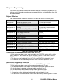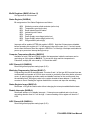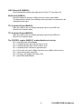
1
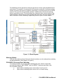
10623 Roselle Street, San Diego, CA 92121 • (858) 550-9559 • FAX (858) 550-7322
[email protected] • www.accesio.com
MODEL P104-WDG-CSM
PC/104-PLUS WATCHDOG TIMER
USER MANUAL
FILE: MP104-WDG-CSM.B3j
Notice
The information in this document is provided for reference only. ACCES does not assume any liability arising
out of the application or use of the information or products described herein. This document may contain or
reference information and products protected by copyrights or patents and does not convey any license under
the patent rights of ACCES, nor the rights of others.
IBM PC, PC/XT, and PC/AT are registered trademarks of the International Business Machines Corporation.
Printed in USA. Copyright by ACCES I/O Products Inc, 10623 Roselle Street, San Diego, CA 92121. All rights
reserved.
WARNING!!
ALWAYS CONNECT AND DISCONNECT YOUR FIELD CABLING WITH THE
COMPUTER POWER OFF. ALWAYS TURN COMPUTER POWER OFF
BEFORE INSTALLING A CARD. CONNECTING AND DISCONNECTING
CABLES, OR INSTALLING CARDS INTO A SYSTEM WITH THE
COMPUTER OR FIELD POWER ON MAY CAUSE DAMAGE TO THE I/O
CARD AND WILL VOID ALL WARRANTIES, IMPLIED OR EXPRESSED.
2
P104-WDG-CSM User Manual
Warranty
Prior to shipment, ACCES equipment is thoroughly inspected and tested to applicable specifications. However,
should equipment failure occur, ACCES assures its customers that prompt service and support will be available.
All equipment originally manufactured by ACCES which is found to be defective will be repaired or replaced
subject to the following considerations.
Terms and Conditions
If a unit is suspected of failure, contact ACCES' Customer Service department. Be prepared to give the unit
model number, serial number, and a description of the failure symptom(s). We may suggest some simple tests
to confirm the failure. We will assign a Return Material Authorization (RMA) number which must appear on the
outer label of the return package. All units/components should be properly packed for handling and returned
with freight prepaid to the ACCES designated Service Center, and will be returned to the customer's/user's site
freight prepaid and invoiced.
Coverage
First Three Years: Returned unit/part will be repaired and/or replaced at ACCES option with no charge for labor
or parts not excluded by warranty. Warranty commences with equipment shipment.
Following Years: Throughout your equipment's lifetime, ACCES stands ready to provide on-site or in-plant
service at reasonable rates similar to those of other manufacturers in the industry.
Equipment Not Manufactured by ACCES
Equipment provided but not manufactured by ACCES is warranted and will be repaired according to the terms
and conditions of the respective equipment manufacturer's warranty.
General
Under this Warranty, liability of ACCES is limited to replacing, repairing or issuing credit (at ACCES discretion)
for any products which are proved to be defective during the warranty period. In no case is ACCES liable for
consequential or special damage arriving from use or misuse of our product. The customer is responsible for all
charges caused by modifications or additions to ACCES equipment not approved in writing by ACCES or, if in
ACCES opinion the equipment has been subjected to abnormal use. "Abnormal use" for purposes of this
warranty is defined as any use to which the equipment is exposed other than that use specified or intended as
evidenced by purchase or sales representation. Other than the above, no other warranty, expressed or implied,
shall apply to any and all such equipment furnished or sold by ACCES.
3
P104-WDG-CSM User Manual
TABLE OF CONTENTS
Chapter 1: Introduction ..................................................................................................................... 5
Watchdog .......................................................................................................................................... 5
Figure 1-1: Block Diagram ........................................................................................................ 6
Watchdog Models ........................................................................................................................... 6
P104-WDG-E: Economy Basic Watchdog ............................................................................ 6
P104-WDG-CSM: Standard Watchdog with Computer Status Monitor ........................ 7
P104-WDG-CSMA: Standard Watchdog with Advanced Computer Status Monitor . 8
Ordering Guide / P1 Connector Configurations ..................................................................... 9
Model Options.................................................................................................................................. 9
Included with your board .............................................................................................................. 9
Chapter 2: Installation...................................................................................................................... 10
Hardware Installation ................................................................................................................... 11
Figure 2-1: Fan Connection Diagram................................................................................... 12
Chapter 3: Address Selection........................................................................................................ 13
Chapter 4: Programming................................................................................................................. 14
Register Definitions...................................................................................................................... 14
Table 4-1: Register Address Map.......................................................................................... 14
Three events will generate an active-low RESET at P1-12: ............................................... 14
Seven events may generate interrupts ................................................................................... 14
82c54 Registers (BASE +0 thru +3).......................................................................................... 15
Status Register (BASE+4)........................................................................................................... 15
Computer Temperature Monitor (BASE+5) ............................................................................ 15
A/DC Channel #1 (BASE+6)........................................................................................................ 15
Watchdog Programming Options (BASE+7) ......................................................................... 15
Status Register Image (BASE+8) .............................................................................................. 15
Disable Interrupts (BASE+9) ...................................................................................................... 15
A/DC Channel #2 (BASE+A) ....................................................................................................... 15
A/DC Channel #3 (BASE+B) ....................................................................................................... 16
82c54 Out 2 (BASE+C) ................................................................................................................. 16
TTL & Isolated Output (BASE+D).............................................................................................. 16
TTL & Isolated Output (BASE+E).............................................................................................. 16
The CONTROL register (BASE+F) enables/disables six circuits:.................................... 16
To Program the Watchdog Interval .......................................................................................... 17
Debug Script to Initialize the Counter/Timers ................................................................... 17
Foreground Watchdog Mode ................................................................................................. 17
Background Watchdog Mode ................................................................................................ 19
Combination Reset Mode........................................................................................................ 19
Chapter 5: Connector Pin Assignments ..................................................................................... 20
Table 5-1: Connector P1 Pin Assignments (40 pin shrouded header) ....................... 20
Chapter 6: Specification.................................................................................................................. 21
Appendix A: Programmable Interval Timer ............................................................................... 22
Customer Comments ....................................................................................................................... 26
4
P104-WDG-CSM User Manual
Chapter 1: Introduction
This multifunction card contains a watchdog timer. Additionally, two additional models with
multiple features may be included on your card. Example of these are: a computer power
supply monitor, a computer internal temperature monitor, capability to read the temperature, a
pair of opto-isolated inputs and outputs and a fan-speed control.
Watchdog
Your application program must communicate with the watchdog circuit at prescribed intervals.
If this communication ("prompt") is missed, the Watchdog can be programmed to initiate a
computer reset (reboot). If the reboot is successful, operation may be returned to the previous
application program. If the failure was temporary, proper operation is resumed. If, however,
the failure is persistent, the Watchdog will continuously reset the computer. The more
frequently the Watchdog is prompted (and shorter Watchdog time selected), the less time a
faulty computer has to cause damage.
The method used by the card to detect loss of computer function is as follows:
A type 82C54 counter/timer is used. This chip contains three 16-bit counters. A number
greater than one is set into the chip's Counters by your application program. The Watchdog is
armed by software commands and the counters begin counting down. As long as the
computer is operating properly, the counters will be periodically reloaded to their original
programmed values by your application program before the counters have counted down to
zero. (See Chapter 4, Programming for detailed information.)
If your software fails to reload the counters, then both counters continue counting until zero is
reached (timeout). When the counters 0 and 1 reach zero an open-collector transistor will pull
pin 12 of connector P1 LOW. Pin 11 will go HIGH. Note that RESET must be enabled (see the
Programming chapter). When a reset condition occurs, the reset circuit is active until a reset
pulse returns from the system bus or power is cycled to the system, or counter 2 times out.
The clock frequency to Counter 0 is derived from the computer's clock and is:
33 MHz÷16= 2.08333 MHz. (The period is 0.48 μsec.)
The output of Counter 0 is used as a clock to Counter 1. Each counter can divide by any
whole number from 2 to 65,536 (216), so the watchdog timeout period may vary from about 2
microseconds to 2060 seconds.
The duration of the watchdog reset output (WDRST) and ("not WDRST") can be programmed
at Counter 2. There are two clock rates available for the counter and you can select the rate
that best suits your needs. The default clock rate is half the PCI bus clock speed, 16.67 MHz.
You can select a lower rate (2.08333 MHz) by a write to base address +C. That selection will
be held until a read from base address +C.
5
P104-WDG-CSM User Manual
The Watchdog card can generate an interrupt request one Counter 0 period-width before the
reset timeout. For example, if a reset period of 60 seconds is used with a 5 millisecond delay
stored in Counter 0 (the result of a maximum value delay), an interrupt would occur at 59.995
seconds. This gives the Interrupt handler software 5 milliseconds to refresh the watchdog
before a reset action occurs. This should allow your software to take corrective actions if the
system software continued to run but the software that should have reset the watchdog had
failed. Discussion of these Watchdog Programming Options is given in a later chapter.
Figure 1-1: Block Diagram
Watchdog Models
There are three basic models of this board. Special variations can be configured by contacting
the sales department. (See Chapter 5 for pinout.)
P104-WDG-E: Economy Basic Watchdog
This model provides a fully programmable watchdog with open collector outputs that
can reset the computer. Both “WDRST” and “not WDRST” outputs are provided on the
four pin header connector:
a.
Open collector watchdog output, active HIGH, 1k pull-up to 5V.
b.
Open collector watchdog output, active LOW, no current limiting.
6
P104-WDG-CSM User Manual
P104-WDG-CSM: Standard Watchdog with Computer Status Monitor
This model provides a fully programmable watchdog with open collector outputs that
can reset the computer. It also contains various I/O to monitor and control the health of the
computer. It contains computer power monitoring, computer temperature monitoring and
measurement, isolated inputs and isolated outputs. (See Chapter 5 for 40-pin connector
information.) The following I/O connections are provided:
a.
Two isolated digital inputs, current limited.
b.
Two isolated digital outputs, current limited.
c.
Two non-isolated digital outputs in parallel to isolated digital outputs.
d.
Reset pushbutton input, TTL, active LOW, buffered.
e.
Fused external 5VDC power for external LED.
Computer Power Monitor
The +5VDC computer power supply may be monitored. If the voltage varies by more than
+6%, two bits of a Status Register indicate whether there is an overvoltage or an
undervoltage. In addition, an interrupt request can be generated.
Computer Temperature Monitor
This feature monitors ambient temperature in the area of the watchdog circuit board. The
temperature monitor circuit compares the output of an on-board LM334 temperature sensor
with a preset DC voltage level. The output of the circuit can be read at bit 1 of the Status
Register and can also cause an interrupt request if that temperature exceeds the factory
preset limit (approx. 50 °C).
Computer Temperature Measurement
The on-board LM334 temperature sensor output is input to a dedicated onboard 8 bit A/D
converter which provides means for a software read of the measured temperature.
Opto-Isolated Outputs
Software can control two optically isolated outputs. Each has a transistor with a 330Ω current
limiting resistor on the collector and an uncommitted emitter. Also, two non-isolated digital
outputs at pin 2 of connector P1 (LED/Digital 1) and pin 6 of connector PI(LED/Digital 2), are
available for driving an external device such as a LED (up to 15mA sink or source). These
signals are in parallel with the isolated outputs making the isolated outputs activated with the
non-isolated digital outputs. OUT1 at pin 28 connects to a 330 ohm resistor which is
connected to the collector of an opto-coupled transistor. Pin 29 connects to the emitter. As
much as 18 volts and 100mA can be switched, reverse bias should be avoided. Out2 at pins
32 and 33 are an identical circuit.
Push Button Reset Input
The Push Button Reset buffered input (P1 pin 16) has a 4.7kΩ pull-up.
Fused External Power LED
Pin 4 has a 0.3A (300mA) (at room temperature) resettable fuse connected to +5V. At +85C
this fuse trips at 0.15A (150mA), at 0 degrees C this fuse trips at 0.6A (600mA).
7
P104-WDG-CSM User Manual
P104-WDG-CSMA: Standard Watchdog with Advanced Computer Status Monitor
This model provides a fully programmable watchdog with open collector outputs that
can reset the computer. It contains all available I/O to monitor and control the health of the
computer. It additionally contains extra features such as external or remote reset isolated
input, fan speed detect and fan speed control, light sensor for security if enclosure is opened
and two extra analog inputs that could be used to measure humidity or battery power for
example. (See Chapter 5 for 40-pin connector.)
a.
b.
c.
d.
e.
Two undedicated analog inputs, 0 to +5V, eight-bit conversion.
One remote reset isolated input, current limit
Fan drive, PWM, open collector.
Additional +5 volts through a resettable fuse (300mA at room temperature).
+12 volts through a resettable fuse (300mA at room temperature).
Computer Power Monitor
The three computer power supplies (+5V, +12V, and -12V) may be monitored by this fullfeatured version of the card. If one or more of those voltages vary by more than +6%, two bits
of a Status Register indicate whether there is an overvoltage or an undervoltage. In addition,
an interrupt request can be generated.
Fan Speed Control
This feature is used in conjunction with the Computer Temperature Monitor to automatically
maintain internal temperature in the enclosure by control of the fan speed. The duty cycle of
the +12V fan power return (GND) is pulse-width modulated to speed up the fan when
temperature increases. If no current is detected or the duty cycle reaches 100 percent, an
interrupt occurs.
Security Light Sensor
This feature is used when notification of un-authorized opening of dark computer enclosure is
required. A photo (light) sensor on one corner of watchdog board is connected to a dedicated
input of the onboard 8 bit A/D converter which provides the means for a software read of the
measured light.
External Remote Reset Opto-Isolated Input
Opto-isolated input #2 may be enabled to generate a reset (logically ORed with the Push
Button Reset input and the watchdog timer circuit). At least 3V must be applied to the isolated
input to trigger a RESET. The isolated input will tolerate 18 volts reverse bias. This second
dedicated opto-isolated input is used to remotely trigger a reset in the system. The voltage
input range is even capable of using an RS-232 transition to trigger a reset. The Opto-isolated
input signals are available at the P1 connector. (see Chapter 5)
8
P104-WDG-CSM User Manual
Additional Fused External Power
Pin 38 has a 0.3A (300mA) (at room temperature) resettable fuse connected to +5V. At +85C
this fuse trips at 0.15A (150mA), at 0 degrees C this fuse trips at 0.6A (600mA). The same is
true for the fuse connected to pin 40 (12VDC).
Special Options
Programmable array logic is available on this card and many possibilities exist for special
modifications to suit unique requirements. If your card includes any such modifications, an "S"
number (e.g. S08, S09, etc.) will be appended to the model number on the board label.
Status Register
Bit assignments of the Status Register are as follows:
BD0
BD1
BD2
BD3
BD4
BD5
BD6
BD7
Watchdog counter refresh reminder (active low)
Temperature good (active low)
Reset Isolated Input #2 status
Isolated Input #1 status
Fan good
Power Supply overvoltage (active low)
Power Supply undervoltage (active low)
IRQ generated (active high)
Ordering Guide / P1 Connector Configurations
P104-WDG-E
P104-WDG-CSM
P104-WDG-CSMA
Economy Basic Watchdog
Standard Watchdog with
Computer Status Monitor
Standard Watchdog with
Advanced Computer Status
Monitor
4-pin right-angle 2x2 header (pins 9 – 12)
40-pin right-angle 2x20 header
40-pin right-angle 2x20 header
Model Options
Extended Temperature
Included with your board
Quick Start Guide
Master Software CD
9
P104-WDG-CSM User Manual
Chapter 2: Installation
A printed Quick-Start Guide (QSG) is packed with the board for your convenience. If you’ve
already performed the steps from the QSG, you may find this chapter to be redundant and
may skip forward to begin developing your application.
The software provided with this PC/104-Plus board is on CD and must be installed onto your
hard disk prior to use. To do this, perform the following steps as appropriate for your operating
system.
CD Software Installation
The following instructions assume the CD-ROM drive is drive “D”. Please substitute the
appropriate drive letter for your system as necessary.
DOS
1.
2.
3.
4.
Place the CD into your CD-ROM drive.
Type B- to change the active drive to the CD-ROM drive.
Type GLQR?JJ- to run the install program.
Follow the on-screen prompts to install the software for this board.
Windows
1.
2.
3.
Place the CD into your CD-ROM drive.
The system should automatically run the install program. If the install program does
not run promptly, click START | RUN and type BGLQR?JJ, click OK or press -.
Follow the on-screen prompts to install the software for this board.
1.
Please refer to linux.htm on the CD-ROM for information on installing under linux.
Linux
Caution! * ESD
A single static discharge can damage your card and cause
premature failure! Please follow all reasonable precautions to
prevent a static discharge such as grounding yourself by touching
any grounded surface prior to touching the card.
10
P104-WDG-CSM User Manual
Hardware Installation
Before installing the board, please run Setup.exe. The Setup program can be used to assist
in configuring the two switches on the board. Our setup program will lead the user through
the process of setting the options on the board (the program does not set the options on the
board).
The PCI bus clock trace length from the CPU to the cards in the stack is tuned so that the
clock edge arrives at the interface when data is valid. Since boards in the PC/104 stack are at
different distances from the CPU, provision is made on the CPU board to supply four clock
signals with compensating trace lengths. Two signals from other groups must be likewise
selected: IDSEL and INT. When the PCI bus is being initialized, the operating system will
enable each card with a hard-wired select line and read it's configuration registers. An
address is assigned, space in the memory map and I/O map is reserved, etc. Similarly, the
CPU's interrupt controller resources (INTA, INTB, INTC, INTD) will be distributed among the
cards in the stack. A set of four-to-one multiplexers and two slide switches are used to select
which PCI clock, IDSEL and INT lines are routed to the board’s PCI bus interface.
Only four boards (not including the CPU) are allowed in a PC104-Plus stack, each board must
get a specific set of signals. These signals are selected with two slide switches, labeled SEL1 and SEL-2, which form a binary value to control the mux (SEL-1 is the least significant bit
and SEL-2 is the most significant bit). If the board is closest to the CPU, slide both switches
to the right. This will select the signal with the longest trace on the CPU board (signal group
0). If this product is the farthest board from the CPU, slide both switches to the left. This will
select the signal with the shortest trace on the CPU board (signal group 3). Place the SEL-1
switch to the left and SEL-2 to the right to select signal group 1, place the SEL-1 switch to the
right and SEL-2 to the left to select signal group 2.
1.
2.
3.
4.
5.
6.
7.
8.
9.
10.
Make sure to set switches and jumpers from either the Option Selection section of this
manual or from the suggestions of SETUP.EXE.
Do not install card into the computer until the software has been fully installed.
Turn OFF computer power AND unplug AC power from the system.
Gain access to the card stack and prepare it to receive this new card regarding
hardware & fasteners.
Plug the card onto the bus ensuring alignment of the PC/104 and PCI-104 pins.
Install an I/O cable onto the card’s header connector.
Inspect for proper fit of the card and cable and tighten the hardware.
Replace the enclosure/cover and turn ON the computer which should auto-detect the
card (depending on the operating system) and automatically finish installing drivers.
Run PCIfind.exe to complete installing the card into the registry (for Windows only) and
to determine the assigned resources.
Run one of the provided sample programs that was copied to the newly created card
directory (from the CD) to test and validate your installation.
The base address assigned by BIOS or the operating system can change each time new
hardware is installed into or removed from the computer. Please recheck PCIFind or Device
Manager if the hardware configuration is changed. Software you write can automatically
determine the base address of the card using a variety of methods depending on the
operating system. In DOS, the PCI\SOURCE directory shows the BIOS calls used to
determine the address and IRQ assigned to installed PCI devices. In Windows, the Windows
sample programs demonstrate querying the registry entries (created by PCIFind and
NTIOPCI.SYS during boot-up) to determine this same information.
11
P104-WDG-CSM User Manual
Figure 2-1: Fan Connection Diagram
12
P104-WDG-CSM User Manual
Chapter 3: Address Selection
The Watchdog Timer uses one PCI address space, occupying 16 consecutive register
locations.
PCI architecture is Plug-and-Play. This means that the BIOS or Operating System determines
the resources assigned to PCI cards rather than you selecting those resources with switches
or jumpers. As a result, you cannot set or change the card's base address. You can only
determine what the system has assigned.
To determine the base address that has been assigned, run the PCIFind utility program
provided. This utility will display a list of all of the cards detected on the PCI bus, the
addresses assigned to each function on each of the cards, and the respective IRQs.
Alternatively, Windows systems can be queried to determine which resources were assigned.
In these operating systems, you can use either PCIFind, or the Device Manager utility from
the System Properties Applet of the control panel. The card is installed in the Data Acquisition
class of the Device Manager list. Selecting the card, clicking Properties, and then selecting the
Resources Tab will display a list of the resources allocated to the card.
The PCI bus supports 64K of address space, so your card's addresses may be located
anywhere in the 0000 to FFFF hex range.
PCIFind uses the Vendor ID and Device ID to search for your card, then reads the base
address and IRQ.
To determine the base address and IRQ yourself, use the following information.
The Vendor ID for all cards is 494F. (ASCII for "IO")
The Device ID’s are as follows:
P104-WDG-CSME is 2F50h.
P104-WDG-CSM is 2FC0h.
P104-WDG-CSMA is 2FC1h.
13
P104-WDG-CSM User Manual
Chapter 4: Programming
This section of the manual contains information to assist you in developing programs for use
with the card. I/O bus address assignments, programming hints, and a description of the utility
driver are included.
Register Definitions
The card uses sixteen consecutive registers in I/O space as listed in the following table:
Address
Base Address
Base Address +1
Base Address +2
Base Address +3
Base Address +4
Base Address +5
Base Address +6
Base Address +7
Base Address +8
Base Address +9
Base Address +A
Base Address +B
Base Address +C
Base Address +D
Base Address +E
Base Address +F
Read
Counter #0 Real-time Value
Counter #1 Real-time Value
Counter #2 Real-time Value
Unused
Status Register, Clear IRQ, Enable IRQs
8-bit Temperature Value
0-5V Analog 1 8-bit Value
Disable Counters
Status Register Image
Disable Interrupts
0-5V Analog 2 8-bit Value
Light Sensor 8-bit Value
Hi Rate Clock Select (16MHz)
Isolated Output1 (and LED1) Off
(P1-2,29 High)
Isolated Output2 (and LED2) Off
(P1-6,31 High)
Control Register Circuit Status
Write
Counter #0 Load Value
Counter #1 Load Value
Counter #2 Load Value
Counter #0-2 Control Register
IRQ Enable Register
Unused
Unused
Enable Counters
Unused
Unused
Unused
Unused
Low Rate Clock Select (2MHz)
Isolated Output1 (and LED1) On
(P1-2,29 Low)
Isolated Output2 (and LED2) On
(P1-6,31 Low)
Circuit Enable/Disable
Table 4-1: Register Address Map
Three events will generate an active-low RESET at P1-12:
1. 32 bit timer counts down to zero, must be enabled with CONTROL register bit 0 or with a
WRITE at base+7. READ base+7 to stop the counters or write 0 to CONTROL bit 0. The
RESET persists as long as the output of counter 2 is HIGH.
2. The active-low reset push button input at P1-16 when CONTROL register bit 5 is set.
3. Current driven thru the isolated input #2 circuit when CONTROL register bit 3 is set.
Seven events may generate interrupts
If interrupt enable register bit 7 is set or if base+4 is read or if CONTROL register bit 7 is set:
1. 32 bit timer counts down to zero and interrupt enable register bit 0 is set.
2. The temperature sense circuit detects ~122F and interrupt enable register bit 1 is set.
3. 5 volt overvoltage is detected and interrupt enable register bit 2 is set.
4. 5 volt undervoltage is detected and interrupt enable register bit 3 is set.
5. +12 under/over voltage is detected and interrupt enable register bit 4 is set.
6. -12 under/over voltage is detected and interrupt enable register bit 5 is set.
7. The fan control circuit hits maximum or zero power and interrupt enable register bit 6 is set.
14
P104-WDG-CSM User Manual
82c54 Registers (BASE +0 thru +3)
See Appendix A of this manual.
Status Register (BASE+4)
Bit assignments of the Status Register are as follows:
BD0
BD1
BD2
BD3
BD4
BD5
BD6
BD7
Watchdog counter refresh reminder (active low)
Temperature good (active low)
Reset Isolated Input #2 status
Isolated Input #1 status
Fan good
Power Supply overvoltage (active low)
Power Supply undervoltage (active low)
IRQ generated (active high)
Interrupts will be enabled AFTER this register is READ. Note that if interrupts are disabled
before accessing this register, bit 7 of the returned value will be zero (low). If a circuit needs
service then the second time this register is READ bit 7 will be high. Interrupts are disabled at
power-up to prevent an interrupt during boot-up.
Computer Temperature Monitor (BASE+5)
Available on both “CSM and CSMA” models, the temperature inside the enclosure can be
read using an 8-bit register at BASE+5. To convert the byte read into temperature in
Fahrenheit, multiply the value read by 11/15 and then add 7.
A/DC Channel #1 (BASE+6)
Read 8-bit general purpose analog input (0-5V).
Watchdog Programming Options (BASE+7)
Programming the card is straightforward. Counters 0 and 1 of the type 8254 counter/timer are
concatenated and operate as a 32-bit down counter to provide the time delay before a timeout
occurs. A special register provides enable and disable functions for the counters and, thus,
the watchdog itself. Writing any value to the register located at base address +7 enables the
counters to count. Reading the register disables the counters and stops the watchdog.
Status Register Image (BASE+8)
Read base +8 to get the Status value without changing the Interrupt enabled/disabled state.
Disable Interrupts (BASE+9)
Read base address +9 to disable interrupts. If interrupts were enabled and a circuit was
requesting attention then bit 7 will be high. A second reading of this register will have bit 7
LOW.
A/DC Channel #2 (BASE+A)
Read 8-bit general purpose analog input (0-5V).
15
P104-WDG-CSM User Manual
A/DC Channel #3 (BASE+B)
Read 8-bit dedicated analog input (light sensor). Dark = FF, Max Light = 00
82c54 Out 2 (BASE+C)
Read this address to select the 16MHz clock rate, write to select 2MHz.
This determines the width of the watchdog reset output when not connected to the
motherboard reset input.
TTL & Isolated Output (BASE+D)
Write (any value) to turn on isolated (transistor) output #1 and LED1 sink.
Read to turn off (default state).
TTL & Isolated Output (BASE+E)
Write (any value) to turn on isolated (transistor) output #2 and LED2 sink.
Read to turn off (default state).
The CONTROL register (BASE+F) enables/disables six circuits:
bit 0 = watchdog timer enable/disable
bit 1 = isolated output #1 (also LED drive #1) is on/off
bit 2 = isolated output #2 (also LED drive #2) is on/off
bit 3 = isolated input #2 is allowed to generate reset
bit 4 = 32 bit timer clock rate is 2MHz if this bit is set or 16MHz if this bit is zero
bit 5 = reset button enable (set HIGH)
bit 6 = fan stop / start (toggle HIGH then LOW)
bit 7 = global IRQ enable/disable
16
P104-WDG-CSM User Manual
To Program the Watchdog Interval
1.
2.
3.
4.
Disable the counters.
Program the counter modes
Program the desired time delays.
Enable the counters.
Once the counters have been enabled, the computer will reset if the 32-bit counter (counters 0
and 1) decrements all the way to zero. (Note: An alternative use of the reset signal is to simply
notify an external device that a reset is necessary.)
Debug Script to Initialize the Counter/Timers
The following debug script will initialize the counter/timers for a reasonable delay with a 2mS
positive pulse at pin 11 and an active-low (open-collector) signal at pin 12 on the I/O
connector. For suggestions regarding base address determination see page 11.
I BASE+7
;DISABLE THE COUNTERS
I BASE+C
;SELECT THE 16MHz COUNTER CLOCK
O BASE+3 36 ;COUNTER 0 MODE
O BASE+0 FF ;COUNTER 0 DIVISOR LSB
O BASE+0 00 ;COUNTER 0 DIVISOR MSB
O BASE+3 76 ;COUNTER 1 MODE
O BASE+1 16 ;COUNTER 1 DIVISOR LSB
O BASE+1 00 ;COUNTER 1 DIVISOR MSB
O BASE+3 B6 ;COUNTER 2 MODE
O BASE+2 FF ;COUNTER 2 DIVISOR LSB
O BASE+2 FF ;COUNTER 2 DIVISOR MSB
And then send
O BASE+7 0
;START THE WATCHDOG
OR
O BASE+F 01 ;START THE WATCHDOG
To pet the watchdog, reload counters 0 and 1 before they time-out.
Foreground Watchdog Mode
In order to prevent the reset, the software program must periodically reload Counter 1 with the
initial load value (or any other suitable load value). The maximum delay between Counter 1
reloads is determined by the load values of the concatenated counters minus a suitable fudge
factor. (Note: It is not necessary to re-load Counter 0 because it will simply recycle. Also note
that loading Counter 0 with full-scale is customary, as exact timing is rarely a requirement of a
watchdog function.)
Counter 0 must be programmed for mode 3. Counter 1 and 2 must be programmed for mode
2. The card was designed specifically for these modes. Any other modes may cause
unpredictable behavior. See Appendix A for details on how to program the counters.
In Summary:
1.
Disable Watchdog
2.
Program CTR0 for Mode 3
3.
Program CTR1 and 2 for Mode 2
17
Read BASE+7
See Appendix A
See Appendix A
P104-WDG-CSM User Manual
4.
5.
Load CTR0,1,2 with reset delay
Enable Watchdog
Then, before the first timeout occurs:
1.
Enter main loop
2.
Program CTR1 (again) for Mode 2
3.
Load CTR1
4.
User code goes here
5.
Repeat main program loop
18
See Appendix A
Write BASE+7
See Appendix A
P104-WDG-CSM User Manual
Background Watchdog Mode
An alternative method to refresh the counters that provides some flexibility but potentially
reduces dependability is to use an interrupt service routine (ISR). The card will generate an
interrupt one Counter 0 load value before timeout occurs. If that interrupt is used by a userdefined ISR, it's possible for that ISR to refresh the counters and, thus, avoid need for the
main program loop to refresh the counters.
There is the possibility of reduced dependability because this method will not detect certain
types of program lock-ups. For example, if the application program were to lock up in a loop
such as "JMP $", the interrupt service routine would never know it and would therefore
continue refreshes despite the lockup. It is possible to modify the host program to enable the
ISR to detect such loops (perhaps by checking the return stack location for the ISR each time,
and making sure it changes...) However, if the code is going to be modified, the next, hybrid,
method might be more effective.
This method does, however, allow "off-the-shelf" existing programs to be used with the card
without modification. Also, this method could cause spurious resets if your program disables
interrupts for an extended duration. The IRQ that would have caused the ISR might be missed
and allow the counter to time out. If the counter counts-down, the reset signals will be
generated and the counters will restart.
Combination Reset Mode
By combining the two methods ("Foreground" and "Background") it is possible to create a very
elaborate scheme for monitoring the status of the computer. This combined method eliminates
the negatives associated with either method used individually, but does require extensive
modifications to existing code, or even rewriting code entirely. In this scheme, both foreground
and background routines can prompt the watchdog.
The foreground routine would prompt the watchdog under normal conditions, and the ISR
running in the background would only prompt the watchdog if the foreground routine failed to
do so. The ISR, noting that the foreground routine missed its prompt, could take steps to
determine why, and even try to correct it. For example, the foreground program can post its
current status to a shared-memory variable, indicating that it is about to enter a long dedicated
process (calculations for a print job, perhaps) and that it might miss several of its prompts.
The ISR, when executed by the warning IRQ, notes that the foreground program indicated it
might miss its turn, and starts counting misses. After prompting the watchdog, it returns
control to the foreground process. If the count of missed prompts gets too high, it could write
status to a disk file or serial port, then skip the prompt, allowing the computer to reset.
19
P104-WDG-CSM User Manual
Chapter 5: Connector Pin Assignments
One 40-pin right-angle shrouded 2x20 header connector with 0.1” spacing provides access to
the I/O signals. The standard mating connector is a Molex “crimp and poke” discrete wire type
with a latching feature. Other mating connectors and/or cables may be used.
Pin #
1
3
5
7
9
13
Function
Ground
Ground
Ground
Ground
Ground
Watchdog Output, open
collector, active HIGH, 1k
pull-up to 5V
Ground
15
Ground
16
17
19
21
23
25
27
29
31
33
35
37
Ground
Ground
+5VDC via Resettable Fuse
Analog Input 2, 0 to +5V
Ground
Isolated input 1, cathode
Isolated output 1, emitter
Isolated input 2, cathode
Isolated output 2, emitter
Ground
Ground
Fan drive, PWM, open
collector
18
20
22
24
26
28
30
32
34
36
38
11
39
Pin #
2
4
6
8
10
12
14
40
Function
LED1 Cathode
+5VDC via Resettable fuse
LED2 Cathode
Ground
Ground
Watchdog Output, open
collector, active LOW, no
pull-up
Ground
Reset pushbutton input,
TTL active LOW
Ground
Analog input 1, 0 to +5V
Ground
Ground
Isolated input 1, anode
Isolated output 1, collector
Isolated input 2, anode
Isolated output 2, collector
Ground
Ground
+5VDC via Resettable fuse
+12VDC via Resettable fuse
(also fan power)
Table 5-1: Connector P1 Pin Assignments (40 pin shrouded header)
On P104-WDG-E model, connector P1 is replaced with a
four pin header at location of P1 Pins 9, 10, 11 & 12
20
P104-WDG-CSM User Manual
Chapter 6: Specification
Watchdog Timer
•
Time-out:
Software selectable from 2 μsec. to 2060 sec
•
Pulse Width:
Output, 120 nsec. Minimum, 31 msec. Maximum
•
Clock:
2.08333 MHz, derived from computer clock (33 MHz÷16)
•
Address:
8-Bit I/O Mapped
Status Monitor Register
•
Voltages
IRQ and register indication if +5, +12, or -12 varies by more than +/-6%
•
Temp. Alarm:
IRQ and status register indication when above ~ 122°F (50°C)
•
Temp. Digitizer:
8 bit ADC, LSB = 0.7 °F (0.39o C)
•
Isolated Outputs: Two, (customer supplied 5 - 24V) through a 330 Ω resistor
•
Isolated Inputs:
Two, opto-isolated and current limited through 330 Ω, one may be reassigned as External Reset
•
Reset Outputs:
Active low open collector, active high with 1k pull-up
•
Fan Speed:
IRQ and Status Register indication if speed is too high or too low
Environmental
•
Operating Temp.: 0 to 70C (-40 °C to +85 °C option)
•
Storage Temp.:
-50 °C to +120 °C
•
Humidity:
10% to 90% RH, non-condensing
•
Power Required: +5 VDC at 125 mA typical
21
P104-WDG-CSM User Manual
Appendix A: Programmable Interval Timer
This Appendix includes basic information about the type 8254 Counter/Timer chip. For those
interested in more detailed information, a full description can be found in the manufacturer's
data sheets.
Please note: The information in this Appendix is for general reference, and may include
features or functions not applicable to this card.
Operation Modes
Modes of operation are described in the following paragraphs to familiarize you with the power
and versatility of this device. The following conventions apply in describing operation of type
8254 chips:
Clock:
Trigger:
Counter Loading:
A positive pulse into the counter's clock input.
A rising edge input to the counter's gate input.
Programming a binary count into the counter.
Mode 0: Pulse on Terminal Count
After the counter is loaded, the output is set low and will remain low until the counter
decrements to zero. The output then goes high and remains high until a new count is loaded
into the counter. A trigger enables the counter to start decrementing. This mode is commonly
used for event counting with Counter #0.
Mode 1: Retriggerable One-Shot
The output goes low on the clock pulse following a trigger to begin the one-shot pulse and
goes high when the counter reaches zero. Additional triggers result in reloading the count and
starting the cycle over. If a trigger occurs before the counter decrements to zero, a new count
is loaded. Thus, this forms a re-triggerable one-shot. In mode 1, a low output pulse is provided
with a period equal to the counter count-down time.
Mode 2: Rate Generator
This mode provides a divide-by-N capability where N is the count loaded into the counter.
When triggered, the counter output goes low for one clock period after N counts, reloads the
initial count, and the cycle starts over. This mode is periodic, the same sequence is repeated
indefinitely until the gate input is brought low. This mode also works well as an alternative to
mode 0 for event counting.
Mode 3: Square Wave Generator
Like mode 2, this mode operates periodically. The output is high for half of the count and low
for the other half. If the count is even, then the output is a symmetrical square wave. If the
count is odd, then the output is high for (N+1)/2 counts and low for (N-1)/2 counts. Periodic
triggering or frequency synthesis are two possible applications for this mode. Note that in this
mode, to achieve the square wave, the counter decrements by two for the total loaded count,
then reloads and decrements by two for the second part of the waveform.
Mode 4: Software Triggered Strobe
This mode sets the output high and, when the count is loaded, the counter begins to count
down. When the counter reaches zero, the output will go low for one input period. The counter
must be reloaded to repeat the cycle. A low gate input will inhibit the counter.
22
P104-WDG-CSM User Manual
Mode 5: Hardware Triggered Strobe
In this mode, the counter will start counting after the rising edge of the trigger input and will go
low for one clock period when the terminal count is reached. The counter is retriggerable. The
output will go low until the full count after the rising edge of the trigger.
Programming
On the card, the 8254 counters occupy the following addresses:
Base Address
Base Address +1
Base Address +2
Base Address +3
Read/Write Counter 0
Read/Write Counter 1
Read/Write Counter 2
Read/Write Counter Control Register
The counters are programmed by writing a control byte into the counter control register. The
control byte specifies the counter to be programmed, the counter mode, the type of read/write
operation, and the modulus. The control byte format is a follows:
B7
B6
B5
B4 B3 B2 B1 B0
SC1 SC0 RW1 RW0 M2 M1 M0 BCD
SC0 and SC1: These bits select the counter that the control byte is destined for.
SC1
0
0
1
1
SC0
0
1
0
1
Function
Program Counter 0
Program Counter 1
Program Counter 2
Read/Write Command
RW0 and RW1: These bits select the read/write mode of the selected counter.
RW1
0
0
1
1
RW0
0
1
0
1
Counter Read/Write Function
Counter Latch Command
Read/Write LS Byte
Read/Write MS Byte
Read/Write LS Byte, then MS Byte
M0, M1, and M2: These bits set the operational mode of the selected counter.
Mode
0
1
2
3
4
5
M2
0
0
x
x
1
1
M1
0
0
1
1
0
0
M0
0
1
0
1
0
1
BCD: Set the selected counter to count in binary (0) or BCD (1).
23
P104-WDG-CSM User Manual
Reading and Loading the Counters
If you attempt to read the counters on the fly when there is a high frequency input, you will
most likely get erroneous data. This is partly caused by "carries" rippling through the counter
during the read operation. Also, the low and high bytes are read sequentially rather than
simultaneously and, thus, it's possible that "carries" will be propagated from the low byte to the
high byte during the read cycle.
To circumvent this, you can perform a counter-latch operation in advance of the read cycle. To
do this, load the RW0 and RW1 bits with zeroes. This instantly latches the count of the
selected counter in a 16-bit hold register. (An alternative method of latching counters that has
an additional advantage of operating simultaneously on several counters is by use of a
readback command to be discussed later.) A subsequent read operation on the selected
counter returns the held value. Latching is the best way to read a counter on the fly without
disturbing the counting process. You can only rely on directly read counter data if the counting
process is suspended while reading, by bringing the gate low, or by halting the input pulses.
You must specify in advance the type of read or write operation that you intend to perform for
each counter. You have a choice of loading/reading (a) the high byte of the count, (b) the low
byte of the count, or (c) the high byte followed by the low byte. This last is of the most general
use and is selected for each counter by setting the RW0 and RW1 bits to ones. Of course,
subsequent read/load operations must be performed in pairs in this sequence or the
sequencing flip-flop in the 8254 chip will get out of step.
The readback command byte format is:
1
CNT:
STA:
C0,C1,C2:
1
CNT STA C2 C1 C0
0
When is 0, latches the counters selected by bits C0-C2.
When is 0, returns the status byte of counters selected by C0-C2
When high, select a particular counter for readback. C0 selects Counter
0, C1 selects counter 1, and C2 selects counter 2.
You can perform two types of readback operations with the readback command. When
CNR=0, the counters selected by C0-C2 are latched simultaneously. When STA=0, the
counter status byte is read when the counter I/O location is accessed. The counter status byte
provides information about the current output state of the selected counter and its
configuration. The status byte returned if STA=0 is:
B7 B6
B5
B4 B3 B2 B1 B0
OUT NC RW1 RW2 M2 M1 M0 BCD
24
P104-WDG-CSM User Manual
OUT: Current state of counter output pin.
NC:
Null count. this indicates when the last count loaded into the counter register has
actually been loaded into the counter itself. The exact time of load depends on the
configuration selected. Until the count is loaded into the counter itself, it cannot be read.
RW0 and RW1:
M0-M2:
BCD:
Read/Write command.
Counter mode.
BCD=0 sets binary mode, otherwise counter is in BCD mode.
If STA and CNT bits in the readback command byte are set low and the RW1 and RW0 bits
have both been previously set high in the counter control register (thus selecting two-byte
reads), then reading a counter address location will yield:
1st Read:
2nd Read:
3rd Read:
Status byte
Low byte of latched data
High byte of latched data.
After any latching operation of a counter, the contents of its hold register must be read before
any subsequent latches of that counter will have any effect. If a status latch command is
issued before the hold register is read, then the first read will read the status, not the latched
value.
25
P104-WDG-CSM User Manual
Customer Comments
If you experience any problems with this manual or just want to give us some feedback,
please email us at: [email protected]. Please detail any errors you find and include
your mailing address so that we can send you any manual updates.
10623 Roselle Street, San Diego CA 92121
Tel. (858)550-9559 FAX (858)550-7322
www.accesio.com
26
P104-WDG-CSM User Manual