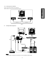
1
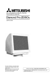
SERVICE MANUAL
HIGH RESOLUTION DISPLAY MONITOR
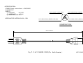
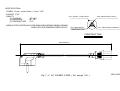
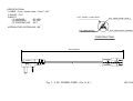
Diamond Pro 2060u
NSZ2107STTUW
NEC-MITSUBISHI ELECTRIC VISUAL SYSTEMS CORPORATION
MARCH 2001
CBB-S5730
Contents
1.
Circuit description ...................................................................................................................... 1-1
1.1 Power block ......................................................................................................................... 1-1
1.1.1 Outline ...................................................................................................................... 1-1
1.1.2 Rectifying circuit ....................................................................................................... 1-1
1.1.3 Surge current suppression ...................................................................................... 1-1
1.1.4 Higher harmonic circuit ............................................................................................ 1-2
1.1.5 Sub power circuit ...................................................................................................... 1-4
1.1.6 Main power circuit ..................................................................................................... 1-4
1.1.7 Degaussing circuit .................................................................................................... 1-7
1.1.8 Power management circuit ...................................................................................... 1-7
1.1.9 Protective circuit ....................................................................................................... 1-7
1.2 Horizontal deflection block ................................................................................................ 1-12
1.2.1 Distortion compensation waveform generating circuit ........................................ 1-13
1.2.2 Deflection current compensation circuit ................................................................ 1-22
1.3 Vertical output block ........................................................................................................... 1-24
1.4 High voltage block .............................................................................................................. 1-25
1.4.1 High voltage control circuit ...................................................................................... 1-25
1.4.2 Protective function circuit ........................................................................................ 1-25
1.4.3 DBF (Dynamic Beam Focus) circuit ....................................................................... 1-27
1.5 CRT compensation block ................................................................................................... 1-29
1.5.1 Rotation circuit .......................................................................................................... 1-29
1.5.2 Corner purity circuit .................................................................................................. 1-29
1.5.3 Earth magnetism cancel circuit .............................................................................. 1-30
1.5.4 Digital dynamic convergence clear (DDCC) circuit ............................................. 1-31
1.6 Control block ........................................................................................................................ 1-38
1.6.1 Sync. signal process ................................................................................................ 1-38
1.6.2 Front button ............................................................................................................... 1-38
1.6.3 I2C bus control .......................................................................................................... 1-38
1.6.4 Power control ............................................................................................................ 1-38
1.6.5 ABL, Beam protector ................................................................................................ 1-39
1.6.6 CRT support .............................................................................................................. 1-39
1.6.7 High voltage control ................................................................................................. 1-39
1.6.8 Display Data Channel .............................................................................................. 1-40
1.6.9 LED ............................................................................................................................. 1-40
1.6.10 Clamp pulse ............................................................................................................. 1-41
1.6.11 SPARK ...................................................................................................................... 1-41
1.6.12 Avoidance operation during input SYNC switching ........................................... 1-41
1.6.13 CS switch and vertical linearity switch ............................................................... 1-41
iii
1.6.14 H/W RESET ............................................................................................................. 1-41
1.6.15 Oscillation circuit ..................................................................................................... 1-42
1.6.16 I/O expander ............................................................................................................ 1-42
1.7 Software ................................................................................................................................ 1-42
1.7.1 Outline ...................................................................................................................... 1-42
1.7.2 Frequency variation detection function ................................................................. 1-42
1.7.3 Memory of user timing ............................................................................................. 1-43
1.7.4 Picture adjustment .................................................................................................... 1-43
1.7.5 Power management .................................................................................................. 1-43
1.7.6 OSD display at NO SYNC ....................................................................................... 1-44
1.7.7 LED display ................................................................................................................ 1-44
1.7.8 Status memory to EEPROM .................................................................................... 1-45
1.8 Deflection processor block ................................................................................................ 1-46
1.8.1 Outline ...................................................................................................................... 1-46
1.8.2 Vertical deflection waveform generating circuit ................................................... 1-46
1.8.3 Horizontal deflection drive waveform generating circuit ..................................... 1-47
1.8.4 Distortion compensation waveform generating circuit ........................................ 1-47
1.8.5 DBF compensation waveform generating circuit ................................................. 1-47
1.8.6 Convergence compensation waveform generating circuit .................................. 1-48
1.8.7 Blanking waveform generating circuit .................................................................... 1-48
1.8.8 Moire canceling circuit ............................................................................................. 1-48
1.8.9 Distortion compensating operation ........................................................................ 1-50
1.9 Video block .......................................................................................................................... 1-51
1.9.1 Picture signal amplifier circuit ................................................................................ 1-51
1.9.2 Cut-off circuit ............................................................................................................. 1-51
1.9.3 2-input change over circuit and synchronizing signal circuit ............................. 1-54
1.9.4 On Screen Display circuit ........................................................................................ 1-56
1.9.5 AUTO SIZE function ................................................................................................. 1-57
1.10 USB circuit ......................................................................................................................... 1-59
1.10.1 Outline ...................................................................................................................... 1-59
1.10.2 USB downstream power supply ............................................................................ 1-59
1.10.3 HUB controller power output ................................................................................. 1-59
1.11 Wave form of main circuit voltage .................................................................................. 1-60
iv
2.
Adjustment procedure ............................................................................................................... 2-1
2.1 Measuring instruments ....................................................................................................... 2-1
2.2 Preparatory inspections ..................................................................................................... 2-1
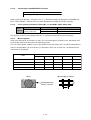
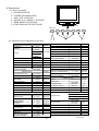
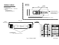
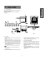
2.3 Names of each monitor part .............................................................................................. 2-2
2.3.1 Configuration of front control panel ....................................................................... 2-2
2.3.2 Configuration of rear input connector .................................................................... 2-2
2.3.3 OSD display matrix ................................................................................................... 2-3
2.3.3.1 User mode ................................................................................................... 2-3
2.3.3.2 Factory mode .............................................................................................. 2-4
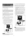
2.4 Adjustment ........................................................................................................................... 2-6
2.4.1 How to select the factory adjustment (FACTORY) mode ................................... 2-6
2.4.1.1 Selecting with front panel switches ......................................................... 2-6
2.4.2 Adjustments before aging ........................................................................................ 2-6
2.4.2.1 Adjusting the high voltage and high voltage protector ......................... 2-6
2.4.2.2 SCREEN voltage / FOCUS adjustment ................................................... 2-7
2.4.2.3 Shock test .................................................................................................... 2-7
2.4.2.4 Preadjustment before aging ...................................................................... 2-7
2.4.2.5 Adjusting the landing (ITC/4 corner purity adjustment) ........................ 2-7
2.4.3 Adjustments after aging ........................................................................................... 2-7
2.4.3.1 +B adjustment ............................................................................................. 2-7
2.4.4 Adjusting the picture size, position and distortion (using automatic adjustment device) .. 2-8
2.4.4.1 Adjusting the picture inclination ............................................................... 2-8
2.4.4.2 Adjusting the back raster position ........................................................... 2-8
2.4.4.3 Adjusting the left/right distortion, picture width, picture position
(H-PHASE) and vertical linearity (all preset) ......................................... 2-8
2.4.4.4 Adjusting the DBF amplitude and phase ................................................ 2-9
2.4.5 Adjusting the cut off ................................................................................................. 2-10
2.4.6 Adjusting the RGB drive signal and X-Pro ............................................................ 2-13
2.4.6.1 Adjusting the R, G, B drive signal (Adjustment of COLOR 1) ............. 2-13
2.4.6.2 Adjusting ABL .............................................................................................. 2-13
2.4.6.3 Adjustment of X-Pro (Timing No.A 30k / 70Hz Full white) ................... 2-14
2.4.6.4 Confirmation for operation of X-Pro (Timing No.25 1800x1350 at 85Hz, Full white) ... 2-14
2.4.7 Adjusting the Purity .................................................................................................. 2-14
2.4.8 Adjusting the focus ................................................................................................... 2-15
2.4.9 Adjusting the convergence ...................................................................................... 2-16
2.4.9.1 Adjusting with ITC ...................................................................................... 2-16
2.4.9.2 Adjusting DDCP .......................................................................................... 2-18
2.4.10 Default settings (With factory mode) ................................................................... 2-23
2.5 Inspections (In normal mode) ........................................................................................... 2-24
2.5.1Electrical performance .............................................................................................. 2-24
2.5.1.1 Withstand voltage ....................................................................................... 2-24
v
2.5.1.2 Grounding conductivity check .................................................................. 2-24
2.5.1.3 Degaussing coil operation ......................................................................... 2-24
2.5.1.4 POWER SAVE function operation (Set the AC power input to 230V) ...... 2-24
2.5.1.5 Confirming the CORNER-PURITY function ............................................ 2-25
2.5.1.6 Focus, picture performance (Timing No.12 106.25kHZ / 85Hz 1600x1200) .... 2-25
2.5.1.7 Misconvergence .......................................................................................... 2-25
2.5.1.8 Picture distortion ........................................................................................ 2-26
2.5.1.9
Linearity ..................................................................................................... 2-28
2.5.1.10 Adjustment value list ................................................................................ 2-29
2.5.1.11 Confirming CLAMP PULSE POSITION, SYNC ON GREEN .............. 2-29
2.5.1.12 Checking the functions during Composite Sync input ........................ 2-30
2.5.1.13 Confirming the full white luminance ...................................................... 2-30
2.5.1.14 Confirming CONVERGENCE compensation function ......................... 2-30
2.5.1.15 Confirming ROTATION compensation function ................................... 2-30
2.5.1.16 Luminance/color coordination uniformity .............................................. 2-30
2.5.1.17 Confirming the full white color coordination ......................................... 2-30
2.5.1.18 Confirming the color tracking ................................................................. 2-31
2.5.1.19 CRT installation position ......................................................................... 2-31
2.5.1.20 Confirming FPM operation ...................................................................... 2-31
2.5.1.21 Confirming Auto size operation .............................................................. 2-31
2.5.1.22 Others ......................................................................................................... 2-31
2.5.1.23 Confirming USB ........................................................................................ 2-31
2.6 DDC write data contents .................................................................................................... 2-32
2.7 Self-diagnosis shipment setting ........................................................................................ 2-33
2.8 Default inspection ............................................................................................................... 2-33
2.8.1 Default setting of switches ...................................................................................... 2-33
2.8.2 Default setting of OSD ............................................................................................. 2-33
2.8.3 Checking the labels .................................................................................................. 2-33
2.8.4 Packaging .................................................................................................................. 2-33
2.9 Degaussing with handy-demagnetizer ............................................................................. 2-34
2.9.1 General precautions ................................................................................................. 2-34
2.9.2 How to hold and use the handy-demagnetizer ................................................... 2-34
2.10 Timing chart ....................................................................................................................... 2-35
2.11 Adjustment timing ............................................................................................................. 2-36
3.
Schematic diagram
4.
Exploded view
<Appendix>
Specification
User's guide
All parts list
vi
1.
Circuit description
1.1
Power block
1.1.1 Outline
(1) The power block is compatible with 100 to 120VAC/220 to 240VAC(50/60Hz).
(2) The active filter circuit is adopted to suppress the higher harmonic current and improve
the power factor.
(3) The circuit that supplies the electric power to the secondary side is divided into two
circuits that are respectively called the main power and sub power.
Though both main and sub circuits supply the power to the secondary side in the normal
operation mode, the power is supplied from the sub power only in the power save mode
since the main power is stopped.
The main power is the configuration used the flyback converter type switching control IC of
the simulative resonant operation. Moreover, the sub power is the configuration used PRC
(OFF width fix) control IC.
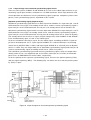
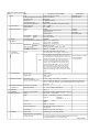
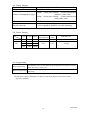
(4) The output on the secondary side is shown in Table 1.
(Refer to the power system diagram1-3 in Pages 1-3, 1-4 and 1-5.)
Power block
Main power
side
Sub power
side
Output voltage
Application
When power save
+215V
H. deflection circuit, Video cut off circuit
OFF
+80V
Video circuit, DBF circuit, High voltage circuit
OFF
+15V
H/V deflection circuit, etc.
OFF
-15V
H/V deflection circuit, etc.
OFF
+12V
Video circuit, H. deflection circuit, etc.
OFF
+7.5V
Heater
OFF
+5V
MPU, etc.
ON
P-OFF+5V
Video circuit, etc.
OFF
Table 1
1.1.2 Rectifying circuit
(1) The AC input voltage is rectified in the full wave mode with the diode bridge in D901.
(2) In the higher harmonic circuit of the section 1.1.4, the AC input current becomes the sine
wave form in the same phase with the AC input voltage waveform, but the interference is
given to other peripheral devices since the noise of the switching current appears on the
input side owing to the switching waveform. Therefore, L902 and C906 are inserted to
suppress the noise that is caused by the switching current.
1.1.3 Surge current suppression
(1) TH901 (thermistor) suppresses the rush current that flows when the power switch is turned
ON. Moreover, D933 is added to protect D902 from the rush current.
1-1
1.1.4 Higher harmonic circuit
(1) The pulsating waveform rectified in the full wave mode by D901 is switched throughout the full cycle
by the frequency of several tens kHz or more. Through this, the input current waveform becomes
an average of the switching currents of the partial cycles, thus becoming the sine waveform in the
macro. (See Fig.1)
(2) For the AC input voltage, the AC input current of the sine wave type in the same phase flows to
achieve the power circuit of improved power factor and reduced higher harmonic wave component.
(3) L903 is the choke coil, Q901 is MOS FET, D902 is the rectifying diode, C911 is the block capacitor,
and IC901 is the power factor improved controller. The power factor improved controller uses
MC33262P of Motorola. (See Fig. 2)
(4) After the sub power circuit operates, P-SUS signal becomes HI when +5V voltage is supplied to the
MPU. Then, Q902 is turned ON, the voltage of approx. +18V is supplied to pin8 (VCC terminal) of
IC901 through D929 from pin2 of T902, and the following operation is started.
(5) The pulsating voltage waveform rectified in the full wave mode by D901 is divided with R904, R905,
R906, R907 and R908 (100VAC : 1.1Vp-p and 240VAC: 2.9Vp-p), and is input to pin3 of IC901
(Multiplier input). Moreover, the output (+side of C911: 400VDC) of the higher harmonic circuit is
divided with R913, R914, R915, R916 and R917 (2.5VDC), and is input to pin1 of IC901 (error
amplifier input).
(6) The output of the error amplifier and the divided waveform of the pulsating voltage input to pin3 of
IC901 sets the threshold voltage of the current sense comparator to control the Q901 flowing
current from zero to the peak line of the AC input voltage in the sine wave pattern.
(7) When Q901 is turned ON, the drain current of Q901 flows to R910 and R937 to drop the voltage,
and the voltage generated by the voltage drop is input to pin4 (current sense input) of IC901. When
the voltage reaches the threshold voltage of the current sense comparator, Q901 is turned OFF.
(8) When Q901 is turned OFF, the accumulated energy of L903 starts to be supplied to the load
through D902.
(9) As the accumulated energy of L903 drops, the auxiliary coil voltage (pin8 of L903) also drops.
When it reaches the threshold voltage of *zero current detector, Q901 will be turned ON again.
* Pin 5 of IC901 is the zero current detection terminal to input the auxiliary coil voltage of pin10 of
L903. The zero current detector monitors that the auxiliary coil voltage drops beyond the thresh
old voltage. Thus, the accumulated energy of L903 is indirectly detected.
(10) The above operation is repeated to continue the oscillating operation. Thus, the DC voltage (L903,
Q901, D902 and C911 compose the voltage rise circuit.) is gained on the output, and the AC input
current of the sine wave in the same phase with the AC input voltage is gained on the input side.
2
ID90
IQ901
Peak
0
ON
MOSFET
Q901
OFF
Figure 1. L903 coil current
1-2
Average
D933
Waveform 1
(Refer to P1-11.)
6
L903
C906
5
4
3
2
1
400VDC
Figure. 1
(Refer to P1-2.)
D902
8
+
6.7V
1.6V/
1.4V
UVLO
2.5V Reference
voltage source
R906
5
+
-
R907
+13V/
Waveform2, 3
(Refer to P1-11.)
8.0V
16V
Timer R
10
Drive
output
Delay
7 R912
Q901
PG
10
RS latch
+
Vref
+
-
+ 1.08Vref
10μA
C909
6
PG
Error amplifier
+
-
+
Vref
1
PG
Quick
start
PG
PG
C908
R908
Multi plier
R909
10pF
Overvoltage
comparator
3
4
R910
20k
R937
+
-
C910
Current sense
comparator
R916 R915
R905
+
-
2
2.5V
PG
Figure 2. High harmonic waveform circuit
1-3
C911
+
PG
36V
R917
1.2V
Zero current detector
+
Q902
L905
R904
MC33262P
R913
IC901
R914
PG
R918
9 10 11 12
R919
8
R911
7
R920
PG
R921
L902
PG
1.1.5 Sub power circuit
(1) The sub power uses PRC control regulator STR-G6352 (IC903) produced by Sanken Electric. (See Fig.3)
(2) When the power switch is turned ON, the rectified and smoothened DC voltage (AC voltage
x 2 ) is supplied to pin4 of IC903, through R950, R951 and R952. When pin4 reaches
approx. 17V, the built-in output FET is put into operation. (Since Q902 is OFF, IC902 and
IC 903 do not operate.)
(3) This also induces the voltage at pin2 of T902 and on the secondary side. These outputs
are respectively rectified, and are used as the power for control on the primary side and
the power for the MPU.
(4) IC903 monitors +5V and -15V output on the secondary side by IC922 (Shunt regulator),
and suppresses the voltage regulation by feeding back to pin 5 of IC903 via IC912
(Photocoupler).
(5) When the voltage on the secondary side starts, the MPU will be put into operation and the
P-SUS signal line will become HIGH.
(6) This information is transmitted to the primary side via IC913 to turn ON Q902.
When Q902 is turned ON, the power for control on the primary side will be supplied to
IC901 and IC902 to operate the higher harmonic circuit. Thus, the main power circuit will
be put into operation.
1.1.6 Main power circuit
(1) The main power circuit adopts the flyback type switching power of pseudo-reosonance
operation. This is composed of a Sanken brand hybrid IC STR-F6676 (IC902) that integrates the power MOS-FET and control IC.
The circuit operation is described as follows. (See Fig. 4.)
(2) The timing at that the power MOS-FET is turned ON is consistent with the bottom point of
the voltage resonant waveform after the transformer (T901) discharges the energy to the
secondary side, that is, a half cycle of the resonant frequency determined by LP value
(primary coil inductor value) of T901, and C914 (resonant capacitor). This is called
pseudo-reosonance operation. The advantage of such an effect is that the switching loss
is reduced by turning it ON when the voltage between the drain sources of the power MOSFET becomes the lowest.
(3) Like the higher harmonic circuit, voltage of approx. +18V is supplied to the Vcc terminal
(Pin 4) of IC902 (STR-F6676) via D929 from pin2 of T902 when Q902 is turned ON by the
P-SUS signal from the MPU.
When the voltage of Pin 4 of IC902 reaches 16V, the control circuit will be put into operation to turn ON the integrated MOS-FET.
(4) When MOS-FET is turned ON, the capacitor C1 in IC will be charged to approx. 6.5V. On
the other hand, the drain current flows to R928, and the voltage generated by the voltage
drop is applied to pin1 (OCP/FB terminal) of IC902.
When the voltage of Pin 1 reaches approx. 0.73V, the comparator (Comp. 1) in IC will be
activated to turn OFF MOS-FET.
(5) The voltage between both ends of C1 drops to approx. 3.7V. the oscillator output will be
reversed again to turn ON MOS-FET.
The above is repeated to continue the oscillation operation.
(6) Here, IC902 monitors +215V of the output on the secondary side with IC921 (error amplifier) and feeds back it to pin1 of IC902 via IC911 (photocoupler), thus suppressing the
voltage fluctuation of the primary side.
1-4
R950
D932
R935
D941
C931
R952
D971
T902
4
5
3
6
2
7
1
8
4
Vin(on)=17.5V
Vin (off)=10V
+
-
UVLO
REG
TSD
Latch
Delay
Internal Bias
Tri
+
-
Vth=25.5V
+
-
Ta=160°C
+
-
Vth=1.45V
REG1
C940
1
D
PQM Latch
Toff=15µS
Drive
S Q
R
2
OCP Comp.
+
-
5
Icont
Vth=0.73V
3 GND
IC903 (STR-G6352)
R931
OSC
+
C972
OVP
C971
L971
Vin
C933 R936
1-5
Figure 3. IC903 (STR-G6352) block diagram and peripheral circuit
R951
C939
R939
(AC x 2 )V
+
T901
5
R926
C912
R922
R941
3
D904
4
4
R923
Waveform5
(Refer to P1-11)
IC902(STR-F6676)
R3
2
C914
3
R4
LATCH
D908
DRIVE
REG.
9
+
O.S.C
T.S.D
2
Vth(1)
R927
Comp.1
1
+
Iconst
Vth(2)
Comp.2
Rconst +
Rconst -
R2
C1
R925 D912
R1
5
C916
O.V.P
R928
START
C917
1-6
Figure 4. IC902 (STR-F6676) block diagram and peripheral circuit
400V
7
1.1.7 Degaussing circuit
(1) The automatic and manual degaussing circuit is provided.
The circuit prevents the picture from dropping its quality due to the magnetization on CRT,
and operates as follows.
(2) When powering ON, Q963 flows to activate RY901 by DG signal output by the MPU.
This will make the current flow through the demagnetizing coil for demagnetization. The
demagnetizing time is approximately 5 seconds.
Manual demagnetization becomes possible by selecting the demagnetizing menu on the
OSD picture.
1.1.8 Power management circuit
Turn ON the power management setting on the menu picture of OSD, and the energy saving
mode shown in Table 2 will be ready depending on whether the horizontal/vertical sync. signal
is present or not.
Power Save
H-sync
V-sync
Video
Power
consumption
Recovery
time
LED indicator
OFF
On
On
Active
140W
―
Green
Off
On
Blank
On
Off
Blank
≦3W
5 sec.
Amber
Off
Off
Blank
ON
1.1.9 Protective circuit
(1) Overcurrent protective circuit (primary side)
IC902 is provided with an overcurrent protective circuit. The voltage drop generated by the
drain current that flows into R928 is input to Pin 1 (OCP/FB terminal) of IC902. When the
voltage reaches 0.73V, the overcurrent protective circuit will be activated.
(2) Overcurrent protective circuit (secondary side)
To protect the parts on the secondary side, the short-circuit detection circuit is provided on
the secondary side output (+215V, +80V, +/-15V, +7.5V), one for each. As an example of
+215V, the output line of +215V is monitored with R964, R965, D966 and Q961. If it drops
beyond approx. +140V for any reason, Q961 will be turned ON to transmit the information
to the MPU. Then, since the MPU sets P-SUS signal at LOW, Q902 will be turned OFF to
cut off the power to IC902 in order to stop IC902. (IC901 will be also stopped at the same
time.) The overcurrent protective circuit is designed to be activated when the output voltage drops approx. 30 to 40%.
(3) Overvoltage protective circuit
R918, R919, R920 and R921 are used to detect the overvoltage in the higher harmonic
circuit, and the tertiary coil (Pin 9) of T901 is used to detect the overvoltage of the voltage
on the secondary side. They are both connected to the overvoltage protective circuit
(Q904, Q905) on the primary side. If any overvoltage results for any reason, Q905 will be
turned ON to turn ON Q904. Then Q902 will be stopped. Since the power for IC901 and
IC902 is cut off as Q902 is stopped, the switching operation will be stopped.
1-7
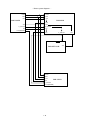
~ Power system diagram 1 ~
+215V
+215V
+80V
+80V
+15V
+15V
PWB-MAIN
PWB-POWER
+12V
-15V
P_OFF+5V
+5V
-15V
P_OFF+5V
+5V
+7.5V(HEATER)
+5V
P_OFF+5V
+3.3V
PWB-DEFL-SUB
+5V
-15V
+215V
+80V
+12V
+5V
PWB-VIDEO
P_OFF+5V
+7.5V(HEATER)
1-8
-15V
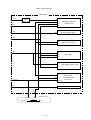
~ Power system diagram 2 ~
PWB-MAIN
+215V
Variable
circuit
+B
+B
+15V
(Chopper circuit)
-15V
Horizotnal width/PCC
control circuit
+15V
+12V
-15V
-15V
Horizontal drive circuit
+12V
+15V
-15V
+80V
Vertical system circuit
+80V
DBF circuit
+12V
-15V
+80V
High voltage system circuit
+12V
+15V
-15V
P-OFF+5V
P-OFF+5V
+5V
+5V
PWB-DEFL-SUB
P_OFF+5V
P_OFF+5V
-15V
Reg.
3.3V
1-9
Corner purity
H/V ROTATION
Drive circuit
MPU circuit
~ Power system diagram 3 ~
PWB-VIDEO
+215V
+215V
Cut off circuit
+12V
+12V
+80V
+80V
Main amplifier circuit
+12V
+12V
Preamplifier circuit
P-OFF+5V
P-OFF+5V
P-OFF+5V
+12V
+5V
+5V
+7.5V(HEATER)
PWB-CRT
+7.5V(HEATER)
1 - 10
OSD circuit
Magnetic cancel circuit
Asset circuit
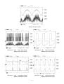
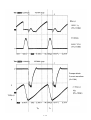
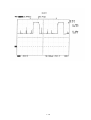
Waveform 1. Top
:AC input voltage
Bottom :AC input current
Waveform 2. Top
:Q901 drain voltage
Bottom :Q901 drain current
Waveform 3. Top
:Q901 drain voltage
Bottom :Q901 drain current
Waveform 4. Top
:IC903 drain voltage
Bottom :IC903 drain current
Waveform 5. Top
:IC902 drain voltage
Bottom :IC902 drain current
1 - 11
1.2 Horizontal deflection block
The operating principle of the horizontal deflection circuit is given below.
The Q502 operates as horizontal output, and the D503 as the dumper diode.
As shown in Fig. 5, the horizontal output transistor Q502 turns to ON/OFF by means of the drive pulse in
pin 25 of IC601 in substrate DEFL-SUB through the drive transformer T501, drive transistor Q501, or
Q560, Q561, Q562, etc.
The deflection current Idy during Q502 ON gets increased to the maximum level Ip according to the
equation shown below:
Idy = (Vcc/Ldy) x Ton
The maximum Ip is approximately 8A at full scan when fh = 106k.
Here;
Vcc: Output voltage of Q504
Ldy: Parallel value of the Lh value of DY (=62µH) and the horizontal output transformer
(=5mH)
TON: The ON time of Q502
When the drive pulse has negative polarity, Q502 turns OFF and Idy starts flowing to charge C506 until
the collector voltage reaches the maximum level Vcp.
Vcp = Vccx{1 + (π/2)x(Ts/Tr)}
With the maximum Vcp attained, the charges accumulated in C506 flow into DY as the discharge current.
This charge/discharge current is called retrace time, and is expressed by the equation given below.
Tr = π
(Ldy•Cr)
* Cr = C506 value
In the present model, the retrace time is set to approx. 1.8µs.
Ts is called trace time, and is expressed by the equation given below with the horizontal cycle as T.
T = Ts + Tr
With Vcp = 0, the dumper diode D503 turns ON and Idy gets decreased from –Ip to 0 ampere. Since
Q502 ON time and dumper diode ON time are set to overlap at 0 ampere point of Idy, the crossover
distortion is prevented from occurring at 0 ampere point of Idy.
The D503 causes the transient current to flow in the high-speed dumper diode.
The horizontal output transformer T502, connected in parallel to the deflection yoke, operates as a choke
coil. Figs. 6 and 7 show the image of circuit operation and the waveforms in actual machine.
1 - 12
1.2.1 Distortion compensation waveform generating circuit
The deflection distortion compensation waveform for horizontal size system is output from pin
64 of IC601. This waveform is output from 1-bit DAC, with 3.3V pulse waveform with resolution 25MHz output at pin 64. This pulse waveform is leveled by the low-pass filters R632 and
C622 to obtain the vertical cycle compensation waveform, with the amplitude 1.0 to 1.2Vp-p
and connected to pin5 of IC5J1.
The compensation waveform circuit carries out horizontal size and trapezoid compensation,
side pin compensation, side pin top and bottom compensation, side pin S-shape compensation
and side pin W compensation. (Refer to Compensation Image Diagram in Fig. 22)
The deflection compensation waveform for horizontal phase system is output from pin 57 of
IC601. The pin 57 has 1-bit DAC output and outputs the 3.3V pulse waveform with 25MHz
resolution. This pulse waveform is then leveled by the low-pass filters R619, R614, C604 and
C601 to obtain the vertical cycle waveform, which is then electrically added to the horizontal
system PLL filter (pin 20 of IC601) to carry out the deflection distortion compensation of the
horizontal phase system. It carries out parallelogram distortion compensation and side pin
balance (top and bottom) correction. (Refer to the Compensation Image Diagram in Fig. 22.)
The control of horizontal screen width and the side PCC control are carried out by IC5J1, Q503
and Q504. First, the horizontal width signal and each distortion compensation signal impressed in pin 5 of IC5J1 from pin 64 of IC601 are compared with the AFC pulse signal rectified and fed back to pin 13 of IC5J1. The signals are further compared with the constantinclination type saw-tooth wave synchronized with the horizontal cycle created inside IC before
turning into the PWM signal of square wave. This PWM signal output from pin 9 of IC5J1
carries out the above control by driving the Q504 gate. Fig. 8 shows the block diagram of
IC5J1 and Fig. 9 the operation image waveforms.
IC5K1 connected to pin 8 of IC5J1 is a transistor with 2 circuits.
Pins 1 and 3 of IC5K1 are for the base, pin 2 is for GND and pins 4 and 5 are for the collector.
Pin 32 of IC101 connected to pin 3 makes pins 5 and 2 open/short by P-SUS signal.
When P-SUS signal is LOW, pin 8 of IC5J1 is led into GND from pin 5 of IC5K1, and make
SYNC input of IC5J1 LOW. As IC5J1 stops operation without SYNC input, Q504 turns OFF
and horizontal deflecting output stops.
Due to this process, destruction by wrong pulse is prevented when it exceeds in Q502.
The Q503 works as a ripple filter in 215V line and keeps the Q503 emitter voltage constant
even if there is a slight fluctuation in the collector voltage of Q503. The Q503 collector has
215V applied to it, with the emitter output being stable at 203V. This is mainly effective in
dynamic regulation.
The horizontal raster position is adjusted by using Q5A1, Q5A2, VR5A1 and T502. The reference voltage is obtained from the connecting point of Cs and is then input into pin 2 of T502.
When the emitter voltage in Q5A1 and Q5A2 has the DC level increased by adjusting VR5A1,
the current flows to DY side, causing the raster to move left. Reversely, when the DC level of
the emitter voltage is decreased, the current flows to Q5A2 side, causing the raster to move
right.
The Idy DC level is adjusted by varying the emitter voltage of Q5A1 and Q5A2 at the timing
No. 25 (120kHz/85Hz) using VR5A1, so that the raster position comes at the center of CRT.
The operation image is shown in Fig. 10.
This adjustment, however, is confined to the factory, and is not open to the users.
1 - 13
215V
Q503
Q504
T502
Q502
D503
C506
L540
LIN
Q540
Q510
IC501
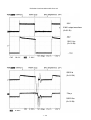
Figure 5 Horizontal deflection circuit
1 - 14
IC601 output waveform
Q501 Vce
Q502 Ib
Q502 Vbe
Q502 Ic
Q502 Vce
Dumper diodes current waveform
Idy
Figure 6 Horizontal deflection circuit operation image
1 - 15
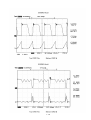
Figure 7. Deflection circuit waveform while fh=106k
IC601 output waveform
(fh=106k)
Q501
Vce
Q501
(fh=106k)
Q502 Ib
Q502
(fh=106k)
Q502
Vbe
Q502
(fh=106k)
1 - 16
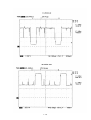
Q502
Q502
Damper diode
Current waveform
(fh=106k)
1 - 17
Deflection circuit waveform while fh=31.5k
3.3V
IC601 output waveform
(fh=31.5k)
Q501 Vce
(fh=31.5k)
Q501
Q502 Ib
Q502
(fh=31.5k)
-7Ao-p
Q502
Q502 Vbe
(fh=31.5k)
1 - 18
Q502 Ic
Q502
Q502
Q502Vce
Damper diode
Current waveform
1 - 19
Err
Err
Vcc
IN
OUT
14
13
12
DTC
11
Power
PWM
Vcc
OUT
10
9
HD IN
8
+
+
-
9.0V
Ref
+
SAW Gen.
1
2
3
4
5
6
7
Ref
IN
SAW
R
SAW
OUT
Buff
OUT
Buff
IN
Vreg
GND
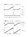
Figure 8. IC5J1 block diagram
HD IN
SAW OUT
Error amplifier
output
PWM OUT
Figure 9. Operation image
1 - 20
Ip
0
When the picture is the center
0.8Ap-p
0
When the raster moves to the left
0
When the raster moves to the right
Figure 10 Horizontal position adjustment image
1 - 21
1.2.2 Deflection current compensation circuit
As the picture becomes flatter, the arrival distance of the deflected electronic beam becomes
more different between the center and both ends of the picture. Therefore, there is a tendency
for the image to be contracted at the center of the picture and expanded at both ends of the
picture. Moreover, the left side of the picture is more expanded than the right side of the picture owing to the characteristics of the circuit. CS applies S type compensation to the deflection current with the resonant effect of the deflection yoke and contracts at both ends of the
horizontal axis. The linearity coil increases the inductance of the starting section of the deflection current with the supersaturated reactor, and works to contract the left side of the horizontal axis.
As the frequency is lower, the capacity of CS is generally increased and the linearity coil with a
larger impedance value is used. In the practical circuit, seven CS capacitors are prepared, and
are combined as desired. The linearity coil changes inductance by letting the control current
corresponding to the horizontal frequency flow to the control coil.
(1) S type compensation with CS
CS is switched in seven steps by FET. IC501 element with six FETs included and Q510 are
used. On IC501, pins 2, 5, 7, 9, 11 and 13 are used as the gate, and pins 3, 6, 8, 10, 12
and 14 are used as the drain. Pins 1 and 15 are used as the ground, and each source are
grounded to the earth. The binary value signal of HIGH (5V) or LOW (0V) is input to each
gate by IC102. In case of HIGH, FET is turned ON. In case of LOW, FET is turned OFF.
The correspondence to the signals from the capacitor and IC102 are as follows.
Table 3
G
D
Capacitor
Signal
FET1
2
3
C523
CS2
FET2
5
6
C524
CS1
FET3
7
8
C525
CS5
FET4
9
10
C526
CS6
FET5
11
12
C527
CS3
FET6
FET7
13
14
C528
CS4
C529
CS7
(Q510)
The column of G and D is Pin No.
(2) Compensation with linearity coil
The linearity coil compensates the left expansion of raster by changing the inductance
value through the current value flow in order to keep the horizontal linearity to appropriate
level. In the actual circuit, L540 stands for the linearity coil.
The newly adopted linearity coil is provided with a control winding capable of controlling the current
characteristics of the inductance value. The control voltage (DC) corresponding to each horizontal
frequency is supplied from pin 2 of IC101 to pass the control current to the control winding through
IC103 and Q540. This controls the current characteristics of the inductance value, and eventually
keeps the horizontal linearity to appropriate level. An image of characteristic of linearity coil is as
fugure 11.
1 - 22
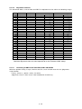
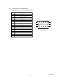
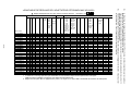
As shown in the Table 4 below, CS is switched on the horizontal frequency bands. 1/0 in the
table express the signals from IC101 with 1 for HIGH and 0 for LOW. Here, the column of the
frequency expresses the lower limit value.
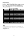
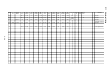
Table 4
User Timing
Fh
(kHz)
31
34
36.5
39
45
47.5
49
52
55
59
61
63
66
70
73
76
78.5
81.5
83
86.5
89
92
94
97
104
108
111
114
116
125
CS7
0.024
1
0
0
0
0
0
1
1
0
1
0
0
1
1
0
0
1
0
0
0
0
0
0
0
1
1
0
0
1
0
CS6
0.056
1
0
0
0
1
1
1
1
0
0
0
0
1
1
1
0
1
1
1
1
1
0
0
0
1
1
1
1
0
0
CS5
0.15
1
0
1
1
0
0
1
1
1
0
0
0
1
1
1
1
0
0
0
1
1
1
1
1
0
0
0
0
0
0
CS4
0.24
1
1
0
1
0
0
1
1
1
1
1
1
1
1
1
1
1
1
1
0
0
0
0
0
0
0
0
0
0
0
CS3
0.47
1
0
0
1
1
1
1
1
1
1
1
1
0
0
0
0
0
0
0
0
0
0
0
0
0
0
0
0
0
0
CS2
0.82
1
1
1
1
1
1
0
0
0
0
0
0
0
0
0
0
0
0
0
0
0
0
0
0
0
0
0
0
0
0
CS1
1.3
1
1
1
0
0
0
0
0
0
0
0
0
0
0
0
0
0
0
0
0
0
0
0
0
0
0
0
0
0
0
CS7
0.024
1
0
1
0
0
1
0
1
0
1
CS6
0.056
1
1
0
1
0
1
0
1
1
0
CS5
0.15
1
0
0
1
1
1
1
0
0
0
CS4
0.24
1
0
1
1
1
0
0
0
0
0
CS3
0.47
1
1
1
0
0
0
0
0
0
0
CS2
0.82
1
1
0
0
0
0
0
0
0
0
CS1
1.3
1
0
0
0
0
0
0
0
0
0
com
0.173
0.173
0.173
0.173
0.173
0.173
0.173
0.173
0.173
0.173
0.173
0.173
0.173
0.173
0.173
0.173
0.173
0.173
0.173
0.173
0.173
0.173
0.173
0.173
0.173
0.173
0.173
0.173
0.173
0.173
0.173
total
3.233
2.533
2.443
1.853
1.519
1.519
1.113
1.113
1.033
0.907
0.883
0.883
0.643
0.643
0.619
0.563
0.493
0.469
0.469
0.379
0.379
0.323
0.323
0.323
0.253
0.253
0.229
0.229
0.197
0.173
Preset Timing
timing
31k/60
46k/75
60k/75
68k/85
80k/75
91k/85
93k/75
106k/85
112k/75
120k/85
total
Cap.
3.233
1.519
0.907
0.619
0.563
0.403
0.323
0.253
0.229
0.197
com
cs
0.173
0.173
0.173
0.173
0.173
0.173
0.173
0.173
0.173
0.173
1: ON
0: OFF
20.00
Inductance(mH)
15.00
Control current OA
10.00
Control current
200mA
5.00
-11
-6
0.00
-1
4
Deflection current (A)
Figure 11 Characteristic of variable lineality
1 - 23
9
The waveform of the deflection current is compensated from Fig. (a) to Fig. (b) through the
above. The starting section of the current is smoothened, and the linear section becomes the
S type.
Figure(a)
Figure(b)
1.3
Vertical output block
The vertical deflection circuit controls the vertical width and vertical position with IC601 on the
DEFL_SUB substract, and IC603 controls the linearity. Moreover, the signal output from IC603
is input to the vertical deflection output IC401.
THERMAL
PROTECTION
PUMP
UP
−
AMP
5
6
+15V
7
PUMP UP OUT
4
INVERTING
INPUT
3
OUTPUT
STAGE VCC
2
Ver. OUTPUT
-15V
1
NON INV. INPUT
+
Figure 12 IC401(LA7841L) Pin connection & Function Block diagram
1 - 24
1.4 High voltage block
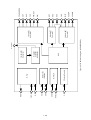
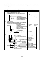
The high voltage circuit is composed of the high-voltage regulator IC701, MOS-FET Q701
flyback transformer (FBT) T701, operation amplifier IC702 and their peripheral circuits.
1.4.1 High voltage control circuit
The IC701 is an IC for high voltage control, with the block diagram given in Fig.13. The OFF trigger PWM
control system is adopted to carry out high voltage control. The built-in VCO circuit gets synchronized
when the horizontal synchronous signal (hereafter SYNC signal) is input from Pin 3 of IC701 (horizontal
synchronous input terminal). Thus, the MOS-FET Q701 is controlled to turn OFF with the timing of the
SYNC signal changing over to HI, and is called OFF trigger system.
Further, the DC voltage, output after the feedback signal (IC701 Pin 11) from FBT T701 is compared with the
high-voltage set voltage (IC701 Pin 12) from IC101 in the internal error amplifier, is compared with the sawtooth-waveform of VCO to control the pulse output DUTY so as to keep the high voltage constant (PWM control).
The timing chart for OFF trigger PWM control system is given in Fig.14. Set the high voltage by selecting
[HVADJ] in OSD and manipulating +/- button (Standard value: 27.0kV).
1.4.2 Protective function circuit
(1) Start and stop of high-voltage regulator IC701
The IC701 starts operation when Vcc voltage (power voltage applied to Pin 2 and Pin 10) attains the
level of 8.4 Vtyp, and the operation stops when the Vcc voltage is less than 7.4 Vtyp.
(2) IC701 overcurrent protection (OCP) function
It detects the peak value of the drain current in MOS-FET Q701 per pulse and stops DRIVE when the
voltage in Pin 6 of IC701 detecting the end-to-end voltage of the source resistors (R706 and R707),
exceeds 1.0 Vtyp until the next SYNC signal is input.
(3) IC701 overload protection (OLP) function
This function brings the system to the latch stop when OCP gets continuously activated due to
continuous overload.
It forms time constant using C716. With OCP activated and C716 charged and the voltage in Pin 8 of
IC701 exceeding 2.5 Vtyp, IC701 gets set to Latch mode, bringing the control operation to stop. This
status does not get released (reset) until the Vcc voltage (power voltage applied to Pin 2 and Pin 10)
in IC701 is less than 7.4 Vtyp.
(4) Over-voltage protection function for anode voltage (X-ray protector)
A voltage proportional to the high voltage is generated in Pin 6 of T701 due to the winding ratio
between secondary and tertiary winding inside FBT T701. This voltage is then rectified by D707 and
C708 and is further divided by R708 and R709 before being input in Pin 17 of microcomputer IC101
for comparison with the X-Pro set value. In case the voltage exceeds the set value, the output in Pin
33 of microcomputer IC101 gets fixed to LOW (P-OFF mode). With the mode set to P-OFF, the
application of voltage Vcc to IC701 stops, causing the IC701 operation to stop. The status continues
until the power SW is turned OFF. The overvoltage protection function is set to operate when the
high voltage level reaches 30kV (with the beam current is approx. 1mA).
(5) Overcurrent protection function for beam current (beam protector)
The beam current is supplied from +12V power source through R722. Since the end-to-end voltage of
R722 varies according to the beam current, the voltage drop due to R722 becomes large if the beam
current increases. The voltage in Pin 9 of FBT T701 (the voltage obtained by subtracting the voltage
drop due to beam current from the +12V power voltage) undergoes resistance division by R723 and
R724, and is then input into Pin 6 of operation amplifier IC702 for comparison with Pin 5 of IC702
(reference voltage). The voltage is then output (Pin 7 of IC702) and is input into Pin 16 of microcomputer IC101. The voltage in Pin 7 of IC702 (output terminal) is output linearly due to the fluctuation in
beam current. However, if the terminal voltage in Pin 16 of IC101 exceeds Beam-Pro setting value (ABL
data +70 : Max. 254), the output of Pin 33 of IC101 gets fixed to LOW (P-OFF mode). With the mode
set to P-OFF, the application of Vcc voltage to IC701 stops, causing the IC701 operation to stop. This
status continues until the power switch is turned OFF. The overcurrent protection function is set to
operate when the beam current reaches the level of approximately 1300µA.
1 - 25
GND2
16
SW
Condenser
connection
for DTC
COMP
HV
ADJ
FEED
BACK
Vcc1
12V
X-RAY
15
14
13
12
11
10
9
Vcc2
12V
DTC
−
−
−
+
+
SYNC-IN
RAMP
GEN.
DUTY
ADJUSTMENT
GND2
PROTECT
VCO
1
2
PWM
output
Vcc2
12V
3
5
4
6
SYNC Condenser Resistance Is detection
connection connection input
IN
for DUTY
for DUTY
adjustment adjustment
7
GND1 Condenser
connection
for IS
detection
Figure 13. High voltage regulator IC701 block diagram
SYNC. signal
input (3pin)
Vds wave form
Threshold voltage for
MAX DUTY
adjustment (5pin)
Saw-tooth wave for
MAX DUTY
adjustment (4pin)
Err AMP output
voltage (13pin)
RAMP wave form
PWM output
(1pin)
Id wave form
Figure 14. OFF trigger PWM control system timing chart
1 - 26
8
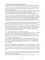
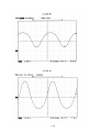
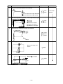
1.4.3 DBF (Dynamic Beam Focus) circuit
Since the display is flattened, the focus becomes unequal between the center and circumference of the picture. To compensate for it, it is necessary to superimpose the parabola voltage
of 370Vp-p in the horizontal cycle with the static focus (with the horizontal width is 396mm) and
the parabola voltage of 145Vp-p in the vertical cycle. The slight voltage that is generated from
the parabola voltage generating circuit is amplified and reversed to generate the high voltage
in order to keep the focus equal. This circuit is called DBF circuit.
As shown in Fig. (16), the circuit is composed of the parabola voltage generating circuit IC601,
amplifier section IC6A1 in the front step, Q7A1 to Q7B5 of amplifier section in the rear step,
T7A1, and so on.
Video period
In case of the horizontal DBF :370Vp-p
In case of the vertical DBF
:145Vp-p
Figure 15
Approx. 350V
90V
IC601
DEFLPROCESSOR
IC
Vertical DBF
R7A5
Q7B3
R7A3
Q7B1
T7A1
Horizontal DBF
OP-AMP
Q7B2
To FBT
Q7B5
IC6A1
Q7B4
R7B9
Q7A1
R7A5
R7B7
R7A4
R7A6
Figure 16
1 - 27
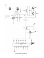
After the horizontal and vertical DBF
voltage are separately generated, they are
amplified and are finally composed.
<Horizontal section>
The voltage (approx. 0.5Vp-p) of the parabola waveform shown in Fig. (a) is output
from the deflection processor IC (IC601),
and is amplified approx. 10 times by OPAMP (IC6A2). Thereafter, it is amplified to
50 to 60Vp-p by the transistor (Q7B1 and
Q7B2). The amplification ratio is determined by the ratio between the resistors
R7B6 and R7B7, being approx. 10 times.
Moreover, the waveform is reversed as
shown in Fig. (b) at this time. Then, it is
amplified to approx. 500Vp-p by DBF
transformer (T7A1). The coil ratio between
the primary and secondary coils of the DBF
transformer is 1: 10, being the amplification ratio of approx. 10 times.
<Vertical section>
The voltage (approx. 1.0Vp-p) of the parabola waveform shown in Fig. (a) is output
from the deflection processor IC (IC601),
and is amplified approx. 4 times by OPAMP (IC6A2). Thereafter, it is amplified to
approx. 160Vp-p by the transistor (Q7A1).
The amplification ratio this time is determined by the ratio between R7A3 and
R7A4, being approx. 40 times.
Figure (a)
Figure (b)
Vertical DBF
Horizontal DBF
Figure (c)
The horizontal and vertical DBF voltages
amplified and reversed are composed by
applying vertically synchronous modulation
to the output on the secondary side as
shown in Fig. (c). The composed voltage
is input to Pin 12 of the flyback transformer
(T701).
Horizontal period
Vertical period
1 - 28
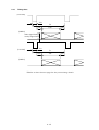
1.5
CRT compensation block
1.5.1 Rotation circuit
The rotation circuit is a circuit to compensate the picture inclination caused by the earth magnetism by letting DC current flow to the rotation coil wound on the front side of DY for adjustment. It is controlled to 0 to 5V with the reference of 2.5V by IC103 pin 3 (PWM_DAC), and
DC current of +/-90mA (max) is made to flow to the rotation coil by IC804 pin 2.
This correction circuit has two functions; (1) User adjustment (OSD display) and (2) Southern/
Northern horizontal magnetic field rotation cancellation, as follows.
(1) User adjustment (OSD display)
User provides DC current to the rotation coil according to the value displayed on OSD.
(2) Southern/Northern horizontal magnetic field rotation cancellation
Southern/Northern horizontal magnetic field rotation cancellation is to automatically adjust
the variation of raster rotation by earth magnetism.
Detection voltage and direction of the southern/northern horizontal magnetic field (pin 2 of
IC214) is detected by IC214 (Earth magnetism sensor unit), and pin 18 of IC101
(CPU_ADC) reads the detected voltage and provides DC current to the rotation coil according to the prescribed control program.
1.5.2 Corner purity circuit
The corner purity circuit is a circuit to compensate for the color shade and color deviation of
the picture corner. On the rear side of CRT, it is adjusted by DC current flowing to the corner
purity coils installed in the four corners on the display surface.
The compensation circuit is composed of the following four functions of (1) User adjustment
(OSD display), (2) Aging variation compensation, (3) High/low temperature drift compensation
and (4) Southern / Northern horizontal magnetic field landing cancellation.
(1) User adjustment (OSD display)
The user causes DC current of +/-60mA (max.) to flow to the purity coil of each corner
according to the value displayed on OSD.
(2) Aging variation compensation
As the electronic beam collides with the aperture grille, it is thermally expanded and contracted. The thermal expansion/contraction is varied according to the elapse of the power
ON/OFF time of the monitor. The color shade and deviation of the picture corner thus
generated are automatically adjusted.
The voltage of the beam current supply pin (T701 pin 9) is detected with R723/R724, and
the voltage that detects the time elapse of the power ON/OFF of the monitor is read from
the CR charge (integration) circuit composed of C723 and R736 and CR discharge (integration) circuit, composed of C723 and R737 through IC702 (buffer amplifier) by IC101 pin
15 (CPU_ADC), and the DC current of +/-17mA(max) flows to the purity coil on each corner
according to the specified control program.
(3) High/low temperature drift compensation
The front panel (glass) is thermally expanded and contracted as the temperature varies in
the installation environments of the monitor. The color shade and deviation of the picture
corner are automatically adjusted. The voltage that detects the temperature variation of
the installation environments of the monitor is read from the environment temperature
detection circuit composed of TH101 (thermistor) arranged near the front panel (glass) by
IC101 pin 14 (CPU_ADC), and DC current of +/-13mA (max) is made to flow to the purity
coil on each corner according to the specified control program.
1 - 29
(4) North-south horizontal field landing cancel
The north-south horizontal field landing cancel carries out automatic adjustment of color shading and
color shift occurring appeared in the opposite derection at the top and bottom end of the monitor
display surface in the horizontal direction.
The detecting voltage and direction of the north-south horizontal field (IC214 pin 2) are detected by
IC214 (geomagnetic sensor unit), the detecting voltage is read by IC101 pin 18 (CPU_ADC), and the
direct current of ±20mA (max) flows in each corner purity coil according to the specified control
program. (Four-corner interlock control)
• The left upper corner on the display surface is controlled with 0 to 5V of 2.5V reference
by IC101 pin 6 (PWM-DAC), and the DC current of the above value is made to flow to
the purity coil on the left upper corner by IC803 pin 2.
• The right upper corner on the display surface is controlled with 0 to 5V of 2.5V refer
ence by IC101 pin 7 (PWM-DAC), and the DC current of the above value is made to
flow to the purity coil on the right upper corner by IC803 pin 8.
• The left lower corner on the display surface is controlled with 0 to 5V of 2.5V reference
by IC101 pin 8 (PWM-DAC), and the DC current of the above value is made to flow to
the purity coil on the left lower corner by IC801 pin 2.
• The right lower corner on the display surface is controlled with 0 to 5V of 2.5V reference
by IC101 pin 9 (PWM-DAC), and the DC current of the above value is made to flow to
the purity coil on the right lower corner by IC801 pin 8.
1.5.3 Earth magnetism cancel circuit
The earth magnetism cancel circuit has a south-north horizontal magnetic field canceling
function and a vertical magnetic field canceling function.
IC214 (earth magnetism sensor unit) detects the voltage and direction of the south-north horizontal magnetic field (IC214 pin 2) and the vertical magnetic field (IC214 pin1), and IC101 pins
18 and 19 (CPU_ADC) reads the detected voltage to automatically control the following canceling function according to the specified control program.
Here, the output voltage of IC214 (earth magnetism sensor unit) operates as follows.
• South-north horizontal magnetic field (IC214 pin 2): 0.8V(-0.04mT) to 2.5V(+/-0.00mT) to
4.2V(+0.04mT)
• Vertical magnetic field (IC214 pin 1) : 3.3V (-0.04mT) to 2.5V (+/-0.00mT) to 0.5V (+0.10mT)
<South-north horizontal magnetic field canceling function>
(a) Horizontal magnetic field landing cancel
The horizontal magnetic field landing cancel circuit is a circuit to compensate for the color
shade and deviation that appear in the horizontal direction that becomes the opposite
direction at the upper and lower ends on the monitor display surface, and the automatic
adjustment is done by DC current flowing to the corner purity coil that is wound around the
display surface. (synchronized control for four corners)
(Refer to 1.5.2 (4) for detail.)
(b) Horizontal magnetic filed convergence cancel
The horizontal magnetic field convergence cancel circuit is the circuit to compensate for
the misconvergence that results after the vertical convergence of RED and BLUE in the
whole display area of the monitor deteriorates, and it is automatically adjusted by DC
current flowing to the 4V convergence compensation coil mounted on DY. It is controlled
with the DC component (V-CONVERGENCE) by IC601 pin 60 (4V_SC), and DC current of
+/-30mA (max) is flowen to the 4V convergence compensation coil by IC8A1 pin 6 (Power
Opamp).
1 - 30
<Vertical magnetic field canceling function>
The vertical magnetic field landing cancel circuit is the circuit to compensate for the color
shade and deviation that reaches its maximum at the center in the horizontal axis direction
and its minimum at the upper and lower ends on the monitor display surface, and the
adjustment is done by DC current according to the value displayed on OSD flowing to the
speed modulating coil installed in the neck part of CRT.
It is controlled with 0 to 5V of 2.5V reference by IC101 pin 4 (PWM-DAC), and DC current
of +/-140mA (max) is made to flow to the speed modulating coil by IC804 pin 8.
1.5.4 Digital dynamic convergence clear (DDCC) circuit
In the digital dynamic convergence clear (hereafter called DDCC) circuit, the convergence
compensating current waveform is produced and amplified, and the convergence is compensated by the compensation current flowing to the sub yoke that is installed as the rear unit of
the deflection yoke.
Though the principle of the convergence compensation with the sub yoke is same as the CP
ring, the CP ring is used for the static variation with the parallel movement in the whole picture
in the uniform magnetic field with the permanent magnet but the sub yoke is used for dynamic
variation that compensates a desired position on the picture by controlling the current waveform that flows to the coil of the electric magnet.
(See Fig. 18)
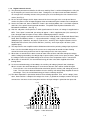
(1) Production of compensation current waveform
There are 30 kinds of compensation elements, and they are programmed in
IC601(CP267P151=uPD61882BGC) one by one by using the functions. The amplitude of
the current is controlled by inputting the compensation coefficient into the function.
V
YHTT= b11T・y^2
YHTB= b11B・y^
b11T
YHTT&YHTB
b11T
2
YHJT= b12T・y
YHJB= b12B・y
b11B
b11B
YHT=b11T・y^2+b11B・y^2
V
YHJ=b12T・y+b12B・y
YHJT&YHJB
↓
4H_SC=all・(YHT+YHJ)
b12T
b12T
b12B
b12B
Red :
Blue:
Figure 17 DDCC compensation image
1 - 31
Examples of the functions and current waveform/compensation operation of YH(YHTT,
YHTB, YHJT, YHJB) are shown as follows.
In the above formulas, b11T, b11B, b12T and b12B express the compensation coefficients,
and y and y^2 express the primary and secondary functions of the vertical frequencies.
The other parts except the compensation coefficients are programmed, and desired amplitudes (= compensation amount) are gained by varying the coefficients.
YHTT and YHTB compensate the upper and lower parts of the picture of the characteristic
components of their DYs to compensate the upper and lower parts of the picture of the
axis deviation component. The component gained by adding YHT and YHJ is multiplied by
the offset compensation coefficient a11. The resultant component is regarded as 4H_SC,
and is output from IC601 (CP267P151=uPD61882BGC) pin 61.
(2) Waveform, and operation on the picture
The case in which the currents flow through 4H coils of the sub yoke is explained. Regarding YHT (secondary function in the vertical frequency), in case of Fig 17 as an example, the current is large in the same direction at the start (upper end of the picture) and
the end (lower end of the picture) of the vertical frequency, and is zeroed on the X axis of
the picture. Therefore, the magnetic field that is proportional to it is generated, and RED
and BLUE vary in the same direction only at the upper and lower ends of the picture. As
aforementioned, YHT can be independently controlled at the upper part (b11T.y^2) and
lower part (b11B.y^2).
Moreover, regarding YHJ (Primary function in the vertical frequency), if the flowing direction of the current is opposite at the start (upper end of the picture) and the end (lower end
of the picture) of the vertical frequency as an example, RED and BLUE vary in the opposite direction only at the upper and lower ends of the picture. Compensation in the vertical
direction can be done by making the current flow to the 4V coil.
Fig.19(a) and (b) shows the image of each adjustment item of the DDCC adjustment.
(3) Adjustment method
Before the adjustment with the compensation circuit, it is necessary that they are properly
adjusted at the center (H-STATIC and V-STATIC), on the X axis (XH slider, B-Bow 4P, XV
differential coil) and on the Y axis (YH volume, YV volume).
Though DC current is superimposed on the sub yoke, H-STATIC and V-STATIC are
pushed to the greatest possible extent by the adjustment with CP ring in order to reduce
the stress of the driver IC8A1 (STK391-110).
Moreover, since 4H and 4V coils alone are installed on the chassis, it is first necessary
that the convergence of RED, BLUE and GREEN (6H, 6V) satisfy the specifications for the
performance of ITC(CRT&DY).
As the adjustment procedure, the adjustment values of 30 elements are not respectively
zeroed but they are adjusted to nearest to zero with a total balance in good order.
In other words, the balance (compromise) adjustment with each adjustment item is applied.
The correspondence of the names of DDCC adjustment mode to the coefficients of all 30
elements is shown below.
1 - 32
<Factory mode>
4H
Coil
b11T
b21L
b31TL
b41TL
c11T
c21L
c31TL
c41TL
4V
Coil
YHTT
XHL
S3HTL
PQHTL
YVTT
XVL
S3VTL
PQVTL
y^2
x^2
x^2・-(y^3+y^4+y^5+y^6)
x^2・y^4
y^2
x^2
x^2・-(y^3+y^4+y^5+y^6)
x^2・y^4
b11B
b21R
b31TR
b41TR
c11B
c21R
c31TR
c41TR
YHTB
XHR
S3HTR
PQHTR
YVTB
XVR
S3VTR
PQVTR
y^2
x^2
x^2・-(-y^3+y^4+y^5+y^6)
x^2・y^4
y^2
x^2
x^2・-(-y^3+y^4+y^5+y^6)
x^2・y^4
b12T
YHJT
y
b12B
YHJB
y
b31BL S3HBL x^2・-(-y^3+y^4-y^5+y^6) b31BR S3HBR
x^2・y^4
b41BL PQHBL
b41BR PQHBR
y
c12T YVJT
c12B YVJB
x^2・-(-y^3+y^4-y^5+y^6)
x^2・y^4
y
c31BL S3VBL x^2・-(-y^3+y^4-y^5+y^6) c31BR S3VBR
x^2・y^4
c41BL PQVBL
c41BR PQVBR
x^2・-(-y^3+y^4-y^5+y^6)
x^2・y^4
<User & Factory mode>
4H Coil
a11
H-CONVERGENCE
DC
4V Coil
a12
V-CONVERGENCE
DC
Table 5
(4) Block diagram
Fig. 20 shows the block diagram of the DDCC circuit.
The components 4H_DC(pin 6), 4H_SC(pin 61), 4V_DC(pin 8) and 4V_SC(pin 60) supplied
from IC601(CP267P151=uPD61882BGC) to 4H-Coil and 4V-Coil are output, the dynamic
component (4H_DC, 4V_DC) is amplified with IC6A1(TL084), and the static component
(4H_SC, 4V_SC) is amplified with IC6A2(KIA4558).
DCC(pin 7) output from IC601 (CP267P151=uPD61882BGC) and DEFL_+3.3V(pin 3)
output from IC602 (TA48M033F) are respectively the reference voltage of OpAmp(IC6A1:TL084) that amplifies the above dynamic component (4H_DC, 4V_DC) and the
reference voltage of Op-Amp(IC6A2:KIA4558) that amplifies the static component (4H_SC,
4V_SC).
On each of 4H and 4V, the waveform added with the dynamic component and static component is input to IC8A1 pin 3 and pin 4 (STK391-110) allow the specified current to flow to
each convergence compensation coil.
1 - 33
For four poles magnetic field
S
N
B
G
B
R
R
N
S
Static change by
the eternal magnetic field
(Parallel shifting totally)
N
R
S
B
G
R
S
B
N
S
N
B
4H coils
G
R
B
R
B
R
R
N
S
Dynamic change by
YHT compensate
electromagnet
(Compensate at the
optional position on the picture.)
N
4V coils
S
B
G
R
B
R
S
R
B
N
YVT compensate
Figure 18 The principle of DDCC compensation
1 - 34
B
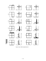
Figure 19 (a) DDCC adjustment item
1 - 35
amp
V-CONVERGENCE
amp
H-CONVERGENCE
RED
BLUE
time
time
1V
YHTB
time
YVTT
1V
YVTB
time
amp
YVJB
1V
YVJT
YVJB
YVTB
YVJT&YVJB
YVJT
amp
YHJB
1V
YHJT
YVTT
YVTT&YVTB
YHTT
amp
YHJB
YHTB
amp
YHJT
YHJT&YHJB
YHTT
YHTT&YHTB
time
time
1H
amp
1H
amp
1V
PQVTL
1V
PQHTL
time
time
1H
amp
1H
amp
1V
PQVTR
1V
PQHTR
time
time
amp
amp
1V
PQVBL
1V
PQHBL
1H
1H
time
time
amp
amp
1V
PQVBR
1V
PQHBR
1H
1H
time
time
Figure 19 (b) DDCC adjustment item
1 - 36
1H
amp
1H
amp
RED
BLUE
1V
XVL
1V
XHL
time
time
1H
amp
1H
amp
1V
XVR
1V
XHR
time
time
amp
amp
1H
1H
1V
S3VTL
1V
S3HTL
time
time
amp
amp
1H
1H
1V
S3VTR
1V
S3HTR
time
time
amp
amp
1V
1H
S3VBL
1V
1H
S3HBL
time
time
amp
amp
1V
1H
S3VBR
1V
1H
S3HBR
time
time
IC101
ST72T771N9B1
+12V
Pin37, Pin38:SDA_I2C
Pin36
+
:SCL_I2C
-15V
IC6A2
Pre-Amp for 4H_DC TL084
+15V
+
-15V
IC601
CP267P151=uPD61882BGC
1 - 37
Figure 20 DDCC circuit diagram
Pin6:4H_DC(XDC)
x^2
Pin8:4V_DC(YDC)
x^2•y^4
x^2•-(Y^3+Y^4+Y^5+Y-6) Pin7:DCC
x^2•-(-Y^3+Y^4-Y^5+Y-6)
Pin61:4H_SC(XSC)
Pin47:SDA_I2C
Pin48:SCL_I2C
4H-Coil
+12V
*
*
+
-15V
IC8A1
Main-Amp for 4H_CONVERGENCE STK391-110
IC6A2
Pre-Amp for 4V_DC TL084
*
y
+12V
y^2
Pin60:4V_SC(YSC)
*
+
+15V
-15V
IC6A3
Pre-Amp for 4H_SC KIA4558
IC602
TA48M033F
P-OFF-+5V
Pin1
Pin3
+
+12V
-15V
IC6A3
Pre-Amp for 4V_SC KIA4558
* Pin6:4H_DC(XDC) =XHL+XHR+S3HTL+S3HTR+S3HBL+S3HBR+PQHTL+PQHTR+PQHBL+PQHBR
Pin8:4V_DC(YDC) =XVL+XVR+S3VTL+S3VTR+S3VBL+S3VBR+PQVTL+PQVTR+PQVBL+PQVBR
Pin61:4H_SC(XSC) =H-CONVERGENCE • (YHTT+YHTB+YHJT+YHJB)
Pin60:4V_SC(YSC) =V-CONVERGENCE • (YVTT+YVTB+YVJT+YVJB)
-15V
IC8A1
Main-Amp for 4V_CONVERGENCE STK391-110
DEFL-+3.3V
PWB-DEFLSUB
+
PWB-MAIN
4V-Coil
1.6 Control block
The control block is composed of the following:
Monitor MPU IC101 to process the sync. signals, control the inside of the monitor and communicate with the external, EEPROM IC104 to memorize the picture adjustment values, I/O expander IC102 to output CS and V-LIN, etc.
1.6.1 Sync. signal process
When HSYNC or Composite Sync is input from the VIDEO board to the MPU IC101 pin 30 and
VSYNC is input to the MPU IC101 pin 20 the frequency/polarity of SYNC will be discriminated.
Then, HS_OUT will be output from pin 27 for beam deflection and OSD display and VS_OUT
will be output from pin 26 as the polarity POSI.
If SYNC is not input or abnormal SYNC is input, the MPU IC101 will output simulative SYNC.
The frequency of the simulative SYNC is near that of the previously input SYNC.
(Initial values: FH:31kHz and FV:60Hz)
1.6.2 Front button
When any tact switch of SW1X0 to SW1X8 on the front panel is pressed, the voltage of +5V will
be divided with the resistor according to the button.
The signal is converted into the digital value with the A/D converter of the MPU IC101 pin 12
and pin 13 to discriminate which button is pressed.
1.6.3 I2C bus control
The IC control inside the monitor is carried out using pin 36: SCL-I2C, pin 37 and pin 38: SDAI2C I2C bus.
The adjustment data corresponding to the input timing is read out from EEPROM and transmitted to each IC. For this I2C bus, the master always works as microcomputer. EEPROM IC104,
deflection processor IC601, OSD-IC IC212, and pre-amplifier IC211 work as slaves, transmit
control data. Each slave address is as mentioned in Table 6.
The MPU IC 101 pin 46 is a write protect signal of EEPROM IC 104. At normal state (when
data is not written onto EEPROM), this signal is HI. When data is written onto EEPROM, this
signal turns to LO.
With the SDA_12C (input) of MPU IC 101 pins 37 and 38 turned to LO level for 2 seconds or
more, the system regards the situation as I2C bus error, bringing the system forcibly to POWER
SAVE state.
Table 6 Slave address list
Device
Symbol No.
EEPROM
IC104
A0(Write) / A1(Read)
Deflection processor
IC601
DC
Preamplifier
IC211
78(Write) / 79(Read)
OSD
IC212
7A(Write) / 7B(Read)
ADR(HEX)
1.6.4 Power control
The normal state and power management state are switched according to pin 33 P-OFF signal
and pin 32 P-SUS signal.
"Power save" of the OSD adjustment item is turned to "ON", and the power management is
activated when either H/VSYNC goes out.
In the power management mode, P-OFF+5V is turned OFF by setting pin 33 P-OFF signal at
LOW, other power supplies except +5V and heater are turned OFF by setting pin 32 P-SUS
signal at LOW.
1 - 38
Moreover, if pin 39 PRO 1 signal is at HI for 1 second or more, it will be regarded as a short
circuit of the power of the secondary side to forcibly turn ON POWER SAVE in order to
prevent trouble from being escalated.
1.6.5
ABL, Beam Protector
The feedback signal ABL of the beam current is input into MPU IC101 pin 16.
In case the signal ABL exceeds the voltage level given below, the contrast setting of the preamplifier
IC211 is lowered down to prevent the excessive flow of the beam current.
ABL specified voltage: {5 * (OSD item ABL) / 256} (V)
Further, in case the signal ABL exceeds the 4.7 V level continuously for 2 seconds or more, the situation
is judged as circuit error, bringing the system forcibly to POWER SAVE mode.
1.6.6
CRT support
(1) Geomagnetism
The voltage conversion signal of horizontal magnetic field is output from pin 2 of the Geomagnetism sensor IC214, and the one of vertical magnetic filed is output from pin 1 of the
Geomagnetism sensor IC214. These are buffered or reversed and amplified by IC103
operational amplifier, and input to A/D converter of pins 18 and 19 of microcomputer
IC101. These signals are converted to digital values, and the Geomagnetism around the
monitor is detected.
(2) Temperature
The signal that divides the P_OFF_+5V at the thermistor TH100, R136 and R137 is input
into the A/D converter of MPU IC101 pin 14 and converted into digital value. Thus, the
temperature inside the monitor is detected.
(3) ON time
The monitor ON time signal BEAM TIME is input into the A/D converter of MPU IC101 pin
15 and converted into digital signal to detect the monitor ON time.
In order to cancel the deterioration in purity and convergence due to the aforesaid in (1) ~
(3) geomagnetism, temperature and variation with time, the cancel current is passed to
each C_PURITY 4V coil.
Each C_PURITY ROTATION controls the PWM DAC output (pin 3 and pin 6 to pin 9) of
MPU IC101 by means of the signal smoothened by R and C.
The digital signal transmitted to the deflection processor IC601 from the microcomputer
through I2C bus and converted into analog voltage by IC601 is output from pin 60 then it
controls the convergence 4V.
1.6.7
High voltage control
The high output voltage control is carried out by means of HV-ADJ signal smoothening the PWM DAC
output of the microcomputer MPU IC101 pin 1 using R133 and C114.
The high voltage feedback signal X-PRO is input into the A/D converter of MPU IC101 pin 17. When this
voltage exceeds the specified level for 600 msec or more, the situation is regarded as high voltage error,
setting the monitor to POWER SAVE mode.
The specified voltage level is obtained from {5 * (OSD item XPRO LEVEL) / 256} (V)
1 - 39
1.6.8 Display Data Channel
The DDC2B/2Bi function belongs to IC101 (microcomputer).
DDC2B: Immediately after the monitor power is turned ON, the microcomputer reads the EDID
data from IC104. It outputs the EDID data according to the clock input into pin 34 SCL-DDC.
DDC2Bi: The monitor adjusts the picture etc. corresponding to DDC2Bi command which is
input to pin 34 SCL-DDC and pin 35 SDA-DDC of microcomputer. This DDC2Bi command is
used for the adjustment operated at factory. In case general user uses this, he/she needs
specified application and adapter.
Table 7 IC101 (MPU) Pin assignment
PIN#
1
2
3
4
5
6
7
8
9
10
11
12
13
14
15
16
17
18
19
20
21
22
23
24
25
26
27
28
FUNCTION
DA0
DA1
DA2
DA3
DA4
DA5
DA6
DA7
DA8
VSSA
VDDA
PB7/AN7
PB6/AN6
PB5/AN5
PB4/AN4
PB3/AN3
PB2/AN2
PB1/AN1
PB0/VFBACK/AN0
VSYNCI1
PC7/VSYNCI2/ITD
PD6/CLAMP0
PD5/ITA
PD4/ITB
PD3/ITC
PD2/VSYNCO
PD1/HSYNCO
OD0/CSYNCI
ASSIGNMENT
H/V-ADJ(D/A)
LIN(D/A)
ROTATION(D/A)
VCANCEL(D/A)
PWM-HEAT(D/A)
TL(D/A)
TR(D/A)
BL(D/A)
BR(D/A)
GND
+5V
KEY-4DIR(A/D)
KEY-PUSH(A/D)
THERM(A/D)
BEAM-TIME(A/D)
ABL(A/D)
X-PRO(A/D)
X-OUT(A/D)
Y-OUT(A/D)
V-SYNC(IN)
DEGAUSS(OUT)
CLP(OUT)
LOCK(IN)
LED(OUT)
SPARK(OUT)
VS-OUT(OUT)
HS-OUT(OUT)
G-SYNC(IN)
PIN#
56
55
54
53
52
51
50
49
48
47
46
45
44
43
42
41
40
39
38
37
36
35
34
33
32
31
30
29
FUNCTION
VPP/TEST
IRIN
NOT(RESET)
PA0
PA1
PA2
PA3
PA4
PA5
PA6
PA7/BLANKO
OSCIN
OSCOUT
USBVCC
USBDP
USBDM
USBGND
PC7/TDO(SCI)
PC6/RDI(SCI)
PC5/SDAI(I2C)
PC4/SCLI(I2C)
PC3/SDAD(DDC)
PC2/SCLD(DDC)/RX
PCI/HSYNCI2
PC0/OCMP/HFBACK
VDD
HSYNCI1
VSS
ASSIGNMENT
GND
GND
RESET(IN)
SEL(OUT)
DATA(OUT)
CLOCK(OUT)
HSK(OUT)
USB-RST(OUT)
INT-SUB(OUT)
NC
WP(OUT)
CRYSTAL-IN
CRYSTAL-OUT
NC
NC
NC
GND
PRO1(IN)
SDA-I2C(IN)
SDA-I2C(OUT)
SCL-I2C(OUT)
SDA-DDC(SIO)
SCL-DDC(SIO)
P-OFF(OUT)
P-SUS(OUT)
+5V
H-SYNC(IN)
GND
1.6.9 LED
J100 pin 1 is connected to the anode of the green LED, J100 pin 3 is connected to the anode
of the amber LED, and pin 2 is connected to the cathodes of both. Since P_OFF_+5V is
normally supplied, the current flows to J100 pin 1 to turn OFF Q100. Therefore, any current
does not flow to J100 pin 3.
(The green LED only is lit.)
Since P_OFF_+5V is turned OFF in the power management mode, no current is not flowed to
1 - 40
J100 pin 1 to turn ON Q100. Therefore, the current flows to J100 pin 3. (The amber LED only
is lit.)
1.6.10
Clamp pulse
The clamp pulse signal CLP is output from pin 22 of the MPU IC101 with the polarity POSI.
When "FRONT" is selected in the OSD adjustment item "CLAMP PULS POSITION", the signal
is triggered at the front edge of HSYNC, and when "BACK" is selected, the signal is triggered
at the rear edge.
1.6.11 SPARK
If it is electrically discharged in the CRT tube, the GND level of the high-voltage system circuit
is considerably varied. GND of this high-voltage system is connected to the MPU IC101 pin 25
via C103. The voltage level of MPU IC101 pin 25 is normally set at HI. If GND in the highvoltage system varies since it is electrically discharged in the CRT tube, the current will flow to
R130 to set MPU IC101 pin 25 at the LO level. Pin 25 is the external interrupt terminal that
detects the trailing edge. When the trailing edge is detected, the MPU forcibly applies S/W
RESET. (It is the same as when the power SW is turned ON.)
The above operation prevents the monitor from going out of control when it is electrically discharged in the CRT tube.
1.6.12 Avoidance operation during input SYNC switching
The horizontal LOCK output signal of the deflection processor IC601 pin 46 is connected to the
MPU IC101 pin 23. MPU IC101 pin 23 is the external interrupt terminal of the trailing edge
detection. Though the voltage level of the LOCK signal is normally set at HI, IC601 outputs LO
when the horizontal deflection lock is released since the input SYNC is switched.
When the MPU detects the trailing edge, the HSK signal of IC101 pin 50 is set at HI, and the
simulative SYNC that is near the original frequency is output from pin 26 and pin 27. HSK
signal is used to set +B, voltage at MIN.
This reduces the stress when the input SYNC is switched for a short time.
1.6.13 CS switch and vertical linearity switch
Microcomputer IC101 outputs CS switch signal and vertical linearity switch signal via I/O expander IC102, and corrects the linearity in the screen.
Patterns of vertical linearity switch are shown in the table below.
As for CS switch pattern, refer to Table 4.
Table 8 SW_VLIN1, SW_VLIN2 select pattern (IC102)
Vertical frequency
SW-VLIN1
Pin 12
50Hz∼78Hz
LO
LO
78Hz∼90Hz
HI
LO
90Hz∼125Hz
LO
HI
125Hz∼160Hz
HI
HI
SW-VLIN2
Pin 13
1.6.14 H/W RESET
The +5V power is connected to pin 2 of the voltage detector IC100, and IC100 pin 1 output is
connected to the MPU IC101 pin 54.
On the voltage detector, pin 1 is the open drain output, being turned OFF when pin 2 voltage is
4.5V or more, and ON when it is 4.5V or less. When the power switch is turned ON, IC100 pin
1 is turned ON and the MPU pin 54 level is set at 0V since +5V has not started up.
1 - 41
When the voltage of IC100 pin 2 becomes 4.5V or more, IC100 pin 1 will be turned OFF, and
the voltage of the MPU pin 54 rises with the time constants of R100 and C100.
When the voltage of the MPU pin 54 becomes 3.5V or more, the MPU will start operating.
1.6.15 Oscillation circuit
The crystal oscillator X100 is connected to the MPU IC101 pin 45 and pin 44. Pin 45 is the
clock input, and pin 44 is the amplification circuit output in the MPU. The operation frequency
of the crystal oscillator is 24MHz. The basic clock is divided in the MPU to operate the program and circuits of the MPU.
1.6.16 I/O expander
Pin 51 CLOCK and pin 52 DATA of microcomputer are a serial interface for transmit the output
data to I/O expander IC102. I/O expander inside is a shift resister, and interface only transmits
the data to this shift resistor in order and sends the ratch signal.
1.7
Software
1.7.1 Outline
(1) Input frequency
•Horizontal : 30kHz to 121kHz (Lower limit : 29.5kHz, Upper limit: 125kHz)
•Vertical
: 50Hz to 160Hz (Lower limit: 47Hz Upper limit: 162Hz)
(2) Memory timing number
•Preset timing : 10 timing (22 timing max.)
•User timing
: 15 timings can be memorized.
1.7.2 Frequency variation detection function
At normal signal input, this function checks the input frequency and polarity per VSYNC input and judges
that input signal has been transmitted if the conditions a, b and c given below are satisfied 4 times continuously against the first synchronous signal state.
Condition a: There is no change in the input synchronous signal polarity both in horizontal and
vertical directions.
Condition b: The horizontal frequency difference is less than 0.4kHz.
Condition c: The vertical frequency difference is less than 0.4Hz.
On detecting the change in input signal, this function compares, in the order given below, the directory
data written in EEPROM with the directory data of the input signal before reading and outputting the
screen data.
(1) If the input signals satisfy conditions a, b and c, they are judged to be the same as the
signals registered in the directory, and the timing data are read from EEPROM and are
output.
Condition a: The polarities of the input sync. signal are the same in both horizontal
and vertical directions.
Condition b: Horizontal frequency difference is 0.6kHz
Condition c: Vertical frequency difference is 0.6Hz.
The sequence of the compared directories is as follows:
PRESET1
PRESET2
•••
PRESET10
USER1
USER2
•••
USER15
If the same timing is judged on the way, the comparison work is stopped there, and the
adjustment value for each corresponding timing is read out from EEPROM.
(2) If the conditions of (1) are not satisfied (when the new timing is input), the horizontal frequency reads the backup picture data of the nearest preset timing and outputs it.
1 - 42
1.7.3 Memory of user timing
The new timing is input. When the picture adjustment is executed, the directory data (frequency and polarity) and picture data will be memorized in EEPROM.
If 15 user timings (MAX) are memorized, the memory of the oldest user timing (directory data
and picture data) is deleted, and the new timing information is memorized there.
USER1
USER2
•••
USER15
USER1
USER2
•••
1.7.4 Picture adjustment
(1) The monitor has the function to do the picture adjustment with OSD and communication.
The function has the following adjustment modes.
a: Normal mode
b: Factory mode
For entry into each adjustment mode, refer to Item "Adjustment method".
(2) High voltage adjustment supplement
High voltage under normal conditions is decided by "HVAD" setting value of OSD adjustment item, and X-ray protect voltage is decided by "XPRO" setting value of OSD adjustment item. For X-ray protect voltage, the calculated value is set inside the microcomputer
by executing XPRO CALIBRATE with the input frequency 32kHz or less.
(3) If XRAY-PROTECT activates even in the normal state because XRAY-PROTECT is excessively lowered by mistake, the XRAY-PROTECT and HV-ADJUST adjustment values can
be initialized using the following procedure.
(a) Input the image signal to the monitor.
(b) Keeping both + and - buttons pressed, turn ON the power.
(c) Keep both + and - buttons pressed for approx. 30 seconds or more.
(d) Release - button only.
(e) Keep the + button only pressed for 15 seconds or more.
(f) When it is successfully completed, LED gets green in a flash.
(g)Turn OFF the power, and turn it ON again, and the XRAY-PROTECT adjust
ment value will become 254 and HV-ADJUST adjustment value will become 0.
(4) Vertical position adjustment supplement
The displayed adjustment data corresponding to the vertical position icon in OSD adjustment item differs at Normal and Factory mode.
Normal mode ("VERT-POSITION"):
When this icon is moved, the trapezoid distortion compensation is automatically
carried out. This is mainly used for compensating the distortion against the vertical
position of the input timing image.
Factory mode ("PF"):
The trapezoid distortion compensation is not carried out automatically even if this
icon is moved. This is mainly used for compensating the offset of the circuit and
deflection yoke.
1.7.5 Power management
The function reduces the power consumption of the monitor when the connected computer is
not used.
The function is turned ON and OFF from the adjustment picture.
The monitor has only one kind of the power management function.
(1) Conditions to enter power management mode
a: "POWER SAVE" of the picture adjustment item is left ON.
b: Neither HSYNC nor VSYNC are input.
1 - 43
(2) Power management operation
When the power management is activated,
(i) P_SUS signal is turned to LO to stop the power output on the secondary side
except CRT heater, P-OFF+5V, +5V line.
(ii) P-OFF signal is turned to LO to stop the power output of P-OFF+5V line.
(iii) The front LED is lit amber.
1.7.6 OSD display at NO SYNC
(1) In case there is no input in either HSYNC or VSYNC, the following OSD is displayed.
(a) When OSD item "POWER SAVE" is set to "OFF", this OSD is continuously displayed.
(b) When OSD item "POWER SAVE" is set to "ON", this OSD is displayed for about 6 sec and moves
to (2)
(2) After displaying the OSD given below for about 3 seconds, the system enters POWER MANAGEMENT mode.
(3) During POWER MANAGEMENT mode, if one of the buttons is pressed, the OSD in (1) is displayed
again.
If no button is further pressed, the display moves to the state in (2) after about 1 minute.
" button is pressed with OSD in (1) under display, cross hatch is displayed in the back of OSD.
(4) If "
If " " is pressed again, it returns to the initial screen.
(5) If "-" and "+" buttons are simultaneously pressed with OSD in (1) under display, the OSD given below
is displayed. If no button is pressed for about 1 minute, the displays from 1: to 4: are deleted.
* Item 1: Operating time (Cumulative time while the power switch is ON)
Item 2: Preceding input frequency, horizontal frequency, and vertical
frequency
Item 3: Input frequency, horizontal frequency, and vertical frequency
before item 2
Item 4: Input frequency, horizontal frequency, and vertical frequency
before item 3
1.7.7 LED display
Normally the LED is lit up green during screen display and amber during power management.
However, when circuit operation error is detected, the system gets forcibly set to POWER MANAGEMENT mode, with the LED being lit up in the pattern given below.
LED indication
High voltage protector action
High voltage adjustment data error
Beam protector action
Secondary side load short-circuit
:Umbar ON (1sec)
:LED OFF (1sec)
:Umbar ON (4sec)
1 - 44
* EEPROM memory error: Each of the high voltage adjustment “HVADJ” and “XPRO LEVEL” has independent backup data. As the power is turned ON, each adjusted value is read from EEPROM, and in
case this value fails to correspond with the backup data, the situation is regarded as EPPROM memory
error, setting the system forcibly to POWER MANAGEMENT mode.
1.7.8 Status memory to EEPROM
The following contents are stored in EEPROM in order to supplement the analysis of fault and claim
causes.
(1) Operation time/Heater ON time
Operation time: Total time that the power supply switch is ON, Heater ON time: Total time
that HEATER voltage is ON, both are by 30 min. unit, and memorized in EEPROM by 2
byte in size. When the memory value becomes FFFFH, count up stops. Item 1 of OSD
indication in 1.7.6-(5) shows this memory value.
Table 9
EEPROM address
0 x 0A0
0 x 0A1
0 x 0A3
0 x 0A4
Content
Lower byte of operation time
Upper byte of operation time
Lower byte of HEATER ON time
Upper byte of HEATER ON time
(2) Operating frequency memory
The input frequency for the past 3 times is memorized in EEPROM in 2*3 byte size.
The items 2 to 3 of OSD display in 1.7.6-(5) display these memory values.
In case the input frequency exceeds 3 times, the oldest memory value is discarded.
Table 10
EEPROM address
06C
06D
06E
06F
070
071
Content
Preceding input horizontal frequency (unit: kHz)
Preceding input vertical frequency (unit: Hz)
Input horizontal frequency one step before (unit: kHz)
Input vertical frequency one step before (unit: Hz)
Input horizontal frequency two steps before (unit: kHz)
Input vertical frequency two steps before (unit: Hz)
(3) Protector operation rate memory
The protector operation rate due to error in high voltage, power short-circuit on the secondary side, I2C, BEAM, high voltage fale safe, or EEPROM is memorized in EEPROM in 6
byte size. The data is memorized in EEPROM per FACTORY ADJUSTMENT and USER
mode (total 12 byte).
1 - 45
1.8
Deflection processor block
1.8.1
Outline
The deflection processor block mainly composed of deflection processor IC generates and
controls a variety of the following compensation waveform that are produced by this IC.
The deflection processor IC is a 64pins IC of uPD61882 of IC601.
The following seven points are generated and controlled by the deflection processor IC.
(Refer to the block diagram of IC601 in the figure 21.)
(1)Vertical deflection waveform generating circuit
(2)Horizontal deflection drive waveform generating circuit
(3)Distortion compensation waveform generating circuit
(4)DBF compensation waveform generating circuit
(5)Convergence compensation waveform generating circuit
(6)Blanking waveform generating circuit
(7)Moire canceling circuit
Moreover, the block is provided with a small both-face board (PWB-DEFL-SUB) of 60mm X
70mm.
The power of the deflection processor block is +3.3V that is converted from P-OFF+5V by the
regulator of IC602, and the power and GND are divided into the digital system and analog
system in the inner circuit of IC601 in order to prevent noise interference for the waveforms.
OP amplifier of IC603 uses the power of +5V and -15V, and works as the trace filter and voltage amplification of the amplitude of the saw-toothed waveform for vertical deflection.
1.8.2
Vertical deflection waveform generating circuit
The deflection processor IC (IC601) does 10-bit DAC output of the saw-toothed wave for
vertical deflection that is synchronized with the vertical frequency input to pin 42, from pin 1
and pin 11 at both polarities (approx. 1.2V.p-p). Moreover, the center voltage IMID (approx.
1.6VDC) of the saw-toothed wave is output from pin 2.
To remove the noise, the OP amplifier (pins 1, 2 and 3) of the front step of IC603 removes the
difference between the waveforms of both polarities of the saw-toothed wave for vertical deflection, using the center voltage IMID of the saw-toothed wave as the reference. From the
output of the amplifier, the digital gradation component of the saw-toothed wave is removed
with the low pass filter that is made of R642 and C628. Moreover, pin 62 and pin 63 of IC601
are the analog switch turning ON the retrace term, prevents the waveform deformation that is
produced by the low pass filter, and prevents the degradation of the linearity and the fluctuation of the scanning line.
Moreover, the saw-toothed wave for vertical deflection is controlled to adjust the vertical
picture width, vertical phase and linearity.
R645, R646, R647 and R649 connected to pair GND on the filter output composed of R642
and C628 are the resistor to improve the linearity of the saw-toothed wave for input vertical
deflection, and switches the resistance into four steps with the transistor switch of Q603 and
Q604 according to the vertical frequency. (Refer to Table 12.)
The saw-toothed wave for vertical deflection is output to the low output impedance with the OP
amplifier (pins 5, 6 and 7) of the rear step of IC603.
1 - 46
Vertical frequency
Q604
Q603
50∼78Hz
OFF
OFF
73∼89.9Hz
ON
OFF
90∼124.9Hz
125∼160Hz
OFF
ON
ON
ON
Table 12 Vertical linearity compensation resistance select transistor ON/OFF
1.8.3 Horizontal deflection drive waveform generating circuit
The rectangular wave for horizontal deflection drive are output at the amplitude 3.3Vp-p and
approx. 45% Duty from IC601 pin 25 with the delay of the transistor taken into account in order
to make the Duty become 50% at the output of Q501 of the horizontal deflection circuit.
Here, the simulative horizontal sync. signal (5V pulse) from the horizontal flyback pulse (AFC,
5V pulse) input to IC601 pin 27 and IC101 (MPU) input to IC601 pin 44 is passed through the
invertor of IC6A1 to produce the edges of these waveforms. This prevents the noises of the
jitter , etc. from generating.
Moreover, the circuit composed of Q602, Q605 , etc. connected to IC601 pin 13 prevents the
rapid frequency variation of the horizontal output when the horizontal input signal becomes no
signal. IC601 pin 13 is a phase comparator filter terminal to phase-lock the horizontal input
sync. signal and the oscillation in IC601. When the horizontal input sync. signal becomes no
signal, the terminal voltage rapidly varies from approx. 0.8V of the phase lock time to 0V, and
the frequency of the horizontal output rapidly varies according to this. The circuit is added to
compress the rapid frequency variation width by smoothening the variation of the terminal
voltage of pin 13 by C636 when it becomes unlocked. This prevents the horizontal collector
pulse from jumping in order to prevent overvoltage against the horizontal output transistor
(Q502).
The terminals pin 13 to pin 20 of IC601 become the control filter terminal of horizontal PLL.
1.8.4 Distortion compensation waveform generating circuit
The deflection distortion compensating waveform is output from pin 64 of IC601. The waveform is output from 1-bit DAC, and 3.3V pulse waveform of resolution power of 25MHz is output
at pin64 direct. The pulse waveform is smoothened with the low pass filter of R632 and C622
to gain the compensation waveform of the vertical frequency. The amplitude is approximately
1.0 to 1.2Vp-p, and is connected to pin5 of IC5J1.
The horizontal size, trapezoid compensation, side pin compensation, upper/lower compensation of the side pin, S type compensation of the side pin and W compensation of the side pin
are applied. (Refer to the compensation image, figure 22.)
The deflection compensation waveform in the horizontal phase system is output from pin 57 of
IC601. Pin 57 is the 1-bit DAC output, and outputs the pulse waveform of 3.3V of resolution
power of 25MHz. The pulse waveform is smoothened with the low pass filter of R614, R619,
C601 and C604, and the waveform of the vertical frequency is current-added to the filter (pin
20 of IC700) of the horizontal system PLL to compensate for the deflection distortion of the
horizontal phase system. The parallel rectangular distortion compensation and the side pin
balance (upper and lower) compensation are executed. (Refer to the compensation image,
figure 22.)
1.8.5 DBF compensation waveform generating circuit
The horizontal system DBF compensation waveform is output in 8-bit DAC mode from pin 10 of
IC601. The amplitude is approximately 0.5Vp-p. It is connected to pin 6 of IC6A2.
1 - 47
The vertical system DBF compensation waveform is output from pin58 in the 1-bit DAC mode.
Pin 58 direct outputs the pulse waveform of the resolution power of 25MHz. The pulse waveform is smoothened with the low pass filter of R621 and C607 to gain the DBF compensation
waveform of the vertical frequency. The amplitude is approximately 0.6Vp-p. It is connected
to pin 3 of IC6A2.
1.8.6 Convergence compensation waveform generating circuit
The horizontal dynamic convergence compensation waveform is output from pin 6 of IC601 in
the 8-bit DAC mode. The amplitude is approximately 0V to 0.5V. The vertical dynamic convergence compensation waveform is output from pin 8 in the 10-bit DAC mode. The amplitude is
approximately 0V to 0.5V. The dynamic convergence compensation waveform center voltage
(approx. 1.6V) is output from pin 7.
In the 1-bit DAC mode, the horizontal static convergence compensation waveform is output
from pin 61, and the vertical static convergence compensation waveform is output from pin 60.
In pins 60 and 61 direct, the pulse waveform of the resolution power of 25MHz is output. The
pulse waveform is smoothened through the low pass filter to gain the horizontal static convergence compensation waveform and vertical static convergence compensation waveform of the
vertical frequency.
1.8.7 Blanking waveform generating circuit
The horizontal blanking pulse and vertical blanking pulse are generated in IC601, and these
two waveforms are mixed and output at 3.3Vp-p from pin 40 of IC601.
The reference of the phase of the vertical blanking pulse is determined at the leading edge of
VFLY (vertical flyback pulse, 5V pulse) of pin 39 input of IC601, and the phase can be variably
controlled to output the optimal waveform of the blanking pulse.
The horizontal blanking pulse is a pulse that is synchronized with H-IN (horizontal sync. signal,
5V pulse) of pin 44 input of IC601, and can be also variably controlled.
The waveform is connected to pin 6 of the preamplifier (IC211) of the video board.
1.8.8 Moire canceling circuit
The moire canceling circuit outputs the waveform that is reversed every line of the horizontal
frequency and every 1 frame of the vertical frequency from pin 22. The vertical frequency
waveform is output from pin 23, and these two waveforms are added to the horizontal PLL
through the filter of R630 and C618 to achieve the moire canceling function.
Pin 30 of IC601 is a terminal to detect the drop of the power voltage (+3.3V), and the detection
voltage is approximately 1.0V. When a power voltage drop is detected, pin 32 of IC601 varies
from Hi level (5V) to Lo level (0V) but is not used now.
Pin 46 is a terminal to detect whether the horizontal PLL is locked and HD output from pin 25 is
normal or not. It is output at the Hi level (5V) when it is locked, and at the Lo level (0V) when it
is unlocked. It is connected to IC103 (MPU).
Pin 49 is the reset terminal of IC601. The reset IC of IC6A4 resets IC601 when P-OFF+5V
drops to approx. 2.7V.
1 - 48
1 - 49
V-IN
HV-BLK
V-FBP
SDA
SCL
H-IN
FBP-IN
H-OUT
DSP
Moire
Cancel
Generator
Figure 21 IC601 block diagram (uPD61882BGC)
V-Polarity Control
H/V-BLK
I2C Bus
Interface
H-PLL
1Bit D/A
Convertor
MOR-OUT
10Bit D/A
Convertor
8Bit D/A
Convertor
1Bit D/A
Convertor
VSAWN
VSAWP
IMID
YDC
DCC
XDC
HDF
E/W
PIN/KEY
YSC
XSC
VDF
V-PARABORA
1.8.9
Distortion compensating operation
The followings are the operation image figures on the picture of the distortion compensstion.
HORIZE-SIZE
HORIZE-PHASE
PINCUSHION
KEYSTONE
PIN-CENTER
PCC-SINE
TOP-PIN
BOTTOM-PIN
PIN-BALANCE
KEYBALANCE
BOTTOM-PIN
TOP-PIN
Figure. 22
1 - 50
1.9
Video Block
1.9.1 Picture signal amplifier circuit
As for picture signal (video) amplification circuit, R, G and B is respectively the same circuit in structure.
G (green) video circuit is explained in this section.
There are two systems, i.e. SIGNAL-A and SIGNAL-B, in the video input terminal, and both have a DSUB connector.
SIGNAL-A input means to input from pin 2 of D-SUB connector J215 to pin 12 of analog switch IC216.
SIGNAL-B input means to input from pin 2 of D-SUB connector J216 to pin 4 of analog switch IC216.
(Refer to A point.)
Analog switch IC216 selects the signal when SIGNAL-A and SIGNAL-B are simultaneously input.
As for the method of selecting the signal, according to SELECT signal of pin 53 of microcomputer IC101,
input signal SIGNAL-A is selected when pin 13 of analog switch IC216 (SELECT SW) is HIGH, and input
signal SIGNAL-B is selected (refer to B point) when it is LOW. Either signal is output from pin 28 of
analog switch IC216.
Video signal output from pin 28 of analog switch IC216 is input to pin 10 of Pre-AMP IC211. (Refer to C
point.)
For video signal, voltage amplification, composite and amplitude control [Explanation 1] is performed in
Pre-AMP IC211, and the signal is output from pin 27. (Refer to D point.)
Video signal output from Pre-AMP is input to pin 8 of MAIN-AMP IC210 and is output from pin 5 of
MAIN-AMP IC210 after final amplification. (Refer to E point.)
(MAIN-AMP IC210 is an amplifier to amplify the video signal with voltage (GAIN: 12 to 15 times).
The video signal is coupled by AC to cut-off circuit (Refer to the cut-off circuit mentioned below.), and
then it is input to CRT socket J200 via connector J202 on CRT substrate through connector J210, and
supplied to the cathode of CRT. (Refer to F point.)
[Explanation 1] Duty of Pre-AMP IC211
•Voltage amplification of video signal (GAIN: 0 to 5 times)
•Composite of the video signal for adjustment screen (OSD) output from IC212 and the
blanking signal output from IC601
•Amplitude control of output voltage (ABL control) <Note 1>
•D/A output for bias control
The above is completely controlled by I2C bus (IC211 #3: SDA_I2C, #4:SCL_I2C) comes from microcomputer IC101.
<Note 1>
According to detection of current by the flyback transformer on MAIN substrate, the upper limit value of
brightness when the screen is totally white, by controlling CRT anode current.
1.9.2 Cut-off circuit
The video signal amplified with voltage in the picture signal amplification circuit is coupled by AC (superimpose the pulse into DC voltage) to the cut-off (diode clamp) circuit (DC bias control circuit) consists of
D250G, D251D, Q250G and Q251G at C210G.
The cut-off (DC bias control) circuit changes back raster brightness and chromaticity (bias) by brightness
control signal and bias control signal.
The brightness control signal, which is superimposing SUB-BRT signal (for factory adjustment) output
from pins 14 and 13 of OSD-IC IC212 and BRT signal (for user adjustment) output from pin 32 of PreAMP IC211 at OP-AMP IC213, is output from pin 1 of OP-AMP IC213. When the superimposed brightness control signal is applied to the emitter of the base ground transistor Q250G, the back raster brightness changes.
The bias control signal is output from pin 30 of Pre-AMP IC211. The bias control signal is, as well as the
brightness control signal, applied to the emitter of the base ground transistor Q250G, and changes the
back raster chromaticity (BIAS).
1 - 51
Figure 23 Video signal amplification circuit diagram
VCC
6
R1
11
10
9
8
7
6
5
4
3
2
1
Q3
R7
R4
Q6
R8
VBB
10
R5
VOUT
1,3,5
Q4
Rb
Q2
R6
R3
Pin 1 Designator
Q1
VIN
Note: Tab is at GND
Q5
11,9,8
R9
VIN1
VBB
VIN2
VIN3
GND
VCC
VOUT3
GND 2
VOUT2
GND 1
VOUT1
R2
GND
2,4,7
Top View
Simplified Schematic Diagram
(One Channel)
Figure 24 IC210 (LM2402T) block diagram
1 - 52
Figure 25 IC211 (MC13289ASP) block diagram
1 - 53
1.9.3 2-input change over circuit and synchronizing signal circuit
There are two systems; SINGAL-A and SIGNAL-B, as well as the video input terminal, in synchronizing signal input terminal, and both has a D-SUB connector. Since input terminals and
circuit operation are different in each synchronizing signal (separate, composite, picture composite), each synchronizing signal is explained in this section.
[Separate synchronizing signal] (Separate Sync)
Horizontal synchronizing signal which has been input from SINGAL-A is input from pin 13 of DSUB connector J215 to pin 15 of analog switch IC216, and the vertical synchronizing signal is
input from pin 14 of D-SUB connector J215 to pin 16 of analog switch IC216. Besides, the
horizontal synchronizing signal which has been input from SINGAL-B is input from pin 13 of DSUB connector J216 to pin 7 of analog switch IC216, and the vertical synchronizing signal is
input from pin 14 of D-SUB connector J216 to pin 8 of analog switch IC216. (Refer to A point.)
The analog switch IC216 selects a signal (2-input change over) when SIGNAL-A and SIGNALB are simultaneously input, as well as the video signal.
As for the method of selecting a signal, like the video signal, according to SELECT signal of
pin 53 of microcomputer IC101, input signal of SIGNAL-A is selected when pin 13 of analog
switch IC216 (SELECE SW) is HIGH, and input signal SIGNAL-B is selected (refer to B point)
when it is LOW. They are output from pin 19 (horizontal synchronizing signal) and from pin 18
(vertical synchronizing signal) of analog switch IC216. (Refer to C point.)
The horizontal synchronizing signal and vertical synchronizing signal, which are output from
analog switch IC216, are supplied to pin 30 (H-SYNC) and to pin 20 (V-SYNC) of microcomputer IC101 on PWB-MAIN via the flat cable, respectively.
As for the polarity of the separate synchronizing signal, there are the positive polarity (POS)
and the negative polarity (NEG). The following Fig. 26 shows the case that the positive polarity (POS) is input.
Figure 26 2-input change over circuit and separate synchronizing signal
1 - 54
[Composite synchronizing signal] (Composite Sync)
The composite synchronizing signal which has been input from SINGAL-A is input from pin 13 of D-SUB
connector J215 to pin 15 of analog switch IC216. While, the composite synchronizing signal which has
been input from SINGAL-B is input from pin 13 of D-SUB connector J216 to pin 7 of analog switch IC216.
(Refer to A point.)
Analog switch IC216 selects a signal (2-input change over) when SIGNAL-A and SIGNAL-B are simultaneously input, as well as the separate synchronizing signal.
As for the method of selecting a signal, like the separate synchronizing signal, according to SELECT
signal of pin 53 of microcomputer IC101, the input signal of SIGNAL-A is selected when pin 13 (SELECE
SW) of analog switch IC216 is HIGH, and the input signal SIGNAL-B is selected (refer to B point) when it
is LOW. Either signal is output from pin 19 of analog switch IC200. (Refer to C point.)
The composite synchronizing signal output from analog switch IC216 is supplied to pin 30 of microcomputer IC101 on PWB-MAIN via the flat cable, and its synchronization is separated at microcomputer
IC101.
Figure 27 2-input change over circuit and composite synchronizing signal
1 - 55
[Picture composite synchronizing signal] (Sync on Green)
The picture (green video) composite synchronizing signal, which has been input from SINGAL-A, is input
from pin 2 of D-SUB connector J215 to pin 12 of analog switch IC216. While, the picture (green video)
composite synchronizing signal, which has been input from SIGNAL-B, is input from pin 2 of D-SUB
connector J216 to pin 4 of analog switch IC216. (Refer to A point)
Analog switch IC216 selects a signal (2-input change over) when SIGNAL-A and SIGNAL-B are simultaneously input, as well as the separate synchronizing signal and the composite synchronizing signal.
As for the method of selecting a signal, like the separate synchronizing signal and the composite synchronizing signal, according to SELECT signal of pin 53 of microcomputer IC101, the input signal of SIGNALA is selected when pin 13 of analog switch IC216 (SELECE SW) is HIGH, and the input signal SIGNAL-B
is selected (refer to B point) when it is LOW. The video signal is output from pin 28 (refer to C point), and
the composite synchronizing signal (refer to D point) is output from pin 21 of analog switch IC216.
For the picture composite synchronizing signal, it is necessary to separate it to a video signal and a
composite synchronizing signal.
The picture composite synchronizing signal is separated to a picture signal and a composite synchronizing signal as follows.
When microcomputer IC101 detects the picture (green video) composite synchronizing signal, S/G-SEL
signal of microcomputer IC101 becomes HIGH (5V), transistor Q280 turns OFF, the picture (green video)
composite synchronizing signal is output from pin 23 of analog switch IC216. The picture (green video)
composite synchronizing signal, which is output from pin 23, is input to pin 22 of analog switch IC216.
Then, after it is separated to a picture signal and a composite synchronizing signal in analog switch
IC216, the composite synchronizing signal only is output from pin 21.
The composite synchronizing signal which has been output from pin 21 of analog switch IC216 is supplied to pin 28 of microcomputer IC101 on PWB-MAIN via the flat cable, and its synchronization is separated in microcomputer IC101.
Figure 28 2-input change over circuit and picture composite synchronizing signal
1.9.4 On screen display circuit
The control signal on adjustment screen (OSD) is input to pin 8 (CLK), pin 7 (DATA), pin 5 (HBLK) and pin 18 (V-BLK) of IC212.
IC212 outputs the signals from pin 20 (BLK), pin 21 (OSD-B), pin 22 (OSD-R) and pin 23
(OSD-G), and they are composed with the video signal at IC211.
1 - 56
1.9.5 AUTO-SIZE function
AUTO-SIZE functions to calculate the required width and position of screen in user mode
based on the position of picture signal and the phase of AFC Feed Back and to automatically
adjust them. "AUTO SIZE ADJUST" is selected in OSD, and when (+) button is pressed, AUTO
SIZE ADJUST process is operated.
<AUTO-SIZE circuit action>
AUTO-SIZE detects the phase data of RGB OR signal, which is output from Pre-AMP IC211 to
OSD-IC IC212, based on H-OSD and V-S signals input to OSD-IC IC212. Then, it sends the
data to microcomputer IC101 via I2C bus so as to be calculated and processed.
The details are as follows.
RGB OR signal output from pin 1 of Pre-AMP IC211 is input to pin 19 of OSD-IC IC212. (C point)
H-OSD signal output from pin 12 of inverter IC8A1 on PWB-MAIN is input to pin 5 (B point) of
OSD-IC IC212 via connector J212 on PWB-VIDEO from connector J103, and the signal (A
point) with delay of 700ns by filters of R2D8 and C2D7 is input to pin 9 of OSD-IC IC212.
V-S signal, like the above, is output from pin 6 of inverter IC8A1 on PWB-MAIN, and input to
pin 18 of OSD-IC IC212 via connector J212 on PWB-VIDEO from connector J103, and the
signal with filters R2D6 and C2D6 is input to pin 16 of OSD-IC IC212. (D point)
OSD-IC IC212 detects the signal with this delay of 700ns (A and D points) and the position
data (a to e mentioned below) of RGB OR signal (C point), and sends them to microcomputer
IC101. The microcomputer IC101 calculates and processes the data to automatically adjust to
ensure the appropriate width and position of screen.
a: Drgbsta (AFC front edge + 700ns to Front edge of Picture)
b: Drgbend (AFC front edge + 700ns to Back edge of Picture)
c: Dvrgbsta ( V_BLK front edge + 700ns to Front edge of Picture)
d: Dvrgbend (V_BLK front edge + 700ns to Back edge of Picture)
e: Dvsline (Number of vertical lines)
Figure 29 AUTO SIZE circuit
1 - 57
Figure 30 IC212 (XC3825P2) block diagram
1 - 58
1.10 USB circuit
1.10.1 Outline
This monitor loads the standard USB SELF POWERED HUB with 1 upstream and 3
downstreams.
(1) Serial data bus
Data bus is connected from upstream connector J1A0 to upstream port of HUB controller
IC1A0, and downstream connector J1A1 and J1A2 are connected from HUB controller.
HUB controller relays data communication between the upstream side (PC) and the downstream side (device).
Downstream connection of HUB controller
Port on circuit diagram
Connector
Silk indication
port 1
J1A1
3
port 2
J1A2 (UP)
1
port 3
J1A2 (DOWN)
2
(2) Power supply to downstream
USB HUB of this monitor is SELF POWERED HUB, and it can supply the power of +5V
500mA (max) to each downstream from transformer T902 on PWB-MAIN. Further, HUB
controller IC1A0 has the function of detecting overcurrent, and stops supplying the power
to each downstream port when overcurrent (500mA or more) is detected at each port.
1.10.2 USB downstream power supply
(1) Supply of Vpp power
When HUB controller IC1A0 is recognized from the direction of upstream, the signal which
functions as a switch of power output for a downstream port is output (IC1A0 #2, 16, 32).
When IC1A0 #2, 16 and 32 become LOW, FET gates are turned ON, and EFT transistors
Q1A1, Q1A2 and Q1A3 supply the power to the downstream ports (J1A1 #1, #5, J1A2 #1)
respectively.
(2) Detection of overcurrent
HUB controller IC1A0 has the function of detecting ovecurrent. If the current output at each
port exceeds 550mA (min), gates of FET transistors Q1A1, Q1A2 and Q1A3 turn OFF
(HIGH), automatically output of current stops only to the port that overcurrent is detected.
In order to re-operate the port that overcurrent is detected, either of the followings should
be carried out:
1. OFF/ON of monitor power supply
2. Pulling-out and pulling-in of upstream cable
3. Restart of PC
1.10.3 HUB controller power output
HUB controller IC1A0 has a built-in 3.3V regulator, and outputs from IC1A0 #1.
1 - 59
1.11
Wave form of main circuit voltage
1 - 60
1 - 61
1 - 62
1 - 63
1 - 64
1 - 65
1 - 66
1 - 67
1 - 68
1 - 69
1 - 70
1 - 71
1 - 72
1 - 73
1 - 74
1 - 75
1 - 76
2.
Adjustment procedure
2.1 Measuring instruments
(1) Signal generator A:
Astro Design VG-812 or equivalent
(2) Signal generator B:
Astro Design VG-829 or equivalent
(3) DC voltmeter:
150V 0.5 Class or digital voltmeter
(4) High voltage meter:
0.5 Class that can measure 30KV
(5) Luminance meter:
Minolta color analyzer CA-100 or equivalent
(6) AC voltmeter:
150V/300V 0.5 Class
(7) Oscilloscope:
Scope with band of 100MHz or more
(8) Landing measuring device:
Felmo product
(9) Double scale:
For width and distortion measurement
(10)Withstand voltage meter:
Kikusui Model TOS8650 or equivalent
(11)Grounding conductivity measuring instrument: CLARE U.K. product
2.2 Preparatory inspections
(1) There must be no cracks or remarkable contamination on the PWB.
(2) There must be no remarkable lifting or inclination of the parts on the PWB, and the
parts must not be touching.
(3) The connectors must be securely inserted without crimping faults.
(4) The CRT socket, anode cap and focus lead must be securely mounted.
(5) The lead wires must not be pressed against the edges of the board.
(6) The lead wires must not touch the high temperature parts such as the R-METAL, RCEMENT or TR with FIN.
(7) The board must not be bent, remarkably contaminated or scratched.
(8) The CRT has no scratch or chipping.
(9) Each potentiometer must turn smoothly.
(10)Always set each potentiometer to the following positions before turning the power ON.
Potentiometer default settings
PWB name IC sources
PWB-MAIN
VR5A1
Name (symbol)
Default adjustment position Remarks
H-POSI
Center
FOCUS1
Center
FBT
FOCUS2
Center
FBT
SCREEN
Completely counterclockwise FBT
2-1
2.3
Names of each monitor part
2.3.1
Configuration of front control panel
a:Power Switch
b:Power-ON Indicator
c:Input Connector Select / OSD OFF Button
d:Item Select Button
e:Function Adjustment Button
Inline key
b a
SIGNAL A/B
−
OSD OFF
c
2.3.2
d
+
e
Configuration of rear input connector
Shrink D-SUB 15P X 2
1
2
(UP)
(DOWN)
USB connector
3
(DOWN)
SIGNAL A
2-2
SIGNAL B
2.3.3
2.3.3.1
OSD display matrix
User mode
Adjustment items
Setting contents
Default setting
Setting classification
Common
By timings
OSD group USER 1
100%
0∼100%
CONTRAST
50%
0∼100%
BRIGHT
COLOR NO.1
COLOR NO.1,2,3,sRGB
COLOR
0∼100%
R-GAIN 1,2,3
0∼100%
G-GAIN 1,2,3
0∼100%
B-GAIN 1,2,3
5000K∼9300K
COLOR1:9300K,2:6500K,3:5000K
COLOR TEMPERATURE 1,2,3
GRAPHIC/TEXT/NORMAL
NORMAL
FINE PICTURE MODE
PROCEED
FACTORY PRESET
OSD group USER 2
AUTO ADJUST
HORIZ-SIZE
HORIZ-POSITION
VERT-SIZE
VERT-POSITION
ROTATION
GTF ADJUST
FACTORY PRESET
PROCEED
0∼100%
0∼100%
0∼100%
0∼100%
0∼100%
PROCEED
PROCEED
OSD group USER 3
PINCUSHION
PIN-BALANCE
KEYSTONE
KEY-BALANCE
TOP-PIN
TOP-BALANCE
BOTTOM-PIN
BOTTOM-BALANCE
VERT-LIN
VERT-LIN-BALANCE
FACTORY PRESET
0∼100%
0∼100%
0∼100%
0∼100%
0∼100%
0∼100%
0∼100%
0∼100%
0∼100%
0∼100%
PROCEED
OSD group USER 4
CORNER PURITY (TL)
CORNER PURITY (TR)
CORNER PURITY (BL)
CORNER PURITY (BR)
MOIRE CANCEL LEVEL
CLAMP PULSE POSITION
FACTORY PRESET
OSD group USER 5
HORIZ-CONVERGENCE
VERT-CONVERGENCE
FACTORY PRESET
OSD group USER 6
DEGAUSS
INPUT
POWER SAVE
CONTROL LOCK
OSD POSITION
OSD TURN OFF
DIAGNOSIS
LANGUAGE
AUTO SAVE
ALL RESET
FACTORY PRESET
50%
CENTER
○
○
○
○
○
○
○
○
○
○
○
○
○
○
○
○
○
○
○
○
○
○
○
0∼100%
0∼100%
0∼100%
0∼100%
0∼100%
FRONT / BACK
PROCEED
CENTER
CENTER
CENTER
CENTER
0
BACK
0∼100%
0∼100%
PROCEED
CENTER
CENTER
○
○
ON
OFF
(OSD is at the center of picture)
45SEC
○
○
○
○
○
ENG
ON
○
○
PROCEED
SIGNAL A/B
OFF / ON
OFF / ON
<- / +>
5SEC∼120SEC
ENG/GER/FRA/ESP/ITA/JPN
OFF / ON
PROCEED
PROCEED
*) CENTER:The factory setting value returning by pressing (+) (-) buttons simultaneously.
2-3
○
○
○
○
○
○
2.3.3.2
Factory mode
Adjustment items
setting contents
Default setting
OSD group USER 1
0∼254
254
CONTRAST
0∼254
127
BRIGHT
COLOR NO.1,2,3
COLOR NO.1
COLOR
0∼254
R-GAIN 1,2,3
0∼254
G-GAIN 1,2,3
0∼254
B-GAIN 1,2,3
5000K∼9300K
COLOR1:9300K,2:6500K,3:5000K
COLOR TEMPERATURE 1,2,3
GRAPHIC/TEXT/NORMAL
NORMAL
FINE PICTURE MODE
PROCEED
FACTORY PRESET
OSD group USER 2
AUTO ADJUST
HORIZ-SIZE
HORIZ-POSITION
VERT-SIZE
VERT-POSITION
ROTATION
GTF ADJUST
FACTORY PRESET
PROCEED
0∼(depend on +B adjustment)
0∼254
0∼254
0∼254
0∼254
PROCEED
PROCEED
OSD group USER 3
PCC-CENTER
PCC-SINE
PINCUSHION
PIN-BALANCE
KEYSTONE
KEY-BALANCE
TOP-PIN
TOP-BALANCE
BOTTOM-PIN
BOTTOM-BALANCE
VERT-LIN
VERT-LIN-BALANCE
FACTORY PRESET
0∼254
0∼254
0∼254
0∼254
0∼254
0∼254
0∼254
0∼254
0∼254
0∼254
0∼254
0∼254
PROCEED
OSD group USER 4
CORNER PURITY (TL)
CORNER PURITY (TR)
CORNER PURITY (BL)
CORNER PURITY (BR)
MOIRE CANCEL LEVEL
CLAMP PULSE POSITION
FACTORY PRESET
OSD group USER 5
HORIZ-CONVERGENCE
VERT-CONVERGENCE
FACTORY PRESET
OSD group USER 6
DEGAUSS
INPUT
POWER SAVE
CONTROL LOCK
OSD POSITION
OSD TURN OFF
DIAGNOSIS
LANGUAGE
AUTO SAVE
ALL RESET
FACTORY PRESET
setting classification
Common
By timings
○
○
○
○
○
○
○
○
○
○
○
○
○
○
○
○
○
○
○
○
○
○
○
○
○
0∼254
0∼254
0∼254
0∼254
0∼127
FRONT / BACK
PROCEED
○
○
○
○
0
BACK
0∼254
0∼254
PROCEED
○
○
○
○
PROCEED
SIGNAL A/B
OFF / ON
OFF / ON
<- / +>
0∼23
ON
OFF
(OSD is at the center of picture)
08
○
○
○
○
○
ENG
ON
○
○
ENG/GER/FRA/ESP/ITA/JPN
OFF / ON
PROCEED
PROCEED
2-4
Adjustment items
FACT 1
PURITY/CPURITYOFF(CP P OFF)
PURITY OFF(P-OFF)
YHTT
YHTB
YHJT
YHJB
XH-L
XH-R
PQH-TL
PQH-TR
PQH-BL
PQH-BR
S3H-TL
S3H-TR
S3H-BL
S3H-BR
YVTT
YVTB
YVJT
YVJB
XV-L
XV-R
PQV-TL
PQV-TR
PQV-BL
PQV-BR
S3V-TL
S3V-TR
S3V-BL
S3V-BR
DBF-H-AMP
DBF-H-PHASE(DBF PHS)
DBF-V-AMP
R BIAS (COLOR1) RB93
G BIAS (COLOR1) GB93
B BIAS (COLOR1) BB93
R BIAS (COLOR2) RB65
G BIAS (COLOR2) GB65
B BIAS (COLOR2) BB65
R BIAS (COLOR3) RB50
G BIAS (COLOR3) GB50
B BIAS (COLOR3) BB50
SUB-BRIGHT
ABL
HEATER-OFF (HEATER)
B-LOW (BLO)
B-HIGH (B HI)
WP DDC
FACT 2
HV-ADJ
XPRO-CALIBRATE
XPRO-TEST 28, 31
XPRO LEVEL
setting contents
Default setting
0 (OFF) / 1 (ON)
0 (OFF) / 1 (ON)
0∼254
0∼254
0∼254
0∼254
0∼254
0∼254
0∼254
0∼254
0∼254
0∼254
0∼254
0∼254
0∼254
0∼254
0∼254
0∼254
0∼254
0∼254
0∼254
0∼254
0∼254
0∼254
0∼254
0∼254
0∼254
0∼254
0∼254
0∼254
0∼254
0∼100
0∼127
0∼254
0∼254
0∼254
0∼254
0∼254
0∼254
0∼254
0∼254
0∼254
0∼480
0∼254
0∼254
0∼254
0∼254
0 (OFF) / 1 (ON)
1 (ON)
1 (ON)
127
127
127
127
127
127
127
127
127
127
127
127
127
127
127
127
127
127
127
127
127
127
127
127
127
127
127
127
setting classification
By timings
Common
○
○
○
○
○
○
○
○
○
○
○
○
○
○
○
○
○
○
○
○
○
○
○
○
○
○
○
○
○
○
○
○
○
30
30
30
30
30
30
30
30
30
380
200
○
○
○
○
○
○
○
○
○
○
○
○
○
0 (OFF)
○
○
○
○
2-5
2.4
Adjustment
2.4.1
How to select the factory adjustment (FACTORY) mode
2.4.1.1
Selecting with front panel switches
(1) Turn the power ON while holding down the Input Connector Select / OSD OFF button.
(2) After step (1), release the button after one to two seconds.
(3) Confirm that 00 is displayed for the counter on the OSD display, and set to 225 with the (-)
ADJUST button.
(4) Set to 05 with the (+) ADJUST button.
(5) When the Input Connector Select / OSD OFF button is pressed, the factory mode will be
entered.
This factory adjustment mode is entered with the above steps.
*The factory adjustment mode remains valid even after the power is turned OFF.
Note that steps (3) to (4) must be carried out within ten seconds. If ten seconds are exceeded,
the mode will return to the user mode.
<Returning to the user mode from the factory mode>
(1) OSD (for factory, user select) is displayed with the group selection.
(2) Set the counter value to 010 with the (-) (+) ADJUST buttons.
(3) When the Input Connector Select / OSD OFF button (RIGHT side) is pressed, the mode will
return to the user mode.
2.4.2 Adjustments before aging
Especially without any designation in each adjustment, full white signal of timing No. 12
(106.25k/85, 1600 x 1200) is input.
2.4.2.1
Adjusting the high voltage and high voltage protector
Status
indicator
Adjustment item
Adjustment mode/set
Imput signal/pattern
High voltage and high
The only the sync. signal of
voltage protector
No. 25:85Hz, 1800x1350
(Timing No. 25 (85Hz, 1800 X 1350) SYNC signal is only input)
(1) Turn the monitor power OFF and connect a high voltage indicator to the anode of CRT before turning
the monitor power ON.
(2) Select 「GO TO FACTORY MODE」 on OSD and set to 250 using the (-) button before pushing the
Input Connector Select / OSD OFF button.
(3) Select HVADJ on OSD to adjust the high voltage to 27.0kV ± 0.3kV.
(4) Turn XPRO TEST31 ON with OSD, and make sure that the high voltage reaches to 30.8kV ± 0.7kV.
Note) Adjustment (3) and (4) can be made with the screen VR turned all the way down
counter-clockwise.
2-6
2.4.2.2
SCREEN voltage / FOCUS adjustment
(Input the timing No.12 (106.25kHz / 85Hz, 1600 X 1200) crosshatch signal)
(1) Connect a high voltage meter to the TP-SC terminal on the CRT PWB.
(2) Set to 700V±5V with the FBT picture potentiometer.
(3) Adjust the focus pack "FOCUS 1, 2" so that both edges of the picture are clear.
2.4.2.3
Shock test
(1) Display the "color bar".
(2) Confirm that there is no abnormality in the image when shock is applied on the monitor.
2.4.2.4
Preadjustment before aging
(1) Display a "full white".
(2) Confirm that the R, G and B channel images are output.
(3) Confirm that the HORIZ-PHASE (VR), picture position, picture size, PCC and balance can
be controlled, and approximately adjust.
(4) Confirm that the OSD power management is turned OFF.
(5) Enter the factory mode (aging mode) beforehand.
(6) Disconnect the signal and confirm that the following display appears on the OSD. Then,
adjust the picture luminance using BRIGHT adjustment, and carry out heat run for 60
minutes or more.
*****
2.4.2.5
VER*.**
Adjusting the landing (ITC/4 corner purity adjustment)
Status
indicator
Adjustment mode/set
Adjustment item
Imput signal/pattern
No. 12:106.25K / 85Hz, 1600x1200
landing
Full green
(1)
(2)
(3)
(4)
Input the timing No. 12 (106. 25kHz/85Hz, 1600¥1200) full green signal.
Turn OFF the monitor power to carry out hand degaussing.
Select TL on OSD.
Adjust to the best landing condition using the ADJUST button. Here, make sure that the
adjusted value is within the range of OSD display = 57 to 197.
(5) Carry out similar adjustment for TR/BL/BR.
Note) When the substitute is replaced at the time of repair, set TL/TR/BL/BR to the values before
replacement before carrying out adjustment.
2.4.3
Adjustments after aging
2.4.3.1
+B adjustment
Input the sync. signal of the following timings to adjust the picture width to 396 ± 4mm.
Timing No.
H-frequency
OSD adjustment item
A
30.0kHz
+B-L
12
106.25kHz
+B-H
2-7
2.4.4
Adjusting the picture size, position and distortion
The manual adjustment methods are explained below. The adjustments are executed in the
factory adjustment (factory) mode.
Adjust the picture size to the value indicated in the list of adjustment values.(Refer to 2.5.1.10
Adjustment value list.)
Adjust the distortion to the value indicated in the picture performance inspection item. (Refer
to 2.5.1.8 Picture distortion.)
2.4.4.1
Adjusting the picture inclination
Status
indicator
Adjustment item
Adjustment mode/set
Factory
Picutre inclination
Imput signal/pattern
No. 12:106.25K / 85Hz, 1600x1200
Crosshatch with frame
Set the OSD to ROTATION, and using the (-) (+) ADJUST buttons, set the raster inclination to
be horizontal to the CRT face surface.
2.4.4.2
Adjusting the back raster position
Status
indicator
Adjustment item
Back raster position
Adjustment mode/set
Factory
Imput signal/pattern
No. 25:85Hz, 1800x1350
Only the sync. signal input
(1) Set BRT to 100% to show the back raster.
(2) Select HORIZ-PHASE with the OSD and adjust the horizontal back raster position to the
center of the bezel using the (-) (+) ADJUST buttons.
At this time, the raster width will be |L1-L2| ≤ 2.0mm.
Back raster
L1
L2
2.4.4.3
Adjusting the left/right distortion, picture width, picture position (H-PHASE) and
vertical linearity (all preset)
(1) Set V-POSI of the user mode to 50%.
<Setting in the factory mode for the following steps>
(2) Adjust the vertical size to approx. 297mm, and the vertical position to the approximate
center.
(3) Select V-LIN and V-LIN-BAL with the OSD, and adjust so that the vertical linearity is equal
at the very top of the picture, at the very bottom of the picture, and at the center of the
picture.
(4) Select V-SIZE and V-POSI with the OSD, and adjust the vertical width and vertical position
to set the specified values using the ADJUST buttons.
(5) Select PINCUSHION, KEYSTONE, PCC-CENTER, TOP-PIN, and BOTTOM-PIN with the
OSD, and adjust the vertical line at both side of the picture to the straight line using the
ADJUST buttons.
2-8
(6) If the left and right distortions differ, select PIN-BALANCE, KEY-BALANCE, TOP-BALANCE and BOTTOM-BALANCE with the OSD, and adjust so that the distortions are visually balanced.
(7) Select H-PHASE with the OSD, and adjust the horizontal raster position to the center of
the picture using the ADJUST buttons.
(8) Select H-SIZE with the OSD, and adjust the horizontal raster width to the value given in
the adjustment list using the ADJUST buttons. (Refer to 2.5.1.10 Adjustment value list.)
* Note (1) PCC-SINE and PIN-BALANCE are used only for touch up.
* Note (2) The picture position and distortion must be within the ranges given in the
picture performance inspection items. (Refer to 2.5.1.8 Picture distortion.)
2.4.4.4
Adjusting the DBF amplitude and phase
(1) Connect the oscilloscope to the lead of R7A2 (AG703 side) on PWB-MAIN and to one of
the signal outputs for the signal sources full R, G, B (VIDEO).
(2) Set the OSD to the select picture of DBF-H-AMP, and using the (-) (+) ADJUST buttons
adjust the horizontal parabola wave amplitude (Video area) to the value given in the list of
adjustment values. (Refer to 2.5.1.10 Adjustment value list.)
(3) Set the OSD to the select picture of DBF-H-PHASE, and using the (-) (+) ADJUST buttons
adjust the horizontal parabola wave phase as shown below in respect to the image signal.
(4) Set the OSD to the DBF-V-AMP select picture, and using the (-) (+) ADJUST buttons adjust
the vertical parabola wave amplitude (video area) to the value given in the list of adjustment values. (Refer to 2.5.1.10 Adjustment value list.)
Vertical parabola wave
Measure
the center.
DBF-V-AMP
Video signal 1V
DBF-V-AMP adjustment
DBF-H-AMP
Horizontal parabola wave
DBF-H-PHASE
The center of the horizontal
parabola waveform and
center of the image signal
waveform must match.
Video signal
DBF-H-AMP / PHASE adjustment
2-9
2.4.5
Adjusting the cut off
Status
indicator
Adjustment mode/set
Adjustment item
Factory
Cut off
Imput signal/pattern
No. 12:106.25K / 85Hz, 1600x1200
(1) Input the timing No. 12 (106.25kHz/85Hz, 1600x1200)from the signal generator. (R, G, B
OFF)
(2) Select BIAS1, and set BRIGHT to 127, SUB-BRIGHT to 380, and the R, G, B-BIAS to 30.
(3) Adjust the back raster luminance to 0.3±0.1cd/m 2 with SUB-BRIGHT.
(4)
(5)
(6)
(7)
(8)
(9)
When the back raster luminance is less than 0.3cd/m 2 even after SUB-BRIGHT was
changed, change R, G, B-BIAS to adjust.
The R, G, B-BIAS data must be the same at this time.
Using two colors except for the basic colors, adjust the color coordination to the following
values.
Change SUB-BRIGHT, and adjust the back raster luminance to 0.3±0.1cd/m 2.
If the back raster color coordination is deviated from the following values, repeat steps (4)
and (5).
Set the G-BIAS datas of COLOR 2 and 3 to the same value as the one of COLOR1.
Select BIAS 2, and change the BIAS data for the R and B colors (G-BIAS is fixed). Adjust
the back raster color coordination to the following table.
Select BIAS 3, and change the BIAS data for the R and B colors (G-BIAS is fixed). Adjust
the back raster color coordination to the following table.
Condirmation item
COLOR 1
COLOR 2
COLOR 3
Color
x
0.283
0.015
0.313
0.015
0.345
0.015
coordination
y
0.297
0.015
0.329
0.015
0.359
0.015
*The flow chart is provided on the next page.
2 - 10
Cutoff adjustment procedure
Select BIAS1. Set BRIGHT to 127, SUBBRIGHT to 380, and R, G, B-BIAS to 30.
Back raster luminance
= 0.3 ± 0.1cd/m2
N
Y
Back raster luminance
at SUB-BRIGHT
= 0.3 ± 0.1cd/m2
luminance < 0.3
Y
Back raster
color coordination
x=0.283 ± 0.015
y=0.297 ± 0.015
N
Vary R,G,B-BIAS
Y
Back rasterYluminance
= 0.3 ± 0.1cd/m2
N
Vary SUB-BRIGHT
Y
Back raster
color coordination
x=0.283 ± 0.015
y=0.297 ± 0.015
N
Y
Select BIAS2
Continued on next page
2 - 11
Change of R, G, B-BIAS
(Each R, G, B data should be
the same value.)
Continued from previous page
Select BIAS2
Set the value to the same one as G-BIAS of COLOR 1.
Back raster
color coordination
x=0.313±0.015
y=0.329±0.015
N
Vary R,G,B-BIAS
Y
Select BIAS3
Set the value to the same one as G-BIAS of COLOR 1.
Back raster
color coordination
x=0.345±0.015
y=0.359±0.015
N
Y
Select BIAS1
End
2 - 12
Vary R,G,B-BIAS
2.4.6
2.4.6.1
Adjusting the RGB drive signal and X-Pro
Adjusting the R, G, B drive signal (Adjustment of COLOR 1)
Adjustment mode/set
Adjustment item
Status
indicator
Factory
R, G, B drive signal
Imput signal/pattern
No. 12:106.25K / 85Hz, 1600x1200
WINDOW picture
(1) Input the timing No.12.
WINDOW picture (Input amplitude = 0.7Vp-p)
(2) Select CONTRAST with the OSD, and set to MAX with (+) ADJUST button.
(3) Select BRIGHT with the OSD, and set the data to 127 with the (-) (+) ADJUST buttons.
(4) Set the WINDOW pattern (approx. 80mm square at center of CRT picture), and input only
"GREEN".
(5) Set the COLOR 1 G with the OSD, and adjust the luminance to the following value with the
ADJUST button.
(6) Input BLUE, RED and GREEN, appropriately select the COLOR 1 B and R, and adjust the
color coordination to the following value with the ADJUST button.
(7) Set CONTRAST to 25cd/m 2 with the OSD to confirm that the change in color coordination
is within ±0.015 for both x and y.
*Adjust COLOR 2 and 3 to the following values with the same method.
If COLOR 2 and 3 are contented with the following value, they can be adjusted with
presumptioni respectively.
The values of G-WINDOW luminance are reference.
(Note) After adjusting COLOR, always set to COLOR 1.
(The COLOR preset will be set to the default COLOR 1 with this step.)
1
2
3
Remarks
G-WINDOW luminance
(76.0)
(67.0)
(56.0)
(Reference value)
W-WINDOW
x
0.283
0.313
0.345
± 0.005
color coordination
y
0.297
0.329
0.359
± 0.005
105 or more
92 or more
77 or more
COLOR
Full white luminance (cd/m2)
2.4.6.2
Adjusting ABL
Status
indicator
Adjustment item
ABL
Adjustment mode/set
Factory
Imput signal/pattern
No. 12:106.25K / 85Hz, 1600x1200
Full white
(1) Set the OSD ABL to 254.
(2) Input the timing No. 12 (106.25kHz/85Hz, 1600x1200).
(Full white picture input amplitude = 0.7Vp-p)
(3) Set contrast to MAX, bright to MAX, and select ABL-ADJUST with OSD. Adjust to 115cd/
m 2±5 with COLOR 1.
The picture size must be approximately the H width given in the list of adjustment values at
this time. (Refer to 2.5.1.10 Adjustment value list.)
2 - 13
2.4.6.3
Adjustment of X-Pro (Timing No. A 30k/70Hz Full white)
(1) Select XPRO-CALIBRATE by
button and press (+) button.
(When (+) button is pressed, microcomputer automatically sets the protector.)
(2) Confirm that OK is indicated on OSD.
2.4.6.4
Confirmation for operation of X-Pro (Timing No. 25 1800 x 1350 at 85Hz, Full white)
(1) Select XPRO-TEST 28 mode by
button and press (+) button.
(2) Confirm that OK is indicated on OSD without entering power save state.
(3) Change to full white of timing No. A, select XPRO-TEST 31 mode by
button, and press
(+) button.
(4) Confirm that X-Pro operates and enters into the self-diagnosis mode (LED flacker: color
amber for a second, OFF a second, color amber for 4 seconds, OFF 1 second, and refrain).
2.4.7
Adjusting the Purity
Status
indicator
Adjustment item
Purity
Adjustment mode/set
Factory
Imput signal/pattern
Check 4 : 85Hz, 1600x1200
GREEN crosshatch reverse
(1) Input the check 4 timing (85Hz, 1600 x 1200) to confirm that the GREEN crosshatch is
displayed in reverse.
(2) Set the chamber adjustment magnetic field to the northern hemisphere magnetic field
(HORIZ. = 0mT, VERT. = +0.04mT).
(Degauss by handy-demagnetizer with monitor set degauss operation.)
(3) Set the monitor to the factory mode from the front, select CP P OFF, and press Input
Connector Select / OSD OFF button once.
With this, the calibration of the horizontal (tube axis) one way geomagnetism sensor will be
carried out by the MPU. ("H/V MAG CAL" is displayed.)
2 - 14
2.4.8 Adjusting the focus
(1) Adjustment of vertical line (F1-VR adjustment)
Focus Just at the point A (circled) with full green color displayed.
If Core : Halo of the both vertical lines with full red color displayed 1 : 1, adjust to the
less than 1 : 1.
(2) Adjustment of horizontal line (F2-VR adjustment)
Focus Just at the point B (circled, at center of screen) with full white.
(3) If the vertical line is not fully focused, repeat operation (1) and (2) to readjust.
Display
Vertical
line
Point to align with
Crosshatch (or H character)
Revers
Point A
Full green
Crosshatch
Horizontal
Normal
line
Full white
Adjustment of vertical line (F1-VR adjustment)
Focus Just at the point A (circled) with full
green color displayed.
If Core : Halo of the both vertical lines with
full red color displayed 1 : 1, adjust to the
less than 1 : 1.
Focus Just at center of screen.
Peripheral halo should be within 1 : 1.5.
Point B
*Ratio of Core : Halo
Vertical line
Core
Halo
Core
: Less than 1 : 1 at both side of picture
Horizontal line : Center = 1 : 0
Less than 1 : 1.5 at top and bottom
of the picture.
Halo
<Adjusting the static focus>
Status
indicator
Adjustment item
Adjustment mode/set
Imput signal/pattern
No. 12:106.25K/85Hz, 1600x1200
Static focus
H character, crosshatch
For steps (1) and (2), use the timing No. 12 (106.25kHz/85Hz, 1600 x 1200) H character pattern and crosshatch pattern.
For step (3), use all preset timing H character patterns and crosshatch patterns.
(1) Display a white crosshatch pattern, and adjust the focus according to "2.4.8 Adjusting the
focus".
(2) If the DBF voltage is insufficient or excessive, select DBF H AMP and DBF V AMP from the
OSD, and readjust with the ADJUST button. Then repeat step (1), and adjust so that the
following judgement conditions are satisfied.
(3) For all of the other preset timings, if the DBF voltage is insufficient or excessive, select
DBF H AMP and DBF V AMP from the OSD, and readjust with the ADJUST button.
(4) Make sure that there is no abnormality with the timing No.9 (80kHz/75Hz, 1280 X 1024)
crosshatch (reverse).
*Adjustment votlage max value:
DBF-H-AMP H width: 396mm:
H width: 371mm:
DBF-V-AMP V width: 297mm:
430V
400V
190V
2 - 15
The focus is judged as follows.
Timing
Judgment pattern (Note 1) (Note 2)
Normal display (All preset)
Crosshatch pattern
Reverse display
Resolution: ≤1600x1200
Resolution: ≥1600x1200
Judge with pattern A
Judge with pattern B
(Note 1) Pattern A: Font 7 X 9, Cell 10 X 11, e character
Pattern B: Font 7 X 9, Cell 10 X 11, H character
(Note 2) Focus judgement: Crosshatch pattern should be used for normal display judgement
Core: Judge the ratio of the halo (Center 1:1) and (both side, less than 1:1.5).
To judge the reverse display, do not carry out a relative evaluation with the other point
on the screen. Instead, judge whether the e (H) character can be read at that point.
Focus pack
FOCUS1-VR
FOCUS
FOCUS2-VR
Focus attention point
2.4.9
Adjusting the convergence
2.4.9.1
Adjusting with ITC
Before adjusting the center mis-convergence and axial mis-convergence, carry out sufficient
full white aging (100cd/m 2 or more, for one hour or more). Then, adjust with the following
timing.
Timing: No. 12 (106.25kHz/85Hz, 1600 x 1200) crosshatch pattern
Confirm that the following DDCP default setting is as shown in the table.
Factory mode in section 2.3.3.2 OSD display matrix
H-CONVERGENCE, V-CONVERGENCE,
Factory mode in section 2.3.3.2 OSD display matrix
All of FACT1
Adjust the horizontal and vertical convergence to the optimum setting with the CRT CP ring,
etc.
(Refer to following drawings.)
;
;
;; ;;; ;;; ;;;
;
;; ; ;
;
;
;
;;;;;; ; ;;
R or B
G
B or R
Horizontal convergence
Vertical convergence
2 - 16
Adjusting the center misconvergence and axial misconvergence
Adjustment item name
Problem
R
Adjustment point
Adjustment procedure
B
Adjust to ±0.1mm or less with
CP-ASSY 4P.
H-STATIC
V-STATIC
YH axial deviation
Adjust so that TOP+BOTTOM
are ±0.1mm or less with YH
volume.
YV axial deviation
Adjust so that TOP-BOTTOM
is ±0.1mm or less with YV
volume.
XH axial deviation
Adjust so that LEFT-RIGHT is
±0.1mm or less with XH
slider.
XV characteristics
Only when XV (B-Bow) is
±0.15mm or more, adjust so
that LEFT-RIGHT is
±0.15mm or less with the
interlock of B-Bow 4P and
CP-ASSY 4P.
XV axial deviation
Adjust so that LEFT+RIGHT
is ±0.15mm or less with XV
differential.
2 - 17
2.4.9.2
Adjusting DDCP
(1) Input the timing No. 12 (106.25kHz/85Hz, 1600 x 1200) crosshatch pattern.
(2) Enter the factory mode.
(3) Adjust in the following order. (It is assumed that the center and axial misconvergence on
the previous page have already been adjusted.)
Adjustment Adjustment item name
order
Problem
Adjustment point
Adjustment procedure
4H-COIL
1
HORIZCONVERGENCE
R
B
Adjust to 0.05mm or less.
(Adjustment target is 0mm.)
YH (Top)
YH-TT
Adjust to 0.05mm or less.
(Adjustment target is 0mm.)
2
YH-JT
YH-M (Top)
(NOTE)
The operating amount at YHM(TOP) when moving YH-TT
and YH-JT : YH-TT < YH-JT
YH -M (Bottom)
YH-TB
Adjust to 0.05mm or less.
(Adjustment target is 0mm.)
3
YY-JB
YH (Bottom)
(NOTE)
The operating amount at YH
(BOTTOM) when moving YHTB and YH-JB :
YH-TB < YH-JB
XH(Left)
4
XH-L
Adjust to 0.1mm or less.
XH(Right)
5
XH-R
Adjust to 0.1mm or less.
2 - 18
Adjustment Adjustment item name
order
Problem
Adjustment point
Adjustment procedure
4H-COIL
S3H(TL)
R
6
B
S3H-TL
Adjust to 0.3mm or less.
S3H(TR)
7
S3H-TR
Adjust to 0.3mm or less.
S3H(BL)
8
S3H-BL
Adjust to 0.3mm or less.
S3H(BR)
9
S3H-BR
Adjust to 0.3mm or less.
PQH (TL)
B
10
PQH-TL
Adjust to 0.3mm or less.
R
PQH (TR)
11
Adjust to 0.3mm or less.
PQH-TR
2 - 19
Adjustment Adjustment item name
order
Problem
Adjustment point
Adjustment procedure
4H-COIL
12
PQH-BL
Adjust to 0.3mm or less.
PQH (BL)
13
Adjust to 0.3mm or less.
PQH-BR
PQH (BR)
Adjustment
Adjustment item name
order
Problem
Adjustment point
Adjustment procedure
4V-COIL
1
VERTCONVERGENCE
(Basic Convergence
vertical)
R
Adjust to 0.05mm or less.
(Adjustment target is 0mm.)
B
YV (TOP)
2
YV-TT
YV-JT
YV-M (TOP)
YV-M (BOTTOM)
3
YV-TB
YV-JB
YV (BOTTOM)
2 - 20
Adjust YV (TOP) to 0.05mm or
less with balance adjustment
of YV-TT and YV-JT.
(Adjustment target is 0mm.)
(Note) The operating amount
at YV-M (TOP) when
moving YV-TT and YVJT.
YV-TT<YV-JT
Adjust YV (BOTTOM) to
0.05mm or less with balance
adjustment of YV-TB and YVJB.
(Adjustment target is 0mm.)
(Note) The operating amount
at YV-M (BOTTOM)
when moving YV-TB
and YV-JB.
YV-TB<YV-JB
Adjustment
Adjustment item name
order
Problem
Adjustment point
Adjustment procedure
4V-COIL
XV(Left)
4
XV-L
Adjust to 0.1mm or less.
XV(Right)
5
XV-R
Adjust to 0.1mm or less.
S3V(TL)
B
6
S3V-TL
Adjust to 0.3mm or less.
R
S3V(TR)
7
S3V-TR
Adjust to 0.3mm or less.
S3V(BL)
8
S3V-BL
Adjust to 0.3mm or less.
S3V(BR)
9
S3V-BR
Adjust to 0.3mm or less.
2 - 21
Adjustment
Adjustment item name
order
Problem
Adjustment point
Adjustment procedure
4V-COIL
B
R
10
PQV (TL)
PQV-TL
Adjust to 0.3mm or less.
PQV (TR)
11
PQV-TR
Adjust to 0.3mm or less.
12
PQV-BL
Adjust to 0.3mm or less.
PQV (BL)
13
PQV-BR
Adjust to 0.3mm or less.
PQV (BR)
*
Specify the adjustment value range of the following adjustment items in general DDCP
adjustment.
Adjustment items
Adjustment value range (Factory mode))
H-CONVERGENCE
73~181 (OSD display value=DAC output value)
V-CONVERGENCE
73~181 (OSD display value=DAC output value)
2 - 22
2.4.10
Default settings (With factory mode)
Status
indicator
Adjustment item
Default settings
Adjustment mode/set
Factory mode
Imput signal/pattern
Each adjustment timing
Crosshatch
(1) Set the default values as shown in the table (user mode) given in the OSD display (Refer
to 2.3.3.1 User mode).
If the setting class is an item for each timing, carry out for each adjustment timing except
the item of default setting "CENTER".
(2) Return to the user mode with the front panel.
(3) Execute ALL RESET to confirm that each OSD setting is as shown in the table (user mode)
given in the OSD display (Refer to 2.3.3.1 User mode).
The default setting CENTER is the factory adjustment value called when the (-) (+) ADJUST buttons are pressed simultaneously in the normal mode.
Only CONTRAST will be set to 100% when the (-) (+) ADJUST buttons are pressed simultaneously in the normal mode.
(4) After setting the default values, turn the power switch OFF.
2 - 23
2.5
Inspections (In normal mode)
Status
indicator
Adjustment mode/set
Adjustment item
Imput signal/pattern
Normal mode
Inspections
2.5.1 Electrical performance
Inspect the electrical performance by setting contrast to MAX and bright to center (press the (-)
(+) ADJUST buttons simultaneously).
2.5.1.1
Withstand voltage
There must be no abnormality when 1500VAC is applied for two seconds between both ends of
the AC input terminal and chassis, and between the DG coil terminal and chassis.
2.5.1.2
Grounding conductivity check
Check that the resistance value is 100mΩ or less when 25A is passed between the AC input
terminal grounding GND and chassis GND.
2.5.1.3
Degaussing coil operation
Confirm that when OSD DEGAUSS is executed, the picture vibrates and then stops.
2.5.1.4
POWER SAVE function operation (Set the AC power input to 230V)
Confirmation timing
Timing No. 12 (106.25kHz / 85Hz, 1600x1200)
Use the full white pattern without R, G, B signals.
Select POWER-SAVE from the OSD, and set the POWER-SAVE function ON.
(1) POWER SAVE ON
(a)Confirm that when SYNC (H&V) is removed, the system waits for approx. 5 seconds,
displays POWER SAVE for approx. three seconds, and then the picture dark ens.
Also confirm that the power LED changes to orange and the power consumption is as
follows.
Power consumption
3W or less
(b)Confirm that when SYNC is input again, the high voltage is recovered, and the picture
appears in approx. five seconds.
2 - 24
2.5.1.5
Confirming the CORNER-PURITY function
Confirmation timing
Timing No. 12 (106.25kHz / 85Hz, 1600x1200)
Input a (full white display), and press the (-)(+) ADJUST buttons to change the CORNER PURITY (TR/TL/BR/BL). Confirm that the color coordination around the picture changes.
2.5.1.6
Focus, picture performance (Timing No. 12 106.25kHz / 85Hz, 1600 x 1200)
Adjustment mode/set
Adjustment item
Status
indicator
Imput signal/pattern
No.12 : 106.25kHz/85Hz, 1600x1200
Focus,
picture performance
The picture must be evenly bright with the "e" character normal and reverse displays.
2.5.1.7
Misconvergence
After heat running for 20 minutes or more, the mis-convergence amount in the horizontal and
vertical directions must be below the following values.
The mis-convergence amount is the value between the two colors of R, G and B separated the
most in the horizontal (X) and vertical (Y) directions when a 9 vertical line x 9 horizontal line
crosshatch is displayed.
Mis-convergence amount
Zone
A
0.25mm or less
B
0.35mm or less
Measurement timing (Timing No.)
12
<Mis-convergence amount>
<Zone>
B
A
Y
Specified picture size
396mm x 297mm
X
2 - 25
2.5.1.8
Picture distortion
When the picture distortion is measured, each distortion of the preset timing must be less than
the following values.
<Picture performance inspection items> Inspect the following items for the picture distortion.
No.
1.
Item
4-corner section distortion
Inspect the distortion at the four corners.
¥ Signal, H character with frame (both normal/reverse)
x
2.
¥ Distortion x:
Distortion in the range of one H
character height.
Judge with the white display G.
(Judge the distortion amount with
a fluorescent material stripe.)
Input signal
x 1pitch
(=0.3mm)
H character
with frame
(both normal/
reverse)
x 0.6mm
* Note
Crosshatch
pattern
4-edge distortion
When S-character or seagull type high frequency distortion
is visible, check with the following method.
¥ Distortion x of S-character
distortion, etc.:
Distortion excluding normal pin,
barrel or trapezoid.
Note:There must be no seagull distortion.
Left/right
distortion
x
y
Top/bottom
distortion
3.
Judgement reference value
Inner distortion
x
¥ Distortion y:
High frequency distortion
excluding trapezoid.
¥ Distortion x:
a. Center line
b. Curve of other vertical line
a. x 1.0mm
(*)
b. x 1.5mm
(*) Present No. 1
¥ Distortion x:
(31.5kHz, 60Hz) is:
50mm a. Center line
b. Curve of other vertical a. x 1.5mm
line
x
b. x 2.0mm
Vertical line X
¥ Distortion
measurement method
H line
Scale
Per 50mm
y 1.0mm
Within
n mm
x:Curve within
50mm range
Enlarged
V line
Set scale to V line
2 - 26
x
When Fh < 61kHz,
total area : less than 0.9mm.
When Fh 61kHz,
center : less than 0.6mm,
peripheral : less than 0.9mm.
No.
4.
Item
Judgement reference value
Line curve (crosshatch pattern outer contour)
x
x 1.0mm
y 1.0mm
y
x: Curve within 50mm range (horizontal)
y: Curve within 50mm range (vertical)
5.
Horizontal trapezoid (top/bottom), vertical trapezoid (left/right)
Bezel
y1
y1
6.
y2
y=|y1-y2|
x=|x1-x2|
Control
with the above
•
x1
right value for each the
top, bottom, left and right.
x2
•
y 2.0mm
x 1.8mm
Top/bottom pin and barrel, left/right pin and barrel
yb
yb 1.3mm
yp 1.5mm
x 1.0mm
yp
x
7.
Picture
Parallelogram distortion
x1
Measure the larger of x1
and x2.
x 0.8mm
x2
8.
Input signal
Inclination
Measure
y = |y1-y2|.
y 2.0mm
y2
y1
Bezel
2 - 27
Crosshatch
pattern
No.
9.
Item
Distortion
Judgement reference value
Must be within the following frame.
(Note, excluding ROTATION)
y
x
y
x
Input signal
2.0mm
2.0mm
Crosshatch
pattern
|L1-L2| 5.0mm
|L3-L4| 3.0mm
Full white
x
y
10.
Picture position
Display picture
Specified H width
L3
L2
L1
Specified
V width
L4
Phosphors surface
2.5.1.9
Linearity
Measure the linearity with a 17 horizontal
Horizontal linearity : fH=30-40kHz
fH=40-60kHz
fH=60-130kHz
Vertical linearity
:
line x 13 vertical line
whole : 15% or less,
whole : 12% or less,
whole : 10% or less,
whole : 10% or less,
crosshatch.
adjacent : 7%
adjacent : 7%
adjacent : 7%
adjacent : 7%
or
or
or
or
less
less
less
less
Calculation expression : (Xmax - Xmin)
x 100(%)
(Xmax + Xmin)/2
* If any doubts arise about the judgment, judge with the horizontal/vertical width tolerance
of ±3mm, picture position: |L1-L2|≤3.0mm and |L3-L4|≤3.0mm.
2 - 28
2.5.1.10 Adjustment value list
The horizontal width, vertical width and DBF-H amplitude must be within the following ranges.
Timing Horizontal width (mm) Vertical width (mm)
No.
1
2
3
4
5
6
7
8
9
10
11
12
13
14
15
16
17
18
19
20
21
22
23
24
25
26
27
28
DBF-H amplitude (H)
DBF-V amplitude (V)
Standard Adj. value Max. Adj. value Standard Adj. value Max. Adj. value
Adj. value
Adj. value
396±5
297±4
370±10
430
150±5
190
396±5
297±4
370±10
430
150±5
190
396±5
396±5
371±5
371±5
396±5
396±5
297±4
297±4
297±4
297±4
297±4
297±4
370±10
370±10
340±10
340±10
370±10
370±10
430
430
400
400
430
430
150±5
150±5
150±5
150±5
150±5
150±5
190
190
190
190
190
190
396±5
297±4
370±10
430
150±5
190
396±5
297±4
370±10
430
150±5
190
Standard adjustment value: in case of determining DBF voltage
Maximum adjustment value: the value impossible to set the maximum of DBF voltage
2.5.1.11 Confirming CLAMP PULSE POSITION, SYNC ON GREEN
When an optional timing is input, confirm that the screen should meet with the judgement
criteria below.
Timing : Check 4 (35kHz / 66Hz), full white.
Judgement criteria : Back raster color coodination should vary.
2 - 29
2.5.1.12
Checking the functions during Composite Sync input
Adjustment mode/set
Adjustment item
Status
indicator
Imput signal/pattern
Checking the functions during Sync.
Check 2 : 35kHz / 66Hz
on Green and Composite Sync input
Full white
[Composite Sync]
Timing: Check 2 (35kHz/66Hz), full white
In the normal mode, input the above timing to confirm that the operation is normal.
2.5.1.13
Confirming the full white luminance
Adjustment mode/set
Adjustment item
Status
indicator
Imput signal/pattern
Confirming the full white
No.12: 106.25kHz / 85Hz 1600x1200
luminance
Full white
Timing No. 12 (106.25kHz/85Hz, 1600 x 1200), input amplitude = 0.7Vp-p
Confirm that the full white luminance is the following value.
COLOR 1
COLOR 2
COLOR 3
105 or more
92 or more
77or more
2.5.1.14 Confirming CONVERGENCE compensation function
Confirm that CONVERGENCE changes by varying H-CONVERGENCE and V-CONVERGENCE.
2.5.1.15 Confirming ROTATION compensation function
Confirm that the picture rorates by changing ROTATION.
2.5.1.16
Luminance/color coordination uniformity
Adjustment item
Status
indicator
Adjustment mode/set
Imput signal/pattern
No.12: 106.25kHz / 85Hz 1600x1200
Lluminance/color
coordination uniformity
The luminance ratio between the center and periphery must be 80% or more with timing No. 12
(106.25kHz/85Hz, 1600 x 1200) COLOR 1.
The color coordination difference between the center and periphery must be ∆x, y < ±0.012 at
COLOR 1/2/3.
2.5.1.17 Confirming the full white color coordination
Confirm that the color coordination at the center of the full white is within the following range at
timing No.12 (106.25kHz/85Hz, 1600 x 1200).
Condirmation item
COLOR 1
COLOR 2
COLOR 3
Color
x
0.283
0.007
0.313
0.007
0.345
0.007
coordination
y
0.297
0.007
0.329
0.007
0.359
0.007
* Confirmation of OSD coodination
X=0.283±0.04, Y=0.297±0.05 (Confirm at white colored area in OSD)
2 - 30
2.5.1.18
Confirming the color tracking
Status
indicator
Adjustment item
Adjustment mode/set
Imput signal/pattern
Confirming
No.12 : 106.25kHz/85Hz
color tracking
Full White
Confirm with the timing No. 12 (106.25kHz/85Hz, 1600 x 1200).
Measure the color coordination at the center of the picture using a full white pattern (input
amplitude = 0.7Vp-p).
Confirm that the color coordination change is within the ±0.015 range when the CONTRAST is
set to 25cd/m 2 with the OSD.
2.5.1.19
CRT installation position
CRT installation position tolerance Within ±3mm in vertical direction Within ±2.5mm in horizontal direction
Inclination: Within ±2.5mm at bezel reference
2.5.1.20 Confirming FPM operation
Confirm with the timing No. 12 (106.25kHz/85Hz, 1600 x 1200) and COLOR 1.
Confirm that the relation of the window luminance with the back raster luminance in each mode
is as follows.
Normal
Text
Graphic
Window luminance
Standard
Low
Standard
Back raster luminance
Standard
Low
Low
* Confirm that the color is not saturated when Graphic mode.
2.5.1.21 Confirming Auto size operation
(Timing No.6 (VESA 800 X 600))
(1) Select Auto size fuction with OSD in user mode, and press (+) function adjust button.
(2) Confirm that Auto size function operates and the crosshatch frame should be within
phosphor area.
Phosphor area
Image area
Crosshatch frame
2.5.1.22 Others
(1) When the PUSH button is pressed, the changes must be smooth, and there must be no
abnormalities such as noise.
(2) Synchronization must not flow when the power switch is turned ON and OFF.
(3) Confirm that the POWER LED is lit.
2.5.1.23 Confirming USB
Confirming USB hub
(1) Connect upstream connector to PC with USB cable.
(2) Connect USB device to downstream connector 1, and confirm the operation.
(3) Connect USB device to downstream connector 2, and confirm the operation.
(4) Connect USB device to downstream connector 3, and confirm the operation.
(5) Disconnect USB cable.
2 - 31
2.6
DDC write data contents
The contents of DDC write data must be as follows.
EDID DATA for DDC (NSZ2107)
ADR (H)
E80-E8F
E90-E9F
EA0-EAF
EB0-EBF
EC0-ECF
ED0-EDF
EE0-EEF
EF0-EFF
00
WW
12
e1
13
79
53
00
ff
YY
48
4f
00
24
5a
##
ff
01
4c
61
8c
00
32
##
ff
02
ff
59
29
0a
31
##
WW : Week of Manuf.
YY : Year of Manuf.
Manuf Code: MEL
Product Code LSB (HEX): 11
Product Code MSB (HEX): 45
Product Code (DEC): 17681
(Microsoft INF ID: MEL4511)
Serial Number (DEC): **
Serial Number (HEX): **
Week of Manuf: WW
Year of Manuf: YY
EDID Version: 1
EDID Revision: 2
Extension Flag: 0
Video:
Input Singal: ANALOG
Setup: NO
Sync on Green: YES
Composite Sync: YES
Separate Sync: YES
V Sync Serration: NO
V Signal Level: 0.700V/0.300V (1V p-p)
Max Image Size H: 40cm
Max Image Size V: 30cm
DPMS Stand By: YES
DPMS Suspend: YES
DPMS Active Off: YES
GTF Support: YES
Standard Default Color Space: NO
Preferred Timing Mode: NO
Display Type: RGB Color
Color:
Gamma: 2.20
Red x: 0.627
Red y: 0.341
Green x: 0.292
Green y: 0.605
Blue x: 0.149
Blue y: 0.072
White x: 0.283
White y: 0.297
ff
0e
ff
45
11
20
30
##
ff
28
80
59
00
20
37
##
ff
1e
31
0f
00
20
55
##
DATA
00
34
78
e9
59
d
75
08
18
00
20
20
0a
20
##
##
** : Serial Number (HEX)
## : Serial Number (ASCII)
Established Timings:
720x400 @70 Hz
720x400 @88 Hz
640x480 @60 Hz
640x480 @67 Hz
640x480 @72 Hz
640x480 @75 Hz
800x600 @56 Hz
800x600 @60 Hz
800x600 @72 Hz
800x600 @75 Hz
832x624 @75 Hz
1024x768 @87 Hz (I)
1024x768 @60 Hz
1024x768 @70 Hz
1024x768 @75 Hz
1152x870 @75 Hz
1280x1024 @75 Hz
Standard Timing #1:
Horizontal Active Pixels: 640
Aspect Ratio: 4:3
(480 active lines)
Refresh Rate: 85Hz
Standard Timing #2:
Horizontal Active Pixels: 1920
Aspect Ratio: 4:3
(1440 active lines)
Refresh Rate: 75Hz
Standard Timing #3:
Horizontal Active Pixels: 1600
Aspect Ratio: 4:3
(1200 active lines)
Refresh Rate: 85Hz
Standard Timing #4:
Horizontal Active Pixels: 1600
Aspect Ratio: 4:3
(1200 active lines)
Refresh Rate: 75Hz
Standard Timing #5:
Horizontal Active Pixels: 1280
Aspect Ratio: 5:4
(1024 active lines)
Refresh Rate: 85Hz
Standard Timing #6:
Horizontal Active Pixels: 2048
Aspect Ratio: 4:3
(1536 active lines)
Refresh Rate: 75Hz
2 - 32
ac
9c
4f
b0
00
20
20
##
11
68
a9
72
00
00
20
0a
45
a0
59
46
fd
00
20
20
**
57
a9
43
00
00
00
20
**
4a
4f
50
32
fc
00
20
**
9b
81
90
a0
00
00
00
**
26
99
c8
1e
4e
ff
ss
SS : Check SUM
Standard Timing #7:
Horizontal Active Pixels: 1024
Aspect Ratio: 4:3
(768 active lines)
Refresh Rate: 85Hz
Standard Timing #8:
Horizontal Active Pixels: 800
Aspect Ratio: 4:3
(600 active lines)
Refresh Rate: 85Hz
Detailed Timing (block #1):
Pixel Clock: 229.67 MHz
Horizontal Active: 1800 pixels
Horizontal Blanking: 688 pixels
Vertical Active: 1350 lines
Vertical Blanking: 67 lines
(Horizontal Frequency: 120.45 kHz)
(Vertical Frequency: 85.0 Hz)
Horizontal Sync Offset: 144 pixels
Horizontal Sync Width: 200 pixels
Vertical Sync Offset: 1 lines
Vertical Sync Width: 3 lines
Horizontal Border: 0 pixels
Vertical Border: 0 pixels
Horizontal Image Size: 396 mm
Vertical Image Size: 297 mm
Interlaced: NO
Image: Normal Display
Sync: Digital Separate
Bit 1: OFF
Bit 2: OFF
Monitor Range Limits (block #2):
Minimum Vertical Rate: 50 Hz
Maximum Vertical Rate: 160 Hz
Minimum Horizontal Rate: 30 kHz
Maximum Horizontal Rate: 121 kHz
Maximum Pixel Clock: 360 MHz
GTF Data: 00 0a 20 20 20 20 20 20
Monitor Name (block #3): NSZ2107U
Monitor Serial Number (block #4): ########
EDID EDITOR V1.40 (000621)
(C) Mitsubishi Electric 1995-2000
2.7
Self-diagnosis shipment setting
The shipment settings for self-diagnosis data area (region) are given below.
ADR Default Setting (H)
6A
6B
6C
6D
6E
6F
70
71
00
72
00
73
00
74
00
75
00
76
00
77
78
79
7A
7B
7C
7D
00
A0
00
A1
A2
00
A3
00
A4
2.8
Function
Operation horizontal frequency 1 (frequency indicated in the latest period)
Operation vertical frequency 1 (frequency indicated in the latest period)
Operation horizontal frequency 2 (frequency indicated in the secondary latest period)
Operation vertical frequency 2 (frequency indicated in the secondary latest period)
Operation horizontal frequency 3 (frequency indicated in the third latest period)
Operation vertical frequency 3 (frequency indicated in the third latest period)
Short-circuit rate at User mode
X-PRO rate at User mode
Beam Pro rate at User mode
I2C error rate at User mode
High voltage fail safe operation rate at User mode
High voltage, X-PRO data EEPROM reading error rate at User mode
Short-circuit rate at Factory mode
X-PRO rate at Factory mode
Beam Pro rate at Factory mode
I2C error rate at Factory mode
High voltage fail safe operation rate at Factory mode
High voltage, X-PRO data EEPROM reading error rate at Factory mode
Lower byte of operating time (including POWER SAVE)
Upper byte of operating time (including POWER SAVE)
Lower byte of Heater ON time (excluding POWER SAVE)
Upper byte of Heater ON time (excluding POWER SAVE)
Default inspection
2.8.1
Default setting of switches
Confirm that the following switch is set as follows.
(1) Power switch: OFF
2.8.2
Default setting of OSD
Confirm that each OSD setting is as shown in the OSD display (section 2.3.3) table (user
mode/factory mode).
If the setting class is an item for each timing, carry out for each adjustment timing.
*
CENTER is the factory adjustment value called when the (-) (+) ADJUST buttons are
pressed simultaneously in the normal mode.
Only CONTRAST will be set to MAX 100% when the (-) (+) ADJUST buttons are pressed
simultaneously in the normal mode.
2.8.3
Checking the labels
Confirm that the "SERVICEMAN WARNING", "rating label", "manufacturing date stamp", "SERIAL NO. label", and "set sub-No.", etc., are attached to the specified position, and have been
checked.
2.8.4
Packaging
(1) There must be no remarkable contamination, tearing or scratches, etc.
(2) The model name must be accurately displayed.
(3) The SERIAL NO. must be attached. (Must be the same No. as the set.)
(4) The package must be accurately sealed.
2 - 33
2.9
Degaussing with handy-demagnetizer
2.9.1
General precautions
(1) Carry this procedure out with the monitor power ON.
(2) When degaussing with handy-demagnetizer, the demagnetizer power must be turned ON
and OFF at a position at least 1m away from CRT tube.
(3) Use a bar type demagnetizer instead of a ring type.
Carefully and slowly (1m/3 sec.) demagnetize the CRT tube and bezel side surface.
When separating the degaussing coil at the end, separate as slow as possible with the
following procedure.
If separated quickly, stripes could remain at the picture corners.
2.9.2
How to hold and use the handy-demagnetizer
(1) Approach the demagnetizer as carefully and slowly (approx. 1m/3 sec.) as possible, and
move around the bezel side periphery two to three times.
(2) Next, gradually (approx. 1m/3 sec.) move to the CRT tube side, and move around the CRT
tube four to five times with the following procedure.
(3) Finally, leave the CRT tube as slowly (approx. 1m/3 sec.) as possible, and turn the handydemagnetizer unit switch OFF at a position 1 to 1.5m away.
(NOTE): The monitor should be degaussed as whichever following conditions.
(1) Degauss by handy demagnetizer in off condition.
(2) Degauss by handy demagnetizer in power management condition.
(3) Degauss by handy demagnetizer with monitor set degauss operation.
Looking from side of set
1m or more
SW
ON / OFF
※Slowly (approx. 1m/3 sec.) pull away from center of tube.
<Holding the hand degaussing unit>
Face the hand degaussing unit
so that the longitudinal direction
is vertical in respect to the CRT.
Do not hold the hand degaussing
unit so that the longitudinal direction
is parallel in respect to the CRT.
Separate at least
2cm away from tube.
CRT
CRT
2 - 34
2.10
Timing chart
[H-SYNC]
Tsh
Th
Tbh
Tdh
Tfh
[VIDEO]
Video signal level
Set Up nsignal level
[V-SYNC]
Tsv
Tv
Tbv
Tdv
Tfv
[VIDEO]
※Refer to after the next page for the preset timing details.
2 - 35
2.11
Fh
(kHz)
Check
35
1
Check
35
2
Check
130
3
Check 106.250
4
A
30
Clock
(MHz)
Th
(µSEC)
(dot)
28.571
Tsh
(µSEC)
(dot)
3.500
Tfh
(µSEC)
(dot)
1.891
Tbh
(µSEC)
(dot)
4.000
Tdh
(µSEC)
(dot)
19.180
28.571
3.500
1.891
4.000
368.116
7.692
0.608
0.456
229.500
9.412
0.837
33.333
4.000
Fv
(Hz)
Vs
VIDEO set up Serralevel
tion
level
(V)
(V)
0.7
-
Check 1
0.7
-
1H
Check 2
-
0.7
-
-
+
-
0.7
-
-
+
-
0.7
-
-
66.70
Tv
(mSEC)
(line)
15.000
Tsv
(mSEC)
(line)
0.086
Tfv
(mSEC)
(line)
1.485
Tbv
(mSEC)
(line)
2.000
Tdv
(mSEC)
(line)
11.428
19.180
66.70
15.000
0.086
1.485
2.000
11.428
1.065
5.563
80.795
12.377
0.023
0.008
0.530
11.815
+
0.279
1.325
6.972
85.000
11.765
0.028
0.009
0.433
11.294
0.833
2.500
26.000
70.10
14.268
0.064
1.176
1.906
11.122
Hs
S/G
Com
posite
Remarks
Check 3
GTF(2084*1536)81kHz
Check 4
(1600*1200)85Hz
+B-L adjustment
Adjustment timing
NO
2 - 36
NO
Fh
(kHz)
Clock
(MHz)
1
31.469
25.175
2
31.469
25.175
3
37.500
31.500
4
43.269
36.000
5
46.875
49.500
6
53.674
56.250
7
60.023
78.750
8
68.677
94.500
9
79.976
135.000
10
91.146
157.500
11
93.750
202.500
12 106.250 229.500
13 106.270 261.000
14 112.500 288.000
2 - 37
15 112.500 297.000
16
35.00
30.240
17
49.710
57.270
18
60.240
80.000
19
68.680
100.000
20 100.200 219.638
21 107.200 234.982
22 114.240 252.242
23 105.675 261.229
24 113.040 279.435
25 120.445 299.667
26 112.725 278.656
27 120.560 299.953
28
80.530
105.656
29
128.64
364.308
Th
(µSEC)
(dot)
31.778
(800)
31.778
(800)
26.667
(840)
23.111
(832)
21.333
(1056)
18.631
(1048)
16.660
(1312)
14.561
(1376)
12.504
(1688)
10.971
(1728)
10.667
(2160)
9.412
(2160)
9.41
(2456)
8.889
(2560)
8.889
(2640)
28.571
(864)
20.115
(1152)
16.600
(1328)
14.560
(1456)
9.980
(2192)
9.328
(2192)
8.754
(2208)
9.463
(2472)
8.846
(2472)
8.303
(2488)
8.871
(2472)
8.295
(2488)
12.418
(1312)
7.774
Tsh
(µSEC)
(dot)
3.813
(96)
3.813
(96)
2.032
(64)
1.556
(56)
1.616
(80)
1.138
(64)
1.219
(96)
1.016
(96)
1.067
(144)
1.016
(160)
0.948
(192)
0.837
(192)
0.828
(216)
0.778
(224)
0.754
(224)
2.116
(64)
1.118
(64)
1.200
(96)
1.280
(128)
0.801
(176)
0.749
(176)
0.698
(176)
0.766
(200)
0.716
(200)
0.667
(200)
0.718
(200)
0.667
(200)
1.060
(112)
0.615
Tfh
(µSEC)
(dot)
0.636
(16)
0.636
(16)
0.508
(16)
1.556
(56)
0.323
(16)
0.569
(32)
0.203
(16)
0.508
(48)
0.119
(16)
0.406
(64)
0.316
(64)
0.279
(64)
0.368
(96)
0.444
(128)
0.485
(144)
2.116
(64)
0.559
(32)
0.400
(32)
0.320
(32)
0.546
(120)
0.511
(120)
0.507
(128)
0.521
(136)
0.487
(136)
0.481
(144)
0.488
(136)
0.480
(144)
0.303
(32)
0.461
Tbh
(µSEC)
(dot)
1.907
(48)
1.907
(48)
3.810
(120)
2.222
(80)
3.232
(160)
2.702
(152)
2.235
(176)
2.201
(208)
1.837
(248)
1.422
(224)
1.501
(304)
1.325
(304)
1.349
(352)
1.222
(352)
1.185
(352)
3.175
(96)
3.910
(224)
2.200
(176)
1.440
(144)
1.348
(296)
1.260
(296)
1.205
(304)
1.286
(336)
1.202
(336)
1.148
(344)
1.206
(336)
1.147
(344)
1.363
(144)
1.076
Tdh
Utili(µSEC) zation
(dot)
25.422 80.00
(640)
25.422 80.00
(640)
20.317 76.19
(640)
17.778 76.92
(640)
16.162 75.76
(800)
14.222 76.34
(800)
13.003 78.05
(1024)
10.836 74.42
(1024)
9.481 75.82
(1280)
8.127 74.08
(1280)
7.901 74.07
(1600)
6.972 74.08
(1600)
6.866 72.96
(1792)
6.444 72.49
(1856)
6.465 72.73
(1920)
21.164 74.08
(640)
14.528 72.22
(832)
12.800 77.11
(1024)
11.520 79.12
(1152)
7.285 73.00
(1600)
6.809 73.00
(1600)
6.343 72.46
(1600)
6.891 72.82
(1800)
6.442 72.82
(1800)
6.007 72.35
(1800)
6.460 72.82
(1800)
6.001 72.34
(1800)
9.692 78.05
(1024)4
5.622
72.3
H reFv
Tv
Tsv
Tfv
Tbv
Tdv
trace (Hz) (mSEC) (mSEC) (mSEC) (mSEC) (mSEC)
s+f+b
(line)
(line)
(line)
(line)
(line)
6.356 70.090 14.268
0.064
0.382
1.111
12.711
(449)
(2)
(12)
(35)
(400)
6.356 59.940 16.683
0.064
0.318
1.048
15.253
(525)
(2)
(10)
(33)
(480)
6.350 75.000 13.333
0.080
0.027
0.427
12.800
(500)
(3)
(1)
(16)
(480)
5.334 85.008 11.764
0.069
0.023
0.578
11.093
(509)
(3)
(1)
(25)
(480)
5.171 75.000 13.333
0.064
0.021
0.448
12.800
(625)
(3)
(1)
(21)
(600)
4.409 85.061 11.756
0.056
0.019
0.503
11.179
(631)
(3)
(1)
(27)
(600)
3.657 75.029 13.328
0.050
0.017
0.466
12.795
(800)
(3)
(1)
(28)
(768)
3.725 84.997 11.765
0.044
0.015
0.524
11.183
(808)
(3)
(1)
(36)
(768)
3.023 75.025 13.329
0.038
0.013
0.475
12.804
(1066)
(3)
(1)
(38)
(1024)
2.844 85.027 11.761
0.033
0.011
0.483
11.235
(1072)
(3)
(1)
(44)
(1024)
2.765 75.000 13.333
0.032
0.011
0.491
12.800
(1250)
(3)
(1)
(46)
(1200)
2.441 85.000 11.765
0.028
0.009
0.433
11.294
(1250)
(3)
(1)
(46)
(1200)
2.545 74.997 13.334
0.028
0.009
0.649
12.647
(1417)
(3)
(1)
(69)
(1344)
2.444 75.000 13.333
0.027
0.009
0.924
12.373
(1500)
(3)
(1)
(104)
(1392)
2.424 75.000 13.333
0.027
0.009
0.498
12.800
(1500)
(3)
(1)
(56)
(1440)
7.407 66.67 15.000
0.086
0.086
1.114
13.714
(525)
(3)
(3)
(39)
(480)
5.587 74.530 13.417
0.060
0.020
0.785
12.552
(667)
(3)
(1)
(39)
(624)
3.800 74.930 13.346
0.050
0.049
0.498
12.749
(804)
(3)
(3)
(30)
(768)
3.040 75.060 13.322
0.044
0.043
0.568
12.667
(915)
(3)
(3)
(39)
(870)
2.695 75.000 13.333
0.03
0.01
0.519
12.774
(1336)
(3)
(1)
(52)
(1280)
2.520 80.000
12.5
0.028
0.009
0.522
11.94
(1340)
(3)
(1)
(56)
(1280)
2.410 85.000 11.765
0.026
0.009
0.525
11.204
(1344)
(3)
(1)
(60)
(1280)
2.573 75.000 13.333
0.028
0.009
0.52
12.775
(1409)
(3)
(1)
(55)
(1350)
2.405 80.000
12.5
0.027
0.009
0.522
11.943
(1413)
(3)
(1)
(59)
(1350)
2.296 85.000 11.765
0.025
0.008
0.523
11.208
(1417)
(3)
(1)
(63)
(1350)
2.412 75.000 13.333
0.027
0.009
0.523
12.774
(1503)
(3)
(1)
(59)
(1440)
2.294 80.000
12.5
0.025
0.008
0.523
11.944
(1507)
(3)
(1)
(63)
(1440)
2.726 100.000 10.0
0.037
0.012
0.410
9.537
(805)
(3)
(1)
(33)
(768)
2.152 80.000
12.5
0.023
0.008
0.528
11.940
V retrace
1.175
Group
Hs Vs VIDEO set up Serralevel level tion
(V) (V)
(V)
+
0.7
1.112
-
-
0.7
-
-
0.506
-
-
0.7
-
-
0.647
-
-
0.7
-
-
0.512
+
+
0.7
-
-
0.559
+
+
0.7
-
-
Remarks
(640*400)70Hz
1
VGA(640*480)60Hz
VESA(640*480)75Hz
VESA(640*480)85Hz
2
VESA(800*600)75Hz
VESA(800*600)85Hz
0.516
+
+
0.7
-
-
3
VESA(1024*768)75Hz
0.568
+
+
0.7
-
-
4
VESA(1024*768)85Hz
0.513
+
+
0.7
-
-
5
VESA(1280*1024)75Hz
0.516
+
+
0.7
-
-
6
VESA(1280*1024)85Hz
-
7
VESA(1600*1200)75Hz
8
VESA(1600*1200)85Hz
0.523
+
+
0.7
-
0.461
+
+
0.7
-
-
0.677
-
+
0.7
-
-
VESA(1792*1344)75Hz
VESA(1856*1392)75Hz
0.951
-
+
0.7
-
-
0.525
-
+
0.7
-
-
1.2
-
0.7
-
-
APPLE13(640*480)
9
VESA(1920*1440)75Hz
0.845
-
-
0.7
-
-
APPLE16(832*624)
0.548
-
-
0.7
-
-
APPLE19(1024*768)
0.612
-
-
0.7
-
-
APPLE21(1152*870)
0.549
-
-
0.7
-
-
GTF(1600*1280)75Hz
0.55
-
-
0.7
-
-
GTF(1600*1280)80Hz
0.551
-
-
0.7
-
-
GTF(1600*1280)85Hz
0.548
-
-
0.7
-
-
GTF(1800*1350)75Hz
0.549
-
-
0.7
-
-
GTF(1800*1350)80Hz
0.548
-
-
0.7
-
-
10
GTF(1800*1350)85Hz
0.55
-
-
0.7
-
-
GTF(1800*1440)75Hz
0.548
-
-
0.7
-
-
GTF(1800*1440)80Hz
0.463
-
-
0.7
-
-
ELSA(1024*768)100Hz
0.551
-
-
0.7
-
-
GTF(2048*1536)80Hz
Mark : Factory adjustment
Mark : Factory adjustment [Though they are presets, it does not apply to the specification of the picture distortion. The sync. signals are reference to the above. (It is possible to reset with the above timings.))
Mark : Initial data [So long as initial data, the sync. signals are reference to Hs: + and Vs: -. However, it is necessary to adjust only the H-SIZE, H-PHASE, DBF-H-AMP, DBF-H-PHASE in factory mode.
The numbers after the marks are the number of preset.
TECHNICAL SPECIFICATION
FOR
55cm/51cmV (22"/20"V) HIGH RESOLUTION
DIGITAL CONTROL AUTO-TRACKING
COLOR DISPLAY MONITOR
MODEL NAME: NSZ2107STTUW
DATE : Jan 18, 2001
NEC-MITSUBISHI ELECTRIC VISUAL SYSTEMS CORPORATION
1/
DOCUMENT No.
VSP-C0459
VSP-C0459
TABLE OF CONTENTS
1. Regulations
1.1
Geographical Region and Regulations
2. CRT Specifications
3. Electric Specifications
3.1
3.2
3.3
3.4
3.5
Deflections
Signal Input
Video performance
Power Supply
Power Saving
3.6
Degaussing
4. Functions
4.1
4.2
4.3
4.4
4.5
4.6
Front Controls
OSD (On Screen Display) Functions
Back Panel
Connector Pin Assignment
DDC (Display Data Channel) Functions
Preset Timing
5. Display Quality
5.1
5.2
5.3
5.4
5.5
5.6
5.7
5.8
5.9
Test Conditions
Display size
Luminance
Color
Other Distortion
Linearity
Misconvergence
Focus
Raster Regulation
6.Mechanical Specifications
6.1
6.2
Cabinet, Tilt / Swivel Base
Rating Label
6.3
6.4
6.5
Carton Box
Weight
Accessories
3/
VSP-C0459
7. Environmental Conditions
7.1 Vibration Test (with carton box)
7.2 Drop Test (with carton box)
Appendix 1 Preset Timing Chart
Appendix 2 EDID data for VESA DDC
Fig.1
Fig.2
Fig.3
Fig.4
Outline
Bezel Logo
Rating Label
Carton Box
Fig.5-1
Fig.5-2
Fig.6
Fig.7-1
Fig.7-2
Fig.7-3
Fig.8
Fig.9
Printing Specification of Carton Box (US)
Printing Specification of Carton Box (EU)
Packing Style
AC Power Cord for North America
AC Power Cord for Except U.K.
AC Power Cord for U.K.
Signal Cable (SC - B110)
USB Cable
• Design and specifications are subject to change without any notice
4/
VSP-C0459
MODEL: NSZ2107STTUW
NO.
1 CRT
2
3
4
5
TYPE
NM VISUAL STANDARD
Size
55cm / 51cmV ( 22" / 20"V)
Grill Spacing(Phosphor Spacing) 0.24mm (0.25mm)
Phosphor Type
B22 (EBU)
G-WARAS Coating
Face-plate
S-NX-DBF
Electron Gun Type
Face-plate Transmission
approx.38.4 %(Including face-plate coating)
SCANNING
30k - 121kHz
Horizontal Freq.
Vertical Freq.
50 - 160Hz
SIGNAL INPUT
Video
Analog
Composite Sync. with G-video
Sync.
Composite Sync.
Separate Sync.
Termination
Video
75 Ω to Ground
(Impedance)
Sync.
2.2k Ω to Ground
clock frequency
240MHz
VIDEO
Display Resolution(Maximum) 2048 x 1536 ( addressable)
SCREEN
1600 x 1200 ( recommend)
CHARACTERISTICS
Horizontal
396mm (4:3) 371mm (5:4)
Display size
Vertical
297mm (4:3),(5:4)
Misconvergence
Center : 0.25 mm , Corner : 0.35 mm
6 CONTROL
(User Controls)
8 POWER SUPPLY
100cd/m at 9300K
Front
Power SW, Signal A/B / OSD off Button,
Select Button(up/down/left/right) , Adjust Button (+/-)
Micro-processor control.
Color adjustment.
(3 color preset)
3P IEC Plug
Signal Input
DB9 - 15P x2
Auto-select
AC100 - 120V / 220 - 240V , 50 / 60 Hz
140 W 1.4 A@100-120VAC 0.7 A@220-240VAC(without USB load)
155 W 1.55A@100-120VAC 0.75 A@220-240VAC(with USB load)
Power save < 3W
5 - 35˚C
10 - 90% (without condensation)
Operating range
Power consumption (typ.)
with Tilt / Swivel stand
Safety
EMC
X - Ray
VLF / ELF
Power Management
13 OTHERS
Contrast, Bright, Color,RGB-Gain,Color Temperature
1/2/3/sRGB,Fine Picture mode,Factory Preset, Auto
size adjust, Horiz-size, Horiz-position, Vert-size,Vertposition, Rotation,GTF-Auto Adjust, Factory Preset,
Pincushion, Pin Balance, Keystone, Key-balance,
Top-Pin,Top-balance,Bottom-Pin, Bottom-balance,
Vert-Lin,Vert-Lin-Balance, Factory Preset,Corner
Purity(TL/TR/BL/BR),Moire Cancel Level,Clamp
pulse position,Factory Preset,Horiz-Convergence,
Vert-Convergence,Degauss, Factory Preset, Input,
Power Save,Control Lock,OSD Position,OSD turn
off,Diagnosis,Language, Auto Save,All-reset, Factory
preset
Power Input
9 ENVIRONMENTAL Operating temperature
CONDITION
Relative humidity
10 WEIGHT
11 CABINET
12 REGULATION
0.7Vp-p
0.3Vp-p
TTL Nega
TTL Posi / Nega
2
Brightness (Full White)
OSD
7 CONNECTOR
REMARKS
Diamondtron NF
Aperture Grille
Ergonomics
Plug & Play
Digital Dynamic Convergence
Communication
29.7kg
NM Visual standard (W:495mm,H:493.5,D:473)
UL / C-UL
TÜV (GS)
FCC-B CE-Marking EN60950 EN55022 - B
DOC-B
EN55024
EN61000 - 3 - 2, - 3 - 3
DHHS
RöV
HWC
MPR - II , TCO91
International Energy Star Program ,
Energy 2000
TCO99 , TÜV (GS) , TÜV -Ergo
DDC2B(Signal A) , 2BI(Signal B)
Universal Serial Bus (Self Powered Hub 500mA per 1 port )
3 x Downstream Port , 1 x Upstream Port
VSP-C0459
5 /
1. Regulations
1.1 Geographical Region and Regulations
REGULATIONS
GEOGRAPHICAL REGION
SAFETY
EMC
X-RAY ELF/VLF
UL
DHHS MPR-II
FCC-B
C-UL
DOC-B
HWC
TCO'91
TÜV-GS EN55022-B
RöV
EN55024
EN61000-3-2
EN61000-3-3
VCCI - B
JPHG
NSZ2107STTUW
Power
Ergonomics Miscellaneous
Management
Energy Star
Energy2000
TÜV-GS
TCO'99
TÜV-Ergo CE Marking
UL
: UL1950 3rd Edition
C-UL
: CAN/CSA-C22.2 NO.950:1995
TÜV-GS
: EN60950 : 1992 & AD1/AD2/AD3/AD4/AD11 & ISO9241-3,-7and-8
FCC
: 47 CFR Part15 Subpart B, Class B
DOC
: Interference-Causing Equipment Standard ICES-003 Issue 3, Class B
DHHS
HWC
: 21CFR Chapter I Subchapter J
: Radiation Emitting Devices Regulations Chapter 1370
RöV
: RöV Vom 8.1. 1987
MPR-II
: MPR 1990:8
: Requirements for environmental labeling of personal computers (First Edition)
: EN60950:1992 & AD1/AD2/AD3/AD4/AD11
EN55022:1998 Class B
EN55024:1998
EN61000-3-2 : 1995 & AD1/AD2
EN61000-3-3 : 1995
TCO'99
CE-Marking
: International Energy Star office Equipment Program
: Guide to membership of Voluntary Control Council for Interference by data Processing
Energy Star
VCCI
Equipment and Electronic Office Machines , Class B .
: Guidelines for the suppression of Harmonics in Appliances and General - Use Equipment
JPHG (Japan
Power Harmonics
Guidelines)
Energy2000
TÜV-Ergo
: Award Criteria for the Energy label 1999
EN50279
2PfG1041/11.99
ISO 9241-3:1992
ISO 9241-7:1998
ISO 9241-8:1997
6/
VSP-C0459
2. CRT Specifications
M51LRY32X61
Diamondtron NF (Aperture Grille)
55cm / 51cm Diagonal View able Image
Size
(22" /20" Diagonal View able Image)
Grille Spacing
0.24mm
0.25mm
Phosphor Spacing
Deflection Angle
90 degree
Phosphor Type
B22 (Medium short persistence)
Electron Gun Type
S-NX-DBF
Face-plate Transmission Approx. 38.4% (Include Face-plate coating)
CRT model no.
Type
Face-plate
Screen Phosphor Area
Face-plate Curvature
Phosphor Color
Coordinate
G-WARAS Coating
(Anti-reflection,Anti-glare and Anti-static)
406.1 x 304.6 mm
H: R= 50000 mm , V: R= 80000 mm
R: X=0.627 , Y=0.341
(Typical)
G: X=0.292 , Y=0.605
B: X=0.149 , Y=0.072
7/
VSP-C0459
3.Electric Specifications
3.1 Deflections
Scanning Frequency
Horizontal
30 - 121kHz
≥1.0 µsec
Back Porch
Blanking
≥ 2.0 µsec
≥ 0.6 µsec
50 - 160Hz
≥ 400 µsec
H-sync Width
Scanning frequency
Vertical
V-sync + V-back Porch
3H ≤ Vs ≤ 10H---over 50kHz (fh)
2H ≤ Vs ≤ 10H---up to 50kHz (fh)
V-sync Width
≥ 256H + V-sync Width
V-Total Line
(*) Full screen adjustment may not be available for the timing which
Tdh / Th < 72% - Over 100kHz (fh)
Tdh / Th < 74% - Up to 100kHz (fh)
Tdh : Horizontal Display Time
Th
: Horizontal Scanning Time
3.2 Signal Input
Video Input Signal
R.G.B analog
Sync. Input Signal
Composite sync with Green video (Sync on Green)
External composite sync. , Negative TTL
External HD/VD separate sync. TTL (N or P)
Video Input Impedance
75Ω to ground
Sync. Input Impedance
2.2kΩ to ground
Video signal : 0.7V p-p +10% -5%
Separate H/V-sync. : TTL level ( >2.5V)
Signal Level
Sync on Green : 0.3V p-p ± 10%
3.3 Video Performance
Video Clock Frequency
Pulse Rise and Fall time
240MHz
4.0nsec(typ.) 10 to 90% at 35Vp-p
•The rise and fall time of the input video signal is 2.0nsec or less.
•The pulse rise or fall time is determined using the formula :
Ta = Tm2 - (Ts2 + Tp2 + Tsc2 )
Where : Ta
Tm
Ts
Tp
=
=
=
=
Amplifier rise / fall time
Measured rise / fall time
Input signal rise / fall time
Probe effect on rise / fall time = 2.2 x Rl x Cp
Rl = Amplifier output resistance (ohm)
Cp = Total probe capacitance (F)
Tsc = Scope rise / fall time = 0.35 / Scope
bandwidth (MHz)
8/
VSP-C0459
3.4 Power Supply
100 - 120 / 220 - 240 VAC ± 10%
50/60Hz ± 3Hz
Input Voltage
Frequency
Power Consumption (typ.)
140W 1.40A@100-120VAC 0.70A@220-240VAC
(without USB load)
155W 1.55A@100-120VAC 0.75A@220-240VAC
(with USB load)
AC leakage current
≤ 3.5mA
Inrush current
≤ 70A 0-peak at 240VAC on cold starting
3.5 Power Saving
On
On
Power
Recovery
Consumption
Time
Active
140W
-
Off
On
Blank
On
Off
Blank
Off
Off
Blank
H-sync V-sync Video
OFF
ON
≤ 3W
5 sec
LED Indicator
Green
Orange
3.6 Degaussing
Auto Degaussing
Manual Degaussing
The monitor have an automatic degaussing function which activates
when the unit is turned on.
This activates degaussing at the user's discretion after the unit is
operating.
•The Monitor requires minimum 15 minutes after last degauss operation for full
degauss capability.
9/
VSP-C0459
4.Functions
4.1 Front Controls
a : POWER SWITCH
b : POWER-ON INDICATOR
c : OSD OFF BUTTON
d : SIGNAL A/B SELECT BUTTON
e : ITEM SELECT BUTTONS
f : FUNCTION ADJUST BUTTONS
b a
SIGNAL A/B
+
OSD OFF
c d
4.2 OSD(On Screen Display) Function
default
OSD1 Group
OSD4 Group
CONTRAST
0 - 100%
100%
CORNER PURITY(TL)
BRIGHT
0 - 100%
50%
COLOR
default
adjusted
1 (9300K)
CORNER PURITY(TR)
CORNER PURITY(BL)
0 - 100%
0 - 100%
0 - 100%
2 (6500K)
1 (9300K) CORNER PURITY(BR)
0 - 100%
adjusted
0 - 100%
Front / Back
0%
Back
PROCEED
-
3 (5000K)
sRGB
R-GAIN
0 - 100%
adjusted
G-GAIN
B-GAIN
0 - 100%
0 - 100%
adjusted
COLOR TEMPERATURE
FINE PICTURE MODE
f
e
5000 - 9300K
Normal/Text/Graphic
MOIRE CANCEL LEVEL
CLAMP PULSE POSITION
FACTORY PRESET
9300K
AUTOSIZE ADJUST
PROCEED
HORIZ-SIZE
0 - 100%
adjusted
HORIZ-POSITION
0 - 100%
adjusted
VERT-SIZE
0 - 100%
adjusted
VERT-POSITION
0 - 100%
ROTATION
0 - 100%
adjusted
GTF AUTO ADJUST
PROCEED
-
FACTORY PRESET
PROCEED
-
PROCEED
OSD2 Group
50%
FACTORY PRESET
PROCEED
OSD6 Group
default
adjusted
adjusted
default
-
INPUT
SIGNAL A/B
DEGAUSS
PROCEED
POWER-SAVE
OFF/ON
ON
CONTROL LOCK
OSD POSITION
OFF/ON
<--->
Off
OSD TURN OFF
OSD3 Group
KEY-BALANCE
adjusted
adjusted
Normal
OSD5 Group
default HORIZ-CONVERGENCE
0 - 100%
VERT-CONVERGENCE
0 - 100%
FACTORY PRESET
adjusted
Center
5SEC - 120SEC 45SEC
default
Preset Information
adjusted
adjusted
Horizontal Frequency
PIN-BALANCE
0 - 100%
0 - 100%
KEYSTONE
0 - 100%
adjusted
KEY-BALANCE
adjusted
adjusted
TOP-BALANCE
0 - 100%
0 - 100%
0 - 100%
adjusted
AUTO SAVE
BOTTOM-PIN
0 - 100%
adjusted
ALL RESET
PROCEED
BOTTOM-BALANCE
0 - 100%
adjusted
FACTORY PRESET
PROCEED
VERT-LIN
0 - 100%
adjusted
0 - 100%
PROCEED
adjusted
PINCUSHION
TOP-PIN
VERT-LIN-BALANCE
FACTORY PRESET
DIAGNOSIS
LANGUAGE
Vertical Frequency
Video Information
ENG/GER
ESP/FRA
ENG
ITA/JPN
Off / On
ON
-
10/
VSP-C0459
4.3 Back Panel
a : AC POWER CONNECTOR (3P IEC Plug)
b : SIGNAL A INPUT CONNECTOR (DB9 -15P)
c : SIGNAL B INPUT CONNECTOR (DB9 -15P)
d : USB UPSTREAM PORT
e : USB DOWNSTREAM PORTX3
SIGNAL A
SIGNAL B
a
d
e
b
11 /
c
VSP-C0459
4.4 Connector Pin Assignment
1) Signal Input Connector (DB9-15P)
Pin
1
2
3
4
5
6
7
8
9
10
11
12
13
14
15
Signal
Red-video
Green-video
Blue-video
Gnd
DDC Gnd
Red Gnd
Green Gnd
Blue Gnd
Sync Gnd
Gnd
Serial data
H-sync or Composite sync
V-sync (V-clock)
Serial clock
12/
5
1
10
6
15
11
Rear Panel
VSP-C0459
4.5 DDC (Display Data Channel) Functions
VESA DDC2B(EDID data only) Compliance (for Signal A).
VESA DDC2Bi Compliance (for Signal B).
See Appendix 2 for EDID data.
4.6 Preset Timing
Factory-preset :10(max22) see Appendix 1 for detail timing parameters.
User-preset
:15
Preset Timing Discrimination
Horizontal Frequency
≥1kHz
Vertical Frequency
≥1Hz
Sync Signal Polarity
H or V-sync signal polarity is different.
•The monitor is able to discriminate input signals
by at least one of above parameters.
4.7 USB (Universal Serial Bus)
Comply with Universal Serial Bus Specification Revision 1.1
Self Powered HUB(500mA max per 1 Downstream port)
3xDownstream Port.
1xUpstream
13/
VSP-C0459
5. Display Quality
5.1 Test Conditions
AC Voltage
Video Signal
Warm Up
Temperature
120VAC 60Hz or 230VAC 50Hz
1600 x 1200 (106kHz at 85Hz Hz) 0.7Vp-p
More than 30 min. with full white picture
20 - 25 ˚C
Relative Humidity
Magnetic Field
Contrast & Brightness
40 - 80%
BH=0, BV=0.040mT
Contrast maximum and
Brightness detent position
Display Size
Ambient light
Luminance Meter
396 x 297mm for 4:3 aspect ratio
200 ± 50 lx
Minolta CA100 or Equivalent
•Unless specified, the monitor is set at the factory default setting.
5.2 Display size
4:3 aspect ratio
Width: 396mm , Height: 297mm
5:4 aspect ratio
Width: 371mm , Height: 297mm
5.3 Luminance
Luminance at CRT center
Full White: ≥100cd/m2
≥ 85 cd/m2(TBD)
≥ 70 cd/m2
Luminance Variation
∆Luminance / Center Luminance: ≤25%
Back Raster Luminance
(at Color No.1)
(at Color No.2)
(at Color No.3)
Approx. 0.3 cd/m2 at Brightness detent position
Raster must not visible at minimum Brightness control
5.4 Color
Color-1: 9300K + 8 M.P.C.D.
X=0.283 ± 0.015
Y=0.297 ± 0.015
Color Temperature
Color-2: 6500K
X=0.313 ± 0.015
Y=0.329 ± 0.015
Color-3: 5000K + 8 M.P.C.D.
X=0.345 ± 0.015
Y=0.359 ± 0.015
White Uniformity
Color Tracking
≤ 0.015: in either the X or Y shift
between the center and peripheral area
Contrast Control: ±0.020 from 25cd/m2 to Maximum
at detent Brightness position
14/
VSP-C0459
5.5 Overall Distortion
Distortion
Except rotation and centering
H: ≤ 2.0mm , V: ≤ 2.0mm
•With Green-Crosshatch applied.
•The other distortion is defined as the total of all image distortion
excluding rotation and display centering.
≤ 2.0mm
Picture
≤ 2.0mm
≤ 2.0mm
≤ 2.0mm
5.6 Linearity
Linearity
H: ≤15%(30-40k) , ≤12%(40-60k) ,≤10%(60-121k) adjacent: ≤ 7%
V: ≤10% adjacent: ≤ 7%
•at preset timings
•With Green-Crosshatch (17 lines horizontally by 13 lines vertically ) applied.
•The formula used to calculate linearity is:
Xmax - Xmin
(Xmax + Xmin)/2
x
Ymax - Ymin
100%
(Ymax + Ymin)/2
x
100%
X1 X2 X3 X4 X5 X6 X7 X8 X9 X10 X11 X12 X13 X14 X15 X16
Y1
X1=X2=X3= ••• =X16
Y1=Y2=Y3= ••• =Y12
Y2
Y3
Y4
Y5
Y6
Y7
Y8
Y9
Y10
Y11
Y12
15/
VSP-C0459
5.7 Misconvergence
Misconvergence
Area A: ≤ 0.25 mm within the 297mm diameter circle
Area B: ≤ 0.35 mm within 396mm x 297mm
•With White-Crosshatch applied.
•Zone A is a circular area with 297mm diameter at the center.
•Zone B is a rectangular area (396mm x 297mm) outside of the zone A.
•Use worst case horizontal/vertical misconvergence between any two
primary colors.
Area B
Area A
Y
X
16/
VSP-C0459
5.8 Focus
Focus
Displaying 7 x 9 pixel "e" with white single pixel
strokes, the entire screen shall be readable with clearly
discernible characters at normal viewing distance.
5.9 Raster Regulation
Rater Size Regulation
≤ 0.5% of the horizontal or vertical picture size
•The picture size change is less than adjusted value in either the horizontal
or vertical direction over 30% to 100% luminance range and 90 - 132VAC
or 198 - 264VAC Input respectively.
17/
VSP-C0459
6. Mechanical Specifications
6.1 Cabinet , Tilt / Swivel Base
Molded material
Cabinet : ABS (Flame Class HB)
Tilt /Swivel Base : ABS (Flame Class HB)
Cabinet color
Grayish White
(Mitsubishi Control Color No. : B-N-C039)
Bezel Logo
See Fig.2
Tilt & Swivel
Right & Left : -90˚to +90˚ Up & Down : 10˚ to -5˚
Dimension
495mm (W) x 493.5mm
(H) x
473mm(D)
19.5"
(W) x 19.4" (H) x 18.6" (D)
(include Tilt /Swivel Base, see Fig.1)
6.2 Rating Label
see Fig. 3
6.3 Carton Box
Paper Material
Carton Box Print
Kraftliner and trifaced corrugated board
(Double wall)
North America
See Fig.5 -1
Europe
See Fig.5-2
Dimension
See Fig.4
Packing Contents
See Fig.6
6.4 Weight
Net
approx. 29.7 kg (65.5 lbs)
Gross
approx. 35 kg (77 lbs)
6.5 Accessories
North America
AC Power Cord
except UK
see Fig.7-1
see Fig.7-2
Europe
U.K.
see Fig.7-3
Signal Cable
SC-B110 : see Fig.8
North America
User's Guide
Europe
USB Cable
English,French
5 Languages ( English, German
, French, Italian, Spanish )
see Fig.9
18/
VSP-C0459
7.
Environmental Conditions
7.1 Temperature, Relative Humidity & Altitude
Operating
Temperature
Storage and shipment
5 - 35˚C
-20 - 60˚C
Relative Humidity
10 - 90%
10 - 90%
Altitude
3000m (10000ft)
without condensation without condensation
15000m (50000ft)
7.2 Vibration Test (with carton box)
1) Random Vibration
Test Axis
3 axis
Search Frequency
Acceleration
Dwelling Time
Mounting
5 - 200Hz
0 - 14.42m/s2rms
30 minutes x 3 axis
fixed firmly on the vibration table
19/
VSP-C0459
7.2 Drop Test (with carton box)
E
C
A
B
2
D
Front
5
3
F
1
4
The inside unit shall be withstand without any damage by following
procedure.
Drop to the hard wooden board from the position of the following heights.
After finish the drop test of edges (3 position) and also corners(2 position),
tester has to change to new cushion. However for the carton box,
tester must not change to the new box and use the damaged box continuously.
Edge
Corner
Other Surfaces
Top Surface
Bottom Surface
Position
1,2,3
4,5
A,B,C,D
E
F
20/
Height
40.5cm(16inch)
40.5cm(16inch)
40.5cm(16inch)
34.5cm(14inch)
46cm(18inch)
VSP-C0459
Appendix 1 Preset Timing Chart
[H-SYNC]
[VIDEO]
Tsh
Tbh
Th
Tdh
Tfh
[V-SYNC]
[VIDEO]
Tsv
Tbv
Tv
Tdv
Tfv
Clock
Th
Tsh
Tfh
Tbh
Tdh
Tv
Tsv
Tfv
Tbv
Tdv
Fh
Fv
Hs Vs
REMARK
( MHz ) ( µ SEC) ( µ SEC) ( µ SEC) ( µ SEC) ( µ SEC) (mSEC) (mSEC) (mSEC) (mSEC) (mSEC)
(kHz)
(Hz)
S
( dot )
( dot )
( dot )
( dot )
( dot ) ( line )
( line ) ( line ) ( line )
( line )
25.175
31.778
3.813
0.636
1.907
25.422
16.683
0.064
0.318
1.048
15.253
31.469
59.940
VESA
1
(800)
(96)
(16)
(48)
(640)
(525)
(2)
(10)
(33)
(480)
640*480 / 60Hz
49.500 21.333 1.616
0.323
3.232 16.162 13.333 0.064
0.021
0.448 12.800 + +
46.875 75.000
VESA
2
(1056)
(80)
(16)
(160)
(800)
(625)
(3)
(1)
(21)
(600)
800*600 / 75Hz
78.750 16.660 1.219
0.203
2.235 13.003 13.328 0.050
0.017
0.466 12.795 + + 60.023 75.029
3
VESA
(1312)
(96)
(16)
(176)
(1024)
(800)
(3)
(1)
(28)
(768)
1024*768 / 75Hz
94.500 14.561 1.016
0.508
2.201 10.836 11.765 0.044
0.015
0.524 11.183 + + 68.677 84.997
VESA
4
(1376)
(96)
(48)
(208)
(1024)
(808)
(3)
(1)
(36)
(768)
1024*768 / 85Hz
0.119
1.837
9.481 13.329 0.038
0.013
0.475 12.804 + + 79.976 75.025
5 135.000 12.504 1.067
VESA
1280*1024 / 75Hz
(1688)
(144)
(16)
(248)
(1280)
(1066)
(3)
(1)
(38)
(1024)
0.406
1.422
8.127 11.761 0.033
0.011
0.483 11.235 + + 91.146 85.027
VESA
6 157.500 10.971 1.016
1280*1024 / 85Hz
(1728)
(160)
(64)
(224)
(1280)
(1072)
(3)
(1)
(44)
(1024)
0.316
1.501
7.901 13.333 0.032
0.011
0.491 12.800 + + 93.750 75.000
7 202.500 10.667 0.948
VESA
1600*1200 / 75Hz
(2160)
(192)
(64)
(304)
(1600)
(1250)
(3)
(1)
(46)
(1200)
229.500
9.412
0.837
0.279
1.325
6.972
11.765
0.028
0.009
0.433
11.294
+
+
106.250
85.000
8
VESA
1600*1200 / 85Hz
(2160)
(192)
(64)
(304)
(1600)
(1250)
(3)
(1)
(46)
(1200)
0.754
0.485
1.185
6.465 13.333 0.027
0.009
0.498 12.800 - + 112.500 75.000
9 297.000 8.889
GTF
1920*1440 / 75Hz
(2640)
(224)
(144)
(352)
(1920)
(1500)
(3)
(1)
(56)
(1440)
10 299.667 8.303
0.667
0.481
1.148
6.007 11.765 0.025
0.008
0.523 11.208 - - 120.445 85.000
GTF
1800*1350 / 85Hz
(2488)
(200)
(144)
(344)
(1800)
(1417)
(3)
(1)
(63)
(1350)
NO.
21/
VSP-C0459
Appendix 2 EDID data for VESA DDC
Manuf Code: MEL
640x480 @ 72 Hz
Product Code LSB (HEX): 11
640x480 @ 75 Hz
Standard Timing #7:
Horizontal Active Pixels: 1024
Product Code MSB (HEX): 45
800x600 @ 56 Hz
Aspect Ratio: 4:3
Product Code (DEC): 17681
800x600 @ 60 Hz
(768 active lines)
(Microsoft INF ID: MEL4511)
800x600 @ 72 Hz
Refresh Rate: 85 Hz
Serial Number (DEC): **
800x600 @ 75 Hz
Serial Number (HEX): **
832x624 @ 75 Hz
Standard Timing #8:
Week of Manuf: WW
1024x768 @ 87 Hz (I)
Horizontal Active Pixels: 800
Year of Manuf: YY
1024x768 @ 60 Hz
Aspect Ratio: 4:3
EDID Version: 1
1024x768 @ 70 Hz
(600 active lines)
1024x768 @ 75 Hz
Refresh Rate: 85 Hz
EDID Revision: 2
1152x870 @ 75 Hz
Extension Flag: 0
1280x1024 @ 75 Hz
Detailed Timing (block #1):
Pixel Clock: 299.67 MHz
Video:
Standard Timing #1:
Horizontal Active: 1800 pixels
Input Singal: ANALOG
Horizontal Active Pixels: 640
Setup: NO
Aspect Ratio: 4:3
Vertical Active: 1350 lines
Sync on Green: YES
(480 active lines)
Vertical Blanking: 67 lines
Composite Sync: YES
Refresh Rate: 85 Hz
Separate Sync: YES
V Sync Serration: NO
V Signal Level: 0.700V/0.300V (1V p-p)
Horizontal Blanking: 688 pixels
(Horizontal Frequency: 120.45 kHz)
(Vertical Frequency: 85.0 Hz)
Standard Timing #2:
Horizontal Sync Offset: 144 pixels
Horizontal Active Pixels: 1920
Horizontal Sync Width: 200 pixels
Aspect Ratio: 4:3
Vertical Sync Offset: 1 lines
Max Image Size H: 40 cm
(1440 active lines)
Vertical Sync Width: 3 lines
Max Image Size V: 30 cm
Refresh Rate: 75 Hz
Horizontal Border: 0 pixels
DPMS Stand By: YES
DPMS Suspend: YES
Vertical Border: 0 lines
Standard Timing #3:
Horizontal Image Size: 396 mm
DPMS Active Off: YES
Horizontal Active Pixels: 1600
Vertical Image Size: 297 mm
GTF Support: YES
Aspect Ratio: 4:3
Interlaced: NO
Standard Default Color Space: NO
(1200 active lines)
Image: Normal Display
Preferred Timing Mode: NO
Refresh Rate: 85 Hz
Sync: Digital Separate
Display Type: RGB Color
Bit 1: OFF
Standard Timing #4:
Color:
Bit 2: OFF
Horizontal Active Pixels: 1600
Gamma: 2.20
Aspect Ratio: 4:3
Red x: 0.627
(1200 active lines)
Minimum Vertical Rate: 50 Hz
Red y: 0.341
Refresh Rate: 75 Hz
Maximum Vertical Rate: 160 Hz
Green x: 0.292
Green y: 0.605
Monitor Range Limits (block #2):
Minimum Horizontal Rate: 30 kHz
Standard Timing #5:
Maximum Horizontal Rate: 121 kHz
Blue x: 0.149
Horizontal Active Pixels: 1280
Maximum Pixel Clock: 360 MHz
Blue y: 0.072
Aspect Ratio: 5:4
GTF Data: 00 0a 20 20 20 20 20 20
White x: 0.283
(1024 active lines)
White y: 0.297
Refresh Rate: 85 Hz
Established Timings:
Standard Timing #6:
720x400 @ 70 Hz
Horizontal Active Pixels: 2048
720x400 @ 88 Hz
Aspect Ratio: 4:3
640x480 @ 60 Hz
(1536 active lines)
640x480 @ 67 Hz
Refresh Rate: 75 Hz
22/
Monitor Name (block #3): NSZ2107U
Monitor Serial Number (block #4): ########
EDID EDITOR V1.40 (000621)
(C) Mitsubishi Electric 1995-2000
VSP-C0459
•CABINET COLOR : Graysh white
355.5
•TILT / SWIVEL BASE
Swivel Angle : +90° ~ -90°
Tilt Angle
: +10° ~ -5°
473
495
1
98.5
102
63
233
81.5
287.5
461
224.5
312
493.5
412
30.5
57
CONTROL BUTTONS
230
420
POWER SWITCH
AC POWER CONNECTOR
11
SIGNAL INPUT CONNECTOR (DB9-15P)
115
USB UPSTREAM PORT
POWER-ON INDICATOR
Fig. 1 OUTLINE
3 USB DOWNSTREAM PORT
VSP-C0459
9
55.7
36
56.5
SIGNAL A/B
COLOR OF LETTERING:PANTONE COOL GRAY 10C
OSD OFF
Fig. 2 BEZEL LOGO
VSP-C0459
COLOR OF BACKGROUND •••• Graysh white(Cabinet color)
COLOR OF LETTERING ••••• Pantone cool gray 10C
135±0.5 mm
LISTED
Info Tech Equip
45FN
E211679
Color Display Monitor
Model No.
NSZ2107STTUW
46±0.5 mm
50 / 60Hz
1.55A / 0.75A
Beschleunigungsspannung maximal 28.0kV. Vorsicht Hochspannung
Die in diesem Gerät erzeugten Röntgenstrahlen sind durch die eigensichere
Kathodenstrahlröhre ausreichend abgeschirmt.
This product complies with DHHS Rules 21 CFR Subchapter J applicable at date of
manufacture.
This Class B digital apparatus complies with Canadian ICES-003.
Cet appareil numérique de la classe B est conforme à la norme NMB-003 du Canada.
Serial No.
Manufactured
CHASSIS FAMILY : Z2107
4-13-23 SHIBAURA MINATO-KU, TOKYO, 108-0023, JAPAN
MADE IN JAPAN
Label serial
Fig.3 RATING LABEL
VSP-C0459
617
623
614
311
625
311
623
(outer flap)
(inner flap)
<REAR>
(inner flap)
(outer flap)
<FRONT>
MARK OF BOX
CERTIFICATION.
D
H
FRONT
W
Printing process. :
Outer dimension. :
Number of piles. :
Bursting strength. :
Material.
:
Printing color
:
FLEXO-PRINTING
W:632 x H:643 x D:626 (mm)
Max. 5 piles. 2
275LBS / inch
Kraft color linerboard and trifaced corrugated board.
(Double wall)
Black
Fig.4 CARTON BOX
VSP-C0459
Fig.5-1 PRINTING SPECIFICATION OF CARTON BOX (North America)
VSP-C0459
Fig.5-2 PRINTING SPECIFICATION OF CARTON BOX (Europe)
VSP-C0459
NOTE 1
USER'S GUIE
NOTE 1: AC POWER CORD
(1) North America : see Fig.7-1
(2) Eurpe : see Fig.7-2 & Fig.7-3
AC POWER CORD
SIGNAL CABLE
USB CABLE
SEAL STYLE
JOINT
STAPLE (STEEL)
CARTON-TAPE
(TOP & BOTTOM)
TOP CUSHION
MONITOR
PACKING BAG
BOTTOM CUSHION
FRONT
HOTMELT-BOND
(INSIDE FLAP)
CARTON BOX
Fig.6 PACKING STYLE
VSP-C0459
<SPECIFICATION>
1.CABLE:Cross - section Area-----AWG18X3C
2.JACKET:PVC
3.ABILITY
(1) VOLTAGE
: AC 125V
(2) AMPERAGE
: AC 10A
(3) TEMPERATURE : 60°C
PVC JACKET : LIGHT GRAY
PVC INSULATION ( WHITE )
4.REGULATORY APPROVALS:UL, CSA
PVC INSULATION ( GREEN / YELLOW)
PVC INSULATION ( BLACK )
CONSTRUCTION
About 1800mm
Fig. 7 - 1 AC POWER CORD (For North America )
VSP-C0459
<SPECIFICATION>
1.CABLE : Cross - section Area----1.0mm2 X3C
2.JACKET : PVC
3.ABILITY
(1) VOLTAGE
: AC 250V
(2) AMPERAGE
:AC 10A
(3) TEMPERATURE
:70°C
PVC JACKET : LIGHT GRAY
4.REGULATORY APPROVALS:VDE,KEMA-MEUK,SEMKO,NEMKO,DEMKO,
FIMKO,SEV,ÖVE,IEMMEQU,CEBEC,IEC227
PVC INSULATION
( GREEN/YELLOW )
PVC INSULATION ( BLUE )
PVC INSULATION ( BROWN )
CONSTRUCTION
About 2500mm
Fig. 7 - 2 AC POWER CORD ( For except U.K. )
VSP-C0459
<SPECIFICATION>
2
1.CABLE : Cross - section Area---1.0mm X3C
2.JACKET : PVC
3.ABILITY
(1) VOLTAGE
: AC 250V
(2) AMPERAGE
: AC 10A
(3) TEMPERATURE : 60°C
PVC JACKET : LIGHT GRAY
PVC INSULATION ( BLUE )
4.REGULATORY APPROVALS : BS
PVC INSULATION
( GREEN/YELLOW)
PVC INSULATION ( BROWN )
CONSTRUCTION
About 2100mm
Fig. 7 - 3 AC POWER CORD ( For U. K. )
VSP-C0459
Packing
SIGNAL CABLE
Vinyl band
(230)
<SPECIFICATION>
1. JACKET:PVC (Color......Light gray)
2. ABILITY
(1)VOLTAGE:30V
(2)TEMPERATURE:80 C°
Vinyl bag specifications
SC-B110
•Material:Polyethylene (PE)
•Thickness:0.05mm
•Dimension:100X300mm
SC-B11 0
The undermentioned content is printed in red.
NEC-MITSUBISHI ELECTRIC VISUAL SYSTEMS CORPORATION S C - B 1 1 0
1800 +100
0
SCREW
No.4-40 UNC
SCREW
No.4-40 UNC
WIRING LIST
D/M
P/C
SIGNAL
SC-B110
SC-B110
1
6
2
7
Color....Light gray
Pre -Mold Material:PE
Over-Mold Material:PVC
Color......Royal Blue (Pantone 661C)
Fig. 8 SIGNAL CABLE
3
1
6
2
7
3
8
4
13
8
4
13
10
12
5
10
12
5
9
11
14
9
11
14
15
15
Red - video
Red Gnd
Green - video or
Composite sync with Green video
Green Gnd
Blue - video
Blue Gnd
Gnd
H - sync or Composite sync
Sync Gnd
Serial data
DDC Gnd
Gnd
V - sync (V-clock)
Serial clock
VSP-C0459
(160)
USB Cable (RC - X301)
Packing
Vinyl bag specif icat ions
<SPECIFICATION>
1. JACKET:PVC
2. ABILITY
(1) VOLTAGE
:30V
(2) TEMPERATURE :80ºC
• Mat erial:Polyet hylene (PE)
• Thickness:0.05mm
LABEL
TRANSPARENT-TAPE
180 0 ±50
USB PLUG B
30.5
11.75 MIN
(8)
(8)
11.75 MIN
30.5
USB PLUG A
RC-X301
Color....Light gray
Color....Black
Color....Black
CONSTRUCTION
PE JACKET(GREEN)
PLUG A
PVC JACKET(Light gray)
PE JACKET(WHITE)
COPPER BRAID SHIELD
PVC JACKET(BLACK)
CONTACT NO.
WIRING LIST
CABLE
PLUG B
SIGNAL NAME CABLE COLOR
CONTACT NO.
RED
1
- DATA
WHITE
2
3
+ DATA
GREEN
3
4
Ground
BLACK
4
1
VCC
2
DRAIN WIRE
PVC JACKET(RED)
AL / MY SHIELD
Fig. 9 USB CABLE
SHIELD COVER A,B
SHIELD
SHIELD COVER A,B
VSP-C0459
AUTO-SCANNING WITH DIGITAL CONTROL
COLOR DISPLAY MONITOR
USER S GUIDE
For future reference, record the serial
number of your display monitor in the
space below:
SERIAL No.
The serial number is located on the
rear cover of the monitor.
Internet Home Page: http://www.necmitsubishi.com/
®
Supplying Windows 95/98/2000 INF File download service, new
product information, etc.
RADIO INTERFERENCE REGULATIONS STATEMENT FOR U.S.A.
As an ENERGY STAR Partner, NEC-Mitsubishi
Electronics Display of America,Inc. has determined
that this product meets the ENERGY STAR guidelines for energy efficiency.
This equipment has been tested and found to comply
with the limits for a Class B digital device, pursuant to
Part 15 of the FCC Rules. These limits are designed to
provide reasonable protection against harmful interference in a residential installation. This equipment generates, uses and can radiate radio frequency energy and,
if not installed and used in accordance with the instructions, may cause harmful interference to radio communications. However, there is no guarantee that interference will not occur in a particular installation. If this
equipment does cause harmful interference to radio or
television reception, which can be determined by turning the equipment off and on, the user is encouraged to
try to correct the interference by one or more of the
following measures:
-
-
高調波ガイドライン適合品
この装置は、情報処理装置等電波障害自主規制協議会
(VCCI)の基準に基づくクラスB情報技術装置です。この装置
は、家庭環境で使用することを目的としていますが、この装
置がラジオやテレビジョン受信機に近接して使用されると、
受信障害を引き起こすことがあります。
取扱説明書に従って正しい取り扱いをしてください。
Reorient or relocate the receiving antenna.
Increase the separation between the equipment and
receiver.
Connect the equipment into an outlet on a circuit
different from that to which the receiver is connected.
Consult the dealer or an experienced radio/TV technician for help.
Energy 2000 Labeling Award
THIS PRODUCT HAS BEEN TESTED AND FOUND
TO COMPLY WITH THE LIMITS WITH SIGNAL
CABLE SC-B110. USE IT TO REDUCE THE POSSIBILITY OF CAUSING INTERFERENCE TO RADIO,
TELEVISION, AND OTHER ELECTRIC DEVICES.
NO USER SERVICEABLE PARTS INSIDE. DO
NOT ATTEMPT TO MODIFY THIS EQUIPMENT. IF
MODIFIED, YOUR AUTHORITY TO OPERATE THIS
EQUIPMENT MIGHT BE VOIDED BY FCC.
Declaration of Conformity - United States only
Product Name:
Type:
Brand Name:
22 in. Color Display Monitor
NSZ2107STTUW
MITSUBISHI
This device complies with Part 15 of the FCC Rules.
Operation is subject to the following two conditions: (1)
this device may not cause harmful interference, and (2)
this device must accept any interference received, including interference that may cause undesired operation.
For questions regarding this declaration, contact:
NEC-Mitsubishi Electronics Display of
America, Inc.
1250 North Arlington Heights Road, Itasca,
Illinois 60143-1248, U.S.A.
or, call
(630) 467-5000
To identify this product, refer to the model number found
on the product.
- ii -
Below you will find a brief summary of the environmental
requirements met by this product. The complete
environmental criteria document may be ordered from:
TCO Development
SE-114 94 Stockholm, Sweden
Fax: +46 8 782 92 07
Email (Internet): [email protected]
Current information regarding TCO’99 approved and
labelled products may also be
obtained via the Internet, using the address:
http://www.tco-info.com/
Congratulations!
You have just purchased a TCO’99 approved and labelled
product! Your choice has provided you with a product
developed for professional use. Your purchase has also
contributed to reducing the burden on the environment and
also to the further development of environmentally adapted
electronics products.
Environmental requirements
Flame retardants
Flame retardants are present in printed circuit boards,
cables, wires, casings and housings. Their purpose is to
prevent, or at least to delay the spread of fire. Up to 30% of
the plastic in a computer casing can consist of flame
retardant substances. Most flame retardants contain
bromine or chloride, and those flame retardants are
chemically related to another group of environmental toxins,
PCBs. Both the flame retardants containing bromine or
chloride and the PCBs are suspected of giving rise to
severe health effects, including reproductive damage in
fish-eating birds and mammals, due to the bio-accumulative*
processes. Flame retardants have been found in human
blood and researchers fear that disturbances in foetus
development may occur.
The relevant TCO’99 demand requires that plastic
components weighing more than 25 grams must not contain
flame retardants with organically bound bromine or chlorine.
Flame retardants are allowed in the printed circuit boards
since no substitutes are available.
Why do we have environmentally labelled computers?
In many countries, environmental labelling has become an
established method for encouraging the adaptation of
goods and services to the environment. The main problem,
as far as computers and other electronics equipment are
concerned, is that environmentally harmful substances are
used both in the products and during their manufacture.
Since it is not so far possible to satisfactorily recycle the
majority of electronics equipment, most of these potentially
damaging substances sooner or later enter nature.
There are also other characteristics of a computer, such as
energy consumption levels, that are important from the
viewpoints of both the work (internal) and natural (external)
environments. Since all methods of electricity generation
have a negative effect on the environment (e.g. acidic and
climate-influencing emissions, radioactive waste), it is vital
to save energy. Electronics equipment in offices is often left
running continuously and thereby consumes a lot of energy.
Cadmium* *
Cadmium is present in rechargeable batteries and in the
colour-generating layers of certain computer displays.
Cadmium damages the nervous system and is toxic in high
doses. The relevant TCO’99 requirement states that
batteries, the colour-generating layers of display screens
and the electrical or electronics components must not
contain any cadmium.
What does labelling involve?
This product meets the requirements for the TCO’99 scheme
which provides for international and environmental labelling
of personal computers. The labelling scheme was developed
as a joint effort by the TCO (The Swedish Confederation of
Professional Employees), Svenska Naturskyddsforeningen
(The Swedish Society for Nature Conservation) and Statens
Energimyndighet (The Swedish National Energy
Administration).
Mercury* *
Mercury is sometimes found in batteries, relays and
switches. It damages the nervous system and is toxic in
high doses. The relevant TCO’99 requirement states that
batteries may not contain any mercury. It also demands
that mercury is not present in any of the electrical or
electronics components associated with the labelled unit.
Approval requirements cover a wide range of issues:
environment, ergonomics, usability, emission of electric
and magnetic fields, energy consumption and electrical
and fire safety.
CFCs (freons)
The relevant TCO’99 requirement states that neither CFCs
nor HCFCs may be used during the manufacture and
assembly of the product. CFCs (freons) are sometimes
used for washing printed circuit boards. CFCs break down
ozone and thereby damage the ozone layer in the
stratosphere, causing increased reception on earth of
ultraviolet light with e.g. increased risks of skin cancer
(malignant melanoma) as a consequence.
The environmental demands impose restrictions on the
presence and use of heavy metals, brominated and
chlorinated flame retardants, CFCs (freons) and chlorinated
solvents, among other things. The product must be prepared
for recycling and the manufacturer is obliged to have an
environmental policy which must be adhered to in each
country where the company implements its operational
policy.
The energy requirements include a demand that the
computer and/or display, after a certain period of inactivity,
shall reduce its power consumption to a lower level in one
or more stages. The length of time to reactivate the computer
shall be reasonable for the user.
Labelled products must meet strict environmental demands,
for example, in respect of the reduction of electric and
magnetic fields, physical and visual ergonomics and good
usability.
Lead* *
Lead can be found in picture tubes, display screens,
solders and capacitors. Lead damages the nervous system
and in higher doses, causes lead poisoning. The relevant
TCO´99 requirement permits the inclusion of lead since no
replacement has yet been developed.
*
**
- iii -
Bio-accumulative is defined as substances which
accumulate within living organisms
Lead, Cadmium and Mercury are heavy metals which
are Bio-accumulative.
CONTENTS
1.1 Features ........................................................ 1-2
CAUTION
1.2 Internal Preset Memory Capability ................ 1-3
The power cord provided with this monitor is designed for safety and must be used with a properly
grounded outlet to avoid possible electrical shock.
1.3 Power Management Function ....................... 1-3
Do not remove the monitor cabinet as this can
expose you to very high voltages and other hazards.
1.6 Cleaning Your Monitor .................................. 1-3
1.4 DDC .............................................................. 1-3
1.5 Location Considerations ............................... 1-3
1.7 Unpacking ..................................................... 1-4
1.8 Tilt/Swivel Base ............................................. 1-4
Screen Position Adjustment .......................... 1-4
1.9 Quick Operation Chart .................................. 1-4
2. PART NAME ............................................................ 1-5
2.1 Control Names .............................................. 1-5
MANUFACTURER DECLARATION FOR CE-MARKING:
We, NEC-Mitsubishi Electric Visual Systems Corporation, declare under our sole responsibility, that this
product is in conformity with the following standards:
EN60950
EN55022 Class B
EN61000-3-2
EN61000-3-3
EN55024
following the provisions of:
73/23/EEC Low Voltage Directive
89/336/EEC EMC Directive
2.2 Function ........................................................ 1-5
3. INSTALLATION AND CONNECTION ..................... 1-6
3.1 AC Power Connection ................................... 1-6
3.2 Signal Cable Connection .............................. 1-6
3.2.1 Connecting to any IBM VGA Compatible
System ................................................... 1-6
3.2.2 Connecting to an Apple Macintosh
Computer ............................................... 1-6
3.2.3 Connecting to two computers ................ 1-7
3.3 USB System Basic Application ..................... 1-7
3.4 Installation of USB Function ......................... 1-8
WARNING!
This product is not designed for use in life support
devices and NEC-Mitsubishi Electronics Display makes
no representations to the contrary. Life support devices are those devices which are used to measure,
diagnose, or evaluate the tissue, systems or functions
of the human body; or other devices employed to
support or sustain life or good health.
4. OSD(On Screen Display) FUNCTIONS .................. 1-9
4.1 How to adjust the screen .............................. 1-9
4.2 Adjustment Items .......................................... 1-10
5. TROUBLESHOOTING ............................................ 1-12
6. SPECIFICATIONS ................................................... 1-14
7. APPENDIX .............................................................. 1-15
7.1 Monitor Signal Input Connector (DB9-15P) .. 1-15
7.2 SC-B110 Signal Cable .................................. 1-15
Trademark
7.3 Optional Macintosh Adapter AD-A205 Settings 1-15
IBM, PC, PS/2, PS/V, Personal System/2 are registered trademarks of International Business Machines Corp.
Apple Macintosh is a registered trademark of Apple Computer, Inc.
Quadra is a trademark of Apple Computer, Inc.
UNIX is a registered trademark in the United States and other
countries, licensed exclusively through X/Open Company Limited.
ENERGY STAR is a U.S. registered mark.
© 2000 NEC-Mitsubishi Electronics Display of America, Inc.
- 1-1 -
ENGLISH
1. INTRODUCTION ..................................................... 1-2
1
INTRODUCTION
Congratulations on your purchase of the high resolution
color monitor. We designed this monitor to provide you with
years of reliable trouble-free operation.
• The world's standard DIAMONDTRON NF CRT upgraded and pure picture images.
• The monitor complies with Video Electronics Standards
Association (VESATM) DDCTM2B and 2Bi (EDID) specification. If your computer is Plug & Play compliant setup
will be done automatically.
This guide tells you how to connect, adjust and care for your
monitor. This guide also provides technical specifications
and instructions for troubleshooting any basic problems
you may experience with your monitor.
1.1
• Fine 0.24mm aparture grille pitch/Maximum addressable resolution of 2048 x 1536.
Features
This monitor is a 55cm/22" (508mm/20" Viewable Image
Size) intelligent, microprocessor-based monitor compatible with most analog RGB (Red, Green, Blue) display
standards.
• USB self-powered hub with 1 upstream port and 3downstream ports.
It provides crisp text and vivid color graphics with both PC
and Macintosh platforms.
• The monitor’s wide auto-scanning compatibility range
makes it possible to upgrade video cards or software
without purchasing a new monitor.
• Digitally controlled auto-scanning is done using an internal microprocessor, for horizontal scan frequencies
between 30kHz and 121kHz, and vertical scan frequencies between 50Hz and 160Hz. The microprocessorbased intelligence allows the monitor to operate in each
frequency mode with the precision of a fixed frequency
monitor.
• The monitor contains resident memory for pre-programmed screen display standards and is also capable
of storing additional user adjustment parameters.
• The monitor has "AUTO SIZE ADJUST" function to
optimize the size and distortion for Non-Preset timings.
• The monitor is capable of producing a non-interlaced
maximum addressable resolution format of 2048 dots x
1536 lines. This display is well suited for windowing
environments.
• Because of the analog signal inputs, the monitor can
display an unlimited palette of colors that can be manually adjusted to suit your specific needs.
• The monitor has a power management function accorded to VESATM-DPMSTM-standard. To save energy,
the monitor must be connected to a system compliant
with the VESATM -DPMSTM-standard. (Refer to your
computer and/or video card instructions for proper operation.)
• To ensure ease of installation and ongoing use, the
monitor features On Screen Display (OSD) of all monitor
set-up and adjustment functions.
• For use in a variety of applications, the monitor complies
with UL 1950, CSA C22.2 No.950 and EN60950 for
safety, FCC Class-B, VCCI Class-B and EN55022 ClassB for EMI, MPR-II, ISO 9241-3, ISO9241-7 and ISO92418 for ergonomics. The monitor also complies with TCO’99
guideline for environmental safe use.
-1-2 -
1.2
1.5
Internal Preset Memory Capability
Location Considerations
When setting up and using the monitor, keep the following
in mind:
• For optimum viewing, avoid placing the monitor against
a bright background or where sunlight or other light
sources may reflect on the display area of the monitor.
Place the monitor just below eye level.
• Place the monitor away from strong magnetic or electromagnetic fields, such as high capacity transformers,
electric motors, large current power lines, steel pillars,
etc....
Magnetism can cause distortion in the picture and/or
color purity.
Table 1. Memory Buffer Factory Presets
PRESET
Polarity
TIMING
Fh(kHz) Fv (Hz) H
V
640 x
480 N.I.
31.5
60.0
–
–
800 x
600 N.I.
46.8
75.0
+
+
1024 x
768 N.I.
60.0
75.0
+
+
1024 x
768 N.I.
68.7
85.0
+
+
1280 x 1024 N.I.
80.0
75.0
+
+
1280 x 1024 N.I.
91.1
85.0
+
+
1600 x 1200 N.I.
93.8
75.0
+
+
1600 x 1200 N.I.
106.3
85.0
+
+
1920 x 1440 N.I.
112.5
75.0
–
+
1800 x 1350 N.I.
120.4
85.0
–
–
• Avoid covering the slots or openings of the monitor. Allow
adequate ventilation around the monitor so the heat from
the monitor can properly dissipate. Avoid putting the
monitor into any enclosure that does not have adequate
ventilation.
• Avoid exposing the monitor to rain, excessive moisture,
or dust, as this can cause a fire or shock hazard.
• Avoid placing the monitor, or any other heavy object, on
the power cord. Damage to the power cord can cause a
fire or electrical shock.
• When transporting the monitor, handle it with care.
1.3
Power Management Function
The monitor has a power management function which
reduces the power consumption of the monitor when not
in use.
Power saving mode is invoked by a VESA DPMScompliant computer. Check your computer's manual for
setting this function.
Mode
Power
Power-On Indicator
Normal
Power Saving Mode
140 W
3W
Green
Orange
NOTE
1.6
Cleaning Your Monitor
When cleaning the monitor, please follow these guidelines:
• Always unplug the monitor before cleaning.
• Wipe the screen and cabinet front and sides with a soft
unspoil cloth to prevent causing imperfections.
• If the screen requires more than dusting, apply water or
neutral detergent to a soft cloth to clean the monitor
screen.
without USB operation
CAUTION
1.4
DDC
TM
• Do not use benzene, thinner or any volatile substances to clean the unit as the finish may be
permanently marked.
TM
The monitor includes the VESA DDC 2B and DDC 2Bi
feature. DDC (Display Data Channel) is a communication
channel over which the monitor automatically informs the
computer system about its capabilities (e.g. each supported resolution with its corresponding timing).
DDC is routed through previously unused pins of the 15-pin
VGA connector.
The system will “Plug and Play” if both monitor and computer implement the DDC protocol.
• Never leave the monitor in contact with rubber or
vinyl for an extended time period.
• Do not spray directly on the screen as cleaner may
drip into the monitor and damage the circuitry.
• Never use an abrasive cleaner on the screen surface as this will damage the anti-reflection coating.
NOTE
DDCTM2Bi is available only with connector SIGNAL-B.
- 1-3 -
ENGLISH
To minimize adjustment needs, the factory has preset
popular display standards into the monitor, as shown in
Table 1. If any of these display standards are detected, the
picture size and position are automatically adjusted. All of
the factory presets may be overwritten by adjusting the user
controls. This monitor is capable of automatically storing up
to 15 additional display standards. The new display information must differ from any of the existing display standards by at least 1kHz for the horizontal scan frequency or
1Hz for the vertical scan frequency or the sync signal
polarities must be different.
1.7
1.9 Quick Operation Chart
Unpacking
To summarize the steps in connecting your computer
with the color monitor and setting the necessary controls
and switches, refer to the chart below.
After you unpack the box you should have all of the items
indicated in Figure 1. Save the box and packing materials
in case you transport the monitor.
1
2
Connect the color monitor and computer with
the necessary cords and cables.
See
Section 3. INSTALLATION AND CONNECTION
4
3
5
Turn on the color monitor.
Turn on the computer.
Figure 1
4. User's Guide
(this document)
5. USB Upstream Cable
1. Color Monitor
2. AC Power Cord
3. Signal Cable SC-B110
Set the controls.
See
Section 4. OSD(On Screen
Display) FUNCTIONS
OK
1.8
Tilt/Swivel Base
If a problem appears.
OK
The monitor comes with a tilt/swivel base. This enables you
to position the monitor at the best angle and tilt for
maximum viewing comfort.
See Section 5. TROUBLESHOOTING
If the problem persists.
Screen Position Adjustment
Adjust the tilt and rotation of the monitor by placing your
hands at opposite sides of the case. You can adjust the
monitor 90 degrees right or left, 10 degrees up or 5 degrees
down, as shown below.
Call for your authorized Product Support.
Monitor
90°
10°
90°
5°
Tilt/swivel base
Figure 2
CAUTION
Keep your fingers away from the pivot area of the tilt/swivel
base.
-1-4 -
2
PART NAME
ENGLISH
2.1
Control Names
See Figures 3 and 4 for the location of the user controls,
indicator and connectors.
Each part is identified by number and is described
individually.
1
1
2
3
4
5
FRONT
SIGNAL A/B
−
OSD OFF
SIGNAL-B
+
SIGNAL-A
6
8
7
9
REAR
10
Figure 4
Figure 3
2.2
Function
1. POWER SWITCH: A push-on / push-off switch for AC
power.
5.
2. POWER-ON INDICATOR: This indicator illuminates
green when AC power is on, and illuminates orange
when the monitor is in the power management modes.
6. AC POWER CONNECTOR
FUNCTION ADJUST BUTTONS: Push the adjust
buttons to adjust the image on the screen.
7. SIGNAL INPUT CONNECTOR (SIGNAL-A):DB9-15P
3. INPUT CONNECTOR SELECT/OSD OFF BUTTON:
• Without OSD screen, push to select the signal input
connector, SIGNAL A or B.
• With OSD screen, push to turn the OSD screen off.
8. SIGNAL INPUT CONNECTOR (SIGNAL-B):DB9-15P
9. USB UPSTREAM PORT: To connect to USB equipped
computer.
NOTE
If only one input is used, the monitor will select it
automatically.
10. USB DOWNSTREAM PORTS: To connect to USB
equipped peripherals, e.g, USB cameras, keyboards,
printers, etc.
4. ITEM SELECT BUTTONS: Push to select the item icon.
- 1-5 -
3.2.2 Connecting to An Apple Macintosh Computer
3 INSTALLATION AND
Figure 6 shows the SC-B110 cable and AD-A205
Adapter(option) to the video port in an Apple Macintosh.
CONNECTION
For Macintosh Adapter AD-A205, contact your dealer.
On the back of the monitor three kinds of plug-in connections are provided: AC power connector for the AC input,
two DB9-15P connectors for video signal input, and USB
ports for USB communication.
3.1
1.
2.
AC Power Connection
3.
One end of the AC power cord is connected to the AC
power connector on the back of the monitor. The other end
is plugged into a properly grounded three-prong AC outlet.
The monitor’s auto-sensing power supply can automatically detect 100-120V AC or 220-240V AC and 50 or 60Hz.
3.2
4.
5.
Signal Cable Connection
6.
7.
The DB9-15P(VGA) connector is provided for compatible
analog RGB outputs from your computer. Apple Macintosh
computers can also be interfaced with using the optional
Mitsubishi Macintosh adapter AD-A205.
Power off, both the monitor and the computer.
Set the DIP switches of Macintosh Adapter according
to the setting chart.
(See Section 7.3 Optional Macintosh Adapter ADA205 Settings)
Connect the 15-pin (DB-15P) end of the AD-A205
Adapter to the straight 15-pin connector on the
Macintosh video port on the computer or on the video
board.
Connect the sub-miniature 15-pin (DB9-15P) end of
the AD-A205 Adapter to the SC-B110 cable.
Connect the other end of the SC-B110 cable to the
DB9-15P receptacle on the back of the monitor.
Power on the monitor, then the Macintosh.
After using the system, power off the monitor, then the
Macintosh.
3.2.1 Connecting to Any IBM VGA Compatible System
Figure 5 shows the SC-B110 cable connection to the Video
Graphics Array (VGA) port in an IBM Personal System/2®
series, or any VGA compatible system.
1.
2.
3.
4.
5.
Power off, both the monitor and the computer.
Connect the one end of the SC-B110 cable to the
DB9-15P connector on the VGA controller card.
Connect the other end of the SC-B110 cable to the
DB9-15P receptacle on the back of the monitor.
Power on the monitor, then the computer.
After using the system, power off the monitor, then
the computer.
SIGNAL-B SIGNAL-A
Apple Macintosh
Computer
1 D-SUB15P
502A-DA
NO
65 4 3 2 1
IHSIBUSTIM
Cable
SC-B110
2 DB9-15P
Macintosh Adapter
AD-A205 (Option)
Figure 6
NOTE
• For the Apple Macintosh Computers having a VGA
compatible port, steps 2 through 4 are not necessary.
Connect the end of the signal cable to the port directly.
SIGNAL-B SIGNAL-A
VGA
Compatible
System
• In case of Apple Macintosh G3 series, use "Control
Panel" of "Apple Menu" when selecting a resolution.
If select the resolution from "Control Bar", no screen may
be displayed and the computer may freeze.
Cable
SC-B110
Connect to Analog RGB
Connector (D-Sub 15p)
Figure 5
CAUTION
The socket-outlet shall be installed near the equipment
and shall be easily accessible. During servicing, disconnect the plug from the socket-outlet.
-1-6 -
3.2.3 Connecting to two computers
Figure 7 shows the connection to two computers.
Refer to clause 3.2.1 or 3.2.2 for the connection procedure.
ENGLISH
SIGNAL-B SIGNAL-A
Computer A
Computer B
Signal Cable
Signal Cable
Figure 7
3.3
USB System Basic Application
REAR
SIGNAL-B SIGNAL-A
Downstream
Ports
USB
Cable
Upstream
Port
Signal Cable
Keyboard
Camera
Scanner
Computer
NOTE
The Computer is required to have Windows® 98 or later installed and USB functions.
- 1-7 -
3.4
Installation of USB Function
(a) Disconnect and connect the USB cable to the upstream port of the display monitor.
(b) Cycle power of the display monitor off then on.
The following procedure permits your computer to recognize or "enumerate"(A USB term) the USB HUB.
1.
Power on the display monitor and then the computer.
2.
Start "Enumeration" from the Windows® Desktop.
NOTE
If the mark
appears with “Generic USB HUB”, then
enumeration was unsuccessful. Select “Generic USB
HUB” marked with
mark and click “Remove” and
“Refresh”. After that, the enumeration is automatically
started.
NOTE
• During the enumeration of USB Hub, connect the keyboard and mouse, to the computer and not to the downstream ports on the display monitor. After the enumeration, the keyboard and mouse can be used by connecting
to the downstream ports, if they are USB-compliant.
• Do not unplug the USB cable during the enumerations.
NOTE
The enumeration of USB HUB may be necessary for
each USB port on the computer.
(1) Connect the computer and the display monitor with the
included USB cable. Figure 8 will appear.
(2) Click “Next” on Figure 8 to get Figure 9.
(3) Click “Finish” on Figure 9 to complete the enumeration
of USB HUB.
Figure 10
Figure 8
Figure 9
You can confirm that the USB HUB is successfully enumerated with the following method.
•
Open “Device Manager” tab in “System” property
under “Control Panel”. Confirm that “Generic USB
HUB” is listed in “Universal Serial Bus Controller”. If
you can’t confirm it, re-enumerate the USB HUB
again by following (a) or (b).
-1-8 -
4
ENGLISH
4.1
OSD (On Screen Display)
FUNCTIONS
How to adjust the screen
The monitor has an OSD(On Screen Display) function.
The following procedure shows how to adjust the screen using the OSD function.
Group icon
Main Menu
Sub Menu
SIGNAL A/B
−
OSD OFF
+
(1) Turn on the monitor by pressing
(2) Display the OSD screen by pressing
−
+
(3) Select the group icon on Main Menu by pressing
(4) Display the Sub Menu by pressing
(5) Select the item icon on Sub Menu by pressing
(6) Adjust by pressing
−
+
SIGNAL A/B
(7) To turn the OSD screen off, press button
OSD OFF
If you don't press any button for the time set at "OSD TURN OFF", the OSD
will turn off automatically.
- 1-9 -
4.2
X: Available
Adjustment Items
Group
Icon
Press the Plus Button
Press the Minus Button
Item
Icon
A B C
Item
−
+
To decrease the contrast.
To increase the contrast.
X X X
BRIGHT
To decrease the brightness.
To increase the brightness.
X X X
COLOR
To select preferable display color mode. And, to adjust the color balance at the
selected color mode.
CONTRAST
(COLOR)
−
+
NOTE
X X X
When selecting mode "sRGB", "COLOR TEMPERATURE", "CONTRAST" and "BRIGHT" are unavailable.
COLOR TEMPERATURE
To decrease the color temperature of the To indecrease the color temperature of the
color mode selected by "COLOR"
color mode selected by "COLOR"
X X X
Selects the status which provides the most pleasing image.
FINE PICTURE MODE
NORMAL MODE
TEXT MEDE
GRAPHIC MODE
for normal use
for image using many letters or characters
for graphic and photographic images.
FACTORY PRESET
To restore to factory preset level.
AUTO SIZE ADJUST
To adjust the screen size automatically
based on input timming.
NOTE
-
-
-
-
-
"AUTO SIZE ADJUST" is unavailable when no image signal or narrow size of the image signal are inputted.
HORIZ-SIZE
To narrow the width of the image on the
screen.
To expand the width of the image on the
screen.
X X
HORIZ-POSITION
To move the image on the screen to the
left.
To move the image on the screen to the
right.
X X
(GEOMETRY)
VERT-SIZE
VERT-POSITION
ROTATION
To narrow the height of the image on the To expand the height of the image on
screen.
the screen.
X X
To move the image down.
To move the image up.
X X
To rotate the image counterclockwise.
To rotate the image clockwise.
X X X
To adjust the screen size automatically
based on GTF timming.
-
-
-
-
-
-
GTF AUTO ADJUST
NOTE
"GTF AUTO ADJUST" is available when using with the computer which VESA GTFTM function is installed.
FACTORY PRESET
NOTE
To restore to factory preset level.
If a non-Factory Preset timing is used, "FACTORY PRESET" is unavailable.
PINCUSHION
To collapse the center of the image.
To expand the center of the image.
X X
PIN-BALANCE
To move the top and bottom of the
screen image to the right.
To move the top and bottom of the
screen image to the left.
X X
To decrease the width at the top of the
screen image and to increase the width at
the bottom.
To increase the width at the top of the
screen image and to decrease the width at
the bottom.
X X
To make the screen slant to the left.
To make the screen slant to the right.
X X
KEYSTONE
(DISTORTION)
KEY-BALANCE
TOP-PIN
TOP-BALANCE
BOTTOM-PIN
BOTTOM-BALANCE
VERT-LIN
VERT-LIN-BALANCE
To expand the width of the screen image To narrow the width of the screen image
near the corners of top.
near the corners of top.
To make the screen slant to the left at
the top.
NOTE
To make the screen slant to the right at
the top.
X X
X X
To expand the width of the screen image To narrow the width of the screen image
near the corners of bottom.
near the corners of bottom.
X X
To make the screen slant to the left at
the bottom.
To make the screen slant to the right at
the bottom.
X X
To vertically compress the center of the
screen and expand the top and bottom.
To vertically expand the center of the
screen and compress the top and bottom. X X
To vertically expand the bottom of the
screen and compress the top.
To vertically compress the bottom of the
screen and expand the top.
FACTORY PRESET
To restore to factory preset level.
If a non-Factory Preset timing is used, "FACTORY PRESET" is unavailable.
A. Press "FACTORY PRESET" to restore to the factory preset level.
B. Press
and
buttons together, to restore to the factory preset level.
C. Set data does not change by the change of the signal timing.
−
-
+
If a non-Factory Preset timing is used, "FACTORY PRESET" does not work.
-1-10 -
X X
-
-
-
X: Available
Group
Icon
Press the Minus Button
Item
Icon
A B C
−
−
+
+
CORNER PURITY(TL)
To adjust the purity condition on the top-left corner.
X X X
CORNER PURITY(TR)
To adjust the purity condition on the top-right corner.
X X X
CORNER PURITY(BL)
To adjust the purity condition on the bottom-left corner.
X X X
CORNER PURITY(BR)
To adjust the purity condition on the bottom-right corner.
X X X
MOIRE CANCEL LEVEL
To decrease the level of the moire-clear wave.
X X
CLAMP PULSE POSITION
To eliminate an excessive green or white-back ground that may occur when
both Sync-On green and external sync signals are applied to the monitor.
To clamp the video signal at the
front of the H-Sync pulse.
FACTORY PRESET
To clamp the video signal at the back of the HSync pulse. If you connect to an older
Macintosh, you may need to press plus button.
X
To restore to factory preset level.
-
-
-
HORIZ-CONVERGENCE
To adjust the horizontal beam alignment on the full screen area.
X X X
VERT-CONVERGENCE
To adjust the vertical beam alignment on the full screen area.
X X X
(CONVER.)
FACTORY PRESET
DEGAUSS
INPUT
POWER SAVE
(MISC.)
CONTROL LOCK
To restore to factory preset level.
-
-
-
To eliminate possible color shading
or impurity due to magnetic effects.
-
-
-
To select the signal input connector, SIGNAL A or B.
To select the constant power
consumption mode.
To select the power-save mode.
(Your computer must be set for
power management.)
To unlock the OSD adjustments.
To lock the OSD function except
for "BRIGHT" and "CONTRAST".
X
X
X
NOTE
"BRIGHT" and "CONTRAST" are available at the locked condition.
To move the OSD screen position
in a clockwise direction.
OSD POSITION
To move the OSD screen position
in a counter clockwise direction.
OSD TURN OFF
To adjust the time that the OSD screen disappear when no access.
X X X
Indicates the current scanning frequency, factory or user preset timing
number, and signal iput connector.
-
DIAGNOSIS
LANGUAGE
AUTO SAVE
X
X
-
To choose the language used on OSD.
ENG.....English, GER.....German, FRA.....French,
ESP.....Spanish, ITA ..... Italian,
日本語.....Japanese
-
X
To save the new setting with a
To save the new setting automatically. comfirmation message.
X
NOTE
When selecting "OFF", if "SAVE" is not done before the OSD screen disappeared, the new setting is invalid.
ALL RESET
Restores all items to the factory
preset level.
-
-
-
FACTORY PRESET
To restore to factory preset level.
-
-
-
A. Press "FACTORY PRESET" to restore to the factory preset level.
B. Press
and
buttons together, to restore to the factory preset level.
C. Set data does not change by the change of the signal timing.
−
+
If a non-Factory Preset timing is used, "FACTORY PRESET" does not work.
- 1-11 -
ENGLISH
(PURITY)
Press the Plus Button
Item
5
Before calling your Authorized Product Support, please
check that the items below are properly connected or set.
In case of using a non-standard signal, please check the
pin assignments and the signal timing of your computer
with the specification outlined in Section 6. SPECIFICATIONS and Section 7. APPENDIX.
TROUBLESHOOTING
PROBLEM
ITEMS TO CHECK
LOCATION
• Contrast and brightness controls.
• Front
• Power switch.
• AC power cord disconnected.
• Front
• Rear
• Signal cable disconnected.
• Computer power switch.
• Power management function is active.
• Rear
• Computer
• Press any key on the keyboard
or move the mouse.
• Signal cable disconnected.
• Computer power switch.
• Power management function is active.
• Rear
• Computer
• Press any key on the keyboard
or move the mouse.
• Input signal frequency range is too high or too low for the
monitor to synchronize with.
• Check the specification of
graphics adapter
• Do "FACTORY PRESET" or "ALL RESET" for a standard
signal.
• Adjust HORIZ-SIZE, VERT-SIZE, HORIZ-POSITION, and
VERT-POSITION with non-standard signals.
• Monitor may not be able to get full-screen image depend on
signal. In this case, please select other resolution, or other
vertical refresh timing.
• Make sure you wait a few seconds after adjusting the size
of the image before changing or disconnecting the signal.
• Front (OSD)
• [Universal serial bus controller] is not listed in [Device
Manager].
• Confirm that Windows98 is installed into the computer.
• [Generic USB HUB] is not listed in [Device Manager].
• Make sure of the cable connections.
• Restart the computer.
• Turn off the monitor and turn
on then.
• Disconnect all the cables connected to the Upstream ports
and re-connect then.
LED On
(Green)
LED Off
No
picture
LED On
(Orange)
The following message appeared.
The following message appeared.
ATTENTION
SIGNAL FREQUENCY
IS OUT OF RANGE.
FH 24.8KHz
FH 24.8KHz
FV 43.0Hz
Abnormal picture
PLEASE CHANGE
SIGNAL TIMING.
Display is missing, center shifts,
or too small or too
large of a display
size
No operation of
the USB devices
-1-12 -
• Front (OSD)
ITEMS TO CHECK
PROBLEM
Abnormal Picture
• Thin vertical black lines on one or both sides of the
• screen. This minor condition is caused by grille element
• overlap which can occur during shipping.
ENGLISH
Black vertical
lines are visible
on the screen.
LOCATION
• Position an open white window over the affected area of
the screen and maximize the brightness and contrast
controls. This will cause localized heating of the overlap
which will clear in a few minutes. Be sure to readjust the
brightness and contrast controls back to the normal
viewing levels after this procedure.
Two fine horizontal
lines are visible on
the screen.
• The 2 very faint thin lines across the screen are normal.
They are caused by the aperture grille stabilization
filaments(Damper Wires) which are required for all
aperture grille CRTs’.
Aperture Grille
Shadow of
Damper Wires
Electron Gun
Damper Wires
Aperture Grille Type
Shadow of Damper Wires
SELF DIAGNOSIS FUNCTION
A buzzing sound
when power on.
This monitor has
"SELF DIAGNOSIS" to check the
operating conditions of the monitor.
If the signal cable
is disconnected or
abnormal signal is
received, the following message
will appear.
• A brief vibration or hum sound that is heard just after power
up is normal. This is caused by the automatic degaussing
function. This sound will be heard each time the monitor is
powered up from a cold start and each time the manual
degauss button is used.
• Check the color bar. (e.g RED, GREEN, BLUE)
• CHECK the H, V signal input.
• Push the button, the picture size is expanded to a large
size.
• Check power-on indicator on the bezel.
If this indicator is blinking (Orange--> Black--> Orange),
there is a possibility of failer.
Please call your Authorized Product Support.
- 1-13 -
6
SPECIFICATIONS
CRT
Size
55cm/22" (508mm/20" Viewable Image Size)
Mask type
Aperture grille
Gun
In-line
Deflection angle
90°
Phosphors
Red, Green, Blue EBU (medium short persistence)
Aperture grille pitch
0.24mm
Phosphor pitch
0.25mm
Face Plate
G-WARAS
Focusing method
Dynamic Beam Forming (DBF)
INPUT SIGNAL
Video
Sync
0.7Vp-p analog RGB
Separate H, V sync., Composite sync., or Sync on Green
SIGNAL INTERFACE
Input Connectors
Input Impedance
DB9-15P X 2
75Ω (video), 2.2kΩ (sync.)
Function
Interface
•Self-powered HUB complying with Universal Serial Bus Specification Rev.1.1
•Upstream port/12Mbps
USB
•3 Downstream ports/12Mbps, 1.5 Mbps (500mA max. per each
Downstream port)
SCANNING
Horizontal
30 - 121kHz
FREQUENCY
Vertical
50 - 160Hz
RESOLUTION (HxV)
2048 dots x 1536 lines Non-Interlaced maximum addressable resolution format at 75Hz
WARM-UP TIME
30 minutes to reach optimum performance level
BRIGHTNESS
100cd/m2, standard full white video signal at 9300K (+ 8MPCD)
BLANKING TIME
Horizontal
2.0 µsec (typ.)
Vertical
400 µsec (typ.)
DISPLAY SIZE
396mm x 297mm(typ.) ratio 4:3
COLOR
5000K~9300K
(371mm x 297mm(typ.) ratio 5:4)
POWER SOURCE
OPERATING
AC100-120/220-240V±10% 50/60Hz 140W (typ.) (155W (typ.) with USB operation)
Temperature
5 - 35°C
ENVIRONMENT
Humidity
DIMENSIONS
WEIGHT
(W)19.5inch x (H)19.4inch x (D)18.6inch / (W) 495mm x (H) 493.5mm x (D) 473mm
Approx. 29.7kg (65.5 lbs.)
TILT/SWIVEL
BASE
Tilt Angle
Swivel Angle
-5° - +10°
±90°
Safety
UL1950 (UL), CSA C22.2 No.950 (C-UL)
10 - 90%RH (without condensation)
EN60950 (TÜV-GS)
EMC
FCC Class-B, DOC Class-B
EN55022 Class-B, VCCI Class-B
EN61000-3-2, EN61000-3-3, EN55024
REGULATIONS
X-Ray
Other
DHHS, HWC, Röv vom 8.1, 1987
CE-Marking, MPR-II/TCO'91
ISO9241-3, ISO9241-7, ISO9241-8 (TÜV-GS)
TCO '99
International ENERGY STAR Program
Energy 2000 Labeling Award
Guidelines for the Suppression of Harmonics
in Appliances and General-Use Equipment
*
This monitor is registered / certified with Model No. NSZ2107STTUW.
-1-14 -
7
Monitor Signal Input Connector (DB9-15P)
7.2
(Female)
SC-B110 Signal Cable
Approx. 1.8m
2
1
DB9-15P
6
12
MOUNTED ON THE REAR PANEL
4
3
9
8
7
11
13
5
10
14
15
DB9-15P(Male)
DB9-15P(Male)
PIN ASSIGNMENTS
Pin No.
1
2
3
4
5
6
7
8
9
10
11
12
13
PIN ASSIGNMENTS
Signal
RED VIDEO
GREEN VIDEO
BLUE VIDEO
GROUND
DDC GROUND
RED GROUND
GREEN GROUND
BLUE GROUND
NC
SYNC GROUND
GROUND
SDA
HORIZONTAL SYNC
or COMPOSITE SYNC
VERTICAL SYNC(VCLK)
SCL
14
15
Pin No.
1
2
3
4
5
6
7
8
9
10
11
12
13
14
15
DDC .................. DISPLAY DATA CHANNEL
SDA ................... SERIAL DATA
SCL ................... SERIAL CLOCK
NC ..................... NO-CONNECTION
7.3
DISPLAY DATA CHANNEL
SERIAL DATA
SERIAL CLOCK
NO-CONNECTION
Optional Macintosh Adapter AD-A205 Settings
The AD-A205 Macintosh Adapter(option) allows you to
take an advantage of the built in video capabilities of
your Macintosh computer with the monitor.
(1)
DDC ................
SDA ................
SCL .................
NC ..................
Signal
RED
GREEN
BLUE
GROUND
DDC GROUND
RED GROUND
GREEN GROUND
BLUE GROUND
NC
SYNC GROUND
GROUND
SDA
HORIZONTAL SYNC
VERTICAL SYNC(VCLK)
SCL
(2)
Set the dip switches of the adapter, before connect
to the computer.
Set the dip switches according to the following chart.
By using the following chart, you can choose a main
resolution, quickly.
If you wish to operate by other resolution, refer to
next page; “AD-A205 Mac Adapter Setting Chart”
Apple Macintosh
Macintosh IIsi, IIci, IIvi, IIvx, LC, LC II
Dip Switches
Switch
ON
1,2
Macintosh
Macintosh LC III, LC475, LC630
2,4
N
5
20
O
-A
AD
1
2
5
4
I
3
SH
BI
SU
IT
M
6
Macintosh Quadra 610, 650, 700, 800, 840AV, 900, 950
1,2,3,4
Macintosh Centris 610, 650, 660AV
ON
Display monitor
F
OF
Performa 6260, 6310, 6410, 6420
Power Macintosh 6100, 6100AV, 6200, 6300
Power Macintosh 7100AV, 7200, 7300, 7500, 7600
Power Macintosh 8100, 8100AV, 8500, 8600
Power Macintosh 9500, 9600
Workgroup Server 7350, 8150, 9150, 9650
Power Macintosh 4400, G3
- 1-15 -
1,2,6
3,4
Switch Setting
ENGLISH
7.1
APPENDIX
-1-16 -
1,2
1,2
3,4
IIvi
IIvx
Macintosh
3,4
1,2
2,4
1,2
3,4
2,4
2,3
1,2,3,4 1,2,3,4 1,2,3,4
2,3
3,4
2,4
3,4
3,4
1,2,6
1,2,6
1,2,6
1,2,6
2,4
3,4
1,2
1,2,6
2,4
3,4
1,2
3,4
1,2
3,4
3,4
1,2
3,4
Centris
610
650
1,2,6
1,2,6
1,2,6
1,2,6
1,2,6
1,2,6
1,2,6
1,2,6
1,2,6
3,4
1,2,6
1,2,6
1,2,6
3,4
3,4
3,4
1,2,6
3,4
6100
6100AV
8100
7100AV
6100AV
8100AV
7100AV
AV
8100AV Video Card
DRAM
(DB-15)
Video Port
(HDI-45)
6410 Workgroup
8100
Server
VRAM
6420
8150
Video Card
9150
(DB-15)
Performa
LC LCIII LC630 Quadra Quadra Quadra 6260
LCII LC475
700
610 840AV 6310
900
650
800 Centris
950 660AV
1,2,6
1,2,6
1,2,6
1,2,6
1,2,6
1,2,6
3,4
1,2,6
1,2,6
3,4
3,4
3,4
3,4
1,2,6
3,4
6200 7200
6300
1,2,6
1,2,6
1,2,6
3,4
3,4
3,4
1,2,6
3,4
1,2,6
3,4
3,4
3,4
3,4
1,2,6
3,4
Workgroup
Server
7350
7300
7500
7600
8500
8600
3,4
3,4
3,4
3,4
3,4
3,4
3,4
3,4
3,4
3,4
3,4
3,4
4400
Power Macintosh
1. The resolution does not change with the computer powered on when you set the dip switches.
Be sure to power off the computer when you set the dip switches.
2. Set the dip switches by a pointed article like a pencil or ball point pen to touch end of the switch groove.
640 x480@60Hz
640 x480@67Hz
640 x480@72Hz
640 x480@75Hz
640 x480@85Hz
800 x600@60Hz
800 x600@72Hz
800 x600@75Hz
800 x600@85Hz
832 x624@75Hz
1024 x768@60Hz
1024 x768@70Hz
1024 x768@72Hz
1024 x768@75Hz
1024 x768@85Hz
1152 x870@75Hz
1280 x960@60Hz
1280 x960@75Hz
1280 x960@85Hz
1280 x1024@60Hz
1280 x1024@75Hz
1280 x1024@85Hz
1600 x1200@60Hz
1600 x1200@65Hz
1600 x1200@67Hz
1600 x1200@70Hz
1600 x1200@75Hz
RESOLUTION
IIsi
IIci
)
1,2,6
1,2,6
1,2,6
1,2,6
1,2,6
3,4
3,4
1,2,6
1,2,6
3,4
1,2,6
1,2,6
3,4
3,4
3,4
3,4
1,2,6
3,4
3,4
3,4
3,4
3,4
3,4
1,2,6
3,4
3,4
3,4
3,4
3,4
3,4
3,4
3,4
1,2,6
1,2,6
1,2,6
3,4
3,4
3,4
3,4
1,2,6
3,4
3,4
1,2,6
1,2,6
3,4
1,2,6
3,4
3,4
3,4
3,4
3,4
3,4
3,4
3,4
3,4
3,4
3,4
3,4
3,4
3,4
G3
1,2,6
3,4
9600/233 9600/300
9600/350
Workgroup
Server
9650
1,2,6
1,2,6
3,4
1,2,6
3,4
3,4
3,4
3,4
1,2,6
3,4
9500
(4)
Set the dip switch "ON" as shown below. (Example; "1,2"
<Optional Macintosh AD-A205 Adapter Setting Chart>
(3)
“AD-A205 Mac Adapter Setting Chart” shows all available modes for Macintosh systems and all possible combinations
with the monitor.
We recommend that you use the monitor with a preset timing. (See Section 1.2 Internal Preset Memory Capability)
Please refer to the instruction book of your computer about the resolution setting.
Resolution may not be changed on some computers.
TABLE DES MATIERES
1. INTRODUCTION ................................................. 2-2
1.1 Caractéristiques ........................................ 2-2
ATTENTION !
1.2 Valeurs préréglées stockées en mémoire . 2-3
Le moniteur est livré avec un cordon d’alimentation
de sécurité qui doit s’utiliser sur une prise
correctement mise à la terre afin d’éviter d’éventuels
chocs électriques.
Ne pas retirer le boîtier du moniteur : vous pouvez
être exposé à des tensions élevées et à d’autres
risques.
1.3 Fonction Economiseur d’énergie .............. 2-3
1.4 DDC .......................................................... 2-3
1.5 Considérations relatives à l'emplacement du
moniteur ................................................. 2-3
1.6 Nettoyage de votre moniteur ..................... 2-3
1.7 Déballage .................................................. 2-4
1.8 Pied orientable .......................................... 2-4
Réglages de la position de l'image ............. 2-4
1.9 Processus de mise en route ..................... 2-4
2. GLOSSAIRE ........................................................ 2-5
DÉCLARATION DE CONFORMITÉ POUR
MARQUAGE CE:
Nous, Mitsubishi Elctric Corp., déclarons sous nolre
seule responsabililé que le produit auquel se rétére
celte déclaration est conforme a la aux normes ou
autres documents normatifs:
EN60950
EN55022 Classe B
EN61000-3-2
EN61000-3-3
EN55024
conformément aux dispositions de Directives:
73/23/EEC Lage-netspanningsrichtlijn
89/336/EEC EMC-richtlijn
2.1 Dénomination ............................................ 2-5
2.2 Fonction des commandes ......................... 2-5
3.1 Branchement au secteur ........................... 2-6
3.2 Branchement des câbles véhiculant les
signaux ..................................................... 2-6
3.2.1 Branchement à tout système compatible
IBM VGA ........................................... 2-6
3.2.2 Raccordement à un système de la famille
Apple Macintosh Ordinateur .............. 2-6
3.2.3 Connexion à deux ordinateurs .......... 2-7
3.3 Fonctionnement de L'USB ....................... 2-7
ATTENTION!
3.4 Installation de la FONCTION USB ........... 2-8
Ce produit n'a pas été désigné pour fonctionner dans
des systèmes qui permettent de mesurer, d'évaluer ou
d'assurer le bon fonctionnement des fonctions du corps
humain. Mitsubishi Electronics Display ne peut en
aucun cas être tenu responsable en cas d'utilisation de
ce produit sur de tels systèmes.
4. UTILISATION DES FONCTIONS ........................ 2-9
4.1 Comment régler l'écran ............................. 2-9
4.2 Différents réglages .................................... 2-10
5. DEPANNAGE ...................................................... 2-12
6. SPÉCIFICATIONS ............................................... 2-14
7. APPEXES ............................................................ 2-15
7.1 Connecteur d'entrée signal de moniteur
Marques déposées
IBM, PC, PS/2, PS/V, Personal System/2 sont des marques déposes
d’International Business Machines Corp.
Apple Macintosh est une marque déposée de Apple Computer Inc.
Quadra est une marque déposée de Apple Computer Inc.
UNIX est une marque déposée aux Etats Unis et dans d’autres
pays, la licence reste la propriété exclusive de X/open Company
limited.
ENERGY STAR est une marque déposée aux Etats Unis.
(DB9-15P) .. 2-15
7.2 Câble signal SC-B110 .............................. 2-15
7.3 Configuration de l'adaptateur optionnel Macintosh
AD-A205 ................................................... 2-15
© 2000 NEC-Mitsubishi Electronics Display-Europe GmbH
- 2-1 -
FRANÇAIS
3. INSTALLATION ET CONNEXION ....................... 2-6
1
INTRODUCTION
Nous vous adressons nos félicitations pour votre achat
d'un moniteur couleur haute résolution. Novs avons conçu
ce moniteur de façon à ce qu’il vous assure des années de
fonctionnement fiable et sans problème.
•
Afin de faciliter l'installation et l'utilisation, les informations concernant les fonctions de réglages sont
indiquées sur le menu à l'écran (OSD).
•
Pour une utilisation optimale sous diffèrentes applications, le moniteur est compatible avec les normes de
sècurité UL 1950, CSA C22.2 No.950, EN60950, les
normes d’interférence électromagnétique FCC, VCCI,
EN55022 (Classe B), la norme EMI,MPR-II, ISO 92413, ISO 9241-7 et ISO 9241-8 la norme d’ergonomie. Ce
moniteur respecte en outre les recommandations TCO
'99 en matière de respect de l’environnement.
•
Le standard mondial DIAMONDTRON NF CRT amélioré
et des images d’une grande pureté.
•
Ce moniteur répond aux normes Video Electronics
Standards Association (VESA) DDC2B/2Bi(EDID). Si
votre PC est compatible avec la fonction "Plug & Play",
alors le réglage d'initialisation se fera automatiquement.
•
Grille à fils tendus au pas de 0.24mm / Résolution
adressage maximum de 2048 x 1536.
•
Fonction USB pourvue de 2 entrées hautes et de 3
entreés basses.
Ce guide vous permet de connecter et d’utiliser votre
moniteur en toute sécurité. Vous y trouverez également les
spécifications techniques et les instructions nécessaires
pour résoudre certains problèmes que vous pourriez
rencontrer lors de l’utilisation de votre moniteur.
1.1
Caractéristiques
Le moniteur intelligent 55cm/22" (508mm/20" Aire
d'affichage), à microprocesseur, compatible avec la plupart
des standards d’affichage analogique RVB (Rouge, Vert,
Bleu).
Cette fonction procure des caractères nets et des couleurs
éclatantes avec une utilisation PC ou Macintosh.
•
Le haut degré de compatibilité du balayage automatique
permet de faire évoluer les cartes vidéo ou le logiciel
sans changer de moniteur.
•
La détection automatique des fréquences de balayage
numérique et effectuée par un microprocesseur interne, permet de travailler avec des fréquences de
balayage horizontal situées entre 30 kHz et 121 kHz, et
avec des fréquences de balayage vertical situées entre
50 Hz et 160 Hz. Le processus intelligent mis en oeuvre
par le microprocesseur permet au moniteur de travailler
dans chaque mode de balayage avec la précision d’un
moniteur à fréquence fixe.
•
Le moniteur comporte une mémoire résidente pour les
standards préprogrammés d’affichage sur écran et
peut également mémoriser d’autres paramètres définis
par l’utilisateur.
•
Le moniteur posséde une fonction "REGLAGE TAILLE
AUTO " d'optimisation de la taille et de la distorsion pour
les calages non préréglés.
•
La résolution horizontale maximum de ce moniteur est
de 2048 points par ligne, et sa résolution verticale
maximum est de 1536 lignes (valeurs typiques). Ce
moniteur est donc bien adapté aux environnements à
fenêtres.
•
Comme les signaux d'entrée sont analogiques, ce
moniteur peut afficher une palette de couleur illimitée,
que l’on peut ajuster manuellement en cas de besoins
spécifiques.
•
Pour des raisons d’économies d’énergie, le moniteur
est intégralement conforme aux méthodes de gestion
d’énergie DPMS, NUTEK et Energy Star. Pour obtenir
son arrêt automatique, il est nécessaire que le moniteur
soit connecté à un système compatible avec l'un ou
l’autre de ces standards (Reportez-vous aux instructions accompagnant votre ordinateur et/ou votre carte
vidéo pour assurer un fonctionnement correct).
- 2-2 -
1.2
Valeurs préréglées stockées en mémoire
1.5
Pour limiter autant que possible la nécessité d'effectuer des
réglages, les standards d’affichage les plus courants ont été
chargés en usine dans la mémoire du moniteur, comme le
montre le Tableau 1. Dès que l’un de ces standards se
trouve détecté, le centrage et la dimension de l’image sont
réglés automatiquement. Toutes les valeurs préréglées en
usine peuvent être modifiées au moyen des commandes
accessibles à l’utilisateur. Ce moniteur peut stocker jusqu’à
15 standards d’affichage supplémentaires. Les nouvelles
informations ainsi stockées doivent être différentes de celles
chargées en usine d'au moins 1 kHz pour ce qui concerne les
fréquences de balayage horizontal, et de 1 Hz pour les
fréquences de balayage vertical, ou alors les polarités des
signaux de synchro devront être différentes.
Lors de la mise en place et lorsque vous utilisez votre
moniteur, gardez en mémoire ces quelques règles:
Pour garantir une vision optimale, éviter d’installer
votre moniteur face à un arrière-plan lumineux ou à
un endroit où la lumière solaire ou d’autres sources
lumineuses peuvent être réfléchies sur la zone
d’affichage. Installez le moniteur juste sous la hauteur des yeux.
•
Installer le moniteur à l’écart des sources de champs
magnétiques ou électro-magnétiques intenses, telles
que transformateurs de puissance, moteurs
électriques, câbles d’alimentation véhiculant de fortes
intensités, colonnes en acier, etc... Les champs
magnétiques peuvent provoquer des distorsions
d’image et/ou altérer la pureté des couleurs.
•
Eviter d’obstruer les fentes ou ouvertures du moniteur.
Laissez une ventilation adéquate autour du moniteur,
de telle sorte que la chaleur produite par celui-ci
puisse se dissiper librement. Eviter de placer le
moniteur dans un compartiment insuffisamment
ventilé.
•
Ne pas exposer le moniteur à la pluie, à une humidité
excessive ou à la poussière, ceci pouvant entraîner
des dangers d’électrocution.
•
Eviter de poser le moniteur ou tout autre objet lourd
sur le cordon secteur. Un cordon secteur endommagé
est une cause possible d’incendie ou d’électrocution.
•
Lorsqu’on déplace le moniteur, le manipuler avec
précaution.
Fonction Economiseur d’énergie
L’économiseur d’énergie permet de réduire la
consommation du moniteur lorsqu’il n’est pas utilisé. Les
modes d’économie d’énergie sont évoqués par un
ordinateur compatible avec les normes VESA DPMS.
Vérifier votre manuel d’utilisation, pour utiliser cette fonction.
1.6
NOTE
Nettoyage de votre moniteur
Lorsque vous nettoyez votre moniteur, appliquez ces
quelques règles de base:
Indicateur
Alimentation d'alimentation
Mode
Normal
140 W
Vert
Mode économiseur d’énerg
3W
Orange
1.4
•
Sans fonctionnement USB.
•
Toujours débrancher le moniteur avant de le
nettoyer.
•
Nettoyer l’écran et les parties avant et latérales du
boîtier au moyen d’un chiffon doux.
•
S’il est nécessaire de nettoyer l’écran au delà d’un
simple dépoussiérage, utiliser pour ce faire un
chiffon doux humecté d’un nettoyant ménager pour
vitres.
DDC
Ce moniteur est muni de la fonction DDC2B et DDC2Bi
feature. DDC (Display Data Channel) est un mode de
communication par lequel le moniteur informe
automatiquement ses performances techniques à l'unité
centrale (par exemple chaque mode offert par le moniteur
et les temps correspondants).
DDC utilise un contact du connecteur VGA 15 pin auparavant
non utilisé.
Le système sera “Plug n’ Play” seulement si l’ ordinateur et
le moniteur sont munis l’un et l’autre de la fonction DDC.
ATENTION !
NOTE
DDCTM2Bi n'est disponible qu'avec le connecteur
SIGNAL-B.
- 2-3 -
•
Ne jamais utiliser de benzène, de solvant ou autre
substance volatile pour nettoyer l’appareil, car son
revêtement risque d’être irréversiblement détérioré.
•
Ne jamais laisser le moniteur en contact avec du
caoutchouc ou du vinyle pendant une longue
période.
•
Ne pas pulvériser directement sur l’écran car le
liquide peut tomber dans le moniteur et endommager
le circuit.
•
N’utiliser jamais un liquide abrasif sur la surface de
l’écran car cela pourrait endommager la pellicule
anti-reflet.
FRANÇAIS
Tableau 1. Standards de balayages chargés en usine
STANDARD
Polarité
DE BALAYAGE
Fh(kHz) Fv (Hz)
H
V
640 x
480 N.I.
31.5
60.0
–
–
800 x
600 N.I.
53.7
85.1
+
+
1024 x
768 N.I.
60.0
75.0
+
+
1024 x
768 N.I.
68.7
85.0
+
+
1280 x 1024 N.I.
80.0
75.0
+
+
1280 x 1024 N.I.
91.1
85.0
+
+
1600 x 1200 N.I.
93.8
75.0
+
+
1600 x 1200 N.I.
106.3
85.0
+
+
1920 x 1440 N.I.
112.5
75.0
+
1800 x 1350 N.I.
120.4
85.0
-
1.3
Considérations relatives à l’emplacement du
moniteur
1.7
1.9 Processus de mise en route
Déballage
Pour assurer la connexion, les pré-réglages (par les
switches) et les réglages du moniteur à votre ordinateur,
veuillez suivre le processus suivant:
Une fois votre moniteur couleur déballé, vous devez vous
trouver en possession des éléments représentés Figure 1,
et dont la liste se trouve ci-dessous. Conserver l’emballage
d’origine dans le cas ou vous seriez obliger de transporter
le moniteur.
2
1
Connecter le moniteur au PC avec les câbles
appropriés.
Voir la section
3. INSTALLATION ET CONNEXION
3
5
4
Mettre le moniteur en marche.
Figure 1
1.
2.
3.
4.
5.
Mettre l'ordinateur en marche.
Moniteur couleur haute résolution
Cordon secteur
Câble SC-B110
Manuel d'utilisation (Ce document)
USB Upstream Cable
Définir les pré-réglages (par les switches)
et les réglages.
Voir la section
4. UTILISATION DES FONCTIONS
OK
1.8
Pied orientable
OK
Le moniteur est équipé d'un socle pivotant et inclinable.
Ceci vous permet de positionner le moniteur sous le
meilleur angle tant en inclinaison qu’en rotation,
augmentant d'autant le confort visuel.
En cas de problème.
Voir la section 5. DEPANNAGE
Si le problème persiste
Réglages de la position de l'image
Régler l'angle et l’inclinaison du moniteur en plaçant les
mains en diagonale. L'écran peut pivoter de 90° à droite
ou à gauche, de 10° vers le haut et de 5° vers le bas,
comme représenté ci-dessous.
Contacter votre revendeur habituel.
Moniteur
90°
10°
90°
5°
Pied orientable
Figure 2
ATENTION !
Tenir vos doigts à l'écart de la base pivotante du
moniteur.
- 2-4 -
2
GLOSSAIRE
2.1
Dénomination
Voir Figures 3 et 4 pour I'emplacement des commandes
et voyants desitinés à l'utillisateur.Chaque commande
est repérée par son numéro, et elle est décrite
individuellement.
11
2
3
4
5
DEVANT
DEVANT
SIGNAL A/B
−
OSD OFF
SIGNAL-B
+
SIGNAL-A
8
9
ARRIÈRE
ARRIÉRE
10
Figure 4
Figure 3
2.2
7
Fonction des commandes
5. TOUCHES DE RÉGLAGE: Utiliser les boutons de
commande pour régler l’image sur l’écran.
1. INTERRUPTEUR MARCHE / ARRÊT: poussoir
permettant de mettre sous tension ou hors tension le
moniteur; enfoncé: marche; sorti: arrêt.
6. CONNECTEUR D'ALIMENTATION
2. VOYANT SECTEUR: Ce voyant est de couleur verte
lorsque le moniteur est sous tension, et de couleur
orange lorsque le moniteur est en mode économiseur
d'énergie.
3. B O U T O N S E L E C T I O N D E C O N N E C T E U R
D'ENTREE/ARRET OSD :
• Appuyez pour sélectionner le connecteur d'entrée
de signal, SIGNAL A ou B, lorsque l'écran OSD est
absent.
• Appuyez sur ce bouton pour éteindre l'écran OSD
s'il est affiché.
NOTE
Le moniteur sélectionnera automatiquement
l'entrée si elle est la seule utilisée.
7. CONNECTEUR
15P(SIGNAL-A)
DU SIGNAL D'ENTRÉE: DB9-
8. CONNECTEUR
15P(SIGNAL-B)
DU SIGNAL D'ENTRÉE: DB9-
9. ENTRÉE HAUTE: Pour connecter une unité centrale
équipée de la fonction USB.
10.ENTRÉE BASSE: Pour connecter des équipements
périphériques USB, caméra, clavier, imprimante, etc.
4. BOUTON DE SELECTION: Presser pour
sélectionner l’icône correspondant au réglage
désiré.
- 2-5 -
FRANÇAIS
6
3.2.2 Raccordement à un système de la famille Apple
Macintosh Ordinateur
3 INSTALLATION ET
La Figure 6 montre le câble SC-B110 et l'adaptateur ADA205 (option) au port vidéo d’un Apple Macintosh.
CONNECXION
1.
2.
3 connecteurs sont disponibles en face arrière du moniteur:
Le connecteur AC pour l’alimentation électrique et deux
connecteurs DB9 -15P pour les entrées vidéo.
3.1
Branchement au secteur
3.
Une extrémité du cordon d'alimentation doit être raccordé
au connecteur de face arrière du moniteur. L'autre extrémité
sera branchée dans une prise secteur murale à trois
broches, avec une mise à la terre correcte. L'alimentation
à détection automatique de tension du moniteur s'adaptera
automatiquement aux tensions 100 à 120 VCA ou 220 à
240 VCA, 50 ou 60 Hz.
3.2
4.
5.
Branchement des câbles véhiculant les signaux
6.
Le connecteur DB9-15P(VGA) accepte des signaux
d’entrées RVB analogiques en provenance de votre
ordinateur. Les unités centrales Apple Macintosh sont
compatibles grâce à l’adaptateur Mitsubishi Macintosh
AD-A205.
7.
Arrêter le moniteur et l’ordinateur.
Configurer les micro-interrupteurs de l’adaptateur
Macintosh suivant le tableau joint (voir la section 7.3
Configuration de l’adaptateur optionnel Macintosh
AD-A205).
Brancher l’extrémité 15 broches (DB-15P) de
l’adaptateur AD-A205 au connecteur 15 broches de la
sortie vidéo du Macintosh, située soit sur la cartemère, soit sur la carte vidéo.
Brancher l’extrémité munie d’un connecteur subminiature 15 broches (DB9-15P) de l’adaptateur ADA205 au câble SC-B110 (PC).
Brancher l’extrémité moniteur (D/M) du câble SCB110 au connecteur 15 broches situé en face arrière
du moniteur.
Mettre en marche le moniteur en premier, puis le
Macintosh.
En fin d’utilisation du système, éteindre l’ordinateur,
puis ensuite le moniteur.
3.2.1 Branchement à tout système compatible IBM
VGA
La Figure 5 montre la connexion à l'aide d’un câble SCB110 à la sortie VIDEO VGA (Video Graphic Array) d’une
unité centrale IBM ou à toute autre source VIDEO compatible VGA.
1. Mettre hors tension le moniteur et le PC.
2. Brancher l’extrémité ordinateur (PC) du câble SCB110 au connecteur 15 broches de la carte contrôleur
VGA.
3. Brancher l’extrémité Moniteur (D/M) du câble SCB110 au connecteur 15 broches situé en face arrière
du moniteur.
4. Allumer le moniteur, puis seulement ensuite, le PC.
5. En fin d’utilisation du système, arrêter le PC en
premier, puis seulement ensuite le moniteur.
SIGNAL-B SIGNAL-A
Ordinateur
Apple Macintosh
Ordinateur
1 D-SUB15P
502A-DA
NO
65 4 3 2 1
IHSIBUSTIM
Câvo
SC-B110
2 DB9-15P
Macintosh Adaptateur
AD-A205 (Optionnel)
Figure 6
•
•
SIGNAL-B SIGNAL-A
Ordinateur
Système
compatible
VGA
Câvo
SC-B110
Pour un Apple Macintosh muni d'un port compatible
VGA, l'étape 2 à 4 ne sont pas nécessaires. Connectez
le câble du signal directement sur le port.
Dans le cas d’une utilisation avec un Apple Macintosh
de type G3, utiliser “Poste de travail” ou le “Menu Apple”
afin de sélectionner la résolution. Dans le cas d’un
sélection de la résolution depuis la barres des tâches,
il se peut qu’il n’y ait pas d’image et que l’unité centrale
se bloque.
ATTENTION !
L'alimentation secteur de ce moniteur reste sous tension
même lorsque le commutateur Marche/Arrêt est en position "Arrêt"(OFF). De ce fait, il est nécessaire que la prise
secteur soit facilement accessible, en cas d’urgence.
Méme si le moniteur est mis hors tension il reste toujours
alimenté. La prise secteur devrait ainsi ètre facilement
accessible en cas d’urgence.
Connecté au
connecteur
analogique RVB
(D-Sub 15 broches)
Figure 5
- 2-6 -
3.2.3
Connexion à deux ordinateurs
La figure 7 illustre la connexion à deux ordinateurs.
Voir les paragraphes 3.2.1 ou 3.2.2 pour la procédure de connexion.
Ordinateur B
Ordinateur A
Câble Signal
Câble Signal
Figure 7
Fonctionnement de L'USB
FRANÇAIS
3.3
ARRIÈRE
SIGNAL-B SIGNAL-A
Câble USB
Entrée basse
Entrée haute
Câble Signal
Clavier
Caméra
Scanner
Unité centrale
NOTE
L'ordinateur doit disposer de fonctions USB et de Windows® 98 ou supérieur installé.
- 2-7 -
3.4
Installation de la Fonction USB
(a) Déconnecter et connecter le câble USB sur l'entrée
haute du moniteur.
(b) Eteindre / Allumer l'écran.
La procédure suivante permet à votre ordinateur de
reconnaître ou "énumérer" (un terme USB) le répartiteur
USB.
NOTE
1.
Eteindre le moniteur et l'unité centrale.
2.
Start "Enumeration" from the Windows® Desktop.
Si le caractère apparaît dans le fichier "Generic USB
HUB" , alors l’installation a échouée. Sélectionner
"Generic USB HUB" sur lesquels la marque apparaît.
Cliquer sur "Remove" et "Refresh". Dès lors l'installation
démarre automatiquement.
NOTE
• Pendant l'installation de la fonction USB, le clavier ainsi
que la souris équipés de fonction USB devront être
connectés à l'unité centrale et non pas sur les entreés
basses du moniteur. Après l'installation, le clavier et la
souris pourront être connectés au moniteur.
• Ne pas débrancher le cable USB pendant la phase de
reconnaissance
NOTE
L'installation de la fonction USB est nécessaire
pour chaque port USB de l'unité centrale.
(1) Connecter l'unité centrale et le moniteur à l'aide du
câble USB. L'écran 8 doit apparaître.
(2) Choisisser "Next" pour passer à l'écran 9.
(3) Choisisser "Finish" sur l'écran 9 afin de terminer
l'installation.
Figure 10
Figure 8
Figure 9
Vous pouvez vous assurer du bon fonctionnement de
l'USB à l'aide de la procédure suivante.
•
Ouvrir "Poste de travail", aller dans "System" situé
dans "Panneau de contrôle". Assurez vous que
"Generic USB HUB" sont bien listés dans "Universal
Serial Bus Controller", s'ils n'apparaîssent pas,
reprendre l'installation depuis (a) ou (b).
- 2-8 -
4
4.1
UTILISATION DES
FONCTIONS
Comment régler l'écran
Le moniteur est pourvu d’une fonction menu à l'écran.(OSD)
La procédure suivante indique comment éffectuer les
réglages de l'écran à partir de la fonction Menu à l'écran.
Groupe d’ic nes
Menuprincipal
Sous menu
CONTRASTE
CONTRASTE
FRANÇAIS
FPM
OSD OFF
L'OSD s'éteint automatiquement si vous n'avezé sur aucun bouton à
l'expiration du délai défini dans "EXTINCTION DE L'OSD".
- 2-9 -
4.2
Adjustment Items
Groupe
d'icônes
X: Disponibles
Appuyer sur la touche de réglage:
Icône
Appuyer sur la touche de réglage:
Objet
A B C
CONTRASTE
Diminue le contraste.
Augmente le contraste.
X X X
LUMINOSITE
Diminue la luminosité.
Augmente la luminosité.
X X X
COULEUR
Pour sélectionner le mode d'affichage des couleurs préféré. Et pour régler
la balance de couleur par rapport au mode de couleur sélectionné.
X X X
Lors de la sélection de "sRVB", "COULEUR TEMPERATURE", "CONTRASTE" et "LUMINOSITE" sont
NOTE disponibles.
TEMPÉRATURE
COULEURE
FINE PICTURE
MODE
Pour diminuer la température de couleur du
mode de couleurs sélectionné par "COULEUR"
X X X
Pour sélectionner le statut qui permet d’obtenir la meilleure image.
MODE NORMAL pour un fonctionnement normal
MODE TEXTE pour des images comportant beaucoup de lettres et caractéres
MODE GRAPHIQUE pour des images graphiques ou photographiques.
PRÉRÉGLAGE
USIN
Retour aux reglages usines.
AUTOSIZE
ADJUST
NOTE
Pour augmenter la température de couleur du
mode de couleurs sélectionné par "COULEUR"
Pour régler automatiquement les dimensions
de l’écran selon le calage de l’entrée.
-
-
-
-
-
-
"REGLAGE TAILLE AUTO" n'est pas disponible si aucun signal d'image n'est présent ou si sa taille est réduite.
LARGEUR
CENTRAGE
HORIZONTAL
HAUTEUR
D'IMAGE
CENTRAGE
VERTICAL
ROTATION
Diminue la largeur d'image sur l'écran.
Augmente la largeur d'image sur l'écran.
X X
Déplace l'image vers la gauche.
Déplace l'image vers la droite.
X X
Diminue la hauteur de l'image sur l'écran. Augmente la hauteur de l'image sur l'écran.
X X
Permet de déplacer l'image ver le bas.
Permet de déplacer l'image vers le haut.
X X
Pour tourner l'image dans le sens
opposé aux aiguilles d'une montre.
Pour tourner l'image dans le sens des
aiguilles d'une montre.
X X X
Réglage automatique de la taille, de la position
et de la position et de la géométrie de l'image.
REGALGE GTF
-
-
- Si la synchronisation utilisée n’est pas un préréglage usine, “PREREGLAGE USINE” n’est pas
disponible.
Réduit la largeur de la partie centrale de Augmente la largeur de la partie centrale
CORRECTION
X X
de l'image.
l'image.
AMPHORE
-
NOTE
-
"REGLAGE AUTOMATIQUE GTF" est disponible en l'utilisant avec un ordinateur où la fonction VESA GTF
est installée.
Retour aux reglages usines.
PRÉRÉGLAGE
USINE
NOTE
CORRECTION
TRAPEZE
Permet de déplacer vers la droite la partie
inférieure et la partie supérieure de l'image
affichée.
Diminue la largeur de la partie supérieure de
l'image, et augmenta la largeur de la partie
inférieure de l'image.
Permet de déplacer vers la gauche la partie
inférieure et la partie supérieure de l'image
affichée.
Augmente la largeur de la partie supérieure
de l'image, et diminue la largeur de la partie
inférieure de l'image
INCLINAISON
Incline l'écran vers la gauche.
Incline l'écran vers la droite.
X X
COUSSIN SUP.
Augmente la taille de l'image dans les
angles de la partie haute de l'écran.
Diminue la taille de l'image dans les
angles de la partie haute de l'écran.
X X
BALANCE SUP.
Pour incliner l’écran vers la gauche du
sommet.
Pour incliner l’écran vers la droite du
sommet.
X X
COUSSIN INF.
Augmente la taille de l'image dans les
angles de la partie basse de l'écran.
Diminue la taille de l'image dans les
angles de la partie basse de l'écran.
X X
BALANCE INF.
Pour incliner l’écran vers la gauche du
bas.
Pour incliner l’écran vers la droite du
bas.
X X
LINEARITE
V.EQUIL
Pour étendre verticalement le bas de
l'image et compresser le haut.
Pour compresser verticalement le bas de
X X
l'image et étendre le haut.
Pour étendre verticalement le centre de
l'image et compresser le haut et le bas.
Pour compresser verticalement le centre
X X
de l'image et étendre le haut et le bas.
COURBURE
LINEARITE V.
PRÉRÉGLAGE
USINE
Retour aux reglages usines.
NOTE Si la synchronisation utilisée n'est pas un préréglage usine, "PREREGLAGE USINE" n'est pas disponible.
A. Presser "PRÉRÉGLAGE USINE" pour revenir sur le réglage usine.
B. Presser les touches
et
simultanément ramène au réglage memorisé en usine.
C. Les informations ne sont pas affectées par le changement de timing.
−
+
Si vous utilisez un préréglage qui n’est pas d’usine, "PRÉRÉGLAGE USINE" ne sont pas opérationnelles.
- 2-10 -
X X
X X
-
-
-
X: Disponibles
Groupe
d'icônes
Appuyer sur la touche de réglage:
Icône
Appuyer sur la touche de réglage:
Objet
A B C
PURETE COINS
SUPG
Réglage de la pureté dans le coin supérieur gauche.
X X X
PURETE COINS
SUPD
Réglage de la pureté dans le coin supérieur droit.
X X X
PURETE COINS
INFG
Réglage de la pureté dans le coin inférieur gauche.
X X X
PURETE COINS
INFD
Réglage de la pureté dans le coin inférieur droit.
X X X
Pour diminuer l'effet de moirage.
X X
NIVEAU DE
MOIRAGE
FRONT DE
SYNCHRO
Elimine l'excés de couleur verte ou lde luminosité qui peuvent apparaître lorsqu'un
signal de synchronisation externe sont appliqués simultanément sur les entrées du
moniteur.
Synchronise le signal vidéo sur le
front montant de l'impulsion de
synchro horizontale.
PRÉRÉGLAGE
USINE
X
Synchronise le signal vidéo sur le
front descendant de l'impulsion de
synchro horizontale. Si vous utilisez
un Macintosh ancienne génération, vous devez presser le bouton "Plus".
-
-
Retour aux reglages usines.
Régler l’alignement du canon horizontal sur toute la surface de l’écran.
X X X
CONVERGENCE
STAT.V
Régler l’alignement du canon vertical sur toute la surface de l’écran.
X X X
PRÉRÉGLAGE
USINE
DÉMAGNÉTISATION
SIGNAL D'ENTRÉE
Retour aux reglages usines.
-
-
-
Elimine les éventuels défauts de
pureté ou problèmes de shading.
-
-
-
Pour sélectionner le connecteur d’entrée de signal' SIGNAL A ou B.
ECONOMISEUR
Sélectionne une consommation
d'énergie constante.
Sélectionne le mode économiseur d’énergie.
(Votre unité centrale doit être configurée dans X
le mode économiseur d’énergie)
VERROUILLAGE
OSD
Pour autoriser tous les réglages
depuis le OSD.
Fige les fonctions du Menu à l’écran à l’exception
de la "LUMINOSITE"et du "CONTRASTE".
X
X
NOTE
"LUMINOSITE" et "CONTRASTE" ne sont pas disponibles en condition de verronillage.
POSITION DU
MENU
EXTINCTION DE
L'OSD
DIAGNOSTIC
LANGUAGE
Pour bouger la position du menu à
l'écran (OSD) dans le sens opposé des
aiguilles d'une montre.
NOTE
X
X
Pour régller le détlai d'extinction de l'écran OSD si aucune action nest
exécutée.
X X X
Indique le fréquence de travail utilisé, le numéro du timing et le connecteur
vidéo utilisés.
-
-
-
Pour choisir le langage du Menu à L'écran.
ENG.....Anglais,
ESP.....Espagnol,
MÉMORISATION
AUTUM
Pour bouger le menu à l'écran (OSD)
dans le sens des aiguilles d'une montre.
GER.....Allemand,
ITA ..... Italien,
Pour enregistrer les nouveaux réglages
avec un message de confirmation.
X
FRA.....Français,
日本語.....Japonnais
Pour enregistrer automatiquement
les nouveaux réglages.
X
En sélectionnant "ARRET", si aucune opération "SAVE"(enregistrer)n'est exécutée
avant l'extinction de l'écran OSD, les nouveaux réglages ne sont pas enregistrés.
RESET
GENERAL
PRÉRÉGLAGE
USINE
- 2-11 -
Rétablit la valeur définie en usine
pour tous les éléments.
-
-
-
Retour aux reglages usines.
-
-
-
FRANÇAIS
CONVERGENCE
STAT.H
5
Avant de retourner votre moniteur auprès de votre revendur,
assurez vous que les points suivants soient respectés.
Dans le cas d'une utilisation sous un signal vidéo standard,
veillez à la compatibilité du brochage du connecteur vidéo
ainsi que des specifications êlectriques définies dans ce
manuel.
DEPANNAGE
PROBLEME
ARTICLE A CONTROLER
LOCALISATION
• Contrast luminosité.
• Face avant
LED
éteinte
• Interrupteur de mise en marche.
• Câble d'alimentation non connecté.
• Face avant
• Face arrière
LED
allumee
(Orange)
• Câble vidéo non connecté.
• Systeme non allumé.
• Fonction économiseur d'energie active.
• Face arrière
• Système
• Appuyez sur une touche du clavier ou bougez la souris.
Le message suivant apparaît • Câble vidéo non connecté.
• Systeme non allumé.
• Fonction économiseur d'energie active.
• Face arrière
• Système
• Appuyez sur une touche du clavier ou bougez la souris.
Le message suivant apparaît • La plage de fréquence du signal d’entrée est trop élevée
ou trop basse pour que le moniteur se synchronise.
• Contrôler les specifications de la
source graphique et du moniteur.
LED
allumee
(Vert)
Pas
d'image
ATTENTION
SIGNAL FREQUENCY
IS OUT OF RANGE.
FH 24.8KHz
FH 24.8KHz
FV 43.0Hz
PLEASE CHANGE
SIGNAL TIMING.
Image Anormale
Absence d'image
Mauvais centrage
Image trop petite
ou trop grande
Périphériques
USB non
opérationnels
• Procéder à un "FACTORY-PRESET" dabs le cas d'un
signal standard.
• Presser le bouton de réinitialisation.
Le moniteur peut ne pas obtenir une image plein écran,
• selon le signal. Dans ce cas, sélectionner une autre
résolution, ou une autre fréquence de rafraîchissement
écran.
• Régler la taille à la position horizontales et verticales
attendez quelques secondes après avoir effectué le réglage
de la taille avant de dèconnecter ou d'eteindre le moniteur.
• Face avant (OSD)
• [contrôleur Universail serial bus] n'est pas listé pas listé
dans [Panneau de configuration].
• Assurer vous que Windows98
est installé dans l'unité centrale.
• [Generic USB HUB] n'est pas listé dans le [Panneau de
configuration].
• Contrôler les câbles de
connexion.
• Redémmarer l'unité centrale
• Mettre le moniteur sur arrêt
puis sur marche.
• Déconnecter puis connecter de
nouveau tous les câbles du
port Upstream.
- 2-12 -
• Face avant (OSD)
ARTICLE A CONTROLER
PROBLEME
LOCALISATION
Image Anormale
Lignes fines verticales noires visibles sur un ou les deux
côtés de l’écran. Ce phénomène peu important est provoqué
par un chevauchement des éléments de la grille qui aurait pu
se produire pendant le transport.
Si vous n’obtenez aucun résultat, positionnez une fenêtre
ouverte blanche sur l’endroit affecté de l’écran et maximalisez
les contrôles de luminosité et de contraste. Ceci provoquera
un échauffement localisé du chevauchement et fera
disparaître le problème après quelques minutes. Veillez à
remettre les contrôles de la luminosité et du contraste aux
niveaux de vision normales après avoir terminé ce procédé.
Lignes verticales
noires visibles
sur l’écran
Deux lignes fines
horizontales sont
visibles sur l’écran.
• Les deux lignes fines très faibles traversant l’écran sont
normales. Ces lignes apparaissent à cause des filaments
de stabilisarion de la grille d’ouverture, nécessaires pour
tous CRT de grilles d’ouverture.
Ombre du Câble
de tension
Canon à électron
Câble de tension
Aperture Grille Type
Ombre du Câble de tension
FONCTION d'AUTO-DIAGNOSTIC
Un bruit sonore
lorsque l’écran est
allumé.
Le moniteur possède un "AUTO-DIAGNOSTIC" pour
vérifier ses conditions de fonctionnement.
Les messages suivant apparaissent si
le câble de signal est
déconnecté ou si un
signal anormal est
reçu.
• La brève vibration ou le ronflement léger que vous ressentez
lorsque vous allumez l’écran sont des phénomènes normaux.
Ceux-ci sont provoqués par la fonction de démagnétisation
automatique. Vous remarquerez ces phénomès chaque fois
que vous allumez le moniteur froid et chaque fois que vous
activez le boutton de démagnetisation manuelle.
•
•
•
•
Vérifier la barre de couleurs. (p.ex. ROUGE, VERT, BLEU)
VERIFIER le signal d’entrée H, V.
Appuyer sur le bouton , la taille de l’image est agrandie.
Vérifier l’indicateur d’alimentation sur la façade.
Une panne est possible si cet indicateur clignote (Orange ->
Eteint -> Orange).
Veuillez appeler votre support produit autorisé.
- 2-13 -
FRANÇAIS
Aperture Grille
6
SPÉCIFICATIONS
TUBE COULEUR
Dimensions
55cm/22" (508mm/20" Aire d'affichage)
Masque
Aperture grille
Canon
En ligne
Angle de déflexion
90°
Luminophones
Rouge, Vert, Bleu EBU (persistance moyenne/courte)
Pas
0.24mm
Pas du phosphore.
0.25mm
Ecran
G-WARAS(Ecran anti-reflets, non diffusant, avec revêtement antistatique)
Focalisation
Mise en forme dynamique du faisceau
SIGNAUX D'ENTREE
Vidéo
Sync
0.7Vp-p analogique RGB
Synchro sur signal Vert, ou synchro H et V séparées, ou synchro composite
INTERFACE
Connecteur d'entrée
Impédance d'entrée
DB9-15P x 2
75Ω (video), 2.2kΩ(sync.)
Fonction
HUB Autoalimenté compatible avec les spécifications de USB revision 1.1
•Upstream port/12Mbps
•3 ports Downstream/12Mbps, 1.5Mbps, possibilité de fournir 500 mA
max. Par Port
FREQUENCE
Horizontal
30 - 121kHz
DE BALAYAGE
Vertical
50 - 160Hz
RÉSOLUTION (HxV) 2048 points x 1536 Lignes Résolution maximale en mode non entrelacé à 75Hz.
TEMPS DE MISE EN 30 minutes pour obtenir les performances optimales
TEMPERATURE
LUMINOSITE
TEMPS
D'EFFACEMENT
100cd/m2, Blanc à 9300K (+ 8MPCD) aux signaux vidéo standard
Horizontal
Vertical
DIMENSIOND'IMAGE 396mm x 297mm(typigue.)
2.0 µsec (typigue.)
400 µsec (typigue.)
Rapport 4:3
(371mm x 297mm(typigue.) Rapport 5:4)
NUMERO DE COULEUR 5000K~9300K
ALIMENTATION
AC100-120/220-240V±10% 50/60Hz 140W (typigue.) (155W (typigue.) : avec le mode USB opérant)
CONDITION
DE FONCTION.
Température
Hygrométrie
5 - 35°C
10 - 90%RH (sans condensation)
BOITIER
(W)19.5" x (H)19.4" x (D)18.6" / (W) 495mm x (H) 493.5mm x (D) 473mm
POIDS
SOCLE PIVOTANT
Environ 29.7kg (65.5lbs.)
Angle d'inclinaison
-5° - +10°
ET INCLINABLE
Angle de pivotement
Sécurité
±90°
UL1950 (UL), CSA C22.2 No.950 (C-UL)
EN60950 (TÜV-GS)
EMI
FCC Classe B, DOC Classe B
EN55022 Classe B, VCCI Classe B
NORMES
X-Ray
Other
EN61000-3-2, EN61000-3-3, EN55024
DHHS, HWC, Röv vom 8.1, 1987
CE-Marking, MPR-II/TCO'91
ISO9241-3, ISO9241-7, ISO9241-8 (TÜV-GS)
TCO '99
International ENERGY STAR Program
Energy 2000 Labeling Award
Guidelines for the Suppression of Harmonics
in Appliances and General-Use Equipment
Ce moniteur est enregistré / certifié avec le numéro de modèle NSZ2107STTUW.
- 2-14 -
7
7.1
APPEXES
Connecteur d'entrée signal de moniteur (DB9-15P)
7.2
(Femelle)
Câble signal SC-B110
Approx. 1.8m
6
MONTE EN FACE ARRIERE
14
15
PIN N°
1
2
3
4
5
6
7
8
9
10
11
12
13
14
15
Configuration de l’adaptateur optionnel
Macintosh AD-A205
(2)
Régler les interrupteurs DIP de l’adaptateur avant
de raccorder à l’ordinateur.
Régler les interrupteurs DIP en fonction du graphique suivant.
En suivant le graphique est possible de choisir
rapidement une résolution principale.
Si on désire opérer avec une autre résolution, se
référer à la page suivante, “Graphique de réglage
de l’adaptateur Mac AD-A205".
Apple Macintosh
Macintosh IIsi, IIci, IIvi, IIvx, LC, LC II
Interrupteurs DIP
DESIGNATION
ROUGE
VERT
BLUE
MASSE
MASSE DDC
MASSE ROUGE
MASSE VERTE
MASSE BLEUE
N.C
MASSE
MASSE
SDA
SYNCHRO HORIZONTALE
SYNCHRO VERTICALE
SCL
DDC .................. EXPRESSION DATUM CHAÎNE
SDA ................... SÉRIE DATUM
SCL ................... SÉRIE MONTRE
NC ..................... NON CONNECTÉ
L’adaptateur Macintosh AD-A205 (Option) vous permet
de faire fonctionner votre moniteur á partir des interfaces
graphiques intégrés dans votre Macintosh.
(1)
Interrupteur
Enclenché Réglage de l’interrupteur
1,2
Macintosh
1
05
N
O
2
-A
AD
Macintosh LC III, LC475, LC630
2,4
2
5
4
I
3
SH
BI
SU
IT
M
6
Endenché Macintosh Quadra 610, 650, 700, 800, 840AV, 900, 950
Macintosh Centris 610, 650, 660AV
N
1,2,3,4
O
Moniteur
F
OF
Désenclenché
15
BROCHAGE DES CONNECTEURS
DESIGNATION
VIDEO ROUGE
VIDEO VERTE
ou SYNCHRO.COMPOSITE avec VIDEO VERTE
VIDEO BLEUE
MASSE
MASSE DDC
MASSE ROUGE
MASSE VERTE
MASSE BLEUE
N.C
MASSE SYNCHRO.
MASSE
SDA
SYNCHRO. HORIZONTALE
ou SYNCHRO. COMPOSITE
SYNCHRO. VERTICALE
SCL
DDC .................. EXPRESSION DATUM CHAÎNE
SDA ................... SÉRIE DATUM
SCL ................... SÉRIE MONTRE
NC ..................... NON CONNECTÉ
7.3
5
10
14
Performa 6260, 6310, 6410, 6420
Power Macintosh 6100, 6100AV, 6200, 6300
Power Macintosh 7100AV, 7200, 7300, 7500, 7600
Power Macintosh 8100, 8100AV, 8500, 8600
Power Macintosh 9500, 9600
Workgroup Server 7350, 8150, 9150, 9650
Power Macintosh 4400, G3
- 2-15 -
FRANÇAIS
3
4
5
6
7
8
9
10
11
12
13
9
13
DB9-15P(Mâle)
DB9-15P(Mâle)
BROCHAGE DES CONNECTEURS
12
4
3
8
7
11
PIN N°
1
2
2
1
DB9-15P
1,2,6
3,4
Macintosh
IIsi
IIci
IIvi
IIvx
Performa
LC LCIII LC630 Quadra Quadra Quadra 6260
LCII LC475
700
610 840AV 6310
900
650
800 Centris
950 660AV
1,2
6200 7200
6300
4400
6100
6100AV
8100
7100AV
6100AV
8100AV
7100AV
AV
8100AV Video Card
DRAM
(DB-15)
Video Port
(HDI-45)
RÉSOLUTION
)
Power Macintosh
6410 Workgroup
8100
Server
VRAM
6420
8150
Video Card
9150
(DB-15)
Centris
610
650
- 2-16 -
640 x480@60Hz
640 x480@67Hz
640 x480@72Hz
640 x480@75Hz
640 x480@85Hz
800 x600@60Hz
800 x600@72Hz
800 x600@75Hz
800 x600@85Hz
832 x624@75Hz
1024 x768@60Hz
1024 x768@70Hz
1024 x768@72Hz
1024 x768@75Hz
1024 x768@85Hz
1152 x870@75Hz
1280 x960@60Hz
1280 x960@75Hz
1280 x960@85Hz
1280 x1024@60Hz
1280 x1024@75Hz
1280 x1024@85Hz
1600 x1200@60Hz
1600 x1200@65Hz
1600 x1200@67Hz
1600 x1200@70Hz
1600 x1200@75Hz
(Exemple: "1,2"
7300
7500
7600
8500
8600
9500
9600/233 9600/300
9600/350
Workgroup
Server
9650
G3
Workgroup
Server
7350
3,4
3,4
3,4
3,4
3,4
3,4
3,4
1,2,6
1,2,6
3,4
3,4
1,2,6
3,4
3,4
3,4
3,4
3,4
3,4
3,4
1,2
1,2
1,2
1,2
1,2
1,2
1,2
1,2,6
1,2,6
1,2,6
1,2,6
1,2,6
1,2,6
3,4
3,4
3,4
1,2,6
1,2,6
1,2,6
1,2,6
1,2,6
1,2,6
3,4
1,2,6
1,2,6
2,4
3,4
1,2,6
1,2,6
1,2,6
3,4
3,4
2,4
2,4
2,4
2,4
3,4
1,2,6
1,2,6
3,4
3,4
3,4
3,4
3,4
3,4
3,4
3,4
3,4
3,4
3,4
3,4
1,2,6
3,4
3,4
3,4
3,4
3,4
3,4
3,4
3,4
3,4
3,4
3,4
3,4
3,4
3,4
1,2,6
3,4
3,4
1,2,6
1,2,6
3,4
3,4
3,4
3,4
1,2,6
3,4
1,2,6
3,4
1,2,6
3,4
3,4
1,2,6
3,4
3,4
3,4
3,4
3,4
3,4
2,3
2,3
1,2,6
3,4
3,4
3,4
1,2,3,4 1,2,3,4 1,2,3,4
3,4
1,2,6
3,4
1,2,6
3,4
1,2,6
1,2,6
3,4
1,2,6
1,2,6
1,2,6
3,4
1,2,6
1,2,6
1,2,6
1,2,6
3,4
3,4
3,4
1,2,6
3,4
1,2,6
3,4
3,4
3,4
1,2,6
3,4
1,2,6
1,2,6
1,2,6
3,4
3,4
1,2,6
3,4
1,2,6
1,2,6
3,4
3,4
3,4
1,2,6
3,4
1,2,6
3,4
3,4
1,2,6
3,4
1,2,6
1,2,6
1. La résolution ne change pas alors que l’ordinateur est sous tension lorsque les interrupteurs DIP sont réglés.
Veiller à mettre l’ordinateur hors tension pour régler les interrupteurs DIP.
2. Régler les interrupteur DIP en appliquant une pointe, ‘un crayon ou un stylo à bille à l’extrémité de la rainure de l’interrupteur.
3,4
Le “Graphique de réglage de l’adaptateur Mac AD-A205" montre tous les modes disponibles pour les systèmes
Macintosh et toutes les combinaisons possibles avec le moniteur.
Cependant, nous vous recommandons d’utiliser le moniteur avec une synchronisation préréglée. (Voir la section 1.2
Possibilités de la mémoire préreglée interne)
Veuillez vous référer au manuel d’instructions de votre ordinateur pour le réglage de la résolution. Il se peut que sur
certains ordinateurs, il ne soit pas possible de changer la résolution.
Régler l'interrupteur DIP sur "ON" comme montré ci-dessous.
(3)
(4)
<GRAPHIQUE
DE RÉGLAGE
DE L'ADAPTATEUR
MACAD-A205>
AD-A205>
<GRAPHIQUE
DE RÉGLAGE
DE L'ADAPTATEUR
OPTIONNEL MAC
Registration
To learn about other special offers, register online at,
http://www.necmitsubishi.com/productregistration
Limited Warranty
NEC-Mitsubishi Electronics Display of America, Inc. (hereinafter "NMD-A") warrants this
Product to be free from defects in material and workmanship and, subject to the conditions set
forth below, agrees to repair or replace (at NMD-A's sole option) any part of the enclosed unit
which proves defective for a period of three (3) years from the date of first consumer purchase.
Spare parts are warranted for ninety (90) days. Replacement parts or unit may be new or
refurbished and will meet specifications of the original parts or unit.
This warranty gives you specific legal rights and you may also have other rights, which vary
from state to state. This warranty is limited to the original purchaser of the Product and is not
transferable. This warranty covers only NMD-A-supplied components. Service required as
a result of third party components is not covered under this warranty. In order to be covered
under this warranty, the Product must have been purchased in the U.S.A. or Canada by the
original purchaser. This warranty only covers Product distribution in the U.S.A. or Canada by
NMD-A No warranty service is provided outside of the U.S.A. or Canada. Proof of Purchase
will be required by NMD-A to substantiate date of purchase. Such proof of purchase must be
an original bill of sale or receipt containing name and address of seller, purchaser, and the
serial number of the product.
It shall be your obligation and expense to have the Product shipped, freight prepaid, or
delivered to the authorized reseller from whom it was purchased or other facility authorized
by NMD-A to render the services provided hereunder in either the original package or a similar
package affording an equal degree of protection. All Products returned to NMD-A for service
MUST have prior approval, which may be obtained by calling 1-800-632-4662. The Product
shall not have been previously altered, repaired, or serviced by anyone other than a service
facility authorized by NMD-A to render such service, the serial number of the product shall not
have been altered or removed. In order to be covered by this warranty the Product shall not
have been subjected to displaying of fixed images for long periods of time resulting in image
persistence (afterimage effects), accident, misuse or abuse or operated contrary to the
instructions contained in the User's Manual. Any such conditions will void this warranty.
NMD-A SHALL NOT BE LIABLE FOR DIRECT, INDIRECT, INCIDENTAL, CONSEQUENTIAL, OR OTHER TYPES OF DAMAGES RESULTING FROM THE USE OF ANY NMD-A
PRODUCT OTHER THAN THE LIABILITY STATED ABOVE. THESE WARRANTIES ARE
IN LIEU OF ALL OTHER WARRANTIES EXPRESS OR IMPLIED, INCLUDING, BUT NOT
LIMITED TO, THE IMPLIED WARRANTIES OF MERCANTABILITY OR FITNESS FOR A
PARTICULAR PURPOSE. SOME STATES DO NOT ALLOW THE EXCLUSION OF
IMPLIED WARRANTIES OR THE LIMITATION OR EXCLUSION OF LIABILITY FOR
INCIDENTAL OR CONSEQUENTIAL DAMAGES SO THE ABOVE EXCLUSIONS OR
LIMITATIONS MAY NOT APPLY TO YOU.
This Product is warranted in accordance with the terms of this limited warranty. Consumers
are cautioned that Product performance is affected by system configuration, software, the
application, customer data, and operator control of the system, among other factors. While
NMD-A Products are considered to be compatible with many systems, specific functional
implementation by the customer of the Product may vary. Therefore, suitability of a Product
for a specific purpose or application must be determined by consumer and is not warranted
by NMD-A.
For the name of your nearest authorized NEC-Mitsubishi Electronics Display service facility,
contact NEC-Mitsubishi Electronics Display at 1-800-632-4662.
All Parts List
MODEL NO. Diamond Pro 2060u (NSZ2107STTUW)
SYMBOL NO.
PART NO.
*** SURGE-ABSORBER ***
AG200B
CP252P00106
AG200G
CP252P00106
AG200R
CP252P00106
AG205S
CP252P00502
AG701
CP252P00102
AG703
CP252P00502
*** CAPACITOR ***
C 100
CP182P16508
C 101
CP156P06601
C 102
CP156P06601
C 103
CP156P06002
C 104
CP156P06601
C 105
CP156P06601
C 106
CP156P06601
C 107
CP156P06601
C 108
CP156P06003
C 109
CP182P16204
C 110
CP156P06002
C 111
CP156P06209
C 112
CP182P16204
C 113
CP156P06601
C 114
CP156P06601
C 117
CP156P06002
C 118
CP156P06209
C 119
CP156P06002
C 120
CP156P06209
C 123
CP156P05007
C 124
CP156P05007
C 128
CP156P06002
C 129
CP156P06002
C 130
CP156P06003
C 131
CP182P16204
C 132
CP156P06002
C 133
CP156P05403
C 134
CP156P05403
C 135
CP182P16504
C 136
CP156P06002
C 137
CP156P06104
C 139
CP182P16504
C 140
CP156P05502
C 141
CP156P06002
C 142
CP156P06002
C 143
CP156P06002
C 1A0
CP182P16105
C 1A1
CP156P06601
C 1A2
CP156P06002
C 1A3
CP182P16203
C 1A4
CP156P05209
C 1A5
CP156P05209
C 1A6
CP156P05209
C 1A7
CP156P05209
C 1A8
CP156P05209
C 1A9
CP156P05209
C 1B0
CP156P05102
C 1B1
CP156P05102
C 1B2
CP156P05502
C 1B3
CP182P16105
C 1B6
CP156P05304
C 1B7
CP156P06002
C 1C0
CP182P16105
DESCRIPTION/SPECIFICATION
SURGE-ABSORBER
SURGE-ABSORBER
SURGE-ABSORBER
SURGE-ABSORBER
SURGE-ABSORBER
SURGE-ABSORBER
DSP-301N-C04F
DSP-301N-C04F
DSP-301N-C04F
AG15PC152FB-K2M
DSP-201M
AG15PC152FB-K2M
C-ELECTROLYTIC
C-CERAMIC-CHIP
C-CERAMIC-CHIP
C-CER-CHIP
C-CERAMIC-CHIP
C-CERAMIC-CHIP
C-CERAMIC-CHIP
C-CERAMIC-CHIP
C-CERAMIC-CHIP
C-ELECTROLYTIC
C-CER-CHIP
C-CERAMIC-CHIP
C-ELECTROLYTIC
C-CERAMIC-CHIP
C-CERAMIC-CHIP
C-CER-CHIP
C-CERAMIC-CHIP
C-CER-CHIP
C-CERAMIC-CHIP
C-CERAMIC-CHIP
C-CERAMIC-CHIP
C-CER-CHIP
C-CER-CHIP
C-CERAMIC-CHIP
C-ELECTROLYTIC
C-CER-CHIP
C-CERAMIC-CHIP
C-CERAMIC-CHIP
C-ELECTROLYTIC
C-CER-CHIP
C-CERAMIC-CHIP
C-ELECTROLYTIC
C-CERAMIC-CHIP
C-CER-CHIP
C-CER-CHIP
C-CER-CHIP
C-ELECTROLYTIC
C-CERAMIC-CHIP
C-CER-CHIP
C-ELECTROLYTIC
C-CERAMIC-CHIP
C-CERAMIC-CHIP
C-CERAMIC-CHIP
C-CERAMIC-CHIP
C-CERAMIC-CHIP
C-CERAMIC-CHIP
C-CERAMIC-CHIP
C-CERAMIC-CHIP
C-CERAMIC-CHIP
C-ELECTROLYTIC
C-CERAMIC-CHIP
C-CER-CHIP
C-ELECTROLYTIC
CE04W 50V 47M-M
F 10V 105-Z
1.6X0.8
F 10V 105-Z
1.6X0.8
B50V 103-K
F 10V 105-Z
1.6X0.8
F 10V 105-Z
1.6X0.8
F 10V 105-Z
1.6X0.8
F 10V 105-Z
1.6X0.8
B16V 104-K
CE04W 16V 100M-M
B50V 103-K
B50V 472 K
CE04W 16V 100M-M
F 10V 105-Z
1.6X0.8
F 10V 105-Z
1.6X0.8
B50V 103-K
B50V 472 K
B50V 103-K
B50V 472 K
CH50V 10P-D
1.6X0.8
CH50V 10P-D
1.6X0.8
B50V 103-K
B50V 103-K
B16V 104-K
CE04W 16V 100M-M
B50V 103-K
CH50V 220P-J
1.6X0.8
CH50V 220P-J
1.6X0.8
CE04W 50V 4.7M-M
B50V 103-K
B50V 221-K
CE04W 50V 4.7M-M
CH50V 470P-J
1.6X0.8
B50V 103-K
B50V 103-K
B50V 103-K
CE04W 10V 220M-M
F 10V 105-Z
1.6X0.8
B50V 103-K
CE04W 16V 47M-M
CH50V 68P-J
1.6X0.8
CH50V 68P-J
1.6X0.8
CH50V 68P-J
1.6X0.8
CH50V 68P-J
1.6X0.8
CH50V 68P-J
1.6X0.8
CH50V 68P-J
1.6X0.8
CH50V 15P-J
CH50V 15P-J
CH50V 470P-J
1.6X0.8
CE04W 10V 220M-M
CH50V 100P-J
1.6X0.8
B50V 103-K
CE04W 10V 220M-M
1 / 23
All Parts List
MODEL NO. Diamond Pro 2060u (NSZ2107STTUW)
SYMBOL NO.
C 1C3
C 1C4
C 1C7
C 1C9
C 1D0
C 1D1
C 1D2
C 1D3
C 1D4
C 1D5
C 1D6
C 203H
C 205S
C 210B
C 210G
C 210R
C 211B
C 211G
C 211R
C 220B
C 220G
C 220R
C 221B
C 221G
C 221R
C 222B
C 222G
C 222R
C 240B
C 240G
C 240R
C 250B
C 250G
C 250R
C 251B
C 251G
C 251R
C 260
C 261
C 262
C 263
C 264
C 265
C 266
C 280
C 281
C 283
C 284
C 285
C 286
C 287
C 288
C 289
C 290
C 291
C 292
C 294
C 295
C 296
C 298
C 299
PART NO.
CP156P05304
CP182P16105
CP156P05304
CP156P06003
CP156P06003
CP156P06003
CP182P16105
CP156P05104
CP156P05104
CP156P05209
CP156P05209
QX142P02308
CP155P01109
CP172P20101
CP172P20101
CP172P20101
CP156P06003
CP156P06003
CP156P06003
CP156P06601
CP156P06601
CP156P06601
CP182P18107
CP182P18109
CP182P18107
CP156P06002
CP156P06002
CP156P06002
CP182P18107
CP182P18109
CP182P18107
CP182P17305
CP182P17305
CP182P17305
CP156P06002
CP141P51201
CP156P06002
CP182P17308
CP156P06002
CP182P16204
CP156P06002
CP156P06002
CP156P06002
CP156P06002
CP182P16203
CP182P19707
QX142P01205
CP156P06002
CP182P16204
CP156P06002
CP182P16204
CP156P06002
CP156P06001
CP182P16203
CP182P16203
CP172P40004
CP182P16203
CP156P06002
CP156P06002
CP156P06002
CP182P16203
C-CERAMIC-CHIP
C-ELECTROLYTIC
C-CERAMIC-CHIP
C-CERAMIC-CHIP
C-CERAMIC-CHIP
C-CERAMIC-CHIP
C-ELECTROLYTIC
C-CERAMIC-CHIP
C-CERAMIC-CHIP
C-CERAMIC-CHIP
C-CERAMIC-CHIP
C-CERAMIC
C-CERAMIC
C-M-POLYESTER
C-M-POLYESTER
C-M-POLYESTER
C-CERAMIC-CHIP
C-CERAMIC-CHIP
C-CERAMIC-CHIP
C-CERAMIC-CHIP
C-CERAMIC-CHIP
C-CERAMIC-CHIP
C-ELECTROLYTIC-NP
C-ELECTROLYTIC-NP
C-ELECTROLYTIC-NP
C-CER-CHIP
C-CER-CHIP
C-CER-CHIP
C-ELECTROLYTIC-NP
C-ELECTROLYTIC-NP
C-ELECTROLYTIC-NP
C-ELECTROLYTIC
C-ELECTROLYTIC
C-ELECTROLYTIC
C-CER-CHIP
C-CERAMIC-CHIP
C-CER-CHIP
C-ELECTROLYTIC
C-CER-CHIP
C-ELECTROLYTIC
C-CER-CHIP
C-CER-CHIP
C-CER-CHIP
C-CER-CHIP
C-ELECTROLYTIC
C-ELECTROLYTIC
C-CERAMIC
C-CER-CHIP
C-ELECTROLYTIC
C-CER-CHIP
C-ELECTROLYTIC
C-CER-CHIP
C-CERAMIC-CHIP
C-ELECTROLYTIC
C-ELECTROLYTIC
C-POLYESTER
C-ELECTROLYTIC
C-CER-CHIP
C-CER-CHIP
C-CER-CHIP
C-ELECTROLYTIC
DESCRIPTION/SPECIFICATION
CH50V 100P-J
1.6X0.8
CE04W 10V 220M-M
CH50V 100P-J
1.6X0.8
B16V 104-K
B16V 104-K
B16V 104-K
CE04W 10V 220M-M
CH50V 18P-J
1.6X0.8
CH50V 18P-J
1.6X0.8
CH50V 68P-J
1.6X0.8
CH50V 68P-J
1.6X0.8
BF50V 0.01M-Z
B2KV 1000P-K
ECQ-E2104JF OR RJF
ECQ-E2104JF OR RJF
ECQ-E2104JF OR RJF
B16V 104-K
B16V 104-K
B16V 104-K
F 10V 105-Z
1.6X0.8
F 10V 105-Z
1.6X0.8
F 10V 105-Z
1.6X0.8
04W 16V 47M-M NP 5/6.3X11
04W 16V 100M-M NP 6.3/8X11.5
04W 16V 47M-M NP 5/6.3X11
B50V 103-K
B50V 103-K
B50V 103-K
04W 16V 47M-M NP 5/6.3X11
04W 16V 100M-M NP 6.3/8X11.5
04W 16V 47M-M NP 5/6.3X11
04W 250V 0.47M-M/Q 6.3X11
04W 250V 0.47M-M/Q 6.3X11
04W 250V 0.47M-M/Q 6.3X11
B50V 103-K
B 50V 103-K
2.0X1.25
B50V 103-K
04W 250V 3.3M-M/Q 8X11.5
B50V 103-K
CE04W 16V 100M-M
B50V 103-K
B50V 103-K
B50V 103-K
B50V 103-K
CE04W 16V 47M-M
04W 100V 47M-M
10X12.5
B500V 0.01M-K
103 SO
B50V 103-K
CE04W 16V 100M-M
B50V 103-K
CE04W 16V 100M-M
B50V 103-K
B50V 102-K
CE04W 16V 47M-M
CE04W 16V 47M-M
50V 0.1M-J
CE04W 16V 47M-M
B50V 103-K
B50V 103-K
B50V 103-K
CE04W 16V 47M-M
2 / 23
All Parts List
MODEL NO. Diamond Pro 2060u (NSZ2107STTUW)
SYMBOL NO.
C 2C0
C 2C1
C 2D0
C 2D1
C 2D2
C 2D3
C 2D4
C 2D5
C 2D6
C 2D7
C 2D8
C 2D9
C 2E1
C 2E2
C 2E3
C 2L0
C 2L1
C 2P0
C 2P1
C 2P2
C 2P4
C 2P6
C 2P8
C 2W0
C 2W1
C 401
C 402
C 403
C 404
C 405
C 406
C 407
C 410
C 501
C 502
C 503
C 504
C 505
C 506
C 508
C 509
C 510
C 511
C 514
C 515
C 516
C 521
C 522
C 523
C 524
C 525
C 526
C 527
C 528
C 529
C 540
C 541
C 560
C 5A1
C 5A2
C 5J1
PART NO.
CP156P06002
CP182P16203
CP182P16204
CP156P06002
CP172P13100
CP156P06002
CP141P51201
CP182P16203
CP155P54201
CP156P05205
CP182P16504
CP182P16504
CP156P05207
CP156P05102
CP182P16504
CP156P06002
CP182P16204
CP141P51201
CP141P51201
CP156P06002
CP156P06002
QX142P01103
QX142P01103
CP156P05304
CP156P05304
CP182P16308
CP182P16308
CP156P06208
CP182P16509
CP173P23108
CP156P06208
CP172P13705
CP173P23009
CP172P40103
CP156P06106
CP156P06002
CP182P16307
QX142P01107
CP173P25102
CP155P02501
CP155P03004
CP181P27405
CP182P20402
CP182P17307
CP182P17202
CP182P17202
CP173P14007
CP173P14407
CP173P19304
CP173P19309
CP173P09104
CP173P19003
CP173P19207
CP173P19109
CP173P14408
QX142P01101
QX142P01009
CP156P05403
CP182P16208
CP182P16208
CP156P06002
C-CER-CHIP
C-ELECTROLYTIC
C-ELECTROLYTIC
C-CER-CHIP
C-POLYESTER
C-CER-CHIP
C-CERAMIC-CHIP
C-ELECTROLYTIC
C-CERAMIC-CHIP
C-CERAMIC-CHIP
C-ELECTROLYTIC
C-ELECTROLYTIC
C-CERAMIC-CHIP
C-CERAMIC-CHIP
C-ELECTROLYTIC
C-CER-CHIP
C-ELECTROLYTIC
C-CERAMIC-CHIP
C-CERAMIC-CHIP
C-CER-CHIP
C-CER-CHIP
C-CERAMIC
C-CERAMIC
C-CERAMIC-CHIP
C-CERAMIC-CHIP
C-ELECTROLYTIC
C-ELECTROLYTIC
C-CERAMIC-CHIP
C-ELECTROLYTIC
C-POLY
C-CERAMIC-CHIP
C-POLYESTER
C-POLY
C-POLYESTER
C-CERAMIC-CHIP
C-CER-CHIP
C-ELECTROLYTIC
C-CERAMIC
C-M-PP
C-CERAMIC
C-CERAMIC
C-ELE
C-ELECTROLYTIC
C-ELECTROLYTIC
C-ELECTROLYTIC
C-ELECTROLYTIC
C-M-PP
C-M-PP
C-M-PP
C-M-PP
C-M-PLASTIC-PP
C-M-PP
C-M-PP
C-M-PP
C-M-PP
C-CERAMIC
C-CERAMIC
C-CERAMIC-CHIP
C-ELECTROLYTIC
C-ELECTROLYTIC
C-CER-CHIP
DESCRIPTION/SPECIFICATION
B50V 103-K
CE04W 16V 47M-M
CE04W 16V 100M-M
B50V 103-K
50V 0.033M-K-OR-J 333 SO
B50V 103-K
B 50V 103-K
2.0X1.25
CE04W 16V 47M-M
CH 50V 47P-J
2.0X1.25
CH50V 47P-J
1.6X0.8
CE04W 50V 4.7M-M
CE04W 50V 4.7M-M
CH50V 56P-J
CH50V 15P-J
CE04W 50V 4.7M-M
B50V 103-K
CE04W 16V 100M-M
B 50V 103-K
2.0X1.25
B 50V 103-K
2.0X1.25
B50V 103-K
B50V 103-K
B500V 1000P-K
102 SO
B500V 1000P-K
102 SO
CH50V 100P-J
1.6X0.8
CH50V 100P-J
1.6X0.8
CE04W 25V 1000M-M
CE04W 25V 1000M-M
B50V 471-K
CE04W 50V 100M-M
100V 224-J
B50V 471-K
50V 1500P-J
152 SO
100V 473-J
50V 0.47M-J
B25V 223-K
B50V 103-K
CE04W 25V 470M-M
B500V 2200P-K
222 SO
1800V 4400P-H
R2KV 220P-K
R250V 3300P-K
04W 250V 47M-M
04W 250V 22M-M
12.5X20
04W 250V 2.2M-M/Q 6.3X11
04W 200V 2.2M-M/Q 6.3X11
04W 200V 2.2M-M/Q 6.3X11
DHSM204 250V 823JTP
DHSM204 250V 913JTP
250V 824-J
250V 135-J
MPW 250V 154-J
250V 563-J
250V 474-J
250V 244-J
DHSM204 250V 243JTP
B500V 680P-K
681 SO
B500V 470P-K
471 SO
CH50V 220P-J
1.6X0.8
CE04W 16V 1000M-M
CE04W 16V 1000M-M
B50V 103-K
3 / 23
All Parts List
MODEL NO. Diamond Pro 2060u (NSZ2107STTUW)
SYMBOL NO.
C 5J2
C 5J3
C 5J4
C 5J5
C 5K1
C 5L1
C 5L2
C 5L3
C 5L6
C 5M1
C 601
C 602
C 603
C 604
C 605
C 606
C 607
C 608
C 609
C 610
C 611
C 612
C 613
C 614
C 615
C 616
C 617
C 618
C 619
C 620
C 621
C 622
C 623
C 624
C 625
C 626
C 627
C 628
C 630
C 631
C 632
C 633
C 634
C 635
C 636
C 638
C 639
C 6A1
C 6A2
C 6A3
C 6A4
C 6A5
C 6A6
C 6A7
C 6A8
C 6A9
C 6B3
C 6B4
C 6B5
C 701
C 702
PART NO.
CP182P16205
CP173P23001
CP172P40106
CP172P20101
CP182P16502
CP156P05407
CP156P05104
CP182P16203
CP156P06001
CP172P13903
CP141P51500
CP182P16204
CP141P51401
CP156P06002
CP141P51604
CP141P51500
CP156P06002
CP182P16204
CP156P06002
CP156P06002
CP156P06002
CP182P16107
CP156P06002
CP156P06002
CP141P51107
CP156P06002
CP141P51500
CP141P51500
CP141P51009
CP182P16107
CP182P16203
CP141P51406
CP182P16505
CP156P06002
CP182P31402
CP156P06002
CP141P51604
CP141P51703
CP182P29006
CP156P06002
CP141P51500
CP156P06002
CP156P06002
CP182P16203
CP182P29002
CP156P05304
CP156P05304
CP156P06002
CP156P06002
CP156P06002
CP156P06002
CP156P06002
CP156P06002
CP156P06002
CP156P05308
CP156P06002
CP182P16206
CP182P16505
CP156P06002
CP181P09707
CP173P27509
C-ELECTROLYTIC
C-POLY
C-POLYESTER
C-M-POLYESTER
C-ELECTROLYTIC
C-CERAMIC-CHIP
C-CERAMIC-CHIP
C-ELECTROLYTIC
C-CERAMIC-CHIP
C-POLYESTER
C-CERAMIC-CHIP
C-ELECTROLYTIC
C-CERAMIC-CHIP
C-CER-CHIP
C-CERAMIC-CHIP
C-CERAMIC-CHIP
C-CER-CHIP
C-ELECTROLYTIC
C-CER-CHIP
C-CER-CHIP
C-CER-CHIP
C-ELECTROLYTIC
C-CER-CHIP
C-CER-CHIP
C-CERAMIC-CHIP
C-CER-CHIP
C-CERAMIC-CHIP
C-CERAMIC-CHIP
C-CERAMIC-CHIP
C-ELECTROLYTIC
C-ELECTROLYTIC
C-CERAMIC-CHIP
C-ELECTROLYTIC
C-CER-CHIP
C-ELECTROLYTIC
C-CER-CHIP
C-CERAMIC-CHIP
C-C-CHIP
C-ELECTROLYTIC
C-CER-CHIP
C-CERAMIC-CHIP
C-CER-CHIP
C-CER-CHIP
C-ELECTROLYTIC
C-ELECTROLYTIC
C-CERAMIC-CHIP
C-CERAMIC-CHIP
C-CER-CHIP
C-CER-CHIP
C-CER-CHIP
C-CER-CHIP
C-CER-CHIP
C-CER-CHIP
C-CER-CHIP
C-CERAMIC-CHIP
C-CER-CHIP
C-ELECTROLYTIC
C-ELECTROLYTIC
C-CER-CHIP
C-ELECTROLYTIC
C-P-PP
DESCRIPTION/SPECIFICATION
CE04W 16V 220M-M
100V 103-J
50V 0.82M-J
ECQ-E2104JF OR RJF
CE04W 50V 2.2M-M
CH50V 330P-J
CH50V 18P-J
1.6X0.8
CE04W 16V 47M-M
B50V 102-K
50V 0.047M-J
473 SO
B 25V 104-K
2.0X1.25
CE04W 16V 100M-M
B 50V 183-K
B50V 103-K
F 16V 105-Z
2.0X1.25
B 25V 104-K
2.0X1.25
B50V 103-K
CE04W 16V 100M-M
B50V 103-K
B50V 103-K
B50V 103-K
CE04W 10V 470M-M
B50V 103-K
B50V 103-K
B 50V 472-K 2.0X1.25
B50V 103-K
B 25V 104-K
2.0X1.25
B 25V 104-K
2.0X1.25
B 50V 102-K
2.0X1.25
CE04W 10V 470M-M
CE04W 16V 47M-M
B 50V 473-K
CE04W 50V 10M-M
B50V 103-K
25V 47M-M
5X11
B50V 103-K
F 16V 105-Z
2.0X1.25
B25V 823-J
2.0X1.25
6.3V 330M-M
8X7
B50V 103-K
B 25V 104-K
2.0X1.25
B50V 103-K
B50V 103-K
CE04W 16V 47M-M
6.3V 33M-M
5X7
CH50V 100P-J
1.6X0.8
CH50V 100P-J
1.6X0.8
B50V 103-K
B50V 103-K
B50V 103-K
B50V 103-K
B50V 103-K
B50V 103-K
B50V 103-K
CH50V 150P-J
1.6X0.8
B50V 103-K
CE04W 16V 330M-M
CE04W 50V 10M-M
B50V 103-K
04W 100V 220 M-M
630V 822-J OR K
4 / 23
All Parts List
MODEL NO. Diamond Pro 2060u (NSZ2107STTUW)
SYMBOL NO.
C 703
C 704
C 705
C 706
C 707
C 708
C 709
C 710
C 711
C 712
C 713
C 714
C 715
C 716
C 717
C 719
C 720
C 721
C 722
C 723
C 724
C 725
C 7A1
C 7A2
C 7B1
C 7B2
C 801
C 805
C 806
C 807
C 811
C 812
C 813
C 814
C 815
C 816
C 817
C 818
C 819
C 820
C 821
C 827
C 828
C 829
C 830
C 831
C 832
C 834
C 835
C 836
C 838
C 840
C 841
C 842
C 843
C 844
C 845
C 846
C 847
C 8A1
C 8A2
PART NO.
CP156P07101
CP173P26509
CP182P31402
CP156P05205
CP156P07005
CP182P16505
CP156P07005
CP182P16502
CP156P06002
CP156P07005
CP156P07005
CP156P06002
CP156P05304
CP182P16502
CP182P16502
CP182P16502
CP156P07005
CP156P06002
CP156P06002
CP182P27006
CP156P06002
CP156P06002
CP181P04900
QX142P01007
CP181P03409
CP173P23201
CP156P06002
CP182P19302
CP182P19302
CP156P06403
CP156P06403
CP156P06209
CP156P06002
CP156P06002
CP156P06403
CP156P05502
CP156P06209
CP156P06209
CP156P06209
CP156P05502
CP156P06403
CP156P06403
CP156P06209
CP156P06209
CP156P06209
CP156P06002
CP156P06002
CP156P05502
CP156P06209
CP156P06403
CP156P05502
CP156P06209
CP156P06002
CP156P06002
CP156P05502
CP156P06209
CP156P06209
CP156P06209
CP156P05502
CP156P05106
CP156P05308
C-CERAMIC-CHIP
C-M-PP
C-ELECTROLYTIC
C-CERAMIC-CHIP
C-CERAMIC-CHIP
C-ELECTROLYTIC
C-CERAMIC-CHIP
C-ELECTROLYTIC
C-CER-CHIP
C-CERAMIC-CHIP
C-CERAMIC-CHIP
C-CER-CHIP
C-CERAMIC-CHIP
C-ELECTROLYTIC
C-ELECTROLYTIC
C-ELECTROLYTIC
C-CERAMIC-CHIP
C-CER-CHIP
C-CER-CHIP
C-ELE
C-CER-CHIP
C-CER-CHIP
C-ELECTROLYTIC
C-CERAMIC
C-ELECTROLYTIC
C-POLY
C-CER-CHIP
C-ELECTROLYTIC
C-ELECTROLYTIC
C-CERAMIC-CHIP
C-CERAMIC-CHIP
C-CERAMIC-CHIP
C-CER-CHIP
C-CER-CHIP
C-CERAMIC-CHIP
C-CERAMIC-CHIP
C-CERAMIC-CHIP
C-CERAMIC-CHIP
C-CERAMIC-CHIP
C-CERAMIC-CHIP
C-CERAMIC-CHIP
C-CERAMIC-CHIP
C-CERAMIC-CHIP
C-CERAMIC-CHIP
C-CERAMIC-CHIP
C-CER-CHIP
C-CER-CHIP
C-CERAMIC-CHIP
C-CERAMIC-CHIP
C-CERAMIC-CHIP
C-CERAMIC-CHIP
C-CERAMIC-CHIP
C-CER-CHIP
C-CER-CHIP
C-CERAMIC-CHIP
C-CERAMIC-CHIP
C-CERAMIC-CHIP
C-CERAMIC-CHIP
C-CERAMIC-CHIP
C-CERAMIC-CHIP
C-CERAMIC-CHIP
DESCRIPTION/SPECIFICATION
BJ 16V 0.22MF-K 2.1X1.25
800V 222-H ORJ
25V 47M-M
5X11
CH50V 47P-J
1.6X0.8
BJ 50V 0.1MF-K
2.1X1.25
CE04W 50V 10M-M
BJ 50V 0.1MF-K
2.1X1.25
CE04W 50V 2.2M-M
B50V 103-K
BJ 50V 0.1MF-K
2.1X1.25
BJ 50V 0.1MF-K
2.1X1.25
B50V 103-K
CH50V 100P-J
1.6X0.8
CE04W 50V 2.2M-M
CE04W 50V 2.2M-M
CE04W 50V 2.2M-M
BJ 50V 0.1MF-K
2.1X1.25
B50V 103-K
B50V 103-K
6.3V 2200M-M
12.5X20
B50V 103-K
B50V 103-K
04W 450V 2.2M-M
B500V 330P-K
331 SO
04W 100V 47M-M
100V 334-J
B50V 103-K
04W 25V 220M-M
8X11.5
04W 25V 220M-M
8X11.5
B25V 104-K
B25V 104-K
B50V 472 K
B50V 103-K
B50V 103-K
B25V 104-K
CH50V 470P-J
1.6X0.8
B50V 472 K
B50V 472 K
B50V 472 K
CH50V 470P-J
1.6X0.8
B25V 104-K
B25V 104-K
B50V 472 K
B50V 472 K
B50V 472 K
B50V 103-K
B50V 103-K
CH50V 470P-J
1.6X0.8
B50V 472 K
B25V 104-K
CH50V 470P-J
1.6X0.8
B50V 472 K
B50V 103-K
B50V 103-K
CH50V 470P-J
1.6X0.8
B50V 472 K
B50V 472 K
B50V 472 K
CH50V 470P-J
1.6X0.8
CH50V 22P-J
1.6X0.8
CH50V 150P-J
1.6X0.8
5 / 23
All Parts List
MODEL NO. Diamond Pro 2060u (NSZ2107STTUW)
SYMBOL NO.
C 8A3
C 8A4
C 8A5
C 8A6
C 8A8
C 8A9
C 901
C 902
C 903
C 906
C 907
C 908
C 909
C 910
C 911
C 912
C 914
C 915
C 916
C 917
C 918
C 919
C 920
C 921
C 930
C 931
C 932
C 933
C 935
C 938
C 939
C 940
C 941
C 961
C 963
C 964
C 965
C 966
C 967
C 968
C 969
C 971
C 972
C 973
C 9A0
C 9A1
C 9A2
C 9A3
*** DIODE ***
D 100
D 101
D 102
D 107
D 108
D 1A0
D 1A1
D 1A2
D 1A3
D 1A4
D 1A5
D 1A6
PART NO.
CP156P05201
CP156P05201
CP182P31404
CP182P31404
CP156P05106
CP156P05308
CP172P93007
CP156P11009
CP156P11009
CP173P25005
CP172P40004
CP172P40105
CP156P06002
CP156P06208
CP185P04001
CP173P21007
CP155P00309
CP182P16405
CP156P05601
CP156P06208
CP156P06002
CP156P06002
CP156P06302
CP156P06002
CP182P31506
CP182P16504
QX142P02107
QX142P02005
CP182P16504
CP156P06302
CP173P21007
CP155P02407
QX142P02107
CP182P11404
CP182P31901
CP182P31408
CP182P31408
CP172P13805
CP182P19705
CP182P16204
CP182P31209
CP182P31203
CP182P10208
CP172P40102
CP182P31507
CP182P31507
QX142P01103
QX142P01103
C-CERAMIC-CHIP
C-CERAMIC-CHIP
C-ELECTROLYTIC
C-ELECTROLYTIC
C-CERAMIC-CHIP
C-CERAMIC-CHIP
C-M-P
C-CERAMIC-AC
C-CERAMIC-AC
C-M-P
C-POLYESTER
C-POLYESTER
C-CER-CHIP
C-CERAMIC-CHIP
C-ELE
C-M-P
C-CERAMIC
C-ELECTROLYTIC
C-CERAMIC-CHIP
C-CERAMIC-CHIP
C-CER-CHIP
C-CER-CHIP
C-CERAMIC-CHIP
C-CER-CHIP
C-ELECTROLYTIC
C-ELECTROLYTIC
C-CERAMIC
C-CERAMIC
C-ELECTROLYTIC
C-CERAMIC-CHIP
C-M-P
C-CERAMIC
C-CERAMIC
C-ELECTROLYTIC
C-ELECTROLYTIC
C-ELECTROLYTIC
C-ELECTROLYTIC
C-POLYESTER
C-ELECTROLYTIC
C-ELECTROLYTIC
C-ELECTROLYTIC
C-ELECTROLYTIC
C-ELECTROLYTIC
C-POLYESTER
C-ELECTROLYTIC
C-ELECTROLYTIC
C-CERAMIC
C-CERAMIC
CP264P29206
CP264P46202
CP264P42603
CP264P29206
CP264P29206
CP264P43901
CP264P43901
CP264P43901
CP264P43901
CP264P43901
CP264P43901
CP264P43901
DIODE
DIODE-ZENER-CHIP
DIODE-ZENER-CHIP
DIODE
DIODE
DIODE-ZENER-CHIP
DIODE-ZENER-CHIP
DIODE-ZENER-CHIP
DIODE-ZENER-CHIP
DIODE-ZENER-CHIP
DIODE-ZENER-CHIP
DIODE-ZENER-CHIP
DESCRIPTION/SPECIFICATION
CH50V 33P-J
1.6X0.8
CH50V 33P-J
1.6X0.8
25V 220M-M
8X11.5
25V 220M-M
8X11.5
CH50V 22P-J
1.6X0.8
CH50V 150P-J
1.6X0.8
RE105-C
E 2200P-M-KX
E 2200P-M-KX
HCE450V 105K-SC-I
50V 0.1M-J
50V 0.68M-J
B50V 103-K
B50V 471-K
450V 220M LI B45
C630V 0.033M-J-OR-K
SL2KV 220P-J
CE04W 35V 47M-M
CH25V 1000P-J
1.6X0.8
B50V 471-K
B50V 103-K
B50V 103-K
B25V 473-K
B50V 103-K
35V 56M-M
6.3X11
CE04W 50V 4.7M-M
B50V 4700P-K
472 SO
B50V 470P-K
471 SO
CE04W 50V 4.7M-M
B25V 473-K
C630V 0.033M-J-OR-K
SL2KV 100P-J
B50V 4700P-K
472 SO
250V 100M-M
16X31.5
100V 82M-M
10X20
25V 820M-M
10X23
25V 820M-M
10X23
50V 0.01M-J
103 SO
04W 100V 22M-M
6.3X11
CE04W 16V 100M-M
16V 120M-M
6.3X11
10V 2200M-M
12.5X20
16V 220M-M
6.3X11
50V 0.39M-J
35V 150M-M
8X11.5
35V 150M-M
8X11.5
B500V 1000P-K
102 SO
B500V 1000P-K
102 SO
6 / 23
MTZ J 5.6A
HZU 5.6G TRF
UDZS TE17 5.6B
MTZ J 5.6A
MTZ J 5.6A
MA8056
MA8056
MA8056
MA8056
MA8056
MA8056
MA8056
(DH)
All Parts List
MODEL NO. Diamond Pro 2060u (NSZ2107STTUW)
SYMBOL NO.
D 1A7
D 1A8
D 1A9
D 1B0
D 1B1
D 210B
D 210G
D 210R
D 211B
D 211G
D 211R
D 220B
D 220G
D 220R
D 240B
D 240G
D 240R
D 250B
D 250G
D 250R
D 251B
D 251G
D 251R
D 260
D 261
D 262
D 263
D 2C0
D 2C1
D 2C2
D 2C3
D 2C4
D 2C5
D 2H0
D 2H5
D 2V0
D 2V5
D 401
D 402
D 501
D 502
D 503
D 504
D 505
D 506
D 510
D 512
D 540
D 541
D 5A1
D 5A2
D 5J1
D 5J2
D 5J3
D 5J5
D 5K1
D 5M1
D 600
D 601
D 6A2
D 6A3
PART NO.
CP264P43901
CP264P43901
CP264P43901
CP264P43901
CP264P43901
CP264P32001
CP264P32001
CP264P32001
CP264P32001
CP264P32001
CP264P32001
CP264P40801
CP264P40801
CP264P40801
CP264P40801
CP264P40801
CP264P40801
CP264P32001
CP264P32001
CP264P32001
CP264P32001
CP264P32001
CP264P32001
CP264P38001
CP264P47001
CP264P47001
CP264P47001
CP264P47001
CP264P47001
CP264P46202
CP264P46202
CP264P46202
CP264P46202
CP264P42603
CP264P42603
CP264P42603
CP264P42603
CP264P49901
CP264P07305
CP264P47001
CP264P46402
CP264P46501
CP264P49901
CP264P29405
CP264P01901
CP264P49901
CP264P49901
CP264P15501
CP264P12402
CP264P25002
CP264P25002
CP264P56304
CP264P38001
CP264P47001
CP264P32001
CP264P47001
CP264P47001
CP264P38001
CP264P38001
CP264P29203
CP264P38001
DIODE-ZENER-CHIP
DIODE-ZENER-CHIP
DIODE-ZENER-CHIP
DIODE-ZENER-CHIP
DIODE-ZENER-CHIP
DIODE
DIODE
DIODE
DIODE
DIODE
DIODE
DIODE-CHIP
DIODE-CHIP
DIODE-CHIP
DIODE-CHIP
DIODE-CHIP
DIODE-CHIP
DIODE
DIODE
DIODE
DIODE
DIODE
DIODE
DIODE
DIODE
DIODE
DIODE
DIODE
DIODE
DIODE-ZENER-CHIP
DIODE-ZENER-CHIP
DIODE-ZENER-CHIP
DIODE-ZENER-CHIP
DIODE-ZENER-CHIP
DIODE-ZENER-CHIP
DIODE-ZENER-CHIP
DIODE-ZENER-CHIP
DIODE
DIODE
DIODE
DIODE
DIODE
DIODE
DIODE
DIODE
DIODE
DIODE
DIODE
DIODE
DIODE
DIODE
DIODE
DIODE
DIODE
DIODE
DIODE
DIODE
DIODE
DIODE
DIODE
DIODE
DESCRIPTION/SPECIFICATION
MA8056
MA8056
MA8056
MA8056
MA8056
1SS244
1SS244
1SS244
1SS244
1SS244
1SS244
KDS226
KDS226
KDS226
KDS226
KDS226
KDS226
1SS244
1SS244
1SS244
1SS244
1SS244
1SS244
1SS355TE-17
1SS133 T-72
1SS133 T-72
1SS133 T-72
1SS133 T-72
1SS133 T-72
HZU 5.6G TRF
HZU 5.6G TRF
HZU 5.6G TRF
HZU 5.6G TRF
UDZS TE17 5.6B
(DH)
UDZS TE17 5.6B
(DH)
UDZS TE17 5.6B
(DH)
UDZS TE17 5.6B
(DH)
1N4005E-6580
HZ5C1
(DH)
1SS133 T-72
SB560L-6511
FMQ-G2FS
1N4005E-6580
MTZ J 10 B
EG-1
1N4005E-6580
1N4005E-6580
RGP10G
EU2A LF012
EGP10D STRAIGHT
EGP10D STRAIGHT
UG06D
1SS355TE-17
1SS133 T-72
1SS244
1SS133 T-72
1SS133 T-72
1SS355TE-17
1SS355TE-17
MTZ J 5.1 A
1SS355TE-17
7 / 23
All Parts List
MODEL NO. Diamond Pro 2060u (NSZ2107STTUW)
SYMBOL NO.
D 701
D 702
D 703
D 704
D 705
D 706
D 707
D 709
D 710
D 712
D 713
D 715
D 7A1
D 7B1
D 7B2
D 901
D 902
D 904
D 905
D 906
D 907
D 908
D 909
D 910
D 911
D 912
D 920
D 929
D 930
D 931
D 932
D 933
D 934
D 961
D 963
D 964
D 965
D 966
D 967
D 968
D 969
D 970
D 971
D 972
D 973
D 976
D 978
D 979
*** FUSE ***
F 901
*** IC ***
IC100
IC101
IC102
IC103
IC104
IC1A0
IC210
IC211
IC212
IC213
PART NO.
CP264P47001
CP264P08003
CP264P47101
CP264P22201
CP264P34104
CP264P34104
CP264P22801
CP264P29206
CP264P38001
CP264P29206
CP264P47001
CP264P07307
CP264P34109
CP264P47001
CP264P47001
CP264P12304
CP264P47701
CP264P34107
CP264P32001
CP264P18603
CP264P47001
CP264P47001
CP264P47001
CP264P18603
CP264P47001
CP264P32001
CP264P48002
CP264P56304
CP264P34107
CP264P47001
CP264P56304
CP264P49801
CP264P47001
CP264P34107
CP264P25603
CP264P49101
CP264P49101
CP264P47001
CP264P39801
CP264P47001
CP264P47001
CP264P47001
CP264P57101
CP264P47001
CP264P47001
CP264P39801
CP264P47001
CP264P15401
DIODE
DIODE
DIODE
DIODE
DIODE
DIODE
DIODE
DIODE
DIODE
DIODE
DIODE
DIODE
DIODE
DIODE
DIODE
DIODE
DIODE
DIODE
DIODE
DIODE-ZENER
DIODE
DIODE
DIODE
DIODE-ZENER
DIODE
DIODE
LED
DIODE
DIODE
DIODE
DIODE
DIODE
DIODE
DIODE
DIODE
DIODE
DIODE
DIODE
DIODE
DIODE
DIODE
DIODE
DIODE
DIODE
DIODE
DIODE
DIODE
DIODE
DESCRIPTION/SPECIFICATION
1SS133 T-72
HZ11A3
CB903-4SV1
UF5408
UF4004
UF4004
MPG06JG23
MTZ J 5.6A
1SS355TE-17
MTZ J 5.6A
1SS133 T-72
HZ5C3
UF4005-FORMING
UF1JL-6396
1SS133 T-72
1SS133 T-72
RBV-606 STRAIGHT
FMG-G26S
UF4007
1SS244
HZS24-2L
1SS133 T-72
1SS133 T-72
1SS133 T-72
HZS24-2L
1SS133 T-72
1SS244
SML 19460C LF68
UG06D
UF4007
1SS133 T-72
UG06D
RM10A
1SS133 T-72
UF4007
EGP30G(FORMING) 15MM
FMB-G16L
FMB-G16L
1SS133 T-72
ERA83-006V1
1SS133 T-72
1SS133 T-72
1SS133 T-72
FMB-24M
1SS133 T-72
1SS133 T-72
ERA83-006V1
1SS133 T-72
RGP10D
CP283P01708
FUSE
215-T5.0AH 250V
CP266P30901
CP266P36002
CP263P35301
CP263P34602
CP266P91601
CP266P32703
CP267P14801
CP263P35001
CP263P34901
CP263P12901
IC
IC-MOS
IC
IC-LINEAR
IC-MOS
IC-MOS-USB
IC
IC
IC-OSD
IC-LINEAR
RN5VS45AA-TR
ST72T771N9B1/2107 NSZ21XX
BU2090AF
LM324DT
M24C32-W/24LC32A 282-1/288-1
ISP1122ANB
LM2402T
MC13289ASP
XC3825P2
BA4558F-E2
8 / 23
All Parts List
MODEL NO. Diamond Pro 2060u (NSZ2107STTUW)
SYMBOL NO.
PART NO.
IC214
CP267P13201
IC216
CP263P35201
IC217
CP266P92802
IC401
CP263P32701
IC501
CP263P33901
IC5J1
CP263P26501
IC5K1
CP260P44901
IC601
CP267P15101
IC602
CP263P28202
IC603
CP263P12901
IC6A1
CP263P34402
IC6A2
CP263P34302
IC6A3
CP263P27401
IC6A4
CP263P34501
IC701
CP263P36501
IC702
CP263P12901
IC801
CP263P30001
IC803
CP263P30001
IC804
CP263P30001
IC8A1
CP267P12801
IC901
CP263P26901
IC902
CP263P30401
IC903
CP267P15601
IC911
CP268P01207
IC912
CP268P01207
IC913
CP268P01207
IC921
CP263P33801
IC922
CP263P21502
IC923
CP263P34001
*** CONNECTOR ***
J 100
CP452C06403
J 102
CP452C06406
J 103
CP452P18209
J 1A0
CP452P25401
J 1A1
CP452P29001
J 1A2
CP452P25601
J 1A3
CP452C06405
J 1X0
CP452C02706
J 200
CP449P02401
J 201
CP452P28301
J 211
CP452C06406
J 212
CP452P18209
J 215
CP452C07001
J 216
CP452C07001
J 401
CP452P24703
J 501
CP452P24806
J 600
CP452P28808
J 601
CP452P28808
J 801
CP452C06408
J 802
QX452D10902
J 803
QX452D10903
J 8A1
QX452D10904
J 901
CP452P24703
J 902
CP442P00101
J 903
CP442P00101
J 904
CP452P24703
J 906
CP452P31403
J 907
CP452D01601
J 908
CP452C06403
J 950
CP452P33301
J 9A0
CP452C06407
HIC
IC
IC-MOS
IC
IC-MOS
IC
TRANSISTOR-CHIP
IC
IC-REGULATOR
IC-LINEAR
IC-MOS
IC
IC
IC-LINEAR
IC-LINEAR
IC-LINEAR
IC
IC
IC
HIC
IC
HIC
HIC
PHOTO-COUPLER
PHOTO-COUPLER
PHOTO-COUPLER
IC
IC
IC-REG
DESCRIPTION/SPECIFICATION
MIU-211
MM1470AD(DIP)
24LC21TSN/BR24C21F
LA7841
SLA5070
BA9757
RN1502(TE85R)
CP267P151-1
TA48M033F(TE16L) 3.3V
BA4558F-E2
74VHC14SJ
TL084CD
KIA4558F
KIA7027AP
AN5751N
BA4558F-E2
LA6510
LA6510
LA6510
STK391-110
MC33262P
STR-F6676
STR-G6352
LXA595W
TCET1106(G)
TCET1106(G)
TCET1106(G)
SE-B3
KIA431A-AT
KIA7812API
CONNECTOR-EH
CONNECTOR-EH
CONNECTOR-FFC
CONNECTOR-USB
CONNECTOR-USB
CONNECTOR-USB
CONNECTOR-EH
CONNECTOR-EH
SOCKET-CRT
CONNECTOR
CONNECTOR-EH
CONNECTOR-FFC
CONNECTOR-D-SUB
CONNECTOR-D-SUB
CONNECTOR
CONNECTOR
CONNECTOR-RF
CONNECTOR-RF
CONNECTOR-EH
CONNECTOR
CONNECTOR
CONNECTOR
CONNECTOR
FUSE-CLIP
FUSE-CLIP
CONNECTOR
CONNECTOR
CONNECTOR-VH
CONNECTOR-EH
CONNECTOR-XAD
CONNECTOR-EH
9 / 23
B3B-EH
(MI)
B6B-EH
(MI)
19FE-BT-VK-N
(MI)
UBB-4R-D14C
(MI)
UBA-4R-D10C2
(MI)
UBA-4RS-D10C
(MI)
B5B-EH
(MI)
S6B-EH
(MI)
CVT3280-5101
TP00705-51
(MI)
B6B-EH
(MI)
19FE-BT-VK-N
(MI)
NFN8715F
NFN8715F
B2P3-VH-B
(MI)
B6P-VH-B
(MI)
RF-H164TD-1190-W1
(MI)
RF-H164TD-1190-W1
(MI)
B8B-EH
(MI)
B2B-XH-AM
B3B-XH-AM
B4B-XH-AM
B2P3-VH-B
(MI)
TP00351-51
TP00351-51
B2P3-VH-B
(MI)
B2P3-VH-B-E
(MI)
B2P3S-VH
(MT)
B3B-EH
(MI)
B26B-XADSS-N-A
B7B-EH
(MI)
All Parts List
MODEL NO. Diamond Pro 2060u (NSZ2107STTUW)
SYMBOL NO.
PART NO.
J 9A1
CP452C06408
*** FILTER, COIL ***
L 1A3
CP410P07003
L 1A4
CP410P10102
L 1A5
CP410P10102
L 1A6
CP410P07003
L 1A7
CP410P10102
L 1A8
CP410P10102
L 1A9
CP410P07003
L 1B0
CP410P10102
L 1B1
CP410P10102
L 200B
CP410P01204
L 200G
CP410P01204
L 200R
CP410P01204
L 201B
CP410P01204
L 201G
CP410P01204
L 201R
CP410P01204
L 280
CP410P01204
L 281
CP410P04101
L 282
CP321P03109
L 283
CP410P04101
L 284
CP410P04101
L 2C0
CP410P04101
L 2D0
CP410P04101
L 2D1
CP410P04101
L 2D2
CP410P04101
L 2H0
CP410P07205
L 2H5
CP410P07205
L 2P0
CP410P04101
L 2P1
CP410P04101
L 2P2
CP410P01201
L 2P4
CP410P01201
L 2P6
CP410P01201
L 2V0
CP410P07205
L 2V5
CP410P07205
L 2W0
CP410P04101
L 2W1
CP410P04101
L 501
CP410P01201
L 506
CP321P19106
L 507
CP321P03302
L 508
CP321P03301
L 509
CP321P03301
L 540
CP333P04701
L 541
CP321P03201
L 5A1
CP321P41101
L 600
CP410P07205
L 601
CP410P07205
L 602
CP410P07205
L 603
CP410P07205
L 604
CP410P07205
L 6A1
CP410P07205
L 6A2
CP410P07205
L 701
CP321P17005
L 702
CP321P17005
L 704
CP410P01201
L 8A1
CP321P03109
L 8A2
CP321P03109
L 901
CP351P07201
L 902
CP351P07402
L 903
CP321P43101
L 905
CP410P01203
CONNECTOR-EH
DESCRIPTION/SPECIFICATION
B8B-EH
(MI)
FERRITE-CHIP
BEAD-FERRITE-CHIP
BEAD-FERRITE-CHIP
FERRITE-CHIP
BEAD-FERRITE-CHIP
BEAD-FERRITE-CHIP
FERRITE-CHIP
BEAD-FERRITE-CHIP
BEAD-FERRITE-CHIP
BEAD-FERRITE
BEAD-FERRITE
BEAD-FERRITE
BEAD-FERRITE
BEAD-FERRITE
BEAD-FERRITE
BEAD-FERRITE
FERRITE-CHIP
COIL-RF
FERRITE-CHIP
FERRITE-CHIP
FERRITE-CHIP
FERRITE-CHIP
FERRITE-CHIP
FERRITE-CHIP
FERRITE-CHIP
FERRITE-CHIP
FERRITE-CHIP
FERRITE-CHIP
BEAD-FERRITE
BEAD-FERRITE
BEAD-FERRITE
FERRITE-CHIP
FERRITE-CHIP
FERRITE-CHIP
FERRITE-CHIP
BEAD-FERRITE
COIL-RF
COIL-RF
COIL-RF
COIL-RF
COIL-HORIZ-LIN
COIL-RF
COIL-CHOKE
FERRITE-CHIP
FERRITE-CHIP
FERRITE-CHIP
FERRITE-CHIP
FERRITE-CHIP
FERRITE-CHIP
FERRITE-CHIP
COIL-RF
COIL-RF
BEAD-FERRITE
COIL-RF
COIL-RF
LINE-FILTER
LINE-FILTER
TRANS-CHOKE
BEAD-FERRITE
10 / 23
BLM21P300SPT
BK2125LL121
BK2125LL121
BLM21P300SPT
BK2125LL121
BK2125LL121
BLM21P300SPT
BK2125LL121
BK2125LL121
FBR07UA850
FBR07UA850
FBR07UA850
FBR07UA850
FBR07UA850
FBR07UA850
FBR07HA850
BK2125HS121
100MH-K
BK2125HS121
BK2125HS121
BK2125HS121
BK2125HS121
BK2125HS121
BK2125HS121
BLM21A601SPT
BLM21A601SPT
BK2125HS121
BK2125HS121
FBR07HA850
FBR07HA850
FBR07HA850
BLM21A601SPT
BLM21A601SPT
BK2125HS121
BK2125HS121
FBR07HA850
2200MH-J
1200MH-J
1000MH-J
1000MH-J
77A-0001
150MH-K
101 SO
222
122 SO
102 SO
102 SO
(MI)
151 SO
(MI)
BLM21A601SPT
BLM21A601SPT
BLM21A601SPT
BLM21A601SPT
BLM21A601SPT
BLM21A601SPT
BLM21A601SPT
3.3MH-L
3R3
3.3MH-L
3R3
FBR07HA850
100MH-K
101 SO
100MH-K
101 SO
25060
(MI)
SN10P-601JB
(MI)
7101-0297
(MI)
FBR07VB850
All Parts List
MODEL NO. Diamond Pro 2060u (NSZ2107STTUW)
SYMBOL NO.
L 906
L 907
L 961
L 971
PART NO.
CP410D00202
CP410P01203
CP321P03105
CP321P03105
CP409B03101
CP410D01304
CP452P25301
*** TRANSISTOR ***
Q 100
CP260P48801
Q 1A1
CP260P47001
Q 1A2
CP260P47001
Q 1A3
CP260P47001
Q 250B
CP260P49201
Q 250G
CP260P49201
Q 250R
CP260P49201
Q 251B
CP260P49101
Q 251G
CP260P49101
Q 251R
CP260P49101
Q 260
CP260P49401
Q 280
CP260P49501
Q 501
CP260P32501
Q 502
CP260P43105
Q 503
CP260P33402
Q 504
CP260P42302
Q 510
CP260P30801
Q 540
CP260P47901
Q 560
CP260P59701
Q 561
CP260P45401
Q 562
CP260P45501
Q 5A1
CP260P47901
Q 5A2
CP260P48001
Q 5L1
CP260P42201
Q 601
CP260P45701
Q 602
CP260P45401
Q 603
CP260P45701
Q 604
CP260P45701
Q 605
CP260P45501
Q 701
CP260P38402
Q 7A1
CP260P41901
Q 7B1
CP260P41701
Q 7B2
CP260P41801
Q 7B3
CP260P13801
Q 7B4
CP260P42401
Q 7B5
CP260P36701
Q 901
CP260P46401
Q 902
CP260P46101
Q 903
CP260P42201
Q 904
CP260P46201
Q 905
CP260P45401
Q 961
CP260P46201
Q 962
CP260P36801
Q 963
CP260P46301
Q 966
CP260P01202
Q 967
CP260P36801
*** RESISTOR ***
D 5J4
CP103P06402
L 1A0
CP103P10702
L 1A1
CP103P10702
R 101
QX103P41303
R 102
CP103P10400
R 103
CP103P10400
DESCRIPTION/SPECIFICATION
ZBF503D-00
FBR07VB850
47MH-K
470 SO
47MH-K
470 SO
NSV1107K (MT)
3A4 TR-23-11-14
SUP-L3G-E-3B
TFA1105U (MT)
CORE-FERRITE
BEAD-FERRITE
COIL-RF
COIL-RF
COIL-SET
CORE-FERRITE
NOISE-FILTER
TRANSISTOR
FET-CHIP
FET-CHIP
FET-CHIP
TRANSISTOR
TRANSISTOR
TRANSISTOR
TRANSISTOR
TRANSISTOR
TRANSISTOR
TR-CHIP
TR-CHIP
MOS-FET
TRANSISTOR
TRANSISTOR
MOS-FET
MOS-FET
TRANSISTOR
MOS-FET-CHIP
TRANSISTOR-CHIP
TRANSISTOR-CHIP
TRANSISTOR
TRANSISTOR
TRANSISTOR-CHIP
TRANSISTOR-CHIP
TRANSISTOR-CHIP
TRANSISTOR-CHIP
TRANSISTOR-CHIP
TRANSISTOR-CHIP
MOS-FET
TRANSISTOR
TRANSISTOR
TRANSISTOR
TRANSISTOR
TRANSISTOR
TRANSISTOR
MOS-FET
TRANSISTOR
TRANSISTOR-CHIP
TRANSISTOR-CHIP
TRANSISTOR-CHIP
TRANSISTOR-CHIP
TRANSISTOR
TRANSISTOR
TRANSISTOR
TRANSISTOR
KRA107M
SI3457DV
SI3457DV
SI3457DV
2SD2651TZ
2SD2651TZ
2SD2651TZ
2SB1688TZ
2SB1688TZ
2SB1688TZ
DTC114WUA
DTA114EUA
2SK2292
2SC5516005M1
ET453MR-F143
2SJ512-LB107
2SK1088-MR-F1111
KTC2026-Y
2SK1581
C2412K-R,S/C3928A-R,
A1037K-R,S/A1530A-R,114-3/330-4
KTC2026-Y
KTA1046-Y
KRC102S
DTC124EK/RT1N241C319
C2412K-R,S/C3928A-R,
DTC124EK/RT1N241C319
DTC124EK/RT1N241C319
A1037K-R,S/A1530A-R,114-3/330-4
2SK2645-01MR-F111
2SC4620
KTC4370-Y
KTA1659-Y
2SC2240-GR
2SA970-GR
2SC3200GR-AT
2SK2148
FORMING
KRA224M
KRC102S
KRA107S
C2412K-R,S/C3928A-R,
KRA107S
KRC102M-AT
KRC105M
2SA1020-Y
KRC102M-AT
R-METAL-S
R-CARBON-CHIP
R-CARBON-CHIP
R-CARBON
R-CARBON-CHIP
R-CARBON-CHIP
1/4W 510-F
1/10W 0 JUMPER
1/10W 0 JUMPER
1/4W 4.7K-J
472 RD-H
1/10W 10K-J
1/10W 10K-J
11 / 23
All Parts List
MODEL NO. Diamond Pro 2060u (NSZ2107STTUW)
SYMBOL NO.
R 105
R 106
R 107
R 108
R 109
R 110
R 111
R 112
R 113
R 114
R 115
R 116
R 117
R 118
R 119
R 120
R 121
R 122
R 123
R 124
R 125
R 127
R 128
R 129
R 130
R 131
R 132
R 133
R 135
R 136
R 137
R 138
R 139
R 140
R 141
R 142
R 143
R 145
R 146
R 147
R 148
R 149
R 151
R 152
R 153
R 154
R 155
R 156
R 157
R 158
R 159
R 160
R 161
R 162
R 163
R 164
R 165
R 166
R 167
R 168
R 169
PART NO.
QX103P41307
QX103P41307
CP103P06303
QX103P41307
QX103P41303
QX103P41109
CP103P11402
CP103P11406
CP103P06703
CP103P06801
CP103P11400
CP103P11400
CP103P10400
CP103P10400
QX103P41307
QX103P41307
QX103P41307
CP103P10400
CP103P10400
CP103P10400
CP103P10400
CP103P10400
CP103P10400
CP103P10400
QX103P41103
QX103P41103
QX103P41103
CP103P10400
CP103P11307
CP103P11300
CP103P11400
CP103P11502
CP103P10604
CP103P10400
QX103P41307
QX103P41307
CP103P11302
CP103P10106
CP103P10702
CP103P10702
CP103P11600
CP103P11808
CP103P11306
CP103P11309
CP103P10106
CP103P10106
QX103P41103
CP103P10106
CP103P10106
CP103P10300
CP103P10204
QX103P41103
QX103P41103
QX103P41302
QX103P41302
CP103P10101
CP103P10004
CP103P10400
CP103P10408
CP103P10106
QX103P41103
R-CARBON
R-CARBON
R-METAL-S
R-CARBON
R-CARBON
R-CARBON
R-CARBON-CHIP
R-CARBON-CHIP
R-METAL-S
R-METAL-S
R-CARBON-CHIP
R-CARBON-CHIP
R-CARBON-CHIP
R-CARBON-CHIP
R-CARBON
R-CARBON
R-CARBON
R-CARBON-CHIP
R-CARBON-CHIP
R-CARBON-CHIP
R-CARBON-CHIP
R-CARBON-CHIP
R-CARBON-CHIP
R-CARBON-CHIP
R-CARBON
R-CARBON
R-CARBON
R-CARBON-CHIP
R-CARBON-CHIP
R-CARBON-CHIP
R-CARBON-CHIP
R-CARBON-CHIP
R-CARBON-CHIP
R-CARBON-CHIP
R-CARBON
R-CARBON
R-CARBON-CHIP
R-CARBON-CHIP
R-CARBON-CHIP
R-CARBON-CHIP
R-CARBON-CHIP
R-CARBON-CHIP
R-CARBON-CHIP
R-CARBON-CHIP
R-CARBON-CHIP
R-CARBON-CHIP
R-CARBON
R-CARBON-CHIP
R-CARBON-CHIP
R-CARBON-CHIP
R-CARBON-CHIP
R-CARBON
R-CARBON
R-CARBON
R-CARBON
R-CARBON-CHIP
R-CARBON-CHIP
R-CARBON-CHIP
R-CARBON-CHIP
R-CARBON-CHIP
R-CARBON
DESCRIPTION/SPECIFICATION
1/4W 10K-J
103 RD-H
1/4W 10K-J
103 RD-H
1/4W 220-F
221 RN-H
1/4W 10K-J
103 RD-H
1/4W 4.7K-J
472 RD-H
1/4W 330-J
331 RD-H
1/10W 15K-F
1/10W 33K-F
1/4W 10K-F
103 RN-H
1/4W 22K-F 223RN-H
1/10W 10K-F
1/10W 10K-F
1/10W 10K-J
1/10W 10K-J
1/4W 10K-J
103 RD-H
1/4W 10K-J
103 RD-H
1/4W 10K-J
103 RD-H
1/10W 10K-J
1/10W 10K-J
1/10W 10K-J
1/10W 10K-J
1/10W 10K-J
1/10W 10K-J
1/10W 10K-J
1/4W 100-J
101 RD-H
1/4W 100-J
101 RD-H
1/4W 100-J
101 RD-H
1/10W 10K-J
1/10W 5.6K-F
1/10W 1.5K-F
1/10W 10K-F
1/10W 100K-F
1/10W 1.0M-J
1/10W 10K-J
1/4W 10K-J
103 RD-H
1/4W 10K-J
103 RD-H
1/10W 2.2K-F
1/10W 100-J
1/10W 0 JUMPER
1/10W 0 JUMPER
1/10W 470K-F
1/10W 240K-F
1/10W 4.7K-F
1/10W 8.2K-F
1/10W 100-J
1/10W 100-J
1/4W 100-J
101 RD-H
1/10W 100-J
1/10W 100-J
1/10W 1.5K-J
1/10W 470-J
1/4W 100-J
101 RD-H
1/4W 100-J
101 RD-H
1/4W 3.9K-J
392 RD-H
1/4W 3.9K-J
392 RD-H
1/10W 39-J
1/10W 10-J
1/10W 10K-J
1/10W 47K-J
1/10W 100-J
1/4W 100-J
101 RD-H
12 / 23
All Parts List
MODEL NO. Diamond Pro 2060u (NSZ2107STTUW)
SYMBOL NO.
R 170
R 171
R 172
R 173
R 174
R 175
R 178
R 179
R 180
R 181
R 188
R 189
R 190
R 195
R 1A0
R 1A1
R 1A2
R 1A3
R 1A4
R 1A5
R 1A6
R 1A7
R 1A8
R 1A9
R 1B0
R 1B1
R 1B2
R 1B3
R 1B5
R 1B6
R 1B7
R 1B8
R 1B9
R 1C0
R 1C2
R 1C3
R 1C4
R 1C5
R 1C6
R 1C7
R 1D0
R 1D1
R 1D2
R 1D3
R 1D4
R 1X2
R 1X3
R 1X4
R 1X5
R 1X6
R 1X7
R 1X8
R 200B
R 200G
R 200R
R 203H
R 205S
R 210B
R 210G
R 210R
R 211B
PART NO.
CP103P10106
CP103P10400
CP103P10400
CP103P10400
QX103P41205
CP103P10300
QX103P41103
CP103P10102
CP103P10102
QX103P41103
QX103P41307
QX103P41307
QX103P41001
QX330H50909
CP103P10502
CP103P10604
CP103P10502
QX103P41207
CP103P10009
CP103P10009
QX103P41005
QX103P41005
CP103P10009
CP103P10009
CP103P10402
CP103P10402
CP103P10402
CP103P10402
CP103P10009
CP103P10009
CP103P10402
CP103P10402
CP103P10702
CP103P10400
CP103P10306
CP103P10702
CP103P10400
CP103P10400
CP103P10400
CP103P10502
CP103P10702
CP103P10307
CP103P10208
CP103P10208
CP103P10208
CP103P06409
CP103P06402
CP103P06409
CP103P06509
CP103P06408
CP103P06307
CP103P06509
CP103P41007
CP103P41007
CP103P41007
CP103P41801
CP103P41107
CP103P41100
CP103P41101
CP103P41100
QX103P41105
R-CARBON-CHIP
R-CARBON-CHIP
R-CARBON-CHIP
R-CARBON-CHIP
R-CARBON
R-CARBON-CHIP
R-CARBON
R-CARBON-CHIP
R-CARBON-CHIP
R-CARBON
R-CARBON
R-CARBON
R-CARBON
SO-COPPER-WIRE
R-CARBON-CHIP
R-CARBON-CHIP
R-CARBON-CHIP
R-CARBON
R-CARBON-CHIP
R-CARBON-CHIP
R-CARBON
R-CARBON
R-CARBON-CHIP
R-CARBON-CHIP
R-CARBON-CHIP
R-CARBON-CHIP
R-CARBON-CHIP
R-CARBON-CHIP
R-CARBON-CHIP
R-CARBON-CHIP
R-CARBON-CHIP
R-CARBON-CHIP
R-CARBON-CHIP
R-CARBON-CHIP
R-CARBON-CHIP
R-CARBON-CHIP
R-CARBON-CHIP
R-CARBON-CHIP
R-CARBON-CHIP
R-CARBON-CHIP
R-CARBON-CHIP
R-CARBON-CHIP
R-CARBON-CHIP
R-CARBON-CHIP
R-CARBON-CHIP
R-METAL-S
R-METAL-S
R-METAL-S
R-METAL-S
R-METAL-S
R-METAL-S
R-METAL-S
R-CARBON
R-CARBON
R-CARBON
R-CARBON
R-CARBON
R-CARBON
R-CARBON
R-CARBON
R-CARBON
DESCRIPTION/SPECIFICATION
1/10W 100-J
1/10W 10K-J
1/10W 10K-J
1/10W 10K-J
1/4W 1K-J
102 RD-H
1/10W 1.5K-J
1/4W 100-J
101 RD-H
1/10W 47-J
1/10W 47-J
1/4W 100-J
101 RD-H
1/4W 10K-J
103 RD-H
1/4W 10K-J
103 RD-H
1/4W 10-J
100 RD-H
030N001 0.6
1/10W 100K-J
1/10W 1.0M-J
1/10W 100K-J
1/4W 1.5K-J
152 RD-H
1/10W 27-J
1/10W 27-J
1/4W 22-J
220 RD-H
1/4W 22-J
220 RD-H
1/10W 27-J
1/10W 27-J
1/10W 15K-J
1/10W 15K-J
1/10W 15K-J
1/10W 15K-J
1/10W 27-J
1/10W 27-J
1/10W 15K-J
1/10W 15K-J
1/10W 0 JUMPER
1/10W 10K-J
1/10W 4.7K-J
1/10W 0 JUMPER
1/10W 10K-J
1/10W 10K-J
1/10W 10K-J
1/10W 100K-J
1/10W 0 JUMPER
1/10W 5.6K-J
1/10W 1K-J
1/10W 1K-J
1/10W 1K-J
1/4W 1K-F
102 RN-H
1/4W 510-F
1/4W 1K-F
102 RN-H
1/4W 2.7K-F
272 RN-H
1/4W 910-F
911 RN-H
1/4W 330-F
331 RN-H
1/4W 2.7K-F
272 RN-H
1/2W 33-J
1/2W 33-J
1/2W 33-J
1/2W 1.2-J
1/2W 220-J
1/2W 56-J
1/2W 68-J
1/2W 56-J
1/4W 150-J
151 RD-H
13 / 23
All Parts List
MODEL NO. Diamond Pro 2060u (NSZ2107STTUW)
SYMBOL NO.
R 211G
R 211R
R 212B
R 212G
R 212R
R 220B
R 220G
R 220R
R 222B
R 222G
R 222R
R 223B
R 223G
R 223R
R 224B
R 224G
R 224R
R 240B
R 240G
R 240R
R 241B
R 241G
R 241R
R 250B
R 250G
R 250R
R 251B
R 251G
R 251R
R 252B
R 252G
R 252R
R 253B
R 253G
R 253R
R 254B
R 254G
R 254R
R 255B
R 255G
R 255R
R 256B
R 256G
R 256R
R 257B
R 257G
R 257R
R 260
R 261
R 263
R 264
R 265
R 266
R 267
R 268
R 269
R 271
R 272
R 273
R 274
R 275
PART NO.
QX103P41105
QX103P41105
CP103P10202
CP103P10202
CP103P10202
CP103P51004
CP103P51004
CP103P51004
CP103P10104
CP103P10104
CP103P10104
CP103P10004
CP103P10004
CP103P10004
CP103P48204
CP103P48204
CP103P48204
CP103P10004
CP103P10004
CP103P10004
CP103P48204
CP103P48204
CP103P48204
QX103P41502
QX103P41502
QX103P41502
QX103P41500
QX103P41500
QX103P41500
QX103P41401
QX103P41401
QX103P41401
CP103P10004
CP103P10004
CP103P10004
CP103P11703
CP103P11703
CP103P11703
CP103P11702
CP103P11702
CP103P11702
CP103P10306
CP103P10306
CP103P10306
QX103P41307
QX103P41307
CP103P10400
CP103P11308
CP103P06609
CP103P11404
CP103P11308
CP103P10106
CP103P10106
CP103P11404
CP103P11702
CP103P10106
CP103P10308
CP103P10401
QX103P41307
QX103P41307
CP103P10400
R-CARBON
R-CARBON
R-CARBON-CHIP
R-CARBON-CHIP
R-CARBON-CHIP
R-METAL-CHIP
R-METAL-CHIP
R-METAL-CHIP
R-CARBON-CHIP
R-CARBON-CHIP
R-CARBON-CHIP
R-CARBON-CHIP
R-CARBON-CHIP
R-CARBON-CHIP
R-METAL-CHIP
R-METAL-CHIP
R-METAL-CHIP
R-CARBON-CHIP
R-CARBON-CHIP
R-CARBON-CHIP
R-METAL-CHIP
R-METAL-CHIP
R-METAL-CHIP
R-CARBON
R-CARBON
R-CARBON
R-CARBON
R-CARBON
R-CARBON
R-CARBON
R-CARBON
R-CARBON
R-CARBON-CHIP
R-CARBON-CHIP
R-CARBON-CHIP
R-CARBON-CHIP
R-CARBON-CHIP
R-CARBON-CHIP
R-CARBON-CHIP
R-CARBON-CHIP
R-CARBON-CHIP
R-CARBON-CHIP
R-CARBON-CHIP
R-CARBON-CHIP
R-CARBON
R-CARBON
R-CARBON-CHIP
R-CARBON-CHIP
R-METAL-S
R-CARBON-CHIP
R-CARBON-CHIP
R-CARBON-CHIP
R-CARBON-CHIP
R-CARBON-CHIP
R-CARBON-CHIP
R-CARBON-CHIP
R-CARBON-CHIP
R-CARBON-CHIP
R-CARBON
R-CARBON
R-CARBON-CHIP
DESCRIPTION/SPECIFICATION
1/4W 150-J
151 RD-H
1/4W 150-J
151 RD-H
1/10W 330-J
1/10W 330-J
1/10W 330-J
1/8W 10-J
3.2X1.6
1/8W 10-J
3.2X1.6
1/8W 10-J
3.2X1.6
1/10W 68-J
1/10W 68-J
1/10W 68-J
1/10W 10-J
1/10W 10-J
1/10W 10-J
1/4W 75-F
1/4W 75-F
1/4W 75-F
1/10W 10-J
1/10W 10-J
1/10W 10-J
1/4W 75-F
1/4W 75-F
1/4W 75-F
1/4W 180K-J
184 RD-H
1/4W 180K-J
184 RD-H
1/4W 180K-J
184 RD-H
1/4W 120K-J
124 RD-H
1/4W 120K-J
124 RD-H
1/4W 120K-J
124 RD-H
1/4W 22K-J
223 RD-H
1/4W 22K-J
223 RD-H
1/4W 22K-J
223 RD-H
1/10W 10-J
1/10W 10-J
1/10W 10-J
1/10W 24K-F
1/10W 24K-F
1/10W 24K-F
1/10W 20K-F
1/10W 20K-F
1/10W 20K-F
1/10W 4.7K-J
1/10W 4.7K-J
1/10W 4.7K-J
1/4W 10K-J
103 RD-H
1/4W 10K-J
103 RD-H
1/10W 10K-J
1/10W 6.8K-F
1/4W 6.8K-F 682 RN-H
1/10W 22K-F
1/10W 6.8K-F
1/10W 100-J
1/10W 100-J
1/10W 22K-F
1/10W 20K-F
1/10W 100-J
1/10W 6.8K-J
1/10W 12K-J
1/4W 10K-J
103 RD-H
1/4W 10K-J
103 RD-H
1/10W 10K-J
14 / 23
All Parts List
MODEL NO. Diamond Pro 2060u (NSZ2107STTUW)
SYMBOL NO.
R 282
R 283
R 284
R 285
R 286
R 289
R 290
R 291
R 292
R 293
R 2A1
R 2A2
R 2A4
R 2C0
R 2C1
R 2C2
R 2C3
R 2C4
R 2C5
R 2D0
R 2D1
R 2D2
R 2D3
R 2D4
R 2D5
R 2D6
R 2D7
R 2D8
R 2E0
R 2E1
R 2E2
R 2E3
R 2E4
R 2E5
R 2E6
R 2H0
R 2H1
R 2H5
R 2H6
R 2H8
R 2H9
R 2L0
R 2L1
R 2V0
R 2V1
R 2V2
R 2V5
R 2V6
R 2V8
R 2V9
R 2W0
R 2W1
R 2W2
R 2W3
R 2W4
R 2W5
R 403
R 404
R 405
R 406
R 407
PART NO.
QX103P41103
QX103P41103
CP103P10604
QX103P41009
QX103P41303
CP103P10306
CP103P10702
CP103P11106
CP103P11108
CP103P10202
CP103P10702
CP103P10702
CP103P10208
CP103P10106
QX103P41103
CP103P10400
CP103P10408
CP103P10004
CP103P10106
QX103P41103
QX103P41103
QX103P41103
CP103P10400
QX103P41103
CP103P10004
CP103P10400
CP103P10106
QX103P41307
CP103P10004
QX103P41201
QX103P41201
CP103P11507
CP103P11307
CP103P10309
QX103P41201
CP103P14507
CP103P10102
CP103P14507
CP103P10102
CP103P10102
CP103P10702
QX103P41103
QX103P41103
CP103P14507
QX103P41009
CP103P10306
CP103P14507
CP103P10102
CP103P10102
CP103P10702
CP103P10106
CP103P10106
QX103P41001
QX103P41001
CP103P10308
CP103P10308
CP104P11109
QX103P41800
CP103P06608
CP103P11307
CP103P06605
R-CARBON
R-CARBON
R-CARBON-CHIP
R-CARBON
R-CARBON
R-CARBON-CHIP
R-CARBON-CHIP
R-CARBON-CHIP
R-CARBON-CHIP
R-CARBON-CHIP
R-CARBON-CHIP
R-CARBON-CHIP
R-CARBON-CHIP
R-CARBON-CHIP
R-CARBON
R-CARBON-CHIP
R-CARBON-CHIP
R-CARBON-CHIP
R-CARBON-CHIP
R-CARBON
R-CARBON
R-CARBON
R-CARBON-CHIP
R-CARBON
R-CARBON-CHIP
R-CARBON-CHIP
R-CARBON-CHIP
R-CARBON
R-CARBON-CHIP
R-CARBON
R-CARBON
R-CARBON-CHIP
R-CARBON-CHIP
R-CARBON-CHIP
R-CARBON
R-METAL-CHIP
R-CARBON-CHIP
R-METAL-CHIP
R-CARBON-CHIP
R-CARBON-CHIP
R-CARBON-CHIP
R-CARBON
R-CARBON
R-METAL-CHIP
R-CARBON
R-CARBON-CHIP
R-METAL-CHIP
R-CARBON-CHIP
R-CARBON-CHIP
R-CARBON-CHIP
R-CARBON-CHIP
R-CARBON-CHIP
R-CARBON
R-CARBON
R-CARBON-CHIP
R-CARBON-CHIP
R-METAL
R-CARBON
R-METAL-S
R-CARBON-CHIP
R-METAL-S
DESCRIPTION/SPECIFICATION
1/4W 100-J
101 RD-H
1/4W 100-J
101 RD-H
1/10W 1.0M-J
1/4W 47-J
470 RD-H
1/4W 4.7K-J
472 RD-H
1/10W 4.7K-J
1/10W 0 JUMPER
1/10W 100-F
1/10W 150-F
1/10W 330-J
1/10W 0 JUMPER
1/10W 0 JUMPER
1/10W 1K-J
1/10W 100-J
1/4W 100-J
101 RD-H
1/10W 10K-J
1/10W 47K-J
1/10W 10-J
1/10W 100-J
1/4W 100-J
101 RD-H
1/4W 100-J
101 RD-H
1/4W 100-J
101 RD-H
1/10W 10K-J
1/4W 100-J
101 RD-H
1/10W 10-J
1/10W 10K-J
1/10W 100-J
1/4W 10K-J
103 RD-H
1/10W 10-J
1/4W 470-J
471 RD-H
1/4W 470-J
471 RD-H
1/10W 270K-F
1/10W 5.6K-F
1/10W 8.2K-J
1/4W 470-J
471 RD-H
1/8W 2.2K-F
3.2X1.6
1/10W 47-J
1/8W 2.2K-F
3.2X1.6
1/10W 47-J
1/10W 47-J
1/10W 0 JUMPER
1/4W 100-J
101 RD-H
1/4W 100-J
101 RD-H
1/8W 2.2K-F
3.2X1.6
1/4W 47-J
470 RD-H
1/10W 4.7K-J
1/8W 2.2K-F
3.2X1.6
1/10W 47-J
1/10W 47-J
1/10W 0 JUMPER
1/10W 100-J
1/10W 100-J
1/4W 10-J
100 RD-H
1/4W 10-J
100 RD-H
1/10W 6.8K-J
1/10W 6.8K-J
1W 270-J
1/4W 1-J
010 RD-H
1/4W 6.2K-F
622 RN-H (DH)
1/10W 5.6K-F
1/4W 4.7K-F 472RN-H
15 / 23
All Parts List
MODEL NO. Diamond Pro 2060u (NSZ2107STTUW)
SYMBOL NO.
R 408
R 409
R 410
R 411
R 417
R 418
R 419
R 501
R 502
R 503
R 504
R 505
R 506
R 507
R 508
R 509
R 510
R 511
R 512
R 513
R 515
R 519
R 520
R 521
R 522
R 523
R 524
R 525
R 526
R 527
R 528
R 529
R 530
R 531
R 532
R 533
R 534
R 535
R 536
R 540
R 541
R 542
R 543
R 550
R 560
R 561
R 562
R 563
R 564
R 5A3
R 5A4
R 5J1
R 5J2
R 5J3
R 5J4
R 5J5
R 5K1
R 5K7
R 5K9
R 5L1
R 5L3
PART NO.
CP103P06603
CP103P06607
CP104P30301
CP103P11605
CP103P41203
QX330H50909
QX330H50909
QX103P41105
QX103P41205
CP104P36800
CP104P11104
CP103P33809
CP103P33809
CP103P33704
CP104P11006
CP103P33809
CP104P36300
QX103P41505
QX103P41303
QX103P41105
CP103P33808
CP103P33809
CP103P41007
CP103P41009
CP103P41101
QX103P41409
QX103P41409
QX103P41409
QX103P41409
QX103P41409
QX103P41409
QX103P41409
QX103P41107
QX103P41107
QX103P41107
QX103P41107
QX103P41107
QX103P41107
QX103P41107
CP104P11104
CP103P33100
CP103P33100
CP103P41203
CP103P10208
QX103P41103
CP103P10400
QX103P41209
CP103P10208
QX103P41004
QX103P41201
QX103P41201
CP103P11503
CP103P06609
CP103P11403
CP103P11502
QX330H50909
QX103P41103
CP103P10400
QX103P41905
CP103P11501
CP103P10106
R-METAL-S
R-METAL-S
R-METAL
R-CARBON-CHIP
R-CARBON
SO-COPPER-WIRE
SO-COPPER-WIRE
R-CARBON
R-CARBON
R-FUSE
R-METAL
R-METAL
R-METAL
R-METAL
R-METAL
R-METAL
R-FUSE
R-CARBON
R-CARBON
R-CARBON
R-METAL
R-METAL
R-CARBON
R-CARBON
R-CARBON
R-CARBON
R-CARBON
R-CARBON
R-CARBON
R-CARBON
R-CARBON
R-CARBON
R-CARBON
R-CARBON
R-CARBON
R-CARBON
R-CARBON
R-CARBON
R-CARBON
R-METAL
R-METAL
R-METAL
R-CARBON
R-CARBON-CHIP
R-CARBON
R-CARBON-CHIP
R-CARBON
R-CARBON-CHIP
R-CARBON
R-CARBON
R-CARBON
R-CARBON-CHIP
R-METAL-S
R-CARBON-CHIP
R-CARBON-CHIP
SO-COPPER-WIRE
R-CARBON
R-CARBON-CHIP
R-CARBON
R-CARBON-CHIP
R-CARBON-CHIP
DESCRIPTION/SPECIFICATION
1/4W 3.9K-F
392 RN-H (DH)
1/4W 5.6K-F
562 RN-H
2W 0.56-F
1/10W 6.2K-F
1/2W 680-J
030N001 0.6
030N001 0.6
1/4W 150-J
151 RD-H
1/4W 1K-J
102 RD-H
1/2W 1-J
FMR
1W 100-J
3W 5.6-J RHU
3W 5.6-J RHU
3W 0.33-J RHU
1W 27-J
3W 5.6-J RHU
1/2W 2.7K-J
FMR
1/4W 330K-J 334 RD-H
1/4W 4.7K-J
472 RD-H
1/4W 150-J
151 RD-H
3W 4.7-J RHV
3W 5.6-J RHU
1/2W 33-J
1/2W 47-J
1/2W 68-J
1/4W 100K-J
104 RD-H
1/4W 100K-J
104 RD-H
1/4W 100K-J
104 RD-H
1/4W 100K-J
104 RD-H
1/4W 100K-J
104 RD-H
1/4W 100K-J
104 RD-H
1/4W 100K-J
104 RD-H
1/4W 220-J
221 RD-H
1/4W 220-J
221 RD-H
1/4W 220-J
221 RD-H
1/4W 220-J
221 RD-H
1/4W 220-J
221 RD-H
1/4W 220-J
221 RD-H
1/4W 220-J
221 RD-H
1W 100-J
3W 56-J RHU
3W 56-J RHU
1/2W 680-J
1/10W 1K-J
1/4W 100-J
101 RD-H
1/10W 10K-J
1/4W 2.2K-J
222 RD-H
1/10W 1K-J
1/4W 18-J
180 RD-H
1/4W 470-J
471 RD-H
1/4W 470-J
471 RD-H
1/10W 120K-F
1/4W 6.8K-F 682 RN-H
1/10W 18K-F
1/10W 100K-F
030N001 0.6
1/4W 100-J
101 RD-H
1/10W 10K-J
1/4W 0OHM
1/10W 82K-F
1/10W 100-J
16 / 23
All Parts List
MODEL NO. Diamond Pro 2060u (NSZ2107STTUW)
SYMBOL NO.
R 5L4
R 5L5
R 5L6
R 5L7
R 5L8
R 5L9
R 5M1
R 5M2
R 602
R 603
R 604
R 605
R 606
R 607
R 608
R 609
R 610
R 611
R 612
R 614
R 615
R 616
R 617
R 618
R 619
R 620
R 621
R 622
R 623
R 624
R 625
R 626
R 627
R 628
R 629
R 630
R 631
R 632
R 633
R 634
R 635
R 636
R 637
R 638
R 639
R 640
R 641
R 642
R 643
R 644
R 645
R 646
R 647
R 648
R 649
R 650
R 651
R 652
R 653
R 654
R 655
PART NO.
CP103P11706
QX103P41405
CP103P07001
QX103P41401
CP103P10408
CP103P10208
CP103P10407
CP103P10400
CP103P49100
CP103P49100
CP103P49200
CP103P49004
CP103P49200
CP103P49200
CP103P49200
CP103P49406
CP103P49400
CP103P49406
CP103P49406
CP103P49208
CP103P49400
CP103P49400
CP103P49406
CP103P49308
CP103P49208
CP104P00606
CP103P49208
CP103P49208
CP103P49701
CP103P49004
CP103P49208
CP103P49208
CP103P49306
CP103P49208
CP104P00408
CP103P49606
CP103P49206
CP103P49208
CP104P00406
CP104P00202
CP103P49502
CP103P49102
CP104P00403
CP103P49200
CP103P49200
CP103P49200
CP103P49200
CP104P00703
CP104P00409
CP104P00405
CP104P01009
CP104P00703
CP104P01201
CP104P01300
CP104P01205
CP104P00809
CP104P00809
CP104P00809
CP104P00809
CP104P00507
CP104P00507
R-CARBON-CHIP
R-CARBON
R-METAL-S
R-CARBON
R-CARBON-CHIP
R-CARBON-CHIP
R-CARBON-CHIP
R-CARBON-CHIP
R-CHIP
R-CHIP
R-CHIP
R-CHIP
R-CHIP
R-CHIP
R-CHIP
R-CHIP
R-CHIP
R-CHIP
R-CHIP
R-CHIP
R-CHIP
R-CHIP
R-CHIP
R-CHIP
R-CHIP
R-CHIP
R-CHIP
R-CHIP
R-CHIP
R-CHIP
R-CHIP
R-CHIP
R-CHIP
R-CHIP
R-CHIP
R-CHIP
R-CHIP
R-CHIP
R-CHIP
R-CHIP
R-CHIP
R-CHIP
R-CHIP
R-CHIP
R-CHIP
R-CHIP
R-CHIP
R-CHIP
R-CHIP
R-CHIP
R-CHIP
R-CHIP
R-CHIP
R-CHIP
R-CHIP
R-CHIP
R-CHIP
R-CHIP
R-CHIP
R-CHIP
R-CHIP
DESCRIPTION/SPECIFICATION
1/10W 7.5K-F
1/4W 47K-J
473 RD-H
1/4W 100K-F
104 RN-H
1/4W 22K-J
223 RD-H
1/10W 47K-J
1/10W 1K-J
1/10W 39K-J
1/10W 10K-J
1/16W 33-J
1/16W 33-J
1/16W 220-J
1/16W 10-J
1/16W 220-J
1/16W 220-J
1/16W 220-J
1/16W 33K-J
1/16W 10K-J
1/16W 33K-J
1/16W 33K-J
1/16W 1.0K-J
1/16W 10K-J
1/16W 10K-J
1/16W 33K-J
1/16W 6.8K-J
1/16W 1.0K-J
1/16W 5.1K-F
1.6X0.8
1/16W 1.0K-J
1/16W 1.0K-J
1/16W 0 JUMPER
1/16W 10-J
1/16W 1.0K-J
1/16W 1.0K-J
1/16W 4.7K-J
1/16W 1.0K-J
1/16W 910-F
1.6X0.8
1/16W 1.5M-J
1/16W 680-J
1/16W 1.0K-J
1/16W 750-F
1.6X0.8
1/16W 75-F
1.6X0.8
1/16W 100K-J
1/16W 47-J
1/16W 560-F
1.6X0.8
1/16W 220-J
1/16W 220-J
1/16W 220-J
1/16W 220-J
1/16W 10K-F
1.6X0.8
1/16W 1K-F
1.6X0.8
1/16W 680-F
1.6X0.8
1/16W 220K-F
1.6X0.8
1/16W 10K-F
1.6X0.8
1/16W 680K-F
1.6X0.8
1/16W 1.6M-F
1.6X0.8
1/16W 1M-F
1.6X0.8
1/16W 47K-F
1.6X0.8
1/16W 47K-F
1.6X0.8
1/16W 47K-F
1.6X0.8
1/16W 47K-F
1.6X0.8
1/16W 2.2K-F
1.6X0.8
1/16W 2.2K-F
1.6X0.8
17 / 23
All Parts List
MODEL NO. Diamond Pro 2060u (NSZ2107STTUW)
SYMBOL NO.
R 656
R 657
R 658
R 659
R 660
R 661
R 662
R 6A1
R 6A2
R 6A3
R 6A4
R 6A5
R 6A6
R 6A7
R 6A8
R 6A9
R 6B1
R 6B2
R 6B3
R 6B4
R 6B5
R 6B6
R 6B7
R 6B8
R 6B9
R 6C1
R 6C2
R 6C3
R 6C4
R 6C5
R 6C6
R 6C7
R 6C8
R 6C9
R 6D1
R 6D2
R 6D3
R 6D4
R 6D5
R 6D6
R 6D7
R 701
R 702
R 703
R 704
R 705
R 706
R 707
R 708
R 709
R 710
R 711
R 712
R 713
R 714
R 715
R 716
R 717
R 718
R 719
R 720
PART NO.
CP104P00301
CP104P00705
CP104P00809
CP103P49308
CP103P49308
CP103P49305
CP103P49305
CP103P10305
CP103P10405
CP103P06707
CP103P06705
CP103P11501
CP103P10405
CP103P06707
CP103P06707
CP103P10305
CP103P06707
CP103P11800
QX103P41307
CP103P06705
CP103P11501
QX103P41103
CP103P06708
CP103P06801
CP103P11502
CP103P11800
CP103P11400
CP103P11405
CP103P11401
CP103P10400
CP103P11407
CP103P10400
CP103P11703
CP103P10302
CP103P10208
CP103P10400
QX103P41103
CP103P10204
CP103P10103
CP103P10106
QX103P41103
CP103P33100
CP103P33100
CP103P10103
QX103P41307
CP103P41302
CP104P12702
CP104P12703
CP103P06803
CP103P06605
CP103P11502
QX103P41205
QX103P41205
CP103P06900
QX103P41300
QX103P41304
CP103P06808
CP103P11304
CP103P11306
QX103P41307
CP103P10400
R-CHIP
R-CHIP
R-CHIP
R-CHIP
R-CHIP
R-CHIP
R-CHIP
R-CARBON-CHIP
R-CARBON-CHIP
R-METAL-S
R-METAL-S
R-CARBON-CHIP
R-CARBON-CHIP
R-METAL-S
R-METAL-S
R-CARBON-CHIP
R-METAL-S
R-CARBON-CHIP
R-CARBON
R-METAL-S
R-CARBON-CHIP
R-CARBON
R-METAL-S
R-METAL-S
R-CARBON-CHIP
R-CARBON-CHIP
R-CARBON-CHIP
R-CARBON-CHIP
R-CARBON-CHIP
R-CARBON-CHIP
R-CARBON-CHIP
R-CARBON-CHIP
R-CARBON-CHIP
R-CARBON-CHIP
R-CARBON-CHIP
R-CARBON-CHIP
R-CARBON
R-CARBON-CHIP
R-CARBON-CHIP
R-CARBON-CHIP
R-CARBON
R-METAL
R-METAL
R-CARBON-CHIP
R-CARBON
R-CARBON
R-METAL
R-METAL
R-METAL-S
R-METAL-S
R-CARBON-CHIP
R-CARBON
R-CARBON
R-METAL-S
R-CARBON
R-CARBON
R-METAL-S
R-CARBON-CHIP
R-CARBON-CHIP
R-CARBON
R-CARBON-CHIP
DESCRIPTION/SPECIFICATION
1/16W 180-F
1.6X0.8
1/16W 12K-F
1.6X0.8
1/16W 47K-F
1.6X0.8
1/16W 6.8K-J
1/16W 6.8K-J
1/16W 3.9K-J
1/16W 3.9K-J
1/10W 3.9K-J
1/10W 27K-J
1/4W 15K-F
153 RN-H
1/4W 12K-F 123 RN-H
1/10W 82K-F
1/10W 27K-J
1/4W 15K-F
153 RN-H
1/4W 15K-F
153 RN-H
1/10W 3.9K-J
1/4W 15K-F
153 RN-H
1/10W 43K-F
1/4W 10K-J
103 RD-H
1/4W 12K-F 123 RN-H
1/10W 82K-F
1/4W 100-J
101 RD-H
1/4W 16K-F
163 RN-H
1/4W 22K-F 223RN-H
1/10W 100K-F
1/10W 43K-F
1/10W 10K-F
1/10W 27K-F
1/10W 12K-F
1/10W 10K-J
1/10W 39K-F
1/10W 10K-F
1/10W 24K-F
1/10W 2.2K-J
1/10W 1K-J
1/10W 10K-J
1/4W 100-J
101 RD-H
1/10W 470-J
1/10W 56-J
1/10W 100-J
1/4W 100-J
101 RD-H
3W 56-J RHU
3W 56-J RHU
1/10W 56-J
1/4W 10K-J
103 RD-H
1/2W 3.9K-J
2W 0.22-J
2W 0.27-J
1/4W 27K-F
273 RN-H
1/4W 4.7K-F 472RN-H
1/10W 100K-F
1/4W 1K-J
102 RD-H
1/4W 1K-J
102 RD-H
1/4W 51K-F
1/4W 2.7K-J
272 RD-H
1/4W 5.6K-J
562 RD-H
1/4W 43K-F
433 RN-H
1/10W 3.3K-F
1/10W 4.7K-F
1/4W 10K-J
103 RD-H
1/10W 10K-J
18 / 23
All Parts List
MODEL NO. Diamond Pro 2060u (NSZ2107STTUW)
SYMBOL NO.
R 722
R 723
R 724
R 725
R 726
R 727
R 728
R 730
R 735
R 736
R 737
R 738
R 739
R 741
R 7A1
R 7A2
R 7A3
R 7A4
R 7A5
R 7A6
R 7B1
R 7B2
R 7B5
R 7B6
R 7B7
R 7B9
R 802
R 803
R 809
R 811
R 813
R 817
R 818
R 820
R 823
R 825
R 826
R 827
R 828
R 829
R 831
R 832
R 833
R 8A2
R 8A3
R 8A4
R 8A5
R 8A6
R 8A7
R 8A9
R 8B1
R 8B2
R 8B3
R 8B4
R 8B7
R 903
R 904
R 905
R 906
R 907
R 908
PART NO.
CP103P06604
CP103P11501
CP103P11407
CP103P11502
CP103P11509
CP103P11503
CP103P06805
CP103P06801
CP103P10302
CP103P10400
CP103P10606
CP104P05002
CP103P33100
QX103P39800
QX330H50909
CP103P46205
CP103P41505
CP103P06701
CP103P10400
QX103P41103
CP104P35001
CP103P41004
CP104P35201
CP104P11401
CP103P11208
CP103P10106
CP103P11708
CP103P11404
CP103P11601
CP103P11601
CP103P11601
CP103P07001
CP103P11601
CP103P07001
CP103P11507
CP103P07001
CP103P10502
CP103P33102
CP103P11502
CP103P11601
CP103P11502
CP103P07001
QX103P41103
CP103P11304
CP103P10208
CP103P10308
CP103P10308
CP103P33804
CP104P12102
CP104P12102
CP103P11304
CP103P10208
CP103P10308
CP103P10308
CP103P33800
CP103P46501
CP103P07107
CP103P07107
CP103P11506
CP103P11502
CP103P11400
R-METAL-S
R-CARBON-CHIP
R-CARBON-CHIP
R-CARBON-CHIP
R-CARBON-CHIP
R-CARBON-CHIP
R-METAL-S
R-METAL-S
R-CARBON-CHIP
R-CARBON-CHIP
R-CARBON-CHIP
R-CARBON
R-METAL
R-FUSE
SO-COPPER-WIRE
R-SURGE
R-CARBON
R-METAL-S
R-CARBON-CHIP
R-CARBON
R-FUSE
R-CARBON
R-FUSE
R-METAL
R-CARBON-CHIP
R-CARBON-CHIP
R-CARBON-CHIP
R-CARBON-CHIP
R-CARBON-CHIP
R-CARBON-CHIP
R-CARBON-CHIP
R-METAL-S
R-CARBON-CHIP
R-METAL-S
R-CARBON-CHIP
R-METAL-S
R-CARBON-CHIP
R-METAL
R-CARBON-CHIP
R-CARBON-CHIP
R-CARBON-CHIP
R-METAL-S
R-CARBON
R-CARBON-CHIP
R-CARBON-CHIP
R-CARBON-CHIP
R-CARBON-CHIP
R-METAL
R-METAL
R-METAL
R-CARBON-CHIP
R-CARBON-CHIP
R-CARBON-CHIP
R-CARBON-CHIP
R-METAL
R-SURGE
R-METAL-S
R-METAL-S
R-CARBON-CHIP
R-CARBON-CHIP
R-CARBON-CHIP
DESCRIPTION/SPECIFICATION
1/4W 4.3K-F 432 RN-H
1/10W 82K-F
1/10W 39K-F
1/10W 100K-F
1/10W 390K-F
1/10W 120K-F
1/4W 33K-F 333RN-H
1/4W 22K-F 223RN-H
1/10W 2.2K-J
1/10W 10K-J
1/10W 1.5M-J
1/4W 1.5M-J
3W 56-J RHU
1/2W 1.0-J
010RNF-H
030N001 0.6
1/2W 3.3K-J
1/2W 330K-J
1/4W 8.2K-F
822 RN-H
1/10W 10K-J
1/4W 100-J
101 RD-H
1/4W 10-J
FMR
1/2W 18-J
1/4W 470-J
FOR
1W 10K-J
1/10W 1.0K-F
1/10W 100-J
1/10W 30K-F
1/10W 22K-F
1/10W 560K-F
1/10W 560K-F
1/10W 560K-F
1/4W 100K-F
104 RN-H
1/10W 560K-F
1/4W 100K-F
104 RN-H
1/10W 270K-F
1/4W 100K-F
104 RN-H
1/10W 100K-J
3W 82-J RHU
1/10W 100K-F
1/10W 560K-F
1/10W 100K-F
1/4W 100K-F
104 RN-H
1/4W 100-J
101 RD-H
1/10W 3.3K-F
1/10W 1K-J
1/10W 6.8K-J
1/10W 6.8K-J
3W 2.2-J RHU
2W 68-J
2W 68-J
1/10W 3.3K-F
1/10W 1K-J
1/10W 6.8K-J
1/10W 6.8K-J
3W 1-J RHU
1/2W 470K-J
1/4W 470K-F
474 RN-H
1/4W 470K-F
474 RN-H
1/10W 220K-F
1/10W 100K-F
1/10W 10K-F
19 / 23
All Parts List
MODEL NO. Diamond Pro 2060u (NSZ2107STTUW)
SYMBOL NO.
R 909
R 910
R 911
R 912
R 913
R 914
R 915
R 916
R 917
R 918
R 919
R 920
R 921
R 922
R 923
R 924
R 925
R 926
R 927
R 928
R 929
R 930
R 931
R 932
R 933
R 934
R 935
R 936
R 937
R 938
R 939
R 941
R 944
R 946
R 947
R 950
R 951
R 952
R 960
R 961
R 962
R 963
R 964
R 965
R 966
R 967
R 968
R 969
R 970
R 971
R 972
R 973
R 974
R 975
R 976
R 977
R 978
R 979
R 980
R 981
R 984
PART NO.
CP103P10208
CP104P12702
CP103P10404
QX103P41002
CP103P07108
CP103P07108
CP103P07108
CP103P11703
CP103P11400
CP103P07103
CP103P07103
CP103P07005
CP103P11408
CP104P12405
CP104P12405
QX103P41103
CP103P11801
QX103P41807
CP103P10206
CP104P20003
CP103P06601
QX103P41808
CP104P12709
CP103P06601
CP103P10400
QX103P41002
QX103P41104
QX103P41203
CP104P12702
QX103P41108
CP104P12409
CP104P12405
CP103P10400
CP103P10400
QX103P14300
QX103P41503
QX103P41503
QX103P41503
CP103P06900
CP103P06900
CP103P06806
CP103P06409
CP103P41502
CP103P10306
QX103P41307
CP103P10208
QX103P41408
CP103P10309
CP103P10401
CP103P10400
CP103P10306
CP103P10306
QX103P41106
QX103P41205
CP103P06702
CP103P06503
CP103P06703
QX103P41205
CP103P10208
CP103P41101
CP104P11006
R-CARBON-CHIP
R-METAL
R-CARBON-CHIP
R-CARBON
R-METAL-S
R-METAL-S
R-METAL-S
R-CARBON-CHIP
R-CARBON-CHIP
R-METAL-S
R-METAL-S
R-METAL-S
R-CARBON-CHIP
R-METAL
R-METAL
R-CARBON
R-CARBON-CHIP
R-CARBON
R-CARBON-CHIP
R-CEMENT
R-METAL-S
R-CARBON
R-METAL
R-METAL-S
R-CARBON-CHIP
R-CARBON
R-CARBON
R-CARBON
R-METAL
R-CARBON
R-METAL
R-METAL
R-CARBON-CHIP
R-CARBON-CHIP
R-CARBON
R-CARBON
R-CARBON
R-CARBON
R-METAL-S
R-METAL-S
R-METAL-S
R-METAL-S
R-CARBON
R-CARBON-CHIP
R-CARBON
R-CARBON-CHIP
R-CARBON
R-CARBON-CHIP
R-CARBON-CHIP
R-CARBON-CHIP
R-CARBON-CHIP
R-CARBON-CHIP
R-CARBON
R-CARBON
R-METAL-S
R-METAL-S
R-METAL-S
R-CARBON
R-CARBON-CHIP
R-CARBON
R-METAL
DESCRIPTION/SPECIFICATION
1/10W 1K-J
2W 0.22-J
1/10W 22K-J
1/4W 12-J
120 RD-H
1/4W 510KF
1/4W 510KF
1/4W 510KF
1/10W 24K-F
1/10W 10K-F
1/4W 330K-F
1/4W 330K-F
1/4W 150K-F 154 RN-H
1/10W 47K-F
2W 22K-J
2W 22K-J
1/4W 100-J
101 RD-H
1/10W 2.4K-F
1/4W 3.9-J 3R9 RD-H
1/10W 680-J
2W 0.33-J
1/4W 3.3K-F
1/4W 4.7-J 4R7 RD-H
2W 0.82-J
1/4W 3.3K-F
1/10W 10K-J
1/4W 12-J
120 RD-H
1/4W 120-J
121 RD-H
1/4W 680-J
681 RD-H
2W 0.22-J
1/4W 270-J
271 RD-H
2W 47K-J
2W 22K-J
1/10W 10K-J
1/10W 10K-J
1/2W 2.7K-J
272 RD-H
1/4W 220K-J
224 RD-H
1/4W 220K-J
224 RD-H
1/4W 220K-J
224 RD-H
1/4W 51K-F
1/4W 51K-F
1/4W 36K-F
363 RN-H (DH)
1/4W 1K-F
102 RN-H
1/2W 180K-J
1/10W 4.7K-J
1/4W 10K-J
103 RD-H
1/10W 1K-J
1/4W 82K-J
823 RD-H
1/10W 8.2K-J
1/10W 12K-J
1/10W 10K-J
1/10W 4.7K-J
1/10W 4.7K-J
1/4W 180-J
181 RD-H
1/4W 1K-J
102 RD-H
1/4W 9.1K-F
912 RN-H (DH)
1/4W 1.5K-F
152 RN-H
1/4W 10K-F
103 RN-H
1/4W 1K-J
102 RD-H
1/10W 1K-J
1/2W 68-J
1W 27-J
20 / 23
All Parts List
MODEL NO. Diamond Pro 2060u (NSZ2107STTUW)
SYMBOL NO.
R 985
R 986
R 989
R 990
R 991
R 993
R 994
R 995
R 996
R 997
PART NO.
CP103P10208
CP103P10400
QX103P41307
QX103P41205
QX103P41307
QX103P41103
QX330H50909
QX330H50909
CP104P11802
CP103P41402
CP103P10702
CP103P10702
CP103P51605
CP103P51605
*** POSISTOR ***
RP901
CP265P12001
*** RELAY ***
RY901
CP287P04401
*** SWITCH ***
SW1X0
CP432P02801
SW1X1
CP432P02801
SW1X2
CP432P02801
SW1X3
CP432P02801
SW1X6
CP432P02801
SW1X7
CP432P02801
SW1X8
CP432P02801
SW901
CP432P02001
*** TRANS ***
T 501
CP336P03301
T 502
CP332P03503
T 701
CP334P06701
T 7A1
CP409P08701
T 901
CP350P09701
T 902
CP350P09801
*** THERMISTOR ***
TH100
CP265P11401
TH901
CP265P11302
*** CRT ***
O381F06B
*** PALSTIC PARTS ***
CP702A01402
CP706A00101
CP720B09904
CP721B05501
CP722B02401
*** OTHERS ***
E 200
CP442P00401
E 201
CP442P00401
E 202
CP442P00401
E 203
CP442P00401
SP200
CP570D04501
VR5A1
CP127C03107
X 100
CP285P00804
X 1A0
CP285P00807
CP077W00101
CP081X00401
CP081X00401
CP096P01201
CP223D07301
CP223D07401
CP242C23808
R-CARBON-CHIP
R-CARBON-CHIP
R-CARBON
R-CARBON
R-CARBON
R-CARBON
SO-COPPER-WIRE
SO-COPPER-WIRE
R-METAL
R-CARBON
R-CARBON-CHIP
R-CARBON-CHIP
R-METAL-CHIP
R-METAL-CHIP
DESCRIPTION/SPECIFICATION
1/10W 1K-J
1/10W 10K-J
1/4W 10K-J
103 RD-H
1/4W 1K-J
102 RD-H
1/4W 10K-J
103 RD-H
1/4W 100-J
101 RD-H
030N001 0.6
030N001 0.6
1W 1.2-J
1/2W 27K-J
1/10W 0 JUMPER
1/10W 0 JUMPER
1/8W 0 JUMPER 3.2X1.6
1/8W 0 JUMPER 3.2X1.6
POSISTOR
PTH451A4R5Q23
RELAY
P040-1/P039-1
SW-TACT
SW-TACT
SW-TACT
SW-TACT
SW-TACT
SW-TACT
SW-TACT
SW-PUSH
KSH0612BT
KSH0612BT
KSH0612BT
KSH0612BT
KSH0612BT
KSH0612BT
KSH0612BT
ESB92S21B
TRANS-HORIZ-DRIVE
TRANS-HORIZ-OUT
TRANS-FLYBACK
TRANS-DBF
TRANS-POWER
TRANS-POWER
(MI)
(MI)
0133016700
(MI)
(MD)
0133013000
EER40/42-18PIN
EE22/29-10PIN
(MI)
THERMISTOR
THERMISTOR
NRD3103K400K03FMT
E100L14D325JFZ00
M51LRY32X
CT2518022-4
CONNECTOR-COVER
PLATE-LOGO
BEZEL-UNIT
BACK-COVER-UNIT
TILT-STAND-UNIT
ABS 500
ABS 500
CP700A257-1
CP700A251-1
CP770A036-1
EARTH-TERMINAL
EARTH-TERMINAL
EARTH-TERMINAL
EARTH-TERMINAL
SPRING
VR-SEMIFIXED
CRYSTAL
CRYSTAL
SILICON-COMPOUND
SILICONE-GUM
SILICONE-GUM
TAPE-AL
INSULATOR
INSULATOR-TOP
USB-CABLE
TP00370-41
TP00370-41
TP00370-41
TP00370-41
C5210R-H T0.2
NSV1107K
1/5W B-3K
HC49/U-S*24MHZ
HC49/U-S*6MHZ
CP077N001/CP077N002
CP081N001 CP081N003
CP081N001 CP081N003
CCJ-36-201-W20MM
(MT)
SR1825P T0.45
NSV1107K (MI)
FORMEX-18T=0.46 NSV1107K (MI)
NSZ2107U (MT)
21 / 23
NSV1107K (MI)
NSV1107K-JP(MI)
NSZ2107U (ME)
NSV1107K-JP(ME)
NSV1107K-JP(ME)
All Parts List
MODEL NO. Diamond Pro 2060u (NSZ2107STTUW)
SYMBOL NO.
PART NO.
CP242C28607
CP246B18304
CP246B18305
CP246B18306
CP246B18308
CP246B18302
CP246C34302
CP246C39407
CP246C42601
CP246C42901
CP246C43001
CP246C43101
CP338P01302
CP540C00403
CP540C01303
CP540C05101
CP540D00503
CP540D02303
CP540D05002
CP540D07601
CP540D07601
CP549D00502
CP570C01001
CP570C01001
CP570C01002
CP570D04701
CP580A10601
CP580A10801
CP580A10901
CP580A11701
CP580B08802
CP580C08701
CP590B07601
CP590C12604
CP590C16005
CP590C16006
CP590C17301
CP590D07501
CP590D07602
CP590D09001
CP590D09002
CP590D09401
CP590D09501
CP593A16001
CP593B15101
CP593D20201
CP593D20301
CP620A03101
CP623A02301
CP626A02201
CP626A02301
CP641C06601
CP650D00201
CP669D01602
CP669D03301
CP669D04101
CP669D07401
CP669D07401
CP669D07401
CP669D08001
CP669D10301
SIGNAL-CABLE
LEAD-CONNECTOR
LEAD-CONNECTOR
LEAD-CONNECTOR
LEAD-CONNECTOR
LEAD-CONNECTOR
PIN-LEAD
TERMINAL-LEAD
LEAD-CONNECTOR
FFC-CABLE
LEAD-CONNECTOR
LEAD-CONNECTOR
CP-ASSY
LEAD-CLAMPER
EDGE-SADDLE
EDGE-SADDLE
LEAD-CLAMPER
BAND-RIVET
LEAD-CLAMPER
CLAMPER
CLAMPER
CARD-SPACER
SPRING
SPRING
SPRING
SPRING
TILT-BASE
COVER-VIDEO
SHIELD-TOP
SHIELD-POWER
CONNECTOR-PLATE
SHIELD-USB
RADIATOR-HV
RADIATOR-FIN
RADIATOR-FIN
RADIATOR-FIN
RADIATOR-FIN
RADIATOR-TR
RADIATOR-TR
RADIATOR-F
RADIATOR-F
RADIATOR-FIN
RADIATOR
REAR-PLATE
HOLDER-TOP
HOLDER-USB
HOLDER-BOTTOM
FRAME-BOTTOM
FRAME-POWER
FRAME-CRT-TB
FRAME-CRT-SIDE
LEVER-POWER
SCREW-SEMS
SCREW-TB-BIND-W
SCREW-TB-SOLDER
SCREW-HEX
SCREW-TB-SEMS
SCREW-TB-SEMS
SCREW-TB-SEMS
SCREW
SCREW-TB-CAP
DESCRIPTION/SPECIFICATION
SC-B110
UL1007 AWG26
NSV1107K (MT)
UL1007 AWG26
NSV1107K (MT)
UL1672 AWG22
NSV1107K (MT)
UL1007 AWG26
NSV1107K (MT)
UL1007 AWG26
NSV1107K (MT)
TFW9105K (MI)
PVC-UL UL1015 AWG16 NSV1107K (MT)
NSZ2107U (MT)
19P
NSV1107K (MT)
NSV1107K (MT)
NSV1107K (MT)
TP-13000MZ2
CKN-10
EDS-1208U
PA66
NSV1107K (MI)
NYLON 6
(MI)
NYLON 6
NAD-06 (MI)
NYLON6
THN9105K (MI)
PA66
NSV1107K (MI)
PA66
NSV1107K (MI)
(MI)
SUS304-CSPH T0.2 NSV1107K
SUS304-CSPH T0.2 NSV1107K
SUS304-CSPH T0.2 NSV1107K
SUS304-CSPH T0.2
SECC-C E16/E16 T0.8 NSV1107K
A1100P-H24 T0.5 NSV1107K
A1100P-H24 T0.5 NSZ2107U
A5052P-H32 T0.5 NSV1107K
SECC-C E16/E16 T0.8 NSZ2107U
SPTE 5.6/5.6 T0.3 NSZ2107U
A1100P-H24 T3.0 NSV1107K
A6063S-T5
NUH1107U
A6063S-T5
NSV1107K
A6063S-T5
NSV1107K
A6063S-T5
NUH1107U
TERNE-SHEET T0.8 FFD6505K
TERNE-SHEET T1.0 TFG8705EK
SILVER-TOP T1.0 TFA1105U
SILVER-TOP T1.0 NUH1107U
A6063S-T5
NUH1107U
SILVER-TOP
NSH1107U
A1100P-H24 T1.5 NSZ2107U
SPTE-2.8/2.8 T0.25 NSV1107K
SPTE-2.8/2.8 T0.25 NSZ2107U
SECC-C E16/E16 T0.8 NSV1107K
SECC-C E16/16 T1.0 NSV1107K
A5052P-H32 T1.0 NSZ2107U
SECC-C E16/E16 T0.8 NSV1107K
SECC-C E16/E16 T0.8 NSV1107K
ABS 500
NSV1107K (MI)
M3X0.5-16
3X8 26AA005+BLACK
3X8 SOLDER
3X8
JFS-4S-B1WM
FS6605K
3X8
LXM510J
3X8
LXM510J
3X8
LXM510J
5X20
NFN8715F
SCREW-TB-CAP
22 / 23
All Parts List
MODEL NO. Diamond Pro 2060u (NSZ2107STTUW)
SYMBOL NO.
PART NO.
CP669D10301
CP669D10301
CP669D10301
CP669D10301
CP669D10301
CP669D50202
CP669D50202
CP677D00101
CP677D00101
CP677D00101
CP677D02001
CP677D02001
CP677D02001
CP677D02002
CP677D02002
CP775C34209
CP803A10001
CP831C02201
CP850D26801
CP980C18101
CP980D02001
CP980D02101
CT920A34001
CT920B58401
CT920B58501
CT920C25701
CT920C25801
CT920C25901
QX077W72102
QX096Z46609
QX330H50909
QX330H50909
QX330H50909
QX330H50909
QX540D03601
QX540D03601
QX540D08501
QX540D08501
QX540D11101
QX669D17301
QX669D22002
QX669D22102
QX669D22104
QX669D22106
RX669D17105
DESCRIPTION/SPECIFICATION
SCREW-TB-CAP
SCREW-TB-CAP
SCREW-TB-CAP
SCREW-TB-CAP
SCREW-TB-CAP
SCREW-TB-CAP
SCREW-TB-CAP
SCREW-TB-CAP
SCREW-TB-CAP
SCREW-TB-CAP
SCREW-SEMS
M3X0.5-10
SCREW-SEMS
M3X0.5-10
EYELET
BSR T0.2
EYELET
BSR T0.2
EYELET
BSR T0.2
EYELET
2.0X3.0X3.3 0.2T
EYELET
2.0X3.0X3.3 0.2T
EYELET
2.0X3.0X3.3 0.2T
EYELET
1.6X3.0X3.0 0.2T
EYELET
1.6X3.0X3.0 0.2T
RATING-LABEL
YUPO 0.11
NSZ2107U-US
CUSHION
FOAMED-P.S P=0.017 NSV1107K
PACKING-BAG
POLYETHYLENE-SHEET-TTFA1105U
LABEL-CAUTION
WHITE-PAPER 70KG NUH1107U
SCHEMATIC-DIAGRAM
CRT
NSZ2107U
SCHEMATIC-DIAGRAM
TACT-SW
NSZ2107U
SCHEMATIC-DIAGRAM
POWER-SW
NSZ2107U
ASSY PCB MAIN
ASSY PCB POWER
ASSY PCB VIDEO
ASSY PCB CRT
ASSY PCB TACT-SW
ASSY PCB POWER-SW
SILICON-COMPOUD
G746
CARTON-TAPE
75X500M
SO-COPPER-WIRE
030N001 0.6
SO-COPPER-WIRE
030N001 0.6
SO-COPPER-WIRE
030N001 0.6
SO-COPPER-WIRE
030N001 0.6
LEAD-CLAMPER
*
(MI)
LEAD-CLAMPER
*
(MI)
LEAD-CLAMPER
NYLON-6 CM1017
(MI)
LEAD-CLAMPER
NYLON-6 CM1017
(MI)
LEAD-CLAMPER
NYLON CM1017
(MI)
SCREW(SW)-PAN
FE, M3X6
RKS-1BC0010
SCREW-TB
* 3X8
SCREW-TB
4X8 46LA005
SCREW-TB
SCREW-TB
46LA005 4X16
SCREW-SEMS-W
M4X0.7-8
OPTIONAL PARTS
For USA
CP242C22906
CP802C31203
CP859C24003
AC-POWER-CORD
PACKING-CASE
ACCESSORY
(MT)
NSZ2107U-US
CP871C200A40
NSV2107U-US
CP242C28902
CP802C31207
CP859C24004
AC-POWER-CORD
PACKING-CASE
ACCESSORY
(MT)
NSZ2107U-EU
CP871C200A60
NSZ2107U-EU
For EUROPE
23 / 23