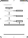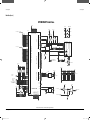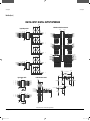
1
BACnet Gateway Basic :MIM-D00A Model :MIM-B17 MIM-B17C Model Code : MIM-B17 MIM-B17C BACnet Gateway CONTENTS 1. Precautions 2. Product Specifications 3. Disassembly and Reassembly 4. Program Update 5. Troubleshooting 6. Exploded Views and Parts List 7. PCB Diagram 8. Wiring Diagram 9. Schematic Diagram Refer to the service manual in the GSPN(see the rear cover) for the more information. BACnet Gateway_E_32400A(1)_cover.indd 1 2010-05-17 �� 10:09:39 Section 0 Contents 11. Precautions .............................................................................................................................................. 1-1 1-1. Precautions for the Service . ............................................................................................................................................. 1-1 1-2. Precautions for the Static Electricity and PL ................................................................................................................. 1-1 1-3. Precautions for the Safety . ............................................................................................................................................... 1-1 12. Product Specifications ......................................................................................................................... 2-1 2-1. The Feature of Product ...................................................................................................................................................... 2-1 2-2. Product Specifications........................................................................................................................................................ 2-2 2-3. System Organization........................................................................................................................................................... 2-3 2-4. Main Function ...................................................................................................................................................................... 2-4 13. Disassembly and Reassembly .......................................................................................................... 3-1 3-1. Disassembly and Reassembly .......................................................................................................................................... 3-2 3-2. Sub board Disassembly and Reassembly ..................................................................................................................... 3-5 3-3. Main board Disassembly and Reassembly ................................................................................................................... 3-6 3-4. Display board Disassembly and Reassembly ............................................................................................................... 3-7 14. Program Update .................................................................................................................................... 4-1 4-1. OS Update ............................................................................................................................................................................. 4-2 4-2. Application Update using SD Card.................................................................................................................................. 4-4 4-3. How to make OS Update SD Card using PC. ................................................................................................................ 4-6 4-4. How to make OS update SD Card using BACnet Gateway ...................................................................................... 4-7 4-5. How to make Application SD Card using PC . .............................................................................................................. 4-9 4-6. How to make Application SD Card using BACnet Gateway . ................................................................................... 4-10 4-7. Application Update using FTP.......................................................................................................................................... 4-12 15. Troubleshooting . .................................................................................................................................. 5-1 5-1. Items to be checked first................................................................................................................................................. 5-1 5-2. Fault diagnosis by symptom......................................................................................................................................... 5-2 5-2-1. When BACnet Gateway is not working ..................................................................................................................................................................... 5-2 5-2-2. When the LCD Display is Not Working or the Backlight is Turing OFF ............................................................................... 5-4 5-2-3. When the Static LED is Not Turning ON/OFF ..................................................................................................................................................... 5-5 5-2-4. When the RS485 is Not Connecting .............................................................................................................................................................................. 5-6 5-2-5. When the Ethernet is Not Connecting ....................................................................................................................................................................... 5-7 5-2-6. When the SD Card is Not Doing Backup Data ................................................................................................................................................... 5-8 5-2-7. When the Button is Not Working ...................................................................................................................................................................................... 5-9 Samsung Electronics BACnet Gateway_E_32400A(1)_1.indd 1 1 2010-05-17 �� 10:34:39 Section 0 Contents 5-2-8. When the DI/Do is Not Working ......................................................................................................................................................................................... 5-10 5-2-9. Action when the Tracking Error ........................................................................................................................................................................................... 5-11 5-2-10. Initialization Way when Admin Password is forgotten ...................................................................................................................... 5-12 5-2-11. How to know MAC address .................................................................................................................................................................................................. 5-12 5-2-12. If the connection to BACnet Gateway from the outside using internet is not working ............................ 5-13 5-2-13. Solution for DDC connection error .............................................................................................................................................................................. 5-14 5-2-14. When the BACnet is Not Connecting ______________________________________________ 5-15 5-2-15. When the BACnet Object Identification Not Display___________________________________ 5-16 16. Exploded Views and Part List . ........................................................................................................ 6-1 17. PCB Diagram ......................................................................................................................................... 7-1 7-1. Main Board ............................................................................................................................................................................................................................................................................ 7-1 7-2. Display Board ..................................................................................................................................................................................................................................................................... 7-2 7-3. Sub Board ............................................................................................................................................................................................................................................................................... 7-3 18. Wiring Diagram .................................................................................................................................... 8-1 19. Schematic Diagram ............................................................................................................................ 9-1 2 BACnet Gateway_E_32400A(1)_1.indd 2 9-1. Main Board......................................................................................................................................................................... 9-2. Display Board. ................................................................................................................................................................... 9-15 9-3. Sub Board........................................................................................................................................................................... 9-16 9-1 Samsung Electronics 2010-05-17 �� 10:34:39 1. Precautions 1-1. Precautions for the Service ● Use the standard parts when replacing the electric parts. – Confirm the model name, rated voltage, rated current of the electric parts. ● Repair the disconnection of HARNESS securely when repairing the break down. – If there is any connection error, it causes an abnormal noise and incorrect operation. ● In case that you assemble or disassemble the products with laying it on the side, do work on the work cloth. – If not, the exterior of products can be scratched. ● Remove dust and foreign materials from harness, connection part, and inspection part thoroughly when repairing the break down. – It protects the danger of fire such as tracking and short. ● Check the assembly status of parts after repairing the break down. – It should be same as the status before repairing. 1-2. Precautions for the Static Electricity and PL ● As the PCB power terminal has a weakness for the static electricity, pay attention to it during the repair and measurement. – Work with insulation gloves during the repair and measurement of PCB. ● Check the distance between the product and the other electronic appliances such as TV, video, and audio. It should be over 2m. – If not, it causes a bad picture quality or a noise. ● Repairing the products by consumer should be strictly prohibited. – There is a danger of electric shock or fire due to incorrect disassembly. 1-3. Precautions for the Safety ● Do not pull any electric wires and do not touch an auxiliary power switch with a wet hand. – There is a danger of electric shock or fire. ● In case any wire or power plug has been damaged, replace it to eliminate any possible danger. ● Do not bend the power cord by force and do not put any heavy object on the power cord. – There is a danger of electric shock or fire. ● Do not use multi socket. – There is a danger of electric shock or fire. ● Ground the product if necessary. – Be sure to ground the product if there is any danger of electric leakage due to water or moisture. ● Be sure to turn off the auxiliary power switch or pull out the power plug during replacement or repair of electric parts. – There is a danger of electric shock. Samsung Electronics BACnet Gateway_E_32400A(1)_1.indd 1 1-1 2010-05-17 �� 10:34:39 2. Product Specifications 2-1. The Feature of Product 1) BACnet Gateway ●Connecting BACnet Gateway with Centralized Controller (Type ⓐ) - You can control up to 16 Centralized Controllers and 256 indoor units by using BACnet Gateway. ●Connecting BACnet Gateway with Interface Module (Type ⓑ) - You can control up to 80 Interface Modules and 256 indoor units by using BACnet Gateway. ※ You can connect 16 Interface Modules in each communication channel. - When connected Interface Modules is more, Tracking time can be long. BMS system BMS Engineering Internet SAMSUNG Engineering BACnet Gateway ⓐ ⓑ Centralized controller Interface Module 2-1 BACnet Gateway_E_32400A(1)_1.indd 1 Interface Module Interface Module Samsung Electronics 2010-05-17 �� 10:34:40 2-2. Product Specifications Item Remark - Adaptor : DC Adaptor - Input Voltage : 100 ~ 240V, 50/60Hz, 1.0A Power - Output Voltage : 12V, 3A 240(W)x255(H)x64.8(D) (Unit : mm) Size 1.48kg Weight Panel sticking Install Method LCD(Text) Display DI / DO LED Power, CPU-Alive, Ethernet Linked, Ethernet Active, COM1, COM2, COM3, COM4, COM5 TX, RX, Check KEY 4keys (Menu, ▲ , ▼, Set) DO(Dry Contact) Digital signal output(10CH) DI(Dry Contact) Digital signal input(10CH) RS-232 Debugging port Communication Port RS485 Connection port for external devices Etc. Data Backup Ethernet Samsung Electronics BACnet Gateway_E_32400A(1)_1.indd 2 RJ45 connector (10/100Mbps) for Ethernet SD CARD slot (SD card is needed additional purchase) 2-2 2010-05-17 �� 10:34:40 2-3. System Organization BMS system BMS Engineering Internet SAMSUNG Engineering BACnet Gateway ⓐ ⓑ Centralized controller Interface Module 2-3 BACnet Gateway_E_32400A(1)_1.indd 3 Interface Module Interface Module Samsung Electronics 2010-05-17 �� 10:34:41 2-4. Main Function As an Internet based device for centralized management of system airconditioner, BACnet Gateway supports LAN and MAN. It can operate for 24 hrs without extra computer. ● 24 Hrs operation - Convenience with 24hrs, 365 day operation. ● Independent operation and Electricity saving(DMS2 Function) - BACnet Gateway executes Schedule control, Peak electricity control, and Integration power distribution and independently without extra computer. - BACnet Gateway achieves Energy saving with no PC operation at all times. ● Data storage(DMS2 Function) - BACnet Gateway stores and check the list of malfunction, installation information of indoor unit and the data of integration power distribution itself with built-in database. ● Management of Large quantities units - The maximum 256 indoor units are connected to one BACnet Gateway realizing efficiency. ● Automatic e-mail(DMS2 Function) - BACnet Gateway sends a e-mail automatically with the list of malfunction to pre-registered address when certain problem occurred. ● Web-server - You can use various function remotely without extra program. (Unit condition monitoring, Function control, list of malfunction, schedule setting etc.) ● BACnet Support ※ Samsung is not responsible for BMS Engineering which create each device and objects. For futher directions regarding on BMS engineering, consult with specialized BMS related render. Samsung Electronics BACnet Gateway_E_32400A(1)_1.indd 4 2-4 2010-05-17 �� 10:34:41 MEMO 2-5 BACnet Gateway_E_32400A(1)_1.indd 5 Samsung Electronics 2010-05-17 �� 10:34:41 3. Disassembly and Reassembly ■ Necessary Tools Item Remark +Screw Driver -Screw Driver Samsung Electronics BACnet Gateway_E_32400A(1)_1.indd 1 3-1 2010-05-17 �� 10:34:42 3-1. Disassembly and Reassembly No Parts 1 Common Procedure Remark 1) Unscrew 2 fixing screws. (Use +Screw Driver) 2) Detach the lower cover. 3) Press lower part of cable tie and detach the cable tie. 4) Pull the bead-core part of adapter. 5) Turn connector of adapter Counterclockwise. 3-2 BACnet Gateway_E_32400A(1)_1.indd 2 Samsung Electronics 2010-05-17 �� 10:34:43 Disassembly and Reassembly No Parts Procedure Remark 6) Detach the connector of adapter from BACnet Gateway. 7) Detach connectors for 485communication, network and DI/DO. 8) Unscrew at red circle part. (Use +Screw Driver) Ref.) The case of using additional Hole for install, detach from wall after detaching upper cover. 9) Push up BACnet Gateway. and pull the BACnet Gateway.0 front direction. Samsung Electronics BACnet Gateway_E_32400A(1)_1.indd 3 3-3 2010-05-17 �� 10:34:44 Disassembly and Reassembly No Parts Procedure Remark 10) Unscrew 2 fixing screws at red circle. 11) Pick up the upper cover. Be careful not to damage LED on sub board. 12) As the shown picture, detach the cable between main and LCD board. 3-4 BACnet Gateway_E_32400A(1)_1.indd 4 Samsung Electronics 2010-05-17 �� 10:34:45 3-2. Sub board Disassembly and Reassembly No Parts 1 Common Procedure Remark 1) As shown picture, detach the connector pulling upper direction. 2) Unscrew 4 fixing screw on sub board. (Use +Screw Driver) 3) Detach the sub board from BACnet Gateway. Samsung Electronics BACnet Gateway_E_32400A(1)_1.indd 5 3-5 2010-05-17 �� 10:34:46 3-3. Main board Disassembly and Reassembly No Parts 1 Common Procedure Remark 1) As shown picture, detach the connector on sub board pulling upper direction. 2) Detach connector on main board, as a same way. 3) Detach connector for connecting display board. 4) Unscrew 4 fixing screw on main board. (Use +Screw Driver) 5) Push up the main board and detach it from BACnet Gateway. 3-6 BACnet Gateway_E_32400A(1)_1.indd 6 Samsung Electronics 2010-05-17 �� 10:34:47 3-4. Display board Disassembly and Reassembly No Parts 1 Common Procedure Remark 1) Unscrew 4 fixing screw on display board. (Use +Screw Driver) 2) Push up the display board and detach it from upper cover. Samsung Electronics BACnet Gateway_E_32400A(1)_1.indd 7 3-7 2010-05-17 �� 10:34:48 4. Program Update ■ Necessary Tools Item Remark +Screw Driver SD-CARD - At least 512MB - Type: Normal, SDHC 4-1 BACnet Gateway_E_32400A(1)_1.indd 1 Samsung Electronics 2010-05-17 �� 10:34:48 4-1. OS Update No Parts 1 Common Procedure Remark 1) Unscrew 2 fixing screws of the bottom. (Use +Screw Driver) 2) Pull the cover of the bottom, and detach lifting up. 3) Insert a SD card for updating software. 4) Push [Reset] button once with pushing [Menu] button. - Keep pushing [Menu] button until “1. Update O/S” is showed. 5) Push [Set] button after seeing “1.Update O/S” referring the right picture. (If you can’t see “1.Update O/S” after completing 1)~4) with inserting SD card, Confirm whether your SD-Card has a problem.) Samsung Electronics BACnet Gateway_E_32400A(1)_1.indd 2 4-2 2010-05-17 �� 10:34:49 Program Update No Parts Procedure Remark 6) Unscrew 2 fixing screws of the bottom. (Use +Screw Driver) Like the right picture, Kernel update is completed. 7) Click [▲] button like the right picture. 8) Push [Set] button after seeing “Update RootFS”. 9) “Updating RootFS” is showed, the program writing step is progressed. 10) After showing “OK” under “Updating RootFS” like the right picture, updating of Root File System is completed. 4-3 BACnet Gateway_E_32400A(1)_1.indd 3 Samsung Electronics 2010-05-17 �� 10:34:49 4-2. Application Update using SD Card No Parts 1 Common Procedure Remark 1) Insert a SD card for updating. 2) Push [Reset] button once. 3) System is reset, Application is updated. 4) “remove SD card” is showed like the right picture, detach SD card pushing it one more time. 5) There is nothing on the display for a while after removing SD card, and system is reset. Samsung Electronics BACnet Gateway_E_32400A(1)_1.indd 4 4-4 2010-05-17 �� 10:34:50 Program Update No Parts Procedure Remark 6) After completing application update, confirm IP, time and regular operation . 4-5 BACnet Gateway_E_32400A(1)_1.indd 5 Samsung Electronics 2010-05-17 �� 10:34:50 4-3. How to make OS Update SD Card using PC No Parts 1 Common Procedure Remark 1) Connect to a PC after insert a SD card into a SD card reader. 2) Select ‘Format’ with right-click on the created ‘Removable storage devices’ . 3) Select ‘FAT32’ of ‘File system’, and start format pushing [Start] button. 4) Format completed, Copy the provided OS files of BACnet Gateway to the top in SD card. - Provided OS files : rootfs.bin, vmlinux, xbl.bin, xblelf32, zImage 5) Remove SD card from PC after completing copy. Samsung Electronics BACnet Gateway_E_32400A(1)_1.indd 6 4-6 2010-05-17 �� 10:34:50 4-4. How to make OS update SD Card using BACnet Gateway No Parts 1 Common Procedure Remark 1) Insert a SD card for updating. 2) Connect BACnet Gateway to PC with a crossover lan cable. 3) Set IP to 192.168.0.250. - You can connect all BACnet Gateway with 192.168.0.254. 4) Type ‘telnet 192.168.0.254’ in the window of ‘Run’ after ‘Start’ button. 5) Log on the telnet. 4-7 BACnet Gateway_E_32400A(1)_1.indd 7 Samsung Electronics 2010-05-17 �� 10:34:51 Program Update No Parts Procedure Remark 6) Format SD card. - mkfs.vfat /dev/mss/blk0p1 7) Run ‘mount /dev/mss/blk0p1 /mnt/mmc0 -t vfat’. 8) Copy the provided OS files of BACnet Gateway after connecting BACnet Gateway with FTP. You must close FTP window after completing copy. - ftp://192.168.0.254/../../../mnt/mmc0 - Provided OS files : rootfs.bin, vmlinux, xbl.bin, xbl-elf32, zImage 9) Type the below. cd / umount /mnt/mmc0 10) Remove SD card. Samsung Electronics BACnet Gateway_E_32400A(1)_1.indd 8 4-8 2010-05-17 �� 10:34:52 4-5. How to make Application SD Card using PC No Parts 1 Common Procedure Remark 1) Connect to a PC after insert a SD card into a SD card reader. 2) Select ‘Format’ with right-click on the created ‘Removable storage devices’. 3) Select ‘FAT32’ of ‘File system’, and start format pushing [Start] button. 4) Format completed, Copy the application files of BACnet Gateway to the top in SD card. - Provided OS files : BACnet Gateway.tar.gz, r, startapp, svcapp 5) Remove SD card from PC after completing copy. 4-9 BACnet Gateway_E_32400A(1)_1.indd 9 Samsung Electronics 2010-05-17 �� 10:34:52 4-6. How to make Application SD Card using BACnet Gateway No Parts 1 Common Procedure Remark 1) Insert a SD card for updating. 2) Connect BACnet Gateway to PC with a crossover lan cable. 3) Set IP to 192.168.0.250. - You can connect all BACnet Gateway with 192.168.0.254. 4) Type ‘telnet 192.168.0.254’ in the window of ‘Run’ after ‘Start’ button. 5) Log on the telnet. Samsung Electronics BACnet Gateway_E_32400A(1)_1.indd 10 4-10 2010-05-17 �� 10:34:53 Program Update No Parts Procedure Remark 6) Run ‘mount /dev/mss/blk0p1 /mnt/mmc0 -t vfat'. 7) Copy the provided OS files of BACnet Gateway after connecting BACnet Gateway with FTP. You must close FTP window after completing copy. - ftp://192.168.0.254/../../../mnt/mmc0 - Provided OS files : BACnet Gateway.tar.gz, r, startapp, svcapp 8) Type the below on the telnet window. cd /mnt/mmc0 chmod 755 svcapp cd / umount /mnt/mmc0 9) Remove SD card. 4-11 BACnet Gateway_E_32400A(1)_1.indd 11 Samsung Electronics 2010-05-17 �� 10:34:53 4-7. Application Update using FTP No Parts Procedure 1 Common 1) Connect BACnet Gateway to PC with a crossover lan cable. Remark 2) Set IP to 192.168.0.250. - You can connect all BACnet Gateway with 192.168.0.254. 3) Connect to BACnet Gateway with FTP. - ftp://192.168.0.254/../../../dms 4) Copy the provided application folder to PC and Rewrite it to the application folder in BACnet Gateway connected by FTP. 5) Push [Reset] button once. Samsung Electronics BACnet Gateway_E_32400A(1)_1.indd 12 4-12 2010-05-17 �� 10:34:54 5. Troubleshooting 5-1. Items to be checked first Problem BACnet Gateway.0 does not work Check Explanation / Solution Power failure? After checking power line of each devices, try again. Is there communication problem between BACnet Gateway.0 and other control units? After checking communication line of each devices, try gain. Is the connection between adapter and power cable correct? After checking connection between adapter and power cable, try again. Is the Silverlight 2.0 version installed? You can download Silverlight 2.0 version at http://www.microsoft.com/silverlight/. Is the Windows XP SP2 installed? Silverlight 2.0 version can run properly under Windows XP SP2. Under previous OS version, Silverlight 2.0 version cannot run poroperly. Can’t access Log-in page Can’t access Log in page From external PC Is the setting value for netwkor correct? Not monitoring centralized contol unit Are the communication cables of BACnet Gateway(C1, C2) properly connected? Connect BACnet Gateway communication cables (C1, C2) properly. Be careful to deal with the RS485 communication cable because it has polarity. Peak power management is out of order Are there no problems on power line of BACnet Gateway? If there is problem on power line of BACnet Gateway, Peak power management function cannot operate properly. Forget the IP address of BACnet Gateway.0 At initial display, press [Menu] button and then "1. IP config" message will be displayed. Under that condition press [Set] button. The IP address of BACnet Gateway is initialized at 192.168.0.100 when factory out. Is Peak Power management or schedule control running? According to schedule control and power management, indoor units can be turned it on or off. Is BACnet Gateway system time different from current time? Set time of BACnet Gateway, according to real time. Is the external circuit constituted? Check additional circuit for external input control function of BACnet Gateway. Is the contact control pattern of BACnet Gateway set to 1? Set the pattern which fits to the control pattern you want. Isn't there any indoor units? BACnet Gateway is unsuccessful in tracking. Try it again. Indoor units are out of order External digital inputs are out of order Tracking Fail Isn't firewall set in local computer? You should consult with network manager. ※ Ref. Switch for using digital input and digital output OFF 5-1 BACnet Gateway_E_32400A(1)_1.indd 1 ON Samsung Electronics 2010-05-17 �� 10:34:54 5-2. Fault diagnosis by symptom 5-2-1. When BACnet Gateway is not working Start Power failure or Is plug connection proper? No Check Power failure and plug connection. Yes Is the connection between adapter and power cable proper? No Check the connection Between adapter and power cable Yes Is the output of adapter 12V? No Change adapter Yes Is the connection between Main Board and adapter cable proper? No Check the condition of adapter Yes Continue Samsung Electronics BACnet Gateway_E_32400A(1)_1.indd 2 5-2 2010-05-17 �� 10:34:55 Troubleshooting When BACnet Gateway is not working(cont.) Continue Change Main Board No Is BACnet Gateway working? Change Display Board Is BACnet Gateway working? Yes No Change Sub Board Yes End 5-3 BACnet Gateway_E_32400A(1)_1.indd 3 Samsung Electronics 2010-05-17 �� 10:34:56 Troubleshooting 5-2-2. When the LCD Display is Not Working or the Backlight is Turing OFF Start No Is the connection between Main Board and Display Board proper? Check the condition of cable connection Yes Change Display Board No Is LCD working properly? Change Main Board Yes End Samsung Electronics BACnet Gateway_E_32400A(1)_1.indd 4 5-4 2010-05-17 �� 10:34:56 Troubleshooting 5-2-3. When the Static LED is Not Turning ON/OFF Start No Is the connection between Main Board and Sub Board proper? Check the condition of cable connection Yes Change Sub Board No Is static LED working properly? Change Main Board Yes End 5-5 BACnet Gateway_E_32400A(1)_1.indd 5 Samsung Electronics 2010-05-17 �� 10:34:57 Troubleshooting 5-2-4. When the RS485 is Not Connecting Start Is the cable connection for RS485 proper? No Check the condition of cable connection Yes Is the polarity of RS485 cable correct? [Left : +(or “A”), Right : – (or “B”)] Yes No Check the polarity of RS485 cable ⓐ ⓑ Change Main Board End Samsung Electronics BACnet Gateway_E_32400A(1)_1.indd 6 5-6 2010-05-17 �� 10:34:57 Troubleshooting 5-2-5. When the Ethernet is Not Connecting Start No Is the cable for Ethernet proper? Check the condition of Ethernet cable Yes Is the connector for Ethernet proper? No Check the condition of Ethernet connector Yes Are the static LEDs for Ethernet proper? (Ehternet Linked, Ehernet Active) No Change Main Board Linked : Constant Active : Flickering Yes Are the addresses for ethernet correct? No Check IP, Sub net mask and gateway address (Refer to install and service manual) Yes Change Main Board End 5-7 BACnet Gateway_E_32400A(1)_1.indd 7 Samsung Electronics 2010-05-17 �� 10:34:59 Troubleshooting 5-2-6. When the SD Card is Not Doing Backup Data Start Is the SD card inserted in the slot? No Check the SD card slot Yes Is the SD card locked? No Check the SD card. (If SD card was locked, BACnet Gateway is not doing Backup data) Yes Change SD card End Samsung Electronics BACnet Gateway_E_32400A(1)_1.indd 8 5-8 2010-05-17 �� 10:34:59 Troubleshooting 5-2-7. When the Button is Not Working Start No Is the connection between Main Board and Display Board proper? Check the condition of cable connection Yes Change Display Board No Are buttons working properly? Change Main Board Yes End 5-9 BACnet Gateway_E_32400A(1)_1.indd 9 Samsung Electronics 2010-05-17 �� 10:35:00 Troubleshooting 5-2-8. When the DI/Do is Not Working Start No Is the connection between Main Board and Sub Board proper? Check the condition of cable connection Yes No Is the setting of dip switch for DI/Do correct? Check setting value of SW2 (Refer to User manual) Yes Change Main Board No Is the DI(/DO working properly? Change Sub Board Yes End Samsung Electronics BACnet Gateway_E_32400A(1)_1.indd 10 5-10 2010-05-17 �� 10:35:01 Troubleshooting 5-2-9. Action when the Tracking Error Start No Is the cable connection of RS485 proper? Check the condition of cable connection Yes No Is the polarity of RS485 cable correct? Check the polarity of RS485 cable Yes No Is the speed of centralized control unit set 9600bps? Set the speed of centralized control unit as 9600bps(Turn 4th dip switch off) Yes No Are the devices connected to BACnet Gateway Satisfied with install limitation? Less than 256 indoor units, 1 demand controller, Less than 8 SIMs(When demand controller is connected, less than 7 SIMs), Less than 8 DDCs. Connect using less than 128 DDC connection points or install additional BACnet Gateway. Yes End 5-11 BACnet Gateway_E_32400A(1)_1.indd 11 Samsung Electronics 2010-05-17 �� 10:35:01 Troubleshooting 5-2-10. Initialization Way when Admin Password is forgotten Start Press the [▲],[▼] buttons under LCD window snd select 8.Password Reset menu. Press [Menu],[Set] buttons simultaneously after “RESET PASSWORD WAITING” message. If you Press [Set] button after “Are you sure?” message, the password is initialized as 1234. End 5-2-11. How to know MAC address Start From local PC, access to BACnet Gateway.0 using telnet program. Log in Press Enter, after input data“ifconfigeth0” . String beside HWaddr is MAC address. End Samsung Electronics BACnet Gateway_E_32400A(1)_1.indd 12 5-12 2010-05-17 �� 10:35:01 Troubleshooting 5-2-12.If the connection to BACnet Gateway from the outside using internet is not working Start No Is official IP address set in the BACnet Gateway? Set official IP address Yes No Is the firewall of 80.1100 port open to BACnet Gateway? Request firewall opening to network manager. Yes End 5-13 BACnet Gateway_E_32400A(1)_1.indd 13 Samsung Electronics 2010-05-17 �� 10:35:01 Troubleshooting 5-2-13. Solution for DDC connection error Start No Is the cable connection proper? Check the condition of cable connection Yes No Is the polarity correct? Check the polarity Yes No Are the DDCa connected to BACnet Gateway Satisfied with install limitation? Less than 8 DDCs. Connect using less than 128 DDC connection points or install additional BACnet Gateway. Yes End Samsung Electronics BACnet Gateway_E_32400A(1)_1.indd 14 5-14 2010-05-17 �� 10:35:02 Troubleshooting 5-2-14. When the BACnet is Not Connecting Start Is the cable for Ethernet proper? No Check the condition of Ethernet cable Yes Is the connector for Ethernet proper? No Check the condition of Ethernet connector Yes Are the static LEDs for Ethernet proper? (Ethernet Linked, Ethernet Active) No Linked : Constant Active : Flickering Yes Are the addresses for Ethernet correct? Change Main Board No Check IP, Subnet mask and gateway address (Refer to install and service manual) Yes Is the device instance number for BACnet correct? No Check Device Instance number Yes Change Main Board Yes End 5-15 BACnet Gateway_E_32400A(1)_1.indd 15 Samsung Electronics 2010-05-17 �� 10:35:02 Troubleshooting 5-2-15. When the BACnet Object Identification Not Display Start Executed tracking proper? No Check the tracking execute Yes From local PC, access BACnet Gateway using telnet program No Yes Login No Yes Press Enter, after input data "ps -e". Find a "BACipDMS2app" No Reboot BACnet Gateway Yes Change Main Board Yes End Samsung Electronics BACnet Gateway_E_32400A(1)_1.indd 16 5-16 2010-05-17 �� 10:35:02 6. Exploded Views and Part List 1 14 13 5 16 6 3 8 4 7 2 9 21 11 10 15 12 6 22 18 19 20 21 13 17 6-1 BACnet Gateway_E_32400A(1)_1.indd 1 Samsung Electronics 2010-05-17 �� 10:35:03 Exploded Views and Part List Parts List No. Code No. 1 DB61-03889A Specification Description CASE-MAIN PC/ABS 5VA/DARK GRAY(NH-1000T/G31760) Q'TY SA/SNA 1 SNA SE-1010(13um) 2 DB61-03885A CASE-SUB PC/ABS 5VA/DARK GRAY(NH-1000T/G31760) 1 SNA 3 DB93-08178A ASS'Y PCB MAIN PCB BOARD (MAIN) 1 SA 4 DB93-08179A ASS'Y PCB SUB PCB BOARD (SUB) 1 SA 5 DB93-08180A ASS'Y PCB SUB PCB BOARD(DISPLAY) 1 SA 6 DB61-03887A CASE-UPPER PC/ABS 5VA DARK GRAY(NH-1000T/G31760) 1 SNA 7 DB64-02277A BUTTON-KEY ABS(NATURAL)/HG-0760GP BUTTON 1 SNA 8 DB64-02276A INLAY-WINDOW ACRYL 1 SNA 9 DB09-04757C ASS'Y-COVER CASE UP ASSY 1 SNA 10 DB61-03888A CASE-LED ABS(UT-0510/G0526)/BLACK SMOG 1 SNA 11 DB61-03886A CASE-WIRE PC/ABS 5VA/ DARK GRAY(NH-1000T/G31760) 1 SNA SE-1010(13um) 12 DB90-04780A ASS'Y-COVER CASE DOWN ASSY 1 SNA 13 DB61-03890A BRACKEY PC/ABS 5VA DARK GRAY(NH-1000T/G31760) 1 SNA 14 6002-000630 SCREW-TAPPING ø3 X L8, 2 19 SNA 15 6001-000044 SCREW-MACHINE M4 x L18, 2, TH 4 SNA 16 6501-001052 CABLE TIE NYLON66, DACK-140 1 SNA 17 DB74-00042A TAPE FILAMENT W18, H40, D1.0 1 SNA 18 DB93-08182A ASS'Y CONNECTOR WIRE MAIN-DISPLAY 2 SNA 19 DB93-08183A ASS'Y CONNECTOR WIRE MAIN-SUB 1 SNA 20 DB61-04025A CASE-INDICATOR ABS 1 SNA 21 3716-001329 TERMINAL-BLOCK RS485, DI-DO 25 SNA 22 DB98-32326B ASS'Y-LABLE RATING L/C 1 SNA Samsung Electronics BACnet Gateway_E_32400A(1)_1.indd 2 6-2 2010-05-17 �� 10:35:03 7. PCB Diagram 7-1. Main Board 1 2 3 4 5 6 7 8 9 10 11 ① J11 : Power connector #1 : GND #2 : Not used #3 : DC 12V #4 : DC 12V ② S2 : Reset SW #1 : GND #2 : Reset signal ③ J18 : Main_Sub Connector #1 : DC 12V #2 : DC 12V #3, 4 : GND #5~#14 : DI_S1~10 signal #15~#24 : DI_S1~10 signal #25 : DC3.3V #26 : CPU_ALIVE #27 : GND #28 : ETH_ALIVE #29 : ETH_LINK #30 : ERROR #31~#40 : 485_TX LED signal ④ J21 : Connector for Serial Communication #1 : Not used #2 : TXR #3 : RXR #4 : Not used #5 : GND #6~#9 : Not used ⑤ J20 : Connector for Debugging #1 : DC3.3V #2 : DC3.3V #3 : nTRST #4 : GND #5 : TDI #6 : GND #7 : TMS #8 : GND #9 : TCK #10~#12 : GND #13 : TDO #14 : GND #15 : CPU_nRESET #16 : GND #17 : Not used #18 : GND #19 : Not used #20 : GND ⑥ CON1 : SD Card Socket #1 : SD1_D3 #2 : SD1_CMD #3 : GND #4 : DC3.3V #5 : SD1_CLK #6 : GND #7 : SD1_D0 #8 : SD1_D1 #9 : SD1_D2 #10 : SD1_nCD #11 : GND #12 : SD1_WP ⑦ J17 : Connector for Displaying #1 : VCC_SUB_A(DC5V) #2 : VCC_SUB_A(DC5V) #3 : GND #4 : GND #5 : CLCD_RS #6 : CLCD_RnW #7 : CLCD_EN #8~#15 : CLCD_DB0~7 #16 : GND #17 : MENU #18 : UP #19 : DOWN #20 : OK ⑧ J1 : Connector for Ethernet #1 : TPO+ #2 : TPO#3 : TDC(DC3.3V) #4 : Not used #5 : TPI+ #6 : TPI#D2 : ETHERNET_LINK #D1 : DC3.3V(Pullup 24.9 ohm) #D4 : ETHERNET_ALIVE #D3 : DC3.3V(Pullup 24.9 ohm) ⑨ J19 : Connector for Reset #1 : MISO #2 : VCC_5V #3 : SCK #4 : MOSI #5 : nISP_RESET #6 : GND ⑩ CN10 : Connector for RS485 #1(+) : 485 Ch1 A #2(-) : 485 Ch1 B #3(+) : 485 Ch2 A #4(-) : 485 Ch2 B #5(+) : 485 Ch3 A #6(-) : 485 Ch3 B #7(+) : 485 Ch4 A #8(-) : 485 Ch4 B #9(+) : 485 Ch5 A #10(-) : 485 Ch5 B ⑪ SW2 : Mode Select Swich #1 : MODE_SEL1 #2 : MODE_SEL2 #3 : MODE_SEL3 #4 : MODE_SEL4 #5~#8 : GND(Pulldown 330ohm) 7-1 BACnet Gateway_E_32400A(1)_1.indd 1 Samsung Electronics 2010-05-17 �� 10:35:04 PCB Diagram and Part List 7-2. Display Board 1 ① Button1 : Menu Button #1 : GND #2 : B_Menu Samsung Electronics BACnet Gateway_E_32400A(1)_1.indd 2 2 3 ② J1 : Connector for Displaying #1~#2 : DC15V #3~#4, #16 : GND #5~#15 : CLCD signal #17~#20 : Button signal 4 ③ Button2 : Down Button #1 : GND #2 : B_Down 5 ④ Button3 : Up Button #1 : GND #2 : B_Up ⑤ Button4 : OK Button #1 : GND #2 : B_OK 7-2 2010-05-17 �� 10:35:05 PCB Diagram and Part List 7-3. Sub Board 1 ① J2 : Digital Input Connector #1,#3,#5,#7,#8 : DC12V #2,#4,#6,#7,#10 : CH1~5 DI signal 2 3 ② J5 : Main_Sub Connector #1, #2 : DC12V #3, #4, #27 : GND #5~#24 : DI signal #25 : POWER LED signal #26 : CPU_ALIVE LED signal #28 : ETH_ALIVE LED signal #29 : ETH_LINK LED signal #30 : CHECK LED signal #31~#40 : 485 TXD, RXD signal 4 ③ J4 : Digital Input Connector #1,#3,#5,#7,#8 : DC12V #2,#4,#6,#7,#10 : CH6~10 DI signal 5 ④ J1 : Digital Output Connector #1,#3,#5,#7,#8 : DC12V #2,#4,#6,#7,#10 : CH1~5 DO signal ⑤ J3 : Digital Output Connector #1,#3,#5,#7,#8 : DC12V #2,#4,#6,#7,#10 : CH6~10 DO signal 7-3 BACnet Gateway_E_32400A(1)_1.indd 3 Samsung Electronics 2010-05-17 �� 10:35:05 8. Wiring Diagram Display Board 20 PIN cable Ass'y Connector Wire-Display (DB93-08182A) 40 PIN Cable Ass'y Connector Wire-Sub (DB93-08183A) Main Board Sub Board This Document can not be used without Samsung’s authorization. Samsung Electronics BACnet Gateway_E_32400A(1)_1.indd 1 8-1 2010-05-17 �� 10:35:06 9. Schematic Diagram 9-1. Main Board PXA320-806MHz U1A GPIO MA15 MA14 MA13 MA12 MA11 SDMA10 MA9 MA8 MA7 MA6 MA5 MA4 MA3 MA2 MA1 MA0 L4 K1 L2 L3 P4 K2 P2 N3 P3 R3 P1 T4 H1 J2 J1 K4 7 7 7 nSDRAS nSDCAS nSDCS0 7 7 7 7 7 7 7 7 7 7 7 7 nSDWE nSDCKE nSDCLK0 nSDCLK1 DQM3 DQM2 DQM1 DQM0 DQS3 DQS2 DQS1 DQS0 N2 R4 L1 N4 M3 M2 M1 N1 AA3 V2 F1 C3 AA2 W2 E1 D2 nSDRAS nSDCAS nSDCS0 nSDCS1 nSDWE nSDCKE nSDCLK0 nSDCLK1 DQM3 DQM2 DQM1 DQM0 DQS3 DQS2 DQS1 DQS0 U4 T3 U3 AD4 U1 R1 T2 T1 K3 R2 U2 nOE_RSV nWE_RSV nADV2_RSV RFU_AD4 RFU_U1 RCOMP_DDR nCS1_RSV nCS0_RSV MA10_RSV DDR_EVAL_RSV RFU_U2 AB2 AB3 AD1 AC1 AB4 AB1 AA4 Y2 W3 Y3 AA1 Y1 W1 V1 V3 V4 H2 G1 G2 H3 G3 F2 F3 E3 D1 E2 D3 C1 C4 C2 B2 B3 MD31 MD30 MD29 MD28 MD27 MD26 MD25 MD24 MD23 MD22 MD21 MD20 MD19 MD18 MD17 MD16 MD15 MD14 MD13 MD12 MD11 MD10 MD9 MD8 MD7 MD6 MD5 MD4 MD3 MD2 MD1 MD0 40.2_F/1608 7 7 7 7 7 7 7 7 7 7 7 7 7 7 7 7 7 7 7 7 7 7 7 7 7 7 7 7 7 7 7 7 MD31 MD30 MD29 MD28 MD27 MD26 MD25 MD24 MD23 MD22 MD21 MD20 MD19 MD18 MD17 MD16 MD15 MD14 MD13 MD12 MD11 MD10 MD9 MD8 MD7 MD6 MD5 MD4 MD3 MD2 MD1 MD0 A3 A4 A5 SDRAM_CONTROL RESERVED TP478 USBOTG_N USBOTG_P USBH1_N AC3 AC4 DF_nCS1 DF_nCS0 nCS2/GPIO3 nCS3/GPIO4 DF_nWE DF_nRE DF_SCLK_E DF_ALE_nWE2 DF_ALE_nWE1 DF_CLE_nOE DF_INT_RnB RDY_GPIO2 nLUA nLLA nBE1 nBE0 AF6 AE6 AD2 AD3 AF7 AD7 AF4 AB6 AF3 AD5 AE5 AC2 AE7 AE8 AF5 AE4 PWR_SCL PWR_SDA VCTCXO_EN nBATT_FAULT PWR_EN SYS_EN nGPIO_RESET nRESET nRESET_OUT EXT_WAKEUP1 EXT_WAKEUP0 C11 A12 B12 B7 A7 E5 A11 E6 C9 F5 G5 TOUCH_XP TOUCH_XM TOUCH_YP TOUCH_YM E18 D19 E17 D18 TOUCH JTAG nTRST TCK TDI TDO TMS DF_DATA EMPI_DATA R1 POWER_CONTROL 1 nSDCS1 DREQ/GPIO1 GPIO0 DF_CONTROL TP1 MA15 MA14 MA13 MA12 MA11 SDMA10 MA9 MA8 MA7 MA6 MA5 MA4 MA3 MA2 MA1 MA0 EMPI_ADDRESS 7 7 7 7 7 7 7 7 7 7 7 7 7 7 7 7 DF_ADDR DF_ALE_nWE2 8 DF_ALE_nWE1 8,10,11 DF_CLE_nOE 6,8,10,11 DF_INT_R/B 8 ETH_RDY 10 nLUA 6,9 nLLA 6,9 nBE1 6,10 nBE0 6,10 VCTCXO_EN 1 PWR_SCL 18 PWR_SDA 18 TP2 WAKEUP0 nBATT_FAULT 18 PWR_EN 8,18 SYS_EN 18 nGPIO_RESET 6 CPU_nRESET 16,18 nRST_OUT 10,11 WAKEUP1 6 TP3 1 nTRST TCK TDI TDO TMS 16 16 16 16 16 AC13 AB14 AD12 AB13 AD11 AE10 AF9 AB10 AF13 AE12 AF12 AC12 AF10 AD10 AC11 AD9 DF_IO15 DF_IO14 DF_IO13 DF_IO12 DF_IO11 DF_IO10 DF_IO9 DF_IO8 DF_IO7 DF_IO6 DF_IO5 DF_IO4 DF_IO3 DF_IO2 DF_IO1 DF_IO0 9 9 9 9 9 9 9 9 8,9 8,9 8,9 8,9 8,9 8,9 8,9 8,9 AE9 AF8 AD8 AC8 AE3 AF14 AE14 AB15 AC15 AC97_SYSCLK/GPIO34 AC97_BITCLK/GPIO39 AC97_nRESET/GPIO40 AC24 Y22 AA23 USB_HOST_CLIENT RTPXA320B2C806-643 DF_ADDR3 DF_ADDR2 DF_ADDR1 DF_ADDR0 DF_nCS1 8 DF_nCS0 8 ETH_nCS1 10 nCS3 9 DF_nWE 6,8 DF_nRE 6,8 D6 B4 B6 D5 A8 nXCVREN GPIO5/nPIOR GPIO6/nPIOW GPIO7/nIOIS16 GPIO8/nPWAIT CF_ADDR AC97 DF_IO15 DF_IO14 DF_IO13 DF_IO12 DF_IO11 DF_IO10 DF_IO9 DF_IO8 DF_IO7 DF_IO6 DF_IO5 DF_IO4 DF_IO3 DF_IO2 DF_IO1 DF_IO0 U1B nXCVREN 6,9 16 16 SD1_nCD SD1_WP 10 ETH_IRQ1 USBH_OVC USBH_PEN USBH1_P CIF_D0/GPIO_49 CIF_D1/GPIO_50 CIF_D2/GPIO_51 CIF_D3/GPIO_52 CIF_D4/GPIO_53 CIF_D5/GPIO_54 CIF_D6/GPIO_55 CIF_D7/GPIO_56 CIF_D8/GPIO_57 CIF_D9/GPIO_58 CIF_CLK/GPIO_59 CIF_PCLK/GPIO_60 CIF_HSYNC/GPIO_61 CIF_VSYNC/GPIO_62 SSP B25 B24 A24 A23 A22 A21 B21 E22 FF_RXD/GPIO_97 FF_TXD/GPIO_98 UART1_F/F FF_CTS/GPIO_99 FF_DCD/GPIO_100 FF_DSR/GPIO_101 FF_RI/GPIO_102 FF_DTR/GPIO_103 FF_RTS/GPIO_104 13 11 11 11 RS485_EN5 RS485_RXD5 RS485_TXD5 RS485_INV5 A19 B19 E19 C19 UART2_RTS/GPIO_109 UART2_RXD/GPIO_110 UART2_TXD/GPIO_111 UART2_CTS/GPIO_112 8 DF_INT_R/B2 AF16 W25 AF19 AB19 AC19 J23 H23 H24 G24 G22 F25 F23 E25 E26 D22 D25 D23 C21 A20 B20 E21 B18 A17 C17 D17 E16 C16 B17 E14 B16 C15 A16 D14 E13 A15 D13 17 RS232_nEN C_LCD_D0 C_LCD_D1 C_LCD_D2 C_LCD_D3 C_LCD_D4 C_LCD_D5 C_LCD_D6 C_LCD_D7 C_LCD_C1 C_LCD_C2 C_LCD_C3 DO_7 DO_8 DO_9 DO_10 14 16 17 17 14 15 15 15 15 15 15 15 15 15 15 CPU_ALIVE1 CPU_ALIVE2 DEBUG_L1 DEBUG_L2 ERR DI_1 DI_2 DI_3 DI_4 DI_5 DI_6 DI_7 DI_8 DI_9 DI_10 VCC_3P3 RTC_nINT 17 R265 5.1K/1608_NCE12 B14 B13 D12 K25 H22 J24 H25 BUZ_PWM BUZ_ON GPIO_0_2 GPIO_1_2 GPIO_4_2 GPIO_5_2 GPIO_14_2/LCD_FCLK GPIO_15_2/LCD_LCLK GPIO_16_2/LCD_PCLK GPIO_17_2/LCD_BIAS PWM0/GPIO_11 GPIO_12/PWM1 AF17 AC17 GPIO_13/PWM2 GPIO_14/PWM3 C1 10uF_16V/A_NC UART GPIO_9/L_CS GPIO GPIO_10/UTM_CLK GPIO_15 GPIO_16 GPIO_17 GPIO_74/U2D_RESET GPIO_75 GPIO_76 GPIO_77 GPIO_78 GPIO_79 GPIO_80 GPIO_81 GPIO_82 GPIO_87/U2D_RXERROR GPIO_89 GPIO_92 GPIO_105 GPIO_106 GPIO_107 GPIO_108/U2D_OPMODE1 GPIO_113/KEY_IN0 GPIO_114/KEY_IN1 GPIO_115/KEY_IN2 GPIO_116/KEY_IN3 GPIO_117 GPIO_118 GPIO_119 GPIO_120 GPIO_121/KEY_OUT0 GPIO_122/KEY_OUT1 GPIO_123/KEY_OUT2 GPIO_124/KEY_OUT3 GPIO_125 GPIO_126 GPIO_127 AB16 AB17 AA22 AD25 I2C_SCL I2C_SDA 17,18 17,18 GPIO_18/MM1_D0 GPIO_19/MM1_D1 GPIO_20/MM1_D2 GPIO_21/MM1_D3 GPIO_22/MM1_CLK GPIO_23/MM1_CMD AE20 AB20 AC21 AF22 AC22 AF23 SD1_D0 SD1_D1 SD1_D2 SD1_D3 SD1_CLK SD1_CMD 16 16 16 16 16 16 SSPSCLK1/GPIO_83 SSPSFRM1/GPIO_84 SSPTXD1/GPIO_85 SSPRXD1/GPIO_86 SSPIRQ1/GPIO_24 SSPINV1/GPIO_25 SSPEN1/GPIO_26 SSPSCLK2/GPIO_35 SSPSFRM2/GPIO_36 SSPTXD2/GPIO_37 SSPRXD2/GPIO_38 SSPIRQ2/GPIO_27 SSPINV2/GPIO_28 SSPEN2/GPIO_29 SSPSCLK3/GPIO_69 SSPRXD3/GPIO_72 SSPSFRM3/GPIO_90 SSPTXD3/GPIO_91 SSPIRQ3/GPIO_41 SSPINV3/GPIO_42 SSPEN3/GPIO_43 SSPSCLK4/GPIO_93 SSPSFRM4/GPIO_94 SSPTXD4/GPIO_95 SSPRXD4/GPIO_96 SSPIRQ4/GPIO_44 SSPINV4/GPIO_45 SSPEN4/GPIO_46 F22 D26 E23 E24 AE22 AD22 AF24 AD26 AC25 AB25 AC26 AD23 AB22 AE25 L23 K24 C26 D24 Y23 AA24 W22 D21 B23 C23 C24 AA25 W24 Y26 TXD1_LED 14 TXD2_LED 14 TXD3_LED 14 TXD4_LED 14 RS485_IRQ1 11 RS485_INV1 11 RS485_EN1_A 12 TXD5_LED 14 RXD1_LED 14 RXD2_LED 14 RXD3_LED 14 RS485_IRQ2 11 RS485_INV2 11 RS485_EN2_A 12 RXD4_LED 14 RXD5_LED 14 GPIO_30/UART3_RX GPIO_31/UART3_TX GPIO_47/UTM_D6 GPIO_48/UTM_D7 GPIO_63/LCD_D8 GPIO_64/LCD_D9 GPIO_65/LCD_10 GPIO_66/LCD_11 GPIO_67/LCD_11 GPIO_68/LCD_13 GPIO_70/LCD_15 GPIO_71/LCD_16 GPIO_73/UTM_TXRDY GPIO_88/U2D_OPMODE0 GPIO_6_2/LCD_D0 GPIO_7_2/LCD_D1 GPIO_8_2/LCD_D2 GPIO_9_2/LCD_D3 GPIO_10_2/LCD_D4 GPIO_11_2/LCD_D5 GPIO_12_2/LCD_D6 GPIO_13_2/LCD_D7 AC23 AD24 Y25 V22 M24 L25 M26 K22 L24 L26 K26 K23 J22 C25 P25 P23 N23 M22 N25 L22 N26 M25 SDMMC CARD1 RXD1 TXD1 DO_1 DO_2 DO_3 DO_4 DO_5 DO_6 14 14 14 14 14 14 14 14 14 14 14 15 15 15 15 I2C_SCL/GPIO_32 I2C_SDA/GPIO_33 CAMERA I2C 17 17 15 15 15 15 15 15 16 16 A14 C13 A6 W26 V23 U22 U23 T22 U25 U26 T24 R22 T23 R24 R23 P24 P26 PWM NO_CONNECTION NC NC NC NC NC NC NC NC NC NC NC NC NC TESTCLK TEST A1 A2 A25 A26 AE1 AE2 AE26 AF1 AF2 AF25 AF26 B1 B26 C12 A13 RS485_IRQ3 RS485_INV3 RS485_EN3 MODE_SEL1 MODE_SEL2 MODE_SEL3 MODE_SEL4 RS485_IRQ4 RS485_INV4 RS485_EN4 11 11 13 15 15 15 15 11 11 13 RS485_EN1_B RS485_EN2_B ETH_SW_RST SD_RST 16 LCD_nEN 14 DIO_PWR_EN 485_SW_ RST B_UP B_DOWN B_OK B_MENU TP480 R2 TP481 R3 12 12 10 15 11 14 14 14 14 0/1608 0/1608 RTPXA320B2C806-643 This Document can not be used without Samsung’s authorization. Samsung Electronics DMS2_E_32236A(1)_1.indd 1-1 9-1 2010-05-12 �� 6:39:25 Schematic Diagram Schematic Diagram Main Board(cont.) VCC_3P3 VCC_SD1 VCC_SD2 B8 D11 C6 D8 C8 B10 C10 C7 D7 C41 CT3 10uF_16V/A 100nF_16V/1005 C40 C39 C38 100nF_16V/1005 100nF_16V/1005 100nF_16V/1005 C37 C12 100nF_16V/1005 C11 100nF_16V/1005 C10 100nF_16V/1005 C9 100nF_16V/1005 C8 100nF_16V/1005 C7 100nF_16V/1005 C6 100nF_16V/1005 C5 C4 100nF_16V/1005 C3 TP483 100nF_16V/1005 C226 100nF_16V/1005 C225 100nF_16V/1005 C224 100nF_16V/1005 C223 100nF_16V/1005 C222 C35 100nF_16V/1005 C34 100nF_16V/1005 C33 100nF_16V/1005 C32 100nF_16V/1005 C31 100nF_16V/1005 C30 100nF_16V/1005 C29 100nF_16V/1005 C28 100nF_16V/1005 C27 100nF_16V/1005 C26 100nF_16V/1005 C25 100nF_16V/1005 C23 C24 100nF_16V/1005 CT2 10uF_16V/A TP4 VCC_APPS VCC_MVT (14EA) 100nF_16V/1005 C236 100nF_16V/1005 C235 100nF_16V/1005 C234 100nF_16V/1005 C233 C52 100nF_16V/1005 C51 100nF_16V/1005 C50 100nF_16V/1005 C49 100nF_16V/1005 C48 100nF_16V/1005 C47 100nF_16V/1005 C46 100nF_16V/1005 C45 C43 C44 TP485 100nF_16V/1005 VCC_BBATT (1EA) 100nF_16V/1005 C36 100nF_16V/1608 100nF_16V/1005 1 100nF_16V/1005 C19 22pF/1608 32.768KHz(CM200S) PWR_OUT CT1 10uF_16V/A (5EA) TP484 C22 N.C VCC_SRAM TP482 (21EA) 100nF_16V/1005 N.C 3 C21 4 100nF_16V/1005 C2 X-TAL 100nF_16V/1005 X-TAL VCC_APPS CT4 10uF_16V/A R4 VCC_BBATT 1 1 TXTAL_IN TXTAL_OUT PXTAL_IN PXTAL_OUT TP494 C64 100K/1608 TP5 TP6 TP493 TP488 C63 100nF_16V/1608 nGPIO_RESET 5 CT5 10uF_16V/A VCC_BBATT R215 R216 R217 R218 100K/1608 100K/1608 100K/1608 100K/1608 R221 R224 R225 R222 100K/1608 100K/1608 100K/1608 100K/1608 TP495 TP496 TP497 TP498 100nF_16v/1608 100nF_16V/1005 C245 100nF_16V/1005 C244 100nF_16V/1005 C243 100nF_16V/1005 C242 100nF_16V/1005 C241 100nF_16V/1005 C240 100nF_16V/1005 C239 100nF_16V/1005 C238 100nF_16V/1005 C237 C62 100nF_16V/1005 C61 100nF_16V/1005 C60 100nF_16V/1005 C59 100nF_16V/1005 C58 100nF_16V/1005 C57 100nF_16V/1005 C56 VCC_SD1 VCC_SD2 VCC_BBATT R5 PWR_OUT TP486 100nF_16V/1005 C42 100nF_16V/1608 (19EA) C55 WAKEUP1 5 C54 TP487 VCC_3P3 100nF_16V/1005 100K/1608 100nF_16V/1005 SRAM POWER RTPXA320B2C806-643 PWR_OUT CLK_POUT CLK_TOUT TXTAL_IN TXTAL_OUT PXTAL_IN PXTAL_OUT PWR_CAP1 PWR_CAP0 2 100nF_16V/1005 VCC_IO6 VCC_IO6 VCC_IO4 VCC_IO4 VCC_IO3 VCC_IO1 VCC_IO1 VCC_USB VCC_TSI VCC_MSL VCC_LCD VCC_LCD VCC_DF VCC_DF VCC_DF VCC_DF VCC_DF VCC_OSC13M VCC_BG VCC_PLL VCC_PLL VCC_CI VCC_CI VCC_CARD1 VCC_CARD2 1 C18 22pF/1608 TXTAL_OUT X2 C20 C20 B22 W23 AB24 AB18 E10 D15 C5 A18 F24 J26 N24 AB7 AC9 AD6 AE11 AE13 E8 D9 AE18 B15 R26 V24 AB21 AE23 TXTAL_IN 100nF_16V/1005 VCC_MVT VCC_MVT VCC_MVT VCC_MVT VCC_MVT VCC_MVT VCC_MVT VCC_MVT VCC_MVT VCC_MVT 13MHZ(SO10130E3-13.0000) 100nF_16V/1005 C227 AB26 AB8 AD15 E20 E7 G23 H5 M4 P22 W4 GND XTAL- C16 10pF/1608 PXTAL_OUT 3 C53 VCC_MEM VCC_MEM VCC_MEM VCC_MEM VCC_MEM VCC_MEM VCC_MEM VCC_MEM VCC_MEM VCC_MEM VCC_MEM CORE_POWER AB5 D4 F4 H4 J5 K5 M5 P5 T5 W5 Y5 2 4 100nF_16V/1005 C248 VCC_MVT VCC_SRAM VCC_SRAM VCC_SRAM VCC_SRAM VCC_SRAM C17 10pF/1608 XTAL+ GND 100nF_16V/1005 C247 VCC_3P3 AB11 D16 E9 H26 J3 AA26 AB12 AB9 AD14 AD16 AD17 AD18 AD21 AE15 AE19 AE21 G25 G26 L11 L12 L15 L16 M11 M12 M15 M16 N13 N14 N22 P13 P14 R11 R12 R15 R16 T11 T12 T15 T16 T26 V26 Y4 A9 B9 D10 AD20 AE24 R25 U24 AC10 AC6 AC7 AD13 AF11 E11 E15 AE17 AB23 Y24 C22 D20 J25 M23 AA5 AC5 E4 G4 J4 L5 N5 R5 U5 V5 F26 B11 AC18 C14 C18 B5 1 100nF_16V/1005 VCC_MVT VCC_APPS VCC_APPS VCC_APPS VCC_APPS VCC_APPS VCC_APPS VCC_APPS VCC_APPS VCC_APPS VCC_APPS VCC_APPS VCC_APPS VCC_APPS VCC_APPS VCC_APPS VCC_APPS VCC_APPS VCC_APPS VCC_APPS VCC_APPS VCC_APPS VCC_APPS VCC_APPS VCC_APPS VCC_APPS VCC_APPS VCC_APPS SDRAM_POWER VCC_MEM_1P8 AC14 AC16 AC20 AD19 AE16 AF15 AF18 AF20 AF21 L13 L14 M13 M14 N11 N12 N15 N16 P11 P12 P15 P16 R13 R14 T13 T14 T25 V25 VSS VSS VSS VSS VSS VSS VSS VSS VSS VSS VSS VSS VSS VSS VSS VSS VSS VSS VSS VSS VSS VSS VSS VSS VSS VSS VSS VSS VSS VSS VSS VSS VSS VSS VSS VSS VSS VSS VSS_BBATT VSS_BG VSS_CARD1 VSS_CARD2 VSS_CI VSS_CI VSS_DF VSS_DF VSS_DF VSS_DF VSS_DF VSS_IO1 VSS_IO1 VSS_IO3 VSS_IO4 VSS_IO4 VSS_IO6 VSS_IO6 VSS_LCD VSS_LCD VSS_MEM VSS_MEM VSS_MEM VSS_MEM VSS_MEM VSS_MEM VSS_MEM VSS_MEM VSS_MEM VSS_MEM VSS_MSL VSS_OSC13M VSS_PLL VSS_PLL VSS_TSI VSS_USB PXA320_GND VCC_SRAM VCC_BBATT PXTAL_IN 100nF_16V/1005 C246 A10 X1 U1C IO POWER VCC_BBATT INTERNAL LOGIC POWER VCC_APPS (11EA) 100nF_16V/1005 PXA320-806MHz 100nF_16V/1005 BYPASS CAPACITOR VCC_MEM_1P8 nLUA nLLA 5,9 5,9 nBE1 nBE0 5,10 5,10 DF_nWE 5,8 DF_nRE 5,8 nXCVREN 5,9 DF_CLE_nOE 5,8,10,11 This Document can not be used without Samsung’s authorization. Samsung Electronics DMS2_E_32236A(1)_1.indd 2-3 9-2 2010-05-12 �� 6:39:26 Schematic Diagram Schematic Diagram Main Board(cont.) Mobile DDR SDRAM (256MB) BA1 BA0 A13 A12 A11 A10/AP A9 A8 A7 A6 A5 A4 A3 A2 A1 A0 nSDCLK0 nSDCLK1 nSDCKE G2 G3 G1 CK nCK CKE nSDCS0 nSDWE H7 G7 nSDRAS nSDCAS G9 G8 nRAS nCAS F3 NC DDR SDRAM 64M x 16 nCS nWE VSS VSS VSS DQ15 DQ14 DQ13 DQ12 DQ11 DQ10 DQ9 DQ8 DQ7 DQ6 DQ5 DQ4 DQ3 DQ2 DQ1 DQ0 A2 B3 B2 C3 C2 D3 D2 E3 E7 D8 D7 C8 C7 B8 B7 A8 LDQS UDQS E8 E2 DQS0 DQS1 5 5 LDQM UDQM F8 F2 DQM0 DQM1 5 5 VSSQ VSSQ VSSQ VSSQ VSSQ D9 B9 A3 E1 C1 K9 F9 A9 VDD VDD VDD H9 H8 F7 H3 H2 J7 H1 J3 J2 J1 K3 K2 K8 K7 J9 J8 BA1 BA0 A13 A12 A11 A10/AP A9 A8 A7 A6 A5 A4 A3 A2 A1 A0 nSDCLK0 nSDCLK1 nSDCKE G2 G3 G1 CK nCK CKE nSDCS0 nSDWE H7 G7 nCS nWE nSDRAS nSDCAS G9 G8 nRAS nCAS F3 NC A1 F1 K1 VSS VSS VSS MD[0..15] 5 5 5 5 5 5 5 5 5 5 5 5 5 5 5 5 5 MD15 MD14 MD13 MD12 MD11 MD10 MD9 MD8 MD7 MD6 MD5 MD4 MD3 MD2 MD1 MD0 5 5 5 5 5 5 5 MA15 MA14 MA13 MA12 MA11 SDMA10 MA9 MA8 MA7 MA6 MA5 MA4 MA3 MA2 MA1 MA0 K4X1G163PE-FGC60 DDR TEST POINT B1 D1 A7 C9 E9 DQ15 DQ14 DQ13 DQ12 DQ11 DQ10 DQ9 DQ8 DQ7 DQ6 DQ5 DQ4 DQ3 DQ2 DQ1 DQ0 A2 B3 B2 C3 C2 D3 D2 E3 E7 D8 D7 C8 C7 B8 B7 A8 LDQS UDQS E8 E2 DQS2 DQS3 5 5 LDQM UDQM F8 F2 DQM2 DQM3 5 5 VSSQ VSSQ VSSQ VSSQ VSSQ D9 B9 A3 E1 C1 MD[16..31] 5 MD31 MD30 MD29 MD28 MD27 MD26 MD25 MD24 MD23 MD22 MD21 MD20 MD19 MD18 MD17 MD16 BYPASS CAPACITOR VCC_MEM_1P8 VCC_MEM_1P8 VCC_MEM_1P8 VCC_MEM_1P8 TP499 TP500 C80 100nF_16V/1005 C79 100nF_16V/1005 C78 100nF_16V/1005 C77 100nF_16V/1005 CT6 10uF_16V/A C76 C73 C72 100nF_16V/1005 C71 100nF_16V/1005 C70 100nF_16V/1005 C69 100nF_16V/1005 C68 100nF_16V/1005 C67 100nF_16V/1005 100nF_16V/1005 C66 1 1 1 1 BYPASS CAPACITOR C65 nSDCKE nSDCS0 nSDWE MD0 nSDCLK0 nSDCLK1 VDDQ VDDQ VDDQ VDDQ VDDQ K4X1G163PE-FGC60 100nF_16V/1005 5 5 5 5 5 5 1 1 TP7 TP8 TP9 TP10TP11TP12 DDR SDRAM 64M x 16 100nF_16V/1005 A1 F1 K1 B1 D1 A7 C9 E9 C75 5 5 H9 H8 F7 H3 H2 J7 H1 J3 J2 J1 K3 K2 K8 K7 J9 J8 MA15 MA14 MA13 MA12 MA11 SDMA10 MA9 MA8 MA7 MA6 MA5 MA4 MA3 MA2 MA1 MA0 VDDQ VDDQ VDDQ VDDQ VDDQ 100nF_16V/1005 5 5 VDD VDD VDD C74 5 5 5 K9 F9 A9 VCC_MEM_1P8 U3 100nF_16V/1005 5 5 5 5 5 5 5 5 5 5 5 5 5 5 5 5 VCC_MEM_1P8 VCC_MEM_1P8 U2 100nF_16V/1005 VCC_MEM_1P8 CT7 10uF_16V/A This Document can not be used without Samsung’s authorization. Samsung Electronics DMS2_E_32236A(1)_1.indd 4-5 9-3 2010-05-12 �� 6:39:27 Schematic Diagram Schematic Diagram Main Board(cont.) 512MB x 2 NAND FLASH VCC_3P3 R6 R7 100K/1608 100K/1608 5 DF_INT_R/B 5,6 DF_nRE 5 DF_nCS0 TP501 TP315 TP316 R226 10K/1608_NC 5,6,10,11 5,10,11 5,6 5,18 DF_CLE_nOE DF_ALE_nWE1 DF_nWE PWR_EN VCC_3P3 U4 TP317 R8 0/1608 R12 10K/1608_NC TP503 1 2 3 4 5 6 7 8 9 10 11 12 13 14 15 16 17 18 19 20 21 22 23 24 NC NC NC NC NC NC nR/B nRE nCE NC NC VCC VSS NC NC CLE ALE nWE nWP NC NC NC NC NC 512MB NAND FLASH NC NC NC NC I/O7 I/O6 I/O5 I/O4 NC NC NC VCC VSS NC NC NC I/O3 I/O2 I/O1 I/O0 NC NC NC NC 48 47 46 45 44 43 42 41 40 39 38 37 36 35 34 33 32 31 30 29 28 27 26 25 DF_IO[0..7] DF_IO7 DF_IO6 DF_IO5 DF_IO4 5,9 U6 R16 R15 100K/1608 100K/1608 DF_INT_R/Bx 5,6 DF_nRE 5 DF_nCS1 TP502 TP319 TP320 R227 10K/1608_NC VCC_3P3 5,6,10,11 DF_CLE_nOE DF_ALE_nWEx 5,6 DF_nWE 5,18 PWR_EN DF_IO3 DF_IO2 DF_IO1 DF_IO0 TP318 TP321 R17 0/1608 R18 10K/1608_NC TP504 1 2 3 4 5 6 7 8 9 10 11 12 13 14 15 16 17 18 19 20 21 22 23 24 BYPASS CAPACITOR VCC_3P3 5 DF_INT_R/B2 5,10,11 DF_ALE_nWE1 5 DF_ALE_nWE2 TP505 R19 R20 TP509 R21 R22 512MB NAND FLASH NC NC NC NC I/O7 I/O6 I/O5 I/O4 NC NC NC VCC VSS NC NC NC I/O3 I/O2 I/O1 I/O0 NC NC NC NC 48 47 46 45 44 43 42 41 40 39 38 37 36 35 34 33 32 31 30 29 28 27 26 25 DF_IO[0..7] 5,9 DF_IO7 DF_IO6 DF_IO5 DF_IO4 VCC_3P3 DF_IO3 DF_IO2 DF_IO1 DF_IO0 TP322 K9F4G08U0B-PIB0_NC K9F4G08U0B-PIB0 5 DF_INT_R/B NC NC NC NC NC NC nR/B nRE nCE NC NC VCC VSS NC NC CLE ALE nWE nWP NC NC NC NC NC 0/1608 0/1608_NC VCC_3P3 TP506 TP507 DF_INT_R/Bx 0/1608_NC 0/1608 BYPASS CAPACITOR TP510 DF_ALE_nWEx C81 C82 CT8 100nF_16V/1608 10uF_16V/A 100nF_16V/1608 C83 CT9 C84 100nF_16V/1608 10uF_16V/A 100nF_16V/1608 This Document can not be used without Samsung’s authorization. Samsung Electronics DMS2_E_32236A(1)_1.indd 6-7 9-4 2010-05-12 �� 6:39:27 Schematic Diagram Schematic Diagram Main Board(cont.) LATCH & TRANSCEIVER for VLIO 5,8 DF_IO[0..15] VCC_3P3 U7 47 46 44 43 41 40 38 37 36 35 33 32 30 29 27 26 TP21 TP22 TP23 TP24 TP25 TP26 TP28 TP30 TP32 TP34 TP36 TP38 TP40 TP42 TP44 TP46 1D1 1D2 1D3 1D4 1D5 1D6 1D7 1D8 2D1 2D2 2D3 2D4 2D5 2D6 2D7 2D8 LATCH 5 VCC_3P3 TP50 2 2 4 TP51 4 TP55 3 nLLA 5 U8 5,6 1LE 25 2LE 1 24 1OE 2OE 3 TC7SZ04FU 48 VCC VCC VCC VCC 7 18 31 42 1Q1 1Q2 1Q3 1Q4 1Q5 1Q6 1Q7 1Q8 2Q1 2Q2 2Q3 2Q4 2Q5 2Q6 2Q7 2Q8 2 3 5 6 8 9 11 12 13 14 16 17 19 20 22 23 GND GND GND GND GND GND GND GND 45 39 34 28 21 15 10 4 B_AD[0..15] 10,11 TP27 TP29 TP31 TP33 TP35 TP37 TP39 TP41 TP43 TP45 TP47 TP48 TP49 TP52 TP53 TP54 5,8 B_AD0 B_AD1 B_AD2 B_AD3 B_AD4 B_AD5 B_AD6 B_AD7 B_AD8 B_AD9 B_AD10 B_AD11 B_AD12 B_AD13 B_AD14 B_AD15 5 DF_IO[0..15] VCC_3P3 U45 DF_IO15 TP511 1 FF_CLK TP512 2 CLK 3 GND D VCC Q 5 5,6 DF_IO0 DF_IO1 DF_IO2 DF_IO3 DF_IO4 DF_IO5 DF_IO6 DF_IO7 DF_IO8 DF_IO9 DF_IO10 DF_IO11 DF_IO12 DF_IO13 DF_IO14 DF_IO15 TP73 nXCVREN TP74 4 U10 7 18 31 42 VCC1 VCC1 VCC2 VCC2 47 46 44 43 41 40 38 37 36 35 33 32 30 29 27 26 1A0 1A1 1A2 1A3 1A4 1A5 1A6 1A7 2A0 2A1 2A2 2A3 2A4 2A5 2A6 2A7 48 25 1 24 1OE 2OE 1DIR 2DIR SN74LVCH16245 DF_IO0 DF_IO1 DF_IO2 DF_IO3 DF_IO4 DF_IO5 DF_IO6 DF_IO7 DF_IO8 DF_IO9 DF_IO10 DF_IO11 DF_IO12 DF_IO13 DF_IO14 DF_IO15 B_D[0..15] 10,11 VCC_3P3 1B0 1B1 1B2 1B3 1B4 1B5 1B6 1B7 2B0 2B1 2B2 2B3 2B4 2B5 2B6 2B7 2 3 5 6 8 9 11 12 13 14 16 17 19 20 22 23 GND GND GND GND GND GND GND GND 4 10 15 21 28 34 39 45 TP57 TP58 TP59 TP60 TP61 TP62 TP63 TP64 TP65 TP66 TP67 TP68 TP69 TP70 TP71 TP72 B_D0 B_D1 B_D2 B_D3 B_D4 B_D5 B_D6 B_D7 B_D8 B_D9 B_D10 B_D11 B_D12 B_D13 B_D14 B_D15 SN74LVCH16245ADGGR SN74AUP1G80DCKT SN74LVCH16373ADGGR 5 VCC_3P3 nLUA 4 2 4 FF_CLK 3 5,6 5 U9 TP56 2 3 TC7SZ04FU CHIP-SELECT DECODER 5 5 TP443 2 4 2 4 TP444 C94 100nF_16V/1608 C93 C92 DECODER_EN 3 nCS3 CT12 10uF_16V/A R371 4.7K/1608 U74 5 VCC_3P3 100nF_16V/1608 VCC_3P3 CT11 10uF_16V/A 100nF_16V/1608 74HC138D-T TP516 C91 11 11 11 11 CT53 10uF_16V/A TP515 C90 RS485_nCS1 RS485_nCS2 RS485_nCS3 RS485_nCS4 C363 100nF_16V/1608 VCC_3P3 VCC_3P3 C89 TP514 Transceiver(U10) BYPASS CAPACITOR 100nF_16V/1608 GND VCC_3P3 TP442 TP456 TP457 TP458 TP437 TP438 TP440 TP441 1 1 1 1 100nF_16V/1608 8 Y0 Y1 Y2 Y3 Y4 Y5 Y6 Y7 15 14 13 12 11 10 9 7 100nF_16V/1608 E1 E2 E3 16 C88 TP439 4 5 6 VCC 100nF_16V/1608 DECODER_EN A0 A1 A2 C87 5 nCS3 1 2 3 100nF_16V/1608 10 B_AD13 10 B_AD14 10 B_AD15 LATCH(U7) BYPASS CAPACITOR VCC_3P3 U73 3 TC7SZ04FU_NC This Document can not be used without Samsung’s authorization. Samsung Electronics DMS2_E_32236A(1)_1.indd 8-9 9-5 2010-05-12 �� 6:39:28 Schematic Diagram Schematic Diagram Main Board(cont.) ETHERNET Interface LAN_+3.3V LAN_+3.3V 0/1608 R39 TP534 0/1608 R40 TP535 10K/1608_NC R41 10K/1608 10K/1608 10K/1608 10K/1608 R42 R43 R44 R45 TP539 TP540 TP542 TP543 LAN91C111-NU LAN91C111I-NU TP81 D4 D3 AN2 CA2 LAN_+3.3V XTAL1 XTAL2 128 SH2 SH2 J8 2 TP527 TP528 TP529 24.9_F/1608 24.9_F/1608 FB4 HH-1T1608-260JT 1 1 FB1 HH-1T1608-260JT LAN_+3.3V Vcc NC ORG GND TP531 8 7 6 5 C96 100nF_16V/1608 AT93C46-10SU-2.7 VCC_3P3 3 C215 18pF/1608 4 X-TAL X-TAL 1 GND 2 GND 5,11 nRST_OUT C216 18pF/1608 TP5362 2 4 4 TC7SZ04FU 25MHz(SX-7) CT13 10uF_16V/A VCC_3P3 U13 X3 100nF_16V/1608 C106 CS SK DI DO 100nF_16V/1608 C105 1 2 3 4 100nF_16V/1608 C104 TP82 TP83 TP85 TP87 100nF_16V/1608 C103 U12 EESK1 EECS1 EEDI1 EEDO1 TP530 LAN_+3.3V 2 47 127 J7 2 TP526 ETHERNET_LINK 14 ETHERNET_ALIVE 14 J6 XRJH-01E-4-E11-17 0 TP525 R30 R31 J5 C99 PHY nCSOUT X25out R29 11K_F/1608 J4 SH1 SH1 11 16 6 5 4 3 AN1 CA1 J3 100nF_16V/1608 C102 nADS nCYCLE W_nR nVLBUS LCLK nSRDY nRDYRTN nDATACS ENEEP IOS2 IOS1 IOS0 D2 D1 J2 100nF_16V/1608 C101 37 35 36 40 42 43 46 34 9 10 8 7 TP80 TP78 TP79 RJ-45 J1 100nF_16V/1608 C100 RESET AEN ARDY nRD nWR INTR nLDEV EESK EECS EEDI EEDO TX+ TXTDC NC1 NC2 RDC RD+ RD- 100nF_16V/1608 30 41 38 31 32 29 45 TXEN100 CRS100 COL100 RX_DV RX_ER MDI MDO MCLK RX25 TX25 111 119 112 125 126 25 26 27 118 109 24.9_F/1608 24.9_F/1608 TRANSFORMER 1 2 3 4 5 6 7 8 5 R38 TP88 TP89 TP90 TP91 TP92 TP93 121 122 123 124 113 114 115 116 HH-1T1608-260JT 2 TP537 R46 10K/1608 1 U69 4 2 ETH_RESET MC74VHC1G32DFT2G 3 LAN_+3.3V 10K/1608 nBE0 nBE1 nBE2 nBE3 RXD3 RXD2 RXD1 RXD0 TXD3 TXD2 TXD1 TXD0 TP522 R27 R28 FB5 1 5 5 5 5,6,8,11 5,8,11 5 ETH_RESET ETH_nCS1 ETH_RDY DF_CLE_nOE DF_ALE_nWE1 ETH_IRQ1 94 95 96 97 22 23 TP524 TP75 TP76 TP77 5 5,6 nBE0 5,6 nBE1 TP84 TP86 TP532 TP533 nLEDA nLEDB TP523 HH-1T1608-260JT 2 3 10K/1608 10K/1608 10K/1608 10K/1608 10K/1608 10K/1608 LBK nLNK nCNTRL RBIAS 21 20 28 12 FB3 1 J1 3 R37 18 C98 R36 TPI- HH-1T1608-260JT TP518 2 R23 R24 49.9_F/1608 49.9_F/1608 100nF_16V/1608 R35 TPI+ R25 R26 24.9_F/1608 24.9_F/1608 C97 R34 15 17 TP521 100nF_16V/1608 R33 GND0 GND1 GND2 GND3 GND4 GND5 GND6 GND7 GND8 GND9 R32 D0 D1 D2 D3 D4 D5 D6 D7 D8 D9 D10 D11 D12 D13 D14 D15 D16 D17 D18 D19 D20 D21 D22 D23 D24 D25 D26 D27 D28 D29 D30 D31 C95 10nF_16V/1608 TP520 14 TPO- AGND0 AGND1 LAN_+3.3V 107 106 105 104 102 101 100 99 76 75 74 73 71 70 69 68 66 65 64 63 61 60 59 58 56 55 54 53 51 50 49 48 MII INTERFACE B_D0 B_D1 B_D2 B_D3 B_D4 B_D5 B_D6 B_D7 B_D8 B_D9 B_D10 B_D11 B_D12 B_D13 B_D14 B_D15 TPO+ SERIAL EEPROM 9,11 B_D[0..15] TP517 FB2 1 5 ETH_SW_RST TP541 13 19 A15 A14 A13 A12 A11 A10 A9 A8 A7 A6 A5 A4 A3 A2 A1 LAN_+3.3V TP519 AVDD0 AVDD1 92 91 90 89 88 87 86 85 84 83 82 81 80 79 78 LAN_+3.3V 24 39 52 57 67 72 93 103 108 117 B_AD15 B_AD14 B_AD13 B_AD12 B_AD11 B_AD10 B_AD9 B_AD8 B_AD7 B_AD6 B_AD5 B_AD4 B_AD3 B_AD2 B_AD1 VDD0 VDD1 VDD2 VDD3 VDD4 VDD5 VDD6 VDD7 9,11 B_AD[0..15] 32-bit ISA-LIKE INTERFACE U11 1 33 44 62 77 98 110 120 VCC_3P3 R320 10K/1608 This Document can not be used without Samsung’s authorization. Samsung Electronics DMS2_E_32236A(1)_1.indd 10-11 9-6 2010-05-12 �� 6:39:29 Schematic Diagram Schematic Diagram Main Board(cont.) RS-485 Channels (1) B_AD[0..2] VCC_3P3 VCC_3P3 BYPASS CAPACITOR VCC_3P3 100nF_16V/1608 C373 100nF_16V/1608 C372 100nF_16V/1608 C371 100nF_16V/1608 C370 TP550 9 9 9 9 CT54 10uF_16V/A RS485_nCS1 RS485_nCS2 RS485_nCS3 RS485_nCS4 5,8,10 DF_ALE_nWE1 5,6,8,10 DF_CLE_nOE 5 5 5 5 TXA RXA 8 62 TXB RXB 10 20 DTRA RTSA CTSA RIA CDA DSRA 3 5 2 63 64 1 DTRB RTSB CTSB RIB CDB DSRB 15 13 16 19 18 17 7 11 38 42 CSA CSB CSC CSD 9 40 IOW IOR X10 X-TAL 2 14 28 45 61 C375 22pF/1608 14.7456MHz(SX-1) RESET 10K/1608 25 26 X-TAL INTA INTB INTC INTD XTAL1 XTAL2 GND GND GND GND DTRC RTSC CTSC RIC CDC DSRC 34 36 33 30 31 32 TXC RXC 39 29 TXD RXD 41 51 DTRD RTSD CTSD RID CDD DSRD 46 44 47 50 49 48 R372 10K/1608 12 5 12 R373 10K/1608 485_TXD1 TP547 RS485_INV1 485_RXD1 TP549 CH-1/2 C364 100nF_50V/1608 U76 1 3 2 A1 Y1 B1 5 4 6 B2 A2 Y2 7 GND VCC 14 A4 Y4 B4 12 11 13 B3 A3 Y3 10 9 8 R375 D0 D1 D2 D3 D4 D5 D6 D7 TP55327 R377 C374 22pF/1608 53 54 55 56 57 58 59 60 6 12 37 43 RS485_IRQ1 RS485_IRQ2 RS485_IRQ3 RS485_IRQ4 485_RST 1 VCC VCC VCC VCC TP548 10K/1608 B_D0 B_D1 B_D2 B_D3 B_D4 B_D5 B_D6 B_D7 A0 A1 A2 485_RXD2 12 TP546 RS485_INV2 5 485_TXD2 12 MM74HC86M VCC_3P3 VCC_3P3 VCC_3P3 TP552 R381 10K/1608 13 5 13 R382 10K/1608 1 3 2 485_TXD3 TP556 RS485_INV3 485_RXD3 TP558 CH-3/4 C367 100nF_50V/1608 U82 A1 Y1 B1 5 4 6 B2 A2 Y2 7 GND VCC 14 A4 Y4 B4 12 11 13 B3 A3 Y3 10 9 8 TP557 R384 U83 B_D[0..7] 4 21 35 52 10K/1608 9,10 TP544 24 23 22 10K/1608 R374 U83 B_AD0 B_AD1 B_AD2 VCC_3P3 VCC_3P3 10K/1608 R383 9,10 485_RXD4 13 TP555 RS485_INV4 5 485_TXD4 13 MM74HC86M ST16C554DIQ64-F CH-5 VCC_3P3 U79 VCC_3P3 5 VCC_3P3 5 5 U77 2 4 2 4 TP562 3 5,10 nRST_OUT R376 10K/1608 5 485_SW_R ST 5 U78 2 RS485_TXD5 RS485_INV5 TP560 1 A 2 B 3 4 TP563 GND VCC 5 Y 4 485_RST VCC_3P3 U81 13 485_RXD5 TP564 1 A 2 B 3 R378 10K/1608 GND VCC 5 Y 4 VCC_3P3 R380 10K/1608 485_TXD5 13 NC7SV86P5X MC74VHC1G32DFT2G 3 3 TC7SZ04FU 1 5 VCC_3P3 C368 100nF_16V/1608 VCC_3P3 C369 100nF_16V/1608 VCC_3P3 R385 10K/1608 TP565 NC7SV86P5X 5 RS485_RXD5 This Document can not be used without Samsung’s authorization. Samsung Electronics DMS2_E_32236A(1)_1.indd 12-13 9-7 2010-05-12 �� 6:39:29 Schematic Diagram Schematic Diagram Main Board(cont.) RS-485 Channels (2) VCC_5V VCC_3P3 VCC_3P3 11 11 485_RXD1 485_TXD1 485_IN1 RS485_EN1 485_EN1 1 2 485_IN1 R74 10K/1608 485_OUT1 R228 1K/1608 U17 TP115 1 1A R75 10K/1608 C193 4.7nF_50V/1608 14 VCC TP116 2 1Y 6A 13 TP117 TP118 3 2A 6Y 12 TP119 TP120 4 2Y 5A 11 TP121 TP122 5 3A 5Y 10 TP123 TP124 6 3Y 4A 9 TP125 7 GND 4Y 8 TP126 3 4 VCC485A_5V U38 NC A C NC VCC 8 Vo 7 NC 6 GND 5 C194 100nF_50V/1608 VCC485A_5V 485_OUT2 C121 100nF_50V/2012 VCC_5V R229 1K/1608 485_TXD2 11 485_IN2 RS485_EN2 1 2 485_EN1 C195 4.7nF_50V/1608 485_EN2 3 4 VCC485A_5V U39 NC A C NC VCC 8 4 Vo 7 TP324 3 NC 6 2 GND 5 R230 1K/1608 C196 100nF_50V/1608 5 RS485_EN1_A 5 RS485_EN2_A TP572 R422 TP573 R423 5 RS485_EN1_B 5 RS485_EN2_B 1 HCPL-0201 R231 1K/1608 RS485_EN1 RS485_EN2 J3 0/1608 0/1608 8 C197 100nF_50V/1608 U16 VCC 8 DE B 7 RE A 6 GND 5 DI RO MAX1487EESA U40 VCC NC 1 7 Vo A 2 6 NC C 3 NC 4 5 R77 D2 1K/2012 C124 SMBJ5.0CA R76 C123 1K/2012 10nF_50V/2012 10nF_50V/2012 GND R232 1K/1608 TP325 R233 1K/1608 C127 100nF_50V/2012 TP575 C198 4.7nF_50V/1608 1 VCC485A_5V 2 C200 4.7nF_50V/1608 3 4 NC A C NC VCC 8 Vo 7 NC 6 GND 5 C201 100nF_50V/1608 VCC485A_5V 13 13 485_CH4_A 485_CH4_B 7(+) 8(-) 13 13 485_CH5_A 485_CH5_B 9(+) 10(-) 2 485_EN2 C202 4.7nF_50V/1608 3 4 VCC485A_5V U43 NC A C NC VCC 8 4 Vo 7 TP328 3 NC 6 2 GND 5 R236 1K/1608 C203 100nF_50V/1608 1 HCPL-0201 R237 1K/1608 TP580 C204 100nF_50V/2012 TP582 C205 100nF_50V/1608 AVL_5M_03_300 AVL_5M_03_300 TP127 VCC 8 DE B 7 RE A 6 GND 5 DI RO 485_CH2_B C126 10nF_50V/2012 485_CH2_A TP128 R82 D5 1K/2012 C129 R81 C128 SMBJ5.0CA 1K/2012 10nF_50V/2012 10nF_50V/2012 D6 SMBJ5.0CA VCC485A_5V VCC_5V 485_OUT2 U18 MAX1487EESA VCC_5V VCC485A_5V RV3 RV4 TP577 C125 100nF_50V/2012 7 -Vout +Vout NTE0505MC 1 8 5 NA NA 10 3 +Vin NA 12 1 -Vin NA 14 R235 1K/1608 U42 CT44 220uF_10V/D 5(+) 6(-) 485-CH2 TP327 VCC_5V C199 100nF_50V/2012 485_CH3_A 485_CH3_B VCC485A_5V U41 HCPL-0201 CT43 10uF_16V/A 13 13 VCC_5V 485_IN2 TP579 3(+) 4(-) STL950-5.0-H(10-Pol e) R234 1K/1608 VCC_5V D3 SMBJ5.0CA 485_CH2_A 485_CH2_B TP326 TP574 VCC_5V 1(+) TP114 HCPL-0201 VCC_3P3 CT15 10uF_16V/A 2(-) C122 10nF_50V/2012 VCC485A_5V VCC_5V 485_OUT1 AVL_5M_03_300 AVL_5M_03_300 TP113 485_RXD2 11 VCC_5V 0/1608_NC 0/1608_NC RV1 RV2 TP567 HCPL-0201 74LVC07APW R420 R421 485-CH1 TP323 8 U44 VCC NC 1 7 Vo A 2 6 NC C 3 5 GND NC 4 R238 1K/1608 TP329 R239 1K/1608 TP330 C206 4.7nF_50V/1608 HCPL-0201 This Document can not be used without Samsung’s authorization. Samsung Electronics DMS2_E_32236A(1)_1.indd 14-15 9-8 2010-05-12 �� 6:39:30 Schematic Diagram Schematic Diagram Main Board(cont.) VCC_5V R288 1K/1608 RS-485 Channels (3) VCC_3P3 11 11 485_RXD3 485_IN3 5 RS485_EN3 485_EN3 VCC_5V C252 4.7nF_50V/1608 U55 1 R292 10K/1608 1A VCC 14 TP359 TP361 TP358 2 1Y 6A 13 TP360 3 2A 6Y 12 TP362 4 2Y 5A 11 TP363 TP364 5 5Y 10 TP365 TP368 6 3Y 4A 9 TP369 7 GND 4Y 8 TP370 3A 485_OUT4 485_RXD4 11 R295 1K/1608 485_TXD4 11 485_IN4 C255 4.7nF_50V/1608 3 C 4 NC 3 C 4 NC 7 R298 1K/1608 7 -Vout +Vout NA 10 U63 NTE0505MC CT45 220uF_10V/D 485_IN4 C274 100nF_50V/2012 TP590 VCC_5V C261 4.7nF_50V/1608 R300 1K/1608 U58 R299 10K/1608 1 1A VCC 14 2 1Y 6A 13 TP373 3 2A 6Y 12 TP375 4 2Y 5A 11 TP376 TP378 5 3A 5Y 10 6 3Y 4A 9 TP379 7 GND 4Y 8 TP380 7 NC 6 GND 5 4 C254 100nF_50V/1608 NC 2 C 3 GND NC 4 U54 DI VCC 8 B 7 TP356 3 DE R291 1K/1608 2 RE A 6 1 RO GND 5 VCC485B_5V MAX1487EESA TP354 485_CH3_B 12 C283 10nF_50V/2012 485_CH3_A 12 TP355 R294 D48 1K/2012 SMBJ5.0CA R293 C257 C256 1K/2012 10nF_50V/2012 10nF_50V/2012 D49 SMBJ5.0CA R296 1K/1608 1 A AVL_5M_03_300 AVL_5M_03_300 TP366 R297 1K/1608 TP367 C259 4.7nF_50V/1608 NTE0505MC NC VCC 8 2 A Vo 7 3 C NC 6 GND 5 4 NC 485-CH4 VCC485B_5V U57 TP371 VCC485B_5V NC VCC 8 C262 100nF_50V/2012 4 U60 DI VCC 8 2 A Vo 7 TP377 3 DE B 7 3 C NC 6 2 RE A 6 GND 5 R301 1K/1608 GND 5 4 NC C263 100nF_50V/1608 VCC_5V 1 VCC485B_5V NC 1 7 Vo A 2 6 NC C 3 5 GND NC 4 8 VCC RO MAX1487EESA U61 TP372 R307 1K/1608 1 485_IN5 VCC_5V C270 4.7nF_50V/1608 R303 D51 1K/2012 C266 C265 R302 SMBJ5.0CA 1K/2012 10nF_50V/2012 10nF_50V/2012 D52 SMBJ5.0CA R305 1K/1608 TP381 R306 1K/1608 TP382 C268 4.7nF_50V/1608 485-CH5 VCC_5V R312 1K/1608 NC VCC VCC485C_5V 8 2 A Vo 7 3 C NC 6 4 NC GND 5 1 485_EN5 C275 100nF_50V/2012 TP600 VCC485C_5V U62 TP383 C269 100nF_50V/1608 C273 4.7nF_50V/1608 4 VCC485C_5V U65 DE VCC 8 B 7 VCC A Vo 7 TP386 2 RE A 6 3 C NC 6 1 RO GND 5 GND 5 R309 1K/1608 4 VCC_5V C278 100nF_50V/1608 DI 3 2 NC C272 100nF_50V/1608 8 U67 VCC NC 1 7 Vo A 2 6 NC C 3 5 GND NC 4 MAX1487EESA VCC485C_5V HCPL-0201 485_OUT5 U66 8 NC RV9 RV10 AVL_5M_03_300 AVL_5M_03_300 TP597 C271 100nF_50V/2012 HCPL-0201 R308 1K/1608 CT46 220uF_10V/D 485_CH4_A 12 TP374 VCC_5V 485_IN5 485_EN5 485_CH4_B 12 C284 10nF_50V/2012 485_TXD5 11 RS485_EN5 5 AVL_5M_03_300 AVL_5M_03_300 TP589 C260 100nF_50V/1608 VCC485B_5V U59 RV7 RV8 HCPL-0201 485_RXD5 11 7 -Vout +Vout 8 5 NA NA 8 Vo Vo NC 485_OUT5 TP599 U64 C264 4.7nF_50V/1608 C267 100nF_50V/1608 VCC485C_5V 10 3 +Vin NA 12 1 -Vin VCC 5 1 485_OUT4 VCC485C_5V NA C253 100nF_50V/2012 VCC485B_5V VCC RV5 RV6 TP584 C251 100nF_50V/1608 HCPL-0201 R304 1K/1608 74LVC07APW 14 VCC485B_5V HCPL-0201 VCC_3P3 VCC_5V 6 5 U56 6 1 8 5 NA 3 12 NA +Vin 1 -Vin NA 14 TP588 VCC_3P3 TP595 NC GND TP353 VCC_5V VCC485B_5V VCC_5V TP594 NC A 8 485_EN4 TP593 Vo 7 HCPL-0201 VCC485B_5V R321 R322 R323 10K/1608 10K/1608 10K/1608 8 U53 2 74LVC07APW VCC_5V VCC HCPL-0201 C258 100nF_50V/1608 485_EN4 A VCC_5V 485_OUT3 RS485_EN4 5 2 1 485_EN3 VCC_5V NC 485-CH3 VCC485B_5V U52 HCPL-0201 R289 1K/1608 TP357 485_TXD3 485_IN3 VCC_3P3 R290 10K/1608 485_OUT3 1 TP384 485_CH5_B 12 C285 10nF_50V/2012 485_CH5_A 12 TP385 R311 D54 1K/2012 R310 C276 C277 SMBJ5.0CA 1K/2012 10nF_50V/2012 10nF_50V/2012 D55 SMBJ5.0CA R313 1K/1608 TP387 R314 1K/1608 TP388 C279 4.7nF_50V/1608 HCPL-0201 This Document can not be used without Samsung’s authorization. Samsung Electronics DMS2_E_32236A(1)_1.indd 16-17 9-9 2010-05-12 �� 6:39:31 Schematic Diagram Schematic Diagram Main Board(cont.) MAIN-DISPLAY CONNECTOR 10 ETHERNET_LINK R329 0/1608 2 TP390 TP605 C298 10pF/1608_NC Q20 KRA226S ETH_ALIVE 15 ETH_LINK 15 VCC_3P3 RXD1_LED R340 0/1608 2 TP400 TP607 C308 10pF/1608_NC 485_RX1_LED 15 C316 10pF/1608_NC 1 Q23 KRA226S 5 RXD2_LED R346 0/1608 2 TP401 TP609 C317 10pF/1608_NC 5 RXD3_LED R349 0/1608 2 TP402 TP612 14 TP470 1 TP471 3 TP472 5 TP473 9 11 13 7 U87 VCC 1A 2A 3A 4A 5A 6A GND 1Y 2Y 3Y 4Y 5Y 6Y 2 4 6 8 10 12 B_UP B_DOWN B_OK B_MENU 10pF/1608 C306 10pF/1608 C305 10pF/1608 C304 TP465 TP466 TP467 TP468 TP469 C_LCD_D3 C_LCD_D4 C_LCD_D5 C_LCD_D6 C_LCD_D7 14 1 3 5 9 11 13 7 VCC 1A 2A 3A 4A 5A 6A GND 1Y 2Y 3Y 4Y 5Y 6Y 2 4 6 8 10 12 TP610 CLCD_DB3 CLCD_DB4 CLCD_DB5 CLCD_DB6 CLCD_DB7 74LVC07APW 5 5 5 5 74LVC07APW 1 1 Q28 KRA226S 5 RXD4_LED R351 0/1608 2 TP403 TP614 C322 10pF/1608_NC VCC_5V VCC_5V Q29 KRA226S VCC_SUB_A_5V R347 4.7K/1608 TP406 485_RX4_LED 15 3 485_TX4_LED 15 VCC_3P3 5 LCD_nEN TP617 2 Q25 CT49 10uF_16V/A KRC246S Vin Vout EN GND Cbyp MIC5219YM5 TP405 5 4 TP616 C318 470pF_50V/1608 R407 100K_F/1608 R408 300K_F/1608 1 FB26 VCC_SUB_A 2 TP615 HH-1T2012-251JT CT50 10uF_16V/A 1 1 1 VCC_3P3 U70 1 3 2 3 C321 10pF/1608_NC UP DOWN OK MENU VCC_3P3 3 R350 0/1608 2 TP398 TP613 5 5 5 5 5 R416 R417 R418 R419 485_RX3_LED 15 VCC_3P3 TXD4_LED VCC_3P3 Q27 KRA226S 3 C320 10pF/1608_NC VCC_SUB_A U86 VCC_3P3 485_TX3_LED 15 5 CLCD_RS CLCD_RnW CLCD_EN CLCD_DB0 CLCD_DB1 CLCD_DB2 VCC_3P3 1 1 C319 10pF/1608_NC 2 4 6 8 10 12 1Y 2Y 3Y 4Y 5Y 6Y VCC_3P3 3 TXD3_LED Q26 KRA226S VCC 1A 2A 3A 4A 5A 6A GND 74LVC07APW 485_RX2_LED 15 VCC_3P3 5 TP459 TP460 TP461 TP462 TP463 TP464 C_LCD_C3 C_LCD_C2 C_LCD_C1 C_LCD_D0 C_LCD_D1 C_LCD_D2 Q24 KRA226S 485_TX2_LED 15 R348 0/1608 2 TP397 TP611 14 1 3 5 9 11 13 7 3 R345 0/1608 2 TP396 TP608 3 TXD2_LED 5 5 5 5 5 5 VCC_3P3 1 VCC_3P3 U85 VCC_3P3 485_TX1_LED 15 5 10pF/1608 C303 Q22 KRA226S R410 R411 R412 R413 R414 R415 5 10K/1608 10K/1608 10K/1608 10K/1608 10K/1608 10K/1608 Q21 KRA226S R401 R402 R403 R404 R405 R406 C307 10pF/1608_NC VCC_SUB_A 3 R339 0/1608 2 TP395 TP606 CLCD_DB6 UP OK JE304-A1G-20 1 1 TXD1_LED 14 16 18 20 VCC_3P3 3 5 13 15 17 19 CLCD_RnW CLCD_DB0 CLCD_DB2 CLCD_DB4 10pF/1608 C315 1 Q19 KRA226S 2 4 6 8 10 12 10K/1608 10K/1608 10K/1608 10K/1608 10K/1608 10K/1608 C297 10pF/1608_NC CLCD_DB5 CLCD_DB7 MENU DOWN 3 R328 0/1608 2 TP393 TP604 3 10 ETHERNET_ALIVE 1 3 5 7 9 11 10pF/1608 C302 VCC_3P3 1 VCC_3P3 15 10pF/1608 C301 ERROR 10pF/1608 C312 CPU_ALIVE 15 10pF/1608 C311 C296 10pF/1608_NC 10pF/1608 C300 Q18 KRA226S R325 0/1608 2 TP394 TP603 10pF/1608 C299 ERR 10pF/1608 C310 5 10pF/1608 C309 C295 10pF/1608_NC Q17 KRA226S 10K/1608 10K/1608 10K/1608 10K/1608 R324 0/1608 2 TP392 TP602 3 CPU_ALIVE1 3 5 VCC_SUB_A J17 CLCD_RS CLCD_EN CLCD_DB1 CLCD_DB3 1 1 VCC_3P3 10pF/1608 C314 VCC_SUB_A VCC_3P3 10pF/1608 C313 DESIGN LEDs INTERFACE R352 0/1608 2 TP399 TP619 C323 10pF/1608_NC Q30 KRA226S 5 RXD5_LED R353 0/1608 2 TP404 TP620 C324 10pF/1608_NC 485_TX5_LED 15 Q31 KRA226S VCC_3P3 VCC_SUB_A 3 TXD5_LED 3 5 485_RX5_LED 15 1 FB30 2 TP474 HH-1T2012-251JT_NC This Document can not be used without Samsung’s authorization. Samsung Electronics DMS2_E_32236A(1)_1.indd 18-19 9-10 2010-05-12 �� 6:39:31 Schematic Diagram Schematic Diagram Main Board(cont.) DIGITAL INPUT / DIGITAL OUTPUT INTERFACE VCC_3P3 MAIN-Board & Sub-Board Connector DI_7 DI_8 VCC_3P3 TD62503F Digital Output 10-CH U22 5 5 5 5 DO_7 DO_8 DO_9 DO_10 TP154 TP156 TP158 TP159 1 2 3 4 5 6 7 8 16 15 14 13 12 11 10 9 TP644 TP645 TP646 TP647 R246 R247 R248 R249 0/2012 0/2012 0/2012 0/2012 DO_S_7 DO_S_8 DO_S_9 DO_S_10 R252 R253 6.8K/1608 6.8K/1608 10pF/1608 C333 10pF/1608 C334 10pF/1608 C344 10pF/1608 C331 10pF/1608 C330 10pF/1608 C332 10pF/1608 C343 10pF/1608 C342 10pF/1608 C341 10pF/1608 C340 MF-NSMF020_NC Q32 FDS4435BZ 8 7 6 5 TP408 CT51 47uF_25V/D R354 100K/2012 TP631 + C359 100nF_50V/2012 D57 P6SMB18CAT3G TP637 3 MODE_SEL1 MODE_SEL2 MODE_SEL3 MODE_SEL4 TP331 TP332 TP333 TP334 100nF_16V/1608 C214 5 5 5 5 100nF_16V/1608 C213 2 HH-1T2012-251JT_NC R251 1 FB19 3 2 1 + CT52 47uF_25V/D 6.8K/1608 TD62503F AC_12V 5 5 TP407 CPU_ALIVE 14 ETH_ALIVE 14 ERROR 14 485_RX1_LED 14 485_RX2_LED 14 485_RX3_LED 14 485_RX4_LED 14 485_RX5_LED 14 P12V_SUB F2 VCC_3P3 DO_S_1 DO_S_2 DO_S_3 DO_S_4 DO_S_5 DO_S_6 100nF_16V/1608 C212 0/2012 0/2012 0/2012 0/2012 0/2012 0/2012 R250 16 15 14 13 12 11 10 9 R240 R241 R242 R243 R244 R245 DI_9 DI_10 6.8K/1608 1 2 3 4 5 6 7 8 TP632 TP633 TP634 TP635 TP636 TP638 100nF_16V/1608 C211 TP142 TP143 TP144 TP145 TP146 TP147 10pF/1608 C329 AC_12V DI/DO Mode Select Switch U20 DO_1 DO_2 DO_3 DO_4 DO_5 DO_6 JE304-A1G-40 D56 MMSZ5227BT1 D25 D26 R114 R115 4.7K/1608 RLS4148 4.7K/1608 RLS4148 TP160 TP161 5 5 5 5 5 5 5 5 DO_S_2 DO_S_4 DO_S_6 DO_S_8 DO_S_10 10pF/1608 C358 TP155 TP157 16 15 14 13 12 11 10 9 10pF/1608 C357 1 2 3 4 5 6 7 8 10pF/1608 C356 TP627 TP628 TP629 TP630 26 28 30 32 34 36 38 40 10pF/1608 C355 150/2012 150/2012 150/2012 150/2012 25 27 29 31 33 35 37 39 4 R110 R111 R112 R113 HH 1 -1T1608-260JT 16 18 20 22 24 DI_S_2 DI_S_4 DI_S_6 DI_S_8 DI_S_10 1 2 3 4 SW2 5 DIO_PWR_EN 8 7 6 5 TP64R 0 254 TP64R 1 255 TP64R 2 256 TP64R 3 257 330/1608 330/1608 330/1608 330/1608 KHS-42C R355 TP639 2K/1608 Q33 SI2312DS(SOT23) 1 TP409 2 DI_S_7 DI_S_8 DI_S_9 DI_S_10 ETH_LINK 485_TX1_LED 485_TX2_LED 485_TX3_LED 485_TX4_LED 485_TX5_LED 10pF/1608 C345 D21 D22 R108 R109 4.7K/1608 RLS4148 4.7K/1608 RLS4148 U23 2FB27 VCC_3P3 14 14 14 14 14 14 15 17 19 21 23 10pF/1608 C354 VCC_3P3 2 4 6 8 10 12 14 10pF/1608 C353 TP152 TP153 1 3 5 7 9 11 13 10pF/1608 C352 D17 D18 R106 R107 4.7K/1608 RLS4148 4.7K/1608 RLS4148 10pF/1608 C350 5 5 DO_S_1 DO_S_3 DO_S_5 DO_S_7 DO_S_9 VCC_3P3 10pF/1608 C328 TP150 TP151 P12V_SUB J18 10pF/1608 C339 DI_5 DI_6 D13 D14 R104 R105 4.7K/1608 RLS4148 4.7K/1608 RLS4148 10pF/1608 C349 TD62503F 10pF/1608 C327 5 5 VCC_3P3 10pF/1608 C338 DI_3 DI_4 DI_S_1 DI_S_3 DI_S_5 DI_S_7 DI_S_9 10pF/1608 C348 5 5 10pF/1608 C326 DI_1 DI_2 10pF/1608 C337 TP148 TP149 16 15 14 13 12 11 10 9 10pF/1608 C347 1 2 3 4 5 6 7 8 10pF/1608 C325 TP621 TP622 TP623 TP624 TP625 TP626 10pF/1608 C336 150/2012 150/2012 150/2012 150/2012 150/2012 150/2012 10pF/1608 C335 R96 R97 R98 R99 R102 R103 10pF/1608 C346 DI_S_1 DI_S_2 DI_S_3 DI_S_4 DI_S_5 DI_S_6 P12V_SUB R100 D9 R101 D10 4.7K/1608 RLS4148 4.7K/1608 RLS4148 U21 10pF/1608 C351 Digital INntput 10-CH R356 10K/1608 C360 100nF_16V/1608 TD62503F AC_12V 1 FB21 2 HH-1T2012-251JT_NC This Document can not be used without Samsung’s authorization. Samsung Electronics DMS2_E_32236A(1)_1.indd 20-21 9-11 2010-05-12 �� 6:39:32 Schematic Diagram Schematic Diagram Main Board(cont.) SD CARD CON1 R146 R147 4.7K/1608 4.7K/1608 SD1_nCD SD1_D1 SD1_D0 5 SD1_CLK 5 5 5 SD1_CMD SD1_D3 SD1_D2 TP246 TP248 TP249 TP250 D58 D59 RClamp0502B D60 RClamp0502B D61 RClamp0502B WP VSS nCD DAT1 DAT0 VSS2 CLK VDD VSS1 CMD DAT3 DAT2 PAD2 PAD1 FB16 TP649 1 FB24 TP651 1 Q13 KRA226S HH-1T1608-260JT 2 2 TP650 HH-1T1608-260JT 2 TP410 BZ1 R317 560/1608 RClamp0502B R318 2K/1608 2 VCC_3P3 TP652 TP413 R366 10K/1608_NC Q15 KRC246S TP414 2 3 TP655 SD_RST Q34 KRC246S 2 Vin Vout EN GND Cbyp 5 4 TP654 TP653 MIC5219-3.3YM5 CT48 10uF_16V/A C294 100nF_16V/1608 1 FB25 2 BUZ_ON 5 C282 10nF_50V/1608 TP415 HH-1T2012-251JT CT47 10uF_16V/A 1 5 U68 BUZ_PWM 5 C280 10nF_50V/1608 R319 2K/1608 1 1 3 2 TP417 TP411 CBE2220BS_NC VCC_SD1 R357 10K/1608 R365 10K/1608_NC Q14 KRC246S TP412 SCDA7A0201 VCC_5V 10/1608 R316 10/1608 C281 47uF_25V/D VCC_5V R315 TP648 3 5 5 5 12 11 10 8 7 6 5 4 3 2 1 9 TP247 TP244 TP245 1 TP243 SD1_WP VCC_3P3 3 5 R144 R145 4.7K/1608 4.7K/1608 BUZZER VCC_5V 1 R142 R143 R141 4.7K/1608 4.7K/1608 4.7K/1608 VCC_SD1 3 VCC_SD1 JTAG Interface 5 TDO 5,18 CPU_nRESET TP656 J20 TP449 TP450 R392 10K/1608 R390 33/1608 R391 0/1608 D68 R393 10K/1608_NC D69 D70 D71 2 4 6 8 10 12 14 16 18 20 MON_nRST R359 R360 4.7K/1608 4.7K/1608_NC TP418 3 1 3 5 7 9 11 13 15 17 19 TP445 TP446 TP447 TP448 18 nISP_RESET Q16 KRC246S C376 100nF_50V/1608 D72 MMSZ5227BT1 2 TP657 VCC_5V R361 100/1608 CPU_ALIVE2 TP425 1 RESET/PB5 TP420 2 PB3 3 NC 4 PB4 R363 100/1608 GND VCC 10 TP421 PB2/SCK 9 NC 8 PB1/MISO 7 TP423 PB0/MOSI 6 TP424 SCK MISO MOSI ATTINY13V-10MMU_NC Q35 KRC246S 2 1 5 TP419 5 TP658 VCC_5V U71 TP422 R362 4.7K/1608 HIF3H-20DA-2.54DSA RClamp0502B_NC RClamp0502B_NC RClamp0502B_NC RClamp0502B_NC VCC_5V BOTTOM nTRST TDI TMS TCK R387 R388 R389 10K/1608 10K/1608 10K/1608 VCC_5V R358 4.7K/1608 3 5 5 5 5 VCC_BBATT VCC_JTAG_3P3 1 VCC_BBATT R386 10K/1608_NC RESET MICOM VCC_5V J19 VCC_SD2 Power VCC_5V VCC_SD2 1 3 2 CT17 10uF_16V/A_NC U19 Vout Vin EN GND Cbyp 5 4 MIC5219-3.3YM5_NC FB32 TP136 1 2 TP659 HH-1T2012-251JT_NC TP662 C130 100nF_16V/1608_NC JTAG POWER VCC_BBATT TP660 VCC_JTAG_3P3 1 FB33 MISO SCK nISP_RESET 1 3 5 2 4 6 MOSI JE304-A1G-06_NC 2 HH-1T2012-251JT CT16 10uF_16V/A_NC This Document can not be used without Samsung’s authorization. Samsung Electronics DMS2_E_32236A(1)_1.indd 22-23 9-12 2010-05-12 �� 6:39:33 Schematic Diagram Schematic Diagram Main Board(cont.) Real Time Clock VCC_3P3 D34 BAT54C ANODE 3 1 2 ANODE RTC_Backup C163 SC_DCL_5R5_155H 3 TP261 2 BAT54C/SOT R159 0/1608 R155 1.2k/1608 U31 1 CATHODE VCC_3P3 TP259 R160 470/1608 8 C160 10nF_16V/1608 TP665 C161 11pF/1608 + 1 2 X9 X-TAL N.C X-TAL 4 N.C 3 1 2 4 C162 11pF/1608 32.768KHz(CM200S) INTA 3 X1 SQW/INTB 7 X2 SCL 6 SDA 5 VCC GND VCC_3P3 R156 1.2k/1608 VCC_3P3 R157 1.2k/1608 TP260 TP663 TP664 R162 0/1608 TP264 R163 0/1608 TP265 RTC_nINT 5 I2C_SCL 5,18 I2C_SDA 5,18 DS1337S+ ADAPTOR AC_12V F1 TP667 D62 P6SMB18CAT3G DC-005C-1.3 MF-MSMF110/24X D41 RV11 P6SMB18CAT3G AVL-14K_ 03_300 5 TP280 C170 100nF_50V/2012 + C169 47uF_25V/D C180 47uF_25V/D_NC + 2 SHDN TP668 1 Vc C181 C182 1.5nF_50V/2012 TP670 100nF_50V/2012 4 GND TP666 6 BOOST Vin Vsw 3 SENSE 7 TP669 L3 D46 MBRS330T3 TAB is GND C381 0.1uF_10V/A 5 TXD1 5 RXD1 5 RS232_nEN 4 C1- TP679 5 C2+ + TP682 6 33/1608 TP683 11 TP453 R397 33/1608 TP686 TP455 R399 33/1608_NC TP687 C2- ROUT 1 EN 14 GND LED1 BLUE/1608_NC AC status DEBUG LED V- 7 TP678 INVALID 10 C380 0.1uF_10V/A FORCEOFF 16 RIN FORCEON MAX3221IPW R 13 TP452 8 TP454 12 5 + R394 R395 C378 0.1uF_10V/A 0/1608 0/1608 + C379 0.1uF_10V/A UART1 TX - 2 RX - 3 TP688 R398 0/1608_NC D67 C382 330pF/1608 VCC_3P3 1 TP674 3 DOUT VCC_3P3 TP673 15 V+ DIN 9 + C383 330pF/1608 DEBUG_L1 RClamp0502B_NC JE800-S-09P-NISN DEBUG_L2 R368 0/1608 2 TP676 TP427 TP680 J21 1 6 2 7 3 8 4 9 5 Q36 5 KRA226S R367 0/1608 2 TP426 TP675 C361 10pF/1608_NC 3 1 Q37 KRA226S TP681 3 VCC + TP677 TP451 R396 R400 33/1608 C1+ + C377 0.1uF_10V/A C183 100uF_16V/C VCC_3P3 U84 2 R178 200/2012_NC IHSM4825RE4R7L TP671 RS-232 Interface TP672 TP285 C177 270nF_50V/2012 LT1374IR-5 TP475 CMDSH-3 1 4 3 2 1 D44 3 J11 VCC_5V U33 AC_12V LED2 LTST-C191KGKT/1608 TP684 R369 300/1608 C362 10pF/1608_NC LED3 LTST-C191KGKT/1608 TP685 R370 300/1608 2 KRA226S KRC246S This Document can not be used without Samsung’s authorization. Samsung Electronics DMS2_E_32236A(1)_1.indd 24-25 9-13 2010-05-12 �� 6:39:34 Schematic Diagram Schematic Diagram Main Board(cont.) POWER VCC_5V TP689 R197 0/1608 6 TP693 LBF R199 80.6K_F/1005 5 VCC_BBATT LBR 5 nBATT_FAULT SYS_EN 5,8 PWR_EN R204 1M_F/1005 R409 10K/1608 nMR VCC_BBATT 5 PWR_SDA 5 PWR_SCL 5,16 CPU_nRESET 5 5,17 I2C_SDA U72 5,17 I2C_SCL 1 4 2 TP308 TP309 21 LBF LBR 22 LBR 13 nLBO 0/1608 37 0/1608 TP69362 0/1608 TP69275 0/1608 TP69381 TP699 33 23 29 56K_F/1005 24 TP701 R206 0/1608 12 TP702 TP310 R207 0/1608 11 TP703 TP312 R208 0/1608_NC TP313 R209 0/1608_NC TP314 R205 18 IN 1 17 IN8 IN5 SET2 LBF TP301 TP302 R200 R201 R202 TP305 R203 SET1 V1 LX2 15 V2 10 LX3 27 V3 30 TP69L04 1098AS-1R2N TP69L25 VCC_APPS TP69L46 LX4 4 TP298 1098AS-1R2N V4 40 V5 2 V6 7 TP69L57 CT27 10uF_16V/A TP297 1098AS-2 R0M VCC_SRAM EN1 EN2 EN5 EN34 SRAD 1098AS-4 R7M CT35 10uF_16V/A CT28 10uF_16V/A TP477 CT31 10uF_16V/A CT32 10uF_16V/A CT36 10uF_16V/A TP300 + CT37 100uF_10V/D CT38 10uF_16V/A VCC_MVT TP306 VCC_SD2 nMR nRSO RAMP SDA SCL MAX8660ETL+ TP296 VCC_MEM_1P8 1 CT34 4.7uF_16V/A 0/1608 39 TP691 35 38 2 CT33 4.7uF_16V/A R196 LX1 V7 9 V8 20 TP307 TP303 VCC_SD1 FB31 2 TP700 CT39 10uF_16V/A CT40 1 10uF_16V/A CT41 HH-1T2012-251JT_NC 10uF_16V/A CT42 10uF_16V/A VCC_BBATT TP311 D63 EP R198 1.8M_F/1005 CT30 4.7uF_16V/A EP CT29 4.7uF_16V/A AGND PG1 PG2 PG3 PG4 VCC_5V PV1 PV2 PV3 PV4 19 34 16 26 5 36 14 28 3 TP476 VCC_3P3 8 U37 CT26 10uF_16V/A IN67 CT25 10uF_16V/A RTC_Backup 1 FB28 1 MON_nRST 16 HH-1T1608-260JT TP704 2 2 C187 100nF_16V/1608 BAT54C/SOT_NC 3 TC7S08FU 3 VCC_BBATT VCC_BBATT VCC_3P3 VCC_5V R210 TP705 100K/1608 R211 1.2K/1608 5 5 PWR_SDA PWR_SCL R212 1.2K/1608 5,16 CPU_nRESET 5 nBATT_FAULT R213 10K/1608 R214 100K/1608 TP707 1 S1 2 STP-1236D D64 SM05 TP436 nMR C190 C191 C188 C189 100nF_50V/2012 100nF_50V/2012 100nF_50V/2012 100nF_50V/2012 C192 100nF_16V/1608 This Document can not be used without Samsung’s authorization. Samsung Electronics DMS2_E_32236A(1)_1.indd 26-27 9-14 2010-05-12 �� 6:39:34 Schematic Diagram Schematic Diagram 9-2. Display Board MAIN INTERFACE P5V P5V J1 P5V 1 2 3 4 5 6 7 8 9 10 1112 1314 1516 1718 1920 CLCD_RS CLCD_EN CLCD_D1 CLCD_D3 CLCD_D5 CLCD_D7 B_MENU B_DOWN CLCD_RnW CLCD_D0 CLCD_D2 CLCD_D4 CLCD_D6 CT3 10uF_16V/A + C1 100nF_16V/1608 BUTTON B_UP B_OK JE304-A1G-20 P5V CHARACTER LCD INTERFACE P5V R5 5.1K/2012 TP1 B_UP C2 D2 100nF/2012 MMSZ5232BT1 10K/2012_NC BUTTON3 STP-1230A D1 SM05 1 R3 10K/1608 2 R1 VCC_CLCD P5V J2 R9 47/2012 R2 CT4 10uF_16V/A + D11 SMF05 D12 2 B_DOWN C5 100nF_16V/1608 BUTTON2 STP-1230A D3 SM05 D7 SMBJ5.0CA SMF05 R7 10K/1608 TP3 B_OK BUTTON4 STP-1230A C4 D6 100nF/2012 MMSZ5232BT1 D5 SM05 1 SMF05 TP2 C3 100nF/2012 D4 MMSZ5232BT1 JE117-A33T16P D10 10K/1608 P5V 1 TP5 TP6 TP7 TP8 TP9 TP10 TP11 TP12 TP13 TP15 TP16 VSS VDD VO RS R/W EN DB0 DB1 DB2 DB3 DB4 DB5 DB6 DB7 BLA BLK 2 CLCD_RS CLCD_RnW CLCD_EN CLCD_D0 CLCD_D1 CLCD_D2 CLCD_D3 CLCD_D4 CLCD_D5 CLCD_D6 CLCD_D7 TP4 1 2 3 4 5 6 7 8 9 10 11 12 13 14 15 16 10K/1608 TP14 B_MENU 2 R8 CLCD_RS CLCD_RnW CLCD_EN CLCD_D0 CLCD_D1 CLCD_D2 CLCD_D3 CLCD_D4 CLCD_D5 CLCD_D6 CLCD_D7 C8 C9 C11 C10 C12 C13 C14 C15 C16 C17 BUTTON1 STP-1230A C6 D9 100nF/2012 MMSZ5232BT1 D8 SM05 1 CLCD_RS CLCD_RnW CLCD_EN CLCD_D0 CLCD_D1 CLCD_D2 CLCD_D3 CLCD_D4 CLCD_D5 CLCD_D6 CLCD_D7 C18 50pF/1608_NC50pF/1608_NC50pF/1608_NC50pF/1608_NC50pF/1608_NC50pF/1608_NC 50pF/1608_NC50pF/1608_NC50pF/1608_NC50pF/1608_NC50pF/1608_NC P5V VCC_CLCD 1 3 2 CT2 10uF_16V/A_NC U1 Vin Vout EN GND Cbyp 5 4 MIC5219YM5_NC C7 470pF_50V/1608_NC TP17 R10 180K_F/1608_NC CT1 10uF_16V/A R11 300K_F/1608_NC P5V VCC_CLCD 1 FB1 2 HH-1T2012-251JT This Document can not be used without Samsung’s authorization. Samsung Electronics DMS2_E_32236A(1)_1.indd 28-29 9-15 2010-05-12 �� 6:39:35 Schematic Diagram Schematic Diagram 9-3. Sub Board DI/DO INTERFACE P12V DO_1 DO_2 DO_3 DO_4 DO_5 DO_6 TP1 TP4 TP6 TP8 TP10 TP12 R16 R17 R18 R19 R20 R21 R22 R23 R24 R25 + C1 47uF_25V/D D1 P6SMB18CAT3G D2 P6SMB18CAT3G 47K/1608 47K/1608 47K/1608 47K/1608 47K/1608 47K/1608 47K/1608 47K/1608 47K/1608 47K/1608 C3 100nF/2012 J1 1 2 3 4 5 6 7 8 9 10 STL950-5.0-H(10P ) J3 + C4 100nF/2012 POWER D4 SM12 TP2 TP5 TP7 TP9 TP11 TP13 DI_1 DI_2 DI_3 DI_4 DI_5 DI_6 Digital Output ETH_LINK ETH_ALIVE 1 2 3 4 5 6 7 8 9 10 STL950-5.0-H(10P ) CPU_ALIVE STL950-5.0-H(10P ) J4 1 2 3 4 5 6 7 8 9 10 D5 SM12 C2 47uF_25V/D J2 1 2 3 4 5 6 7 8 9 10 D3 SM12 D7 SM12 LED P12V P12V D6 SM12 485_TXD1 485_RXD1 STL950-5.0-H(10P ) Digital Input 485_TXD2 TP20 TP22 TP24 TP26 TP21 TP23 TP25 TP27 D9 SM12 D10 SM12 DI_7 DI_8 DI_9 DI_10 485_TXD3 485_RXD3 485_TXD4 D11 SM12 D12 SM12 485_RXD4 485_TXD5 MAIN and SUB(B) INTERFACE P12V ETH_LINK 485_TXD1 485_TXD2 485_TXD3 485_TXD4 485_TXD5 100/1608 LED1 BLUE/1608 TP14 R2 180/1608 LED2 YELLOW/1608 TP15 R3 180/1608 LED3 GREEN/1608 TP16 R4 180/1608 LED4 YELLOW/1608 TP17 R5 180/1608 LED5 GREEN/1608 TP18 R6 180/1608 LED6 GREEN/1608 TP19 R7 180/1608 LED7 GREEN/1608 TP28 R8 180/1608 LED8 GREEN/1608 TP29 R9 180/1608 LED9 GREEN/1608 TP30 R10 180/1608 LED10 GREEN/1608 TP31 R11 180/1608 LED11 GREEN/1608 TP32 R12 180/1608 LED12 GREEN/1608 TP33 R13 180/1608 LED13 GREEN/1608 485_RXD5 TP34 R14 180/1608 LED14 GREEN/1608 TP35 R15 180/1608 LED15 GREEN/1608 P12V J5 DI_1 DI_3 DI_5 DI_7 DI_9 DO_1 DO_3 DO_5 DO_7 DO_9 POWER R1 D8 SM12 485_RXD2 DO_7 DO_8 DO_9 DO_10 TP3 1 3 5 7 9 11 13 15 17 19 21 23 25 27 29 31 33 35 37 39 ERROR 2 4 6 8 10 12 14 16 18 20 22 24 26 28 30 32 34 36 38 40 DI_2 DI_4 DI_6 DI_8 DI_10 DO_2 DO_4 DO_6 DO_8 DO_10 CPU_ALIVE ETH_ALIVE ERROR 485_RXD1 485_RXD2 485_RXD3 485_RXD4 485_RXD5 * LED (LITEON) - BLUE LED : LTST-C193TBKT-AC - YELLOW LED : LTST-C191KSKT - GREEN LED : LTST-C191KGKT JE304-A1G-40 This Document can not be used without Samsung’s authorization. Samsung Electronics DMS2_E_32236A(1)_1.indd 30-31 9-16 2010-05-12 �� 6:39:35 GSPN(Global Service Partner Network) Area Web Site North America http://service.samsungportal.com Latin America http://latin.samsungportal.com CIS http://cis.samsungportal.com Europe http://europe.samsungportal.com China http://china.samsungportal.com Asia http://asia.samsungportal.com Mideast & Africa http://mea.samsungportal.com This Service Manual is a property of Samsung Electronics Co., Ltd. Any unauthorized use of Manual can be punished under applicable International and/or domestic law. BACnet Gateway_E_32400A(1)_cover.indd 2 ©Samsung Electronics Co., Ltd. May. 2010. Printed in Korea. Code No. DB98-32400A(1) 2010-05-17 �� 10:09:39