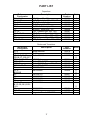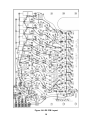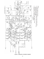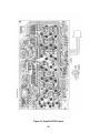
1
SUPPLEMENT
Bose® Model 1801/1800
Power Amplifier
Q4, part number 102428 and Q5, part number 102429 are no longer available with the lead length
needed for soldering to the PCB. Use the part numbers listed below when ordering these transistors. Make a note in your Model 1801/1800 power amplifier service manual, part number 192527.
Reference
Designator
Q4
Q5
Description
SIM, 2N2219
SIM, 2N5415
Part
Number
102428-1K
102429-1K
Note
1
2
NOTE: The part numbers listed are kits. They include the following parts:
1. Q4 kit: 1 102428 transistor
3 264371 extension pins
1 192527-S1 supplement.
2. Q5 kit: 1 102429 transistor
3 264371 extension pins
1 192527-S1 supplement.
©
2001 Bose Corporation
10/2001
Supplement
Part Number 192527-S1
Contents
Specifications ................................................................................................................................... 2
Safety Information ............................................................................................................................ 3
Electrostatic Discharge Sensitive (ESDS) Device Handling ........................................................ 4
Disassembly/Assembly Procedures ........................................................................................... 5-8
Test Procedures ............................................................................................................................... 9
Figure 1. 1801 Component Location .............................................................................................. 10
Figure 2. 1801 Side View ............................................................................................................... 10
Figure 3. 1800 Front Panel ............................................................................................................ 11
Figure 4. 1800 Rear View of Front Panel ....................................................................................... 11
Figure 5. 1801 Rear View of Front Panel ....................................................................................... 11
Figure 6. 1800 Rear Panel ............................................................................................................. 12
Figure 7. 1801 Rear Panel ............................................................................................................. 12
Part List Notes ................................................................................................................................ 13
Figure 8. 1801 Front Panel ............................................................................................................ 13
Part List ...................................................................................................................................... 14-17
Figure 9. 1801/1800 Block Diagram ............................................................................................... 18
Figure 10. LED PCB Layout ........................................................................................................... 19
Figure 11. LED PCB Schematic Diagram ...................................................................................... 20
Figure 12. Amplifier Schematic Diagram ........................................................................................ 21
Figure 13. Amplifier PCB Layout .................................................................................................... 22
Troubleshooting Guide .................................................................................................................. 23
Voltage Conversion Instructions .................................................................................................. 24
Service Bulletin ......................................................................................................................... 25-28
PROPRIETARY INFORMATION
THIS DOCUMENT CONTAINS PROPRIETARY INFORMATION OF
BOSE® CORPORATION WHICH IS BEING FURNISHED ONLY FOR
THE PURPOSE OF SERVICING THE IDENTIFIED BOSE PRODUCT
BY AN AUTHORIZED BOSE SERVICE CENTER OR OWNER OF THE
BOSE PRODUCT, AND SHALL NOT BE REPRODUCED OR USED
FOR ANY OTHER PURPOSE.
1
SPECIFICATIONS
Mechanical
Dimensions:
1801
7 3/16" H x 18" W x 18 1/2" D
(Including Knobs)
81/4"H x 19"W x 15"D
(not including handles)
1800
Weight:
1801
82
95
80
91
1800
lbs
lbs (shipping)
lbs
lbs (shipping)
Power Requirements
Voltage:
105-125 AC USA, 210-250 AC EUR
Frequency:
50-60 Hz
Power Consumption:
Minimum 60 watts
Normal 1000 watts
Maximum 1960 watts
Integral Design™
Amplifier
Output :
(both channels operating )
250/250 watts @8 ohms
400/400 watts @4 ohms
Harmonic Distortion:
(THD) @ 250 watts
Less Than .15% (20Hz-5kHz)
Less Than .5% (5kHz-10kHz)
IM Distortion:
(4:1 60-7kHz) 150 watts
Less Than .15%
Frequency Response:
20Hz-10kHz ±.25dB
10kHz-15kHz ±.7dB
15kHz-20kHz ±1dB
Signal to Noise Ratio:
(unweighted)
-100dB ≤.5mV across 8Ω at zero volume
Load Impedance:
4 ohms or higher
Input Sensitivity:
1.5 Vrms for 250 watts output into 8 ohms
Input Impedance:
50,000 ohms or higher
2
SAFETY INFORMATION
1. Parts that have special safety characteristics are identified by the
symbol on
schematics or by special notes on the parts list. Use only replacement parts that
have critical characteristics recommended by the manufacturer.
2. Make leakage current or resistance measurements to determine that exposed
parts are acceptably insulated from the supply circuit before returning the unit
to the customer. Use the following checks to perform these measurements:
A. Leakage Current Hot Check-With the unit completely reassembled, plug
the AC line cord directly into a 120V AC outlet. (Do not use an isolation
transformer during this test.) Use a leakage current tester or a metering
system that complies with American National Standards Institute (ANSI)
C101.1 “Leakage Current for Appliances” and Underwriters Laboratories
(UL) 1492 (71). With the unit AC switch first in the ON position, then in the
OFF position, measure from a known earth ground (metal water pipe,
conduit, etc.) to all exposed metal parts of the unit (antennas, handle bracket,
metal cabinet, screwheads, metallic overlays, control shafts, etc.), especially
any exposed metal parts that offer an electrical return path to the chassis.
Any current measured must not exceed 0.5 milliamp. Reverse the unit power
cord plug in the outlet and repeat test. ANY MEASUREMENTS NOT WITHIN
THE LIMITS SPECIFIED HEREIN INDICATE A POTENTIAL SHOCK HAZARD THAT MUST BE ELIMINATED BEFORE RETURNING THE UNIT TO
THE CUSTOMER.
B. Insulation Resistance Test Cold Check-(1) Unplug the power supply and
connect a jumper wire between the two prongs of the plug. (2) Turn on the
power switch of the unit. (3) Measure the resistance with an ohmmeter between the jumpered AC plug and each exposed metallic cabinet part on the
unit. When the exposed metallic part has a return path to the chassis, the
reading should be between 1 and 5.2 Megohms. When there is no return path
to the chassis, the reading must be “infinite”. If it is not within the limits specified,
there is the possibility of a shock hazard, and the unit must be repaired and rechecked before it is returned to the customer.
3
ELECTROSTATIC DISCHARGE SENSITIVE (ESDS)
DEVICE HANDLING
This unit contains ESDS devices. We recommend the following precautions when repairing,
replacing or transporting ESDS devices:
• Perform work at an electrically grounded work station.
• Wear wrist straps that connect to the station or heel straps that connect to conductive floor
mats.
• Avoid touching the leads or contacts of ESDS devices or PC boards even if properly
grounded. Handle boards by the edges only.
• Transport or store ESDS devices in ESD protective bags, bins, or totes. Do not insert unprotected devices into materials such as plastic, polystyrene foam, clear plastic bags, bubble
wrap or plastic trays.
General Description
The 1801 and 1800 are Integral Design™ Power Amplifiers with all Silicon Solid-State Circuitry
using 14 power transistors per channel. Capable of complete stability with all loudspeaker
loads regardless of capacitive or inductive character. They employ fast acting electronic protection circuits for current limiting. They use computer grade capacitors throughout the power
supply, along with a 2.0kW power transformer and 1300 sq. inches of heat sink area. They also
have a power monitor display using a light emitting diode array and in the case of the 1801
signal meters as well.
CAUTION: THE BOSE® 1801/1800 POWER AMPLIFIERS CONTAIN NO USER-SERVICEABLE PARTS. TO PREVENT WARRANTY INFRACTIONS, REFER SERVICE TO WARRANTY SERVICE STATIONS OR FACTORY SERVICE.
4
DISASSEMBLY/ASSEMBLY PROCEDURES
1801 Power Amplifier
Note: Refer to Figure 1 for the following
procedures.
4.3 Connect the wire harness, thermal
cutout wires, and the input cable to the
PCB.
1. Top Cover Removal
5. Front Panel Removal
1.1 Remove the two screws that secure
the top cover at the rear of the unit. Loosen
the two screws located on each side of the
unit towards the front.
5.1 Perform procedure 1.
5.2 Remove the nut securing the top of the
front panel. The nut is located on the inside
of the front chassis beside the thermal
cutout indicator.
1.2 Slide the top cover towards the rear of
the unit and lift the cover off the unit.
5.3 Remove the knobs on the controls and
remove the two shaft nuts holding the front
panel in place.
2. Top Cover Replacement
2.1 Slide the top cover onto the unit while
making sure the screws on the side of the
unit are lining up with the slots in the top
cover.
6. Front Panel Replacement
6.1 Align the front panel over the controls
and secure it in place.
2.2 Secure the top cover to the unit.
6.2 Secure the top of the front panel and
replace the knobs.
3. Amplifier PCB Removal
3.1 Perform procedure 1.
6.3 Perform procedure 2.
3.2 Disconnect the wire harness, the two
wires connected to the thermal cutout, and
the input cable going to the PCB.
7. Front Chassis Assembly Removal
7.1 Perform procedure 5.
3.3 Remove the six screws (2B) located on
the side of the unit between the heat sink
fins (see Figure 2).
7.2 Locate and remove the four screws
that secure the front assembly to the
chassis.
3.4 Carefully pry the PCB inward towards
the power transformer (the PCB is stuck to
the chassis by the heat sinking compound)
and lift the board out of the unit.
7.3 Push down on the top of the front
assembly to release the bottom of the
assembly and pull the assembly towards
you.
4. Amplifier PCB Replacement
8. Front Chassis Assembly Replacement
4.1 Slide the PCB into place. Be sure there
is sufficient heat sink compound on the
PCB's heat sink.
8.1 While pushing down on the front
assembly slide the assembly in towards the
unit.
4.2 Align the six screws that secure the
PCB into place and secure the PCB to the
chassis.
8.2 Pull up on the front assembly to align
the screw holes with the unit and secure
the assembly in place.
8.3 Perform procedure 6.
5
DISASSEMBLY/ASSEMBLY PROCEDURES
1801 Power Amplifier
Note: Refer to Figure 5 for the following
procedures.
9. LED PCB Removal
12.2 Place the meter lamp housing over
the meters and secure it to the front assembly.
9.1 Perform procedure 7.
12.3 Perform procedure 8.
9.2 Unsolder the wires to the LED PCB
and make a note of the wiring configuration.
13. Front Panel Controls Removal
13.1 Perform procedure 7.
9.3 Remove the center nut located on
each side on the LED lamp housing.
13.2 Locate the control or switch you want
to replace and unsolder the wires and
components on that control or switch.
9.4 Lift the LED assembly out from the
front chassis.
13.3 Remove the shaft nut holding the
control or switch to the front assembly and
remove it.
9.5 Disassemble the LED assembly to gain
access to the PCB.
Note: Remember how the lamp housing
spacers are placed.
14. Front Panel Controls Replacement
14.1 Place the new control or switch into
the front assembly and secure it in place.
10. LED PCB Replacement
10.1 After reassembling the LED assembly, place it onto the front panel assembly
and secure it in place.
14.2 Resolder the wires and/ or components to the control or switch.
14.3 Perform procedure 8.
10.2 Resolder the wires to the PCB.
15. Lamp Removal
10.3 Perform procedure 8.
15.1 Perform procedure 7.
11. Meter Assembly Removal
15.2 Using a flat blade screwdriver, pry
under the edge of the socket and lift the
socket out.
11.1 Perform procedure 7.
11.2 Remove the three nuts holding the
meter lamp housing assembly to the front
panel assembly.
16. Lamp Replacement
16.1 Replace the defective lamp.
11.3 Remove the two nuts holding the
wires to the meter you want to replace and
remove the meter.
16.2 Place the lamp socket back into the
lamp housing.
12. Meter Assembly Replacement
16.3 Perform procedure 8.
12.1 Place the new meter on to the front
assembly. Connect the wires going to the
meter.
Note: It may be necessary to remove the
LED PCB Assembly to replace the lamps
see procedure 9.
6
DISASSEMBLY/ASSEMBLY PROCEDURES
1800 Power Amplifier
Note: Refer to Figure 1 for the following
procedures.
5. Front Panel Removal
5.1 Perform procedure 1.
1. Top Cover Removal
5.2 Locate and remove the eight screws
holding the front panel to the chassis. Four
of the screws are located just inside the
two handles and the other four are the
larger screws on the front panel.
1.1 Remove the four screws that secure
the top cover to the unit.
1.2 Slide the top cover towards the back of
the unit and lift it off.
5.3 Using the handles pull the front panel
away from the chassis enough to access
the gain controls and LED PCB.
2. Top Cover Replacement
2.1 Place the top cover on to the unit and
slide it under the front panel lip.
6. Front Panel Replacement
6.1 Slide the front panel into place. Be
careful not to pinch the wiring harness at
the bottom of the front panel between it
and the chassis.
2.2 Secure the top cover to the unit.
3. Amplifier PCB Removal
3.1 Perform procedure 1.
6.2 Align the holes in the front panel with
the chassis, place the screws into their
location by hand and then tighten with a
screwdriver.
Note: While tightening the screws lift up
on the top lip of the panel to provide
enough room to slide the top cover under
the lip.
3.2 Disconnect the wire harness, input
cable, and the two wires going to the
thermal cutout.
3.3 Remove the six screws (2B) located on
the side of the unit between the heat sink
fins (see Figure 2).
7. LED PCB Removal
3.4 Carefully pry the PCB inward towards
the power transformer (the PCB is stuck to
the chassis by the heat sinking compound)
and lift the board out of the unit.
7.1 Perform procedure 5.
7.2 Remove the two screws that secure
the PCB to the front panel.
4. Amplifier PCB Replacement
7.3 Unsolder the wires at the LED PCB,
make a note of the wiring configuration,
and remove the board from the unit.
4.1 Slide the PCB into place. Be sure there
is sufficient heat sinking compound on the
PCB's heat sink.
8. LED PCB Replacement
4.2 Align the six screws that secure the
PCB into place and secure the PCB to the
chassis.
8.1 Place the LED PCB into place on the
front panel.
4.3 Connect the wire harness, thermal
cutout wires, and the input cable to the
PCB.
8.2 Secure the PCB to the front panel.
8.3 Resolder the wires to the LED PCB.
7
DISASSEMBLY/ASSEMBLY PROCEDURES
1800 Power Amplifier
Note: Refer to Figure 6 for the following
procedures.
Note: Refer to Figures 3, and 4 for the
following procedures.
9. Gain Control Removal
13. Rear Panel Removal
9.1 Perform procedure 5.
13.1 Perform procedure 1.
9.2 Remove the gain control knobs.
13.2 Locate and remove the four screws
securing the rear panel and the rear panel
bracket to the unit.
Note: One of the screws holds the ground
wires to the chassis. Take care not to lose
the nuts that secure this screw and the
wires.
9.3 Unsolder the capacitor lead and wires
from the control.
9.4 Remove the nut that secures the
control to the front panel and remove the
control.
14. Rear Panel Replacement
10. Gain Control Replacement
14.1 Align the rear panel with the chassis.
10.1 Place the new control into the front
panel and secure it into place.
14.2 Secure the rear panel to the chassis.
Be sure to use the rear panel bracket on
the bottom of the panel.
10.2 Resolder the capacitor lead and the
wires to the terminals on the gain control.
14.3 Secure the ground wires to the
chassis.
10.3 Perform procedure 6.
14.4 Perform procedure 2.
11. Power Switch Removal
11.1 Perform procedure 5.
11.2 Remove the wires on the rear of the
power switch.
11.3 Remove the nut securing the switch
to the front panel and remove the switch.
12. Power Switch Replacement
12.1 Place the new power switch into the
front panel and secure it in place.
12.2 Reconnect the wires on the rear of
the switch.
12.3 Perform procedure 6.
8
TEST PROCEDURES
1. Bias Adjustment Setup and Procedure
4. Power Output Procedure
1.1 Locate the -85V negative terminal
found on the capacitor (C4). See Figure 1
for the location of C4.
4.1 Connect an 8 ohm, 250 Watt load to
the output.
4.2 Apply a 1.75Vrms, 1kHz signal to the
input.
Note: The 1801 and very early 1800's had
two lugs on the caps. One with two or three
wires and one single wire. The later production 1800 had three lugs on the capacitor. Either way the lug with the two or three
wires is the lug to disconnect from the
capacitor. All other lugs remain.
4.3 Turn the gain controls up to the point
where the clipping LED's just begin to
light up and check the output for 250
watts.
4.4 Repeat the steps above for a 4 ohm
load. The output measurement should be
400 watts.
1.2 Remove the lug with two or three wires
connected to it.
1.3 Connect a 0-200mA meter between
the disconnected lug and the - terminal on
the capacitor C4.
5. Harmonic Distortion Procedure
5.1 With the unit connected as in procedure 3, turn the gains up to just before
clipping and check the distortion at the
frequencies of 20Hz, 5kHz, and 10kHz.
1.4 Disconnect the PCB that is not being
tested by unplugging the multiple pin
connector.
5.2 The distortion limits are ≤.15% from
20Hz to 5kHz and ≤.5% from 5kHz to
10kHz.
1.5 Turn the amplifier on with no input
signal applied and adjust the bias pot (R13)
for 90mA with the board cold.
6. Thermal Cutoff Procedure
Note: The PCB must be removed from
the chassis for the bias to be adjusted.
6.1 Apply a signal to the unit with the
outputs loaded ( 8 or 4 ohms ). Short one
channel at a time until the unit goes into
thermal cutoff. The thermal indicator should
turn on and the output of the unit should be
off.
2. Frequency Response Procedure
2.1 Apply a 1Vrms, 1kHz signal to the
input.
2.2 Reference a dB meter to the output.
6.2 Disconnect the short from the output.
Wait until the unit comes out of thermal
cutoff. You can speed this process by
cooling the PCB with a fan.
2.3 Check the response from 20Hz to
20kHz. The response should not exceed ±1
dB. Refer to the response specification on
page 2.
6.3 Once the unit is cooled apply a signal
to the channel you had shorted to check to
see if its operational.
3. DC Offset Procedure
3.1 With no signal applied measure the DC
offset at the output. It should measure
250mV or less.
6.4 Apply a signal to the other channel and
short the output. Wait for the thermal
indicator to come on then remove the short
and cool the PCB.
9
Figure 1. 1801 Component Location
Figure 2. 1801 Side View
10
Figure 3. 1800 Front Panel
Figure 4. 1800 Rear View of Front Panel
Figure 5. 1801 Rear View of Front Panel
11
Figure 6. 1800 Rear Panel
Figure 7. 1801 Rear Panel
12
PART LIST NOTES
1. This part is not normally available from Customer Service. Approval from the Field Service
Manager is required before ordering.
2. The reference designators in bold are located on the LED PCB.
3. This part is not located on the PCB'S.
4. The reference designators marked with a ‡ symbol are located on the Front Panel.
5. The part numbers listed with SIM are selected components and may not be directly interchangeable with standard available parts.
6. This part is located on the amplifier PCB.
7. This part is used on the 1801 Power Amplifier.
8. This part is used on the 1800 Power Amplifier.
9. Items marked with a ¥ symbol are not shown in the exploded views.
Figure 8. 1801 Front Panel
13
PART LIST
Main Part List (per figures 1-7)
Item
Number
A1
RT-1, RT-2
¥
Q10-23
Q10-23
Q10-23
Q10-23
Q4, 5
¥
¥
¥
¥
¥
S1
S1
S2
S3
J3, 4 (J5, 6 1801 )
R5, 6
R5, 6
1
2
3
4
5
5
M1, 2
B1-4
B5, 6, 7
B8
K1
6
7
T1
T1
T1
Description
Preload Network
Thermal Cut-Out
RCA Jack
Screw, 6/32 x 1/2 Stainless Steel
Washer
Plastic Insulator
Nut, Brass, 6/32 x 5/16 x 1/8
Heat Sink Assy
Top Wiring Harness
Bottom Wiring Harness
Top Wiring Harness
Bottom Wiring Harness
Audio Cable
Toggle Switch, ON/OFF
Switch, ON/OFF
Input Switch
Speaker Switch
Phone Jack
Gain Control, 100kΩ
Gain Control, 100kΩ
Indicator Lens, White
Indicator Lens, Red
Lens Housing
Front Handle
Knob
Knob
VU Meters
Meter Lamps
L.E.D / Bose® Logo Lamp 1847
Thermal Cutout Indicator
Start-up Relay
Accy Outlet
Line Cord
Transformer
Transformer (110v)
Transformer (220v)
14
Part
Number
102666
102440
102784
106348
103032
102901
103016
102571
102929-1
103281-1
103365
103366
102838
103291
102740
102576
103400
102704
102406
103260
103479-1
103479-0
103478
121914
128907
121911
102570
103063
102580
102582
102818
107558
103441
102434
110185
112669
Note
6
6
6, 9
6
6
6
6
6
1, 7, 9
1, 7, 9
1, 8, 9
1, 8, 9
9
8
7
7
7
7
8
8
7
8
7
7
7
7
1, 7
1
1
PART LIST
Main Part List (per figures 1-7)
Item
Number
8
F1
F1
F1
¥
¥
9
10
11¥
12
13
14
15
16
17
18
19
¥
¥
20
21
22
23
24
25
Description
Part
Number
Rubber Foot
121929
Fuse (110v)15A, 1 1/4 x 1/4Slo-Blo
103608
Fuse (220v) 8A, 5 x 20mm
108190-800
Fuse (220v) 7A, 1 1/4 x 1/4Slo-Blo
103609
Fuse Cap for 1 1/4 x 1/4
109484
Fuse Cap for 5 x 20mm
109493
Front Panel Assy
103380
Front Panel Assy
121910
Rear Panel Assy
103282
Rear Panel Assy
103266
Amp PCB Complete
102735-1
L.E.D Board Complete
102751
Carton and Fillers
103268
Heat Sink Side
102536
Heat Sink Corner
102474
Top Cover
102544
Top Cover
121930
Screw Heat Sink
103041
Accessory Kit
102745
Accessory Kit
103361
Black Binding Post
109068-0
Red Binding Post
109068-2
Blue Binding Post
109068-6
Black Binding Post Base
109069-0
Fuse Holder
109485
Strain Relief
102708
Plug, double banana red, 103362-2
blue, 103362-6
15
black, 103362-0
Note
9
9
1, 7
1, 8
1, 7, 9
1, 8
1
1
1
1
1, 7
1, 8
1, 7, 9
1, 8, 9
PART LIST
Resistors
Reference
Designator
R1-4
R2
R3
R9, 17
R11
R12, 51, 53
R13
R18, 20, 48
R25, 26
R31-36, 41-46
R37-39
R47
R50
R52, 54
R55, 57
R56
R1,3,101,103
R2,4,10,13,16,19
102,104,107,110
113,116,119
R5,105
R6,9,106,109
R8,108
R11,111
R12,15,18,112,
115,118
R14,114
R17,117
R20,120
R21,121
R22,122
Description
1MΩ, 1/2W, 10%
8.2kΩ, 1/2W, 10%
3kΩ, 2W, 10%
6.19Ω, 1/4W, 1%
1.5kΩ, 1/4W, 1%
340Ω, 1/4W, 1%
100Ω, Bias Pot
23.7kΩ, 1/4W, 1%
182Ω, 1/4W, 1%
0.8Ω, Wirewound, 3W, 5%
0.4Ω, Wirewound, 6W, 5%
4.7Ω, 2W, 5%
470Ω, 1/2W, 5%
10kΩ, 1/4W, 1%
100kΩ, 1/4W, 1%
680Ω, 1/2W, 5%
5.1kΩ, 1W, 5%
150Ω 1/2W, 5%
3.6kΩ, 1W, 5%
2kΩ, 1/2W, 5%
8.2kΩ, 1W, 5%
12kΩ, 1/2W, 5%
1kΩ, 1/2W, 5%
Part
Note
Number
102944-105
3
104064-822
108676-302
104095-6191
104095-1501
104095-3400
102832
104095-2372
104095-1820
102394
102395
102393
102942-471
104095-1002
104095-1003
102942-681
104064-512
2
102942-151
2
104064-362
102942-202
104064-822
102942-123
102942-102
24kΩ, 1/2W, 5%
43kΩ, 1/2W, 5%
15kΩ, 1/2W, 5%
120Ω, 1/2W, 5%
18kΩ, 1/2W, 5%
102942-243
102942-433
102942-153
102942-121
102942-183
16
2
2
2
2
2
2
2
2
2
2
PART LIST
Capacitors
Reference
Designator
C1‡, 2‡
C1, 14, 15
C1,101
C2, 3
C3, 4
C5
C5, 16
C6, 7, 10, 11
C8
C9
C12, 13, 17
Description
1uF, Mylar, 50v, 10%
.1uF, Electrolytic, 100v, 10%, NP
100uF Electrolytic, 3v
30uF Electrolytic, 100v
14,000uF, Electrolytic, 100v
18,000uF, Electrolytic, 10v
27pF, Ceramic Disc, 25v, 10%
.01uF, Ceramic Disc, 25v, 10%
200pF, Ceramic Disc, 200v, 10%
300pF, Ceramic Disc, 200v, 10%
1000pF, Ceramic Disc, 200v, 10%
Part
Number
102751
102403
102836
102405
102438
104229
102397
102399
102400
102396
102453
Note
Part
Number
102578
102422
116997
Note
4
2
3
3
Diodes and Transistors
Reference
Designator
D1-4
D5-8
CR1-4, 7, 16, 17
CR10-17,110-117
CR1-9,101-109
CR5, 18, 19
CR6, 15
CR8-14, 20, 21
Q1
Q2, 8
Q2,102
Q3
Q4
Q5
Q6
Q7, 24, 25
Q1,3-10,101,103110
Q9
Q10-23
U1
Description
Bridge Rectifier
Diodes
Diode 1N4148
L.E.D Diode
Diode SIM 1N3070
Diode 1N5425, Zener, 15V, 1/2w
Diode SIM 1N4003
SIM MM-4001
SIM 2N3906
106864
102411
102423
102422
102425
102426
SIM
SIM
SIM
SIM
SIM
102427
102428
102429
102430
102432
2N6175
2N2219
2N5415
2N3584
2N3904
SIM 2N6211
MJ15011
Integrated Circuit, MC1556G
17
102431
117579
102409
2
2
5
5
2
5
5
5
5
5
2
5
Bridge Rectifier
Turn On Relay
Figure 9. 1801/1800 Block Diagram
18
Figure 10. LED PCB Layout
19
Figure 11. LED PCB Schematic Diagram
20
Notes:
1. See Bias Adjustment Procedure.
2. U1 input (pin 2) virtual ground, output test point 8 (pin 6) 275mV.
3. Early production units replace R28 with capacitor C15 (0.1uF) found
in either side of the pc board.
4. All resistors are 1/2 watt 5% unless otherwise specified.
5. All capacitor in uF unless otherwise specified.
Figure 12. Amplifier Schematic Diagram
21
Figure 13. Amplifier PCB Layout
22
TROUBLESHOOTING GUIDE
SYMPTOM
1. DC Offset:
POSSIBLE CAUSE
≤2v
Defective U1
Defective Q1
≥2v
Defective U1
Defective CR1, 2, 6, 15
Open ground at the RCA
input jack
Defective Q1-8, Q24
Defective CR16, 17
Test point "A" polarity
the same as DC offset
(see Figure 11)
Short between transistor
and heat coupler
Shorted driver or output
transistor
Trouble shoot (by removing
collector screws) in this
sequence.
2. High Current:
Test point "A" polarity
opposite to the DC offset
(see Figure 11)
Negative: Q9, 11, 23, 21,
22, 19, 20, 18
Positive: Q6, 10, 17, 16,
14, 13, 12, 15
3. Oscillation:
Unloaded
Loaded
Defective C5
Defective Q6, Q9
Defective CR8
Open C4, 5, 9, 11
Defective R24, 29, 30,
51, 52
4. Excessive Noise:
Defective U1, Q1
Defective R57, 58
5. No Bias Adjustment:
Defective Q4, 6, 7, 9
Open R11, 12, 13
6. Incorrect Frequency
Response:
Defective C5, C8
Shorted Mica Insulator Q3
7. Excessive Distortion: Defective Q7, Q8, Q25
Defective CR18, 19
Defective CR5 ( at full
output only)
23
VOLTAGE CONVERSION INSTRUCTIONS
1. Perform Top Cover removal procedures for the model amplifier your going to convert.
2. Refer to the figures below for the voltage conversion being performed.
3. On the 1801 when converting to 110 volts remove the in-line resistor found wired to the
thermal cutoff indicator. Connect the wire directly. For 220 voltage conversion connect a
56k ohm 1/2 Watt resistor directly to the thermal cutoff indicator terminal.
4. Use an MDL 10 amp fuse for 110 volt operation.
5. Use an MDL 5 amp fuse for 220 volt operation.
NOTE: FOR 220 VOLT AC USERS ONLY
For 110 volt operation of the accessory outlet, move the wire labeled "TO RECEPTACLE"
from transformer connector #4 to connector #2. The amplifier will operate on 220 volts
and provide 110 volts to the accessory outlet (up to a maximum of 3 amps).
24
SERVICE BULLETIN
Subject: Interchangeability of repaired amplifier PCB.
Torroidal Power Transformer.
1800 Amplifier used with a TC-18 Transit Case.
Date: 09/19/1977
Bulletin #13
Remarks:
The 1801 power amplifier board ( part # 102735 ) will no longer be shipped as a standard
repair part. Instead, a universal replacement board ( part # 102735-1 ) with a special thermostatic clip connection allowing the use of this board in the 1801 and early production 1800 wire
harness assembly.
In the case of the 1801, amplifier boards may be intermixed with no difficulty, using the clip
connection.
In the case of the 1800, amplifier boards may be intermixed below serial #750. However, for
serial numbers above 750, use of the larger heat sink version (102735-1) is required.
When replacing amplifier boards in either unit, be certain to use additional thermal grease and
to tighten the screws holding the board to the chassis.
The 1800/1801 amplifiers are now using a torroidal power transformer that reduces the unit's
overall weight by 20 Lbs. The new transformer, ( P/N 107968 ) is found in 1800 amplifiers ( S/N
1630 and above ) and in 1801 amplifiers ( S/N 6838 and above ). Connections for the transformer are the same as indicated in the Service Manual for both units.
The 1800 power amplifier, when used with the TC-18 transit case, should be inspected periodically for dirt and dust accumulation on the heat sink surfaces. Any accumulation should be
removed as this significantly reduces the amplifier's ability to dissipate heat and increases the
likelihood of thermal overload.
25
SERVICE BULLETIN
Subject: Resistor Failure
Date: 09/19/1977
Bulletin #13A
Remarks:
We have found that the resistor R3 on the 1801/1800 amplifier PCB's have shown a higher
failure rate than normal. Studies reveal that the resistor normally runs at about 150-170°F. The
etch layout at R3 is not sufficient to provide adequate heat sink for this component, and the
resistor eventually changes value due to the heat.
This changing value causes the resistor, capacitor C2, and the zener diode CR15, to fail. The
symmetrical circuit, R2, C2, and CR6 all have sufficient heat sinking capability on the etch
layout and does not cause failures.
To improve the reliability of the boards, R3 should be changed from a carbon resistor to a
ceramic resistor of the same value. The ceramic resistor should be elevated slightly above the
PCB surface to provide adequate air ventilation for self cooling purposes. The new ceramic
resistor P/N is 108676-302.
In addition, R2 should also be changed to a new value. The resistor will be changed from 3kΩ
to 8.2kΩ, P/N 104064-822. This resistor is carbon, and due to the etch layout, need not be
elevated.
This modification must be preformed on all PCB's brought in for repair, regardless of the actual
failure.
26
SERVICE BULLETIN
Subject: Thermal Improvement
Date 10/05/1979
Bulletin #17
Remarks:
I'm pleased to inform you that we have developed a method for improving the thermal stability
of the 1800 amplifier, which may have been a problem to you during the last several months.
This problem was caused by a change we were forced to make when RCA discontinued the
manufacture of the transistor we had been using as Q3 on the 1800 PCB's.
The following change should be made on 1800 PCB,s which have the new Q3 ( MMPS U10 ).
1. Change R13, the bias pot (P/N 102832), to a new one which has not been sealed with
glyptol. This will allow you to adjust the bias current later.
2. Change R11 (P/N 102977-1501) from 1.5kΩ to 1.8kΩ (P/N 107170-182).
3. Apply a piece of Mylar insulating tape over the small (3/4" x 1/4") vertical surface of the heat
coupler bracket that is immediately above and parallel to C12.
4. Apply a small blob of thermal grease to the Mylar tape.
5. Obtain a 10kΩ thermistor (P/N 111153) and place insulating tubing over the leads, leaving
them about 1 inch long.
6. Solder the thermistor across (in parallel) the new R11.
7. Place the body of the thermistor against the blob of thermal grease applied in step 4.
8. Obtain a thin piece of polypropylene or other springy plastic and cut it to about 3/8" x 3/4".
Punch a small hole in one end of it and fasten it to the heat bracket using the screw that
mounts Q3 to the bracket. The tension of the bent piece of plastic will keep the thermistor
pressed into the thermal grease.
9. Adjust the bias current to 90ma according to the service manual.
NOTE: This change will be made on all future production units of the 1800 amplifier.
27
SERVICE BULLETIN
Subject: Output Transistors
Date: 10/13/1980
Bulletin # Pro-81-001
Remarks:
Due to supply demands, Bose® Corporation has changed the output transistors on the PM-2
and the 1800 amplifier boards currently being produced. The transistors have been change
from Bose P/N 102433 (2N5840) to P/N 117579 ( Motorola MJ15011). The new output transistors are not compatible with the original 102433 transistors. If you service an 1800 power
amplifier or PM-2 mixer, check the serial numbers on the printed circuit board and the P/N on
the output transistors to see which output device is being used. Below is a list of the approximate serial number break for the newer P/N 117579 transistors.
PM-2 Boards:
Approximately 30800 and above
1800 Boards:
Approximately 30800 and above
PM-1 Boards:
All have P/N 102433
1801 Boards:
All have P/N 102433
When replacing output transistors, you must use the correct replacement device. Older units
with P/N 102433 on the output transistors must be replaced with 102433 (2N5840) transistors.
Units with output transistors with P/N 117579 must be replaced with 117579 (MJ15011) transistors.
28
29
®
®
Bose Model 1801/1800
Power Amplifiers
©
1997 Bose Corporation
Service Manual
Part Number 192527 REV 01
SPECIFICATIONS AND FEATURES SUBJECT TO CHANGE WITHOUT NOTICE
®
®
Bose Corporation
The Mountain
Framingham Massachusetts USA 01701
P/N 192527 REV. 01 06/97 FOR TECHNICAL ASSISTANCE OR PART ORDERS, CALL 1-800-367-4008