1
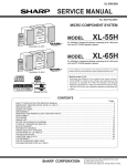
XL-55/55C
SERVICE MANUAL
No. S1308XL55////
MICRO COMPONENT SYSTEM
MODEL
XL-55
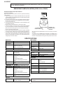
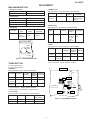
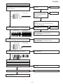
XL- 55 Micro Component System consisting of XL- 55 (main unit)
and CP- XL55 (speaker system).
MODEL
Illustration XL-55
XL-55C
XL- 55C Micro Component System consisting of XL- 55C (main
unit) and CP- XL55 (speaker system).
• In the interests of user-safety the set should be restored to its original
condition and only parts identical to those specified should be used.
CONTENTS
Page
IMPORTANT SERVICE NOTES (FOR U.S.A. ONLY) ..................................................................................................... 2
SPECIFICATIONS ............................................................................................................................................................ 2
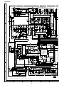
NAMES OF PARTS .......................................................................................................................................................... 3
DISASSEMBLY ................................................................................................................................................................. 4
REMOVING AND REINSTALLING THE MAIN PARTS .................................................................................................... 5
ADJUSTMENT .................................................................................................................................................................. 7
TEST MODE ..................................................................................................................................................................... 8
ERROR LIST .................................................................................................................................................................. 12
NOTES ON SCHEMATIC DIAGRAM ............................................................................................................................. 13
TYPES OF TRANSISTOR AND LED .............................................................................................................................. 13
BLOCK DIAGRAM .......................................................................................................................................................... 14
SCHEMATIC DIAGRAM ................................................................................................................................................. 18
WIRING SIDE OF P.W.BOARD ...................................................................................................................................... 25
WAVEFORMS OF CD CIRCUIT ..................................................................................................................................... 30
TROUBLESHOOTING .................................................................................................................................................... 31
FUNCTION TABLE OF IC .............................................................................................................................................. 37
LCD SEGMENT .............................................................................................................................................................. 44
PARTS GUIDE/EXPLODED VIEW
PACKING OF THE SET (FOR U.S.A. ONLY)
SHARP CORPORATION
–1–
This document has been published to be used
for after sales service only.
The contents are subject to change without notice.
XL-55/55C
FOR A COMPLETE DESCRIPTION OF THE OPERATION OF THIS UNIT, PLEASE REFER
TO THE OPERATION MANUAL.
IMPORTANT SERVICE NOTES (FOR U.S.A. ONLY)
BEFORE RETURNING THE AUDIO PRODUCT
(Fire & Shock Hazard)
Before returning the audio product to the user, perform the following
safety checks.
1. Inspect all lead dress to make certain that leads are not pinched
or that hardware is not lodged between the chassis and other metal
parts in the audio product.
2. Inspect all protective devices such as insulating materials, cabinet,
terminal board, adjustment and compartment covers or shields,
mechanical insulators etc.
3. To be sure that no shock hazard exists, check for leakage current
in the following manner.
* Plug the AC line cord directly into a 120 volt AC outlet.
* Using two clip leads, connect a 1.5k ohm, 10 watt resistor paralleled
by a 0.15µF capacitor in series with all exposed metal cabinet
parts and a known earth ground, such as conduit or electrical
ground connected to earth ground.
* Use a VTVM or VOM with 1000 ohm per volt, or higher, sensitivity
to measure the AC voltage drop across the resistor (See diagram).
* Connect the resistor connection to all exposed metal parts having
a return path to the chassis (antenna, metal cabinet, screw heads,
knobs and control shafts, escutcheon, etc.) and measure the AC
voltage drop across the resistor.
VTVM
AC SCALE
1.5k ohms
10W
0.15 µ F
TO EXPOSED
METAL PARTS
TEST PROBE
CONNECT TO
KNOWN EARTH
GROUND
All check must be repeated with the AC line cord plug connection
reversed.
Any reading of 0.3 volt RMS (this corresponds to 0.2 milliamp. AC.)
or more is excessive and indicates a potential shock hazard which
must be corrected before returning the audio product to the owner.
SPECIFICATIONS
■ General
■ CD player
Power source
AC 120 V, 60 Hz
Type
Compact disc player
Power
consumption
48 W
Signal readout
Non-contact, 3-beam semiconductor laser
pickup
Dimensions
Width: 6-5/16" (160 mm)
Height: 9-1/2" (240 mm)
Depth: 11-11/16" (296 mm)
D/A converter
1-bit D/A converter
Frequency
response
20 - 20,000 Hz
Dynamic range
90 dB (1 kHz)
Weight
7.9 lbs. (3.6 kg)
■ Amplifier (Except for Canada)
Output power
Output terminals
20 watts minimum RMS per channel into 4
ohms from 100 Hz to 20 kHz, 10% total harmonic distortion
Frequency
response
50 - 14,000 Hz (normal tape)
Speakers: 4 ohms
Signal/noise ratio
50 dB (recording/playback)
Headphones: 16 - 50 ohms (recommended:
32 ohms)
Wow and flutter
0.25 % (WRMS)
CD digital output (optical)
Subwoofer (Audio signal): 500 mV/47 k
ohms
Input terminals
Video/Auxiliary (audio signal): 500 mV/47 k
ohms
Output terminals
■ Speaker
Type
2-way type speaker system
Tweeter
4" (10 cm) Woofer
Maximum input
power
40 W
RMS: 40 W (20 W + 20 W) (10 % T.H.D.)
Rated input power
20 W
Speakers: 4 ohms
Impedance
4 ohms
Headphones: 16 - 50 ohms (recommended:
32 ohms)
Dimensions
Width: 6-5/16" (160 mm)
Height: 9-1/2" (240 mm)
Depth: 7-7/8" (200 mm)
Weight
4.7 lbs. (2.1 kg)/each
■ Amplifier (For Canada)
Output power
■ Cassette deck
CD digital output (optical)
Subwoofer (Audio signal): 500 mV/47 k
ohms
Input terminals
Video/Auxiliary (audio signal): 500 mV/47 k
ohms
■ Tuner
Frequency range
FM: 87.5 - 108 MHz
AM: 530 - 1,720 kHz
Specifications for this model are subject to change without
prior notice.
–2–
XL-55/55C
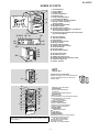
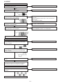
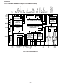
NAMES OF PARTS
1
2
6
7
8
9
3
4
10 11 12
13 14
5
15 16 17 18 19
20
21
23
24
22
25
27
28
29
30
26
1. CD Compartment
2. CD Eject Button
3. Volume Control
4. Cassette Compartment
5. Headphone Jack
6. Power On/Stand-by Button
7. Function Selector Button
8. CD or Tape Stop, Tuning Down Button
9. CD Play or Pause, Tape Play,
Tuning Up Button
10. Bass/Treble Selector Button
11. Memory/Set Button
12. Tape Record Pause Button
13. CD Track Down or Fast Reverse, Tape Rewind,
Tuner Preset Down Button
14. CD Track Up or Fast Forward, Tape Fast Forward,
Tuner Preset Up Button
15. Timer Play Indicator
16. Tape Record Indicator
17. Sleep Indicator
18. CD Random Play Indicator
19. Memory Indicator
20. FM Stereo Mode Indicator
21. FM Stereo Receiving Indicator
22. Surround Indicator
23. CD Play Indicator
24. CD Repeat Play Indicator
25. CD Digital Output Jack
26. AC Power Input Jack
27. FM/AM Loop Antenna Jack
28. Video/Auxiliary (Audio Signal) Input Jacks
29. Subwoofer Output Jack
30. Speaker Terminals
1. Tweeter
2. Woofer
3. Speaker Wire
1
3
Speaker grilles are removable:
Make sure nothing comes into contact with the
speaker diaphragms when you remove the
speaker grilles.
2
4
5
6
7
8
9
10
11
12
13
14
15
16
18
19
20
21
22
23
24
25
26
27
17
28
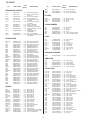
Buttons with " " mark in the illustration can be operated on the remote control only.
4. Remote Control Transmitter
5. Clock Button
6. Power On/Stand-by Button
7. CD Button
8. Tuner and Band Selector Button
9. Clear Button
10. Memory Button
11. CD Track Down, Tuner Preset Down Button
12. CD Fast Reverse, Tuning Down,
Tape Rewind Button
13. CD or Tape Play Button
14. Surround Button
15. CD or Tape Stop Button
16. Volume Up and Down Buttons
17. Bass Up and Down Buttons
18. Timer Button
19. Sleep Button
20. Video/Auxiliary Button
21. Tape Button
22. Repeat Button
23. Random Button
24. CD Track Up, Tuner Preset Up Button
25. CD Fast Forward, Tuning Up,
Tape Fast Forward Button
26. Tape Record Pause Button
27. CD Pause Button
28. Treble Up and Down Buttons
–3–
XL-55/55C
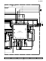
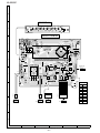
DISASSEMBLY
Caution on Disassembly
Follow the below-mentioned notes when disassembling
the unit and reassembling it, to keep it safe and ensure
excellent performance:
1. Take cassette tape and compact disc out of the unit.
2. Be sure to remove the power supply plug from the wall
outlet before starting to disassemble the unit.
3. Take off nylon bands or wire holders where they need to
be removed when disassembling the unit. After servicing
the unit, be sure to rearrange the leads where they were
before disassembling.
4. Take sufficient care on static electricity of integrated
circuits and other circuits when servicing.
STEP
REMOVAL
PROCEDURE
FIGURE
1. Screw .................. (A1) x5
2. Socket ................. (A2) x2
4-1
4-1,3
Main PWB
(C2)x2
ø3x10mm
(D2)x1
(D1)x1
ø3x10mm
Rear Panel
(D3)x1
Power Amp. PWB
Power PWB
Figure 4-2
1
Top Cabinet
2
Side Panel(Left/Right) 1. Screw .................. (B1) x4
4-1
3
Rear Panel
1. Screw .................. (C1) x2
2. Screw .................. (C2) x2
4-1
4-2
4
Power Amp. PWB
1. Screw .................. (D1) x1
2. Socket ................. (D2) x1
3. Socket ................. (D3) x1
4-2
Headphones
PWB
(E1)x1
ø3x10mm
5
Main PWB/
Headphones PWB
1. Screw .................. (E1) x4
2. Socket ................. (E2) x4
3. Socket ................. (E3) x1
4-3
Main PWB
6
Front Panel
1. Screw .................. (F1) x2
2. Socket ................. (F2) x2
4-4
7
Power PWB
1. Screw .................. (G1) x2
2. Shield Cover ....... (G2) x1
3. Screw .................. (G3) x5
4-4
Tape Mechanism
1. Screw .................. (H1) x4
4-5
Display PWB
1. Knob .................... (J1) x1
2. Screw .................. (J2) x8
4-5
10
CD PWB(Note)/
1. Screw .................. (K1) x4
Open Close Switch PWB 2. Screw .................. (K2) x2
Jack PWB
3. Socket ................. (K3) x3
5-1
11
CD Mechanism
5-2
CD PWB
(G1)x2
ø3x6mm
(G2)x1
Shield
Cover
(F2)x1
(F2)x1
Front Panel
Bracket,
(G3)x4 Shield Cover
ø4x10mm
Power
PWB
(F1)x1
ø3x10mm
(F1)x1
ø3x10mm
(A2)x1
Front Panel
(A1)x2
ø3x10mm
(C1)x1
ø3x10mm
Display PWB
(J2)x8
ø2.6x10mm
(J1)x1
(A1)x1
ø3x10mm
Side Panel
(Right)
(G3)x1
ø3x10mm
Figure 4-4
(B1)x2
ø3x10mm
(A1)x1
ø3x10mm
(E1)x1
ø3x10mm
Power PWB
Note:
After removing the connector for the optical pickup from the
connector, wrap the conductive aluminium foil around the front end
of the connector so as to protect the optical pickup from electrostatic damage.
(A1)x1
ø3x10mm
(E1)x1
ø3x10mm
(E2)x2
Figure 4-3
9
Top Cabinet
(E3)x1
(E1)x1
ø3x10mm
Tape
Mechanism
PWB
(A2)x1
8
1. Screw .................. (L1) x3
(E2)x2
Tape
Mechanism
Open
Side Panel
(Lift)
(B1)x2
ø3x10mm
Rear Panel
(C1)x1
ø3x10mm
Cassette
Holder
(H1)x4
ø2.6x10mm
Figure 4-1
Figure 4-5
–4–
XL-55/55C
(K1)x4
ø2.4x10mm
CD PWB
(K2)x1
ø2.6x10mm
(L1)x3
ø2.6x10mm
(K2)x1
ø2.6x10mm
Top Cabinet
Open/Close
Switch PWB
Top Cabinet
(K3)x1
(K3)x2
Jack
PWB
CD Mechanism
CD Mechanism
Figure 5-2
Figure 5-1
REMOVING AND REINSTALLING THE MAIN PARTS
TAPE MECHANISM SECTION
(A2)x1
ø2x7mm
Perform steps 1 to 6 and 8 of the disassembly method to
remove the tape mechanism. (See page 4.)
(A2)x1
ø2x3mm
(A1)x2
ø2x8mm
How to remove the record / playback and erase
heads (See Fig. 5-3.)
1. Remove the screws (A1) x 2 pcs., to remove the erase
head.
2. Remove the screws (A2) x 2 pcs., to remove the record/
playback head.
Note:
After replacing the heads and performing the azimuth
adjustment, be sure to apply screwlock.
Erase Head
Record/
Playback Head
Figure 5-3
How to remove the pinch roller (See Fig. 5-4.)
1. Carefully bend the pinch roller pawl in the direction of the
arrow <A>, and remove the pinch roller (B1) x 1 pc.,
upwards.
<A>
Pinch Roller
Pawl
Pinch Roller
(B1)x1
Figure 5-4
How to remove the belts (See Fig. 5-5.)
1. Remove the main belt (C1) x 1 pc., from the motor pulley.
2. Remove the FF/REW belt (C2) x 1 pc., from the REW/FF
roller.
3. Put on the belts in the reverse order of removal.
Note:
When putting on the belt, ascertain that the belt is not twisted,
and clean it.
Motor
Main Belt
(C1)x1
REW/FF
Clutch
FF/REW Belt
(C2)x1
Figure 5-5
How to remove the motor
(See Fig. 5-6.)
(D2)x3
Special
Screw
(D1)x1
ø2x4mm
Motor
1. Remove the main belt.
2. Remove the screws (D1) x 2 pcs., to remove the motor
bracket.
3. Remove the screws (D2) x 3 pcs., to remove the motor.
Note:
When mounting the motor, pay attention to the motor mounting
angle.
Motor
Bracket
(D1)x1
ø2x4mm
Motor
Figure 5-6
–5–
XL-55/55C
How to remove the flywheel (See Fig. 6-1.)
Mechanism
Chassis
1. Remove the belt.
2. Remove the stop washer (E1) x 1 pc., with a small precision
screwdriver to extract the flywheel from the capstan metal.
Note:
When the stop washer is deformed or damaged, replace it
with a new one.
(E1)x1
Stop Washer
Stop
Washer
Driver
Washerx2
Flywheel
How to reinstall the parts
Install each part in the reverse order of the removal with care.
Figure 6-1
How to remove the tape mechanism PWB
(See Fig. 6-2.)
(F1)x1
Tape ø2x3mm
Mechanism
PWB
1. Remove the screw (F1) x 1 pc., to remove the tape
mechanism PWB.
2. Remove the screw (F2) x 1 pc.
3. Remove the solder joints (F3) x 2 pcs., to remove the tape
mechanism PWB.
(F2)x1
ø2x8mm
Tape
Mechanism
PWB
(F3)x2
Solder
Joint
Figure 6-2
Mechanism Cover
CD MECHANISM SECTION
Perform steps 1, 10 and 11 of the disassembly method to
remove the CD mechanism. (See page 4.)
(A1) x2
(A1) x2
(A2) x2
ø2.6 x6mm
How to remove the pickup (See Fig. 6-3)
1. Remove the mechanism cover, paying attention to the
pawls (A1) x 4 pcs.
2. Remove the screws (A2) x 2 pcs., to remove the shaft (A3)
x 1 pc.
3. Remove the stop washer (A4) x 1 pc., to remove the gear
(A5) x 1 pc.
4. Remove the pickup.
Note:
After removing the connector for the optical pickup from the
connector, wrap the conductive aluminium foil around the
front end of connector remove to protect the optical pickup
from electrostatic damage.
CD Mechanism
Shaft
(A3) x1
StopWasher
(A4) x1
Gear
(A5) x1
Pickup Unit
Figure 6-3
–6–
XL-55/55C
ADJUSTMENT
MECHANISM SECTION
• Driving Force Check
Torque Meter
• FM Mute Level
Signal generator: 1 kHz, 40 kHz dev., FM modulated
Specified Value
Play: TW-2412
• Torque Check
Torque Meter
98.00 MHz
(30 dBµV)
Specified Value
Play: TW-2111
30 to 60 g. cm
Fast forward: TW-2231
55 to 140 g.cm
Rewind: TW-2231
55 to 140 g.cm
Adjusting
Point
MTT-111
Variable
resistor in
motor.(M901)
Specified
Value
3,000 ±
90 Hz
Adjusting
Parts
98.00 MHz
VR351*1
Frequency
Test
Stage
Instrument
Connection
Headphone
terminal
FM IF
10.7 MHz
Frequency
Display
98.00 MHz
Setting/
Adjusting
Parts
Variable
resistor
in motor
Figure 7-1 ADJUSTMENT POINT
T304(Turn Input: Pin 1 of
the core of IC301
T304 fully
counterclockwise).
Test Stage Frequency
Frequency
Display
FM Band
Coverage
—
87.50 MHz
FM RF
98.00 MHz
(10~30 dB)
98.00 MHz
*1. Input: Antenna,
*2. Input: Antenna,
TUNER SECTION
fL: Low-renge frequency
fH: High-renge frequency
• AM IF/RF
Signal generator: 400 Hz, 30%, AM modulated
Setting/ Instrument
Adjusting Connection
Parts
(fL): L303 *1
3.4 ± 0.1 V
L302
*2
Output: TP301
Output: Speaker Terminal
MAIN PWB
IC302
Setting/ Instrument
Adjusting Connection
Parts
T351
*1
IF
450 kHz
1,602 kHz
AM Band
Coverage
—
531 kHz
(fL): T306 *2
1.1 ± 0.1 V
AM
Tracking
990 kHz
990 kHz
T302
FM Mute
AM IF Level
T351 VR351
FM Band
Coverage fL
FM OSC.
L303
9
*1
CF352
T304
TP301
IC301
FM IF
IC303
*1. Input: Antenna Output: Speaker terminal
*2. Input: Input is not connected Output: TP301
R336
T306
AM Band
Coverage fL
AM OSC.
• Check FM VT
Signal generator: 1 kHz, 40 kHz dev., FM modulated
Frequency
Instrument
Connection
• FM RF
Signal generator: 1 kHz, 75 kHz dev., FM modulated
M901
Tape
Motor
Frequency
Display
Input: CNP301
Output: Speaker
Terminal
• FM Detection
Signal generator: 10.7 MHz, FM sweep generator
TAPE MECHANISM
Test Stage Frequency
Instrument
Connection
*1. Adjust so that an output signal appears.
• Tape Speed
Test Tape
Display
Frequency
Over 80 g
Display
Check Point
FM RF
L302
1
BF301
T302
AM
Tracking
Instrument
Connection
87.5 MHz
87.5 MHz
3.4 V ± 1.0 V
TP301
108 MHz
108 MHz
7.8 V ± 1.0 V
TP301
Figure 7-2 ADJUSTMENT POINTS
–7–
CNP301
ANTENNA
SOCKET
XL-55/55C
• Setting the Test Mode
Keeping the REW/REV button and BASS/TREBLE button
pressed, turn on POWER. Then, the frequency is initially set
in the memory as shown in Table. Call it with the PRESET
button to use it for adjustment and check of tuner circuit.
Preset No.
1
2
3
4
5
11~25
FM STEREO
87.50 MHz
108.00 MHz
98.00 MHz
90.00 MHz
106.00 MHz
––––
Preset No.
6
7
8
9
10
Preset No.
AM
26
27
28
29
30
531 kHz
1,602 kHz
990 kHz
603 kHz
1,404 kHz
FM MONO
106.00 MHz
90.00 MHz
98.00 MHz
108.00 MHz
87.50 MHz
TEST MODE
The test mode applied to this microcomputer has three modes, namely ordinary test mode to be used for adjustment or
measurement, aging test mode to be used for aging test, and self-diagnosis test mode for self-inspection in case of final product
inspection.
1. Turning on the test mode
To turn on the specific test mode, press the POWER ON/STAND-BY button, holding down the following two buttons in the
ordinary stand-by mode (power off state). In this case only the main unit button is valid. Even when the POWER of remote control
button is set to on, the test mode is not turned on.
[Ordinary test mode]
1. CD Test Mode (TEST 1)…………………… BASS/TREBLE + FF/FWD
2. Tuner Test Mode (TEST 2)………………… BASS/TREBLE + REW/REV
3. Electronic volume Test Mode (TEST 3)…… BASS/TREBLE + REC
4. Timer Test Mode (TEST 4)………………… MEMORY/SET + REC
5. LCD Test Mode (TEST 5)……………………MEMORY/SET + REW/REV
[Self-diagnosis Test Mode]
1. Button input diagnosis test mode (TEST6).… MEMORY/SET + PLAY
2. CD Test Mode (TEST 1)
In the CD test mode the operation of each step is enabled even when the LID-SW is off. However, if focus cannot be set in step 3 or any
error processing is started, it is impossible to proceed to the next step. When the error processing is started, operations other than
termination of test mode by pressing the POWER ON/STAND-BY button or return to the step 1 by pressing the STOP button are inhibited.
1. Step 1 Mode
When the CD test mode is turned on, the following indication lights, the processing (until turning-off of CD STB terminal of CD
initialization operation flow) is executed, and the next button input is waited.
After lighting for one second
If the following operation buttons are pressed in this state, the operation is performed as follows.
"POWER ON/STAND-BY" ... The test mode is turned off, the power is turned off, and the ordinary stand-by mode is set.
"FF/FWD" ................. After the pickup returns once to the innermost periphery, it slides toward the outer periphery while this
button is held down.
"REW/REV" .............. After the pickup returns once to the innermost periphery, it slides toward the inner periphery while this
button is pressed. However, if PU-IN is on, input is invalid.
"PLAY" ..................... Shift to step 2
"STOP" ..................... Invalid
"REC PAUSE" .......... Shift to step 5
–8–
XL-55/55C
* In case of initialization the pickup is moved toward the inner periphery. Any buttons other than POWER ON/STAND-BY button
are not accepted until the shift of pickup to the inner periphery is completed at this time. If PU-IN SW ON cannot be detected
within 10 seconds, the slide motor is stopped, and the following error indication appears. Press the POWER ON/STAND-BY
button to end the test mode, or press the STOP button to return to step 1. Any other operations are inhibited.
2. Step 2 Mode
When the "PLAY" button is pressed in this mode, the laser lighting command LDON (8400) is sent, and the laser is turned on.
Other operations are not performed.
If the following buttons are pressed in this state, the operation is performed as follows.
"POWER ON/STAND-BY" .. The test mode is turned off, the power is turned off, and the ordinary stand-by mode is set.
"FF/FWD" ................ The pickup slides toward the outer periphery while this button is held down.
"REW/REV" ............. The pickup slides toward the inner periphery while this button is held down. However, if PU-IN is on, input
is invalid.
"PLAY" ..................... Shift to step 3
"STOP" .................... Return to step 1
"REC PAUSE" ......... Shift to step 5
3. Step 3 Mode
The laser is kept lighting. The processing (until turning-on of CLV servo of CD initialization operation flow) is executed, and
the next button input is waited. (The focus servo is turned on, and focus search is performed.)
The focus search is repeated until the focus is set.
When the following operation buttons are pressed in this state, the operation is executed as follows.
"POWER ON/STAND-BY" .. The test mode is turned off, the power is turned off, and the ordinary standby mode is set.
"FF/FWD" ................ The pickup slides toward the outer periphery while this button is held down.
"REW/REV" ............. The pickup slides toward the inner periphery while this button is held down. However, if PU-IN is on, input
is invalid.
"PLAY" ..................... If the focus has been set, shift to step 4 is executed. If the focus has not been set, acceptance is inhibited.
"STOP" .................... Return to step 1
"REC PAUSE" ......... Shift to step 5
*If the focus is disturbed after it has been set, the process returns to step 1.
4. Step 4 Mode (Only focus "OK" can make this item showing)
The CLV servo ON command (8600) sending operation is performed, and the next button input is waited. (The disc is rotated
to perform CLV locking.)
The time display indicates always "0:00".
When the following buttons are pressed in this state, the operation is executed as follows.
"POWER ON/STAND-BY" .. The test mode is turned off, the power is turned off, and the ordinary standby mode is set.
"FF/FWD" ................ The pickup slides toward the outer periphery while this button is held down.
"REW/REV" ............. The pickup slides toward the inner periphery while this button is held down. However, if PU-IN is on, input
is invalid.
"PLAY" ..................... Shift to step 5
"STOP" .................... Return to step 1
"REC PAUSE" ......... Shift to step 5
*If the focus is disturbed, the process returns to step 1.
–9–
XL-55/55C
5. Step 5 Mode
The CD initialization operation flow is executed to the end, the mute is set to off, and playback is started. Even when the
playback reaches the outermost periphery of disc, the operation does not stop. The LCD display indicates the playback past
time as in case of ordinary CD playback.
When the following operation buttons are pressed in this sate, the operation is executed as follows.
"POWER ON/STAND-BY" ... The test mode is turned off, the power is turned off, and the ordinary standby mode is set.
"FF/FWD" ................. The pickup slides toward the outer periphery while this button is held down.
"REW/REV" .............. The pickup slides toward the inner periphery while this button is held down. However, if PU-IN is on, input
is invalid.
"PLAY" ..................... Invalid
"STOP" ..................... Return to step 1
*If the focus is disturbed, the process returns to step 1.
Other cautions
• TOC IL is not executed in the test mode.
• As for button operations other than those shown above, only the sound volume operation (with JOG) is accepted.
3. Tuner Test Mode (TEST 2)
1. Outline of tuner (radio) test mode
The tuner test mode is intended to store the adjustment and measurement frequencies in the preset memory CH without
frequency setting by adjusting personnel when the tuner section is adjusted in the production line.
2. Details of tuner test mode
When the power is turned on by using the POWER ON/STAND-BY button while the BASS/TREBLE and REW/REV buttons
are held down in POWER OFF state, the frequency for adjustment and measurement of destination specified by the AREA
terminal is preset and stored in the preset memory CH. However, Ordinary 1 and Ordinary 2 are set to the designation
(destination selected by SPAN switching operation) set when the test mode is obtained.(Memory/Set+Function Key Span
Charged) (As for frequencies to be preset and stored for each destination, refer to item 3.)
The tuner test mode is started from preset No.1.
The operations of test mode are identical with the ordinary operations of TUNER function. However, FUNCTION switching
is invalid.
Since it is necessary to discard the content of preset memory when the tuner test mode is ended, "0000" or "1111" bits are
written in the memory to be checked in case of memory check (in case of initial setting) so that memory abnormality is detected
in case of initial setting so as to ensure memory initialization.
When the tuner test mode is turned on, the following indication lights for one second.
• The TUNER TEST2 mode is set as a result of BASS/TREBLE+ REW/REV. -> POWER OFF -> IF AC is set to OFF in the TEST2
mode, the initial state is restored.
When POWER is set to OFF, the memory of TEST2 mode is protected.
When the power is turned on again, the ordinary operation is enabled while the data is stored in the
memory (besides TUNER).
If AC OFF state is maintained in this state for about 1/2 day, start is executed in the initial state.
• To clear the whole memory, insert the AC cord, holding down MEMORY + STOP.
– 10 –
XL-55/55C
3. Preset frequencies for various destinations (random preset memory)
CH
1
2
3
4
5
BAND
FM
STEREO
Europe 2, 4
FM 87.50 MHz
FM108.00 MHz
FM 98.00 MHz
FM 90.00 MHz
FM106.00 MHz
CH
6
7
8
9
10
11-15
BAND
AM
Europe 2, 4
AM 531 kHz
AM1602 kHz
AM 990 kHz
AM 603 kHz
AM1404 kHz
LW
CH
16-25
26
27
28
29
30
BAND
FM
MONO
Europe 2, 4
FM106.00 MHz
FM 90.00 MHz
FM 98.00 MHz
FM108.00 MHz
FM 87.50 MHz
• The hatched sections of the table are not stored in memory.
4. Electronic volume Test Mode (TEST 3)
When the test mode is set, the following indication lights for one second.
When this mode is set, BASS/TREBLE is set to 0 (0 dB) and start-up function is set to CD when volume is -14 dB (STEP 23).
The button operations in the test mode are the same as those of ordinary operation excepting sound volume UP/DOWN.
(1) The indication is the same as that of ordinary operation excepting test mode setting.
(2) The sound volume control with the sound volume UP/DOWN button is only the following 3 steps unlike the ordinary state.
Volume- ∞ (STEP 0) <-> Volume-14 dB (STEP 23) <-> Volume-0 (STEP 30)
(3) BASS/TREBLE is switched when button operation is performed.
5. Timer test Mode (TEST 4)
When the test mode is set, the following indication lights for one second.
The current time and timer time are set in the following procedure to perform the timer playback.
1.Set the current time to 1:00, set the timer to ON time 1:05, set the function to Aux, and set volume STEP 12. One minute is counted
as one second, and the timer playback operation is performed. The fade-in (when playback is started) is executed at a rate of
one step for 1 sec. After completion of fade-in the fade-out is executed at a rate of one step for 1 sec (WAIT 1 sec inserted). After
completion of fade-out the power is turned off (after WAIT 1 sec), and the mode is changed to the standby mode.
The indication during operation is the same as that of ordinary timer operation.
6. LCD Test Mode (TEST 5)
When the LCD test mode is set, all the LCD segments are lighted. After that the indication is changed as follows according to
the "PLAY" button input.
Lighting of all segments
Lighting of odd segments
– 11 –
Lighting of even segments
XL-55/55C
7. Key input diagnosis Test Mode (TEST 6)
When the test mode is set, the following indication appears.
This test mode is intended to check whether all the main unit buttons can be detected. Accordingly, in this test mode checking as to
whether the "POWER ON/STAND-BY" button was pressed after all the buttons shown below were pressed is performed. If the result
is OK, OK is indicated. Even any one of keys was not pressed, an error is indicated. In case of OK termination or error termination
exit from this mode occurs when the "POWER ON/STAND-BY" button is pressed next time, and the standby mode is set.
1. In case of "MEMORY/SET" + "PLAY"+ "POWER ON/STAND-BY"
Since SURROUND and RDS are not provided, the following 9 buttons are detected as all buttons.
PLAY, POWER ON/STAND-BY, BAND, BASS/TREBLE, FUNCTION, MEMORY/SET, REC PAUSE, REW, FF, STOP.
The OK/NG indication of test result is as follows.
ERROR LIST
PU-IN SW detection error
Tape mechanism error 1
Error content ............ The detection SW cannot detect ON
after a fixed period of time even if the
microcomputer controls the CD pickup
to return to the innermost position.
Probable cause ........ Defective or poorly connected PU-IN
SW or slide motor.
Action ....................... Solve the problem and turn on the power
again.
Error content ........... The detection SW "CAM-SW" cannot
detect ON (mechanism in operation) even
if the motor and solenoid are controlled
to play back, fast forward, rewind, or
record the tape.
Probable cause ....... Mechanism is in operation when this
message appears: Defective or poorly
connected CAM-SW. Mechanism stops:
Defective or poorly connected motor or
solenoid.
Action ...................... Solve the problem and turn on the power
again.
CD read error
Error content ........... Disc data cannot be read properly or
even if it can be read, the disc is not a
playable one.
Probable cause ....... The disc is loaded upside down, not CDDA, scratches, stains, etc.
Action ...................... Open the CD lid, then reload the disc
correctly. Remove the scratches or stains
on the disc.
NO DISC
Error content ........... Focusing is impossible.
Probable cause ....... The disc is loaded upside down, not CDDA, scratches, stains, etc.
Action ...................... Open the CD lid, then reload the disc
correctly. Remove the scratches or stains
on the disc.
Tape mechanism error 2
Error content ........... Initialization cannot be completed when
the microcomputer controls the motor
and solenoid to initialize the tape
mechanism (to set the mechanism to the
stop mode). The detection SW "CAMSW" cannot detect OFF While the
mechanism is in operation.
Probable cause ....... Mechanism is in operation when this
message appears: Defective or poorly
connected CAM-SW. Mechanism stops:
Defective or poorly connected motor or
solenoid.
Action ...................... Solve the problem and turn on the power
again.
– 12 –
XL-55/55C
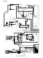
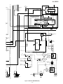
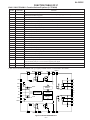
NOTES ON SCHEMATIC DIAGRAM
• Resistor:
To differentiate the units of resistors, such symbol as K and
M are used: the symbol K means 1000 ohm and the symbol
M means 1000 kohm and the resistor without any symbol is
ohm-type resistor. Besides, the one with “Fusible” is a fuse
type.
• Capacitor:
To indicate the unit of capacitor, a symbol P is used: this
symbol P means micro-micro-farad and the unit of the
capacitor without such a symbol is microfarad. As to
electrolytic capacitor, the expression “capacitance/withstand
voltage” is used.
(CH), (TH), (RH), (UJ): Temperature compensation
(ML): Mylar type
(P.P.): Polypropylene type
• Schematic diagram and Wiring Side of P.W.Board for this
model are subject to change for improvement without prior
notice.
REF. NO
DESCRIPTION
• The indicated voltage in each section is the one measured
by Digital Multimeter between such a section and the chassis with no signal given.
1. In the tuner section,
( ) indicates AM
< > indicates FM stereo
2. In the main section, a tape is being played back.
3. In the deck section, a tape is being played back.
( ) indicates the record state.
4. In the power section, a tape is being played back.
5. In the CD section, the CD is stopped.
• Parts marked with “
”(
) are important for
maintaining the safety of the set. Be sure to replace these
parts with specified ones for maintaining the safety and
performance of the set.
POSITION
REF. NO
POSITION
DESCRIPTION
SW700
VOLUME
ON—OFF
SW707
REC/PAUSE
ON—OFF
SW701
POWER ON/STAND-BY
ON—OFF
SW708
REW/PRESET DOWN
ON—OFF
SW702
FUNCTION
ON—OFF
SW709
FF/PRESET UP
ON—OFF
SW703
STOP/CLEAR,TUNING DOWN
ON—OFF
SW800
PICKUP IN
ON—OFF
SW704
PLAY/CD PAUSE,TUNING UP
ON—OFF
SW801
CD LID OPEN/CLOSE
ON—OFF
SW705
BASS/TREBLE
ON—OFF
SW901
FOOL PROOF
ON—OFF
SW706
MEMORY/SET
ON—OFF
SW902
CAM
ON—OFF
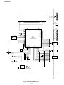
TYPES OF TRANSISTOR AND LED
FRONT
VIEW
E C B
(S) (G) (D)
(1) (2) (3)
2HA1015 GR
2HC1815 GR
2SC2001 K
2SK2541
HSB562 C
KRA102 M
KRA107 M
KRC102 M
KRC104 M
KRC107 M
SC1674 C
FRONT
VIEW
FRONT
VIEW
B C E
KTC2026 Y
MPG3372X
1
2
3
SVC348S
KDV147B
Figure 13 TYPES OF TRANSISTOR AND LED
– 13 –
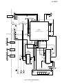
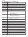
XL-55/55C
FM MUTE LEVEL
T302
SWITCHING
VR351
10K(B)
VD301-1
SVC348S
4 5
FM/AM OUT
AM LOW CUT
VSM
6
FM DET
STEREO
SD
GND
IC303
FM IF DET./FM MPX./AM IF
LA1832S
9
8
7
16
14 13
15
MO/ST
AM IF IN
3
17
L-CH OUT
AM RF IN
2
18
PHASE
(AM/FM)
FM AFC
REG
CNP301
10 11
12
1
3
+5V
AM IF IN
2
AM MIX OUT
AM/FM
ANTENNA
TERMINALS
19
R-CH OUT
AM OSC OUT
FM IF IN
1
VD301-2
SVC348S
20
MPX IN
21
PHASE
22
MPX VCO
23
VCC
24
AM MIX OUT AM OSC IN
X351
456kHz
T306
AM OSC.
R_MUTE
Q351
AM OSC OUT
IF OUT
AM TRACKING
AM IF
T351
3
1
CF351
FM IF
CF352
ZD351
+5V
2
A_12V
A_GND
Q302
10.7MHz
FM IF
FM IF
T304
CF303
CF302
1 3
FM IF AMP.
FM IF
Q306
TP301
VT
VT
FM OSC
R-MUTE
L303
VD302
L302
VD303
FM RF
VT
D_GND
L-CH
R-CH
L-CH
DI
IF IN
NC
NF
L-OUT
3
IC101
6
2
ALC
150K
7
11
6
7
12 R-OUT
NF
8
R-CH
REC
ALC
+
-
9
R-IN
P/B SW
R-CH
ERASE
HEAD
Q105
Q106
A_12V
8
10
MUTE
5
A-12V
IC102
BA3311L
+
IC102
REC./P.B.
EQUALIZER
AMP.
P/B SW
CONT
REC MUTE
1
3
L-IN
5
4
A_12V
Q101-Q104
SWITCHING
2
CNS101 CNP101
L-CH
8
8
L-CH
7
7
A-GND
6
6
A-GND
5
5
R-CH
4
4
R-CH
3
3
ERASE
2
2
A-GND
1
1
Q360
10 11
150K
RECORD/
PLAYBACK
HEAD
FM+B
IF REQ
7 8 9
SW
AM IN
6
MO/ST
5
FM
4
REC SW
1
FM IN
3
CE
IC101
HEAD SELECTOR
BA3126N
L-CH
VDD
VSS
1 2
FM
X IN
BAND
PASS
FILTER
IC302
LC72131 PLL (TUNER)
MUTE
X352
4.5MHz
DO
9
CL
8
DO
7
CL
5 6
DI
4
IC301
FM FRONT END
TA7358AP
CE
2 3
AOUT
1
BF301
15 14 13 12
17 16
NC
1 2 3
X OUT
22 21 20
9
REC SW
BIAS OSC
SWITCHING
Q151
L151
Q152
A_12V
REC
Q171
Q172
SWITCHING
Q153
SWITCHING
SWITCHING
REC BIAS
CONT
RUN PLS
Q903
SOL
SWITCHING
PH901
PHOTE INTERRUPTER
SOL901
SOLENOID
SW902
CAM
3
2
2
1
CNP901
1
MOT
P.F
CAM SW
SOLENOID
DRIVER
Q902
CNS901
M_GND
SWITCHING
Q901
Figure 14 BLOCK DIAGRAM (1/4)
– 14 –
Q905
Q904
TAPE MOTOR
DRIVER
SWITCHING
TAPE SW
3
D-GND
A_12V
5
4
U_CON 5V
SW901
FOOL
PROOF
6
5
4
SOL
6
2
RUN_PLS
1
Q906
MOT
- 2
SWITCHING
7
REC
+ 1
U_CON5V
7
B-CAN(NC)
BIAS
M
CFW901
SURROUND
M901
TAPE MOTOR
M_12V
CNP703 1 2 3 4 5 6 7 8 9 10 10
TO DISPLAY PWB
XL-55/55C
DO
CL
R_MUTE
CE
DI
CD+B
P MUTE
P-STB
9
8
SO401
VIDEO/AUX IN
7
6
5
4
A_12V
SD
FM ST
TO DISPLAY
PWB
AUX R
5
3
SURROUND
Q463
2
1 CNS704
6
7
8
IC461
KIA4558P
OPE AMP.
Q461
SUB
WOOFER
OUT
4
3
2
1
REC R CH
R-CH OUT
TAPE R
TUN R
14
13
11
12
10
9
8
6
7
5
4
3
2
1
VSS
15
DI
CE
CD R
IC401
LC75342M
LOGIC
FUNCTION/VOLUME EQUALIZER
NC
VDD
A_12V
16
19
18
20
21
22
24
23
25
26
27
29
28
30
CL
17
CD L
TUN L
TAPE L
AUX L
REC L CH
A_12V
L-CH OUT
Q360
A_12V
Q603A
Q605A
Q609A
R-MUTE
CNP652
1
PROTECT
2
FROM DISPLAY
PWB
A_12V
L-IN
13
2
L-CH
OUT
R-IN
9
5
R-CH
OUT
STEREO
11
Q601
Q602
REC L/R CH
+
SO601
SPEAKER
TERMINALS
+
IC601
LA4451
POWER
AMP.
SD
L-CH
3
4
J601
HEADPHONES
L-CH
MUTE
TAPE L/R CH
TE
VCC
12
Q105
Q106
7
P-STB
REC
T651
POWER
TRANSFORMER
(MAIN)
D651~D654
CD_6.2V
F651
4.0A 125V
Q607
Q606
Q609
VOLTAGE
REGULATOR
T.F
CNP652 CNS652
CD+B
MECHA 12V
(M_12V)
F652
1.6A 125V
D656~D659
Q608
1
1
2
2
Q605
GND
RLY681
AUDIO 12V
(A_12V)
Q683
Q604
Q603
T681
POWER
TRANSFORMER
(SUB)
D656~D659
GND
7 8 9 10 10
LAY PWB
CD_6.2V
M_GND
D-GND
CD R
CD L
A-GND
TAPE SW
D-GND
A_12V
SOL
U_CON 5V
IC681
KIA7805P
VOLTAGE REGULATOR
TO
DISPLAY
PWB
CNP707
USWD_5R6V
3
P-CONT
2
D_GND
1
3
1
2
1 2 3 4 5 6 CNP605
GND
TO CD SERVO PWB
Figure 15 BLOCK DIAGRAM (2/4)
– 15 –
SO651
AC POWER
INPUT SOCKET
AC120V,60Hz
XL-55/55C
CNS605
C
6
A
5
TO MAIN SECTION
4
CNP605
3
C
D
C
2
LCD701
M
1
1
~
4
5
39 ~ 42
38
SW801
CD LID
OPEN/CLOSE
100
67
SEG0
SEG33
M_G
~
~
4 COM3
1 COM0
CNP702
CLID_SW 65
CLID SW
10
CD STB
9
MCLK 65
X701
8MHz
KEY
SW702-SW704
SW707-SW709
9
MLD 64
10
MDATA 63
SW701
12
STAT 61
13
CD_STB 60
17
KEY1
18
KEY2
IC701
IX0060SJ
SYSTEM CONTROL
MICROCOMPUTER
MRST 59
PU_IN 58
7
VLC2
STEREO 49
7
VLC1
DO 26
8
VDD
CL 27
VREF+
CE 28
5
VLC3
11
VSS
14
MMOD
15
VREF
STEREO
TAPE_SW
SOL
MOT
REC
RUN_PLS
B-CAN
36 35 34 31 30 29 22 22
BIAS
BACK_LIGHT
51
SYS_STOP
41 42 47 38 39
P_CONT
REMOCON
CD+B 46
JOG_UP
6
5
BLKCK
4
STAT
SW700
VOLUME
P_MUTE 45
P_STB 44
9
3
PICK_IN
2
8
GVSW
1
DO
7
CL
6
CE
DI
DI 25
JOG_DOWN
21
SD
SD 50
6
24
MLD
MDATA
GVSW 33
37 POWER
CNS707
8
MCLK
BLBCK 62
X702
32.768MHz
SW705,SW706
CD+B
P_MUTE
P_STB
SURR 43
5
TO MAIN SECTION
4
CNP704
3
2
1
CNS704
CNS680
PROTECT
A–12V
1
TO AMP. SECTION
2
CNP680
1
CNS703
2
3
TAPE_SW
USWD_5.6V
A–12V
RX701
GP1U281X
REMOTE
SENSOR
D_GND
U_CON5V
SOL
MOT
1
2
3
REC
RUN_PLS
SYS_STOP
TO POWER
MRST
Q701
BIAS
B_CAN
SURROUND
Q702
Q703
LED
D701~709
D_GND
11
10
9
8
7
TO MAIN SECTION
6
CNP703
5
4
3
2
1
Q707
Q706
SWITCHING
M_
Figure 16 BLOCK DIAGRAM (3/4)
– 16 –
XL-55/55C
CNS605
CD_L
6
TO MAIN SECTION
4
CNP605
3
3
+5V
A_GND
5
2
CD_R
J801
DIGITAL
OUT
1
D_GND
CD_6.2V
2
M_GND
1
6
40 LD
39 BDO
38 /RFDET
37 TRCRS
36 OFT
35 VDET
34 RFENV
7
33 TE
1
O
CL
32 FE
2
GVSW
31 TBAL
PICK_IN
ARF
/RST
30 FBAL
3
IREF
STAT
29 VREF
STAT
DMUTE
28 FOO
4
D_GND
27 TRO
5
BLKCK
X803
16.93MHz
SQCK
26 KICK
MDATA
AVSS2
AVDD2
BLKCK
25 ECS
6
4
7
MLD
5
MCLK
IC801
MN6627482W
SERVO/SIGNAL CONTROL
14 13
8
18 17 16
MRST
MLD
24 ECM
8
9
MDATA
VSS
22 TVD
9
CD STB
MCLK
21 TVR
D
O
10
7
CNP702
CLID SW
DVSS1
8
M_GND
DVDD1
9
X1
+5V
50 51
X2
+6.2V
57 58 59 60
TX
/TEST 71
IOSEL 70
OUTL 73
AVDD1 72
AVSS1 74
RSEL 76
OUTR 75
PSEL 78
VDD
+5V
Q804
44 45
CD_6.2V
CSEL 77
SSEL 80
CONSTANT
VOLTAGE
SW801
CD LID
OPEN/CLOSE
MSEL 79
D_GND
6
E
CNP704
3
2
1
CNS704
D_GND
CNS680
1
TO AMP. SECTION
2
CNP680
IC804
MM1469XH
FOCUS/TRACKING/
SPIN/SLED DRIVER
CNS703
11
10
9
8
7
TO MAIN SECTION
6
CNP703
5
14 OPO
13 GND
PO1– 15
PO1+ 16
12 VO2–
11 VO2+
VO3– 17
VO3+ 18
VIN3 19
VG3 20
10 VIN2
4
17 VREF
GND 16
18 VDET
NRFDET 15
19 TEBPF
OFTR 14
20 TEOUT
CDFTR 13
21 TEN
BDO 12
22 FEN
CBDO 11
23 FEOUT
3TOUT 10
24 GCTL
CEA
9
25 FBAL
ARF
8
26 TBAL
CACC
7
27 F
RFIN
6
28 E
RFOUT
5
29 D
RFN
4
9
VG2
3
8
GND
2
7
MUTE
6
REG O
5
TRB
BIAS 23
VG4 24
VG1
VIN4 25
30 B
VCC
4
3
3
VIN1
VO4+ 26
31 C
LD
2
2
VO1+
PD
1
VO1–
VO4– 27
GND 28
32 A
1
M_GND
1
+5V
+6.2V
VCC 21
VCC 22
+5V
IC802
AN22000A
HEAD AMP.
M_GND
+5V
Q801
LASER
DRIVER
M_GND
SW800
PICKUP IN
M
M
NM802 NM801
SPINDLE SLED
MOTOR MOTOR
1/2V
C
F
B
A
VCC
PICKUP UNIT
Figure 17 BLOCK DIAGRAM (4/4)
– 17 –
E
LD
TB
TO MAIN SECTION
4
MON
TE
5
TRACKING COIL
B
FOCUS COIL
DI
GND
+5V
XL-55/55C
8
4V
(2.2V)
MO/ST
PHASE
(AM/FM)
3.8V
(1.2V)
0.022
C383
47K
ZD351
DZ5.1BSB
R387 5.6K
R391
390
10.8V
11.7V
0V
R383
5.6K
10.9V
C391
47/16
R385
5.6K
R365
10K
IF REQ
IF IN
MO/ST
C395
0.022
R392
390
Q360
2HA1015 GR
C386
330P
C385
0.01
0V
(2.6V)
+B
R384
6.8K
11
R359
1.8K
D308
1N4148
5.1V
R371 1K
9 10
3.7V
(0V)
3.9V
4.8V
R372 1K
1.7V
(11.4V)
0.1V
8
3.5V
(0V)
FM
7
0.1V
2.6V (0V)
5.2V
VDD
MUTE
FM IN
AM IN
FM
DO
6
R373 1K
R395
C387
0.022
R379
2.2K
0.9V
DI
CL
PD
CE
4
5
14 13 12
17 16 15
3
R374 1K
2
0V
1
IC302
LC72131
PLL(TUNER)
15P(CH)
+B
L351
100µH
18
AIN
X OUT
X IN
VSS
AOUT
2.6V
X352
4.5MHz
C380 10/16
R381
10K
2.6V
19
22 21 20
+B
7
0.9V
Q306
SC1674-C
R309
470
C392
0.001
C394
47/16
0.022
C397
33
C381
12P(CH)
C384
0.001
2
CF303
FM IF
+B
L352
100µH
C396
100/10
R360
4.7K
+B
9
R115
15K
C154
0.027
(ML)
7
12
C
0.7V
Q106
2HC1815 GR
R132
4.7K
D104
1N4148
150K
2
R157
150
R156
150
1
R113
3.3K
R112
2.2K
R106
3
R133
1K
C126
22/16
2
R110
3.9K
R108
10K
C125
100/25
R114
3.3K
C110
0.015
+B
R141
330
C112
10/16
47/16
4.6V
0.6V
120
6
10
R134
100K
C123
2.2/50
0.6V
4.6V
1
10.2V 8
11
C108
R154
10K
2.6V
(0V)
Q151
C2001-K
R131
4.7K
IC102
10.1V
BA3311L
REC./P.B.
EQUALIZER 0V
AMP.
R104
4.7V
(0V)
3
Q105
2HC1815 GR
0.7V
0V
270P
4
R155
56
Q171
KRA102 M
3
11.7V
(0V)
R153
10K
2
2
8.3V
100K
47K
C155
(11.7V)
Q152
2HA1015 GR
7.8V
(0V)
R151 R152
0V
L151
1
100/16
Q172
KRC102 M
1
330µH
+B
C153
0.0039
F
3.9K
C111
10/16
0V
C116
0.0022
C104
0.3V
(0.8V)
C105
4.7/25
C103
22K
R116
15K
C122
82P
R109
C109
0.015
3
5 0V
330P 330P
C130
R120
100
R118
9 0V
9
150K
C115
0.0022
R119
100
0.3V
(0.8V)
R123
4.7K
0.3V
(0.8V)
R121
4.7K
C107
47/16
C106
270P
0V
C129
R125
100K
8
R124
4.7K
7
0V
C117
10/16
R102
1K
0V
0.3V
(0.8V)
2
1
6
1.5V
(0V)
R107
10K
R103
120
R117
22K
4.7/25
Q104
Q102
2HC1815 GR 2HC1815 GR
R122
4.7K
2
1
ERASE
HEAD
5
R126
5.6K
C114
4.7/25
4
3
4
1.5V
(0V)
C113
4.7/25
0V
3 0V
(8.3V)
0V
8V
(10V)
4
3
C121
82P
0.001
6
5
2
R140
10K 0.3V
R138
330
6
5
C101
0.001
R139
2.7K
8
7
C102
8
7
Q103
2HC1815 GR
Q101
2HC1815 GR
1 0V
IC101
BA3126N
HEAD SELECTOR
CNP101
CNW101
R101
1K
REC L
REC R
TAPE R
TAPE L
R111
2.2K
R105
C131
820P
R-CH
R380
1.5K
C382
TAPE MECHANISM
Ass'y (217)
L-CH
C323
0.022
R313
680
R314
C321
0.0033
C317
0.022
C316
10/16
R306
33
C311
10P(CH)
R376
10K
C370
1/50
C357
2.2/50
R377
5.6K
+B
C393
1/50
VT
R393
1K
R366
2.2K
R355
3.3K
1.3V
1.3V
0V
CF352
3
IC301
TA7358AP
FM FRONT END
BF301
RECORD/PLAYBACK
HEAD
330
R307
47
T304
FM IF
4 5 6
R312
2.2K
R382
330
R386
3
1
C358 12
1/50
10 11
2
R362
12K
C372
1/50
13
MPX IN
IF OUT
PHASE R-CH
OUT
L-CH
OUT
15 14
Q351
KRC104 M
C373
0.022
R364
6.8K
R357
470K
C369
56P
X351
456kHz
2.3V
(0V)
MPX VCO
VCC
270 2.9V
R353
FM IF
C399
0.022
CF351
C354
0.022
C368 R356
2.1V 1/50
1K
C366 0.001
0V (0.9V)
1K
3
9
C398 5V
100/10
FM DET
8
(4.3V)
STEREO
7
5V
5V
6
0V
5
2
C378
330P
C367 R350
1/50 2.7K
C365 0.022
C363
0.022
VSM
AM IF
IN AM LOW
GND CUT
FM/AM
OUT
SD
4
C353 0.022
C350
0.022
C364
4.7/25
2.1V (2.7V)
FM AFC
FM IF AM OSC
OUT
IN
AM MIX
OUT AM OSC
IN
REG
2.1V
0.022
C351
2.1V
AM IF
T351
1/50
16
17
4.7V
(0V)
+B
R316
330
VD303
KDV147B
R302
100K
3
C313
6P(UJ)
C312
33P
C318
5P
VD302
KDV147B
R308
10K
FM RF
L302
C306
9P(UJ)
D306
1N4148
L303
FM BAND
COVERAGE fL
FM OSC
C320
0.001
C319
18P(CH)
1 2 3
1 2
680
C314
22P(CH)
R304
47K
22
C304
0.01
C315
100P
Q302
SC1674-C
C308
0.022
C309
0.001
D305
1N4148
C305
0.0047
C307
0.0047
R303
33K R310
4.7K
R305
C303
0.001
E
19 18 2.3V
1
R315
33
R301
D
20
1
R361
C371 12K
+B
D307
1N4148
C
2
21
3 2.1V
2
R363
6.8K
C374
0.022
C356
C355
22P(CH) 0.001 3.8V
(1.9V)
C349
0.001
CHASSIS
GND
C376
0.001
1
FM IF
CF302
3
1
C301
0.001
TP301
5V
2.5V
R351
5.6K
AM OSC
C352
10/16
B
22
C344
33P
C302
0.001
24 23
5V
C337
0.022
T306
1
2
3
R336
10K
68K
C334
27P (UJ)
C335
560P
R323
CNP301
FM/AM
ANTENNA
AM BAND COVERAGE fL
D302
1N4148
0.6V
+B
2.1V
(2.7V)
L353
1mH
AM RF
IN
R358
8.2K
VR351
C362
3.3/50
C360
0.022
C361
0.022
C329 0.022
C343
33P
VD301
SVC348S
C332
0.022
C331
0.047
C330
T302
D301
1N4148
FM MUTE LEVEL
12P (CH)
A
IC303
LA1832S
FM IF DET./FM MPX./AM IF
R352
AM ANT AM TRACKING
+B
Q153
KRC104 M
SW902(217-8)
CAM
PHOTO
INTERRUPTER
11.8V
R901
1.5K
R906
1.5K
3
D904
1N4148
C901
0.001
4.4V
0V
2
1
Q906
2 KRA102 M
2
3
4.9V
1
3
0.6V
11.8V
M 12V
Q904
KRC102 M
Q905
HSB562-C
11.9V
R909
18K
R910
33K
11.7V
C904
0.022
11.7V
Q902
HSB562-C
R907 11.7V
10K
Q901
KRC102 M
1 0V
C905
0.022
1
D903
1N4148
SURROUND
BIAS
RUN_PLS
REC
MOT
SOL
U_CON5V
D_GND
A-12V
SW901(217-7)
FOOL PROOF
3
2
1
3.2V
0.7V
D902
1N4148
SOL901(217-4)
SOLENOID
3
2
1
5
4
3
2
1
C903
100/25
2
4.9V
R905
10K
2
R903
47K
Q903
KRC107 M
C902
3.3/50
2
3
R902
–
270
7
6
D901
1
7
6
5
4
1N4148
1
7
6
5
4
CNW901
+
M
TAPE MECHANISM PWB-D,E(217-10,11)
56K
R904
M901(217-9)
TAPE
MOTOR
CNS901
G
1 2 3 4 5 6 7 8 9 10
H
CNS703
FROM DISPLAY PWB
P21 12 - E
• NOTES ON SCHEMATIC DIAGRAM can be found on page 13.
1
2
3
4
Figure 18 SCHEMATIC DIAGRAM (1/7)
– 18 –
5
6
XL-55/55C
28
C430
CL
DI
CE
D402
1N4004
D401
1N4004
IC461
KIA4558P
OPE AMP.
L
R
R
L
C468
100/16
CNP604
LCH_IN
A_GND
RCH_IN
P_STB
P_MUTE
RCH_OUT
RCH_OUT
RCH_GND
RCH_GND
LCH_GND
LCH_GND
LCH_OUT
LCH_OUT
L-CH SPEAKER BOX
TWEETER
R477
12K
+
SPEAKER
TERMINAL
C462
0.0056
C471
0.0033
+B
7
8
9
10
11
12
13
SO601
R473
R463 12K
10K
R465
Q463
3 KRC107 M
R470
1 C475
1/50 10K
R475
12K
2
C473
4.7/50
1
R468
330
C469
47/16
3
R469
10K
R474
12K
R464
100K
8
IC461
4
S
R471
2.7K
+B
7
6
5
6
R478
12K
C476
1/50
R476
12K
100K
D461
2 1N4148
5
G
1
2
3
4
R462
8.2K
C461
0.0056
Q461
2SK2541
D
2.7K
R466
10K
R472
C474
4.7/50
J923
120
J920
120
C464
1/50
C472
0.0033
R467
47K
R412
27K
C414
0.47/50
DO
CL
DI
CE
R634
3.3K
R413
27K
+B
R411
1K
+B
100/16
4.8V
R437
6.8K
D403
1N4004
27
1K
1K
1K
0V
CL
26
5V
25
9.6V
24
4.8V
23
C425
10/16
22
LIN
21
L4
20
DI
VDD CE
0V
C426
10/16
0V
0V
30
TEST
29
VREF
VSS
1
ROUT
4.8V LOUT
4.8V
2
RBS2
4.8V LBS2
4.8V
C424 0.1
C420 0.0027
C422 0.1
4.8V
4.8V
3
RBS1
4.8V LBS1
4
RTRE
4.8V LTRE
4.8V
4.8V
5
CNS604
FROM POWER AMP. PWB
P24 2 - C
R423
R424
R425
6
C429
33/16
10/16
7
C423 0.1
C407
8
RIN
19
9
R4
18
10/16
10/16 R415
10/16 1K
10
RSL0 LSL0
17
C401
C403
C405
11
C416
10/16
C418
2.2/50
R418
1K
R420
1K
R422 1K
4.8V
L3
4.8V
12
R3
16
L2
4.8V
L1
13
R439
CD L
TUN L
TAPE L
AUX L
14
R2
C413
0.001
15
R1
C340
0.001
TUN R
CD R
TAPE R
R410
1K
4.8V
L-CH
SUB
WOOFER
OUT
10/16
10/16
10/16
10/16
R416
1K
R417 4.8V
1K
R419 4.8V
1K
R421
1K
4.8V
C415
10/16
C417
2.2/50
C419
0.0027 C421 0.1
C408
C406
C404
C402
R440
3.9K
AUX R
IC401
LC75342M
FUNCTION/
VOLUME
EQUALIZER
R405
27K
1.5K 1.5K
VIDEO/AUX IN
R407 R408
WOOFER
4 Ohm
–
–
WOOFER
4 Ohm
+
L-CH
R461
8.2K
C463
1/50
R-CH
TWEETER
R-CH SPEAKER BOX
HEADPHONES PWB-A5
FM SIGNAL
5
AM SIGNAL
+B
R662
330
C663
820P
CHASSIS
GND
CFW601
SURROUND
5
L603
10µH
6 CL
5 CE
4 DI
3 CD+B
2 P MUTE
1 P-STB
CNS704
TO DISPLAY PWB
P21 12 - F
R406
27K
R-CH
3.9K
C412
330P
SO401
9 SD
8 FM ST
7 DO
C411
330P
CNP704
STEREO
R438
6.8K
MAIN PWB-A1
R661
330
J601
HEADPONES
3
2
1
4
5
9
10
CD SIGNAL
AUX SIGNAL
1
1
CFW601A
1 2 3 4 5 6
C626
47/16
R625
10K
ZD602
DZ7.5BSC
3
0V
3
2
0V 1
Q605
KTC2026 Y
20V
2
1
2
1
CNP652
Q609
KRC107 M
+B
11.7V
R619
Q604 47
KTC2026 Y
20V
12.3V
+B
C620
470/25
22K
0.022
R623
C616
4700/25
R624
1K
Q608
KRA102 M
D603
1N4148
Q603
2HC1815 GR
20V
R617
33K
D602
1N4148
22K
C621 R621
100/25
0.022
M-GND
CD_L
A_GND
CD_R
D-GND
CD-6.2V
C622
TAPE_SW
CNP703
2
11.7V
+B
U_CON5V
D_GND
A-12V
7 8 9 10 11
D604
1N4148
C627
0.022
+B
C624
+B
C625
10/16
+B
1 7.8V
7.5V
R627 10K
CD TEST POINT
TO POWER PWB
P24 2 - E
+B
20V
Q606
2HC1815 GR
4.5V
6.2V
CNS652
Q607
KTC2026 Y
+B
CNW652
PLAYBACK SIGNAL
RECORD SIGNAL
R629
1K
R620
47
13V
R628
100
ZD601
DZ130BSA
CNP605
CNS605
FROM CD SERVO PWB
P23 12 - D
PWB
7
8
9
10
Figure 19 SCHEMATIC DIAGRAM (2/7)
– 19 –
11
12
XL-55/55C
LED PWB-A4
+B
1
A
D709
MPG3372X
CFW701A
2
D708
MPG3372X
R7D3
82
D706
MPG3372X
R7D9
D703
MPG3372X
R7E1
82
D705
MPG3372X
82
82
D702
MPG3372X
+B
R7D8
82
D704
MPG3372X
R7D1
R7D6
1
82
D701
MPG3372X
R7D2
2
3
4
5
6
7
8
10 11 12 13 14 15 16 17
9
R7D4
82
82
1
D707
MPG3372X
R7D5
82
2
CFW701
SW707
REC/
PAUSE
SW708
R708
10K
SW709
R709
5.6K
PLAY/
CD PAUSE
TUNING UP
SW704
R710
3.9K
STOP/
CLEAR
TUNING DOWN
SW703
R706
4.7K
SW702
R705
3.9K
R729
47K
MEMORY/
SET
FUNCTION
R727
47K
R723
+B 47K
SW701
L701
100µH
C
R702
10K
R728
1K
C703
0.022
X701
8MHz
POWER ON/
STAND-BY
C702
22P
(CH)
X702
32.768MHz
R724
R731
12K
R732 1K
1K
C701
22P(CH)
R733 1K
R734 1K
D
+B
SEG7
SEG8
2.5V
COM1
4
COM0
5
VLC3
0V
6
VLC2
1.7V
7
VLC1
3.3V
8
VDD
5V
9
OSC2
2.6V
10
OSC1
2.6V
11
VSS
0V
12
XI
2.4V
13
XO
1.9V
14
MMOD
0V
15
VREF
0V
16
CLID_SW
17
KEY1
5V
18
KEY2
5V
19
MODEL
5V
22
TAPE_SW
5V
23
VSM
24
VREF+
2.5V
2.5V
SEG12
SEG6
2.5V
COM2
3
2.5V SEG11
SEG5
2.5V
2
SEG9
SEG4
2.5V
COM3
2.5V SEG10
SEG3
2.5V
1
2.5V
SEG2
R707
1.2K
SW706
2.5V
BASS/
TREBLE
2.5V
100 99 98 97 96 95 94 93 92 91 90 89 88
SW705
SEG1
FF>>
PRESET UP
2.5V
B
SEG0
<<REW
PRESET DOWN
2.5V
2.5V
IC70
IX006
SYSTEM C
MICROCO
20
2
3
3
+B
D722
1N4148
F
D723
1N4148
0.01
D721
1N4148
C712
0.01
R7A7
1K
C710
R7A5
R7B0
10K
10K
Q703
2HC1815 GR
R7A4
120
R7A1
1K
2
3
C714
560P
C713
10/16
+B
R792
47K
+B
1
R7A8
82
G
Q707
2HA1015 GR
RX701
GP1U281X
REMOTE
SENSOR
2.2K
2
1K
1K
1K
1K
1K
1K
1K
R746
R744
R745
R748
R747
R756
R749
R750
R779
47K
R780
47K
R781
47K
R782
33K
R783
33K
+B
C704
0.022
H
• NOTES ON SCHEMATIC DIAGRAM can be found on page 13.
2
3
4
Figure 20 SCHEMATIC DIAGRAM (3/7)
– 20 –
SYS STOP 5V
1K
R743
R778
47K
1
1
5V
1K
R775
R7A3
100
Q706
KRC102 M
3
R793
POWER
1K
R741
+B
ZD701
ZD3.3BSB
Q702
2HC1815 GR
C711
3.3/50
Q701
KRC102 M
100K
R7A6
1K
R7A2
D720
1N4148
R7A9
3.3K
B-CAN
1K
+B
+B
0V
1K
R740
+B
R7A0
1K
BIAS
0V
GVSW
RESET
1K
R739
USWD_5.6V
100/10
1
2
C715
CNS707
1
RUN_PLS
0V
5V
5V
MOT
REC
SOL
CE
0V
1K
R738
R737
1K
26 27 28 29 30 31 32 33 34 35 36 37 38
CNW707
SW700
VOLUME
CNP707 TO POWER PWB
P24 2 - F
E
0V
JOG_UP
5V
CL
C705
0.001
C
A
25
DO
JOG_DOWN
0V
C706
0.001
5V
DI
B
0.6V
5V
R725
10K
R722
10K
R721
10K
21
5
6
XL-55/55C
DISPLAY PWB-A2
LCD701
2.5V
SEG24
SEG23
2.5V
12 13 14 15 16 17 18 19 20 21 22 23 24 25 26 27 28 29 30 31 32 33 34 35 36 37 38 39 40 41 42
2.5V SEG22
2.5V SEG21
2.5V SEG20
2.5V SEG19
2.5V SEG18
2.5V SEG17
2.5V SEG16
2.5V SEG15
2.5V SEG14
2.5V SEG13
2.5V SEG12
2.5V SEG11
SEG9
2.5V SEG10
SEG8
2.5V
SEG7
2.5V
2.5V
2.5V
SEG6
93 92 91 90 89 88 87 86 85 84 83 82 81 80 79 78 77 76
SEG25 75
2.5V
SEG26 74
2.5V
SEG27 73
2.5V
2.5V SEG28 72
2.5V SEG30 70
2.5V SEG31 69
CLID_SW
2.5V SEG32 68
MCLK 65
MLD 64
4.3V
MDATA 63
4.3V
BLBCK 62
4.3V
STAT 61
5V CD_STB 60
5V
MRST 59
5V
PU_IN 58
R774
1K
MCLK
R762
1K
MLD
R763
1K
MDATA
MDATA
R764
1K
BLBCK
BLBCK
R765
1K
STAT
R766
1K
CD_STB
PU_IN
R767
1K
MRST
GVSW
R768
1K
PU_IN
R791
47K
R794
1K
0V
0V
10
D_GND
9
U_CON5V
R785
51
1K
8
SOL
BACK_LIGHT
7
MOT
6
1K
REC
5
RUN_PLS
4
BIAS
R776
1K
R777
1
CNS702
11
A–12V
52
SD
5V
STEREO
5V
1K
R759
1K
R758
1K
R757
1K
R742
2
CNS703
+B
SP_DEC 53
DATA
5V
CD+B
P_CONT
P_MUTE 0V
4.6V
P_STB
SURR
JOG_DOWN
JOG_UP
1K
R755
1K
R753
1K
R754
1K
1K
R751
R750
3
B_CAN
SURROUND
2
SURROUND
1
+B
SD
SD
STEREO
9
STEREO
RUN_PLS
DO
GVSW
CL
REC
CE
8
7
+B
6
5
B_CAN
DI
CD+B
+B
P_MUTE
4
CD+B
3
P_MUTE
P_STB
CNP704 TO MAIN PWB
P19 7 - A
BIAS
2
P_STB
1
CFW704
CNS704
MOT
SOL
CE
CL
DO
DI
TAPE_SW
CLID_SW
D718
1N4004
+B
CNW680
+B
+B
A–12V
PROTECT
7
8
9
10
Figure 21 SCHEMATIC DIAGRAM (4/7)
– 21 –
11
CNS680
2
2
1
1
12
CNP680 TO POWER AMP. PWB
P24 6 - B
1K
R749
1K
R756
1K
R747
3
2
1
TAPE_SW
54
5V
CLE
REMOCON 5V
5V
SYS_STOP 5V
POWER
B-CAN
0V
BIAS
0V
RUN_PLS
GVSW
4
3
CNW702
33 34 35 36 37 38 39 40 41 42 43 44 45 46 47 48 49 50
1K
5
4
R784
47K
55
1K
6
5
STAT
56
R748
7
6
MLD
57
R745
8
7
MCLK
CNP703
4.3V
9
8
FROM MAIN PWB
P18,19 6,7 - H
IC701
IX0060SJ
SYSTEM CONTROL
MICROCOMPUTER
10
9
MRST
66
4V
10
CD_STB
2.5V SEG33 67
CNP702 TO CD SERVO PWB
P23 12 - B
2.5V SEG29 71
XL-55/55C
CD SERVO PWB-A3
C864
100/10
2
1
CNW808A
L806
0.82µH
3
J801
DIGITAL
OUT
B
C865
0.0022(ML)
JACK PWB-A7
CNW808B
A
1
1
2
3
2
3
4
4
SW801
CD LID
OPEN/
CLOSE
1
1
2
2
CFW807B
CFW807A
SWITCH PWB-A6
+B
R823 1.8K
C
R824 12K
+B
5.2V
3
4
3
4
5
5
6
6
6
7
8
7
8
7
8
1
2.9V
2.9V
0V
GND
ACTUATOR
PD
VR
E
LD
5
9
FO+
2
FO–
R829 4.7K
R827 18K
GND
PD
+B
R805
100
VR
LD
CNW801
CNS801
R817
220K
FO–
FO–
0.1
R828 1.5K
TR+
R809
1K
FO+
TR–
3
4
2.5V
TR+
82K
C825
2
TR+
0.01
0V
1
+B
0V
28 27 26 25 24 23 22 21 20 19 18 17 16 15
2.7V
5.6V
R850
47/16
OPO
PO1–
R892
12K
C817
GND
PO1+
VIN2
VO2–
VO2+
VO3–
VO3+
VG2
VG3
VIN3
GND
VCC
9 10 11 12 13 14
C816
2.4V
5.2V
2.7V
2.7V
0V
4.7V
5.2V
TRB
MUTE
REG O
8
VCC
BIAS
7 8
VG4
2.7V
5.2V
2.7V
5 6
2.7V
2
4
2.7V
1
2
3
2.7V
1
2
6V
FO+
TR–
1
VG1
M_GND
2.7V
PU-IN
6V
1
SL–
VIN4
1
SL+
2.7V
2.7V 2.7V
1
3
2
2.7V
4
VIN1
3
2
VO1+
3
2
IC804
MM1469XH
FOCUS/TRACKING/
SPIN/SLED DRIVER
TR–
6.3V
SP–
VO4+
D
GND
5
VO4–
SW800
PICKUP IN
4
3V
PU-IN
–
5
4
CNW803
SP+
0.1
M
5
7
6
VO1–
NM801
SLED MOTOR
SL–
6
C803
SL+
+
CNS803
6
GND
SP–
–
+B
Q804
HSB562-C
C801
470/10
CNP803
SP+
+
M
R826 18K
R812
2.2K
R801
1K
CD MOTOR PWB-C
NM802
SPINDLE
R808
2.2K
R825 5.6K
R816
270K
1/2VCC
R820
62K
C823
0.0022
VREF
GND
C824
47/16
VDET
TEBPF
OFTR
NRFDET
C85
120P(C
0V
0V
BDO
C821
0.1
2.7V
0V
2.7V
2.7V
2.7V
TEN
TEOUT
CDFTR
0V
0V
C815
0.0056
R822
1M
C813
0.027
C812
2.2K
R814
R810
7.5K
C808
0.1
0.33 1.7V
2.4V
C807
4.3V
C806
0.1
C804
47/10
3.8V
9 10 11 12 13 14 15 16
R807
39K
C802
47/10
FEN
8
4.2V
0V
2.1V
R806
4.7
FEOUT
CEA
7
5V
Q801
2HA1015 GR
C805
22/10
4.2V
CBDO
ARF
6
+B
G
3TOUT
CACC
5
4V
RFIN
4
0.027 2.7V
FBAL
RFOUT
3
3.5V
TBAL
RFN
2
IC802
AN22000A
HEAD AMP.
VCC
2.7V
VCC
A
1
LD
CD PICKUP UNIT(307)
GCTL
32 31 30 29 28 27 26 25 24 23 22 21 20 19 18 17
MON
C820
0.022
R836
150K
2.7V
2.7V
3.1V
+B
R804
33
R832
390K
C810
82P
2.7V
+5V
CNW802
2.7V
R803
10
2.7V
VREF
F
7
CNS802
E
E
7
8
7
GND
5
R811
3.9K
R813
3.9K
C809
82P
6
6
A
2.7V
5
6
B
2.8V
+5V
5
C814
330P
F
2.8V
E
3
4
3
4
B
E
1/2V
3
4
2
D
A
2
5.1V
F
A
1
2
2.7V
+
–
B
B
1
1
2.8V
+
–
F
C
F
+
–
C818
180P
C
LD
+
–
R833
100K
C
PD
C
2.8V
+
–
R890
4.7M
C819
0.0056
R815
910
C811
100P
H
• NOTES ON SCHEMATIC DIAGRAM can be found on page 13.
• The numbers 1 to 11 are waveform numbers shown in page 30.
1
2
3
4
Figure 22 SCHEMATIC DIAGRAM (5/7)
– 22 –
5
6
CNP702
CLID_SW
10
CD_STB
R849
1K
9
MRST
8
MCLK
7
MLD
6
MDATA
5
BLKCK
4
STAT
3
PICK_IN
2
1
C867
10P
(CH)
R839
100
+B
+B
R845
47K
+B
R846
47K
R844
47K
R856
47K
R898
1K
C837
0.1
+B
+B
DVDD1
2.6V
2.6V
2
1
5.1V
SSEL 80
RSEL
11
7
3
OUTR
AVSS1
10
OUTL
AVDD1
IC801
MN6627482W
SERVO/SIGNAL CONTROL
6
9
/TEST
IOSEL
RESY
DEMPH
CRC
CLVS
FLAG
R883
560
R885
560
C845
0.2V 0.001
5.1V
76
R884
2.4V 680
75
0.3V
74
2.4V
73
4.7V C843
72
0.1
5.1V
71
5.1V
70
5.1V
69
0.3V
68
5.1V
67
5.1V
66
0.3V
65
C848
0.001
A_GND
CD_L
7
6
6
5
4
4
3
2
3
2
1
CNW805
R886
680
C846
470/6.3
R887
100
C858
0.1
C859
0.01
+B
VDD
X2
X1
R874
2.7K
5.1V
2.7V
2.5V
5V
0.3V
L802
0.82µH
X803
16.93MHz
C836
0.33
C838
15P(CH)
C831
0.001
C857
0.1
C832
0.68
+B
C841
0.1
C842
15P(CH)
L801
0.82µH
0.3V
0.2V
2.7V
2.7V
220K
C833
0.33
R802
0.3V
0.3V
1.6V
5.1V
R866
2.7K
C829
0.012
R858
100K
R864
270
0.5V
2.7V
C830
0.1
R862
120K
R857
220K
R893
7.5K
4.6V
BYTCK 61
VSS
SBCK
SUBC
VCDF2
CLOCK 62 0.3V
PCK
EFM/CK384
AVSS2
AVDD2
VCOF
PLLF
DSLF
DRF
IREF
ARF
WVEL
0V
2.7V
1.3V
0.2V
CD_R
R855
560
C850 R853
10/50 3.9K
6.2V
D_GND
0.3V
FCLK 63
5
41 42 43 44 45 46 47 48 49 50 51 52 53 54 55 56 57 58 59 60
C828
560P
C844
0.0027
C847
0.0027
+B
IPFLAG 64 0.2V
4
TDFS
1K
PLLF1
1K
R889B
R851
1M
R889A
MSEL 79
5.1V
PSEL 78
0.2V
CSEL 77
2.7V
0.1
22 TVD
2.7V 23 PC
2.7V
24 ECM
2.7V
25 ECS
2.7V
26 KICK
2.7V
27 TRO
2.7V
28 FOO
2.7V
29 VREF
2.4V
30 FBAL
2.4V
31 TBAL
2.7V
32 FE
2.7V
33 TE
2.7V
34 RFENV
0.3V
35 VDET
0.3V
36 OFT
C827
2.3V
37 TRCRS
0.1 0.3V
38 /RFDET
0.3V
39 BDO
5V
40 LD
R854
560
R852
3.9K
BCLK
3
LRCK
5.1V
2.6V
4
SRDATA
4.5V
2.5V
4V
0V
5
DVSS1
6
MCLK
MLD
SENSE
/FLOCK
BLKCK
/TLOCK
SQCK
SUBQ
STAT
/RST
DMUTE
21 TVR
7
2.7V
R892
12K
C851
120P(CH)
R869
1.5
C835
100/10
+B
+B
C834
0.1
C825
PMCK
2.7V
8
MDATA
9
20 19 18 17 16 15 14 13 12 11 10
TX
4.7V
0V
0V
0V
0V
5.1V
0.2V
2.5V
0.3V
4.8V
2.6V
2.6V
M_GND
C849
10/50
7
8
9
10
Figure 23 SCHEMATIC DIAGRAM (6/7)
– 23 –
11
12
5
1
CNS605
CNP605 TO MAIN PWB
P19 7 - H
R897
1K
R895
1K
R896
1K
GVSW
R899
1K
CNS702
CD SIGNAL
FROM DISPLAY PWB
P21 12 - D
XL-55/55C
XL-55/55C
POWER AMP. PWB-B2
C647
330P
FM SIGNAL
CNS604
C629
10
220/50
9
6
5
C606
4.7/25 C648
0.0012
12
7
C610
47/50
R613
270
C611
0.22(ML)
C614
2200/35
D615
1N4148
R617A
680K
2
3
Q609A
KRA107 M
1
12V
2
PROTECT
1
2
CNP680
CNS680
P21 12 - G
FROM DISPLAY PWB
8
Q605A
KRC107 M
1
3
R614
270
D614
1N4004
4
C612
0.22(ML)
3
D611
1N4004
11
C643
R609
0.22(ML) 3.3
1
D612
1N4004
C644
R610
3.3 0.22(ML)
14
C613
2200/35
C609
47/50
D613
1N4004
R606 R605
82
82
2
C652
33/16
+B
R608 D601
1K
1N4148
Q603A
2HC1815 GR
R618
680K
C670
100/25
7
8
9
10
11
12
13
R602
1K
C602
1/50
R616
4.7K
13
C615
0.022
5
6
R604
10K
Q602
KTC3199 GR
C604 C608
220/25
100P
R603
10K
R607
6.8K
C
1
2
3
4
LCH_IN
A_GND
RCH_IN
P_STB
P_MUTE
RCH_OUT
RCH_OUT
RCH_GND
RCH_GND
LCH_GND
LCH_GND
LCH_OUT
LCH_OUT
B1GND
TO MAIN PWB
P19 11 - C
CNP604
B
Q601
KTC3199 GR
C607
220/25
C601
33/16
R615
4.7K
C603
100P
C605
4.7/25
R601
1K
IC601
LA4451
POWER AMP.
C630
3300/50
A
+B
+B1
1 2
CNP651
1 2 CNS651
POWER PWB-B1
D
D652
1N5402M
CNW651
C651
0.1
D651
1N5402M
C654
0.1
+B1
2
B1GND
1
D659
1N4004
D658
1N4004
T651
POWER
TRANSFORMER
(MAIN)
120V
C656
0.1
D656
1N4004
F651
4.0A 125V
C658
0.1
CNP652
2
1
D657
1N4004
TF 0V
F652
1.6A 125V
VOLTAGE REGULATOR
3 IC681 1
KIA7805P
C688
0.047
C689
0.47/50
2
D688
1N4004
C665
0.047
E
C659
0.1
FROM MAIN PWB
P19 10 - F
CNS652
C657
0.1
D653
D654
1N5402M 1N5402M
D685
1N4004
USWD_ 5R6V
3
P_CONT
2
D_GND
1
CNP707
R686
47K
D681
1N4004
C681
0.047
D683
1N4004
D684
1N4004
CNW654
CNW653
TO TAPE
MECHANISM
CHASSIS
T681
POWER
TRANSFORMER
(SUB)
CNP653
1
2
1
2
SO651
AC INPUT
SOCKET
AC120V, 60Hz
C696
0.001
AC POWER SUPPLY CORD
TO
MAIN
CHASSIS
D682
1N4004
RLY681
RELAY
C684
0.047
C660
0.001
C695
0.001
G
Q683
2HC1815 GR
R685
10K
C683
2200/16
FROM DISPLAY PWB
P20 1 - F
CNS707
F
AC 120V,60Hz
D689
1N4004
H
• NOTES ON SCHEMATIC DIAGRAM can be found on page 13.
1
2
3
4
Figure 24 SCHEMATIC DIAGRAM (7/7)
– 24 –
5
6
XL-55/55C
1413121110 9 8 7 6 5 4 3 2 1
POWER AMP. PWB-B2
C611
Q609A
R618
CNP680
2
1 2 3
1
1 2 3
CNS680
P28 3 - G
FROM
DISPLAY PWB
BK
CNW654
D682
D683
D688
CNP653
IC681
3 2 1
D681
C681
E
C
B
D689
C688
C683
BK
CNW653
1 2
R686
R685
Q683
C695
C689
CNP707
1
2
3
1
2
CNP652
CNS707
P28 1 - F
D684
C660
C665
CNS652
P26 4 - H
1
2
FROM
FROM
MAIN PWB DISPLAY PWB
C684
Q603A
B
D615 C
E
C652
POWER PWB-B1
C696
TO MAIN
CHASSIS
C670
CNP604
P26 3 - D
R617A
C614
Q605A
D613
D612
CNP651
2 1
CNS604
13
12
11
10
9
8
7
6
5
4
3
2
1
FROM
MAIN PWB
C612
R606
D611
R614
R602
C601
C613
R613
C630
R616
E
C
B
C602
R609
C644
C648
C615
R604
Q601
D601
E
C
B
C609
C643
C608
R605
R603
R607
R608
R601
R615
C605
C629
Q602
C606
C607
R610
C604 C647 C610
D614
IC601
C603
D654
D685
T681
POWER TRANSFORMER
(SUB)
TO TAPE
MECHANISM
CHASSIS
D653
C654
D651
D652
1
RLY681
RELAY
2
CNW651
C651
F651
4.0A 125V
RD
BR
CNS651
1
2
D657
AC 120V,60Hz
C657
C656
D656
AC POWER SUPPLY CORD
D659
C659
D658
C658
T.F.
COLOR TABLE
BR
F652
1.6A 125V
SO651
AC INPUT
SOCKET
AC 120V,60Hz
7
8
9
T651
POWER TRANSFORMER
(MAIN)
10
Figure 25 WIRING SIDE OF P.W.BOARD (1/5)
– 25 –
BROWN
RD(R)
RED
OR
ORANGE
YL
YELLOW
GR
GREEN
BL
BLUE
VL
VIOLET
GY
GRAY
WH(W)
WHITE
BK
BLACK
PK
PINK
11
12
C384
1
R383
Q360
C386
R393
R363
C371
R63
C373
R356
Q35
C620
R617
C616
1
C417
C425
D403
G
CHASSIS
GND
CNS604
P25 11 - B
FROM POWER AMP. PWB
H
3
TO POWER PWB
CNP652
P25 11 - D
CNS652
2
1
BK
RD
4
Figure 26 WIRING SIDE OF P.W.BOARD (2/5)
– 26 –
C4
C4
CNW652
R412
2
C4
C407
D402
J920
3
2
1
3
2
1
Q608
D401
LEFT
C622
SO601
SPEAKERS
Q609
B C E
Q605
R628
B C E
Q607
R624
C627
Q603
Q606 E C B
R627
R619
D603
D602
R620
B
R621
C
E
B C E
Q604
C625
R625
R623
C621
D604
ZD602
R411
C414
R410
C626
C624
R406
R408
C412
C413
R629
R407
2
3 2
R361
J923
1
R366
R377
R395
L352
15 10
R357
C374
C369
C368
C361
C367
C362
C337
T306
AM BAND COVERAGE fL
13
X351
C360
C363
20
C344
5
C399
R364 R362 C372
1
R351
R352 R353
CF302
1 2 3
R313
B
C
E
C358
12
C354
C353
CF351
C357
R355
R376
C355
C356
C352
CF352
C351
AM IF
T351
VR351
1
2
3
C364
R350
C366
CF303
R303
C370
C398
IC303
C335
FM IF
R301
C317
IC301 C318
C378
13 12 11 10 9 8 7 6 5 4 3 2 1
E
RIGHT
C396
CNP604
R413
F
C395
R385
R384
ZD601
RIGHT
C411
D302
T302
AM TRACKING
C329
C330
C331
C334
R323
LEFT
C340
R405
SUB
WOOFER
OUT
D
SO401
VIDEO/AUX IN
C302
C349
C320
Q302
CNP301
1 2 3
FM/AM
ANTENNA
C
C301
FM MUTE
R309 LEVEL
R316
L353
C312
L303
9
8
R304
R308
C314
7
C308
B
6
C323
C309
T304
C
C311 5
TP301
R315
E
4
3
3 C305
2
R307
2 C307
BF301 C304
D306
1
1
1 2 3
C303 R302
C319
C306
D305
D307
VD303
C332
FM RF L302
VD301
D301
E
C
B
ZD351
R312
C321
C315
R305
R310
C316
R382
R387
L351
FM BAND
COVERAGE fL
C393
B
R386
R359
R360
VD302
C313
C376
C391
R392
R314
Q306
C343
R358
24
C350
C365
12
C394
R391
D308
C385
15
C383
10
C387
X352
R336
R380
IC302
CHASSIS
GND
R374
R373
R372
R371
11
R365
C380
R306
A
20
C392 C381
5 C382
C397
R381
R379 22
XL-55/55C
5
6
R
XL-55/55C
C117
C116
R118
R120
Q351
C129
C130
CNP704
9 8 7 6 5 4 3 2 1
C125
R141
C109
C111
R103
12 10 8 6 4 2
11 9 7 5 3 1
C104 C103
C106
C105
R126
B
C
E
Q104R123
3 2 1
IC102
B
C
E
C114
C113
IC101
9 8 7 6 5 4 3 2 1
Q102R138
R140 C101
B C E
R139
C102
3 2 1
C131 CNP101
B
C
E
Q171
1 2 3
C107
R115
R366
C115
R117
R119 Q103
ZD351
R112
R101
C396
CNP703
R114
R107
R132
C395
5
C123
R113
R125 R134
R124
R121
R122
C126
Q101
R133
R116
R108
D104
C112
C108 R104
R110
R102
R111
C391
R106
C110
Q105 B C E
R131 Q106 B C E
R109
R105
MAIN PWB-A1
1
2
3
4
5
6
7
8
9
10
11
FROM DISPLAY PWB
P28 5 - E
CNS703
FROM TAPE HEAD
P29 10 - H
1 2 34 5 6 7 8
CNW101
C122 C121
Q172
61
CNS704
R910 BK
R909 GY
GY
GY
GY
GY
GY
FROM DISPLAY PWB
P28 3 - F
R634
Q151
E C B
D902
Q904
C904
E C B
C404
R468
C408
C905
R470
R469
R477
R461
Q463
R474
R465
C475
R475
C463
1
C424
R471
C471
SG D
R472
R466
C469
C472
C462
R440
C464
R464
R478
15
R420
R422
C416
R416
R418
10
5
20
C430
1
2
3
4
C418 R438
C420
R425
R424
C426
R437
IC461
8
7
6
C476 5
C474
C422
R423
C429
25
C421
C423
IC401
C419
30
C425
R439
C417
C468
R476
R417
R415
C415
R421
16
R419
C407
CNS605
P29 11 - B
C155
C461
1 2 3
R463
R467
R462
C405
R156
FROM CD SERVO PWB
Q152
C401
C403
BR
D461
R906
COLOR TABLE
L151
R155
Q906
D903
D904
TO
TAPE MECHANISM
PWB
P29 9 - G
R152
Q153 3 2 1
Q901 3 2 1 R154
R153
R907
C406
3
2
1
R157
1 2 3 4 5 6
C903
R901
Q905
E C B
C402
Q608
3
2
1
3
2
1
CNP605
Q609
C620
R902
1
2
3
C154
C153
BROWN
RD(R)
RED
OR
ORANGE
YL
YELLOW
GR
GREEN
BL
BLUE
VL
VIOLET
GY
GRAY
WH(W)
WHITE
BK
BLACK
PK
PINK
Q461
R473
E C B
Q903
R905 1
7
2
R904
3
R903
C902
R151
C901
1
CNW901
Q902 D901
CNS901
1
2
3
4
5
6
7
BK
GY
GY
GY
GY
GY
GY
CHASSIS
GND
C473
R662
J601
HEAD PHONES
R661
C663
L603
5
CFW601A
5
1
CFW601
1
HEADPHONES PWB-A5
7
8
9
10
Figure 27 WIRING SIDE OF P.W.BOARD (3/5)
– 27 –
11
12
XL-55/55C
A
LED PWB-A4
D701
D702
D703
R7E1
2
D704
R7D6
R7D4
R7D2
D705
R7D1
R7D9
D708
D709
R7D3
D707
D706
R7D8
1 CFW701A
B
R7D5
95
100
C715
5
1
R727
42 41 40 39 38 37 36 35 34 33 32 31 30 29 28 27 26 25 24 23 22 21 20 19 18 17 16 15 14 13 12 11 10 9 8 7 6 5 4 3 2 1
LCD701
L701
E
B
C
C706
SW703
R791
R705
R706
SW702
FUNCTION
TUNING
R702
R725
SW701
POWER ON/STAND-BY
1
R784
SW700
VOLUME
R792
CNW680
CNW707
R708
R709
1
2 SW709
3
SW708
R707
SW707
REC/PAUSE SW706
MEMORY/
SET
1
2
3
4
5
6
7
8
9
10
11
TO MAIN PWB
P27 11 - B
CNP703
SW705
BASS/
TREBLE
D718
1
R749
R731
R782
Q707
WH
BK
BK
B
C
E
R783
R722
R721
X702
R732
R724
A
C705
R793
R723
SW704
R710
Q706
R729
1
2
3
R737
R740
R741
R778
R775
R743
R746
10
R780
R779
25
15
90
R781
R739
85
26 R738
CNS703
76
30
20
R733
R734
35
70
80
CFW701
R7A9
D
R745
R777
R776
55 45
40
60
65
75
RX701
REMOTE
SENSOR
R756
R747
R748
X701
D722
50
51
IC701
C701
D723
2
R759
R744
D720
R7A7
R7A6
1
Q703
C710
1 2 3
C714
R7A3
C702
C713
C704
B C E
C703
R728
R7A4 D721
R755
R785
R794
R768
R767
R766
R765
R764
R763
R762
R774
C
R750
R753
R754
R7A1
C711
Q702
E C B
R751
R742
R757
R758
R7A2
R7B0 R7A5
R7A8 C712
ZD701
Q701
1 2 3
R7A0
DISPLAY PWB-A2
PRESET
CNW702
9
1
10
CFW704
COLOR TABLE
BK
GY
GY
GY
GY
GY
GY
GY
GY
GY
BR
1 2
CNS702
1 2 3
CNS704
CNS680
CNS707
F
1 2 3 4 5 6 7 8 9
1 2 3 4 5 6 7 8 9 10
CNP707
CNP680
CNP704
CNP702
TO POWER PWB
P25 11 - D
TO POWER AMP. PWB
P25 10 - C
TO MAIN PWB
P27 7 - C
TO CD SERVO PWB
P29 9 - B
BROWN
RD(R)
RED
OR
ORANGE
YL
YELLOW
GR
GREEN
BL
BLUE
VL
VIOLET
GY
GRAY
WH(W)
WHITE
BK
BLACK
PK
PINK
G
H
1
2
3
4
Figure 28 WIRING SIDE OF P.W.BOARD (4/5)
– 28 –
5
6
XL-55/55C
J801
DIGITAL
OUT
JACK PWB-A7
3 2 1
CNS605
6
5
WH 4
3
BK 2
RD 1
4
BK
CNS702
RD
TO MAIN PWB
CNP605
P27 7 - E
GY
FROM DISPLAY PWB
P28 5 - G
WH
GY
GY
GY
C865
CNW808B
L806
C864
BR
BK
1
C824
R803
R813
R811
8
R864
C830 C829
R804
R805
CNW801
WH
R849
8
R808
1
14
10
5
COLOR TABLE
R809
R827
R829
R850
20
15
25
BR
28
IC804
1
2
C803
C816
6 5 4 3 2 1
C801
E C B
CNS803
Q804
1
9
GY
GY
GY
GY
GY
GY
GY
BK
BK
GY
GY
GY
GY
GY
GY
ORANGE
YL
YELLOW
GR
GREEN
BL
BLUE
VL
VIOLET
GY
GRAY
WH( W)
WHITE
BK
BLACK
PK
PINK
+
CNS801
SW800
PICKUP IN
7
8
+
1
RED
OR
8 7 6 5 4 3 2 1
CNS802
1
BROWN
RD( R)
NM801
SLED MOTOR
654321
CNP803
1 2 3 4 5 6 7
SW801
CD LID
OPEN/CLOSE
SWITCH PWB-A6
C817
R812
C850
R885
C848
2
CNW803
R826
R825
R824
R823
C847
1
1
R854
R828
C858
7
CFW807B
RD
WH
BK
RD
R853
R856
R852
C849
C837
C846
C857
2
1
GY
GY
GY
GY
GY
R897
R896
R895
R839
R844
R845
C841
X803
R887
CNW802
1
C833
C832
C831
L802
C802
C859
C845
R869
R866
R857
R807
C842
L801
C809
C810
R806
R816
R817
R898
R899
32
17
R833
C818
C823
R836
B
C
E
C838
20 25 30
R832
R851
C827
R889A
R893
15 10 5
40
R802
R874
C836
C821 R890
C851
C820
R820
C814
1
30
10
1
35
5
80
75
41 45
R884 C844
50
70
C828 5
11 R883
55 65
R858 C834
C843
R886
R862
60 61 10
C835
4
CNW805
R855
C867
R846
25 15
C804
16 IC802
R892
C806
C808
Q801
C811
C819
R815
C805
R810
R814
7
CNW808A
7
9 3
IC801
6 21 20
R889B
C825
C815
C812
C813 C807
1
4
CD SERVO PWB-A3
R822
R801
1
CFW807A
WH
10 9 8 7 6 5 4 3 2 1
CNP702
CD PICKUP UNIT (307)
NM802
SPINDLE MOTOR
RECORD/PLAYBACK
HEAD
M901(217-9)
TAPE
MOTOR
RD
OR
YL
RD
GR
P27 11-D
FROM MAIN PWB
CNS901
BK
WH
+-
RD
WH
BK
ERASE HEAD
WH
TAPE MECHANISM ASS'Y (217)
-
CD MOTOR PWB-C
7 6 5 4 3 2 1
SW901(217-7)
FOOL
PROOF
SW902(217-8)
CAM
PHOTO
INTERRUPTER
CNP101
P27 9-C
TO MAIN PWB
TAPE MECHANISM PWB-D,E
SOL901(217-4)
SOLENOID
CNW101
1 BK
2 WH
3 BL
4 YL
5 BK
6
7 WH
8 RD
GR
GY
• The numbers 1 to 11 are waveform numbers shown in page 30.
7
8
9
10
Figure 29 WIRING SIDE OF P.W.BOARD (5/5)
– 29 –
11
12
XL-55/55C
WAVEFORMS OF CD CIRCUIT
NO DISC FOCUS SEARCH
1
7
FO-
IC804 27pin
2
IC801 27pin
8
FO+
IC804 26pin
3
CUE(TE)
TRO
FMO
IC804 3pin
9
FOO
IC801 28pin
TE
IC801 33pin
Figure 30-1
STOP
Figure 30-4
PLAY(FE)
REVIEW(TE)
7
4
IC801 27pin
RFDET
8
IC801 38pin
5
FMO
IC804 3pin
ARF
9
IC801 44pin
6
TRO
TE
IC801 33pin
FE
IC801 32pin
Figure 30-2
STOP
7
Figure 30-5
TCD-782 JNO-02 PLAYBACK
PLAY(TE)
TRO
IC801 27pin
8
10
FMO
OUTL
IC801 73pin
IC804 3pin
9
11
TE
OUTR
IC801 75pin
IC801 33pin
Figure 30-6
Figure 30-3
– 30 –
XL-55/55C
TROUBLESHOOTING
When the CD does not function
When the CD section does not operate when the objective lens of the optical pickup is dirty, this section may not operate. Clean
the objective lens, and check the playback operation. When this section does not operate even after the above step is taken, check
the following items.
Remove the cabinet and follow the troubleshooting instructions.
"Track skipping and/or no TOC (Table Of Contents) may be caused by build up of dust other foreign matter on the laser pickup
lens. Before attempting any adjustment make certain that the lens is clean. If not, clean it as mentioned below."
Turn the power off.
Gently clean the lens with a lens cleaning tissue and a small amount of isopropyl alcohol.
Do not touch the lens with the bare hand.
Dust gradually accumulates on the objective lens during use, and it may degrade performance. To avoid this problem, use a
cleaning disc designed for CD optical pickup lenses.
HOW TO USE
1. Using the brush in the cleaner cap, apply 1 or 2 drops of the cleaning fluid to the brush on the CD cleaner disc which has
the mark next to it.
2. Place the CD cleaner disc onto the CD disc tray with the brush side down, then press the play button.
3. You will hear music for about 20 seconds and the CD player will automatically stop. If it continues to turn, press the stop
button.
CAUTION
The CD lens cleaner should be effective for 30~50 operations, however if the brushes become worn out earller then please
replace the cleaner disc.
If the CD cleaner brushes become very wet then wipe off any excess fluid with a soft cloth.
Do not drink the cleaner fluid or allow it to come in contact with the eyes. In the event of this happening then drink and /
or rinse with clean water and seek medical advice.
The CD cleaner disc must not be used on car CD players or on computer CD ROM drives.
All rights reserved. Unauthorized duplicating, broadcasting and renting this product is prohibited by law.
Cleaner Liquid
Cleaning Disc
PARTS CODE: UDSKA0004AFZZ
– 31 –
XL-55/55C
Make sure that the disc is normal, and set the CD TEST MODE (STEP 1).
Is the measured voltage as specified in circuit diagram?
Check the main unit power supply circuit.
No
Yes
Is "Er-CD01" displayed"?
No
Yes
Move the pickup to most internal circumference side of disc.
Turn the power off and reset the CD TEST MODE (STEP 1).
Is "PU ERROR " not displayed?
No
Check the pattern between pin 58 (PUIN) of IC701 and
CNW803/CNS803.
Check the between CNW803/CNS803 and PU-IN switch.
Yes
Is +5V applied to pin 18 (/RST) of IC801?
No
Check the PWB pattern between pin 59 (MRST) of IC701 and pin
18 (/RST) of IC801.
No
Is CD Lid switch SW801
ON condition ?
Yes
Does the CD TEST MODE advance from "STEP 2"?
Yes
No
Set ON condition the CD
Lid switch.
Yes
Check the between pattern IC701 and SW801 If OK.
Check the main unit power supply circuit.
Does the laser come on in CD TEST MODE "STEP 2"?
No
Check the procedure in "LASER FAILURE".
Yes
Does the CD TEST MODE advance from "STEP 3" to "STEP
4"?
Yes
No
Does the spindle motor rotate normally when the CD TEST
MODE changes from "STEP 4" to "STEP 3"?
No
Check the procedure in "FOCUS FAILURE".
Check the procedure in "SPINDLE MOTOR CLV SERVO
FAILURE".
Yes
Is the HF output on pin 34 of IC801 in CD TEST MODE "STEP 5"?
No
Check the procedure "HF ERROR".
Yes
Does the sound heard when the optical pickup move to the
selected play by the FF/REW key.
No
Does the sled motor
move ?
No
Yes
Check the procedure in
"SLED MOTOR
OPERATING FAILURE ".
Yes
Check the procedure "NO SOUND"
Does the LCD track number and time indicator work properly ?
No
Check the pattern between IC701 and LCD701.
Yes
Turn the power off and then back on.
Does the unit initialize properly and start playback when PLAY
key is pressed?
No
Is "Er-CD01 "
displayed ?
No
Is "Er-CD01" displayed?
Yes
Yes
Check the pattern between pin 58 (PUIN) of IC701 and
CNW803/CNS803. Check the between CNW803/
CNS803 and PICKUP-IN switch.
Check the procedure in "HF ERROR".
Does the unit play in order in the FF mode?
No
Check the procedure in "TRACK SEARCH FAILURE".
Yes
Does playback continue for 30 seconds after the start of
playback ?
No
Yes
Normal
– 32 –
Check the procedure in "SLED SERVO FAILURE".
Yes
XL-55/55C
• Laser failure.
Is +6.2V applied to the emitter of Q804 ?
No
Check the PWB pattern between pin 5 of CNS605 and emitter of
Q804.
Yes
Check the peripheral parts of IC804 and Q804.
Is +5V applied to the collector of Q804 ?
No
Yes
No
Check the PWB pattern between collector of Q804 and pin 3 of
IC802.
No
Does the laser come on when pattern cut between pin 24 of IC802
and pin 40 of IC801 ?
Is +5V applied to the pin 3 (VCC) of IC802 ?
Yes
Is 0V applied to the pin 40 of IC801 ?
Yes
Yes
No
Check the PWB pattern between IC701 and IC801 (MCLK/MLD/
MDATA/BL)
Is approx. 2V applied to the collector of Q801.
No
Check the peripheral parts of IC802 and Q801. If it is normal, the
optical pickup is faulty.
No
Check as stated in item "FOCUS SERVO SAWTOOTH WAVE
FAILURE".
Yes
Check CNW802/CNS802. If it is normal, the optical pickup is
faulty.
• Focus failure.
Does the optical pickup move up and down when the disc is
removed?
Yes
Is the following waveform output at the pin 32 (FE) of IC801
when the disc is set? (See Fig.30-1)
Check the periphery of IC802 and CNW802/CNS802. Is it normal?
No
Yes
Yes
The optical pickup is faulty.
IC802 is faulty.
– 33 –
XL-55/55C
• Focus servo sawtooth wave failure.
Is sawtooh wave output to the pin 28 (FOO) of IC801 ?
No
IC801 is faulty.
Yes
1.5~2.5sec
Check the PWB pattern between pin 5 of CNS605 and IC804.
Is +6.2V applied to the pins 21 and 22 (VCC) of IC804 ?
No
Yes
Is sawtooth wave obtained between pins 26 and 27 of IC804 ?
No
Yes
Is +5V applied to the pin 7
(MUTE) of IC804 ?
No
Yes
1.5~2.5sec
Check the PWB pattern
between pin 7 of IC804
and pin 60 (CD STB) of
IC701.
Check the PWB pattern between pin 28 (FOO) of IC801 and pins
24 and 25 of IC804. If OK. IC804 is faulty.
Is sawtooth wave obtained between pins 3 and 4 of CNW801/
CNS801 ? (as shown above)
Check the PWB pattern between CNW801/CNS801 and IC804.
No
Yes
CNW801/CNS801 connection failure or optical pickup failure.
• Spindle motor clv servo failure.
Is following wave output to the pin 11,12 of IC804 when the CD
TEST MODE "STEP 3" is changed to " STEP 4" ?
No
Check the procedure in "HF ERROR".
If OK. IC801 is faulty.
No
Check the PWB pattern between pin 24,25 of IC801 and pins 9
and 10 of IC804. If OK. IC804 is faulty.
Yes
VO2
Is above wave obtained between pins 9 and 10 of IC804 ?
Yes
Is above wave obtained between pins 5 and 6 of CNW801/
CNS801 ?
Check the PWB pattern between CNW801/CNS801 and IC804.
No
Yes
CNW801/CNS801 connection failure or optical pickup failure.
– 34 –
XL-55/55C
• HF error.
Is output (tracking error signal) obtained at the pins 33 (TE)
and 37 (TRCRS) of IC801 the CD TEST MODE "STEP 4" is
changed to "STEP 5"?
No
Is output obtained at the pins 2 and
No
5 of CNS802
Optical pickup failure.
Yes
Yes
test mode "step 4"
Check the periphery of IC802.
Check the PWB pattern between
pin 20 (TEOUT) of IC802 and pins
33 and 37 of IC801.
Is it normal ?
test mode "step 5"
TE
TRCRS
IC801 is faulty.
No
Yes
Check the PWB pattern between pin 33 (TE) of IC801 and pin 19
of IC804.
Check the periphery of IC804 and CNW801/CNS801.
If OK. Optical pickup failure.
Is output (HF signal) obtained at the pin 44 (ARF) of IC801
when the CD TEST MODE "STEP 4" is changed to "STEP 5"?
No
Is output obtained at the pins 1 and
3, 4 of CNS802.
No
Optical pickup failure.
Yes
Yes
test mode "step 4"
test mode "step 5"
Check the periphery of IC801.
Check the PWB pattern pin 44 (ARF) of IC801.
If OK. IC802 is faulty
ARF
Is output (HF signal) obtained at the pin 38 (/RFDET) of IC801
when the CD TEST MODE "STEP 4" is changed to "STEP 5"?
No
Check the periphery of IC801.
Check the PWB pattern pin38 (/RFDET) of IC801.
If OK. IC802 is faulty.
No
Check the periphery pins 52~53 of IC801.
If OK. IC801 failure.
No
Check the interval between the pins 73 or 75 of IC801 and the pins
1 or 3 IC601.
Yes
test mode "step 4"
test mode "step 5"
/RFDET
Is the following wave output to the pin 10 (VIN2) of IC804
when the CD TEST MODE "STEP 4" or "STEP 5"?
Yes
test mode "step 4"
test mode "step 5"
VO2
Normal.
• No sound.
No sound from both L and R-ch?
Yes
No
Is signal of pins 73 and 75 of IC801 output?
Check the peripheral parts of IC801. If OK, IC801 is faulty.
Yes
The main PWB is faulty.
– 35 –
XL-55/55C
• Track search failure
Does the sled motor run in FF/REW state when the SERVO
TEST MODE "STEP1" is set?
No
Check as stated in item "SLED MOTOR OPERATION FAILURE".
Yes
Is the following wave output to the pin 27 (TRO) of IC801
during track search in normal playback?
No
IC801 failure.
Yes
TRO
Is the following wave output to the pins 20(TEOUT) of IC802
during track search in normal playback?
No
Yes
TEOUT
TE
Is the above wave output to the pins 33 (TE) of IC801 during
track search in normal playback?
Check the PWB pattern between pin 27 (TRO) of IC801 and pin
19 of IC804.
Check the PWB pattern between pins 17 and 18 of IC804 and
Optical pickup.
If OK. Optical pickup failure.
No
Check the PWB pattern between pin 20 (TEOUT) of IC802 and pin
33 of IC801. If OK. IC802 failure.
No
Check the PWB pattern pin 38 (/RFDET) of IC801 and pin 8 (ARF)
and pin15 (NRFDET) of IC802 . If OK. IC802 failure.
Yes
Is the following wave output to the pin 38 (/RFDET) of IC801
during track search in normal playback?
Yes
/RFDET
Normal.
• Sled motor operation failure.
Is following sled feed signal input the pin 3 (VIN1) of IC804
when FF/REW key is pressed after the CD TEST MODE
"STEP 1" is seted?
Yes
FF
C801 is faulty.
No
REW
VIN1
Is following sled feed signal output the pins 1 and 2 of IC804
when FF/REW key is pressed after the CD TEST MODE
"STEP 1" is seted?
FF
Yes
No
IC804 is faulty.
REW
SL ±
Is sled feed voltage applied between both terminals of sled
motor?
Yes
No
Check the CNW803/CNS803.
Check the CD mechanism (periphery of sled motor).
If the sled motor does not run when DC2.0V is applied to
both terminals of sled motor, the sled motor is faulty.
• Sled servo failure.
Is following sled signal output the pin 3 (VIN1) of IC804 during
playback?
IC801 is faulty.
No
Yes
VIN1
Normal.
– 36 –
XL-55/55C
FUNCTION TABLE OF IC
IC401 VHiLC75342M-1: Function/Volume Equalizer (LC75342M)
Pin No.
Port Name
Function
1
DI
Serial data and clock input pin for control.
2
CE
Chip enable pin. Data written into an internal latch in a timing of [H] -> [L]. Each analog switch is activated.
Data transfer enabled at [H] level.
3
VSS
Ground pin.
4
TEST
Electronic volume control pin. To be set to the VSS potential.
5
LOUT
Volume + equalizer output pin.
6
LBASS2
Bass-band filter comprising capacitor and resistor connection pin.
7
LBASS1
Bass-band filter comprising capacitor and resistor connection pin.
8
LTRE
Capacitor connection pin comprising treble band filter.
9
LIN
Volume + equalizer input pin.
10
LSEL0
Input selector output pin.
11
L4
Input signal pin.
12-14
L3-L1
Input signal pin.
15*
NC
No CONNECT pin. To be open or connected to VSS.
16*
NC
No CONNECT pin. To be open or connected to VSS.
17-19
R1-R3
Input signal pin.
20
R4
Input signal pin.
21
RSEL0
Input selector output pin.
22
RIN
Volume + equalizer input pin.
23
RTRE
Capacitor connection pin comprising treble band filter.
24
RBASS1
Bass-band filter comprising capacitor and resistor connection pin.
25
RBASS2
Bass-band filter comprising capacitor and resistor connection pin.
26
ROUT
Volume + equalizer output pin.
27*
NC
No CONNECT pin. To be open or connected to VSS.
28
Vref
0.5 x VDD voltage generation block for analog ground. Capacitor of several 10µF to be connected between
Vref and AWSS (VSS) as a counter measure against power ripple.
29
VDD
Supply pin.
30
CL
Serial data and clock input pin for control.
In this unit, the terminal with asterisk mark (*) is (open) terminal which is not connected to the outside.
ROUT
26
RBASS2 RBASS1
25
24
RTRE
23
RIN RSEL0
22
21
NC 27
20 R4
19 R3
Vref 28
VDD 29
CL 30
CCB
INTERFACE
DI 1
CE 2
17 R1
16 NC
LOGIC
CIRCUIT
15 NC
14 L1
CONTROL
CIRCUIT
LVref
VSS 3
18 R2
CONTROL
CIRCUIT
RVref
13 L2
TEST 4
12 L3
11 L4
5
LOUT
6
7
LBASS2 LBASS1
8
LTRE
9
LIN
10
LSEL0
Figure 37 BLOCK DIAGRAM OF IC
– 37 –
XL-55/55C
IC701 RH-iX0060SJZZ: System Control Microcomputer (IX0060SJ) (1/2)
Pin No.
Terminal Name Input/Output
1-4
COM3-COM0
Output
Function
LCD common output terminal.
5-7
VLC3-VLC1
—
8
VDD
—
9
OSC2
Output
Oscillator ground terminal for main clock. f=8MHz
10
OSC1
Input
Oscillator ground terminal for main clock. f=8MHz
11
VSS
12
XI
Input
Oscillator ground terminal for sub clock. f=32.768kHz
13
XO
Output
Oscillator ground terminal for sub clock. f=32.768kHz
14
MMOD
Input
15
VREF-
—
16
KEY0 AN0/PA0
Input
CD lid status detection input.
17
KEY1 AN0/PA1
Input
Operation button input, Max-8 buttons.
18
KEY2 AN0/PA2
Input
Operation button input, Max-8 buttons.
19
KEY3 AN0/PA3
Input
MODEL/TUNER destination input.
20*
KEY4 AN0/PA4
Input
Current detection of CD lid control motor.
Used to decide the CD lid drive error to control it.
21
KEY5 AN0/PA5
Input
CD servo auto adjustment mode selection input.
22
KEY6 AN0/PA6
Input
Tape mechanism operating status detection input.
Decides the F.P/CAM-SW status with A/D value.
23*
KEY7 AN7/PA7
Input
24
VREF+
25
TXD SBO0/P00
26
RXD SBI0/P01
27
SBT0/P02
Output
Synchronous clock output with TUNER PLL IC
28
SBO1/P03
Output
Enable output of TUNER PLL IC. "L" = OFF, "H" = ON
29
SBI1/P04
Output
Tape mechanism solenoid drive control output.
30
SBT1/P05
Output
Tape mechanism motor drive control output.
31
DK/BZER P06
Output
Recording/playback selection output of tape circuit.
"H" = Recording mode, "L" = Playback mode
32
RST/P27
Input
Reset signal input
33
RMOUT P10
Input
GVSW input.
34
P11
Input
Tape run/END detection input. Decided as tape run if pulse is input.
35
TM2IO P12
Output
Recording bias oscillation circuit control output.
"H" = Bias oscillation, "L" = oscillation stop.
36
TM3IO P13
Output
Recording bias oscillation frequency selection control output.
37
TM4IO P14
Input
38
IRQ0 P20
Input
Switches to the HALT mode when changing to . "L" at power failure detection input.
39
SENS IRQ1/P21
Input
Remote control signal input.
—
—
Output
Input
LCD power supply terminal.
Microcomputer power supply +5V.
Microcomputer power supply GND.
Memory mode selection terminal.
Power supply GND for AD converter.
Tuner signal meter (S meter) voltage input terminal.
Power supply for A/D converter +5V.
Data output terminal to TUNER PLL IC.
Data input from TUNER PLL IC
Power (POWER) button input detection.
40*
IRQ2 P22
Input
Synchronous clock input with RDS IC.
41
IRQ3 P23
Input
Jog dial UP pulse input.
42
IRQ4 P24
Input
Jog dial DOWN pulse input.
43*
P30
Output
SURROUND control output.
44
P31
Output
POWER IC STAND-BY terminal CONTROL.
45
P32
Output
Power mute output. "H" = MUTE ON, "L" = MUTE OFF
46
LED0 WE/P50
Output
CD servo power supply circuit control output. "H" = CD power ON, "L" = CD power OFF
47
LED1 RE/P51
Output
Main TRANS RELAY CONTROL. "H" = ON, "L" = OFF
48*
LED2 CS/P52
Input
Data input from RDS IC.
49
LDE3/S51 A16/P53
Input
Radio stereo broadcast reception detection input. "L" = During stereo broadcast reception
50
LED4/S50 A17/P54
Input
Broadcast reception status detection input. "L" = During broadcasting signal reception
51
SEG49 P60/A0
Output
52*
SEG48 P61/A1
Output
Speaker relay control.
53
SEG47 P62/A2
Output
Speaker output detect.
LCD backlight control signal output. "H" = Backlight ON, "L" = Backlight OFF
In this unit, the terminal with asterisk mark (*) is (open) terminal which is not connected to the outside.
– 38 –
XL-55/55C
IC701 RH-iX0060SJZZ: System Control Microcomputer (IX0060SJ) (2/2)
Pin No.
Terminal Name Input/Output
Function
54*
SEG46 P63/A3
Output
Power IC amplifier detect.
55*
SEG45 P64/A4
Output
Fan control.
56*
SEG44 P65/A5
Output
57*
SEG43 P66/A6
Output
58
SEG42 P67/A7
Input
59
SEG41 P70/A8
Output
Reset signal output for MN8827482W
60
SEG40 P71/A9
Output
ON/OFF output terminal of CD servo control IC. "H" = Servo ON, "L" = Servo stand-by
61-64
SEG39 P72/A10- Input/Output
SEG36 P75/A13
Data input/output terminal for MN8827482W control.
65
SEG35 P76/A14
Output
Data synchronous clock output for MN8827482W.
66*
SEG34 P77/A15
Output
67
SEG33 P87/D7
—
LCD segment output.
68
SEG32 P86/D6
—
LCD segment output.
69-73,
74
SEG31 P85/D5SEG26 P80/D0
—
LCD segment output
—
LCD segment output
75-93,100 SEG25-SEG0
CD pickup position detection SW input. "L" = Innerst periphery
Chip enable terminal for MN8827482W. "L" = BUS terminal active
100
99
98
97
96
95
94
93
92
91
90
89
88
87
86
85
84
83
82
81
80
79
78
77
76
S
S
S
S
S
S
S
S
S
S
S
S
S
S
S
S
S
S
S
S
S
S
S
S
S
SEG0
SEG1
SEG2
SEG3
SEG4
SEG5
SEG6
SEG7
SEG8
SEG9
SEG10
SEG11
SEG12
SEG13
SEG14
SEG15
SEG16
SEG17
SEG18
SEG19
SEG20
SEG21
SEG22
SEG23
SEG24
In this unit, the terminal with asterisk mark (*) is (open) terminal which is not connected to the outside.
I
O
I
I
I
I
I
I
I
I
I
O
26
27
28
29
30
31
32
33
34
35
36
37
38
39
40
41
42
43
44
45
46
47
48
49
50
O
I
75
74
73
72
71
70
69
68
67
66
65
64
63
62
61
60
59
58
57
56
55
54
53
52
51
1
2
3
4
5
6
7
8
9
10
11
12
13
14
15
16
17
18
19
20
21
22
23
24
25
I
O
O
O
O
O
I
I
I
O
O
I
I
I
I
I
I
O
O
O
O
O
O
O
I
O
O
O
O
DO
CL
CE
SOL
MOT
REC
RESET
GVSW
RUN_PLS
BIAS
B-CAN
POWER
SYS STOP
REMOCON
CLE
JOG UP
JOG DOWN
SURR
P-STB
P-MUTE
CD+B
P-CONT
DATA
STEREO
SD
COM3
COM2
COM1
COM0
VLC3
VLC2
VLC1
VDD
OSC2
OSC1
VSS
XI
XO
MMOD
VREFCLID_SW
KEY1
KEY2
MODEL
CLID_PRO
CD_CONF
TAPE_SW
VSM
VREF+
DI
Figure 39 BLOCK DIAGRAM OF IC
– 39 –
S
SEG25
S
SEG26
S
SEG27
S
SEG28
S
SEG29
S
SEG30
S
SEG31
S
SEG32
S
SEG33
O
O
MCLK
I/O
MLD
I/O MDATA
I/O BLKCK
I/O
STAT
O CD_STB
O
MRST
I
PU-IN
O
O
O
FAN
O AMP_DEC
O SP_DEC
O
B-LIGHT
XL-55/55C
IC801 VHiMN6627482W: Servo/Signal Control (MN6627482W) (1/2)
Pin No.
Terminal Name
Input/Output
Function
1*
BCLK
Output
SRDATA bit clock output.
2*
LRCK
Output
L/R identification signal output.
3*
SRDATA
Output
4
DVDD1
Input
Input
Serial data output.
Digital circuit power supply.
5
DVSS1
6*
TX
7
MCLK
8
MDATA
Input
Microcomputer command data input.
9
MLD
Input
Microcomputer command load signal input. L: Load
10*
SENSE
Output
Sense signal output. (OFT, FESL, NACEND, NAJEND, SFG)
11*
/FLOCK
Output
Focus servo lead-in signal. (L: Lead-in)
Output
Input
Digital circuit GND.
Digital audio interface output signal.
Microcomputer command clock signal input. (Data latch at the rising edge.)
12*
/TLOCK
Output
Tracking servo lead-in signal. (L: Lead-in)
13
BLKCK
Output
Subcode block clock signal. (fBLKCK=75 Hz)
14
SQCK, GIO0
15*
SUBQ
16
DMUTE
17
STAT
18
/RST
19*
SMCK
Output
MSEL=H: 8.4672 MHz clock signal output.
MSEL=L: 4.2336 MHz clock signal output.
20*
PMCK, PLAY
Output
Default: 88.2 kHz clock signal output.
Command execution: Play signal output. H: play
21
TRV
Output
Traverse forcing transmission output. 3-State
22
TVD
Output
Traverse drive output.
Input
Output
Input
Output
Input
Default: external clock input for subcode Q resistor.
Command execution: general purpose I/O port.
CD-TEXT mode 2: TEXT data read clock input.
Subcode Q data output.
CD-TEXT mode 2: TEEXT data output.
Muting input. (Effective only at bit rate 64fs output.) H: Mute
Status signal. (CRC, STCNT, CLVS, TTSTOP, JCLVS, SQOK, FLAG6, SENE, FLOCK,
TLOCK, revolving speed data, FCLV, SUBQ, SYFLG)
CD-TEXT mode 3: subcode Q and TEXT data output.
Reset input (L: Reset)
23*
PC
Output
Spindle motor ON output. L: ON (Default)
24
ECM
Output
Spindle motor drive signal. (Forcing mode output.) 3-State
25
ECS
Output
Spindle motor drive signal. (Servo error signal output.)
26
KICK
Output
Kick pulse output. 3-State
27
TRD
Output
Tracking drive output.
28
FOD
Output
Focus drive output.
29
VREF
Input
30
FBAL
Output
Focus balance adjustment output.
31
TBAL
Output
Tracking balance adjustment output.
32
FE
Input
33
TE
Input
Tracking error signal input. (Analog input)
34
RFENV
Input
RF envelope signal input. (Analog input)
35
VDET
Input
Oscillation detection signal input. H: Detection
36
OFT
Input
Off track signal input. H: Off track
37
TRCRS
Input
Track cross signal input. (Analog input)
38
/RFDET
Input
RF detection signal input. L: Detection
39
BDO
Input
Drop out signal input. H: Drop out
40
LDON
Output
41
PLLF2
Input/Output
42*
TOFS
Output
Tracking offset adjustment output. (Shared with general purpose DA output terminal.)
43*
WVEL
Output
Double-speed status signal output. H: Double-speed
44
ARF
Input
RF signal input.
45
IREF
Input
Reference current input terminal
46*
DRF
Input
DSL bias terminal.
DA output section (TVD, ECS, TRD, FOD, FBAL, TBAL, TOFS) reference voltage.
Focus error signal input. (Analog input)
Laser ON signal output. H: ON
Loop filter characteristic switch terminal for PLL.
In this unit, the terminal with asterisk mark (*) is (open) terminal which is not connected to the outside.
– 40 –
XL-55/55C
IC801 VHiMN6627482W: Servo/Signal Control (MN6627482W) (2/2)
Pin No.
Terminal Name
Input/Output
Function
47
DSLF
Input/Output
DSL loop filter terminal.
48
PLLF
Input/Output
PLL loop filter terminal.
49
VCOF
Input/Output
50
AVDD2
Input
Analog circuit power supply. (DSL, PLL and DA output sections for AD)
51
AVSS2
Input
Analog circuit GND. (DSL, PLL and DA output sections for AD)
52*
EFM, CK384
Output
· IOSEL=H: EFM signal output.
· IOSEL=L: X-tal system 16.9344 MHz clock output.
Signal processing system: 384fs output. (VCO clock for jitter-free operation)
(X-tal system or signal processing system can be selected by the command.)
53
PCK, DSLB
Output
PLL extraction clock output or DSL balance output. fPCK-4.3218 MHz
54
VCOF2
Input/Output
55*
SUBC
Output
VCO loop filter terminal.
Loop filter terminal for digital servo 33.8688 MHz creation VCO.
X-tal 16.9344 MHz: external circuit is needed.
Subcode serial output. CD-TEXT mode 1: TEXT data output.
56*
SBCK
Input
Subcode serial output clock input. CD-TEXT mode 1: TEXT data read clock input
57
VSS
Input
Oscillation circuit GND.
58
X1
Input
Oscillation circuit input terminal. f=16.9344 MHz, 33.8688 MHz
59
X2
Output
60
VDD
61*
BYTCK, TRVSTP
Output
IOSEL=H: byte clock signal output.
IOSEL=L: traverse STOP signal output. H: STOP Mode
62*
GIO1, /CLDCK
Output
Default: general purpose I/O port.
Command execution: terminal for subcode frame clock signal output. (fCLDCK=7.35 kHz)
63*
GIO2, FCLK
Output
Default: general purpose I/O port.
Command execution: crystal frame clock signal output. (fFCLK=7.35 kHz)
64*
IPFLAG
Output
Interpolation flag signal output. H: Interpolation
65*
FLAG
Output
Flag signal output.
66*
CLVS
Output
Output for spindle servo phase synchronization signal. H: CLV, L: Rough servo
67*
CRC
Output
Default: output for subcode CRC check results. H: OK, L: NG
68*
DEMPH
Output
Demphasis detection signal output. H: ON
69*
RESY, FLAG6
Output
IOSEL= H: resync signal RESY output for frame synchronization.
H: Synchronization, L: Synchronization lost
IOSEL=L: RAM address reset signal for error correct deinterleave.
FLAG 6 output L: Address reset
70
IOSEL
Input
Mode switch terminal.
71
/TEST
Input
Test terminal. Normal: H
72
AVDD1
Input
73
OUTL
Output
74
AVSS1
Input
75
OUTR
Output
76
RSEL, GIO3
Input
Default: RF signal polarity specification terminal.
Brightness H: RESEL=H
Brightness L: RESEL=L
Command execution: general purpose I/O port.
RF signal polarity can be specified by command.
CD-TEXT mode 1 or 2: TEXT data read enabling signal (DQSY) output
77
CSEL
Input
Oscillation frequency specification terminal.
H: Oscillation frequency=33.8688 MHz L: Oscillation frequency=16.9344 MHz
78
PSEL
Input
IOSEL=H: test terminal. (Normal: L)
IOSEL=L: SRDATA input.
79
MSEL
Input
IOEL=H: SMCK terminal output, frequency switch terminal.
H: SMCK=8.4672 MHz
L: SMCK=4.2336 MHz
IOSEL=L: LRCK input
H: Lch data, L: Rch data
SMCK=4.2336 MHz fixed
80
SSEL
Input
IOSEL=H: switch terminal for SUBQ terminal output mode.
H: Q code buffer mode
L: CLDCK synchronization mode
IOSEL=L: BCLK input
Q code buffer mode fixed
Input
Oscillation circuit output terminal. f=16.9344 MHz, 33.8688 MHz
Oscillation circuit power supply.
Analog circuit power supply. (Audio output section (for both Lch and Rch))
Lch audio output.
Analog circuit GND. (Audio output section (for both Lch and Rch))
Rch audio output.
In this unit, the terminal with asterisk mark (*) is (open) terminal which is not connected to the outside.
– 41 –
XL-55/55C
SRDATAIN(PSEL)
BCLKIN(SSEL)
LRCKIN(MSEL)
IOSEL
DEMPH
SUBC
SBCK
GIO1(/CLDCK)
BLKCK
CRC
CLVS
FLAG6(RESY)
CLV
SERVO
DIGITAL
AUDIO
INTERFACE
Figure 42 BLOCK DIAGRAM OF IC
– 42 –
PWM
(L)
PWM
(R)
+ -
+ -
OUTL
16k
SRAM
IPFLAG
FLAG
SENSE
WVEL
INTER
POLATION
SOFT MUTING
DIGITAL
ATTENUATION
LDON
/FLOCK
/TLOCK
FBAL
TBAL
FOD
TRD
TVD
VREF
TRV
KICK
TOFS
DMUTE
D/A
CONVERTER
1 BIT DAC
PWMLOGIC
OUTR
AVDD1
AVSS1
AVSS2
SUBQ
SOCK(GIO0)
SSEL
DEINTERLEAVE
CPU
SERVO
TIMING
GENERATOR
OFT
PSEL
RSEL(GIO3)
ARF
DRF
IREF
DSLF
PLLF2
PLLF
EFM(CK384)
PCK(DSLB)
AVDD2
CIRC ERROR CORRECTION
SERVO
OUTPUT PORT
/RFDET
8TIMES
OVER
SAMPLING
DIGITAL FILTER
DEMODULATION
TX
BDO
SUBCODE
PC
ECS
ECM
VDET
DIGITAL
DEEMPHSIS
DEMODULATION CD-TEXT
SYNC INTERPOLATION BUFFER
LRCK
TRCRS
SUBCODE
BUFFER
EFM
SRDATA
RFENV
MICRO
COMPUTER
INTERFACE
DSL • PLL VCO
BCLK
TE
A/D CONVERTER
FE
TIMING
GENERATOR VCO
PITCH CONTROL
INPUT PORT
VDD
VSS
DVDD1
DVSS1
/RST
/TEST
X1
X2
MSEL
CSEL
PMCK(PLAY)
GIO2(FCLK)
SMCK
BYTCK(TRVSTP)
VCOF
VCOF2
MDATA
MCLK
MLD
STAT
IC801 VHiMN6627482W: Servo/Signal Control (MN6627482W)
XL-55/55C
IC802 VHiAN22000A-1: Head Amp. (AN22000A)
Function
Terminal Name
1
PD
APC amp input.
2
LD
APC amp output.
3
VCC
Power supply.
4
RFN
RF amp inverting input.
5
RFOUT
RF addition amp output.
6
RFIN
AGC amp input.
7
CAGC
AGC loop filter connection.
8
ARF
AGC output.
9
CEA
Capacitor for HPF-amp connection.
10
3TOUT
3T-ENV output.
11
CBDO
Capacitor for RF dark-side envelope detection connection.
12
BDO
BDO output.
13
COFTR
Capacitor for RF bright-side envelope detection connection.
14
OFTR
OFTR output.
15
NRFDET
NRFDET output.
16
GND
Ground
17
VREF
VREF output.
18
VDET
VDET output.
19
TEBPF
VDET input.
FBAL control.
TBAL
TBAL control.
27
E
Tracking signal input 1.
28
F
Tracking signal input 2.
29
D
Focus signal input 4.
30
B
Focus signal input 2.
31
C
Focus signal input 3.
32
A
Focus signal input 1.
VDET
+
VCC
16 GND
SUBT
SUBT
+
3TENV
BCA
AMP
+
-
27
28
17
VREF
29
F
30
GCA
BCA
31
24 GCTL
AMP
32
26 TBAL
E
GCA
BCA
4
3
25 FBAL
GCA
RFN
1
AMP
5
2
B
RFOUT
18
D
6
19
BCA
RFIN
20
GCA
7
21
AMP
CAGC
23
A
8
22
C
ARF
15
NRFDET
CBD0 11
10
BDO
BD0 12
9
AGC
COFTR 13
RF_EQ
OFTR 14
PD
FBAL
26
LD
25
VDET
Gain & APC control.
TEBPF
GCTL
TEOUT
FE amp output.
24
TEN
FE amp inverting input.
FEOUT
FEOUT
FEN
23
FEN
22
NRFDET
TE amp inverting input.
3TOUT
TE amp output.
TEN
CEA
TEOUT
21
OFTR
20
+
Pin No.
Figure 43 BLOCK DIAGRAM OF IC
– 43 –
XL-55/55C
LCD701: RV-LX0007SJZZ LCD Display
z1
z4
z2
r
z3
q
1 2 3 4 5 6 7 8 9 10 11 12 13 14 15 16 17 18 19 20 21 22 23 24 25 26 27 28 29 30 31 32 33 34 35 36 37 38 39 40 41 42
PinNo
com1
1
com1
2
com2
com3
PinNo
com1
com2
com3
com4
22
h5
j5
l5
k5
23
g5
n5
m5
d5
24
a5
p5
f5
e5
com4
25
RDS
b6
c6
ST
com4
com2
3
com3
4
5
z1
b1
c1
z2
26
h6
j6
l6
k6
6
h1
j1
l1
k1
27
g6
n6
m6
d6
7
g1
n1
m1
d1
28
a6
p6
f6
e6
8
a1
p1
f1
e1
29
r
b7
c7
q
9
REC
b2
c2
z3
30
h7
j7
l7
k7
10
h2
j2
l2
k2
31
g7
n7
m7
d7
11
g2
n2
m2
d2
32
a7
p7
f7
e7
12
a2
p2
f2
e2
33
TP
b8
c8
13
SLEEP
b3
c3
MHz
34
h8
j8
l8
k8
14
h3
j3
l3
k3
35
g8
n8
m8
d8
15
g3
n3
m3
d3
36
a8
p8
f8
e8
16
a3
p3
f3
e3
37
EON
PTY
TI
TA
17
RANDOM
b4
c4
kHz
38
SRS(0)
18
h4
j4
l4
k4
39
com4
19
g4
n4
m4
d4
40
20
a4
p4
f4
e4
41
21
MEMORY
b5
c5
z4
42
Figure 44 LCD SEGMENT
– 44 –
com3
com2
com1
XL-55/55C
PARTS GUIDE
MICRO COMPONENT SYSTEM
XL-55
MODEL
XL- 55 Micro Component System consisting of XL- 55 (main unit)
and CP- XL55 (speaker system).
MODEL
XL-55C
XL- 55C Micro Component System consisting of XL- 55C (main
unit) and CP- XL55 (speaker system).
“HOW TO ORDER REPLACEMENT PARTS”
To have your order filled promptly and correctly, please furnish the
following information.
1. MODEL NUMBER
2. REF. No.
3. PART NO.
4. DESCRIPTION
For U.S.A. only
Contact your nearest SHARP Parts Distributor to order.
For location of SHARP Parts Distributor,
Please call Toll-Free;
1-800-BE-SHARP
MARK: SPARE PARTS-DELIVERY SECTION
Explanation of capacitors/resistors parts codes
Capacitors
Resistors
VCC ....................... Ceramic type
VCK ........................ Ceramic type
VCT ........................ Semiconductor type
VC • • MF ............... Cylindrical type (without lead wire)
VC • • MN ............... Cylindrical type (without lead wire)
VC • • TV ................ Square type (without lead wire)
VC • • TQ ............... Square type (without lead wire)
VC • • CY ............... Square type (without lead wire)
VC • • CZ ............... Square type (without lead wire)
VC • • • • • • • • • J .. The 13th character represents capacity difference.
("J" ±5%, "K" ±10%, "M" ±20%, "N" ±30%,
"C" ±0.25 pF, "D" ±0.5 pF, "Z" +80-20%.)
VRD ....................... Carbon-film type
VRS ........................ Carbon-film type
VRN ....................... Metal-film type
VR • • MF ............... Cylindrical type (without lead wire)
VR • • MN ............... Cylindrical type (without lead wire)
VR • • TV ................ Square type (without lead wire)
VR • • TQ ............... Square type (without lead wire)
VR • • CY ............... Square type (without lead wire)
VR • • CZ ............... Square type (without lead wire)
VR • • • • • • • • • J .. The 13th character represents error.
("J" ±5%, "F" ±1%, "D" ±0.5%.)
If there are no indications for the electrolytic capacitors, error is ±20%.
If there are no indications for other parts, the resistors are ±5%
carbon-film type.
CAUTION:FOR CONTINUED
PROTECTION AGAINST FIRE
HAZARD, REPLACE ONLY WITH
SAME TYPE F651 4.0A, 125V/
F652 1.6A, 125V FUSES.
ATTENTION:POUR ASSURER
UNE LONGUE PROTECTION CONTRE
UN INCENDIE, REMPLACER SEULEMENT
PAR UN FUSIBLE DE
TYPE F651 4.0A, 125V/
F652 1.6A, 125V FUSES.
NOTE:
Parts marked with “
” are important for maintaining the safety of the set.
Be sure to replace parts with specified ones for maintaining the safety and performance of the set.
XL-55/55C
NO.
PRICE
RANK
PART CODE
DESCRIPTION
INTEGRATED CIRCUITS
IC101
IC102
VHIBA3126N/-1
VHIBA3311L/-1
J
J
IC301
IC302
IC303
VHITA7358AP-1
VHILC72131/-1
VHILA1832S/-1
J
J
J
IC401
VHILC75342M-1
J
IC461
IC601
IC681
IC701
VHIKIA4558P-1
VHILA4451//-1
VHIAN78L05/-1
RH-IX0060SJZZ
J
J
J
J
IC801
VHIMN6627482W
J
IC802
IC804
VHIAN22000A-1
VHIMM1469XH-1
J
J
AF Head Selector,BA3126N
AK REC./P.B.Equalizer Amp.,
BA3311L
AG FM Front End,TA7358AP
AP PLL (Tuner),LC72131
AN FM IF Det./FM Mpx./AM IF,
LA1832S
AN Function/Volume Equalizer,
LC75342M
AC Ope Amp.,KIA4558P
AN Power Amp.,LA4451
AE Voltage Regulator,KIA7805P
AX System Control Microcomputer,
IX0060SJ
AV Servo/Signal Control,
MN6627482W
AF Head Amp.,AN22000A
AN Focus/Tracking/Spin/Sled Driver,
MM1469XH
TRANSISTORS
Q101~106
Q151
Q152
Q153
Q171
Q172
Q302
Q306
Q351
Q360
Q461
Q463
Q601~603
Q603A
Q604,605
Q605A
Q606
Q607
Q608
Q609
Q609A
Q683
Q701
Q702,703
Q706
Q707
Q801
Q804
Q901
Q902
Q903
Q904
Q905
Q906
VS2HC1815GR-1
VS2SC2001-K-1
VS2HA1015GR-1
VSKRC104M//-1
VSKRA102M//-1
VSKRC102M//-1
VSSC1674-C/-1
VSSC1674-C/-1
VSKRC104M//-1
VS2HA1015GR-1
VS2SK2541//-1
VSKRC107M//-1
VS2HC1815GR-1
VS2HC1815GR-1
VSKTC2026Y/-1
VSKRC107M//-1
VS2HC1815GR-1
VSKTC2026Y/-1
VSKRA102M//-1
VSKRC107M//-1
VSKRA107M//-1
VS2HC1815GR-1
VSKRC102M//-1
VS2HC1815GR-1
VSKRC102M//-1
VS2HA1015GR-1
VS2HA1015GR-1
VSHSB562-C/-1
VSKRC102M//-1
VSHSB562-C/-1
VSKRC107M//-1
VSKRC102M//-1
VSHSB562-C/-1
VSKRA102M//-1
J
J
J
J
J
J
J
J
J
J
J
J
J
J
J
J
J
J
J
J
J
J
J
J
J
J
J
J
J
J
J
J
J
J
AB
AD
AB
AC
AC
AC
AC
AC
AC
AB
AC
AC
AB
AB
AE
AC
AB
AE
AC
AC
AE
AB
AC
AB
AC
AB
AB
AC
AC
AC
AC
AC
AC
AC
Silicon,NPN,2HC1815 GR
Silicon,NPN,2SC2001 K
Silicon,PNP,2HA1015 GR
Digital,NPN,KRC104 M
Digital,PNP,KRA102 M
Digital,NPN,KRC102 M
Silicon,NPN,SC1674 C
Silicon,NPN,SC1674 C
Digital,NPN,KRC104 M
Silicon,PNP,2HA1015 GR
FET,2SK2541
Digital,NPN,KRC107 M
Silicon,NPN,2HC1815 GR
Silicon,NPN,2HC1815 GR
Silicon,NPN,KTC2026 Y
Digital,NPN,KRC107 M
Silicon,NPN,2HC1815 GR
Silicon,NPN,KTC2026 Y
Digital,PNP,KRA102 M
Digital,NPN,KRC107 M
Digital,PNP,KRA107 M
Silicon,NPN,2HC1815 GR
Digital,NPN,KRC102 M
Silicon,NPN,2HC1815 GR
Digital,NPN,KRC102 M
Silicon,PNP,2HA1015 GR
Silicon,PNP,2HA1015 GR
Silicon,PNP,HSB562 C
Digital,NPN,KRC102 M
Silicon,PNP,HSB562 C
Digital,NPN,KRC107 M
Digital,NPN,KRC102 M
Silicon,PNP,HSB562 C
Digital,PNP,KRA102 M
VHD1N4148//-1
VHD1N4148//-1
VHD1N4148//-1
VHD1N4004//-1
VHD1N4148//-1
VHD1N4148//-1
VHD1N4004//-1
VHD1N4148//-1
VHD1N5402M/-1
VHD1N4004//-1
VHD1N4004//-1
VHD1N4004//-1
VHPMPG3372X-V
VHD1N4004//-1
VHD1N4148//-1
VHD1N4148//-1
VHCSVC348S/-1
VHCKDV147B/-1
VHEDZ5R1BSB-1
J
J
J
J
J
J
J
J
J
J
J
J
J
J
J
J
J
J
J
AA
AA
AA
AB
AA
AA
AB
AA
AE
AB
AB
AB
AD
AB
AA
AA
AK
AH
AC
Silicon,1N4148
Silicon,1N4148
Silicon,1N4148
Silicon,1N4004
Silicon,1N4148
Silicon,1N4148
Silicon,1N4004
Silicon,1N4148
Silicon,1N5402M
Silicon,1N4004
Silicon,1N4004
Silicon,1N4004
LED,Green,MPG3372X
Silicon,1N4004
Silicon,1N4148
Silicon,1N4148
Variable Capacitance,SVC348S
Variable Capacitance,KDV147B
Zener,5.1V,DZ5.1BSB
DIODES
D104
D301,302
D305~308
D401~403
D461
D601~604
D611~614
D615
D651~654
D656~659
D681~685
D688,689
D701~709
D718
D720~723
D901~904
VD301
VD302,303
ZD351
NO.
ZD601
ZD602
ZD701
PRICE
RANK
PARTS CODE
DESCRIPTION
VHEDZ130BSA-1
VHEDZ7R5BSC-1
VHEDZ3R3BSB-1
J
J
J
AC Zener,13V,DZ130A
AB Zener,7.5V,DZ7.5C
AB Zener,3.3V,DZ3.3BSB
RFILR0008AWZZ
RFILF0004SJZZ
RFILF0003AWZZ
RFILA0003SJZZ
J
J
J
J
AE
AG
AK
AF
Band Pass Filter
FM IF,10.7 MHz
FM IF
AM IF
RCILA0007SJZZ
RCILI0005SJZZ
RCILB0009SJZZ
RCILI0004SJZZ
RTRNP0110SJZZ
RTRNP0056SJZZ
J
J
J
J
J
J
AG
AF
AG
AF
AY
AM
AM Tracking
FM IF
AM OSC.
AM IF
Power Transformer (Main)
Power Transformer (Sub)
VP-MK331K0000
RCILR0003SJZZ
RCILB0016SJZZ
VP-DH101K0000
VP-DH102K0000
VP-DH100K0000
VP-DH101K0000
VP-DHR82K0000
VP-XHR82K0000
J
J
J
J
J
J
J
J
J
AB
AD
AD
AB
AB
AB
AB
AE
AC
330 µH,Choke
FM RF
FM OSC.
100 µH,Choke
1 mH,Choke
10 µH,Choke
100 µH,Choke
0.82 µH,Choke
0.82 µH
J
AC 10 kohm (B),Semi-VR
J
J
J
J
J
AG
AF
AG
AE
AL
VCO,456 kHz
Crystal,4.5 MHz
Ceramic,8 MHz
Crystal,32.768 kHz
Crystal,16.93 MHz
J
J
J
J
J
J
J
J
J
J
J
J
J
J
J
J
J
J
J
J
J
J
J
J
J
J
J
J
J
J
J
J
J
AA
AA
AA
AB
AB
AB
AB
AA
AB
AA
AB
AB
AB
AB
AA
AB
AB
AB
AA
AA
AA
AB
AA
AB
AA
AA
AD
AB
AA
AB
AB
AB
AD
0.001 µF,50V
330 pF,50V
270 pF,50V
47 µF,16V,Electrolytic
0.015 µF,50V,Mylar
10 µF,16V,Electrolytic
4.7 µF,25V,Electrolytic
0.0022 µF,50V
10 µF,16V,Electrolytic
82 pF,50V
2.2 µF,50V,Electrolytic
100 µF,25V,Electrolytic
22 µF,16V,Electrolytic
4.7 µF,25V,Electrolytic
820 pF,50V
0.0039 µF,100V,Polypropylene
0.027 µF,50V,Mylar
100 µF,16V,Electrolytic
0.001 µF,50V
0.01 µF,25V
0.0047 µF,50V
9 pF (UJ),50V
0.0047 µF,50V
0.022 µF,25V
0.001 µF,50V
10 pF (CH),50V
33 pF,50V
6 pF (UJ),50V
22 pF (CH),50V
100 pF,50V
10 µF,16V,Electrolytic
0.022 µF,25V
5 pF,50V
FILTERS
BF301
CF302,303
CF351
CF352
TRANSFORMERS
T302
T304
T306
T351
1 T651
1 T681
COILS
L151
L302
L303
L351,352
L353
L603
L701
L801,802
L806
VARIABLE RESISTOR
VR351
RVR-M0026AWZZ
VIBRATORS
X351
X352
X701
X702
X803
RCRM-0007SJZZ
RCRSP0006SJZZ
RCRM-0008SJZZ
RCRSP0007SJZZ
RCRSP0002SJZZ
CAPACITORS
C101,102
C103,104
C105,106
C107,108
C109,110
C111,112
C113,114
C115,116
C117
C121,122
C123
C125
C126
C129,130
C131
C153
C154
C155
C301~303
C304
C305
C306
C307
C308
C309
C311
C312
C313
C314
C315
C316
C317
C318
–1–
VCKYCY1HB102K
VCKYCY1HB331K
VCKYCY1HB271K
RC-GZA476AF1C
VCQYKA1HM153J
RC-GZA106AF1C
RC-GZA475AF1E
VCKYCY1HB222K
RC-GZA106AF1C
VCCSCY1HL820J
RC-GZA225AF1H
RC-GZA107AF1E
RC-GZA226AF1C
RC-GZA475AF1E
VCKYBT1HB821K
VCQPKA2AA392J
VCQYKA1HM273J
RC-GZA107AF1C
VCKYCY1HB102K
VCKYCY1EB103K
VCKYCY1HB472K
VCCUCY1HJ9R0D
VCKYCY1HB472K
VCKYCY1EF223Z
VCKYCY1HB102K
VCCCPA1HH100J
VCCSCY1HL330J
VCCUCY1HJ6R0D
VCCCCY1HH220J
VCKYCY1HB101K
RC-GZA106AF1C
VCKYCY1EF223Z
VCCSCY1HL5R0C
XL-55/55C
NO.
C319
C320
C321
C323
C329
C330
C331
C332
C334
C335
C337
C340
C343,344
C349
C350,351
C352
C353,354
C355
C356
C357
C358
C360,361
C362
C363
C364
C365
C366
C367,368
C369
C370~372
C373,374
C376
C378
C380
C381
C382
C383
C384
C385
C386
C387
C391
C392
C393
C394
C395
C396
C397
C398
C399
C401~408
C411,412
C413
C414
C415,416
C417,418
C419,420
C421~424
C425,426
C429
C430
C461,462
C463,464
C468
C469
C471,472
C473,474
C475,476
C601
C602
C603,604
C605,606
C607,608
C609,610
C611,612
C613,614
C615
C616
C620
C621
C622
C624
PRICE
RANK
PART CODE
VCCCCY1HH180J
VCKYCY1HB102K
VCKYCY1HB332K
VCKYCY1EF223Z
VCKYCY1EF223Z
VCCCPA1HH120J
VCKYCY1EF473Z
VCKYPA1EF223Z
VCCUPA1HJ270J
VCKYCY1HB561K
VCKYPA1EF223Z
VCKYCY1HB102K
VCCSCY1HL330J
VCKYCY1HB102K
VCKYCY1EF223Z
RC-GZA106AF1C
VCKYCY1EF223Z
VCCCCY1HH220J
VCKYCY1HB102K
RC-GZA225AF1H
RC-GZA105AF1H
VCKYCY1EF223Z
RC-GZA335AF1H
VCKYCY1EF223Z
RC-GZA475AF1E
VCKYCY1EF223Z
VCKYCY1HB102K
RC-GZA105AF1H
VCCSCY1HL560J
RC-GZA105AF1H
VCTYPA1CX223K
VCKYCY1HB102K
VCKYPA1HB331K
RC-GZA106AF1C
VCCCCY1HH120J
VCCCCY1HH150J
VCKYCY1EF223Z
VCKYCY1HB102K
VCKYPA1HF103Z
VCKYPA1HB331K
VCKYCY1EF223Z
RC-GZA476AF1C
VCKYCY1HB102K
RC-GZA105AF1H
RC-GZA476AF1C
VCKYCY1EF223Z
RC-GZA107AF1A
VCKYCY1EF223Z
RC-GZA107AF1A
VCKYPA1HF223Z
RC-GZA106AF1C
VCKYCY1HB331K
VCKYCY1HB102K
RC-GZA474AF1H
RC-GZA106AF1C
RC-GZA225AF1H
VCKYCY1HB272K
RC-QZA104AFYJ
RC-GZA106AF1C
RC-GZA336AF1C
RC-GZA107AF1C
VCKYCY1HB562K
RC-GZA105AF1H
RC-GZA107AF1C
RC-GZA476AF1C
VCKYCY1HB332K
RC-GZA475AF1H
RC-GZA105AF1H
RC-GZA336AF1C
RC-GZA105AF1H
VCKYPA1HB101K
RC-GZA475AF1E
RC-GZA227AF1E
RC-GZA476AF1H
RC-QZA224AFYJ
RC-GZW228AF1V
VCKYPA1HF223Z
RC-GZW478AF1E
RC-GZV477AF1E
RC-GZA107AF1E
VCKYPA1HF223Z
VCKYPA1HF223Z
J
J
J
J
J
J
J
J
J
J
J
J
J
J
J
J
J
J
J
J
J
J
J
J
J
J
J
J
J
J
J
J
J
J
J
J
J
J
J
J
J
J
J
J
J
J
J
J
J
J
J
J
J
J
J
J
J
J
J
J
J
J
J
J
J
J
J
J
J
J
J
J
J
J
J
J
J
J
J
J
J
J
AA
AA
AA
AB
AB
AA
AB
AA
AA
AA
AA
AA
AD
AA
AB
AB
AB
AA
AA
AB
AB
AB
AB
AB
AB
AB
AA
AB
AD
AB
AA
AA
AA
AB
AA
AA
AB
AA
AB
AA
AB
AB
AA
AB
AB
AB
AB
AB
AB
AB
AB
AA
AA
AA
AB
AB
AA
AC
AB
AB
AB
AA
AB
AB
AB
AA
AB
AB
AB
AB
AA
AB
AB
AB
AB
AF
AB
AG
AC
AB
AB
AB
DESCRIPTION
NO.
18 pF (CH),50V
0.001 µF,50V
0.0033 µF,50V
0.022 µF,25V
0.022 µF,25V
12 pF (CH),50V
0.047 µF,25V
0.022 µF,25V
27 pF (UJ),50V
560 pF,50V
0.022 µF,25V
0.001 µF,50V
33 pF,50V
0.001 µF,50V
0.022 µF,25V
10 µF,16V,Electrolytic
0.022 µF,25V
22 pF (CH),50V
0.001 µF,50V
2.2 µF,50V,Electrolytic
1 µF,50V,Electrolytic
0.022 µF,25V
3.3 µF,50V,Electrolytic
0.022 µF,25V
4.7 µF,25V,Electrolytic
0.022 µF,25V
0.001 µF,50V
1 µF,50V,Electrolytic
56 pF,50V
1 µF,50V,Electrolytic
0.022 µF,16V
0.001 µF,50V
330 pF,50V
10 µF,16V,Electrolytic
12 pF (CH),50V
15 pF (CH),50V
0.022 µF,25V
0.001 µF,50V
0.01 µF,50V
330 pF,50V
0.022 µF,25V
47 µF,16V,Electrolytic
0.001 µF,50V
1 µF,50V,Electrolytic
47 µF,16V,Electrolytic
0.022 µF,25V
100 µF,10V,Electrolytic
0.022 µF,25V
100 µF,10V,Electrolytic
0.022 µF,50V
10 µF,16V,Electrolytic
330 pF,50V
0.001 µF,50V
0.47 µF,50V,Electrolytic
10 µF,16V,Electrolytic
2.2 µF,50V,Electrolytic
0.0027 µF,50V
0.1 µF,50V,Mylar
10 µF,16V,Electrolytic
33 µF,16V,Electrolytic
100 µF,16V,Electrolytic
0.0056 µF,50V
1 µF,50V,Electrolytic
100 µF,16V,Electrolytic
47 µF,16V,Electrolytic
0.0033 µF,50V
4.7 µF,50V,Electrolytic
1 µF,50V,Electrolytic
33 µF,16V,Electrolytic
1 µF,50V,Electrolytic
100 pF,50V
4.7 µF,25V,Electrolytic
220 µF,25V,Electrolytic
47 µF,50V,Electrolytic
0.22 µF,50V,Mylar
2200 µF,35V,Electrolytic
0.022 µF,50V
4700 µF,25V,Electrolytic
470 µF,25V,Electrolytic
100 µF,25V,Electrolytic
0.022 µF,50V
0.022 µF,50V
C625
C626
C627
C629
C630
C643,644
C647
C648
C651
C652
C654
C656~659
C660
C663
C665
C670
C681
C683
C684
C688
C689
C695,696
C701,702
C703,704
C705,706
C710
C711
C712
C713
C714
C715
C801
C802
C803
C804
C805
C806
C807
C808
C809,810
C811
C812,813
C814
C815
C816
C817
C818
C819
C820
C821
C823
C824
C825
C827
C828
C829
C830
C831
C832
C833
C834
C835
C836
C837
C838
C841
C842
C843
C844
C845
C846
C847
C848
C849,850
C851
C857,858
C859
C864
C865
C867
C901
C902
–2–
PRICE
RANK
PARTS CODE
RC-GZA106AF1C
RC-GZA476AF1C
VCKYCY1EF223Z
RC-GZV227AF1H
RC-GZW338AF1H
RC-QZA224AFYJ
VCKYBT1HB331K
VCKYPA1HB122K
VCFYFA1HA104J
RC-GZA336AF1C
VCFYFA1HA104J
VCFYFA1HA104J
VCKYPA1HB102K
VCKYPA1HB821K
VCFYFA1HA473J
RC-GZA107AF1E
VCFYFA1HA473J
RC-GZV228AF1C
VCFYFA1HA473J
VCFYFA1HA473J
RC-GZA474AF1H
VCKYPA1HB102K
VCCCCY1HH220J
VCKYCY1EF223Z
VCKYCY1HB102K
VCKYCY1EB103K
RC-GZA335AF1H
VCKYCY1EB103K
RC-GZA106AF1C
VCKYCY1HB561K
RC-GZA107AF1A
RC-GZA477AF1A
RC-GZA476AF1A
VCKYCY1EF104Z
RC-GZA476AF1A
RC-GZA226AF1A
VCFYFA1HA104J
VCKYPA1HF334Z
VCFYFA1HA104J
VCCSPA1HL820J
VCKYCY1HB101K
VCKYPA1HF273Z
VCKYPA1HB331K
VCKYCY1HB562K
RC-GZA476AF1C
VCKYCY1EF103Z
VCKYCY1HB181K
VCKYCY1HB562K
VCKYPA1HF223Z
VCKYCY1EF104Z
VCKYPA1HB222K
RC-GZA476AF1C
VCFYFA1HA104J
VCFYFA1HA104J
VCKYPA1HB561K
VCKYCY1EF123Z
VCKYCY1EF104Z
VCKYCY1HB102K
VCKYPA1HF684Z
VCKYPA1HF334Z
VCKYCY1EF104Z
RC-GZA107AF1A
VCKYPA1HF334Z
VCKYCY1EF104Z
VCCCCY1HH150J
VCKYCY1EF104Z
VCCCCY1HH150J
VCKYCY1EF104Z
VCKYCY1HB272K
VCKYCY1HB102K
RC-GZA477AF0J
VCKYCY1HB272K
VCKYCY1HB102K
RC-GZA106AF1H
VCCCCY1HH121J
VCKYCY1EF104Z
VCKYPA1HF103Z
RC-GZA107AF1A
VCQYKA1HM222J
VCCCCY1HH100J
VCKYCY1HB102K
RC-GZA335AF1H
J
J
J
J
J
J
J
J
J
J
J
J
J
J
J
J
J
J
J
J
J
J
J
J
J
J
J
J
J
J
J
J
J
J
J
J
J
J
J
J
J
J
J
J
J
J
J
J
J
J
J
J
J
J
J
J
J
J
J
J
J
J
J
J
J
J
J
J
J
J
J
J
J
J
J
J
J
J
J
J
J
J
AB
AB
AB
AC
AF
AB
AA
AA
AC
AB
AC
AC
AA
AA
AB
AB
AB
AG
AB
AB
AA
AA
AA
AB
AA
AA
AB
AA
AB
AA
AB
AC
AB
AA
AB
AB
AC
AC
AC
AA
AB
AA
AA
AA
AB
AA
AB
AA
AB
AA
AA
AB
AC
AC
AA
AA
AA
AA
AC
AC
AA
AB
AC
AA
AA
AA
AA
AA
AA
AA
AB
AA
AA
AB
AA
AA
AB
AB
AB
AA
AA
AB
DESCRIPTION
10 µF,16V,Electrolytic
47 µF,16V,Electrolytic
0.022 µF,25V
220 µF,50V,Electrolytic
3300 µF,50V,Electrolytic
0.22 µF,50V,Mylar
330 pF,50V
0.0012 µF,50V
0.1 µF,50V,Thin Film
33 µF,16V,Electrolytic
0.1 µF,50V,Thin Film
0.1 µF,50V,Thin Film
0.001 µF,50V
820 pF,50V
0.047 µF,50V,Thin Film
100 µF,25V,Electrolytic
0.047 µF,50V,Thin Film
2200 µF,16V,Electrolytic
0.047 µF,50V,Thin Film
0.047 µF,50V,Thin Film
0.47 µF,50V,Electrolytic
0.001 µF,50V
22 pF (CH),50V
0.022 µF,25V
0.001 µF,50V
0.01 µF,25V
3.3 µF,50V,Electrolytic
0.01 µF,25V
10 µF,16V,Electrolytic
560 pF,50V
100 µF,10V,Electrolytic
470 µF,10V,Electrolytic
47 µF,10V,Electrolytic
0.1 µF,25V
47 µF,10V,Electrolytic
22 µF,10V,Electrolytic
0.1 µF,50V,Thin Film
0.33 µF,50V
0.1 µF,50V,Thin Film
82 pF,50V
100 pF,50V
0.027 µF,50V
330 pF,50V
0.0056 µF,50V
47 µF,16V,Electrolytic
0.01 µF,25V
180 pF,50V
0.0056 µF,50V
0.022 µF,50V
0.1 µF,25V
0.0022 µF,50V
47 µF,16V,Electrolytic
0.1 µF,50V,Thin Film
0.1 µF,50V,Thin Film
560 pF,50V
0.012 µF,25V
0.1 µF,25V
0.001 µF,50V
0.68 µF,50V
0.33 µF,50V
0.1 µF,25V
100 µF,10V,Electrolytic
0.33 µF,50V
0.1 µF,25V
15 pF (CH),50V
0.1 µF,25V
15 pF (CH),50V
0.1 µF,25V
0.0027 µF,50V
0.001 µF,50V
470 µF,6.3V,Electrolytic
0.0027 µF,50V
0.001 µF,50V
10 µF,50V,Electrolytic
120 pF (CH),50V
0.1 µF,25V
0.01 µF,50V
100 µF,10V,Electrolytic
0.0022 µF,50V,Mylar
10 pF (CH),50V
0.001 µF,50V
3.3 µF,50V,Electrolytic
XL-55/55C
NO.
C903
C904,905
PRICE
RANK
PART CODE
RC-GZA107AF1E
VCKYCY1HF223Z
DESCRIPTION
J
J
AB 100 µF,25V,Electrolytic
AA 0.022 µF,50V
J
J
J
J
J
J
J
J
J
J
J
J
J
J
J
J
J
J
J
J
J
J
J
J
J
J
J
J
J
J
J
J
J
J
J
J
J
J
J
J
J
J
J
J
J
J
J
J
J
J
J
J
J
J
J
J
J
J
J
J
J
J
J
J
J
J
J
J
J
J
J
J
J
J
J
J
AA
AA
AA
AA
AA
AA
AA
AA
AA
AA
AA
AA
AA
AA
AA
AA
AA
AA
AA
AA
AA
AA
AA
AA
AA
AA
AA
AA
AA
AA
AA
AA
AA
AA
AA
AA
AA
AA
AA
AA
AA
AA
AA
AA
AA
AA
AA
AA
AA
AA
AA
AA
AA
AA
AA
AA
AA
AA
AA
AA
AA
AA
AA
AA
AA
AA
AA
AA
AA
AA
AA
AA
AA
AA
AA
AA
RESISTORS
J920
J923
R7A0,1
R7A2
R7A3
R7A4
R7A5
R7A6
R7A7
R7A8
R7A9
R7B0
R7D1~6
R7D8,9
R7E1
R101,102
R103,104
R105
R106
R107
R108
R109,110
R111,112
R113,114
R115,116
R117,118
R119,120
R121~124
R125
R126
R131
R132
R133
R134
R138
R139
R140
R141
R151
R152
R153,154
R155
R156,157
R301
R302
R303
R304
R305
R306
R307
R308
R309
R310
R312
R313
R314,315
R316
R323
R336
R350
R351
R352
R353
R355
R356
R357
R358
R359
R360
R361,362
R363
R364
R365
R366
R371~374
R376
VRS-CY1JB121J
VRS-CY1JB121J
VRS-CY1JB102J
VRS-CY1JB104J
VRD-ST2EE101J
VRS-CY1JB121J
VRS-CY1JB103J
VRD-ST2CD102J
VRS-CY1JB102J
VRS-CY1JB820J
VRD-ST2CD332J
VRS-CY1JB103J
VRS-CY1JB820J
VRS-CY1JB820J
VRS-CY1JB820J
VRD-ST2CD102J
VRS-CY1JB121J
VRS-CY1JB154J
VRD-ST2CD154J
VRD-ST2CD103J
VRS-CY1JB103J
VRS-CY1JB392J
VRD-ST2CD222J
VRS-CY1JB332J
VRS-CY1JB153J
VRS-CY1JB223J
VRS-CY1JB101J
VRS-CY1JB472J
VRS-CY1JB104J
VRS-CY1JB562J
VRD-ST2CD472J
VRS-CY1JB472J
VRS-CY1JB102J
VRS-CY1JB104J
VRD-ST2EE331J
VRD-ST2CD272J
VRS-CY1JB103J
VRD-ST2CD331J
VRS-CY1JB473J
VRS-CY1JB104J
VRS-CY1JB103J
VRD-ST2EE560J
VRD-ST2EE151J
VRD-ST2EE220J
VRS-CY1JB104J
VRD-ST2CD333J
VRS-CY1JB473J
VRS-CY1JB681J
VRS-CY1JB330J
VRD-ST2EE470J
VRS-CY1JB103J
VRD-ST2EE471J
VRS-CY1JB472J
VRS-CY1JB222J
VRS-CY1JB681J
VRS-CY1JB330J
VRS-CY1JB331J
VRS-CY1JB683J
VRD-ST2CD103J
VRS-CY1JB272J
VRS-CY1JB562J
VRS-CY1JB102J
VRS-CY1JB271J
VRS-CY1JB332J
VRS-CY1JB102J
VRS-CY1JB474J
VRS-CY1JB822J
VRS-CY1JB182J
VRS-CY1JB472J
VRS-CY1JB123J
VRD-ST2CD332J
VRS-CY1JB332J
VRS-CY1JB103J
VRS-CY1JB222J
VRS-CY1JB102J
VRD-ST2CD103J
120 ohms,1/16W
120 ohms,1/16W
1 kohm,1/16W
100 kohm,1/16W
100 ohm,1/4W
120 ohms,1/16W
10 kohm,1/16W
1 kohm,1/6W
1 kohm,1/16W
82 ohms,1/16W
3.3 kohms,1/6W
10 kohm,1/16W
82 ohms,1/16W
82 ohms,1/16W
82 ohms,1/16W
1 kohm,1/6W
120 ohms,1/16W
150 kohms,1/16W
150 kohms,1/6W
10 kohm,1/6W
10 kohm,1/16W
3.9 kohms,1/16W
2.2 kohms,1/6W
3.3 kohms,1/16W
15 kohms,1/16W
22 kohms,1/16W
100 ohm,1/16W
4.7 kohms,1/16W
100 kohm,1/16W
5.6 kohms,1/16W
4.7 kohms,1/6W
4.7 kohms,1/16W
1 kohm,1/16W
100 kohm,1/16W
330 ohms,1/4W
2.7 kohms,1/6W
10 kohm,1/16W
330 ohms,1/6W
47 kohms,1/16W
100 kohm,1/16W
10 kohm,1/16W
56 ohms,1/4W
150 ohms,1/4W
22 ohms,1/4W
100 kohm,1/16W
33 kohms,1/6W
47 kohms,1/16W
680 ohms,1/16W
33 ohms,1/16W
47 ohms,1/4W
10 kohm,1/16W
470 ohms,1/4W
4.7 kohms,1/16W
2.2 kohms,1/16W
680 ohms,1/16W
33 ohms,1/16W
330 ohms,1/16W
68 kohms,1/16W
10 kohm,1/6W
2.7 kohms,1/16W
5.6 kohms,1/16W
1 kohm,1/16W
270 ohms,1/16W
3.3 kohms,1/16W
1 kohm,1/16W
470 kohms,1/16W
8.2 kohms,1/16W
1.8 kohms,1/16W
4.7 kohms,1/16W
12 kohms,1/16W
3.3 kohms,1/6W
3.3 kohms,1/16W
10 kohm,1/16W
2.2 kohms,1/16W
1 kohm,1/16W
10 kohm,1/6W
NO.
R377
R379
R380
R381
R382
R383
R384
R385
R386
R387
R391,392
R393
R395
R405,406
R407,408
R410,411
R412,413
R415~425
R437,438
R439,440
R461
R462
R463,464
R465,466
R467
R468
R469
R470
R471
R472
R473~476
R477
R478
R601,602
R603,604
R605,606
R607
R608
R609,610
R613,614
R615,616
R617
R617A
R618
R619,620
R621
R623
R624
R625
R627
R628
R629
R634
R661,662
R685
R686
R702
R705
R706
R707
R708
R709
R710
R721,722
R723
R724
R725
R727
R728
R729
R731~734
R737,738
R739~741
R742,743
R744,745
R746
R747~750
R751
R753~756
R757,758
R759
R762~768
–3–
PRICE
RANK
PARTS CODE
VRD-ST2CD562J
VRS-CY1JB222J
VRD-ST2CD152J
VRS-CY1JB103J
VRD-ST2EE331J
VRS-CY1JB562J
VRD-ST2CD682J
VRD-ST2CD562J
VRD-ST2EE331J
VRD-ST2CD562J
VRD-ST2EE391J
VRS-CY1JB102J
VRD-ST2CD473J
VRS-CY1JB273J
VRS-CY1JB152J
VRS-CY1JB102J
VRS-CY1JB273J
VRS-CY1JB102J
VRS-CY1JB682J
VRS-CY1JB392J
VRD-ST2CD822J
VRS-CY1JB822J
VRS-CY1JB104J
VRS-CY1JB103J
VRD-ST2CD473J
VRD-ST2EE331J
VRS-CY1JB103J
VRD-ST2CD103J
VRS-CY1JB272J
VRD-ST2CD272J
VRS-CY1JB123J
VRD-ST2CD123J
VRS-CY1JB123J
VRD-ST2CD102J
VRD-ST2CD103J
VRD-ST2CD820J
VRD-ST2CD682J
VRD-ST2CD102J
VRD-ST2EE3R3J
VRD-RT2HD271J
VRD-ST2CD472J
VRS-CY1JB333J
VRD-ST2CD684J
VRD-ST2CD684J
VRD-ST2EE470J
VRS-CY1JB223J
VRS-CY1JB223J
VRD-ST2EE102J
VRS-CY1JB103J
VRS-CY1JB103J
VRD-ST2EE101J
VRD-ST2EE102J
VRD-ST2EE332J
VRD-ST2EE331J
VRD-ST2CD103J
VRD-ST2CD473J
VRS-CY1JB103J
VRD-ST2CD392J
VRD-ST2CD472J
VRD-ST2CD122J
VRD-ST2CD103J
VRD-ST2CD562J
VRD-ST2CD392J
VRS-CY1JB103J
VRD-ST2CD473J
VRS-CY1JB123J
VRS-CY1JB103J
VRS-CY1JB473J
VRD-ST2CD102J
VRS-CY1JB473J
VRS-CY1JB102J
VRS-CY1JB102J
VRD-ST2CD102J
VRS-CY1JB102J
VRD-ST2CD102J
VRS-CY1JB102J
VRD-ST2CD102J
VRS-CY1JB102J
VRD-ST2CD102J
VRS-CY1JB102J
VRD-ST2CD102J
VRS-CY1JB102J
J
J
J
J
J
J
J
J
J
J
J
J
J
J
J
J
J
J
J
J
J
J
J
J
J
J
J
J
J
J
J
J
J
J
J
J
J
J
J
J
J
J
J
J
J
J
J
J
J
J
J
J
J
J
J
J
J
J
J
J
J
J
J
J
J
J
J
J
J
J
J
J
J
J
J
J
J
J
J
J
J
J
AA
AA
AA
AA
AA
AA
AA
AA
AA
AA
AA
AA
AA
AA
AA
AA
AA
AA
AA
AA
AA
AA
AA
AA
AA
AA
AA
AA
AA
AA
AA
AA
AA
AA
AA
AA
AA
AA
AA
AA
AA
AA
AA
AA
AA
AA
AA
AA
AA
AA
AA
AA
AA
AA
AA
AA
AA
AA
AA
AA
AA
AA
AA
AA
AA
AA
AA
AA
AA
AA
AA
AA
AA
AA
AA
AA
AA
AA
AA
AA
AA
AA
DESCRIPTION
5.6 kohms,1/6W
2.2 kohms,1/16W
1.5 kohms,1/6W
10 kohm,1/16W
330 ohms,1/4W
5.6 kohms,1/16W
6.8 kohms,1/6W
5.6 kohms,1/6W
330 ohms,1/4W
5.6 kohms,1/6W
390 ohms,1/4W
1 kohm,1/16W
47 kohms,1/6W
27 kohms,1/16W
1.5 kohms,1/16W
1 kohm,1/16W
27 kohms,1/16W
1 kohm,1/16W
6.8 kohms,1/16W
3.9 kohms,1/16W
8.2 kohms,1/6W
8.2 kohms,1/16W
100 kohm,1/16W
10 kohm,1/16W
47 kohms,1/6W
330 ohms,1/4W
10 kohm,1/16W
10 kohm,1/6W
2.7 kohms,1/16W
2.7 kohms,1/6W
12 kohms,1/16W
12 kohms,1/6W
12 kohms,1/16W
1 kohm,1/6W
10 kohm,1/6W
82 ohms,1/6W
6.8 kohms,1/6W
1 kohm,1/6W
3.3 ohms,1/4W
270 ohms,1/2W
4.7 kohms,1/6W
33 kohms,1/16W
680 kohms,1/6W
680 kohms,1/6W
47 ohms,1/4W
22 kohms,1/16W
22 kohms,1/16W
1 kohm,1/4W
10 kohm,1/16W
10 kohm,1/16W
100 ohm,1/4W
1 kohm,1/4W
3.3 kohms,1/4W
330 ohms,1/4W
10 kohm,1/6W
47 kohms,1/6W
10 kohm,1/16W
3.9 kohms,1/6W
4.7 kohms,1/6W
1.2 kohms,1/6W
10 kohm,1/6W
5.6 kohms,1/6W
3.9 kohms,1/6W
10 kohm,1/16W
47 kohms,1/6W
12 kohms,1/16W
10 kohm,1/16W
47 kohms,1/16W
1 kohm,1/6W
47 kohms,1/16W
1 kohm,1/16W
1 kohm,1/16W
1 kohm,1/6W
1 kohm,1/16W
1 kohm,1/6W
1 kohm,1/16W
1 kohm,1/6W
1 kohm,1/16W
1 kohm,1/6W
1 kohm,1/16W
1 kohm,1/6W
1 kohm,1/16W
XL-55/55C
NO.
R774~777
R778~780
R781
R782,783
R784
R785
R791,792
R793
R794
R801
R802
R803
R804
R805
R806
R807
R808
R809
R810
R811
R812
R813
R814
R815
R816
R817
R820
R822
R823
R824
R825
R826,827
R828
R829
R832
R833
R836
R839
R844~846
R849
R850
R851
R852,853
R854,855
R856
R857
R858
R862
R864
R866
R869
R874
R883
R884
R885
R886
R887
R889A,B
R890
R892
R893
R895~899
R901
R902
R903
R904
R905
R906
R907
R909
R910
PRICE
RANK
PART CODE
VRS-CY1JB102J
VRS-CY1JB473J
VRD-ST2CD473J
VRS-CY1JB333J
VRD-ST2CD473J
VRS-CY1JB102J
VRS-CY1JB473J
VRS-CY1JB222J
VRS-CY1JB102J
VRD-ST2CD102J
VRD-ST2CD224J
VRS-CY1JB100J
VRD-ST2CD330J
VRS-CY1JB101J
VRD-ST2EE4R7J
VRD-ST2CD393J
VRS-CY1JB222J
VRS-CY1JB102J
VRD-ST2CD752J
VRS-CY1JB392J
VRS-CY1JB222J
VRS-CY1JB392J
VRD-ST2CD222J
VRD-ST2CD911J
VRD-ST2CD274J
VRD-ST2CD224J
VRD-ST2CD623J
VRD-ST2CD105J
VRD-ST2CD182J
VRD-ST2CD123J
VRD-ST2CD562J
VRD-ST2CD183J
VRD-ST2CD152J
VRD-ST2CD472J
VRS-CY1JB394J
VRS-CY1JB104J
VRD-ST2CD154J
VRD-ST2EE101J
VRS-CY1JB473J
VRD-ST2CD102J
VRD-ST2CD823J
VRD-ST2CD105J
VRD-ST2CD392J
VRS-CY1JB561J
VRD-ST2CD473J
VRD-ST2CD224J
VRD-ST2CD104J
VRD-ST2CD124J
VRD-ST2CD271J
VRD-ST2CD272J
VRD-ST2EE1R5J
VRD-ST2CD272J
VRS-CY1JB561J
VRS-CY1JB681J
VRS-CY1JB561J
VRS-CY1JB681J
VRD-ST2EE101J
VRD-ST2CD102J
VRS-CY1JB475J
VRD-ST2CD123J
VRS-CY1JB752J
VRD-ST2CD102J
VRD-ST2CD152J
VRD-ST2CD563J
VRS-CY1JB473J
VRS-CY1JB271J
VRS-CY1JB103J
VRD-ST2CD152J
VRD-ST2CD103J
VRS-CY1JB183J
VRS-CY1JB333J
J
J
J
J
J
J
J
J
J
J
J
J
J
J
J
J
J
J
J
J
J
J
J
J
J
J
J
J
J
J
J
J
J
J
J
J
J
J
J
J
J
J
J
J
J
J
J
J
J
J
J
J
J
J
J
J
J
J
J
J
J
J
J
J
J
J
J
J
J
J
J
AA
AA
AA
AA
AA
AA
AA
AA
AA
AA
AA
AA
AA
AA
AA
AA
AA
AA
AA
AA
AA
AA
AA
AA
AA
AA
AA
AA
AA
AA
AA
AA
AA
AA
AA
AA
AA
AA
AA
AA
AA
AA
AA
AA
AA
AA
AA
AA
AA
AA
AA
AA
AA
AA
AA
AA
AA
AA
AA
AA
AA
AA
AA
AA
AA
AA
AA
AA
AA
AA
AA
DESCRIPTION
NO.
1 kohm,1/16W
47 kohms,1/16W
47 kohms,1/6W
33 kohms,1/16W
47 kohms,1/6W
1 kohm,1/16W
47 kohms,1/16W
2.2 kohms,1/16W
1 kohm,1/16W
1 kohm,1/6W
220 kohms,1/6W
10 ohm,1/16W
33 ohms,1/6W
100 ohm,1/16W
4.7 ohms,1/4W
39 kohms,1/6W
2.2 kohms,1/16W
1 kohm,1/16W
7.5 kohms,1/6W
3.9 kohms,1/16W
2.2 kohms,1/16W
3.9 kohms,1/16W
2.2 kohms,1/6W
910 ohms,1/6W
270 kohms,1/6W
220 kohms,1/6W
62 kohms,1/6W
1 Mohm,1/6W
1.8 kohms,1/6W
12 kohms,1/6W
5.6 kohms,1/6W
18 kohms,1/6W
1.5 kohms,1/6W
4.7 kohms,1/6W
390 kohms,1/16W
100 kohm,1/16W
150 kohms,1/6W
100 ohm,1/4W
47 kohms,1/16W
1 kohm,1/6W
82 kohms,1/6W
1 Mohm,1/6W
3.9 kohms,1/6W
560 ohms,1/16W
47 kohms,1/6W
220 kohms,1/6W
100 kohm,1/6W
120 kohms,1/6W
270 ohms,1/6W
2.7 kohms,1/6W
1.5 ohms,1/4W
2.7 kohms,1/6W
560 ohms,1/16W
680 ohms,1/16W
560 ohms,1/16W
680 ohms,1/16W
100 ohm,1/4W
1 kohm,1/6W
4.5 Mohms,1/16W
12 kohms,1/6W
7.5 kohms,1/16W
1 kohm,1/6W
1.5 kohms,1/6W
56 kohms,1/6W
47 kohms,1/16W
270 ohms,1/16W
10 kohm,1/16W
1.5 kohms,1/6W
10 kohm,1/6W
18 kohms,1/16W
33 kohms,1/16W
CNP301
CNP604
CNP605
CNP651
CNP652
CNP653
CNP680
CNP702
CNP703
CNP704
CNP707
CNP803
CNS604
CNS703
CNW101
CNW651/CNS651
CNW652/CNS652
CNW653
CNW654
CNW680/CNS680
CNW702/CNS702
CNW707/CNS707
CNW801/CNS801
CNW802/CNS802
CNW803/CNS803
CNW805/CNS605
CNW808A/B
CNW901/CNS901
1 F651
1 F652
J601
J801
LCD701
M901(217- 9)
NM801
NM802
1 RLY681
RX701
SO401
QCNWN0504SJZZ
QCNWN0505SJZZ
QCNWN0518SJZZ
QCNWN0509SJZZ
QCNCM070HSJZZ
J
J
J
J
J
QCNCM042CSJZZ
QCNCM010NAWZZ
QCNCM999FAFZZ
QCNCM998BAFZZ
QCNCM062BSJZZ
QCNCM998BAFZZ
QCNCM999BAFZZ
QCNCM071KSJZZ
QCNCM010LAWZZ
QCNCM068JSJZZ
QCNCM052CSJZZ
QCNCM932FAFZZ
QCNCW010NAWZZ
QCNCW010LAWZZ
QCNWN0521SJZZ
QCNWN0177SJZZ
QCNWN0511SJZZ
QCNWN0148SJZZ
QCNWN0147SJZZ
QCNWN0556SJZZ
QCNWN0526SJZZ
QCNWN0125SJZZ
QCNWN0499SJZZ
QCNWN0501SJZZ
QCNWN0500SJZZ
QCNWN0539SJZZ
QCNWN0520SJZZ
QCNWN0513SJZZ
QFS-D402BSJNI
QFS-D162BSJNI
QJAKM0001SJZZ
VHPIF11381+-1
RV-LX0007SJZZ
9GD192112347
RMOTV0409AFM1
RMOTV0408AFM3
RRLYD0004SJZZ
VHLGP1U281X-1
QSOCJ0301SJZZ
SW702
SW703
QSW-K0005SJZZ
QSW-K0005SJZZ
J
J
AD
AD
SW704
QSW-K0005SJZZ
J
AD
SW705
QSW-K0005SJZZ
J
AD
SW706
QSW-K0005SJZZ
J
AD
SW707
SW708
QSW-K0005SJZZ
QSW-K0005SJZZ
J
J
AD
AD
SW709
QSW-K0005SJZZ
J
AD
SW800
SW801
QSW-F9001AWZZ
QSW-P0004AWZZ
J
J
AE
AE
J
J
AE
AE
J
J
J
J
J
J
J
AC
AC
AC
AD
AF
AC
BC
––
AA
AC
AA
Rail,Guide
Gear,Middle
Gear,Drive
Shaft,Guide
Cover,Mechanism
Cushion
Pickup Unit Ass’y
Pickup Unit
Spring,Rack
Gear,Rack
Washer,ø1.5×ø3.8×0.25mm
SW901(217- 7) 9GD640101210
SW902(217- 8) 9GD640101210
J
J
J
J
J
J
J
J
J
J
J
J
J
J
J
J
J
J
J
J
J
J
J
J
J
J
J
J
J
J
J
J
J
J
J
J
J
J
J
AB
AC
AE
AC
AB
AC
AD
AC
AC
DESCRIPTION
Plug,3Pin
Plug,13Pin
Plug,6Pin
Plug,2Pin
Plug,2Pin
Plug,2Pin
Plug,2Pin
Plug,10Pin
Plug,11Pin
Plug,9Pin
Plug,3Pin
Plug,6Pin
Socket,13Pin
Socket,11Pin
Connector Ass’y,8Pin
Connector Ass’y,2/2Pin
Connector Ass’y,2/2Pin
Connector Ass’y,2Pin
Lead Wire with Lug
Connector Ass’y,2/2Pin
Connector Ass’y,10/10Pin
Connector Ass’y,3/3Pin
Connector Ass’y,9/8Pin
Connector Ass’y,8/7Pin
Connector Ass’y,7/6Pin
Connector Ass’y,7/6Pin
Connector Ass’y,4/4Pin
Connector Ass’y,7/7Pin
Fuse,4.0A/125V
Fuse,1.6A/125V
Jack,Headphones
Jack,Digital Out
LCD Display
Motor with Pulley [Tape]
Motor with Gear [Sled]
Motor with Chassis [Spindle]
Relay
Remote Sensor,GP1U281X
Socket,Video/AUX Input/Sub
Woofer Out
Terminal,Speakers
Socket,AC Input
Solenoid Ass’y
Switch,Rotary Type [VOLUME]
Switch,Key Type
[POWER ON/STAND-BY]
Switch,Key Type [FUNCTION]
Switch,Key Type
[STOP/CLEAR,TUNING
DOWN]
Switch,Key Type
[PLAY/CD PAUSE,TUNING
UP]
Switch,Key Type
[BASS/TREBLE]
Switch,Key Type
[MEMORY/SET]
Switch,Key Type [REC/PAUSE]
Switch,Key Type
[REW/PRESET DOWN]
Switch,Key Type
[FF/PRESET UP]
Switch,Push Type [PICKUP IN]
Switch,Push Type
[CD LID OPEN/CLOSE]
Switch,Leaf Type [Fool Proof]
Switch,Leaf Type [Cam]
SO601
QTANA0008SJZZ
1 SO651
QSOCA0214AWZZ
SOL901(217- 4) 9GD19212118
SW700
QSW-Z0003SJZZ
SW701
QSW-K0005SJZZ
AC
AC
AD
AF
AC
AC
AD
AC
AE
AE
AE
AD
AD
AE
AB
AE
AG
AM
AR
AN
AN
AG
AH
AG
J
J
J
J
J
AE
AD
AP
AG
AD
CD MECHANISM PARTS
301
302
303
304
305
306
1 307
307- 1
307- 2
307- 3
701
OTHER CIRCUITRY PARTS
CFW601/A
CFW701/B
CFW704/CNS704
CFW807A/B
CNP101
PRICE
RANK
PARTS CODE
AB Flat Wire,5Pin
AA Flat Wire,2Pin
Connector Ass’y,9Pin
AB Flat Wire,2Pin
AC Plug,8Pin
–4–
MLEVP1054AFZZ
NGERH0586AFZZ
NGERH0587AFZZ
NSFTM0291AFFW
PCOVP1333AFSA
PCUSG0613AFZZ
DCTRH8004SJ01
————
MSPRC0961AFZZ
NGERR0043AFZZ
LX-WZ1070AFZZ
J
J
J
XL-55/55C
NO.
702
703
704
NM801
NM802
SW800
PART CODE
XBBSD20P03000
XBSSD26P06000
XHBSD20P05000
RMOTV0409AFM1
RMOTV0408AFM3
QSW-F9001AWZZ
J
J
J
J
J
J
PRICE
RANK
DESCRIPTION
AA
AA
AA
AN
AN
AE
Screw,ø2×3mm
Screw,ø2.6×6mm
Screw,ø2×5mm
Motor with Gear [Sled]
Motor with Chassis [Spindle]
Switch, Push Type [Pickup In]
NO.
J
J
J
J
J
J
J
J
J
J
J
J
J
J
J
J
J
J
J
J
J
J
J
J
J
J
J
J
J
J
J
J
J
J
J
J
J
J
J
J
J
J
J
J
J
J
J
236
237
238
239
TSPC-0404SJZZ
LANGF0011SJFW
LANGF0047SJFW
LANGT0001SJFW
J
J
J
J
240
241
242
243
601
602
603
604
605
606
607
608
609
PCOVP1001SJSC
PCOVS3010SJFW
PRDAR0018SJFW
QCNWN0219SJZZ
LX-HZ0240AFFD
LX-JZ0001SJFD
XEBSD25P10000
XEBSD25P14000
XEBSF25P08000
XESSD30P10000
XHBSD30P06000
XJBSD30P08000
XJBSF30P10000
J
J
J
J
J
J
J
J
J
J
J
J
J
AH
AK
AG
AK
AG
AG
AD
AF
AN
AF
AF
AG
AE
AE
AF
BA
AE
AG
AP
AP
AN
AE
AE
AZ
AB
AH
AD
AD
AE
AB
AB
AC
AD
AD
AD
AC
AD
AC
AE
AP
AF
AB
AH
AD
AH
AC
AB
AA
AA
AA
AA
AA
AA
AA
AA
Rear Panel
Top Cabinet
Cassette Holder
CD Lid
Side Panel,Left
Side Panel,Right
SHARP Badge
Cassette Holder Window
CD Lid Window
LCD Window
Ring,VOLUME Knob
Front Panel
Knob,VOLUME
Button,Operation
Button,CD Eject
Damper Gear Ass’y
Tape Mechanism Ass’y
Belt,FF/REW
Belt,Main
Pinch Roller Arm Ass’y
Solenoid Ass’y
Head,Erase
Head,Record/Playback
Switch,Leaf Type [Fool Proof]
Switch,Leaf Type [Cam]
Motor with Pulley [Tape]
Tape Mechanism PWB Ass’y
Tape Mechanism PWB Ass’y
Bracket,PWB
Main Chassis
Stabilizer
Nylon Band
Holder,LCD Display
Holder,LED
Lever,CD Eject Button
Spring,Cassette Holder
Spring,CD Lid
Damper Gear
Shield Cover
Shield Cover
Bracket,Terminal
Cushion,Leg
Magnet
Heat Sink,Main
Sheet,LCD Display
Holder,Fuse
Label,Specification
[Except for Canada]
Label,Specification [For Canada]
Bracket,Heat Sink
Bracket,Shield Cover
Bracket,Main PWB/CD Servo
PWB
Cover,Heat Sink
Shield Cover
Heat Sink,Transistor
Lead Wire with Lug
Screw,Special
Screw,ø3×10mm
Screw,ø2.5×10mm
Screw,ø2.5×14mm
Screw,ø2.5×8mm
Screw,ø3×10mm
Screw,ø3×6mm
Screw,ø3×8mm
Screw,ø3×10mm
J
SPAKA0141SJZZ
SPAKA0142SJZZ
SPAKA0152SJZZ
SPAKC0268SJZZ
J
J
J
J
SPAKC0269SJZZ
SPAKP0042SJZZ
SPAKP0043SJZZ
SSAKA0002SJZZ
TLABM0071SJZZ
TLABN0282SJZZ
J
J
J
J
J
J
TLABN0283SJZZ
TLABRF254SJZZ
TLABR1303SJZZ
J
J
J
TLABZ0038SJZZ
J
Packing Add.,Top
Packing Add.,Bottom
Side Pad,Set
Packing Case
[Except for Canada]
Packing Case [For Canada]
AC Polyethylene Bag,Set
Sheet,AC Cord
AE Polyethylene Bag,Accessories
Label,Pop
Label,Serial No.
[Except for Canada]
Label,Serial No. [For Canada]
Label,Bar Code [For Canada]
Label,Bar Code
[Except for Canada]
AC Label,Energy Star
ACCESSORIES
1
QACCU0003SJ00
QANTL0004SJZZ
TINSE0115SJZZ
J
J
J
TINSZ0178SJZZ
TINSZ0179SJZZ
RRMCG0059SJSA
GCOVA1028SJSA
J
J
J
J
AH AC Power Supply Cord
AG AM/FM Loop Antenna
AF Operation Manual
[Except for Canada]
AD Quick Guide [Except for Canada]
AG Operation Manual [For Canada]
AQ Remote Control
AC Battery Lid,Remote Control
P.W.B. ASSEMBLY (Not Replacement Item)
PWB-A1~7
DCEKKV283SJ03
1 PWB-B1,2
DCEKAV283SJ06
PWB-C
QPWBF3895AFZZ
PWB-D(217-10) 9GD192121303
PWB-E(217-11) 9GD192121306
J
J
J
J
J
––
Main/Display/CD Servo/LED/
Headphones/Switch/Jac
–– Power/Power Amp.
AC CD Motor (PWB Only)
AZ Tape Mechanism PWB Ass’y
Tape Mechanism PWB Ass’y
OTHER SERVICE PARTS
UDSKA0004AFZZ
SPEAKER BOX PART
B3CPXL55 1
DESCRIPTION
PACKING PARTS (EXCEPT FOR U.S.A.)
CABINET PARTS
201
GCABB1107SJSA
202
GCABC1108SJSA
203
GDORF0029SJSA
204
GDORT0011SJSA
205
GITAS0008SJSA
206
GITAS0009SJSA
207
HBDGA1002SJSB
208
HDECQ0108SJSA
209
HDECQ0110SJSA
210
HDECQ0111SJSA
211
HDECQ0112SJSB
212
HPNLC1069SJSA
213
JKNBK0030SJSA
214
JKNBZ0080SJSB
215
JKNBZ0081SJSB
216
CGERH0001SJ01
217
CMECB0013SJ01
217- 1
9GD19210703
217- 2
9GD19210943
217- 3
9GD192104310
217- 4(SOL901) 9GD19212118
217- 5
9GD62161401
217- 6
9GD62010111
217- 7(SW901) 9GD640101210
217- 8(SW902) 9GD640101210
217- 9(M901) 9GD192112347
217-10(PWB-D) 9GD192121303
217-11(PWB-E) 9GD192121306
218
LANGK0019SJFW
219
LCHSM0021SJFW
220
LHLDM1002SJZZ
221
LHLDW1001SJZZ
222
LHLDZ1010SJSA
223
LHLDZ1022SJSA
224
MLEVP0003SJZZ
225
MSPRD0006SJFJ
226
MSPRD0025SJFJ
227
NGERH0001SJSA
228
PCOVS3003SJFW
229
PCOVS3004SJFW
230
PCOVS3009SJFW
231
PCUSG0003SJZZ
232
PMAGF0002AWZZ
233
PRDAR0017SJFW
234
PSHEP0001SJZZ
1 235
QFSHD0001AWZZ
236
TSPC-0403SJZZ
PRICE
RANK
PARTS CODE
Speaker Box Ass’y,L-CH/R-CH
–5–
J
AZ
CD Optical Pickup Lens Cleaner
Disc
XL-55/55C
A
307-3
307
B
307-1
305
703
307-2
304
703
C
701
303
704
302
D
301
702x2
E
NM802
F
306
NM801
306x2
G
SW800
PWB-C
H
1
2
3
4
Figure 6 CD MECHANISM EXPLODED VIEW
–6–
5
6
XL-55/55C
609
226
209
215
205
204
A
609
202
609
PWB-A7
232
216
B
220
609
609x2
PWB-A2
222
605
603
603
LCD701
CD
MECHANISM
PWB
218
212
223
PWB-A6
A
234
C
608
224
PWB
603
PWB-A4
603x3
229
214
PWB
PWB-A3
603x7
236
207
243
210
227
D
240
237
y
,
|z{y,
211
603x4
233
Silicon
Grease
Washer
Nut
Provided with
606
SW700
231x2
609
608
213
E
604x4
217(217-1, 217-2,217-3,
217-4,217-5,217-6,
217-7,217-8,217-9,
217-10,217-11 )
239
606x2
PWB-B2
608
602x2
241
608x2
601x4
230
228
201
IC601
607x2
203
608x2
PWB-B1
608
609x2
607
208
225
608 238
F
235x4
609
602
608
A
602
219
PWB-A1
608x3
Q607
Q605
PWB-A5
Q604
BELT CONNECTION
Motor
FF/REW
Clutch
Main
Belt
Flywheel
|
,
z
y
{
|{
G
206
Silicon
Grease
242
FF/REW
Belt
602
221
609x2
H
Note: Only the unit and consumale parts are supplied as parts supply for the Tape mechanism.
1
2
3
4
Figure 7 CABINET EXPLODED VIEW
–7–
5
6
XL-55/55C
PACKING OF THE SET (FOR U.S.A. ONLY)
Setting position of switches and knobs
Polyethylene Bag,Set
SPAKP0042SJZZ
Tape Mechanism
STOP
Cassette Holder
CLOSE
CD Lid
CLOSE
Packing Add.,Top
SPAKA0141SJZZ
Label,Pop
TLABM0071SJZZ
Packing Add.,Bottom
SPAKA0142SJZZ
Label,Energy Star
TLABZ0038SJZZ
Label,Serial No.
TLABN0282SJZZ
Remote
Control
Polyethylene Bag,Accessories
SSAKA0002SJZZ
Side Pad,Set
SPAKA0152SJZZ
AM/FM
Loop Antenna
AC Power Supply Cord
Operation
Manual
Quick
Guide
SPEAKER
BOX ASS'Y
Packing Case
SPAKC0268SJZZ
AC Cord Packing Sheet
SPAKP0043SJZZ
Label Bar Code
TLABR1303SJZZ
: Not Replacement Item
–8–
XL-55/55C
–MEMO–
XL-55/55C
–MEMO–
XL-55/55C
COPYRIGHT
©
2003 BY SHARP CORPORATION
ALL RIGHTS RESERVED.
No part of this publication may be reproduced,
stored in a retrieval system, or transmitted in
any form or by any means, electronic, mechanical,
photocopying, recording, or otherwise, without
prior written permission of the publisher.
SHARP CORPORATION
AV Systems Group
Audio Systems Division
Higashihiroshima, Hiroshima 739-0192, Japan
Printed in Japan
A0301-1455SS•HA•C
SC•SL