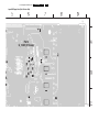
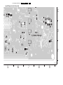
1
Colour Television
Chassis
LC4.31E
AB
Supplement to manual LC4.31E AA 3122 785 16210
ME6
ME5
G_16210_000.eps
090206
Contents
Page
1. Technical Specifications, Connections, and Chassis
Overview
2
2. Safety Instructions, Warnings, and Notes
4
3. Directions for Use
4
4. Mechanical Instructions
5
5. Service Modes, Error Codes, and Fault Finding 7
6. Block Diagrams, Test Point Overviews, and
Waveforms
Wiring Diagram 26” & 32”
9
Wiring Diagram 37”
10
Wiring Diagram 42”
11
Block Diagram Supply 37”
12
Block Diagram Supply 42”
13
Block Diagram Video
14
Block Diagram Audio & Control
15
Block Diagram IBO Zapper
16
I2C Overview
17
Supply Voltage Overview
18
7. Circuit Diagrams and PWB Layouts
Diagram
IBO Zapper Panel: MOJO
(K1) 19
IBO Zapper Panel: Flash Memory
(K2) 20
IBO Zapper Panel: Power Supply
(K3) 21
IBO Zapper Panel: Interface
(K4) 22
IBO Zapper Panel: Analog Back End
(K5) 23
IBO Zapper Panel: Front End
(K6) 24
IBO Zapper Panel: Common Interface
(K7) 25
8. Alignments
37
9. Circuit Descriptions, Abbreviation List, and IC Data
Sheets
40
Abbreviation List
42
IC Data Sheets
44
10. Spare Parts List
46
11. Revision List
48
PWB
26-31
26-31
26-31
26-31
26-31
26-31
26-31
©
Copyright 2006 Philips Consumer Electronics B.V. Eindhoven, The Netherlands.
All rights reserved. No part of this publication may be reproduced, stored in a
retrieval system or transmitted, in any form or by any means, electronic,
mechanical, photocopying, or otherwise without the prior permission of Philips.
Published by WS 0662 TV Service
Printed in the Netherlands
Subject to modification
EN 3122 785 16220
EN 2
1.
Technical Specifications, Connections, and Chassis Overview
LC4.31E AB
1. Technical Specifications, Connections, and Chassis Overview
: VGA (720x400)
Index of this chapter:
1.1 Technical Specifications
1.2 Connection Overview
1.3 Chassis Overview
Notes:
• Only information that is related to the IBO Zapper module
is published in this manual. For the other information, see
the relevant chassis manual (order code on front page).
• Some models in this chassis range have a different
mechanical construction. The information given here is
therefore model specific.
• Figures below can deviate slightly from the actual situation,
due to the different set executions.
• Specifications are indicative (subject to change).
1.1
Technical Specifications
1.1.1
Vision
Display type
: LCD, IPS
Screen size
- 26PF5521D/10/12
- 32PF5521D/10/12
- 37PF5521D/10
- 26PF7521D/10
- 32PF7521D/10
- 37PF7521D/10
- 42PF7421D/10
:
:
:
:
:
:
:
:
Resolution (HxV pixels)
: 1366 x 768
26” (66 cm), 16:9
32” (82 cm), 16:9
37” (94 cm), 16:9
26” (66 cm), 16:9
32” (82 cm), 16:9
37” (94 cm), 16:9
42” (107 cm), 16:9
Contrast ratio
- 26PF5521D/10/12
- 32PF5521D/10/12
- 37PF5521D/10
- 26PF7521D/10
- 32PF7521D/10
- 37PF7521D/10
- 42PF7421D/10
:
:
:
:
:
:
:
:
Light output (cd/m2)
: 500
Response time (ms)
: 8
Viewing angle (HxV degrees)
- 26PF5521D/10/12
- 32PF5521D/10/12
- 37PF5521D/10
- 26PF7521D/10
- 32PF7521D/10
- 37PF7521D/10
- 42PF7421D/10
:
:
:
:
:
:
:
:
Tuning system
: PLL
TV Colour systems
: PAL B/G, D/K, I
: SECAM B/G, D/K, L/L’
Video playback
: NTSC M/N 3.58, 4.43
: PAL B/G
: SECAM L/L’
Supported computer formats
:
:
:
:
600:1
800:1
800:1
600:1
800:1
800:1
550:1
178x178
178x178
176x176
178x178
178x178
176x176
176x176
VGA (640x480)
MAC (640x480)
SVGA (800x600)
XVGA (1024x768)
1.1.2
1.1.3
Supported video formats
:
:
:
:
640x480p - 2fH
720x576p - 2fH
1280x720p - 3fH
1920x1080i - 2fH
Presets/channels
: 100 presets
Tuner bands
:
:
:
:
VHF
UHF
S-band
Hyper-band
Sound
Sound systems
: NICAM B/G, D/K, I, L
: AV Stereo
Maximum power (WRMS)
- 26PF5521D/10/12
- 32PF5521D/10/12
- 37PF5521D/10
- 26PF7521D/10
- 32PF7521D/10
- 37PF7521D/10
- 42PF7421D/10
:
:
:
:
:
:
:
:
2x5
2 x 15
2 x 15
2x5
2 x 15
2 x 15
2 x 15
Power supply:
Mains voltage (VAC)
- 26PF5521D/10/12
- 32PF5521D/10/12
- 37PF5521D/10
- 26PF7521D/10
- 32PF7521D/10
- 37PF7521D/10
- 42PF7421D/10
:
:
:
:
:
:
:
:
110 - 240
110 - 240
220 - 240
110 - 240
110 - 240
220 - 240
220 - 240
Mains frequency (Hz)
: 50 / 60
Ambient conditions:
- Temperature range (°C)
- Maximum humidity
: +5 to +40
: 90% R.H.
Power consumption:
Normal operation (W)
- 26PF5521D/10/12
- 32PF5521D/10/12
- 37PF5521D/10
- 26PF7521D/10
- 32PF7521D/10
- 37PF7521D/10
Stand-by (W)
- 26PF5521D/10/12
- 32PF5521D/10/12
- 37PF5521D/10
- 26PF7521D/10
- 32PF7521D/10
- 37PF7521D/10
- 42PF7421D/10
:
:
:
:
:
:
:
:
:
:
:
:
:
:
:
Dimensions (WxHxD cm):
- 26PF5521D/10/12
- 32PF5521D/10/12
- 37PF5521D/10
- 26PF7521D/10
- 32PF7521D/10
:
:
:
:
:
Miscellaneous
100
120
180
100
120
180
<1
<1
<2
<1
<1
<2
<2
80.45 x 43.8 x 11.4
92.4 x 50.7 x 11.9
110.0 x 60.9 x 10.25
69.75 x 49.48 x 9.97
93.5 x 51.65 x 12.0
Technical Specifications, Connections, and Chassis Overview
1.2
- 37PF7521D/10
- 42PF7421D/10
: 111.4 x 61.8 x 10.3
: 124.9 x 69.7 x 12.8
Weight (kg):
- 26PF5521D/10/12
- 32PF5521D/10/12
- 37PF5521D/10
- 26PF7521D/10
- 32PF7521D/10
- 37PF7521D/10
- 42PF7421D/10
:
:
:
:
:
:
:
13.3
18.9
25.1
13.0
19.2
25.9
32
Connection Overview
Note: The following connector colour abbreviations are used
(acc. to DIN/IEC 757): Bk= Black, Bu= Blue, Gn= Green, Gy=
Grey, Rd= Red, Wh= White, and Ye= Yellow.
1.2.1
Rear Connections
G_16220_020.eps
090206
Figure 1-1 Rear I/O (26” and 32”)
G_16220_021.eps
090206
Figure 1-2 Rear I/O (37” and 42”)
CI Common Interface: PCMCIA
68p - See diagram K7
jk
S/PDIF Cinch: Out
Bk - Coaxial
kq
0.2 - 0.6 VPP / 75 ohm
Service connector (UART)
1 - UART_TX
Transmit
2 - Ground
Gnd
3 - UART_RX
Receive
k
H
j
LC4.31E AB
1.
EN 3
EN 4
1.3
2.
LC4.31E AB
Safety Instructions, Warnings, and Notes
Chassis Overview
Chassis Overview 26” & 32” Models
LCD PANEL
A
POWER SUPPLY
PANEL
T
OTC TXT PANEL
CLASS D AUDIO
AMPLIFIER PANEL
C
SMALL SIGNAL BOARD
B
IBO ZAPPER 2 PANEL
K
KEYBOARD CONTROL
PANEL
E
SIDE I/O PANEL
D
LED & IR PANEL
J
POWER SUPPLY
UNIT
A
IBO ZAPPER 2 PANEL
K
Chassis Overview 37” + 42” Models
LCD PANEL
SA
B
STANDBY & AUDIO
PANEL
SMALL SIGNAL
BOARD
T
OTC TXT PANEL
E
CONTROL BOARD
SIDE I/O PANEL
D
LED & IR PANEL
J
G_16220_025.eps
090206
Figure 1-3 Chassis overview
2. Safety Instructions, Warnings, and Notes
See the relevant chassis manual (order code on front page).
3. Directions for Use
You can download this information from the following websites:
http://www.philips.com/support
http://www.p4c.philips.com
Mechanical Instructions
LC4.31E AB
4.
EN 5
4. Mechanical Instructions
4.1.3
Index of this chapter:
4.1 Assy/Panel Removal
4.2 Set Re-assembly
Unlocking the metal cover of the IBO zapper module (26”
and 32”)
Notes:
• Figures below can deviate slightly from the actual situation,
due to the different set executions.
• Follow the disassembling instructions in described order.
• Only information that is related to the IBO Zapper module
is published in this manual. For the other information, see
the relevant chassis manual (order code on front page).
4.1
Assy/Panel Removal
4.1.1
IBO Zapper Module (26” and 32”)
2
1
F_15270_089.eps
300505
3
Figure 4-3 Unlocking the metal cover of the IBO zapper module
(26” and 32”)
4
F_15270_087.eps
310505
Figure 4-1 IBO zapper module (26” and 32”)
1. Disconnect the cable [1] from connector 1301 on the IBO
zapper module.
2. Disconnect the flatcable [2] from connector 1500 on the
IBO zapper module and remove the tape which secures it
to the IBO zapper module.
3. Disconnect the antenna cable [3] from the tuner on the IBO
zapper module.
4. Remove the torx screws [4] and remove the IBO zapper
module from the TV set.
4.1.2
IBO Zapper Module Front Panel (26” and 32”)
1
F_15270_088.eps
300505
Figure 4-2 IBO zapper module front panel
1. Remove the two screws [1].
2. Remove the front panel by shifting it sideways to unlock it.
F_15270_090.eps
300505
Figure 4-4 Opening the IBO zapper module (26” and 32”)
1. Unlock the metal cover with a screwdriver (see Figure
“Unlocking the metal cover of the IBO zapper module (26”
and 32”)”).
2. Unhook the metal cover from its hinges (see Figure
“Opening the IBO zapper module (26” and 32”)”) and
remove the cover (this is possible only if the front panel has
been removed first).
EN 6
4.1.4
4.
LC4.31E AB
Mechanical Instructions
Cover Shield for IBO-zapper & SSB (37” and 42”)
9
3
1
8
2
10
3
4
3
5
G_16220_022.eps
090206
G_16220_024.eps
090206
Figure 4-5 Cover shield (37” and 42”)
Figure 4-7 IBO-zapper & SSB (37” and 42”)
7
7
6
6
G_16220_023.eps
090206
Figure 4-6 Connector screws (37” and 42”)
1. Remove the rear cover from the set.
2. Very cautiously disconnect the LVDS cable [1] from the
SSB panel (see Figure “Cover shield (37” and 42”)”).
Notice that this connector is very fragile.
3. Unplug the black cable [2] going from the IBO zapper/SSB
to the Audio/STBY board.
4. Remove all other cables [3] from the IBO zapper/SSB.
5. Remove the fixation screws [4] that connect the top
shielding with the bottom shielding.
6. Remove the fixation screws [5] that connect the connector
plate to the frame.
7. Remove the fixation screws [6] that connect the shield to
the rear connector plate, see Figure “Connector screws
(37” and 42”)”.
8. Remove the fixation screws [7] from the connectors.
9. Remove the connector plate from the shielding.
10. Remove the upper part of the shield (with the IBO zapper
attached to it) from the lower part of the shield (on which
the SSB is located), by unhooking it from its brackets.
11. Disconnect the antenna connector [8] from the tuner, see
Figure “IBO zapper & SSB (37” and 42”)”.
12. Carefully unlock the locking mechanism of the FFC
connector [9] and remove the flatfoil cable (see Figure
“How to unlock an FFC connector”).
13. Finally, loosen four screws [10], and remove the IBO
zapper from the top shielding.
F_16040_038.eps
021105
Figure 4-8 How to unlock an FFC connector
4.2
Set Re-assembly
To re-assemble the whole set, execute all processes in reverse
order.
Notes:
• While re-assembling, make sure that all cables are placed
and connected in their original positions.
Be careful with the fragile LVDS cable.
Service Modes, Error Codes, and Fault Finding
LC4.31E AB
5.
EN 7
5. Service Modes, Error Codes, and Fault Finding
Index of this chapter:
5.1 Service Modes
5.2 Error Codes
Notes:
• Only information that is related to the IBO Zapper module
is published in this manual. For the other information, see
the relevant chassis manual (order code on front page).
5.1
Service Modes
5.1.1
Digital Customer Service Mode (DCSM)
Purpose
The Digital Customer Service Mode shows error codes and
information on the IBO Zapper module operation settings. The
call centre can instruct the customer to activate DCSM by
telephone and read off the information displayed. This helps
the call centre to diagnose problems and failures in the IBO
Zapper module before making a service call.
E_14970_041.eps
100904
Figure 5-2 DCSM menu - 2
The DCSM is a read-only mode; therefore, modifications are
not possible in this mode.
How to Activate
To activate the DCSM, put the television in its digital mode (via
the A/D button on the remote control).
1. Press the “Digital” Menu button on the remote control to
activate the digital user menu (“Setup”).
2. Activate the “Information” sub menu (via the “down” and
“right” cursor buttons).
3. In the “Information” sub menu, press the following buttons
on the remote control to activate the DCSM:
“GREEN RED YELLOW 9 7 5 9”. Then, the “Service menu”
will appear (see figures below).
E_14970_042.eps
090904
Menu explanation
Figure 5-3 DCSM menu - 3
E_14970_040.eps
090904
Figure 5-1 DCSM menu - 1
1. Hardware version: This indicates the version of the IBO
Zapper module hardware.
2. Application SW: The application software version.
3. NOR Version: The NOR Flash image software version
4. Digital Frequency: The digital frequency that the set is
tuned to.
5. Bit Error Rate: The error rate measured before the error
correction algorithm circuitry. (this value gives an
impression of the received signal)
6. Tuner AGC: Tuner AGC value.
7. COFDM Lock: Indication if COFDM decoder is locked.
8. AFD Status: Status of the Active Picture Format
Descriptor.
9. Terrestrial Delivery System Parameters:
– Bandwidth: Bandwidth of the received signal.
– Constellation Pattern: Displays the signal
constellation.
– Alpha Value: Displays the Alpha Value.
– FEC Scheme: Displays the Forward Error Correcting
Scheme
– Guard Interval: Displays the value for the Guard
Interval.
– Transmission Mode: Displays the Transmission
Mode.
10. Audio Comp Type: Type of detected audio stream.
11. MHEG Present: Indicates if MHEG is present or not.
12. CIM Card Present: Indicates if CIM card is present or not.
How to exit
Press the BLUE button on the Remote Control to exit DCSM.
EN 8
5.2
5.
LC4.31E AB
Service Modes, Error Codes, and Fault Finding
Error Codes
The error code buffer contains all errors detected since the last
time the buffer was erased. The buffer is written from left to
right. When an error occurs that is not yet in the error code
buffer, it is displayed at the left side and all other errors shift one
position to the right.
5.2.1
How to Read the Error Buffer
Error Description
0
No Error
Check Item
Diagram
1
Mis-match of TV (Hercules) SW and
Scaler SW
Software
versions
N.A.
2
+12V from PSU error
PSU
A
3
Plasma I2C error (only for plasma sets) N.A.
N.A.
4
I2C error while communicating with the 7801
Genesis Scaler
B7 + B8
+5V protection
7752
B6
6
General I2C error; communication
between ADC, analogue tuner, and/or
Columbus I2C failed
1102, 7L01,
7M00
B1 + B18 +
B19
7
I2C error while communicating with
ADC
7L01
B18
8
I2C error while communicating with the 7C01
Scaler EEPROM
B11
9
I2C
error while communicating with the 7207
Hercules EEPROM (NVM for TV).
Remark: when the Hercules EEPROM
is defective, the Hercules should
operate with its default values.
B2
10
I2C error while communicating with the 1102
PLL tuner
B1
How to Clear the Error Buffer
11
I2C
error while communicating with the 7M00
3D combfilter IC-7M00 (Columbus)
B19
The error code buffer is cleared in the following cases:
• By using the CLEAR command in the SAM menu:
– To enter SAM, press the following key sequence on the
remote control transmitter: “062596” directly followed
by the OSD/i+ button (do not allow the display to time
out between entries while keying the sequence).
– Make sure the menu item CLEAR is selected. Use the
MENU UP/DOWN buttons, if necessary.
– Press the MENU RIGHT button to clear the error
buffer. The text on the right side of the “CLEAR” line will
change from “CLEAR?” to “CLEARED”
• If the contents of the error buffer have not changed for 50
hours, the error buffer resets automatically.
12
I2C error while communicating with
iBoard uP (only iTV sets)
N.A.
N.A.
13
I error while communicating with the N.A.
HDMI decoder IC-7D03 (only for
NAFTA and AP)
N.A.
14
Read-write error with the Scaler
SDRAM
B10
15
I2C
error while communicating with the 7001
OTC
T
16
I2C error while communicating with
EPLD or Pacific III
B20 + B21
17
I2C
Note: If you exit SAM by disconnecting the mains from the
television set, the error buffer is not reset.
5.2.3
Error
5
You can read the error buffer in 3 ways:
• On screen via the SAM (if you have a picture).
Examples:
– ERROR: 0 0 0 0 0 : No errors detected
– ERROR: 6 0 0 0 0 : Error code 6 is the last and only
detected error
– ERROR: 9 6 0 0 0 : Error code 6 was detected first and
error code 9 is the last detected (newest) error
• Via the blinking LED procedure (when you have no
picture). See “The Blinking LED Procedure”.
• Via ComPair.
5.2.2
Table 5-1 Error code overview
Error Codes
In case of non-intermittent faults, write down the errors present
in the error buffer and clear the error buffer before you begin
the repair. This ensures that old error codes are no longer
present.
If possible, check the entire contents of the error buffer. In
some situations, an error code is only the result of another error
and not the actual cause of the problem (for example, a fault in
the protection detection circuitry can also lead to a protection).
2C
7B01
7N00
error while communicating with the 7100
Digital Module (only for digital sets)
K1
Block Diagrams, Test Point Overviews, and Waveforms
LC4.31E AB
6.
9
6. Block Diagrams, Test Point Overviews, and Waveforms
Wiring Diagram 26” & 32”
WIRING 26”- 32”
8903
8903
8301
INVERTER
INVERTER
INVERTER
32P
3P
X220
1500
3P
1301
POWER
SUPPLY
TUNER
(IBO ZAPPER2)
LVDS CONNECTION
TO SCREEN
30P
RIGHT
SPEAKER
LEFT
SPEAKER
C
8P06
8J02
IBO ZAPPER
9P
1JO4(1M52)
8500
8870
12P
SSB
3P
1684
3P
1J03
1K01(1M06)
12P
8520
D
1303
8K01
HP
12P
1K02
3P
1302
L
R
Y
1301
8684
SVHS
TUNER
32P
1J03
E
POWER
IN
2P3
X002
SIDE AV
KEYBOARD CONTROL
12P
1J02
1304
(1M06)
12P
B
30P
31P
1P06
14P
14P
8520
K
8J04
X530
X520
CLASS D
AUDIO
AMPLIFIER
4P
1001
8J03
1002
9P
1K00(1M21)
6P
12P
X200
3P
1003
8600
8002
6P
1870
AC POWER
INLET
J
IR/LED/LIGHT
SENSOR
G_16220_001.eps
070206
Block Diagrams, Test Point Overviews, and Waveforms
LC4.31E AB
6.
10
Wiring Diagram 37”
WIRING 37”
8903
8902
8302
8304
8309
8521
8305
A LCD SUPPLY
4P
1M10
1M46
11P
1309
3P
8301
INVERTER
4P
1304
LEFT
SPEAKER
1304
4P
1739
9P
14P
1319
12P
1317
12P
1316
7P
1M02
3P
1309
1305
3P
SA STANDBY
1M03
10P
RIGHT
SPEAKER
7P
1M02
8306
1307
4P
3P
1735
1306
2P3
3P
1736
LCD PANEL
INVERTER
TO DISPLAY
LVDS
8337
8520
8322
8P06
8101
9P
1J04
2P3
1306
3P
1J03
1K00
6P
10P
1J00
1442
14P
11P
1J01
8870
1K04
11P
B SSB
8K01
1000
14P
3P
1305
1N20
3P
OTCFLASH
T
D
SIDE AV
1308
2P3
TUNER
1G03
32P
11P
1M36
1301
3P
1K02
3P
8000
K IBO ZAPPER
32P
8500
8600
8002
1M01
3P
TUNER
AC INLET
1402
3P
J
LED PANEL
6P
0345
8187
(8188UK)
1500
E KEYBOARD CONTROL
14P
30P
1N17
12P
8J04
G_16220_002.eps
070206
Block Diagrams, Test Point Overviews, and Waveforms
LC4.31E AB
6.
11
Wiring Diagram 42”
WIRING 42”
8903
8902
8302
8304
8309
8521
8303
1306
2P3
3P
1736
8320
INVERTER
1M03
10P
1M46
11P
4P
1M10
8301
LEFT
SPEAKER
4P
1303
4P
1304
1305
3P
8305
1304
4P
14P
1319
12P
1317
1320
3P
12P
1316
8307
LCD PANEL
1309
3P
1303
4P
7P
1M02
9P
1739
SA STANDBY
3P
1320
3P
1309
1307
4P
3P
1735
RIGHT
SPEAKER
7P
1M02
8306
A LCD SUPPLY
INVERTER
TO DISPLAY
LVDS
8337
8520
8322
8P06
8101
3P
1J03
9P
1J04
8870
3P
1C05
3P
1B06
8K01
D
SIDE AV
K IBO ZAPPER
32P
TUNER
1G03
32P
11P
1M36
1301
3P
1K02
3P
8000
3P
1305
1420
1K04
11P
1000
14P
12P
2P3
1306
10P
1J00
1442
14P
11P
1J01
1K00
6P
B SSB
1N20
3P
OTCFLASH
T
1308
2P3
8500
8600
8002
1M01
3P
TUNER
AC INLET
1402
3P
J
LED PANEL
6P
0345
8187
(8188UK)
1500
E KEYBOARD CONTROL
14P
30P
1N17
4P
1307
8J04
G_16220_003.eps
070206
Block Diagrams, Test Point Overviews, and Waveforms
LC4.31E AB
6.
12
Block Diagram Supply 37”
SUPPLY 37"
SUPPLY
A2
HOT
2319
3318
3000
25V_HOT
5017
3
2
6024
5010
400V_HOT
5007
5011
7005
STP15NK50
3007
399V_HOT
CONTROL
14
OA
SOFT
START
+
CURRENT
PROTECTION
4
2059
3052
2029
5025
OB
11 SOST
FI
2
12
7008
LOW
10
SIDE
DRIVE
9
10
5 VREF
7006
STP15NK50
6021
3
4
3
2
2
1
1
5
1319
1
2
3
2022
6041
5026
TO
DISPLAY
+12V_+24V
4
TO
DISPLAY
5
2045
7010
TS2431
OVER
VOLTAGE
PROTECTION
RES
+12V_A
+24Va
7004
7009
7307
TCET1102
3
2
1304
4
5012
4
1M10
1
5002
3030
2
2060
TO 1301
B01B
K3
IBO ZAPPER
(ONLY DVB SETS)
3026
6316 6315
7011
7012
1304
4
2020
7 ERROR
3
1317
1
+12V
7007
HIGH
6
SIDE
DRIVE
7
TO
DISPLAY
5
6019
STPS20L40CFP
6019
STPS20L40CFP
7001
15
MC34067P
VCC
11 OSCC
2
3
DC_PROT
399V_HOT
5008
5001
1
2
3031
4
4
25V_HOT
CONNECTIONS
1316
1
7003
400V_HOT
2003
+
-
1
5009
MAINS
FILTER
1
6025
6307
GBJ6J
3
6317
VS Voltage
Adj.
PRINTED
COMPONENT
2042
5021
+24Vb
6031
6040
2049
5022
1M02
DC_PROT
1007
2009
T5A
6029
5020
VSND_POS
5018
GND_SND
6030
7
6
5
TO 1M02
4
SA3
3
AUDIO
2
2021
HOT
SA2
1305
1
2
3
3
VSND_NEG
1
STANDBY
1305
1
2
5019
COLD
1M03
+5V2
CONTROL
7505/7509/7560
Prot-OVV
SA2
SA1
PROT_AUDIOSUPPLY
7507
7506
7512
COLD
SA2
+12V_A
HOT
COLD
STANDBY
7
TO 1M03
4
B01B
B16
SSB
STANDBY
HOT
6306
DF06M
6
5
5104
VTUN
6140
7
3
+11V
2141
8
2
9
+12V
10
3104
CONTROL
4
6107
5103
3128
3127
3100
4
1
3
2
4
TO 1M46
+8V6
7131
3V MAX
1V MAX STBY
3150
1M46
11
1
2
N.C. 3
3509
RES
7102
STP15NK50
1307
1
6504
5507
7100
7101
7105
5110
5105
2303
2
5505
3124
2513
6122 3113
RES
5506
+5V2
2512
1
2
7
STANDBY
STANDBY: LOW = ON
HIGH = STBY
7501
TCET1102
7531
OVERVOLTAGE
PROTECTION
+5V_SW
6150
6151
3155
3158
3156
6156
2
5504
3157
T1A
+
1306
1
3108
1306
1
3101
-
7511
5500
1315
6153
T5AH
2
6304
6314
1
1314
1350
6318
2
5305
5306
4
SA1
3057
7002
TCET1102
BIAS SUPPLY
1308
COLD
3025
MAINS FILTER + STANDBY
9311
A1
1
4
2
3
HOT
COLD
PROT-OVV
7150
TCET1102
G_16210_060.eps
010206
B01B
B16
SSB
Block Diagrams, Test Point Overviews, and Waveforms
LC4.31E AB
6.
13
Block Diagram Supply 42”
SUPPLY 42"
MAINS FILTER + STANDBY PART A
A2
SUPPLY PART A
HOT
3028
4
COLD
SA1
7002
TCET1102
3A15
2
2
3810
3
MAINS
FILTER
BIAS SUPPLY 3000
25V_HOT_A
2
6078 5010
3
2003
400V_HOT_A
2816
MAINS_N
7005
STP15NK50
5001
7001
15
MC34067P
VCC
11 OSCC
3007
6
CONTROL
14
OA
OB
11 SOST
SOFT
START
+
CURRENT
PROTECTION
FI
5028
11
5040
5
13
2
7006
STP15NK50
7008
LOW
10
SIDE
DRIVE
9
5 VREF
6021
STPS20L40CFP
5025
14
10
1
12
3
4
12
1304
4
+12V
2
3
2020
7 ERROR
7017
7018
5
3
10
7007
HIGH
SIDE
DRIVE
7
+24Va
1304
4
+12V_A
3
2
2
1
1
+12V_+24V
2022
6021
STTH2003CFP
1
6014
2
15
5026
16
1M10
7010
TL431ACD
3
2
3
3
3026
COLD
STANDBY
1M03
1305
1
2
STANDBY
+5V2
CONTROL
7505/7509/7560/
7507
7506
7512
Prot-OVV
PROT_AUDIOSUPPLY
HOT
2
2
3
3
3
7
2
8
7102
3104
CONTROL
3108
400V_HOT_B
1
RES
2513
5506
3
4
1 7501
TCET1102
3124
3
2
6122
+5V2
2512
3113
B01B
B16
SSB
7
STANDBY
STANDBY: LOW = ON
HIGH = STBY
7531
OVERVOLTAGE
PROTECTION
RES
+5V_SW
6151
3155
3158
3156
SUPPLY PART B
3157
6153
6156
6150
1
4
2
3
HOT
3U28
3
3H10
25V_HOT_B
BIAS SUPPLY 3U00
5U17
5U07
5U08
PROT-OVV
7150
TCET1102
1317
1
COLD
3U57
3U52
1 7U02
TCET1102
2
3
DC_PROT
DC_PROT
2
1303
1
+24V
2U22
6U79 6U77 6U78 5U10
5U02
6H07
GBJ6J
2003
400V_HOT_B
+
2H16
7U05
STP15NK50
5U01
5 VREF
10
5U40
7
4
3
5
2
7U08
10
2
3
3
4
4
TO
DISPLAY
5
1M02
DC_PROT 7
11
12
14
7U06
STP15NK50
1U07
2B91
T5A
6B91
13
5U25
15
9
16
7U04
7U09
OVER
VOLTAGE
PROTECTION
HOT
COLD
6
5
4
3
2
2B93
2
5U26
VSND_POS
6B93
1
LOW
SIDE
DRIVE
5B93
5B91
6021
STPS20L40CFP
5B92
VSND_NEG
1
7U10
TL431ACD
3
3U24
3U26
SOFT
START
+
CURRENT
PROTECTION
CONTROL
14
OA
7 ERROR
12
OB
11 SOST
10
FI
6
7U07
HIGH
SIDE
DRIVE
2
4
+24V_2
9
3U30
7U17
7U18
7U01
15
MC34067P
VCC
11 OSCC
5U09
7
3U07
2H15
China
8
1303
1
3U25
2
9
+8V6
TO 1M46
4
-
+12V
2
6107
3128
4
3
11
7131
3127
5D00
5D01
5D03
MAINS
FILTER
1M46
2141
5103
1D50
3A15
+11V
3V MAX
1V MAX STBY
3150
4
A4
2
VTUN
6140
10
3100
1400
3509
1
COLD
1
6504
5110
B01B
B16
RES
5104
1307
1
2
4
7100
7101
7105
6
TO 1M03
4
3U39
HOT
1307
1
2
7511
5
3
MAINS FILTER + STANDBY
PART B
2
A3
1C05
1
1B06
1
6157
3406
5505
3U22
2503
5504
5507
T1A
+
1306
1
5500
5105
1306
1
3101
-
1401
7
SSB
STANDBY
COLD
6506
DF06M
VS Voltage
Adj.
+12V_A
1305
1
K
IBO ZAPPER
4 (ONLY DVB SETS)
3030
HOT
HOT
COLD
TO 1301
2
3025
OVER
VOLTAGE
PROTECTION
1
3
7004
7009
SA2
TO
DISPLAY
6019
STPS20L40CFP
5027
9
7
6156
2815
China
4
8
5008
5007
+
-
4
1316
1
5002
6807
GBJ6J
1
MAINS_L
5017 6080 6077
DC_PROT
DC_PROT
3057
MAINS INPUT
1450
7030
2
3052
1400
1
3
5400
5401
5403
5009
1308
CONNECTIONS
1
3022
A1
VS Voltage
Adj.
G_16220_004.eps
070206
SA3
SA3
TO 1M02
AUDIO
Block Diagrams, Test Point Overviews, and Waveforms
LC4.31E AB
6.
14
Block Diagram Video
B2 HERCULES
2156 IF-TER
4
4
5
5
1
24
RO
Sound
Traps
1
MAIN
TUNER
FROM
IBO-TUNER
VIF1
3154
VIF2
25
AC
31
RF_AGC
K6
SCL
See also
Block Diagram
IBO-ZAPPER
SDA
DC
1156
SIF1
29
5 SIF2
30
4
B20 PACIFIC3
CVBS1
RGB Matrix
Blue & Black
Strech
Gamma Corr.
HERCULES
AGC
Detect
Video
Switch
+
Control c
Skin Tone
U/V Tint
Saturation
SAT
QSS/FM
QSS Mixer
AM Demod. AM
1
85
7208
EF
RO
GO
86
GO
BO
87
BO
7E01
FE00
7209
EF
R_OTC_SDTV
27
G_OTC_SDTV
3
B_OTC_SDTV
7
SOG
C3
FE01
7210
EF
LVDS_VCC
FE02
SC1_R_CVI_Pr_IN
For sets without
OTC-Flash (26”, 32”)
17 R-PR-ADC
R_PR+
D2
14
G-Y-ADC
G_Y+
C2
11
B-PB-ADC
B_PB+
B2
25
B13
SC1_G_CVI_Y_IN
1
SC1_B_CVI_Pb_IN
5
LVDSALVDSA+
12
13
LVDSBLVDSB+
14
15
16
B13
B3 SYNC INTERFACE
B13
9
I_PC_HD_SEL
YUV
LVDSC-
ANALOG
INPUT
PORT
SCALER
19
20
LVDSD-
24
25
26
RGB-B_IN
DMMI_CVBS_IN|Y_IN
3
SC2_CVBS_MON_OUT
5
AV2_DMMI_SW
B2
7G02
EF
7219
13
9
7G03
EF
1G01
19
SC1_CVBS_RF_OUT
77
78
79
B2
67
HOUT
1
GRAPHIC
ZOOM
80
74
75
7B01
K4D263238F
76
70
71
DMMI_B_Pb_IN
19
13
SC1_CV1_DMMI_G_Y_IN
18
SC1_CV1_DMMI_B_Pb_IN
B2,B13
B2,B13
SC2_AV3_Y_IN
DMMI_CVBS_IN|Y_IN
DMMI_CVBS_IN
7G07
4
3
DMMI_RGB_SW
B2
72
7G08
EF
12
T
12
7G05
EF
DMMI_G_Y_IN
9
INTF_V_OUT
7L71
EF
INTF_Y_OUT
DMMI_B_Pb_IN
7L72
4N01
TXO0TXO0+
AE15
AF15
TXB1TXB1+
4N04
4N03
TXO1TXO1+
AE14
TXB2-
4N06
AF14
TXB2+
4N05
TXO2TXO2+
AF12
AF11
TXB3TXB3+
4N10
4N09
TXO3-
AF13
AE12
TXBCTXBC+
4N08
TXOC-
4N07
TXOC+
38
1G01
7M01
MSM56V16
3
7007
MSM51V18165F
FLASH
ROM
512Kx8
7006
M29W160ET70N6E
TV
CONTROL
DD(0-15)
AA(1-20)
H
1
1
Hsync_SDTV
B13
84
5
V
CVBS_COMB
2
2
INT_OTC
R_OTC
4
5
B13
B2
96
77
4
5
Vsync_SDTV
CVBS_COMB
B7
78
79
7
9
74
G_OTC
B_OTC
RESET_FLASH
7
9
INT_OTC
R_OTC_SDTV
78
79
SCL
SDA
11
12
13
14
11
12
13
14
83
G_OTC_SDTV
B_OTC_SDTV
RESET_FLASH
SCL
SDA
B13
B13
TXB0-
1
FLASH
ROM
512Kx8
SC1_CV1_DMMI_R_Pr_IN
13
SC1_CV1_DMMI_G_Y_IN
1
3
14
SC1_R_CVI_Pr_IN
B13
5
15
4
SC1_G_CVI_Y_IN
BINA|Pb
SC1_B_CVI_Pb_IN
GINA|YINA
2
B13
B13
RINA|Pr
12
B17 SIDE
19
18
RX2+A
A9
3
RX2-A
A10
RX1+A
RX1-A
RX0+A
A12
A13
9
RX0-A
RXC+A
10
12
RXC-A
A15
A16
F16
G16
FRONT_C_IN
4
2
FRONT_YCVBS_IN
4
FRONT_C_IN
1
1301
(1001)
19
18
3
S-VHS 5
4
( ) 37” - 42” only
LVDSCLK+
21
23
29
28
LVDS
PACIFIC3
103
102
TXO0TXO0+
TXO1TXO1+
99
98
TXO2TXO2+
TXB3+
TXB3TXBC+
41
93
TXO3-
40
37
92
96
TXO3+
TXOC-
TXBC-
38
95
TXOC+
32
31
MICRO
CONTROLLER
INTERNAL
RAM
A2
H_HDMI
C14
A1
V_HDMI
B14
D1
HDMI_VCLK
D16
B11 FLASH/CONTROL
HDMI_Y(0-7)
7C03
M29W400DT55N6E
1F03
1
2
FRONT_YCVBS_IN
1K01
(1K04)
LVDSCLK-
RGB|CVI_HDA_SEL B7
HDMI-1
1304
(1M36)
2
1N11
26
28
22
UART
INTERFACE
DVI/HDMI
INPUT
PORT
HDMI
PANELLINK
RECEIVER
LVDSDLVDSD+
TXO3+
19
18
20
27
(RES For PIXEL+)
B12 HDMI
4
6
7
LVDSCLVDSC+
101
100
TXB1TXB2+
TXB2-
SC1_CV1_DMMI_B_Pb_IN
1F02
14
13
15
35
34
TXB1+
7D03
SII9993CTG100
B2
1N15
LVDSBLVDSB+
7N00
T6TF4AFG
TXB0+
B15b
B15b
B13
1N14
10
12
OR
B15b
9
B14 DIGITAL IO
1N13
LVDSALVDSA+
VIDEO
ZOOM
7E00
1442
1N12
COL_YB(1-8)
B15A SCART ANALOG IO
B3 SYNC INTERFACE
CONNECTIONS
2
COL_YA(1-9)
8
18
RGB-G_IN
RGB-R|YC-C_IN
SVHS
4N02
TXB0+
1N17
1
11
COL_Do(1-8)
COLUMBUS
DIGITAL COMB
FILTER
37
(TO OTC-FLASH)
2
FBL_HSYNC_OUT
RGB-B_IN
VIDEO
IN
COL_Di(1-9)
DISPLAY
TIMING
GEN.
TXB0-
DRAM
512Kx16x2
OTC-FLASH (FOR 1000pg TXT)
10,11
1302
(1002)
A/D
CONV.
9
13
19
For DVB
Sets Only
SIDE AV
6
VIN VOUT
COM
1
2
10
15 FBL_HSYNC_PIN16_IN
7M00
T6TU5XBG
11
7L51/7L52
EF
INTF_U_OUT
1000
7G04
EF
(Dig. PAL/NTC Comb)
2
7L61/7L62
EF
7001
SAA5801H/015
K5
B19 COLUMBUS
7L01
P3563M-LF
SCL
FROM 1500
1
SDRAM
1Mx32x4
3
7G06
7G10
EF
DMMI_R_Pr_IN
FRAME
STORE
CONTROL
AE16
AF16
10,11
SC2_Y_IN_1
14
95
FSDATA
B18 ADC
1,10,11,20
5
LVDS_VCC
B10 SDRAM
SDA
1G03
8
OR
B9 SCALER
Hsync_SDTV
2
+2V5_DDR
SC1_CV1_DMMI_B_Pb_IN
17
DMMI_RGB_SW
B2
L4
B15b
EXT 1
SCART 1
12
CVI_Pb_IN
B2,B13
B15b
STATUS_1
DMMI_G_Y_IN
SC1_CV1_DMMI_R_Pr_IN
SC1_CV1_DMMI_G_Y_IN
CVI_Pb_IN
CVI_Y_IN
8
B2
9
14
B15b
7
CVI_Pr_IN
DMMI_R_Pr_IN
SC1_FBL_IN_1
2
7
SC1_FBL_IN_1
SC1_CV1_DMMI_R_Pr_IN
FBL_HSYNC_PIN16_IN
3
CVBS_COMB
4
B3
(OTC)
B15b
CVI_Y_IN
8
See also
Block giagram
IBO-ZAPPER
HOUT
7G09
SC1_FBL_IN
CVI_Pr_IN
11
21
H/V
N.C.
B15B DMMI
15
L3
AHSYNC
FSADDR
SC1_FBL_IN
16
AVSYNC
4
B3
7436-1
SC1_CVBS_IN
20
1
55
43
B7 SC2_OUT_SW
8
1
48
B/Pb-3
12
G/Y3
14
R/Pr-3
SC2_CVBS_MON_OUT
5
RGB/Pr Pb Insert
YUV Interface
INSSW3
EXT 2
SCART 2
Sync Sep
H-OSC
H-Shift
H-Drive
Vint
SC2_AV3_Y_IN
21
D
Uint
PAL/NTSC/
SECAM
Decoder &
Baseband
Delay
51
52
9
Vsync_SDTV
Hsync_SDTV
COL_DQ
B2
B3
21
22
YUV in/out
Chroma
64
4
CVBS_COMB
LVDSCLK+
7604
COL_A
STATUS_2_IN|OUT
8
19
59
LVDSCLKVsync_SDTV
4
OUT BLENDER
13
7
7206
EF
3
BRIGHTNESS/CONTRAST/HUE/SAT
FRONT_C_IN
14
15
22 VSYNC
CVBS/Y
11
RGB-G_IN
SC2_C_IN
VDRB
YIN
RGB-R|YC-C_IN
Yint
Vertical &
East-West
Geometry
UIN
1
12
FBL_HSYNC_OUT
15
cvbs/y
Peaking
SCAVEM
U/V Delay
VIN
FRONT_Y_CVBS_IN
16
SC2_AV3_C_IN
SCAVEM
on text
VOUT
2
Dig. 2H/4H
Combfilter
Y Delay Adj.
UOUT
SC2_Y_IN
20
1
7436-2
58
OSD CONTROLLER
SC2_Y_IN_1
7G11
YOUT
SC2_Y_IN_1
1G02
17
18
LVDSC+
LVDSD+
B15A SCART ANALOG IO
1N16
1
11
TO DISPLAY (26” & 32”)
11
B_OSD
1154
7
Fast Blanking
6
B7 SCALER
7801
GM1501
R_OSD
1152
RF UV1318S
IN
B13 MUX-SYNC INTERFACE
7217
TDA15021H
TO DISPLAY (LCD 37” & 42”, PDP 42” & 50”)
+VTUN
+5SW_a
G_OSD
VIDEO
B1 TUNER & VIF
(Only For 37” - 50” Sets)
HDMI-2
RX2+B
C10
3
RX2-B
C9
4
6
7
RX1+B
RX1-B
RX0+B
C13
C12
9
RX0-B
RXC+B
10
12
RXC-B
OCMDATA
HDMI_CbCr(1-7)
EXTERNAL
ROM
INTERFACE
OCMADDR
FLASH
ROM
512Kx8
C16
C15
G14
F14
G_16220_005.eps
070206
Block Diagrams, Test Point Overviews, and Waveforms
LC4.31E AB
6.
15
Block Diagram Audio & Control
B2 HERCULES
B5 AUDIO PROCESSING
B16
C AUDIO AMPLIFIER
7001
TDA8931T
(CLASS-D)
IFOUT
F158
IF-TER
11
2156
1
6154
RF IN
7217
TDA15021H
TUNER
1156
2
3
4
SIF1
29
5
SIF2
30
7151
FROM
IBO-TUNER
4
5
B2
SCL
See also
Block Diagram
IBO-ZAPPER
AD Conv.
Std Stereo
Decoder
33
B14 DIGITAL IO
B15A SCART ANALOG-IO
1002
61
4211
AUDOUTLSR
AUDIO-R
3
3
AUDIO-R
60
4212
AUDOUTLSL
AUDIO-L
1
1
AUDIO-L
AUDIO
CONTROL
Vol/Treb/
Bass
Features
DACs
SDA
K6
QSS Mixer
AM Demod. QSS/FM
SEL_IF_SDM
PROTECT_AUD
7
7
SOUND-ENABLE
8
8
POR_AUDIO
9
9
AV1_Audio_INL
1
AV1_Audio_INR
12
21
2
4
11
DMMI_AudioINL
5
DMMI_AudioINR
14
AV2_Audio_INL
SIDE_AudioINL
2
AV2_Audio_INR
SIDE_AudioINR
15
EXT 2
SCART 2 1G02-1
1
6
SIDE_AudioINL
SIDE_AudioINR
Analog_AudioINR
35
7601
TS482ID
B7
2
HD_AudioINL
HD_AudioINL
HD_AudioINR
HD_AudioINR
50
DVI_D_AudioINR
D SIDE AV
1302
L_FRONT_IN
6
8
3
&
6
&
OUT_MUTE 8
&
57
OUT_MUTE
HP_DET_R_DC_1
1
SOUND_ENABLE B2
5
9
POWER_DOWN B16
10
EXT_MUTE
B2
A5
1
14 HDMI_AudioINL
53
A7
10-BIT
B7
VIDEO
CONVERTER
3
2
16 HDMI_AudioINR
54
63 HER_SC2_AudioOutR
7
6703
3764 -16 V-19V
1
6702
3761 +16 V+19V
5
TO 1002
SA
SUPPLY
SIDE AV
1304
(1M06)
1303
7
HEAD_PH_L
HP_ROUT
12
12
HEAD_PH_R
HP_DET_R_DC_1
11
11
HP_DET_R_DC1
1
2
HEADPHONE
B15A SCART ANALOG-IO
3
SC1_R_RF_OUT
SC1_R_RF_OUT
1
1
21
EXT 1
SCART 1
SC1_R
SC2_L_MON_OUT
SC2_L_MON_OUT
3
SC2_R_MON_OUT
SC2_R_MON_OUT
1
SC2_L
MUTE
1
21
EXT 2
SCART 2
19
18
SC2_R
7G07
2
15
6
DMMI_AudioINL
DMMI_AudioINL
1
4
DMMI_AudioINR
DMMI_AudioINR
13
K5
12
14
DMMI_SC2_REC_SEL
10
CONTROL
E KEYBOARD CONTROL
VolumePower
B2 HERCULES
B6 DC-DC CONVERTER
7217
TDA15021H
3324
1311
1312
1313
1684
(1M01)
2
KEYBOARD
1K02
(1M01)
HERCULES
KEYBOARD
2
120
114
SEL_IF_SDM
4204
B1
5756
+12VSW
4205
J IR/LED/LIGHT-SENSOR
1870
(0345)
RC
REMOTE
CONTROL
LIGHT-SENSOR
LIGHT
SENSOR
3
1
2
1K00
3
RC_OUT
1
LSIPDP_DVB_SEMISTANDBY
97
STATUS_1
119
STATUS_2
102
EXT_MUTE
111
SOUND-ENABLE
122
SC_STANDBY
127
AV2_DMMI_SW
2
3431
5
116
5
+3V3STBY
+3v3STBY
7430
6430
+5VSW
LED_SEL
4
4
LED_SEL
LED
SELECT
3432
P50_LIN2_ITV_IR_SW_RST
123
RES
PC-TV-LED
6
6
PC-TV-LED
5757
PAN_VCC
5700 LVDS_VCC
7755
B15A
B8
PANEL-PWR-CTL
+3V3STBY
3759
B15A
7758
+3V3SW
115
B3 SYNC INTERFACE
+3V3STBY
3758
SERVICE
SDM
7754
3750
Menu
Volume+
B17 SIDE CONNECTORS
1309
1310
3755
Channel+
Channel-
LED
RED
AUDIO SUPPLY
PROT, CIRCUIT
10
RIGHT
SPEAKER
1M02
SC1_L_RF_OUT
7202
1G03
LED
GREEN
2
DCPROT
7708÷7711
LEFT
SPEAKER
3
1G02-1
B15B DMMI (IBO-ZAPPER2)
See also
Block giagram
IBO-ZAPPER
PROT1
1735
1
5730
5701
SC1_L
62 HER_SC2_AudioOutL
DAC
HDMI
1
2
1K01
10
2
3
SC1_L_RF_OUT
MUTE
HDMI_B
FROM 1500
PWM 23
D
SIDE
CONNECTORS
1736
1
5731
5702
7D04
UDA1334ATS
7D03
TDA9975
1
2
19
18
PROT_AUDIOSUPPLY
HP_LOUT
2
37
B12 HDMI
1F03
1
13
1G01-1
FRONT_R_IN
HDMI_A
2
OSC
SOUND
ENABLE
FRONT_L_IN
8
1F02
7
7602
74HC08PW
7201
B14 DIGITAL IO
POR-CLASSD
MUTE
36
R_FRONT_IN
SOUND-ENABLE
9
7
1K01
(1M06)
6
8
7606
B17 SIDE CONNECTORS
1304
(1M06)
HVPI
PWM 3
18
FOR 37”ONLY
1
OUT_MUTE
56
DVI_D_AudioINL
AUDIO-R
B17
AUDIO
SELECT
ADC/DAC
1F01
DVI_D_AudioINR
IN+
7701÷7707
6
AUDIO
L/R IN
10
I2S
Processor
Analog_AudioSEL1
49
DVI_D_AudioINL
RIGHT
SPEAKER
LEFT
SPEAKER
AUDIO-L
3
Analog_AudioSEL2
3
13
34
Analog_AudioINL
13
HVPI
7700
TDA7490
6 stbymute
1G02-2
AUDIO
L/R IN
4
1
3
IN+
POWER
7 COMPARATOR 16
OUT
SOUND-ENABLE
1739
10 9
21
4
7000
TDA8931T
SA3 AUDIO
7F03
2
7004
PHASE
INVERTER
1001
4
FOR 26” & 32” ONLY
OR
EXT 1
SCART 1 1G01-1
6
1
POWER
COMPARATOR
16
OUT
7
1J04
AM
3718
1152
UV1318S
3717
AUDIO
B1 TUNER & IF
7756
B5
B2
SC_STANDBY
B5
B6
B15B
B15A
B15B
10
11
1202
24M576
107
G_16220_006.eps
070206
Block Diagrams, Test Point Overviews, and Waveforms
LC4.31E AB
6.
16
Block Diagram IBO Zapper
1600
TD1316L
FROM
MAIN TUNER
K1
203
TUNER
15
3607
3606
+5V +5V
10
5
3627
3626
3634
dsp_EEPROM_WP
3633
3612
4
3631
3
I2C_LOCAL_SDA
3625
8
I2C_LOCAL_SCL
3629
7605
74AHC1GU04GW
4
2
INVERTER
7602
7 M24C256
EEPROM
2
3133
204
38
TDA_DAT (0-7)
TDA_CLK
TDA_VALID
TDA_SYNC
UNCOR
37
36
35
33
TS_DATA (0-7)
TS
INTER
FACE
50 TS
48 IN
49
TS
63
OUT
62
61
TS_CLK
TS_SYNC
TS_VALID
29
30
28
K7
TS
IN
205
MOJO_I2S_OUT_SD
3
MOJO_I2S_OUT_SCK
1
MOJO_I2S_OUT_WS
2
MOJO_SYSCLK
6
3164
AUDIO
DAC
C_CVBS
165
G/Y
4
L1
6
CVBS_VCR
8
GREEN/Y
12
7503
7504
14
7512 7511
7507
5511
172
1500
R1
16
FILTER
AV
7521÷7523
5512
3630
6
3134
7500
7501
1 COMB-OUT 21
3
I2C_TDA_SCL
7606
74AHC1GU04GW
4
INVERTER
X-IN
COFMD
FE_LOCK
25
K1
FILTER
MOJO
PCMCIA
CONTROLLER
163
B/Pb
167
R/Pr
BLUE/U
10
RED/V
14
8
I2C_TV_SDA
1
9
I2C_TV_SCL
2
TV_IRQ
3
TV_IRQ
25
7527÷7529
5514
K1
I2C
LC4.x (EUR)
FILTER
54
4MHz_MOJO
FILTER
1700
180
1
A_MD (0-7) + A_MDO (0-7)
35
7520
K6
CONTROL LINES
FE_LOCK
34
181
AR1
182
AR2
7701
74LVC573ADB
68P PCMCIA CONN
K7
PCMCIA-A (0-7)
K7
8
3 CURRENT
SWITCH 6
LATCH
K4 INTERFACE
12
FAULT
7704
FXO-31FT
35
OSC
27MHz
PCMCIA-A (8-14)
7518÷7819
PCMCIA_5V
VCCEN
CONTROL
GPIO
7705
ST890C
MIU_ADDR (0-7)
7702
74LVC573ADB
K7
UCSG
MIU_ADDR (15-24)
CONTROL
LATCH
AV
INTERRUPT
MANAGEMENT
GPIO
MIU_ADDR (8-14)
206
7402
EF
SPDIF
15
3700
I2C_LOCAL_SDA
3701 30
31
ICC
INTERFACE
+5V
USB_OVRCUR
199
USB_PWR
201
USB_DM
200
USB_DP
UART
CONN.
FOR
COMPAIR
ONLY
2
Power Switch and
Over-current
6,8
1
Protection
7
1403
VBUS
1
3420
USB_D-
2
3421
USB_D+
3
USB
CONNECTOR
(Reserved)
3211
4
3206
K3 POWER SUPPLY
I2C_LOCAL_SDA
I2C_LOCAL_SCL
1301
7
6
+12V
+12V
5309
+12V_A
6
7203
M24C64
7
user_EEPROM_WP
185
GPIO
EEPROM
8KX8
1
2
TO X220
OR 1M10
3
PSU
7300
MC34063AP1
1304
5301
6
SUPPLY
5300
2
F500mA
7311
+3V3
5302
6300
5
+3V3CLEAN
7309
7310
CONTROL
MIU BUS
MIU_ADDR
MIU
7301
LD1117V18
IN OUT
COM
MIU_DATA
7303
MC34063AP1
7201
M58LWO32A
7202
K4S281632F
EPROM
NOR
FLASH
NOR
FLASH
(optional)
SYNC
DRAM
4x2Mx16
SDRAM_DATA
6
SUPPLY
7305
MC34063AP1
SDRAM
5306
6 SUPPLY
SDRAM_ADDR
7306
NCP303LSN30
+3V3
2 POWER 1
ON
RESET
5305
2
RESET_n
K1 K2
+1V8FE
7302
LD1117V18
5303
2
2311
7200
M29W320DT
5304
6304
68
K2 FLASH MEMORY
3207
34
I2C
MIU_DATA (0-7)
3
RXDO
198
3210
PCMCIA-D (0-7)
1402
1
7403
LM3525
+5V_USB
BUS
TRANS
CEIVER
SPDIF
OUT
2
6303
CONTROL
I2C_LOCAL_SCL
1401
TXDO
14
7703
74LVC245A
K7
TO 1G03
B15B
7524÷7526
5513
6
3209
K1
2
1
7601-1
LM393D
I2C_TDA_SDA
5
COFDM
CHANNEL
DECODER
61
IF-AGC
AGC-TUN
2
+5V
62
IF2
13
AGC
8
XTAL
SSB
3135
202
MPEG
IF1
7502
UDA1334ATS
7100
PNX8316HS
9
RESET_FE-N
14
9
K5 ANALOG BACK END
K1 MOJO
7700
STV0700
11
RF-IN
B1
K7 COMMON INTERFACE
7600
TDA10046HT
+5VClean
5602
IBO - ZAPPER 2 PANEL (DVB)
K6 FRONT END
IN OUT
COM
+1V2_MOJO
7307
LD1117V50
IN OUT
COM
+5V
7308
LD1117V50
IN OUT
COM
+5VCLEAN
G_16220_007.eps
070206
Block Diagrams, Test Point Overviews, and Waveforms
LC4.31E AB
6.
17
I2C Overview
I²C
13
4
EEPROM
NVM
SCALER
TUNER
ERR
9
ERR
4
2
SCL
COLUMBUS
CTRL
3
+3V3STBY
ERR
10
B7
SCALER
M1
UART_TX 3172
M2
UART_RX 3173
TV
CONTROL
7M00
T6TU5XBG
1151
SDA 1
38
ERR
11
SERVICE
CONNECTOR
COMPAIR
1177
1
ERR
15
37
7L01
P3563M
ADC
2
ERR
7
3
SERVICE
CONNECTOR
UART
(Only For 27” - 42” Sets)
+3V3SW
B11
3817
3818
B12
FLASH / CONTROL
B14
HDMI
DIGITAL I/O
B20
PACIFIC3
SDA_IO
4N30
SDA_PF3
P4
SCL_IO
4N31
SCL_PF3
HDMI
PANELLINK
RECEIVER
ERR
8
3837
3838
B10
3N21
2
SSCL
3
7D01
M24C02
7D00
M24C02
EEPROM
256x8
EEPROM
256x8
192
191
194
188
187
193
SPI_SO
SPI_SCK
SPI_CS
SPI_WP
SPI_RST
SPI_SI
5
6
1
3
7
2
7A00
PCA9515ADP
JTAG
I2C
7B01
K4D263238F
FSADDR
4
FOR
DEVELOPMENT
USE ONLY (N.S.)
7N02
M25P05
Flash
512k
1N17
(1G50)
3
6
SDA_DMA_BUS1_DISP
31
2
7
SDA_DMA_BUS1_DISP
30
TO
DISPLAY
RES
SDRAM
FSDATA
3
FOR PACIFIC3
PROGRAMMING (N.S.)
2x HDMI
CONNECTOR
1
JTAG_CLK_SCL
DATA
SSDA
204
2
SCL
4
SCALER INTERFACE
1802
2
JTAG_TDI_SDA
ADDRESS
B9
SDRAM
202
SDA
6
5
ERR
16
+3V3_IO
AD6
3D01
1
2
ERROM
AF7
6
5
1N03
1
DOC_SDAB 16
DOC_SCLB 15
OCMDATA
DATA
1F03
1N04
1
+3V3SW
PACIFIC3
MISC
+5VHDMI_B
J15
7C03
M29W400D
OCMADDR
7N00
T6TF4AFG
DOC_SCLA 15
K15
J16
ERR
13
ADDRESS
3D09
7D03
SII9993CT
EEPROM
DOC_SDAA 16
200
19
18
7
K16
198
1F02
3D03
NVM_WP_SCALER
AF5
+3V3SW
+5VHDMI_A
74
75
7C01
M24C32
3D10
6
5
3D06
3D05
P3
3N20
1102
UV1318S
85
7001
SAA5801H/
B15
A15
3152
7801
GM1501H
+3V3SW
ADC
3L18
5
B18
3M15
3M14
3101
N2
3171
7
13
3016
3902
N1
6
3170
3249
104 NVM_WP_HERC
1000
14
86
+3V3STBY
7207
M24C16
OTC-FLASH
1442
14
3L19
5
T
SYNC INTERFACE
SCL
3102
ERR
6
HERCULES
SET
PROCESSOR
SDA
7220
B3
COLUMBUS
+3V3STBY
3151
108
3297
7221
3298
3232
109
+3V3SW
B19
TUNER & IF
3901
+3V3STBY
7217
TDA15021H
B1
SCALER
3015
B8
HERCULES
3233
4A01
ERR
14
4A00
FOR PDP ONLY
(Depending on screen manufacturer)
1600
TD1316L
TUNER
DIGITAL
8
5
6
7602
M24C256
EEPROM
RES
4
3
8
6
7600
TDA10046
COFDM
CHANNEL DECODER
8
7
7100-6
PNX8316HS
MOJO
(I2C-USB-SCO)
3209
3146
9
6
5
7100-7
PNX8316HS
15
TXD0
MOJO
(GPIO)
14
RXD0
1402
1
2
3
UART
CONNECTOR
FOR COMPAIR
K7
COMMON
INTERFACE
3701
3207
+5V
6
3700
FLASH
MEMORY
3206
K2
3210
I2C_local_SCL
9
INTERFACE
3143
I2C_local_SDA
I2C_TDA_SCL
3144
I2C_TDA_SDA
3147
For DMMI
3629
I2C_TV_SCL
K4
MOJO
3627
2
3625
ERR
17
I2C_TV_SDA
3512
3631
2
3513
3630
SWHW_I2C_SCL
1500
1
K1
+5V
3633
113
1
FRONT END
3632
1G03
SWHW_I2C_SDA
K6
3626
IBO ZAPPER2 (Only For DVB Sets)
K5 ANALOGBACKEND
112
(OPTIONAL PIXEL+)
DMMI
3606
B15B
3607
B2
30
31
7203
M24C64
7700
STV0700
EEPROM
8kx8
PCMCIA
CONTROLLER
G_16220_008.eps
090206
Block Diagrams, Test Point Overviews, and Waveforms
LC4.31E AB
6.
18
Supply Voltage Overview
SUPPLY LINE OVERVIEW
B16
TOP CONNECTORS
SUPPLY
PANEL 26”- 32”
(PSU)
B1
B6
TUNER & IF
(Supply to Tuner & Hercules)
+5VSW
+5VSW
B6
VP
1J03
1
+3V3STBY
4
+12VSW
+5VSW_a
5152
1003
C
5738
+5VSW_b
5153
B1,B2,B3,
B5,B8,B9,
B15b
+3V3STBY
+3V3STBY
5J03
9
+12VSW
B3,B6
B2
POWER_DOWN
STANDBY
BACKLIGHT_CTRL
LAMP_ON_OFF
10
11
12
3718
X200
B6,B16
7
8
X220
+5VSWI
B2
B15b
B16
B6
TO 1301
K3
IBO ZAPPER2
(DVB)
3264
7754
FLASH / CONTROL
+3V3_IO
5733
PWR
REG
PAN_VCC
5700
+3V3SW
+3V3SW
B12
1J01
(1M46)
3262
37” SETS
7216-2
B1,B2,B3,B5
B15a,B15b,
B17
N.C.
1M46
4
STBY-SUPPLY
5
1J07
B14
B14
+5VHDMI_A
+5VHDMI_A
+5VHDMI_B
+5VHDMI_B
+3V3SW
+3V3SW
N.C.
6
8
+5V_UFD
5J04
+5V
B20
N.C.
11
4J01
1J00
(1M03)
UFD CONTROL
(For 37”-50” Large Screen)
N.C.
3
+5VSW
+5VSW
+8VSW_TV
VDDA_3V3PLL
5D00
VDDA_3V3
5D01
VDDD_3V3
5D02
VDDI_3V3
+3V3SW
+3V3SW
7D02
7758
STEP
DOWN
CONTR
+5V
SYNC INTERFACE
IN OUT
COM
5713
5717
B2,B3,B5,B7,
B8,B9,B11,B12
B13,B19,B20
+3V3SW
7758
FAN_SPEED
6
N.C.
7
8
9
10
B6
+3V3STBY
+3V3STBY
+3V3SW
+3V3SW
+5VSW
+5VSW
+5V
+5V
+12VSW
+12VSW
5D05
VDDC_1V8
5D03
VDDA_1V8
5D04
B13
+5V
7708
5704
1304
K5
7300
MC34063AP1
6 SUPPLY 2 5300
+3V3STBY
IN OUT
COM
B6
+5VSWIA
5M04
B20
B18
5304
7303
MC34063AP1
5303
6
2
5306
7305
MC34063AP1
6
2 5308
PACIFIC3
+3V3SW
+3V3SW
B6
7N04
B1,B2,B3,B5,
B8,B9,B15b
7N03
IN OUT
COM
+3V3SW
B8
SCALER
+2V5PLL
5N03
+2V5VDD
LVDS_VCC
B14
+3V3SW
+3V3SW
AUDIO DELAY LINE (FOR PDP SETS ONLY)
T
5900
3V3_PLL
5901
3V3_ADC
B7
DVI
3V3_DVI
5902
1F03
18
DVI
5501
SA3
6
A2
5
SUPPLY 37”
OR 1M02
1M02
TO 1M02
B5
3V3_LBADC
5905
3V3_LVDSA
5906
3V3_LVDSB
7900
B7,B11
K4
+3V3SW
+3V3SW
+3V3STBY
+3V3STBY
IN OUT
COM
1F02
18
+5VHDMI_A
1442
B3
B12
5001
K3
+3V3_INTOTC
K3
(OPTIONAL)
-16V-19V
2
5723
-Vf21
5707
-Vf11
5711
7712
+5VSW
B6
Vp
6710
+5V
B7
2797
B8
2798
B8
+5VSW
+5V
B7,B10
B18
Vm
+1V8_CORE
+2V5_DDR
+2V5_DDR
+1V8_ADC
5910
+1V8_DV1
5911
+1V8_CORE
+3V3SW
+3V3_IO
+3V3_IO
+3V3_PLL
+3V3_PLL
B6
B6
B16
B6
B16
1J03
B16
D
+5VSW
5001
+3V3
+5V_USB
+5V_USB
ANALOG BACK END
+3V3
+3V3
+3V3clean
+3V3clean
+5Vclean
K3
+3V3STBY
B6
+5VSWI
+5VSWI
+5V
+5V
FRONT END
+1V8FE
+1V8FE
+3V3
+3V3
K3
SIDE-AV
K3
+3V3_FE
5801
+5VSW
(Only For 26” - 32” Sets)
+5V
+5V
+5Vclean
+5Vclean
K3
J
(ONLY FOR DVB SET)
IR / LED / LIGHT-SENSOR
1870
5
SIDE CONNECTORS
K7
+3V3STBY
COMMON INTERFACE
+3V3
+3V3
K3
+3V3STBY
5K00
+3V3STBY
K6
VP_SGN
K3
B7
+3V3SW
+12V_A
+12V_A
SCALER INTERFACE
+3V3SW
+3V3STBY_1
1K00
5
+5VSW
+5VSW
5K01
+5V_amp
VP
1304
7
1K01
B17
+8VSW_TV
+3V3STBY
K6
(ONLY FOR DVB SET)
3001
+3V3STBY
+8VSW_TV
B6
+5Vclean
INTERFACE
+5Vclean
CLASS D AUDIO AMPLIFIER
1003
3
DMMI
+5VSW
B6
K2,K5,
K6,K7
K3
+5VSW
+3V3STBY
B6,B16
B6,B16
B8
B8
5909
B15B
B17
+1V8_CORE
+3V3SW
7713
+1V8
SCALER
B6
3760
6711
IN OUT
COM
B9
-16V-19V
(Only For 37” Sets)
7901
B6
3759
+16V+19V
-Vf1
B16
B6
C
SCART ANALOG IO
(Only For 26” - 32” Sets)
+2V5_DDR
+5V
+3V3
K5
+3V3SW
+5VHDMI_B
3V3_LVDS
5908
IN OUT
COM
K1
N.C.
OTC-FLASH (FOR 1000pg TXT)
1000
6
B12
B15A
7307
K3
+5VSWI
+5VSW
B6
B6
SUPPLY 42”
1M10
3V3_IO
5904
5907
AUDIO PROCESSING
+16V+19V
1
A4
+5VD
AUDIO
1M02
5903
+5VSWI
+5VSWI
B6
+1V2_MOJO
(ONLY FOR DVB SET)
5515
RES
K6
IN OUT
COM
IN OUT
COM
DIGITAL IO
+5VSWI
B6
7302
7308
+1V5PLL
5N05
+1V8FE
IN OUT
COM
(ONLY FOR DVB SET)
+3V3STBY
+3V3STBY
SUPPLY
1V5CORE
+5VSWI
+5VSWI
SUPPLY
+1V5
IN OUT
COM
VDDD_1V8
K1,K2,K4,
K5,K6,K7
K1,K5
+5VSWI
LVDS_VCC
B6
B16
+3V3
7311
+3V3SWA
5M03
+5VSWI
MUX-SYNC INTERFACE
+3V3SW
B6
B6
B6
B4
POWER_UP_OK
+12V_A
5302 3V3clean
B6
STANDBY
PROTECT_AUD
N.C.
+12V
+3V3SW
5N04
SC_STANDBY
B16
B6
5
POWER SUPPLY
COLUMBUS
+3V3SW
7754
B6
LAMP_ON_OFF
4
1M03
5D06
B6
BACKLIGHT_CTRL
1
2
K3
X220(26”)
1M10(37”-42”) 1301
1
PSU
HERCULES
+8VSW_TV
B3
B6
B16
STBY-SUPPLY
B19
5N06
10
(ONLY FOR DVB SET)
7301
+1V8_B
B6
N.C.
9
B5,B6,B9
VMPLL
+2V5_DDR
VDDC
+5V
+5V
K3
B6
B6
1J08
7
VPLL
B6
B6
+12VUFD
VADC
5L17
+3V3_NOR48
5309
1
2
3
5L11
5L21
HDMI
PANEL-PWR-CTL
7217
5200
+2V5_DDR
B1
LVDS_VCC
7216-1
5201
VDDP
B8
6735 +VTUN
5757
+3V3SWB
5L01
5L19
B4,B9,B19
B13
B6
(For 26”-42” Screen)
+1V8_A
7215
FSVREF
+3V3_IO
+3V3
K3
7L02
B8
+3V3STBY
+3V3STBY
B11
FLASH MEMORY
+3V3
+5VSWIA
IN OUT
COM
5737 +5VSW
3263
SA1
DC/DC
Converter
7730
5730
HERCULES
3265
TO 1M02
5753
5754
7752
5752
6
3B01
+8VSW_TV
IN OUT
COM
+VTUN
+VTUN
B8
K2
ADC
+5VSWIA
B19
7738
5
SA1
+2V5_DDR
+12VSW
B16
5709
26” SETS
3
TO 1M02
B18
SDRAM
+2V5_DDR
1J02
1
2
SUPPLY
PANEL 37”
(PSU)
B10
DC-DC CONVERTER
+5VSW_1
1K01
7
K1
K3
MOJO
+1V2_MOJO
+1V2_MOJO
3V3clean
3V3clean
5703
+3V3_STV
5704
+3V3_CORE
5702
+3V3_BUF
+5V
+5V
K3
1304
D
K3
+3V3
+3V3
5100
(ONLY FOR DVB SET)
K3
7705
1 CURRENT 7
SWITCH
+3V3_MOJO
PCMCIA_5V
5700
PCMCIA_VPP
5701
PCMCIA_AVCC
(ONLY FOR DVB SET)
1301
K3
IBO ZAPPER2
(DVB)
1308
G_16220_009.eps
070206
Circuit Diagrams and PWB Layouts
LC4.31E AB
7.
19
7. Circuit Diagrams and PWB Layouts
IBO Zapper Panel: MOJO
3
MOJO
4
10K
A
K2
6
7
8
F105
3138
10K
K1
5
3114 RES
+3V3
K1
2
+3V3 +3V3 +3V3 +3V3 +3V3
1
MIU_WEN
3116
3117
3100
4102
NOR_RYBY
2
4
K2 SDRAM_DATA(0)
10046_TDO
5
6
K2 SDRAM_DATA(1)
2V6 114
MOJO_TMS
7
8
K2 SDRAM_DATA(2)
2V6 115
MOJO_TCK
9
10
K2 SDRAM_DATA(3)
2V6 116
RESET_n
11
12
K2 SDRAM_DATA(4)
2V6 117
F107
PCST0_0
13
14
K2 SDRAM_DATA(5)
2V6 118
F110
PCST0_1
15
16
K2 SDRAM_DATA(6)
PCST0_2
17
18
K2 SDRAM_DATA(7)
2V3
122
19
20
K2 SDRAM_DATA(8)
2V9
132
K2 SDRAM_DATA(9)
2V5
129
K2 SDRAM_DATA(10)
0V
128
K2 SDRAM_DATA(11)
2V5
127
K2 SDRAM_DATA(12)
2V3
126
F106
10K
F112
4104
K3
K6
4MHz_MOJO
33R
F125
0V
113
121
4105
JTAG_TCK
4110
JTAG_TRST
4106
JTAG_TMS
K2 SDRAM_DATA(13)
2V3
125
4107
STV_TDI
K2 SDRAM_DATA(14)
0V
124
4109
RES
10046_TDO
K2 SDRAM_DATA(15)
2V3
123
(SDRAM)
0
0
1
1
2
2
3
3
4
4
5
5
6
6
SDRAM_ADDR
7
8
7
SDRAM_DATA
8
9
9
10
10
11
11
12
12
13
13
14
14
15
DQM0
DQM1
3V2
3139
0V
CAS
3V3
3V3
1V2
0V
10u
3V2
1V2clean
2133
C
0V
100MHz
3V3
5103
FOR DEV.
ONLY
CONFIGURABLE
RESET_n
+1V2_MOJO
DSU_CLK
1101
FTR
MOJO_TDI
MOJO_TDO
MOJO_TMS
MOJO_TCK
RESET_n
B
MOJO_TRST
F113
13
RAS
3113
208
CKE
TS_STROBE
TS_VAL
30 0V TS_SYNC K7
TS_CLK K7
29 1V6
+3V3_MOJO
0V
0V
0V
28 1V3 TS_VALID K7
185
2
4
6
8
10
12
14
16
18
20
22
24
26
28
K6
K6
+3V3_MOJO
K2
(AV)
SCK_OUT
Y
CVBS
WS_OUT
SPDIF
B
FSCLK
G
Y
22R
RES
R
C
2101
170
10u
163
0V
B|Pb K5
165
0V
G|Y K5
167
R|Pr
0V
K2, K6, K7 I2C_LOCAL_SCL
F133
K2, K6, K7 I2C_LOCAL_SDA
F134
2102
10u
K5
K7
STV_A25
0V
47
1
+3V3_MOJO
119
134
135
2116
100n
191
192
2103
100n
10
11
3V3
K4
USB_DP
120
2104
100n
43
44
2105
100n
60
61
100R
2108
100n
111
112
2109
100n
130
131
2110
100n
161
162
2111
100n
190
193
I100
3146
100R
3V3
8
I101
3147
100R
3V3
9
36
198
39
(I2C-USB-SCO)
SC0_CMDVCC
SDA0
USB_PWR
SCL1
USB_DP
SDA1
USB_DM
SC0_DA
SC0_CCK
USB_OVRCUR
SC0_RST
37
199
VSSP
0
AVDD 1
10u 16V
201
2131
40
2
10u 16V
1
IDUMP
38
SDRAM_ADDR(2) K2
156
0V
SDRAM_ADDR(3) K2
149
0V
SDRAM_ADDR(4)
148
0V
SDRAM_ADDR(5) K2
147
0V
SDRAM_ADDR(6) K2
146
0V
SDRAM_ADDR(7) K2
145
0V
SDRAM_ADDR(8)
144
0V
SDRAM_ADDR(9) K2
152
0V
SDRAM_ADDR(10) K2
143
0V
SDRAM_ADDR(11) K2
142
0V
SDRAM_ADDR(12)
150
0V
SDRAM_ADDR(13) K2
151
0V
SDRAM_ADDR(14) K2
138
2V1
SDRAM_DQM0
K2
133
3V1
SDRAM_DQM1
K2
140
3V
SDRAM_CAS
K2
141
2V9
SDRAM_RAS
K2
139
3V
SDRAM_WE
K2
IR_IN
2130
2
SC0_OFF
95
+3V3clean
175
2119
169
2120
164
2121
100n
3V3
SDRAM_CKE
K2
1V5
SDRAM_CLK
K2
3141
IR_OUT
PWM
DTR0
10K
17 0V
1106
B2B-PH-K
VCXO_CLOCK
VPP
RX1
C4
TX1
C8
18
0V
UART1_RX F129
19
3V3
UART1_TX F131
1
2
RES
E
BOOT <0:3>
0
SC1_DA
SC1_CMDVCC
1
SC1_RST
2
3
SC1_OFF
ITU_OUT
SC1_CCK
4
CTS0
5
RTS0
6
7
RX0
ITU_CLOCK
TX0
DCD0
176
3130 10K
0V PIO19|ITU_OUT0|BOOT0
177 3V3
3128
10K
3131
10K
3136
10K
+3V3
PIO20|ITU_OUT1|BOOT1
178 3V3 PIO21|ITU_OUT2|BOOT2
+3V3
RES
179
PIO22|ITU_OUT3|BOOT3
3129
10K
3137
10K
180 I103
+3V3
RES
181
AR1
AR2
182
F132 3V2
183
0V
184
4108
RES
2
7105
BSN20
K5
K5
F137 TV_IRQ
K5
3132
10K
+3V3
3151
RES10K
33R 69 0V
1 33R 67 0V
3 33R 65 0V
1 33R 63 0V
3 33R 59 0V
1 33R57 0V
3 33R55 0V
1 33R53 0V
3 33R68 0V
2 33R 66 0V
4 33R 64 0V
2 33R 62 0V
4 33R 58 0V
2 33R 56 0V
4 33R 54 0V
2 33R 52 0V
4
3V3 109
K2
NOR_CS
K7
171
STV_CS
3160
3V3
74
3V3
73
33R
166
72
I105
71
1V2
K2, K7 MIU_OEN
K1, K2, K7
MIU_WEN
3161 3V3
33R
3V3
3162
33R
70
108
106
10K
0
(MIU)
1
2
3
4
5
6
7
MIU_DATA
8
9
10
11
MIU_ADDR
12
13
14
15
MIU_RDY
MIU_CS_N0
MIU_CS_N1
MIU_CS_N2
0
1
2
3
4
5
6
7
8
9
10
11
12
13
14
15
16
17
18
19
20
21
22
23
24
MIU_CS_N3
MIU_MASK1
MIU_OE_N
MIU_LBA
MIU_WEN
MIU_BAA
MIU_MASK0
75
80
81
82
83
84
85
86
87
88
89
90
91
92
93
96
97
98
99
100
101
102
103
104
105
0V
3V3
0V
3V3
3V3
3V3
3V3
0V
0V
3V3
0V
0V
3V3
0V
3V3
0V
0V
3V3
3V3
3V3
3V3
3V3
0V
0V
0V
3154
3155
+3V3
RES
G
10K
MIU_ADDR(0)
MIU_ADDR(1)
MIU_ADDR(2)
MIU_ADDR(3)
MIU_ADDR(4)
MIU_ADDR(5)
MIU_ADDR(6)
MIU_ADDR(7)
MIU_ADDR(8)
MIU_ADDR(9)
MIU_ADDR(10)
MIU_ADDR(11)
MIU_ADDR(12)
MIU_ADDR(13)
MIU_ADDR(14)
MIU_ADDR(15)
MIU_ADDR(16)
MIU_ADDR(17)
MIU_ADDR(18)
MIU_ADDR(19)
MIU_ADDR(20)
MIU_ADDR(21)
MIU_ADDR(22)
MIU_ADDR(23)
MIU_ADDR(24)
K2, K7
K2, K7
K2, K7
K2, K7
K2, K7
K2, K7
K2, K7
K2, K7
K2, K7
K2, K7
K2, K7
K2, K7
K2, K7
K2, K7
K2, K7
K2, K7
K2, K7
K2, K7
K2, K7
K2, K7
K2, K7
K2, K7
K2, K7
K2, K7
K2, K7
110
50
51
G_16220_011.eps
070206
4
5
6
7
8
9
10
11
12
H
I
107
3139 123 6147.1
3
F
3
1
PIO <16:27>
MIU_CLK
2
C
D
(GPIO)
+3V3
1
B
K2
136
PIO <0:15>
K2, K7 MIU_DATA(0) 3157-1
K2, K7 MIU_DATA(1) 3157-3 8
K2, K7 MIU_DATA(2) 3158-1 6
K2, K7 MIU_DATA(3) 3158-3 8
K2, K7 MIU_DATA(4) 3156-16
K2, K7 MIU_DATA(5) 3156-38
K2, K7 MIU_DATA(6) 3159-16
K2, K7 MIU_DATA(7) 3159-38
K2
MIU_DATA(8) 3157-26
K2
MIU_DATA(9) 3157-4 7
K2
MIU_DATA(10) 3158-2 5
MIU_DATA(11)3158-4 7
K2
MIU_DATA(12)3156-2 5
K2
MIU_DATA(13)3156-4 7
K2
MIU_DATA(14)3159-2 5
K2
MIU_DATA(15)3159-4 7
K2
5
MIU_RDY
K7
100n
173
K2
PLL_OUTX0
100n
174
+3V3_MOJO
A
K2
137
7100-5
PNX8316HS
77
VDDP
2132
200
0V
DSW_I2C_enable
3144
SCL0
SDRAM_ADDR(1) K2
155
+3V3_MOJO
5100
USB_DM
16
100n
K4 USB_OVRCUR
K4
0V
94
+3V3_MOJO+3V3_MOJO
USB_PWR
15
DCD0
100n
10u 16V
K4
K4 TXD0
2115
VSSC
12
79
2114
VDDC
0V
42
76
RES
I
(PWR)
100n
10K
10K
RES
2
7104
BSN20
10K
3
78
100n
4V6 7
1+3V3_MOJO
41
100n
49
0V
2107
3150
RES
I2C_TV_SDA
3148
2
7103
BSN20
100n
2113
0V
14
2106
7100-6
PNX8316HS
4101
F136
K5
10K
3145
3
2112
48
13
100R
4V6 6
CTSN0
3V3
0V
3143
F135
I2C_TV_SCL
3149
K5
10u
100MHz
4100
H
2100
5102
K5
45
0V
100MHz
172 0V C_CVBS
35
0V
46
3163
C
CVBS
0V
K4 RXD0
3140
G
K5 MOJO_I2S_OUT_SCK
3134
K5 MOJO_I2S_OUT_WS
3133
K4 SPDIF
206
3142
100R
3164
K5 MOJO_SYSCLK
205
SD_OUT
34
0V
RTSN0
+1V2_MOJO
33
3V3
STV_INT
RS232_DSR
7100-1
PNX8314HS
1V2
1V2_CORE
3V3
K7
FTSH-114-01-L-DV
1K2 1%
1V 202
22R
0V 203
22R
1V6 204
22R
K5 MOJO_I2S_OUT_SD
3135
NOR_WP
N.C.
5101
168
FE_LOCK
DSW_n
FOR DEV. ONLY
CVBS
Y
dsp_EEPROM_WP
K2 NOR_RYBY
PCST1_2
0V
7100-3
PNX8316HS
SDRAM_ADDR(0) K2
0V
DTR0
32
4V6
N.C.
F
0V
154
N.C.
PNX8316HS
7100-8
TDO
SYS_RESETN
PCST1_1
5
0V
I104
3124188
3123189
3122194
2
1 PCST0
0
2
1 PCST1
0
3127195
3126196
3125197
DSU_TPC1
0V
10K
TS_SYNC
PCST0_0
PCST0_1
DSU_CLK
PCST0_2
K7 RESET_STV
31
VS
10K
0
1
2
3 TS_DATA
4
5
6
7
0V
10K
(TS)
3V3
ROW_2
1100-2
3112
20
21
22
23
24
25
26
27
K6 RESET_FE_n
K2 user_EEPROM_WP
3101
153
7100-7
PNX8316HS
FTSH-114-01-L-DV
ROW_1
1100-1
MOJO_TRST
1
MOJO_TDI
3
10046_TDO
5
MOJO_TMS
7
MOJO_TCK
9
RESET_n
11
PCST0_0
13
PCST0_1
15
17
PCST0_2
DSU_CLK
19
21
23
TPCI
25
27
PCST1_0
33R
33R
33R
2V2
2V2
2V2
2V2
2V2
2V2
2V2
2V2
33R
33R
33R
TS_DATA(0)
TS_DATA(1)
TS_DATA(2)
TS_DATA(3)
TS_DATA(4)
TS_DATA(5)
TS_DATA(6)
TS_DATA(7)
33R
K7
K7
K7
K7
K7
K7
K7
K7
33R
E
3121187
3120186
7100-2
PNX8316HS
HSCKB
(JTAG-ETAG-SYS) TDI
DSU_TPC0
TMS
TCK
TRST
RESETN
XTAL_IN
XTAL_OUT
AVSS_PLL
AVDD_PLL
DSU_CLK
D
2122
RES
F122
207
1
2
3
4
158
157
159
160
WE
RES
14
7100-4
PNX8316HS
F138
3
F111
10K
12
1
F109
10K
11
MOJO_TDI
F114
RES
10
MOJO_TRST
F108
3119 10K
3115 10K
9
13
14
1100-1 E8
1100-2 E8
1101 B9
1106 E14
2100 F6
2101 G6
2102 G6
2103 G6
2104 G6
2105 G6
2106 G6
2107 H6
2108 H6
2109 H6
2110 H6
2111 H6
2112 F6
2113 F6
2114 G6
2115 G6
2116 G6
2119 H9
2120 H9
2121 I9
2122 C8
2130 I7
2131 I7
2132 H7
2133 C5
3100 A4
3101 E6
3112 E9
3113 C7
3114 A3
3115 A4
3116 A4
3117 A4
3119 A4
3120 E5
3121 E5
3122 E6
3123 E6
3124 E6
3125 E6
3126 E6
3127 E6
3128 E14
3129 F14
3130 E14
3131 E14
3132 F14
3133 G1
3134 G1
3135 F1
3136 E14
3137 F14
3138 A3
3139 C6
3140 I9
3141 D14
3142 G1
3143 H4
3144 H4
3145 H2
3146 H4
3147 H4
3148 I2
3149 I3
3150 I3
3151 G13
3154 G13
3155 G14
3156-1 G11
3156-2 H11
3156-3 G11
3156-4 H11
3157-1 G11
3157-2 H11
3157-3 G11
3157-4 H11
3158-1 G11
3158-2 H11
3158-3 G11
3158-4 H11
3159-1 H11
3159-2 H11
3159-3 H11
3159-4 H11
3160 I11
3161 I11
3162 I11
3163 G11
3164 G1
4100 H3
4101 H2
4102 A4
4104 A4
4105 B7
4106 B7
4107 B7
4108 F14
4109 C7
4110 B7
5100 I7
5101 F5
5102 F5
5103 C5
7100-1 F8
7100-2 E2
7100-3 F2
7100-4 A12
7100-5 G12
7100-6 H5
7100-7 D12
7100-8 D7
7103 H3
7104 I2
7105 F13
F105 A7
F106 A7
F107 A7
F108 A7
F109 A7
F110 A7
F111 A7
F112 A7
F113 B7
F114 A7
F122 E9
F125 B6
F129 E13
F131 E13
F132 F13
F133 H3
F134 H3
F135 H2
F136 H2
F137 F14
F138 A10
I100 H4
I101 H4
I103 F13
I104 E6
I105 I9
Circuit Diagrams and PWB Layouts
LC4.31E AB
7.
20
IBO Zapper Panel: Flash Memory
1
K2
2
3
4
5
6
7
8
9
10
11
12
13
14
FLASH MEMORY
K2
A
A
+3V3_NOR48
+3V3_NOR48
G
K1
K1
K1
1V5
3V3
38
37
19
18
17
16
SDRAM_RAS 3V
SDRAM_CAS 3V
SDRAM_WE 3V
0003
TYPE
0004
TYPE
15
K1
+3V3_NOR48
NOR_WP
K1, K7
K1, K7
K1
NOR_WP
K1
RES
46
K1, K3
MIU_WEN
55
NOR_CS
14
MIU_OEN
54
RESET_n
16
I209
29
I210
31
43
37
Φ
A
MIU_ADDR(22) K1, K7
MIU_ADDR(23) K1, K7
1
30
32
56
2/4/8MB
NOR
FLASH
MIU_ADDR(24) K1, K7
C
0
2048k-1
W
E
G
MIU_DATA(0) K1, K7
MIU_DATA(1) K1, K7
MIU_DATA(2) K1, K7
MIU_DATA(3) K1, K7
MIU_DATA(4) K1, K7
MIU_DATA(5) K1, K7
MIU_DATA(6) K1, K7
MIU_DATA(7) K1, K7
MIU_DATA(8)
K1
MIU_DATA(9)
K1
MIU_DATA(10)
K1
MIU_DATA(11)
K1
MIU_DATA(12)
K1
MIU_DATA(13)
K1
MIU_DATA(14)
K1
MIU_DATA(15)
K1
NOR_RYBY
K1
33
35
38
40
44
46
49
51
34
36
39
41
45
47
50
52
0
1
2
3
4
5
6
7
8
9
10
11
12
13
14
15
D
VPP
RP
L
21
2
R
+3V3_NOR48
D
4213
53
RB
K
I205
3203
VDDQ
9
1
2
3
4
5
6
7
8
9
10
11
12
13
14
15
16
17
18
19
20
21
3201
I203
MIU_ADDR(22) K1, K7
10K
4215
470R
3212
3V2
3205
28
27
26
25
24
23
22
20
19
18
17
13
12
11
10
8
7
6
5
4
3
VSSQ
NOR_CS
14
4205
3204
10u
2206
100n
100n
2211
100n
2207
VPP/WP_
+3V3_NOR48
MIU_ADDR(1)
MIU_ADDR(2)
MIU_ADDR(3)
MIU_ADDR(4)
MIU_ADDR(5)
MIU_ADDR(6)
MIU_ADDR(7)
MIU_ADDR(8)
MIU_ADDR(9)
MIU_ADDR(10)
MIU_ADDR(11)
MIU_ADDR(12)
MIU_ADDR(13)
MIU_ADDR(14)
MIU_ADDR(15)
MIU_ADDR(16)
MIU_ADDR(17)
MIU_ADDR(18)
MIU_ADDR(19)
MIU_ADDR(20)
MIU_ADDR(21)
I211
3202
+3V3_NOR48
470R
E
43
49
NC
0
1
2
3
4
5
6
7
8
9
10
11
12
13
14
15
Φ
SYNC
DRAM
4x2Mx16
D
0
BA
1
CLK
CKE
CS
RAS
CAS
WE
DQM
41
L
U
36 0V SDRAM_ADDR(12)
40
2 1V3 SDRAM_DATA(0)
4 1V3 SDRAM_DATA(1)
5 1V
SDRAM_DATA(2)
7 1V3 SDRAM_DATA(3)
8 1V3 SDRAM_DATA(4)
10 1V2 SDRAM_DATA(5)
11 0V SDRAM_DATA(6)
13 1V4 SDRAM_DATA(7)
42 1V3 SDRAM_DATA(8)
44 1V3 SDRAM_DATA(9)
45 1V SDRAM_DATA(10)
47 1V4 SDRAM_DATA(11)
48 1V4 SDRAM_DATA(12)
50 1V3 SDRAM_DATA(13)
51 0V7 SDRAM_DATA(14)
53 1V2 SDRAM_DATA(15)
15 3V3
39 2V2
K1
RES
K1
K1
K1
K1
K1
K1
K1
K1
K1
K1
K1
K1
K1
K1
K1
K1
SDRAM_DQM0
SDRAM_DQM1
+5V
100MHz
2214
6
12
+5V
100n
F
user_EEPROM_WP K1
4212
F200
5V
I2C_LOCAL_SCL
K1
I2C_LOCAL_SDA
K1
I207
7203
M24C64-WMN6
K1
K1
1 E0
2 E1
3 E2
+5V
5V
VSSQ
54
+5V
5203
+5V
3K3
VDDQ
3K3
3207
9
3211
3206
3
10K
27
VDD
28
0002
TYPE
2212
100n
100n
2213
14
0
1
2
3
4
5 A
6
7
8
9
10
11
VSS
0001
TYPE
K1
0V
13
K1, K7
K1, K7
K1, K7
K1, K7
K1, K7
K1, K7
K1, K7
K1, K7
K1, K7
K1, K7
K1, K7
K1, K7
K1, K7
K1, K7
K1, K7
K1, K7
K1, K7
K1, K7
K1, K7
K1, K7
K1, K7
I208
Φ
(8Kx8)
EEPROM
0
1
2
WC
SYSTEM SCL
ADR EEPROM
I2C ADDRESS=A8
SDA
VSS
7
4V6
WC_
6 4V6
SCL
SDA
100R
SDRAM_CLK
SDRAM_CKE
20
21
MIU_WEN F201
MIU_OEN
0V
0V
I206
RB
RP
WE
OE
CE
BYTE
27
K1
K1, K7
0V
0V
0V
0V
K1, K7
K1, K7
K1, K7
K1, K7
K1, K7
K1, K7
K1, K7
K1, K7
K1
K1
K1
K1
K1
K1
K1
K1
3210
3209
K1
K1
0V
0V
NC
0V
0V
0V
0V
MIU_DATA(0)
MIU_DATA(1)
MIU_DATA(2)
MIU_DATA(3)
MIU_DATA(4)
MIU_DATA(5)
MIU_DATA(6)
MIU_DATA(7)
MIU_DATA(8)
MIU_DATA(9)
MIU_DATA(10)
MIU_DATA(11)
MIU_DATA(12)
MIU_DATA(13)
MIU_DATA(14)
MIU_DATA(15)
100R
K1 SDRAM_ADDR(13)
K1 SDRAM_ADDR(14)
23
24
25
26
29
30
31
32
33
34
22
35
32M-1
2/4/8MB
NOR
FLASH
0V
0V
0V
0V
0V
0V
29
31
33
35
38
40
42
44
30
32
34
36
39
41
43
45
8
F
0V
0V
0V
0V
0V
0V
0V
0V
0V
0V
0V
0V
SDRAM_ADDR(0)
SDRAM_ADDR(1)
SDRAM_ADDR(2)
SDRAM_ADDR(3)
SDRAM_ADDR(4)
SDRAM_ADDR(5)
SDRAM_ADDR(6)
SDRAM_ADDR(7)
SDRAM_ADDR(8)
SDRAM_ADDR(9)
SDRAM_ADDR(10)
SDRAM_ADDR(11)
RESET_n
4201
RES
A
0
0
1
2
3
4
5
6
7
D
8
9
10
11
12
13
14
15
A-1
+3V3_NOR48
7202
K4S281632F 1
K1
K1
K1
K1
K1
K1
K1
K1
K1
K1
K1
K1
2208
100n
100n
2210
2209
E
I204
15
12
11
28
26
47
EPROM
4Mx8/2Mx16
470R
K3
100MHz
3K3
3V2
3V2
3V2
3V2
3V2
3V2
0
1
2
3
4
5
6
7
8
9
10
11
12
13
14
15
16
17
18
19
20
470R
+3V3
4204
4200
NOR_RYBY
K1
K1, K7 MIU_ADDR(20)
I202
5202
4203
RES
25
24
23
22
21
20
19
18
8
7
6
5
4
3
2
1
48
17
16
9
10
B
100n
42
4202
K1, K7 MIU_ADDR(22)
K1, K7 MIU_ADDR(21)
3200
+3V3_NOR48
D
3V2
0V
3V2
3V2
3V2
3V2
0V
0V
3V2
0V
0V
3V2
0V
3V2
0V
0V
3V2
0V
3V2
3V2
3V2
4214
C
MIU_ADDR(1)
MIU_ADDR(2)
MIU_ADDR(3)
MIU_ADDR(4)
MIU_ADDR(5)
MIU_ADDR(6)
MIU_ADDR(7)
MIU_ADDR(8)
MIU_ADDR(9)
MIU_ADDR(10)
MIU_ADDR(11)
MIU_ADDR(12)
MIU_ADDR(13)
MIU_ADDR(14)
MIU_ADDR(15)
MIU_ADDR(16)
MIU_ADDR(17)
MIU_ADDR(18)
MIU_ADDR(19)
MIU_ADDR(20)
100n
2205
7201
M58LW032C90N1
37
RES
K1, K7
K1, K7
K1, K7
K1, K7
K1, K7
K1, K7
K1, K7
K1, K7
K1, K7
K1, K7
K1, K7
K1, K7
K1, K7
K1, K7
K1, K7
K1, K7
K1, K7
K1, K7
K1, K7
K1, K7
100n
2202
16V
10u
100n
7200
M29W320ET70N
2200
100MHz
2201
VDD
2204
10u
B
H
2203
VSS
+3V3
100MHz
I200
5200
+3V3
470R
I201
48
5201
G
5
4V6
4
46
52
0005
0006
0007
0008
0009
0010
0011
0012
0013
0014
0015
0016
0017
0018
HEATSINK
HEATSINK
HEATSINK
HEATSINK
HEATSINK
HEATSINK
HEATSINK
HEATSINK
HEATSINK
HEATSINK
HEATSINK
HEATSINK
HEATSINK
HEATSINK
H
MECHANICAL 3.5MM HOLE
I
I
G_16220_012.eps
070206
3139 123 6147.1
1
2
3
4
5
6
7
8
9
10
11
12
13
14
0001 H1
0002 H2
0003 H2
0004 H2
0005 H3
0006 H4
0007 H4
0008 H5
0009 H5
0010 H6
0011 H6
0012 H7
0013 H8
0014 H9
0015 H9
0016 H10
0017 H10
0018 H11
2200 B13
2201 B12
2202 B13
2203 B8
2204 B9
2205 B13
2206 E5
2207 E4
2208 E4
2209 E4
2210 E4
2211 E4
2212 E4
2213 E4
2214 F11
3200 D6
3201 D14
3202 E13
3203 E11
3204 E12
3205 D9
3206 F12
3207 F13
3209 G13
3210 G13
3211 F12
3212 D11
4200 D7
4201 D7
4202 D7
4203 D7
4204 D7
4205 D9
4212 F13
4213 E13
4214 D11
4215 D9
5200 B12
5201 B8
5202 D3
5203 F12
7200 B8
7201 B12
7202 E3
7203 G11
F200 F12
F201 E7
I200 B12
I201 B8
I202 D4
I203 D12
I204 D7
I205 E7
I206 D9
I207 F12
I208 G13
I209 E12
I210 E12
I211 E13
Circuit Diagrams and PWB Layouts
LC4.31E AB
7.
21
IBO Zapper Panel: Power Supply
1
2
3
4
5
6
7
8
9
10
11
12
13
2323
+12V_A
F309
4
7311
SI2314EDS
SUPPLY_GND
B
11V2
100R 1%
SUPPLY_GND
IN
8
11V3
DCOL
SWC
SUPPLY_GND
10u
TIMC
3
I321
5V1
(197mA)
SS14
470p
REFERENCE
REGULATOR
VCC
11V3
D
6303
2308
0V7
I322
6
2
100u
SUPPLY_GND
SWE
470n
5303
IPK
OSC
+5V
+1V8FE
100n
IS
2325
RES
1R0
3311
1R0
3312
1R0
3313
3314
7
I306
C
100u
RES
2321
R
5304
25V
1
S Q
+3V3
OUT
+3V3clean
(193mA)
2302
F307
2
1V8
1
F308
I301
10u
COM
7303
MC34063AP1
F306
F304
5302
7301
LD1117V18
3
3V2
+3V3
(446mA)
100u
1K0 1%
6308
RES
4n7
3307
3306
F303
2 3V2
3V2 3
1K8 1%
2329
2306
2303
I317
3304
SUPPLY_GND
D
1K0
33K
100n
PDZ3.6-B
I318
SUPPLY_GND
I302
3334
SUPPLY_GND
2335
100u 16V
SUPPLY_GND
F305
7312
BC847B
3328
6307
100K
1K8
3330
1N4148
27K
2320
B3B-PH-K
33R
I312
I313
GND
CIN_NEG
3327
11V3
3333
1m0 16V
2334
100n
2333
10n
5
1V2
4n7
RES
1
2
3
5309
2301
I328
+12V
470p
47u
2304
C
1301
330u
FROM
POWER SUPPLY BOARD
B
0V7
REFERENCE
REGULATOR
VCC
5300
1
11V3
6
I316
2300
2337
1304
10u
+12V
I314
2
3V3
3
100K
47K
RES
2u2 50V
SWE
TIMC
A
3325 10V6
1
3329
IS
K3
7309
BC857B
TL431CZ
470n
7
2324
RES
1R0
3302
1R0
3303
1R0
3300
3301
5301
K
R
IPK
OSC
500mA
A
2
1
100n
RES
SWC
2312
8
DCOL
11V3
S Q
F302
R
1V9
F300
F301
7310
2V6
SUPPLY_GND
6300
A
3
10K
7300
MC34063AP1
+12V
+12V
I310
3324
POWER SUPPLY
SS14
K3
RES
3326
SUPPLY_GND
SUPPLY_GND
3332
1K0
75R
SUPPLY_GND
SUPPLY_GND
6306
S1D
RES
I330
2330
10u
RES
4303
4n7
3315
F310
5307
I327
E
+5V_USB
(500mA)
470u 16V
RES
SUPPLY_GND
3K3
2336
2311
SUPPLY_GND
SUPPLY_GND
4
3317
4n7
RES
2310
E
GND
RES
CIN_NEG
4302
5
1V3
I323
470u 16V
330u
2309
SUPPLY_GND
6305
S1D
RES
F
7302
LD1117V
I331
3
IN
2305
100n
+1V2_MOJO
F
(230mA)
2332
100u 25V
1
POWER ON RESET
F317
2
OUT
COM
7305
MC34063AP1
I324
SWE
TIMC
F312
I325
REFERENCE
REGULATOR
SUPPLY_GND
470p
5308
VCC
SS14
SUPPLY_GND
2331
3331
100R 1%
6V5
IN
IN
+5V
(400mA)
COM
GND
7308
LD1117V50
3
6V5
IN
OUT
+5Vclean
(380mA)
G_16220_013.eps
070206
3139 123 6147.1
1
F314
2
5V
COM
1
SUPPLY_GND
H
F313
5V
OUT
OUT
SUPPLY_GND
2328
I
F316
3K9 1%
4n7
SUPPLY_GND
7307
LD1117V50
4
SUPPLY_GND
2318
3323
820R 1%
4n7
RES
2316
FOR DEV. ONLY
GND
3322
3
SUPPLY_GND
CIN_NEG
2327
5
1V2
I326
470u 16V
330u
2315
2
1
1303
SKQTLB
H
33n
2314
4
6
11V9
10u
6304
2313
2326
5306
2
6V5
3
0V7
100u
IPK
OSC
3
G
100n
IS
100u
7
100u
1R0
1R0
3321
RESET_n K1, K2
2319
3V3
NC GND
4
CD
1
RES
2322
R
470n
5
2V9
1
2317
OUTP
1R0
INP
3320
2
1R0
3V3
3319
+3V3
SWC
DCOL
S Q
3318
G
8
11V9
100n
1K0
7306
NCP303LSN30
100n
F315
3316
2
3
4
5
6
7
8
9
10
11
12
13
I
1301 B1
1303 H3
1304 B6
2300 B10
2301 B7
2302 C13
2303 C8
2304 C11
2305 F11
2306 C12
2308 D10
2309 E7
2310 E8
2311 E11
2312 A11
2313 G10
2314 H2
2315 H7
2316 H8
2317 H12
2318 H11
2319 I13
2320 C12
2321 D11
2322 G11
2323 A11
2324 B10
2325 D10
2326 H11
2327 H11
2328 I11
2329 C9
2330 E12
2331 H9
2332 F13
2333 B2
2334 B3
2335 B3
2336 E9
2337 B11
3300 A7
3301 A7
3302 A8
3303 A7
3304 B9
3306 C8
3307 C9
3311 D8
3312 D7
3313 D7
3314 D7
3315 E9
3316 G3
3317 E9
3318 G7
3319 G7
3320 G7
3321 G8
3322 H9
3323 H8
3324 A12
3325 A13
3326 A11
3327 A13
3328 B13
3329 A12
3330 A11
3331 I8
3332 F9
3333 B11
3334 B12
4302 F11
4303 E12
5300 B11
5301 B7
5302 C12
5303 D11
5304 D6
5306 H6
5307 E12
5308 H11
5309 B3
6300 A10
6303 D11
6304 G11
6305 F11
6306 E11
6307 B12
6308 C12
7300 A9
7301 C12
7302 F12
7303 C9
7305 G9
7306 G2
7307 H12
7308 I12
7309 A13
7310 A12
7311 B11
7312 B12
F300 A7
F301 B5
F302 B5
F303 B13
F304 C13
F305 C1
F306 C1
F307 C12
F308 D7
F309 B2
F310 E12
F312 H2
F313 H13
F314 I13
F315 G7
F316 H11
F317 F13
I301 D2
I302 D1
I306 D1
I310 A11
I312 A13
I313 B13
I314 B10
I316 B7
I317 B11
I318 B8
I321 D11
I322 D7
I323 E8
I324 G11
I325 H7
I326 H8
I327 E11
I328 B2
I330 F11
I331 F11
Circuit Diagrams and PWB Layouts
IBO Zapper Panel: Interface
1
2
K4
LC4.31E AB
3
4
7.
22
5
6
7
8
9
10
11
INTERFACE
K4
A
A
+3V3
3405
1K0
3V3
K1
SPDIF
3404
I418
2411
SPDIF OUTPUT
I416
1V6
7402
BC847B
1V
560R
100n
3407
I417
68R
3406
1K0
4414
1402
F414
1
UART CON
2
FOR
COMPAIR ONLY3
3414
F415
3415
RES
100R
TXD0
RXD0
I421
2412
100n
3411
180R
3408
RES
K1
K1
5401
F407
100MHz
F408
6400
1
2
1400
3
YKC21-3416
2413
100n
RES
4415
6403
BZX384-C8V2
6401
ESD Protection
BZX384-C8V2
S3B-PH-K
C
100R
B
1401
I419
BZX384-C5V1
B
I420
2415
330p
RES
C
2414
330p
RES
RES
D
D
FOR BOARD WITH USB FEATURE ONLY
+3V3 +5V_USB
E
3409
10K
E
2403
100n
3403
10K
LM3525MY
7403
LM3525MX-H
RES
5V1
3424
K1
F409
USB_OVRCUR
RES
4402
K1 USB_PWR
F
7
I402
I403
3V3 2
0V
OUT
FLG
EN
NC
6
8
I404
1403
5420
VBUS
4V5
K1
K1
4
5
USB_DM
USB_DP
I405
I406
COM
2405
100n
5421
3420
33R
47R
4417
3421
33R
F420
USB_DF421
F422
USB_D+
F423 4416
5
5423
6
1
2
3
4
USB
F
5422
2406
100u 6.3V
3423
15K
3422
15K
47R
4418
60R
RES
5401-032-100-70
3
RES
2416
F410
1
IN
F424
G
G
G_16220_014.eps
070206
3139 123 6147.1
1
2
3
4
5
6
7
8
9
10
11
1400 B10
1401 B11
1402 C3
1403 F11
2403 E7
2405 F7
2406 F8
2411 B6
2412 B8
2413 C9
2414 C4
2415 C4
2416 F5
3403 E6
3404 B6
3405 B7
3406 B7
3407 B8
3408 C9
3409 E6
3411 B7
3414 C4
3415 C4
3420 F9
3421 F9
3422 F9
3423 F9
3424 F5
4402 F5
4414 B4
4415 C4
4416 F11
4417 F10
4418 F10
5401 B9
5420 F7
5421 F10
5422 F10
5423 F11
6400 C9
6401 C3
6403 C3
7402 B7
7403 E6
F407 B10
F408 B10
F409 F5
F410 F5
F414 C4
F415 C4
F420 F11
F421 F11
F422 F11
F423 F10
F424 F9
I402 F6
I403 F6
I404 F7
I405 F9
I406 F9
I416 B7
I417 B8
I418 B6
I419 B7
I420 B6
I421 B9
Circuit Diagrams and PWB Layouts
LC4.31E AB
7.
23
IBO Zapper Panel: Analog Back End
1
3
4
5
6
7
8
9
10
11
12
13
ANALOG BACK END
K5
3528
5528
+12V_A
+5Vclean
2502
+5V_amp
1K0
2500
I500
3508
100n
3V3
13
7502
UDA1334BTS
1V6 2
3
100p
3501
TV_IRQ
F505
F507
SFOR0
11
SFOR1
7
I507
I509
A
75R
2528
22p
2509
100p
2510
100p
I504
3503
2505
1K0
1u0
I505
3527
F517
75R
B
2534
22p
INTERPOLATION
FILTER
I508
2508
I511
1K5
4n7
2507
7503
BC857B
8V2
I512
3514
I514
2513
1K0
1u0
+5V_amp
1V5
I549
270R
3573
150R
I569
I570
3579
0V
10K
75R
6508
7519
BC847B
I567
BZX384-C12
68R
RES
3578
6515
820R
3575
100n
I568
AR2
1K0
2V5
K1
F509
4512
RES
BAS316
9V6
F514
3569
3598
7512
BC847B
3561
I548
2521
22p
47R
3547
68p
2522
2V1
4511
RES
4505
I563
I565
22p
2551
I538
10u 16V
2558
2557
7507
BC847B
I537
3548
I532
BAS316
RED|V
6507
BC857B
7518
0V
I566
3V1
560R
RES
5504
1u0
180p
2523
I546
7V
3u3
180R
11V6
2559
220n
27K
2550
3560
7V7
RES
2520
I562
11V2
I564
3576
3572
4506
RES
4n7
2515
+12V_A
I544
BC857B
7511
BLUE|U
2533
22p
680R
3559
3558
I545
1K0
3557
100K
6503
BAS316
I543
L1
F516
CVBS_VCR
+12V_A
1K5
+12V_A
75R
150R
3574
I518
I516
3526
820R
3577
3517
R1
820R
I517
3516
F512
D
22p
5511
SDA
SCL
IRQ
3V8
7504
BC847B
2V1
2514
2512
47u 16V
100n
2511
2V7
1K0
3580
I513
I515
E
1500
100K
1V6
33K
5
1u0
15
C
8V8
VREF-DAC
12
VSSD
820R
C
100p
3511
16 1V6
3507
68K
2503
VOR
VSSA
TO SSB
1u0
VOL
F501
3510
PCS
3515
10
1V6
14
NOISE SHAPER
DAC
DEEM
DAC
9
1K0
3509
MUTE
4507
3519
K1
SYSCLK
8
I510
F506
100R
3523
I506
DATAI
6
100R
3512
3V8
7501
BC847B
2V1
DE-EMPHASIS
K1
MOJO_SYSCLK
3513
I2C_TV_SCL
560R
1V
2V7
DIGITAL
INTERFACE
WS
I2C_TV_SDA
K1
7500
BC857B
8V2
3505
F503
I503
33K
K1 MOJO_I2S_OUT_SD
VDDD
BCK
1u0
F502
VDDA
1
I502
3506
K1 MOJO_I2S_OUT_WS
4
2506
B
F500
0V6
K1
8V8
3V3
820R
100n
820R
3502
2504
K1 MOJO_I2S_OUT_SCK
68K
2501
1u0
2R2
100n
2R2
A
47u 16V
2517
+3V3
2516
2544
100n
5502
100u 16V
I501
1K0
I524
3504
+3V3clean
5515
10R
2543
3500
K5
2
33 34
I571
1
2
3
4
5
6
7
8
9
10
11
12
13
14
15
16
17
18
19
20
21
22
23
24
25
26
27
28
29
30
31
32
D
E
0V
4503
K1
I573
3581
7520
BC847B
10K
F
22p
2560
68R
3585
270R
3584
AF732L-N2G1A
I574
3582
75R
2K2
3583
F
I572
I547
+5V_amp
150R
3562
RES
AR1
I554
4V7
I539
1V2
3589
2K2
2529
22p
68R
F519
0V
I531
6514
BAS316
BAS316
68R
3595
BC857B
7527
6511
I552
F521
3545
1V8
390R
I
2536
22p
47R
3539
68p
2538
180p
2537
3522
180R
BC857B
7529
RES
5508
I535
3u3
I557
3596
1V2
0V6
22p
5514
4V
3597
RES
2532
1V8
7528
BC847B
220R
4509
RES
H
I561
4V7
7V7
2535
22p
I540
I
270R
BAS316
3594
BAS316
1V8
390R
2K2
6513
3593
BC857B
7524
6510
+5V_amp
3544
I559
47R
3533
68p
2530
180p
2531
3521
I526
3591
0V
I528
3u3
180R
7525
BC847B
1V2
I529
0V6
5507
BC857B
7526
3592
RES
2527
I534
4V
I550
1V8
22p
5513
G
I560
4V7
I558
4508
RES
H
270R
RES
3590
390R
RES
I523
6512
BAS316
3588
3u3
BC857B
7521
6509
BAS316
3586
0V
I551
F518
+5V_amp
1V8
3543
220R
R|Pr
I541
47R
I522
3530
B|Pb
68p
K1
5505
I533
2526
I521
180p
G|Y
0V6
5512
2525
K1
K1
22p
I520
3520
G
C_CVBS
180R
K1
1V8
BC857B
7523
220R
2524
RES
7522
BC847B
I553
3587
I542
4V
4510
RES
3139 123 6147.1
1
G_16220_015.eps
070206
VOLTAGE MEASURED IN SDM MODE
2
3
4
5
6
7
8
9
10
11
12
13
1500 C13
2500 A7
2501 A6
2502 A3
2503 C7
2504 A3
2505 B7
2506 B5
2507 C5
2508 C8
2509 A12
2510 A12
2511 D3
2512 D4
2513 D8
2514 D6
2515 D6
2516 A8
2517 A9
2520 E3
2521 F4
2522 F3
2523 F3
2524 G3
2525 G3
2526 G3
2527 H3
2528 A11
2529 G5
2530 H3
2531 H2
2532 I3
2533 D9
2534 B9
2535 H4
2536 I4
2537 I2
2538 I3
2543 A5
2544 A4
2550 E5
2551 E5
2557 E8
2558 E8
2559 E10
2560 F10
3500 A6
3501 A6
3502 A5
3503 B6
3504 A3
3505 B6
3506 B5
3507 C5
3508 A3
3509 C7
3510 C6
3511 C7
3512 A11
3513 A11
3514 D7
3515 D6
3516 D7
3517 D6
3519 F2
3520 G2
3521 H2
3522 I2
3523 A11
3526 D8
3527 B8
3528 A5
3530 G4
3533 H3
3539 I3
3543 G7
3544 H9
3545 I11
3547 F3
3548 E7
3557 E5
3558 E5
3559 E6
3560 E4
3561 E6
3562 F5
3569 E8
3572 D7
3573 D12
3574 D12
3575 E11
3576 E12
3577 E12
3578 E10
3579 E11
3580 E12
3581 F10
3582 F11
3583 F6
3584 F7
3585 F8
3586 G7
3587 G7
3588 G8
3589 G8
3590 G9
3591 H9
3592 H9
3593 H10
3594 H11
3595 H12
3596 I11
3597 I12
3598 E12
4503 F6
4505 E8
4506 D7
4507 B2
4508 H6
4509 I8
4510 I11
4511 E7
4512 E13
5502 A4
5504 E4
5505 G4
5507 H4
5508 I4
5511 E3
5512 G3
5513 H3
5514 I3
5515 A8
5528 A5
6503 E5
6507 D13
6508 E13
6509 G6
6510 H8
6511 I10
6512 G6
6513 H8
6514 I10
6515 E13
7500 A7
7501 B6
7502 A3
7503 C7
7504 C7
7507 E7
7511 E6
7512 E5
7518 D12
7519 E11
7520 F12
7521 G5
7522 G7
7523 F7
7524 H7
7525 H9
7526 G9
7527 I9
7528 I11
7529 H12
F500 B2
F501 C4
F502 B2
F503 B2
F505 A12
F506 A12
F507 A12
F509 E13
F512 D5
F514 E9
F516 D13
F517 B13
F518 G10
F519 G12
F521 H12
I500 A6
I501 A3
I502 A6
I503 B5
I504 B7
I505 B7
I506 B6
I507 B4
I508 B5
I509 B4
I510 C2
I511 C7
I512 C7
I513 C6
I514 D7
I515 C4
I516 D8
I517 D7
I518 D6
I520 G2
I521 G2
I522 G2
I523 G2
I524 A3
I526 H7
I528 H4
I529 H9
I531 I4
I532 E3
I533 G4
I534 H3
I535 I3
I537 E8
I538 E4
I539 F7
I540 H11
I541 G5
I542 G6
I543 D5
I544 E5
I545 E5
I546 E6
I547 F6
I548 E5
I549 F5
I550 H8
I551 G5
I552 I11
I553 G7
I554 F8
I557 I9
I558 G9
I559 H11
I560 G9
I561 H12
I562 D12
I563 D13
I564 D11
I565 E12
I566 E12
I567 E13
I568 E10
I569 E11
I570 E11
I571 F12
I572 F10
I573 F11
I574 F12
Circuit Diagrams and PWB Layouts
LC4.31E AB
7.
24
IBO Zapper Panel: Front End
1
K6
2
3
4
5
6
7
8
9
10
11
12
13
FRONT END
K6
TUNER
1600
TD1316/SPHP
A
A
OSC
RF
IN
LB
OSC
B
B
MB
OSC
HB
16
IF-AGC
IF-1
IF-2
14
15
IF-OUT
13
XTAL
12
I633
3639
4MHz
330R
3637
390R
3636
I635
3638
3
I602
C
+3V3
7605
3V2
74AHC1GU04GW
2
4
1
1V6
1V3 NC
5
100R
1V3
5604
+5Vclean
19
1
3606
F600
3607
100R
1V3
4611
MT
680K
C
5V
9
5V
5V
10
SDA
PLL
SCL
PLL
8
3V2
5
33
7
11
AGC
6
4
3
5
DC-PWR
NC
2
1
VTUN
18
MT
17
2628
F604
100n
F605
100n
62
1V5
61
0V7
54
0V6
55
F609 21
I614
26
11
3625
4V6
8
4V6
6
100R
3629
100R
3630
5V
4
5V
3
100R
3631
dsp_EEPROM_WP
100R
3632
100n
2635
F613
K1
2614
47u 16V
100n
2613
100n
2612
100n
2611
100n
2610
100n
2607
100n
2609
SADDR0
SADDR1
SDA
SCL
SDA_TUN
56
52
45
40
29
24
2621
27
38
39
41
43
44
46
48
49
2V2
2V2
2V2
2V2
2V2
2V2
2V2
2V2
3622-4
3622-3
3622-2
3622-1
3624-4
3624-3
3624-2
3624-1
4
3
2
1
4
3
2
1
5
6
7
8
5
6
7
8
33R
33R
33R
33R
33R
33R
33R
33R
I615
I618
I619
I620
I621
I622
I623
I624
TDA_DAT(0)
TDA_DAT(1)
TDA_DAT(2)
TDA_DAT(3)
TDA_DAT(4)
TDA_DAT(5)
TDA_DAT(6)
TDA_DAT(7)
K7
K7
K7
K7
K7
K7
K7
K7
K7
37 1V7 3644-1
1
8 33R
I625
TDA_CLK
36 1V3 3644-2
2
7 33R
I626
TDA_VALID K7
35 0V 3644-3
3
6 33R
I627
TDA_SYNC K7
33 0V 3644-4
4
5 33R
I603
51
I629
G
UNCOR
I628
H
15
ROW_2
1603-2
7
WC
5
4610
ROW_1
1603-1
TDA_DAT(0)
TDA_DAT(1)
TDA_DAT(2)
TDA_DAT(3)
TDA_DAT(4)
TDA_DAT(5)
TDA_DAT(6)
TDA_DAT(7)
2
4
6
8
10
12
14
16
18
20
FTSH
K7
K7
K7
K7
K7
K7
K7
K7
1
3
5
7
9
11
13
15
17
19
UNCOR
K7
TDA_VALID
K7
TDA_SYNC
K7
TDA_CLK
FTSH
EEPROM
OPTION
G_16220_016.eps
070206
3139 123 6147.1
1
100n
2624
K1
F
(32Kx8)
EEPROM
SDA
47u 16V
K1
JTAG_TRST
Φ
SCL
100n
2620
100n
2619
100n
JTAG_TCK
8
58
SACLK
K1
0V
28
S_UNCOR
UNCOR
JTAG_TMS
18
30
S_DEN
PSYNC
0V
2V4
2V4
E
31
S_PSYNC
DEN
K7
K1
32
S_DO
S_OCLK
OCLK
STV_TDO
13
ENSERI
DO0
DO1
DO2
DO3
DO4
DO5
DO6
DO7
10046_TDO
33R
16
14
TRST
SCL_TUN
TEST
+3V3FE
VDDE33_1
VDDE33_3
VDDI18_1
VDDI18_2
VDDI18_3
VDDI18_4
VDDA18_PLL
VDDE33_2
TCK
3635
17
4
I
100R
3633
12
GPIO3
63
7602
M24256-BWMN6
1
0
2
1 E
3
2
TDI
GPIO2
0V
20
TMS
MPEG-TS (PARALLEL)
I2C_LOCAL_SCL
GPIO1
VSS2
2K7
2K7
3627
I2C_LOCAL_SDA
GPIO0
5601
+3V3
19
TDO
25
3V2
100R
6
XOUT
VSS3
4K7
3626
K1
K1
F612
+5V
XIN
VSS4
33R
3645
+5V
N.C. I2C_TDA_SCL
7
VIM
34
COFDM
CHANNEL DECODER
VSS5
3621
+3V3FE
F611
3634
VIP
VSS6
K1 FE_LOCK
10K
+5V
N.C. I2C_TDA_SDA
470R
AGC_IF
VSS7
2V3
10
RES
100n
2618
1V5
23
RES
H
47
AGC_TUN
VSSA_OSC
COMP_OUT
4
3623
1
2
33p
AT-49
4MHz
2634
33p
100K
100K
3619
10p
3618
2632
F608
3617
F610
5603
VDDA18_OSC
4K7
2629
I616
G
5
220R
2633
6
+5V
22
1K0
F607
4K7
RES
7
3620
LM393D
2V8
1V3
100n
1601
5
I631
2631
RES
8
3610
I607
3615
+5Vclean
+5Vclean
42
I2C
100n
3614
100K
F606
7601-2
50
MPEG-TS (SERIAL)
2627
D
VSS1
4607
F
CLR_
53
MPEG-TS (SERIAL)
JTAG
I606
4606
RES
4
4K7
3611
680K
I605
3613 100K
I632
3616
100n
2630
2
3V3
3V2 9
57
VSS_PLL_ADC
3V3
3
I604
K1
59
VSSA_ADC
8
10K
60
RESET_FE_n
100K
4K7
3612
LM393D
1
2V2
3609
+5Vclean
2626
100n
COMP_OUT
3608
+5Vclean
4605
+5Vclean
+5Vclean
VDD33_ADC
+5Vclean
64
VDD18_PLL_ADC
7600
TDA10046AHT
VDDA33_ADC
2617
3643
2625
100n
220K
+3V3FE
+3V3FE
K1
330R
3641
100n
4MHz_MOJO
I634
330R
100n
5
1
680K
3640
100n
2622
47u 16V
2623
5602
3642
2615
7606
3V2
74AHC1GU04GW
2
4
1
1V6
1V3 NC
I601
E
2608
+3V3FE
+3V3
3
100n
2637
2636
10u
F603
D
7601-1
+1V8FE
220K
60R
+5V
5600
+1V8FE
2
3
4
5
6
7
8
9
10
11
12
13
I
1600 A2
1601 F6
1603-1 H13
1603-2 H12
2607 D10
2608 D9
2609 D9
2610 D10
2611 D10
2612 D10
2613 D11
2614 D11
2615 D8
2617 D8
2618 D10
2619 D11
2620 D11
2621 D11
2622 D3
2623 D4
2624 E13
2625 D7
2626 E2
2627 E5
2628 F6
2629 F7
2630 F1
2631 F6
2632 F5
2633 G5
2634 G6
2635 H4
2636 D2
2637 D2
3606 C4
3607 C4
3608 E8
3609 E6
3610 E6
3611 E4
3612 E1
3613 E2
3614 E6
3615 E6
3616 F4
3617 F6
3618 F5
3619 F5
3620 G3
3621 G8
3622-1 G11
3622-2 G11
3622-3 G11
3622-4 G11
3623 G3
3624-1 G11
3624-2 G11
3624-3 G11
3624-4 G11
3625 G8
3626 G5
3627 G5
3629 G8
3630 H8
3631 H8
3632 H5
3633 H5
3634 I3
3635 E11
3636 C6
3637 C6
3638 C7
3639 C7
3640 D6
3641 D6
3642 D7
3643 D7
3644-1 G11
3644-2 H11
3644-3 H11
3644-4 H11
3645 G8
4605 E7
4606 E3
4607 E5
4610 I3
4611 C3
5600 C10
5601 D13
5602 D3
5603 H4
5604 C2
7600 E8
7601-1 E2
7601-2 F2
7602 H4
7605 C6
7606 D6
F600 C2
F603 D3
F604 F5
F605 F5
F606 F5
F607 F7
F608 F7
F609 F8
F610 G7
F611 H5
F612 H5
F613 I3
I601 D4
I602 C5
I603 H12
I604 E8
I605 E4
I606 E5
I607 E6
I614 G8
I615 G12
I616 G4
I618 G12
I619 G12
I620 G12
I621 G12
I622 G12
I623 G12
I624 G12
I625 G12
I626 H12
I627 H12
I628 H11
I629 H11
I631 E7
I632 E2
I633 C7
I634 D7
I635 C3
Circuit Diagrams and PWB Layouts
LC4.31E AB
7.
25
IBO Zapper Panel: Common Interface
1
2
3
4
5
6
7
8
9
10
11
12
13
14
15
16
17
18
19
20
TCK
K6
K1
38
8
A
PCMCIA
CONTROLLER
STV_TDO
STV_TDI
65
TMS
11
K7
10
TDO
STV0700
TDI
7700
TRST_
K1, K6
JTAG_TCK
JTAG_TMS K1, K6
A
JTAG_TRST K1, K6
COMMON INTERFACE
K7
32 SA0
2
IC
INTERFACE
33 SA1
3701
31 SCL
4V6
30 SDA
B
100R
100R
TDA_VALID
2V2
48 MIVAL
K6
TDA_DAT(0)
2V2
40 MDI0
MDIA0
K6
TDA_DAT(1)
2V2
41 MDI1
MDIA1
K6
TDA_DAT(2)
MDIA2
MIVALA
42 MDI2
2V2
110
0V
3727
47R
A_MICLK
92
0V
3728
47R
A_MISTRT
105
0V
3729
47R
A_MIVAL
94
0V
3730
47R
A_MDI(0)
96
0V
3731
47R
A_MDI(1)
99
0V
3732
47R
A_MDI(2)
A_MDO(0:7)
+3V3_BUF
C
2700
LATCH
100n
7701
74LVC573ADB
K6
TDA_DAT(3)
2V2
43 MDI3
MDIA3
103
0V
3733
K6
TDA_DAT(4)
2V2
44 MDI4
MDIA4
107
0V
3734-1
47R
8
3734-2
7
3734-3
1
47R
3
47R
4
K6
TDA_DAT(5)
2V2
45 MDI5
MDIA5
112
0V
K6
TDA_DAT(6)
1V3
46 MDI6
MDIA6
114
0V
TDA_DAT(7)
K6
D
K7
K7
K7
2V2
TS_CLK
3702-3
TS_SYNC
3702-2
33R
TS_VALID
3702-1
33R
47 MDI7
63 MOCLK
1V5
0V
62 MOSTRT
1V3
61 MOVAL
2V2
53 MDO0
2V2
54 MDO1
2V2
55 MDO2
2V2
56 MDO3
2V2
57 MDO4
2V2
58 MDO5
2V2
59 MDO6
2V2
60 MDO7
MDIA7
116
0V
6
3734-4
5
MOCLKA
118
2V8
3738
47R
A_MDI(3)
|ADOE
ADLE
A_MDI(4)
A_MDI(6)
A_MDI(7)
47R
A_MOCLK
33R
3750
K1, K2 MIU_ADDR(7)
K1, K2 MIU_ADDR(6)
K1, K2 MIU_ADDR(5)
K1, K2 MIU_ADDR(4)
K1, K2 MIU_ADDR(3)
K1, K2 MIU_ADDR(2)
K1, K2 MIU_ADDR(1)
K1, K2 MIU_ADDR(0)
A_MDI(5)
2
47R
3749
PCMCIA_A(0:14)
1 OE_
20
EN
11
C1VCC
0V
3V2
33R
0V
3V2
3V2
3V2
3V2
0V
3V2
3V2
2
3
4
5
6
7
8
9
D0
D1
D2
D3
D4
D5
D6
D7
Q0
Q1
Q2
Q3
Q4
Q5
Q6
Q7
1D
19
18
17
16
15
14
13
12
0V
3V2
3V2
3V2
3V2
0V
3V2
3V2
68p PCMCIA
CONNECTOR
PCMCIA_A(7)
PCMCIA_A(6)
PCMCIA_A(5)
PCMCIA_A(4)
PCMCIA_A(3)
PCMCIA_A(2)
PCMCIA_A(1)
PCMCIA_A(0)
1700-A
ROW_A
GND10
MOSTRTA
127
0V
3739
47R
A_MOSTRT
MOVALA
125
0V
3740
47R
A_MOVAL
MDOA0
1
0V
3741
47R
A_MDO(0)
MDOA1
3
0V
3742
47R
A_MDO(1)
MDOA2
5
0V
3743
47R
A_MDO(2)
MDOA3
74
0V
3744
47R
A_MDO(3)
MDOA4
76
0V
3745
MDOA5
78
0V
MDOA6
80
0V
MDOA7
84
0V
A_|CE1
PCMCIA_A(10)
33R
TS_DATA(0)
3703-1
TS_DATA(1)
33R
K1
3703-2
K1
TS_DATA(2)
3703-3
33R
K1
TS_DATA(3)
3703-4
33R
K1
E
K1
TS_DATA(4)
3705-1
33R
K1
TS_DATA(5)
3705-2
33R
K1
TS_DATA(6)
3705-3
33R
K1
TS_DATA(7)
3705-4
I700
I702
I704
I706
I708
I710
I712
I714
I716
I718
I720
I722
I724
I726
I728
I730
I731
I732
I734
I736
I738
I740
I742
I744
I746
I748
I750
I752
I754
I756
I758
I760
PCMCIA_D(3)
PCMCIA_D(4)
PCMCIA_D(5)
PCMCIA_D(6)
PCMCIA_D(7)
33R
TS INTERFACE
47R
A_MDO(4)
3746
47R
A_MDO(5)
3747
47R
A_MDO(6)
3748
47R
A_MDO(7)
+3V3_BUF
LATCH
0V
108
K1, K2
K1, K2
K1, K2
K1, K2
K1, K2
K1, K2
K1, K2
91
104
MDIB0
93
MDIB1
95
MDIB2
98
MDIB3
102
MDIB4
106
MDIB5
111
MDIB6
113
4K7
MIVALB
3752
MICLKB
MISTRTB
2701
7702
74LVC573ADB
33R
F
PCMCIA_|OE
PCMCIA_A(11)
PCMCIA_A(9)
PCMCIA_A(8)
PCMCIA_A(13)
PCMCIA_A(14)
PCMCIA_|WE
A_|RDY|IRQ
PCMCIA_AVCC
PCMCIA_VPP
A_MIVAL
A_MICLK
PCMCIA_A(12)
PCMCIA_A(7)
PCMCIA_A(6)
PCMCIA_A(5)
PCMCIA_A(4)
PCMCIA_A(3)
PCMCIA_A(2)
PCMCIA_A(1)
PCMCIA_A(0)
MIU_ADDR(8)
MIU_ADDR(9)
MIU_ADDR(10)
MIU_ADDR(11)
MIU_ADDR(12)
MIU_ADDR(13)
MIU_ADDR(14)
0V
3V2
0V
0V
3V2
0V
3V2
100n
1 OE_
20
EN
11
C1VCC
2
3
4
5
6
7
8
9
D0
D1
D2
D3
D4
D5
D6
D7
Q0
Q1
Q2
Q3
Q4
Q5
Q6
Q7
1D
GND
19
18
17
16
15
14
13
12
0V
3V2
0V
0V
3V2
0V
3V2
PCMCIA_A(8)
PCMCIA_A(9)
PCMCIA_A(10)
PCMCIA_A(11)
PCMCIA_A(12)
PCMCIA_A(13)
PCMCIA_A(14)
PCMCIA_D(0)
PCMCIA_D(1)
PCMCIA_D(2)
A_|IOIS16
10
MDIB7
115
MOCLKB
117
MOSTRTB
H
MOVALB
+5V
1700-B
ROW_B
1
2
3
4
5
6
7
8
9
10
11
12
13
14
15
16
17
18
19
20
21
22
23
24
25
26
27
28
29
30
31
32
33
34
4K7
3708
10K
3751
72 71
+3V3_STV
GND3
CD1
D11
D12
D13
D14
D15
CE2
VS1
IORD
IOWR
A17
A18
A19
A20
A21
VCC2
VPP2
A22
A23
A24
A25
VS2
RESET
WAIT
INPACK
REG
BVD2|SPKR
BVD1|STSCHG
D8
D9
D10
CD2
I762
GND4
35
36
37
38
39
40
41
42
43
44
45
46
47
48
49
50
51
52
53
54
55
56
57
58
59
60
61
62
63
64
65
66
67
68
I701
I703
I705
I707
I709
I711
I713
I715
I717
I719
I721
I723
I725
I727
I729
D
A_|CD1
A_MDO(3)
A_MDO(4)
A_MDO(5)
A_MDO(6)
A_MDO(7)
A_|CE2
A_|VS1
PCMCIA_|IORD
PCMCIA_|IOWR
A_MISTRT
A_MDI(0)
A_MDI(1)
A_MDI(2)
A_MDI(3)
A_MDI(4)
A_MDI(5)
A_MDI(6)
A_MDI(7)
I733
I735
I737
I739
A_MOCLK
I741
I743
A_RESET
A_|WAIT
I745
A_|INPACK
I747
I749 PCMCIA_|REG
I751 A_MOVAL
I753 A_MOSTRT
I755
I757
I759
I761
ICME68H-D1121NS
F
A_MDO(0)
A_MDO(1)
A_MDO(2)
A_|CD2
G
5700
PCMCIA_5V
PCMCIA_VPP
126
+3V3_BUF
124
H
3V2
2
MDOB2
4
MDOB3
73
MDOB4
75
MDOB5
77
+3V3_STV
K1, K2
MIU_DATA(7)
0V
18
MDOB6
79
PCMCIA_5V
MDOB7
83
MIU_DATA(6)
MIU_DATA(5)
MIU_DATA(4)
MIU_DATA(3)
MIU_DATA(2)
MIU_DATA(1)
MIU_DATA(0)
0V
0V
0V
0V
0V
0V
0V
72
17
16
15
14
13
12
11
CD1A_
3V2
A_|CD1
K1, K2
K1, K2
K1, K2
K1, K2
K1, K2
K1, K2
K1, K2
CD2A_
7
3V2
A_|CD2
CD1B_
71
3V2
6
3V2
101
5V
5701
STV_INT
K2, K7
MIU_OEN
K
L
K2
MIU_WEN
K1
STV_CS
I777
+3V3
+3V3_STV
MIU_RDY
MIU_ADDR(15)
100n
18 CS
3V2
15 WAIT|ACK
K1, K2
K1, K2
K1, K2
K1, K2
10K
3719
10K
10K
10K
10K
10K
10K
3721
3720
3718
3715
3716
10K
RDY|IRQB_
100
5V
RSTA
120
0V
+3V3
RSTB
119
WAITA_
122
5V
WAITB_
121
5V
REG_
123
3V2
A_RESET
3723-4
4
5
3
4
5
6
7
8
9
0V
0V
0V
0V
0V
0V
0V
3723-3
3723-2
3
2
1
4
3
2
1
1
2
3725
3723-1
3724-4
3724-3
3724-2
3724-1
33R
100n
2705
3726
0V
DATDIR
33R
|DATOE
33R
PCMCIA_D(7)
6 33R
7 33R
8 33R
5 33R
6 33R
7 33R
8 33R
PCMCIA_D(6)
PCMCIA_D(5)
PCMCIA_D(4)
PCMCIA_D(3)
PCMCIA_D(2)
PCMCIA_D(1)
PCMCIA_D(0)
I
GND
+3V3_BUF
A_|WAIT
K
0V
20 A16
WE_
97
3V2
3V2
21 A17
IORD_
89
3V2
PCMCIA_|IORD
MIU_ADDR(18)
3V2
22 A18
IOW_R
90
3V2
PCMCIA_|IOWR
MIU_ADDR(19)
3V2
23 A19
OE_
88
3V2
PCMCIA_|OE
K1, K2 MIU_ADDR(20)
3V2
24 A20
CE1A_
82
3V2
A_|CE1
CE1B_
81
CE2A_
87
3V2
A_|CE2
85
UCSG
J
I779
5702
I776
MIU_ADDR(17)
PCMCIA_|REG
PCMCIA_|WE
F703
3999
F704
68R
PROCESS CHIP
L
3V2
25 A21
K1, K2 MIU_ADDR(22)
0V
26 A22
K1, K2 MIU_ADDR(23)
0V
27 A23
CE2B_
0V
28 A24
VCCEN
70
0V
29 A25
DATOE_
69
0V
DATDIR
68
0V
ADOE_
67
0V
|ADOE
ADLE
66
0V
ADLE
K1
0V
2
A_|RDY|IRQ
I773
MIU_ADDR(16)
STV_A25
0V
19
10
I769
19 A15
MIU_ADDR(21)
1
3EN2
G3
BUS TRANSCEIVER
0V
K1, K2 MIU_ADDR(24)
2710
16 WR|STR
3V2
20
VCC 3EN1
I768
17 RD|DIR
3V2
I775
K1, K2
K1, K2
100n
CD2B_
3V2
PCMCIA_AVCC
2715
100p
INTERRUPTS
RDY|IRQA_
K2
100n
2708
12 EXTINT
14 INT
+3V3_STV
VCCEN
10u
2711
3V2
3V2
I770
0V
4
2709
34 RESET
MANAGEMENT
6
5
3717
3722
K1
0V
10K
SET
PCMCIA_5V
3712
OUT2
FAULT_
5703
4700
2714
1n0
10K
3710
IN2
ON_
F702
RESET_STV
10u
3
0V
OUT1
1%
I772
8
K1
I767
5V
3713
10K
3711
2
IN1
7
2K0
J
1
2V5
F701 35 CLK
I766
GND
+5V
5V
F700
+3V3_STV
3V2
7705
ST890C
2
10K
3709
CURRENT
SWITCH
2707
I
100n
7703
74LVC245A
GND
27M0
PCMCIA_5V
PCMCIA_D(0:7)
I764
MDOB1
10u
2V3
3
128
2706
+3V3_STV
MDOB0
2704
7704
FXO-31FT
4
1
VDD
E
PCMCIA_AVCC
PCMCIA_VPP
ICME68H-D1121NS
2702
G
I763
GND1
D3
D4
D5
D6
D7
CE1
A10
OE
A11
A9
A8
A13
A14
WE|P
RDY|BSY
VCC1
VPP1
A16
A15
A12
A7
A6
A5
A4
A3
A2
A1
A0
D0
D1
D2
WP|IOIS16
GND2
+3V3_STV
10K
K6
MICLKA
MISTRTA
3707
49 MISTRT
+3V3_STV
50 MICLK
0V
100n
1V6
TDA_SYNC
2703
TDA_CLK
K6
100n
C
A_MDI(0:7)
K6
3704
I2C_LOCAL_SDA
4V6
3706
10K
K1
3700
10K
K1
I2C_LOCAL_SCL
+3V3_STV
B
0V
VCCEN
|DATOE
DATDIR
13 EXTCS
M
M
I778
5704
+3V3
36
N
51
64
109
37
39
52
GND-DVB2
GND-PROC
GND-TSO
GND-TSI
GND-CORE
VCC-PROC
VCC-TSO
VCC-TSI
VCC-CORE
10u
100n
2712
2713
+3V3_CORE
9
86
N
+3V3_CORE
+3V3_STV
MIU_ADDR(0:24)
G_16220_017.eps
070206
3139 123 6147.1
1
2
3
4
5
6
7
8
9
10
11
12
13
14
15
16
17
18
19
20
1700-A D18
1700-B D18
2700 C14
2701 E14
2702 G18
2703 G18
2704 H12
2705 H18
2706 K13
2707 J3
2708 M2
2709 M2
2710 M2
2711 M2
2712 M2
2713 M2
2714 I3
2715 J14
3700 B4
3701 B4
3702-1 D4
3702-2 D4
3702-3 D4
3703-1 E4
3703-2 E4
3703-3 E4
3703-4 E4
3704 D20
3705-1 E4
3705-2 E4
3705-3 F4
3705-4 F4
3706 G19
3707 G19
3708 G17
3709 I3
3710 J3
3711 J1
3712 J4
3713 J2
3715 I9
3716 I9
3717 I9
3718 I10
3719 I10
3720 I10
3721 I10
3722 I9
3723-1 I14
3723-2 I14
3723-3 I14
3723-4 I14
3724-1 I14
3724-2 I14
3724-3 I14
3724-4 I14
3725 I14
3726 I14
3727 B8
3728 C8
3729 C8
3730 C8
3731 C8
3732 C8
3733 C8
3734-1 D8
3734-2 D8
3734-3 D8
3734-4 D8
3738 D8
3739 D8
3740 D8
3741 E8
3742 E8
3743 E8
3744 E8
3745 E8
3746 E8
3747 F8
3748 F8
3749 C12
3750 D12
3751 G17
3752 F8
3999 K19
4700 I5
5700 G18
5701 H18
5702 J13
5703 L1
5704 M1
7700 A5
7701 C13
7702 E13
7703 H13
7704 H4
7705 J2
F700 I4
F701 I5
F702 J5
F703 K18
F704 K19
I700 D17
I701 D19
I702 D17
I703 D19
I704 D17
I705 D19
I706 D17
I707 D19
I708 D17
I709 D19
I710 E17
I711 E19
I712 E17
I713 E19
I714 E17
I715 E19
I716 E17
I717 E19
I718 E17
I719 E19
I720 E17
I721 E19
I722 E17
I723 E19
I724 E17
I725 E19
I726 E17
I727 E19
I728 E17
I729 E19
I730 E17
I731 E17
I732 E17
I733 E19
I734 E17
I735 E19
I736 F17
I737 F19
I738 F17
I739 F19
I740 F17
I741 F19
I742 F17
I743 F19
I744 F17
I745 F19
I746 F17
I747 F19
I748 F17
I749 F19
I750 F17
I751 F19
I752 F17
I753 F19
I754 F17
I755 F19
I756 F17
I757 F19
I758 F17
I759 F19
I760 F17
I761 F19
I762 F19
I763 G17
I764 I5
I766 J2
I767 J3
I768 J9
I769 J9
I770 J2
I772 J1
I773 J9
I775 K5
I776 K9
I777 L2
I778 M2
I779 J13
Circuit Diagrams and PWB Layouts
LC4.31E AB
7.
26
Layout IBO Zapper Panel (Overview Top Side)
0005
0006
0007
0008
0009
0010
0011
1100
1101
1106
1301
1303
1304
1401
1402
1403
E3
D3
C3
C3
B3
B3
A3
B9
B9
C9
E1
A9
E2
A9
A7
A8
1500
1600
1601
1603
1700
2100
2101
2102
2122
2130
2131
2132
2133
2201
2203
2204
D1
B2
A4
B5
A6
C9
D8
C8
B9
C9
D8
C8
D9
C7
C7
C7
2206
2214
2301
2302
2303
2304
2306
2308
2309
2310
2311
2314
2315
2316
2317
2318
E8
A5
D3
D6
D3
E4
D4
E5
D4
E5
E5
A9
D3
C3
C4
C4
2319
2320
2323
2325
2328
2329
2330
2331
2332
2333
2334
2335
2336
2337
2403
2405
C4
D5
D4
E5
C4
D3
E6
C3
E7
E1
E1
E2
E5
E5
B9
B9
2406
2411
2412
2414
2415
2416
2500
2501
2502
2503
2504
2505
2506
2507
2508
2509
B9
A9
A9
A7
A7
B9
B7
B7
B8
B7
B8
B7
B7
B8
B7
A3
2510
2511
2512
2513
2514
2515
2516
2517
2520
2521
2522
2523
2524
2525
2526
2527
A3
B8
B8
B7
B7
B8
D3
D1
E8
E3
E8
E8
E8
E8
E8
E8
Part 1
G_16220_018a.eps
Part 3
G_16220_018c.eps
3139 123 6147.1
2529
2530
2531
2532
2533
2534
2535
2536
2537
2538
2543
2550
2551
2557
2558
2614
E3
E8
E8
E8
A3
A3
E3
E3
E8
E8
B7
E2
E2
E1
E1
A4
2621
2622
2623
2624
2625
2626
2627
2628
2629
2630
2631
2632
2633
2634
2635
2636
B4
C3
B3
B4
A4
C3
B3
B3
A3
C3
A3
A3
A4
A4
B3
D2
2700
2701
2704
2706
2707
2709
2713
3100
3113
3114
3115
3116
3117
3119
3120
3121
E7
E6
E6
D6
B7
C4
C4
B9
B9
B8
B8
B9
B9
B8
B9
B9
3122
3123
3124
3125
3126
3127
3128
3131
3133
3134
3135
3136
3138
3139
3141
3143
B9
B9
B9
B9
B9
B9
D9
D9
B8
B8
B8
D9
B8
B9
C9
C9
3144
3145
3146
3147
3148
3149
3150
3156
3157
3158
3159
3206
3207
3209
3210
3211
C9
A6
A6
A6
A6
A6
A6
C8
C8
C8
C7
A5
A5
A5
A5
A5
3300
3301
3302
3303
3304
3315
3316
3317
3318
3319
3320
3321
3322
3323
3324
3325
E3
E3
D3
D3
D3
E5
B9
E5
D3
D3
D3
D3
C3
C3
D5
D5
3326
3327
3328
3329
3330
3331
3332
3333
3403
3404
3405
3406
3407
3408
3409
3411
D5
D5
D5
D5
D4
C3
E5
D5
B9
A9
A9
A9
A9
A9
B9
A9
3414
3415
3420
3421
3422
3423
3424
3500
3501
3502
3503
3504
3505
3506
3507
3508
A7
A7
B9
B9
B9
B9
B9
B8
B7
B8
B7
B8
B7
B8
B8
B8
3509
3510
3511
3512
3513
3514
3515
3516
3517
3519
3520
3521
3522
3526
3527
3528
B7
B7
B7
A3
A3
B7
B8
B7
B8
E8
E8
E8
E8
A3
A3
B7
3530
3533
3539
3543
3544
3545
3547
3548
3557
3558
3559
3560
3561
3562
3569
3572
E3
E3
E3
D2
E2
E1
E3
E1
E2
E2
E2
E2
E2
E2
E1
E2
3583
3584
3585
3586
3587
3588
3589
3590
3591
3592
3593
3594
3595
3596
3597
3608
D1
D1
D1
D2
D2
D2
D1
D1
D2
D1
E1
E1
D1
E1
D1
B4
3609
3610
3611
3612
3613
3614
3615
3616
3617
3618
3619
3620
3621
3622
3623
3624
B3
B3
B3
C3
C3
B3
B3
B3
A4
A3
A3
B3
B4
B4
B3
B4
3625
3626
3627
3629
3630
3631
3632
3633
3634
3635
3636
3637
3638
3639
3640
3641
A5
A3
A3
A5
B3
B3
A3
A3
B3
B4
A4
A4
A4
A4
D9
D9
3642
3643
3644
3700
3701
3702
3703
3705
3711
3715
3716
3719
3720
3723
3724
3725
D9
D9
B4
A5
A5
B5
B5
B5
B7
C6
C6
C5
C5
D6
D6
C5
3734
3749
3750
4100
4101
4102
4104
4105
4106
4107
4109
4110
4200
4201
4202
4203
C6
C5
C5
A6
A6
B9
B9
A8
B8
B8
B8
B8
E7
E7
E7
E7
4205
4212
4402
4414
4415
4417
4418
4503
4505
4506
4508
4509
4510
4511
4605
4606
E7
A5
B9
A7
A7
A8
A8
E1
E1
E1
D2
E2
D1
E1
A4
B3
4607
4610
4700
5100
5101
5102
5103
5200
5201
5202
5203
5300
5301
5302
5303
5304
B3
A3
B5
D9
E8
E8
D9
C7
C7
E8
A5
E4
D2
D5
E5
E4
5306
5307
5308
5309
5401
5420
5421
5422
5502
5504
5505
5507
5508
5511
5512
5513
D2
E6
D4
E1
A9
B9
A8
A8
B8
E3
E3
E3
E3
E8
E8
E8
5514
5600
5601
5602
5603
5702
5703
5704
6401
6403
6503
6509
6510
6511
6512
6513
E8
A4
C4
B3
B3
D6
C4
C4
A7
A7
E2
D2
D2
E1
D2
D2
6514
7100
7103
7104
7200
7201
7202
7203
7300
7301
7302
7303
7305
7306
7307
7308
E1
D9
A6
A6
D7
D8
E9
A5
D3
D4
E6
E5
D3
A9
C4
C4
7309
7310
7311
7402
7403
7500
7501
7502
7503
7504
7507
7511
7512
7521
7522
7523
D5
D5
D5
A9
B9
B7
B7
B8
B7
B7
E1
E2
E2
D2
D1
D2
7524
7525
7526
7527
7528
7529
7600
7601
7602
7605
7606
7700
7701
7702
7703
7704
D2
D2
D1
D1
E1
D1
B4
C3
B3
A4
D9
B6
E7
D7
D7
A5
7705 B7
Part 2
G_16220_018b.eps
Part 4
G_16220_018d.eps
G_16220_018.eps
090206
Circuit Diagrams and PWB Layouts
LC4.31E AB
7.
27
Layout IBO Zapper Panel (Part 1 Top Side)
Part 1
G_16220_018a.eps
090206
Circuit Diagrams and PWB Layouts
LC4.31E AB
7.
28
Layout IBO Zapper Panel (Part 2 Top Side)
Part 2
G_16220_018b.eps
090206
Circuit Diagrams and PWB Layouts
LC4.31E AB
7.
29
Layout IBO Zapper Panel (Part 3 Top Side)
Part 3
G_16220_018c.eps
090206
Circuit Diagrams and PWB Layouts
LC4.31E AB
7.
30
Layout IBO Zapper Panel (Part 4 Top Side)
Part 4
G_16220_018d.eps
090206
Circuit Diagrams and PWB Layouts
LC4.31E AB
7.
31
Layout IBO Zapper Panel (Overview Bottom Side)
2103
2104
2105
2106
2107
2108
2109
C1
C2
C2
C2
D2
D2
D1
2110
2111
2112
2113
2114
2115
2116
D1
C1
C2
D2
D2
D1
C1
2119
2120
2121
2200
2202
2205
2207
D1
D1
D1
D2
C2
C2
E1
2208
2209
2210
2211
2212
2213
2300
E2
E2
E1
D2
D1
E1
D6
2305
2312
2313
2321
2322
2324
2326
E4
D7
D7
E5
D6
D6
D7
2327
2413
2528
2544
2559
2560
2607
C6
A1
E7
A7
E7
E7
B6
2608
2609
2610
2611
2612
2613
2615
B6
B6
B6
B6
B6
B6
B6
2617
2618
2619
2620
2637
2702
2703
B6
B6
B6
B6
C8
C5
C5
2705
2708
2710
2711
2712
2714
2715
C5
B5
B5
B4
B5
B5
D3
3101
3112
3129
3130
3132
3137
3140
C1
C2
D1
D1
D1
D1
D1
3142
3151
3154
3155
3160
3161
3162
C1
D1
C1
C1
C2
D3
D2
3163
3164
3200
3201
3202
3203
3204
C1
C1
D3
C3
D3
C2
C2
3205
3212
3306
3307
3311
3312
3313
D3
D2
D7
D6
E5
E5
E5
3314
3334
3523
3573
3574
3575
3576
E6
E5
E7
E9
E9
C9
D9
3577
3578
3579
3580
3581
3582
3598
D9
E7
C8
D9
E7
D8
D9
3606
3607
3645
3704
3706
3707
3708
B7
B7
B6
C4
C5
C5
C5
3709
3710
3712
3713
3717
3718
3721
B5
B4
B4
B3
B4
B4
B4
3722
3726
3727
3728
3729
3730
3731
B4
C3
B4
C4
C5
C4
C4
3732
3733
3738
3739
3740
3741
3742
C4
C4
C5
C5
C5
C5
C5
3743
3744
3745
3746
3747
3748
3751
C5
C4
C4
C4
C4
C4
C5
3752
3999
4108
4204
4213
4214
4215
B4
A5
D1
D3
C3
D2
D3
4302
4303
4416
4507
4512
4611
5423
E4
E4
A2
B2
D9
A8
A2
5515
5528
5604
5700
5701
6300
6303
C8
A7
C8
C5
C5
E6
E5
6304
6305
6306
6307
6308
6400
6507
D6
E4
E4
E5
E5
A1
E9
6508
6515
7105
7312
7518
7519
7520
D9
D9
D1
D5
C9
C9
D9
Part 2
G_16220_019b.eps
Part 1
G_16220_019a.eps
Part 4
G_16220_019d.eps
Part 3
G_16220_019c.eps
3139 123 6147.1
G_16220_019.eps
070206
Circuit Diagrams and PWB Layouts
LC4.31E AB
7.
32
Layout IBO Zapper Panel (Part 1 Bottom Side)
Part 1
G_16220_019a.eps
G_16220_019a.eps
100206
Circuit Diagrams and PWB Layouts
LC4.31E AB
7.
33
Layout IBO Zapper Panel (Part 2 Bottom Side)
Part 2
G_16220_019b.eps
G_16220_019b.eps
090206
Circuit Diagrams and PWB Layouts
LC4.31E AB
7.
34
Layout IBO Zapper Panel (Part 3 Bottom Side)
Part 3
G_16220_019c.eps
G_16220_019c.eps
090206
Circuit Diagrams and PWB Layouts
LC4.31E AB
7.
35
Layout IBO Zapper Panel (Part 4 Bottom Side)
Part 4
G_16220_019d.eps
G_16220_019d.eps
090206
Circuit Diagrams and PWB Layouts
LC4.31E AB
7.
36
Personal Notes:
E_06532_013.eps
131004
Alignments
LC4.31E AB
8.
EN 37
8. Alignments
Index of this chapter:
8.1 General Alignment Conditions
8.2 Hardware Alignments
8.3 Software Alignments
Note: Figures below can deviate slightly from the actual
situation, due to the different set executions.
8.1
General Alignment Conditions
Perform all electrical adjustments under the following
conditions:
Mains voltage and frequency: 110-240 V / 50/60 Hz (26 and
32”), 220-240 V / 50/60 Hz (37” and 42”).
Allow the set to warm up for approximately 10 minutes.
Test probe: Ri > 10 MΩ; Ci < 2.5 pF.
8.2
Hardware Alignments
There are no hardware alignments foreseen for the IBO Zapper
module.
8.3
SDTV ADC Gain settings: Use the NVM Editor in SAM to set these values in
the Hercules NVM
26PF5521D/10/12
32PF5521D/10/12
37PF5521D/10
Hercules NVM Address
26PF7521D/10
Setting
(decimal value)
32PF7521D/10
37PF7521D/10
42PF7421D/10
NVM_ADC_GAIN_R
006
135
NVM_ADC_GAIN_G
007
185
NVM_ADC_GAIN_B
008
165
SDTV Greyscale settings: Use the SC NVM Editor in SAM to set these values
in the Scaler NVM
26PF5521D/10/12
32PF5521D/10/12
37PF5521D/10
Scaler NVM Address
26PF7521D/10
Setting
(decimal value)
32PF7521D/10
37PF7521D/10
42PF7421D/10
ADC_RED_OFFSET2
338
070
ADC_GRN_OFFSET2
339
070
ADC_BLU_OFFSET2
340
070
ADC_RED_GAIN
341
150
ADC_GRN_GAIN
343
150
ADC_BLU_GAIN
345
150
Software Alignments
With the software alignments of the Service Alignment Mode
(SAM) the geometry, white tone and tuner (IF) can be aligned.
To store the data: Use the RC button Menu to switch to the
main menu and next, switch to ‘Stand-by’ mode.
8.3.1
Table 8-1 ADC gain and grey scale alignment
ADC Gain and Grey Scale Alignment
The table below shows a number of NVM settings used for
each model of TV set. Be sure to use the correct editor in the
SAM menu (NVM Editor or SC NVM Editor), because the first
one is used for the Hercules NVM, and the second one for the
SCALER (SC) part of the TV set.
PC Greyscale settings
Setting
ADC_RED_OFFSET2
ADC_GRN_OFFSET2
ADC_BLU_OFFSET2
ADC_RED_GAIN
ADC_GRN_GAIN
ADC_BLU_GAIN
325
326
327
328
330
332
HD Greyscale settings
Setting
Caution:
• Do not change the NVM settings without
understanding the function of each setting, because
incorrect NVM settings may seriously hamper the
correct functioning of the TV set!
• Do not change the Scaler NVM settings, as this will
hamper the DVI / HDMI functionality of the TV set!
• Always note down the existing NVM settings, before
changing the settings. This will enable you to return to the
original settings, if the new settings turn out to be incorrect.
Scaler NVM Address
(decimal value)
26PF5521D/10/12
32PF5521D/10/12
37PF5521D/10
26PF7521D/10
32PF7521D/10
37PF7521D/10
42PF7421D/10
070
070
070
240
240
240
ADC_RED_OFFSET2
ADC_GRN_OFFSET2
ADC_BLU_OFFSET2
ADC_RED_GAIN
ADC_GRN_GAIN
ADC_BLU_GAIN
Scaler NVM Address
(decimal value)
351
352
353
354
356
358
26PF5521D/10/12
32PF5521D/10/12
37PF5521D/10
26PF7521D/10
32PF7521D/10
37PF7521D/10
42PF7421D/10
064
075
064
180
180
180
EN 38
8.3.2
8.
LC4.31E AB
Alignments
Table 8-3 Option codes OP1...OP7
Panel Size Settings
The table below shows the NVM settings for panel selection,
based on panel size and manufacturer. Use the SC NVM editor
in the SAM menu to change the panel code at decimal address
320.
Caution:
• Make sure to choose the right panel, because incorrect
NVM settings may seriously hamper the correct
functioning of the TV set!
• Always note down the existing NVM settings, before
changing the settings. This will enable you to return to the
original settings, if the new settings turn out to be incorrect.
Table 8-2 Panel size settings
Manufacturer
LPL
26
LPL
32
0F
LPL
37
0E
LPL
42
26
22
11
Sharp
8.3.3
Option table for panel size settings
Size (inch)
Panel code (hex)
1A
Sharp
32
10
AUO
26
08
AUO
32
09
AUO
37
0A
Options
Options OP1...OP7 in the SAM menu can be used for quickly
restoring 64 features or settings of the HERCULES part of the
TV set to their original default factory values (8 groups of 8
features/settings each). When the decimal value of one option
byte OP1...OP7 is changed (see the first table below) then a
group of 8 bits, representing 8 HERCULES options or features,
is changed as well (see the second table below for a detailed
description of the features or settings that are changed).
The second table shows which option byte (OP1...OP7)
represents which group of 8 option bits. Each bit (0...7)
switches a particular HERCULES feature or setting ON or OFF,
depending on its value (1 or 0).
It is also possible to change the features or settings mentioned
in the second table directly at bit level, by means of the NVM
Editor in the SAM menu. In the NVM Editor, first the correct
NVM address (ADR) has to be entered, then the correct value
(VAL, 1 or 0) for each bit (see second table), and finally the
settings have to be stored (STORE). For quickly restoring the
HERCULES part of the TV set to its original factory settings,
however, it is more convenient to simply enter the default
factory settings OP1...OP7 that are given in the first table
below. How to do this, is described in the next paragraph.
How to Change an Option Byte
As has been explained above, an Option byte (OP) represents
a number of different HERCULES options. Changing these
bytes directly makes it possible to set all HERCULES options
very fast. All options are controlled via seven option bytes.
Select the option byte (OP1.. OP7) with the Menu Up/ Down
keys, and enter the new (decimal) value. For the correct
Factory Default settings, see the first table below. For more
detailed information, see the second table.
Leaving the Option submenu saves the changes in the Option
Byte settings. Some changes will only take effect after the set
has been switched “off” and “on” with the AC power switch (cold
start).
Option table for quickly restoring the HERCULES to its
Factory Default settings
Model number
OP1
OP2
OP3
OP4
OP5
OP6
OP7
Options (can be
changed only via the
SAM menu)
26PF5521D/10/12
32PF5521D/10/12
156
231
47
81
252
27
19
26PF7521D/10
37PF5521D/10 32PF7521D/10
37PF7521D/10
42PF7421D/10
156
156
231
231
47
111
113
113
252
252
27
27
19
19
Total decimal value for each option per model
number
How to Change Options at Bit Level
If you wish to know which features or settings of the
HERCULES are changed via OP1...OP7, or if you want to
change each option or feature bit by bit, use the more detailed
table below.
Note: the table below contains only part of the NVM settings
that can be changed. A second range of settings and features
can be found in Chapter 5 of this manual, in table NVM Default
values. The settings mentioned there can only be changed via
the NVM editor. For further settings, see also the table “ADC
Gain and Grey scale alignment” elsewhere in this manual.
Alignments
LC4.31E AB
8.
EN 39
Table 8-4 Option codes in detail, at bit level
Option byte & bit table for restoring the TV set to its original Factory Default settings via the NVM Editor in the SAM menu
OP1
bit 7 (msb)
bit 6
bit 5
bit 4
bit 3
bit 2
bit 1
bit 0 (lsb)
OP2
bit 7 (msb)
bit 6
bit 5
bit 4
bit 3
bit 2
bit 1
bit 0 (lsb)
OP3
bit 7 (msb)
bit 6
bit 5
bit 4
bit 3
bit 2
bit 1
bit 0 (lsb)
OP4
bit 7 (msb)
bit 6
bit 5
bit 4
bit 3
bit 2
bit 1
bit 0 (lsb)
OP5
bit 7 (msb)
bit 6
bit 5
bit 4
bit 3
bit 2
bit 1
bit 0 (lsb)
OP6
bit 7 (msb)
bit 6
bit 5
bit 4
bit 3
bit 2
bit 1
bit 0 (lsb)
OP7
bit 7 (msb)
bit 6
bit 5
bit 4
bit 3
bit 2
bit 1
bit 0 (lsb)
26PF7521D/10
32PF7521D/10
37PF7521D/10
42PF7421D/10
26PF5521D/10/12
32PF5521D/10/12
37PF5521D/10
Description of feature/option to be switched ON or OFF
OP_PHILIPS_TUNER
OP_FM_RADIO
OP_LNA
OP_ATS // for EU
OP_ACI
OP_UK_PNP
OP_VIRGIN_MODE
OP_CHINA
Total DEC Value
Total HEX Value
1
0
0
1
1
1
0
0
156
9C
1
0
0
1
1
1
0
0
156
9C
1
0
0
1
1
1
0
0
156
9C
OP_HDMI-2X
OP_IBEX (for DVB)
OP_CHANNEL_NAMING
OP_LTI (Lum Transcient Improvmt)
OP_TILT
OP_FINE_TUNING
OP_BACKLIGHT_DIMMING (for Malibu only)
OP_HUE
Total DEC Value
Total HEX Value
1
1
1
0
0
1
1
1
231
E7
1
1
1
0
0
1
1
1
231
E7
1
1
1
0
0
1
1
1
231
E7
OP_EW_FUNCTION
OP_PIXEL_PLUS (for Option A)
OP_SCL_RECOVERY
OP_SPLITTER
// temp
OP_VIRTUAL_DOLBY
OP_WIDE_SCREEN
OP_WSSB
OP_OP_ME5 // OP_ME5 - 5/6 local buttons implementation
Total DEC Value
Total HEX Value
0
0
1
0
1
1
1
1
47
2F
0
0
1
0
1
1
1
1
47
2F
0
1
1
0
1
1
1
1
111
6F
OP_LIP_SYNC (for PDP only)
OP_HD
OP_1000P_TEXT
OP_DELTA_VOLUME
OP_TAIWAN_KOREA
OP_VOLUME_LIMITER
OP_STEREO_DBX
OP_STEREO_NICAM_2CS
Total DEC Value
Total HEX Value
0
1
0
1
0
0
0
1
81
51
0
1
1
1
0
0
0
1
113
71
0
1
1
1
0
0
0
1
113
71
OP_AV1
OP_AV2
OP_AV3
OP_CVI
OP_SVHS2
OP_SVHS3
OP_HOTEL_MODE
OP_SIMPLY_FACTORY=OP_BTSC_AVSTEREO
Total DEC Value
Total HEX Value
1
1
1
1
1
1
0
0
252
FC
1
1
1
1
1
1
0
0
252
FC
1
1
1
1
1
1
0
0
252
FC
OP_PERSONAL_ZAPPING
OP_SMART_SURF
OP_FMTRAP
OP_COMBFILTER
OP_ACTIVE_CONTROL
OP_VIDEO_TEXT
OP_LIGHT_SENSOR
OP_TWIN_TEXT
Total DEC Value
Total HEX Value
0
0
0
1
1
0
1
1
27
1B
0
0
0
1
1
0
1
1
27
1B
0
0
0
1
1
0
1
1
27
1B
OP_TIME_WIN1
OP_DVB_USB = OP_MALAY
OP_AMBILIGHT
OP_COLUMBUS
OP_DUMMY6
OP_DUMMY7
OP_WEST_EU
OP_MULTI_STANDARD_EUR
Total DEC Value
Total HEX Value
0
0
0
1
0
0
1
1
19
13
0
0
0
1
0
0
1
1
19
13
0
0
0
1
0
0
1
1
19
13
Model number
EN 40
9.
Circuit Descriptions, Abbreviation List, and IC Data Sheets
LC4.31E AB
9. Circuit Descriptions, Abbreviation List, and IC Data Sheets
Index of this chapter:
9.1 Introduction
9.2 IBO Zapper 2 Module
9.3 Block diagram IBO Zapper 2 Module
9.11 Abbreviation List
9.12 IC Data Sheets
Introduction
9.2
IBO Zapper 2 Module
The LC4.31 chassis is a global chassis for the year 2006. It is
the successor of the LC4.3 chassis and covers screen sizes of
26, 32, 37 and 42 inch (in 16:9 ratio). It has two new stylings,
called ME5FL and ME6 (see front page). There are two
different picture qualities available, depending on the model:
Pixel Plus in the xxPF7x21/10 models, and Digital Crystal Clear
in the xxPF5321/10 and /12 models.
The “IBO Zapper 2” module is meant to receive, process, and
transfer Digital Video Broadcasting-Terrestrial (DVB-T) signals
to the internal TV interface for audio, video, and control. The
“IBO Zapper 2” is intended for use in combination with an
analogue TV chassis.
Differences with respect to the earlier version of the IBO zapper
module are:
• The PCMCIA connector is different.
• The USB connector has been removed.
The Digital Video Broadcasting (DVB) TV sets/models
discussed in this manual are a combination of a standard TV
set and an IBO Zapper 2 module.
Block diagram IBO Zapper 2 Module
I BO Z apper module
HF in
HF in
d i gi t al I F
h yb r i d T U N E R
T D 1316
anal og I F
D / A sw i t ch
anal og I F
I 2C
A GC
IF in
JT A G
T S o ut
COFDM
10046
I 2C t uner
A GC
TS in
JT A G
PC M C I A conn ect or
CON T RO L
C .I .
ST V 0700A
I 2C
I 2C
T S o ut
C PU I / F
L at c h+
F L A SH
Transcei ver
4 MB
M U X + H EF
SD R A M
E JT A G
TS in
IR
D E SC R
M PE G 1 - A ud i o
decoder
M PE G 2 - V i d eo
decoder
C PU
O SD
M O JO
pnx83xx
U SB
I 2C 1
R E SE T
16 M B
d i gi t al aud i o
audi o
DA C
Analog Video Out
I RQ
D EM U X
SD R A M
I2S
I 2C
E E PR O M
( user set t i ng s)
X TA L
SPDIF
A GC
M IU
I2C0
9.3
SmCard0 SmCard1
9.1
Note:
• Only information that is related ito the IBO Zapper 2
module is published in this manual. For the other
information, see the relevant chassis manual (order code
on front page).
anal og audi o L ,R
pr i m ar y ( T V ) :
R G B (4:4:4) +
C V B Ssy n c
or Y Pb Pr ( 4 : 4 : 4 )
R S2 3 2
sec u nd ar y ( V C R ) :
I 2C
CV BS
Po w er O n/ O f f
12V
PSU
T T L / R S2 32
R S2 3 2
5V
E_14970_036.eps
011105
Figure 9-1 Block Diagram IBO zapper 2 module
Circuit Descriptions, Abbreviation List, and IC Data Sheets
9.4
PNx83xx MOJO
9.5
9.6
9.6.3
9.7
IBOLink Interface
9.8
Control Interface
The “IBO Zapper” is connected as a slave I2C device, The I2C
bus should be +5V tolerable and operating at 100kHz(MAX).
The “IBO Zapper” module slave address is 0xE4 (similar to
IBO+) but is configurable via IBOLink.
Back End
Transport Stream Input
The Transport Stream input is according to MPEG2 standard.
In the “IBO Zapper 2”, only 8-bit parallel is supported. The used
TS names are TDA_DATA.
9.6.2
Audio Outputs
The IBOLink™ approach is such that the conventional TV
microcontroller is re-used when digital functionality is added. In
principle, the TV can still operate without the bolt-on module.
The IBOLink™ software is added to the TV-set software, and is
operating as a software bridge.
All communication from digital module to Television chassis
has to be initiated via an active low hardware interrupt line from
the digital module.
The MOJO is the main building block of the back-end of the
“IBO Zapper” module. The IC decodes the MPEG-2 stream into
analogue video and digital audio.
9.6.1
EN 41
The MOJO has two audio output interfaces:
• SPDIF Out: The SPDIF sound output goes directly to a
connector on the back of the module.
• I2S Out: This digital sound output is fed through a DAC and
the analogue L/R signals are directely fed into the
Hercules.
Front End
The front end of the “IBO Zapper” module is almost identical to
the “IBO+” module as used in the A10E with the exception that
the Transport Streams that come from the COFDM
demodulator are now fed through the PCMCIA controller first.
The PCMCIA controller receives encrypted Transport Streams
from the COFDM demodulator. Via the PCMCIA card, these
encrypted Transport Streams are decrypted, and transported
to the MOJO.
9.
were first sent to the Hercules input for e.g. teletext reinsertion
purposes before they are passed on to the Scaler.
The secundary MOJO output, which delivers CVBS signals, is
used for monitoring purposes or for recording via the SCART 2
output of the TV set. The signal path of the secundary MOJO
output is as follows:
the CVBS/VCR signal coming from the MOJO is sent to the
Hercules video switch input, pin 58, via switch 7G07. The
signal then appears on one of the outputs of the Hercules video
switch, pin 48, and is passed on via switches 7219 and 7G10
to pin 19 of SCART 2, which is the CVBS/monitor output.
For further details, see the manuals of the original TV sets on
which the various models of IBO zappers are based.
The MOJO is a source decoder chip targeted for very low cost
application in integrated digital televisions.The device contains
all hardware and software to be able to decode and display
MPEG2 transport streams, including:
• Descrambling
• Demultiplexing
• Audio / video decompression
• Video encoding.
• Overlay graphics provisions
Some features of the MOJO are:
• 32-bit PR1910 core operating at 120 MHz.
• 16-bit memory and peripheral interface to connect ROM,
NOR Flash and various peripherals.
• Sixteen external interrupt inputs shared with PIO lines.
• Several embedded peripheral units with physical interfaces
to:
– Two UART (RS-232) data ports
– Two I2C master / slave transceivers
– Two smart-card reader interfaces
– One Integrated Conditional Access Module interface
• Supports parallel and serial transport stream input
interfaces
LC4.31E AB
Video Outputs
The MOJO has two analogue video outputs:
• Primary (TV): YUV + RGB
• Secundary (VCR): CVBS
9.9
UART Interface
The UART interfaces (Universal Asynchronous Receiver And
Transmitter) are serial interfaces, which are used to transfer
data and commands between two devices.
The “IBO Zapper” system uses an UART interface for serial
communication with a PC for:
• Diagnostic SW for Service or Production
• SW uploading for Service or Development
9.10 Power Supply IBO Zapper Module
The primary MOJO output is used as input for the TV display
and is fed either to the Hercules YUV/RGB input (pins 78/79/
80), for teletext insertion purposes, or directly to the analogue
Scaler input D2/C2/B2. The signal path is as follows:
switch 7G09 chooses between the SCART1 input signal and
the YUV/RGB output of the MOJO. The signal selected by
switch 7G09 is passed on to one group of the inputs of switch
7E00. The other group of inputs of this switch is connected to
the three analogue input pins of the DVI-D connector. The
output signal of switch 7E00 is passed on to the Hercules input,
pins 78/79/80 and to the Scaler input D2/C2/B2 via switch 7E01
in the MUX-SYNC interface. This switch chooses between the
MOJO output signal and the Hercules output signal, which is
used for SDTV signals (analogue terrestrial TV reception via
the analogue receiving part). The Hercules output is not only
used for SDTV signals, but also for MOJO output signals that
The “IBO Zapper” module operates from a single 12V supply
provided by the TV chassis. All other voltages that the module
needs are derived from the +12V. The module has four
different physical power states:
• “Off” State.
• “Passive Standby”.
• “Active Standby”.
• “On” State.
Please refer to the LC4.31E AA manual for more information.
EN 42
9.
LC4.31E AB
Circuit Descriptions, Abbreviation List, and IC Data Sheets
9.11 Abbreviation List
0/6/12
1080i
1080p
2CS
480i
480p
ACI
ADC
AFC
AGC
AM
AP or A/P
AR
ASD
AV
B-SC1-IN
B-SC2-IN
B-TXT
B/G
C-FRONT
CBA
CL
CLUT
COFDM
ComPair
CSM
CVBS
CVBS-EXT
CVBS-INT
CVBS-MON
CVBS-TER-OUT
DAC
DBE
DFU
DNR
DRAM
DSP
DST
DTS
SCART switch control signal on A/V
board. 0 = loop through (AUX to TV), 6
= play 16:9 format, 12 = play 4:3
format
1080 visible lines, interlaced
1080 visible lines, progressive scan
2 Carrier Sound (or 2 Channel Stereo)
480 visible lines, interlaced
480 visible lines, progressive scan
Automatic Channel Installation:
algorithm that installs TV channels
directly from a cable network by
means of a predefined TXT page
Analogue to Digital Converter
Automatic Frequency Control; Control
signal used to tune and lock to the
correct frequency
Automatic gain control (feedback)
signal to the tuner. This circuit ensures
a constant output amplitude
regardless of the input amplitude
Amplitude Modulation; A "data
encoding to a carrier" method, such
that the carrier amplitude is
proportional to the data value
Asia Pacific
Aspect Ratio: 4 by 3 or 16 by 9
Automatic Standard Detection
External Audio Video
Blue SCART1/EXT1 in
Blue SCART2/EXT2 in
Blue TeleteXT
Monochrome TV system. Sound
carrier distance is 5.5 MHz. B= VHFband, G= UHF-band
Chrominance front input
Circuit Board Assembly (also called
PCB or PWB)
Constant Level: audio output to
connect with an external amplifier
Colour Look-Up Table
COLour LUMinance Baseband
Universal Subsystem. IC performing
noise reduction and 2D/3D comb
filtering
Computer aided rePair. A tool for
diagnosing a TV through a PC
controlled interface
Customer Service Mode
Composite Video and Blanking Signal;
A single video signal that contains
luminance, colour, and timing
information
CVBS signal from external source
(VCR, VCD, etc.)
CVBS signal from internal Tuner
CVBS monitor signal
CVBS TERrestrial OUTput signal
Digital to Analogue Converter
Dynamic Bass Enhancement: extra
low frequency amplification
Directions For Use: Owner's manual
Dynamic Noise Reduction / Digital
Noise Reduction; Noise reduction
feature of the set
Dynamic RAM; dynamically refreshed
RAM
Digital Signal Processing
Dealer Service Tool; Special remote
control designed for dealers to enter
e.g. service mode (a DST-emulator is
available in ComPair)
DVB
DVB-T
DVD
EEPROM
EPG
EU
EXT
FBL
FM
FRC
H
HA
HD
HP
I
IBO
I2 C
I2 S
IC
IF
Interlaced
IR
IRQ
Last Status
LATAM
LC04
LCD
LED
L/L'
LS
LVDS
M/N
MOSFET
MPEG
Digital Theatre System; A multichannel surround sound format,
similar to Dolby Digital
Digital Video Broadcast; A method of
transmitting digital audio and video,
based on MPEG2
DVB-Terrestrial; HDTV standard for
the EU
Digital Versatile Disc
Electrically Erasable and
Programmable Read Only Memory
Electronic Program Guide: system
used by broadcasters to transmit TV
guide information (= NexTView)
Europe
EXTernal (source), entering the set by
SCART or by cinches (jacks)
Fast BLanking; DC signal
accompanying RGB signals. To blank
the video signal when it is returning
from the right side of the screen to the
left side. The video level is brought
down below the black video level
Field Memory; A memory chip that is
capable of storing one or more TV
picture fields / Frequency Modulation;
A technique that sends data as
frequency variations of a carrier signal
Frame Rate Converter
H_sync to the module
Horizontal Acquisition; horizontal sync
pulse
High Definition
HeadPhone
Monochrome TV system. Sound
carrier distance is 6.0 MHz. VHF- and
UHF-band
Intelligent Bolt On
Integrated IC bus
Integrated IC Sound bus
Integrated Circuit
Intermediate Frequency
Scan mode where two fields are used
to form one frame. Each field contains
half the number of the total amount of
lines. The fields are written in "pairs",
causing line flicker.
Infra Red
Interrupt ReQuest
The settings last chosen by the
customer and read and stored in RAM
or in the NVM. They are called at startup of the set to configure it according
to the customer's preferences
LATin AMerica
Philips chassis name for LCD TV 2004
project
Liquid Crystal Display
Light Emitting Diode; A semiconductor
diode that emits light when a current is
passed through it
Monochrome TV system. Sound
carrier distance is 6.5 MHz. L' is Band
I, L is all bands except for Band I
LoudSpeaker
Low Voltage Differential Signalling,
data transmission system for high
speed and low EMI communication.
Monochrome TV system. Sound
carrier distance is 4.5 MHz. M= 525
lines @ 60 Hz, N= 625 lines @ 50 Hz
Metal Oxide Semiconductor Field
Effect Transistor
Motion Pictures Experts Group. An
ISO/IEC body that has given its name
Circuit Descriptions, Abbreviation List, and IC Data Sheets
MSP
MUTE
NC
NICAM
NOR
NTSC
NVM
O/C
ON/OFF LED
OSD
PAL
PC
PCB
PCMCIA
PIG
PIP
PLL
Progressive Scan
PWB
RAM
RC
RC5 or 6
RGB
RGBHV
ROM
SAM
S/C
SCART
SCL
SD
SDA
SDRAM
SECAM
to an image compressing scheme for
moving video
Multi-standard Sound Processor: ITT
sound decoder
MUTE Line
Not Connected
Near Instantaneously Companded
Audio Multiplexing; This is a digital
sound system, mainly used in Europe
National Television Standard
Committee. Colour system used
mainly in North America and Japan.
Colour carrier NTSC M/N = 3.579545
MHz, NTSC 4.43 = 4.433619 MHz
(this is a VCR norm, it is not
transmitted off-air)
Non Volatile Memory; IC containing
data such as alignment values, preset
stations
Open Circuit
On/Off control signal for the LED
On Screen Display
Phase Alternating Line. Colour system
used mainly in Western Europe
(colour carrier = 4.433619 MHz) and
South America (colour carrier PAL M =
3.575612 MHz and PAL N = 3.582056
MHz)
Personal Computer
Printed Circuit Board (or PWB)
Personal Computer Memory Card
International Association
Picture In Graphic
Picture In Picture
Phase Locked Loop. Used, for
example, in FST tuning systems. The
customer can directly provide the
desired frequency
Scan mode where all scan lines are
displayed in one frame at the same
time, creating a double vertical
resolution.
Printed Wiring Board (also called PCB
or CBA)
Random Access Memory
Remote Control transmitter
Remote Control system 5 or 6, the
signal from the remote control receiver
Red, Green, and Blue colour space;
The primary colour signals for TV. By
mixing levels of R, G, and B, all colours
(Y/C) are reproduced
Red, Green, Blue, Horizontal sync,
and Vertical sync
Read Only Memory
Service Alignment Mode
Short Circuit
Syndicat des Constructeurs
d'Appareils Radiorécepteurs et
Téléviseurs; This is a 21-pin connector
used in EU, that carries various audio,
video, and control signals (it is also
called Péritel connector)
Serial CLock Signal on I2C bus
Standard Definition
Serial DAta Signal on I2C bus
Synchronous DRAM
SÉquence Couleur Avec Mémoire;
Colour system mainly used in France
and East Europe. The chroma is FM
modulated and the R-Y and B-Y
signals are transmitted line
sequentially. Colour carriers=
4.406250 MHz and 4.250000 MHz
SIF
SMPS
SND
SOPS
SPDIF
SRAM
STBY
SVHS
SW
THD
TS
TXT
uP
USB
VA
VL
VCR
VGA
WD
WYSIWYR
XTAL
Y
Y/C
YPbPr
YUV
LC4.31E AB
9.
EN 43
Sound Intermediate Frequency
Switched Mode Power Supply
SouND
Self Oscillating Power Supply
Sony Philips Digital Interface; a
consumer interface, used to transfer
digital audio
Static RAM
STandBY
Super Video Home System
Software or Subwoofer or Switch
Total Harmonic Distortion
Transport Stream
Teletext; TXT is a digital addition to
analogue TV signals that contain
textual and graphical information (25
rows x 40 columns). The information is
transmitted within the first 25 lines
during the Vertical Blank Interval (VBI)
Microprocessor
Universal Serial Bus
Vertical Acquisition
Variable Level out: processed audio
output towards external amplifier
Video Cassette Recorder
Video Graphics Array; 640x480 (4:3)
Watch Dog
What You See Is What You Record:
record selection that follows main
picture and sound
Quartz crystal
Luminance signal
Y consists of luminance signal,
blanking level and sync; C consists of
chroma (colour) signal
This is a scaled version of the YUV
colour space. Y= Luminance, Pb/Pr=
Colour difference signals B-Y and R-Y,
other amplitudes w.r.t. to YUV
Colour space used by the NTSC and
PAL video systems. Y is the luminance
and U/V are the colour difference
signals
EN 44
9.
LC4.31E AB
Circuit Descriptions, Abbreviation List, and IC Data Sheets
9.12 IC Data Sheets
This section shows the internal block diagrams and pin layouts
of ICs that are drawn as "black boxes" in the electrical diagrams
(with the exception of "memory" and "logic" ICs).
9.12.1 Diagram K1, PNx83xx (IC7100)
Block Diagram
16 bit@133 MHz
MIU
SDRAM interface
DMA
Central Data Unit
CPU PR1910
DVP L 3
Bus
EJTAG, DSU
Fast PI-Bus@120 MHz
Priority int ctrl
PI Bridge
Slow PI-Bus (60 MHz)
Clock, Reset
Power down
MPEG system processor
I2C-unit2
Video decoder
GPIO
Audio decoder
Infrared
Background color
DVP L 2B u s
I2C-unit1
Boot
Display
USB host
Graphics (OSD)
RS232-UART0
Cursor
RS232-UART1
Mixer unit
ISO7816-UART
DENC
Analog video
RGB, Y,C,CVBS
CCIR
CCIR-656
E_14970_043.eps
020605
Figure 9-2 PNx831x architecture and data paths
Circuit Descriptions, Abbreviation List, and IC Data Sheets
LC4.31E AB
9.
EN 45
9.12.2 Diagram K6, TDA10046 (IC7600)
Block Diagram
AGC_IF
AGC_TUN
ANALOG
DIGITAL FRONT-END
AND OFDM
DEMODULATION
∆Σ
Dual AGC
VIM
A
D
C
VIP
10
Fsamp
SACLK
∆Σ
OFDM Spectrum
Carrier
Recovery
Time
Recovery
ACI
Filtering
Digital
AGC
FFT
2K/8K
Dynamic
TimeShift
Partial
Channel
Estimation
CPE
calculation
PLL
Coarse
Time
Estimator
XIN
XOUT
CHANNEL ESTIMATION
AND CORRECTION
O
S
C
Time
Interpolation
SCL_TUN
SDA_TUN
SCL
SDA
SADDR(1:0)
Frequency
Interpolation
I2C
spare inputs
Interface
DSP CORE
SYNCHRONISATION
Frequency, Time, Frame Recovery
FFT Window positioning
TPS decoding
∆Σ
∆Σ
GPIO(3:0)
∆Σ
∆Σ
Confidence
Calculation
Channel
Correction
(I,Q)
Confidence
MPEG-TS
(parallel)
MPEG-TS
(serial)
MPEG2
Output
Interface
Descrambler
RS decoder
CPT_UNCOR
Outer
Forney
Deinterleaver
Bit
Deinterleaver
Viterbi
Decoder
VBER
Demapper
Inner
Frequency
Deinterleaver
CBER
CHANNEL DECODER
E_14970_044.eps
020605
Figure 9-3 Internal blockdiagram TDA10046
EN 46
10.
LC4.31E AB
Spare Parts List
10. Spare Parts List
Sets included in this parts list:
2315
2317
2318
26PF5521D/10
2319
26PF5521D/12
2320
32PF5521D/10
2324
32PF5521D/12
2325
2326
2327
Set Level
2328
2329
Various
2330
2331
8301
3139 110 27701 Cable 3p/480/3p Bk
2332
8500
3139 131 06221 FFC 32p/400/32p
2333
8600
3139 131 05451 Wire Phono/340/Phono
2334
8870
3104 311 09151 Cable 6p/400/6p
2335
2336
2337
IBO Zapper Panel [K]
2403
2405
2406
e Software
2411
2412
0601
3139 127 04472 IBO Z2 SW R2C49
2413
2500
Various
2501
2502
1028
3139 267 20961 IBO Zap.2.1 Panel ASDM 2503
1301
2422 025 10768 Connector 3p m
2504
1303
2422 128 02863 Switch tact 1p
2505
1304
4822 252 51187 19398E1(0,500A)
2506
1401
4822 267 31729 Connector cinch 1p
2507
1402
4822 267 10459 Connector 3p
2508
1403
2422 025 18799 Socket USB 4p f
2509
1500
2422 025 18872 Connector 32p f
2510
1600
3112 297 13771 TUNER TD1316A/SPHP 2511
1700
2422 033 00364 Connector smartcard
2512
8301
3104 311 02141 Cable 3p/480/3p
2513
8500
3139 131 06221 Cable 32p/400/32P
2514
2515
2516
g
2517
2521
2100
4822 124 23002 10µF 16V
2522
2101
4822 124 23002 10µF 16V
2523
2102
4822 124 23002 10µF 16V
2525
2103
2238 586 59812 100nF 20% 50V 0603
2526
2104
2238 586 59812 100nF 20% 50V 0603
2528
2105
2238 586 59812 100nF 20% 50V 0603
2529
2106
2238 586 59812 100nF 20% 50V 0603
2530
2107
2238 586 59812 100nF 20% 50V 0603
2531
2108
2238 586 59812 100nF 20% 50V 0603
2533
2109
2238 586 59812 100nF 20% 50V 0603
2534
2110
2238 586 59812 100nF 20% 50V 0603
2535
2111
2238 586 59812 100nF 20% 50V 0603
2536
2112
2238 586 59812 100nF 20% 50V 0603
2537
2113
2238 586 59812 100nF 20% 50V 0603
2538
2114
2238 586 59812 100nF 20% 50V 0603
2543
2115
2238 586 59812 100nF 20% 50V 0603
2544
2116
2238 586 59812 100nF 20% 50V 0603
2550
2119
2238 586 59812 100nF 20% 50V 0603
2551
2120
2238 586 59812 100nF 20% 50V 0603
2557
2121
2238 586 59812 100nF 20% 50V 0603
2558
2130
4822 124 23002 10µF 16V
2559
2131
4822 124 23002 10µF 16V
2560
2132
4822 124 23002 10µF 16V
2607
2133
4822 124 23002 10µF 16V
2608
2203
4822 124 23002 10µF 16V
2609
2204
2238 586 59812 100nF 20% 50V 0603
2610
2206
4822 124 23002 10µF 16V
2611
2207
2238 586 59812 100nF 20% 50V 0603
2612
2208
2238 586 59812 100nF 20% 50V 0603
2613
2209
2238 586 59812 100nF 20% 50V 0603
2614
2210
2238 586 59812 100nF 20% 50V 0603
2615
2211
2238 586 59812 100nF 20% 50V 0603
2617
2212
2238 586 59812 100nF 20% 50V 0603
2618
2213
2238 586 59812 100nF 20% 50V 0603
2619
2214
2238 586 59812 100nF 20% 50V 0603
2620
2300
4822 126 13881 470pF 5% 50V
2621
2301
4822 124 40849 330UF 20% 16V
2622
2302
4822 124 40207 100µF 20% 25V
2623
2304
2020 021 91506 1000µF 20% 16V
2624
2305
2238 586 59812 100nF 20% 50V 0603
2625
2306
4822 124 40207 100µF 20% 25V
2626
2308
4822 126 13881 470pF 5% 50V
2627
2309
4822 124 40849 330UF 20% 16V
2628
2311
2020 021 91687 470µF 20% 16V
2629
2313
4822 126 13881 470pF 5% 50V
2630
2314
3198 017 33330 33nF 20% 16V 0603
4822 124 40849
4822 124 40207
2020 021 91687
2020 021 91634
2238 586 59812
3198 017 44740
3198 017 44740
3198 017 44740
2238 586 59812
2238 586 59812
4822 126 13193
2020 021 91687
4822 126 13193
4822 124 40207
5322 126 11583
2238 586 59812
4822 124 12095
4822 126 13193
4822 124 22652
2238 586 59812
2238 586 59812
3198 032 27190
2238 586 59812
2238 586 59812
2238 586 59812
3198 017 41050
2020 552 94427
2238 586 59812
2020 552 94427
2238 586 59812
3198 017 41050
4822 124 12084
4822 126 13193
3198 017 41050
2020 552 94427
2020 552 94427
2238 586 59812
4822 124 80151
3198 017 41050
4822 124 12084
4822 126 13193
4822 124 41643
2238 586 59812
4822 122 33761
4822 126 14221
4822 126 14508
4822 126 14508
4822 126 14221
4822 122 33761
4822 122 33761
4822 126 14221
4822 126 14508
4822 122 33761
4822 122 33761
4822 122 33761
4822 122 33761
4822 126 14508
4822 126 14221
4822 124 80151
2238 586 59812
3198 017 42240
3198 017 41050
4822 124 23002
2238 586 59812
4822 122 33761
4822 122 33761
2238 586 59812
2238 586 59812
2238 586 59812
2238 586 59812
2238 586 59812
2238 586 59812
2238 586 59812
4822 124 80151
2238 586 59812
2238 586 59812
2238 586 59812
2238 586 59812
2238 586 59812
4822 124 80151
4822 124 80151
2238 586 59812
2238 586 59812
2238 586 59812
2238 586 59812
2238 586 59812
2238 586 59812
2238 586 59812
2238 586 59812
330UF 20% 16V
100µF 20% 25V
470µF 20% 16V
100µF 25V
100nF 20% 50V 0603
470nF 10V 0603
470nF 10V 0603
470nF 10V 0603
100nF 20% 50V 0603
100nF 20% 50V 0603
4.7nF 10% 63V
470µF 20% 16V
4.7nF 10% 63V
100µF 20% 25V
10nF 10% 50V 0603
100nF 20% 50V 0603
100µF 20% 16V
4.7nF 10% 63V
2.2µF 20% 50V
100nF 20% 50V 0603
100nF 20% 50V 0603
100µF 6.3V
100nF 20% 50V 0603
100nF 20% 50V 0603
100nF 20% 50V 0603
1µF 10V 0603
100pF 5% 50V
100nF 20% 50V 0603
100pF 5% 50V
100nF 20% 50V 0603
1µF 10V 0603
1µF 20% 50V
4.7nF 10% 63V
1µF 10V 0603
100pF 5% 50V
100pF 5% 50V
100nF 20% 50V 0603
47µF 16V
1µF 10V 0603
1µF 20% 50V
4.7nF 10% 63V
100µF 20% 16V
100nF 20% 50V 0603
22pF 5% 50V
68pF 5% 50V NP0 0603
180pF 5% 50V 0603
180pF 5% 50V 0603
68pF 5% 50V NP0 0603
22pF 5% 50V
22pF 5% 50V
68pF 5% 50V NP0 0603
180pF 5% 50V 0603
22pF 5% 50V
22pF 5% 50V
22pF 5% 50V
22pF 5% 50V
180pF 5% 50V 0603
68pF 5% 50V NP0 0603
47µF 16V
100nF 20% 50V 0603
220nF 16V Y5V 0603
1µF 10V 0603
10µF 16V
100nF 20% 50V 0603
22pF 5% 50V
22pF 5% 50V
100nF 20% 50V 0603
100nF 20% 50V 0603
100nF 20% 50V 0603
100nF 20% 50V 0603
100nF 20% 50V 0603
100nF 20% 50V 0603
100nF 20% 50V 0603
47µF 16V
100nF 20% 50V 0603
100nF 20% 50V 0603
100nF 20% 50V 0603
100nF 20% 50V 0603
100nF 20% 50V 0603
47µF 16V
47µF 16V
100nF 20% 50V 0603
100nF 20% 50V 0603
100nF 20% 50V 0603
100nF 20% 50V 0603
100nF 20% 50V 0603
100nF 20% 50V 0603
100nF 20% 50V 0603
100nF 20% 50V 0603
2631
2632
2636
2637
2700
2701
2702
2703
2704
2705
2706
2707
2708
2709
2710
2711
2712
2713
2714
2715
2238 586 59812
4822 122 33741
4822 124 11947
2238 586 59812
2238 586 59812
2238 586 59812
2238 586 59812
2238 586 59812
2238 586 59812
2238 586 59812
4822 124 23002
4822 124 23002
2238 586 59812
4822 124 23002
2238 586 59812
2238 586 59812
2238 586 59812
4822 124 23002
5322 126 11578
2020 552 94427
100nF 20% 50V 0603
10pF 10% 50V
10µF 20% 16V
100nF 20% 50V 0603
100nF 20% 50V 0603
100nF 20% 50V 0603
100nF 20% 50V 0603
100nF 20% 50V 0603
100nF 20% 50V 0603
100nF 20% 50V 0603
10µF 16V
10µF 16V
100nF 20% 50V 0603
10µF 16V
100nF 20% 50V 0603
100nF 20% 50V 0603
100nF 20% 50V 0603
10µF 16V
1nF 10% 50V 0603
100pF 5% 50V
4822 051 30103
4822 051 30103
4822 051 30103
4822 051 30103
4822 051 30103
4822 051 30103
4822 051 30103
4822 051 30103
4822 051 30103
3198 021 32290
3198 021 32290
3198 021 32290
4822 051 30103
4822 051 30103
4822 051 30339
5322 117 13036
4822 051 30103
4822 051 30101
4822 051 30101
4822 051 30101
4822 051 30101
4822 051 30101
4822 051 30103
4822 051 30103
3198 031 13390
3198 031 13390
3198 031 13390
3198 031 13390
4822 051 30339
4822 051 30339
4822 051 30339
4822 051 30103
3198 021 32290
4822 051 30332
4822 051 30103
4822 051 30332
4822 051 30332
4822 051 30101
4822 051 30101
4822 051 30103
3198 021 31080
3198 021 31080
3198 021 31080
5322 117 13046
2322 704 61002
2322 704 61001
3198 021 31080
3198 021 31080
3198 021 31080
4822 051 30102
4822 051 30102
2322 704 63302
3198 021 31080
3198 021 31080
3198 021 31080
3198 021 31080
5322 117 13042
5322 117 13057
4822 051 30102
4822 117 13632
4822 051 30103
4822 051 30339
4822 117 13632
3198 021 31820
2322 704 61001
5322 117 13055
10kΩ 5% 0.062W
10kΩ 5% 0.062W
10kΩ 5% 0.062W
10kΩ 5% 0.062W
10kΩ 5% 0.062W
10kΩ 5% 0.062W
10kΩ 5% 0.062W
10kΩ 5% 0.062W
10kΩ 5% 0.062W
22Ω 5% 0603
22Ω 5% 0603
22Ω 5% 0603
10kΩ 5% 0.062W
10kΩ 5% 0.062W
33Ω 5% 0.062W
1.2kΩ 1% 0.063W 0603
10kΩ 5% 0.062W
100Ω 5% 0.062W
100Ω 5% 0.062W
100Ω 5% 0.062W
100Ω 5% 0.062W
100Ω 5% 0.062W
10kΩ 5% 0.062W
10kΩ 5% 0.062W
4 x 33Ω 5% 1206
4 x 33Ω 5% 1206
4 x 33Ω 5% 1206
4 x 33Ω 5% 1206
33Ω 5% 0.062W
33Ω 5% 0.062W
33Ω 5% 0.062W
10kΩ 5% 0.062W
22Ω 5% 0603
3.3Ω 5% 0.062W
10kΩ 5% 0.062W
3.3Ω 5% 0.062W
3.3Ω 5% 0.062W
100Ω 5% 0.062W
100Ω 5% 0.062W
10kΩ 5% 0.062W
1Ω 5% 0603
1Ω 5% 0603
1Ω 5% 0603
1.8kΩ 1% 0.063W 0603
1kΩ 1%
100Ω 1% 0603
1Ω 5% 0603
1Ω 5% 0603
1Ω 5% 0603
1kΩ 5% 0.062W
1kΩ 5% 0.062W
3.3kΩ 1% 0603
1Ω 5% 0603
1Ω 5% 0603
1Ω 5% 0603
1Ω 5% 0603
3.9kΩ 1% 0.063W 0603
820Ω 1% 0.063W 0603
1kΩ 5% 0.062W
100kΩ 1% 0603 0.62W
10kΩ 5% 0.062W
33Ω 5% 0.062W
100kΩ 1% 0603 0.62W
1.8kΩ 5% 0.062W 0603
100Ω 1% 0603
75Ω 1% 0.063W 0603
f
3100
3101
3112
3116
3117
3119
3128
3130
3131
3133
3134
3135
3137
3138
3139
3140
3141
3142
3143
3144
3146
3147
3151
3154
3156
3157
3158
3159
3160
3161
3162
3163
3164
3200
3205
3206
3207
3209
3210
3211
3300
3301
3303
3304
3306
3307
3312
3313
3314
3315
3316
3317
3318
3319
3320
3321
3322
3323
3324
3325
3326
3327
3328
3330
3331
3332
Spare Parts List
3333
3334
3403
3404
3405
3406
3407
3411
3420
3421
3422
3423
3500
3501
3502
3503
3504
3505
3506
3507
3508
3509
3510
3511
3512
3513
3514
3515
3516
3517
3519
3520
3521
3522
3523
3526
3527
3528
3530
3533
3539
3543
3544
3545
3547
3557
3558
3559
3560
3561
3562
3572
3573
3574
3575
3576
3577
3578
3579
3580
3581
3582
3583
3584
3585
3586
3588
3589
3590
3591
3593
3594
3595
3596
3598
3606
3607
3608
3609
3610
3612
3613
3614
3615
3618
3619
3621
3622
3623
3624
3625
3626
3627
3629
4822 051 30273
4822 051 30333
4822 051 30103
4822 051 30561
4822 051 30102
4822 051 30102
4822 051 30689
4822 051 30181
4822 051 30339
4822 051 30339
4822 051 30153
4822 051 30153
4822 051 30102
4822 117 12968
4822 051 30683
4822 051 30102
4822 117 13613
4822 117 12968
4822 051 30333
4822 051 30152
4822 117 13613
4822 051 30102
4822 051 30683
4822 117 12968
4822 051 30101
4822 051 30101
4822 051 30102
4822 051 30333
4822 117 12968
4822 051 30152
4822 051 30181
4822 051 30181
4822 051 30181
4822 051 30181
4822 051 30759
4822 051 30759
4822 051 30759
5322 117 11726
4822 051 30479
4822 051 30479
4822 051 30479
4822 051 30391
4822 051 30391
4822 051 30391
4822 051 30479
4822 117 13632
4822 051 30102
4822 051 30681
4822 051 30273
4822 051 30271
4822 051 30151
4822 051 30561
4822 051 30151
4822 051 30151
4822 117 13632
4822 117 12968
4822 117 12968
4822 051 30759
4822 051 30103
4822 051 30102
4822 051 30759
4822 051 30103
4822 051 30222
4822 051 30271
4822 051 30121
4822 051 30221
4822 051 30222
4822 051 30271
4822 051 30121
4822 051 30221
4822 051 30222
4822 051 30271
4822 051 30121
4822 051 30221
4822 051 30102
4822 051 30101
4822 051 30101
4822 051 30103
4822 051 30472
4822 051 30472
4822 051 30472
4822 117 13632
4822 117 13632
4822 051 30102
4822 117 13632
4822 117 13632
4822 051 30339
3198 031 13390
4822 051 30472
3198 031 13390
4822 051 30101
4822 051 30272
4822 051 30272
4822 051 30101
27kΩ 5% 0.062W
33kΩ 5% 0.062W
10kΩ 5% 0.062W
560Ω 5% 0.062W
1kΩ 5% 0.062W
1kΩ 5% 0.062W
68Ω 5% 0.063W 0603
180Ω 5% 0.062W
33Ω 5% 0.062W
33Ω 5% 0.062W
15kΩ 5% 0.062W
15kΩ 5% 0.062W
1kΩ 5% 0.062W
820Ω 5% 0.62W
68kΩ 5% 0.062W
1kΩ 5% 0.062W
2.2Ω 5% 0603
820Ω 5% 0.62W
33kΩ 5% 0.062W
1.5Ω 5% 0.062W
2.2Ω 5% 0603
1kΩ 5% 0.062W
68kΩ 5% 0.062W
820Ω 5% 0.62W
100Ω 5% 0.062W
100Ω 5% 0.062W
1kΩ 5% 0.062W
33kΩ 5% 0.062W
820Ω 5% 0.62W
1.5Ω 5% 0.062W
180Ω 5% 0.062W
180Ω 5% 0.062W
180Ω 5% 0.062W
180Ω 5% 0.062W
75Ω 5% 0.062W
75Ω 5% 0.062W
75Ω 5% 0.062W
10Ω 5%
47Ω 5% 0.062W
47Ω 5% 0.062W
47Ω 5% 0.062W
390Ω 5% 0.062W
390Ω 5% 0.062W
390Ω 5% 0.062W
47Ω 5% 0.062W
100kΩ 1% 0603 0.62W
1kΩ 5% 0.062W
680Ω 5% 0.062W
27kΩ 5% 0.062W
270Ω 5% 0.062W
150Ω 5% 0.062W
560Ω 5% 0.062W
150Ω 5% 0.062W
150Ω 5% 0.062W
100kΩ 1% 0603 0.62W
820Ω 5% 0.62W
820Ω 5% 0.62W
75Ω 5% 0.062W
10kΩ 5% 0.062W
1kΩ 5% 0.062W
75Ω 5% 0.062W
10kΩ 5% 0.062W
2.2kΩ 5% 0.062W
270Ω 5% 0.062W
120Ω 5% 0.062W
220Ω 5% 0.062W
2.2kΩ 5% 0.062W
270Ω 5% 0.062W
120Ω 5% 0.062W
220Ω 5% 0.062W
2.2kΩ 5% 0.062W
270Ω 5% 0.062W
120Ω 5% 0.062W
220Ω 5% 0.062W
1kΩ 5% 0.062W
100Ω 5% 0.062W
100Ω 5% 0.062W
10kΩ 5% 0.062W
4.7Ω 5% 0.062W
4.7Ω 5% 0.062W
4.7Ω 5% 0.062W
100kΩ 1% 0603 0.62W
100kΩ 1% 0603 0.62W
1kΩ 5% 0.062W
100kΩ 1% 0603 0.62W
100kΩ 1% 0603 0.62W
33Ω 5% 0.062W
4 x 33Ω 5% 1206
4.7Ω 5% 0.062W
4 x 33Ω 5% 1206
100Ω 5% 0.062W
2.7kΩ 5% 0.062W
2.7kΩ 5% 0.062W
100Ω 5% 0.062W
3630
3631
3636
3637
3638
3639
3640
3641
3642
3643
3644
3645
3700
3701
3702
3703
3704
3705
3707
3708
3709
3710
3711
3712
3713
3715
3716
3717
3718
3719
3720
3721
3722
3723
3724
3725
3726
3727
3728
3729
3730
3731
3732
3733
3734
3738
3739
3740
3741
3742
3743
3744
3745
3746
3747
3748
3749
3750
3751
3752
4822 051 30101
4822 051 30101
4822 051 30684
4822 117 12891
4822 051 30331
4822 051 30391
4822 051 30684
4822 117 12891
4822 051 30331
4822 051 30331
3198 031 13390
4822 051 30103
4822 051 30101
4822 051 30101
3198 031 13390
3198 031 13390
4822 051 30103
3198 031 13390
4822 051 30103
4822 051 30103
4822 051 30103
4822 051 30103
4822 051 30103
4822 051 30103
2322 704 62002
4822 051 30103
4822 051 30103
4822 051 30103
4822 051 30103
4822 051 30103
4822 051 30103
4822 051 30103
4822 051 30103
3198 031 13390
3198 031 13390
4822 051 30339
4822 051 30339
4822 051 30479
4822 051 30479
4822 051 30479
4822 051 30479
4822 051 30479
4822 051 30479
4822 051 30479
4822 117 13573
4822 051 30479
4822 051 30479
4822 051 30479
4822 051 30479
4822 051 30479
4822 051 30479
4822 051 30479
4822 051 30479
4822 051 30479
4822 051 30479
4822 051 30479
4822 051 30339
4822 051 30339
4822 051 30472
4822 051 30472
100Ω 5% 0.062W
100Ω 5% 0.062W
680kΩ 5% 0.062W
220kΩ 1%
330Ω 5% 0.062W
390Ω 5% 0.062W
680kΩ 5% 0.062W
220kΩ 1%
330Ω 5% 0.062W
330Ω 5% 0.062W
4 x 33Ω 5% 1206
10kΩ 5% 0.062W
100Ω 5% 0.062W
100Ω 5% 0.062W
4 x 33Ω 5% 1206
4 x 33Ω 5% 1206
10kΩ 5% 0.062W
4 x 33Ω 5% 1206
10kΩ 5% 0.062W
10kΩ 5% 0.062W
10kΩ 5% 0.062W
10kΩ 5% 0.062W
10kΩ 5% 0.062W
10kΩ 5% 0.062W
2kΩ 1%
10kΩ 5% 0.062W
10kΩ 5% 0.062W
10kΩ 5% 0.062W
10kΩ 5% 0.062W
10kΩ 5% 0.062W
10kΩ 5% 0.062W
10kΩ 5% 0.062W
10kΩ 5% 0.062W
4 x 33Ω 5% 1206
4 x 33Ω 5% 1206
33Ω 5% 0.062W
33Ω 5% 0.062W
47Ω 5% 0.062W
47Ω 5% 0.062W
47Ω 5% 0.062W
47Ω 5% 0.062W
47Ω 5% 0.062W
47Ω 5% 0.062W
47Ω 5% 0.062W
4 x 47Ω 5%
47Ω 5% 0.062W
47Ω 5% 0.062W
47Ω 5% 0.062W
47Ω 5% 0.062W
47Ω 5% 0.062W
47Ω 5% 0.062W
47Ω 5% 0.062W
47Ω 5% 0.062W
47Ω 5% 0.062W
47Ω 5% 0.062W
47Ω 5% 0.062W
33Ω 5% 0.062W
33Ω 5% 0.062W
4.7Ω 5% 0.062W
4.7Ω 5% 0.062W
4822 157 11499
4822 157 11717
4822 157 11717
4822 157 11717
4822 157 11499
4822 157 11499
4822 157 11499
2422 536 00491
4822 157 10452
2422 535 94639
2422 536 00548
4822 157 10452
4822 157 10452
2422 535 94639
3198 018 90050
4822 157 11499
2422 549 44197
4822 157 11499
4822 157 11499
4822 157 11499
4822 157 11499
4822 157 11499
3198 018 53380
3198 018 53380
3198 018 53380
3198 018 53380
4822 156 21729
4822 157 11499
4822 157 11499
4822 157 11499
Bead 60Ω at 100MHz
Bead 50Ω at 100MHz
Bead 50Ω at 100MHz
Bead 50Ω at 100MHz
Bead 60Ω at 100MHz
Bead 60Ω at 100MHz
Bead 60Ω at 100MHz
47µH
10µH 10%
10µH 20%
100µ
10µH 10%
10µH 10%
10µH 20%
Bead 1kΩ at 100MHz
Bead 60Ω at 100MHz
Bead 220Ω at 100MHz
Bead 60Ω at 100MHz
Bead 60Ω at 100MHz
Bead 60Ω at 100MHz
Bead 60Ω at 100MHz
Bead 60Ω at 100MHz
3.3µH 10% 0603
3.3µH 10% 0603
3.3µH 10% 0603
3.3µH 10% 0603
Bead 1kΩ 100MHz 0805
Bead 60Ω at 100MHz
Bead 60Ω at 100MHz
Bead 60Ω at 100MHz
b
5100
5101
5102
5103
5201
5202
5203
5300
5301
5302
5303
5304
5306
5307
5309
5401
5420
5502
5504
5505
5507
5508
5511
5512
5513
5514
5515
5528
5600
5601
LC4.31E AB
5602
5604
5700
5701
5702
5703
5704
10.
EN 47
4822 157 11499
4822 157 11499
4822 157 11499
4822 157 11499
4822 157 11499
4822 157 11499
4822 157 11499
Bead 60Ω at 100MHz
Bead 60Ω at 100MHz
Bead 60Ω at 100MHz
Bead 60Ω at 100MHz
Bead 60Ω at 100MHz
Bead 60Ω at 100MHz
Bead 60Ω at 100MHz
9322 128 70685
9322 128 70685
9322 128 70685
9965 000 20150
9340 548 48115
9340 548 52115
4822 130 10837
4822 130 10837
4822 130 11397
4822 130 11397
4822 130 11397
4822 130 11397
4822 130 11397
4822 130 11397
4822 130 11397
4822 130 11397
4822 130 11397
9322 129 41685
SMSS14
SMSS14
SMSS14
1N4148WS SOD-323
PDZ3.6B
PDZ5.1B
UDZS8.2B
UDZS8.2B
BAS316
BAS316
BAS316
BAS316
BAS316
BAS316
BAS316
BAS316
BAS316
BZM55-C12
d
6300
6303
6304
6307
6308
6400
6401
6403
6503
6507
6508
6509
6510
6511
6512
6513
6514
6515
ce
7100
7200
7202
7203
7300
7301
7302
7303
7305
7306
7307
7308
7309
7310
7311
7312
7402
7403
7500
7501
7502
7503
7504
7507
7511
7512
7518
7519
7520
7521
7522
7523
7524
7525
7526
7527
7528
7529
7600
7601
7605
7606
7700
7701
7702
7703
7704
7705
9352 773 55557 PNX8314HS/C102
For SW see item 0601
9322 217 26668 MT48LC8M16A2P-6A
9322 130 41668 M24C64-WMN6
4822 209 60059 MC34063AP1
9322 184 19687 LD1117V18
9322 216 98687 LD1117V
4822 209 60059 MC34063AP1
4822 209 60059 MC34063AP1
9322 165 15685 NCP303LSN30
9322 202 15687 LD1117V50
9322 202 15687 LD1117V50
4822 130 60373 BC856B
3198 010 70510 TL431CZ
9322 231 51685 FET NTR4501NG
5322 130 60159 BC846B
5322 130 60159 BC846B
9322 150 49668 LM3525M-H
4822 130 60373 BC856B
5322 130 60159 BC846B
9352 668 47118 UDA1334BTS/N2
4822 130 60373 BC856B
5322 130 60159 BC846B
5322 130 60159 BC846B
4822 130 60373 BC856B
5322 130 60159 BC846B
4822 130 60373 BC856B
5322 130 60159 BC846B
5322 130 60159 BC846B
4822 130 60373 BC856B
5322 130 60159 BC846B
4822 130 60373 BC856B
4822 130 60373 BC856B
5322 130 60159 BC846B
4822 130 60373 BC856B
4822 130 60373 BC856B
5322 130 60159 BC846B
4822 130 60373 BC856B
9352 732 45557 TDA10046AHT/C1
5322 209 70225 LM393D
9352 630 16165 74AHC1GU04GW
9352 630 16165 74AHC1GU04GW
9322 227 91671 STV0700L
9352 190 10118 74LVC573ADB
9352 190 10118 74LVC573ADB
9352 115 40118 74LVC245APW
2722 171 00207 Xtal 27MHZ 50P
9322 175 13668 ST890CD
EN 48
11.
LC4.31E AB
11. Revision List
Manual xxxx xxx xxxx.0
• First release.
Revision List