1
ORDER NO.MD0510385C3
DVD Home Theater Sound System
SA-HT885WGC
SA-HT885WGS
Colour
(S).......................Silver Type
Specifications
Type of Emissions:
lGeneral
Power Source:
AC 110/127/220-230/240V,
50/60Hz
Power consumption:
25 W
Dimensions (W×H×D):
430×60×348.3 mm
Mass:
2.7 kg
lGeneral (For digital transmitter and receiver)
Power Source:
AC 110-127/220-240V, 50/60
Hz
Power consumption:
Digital transmitter
0.3 W
Digital receiver
36 W
Dimensions (W×H×D):
Digital transmitter
97×47.5×8.5 mm
Digital receiver
103×215×178 mm
Mass:
Digital transmitter
0.03 kg
Digital receiver
2.3 kg
Wireless module:
Frequency range
2.402-2.480 GHz
No. of channels
79
Bandwidth/Channel
1MHz
RF Output Power
14dBm (max)
RF Output Impedance
50Ω
Data Rate
1 Mbps
lAmplifier section
RMS Output Power: Dolby Digital Mode
lTotal RMS Dolby Digital
mode Power:
700 W
At 1kHz and total harmonic of 10%
lFront:
60 W/ Channel (6Ω)
lCenter:
220 W/ Channel (6Ω)
lSurround:
60 W/ Channel (6Ω)
At 100Hz and total harmonic of 10%
lActive subwoofers:
PMPO:
240 W/ Channel (4Ω)
6000 W
DIN Output Power: Dolby Digital Mode:
lTotal DIN Dolby Digital mode Power:
450 W
At 1kHz and total harmonic of 1%
lFront:
40 W/ Channel (6Ω)
lCenter:
140 W/ Channel (6Ω)
lSurround:
40 W/ Channel (6Ω)
At 100Hz and total harmonic of 1%
lSubwoofer:
150 W/ Channel (4Ω)
lAmplifier section (For Wireless Receiver)
RMS Output Power: Dolby Digital Mode
At 1kHz and total harmonic of 10%
© 2005 Panasonic AVC Networks Singapore Pte.
Ltd. All rights reserved. Unauthorized copying and
distribution is a violation of law.
SA-HT885WGC / SA-HT885WGS
lSurround:
PMPO:
60 W/ Channel (6Ω)
Comforming to SD VIDEO specifications (ASF standard)/
MPEG4 (Simple Profile) video system/G.726 audio system.
1000 W
(12)
lFM tuner section
Frequency Range:
lMaximum number of recognizable audio, picture and video
contents and groups:
87.5-108.0MHz
(50kHz in step)
Sensitivity:
2.5µV (IHF)
S/N 26dB
2.2µV
Antenna Terminal:
75Ω (non balance)
4000 audio, picture and video
contents and 400 groups
lExif Ver 2.1 JPEG Baseline files
lPicture resolution: between 160 x 120 and 6144 x 4096
pixels (sub sampling is 4:2:2 or 4:2:0)
lAM tuner section (AM/MW)
Frequency Range:
AM Sensitivity S/N 20dB at
999kHz:
522-1629kHz (9kHz in step)
(13)
520-1630kHz (10kHz in step)
Pick up:
Stereo 3.5mm jack
lCD:
785nm
lDVD:
662nm
Laser power:
MIC Jack:
0.7 mv 1.2kΩ
Terminal:
Mono 6.3 mm jack (2 systems)
Number of channels:
Frequency response:
Discs played [8 cm or 12 cm]:
DVD (linear audio):
DVD-RAM (DVD-VR compatible, JPEG formatted discs,
MPEG4, DivX)
DVD-Audio
(3)
DVD-Video
(4)
DVD-R, DVD-RW (DVD-Video compatible, DivX, DVD-VR
compatible)
+R, +RW (Video compatible)
DVD-Audio:
10 Hz-88 kHz (192 kHz
sampling)
CD-Audio:
10 Hz-20 kHz
S/N ratio:
(5)
CD-Audio (CD-DA)
(6)
Video CD
(7)
SVCD (Conforming to IEC62107)
(8)
CD-R/CD-RW (CD-DA, Video-CD, SVCD, MP3, WMA, JPEG
CD-Audio:
95 dB
Dynamic range:
formatted discs, MPEG4, DivX, HighMAT Level 2)
DVD (linear audio):
95 dB
CD-Audio:
93 dB
Total harmonic distortion:
MP3/WMA
CD-Audio:
lMaximum number of recognizable audio, picture and video
contents and groups:
0.005 %
lVideo section
Video system:
4000 audio, picture and video
contents and 400 groups
Signal system:
lMPEG-1 Layer 3, MPEG-2 Layer 3
PAL 625/50, PAL 525/60,
NTSC
Composite video output:
lWIndows Media Audio Ver.9.0 L3
Not compatible with multiple Bit Rate (MBR)
DivX
Output level:
1 Vp-p (75 Ω)
Terminal:
Pin jack (1 system)
S-video output:
lDivX 3.11,4.x, 5.x
GMC (Global Motion Compensation) is not supported.
lMaximum number of recognizable audio, picture and video
contents and groups:
Y output level:
1 Vp-p (75 Ω)
C output level:
PAL; 0.3Vp-p (75 Ω)
NTSC; 0.286 Vp-p (75 Ω)
Terminal
4000 audio, picture and video
contents and 400 groups
(11)
10 Hz-22 kHz (48 kHz
sampling)
10 Hz-44 kHz (96 kHz
sampling)
(2)
(10)
5.1 ch (FL, FR, C, SL, SR,
SW)
Audio performance (measured at REC OUT terminal):
lDisc section
(9)
CLASS 2/ CLASS 3A
Audio output (DISC):
Sensitivity:
(1)
HighMAT Level 2 (Audio and lmage)
Wavelength:
560µV/m
Phone Jack:
Terminal:
JPEG
S terminal (1 system)
Component video output (480P/480I):
NTSC: 525(480)p/525(480)i,
MPEG4
PAL: 625(576)p/625(567)i:
lMaximum number of recognizable audio, picture and video
contents and groups:
4000 audio, picture and video
contents and 400 groups
lData recorded with Panasonic SD multi cameras or DVD
video recorders.
Note:
2
Y output level:
1 Vp-p (75 Ω)
PB output level:
0.7 Vp-p (75 Ω)
PR output level:
0.7 Vp-p (75 Ω)
Terminal:
Pin jack (Y: green, PB: blue,
PR: red) (1 system)
SA-HT885WGC / SA-HT885WGS
1. Specifications are subject to change without notice.
Mass and dimensions are approximate.
2. Total harmonic distortion is measured by the digital spectrum
analyzer.
Solder:
This model uses lead free solder (PbF).
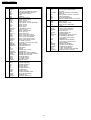
CONTENTS
Page
1 Use of Active Subwoofer
Page
5
12 Disassembly and Main Component Replacement Procedure
5
1.1. Checking Player when Active Subwoofer is not used
2 Safety Precautions
2.1. GENERAL GUIDELINES
22
6
12.1. Disassembly Procedure
22
6
12.2. Main Components and P.C.B. Locations.
23
12.3. Disassembling the Top Cabinet
24
3 Prevention of Electro Static Discharge (ESD) to
6
Electrostatically Sensitive (ES) Devices
12.4. Disassembling the Lid assembly (When taking out disc
4 Before Repair and Adjustment (Using Active Subwoofer)
7
5 Protection Circuitry
7
12.5. Disassembling the Front Panel
6 Precaution of Laser Diode
8
12.6. Disassembling the FL P.C.B., Volume P.C.B. and MIC
7 About Lead Free Solder (PbF)
8
8 General Description
9
12.7. Disassembling the DVD mechanism Unit
25
9
12.8. Disassembling the DVD Module P.C.B.
26
12.9. Disassembling the Rear panel
26
8.1. Operating instructions
manually)
P.C.B.
24
25
25
8.2. Disc information
10
8.3. Using of Receiver Unit (SH-FX50)
12
12.10. Disassembling Main P.C.B.
26
8.4. About HighMAT
13
12.11. Service Position
27
9 Accessories
13 Assembling and disassembling the DVD mechanism Unit
18
28
10 Caution for AC Cord
19
13.1. Disassembly Procedure
28
11 Handling Precautions for Optical Pickup Unit
20
13.2. Traverse Unit
28
13.3. Tray Unit
29
13.4. Loading section
30
11.1. Cautions to Be Taken in Handling the Optical Pickup Unit
20
13.5. Tray Loading P.C.B.
31
20
13.6. Optical Pickup Unit
31
20
13.7. Traverse Motor and Spindle Motor
33
11.2. Cautions to Be Taken When Replacing the Optical Pickup
11.3. Grounding for electrostatic breakdown prevention
3
SA-HT885WGC / SA-HT885WGS
14 Optical Pick-up Self-Diagnosis and Replacement Procedure
35
18 Abbreviations
45
19 Voltage Chart
47
14.1. Optical Pickup Breakdown Diagnosis
35
19.1. DVD Module P.C.B.
47
14.2. Service Mode Table 1
36
19.2. Main P.C.B.
48
14.3. DVD Self Diagnostic Function-Error Code
36
19.3. FL P.C.B. & MIC P.C.B & Tray Loading P.C.B.
49
14.4. Service mode table 2
38
20 Wave Form Chart
50
14.5. Sales demonstration lock function
40
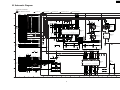
21 Schematic Diagram Notes
51
14.6. Handling After Completing Repairs
40
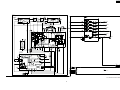
22 Block Diagram
53
41
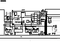
23 Schematic Diagram
59
15.1. Automatic Displayed Error Codes
41
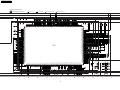
24 Printed Circuit Board Diagram
69
15.2. Memorized Error Codes
41
25 Wiring Connection Diagram
73
15 Self-Diagnosis Function
42
26 Illustration of IC's, Transistors and Diodes
75
16.1. Recovery after the DVD player is repaired
42
27 Terminal Function of ICs
76
16.2. Firmware version-up of the DVD player
42
16 Service Precautions
17 Adjustment Procedure
27.1. IC2018 (C2CBJG000672): System control
43
28 Parts Location and Replacement Parts List
76
77
17.1. Service Tools and Equipment
43
28.1. Loading Mechanism, Traverse Unit & Cabinet
78
17.2. Important points in adjustment
43
28.2. Component Parts List
81
17.3. Storing and Handling Test Discs
43
28.3. Packing Materials & Accessories Parts List
91
17.4. Optical adjustment
44
28.4. Packaging
91
4
SA-HT885WGC / SA-HT885WGS
1 Use of Active Subwoofer
1.1.
Checking Player when Active Subwoofer is not used
1. This unit uses the active subwoofer to supply the power of the component, and the active subwoofer should be connected to
the component to check operational conditions of the component.
2. If the active subwoofer is not available due to repair of the unit, use the following equipment.
Jig product number: RFKZ0182 (110V, 127V, 220V, 230V-240V for overseas domestic use)
5
SA-HT885WGC / SA-HT885WGS
2 Safety Precautions
2.1.
GENERAL GUIDELINES
1. When servicing, observe the original lead dress. If a short circuit is found, replace all parts which have been overheated or
damaged by the short circuit.
2. After servicing, see to it that all the protective devices such as insulation barriers, insulation papers shields are properly
installed.
3. After servicing, carry out the following leakage current checks to prevent the customer from being exposed to shock hazards.
2.1.1.
LEAKAGE CURRENT COLD
CHECK
2.1.2.
LEAKAGE CURRENT HOT CHECK
(See Figure 1 .)
1. Unplug the AC cord and connect a jumper between the two
prongs on the plug.
1. Plug the AC cord directly into the AC outlet. Do not use an
isolation transformer for this check.
2. Measure the resistance value, with an ohmmeter, between
the jumpered AC plug and each exposed metallic cabinet
part on the equipment such as screwheads, connectors,
control shafts, etc. When the exposed metallic part has a
return path to the chassis, the reading should be between
1MΩ and 5.2MΩ.
When the exposed metal does not have a return path to
the chassis, the reading must be .
2. Connect a 1.5kΩ, 10 watts resistor, in parallel with a 0.15µF
capacitors, between each exposed metallic part on the set
and a good earth ground such as a water pipe, as shown in
Figure 1.
3. Use an AC voltmeter, with 1000 ohms/volt or more
sensitivity, to measure the potential across the resistor.
4. Check each exposed metallic part, and measure the
voltage at each point.
5. Reverse the AC plug in the AC outlet and repeat each of the
above measurements.
6. The potential at any point should not exceed 0.75 volts
RMS. A leakage current tester (Simpson Model 229 or
equivalent) may be used to make the hot checks, leakage
current must not exceed 1/2 milliamp. In case a
measurement is outside of the limits specified, there is a
possibility of a shock hazard, and the equipment should be
repaired and rechecked before it is returned to the
customer.
Figure 1
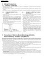
3 Prevention of Electro Static Discharge (ESD) to
Electrostatically Sensitive (ES) Devices
Some semiconductor (solid state) devices can be damaged easily by static electricity. Such components commonly are called
Electrostatically Sensitive (ES) Devices. Examples of typical ES devices are integrated circuits and some field-effect transistors and
semiconductor "chip" components. The following techniques should be used to help reduce the incidence of component damage
caused by electro static discharge (ESD).
1. Immediately before handling any semiconductor component or semiconductor-equipped assembly, drain off any ESD on your
body by touching a known earth ground. Alternatively, obtain and wear a commercially available discharging ESD wrist strap,
which should be removed for potential shock reasons prior to applying power to the unit under test.
2. After removing an electrical assembly equipped with ES devices, place the assembly on a conductive surface such as
aluminum foil, to prevent electrostatic charge buildup or exposure of the assembly.
3. Use only a grounded-tip soldering iron to solder or unsolder ES devices.
4. Use only an anti-static solder removal device. Some solder removal devices not classified as "anti-static (ESD protected)" can
generate electrical charge sufficient to damage ES devices.
5. Do not use freon-propelled chemicals. These can generate electrical charges sufficient to damage ES devices.
6. Do not remove a replacement ES device from its protective package until immediately before you are ready to install it. (Most
replacement ES devices are packaged with leads electrically shorted together by conductive foam, aluminum foil or comparable
conductive material).
7. Immediately before removing the protective material from the leads of a replacement ES device, touch the protective material
to the chassis or circuit assembly into which the device will be installed.
6
SA-HT885WGC / SA-HT885WGS
Caution
Be sure no power is applied to the chassis or circuit, and observe all other safety precautions.
8. Minimize bodily motions when handling unpackaged replacement ES devices. (Otherwise harmless motion such as the
brushing together of your clothes fabric or the lifting of your foot from a carpeted floor can generate static electricity (ESD)
sufficient to damage an ES device).
4 Before Repair and Adjustment (Using Active Subwoofer)
Disconnect AC power, discharge Power Supply Capacitors C546~C549 through a 10 Ω, 10 W resistor to ground.
DO NOT SHORT-CIRCUIT DIRECTLY (with a screwdriver blade, for instance), as this may destroy solid state devices.
After repairs are completed, restore power gradually using a variac, to avoid overcurrent.
Current consumption at AC 220 - 240 V, 50 Hz in NO SIGNAL mode should be ~ 600 mA.
Current consumption at AC 110/127 V, 50/60Hz in NO SIGNAL mode should be ~1180 mA.
5 Protection Circuitry
The protection circuitry may have operated if either of the following conditions are noticed:
· No sound is heard when the power is turned on.
· Sound stops during a performance.
The function of this circuitry is to prevent circuitry damage if, for example, the positive and negative speaker connection wires are
“shorted”, or if speaker systems with an impedance less than the indicated rated impedance of the amplifier are used.
If this occurs, follow the procedure outlines below:
1. Turn off the power.
2. Determine the cause of the problem and correct it.
3. Turn on the power once again after one minute.
Note:
When the protection circuitry functions, the unit will not operate unless the power is first turned off and then on again.
7
SA-HT885WGC / SA-HT885WGS
6 Precaution of Laser Diode
CAUTION :
This product utilizers a class 1 laser. Invisible laser radiation is emitted from the optical pick up lens.
When the unit is turned on:
Wavelength : 658nm/780nm
Maximum output radiation power from pick up : 100µW/VDE
Laser radiation from pick up unit is safety level, but be sure the followings:
1. Do not disassemble the optical pick up unit, since radiation from exposed laser diode is dangerous.
2. Do not adjust the variable resistor on the pick up unit. It was already adjusted.
3. Do not look at the focus lens using optical instruments.
4. Recommend not to look at pick up lens for a long time.
7 About Lead Free Solder (PbF)
Distinction of PbF PCB: PCBs (manufactured) using lead free solder will have a PbF stamp on the PCB.
Caution:
· Pb free solder has a higher melting point than standard solder; Typically the melting point is 50 - 70°F (30 - 40°C) higher.
Please use a high temperature soldering iron. In case of the soldering iron with temperature control, please set it to 700 ±
20°F (370 ± 10°C).
· Pb free solder will tend to splash when heated too high (about 1100°F/ 600°C).
When soldering or unsoldering, please completely remove all of the solder on the pins or solder area, and be sure to heat the
soldering points with the Pb free solder until it melts enough.
8
SA-HT885WGC / SA-HT885WGS
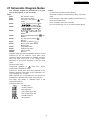
8 General Description
8.1.
Operating instructions
/AV SYSTEM
AV SYSTEM
TV
TV/AV
AUX
TV/AV
AUX
1
2
3
4
5
6
7
8
VCR
TUNER/BAND,
DVD/CD
TUNER/BAND DVD/CD
CH
CH
CH
NUMBERED
BUTTONS
CANCEL
9
VOLUME
-/--
0
CANCEL
VOLUME
S 10
SLOW/SEARCH
SKIP
(STOP)
TOP MENU
MENU
DIRECT
NAVIGATOR
PLAY
LIST
TOP MENU
(SLOW/SEARCH)
(PLAY)
(SKIP)
(PAUSE)
MENU
ENTER
ENTER
FUNCTIONS/
TV VOL
FUNCTIONS
RETURN
TV VOL
TV VOL
SUBWOOFER SUPER SRND C.FOCUS
LEVEL
H.BASS
SFC
MIX 2CH
PL
SLEEP
ZOOM
SUBTITLE
QUICK OSD MANUAL SKIP AUDIO
SETUP
MUTING
ANGLE/PAGE
GROUP
PLAY MODE
RETURN /TV VOL
FL DISPLAY
SHIFT
SHIFT
REPEAT
SUBWOOFER
LEVEL
SUPER SRND
H.BASS
C.FOCUS
SFC
MIX 2CH
PL
SLEEP
QUICK OSD
ZOOM
MANUAL SKIP
SUBTITLE
AUDIO
SETUP
MUTING
FL DISPLAY
ANGLE/PAGE
GROUP
REPEAT
PLAY MODE
ADVANCED
DISC REVIEW
PLAY SPEED
QUICK REPLAY
TEST
CH SELECT
TEST
ADVANCED PLAY SPEED
DISC REVIEW QUICK REPLAY CH SELECT
OPEN/CLOSE
STANDBY/ON INDICATOR
TUNING
INPUT SELECTOR
OPEN CLOSE
TUNING
INPUT SELECTOR
PROGRESSIVE
VOLUME
H.BASS
REMOTE CONTROL
SIGNAL SENSOR
PHONES
TUNE MODE
FM MODE
MEMORY
DOWN
UP
PHONES
MIN
MIC, MIC LEVEL
MAX
PROGRESSIVES/
H.BASS/H.BASS INDICATOR
STANDBY/ON SWITCH [ I /I]
9
TUNE MODE /
FM MODE /
MEMORY
VOLUME
SA-HT885WGC / SA-HT885WGS
8.2.
Disc information
Discs that can be played
Disc
Logo
Indication in
these operating
instructions
RAM
Recorded with devices using Version 1.1 of the Video Recording Format (a
unified video recording standard), such as DVD video recorders, DVD video
cameras, personal computers, etc.
JPEG
Recorded with Panasonic SD multi cameras or DVD
video recorders using the DCF (Design rule for Camera
File system) Standard Version 1.0.
DVD-RAM
Recorded with Panasonic SD multi cameras or DVD
video recorders [conforming to SD VIDEO
specifications (ASF standard)/MPEG4 (Simple Profile)
video system/G.726 audio system].
MPEG4
DivX
1
To play JPEG,
MPEG4 or DivX video
contents, select "Play
as Data Disc" in Other
Menu
—
—
DVD-A
DVD-Audio
Remarks
Some DVD-Audio discs contain DVD-Video content.
To play DVD-Video content, select “Play as DVD-Video” in Other Menu.
DVD-V
—
DVD-Video
Discs recorded and finalized 2 on DVD video recorders or DVD video cameras.
DVD-R
(DVD-Video)/
DVD-RW
(DVD-Video)
+R (Video)/
+RW (Video)
DVD-V
Discs recorded and finalized 2 on DVD video recorders or DVD video cameras.
—
Finalize
DVD-R
(DivX-Video)/
DVD-RW
(DivX-Video)
DivX
DVD-RW
(DVD-VR)
2
the disc after recording.
1
DVD-RW (VR)
Discs recorded and finalized 2 on DVD video recorders or DVD video cameras
using Version 1.1 of the Video Recording Format (a unified video recording
standard).
—
Video CD
VCD
Conforming to IEC62107
SVCD
CD
This unit is compatible with HDCD, but does not support the Peak Extend
function (a function which expands the dynamic range of high level signals).
HDCD-encoded CD’s sound better because they are encoded with 20 bits, as
compared with 16 bits for all other CD’s.
CD
WMA
MP3
CD-R
CD-RW
JPEG
—
CD
MPEG4
DivX
VCD
1
2
1
This unit can play CD-R/RW (audio recording disc) recorded with the formats
on the left. Close the sessions or finalize 2 the disc after recording.
HighMAT discs
WMA, MP3 or JPEG files only.
To play without using the HighMAT function, select “Play as Data Disc” in Other
Menu.
WMA This unit does not support Multiple Bit Rate (MBR: a file that contains the
same content encoded at several different bit rates).
Created using DivX ver.3.11, 4.x, 5.x [DivX video system/MP3, Dolby Digital or MPEG audio system].
A process that allows play on compatible equipment.
It may not be possible to play the above discs in all cases due to the type of discs, the condition of the recording, the recording method and how
the files were created.
Discs that cannot be played
Video systems
– This unit can play PAL and NTSC, but your television must match
the system used on the disc.
– PAL discs cannot be correctly viewed on an NTSC television.
– This unit can convert NTSC signals to PAL 60 for viewing on a PAL
television.
Version 1.0 of DVD-RW, DVD-ROM, CD-ROM,CDV, CD-G, SACD
and Photo CD, DVD-RAM that cannot be removed from their
cartridge, 2.6-GB and 5.2-GB DVD-RAM and "Chaoji VCD" available
on the market including CVD, DVCD and SVCD that do not conform
to IEC62107.
Audio format of DVD's
This unit automatically recognizes
and decodes discs with these
symbols.
10
SA-HT885WGC / SA-HT885WGS
11
SA-HT885WGC / SA-HT885WGS
8.3.
Using of Receiver Unit (SH-FX50)
· This model can be equipped with the digital transmitter and receiver to enjoy surround sound wirelessly..
8.3.1.
Below is tips on using the digital receiver
12
SA-HT885WGC / SA-HT885WGS
8.3.2.
8.4.
8.4.1.
Tips of using digital transmitter
About HighMAT
What’s HighMAT?
Consumers worldwide are using PCs to create their own collections of music, photos and even video by burning them onto CDs.
But how these collections can be experienced across different devices can be confusing to navigate, time consuming to access for
a DVD player, and be incomplete in terms of music information available to the customer.
HighMAT offers a solution to this growing consumer problem. HighMAT dramatically improves the digital media experience on
consumer electronic devices by delivering a simple, standardized approach that allows consumers who have created personal
collections of digital music, photography and video on their PC to:
lCreate a HighMAT CD or DVD which can be easily played back on consumer electronics devices such as CD and DVD players,
and car stereos.
lMove digital media files (using recordable media such as CD-R and CD-RW) between the PC and various playback devices such
as CD and DVD players.
A new standard for creating personal media on consumer electronic devices, HighMAT enable easier and more seamless
interoperability between Windows PCs and devices designed for your living room, or the car.
13
SA-HT885WGC / SA-HT885WGS
8.4.2.
Why take advantage of HighMAT?
A Problem Defined:Today, when consumers create their own digital audio, video or photo collections on CD-R or other physical
formats, there are numerous, inconsistent ways that devices read the data. For the consumer, the playback experience can be
confusing:
A Solution Created: HighMAT delivers a better digital media access experience by creating a standard approach for PCs to
structure digital media on various physical formats and for playback devices to read the data.
14
SA-HT885WGC / SA-HT885WGS
8.4.3.
Benefits of HighMAT?
Conventional
HighMAT
Even though DVD player is CD-R/RW compatible, the inconsistent ways HighMAT compatible products play content back with consistent
that various DVD players can read the music or photos files often leads interface. This includes products which are JPEG compatible products
to a confusing and inconsistant playback experince.
without HighMAT support.
15
SA-HT885WGC / SA-HT885WGS
HighMAT is now available for CD Burning and in Leading DVD Players
HighMAT is a new technology that is now available in leading software and consumer electronic devices to dramatically improve
the digital media experience when you create homemade CDs
HighMAT delivers a simple, standardized way for PC software and consumer electronics devices to talk to each other and work
better together.
16
SA-HT885WGC / SA-HT885WGS
When you create your homemade CDs with software that supports HighMAT CD burning, and then play them back on a DVD
player that supports HighMAT, you get better, easier navigation. You get folders you can access with a single click of your DVD
player´s remote control. You can view important information about your music like full song names, artist titles, album names and
genre. And you can get faster startup on your home entertainment device.
To enjoy the benefits of HighMAT, all you need is software that supports HighMAT for CD burning of music or photos, as well as
a home entertainment device like a DVD player that supports HighMAT for playback. Always look for the HighMAT logo on your
software or home entertainment device to ensure it supports the HighMAT experience.
17
SA-HT885WGC / SA-HT885WGS
9 Accessories
Remote control
AC cord
AM loop antenna
AC cord (For GS area)
FM indoor antenna
System cable
Video Cable
Speaker label
Speaker cable
18
SA-HT885WGC / SA-HT885WGS
10 Caution for AC Cord
19
SA-HT885WGC / SA-HT885WGS
11 Handling Precautions for Optical Pickup Unit
The laser diode in the optical pickup unit may break down due to static electricity of clothes or human body. Special care must be
taken avoid to electrostatic breakdown when servicing and handling the laser diode.
11.1. Cautions to Be Taken in Handling the Optical Pickup Unit
The laser diode in the optical pickup unit may be damaged due to electrostatic discharge generating from clothes or human body.
Special care must be taken avoid to electrostatic discharge damage when servicing the laser diode.
1. Do not give a considerable shock to the optical pickup unit as it has an extremely high-precise structure.
2. To prevent the laser diode from the electrostatic discharge damage, the flexible cable of the optical pickup unit removed should
be short-circuited with a short pin or a clip.
3. The flexible cable may be cut off if an excessive force is applied to it. Use with caution when handling the flexible cable.
4. The antistatic FPC is connected to the new optical pickup unit. After replacing the optical pickup unit and connecting the flexible
cable, cut off the antistatic FPC.
11.2. Cautions to Be Taken When Replacing the Optical Pickup
The flexible cable of the optical pickup unit which was supplied as a component is equipped with a short clip to prevent the laser
diode from being damaged due to electrostatic discharge. Remove the short clip before connecting the flexible cable and make
sure that the short land is open. (If the flexible cable is short-circuited, remove the solder.)
11.3. Grounding for electrostatic breakdown prevention
Some devices such as the DVD player use the optical pickup (laser diode) and the optical pickup will be damaged by static
electricity in the working environment. Proceed servicing works under the working environment where grounding works is
completed.
11.3.1. Worktable grounding
1. Put a conductive material (sheet) or iron sheet on the area where the optical pickup is placed, and ground the sheet.
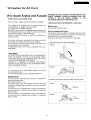
20
SA-HT885WGC / SA-HT885WGS
11.3.2. Human body grounding
1. Use the anti-static wrist strap to discharge the static electricity form your body.
21
SA-HT885WGC / SA-HT885WGS
12 Disassembly and Main Component Replacement
Procedure
“ATTENTION SERVICER”
Some chassis components may have sharp edges.
Be careful when disassembling and servicing.
1. This section describes procedures for checking the operation of the major printed circuit boards and replacing the
main components.
2. For assembly after operation checks or replacement, reverse the respective procedures.
Special reassembly procedures are described only when required.
3. Select items from the following index when checks or replacement are required.
· Disassembling the Top Cabinet
· Disassembling the Lid assembly (When taking out disc manually)
· Disassembling the Front Panel
· Disassembling the FL P.C.B., Volume P.C.B and MIC P.C.B.
· Disassembling the DVD mechanism Unit
· Disassembling the DVD Module P.C.B
· Disassembling the Rear panel
· Disassembling the Main.P.C.B.
12.1. Disassembly Procedure
22
SA-HT885WGC / SA-HT885WGS
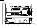
12.2. Main Components and P.C.B. Locations.
23
SA-HT885WGC / SA-HT885WGS
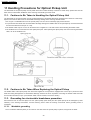
12.3. Disassembling the Top
Cabinet
Step 1 Unscrew the screw.
Step 2 Lift up and remove the top cabinet.
12.4. Disassembling the Lid
assembly (When taking out
disc manually)
· Follow the (Step 1) - (Step 2) of Item 12.3.
Step 1 Separates the gear for drawing out tray from the
mechanism unit. It inserts a screw driver in the gear. (The gear
jig)
Step 2 Insert the gear jig into the tray open/ close hole.
Step 3 Turn the gear jig counterclockwise to open the tray.
Note : Do not use force to push the tray backwards as it can
damage the mechanism unit.
Turn the gear jig clockwise to return tray.
24
SA-HT885WGC / SA-HT885WGS
12.5. Disassembling the Front Panel
· Follow the (Step 1) - (Step 2) of Item 12.3.
· Follow the (Step 1) - (Step 3) of Item 12.4.
Step 1 Remove the lid assembly from the tray section.
Step 2 Detach FFC cables at connectors. (CN2008, CN2009)
Step 2 Unscrew the screws.
Step 3 Remove the front angle.
Step 4 Unscrew the screws.
Step 3 Release the tabs.
12.7. Disassembling the DVD
mechanism Unit
· Follow the (Step 1) - (Step 2) of Item 12.3.
· Follow the (Step 1) - (Step 3) of Item 12.4.
· Follow the (Step 1) - (Step 4) of Item 12.5.
Step 1 Turn the gear jig clockwise to close the tray.
Step 2 Unscrew the screws.
Step 3 Detach FFC cable at connectors. (CN2004, H2000).
Step 4 Lift up the mechanism unit vertically.
Step 4 Lift up the front panel to remove it.
12.6. Disassembling the FL P.C.B.,
Volume P.C.B. and MIC P.C.B.
· Follow the (Step 1) - (Step 2) of Item 12.3.
· Follow the (Step 1) - (Step 3) of Item 12.4.
· Follow the (Step 1) - (Step 4) of Item 12.5.
Step 1 Remove the volume knob and mic knob.
25
SA-HT885WGC / SA-HT885WGS
12.9. Disassembling the Rear panel
· Follow the (Step 1) - (Step 2) of Item 12.3.
Step 1 Unscrew the screws.
Step 2 Release the tabs.
12.8. Disassembling the DVD
Module P.C.B.
12.10. Disassembling Main P.C.B.
· Follow the (Step 1) - (Step 2) of Item 12.3.
· Follow the (Step 1) - (Step 2) of Item 12.3.
· Follow the (Step 1) - (Step 3) of Item 12.4.
· Follow the (Step 1) - (Step 3) of Item 12.4.
· Follow the (Step 1) - (Step 4) of Item 12.5.
· Follow the (Step 1) - (Step 4) of Item 12.5.
· Follow the (Step 1) - (Step 4) of Item 12.7.
· Follow the (Step 1) - (Step 4) of Item 12.7.
· Follow the (Step 1) - (Step 2) of Item 12.9.
Step 1 Unscrew the screws.
Step 1 Unscrew the screws.
Step 2 Detach FFC cable at the connectors.(FP8201, FP8501)
26
SA-HT885WGC / SA-HT885WGS
12.11. Service Position
12.11.1. Servicing position of the DVD
Module P.C.B.
· Follow the (Step 1) - (Step 2) of Item 12.3.
· Follow the (Step 1) - (Step 3) of Item 12.4.
· Follow the (Step 1) - (Step 4) of Item 12.5.
· Follow the (Step 1) - (Step 4) of Item 12.7.
· Follow the (Step 1) of Item 12.8.
· Follow the (Step 1) - (Step 2) of Item 12.9.
Step 1 Connect FFC cable at connector. (CN2008, CN2009)
Step 2 Turn Mechanism unit to vertically position.
12.11.2. Servicing position of the Main
P.C.B.
· Follow the (Step 1) - (Step 2) of Item 12.3.
· Follow the (Step 1) - (Step 3) of Item 12.4.
· Follow the (Step 1) - (Step 4) of Item 12.5.
· Follow the (Step 1) - (Step 4) of Item 12.7.
· Follow the (Step 1) of Item 12.8.
· Follow the (Step 1) - (Step 2) of Item 12.9.
Step 1 Connect FFC cable at connector. (CN2008, CN2009)
Step 2 Turn Main P.C.B to vertically position.
27
SA-HT885WGC / SA-HT885WGS
13 Assembling and
disassembling the DVD
mechanism Unit
13.2. Traverse Unit
1. Slide the lever (A) in the arrow direction (to the opposite
side) till it stops.
2. Slide the lever (A) further by bending the tab at the right
side of the lever A in the right direction. (The right groove
opens and the boss becomes seen.)
13.1. Disassembly Procedure
3. Open the lever (B) to left. (The 2 grooves at the left side
open.)
4. Remove the traverse unit
28
SA-HT885WGC / SA-HT885WGS
13.3. Tray Unit
1. Slide the guide tray unit while pressing the stopper in the
arrow direction, and remove the guide tray unit.
5. Remove the drive arm concave phase from the tray slider
and tray.
(Assembling the tray unit)
2. Raise the loading unit.
1. Insert a part of the tray into the unit sliding over the
groove on the mechanical chassis unit.
3. Slide the lever in the arrow direction till it stops and pull the
tray out.
2. Insert the tray to the point before the tab of the
mechanical chassis unit.
4. Spread the tabs at the both sides and pull the tray out. (The
tray slides a little forward and stops.)
3. Hook the drive arm concave phase over the tray and the
tray slider.
4. Press in the tray.
5. Make sure that the tray and the drive arm move
smoothly.
29
SA-HT885WGC / SA-HT885WGS
4. Remove the belt.
13.4. Loading section
5. Unlock the tab and remove the pulley.
6. Remove the relay gear.
1. Spread the tabs at the both sides and push out the drive
arm shaft.
7. Turn the change lever in the arrow direction till it stops.
8. Hook the change lever spring on the change lever project
part temporarily.
2. Hook the lock lever spring on the lock lever projection part
temporarily.
3. Unlock the tab and remove the lock lever.
30
SA-HT885WGC / SA-HT885WGS
9. Pull the lever (B) in the bottom side to your side and remove
the change lever.
13.6. Optical Pickup Unit
13.6.1. Procedure for Disassembling the
Optical Pickup Unit
1. Spread the tabs to push in the pin.
10. Remove the drive rack, the sub rack and the drive gear.
2. Remove the pins.
13.5. Tray Loading P.C.B.
1. Unscrew the screws
3. Remove the traverse deck.
31
SA-HT885WGC / SA-HT885WGS
7. Unscrew the screw
8. Slide the shaft in the arrow direction.
4. Move the optical pickup unit in the arrow direction till it
stops.
9. Lift the optical pickup unit with the shaft.
5. Unscrew the screws.
10. Remove the optical pickup unit.
6. Remove the drive rack.
32
SA-HT885WGC / SA-HT885WGS
(Assembling the optical pickup unit)
1. Pass the intermediate FPC through the frame hole.
2. Align the guide section of the optical pickup unit with the
rail.
3. Install the shaft top to the holder.
11. Pull the shaft and the rubber out.
13.7. Traverse Motor and Spindle
Motor
1. Unscrew the screws.
2. Remove the cover while lifting the inner gear.
33
SA-HT885WGC / SA-HT885WGS
7. Unscrew the screws with torx screw driver (T6).
8. Remove the spindle motor.
3. Remove the solders.
4. Remove the traverse motor.
5. Remove the solders.
6. Remove the screw lock as carefully as you can.
34
SA-HT885WGC / SA-HT885WGS
14 Optical Pick-up Self-Diagnosis and Replacement
Procedure
14.1. Optical Pickup Breakdown Diagnosis
The optical pickup self-diagnosis function and tilt adjustment check function have been included in this unit. When repairing, use
the following procedure for effective Self-diagnosis and tilt adjustment. Be sure to use the self-diagnosis function before replacing
the optical pickup when "NO DISC" is displayed. As a guideline, you should replace the optical pickup when the value of the laser
drive current is more than 55.
Note:
Press the power button to turn on the power, and check the value within three minutes before the unit warms up. (Otherwise,
the result will be incorrect.)
35
SA-HT885WGC / SA-HT885WGS
14.2. Service Mode Table 1
The service modes can be activated by pressing various button combination on the player and remote control unit.
Player buttons
STOP
Remote control unit buttons
0
5
6
7
DISPLAY
3
PAUSE
Application
Error code display
Tilt adjustment
Note
(Refer to the item, “14.3.
DVD
Self
Diagnostic
Function-Error Code”).
Refer to the item “17.4.
Optical adjustment”).
Area number and broadcasting system check
Built-in program version check
DVD laser drive current check
Refer to the item “14.1.
Optical
Pickup
CD laser drive current check
Breakdown
Diagnosis”.
Writing of laser drive current value after replacement of optical
pickup (Do use this function only when optical pickup is
replaced.)
Initialization of the player (factory setting is restored.)
Used after replacement of micro-computer and its peripherals
and printed circuit board.
14.3. DVD Self Diagnostic Function-Error Code
Error Code
U11
H01
H02
H03
H04
H05
H06
H07
F500
F501
F502
F503
F504
F505
F506
F600
F601
F602
F603
F610
F611
F612
F620
F621
F630
F631
F632
F103
F4FF
F700
F701
F702
F880
Error Content
U, H error
Focus error
Tray loading error
Spindle servo error
Traverse servo error
Tracking servo error
Seek error
Power error
Spindle motor drive error
DSC related
DSC error
DSC not Ready error
DSC Time out error
DSC communication Failure
Error adjusting DSC data slice offset
DSC Attention error
Invalid media
ODC related
Access failure to management
information caused by demodulation
error
Indeterminate sector ID requested
Access failure to LEAD-IN caused by
demodulation error
Access failure to KEYDET caused by
demodulation error
ODC abnormality
6626 QCODE don’t read Error
No CRC OK for a specific time
Laser safeguard: high temperature
condition
Laser safeguard: circuit failure
condition
No reply to KEY DET enquiry
CPPM KEY DET is not available till
the FILE terminal
CPPM KEY DET is not available
Disc code
Illegal highlight Position
HIC Error
Force initialize failure (time out)
Micro computer error
MBX overflow
Message command does not end
Message command changes
Task number is not appropriate
Additional error explanation
(Spindle servo, DSC (IC8271) SP motor, CLV servo error)
(Traverse motor, IC8251)
Cannot switch off the power because of the panel and system computer communication error
Spindle motor
DSC (IC8271) stops in the occurrence of servo error (startup, focus error, etc.)
DSC-system computer communication error (Communication failure caused by idling of DSC)
Similar disposal as F500
Communication error (result error occurred although communication command was sent)
Similar disposal as F500
Disc is flipped over, TOC unreadable, incompatible disc media
Operation stopped because navigation data is not accessible caused by the demodulation
defect
Operation stopped caused by the request to access abnormal ID data
LEAD IN data unreadable
Access failure to CSS data of disc
No permission for command execution
Access failure to seek address in CD series
Access failure to ID data in DVD series
(for internal use only)
(CPPM file system is unreadable caused by scratches)
Been revoked or falsified
Big possibility of disc specification violation during highlight display
When replying message to disc manager
Next message is sent before replying to disc manager
Message is changed before it is sent as a reply to disc manager
Message coming from a non-existing task
36
SA-HT885WGC / SA-HT885WGS
Error Code
F890
F891
F893
F894
F895
F896
F897
F898
F8A0
Error Content
Sending message when message is
being sent to AV task
Message couldn’t be sent to AV task
FROM falsification
EEPROM abnormality
Language area abnormality
No existence model
Initialize is not completed
Disagreement of hardware and
software
Message command is not appropriate
Additional error explanation
Sending message to AV task
Begin sending message to AV task
Firm version agreement check for factory preset setting failure prevention
Firm version agreement check for factory preset setting failure prevention
Initialize completion check for factory preset setting failure prevention
Unsuitable combination of AV DECORDER, SDRAM and FLASH ROM
(firmware)
Begin sending message to AV task
Note:
An error code will be canceled if a power supply is turned OFF.
*1: CPPM is the copy guard function beforehand written in the disk for protection of copyrights.
37
SA-HT885WGC / SA-HT885WGS
14.4. Service mode table 2
Pressing various button combinations on the player and remote control unit can activate the service modes.
38
SA-HT885WGC / SA-HT885WGS
39
SA-HT885WGC / SA-HT885WGS
14.5. Sales demonstration lock function
This function prevents discs from being lost when the unit is used for sales demonstrations by disabling the disc eject function.
"LOCKED" is displayed on the unit, and ordinary operation is disabled.
14.5.1. Setting
· Prohibiting removal of disc
1. Select the DVD/CD function.
2. Press and hold down the
button on the player and the power button on the remote controller unit for at least three
seconds. (The message, “___LOCKED_” appears when the function is activated.)
Note:
OPEN/CLOSE
button is invalid and the player displays “___LOCKED_” while the lock function mode is entered.
· Prohibiting operation of selector and disk
1. Select the DVD/CD function.
button on the player and the power button on the remote controller unit for at least three
2. Press and hold down the
seconds. (The message, “___LOCKED_” appears when the function is activated.)
Note:
The following buttons are invalid and the player displays “___LOCKED_” while the lock function mode is entered.
Player
,
,
, SELECTOR,
,
, VOLUME KNOB,
Remote
SLEEP, REPEAT, 0~9,
, RETURN, TOP MENU,
,
,
,
,
,
,
controller unit POSITION MEMORY, TUNER/BAND, D.MIX, CH SELECT/ TEST, SET UP/ MUTING, DISPLAY, GROUP, TV, VCR/
AUX, QUICK REPLAY, SUBTITLE, FL DISPLAY, CH & VOLUME
14.5.2. Cancellation
The lock can be cancelled by the same procedure as used in setting. ("UNLOCK" is displayed on cancellation. Disconnecting the
power cable from power outlet does not cancel the lock.)
14.6. Handling After Completing Repairs
Use the following procedure after completing repairs.
14.6.1. Method
Confirm that the power is turned on:
1. Press the "OPEN/CLOSE" button to close the tray.
2. Press the "POWER" button to turn off the power.
3. Disconnect the power plug from the outlet.
14.6.2. Precautions
Do not disconnect the power plug from the outlet with the tray still open, then close the tray manually.
40
SA-HT885WGC / SA-HT885WGS
15 Self-Diagnosis Function
15.2. Memorized Error Codes
15.1. Automatic Displayed Error
Codes
15.2.1. Activating Self-Diagnosis Function
and Displaying Method
1. Turn on the power.
15.1.1. Automatic Display Function
2. Select DVD/CD function. With no DVD/CD inserted in the
player, press and hold down the
button simultaneously
for at least two seconds, and press the F_SKIP
button for at least two seconds in order to display
“T___________”.
For a power unit error, the code is automatically displayed.
F61:
Automatically displayed on the LCD of
the player.
button. If a memorized error is detected, the
3. Press the
result of self diagnosis is displayed. (Ex.: T H15)(See table
below)
If several errors are detected, press the
button to
display each.
15.1.2. Re-Display
· For F61 Display
15.2.2. Re-Display
− When the code, F61 is displayed, the power is
automatically turned off.
· Press the power button to turn off the power, and then turn
on the power.
− The code, F61 is displayed for three seconds, and then
the current time appears.
· The details of self diagnosis are stored in the unit memory.
To retrieve them, follow the procedure described the above,
“Activating Self-Diagnosis Function and Displaying
Method”.
− To retrieve the code, turn on the power button so that
the code F61 appears, however, is switched to time
display after three seconds, and the power is
automatically turned off.
15.2.3. Deleting Details of Self Diagnosis
15.1.3. Description of Error Code
· After repair, press and hold down the
button for at least
five seconds, “_ CLEAR __” appears for a second and then
“T________” appears. (Deleting the details of self
diagnosis)
15.1.3.1. F61
· State, Condition
When the power is turned on, the unit is automatically
turned off. The power does not turn on.
· After repairing errors, be sure to delete the details of self
diagnosis.
· Cause, Troubleshooting
Power circuit system failure and/or direct current flown to
speaker terminal
Identify the cause and replace with new parts.
Error Code
H15
H16
State, Condition
The disc tray cannot be opened: it closes spontaneously.
The disc tray cannot be closed: it opens spontaneously.
41
Cause, Troubleshooting
Disc tray open/close detection switch (S901/S902) failure.
(Check and replace)
SA-HT885WGC / SA-HT885WGS
16 Service Precautions
16.1. Recovery after the DVD player is repaired
· When FLASH ROM IC or DVD module P.C.B. is replaced, carry out the recovery processing to optimize the drive.
Playback the recovery disk to process the recovery automatically.
· Recovery disc (Product number: RFKZD03R005)
· Performing recovery
1. Load the recovery disc RFKZD03R005 on to the player and run it.
2. Recovery is performed automatically. When it is finished, a message appears on the screen.
3. Remove the recovery disc.
4. Turn off the power.
Note:
This unit requires no initialization process carried out after the traditional DVD players were repaired.
When the recovery measures are taken, the customer setting will return to the factory setting as same as the procedure
described in item of "Initialization" in 14.4. is carried out. Write down the contents of the setting before recovery processing, and
reset the player.
16.2. Firmware version-up of the DVD player
· The firmware of the DVD player may be renewed to improve the quality including operability and playability to the substandard
discs.processing to optimize the drive.
The recovery disc has also firmware version-up.
· After version-up, recovery processing is executed automatically.
· Part number of the recovery disc for version-up will be noticed when it is supplied.
· Updating firmware
1. Load the recovery disc that is supplied to the player and run it.
2. Firmware version of the player is automatically checked. Appropriate message appears whenever necessary.
3. Using remote controller´s cursor key, select whether version updating is to be done or not. (Selection of Yes/No)
4. a. If Yes is selected, version updating is performed.
b. If No is selected, only recovery is performed.
5. a. When updating is finished, remove the disc according to the message appearing on the screen.
b. Remove the disc according to the message appearing on the screen.
6. Turn off the power.
Note:
If the AC power supply is shut out during version-up due to a power failure, the version-up is improperly carried out.
In such a case, replace the FLASH ROM IC and carry out the version-up again.
42
SA-HT885WGC / SA-HT885WGS
17 Adjustment Procedure
17.1. Service Tools and Equipment
Application
Tilt adjustment
Name
Number
DVDT-S20 [SPG]
DVD test disc
TORX screw driver (T6)
Others
Confirmation
Available on sales route.
(T6) or RFKZ0185 [SPG]
RFKXPG641
VFK1784 [SPG]
RFKXGUD24
PVCD-K06 or any other commercially
available disc
PVCD-K06 or any other commercially
available disc
RFKZD03R005 [SPG]
Grease
Harnal
Drysurf
CD test disc
VCD test disc
Recovery disc
17.2. Important points in adjustment
17.2.1. Important points in optical adjustment
· Before starting optical adjustment, be sure to take anti-static measures.
· Optical pickup tilt adjustment is needed after replacement of the following components.
1. Optical pickup unit
2. Spindle motor unit
3. Optical pickup peripheral parts (such as rail)
Notes
Adjustment is generally unnecessary after replacing other parts of the traverse unit. However, make adjustment if there is a
noticeable degradation in picture quality. Optical adjustments cannot be made inside the optical pickup. Adjustment is generally
unnecessary after replacing the traverse unit.
17.2.2. Important points in electrical adjustment
· Follow the adjustment procedures described in this Manual.
17.3. Storing and Handling Test Discs
· Surface precision is vital for DVD test discs. Be sure to store and handle them carefully.
1. Do not place discs directly onto the workbench, etc., after use.
2. Handle discs carefully in order to maintain their flatness. Place them into their case after use and store them vertically. Store
discs in a cool place where they are not exposed to direct sunlight or air from air conditioners.
3. Accurate adjustment will not be possible if the disc is warped when placed on a surface made of glass, etc. If this happens, use
a new test disc to make optical adjustments.
4. If adjustment is done using a warped disc, the adjustment will be incorrect and some discs will not be playable.
43
SA-HT885WGC / SA-HT885WGS
17.4. Optical adjustment
17.4.1. Optical pickup tilt adjustment
Measurement point
Adjustment point
Tangential adjustment screw
Tilt adjustment screw
Measuring equipment
None (Main unit display for servicing is used.)
Mode
Disc
T01 (inner periphery) play
DVDT-S20 [SPG]
T30 (center periphery) play
T43 (outer periphery) play
Adjustment value
Adjust to the minimum jitter value.
17.4.1.1. Adjustment procedure
1. While pressing STOP button on the main unit, press "5" on
the remote control unit.
2. Confirm that "J_xxx/yyy_zz" (display1/display2) is shown on
the front display.
For your information:
"yyy" and "zz" shown to the right have nothing to do with
the jitter value. "yyy" is the error counter, while "zz" is
the focus drive value.
Note:
Jitter value appears on the front display.
3. Play test disc T30 (center periphery).
4. Adjust tangential adjustment screw so that the jitter value is
minimized.
5. Play test disc T30 (center periphery).
6. Adjust tilt adjustment screw 1 so that the jitter value is
minimized.
7. Play test disc T30 (center periphery).
8. Adjust tilt adjustment screw 2 so that the jitter value is
minimized.
17.4.1.3. Check after adjustment
9. Repeat adjusting tilt adjustment screws 1 and 2 alternately
until the jitter value is minimized.
Play test disc or any other disc to make sure there is no picture
degradation in the inner, middle and outer peripheries, and no
audio skipping. After adjustment is finished, lock each
adjustment screw in position using screw lock.
17.4.1.2. Important points
1. Make tangential adjustment first, and then make tilt
adjustment.
17.4.1.4. Procedure for screw lock
1. After adjustment, remove top cover, tray, clamper base and
traverse unit in this sequence.
2. Repeat adjusting two or three times to find the optimum
point.
2. Lay the traverse unit upside down, and fix adjustment screw
with screw lock.
3. Finish the procedure with tilt adjustment.
3. After fixing, reassemble traverse unit, clamper base, tray
and top cover.
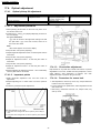
Jitter value depends on the model:
1. If the jitter value changes like B, the optimum point is easy to
find.
2. If the jitter value changes like A, set the optimum point near the
middle.
44
SA-HT885WGC / SA-HT885WGS
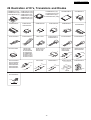
18 Abbreviations
INITIAL/LOGO
A
A0~UP
ACLK
AD0~UP
ADATA
ALE
AMUTE
AREQ
ARF
ASI
ASO
ASYNC
B
BCK
BCKIN
BDO
BLKCK
BOTTOM
BYP
BYTCK
C
CAV
CBDO
CD
CDSCK
CDSRDATA
CDRF
CDV
CHNDATA
CKSL
CLV
COFTR
CPA
CPCS
CPDT
CPUADR
CPUADT
CPUIRQ
CPRD
CPWR
CS
CSYNCIN
CSYNCOUT
D
DACCK
DEEMP
DEMPH
DIG0~UP
DIN
DMSRCK
DMUTE
DO
DOUT0~UP
DRF
DRPOUT
DREQ
DRESP
DSC
DSLF
DVD
ABBREVIATIONS
ADDRESS
AUDIO CLOCK
ADDRESS BUS
AUDIO PES PACKET DATA
ADDRESS LATCH ENABLE
AUDIO MUTE
AUDIO PES PACKET REQUEST
AUDIO RF
SERVO AMP INVERTED INPUT
SERVO AMP OUTPUT
AUDIO WORD DISTINCTION SYNC
BIT CLOCK (PCM)
BIT CLOCK INPUT
BLACK DROP OUT
SUB CODE BLOCK CLOCK
CAP. FOR BOTTOM HOLD
BYPATH
BYTE CLOCK
CONSTANT ANGULAR VELOCITY
CAP. BLACK DROP OUT
COMPACT DISC
CD SERIAL DATA CLOCK
CD SERIAL DATA
CD RF (EFM) SIGNAL
COMPACT DISC-VIDEO
CHANNEL DATA
SYSTEM CLOCK SELECT
CONSTANT LINEAR VELOCITY
CAP. OFF TRACK
CPU ADDRESS
CPU CHIP SELECT
CPU DATA
CPU ADDRESS LATCH
CPU ADDRESS DATA BUS
CPU INTERRUPT REQUEST
CPU READ ENABLE
CPU WRITE ENABLE
CHIP SELECT
COMPOSITE SYNC IN
COMPOSITE SYNC OUT
D/A CONVERTER CLOCK
DEEMPHASIS BIT ON/OFF
DEEMPHASIS SWITCHING
FL DIGIT OUTPUT
DATA INPUT
DM SERIAL DATA READ CLOCK
DIGITAL MUTE CONTROL
DROP OUT
DATA OUTPUT
DATA SLICE RF (BIAS)
DROP OUT SIGNAL
DATA REQUEST
DATA RESPONSE
DIGITAL SERVO CONTROLLER
DATA SLICE LOOP FILTER
DIGITAL VIDEO DISC
INITIAL/LOGO
E
EC
ECR
F
G
H
I
L
M
O
P
45
ENCSEL
ETMCLK
ETSCLK
FBAL
FCLK
FE
FFI
FEO
FG
FSC
FSCK
GND
HA0~UP
HD0~UP
HINT
HRXW
IECOUT
IPFRAG
IREF
ISEL
LDON
LPC
LRCK
MA0~UP
MCK
MCKI
MCLK
MDATA
MDQ0~UP
MDQM
MLD
MPEG
ODC
OFTR
OSCI
OSCO
OSD
P1~UP
PCD
PCK
PDVD
PEAK
PLLCLK
PLLOK
PWMCTL
PWMDA
PWMOA, B
ABBREVIATIONS
ERROR TORQUE CONTROL
ERROR
TORQUE
CONTROL
REFERENCE
ENCODER SELECT
EXTERNAL M CLOCK (81MHz/40.5MHz)
EXTERNAL S CLOCK (54MHz)
FOCUS BALANCE
FRAME CLOCK
FOCUS ERROR
FOCUS ERROR AMP INVERTED INPUT
FOCUS ERROR AMP OUTPUT
FREQUENCY GENERATOR
FREQUENCY SUB CARRIER
FS (384 OVER SAMPLING) CLOCK
COMMON GROUNDING (EARTH)
HOST ADDRESS
HOST DATA
HOST INTERRUPT
HOST READ/WRITE
IEC958 FORMAT DATA OUTPUT
INTERPOLATION FLAG
I (CURRENT) REFERENCE
INTERFACE MODE SELECT
LASER DIODE CONTROL
LASER POWER CONTROL
L CH/R CH DISTINCTION CLOCK
MEMORY ADDRESS
MEMORY CLOCK
MEMORY CLOCK INPUT
MEMORY SERIAL COMMAND CLOCK
MEMORY SERIAL COMMAND DATA
MEMORY DATA INPUT/OUTPUT
MEMORY DATA I/O MASK
MEMORY SERIAL COMMAND LOAD
MOVING PICTURE EXPERTS GROUP
OPTICAL DISC CONTROLLER
OFF TRACKING
OSCILLATOR INPUT
OSCILLATOR OUTPUT
ON SCREEN DISPLAY
PORT
CD TRACKING PHASE DIFFERENCE
PLL CLOCK
DVD TRACKING PHASE DIFFERENCE
CAP. FOR PEAK HOLD
CHANNEL PLL CLOCK
PLL LOCK
PWM OUTPUT CONTROL
PULSE WAVE MOTOR DRIVE A
PULSE WAVE MOTOR OUT A, B
SA-HT885WGC / SA-HT885WGS
INITIAL/LOGO
R
RE
RFENV
RFO
RS
RSEL
RST
RSV
S
SBI0, 1
SBO0
SBT0, 1
SCK
SCKR
SCL
SCLK
SDA
SEG0~UP
SELCLK
SEN
SIN1, 2
SOUT1, 2
SPDI
SPDO
SPEN
SPRCLK
SPWCLK
SQCK
SQCX
SRDATA
SRMADR
SRMDT0~7
SS
STAT
STCLK
STD0~UP
STENABLE
STSEL
STVALID
SUBC
SBCK
SUBQ
SYSCLK
T
TE
TIBAL
TID
TIN
TIP
TIS
TPSN
TPSO
TPSP
TRCRS
TRON
TRSON
ABBREVIATIONS
READ ENABLE
RF ENVELOPE
RF PHASE DIFFERENCE OUTPUT
(CD-ROM) REGISTER SELECT
RF POLARITY SELECT
RESET
RESERVE
SERIAL DATA INPUT
SERIAL DATA OUTPUT
SERIAL CLOCK
SERIAL DATA CLOCK
AUDIO SERIAL CLOCK RECEIVER
SERIAL CLOCK
SERIAL CLOCK
SERIAL DATA
FL SEGMENT OUTPUT
SELECT CLOCK
SERIAL PORT ENABLE
SERIAL DATA IN
SERIAL DATA OUT
SERIAL PORT DATA INPUT
SERIAL PORT DATA OUTPUT
SERIAL PORT R/W ENABLE
SERIAL PORT READ CLOCK
SERIAL PORT WRITE CLOCK
SUB CODE Q CLOCK
SUB CODE Q DATA READ CLOCK
SERIAL DATA
SRAM ADDRESS BUS
SRAM DATA BUS 0~7
START/STOP
STATUS
STREAM DATA CLOCK
STREAM DATA
STREAM DATA INPUT ENABLE
STREAM DATA POLARITY SELECT
STREAM DATA VALIDITY
SUB CODE SERIAL
SUB CODE CLOCK
SUB CODE Q DATA
SYSTEM CLOCK
TRACKING ERROR
BALANCE CONTROL
BALANCE OUTPUT 1
BALANCE INPUT
BALANCE INPUT
BALANCE OUTPUT 2
OP AMP INPUT
OP AMP OUTPUT
OP AMP INVERTED INPUT
TRACK CROSS SIGNAL
TRACKING ON
TRAVERSE SERVO ON
INITIAL/LOGO
V
VBLANK
VCC
VCDCONT
W
X
46
VDD
VFB
VREF
VSS
WAIT
WDCK
WEH
WSR
X
XALE
XAREQ
XCDROM
XCS
XCSYNC
XDS
XHSYNCO
XHINT
XI
XINT
XMW
XO
XRE
XSRMCE
XSRMOE
XSRMWE
XVCS
XVDS
XVSYNCO
ABBREVIATIONS
V BLANKING
COLLECTOR POWER SUPPLY
VOLTAGE
VIDEO CD CONTROL (TRACKING
BALANCE)
DRAIN POWER SUPPLY VOLTAGE
VIDEO FEED BACK
VOLTAGE REFERENCE
SOURCE POWER SUPPLY VOLTAGE
BUS CYCLE WAIT
WORD CLOCK
WRITE ENABLE HIGH
WORD SELECT RECEIVER
X´ TAL
X ADDRESS LATCH ENABLE
X AUDIO DATA REQUEST
X CD ROM CHIP SELECT
X CHIP SELECT
X COMPOSITE SYNC
X DATA STROBE
X HORIZONTAL SYNC OUTPUT
XH INTERRUPT REQUEST
X´ TAL OSCILLATOR INPUT
X INTERRUPT
X MEMORY WRITE ENABLE
X´ TAL OSCILLATOR OUTPUT
X READ ENABLE
X SRAM CHIP ENABLE
X SRAM OUTPUT ENABLE
X SRAM WRITE ENABLE
X V-DEC CHIP SELECT
X V-DEC CONTROL BUS STROBE
X VERTICAL SYNC OUTPUT
SA-HT885WGC / SA-HT885WGS
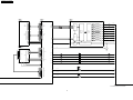
19 Voltage Chart
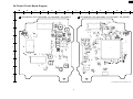
19.1. DVD Module P.C.B.
Re f No.
MODE
CD P LAY
Re f No.
MODE
CD P LAY
Re f No.
MODE
CD P LAY
Re f No.
MODE
CD P LAY
Re f No.
MODE
CD P LAY
Re f No.
MODE
CD P LAY
Re f No.
MODE
CD P LAY
Re f No.
MODE
CD P LAY
Re f No.
MODE
CD P LAY
Re f No.
MODE
CD P LAY
Re f No.
MODE
CD P LAY
Re f No.
MODE
CD P LAY
Re f No.
MODE
CD P LAY
Re f No.
MODE
CD P LAY
Re f No.
MODE
CD P LAY
Re f No.
MODE
CD P LAY
Re f No.
MODE
CD P LAY
Re f No.
MODE
CD P LAY
Re f No.
MODE
CD P LAY
Re f No.
MODE
CD P LAY
Re f No.
MODE
CD P LAY
Re f No.
MODE
CD P LAY
Re f No.
MODE
CD P LAY
Re f No.
MODE
CD P LAY
Re f No.
MODE
CD P LAY
Re f No.
MODE
CD P LAY
Re f No.
MODE
CD P LAY
Re f No.
MODE
CD P LAY
Re f No.
MODE
CD P LAY
Re f No.
MODE
CD P LAY
Re f No.
MODE
CD P LAY
1
3.1
2
3.0
3
0
4
3.1
5
3.3
6
3.4
7
3.0
8
3.1
9
0
21
3.4
22
-
23
-
24
1.5
25
0.8
26
1.2
27
1.0
28
3.4
29
0
41
-
42
-
43
-
44
1.2
45
-
46
-
47
-
48
3.4
49
0
61
-
62
3.4
63
0
64
0
65
0.1
66
1.0
67
1.0
68
3.0
69
2.8
81
3.4
82
0.1
83
3.4
84
3.4
85
0.1
86
0.1
87
0
88
0.1
89
1.2
101
2.4
102
2.1
103
1.9
104
0.3
105
0
106
1.9
107
3.4
108
2.1
109
2.1
121
1.5
122
0
123
0
124
0.1
125
0
126
0
127
2.3
128
1.7
129
2.6
141
0.5
142
0
143
0
144
0
145
0
146
1.1
147
2.2
148
1.7
149
2.6
161
3.4
162
0
163
0
164
0
165
0
166
3.4
167
3.4
168
1.7
169
0
181
0
182
3.4
183
0
184
0
185
-
186
-
187
-
188
-
189
-
201
0
202
3.4
203
3.4
204
1.2
205
0
206
1.7
207
1.4
208
1.4
209
3.4
221
0.2
222
0
223
1.7
224
0.2
225
3.4
226
1.7
227
0.1
228
0.9
229
0
241
1.7
242
0
243
1.7
244
3.3
245
3.4
246
3.4
247
0
248
3.3
249
2.6
1
3.4
2
3.2
3
3.4
4
3.1
5
3.2
6
0.1
7
3.2
8
3.4
9
3.1
21
1.6
22
0.1
23
-
24
-
25
-
26
-
27
3.4
28
0
29
-
41
0.1
42
3.0
43
3.4
44
3.2
45
3.1
46
0
47
3.0
48
3.1
49
3.4
1
3.4
2
0
3
0.1
4
-
5
-
6
0
7
0
8
4.9
1
1.7
2
1.7
3
1.7
4
1.9
5
1.9
6
1.8
7
0
8
4.9
21
9.6
22
9.4
23
1.8
24
1.7
25
1.7
26
1.7
27
3.4
28
3.2
1
0
2
3.4
3
3.0
4
3.4
5
1.7
6
0.9
7
1.7
8
1.7
21
2.4
22
4.9
23
-
24
0
25
2.5
26
2.4
27
2.4
28
4.8
1
0
2
3.2
3
3.4
1
0.7
2
1.2
3
0
4
0
5
0
1
0.1
2
0.1
3
0.1
4
0.1
5
3.4
6
3.4
7
0.1
8
3.4
1
-
2
-
3
-
4
-
5
-
6
-
7
-
8
-
9
-
21
-
22
-
23
-
24
-
25
-
26
2.4
27
0
28
1.9
29
1.0
41
1.4
42
1.4
43
44
1.7
1.7
IC8691
3
4
0.1
4.3
45
1.9
46
0
47
3.4
48
-
IC8001
10
11
0
3.1
IC8001
30
31
0.5
1.0
IC8001
50
51
IC8001
70
71
3.1
0.1
IC8001
90
91
0
0
IC8001
110
111
1.9
1.8
IC8001
130
131
2.6
2.6
IC8001
150
151
2.6
2.6
IC8001
170
171
1.7
0.9
IC8001
190
191
3.4
0
IC8001
210
211
3.4
1.0
IC8001
230
231
0.1
3.4
IC8001
250
251
0
3.6
IC8051
10
11
3.0
IC8051
30
31
IC8051
50
51
2.8
2.8
IC8111
12
3.4
13
2.9
14
3.1
15
3.0
16
0
17
3.0
18
3.0
19
3.4
20
0
32
-
33
-
34
3.4
35
0
36
-
37
-
38
2.4
39
-
40
-
52
2.5
53
0
54
0
55
0
56
-
57
-
58
-
59
-
60
-
72
0.1
73
3.2
74
0
75
1.7
76
.0
77
1.7
78
0.1
79
3.4
80
0
92
0
93
0
94
0.1
95
0.1
96
0
97
0
98
3.4
99
0.8
100
0.1
112
1.1
113
1.1
114
1.7
115
1.7
116
1.7
117
1.7
118
3.3
119
2.0
120
1.7
132
2.6
133
2.6
134
2.6
135
2.4
136
2.4
137
0
138
2.4
139
0
140
0
152
2.6
153
2.6
154
2.6
155
2.4
156
2.4
157
0
158
2.4
159
3.4
160
0
172
1.2
173
0
174
0
175
0
176
0.9
177
1.7
178
3.4
179
0
180
3.4
192
1.0
193
1.7
194
0
195
1.5
196
3.4
197
1.3
198
0.5
199
1.5
200
1.4
212
1.8
213
0
214
-
215
-
216
3.4
217
2
218
0
219
1.2
220
1.6
232
1.6
233
-
234
2.2
235
0
236
1.2
237
0.1
238
0.1
239
3.4
240
3.2
252
2.8
253
0
254
2.9
255
3.4
256
2.9
12
0.1
13
2.9
14
3.4
15
2.7
16
3.3
17
3.3
18
3.3
19
3.0
20
2.2
32
-
33
-
34
-
35
-
36
-
37
3.4
38
1.7
39
2.7
40
-
52
0
53
2.9
54
0
9
3.4
IC8251
10
11
0.1
2.6
IC8251
12
2.4
13
2.5
14
2.5
15
4.5
16
4.6
17
5.1
18
4.0
19
0.1
20
0.6
9
4.8
IC8421
10
11
0
0.9
IC8421
12
0.1
13
0.1
14
0
15
2.4
16
2.4
17
4.9
18
0
19
2.4
20
2.4
12
2.9
13
3.4
14
3.4
15
1.0
16
-
17
-
18
-
19
-
20
-
32
1.0
33
1.4
34
1.2
35
1.5
36
1.5
37
3.4
38
1.4
39
1.2
40
1.3
E
1.5
Q8341
C
0
B
0.9
IC8601
IC8606
IC8611
1
3.0
E
1.1
E
0.1
E
0.1
2
3.0
Q8321
C
B
0
0.4
Q8551
C
B
4.8
0.1
QR8111
C
B
0.1
1.2
IC8651
10
11
IC8651
30
31
1.0
1.0
IC8651
5
4.9
E
1.6
E
4.8
E
0
1
0
Q8325
C
B
0
0.9
Q8552
C
B
0
4.8
QR8420
C
B
4.0
0.1
Q8331
E
C
1.1
0
Q8561
E
C
1.5
3.5
QR8571
E
C
3.4
3.3
47
B
0.4
B
2.1
B
0.1
2
0
IC8695
3
4
0
0
Q8335
E
C
1.6
0
Q8562
E
C
4.2
2.3
5
4.9
B
0.9
B
3.6
SA-HT885WGC / SA-HT885WGS
19.2. Main P.C.B.
Re f No.
MODE
CD P LAY
S TANDBY
Re f No.
MODE
CD P LAY
S TANDBY
Re f No.
MODE
CD P LAY
S TANDBY
Re f No.
MODE
CD P LAY
S TANDBY
Re f No.
MODE
CD P LAY
S TANDBY
Re f No.
MODE
CD P LAY
S TANDBY
Re f No.
MODE
CD P LAY
S TANDBY
Re f No.
MODE
CD P LAY
S TANDBY
Re f No.
MODE
CD P LAY
S TANDBY
Re f No.
MODE
CD P LAY
S TANDBY
Re f No.
MODE
CD P LAY
S TANDBY
Re f No.
MODE
CD P LAY
S TANDBY
Re f No.
MODE
CD P LAY
S TANDBY
Re f No.
MODE
CD P LAY
S TANDBY
Re f No.
MODE
CD P LAY
S TANDBY
Re f No.
MODE
CD P LAY
S TANDBY
Re f No.
MODE
CD P LAY
S TANDBY
Re f No.
MODE
CD P LAY
S TANDBY
Re f No.
MODE
CD P LAY
S TANDBY
Re f No.
MODE
CD P LAY
S TANDBY
Re f No.
MODE
CD P LAY
S TANDBY
1
4.7
0
2
2.2
0
3
2.4
0
1
0
0.5
2
0
0.5
3
0
0
4
5
1.6
4.7
0
0
IC2010
4
5
-6.8
0
0.2
0
6
1.6
0
7
0
0
8
2.2
0.2
6
0
0.5
7
0
0.5
8
7.0
0.3
1
0
0
2
0
0
3
0
0
4
0.2
5
0.2
6
0
0
7
0
0
8
0
0
9
0.2
21
0
0
22
0
0
23
0
0
24
0
0
25
0
0
26
0
0
27
0
0
28
0
0.4
29
0
0.2
41
0
0
42
-6.9
0.2
43
7.0
0.3
44
0
0
45
0
0
46
0
0
47
0
0
48
0
0
49
0
0
61
0
0
62
0
0
63
0
0
64
65
0
0
0
0
IC2013
4
5
-6.8
0
0.2
0
66
0
0
67
0
0
68
0
0
69
0
0
1
0
0.6
2
0
0.5
3
0
0
6
0
0.6
7
0
0.6
8
7.0
0.3
1
0
0
2
0
0
3
0
0
4
0
0
5
0
0
6
0
0
7
0
0
8
0
0
1
0
0.5
2
0
0.4
3
0
0
4
-6.8
0.2
5
0
0
6
0
0
7
0
0
8
7.0
0.3
1
0
0
2
0
0
3
0
0
4
7.0
0.5
5
0
0
6
0
0
7
0
0
8
0
0
9
0
0
1
0.1
0
2
4.7
0
3
4.7
0
4
4.7
0.1
5
0
0
6
0
0
7
4.6
0
8
0
0
9
0
0
21
0
0
22
4.7
4.8
23
0
0
24
0
0
25
0
0
26
0
0
27
4.7
0
28
4.7
0
29
4.7
0
41
0
0
42
4.6
0
43
0
0
44
0.1
0
45
0
0
46
0
0
47
0
0
48
0
0
49
0
0
61
0
0
62
4.7
4.9
63
4.7
0
64
0
0
65
0
0
66
0
0
67
0
0
68
4.6
0
69
0
0
81
0
0
82
0
0
83
0
0
84
4.7
0
85
0
0
86
0
0
87
4.7
0
88
0
0
89
0
0
1
-
2
4.8
4.9
3
0
0
4
0
0
6
0
0
7
0
0
8
-
1
0.7
0
2
0
0.1
6
0
0
7
0
0
8
7.0
0.3
1
16.1
0.5
2
6.1
0
Q2000
C
4.6
4.9
Q2030
C
0.1
4.9
Q2103
C
1.7
0.1
3
0
0
IC2801
3
0
0
E
0
0
E
0.1
0
E
1.8
0
5
0
0
IC2601
4
5
-6.8
0
0.2
0
4
1.0
0
5
3.7
0
1
6.1
0
B
0
0
E
0
0
Q2004
C
0
0
B
4.5
0
1
0
0
2
-4.6
0.1
B
0
0
1
0
0
2
0.7
0.1
B
4.5
0
Q2100
3
4
0
0
0
0
Q2104
3
4
0
0
0
0
IC2006
10
11
0
2.2
0
0
9
2.2
0.1
IC2011
10
11
0
0
0
0.4
IC2011
30
31
0
0
0.1
0.1
IC2011
50
51
0
0
0
0
IC2011
70
71
0
0
0
0
IC2014
10
11
0
0
0
0
IC2015
9
0
0
IC2016
10
11
0
-6.8
0
0.2
IC2018
10
11
0
0
0
0
IC2018
30
31
4.7
0
0
0
IC2018
50
51
0
4.7
0
0
IC2018
70
71
4.4
4.7
0
0
IC2018
90
91
0
4.7
0
4.8
IC2019
1
0
0
IC2802
2
0
0
E
0
0
3
5.0
0
Q2026
C
-4.6
0.1
5
-4.6
0.1
6
0
0
5
0.7
0.1
6
0
0
48
12
2.2
0
13
1.6
0
14
1.6
0
15
1.6
0
16
2.2
0
12
0
0
13
0
0.2
14
0
0
15
0
0.1
16
0
0
17
0
0
18
0
0
19
0
0
20
0
0
32
0
0
33
-6.8
0.2
34
2.1
0.1
35
0
0
36
0
0.1
37
0
0
38
0
0
39
0
0.1
40
0
0
52
0
0
53
0
0
54
0
0
55
0
0
56
0
0
57
0
0.2
58
0
0.2
59
0
0
60
0
0
72
0
0
73
0
0
74
0
0
75
0
0
76
0
0
77
0
0
78
0
0
79
0
0
80
0
0
12
0
0
13
0
0
14
0
0.1
15
0
0.1
16
7.0
0.3
17
-6.8
0.2
18
0
0
19
0
0
20
0
0
12
0
0
13
0
0
14
0
0
12
4.7
4.9
13
2.4
2.5
14
0
0
15
2.3
2.4
16
4.7
4.9
17
4.7
4.9
18
4.7
4.8
19
2.1
2.7
20
0
0
32
0
0
33
0
0
34
4.6
0
35
0
0
36
4.0
0.1
37
4.4
0.1
38
4.6
0
39
0
0
40
4.6
0
52
0
0
53
0
0
54
0
0
55
4.6
0
56
4.6
0
57
4.6
0
58
4.5
0
59
4.7
0
60
0
0
72
4.7
0.7
73
2.5
0
74
0
0
75
0
0
76
0
0
77
0
0
78
0
0
79
0
0
80
0
0
92
0
0
93
0.7
0.7
94
1.2
1.2
95
0.4
0.4
96
0
0
97
1.6
1.6
98
4.8
4.9
99
4.7
4.9
100
4.7
0
2
0
0.1
3
0
0
7
0
0
8
7.0
0.3
1
0.8
0
B
0
0
E
0.1
0
E
0
0
1
0
0
Q2105
C
-4.4
0.1
IC2602
4
5
6
-6.8
0
0
0.2
0
0
IC2803
2
3
4
3.0
0
1.4
0
0
0
Q2028
C
B
0.1
3.9
0
0
Q2102
2
3
4
-4.6
0
0
0.1
0
0
B
0
0
5
5.0
0
E
0
0
Q2029
C
0.1
3.3
5
-4.6
0.1
6
0
0
B
3.4
0
SA-HT885WGC / SA-HT885WGS
Re f No.
MODE
CD P LAY
S TANDBY
Re f No.
MODE
CD P LAY
S TANDBY
Re f No.
MODE
CD P LAY
S TANDBY
Re f No.
MODE
CD P LAY
S TANDBY
Re f No.
MODE
CD P LAY
S TANDBY
Re f No.
MODE
CD P LAY
S TANDBY
1
0
0
E
2.2
0
E
-0.7
0.2
E
6.9
2.2
E
6.1
0
E
9.3
0.3
2
-4.4
0.1
Q2600
C
2.1
0.1
Q2607
C
7.0
0.3
Q2800
C
9.3
0.4
Q2806
C
5.0
0
Q2813
C
5.0
0.3
3
0
0
Q2200
4
0
0
5
-4.4
0.1
6
0
0
B
0
0
1
0
0
B
0
0
E
0
0.1
B
7.5
0.4
E
16.2
0.5
B
5.4
0
E
-6.8
0.2
B
5.6
0.3
E
7.0
0.3
2
0.7
0.1
Q2608
C
0
0
Q2801
C
-3.0
0.2
Q2807
C
-13.8
-0.1
Q2814
C
15.6
0.5
E
0
0
Q2601
3
4
0
0
0
0
Q2201
C
-4.6
0.1
5
0.7
0.1
B
0.7
0.1
E
2.0
0
B
16.1
0.5
E
14.0
0
B
-7.4
-0.1
E
0
0
B
7.5
0.5
E
10.0
0.5
B
0
0
E
2.1
0
6
0
0
Q2609
B
C
0
2.0
0
0.1
Q2803
C
B
14.5
9.3
0.2
0.3
Q2808
C
B
-7.4
-0.6
-0.1
0.2
Q2816
C
B
15.7
10.4
0.5
0.5
E
0
0
Q2500
C
2.1
0.1
Q2604
C
0
0
E
2.0
0
E
8.6
0
E
-22.4
0
E
0
0
B
0
0
B
0.7
0.1
Q2702
B
C
0
2.0
0
0.1
Q2804
C
B
14.0
9.2
0
0.5
Q2809
C
B
-39.6 -23.0
-0.4
-0.4
Q2818
C
B
4.7
-3.0
0.7
0.2
E
2.0
0
Q2605
C
2.0
0.1
B
0.7
0.1
E
4.3
0
B
0
0
Q2703
C
0
0
Q2805
C
5.4
0
E
0
0
B
4.9
0
19.3. FL P.C.B. & MIC P.C.B & Tray Loading P.C.B.
FL P .C.B.
Re f No.
MODE
CD P LAY
S TANDBY
Re f No.
MODE
CD P LAY
S TANDBY
Re f No.
MODE
CD P LAY
S TANDBY
1
-22.2
0
21
-10.3
0
E
0
0
2
-10.2
0
3
1.7
0
22
23
-19.9 -19.9
0
0
Q6074
C
B
8.1
-10.3
2.1
0
4
0
0
5
1.8
0.6
6
1.8
0.6
7
4.2
1.2
8
4.6
0
9
3.5
0
24
-19.9
0
25
-22.2
0
26
-19.9
0
27
-22.3
0
28
-22.3
0
29
-19.9
0
E
0.1
0
Q6072
C
3.3
0.4
B
0.7
0.4
IC904
5
0.1
0
6
8.0
2.1
7
0.6
0.9
IC6000
10
11
0.4
-22.2
0
0
IC6000
30
31
-19.9 -17.5
0
0
MIC P .C.B.
Re f No.
MODE
CD P LAY
S TANDBY
E
2.0
0
Q6071
C
3.3
0.4
B
2.5
0.4
E
4.9
0
Q6073
C
6.7
0.4
Tra y Lo a d in g P .C.B.
Re f No.
MODE
CD P LAY
S TANDBY
1
4.7
0
2
8.0
1.8
3
0.6
0.8
4
8.0
1.8
8
2.7
4.9
9
4.7
0
49
B
5.5
0.4
12
-22.2
0
13
-22.2
0
14
-19.9
0
15
-22.3
0
16
-19.9
0
17
-17.4
0
18
-19.9
0
19
-19.8
0
20
-19.9
0
32
-22.3
0
33
-19.9
0
34
-19.8
0
35
-19.9
0
36
-22.3
0
37
-15.0
0
38
-12.7
0
39
-12.7
0
40
-22.3
0
SA-HT885WGC / SA-HT885WGS
20 Wave Form Chart
WF No. IC2006-2 (PLAY)
0.6Vp-p(20usec/div)
WF No. IC2006-9 (PLAY)
0.5Vp-p(20usec/div)
WF No. IC2006-14 (PLAY)
2.1Vp-p(20usec/div)
WF No. IC2013-7 (PLAY)
80mVp-p(200usec/div)
WF No. IC2006-4 (PLAY)
WF No. IC2006-6 (PLAY)
1.1Vp-p(20usec/div)
1.1Vp-p(20usec/div)
WF No. IC2006-11 (PLAY)
WF No. IC2006-12 (PLAY)
1.0Vp-p(20usec/div)
1.0Vp-p(20usec/div)
WF No. IC2006-15 (PLAY)
WF No. IC2006-16 (PLAY)
2.1Vp-p(20usec/div)
1.2Vp-p(20usec/div)
WF No. IC2018-13 (PLAY)
3.8Vp-p(100nsec/div)
50
WF No. IC2006-8 (PLAY)
0.5Vp-p(20usec/div)
WF No. IC2006-13 (PLAY)
2.1Vp-p(20usec/div)
WF No. IC2011-36 (PLAY)
40mVp-p(200usec/div)
SA-HT885WGC / SA-HT885WGS
21 Schematic Diagram Notes
· This schematic diagram may be modified at any time
with the development of new technology.
Caution!
IC and LSI are sensitive to static electricity.
Notes:
S901:
S902:
S6000:
S6001:
S6002:
S6003:
S6004:
S6005:
S6011:
S6012:
S6013:
S6014:
VR6000:
VR6001:
Secondary trouble can be prevented by taking care during
repair.
Play detection switch.
Open detection switch.
Tray open / close switch (
Open /
Close).
F. skip, search and Tuning switch
(
/
/ TUNING
).
R. skip, search and Tuning switch
(
/
/ TUNING
).
Stop and Tune mode / FM mode
switch (
TUNE MODE / FM
MODE).
Pause and FM mode switch (
FM
MODE ).
Play and memory switch (
Memory).
).
Standby / on switch (
Source select switch (INPUT
SELECTOR).
Progressive switch.
Harmonic out switch.
Volume control.
Main mic.
Cover the parts boxes made of plastics with aluminum foil.
Ground the soldering iron.
Put a conductive mat on the work table.
Do not touch the legs of IC or LSI with the fingers directly.
· Indicated voltage values are the standard values for the unit
measured by the DC electronic circuit tester (highimpedance) with the chassis taken as standard. Therefore,
there may exist some errors in the voltage values,
depending on the internal impedance of the DC circuit
tester.
· Important safety notice:
Components identified by
mark
characteristics important for safety.
have
special
Furthermore, special parts which have purposes of fireretardant (resistors), high-quality sound (capacitors), lownoise (resistors), etc. are used.
When replacing any of components, be sure to use only
manufacturer´s specified parts shown in the parts list.
· The supply part number is described alone in the
replacement parts list.
· Voltage and signal line
: +B Signal line
: CD-DA signal line
: Main signal line
: DVD (Video) signal line
: DVD (Audio) signal line
: FM/AM signal line
: -B Signal line
51
SA-HT885WGC / SA-HT885WGS
52
SA-HT885WGC / SA-HT885WGS
22 Block Diagram
IC8251
C0GBG0000048
IC8001
MN2DS0009AP
138
PHOTO DETECTOR
137
A1
A4
B4
136
B2
A2
A3
HEAD
AMP
135
B3
134
133
132
131
129
130
VIN1
VOL4+
15
VOL4-
16
OPIN+
4
VOL3+
17
VOL3-
18
OPIN-
5
VOL1+
14
VIN2
+
VIN4
VIN3
LEVEL
SHIFT
VIN8
VIN7
VHALF
128
1
BIAS1
2
VIN1
TRAVERSE
MOTOR
+
+
VIN6
VIN5
PWM1
144
TRV DRV
VIN10
VIN9
PWM0
145
FO DRV
3
VIN2
90
SP DRV
23
VIN3
91
TRS DRV
24
LDIN
+
LASER DIODE
SPINDLE
MOTOR
Q8551,8552
LD DRIVE
124
123
LPC01
DRV1
LEVEL
SHIFT
+
LPC1
DRV0
LASER DIODE
+
Q8561,8562
LD DRIVE
126
125
LPC02
BIAS2
114
OPTICAL PICK UP UNIT
ACTUATOR
LPC2
AD1
113
+
B1
TRACKING COIL/FOCUS COIL/TRAVERSE/SPINDLE MOTOR DRIVE
DV3.2 LSI
OPTICAL PICK UP UNIT
140
6
OPOUT
+
VOL1-
LEVEL
SHIFT
RFINN
13
TRACKING
COIL
ACT T-
+
+
RFINP
ACT T+
ACT F+
FOCUS
COIL
ACT FDRV4
87
SP MUTE
27
MUTE3
CH3
MUTE
VOL2+
12
HFM
+
DRV8
88
TRVFT MUTE
9
20
MUTE12
MUTE4
CH1,2
MUTE
CH4
MUTE
VOL2-
LEVEL
SHIFT
+
11
+
QR8571
IC8606
C0EBE0000455
P14
81
BUFFER
RESET
TRAVERSE SW
DRV2
IC8601
C0EBA0000029
SW
OUT
FG
1
RESET
OUT
89
85
CL8230
IC8611
C3EBGC000044
1
EEP ROM
84
NRST
P0
P2
66
SDA
5
67
SCL
6
SDA
SCL
(Not supplied)
SA-HT885WGC/GS BLOCK DIAGRAM
53
SA-HT885WGC / SA-HT885WGS
IC8051
C3ABPG000145
IC8001
MN2DS0009AP
IC8421
C0FBBK000050
64M SDRAM
DV3.2 LSI
AUDIO DAC
A0
A1
A2
A3
A4
A5
A6
A7
A8
A9
A10
A11
MEMORY
ADDRESS
12bit
DQ0
DQ1
DQ2
DQ3
DQ4
DQ5
DQ6
DQ7
DQ8
DQ9
DQ10
DQ11
DQ12
DQ13
DQ14
DQ15
MEMORY
DATA
16bit
CS
NRAS
NCAS
NWE
CLK
23
24
25
26
29
30
31
32
33
34
22
35
241
243
245
247
246
244
242
240
236
232
237
230
2
4
5
7
8
10
11
13
42
44
45
47
48
50
51
53
199
201
203
207
209
211
213
217
216
212
210
208
206
202
200
198
19
18
17
16
38
229
228
227
221
223
IC8651
RFKWMH90B160
16M FLASH ROM
29
31
33
35
38
40
42
44
30
32
34
36
39
41
43
45
DQ0
A0
A7
A8
A15
25
18
8
1
DATA
ADDRESS
18
64
63
62
61
60
59
58
51
50
49
48
47
46
43
42
MA0
MA1
MA2
MA3
MA4
MA5
MA6
MA7
MA8
MA9
MA10
MA11
MDQ0
MDQ1
MDQ2
MDQ3
MDQ4
MDQ5
MDQ6
MDQ7
MDQ8
MDQ9
MDQ10
MDQ11
MDQ12
MDQ13
MDQ14
MDQ15
MEMORY
ADDRESS
12bit
SRCK
LRCK
AD OUT0
AD OUT1
AD OUT2
AD OUT3
7
8
11
12
13
6
168
167
172
171
170
169
BCK
LRCK
DATA2
DATA3
DATA4
DATA1
SERIAL
INPUT
I/F
4X/8X
OVERSAMPLING
DIGITAL FILTER
WITH
FUNCTION
CONTROLLER
2
3
4
179
176
177
MS
MC
MD
OUTPUT AMP AND
LOW-PASS FILTER
V OUT1
27
DVD MIX L
DAC
OUTPUT AMP AND
LOW-PASS FILTER
V OUT2
26
DVD MIX R
DAC
OUTPUT AMP AND
LOW-PASS FILTER
V OUT3
22
DVD FL
DAC
OUTPUT AMP AND
LOW-PASS FILTER
V OUT4
21
DVD FR
DAC
OUTPUT AMP AND
LOW-PASS FILTER
V OUT5
20
DVD SL
DAC
OUTPUT AMP AND
LOW-PASS FILTER
V OUT6
19
DVD SR
DAC
OUTPUT AMP AND
LOW-PASS FILTER
V OUT7
16
DVD CNT
DAC
OUTPUT AMP AND
LOW-PASS FILTER
V OUT8
15
SUBW
ZFLAG
28
ZFLAG
ENHANCED
MULTI-LEVEL
DELTA-SIGMA
MODULATOR
MEMORY
DATA
16bit
VDI04
VDI07
VDI06
DAC
FUNCTION
CONTROL
I/F
SYSTEM
CLOCK
NCSM
NRAS
NCAS
NWE
MCK
DACCK
166
5
SCK
SYSTEM
CLOCK
MANAGER
ZERO DETECT
QR8420
EXADT0
VDI03
180
A MUTE
156
Y
157
C
149
Y/PY/G
148
CB/PB/B
MUTING
EXADT7
ADDRESS
EXADT8
Q8321
DAC4 OUT
Y
AMP
Q8325
DAC5 OUT
C
AMP
EXADT15
Q8331
A16
A17
A18
A19
A20
DQ15
XCE
26
XWE
11
48
17
16
9
10
41
57
56
54
65
EXADR16
EXADR17
EXADR18
EXADR19
EXADR20
DAC1 OUT
Y/PY/G
AMP
ADDRESS
Q8335
DAC2 OUT
CB/PB/B
AMP
XOE
Q8341
DAC3 OUT
28
20
55
19
23
25
27
29
31
33
37
39
24
26
28
30
32
36
38
40
147
CR/PR/R
CR/PR/R
AMP
NEXOE
NEXWE
NEXCE
IC8691
C0JBAA000346
EXDT0
AND GATE
VDI02
181
OP CPU CLK
182
OP CPU CMD
1
2
4
DVD CLK
DATA
VDI01
DVD CMD
IC8695
C0JBAA000346
AND GATE
EXDT15
VDI00
183
1
2
OP CPU STAT
4
DVD STAT
SA-HT885WGC/GS BLOCK DIAGRAM
54
SA-HT885WGC / SA-HT885WGS
TUNER PACK
AM ANT
FM ANT
IC2006
C9ZB00000498
VIDEO DRIVE
1
7
MIXER
FM
IF AMP
AM
ANT
COIL
RF AMP
5
OSC
+B
AM
OSC
COIL
BIAS
150K
BUFFER
Y/PY/G
6
CY IN
8
6
4dB
13.5MHz
LPF
2dB
75
4dB
13.5MHz
LPF
2dB
75
4dB
13.5MHz
LPF
2dB
75
4dB
13.5MHz
LPF
2dB
75
2dB
75
2dB
75
CY OUT
13
JK2001
Y(RED)
CB OUT
12
JK2001
CB(GREEN)
CR OUT
11
JK2001
CR(BLUE)
Y OUT
14
V OUT
15
C OUT
16
BIAS
150K
+B (FM)
CB/PB/B
8
CB IN
BIAS
150K
Rch
TUN L
22
ALC
21
AM
MIX
AM
OSC
20
19
18
17
16
15
14
DET OUT
23
AM
RM AMP
9
CR IN
BIAS
150K
FM/AM IF AMP,
DET/AM OSC MIX
/FM MPX
24
CR/PR/R
4
Y
Y IN
(LA1833NMNTLM)
13
DECODER
BUFFER
+
PHASE
DET
PILOT
CANCEL
JK2001
VIDEO OUT
BIAS
150K
AGC
Y
2
C
LEVEL
DET
S-CURVE
5
STEREO
SWITCH
FM IF
AM/FM
IF
BUFFER
FM
DET
AM IF
+B
AM DET
1
7
C IN
VCC1
4dB
13.5MHz
LPF
GND2
C
JK2001
S-VIDEO OUT
10
VCC2
GND1
COMP
VCO
AM IFT
TUNING
DRIVE
FF
FF
FF
PILOT
DET
REG
1
2
3
4
5
ST
SD
REG
6
7
8
9
10
11
12
+B
+B
PLL FREQUENCY
SYNTHESIZER
(LC7213MDTRM)
X103
16
PHASE DETECTOR
CHARGE PUMP
1
REFERENCE
DIVIDER
20
UNLOCK
DETECTOR
18
SWALLOW COUNTER
1/6,1/17,4 BITS
14
1/2
17
12 BITS
PROGRAMMABLE
DIVIDER
13
11
SD
Q2004
C2B
I/F
SHIFT REGISTER LATCH
+B
15
POWER ON
RESET
19
+B
(FM)
+B
10
7
12
6
9
DO
CE
DI
CL
5
2
3
4
SWITCHING
ST/DO
CE
DI
CL
38
Q2028
ZFLAG
44
MUTING
DVD CLK
DVD CMD
DVD STAT
ST/DO
DI
SD
CE
NC
CL
8
POWER
SUPPLY
(FM:ON)
37
35
36
28
30
27
29
WIDE 1
UNIVERSAL
COUNTER
DVD MUTE
DVD CLK
DVD CMD
DVD STAT
TUN DO
TUN DI
TUN SD
IC2018
C2CBJG000672
SYSTEM CONTROL
TUN CLK
SA-HT885WGC/GS BLOCK DIAGRAM
55
SA-HT885WGC / SA-HT885WGS
IC2013
C0AABB000125
HEADPHONES AMP
IC2011
C1BB00000845
ASP(INPUT SELECT/DIGITAL SOUND PROCESSOR/ELECTRONIC VOLUME/TONE)
(58)
57
(56)
55
TMF L
(TMFR)
(L OUT2)
L OUT1
JK2001
LINE OUT
(60)59
JK2001
TV
(62)61
JK2001
VCR
(64)63
(IN B2)
IN B1
JK2001
AUX
(66)65
(IN C2)
IN C1
TUNER L(R)
(68)67
(IN D2)
IN D1
DVD MIX L(R)
(70)69
(IN E2)
IN E1
-B
NF
IC2010
C0ABBB000230
+B
42
43
TMF RB
(TMF RA)
(6)2
(5)3
(54)
53
+
1(7)
Q2102
TMF LB
(TMF LA)
Q2201
MUTING
CONTROL
MUTING
TONE
(OUT FR)
OUT FL
+
-
(IN A2)
IN A1
4
Q2200
(OUT RS)
OUT LS
AMP
+B
Q2105
MUTING
CONTROL
MUTING
+
-
25(23)
Q2104
24(22)
(F OUT3)
F OUT4
41(38)
(FM3)
FM4
40(37)
VEE
Q2103
MUTING
CONTROL
MUTING
(OUT RST)
OUT LSW
+
-
8
-B
39(36)
IC2015
C0ABBB000230
BUFFER AMP
(CENTER/SUB WOOFER)
VCC
BUFFER AMP
(2)6
(3)5
DVD FL(FR)
+
(76)75
7(1)
4
(IN FRA)
IN FLA
+
-
DIGITAL
SOUND
PROCESSOR
OUT C
6
5
27
Q2601(1/2)
26
F OUT1
28
7
+
1
MUTING
CONTROL
MUTING
OUT CW
+
Q2500
8
-B
+B
DVD SL(SR)
(79)78
(IN RSA)
IN LSA
AMP
(G OUT RS)
G OUT LS
(15)
13
(16)
14
11
12
+
-
(VIN RS)
VIN LS
Q2601(1/2)
MUTING
CONTROL
MUTING
FM1
DVD CNT
77
SUBW
80
IN CA
G OUT C
AMP
29
4
VIN C
+
-
IN SUBA
3
2
Q2600
(G OUT FR)
G OUT FL
8
-B
+B
52(50)
NF
AMP
(VM FR)
VM FL
51(49)
LOGIC
Q2026
Q2100
MUTING
CONTROL
DA
CL
(A OUT2)
A OUT1
45
46
1(2)
IN C0
(EX IN2)
EX IN1
(IN R SB)
IN L SB
G OUT SUB
V IN SUB
72(73)
7(8)
17
18
MIX IN
35
MUTING
6
Q6071-6073
MIC
AMP
JK6011
MIC 1
IC2014
C1BB00000979
IC2016
C0ABCB000052
BUFFER AMP
(HARMONIC GENERATOR)
BUFFER AMP
(HARMONIC GENERATOR)
15(14)
NF
12
SS S
SS C
MIC IN
13
VR6001
MIC VOL
NF
NF
3
EXTL
(EXTR)
8(9)
LS IN
(RS IN)
(1)14
LC IN
(RC IN)
+
L IN
(R IN)
13(2)
12(3)
(7)8
6(7)
2
3
+
1
6
5
+
6
5
7
+
7
Q2607
BUFFER
AMP
2
3
+
1
JK6010
MIC 2
+VCC
+B
Q2605
Q2604
MUTING
CONTROL
-B
EEPROM (Not supplied)
8
+B
Q2703
D2001
MUTING
Q2608,2609
+B
3
4
5
6
39
43
13
X OUT
34
HP MUTE
40
MUTE S
42
MUTE FRONT
23
MUTE C
24
MUTE SUB
25
EDA
VREF
HB MUTE
98
ECK
55
ECS
53
SS CLK
52
SS DA
49
VOL CK
48
VOL DATA
18
RMT
99
AVCC
16
VCC
76
JOG B
JOG A
MUTE L
75
RESET
X2000
HARMONIC
LEVEL
CONTROL
47
MUTING
Q2000
15
12
Q2702
MUTING
CONTROL
+B
51
MIC MUTE
-B
4
RESET
+B
8
X IN
4
DO
+B
IC2019
C3EBEG000072
16
DI
-B
Z6000
(REMOTE SENSOR)
VR6000
(VOLUME)
17
CLK
19
CS
18
+B
VCC
-VCC
VEE
11
CLOCK
-B
4
1(5)
DATA
+B
+
IC2601
C0ABBB000230
ANALOG SUPER SURROUND
BUFFER AMP
9(6)
10(5)
IC2602
C0ABBB000230
IC2018
C2CBJG000672
SYSTEM CONTROL
SA-HT885WGC/GS BLOCK DIAGRAM
56
SA-HT885WGC / SA-HT885WGS
CN2012
Rch
3
SURR Rch
1
SURR Lch
4
RF PCONT
: MAIN SIGNAL LINE
: AM SIGNAL LINE
6
RF LINK
: FM SIGNAL LINE
: AM OSC SIGNAL LINE
: DVD VIDEO SIGNAL LINE
5
RF DET
: FM OSC SIGNAL LINE
: FM /AM SIGNAL LINE
: CD-DA (AUDIO /VIDEO) SIGNAL LINE
8
+5V
SIGNAL LINES
WIRELESS
JK6002
PHONES
Rch
( ) Indicates the Pin No. of Right Channel.
: DVD AUDIO SIGNAL LINE
NOTE : Signal Lines are applicable to the Left Channel only.
JK2000
Q2802
MUTING
+B
Rch
8
SUB +B
IC2803
C0DBEZG00021
REGULATOR
1
DVD AC2
25
SUB AC2
3
DVD AC1
23
SUB AC1
4
SYS 6V
6
D.GND
IC8111
C0CBCBD00018
14
SURR Rch
POWER SUPPLY
13
GND
4
+B
6
Q2805,2806
12
SURR Lch
11
FRONT Rch
7
5
VCC
GND
1
+B
Rch
2
PVCC
VO
FRONT Lch
9
OUTPUT GND
10
OUTPUT GND
15
CENTER
16
GND
17
SUB WOOFER
18
GND
VO
+B
REGULATOR
Q2800,D2800
CONT
GND
5
3
REGULATOR
8
V IN
QR8111
+B
TO ACTIVE
SUB WOOFER
P.SUPPLY
CONTROL
IC2802
C0CBADG00023
IC2801
C0DAAMH00010
REGULATOR
+B
3
VOUT
V IN
DC-DC CONVERTER
1
2
VOUT
VCC
GND
STBY
GND
2
5
3
1
20
26
CASE GND
22
FL1
24
FL2
19
P CONT
5
MUTE H
21
SYNC
2
DC DET
Q2801
+B
D6010
LED
DRIVE
POWER
SUPPLY
D2827
Q2813,D2823
D2822
+B
Q6074
REGULATOR
Q2803,2804,
D2804-2807
+B
+B
FL6000
Q2814,D2824
Q2030
+B
MOTOR DRIVE(LOADING)
Q2029
5,10,12,16,19,21,
22,24,30,31,33,35,38,41
LED
DRIVE
LOADING
MOTOR
D6000
V REF
3
7
G10
2
5
97
91
P CONT
71
19
72
4
1
2
3
7
68
DVD P CONT
70
FLD RST
FLD CS
-B
TRY CW
87
REGULATOR/
STABILIZER
DC IN
DET.
BRAKE H
88
S901
15
TRY OPEN
89
-B
D2851
Q2818
SYNC
81
REGULATOR
Q2807,2808
DC DET
4
D2812-2817
FP2000
S902
MUTE H
7
Q2809,D2818
-B
KEY SWITCH
(S6000-6005)
KEY SWITCH
(S6011-6014)
KEY2
GND
8
REGULATOR
9
+B
KEY1
VCC
3
FLD CLK
GND
-VP
FLD RST
9
Q2816,D2830
+B
8
TRY CCW
G1
FLD CS
10
FLD DA
65
RF DET
RF LINK
RF PCONT
67
VCC
DISPLAY DRIVER
FLD CLK
X IN
CONTROL
2
IC6000
C0HBB0000044
+B
66
FLO0
X OUT
FLD DA
5
DRIVE
14,18,20,22-24,
26,29,33,35
P1
P17
12,13,16,17,19,21,25,
27,28,30-32,34,36-39
REGULATOR
1
TRY CLOSE
6-9,11,13-15,17,18,
20,32,34,36,37,39,40
+B
MOTOR
DRIVE
IC904
C0GAG0000022
G1
G10
P17
P1
FL DISPLAY
6
REGULATOR/
STABILIZER
D2852
D2850
IC2018
C2CBJG000672
SYSTEM CONTROL
VSS
14
VSS
64
AVSS
96
SA-HT885WGC/GS BLOCK DIAGRAM
57
SA-HT885WGC / SA-HT885WGS
58
SA-HT885WGC / SA-HT885WGS
23 Schematic Diagram
SCHEMATIC DIAGRAM-1
D
TO
SPINDLE/
TRAVERSE
MOTOR
ASS'Y
FP8251
SPMSPM+
TRVMTRVM+
DGND
TRV INNER SW
:DVD(VIDEO) SIGNAL LINE
:DVD(AUDIO) SIGNAL LINE
A20
A22
A21
A12
A13
A14
A15
1
A16
28
27
26
25
24
23
22
30
21
20
19
18
17
16
15
VO1+
7
VO1-
6
VO2+
GND(PRE)
5
VO2-
OPOUT
4
GND
(CH1,2)
OPIN-
3
MUTE12
OPIN+
2
29
8
9
10
11
12
13
14
A19
5
VCC
A27
1
LB8691
LB8693
LB8692
ERJ2GEJ101X
ERJ2GEJ101X
ERJ2GEJ101X
A17
A18
A19
CL8222
A20
A21
A22
A23
6
5
4
3
2
1
Power Supply IC
GND
3
2
1
2
3
4
A26
C8113
470P
A29
A30
A31
A32
CL8226
CL8221
CL8225
R8221
8200
C8253 0.1
5
A25
C8251
6V220
R8264
15K
C8550
6V33
6
IC8111
C0CBCBD00018
AND GATE LOGIC IC
C8330
6V47
7
IC8695
C0JBAA000346
A24
R8262
15K
8
4
G15
C8252
0.1
3
C8695 0.1
FL8101 F1H0J1050022
FL8104
F1J1E1040022
2
Motor Drive
FIN
VIN2
1
1
A28
VCC
(CH1,2)
VIN1
G1C100K00019
BIAS1
L8330
R8230
2200
R8261 82K
G1C100KA0055
R8263 82K
L8550
Power Supply
Control
GND
3
2
IC8251
C0GBG0000048
FL8103 F1H0J1050022
FL8102
F1H0J1050022
QR8111
XP0621400L
AND GATE LOGIC IC
NC
ERJ2GE0R00X
4
CONT
LB8491
5
6
IC8691
C0JBAA000346
CN
ERJ2GE0R00X
ERJ2GE0R00X
ERJ2GE0R00X
4
NC
LB8430
LB8423
LB8424
5
VCC
R8231
22K
G13
G14
GND
ERJ2GE0R00X
A11
VIN
LB8429
A10
NC
ERJ2GE0R00X
CL8261
G11
G12
VO4-
LB8428
RX8111
22KX2
1 3
A17
R8232
7500
A9
VO4+
ERJ2GE0R00X
VO3-
LB8427
A8
2 4
C8691 0.1
VO3+
ERJ2GE0R00X
C8255
16V22
MUTE4
ERJ2GE0R00X
LB8426
C8256
0.1
R8251
6.8
GND
(CH3,4)
LB8425
A7
C8111
0.1
LB8690
J0JBC0000044
C8257
16V47
FIN
ERJ2GE0R00X
C8258
0.1
A6
VCC
(CH3,4)
LB8422
A5
VIN3
ERJ2GE0R00X
PREVCC
LB8421
A4
LDIN
J0JBC0000042
TRIN
LB8302
A3
BIAS2
J0JBC0000042
LDCNT
LB8301
A2
MUTE3
J0JBC0000042
CL8252
J0JBC0000042
LB8305
CL8251
LB8304
A23
A1
C8231 0.1
J0JBC0000042
C8232 0.1
LB8303
CL8231
1
2
3
4
5
6
7
8
9
10
11
12
13
14
15
16
17
18
19
20
21
22
23
24
25
26
27
28
29
30
31
32
33
34
35
36
37
38
39
40
41
42
43
44
45
46
47
48
49
50
VO
E
:MAIN SIGNAL LINE
C8261 0.1
F
TO
MAIN
CIRCUIT
(CN2004)on
SCHEMATIC
DIAGRAM-4
:CD-DA SIGNAL LINE
C8262 0.1
B
FP8101
VGND
Y/PY/G
VGND
CB/PB/B
VGND
CR/PR/R
VGND
Y
VGND
C
ADAC5V
MIX-L
ADAC5V
MIX-R
ADGND
FL
ADGND
FR
ADGND
SL
ADGND
SR
ADGND
CNT
ADGND
SW
A-REF
ZFLAG & AMUTE
DGND
AUDIODIGITAL
DGND
D+5V
DGND
D+5V
DGND
A+5V
AGND
A+5V
AGND
D+1.2V
DGND
D+1.2V
DGND
M+9V
MGND
M+9V
MGND
DOP CPU-CLK
DOP CPU-CMD
DOP CPU-STAT
:+B SIGNAL LINE
CL8232
G
DVD MODULE CIRCUIT
CL8262
A
C8112
1
R8225
8200
TL8111
A33
C8222
820P
G8
C8221
1000P
C8226
1000P
CL8213
C8225
1000P
CL8212
A34
K8106 0
A15
A6
A14
A8
A7
R8420 2200
C8572 0.1
A12
A11
A13
C8423 6V33
K8421 0
C8571 10
C
A10
A9
C8422
0.1
C8427
0.1
C8421
6V100
CL8435
A24
A25
A26
A27
G1
QR8420
UNR521100L
G16
CL8430
ERJ2GE0R00X
J0JHC0000045
R8532
C8530
0.1
C8533
0.1
2
4
1
3
4
2
C8532
220P
VCC2
VOUT3
VOUT4
VOUT5
VOUT6
AGND1
15
VOUT8
VCOM
AGND2
16
6
MSEL
5
DATA4
4
DATA3
3
DATA2
2
BUFFER
8ch Audio
D/A Converter
DGND
1
7
8
9
10
11
12
13
14
CL8571
C8426
0.1
CL8428
CL8427
3
1
QR8571
UNR511V00L
VIN8
VIN7
RX8533
56X2
G6
G7
17
VCC1
18
VOUT7
19
IC8421
C0FBBK000050
VIN1
VIN2
VIN3
VIN4
RX8534
56X2
G5
2200
R8533 0
RX8531
56X2
G4
20
VIN6
VIN5
CL8431
CL8432
CL8433
C8424 0.1
D8571
MA2J72800L
LB8531
LB8530
G2
G3
21
VDD
J0JBC0000042
22
BCK
J0JBC0000042
LB8551
23
LRCK
LB8561
24
DATA1
100P
25
SCK
C8531
G9
G10
26
R8421 0
1500
1
3
8
6
4
2
27
MD
R8531
2
4
7
5
3
1
28
VOUT2
RX8532
56X4
VOUT1
Muting Switch
MC
ERJ3GEY0R00V
ERJ3GEY0R00V
ERJ3GEY0R00V
ERJ3GEY0R00V
J0JBC0000042
ZERO2
LB8257
LB8259
LB8260
LB8258
LB8571
MS
TO
OPTICAL
PICKUP
UNIT
26
25
24
23
22
21
20
19
18
17
16
15
14
13
12
11
10
9
8
7
6
5
4
3
2
1
ZERO1
B
FP8531
T+
F+
FTHFM
TA(DVD)
TB(DVD)
TD(DVD)
TC(DVD)
FE2(DVD/CD)
FE1(DVD/CD)
GND
RF
VREF2(RF-)
PIN(DVD)
LDCD
LDGND
LDDVD
GND(OEIC)
VREF1
VCC
SUB2
SUB1
PIN(CD)
SUBSEL
GND(VRCD)
C8428 0.1
A
G17
G19
G18
1
2
3
4
5
6
7
59
8
G21
G20
G23
G25
G22
G24
9
G26
G1
G27
SA-HT885WGC/GS DVD MODULE CIRCUIT
10
11
SA-HT885WGC / SA-HT885WGS
SCHEMATIC DIAGRAM-2
DVD MODULE CIRCUIT
:+B SIGNAL LINE
:CD-DA SIGNAL LINE
:DVD(VIDEO) SIGNAL LINE
A35
B9
B11
B12
B10
B14
B15
B13
C8016 0.1
B8
B17
B16
B19
B18
B21
B20
B23
B22
B25
B24
B27
B26
B29
B28
B31
B30
B33
B32
B34
C8014 0.1
B7
B6
CL8069
CL8068
CL8066
CL8051
CL8065
CL8052
CL8064
C8017
0.1
B5
B4
C8013 0.1
B3
B2
C8011
6V100
A44
C8004
0.1
B1
LB8011
J0JHC0000045
A37
R8011 22
R8012 22
C8003
0.1
C8012 0.1
C8001
4V330
:DVD(AUDIO) SIGNAL LINE
A36
R8013 22
LB8001
J0JHC0000045
C8015
0.1
C8025
0.1
C8026
0.1
2 4
1 3
1 3
RX8691
10KX2
RX8031
4.7KX2
1 3
2 4
C8018 0.1
RX8001
10KX2
2 4
R8041
33
CL8031
A29
A18
A28
G16
G17
CL8041
G19
G18
R8401
100
G34
G35
G36
G37
G38
G39
G20
C8005
LB8401
J0JBC0000042
0.1
C8305
0.1
R8313 12K
1
R8311
C3
C4
C5
C8522 0.1
C8621
12P
2400
C8622
12P
C8311 0.1
L8301
G1C100K00019
L8201
G1C100K00019
C8301
6V220
C8312
R8314 1800
R8622
1K
X8621
H0J270500085
C8302
6V33
R8312
1000
A33
A31
D8211
MA2J11100L
C8202
0.1
C8201
6V100
CL8211
L8501
G1C100K00019
CL8541
C8541
4700P
C8501
6V100
RX8402
100X2
G24
G25
R8541
15K
C8529 1
C8503
0.1
C8504
0.1
1
3
G34
G35
2
4
1
3
G36
G37
1
3
G38
G39
RX8401
100X2
G22
G23
C8502 0.1
2
4
RX8403
100X2
G26
G21
C8528 1
A32
A34
A30
R8211
10K
VIN1
VIN2
VIN4
VIN3
VIN8
VIN7
VIN6
VIN5
VIN5
VIN6
TL8201
C8521 0.1
C8515 0.1
VIN3
C8516 0.1
VIN4
VIN2
C8514 0.1
C8513 0.1
CL8512
VIN1
C8512
1
CL8002
CL8001
C8525 5600P
C8524 0.1
C8523 0.1
CL8010
C8527 0.033
CL8011
CL8012
CL8013
C8526 0.018
C8024 0.1
CL8014
CL8015
CL8016
CL8017
CL8230
R8003 47K
CL8030
CL8029
CL8028
CL8027
CL8026
CL8025
CL8024
CL8023
CL8022
CL8021
CL8020
R8002
47K
C8304
0.1
C1
C2
C8313 1
C8401
15P
R8621 1M
L8302 G1C100K00019
65 66 67 68 69 70 71 72 73 74 75 76 77 78 79 80 81 82 83 84 85 86 87 88 89 90 91 92 93 94 95 96 97 98 99 100 101 102 103 104 105 106 107 108 109 110 111 112 113 114 115 116 117 118 119 120 121 122 123 124 125 126 127 128
EXADR 20
CL8491
A16
C8303
0.1
192
191
190
189
188
187
186
185
184
183
182
181
180
179
178
177
176
175
174
173
172
171
170
169
168
167
166
165
164
163
162
161
160
159
158
157
156
155
154
153
152
151
150
149
148
147
146
145
144
143
142
141
140
139
138
137
136
135
134
133
132
131
130
129
VHALF
VREFH
LPCO2
LPC2
LPCO1
LPC1
AVSSB
VREFL5
VREFH5
AVDDB
VIN3RF
VIN4RF
VIN2RF
VIN1RF
RFINP
RFINN
ANAMONI2
ANAMONI1
AVDDC
CDATA
AVSSC
CCAPA
VREFL7
VREFH7
AVSSD
PLFIL1
AVDDD
MONI0
MONI1
MONI2
MONI3
MONI4
MONI5
MONI6
MONI7
VDD33
VSS
DRV0
DRV1
DRV2
DRV3
DRV4
DRV5
FG
NRST
VDD12
NC
NC
NC
VSS
VDD33
MDQ0
MDQ15
MDQ1
MDQ14
MDQ2
MDQ13
VSS
VDD33
MDQ3
MDQ12
MDQ4
MDQ11
MDQ5
MDQ10
MDQ9
MDQ6
VSS
VDD33
MDQ8
MDQ7
DQM0
VDD12
DQM1
VSS
NWE
MCK
VDD33
VSS
MCKI
NCAS
NRAS
NCSM
BA0
MA11
VSS
MA9
BA1
VDD12
MA8
MA10
VSS
MA7
MA0
MA6
MA1
MA5
MA2
MA4
VSS
MA3
VDD33
DQM2
DQM3
MDQ31
MDQ16
MDQ30
VDD33
VSS
P14
P13
P12
C8023
0.1
C8022
0.1
P11
EXADR 18
EXADR 17
EXADR 7
EXADR 6
EXADR 5
EXADR 4
EXADR 3
EXADR 2
EXADR 1
P10
EXADR 19
P9
EXADR 13
EXADR 12
EXADR 11
EXADR 10
EXADR 9
EXADR 8
P8
EXADR 16
EXADR 15
EXADR 14
P7
EXDT 13
EXDT 6
EXDT 14
EXDT 7
EXDT 15
DV3.2 LSI
P6
C8021
0.1
NC
NC
TRCCLK
EXTRG0
SDATA
SCLOCK
EXTRG1
VSS
VDD33
VDIO0
VDIO1
VDIO2
VDIO3
VDIO4
VDIO5
VDIO6
VDIO7
VDD33
VSS
IECOUT
ADOUT0
ADOUT1
ADOUT2
ADOUT3
SRCK
LRCK
DACCK
VDD12
VSS
OSCO
OSCI
AVSSG
AVDDG
AVSSE
AVDDE
DAC5OUT
DAC4OUT
AVSSF
COMP2
IREF1
VREF
COMP1
AVDDF
DAC1OUT
DAC2OUT
DAC3OUT
AVDDH
PWM0
PWM1
AVSSH
AD4
AD2
AD1
AD0
VIN1
VIN2
VIN4
VIN3
VIN8
VIN7
VIN6
VIN5
VIN9
VIN10
IC8001
MN2DS0009AP
P5
C8007
0.1
P4
C8006
0.1
EXDT 0
EXDT 8
EXDT 1
EXDT 9
EXDT 2
EXDT 10
EXDT 3
EXDT 11
EXDT 4
EXDT 12
EXDT 5
P3
EXADR 0
NEXCE
NEXOE
VDD33
CL8061
CL8056
CL8060
CL8057
CL8059
CL8058
VSS
C8020 0.1
CL8063
CL8054
CL8062
CL8055
P2
C8019 0.1
MDQ18
VSS
VDD33
MDQ28
MDQ19
MDQ27
MDQ20
VDD33
VSS
MDQ26
MDQ21
MDQ25
MDQ22
MDQ24
MDQ23
VSS
VDD33
EXADT0
NEXCE
NEXOE
VSS
VDD12
EXDT0
EXDT8
EXDT1
EXDT9
EXDT2
EXDT10
EXDT3
EXDT11
EXDT4
EXDT12
EXDT5
VSS
VDD33
EXDT13
EXDT6
EXDT14
EXDT7
EXDT15
EXADR16
EXADT15
EXADT14
VSS
VDD12
EXADT13
EXADT12
EXADT11
EXADT10
EXADT9
EXADT8
VSS
VDD33
EXADR19
NEXWE
EXADR18
EXADR17
EXADT7
EXADT6
EXADT5
EXADT4
EXADT3
EXADT2
EXADT1
P1
1
2
3
4
5
6
7
8
9
10
11
12
13
14
15
16
17
18
19
20
21
22
23
24
25
26
27
28
29
30
31
32
33
34
35
36
37
38
39
40
41
42
43
44
45
46
47
48
49
50
51
52
53
54
55
56
57
58
59
60
61
62
63
64
CL8053
MDQ17
MDQ29
256 255 254 253 252 251 250 249 248 247 246 245 244 243 242 241 240 239 238 237 236 235 234 233 232 231 230 229 228 227 226 225 224 223 222 221 220 219 218 217 216 215 214 213 212 211 210 209 208 207 206 205 204 203 202 201 200 199 198 197 196 195 194 193
P0
A
2
4
C8008
0.1
C8306 0.1
G30
G28
12
G14
G29
13
G27
14
G31
15
G7
G8
G12
C8505 0.1
G13
G11
G10
16
17
60
CL8511
18
C8511
1
G32
G9
G2
G33
G6
C8203 0.1
G15
G40
G5
19
20
SA-HT885WGC/GS DVD MODULE CIRCUIT
21
22
SA-HT885WGC / SA-HT885WGS
SCHEMATIC DIAGRAM-3
A
DVD MODULE CIRCUIT
:+B SIGNAL LINE
:DVD(VIDEO) SIGNAL LINE
A44
RX8032
4.7KX2
3
1
4
2
C8606 0.1
B16
B15
B18
B17
B13
B11
B34 B32
B33 B31
B30 B28
B29 B27
B26 B24
B25 B23
B22 B20
B21 B19
B14 B10
B12 B9
B8
B6
B7
B4
B5
B2
B3
R8601
100K
3
VSS
2 4
2 4
C8325
0.1
RX8018
22X2
R8328
1K
1 3
2 4 6 8
2 4
RX8019
22X2
RX8020
22X2
1 3
2 4 6 8
2 4 6 8
RX8011
82X4
1 3
RX8012
82X4
1 3 5 7
2 4 6 8
2 4 6 8
RX8013
82X4
1 3 5 7
1 3 5 7
RX8014
82X4
2 4 6 8
RX8015
82X4
1 3 5 7
1 3 5 7
2
VDD
1
OUT
IC8606
C0EBE0000455
2 4 6 8
RX8016
82X4
1 3 5 7
RX8017
82X4
1 3 5 7
G
C8611 0.1
B1
RESET IC
NC
4
NC
5
4 2
RX8611
4.7KX2
A5
3 1
CL8611
Q8325
2SB1218ARL
R8325
100
MA 5
MA 2
MA 4
MA 3
MA 7
MA 0
MA 6
MA 1
MA 11
MA 9
MA 8
MA 10
MDQ 9
MDQ 6
MDQ 8
MDQ 7
MDQ 11
MDQ 4
MDQ 10
MDQ 5
MDQ 13
MDQ 2
MDQ 12
MDQ 3
MDQ 15
MDQ 0
MDQ 14
MDQ 1
BA0
BA1
NCAS
NRAS
DQM0
DQM1
R8611
100
Amplifier
R8327 33
G29
G30
F
7
6
5
SDA
NC
VCC
3
GND
MA 4
MA 5
MA 6
MA 7
MA 8
MA 9
MA 11
DQM1
MDQ 8
MDQ 9
MDQ 10
MDQ 11
MDQ 12
MDQ 13
MDQ 14
MDQ 15
IC8611
C3EBGC000044
IC8601
C0EBA0000029
EEPROM IC
2
(Not Supplied)
GND
1
A2
C8056
2200P
A1
C8057
1
A4
A0
R8324
1K
VDD
RESET IC
OUT
C8321
0.1
4
WP
8
A36
R8326
0
SCL
CL8612
1
2
3
4
Q8321
2SB1218ARL
42
41
40
39
DQ14
DQ13
VDDQ
DQ12
DQ11
VSSQ
DQ10
DQ9
VDDQ
DQ8
VSS
NC
UDQM
38
37
36
35
34
33
32
31
30
29
28
VSS
43
A4
44
A5
45
A6
46
A7
47
A8
48
A9
49
A11
50
NC
51
CLK
52
CKE
53
VSSQ
R8321
100
54
VSS
C2
DQ15
Amplifier
R8323 33
C1
E
C8601
0.1
IC8051
C3ABPG000145
R8322
0
VDDQ
DQ1
DQ2
VSSQ
DQ3
DQ4
VDDQ
DQ5
DQ6
VSSQ
DQ7
VDD
LDQM
/WE
/CAS
/RAS
/CS
BA0
BA1
A10/AP
A0
A1
A2
A3
VDD
R8334
1K
VDD
C8331
0.1
DQ0
64M SDRAM
1
2
3
4
5
6
7
8
9
10
11
12
13
14
15
16
17
18
19
20
21
22
23
24
25
26
27
A1
G3
Q8331
2SB1218ARL
C8054 220P
G33
LD Drive
A37
A35
C8564
1
C8562
16V10
R8563
1K
C8563
6V47
R8566
56
R8567
51
G4
NEXCE
EXADR 0
NEXOE
EXDT 0
EXDT 8
EXDT 1
EXDT 9
EXDT 2
EXDT 3
EXDT 10
EXDT 11
EXDT 4
EXDT 12
EXDT 5
EXDT 13
EXDT 6
EXDT 15
Q8335
2SB1218ARL
EXDT 7
C8561
0.1
A2
CL8551
G32
C8651
0.1
C4
CL8654
C8652
0.1
R8554
68
Q8551
2SD1819A0L
CL8653
Amplifier
R8336 33
R8551
0
CL8651
LD Drive
37
36
35
34
33
32
31
30
29
28
27
26
25
DQ10
DQ2
DQ9
DQ1
DQ8
DQ0
XOE
VSS
XCE
A0
38
DQ3
39
VDD
40
DQ11
41
DQ4
DQ15/A-1
42
DQ12
VSS
43
DQ5
XBYTE
R8343
1K
44
DQ13
45
DQ6
46
DQ7
47
DQ14
48
A16
R8552
1K
C5
R8558
47K
C8552
16V10
R8553
1K
R8556
56
C8553
6V47
C8551
0.1
A14
A13
A12
A11
A10
A9
A8
A19
A20
XWE
XRESET
NC
WP/ACC
RDY/XBSY
A18
A17
A7
A6
A5
A4
A3
A2
A1
1
2
3
4
5
6
7
8
9
10
11
12
13
14
15
16
17
18
19
20
21
22
23
24
UNIT CHECK FOR PAVCSG
CL8034
CL8006
CL8032
K8009 0 (GC)
CL8004
EXADR 1
EXADR 2
EXADR 3
EXADR 4
EXADR 5
EXADR 6
EXADR 7
EXADR 17
EXADR 18
EXADR 20
EXADR 19
EXADR 8
EXADR 9
EXADR 10
EXADR 11
EXADR 12
EXADR 13
EXADR 14
K8010 0 (GS)
CL8005
K8004 0 (GC)
C8602 0.015
EXADR 15
B
UNIT CHECK FOR PAVCSG
K8005 0 (GS)
R8341
100
EXADR 16
R8559
15K
R8557
51
16M Flash
A15
Amplifier
R8342 33
TL8511
C8554
1
IC8651
RFKWMH90B160
A3
Q8341
2SB1218ARL
TL8510
CL8033
K8003 0 (GC)
K8008 0 (GC)
CL8014
CL8009
K8001 0 (GS)
K8006 0 (GS)
CL8019
CL8007
CL8652
G28
G31
23
24
25
26
27
28
29
61
30
C
Q8552
B1ADGB000008
LD Drive
R8555
2.2
R8335
100
C8341
0.1
G40
TL8521
R8337
1K
EXDT 14
C8335
0.1
R8568
47K
R8565
2.2
R8562
1K
R8332
0
D
Q8562
B1ADGB000008
LD Drive
MA 3
MA 2
MA 1
R8564
22
Q8561
2SD1819A0L
R8561
0
MA 0
MA 10
BA1
BA0
NCAS
DQM0
NRAS
C8055
1
MDQ 7
MDQ 4
MDQ 3
MDQ 2
R8331
100
MDQ 1
MDQ 0
C3
MDQ 6
C8052
0.1
MDQ 5
Amplifier
R8333 33
C8053 0.1
CL8561
C8051
1
31
32
SA-HT885WGC/GS DVD MODULE CIRCUIT
33
A
SA-HT885WGC / SA-HT885WGS
SCHEMATIC DIAGRAM-4
B
MAIN CIRCUIT
:+B SIGNAL LINE
:-B SIGNAL LINE
:MAIN SIGNAL LINE
:DVD(VIDEO) SIGNAL LINE
:FM/AM SIGNAL LINE
CN2004
TUN R
R2300 10K
ADACGND
30
SR
29
ADACGND
28
CENTER
27
ADACGND
26
SUBW
25
VREF
24
ZFLAG
23
Q2802
B1GFGCAA0001
DGND
AUDIO
DIGITAL
DGND
22
Muting Switch
D+5V
19
8
M+9V
7
MGND
6
M+9V
5
MGND
4
DSPCLK
3
CMD
2
STATUS
1
VOL DA
VOL CLK
LOUT1
b
LOUT2
a
R2211
33K
R2894 220K
C2827 50V10
C2822 0.01
C2831 16V47
C2820 0.01
C2833 16V47
R2165
10K
R2265
10K
C2212
470P
AGND
VCC
VEE
CL
DA
FOUT4
AGND
THGND
OUTFL 39
63 INB1
FOUT3 38
64 INB2
FW3 37
65 INC1
OUTFR 36
66 INC2
MIX IN 35
67 IND1
AGCR 34
68 IND2
AGCC 33
69 INE1
GAOUT 32
FW2 31
IC2011
C1BB00000845
71 AGND
EXT R
C2266 50V4.7
C2167 50V4.7
C2166 0.12
C2165 0.12
C2220 0.12
C2219 0.12
C2164 2700P
C2265 2700P
C2112
470P
EXT L
W2460
0
FW4 40
62 INA2
70 INE2
R2111
33K
R2895
10K
61 INA1
FOUT2 30
ASP IC
72 EXM1
FW1 29
73 EXM2
FOUT1 28
DVD D+5V
C2023
10V220
MUTE TX
R2867 2.2K
CN2012
TX SURL
R2865 100K
D+1.2V
TX SURR
C2053
0.01
RF PCON
RF DET
M+9V
C2813
16V220
RF LINK
RF +5V
R2852 8.2
1
SURROUND LEFT
2
AGND
3
SURROUND RIGHT
4
RF PCONT
5
DETECT
6
LINK
7
PGND
8
+5V
DVDCNT
DVDSL
TO
WIRELESS
MODULE
DVDSR
SUBW
74 AGND
OUTC 27
75 INFLA
OUTCN 26
76 INFRA
OUTLS 25
77 INCA
OUTLSN 24
78 INLSA
OUTRS 23
79 INRSA
OUTRSW 22
80 INSUBA
OUTSUB 21
OUTSUBN
DGND
DVD MIXR
DVD MUTE
41
AGND
9
R2864
100K
Muting Switch
42
VNSUB
10
DVD MIXL
43
GOUTSUB
DGND
D+1.2V
R2866
2.2K
Q2028
B1GBCFJN0033
TUN R
44
1
2
3
4
5
6
7
8
9
10
11
12
13
14
15
16
17
18
19
20
C2852
6.3V820
DVD CLK
DVD CMD
DVD STAT
C2169 470P
C2301 470P
C2302 1
C
R2170 2.7K
R2978 10K
R2301 3K
R2402 10K
R2401 3K
R2302 10K
C2602 50V10
11
TUN L
45
R2650 30K
12
AUX R
R2169
5.6K
46
VRRS
13
AUX L
47
GOUTRS
D+5V
AGND
D+1.2V
VCR R
TUNER GND
48
C2401 1
14
VCR L
49
VRLS
15
Muting Control
50
GOUTLS
D+5V
AGND
10
TV R
51
C2405 1
16
VCC M+9V
Q2026
B1GDCFGA0018
52
VDDC
17
DGND
SUBW
NC
9
R2872
1K
53
GOUTC
R2600 10K
8
TV L
MUTE L
54
C2501 50V4.7
C2600 1
TUNER RCH
55
AGND
18
DVDCNT
R2269
5.6K
20
D+5V
T+9V
7
TO
TUNER
PACK
56
INSUBB
R2500 10K
21
DGND
DVDSR
TUNER DO/ST(STEREO)
57
INRSB
C2500 16V10
R2400 10K
TUNER LCH
6
58
R2172 0
D
C2400 50V10
5
59
VINFR
C2202 0.039
60
GOUTFR
C2102 0.039
R2200 1K
R2873
27K
R2874
56K
VINFL
R2100 1K
C2099
50V4.7
INLSB
31
TUN L
TUN DO
DVDSL
TUNER SD(TUNED)
BNFLB
R2292
56K
TUNER DI(DATA)
4
C2107
50V3.3
INCB
C2178 220P
3
R2106
1K
R2108
2.7K
R2208
2.7K
GOUTFL
TUN SD
DVDFR
R2256 10K
C2300 16V10
TUN DI
TUNER CLK(CLOCK)
BNFLA
R2192
56K
PORT SEL
2
BNFRB
DVDFL
C2278 220P
C2256 1
1
BNFRA
TUN CLK
INFRB
32
R2156
10K
C2106 50V4.7
LINE L
CN2002
TMFL
33
C2156 1
Motor Drive
DVD MIXR
TMFR
FR
ADACGND
R2257 12K
INFLB
34
C2257 10V1
C2816 220P
Q2030
B1GBCFJN0033
BRAKE H
DVD MIXL
C2818 220P
AGND
35
R2157 12K
C2207
50V3.3
LOUT1
FL
ADACGND
SC
DVD A+5V
C2157 10V1
R2107
100K
Muting Switch
AOUT2
36
TRAY CW
R2804
2.7K
R2271 0
37
M+9V
7
+7.5V
Q2100
B1GFGCAA0001
LOUT2
MIXR
ADACGND
6
-7.5V
AOUT1
38
GND1
R2206
1K
R2216 100K
39
5
R2207
100K
R2116 100K
MIXL
ADAC5V
VREF+
C2206 50V4.7
LINE R
R2217 100K
41
40
TRAY CW
4
E
TO
TRAY LOADING
CIRCUIT
(CS901)on
SCHEMATIC
DIAGRAM-9
R2117 100K
C
ADAC5V
SY
TRAY CCW
R2260
8.2K
42
D2042
B0EAKM000117
TRY CLOSE
3
C2260
470P
43
D2041
B0EAKM000117
TRY OPEN
2
C2160
470P
44
Y
VGND
CR R
1
R2160
8.2K
VGND
R2803 1.8K
C2201 0.022
A
E
45
TRAY CCW
VREF+
46
CR/PR/R
SL
TO
DVD MODULE
CIRCUIT
(FP8101)on
SCHEMATIC
DIAGRAM-1
47
C2855 25V100
F
CB B
C2507
470P
VGND
TRY CLOSE
R2201 47K
G
TRY OPEN
R2507
10K
CB/PB/B
H2000
PY
C2604
2200P
48
R2607
27K
VGND
C2090 0.01
49
R2101 47K
50
C2101 0.022
VGND
PY/Y/G
R2521
0
SS C
SS S
SS R
SS L
C2402 470P
C2227 1
C2127 1
DVDFL
R2112
10K
B
C2121
150P
R2113
10K
C2123
50V10
C2122
390P
C2124
100P
R2115
27K
R2114
10K
C2125
33P
5
6
4
3
IC2010
C0ABBB000230
Buffer Amp
+7.5V
7
8
C2126
0.01
+
+
C2222
390P
DVDFR
R2212
10K
1
C2226
0.01
-7.5V
C2223
50V10
A
2
R2213
10K
C2225
33P
R2214
10K
C2224
100P
R2215
27K
C2221 150P
1
2
3
4
5
6
62
7
8
9
10
SA-HT885WGC/GS MAIN CIRCUIT
11
SA-HT885WGC / SA-HT885WGS
SCHEMATIC DIAGRAM-5
+
C2262
0.15
1
2
+VCC
4
3
5
6
7
R2219 2.2K
C2622
100P
R2221
22K
R2261
3.9K
C2149
1
R2144
1.5K
C2249
1
R2244
1.5K
R2161
22K
C2213
47P
C2214
100P
C2215
0.01
R2222
22K
R2220
22K
R2218 22K
R2613
3.3K
R2614
1K
R2617
33K
C2612
50V4.7
R2616
33K
C2615
5600P
4
IC2015
C0ABBB000230
3
C2610
50V10
+7.5V
R2893
15K
R2178 22K
R2610
1.5K
C2605
0.47
R2264
33K
R2164
33K
C2270
0.033
6
R2409
2.2K
R2307
1
C2303
50V3.3
R2509
56K
8
R2623 100K
R2312
2.2K
R2501
47K
R2603
15K
R2404
6.8K
R2304
6.8K
R2502
6.8K
R2308
1.8K
MUTE S
R2309
56K
R2606
10K
Q2103
B1GDCFGA0018
Muting Control
Muting Switch
R2504
6.8K
R2311
2.2K
R2305
1K
C2503
0.033
R2503
3.3K
C2618
0.068
R2405
1K
C2302
1
R2303
39K
R2310 27K
C2170 50V4.7
R2406 100K
C2609
5600P
R2403
39K
MUTE C
Q2500
B1GDCFGA0018
Muting Control
C2608
0.1
R2604
33K
R2508
1.8K
Q2104
B1GFGCAA0001
C2502
50V1
MUTE TX
-7.5V
RSURR
TX SURR
SUBWOOFER
LSURR
R2407
1
R2618
1K
R2511
2.2K
1
7
C2504
0.068
R2625
22K
R2609
56K
R2611
56K
C2175
0.033
C2607
0.47
R2608
150K
Muting Control
R2510 27K
R2306 100K
R2612
6.8M
R2605 2.2K
MUTE SUB
Q2600
B1GDCFGA0018
Muting Switch
R2506
33K
C2603
50V10
R2278 22K
C2606
0.12
2
Buffer Amp
C2209
47P
R2620
1.8K
C2508 50V4.7
C2611
50V4.7
5
R2892
18K
C2616
16V10
IC2016
C0ABCB000052
Buffer Amp
R2621
56K
Q2601
B1GFGCAA0001
C2613
0.01
8
R2602
10K
9
C2617 50V2.2
R2619
2.2K
R2624 100K
D2603
B0ACCK000005
10
+
C2261
0.1
C2161
0.1
11
-VCC
+
-
C2162
0.15
R2162
3.9K
12
R2615
100K
R2601
10K
13
R2119 2.2K
C2505
50V1
14
C2110
100P
+
C2624
100P
C2703
50V1
R2408
2.2K
C2506
0.01
R2118 22K
R2121
22K
R2622 27K
-7.5V
C2109
47P
D2602
B0ACCK000005
R2120
22K
R2505
1K
C2625
0.01
R2262
22K
TX SURL
R2122
22K
C2404
50V3.3
C2623
47P
FRONTR
CENTER
FRONTL
LOUT2
R2263
1K
MIC OUT
C2263
50V3.3
LOUT1
R2163
1K
:MAIN SIGNAL LINE
b
C2163
50V3.3
:-B SIGNAL LINE
a
:+B SIGNAL LINE
+
-
MAIN CIRCUIT
+
-
R2255 100K
R2254
2.2K
Q2200
B1GFGCAA0001
C2403
1
Muting Switch
R2167 12K
C2264
50V10
R2663
3.9K
R2638
68K
Buffer Amp
+
5
R2636
10K
C2633
220P
+7.5V
R2661
27K
C2630
50V10
2
3
7
6
C2628
50V1
Q2609
B1GDCFGA0018
R2654
10K
R2655
10K
Q2608
B1ABEB000002
C2619
0.47
Buffer Amp
R2647
3.3K
R2635
10K
Q2604
B1ABEB000002
R2644
27K
C2631
50V4.7
C2627
50V10
R2648
10K
Muting Switch
R2645
56K
R2660
1.8K
C2620
0.1
R2634
8.2K
Q2605
B1GDCFGA0018
Muting Control
HB LVL
C2636
50V4.7
R2646
1.8K
14
6
7
R2630
100K
8
R2253
10
R2629
33K
4
R2631
100K
3
2
1
R2627
100K
R2632
8.2K
C2151
100P
R2145
6.8K
R2249
22
R2248
22
R2250
22
C2155
1000P
R2146
33K
C2153
16V100
R2266
1.8K
R2267
56K
HP MUTE
Q2201
B1GDCFGA0018
Muting Control
R2148
22
R2150
22
R2147
22
R2149
22
R2153
10
R2151 4.7K
R2252
2.7K
+7.5V
-7.5V
16
R2268 27K
R2152
2.7K
HB MUTE
15
R2251
4.7K
HP R
C2267 50V4.7
C2255
1000P
C2152
47P
C2150
50V1
R2247
22
Q2102
B1GFGCAA0001
Muting Switch
C2254
0.01
+7.5V
-7.5V
13
5
R2641
3.9K
R2649
2.2K
-7.5V
R2633
100K
IC2013
C0AABB000125
5
R2643
100K
R2656
4.7K
Q2607
B1ABCF000176
4
Headphone Amp
Level Control
Level Control
12
8
R2637
1K
R2657
100K
R2658
2.2K
R2659
56K
C2637
50V4.7
1
R2662
100K
6
+7.5V
R2155 100K
R2664
3.9K
IC2602
C0ABBB000230
7
MUT FRNT
Q2105
B1GDCFGA0018
Muting Control
+
8
R2168
22K
-7.5V
R2640
0
4
C2154 0.01
3
R2166
1.2K
C2252
47P
D2601
B0ACCK000005
2
+
-
Buffer Amp
C2635
0.022
R2154
2.2K
C2253
16V100
R2246
33K
R2652
100K
+
-
1
R2651
12K
C2251
100P
+
R2642
68K
C2632
100P
C2168 50V3.3
HP L
R2639
1.8K
C2621
33P
IC2601
C0ABBB000230
R2245
6.8K
C2250
50V1
+
-
B
17
63
18
19
+7.5V
-7.5V
20
21
SA-HT885WGC/GS MAIN CIRCUIT
22
SA-HT885WGC / SA-HT885WGS
SCHEMATIC DIAGRAM-6
CrIN
GND2
YOUT
CbIN
VOUT
GND1
COUT
CrOUT
9
CYIN
10
CbOUT
11
VCC1
12
CYOUT
13
YIN
14
BIAS
15
CIN
16
VCC2
Q2804
B1ABCF000176
1
2
3
4
5
6
7
8
Muting Switch
D2803
B0ACCK000005
DVD PCONT
C2036
50V22
IC2803
C0DBEZG00021
IC2802
C0CBADG00023
Regulator
Regulator
SY
OUT
GND
IN
6
5
4
3
2
1
3
2
1
R2826
820
CB B
R2919
0
PY
R2917
0
4
3
2
1
R2806
1
R2805
1
R2855
1K
R2801
1
R2905
1
Q2801
B1ADCF000001
Stabilizer
Regulator
R2836
68
R2932
22
R2931
22
R2821
1.8K
R2930
22
D2829
B0ACCK000005
D2808
B0ACCK000005
D+1.2V
C2037
0.01
5
C2804
100P
Q2806
B1BCCD000019
C2815
0.01
C2032
0.1
R2811
10K
C2802
25V220
R2834
1K
C2035
0.01
SC
C2859
0.01
R2808
1
ADJ
C2025
6V220
R2817
1K
R2833
1K
PVCC
R2708
1.8K
D2801
B0JCPD000025
L2802
G0A200D00002
DVD A+5V
DVD D+5V
Muting Control
R2126
1K
D2804
B0BC9R000008
NC
Q2702
B1GDCFGA0018
Regulator
VO
R2711
2.2K
R2824
820
D2800
B0BC7R500001
D2802
B0BC7R500001
VCC
C2901
50V1
C2862
25V100
C2809
25V33
GND
Q2703
B1ABEB000002
C2806
8.3V820
R2815
4.7K
D2807
B0ACCK000005
K2704
R2862
150
R2822
2.2K
VCC
R2863
820
C2863
0.01
Video Buffer IC
R2823
2.2K
Regulator
L2803
G0A200D00002
Regulator
RF+5V
R2813
470
OUT
C2811
0.01
IC2006
C9ZB00000498
IC2801
C0DAAMH00010
L2801
G0A101ZA0028
GND
D2806
D2805
B0ECKM000016 B0ECKM000016
Regulator
INV
Q2803
B1BCCG000002
R2920
10K
Q2800
B1BACD000018
C2047 6.3V330
C2046 6.3V330
:DVD(VIDEO) SIGNAL LINE
STBY
WIDE1
:-B SIGNAL LINE
CR
CB
Y
YOUT
C2044 6.3V1000
C2042 6.3V1000
COUT
R2713
1K
C2705
470P
C2040 6.3V1000
C2039 0.01
MIC OUT
R2712
100K
VOUT
:+B SIGNAL LINE
M+9V
MAIN CIRCUIT
MIC MUTE
MIC
B
C2817
6.3V220
Q2805
B1ABCF000176
Regulator
C2034
0.1
C2825
6.3V330
C2842
1
C2029
1
R2835
680
C2823
1
R2829
1K
C2824
1
R2819
470
R2898
330
R2856
82K
C2819
1
C2821
6.3V47
R2827
470
Q2807
B1BCCD000019
C2828 63V100
Regulator
C2829 50V100
R2709
27K
R2710
56K
C2702
50V4.7
W2432
0
R2820
2.2K
Q2809
B1ACKD000005
L2010
C0C220JA0055
DVD A+5V
D2818
MAZ82200ML
C2856
50V100
C2837
0.01
Regulator
R2832
150
C2839
10V33
FP2000
K5G202AA0002
R2828
2.7K
D2817
Q2808
B1ADCF000001
R2831
4.7K
C2836
16V100
D2816
D2815
C2834
50V100
C2835
63V100
D2814
D2813
C2832
25V1000
D2812
C2830
25V1000
Regulator
-VP
R2838 2.7K
D2812-D2817
B0EAKM000117
R2837 560
C2038
10V220
D2827
B0EAKM000117
SUB+B
Q2004
B1GBCFJN0033
C2028
1
R2918
0
C2844
0.01
Switch
SS CLK
R2839
820
-7.5V
SS DAT
C2801 100P
DC DET
EXT R
EXT L
C2857
10V2.2
SS S
R2840
150
C2846
16V100
+7.5V
SS C
R2846
2.2K
R2842
1.8K
C2847
0.01
D2823
B0BC5R600003
C2841
25V4700
Regulator
Regulator
Regulator
SW5V
Q2816
B1BACD000018
Q2814
2SD21370PA
Q2813
B1AAKD000014
CR R
C2838
0.01
R2830
2.7K
R2843
470
C2848
16V100
D2824
B0BC7R500001
R2847
2.2K
C2826
0.1
D2822
B0FBAM000010
C2851
0.01
R2854
100
D2830
B0BC01000014
C2854
25V100
R2848
8.2
T+9V
C2320 0.22
C2137 0.1
C2237 0.1
8
9
10
C2310 0.022
C2232
3300P
C2521 1
C2511 1
R2235 12K
C2228 0.15
C2211
0.082
C2210 0.022
C2131
3300P
C2229 1
C2128 1
R2129 12K
C2706
1000P
C2130 0.15
R2879 1
R2125
1.8K
AUX R
AUX L
VCR R
VCR L
TV R
TV L
LINE R
LINE L
COUT
YOUT
VOUT
CB
Y
R2886
75
R2887
75
R2888
75
R2889
75
R2890
75
C2236
220P
R2131
10K
R2891
75
R2230
10K
R2130
10K
R2132
10K
R2229
10K
R2231
10K
R2133
10K
R2134
10K
R2232
10K
R2233
10K
R2135
10K
R2234
10K
R2878 1
R2880 1
R2881 1
R2849
4.7K
R2851
15K
R2850
39K
C2853
50V4.7
R2882 1
C2814
100P
C2812
100P
C2810
100P
C2808
100P
R2127
100K
L2027
J0JBC0000015
7
L2026
J0JBC0000015
6
L2025
J0JBC0000015
5
L2024
J0JBC0000015
4
L2023
J0JBC0000015
3
D2850
B0ACCK000005
SF
2
C2136
220P
D2851
B0ADCJ000020
SOUT
RSIN
1
C2240 680P
D2852
B0ACCK000005
COUT
LSIN
AGND
ROUT
RCIN
DATA
LOUT
11
LCIN
12
VCC
13
RIN
14
VEE
15
RF
16
MICIN
17
CLOCK
18
LF
19
DGND
Analog Super
Surround
20
L IN
IC2014
C1BB00000979
CR
T+9V
C2140 680P
L2022
J0JBC0000015
C2522 1
C2133 1
C2858
10V2.2
C2231 1
C2803 100P
C2807
100P
C2805
100P
R2227
100K
R2128
1K
C2138
220P
C2238
220P
C2139
100P
C2239
100P
C2141
100P
C2241
100P
R2228
1K
Q2818
B1GBCFJA0028
R2883 1
DC Detect Switch
R2884 1
R2885 1
Y
+7.5V
-7.5V
CB
CR
TV
VCR
AUX
SS R
SS L
LINE OUT
JK2001
K2HZ929B0001
23
24
25
26
27
28
29
64
30
31
32
SA-HT885WGC/GS MAIN CIRCUIT
33
SA-HT885WGC / SA-HT885WGS
SCHEMATIC DIAGRAM-7
C2840
0.1
STBY LED
SYS6V
SS DAT
MIC MUTE
HB LVL
SS CLK
HB MUTE
RF DET
DVD PCONT
FAN CTRL
:MAIN SIGNAL LINE
RF LINK
:+B SIGNAL LINE
RF PCOM
MAIN CIRCUIT
MUTE H
B
E2000
K4CZ01000027
G
CN2008
KEY2
R2897
1K
JOG A
JOG B
R2041 220
R2046 220
R2055 220
R2042 220
R2047 220
R2085 0
C2000
0.1
R2040 220
61
60
59
58
57
56
55
54
53
52
51
SS DAT
62
MIC MUTE
63
NC
64
SS CLK
65
NC
66
HB MUTE
PCONT
67
NC
DC DET
MUTE H
68
SURR FC1
RDS CK
69
NC
70
SURR FC2
71
NC
72
VCC
73
FAN CTRL
74
VSS
75
RF DET
76
RF PCON
77
RF LINK
78
NC
79
DVD PCNT
80
JOG B
R2039 220
RDS DAT
R2057
47K
NC
R2056
47K
JOG A
R2058
56K
NC
R2045
47K
R2044
47K
NC
JOG B
JOG A
220
220
220
220
220
NC
R2050
R2051
R2052
R2053
R2054
R2049 220
DC DET
R2048 220
R2043 220
Q2029
B1GBCFJN0033
HP L
LED Drive
HP R
1
KEY2
2
JOG A
3
JOG B
4
NC
5
VREF+
6
GND1
7
RMT
8
HP L
9
GND1 HPGND(AGND)
10
D
TO
VOLUME
CIRCUIT
(CN6032)on
SCHEMATIC
DIAGRAM-8
HP R
R2059 220
FLD DA
81 FLD DA
NC 50
R2037 1K
82 NC
R2036 1K
83 NC
VOL DA 48
84 NC
MUTE L 47
85 NC
YC H 46
86 NC
RGB H 45
F
VOL CLK
VOL CLK 49
VOL DA
MUTE L
+7.5V
CN2009
R2904 0
1
+7.5V
2
SW5V
3
NC
4
MICGND(AGND)
5
MICGND(AGND)
6
MIC
7
NC
8
STBY LED
9
KEY1
10
GND1
11
-VP
12
FLD RST
13
GND1 FLGND(DGND)
14
FLD CS
15
FLD CLK
16
FLD DA
17
FL1
18
SW5V
19
FL2
SW5V
R2035 220
R2903 0
R2034 220
R2033 220
R2060 100
FLD RST
87 FLD RST
DVD MUTE 44
88 FLD CS
HP MUTE 43
DVD MUTE
R2061 220
FLD CS
HP MUTE
R2062 220
FLD CLK
89 FLD CK
MUTE SUB 42
EPM 41
System Control
91 KEY2
92 NC
R2031 220
93 DES3
WIDE1
WIDE1 38
DVD CLK
DVD CLK 37
R2067 10K
R2029 220
95 DES1
R2028 1K
R2073 0
DVD CMD
DVD CMD 35
96 AVSS
97 KEY1
FLD DA
DVD STAT
DVD STAT 36
R2068 10K
FLD CS
FLD CLK
R2030 220
R2066 10K
94 MODEL SEL
FLD RST
MUT FRNT
MUT FRNT 39
R2065 10K
KEY1
KEY1
-VP
MUTE C
MUTE C 40
R2080 10K
R2072
100
STBY LED
R2032 220
IC2018
C2CBJG000672
90 NC
R2064
100
KEY2
MUTE SUB
MIC
MUTE S
MUTE S 34
C
TO
FL CIRCUIT
(CN6008)on
SCHEMATIC
DIAGRAM-8
E
R2027 220
98 VREF
CLK 33
99 AVCC
Rx 32
R2026 220
D
TRAY CCW
TRAY CW
TRY OPEN
NC
NC
BRAKE H
BYTE
CNVSS
NC
NC
RESET
XOUT
VSS
XIN
VCC
NMI
RMT
SYNC
NC
DIVX SEL
SPK EN
EDA
ECK
ECS
NC
TUN SD (TUNED)
TUN DO(STEREO)
TUN CLK
TUN DI
R2070
10K
TRY CLOSE
R2025 220
R2069
10K(GS)
3.3K(GC)
1
2
3
4
5
6
7
8
9
10
11
12
13
14
15
16
17
18
19
20
21
22
23
24
25
26
27
28
29
30
100 NC
R2071
4.7K
R2076 100K
R2077 4.7K
Tx 31
R2021
47K
R2022
47K
R2023
10K
R2861
10K
R2074
2.7K
R2000 220
R2017
10K
R2001 220
TRAY CCW
R2019 220
R2010 47
TRY CLOSE
R2002 220
R2003 220
TRY OPEN
OUT
C2001
0.1
TUN CLK
R2016 220
X2000
H2B100500004
10MHz
R2006 220
BRAKE H
TUN DI
R2018 220
R2079
22K
IN
TUN DO
R2008
10K
JK2000
K1FB125B0097
TUN SD
R2014 220
R2011 47K
TRAY CW
GND
DC DET
R2013 220
R2012 220
SYS6V
MUTE H
R2007 1K
FRONTL
SUB+B
R2078
470
FRONTR
R2083
680
Q2000
B1GBCFLL0037
8
C2007
0.1
C2005
10V1000
SC
CLK
R2094
22K
C2021
330P
R2093
22K
C2022
0.022
RSURR
CENTER
SUBWOOFER
C2006
50V2.2
C2004
0.01
C2020
330P
R2082
47K
Reset Switch
C2003
10V22
4
C2008
0.1
C2009
6.3V100
IC2019
C3EBEG000072
EEPROM IC
(Not Supplied)
D2003
B0ACCK000005
DI
D2001
B0ACCE000003
D2002
B0ACCE000003
3
DO
SYS6V
L2000
G0C3R3JA0027
2
GND
D2000
B0ACCE000003
1
VCC
LSURR
7
6
5
R2092
4.7K
C2019
330P
1
DVDAC2
2
DCDET
3
DVDAC1
4
SYS6V
5
MUTE H
6
DGND
7
FRONT L
8
SUB+B
9
OUTPUT GND
10
OUTPUT GND
11
FRONT R
12
SURR L
13
NC
14
SURR R
15
CENTER
16
GUARD GND
17
SUBWOOFER
18
GUARD GND
19
PCONT
20
NC
21
SYNC
22
FL1
23
SUBAC1
24
FL2
25
SUBAC2
C
TO
ACTIVE
SUBWOOFER
UNIT
SB-WA885EE
CASE GND
C2845
0.1
34
35
36
37
38
39
40
65
41
42
43
SA-HT885WGC/GS MAIN CIRCUIT
44
B
A
SA-HT885WGC / SA-HT885WGS
SCHEMATIC DIAGRAM-8
C
FL CIRCUIT
:+B SIGNAL LINE
:MAIN SIGNAL LINE
FL6000
A2BD00000140
G6
G6
NC
G5
NX
NX
NX
NX
NX
G4
G3
P12
G3
P13
G2
P14
P15
G1
P16
P17
G1
NP
NP
F2
F2
20
21
22
23
24
25
26
27
28
29
30
31
32
33
34
35
36
37
38
39
40
41
42
43
44
45
G2
G3
G4
G6
G7
P9
FL1
G10
R6051
2.7
C6005
50V22
P17
P11
19
P16
G7
18
G1
P10
17
P15
P9
16
P14
G8
15
P13
P8
14
P12
P7
13
G5
P6
12
P11
G9
11
P10
P5
10
G8
G10
9
P8
P4
8
P7
P3
7
P6
P2
6
G9
P1
5
P5
G10
4
P4
NP
3
P3
NP
2
P2
F1
1
P1
F1
G
POWER
KEY1 FL2
R6007
1.2K
R6008
1.8K
P7
P6
G9
P5
G10
P4
37
36
35
34
33
32
31
FL05
FL06
FL07
FL08
FL09
FL10
FL11
1 NC
FL12 30
2 FLO0
FL13 29
G5
7
FLD CS
P12
6
FL22
FLD CLK
FL23
FL21 21
FLD DA
11
12
13
14
15
16
17
18
19
20
FL1
5
4
3
SW5V
C6017
100P
2
C6002 1000P
1
G3
C6012
0.01
G2
C6011
6.3V100
P13
FL2
C6009
0.01
P14
C6016
100P
P15
HB LED
C6015
100P
G1
K6031
0
C6014
100P
P16
Q6074
B1GBCFJN0033
LED Drive
TO B
MAIN CIRCUIT
(CN2009)on
SCHEMATIC
DIAGRAM-7
8
GND1
FL24
FLD DA
9
FLD RST
FL25
R6017 1K
G4
10
-VP
FL26
D6010
B3AAA0000583
HB
10 FLD DA
R6019 68
FLD CLK
11
GND1
G6
FL20 22
9 FLD CLK
12
KEY1
-VP
LED9V
FL19 23
STBY LED
FL27
R6020
0
P11
R6015 1K
FLD CS
R6010
180
8 FLD RST
14
13
G7
FL17 25
FL18 24
15
P10
FL16 26
7 VCC
16
P9
R6027 1K
FLD RST
H BASS
IC6000
C0HBB0000044
FL Drive
6 XOUT
D6008
B0BC5R000009
17
FL15 27
5 XIN
18
G8
FL14 28
R6030 22K
STBY LED SW5V
19
LED9V
P8
FL28
R6005
680
D6000
B3AAA0000583
STBY
D
38
FL29
POWER
C
39
4 GND
MIC SW
D
40
C6003
50V22
C6007
50V10
P17
E
R6013
22K
3 FLD CS
S6014
EVQ21405R
4
TO F
MIC CIRCUIT
(CN6009)on
SCHEMATIC
DIAGRAM-9
CN6008
HB LED
H BASS
3
MIC SW
FL04
L6003
J0JBC0000041
RDS
2
MIC
-VP
R6006
1K
S6013
EVQ21405R
D6006
B0BC5R000009
FL03
S6012
EVQ21405R
P3
R6011
150
1
MIC GND
P2
SELECTOR
R6012
150
P1
R6038
1K
FL30
F
H6010
+7.5V
R6050
2.7
NC
S6011
EVQ21405R
VOLUME CIRCUIT
CN6032
KEY2
L6000
J0JBC0000019
HP R
7
R6024
1.2K
R6026
2.2K
A
2
A
1
VOL
COM
2
PAUSE
R6028
22K
C6021
100P
C6022
100P
4
VDD
2
RMT
G
3
HP L
HP R
C6006
1000P
R6009
39
R6029
22K
TO B
MAIN CIRCUIT
(CN2008)on
SCHEMATIC
DIAGRAM-7
7
8
10
C6008
6.3V47
PLAY
RMT
3
5
9
B
3
S6005
EVQ21405R
R6099
2.7K
1
JOG
STOP
S6004
EVQ21405R
3
6
O
1
S6003
EVQ21405R
R6025
1.8K
2
4
S6001
EVQ21405R
R6023
1K
L6002
J0JBC0000019
1
SENSOR
VREF+
S6002
EVQ21405R
C6000
0.047
JOG B
1
5
6
66
7
VREF+
L6001
J0JBC0000019
3
6
REMOTE
HP L
2
Z6000
B3RAB0000025
R6022
1K
C6001
0.047
5
PHONES
VR6000
EVEKE2F3024M
S6000
EVQ21405R
4
B
JOG A
OPEN/CLOSE
JK6002
K2HC103A0024
8
9
SA-HT885WGC/GS FL/VOLUME CIRCUIT
10
11
SA-HT885WGC / SA-HT885WGS
SCHEMATIC DIAGRAM-9
E
:+B SIGNAL LINE
TRAY LOADING CIRCUIT
:MAIN SIGNAL LINE
IC904
C0GAG0000022
OUT1
VS
GND
NC
OUT2
VCC
9
VREF
REFLECTIVE PHOTO SENSOR
8
7
6
5
4
3
2
1
CS901
TRAY CW
M+9V
GND1
VREF+
TRAY CCW
TRY CLOSE
TRY OPEN
S901
PLAY
C984
25V10
B
7
6
5
4
3
2
1
TO
MAIN CIRCUIT
(H2000)on
SCHEMATIC
DIAGRAM-4
S902
OPEN
M
F
MIC CIRCUIT
JK6011
K2HB102J0038
R6095
68
1
7
C6092
0.1
6
MIC2
3
R6081
680
L6005
J0JBC0000030
C6070
50V4.7
Q6071
B1ABCF000011
R6086
1M
R6085
8.2K
R6089
100K
Q6072
B1ABCF000011
2
C6086
1000P
C6087
10V220
Q6073
B1ABCF000011
MIC GND
Amplifer
MIC
R6084
470K
5
L6004
J0JBC0000019
R6082
560
C6071
1000P
MIC SW
C6072
470P
R6083
4.7K
JK6010
K2HB102J0038
C6077
0.033
C6068
50V4.7
C6088
10V220
+7.5V
C6078
50V1
Amplifer
4
R6092
75
CN6009
C6076
50V1
Muting
R6088
4.7K
C6074
1000P
C6080
100P
R6087
100
C6079
1000P
C6082
50V1
R6090
1.5K
R6091
100
1
2
3
C
TO
FL CIRCUIT
(H6010)on
SCHEMATIC
DIAGRAM-8
4
VR6001
EVUE27FK3853
VIC LOL
1
L6006
J0JBC0000019
7
6
MIC1
3
C6093
0.1
R6080
680
2
4
5
SA-HT885WGC/GS TRAY LOADING/MIC CIRCUIT
67
SA-HT885WGC / SA-HT885WGS
68
SA-HT885WGC / SA-HT885WGS
24 Printed Circuit Board Diagram
H
I
K
CKE1
C8541
CKE3
CL8005
K8005
CL8003
CL8004
K8004
K8003
C8606
IC8606
R8601
(GS)
CL8034
(GC)
RX8611
R8611
CL8612
65
70
80
85
90
1 2 3
4
5
C8023
CL8030
CL8018
K8001 CL8019
C8601
R8533
CL8028
CL8027
R8231
R8230
C8505
CL8025
(GS)
CL8021
CL8022 CL8020
CL8026
75
CL8023
C8232
CL8252
CL8017
C8527
100
CL8015
105
R8532
LB8531
C8532
LB8561
LB8551
C8533
R8531
CL8010
CL8014
C8524
C8525
C8523
C8526
R8232
CKE17
CL8001
CL8002
CL8512
115
CL8511
C8512
C8511
C8504
120
C8008
95
CKE18
CKE19
C8571
D8571
LB8571
Q8551
CKE12
CKE21
LB8259 CKE20
LB8260
CKE25
CKE23
CL8611
M1
64
CL8652
C8022
CL8561 R8561
CL8551 R8551
D8211
R8225
C8024
R8003
CL8024
55
140
150
155
IC8001
35
160
30
15
C8015
C8012
R8012
C8013 C8003
RX8011
RX8014
RX8019
C8019
C8017
RX8016
RX8018
CL8057
CL8059
CL8063
C8018
CL8069
CL8052
C8004
C8016
R8011
255
256
250
245
240
235
230
225
220
C8014
RX8012
CKB4
CKB2
215
205
200
R8041
RX8031
M2
1
CL8056
CL8061
CL8055
CL8062
CL8053
CL8066
RX8017 CL8065 CL8068
CL8051 CL8064
RX8015
RX8032
CL8430
5
190
192
CL8060
15
180
CL8054
20
175
C8020
25
C8006
165
170
CKB9
CKB8
CKB1
CKB6
K8106
C8021
C8304
C8005
RX8401
RX8403
C8305
40
CL8031
RX8001 RX8691
CKC41
C8007
45
C8312
CL8222
CL8211
R8221
CL8221
R8401
28
B
CKF5 CKF3 CKF1
IC8421
C8424
C8428
CKA6
1
CL8422
CL8421
8
CKA5
E
C8427
C8602
CL8029
CL8011
CL8013
C8503 C8502
CL8251
CL8230
C
C8423
CKA2 CKA7
CKA4
CL8434 C8422
R8420
CKA3
CL8435
QR8420
C8056
C8421
CKA1
C8231
4
10
CL8491
LB8692
IC8601
185
14
CL8425
C8426
CL8428
CL8431
54
C8057
CL8213
RL8001
FL8102
CL8433
50
CKC15
CL8432
45
50
45
40
35
30
25
CKC50
CKC40 CKC36
CKC48
CKC32
CKC37
LB8691
CKC49
LB8693
40
C8401
CKC20 CKC18
CKC45
1
2
3
135
LB8401
R8325
R8327
CKC24 CKC27
CL8423
CL8424
R8421
35
Q8325
C
R8326
CKE4
CL8016
50
CKC44
FL8104
30
20
FP8101
LB8428
LB8011
28
E
B
RX8533
145
FL8101
C8011
7
R8328 C8325
FL8103
LB8425
LB8429
LB8430
LB8491
LB8424
LB8423
5
R8321
C8531
CKE2
CKE7 CKE5
60
CL8212
CKC28
LB8426 LB8427
4
IC8051
R8322
CL8225
C8528
CKE9
129
130
RX8402
10
RX8111
15
45 6
QR8111
32 1
C8302
R8621
X8621
4 5
IC8695
32 1
CKC22
LB8690
1
C8691
5
C8695
10
LB8001
15
C8621
C8306
20
C8055
25
IC8691
3 21
C8025
C8052
27
CL8041
LB8422
C8221
C8313
K8421
LB8421
CKC10
CKC14 CKC12
C8111
C8001
C8054
RX8020
C8051
C8053
C8622 R8622
48
45
40
35
30
25
CL8058
CL8651
CL8653
R8013
C8652
C8651
LB8304
1
8
5
7
C8222
B
R8323
CKC8
6
C8225
LB8530
CKE11
CL8012
C8522
CL8226
C8226
C
B
E
QR8571 C8521
TL8201
Q8321
C
E
LB8301
CKC11
R8312
L8302
C8311
C8026
LB8257
E
R8552
R8211
R8324 C8321
LB8305
1
IC8111
5
C
B
Q8341
C
E
B
R8341
R8342
CKC16 LB8302
2
B
R8335
R8336
CKC4
CKC6
3
Q8335
C
E
R8331
C8301
R8311
C8202
C8203
CL8654
C8303
B
R8333
C8112
4
R8562
R8337 C8335 R8343 C8341
R8332
C8330
L8201
Q8331
C
CKC1
L8301
C8113
C8513
IC8651
E
TL8111
L8501
1
5
10
C8514
R8334 C8331
CKC2 LB8303
R8002
6
5
C8516
6
CL8541
L8550
C8201
E
B
C8501
N
CKE6
C8530
CKE14
CKE22
CKE16
CKE13
C8572
RX8532 RX8534
RX8531
CKE26
C8529
C8550
C8564
C8515
5
Q8561
C
C8561
R8313
R8565
8 9 10 11 12 13 14
TL8511
R8314
R8564
R8563
TL8521
C8562
C8552
CL8231
B
29
R8541
R8557
C8551
CL8232
E
C
C8553
7
CL8571
R8556
R8555
E
L8330
15
24
4
20
4
3
IC8611
CL8261
CL8262
8
C8611
CL8008
K8008
2
(GC)
B
R8558
1 2 3 4 5 6 7
TL8510 C8261 R8262
R8264
R8567
C
R8559
(GS)
1
CL8006
K8009
K8010
K8006 CL8007
CL8009
CL8033
CL8032
(GS)
R8553
2120 19 18 17 16 15
IC8251
C8251
Q8562
Q8552
R8554
C8554
30
C8257
C8563
FP8531
3
28 27 26 25 24 23 22
C8253
C8255
2
CKE24
C8262
R8261
C8258
R8566
25 26
R8568
20
C8256
15
C8252
10
R8251
5
M
DVD MODULE P.C.B. (REP3908G...GC, REP3908E...GS) (SIDE:B)
R8263
1
L
110
A
DVD MODULE P.C.B. (REP3908G...GC, REP3908E...GS) (SIDE:A)
J
210
G
RX8013
F
125
E
128
D
193
195
A
C
LB8258
1
B
CKB3
A
CL8427
CKF6
CKF4 CKF2
6 5 4 3 2 1
CL8426
FP8251
9
PbF
PbF
SA-HT885WGC/GS DVD MODULE P.C.B.
69
C2862
C
E
R2852
W2216
C2852
C
70
E
B
Q2804
L2803
C2802
W2715
C
E
B
W2233
IC2802
C2842
C
Q2813
B
D2823
C2844
E
Q2818 E
C
B
R2850
W2235
W2236
R2151
E
D2851
R2904
R2251
W2142
R2832
C2837
C
Q2029
R2036
R2037
1
2
R2040
D2817
W2591
C2000
B
Q2809
R2043
R2085
W2145
R2046
R2058 W2588
W2167
R2057
R2056
W2412
W2535
W2225
W2429
W2231
R2839
D2816
E
R2828
C
C2838 Q2808 B
Q2807
E C B
C2836
C2856
R2837
R2830
C2839
19
18
R2051
R2050
R2052
R2053
R2054
2
1
81
L2000
85
R2013
95
R2061
R2062
0
10
R2007
W2585
W2538
W2108
W2540
R2006
W2714
W2544
W2543
R2067
R2080
R2068
R2065
R2070
R2069
R2066
W2561
W2562
R2093
C2021
W2563
R2076
R2001
R2000
W2041
R2071
W2043
C2001
R2169
C2122
W2120
W2121
19
W2051
C2029 R2919
C2028
W2262
C2126
W2587
R2017
W2049
W2595
R2012
R2060
90
R2082
R2064 R2072
W2552
R2897
W2257
W2701
CN2009
W2549
R2049
R2047
R2055
R2042 R2048
31
W2218
X2000
W2030
45
W2071
10
50
35
IC2018
9
R2035
R2034
40
W2597
C2223
C2831
R2083 W2213 D2001
C2006
W2596 R2014
W2542
R2213
C2224
C2221
W2548
CN2008
R2045
R2044
R2039
R2041
R2033
W2060
W2061
W2344
W2808
W2593
C2829
6
W2556
R2030
R2031
R2153
1
3
4
Q2102
R2073
W2555
R2029
R2025
R2026
C2828
C
W2810
R2861
R2028
R2027
W2594
R2268 R2267 W2545
R2152 R2252
W2811
W2812 R2074
W2247
R2023
W2807
W2592
R2840
R2150
W2582
E B
R2149
C2267
R2249
Q2201
R2266
W2805
W2226
W2851
R2032
C2834
R2826
R2836
R2250
C2846
R2248
L2802
R2148
R2079
R2010 R2008
R2011
R2077
R2838
B E
W2852
E
C
Q2028 B
W2809
R2147
R2247
C2155 C2255
W2129
W2806
R2019
3
D2818
C2823
W2952
W2951
C2153
C2009
W2609
W2323
L2010
W2248
W2335
W2584
W2317
D2002
C2005
W2124
C2156
C2164
W2158
C2035
C2032
C2025
12
C2047
W2500
K2173
W2123
W2122
W2172
W2302
W2303
C2106
C2206
4
3
Q2100
1
6
R2208
R2207
11
L2023
W2222
R2112
R2113
R2114
C2124
C2121
R2115
C2125
W2267
W2223
W2224
W2432
20
18
22
23
21
13
14
C2801
16
17
15
K
W2551
R2819
R2856
R2898
W2900
W2055
C2003
C2300
R2156
R2292
C2816
W2970
1
R2831
C
W2045
R2002
R2003
W2576
R2827
D2003
C2835
3
W2119
R2021
W2044
C2853
C2821
E
B
R2849
2
W2710
R2022
C2825
1
C2847
R2835
E
R2843
6
C
W2950
C2813
Q2000
C2824
W2062
C2817
C2819
B
W2522
W2058
C2508
IC2803
Q2803
B C E
R2508
D2824
W2566
5
W2347
W2709
C2023
R2829
E
R2846
R2842
W2546
W2130
C
R2509
W2015
C
C2848
B
W2705
50
1
R2813
C2851
W2340
47
R2078
W2072
R2016
R2018
W2901
C2832
B E
D2830
C2400
C2833
W2208
C2004
C2008
W1208
C2007
W2426
W2345
C2617
R2510
49
D2829
D2808
W2250
W2708
W2622
W2505
R2178
C2266
C2822 W2264
W2159
W2003 W2245
W2251
R2165
R2265
C2166
C2165
C2219
C2220
R2820
W2428
Q2814
R2848
W2417
B E
R2166 R2620
Q2500
48
R2847
W2712
E
B
Q2105
R2854
C
C
R2621
W2707
C2502
R2622
Q2600
4
Q2816
W2706
C2053
W2610
W2065
R2624 R2511
R2154 R2619 R2168
R2167
C2168
R2895
60
W2166
55
C2167
W2517
W2220
R2300
D2000
C
R2834
R2808
R2905 C2859
R2801 R2817
R2855 R2811
B Q2801 C2804
C
E
W2554
W2854
R2623
4
3
Q2601
1
6
R2600
R2500
C2500
CN2004
W2110
Q2806
C2811
W2855 R2254
W2513
W3000
3
4
Q2200
1
6
C2162
3
D2041
C2815
D2807
2
D2042
Q2805 R2821
D2827
C2038
R2932
W2427
1
D2813
C2840
7
R2931
R2614
W2518
W2520
W4000
W2210
W2580
W2214
R2155
B Q2004
C
E
L2801
W2234
R2503
W2514
C2152
C2150
W2014
45
W2341
41
50
W2501
W2502
W2109
Q2026
9
H2000
D2801
W2414
W2460
D2812
C2504
R2504
C2600
C2854
C2503
R2255
C2254
1
C2262 R2161
C2161
C2270
C2607
C2827
C2605
W2405
C2256
R2930
IC2015
R2400
R2192 C2278
4
1 2 3 4
W2059
IC2801
8 7 6 5
C2123
R2815
C2506
3
C2170
R2144 C2149
R2625
C2610
5
W2307
E2000
W2012
W2343
W2128
1
5
C2251
R2245
C2250 R2244 C2249
15
10
C2112
W2800
W2803
W2802
W2309
W2328
8
C2611
C2264
20
R2501
4
C2253
C2154
C2252
R2246
R2650
R2612
IC2013
C2613
W2424
W2604
W2519
W2702
W2017
C2501
R2304
C2609
C2618
R2610
R2893
C2302
R2613 W2032
C2403
W2033
R2604
R2301
C2301
W2801
R2217
R2216
R2116
R2211
C2212
W2700
W2600
W2403
W2400
W2401
W2402
W2105
W2407
W2430
K2256
K2102
W2101
W2431
C2818
W2615
W2227
W2425
W2232
R2617
C2615
W2113
W2409
W5206
W2268
R2405
W2076
W2013
R2606
R2605
R2603
C2405
1
1
5
R2409
R2145
R2146 C2151
C2157
3
W2035
C2257
W2613
W2168
R2616
C2303
R2309
R2406
6
1
Q2104
4
3
R2978
R2160
R2260
C2260 C2160
R2607 R2507
C2604 C2507
W2103
R2521
C2169
R2235 C2232 W2074
R2170
C2228 C2211
R2401
C2402
C2603
W2031
W2342
R2256
C2178
D2805
D2850
R2164
W2336
Q2030 E
C
B
D2803
W2244
R2601
R2602
C2612
R2305
W2521
C2857
C2858
C2608 R2609
R2611
W2107
R2615 R2506
D2602
W2614
D2603
W2229
R2269
R2804
W2212
R2833
R2862
R2866
R2310
R2308
C2175
1 2 3 4
C2806
R2407
C2855
R2894 R2278
R2157
R2803
D2802
R2307
R2865
R2261 C2261 R2262
R2214
R2212
R2823
R2822 R2806
R2805
W2423
R2162
R2257
C2226
C2222
2
C2616
W2237
Q2103 E
C
B
R2264
1 2 3 4
D2804
W2131
R2404
C2225
R2215
C2809
W2413
R2311
R2892
D2806
W2228
R2312
C2265
8 7 6 5
1
B
C2227
IC2010
R2824
R2713
R2502
R2608
C2606
C2830
R2633
C2127
C2841
W2009
C2602
C2820
W2346
R2618
W2169
W2040
1
R2403
FP2000
IC2602
1
R2200
W2503
R2126
R2303
2
C
10
IC2011
D2822
R2661
C2637
W2567
C2511
C2210
R2710
W2239
R2118
W2028
C2625
R2106
R2874
C2099
3
CN2002
W2106
R2306
4 3 2 1
C2404
R2634
W2560
R2219
C2110
R2119
K2259
W2322
W2319
8
W2601
4
E B
K2308
W2241
1
R2646
C2101
10
R2100
1
8
R2505
R2660
11
C2401
W2507
R2664
IC2014
R2111
CN2012
R2658
20
R2271
R2408
R2644
C2631
R2101
W2254
R2172
1
6
Q2802
3
4
R2864
C
W2255
C2231
W2039
EB
W2064
W2034
C
C2102
C2090
R2125
R2129
C2130
K2704
C2201
R2201
C2202
C2310
C2131
C2706
C2133
W2038
E B
C2229
C2320
W2037
W2240
C2521
R2659
5 6 7 8
C2522
R2867
C2627
Q2703
C
W2057
R2651 R2652
C2632 C2635
R2712
C2705
W2114
C2901
Q2702
E
C
B
C2128
R2117
D2800
C
W2056
R2402
R2302
R2863
R2647
E B
W2559
W2623
R2637
W2002
W2314
Q2609
C2620
C2628
W2164
W2042
B
E
R2645
W2023
R2872
C2863
W2001
R2709
W2263
C2703
W2052
C2630
R2873
Q2800
R2263
C2505
R2654
R2220
C2209
W2238
R2218
R2711
1 2 3 4 5 6 7
C2702
IC2016
W2016
W2243
R2708
R2221 C2622 C2214
C2213 C2215 R2222
W2005
14 13121110 9 8
R2649
R2636
C2633
C2109
R2120
R2662 Q2605
Q2608
C2619
C2263
R2635
R2629 R2627 R2631
R2630 R2648 R2663
R2231
Q2604
5 6 7 8
R2643
E
C
Q2607 B
R2641 R2632 D2601
C2623 R2122
R2121 C2624
C2826
W2086
IC2601
R2639
W2324
C2636
4 3 2 1
C2163
R2638
B E
C2107
C2034
65
R2642
C2621
W2036
R2135
C2240 R2134
R2655
R2133
R2132
C2037
8
75
C2141
C
IC2006
51
W2408
R2108
C2207
1
55
W2804
6
W2027
R2163
5
R2232
W2261
C2036
8 7 6 5 C2020
R2094
IC2019
80
3
W2026
C2039
C2022
70
2
R2128
JK2001
10
R2888
W2565
J
60
W2019
R2656
R2130
C2236 R2227
R2920
9
W2201
5
R2233
R2234
C2040
I
20
C2239
W2603
R2229
W2112
C2238
R2230
R2107
R2206
W2004
W2260
16
W2029
H
15
W2018
R2657
C2136
15 17 19 21 23 25
R2127
5 7 9 11
R2131
C2046
R2918
R2917
G
30
6
4 6 8 10 12 13 14 16 18 20 22 24
C2138
R2887
F
25
3
R2228
C2137
L2024
35
2
7
C2812
C2810
40
9
R2881
21
8
R2886
25
7
L2025
30
1
C2237
R2883
80
R2640
C2140
R2879
L2027
E
1
4
R2878
C2807
65
5
C2805
D
10
C2139
C2803
61
1
4
B
C
75
C2241
2
C2845
3
B
70
JK2000
A
N
1
N
AV JACK
SA-HT885WGC / SA-HT885WGS
L
M
C
N
MAIN P.C.B. (REPX0484F...GC, REPX0484E...GS)
L2026
R2891
R2885
R2884
R2890
C2042
C2814
L2022
C2044
R2882
R2889
R2880
C2808
W2326
R2092
C2019
W2410
R2059
W2586
R2253
W2304
R2903
W2249
W2557
W2537
W2265
B E
W2547
W2553
W2253
D2815
D2814
W2541
D2852
W2252
W2620
W2524
W2266
R2851
W2068
PbF
SA-HT885WGC/GS MAIN P.C.B.
SA-HT885WGC / SA-HT885WGS
A
B
C
D
E
F
G
H
I
J
K
L
M
N
1
D
VOLUME P.C.B (REPX0457D)
PHONES
VOLUME
2
C6008
VR6000
L6000
C6001
L6002
C6002
1
R6009
2
C6000
L6001
C6006
S6005
W6003
R6025
7
JK6002
R6026
R6023
R6024
R6022
6
2
C6021
R6029
W6006
3
3
4
R6028
S6004
1
3
5
W6005
C6022
1
9
S6003
W6001
2
W6015
CN6032
10
R6099
Z6000
1
3
OPEN/CLOSE
W6002
S6001
S6002
S6000
PbF
4
SENSOR
C
FL P.C.B (REPX0457D)
D6010
Q6074
5
D6000
H6010
1
C
4
B E
31
11
R6011
2
+
OPEN SW
-
3
9
2
3
9
L6005
1
4
5
6
6
5
8
L6006
1
R6038
Q6072
R6086
R6088
5
7
4
8
3
L6004
2
1
1
4
3
9
C
C6071
R6082
7
5
PLAY SW
7
7
4
CS901
S901
8
C6074
R6087
E B
R6091
2
3
C6076
Q6071
R6081
6
C6093
C984
9
M
-
C
C6078
6
IC904
R6089
C6079
R6085
C6077
R6080
C6072 R6084
E B
R6083
C6088
TRAY LOADING P.C.B ( REP3288A)
C
C6068
R6095
C6087
C6086
1
C6070
E B
CN6009
C6082
MIC P.C.B (REPX0484F...GC, REPX0484E...GS)
C6080
F
S902
R6005
1
C6092
2
R6092
24
R6090
Q6073
24
4
8
S6011
PbF
7
E
R6006
R6008
W6033
W6034
K6031
W6035
POWER
R6051
15
20
30
S6012
R6007
35
C6005
40
C6015
C6014
C6012
W6012
W6011
R6027
R6030
C6009
W6010
R6015
C6016
R6017
R6019
D6008
W6013
R6050
R6012
C6003
C6007
D6006
W6014
R6013
C6017
CN6008
L6003
21
W605
41
INPUT SELECTOR
S6013
W602
FL6000
45 44
PROGRESSIVE
S6014
W604
25
2
IC6000
H_BASS
30
1
1
10
C6011
5
6
18
19
R6020 R6010
PbF
2
JK6010
JK6011
1
VR6001
PbF
MIC 1
MIC 2
MIC LEVEL
SA-HT885WGC/GS VOLUME/TRAY LOADING/FL/MIC P.C.B.
71
SA-HT885WGC / SA-HT885WGS
72
SA-HT885WGC / SA-HT885WGS
25 Wiring Connection Diagram
OPTICAL
PICKUP
F
4
1
CN6009
1
4
H6010
PbF
MIC P.C.B.
JK6010
6
9
7
8
5
7
8
19
VR6001
C
FL P.C.B.
PbF
(SOLDER SIDE)
1
2
9
1 5 10 15 20 2526
5
19
18
JK6011
6
CN6008
1
(SOLDER SIDE)
FP8531
MIC 2
MIC 1
A
MIC LEVEL
DVD MODULE P.C.B.
(SIDE:A)
1
2
VOLUME
10
2
9
1
CN2008
PHONES
5 3 1
6
4
7
2
CN6032
10
2
9
1
VR6000
D
19
18
CN2009
JK6002
VOLUME P.C.B.
(SOLDER SIDE)
PbF
PbF
Z6000
B
6
PbF
CN2004
49
47
50
48
1
3
2
4
7
1
H2000
SPINDLE
MOTOR ASS'Y
1
MAIN P.C.B.
(SOLDER SIDE)
SENSOR
M
FP8101
DVD MODULE P.C.B.
(SIDE:B)
TRAY LOADING P.C.B.
(SOLDER SIDE)
TUNER PACK UNIT
50
CN2002
10
1
A
1
1
E
50
45
40
35
30
25
20
15
10
5
1
CS901
7
FP8251
PbF
JK2001
PbF
JK2000
25
24
1
2
AV JACK
ACTIVE
SUBWOOFER
SA-HT885WGC/GS WIRING CONNECTION
73
SA-HT885WGC / SA-HT885WGS
74
SA-HT885WGC / SA-HT885WGS
26 Illustration of IC's, Transistors and Diodes
C0ABBB000118 (8p) C3ABPG000133 (54p)
C0FBBK000050 (16p) C0ABCB000052 (14p)
C0CBCBD00018 (8p) C3EBEG000072 (8p)
C1BB00000979 (20p)
C9ZB00000466 (16p)
C3EBGC000044 (8p)
RFKWMH90B160
C0HBB0000044 (40p)
C2CBHG000190 (100p)
C1BB00000845 (80p)
MN2DS0003APH (256p)
48
5
25
8
1
No.1
No.1
C0AABB000125
4
1
24
C0GBG0000048
C0EBE0000384
C0EBA0000031
C0JBAA000346
C0CBADG00023
22
1
7
1
8
14
B1BCCG000023
B1GFGCAA0001
4
2
1
2
5
6
1
1
2
3
B
2SB09700RL
2SB1218ARL
B1ADCF000001
B1ABCF000011
B1ABEB000002
B1GBCFLL0037
B1GBCFJN0033
B1GBCFJA0028
C
12
3
2SD21370PA
C0DAAZG00012
1 3
5
2 4
E
3
4
15
3
3
5
21
C
9
B1BCCD000019
B1BACD000018
B
E
C
E
B1ABCF000176
UNR511V00L
UNR521100L
1
45
C
B1ACKD000005
B1AAKD000014
E
E
C
B
B0BC5R000009
MA2J11100L
MAZ82200ML
B0ACCE000003
B0ACCK000005
B0BC01000014
B0BC9R000008
B0BC7R500001
B0BC5R600003
B
C
B0ECKM000016
B0JCPD000025
Cathode
Cathode
Ca
Ca
B
E
Anode
A
B0EAKM000117
MA2J72800L
B0ADCJ000020
Anode
A
B0FBAM000010
Cathode
Ca
Cathode
Ca
Anode
Ca
Cathode
A
A
Anode
A
Anode
B3AAA0000583
Anode
Cathode
A
C0GAG0000022
2
28
B
C0DBEZG00021
Ca
75
Cathode
Anode
Anode
Anode
SA-HT885WGC / SA-HT885WGS
27 Terminal Function of ICs
27.1. IC2018 (C2CBJG000672):
System control
Pin
Terminal
No.
Name
1 TRY_
CLOSE
2 TRAY_CCW
3 TRAY_CW
4 TRY_OPEN
5
6
7
8
9
10
11
12
13
14
15
16
17
18
19
20
21
N.C
N.C
BRAKE_H
BYTE
CNVSS
N.C
N.C
RESET
XOUT
VSS
XIN
VCC
NMI
RMT
SYNC
N.C
DIVX_SEL
22
SPK_EN
23
24
25
26
27
28
29
30
31
32
33
34
35
36
37
38
39
40
41
42
43
44
EDA
ECK
ECS
N.C
TUN_SD
TUN_DO
TUN_CLK
TUN_DI
Tx
Rx
CLK
MUTE_S
DVD_CMD
DVD_STAT
DVD_CLK
WIDE1
MUT_FRNT
MUTE_C
EPM
MUTE_SUB
HP_MUTE
DVD_MUTE
45
46
47
48
49
50
RGB_H
YC_H
MUTE_L
VOL_DA
VOL_CK
SCART_
MUTE
MIC_MUTE
SS_DAT
SS_CLK
N.C
HB_MUTE
51
52
53
54
55
I/O
Function
I
Loading mechanism close SW ( L: SW
ON )
O Terminal for tray control 1
O Terminal for tray control 2
I Loading Mechanism open SW ( L: SW
ON )
- Not used, open
- Not used, open
O Terminal for tray control 3
- VSS (GND)
- VSS (GND)
- Not used, open
- Not used, open
I System Reset Input
- Main Clock Output (10.0 MHZ)
- GND (0V)
- Main Clock Input (10.0 MHZ)
- Power supply (5V)
I Connect to VCC, External Interrupt I/P
I Remote control input
I AC failure detection input
- Not used, open
I DivX Model Selection ( L = No DivX, H =
DivX)
I Speaker Protection (L = Speaker Protect
OFF, H = Speaker Protect ON)
I/O DATA signal for the EEPROM
O CLOCK signal for the EEPROM
O LAT signal for the EEPROM
- Not used, open
I Station Detection
I Stereo Detection
O Clock for Tuner
O Data for Tuner
- Not used
- Not used
- Not used
O Mute signal for surround Audio signal
O CMD signal for the DVD Module
I STATUS signal from the DVD Module
I CLK signal for the DVD Module
O Control Signal for the WIDE function
O Mute signal output for Front speaker
O Mute signal output for Center speaker
- Not used
O Mute signal output for Subwoofer
O Mute signal output for Headphone
I Signal from DVD module control mute
circuit
O Mute signal 1 for video output
O Control signal for the video signal Mix
O MUTE signal for the Line output
O DATA signal for 6ch VOL ASP
O CLOCK signal for 6ch VOL ASP
O Line out for SCART terminal
O
O
O
O
Pin
No.
56
57
58
59
60
61
62
63
64
65
66
67
68
Terminal
Name
HB_LVL
CMIX
SURR_FC1
SURR_FC2
N.C
N.C
VCC
FAN_CTRL
VSS
RF_DET
RF_PCON
RF_LINK
DVD_PCNT
I/O
Function
O
O
O
69
70
N.C
PCONT
O
O
I
I
I
I
I
I
O
O
O
I
I
I
Not used, open
Not used, open
Surround Freq. Limiter 1
Not used, open
Not used, open
Not used, open
Power supply 5.0V
FAN Control output
GND (0V)
Not used, open
Not used, open
Not used, open
Control signal for the power for the DVD
Module
Not used, open
Control Signal for the Power Control
Relay
HIC Mute
Signal from the DC Detection circuit
Clock signal from the RDS decoder
Data signal from the RDS decoder
Signal B from Volume JOG
Signal A from Volume JOG
Not used, open
Not used, open
Not used, open
Not used, open
Data input for the FL Driver
Not used, open
Not used, open
Not used, open
Not used, open
Not used, open
Reset signal for the FL driver
Latch signal for the FL driver
Clock signal for the FL driver
Not used, open
Key 2 line input
Not used, open
Region setting for DVD
Model selector
I
I
-
Region setting for Tuner
Analog power supply input
Key 1 line input
Reference voltage input
Analog power supply input
Not used, open
71
72
73
74
75
76
77
78
79
80
81
82
83
84
85
86
87
88
89
90
91
92
93
94
MUTE_H
DC_DET
RDS_CK
RDS_DAT
JOG_B
JOG_A
N.C
N.C
N.C
N.C
FLD_DA
N.C
N.C
N.C
N.C
KEY 3
FLD_RST
FLD_CS
FLD_CK
N.C
KEY 2
N.C
DES3
MODEL_
SEL
95 DES1
96 AVSS
97 KEY1
98 VREF
99 AVCC
100 N.C
Muting circuit for the MIC input
DATA Signal for S.SRND IC
Clock Signal for S.SRND IC
Not used, open
H.Bass Mute
76
SA-HT885WGC / SA-HT885WGS
28 Parts Location and Replacement Parts List
Notes:
*Important safety notice:
Components identified by
mark have special characteristics important for safety.
Furthermore, special parts which have purposes of fire-retardant (resistors), high-quality sound (capacitors), low-noise
(resistors), etc. are used.
When replacing any of components, be sure to use only manufacture’s specified parts shown in the parts list.
*Warning: This product uses a laser diode. Refer to caution statements.
*Capacity values are in microfarads (µF) unless specified otherwise, P=Pico-farads (pF), F=Farads (F).
*Resistance values are in ohms, unless specified otherwise, 1K=1,000 (OHM), 1M=1,000k (OHM).
*The parenthesized indications in the Remarks columns specify the model names and areas. (Refer to the cover page)
*The marking (RTL) indicates the retention time is limited for this item. After the discontinuation of this assembly in production,
it will no longer be available.
*Reference for O/I book languages are as follows:
[En: English, Cn: Chinese, Ar: Arabic]
*[M] indicates in the Remarks columns indicates parts supplied by PAVCSG.
*[SPG] indicates in the Remarks columns indicates parts supplied by SPG [PAVC].
77
SA-HT885WGC / SA-HT885WGS
28.1. Loading Mechanism, Traverse Unit & Cabinet
28.1.1. Loading Mechanism, Traverse Unit & Cabinet Parts Location
78
SA-HT885WGC / SA-HT885WGS
79
SA-HT885WGC / SA-HT885WGS
28.1.2. Traverse and Cabinet Parts List
Ref.
No.
Part No.
Part Name & Description
Remarks
CABINET AND CHASSIS
1
2
3
4
6
7
8
9
10
10
11
12
13
14
15
16
17
18
19
20
21
22
23
24
25
26
28
29
30
31
J3CCBB000004
REEX0426-2
REEX0587
REEX0545
REXX0384
RYQX0208-S1
RGLX0105-Q
RGPX0170V-S
RGRX0043F-B
RGRX0043F-C
RGUX0601-S
RGUX0602-S
RGUX0603-S
RGWX0076-S
RHD26046
RHD30007-1SJ
RHD30102-1
RHD30090-1
RHD30119-S
RKA0059-K
RKMX0107-S
RKWX0242-Q
RKWX0243-S
RMAX0071
RMKX0102
RMNX0149
RYPX0091A-K
K1NA08B00012
REXX0447
RGW0352-S
TUNER PACK
10P FFC
19P FFC WIRE (FL)
50P FFC (MECHA)
7P FLAT WIRE (DVD)
DVD LID ASS’Y
LIGHTING PIECE
FRONT PANEL
REAR PANEL
REAR PANEL
POWER BUTTON
OPERATION BUTTON
REV-FWD BUTTON
VOLUME KNOB
SCREW
SCREW
SCREW
SCREW
SCREW
LEG RUBBER
TOP CABINET
FL WINDOW
SENSOR WINDOW
MECHA SUPPORT
BOTTOM CHASSIS
FL HOLDER
TRANSMITTER CLASSIS
WIRELESS CONNECTOR
4P FLAT WIRE (MIC)
MIC KNOB
[M]
[M]
[M]
[M]
[M]
[M]
[M]
[M]
[M]GS
[M]GC
[M]
[M]
[M]
[M]
[M]
[M]
[M]
[M]
[M]
[M]
[M]
[M]
[M]
[M]
[M]
[M]
[M]
[M]
[M]
[M]
TRAVERSE DECK
310
311
312
313
314
315
316
317
318
319
320
321
322
323
324
325
326
327
329
330
331
333
334
335
401
402
403
404
405
406
408
RHM0003-J
RDG0547
RDG0548
RDG0549
RDV0070
REM0102
RGQ0395-K
RME0350
RME0351
RME0353
RMK0591
RML0627-2
RML0628
RML0629
RML0631
RMM0247-2
RMM0248
RMC0387
RMR1446-X
XTN26+6GFJ
XTV2+6GFJ
XWG6FFY
RMR1447-X
RMR1468-K
RAE2012Z-S
RMG0598-A
RMG0617-H
RMG0618-H
RMR1596-X2
RXQ1252
RMS0789
MAGNET
PULLEY GEAR
RELAY GEAR
DRIVE GEAR
BELT
MOTOR UNIT
TRAY
CHANGE LEVER SPRING
LOCK LEVER SPRING
TRAY SLIDER SPRING
MECHA CHASSIS
DRIVE ARM
CHANGE LEVER
LOCK LEVER
TRAY SLIDER
DRIVE RACK
SUB RACK
SUPPORT SPRING
CLAMPER
SCREW
SCREW
WASHER
MAGNET HOLDER
CLAMP PLATE
DU69U (WITH ALIGNMENT)
FLOATING RUBBER
CUSHION RUBBER A
CUSHION RUBBER B
MIDDLE CHASSIS
DVD OPU SUB ASS’Y
FIXED PIN
[M]
[M]
[M]
[M]
[M]
[M]
[M]
[M]
[M]
[M]
[M]
[M]
[M]
[M]
[M]
[M]
[M]
[M]
[M]
[M]
[M]
[M]
[M]
[M]
[M]
[M]
[M]
[M]
[M]
[M]
[M]
80
SA-HT885WGC / SA-HT885WGS
28.2. Component Parts List
Ref.
No.
Part No.
Part Name & Description
Remarks
PRINTED CIRCUIT BOARDS
REP3908G
DVD MODULE P.C.B
REP3908E
DVD MODULE P.C.B
REPX0484F
MAIN P.C.B.
REPX0484E
MAIN P.C.B.
REPX0484F
MIC P.C.B
REPX0484E
MIC P.C.B
REPX0457D
FL P.C.B
REPX0457D
VOLUME P.C.B
REP3288A
TRAY LOADING P.C.B.
[M]
(RTL)GC
[M]
(RTL)GS
[M]
(RTL)GC
[M]
(RTL)GS
[M]
(RTL)GC
[M]
(RTL)GS
[M]
(RTL)
[M]
(RTL)
[M]
(RTL)
INTEGRATED CIRCUITS
IC904
IC2006
IC2010
IC2011
IC2013
IC2014
IC2015
IC2016
IC2018
IC2601
IC2602
IC2801
IC2802
IC2803
IC6000
IC8001
IC8051
IC8111
IC8251
IC8421
IC8601
IC8606
IC8651
IC8691
IC8695
C0GAG0000022
C9ZB00000498
C0ABBB000230
C1BB00000845
C0AABB000125
C1BB00000979
C0ABBB000230
C0ABCB000052
C2CBJG000672
C0ABBB000230
C0ABBB000230
C0DAAMH00010
C0CBADG00023
C0DBEZG00021
C0HBB0000044
MN2DS0009AP
C3ABPG000145
C0CBCBD00018
C0GBG0000048
C0FBBK000050
C0EBA0000029
C0EBE0000455
RFKWMH90B160
C0JBAA000346
C0JBAA000346
IC
IC
IC
IC
IC
IC
IC
IC
IC
IC
IC
IC
IC
IC
IC
IC
IC
IC
IC
IC
IC
IC
IC
IC
IC
MOTOR DRIVER
VIDEO DRIVER
BUFFER AMP
ASP
HP AMP
ANALOG SURROUND
BUFFER AMP
QUAD OP-AMP
MICRO-PROCESSOR
BUFFER AMP
BUFFER AMP
DC-DC CONVERTER
5V REGULATOR
REGULATOR
DISPLAY
DV3.2 LSI
64M DRAM
POWER SUPPLY
MOTOR DRIVER
AUDIO DAC
VOLTAGE DETECTING
RESET
FLASH ROM
AND GATE LOGIC
AND GATE LOGIC
[M]
[M]
[M]
[M]
[M]
[M]
[M]
[M]
[M]
[M]
[M]
[M]
[M]
[M]
[M]
[M]
[M]
[M]
[M]
[M]
[M]
[M]
[SPG]
[M]
[M]
B1GBCFLL0037
B1GBCFJN0033
B1GDCFGA0018
B1GBCFJN0033
B1GBCFJN0033
B1GBCFJN0033
B1GFGCAA0001
B1GFGCAA0001
B1GDCFGA0018
B1GFGCAA0001
B1GDCFGA0018
B1GFGCAA0001
B1GDCFGA0018
B1GDCFGA0018
B1GDCFGA0018
B1GFGCAA0001
B1ABEB000002
B1GDCFGA0018
B1ABCF000176
B1ABEB000002
B1GDCFGA0018
TRANSISTOR
TRANSISTOR
TRANSISTOR
TRANSISTOR
TRANSISTOR
TRANSISTOR
TRANSISTOR
TRANSISTOR
TRANSISTOR
TRANSISTOR
TRANSISTOR
TRANSISTOR
TRANSISTOR
TRANSISTOR
TRANSISTOR
TRANSISTOR
TRANSISTOR
TRANSISTOR
TRANSISTOR
TRANSISTOR
TRANSISTOR
Part No.
Part Name & Description
Remarks
B1GDCFGA0018
B1ABEB000002
B1BACD000018
B1ADCF000001
B1GFGCAA0001
B1BCCG000002
B1ABCF000176
B1ABCF000176
B1BCCD000019
B1BCCD000019
B1ADCF000001
B1ACKD000005
B1AAKD000014
2SD21370PA
B1BACD000018
B1GBCFJA0028
B1ABCF000011
B1ABCF000011
B1ABCF000011
B1GBCFJN0033
2SB1218ARL
2SB1218ARL
2SB1218ARL
2SB1218ARL
2SB1218ARL
2SD1819A0L
B1ADGB000008
2SD1819A0L
B1ADGB000008
TRANSISTOR
TRANSISTOR
TRANSISTOR
TRANSISTOR
TRANSISTOR
TRANSISTOR
TRANSISTOR
TRANSISTOR
TRANSISTOR
TRANSISTOR
TRANSISTOR
TRANSISTOR
TRANSISTOR
TRANSISTOR
TRANSISTOR
TRANSISTOR
TRANSISTOR
TRANSISTOR
TRANSISTOR
TRANSISTOR
TRANSISTOR
TRANSISTOR
TRANSISTOR
TRANSISTOR
TRANSISTOR
TRANSISTOR
TRANSISTOR
TRANSISTOR
TRANSISTOR
[M]
[M]
[M]
[M]
[M]
[M]
[M]
[M]
[M]
[M]
[M]
[M]
[M]
[M]
[M]
[M]
[M]
[M]
[M]
[M]
[M]
[M]
[M]
[M]
[M]
[M]
[M]
[M]
[M]
QR8111
QR8420
QR8571
XP0621400L
UNR521100L
UNR511V00L
TRANSISTOR
TRANSISTOR
TRANSISTOR
[M]
[M]
[M]
DIODES
D2000
D2001
D2002
D2003
D2041
D2042
D2601
D2602
D2603
D2800
D2801
D2802
D2803
D2804
D2805
D2806
D2807
D2808
D2812
D2813
D2814
D2815
D2816
D2817
D2818
D2822
D2823
D2824
D2827
D2829
D2830
D2850
D2851
D2852
D6000
TRANSISTORS
Q2000
Q2004
Q2026
Q2028
Q2029
Q2030
Q2100
Q2102
Q2103
Q2104
Q2105
Q2200
Q2201
Q2500
Q2600
Q2601
Q2604
Q2605
Q2607
Q2608
Q2609
Ref.
No.
Q2702
Q2703
Q2800
Q2801
Q2802
Q2803
Q2804
Q2805
Q2806
Q2807
Q2808
Q2809
Q2813
Q2814
Q2816
Q2818
Q6071
Q6072
Q6073
Q6074
Q8321
Q8325
Q8331
Q8335
Q8341
Q8551
Q8552
Q8561
Q8562
[M]
[M]
[M]
[M]
[M]
[M]
[M]
[M]
[M]
[M]
[M]
[M]
[M]
[M]
[M]
[M]
[M]
[M]
[M]
[M]
[M]
81
B0ACCE000003
B0ACCE000003
B0ACCE000003
B0ACCK000005
B0EAKM000117
B0EAKM000117
B0ACCK000005
B0ACCK000005
B0ACCK000005
B0BC7R500001
B0JCPD000025
B0BC7R500001
B0ACCK000005
B0BC9R000008
B0ECKM000016
B0ECKM000016
B0ACCK000005
B0ACCK000005
B0EAKM000117
B0EAKM000117
B0EAKM000117
B0EAKM000117
B0EAKM000117
B0EAKM000117
MAZ82200ML
B0FBAM000010
B0BC5R600003
B0BC7R500001
B0EAKM000117
B0ACCK000005
B0BC01000014
B0ACCK000005
B0ADCJ000020
B0ACCK000005
B3AAA0000583
DIODE
DIODE
DIODE
DIODE
DIODE
DIODE
DIODE
DIODE
DIODE
DIODE
DIODE
DIODE
DIODE
DIODE
DIODE
DIODE
DIODE
DIODE
DIODE
DIODE
DIODE
DIODE
DIODE
DIODE
DIODE
DIODE
DIODE
DIODE
DIODE
DIODE
DIODE
DIODE
DIODE
DIODE
DIODE
[M]
[M]
[M]
[M]
[M]
[M]
[M]
[M]
[M]
[M]
[M]
[M]
[M]
[M]
[M]
[M]
[M]
[M]
[M]
[M]
[M]
[M]
[M]
[M]
[M]
[M]
[M]
[M]
[M]
[M]
[M]
[M]
[M]
[M]
[M]
SA-HT885WGC / SA-HT885WGS
Ref.
No.
D6006
D6008
D6010
D8211
D8571
Part No.
B0BC5R000009
B0BC5R000009
B3AAA0000583
MA2J11100L
MA2J72800L
Part Name & Description
DIODE
DIODE
DIODE
DIODE
DIODE
Remarks
Ref.
No.
FP8251
FP8531
[M]
[M]
[M]
[M]
[M]
J0JHC0000045
J0JHC0000045
ERJ3GEY0R00V
ERJ3GEY0R00V
ERJ3GEY0R00V
ERJ3GEY0R00V
J0JBC0000042
J0JBC0000042
J0JBC0000042
J0JBC0000042
J0JBC0000042
J0JBC0000042
ERJ2GE0R00X
ERJ2GE0R00X
ERJ2GE0R00X
ERJ2GE0R00X
ERJ2GE0R00X
ERJ2GE0R00X
ERJ2GE0R00X
ERJ2GE0R00X
ERJ2GE0R00X
ERJ2GE0R00X
ERJ2GE0R00X
J0JHC0000045
ERJ2GE0R00X
J0JBC0000042
J0JBC0000042
J0JBC0000042
J0JBC0000044
ERJ2GEJ101X
ERJ2GEJ101X
ERJ2GEJ101X
CHIP
CHIP
CHIP
CHIP
CHIP
CHIP
CHIP
CHIP
CHIP
CHIP
CHIP
CHIP
CHIP
CHIP
CHIP
CHIP
CHIP
CHIP
CHIP
CHIP
CHIP
CHIP
CHIP
CHIP
CHIP
CHIP
CHIP
CHIP
CHIP
CHIP
CHIP
CHIP
INDUCTOR
INDUCTOR
JUMPER
JUMPER
JUMPER
JUMPER
INDUCTOR
INDUCTOR
INDUCTOR
INDUCTOR
INDUCTOR
RESISTOR
JUMPER
JUMPER
JUMPER
JUMPER
JUMPER
JUMPER
JUMPER
JUMPER
JUMPER
JUMPER
JUMPER
INDUCTOR
JUMPER
INDUCTOR
INDUCTOR
INDUCTOR
INDUCTOR
RESISTOR
RESISTOR
RESISTOR
L2000
L2010
L2022
L2023
L2024
L2025
L2026
L2027
L2801
L2802
L2803
L6000
L6001
L6002
L6003
L6004
L6005
L6006
L8201
L8301
L8302
L8330
L8501
L8550
[M]
[M]
[M]
[M]
[M]
[M]
[M]
[M]
[M]
[M]
[M]
[M]
[M]
[M]
[M]
[M]
[M]
[M]
[M]
[M]
[M]
[M]
[M]
[M]
[M]
[M]
[M]
[M]
[M]
[M]
[M]
[M]
EVEKE2F3024M
EVUE27FK3B53
VR VOLUME JOG
VR MIC
6P CONNECTOR
26P CONNECTOR
Remarks
[M]
[M]
G0C3R3JA0027
G0C220JA0055
J0JBC0000015
J0JBC0000015
J0JBC0000015
J0JBC0000015
J0JBC0000015
J0JBC0000015
G0A101ZA0028
G0A200D00002
G0A200D00002
J0JBC0000019
J0JBC0000019
J0JBC0000019
J0JBC0000041
J0JBC0000019
J0JBC0000030
J0JBC0000019
G1C100K00019
G1C100K00019
G1C100K00019
G1C100K00019
G1C100K00019
G1C100KA0055
COIL
COIL
CHIP
CHIP
CHIP
CHIP
CHIP
CHIP
COIL
COIL
COIL
CHIP
CHIP
CHIP
CHIP
CHIP
CHIP
CHIP
CHIP
CHIP
CHIP
CHIP
CHIP
CHIP
INDUCTOR
INDUCTOR
INDUCTOR
INDUCTOR
INDUCTOR
INDUCTOR
INDUCTOR
INDUCTOR
INDUCTOR
INDUCTOR
INDUCTOR
BEEZ
INDUCTOR
COIL
COIL
COIL
COIL
COIL
INDUCTOR
[M]
[M]
[M]
[M]
[M]
[M]
[M]
[M]
[M]
[M]
[M]
[M]
[M]
[M]
[M]
[M]
[M]
[M]
[M]
[M]
[M]
[M]
[M]
[M]
COMPONENT COMBINATION
Z6000
B3RAB0000025
REMOTE SENSOR
[M]
OSCILLATORS
X2000
X8621
H2B100500004
H0J270500085
CERAMIC RESONATORS
CRYSTAL
[M]
[M]
DISPLAY TUBE
VARIABLE RESISTORS
VR6000
VR6001
K1MN06BA0148
K1MN26BA0025
Part Name & Description
COILS
CHIP INDUCTORS
LB8001
LB8011
LB8257
LB8258
LB8259
LB8260
LB8301
LB8302
LB8303
LB8304
LB8305
LB8401
LB8421
LB8422
LB8423
LB8424
LB8425
LB8426
LB8427
LB8428
LB8429
LB8430
LB8491
LB8530
LB8531
LB8551
LB8561
LB8571
LB8690
LB8691
LB8692
LB8693
Part No.
FL6000
FL8101
FL8102
FL8103
FL8104
[M]
[M]
A2BD00000140
F1H0J1050022
F1H0J1050022
F1H0J1050022
F1J1E1040022
FL DISPLAY
CHIP CAPACITOR
CHIP CAPACITOR
CHIP CAPACITOR
CHIP CAPACITOR
[M]
[M]
[M]
[M]
[M]
SWITCHES
FUSE PROTECTOR
S901
S902
S6000
S6001
S6002
S6003
S6004
S6005
S6011
S6012
S6013
S6014
RSH1A044-1A
RSH1A044-1A
EVQ21405R
EVQ21405R
EVQ21405R
EVQ21405R
EVQ21405R
EVQ21405R
EVQ21405R
EVQ21405R
EVQ21405R
EVQ21405R
SW
SW
SW
SW
SW
SW
SW
SW
SW
SW
SW
SW
OPEN
OPEN
OPEN/CLOSE
F.SKIP
R.SKIP
STOP
PAUSE
PLAY
POWER
INPUT SELECT
PROGRESSIVE
H.BASS
[M]
[M]
[M]
[M]
[M]
[M]
[M]
[M]
[M]
[M]
[M]
[M]
FP2000
K1KA10AA0031
K1MY50AA0029
K1MY10AA0016
K1MY19AA0015
K1MP08A00006
K1MY19BA0021
K1KA04BA0061
K1MY10BA0019
K1KA07BA0061
K1MN50BA0173
10P CONNECTOR
50P CONNECTOR
10P CONNECTOR
19P CONNECTOR
8P CONNECTOR
19P CONNECTOR
4P CONNECTOR
10P CONNECTOR
7P CONNECTOR
50P CONNECTOR
FUSE PROTECTOR
[M]
HOLDERS
H2000
H6010
RMR0316
K1ZZ00000832
7P WIRE HOLDER
4P WIRE HOLDER
[M]
[M]
JACKS
JK2000
JK2001
JK6002
JK6010
JK6011
CONNECTORS
CN2002
CN2004
CN2008
CN2009
CN2012
CN6008
CN6009
CN6032
CS901
FP8101
K5G202AA0002
[M]
[M]
[M]
[M]
[M]
[M]
[M]
[M]
[M]
[M]
K1FB125B0097
K2HZ929B0001
K2HC103A0024
K2HB102J0038
K2HB102J0038
JK SYSTEM CONNECTOR
JK COMBO
JK SMALL SIGN
JK
JK
[M]
[M]
[M]
[M]
[M]
EARTH TERMINAL
E2000
K4CZ01000027
TERMINAL
[M]
CHIP RESISTORS
W602
W604
W605
82
ERJ3GEY0R00V
ERJ3GEY0R00V
ERJ6GEY0R00V
CHIP RESISTOR
CHIP RESISTOR
CHIP RESISTOR
[M]
[M]
[M]
SA-HT885WGC / SA-HT885WGS
Ref.
No.
W1208
W2001
W2002
W2003
W2004
W2005
W2009
W2012
W2013
W2014
W2015
W2016
W2017
W2018
W2019
W2023
W2026
W2027
W2028
W2029
W2030
W2031
W2032
W2033
W2041
W2042
W2043
W2044
W2045
W2049
W2051
W2052
W2055
W2056
W2057
W2058
W2059
W2060
W2061
W2062
W2064
W2065
W2068
W2071
W2072
W2074
W2076
W2086
W2119
W2128
W2432
W2460
W3000
W4000
W6001
W6002
W6003
W6005
W6006
W6010
W6011
W6012
W6013
W6014
W6015
W6033
W6034
W6035
Part No.
ERJ6GEY0R00V
ERJ3GEY0R00V
ERJ3GEY0R00V
ERJ3GEY0R00V
ERJ3GEY0R00V
ERJ3GEY0R00V
ERJ6GEY0R00V
ERJ3GEY0R00V
ERJ3GEY0R00V
ERJ3GEY0R00V
ERJ3GEY0R00V
ERJ6GEY0R00V
ERJ3GEY0R00V
ERJ3GEY0R00V
ERJ6GEY0R00V
ERJ6GEY0R00V
ERJ3GEY0R00V
ERJ6GEY0R00V
ERJ6GEY0R00V
ERJ6GEY0R00V
ERJ3GEY0R00V
ERJ3GEY0R00V
ERJ3GEY0R00V
ERJ3GEY0R00V
ERJ3GEY0R00V
ERJ3GEY0R00V
ERJ3GEY0R00V
ERJ6GEY0R00V
ERJ6GEY0R00V
ERJ6GEY0R00V
ERJ6GEY0R00V
ERJ6GEY0R00V
ERJ6GEY0R00V
ERJ6GEY0R00V
ERJ6GEY0R00V
ERJ6GEY0R00V
ERJ6GEY0R00V
ERJ6GEY0R00V
ERJ6GEY0R00V
ERJ6GEY0R00V
ERJ6GEY0R00V
ERJ6GEY0R00V
ERJ6GEY0R00V
ERJ3GEY0R00V
ERJ3GEY0R00V
ERJ6GEY0R00V
ERJ6GEY0R00V
ERJ6GEY0R00V
ERJ6GEY0R00V
ERJ3GEY0R00V
ERJ3GEY0R00V
ERJ3GEY0R00V
ERJ3GEY0R00V
ERJ3GEY0R00V
ERJ6GEY0R00V
ERJ6GEY0R00V
ERJ6GEY0R00V
ERJ6GEY0R00V
ERJ6GEY0R00V
ERJ6GEY0R00V
ERJ6GEY0R00V
ERJ6GEY0R00V
ERJ6GEY0R00V
ERJ6GEY0R00V
ERJ3GEY0R00V
ERJ6GEY0R00V
ERJ6GEY0R00V
ERJ6GEY0R00V
Part Name & Description
CHIP
CHIP
CHIP
CHIP
CHIP
CHIP
CHIP
CHIP
CHIP
CHIP
CHIP
CHIP
CHIP
CHIP
CHIP
CHIP
CHIP
CHIP
CHIP
CHIP
CHIP
CHIP
CHIP
CHIP
CHIP
CHIP
CHIP
CHIP
CHIP
CHIP
CHIP
CHIP
CHIP
CHIP
CHIP
CHIP
CHIP
CHIP
CHIP
CHIP
CHIP
CHIP
CHIP
CHIP
CHIP
CHIP
CHIP
CHIP
CHIP
CHIP
CHIP
CHIP
CHIP
CHIP
CHIP
CHIP
CHIP
CHIP
CHIP
CHIP
CHIP
CHIP
CHIP
CHIP
CHIP
CHIP
CHIP
CHIP
RESISTOR
RESISTOR
RESISTOR
RESISTOR
RESISTOR
RESISTOR
RESISTOR
RESISTOR
RESISTOR
RESISTOR
RESISTOR
RESISTOR
RESISTOR
RESISTOR
RESISTOR
RESISTOR
RESISTOR
RESISTOR
RESISTOR
RESISTOR
RESISTOR
RESISTOR
RESISTOR
RESISTOR
RESISTOR
RESISTOR
RESISTOR
RESISTOR
RESISTOR
RESISTOR
RESISTOR
RESISTOR
RESISTOR
RESISTOR
RESISTOR
RESISTOR
RESISTOR
RESISTOR
RESISTOR
RESISTOR
RESISTOR
RESISTOR
RESISTOR
RESISTOR
RESISTOR
RESISTOR
RESISTOR
RESISTOR
RESISTOR
RESISTOR
RESISTOR
RESISTOR
RESISTOR
RESISTOR
RESISTOR
RESISTOR
RESISTOR
RESISTOR
RESISTOR
RESISTOR
RESISTOR
RESISTOR
RESISTOR
RESISTOR
RESISTOR
RESISTOR
RESISTOR
RESISTOR
Remarks
Ref.
No.
R2002
R2003
R2006
R2007
R2008
R2010
R2011
R2012
R2013
R2014
R2016
R2017
R2018
R2019
R2021
R2022
R2023
R2025
R2026
R2027
R2028
R2029
R2030
R2031
R2032
R2033
R2034
R2035
R2036
R2037
R2039
R2040
R2041
R2042
R2043
R2044
R2045
R2046
R2047
R2048
R2049
R2050
R2051
R2052
R2053
R2054
R2055
R2056
R2057
R2058
R2059
R2060
R2061
R2062
R2064
R2065
R2066
R2067
R2068
R2069
R2069
R2070
R2071
R2072
R2073
R2074
R2076
R2077
R2078
R2079
R2080
R2082
R2083
[M]
[M]
[M]
[M]
[M]
[M]
[M]
[M]
[M]
[M]
[M]
[M]
[M]
[M]
[M]
[M]
[M]
[M]
[M]
[M]
[M]
[M]
[M]
[M]
[M]
[M]
[M]
[M]
[M]
[M]
[M]
[M]
[M]
[M]
[M]
[M]
[M]
[M]
[M]
[M]
[M]
[M]
[M]
[M]
[M]
[M]
[M]
[M]
[M]
[M]
[M]
[M]
[M]
[M]
[M]
[M]
[M]
[M]
[M]
[M]
[M]
[M]
[M]
[M]
[M]
[M]
[M]
[M]
RESISTORS
R2000
R2001
ERJ3GEYJ221V
ERJ3GEYJ221V
220 1/16W
220 1/16W
[M]
[M]
83
Part No.
ERJ3GEYJ221V
ERJ3GEYJ221V
ERJ3GEYJ221V
ERJ3GEYJ102V
ERJ3GEYJ103V
ERJ3GEYJ473V
ERJ3GEYJ473V
ERJ3GEYJ221V
ERJ3GEYJ221V
ERJ3GEYJ221V
ERJ3GEYJ221V
ERJ3GEYJ103V
ERJ3GEYJ221V
ERJ3GEYJ221V
ERJ3GEYJ473V
ERJ3GEYJ473V
ERJ3GEYJ103V
ERJ3GEYJ221V
ERJ3GEYJ221V
ERJ3GEYJ221V
ERJ3GEYJ102V
ERJ3GEYJ221V
ERJ3GEYJ221V
ERJ3GEYJ221V
ERJ3GEYJ221V
ERJ3GEYJ221V
ERJ3GEYJ221V
ERJ3GEYJ221V
ERJ3GEYJ102V
ERJ3GEYJ102V
ERJ3GEYJ221V
ERJ3GEYJ221V
ERJ3GEYJ221V
ERJ3GEYJ221V
ERJ3GEYJ221V
ERJ3GEYJ473V
ERJ3GEYJ473V
ERJ3GEYJ221V
ERJ3GEYJ221V
ERJ3GEYJ221V
ERJ3GEYJ221V
ERJ3GEYJ221V
ERJ3GEYJ221V
ERJ3GEYJ221V
ERJ3GEYJ221V
ERJ3GEYJ221V
ERJ3GEYJ221V
ERJ3GEYJ473V
ERJ3GEYJ473V
ERJ3GEYJ563V
ERJ3GEYJ221V
ERJ3GEYJ101V
ERJ3GEYJ221V
ERJ3GEYJ221V
ERJ3GEYJ101V
ERJ3GEYJ103V
ERJ3GEYJ103V
ERJ3GEYJ103V
ERJ3GEYJ103V
ERJ3GEYJ103V
ERJ3GEYJ332V
ERJ3GEYJ103V
ERJ3GEYJ472V
ERJ3GEYJ101V
ERJ3GEY0R00V
ERJ3GEYJ272V
ERJ3GEYJ104V
ERJ3GEYJ472V
ERJ3GEYJ471V
ERJ3GEYJ223V
ERJ3GEYJ103V
ERJ3GEYJ473V
ERJ3GEYJ681V
Part Name & Description
220 1/16W
220 1/16W
220 1/16W
1K 1/16W
10K 1/16W
47K 1/16W
47K 1/16W
220 1/16W
220 1/16W
220 1/16W
220 1/16W
10K 1/16W
220 1/16W
220 1/16W
47K 1/16W
47K 1/16W
10K 1/16W
220 1/16W
220 1/16W
220 1/16W
1K 1/16W
220 1/16W
220 1/16W
220 1/16W
220 1/16W
220 1/16W
220 1/16W
220 1/16W
1K 1/16W
1K 1/16W
220 1/16W
220 1/16W
220 1/16W
220 1/16W
220 1/16W
47K 1/16W
47K 1/16W
220 1/16W
220 1/16W
220 1/16W
220 1/16W
220 1/16W
220 1/16W
220 1/16W
220 1/16W
220 1/16W
220 1/16W
47K 1/16W
47K 1/16W
56K 1/16W
220 1/16W
100 1/16W
220 1/16W
220 1/16W
100 1/16W
10K 1/16W
10K 1/16W
10K 1/16W
10K 1/16W
10K 1/16W
3.3K 1/16W
10K 1/16W
4.7K 1/16W
100 1/16W
0 1/16W
2.7K 1/16W
100K 1/16W
4.7K 1/16W
470 1/16W
22K 1/16W
10K 1/16W
47K 1/16W
680 1/16W
Remarks
[M]
[M]
[M]
[M]
[M]
[M]
[M]
[M]
[M]
[M]
[M]
[M]
[M]
[M]
[M]
[M]
[M]
[M]
[M]
[M]
[M]
[M]
[M]
[M]
[M]
[M]
[M]
[M]
[M]
[M]
[M]
[M]
[M]
[M]
[M]
[M]
[M]
[M]
[M]
[M]
[M]
[M]
[M]
[M]
[M]
[M]
[M]
[M]
[M]
[M]
[M]
[M]
[M]
[M]
[M]
[M]
[M]
[M]
[M]
[M]GS
[M]GC
[M]
[M]
[M]
[M]
[M]
[M]
[M]
[M]
[M]
[M]
[M]
[M]
SA-HT885WGC / SA-HT885WGS
Ref.
No.
R2085
R2092
R2093
R2094
R2100
R2101
R2106
R2107
R2108
R2111
R2112
R2113
R2114
R2115
R2116
R2117
R2118
R2119
R2120
R2121
R2122
R2125
R2126
R2127
R2128
R2129
R2130
R2131
R2132
R2133
R2134
R2135
R2144
R2145
R2146
R2147
R2148
R2149
R2150
R2151
R2152
R2153
R2154
R2155
R2156
R2157
R2160
R2161
R2162
R2163
R2164
R2165
R2166
R2167
R2168
R2169
R2170
R2172
R2178
R2192
R2200
R2201
R2206
R2207
R2208
R2211
R2212
R2213
R2214
R2215
R2216
R2217
R2218
Part No.
ERJ3GEY0R00V
ERJ3GEYJ472V
ERJ3GEYJ223V
ERJ3GEYJ223V
ERJ3GEYJ102V
ERJ3GEYJ473V
ERJ3GEYJ102V
ERJ3GEYJ104V
ERJ3GEYJ272V
ERJ3GEYJ333V
ERJ3GEYJ103V
ERJ3GEYJ103V
ERJ3GEYJ103V
ERJ3GEYJ273V
ERJ3GEYJ104V
ERJ3GEYJ104V
ERJ3GEYJ223V
ERJ3GEYJ222V
ERJ3GEYJ223V
ERJ3GEYJ223V
ERJ3GEYJ223V
ERJ3GEYJ182V
ERJ3GEYJ102V
ERJ3GEYJ104V
ERJ3GEYJ102V
ERJ3GEYJ123V
ERJ3GEYJ103V
ERJ3GEYJ103V
ERJ3GEYJ103V
ERJ3GEYJ103V
ERJ3GEYJ103V
ERJ3GEYJ103V
ERJ3GEYJ152V
ERJ3GEYJ682V
ERJ3GEYJ333V
ERJ3GEYJ220V
ERJ3GEYJ220V
ERJ3GEYJ220V
ERJ3GEYJ220V
ERJ3GEYJ472V
ERJ3GEYJ272V
ERJ3GEYJ100V
ERJ3GEYJ222V
ERJ3GEYJ104V
ERJ3GEYJ103V
ERJ3GEYJ123V
ERJ3GEYJ822V
ERJ3GEYJ223V
ERJ3GEYJ392V
ERJ3GEYJ102V
ERJ3GEYJ333V
ERJ3GEYJ103V
ERJ3GEYJ122V
ERJ3GEYJ123V
ERJ3GEYJ223V
ERJ3GEYJ562V
ERJ3GEYJ272V
ERJ3GEY0R00V
ERJ3GEYJ223V
ERJ3GEYJ563V
ERJ3GEYJ102V
ERJ3GEYJ473V
ERJ3GEYJ102V
ERJ3GEYJ104V
ERJ3GEYJ272V
ERJ3GEYJ333V
ERJ3GEYJ103V
ERJ3GEYJ103V
ERJ3GEYJ103V
ERJ3GEYJ273V
ERJ3GEYJ104V
ERJ3GEYJ104V
ERJ3GEYJ223V
Part Name & Description
0 1/16W
4.7K 1/16W
22K 1/16W
22K 1/16W
1K 1/16W
47K 1/16W
1K 1/16W
100K 1/16W
2.7K 1/16W
33K 1/16W
10K 1/16W
10K 1/16W
10K 1/16W
27K 1/16W
100K 1/16W
100K 1/16W
22K 1/16W
2.2K 1/16W
22K 1/16W
22K 1/16W
22K 1/16W
1.8K 1/16W
1K 1/16W
100K 1/16W
1K 1/16W
12K 1/16W
10K 1/16W
10K 1/16W
10K 1/16W
10K 1/16W
10K 1/16W
10K 1/16W
1.5K 1/16W
6.8K 1/16W
33K 1/16W
22 1/16W
22 1/16W
22 1/16W
22 1/16W
4.7K 1/16W
2.7K 1/16W
10 1/16W
2.2K 1/16W
100K 1/16W
10K 1/16W
12K 1/16W
8.2K 1/16W
22K 1/16W
3.9K 1/16W
1K 1/16W
33K 1/16W
10K 1/16W
1.2K 1/16W
12K 1/16W
22K 1/16W
5.6K 1/16W
2.7K 1/16W
0 1/16W
22K 1/16W
56K 1/16W
1K 1/16W
47K 1/16W
1K 1/16W
100K 1/16W
2.7K 1/16W
33K 1/16W
10K 1/16W
10K 1/16W
10K 1/16W
27K 1/16W
100K 1/16W
100K 1/16W
22K 1/16W
Remarks
Ref.
No.
R2219
R2220
R2221
R2222
R2227
R2228
R2229
R2230
R2231
R2232
R2233
R2234
R2235
R2244
R2245
R2246
R2247
R2248
R2249
R2250
R2251
R2252
R2253
R2254
R2255
R2256
R2257
R2260
R2261
R2262
R2263
R2264
R2265
R2266
R2267
R2268
R2269
R2271
R2278
R2292
R2300
R2301
R2302
R2303
R2304
R2305
R2306
R2307
R2308
R2309
R2310
R2311
R2312
R2400
R2401
R2402
R2403
R2404
R2405
R2406
R2407
R2408
R2409
R2500
R2501
R2502
R2503
R2504
R2505
R2506
R2507
R2508
R2509
[M]
[M]
[M]
[M]
[M]
[M]
[M]
[M]
[M]
[M]
[M]
[M]
[M]
[M]
[M]
[M]
[M]
[M]
[M]
[M]
[M]
[M]
[M]
[M]
[M]
[M]
[M]
[M]
[M]
[M]
[M]
[M]
[M]
[M]
[M]
[M]
[M]
[M]
[M]
[M]
[M]
[M]
[M]
[M]
[M]
[M]
[M]
[M]
[M]
[M]
[M]
[M]
[M]
[M]
[M]
[M]
[M]
[M]
[M]
[M]
[M]
[M]
[M]
[M]
[M]
[M]
[M]
[M]
[M]
[M]
[M]
[M]
[M]
84
Part No.
ERJ3GEYJ222V
ERJ3GEYJ223V
ERJ3GEYJ223V
ERJ3GEYJ223V
ERJ3GEYJ104V
ERJ3GEYJ102V
ERJ3GEYJ103V
ERJ3GEYJ103V
ERJ3GEYJ103V
ERJ3GEYJ103V
ERJ3GEYJ103V
ERJ3GEYJ103V
ERJ3GEYJ123V
ERJ3GEYJ152V
ERJ3GEYJ682V
ERJ3GEYJ333V
ERJ3GEYJ220V
ERJ3GEYJ220V
ERJ3GEYJ220V
ERJ3GEYJ220V
ERJ3GEYJ472V
ERJ3GEYJ272V
ERJ3GEYJ100V
ERJ3GEYJ222V
ERJ3GEYJ104V
ERJ3GEYJ103V
ERJ3GEYJ123V
ERJ3GEYJ822V
ERJ3GEYJ392V
ERJ3GEYJ223V
ERJ3GEYJ102V
ERJ3GEYJ333V
ERJ3GEYJ103V
ERJ3GEYJ182V
ERJ3GEYJ563V
ERJ3GEYJ273V
ERJ3GEYJ562V
ERJ3GEY0R00V
ERJ3GEYJ223V
ERJ3GEYJ563V
ERJ3GEYJ103V
ERJ3GEYJ302V
ERJ3GEYJ103V
ERJ3GEYJ393V
ERJ3GEYJ682V
ERJ3GEYJ102V
ERJ3GEYJ104V
ECJ1VB1A105K
ERJ3GEYJ182V
ERJ3GEYJ563V
ERJ3GEYJ273V
ERJ3GEYJ222V
ERJ3GEYJ222V
ERJ3GEYJ103V
ERJ3GEYJ302V
ERJ3GEYJ103V
ERJ3GEYJ393V
ERJ3GEYJ682V
ERJ3GEYJ102V
ERJ3GEYJ104V
ECJ1VB1A105K
ERJ3GEYJ222V
ERJ3GEYJ222V
ERJ3GEYJ103V
ERJ3GEYJ473V
ERJ3GEYJ682V
ERJ3GEYJ332V
ERJ3GEYJ682V
ERJ3GEYJ102V
ERJ3GEYJ333V
ERJ3GEYJ103V
ERJ3GEYJ182V
ERJ3GEYJ563V
Part Name & Description
2.2K 1/16W
22K 1/16W
22K 1/16W
22K 1/16W
100K 1/16W
1K 1/16W
10K 1/16W
10K 1/16W
10K 1/16W
10K 1/16W
10K 1/16W
10K 1/16W
12K 1/16W
1.5K 1/16W
6.8K 1/16W
33K 1/16W
22 1/16W
22 1/16W
22 1/16W
22 1/16W
4.7K 1/16W
2.7K 1/16W
10 1/16W
2.2K 1/16W
100K 1/16W
10K 1/16W
12K 1/16W
8.2K 1/16W
3.9K 1/16W
22K 1/16W
1K 1/16W
33K 1/16W
10K 1/16W
1.8K 1/16W
56K 1/16W
27K 1/16W
5.6K 1/16W
0 1/16W
22K 1/16W
56K 1/16W
10K 1/16W
3K 1/16W
10K 1/16W
39K 1/16W
6.8K 1/16W
1K 1/16W
100K 1/16W
1 10V
1.8K 1/16W
56K 1/16W
27K 1/16W
2.2K 1/16W
2.2K 1/16W
10K 1/16W
3K 1/16W
10K 1/16W
39K 1/16W
6.8K 1/16W
1K 1/16W
100K 1/16W
1 10V
2.2K 1/16W
2.2K 1/16W
10K 1/16W
47K 1/16W
6.8K 1/16W
3.3K 1/16W
6.8K 1/16W
1K 1/16W
33K 1/16W
10K 1/16W
1.8K 1/16W
56K 1/16W
Remarks
[M]
[M]
[M]
[M]
[M]
[M]
[M]
[M]
[M]
[M]
[M]
[M]
[M]
[M]
[M]
[M]
[M]
[M]
[M]
[M]
[M]
[M]
[M]
[M]
[M]
[M]
[M]
[M]
[M]
[M]
[M]
[M]
[M]
[M]
[M]
[M]
[M]
[M]
[M]
[M]
[M]
[M]
[M]
[M]
[M]
[M]
[M]
[M]
[M]
[M]
[M]
[M]
[M]
[M]
[M]
[M]
[M]
[M]
[M]
[M]
[M]
[M]
[M]
[M]
[M]
[M]
[M]
[M]
[M]
[M]
[M]
[M]
[M]
SA-HT885WGC / SA-HT885WGS
Ref.
No.
R2510
R2511
R2521
R2600
R2601
R2602
R2603
R2604
R2605
R2606
R2607
R2608
R2609
R2610
R2611
R2612
R2613
R2614
R2615
R2616
R2617
R2618
R2619
R2620
R2621
R2622
R2623
R2624
R2625
R2627
R2629
R2630
R2631
R2632
R2633
R2634
R2635
R2636
R2637
R2638
R2639
R2640
R2641
R2642
R2643
R2644
R2645
R2646
R2647
R2648
R2649
R2650
R2651
R2652
R2654
R2655
R2656
R2657
R2658
R2659
R2660
R2661
R2662
R2663
R2664
R2708
R2709
R2710
R2711
R2712
R2713
R2801
R2803
Part No.
ERJ3GEYJ273V
ERJ3GEYJ222V
ERJ3GEY0R00V
ERJ3GEYJ103V
ERJ3GEYJ103V
ERJ3GEYJ103V
ERJ3GEYJ153V
ERJ3GEYJ333V
ERJ3GEYJ222V
ERJ3GEYJ103V
ERJ3GEYJ273V
ERJ3GEYJ154V
ERJ3GEYJ563V
ERJ3GEYJ152V
ERJ3GEYJ563V
ERJ3GEYJ682V
ERJ3GEYJ332V
ERJ3GEYJ102V
ERJ3GEYJ104V
ERJ3GEYJ333V
ERJ3GEYJ333V
ERJ3GEYJ102V
ERJ3GEYJ222V
ERJ3GEYJ182V
ERJ3GEYJ563V
ERJ3GEYJ273V
ERJ3GEYJ104V
ERJ3GEYJ104V
ERJ3GEYJ223V
ERJ3GEYJ104V
ERJ3GEYJ333V
ERJ3GEYJ104V
ERJ3GEYJ104V
ERJ3GEYJ822V
ERJ3GEYJ104V
ERJ3GEYJ822V
ERJ3GEYJ103V
ERJ3GEYJ103V
ERJ3GEYJ102V
ERJ3GEYJ683V
ERJ3GEYJ182V
ERJ3GEY0R00V
ERJ3GEYJ392V
ERJ3GEYJ683V
ERJ3GEYJ104V
ERJ3GEYJ273V
ERJ3GEYJ563V
ERJ3GEYJ182V
ERJ3GEYJ332V
ERJ3GEYJ103V
ERJ3GEYJ222V
ERJ3GEYJ303V
ERJ3GEYJ123V
ERJ3GEYJ104V
ERJ3GEYJ103V
ERJ3GEYJ103V
ERJ3GEYJ472V
ERJ3GEYJ104V
ERJ3GEYJ222V
ERJ3GEYJ563V
ERJ3GEYJ182V
ERJ3GEYJ273V
ERJ3GEYJ104V
ERJ3GEYJ392V
ERJ3GEYJ392V
ERJ3GEYJ182V
ERJ3GEYJ273V
ERJ3GEYJ563V
ERJ3GEYJ222V
ERJ3GEYJ104V
ERJ3GEYJ102V
ERJ3GEYJ1R0V
ERJ3GEYJ182V
Part Name & Description
27K 1/16W
2.2K 1/16W
0 1/16W
10K 1/16W
10K 1/16W
10K 1/16W
15K 1/16W
33K 1/16W
2.2K 1/16W
10K 1/16W
27K 1/16W
150K 1/16W
56K 1/16W
1.5K 1/16W
56K 1/16W
6.8K 1/16W
3.3K 1/16W
1K 1/16W
100K 1/16W
33K 1/16W
33K 1/16W
1K 1/16W
2.2K 1/16W
1.8K 1/16W
56K 1/16W
27K 1/16W
100K 1/16W
100K 1/16W
22K 1/16W
100K 1/16W
33K 1/16W
100K 1/16W
100K 1/16W
8.2K 1/16W
100K 1/16W
8.2K 1/16W
10K 1/16W
10K 1/16W
1K 1/16W
68K 1/16W
1.8K 1/16W
0 1/16W
3.9K 1/16W
68K 1/16W
100K 1/16W
27K 1/16W
56K 1/16W
1.8K 1/16W
3.3K 1/16W
10K 1/16W
2.2K 1/16W
30K 1/16W
12K 1/16W
100K 1/16W
10K 1/16W
10K 1/16W
4.7K 1/16W
100K 1/16W
2.2K 1/16W
56K 1/16W
1.8K 1/16W
27K 1/16W
100K 1/16W
3.9K 1/16W
3.9K 1/16W
1.8K 1/16W
27K 1/16W
56K 1/16W
2.2K 1/16W
100K 1/16W
1K 1/16W
1 1/16W
1.8K 1/16W
Remarks
Ref.
No.
R2804
R2805
R2806
R2808
R2811
R2813
R2815
R2817
R2819
R2820
R2821
R2822
R2823
R2824
R2826
R2827
R2828
R2829
R2830
R2831
R2832
R2833
R2834
R2835
R2836
R2837
R2838
R2839
R2840
R2842
R2843
R2846
R2847
R2848
R2849
R2850
R2851
R2852
R2854
R2855
R2856
R2861
R2862
R2863
R2864
R2865
R2866
R2867
R2872
R2873
R2874
R2878
R2879
R2880
R2881
R2882
R2883
R2884
R2885
R2886
R2887
R2888
R2889
R2890
R2891
R2892
R2893
R2894
R2895
R2897
R2898
R2903
R2904
[M]
[M]
[M]
[M]
[M]
[M]
[M]
[M]
[M]
[M]
[M]
[M]
[M]
[M]
[M]
[M]
[M]
[M]
[M]
[M]
[M]
[M]
[M]
[M]
[M]
[M]
[M]
[M]
[M]
[M]
[M]
[M]
[M]
[M]
[M]
[M]
[M]
[M]
[M]
[M]
[M]
[M]
[M]
[M]
[M]
[M]
[M]
[M]
[M]
[M]
[M]
[M]
[M]
[M]
[M]
[M]
[M]
[M]
[M]
[M]
[M]
[M]
[M]
[M]
[M]
[M]
[M]
[M]
[M]
[M]
[M]
[M]
[M]
85
Part No.
ERJ3GEYJ272V
ERJ3GEYJ1R0V
ERJ3GEYJ1R0V
ERJ3GEYJ1R0V
ERJ3GEYJ103V
ERJ3GEYJ471V
ERJ3GEYJ472V
ERJ3GEYJ102V
ERJ3GEYJ471V
ERJ3GEYJ222V
ERJ3GEYJ182V
ERJ3GEYJ222V
ERJ3GEYJ222V
ERJ3GEYJ821V
ERJ3GEYJ821V
ERJ3GEYJ471V
ERJ3GEYJ272V
ERJ3GEYJ102V
ERJ3GEYJ272V
ERJ3GEYJ472V
ERJ3GEYJ151V
ERJ3GEYJ102V
ERJ3GEYJ102V
ERJ3GEYJ681V
ERJ3GEYJ680V
ERJ3GEYJ561V
ERJ3GEYJ272V
ERJ3GEYJ821V
ERJ3GEYJ151V
ERJ3GEYJ182V
ERJ3GEYJ471V
ERJ3GEYJ222V
ERJ3GEYJ222V
ERJ3GEYJ8R2V
ERJ3GEYJ472V
ERJ3GEYJ393V
ERJ3GEYJ153V
ERJ3GEYJ8R2V
ERJ3GEYJ101V
ERJ3GEYJ102V
ERJ3GEYJ823V
ERJ3GEYJ103V
ERJ3GEYJ151V
ERJ3GEYJ821V
ERJ3GEYJ104V
ERJ3GEYJ104V
ERJ3GEYJ222V
ERJ3GEYJ222V
ERJ3GEYJ102V
ERJ3GEYJ273V
ERJ3GEYJ563V
ERJ3GEYJ1R0V
ERJ3GEYJ1R0V
ERJ3GEYJ1R0V
ERJ3GEYJ1R0V
ERJ3GEYJ1R0V
ERJ3GEYJ1R0V
ERJ3GEYJ1R0V
ERJ3GEYJ1R0V
D0HB750ZA003
D0HB750ZA003
D0HB750ZA003
D0HB750ZA003
D0HB750ZA003
D0HB750ZA003
ERJ3GEYJ183V
ERJ3GEYJ153V
ERJ3GEYJ224V
ERJ3GEYJ103V
ERJ3GEYJ102V
ERJ3GEYJ331V
ERJ3GEY0R00V
ERJ3GEY0R00V
Part Name & Description
2.7K 1/16W
1 1/16W
1 1/16W
1 1/16W
10K 1/16W
470 1/16W
4.7K 1/16W
1K 1/16W
470 1/16W
2.2K 1/16W
1.8K 1/16W
2.2K 1/16W
2.2K 1/16W
820 1/16W
820 1/16W
470 1/16W
2.7K 1/16W
1K 1/16W
2.7K 1/16W
4.7K 1/16W
150 1/16W
1K 1/16W
1K 1/16W
680 1/16W
68 1/16W
560 1/16W
2.7K 1/16W
820 1/16W
150 1/16W
1.8K 1/16W
470 1/16W
2.2K 1/16W
2.2K 1/16W
8.2 1/16W
4.7K 1/16W
39K 1/16W
15K 1/16W
8.2 1/16W
100 1/16W
1K 1/16W
82K 1/16W
10K 1/16W
150 1/16W
820 1/16W
100K 1/16W
100K 1/16W
2.2K 1/16W
2.2K 1/16W
1K 1/16W
27K 1/16W
56K 1/16W
1 1/16W
1 1/16W
1 1/16W
1 1/16W
1 1/16W
1 1/16W
1 1/16W
1 1/16W
75 3W
75 3W
75 3W
75 3W
75 3W
75 3W
18K 1/16W
15K 1/16W
220K 1/16W
10K 1/16W
1K 1/16W
330 1/16W
0 1/16W
0 1/16W
Remarks
[M]
[M]
[M]
[M]
[M]
[M]
[M]
[M]
[M]
[M]
[M]
[M]
[M]
[M]
[M]
[M]
[M]
[M]
[M]
[M]
[M]
[M]
[M]
[M]
[M]
[M]
[M]
[M]
[M]
[M]
[M]
[M]
[M]
[M]
[M]
[M]
[M]
[M]
[M]
[M]
[M]
[M]
[M]
[M]
[M]
[M]
[M]
[M]
[M]
[M]
[M]
[M]
[M]
[M]
[M]
[M]
[M]
[M]
[M]
[M]
[M]
[M]
[M]
[M]
[M]
[M]
[M]
[M]
[M]
[M]
[M]
[M]
[M]
SA-HT885WGC / SA-HT885WGS
Ref.
No.
R2905
R2917
R2918
R2919
R2920
R2930
R2931
R2932
R2978
R6005
R6006
R6007
R6008
R6009
R6010
R6011
R6012
R6013
R6015
R6017
R6019
R6020
R6022
R6023
R6024
R6025
R6026
R6027
R6028
R6029
R6030
R6038
R6050
R6051
R6080
R6081
R6082
R6083
R6084
R6085
R6086
R6087
R6088
R6089
R6090
R6091
R6092
R6095
R6099
R8002
R8003
R8011
R8012
R8013
R8041
R8211
R8221
R8225
R8230
R8231
R8232
R8251
R8261
R8262
R8263
R8264
R8311
R8312
R8313
R8314
R8321
R8322
R8323
Part No.
ERJ3GEYJ1R0V
ERJ3GEY0R00V
ERJ3GEY0R00V
ERJ3GEY0R00V
ERJ3GEYJ103V
ERG2SJ220E
ERG2SJ220E
ERG2SJ220E
ERJ3GEYJ103V
ERJ3GEYJ681V
ERJ3GEYJ102V
ERJ3GEYJ122V
ERJ3GEYJ182V
ERJ3GEYJ390V
ERJ3GEYJ561V
ERJ3GEYJ151V
ERJ3GEYJ151V
ERJ3GEYJ223V
ERJ3GEYJ102V
ERJ3GEYJ102V
ERJ3GEYJ680V
ERJ3GEYJ681V
ERJ3GEYJ102V
ERJ3GEYJ102V
ERJ3GEYJ122V
ERJ3GEYJ182V
ERJ3GEYJ222V
ERJ3GEYJ102V
ERJ3GEYJ223V
ERJ3GEYJ223V
ERJ3GEYJ223V
ERJ3GEYJ102V
ERJ3GEYJ2R7V
ERJ3GEYJ2R7V
ERJ3GEYJ681V
ERJ3GEYJ681V
ERJ3GEYJ561V
ERJ3GEYJ472V
ERJ3GEYJ474V
ERJ3GEYJ822V
ERJ3GEYJ105V
ERJ3GEYJ101V
ERJ3GEYJ472V
ERJ3GEYJ104V
ERJ3GEYJ152V
ERJ3GEYJ101V
D0HB750ZA003
ERJ3GEYJ680V
ERJ3GEYJ272V
ERJ2GEJ473X
ERJ2GEJ473X
ERJ2GEJ220X
ERJ2GEJ220X
ERJ2GEJ220X
ERJ2GEJ330X
ERJ2GEJ103X
ERJ2GEJ822X
ERJ2GEJ822X
ERJ2GEJ222X
ERJ2GEJ223X
ERJ2GEJ752X
ERJ6GEYJ6R8V
ERJ2GEJ823X
ERJ2GEJ153X
ERJ2GEJ823X
ERJ2GEJ153X
ERJ2RHD242X
ERJ2RHD102X
ERJ2RHD123X
ERJ2RHD182X
ERJ3RBD101V
ERJ3GEY0R00V
ERJ2GEJ330X
Part Name & Description
1 1/16W
0 1/16W
0 1/16W
0 1/16W
10K 1/16W
22 2W
22 2W
22 2W
10K 1/16W
680 1/16W
1K 1/16W
1.2K 1/16W
1.8K 1/16W
39 1/16W
560 1/16W
150 1/16W
150 1/16W
22K 1/16W
1K 1/16W
1K 1/16W
68 1/16W
680 1/16W
1K 1/16W
1K 1/16W
1.2K 1/16W
1.8K 1/16W
2.2K 1/16W
1K 1/16W
22K 1/16W
22K 1/16W
22K 1/16W
1K 1/16W
2.7 1/16W
2.7 1/16W
680 1/16W
680 1/16W
560 1/16W
4.7K 1/16W
470K 1/16W
8.2K 1/16W
1M 1/16W
100 1/16W
4.7K 1/16W
100K 1/16W
1.5K 1/16W
100 1/16W
75 3W
68 1/16W
2.7K 1/16W
47K 2W
47K 2W
22 2W
22 2W
22 2W
33 2W
10K 2W
8.2K 2W
8.2K 2W
2.2K 2W
22K 2W
7.5K 2W
6.8 1/10W
82K 2W
15K 2W
82K 2W
15K 2W
2.4K 2W
1K 2W
12K 2W
1.8K 2W
100 3W
0 1/16W
33 2W
Remarks
[M]
[M]
[M]
[M]
[M]
[M]
[M]
[M]
[M]
[M]
[M]
[M]
[M]
[M]
[M]
[M]
[M]
[M]
[M]
[M]
[M]
[M]
[M]
[M]
[M]
[M]
[M]
[M]
[M]
[M]
[M]
[M]
[M]
[M]
[M]
[M]
[M]
[M]
[M]
[M]
[M]
[M]
[M]
[M]
[M]
[M]
[M]
[M]
[M]
[M]
[M]
[M]
[M]
[M]
[M]
[M]
[M]
[M]
[M]
[M]
[M]
[M]
[M]
[M]
[M]
[M]
[M]
[M]
[M]
[M]
[M]
[M]
[M]
86
Ref.
No.
R8324
R8325
R8326
R8327
R8328
R8331
R8332
R8333
R8334
R8335
R8336
R8337
R8341
R8342
R8343
R8401
R8420
R8421
R8531
R8532
R8533
R8541
R8551
R8552
R8553
R8554
R8555
R8556
R8557
R8558
R8559
R8561
R8562
R8563
R8564
R8565
R8566
R8567
R8568
R8601
R8611
R8621
R8622
Part No.
Part Name & Description
Remarks
ERJ2GEJ102X
ERJ3RBD101V
ERJ3GEY0R00V
ERJ2GEJ330X
ERJ2GEJ102X
ERJ3RBD101V
ERJ3GEY0R00V
ERJ2GEJ330X
ERJ2GEJ102X
ERJ3RBD101V
ERJ2GEJ330X
ERJ2GEJ102X
ERJ3RBD101V
ERJ2GEJ330X
ERJ2GEJ102X
ERJ2GEJ101X
ERJ2GEJ222X
ERJ2GE0R00X
ERJ2GEJ152X
ERJ2GEJ222X
ERJ2GE0R00X
ERJ2GEJ153X
ERJ2GE0R00X
ERJ2GEJ102X
ERJ2GEJ102X
ERJ2GEJ680X
ERJ2GEJ2R2X
ERJ3GEYJ560V
ERJ3GEYJ510V
ERJ2GEJ473X
ERJ2GEJ153X
ERJ2GE0R00X
ERJ2GEJ102X
ERJ2GEJ102X
ERJ2GEJ220X
ERJ2GEJ2R2X
ERJ3GEYJ560V
ERJ3GEYJ510V
ERJ2GEJ473X
ERJ2GEJ104X
ERJ2GEJ101X
ERJ2GEJ105X
ERJ2RHD102X
1K 2W
100 3W
0 1/16W
33 2W
1K 2W
100 3W
0 1/16W
33 2W
1K 2W
100 3W
33 2W
1K 2W
100 3W
33 2W
1K 2W
100 2W
2.2K 2W
0 2W
1.5K 2W
2.2K 2W
0 2W
15K 2W
0 2W
1K 2W
1K 2W
68 2W
2.2 2W
56 1/16W
51 1/16W
47K 2W
15K 2W
0 2W
1K 2W
1K 2W
22 2W
2.2 2W
56 1/16W
51 1/16W
47K 2W
100K 2W
100 2W
1M 2W
1K 2W
[M]
[M]
[M]
[M]
[M]
[M]
[M]
[M]
[M]
[M]
[M]
[M]
[M]
[M]
[M]
[M]
[M]
[M]
[M]
[M]
[M]
[M]
[M]
[M]
[M]
[M]
[M]
[M]
[M]
[M]
[M]
[M]
[M]
[M]
[M]
[M]
[M]
[M]
[M]
[M]
[M]
[M]
[M]
K6031
K8001
K8003
K8004
K8005
K8006
K8008
K8009
K8010
K8106
K8421
ERJ6GEY0R00V
ERJ2GE0R00X
ERJ2GE0R00X
ERJ2GE0R00X
ERJ2GE0R00X
ERJ2GE0R00X
ERJ2GE0R00X
ERJ2GE0R00X
ERJ2GE0R00X
ERJ3GEY0R00V
ERJ3GEY0R00V
CHIP
CHIP
CHIP
CHIP
CHIP
CHIP
CHIP
CHIP
CHIP
CHIP
CHIP
RESISTOR
JUMPER
JUMPER
JUMPER
JUMPER
JUMPER
JUMPER
JUMPER
JUMPER
JUMPER
JUMPER
[M]
[M]GS
[M]GC
[M]GC
[M]GS
[M]GS
[M]GC
[M]GC
[M]GS
[M]
[M]
RX8001
RX8011
RX8012
RX8013
RX8014
RX8015
RX8016
RX8017
RX8018
RX8019
RX8020
RX8031
RX8032
RX8111
RX8401
RX8402
RX8403
D1H410320002
D1H88204A024
D1H88204A024
D1H88204A024
D1H88204A024
D1H88204A024
D1H88204A024
D1H88204A024
D1H422020001
D1H422020001
D1H422020001
D1H447220001
D1H447220001
D1H422320002
D1H410120001
D1H410120001
D1H410120001
CHIP
CHIP
CHIP
CHIP
CHIP
CHIP
CHIP
CHIP
CHIP
CHIP
CHIP
CHIP
CHIP
CHIP
CHIP
CHIP
CHIP
RESISTOR
RESISTOR
RESISTOR
RESISTOR
RESISTOR
RESISTOR
RESISTOR
RESISTOR
RESISTOR
RESISTOR
RESISTOR
RESISTOR
RESISTOR
RESISTOR
RESISTOR
RESISTOR
RESISTOR
[M]
[M]
[M]
[M]
[M]
[M]
[M]
[M]
[M]
[M]
[M]
[M]
[M]
[M]
[M]
[M]
[M]
SA-HT885WGC / SA-HT885WGS
Ref.
No.
RX8531
RX8532
RX8533
RX8534
RX8611
RX8691
Part No.
D1H456020001
D1H85604A024
D1H456020001
D1H456020001
D1H447220001
D1H410320002
Part Name & Description
CHIP
CHIP
CHIP
CHIP
CHIP
CHIP
RESISTOR
RESISTOR
RESISTOR
RESISTOR
RESISTOR
RESISTOR
Remarks
Ref.
No.
C2156
C2157
C2160
C2161
C2162
C2163
C2164
C2165
C2166
C2167
C2168
C2169
C2170
C2175
C2178
C2201
C2202
C2206
C2207
C2209
C2210
C2211
C2212
C2213
C2214
C2215
C2219
C2220
C2221
C2222
C2223
C2224
C2225
C2226
C2227
C2228
C2229
C2231
C2232
C2236
C2237
C2238
C2239
C2240
C2241
C2249
C2250
C2251
C2252
C2253
C2254
C2255
C2256
C2257
C2260
C2261
C2262
C2263
C2264
C2265
C2266
C2267
C2270
C2278
C2300
C2301
C2302
C2303
C2310
C2320
C2400
C2401
C2402
[M]
[M]
[M]
[M]
[M]
[M]
CAPACITORS
C984
C2000
C2001
C2003
C2004
C2005
C2006
C2007
C2008
C2009
C2019
C2020
C2021
C2022
C2023
C2025
C2028
C2029
C2032
C2034
C2035
C2036
C2037
C2038
C2039
C2040
C2042
C2044
C2046
C2047
C2053
C2090
C2099
C2101
C2102
C2106
C2107
C2109
C2110
C2112
C2121
C2122
C2123
C2124
C2125
C2126
C2127
C2128
C2130
C2131
C2133
C2136
C2137
C2138
C2139
C2140
C2141
C2149
C2150
C2151
C2152
C2153
C2154
C2155
ECA1EAK100XE
ECJ1VB1C104K
ECJ1VB1C104K
ECEA1AKA220B
ECJ1VB1E103K
ECA1AM102B
ECEA1HKA2R2B
ECJ1VB1C104K
ECJ1VB1C104K
ECEA0JKA101B
ECJ1VB1H331K
ECJ1VB1H331K
ECJ1VB1H331K
ECJ1VB1H223K
ECEA1AKA221I
ECEA0JKA221I
ECJ1VB1A105K
ECJ1VB1A105K
ECJ1VB1C104K
ECJ1VB1C104K
ECJ1VB1H103K
ECEA1HKA220I
ECJ1VB1H103K
ECEA1AKA221I
ECJ1VB1H103K
ECA0JM102B
ECA0JM102B
ECA0JM102B
ECA0JM331I
ECA0JM331I
ECJ1VB1E103K
ECJ1VB1E103K
ECEA1HKN4R7B
ECJ1VB1H223K
ECJ1VB1C393K
ECEA1HKA4R7I
ECEA1HKA3R3I
ECJ1VC1H470J
ECJ1VC1H101K
ECJ1VC1H471J
ECJ1VC1H151K
ECJ1VC1H391K
ECEA1HKA100I
ECJ1VC1H101K
ECJ1VC1H330J
ECJ1VB1E103K
ECJ1VB1A105K
ECJ1VB1A105K
ECJ1VB1A154K
ECJ1VB1H332K
ECJ1VB1A105K
ECJ1VC1H221J
ECJ1VB1C104K
ECJ1VC1H221J
ECJ1VC1H101K
ECJ1VB1H681K
ECJ1VC1H101K
ECJ1VB1A105K
ECEA1HKA010I
ECJ1VC1H101K
ECJ1VC1H470J
ECA1CM101B
ECJ1VB1E103K
ECJ1VB1H102K
10 25V
0.1 16V
0.1 16V
22 10V
0.01 25V
1000 10V
2.2 50V
0.1 16V
0.1 16V
100 6.3V
330P 50V
330P 50V
330P 50V
0.022 50V
220 10V
220 6.3V
1 10V
1 10V
0.1 16V
0.1 16V
0.01 50V
22 50V
0.01 50V
220 10V
0.01 50V
1000 6.3V
1000 6.3V
1000 6.3V
330 6.3V
330 6.3V
0.01 25V
0.01 25V
4.7 50V
0.022 50V
0.039 16V
4.7 50V
3.3 50V
47P 50V
100P 50V
470P 50V
150P 50V
390P 50V
10 50V
100P 50V
33P 50V
0.01 25V
1 10V
1 10V
0.15 10V
3300P 50V
1 10V
220P 50V
0.1 16V
220P 50V
100P 50V
680P 50V
100P 50V
1 10V
1 50V
100P 50V
47P 50V
100 16V
0.01 25V
1000P 50V
[M]
[M]
[M]
[M]
[M]
[M]
[M]
[M]
[M]
[M]
[M]
[M]
[M]
[M]
[M]
[M]
[M]
[M]
[M]
[M]
[M]
[M]
[M]
[M]
[M]
[M]
[M]
[M]
[M]
[M]
[M]
[M]
[M]
[M]
[M]
[M]
[M]
[M]
[M]
[M]
[M]
[M]
[M]
[M]
[M]
[M]
[M]
[M]
[M]
[M]
[M]
[M]
[M]
[M]
[M]
[M]
[M]
[M]
[M]
[M]
[M]
[M]
[M]
[M]
87
Part No.
ECJ1VB1A105K
ECJ1VB1A105K
ECJ1VB1H471K
ECJ1VB1C104K
ECJ1VB1A154K
ECEA1HKA3R3B
ECJ1VB1H272K
ECJ1VB1A124K
ECJ1VB1A124K
ECEA1HKA4R7I
ECEA1HKA3R3I
ECJ1VB1H471K
ECEA1HKA4R7I
ECJ1VB1C333K
ECJ1VC1H221J
ECJ1VB1H223K
ECJ1VB1C393K
ECEA1HKA4R7I
ECEA1HKA3R3I
ECJ1VC1H470J
ECJ1VB1H223K
ECJ1VB1C823K
ECJ1VC1H471J
ECJ1VC1H470J
ECJ1VC1H101K
ECJ1VB1H103K
ECJ1VB1A124K
ECJ1VB1A124K
ECJ1VC1H151K
ECJ1VC1H391K
ECEA1HKA100I
ECJ1VC1H101K
ECJ1VC1H330J
ECJ1VB1E103K
ECJ1VB1A105K
ECJ1VB1A154K
ECJ1VB1A105K
ECJ1VB1A105K
ECJ1VB1H332K
ECJ1VC1H221J
ECJ1VB1C104K
ECJ1VC1H221J
ECJ1VC1H101K
ECJ1VB1H681K
ECJ1VC1H101K
ECJ1VB1A105K
ECEA1HKA010I
ECJ1VC1H101K
ECJ1VC1H470J
ECA1CM101B
ECJ1VB1E103K
ECJ1VB1H102K
ECJ1VB1A105K
ECJ1VB1A105K
ECJ1VB1H471K
ECJ1VB1C104K
ECJ1VB1A154K
ECEA1HKA3R3I
ECEA1HKA100I
ECJ1VB1H272K
ECEA1HKA4R7I
ECEA1HKA4R7I
ECJ1VB1C333K
ECJ1VC1H221J
ECEA1CKA100B
ECJ1VB1H471K
ECJ1VB1A105K
ECEA1HKA3R3B
ECJ1VB1H223K
ECJ1VB1A224K
ECEA1HKA100B
ECJ1VB1A105K
ECJ1VB1H471K
Part Name & Description
1 10V
1 10V
470P 50V
0.1 16V
0.15 10V
3.3 50V
2700P 50V
0.12 10V
0.12 10V
4.7 50V
3.3 50V
470P 50V
4.7 50V
0.033 16V
220P 50V
0.022 50V
0.039 16V
4.7 50V
3.3 50V
47P 50V
0.022 50V
0.082 16V
470P 50V
47P 50V
100P 50V
0.01 50V
0.12 10V
0.12 10V
150P 50V
390P 50V
10 50V
100P 50V
33P 50V
0.01 25V
1 10V
0.15 10V
1 10V
1 10V
3300P 50V
220P 50V
0.1 16V
220P 50V
100P 50V
680P 50V
100P 50V
1 10V
1 50V
100P 50V
47P 50V
100 16V
0.01 25V
1000P 50V
1 10V
1 10V
470P 50V
0.1 16V
0.15 10V
3.3 50V
10 50V
2700P 50V
4.7 50V
4.7 50V
0.033 16V
220P 50V
10 16V
470P 50V
1 10V
3.3 50V
0.022 50V
0.22 10V
10 50V
1 10V
470P 50V
Remarks
[M]
[M]
[M]
[M]
[M]
[M]
[M]
[M]
[M]
[M]
[M]
[M]
[M]
[M]
[M]
[M]
[M]
[M]
[M]
[M]
[M]
[M]
[M]
[M]
[M]
[M]
[M]
[M]
[M]
[M]
[M]
[M]
[M]
[M]
[M]
[M]
[M]
[M]
[M]
[M]
[M]
[M]
[M]
[M]
[M]
[M]
[M]
[M]
[M]
[M]
[M]
[M]
[M]
[M]
[M]
[M]
[M]
[M]
[M]
[M]
[M]
[M]
[M]
[M]
[M]
[M]
[M]
[M]
[M]
[M]
[M]
[M]
[M]
SA-HT885WGC / SA-HT885WGS
Ref.
No.
C2403
C2404
C2405
C2500
C2501
C2502
C2503
C2504
C2505
C2506
C2507
C2508
C2511
C2521
C2522
C2600
C2602
C2603
C2604
C2605
C2606
C2607
C2608
C2609
C2610
C2611
C2612
C2613
C2615
C2616
C2617
C2618
C2619
C2620
C2621
C2622
C2623
C2624
C2625
C2627
C2628
C2630
C2631
C2632
C2633
C2635
C2636
C2637
C2702
C2703
C2705
C2706
C2801
C2802
C2803
C2804
C2805
C2806
C2807
C2808
C2809
C2810
C2811
C2812
C2813
C2814
C2815
C2816
C2817
C2818
C2819
C2820
C2821
Part No.
ECJ1VB1A105K
ECEA1HKA3R3B
ECJ1VB1A105K
ECEA1CKA100B
ECEA1HKA4R7I
ECEA1HKA010I
ECJ1VB1C333K
ECJ1VB1C683K
ECEA1HKA010I
ECJ1VB1E103K
ECJ1VB1H471K
ECEA1HKA4R7I
ECJ1VB1A105K
ECJ1VB1A105K
ECJ1VB1A105K
ECJ1VB1A105K
ECEA1HKA100I
ECEA1HKA100I
ECJ1VB1H222K
ECJ1VB1A474K
ECJ1VB1A124K
ECJ1VB1A474K
ECJ1VB1C104K
ECJ1VB1H562K
ECEA1HKA100B
ECEA1HKA4R7I
ECEA1HKA4R7I
ECJ1VB1E103K
ECJ1VB1H562K
ECEA1CKA100I
ECEA1HKA2R2I
ECJ1VB1C683K
ECJ1VB1A474K
ECJ1VB1H104K
ECJ1VC1H330J
ECJ1VC1H101K
ECJ1VC1H470J
ECJ1VC1H101K
ECJ1VB1H103K
ECEA1HKA100I
ECEA1HKA010B
ECEA1HKA100I
ECEA1HKA4R7I
ECJ1VC1H101K
ECJ1VC1H221J
ECJ1VB1H223K
ECEA1HKA4R7I
ECEA1HKA4R7I
ECEA1HKA4R7B
ECEA1HKA010I
ECJ1VB1H471K
ECJ1VB1H102K
ECJ1VC1H101K
ECA1EM221B
ECJ1VC1H101K
ECJ1VC1H101K
ECJ1VC1H101K
EEUFC0J821B
ECJ1VC1H101K
ECJ1VC1H101K
ECEA1EKA330B
ECJ1VC1H101K
ECJ1VB1H103K
ECJ1VC1H101K
ECEA1AKA221I
ECJ1VC1H101K
ECJ1VB1H103K
ECJ1VC1H221J
ECEA0JKA221B
ECJ1VC1H221J
ECJ1VB1A105K
ECJ1VB1E103K
ECEA0JKA470B
Part Name & Description
1 10V
3.3 50V
1 10V
10 16V
4.7 50V
1 50V
0.033 16V
0.068 16V
1 50V
0.01 25V
470P 50V
4.7 50V
1 10V
1 10V
1 10V
1 10V
10 50V
10 50V
2200P 50V
0.47 10V
0.12 10V
0.47 10V
0.1 16V
5600P 50V
10 50V
4.7 50V
4.7 50V
0.01 25V
5600P 50V
10 16V
2.2 50V
0.068 16V
0.47 10V
0.1 50V
33P 50V
100P 50V
47P 50V
100P 50V
0.01 50V
10 50V
1 50V
10 50V
4.7 50V
100P 50V
220P 50V
0.022 50V
4.7 50V
4.7 50V
4.7 50V
1 50V
470P 50V
1000P 50V
100P 50V
220 25V
100P 50V
100P 50V
100P 50V
820P 6.3V
100P 50V
100P 50V
33 25V
100P 50V
0.01 50V
100P 50V
220 10V
100P 50V
0.01 50V
220P 50V
220 6.3V
220P 50V
1 10V
0.01 25V
47 6.3V
Remarks
Ref.
No.
C2822
C2823
C2824
C2825
C2826
C2827
C2828
C2829
C2830
C2831
C2832
C2833
C2834
C2835
C2836
C2837
C2838
C2839
C2840
C2841
C2842
C2844
C2845
C2846
C2847
C2848
C2851
C2852
C2853
C2854
C2855
C2856
C2857
C2858
C2859
C2862
C2863
C2901
C6000
C6001
C6002
C6003
C6005
C6006
C6007
C6008
C6009
C6011
C6012
C6014
C6015
C6016
C6017
C6021
C6022
C6068
C6070
C6071
C6072
C6074
C6076
C6077
C6078
C6079
C6080
C6082
C6086
C6087
C6088
C6092
C6093
C8001
C8003
[M]
[M]
[M]
[M]
[M]
[M]
[M]
[M]
[M]
[M]
[M]
[M]
[M]
[M]
[M]
[M]
[M]
[M]
[M]
[M]
[M]
[M]
[M]
[M]
[M]
[M]
[M]
[M]
[M]
[M]
[M]
[M]
[M]
[M]
[M]
[M]
[M]
[M]
[M]
[M]
[M]
[M]
[M]
[M]
[M]
[M]
[M]
[M]
[M]
[M]
[M]
[M]
[M]
[M]
[M]
[M]
[M]
[M]
[M]
[M]
[M]
[M]
[M]
[M]
[M]
[M]
[M]
[M]
[M]
[M]
[M]
[M]
[M]
88
Part No.
ECJ1VB1E103K
ECJ1VB1A105K
ECJ1VB1A105K
ECA0JM331B
ECQB1H104JF4
ECEA1HKA100I
ECA1HM101B
ECA1HM101B
F2A1E1020065
ECEA1CKA470B
F2A1E1020065
ECEA1CKA470B
ECA1HM101B
ECA1HM101B
ECA1CM101B
ECJ1VB1H103K
ECJ1VB1H103K
ECEA1AKA330B
ECJ1VB1C104K
ECA1EM472B
ECJ1VB1A105K
ECJ1VB1H103K
ECJ1VB1C104K
ECA1EM101B
ECJ1VB1H103K
ECA1CM101B
ECJ1VB1H103K
EEUFC0J821B
ECEA1HKN4R7B
ECA1EM101B
ECA1EM101B
ECA1HM101B
ECJ1VB1A225K
ECJ1VB1A225K
ECJ1VB1H103K
ECA1EM101B
ECJ1VB1H103K
ECEA1HKA010I
ECJ1VB1H473K
ECJ1VB1H473K
ECJ1VB1H102K
ECEA1HKA220B
ECEA1HKA220B
ECJ1VB1H102K
ECEA1HKA100B
ECEA0JKS470B
ECJ1VB1H103K
ECEA0JKS101B
ECJ1VB1H103K
ECJ1VC1H101K
ECJ1VC1H101K
ECJ1VC1H101K
ECJ1VC1H101K
ECJ1VC1H101K
ECJ1VC1H101K
ECEA1HKA4R7B
ECEA1HKA4R7B
ECJ1VB1H102K
ECJ1VB1H471K
ECJ1VB1H102K
ECEA1HKA010B
ECJ1VB1C333K
ECEA1HKA010B
ECJ1VB1H102K
ECJ1VC1H101K
ECEA1HKA010B
ECJ1VB1H102K
ECEA1AKA221I
ECEA1AKA221I
ECJ1VB1H104K
ECJ1VB1H104K
EEE0GA331WP
ECJ0EF1C104Z
Part Name & Description
0.01 25V
1 10V
1 10V
330 6.3V
0.1 50V
10 50V
100 50V
100 50V
1000P 25V
47 16V
1000P 25V
47 16V
100 50V
100 50V
100 16V
0.01 50V
0.01 50V
33 10V
0.1 16V
4700 25V
1 10V
0.01 50V
0.1 16V
100 25V
0.01 50V
100 16V
0.01 50V
820P 6.3V
4.7 50V
100 25V
100 25V
100 50V
2.2 10V
2.2 10V
0.01 50V
100 25V
0.01 50V
1 50V
0.047 50V
0.047 50V
1000P 50V
22 50V
22 50V
1000P 50V
10 50V
47 6.3V
0.01 50V
100 6.3V
0.01 50V
100P 50V
100P 50V
100P 50V
100P 50V
100P 50V
100P 50V
4.7 50V
4.7 50V
1000P 50V
470P 50V
1000P 50V
1 50V
0.033 16V
1 50V
1000P 50V
100P 50V
1 50V
1000P 50V
220 10V
220 10V
0.1 50V
0.1 50V
330P 4V
0.1 16V
Remarks
[M]
[M]
[M]
[M]
[M]
[M]
[M]
[M]
[M]
[M]
[M]
[M]
[M]
[M]
[M]
[M]
[M]
[M]
[M]
[M]
[M]
[M]
[M]
[M]
[M]
[M]
[M]
[M]
[M]
[M]
[M]
[M]
[M]
[M]
[M]
[M]
[M]
[M]
[M]
[M]
[M]
[M]
[M]
[M]
[M]
[M]
[M]
[M]
[M]
[M]
[M]
[M]
[M]
[M]
[M]
[M]
[M]
[M]
[M]
[M]
[M]
[M]
[M]
[M]
[M]
[M]
[M]
[M]
[M]
[M]
[M]
[M]
[M]
SA-HT885WGC / SA-HT885WGS
Ref.
No.
C8004
C8005
C8006
C8007
C8008
C8011
C8012
C8013
C8014
C8015
C8016
C8017
C8018
C8019
C8020
C8021
C8022
C8023
C8024
C8025
C8026
C8051
C8052
C8053
C8054
C8055
C8056
C8057
C8111
C8112
C8113
C8201
C8202
C8203
C8221
C8222
C8225
C8226
C8231
C8232
C8251
C8252
C8253
C8255
C8256
C8257
C8258
C8261
C8262
C8301
C8302
C8303
C8304
C8305
C8306
C8311
C8312
C8313
C8321
C8325
C8330
C8331
C8335
C8341
C8401
C8421
C8422
C8423
C8424
C8426
C8427
C8428
C8501
Part No.
ECJ0EF1C104Z
ECJ0EF1C104Z
ECJ0EF1C104Z
ECJ0EF1C104Z
ECJ0EF1C104Z
F2G0J101A066
ECJ0EF1C104Z
ECJ0EF1C104Z
ECJ0EF1C104Z
ECJ0EF1C104Z
ECJ0EF1C104Z
ECJ0EF1C104Z
ECJ0EF1C104Z
ECJ0EF1C104Z
ECJ0EF1C104Z
ECJ0EF1C104Z
ECJ0EF1C104Z
ECJ0EF1C104Z
ECJ0EF1C104Z
ECJ0EF1C104Z
ECJ0EF1C104Z
ECJ1VB0J105K
ECJ0EB1A104K
ECJ0EF1C104Z
ECJ0EC1H221J
ECJ1VB0J105K
ECJ0EB1E222K
ECJ1VB0J105K
ECJ0EB1A104K
ECJ1VB0J105K
ECJ0EB1E471K
F2G0J101A066
ECJ0EB1A104K
ECJ0EB1A104K
ECJ0EB1E102K
ECJ0EB1E821K
ECJ0EB1E102K
ECJ0EB1E102K
ECJ0EB1A104K
ECJ0EB1A104K
F2G0J221A065
ECJ0EF1C104Z
ECJ0EF1C104Z
F2G1C220A037
ECJ0EF1C104Z
F2G1C470A076
ECJ0EF1C104Z
ECJ0EF1C104Z
ECJ0EF1C104Z
F2G0J221A031
F2G0J330A031
ECJ0EB1A104K
ECJ0EB1A104K
ECJ0EB1A104K
ECJ0EB1A104K
ECJ0EB1A104K
ECJ1VB0J105K
ECJ1VB0J105K
ECJ0EF1C104Z
ECJ0EF1C104Z
F2G0J470A031
ECJ0EF1C104Z
ECJ0EF1C104Z
ECJ0EF1C104Z
ECJ0EC1H150J
F2G0J101A083
ECJ0EF1C104Z
F2G0J330A083
ECJ0EF1C104Z
ECJ0EF1C104Z
ECJ0EF1C104Z
ECJ0EF1C104Z
F2G0J101A031
Part Name & Description
0.1 16V
0.1 16V
0.1 16V
0.1 16V
0.1 16V
100P 6.3V
0.1 16V
0.1 16V
0.1 16V
0.1 16V
0.1 16V
0.1 16V
0.1 16V
0.1 16V
0.1 16V
0.1 16V
0.1 16V
0.1 16V
0.1 16V
0.1 16V
0.1 16V
1 6.3V
0.1 10V
0.1 16V
220P 50V
1 6.3V
2200P 25V
1 6.3V
0.1 10V
1 6.3V
470P 25V
100P 6.3V
0.1 10V
0.1 10V
1000P 25V
820P 25V
1000P 25V
1000P 25V
0.1 10V
0.1 10V
220P 6.3V
0.1 16V
0.1 16V
22P 16V
0.1 16V
47P 16V
0.1 16V
0.1 16V
0.1 16V
220P 6.3V
33P 6.3V
0.1 10V
0.1 10V
0.1 10V
0.1 10V
0.1 10V
1 6.3V
1 6.3V
0.1 16V
0.1 16V
47P 6.3V
0.1 16V
0.1 16V
0.1 16V
15P 50V
100P 6.3V
0.1 16V
33P 6.3V
0.1 16V
0.1 16V
0.1 16V
0.1 16V
100P 6.3V
Remarks
Ref.
No.
C8502
C8503
C8504
C8505
C8511
C8512
C8513
C8514
C8515
C8516
C8521
C8522
C8523
C8524
C8525
C8526
C8527
C8528
C8529
C8530
C8531
C8532
C8533
C8541
C8550
C8551
C8552
C8553
C8554
C8561
C8562
C8563
C8564
C8571
C8572
C8601
C8602
C8606
C8611
C8621
C8622
C8651
C8652
C8691
C8695
C8423
C8424
C8426
C8427
C8428
C8501
C8502
C8503
C8504
C8505
C8511
C8512
C8513
C8514
C8515
C8516
C8521
C8522
C8523
C8524
C8525
C8526
C8527
C8528
C8529
C8530
C8531
C8532
[M]
[M]
[M]
[M]
[M]
[M]
[M]
[M]
[M]
[M]
[M]
[M]
[M]
[M]
[M]
[M]
[M]
[M]
[M]
[M]
[M]
[M]
[M]
[M]
[M]
[M]
[M]
[M]
[M]
[M]
[M]
[M]
[M]
[M]
[M]
[M]
[M]
[M]
[M]
[M]
[M]
[M]
[M]
[M]
[M]
[M]
[M]
[M]
[M]
[M]
[M]
[M]
[M]
[M]
[M]
[M]
[M]
[M]
[M]
[M]
[M]
[M]
[M]
[M]
[M]
[M]
[M]
[M]
[M]
[M]
[M]
[M]
[M]
89
Part No.
ECJ0EF1C104Z
ECJ0EF1C104Z
ECJ0EF1C104Z
ECJ0EF1C104Z
ECJ1VB0J105K
ECJ1VB0J105K
ECJ0EB1A104K
ECJ0EB1A104K
ECJ0EB1A104K
ECJ0EB1A104K
ECJ0EB1A104K
ECJ0EB1A104K
ECJ0EF1C104Z
ECJ0EF1C104Z
ECJ0EB1C562K
ECJ0EB1C183K
ECJ0EB1A333K
ECJ1VB0J105K
ECJ1VB0J105K
ECJ0EF1C104Z
ECJ0EC1H101J
ECJ0EC1H221J
ECJ0EF1C104Z
ECJ0EB1E472K
F2G0J330A031
ECJ0EF1C104Z
F2G1C100A072
F2G0J470A031
ECJ1VB0J105K
ECJ0EF1C104Z
F2G1C100A072
F2G0J470A031
ECJ1VB0J105K
ECJ3YB1A106M
ECJ0EF1C104Z
ECJ0EF1C104Z
ECJ0EB1C153K
ECJ0EF1C104Z
ECJ0EF1C104Z
ECJ0EC1H120J
ECJ0EC1H120J
ECJ0EB1A104K
ECJ0EB1A104K
ECJ0EF1C104Z
ECJ0EF1C104Z
F2G0J330A083
ECJ0EF1C104Z
ECJ0EF1C104Z
ECJ0EF1C104Z
ECJ0EF1C104Z
F2G0J101A031
ECJ0EF1C104Z
ECJ0EF1C104Z
ECJ0EF1C104Z
ECJ0EF1C104Z
ECJ1VB0J105K
ECJ1VB0J105K
ECJ0EB1A104K
ECJ0EB1A104K
ECJ0EB1A104K
ECJ0EB1A104K
ECJ0EB1A104K
ECJ0EB1A104K
ECJ0EF1C104Z
ECJ0EF1C104Z
ECJ0EB1C562K
ECJ0EB1C183K
ECJ0EB1A333K
ECJ1VB0J105K
ECJ1VB0J105K
ECJ0EF1C104Z
ECJ0EC1H101J
ECJ0EC1H221J
Part Name & Description
0.1 16V
0.1 16V
0.1 16V
0.1 16V
1 6.3V
1 6.3V
0.1 10V
0.1 10V
0.1 10V
0.1 10V
0.1 10V
0.1 10V
0.1 16V
0.1 16V
5600P 16V
0.018 16V
0.033 10V
1 6.3V
1 6.3V
0.1 16V
100P 50V
220P 50V
0.1 16V
4700P 25V
33P 6.3V
0.1 16V
10P 16V
47P 6.3V
1 6.3V
0.1 16V
10P 16V
47P 6.3V
1 6.3V
10 10V
0.1 16V
0.1 16V
0.015 16V
0.1 16V
0.1 16V
12P 50V
12P 50V
0.1 10V
0.1 10V
0.1 16V
0.1 16V
33P 6.3V
0.1 16V
0.1 16V
0.1 16V
0.1 16V
100P 6.3V
0.1 16V
0.1 16V
0.1 16V
0.1 16V
1 6.3V
1 6.3V
0.1 10V
0.1 10V
0.1 10V
0.1 10V
0.1 10V
0.1 10V
0.1 16V
0.1 16V
5600P 16V
0.018 16V
0.033 10V
1 6.3V
1 6.3V
0.1 16V
100P 50V
220P 50V
Remarks
[M]
[M]
[M]
[M]
[M]
[M]
[M]
[M]
[M]
[M]
[M]
[M]
[M]
[M]
[M]
[M]
[M]
[M]
[M]
[M]
[M]
[M]
[M]
[M]
[M]
[M]
[M]
[M]
[M]
[M]
[M]
[M]
[M]
[M]
[M]
[M]
[M]
[M]
[M]
[M]
[M]
[M]
[M]
[M]
[M]
[M]
[M]
[M]
[M]
[M]
[M]
[M]
[M]
[M]
[M]
[M]
[M]
[M]
[M]
[M]
[M]
[M]
[M]
[M]
[M]
[M]
[M]
[M]
[M]
[M]
[M]
[M]
[M]
SA-HT885WGC / SA-HT885WGS
Ref.
No.
C8533
C8541
C8550
C8551
C8552
C8553
C8554
C8561
C8562
C8563
C8564
C8571
C8572
C8601
C8602
C8606
C8611
C8621
C8622
C8651
C8652
C8691
C8695
Part No.
ECJ0EF1C104Z
ECJ0EB1E472K
F2G0J330A031
ECJ0EF1C104Z
F2G1C100A072
F2G0J470A031
ECJ1VB0J105K
ECJ0EF1C104Z
F2G1C100A072
F2G0J470A031
ECJ1VB0J105K
ECJ3YB1A106M
ECJ0EF1C104Z
ECJ0EF1C104Z
ECJ0EB1C153K
ECJ0EF1C104Z
ECJ0EF1C104Z
ECJ0EC1H120J
ECJ0EC1H120J
ECJ0EB1A104K
ECJ0EB1A104K
ECJ0EF1C104Z
ECJ0EF1C104Z
Part Name & Description
0.1 16V
4700P 25V
33P 6.3V
0.1 16V
10P 16V
47P 6.3V
1 6.3V
0.1 16V
10P 16V
47P 6.3V
1 6.3V
10 10V
0.1 16V
0.1 16V
0.015 16V
0.1 16V
0.1 16V
12P 50V
12P 50V
0.1 10V
0.1 10V
0.1 16V
0.1 16V
Remarks
[M]
[M]
[M]
[M]
[M]
[M]
[M]
[M]
[M]
[M]
[M]
[M]
[M]
[M]
[M]
[M]
[M]
[M]
[M]
[M]
[M]
[M]
[M]
90
SA-HT885WGC / SA-HT885WGS
28.3. Packing Materials & Accessories Parts List
Ref.
No.
Part No.
Part Name & Description
Remarks
PACKING MATERIALS
P1
P1
P2
P3
RPGX1584
RPGX1602
RPNX0316
RPFX0058
PACKING CASE
PACKING CASE
POLYFOAM
MIRAMAT
[M]GS
[M]GC
[M]
[M]
ACCESSORIES
A1
A1-1
EUR7722XC0
UR76EC3103A
REMOTE CONTROL
R/C BATTERY COVER
[M]
[M]
28.4. Packaging
91
Ref.
No.
A2
A2
Part No.
Part Name & Description
Remarks
K2CQ2CA00002
RJA0053-3X
AC CORD
AC CORD
[M]
[M]GS
A3
A3
A4
A5
A6
A7
A8
A9
RQT8221-1B
RQT8481-G
RSA0007-L
K1HA25HA0001
K2KA2BA00001
RQCA1029
REEX0501B-J
N1DAAAA00001
O/I BOOK [En]
O/I BOOK [Cn][Ar]
FM INDOOR ANTENNA
SYSTEM CABLE
VIDEO CABLE
SPEAKER LABEL
SPEAKER CABLE
AM LOOP ANTENNA
[M]
[M]
[M]
[M]
[M]
[M]
[M]
[M]