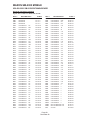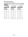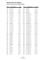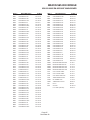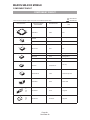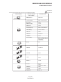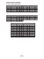
1
SM-2000
SERVICE MANUAL
MAXON AMERICA, Inc.
10828 N. W. Air World Drive
Kansas City, MO 64153
Phone 816-891-6320 Fax 816-891-8815
680-100-0045 Revision C ECO 98017
December 98
MAXON SM-2000 MOBILE
TABLE OF CONTENTS
TABLE OF CONTENTS
Table Of Contents. . . . . . . . . . . . . . . . . . . . . . . . . . . . . . . . . . . . . . . . . . . . . . . . . . . . i
Specifications. . . . . . . . . . . . . . . . . . . . . . . . . . . . . . . . . . . . . . . . . . . . . . . . . . . . . . . . 1
Transceiver Nominal Performance . . . . . . . . . . . . . . . . . . . . . . . . . . . . . . . . . . . . . . 1
General . . . . . . . . . . . . . . . . . . . . . . . . . . . . . . . . . . . . . . . . . . . . . . . . . . . . . . . . . . . 1
Transmitter . . . . . . . . . . . . . . . . . . . . . . . . . . . . . . . . . . . . . . . . . . . . . . . . . . . . . . . . 2
Tx Tone Modulation Characteristics . . . . . . . . . . . . . . . . . . . . . . . . . . . . . . . . . . . . . 4
Sub Audible Tones - DCS . . . . . . . . . . . . . . . . . . . . . . . . . . . . . . . . . . . . . . . . . . . . . 4
Receiver. . . . . . . . . . . . . . . . . . . . . . . . . . . . . . . . . . . . . . . . . . . . . . . . . . . . . . . . . . . 4
Rx Tone Demodulation Characteristics. . . . . . . . . . . . . . . . . . . . . . . . . . . . . . . . . . . 5
Accessories . . . . . . . . . . . . . . . . . . . . . . . . . . . . . . . . . . . . . . . . . . . . . . . . . . . . . . . . 5
Reliability Analysis . . . . . . . . . . . . . . . . . . . . . . . . . . . . . . . . . . . . . . . . . . . . . . . . . . 5
Programmer . . . . . . . . . . . . . . . . . . . . . . . . . . . . . . . . . . . . . . . . . . . . . . . . . . . . . . . . 5
Introduction . . . . . . . . . . . . . . . . . . . . . . . . . . . . . . . . . . . . . . . . . . . . . . . . . . . . . . . . 6
Unpacking Information . . . . . . . . . . . . . . . . . . . . . . . . . . . . . . . . . . . . . . . . . . . . . . . 7
General Description . . . . . . . . . . . . . . . . . . . . . . . . . . . . . . . . . . . . . . . . . . . . . . . . . . 8
Description Of Controls . . . . . . . . . . . . . . . . . . . . . . . . . . . . . . . . . . . . . . . . . . . . . . . 9
Theory Of Operation . . . . . . . . . . . . . . . . . . . . . . . . . . . . . . . . . . . . . . . . . . . . . . . . . 11
RF Section (SM-2150/VHF) . . . . . . . . . . . . . . . . . . . . . . . . . . . . . . . . . . . . . . . . . . . 13
RF Section (SM-2450/UHF) . . . . . . . . . . . . . . . . . . . . . . . . . . . . . . . . . . . . . . . . . . . 17
PLL . . . . . . . . . . . . . . . . . . . . . . . . . . . . . . . . . . . . . . . . . . . . . . . . . . . . . . . . . . . . . . 20
Test Setup . . . . . . . . . . . . . . . . . . . . . . . . . . . . . . . . . . . . . . . . . . . . . . . . . . . . . . . . . . 21
SM-2150/VHF Alignment Procedure . . . . . . . . . . . . . . . . . . . . . . . . . . . . . . . . . . . . 22
Alignment Points Diagram (SM-2150/VHF) . . . . . . . . . . . . . . . . . . . . . . . . . . . . . . 26
SM-2450/UHF Alignment Procedure . . . . . . . . . . . . . . . . . . . . . . . . . . . . . . . . . . . . 27
Alignment Points Diagram (SM-2450/UHF) . . . . . . . . . . . . . . . . . . . . . . . . . . . . . . 31
Component Replacement. . . . . . . . . . . . . . . . . . . . . . . . . . . . . . . . . . . . . . . . . . . . . . 32
Surface Mount Components . . . . . . . . . . . . . . . . . . . . . . . . . . . . . . . . . . . . . . . . . . . 32
Surface Mount Removal . . . . . . . . . . . . . . . . . . . . . . . . . . . . . . . . . . . . . . . . . . . . . . 32
Surface Mount Component Replacement . . . . . . . . . . . . . . . . . . . . . . . . . . . . . . . . . 33
Surface Mounted Integrated Circuit Replacement . . . . . . . . . . . . . . . . . . . . . . . . . . 33
Parts List Common to SM-2000 . . . . . . . . . . . . . . . . . . . . . . . . . . . . . . . . . . . . . . . . 34
Electrical Parts List Main Board Digital Section (SM-2000) . . . . . . . . . . . . . . . . . 35
Electrical Parts List Band Chart (SM-2150/VHF) . . . . . . . . . . . . . . . . . . . . . . . . . 37
Electrical Parts List Main Board (SM-2150/VHF) . . . . . . . . . . . . . . . . . . . . . . . . . 38
Electrical Parts List Band Chart (SM-2450/UHF) . . . . . . . . . . . . . . . . . . . . . . . . . 42
Electrical Parts List Main Board (SM-2450/UHF) . . . . . . . . . . . . . . . . . . . . . . . . . 44
Component Pinout (SM-2000). . . . . . . . . . . . . . . . . . . . . . . . . . . . . . . . . . . . . . . . . . 48
Voltage Charts (SM-2150/VHF) . . . . . . . . . . . . . . . . . . . . . . . . . . . . . . . . . . . . . . . . 51
Voltage Charts (SM-2450/UHF) . . . . . . . . . . . . . . . . . . . . . . . . . . . . . . . . . . . . . . . . 54
Trouble Shooting Chart (SM-2000) . . . . . . . . . . . . . . . . . . . . . . . . . . . . . . . . . . . . . 57
Page-iDecember 98
MAXON SM-2000 MOBILE
TABLE OF CONTENTS
Schematics and Block Diagrams . . . . . . . . . . . . . . . . . . . . . . . . . . . . . . . . . . . . . . . . 59
SM-2150/VHF Front End Schematic . . . . . . . . . . . . . . . . . . . . . . . . . . . . . . . . . . . . 59
SM-2450/UHF Front End Schematic . . . . . . . . . . . . . . . . . . . . . . . . . . . . . . . . . . . . 59
SM-2000 TCXO Schematic . . . . . . . . . . . . . . . . . . . . . . . . . . . . . . . . . . . . . . . . . . . 59
MA-4472 Microphone Schematic . . . . . . . . . . . . . . . . . . . . . . . . . . . . . . . . . . . . . . . 60
SM-2000 Control Head Schematic . . . . . . . . . . . . . . . . . . . . . . . . . . . . . . . . . . . . . . 60
SM-2000 Block Diagram . . . . . . . . . . . . . . . . . . . . . . . . . . . . . . . . . . . . . . . . . . . . . 61
SM-2000 Digital Schematic . . . . . . . . . . . . . . . . . . . . . . . . . . . . . . . . . . . . . . . . . . . 62
SM-2150/VHF RF Schematic . . . . . . . . . . . . . . . . . . . . . . . . . . . . . . . . . . . . . . . . . . 63
SM-2450/UHF RF Schematic . . . . . . . . . . . . . . . . . . . . . . . . . . . . . . . . . . . . . . . . . . 64
PCB Layouts . . . . . . . . . . . . . . . . . . . . . . . . . . . . . . . . . . . . . . . . . . . . . . . . . . . . . . . . 65
SM-2000 Control Head PCB Layout . . . . . . . . . . . . . . . . . . . . . . . . . . . . . . . . . . . . 65
SM-2150/VHF PCB Layout . . . . . . . . . . . . . . . . . . . . . . . . . . . . . . . . . . . . . . . . . . . 66
SM-2450/UHF PCB Layout . . . . . . . . . . . . . . . . . . . . . . . . . . . . . . . . . . . . . . . . . . . 67
SM-2000 Exploded View . . . . . . . . . . . . . . . . . . . . . . . . . . . . . . . . . . . . . . . . . . . . . . 68
SM-2000 Exploded View Parts List . . . . . . . . . . . . . . . . . . . . . . . . . . . . . . . . . . . . . 69
Page-iiDecember 98
MAXON SM-2000 MOBILE
SPECIFICATIONS
SPECIFICATIONS
TRANSCEIVER NOMINAL PERFORMANCE
Performance Specifications . . . . . . . . . . . . . . . . . . . . . . . . . . . . . . FTZ 17TR2049 July 88
TIA/EIA-603
IEC 68 Series
EC 529 IP54
MIL STD 810 C,D,E
RF Output Power . . . . . . . . . . . . . . . . . . . . . . . . . . . . . . . . . . . . . . 25 W
Modulation Type. . . . . . . . . . . . . . . . . . . . . . . . . . . . . . . . . . . . . . . G3E/F3E (PM/FM)
Audio power . . . . . . . . . . . . . . . . . . . . . . . . . . . . . . . . . . . . . . . . . . 4 W
Intermediate frequencies . . . . . . . . . . . . . . . . . . . . . . . . . . . . . . . . 45 MHz
455 kHz
Number of Channels . . . . . . . . . . . . . . . . . . . . . . . . . . . . . . . . . . . . 4
Frequency Source . . . . . . . . . . . . . . . . . . . . . . . . . . . . . . . . . . . . . . Synthesizer
GENERAL
Power Supply. . . . . . . . . . . . . . . . . . . . . . . . . . . . . . . . . . . . . . . . . . 13.2 VDC nominal CEPT
15.6 VDC maximum (extreme)
10.8 VDC minimum (extreme)
13.8 VDC nominal TIA/EIA-603
Temperature Range
Storage . . . . . . . . . . . . . . . . . . . . . . . . . . . . . . . . . . . . . . . . . . . . . . . 80°C Maximum; -40°C Minimum
(Extreme)
Operating (to spec) . . . . . . . . . . . . . . . . . . . . . . . . . . . . . . . . . . . . . 25°C Nominal;
60°C Maximum; -30°C Minimum
(Extreme)
Current Consumption
DC Current
Standby (Muted)
< 140 mA
Unmuted
25% Max. AF power
50% Max. AF power
100% Max. AF power
< 350 mA
< 450 mA
< 570 mA
Transmit
1 Watt RF power
3 Watts RF power
25 Watts RF power
1.6 A
2.4 A
6.7 A
Page-1December 98
MAXON SM-2000 MOBILE
SPECIFICATIONS
Switching range TX and RX (without re-tuning)
Operational Bandwidth
BAND
TX
MIN
RX
MIN
MAX
MAX
VHF Band 1
136
162
136
162
VHF Band 2
148
174
148
174
UHF Band 1
400
430
400
430
UHF Band 2
420
450
420
450
UHF Band 3
440
470
440
470
UHF Band 4
470
490
470
490
UHF Band 5
490
512
490
512
Channel spacing . . . . . . . . . . . . . . . . . . . . . . . . . . . . . . . . . . . . . . . 25 kHz / 20 kHz / 12.5 kHz
programmable
(25 kHz - 12.5kHz switchable
by CPU control)
Dimensions (in / mm). . . . . . . . . . . . . . . . . . . . . . . . . . . . . . . . . . . . 2(H) x 7(W) x 6.25(D)
45(H) x 157(W) x 140(D)
Weight
3lbs, 6oz/ 1.6kg (with mic)
TRANSMITTER
Tests methods are ETS 300 086 Jan
1991 unless stated
Performance Without Sub audible Modulation
Carrier Power @ nominal conditions
Max. Rated Output Power . . . . . . . . . . . . . . . . . . . . . . . . . . . . . . . 25 W +/-10% nominal
25 W +2/-3 dB @ extreme conditions
across switching range
Hi Switched by CPU . . . . . . . . . . . . . . . . . . . . . . . . . . . . . . . . . . . 1 – 25 W
Continuously adjustable
Low Switched by CPU . . . . . . . . . . . . . . . . . . . . . . . . . . . . . . . . . . 1 – 3 W
Continuously adjustable
Frequency stability (SM-2150) . . . . . . . . . . . . . . . . . . . . . . . . . . . +5.0 ppm (+ 0.00025%)
Frequency stability (SM-2450) . . . . . . . . . . . . . . . . . . . . . . . . . . . +2.5 ppm (+ 0.00025%)
Peak audio frequency deviation
(across switching range)
Page-2December 98
MAXON SM-2000 MOBILE
SPECFICATIONS
Channel Spacing
(kHz)
Without sub audible tone
modulation
With sub audible tone modulation
@ 10% peak deviation
MAX DEV
25
+ 5.0 kHz
+ 5.0 kHz
12.5
+ 2.5 kHz
+ 2.5 kHz
Audio characteristic . . . . . . . . . . . . . . . . . . . . . . . . . . . . . . . . . . . . (Method as FTZ 17 TR 2049 July 1988)
MOD Type G3 . . . . . . . . . . . . . . . . . . . . . . . . . . . . . . . . . . . . . . . . . Within +1/-3 dB of 6 dB/octave
pre-emphasis curve:
300 Hz – 2.55 kHz for 12.5 kHz
Channel Spacing
300 Hz – 3 kHz for 20 , 25 kHz
Channel Spacing
MOD Type F3 . . . . . . . . . . . . . . . . . . . . . . . . . . . . . . . . . . . . . . . . . Within +1/-3 dB of 6 dB/octave
pre-emphasis curve:
300 Hz – 2.55 kHz for 12.5 kHz
Channel Spacing
300 Hz – 3 kHz for 20 , 25 kHz
Channel Spacing
Adjacent channel power
25 kHz
12.5 kHz
< 70 dBc
< 60 dBc
TX spurious emissions (conducted)
9 kHz – 1 GHz
1 – 4.0 GHz
< -36 dBm
< -30 dBm
TX spurious emissions (radiated)
9 kHz – 1 GHz
1 – 4.0 GHz
< -36 dBm
< -30 dBm
TX spurious emissions (radiated)
9 kHz – 1 GHz
1 – 4.0 GHz
< -36 dBm
< -30 dBm
Modulation limiting characteristics . . . . . . . . . . . . . . . . . . . . . . . Method as FTZ17 TR2049 July 1988
=75% peak deviation
Transmitter audio distortion (without CTCSS) . . . . . . . . . . . . . . Method as FTZ17 TR 2049 July 1988
1 kHz modulation input
<5%
Transmitter audio distortion (with CTCSS) . . . . . . . . . . . . . . . . . Method as EIA RS 220A Mar 79
Audio frequency 1 kHz
Any CTCSS frequency combined
<8%
Hum & noise (residual modulation) . . . . . . . . . . . . . . . . . . . . . . . . > 40 dB
Page-3December 98
MAXON SM-2000 MOBILE
SPECIFICATIONS
TX TONE MODULATION CHARACTERISTICS
Sub audible tones - CTCSS
Tone range . . . . . . . . . . . . . . . . . . . . . . . . . . . . . . . . . . . . . . . . . . . . 67 – 250 Hz @ 0.3 % accuracy
Tone standard . . . . . . . . . . . . . . . . . . . . . . . . . . . . . . . . . . . . . . . . . RS-220A EIA Standard
Non-standard tones. . . . . . . . . . . . . . . . . . . . . . . . . . . . . . . . . . . . . 50 – 260 Hz @ 0.3 % accuracy
Nominal tone deviation. . . . . . . . . . . . . . . . . . . . . . . . . . . . . . . . . . 10 % peak system deviation
SUB AUDIBLE TONES - DCS
Tone standard . . . . . . . . . . . . . . . . . . . . . . . . . . . . . . . . . . . . . . . . . Normal and inverted
Nominal tone deviation. . . . . . . . . . . . . . . . . . . . . . . . . . . . . . . . . . 10 % peak system deviation
RECEIVER
Performance without sub audible modulation . . . . . . . . . . . . . . . Method ETS 300-086 JAN 1991
unless stated
Sensitivity 12 dB SINAD . . . . . . . . . . . . . . . . . . . . . . . . . . . . . . . . < - 118 dBm
Amplitude characteristic . . . . . . . . . . . . . . . . . . . . . . . . . . . . . . . . + 3 dB
Co-channel rejection
25 kHz
12.5 kHz
<- 6 dB
<- 10 dB
Adjacent channel selectivity
25 kHz
12.5 kHz
> 70 dB @ nominal conditions
> 60 dB @ nominal conditions
Spurious response rejection . . . . . . . . . . . . . . . . . . . . . . . . . . . . . > 70 dB (100 kHz - 4 GHz)
Intermodulation response rejection
+ (25 kHz & 50 kHz)
+ (50 kHz & 100 kHz)
> 65 dB (3 generator method)
Blocking
+ 1 MHz
+ 5 MHz
+ 10 MHz
> 85 dB
> 85 dB
> 85 dB
RX spurious emissions (conducted)
9 kHz – 1 GHz
1 GHz – 4.0 GHz
- 57 dBm
- 47 dBm
RX spurious emissions (radiated)
9 kHz – 1 GHz
1 – 4.0 GHz
-57 dBm
-47 dBm
Page-4December 98
MAXON SM-2000 MOBILE
SPECIFICATIONS
AF power . . . . . . . . . . . . . . . . . . . . . . . . . . . . . . . . . . . . . . . . . . . . . 5 W maximum @10% Distortion into a
4 ohm load. 4 Watts nominal.
AF frequency response . . . . . . . . . . . . . . . . . . . . . . . . . . . . . . . . . . Method as FTZ 17 TR 2049 July 1988
MOD Type G3 . . . . . . . . . . . . . . . . . . . . . . . . . . . . . . . . . . . . . . . . . Within +1/-3 dB of 6 dB/octave
de-emphasis curve
300 Hz – 2.55 kHz for 12.5 kHz
Channel Spacing
300 Hz – 3 kHz for 25 kHz
Channel Spacing
MOD Type F3 . . . . . . . . . . . . . . . . . . . . . . . . . . . . . . . . . . . . . . . . . Within +1/-3 dB of 6 dB/octave
de-emphasis curve
300 Hz – 2.55 kHz for 12.5 kHz
Channel Spacing
300 Hz – 3 kHz for 25 kHz
Channel Spacing
RX Hum & Noise . . . . . . . . . . . . . . . . . . . . . . . . . . . . . . . . . . . . . . > 40 dB
RX TONE DEMODULATION CHARACTERISTICS
Subaudible tones - CTCSS/DCS
CTCSS tone range . . . . . . . . . . . . . . . . . . . . . . . . . . . . . . . . . . . . . 67 Hz to 250 Hz
CTCSS tone standard . . . . . . . . . . . . . . . . . . . . . . . . . . . . . . . . . . . RS-220A EIA Standard
CTCSS non-standard tones . . . . . . . . . . . . . . . . . . . . . . . . . . . . . . 50 – 260 Hz
DCS tone standard . . . . . . . . . . . . . . . . . . . . . . . . . . . . . . . . . . . . . Standard and inverted
Decode Sensitivity . . . . . . . . . . . . . . . . . . . . . . . . . . . . . . . . . . . . . . Method: Decrease signal level @ 10%
peak deviation
All tone . . . . . . . . . . . . . . . . . . . . . . . . . . . . . . . . . . . . . . . . . . . . . . . <= 9 dB SINAD
Environmental . . . . . . . . . . . . . . . . . . . . . . . . . . . . . . . . . . . . . . . . IEC529 level IP54 MIL STD 810C
EMC . . . . . . . . . . . . . . . . . . . . . . . . . . . . . . . . . . . . . . . . . . . . . . . . . EMC Directive 89/336/EEC May 1989
ETS 300.279
ACCESSORIES
MA4472 Microphone
RELIABILITY ANALYSIS
Calculation method
MTBF . . . . . . . . . . . . . . . . . . . . . . . . . . . . . . . . . . . . . . . . . . . . . . . . 15,000 Hr. MIL-HDBK-217F. Ground
benign. Parts stress method.
MTTR . . . . . . . . . . . . . . . . . . . . . . . . . . . . . . . . . . . . . . . . . . . . . . . 30 Min. (Average time to rework any
SMD component & reassemble).
PROGRAMMER
. . . . . . . . . . . . . . . . . . . . . . . . . . . . . . . . . . . . . . . . . . . . . . . . . . . . . SMP4004C
Page-5December 98
MAXON SM-2000 MOBILE
INTRODUCTION
INTRODUCTION
Advanced state-of-the-art technology is used in the design and manufacturing of the SM-2000 Mobile. The
Phase Lock Loop (PLL) synthesizer provides more flexibility and capability in the SM-2000 Mobile. This
scanning mobile has 4 channel capability. It offers CTCSS, DCS, scanning, priority channel, and many other
functions. All these functions are controlled by the micro controller. The micro controller reads specific
channel information from an Electronically Erasable Programmable Read Only Memory (EEPROM).
Page-6December 98
MAXON SM-2000 MOBILE
UNPACKING INFORMATION
UNPACKING INFORMATION
Check the carton carefully for the following items:
1
Transceiver Unit
2
Microphone
3
DC Power Cord
4
Mobile Mounting Bracket
5
Assembly Hardware
6
Operating Guide
Page-7December 98
MAXON SM-2000 MOBILE
GENERAL DESCRIPTION
GENERAL DESCRIPTION
The Maxon SM-2000 is a rugged two way FM mobile radio which operates from 136-174 MHz (VHF) in
two bands & 400-512 MHz (UHF) in five bands. The SM-2000 is a synthesized radio utilizing
microcomputer technology to provide reliable high quality simplex two-way mobile communications. The
SM-2000 transmitter output power level is 25 watts over a wide bandwidth, with a receiver operational
bandwidth that covers the specified frequency band. The basic radio package includes the following
features:
•
Microprocessor Control
•
Synthesized RF Channel Selection (Frequency Control)
•
CTCSS Encode / Decode
•
DCS Encode / Decode
•
Priority Channel Scan
•
5 PPM Frequency Stability (SM-2150/VHF)
•
2.5 PPM Frequency Stability (SM-2450/UHF)
•
Field Programmable with PC
•
Internal 4 watt speaker, with Volume Control
•
Busy Channel Lockout
The small size of the SM-2000 radio makes it ideal for front mounting in conventional vehicles. The radio
is operated with a simple hand held microphone in combination with the operating controls described in the
following section.
Page-8December 98
MAXON SM-2000 MOBILE
DESCRIPTION OF CONTROLS
DESCRIPTION OF CONTROLS
Figure 1 SM-2000 Front Panel
DESCRIPTION OF CONTROLS
The controls, indicators and microphone/programming connector are located on the front panel. The
Monitor and Auxiliary buttons are located on the radio’s front panel. The following table details the
Mobile controls, indicators, and connections.
TABLE 2
Controls, Indicators, And Connections
ITEM
FUNCTION
1. Channel Select Switch
Rotary switch, used to select one of 4 channels (max.) and to engage
scanning function
2. ON/OFF Volume Control
Main power switch and volume control. Fully counter clockwise is off
position
3. Microphone Connect Jack
Used to connect the microphone to the mobile
4. Busy/Call/TX
Tri-colored LED indicator
5. Auxiliary (AUX) Switch
Used for control of after market accessories
6. Monitor Switch
When pushed, monitors the chosen channel
7-10. Channel Indicator LED’s
Indicates the channel when illuminated
Page-9December 98
MAXON SM-2000 MOBILE
DESCRIPTION OF CONTROLS
Rear Panel Connections
ITEM
FUNCTION
1. Antenna Connector ( S0-239 )
50 ohm connector
2. DC Power Connector
Used to connect the mobile to the power supply 13.2 VDC or 13.8 VDC
U.S.A.
3. External Speaker Connector
Multipurpose socket used to connect to a remote speaker or for test
connection
Figure 2 SM-2000 Rear Panel
Page-10December 98
MAXON SM-2000 MOBILE
THEORY OF OPERATION
THEORY OF OPERATION
Each of the Scanning Mobile radios, UHF & VHF, include a unique main P.C.B. consisting of RF, Digital
and Analog circuitry.
DIGITAL CIRCUITRY
IC 411 and IC412 are digitally-controlled analog switches which internally consist of three single pole,
double throw switches. By placing a high (5V) or low (0V) on the control lines which consists of A,B, and
C. “A” controls the X ports “B” controls the Y ports and “C” controls the Z ports. Example: A high on
control “A” would connect X to X1. A low on control “A” would connect X to X0.
CTCSS/DCS Decode Circuits
Discriminator audio from Pin 9 of IC 109 is fed to IC 406 and associated parts, which are the first 2 poles
of a 6th order 250Hz Chebeyshev low pass filter. The output from Pin 1 (IC406A) is fed into IC411 (Pin 2)
and output to Pin 15 (IC411). The signal is then fed to Pin 8 (IC407) which is a 6th order low pass
Butterworth switched capacitor filter. The output from the Butterworth filter (Pin 3 IC407) is then fed to
the remaining 4 poles of the 6th order Chebeyshev, which consist of IC 406C and one of the two
operational amplifiers internal to IC407 (MF6-100) along with associated components. Both the
Chebeyshev and the Butterworth combines for a 4dB ripple low pass filter when programmed for 250Hz.
The output of IC406C(Pin 8) is fed into the remaining operational amplifier internal to IC407 (MF6-100)
which forms the squaring circuit for the Decode signal. The signal is output from Pin 2 IC407 (MF6-100)
and fed into IC409 (micro) where it is matched with a preprogrammed frequency. If successful a Decode
occurs, which is shown by a green L.E.D. on the front panel of the UHF Scanning Mobile and audio is
heard. If valid Decode was not seen, the busy L.E.D. (Yellow) would be shown.
CTCSS/DCS Encoder Circuit
During TX encode the tone squelch digital signal is produced as a 3-bit parallel word at Pins 15 (A), 16
(B), and 18C of the micro controller (IC409). The 3-bit digital signal is converted to an analog signal by
resistors R427, 428, and 430. The analog signal is fed into IC411 Pin 1. The signal is output on Pin 15
(IC411) and fed into Pin 8 of IC407 (6th order Butterworth clock tuned low pass filter). The filtered
encode output from Pin 3 (IC407) is fed into Pin 13 (IC411) and output on Pin 14 (IC411).
The filtered encode signal is fed to IC405B and RV403 (sub-audible gain control), the output of IC405B is
then fed to the audio mixer circuit.
Channel Select Circuit
One of 4 channels may be selected using the channel switch on the front panel. The channel switch SP4T
(single pole 4 throw) with output to 4 channel LED’s and to diode’s to be converted to an inverted 4-Bit
binary code. The binary code inverted is equal to the channel number. The binary code is decoded by the
micro controller enabling the appropriate RX or TX frequency and associated data to be selected from the
EEPROM.
•
NOTE:It is possible any one of the 4 channel locations can be a scanning position. Refer to
Operators Manual for further instructions.
Page-11December 98
MAXON SM-2000 MOBILE
THEORY OF OPERATION
EEPROM
RX/TX channels, CTCSS/DCS as well as other data from the programmer are stored in the EEPROM. The
data stored is retained without power supplied. This is a non-volatile memory. The EEPROM may have
information re-programmed or erased. IC408 is an EEPROM with 2048 (256x 8) bit capacity and data is
written and read serially, with the Programming cable through the front panel microphone connector.
High Pass Filter
The high pass filter is an 8-pole .1dB chebeyshev active filter that comprises IC410 and associated
components. The de-emphasis is provided by resistor R451 and capacitor C452. Receive audio is passed
to IC410 by Pin 4 of IC411 where sub-audible tones below 250Hz are removed. Mic audio is also fed into
IC410 via IC411 (Pin 4) where sub-audible voice products below 250Hz are also removed.
Mute (Squelch) Circuit
The mute circuit which is controlled by the output of IC409 (micro) pin 77 (386) is connected to Q409 via
R438 which opens analog gate IC401D and mutes the audio path to the AF amplifier, in conjunction with
Q137 shorting the input to audio amp IC108.
TX Audio and Filter Circuits
Microphone audio from front panel (via IC412), is fed into IC401A, and into IC404B (Pin 6). The TX
audio is output on Pin 7 (IC404B) and into the high pass filter (IC410), where sub-audible voice products
are removed. The TX audio output from IC410 is fed into IC404A&B which with associated parts form a
pre-emphasis mic amplifier and limiter. The output from Pin 1 IC404A is fed to RV402 (TX Modulation
Level Adjust) and fed into IC404C&D with associated parts to form a 3kHz low pass filter. The output of
IC404D (Pin 14) is then fed into the Audio Mixer Circuit.
Audio Mixer and Inverter
IC405A is an audio mixer where audio and sub-audible tones are combined. RV403 is used as a level
control for the Sub-audible tones. This level is summed with amplified, pre-emphasized, and limited audio
and feed to IC405A, which is an inverting amplifier. The output is fed to the VCO and TCXO to provide
the necessary modulation signal.
Analog Ground Supply
IC406D supplies analog ground (2.0V) to all operational amplifier circuits except for IC405A and IC405D.
Page-12December 98
MAXON SM-2000 MOBILE
THEORY OF OPERATION
PLL
IC101 (MC1459IF) is a PLL frequency synthesizer with an on-board 1.1 GHZ divide by 64/65 dual
modulus prescaler. In addition to the prescaler and frequency counters, the synthesizer IC has a a phase
detector and a C register (Configuration register) that allows certain functions to be configured as desired.
The synthesizer is serially controlled by three wire input to the IC. Serial data is fed to pin 19 of the IC.
Serial data CLK (pin 18) and active low ENABLE (pin 17) are the input pins that allow data transfer into
the integrated circuit for control and frequency selection.
Data transfer is byte-oriented and may be shifted in 1, 2 or 3-byte patterns. One byte (8 bits) accesses the C
or configuration register, two bytes (16 bits) access the R register and 3 bytes (24 bits) access the A
register.
Internally the synthesizer has three counters used as frequency dividers. These counters are the R,A and N
counters. The R counter is actually controlled by 3 bits of the R register while the remaining 13 bits
determine the divide by R value. The frequency at pin 20 (12.8 MHz) is divided by R to determine the
frequency steps of the PLL synthesizer. In programming the radio, 5.0 kHz or 6.250 kHz step sizes can be
selected for any channel.
The 24- bit A register controls the N and A (prescaler) counts. Together these counts determine the total
synthesizer divide ratio affecting the fin (frequency input) signal from the VCO. A0-A7 are the A counter
values. A8-A19 are the N counter values. A21 and A20 must always be set high. A23 and A22 are both
set to 0 which controls the function of output A and causes it to be a port. This port, output A, is used to set
TX power high or low. A high output on port A sets transmit power low.
The 8-bit C register performs control functions as stated:
C7 sets polarity of the phase detector bits. Logic “0” is normal.
C6 determines the phase detector used. A logic “0” selects theta V and theta R outputs
C5 enables the lock detector when its logic is “1”.
C4 when a logic “1”, puts CMOS sections in standby mode.
C3 and C2 set phase detector current at the PD output. Not used in this application.
C1 is the value present at Output A.
C0 is the value present at Output B.
Transistors Q101 through Q104, along with related resistors and capacitors, connect the dual pin theta V
and Theta R outputs into a 2 mA current source that is powered by a 20V DC to DC converter. This allows
the tuning voltage to be approximately 3 to 17 VDC.
Page-13December 98
MAXON SM-2000 MOBILE
THEORY OF OPERATION
RF SECTION (SM-2150/VHF)
VHF Transmitter
The Transmitter is comprised of:
1.
Microphone Audio Circuit
2.
Transmitter Stage and Harmonic Filter
3.
Automatic Power Control
4.
Frequency Synthesizer Circuit
Microphone Audio Circuit
Microphone audio from the digital circuitry is amplified, pre-emphasized, limited, and mixed with
Sub-Audible and applied to the VCO at Pin 1, through RV101, to balance VCO and TCXO modulation.
Transmitter Stage and Harmonic Filter
When in the transmit mode of operation the diode D103 is forward biased enabling the RF signal to pass to
the pre-driver Q118 by Q116 and Q117. The amplified RF signal is amplified again by Q120. The
amplified RF signal passes through the stripline coupler and is fed to the harmonic low pass filter,
comprising of L128, L130, L131, and L132, capacitor 271, 273, 275, 277, and 283 and then to the antenna
connector (ANT). The stripline coupler provides a sample of the RF signal for the automatic power
control. During transmit D107 is forward biased which connects the power amp, D120, to the antenna.
D120 is forward biased inhibiting transmit signal power from being fed to the receiver circuitry.
Automatic Power Control
The automatic power control contains the stripline coupler, diode D107 and variable resistor VR104,
IC104A, and three transistors Q123, Q124, and Q125. IC104A forms a differential amplifier. The RF
signal present in the coupler is rectified by D107, to produce a DC voltage proportional to RF power which
is applied to Pin 3 of IC104A. TX 8.5V is also applied to the input of IC104A via the potential divider
R168, VR104, and R170 at pin 2. The different signal at output of IC104A is passed to Q124 and Q125 to
produce a constant power output to the antenna connector (ANT). VR104 is used to adjust the RF high
power level. VR105 is used to set the low power setting.
RX & TX Voltage Controlled Oscillator Circuit
The circuit contains two VCO’s. One for producing carrier frequencies during transmit and one for
producing the local oscillator frequency during receive. The circuit also has RX and TX power line filters.
RX & TX Power Line Filters
Transistors Q353 and Q354 are configured as TX5v and RX5v power supply ripple filters respectively.
Page-14December 98
MAXON SM-2000 MOBILE
THEORY OF OPERATION
RX VCO
The RX VCO comprises JFET Q351, coil L356 and varactor D353 and is configured as a Colpits oscillator.
D353 produces a change in frequency with a change in DC voltage and is controlled by the phase detector
signal present at the anode. The local oscillator signal at the drain of Q351 is applied to RF out of the
module when diode D103 is reverse biased and D104 is forward biased. L356 is used for PLL alignment.
TX VCO
The TX VCO comprises JFET Q352 coil L353 and varactor D352 and is configured as a colpits oscillator.
The AF signal at MOD port is applied to the cathode of D352. The control voltage from the loop filter is
applied to the drain of Q352 and is passed to the power amplifier and harmonic filter via the buffer Q113
and Q114. When diode D103 is forward biased and D104 is reversed biased L353 is used for PLL
alignment.
Loop Filter
Transistor Q101 to Q104 and associated components form a loop filter. The phase detector from Pin3 and
4 of IC101 are filtered to remove any reference frequency harmonics and applied to the voltage controlled
oscillator.
PLL Frequency Synthesizer
The PLL frequency synthesizer (IC101) contains an oscillator for the reference divider, a programmable
divider, a phase/frequency Comparator and an out of lock detector and a Prescaler.
Reference Oscillator
The reference oscillator of IC01 along with a 10.25 or 12.8MHz TCXO, varactor diode D701 and D702,
and the thermistors TH701, TH702, and TH703 produce a temperature compensated 10.25 or 12.8MHz
reference.
Programmable Dividers
The serial frequency data (DATA) is received by the data programmable divider at Pin 19 of IC101 from
Pin 1 of IC409 (Micro controller) out. The internal Prescaler divided input frequency at pin 11 of IC1 is
further divided by the programmable divider. The 10.25 or 12.8MHz TCXO frequency at pin 20 is the
reference divider to produce a reference frequency of 5 or 6.25kHz respectively. The internal
programmable divided frequency (Fv) and the reference frequency (Fr) are fed to the internal phase
detector.
Phase Detector
The phase detector produces negative pulses when Fv < Fr, positive pulses when Fv>Fr. When Fv = Fr and
phase is the same, the phase detector presents a high impedance at Pin 4. The signal at Pin 2 is applied to
the VCO via the loop filter.
Page-15December 98
MAXON SM-2000 MOBILE
THEORY OF OPERATION
Out of Lock Detector
The out-of-lock detector produces a high logic level when Fr and Fv are in the same phase and frequency,
low logic level pulses when the loop is out-of-lock at Pin 2 of IC101. The signals at Pin 2 of IC101 are
buffered by Q106 and then integrating by R114 and C122. The product of the integrating circuit is fed to
L/D port.
Prescaler
The internal Prescaler of IC101 divides the incoming signal frequency from the VCO via input pin 1 by 64
or 65. The divided VCO frequency is passed to the 6-stage A counter and 12-stage N counter.
Receiver
The receiver uses Dual Conversion Superheterodyning techniques, it is comprised of:
1.
RF amplifier
2.
First Mixer and First IF Amplifier
3.
Second Mixer, Second IF Amplifier and FM Detector
4.
Receiver Audio Circuit
5.
Mute (squelch) Circuit
RF Amplifier
The signal received via the antenna is routed through the 9th chebyshev low-pass filters containing
capacitors C273, C275, C277, C280, C283 and coils L128, L130, L131, L132, and is passed through the
front-end module (RF amplifier) via pin 1. The front-end module contains L800 to L806 and Q800. The
front-end module is configured to enable the RF signal at the operating frequency to pass the first mixer.
First Mixer and First IF Amplifier
The VCO local oscillator signal routed through buffer transistor Q113 and Q114 is filtered by C164, C165,
C281, C310, and L110, L123. IC102 produces a difference frequency IF of 45MHz from pin 6 of the
front-end module and the filtered VCO local oscillator signal at pin 1. The 45MHz difference frequency is
filtered by the 2-pole crystal filter CF101. The tuned circuit T101 and T102 and associated components
provide matching of the crystal filter to insure good band-pass response and selectivity. The IF signal is
amplified by Q130 and passed to the second mixer, second IF and FM detector IC109.
Second Mixer, Second IF and FM Detector
A signal conversion FM receiver integrated chip, IC109 contains the second mixer, second IF and FM
detector functions. The second local oscillator frequency is determined by the crystal X101 connected to
pin 1 of IC109. The IF signal is received at pin 16 of IC109 via R203 and coupling capacitor C182. The
second IF frequency of 455kHz is produced when the different frequency is applied to the mixer via Pin 6.
The output of the second mixer via Pin 3 is applied to a 455kHz band-pass filter, CF104 for 25kHz and
CF103 for 12.5kHz channel spacing. The output of CF104 is passed to a high gain IF amplifier (limiter) in
IC109 via Pin 5. The amplified signal is coupled to the adjustable quadrature detector T103. Any detected
signal is produced at Pin 9 of IC109 and applied to the Receiver Audio Circuit and the Mute (Squelch)
Circuit.
Page-16December 98
MAXON SM-2000 MOBILE
THEORY OF OPERATION
Receiver Audio Circuit
The receiver audio circuit is comprised of a low pass filter and an audio amplifier on the RF PCB.
Low Pass Filter
The low pass filter is configured from coil L227, capacitor C201 and resistor R206.AF signals from Pin 9
of IC109 are filtered by the low pass filter to remove any components of the 455kHz IF signal. The filtered
is passed to the high pass filter.
High Pass Filter
The de-emphasized audio signal from the high pass filter is fed to the audio amplifier (IC108).
Audio Amplifier
IC108 is the audio amplifier. The audio signal is passed to IC108. The gain of the amplifier is set by
resistor R153. The amplified audio signal at Pin 4 of IC108 is applied to the external speaker.
Mute (Squelch) Circuit
The squelch circuit switches off the audio power amplifier in the absence of audio signal. The squelch
circuit comprises a 50kHz pass band filter, squelch control (RV103) and a noise detect circuit.
The audio signal from Pin 9 of IC 109 is filtered by the 50kHz bandpass filter formed by L228, L229,
C191, C192, and C193. The noise in the IF pass band is accepted, frequencies in the voice frequency band
are rejected and noise present at the output of the filter is applied to the noise detect circuit via RV103.
RV103 is used to adjust the squelch sensitivity.
Noise Detect Circuit (SQ Board)
The noise detect circuit in conjunction with IC109 consists of transistor Q133 and Q132, thermistor TH101
and diode D125. Any noise signal present is applied to the base of Q133 of the SQ circuit from Pin 11 of
IC109. The signal is amplified by Q133 rectified by D11 and then buffered by Q132. The buffered signal
output is applied to the squelch trigger of IC109 Pin 12 via resistor R200. The squelch trigger out put (Pin
13 of IC109) is applied to the Micro controller on the Digital circuit. When noise is present, the voltage at
Pin 12 of IC109 exceeds 0.7V, the squelch trigger output is 0V (logic0) muting the receiver audio circuit.
When no noise is present the voltage at Pin 12 of IC109 is less than 0.7 and Pin 13 of IC109 is at 5V
(logic1), unmuting the audio circuit.
Page-17December 98
MAXON SM-2000 MOBILE
THEORY OF OPERATION
RF SECTION (SM-2450/UHF)
UHF Transmitter
The Transmitter is comprised of:
1. Microphone Audio Circuit
2. Transmitter Stage and Harmonic Filter
3. Automatic Power Control
4. Frequency Synthesizer Circuit
Microphone Audio Circuit
Microphone audio is pre-emphasized, limited and mixed with sub-audible tones to provide the modulating
signal for the transmitter. This combined modulation is applied to TCXO modulation pin 1 and also to the
VCO modulation input via RV101 to effect 2-point modulation. RV101 is a modulation balance control
that equalizes modulation sensitivities of the two oscillators.
Transmitter Stage and Harmonic Filter
Power Amplifier IC103 is an RF Module. In transmit, diode D103 is forward biased allowing the RF signal
to pass to the input of IC103 via Q116 and Q117. The amplified RF output passes through the stripline
coupler and is fed to the harmonic low pass filter, consisting of spring coils L118, L120, L121 and L125
and capacitors C271, 273, 275, 277 and 280, and then to the antenna connector. The stripline coupler
provides a sample of the RF signal for automatic power control. During TX, D108 connects the power amp
to the antenna. D120 and D121 are forward biased reducing transmit signal power at the receiver input.
Automatic Power Control
The automatic power control contains the stripline coupler, diode D107, and variable resistor RV104, op
amp IC104 , and two transistors: Q124 and Q125. IC104 acts as a differential amplifier. The RF signal is
rectified by D107 to produce a DC voltage, proportional to RF power, that is applied to IC404 pin 3.
Voltage divider R168, RV104 and R170 monitors TX 8.5V dc to develop a reference for IC104A pin 2.
The difference at the output of (IC104 pin 1) is passed to Q124 and drives the collector of Q125. This
feedback controls the gain of IC103 to maintain a constant RF power output. RV104 is used to adjust the
RF high power level. RV105 is used to set the low power setting.
Frequency Synthesizer Circuit
With data received from the EEPROM ( IC408 ) the frequency synthesizer circuit controls and produces
the RF carrier frequency for the transmitter during transmit and the local oscillator frequency for the
receiver.
The frequency synthesizer circuit is comprised of:
1. RX and TX voltage controlled oscillator module.
2. Loop Filter
3. PLL Frequency Synthesizer
Page-18December 98
MAXON SM-2000 MOBILE
THEORY OF OPERATION
Voltage Controlled Oscillator Circuit
The circuit produces carrier frequencies during transmit and local oscillator frequencies during receive.
Transistor Q107 is configured as a power supply ripple filter. The VCO utilizes transistor Q108, varactor
D101 , D102 and trimmer capacitor TC101 . These components are configured as a Colpitts oscillator.
D101 and D102 produce a change in frequency with a change in DC voltage and are controlled by the
phase detector. Q110 and Q111 are an amplifier and buffer for the output of the oscillator.
Receiver
The receive signal passes through the low pass filter, then onward to pin 1 of the Front End module. A
bandpass filter consisting of C801-C810 (see band chart for different band values) and L801-L803 is
coupled to the base of Q801 (2SC5084) which is the RF amplifier. Diode D801 serves as protection from
static and RF overload from nearby transmitters. The output of Q801 is coupled to a second bandpass filter
consisting of C812-C824 and L804-L807. The output of the Front End ( pin 6) is coupled to the double
balanced mixer IC102. The receiver Front End Module is factory pre-tuned and requires no field
adjustment. Repair is effected by replacement of the entire (properly banded) module. Frequency bands are
listed in the SPECIFICATIONS section of this manual.
The receiver Front End module pin-outs are:
1. RF Input
2. Input Ground
3. Ground
4. Receive +5VDC
5. Output Ground
6. RF Output
First Mixer
IC102 is a Double Balanced Mixer which provides a 45MHz intermediate frequency output. The filtered
frequency from the Front End is coupled to signal input pin3 of the mixer. The Local Oscillator from the
VCO module runs 45MHz lower than the receive frequency and is coupled to IC102 at pin6. The resultant
IF output exits at mixer pin2. The 45MHz IF output is matched to the input of the 4 pole monolithic crystal
filter by C179 , L119 , C172 and C173 . The crystal filter provides a bandwidth of + and - 7.5kHz from the
operating frequency for the signal providing a high degree of spurious and intermodulation protection.
Additionally, a 90MHz trap is placed at the filter input to provide additional attenuation of the second order
IMD (Intermodulation Distortion). The output of the filter is impedance matched by T101 , C175 , and
C176 to the base of the post filter IF amplifier Q130 ( MMBC1321 ).
Second Oscillator- Mixer- Limiter and FM Detector
The output of IF amplifier Q130 is coupled through C182 to the input of IC109 (Pin16), an MC3371
device. IC109 is a monolithic single-conversion FM receiver containing a mixer, the second local
oscillator, limiter and quadrature detector. The second local oscillator is crystal-controlled by X101 and
operates at 44.545 Mhz. Mixing the second L.O. with the 45.0 Mhz IF input signal provides a resultant 455
kHz signal at the second mixer output. The mixer output is then routed to CF103 (455HT) for channel
spacing of 12.5 kHz or to CF104 (455F) for channel spacing of 20 or 25kHz. These ceramic filters provide
adjacent channel selectivity for the desired bandwidths. Selection of CF103 or CF104 is software controlled
and programmable on a channel to channel basis.
Filter selection is performed by Q135, D126 and D126. The selected filter output drives a high gain
limiting amplifier that is internally coupled to the quadrature detector. Refering to the RF schematic, with
Channel Spacing low, Q135 is off and CF104 is the selected filter.
Page-19December 98
MAXON SM-2000 MOBILE
THEORY OF OPERATION
The quadrature detector is also configurable for narrow or wide channel spacing by software control of
Q219 and diode D127. These components with R219 parallel R211 to maintain audio output at the proper
level for the selected bandwidth.
Q134 inserts wideband squelch adjustment RV102 into the circuit whenever standard filter CF104 is
selected. This tends to broaden the filter response and provide the higher frequency noise components
needed to activate the squelch.
Squelch (Mute) Circuit
The squelch output is sent to microcontroller pin 7 after processing by the squelch circuits. The squelch
circuit consists of a double-tuned BPF (Band Pass Filter) and also a noise detector circuit. Details of these
circuits are discussed next.
Squelch Noise Band Pass Filter
The output signal from pin 9 of IC109 (MC3371) is filtered to remove the 455 kHz IF variations. The
remaining audio is then filtered by a double-tuned BPF consisting of resonator L228-C191, resonator
L229-C193 and coupling capacitor C192. The noise in the IF passband is accepted and voice frequencies
are rejected. Any noise present at the filter output is applied to the noise detector via RV103. RV103 is
used to set the squelch circuit sensitivity and is normally adjusted to produce a noise squelch opening
sensitivity of 10dB to 12dB SINAD.
Noise Detector
The noise detector operating in conjunction with IC109 consists of Q132, Q133, D125, D129, TH101 and
their associated biasing components. Noise from RV103 is amplified by an op amp within IC109. This
noise sprectrum is further amplified by Q133 and rectified by D125. This output is buffered by Q132 and
fed to the SQ IN (IC109 pin 12) through R200. When the mute is activated, (IC109 pin9) goes low to pull
the base of inverter Q131 low. Q131 collector goes high thereby signalling the microprocessor to mute the
receiver audio.
Low Pass Filter
The audio output of (IC109 pin9) is fed to a LPF (Low Pass Filter) consisting of R206 and C201. This RC
attenuates 455 kHz IF energy which normally appears at the output of the FM receiver chip. The audio is
then routed to the input of IC406A LPF for audio processing.
Speaker Audio Amplifier
After signal detection and audio filtering, the low level audio is returned to pin 1 of IC108, the Audio PA.
IC108, a TDA2003 device, provides sufficient power gain to drive the mobile speaker. Digital transistor
Q137 mutes the audio amplifier by grounding R157 when the transistor turns on. When Q137 base is high,
the transistor is on and the mobile is muted. Conversely when Q137 is off, the mute is released and audio is
heard.
Page-20December 98
MAXON SM-2000 MOBILE
TEST SETUP
TEST SETUP
TRANSMIT TESTS
VARIABLE POWER
SUPPLY WITH DC
VOLT/CURRENT
METER
POWER
METER
FREQUENCY
COUNTER
DEVIATION
METER
SM-2000
OSCILLOSCOPE
TEST BOX
DISTORTION
ANALYZER
DUMMY LOAD
ATTENUATOR
AUDIO
GENERATOR
RECEIVER TESTS
COMMUNICATION
MONITOR OR
FM SIGNAL
GENERATOR
SINAD
METER
OSCILLOSCOPE
SM-2000
PAD
VARIABLE
POWER
SUPPLY
AC
VTVM
Page-21December 98
DISTORTION
ANALYZER
MAXON SM-2000 MOBILE
SM-2150/VHF ALIGNMENT PROCEDURE
SM-2150/VHF ALIGNMENT PROCEDURE
It is important that the TCXO be on the correct frequency before performing a complete alignment of the
radio. An incorrect TCXO frequency can impair the performance and even cause mis-alignments.
Normally the transmitter is monitored with a frequency counter or service monitor while the transmitter is
keyed at it’s highest frequency. The TCXO is adjusted for the least frequency error. Typically the
frequency is 470MHz with a frequency error of +/-750Hz or less. TC701 adjusts the center frequency if
necessary.
PLL Alignment
•
NOTE: If the PLL is out- of- lock, an audible warning will be heard and the front panel red
LED will flash.
1.
Connect an RF power meter to the ANT socket.
2.
Using the channel switch, select channel with the lowest transmit frequency.
3.
Connect a DC voltmeter to test point 1 (TP1) accessed via the hole in the VCO cover.
4.
Set the PTT switch to transmit.
•
Note:The transmitter switching band width of this radio is 25MHz. A transmitter frequency
range of more than 26MHz may be programmed and used if the voltage specification in step 5 is
met.
5.
Adjusting L353, set the voltage measured at TP1, measure and check that the voltage is above 2.1
volts. If the voltage is below 2.1 volts the transmitter frequency programmed is too high for the
operating bandwidth of the radio.
6.
Set the PTT switch to receive.
7.
Using the channel switch select channel with the lowest receive frequency.
8.
Adjusting L356, set the voltage measured at TP1. Measure and check that the voltage is above 1.5
volts. If the voltage is below 1.5 volts the receive frequency programmed is too high for the
operating bandwidth of the radio.
•
Note:The receiver switching bandwidth of this radio is 26MHz. A receiver frequency range of
more than 26MHz may be programmed and used if the voltage specification in Step 8 is met.
There may be some degradation in actual receiver performance, if bandwidth of more than
26MHz is used.
Page-22December 98
MAXON SM-2000 MOBILE
SM-2150/VHF ALIGNMENT PROCEDURE
Receiver Alignment RF
•
NOTE: The Receiver front end is a pre-aligned module. There are no available field
adjustments.
1.
Connect an RF signal generator to the ANT socket and a SINAD meter to the external speaker
jack ( J1 ) located at the rear panel.
2.
Adjust RV103 to the fully open position to hear receiver noise.
3.
Adjust the VOLUME control to mid position.
4.
Using the channel switch, select the programmed middle receive frequency.
5.
Set the RF signal generator to the same receive channel frequency.
6.
Set the audio frequency to 1kHz at 3K deviation for wide band (25kHz).
6B. Set the audio frequency to 1kHz at 1.5K deviation for narrow band (12.5kHz).
7.
Adjust the RF output voltage level of the RF signal generator until the 1kHz signal is heard.
•
NOTE: The RF output voltage level and the SINAD reading.
8.
Adjust T102 for an improvement in SINAD.
9.
Adjust the RF output voltage level of the RF signal generator keeping the SINAD meter readings
between 6dB and 12dB.
10. Adjust T101 for an improvement in SINAD.
11. Adjust the RF output voltage level of the RF signal generator keeping the SINAD meter readings
between 6dB and 12dB .
12. Check for an RF voltage signal level of 0.31uV and a SINAD meter reading of 12dB or greater.
13. Select the highest receive frequency and check for a SINAD meter reading of 12dB or greater, at
0.42uV . (Sensitivity at the operational band edge).
14. Select the lowest receive frequency and check for a SINAD meter reading of 12dB or greater, at
0.42uV.
Discriminator Tuning
1.
Set the RF level to 1.0mV .
2.
Adjust T103 for a maximum audio output and on the oscilloscope monitor the sinewave distortion.
Adjust T101 and T102 for lowest distortion as observed on a distortion analyzer. This is normally
less than 3%.
Page-23December 98
MAXON SM-2000 MOBILE
SM-2150/VHF ALIGNMENT PROCEDURE
Squelch Adjustment
1.
Select a receiver channel that is programmed for narrow band (12.5 kHz) operation.
2.
Set the RF signal generator to the receiver frequency. Set the AF modulation signal to 1 kHz at
1.5k deviation.
3.
Adjust the RF output level of the RF signal generator until the 1 kHz signal is heard.
4.
Adjust the RF signal to the level desired for squelch sensitivity as you monitor SINAD. This is
usually 8dB to 12dB SINAD.
5.
On the main board adjust RV103 until the squelch is just unmuted (open)
6.
Switch off the RF generator (squelch should close).
7.
Switch on the RF generator. Squelch should open at the SINAD point where RV103 was adjusted.
This completes the narrow band adjustment.
8.
Select a receiver channel that is programmed for wide band operation (25 kHz).
9.
Set the RF signal generator to the receiver frequency. Set the AF modulation signal to 1 kHz at 3k
deviation.
10. Adjust the RF output level of the RF signal generator until the 1 kHz signal is heard.
11. Adjust the RF signal to the level desired for squelch sensitivity as you monitor SINAD. This is
usually 8dB to 12dB SINAD.
12. On the main board adjust RV102 until the squelch is just unmuted (open).
13. Switch off the RF generator (squelch should close).
14. Switch on the RF generator. Squelch should open at the SINAD point where RV102 was
adjusted.
15. Disconnect the test equipment.
Automatic Power Adjustment
•
Continuous transmit periods longer than 5 minutes are to be avoided.
1.
Connect the antenna output to a RF power meter or service monitor.
2.
Set the PTT switch to the ON position.
3.
Adjust the variable resistor RV104 to give the appropriate transmit power. Normally this is
25watts.
4.
Set the PTT switch to the OFF position.
5.
Select a channel programmed to low transmit power.
6.
Set PTT to ON and adjust RV105 for desired low power.
7.
Set PTT to OFF.
Page-24December 98
MAXON SM-2000 MOBILE
SM-2150/VHF ALIGNMENT PROCEDURE
CTCSS/DCS Deviation Adjustment
•
Note:The following adjustment should be preset with factory alignment. If an adjustment must
be made the following procedures must be followed:
1.
Program the radio with a 67.0Hz tone on one channel and 250.3Hz on another channel.
2.
Connect a power meter and modulation meter to the radio antenna jack.
3.
Adjust RV101 to the center of its adjustment.
•
Note:Release the PTT button when changing channels.
4.
•
Alternately select the channel with tone 250.3Hz and the channel with tone 67Hz. Key up and
note the level for each. If necessary, adjust RV101 until a balance occurs between tone 250.3Hz
and tone 67Hz.
Note:This adjustment also sets DCS balance even if a DCS tone is not programmed at this time.
5.
Select tone 250.3Hz or tone 67Hz and adjust RV403 for the tone level, typically between 500Hz
to 1kHz.
6.
Release the PTT button.
Modulation Deviation Adjustment
1.
Connect a power meter and a coupler to the radio.
2.
Connect an AF generator to the test box.
3.
Set the audio output to 30mV and the audio frequency to 1kHz .
4.
Using the channel switch, select the highest transmit channel that does not have CTCSS or DCS
programmed.
5.
Press and hold the PTT switch.
6.
Adjust RV402 for 90% of maximum, system deviation.
6a. Adjust RV402 for 2.25kHz for narrow band (12.5kHz).
6b. Adjust RV402 for 4.5kHz for wide band (25kHz).
7.
Using the channel switch, select the lowest transmit channel that does not have CTCSS or DCS
programmed.
8.
Press and hold the PTT switch.
9.
Measure and check that the deviation is not below 3.8k . If the deviation is below 3.8k, adjust
RV402 to 3.8k .
10. Return to highest transmit channel having a sub- audible tone and verify deviation does not exceed
5k.
11. At the channel that highest deviation is found, sweep the audio frequency between 300kHz and
3kHz . Adjust RV402 to ensure deviation is below peak system deviation at all frequencies.
12. Set the PTT switch to the OFF position.
Page-25December 98
MAXON SM-2000 MOBILE
ALIGNMENT POINTS DIAGRAM (SM-2150/VHF)
ALIGNMENT POINTS DIAGRAM (SM-2150/VHF)
RV103
RV104
RV105
TX HI POWER
TX LOW POWER
SQUELCH 12.5 KHz CH/SP
T103
DISCRIMINATOR
ANT
RV102
SQUELCH 25 KHz CH/SP
T101
L356
T102
L353
RV101
CTCSS
TC701
TP1
TCXO1
RV403
DCS
RV402
MODULATION
Page-26December 98
MAXON SM-2000 MOBILE
SM-2450/UHF ALIGNMENT PROCEDURE
SM-2450/UHF ALIGNMENT PROCEDURE
It is important that the TCXO be on the correct frequency before performing a complete alignment of the
radio. An incorrect TCXO frequency can impair the performance and even cause mis-alignments.
Normally the transmitter is monitored with a frequency counter or service monitor while the transmitter is
keyed at its highest frequency. The TCXO is adjusted for the least frequency error. Typically the frequency
is 470MHz with a frequency error of +/- 750Hz or less. TC701 adjusts the center frequency if necessary.
PLL Alignment
•
NOTE: If the PLL is out- of- lock, an audible warning will be heard and the front panel red
LED will flash.
1.
Connect an RF power meter to the ANT jack.
2.
Using the channel switch, select the channel with the highest transmit frequency.
3.
Connect a DC voltmeter to test point 1 ( TP1 ), accessed via the hole in the VCO cover.
4.
Set the PTT switch to transmit.
5.
Adjusting TC101 , set the voltage measured at TP1 to 12.0 (+/- 0.05) volts.
6.
Release the PTT switch.
7.
Using the channel switch, select the channel with the lowest receive frequency.
8.
At TP1 measure and check that the voltage is 1.4 volts or more. If the voltage is below 1.4 volts
the VCO may not lock because the lowest RX frequency is programmed too far below the TX
frequency.
Receiver Alignment RF
•
NOTE: The Receiver front end is a pre-aligned module. There are no available field
adjustments.
1.
Connect an RF signal generator to the ANT socket and a SINAD meter to the external speaker
jack ( J1 ) located at the rear panel.
2.
Adjust RV103 to the fully open position to hear receiver noise.
3.
Adjust the VOLUME control to mid position.
4.
Using the channel switch, select the programmed middle receive frequency.
5.
Set the RF signal generator to the same receive channel frequency.
6.
Set the audio frequency to 1kHz at 3K deviation for wide band (25kHz).
6B. Set the audio frequency to 1kHz at 1.5K deviation for narrow band (12.5kHz).
7.
Adjust the RF output voltage level of the RF signal generator until the 1kHz signal is heard.
•
NOTE: The RF output voltage level and the SINAD reading.
8.
Adjust T102 for an improvement in SINAD.
9.
Adjust the RF output voltage level of the RF signal generator keeping the SINAD meter readings
between 6dB and 12dB .
10. Adjust T101 for an improvement in SINAD.
Page-27December 98
MAXON SM-2000 MOBILE
SM-2450/UHF ALIGNMENT PROCEDURE
11. Adjust the RF output voltage level of the RF signal generator keeping the SINAD meter readings
between 6dB and 12dB .
12. Check for an RF voltage signal level of 0.31uV and a SINAD meter reading of 12dB or greater.
13. Select the highest receive frequency and check for a SINAD meter reading of 12dB or greater, at
0.42uV . (Sensitivity at the operational band edge).
14. Select the lowest receive frequency and check for a SINAD meter reading of 12dB or greater, at
0.42uV.
Discriminator Tuning
1.
Set the RF level to 1.0mV .
2.
Adjust T103 for a maximum audio output and on the oscilloscope monitor the sinewave distortion.
Adjust T101 and T102 for lowest distortion as observed on a distortion analyzer. This is normally
less than 3%.
Squelch Adjustment
1.
Select a receiver channel that is programmed for narrow band (12.5 kHz) operation.
2.
Set the RF signal generator to the receiver frequency. Set the AF modulation signal to 1 kHz at
1.5k deviation.
3.
Adjust the RF output level of the RF signal generator until the 1 kHz signal is heard.
4.
Adjust the RF signal to the level desired for squelch sensitivity as you monitor SINAD. This is
usually 8dB to 12dB SINAD.
5.
On the main board adjust RV103 until the squelch is just unmuted (open)
6.
Switch off the RF generator (squelch should close).
7.
Switch on the RF generator. Squelch should open at the SINAD point where RV103 was adjusted.
This completes the narrow band adjustment.
8.
Select a receiver channel that is programmed for wide band operation (25 kHz).
9.
Set the RF signal generator to the receiver frequency. Set the AF modulation signal to 1 kHz at 3k
deviation.
10. Adjust the RF output level of the RF signal generator until the 1 kHz signal is heard.
11. Adjust the RF signal to the level desired for squelch sensitivity as you monitor SINAD. This is
usually 8dB to 12dB SINAD.
12. On the main board adjust RV102 until the squelch is just unmuted (open).
13. Switch off the RF generator (squelch should close).
14. Switch on the RF generator. Squelch should open at the SINAD point where RV102 was
adjusted.
15. Disconnect the test equipment.
Page-28December 98
MAXON SM-2000 MOBILE
SM-2450/UHF ALIGNMENT PROCEDURE
Automatic Power Adjustment
•
NOTE: Continuous transmit periods longer than 5 minutes are to be avoided.
1.
Connect the antenna output to an RF power meter or service monitor.
2.
Set the PTT switch to the ON position.
3.
Adjust the Variable resistor RV104 to give the appropriate transmit power. Nominally this is
25watts .
4.
Set the PTT switch to the OFF position.
5.
Select a channel programmed to low transmit power.
6.
Set PTT to ON and adjust RV105 for desired low power .
7.
Set PTT to OFF.
CTCSS/DCS Deviation Adjustment
•
NOTE: The following adjustment should be preset with factory alignment. If an adjustment
must be made the following procedures must be followed:
1.
Program the radio with a 67.0Hz tone on one channel and 250.3Hz on another channel.
2.
Connect a power meter and modulation meter to the radio antenna jack.
3.
Adjust RV101 to the center of its adjustment.
•
Note: Release the PTT button when changing channels.
4.
•
Alternately select the channel with tone 250.3Hz and the channel with tone 67Hz . Key up and
note the level for each. If necessary, adjust RV101 until a balance occurs between tone 250.3Hz
and tone 67Hz .
Note:This adjustment also sets DCS balance even if a DCS tone is not programmed at this time.
5.
Select tone 250.3Hz or tone 67Hz and adjust RV403 for the tone level, typically between 500Hz
to 1kHz.
6.
Release the PTT button.
Page-29December 98
MAXON SM-2000 MOBILE
SM-2450/UHF ALIGNMENT PROCEDURE
Modulation Deviation Adjustment
1.
Connect a power meter and a coupler to the radio.
2.
Connect an AF generator to the test box.
3.
Set the audio output to 30mV and the audio frequency to 1kHz .
4.
Using the channel switch, select the highest transmit channel that does not have CTCSS or DCS
programmed.
5.
Press and hold the PTT switch.
6.
Adjust RV402 for 90% of maximum, system deviation.
6a. Adjust RV402 for 2.25kHz for narrow band (12.5kHz).
6b. Adjust RV402 for 4.5kHz for wide band (25kHz).
7.
Using the channel switch, select the lowest transmit channel that does not have CTCSS or DCS
programmed.
8.
Press and hold the PTT switch.
9.
Measure and check that the deviation is not below 3.8k . If the deviation is below 3.8k, adjust
RV402 to 3.8k .
10. Return to highest transmit channel having a sub- audible tone and verify deviation does not exceed
5k.
11. At the channel that highest deviation is found, sweep the audio frequency between 300kHz and
3kHz . Adjust RV402 to ensure deviation is below peak system deviation at all frequencies.
12. Set the PTT switch to the OFF position.
Page-30December 98
MAXON SM-2000 MOBILE
ALIGNMENT POINTS DIAGRAM (SM-2450/UHF)
ALIGNMENT POINTS DIAGRAM (SM-2450/UHF)
TX HI PWR
RV103
RV104
T103
SQUELCH 12.5 kHz CH/SP
DISCRIMINATOR
RV105
TX LO PWR
SQUELCH 25 kHz CH/SP
RV102
T101
T102
TC101
TP1
CNTR FREQ
TC701
RV101
CTCSS
DCS
RV403
RV402
TX DEVIATION
J1
Page-31December 98
MAXON SM-2000 MOBILE
COMPONENT REPLACEMENT
COMPONENT REPLACEMENT
SURFACE MOUNT COMPONENTS
Surface mount components should always be replaced using a temperature controlled soldering system.
The soldering tools may be either a temperature controlled soldering iron or a temperature controlled
hot-air soldering station. A hot-air system is recommended for the removal of components on these boards.
With either soldering system, a temperature of 700° F (371° C) should be maintained.
The following procedures outline the removal and replacement of surface mount components. If a hot-air
soldering system is employed, see the manufacturer’s operating instructions for detailed information on the
use of your system.
•
•
CAUTION: Avoid applying heat to the body of any surface mount component using standard
soldering methods. Heat should be applied only to the metalized terminals of the components.
Hot-air systems do not damage the components since the heat is quickly and evenly distributed to
the external surface of the component.
CAUTION: The CMOS Integrated Circuit devices used in this equipment can be destroyed by
static discharges. Before handling one of these devices, service technicians should discharge
themselves by touching the case of a bench test instrument that has a 3-prong power cord
connected to an outlet with a known good earth ground. When soldering or desoldering a CMOS
device, the soldering equipment should have a known good earth ground.
SURFACE MOUNT REMOVAL
1. Grip the component with tweezers or small needle nose pliers.
2. Alternately heat the metalized terminal ends of the surface mount component with the soldering iron. If
a hot-air system is used, direct the heat to the terminals of the component. Use extreme care with the
soldering equipment to prevent damage to the printed circuit board (PCB) and the surrounding
components.
3. When the solder on all terminals is liquefied, gently remove the component. Excessive force may
cause the PCB pads to separate from the board if all solder is not completely liquefied.
4. It may be necessary to remove excess solder using a vacuum de-soldering tool or Solder wick . Again,
use great care when de-soldering or soldering on the printed circuit boards. It may also be necessary to
remove the epoxy adhesive that was under the surface mount component and any flux on the printed
circuit board.
Page-32December 98
MAXON SM-2000 MOBILE
COMPONENT REPLACEMENT
SURFACE MOUNT COMPONENT REPLACEMENT
1. “Tin” one terminal end of the new component and the corresponding pad of the PCB. Use as little
solder as possible.
2. Place the component on the PCB pads, observing proper polarity for capacitors, diodes, transistors, etc.
3. Simultaneously touch the “tinned” terminal end and the “tinned” pad with the soldering iron. Slightly
press the component down on the board as the solder liquefies. Solder all terminals, allowing the
component time to cool between each application of heat. Do not apply heat for an excessive length of
time and do not use excessive solder.
With a hot-air system, apply hot air until all “tinned” areas are melted and the component is seated in place.
It may be necessary to slightly press the component down on the board. Touch-up the soldered connections
with a standard soldering iron if needed. Do not use excessive solder.
•
CAUTION: Some chemicals may damage the internal and external plastic parts of the radio.
4. Allow the component and the board to cool and then remove all flux from the area using alcohol or
another approved flux remover.
SURFACE MOUNTED INTEGRATED CIRCUIT REPLACEMENT
Soldering and de-soldering techniques of the surface mounted IC’s are similar to the above outlined
procedures for the surface mounted chip components. Use extreme care and observe static precautions
when removing or replacing the defective (or suspect) IC’s. This will prevent any damage to the printed
circuit board or the surrounding circuitry.
The hot-air soldering system is the best method of replacing surface mount IC’s. The IC’s can easily be
removed and installed using the hot-air system. See the manufacturer’s instructions for complete details on
tip selection and other operating instructions unique to your system.
If a hot-air system is not available, the service technician may wish to clip the pins near the body of the
defective IC and remove it. The pins can then be removed from the PCB with a standard soldering iron and
tweezers, and the new IC installed following the Surface Mount Component Replacement procedures. it
may not be necessary to “tin” all (or any) of the IC pins before the installation process.
Page-33December 98
MAXON SM-2000 MOBILE
PARTS LIST COMMON TO SM-2000
PARTS LIST COMMON TO SM-2000
REF #
DESCRIPTION
PART #
650-100-0002 TCXO PCB ASSY. (SEE NOTE 1)
REF #
DESCRIPTION
PART #
650-050-0003 CONTROL HEAD PCB ASSY.
650-090-0003 MA-4472 MIC ASSY. (SEE NOTE 1)
CON1
HEADER PIN
Z422-492-1
CON801
JACK MODULAR
420-709-9
C801
CHIP CERAMIC
47PF
134-722-1Z
C802
CHIP CERAMIC
47PF
134-722-1Z
C803
CHIP CERAMIC
47PF
134-722-1Z
C804
CHIP CERAMIC
47PF
134-722-1Z
C805
CHIP CERAMIC
47PF
134-722-1Z
C806
CHIP CERAMIC
47PF
134-722-1Z
C807
CHIP CERAMIC
47PF
134-722-1Z
C808
CHIP CERAMIC
47PF
134-722-1Z
C809
CHIP CERAMIC
47PF
134-722-1Z
C815
DISK CERAMIC (FOR SP1) 470PF
134-710-8
C821
CHIP CERAMIC
130-A17-6Z
C823
ELECT CAPACITOR
D801
DIODE SI CHIP
KDS193
243-052-6
D802
DIODE SI CHIP
KDS193
243-052-6
D803
DIODE SI CHIP
KDS193
243-052-6
D804
DIODE SI CHIP
KDS184S
243-051-5
D807
DIODE ZENER
241-099-9
D808
DIODE ZENER
241-099-9
D810
DIODE ZENER
241-099-9
D811
DIODE ZENER
LED1
LED LAMP
GRN
3 V 75MW
251-160-3
LED2
LED LAMP
GRN
3 V 75MW
251-160-3
LED3
LED LAMP
GRN
3 V 75MW
251-160-3
LED4
LED LAMP
GRN
3 V 75MW
LED5
LED LAMP
RED/GRN 3 V
Q821
TRANSISTOR
Q822
TRANSISTOR
R801
CHIP RESISTOR
470 OHM
060-471-0Z
R821
CHIP RESISTOR
22 OHM
060-220-0Z
R822
CHIP RESISTOR
SP1
SPEAKER
SW3
SW PUSH
432-063-7
SW4
TACT SWITCH
436-038-8
SW405
SW ROTARY
VR801
VR
0.001UF
10UF
241-099-9
1. Components are not available, assembly is non-repairable.
Page-34December 98
251-160-3
251-168-1
202-106-5
202-106-5
4.7K
060-472-1Z
4 OHM
420-108-4A
430-070-5
20KA
HOLDER(LED)
NOTES:
101-025-9
450-523-5
892-390
HOLDER(LED)
892-540
P.C.B. CONTROL HEAD
416-988-C
MAXON SM-2000 MOBILE
650-000-0001 SM-2150/VHF MAIN BOARD
650-000-0001 SM-2150/VHF MAIN BOARD
DIGITAL SECTION
Digital Parts Common on Both VHF & UHF
REF #
DESCRIPTION
PART #
REF #
DESCRIPTION
CHIP CERAMIC
0.001UF
130-A17-6Z
C450
CHIP CERAMIC
C402
CHIP CERAMIC
0.22UF
130-270-7Y
C452
CHIP TANTALUM
C403
CHIP CERAMIC
0.01UF
130-172-2Z
C453
CHIP CERAMIC
C404
ELECT CAPACITOR
101-025-9
C454
CHIP TANTALUM
C405
CHIP CERAMIC
220PF
132-220-2Z
C455
CHIP CERAMIC
0.033UF
130-314-5Z
C406
CHIP CERAMIC
220PF
132-220-2Z
C456
CHIP CERAMIC
0.001UF
130-A17-6Z
C407
ELECT CAPACITOR
101-025-9
C457
CHIP CERAMIC
0.047UF
130-424-0Z
C408
CHIP CERAMIC
0.033UF
130-314-5Z
C458
CHIP CERAMIC
0.01UF
130-172-2Z
C409
CHIP CERAMIC
0.0068UF
130-602-4Y
C460
CHIP CERAMIC
0.1UF
130-170-0Y
C410
CHIP CERAMIC
47PF
134-722-1Z
C464
CHIP CERAMIC
0.033UF
130-314-5Z
C411
CHIP CERAMIC
0.1UF
130-170-0Y
C550
CHIP CERAMIC
18PF
131-816-6Z
C412
CHIP CERAMIC
0.015UF
130-A44-0Y
C551
CHIP CERAMIC
18PF
131-816-6Z
C413
CHIP CERAMIC
47PF
134-722-1Z
C552
CHIP CERAMIC
0.01UF
130-172-2Z
C414
CHIP CERAMIC
0.047UF
130-424-0Z
C553
CHIP CERAMIC
0.01UF
130-172-2Z
C415
CHIP CERAMIC
220PF
132-220-2Z
C554
CHIP CERAMIC
0.01UF
130-172-2Z
C416
CHIP CERAMIC
0.01UF
130-172-2Z
C555
CHIP CERAMIC
0.01UF
C417
CHIP CERAMIC
0.0047UF
134-719-7Z
C558
ELECT CAPACITOR
C418
CHIP CERAMIC
0.022UF
130-263-1Z
C559
CHIP CERAMIC
C419
CHIP CERAMIC
0.0018UF
130-A22-0Z
CON403
PROG CONNECTOR
421-677-7
C420
CHIP CERAMIC
470PF
134-761-4Z
CON404
OPTION BOARD CONNECTOR
422-746-1
C421
CHIP CERAMIC
470PF
134-761-4Z
D401
DIODE SI CHIP
243-051-5
C422
CHIP CERAMIC
220PF
132-220-2Z
D402
DIODE SWITCHING
243-063-6
C423
CHIP CERAMIC
220PF
132-220-2Z
D551
DIODE SI CHIP
243-049-4
C424
CHIP CERAMIC
220PF
132-220-2Z
D552
DIODE SI CHIP
243-049-4
C425
CHIP CERAMIC
0.1UF
130-A60-4Y
IC401
I.C.
223-224-9
C426
CHIP CERAMIC
0.022UF
130-263-1Z
IC402
I.C. REGULATOR
220-378-0
C428
CHIP CERAMIC
0.01UF
130-172-2Z
IC404
I.C. OP AMP
222-018-5
C429
CHIP CERAMIC
47PF
134-722-1Z
IC405
I.C. OP AMP
231-064-4
C430
CHIP CERAMIC
0.1UF
130-A60-4Y
IC406
I.C. OP AMP
222-018-5
C431
CHIP CERAMIC
0.0033UF
130-315-6Z
IC407
I.C.
231-073-3
C432
CHIP CERAMIC
0.68UF
130-624-4
IC408
I.C. EEPROM
229-463-8A
C433
CHIP CERAMIC
0.082UF
130-808-4Y
IC409
I.C.
220-130-2
C434
CHIP CERAMIC
120PF
131-107-9Z
IC410
I.C. OP AMP
222-018-5
C435
ELECT CAPACITOR
101-006-2
IC411
I.C.
223-261-2
C436
CHIP CERAMIC
0.1UF
130-170-0Y
IC412
I.C.
223-261-2
C437
CHIP CERAMIC
0.1UF
130-A60-4Y
Q131
TRANSISTOR
202-095-8Z
C438
ELECT CAPACITOR
101-025-9
Q401
TRANSISTOR
202-095-8Z
C440
CHIP CERAMIC
15PF
131-511-0Z
Q402
TRANSISTOR
202-095-8Z
C441
CHIP CERAMIC
15PF
131-511-0Z
Q403
TRANSISTOR
202-095-8Z
C442
CHIP CERAMIC
0.047UF
130-424-0Z
Q404
TRANSISTOR
202-095-8Z
C443
CHIP CERAMIC
0.047UF
130-424-0Z
Q405
TRANSISTOR
202-095-8Z
C445
CHIP CERAMIC
0.033UF
130-314-5Z
Q406
TRANSISTOR
202-095-8Z
C446
CHIP CERAMIC
0.033UF
130-314-5Z
Q407
BRT
202-091-4
C447
CHIP CERAMIC
0.033UF
130-314-5Z
Q409
TRANSISTOR
202-095-8Z
C448
CHIP CERAMIC
0.033UF
130-314-5Z
Q504
TRANSISTOR
202-106-5
10UF
10UF
1UF
10UF
Page-35December 98
0.047UF
PART #
C401
130-424-0Z
1UF
141-036-1Z
0.01UF
130-172-2Z
1UF
141-036-1Z
10UF
0.01UF
130-172-2Z
101-025-9
130-172-2Z
MAXON SM-2000 MOBILE
650-000-0001 SM-2150/VHF MAIN BOARD
DIGITAL SECTION (continued)
Digital Parts Common on Both VHF & UHF
REF #
DESCRIPTION
PART #
REF #
DESCRIPTION
PART #
Q550
TRANSISTOR
202-113-1
R447
CHIP RESISTOR
120K
060-124-6Z
Q551
TRANSISTOR
202-113-1
R448
CHIP RESISTOR
220K
060-224-4Z
Q552
TRANSISTOR
202-113-1
R449
CHIP RESISTOR
820
060-821-3Z
Q553
TRANSISTOR
202-113-1
R450
CHIP RESISTOR
22K
060-223-3Z
R186
CHIP RESISTOR
47K
060-473-2Z
R451
CHIP RESISTOR
2.2K
060-222-2Z
R401
CHIP RESISTOR
680K
060-684-6Z
R452
CHIP RESISTOR
1M
060-105-0Z
R402
CHIP RESISTOR
47K
060-473-2Z
R453
CHIP RESISTOR
3K
060-302-1Z
R403
CHIP RESISTOR
10K
060-103-8Z
R454
CHIP RESISTOR
4.7K
060-472-1Z
R404
CHIP RESISTOR
56K
060-563-0Z
R455
CHIP RESISTOR
3.6K
060-362-5Z
R405
CHIP RESISTOR
7.5K
060-752-4Z
R456
CHIP RESISTOR
27K
060-273-8Z
R406
CHIP RESISTOR
18K
060-183-0Z
R457
CHIP RESISTOR
47K
060-473-2Z
R407
CHIP RESISTOR
330K
060-334-0Z
R458
CHIP RESISTOR
47K
060-473-2Z
R408
CHIP RESISTOR
3.3K
060-332-8Z
R459
CHIP RESISTOR
2.4K
060-242-0
R410
CHIP RESISTOR
220K
060-224-4Z
R460
CHIP RESISTOR
470
060-471-0Z
R411
CHIP RESISTOR
100K
060-104-9Z
R461
CHIP RESISTOR
470
060-471-0Z
R412
CHIP RESISTOR
39K
060-393-3Z
R462
CHIP RESISTOR
47K
060-473-2Z
R414
CHIP RESISTOR
8.2K
060-822-4Z
R463
CHIP RESISTOR
47K
060-473-2Z
R415
CHIP RESISTOR
8.2K
060-822-4Z
R464
CHIP RESISTOR
47K
060-473-2Z
R416
CHIP RESISTOR
220K
060-224-4Z
R465
CHIP RESISTOR
47K
060-473-2Z
R417
CHIP RESISTOR
8.2K
060-822-4Z
R466
CHIP RESISTOR
100K
060-104-9Z
R418
CHIP RESISTOR
8.2K
060-822-4Z
R469
CHIP RESISTOR
10K
060-103-8Z
R419
CHIP RESISTOR
47K
060-473-2Z
R470
CHIP RESISTOR
30K
060-303-2Z
R420
CHIP RESISTOR
10K
060-103-8Z
R471
CHIP RESISTOR
36K
060-363-6Z
R421
CHIP RESISTOR
10K
060-103-8Z
R472
CHIP RESISTOR
30K
060-303-2Z
R422
CHIP RESISTOR
43K
060-433-6Z
R473
CHIP RESISTOR
4.7K
060-472-1Z
R423
CHIP RESISTOR
47K
060-473-2Z
R474
CHIP RESISTOR
360K
060-364-7
R424
CHIP RESISTOR
560
060-561-8Z
R490
CHIP RESISTOR
47K
060-473-2Z
R425
CHIP RESISTOR
10K
060-103-8Z
R550
CHIP RESISTOR
7.5K
060-752-4Z
R426
CHIP RESISTOR
47K
060-473-2Z
R551
CHIP RESISTOR
27K
060-273-8Z
R427
CHIP RESISTOR
39K
060-393-3Z
R552
CHIP RESISTOR
27K
060-273-8Z
R428
CHIP RESISTOR
20K
060-203-5Z
R553
CHIP RESISTOR
7.5K
060-752-4Z
R429
CHIP RESISTOR
100K
060-104-9Z
R554
CHIP RESISTOR
2.2K
060-222-2Z
R430
CHIP RESISTOR
10K
060-103-8Z
R555
CHIP RESISTOR
4.7K
060-472-1Z
R431
CHIP RESISTOR
22K
060-223-3Z
R556
CHIP RESISTOR
2.2K
060-222-2Z
R433
CHIP RESISTOR
47K
060-473-2Z
R559
CHIP RESISTOR
470
060-471-0Z
R434
CHIP RESISTOR
47K
060-473-2Z
RLK3
CHIP RESISTOR
0
060-000-8Z
R435
CHIP RESISTOR
47K
060-473-2Z
RLK4
CHIP RESISTOR
0
060-000-8Z
R436
CHIP RESISTOR
22K
060-223-3Z
RLK5
CHIP RESISTOR
0
060-000-8Z
R437
CHIP RESISTOR
4.7K
060-472-1Z
RLK7
CHIP RESISTOR
0
060-000-8Z
R438
CHIP RESISTOR
4.7K
060-472-1Z
RLK8
CHIP RESISTOR
0
060-000-8Z
R439
CHIP RESISTOR
47K
060-473-2Z
RLK10
CHIP RESISTOR
0
060-000-8Z
R440
CHIP RESISTOR
1M
060-105-0Z
RLK11
CHIP RESISTOR
0
060-000-8Z
R441
CHIP RESISTOR
43K
060-433-6Z
RLK12
CHIP RESISTOR
0
060-000-8Z
R442
CHIP RESISTOR
33K
060-333-9Z
RLK13
CHIP RESISTOR
0
060-000-8Z
R443
CHIP RESISTOR
20K
060-203-5Z
RLK14
CHIP RESISTOR
0
R444
CHIP RESISTOR
220K
060-224-4Z
RV402
RES.CHIP SEMIFIXED 22K
067-223-8Y
R445
CHIP RESISTOR
120K
060-124-6Z
RV403
RES.CHIP SEMIFIXED 47K
067-473-7Y
R446
CHIP RESISTOR
82K
060-823-5Z
X401
CRYSTAL
262-228-0Z
Page-36December 98
060-000-8Z
MAXON SM-2000 MOBILE
650-000-0001 SM-2150/VHF MAIN BOARD
BAND CHART
SM-2150L VHF BAND 1 (136-162 MHz)
REF #
DESCRIPTION
FRONT-END PCB ASSEMBLY
PART #
SM-2150H VHF BAND 2 (148-174 MHz)
REF #
650-110-0011
MAIN BOARD PARTS
DESCRIPTION
FRONT-END PCB ASSEMBLY
PART #
650-110-0002
MAIN BOARD PARTS
C155
CHIP CERAMIC 4PF
134-007-7Y
C155
CHIP CERAMIC 11PF
131-103-5Y
C160
CHIP CERAMIC 24PF
132-407-5Y
C160
CHIP CERAMIC 24PF
132-407-5Y
C164
CHIP CERAMIC 18pF
131-816-6Y
C164
CHIP CERAMIC 24PF
132-407-5Y
C165
CHIP CERAMIC 9pF
139-003-8Y
C165
CHIP CERAMIC 16PF
131-603-0
C245
CHIP CERAMIC 5PF
135-010-4Y
C245
CHIP CERAMIC 8PF
138-004-4Y
C248
CHIP CERAMIC 27PF
132-714-2Y
C248
CHIP CERAMIC 27PF
132-714-2Y
C249
CHIP CERAMIC 20PF
132-012-1Y
C249
CHIP CERAMIC 18PF
131-816-6Y
C253
CHIP CERAMIC 75PF
137-504-4Y
C253
CHIP CERAMIC 75PF
137-504-4Y
C254
CHIP CERAMIC 33PF
133-336-9Y
C254
CHIP CERAMIC 43PF
134-302-2Y
C269
CHIP CERAMIC 9PF
139-003-8Y
C269
CHIP CERAMIC 2.7PF
132-725-2Y
C270
CHIP CERAMIC 4PF
134-013-2Y
C270
CHIP CERAMIC 6PF
136-015-4Y
C273
CHIP CERAMIC 43PF
134-302-2Y
C273
CHIP CERAMIC 51PF
135-106-8Y
C275
CHIP CERAMIC 47PF
134-773-5Y
C275
CHIP CERAMIC 56PF
135-639-1Y
C277
CHIP CERAMIC 43PF
134-302-2Y
C277
CHIP CERAMIC 47PF
134-773-5Y
C278
CHIP CERAMIC 82PF
138-216-9Z
C278
CHIP CERAMIC 75PF
137-512-1Z
C280
CHIP CERAMIC 24PF
132-408-6Y
C280
CHIP CERAMIC 20PF
132-021-9
C281
CHIP CERAMIC 36pF
133-611-7Y
C281
CHIP CERAMIC 56PF
135-613-9Y
C283
CHIP CERAMIC 18PF
131-829-8Y
C283
CHIP CERAMIC 27PF
132-723-0Y
C354
CHIP CERAMIC 39PF
133-932-7Y
C354
CHIP CERAMIC 30PF
133-010-4Y
C356
CHIP CERAMIC 4PF
134-007-7Y
C356
NOT USED
NOT USED
C357
CHIP CERAMIC 4.7PF
134-767-0Y
C357
CHIP CERAMIC 5.6PF
135-627-2Y
C358
CHIP CERAMIC 4.7PF
134-767-0Y
C358
CHIP CERAMIC 5.6PF
135-627-2Y
C365
CHIP CERAMIC 16PF
131-603-0
C365
CHIP CERAMIC 18PF
131-816-6Y
C367
CHIP CERAMIC 3.3PF
133-321-5Y
C367
CHIP CERAMIC 4.7PF
134-767-0Y
C368
CHIP CERAMIC 3.3PF
133-321-5Y
C368
CHIP CERAMIC 4.7PF
134-767-0Y
L353
COIL CORE CHIP
311-117-4
L353
COIL CORE CHIP
320-859-9
L356
COIL CORE CHIP
311-117-4
L356
COIL CORE CHIP
311-117-4
R182
CHIP RESISTOR 120 OHM
060-121-4Z
R182
CHIP RESISTOR 150 OHM
060-151-1Z
650-XXX-XXXX FRONT END ASSY.
Page-37December 98
MAXON SM-2000 MOBILE
650-000-0001 SM-2150/VHF MAIN BOARD
REF #
DESCRIPTION
PART #
REF #
DESCRIPTION
PART #
FRONT-END PCB ASSEMBLY (REFER TO BAND CHART)
C183
CHIP CERAMIC
47PF
134-722-1Y
C1
CHIP CERAMIC
470PF
134-761-4Y
C184
CHIP CERAMIC
33PF
133-306-2Y
C101
CHIP CERAMIC
220PF
132-220-2Y
C185
CHIP CERAMIC
20PF
132-012-1Y
C102
CHIP CERAMIC
220PF
132-220-2Y
C186
CHIP CERAMIC
0.1UF
130-A60-4Y
C103
CHIP CERAMIC
220PF
132-220-2Y
C187
CHIP CERAMIC
0.1UF
130-A60-4Y
C104
CHIP CERAMIC
220PF
132-220-2Y
C188
CHIP CERAMIC
220PF
132-220-2Y
C105
CHIP CERAMIC
5PF
135-010-4Y
C189
CHIP CERAMIC
0.68UF
130-624-4
C106
CHIP CERAMIC
470PF
134-761-4Y
C190
CHIP CERAMIC
0.033UF
130-314-5Y
C107
CHIP CERAMIC
0.1UF
130-170-0Y
C191
CHIP CERAMIC
0.1UF
130-A60-4Y
C108
CHIP CERAMIC
1UF
131-089-7Y
C192
CHIP CERAMIC
0.033UF
130-314-5Y
C109
CHIP CERAMIC
220PF
132-220-2Y
C193
CHIP CERAMIC
0.1UF
130-A60-4Y
C110
CHIP CERAMIC
0.001UF
130-A17-6Y
C194
CHIP CERAMIC
0.0033UF
130-315-6Y
C113
CHIP TANTALUM
141-036-1Z
C195
CHIP CERAMIC
10PF
131-039-1Y
C114
MYLAR CAPACITOR
111-022-9
C196
CHIP CERAMIC
0.01UF
130-172-2Y
C115
CHIP CERAMIC
0.1UF
130-170-0Y
C197
CHIP CERAMIC
47PF
134-722-1Y
C119
CHIP CERAMIC
10PF
131-039-1Y
C198
CHIP CERAMIC
0.001UF
130-A17-6Y
C120
MYLAR CAPACITOR
111-008-7Z
C200
CHIP CERAMIC
0.1UF
130-A60-4Y
C121
CHIP CERAMIC
470PF
134-761-4Y
C201
CHIP CERAMIC
0.01UF
130-172-2Y
C122
CHIP CERAMIC
0.1UF
130-A60-4Y
C202
CHIP CERAMIC
0.01UF
130-172-2Y
C129
CHIP CERAMIC
0.001UF
131-025-8Y
C203
CHIP CERAMIC
0.001UF
130-A17-6Y
C139
CHIP CERAMIC
220PF
132-220-2Y
C207
CHIP CERAMIC
0.001UF
130-A17-6Y
C144
CHIP CERAMIC
1.5PF
131-559-4Y
C209
CHIP CERAMIC
0.1UF
130-A60-4Y
C145
CHIP CERAMIC
0.001UF
130-A17-6Y
C211
CHIP CERAMIC
0.01UF
130-172-2Y
C147
ELECT CAPACITOR
104-713-2
C212
CHIP CERAMIC
0.01UF
130-172-2Y
C148
CHIP CERAMIC
220PF
132-220-2Y
C214
CHIP CERAMIC
220PF
132-220-2Y
C149
CHIP CERAMIC
220PF
132-220-2Y
C216
CHIP CERAMIC
220PF
132-220-2Y
C150
CHIP CERAMIC
220PF
132-220-2Y
C217
CHIP CERAMIC
220PF
132-220-2Y
C151
CHIP CERAMIC
470PF
134-761-4Y
C219
CHIP CERAMIC
220PF
132-220-2Y
C152
ELECT CAPACITOR
102-278-6
C220
CHIP CERAMIC
220PF
132-220-2Y
C156
CHIP CERAMIC
0.001UF
130-A17-6Y
C221
DIP TANTALUM
1UF
141-008-6Z
C157
CHIP CERAMIC
15PF
131-511-0Y
C222
DIP TANTALUM
10UF
141-012-9Z
C158
CHIP CERAMIC
0.001UF
130-A17-6Y
C223
CHIP CERAMIC
220PF
C159
CHIP CERAMIC
0.001UF
130-A17-6Y
C224
ELECT CAPACITOR
C161
CHIP CERAMIC
0.1UF
130-170-0Y
C225
CHIP CERAMIC
C162
CHIP CERAMIC
220PF
132-220-2Y
C226
ELECT CAPACITOR
C167
CHIP CERAMIC
82PF
138-210-3Y
C227
CHIP CERAMIC
0.001UF
130-A17-6Y
C168
CHIP CERAMIC
0.001UF
130-A17-6Y
C228
CHIP CERAMIC
0.001UF
130-A17-6Y
C169
CHIP CERAMIC
0.01UF
130-172-2Y
C230
CHIP CERAMIC
0.001UF
C170
CHIP CERAMIC
220PF
132-220-2Y
C232
ELECT CAPACITOR
C172
CHIP CERAMIC
15PF
131-511-0Y
C233
ELECT CAPACITOR
C173
CHIP CERAMIC
56PF
135-613-9Y
C234
CHIP CERAMIC
220PF
132-220-2Y
C174
CHIP CERAMIC
3.3PF
133-321-5Y
C235
CHIP CERAMIC
0.001UF
130-A17-6Y
C175
CHIP CERAMIC
20PF
132-012-1Y
C236
CHIP CERAMIC
220PF
132-220-2Y
C176
CHIP CERAMIC
39PF
133-932-7Y
C237
CHIP CERAMIC
0.001UF
C177
CHIP CERAMIC
0.001UF
130-A17-6Y
C238
ELECT CAPACITOR
C178
CHIP CERAMIC
0.001UF
130-A17-6Y
C239
ELECT CAPACITOR
C179
CHIP CERAMIC
82PF
138-210-3Y
C240
CHIP CERAMIC
39PF
133-932-7Y
C180
CHIP CERAMIC
0.01UF
130-172-2Y
C241
CHIP CERAMIC
82PF
138-210-3Y
C181
DIP TANTALUM
10UF
141-012-9Z
C244
CHIP CERAMIC
0.001UF
130-A17-6Y
C182
CHIP CERAMIC
0.001UF
130-A17-6Y
C247
CHIP CERAMIC
220PF
132-220-2Y
1UF
0.1UF
0.01UF
47UF
2200UF
Page-38December 98
1000UF
0.1UF
1000UF
132-220-2Y
101-A02-8
130-A60-4Y
101-048-0R
130-A17-6Y
100UF
101-023-7
220UF
102-224-7
130-A17-6Y
2200UF
102-278-6
10UF
101-025-9
MAXON SM-2000 MOBILE
650-000-0001 SM-2150/VHF MAIN BOARD
REF #
DESCRIPTION
C247
CHIP CERAMIC
220PF
C248
CHIP CERAMIC
27PF
C250
ELECT CAPACITOR
C251
CHIP CERAMIC
C252
CHIP CERAMIC
C253
PART #
REF #
DESCRIPTION
PART #
132-220-2Y
C355
CHIP CERAMIC
1.2PF
131-216-4Y
132-714-2Y
C356
CHIP CERAMIC
4PF
134-007-7Y
104-713-2
C359
CHIP CERAMIC
0.001UF
130-A17-6Y
470PF
134-761-4Y
C360
CHIP CERAMIC
2PF
132-011-0Y
0.001UF
130-A17-6Y
C361
CHIP CERAMIC
0.001UF
130-A17-6Y
CHIP CERAMIC
75PF
137-504-4Y
C362
CHIP CERAMIC
0.001UF
130-A17-6Y
C255
CHIP CERAMIC
470PF
134-761-4Y
C363
CHIP CERAMIC
0.001UF
130-A17-6Y
C256
CHIP CERAMIC
75PF
137-504-4Y
C364
CHIP CERAMIC
0.001UF
130-A17-6Y
C257
CHIP CERAMIC
0.01UF
130-172-2Y
C369
CHIP CERAMIC
1PF
131-030-2Y
C258
CHIP CERAMIC
470PF
134-761-4Y
C370
CHIP CERAMIC
0.001UF
130-A17-6Y
C259
CHIP CERAMIC
0.01UF
130-172-2Y
C371
CHIP CERAMIC
0.1UF
130-A60-4Y
C260
CHIP CERAMIC
0.01UF
130-172-2Y
C372
CHIP CERAMIC
0.01UF
130-172-2Y
C261
CHIP CERAMIC
39PF
133-937-2Y
C373
CHIP TANTALUM
3.3UF
143-312-0Z
C262
CHIP CERAMIC
75PF
137-512-1Z
C374
CHIP CERAMIC
0.001UF
130-A17-6Y
C263
CHIP CERAMIC
0.001UF
130-A17-6Y
C375
CHIP CERAMIC
0.001UF
130-A17-6Y
C264
CHIP CERAMIC
0.1UF
130-A60-4Y
C376
CHIP CERAMIC
0.1UF
130-A60-4Y
C265
CHIP CERAMIC
0.001UF
130-A17-6Y
CF101
FILTER CRYSTAL
271-053-6
C266
CHIP CERAMIC
0.001UF
130-A17-6Y
CF103
FILTER CERAMIC
270-007-0Z
C267
CHIP CERAMIC
0.001UF
130-A17-6Y
CF104
FILTER CERAMIC
270-027-8Z
C268
CHIP CERAMIC
22PF
132-225-7Z
D102
DIODE SI CHIP
243-051-5
C271
CHIP CERAMIC
0.001UF
131-025-8Y
D103
DIODE
243-012-0
C272
CHIP CERAMIC
15PF
131-539-6Z
D104
DIODE
243-012-0
C274
CHIP CERAMIC
0.001UF
131-025-8Y
D106
DIODE SI CHIP
243-052-6
C279
ELECT CAPACITOR
101-025-9
D107
DIODE SCHOTTKY CHIP
249-005-4
C282
CHIP CERAMIC
470PF
134-761-4Y
D108
DIODE CHIP
243-081-2
C285
CHIP CERAMIC
0.001UF
130-A17-6Y
D120
DIODE CHIP
243-087-8
C286
CHIP CERAMIC
0.001UF
130-A17-6Y
D124
DIODE RECTIFIER
245-008-7Z
C287
CHIP CERAMIC
0.001UF
130-A17-6Y
D125
DIODE SI CHIP
243-052-6
C288
CHIP CERAMIC
220PF
132-220-2Y
D126
DIODE SWITCHING
243-063-6
C289
CHIP CERAMIC
82PF
138-210-3Y
D127
DIODE PIN
243-073-5
C290
CHIP CERAMIC
0.047UF
130-424-0Y
D128
DIODE SWITCHING
243-063-6
C292
CHIP CERAMIC
220PF
132-220-2Y
D129
DIODE SI CHIP
243-052-6
C295
CHIP CERAMIC
0.01UF
130-172-2Y
D351
DIODE
243-054-8
C296
CHIP CERAMIC
47PF
134-722-1Y
D352
DIODE
243-054-8
C297
CHIP CERAMIC
47PF
134-722-1Y
D353
DIODE
243-054-8
C298
CHIP CERAMIC
22PF
132-216-9Y
FB101
FERITE BEAD
320-423-8
C299
CHIP CERAMIC
47PF
134-722-1Y
IC101
I.C PLL
220-131-3
C300
CHIP CERAMIC
470PF
134-761-4Y
IC102
DBM MIXER MODULE
220-375-7
C301
CHIP CERAMIC
220PF
132-220-2Y
IC104
I.C OP AMP
231-064-4
C302
CHIP CERAMIC
0.1UF
130-170-0Y
IC105
I.C REGULATOR
220-378-0
C310
CHIP CERAMIC
30PF
133-010-4Y
IC107
I.C REGULATOR
222-013-0A
C311
CHIP CERAMIC
0.001UF
131-025-8Y
IC108
I.C
229-289-8
C312
CHIP CERAMIC
7PF
137-011-5Y
IC109
I.C POWER FM IF
223-421-0
C313
CHIP CERAMIC
180PF
131-847-4Y
IC113
I.C OP AMP
231-064-4
C314
CHIP CERAMIC
180PF
131-847-4Y
J1
JACK MINIATURE
420-728-5
C315
CHIP CERAMIC
15PF
131-539-6Z
L107
COIL CHIP
1UH
310-657-0
C351
CHIP CERAMIC
0.001UF
130-A17-6Y
L108
COIL CHIP
1.0UH
311-079-3
C352
CHIP CERAMIC
7PF
137-007-1Y
L110
COIL CHIP
47NH
310-861-7
C353
CHIP CERAMIC
9PF
139-003-8Y
L111
COIL CHIP
0.15UH
310-706-1
47UF
10UF
Page-39December 98
MAXON SM-2000 MOBILE
650-000-0001 SM-2150/VHF MAIN BOARD
REF #
DESCRIPTION
PART #
REF #
DESCRIPTION
PART #
L113
COIL SPRING
310-794-0
Q127
TRANSISTOR
L115
COIL SPRING
310-793-9
Q128
BRT
202-092-5
L116
COIL SPRING
310-224-2
Q130
TRANSISTOR
200-003-5
L117
COIL SPRING
310-368-9
Q132
TRANSISTOR
202-113-1
L118
COIL CHOKE 1K
310-218-7
Q133
TRANSISTOR
202-113-1
L119
COIL CHIP
310-706-1
Q134
TRANSISTOR
202-095-8Z
L120
COIL CHOKE 1K
310-218-7
Q135
TRANSISTOR
202-095-8Z
L121
COIL SPRING
310-275-8
Q137
TRANSISTOR
202-095-8Z
L122
COIL ASS’Y
509-772
Q139
BRT
202-092-5
L123
COIL CHIP
47NH
310-861-7
Q140
TRANSISTOR
202-095-8Z
L124
COIL CHIP
0.68UH
310-711-5
Q219
TRANSISTOR
202-095-8Z
L125
COIL SPRING
310-368-9
Q351
TRANSISTOR
203-116-9
L126
COIL SPRING
310-627-3
Q352
TRANSISTOR
203-116-9
L127
COIL SPRING
311-224-7
Q353
TRANSISTOR
202-099-2Z
L128
COIL SPRING
311-214-8
Q354
TRANSISTOR
202-098-1
L129
COIL SPRING
310-536-4
Q360
TRANSISTOR
L130
COIL SPRING
311-214-8
R100
CHIP RESISTOR
2.2K
060-222-2Z
L131
COIL SPRING
311-214-8
R1001
CHIP RESISTOR
470
060-471-0Z
L132
COIL SPRING
311-305-7
R101
CHIP RESISTOR
1.8K
060-182-9Z
L134
COIL ASS’Y
509-772
R102
CHIP RESISTOR
0
060-000-8Z
L135
COIL ASS’Y
509-013
R103
CHIP RESISTOR
0
060-000-8Z
L225
COIL AXIAL
2.2UH
310-378-7
R104
CHIP RESISTOR
1.8K
060-182-9Z
L226
COIL CHIP
1UH
310-657-0
R105
CHIP RESISTOR
470
060-471-0Z
L227
COIL CHIP
220UH
310-862-8Y
R106
CHIP RESISTOR
1.8K
060-182-9Z
L228
COIL AXIAL
1MH
310-381-0
R107
CHIP RESISTOR
470
060-471-0Z
L229
COIL AXIAL
1MH
310-381-0
R108
CHIP RESISTOR
0
060-000-8Z
L351
COIL CHIP
1.0UH
311-079-3
R110
CHIP RESISTOR
1.2K
060-122-5Z
L352
COIL CHIP
0.82UH
311-078-2
R111
CHIP RESISTOR
2.7K
060-272-7Z
L354
COIL CHIP
2.2UH
311-083-6
R112
CHIP RESISTOR
7.5K
060-752-4Z
L356
COIL CHIP
311-117-4
R113
CHIP RESISTOR
100K
060-104-9Z
L357
COIL CHIP
2.2UH
311-083-6
R114
CHIP RESISTOR
10K
060-103-8Z
L358
COIL CHIP
1.0UH
311-079-3
R116
CHIP RESISTOR
10K
060-103-8Z
Q101
TRANSISTOR
202-113-1
R117
CHIP RESISTOR
24K
060-243-1Z
Q102
TRANSISTOR
202-106-5
R118
CHIP RESISTOR
10K
060-103-8Z
Q103
TRANSISTOR
202-106-5
R119
CHIP RESISTOR
10K
060-103-8Z
Q104
TRANSISTOR
202-113-1
R130
CHIP RESISTOR
1.2K
060-122-5Z
Q105
TRANSISTOR
218-057-7Z
R131
CHIP RESISTOR
91K
060-913-3Z
Q106
TRANSISTOR
203-096-4
R132
CHIP RESISTOR
4.7K
060-472-1Z
Q108
TRANSISTOR
202-095-8Z
R133
CHIP RESISTOR
20K
060-203-5Z
Q113
TRANSISTOR
200-003-5
R134
CHIP RESISTOR
6.8K
060-682-4Z
Q114
TRANSISTOR
200-003-5
R135
CHIP RESISTOR
39
060-390-8Z
Q116
TRANSISTOR
203-181-7
R136
CHIP RESISTOR
2.7K
060-272-7Z
Q117
TRANSISTOR
200-045-3
R137
CHIP RESISTOR
2.7K
060-272-7Z
Q118
TRANSISTOR
203-043-6Z
R138
CHIP RESISTOR
470
060-471-0Z
Q120
TRANSISTOR
203-087-6
R139
CHIP RESISTOR
22K
060-223-3Z
Q121
TRANSISTOR
202-095-8Z
R140
CHIP RESISTOR
10
060-100-5Z
Q122
TRANSISTOR
203-111-4
R141
CHIP RESISTOR
470
060-471-0Z
Q123
TRANSISTOR
202-095-8Z
R142
CHIP RESISTOR
10K
060-103-8Z
Q124
TRANSISTOR
202-113-1
R143
CHIP RESISTOR
1.8K
060-182-9Z
Q125
TRANSISTOR
202-066-2
R144
CHIP RESISTOR
51
060-510-2
0.15UH
Page-40December 98
202-095-8Z
202-113-1
MAXON SM-2000 MOBILE
650-000-0001 SM-2150/VHF MAIN BOARD
REF #
DESCRIPTION
PART #
REF #
DESCRIPTION
PART #
R146
CHIP RESISTOR
15K
060-153-3Z
R206
CHIP RESISTOR
2.7K
060-272-7Z
R147
CHIP RESISTOR
560K
060-564-1Z
R207
CHIP RESISTOR
100
060-101-6Z
R148
CHIP RESISTOR
15K
060-153-3Z
R210
CHIP RESISTOR
100
060-101-6Z
R149
CHIP RESISTOR
10
060-100-5Z
R211
CHIP RESISTOR
68K
060-683-5Z
R150
CHIP RESISTOR
560K
060-564-1Z
R213
CHIP RESISTOR
22K
060-223-3Z
R151
CHIP RESISTOR
22K
060-223-3Z
R214
CHIP RESISTOR
22K
060-223-3Z
R152
CHIP RESISTOR
47
060-470-9Z
R215
CHIP RESISTOR
10K
060-103-8Z
R153
CHIP RESISTOR
3.9K
060-392-2Z
R217
CHIP RESISTOR
10K
060-103-8Z
R154
CHIP RESISTOR
2.2
060-229-9Z
R218
CHIP RESISTOR
10K
060-103-8Z
R156
CHIP RESISTOR
6.8K
060-682-4Z
R219
CHIP RESISTOR
39K
060-393-3Z
R157
CHIP RESISTOR
300
060-301-8Z
R220
CHIP RESISTOR
56K
060-563-0Z
R158
CHIP RESISTOR
3.3K
060-332-8Z
R221
CHIP RESISTOR
22K
060-223-3Z
R159
CHIP RESISTOR
4.7
060-479-8Z
R222
CHIP RESISTOR
22K
060-223-3Z
R160
CHIP RESISTOR
22
060-220-0Z
R223
CHIP RESISTOR
2.2K
060-222-2Z
R161
CHIP RESISTOR
1.8K
060-182-9Z
R224
CHIP RESISTOR
0
060-000-8Z
R162
CHIP RESISTOR
6.8
060-689-5Z
R250
CHIP RESISTOR
12K
060-123-6Z
R163
CHIP RESISTOR
47
060-470-9Z
R251
CHIP RESISTOR
2K
060-202-4Z
R164
CHIP RESISTOR
150
060-151-1Z
R252
CHIP RESISTOR
1K
060-102-7Z
R168
CHIP RESISTOR
10K
060-103-8Z
R253
CHIP RESISTOR
1.8K
060-182-9Z
R170
CHIP RESISTOR
470
060-471-0Z
R351
CHIP RESISTOR
10K
060-103-8Z
R172
CHIP RESISTOR
3.3K
060-332-8Z
R352
CHIP RESISTOR
330
060-331-7Z
R173
CHIP RESISTOR
3.3K
060-332-8Z
R353
CHIP RESISTOR
47
060-470-9Z
R174
CHIP RESISTOR
10
060-100-5Z
R354
CHIP RESISTOR
10K
060-103-8Z
R175
FILM RESISTOR
330
030-331-8Z
R355
CHIP RESISTOR
330
060-331-7Z
R176
FILM RESISTOR
120
030-121-5Z
R356
CHIP RESISTOR
47
060-470-9Z
R177
CHIP RESISTOR
1.2K
060-122-5Z
R357
CHIP RESISTOR
1.2K
060-122-5Z
R178
CHIP RESISTOR
1.2K
060-122-5Z
R358
CHIP RESISTOR
10K
060-103-8Z
R180
CHIP RESISTOR
10K
060-103-8Z
RV101
RESISTOR SEMIFIXED 22KB
071-223-1
R181
FILM RESISTOR
120
030-121-5Z
RV102
RESISTOR SEMIFIXED 1KB
071-102-5
R182
CHIP RESISTOR
120
060-121-4Z
RV103
RESISTOR SEMIFIXED 10KB
071-103-6
R182
CHIP RESISTOR
150
060-151-1Z
RV104
RESISTOR SEMIFIXED 10KB
071-103-6
R183
CHIP RESISTOR
470K
060-474-3Z
RV105
RESISTOR SEMIFIXED 4.7KB
071-472-9
R184
CHIP RESISTOR
10
060-100-5Z
T101
COIL IFT
600NH 45MHZ
321-014-7
R185
CHIP RESISTOR
47K
060-473-2Z
T102
COIL IFT
600NH 45MHZ
321-014-7
R187
CHIP RESISTOR
10K
060-103-8Z
T103
COIL
455KHZ DETECTOR
320-232-2
R190
CHIP RESISTOR
22K
060-223-3Z
T104
TRANSFORMER
R191
CHIP RESISTOR
2.7K
060-272-7Z
TH101
THERMISTOR CHIP
R192
CHIP RESISTOR
22K
060-223-3Z
X101
CRYSTAL NR2B
R193
CHIP RESISTOR
2.7K
060-272-7Z
R194
CHIP RESISTOR
10K
060-103-8Z
R195
CHIP RESISTOR
18K
060-183-0Z
R196
CHIP RESISTOR
82K
060-823-5Z
R197
CHIP RESISTOR
100K
060-104-9Z
R198
CHIP RESISTOR
1K
060-102-7Z
R200
CHIP RESISTOR
47K
060-473-2Z
R201
CHIP RESISTOR
330K
060-334-0Z
R202
CHIP RESISTOR
2.7K
060-272-7Z
R203
CHIP RESISTOR
150K
060-154-4Z
R204
CHIP RESISTOR
1K
060-102-7Z
R205
CHIP RESISTOR
100
060-101-6Z
Page-41December 98
CHOKE
33K
44.545M
300-008-1
098-333-8
261-932-7Z
MAXON SM-2000 MOBILE
650-000-0002 SM-2450/UHF MAIN BOARD
650-000-0002 SM-2450/UHF MAIN BOARD
BAND CHART
SM-2450A UHF BAND 1
(400-430 MHz)
REF #
PART #
VALUE
SM-2450C UHF BAND 2
(420-450 MHz)
REF #
PART #
VALUE
SM-2450D UHF BAND 3
(440-470 MHz)
REF #
PART #
VALUE
FRONT-END PCB ASSEMBLY
650-110-0007
FRONT-END PCB ASSEMBLY
650-110-0008
FRONT-END PCB ASSEMBLY
650-110-0001
MAIN BOARD PARTS
MAIN BOARD PARTS
MAIN BOARD PARTS
C130
C133
C134
C135
C136
C158
133-932-7Y
131-039-1Y
134-767-0Y
139-003-8Y
139-003-8Y
131-039-1Y
39pF
10pF
4.7pF
9pF
9pF
10pF
C242
131-039-1Y
10pF
C243
131-039-1Y
10pF
C272
C273
C275
C277
136-015-4Y
131-029-2Y
131-029-2Y
131-029-2Y
6pF
10PF
10PF
10PF
C281
131-039-1Y
10pF
C283
137-011-5Y
7pF
IC103
R180
R182
R210
220-347-2
060-472-1Z
060-221-1Z
060-470-9Z
M57729L
4.7K
220 OHM
47 OHM
C130
133-932-7Y
39pF
C130
132-714-2Y
27pF
C133
138-004-4Y
8pF
C133
136-833-6Y
6.8pF
C134
134-767-0Y
4.7pF
C134
134-007-7Y
4pF
C135
138-004-4Y
8pF
C135
138-004-4Y
8pF
C136
138-004-4Y
8pF
C136
131-208-7Y
12pF
C158
135-010-4Y
5pF
C158
135-010-4Y
5pF
C242
138-004-4Y
8pF
C242
138-004-4Y
8pF
C243
134-767-0Y
4.7pF
C243
134-767-0Y
4.7pF
C272
135-019-3Y
5pF
C272
135-019-3Y
5pF
C273
131-029-2Y
10PF
C273
137-011-5Y
7PF
C275
131-029-2Y
10PF
C275
139-006-1Y
9PF
C277
131-029-2Y
10PF
C277
131-029-2Y
10PF
C281
137-007-1Y
7pF
C281
137-007-1Y
7pF
C283
136-015-4Y
6pF
C283
136-015-4Y
6pF
IC103
220-348-3
M57729
IC103
220-350-5
M57729H
R180
060-472-1Z
4.7K
R180
060-392-2Z
3.9K
R182
060-221-1Z
220 OHM
R182
060-101-6Z
100 OHM
R210
060-470-9Z
47 OHM
R210
060-470-9Z
47 OHM
650-XXX-XXXX
Page-42December 98
MAXON SM-2000 MOBILE
650-000-0002 SM-2450/UHF MAIN BOARD
BAND CHART(continued)
SM-2450E UHF BAND 4
(470-490 MHz)
REF #
PART #
VALUE
SM-2450B UHF BAND 5
(490-512 MHz)
REF #
PART #
VALUE
FRONT-END PCB ASSEMBLY
650-110-0009
FRONT-END PCB ASSEMBLY
650-110-0010
MAIN BOARD PARTS
MAIN BOARD PARTS
C130
131-829-8Y
18pF
C130
132-407-5Y
24pF
C133
136-015-4Y
6pF
C133
134-007-7Y
4pF
C134
133-321-5Y
3.3pF
C134
133-321-5Y
3.3pF
C135
135-019-3Y
5pF
C135
135-019-3Y
5pF
C136
137-007-1Y
7pF
C136
138-004-4Y
8pF
C158
133-321-5Y
3.3pF
C158
134-007-7Y
4pF
C242
137-007-1Y
7pF
C242
135-019-3Y
5pF
C243
133-321-5Y
3.3pF
C243
133-321-5Y
3.3pF
C272
134-007-7Y
4pF
C272
135-019-3Y
5pF
C273
137-011-5Y
7PF
C273
131-029-2Y
10PF
C275
139-006-1Y
9PF
C275
131-029-2Y
10PF
C277
138-230-1Y
8PF
C277
131-029-2Y
10PF
C281
131-039-1Y
10pF
C281
131-039-1Y
10pF
C283
135-019-3Y
5pF
C283
134-007-7Y
4pF
IC103
220-349-4
M57729UH
IC103
220-346-1
M57729SH
R180
060-272-7Z
2.7K
R180
060-472-1Z
4.7K
R182
060-101-6Z
100 OHM
R182
060-221-1Z
220 OHM
R210
060-470-9Z
47 OHM
R210
060-470-9Z
47 OHM
Page-43December 98
MAXON SM-2000 MOBILE
650-000-0002 SM-2450/UHF MAIN BOARD
REF #
DESCRIPTION
PART #
REF #
DESCRIPTION
PART #
FRONT-END PCB ASSEMBLY (REFER TO BAND CHART)
C163
CHIP CERAMIC 6PF
136-005-5Y
ANT1
CONNECTOR ANT
422-907-0
C164
CHIP CERAMIC 12PF
131-208-7Y
ANT1
CONNECTOR SW-1456(BNC-R)
421-655-7
C165
CHIP CERAMIC 6PF
136-005-5Y
ANT1
PIN CU &1.1X13(101-01)
860-129
C167
CHIP CERAMIC 82PF
138-210-3Y
C101
CHIP CERAMIC 220PF
132-220-2Y
C168
CHIP CERAMIC 0.001UF
130-A17-6Y
C102
CHIP CERAMIC 220PF
132-220-2Y
C169
CHIP CERAMIC 47PF
134-722-1Y
C103
CHIP CERAMIC 220PF
132-220-2Y
C172
CHIP CERAMIC 15PF
131-511-0Y
C104
CHIP CERAMIC 220PF
132-220-2Y
C173
CHIP CERAMIC 56PF
135-613-9Y
C105
CHIP CERAMIC 5PF
135-010-4Y
C174
CHIP CERAMIC 3.3PF
133-321-5Y
C106
CHIP CERAMIC 470PF
134-761-4Y
C175
CHIP CERAMIC 20PF
132-012-1Y
C107
CHIP CERAMIC 0.1UF
130-170-0Y
C176
CHIP CERAMIC 39PF
133-932-7Y
C108
CHIP CERAMIC 220PF
132-220-2Y
C177
CHIP CERAMIC 0.001UF
130-A17-6Y
C109
CHIP CERAMIC 220PF
132-220-2Y
C178
CHIP CERAMIC 0.001UF
130-A17-6Y
C110
CHIP CERAMIC 0.001UF
130-A17-6Y
C179
CHIP CERAMIC 82PF
138-210-3Y
C113A
POLY CAPACITOR 0.33UF
120-313-6
C180
CHIP CERAMIC 0.01UF
130-172-2Y
C114
MYLAR CAPACITOR 0.01UF
111-008-7Z
C181
DIP TANTALUM 10UF
141-012-9Z
C115
CHIP CERAMIC 220PF
132-220-2Y
C182
CHIP CERAMIC 0.001UF
130-A17-6Y
C118
CHIP CERAMIC 4.7PF
134-767-0Y
C183
CHIP CERAMIC 47PF
134-722-1Y
C119
CHIP CERAMIC 15PF
131-511-0Y
C184
CHIP CERAMIC 30PF
133-010-4Y
C120
MYLAR CAPACITOR 0.01UF
111-008-7Z
C185
CHIP CERAMIC 15PF
131-511-0Y
C121
CHIP CERAMIC 220PF
132-220-2Y
C186
CHIP CERAMIC 0.1UF
130-A60-4Y
C122
CHIP CERAMIC 0.1UF
130-170-0Y
C187
CHIP CERAMIC 0.1UF
130-A60-4Y
C125
CHIP TANTALUM 1UF
141-036-1Z
C188
CHIP CERAMIC 220PF
132-220-2Y
C126
CHIP CERAMIC 220PF
132-220-2Y
C189
CHIP CERAMIC 0.1UF
130-170-0Y
C127
CHIP CERAMIC 470PF
134-761-4Y
C190
CHIP CERAMIC 0.033UF
130-314-5Y
C128
CHIP CERAMIC 0.001UF
130-A17-6Y
C191
CHIP CERAMIC 0.1UF
130-A60-4Y
C129
CHIP CERAMIC 0.1UF
130-170-0Y
C192
CHIP CERAMIC 0.033UF
130-314-5Y
C131
CHIP CERAMIC 220PF
132-220-2Y
C193
CHIP CERAMIC 0.1UF
130-A60-4Y
C137
CHIP CERAMIC 68PF
136-816-5Y
C194
CHIP CERAMIC 0.0033UF
130-315-6Y
C138
CHIP CERAMIC 2.2PF
132-266-4Y
C195
CHIP CERAMIC 10PF
131-039-1Y
C139
CHIP CERAMIC 220PF
132-220-2Y
C196
CHIP CERAMIC 0.01UF
130-172-2Y
C140
CHIP CERAMIC 47PF
134-722-1Y
C197
CHIP CERAMIC 47PF
134-722-1Y
C141
CHIP CERAMIC 5PF
135-010-4Y
C198
CHIP CERAMIC 0.001UF
130-A17-6Y
C142
CHIP CERAMIC 12PF
131-208-7Y
C199
CHIP CERAMIC 12PF
131-208-7Y
C143
CHIP CERAMIC 220PF
132-220-2Y
C200
CHIP CERAMIC 0.1UF
130-A60-4Y
C144
CHIP CERAMIC 0.5PF
130-504-9Y
C201
CHIP CERAMIC 0.01UF
130-172-2Y
C145
CHIP CERAMIC 0.001UF
130-A17-6Y
C202
CHIP CERAMIC 0.01UF
130-172-2Y
C146
CHIP CERAMIC 12PF
131-208-7Y
C203
CHIP CERAMIC 0.001UF
130-A17-6Y
C147
ELECT CAPACITOR 47UF
104-713-2
C204
CHIP CERAMIC 6PF
136-005-5Y
C148
CHIP CERAMIC 220PF
132-220-2Y
C207
CHIP CERAMIC 0.001UF
130-A17-6Y
C149
CHIP CERAMIC 220PF
132-220-2Y
C209
CHIP CERAMIC 0.1UF
130-A60-4Y
C150
CHIP CERAMIC 220PF
132-220-2Y
C210
MYLAR CAPACITOR 0.022UF
112-211-8Z
C151
CHIP CERAMIC 470PF
134-761-4Y
C211
CHIP CERAMIC 0.01UF
130-172-2Y
C152
ELECT CAPACITOR 2200UF
102-278-6
C212
CHIP CERAMIC 0.01UF
130-172-2Y
C155
CHIP CERAMIC 2.2PF
132-266-4Y
C214
CHIP CERAMIC 220PF
132-220-2Y
C156
CHIP CERAMIC 47PF
134-722-1Y
C216
CHIP CERAMIC 220PF
132-220-2Y
C157
CHIP CERAMIC 5.6PF
135-627-2Y
C217
CHIP CERAMIC 220PF
132-220-2Y
C159
CHIP CERAMIC 6PF
136-005-5Y
C218
ELECT CAPACITOR 10UF
101-025-9
C160
CHIP CERAMIC 0.001UF
130-A17-6Y
C218
ELECT CAPACITOR 10UF
101-025-9
C162
CHIP CERAMIC 3.3PF
133-321-5Y
C219
CHIP CERAMIC 220PF
132-220-2Y
Page-44December 98
MAXON SM-2000 MOBILE
650-000-0002 SM-2450/UHF MAIN BOARD
REF #
DESCRIPTION
C219
CHIP CERAMIC 220PF
C220
C221
PART #
REF #
DESCRIPTION
PART #
132-220-2Y
C288
CHIP CERAMIC 220PF
132-220-2Y
CHIP CERAMIC 220PF
132-220-2Y
C289
CHIP CERAMIC 82PF
138-210-3Y
DIP TANTALUM 1UF
141-008-6Z
C290
CHIP CERAMIC 0.047UF
130-424-0Y
C222
DIP TANTALUM 10UF
141-012-9Z
C292
CHIP CERAMIC 220PF
132-220-2Y
C223
CHIP CERAMIC 220PF
132-220-2Y
C294
CHIP CERAMIC 220PF
132-220-2Y
C224
ELECT CAPACITOR 1000UF
101-A02-8
C295
CHIP CERAMIC 0.01UF
130-172-2Y
C225
CHIP CERAMIC 0.1UF
130-A60-4Y
C296
CHIP CERAMIC 47PF
134-722-1Y
C226
ELECT CAPACITOR 1000UF
101-048-0
C297
CHIP CERAMIC 12PF
131-208-7Y
C227
CHIP CERAMIC 0.001UF
130-A17-6Y
C298
CHIP CERAMIC 22PF
132-216-9Y
C230
CHIP CERAMIC 0.001UF
130-A17-6Y
C299
CHIP CERAMIC 47PF
134-722-1Y
C231
CHIP CERAMIC 220PF
132-220-2Y
C300
CHIP CERAMIC 470PF
134-761-4Y
C232
ELECT CAPACITOR 100UF
101-023-7
C301
CHIP CERAMIC 220PF
132-220-2Y
C233
ELECT CAPACITOR 220UF
102-224-7
C303
CHIP CERAMIC 220PF
132-220-2Y
C234
CHIP CERAMIC 220PF
132-220-2Y
C407
ELECT CAPACITOR 10UF
101-025-9
C235
CHIP CERAMIC 0.001UF
130-A17-6Y
C435
ELECT CAPACITOR 1UF
101-006-2
C236
CHIP CERAMIC 220PF
132-220-2Y
C438
ELECT CAPACITOR 10UF
101-025-9
C237
CHIP CERAMIC 0.001UF
130-A17-6Y
C558
ELECT CAPACITOR 10UF
101-025-9
C238
ELECT CAPACITOR 2200UF
102-278-6
CABLE1
COAXIAL UT85 SEMI-RIGID
427-335-8
C239
ELECT CAPACITOR 10UF
101-025-9
CF1
FEED THROUGH CAP 0.001UF
181-005-5
C240
CHIP CERAMIC 10PF
131-039-1Y
CF101
FILTER CRYSTAL
271-054-7
C247
CHIP CERAMIC 470PF
134-761-4Y
CF103
FILTER CERAMIC
270-007-0Z
C249
CHIP CERAMIC 220PF
132-220-2Y
CF104
FILTER CERAMIC
270-027-8Z
C250
ELECT CAPACITOR 47UF
104-713-2
CON405
CONNECTOR BOX SOCKET
421-677-7
C251
CHIP CERAMIC 470PF
134-761-4Y
D101
DIODE VARICAP CHIP
242-022-4
C252
CHIP CERAMIC 220PF
132-220-2Y
D102
DIODE VARICAP CHIP
242-022-4
C253
CHIP CERAMIC 33PF
133-306-2Y
D103
DIODE
243-012-0
C255
CHIP CERAMIC 470PF
134-761-4Y
D104
DIODE
243-012-0
C256
CHIP CERAMIC 220PF
132-220-2Y
D105
DIODE SI CHIP
243-051-5
C257
CHIP CERAMIC 0.001UF
130-A17-6Y
D106
DIODE SI CHIP
243-052-6
C258
CHIP CERAMIC 220PF
132-220-2Y
D107
DIODE SCHOTTKY CHIP
249-005-4
C259
CHIP CERAMIC 220PF
132-220-2Y
D108
DIODE PIN
243-081-2
C260
CHIP CERAMIC 0.001UF
130-A17-6Y
D120
DIODE
243-058-2
C261
CHIP CERAMIC 220PF
132-220-2Y
D121
DIODE
243-012-0
C262
CHIP CERAMIC 0.001UF
130-A17-6Y
D124
DIODE RECTIFIER
245-008-7Z
C263
CHIP CERAMIC 0.001UF
131-025-8Y
D125
DIODE SI CHIP
243-052-6
C264
CHIP CERAMIC 220PF
132-220-2Y
D126
DIODE SWITCHING
243-063-6
C265
CHIP CERAMIC 220PF
132-220-2Y
D127
DIODE PIN
243-073-5
C266
CHIP CERAMIC 220PF
132-220-2Y
D128
DIODE SWITCHING
243-063-6
C267
CHIP CERAMIC 220PF
132-220-2Y
D129
DIODE SI CHIP
243-052-6
C269
CHIP CERAMIC 4PF
134-007-7Y
FB
CORE BEAD
320-536-5
C271
CHIP CERAMIC 0.001UF
131-025-8Y
IC101
I.C PLL
220-131-3
C273
CHIP CERAMIC 10PF
131-029-2Y
IC102
DBM MIXER MODULE
220-375-7
C279
ELECT CAPACITOR 47UF
104-713-2
IC104
I.C OP AMP
231-064-4
C280
CHIP CERAMIC 5PF
135-019-3Y
IC105
I.C REGULATOR
220-378-0
C282
CHIP CERAMIC 470PF
134-761-4Y
IC107
I.C REGULATOR
222-013-0A
C284
CHIP CERAMIC 470PF
134-761-4Y
IC108
I.C
229-289-8
C285
CHIP CERAMIC 220PF
132-220-2Y
IC109
I.C POWER FM IF
223-421-0
C286
CHIP CERAMIC 220PF
132-220-2Y
IC401
I.C
223-224-9
C287
CHIP CERAMIC 220PF
132-220-2Y
J1
JACK MINIATURE
420-728-5
Page-45December 98
MAXON SM-2000 MOBILE
650-000-0002 SM-2450/UHF MAIN BOARD
REF #
DESCRIPTION
PART #
REF #
DESCRIPTION
PART #
L101
COIL CHIP 0.68UH
310-711-5
Q132
TRANSISTOR
202-113-1
L102
COIL CHIP 0.68UH
310-711-5
Q133
TRANSISTOR
202-113-1
L103
COIL CHIP 47NH
310-861-7
Q134
TRANSISTOR
202-095-8Z
L104
COIL CHIP 27NH
310-860-6
Q135
TRANSISTOR
202-095-8Z
L106
COIL CHIP 27NH
310-860-6
Q137
TRANSISTOR
202-095-8Z
L107
COIL SPRING
310-304-1
Q140
TRANSISTOR
202-095-8Z
L108
COIL CHIP 18NH
310-859-6
Q219
TRANSISTOR
202-095-8Z
L110
COIL CHIP 18NH
310-859-6
R100
CHIP RESISTOR 2.2K
060-222-2Z
L111
COIL CHIP 0.15UH
310-706-1
R101
CHIP RESISTOR 1.8K
060-182-9Z
L113
COIL SPRING
311-158-1
R102
CHIP RESISTOR 0
060-000-8Z
L114
COIL CHIP 0.15UH
310-706-1
R103
CHIP RESISTOR 0
060-000-8Z
L115
COIL SPRING
311-158-1
R104
CHIP RESISTOR 910
060-911-1Z
L116
COIL SPRING
311-178-9
R105
CHIP RESISTOR 100
060-101-6Z
L118
COIL SPRING
311-180-1
R106
CHIP RESISTOR 910
060-911-1Z
L119
COIL CHIP 0.15UH
310-706-1
R107
CHIP RESISTOR 100
060-101-6Z
L120
COIL SPRING
311-180-1
R108
CHIP RESISTOR 0
060-000-8Z
L121
COIL SPRING
311-180-1
R109
CHIP RESISTOR 10K
060-103-8Z
L122
COIL SPRING
311-179-0
R110
CHIP RESISTOR 3K
060-302-1Z
L123
COIL CHIP 18NH
310-859-6
R111
CHIP RESISTOR 2.7K
060-272-7Z
L124
COIL CHIP 18NH
310-859-6
R112
CHIP RESISTOR 2.7K
060-272-7Z
L125
COIL SPRING
311-180-1
R113
CHIP RESISTOR 100K
060-104-9Z
L225
COIL AXIAL 2.2UH
310-378-7
R114
CHIP RESISTOR 10K
060-103-8Z
L226
COIL CHIP 1UH
310-657-0
R115
CHIP RESISTOR 100
060-101-6Z
L227
COIL CHIP 220UH
310-862-8Y
R116
CHIP RESISTOR 22
060-220-0Z
L228
COIL AXIAL 1MH
310-381-0
R117
CHIP RESISTOR 5.6K
060-562-9Z
L229
COIL AXIAL 1MH
310-381-0
R118
CHIP RESISTOR 3.3K
060-332-8Z
Q101
TRANSISTOR
202-113-1
R119
CHIP RESISTOR 100
060-101-6Z
Q102
TRANSISTOR
202-106-5
R120
CHIP RESISTOR 47
060-470-9Z
Q103
TRANSISTOR
202-106-5
R121
CHIP RESISTOR 10
060-100-5Z
Q104
TRANSISTOR
202-113-1
R122
CHIP RESISTOR 150
060-151-1Z
Q105
TRANSISTOR
218-057-7Z
R123
CHIP RESISTOR 6.8K
060-682-4Z
Q106
TRANSISTOR
203-096-4
R124
CHIP RESISTOR 10
060-100-5Z
Q107
TRANSISTOR
202-113-1
R125
CHIP RESISTOR 220
060-221-1Z
Q108
TRANSISTOR
203-104-8
R126
CHIP RESISTOR 12K
060-123-6Z
Q110
TRANSISTOR
200-003-5
R127
CHIP RESISTOR 3.9K
060-392-2Z
Q111
TRANSISTOR
200-003-5
R128
CHIP RESISTOR 1.2K
060-122-5Z
Q113
TRANSISTOR
200-003-5
R130
CHIP RESISTOR 270K
060-274-9Z
Q114
TRANSISTOR
200-003-5
R131
CHIP RESISTOR 1.2K
060-122-5Z
Q116
TRANSISTOR
200-003-5
R132
CHIP RESISTOR 7.5K
060-752-4Z
Q117
TRANSISTOR
200-045-3
R133
CHIP RESISTOR 12K
060-123-6Z
Q119
BRT
202-092-5
R134
CHIP RESISTOR 3.9K
060-392-2Z
Q121
TRANSISTOR
202-095-8Z
R135
CHIP RESISTOR 1.2K
060-122-5Z
Q122
TRANSISTOR
203-111-4
R136
CHIP RESISTOR 2.7K
060-272-7Z
Q123
TRANSISTOR
202-095-8Z
R137
CHIP RESISTOR 2.7K
060-272-7Z
Q124
TRANSISTOR
202-113-1
R138
CHIP RESISTOR 470
060-471-0Z
Q125
TRANSISTOR
202-066-2
R139
CHIP RESISTOR 22K
060-223-3Z
Q127
TRANSISTOR
202-095-8Z
R140
CHIP RESISTOR 10
060-100-5Z
Q128
BRT
202-092-5
R141
CHIP RESISTOR 470
060-471-0Z
Q130
TRANSISTOR
200-003-5
R142
CHIP RESISTOR 10K
060-103-8Z
Page-46December 98
MAXON SM-2000 MOBILE
650-000-0002 SM-2450/UHF MAIN BOARD
REF #
DESCRIPTION
PART #
REF #
DESCRIPTION
PART #
R140
CHIP RESISTOR 10
060-100-5Z
R202
CHIP RESISTOR 2.7K
060-272-7Z
R141
CHIP RESISTOR 470
060-471-0Z
R203
CHIP RESISTOR 150K
060-154-4Z
R142
CHIP RESISTOR 10K
060-103-8Z
R204
CHIP RESISTOR 1K
060-102-7Z
R143
CHIP RESISTOR 1.8K
060-182-9Z
R205
CHIP RESISTOR 100
060-101-6Z
R144
CHIP RESISTOR 51
060-510-2
R206
CHIP RESISTOR 2.7K
060-272-7Z
R146
CHIP RESISTOR 15K
060-153-3Z
R207
CHIP RESISTOR 100
060-101-6Z
R147
CHIP RESISTOR 560K
060-564-1Z
R211
CHIP RESISTOR 68K
060-683-5Z
R148
CHIP RESISTOR 15K
060-153-3Z
R213
CHIP RESISTOR 22K
060-223-3Z
R149
CHIP RESISTOR 10
060-100-5Z
R214
CHIP RESISTOR 22K
060-223-3Z
R150
CHIP RESISTOR 560K
060-564-1Z
R215
CHIP RESISTOR 10K
060-103-8Z
R151
CHIP RESISTOR 22K
060-223-3Z
R217
CHIP RESISTOR 10K
060-103-8Z
R152
CHIP RESISTOR 47
060-470-9Z
R218
CHIP RESISTOR 10K
060-103-8Z
R153
CHIP RESISTOR 3.9K
060-392-2Z
R219
CHIP RESISTOR 39K
060-393-3Z
R154
CHIP RESISTOR 2.2
060-229-9Z
R220
CHIP RESISTOR 56K
060-563-0Z
R156
CHIP RESISTOR 15K
060-153-3Z
R221
CHIP RESISTOR 22K
060-223-3Z
R157
CHIP RESISTOR 300
060-301-8Z
R222
CHIP RESISTOR 22K
060-223-3Z
R158
CHIP RESISTOR 10K
060-103-8Z
R223
CHIP RESISTOR 2.2K
060-222-2Z
R159
CHIP RESISTOR 68
060-680-2Z
R225
CHIP RESISTOR 470
060-471-0Z
R160
CHIP RESISTOR 10
060-100-5Z
R250
CHIP RESISTOR 12K
060-123-6Z
R161
CHIP RESISTOR 560
060-561-8Z
R251
CHIP RESISTOR 2K
060-202-4Z
R162
CHIP RESISTOR 2.2K
060-222-2Z
R252
CHIP RESISTOR 1K
060-102-7Z
R163
CHIP RESISTOR 470
060-471-0Z
R253
CHIP RESISTOR 1.8K
060-182-9Z
R164
CHIP RESISTOR 10
060-100-5Z
R458
CHIP RESISTOR 47K
060-473-2Z
R165
CHIP RESISTOR 470
060-471-0Z
R601
CHIP RESISTOR 56K
05B-563-7Z
R166
CHIP RESISTOR 0
060-000-8Z
R602
CHIP RESISTOR 100
05B-101-3Z
R168
CHIP RESISTOR 10K
060-103-8Z
RV101
RESISTOR SEMIFIXED 22KB
071-223-1
R170
CHIP RESISTOR 470
060-471-0Z
RV102
RESISTOR SEMIFIXED 1KB
071-102-5
R172
CHIP RESISTOR 3.3K
060-332-8Z
RV103
RESISTOR SEMIFIXED 10KB
071-103-6
R173
CHIP RESISTOR 3.3K
060-332-8Z
RV104
RESISTOR SEMIFIXED 10KB
071-103-6
R175
FILM RESISTOR 330
030-331-8Z
RV105
RESISTOR SEMIFIXED 4.7KB
071-472-9
R176
FILM RESISTOR 120
030-121-5Z
T101
COIL IFT 600NH 45MHZ
321-014-7
R177
CHIP RESISTOR 1.2K
060-122-5Z
T102
COIL IFT 600NH 45MHZ
321-014-7
R178
CHIP RESISTOR 1.2K
060-122-5Z
T103
COIL 455KHZ DETECTOR
320-232-2
R181
FILM RESISTOR 120
030-121-5Z
T104
TRANSFORMER CHOKE
300-008-1
R183
CHIP RESISTOR 470K
060-474-3Z
TC101
DIP TRIMMER 10PF
171-013-9
R184
CHIP RESISTOR 10
060-100-5Z
TH101
THERMISTOR CHIP 33K
098-333-8
R185
CHIP RESISTOR 47K
060-473-2Z
TP1
PIN CU
860-129
R187
CHIP RESISTOR 10K
060-103-8Z
X101
CRYSTAL
261-932-7Z
R190
CHIP RESISTOR 22K
060-223-3Z
P.C.B. MAIN (SM-2450)
406-194-C
R191
CHIP RESISTOR 2.7K
060-272-7Z
R192
CHIP RESISTOR 22K
060-223-3Z
R193
CHIP RESISTOR 2.7K
060-272-7Z
R194
CHIP RESISTOR 10K
060-103-8Z
R195
CHIP RESISTOR 18K
060-183-0Z
R196
CHIP RESISTOR 82K
060-823-5Z
R197
CHIP RESISTOR 100K
060-104-9Z
R198
CHIP RESISTOR 1K
060-102-7Z
R200
CHIP RESISTOR 47K
060-473-2Z
R201
CHIP RESISTOR 330K
060-334-0Z
Page-47December 98
MAXON SM-2000 MOBILE
COMPONENT PINOUT
COMPONENT PINOUT
= SM-2150/VHF
= SM-2450/UHF
Unless otherwise indicated all parts are common to the SM-2000 Series Radio.
MANUFACTURER'S
BASE DIAGRAM
41
PART NUMBER
REFERENCE NO.
TYPE
40
60
21
61
20
80
HD4074818
IC409
CPU
LM358M
IC104, IC105
OP Amp
AT93C56-10S1
IC408
EEPROM
MC14519IF
IC101
PLL
MC14053
IC411,412
Analog SW IC
MC14066
IC401
Analog SW IC
MC3371D
IC109
IF IC
KIA324F
IC404,406,410
OP Amp
MF6CWM-100
IC407
Switched Cap Filter
TDA2003V
IC108
Audio AMP
KIA7808PI
IC107
Regulator
KIA78L05F
IC105,402
Regulator
1
5
8
4
1
11
20
10
1
9
16
8
1
8
14
7
1
8
14
7
1
1
3
5
1:IN
2:GND
1
2
3
3:OUT
1:OUT
1
2
3
2:GND
3:IN
Page-48December 98
MAXON SM-2000 MOBILE
COMPONENT PINOUT
= SM-2150/VHF
= SM-2450/UHF
Unless otherwise indicated all parts are common to the SM-2000 Series Radio.
BASE DIAGRAM
MANUFACTURER'S
REFERENCE NO.
PART NUMBER
3 (GATE)
1 (DRAIN)
2 (SOURCE)
C
E
MMBFJ309LT1
*Q351,*352
KTA1504S(ASG)
Q102,103,504,821,822
BCX-18LT1
*Q122
MMBC1321(Q4)
**Q130
MMBC1321
*Q106
KTC3875S(ALG)
Q101,104,360,550-553
KRA110S(PK)
**Q119,*139,128
KRC111S
*Q353
KRA104S
*Q105,*407
MMBR951
*Q116
KRC104S(ND)
Q121,123,127,131,134,135
Q137,140,219,401-406,409
*Q108,*Q354,
**Q105,**Q407
BFG35
Q117
KTB1367
**Q125,135
KTA1658
*Q125
C1971
*Q118
MRF5711
**Q108
BFR92A
Q113,114,
*Q130,
**Q110,**Q111,**Q116
MMBR951
*Q800
2SC5084
**Q601
MMBR9426
Q701,702
B
B
C
E
B
C
E
B
C
E
B
E
C
3
1
4
2
C
E
B
Page-49December 98
MAXON SM-2000 MOBILE
COMPONENT PINOUT
= SM-2150/VHF
= SM-2450/UHF
Unless otherwise indicated all parts are common to the SM-2000 Series Radio.
MANUFACTURER'S
BASE DIAGRAM
PART NUMBER
C
MMBV3401(4D)
NC
A
REFERENCE NO.
Schematic
D103-105,121
KRS193S(F3)
D106,125,129,801,803
D805
1SS241(TY)
D127
BZX84C-5V
D807,808,810,811
MI402
**D108
MI301
**D120
IN5404
D124
1SV229
D101,102
KDS181(A3)
D402,*126,*128
C
A
A
C
ZENER
A
C
C
Varicap Diode
A
A
C
Diode Switching
A
C
C
KDS226(C3)
COMMON
A
C
C
COM
D551,552
*D800
**D601
A
C
C
C
KDS184S(B3)
A
A
C
A
D401
A
MMBV105
D701
MMBD101
D107
MMBD101
D702
NC
Page-50December 98
A
MAXON SM-2000 MOBILE
VOLTAGE CHARTS (SM-2150/VHF)
VOLTAGE CHARTS (SM-2150/VHF)
IC409
PIN
1
2
3
4
5
6
7
8
9
10
11
12
13
14
15
16
17
18
19
20
DESCRIPTION
DATA
EEPROM ENABLE
PLL ENABLE
CHANNEL SPACING
DATA IN
RED L.E.D.
BUSY
EXT OPTION
HOOK SW
LOCK DET
TEST
X1
X2 (OPEN)
GND
D TO A
D TO A
TONE ENABLE
D TO A
CH-1
CH-2
TX
0
0
5
5/0
0
5
5/0
5
0/3.7
0
5
5
0
0
5/0
5/0
5/0
5/0
RX
0
0
5
5/0
0
0
0
5
0/3.7
0
5
5
0
0
0
0
0
0
PIN
RX VOLTAGE
TX VOLTAGE
1
0
0
2
4
1.2
3
1.9
1.9
PIN
RX VOLTAGE
TX VOLTAGE
9
5
0
10
5
0
11
0
0
PIN
21
22
23
24
25
26
27
28
29
30
72
73
74
75
76
77
78
79
80
DESCRIPTION
CH-4
CH-8
MONITOR
PTT
PROG. ENABLE
TX ENABLE
ALERT TONE
MF6 CLK
CALL DETECT
SEND UP CONTROL
GND
VCC
OSC1
OSC2
RESET
AUDIO ENABLE
GREEN L.E.D.
RX ENABLE
CLK
TX
RX
5
0
5
5
0
CL
0
0
0
5
2.3
2.3
0
5
0
0
5/0
3.9
5
0
0
CL
0
0
0
5
2.3
2.3
0
5/0
5
5
4
1.9
2.75
5
0
2.75
6
0
0
7
0
0
8
0
2
12
1.9
1.9
13
3.7
4
14
1.9
1.9
15
0.5
1.2
16
5
5
TX
0
0
2
2
5
0
0
SAT 1.9
SAT 1.9
0
0
0
5
5
RX
0
0
1.8
2
0
0
0
2
2
0
0
5
5
5
IC411
IC412
PIN
1
2
3
4
5
6
7
8
9
10
11
12
13
14
15
16
TX
3.7
3.7
0
0
0
IC401
RX
0
0
3.7
3.7
0
GND
GND
GND
5
5
5
0
3.8
3.8
0
5
PROGRAM
0
0
0
0
0
GND
GND
GND
0
0
0
0
3.6
3.6
0
5
Page-51December 98
PIN
1
2
3
4
5
6
7
8
9
10
11
12
13
14
MAXON SM-2000 MOBILE
VOLTAGE CHARTS (SM-2150/VHF)
IC404
PIN
1
2
3
4
5
6
7
8
9
10
11
12
13
14
TX UNMODE
1.9
1.9
1.9
5
1.9
1.9
1.9
1.9
1.9
1.9
GND
1.9
1.9
1.9
IC407
RX MODE
VOICE 1.9
VOICE 1.9
VOICE 1.9
5
VOICE 1.9
VOICE 1.9
VOICE 1.9
VOICE 1.9
VOICE 1.9
VOICE 1.9
GND
VOICE 1.9
VOICE 1.9
VOICE 1.9
PIN
1
2
3
4
5
6
7
8
9
10
11
12
13
14
NORMAL
1.9
0
3.6
0
2
5
1.9
1.05
5
GND
5
0
2
2
RX
2.00
2.00
2.00
0
2.00
2.00
2.10
5.00
PIN
1
2
3
4
5
6
7
8
BUSY
AUDIO
AUDIO
AUDIO
5
AUDIO
AUDIO
AUDIO
AUDIO
RX
1.9
1.9
1.9
5
1.9
1.9
1.9
1.9
9
10
11
12
13
14
AUDIO
AUDIO
GND
AUDIO
AUDIO
AUDIO
1.9
1.9
GND
1.9
1.9
1.9
IC405
PIN
1
2
3
4
5
6
7
8
TX
1.93
1.93
1.8
0
1.92
1.92
1.92
5.00
OPTION
XT2
XT2
XT2
XT2
1.9
5
1.9
XT2
CLK
GND
CLK
0
1.9
1.9
IC410
IC406
PIN
1
2
3
4
5
6
7
TX
3.05
1.9
1.9
5
1.9
1.9
1.9
RX
AF 1.05
1.9
1.9
5
1.9
1.9
1.9
8
1.9
1.9
9
10
11
12
13
14
1.9
1.9
GND
1.9
1.9
1.9
1.9
1.9
GND
1.9
1.9
1.9
IC107 IC105 IC402
PIN
IC107
IC105/402
Page-52December 98
1
13.7
8
2
0
0
3
8
5
MAXON SM-2000 MOBILE
VOLTAGE CHARTS (SM-2150/VHF)
IC109
PIN
BUSY
RX (MUTE)
1
7
7
2
OSC
OSC
3
6
6
4
7.2
7.2
5
6
6
6
6
6
7
6
6
8
7.2
7.2
PIN
BUSY
RX (MUTE)
9
AUDIO
AUDIO
10
0.8
0.8
11
NOISE
NOISE
12
2.5
0
13
7
7
14
4.5
0
15
GND
GND
16
2
2
1
0
3
5
5
11
2.7
2.7
4
5
5
12
5
5
5
5
5
13
3.5
3.5
6
PD
0
14
5
5
7
GND
0
15
0
0
8
0
2
16
0
0
19
0
0
20
OSC
2.3
TX
C
3.5
2.5
5
7
7.2
12.5
1.5
0
2.5
8
0
E
GND
1.3
2.3
1.2
GND
13.2
GND
GND
0
8
GND
13.8
6
8
GND
GND
8
IC101
PIN
RX VOLTAGE
TX VOLTAGE
PIN
RX VOLTAGE
TX VOLTAGE
9
5
2.7
2
5
2.5
10
2
3
PIN
RX VOLTAGE
TX VOLTAGE
17
5
5
18
0
0
TRANSISTOR VOLTAGE CHART
REF.NO
Q108
Q113
Q114
Q116
Q117
Q125
Q106
Q140
Q130
Q122
Q121
Q127
Q128
Q120
Q118
Q139
B
7.5
0.7
3.1
0
0
12
7
0
0.7
8
0
5
0
0
0
7.5
RX
C
3.5
2.5
5
0
0
13.72
2.5
7.5
5
0
8.1
0
8
13.8
9.5
0
E
GND
1.5
2.3
0
0
13.7
GND
GND
0
8
0
GND
8
GND
GND
8
Page-53December 98
B
0
0.7
3.1
2
0.7
12
1
5
0
7.3
5
0
0
0
MAXON SM-2000 MOBILE
VOLTAGE CHARTS (SM-2450/UHF)
VOLTAGE CHARTS (SM-2450/UHF)
IC409
PIN
1
2
3
4
5
6
7
8
9
10
11
12
13
14
15
16
17
18
19
20
DESCRIPTION
DATA
EEPROM ENABLE
PLL ENABLE
CHANNEL SPACING
DATA IN
RED L.E.D.
BUSY
EXT OPTION
HOOK SW
LOCK DET
TEST
X1
X2 (OPEN)
GND
D TO A
D TO A
TONE ENABLE
D TO A
CH-1
CH-2
TX
0
0
5
5/0
0
5
5/0
5
0/3.7
0
5
5
0
0
5/0
5/0
5/0
5/0
RX
0
0
5
5/0
0
0
0
5
0/3.7
0
5
5
0
0
0
0
0
0
1
0
0
9
5
0
2
4
1.2
10
2
3
3
1.9
1.9
11
2.7
2.7
PIN
21
22
23
24
25
26
27
28
29
30
72
73
74
75
76
77
78
79
80
DESCRIPTION
CH-4
CH-8
MONITOR
PTT
PROG. ENABLE
TX ENABLE
ALERT TONE
MF6 CLK
CALL DETECT
SEND UP CONTROL
GND
VCC
OSC1
OSC2
RESET
AUDIO ENABLE
GREEN L.E.D.
RX ENABLE
CLK
TX
RX
5
0
5
5
0
CL
0
0
0
5
2.3
2.3
0
5
0
0
5/0
3.9
5
0
0
CL
0
0
0
5
2.3
2.3
0
5/0
5
5
6
0
0
14
5
5
7
0
0
15
0
0
8
0
2
16
TX
0
0
2
2
5
5
0
SAT
SAT
0
0
0
5
5
RX
0
0
1
2
0
5
0
2
2
0
0
0
5
5
IC411
PIN
RX VOLTAGE
TX VOLTAGE
PIN
RX VOLTAGE
TX VOLTAGE
4
1.9
2.75
12
5
5
5
0
2.75
13
3.5
3.5
IC412
PIN
1
2
3
4
5
6
7
8
9
10
11
12
13
14
15
16
NORMAL
0
0
0
0
0
GND
GND
GND
5
5
5
0
3.6
3.6
0
5
0
IC401
PROGRAM
0
0
0
0
0
GND
GND
GND
0
0
0
0
3.6
3.6
0
5
PIN
1
2
3
4
5
6
7
8
9
10
11
12
13
14
Page-54December 98
MAXON SM-2000 MOBILE
VOLTAGE CHARTS (SM-2450/UHF)
IC404
PIN
1
2
3
4
5
6
7
8
9
10
11
12
13
14
TX UNMODE
1.9
1.9
1.9
5
1.9
1.9
1.9
1.9
1.9
1.9
GND
1.9
1.9
1.9
IC407
RX MODE
VOICE
VOICE
VOICE
5
VOICE
VOICE
VOICE
VOICE
VOICE
VOICE
GND
VOICE
VOICE
VOICE
PIN
1
2
3
4
5
6
7
8
9
10
11
12
13
14
NORMAL
1.9
0
0
3
2
5
1.9
0
5
GND
5
0
2
2
RX
2.00
2.00
2.00
0
2.00
2.00
2.10
5.00
PIN
1
2
3
4
5
6
7
8
BUSY
AUDIO
AUDIO
AUDIO
5
AUDIO
AUDIO
AUDIO
AUDIO
RX
1.9
1.9
1.9
5
1.9
1.9
1.9
1.9
9
AUDIO
1.9
10
11
12
13
14
AUDIO
GND
AUDIO
AUDIO
AUDIO
1.9
GND
1.9
1.9
1.9
IC405
PIN
1
2
3
4
5
6
7
8
TX
1.93
1.93
1.8
0
1.92
1.92
1.92
5.00
IC410
IC406
PIN
1
2
3
4
5
6
TX
7
1.9
1.9
1.9
GND
1.9
1.9
1.9
1.9
1.9
1.9
GND
1.9
1.9
1.9
8
9
10
11
12
13
14
1.9
1.9
5
1.9
1.9
OPTION
XT2
XT2
XT2
XT2
1.9
5
1.9
XT2
CLK
GND
CLK
0
1.9
1.9
RX
AF
1.9
1.9
1.9
1.9
1.9
IC107 IC105 IC402
PIN
IC107
IC105/402
Page-55December 98
1
13.2
5
2
0
0
3
8
8
MAXON SM-2000 MOBILE
VOLTAGE CHARTS (SM-2450/UHF)
IC109
PIN
BUSY
RX (MUTE)
1
7
7
2
OSC
OSC
3
6
6
4
7.2
7.2
5
6
6
6
6
6
7
6
6
8
7.2
7.2
PIN
BUSY
RX (MUTE)
9
AUDIO
AUDIO
10
0.8
0.8
11
NOISE
NOISE
12
0.6
1.8
13
7
7
14
0
8
15
GND
GND
16
2
2
1
0
9
TEST
17
5
2
5
10
2
18
0
3
5
11
2
19
0
5
5
13
OSC
6
PD
14
5
7
GND
15
0
8
0
16
0
TX
C
3.5
1.8
4.3
2.5
5
7.5
7.5
12.5
5
0
8
E
0.6
GND
2
GND
2.3
1.2
GND
13.2
1.4
GND
8
6.7
0
6.8
GND
IC101
PIN
VOLTAGE
PIN
VOLTAGE
PIN
VOLTAGE
4
5
12
5
20
OSC
TRANSISTOR VOLTAGE CHART
REF.NO
Q108
Q110
Q111
Q113
Q114
Q116
Q117
Q125
Q106
Q140
Q119
Q130
Q122
Q121
Q127
Q128
B
1.2
0.6
3.6
0.7
3.1
RX
C
3.5
1.8
4.3
2.5
5
E
0.6
GND
2
GND
2.3
2
5
1.4
0.5
5
0
B
1.2
0.6
3.6
0.7
3.1
1.5
0.7
12
2
5
0
7
5
5
0
0
8
GND
8
Page-56December 98
MAXON SM-2000 MOBILE
TROUBLE SHOOTING CHART (SM-2000)
TROUBLE SHOOTING CHART (SM-2000)
Status Indications & Audible Tones
STATUS
DESCRIPTION
LED COLOR
AUDIBLE TONE
Power on ready
N/A
Melody
Busy
Yellow
N/A
Correct Tone
Green
N/A
Transmit
Red
N/A
Scan
Green, Flashing
N/A
Busy Lock
Yellow, Flashing
Single Tone
NORMAL
Time Out Timer
N/A
Single Tone
Battery Low
Red, Flashing
Four Tone, Repeated
EEPROM Error
Red, Flashing
Single Tone Repeated
PLL Error
Red, Flashing
Double Tone Repeated
Filtering Error
Red, Flashing
Three Tone Repeated
WARNING
ERROR
Unit Does Not Program
1. Defective Programming Lead
2. Wrong Programming Mode
3. Defective MIC Connector
4. Defective IC412
Unit Does Not Work
1. Open DC fuse in Power Cable
2. Defective Volume Switch
3. Defective Regulator IC107, 105, 402
4. Broken DC Cable
No Output from Speaker
1. Defective internal speaker and external jack
2. Defective IC108
3. Defective VR801
Squelch Does Not Work
1. Wrong alignment of squelch resistor RV103
2. Defective IC109
3. Defective CPU IC409
No Sub Audio Decode
CTCSS/DCS
1. Wrong Programming
2. Defective Switch Filter IC406 (MF-6)
3. Defective CPU IC409
Page-57December 98
MAXON SM-2000 MOBILE
TROUBLE SHOOTING CHART (SM-2000)
No TX
1. Defective MIC
2. Defective CPU IC409
3. Defective IC412
No TX Power
1. Defective TX enable Q122
2. Defective APC Control Circuit Q125
3. Defective TX Power Buffer AMP Q116 and Q117
4. Defective TX Power Amp (SM-2150) Q118,Q120
5. Defective TX Power Module (SM-2450) IC103
6. Defective ANT SW D108 and D120
7. Defective ANT Connector
Over Power
1. Programming
2. Q125 Short
3. Defective D107 and APC Circuit
Low TX Power Output
1. Wrong Programming
2. Defective TX AMP (SM-2150) Q116 , Q117 , Q118, Q120 and D108
3. Defective TX AMP (SM-2450) Q116 , Q117 , IC103 , and D108
4. Defective Antenna Connector
No Modulation
1. Defective MIC
2. Defective Analog SW IC412 and IC411
3. Defective 300Hz HPF IC410
4. Defective MIC AMP and Splatter Filter IC404
5. Defective Audio Buffer IC405
6. Wrong Alignment of RV402
7. Defective Analog IC401
No Encode of CTCSS/DCS
1. Wrong Programming
2. Defective CPU IC409
3. Defective IC407 and IC411
No Sensitivity
1. Defective Antenna Switch D108 , D120 , and D121
2. Defective Front-End Module
3. Defective DBM IC102
4. Defective 45MHz IF Filter CF101
5. Defective IF IC109
Wrong Frequency
1. Wrong Alignment of 12.8MHz TCXO
2. Wrong Programming
Page-58December 98
REPLACEMENT MODULE SCHEMATICS
4
C816
0.001
5
C821
270P
C817
56P
R804
180
(470)
R801
6.8K
L804
6T
L806
L805
6T
6T
Q800
MMBR951
R702
*
R800
820
C807
33P
C811
100P
L802
6T
C805
6P
C803
33P
C818
100P
C815
150P
6T
C802
100P
C812
39P
R803
2.2
R802
3.3K
C801
39P
C808
100P
R701
1
*
C804
D800
KDS226
R714
2.2K
R705
47K
R703
C705
100pF
C821
27P
C703
91pF
L801
6T
C701
100pF
TC701
20pF
R709
39K
C704
180pF
R711
4.7K
C819
6.8P
C818
6.8P
C816
7P
C815
15P
C813
18P
C810
0.001
C808
20P
C806
7P
C805
7P
C803
8P
C802
11P
RF OUT
IN
2
5
C822
18P
R715
2.2K
C706
220pF
C823
18P
R712
39K
L807
4T
C820
N/A
L806
4T
C817
18P
L805
4T
C814
12P
C824
4P
D801
KDS226
C812
470P
C809
20P
L803
4T
R802
100
C807
N/A
L802
4T
C804
20P
L801
4T
C801
10P
RX 5V
1
4
3
3
SM-2150/VHF FRONT-END
SM-2000 TCXO
SM-2450/UHF FRONT-END
770-110-0002 Rev. B
770-100-0002 Rev. C
770-110-0001 Rev. B
(VHF Band 2 shown)
1
Q801
2SC5084
47K
2
TH702
33K
6
Q702
MMBR9426
Q701
MMBR9426
R707
C702
100pF
*
L804
4T
R801
56K
X701
12.8MHz
LK701
4
R713
47K
*
C800
560P
C806
C814
33P
R704
L800
L803
6T
C822
39P
D701
MMBV
105
R710
2.2K
R708
47K
D702
MMBV109
2
C813
33P
6
R706
47K
TH703
150K
TH701
10K
3
(UHF Band 2 shown)
Note 1: Schematics are for reference only. Reference designators and part values may not reflect product configuration.
Note 2: Refer to band chart for specific Front-End PCB assemblies.
Page-59December 98
SW 1
CORD901
C815
470P
SW 2
MIC901
N/C
1
B+
N/C
5
3
GROUND
AUDIO
2
TX
6
AUDIO
4
MON/HOOK
+
C903
-
MIC
TEL
(RED)
SP
(GREEN)
(WHITE)
(YELLOW)
GND
(SHIELD)
GND
VRT2
(BLACK)
CURRENT LIMITER
C821
0.001
TX
R821
22
SWITCH
VR801
10KR
C808
47P
C823
10/25(E)
SW POW ER
Q822
KRA1504S
CS
PTT
R822
4.7K
Q821
KRA1504S
PLUG
470P
RX
SP1
4 OHM
4W
PTT
MIC
HANGER
13.8
PTT
MIC
HANGER
CS
L901
HOOK
1MH
C901
0.001(M)
D807
5.1V
VRT 1
D808
5.1V
D810
5.1V
C801-805
47P
D811
5.1V
LK1
C807
47P
SM-2000
LED1
LED2
LED3
LED4
TX/CALL/BUSY
LED 5
R801
470
MA-4472 MICROPHONE SCHEMATIC
770-090-0003
LK4
LK2
SW3
AUX
LK3
SW4
MONITOR
8V
MONITOR
LED GRN
LED RED
C806
47P
D801
KDS193
CALL
D804
KDS184
BCD 1
BCD 8
SW 405
4CH
D803
KDS193
BCD 4
3CH
BCD 2
GND
2CH
1CH
D802
KDS193
CH SW
SM-2000
CONTROL HEAD SCHEMATIC
770-050-0003 Rev. B
Page-60December 98
C809
47P
6
5
4
3
2
1
CON801
MIC
REVISIONS
REV
A
DESCRIPTION
RELEASED TO MANUFACTURING
CHG
BY
DATE
JPW
9/96
V0100003.CDR
CORELDRAW
09-10-96
R
UNLESS OTHERWISE NOTED
DIMENSIONS ARE IN MILLIMETERS
HOLES
-+
NA
TOLERENCES:
LINEAR
.XX
.XXX
-++
-
NA
A World of Communications
ANGLES
-+
NA
10828 NW Air World Drive
Kansas City, Missouri 64153
TITLE
SM-2000 BLOCK DIAGRAM
DWN
DATE
CHK
DATE
DOCUMENT
NUMBER
PROD ENGR
DATE
SCALE
SIZE
060-010-0003
NA
SHEET
1
OF
B
1
Page-61December 98
REVISIONS
REV
DESCRIPTION
A
B
C
D
CHG
RELEASED TO MANUFACTURING
ECO 97014 Change to Sheet 1, Digital Section Only
ECO 97020
ECO 98017 Change to Sheet 2, RF Section Only
BY
DATE
JPW
JPW
JPW
JPW
9/96
4/97
4/97
11/98
DIGITAL.DWG
AUTOCAD R13c4
11-18-98
R
UNLESS OTHERWISE NOTED
DIMENSIONS ARE IN MILLIMETERS
HOLES
-+
Page-62December 98
NA
TOLERENCES:
LINEAR
.XX
.XXX
-++
-
NA
A World of Communications
ANGLES
-+
NA
10828 NW Air World Drive
Kansas City, Missouri 64153
TITLE
DWN
DATE
CHK
DATE
DOCUMENT
NUMBER
PROD ENGR
DATE
SCALE
SM-2000
MAIN BOARD SCHEMATIC
(DIGITAL SECTION)
770-000-0001 VHF
770-000-0002 UHF
NA
SHEET
SIZE
1
OF
B
2
REVISIONS
REV
DESCRIPTION
A
B
C
D
CHG
RELEASED TO MANUFACTURING
ECO 97014 Change to Sheet 1, Digital Section Only
ECO 97020
ECO 98017 Change to Sheet 2, RF Section Only
JPW
JPW
JPW
JPW
BY
DATE
9/96
4/97
4/97
11/98
770-000-0001revD.DWG
AUTOCAD R13c4
12-05-98
R
UNLESS OTHERWISE NOTED
DIMENSIONS ARE IN MILLIMETERS
HOLES
-+
NA
TOLERENCES:
LINEAR
.XX
.XXX
-++
-
NA
A World of Communications
ANGLES
-+
NA
10828 NW Air World Drive
Kansas City, Missouri 64153
TITLE
DWN
DATE
CHK
DATE
DOCUMENT
NUMBER
PROD ENGR
DATE
SCALE
SM-2150/VHF
RF SCHEMATIC DIAGRAM
SIZE
770-000-0001
NA
SHEET
2
OF
B
2
Page-63December 98
REVISIONS
REV
A
DESCRIPTION
RELEASED TO MANUFACTURING
CHG
-+
Page-64December 98
NA
TOLERENCES:
LINEAR
.XX
.XXX
-++
-
NA
A World of Communications
ANGLES
-+
DATE
9/96
R
UNLESS OTHERWISE NOTED
DIMENSIONS ARE IN MILLIMETERS
HOLES
BY
JPW
NA
10828 NW Air World Drive
Kansas City, Missouri 64153
TITLE
DWN
DATE
CHK
DATE
DOCUMENT
NUMBER
PROD ENGR
DATE
SCALE
SM-2450/UHF
RF SCHEMATIC DIAGRAM
SIZE
770-000-0002
NA
SHEET
2
OF
B
2
SPKR
SW5
LED4
LED3
D804
D801
D805
LED2
LED1
SW2
R801
C807
C809
SW4
C283
SW3
LED5
CON801
SM-2000 CONTROL HEAD
SM-2000 CONTROL HEAD
650-050-0003
650-050-0003
Page-65December 98
RVC01
Page-66December 98
SM-2150/VHF MAIN BOARD ASSY.
SM-2150/VHF MAIN BOARD ASSY.
650-000-0001
650-000-0001
R125
R551
C550
R196
D402
R435
LK8
CON404
LK15
C367
LK12
LK13
LK9
LK4 R438
C453
R415
C417 R448
C403 R446
C447
R459
C442
R453
C443
R454
R456
C464
C445
R455
LK2
R429
C454
LK10
IC404
D401
LK1
R460 R461
LK5
IC410
R444
R416
R411
C233
CON
L229
C113A
TCXO1
Q406 Q405
IC409
R433
RV402
C232
C422
C423
R437
IC406
IC108
IC107
C226
CON401
X401
LK11
PWR
CON403
C568
C438
D124
C222
IC408
C437
Q407
R436
C435
R423
LK6
LK7
R473
R431
R430
R428
R427
R426
C428
R462
R465
R464
R463
R434
R457
LK14
C152
R458
IC412
LK3
L113
C409
C405 IC405
R405 R403
R402
R404 RV403
IC401
C250
-
RVCO1CABLE1
R112
C120
C554 R559
C407
C424
IC407
IC402
R110
C113
Q551
IC411
C404
R102
R556 Q552
Q121
C256
C257
Q122
C147
R142
R143
C558
Q553Q554
D403
Q550
PLL1
TP2
C239
R105
R104
R113 C110
C121 C108
D551
D552
R553
C552
C553
R554
R555
R114 C189
C122 C111
R100
Q105 Q101
C559
R550
R552 C551 C555
C258 C261
C146
C142
C199
FB1
+
C130 R118
L102
RV101
C114
C210
R111
R108
Q103 R107 Q102
C260
IC103
C262
PWR2
Q104
R106
R103
C221
D102
D101
L101
Q108
C136
L103
R122
C137 TC101
TP1
L107
T104
C133
C134
C135
C127
R117
R115
C238
PWR1
T101A
R196A
Q111
IC102
L228
TH101
RV102
R123
R124
R126
L104 C140
R127
C143
C218
RV103
C181
T103
C138 R121R120
C124
Q110
CF101
Q107
C141
R128
C279
C128
L226
C126
C125
CF102
T101
T102
Q125
D108A
D108
L225
R176
X101
ANT
R175
R219
L227
D127
C187
C186 Q135
Q219
C185 Q134
R210
C184
CF104
CF103
RV105
D120
RV104
FRONT
D120A
R181
R148
C224
SM-2450/UHF MAIN BOARD ASSY.
SM-2450/UHF MAIN BOARD ASSY.
650-000-0002 Rev. C
650-000-0002 Rev. C
Page-67December 98
SM-2000
EXPLODED VIEW
Page-68December 98
SM-2150/VHF EXPLODED VIEW PARTS LIST
SM-2450/UHF EXPLODED VIEW PARTS LIST
REF #
PART #
DESCRIPTION
QTY
REF #
PART #
DESCRIPTION
QTY
1
801-282-A
E.S.C NORYL N190J-7002
1
1
801-282-A
E.S.C NORYL N190J-7002
1
2
905-510
FELT 30-R16.5 (2) XT0.3 FELT BLK
1
2
905-510
FELT 30-R16.5 (2) XT0.3 FELT BLK
1
3
795-654
OVERLAY LEXAN T0.5
1
3
795-654
OVERLAY LEXAN T0.5
1
4
826-137
KNOB (FOR VOL) ABS 94HB BLK
1
4
826-137
KNOB (FOR VOL) ABS 94HB BLK
1
5
826-120
KNOB (FOR CH) ABS 94HB BLK
1
5
826-120
KNOB (FOR CH) ABS 94HB BLK
1
6
650-346
NUT RING (FOR VOL) M7X0.75 (P) &9.9 BSBM
1
6
650-346
NUT RING (FOR VOL) M7X0.75 (P) &9.9 BSBM
1
7
650-335
NUT RING (FOR CH) M9X0.75 (P) &11 BSBM
1
7
650-335
NUT RING (FOR CH) M9X0.75 (P) &11 BSBM
1
8
661-701
WASHER (FOR VOL) T0.5 SPC
1
8
661-701
WASHER (FOR VOL) T0.5 SPC
1
9
662-901
WASHER (FOR CH) 13X9.3XT0.5 SPC
1
9
662-901
WASHER (FOR CH) 13X9.3XT0.5 SPC
1
10
894-650
RING (FOR VOL) &10X&6.9XT0.8 SILI.RUBB BLK
1
10
894-650
RING (FOR VOL) &10X&6.9XT0.8 SILI.RUBB BLK
1
11
895-095
RING (FOR CH) &9.3X&12.5 CR BLK
1
11
895-095
RING (FOR CH) &9.3X&12.5 CR BLK
1
12
611-388
(+) MACHINE SCREW (FH) M3X8 (+) FH BLK
2
12
611-388
(+) MACHINE SCREW (FH) M3X8 (+) FH BLK
2
13
895-040
KEY PAD SILICONE RUBBER
1
13
895-040
KEY PAD SILICONE RUBBER
1
14
420-709-9
JACK MODULAR 1130-662
1
14
420-709-9
JACK MODULAR 1130-662
1
15
650-050-0003
CONTROL HEAD P.C.B. ASSY.
1
15
650-050-0003
CONTROL HEAD P.C.B. ASSY.
1
16
420-108-4A
SPEAKER 4 OHM 5.0W 71MM PB7401A3Y26
1
16
420-108-4A
SPEAKER 4 OHM 5.0W 71MM PB7401A3Y26
1
17
623-034
(+) TAPPING SCREW (PH) T3X6-1S (+) PH ZN-PLAT
3
17
623-034
(+) TAPPING SCREW (PH) T3X6-1S (+) PH ZN-PLAT
3
18
853-078
POST BSBM NI-PLAT
1
18
853-078
POST BSBM NI-PLAT
1
19
752-732
PLATE (ESC MTG) SPC T2
1
19
752-732
PLATE (ESC MTG) SPC T2
1
20
613-174
(+) MACHINE SCREW (FH) M3X5 (+) FH NI-PLAT
1
20
613-174
(+) MACHINE SCREW (FH) M3X5 (+) FH NI-PLAT
1
21
622-039
(+) TAPPING SCREW (BH) T2X6-1S (+) BH ZN-PLAT
2
21
622-039
(+) TAPPING SCREW (BH) T2X6-1S (+) BH ZN-PLAT
2
22
895-044
GASKET (ESC) CR BLK
1
22
895-044
GASKET (ESC) CR BLK
1
23
702-416-AB
FRAME ALDC12 (SM-2450)
1
23
702-416-AB
FRAME ALDC12 (SM-2450)
1
24
623-760
(+) TAPPING SCREW (BH) T3X18-2S (+) BH NI-PLAT
2
24
623-760
(+) TAPPING SCREW (BH) T3X18-2S (+) BH NI-PLAT
2
25
427-411-4
WIRE EMI GASKET 43SM15 (SM-2450)
1
25
427-411-4
WIRE EMI GASKET 43SM15 (SM-2450)
1
26
427-411-4A
WIRE EMI GASKET 43SM20 (SM-2450)
1
26
427-411-4A
WIRE EMI GASKET 43SM20 (SM-2450)
1
27
772-181
SHIELD CAN SPTE T0.3
1
27
772-181
SHIELD CAN SPTE T0.3
1
28
723-844
BRACKET TR SK5 T0.5 NI-PLAT
2
28
723-844
BRACKET TR SK5 T0.5 NI-PLAT
2
29
895-047
GASKET (EXT JACT) CR BLK
1
29
895-047
GASKET (EXT JACT) CR BLK
1
30
613-040-S
(+) MACHINE SCREW (PH) M3X6 (+) PH ZN-PLAT 1
12
30
613-040-S
(+) MACHINE SCREW (PH) M3X6 (+) PH ZN-PLAT 1
11
31
650-000-0001
MAIN P.C.B. ASSY. SM-2150/VHF
1
31
650-000-0002
MAIN P.C.B. ASSY. SM-2450/UHF
1
32
772-298
SHIELD COVER SPTE T0.5
1
32
771-989
SHIELD COVER SPTE T0.5
1
33
752-729
CLIP (FOR TR) SUS304 T0.5
1
33
752-729
CLIP (FOR TR) SUS304 T0.5
1
34
772-243
SHIELD CAN NSP T0.3
1
34
772-243
SHIELD CAN NSP T0.3
1
35
895-041
RING CR BLK
1
35
895-041
RING CR BLK
1
36
421-677-7
CONNECTOR BOX SOCKETBCS-110-P-D-HE
1
36
421-677-7
CONNECTOR BOX SOCKETBCS-110-P-D-HE
1
37
772-179
SHIELD CASE (FOR VCO)
1
37
772-179
SHIELD CASE (FOR VCO)
1
38
613-755-SF
(+) MACHINE SCREW (PH) M3X7 (+) PH NI-PLAT
4
38
613-755-SF
(+) MACHINE SCREW (PH) M3X7 (+) PH NI-PLAT
4
39
895-043
GASKET (BRKT) CR BLK
1
39
895-043
GASKET (BRKT) CR BLK
1
40
723-823
BRACKET ALDC12
1
40
723-823
BRACKET ALDC12
1
41
612-289
(+) MACHINE SCREW (BH) M2X5 (+) BH BLK
6
41
612-289
(+) MACHINE SCREW (BH) M2X5 (+) BH BLK
6
42
504-367-B
2P PLUG ASS’Y SH-50101 (SM-2450)
1
42
504-367-B
2P PLUG ASS’Y SH-50101 (SM-2450)
1
43
719-020
COVER TOP ALDC12
1
43
719-020
COVER TOP ALDC12
1
44
895-075
RUBBER WASHER &6.2X&3.1XT0.5 N.B.R BLK
4
44
895-075
RUBBER WASHER &6.2X&3.1XT0.5 N.B.R BLK
4
45
660-449
WASHER 6X3.2X0.5T SPC NI-PLAT
4
45
660-449
WASHER 6X3.2X0.5T SPC NI-PLAT
4
46
613-764
(+) MECHINE SCREW (PH) M3X20 (+) PH SUS
4
46
613-764
(+) MECHINE SCREW (PH) M3X20 (+) PH SUS
4
47
893-700
FOOT &11X5 RUBB.STIC.
4
47
893-700
FOOT &11X5 RUBB.STIC.
4
48
613-369
(+) MACHINE SCREW (BH) M3X15 (+) BH ZN-PLAT
1
48
613-369
(+) MACHINE SCREW (BH) M3X15 (+) BH ZN-PLAT
1
49
508-085-A
MIC BRACKET ASS’Y
1
49
508-085-A
MIC BRACKET ASS’Y
1
50
660-449
WASHER 6X3.2X0.5T SPC NI-PLAT
2
50
660-449
WASHER 6X3.2X0.5T SPC NI-PLAT
2
51
662-310
WASHER SPRING M3 NI-PLAT
2
51
662-310
WASHER SPRING M3 NI-PLAT
2
52
613-299
(+) MACHINE SCREW (BH) M3X6 (+) BH NI-PLAT
2
52
613-299
(+) MACHINE SCREW (BH) M3X6 (+) BH NI-PLAT
2
53
723-834
BRACKET SPC T2.0
1
53
723-834
BRACKET SPC T2.0
1
54
600-051
SECURING SCREW M6X9 (P:1) BLK
2
54
600-051
SECURING SCREW M6X9 (P:1) BLK
2
55
661-605
WASHER FLAT M6 ZN-PLAT
2
55
661-605
WASHER FLAT M6 ZN-PLAT
2
56
662-606
WASHER SPRING M6 ZN-PLAT
2
56
662-606
WASHER SPRING M6 ZN-PLAT
2
57
625-007
(+) TAPPING SCREW (TH) T5X12-1S (+) TH ZN-PLAT
2
57
625-007
(+) TAPPING SCREW (TH) T5X12-1S (+) TH ZN-PLAT
2
58
772-241
SHIELD PLATE SPTE T0.3
1
58
772-241
SHIELD PLATE SPTE T0.3
1
59
772-242
SHIELD CAN SPTE T0.5
1
59
772-242
SHIELD CAN SPTE T0.5
1
60
772-132-A
SHIELD CAN (FR-P) NSP T0.2
1
60
772-132-A
SHIELD CAN (FR-P) NSP T0.2
1
61
752-769
FINGER STRIP SUS304 T0.3
1
61
752-769
FINGER STRIP SUS304 T0.3
1
62
895-247
CAP (FOR EXT. JACK)
1
62
895-247
CAP (FOR EXT. JACK)
1
63
662-305
WASHER SPRING M3 ZN-PLAT
4
63
662-305
WASHER SPRING M3 ZN-PLAT
4
Page-69December 98
Intentionally Left Blank
Page-70December 98