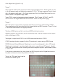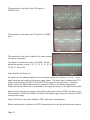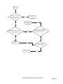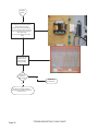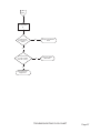
1
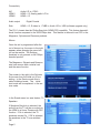
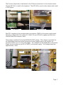
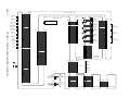
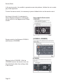
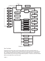
TECHNICAL TRAINING
FL9.1 LCD TV
CHASSIS FOR
2009
P & F USA, INC
SUITE 100
3015 WINDWARD PLAZA
ALPHARETTA, GA 30005
Table of contents
Introduction . . . . . . . . . . . . .
Models covered . . . . . . . . . .
Formats Supported . . . . . . .
Menus . . . . . . . . . . . . . . . . .
Software Upgrade . . . . . . . .
Customer Menu Map . . . . . .
Board Locations . . . . . . . . .
Board Level Repair . . . . . . .
Wiring Interconnect Diagram
Video Signal Flow . . . . . . . .
Video Signal Flow Block . . .
Video Signal Flow Block two
Audio Signal Flow . . . . . . . .
Audio Signal Flow Block . . .
Power Supply Block . . . . . .
Power Supply . . . . . . . . . . .
Protect 1 . . . . . . . . . . . . . . .
Protect 2 . . . . . . . . . . . . . . .
Inverter . . . . . . . . . . . . . . . .
Inverter Signal Flow Block . .
System Control Block . . . . .
Service Mode . . . . . . . . . . .
Service Menu Map . . . . . . .
Troubleshooting Flow Charts
Abbreviation List . . . . . . . . .
Service Tips . . . . . . . . . . . .
.
.
.
.
.
.
.
.
.
.
.
.
.
.
.
.
.
.
.
.
.
.
.
.
.
.
.
.
.
.
.
.
.
.
.
.
.
.
.
.
.
.
.
.
.
.
.
.
.
.
.
.
.
.
.
.
.
.
.
.
.
.
.
.
.
.
.
.
.
.
.
.
.
.
.
.
.
.
.
.
.
.
.
.
.
.
.
.
.
.
.
.
.
.
.
.
.
.
.
.
.
.
.
.
.
.
.
.
.
.
.
.
.
.
.
.
.
.
.
.
.
.
.
.
.
.
.
.
.
.
.
.
.
.
.
.
.
.
.
.
.
.
.
.
.
.
.
.
.
.
.
.
.
.
.
.
.
.
.
.
.
.
.
.
.
.
.
.
.
.
.
.
.
.
.
.
.
.
.
.
.
.
.
.
.
.
.
.
.
.
.
.
.
.
.
.
.
.
.
.
.
.
.
.
.
.
.
.
.
.
.
.
.
.
.
.
.
.
.
.
.
.
.
.
.
.
.
.
.
.
.
.
.
.
.
.
.
.
.
.
.
.
.
.
.
.
.
.
.
.
.
.
.
.
.
.
.
.
.
.
.
.
.
.
.
.
.
.
.
.
.
.
.
.
.
.
.
.
.
.
.
.
.
.
.
.
.
.
.
.
.
.
.
.
.
.
.
.
.
.
.
.
.
.
.
.
.
.
.
.
.
.
.
.
.
.
.
.
.
.
.
.
.
.
.
.
.
.
.
.
.
.
.
.
.
.
.
.
.
.
.
.
.
.
.
.
.
.
.
.
.
.
.
.
.
.
.
.
.
.
.
.
.
.
.
.
.
.
.
.
.
.
.
.
.
.
.
.
.
.
.
.
.
.
.
.
.
.
.
.
.
.
.
.
.
.
.
.
.
.
.
.
.
.
.
.
.
.
.
.
.
.
.
.
.
.
.
.
.
.
.
.
.
.
.
.
.
.
.
.
.
.
.
.
.
.
.
.
.
.
.
.
.
.
.
.
.
.
.
.
.
.
.
.
.
.
.
.
.
.
.
.
.
.
.
.
.
.
.
.
.
.
.
.
.
.
.
.
.
.
.
.
.
.
.
.
.
.
.
.
.
.
.
.
.
.
.
.
.
.
.
.
.
.
.
.
.
.
.
.
.
.
.
.
.
.
.
.
.
.
.
.
.
.
.
.
.
.
.
.
.
.
.
.
.
.
.
.
.
.
.
.
.
.
.
.
.
.
.
.
.
.
.
.
.
.
.
.
.
.
.
.
.
.
.
.
.
.
.
.
.
.
.
.
.
.
.
.
.
.
.
.
.
.
.
.
.
.
.
.
.
.
.
.
.
.
.
.
.
.
.
.
.
.
.
.
.
.
.
.
.
.
.
.
.
.
.
.
.
.
.
.
.
.
.
.
.
.
.
.
.
.
.
.
.
.
.
.
.
.
.
.
.
.
.
.
.
.
.
.
.
.
.
.
.
.
.
.
.
.
.
.
.
.
.
.
.
.
.
.
.
.
.
.
.
.
.
.
.
.
.
.
.
.
.
.
.
.
.
.
.
.
.
.
.
.
.
.
.
.
.
.
.
.
.
.
.
.
.
.
.
.
.
.
.
.
.
.
.
.
.
.
.
.
.
.
.
.
.
.
.
.
.
.
.
.
.
.
.
.
.
.
.
.
.
.
.
.
.
.
.
.
.
.
.
.
.
.
.
.
.
.
.
.
.
.
.
.
.
.
.
.
.
.
.
.
.
.
.
.
.
.
.
.
.
.
.
.
.
.
.
.
.
.
.
.
.
.
.
.
.
.
.
.
.
.
.
.
.
.
.
.
.
.
.
.
.
.
.
.
.
.
.
.
.
.
.
.
.
.
.
.
.
.
.
.
.
.
.
.
.
.
.
.
.
.
.
.
.
.
.
.
.
.
.
.
.
.
.
.
.
.
.
.
.
.
.
.
.
.
.
.
.
.
.
.
.
.
.
.
.
.
.
.
.
.
.
.
.
.
.
.
.
.
.
.
.
.
.
.
.
.
.
.
.
.
.
.
.
.
.
.
.
.
.
.
.
.
.
.
.
.
.
.
.
.
.
.
.
.
.
.
.
.
.
.
.
.
.
.
.
.
.
.
.
.
.
.
.
.
.
.
.
.
.
.
.
.
.
.
.
.
.
.
.
.
.
.
.
.
.
.
.
.
.
.
.
.
.
.
.
.
.
.
.
.
.
.
.
.
.
.
.
.
.
.
.
.
.
.
.
.
.
.
.
.
.
.
.
.
.
.
.
.
.
.
.
.
.
.
.
.
.
.
.
.
.
.
.
.
.
.
.
.
.
.
.
.
.
.
.
.
.
.
.
.
.
.
.
.
.
.
.
.
.
.
.
.
.
.
.
.
.
.
.
.
.1
.1
.1
.2
.3
.4
.5
.6
.8
.9
.10
.11
.12
.13
.14
.15
.15
.16
.17
.18
.19
.20
.22
.23-27
.28
.30
Introduction
The FL9.1 TV chassis is designed for the 2009 model year. The tuning system is designed to
tune both antenna and cable analog and digital signals. The screen size for this chassis is 32
inches with a pixel resolution of 1366 x 768p. Whatever signal is fed to the set will be
rescaled to fit the resolution of the screen.
Models covered by this chassis:
Model
Brand
32PFL3504D/F7
32PFL3514D/F7
32MF339B/F7
LC320SLX
LC320SSX
LC320EMX
Philips
Philips
Magnavox
Sylvania
Sylvania
Emerson
The following is the Jack panel for the Magnavox version. The Jack panel is the same for all
models using this chassis.
Supported display resolutions
Computer
Resolution
Refresh rate
640 x 480
720 x 480
800 x 600
1024 x 768
1280 x 768
1360 x 768
60Hz
60Hz
60Hz
60Hz
60Hz
60Hz
Video formats
Resolution
Refresh rate
480i
480p
720p
1080i
60Hz
60Hz
60Hz
60Hz
The audio amplifier output is two channels at 10 watts per channel.
Page 1
Connectivity
AV1
HDMI1
HDMI2
Audio output
Side
Audio L/R in, YPbPr
HDMI v1.3, Analog audio L/R in
HDMI v1.3
Digital Coaxial
HDMI v1.3, S-video in, CVBS in, Audio L/R in, USB (software upgrade only)
The FL9.1 chassis has the Philips EasyLink (HDMI-CEC) capability. This feature has additional function compared to the 2008 Philips sets. This feature is referred to as CEC in the
Magnavox, Sylvania and Emerson products.
Menus
Once the set is programmed after the
out of box set up, the menu to the right
appears when pressing the menu button on the remote. The Settings
Assistant is only present on the Philips
branded product.
The Magnavox, Sylvania and Emerson
sets have menus with a similar look
and the same function.
The screen to the right is the Sylvania
first screen from the initial out of box
setting. In the Service mode this is
called initialized mode. The initialized mode will be explained in the service mode.
In the Sound menu is a new feature, TV
Speakers.
If Speakers EasyLink is selected, the
sound from the TV will be re-routed via
the HDMI to a Home Theatre with CEC
function. If On is selected, the TV
speakers remain On. If Off is selected,
the speakers in the TV are switched
Off.
Page 2
Setup Menu
In the Setup Menu, channels can be programmed using Autoprogram. Channels
can be deleted from the channel ring
using Channel List. Add Channels can be
used to to add channels not picked up
during Autoprogram. Antenna is only
available in the Antenna mode.
Features
Among other things, Location, Child lock,
and Closed Caption can be selected in
the Features menu. This is called the
Details menu in the Magnavox, Sylvania
and Emerson sets.
Out of box, the Child Lock pin is 0000. If
the customer forgets their pin, unplugging
the set will reset the pin to 0000.
Current Software can also be viewed.
To load new software: (Philips Only)
1. Down the latest version from the
customer website *.zip.
2. Unzip the file and extract the *.ecc
file and load it in to the root
directory of a USB drive.
3. Unplug the TV from AC power.
4. Insert the USB drive into the TV.
5. Re-apply power and turn the set On.
6. Do not unplug the set on use the remote
while the set is programming as this will
damage the TV.
Page 3
Page 4
PICTURE
SOUND
SETUP
FEATURES
SETTING ASSISTANT
AUTO PICTURE
BRIGHTNESS
CONTRAST
COLOR
TINT
SHARPNESS
COLOR TEMPERATURE
LANGUAGE
FIGURE 1 - CUSTOMER MENU MAP
AUTO SOUND
EQUALIZER
VIRTUAL SURROUND SOUND
AUTO VOLUME LEVELING
TV SPEAKERS
AUTOPROGRAM
CHANNEL LIST
ADD CHANNELS
ANTENNA
CLOSED CAPTION
CHILD LOCK
PC SETTINGS
ENERGY SAVING MODE
LOCATION
CURRENT SOFTWARE INFO
ENGLISH
ESPANOL
FRANCAIS
PERSONAL
STANDARD
SPORTS
MOVIE
GAME
NORMAL
WARM
COOL
PERSONAL
STANDARD
MOVIE
MUSIC
NEWS
ON
OFF
SPEAKERS EASY LINK
CAPTION SERVICE
DIGITAL CAPTION SERVICE
CAPTION STYLE
CHANNEL LOCK
US MOVIE RATINGS LOCK
CANADIAN ENGLISH RATING
CANADIAN FRENCH RATING
REGION RATINGS LOCK
CHANGE PIN
Inverter
Keyboard
Side Jack
Power Supply
Digital Main
IR Board
Set Back view
Repair
The FL9.1 chassis is designed for board level repair. To assist with troubleshooting, component level function will be discussed.
The Digital Main board has the microprocessor and signal processing circuits. The HDMI and
USB inputs are located on the Digital Main board. The USB port on this chassis is only used
for software upgrade.
The Tuner AV inputs and Audio Amplifier are located on the Power Supply board. The power
supply produces a AL3.3V supply for standby power. When the set is turned On, the supply
produces a 16, 3.3, 3, 7, 5, 9, 13, and 33 volt supplies.
The Inverter Provides the drive voltage for the panel backlights.
Page 5
Board Level Repair (Figure 2)
The Fl9.1 chassis is designed for board level repair.
Standby mode
In Standby, the processor on the Digital Main board is powered by the AL+3.3V supply. This
voltage can be measured on pins 21 and 22 of connector CN301 on the power supply board.
Power On
When the set is turned On by the keyboard or the remote, the processor on the Digital Main
board switches the P-ON-H1 and P-ON-H2 lines High. This switches the power supply to the
full power mode.
Protect
If any of the supplies fail or the Inverter board is not functioning the Protect lines will cause
the set to shut down. In normal operation the Protect lines should read as follows:
Protect 1
Protect 2
Protect 3
2.4V
0.0V
3.3V
Since a failure in the Protect lines will cause an immediate shutdown, the power supply
should be forced On to check for missing supplies.
1. First unplug CN301 and CN302 to disconnect the Digital Main board.
2. Jumper the AL3.3V supply to P-ON-H1 and P-ON-H2.
P-ON-H1 and P-ON-H2 test points
Page 6
AL3.3V test point (top center)
The Function (Keyboard) is hard-wired to the IR Sensor board and it to the Junction board.
Only the KEY-IN1 is used for the keyboard. The KEY-IN2 is used in other chassis with a built
in DVD player.
IR Board
Junction Board
Raw DC is supplied to the Inverter board via connector CN602 on the power supply board.
Operating voltages INV+16V, LCD+16, P-ON+3.3V and LCD-6.8V supplies are fed to the
Inverter board via connector CN201.
The Inverter is switched On by the BACKLIGHT-SW voltage. This voltage is generated on
the Digital Main board and routed through the Power Supply board to the Inverter via
connector CN201, pin 5 on the power supply. The voltage from the Digital Main to the Power
Supply can be checked on pin 26 of CN301 on the power supply. This voltage should be
approximately 3 volts.
CN302
CN201
CN301
Page 7
Page 8
COMPONENT
-Y-IN
COMPONENT
-Pb-IN
COMPONENT
-Pr-IN
COMPONENTAUDIO(L)-IN
COMPONENTAUDIO(R)-IN
FIGURE 2 - WIRING INTERCONNECT DIAGRAM
HDMIAUDIO(L)-IN
HDMIAUDIO(R)-IN
DIGITAL
AUDIO-OUT
(COAXIAL)
AUDIO(L)
-OUT
AUDIO(R)
-OUT
AC601
AC CORD
CN301
1
2
3
4
5
6
7
8
9
10
11
12
13
14
15
16
17
18
19
20
21
22
23
24
25
26
27
28
29
CN302
1
2
3
4
5
6
7
8
9
10
11
12
13
14
15
16
17
18
19
20
21
22
23
24
25
26
27
28
29
CN3701
1
P-ON-H2
AUDIO(L)-OUT 2
3
GND
AUDIO(R)-OUT 4
PROTECT3
5
AMP(L)-OUT
6
GND
7
AMP(R)-OUT
8
P-ON-H1
9
P-ON+3V
10
11
PROTECT1
GND
12
P-ON+5V
13
P-ON+5V
14
PROTECT2
15
P-ON+7V
16
GND
17
18
GND
19
P-ON+3.3V
20
P-ON+3.3V
21
AL+3.3V
22
AL+3.3V
23
GND
24
OE2
25
REMOTE
BACKLIGHT-SW 26
27
LED1
BACKLIGHT-ADJ 28
VCOM-PWM 29
GND
SPDIF
GND
VIDEO-IN
S-VIDEO-SW
S-VIDEO-C-IN
GND
S-VIDEO-Y-IN
GND
INPUT1
AUDIO(R)
INPUT0
AUDIO(L)
GND
COM-VIDEO-Y-IN
GND
COM-VIDEO-Pb-IN
GND
COM-VIDEO-Pr-IN
AUDIO-MUTE
SDA
SCL
RESET
IF-AGC
GND
DIF-OUT1
GND
DIF-OUT2
KEY-IN1
CN3702
1
2
3
4
5
6
7
8
9
10
11
12
13
14
15
16
17
18
19
20
21
22
23
24
25
26
27
28
29
DIGITAL MAIN CBA UNIT
POWER SUPPLY CBA
TU301 TUNER UNIT
CN4001
1
2
3
4
5
6
7
8
9
10
11
12
13
14
15
16
17
18
19
20
21
22
23
24
25
26
27
28
29
GND
KEY-IN2
DVD-LED
P-ON-H3(NU)
DVD-MAIN-PWR
DVD-P-ON
DVD-REMOTE
DVD-SDATA
DVD-DISC-IN
GND
DVD-CS
GND
DVD-SCLK
GND
DVD-DISC-OUT
LED-CONT
GND
DVD-Pr
GND
DVD-Pb
GND
DVD-Y
GND
DVD-AUDIO(L)
DVD-AUDIO-MUTE
DVD-AUDIO(R)
GND
DVD-SPDIF
GND
CN303
1
2
3
4
5
6
7
8
9
10
11
12
13
14
15
16
17
18
19
20
21
22
23
24
25
26
27
28
29
CN602
1
2
ACL
HOT-GND
CN201
1
2
3
4
5
6
7
8
9
10
11
12
13
14
15
CN1001
1
GND
2
INV+16V
3
GND
BACKLIGHT-ADJ 4
BACKLIGHT-SW 5
6
PROTECT3
7
GND
8
LCD+16V
9
LCD+16V
10
VGH
11
GND
12
P-ON+3.3V
13
LCD-6.8V
14
VCOM
15
GND
CN1900
1
2
INVERTER
CL701A
1
2
3
4
5
6
7
8
9
CN801
SP(L)SP(L)+
CN802
SP(R)SP(R)+
1
CL801
2
1
CL802
2
SP801
SPEAKER
L-CH
SP802
SPEAKER
R-CH
CN101
1
2
3
4
5
6
7
8
CL701
S-VIDEO-Y-IN
S-VIDEO-SW
S-VIDEO-C-IN
GND
VIDEO-IN
GND
AUDIO(L)-IN
GND
AUDIO(R)-IN
CL701B
1
2
3
4
JACK
5
6
7
8
9
GND
REMOTE
AL+3.3V
LED1
P-ON-H1
KEY-IN1
KEY-IN2
DVD-LED
CN101
1
2
3
4
5
6
7
8
CN1050
1
2
BACK
LIGHT
CN1100
1
2
BACK
LIGHT
CN1150
1
2
BACK
LIGHT
CN1200
1
2
BACK
LIGHT
CN1250
1
2
BACK
LIGHT
CN1003
1
2
3
4
5
6
7
8
9
10
CBA 11
STV
XAO
OE1
CPV
POL
TP
GND
LLV5(-)
LLV5(+)
LLV4(-)
LLV4(+)
LLV3(-)
LLV3(+)
GND
LLVCLK(-)
LLVCLK(+)
GND
LLV2(-)
LLN2(+)
LLV1(-)
LLV1(+)
LLV0(-)
LLV0(+)
GND
GND
LCD+16V
LCD+16V
VGH
GND
P-ON+3.3V
P-ON+3.3V
LCD-6.8V
GND
VCOM
GND
CN3902
1
2
3
4
5
6
7
8
9
10
11
12
13
14
15
16
17
18
19
20
21
22
23
24
HDMICONNECTOR-1
HDMICONNECTOR-2
HDMICONNECTOR-3
LCD MODULE
ASSEMBLY
VIDEO-IN
CBA
AUDIO(L)
-IN
AUDIO(R)
-IN
S-VIDEO
-IN
CL102A
1
2
3
4
5
6
7
8
JUNCTION CBA
CL101
GND
REMOTE
AL+3.3V
LED1
P-ON-H1
KEY-IN1
KEY-IN2
DVD-LED
CL102C
1
2
3
4
5
6
7
8
CL103A
1
2
3
4
IR SENSOR CBA
CL103
AL+3.3V
GND
KEY-IN1
KEY-IN2
CL103B
1
2
3
4
FUNCTION CBA
Video Signal flow (Figure 3 & 4)
Figure 3
The composite and S-video inputs are located on the side jack panel. These signals are fed
to the the power supply on hard wired connecter CL701A. The one component input is located on the power supply panel. All of these signals are fed to the Digital Main board via connector CN302 on the power supply board.
Tuner TU301 tunes both analog and digital channels. The IF signal, DIF-OUT1 and DIFOUT2 is fed to the Digital Main board via connector CN302 on the power supply.
Figure 4
All of the system control, audio processing and video processing is performed by IC3301.
The component and AV inputs are fed to an internal switch and A/D converter. Tuner IF is fed
to an internal Demodulator and Digital processor.
The three HDMI inputs are fed to an internal HDMI switch and receiver.
Whatever signal is fed to IC3301, the IC rescales the video to fit the resolution of the screen
which in this case is 720p.
The signal is output from IC3301 in an LVDS format and then fed to IC3901.
IC3901 develops the drive signals for the LCD panel and is output using a RSDS format.
RSDS (Reduced Swing Differential Signaling) is a new format designed to drive LCD panels.
This format is designed to provide a higher data rate to newer thinner LCD panels. As with
LVDS, this format produces an offsetting positive and negative signal of approximately 200mv
to reduce RFI.
If the picture is distorted or has lines, check the RSDS signal from the Digital Main board to
the panel to determine where the problem is located.
This is the CPV signal which can be
checked on CN3902, pin 4.
Page 9
Page 10
VIDEO SIGNAL
AUDIO SIGNAL
JK752
VIDEO-IN
WF2
C
CL701B
5
3
1
2
Y
JK751
S-VIDEO
-IN
VIDEO-IN
S-VIDEO-C-IN
S-VIDEO-Y-IN
S-VIDEO-SW-IN
WF3
WF1
CL701A
5
3
1
2
CN302
4
6
8
5
15
17
19
JACK CBA
WF4
WF5
CN3702
4
6
8
5
COM-VIDEO-Y-IN 15
COM-VIDEO-Pb-IN 17
COM-VIDEO-Pr-IN 19
VIDEO-IN
S-VIDEO-C-IN
S-VIDEO-Y-IN
S-VIDEO-SW
VIDEO-IN
S-VIDEO-C-IN
S-VIDEO-Y-IN
S-VIDEO-SW
COM-VIDEO-Y-IN
COM-VIDEO-Pb-IN
COM-VIDEO-Pr-IN
WF6
FIGURE 3 - VIDEO SIGNAL FLOW ONE
TO DIGITAL
SIGNAL PROCESS
BLOCK DIAGRAM
JK731
COMPONENT
-Y-IN
JK732
COMPONENT
-Pb-IN
JK733
COMPONENT
-Pr-IN
TU301
(TUNER UNIT)
CN302
26 DIF-OUT1
28 DIF-OUT2
24 IF-AGC
DIF-OUT1 11
DIF-OUT2 10
IF-AGC 9
POWER SUPPLY CBA
CN3702
26
28
24
DIF-OUT1
DIF-OUT2
IF-AGC
DIGITAL MAIN CBA UNIT
FIGURE 4 - VIDEO SIGNAL FLOW TWO
Page 11
TMDS-D0(+)
TMDS-D0(-)
TMDS-D1(+)
TMDS-D1(-)
TMDS-D2(+)
TMDS-D2(-)
TMDS-CLOCK(+)
TMDS-CLOCK(-)
SDA
SCL
TMDS-D0(+)
TMDS-D0(-)
TMDS-D1(+)
TMDS-D1(-)
TMDS-D2(+)
TMDS-D2(-)
TMDS-CLOCK(+)
TMDS-CLOCK(-)
SDA
SCL
7
9
4
6
HDMI-IN3 1
3
10
12
16
15
TMDS-D0(+)
TMDS-D0(-)
TMDS-D1(+)
TMDS-D1(-)
TMDS-D2(+)
TMDS-D2(-)
TMDS-CLOCK(+)
TMDS-CLOCK(-)
SDA
SCL
JK3703
7
9
4
6
HDMI-IN2 1
3
10
12
16
15
JK3702
7
9
4
6
1
HDMI-IN1
3
10
12
16
15
JK3701
TO AUDIO
BLOCK DIAGRAM
TO VIDEO
BLOCK DIAGRAM
TO VIDEO
BLOCK DIAGRAM
AUDIO(L)
AUDIO(R)
BCLK
LRCLK
ACLK
SPDIF
ADATA0
ADATA1
IF-AGC
S-VIDEO-SW
DIF-OUT1
DIF-OUT2
VIDEO-IN
S-VIDEO-C-IN
S-VIDEO-Y-IN
COM-VIDEO-Y-IN
COM-VIDEO-Pb-IN
COM-VIDEO-Pr-IN
DIGITAL MAIN CBA UNIT
B1
B2
C1
C2
D1
D2
A1
A2
A3
B3
A5
B5
C4
C5
B4
A4
B6
A6
A7
B7
B11
A11
A10
B10
A9
B9
C8
C9
B8
A8
AD14
AC10
AD11
AD10
AD12
AD9
M1
M2
A/D
CONVERTER
HDMI
I/F
VIDEO
DECODER
AUDIO
DECODER
AUDIO I/F
DEMODULATOR
/MPEG DECODER
SW
IF-AGC
C6 S-VIDEO-SW
AF7
AF2
AE2
V3
U3
U1
V1
U2
AA3
IC3301 (DIGITAL SIGNAL PROCESS)
DIGITAL
SIGNAL
PROCESS
AD23
129
128
C15,C17-19,
C23,C24,D14,
D15,D17-19,
D22,D23
ADDESS(0-12)
DATA(0-15)
IC3201
(DDR2 SDRAM)
LVDS
RX
M2,M3,M7,M8,
N2,N3,N7,N8,
P2,P3,P7,P8,R2
B1,B9,C2,C8,
D1,D3,D7,D9,
F1,F9,G2,G8,
H1,H3,H7,H9
130
AE24
131
AD21
AF24
126
AE22
AD22
124
127
AF23
125
122
123
AF22
AE23
AD24
A13-15,A18,
A21-23,B13-15,
B17,B19-23
LVDS
TX
FAIL SAFE MODE
COLOR PROOF
ADVANCE
OVER DRIVE
FRC
LCD
TIMING
CONTROLLER
IC3901 (TINING CONTROLLER)
RSDS
I/F
27
26
29
28
31
30
42
41
45
44
47
46
33
32
88
19
92
93
94
VIDEO SIGNAL
CN3902
23
22
21
20
19
18
13
12
11
10
9
8
16
15
6
5
4
3
1
AUDIO SIGNAL
LLV0P
LLV0N
LLV1P
LLV1N
LLV2P
LLV2N
LLV3P
LLV3N
LLV4P
LLV4N
LLV5P
LLV5N
LLVCLKP
LLVCLKN
TP
POL
CPV
OE
STV
LCD MODULE
ASSEMBLY
The waveform to the right is the POL signal on
CN3902, pin 5.
The waveform to the right is the TP signal on CN3902,
pin 6.
The waveform to the right is typical of the ones carrying
the picture information.
This signal is measured on pin 8 of CN3902. Similar
signals are present on pins 9, 10, 11, 12, 13, 15, 16, 18,
19, 20, 21, 22 and 23.
Audio Signal Flow (Figure 5)
AV audio from the side jack panel is fed to the power supply via connector CL701A. The AV
audio inputs are all located on the power supply board. The audio input is selected by IC771
which is controlled by the INPUT1 and INPUT0 lines from the microprocessor. Selected
audio is fed to the Digital Main board via connector CN302 on the power supply board.
Digital and analog tuner audio is processed by the signal processor on the digital main board.
Selected audio from the processor on the digital main board is fed to IC3803 and then to two
D/A converters, IC3802 and IC3801 and then to the power supply board via connector CN301
on the power supply.
Audio is then fed to the audio amplifier, IC801, and then to the speakers.
Monitor analog audio is buffered by IC871 before being fed to the left and right audio outputs.
Page 12
AUDIO SIGNAL
CL701B
7 AUDIO(L)-IN
9 AUDIO(R)-IN
JK753
AUDIO(L)
-IN
JK754
AUDIO(R)
-IN
CL701A
7
9
IC771
(AUDIO SELECTOR)
2
4
1
5
3
15
11
12
14
13
JACK CBA
JK741
COMPONENTAUDIO(L)-IN
JK742
COMPONENTAUDIO(R)-IN
WF7
FIGURE 5 - AUDIO BLOCK
CONTROL
LOGIC
9 10
JK721
HDMIAUDIO(L)-IN
JK722
HDMIAUDIO(R)-IN
Q771
CN302
13 AUDIO(L)
11 AUDIO(R)
CN3702
13
11
CN302
10 INPUT1
12 INPUT0
CN3702
10
12
TO
DIGITAL
SIGNAL
PROCESS
BLOCK
DIAGRAM
INPUT1
INPUT0
AUDIO-MUTE
TO
SYSTEM
CONTROL
BLOCK
DIAGRAM
Q772
IC3802
(D/A CONVERTER)
IC871
(OP AMP)
JK871
AUDIO(L)-OUT
1
3
JK872
AUDIO(R)-OUT
7
5
Q871
MUTE
JK841
DIGITAL
AUDIO-OUT
(COAXIAL)
Q872
MUTE
CN301
2
4
6
8
AUDIO(L)-OUT
AUDIO(R)-OUT
AMP(L)-OUT
AMP(R)-OUT
CN3701
2
4
6
8
(L-CH)
D/A
15
(R-CH) CONVERTER
14
IC3803
(AUDIO DSP)
8
7
6
5
CN302
2 SPDIF
20 AUDIO-MUTE
BUFFER
Q841
IC801 (AUDIO AMP)
DRIVE1
PWM1
CN3702
2
20
(L-CH)
15
D/A
(R-CH) CONVERTER
14
35,36
CL801
CN801
SP(L)+ 2
SP(L)- 1
LRCLK
BCLK
ADATA1
ACLK
ADATA0
TO
DIGITAL
SIGNAL
PROCESS
BLOCK
DIAGRAM
1
SPDIF
DRIVE2
PWM2
44
31,32
MUTE CONTROL
20
CL802
DSP
2
40
39
3
4
8
7
6
5
13,14
SP801
SPEAKER
L-CH
35
36
37
34
33
IC3801
(D/A CONVERTER)
Q873,Q874
DRIVE
9,10
Page 13
SP802
SPEAKER
R-CH
AUDIO(L)
AUDIO(R)
Q801
CN802
SP(R)+ 2
SP(R)- 1
POWER SUPPLY CBA
DIGITA L MA IN CBA UNIT
Page 14
CAUTION !
Fixed voltage (or Auto voltage selectable) power supply circuit is used in this unit.
If Main Fuse (F601) is blown , check to see that all components in the power supply
circuit are not defective before you connect the AC plug to the AC power supply.
Otherwise it may cause some components in the power supply circuit to fail.
4A/125V
CAUTION ! : For continued protection against risk of fire,
replace only with same type 4 A, 125V fuse.
ATTENTION : Utiliser un fusible de rechange de mŒme type de 4A, 125V.
NOTE:
The voltage for parts in hot circuit is measured using
hot GND as a common terminal.
HOT CIRCUIT. BE CAREFUL.
Q211
SW-6.8V
AC601
AC CORD
F601
4A/125V
L602
L601
LINE
FILTER
LINE
FILTER
T601
D601- D604
BRIDGE
RECTIFIER
3
Q210
SW+24.5V
11
Q201,Q212
SW
14
4A/125V
FIGURE 6 - POWER SUPPLY
TO
INVERTER
BLOCK
DIAGRAM
(CN1900)
CN602
2 ACL
1 HOT-GND
Q207,Q208
SWITCHING
12
4
CN201
13
8,9
2
10
12
LCD-6.8V
LCD+16V
INV+16V
VGH
P-ON+3.3V
CN1001
13
8,9
2
10
12
CN301
10
16
21,22
19,20
13,14
P-ON+3V
P-ON+7V
AL+3.3V
P-ON+3.3V
P-ON+5V
CN3701
10
16
21,22
19,20
13,14
INVERTER CBA
LCD+6.8V
LCD+16V
INV+16V
VGH
P-ON+3.3V
DIGITAL MAIN CBA UNIT
P-ON+3V
P-ON+7V
AL+3.3V
P-ON+3.3V
P-ON+5V
Q401
17
Q501
SW+16V
18
Q209,D204
SW+16V
5
13
7
16
8
Q601
SWITCHING
Q642
SW+9V
15
9
19
Q637,D666
SW+3.3V
IC601
Q602
SWITCHING
CONTROL
4
1
3
2
Q638,Q639
SWITCHING
Q631
FEED
BACK
Q640
SW+5V
Q634
Q641,643
SW+5V
HOT
POWER SUPPLY CBA
P-ON+9V
AL+33V
P-ON+5V
AL+13V
TUNER+5V
AL+3.3V
COLD
Q635
+5V REG.
3
IC631
+3.3V
REG.
2
P-ON-H1
P-ON-H2
PROTECT1
PROTECT2
TO SYSTEM
CONTROL
BLOCK
DIAGRAM
Power Supply (Figure 6)
AC is fed the line filters and bridge rectifier. RAW DC is fed to the Inverter via connector
CN602 on the power supply board and to transformer T601.
The switch mode supply consist of transistors Q601 and Q602. In standby, the power supply
is running in a low power pulsating mode controlled by Q634 on the secondary side.
When the set is turned On, the P-ON-H1 and P-ON-H2 lines goes High. P-ON-H2 changes
turns on transistor Q634 to change the bias of the feed back circuit switching the power supply to a full power mode. It also turns on transistors Q638, Q639 and Q637 to turn the P-ON3.3V supply On. The P-ON-H1 line switches Q207 and Q208. This switches Q210, Q201
and Q212 to switch the VGH voltages. Q211 is turned On switching the LCD-6.8V supply. It
also switches Q209 switching the LCD+16V supply. Q501 is switched to turn on the INV+16V
supply. Q642 is switched to produce the P-ON+9V supply.
Protect 1 (Figure 7)
Protect 1 is connected to all of the supplies via diodes. If any one of the supplies shorts, the
protect line will go Low causing the set to turn Off. The pull up voltage for Protect 1 is R401.
AL+3.3V
R401
22K
PROTECT1
R408
10K
D411
D409
D417
3.9V
AL+13V
P-ON+3V
D413
D414
P-ON+3.3V
P-ON+5V
D412
D404
LCD+16V
AL+33V
D416
D410
INV+16V
P-ON+9V
D415
D405
TUNER+5V
D406
15V
LCD+24.5V
R412
10K
FIGURE 7 - PROTECT 1
Page 15
+33V
R660
R662
15
R663
1.8K
Q635
R664
1.8K
D659
6.8V
D660
D636
2.7
IC631
D637
3.3V
REG
AL3.3V
R636
2.7
PROTECT2
D407
10V
D418
3.9V
FIGURE 8 - PROTECT 2
Protect 2 (Figure 8)
Protect 2 monitors the circuit feeding the 3.3V standby supply.
In the standby mode, the +33V supply will measure approximately 8 volts. When the set is
turned On, it will go to +33V as the power supply goes to a full power mode. Q635 regulates
the voltage feeding IC631, AL3.3V regulator.
If Q635 fails, the voltage at the emitter of Q635 would exceed the voltage of the 10 volt zener,
D407 causing it to conduct. This will cause the PROTECT 2 line to go High resulting in the
TV set turning Off.
Page 16
Inverter (Figure 9)
The inverter power supply is switched On by the BACKLIGHT-SW line from the digital board.
The BACKLIGHT-ADJ line is fed to IC1000 to control the pulse width output of IC1000 and
the brightness of the backlight. The outputs to the backlights are fed to over voltage protection circuits. If a problem is detected in one of the outputs, Q1600 is turned On causing the
Protect 3 line to go Low. This will cause the set to turn Off.
System Control (Figure 10)
Control signals from the Function board and IR Sensor board are routed through the power
supply board to IC3301. IC3301 preforms all of the system control functions.
Note that the P-ON-HI voltage in pin 5 of CN101 is inverted from the pin with the same label,
CN301, pin 9.
Inverter Board
Page 17
HOT CIRCUIT. BE CAREFUL.
T1050
INV+16V
TO POWER
SUPPLY
BLOCK
DIAGRAM
(CN602)
T1950
CN1900
2 ACL
1 HOT-GND
2
3
10
Q1801,Q1802,
Q1803,Q1804
SW+16V
Q1800,Q1815
SW+16V
11
4
2
4
8
7
1
3
6
5
CN1050
1
2
BACK
LIGHT
CN1100
1
2
BACK
LIGHT
CN1150
1
2
BACK
LIGHT
CN1200
1
2
BACK
LIGHT
CN1250
1
2
BACK
LIGHT
5
Q1930
SWITCHING
7
14
8
15
IC1000
(PWM CONTROL)
12 VCC
Q1004,
Q1005
SW
IC1930
4
3
Q1932
1
2
IC1931
FIGURE 9 - INVERTER
HOT
3
Q1501,
Q1502,
Q1503
11
PWM
CONTROL
LOGIC
4
1
3
2
8
7
1
3
6
5
4 DCT
15
16
Q1970
Q1931
T1100
2
4
2
1
DRIVE
Q1551,
Q1552,
Q1553
8
DRIVE
CURRENT
CONTROL
SWITCH
Q1550
CURRENT
CONTROL
SWITCH
T1150
2
4
8
7
1
3
6
5
T1200
OSC
COLD
Q1500
2
4
8
7
1
3
6
5
5 6
Q1003
T1250
Q1971
Q1972
Q1001
Q1600
IC1700
(COMPARATOR)
TO SYSTEM
CONTROL
BLOCK
DIAGRAM
(CN201)
CN1001
PROTECT3
6
5 BACKLIGHT-SW
4 BACKLIGHT-ADJ
14 VCOM
Q1621
14
6.6V
13
12
8
9
10
7
6
5
1
2
3
IC1750
(COMPARATOR)
7
6
5
2
4
8
7
1
3
6
5
Q1260
OVER VOLTAGE
PROTECTOR
Q1210
OVER VOLTAGE
PROTECTOR
Q1160
OVER VOLTAGE
PROTECTOR
Q1110
OVER VOLTAGE
PROTECTOR
Q1060
OVER VOLTAGE
PROTECTOR
Q1261
OVER VOLTAGE
PROTECTOR
Q1211
OVER VOLTAGE
PROTECTOR
VCOM
OVER VOLTAGE
PROTECTOR
Q1111
OVER VOLTAGE
PROTECTOR
Q1061
OVER VOLTAGE
PROTECTOR
INVERTER CBA
CN1003
10
Q1161
LCD MODULE
ASSEMBLY
Inverter Block Diagram
Page 18
NOTE:
The voltage for parts in hot circuit is measured using
hot GND as a common terminal.
IC3301
(MAIN MICRO CONTROLLER)
CN101
2
5
6
8
Q172
KEY-IN1
AC5
REMOTE
P-ON-H2
P-ON-H1
R22
RS101
JUNCTION
CBA
CN3702
29 KEY-IN1
CN302
29
CN3701
25 REMOTE
1 P-ON-H2
9 P-ON-H1
CN301
25
1
9
REMOTE
P-ON-H1
KEY-IN1
DVD-LED
CN101
2
5
6
8
CL102A
2
5
6
8
REMOTE
SENSOR
REMOTE
P-ON-H1
KEY-IN1
DVD-LED
CL102C
2
5
6
8
D101
POWER
AL+6.0V
AB13
R23
KEY SWITCH
CL103B
3 KEY-IN1
CL103A
3
FUNCTION CBA
FIGURE 10 - SYSTEM CONTROL
TO AUDIO
BLOCK
DIAGRAM
INPUT0
INPUT1
AUDIO-MUTE
E1 INPUT0
E2 INPUT1
AB9 AUDIO-MUTE
P-ON-H2
P-ON-H1
PROTECT1
PROTECT2
CN3701
PROTECT1 AD5
PROTECT2 AD4
PROTECT3 AE5
VCOM-PWM AC14
BACKLIGHT-SW AB16
BACKLIGHT-ADJ AB23
CN301
11
11 PROTECT1
15
15 PROTECT2
5
5 PROTECT3
VCOM-PWM
29
29
26 BACKLIGHT-SW 26
28 BACKLIGHT-ADJ 28
TO
POWER SUPPLY
BLOCK DIAGRAM
CN201
DRIVE
IC201,Q203,
Q204,Q205
TU301 (TUNER UNIT)
CN3702
SCL
SDA
AC18
AC19
22 SCL
21 SDA
CN302
22
21
4 SCL
5 SDA
IC3101 (MEMORY)
SCK
SI
SO
CS
WP
6
5
2
1
3
X3101
25MHz
OSC
Page 19
DIGITAL MAIN CBA UNIT
IR SENSOR CBA
SCK
SIN
SOUT
AC24 CS
E11 WP
AB25
AB24
AC25
N1 CLKIN
N2 CLKOUT
POWER SUPPLY CBA
6
5
4
14
PROTECT3
BACKLIGHT-SW
BACKLIGHT-ADJ
VCOM
TO
INVERTER
BLOCK
DIAGRAM
(CN1001)
Service Mode
In the service mode, it is possible to generate screen test patterns, Initialize the set or make
grey scale alignments.
To enter the service mode, it is necessary to press a hidden button on the remote control.
As shown to the right, it is necessary to
have a Magnavox remote for entering the
service mode for the Magnavox and Philips
models.
Service mode for the Sylvania LC320SLX
and Emerson LC320EMX.
Remote for the LC320SSX. With the
LC320SSX remote, the remote cover can
be peeled back rather than cutting a hole
in the remote.
Page 20
The Service screen is shown to the
right.
Refer to Figure 11 for the service menu
map.
To Initialize the set which puts it in an
out of box condition, press the Info
button on the remote while in the service
screen.
The word Initialized will turn green indicating that the initialization is complete.
After initializing the set, the customer will
be prompted to enter a language and
program the TV when it is turned On for
the first time.
Grey Scale alignment
To perform the grey scale alignment, press the Vol- button three times until C/D appears on
the screen. Then select the desired Cutoff and Drive adjustments. Use the channel up/down
button on the remote to adjust the respective cutoffs or drives. Default values are listed
below.
Select
1
2
3
4
5
6
Adjustment
COR - Cutoff Red
COG - Cutoff Green
COB - Cutoff Blue
DR - Red Drive
DG - Green Drive
DB - Blue Drive
Value
187
0
56
-46
0
-21
VCOM 1 and 2 are used to calibrate the A/D converter for the Component inputs.
2
VCOM1
90
3
VCOM2
90
Refer to the service manual for more details.
Page 21
SERVICE BUTTON
INFO
MENU
INITILIZED
CURSOR LF
2, 3, 5, 6
MAIN MENU
CURSOR RG
BLACK SCRN
CH UP
7
CH DOWN
VOL-
SHADE GRY
CH UP
CH DOWN
LEFT
CURSOR
SCREEN
TEST
MODE
WHITE SCREEN
SOFTWARE UPDATE
CHANNEL 2
CURSOR UP, THEN
CURSOR DOWN TO EXIT
SHADE WH
7
VOLCH UP
CH DOWN
BLACK SCREEN
DEBUGGING
MESSAGE
SHADE RED
7
CH UP
CH DOWN
7
VOL-
GREEN
1
CH UP
CH DOWN
CD
2
BLUE
CH UP
3
CH DOWN
4
WHITE
7
COG - CUTOFF GREEN
COB - CUTOFF BLUE
GREEN SCREEN
DR - DRIVE RED
7
5
CH UP
RED SCREEN
COR - CUTOFF RED
DG - DRIVE GREEN
CH DOWN
6
CH DOWN
BLUE SCREEN
DB - DRIVE BLUE
RED
7
8
7
CO LIST ADJ ALL
CO - DR LIST
WHITE 20%
9
TI
PREV CH TO RETURN TO MAIN MENU
2
VCOM1
VCOM2
(H) CABLE CH
(H) ANTENNA CH
3
5
6
FIGURE 11 - SERVICE MENU
Other Test Modes
Pressing the left cursor button on the remote while in the service mode will switch on a
screen test mode. Press the cursor up followed by the cursor down button on the remote to
exit. Pressing the Menu button will switch on a second screen test mode. Pressing the ch
up/down button will cycle the screen through different patterns. Press the cursor left followed
by the cursor right button to exit this mode.
Page 22
Repair or replace
the power supply.
Dead set
No
Connect the set
to AC power
Does the power LED turn
On when the power button
is pressed?
Is the AL+3.3V supply present?
Measure on pin 21 of CN301 on the
power supply.
No
Replace the Digital
Main board.
No
Yes
Is 3.3 volts present on
pin 29 of CN302?
Does KEY-IN1, pin 6 of CN101
read 3.3 volts with no keyboard
buttons being pressed?
No
Repair or replace the
power supply board.
Yes
Yes
Yes
Does the set turn
on when KEY-IN1 is
grounded?
No
Does KEY-IN1 go Low
when the power button is
pressed?
Yes
Yes
No
Replace the Digital Main
board.
Repair the Keyboard and check
the IR sensor and remote.
Does the Power
LED stay On?
If the power LED
stays On, the
panel backlight is
On.
Yes
Is OSD (On Screen Display,
Menu) present when the Menu
button is pressed?
No
No
Digital Main board.
Yes
Does the Power LED
and screen backlight flash
On and then Off?
No
Does the Power LED
flash On and then Off
Yes
No
Video
Power LED
Flashes
Yes
Backlight
Flashes
No
TROUBLESHOOTING FLOW CHART
Page 23
Power LED
Flashes
Disconnect the
Digital Main board
from the Power
Supply.
Jumper to the AL3.3V
supply to the P-ON-H1
and P-ON-H2 to force
the power supply On.
Replace the Inverter
board.
Yes
Is Protect2 (Pin 15 of
CN301) Low?
Repair or replace
the power supply.
High
No
Low
Is Protect1 (Pin 11 of
CN301) High (2.4V)?
Does the BACKLIGHT-SW on pin
5 of CN201 go to 3.3 Volts when
the set is turned On?
Replace the Digital Main
board.
One or more of the B+ supplies are
missing. Repair or replace the power
supply.
Low
No
Repair or replace the
power supply board.
No
High
Is approximately 160V DC
present between pins 1 and 2 of
CN602 on the power supply?
Yes
Reconnect the Digital
Board and monitor the
PROTECT3 voltage on
pin 6 of CN201 as the
set is turned On.
Replace the Digital Main
board.
Page 24
TROUBLESHOOTING FLOW CHART
Does the PROTECT3
line go to 3.3 volts when
the set is turned On?
Yes
No
Video
Does video return after
connecting an antenna and
auto-programming.
No
Is video present after connecting a
signal to one of the AV inputs and
selecting that input?
Check remaining
inputs.
Yes
Replace the digital
main board.
No
No
Does video appear after reseating
the ribbon cables connecting the
power supply to the digital board?
Yes
Replace the
power supply
board.
Yes
No
Is tuner video present
after auto-programming?
Check remaining
inputs.
Yes
TROUBLESHOOTING FLOW CHART
Page 25
Backlight
Flashes
Turn the set On while monitoring the
HV output from the Inverter board at
each output one at a time.
Repeat for each of the five locations.
It is only necessary to place the scope
probe in the proximity of the output as
shown at the right.
If you connect directly, use a X100
probe.
The waveform will
appear as shown
to the right if the
output is working.
Is output
present at
each location?
No
Replace the
Inverter board.
Yes
The panel is most likely defective.
Check panel connections to make sure
they are sucure.
Page 26
TROUBLESHOOTING FLOW CHART
No
Audio
Turn the volume
up.
Is audio present
on pins 6 and 8 of
CN301?
No
Change the Digital Main
board.
Yes
Is the audio mute
on pin 20 of CN302
zero volts. (<0.4V)
No
Change the Digital
Main board.
Yes
Change the power
supply board.
TROUBLESHOOTING FLOW CHART
Page 27
Abbreviation list
Description
1080i
1080p
480i
480p
ADC A/D
AFC
AGC
AM
AV
C-FRONT
CBA
ComPair
CSM
CVBS
CVBS-EXT
CVBS-INT
CVBS-MON
CVBS-TER-OUT
DAC
DFU
DNR
DRAM
DSP
DTS
DVD
EEPROM
EPLD
EXT
FBL
FLASH
FM
FMR
FRC
FRONT-C
FRONT-DETECT
FRONT-Y_CVBS
H
HD
HDMI
HP
Page 28
1080 visible lines, interlaced
1080 visible lines, progressive scan
480 visible lines, interlaced
480 visible lines, progressive scan
Analogue to Digital Converter
Automatic Frequency Control: control signal used to tune to the correct
frequency
Automatic Gain Control: algorithm that controls the video input of the
feature box
Amplitude Modulation
Audio Video
Chrominance front input
Circuit Board Assembly (or PWB)
Computer aided rePair
Customer Service Mode
Composite Video Blanking and Synchronization
CVBS signal from external source (VCR, VCD, etc.)
CVBS signal from Tuner
CVBS monitor signal
CVBS terrestrial out
Digital to Analogue Converter
Directions For Use: owner's manual
Dynamic Noise Reduction
Dynamic RAM
Digital Signal Processing
Digital Theatre Sound
Digital Video Disc
Electrically Erasable and Programmable Read Only Memory
Electronic Programmable Device
EXTernal (source), entering the set by cinches (jacks)
Fast Blanking: DC signal accompanying RGB signals
FLASH memory
Field Memory / Frequency Modulation
FM Radio
Frame Rate Converter
Front input chrominance (SVHS)
Front input detection
Front input luminance or CVBS (SVHS)
H_sync to the module
High Definition
High Definition Multimedia Interface
HeadPhone
I2C
I2S
IC
IF
Interlaced
Integrated IC bus
Integrated IC Sound bus
Integrated Circuit
Intermediate Frequency
Scan mode where two fields are used to form one frame. Each field contains
half the number of the total amount of lines. The fields are written in 'pairs',
causing line flicker.
IR
Infra Red
IRQ
Interrupt ReQuest
Last Status The settings last chosen by the customer and read and stored in RAM or in the
NVM. They are called at start-up of the set to configure it according the
customers wishes.
LCD
Liquid Crystal Display
LED
Light Emitting Diode
LINE-DRIVE Line drive signal
LVDS
Low Voltage Differential Signalling, data transmission system for high speed
and low EMI communication.
MPEG
Motion Pictures Experts Group
NVM
Non Volatile Memory: IC containing TV related data (for example, options)
OSD
On Screen Display
Progressive Scan Scan mode where all scan lines are displayed in one frame at the same
time, creating a double vertical resolution.
RAM
Random Access Memory
RC
Remote Control transmitter
RC5
Remote Control system 5, the signal from the remote control receiver
RGB
Red, Green, and Blue. The primary colour signals for TV. By mixing
levels of R, G, and B, all colors (Y/C) are reproduced.
RGBHV
Red, Green, Blue, Horizontal sync, and Vertical sync
ROM
Read Only Memory
SAM
Service Alignment Mode
SIF
Sound Intermediate Frequency
SC
SandCastle: two-level pulse derived from sync signals
SCL
CLock Signal on I2C bus
SDA
DAta Signal on I2C bus
SDRAM
Synchronous DRAM
SIF
Sound Intermediate Frequency
STBY
STandBY
VGA
Video Graphics Array
XTAL
Quartz crystal
YPbPr
Component video (Y= Luminance, Pb/Pr= Colour difference signals)
Y/C
Luminance (Y) and Chrominance (C) signal
Y-OUT
Luminance-signal
Page 29
Service Tips
Symptom: Lines in the picture
as shown in the
picture to the right.
Cause: Defective Digital Main
board.
Symptom: High frequency noise from the TV when Off.
Cause: Audio amplifier not being shut off during standby.
Cure: Upgrade software.
Symptom: No audio on some analog channels.
Cause: Low sensitivity to 4.5mHz carrier.
Cure: Upgrade software.
Page 30
MM081909