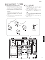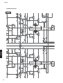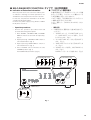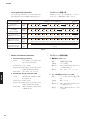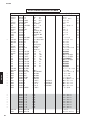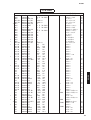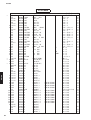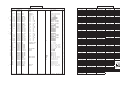
1
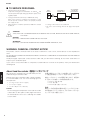
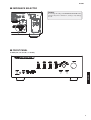
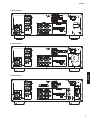
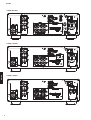
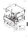
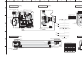
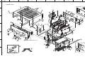
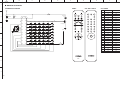
INTEGRATED AMPLIFIER
A-S700
SERVICE MANUAL
IMPORTANT NOTICE
This manual has been provided for the use of authorized YAMAHA Retailers and their service personnel.
It has been assumed that basic service procedures inherent to the industry, and more specifically YAMAHA Products, are already known
and understood by the users, and have therefore not been restated.
WARNING:
Failure to follow appropriate service and safety procedures when servicing this product may result in personal injury,
destruction of expensive components, and failure of the product to perform as specified. For these reasons, we advise
all YAMAHA product owners that any service required should be performed by an authorized YAMAHA Retailer or
the appointed service representative.
IMPORTANT: The presentation or sale of this manual to any individual or firm does not constitute authorization, certification or
recognition of any applicable technical capabilities, or establish a principle-agent relationship of any form.
The data provided is believed to be accurate and applicable to the unit(s) indicated on the cover. The research, engineering, and service
departments of YAMAHA are continually striving to improve YAMAHA products. Modifications are, therefore, inevitable and
specifications are subject to change without notice or obligation to retrofit. Should any discrepancy appear to exist, please contact the
distributor's Service Division.
WARNING:
Static discharges can destroy expensive components. Discharge any static electricity your body may have
accumulated by grounding yourself to the ground buss in the unit (heavy gauge black wires connect to this buss).
IMPORTANT: Turn the unit OFF during disassembly and part replacement. Recheck all work before you apply power to the unit.
A-S700
■ CONTENTS
TO SERVICE PERSONNEL ............................................2
IMPEDANCE SELECTOR ...............................................3
FRONT PANEL ...............................................................3
REAR PANELS ...........................................................4–6
REMOTE CONTROL PANEL ..........................................7
SPECIFICATIONS / 参考仕様 .....................................7–8
INTERNAL VIEW ............................................................9
SERVICE PRECAUTIONS / サービス時の注意事項 ..... 10
DISASSEMBLY PROCEDURES / 分解手順 ........... 10–16
AMP ADJUSTMENT / アンプ部調整 ....................... 17–18
10111 7
SELF-DIAGNOSTIC FUNCTION /
ダイアグ(自己診断機能)....................................... 19–25
IC DATA ...................................................................26–28
BLOCK DIAGRAM ........................................................29
PRINTED CIRCUIT BOARDS .................................30–43
PIN CONNECTION DIAGRAMS ...................................44
SCHEMATIC DIAGRAMS .......................................45–47
REPLACEMENT PARTS LIST ................................49–59
REMOTE CONTROL .....................................................60
Copyright © 2008
All rights reserved.
This manual is copyrighted by YAMAHA and may not be copied or
redistributed either in print or electronically without permission.
P.O.Box 1, Hamamatsu, Japan
animate '08.10
A-S700
■ TO SERVICE PERSONNEL
1. Critical Components Information
Components having special characteristics are marked
and
must be replaced with parts having specifications equal to those
originally installed.
WALL
OUTLET
2. Leakage Current Measurement (For 120V Models Only)
When service has been completed, it is imperative to verify
that all exposed conductive surfaces are properly insulated
from supply circuits.
• Meter impedance should be equivalent to 1500 ohms shunted
by 0.15 μF.
EQUIPMENT
UNDER TEST
AC LEAKAGE
TESTER OR
EQUIVALENT
INSULATING
TABLE
• Leakage current must not exceed 0.5mA.
• Be sure to test for leakage with the AC plug in both polarities.
“CAUTION”
“F251, F252: FOR CONTINUED PROTECTION AGAINST RISK OF FIRE, REPLACE ONLY WITH SAME TYPE 8A,
125V FUSE.”
CAUTION
F251, F252: REPLACE WITH SAME TYPE 8A, 125V FUSE.
ATTENTION
F251, F252: UTILISER UN FUSIBLE DE RECHANGE DE MÉME TYPE DE 8A, 125V.
WARNING: CHEMICAL CONTENT NOTICE!
This product contains chemicals known to the State of California to cause cancer, or birth defects or other reproductive
harm.
DO NOT PLACE SOLDER, ELECTRICAL/ELECTRONIC OR PLASTIC COMPONENTS IN YOUR MOUTH FOR ANY REASON
WHATSOEVER!
Avoid prolonged, unprotected contact between solder and your skin! When soldering, do not inhale solder fumes or
expose eyes to solder/flux vapor!
If you come in contact with solder or components located inside the enclosure of this product, wash your hands before
handling food.
A-S700
About lead free solder / 無鉛ハンダについて
All of the P.C.B.s installed in this unit and solder joints are
soldered using the lead free solder.
本機に搭載されているすべての基板およびハンダ付けに
よる接合部は無鉛ハンダでハンダ付けされています。
Among some types of lead free solder currently available,
it is recommended to use one of the following types for
the repair work.
無鉛ハンダにはいくつかの種類がありますが、修理時に
は下記のような無鉛ハンダの使用を推奨します。
• Sn + Ag + Cu (tin + silver + copper)
• Sn + Cu (tin + copper)
• Sn + Zn + Bi (tin + zinc + bismuth)
Caution:
As the melting point temperature of the lead free solder
is about 30°C to 40°C (50°F to 70°F) higher than that of
the lead solder, be sure to use a soldering iron suitable
to each solder.
2
Sn+Ag+Cu(錫 + 銀 + 銅)
Sn+Cu(錫 + 銅)
Sn+Zn+Bi(錫 + 亜鉛 + ビスマス)
注意:
無鉛ハンダの融点温度は通常の鉛入りハンダに比べ 30 ∼
40℃程度高くなっていますので、それぞれのハンダに合っ
たハンダごてをご使用ください。
A-S700
■ IMPEDANCE SELECTOR
WARNING:
Do not change the setting of the IMPEDANCE SELECTOR switch
when the unit power is switched on, as doing so may damage
the unit.
IMPEDANCE SELECTOR
■ FRONT PANEL
A-S700 (U, R, T, K, A, B, G, L, J models)
A-S700
3
A-S700
■ REAR PANELS
A-S700 (U model)
A-S700
A-S700 (R model)
A-S700 (T model)
4
A-S700
A-S700 (K model)
A-S700 (A model)
A-S700
A-S700 (B model)
5
A-S700
A-S700 (G model)
A-S700
A-S700 (L model)
A-S700 (J model)
6
A-S700
■ REMOTE CONTROL PANEL
RAS7
■ SPECIFICATIONS / 参考仕様
■ Audio Section / オーディオ部
Minimum RMS Output Power (Power Amp. Section) /
定格出力(パワーアンプ部)(20 Hz to 20 kHz)
8 ohms, 0.019 % THD ................................... 90 W + 90 W
6 ohms, 0.03 % THD ................................. 105 W + 105 W
Dynamic Power / ダイナミックパワー (IHF)
8/6/4/2 ohms ...........................................135/160/200/240 W
Maximum Output Power / 実用最大出力 (1 kHz)
R, L, J models (10 % THD, 8/6 ohms, JEITA) ... 140/160 W
B, G models (0.7 % THD, 4 ohms) ........................... 160 W
IEC Output Power [B, G models]
(1 kHz, 0.019 % THD, 8 ohms) ................................. 105 W
Power Band Width / パワーバンド
(0.03 % THD, 50 W, 8 ohms) ....................10 Hz to 50 kHz
Damping Factor / ダンピングファクター
1 kHz, 8 ohms ...................................................240 or more
Maximum Input Signal / 最大許容入力
(1 kHz, 0.019 % THD)
PHONO ....................................................................... 70 mV
CD, etc. ........................................................................ 2.2 V
Frequency Response / 周波数特性
CD, etc. (20 Hz to 20 kHz) ................................. 0 ±0.5 dB
CD DIRECT AMP ON (10 Hz to 100 kHz) .......... 0 ±1.0 dB
RIAA Equalization Deviation / RIAA 偏差
PHONO ................................................................. 0 ±0.5 dB
Total Harmonic Distortion / 全高調波歪率 (20 Hz to 20 kHz)
PHONO to OUT (REC) (3 V) .......................0.008 % or less
CD, etc. to SP OUT (50 W, 8 ohms) ..........0.012 % or less
Signal to Noise Ratio / 信号対雑音比 (IHF-A Network)
PHONO (5 mV input shorted) .......................87 dB or more
CD DIRECT AMP (200 mV input shorted) .......110 dB or more
Residual Noise / 残留ノイズ (IHF-A Network)
CD DIRECT AMP ON .................................................. 30 μV
PURE DIRECT ON ..................................................... 110 μV
Gain Tracking Error / GAIN トラッキングエラー
(0 to -60 dB) .................................................... 2 dB or less
■ Control Section / コントロール部
A-S700
Input Sensitivity/Input Impedance /
入力感度/入力インピーダンス
PHONO .................................................... 3.0 mV/47 k-ohms
CD, etc. .................................................. 200 mV/47 k-ohms
Output Level/Output Impedance /
出力電圧/インピーダンス
REC level ............................................... 200 mV/1.2 k-ohms
RAS7
WQ06690
Headphone Output/Impedance /
ヘッドホン出力/インピーダンス
(Input 1 kHz, 200 mV, 8 ohms, 0.015 % THD)
CD, etc. ..................................................... 0.47 V/470 ohms
Channel Separation / チャンネルセパレーション
(5.1 k-ohms input shorted)
CD, etc. ....................................................65/50 dB or more
Tone Control Characteristics / トーンコントロール特性
BASS
Boost/Cut (50 Hz) .................................................. ±10 dB
Turnover frequency ................................................. 350 Hz
TREBLE
Boost/Cut (20 kHz) ................................................ ±10 dB
Turnover frequency ................................................ 3.5 kHz
Continuous Loudness Control /
コンティニュアスラウドネスコントロール
Attenuation / 最大補正率 (1 kHz) .............................. -30 dB
7
A-S700
■ General / 総合
Power Supply / 電源電圧
U model ........................................................... AC 120 V, 60 Hz
R model ........................... AC 110/120/220/230-240 V, 50/60 Hz
T model ............................................................ AC 220 V, 50 Hz
K model ............................................................ AC 220 V, 60 Hz
A model ............................................................ AC 240 V, 50 Hz
B, G models ..................................................... AC 230 V, 50 Hz
L models ....................................... AC 220/230-240 V, 50/60 Hz
J model ....................................................... AC 100 V, 50/60 Hz
Power Consumption / 消費電力
U model ........................................................ 260 W, 360 VA
R, T, K, A, B, G, L models ........................................ 260 W
J model ........................................................................ 205 W
Standby Power Consumption / 待機時消費電力
...................................................................................... 0.1 W
Maximum Power Consumption [R model]
6 ohms, 1 kHz, 10 % THD ........................................ 650 W
AC Outlets / AC アウトレット
2 switched outlets
U model .............................100 W max. total / 0.8 A max. total
R model ...............................50 W max. total / 0.2 A max. total
T, G models .......................100 W max. total / 0.4 A max. total
L, J models ....................................................100 W max. total
1 switched outlet
A, B models ...................................... 100 W max. / 0.4 A max.
Dimensions (W x H x D) / 寸法(幅 × 高さ × 奥行き)
........... 435 x 151 x 382 mm (17-1/8" x 5-15/16" x 15-1/16")
Weight / 質量
.................................................................... 10.9 kg (24 lbs.)
Finish / 仕上げ
Black color ........................ U, R, T, K, A, B, G, L, J models
Silver color ........................ U, R, T, K, A, B, G, L, J models
Accessories / 付属品
Remote control ................................................................ x 1
Battery (R6, AA, UM-3) ................................................... x 2
Power cable (2 m) .......................................................... x 1
*
Specifications are subject to change without notice due to product
improvements.
※ 参考仕様および外観は予告なく変更されることがあります。
U ... U.S.A. and Canadian models
R .....................General model
T..................... Chinese model
K ...................... Korean model
A .................Australian model
B .......................British model
G ..................European model
L..................Singapore model
J ................... Japanese model
395 (15-9/16")
435 (17-1/8")
8
382 (15-1/16")
339.5 (13-3/8")
151 (5-15/16")
21
(15/16")
130 (5-1/8")
20.5
(13/16")
A-S700
290 (11-7/16")
22
(7/8")
• DIMENSIONS / 寸法図
Unit: mm (inch)
単位:mm(インチ)
A-S700
■ INTERNAL VIEW
Top view
1
2
3 4
5
6
7
8
9
10
11
1
2
3
4
5
6
7
8
9
12
10
11
12
13
14
15
16
17
18
Front view
19
20
17
18
16
15
14
13
21
22
19
20
21
Power Transformer
MAIN (2) P.C.B.
MAIN (3) P.C.B.
MAIN (8) P.C.B.
MAIN (5) P.C.B. (R, L models)
MAIN (4) P.C.B.
MAIN (7) P.C.B.
MAIN (1) P.C.B.
MAIN (6) P.C.B.
FUNCTION (1) P.C.B.
OPERATION (10) P.C.B.
FUNCTION (2) P.C.B.
OPERATION (3) P.C.B.
OPERATION (4) P.C.B.
OPERATION (2) P.C.B.
OPERATION (11) P.C.B.
OPERATION (5) P.C.B.
OPERATION (6) P.C.B.
OPERATION (7) P.C.B.
OPERATION (8) P.C.B.
OPERATION (1) P.C.B.
OPERATION (9) P.C.B.
22
A-S700
9
A-S700
■ SERVICE PRECAUTIONS / サービス時の注意事項
Safety measures
安全対策
•
Some internal parts in this product contain high voltages
and are dangerous. Be sure to take safety measures
during servicing, such as wearing insulating gloves.
・ この製品の内部には高電圧部分があり危険です。修理
の際は、絶縁性の手袋を使用するなどの安全対策を
行ってください。
•
Note that positions indicated below are dangerous even
after the power is turned off because an electric charge
remains and a high voltage continues to exist there.
Before starting any repair work, perform discharge
by connecting a discharge resistor (5k-ohms/10W)
between terminals at following positions. The time required for discharging is about 30 seconds.
・ 下記箇所には電源を OFF にした後も電荷が残り、高電
圧が維持されており危険です。
修理作業前に放電用抵抗(5 k Ω /10 W)を下記箇所の
端子間に接続して放電してください。放電所用時間は
約 30 秒間です。
1. MAIN(1)P.C.B. の C141
2. MAIN(1)P.C.B. の C142
1. C141 on MAIN (1) P.C.B..
PRINTED CIRCUIT BOARDS:MAIN(1)P.C.B. を参照
してください。
2. C142 on MAIN (1) P.C.B..
Refer to “PRINTED CIRCUIT BOARDS: MAIN (1) P.C.B.”.
■ DISASSEMBLY PROCEDURES / 分解手順
(Remove parts in the order as numbered.)
Disconnect the power cable from the AC outlet.
(番号順に部品を取り外してください。)
AC 電源コンセントから、電源コードを抜いてください。
1. Removal of Top Cover
a. Remove 4 screws ( ), 4 screws (
(Fig. 1)
b. Remove the top cover. (Fig. 1)
1. トップカバーの外し方
) and screw (
).
2. Removal of Front Panel
*
A-S700
10
のネジ 4 本、 のネジ 4 本、 のネジ 1 本を外し
ます。(Fig. 1)
b. トップカバーを取り外します。(Fig. 1)
2. フロントパネルの外し方
Prepare an Allen hex socket screwdriver (2 mm)
for removal of knob unit.
a. Remove screw (
), screw (
) and then remove the
frame top. (Fig. 1)
b. Loosen lock set screw to remove the knob VOL unit.
(Fig. 1)
c. Loosen lock set screw to remove the knob SEL unit.
(Fig. 1)
d. Remove 4 knob TCs. (Fig. 1)
e. Remove 2 knob SP13s. (Fig. 1)
f. Remove 7 screws ( ). (Fig. 1)
g. Remove the front panel forward gradually using care
not to cause damage the keys. (Fig. 1)
*
a.
When installing the knob VOL/SEL unit, it is necessary
to position them as specified. (Refer to “When installing the knob VOL/SEL unit”.)
※ ノブユニットを取り外す場合、6 角穴用ドライバー
(2 mm)を準備します。
a.
のネジ 1 本、 のネジ 1 本を外し、フレーム TOP
を取り外します。(Fig. 1)
b. 止めネジを緩め、ノブ VOL ユニットを取り外します。
(Fig. 1)
c. 止めネジを緩め、ノブ SEL ユニットを取り外します。
(Fig. 1)
d. ノブ TC 4 個を取り外します。(Fig. 1)
e. ノブ SP13 2 個を取り外します。(Fig. 1)
f.
のネジ 7 本を外します。(Fig. 1)
g. 各キーに傷がつかないようフロントパネルを前方へ
ゆっくり取り外します。(Fig. 1)
※ ノブ VOL/SEL ユニットを取り付ける場合、決められ
た位置に合わせる必要があります。( ノブ VOL/SEL ユ
ニットを取り付ける場合 を参照)
A-S700
Top cover
トップカバー
Frame top
フレームTOP
A-S700
Knob SP13
ノブSP13
Front panel
フロントパネル
Knob TC
ノブTC
Knob SEL unit
ノブSELユニット
Lock set screw
止めネジ
2mm
Knob VOL unit
ノブVOLユニット
An Allen hex socket screwdriver
6角穴用ドライバー
Fig. 1
11
A-S700
• When installing the knob VOL unit:
a. Turn the VOLUME (VR805) counterclockwise fully. (Fig. 2)
b. Match the slit in the knob VOL unit with the “VOLUME
MIN” position and install it in that state. (Fig. 2)
*
At this time, do not tighten the lock set screw.
c. Keep about 0.5 mm to 0.75 mm clearance from the
front panel to knob VOL unit. (Fig. 2)
d. Tighten the lock set screw. (Fig. 2)
e. After installation, perform following checks.
•
このとき、まだ止めネジは締めません。
・ ノブ VOL ユニットを左右に回し、フロントパネル
に擦っていないか?
・ ノブ VOL ユニットを右いっぱいに回し、ノブ VOL
ユニットのスリットが VOLUME MAX の位置に合
うか?
・ ノブ VOL ユニットを左いっぱいに回し、ノブ VOL
ユニットのスリットが VOLUME MIN の位置に合う
か?
• When installing the knob SEL unit:
a. Turn the INPUT (SW803) so that the cut in it comes at
the top. (Fig. 2)
b. Install the knob SEL unit with its lock set screw positioned at the top. (Fig. 2)
・ ノブ SEL ユニットを取り付ける場合:
a. INPUT(SW803)のカット位置が上になるよう回しま
す。(Fig. 2)
b. ノブ SEL ユニットの止めネジ位置を上にして取り付け
ます。(Fig. 2)
•
*
At this time, do not tighten the lock set screw.
c. Keep about 0.5 mm to 0.75 mm clearance from the
front panel to knob SEL unit. (Fig. 2)
d. Match the lock set screw position with the cut in INPUT (SW803) and tighten the lock set screw.
e. After installation, perform following checks.
•
A-S700
*
c. フロントパネルから 0.5 ∼ 0.75 mm 程度隙間をあけま
す。(Fig. 2)
d. 止めネジを締めます。(Fig. 2)
e. 取り付け後、次の動作を確認します。
Turn the knob VOL unit both directions to check
that it does not rub against the front panel.
Turn the knob VOL unit clockwise fully and check
that the slit in it matches with the VOLUME MAX
position.
Turn the knob VOL unit counterclockwise fully and
check that the slit in it matches with the VOLUME
MIN position.
•
12
・ ノブ VOL ユニットを取り付ける場合:
a. VOLUME(VR805)を左いっぱいに回します。(Fig. 2)
b. ノブ VOL ユニットのスリットを VOLUME MIN の位
置に合わせ、取り付けます。(Fig. 2)
Turn the knob SEL unit in both directions to check
that it does not rub against the front panel.
*
このとき、止めネジは締めません。
c. フロントパネルから 0.5 ∼ 0.75 mm 程度隙間をあけま
す。(Fig. 2)
d. INPUT(SW803)のカット位置に止めネジ位置を合わ
せ、止めネジを締めます。(Fig. 2)
e. 取り付け後、次の動作を確認します。
・ ノブ SEL ユニットを左右に回し、フロントパネル
に擦っていないか?
A-S700
0.5–0.75mm
Front panel
フロントパネル
Lock set screw
止めネジ
Cut
カット位置
SW803
VR805
Lock set screw
止めネジ
VOLUME MIN.
VOLUME MAX.
A-S700
Slit
スリット
Knob SEL unit
ノブSELユニット
Knob VOL unit
ノブVOLユニット
Fig. 2
13
A-S700
3. Removal of Sub-chassis Unit
3. サブシャーシユニットの外し方
a. Remove 2 screws ( ). (Fig. 3)
b. Remove CB283,CB606,CB609,CB611and CB802.
(Fig. 3)
c. Remove the sub-chassis unit. (Fig. 3)
a.
のネジ 2 本を外します。(Fig. 3)
b. CB283、CB606、CB609、CB611、CB802 を外します。
(Fig. 3)
c. サブシャーシユニットを取り外します。(Fig. 3)
CB283
MAIN (4) P.C.B.
CB609
CB606
A-S700
CB611
Sub-chassis unit
サブシャーシユニット
CB802 FUNCTION (2) P.C.B.
OPERATION (1) P.C.B.
Fig. 3
14
A-S700
When checking the P.C.B.s:
P.C.B. をチェックする場合には:
•
・ 本機の上にゴムシートと布を敷き、その上に P.C.B. を
裏返しに置いてチェックします。(Fig. 4)
・ 外したケーブル(コネクター)をすべて接続します。
・ サブシャーシユニットのアースをアース線等で
シャーシに接続してください。(Fig. 4)
•
•
Put the rubber sheet and cloth over this unit. Then
place the P.C.B.s upside down on the cloth and
check it. (Fig. 4)
Reconnect all cables (connectors) that have been disconnected.
Connect the ground point of the sub–chassis unit to the
chassis with a ground lead or the like. (Fig. 4)
A-S700
Ground lead
アース線
Chassis
シャーシ
Sub-chassis unit
サブシャーシユニット
Rubber sheet and cloth
ゴムシートと布
Fig. 4
15
A-S700
When checking the P.C.B.s:
P.C.B. をチェックする場合には:
•
・ ゴムシートと布を敷き、
本機を上下反転します。
(Fig. 5)
・
のネジ 6 本を外しシャーシカバーを取り外します。
(Fig. 5)
•
Spread the rubber sheet and the cloth. Then place
this unit on the cloth upside down. (Fig. 5)
Remove 6 screws (
) and then remove the chassis
cover. (Fig. 5)
Chassis cover
シャーシカバー
A-S700
MAIN (1) P.C.B.
Rubber sheet and cloth
ゴムシートと布
Fig. 5
16
A-S700
■ AMP ADJUSTMENT / アンプ部調整
● CONFIRMATION OF IDLING CURRENT
● アイドリング電流の確認
1. Right after power is turned on, confirm that the voltage across the terminals of R111–R135 (L ch) and
R112–R136 (R ch) are between 0.1 mV to 10.0 mV.
2. If measured voltage exceeds 10.0 mV, open (cut off)
R175 (L ch), R176 (R ch) and reconfirm the voltage.
1. 電源投入直後、R111 ∼ 135(L ch)
、R112 ∼ 136(R
ch)の端子間電圧を測定し、0.1 mV から 10.0 mV
の間であることを確認してください。
2. 電圧が 10.0 mV を超えている場合は、R175(L ch)
、
R176(R ch)をカットし、電圧を再確認してくださ
い。
Attention
If the measured voltage exceeds 10.0 mV after
repairing the power amplifier, check other parts
again for any possible defect before cutting the
resistor.
3. Confirm that the voltage is between 0.20 mV and
15.0 mV after 60 minutes.
注意
パワーアンプ修理後に 10.0 mV を超えている場合
は、抵抗をカットする前に他に故障箇所が無いか
もう一度調べてください。
3. 60 分後、電圧が 0.2 mV ∼ 15.0 mV であることを
確認してください。
0.1mV–10mV
(L ch)
0.1mV–10mV
(R ch)
Cut off
R135
R136
R111
R175 (L ch)
R176 (R ch)
R112
A-S700
R135
R175
R111
R136
R176
R112
17
A-S700
SCHEMATIC DIAGRAM
MAIN (1)
R135
L ch
R175
0.1 mV – 10 mV
Cut off
A-S700
R111
R112
R176
R ch
Cut off
R136
18
0.1 mV – 10 mV
A-S700
■ SELF-DIAGNOSTIC FUNCTION / ダイアグ(自己診断機能)
● Indication of Protection Information
● プロテクション情報の表示
When the power to this unit is turned on and the power indicator is flashing, the normal operation is not
available because the protection function is at work.
In that case, the protection information can be indicated by following procedures.
However, the power supply relay (RY251 of MAIN
P.C.B.) does not turn on.
本機に電源を投入して POWER インジケーターが点滅
表示している場合、プロテクションが動作している
ため正常動作させることができません。
このような場合、下記の操作方法によりプロテクショ
ン情報を表示することができます。
ただし、電源リレー(MAIN P.C.B. の RY251)はオン
しません。
•
Operation procedures
・ 操作方法
*
Perform this operation procedure within 30
seconds after turning off the power.
* この操作方法は、電源を切った後 30 秒以内に行っ
てください。
1. Press “POWER”, “CD DIRECT AMP”, and “PURE
DIRECT” switches to turn them off respectively.
(Fig. 1)
1.
POWER スイッチ、 CD DIRECT AMP スイッ
チ、 PURE DIRECT スイッチを押し、それぞ
れ OFF にします。(Fig. 1)
2. Repeat pressing “CD DIRECT AMP” switch to
turn it ON/OFF twice. (Fig. 1)
2.
CD DIRECT AMP スイッチを2回 ON/OFF し
ます。(Fig. 1)
3. Repeat pressing “PURE DIRECT” switch to
turn it ON/OFF once. (Fig. 1)
3.
PURE DIRECT スイッチを1回 ON/OFF しま
す。(Fig. 1)
4. Press “POWER” switch inward to the ON/
STANDBY position. (Fig. 1)
The POWER indicator flashes. (Fig. 2)
4.
POWER スイッチを押し、ON/STANDBY にし
ます。(Fig. 1)
POWER インジケーターが点滅します。
(Fig. 2)
2. “CD DIRECT AMP” switch
1
2
OFF
ON
OFF
ON
3. “PURE DIRECT” switch
1
OFF
OFF
ON
OFF
A-S700
POWER indicator
4. “POWER” switch
OFF
ON/
STANDBY
Fig. 1
19
A-S700
•
List of protection information
・ プロテクション情報一覧
The protection information is indicated by the
flashing pattern of the POWER indicator. (Fig. 2)
Types of protection function /
プロテクションの種類
POWER インジケーターの点滅パターンにより、
プロテクション情報を表示します。(Fig. 2)
POWER indicator flashing pattern /
POWERインジケーターの点滅パターン
PS protection /
電源電圧プロテクション
Flashing 2 /
点滅 2
500mS
500mS
500mS
AMP DC protection L/R ch /
アンプDC電圧
プロテクションL/Rch
Flashing 4 /
点滅 4
500mS
500mS
500mS
500mS
I protection L/R ch /
過電流プロテクションL/Rch
Flashing 6 /
点滅 6
500mS
500mS
500mS
TMP protection L/R ch /
温度プロテクションL/Rch
Flashing 7 /
点滅 7
500mS
500mS
500mS
Normal
(no protection function) /
正常(プロテクション無し)
Lit /
点灯
1000mS
500mS
500mS
500mS
500mS
500mS
500mS
500mS
500mS
500mS
500mS
500mS
500mS
500mS
500mS
500mS
500mS
: Lit / 点灯
: Off / 消灯
1000mS
500mS
500mS
500mS
500mS
500mS
500mS
500mS
500mS
500mS
500mS
1000mS
500mS
500mS
500mS
500mS 1000mS
1000mS
Continuous
Fig. 2
•
Details of Protection Information
a. PS (Power Supply) protection
Cause:
The voltage in the power supply section is abnormal.
Normal value: 1.12 to 3.04V
Detection port: PRV (90 pin of microprocessor
IC602 of FUNCTION P.C.B.)
Detected at:
A-S700
20
a. 電源電圧プロテクション
原因:
電源部の電圧が異常。
正常値:
1.12 ∼ 3.04V
検出ポート: PRV(FUNCTION P.C.B. のマイコ
ン IC602 の 90 ピン)
検出先:
ACL、ACL2、+15、-15、+5S
ACL, ACL2, +15, -15, +5S
b. Amplifier DC voltage protection L/Rch
Cause:
・ プロテクション情報の詳細
Abnormal DC voltage of amplifier output L/R
b. アンプ DC 電圧プロテクション L/Rch
原因:
アンプ出力 L/R の DC 電圧が異
常。
Normal value: 0.96 to 2.57V
正常値:
0.96 ∼ 2.57V
Detection port: PRD (91 pin of microprocessor
IC602 of FUNCTION P.C.B.)
検出ポート: PRD(FUNCTION P.C.B. のマイコ
ン IC602 の 91 ピン)
Detected at:
検出先:
PRDC (Amplifier output L/Rch
of MAIN P.C.B.)
PRDC(MAIN P.C.B. のアンプ出
力 L/Rch)
A-S700
c. I protection L/Rch
Cause:
Excess current flow into amplifier.
Speaker terminal shorted. (*)
c. 過電流プロテクション L/Rch
原因:
アンプ部に過電流が流れた。
スピーカー端子をショートし
た。(※)
Normal value: LOW (0V)
正常値:
LOW(0V)
Detection port: PRI (80 pin of microprocessor
IC602 of FUNCTION P.C.B.)
検出ポート: PRI(FUNCTION P.C.B. のマイコ
ン IC602 の 80 ピン)
Detected at:
検出先:
*
PRI (Amplifier output L/Rch of
MAIN P.C.B.)
If the protection function works due to
shortage at the speaker terminal, the power turns off at the excess current protection
L/Rch. However, pressing the “POWER”
switch for OFF/ON causes following operation to take place and the power to turn on.
1. All INPUT indicators flash until the power
is turned on.
2. The VOLUME knob rotates counterclockwise automatically and stops at the 0
(MIN.) position.
PRI(MAIN P.C.B. のアンプ出力
L/Rch)
※ スピーカー端子のショートでプロテクショ
ンが働いた場合、過電流プロテクション L/
Rch で電源を切ります。ただし "POWER"
スイッチを OFF/ON すると下記の動作を行
い、電源が入ります。
1. すべての INPUT インジケーターが、電
源が入るまで点滅します。
2. VOLUME ノブが自動で反時計周りに回
転をして、0(MIN.)の位置で停止します。
3. 数秒後、電源が入ります。
3. The power turns on after some seconds.
d. TMP protection L/Rch
Cause:
Abnormal temperature of heat
sink.
Normal value: 0 to 1.74V
Detection port: THML (92 pin of microprocessor IC602 of FUNCTION P.C.B.)
THMR (93 pin of microprocessor IC602 of FUNCTION P.C.B.)
Detected at:
原因:
ヒートシンクの温度が異常。
正常値:
0 ∼ 1.74V
検出ポート: THML(FUNCTION P.C.B. のマイ
コン IC602 の 92 ピン)
THMR(FUNCTION P.C.B. のマイ
コン IC602 の 93 ピン)
検出先:
PRDL(MAIN P.C.B. のヒートシ
ンク Lch 温度検出 IC101)
PRDR(MAIN P.C.B. のヒートシ
ンク Rch 温度検出 IC102)
A-S700
PRDL (Heat sink Lch temperature detection IC101 of MAIN
P.C.B.)
d. 温度プロテクション L/Rch
PRDR (Heat sink Rch temperature detection IC202 of MAIN
P.C.B.)
21
A-S700
● Starting in the Protection Cancel mode
● プロテクション解除モードでの起動
If the protection function works and causes hindrance to
trouble shoot, cancel the protection function as described
below, and it will be possible to turn on the power.
プロテクションが動作することにより、故障箇所の診断
に支障をきたすような場合は、次の方法によりプロテク
ションを解除した状態で起動することができます。
•
Operation procedures
・ 操作方法
*
Perform this operation procedure within 30
seconds after turning off the power.
* この操作方法は、電源を切った後 30 秒以内に行っ
てください。
1. Press “POWER”, “CD DIRECT AMP”, and “PURE
DIRECT” switches to turn them off respectively.
(Fig. 3)
1.
POWER スイッチ、 CD DIRECT AMP スイッ
チ、 PURE DIRECT スイッチを押し、それぞ
れ OFF にします。(Fig. 3)
2. Repeat pressing “CD DIRECT AMP” switch to
turn it ON/OFF twice. (Fig. 3)
2.
CD DIRECT AMP スイッチを2回 ON/OFF し
ます。(Fig. 3)
3. Repeat pressing “PURE DIRECT” switch to
turn it ON/OFF once. (Fig. 3)
3.
PURE DIRECT スイッチを1回 ON/OFF しま
す。(Fig. 3)
4. Press “POWER” switch inward to the ON/
STANDBY position. (Fig. 3)
4.
POWER スイッチを押し、ON/STANDBY にし
ます。(Fig. 3)
“POWER” indicator flashes. (Fig. 3)
POWER インジケーターが点滅します。
(Fig. 3)
5. Press “PURE DIRECT” switch to turn it on. (Fig. 3)
5.
After about 3 seconds, the power relay (RY251
of MAIN P.C.B.) turns on. (Fig. 3)
PURE DIRECT スイッチを押し、ON にします。
(Fig. 3)
約 3 秒後、電源リレー(MAIN P.C.B. の RY251)
がオンします。
2. "CD DIRECT AMP" switch
1
2
ON
OFF
ON
OFF
ON
OFF
OFF
A-S700
OFF
3. "PURE DIRECT" switch
1
POWER indicator
4. "POWER" switch
OFF
5. "PURE DIRECT" switch
ON/
STANDBY
OFF
ON
Fig. 3
22
CAUTION!
注意!
•
・ プロテクション解除モードでは、危険な状態でもプ
ロテクションが作動しないために本機を破壊する可
能性があります。このモードを使用する場合は十分
注意してください。
Using this product with the protection function
disabled may cause damage to itself. Use special
care when using this mode.
A-S700
Note)
注意!
•
・ 異常状態のまま本機の電源を入れると、危険な状態
になり、さらに回路が損傷を受ける原因になります。
それを避けるために、プロテクションが予め設定さ
れた回数だけ働いた以降、 POWER キーを押しても
電源が入らなくなります。
Applying the power to this unit without correcting the
abnormality can be dangerous and cause additional
circuit damage.
To avoid this, if protection function has been activated the number of times which is set beforehand, the
power will not turn on even when the “POWER” key
is pressed.
a. PS (Power Supply) protection:
If protection function has been activated 3 times
continuously, the power will not turn on.
b. Amplifier DC voltage protection L/Rch:
If protection function has been activated 3 times
continuously, the power will not turn on.
c. I protection L/Rch:
If protection function has been activated 1 time,
the power will not turn on.
However, the power turns on when the protection
function worked due to short at the speaker terminal.
a. 電源電圧プロテクション:
連続 3 回動作後、電源が入りません。
b. アンプ DC 電圧プロテクション L/Rch:
連続 3 回動作後、電源が入りません。
c. 過電流プロテクション L/Rch:
1 回動作後、電源が入りません。
スピーカー端子のショートでプロテクションが働
いた場合は、電源が入ります。
d. 温度プロテクション L/Rch:
何回動作しても、電源が入ります。
d. TMP protection L/Rch:
The power turns on no matter how many times the
protection function has worked.
注意!
•
The output transistors in each amplifier channel
should be checked for damage before applying
power of this unit.
•
Amplifier current should be monitored by measuring
DC voltage across the emitter resistors for each
channel.
•
Set this unit once to the “factory reset” state before
turning on the power again.
・ 本機の電源をいれる前に、各アンプのチャンネル内
の出力トランジスタに損傷がないかチェックしてく
ださい。
・ アンプの電流は、各チャンネルのエミッターの抵抗
器間電圧を測定することによりモニターしてくださ
い。
・ 再度電源を入れる場合、一度本機を ファクトリー
リセット してください。(詳細は、ダイアグの " ファ
クトリーリセット " 参照)
A-S700
Note)
(For more information, refer to “Factory Reset”of
SELF-DIAGNOSTIC FUNCTION.)
23
A-S700
● Indication of Firmware Version
● ファームウェアバージョンの表示
The firmware version of the microprocessor is indicated in the binary code (BCD) using INPUT indicates.
マイコンのファームウェアバージョンを INPUT イン
ジケーターを使って 2 進数(BCD)で表示します。
•
Operation procedures
・ 操作方法
*
Perform this operation procedure within 30
seconds after turning off the power.
* この操作方法は、電源を切った後 30 秒以内に行っ
てください。
1.
POWER スイッチ、 CD DIRECT AMP スイッ
チ、 PURE DIRECT スイッチを押し、それぞ
れ OFF にします。(Fig. 4)
2. CD DIRECT AMP スイッチの ON/OFF を3回
繰り返します。(Fig. 4)
3. PURE DIRECT スイッチの ON/OFF を1回行い
ます。(Fig. 4)
4. POWER スイッチを押し、ON/STANDBY にし
ます。(Fig. 4)
INPUT インジケーターが点灯します。(Fig. 4)
1. Press “POWER”, “CD DIRECT AMP”, and “PURE
DIRECT” switches to turn them off respectively.
(Fig. 4)
2. Repeat pressing “CD DIRECT AMP” switch to
turn it ON/OFF 3 times. (Fig. 4)
3. Repeat pressing “PURE DIRECT” switch to
turn it ON/OFF once. (Fig. 4)
4. Press “POWER” switch inward to the ON/
STANDBY position. (Fig. 4)
INPUT indicators lights up. (Fig. 4)
2. "CD DIRECT AMP" switch
1
2
ON
OFF
ON
OFF
ON
OFF
ON
OFF
OFF
A-S700
OFF
3. "PURE DIRECT" switch
1
3
INPUT indicators
4. "POWER" switch
OFF
ON/
STANDBY
Example) When the firmware version is [V0007]
例)
ファームウェアバージョンが[V0007]の場合
Firmware version /
ファームウェアバージョン
INPUT indicators / INPUT インジケーター
LINE 3
(25 = 32)
0
0
0
24
Binary number (BCD) [Lit: 1, Off: 0] / 2 進数(BCD)[点灯:1、消灯:0]
LINE 2
LINE 1
CD
TUNER
(24 = 16)
(23 = 8)
(22 = 4)
(21 = 2)
0
0
1
1
0
0
1
1
0
1
0
0
•
•
•
Fig. 4
PHONO
(20 = 1)
0
1
0
Decimal number / 10 進数
V0006
V0007
V0008
(4 + 2 = 6)
(4 + 2 + 1 = 7)
(8)
•
•
•
A-S700
● Factory Reset
● ファクトリーリセット
Return below settings to those when shipped from
the factory.
下記の設定を工場出荷時に戻します。
( )内は工場出荷時
In the parentheses ( ) are settings when shipped
from the factory.
a. Power (OFF)
b. INPUT (CD)
c. Protection history (None)
d. Number of times when protection is detected (0)
e. Indication of speaker short detected (None)
a.
b.
c.
d.
e.
•
Operation procedures
・ 操作方法
*
Perform this operation procedure within 30
seconds after turning off the power.
* この操作方法は、電源を切った後 30 秒以内に行っ
てください。
電源 (OFF)
INPUT(CD)
プロテクション履歴(無し)
プロテクション検出回数(0 回)
スピーカーショート検出表示(無し)
1. Press “POWER”, “CD DIRECT AMP”, and “PURE
DIRECT” switches to turn them off respectively.
(Fig. 5)
1.
POWER スイッチ、 CD DIRECT AMP スイッ
チ、 PURE DIRECT スイッチを押し、それぞ
れ OFF にします。(Fig. 5)
2. Repeat pressing “CD DIRECT AMP” switch to
turn it ON/OFF 4 times. (Fig. 5)
2.
CD DIRECT AMP スイッチを4回 ON/OFF し
ます。(Fig. 5)
3. Repeat pressing “PURE DIRECT” switch to
turn it ON/OFF once. (Fig. 5)
3.
PURE DIRECT スイッチを1回 ON/OFF しま
す。(Fig. 5)
4. Press “POWER” switch inward to the ON/
STANDBY position. (Fig. 5)
4.
POWER スイッチを押し、ON/STANDBY にし
ます。(Fig. 5)
工場出荷時に戻ると、INPUT インジケーター
の CD が点灯します。(Fig. 5)
数秒後、本機の電源リレーがオンし、通常動
作に戻ります。
When settings return to those when shipped
from the factory, “CD” of the INPUT indicators
lights up. (Fig. 5)
After some seconds, the power relay of this
unit turns on and the normal operation is restored.
2. "CD DIRECT AMP" switch
2
1
ON
OFF
ON
OFF
ON
OFF
ON
OFF
OFF
ON
A-S700
OFF
3. "PURE DIRECT" switch
1
4
3
OFF
INPUT indicators
4. "POWER" switch
OFF
ON/
STANDBY
Fig. 5
25
A-S700
■ IC DATA
IC602: M30302MAP-A95FP (FUNCTION P.C.B.)
Single-chip 16-bit CMOS microprocessor
8
8
Port P1
Port P2
Port P3
8
8
Port P4
Port P5
Port P6
(10-bits
X
18-channels)
X IN-XOUT
XCIN-XCOUT
Output (timer A): 3
(3-channels)
M16C/60 series 16-bit
Microprocessor core
Memory
(15-bits)
DMAC
SB
R0L
R1L
(2-channels)
ISP
53 P41
54 P40
55 P37
56 P36
57 P35
58 P34
59 P33
60 P32
Multiplier
61 P31
62 Vcc2
63 P30
64 Vss
65 P27
FLG
66 P26
67 P25
68 P24
69 P23
70 P22
71 P21
72 P20
73 P17
74 P16
75 P15
76 P14
77 P13
78 P12
79 P11
PC
50 /TMU
82
49 SDTP
/BLK 83
48 SCKP
ISA 84
47 CEP
ISB 85
46 /CE
86
45 SDTR
87
44 SDRR
88
43 SCKR
REC 89
42 CER
PRV 90
41 /EMP
PRD 91
40
THML 92
39 CKRZ
THMR 93
38 DTRZ
SPAB 94
37 CKIS
KEY1 95
36 CEIS
Avss 96
35 DTIS
DEST 97
34 BSY / CLKF
31 DTEV
DTXM 30
/ICXM 28
DRXM 29
XMPWR 27
26
/Z2MT 25
/POMT 24
23
22
21
PDET 20
LED_SP 19
NMI 17
/POMT 18
Vcc 16
Xin 15
Vss 14
MCU 9
BYTE 8
MOD0 7
MOD1 6
DEST0 5
DEST1 4
3
2
1
Xout 13
32 CEEV / TXDF
11
Avcc 99
/RESET 12
33 CKEV / RXDF
/CEEEP 10
Vref 98
100
26
8
Port P10
INTB
A0
A1
A1
FB
FB
80 P10
RAM
USP
R2
R3
8
R0H
R1H
Port P9
ROM
Watchdog timer
A-S700
Port P8_5
CRC arithmetic circuit (CCITT)
(Polynomial : X 16+X12+X5+1)
7
Port P8
UART or clock synchronous
serial I/O
Input (timer B): 3
/PSV 81
8
System clock
generation circuit
A/D converter
Timer (16-bit)
Port P7
Internal peripheral function
51 P43
Port P0
8
8
52 P42
8
A-S700
Pin
No.
1
2
3
4
5
6
7
8
Port Name
Function Name
P96/ANEX1
P95/ANEX0
P94
P93
P92/TB2in
P91/TB1in
P90/TB0in
BYTE
DEST1
DEST0
MOD1
MOD0
BYTE
9
CNVss
MCU
10
11
12
13
14
15
16
17
18
19
20
21
22
23
24
25
26
27
28
29
30
P87/Xcin
P86/Xcout
/RESET
Xout
Vss
Xin
Vcc1
P85/NMI
P84/INT2
P83/INT1
P82/INT0
P81
P80
P77
P76
P75/TA2in
P74/TA2out
P73/CTS2/RTS2/TA1in
P72/CLK2/TA1out
P71/RXD2/SCL2/TA0in
P70/TXD2/SDA2/TA0out
/CEEEP
31 P67/TXD1/SDA1
32 P66/RXD1/SCL1
34
35
36
37
38
39
40
41
42
43
44
45
46
47
48
49
50
51
52
53
54
55
P64/CTS1/RTS1/CTS0/CLKS1
P63/TXD0/SDA0
P62/RXD0/SCL0
P61/CLK0
P60/CTS0/RTS0
P57/RDY/CLKout
P56
P55
P54
P53
P52
P51
P50
P47
P46
P45
P44
P43
P42
P41
P40
P37
/POMT
/Z2MT
XMPWR
/ICXM
DRXM
DTXM
DTEV
TXDF
CEEV
RXDF
CKEV
CLKF
BSY
DTIS
CEIS
CKIS
DTRZ
CKRZ
/EMP
CER
SCKR
SDRR
SDTR
/CE
CEP
SCKP
SDTP
/TMU
SDRP
TUNED
/ST
LED_PHO
Detail of Function
O
O
O
I
I
I
I
MCU Vss: when single chip mode is used
Vss: when single chip mode is used
CNVss
Vcc: when flash writing is used
O
EEPROM CE
O
MCU Reset
MCU Oscillator out
MCU Ground
MCU Oscillator in
MCU Power supply, +5V
I
Connect to vcc because it is unused
O
Pre out mute
O
POWER indicator
IRQ Power down detect
O
O
O
O
O
O
O
O
SI
SO
SO
SO
O
SO
SO
SO
O
SO Input selector Tx DATA
O
Input selector CE
SO Input selector CLOCK
O
Rec selector DATA
O
Rec selector CLOCK
O
I
For flash writing (LO)
O
O
I
O
I
For flash writing (HI)
O
O
O
O
I+
I+
I+
O
O
Input indicators (PHONO)
(Gnd)
(Pull down)
(Gnd)
(Vcc)
(Pull up)
A-S700
33 P65/CLK1
/RESET
Xout
Vss
Xin
Vcc
NMI
/POMT
LED_SP
PDET
I/O
(Pull down)
(Pull up)
27
A-S700
A-S700
Pin
No.
56
57
58
59
60
61
62
63
64
65
66
67
68
69
70
71
72
73
74
75
76
77
78
79
80
81
82
83
84
85
86
87
88
89
90
91
92
93
94
95
96
97
98
99
100
28
Port Name
P36
P35
P34
P33
P32
P31
Vcc2
P30
Vss
P27
P26
P25
P24
P23
P22
P21
P20
P17
P16
P15
P14
P13
P12
P11
P10
P07
P06
P05
P04
P03
P02
P01
P00
P107/AN7/KI3
P106/AN6/KI2
P105/AN5/KI1
P104/AN4/KI0
P103/AN3
P102/AN2
P101/AN1
Avss
P100/AN0
Vref
Avcc
P97/Adtrg
Function Name
LED_TU
LED_CD
LED_LN1
LED_LN2
LED_LN3
/SWMT
Vcc
/CDMT
Vss MCU
/MIMT
PDon
CDon
PLED
CLED
PRY
HPRY
SPSW
REM
FBRY
FARY
VRup
VRdn
PRI
/PSV
/BLK
ISA
ISB
REC
PRV
PRD
THML
THMR
SPAB
KEY1
Avss
DEST
Vref
Avcc
I/O
O
O
O
O
O
O
MCU
O
MCU
O
I+
I+
O
O
O
O
O
IRQ
IRQ
IRQ
O
O
O
O
I
O
O
O
I
I
O
O
O
AD
AD
AD
AD
AD
AD
AD
MCU
AD
MCU
MCU
O
Detail of Function
Input indicators (TUNER)
Input indicators (CD)
Input indicators (LINE1)
Input indicators (LINE2)
Input indicators (LINE3)
Power supply, +5V
CD direct mute
Ground
Main IN mute
Pure direct ON detect
CD direct ON detect
Pure direct indicator
CD direct/Indicator
Power relay
(Vcc)
(Gnd)
Head phone relay
Power ON/OFF key
Remote control
Speaker B relay
Speaker A relay
Volume up
Volume down
I protection
Power save mode
Input selector A
Input selector B
Rec selector
PS protection
DC protection
THM L protection
THM R protection
Speakers A/B selector
AD Ground
(Gnd)
AD reference
AD power supply
(Vcc)
(Vcc)
A
B
C
D
E
F
G
H
I
J
A-S700
■ BLOCK DIAGRAM
CD DIRECT IN
CD DIRECT AMP SW801
ON
RY103
R177,178
JK801
OPERATION
POWER
AMP
MUTING
Q804,805
19,22,25
8,9,12
C871,872
OFF
• See page 46 →
SCHEMATIC DIAGRAM
PHONES
HP RELAY
MUTE CONTROL
CD DIRECT ON
RY101
2
A
C119,120
ON
2,29
VIN
3,28
MUTE
CONTROL
MUTING
Q815,816
• See page 46 →
SCHEMATIC DIAGRAM
10,21
11dB
ATT
CD
IC805
3
OFF
PURE DIRECT
SW802
ON
B
SPEAKER B
RELAY
IC802
TIN+
MIX IN
TIN-
PURE DIRECT ON
OPERATION
• See page 46 →
SCHEMATIC DIAGRAM
TONE CONTROL
BALANCE
LOUDNESS
TOUT
• See page 47 →
SCHEMATIC DIAGRAM
MAIN
MUTING
Q802,803
VR801-804
MUTE CONTROL
POWER
TRANSFORMER
5,26
LINE1
SPEAKERS
C121,122
OFF
IC505
F252
RY251
IC506
IMPEDANCE SELECTOR
HIGH/LOW
ACH
SW101
4,27
AC IN
4
REC OUT SELECTOR
BD3841FS
IC502
25,26 REC A
1,2
INA
INB
3,4
INC
5,6
IND
7,8
INE 9,10
INF 11,12
ING 13,14
LINE1
23,24 REC B
LINE2
C143
C144
11,20
+B
ACL
G
–B
ACH
SW101
D114
ACL
–22V
Q102
–VP
D110
+
IC508
C803
LINE3
PB
ACL
F251/J252
IC507
TE251
LINE2
PB
REC OUT
INPUT
SPEAKER A
RELAY
RY102
ON
VOLUME
VR805
7,24
TUNER
VOUT
SWITCH
NJU7313AM
IC501
PHONO EQ
IC804
PHONO
OPERATION
PDOUT
IC801
OFF
D120
1
G
POWER INDICATOR
D810
75
76
77
19
VOLUME UP/DOWN
IC806
78,79
INPUT SELECTOR
SW803
84,85
M30302
IC602
HP RELAY
SPEAKER B RELAY
SPEAKER A RELAY
MUTE CONTROL
81
POWER SAVE
67
POWER
DETECTOR
/RESET
IC251,252,253
Q254
PURE DIRECT ON
CD DIRECT ON
D605
+5BU
T251
INPUT INDICATORS
D801-809
55-60
15
13
XL601
16MHz
7
s10
94
C261
SPEAKER OFF/A/B
SW804
D116-119
C160
POWER RELAY
18,63,65
66
89
C161
/RESET
DETECT
–LB
72
74
G
ACL2
70
MICROPROCESSOR
REC OUT
SW805
R172
12
20 POWER
THMR IC102
93
THML IC101
PRD
92
91
PRV
R227
D275
Q252 RY251
POWER SW
SW806
+LB
D259
IR REMOTE
U801
6
PRI
OPERATION
• See page 46 →
SCHEMATIC DIAGRAM
80
5
ACL2
• See page 45 →
SCHEMATIC DIAGRAM
90
FUNCTION
R171
+5.5V
IC601
D604
+5M
D603 Q605
+5S
G
POWER RELAY
POWER SAVE
29
A
B
C
D
E
F
G
H
I
A-S700
■ PRINTED CIRCUIT BOARDS
1
FUNCTION (1) P.C.B.
(Side A)
FUNCTION (2)
CB502
L/R
L/R
LINE1
L/R
L/R
5
TUNER
INPUT
PB
4
L/R
LINE2
REC
PB
LINE3
3
(CB602)
L/R
REC
CB501
TUR
TUL
SELE
CDR
CDL
SELE
PHR
PHL
+15
SELR
-15
SELL
FUNCTION (2)
MTZ2
CKEV
CEEV
DTEV
DTRZ
CKRZ
CKIS
CEIS
DTIS
MTSW
MTPO
TRIG
MG
RM2RM2+
RM1RM1+
(CB603)
2
6
• Semiconductor Location
Ref no. Location
Q505
E4
Q506
E4
7
30
J
A
B
C
D
E
F
G
H
I
J
A-S700
1
FUNCTION (1) P.C.B.
(Side B)
2
3
4
1
32
IC508
5
17
30
8
16
IC502
IC501
1
4
4
1
16
1
15
IC507
5
8
4
1
IC506
5
8
4
1
IC505
5
8
5
6
7
• Semiconductor Location
Ref no. Location
D503
E4
D504
E4
IC501
G4
IC502
F4
IC505
D5
IC506
D4
IC507
D4
IC508
D3
31
A
B
C
D
E
F
G
H
I
J
A-S700
1
FUNCTION (2) P.C.B.
(Side A)
OPERATION (1)
OPERATION (1)
(CB803)
MG
RM1-
3
RM2KEY1
REC
ISB
/BLK
SPSW
ZPSW
VRup
PLED
RM1+
PDon
RM2+
MG
MTCD
+15
CDDR
-15
CDDL
E
CDR
E
CDL
E
PHR
E
PHL
CB607
(CB801)
VRdn
CLED
CDon
MTMI
DTFD
CB606
CKFD
W601
OPERATION (1)
+5S
(CB816)
CB611
+5M
OPERATION (10)
+15
SELR
-15
SELL
SELE
CDDR
SELE
CDDL
(CB802)
2
CEFD
KEY0
N.C.
ISA
REM
MPSW
IC601
VOUT
VIN
GND
CB609
4
CB610
CB605
(CB284)
FUNCTION (1)
(CB501)
PRV
LED_LN3
LED_LN2
LED_LN1
LED_CD
LED_TU
LED_PHO
NC
(CB502)
CB603
MTZ2
CKEV
CEEV
DTEV
DTRZ
CKRZ
CKIS
CEIS
DTIS
MTSW
MTPO
TRIG
MG
RM2RM2+
RM1RM1+
FUNCTION (1)
SELL
-15
SELR
+15
PHL
PHR
SELE
CDL
CDR
SELE
TUL
TUR
PRV
THMR
THML
FARY
PRD
MG
+5M
FBRY
PRI
HPRY
MAIN (4)
/RES
PRY
5
PDET
S10
CB602
OPERATION (4)
(W803)
6
• Semiconductor Location
Ref no. Location
IC601
B4
Q605
C3
7
32
A
B
C
D
E
F
G
H
I
J
A-S700
1
FUNCTION (2) P.C.B.
(Side B)
2
3
81 80
IC
2
60
100
1
51
50
4
A
30 31
5
POINT A XL601 (Pin 13 of IC602)
6
7
• Semiconductor Location
Ref no. Location
D601
C4
D602
C4
D603
B4
D604
C4
D605
C4
D606
C4
D607
C4
IC602
E4
Q601
F3
Q602
F3
Q606
C3
33
A
B
C
D
E
F
G
H
I
J
A-S700
1
OPERATION (1) P.C.B.
(Side A)
2
PURE DIRECT
CD DIRECT AMP
3
CB808
MAIN (1)
(CB103)
CB804
OPERATION (4)
7
34
(W802)
FUNCTION (2)
(CB606)
SP_LED
/POMT
REM
NC
FUNCTION (2)
SPSW
NC
ISA
ISB
NC
NC
SPAB
REC
NC
NC
NC
NC
NC
+5S
TOL
E
TOR
+15TC
-15TC
NC
(CB805)
MG
OPERATION (11)
OPERATION (2)
(W601)
(W804)
6
CB802
CDDL
SELE
CDDR
SELE
SELL
-15
SELR
+15
+LB
CDon
MTMI
MG
PDon
VRdn
CLED
VRup
(CB611)
MG
ISB
ISA
PLED
CLED
+5S
CB807
CB801
FUNCTION (2)
TIL+
TILE
TIRTIR+
+5M
W814
5
CB806
VRup
VRdn
-15
VRG
E
VIR
E
VOR
E
VOL
E
VIL
OPERATION (5)
(W806)
PLED
(CB809)
CB803
W801
OPERATION (9)
4
VRG
E
L
E
R
E
-15
+15
+LB
+5M
+15
+5S
SP_LED
REM
SPAB
REC
MG
SPSW
A
B
C
D
E
F
G
H
I
J
A-S700
1
OPERATION (1) P.C.B.
(Side B)
2
4
3
1
IC801
5
4
8
1
IC802
5
8
4
5
6
• Semiconductor Location
Ref no. Location
IC801
G3
IC802
C4
Q801
C5
Q802
C4
Q803
C4
Q804
B3
Q805
B3
7
35
A
B
C
D
E
F
G
H
I
J
A-S700
1
OPERATION (2) P.C.B. (Side A)
OPERATION (3) P.C.B. (Side A)
OPERATION (4) P.C.B. (Side A)
VOLUME
LOUDNESS
2
INPUT indicators
3
FUNCTION (2)
(CB609)
CD
LINE1
W803
NC
LED_AUX
LED_MD
LED_TAPE
LED_CD
LED_TU
LED_PHO
NC
LINE2
TUNER
PHONO
LINE3
TOL
E
TOR
+15TC
-15TC
OPERATION (1)
(W805B)
(CB804)
OPERATION (9)
5
(CB811)
CB812
OPERATION (11)
VRup
VRdn
+15
VRG
E
VIR
E
VOR
E
VOL
E
VIL
IC806
10
1
W804
PURE DIRECT
indicator
MG
ISB
ISA
PLED
CLED
+5S
W802
4
INPUT
W805A
BALL
TREL
LOL
E
LOR
TRER
BALR
+15TC
-15TC
M +
OPERATION (1)
(CB807)
6
• Semiconductor Location
Ref no. Location
D801
I3
D802
J5
D803
I3
D804
I5
D805
I3
D806
I3
D807
J3
D809
J3
IC806
F4
7
36
CD DIRECT AMP
indicator
A
B
C
D
E
F
G
H
I
J
A-S700
1
OPERATION (2) P.C.B. (Side B)
OPERATION (3) P.C.B. (Side B)
OPERATION (4) P.C.B. (Side B)
2
3
4
5
6
7
• Semiconductor Location
Ref no. Location
D808
F4
Q806
H3
Q807
J4
Q808
I3
Q809
I4
Q810
I3
Q811
I3
Q812
I3
Q813
J3
37
A
B
C
D
E
F
G
H
I
A-S700
1
OPERATION (5) P.C.B. (Side A)
OPERATION (6) P.C.B. (Side A)
OPERATION (7) P.C.B.
(Side A)
+15
+5M
SP_LED
REM
MG
(CB808)
SPSW
MG
REC
SPAB
REM
SP_LED
+5S
+15
+5M
OPERATION (1)
2
+15
+5M
SP_LED
REM
MG
POWER
ON/STANDBY
OFF
CB813
W806
W808
+5M
SPSW
CB814
3
CB815
POWER indicator
SPSW
+5M
REC OUT
SPEAKERS
4
OPERATION (8) P.C.B.
(Side A)
W811
OPERATION (9) P.C.B.
5
F1
F2
HPL
HPE
HPR
-VP
(Side A)
OPERATION (1)
OPERATION (3)
(CB806)
(CB812)
MAIN (4)
(CB283)
7
PHONES
38
CB809
JK801
CB811
6
VRup
VRdn
-15
VRG
E
VIR
E
VOR
E
VOL
E
VIL
VRup
VRdn
-15
VRG
E
VIR
E
VOR
E
VOL
E
VIL
• Semiconductor Location
Ref no. Location
F3
D810
J
A
B
C
D
E
F
G
H
I
J
A-S700
1
OPERATION (5) P.C.B. (Side B)
OPERATION (6) P.C.B. (Side B)
OPERATION (7) P.C.B.
(Side B)
2
3
4
OPERATION (8) P.C.B.
(Side B)
OPERATION (9) P.C.B.
(Side B)
5
• Semiconductor Location
Ref no. Location
F3
D811
D812
Q814
F3
E3
6
7
39
A
B
C
D
E
F
G
H
A-S700
1
OPERATION (10) P.C.B. (Side A)
PHL
E
PHR
E
CDL
E
CDR
E
CDDL
-15
CDDR
+15
MTCD
FUNCTION (2)
2
(CB607)
PHONO
L/R
CD
L/R
INPUT
CB816
3
4
BASS
-/+
TREBLE
-/+
BALANCE
L/R
OPERATION (11) P.C.B. (Side A)
5
6
W805B
(W814)
CB805
OPERATION (1)
TIL+
TILE
TIRTIR+
BALL
TREL
LOL
E
LOR
TRER
BALR
+15TC
-15TC
7
OPERATION (2)
(W805A)
40
I
J
A
B
C
D
E
F
G
H
I
J
A-S700
1
OPERATION (10) P.C.B. (Side B)
2
4
1
IC804
5
8
3
4
1
IC805
5
8
4
OPERATION (11) P.C.B. (Side B)
5
• Semiconductor Location
Ref no. Location
F6
IC803
6
4
1
IC803
5
8
IC804
IC805
Q815
Q816
D2
F3
G4
G4
7
41
A
B
C
D
E
F
G
H
I
J
A-S700
Safety measures
• Some internal parts in this product contain high voltages and are dangerous. Be sure to
take safety measures during servicing, such as wearing insulating gloves.
• Note that positions indicated below are dangerous even after the power is turned off because an electric charge remains and a high voltage continues to exist there.
Before starting any repair work, perform discharge by connecting a discharge resistor (5kohms/10W) between terminals at following positions. The time required for discharging is
about 30 seconds.
1. C141 on MAIN (1) P.C.B..
2. C142 on MAIN (1) P.C.B..
1
OUT
VCC
MAIN (6) P.C.B. (Side A)
GND
MAIN (1) P.C.B. (Side A)
IC101
安全対策
・ この製品の内部には高電圧部分があり危険です。修理の際は、絶縁性の手袋を使用するなど
の安全対策を行ってください。
・ 下記箇所には電源を OFF にした後も電荷が残り、高電圧が維持されており危険です。
修理作業前に放電用抵抗(5 k Ω /10 W)を下記箇所の端子間に接続して放電してください。
放電所用時間は約 30 秒間です。
1. MAIN(1)P.C.B. の C141
2. MAIN(1)P.C.B. の C142
CB101
#
Q122A
#
Q124A
#
Q122C
10 W
#
5 k-ohms
2
Q124C
CB103
VRG
E
L
E
R
E
-15
+15
+LB
A, G, L models
• Semiconductor Location
Ref no. Location Ref no. Location
C3
D101
B4
Q112
3
+
OPERATION (1)
+
L
-
4
A/B
SPEAKERS
-
R
(W801)
W101
5
A, G, L models
W102
#
Q121C
#
Q123C
#
Note) Those parts marked with “#” are not included in the P.C.B. ass’y.
(マーク#の部品は、基板に含まれません。
)
10 W
#
Q121A
5 k-ohms
Q123A
MAIN (7) P.C.B. (Side A)
VCC
CB132
OUT
GND
6
IC102
MAIN (4)
(CB282)
B3
C4
C3
C4
C3
F4
F3
B6
G5
G3
G5
G5
G6
G6
H6
B6
B6
B5
D2
D6
B5
B4
B4
B4
B4
B4
B3
B4
B3
C4
S10
PRY
MG
PDET
+5M
/RES
PRDC
PRI
FBRY
FARY
PRV
-LB
E
E
+LB
-VP
RYHP
+LB
E
-LB
E
PRV
THMR
THML
MG
HPL
HPE
HPR
CB102
IMPEDANCE SELECTOR
LOW/HIGH
CB128
D102
D103
D104
D105
D106
D107
D108
D109
D111
D112
D116
D117
D118
D119
D120
D121
D122
D262
IC101
IC102
Q101
Q103
Q104
Q105
Q106
Q107
Q108
Q109
Q110
Q111
MAIN (4) (CB281)
MAIN (3) (CB272)
42
ACH
ACL
ACH
E
ACL
ACL2
S10
PRY
MG
PDET
+5M
/RES
CB106
7
ACL2
W104
POWER TRANSFORMER
Q113
Q114
Q115
Q116
Q117
Q118
Q119A
Q119C
Q120A
Q120C
Q121
Q121A
Q121C
Q122A
Q122C
Q123A
Q123C
Q124A
Q124C
Q125
Q126
Q127
Q128
Q129
Q130
Q131
Q132
Q133
Q255
Q256
B4
B3
B4
B3
D5
D3
D5
D5
D3
D3
B5
D5
E5
C3
E3
C5
E5
D3
E3
C4
C4
F5
F3
F5
B6
B6
H5
G3
G3
H5
A
B
C
D
E
F
G
H
I
J
A-S700
1
MAIN (2) P.C.B. (Side A)
MAIN (3) P.C.B. (Side A)
MAIN (5) P.C.B. (Side A)
R, L models
POWER TRANSFORMER
POWER TRANSFORMER
MAIN (5) (W291A)(W291B)
R model
CB294
2
CB293
W291B
CB256
1
CB255
VOLTAGE SELECTOR
2
230-240V
220V
110V
120V
CB254
8
CB271
7
YE
14
IC252
CB253
U, G models
U, R, T, K, A, B, L models
VI
WH
CB291
CB257
CB252
L model
AC OUTLETS
3
SUBAC
SUBAC
S10
PRY
E
DET
+5M
OR
1-2/5-6
2-3/6-7
3-4/7-8
4-5/8-1
B
POINT B
VOLTAGE
SELECTOR
1 / Pin5, 2 / Pin6 of CB272
BE
W291A
1
BE
CB292
IC253
IC251
GY
MAIN (8)
+5M 1
RE
(W295A)(W295B)
WH
CB252
/RES 2
4
U, K models
R, T, K, A, B, G, L, J models
MAIN (1)
POWER TRANSFORMER
S10
PRY
E
PDET
+5M
/RES
SUBAC
SUBAC
S10
PRY
E
DET
+5M
CB258
POWER cable ON
POWER cable OFF
(W104)
+5M 1
5
/RES 2
MAIN (4) P.C.B. (Side A)
MAIN (8) P.C.B. (Side A)
POWER cable ON
MAIN (5)
CB281
CB282
6
(W291A)(W291B)
BE
HPRY
+LB
E
-LB
E
PRV
THMR
THML
MG
HPL
HPE
HPR
(CB132)
WH
(CB128)
S10
PRY
MG
PDET
+5M
/RES
PRDC
PRI
FBRY
FARY
PRV
-LB
E
E
+LB
-VP
MAIN (1)
MAIN (1)
W295A
W295B
• Semiconductor Location
Ref no. Location Ref no. Location
D3
E3
D133
D274
FUNCTION (2)
7
(CB605)
THMR
PRV
FBRY
PRD
+5M
MG
S10
CB283
CB285
FL2
FL1
-VP
HPR
HPE
HPL
FL1
FL2
THML
HPRY
FARY
PRI
/RES
PDET
PRY
CB284
OPERATION (8)
(W811)
POWER TRANSFORMER
D254
D255
D258
D259
D260
D271
D272
D273
D4
C3
C4
C3
C4
E3
E3
E3
D275
IC251
IC252
IC253
Q252
Q254
Q271
Q272
E3
C4
C3
D4
C4
C3
E3
AC IN
E3
43
A-S700
■ PIN CONNECTION DIAGRAMS
• ICs
• Transistors
BD3841FS
LB1641
2N5401C-AT
M30302MAP-A95FP
LM61CIZ
80
2SA1037K
2SD1938F
1
2SK3850
2SA1145
2SC2705
D
C
10
32
+VS
VOUT
GND
1
OP275GSR
NJU7313AM
G
E
100
31
B
1
NJM2068MD-TE2
2SA970
2SA1015-Y (TPE2,F)
50
81
16
2N5551C-AT
51
S-812C55AY-T-G
30
TC4013BP
E
CE
B
E
CB
S
B
CB
2SA1694 O,P,Y
2SC4467 O,P,Y
2SA1358 O,Y
2SC3421 O,Y
D
CE
2SC1815
2SA1708
14
8
4
7
8
28
1
4
14
1
1
3
2
E
1
1
B
CB
2SD1915F
2SD2375 Q,P
C
E
B
E
E
DTC144ESA-TP
DTC144EKA
CB
KRA102M-AT/P
3
• Diodes
1
1SR139
1SR400
1SS133
1SS176
1SS270A
MTZJ3.0A
MTZJ6.2B
MTZJ6.8B
MTZJ9.1B
MTZJ10B
MTZJ16A
MTZJ22B
1SS355
1SS380
MA8051 5.1V
MA8051-M
MA8075-H 7.7V
Anode
Anode
Cathode
Cathode
S1NB20 1A 200V
S1NB60 1.0A 600V
1T2
AC
–
+
AC
AC
Cathode
S5VB20
2
+
–
B
Anode
AC
44
C
4
1
3
Anode
Cathode
E
CE
CB
2
1: GND
2: IN
3: OUT
1
2
1: GND
2: OUT
3: IN
3
E
CB
B
A
C
D
E
F
G
H
I
J
K
L
M
N
A-S700
SCHEMATIC DIAGRAMS
FUNCTION
Page 47
Page 46
C1
B3
0 13.5
0
IC505
INPUT
0
0
0
0
0
0
IC506
IC501
Page 46
0
B4
0
13.5
IC501
0
0
0
4
IC506
0
0
-13.3
0
CB606
POINT A XL601 (Pin 13 of IC602)
CB611
IC601
0
0
0
CD IN
0
0
-13.3
0
Page 46
IC505
to OPERATION (1)_CB802
3
0
0
0
0
to OPERATION (1)_CB801
TUNER IN
M5
to OPERATION (10)_CB816
CB605
2
Page 46
B8
to OPERATION (1)_CB803
to MAIN (1)_CB284
CB607
1
9.8
5.6
5.6
4.9
4.9
4.8
4.2
0
5.0
5.6
4.8
5.0
0
5.6
0
4.7
W601
0
0
0
0
0
0
0
0
13.5
IC507
SWITCH
0
CB502
CB602
0
0
0
0
0
4.7
0
0
0
4.8
0
0
4.9
4.9
0
4.9
4.8
0
4.8
5.1
0.2
4.9
4.8
0.2
LINE 2
0
5.0
-13.3
0
0
0
0
0
0
0
0
-7.1
IC502
0
0
13.5
0
0
0
0
0
2.4
IC508
G6
to OPERATION (4)_W803
IC602
0
2.1
1.6
0
IC508
Page 46
MICROPROCESSOR
1.1
0
0
0
0
0
0
0
0
0
1.1
0
3.7
0
0
0
0
0
0
0
-13.3
CB501
4.9
CB603
0
A
0
0
REC OUT
SELECTOR
4.8
0
4.8
5.0
0
-14.9
0
0
7
4.8
4.8
0
0
0
0
IC501
0
0
1.6
0
2.1
0
15.2
LINE 3
4.8
4.8
0
2.3
0
0
0
6
0
4.8
0
7.1
0
0
0
0
CB609
0
0
2.4
0
4.7
0
5
0
4.9
IC507
0
0
4.9
4.8
-14.7
15.2
7.1
7.8
4.9
7.8
4.8
4.8
0
0
CB610
-7.8
-7.8
-7.1
-14.9
FUNCTION (1)
8
FUNCTION (2)
IC602: M30302MAP-A95FP
Single-chip 16-bit CMOS microprocessor
L3 4
25 R3
L4 5
24 R4
Port P2
Port P3
Port P4
Port P5
Port P6
CL
DA
VEE
BIAS
VCC
RECA1
RECA2
RECB1
RECB2
RECC1
RECC2
OUT1
OUT2
INI1
INI2
30
29
28
27
26
25
24
23
22
21
20
19
18
17
IC505-508: NJM2068MD-TE2
Dual operational amplifier
23 R-COM1
21 R6
+
–
+
–
VIN 2
OUT1
1
–IN1
2
+IN1
3
+ –
+ –
7 OUT2
M16C/60 series 16-bit
Microprocessor core
6 -IN2
F-SW2
1
2
3
4
5
6
7
8
9
10
11
12
13
14
15
16
V DD 28
15 CK
INA2
INB1
INB2
INC1
INC2
IND1
IND2
INE1
INE2
INF1
INF2
ING1
ING2
INH1
INH2
V EE 1
14 Vss
CONTROL
*
4
5 +IN2
VSS 1
(15-bits)
F-SW1: INPUT FUNCTION 1
F-SW2: INPUT FUNCTION 2
(2-channels)
Memory
ROM
Watchdog timer
DMAC
16 DATA
INA1
ST 13
–VCC
CRC arithmetic circuit (CCITT)
(Polynomial : X 16+X12+X5+1)
3 VOUT
8 +VCC
Vref
F-SW1
17 R-COM3
UART or clock synchronous
serial I/O
R0H
R1H
R0L
R1L
R2
R3
SB
USP
RAM
8
18 R8
L-COM3 12
X IN-XOUT
XCIN-XCOUT
8
10
18-channels)
(3-channels)
19 R7
L8 11
Input (timer B): 3
LOGIC
20 R-COM2
L7 10
X
Output (timer A): 3
IC601: S-812C55AY-T-G
Voltage regulator
22 R5
+
–
L-COM2 9
System clock
generation circuit
A/D converter
(10-bits
Port P8
DGND
31
+
–
LATCH
LEVEL SHIFTER
L6 8
32
Timer (16-bit)
7
L5 7
LATCH
L-COM1 6
LEVEL SHIFTER
Internal peripheral function
Port P7
26 R2
Port P1
Port P8_5
L2 3
Port P0
IC502: BD3841FS
Function switch
8
8
Port P9
27 R1
8
8
8
L1 2
8
Port P10
9
8
8
IC501: NJU7313AM
Analog function switch
ISP
INTB
A0
A1
A1
FB
FB
PC
FLG
Multiplier
45
B
A
C
D
E
F
G
H
I
J
K
L
M
N
A-S700
OPERATION
1
CD DIRECT AMP
2
W801
Page 47
OPERATION (11)
OPERATION (2)
B7
G3
Page 45
3
to FUNCTION (2)_CB611
to MAIN (1)_CB103
PD IN
0
CB801
-14.7
TONE IN
0
0
14.7
VOL OUT
(CD DIRECT)
0
OUT L
VOL IN
IC803
0
-14.7
0
0
W805A
W805B
TONE OUT
W802
CB804
F4
CD IN
to OPERATION (1)_W814
G4
Page 45
to FUNCTION (2)_W601
TONE IN
TONE IN
(PURE DIRECT)
13.0
0
0
0
IC803
-14.5
LOUDNESS
0
TREBLE
0
BASS
0
L3
to OPERATION (11)_CB805
CB802
TUNER IN
4
CB805
BALANCE
W814
OPERATION (3)
OPERATION (9)
VOLUME
VOL OUT
14.7
0
CB812
CB806
IC804
0
0
0
0
0.6
-13.2
0.4
0
PURE DIRECT
IC806
0
0
1.8
0
14.7
5
14.7
0.8
0.6
CB809
Page 45
CB811
VOLUME
MIX IN
0
TUNER
-14.5
LINE3
4.8
4.8
3.3
3.4
IC802
LINE2
4.8
4.8
4.8
4.8
0
INPUT indicators
CD
LINE1
3.0
IC804
0
0
-14.5
14.7
0
3.4
3.4
3.4
INPUT
IC802 0
PHONO
6
to FUNCTION (2)_CB607
0
14.7
0
K2
IC805
CB816
0
0
0
CD IN
3.3
3.4
IC802
0
0
0
3.4
3.4
0
0
4.7
0
3.4
0.8
0
0
W803
-14.7
0
0
0
0
0
0
0
0
0.8
TONE OUT
Page 45
0
-14.7
0
M5
0
to FUNCTION (2)_CB609
0
0
0
4.8
CD DIRECT AMP
indicator
3.4
W804
-14.5
3.4
3.4
CB807
7
IC805
PURE DIRECT
indicator
4.8
3.4
0
0
4.8
-14.7
4.7
0
OPERATION (10)
0
Page 47
INPUT selector
B2
to MAIN (4)_CB283
OPERATION (4)
2.1
15.1
0.2
IC801, 805: OP275GSR
Dual bipolar/JFET, audio operational amplifier
JK801
14.4
SPEAKERS
OUT A 1
8 V+
-IN A 2
5.0
W808
8
4.4
7 OUT B
+IN A 3
CB813
PHONES
0.2
6 -IN B
V- 4
5 +IN B
to FUNCTION (2)_CB606
0
W811
IC802-804: NJM2068MD-TE2
Dual operational amplifier
W806
0
REC OUT
4.7
CB808
5.0
Page 45
I2
4.7
OPERATION (8)
8 +VCC
OUT1
1
–IN1
2
+IN1
3
6 -IN2
–VCC
4
5 +IN2
+ –
7 OUT2
+ –
9
OUT 2
P2
3
2
8
10
9
VCC 1
VCC 2
OPERATION (6)
CB815
OUT 1
OPERATION (1)
P1
IC806: LB1641
Motor driver
CB803
7
PRE DRIVER
CB814
POWER
4
VZ
6
IN 2
OPERATION (5)
10
OPERATION (7)
IN 1 5
GND 1
46
INPUT LOGIC
B
A
C
D
E
F
G
H
I
J
K
L
M
N
A-S700
MAIN
Page 46
Page 45
K8
H2
To POWER TRANSFORMER
to FUNCTION (2)_CB605
CB283
CB284
to OPERATION (8)_W811
CB285
1
MAIN (4)
WJ36180
WJ36180
WJ36180
WJ36180
WJ36180
WE10290
WE10290
WE10290
WE10290
WE10290
WJ36180
WJ36180
WE10290
WE10290
CB128
MAIN (6)
CB101
IMPEDANCE SELECTOR
HIGH/LOW
W101
IC101
6.0
CB106
1.0
0
AC84.8
20.8
CB102
W102
20.8
20.8
0
0
20.8
20.8
15.2
6.0
0.7
0
15.7
1.0
0
0
#
20.7
(46.8)
58.3
-20.8
0
AC32.3
0
0
0
20.7
AC68.1
0
0
20.8
IC102
5 k-ohms
10 W
-20.8
0.7
0
-58.2
(-46.7)
15.7
0
4
MAIN (7)
20.7
20.7
-20.8
-6.5
-20.8
To POWER TRANSFORMER
3
W104
W103
CB281
2
WJ61060
WE10290
IC101, 102: LM61CIZ
Temperature sensor
-15.5
-16.2
5 k-ohms
10 W
-15.5
-20.8
-14.9
MAIN (5)
R, L models
58.3
5
58.3
58.1
57.7
4.9
58.3
57.7
57.1
0.6
57.1
VOLTAGE
SELECTOR
58.3
0
1.1
0.6
4.7
0
57.1
1.1
58.3
#
4.7
0.6
57.9
0
0
0.2
0
-0.4
OUT L
4.7
4.9
0
0.6
1.1
CB272
0
0
0
-1.0
0
0
0
1
0.6
0.6
VOLTAGE SELECTOR
CB293 CB294
CB271
57.7
230-240V
220V
110V
120V
W291B
0
2
4.4
CB292
6
CB291
B
W291A
-57.1
-57.2
1-2/5-6
2-3/6-7
3-4/7-8
4-5/8-1
9.7
-57.1
0
-1.0
-56.6
0
AC IN
-58.3
-57.2
-0.5
-57.2
-57.2
-57.1
-58.3
#
to OPERATION (1)_W801
-57.8
To POWER TRANSFORMER
CB252
CB257
0
SPEAKERS
F2
Page 46
7
AC OUTLETS
CB253
CB254
CB255
0
-57.8
CB103
CB256
IC252: TC4013BP
Dual D-type flip flop
-57.8
-57.1
-57.2
0
-57.1
-57.2
-58.2
(23.1)
-57.2
-57.2
-56.6
-58.2
-56.6
SET1 6
(~)
-58.2
1 Q1
(0)
0
(~)
-0.5
-0.5
RESET1 4
(23.1)
(5.9)
-0.5
-1.0
-1.0
-57.2
MAIN (8)
0
-57.1
-57.8
DATA1 5
(7.4)
-57.1
2 Q1
(0)
CL
(1.0)
(7.4)
-57.2
(1.0)
(3.5)
(0.4)
-57.1
(3.9)
0
0
-57.7
0
-57.7
-1.0
(0) (3.9)
0
0
-57.7
1.1
(0)
(0)
(0)
(0)
57.1
58.2
57.1
13 Q2
12 Q2
CL
CL
IC253
1.0
0.9
9.7
CLOCK2 11
CL
CL
CL
57.9
(0)
VSS 7
0
VDD 14
0
58.2
0
9.7
1.1
0.8
57.1
57.7
SET2 8
CL
0.6
57.7
CL
RESET2 10
(0)
Primary ground
0.6
1.1
(0)
DATA2 9
(5.7)
-0.4
0.6
(0)
(5.7)
CL
CL
AC8.1
(0)
0
1.1
CLOCK1 3
IC252
CB258
(5.9)
0.2
IC251
CL
CL
0
8
W295B
-57.2
To POWER TRANSFORMER
4.4
-58.3
-1.0
-56.6
0
MAIN (3)
-0.5
-0.5
W295A
-57.2
58.2
0
MAIN (1)
Q1
1
14 VDD
Q1
2
13 Q2
CK1
3
12 Q2
RESET1
4
11
DATA1
5
10 RESET2
SET1
6
9
DATA2
Vss
7
8
SET2
57.7
58.2
9
Note) Those parts marked with “#” are not included in the P.C.B. ass’y.
(マーク#の部品は、基板に含まれません。)
MAIN (2)
POINT B 1 / Pin5, 2 / Pin6 of CB272
10
+5M 1
+5M 1
/RES 2
/RES 2
POWER cable ON
POWER cable OFF
Safety measures
• Some internal parts in this produ