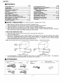
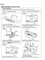
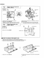
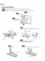
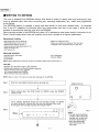
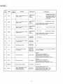
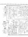
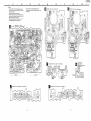
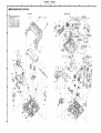
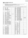
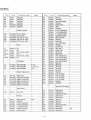
1
ORDER NO.AD9403060CO
A2
Cassette
Dolby NR・EquipPed
Deck
Stereo Double Cassette Deck
*
Colour
(K)
Area
Suffix for
Area
ModeI No.
(P)
Black Type
Colour
U.S.A.
(PC)
Canada.
(E)
Europe.
(EB)
Great Britain.
(EG)
Germany and ltaly、
(K)
Asia,Latin America,
(GC)
Middle Near East
and Africa.
AR・1MECHANISM SERIES
(GN)
Oceania.
*Dolby noise reductbn and HX Pro headroom extension
manufactured under license from Dolby Laboratories
Licensing Corporatlon. HX Pro originated by Bang and
Olufsen. “DOLBY”,the double・D symboI and“HX PRO”
are trademarks of Do巳by Lab6ratories Licensing
SPECIFICATlONS
Corporation,
■CASSETTE DECK SECT10N
S’N(Signal level=max recording Ievel,CrO2type tape)
NR off 56dB(A weighted)
Deck system
Stereo cassette deck
Track sys電em
Recording sys量em
4−track,2−channeI
Bias百requency
80kHz
Dolby B NR on 66dB(A weighted)
Dolby C NR on 74dB(A weighted)
lnput se論si量ivi量y and impedance
E『asing system
AC erase
REC(IN》 100mV147kΩ
Heads DECK1
Recording1Playback head(PermaIloy)×1
Outpu量voltage and匿mpedance
Erasing head(Double・gap ferrite)×1
PLAY(OUT》 500mV/500Ω
DECK2
Mo看ors DECK1
AC bias
Recording/Playback head(Permalby)×1
HEADPHONES
Erasing head(Doubie−gap ferrite)×1
For(E,EB,EG,GC,GN)areas 30mV1(8Ω)
Capstan drive(DC servo motor)×1
(Load impedance8Ω一600Ω)
Reel table drive(DC motor)×1
DECK2
Capstan drive(DC servo motor)×1
Reel table drive(DC motor)×1
Tape speed
4.8cmlsec.(1−718ips)
For others
Powerconsumption 28W
Power supply
For(P,PC》areas AC60Hz,120V
Wow and flut電er
For(P,PC》areas
■GENERAl
0.1%(WRMS)
For(GC》area AC50/60Hz,110V1127V1220V/240V
0,07%(WRMS)
±0.2%(DIN)
For others AC50160Hz,230V−240V
Dimensions《W×H×D》
Fas量fo…ard and rewind量imes
430×136×285mm(16−15/16”×5−5116”×11−7132”)
Approx、50seconds with C−60cassette tape
Weigh量 4.4kg(9.71b.〉
Frequency response(Dolby NR off》
NORMAL 40Hz−15kHz±3dB
No量e=
For(P,PC》areas 20Hz−17kHz
Foro量hers 20Hz−16kHz(DIN)
CrO2 40Hz−15kHz±3dB
For《P,PC》areas 20Hz−17kHz
For oセhers 20Hz−16kHz(DIN)
METAL 40Hz−16kHz±3dB
For(P,PC》areas 20Hz−18kHz
For others 20Hz−17kHz(DIN)
’][1echnics
Disign and specifications are subject to change without notice.
Weight and dimensions are approximate.
RS・TR575
■CONTENTS
Page
Page
25∼30
31∼33
34∼36
SAFETY PRECAUTlON..■....■.■.._。__..._.._.._.....
2
ACCESSORlES......._、..__.._._..._騒._、_,_甲.
2
CONNECTIONS......■.._..........
MEASUREMENTS AND ADJUSTMENTS.
3
TERMINAL FUNCTION OF IC.....__.._.
CAUTlON FOR AC MAINS LEAD._.._._.......”.......
4
FRONT PANEL CONTROLS......”.■.......昌.5..■........巳.._、
5
6,7
TRANSISTORS AND DIODES.......
37
BLOCK DIAGRAM........
38∼40
ABOUTTHEATC FUNCTlON....■.6..巳..■......_._.噂....._、
8
SCHEMATIC DIAGRAM._...
41∼50
SEIF・DIAGNOSTIC...._._
9
PR’NTED CIRCUIT BOARDS._、.._..._..
51∼54
DISASSEM BIY I NSTRUCTIONS.6...、.._._._.......5.....5..
10∼14
WIRING CONNECTlON DIAGRAM....._....
55
PIAYBACK_一■一..._、一..。.一....■..匿一...一1■...1一.ロ.一.一.一ロ_._■.幽.一_._層噂
HOW TO CHECK THE MAIN P.C.B........__.___
TROUBLESHOOTING GUIDE.■........__..
TERMINALGUIDEOFIC,S
REPIACEMENT PARTS UST_......_.......
14,15
lNSTALLATION OF THE SUB CHASSIS ASS,Y...._....
15
CABI N ET PARTS lOCAT10N..__
INSTALLATION OF THE CASSETTE HOIDER ASS,Y..
56,61∼63,66
..... 57,58
16
M ECHANISM PARTS LOCATlON......_..
59,60
REPLACEMENTOFTHE FOOT......_...
16
RESISTORS AND CAPACITORS.........._.
64∼66
REPLACEM ENT OF MAI N PARTS......_.__.。.■........._.
17∼21
PACKAGlNG..__........._
66
WRITING TO EEPROM_......■..■..._
22∼24
■SAFETY PRECAUTlON(This“safety precautlon”is applied only ln u.s.A、)
1、
Before servicing,unplug the power cord to prevent an electric shock.
2、
When replacing parts,use only manufacturer’s recommended components for safety.
3、
Check the、condition of the power cord. RepIace if wear or damage ls evident.
After servicing,be sure to restore the Iead dress,insulation barriers,insulation papers,shields,etc.
4.
5.
Before retuming the serviced equlpment to the customer,be sure to make the fo”owing insulation resistance
test to prevent the customer from being exposed to a shock hazard.
●lNSUIATION RESISTANCE TEST
1.Unplug the powercord and short the two prongs of the plug with ajumperwire.
2.Tum on the power switch.
3.Measure the resistance value with ohmmeter between the jumpered AC plug and each exposed metal cabinet
part,such as screwheads antenna,control shafts,handle brackets,etc. Equipment with antenna terminals
should read between3MΩand5。2MΩto a”exposed parts(Fig.A). Equipment without antenna terminals
should read approximately infinity to all exposed parts(Fig、B).
Note=Some exposed parts may be isolated from the chassis by design. These will read infinity.
Antenna
termlnal
‘
Exposed
Exposed
meヒaI
metal
part
part
繍
Ohmmeter Ohmmeter
(Fl9・A) (Fl9.B》
Reslstance=3MΩ一5.2MΩ Resistance=Approx。oo
4.
lf the measurement is outside the specified Iimits,there is a possibility of a shock hazard.
should be repaired and rechecked before it ls retumed to the customer.
The equipment
■ACCESSORlES
AC power supPly code.
1pc.
(P,PC) (RJAOO36−K)
(SJA172)
(GN)
Stereo connection
cables ...
(SJP2249−3)
7
ノ ク{
眠 。
o
(EB) (RJAOO19−2K).(E,EG,GC)
(VJAO733).
h
駅
∠
㊦
\
2
Power plug adaptor..... 1pc.
2pcs.
(SJP5213・2)(GC area only)
RS・TR575
■CONNECTlONS
●For《P,PC》areas
Before making connections,make surethatthe powertothis unlt
and all other system components is tumed off first,
囮
St●r●o oon“●c電ioo c8bl●
White(し)
Red (R)
Avoid Ietting the cables touch each other as much as possible,
otherwise noise wiIl be generated.
Receiver
or amplifier
Placement hin量s
ACωTLεTS
o
lf this un建is placed near a receiver or a tuner,a“hum”noise
γA匠
Rεαouη崩γで’脚
麟審 ⑯1
日
may be heard during tape playback,recording,or AM reception
目ロ
of the receiver or the tuner。
If this occurs,Ieave as much space as possible between the
units,or place them where there is the least amount of“hum”.
\
o
AC尉∼
心
Rεα置醐阯《》{0囲
ACOUTLσ
回
or Household AC outlet
(AC120V,60Hz)
離
D
③
0
噂“AC・UTLET”(UNSWITCHED》
Power is aIways available,regardless of the unit’s power
Switch Setting.
Cと》nnect璽his cord after
a”o重her cables and
Audioequipmentratedupto100Wcanbeconnected.
cOrds are conneCted,
●For others
Before making connectlons,make surethatthe powertothis unit
For(EB)area only
and aII other system components is tumed off.
BE SURETO READTHE CAUTlON FOR AC
圓
POWER SUPPIY CORD ON PAGE4
●Avoid lettingthecablestoucheach otherasmuch aspossible,
o窒herwise noise will be generated.
●Although the figure beめw shows the AC power supply cord be−
BEFORE THE FOILOWING CONNEC・
丁匿ONS.
ing connected to a household AC outlet,if the amplifier(or
receiver〉isequippedwith an ACoutlet,connectthecord tothat
For(GC》area on’y
Set the voltage selector to the voltage setting for the area
outlet.
ln which the unit will be used.
[Usea minus(一〉screwdriver]
Placement hints
lf this unit is placed near a receiver or a tuner,a“hum”noise
皿
may be heard during tape playback,recording,or AM reception
lf the power supply ln your area is117V or120V,set to
of the receiver or the tuner.
the“127V”position,
if this occurs,Ieave as much space a$possible between the
units,or place them where there is the least amount of“hum”,
Note that this unit will be seriously damaged if this setting
is not made correctly.
lf the power plug wilI not fit your socket,
use the power plug adaptor(included).
S豊●閥ゆco““●C電lo“cab㎞
Whi電e IL》
k
Red
辱 辺 。rrece,ver
o
一蔽
劇αの酬㈹
Ω
OQ
9Qo
薙・匝ン
AmPli壼ier
(R》
{,
For(E,EB,EG,GC》areas only
⑩⑩
⑯
Inse『髄on of Connecto『
’
Even when the connector is perfectly in−
圓
\
serted,dependingonthetypeofinletused,
the front part of the connector may lut out
as shown in the drawing.
奪圏
艇醐酬㎝η
D ⑯
④
d
−
However there is no problem using the unit.
α》nnecUhiScOrdaIter「
a爬01her cables and
CordS are COnneCted
・Voltageselector
F ‘GC、
For(GC)area
Connector
茎
画
Household
H
AC ou璽let
\
\
、4
\
Approx,6mm
ApPliance inlet
一3一
RS・TR575
■CAUTION FOR AC MAINS LEAD
For(EB》area only.
For your safety,please read the fo”owing text care−
fu”y。
This appliance is supplied with a moulded three pin
mainsplugforyoursafetyandconvenience.
A5−ampere fuse is fitted in this plug.
Should the fuse need to be replaced please ensure
that the replacement fuse has a rating of5−ampere
and that it is apProved by ASTA or BSl to BS1362.
Checkf・rtheASTAmark愈・rtheBSlmark甲・n
The wire which is coloured BROWN must be con−
nected to the terminal in the plug which is marked with
theIetterLorcobured RED.
Under no circumstances should either of these wires
be connected to the earth terminal of the three pin
plug,marked with the Ietter E or the Earth Symbol
、去.
Befo『e use
Remove the connector cover as fo”ows.
the body ofthe fuse,
有
盲
If the plug contains a removable fuse cover you must
ensure that it is refitted when the fuse is replaced.
Connector
cover
劃
If you iose the fuse cover the plug must not be used
N
until a replacement cover is obtained。
舷)1ノ
A replacement fuse cover can be purchased from
your local dealer.
How to replace the fuse
CAUTION!
1.Remove the fuse cover with a screwdriver.
lF THE FITTED MOULDED PLUG IS UN−
SUITABLE FOR THE SOCKET OUTLET IN
YOUR HOME THEN THE FUSE SHOULD BE
REMOVED AND THE PLUG CUT OFF AND
DISPOSEDOF SAFELY.
THERE IS A DANGER OF SEVERE ELEC−
Fuse cover
....‘7∼・!εεf恐
−一’ノー一一.も‘“一、‘‘’‘‘一占一一
諌
舷ll
TRICAL SHOCK IF THE CUT OFF PLUG IS
INSERTED INTO ANY13−AMPERE SOCKET.
If a new plug is to be fitted please observe the wiring
・、↓
〔
2.Replace the fuse and attach the fuse cover、
code as shown below.
If in any doubt please consult a qualified electrician・
lMPORTANT
春一”鞠㌦馬
The wires in this mains lead are coloured in accor−
べ
dance with the fo”owing code=
舷l t
Blue: Neutral
Brown:Live
As the colours of the wires in the mains lead of this
appliance may not correspond with the coloured
markings identifying the terminals in your plug,pro−
ceed as foIlows:
Thewirewhich is coloured BLUE must be connected
to the terminal in the plug which is marked with the
letterNorcolouredBLACK.
一4一
・魅
Fuse
(5ampere)
RS・TR575
■FRONT PANEL CONTROLS
When any of the numbers indicated below is repeated more than
once(forexample,②),thenumber indicated on the Ieft lsthe con−
trol for Deck l and that indicated on the right is for Deck2。
①
③④中⑥⑦⑧⑨⑩⑪⑧⑫④③
/
!
②
、
\
脊甲
IIlI
l聾 ︸1
②
し一イ)
徴﹂E
創N▼E爾1
皇誰纂
nE綴麗
叢
壽巴
DECK2
卜1・卜1
Lr1甲1]1単「δ準
1
113 ハb.
鴛 …
む
DECK1璽“7ル1搭穐1運市一ト
一
L
ORξCしEV臥
一
l I
14
1516⑰18⑲⑳⑳⑳1918⑰⑯⑬⑭ ⑮
ハ融me
ハハo.
①Power“STANDBY(b’ON”switch
(POWER,STANDBY(b,ON》
瓦ame
⑫Dolbynoise・reduc量ionbu量ton
《DOIBY NR》
Press to switch the unit from on to standby mode or vice
⑬Reverse・sideplaybackbut量on(〈》
versa.In standby mode,the unit is stiII consuming a smalI
amount of power.
⑭Stopbutton(■》
②Cassetteholder
⑮Fo㎜ard・$ideplaybackbut量on(〉》
③Autotapeca”brationbutton(ATC》
⑯Rewind,fastイorwardsearchbutt・ns
④Open,closebutton(ムOPEN,CLOSE》
(<国く唾,レ>レ》TPS》
⑤Remotecon量rolsignalreceptor
⑰Pausebutton(llPAUSE)
(Refer to“About the remote control function”on page7.)
⑱Automatic・record・mutingbutton
⑥“STANDBY”indicator(STANDBY》
(OAuTo REC MuTE》
When the unit is connected to the AC mains supply,this in−
dicator Iights up in standby mode and goesoutwhen the unit
is turned on.
⑲Recordbutton(●REC》
⑦Reverse・modeselectbutton
(REVERSE MODE》
⑳Synchro・star量button
(SYNCHRO START》
⑧Counterrese量bu量ton
⑳Headphoneslack(PHONES》
(COUNTER RESET》
⑨Recording・ba口ancecontrol(BALANCE》
⑳Tape・to・量aperecording・speedbutton
(SPEED》
⑩Display
⑪Recording・levelcontrol(RECLEVEL》
5
RS・TR575
■PLAYBACK
Either normal,CrO20r metal type cassettes can be used.
F一薗陶魍聞
/ 1
1
1
匿
澱緊’ 唯し[鴫1
園
養○・
鴫醗
II DE
1
一
L
1
一 1
□1・1
[一Io『
K1
》1
・1
○ ㊥ 、
)一!上1
F四 ,欄 P附
■“…r■⊂コ=⊃■<同r■rレレ藍
罵閣’苫2
蝋5 [耶1荊
[釜1・1;10
脚瓢 卿▼o鳳瓢 閥
f
冨
5下糊▼o創
盟∼噂
1陶
lDECK2
一
匿
彫 』一一騨顧■■■『』
lll告甲i
PA占SE l I一一一r II
I I
国 箇2 5回
■
The procedures described below are an exampie of playback on
Deck1.
巨7’H繭ER
REVERSE
匡7’ MODE
昇騨、,喩,騰.。.)
尽
Press REVERSE MODE to
select the apPropriate
reverse mode.
一 一 一 一 ・■レ
一 一 一 一
’’’’’’” ←
’’’’’’”
’’’’’’”
し’仁’.し’し’ 面
LdB
−20 一幡 脚⑩ →5
匿ノ¶
監》 R
一 一 ● 一 _
一3 mO 十2 十4
〉
Press OPEN’CLOSE, and
then inSe『量 the CaSSette
Each time the button ls pressed,the Indicator wi岡
tape、
changeintheorder:;コ→¢)→⇔○.
一
PreSS again tO CIOSe the caSSette
;二二2:0ne slde only.
holder,
(二;=):Both sides repeatedly(up to8times).
○○:Both sides,once only.
(Refer to page7.)
回’勲鬼塵犠繍ll漏』』』、1』
Tape opening facing downward.
〈:To begin from the reverse side。
’一7 ’一ン ’一’ 一7 =
し”Lノ .’_’ _’ 回
匿7
DOLBY NR
Press DOIBY NR to select
PLAY 邑哩墨呂”ロ1繋闘1凹鴇”11零”181理”鵠も
監》 R”””II”llll巳II”1”III”IIII唇1
the apPropriate nolse・reduc・
tion sys量em.
=
’ ’ ’ ’ ’ ’ ”
仁”_’.’_”_’
L
dB 一{∼O 騨15 一ゆ
8
’ ’ ’ ’ ’ ’ ”
’ ’ ’ ’ ’ ’ ”
十2 十4
〉
llluminates lndicatesthe side being played.
To play back on Deck2,in steps2and5above,press量he bu量・
’ ’ ’ ’ ’ ’ ”
t。ns(2and5》f・rDeck2.
疋_”_’ ,毛_”_’
一G −3 0口0 十2 十4
【》 R
To temporarily stoP P響ayback
〉
PAusE press II PAUSE.
Each time the button is pressed,the indicators wiII
changeinthe・rder:回」→回一・ff.
The“PLAY”indicator wiII flash,
一
Select the same type as that used for recording,
Press once again to resume playback.
When playing back a tape which was not recorded us−
ing a Dolby NR system,press so that the indicators
go off.
To stop playback
PreSs■.
黒
6一
RS・TR575
Reve畑ef麗ηe赫oη
Abo口孟孟hθremo孟θeoη孟1●01f口ne孟ゴ0η
The reverse function on this unit has three modes(;二2,⊂=),
The RS−TR575can be operated using the remote control provid−
○○).Read the descriptions below and select the mode as
ed with a Technics amp!ifier or receiver、
You can also tum this unit on and off by using the remote control
desired.(Refer to step40n page6.)
included with the amplifier or receiver compatible with the New
Technlcs Remote Control System.
Tape量ra》eI
”ode
Amplifier:SU−V500/A700MK21A800MK21A900MK2
Receiver:SA−GX1701GX3701GX4701GX670
Only one side of the tape(either the forward side
→
←
○
or the reverse side)wi睦be played,and operation
(aS Of April,1994〉
will automaticaIly stop when playback has been
completed、
[See the operating instructions of the amplifier or the receiver for
deta“s.]
Both sides of the tape wlII be played repeatedly
eight times,and then operation wi”automatica”y
During operatlon from the remote control,the“RC.”indicator
stOP.
wi旧ight up.
(lf playback is begun from the reverse side,the fo卜
ward side wiII be played seven times.)
’一”一”一”一’R.C.
R.C.’一”つ ,}”一’
乏_’ 仁’ .し’ し’
’_’ し’ .仁”_’
When量here is a tapo in only one of電he decks
Both sides of the tape will be played once,and
Deck2“R,C』’
Deck1“R.C.”
indication
then operation wiII automatica”y stoP,
lndication
(lf playback is begun from the reverse side,the for・
ward side wi”not be piayed.)
Oo
Whon thore is a量ape㎞each of th●d㏄ks
Abo郎訪e Do1わyηo蜘・redue孟ゴon
The forward and reverse sides of the tape in Deck
l wiIl be played,followed by the forward and
reverse sides of the tape in Deck2,and after this
研5孟em
operation is repeated elght times,operation wi”
The Dolby noise−reduction system is designed to effectively redu・
automaticaIly stoP.
(lf playback is begun from Deck2,the tape ln
ce the annoying high−frequency “hissing” noise typical of
cassette tapes.During recording,the system functions to in−
Deck l wi”be played seven times.〉
crease the high−frequency sound Ievel,the sound,and then,dur。
lng playback,that same portion is weakened to bring it back to
the previous IeveI.
This unlt includes two types of Dolby noise−reduction systems,
To1観e加hro麗8h五ea⑫honθ5
the Doiby B NR−type and C NR−type.
For(E,EB,GC,GN》areas only。
Dolby B・type noise・reduction
Connect the headphones(not inc塵uded》to the
headphones jack、
Noise is reduced to about one−third.
Use this system when playing back tapes recorded by the Dolby−
B noise・reduction system,such as prerecorded music tapes,etc.
Plug type:1/4inch phone plug,stereo type,
DolbyC・typenoise・reduction
Noise is reduced to about one・tenth.
Usethis system forthe recording and playback of sound sources
i l
that have a wide dynamic range and good tone quality,such as
FM broadcasts of live performances,etc,,and for playing back
such tapes.
琶賢○・蜜
DECK1
岬』○㈲
口卜州 事勢専
猟■
DECK2
一
一
『1ゆ『O順
I l
Abou孟訪eDo1わyHX−Proheadroom
l I
θx孟θn5fonεy5孟θm
Headphones
(not lncluded)
ByfunctioningtoimprovethemaximumoutputIevelofthetape’s
high・frequency range,this system permits recordings without a
reduction in the level of the sound source’s high−frequency
囮
Avoid listening for prolonged periods of time to prevent hearlng
range.ln addition,by using the system in parallel with this unit’s
damage.
noise−reductionsystem,recording andplaybackwith agreatlyex−
tended dynamic range is possible.
AbOU孟伽a庇oma孟ゴe・孟ape・副θe孟
fu.neがon
This unit is equipped with the automatic−tape−select feature;it
automatica時y detects the type o tape being used,and then
makes the suitable adjustments of he bias and equa旺zation ac一
cordingly.
7
RS・TR575
■ABOUT THE ATC FUNCTlON
The ATC(auto tape calibratlon)function records a test signal in
order to automatica”y set the bias,equalizer and recor・
dinglplaybackleveltotheoptimumrecordingconditionsinaccor−
dance with the characteristics of the tape being used.
The table below shows the conditions of the display and the
operation of the unit while the ATC settings are being made,
Example=Performing ATC on Deck1
Unitoperation
Dlsplay
The
bias is adjusted so that the output Ievel is the same
at400 Hz and at10kHz.
国uV一Φ >Φ一一コα
(
“BIAS”is dispiayed.
レ R””朋”19”II”””1”
!∂ 、
馬
o’ 覧
一コ
囮PしAY L醜””””1””””1匿1■1
一婚 一” 一6
J3−20
グ ●
, 、
00
一’”一 一”
刃1
5蕉
①Biasadjustmen量
〆、
一 一 一 一
’’’’’’”
’’’’’’”
一 一 ● 一 』
_一_一ノ↓
」
一1一一一一・一一一一甲一一一一一一一一一一一・一一・一一一
’ 400 1K 3K loK Frequency
(Hz)
/ \ /\
1””1”1
−3 ロロ〇 十2 十4
腿■■1”II レ
/ \\、↑
一 一 − 一 一 − ・ 一 一 一 〇 一 . o
噂
Flashes
、
亀㌦亀 覧 亀
馬、
、、、
、
馬
、
噺
、、
、 、
︵Ωo
u︶
is
一Φ
displayed.
>
Φ一
“EQ”
一⊃
印蕪
②Equalizer adjust・
men量
一 一 一 一
’’’’’’”
’’’’’’”
一⊃0 0
Ω.
, ■ 一 一 ■ 一 一 一 − ■ o , 騨 9 − ● 甲 ■ 一 ■ − ● 葡 9 ■ 9 顧 一 ■ 一 一 ■ 一 , 冒 . 9 ・ . 一 晒 一 一 ■ 一 一 一 . 0 9 . ・ − ■
400 1K 3K loK Frequency
一 一 ● 鴫 }
(Hz)
囮LI””””1”llII醐噂1”1 10””1闘
一総 一,0 −6
輔3 ロロ〇 十2 十4
PLAY d9−20
> R曝III611””IIIgl””1” 1”■””1 1》
/ \、...金_/
\
The equalizer is adjusted so that the output
Flashes
level is the same at400Hz and at3kHz.
︵ロロ
℃V
一Φ >Φ一
“LEVL”is displayed、
個コ
一コO
Ω.
”
”
陣 一
囮PLAY ③level adjustment
’/’
一
・琳
一 ン
’’’’’’”
’’’’’’”
一 一 〇 一 一
L””1””1””1”ll9”1 ””口””
一3 口00 十2 十4
一幡 一駅P −6
dB−20
) R I”””9””””II”瞳”
Frequency
(Hz)
一 一 一 陶
0
乙_鷺上漁_\
一 一
”1””” ‘》
o
ρ 、
、
、
一
The tape sensitMty is compensated so that the
Flashes
recording input Ievel and the playback output
ievel arethe Same.
8一
RS・’『R575
■SELF・DIAGNOSTIC
lndicating Procedure
I ndicating Position
圃
To indicate Self・Diagnos量ic Function
/
1.Check both Deck l and2are empty(no cassette tape),
then tum on the power.
2.Pressand holdthe DOLBY(NR)button(formorethan3
10
seconds),and also press the Deck2STOP(■)button
園野覧○…δ.
forabout2seconds until the level meterchangesfrom
constantly Iit to bllnking、
DECK量
一
E∋1・i
of which has the erase preventing piece folded. Then
close the cassette holder.
4、Press the Deck2FWD.PLAY(>)button and pIay the
tape for more than l second,then press the DECK2
STOP(■)button.
o.
1
1
・卜1
邑
邑
ロ主呂鱒□立
}
卜・
lC
園
α
DECK2
}
一.嘲酬 咽 r 嘱一 }
1
1
、 ,
lPOWER旧軋酬
5.1nsert a normal blank cassette tape for DECK2,both A
and B sidesof which have theerase preventing pieces
respectively,and close the cassette hoIder.
\
一・
回へiOf2「・1”1
ld・1,)1
﹀画
一”︸
3.Insert a normai blank cassette tape,either A or B side
i
[
⊂)1
匝
i
Self・Diagnostic Function lndication
(Example》
’’”
’’’”
し
q吟一20 畠憾 一” 一6
レ 臼
ー3 閃O 十2 十4
〔.し’コ
’「.し’
(NOTElRewindthetapeforlor2minutesbeforeuse.)
レ
6.Press the REC(●)button.
This automaticaIly makes Deck 2 perform the
foIlowing operations.
Record an eight second portion with no sound。■》Record a20second portlon off400Hztest signal.
号
TPS・REVlEW search mode←Stop the unit
(NOTE=Thetape hastobetaken up byplaybackforabout l minute.)
7、Repeat the procedure above for Deck1.
8.To check the self−diagnostic results,press the Deck l STOP(■)button for Deck1,and press the Deck2STOP
(■)button for Deck2.
These results are indicated in the respective displays.
9」f there is no fault,the counter display remains unchanged when the STOP(■)button is pressed.
To resume Ordinary lndlca量ion
To retum the display to normal mode,switch the power off and then back on again.
To have the indication apPear again,take the above−stated steps1,2and8.
NOTE=The seIf・diagnostic results are stored in memory.
To clear this memory,press and hoId the Deck2STOP(■)button for at least6seconds until“CL”appears
in the Deck2FL display.
Pressing the Deck2STOP(■)button clears the Deck l memory at the same time.
Be sure to clear the memory after the repair.
Indication Text
SymboI
Trouble
Remedy
lrreguIar action of cassette mechanism.
HO1
HO2
HO3
The cassette mechanism mode switch(S971,S971A)and
(Example)Pressing the FWD PLAY button results in REW
(Check and replace them.)
No recordlng can be made,orthe unit is placed in the
The erase preventing switch(S974,S974A,S975,S975A)
recording modethough the erase preventing piece has
HO5
HO6
HO7
contacts improperly,orthere is a shortcircuit.
been broken.
(Check and replace the switch、)
Pressing the PLAY(〉)button fails to pIay the tape.
Pressing the PLAY(レ)button causes the motor to rotate
The cassette half detect switch(S972,S972A)contacts
lmproperly,orthere is ashortcircuit.
though no cassette tape is in.
HO4
plunger are defective.
PLAY action.
(Check and replace the switch.)
The cassette holderwi”not open orclose when the
OPENICLOSE(▲)button is pressed.
一
Presslng the OPEN/CLOSE(▲)buttton causes the
−
cassette holder to open after it has closed,and vice versa.
No treble is produced when a normal tape is played or
recorded.
Excessive treble is produced when a CrO2/Metal tape is
played,or the recorded treble is destorted and at a low
level.
The cassette holder openlclose detect switch(S803,
S804,S853,S854)contacts improperly,orthere isa
shortcircuit。(Check and replace the switch.)
The auto tape seIect(CrO2)switch(S973,S973A)contacts
improperly,orthereis ashortcircuit.
(Check and replace the switch、)
The automatic tape select(Metal)switch(S976,S976A)
contacts improperly,orthere isashortcircuit.
(Check and replace the switch.)
FO1
When the PLAY(〉)button is pressed,the tape runs a little
and stops soon.
FO2
TPS does not operate.
The ha”IC(IC971,971A,972,972A)is defective and,as
the result,reel pulse is out of order.
(Check and replace the IC.)
The PLAYBACK AMP IC(IC2)is defective.
(Check and replace the IC.)
9
RS・TR575
■DlSASSEMBLY lNSTRUCTlONS
“AT’『EN層『10N SERV醒CER,,
Some chassis components may have sharp edges. Be careful when disassembling and servicing.
Ref.No.
Ref.No.
Removal of the cabinet
1
Removal of the front panel ass,y
2
Procedure
Procedure
1
1→2
CP2
CN3B CP1
)r∠
/ n【/
Cabinet
)
④
②猷.
.ノゆ
’
田o ③
.!ゆ
●
舎
,励
o猷・§。鎌
、
§馨§
\・@⑤
盟/
■〕 /
ノlHUm期 i 〔,
輸
1 / /
\噸⑥
1.Remove the6screws(①∼⑥).
3
論
→
A、一,,,1,i
、
1
\
//〕〕F売一d
※When connecting the FPC board to the connectors,
connect the FPC board so that the both blue ends of FPC board
are faced upwards as shown above。
2.Remove the cabinet in the direction of arrow.
Ref.No.
1
Removal of the power transformer
1,Remove the2connectors(CP1,CP2).
2.Pull outthe FPC board from connector(CN3B),
P『ocedu『e
①②
1→3
Front panel ass’y
u
マ?
、 ノ㊦③
④
ヤ
コ旗ノ
講鎌
島而000
《
ムi轄§
11000
Power
蓮
transformer
・齢 疇
③ 輔
④⑤
3,Remove the5screws(①∼⑤),
1.Removethe4screws(①一④)。
2.PuII the front power transformer in the direction of arrow.
Ref.No.
Removal of the rec amp P。C.B.and
4
main P.C.B.
4.Remove the front panel ass’y in the direction of arrow.
①
②
③④
Procedure
1→3→4
1
CN3B
CP1
、 /
一 一
⑤
喰
.ノ声
’ 冨
!廿
一
1
CP2
−
‘馨
、
r『、 )
〔鼎、,,1,1
乳
1川口ll旧 1 〔
Rec amp P,C.B、
∼
\ 1
”〕 \
FPC board
1.Remove the2connectors(CP1,CP2)。
2,Pu“outthe FPC board from connector(CN3B)、
Claw
Main P,C.B,
3,Release the2claws,and then remove the rec amp P、C.B.
inthedirectionofarrow①.
4.Remove the5screws(①一⑤).
5.Remove the main P.C,B,in the direction of arrow②.
一10一
Removal of the casse廿e mechaniSm
units(DECK
DECK 2)
Ref.No.
5
1,
Procedure
1→2→5
Cassette holder ass’y(DECK1)
〃
1イ、
②
⇒
『
(DECK2)
謙Iid︵
口
“
CasseUeholderass’y
窃Q◎
/o
》
③
Cassette
2
● ◎哨
DECK1)
o
〃
③
1.
Casse賃eIid(DECK2)
σ
①
Drive Iever
Push the
drive lever
the cassette holder
in
the direction
2.LiftthecasseUelidinthedirectionofarrow②,andremove
ofarrow①,andopen
it in the
aSS’y.
direction ofarrow③.
昌
④
Cassette mechanism
unit(DECK1)
Cassette mechanism
unit (DECK 2)
⑤
②
戸
貧
⑥
﹃ 、
①
Drive rack
BIue
ノ
F
口
日
慧
一
⇔
。曝、一
、嵩
1 ノ
ノ
ゆ Blue
i
「一
\1
④
■』
!
自
ノ
−l
4
、魅﹄⑦
、圧
,’
ぎ⑧
、ら﹄③
置o巨 口 〔 口
2 魯
1
彦
FPC
CNIA
board
k
CN2A
\FPCb。ard
B[ue
3,Push the drive rack in the directionofarrow④,andciose
the cassette hoiderass’y.
5.
Remove the8screws(①∼⑧),
Ref.No.
Removal of the
6
FPC
4.Pull out the
mechaniSmangle
Ref.No.
RemovaI ofthe FL P.C.B.
7
Procedure
Procedure
1→2→5→6
1→2→5→6
board from connectors(CNIA,CN2A).
→7
/ r永
瞥
「
Balance knob
娠
Mechanism
’、 ①ang
’、
’、 ④
③
噺、 ②
凝
自
Claw
κ
叉ノ
Rec level
む
knob
o
∼\ ’\
①
\も
le
〃
FL
P.C.B,
③②
④
Claws
the rec Ievel knob and baiance knob,
2.Removethe4screws(①∼④).
3。Release the 4 claWS,
1,Puli out
●
Claw
Remove the 4screWS(①一④).
一11一
RS・TR575
Ref.No.
Removal of the headphones lack
Ref.No.
Removal ofthe operation(DECK1)
8
P.C.B.
9
P.C.B.and operation(DECK2)P.C.B.
Procedure
※For【E,EB,EG,GC,GN】areas.
Procedure
1→2→5→6
→7→8
1→2→5→6
→9
θ1
コ・廻1
’!
γ ①
vイ ②
Operation(DECK1)
P.C.B.
③
④
Headphoneslack P,C.B。
Operation(DECK2)
P.C,B.
●Remove the headphones jack P,C.B、in the direction of
・Removethe4screw(①∼④).
arrOW.
Ref.No.
10
Removal ofthe motor P.C.B.
Ref.No.
Removal of the rear panel
(DECK1,DECK2)
11
Procedure
Procedure
Rear panel
1→・3→10
1→2→5→11
①
Reel motor
terminaIS
Capstan motor
te,rminaIS
’・ For IP,PC】areas.
4 1
Claw
、、
・轡
◎1
8
②
③
l l
づ一→
麟 監、
一、⑤④
Motor P.C.B.
O
『、⑥
1.Removethe6screws(①一⑥)。For【P,PClareas.
2.Removethe5screws(②∼⑥).For[E,EB,EG】
areas,
1,Removethe2screws(①,②).
2.Unsolder the reel motor and capstan motor terminals.
3.Remove the l claw and have the P.C.B.rise a Iittle.
3.Remove the rear panel in the direction of arrow,
■The difference types of capstan motor
terminal are used forthe units.
When assemblinglreassembling,referto
Soldering iron
Te『minals of.
capstan motor
the Fig.1and Fig.2.
※Notice for mounting the motor P、C.B.
4 CNIB
イ 、 ¥》 (DECK1)
1.Cut the bent terminal of capstan motor with
轡詠甥騰2)
anipper.
一ll蜥 。z
2.Solder while pressing the part with a e screwdriver
Or an eqUiValent tOOL
CS971
Capstanmotortermina1
(DECK1)
e screwdriver
㎝tt㎏㎞m陥命母
N 電
$旨
CS971A
(DECK2)
Motor P,C,B.
Fig.1
indicated by hatching、
㏄tt㎏㎞mh禽
ゆ
4.Putting a soidering iron securely on the capstan motor
terminal and raising the motor P,C,B、in the direction of
arrow,unsolder connected pa口:,
Note)When removing the motor P.C.B.,pull outthe P℃B。
indicated by hatching。
Fig。2
severely because the connectors(CNI B,CN2B,CS971,
CS971A)are connected.
一12一
RS・’『R575
Ref.No.
12
Removal of the power supply P。C。B、
Procedure
1→3→10→12
Power supPly
Claws
Power supPly P、CB、
P.C.B.
1や0ぐ
l I l
I l l
I o⑰
Transformer base
l ass’y
o⑦
Claws
2.Release the3claws,and then remove the transformer base
1.Release the3ciaws,and then remove the power supply
l aSS’y,
P.C.B.
Ref.No.
Removal of the cassette holder ass,y
(DECK1,DECK2)
13
Procedure
1→2一→5→13
獣w
Drive lever
⇒
◎
・娘
Cassette hoIder ass’y
1.Puliouttherivetinthedirectionofarrow②,whilepressing
theclawinthedirectionofarrow①.
2,Push the drive Iever in the direction of arrow③,and open
the cassette holder ass’y.
昌
イ
(
@漣
r
〆
¥
Ribofcassette holder
儀
⑤
壷
⇔
、
◎
⑳鴨禽
“
得
》④
\
勉
⑤
〆
Boss of
Cassette holder ass’y
drive Iever
Fig,1
4.Open the cassette holder ass’y so that the rib of the
3.Operate the casse盤e holder ass’y in the direction of
cassette holder ass’y is located to the position as shown
arrow④,andthenremoveitfromthebossofdrivelever.
in Fig.1,and then pu“out it in the direction of arrow⑤、
一13一
RS・TR575
Ref.No.
14
Remova冒ofthe sub chassis ass’y
④
(DECK1,DECK2)
窟
Procedure
1→2→5→11
→13→14
Subchassis
①
ass y
, 一 軸 、
! 、
ノ ペ
//C・nnect・rh・lde}¥
Belt
Drive rack
Chassis
¥
aSS’y
!
¥
!
、、、一,’
』
ぎ
③
④
1.Pushthedriverackinthedirectionofarrow①.
4.Removethesubchassisass’yinthedirectionofarrow④,
2,Removethe4screws(①∼④).
5.Remove the belt.
3,ReIease the2ciaws in the direction of arrow②,and then
Note:Care must be taken to remove the sub chassis aSs’y
remove the connector holder in the direction of arrow③.
with tweezers that the belt is not applied with grease.
Ref.No.
15
Removal ofthe capstan motor
(DECK1,DECK2)
0
Procedure
②
Subchassisass’y
衆
1→2→5→11
→13→14→15
⑨⑧◎
σ
・Remove the2screws(0,②).
Capstan motor
◎
o
Q
◎
[】
O
。態。□
.81
O⊂)○
■HOWTO CHECKTHE MAIN P.C.B.
1。Remove the cabinet,(See Ref.No,10f the disassembly instructions,)
2,Remove the power transformer,(See Ref.No.30f the disassembly instructions・)
3.Remove the rear panel.(See Ref。No,100f the disassembly instructions、)
③④
Power transformer
⇒
ノ
〃
/
議
魏
診
Power supPly P.CB。
Main P.C.B.
4.Removethe4screws(0一④).
5.Insta”the power transformer on the main P.CB,and power
supply P.C.B、
一14一
RS・TR575
Rear paneI
ρo
︾’層⑥
For[P,PCl areas.
ll
!へ、
噛
阜繭⑥
\
⑧⑦ ⇒
㊦
無
脚
/
⑨
9
◎
◎
,6,lnstall the r6ar panel to the main P,C.B.,power suppIy
P,C,B.and power transformer with5screws(⑤∼⑨).
Main P,C.B.
For[P,PC]areas。
7jnstall the rear panel to the main P.C,B、,power supply
P.CB。and power transformer with4screws(⑥∼⑨).
For[E,EB,EGl areas,
8.When checking the solder surfaces of main P.C.B.and
replacing the parts,do as show.
■INSTALLATlON OF THE SUB CAHSSIS ASS’Y
Idler gear
じ「・1
O
⑤ o
O
○◎
十
I l◎ ◎ ◎1
Boss(A)
・ 口・
o
o。う「
Be[t
Boss(B)
。 、
o
0◎
◎ ot
\喚_________ノ
◎
◎・
⑨
十
◎
び )
O
o
o
/コ\
搾1騨)一蹄讐Bl
FVVD side flywheei ass’y
1、Position the idler gear in the between reel gear(A)and(B).
2.Temporarily instaII the beltto the FWD side flywheel ass’y,
(Mechanism stop Position)
boss(A)and boss(B),
Note:Care mustbetakento insta”the beltwithtweezers
that the belt is not applied with grease.
Chassis ass’y
Belt
σ
Subchassisass’y
0
、o
Drive rack
ノ ペ
/ \
⑦
曾
3
(峯一一緬
り\
@
①
①
ノ
㌔
Tweezers
’ヤ②
Belt
③
④
∼
、ノ
3.Push the drive rack in the direction of arrow.
Capstan motor
4.Insta”the sub chassis ass’y to the chassis ass’y with
4screWS(①一④).
5.lnstallthe connector holder.
6」nstall the belt to the capstan motor using the tweezers.
一15一
RS・TR575
■置NSTALLATlON OF THE CASSETTE HOLDER ASS’Y
Loading cassette
mechanism unit
Drive rack
!/〆レf
@謬
{
r
¥
\
\
雇
黛
\
、¥ \
≧一:・
¥
就 \\ o l
\
Ribofcassette holder
aSS’y
\
⇒
o
\
Fig.1
Cassette hoIder ass’y
1、Tilttheribofcassetteholderass’yattheangleasshownin 2,Pushthedriverackinthedirectionofarrow①.
Fig・1,andthenforcQthecasse廿eholderass’ytotheioading
casse廿emechanismunit {レ
Cassette hoIder
assy l
.瞭
②
0
Hole
◎
、離
β
延⑰
Cassette hoIder (P
aSS’y
Claw of rivet
4」nse吐therivettotheholeofcasseUeholderass’y,
※Makesuretheclawofrivetispositionedinthehole.
3.Closethecassetteholderass’yinthedirectionofarrow②.
■REPLACEMENTOF THE FOOT
1.Remove the4heat melted posts on the Bottom board ass’y
Heat meited posts
with a pair of nipPers or similartool.
2。To replace the foot(RKAOO53−A)on the Bottom board ass’y
melt the4posts with a soldering iron or insta”it with a screw
(XTB3+6J).
Foot(RKAOO53−A)
一16一
RS・TR575
■REPLACEMENT OF MAIN PARTS
Friction gear aSs’y replacement
6国DReferringt・“Disassemblylnstructi・ns”(RefN・・14),rem。vethesubchassisass’y・
回Widenthe2inter−clawspaceandpu”・utthefricti・ngearass’y・
o
.◎/
〆 l
へ ¶
I
ClaWS l
1
「
○ ・
lI
I
﹂u
ヤ算
llII
Friction gear ass’y
I
O
1
]
一
II
III
O
1
ノ
ノ!!一
uOO
卜百 o
〕] 己9ρ
_ _’
l戸
國
ノ
噛
一
ll
噛
一一
、
e
’ 、
1 ー ー ー
餅呼e儲灘
「
一
e
巽
_ _ _ ■ノ
鑑
1
1
1
1
IIlし
冒e翫 r
I
I
l
I
l
し
1
1
紬
9
一
1
1
1
I
l
糞
=
IlII
謹
I
\
乙
Il
II
mesh.
I
ノ
/
「
1
II
I
I
I
Oo◎
Bring into the
、
l
Friction gear ass’y
l I l
『
Friction gear ass’y l
I
II
11
I
l
I
I
I
I
l
一 一 一
}
し
Friction gear ass’y i
l
I
I
・● 」 1
『
g into i
l
mesh,I
I
I
I
I
l
I
I
I
I
lntermediate gear l
l
_ 一 _ 一 一 一 一 一 一 一 一 一 一 ’
戸 一 一 } 一 一 一 一 一 一 一 一 一 } 一 一 一 一 一 甲 一 暉 一 一 一 一 } 一 一 一『
、
Ii1
l1
19
II
II
III
IIし
Friction gear ass’y
’
鋭櫻
k
一
ク
オ
1
{
レ
ノ
Shaft
oe
:
:
Claws should be locked in the concave section.
』
e
I
l
{
l
l
2
1
し
一 一 一 一 一 一 一 ’
一17一
RS曝閣『R575
Drive rack replacement
6置=DReferringt・“Disassembly量nstructi・ns”(Ref・N・・14),rem。vethesubchassisass’y.
画Referringt・“Fricti・nGearass’yRepIacement”(precedingPage),rem・vethefricti・ngearass’y.
囲
函 Removethelsc「ew・
Remove the leaf sprlng
eafspring,
ε向
¶戸
。 。目
OOOO
Siide the drive rackfu”y in
・10
。◎
the direction of arrow.
⑰
o o
。。l q
舎
▲
lnserting a screwdriver in the hole,push it in till the cIaw is out.
〆 一 葡 一 一 一 一 一 一 一 一 一 一 鱒 一 一 一 一 一 一 一 一 一 一 一 鱒 繭 一 一 一 一 一 一 一
l
I
膨/㎞w宙㎞
ド
1
嵐
昏
、
l
l
l
l
l
l
I
l
監↓
l
l く向 ・・
ジm
◎⑨
i rρ
:0 D「ive「ack 亭
Hole
饒
I
I
I
I
l
I
I
I
、 赴
堅
留
▼
一!》1
l Claw of chassis
i
o
I
曳
Drive rack
’
Pushing the screwdriver in,slide the drive rack
in the direction of arrow and remove it.
Removethe lever by moving it as shown by arrows①→②.
Remove the spring、
①謄メ②
困
Lever
Drive rack
Drive rack
一18一
RS・TR575
Adjusting hooks(A)and(B)of the chassis to notches(A)
and(B)of the drive rack,carry out mounting,
Mountthe Ieafspring withthescrew,
Notch(B)
Notch(A)
o
◎
〔bθ
Drive rack
G
Hook(B)
Hook(A)
Slidethedrive rack,
Head replacement
6国DReferringt・“Disassemblylnstructi・ns”(Ref・N・・13),rem。vethecasse廿eh・lderas蓉’y,
画Rem・vethelclaw・
画Rem・vethepinchr。Iler・
●Remove bythe same method as on the REVside.
〆 、
/
/
\
/
/
\
⑨ Claw
\ 、
ノ
\\
、
\
/
⑨
Claw
〔
\懇//
\ /
\_/
、ノ
麟四
Remove the2screws,
Widen the2inter−claw space and
remove the head connector.
/1\ \
〆 馬
⑲
¥
㊥
&
/
》
“
蝿
貰
2
\
HeadC。nnect。r/
の
q
蘇
グ
n
l
\ /
ノ
ク/
\ ノ
\
一19一
\
1
ノ
\』ぐ
/
/
\
/
\
lコ
! \
z
RS・TR575
豊
Mount the2screws.
う
δ◎難
ミ
畠 ● ●
。諺
Bring into the mesh.
、
o
Q
呼
. ●
Mountthe head connector.
Plunger replacement
6囲[DReferringt・・Disassemblylnstructi・ns,,(Ref,N・.14),rem・vethesubchassisassy,
Remove the2screws.
O
O O ◎
十
1◎ ◎ ◎ロ
O
・ ● 一
Raise the P.C.B.while
UnsoIder the2points.
keeping it horizontal。
Q
O O
Remove the2screws,
Remove the2screws,
/
/。
/
一\\
②
づ
\
8
口
\\
\
\
∼
1
』,宅 で
ノ
/
口
》
\
/
ケ砺
モ
○
○
争蛎
\
e
\
\
\
\ ノ
^●
Remove the cover.
一20一
\
ノ
/
/
\ 一
RS・TR575
画D!一 \
\
/ ぜ ゴ」
Remove the4claws,
&
Note=Care should be taken that keeping
the mechanism in such position as
pictured tothe right maydisplacethe
flywheels and gear,
ク
u一_
o
一0
ノ
Gear
Remove the plunger.
Flywheel
Plunge「 一、\Sha我
/ \
μ直llo蜥 \¥囎themesh
Mountthe2screws,
\\傑
l 1ノノ
・/
O
O
、β
l◎
Lever
図
O ◎
穿
◎ ◎口
MounttheP.C.B.
Solderthe2points,
Plunger
O
影智
②
O O
』
8
∫幾・L
一
∫∪』ノ礎β拶U
一21一
畠 ●
O
RS・TR575
■WRITING TO EEPROM
This unit is equipped with EEPROM memory that stores a variety of design data and performance data
such as playback galn,bias value,recording gain,recording equalization,etc.,which was programmed
at the factory.
This EEPROM memory is capable of being read and written to more than100,000times. To i”ustrate
this,if one ATC operation is performed every hour continuously every day for ten years,it worId stlII be
possible to successfu”y read and write with the EEPROM.
Data is actua“y written in this EEPROM onIy when ATC ls actuated or when power supply is tumed on or off.
Since it hardly breaks down,there wiII scarcely occur such a trouble as to require repIacement.
Measurement Condi量ion
●Recording・level control;Maximum
●Recording・balance controll Center
●Makesurecapstan and pressure rollerareclean
●Reverse−mode selector switchl#
●Judgeable room temperature20±5。C(68±9。F)
●Make sure heads are clean
●Tape・to−tape recording−speed switchl Off
●Dolby NR switchl Off
●ATC switchl Off
Measu『ing ins量『ument
●EVM(Electronic Voltmeter) ●ATT(Attenuator)
●Osc眺書oscoρe ●Reslstor(600Ω)
●AF osci”ator
NOTE=Before adjustment,be sure to set the AF osciIlator output IeveI to OdB(1kHz):1V
Test量ape
●Playback gain adjustment(315Hz,OdB)l QZZCFM
●OveraII gain adjustment and Overa“frequency response
Normal reference blank tape;QZZCRA
CrO2reference blank tape l QZZCRX
Metal reference blank tape;QZZCRZ
NOTE=Step2tostep70nlyhasto bedoneafterexchangeofthe EEPROM.
Step1
Short the Test Mode terminals with
ashorting clip.
OPERATION RC。B,
◇
F
「
Step2
WhiIe holding down the STOP button on
DECK2,press the POWER
switch to ON.
↓
AII
贋〉
FL display segments except for the four・digit counter on DECK2
will start bIinking to indicate that the deck has entered Write mode.
Atthis pointthe four薗digit counter wiIl indicate“00**”.
Step3
一 一 一 _
’ノ’’’’”
”,’H’,
一騨一_一,爾一,一一瞬剛騨r隅_.一嗣障鋼一層 周一欄一一;「_ 一 。一 『
〆一噸噸 一、
Blinks 8 L
1
、、酒 の{。.15欄
−6 −3 ロCO +2 +4 1
l R
碧
\墜_一一_一一一一_一,一一一_____一_一___.ノ
Fig.1
Notes:
●The test mode terminals
on main P.C.B.should be
shorted with a short clip
as shown above figure.
●After the adjustment
itemS diSconnect the
o
short c聴p.
一22一
RS・T’R575
o
◎
甥瀟贈編2昌鯉銚壽翁差N↓
AND OVERAIL FREOUENCY RESPONSE
INITIAl SETTING UP FOR OVERALl GAIN
▼
Step4
The counter shows a four・digit hex number。 The two high・order diglts
indicate a ROM address,and the two low・order digits indicate the data
●Load a Normal blank test tape(QZZCRA)into the deck under test.
Press the ATC button,then the REC button. The display wiII flash皿
stored at that address.
「「
Example=Set“FF”in address O3
一 一
’’’”』”一’
し’し’ ’’”
Step9
(see Fig.3).
(see Fig・3)・ Step9
鷲 Y
9W
一 一
』 r 一
’’ ’ ”『ン
’’ ’ ’ ”
’︳
h ﹀ ム
,
Step5
REW button.
hlgh−and Iow−order digits
The
皿.
“5A”using the FWD.
“5A”using the FWD.
high・and Iow・order digits of the
button.
button.
Set these digits to“03”
causes these digits to decrement
using the FF or REW
Step10
using the FF or REW Step10
button.
alternately. For fast incre一
menting,hold down the FF or
menting or decrementing,hold
down the FWD.PLAY or REV、
REW button.
PLAY button.
「
「
Begin from address OO and write data up to address7F(data in
口).Checkthatthedataataddress7Fis“00”(end),andthenexit
the write mode.
address number appears.
add「essnumbe「apPea「s・ 旧hemicr・pr・cess・risreplaced,itisn・tnecessaryt・replace(・rwri量
Note=
Note=睡the microprocessor is replaced,it is not necessaryto replace(orwri量e data to》the EEPROM.
of the
For example,writing of the
For example,writing
data O3.5A has been
●
completed when the EEPROM MAP
completed when the
●EEPROM MAP
address O4is displayed、
address O4is displayed、
0
F
’一”一”騨”一7 ’’’’’’”
1’ ’’ ’’ ’”_”_’.L”_’
!’一一一。一。一一。一〇一一一。一一D鱒噸。一一一’、
団 巌。一15鱒沿}6−3。ロ。+2+4 1〉
l R l
\.一一。。一_。。顧一__一一一,一一。一一一。一。’
(see Fig.2).
Adjust the test signal Ievel using the Rec.Level and Balance controls
until the Iine output levels on both channels are320mV。When the
adlustment is complete,release the REC button.(The deck stores
Step8
flash皿sbwly,meaning that playback gain is belng automatica“y
adjusted. Press the pIay button.(At this point the deck automaticaIly
adjusts playback gains.) After this play back the tape and verify that
the output level fa“s in the specified range.
一
一
一
一
一
一
一
一
一
一
一
一
一
一
一
一
一
一
5A
一
一
68
一
84
一
90
一
68
一
84
90
78
60
60
78
60
60
38
30
18
38
30
18
64
68
78
64
68
78
◎
o客}二二一盤5二二−= し甲喚
v v
AF 050量固or
AFo50“a竃or
一
一
一
一
}
一
一
一
一
一
A8
BO
8C
A8
BO
8C
一
一
9A
AA
94
50
70
68
一
一
6A
OF
一
80
80
80
一
一
70
2B
一
40
50
AO
一
一
50
12
一
B8
B4
B8
一
一
72
07
一
66
5E
40
一
一
4C
FB
00
70
74
02
一
一
55
F5
00
47
47
00
=二:ユ
Note=At an address with no data value indicated(e.g.01→一),the ROM operates
normally irrespective of the kind of the data supplied、
) V
∈VM
∈VM
Fig.2
Fig.2
▼
◎
一23一
一
UN〔OUτ
UN〔OUτ ^
A
、\ /
[団.‘凝
1尉E旧
show皿.
一
Fig、3
Fig、3
Standard value=320mV±0.5dB
No量e=1f adlustment of PLAYBACK GAIN fails,the display w“1刊ash皿
rapidly. Afterasuccessful adjustment,thedisplaywilI no Ionger
7
一
C
D
E
F
●Load the test tape,QZZCFM,into the deck and Iocate the section of
the tape where the playback gain test tone(315Hz,OdB)is recorded,
then playback the portion. Press the ATC button,and the display wi“
6
一
B
the data at the moment the REC button is reIeased.)
5
一
9
A
●With no tape Ioaded in the deck,press and hoId the REC button、
4
一
7
8
●Set the AF osci“ator’s output frequency to315Hz1−20dB(100mV)
3
1
6
PIAYBACK GAlN ▼
2
00
4
5
一 一 ● 一 嶺
1
0
2
3
廟 畠 隔 一
Blinks
Removetheshorting clip from theTest Modeterminals. The FLdisplay
Removetheshorting clip from theTest Modeterminals.
The FLdisplay
will stop blinking.
*The data writing process is
complete when the next
「
Step7
↓
PLAY or REV.PALY
PLAY or REV.PALY
data increment altemately each
time the FWD.PLAY button is
is
pressed.The REW button pressed. TheREV.PLAYbutton
of the address increment alter−
nately each time the FF button
altemately.
For fast incrementing or decre−
RESPONSE fails,the display wi”刊ash皿rapidly.
モsetthesedigitst.
After a successful adjustment,the display wi“no longer show
PLAYorREV.PLAYbutton. The
causesthesedigitstodecrement
Step6
Noセe=lf adjustment of OVERALL GAIN or OVERALL FREQUENCY
仁’コ コ〔
’コ コ〔
とSetthesedigitsuSingtheFF。r 一Set these digits using the FWD、
sIowly.(At this point the deck automatica”y adjusts the overall gain
and frequency response.)
●Afterthe above setting,theoverall gain forselection of CrO2and MetaI
tape wi”be automatically set by the ROM and stored in the ROM,
一24一
RS・TR575 RS・TR575
■TROUBLESHOOTING GU置DE
*To perform troubleshooting,set the unit to the state described in the“Motor Control PCB
Checking Method”on page31、
The unit is not turned on.
The voltage is not output at Q608
NO
emitter apProx.5.6V?
YES
The voltage across R624and
When the POWER button is
onloff,the voltage at Q603base
change from5V to OV
NO
R655A is less than16V.
respectively、
YES
NO
Does the voltage at Q603
coIlector change from OV to
15V?
NO
When the POWER button is
on’off,the voltage at pin130f
CN3A and CN3B changes from
5VtoOV respectively.
Q603soldering check or
replacement.
YES
YES
R624and R655A replacement.
NO
Does the voltage at Q604
collector change from−20V to
NO
Q610and−20V system check.
15V?
YES
YES
Does the voltage at D613change
Connection checks for
connectors,FFC cable,
The voltage D614and Q608base
is Iess than6.2V
NO
D613soldering check or
replacement。
YES
solderlng,etc。
Does the voltage at Q605emitter
YES
NO
from OV to8.2V?
change from−0,4V to7V?
NO
R622disconnection,or Q605
check or replaCement.
YES
D614and Q608replacement、
Power is normal.
一25一
一26一
Power switch tums on but
Microprocessorchecksection
mechanism does not operate
(common to both mechanism).
↓
lsthevoltageatMicroprocessor
pin57apProx.5V?
Voltage check:
ApProx.5V at CNI pin9and CN2
CN2pin12
NO
Connection and power check.
lsthevoltageatMicroprocessor
pin60apProx.5V?
Approx.15V at CNI pin10and
CN2pin13
CN2pin10
YES
lsthevoltageat Microprocessor
pin240V?
diagnosis mode(see page9).
lsthevoltageat Microprocessor
Any switch ls not failure stored in
NO
memory?
Replace any failed switch with a
NO
YES
F
「
YES
OPENICLOSE does not operate
NO
ls the clock osciIlating?
(check with an osci”oscope and
1:10probe.)
Does the flywheel tum instantly
when the AC cord is pIugged in?
correctly.
YES
YES
The doordoes not cbse when the
power cord is plugged in again,
YES
second.
NO
「F
Check power,D601and D602
Both powerand microprocessor
circuits and their connections.
SyStem are nOrmal.
Does the head lift once and then
Iower?
YES
NO
YES
YES
S853,S854,CN1③
S803,S804,CN2③
NO
(S803and S804)ls forced into the
Does the plunger instantly pu”
in?
NO
audio circuit
「
Does failure occur in audio
circuit or tape mechanlsm?
tape mechanism
Switch is failure.
YES
on position?
Are power and connection
checks normal?
YES
F
「
To the tape mechanism.
NO
DECK1⑭
DECK2②
microprocessorterminal aIso
microprocessorpin18and CN3
onpositionformorethana
S804are in the off positions.
Does the voltage at the
There are no Pulses at
(
Force the mode switch into the
check door switches S803and
Does the voltage at CNI pin3
change when the door swltch
NO
pin12?
S853,S854
S803,S804
by hand.
Tothemicroprocessorcheck
section.
NO
Power is failure.
change?
YES
Check connection between the
Tothemicroprocessorcheck
NO
ム
YES
Unplug the power cord and force
thedoorto the half−open position
DECK2
NO
L
7
pin590V?
new one.
DECK l
NO
)
↓YES
Check switches in the seIf・
DECK2
Connection and power check.
↓YES
0V(ground)at CNI pin12and
DECK l
)
L
↓YES
pin14
ApProx.7,5V at CNI pin13and
NO
motor PCB and the sub PCB.
section.
一27一
一28一
)
To the audio circuit
RS・TR575
RS・TR575
Audio circuit
Tape mechanism
DECK1:
DECK2:
131膿o「W701①0
Thevoltagedoes not input toAD
change as each operating switch
F
「
Does the voltage change at IC152
NO
pin12when in the REC and Stop
Do pulses develop at
microprocessorpins20and21
O.4V in approx.0.4V
increments when StoP,F、
Play,and R.Play buttons
NO
〉
when REC mode changes to Stop
StoP,F.Play,R.Play,FF
and REW buttons are
DECK2=
Voltage increases from
「
「
Tape mechanism2
Tape mechanism1
increments when Power,
pressed in that order.
lC152is normaL
YES
YES
Voltage increases from OV
in aPProx。0,4V
)
modes?
is pressed?
DECK1:
NO
Microprocessorisfailure,
mode
Does the voltage change at
Does tぬe voltage change at
CN52B pin4when S853and S854
0f the mechanism PCB(or the
CrO2and Metal switches of the
mechanism)are forced into the
NO
NO
microprocessorpin l when
S803and S8040f the
mechanism PCB(or the CrO2
and Metal switches of the
mechanism)are forced into the
on positions?
on positions?
YES
are pressed in that order.
YES
v
Do pu Ises develop at IC152pi ns
2and3in the REC and Stop
modes?
NO
)
Connection checks for
connectors,FFC cable。
YES
YES
v
Caution=
The counte「「eset is
connected to other
mechanism systems,
Example=
To check mechanism1,be
Does the voltage change at CN2
Does the voltage change at
CN52B pin4when switch of the
mec益anism(MODE,Revers REC
NO
NO
mechanism(MODE,Reverse REC
lNH and HALF SW)are forced
lNH and HALF SW)are forced
into the on positions.
into the on positions.
sure to press the counter
reset switch on
YES
YES
Are pulses apPlied to terminals
whose voItage does not change
As shown above,check the voltage at each pin of IC152for the fo”owing:
①Equalizer120μs170μschange.
②Dubbing seed does not change.
mechanism2.
Check continuity of switches
IC152is failure.
pin4when switch of the
13,15and160f IC852when the
NO
mode switch is pressed on?
when pressed。
Are pulses apPlied to terminals
③ErasecurrentdoesnotchangebetweentheCrO2andNormal1Metaltape.
switch is failure.
13,15and160f IC802when the
(Erase current for CrO2and Normal tape is the same.)
Soldering c銑ecks
mode switch is pressed on?
④Decklanddeck2producesnochange.
Connection check for Connector
NO
YES
YES
In case of failure,replace with
new switches。
Do pulses develop at
microprocessorpins26,27and
NO
28when the mode switch is
Microprocessorisfailure.
⑥REC and Play produces no change.
⑦AutoRECmutedoesnotoperate.
microprocessorpins25,27and
28when the mode switch is
pressed on?
pressed on?
YES
YES
Does the plunger pull in Play
NO
Do pulses口evelop at
⑤Dolby off,B and C produces no change・
NO
button is pressed instantly?
Plunger is failure、
Q854,Q804,D802,D852,D854,
D804failure.
lC8010r IC852is failure.
YES
Does the plunger remain puIled in
during FF/REW operations?
NO
YES
Belt has come off.
Reel motor failure.
lC8520r IC802is failure.
一29一
一30一
RS・’『R575
■MEASUREMENTS AND ADJUSTMENTS
Measu『ement Condition
●Makesure headsareclean
●Recording・level controll Maximum
●Recording・balance controll Center
●Reverse・mode selector switch;ロ
●Make sure capstan and pressure roIIer are clean
●Judgeable room temperature20±5。C(68±9。F)
●Tape−to−tape recording−speed switch;Off
●Dolby NR switch;Off
●ATC switchl Off
Measu『ing inst『umen量
●EVM(Electronic Voltmeter) ●ATT(Attenuator)
●Oscilloscope ●DC voltmeter
●Digital frequency counter ●Resistor(600Ω)
●AF osclllator
NOTE=Before adjustment,be sure to set the AF oscillator output Ievel to OdB(1kHz》:1V
Tes電tape
:灘撚黙)1・一
・Tape speed adjustment(3kHz,一10dB》;Q互CWAT
●OveraII gain adjustment and Overa”frequency response
Normal reference blank tape;QZZCRA
CrO2reference blank tapel QZZCRX
Metal reference blank tapel QZZCRZ
●Adjustment Points
Tope speed
Tope speed
Tope speed
lDECK2:Highl ⊂DECK21
‘DECK”
VR802
VR801
MOTOR RC.B.⊂DECKけ
VR803
MOTOR RC.B,⊂DECK2》
OPERATION RC.B。
◇
Shor†qip
亘)
Notes=
●The test mode terminals on mechanism control P.C.B.
should be shorted wlth a short clip as shown above
figure.
●After the adjustment items dlsconnect the short clip.
一31一
HEAD REPIACEMENT
When replacing the head,adjust the head azimuth as instructed below, and rewrite the data to the
(By
adjusting head azimuth,data isautomaticaIlywritten tothe EEPROM.)
(1) (2)
lStep1・npage22 }Step8・npage23
(4》 (3)
IStep1・・npage24( Step9・npage24
EEPROM.
1
1司
adjustment is necessary becausethe playback gain,the overa”gain, and the overa”frequencyresponse are
(The
by the head replacement.)
HEAD AZIMUTH ADJUSTMENT(DECK1’2》
ー ハ∠3五﹃
Playback the azimuth adlustment portion (8kHz, 一20dB)
ofthetesttape(QZZCFM). Varytheazimuth adjusting screw
untiltheoutputofthe R−CH are maximized.
Perform the same adjustment in the play mode.
Repeat the same check in reverse play mode.
After the adjustment,apply screwbck to the azimuth adjust・
R’P.
E.HEAD
ing screw.
(
団
O O
讐轟、ヂ・』λ.8凱
O
EVM
Fig。
一2
Azimuth Screw
V V
〔Playbackl
(Forward》
(Reverse)
1
Fig.
TAPE SPEED ADJUSTMENT《DECK1’2)
Normal speed
﹂ーハ∠
Playback the middIe portion of the test tape(QZZCWAT).
Short the test termlnal.
し崩E OUT
Adjust Deck1=VR801and Deck2ニVR803so that the output is
一
∠
within the adjustment target.
皿つ
3.
0
→P
0 (f一___幽二
一一 “
一幅■
L購一ゆつ
O O
AdjustmenUarget=3000±15Hz《NORMAしspeed)
一
一
Dlgl電al
lrequency
coun重er
High speed【SeUhe unit to fo㎜ard(FWD》mode.I
Fig.3
Press the tape−to−tape recording・speed selector switch(X2) button.
This will set the high speed mode.
5.
Playback the middIe portion on the test tape(QZZCWAT).
6.
At that time,check if the output from DECK l ls within the standard value.
4.
S量andard value=6000±600Hz(HIGH speed》
7只︾
Adjust VR802so that the output frequency of DECK
Release the test terminaL
2is within±30Hz for the value
of the output
frequency of
PLAYBACK GAlN MEASUREMENT(DECK1’2》
団.≦就
し陶E OUT
1.
2.
Short the test terminaL
/
Load the test tape (QZZCFM)into the deck and locate
the part where the playback gain test tone(315Hz,OdB) is
recorded. After this,play back the tape and verify that the
0 α二「.凱=■=ニコ
3 4
Perform the MEASUREMENT described in step2
above
』一
O o
output level fa”s in the specified range.
A
v 〔V})
Fig.4
for
both DECK l and DECK2.
Release the test terminal、
S量andard value=320mV±0.5dB
5.
azimuth
head
When the data is not within the specified range,the
data is
data in the EEPROM rewritten.(By adjusting head azimuth,
should be readjusted as instructed
written to the EEPROM.)
aUtOmatiCa”y
any eXiSt,USe a
different
or crease.
When adjusteing head azimuth,check the test tape for scratches lf
follow instructions l to3below.
(1》 (2》
(3》
Step1・npage2211Step5・npage 231
1
「
一32一
Step10 on page 24
RS・TR575
PIAYBACK FREQUENCY RESPONSE(DECK1,2》
1.PlaybaGk the frequenGy response portlon(315Hz,12.5kHz∼
鵬
63Hz,一20dB)of the test tape(QZZCFM). +6dB
frequency response range
2.Assure that the is within the
shown in Fig.6for both L・CH and R・CH.
就
ノ
1
1
;
v v
!
一
−
’「
咽
[1
川1
1[
Iill
』
『
0dB
→冊
11 、
l I 一一
+5d8
+3dB
+2d8
}
H I−
l I皿
\
:
63Hz↑00Hz200HZ
∈VM
Fig.
l l
1,1
』。.
o ◎
団
■
冒
L
1
11
十
十
1 一
1−1
∠
O G『・一一。一一_ D_一1
閣
『
へ1
UNE OUτ ^
+4de
+3dB
+2dB
OdB
−2dB
−3dB
一466
一6dB
ρ
一
ロ ー
2dB
−3d8
覗 一5de
一 噸
q
1
500Hz l kHz2kHz4kHz .5kHZ
315Hz
8kHz
5
Fig.6
ERASECURRENTMEASUREMENT(DECK1,2》
1.With no tape Ioaded in the deck,press the Record button.
2.Check if the output at this time between the erase current
DECKll■固■
c・nfirmati・np・intDeck1ニ」551(Deck2ニTP1)andGND DECK2:囮■
(chassis)(the output on both edges of Deck1=R358(Deck
2ニR308))is withln the standard value.
O鴫
十
ERASE円EAD) {}W㌧
Standard value=175±15mA《Me量al》
EVM Readlng=175±15mV DECK1(L353case⇔」551》
EVM
(Electronic
DECK1:R3581Ω
DECK2:R3081Ω 男7
Voltmeteり
DECK2(L303case←・TP1》
The vo脆age wl”vary depending on量he ground provided.
Measuremen量s mus量be made a“he earth points
Fig.7
(L353and L303coils》mentioned above.
CONFIRMATlON OF THE OVERALl GAIN AND OVERAll
”omalO》●『88”“Dqo●“cy『●8po“8●ch●d醐OUη
FREQUENCY RESPONSE +66B
1、lnthe Record Pausemode,Ioad anormaI blanktape(QZZCRA)
the attenuator,and start recordi ng,
2.While playing back the reference signal just recorded,verify
that the output level falls in the followlng range.
li
、、
』1
’
”
一4d8
−6d8
’
’
’
よ
イ
−
!
”+4d6
[
i
i、
into the deck,and apPly the reference input signal(1kHz,
一24dB)to the Rec。input. Adjust the output to320mV with
+4d3
+26B
Od8
−26B
「1
一
Od8
i
打
一噂
一
−308
冒
【
50Hz100Hz200Hz 500HzlkH12kHz 10kHz
Fig.8
S量andard value=320mV±0.5dB
3.Afterward,apply a signal(frequencyatthemeasuredp。intin C『02
顛●ね10》●ro”響r●qu●“cy r●8poo9●c馳8rt{”腕OUT》
the rangefrom50Hzto10kHz),whoselevel is20dB lowerthan
一!,.
+6d8
63mV》,to
the reference signal Ievel(1kHz,一24dBニapProx.
+4dB
(QZZCRA》.
+2d3
口
0d8
、
1[
4. Play back the test signals just recorded and verify that the
−2dB
levels at the test frequencies fal l i n the
ranges specified in
Fig.8wlth respect to the reference
目
1!
with a normal blank tape
the Rec、input. Then start recording
’
1レ1
−468
淋
壮
1\
l l
T1
signalleveL −668
’
■
5、Repeat steps3and4above for CrO2blank test tape(QZZCRX)
ranges specified in Fig.9with respect to the reference signal
+5d8
冒
0d3
陶⊥.
鞠
一46B
ξ
:
Fig.9
A
u飼E I冠
1陶E OUT ^
1、_
600Ω
σσQσ
1
し
AF osCIlla!Of ATY
1,﹂
IeveL
6.Perform the same checks both DECK l and DECK2.
Steps l through2above are concemed with overall gainl
steps3through5pertain to overa“frequency response.
1
1
1
1
”
50Hz 100Hz 200HZ 500Hz l kHz 2区Hz 12.5kHl
◎O
and Metal blanktesttape(QZZCRZ),in these cases raising the
range to12.5kHz.
upPer end of the test signal frequency
Verify that the slgnal Ievels at the test
frequencies fa旧n the
!
F
_毫 α』一一_一一
〇 ◎
飛 り◎
竪
V V V
∈V闇
05Cll㎏5cope
Fig.10
7.When the data is not within the specified range,the head azimuth should be readjusted
as instructed below the
and
to the EEPROM.)
data in the EEPROM rewritten,(Byadlusting head azlmuth,datais automatically
written
When adjusting head azimuth,check the test tape for scratches or creases. lf
anyexist,use a different tape and
fo”ow instructions l to4below.
the foIIowing procedure and there
8.If outside the standard value,data in EEPROM should be written again by taking
thereafter section1・6should be carried out again.
(1) (2) (3)
l Step1・npage22 1−1
Step5・npage23HStep9・npage24
一33一
(4)
}
Step100n page24
1
RS・TR575
■TERMINAL FUNCTION OF IC
●IC701(M38123M4101F》=MICROCOMPUTER
*To checkthe conteハts of the item“※”in the IC terminal tabIe,set the unit to the state
described in the“MotorControl PCB Checking Method”on page31.
Pin
No.
1
Mark
ADI D2
1’O
Function
Division
1
Deck2Mechanism switch
(FINH,CrO2,Metal,
OPEN,CLOSE)input
2
3
ADDIC
ADD2C
1
1
Common input on Deck l
with analog IC switch
Common input on Deck2
with analog IC switch
4
KEY3
1
Key switch input
5
SEL・B
0
Select output B with the
Power control output ON:
“H”,OFF:“L”
analog IC swltch
Check poin量
Connector
CN2③pin
The waveform changes with the meter input
signal.
lC703③pin
IC701④pin
An analog value from O to5V appears when an
input key for power,synchro・start,XI IX2,NR,
reverse,modification or test mode is pressed.
十5V without any key inputs and OV with the
power key ON.
IC703⑨pin
門『H 2ms Constantpulseoutput.
Connector
POWER
0
7
SEL−A
110
8
MSP
1
9
一
一
Not used
10
DMT
O
Lineout mutesignal output
Connector
ON=“L”,OFF:“H”
CN3⑭pin
11
ECS
O
12
ECLK
O
anaIog IC switch
TPS signal det.input ON:
“L”,OFF:“H”
E2PROM chip select signaI
ON:“H”,OFF“L”
E2PROM serial clock output
ON:“L”,OFF=“H”
No tape Ioad:ApProx.4.1V
Normal tape with tab:Approx.OV
CrO2tape with tab:Approx.1.1V
Metal tapewith tab:Approx.1,7V
lC703⑬pln
6
Select output A with the
※Disc巾量ion
CN3⑬pin
lC703⑩pin
Connector
CN3B⑧pin
一
Connector
CN704①pin
CN704⑤pin
Connector
CN704②pin
CN704④pin
1コ㎜
Power ON:“H”(=5V)
Power OFF=“L”(=OV)
へ
ト』輔 4ms
ll皿, Constantpulseoutput・
TPS mode
No program:“H”(=5V)
Programs:“L”(ニOV)
一
“L”(=OV)when sound is belng produced in the
play or REC mode and“H”(=2.5∼5V)when no
sound is produced ln the stop of FFlREW mode.
論 (ex…F・r↑REVPLAY
5」」㎜ゴr一艦,d、、modeischanged)
5」」旧llllL 鵠潔,ε鵯e搬.
(ex_For⇔REV PLAY
13
EDAT
110
E2PROM serial data
input/output
Connector
CN704③pin
5」」旧IllL 朧f謡h辮s、n
response to ll above。
14
PBADJ
O
Playback adj.output ON=
“H”,OFF:“L”
Connector
15
OSC
O
Audio signal for adjustment
Connector
output
CN3⑥pin
16
STB
O
Strobe(bad)output for the
Connector
DA converter(IC151)
CN3⑪pin
17
REMOTE
1
Remocon signal input ON:
Z701
H and L pulse waveform appears on the input of
“H”,OFF:“L”
①pin
a remOte COntrd Signal,
CN3⑦pin
一34一
Used for adjustment at factory but in the
finished product. Remains at“L”(=OV)。
Generated signals at approx.400Hz,10kHz and
3kHz(square wave(H and L,O and5V)in REC
mode during adlustment of ATC)。
Used to Ioad output for the DA converter(IC151).
RS・TR575
Pin
No.
Mark
1’O
Func竜ion
Division
※Discription
Check poin量
5v Rectified waveform at
both50and60Hz
18
POF
1
Connector
Power Qff det.input ON:
“H”,OFF=“L”
o (clamping at5V)
CN3⑫pin
The microprocessor goes into standby mode
when this signal is removed,
Usua“y H(ニ5V)but L
A few tens fOr a period Of a few to a
19
RESET
1
Reset input ON:“L”,
1
lC701⑲pln
OFF:“H”
〆
一
few tens of
mi”iseconds is first
plugged in when the
player.
Serial data output for DA
20
SDAT
O
converter(IC151)’serial−
Connector
Para”el converter(IC152)
CN3⑩pin
51」欄 器outputin「esponse
ON:“H”OFF:“L”
,
Serial clock output for DA
converter(IC151)1seria卜
Parallel converter(IC152)
ON:“H”,OFF:“L”
Connector
A fewμs Afewms pulse slgnal is emitted
5v鵠 。nlywhenam。de
21
SCLK
0
22
XlN
1
terminal
23
XOUT
O
terminaI
terminal
24
GND
一
Microcomputer GND
lC701⑭pin
OV
O
Latch output(Deck2)for
mechanismcontrolON=“H,’,
Connector
Serial data is sent to:IC801,IC802量and the
mechanism driver IC.
25
MしAT2
CN3⑨pin
Microcomputer cbck OSC
Z702①pin
㎜ 繍lato「wavefo「mat
Z702③pin
㎜ 繍lato「wavefo「mat
terminaI
Microcomputer clock OSC
OFF:“L”
CN2⑦pin
Latch output(Deck1)for
Connector
Select the Deck l data from the serial data and
CN1⑥pin
Ioad it into IC801.
MLAT1
0
27
MDAT
0
Serial clock output for
MCLK
0
Connector
28
mechanism control ON=“H”,
OFF=“L”
CN1④pin
CN2⑤pin
0
FL meter segment output
ON:“H”,OFF:“L”
FL701
∼45
P17
mechanism control ON:“H”,
OFF:“L”
Serial data output for
mechanism control ON=“H”,
OFF:“L”
Connector
CN1⑤pin
CN2⑥pin
Serial data used tocontrol the mechanism driver
via IC801and IC802.
Emitted only when mechanism mode changes.
About Ab・ut4ms
P1
∼
Select the Deck2data from this serial data and
Ioad it into IC802.
26
29
。」欄 Change・CCUrS.
⑫∼⑳pin
0.5ms
+5V
O
−20V
1G
∼
7G
0
FL meter glid output ON:
“H”,OFF:“L”
FL701
⑤∼⑪pin
+5V
O
−20V−
一 ∼52
46
H for O∼8pulses of dura塾ion
approx.0.5ms each。
一35一
RS・TR575
Pin
No.
Mark
1’O
Division
Func量lon
Check poin量
※Disc巾tion
Changes within theO←・
53
RPT1
1
Deck l reel puIse det.input
(take up side)
TRANSISTOR
5V range each time the
Q703
5V
coIlector
through apProximately
。一rLrL takeup「eel・ndecklis
30degrees.
54
RPS1
1
Deck l reel pulse det.input
(supply side)
TRANSISTOR
51∫Uエ SuppIyreel。ndeckl
Q704
co”ector
Fast FF/REW mode is disabIed unless both
signals53and54are active,
55
56
RPT2
RPS2
1
匪
Deck2reel pulse det.input
(take up side)
Deck2reel pulse det.input
(supply side)
TRANSISTOR
Q705
5V。∫しrL Takeup「eel・ndeck2
co”ector
TRANSISTOR
5ざ皿 Supp監yreel。ndeck2
Q706
co”ector
Fast FF’REW mode is disabled unless both
signals55and56are active.
57
VDD
58
・VP
59
AVss
一
Microcomputer terminal
Connector
CN3⑳pin
FL meter pu”down voltage
Connector
一
input terminaI
CN3⑬pin
一
GND terminal(A/D)
Connector
CN3⑩pin
+5V,Backup
一20V
OV
Connector
60
VREF
聾
Reference power supPly
(+5V)(A/D)
CN3⑱pin
CN1⑧pin
CN2⑨pin
Can be checked at pin70f connector CN8010r
at pin90f CN802.
DECK1:
61
KEY1
1
When no key is pressed:5V
Key switch input
lC701⑪pin
When Stop key is pressedl O.4V
When Power key is pressed:OV
When any other key is pressed:O to5V
62
KEY2
1
Key swltch input
lC701⑫pin
63
MODEL2
1
Model selector switch
IC701⑬pin
Deck l Mechanism swltch
Connector
64
ADI D1
1
(FINH,CrO2,Metal,
OPEN/CLOSE)input
CN1③pin
一36一
DECK2:
When no key is pressedl5V
When Stop key is pressed:0.4V
When any other key is pressed:O to5V
Approx.5V
No tape loaded:ApProx.4.1V
Normal tape with tab:Approx.2.3V
Chrome tape with tab:Approx.3.5V
Metal tape with tab=Approx.3.5V
■TERMINALGUIDEOFIC,S,TRANSISTORSAND DlODES
BA4560FT1
BA6265FP−E1
XLJ93LC46AFE
XLU2040F・T2
28
MC14052BFR2
8
,窮5
口
M62352FPEl
No.1
AN7353S・E2
AN7352S・E2
15
4
AN7354SC・E2
14
M5218AL
AN7384N・SG
UPC1297CA
2SA1309AIRTA
クde
Anode
2SB1357EFTA
2SD2037EFTA
クe
巳
C E
2SJ164PQRTA
1SR35200TB
・ダ撫
く 、
8
MA29WATA
o
DTA114ESTP
DTC114ESTP
DTC114YSTP
、 》
Co
16
49
CG
2SC3311A巳RTA
2SD1450RSTTA
MA165TA
MA167TA
MA723TA
RVDISS133TA
17
64
B
擁1
CB
Cq
48
C。穐
2SB1030AQSTA
,〆
:53 32
C
No,1
KSB564ACYGTA
M38123M4101F
RVSGP2S24BC
16Pin
18Pin
o
8
8Pin
16Pin
16Pin
20Pin
24Pin
28Pin
42Pin
C E
MTZJ5RIBTA
MTZJ6R2BTA
MTZJ6R8BTA
MTZJ8R2CTA
MTZJ20DTA
Anode
Anode
MA188TA
Co
グde
An◎de
一37一
LN28RPX
鷺。
A乎c・
■BLOCK DIAGRAM
ハ さ イリド 面
ELECTRIC VOLUME
I5「一一一一一「13
ハ さら ピ 12, 14》
距εh∼IN}曾
{需
Q6−7
VCA con曾ro I
Q g R E C
IBuffer
〔QIOl}u↑e
co n電roI
一事・ 1慧
十B
8
「Vcc
VR705
{BALANCE》
Q8,701
o
o
ヱー
Rec IeveI
Vr ef
VCC
9
+ 一B
N
o
o
①
Fo r〔E,E B,EG,G C,G N〕oreo
31L
5…L
55
32
「
Logic circui,
Mu,e
B i G5
For〔E量EB}E G,GC,GN]oreos.
ド
P。Fl
IPloy=on,
離
a今, a魯, a魯,
1
1
1,9
121
s e I e c曾
【葛
一一一一→一一一「
26
X l!X2
Q3{Q41
DEC K2
H eod
R/P HEAD q一剛レ
1L ch l
【Ploy:on》
一
」L咲
一 8
se l e c量
一十2・”・7・μ1
)____の_℃_」
20
15葎1 謬} 謹1『ヲ1
囮
リド し ハ
圃
ナ
1乙、浮L亙,,葺「
、畷、
16「一『
GND Vcc Vcc
l23
【91
121
E Q
I I{81
戸
V C A
L_
Q655,656
ドロサヒロサ ロ C・mp・r・¶or clrcuけ
l de曾
十B
1
18
ReguIO曾or
L __
I O 2
19
6
4
22 21一
5
X2
120/70
ARM2
RE C2
14 QIO
D2P
AR M I
」
____」
ゆ ら ドドピし
圃
12ch D/A CONVERTER
RTER
Q l
GP I
RegulOlor
一8
l EA DJ2
B i os O S C
con l ro I
ERASE HEAO
D I
ハ ら Q352−556
1る
16「一一贈
、L㌧も211
圃
DOLBY HX PRO
191
GNDVccVccr25
サロは
L__
13
“2》
IO 2
“お
含31
6
4
22
21
_」
3
LF ADJ
十B
_」
9 Q301
Regu!o,or
GH2
81AS一し2〔R2,
一B
5昏D
恥
46㌍
55
Q705、706
56
Swilchinq
榊
l I
、8葦8砦,
ANAL・G I I
MULTiPLEXER I I
、、【,”r l l
MCI4052BFR2
A NALOG
MULTIPLEXER
「一,コ4
一・Rch 8−SEレB I
l A−SεL−A l
l l I l
I4榔 Xl3 2ADDIC ADD2C 5 5 Y
1
西5
D E C K I
z97, l l l l
Y。1,
跡
馴【瞭》遜ド隻」i 」
S971【MOOE》
S974{R.REC
S9721HALF,
INH.,
I3
16
鱗聾
藁輩
L__
お ハの えハのけ ビハ らドドドピユ
し 7 AO8
ilii賛
5AO7 1
【4}AO6【AO5, 量
・ホ』幽
團
MECHANISM CONT.‘DECK2
r一一一一r I I
悔 1
憎 I
D854 1
I
漏,繍灘ll
尺 1
呂 l
悔 1
l
1卜
l
ReoI
島5旱占R図 1
mo曾or
l
I l
I
l I
・94
Cops,oin
dri》e
←
→13
・2腎
MしATI MLAT2
mo曾or
drive
1/0
1
25
「}一一一一一一1
釧
釧
鴫
Solenoid 27
15
雇
鵠年
con曾「oI l
矧
428壱
Ree l
mo曾or
B i o5 0S C
l
_______」
十B VR853
L_______」
con2roI
むハヰら ドユし
十B B
一38一
董
囲
1TAPE SPεEDADJ,
A B
Q302−306
一39一
9
mo,or
exponder
16
d ri》e
Cops雪on,
mo↑or
”
co所ro I
1
speed
A B
3
COP5曾on.
1/O
M C L K
speod
I
con量ro1
28
d ri》e
I5
Cops曾on
l
→16
mo曾or
lPUdrive
暑β撫ii忌e
l
・271
exp。nder→15
MDAT I
Q852
瓢AN図
Z971A
2
Z852 1 1
IL
REC一L2【R2}
_野里_
D O D I
PH
l
MCI4。52BFR2 i
圃 l I
MEcHANl鼎Nエ(DECKI》 I I
AO I2 C」K
GPB−L{R,“8》19
Q2
GP2
FP2
18
“71
l靴一蜘鈎
1
PH・馴N〒囎PTER輯…1ch・㎎書…隣 1言ζl
中↑
8L __
19
FM2
c i r cu i書
Re gu lO曾0『
12 AOII
軒
RTER
12ch D/A CONVERTER
「17
I4r一一一一r響7
φ・
1
C・mp・r・曾・r p「o¶ec雪ion
l de,
ハの ぐハの り
1
圃
.r。 1
V C A
d e曾
A O9
{7}6
⇔・
り セ ら ド ロ
{21
E Q
D504
一印一一「
l1
5
A O6 しD
2
(03
19
A O2
E DAT
RvsGP2s24BC Q7。5,7.4 1 1
・監一鑑
誉二
EC L K
A B C
圃
1号L墨、、聾
“易
Abso墜ロ書e
囮
E EPROM
5反
:c『一一こ鞠
4φc
⑲
8【I D
ロド レ ヨレマドてニハ
しの るし ムドヒ
REC EQ AMP(DECK2}
D503
言6}
腿粒
ハほ さう ロピ 囮
十B −B
Z702
、二1蕪翫
蒔溢
l EAADJ I
X
A O5 C L K
F P I
5
AO4
GREC−Ll‘RD “8,8
、B喜亀』,
」歪聾_
OEC K I
4r一一一一rl6
ド
「 16
GH i
__J
悔
11
ロ F隅1
−B
』
4
00
9
Q5
7
Q3
6
Q2
13
BIAS−LIこRP
1も1
Q7 C LK
5
Q I
」
十B
麟1「ソ
−B
十B
13
02)
9 Q351
1き1
∼ξ}
07}
空
Q6
日
N R
l
I
一一一一■一「
墨Ab5。9u曾e
l de曾
圃
DATA CONTROL
12∬8一一一r1
DISPLAY
FL
婁警難珍
ll㌧
AUTO I5
Q I I DATA
BlC lO
R E C I
D554
DOLBY HX PRO l Pe。k
A
B
C
D
E
F
G
E NC
F L701
態騨嚇喰脚
埴締 難繍欝藁
7
EC S
ドド
ムバアるうさ ロピ D353
16 12
B噌DMT
C噌・SC
D→MSP
ヒロセ のドロ REC EQ AMP{DECKD
13》 171
P BA D J
D
A B C
翫
G
1高1
A一醤
I
E
F
甲
一〇 〇一
A
B
C
D
1
I
一醐1>一噂 一(》階一一く
昌る
纏
」一
一B −B
1Q402,404,406,L402,
“Ol
ICTLl l
‘9
ll
占 O
1
iTl!T21
S701 727
「
K EY5
131
I
1
S7.1.727㊥一引CDSYC
十
Q40ち403,405gL401
醗P X
1
上
十
稼。,
L45
R/P
l
l二/1: 46
__」
5 2.
271
21
{2P
H L S L」S
肺29
;
SS
{5}
1
17
H e o d
■
38
Vcc VccGND「
「一一一一
Q I l Q2⊃
1LVEE____ __
,、一ヱー灘
十
L→旨F鳥・1夕
58
ウー
−VP POWER
122
1 !辮
16 14
『
MICRO COMPUTER
1 6
「一一一一一一一■
Me,erin, Rch
27
“6,
141
ハ さる リピ rよ,蕊
ハさ ド さハ ゆラド
回
[
Rec曾
PLAYBACK AMP
ERASE HEAD X
5
40
39
Q5
回 +
DE CK2
言暑1
1
L E V EL)
R!P HεAD q一ひ
【L ch,
言葛
[
,隻1
1R EC
DεC K I
認1
言』、
11P
D I58
D5
囮
十
朧。鳶35
VR7◎2
早
【L ch}
ぼうセし ハし
1 ヨロご ロゆ 十
寸
1免_
「
DOLBY B/C NR
o
守
o
VCA
PLAY‘OUT,
回
L____
コ,TXl
RS・TR575
♀
AN7354SG−E2
一
+ 申8
−34
〇 〇
8︺
9 10 33
一一く
r幽了一了一←一
1 1
Logic circui雪
59
1
十
9五 3五
牛謂、
「
DOLBY B/C NR
一
① N
「Vcc
胆 1
PしAY璽OUT,
回
一〇一¢△o
一
r
No曾es.
圖
Heodphone5
IIOindico7egpinNo.ofrigh曾chonnei.
2》
に竺二.
十
55
1L ch l
ゆうセド ハヒ
32
31
30
u l l
“21
“31
a塁1
言暑1
3
4Q
B i os
27
6
−VP POWER
U6》
Rec曾
L d「ive〃一二当
MICRO COMPUTER
「一一一一陶一軸「
Me曾erin,Rch
1
鑑
L一______________」
l l
しピロ
回
I
I⇒:RECORDINGSIGNALUNE l
ゆ ろ ペヨの ド
l
Mu曾e
1一一IPLAYBACKSIGNALLINE l
For〔E,EB,EG,GC,GN}qreqs,
rよ,.,,,早瑞,,「
For〔E,EB,EG,GC,GN】Greos.
「
「一一一一一一一一一一一一隅「
122
旧
P O F
し4〕
1 蹄,e
SS
【21》
HしS しL S
l
一一 一 一
一 一
L輩
38
{5}
__」
渇
26
誘
5急1
5魯,
鶏1:
錫。》
“71
工
C D SYC
S701 72γ
S701−72γ
塁る
十
十
工
工
「
・引
ドむムロ A
B
C
D
C一→・SC
D→MSP
』
A諜
ハ し セ ドロ 囮
REC EQ AMP{DECK I⊃
モ
1乙,鵠壁L餌ヱゴ「
B!C
N R
X2
120170
D2P
ARM I
R E C I
GND Vcc Vcc
I25
{2,
E Q
13
19
6
4
22 21
RE C2
8
1
Q6
11
Q7 CLK
5
Q I
QO
g
Q5
7
Q3
6
Q2
13
Qg
I4
』
QIO
悔
11
1
5
GP l
2
19
3
GREC一し“RD O8,8
BIAS一Ll‘RD {7》6
l EAADJ l
I E ADJ2
D l
12
9
17
A O5 C L K
A O6 L D
A O5
A O2
AO4
A Og
AO7【AO8》
ハのロ
AV八∀9
■
4r一一一一「16
16
Q l
F P I
網
PHQTQ INTERRUPTER
Q705,704
53
1
齢
凹、、幽
鈎
R P S l
56
RPS2
22 21
3
Switchinq
ぼ ロ 囮,團
PHOTO INTERRUPTER
0601,602
5ンive
ANALOG
MULTIPLEXER
「一魏、
納e↑erhgRch 日X3 B−SEL−B
l A桝SEL−A
D l51
D I52
1
圃
RTER
12ch D/A CONVERTER
φ・
D O D l
φ1§
I3
」FADJ
AO I2 C L K
15
GP8一し〔R,“8}[9
l4偽 XI3 2ADDIC
鮒5
3 5 Y
A DD2C
l I l
Z971 1
z852 1
D ECK2
D603腰604
1 z97IA
ii難一蓑冤藁趾」i
Y。l l藤一藁
L__
酬 摂
煮ど竺二拝
S971A{MODE〕
Q608,D614
S974AこR.REC.INH,
概S975A{F・REC・INH》
GH2
FM2
Q2
GP2
FP2
o
AO2{AOけ LD
1且
ムの ili三楚
旛占R図 1
dri》e
94
l
Cops曾oin
mo璽or
driv憩
Q852
撒AN坐 鵠十
・欝
+B VR855
l TA P E
1TAPE SPEεDADJ》
一39一
Cops曾on
mogor
spoed
con曾roI
一
l l
l l
ぜ ・2警
ex蝋r→15
1!0
→16
1
o
_______」
4
MLAT l
M DAT
M C L K
1副
i㊥糾
1⑲圃
樵蹴
uΣ
匡
oし
十B
MLAT2
Q605けD613
Regu 010r
ト
α
uタ
o色
臨,
drive
Fo r〔G C〕o reo.
卜
o
D611
D616
ふ ⑫臨
Q6Q3蟹604
\
RegulO曾or
一B
†
幹 聯
1 一牛
C。ps1。r lQ8.2
峰 一 職『 凄L糀 図騨N
ゆ
!O
帰,壽51
1 0dj・ 1
ビ2二」
(
Swi曾ching
帥
AC ロN
Z
(
に
ゆ
supply
十B
ω
D605−608
Power
十B
o
i l
l I
L_______」
A B
に
Q611
囲
MECHAMSM CON’T.{DECK2》
1﹂
5AO7 1
【41AO6{AO5, 1
・蓬肥憾第
ReoI
mo,or
油 1
悔 1
艶 l
隅lL
REC一L2藍R2レ
漏,1瀧 :II
↑o
BIAS−L2{R2}
卜
ハ コ
.旺」
丁601
supply
BA6265FP−El
「一一一一一一『「l D804
D804
L
Q612け613
Power
十B
l NH》
F一一「
9
RegulO,or
十B
S972A〔HALF》
For〔RPC〕oreq5.
モ
十B
・・D2隠熊髪
「一一一一一一一「
D854 1
①
モ
十B
D E C K l
「17
l4r一一一『rl7
D6019602
Dl50
l l l
圓 l
MECHANISMCONT・(DECKl》 1
ハ るる ドドヒド
{21
εQ
4
榊
0705曹706
概S973AIATS!C「021
加S976AIATS!METAし,
良、、、一増樋S8031。PENDEτ,
むS8041CしOSEDEτ》
一GNDVccVccr23
6
吃__!曲
『
MCI40528FR2
MCI4。52BFR2 1
圃
ANAしOG l
t号L惹餌蟹
19
恥
l
181
“2》
4
⇔c
CLK NCφ
5⇔D
Dl NCφ8
・6?D
i
⑪
13
55
R PT2
ム うき リヒ 鉾
1
R PT I
54
Swi曾ching
囲
EEPROM
5反
:c7隅一マ・聴㊥
引ID
E DAT
R E SE T
gene『0?or
回,囮
×LJ93LC46AFE
1”』
EC S
↑一■
I9
si gnoI
團 風
1
5
_」
副粒
EC L K
Res t
REC EQ AMP⊂DECK2,
17
Z702
「一一「 1
12ch D/A CONVERTER
RTER
GH I
嬢陵.
,1樺勤
MULTIPLEXER l
圓
FM i
塁二弊:lll
Q702
A B C
ロ ド イビ 4
さら ドドヒラ
」
3
15
Q” DATA
IO
旧﹄孕
1121
r
ARM2
囮
DATA CONTROL
12∬8一一一r1
髪ード
ハバ ヨらる ロヒ AU’『o
おザ
B瑠DMT
。l
A
8
C
D
E
F
G
廟炉
♂叢’.呂醜
一一
一層O σ一一
縄
{Q402,404,406,し402,
ENC
Fし D聖SPLAY
』1旗
K E Y l
一B −B
Q40』403,405,L401
M P×
F L701
“’野聾藁,
譜310n・
dri》e
一B
Q606,607
supply
Q610
exponder
磐L一一 』鯉」騨
VR802,803 相
Poweτ
十
一B
Q609,D615
D609
一B
Regulo曾or
D610
{TAPE SPEED ADJ.
一40一
RS・TR575 RS・’『R575
1
■SCHEMATIC DIAGRAM(Parts Iist on pages61∼66.》
3
2
6
5
4
7
(This schematic diagram may be modlfied at any time with the devebpment
回MECHANISMCIRCU旧DECKP
of new technobgy.)
回M・T・RCIRCUIT‘DECKll
No量e1=
MA723TA
(110v司27v⇔220v⇔240v) A
KI
弩め
r
oZ
田﹂
o
ω
〆
A
D
9
E㌧
{
B
●S713 =DECK l Stop switch(■).
o
』
nu
卜噛¥
σ》σ》
の←
≦
2
毒そ
5
A
講
270
q》一一
●
①o
ゆo
①3
一
0,022
匡¥
〉ゆ
鱒
膨1藁
匡
ど
①O
L
聾器内
〒
α二e哩
肛
8
7
6
5
4
3
2
馨
)一一③‘〈1〉一舟
5 {
6
》
一
側.
S853
B一バ
ト ー
CN803
G
F
_製Eη
蝶目
B A ’
」
」
』
回MOT・R CIRCUITIDECK2)
CIRCUIT (DECK2》
D804
MA725TA
同
rA
︵ト
卜
●S975A:DECK2Forward rec.inhibit switch in“of督”position.
●S976 :DECK l ATS(Metal)switch in“off”position。
麹
気
〆
ず 濁L<
・AIlv。lta◎evaluessh。wnincircuitryareundern。signaIc。nditi。nandpIaybackm。dewithE
需
o
(』
めo
トお
( )..。.._.Voltage values at record mode.
σ,卜
σ》(
●Important safety notice
〕
A工
o
鴨
三
G
噂
■
02V
2
EXPANDER
CAPSTAN
DRIVE
7
53V
10
8 9
Q2V
7ハ’
1
e 6
030.
『o__一〇
39工笹 工
15 14
49V
12
13V
‘12.助
5 5
『》a一
略 4
一
3 3
2
蝉
oa.
十
ogz:z
ω>
Qo一 一
一
C802
0,022
擁
RM802{REEL
「
TAPE
S PEED ADJ.
(X2,DECK2)
\
Q802
2SAl309AIRTA
}OTOR SPEEDCON工
MOTOR}8奪 8お
①と ①董
/野 睾の
TAPE
SPEEDADJ. ①と
oσ}
(Xl,DECK21 野塁藁
oと
①9
匡
一〇一 一
89工
胃
》
Z802
「一一一一一…藝5下「一ゑ5雇「死R「一『一
×
と
x
o
o
o
め《
め《 ゆ
ゆ
麟・
撫
旧 12
ll ll
7 7
CAPSTAN
MOTOR
SPEEDCONT
ト
ODO
13
じ 9
〆一πv
一
1⊇
8 8
MOTOR
5 4 5 6
Cひ
CN2B
I噸 14
l lO
i/O
ぎ
麟
夢
L〈〉{>一(}一①一(1>
N
ON
讐
① ’
xoゆ
※marksindicateprintedresistor.
RVSGP2S24BC
5
1
ト
lC971A,972A
1
OV
0)
16
17
iIIIl
戸
①n
に
OV
i8
とo
220
』σ》
19
11liI
R971A
)
4
IC972A
︵寸
とト
SupPly Part No.
匡
◎モ
1
DRIVE
愈 竜︽
4
¥Φ罪トうト①
、、
!2
lC971A
D、
OV
49V
4.7V
5
REEL
MOTOR
巽
3
14V l4〉
1 SOLENOID〔PLl DRIVE
1
冒
‘
こ
5
〆一47v
山
lI51Vl II5.IVl
\_77V
一
B
c
8。工
SOLENαD{PLl DRIVE
)
■
OV
3
R820
270
NN 十
Qηロ
o
⑩>
OV
=
8r⊥
〆一14V
A
●The supPly part number is described aIone in the replacement parts Iist, F
琶5十麟
L
1
MECHAMS蘭CONT.
7了V
の ・
ωの
Components identified by△mark have speciaI characteristics important for safety.
When replacing any of these components,use only manufacturer’s specified parts.
●(■■●■■医(+B〉一)indicates十B(bias).
一41一
一
、
●(一ロ1−5<一B〉■−−凹)indicates−B(bias)。
●( 轄州轄轄勢 )indicates the fbw of the playback signal.
●( こ==く> )indicates the fbw of the record signaL
SOLENOID DRIVE
◎QV
Z
(一
の6
卜]
σ》α=
くハ
1C802
BA6265FP−EI
2SDI450RSTTA
Gノ
o』“I
工
1…欝ll
σ》\
1
1
↑く︸
For measurement us EVM.
(
(^
C
D
OV
”
、 Q804
0D_
o(
Σ
唖
鯉
(
(卜
・器2
E
F
9
10噛
ノ
5 〈〉一くト
2
A一
volume control at minlmum position otherwise specified。
)一
N←
B
⊥ 轟継
1
1
1
●Capacityare in micro−farads(μF)unlessspecifiedotherwise.
4
(
A、
涙 4
lI
r一一一一’一一一一一一一一一r
●Resistance are in ohms(Ω),114watt(W)unless specified otherwise.
1K=1,000(Ω),1M=1,000k(Ω)
B
C
D
E
II
Z971A
●S976A:DECK2ATS(Metal)switch in“off”position。
2
CS971A
しB
78
56
1 ●S975 =DECK l Forward rec.inhibit switch in“off”position.
SVIBA4560FT1
Z852
r一一一一一麻■駅■駅一一一
MOTOR SPEED CON’『.
9
C DE
一
89工
M一
■MECHANISM
●S974A=DECK2Reverce rec、inhibit switch in“off”position.
BA4560FT1
Oo_
II
MOTOR
●S974 =DECK l Reverce rec.inhibit switch in“off”position、
1C302,352
49V
Oa,
CAPSTAN
●S973A:DECK2ATS(CrO2)switch in“off”position、
XLU2040F−T1
講
14
“2,M
OD} 135V
“2.IVI
4
●S973 :DECK l ATS(CrO2)switch in“o督f”position、
XLU2040F−T2
OしV
盤缶 “a8Vl
≧①需
●S972A:DECK2Half swltch in“off”position.
lC152
15
15V
\
RM8521REEし
PHOTO
●S971A:DECK2Mode swltch in“o督f”position.
M5218L
8
IIlI
■
●S972 :DECK l Half switch in“off”position.
D
M5218AL
SPEED ADJ.
(Xl,DECKD
9 NTERRUPTER
●S853 :DECK l Cassette holder open detection switch in“off”position.
●S854 =DECK l Cassette holder cIose detection switch in“off”position.
●S971 =DECK l Mode switch in“off”position。
■
10
III81
Qo一
『
12
5
12
1『
Q852
2SAl509AIRTA
TAPE
1C97㌧972
RVSGP2S24BC
●S727 :Reverse−mode select switch(REVERSE MODE).
●S803 :DECK2Cassette holder open detection switch in“o””position.
●S804 =DECK2Cassette holder close detection switch in“off”position.
10
「
←一→トー一
13
1
SPEEDCON工
9
C852
lC972
●S726 :Tape・to・tape recording・speed switch(SPEEDl X1,X2).
77V
I4
∋、
‘
「
Cl
嘉
,「47v
」直
嘲
ト
卜o
220
8
CN52B
1
6
〆一ηV
R971
●S725 :Synchro−start switch(SYNCHRO START).
Production Part No.
2
7
3 4 5 6
0.IV
5.IV
B
陣二
I5
MOTOR
DRIVE
DRIVE
』
ミと
2
4
16
iア
CAPSTAN
MOTOR
MOTOR
匡
2
●S724 =Dolby noise・reduction switch(DOLBY NR;回,回)、
I8
C868
100P
OV
OV
OV
壷
CAPSTAN
REEL
愈 MOTORl
●s723 :DEcK2counter reset switch(couNTER2REsET)、 C
5
19
OV
EXPANDER
SOLENOID〔PLl DRIVE
冒
十口
》①
R:『q
49V
1/O
、A
トσ
円と
急
O
1
r−D
1 、 、
5
1
司
昌
O
1 C
47vノ
Gノ
ノ
E
●S720 :DECK l Pause switch(■■PAUSE).
lC971
■
需r⊥
80工
r−14V
Z
一
1
●S722 :Auto tape calibration switch(ATC).
15十謝⊥
E
F
A
●S718 :DECK10pen/close switch(』』OPEN/CLOSE).
●S719 :DECK l Record swltch(●REC).
●S721 =DECK l Automatic・record・muting switch(OAUTO REC MUTE),
MECHAMSMCONT.
77V
:【
A
ψΣ
卜¥
σ》o
の←
BA6265FP−EI
句劔
oゆN
ト周
十R870
①>
口
り晩
一
A
く︸
●S714 :DECK l Foward・side playback switch(〉).
●S715 :DECK l Reverse−side playback switch(〈).
●S716 :DECK l Fast・forward search switch(レ>TPS).
●S717 :DECK l Rewind search switch(<1<I TPS).
50K I
工≡
箭
﹂︵ トu
●S712 =Power“STANDBY6,0N”switch(POWER,STANDBY ’ON).
SOLENOID DRIVE
1
1
鯉
騨ll 響
I
●S711 :DECK l Counter reset switch(COUNTER l RESET)
B
u
G
7
IC852
2SDI450RSTTA
7c
1
A L〈〉
●S710 =Auto tape caIibration switch(ATC).
lo
C
D一
0;
轟
6
1
5
6
一一一一一『一一一『一『一一1
§導
4
5
B
C
II
﹁1
Z971
●S708 :DECK2Pause switch(■■PAUSE)、
●S709 :DECK2Automatic−record・muting switch(OAuTO REC MuTE).
4
一 Q854
△
Σ
ξv
﹀匡
OEi
N①
のOD
①_
o(
B
o一
卜曹の
σ》の
(
卜
A「
kB・
一口
●S706 :DECK20pen/close switch(ムOPEN/CLOSE).
●S707 =DECK2Record switch(●REC).
P852
CS97『
∫A・
『
78
●S701 :DECK2Stop switch(■).
●S702 :DECK2Forward−side pIayback switch(〉).
●S703 :DECK2Reverse・side playback switch(〈).
●S704 :DECK2Fast・forward search switch(〉〉TPS).
●S705 :DECK2Rewind search switch(<1<I TPS).
Ref.No.
lC4
一
D854
●S601 :Voltage selector in“240V”position.(For[GCl area only.)
〉側_
《
駐
RS・TR575 RS・TR575
9
8
7
6
10
16
15
14
13
12
11
回FLCIRCU酢丁
FL701
編 ※
1
(RSLO176−F}
o ×
働 N
匡※
卜 創
一L
CN704
34
12
FL.DISPLAY
f含一
1 2
剛
QO
o一
卜>
Q⑩
〆』14v
47vノ
4
CN52B
一
−
ノ
》
凹 5V
B〆
SCしK21
SDAT
47V
虐
B
1
J
r
ADCB
GJ/
F=6国Hz
FA
9
﹀o
〉
1瑠
2v
22K
「
轡指
}
㌧E
B
C
D
E
F
G
H
1
4・8V』へ
1
※R725
IQK
C705
※R761
470
蝋
1詑
一口←司
1
一
Z702
〆A
a
電
3
・く一一一く ト「
L}
B
C
D
OV
『
一
LED DRIVE
For〔E,EB,EG,GC, r
GN〕oreos・
v〉、.
…壽圭・四
Z701
25V4.7
日
欝
十
’
蜘館「
※R760 22K
R728
−
POF
46V
REMOTE I
ヒ
ンo
1
﹀o
寸
﹀o
卜
﹀o
』〉厘>
d o
﹀o
寸
﹀o
o
﹀N
寸
※
r
一
OV
RESET
F
RESETl9■
5.5V
18
F=6MHz
粗
2SC33UAIRTA
一
2V
OV
OV
2 3 4 5 6 7 8 9 10 11 12 量3 14 r5 16
寸 o の
﹀q
1
〉
>㌧
一
>マ
」
バ
XIN
言㌔
〔vりQ ロ匡( o う
■r ,
晶
XOUT
21V
OOo」Iuo」3ωoΣQQOのωト
●(く(×oつ【LのΣQO国]国匹o。つ
F、
薫勾
㎜
OV
』 IKEYl
4アV
50ms. 2VIDiv
G KEY2
4,7V
BIASADJ
o
﹀ト
S855
1QPENDET}
GND
‘SYSTEM CONT/
FL DRIVE》
皿 48V
4ADO旧1
MLAT2
968望謬L崎トの縞薯Qの
昌
」
MICRO COMPU1「ER
£づVREF
鮭
『6V
1−155VIP3 1 一一7V
1−88V}P2
一7V
1−5,4VIPl29 OV
MCLK 8
OV
MDAT
MLATl 6 49V
49V
1C701
M;58123M4101F
5RPT
22K
DTCll4ESTP
,
RCDHC−278N
し SENSOR)
「一一一一一一「
1
46V
47V
i
2
オ
一
㌧」
1
1
㌧_47V
r4V
「
Blr−1
A
汚
過L_____」
1
し
}1
㌧
2 METER
、
Rcめ
3+Blε.VRl
Lch
4 E.VR
5 E.VR Rch
6 OSC
7 PB ADJ
8 MSP
9 SCLK
10 SDAT
目 SSTB
12 POF
T。四
13 POWER
DMT
1
>CIRC
15CDSYNC
{CN5
Onpo
16 Fl
E
1
し
1
一
チ 1
CN3A
METER Lch
’A
E
ξ
4、7V
A
RPTl
RPSI
一8V
P4
↓
¢
R731
Q702
CONNECTOR
5
※
’C
w
↓↓
(STANDBYl
¥
WRlτE
{For lC7021
Q707
※
※
1ロ8、8VI
54
7 」
dと
而卜
卜 、
D701
8
OV
』OV
⑱ラ34v
蝋 LN28RPX
u
Z
6 7
撃
LED DRIVE
150
o
5
\
2SC3311AIRTA
R762
α=寸
ω ∫
一i6G
VP
つAVss
47V
‘ OV
)
T=26ms
ヌヌヌ3
q圏 N qD uつ
一 7Gノ
弓7V
R770 嚇 lOK
EEPROM
畑⊥弧
,
5︳
6
謙:8誕
※
﹀雪1
※
1
卜
寸
5
1
1
※
ンゆo
⊃n
oの
ヱ
よ
1
>の
と
oの
と
∠
1
『》製
めr》1Ω
↓↓}」L
5G
一20V
承i5π}一一「
1
94G
48V {RPS2
VDD
,
『
詰丁
OV
︾ゆ1
46V
t3
)
『
タ3…;3
o o ① の
ヌ
4.6V _r
4.6V
『
>鯉
r
『
− 虐
ノ
一16V
∫含
1
「
\\_竺⊃匡亙匡圧匡匡圧正
一16V F
一16V
47K
1
『
▲
9 57
5 3
oo o卜㊤の寸而N−o①OD卜㊤『》
氏 〔L orα冒〇一
_ 『16Vイ
※R706
1
l
7
5
l
\
47K
『
>鯉
鴫
※R705
’
1
[
、
▲ 』
一
』
>製
、
」
>而
、
\
704
47K
>
一
﹀而
<
E F GI H / J K L団N O P Q R S T’
①⊥
一
h
※Rア03一
\
47K
一20V
Ti26ms.
ABCD
i\
﹀9
OV
\
鴫※R
1
CDE
1
ABCDE
oNI
㌧
A
E
十〇=n
﹀里
B
−
/
口卜n
﹀雲
r47v
P
QO一
Q
lC702
XLJ95しC46AFE
「
Z
4
Q709
巳
Q●
り
」 Q
≧¢
≧2
F
一〇 N
〇一 oo
轟 卜嘔〉
…
[
3 2
と ω
3のの⊥
−
[
1
OV 47V
一〇V
4
一〇
u
1
L
匡両
ン里
庫_
一 』
しc
r
ABCDEFGH lJKLMNOPQRSTUVWX
ノ
口oo
卜ro
一 』
CNIA
舩
民
oZ
C868
100P
十_
7
5
5i
o﹀
一
rヱ7v
5
5 6 7 8 9 膠O ll l2 15 14 15 16 17 18 19 σ 1
D・ 脅
1
i7 F2
旧 十B“1
19 D.GND
Q十Bl2》
21十Bl51
咽
一20V,ノ
り
十Bl41
3 −VP
24M.GND
り HPRch
6 HP Lch
∩ HPGND
冒
(6MHZ)
」
ノ
19
18
17
20
21
22
23
24
25
26
MAIN CIRCUITIPLAYBACK EQ AMP/POWER SUPPLY/DOLBY NRIHX PRO/BIASOSC/REC EQ AMP/CONTROL/ELECTRICVOLUME》
l C401
MOTOR
Q I
Q l−4
Cl RCU巳T
国
OV OV
2SJE64PQRTA
lDECK l l
o
HEAD SELECT
CP l
C胆1;}4 CP854
DEC K I
GO.2V
2
2
l I
R/P HEAD
LR。h_
2
5
3
3
5
4
4
n
り
配
o
C2 R2
(
ト
ト
N㊤
o一
(
Σ
PLAYBACK
SIGNAL⊂Lch,
1
AN7552S−E2
陽
2.2M
巳
_と
μ》y
庄
曜と一
Noo
“1卜
一Q
〔と_
Rl7
47
寸
O V
店
26 2
〔O.4Vl
OV
OV
0V
Q)
7
8
4 5
9
21 2
50VO.1
舵
◎5
C B A D
回
C l RCU IT
CP且92 CP804
R/P HEAD
2
2
2
3
3
5
5
LRch_一
CP2
4
4
【L
G o.2V
(
←
剛卜,
ロの
C5 ∼
IOOOPΣ
o
ω
l【2.8V
o
R5
ト
リ
2.2M
み一____
と
「1
1
Vco
●
C6 R6
1 2
色
(
←
ト
寸o
4
o_
(
Σ
Gl6轡
ω
り
匡
Q4
と
寧
OV
O V
RI8
〔1,とVl
O V
No
CI9 120P R25 10K
Φo
}N
α:_
R26 『OK
C20 120P 42 41 40 59 38 37 56
Q405
O
o
灯
DE LAY
3
寸y
o o
寸OD
寸o
り里
OV
‘とΦ
D,、為
匡
oと
守N
‘とN
①
0の
寸一=
りo
25456789
6V OV
一47V O V
臓9
寸
や
α=一
3
41
〇 ナ
①一
_〉
り⑩
N【L
寸N
Q①
φ2
OV
OV
lalVl
O V
0 『1
09V
SS H LS
↓
濁工
1闘。
2 ‘3 14 15 16
0、3〉 OV
o一
_〉
寸O
Qの
く
σ、ト
9ゆ
o里
8き
R406
C22
16Vl O
§餓
L
RECT
6 一一一 1
ロ
S S HしS
MUTE
●
OD
o
寸
N O
尊o
の
L402 りΦ
6800P
OV
O V
OV
O V
∼
十
O V
7
8 9
0)
し
ゆ ト
−5V
o〔L
∈8脳
卍工曙 り£工
Nへi
一〉
十寸O
りゆ
理8
の
(
Σ
ナ
1.5K
彗801
十
と
寸N
C65 C66
のじのし のロのヒ
十
Φ ,
匡(v
.r+rh
B
MUTE
OV
rゴ
Q V
OV OV −5V
7 25 24
LOG l C
0V
x酌
0》
RECT
Q406
し
苫o
OV
0)
Qり 寸
Q
OV
OV OV
5 29
0V
窪
1〉
寸o
りの
N と
=と
寸卜r
一ト
A
Q402 Q404
8斜
トーo
N o
D E F
+CI4
ト
ど
岡
O O
寸OD
〔とo
27V 26V QV
5 4 35 5
B I AS
l26V 〔O V l
α=N 【と_
a=_
88
㌍
o o・
NO
R=_
Q6
Qg o+2
Qの Qo
ゆ4V)「=L
IC401 64v ov ov ov ov ov
oの
寸一
Q
0V 21V OV 6・4) OV
Ny 寸¥
N卜・ NOD
oと
OV【L
O V
轟§f
§§」3
A
じN
め
Q401 Q403
OV
專 苫
lVCA
O V
と
匡
000
Ll 30刃H C61560P
o
寸
8
爲
1−1一一一一1
1 1
Rl2 100
o
o
Φ一
_>
りo
o
寸
OV
5 6 7 8 9 怪 O 『I I2 13 ,4
O V
470K
Q
o
R I4 100
Q V O V
ERASE ×
①
4
O V
−6V O V
S
D
H EA D
o
ω
o
¥
3
o
o
N
N
し
Tl/T2 12Q/70
1000P 2.2M
4
一}一一一一コ
o
匹
o
①
o
匡
一一 」 1
1レ⊥__
占一卜十一一一一一
o
N
匡
苫器
ユ
し
B
卜
め
と
L_封一一」
呈雲M
0V D S OV
lDECK2,
「Lch軸
〔とro
『5
I I I
MOTOR
DECK2
16
18 17
ユ
鵠8
oと
oり
OV
楡5
酌
N〔L
寸N
りOD
61
申
十
φ
llE捷§ぎ齎
R63Z2K
φ2
ド
α=n
1VCA
XI双2
R/P
Nり
α=の
O V
寸〉
り里
4 一一一 5
十
O V
れ
L401
R61 C21
I6VIQ ①と
5・6K O O
①Φ
12γvl
56V
OV 2,アV
GND
C l O
Q2
H EAD
σ》と
R I I I OQ
D S
OV OV
卜
寸
6
}〉
りo
ゆ
十
卜o
←
MPX SELECT!SWITCHING
C I5 C l3
8
“2.8Vl
GO2V
りd工
C
10VIOO 6800P
R l3 100
き とo
o
B
A
PLAYBACK AMP
n
Q401−406
2SC3311AIRTA
ニδ
l C2
融工
R9
1000P 2.2M
,繍1呂階・∠ 盤
ERASE
X
o
o
十
∼
4
囮一
/ 3
o
o
R l C9
2.2M 50VO,1
Σ
.iOOQP
No
¥
色
“2.8鵯
CI く
「Lch“
一6V
『s『
(
←
ト
6里
‘?LAY:ON》
AN7354SC−E2
DOLBY B!C NR
64V
十寸と
一〇
廿Q
a=一
A C B
ー
寸
o=寸
〔と寸
一
L2 50ノ』H C62560P
A B C D
Q302,303
2SC3311AIRTA
C D
BI AS OSC
Q30{
2SB I
B IAS
△
△
6鰍頭瞬61う,、8騨
(6gv〕Q3C
十B 7、7V
Q612,6『3
60
Qd
2SD2037EFTA
REGULATOR
8.5V
6・81!4wlま?贈7,8V
C
D
86
For
POWER SUPPLY
ClRCUIT
ロ ロロ ロ
罷螺
回竃舗ε凝B・
△J
鯉,
CN605
!﹀
こ
\
,G㊥)
(1§8ち28ザ翻膿∼E,EB,EG,G㊥)
』一
舎622\△Q6◎5
一〇﹃eO
一
For〔Fl P C〕o re o s
S.
『
」
CN601
r辱『一
o
Φ ・
α:寸
く
ぐ8里
B塞
_◎
N
ぐ
∼
o
oロ
(
←
δお
Nの
O O
o−
o(
霊ぜ12・5
o
酌
ON
㊤
り〉
の
マ
十 〇
〇
ロ
ぐ
め
o
⑩
〉
の
⑩
ロ
ロ
くヨ
《
∼
阿
o
o
り
C605
6800P
ぐΣ
自
o¥
りo
o=_
十
Q
54v IOK
K
く
Q603
DTCII4ESTP
POWER ON DE了.
AC l2V
R605
一
CN607
4.7K
一15.8〉
壱 CN606
o
れ
れ
oN
o〉
Qめ
N
ハ さ ! 、 」.
一16
5V
Q601
_ _
1△R6521
挫J甲16・5v
Q691多8v
Ol,602
十 ト
o
o
ロ
ぐ
89
〉
の
の
o
N
寸
oロ
ロ
8
(
〉一16.5V
×
丹
十マ
o
o
o
匡
宕爺81
0604
ゆヱ
るOD
匡φ
①
14V
N O
⑩o
Qd ooN I
『Kβ
D6i6 n配
MAI65TA−03
0rレ
O N
( ト
ート Σ
一〇
〇〇
〇一
ON
o〉
Qo
Q609
KSB564ACYGTA
−N
o〉
りo
十
2
一1.2V
△D614
}TZJ5R田了A5
8
D301
(
ト
く
シ
o o
N N
⑩(
oΣ
認
MTZJ6R8BTA
o
製霞ぐ塑
め×
十
OO
卜
一〇
⑩o
ド》_
『
『考09
Oo
QO
QO
江
吟o
Oo
陶N
り_
3 2
L3011
1
o¥
oQ
ド》』D
〔と一
.墳
α:一
一〇
〇〇
α:_
REGULATOR
の OO 一7・7V
△R623 0η 86
α=一
璽ど
Φ9
α;㊤
o
め_
o⑩
Q_
o o
りσ
R625
101!4W
20
0鴎
120P
一20,6V
A B
Q609
UPCI297CA
B 一ヱ2v
\
一27,アV
_o
筒Φ
o=の
①
_¥
のo
0V
R引2
【と一
6.8K
N
のり
雨o
Q6
DOLBY HX PRO
D
A
52V
ぐの
一46一
鴎 ・
り
o
眺,§
E R A S E C U R R ENTめQ
CHECK POINT りの
Nと
崎q
α:一
(
oト
oの
I C302 n里
Dく【
‘2!21 Σ
リレ
lQ8Vl5 R552
0V + 7 1K
lO8Vl6 、
一51V
¥
の
十rり
め
OD
o
め
配
め
に
と
め
o曙
4
_ 124V l
O −6.6V
d
5n
り
i揃Vl
一52V
BA4560FTI
1
N_
岡o
寸
の
oの
めΦ
く
o一
Σ
E.CURRENT
ADJ.CON「「.
Q301
2SAI309AIRTA
POWER SUPPしY
−5,8V −66V
り l C301
R525
↓
10
に一
(
巳Ωト・
n一 寸
一20V
{一26.iv}
820P
_と
l C302
1
1
\
卜
り
十
/
(DECK2}
「
κ》・
N
o面
Q
Σ
σ》卜
卜N
O㎝
めQ
ゆ >
5 4 5 6
7 8 9
−13V −5V −56V −5、6V −5,6V −56V −58V
←42V (一49V)1−33V {53Vll53Vl
o寸
nq
りo
鴨霞1
o
ゆり
自=め
0
0DN
●
VEE
/
一44V
l−3、9Vl
25v4,7 13.lv)Q303
3 十 8
1C302
{1!2》10v2
VC A
/ 1−42)1
OD
!
DET. DET.
①o
“蓼O
めN
りN
回
0.O l5
匡
VC A
ABSO PEAK
ゆ
α=一
8昏818
4
!・v
†B 55V
6V
o
REGULATOR
5
o
ド》一
56V −5.6V −5.6V −4V
REGU
LATOR
+B 7、7v
O− i25V
十
_0.8V
←13.8v}△Q607
△D609
の
Φd
圏》o
⑩o
鷹の
Q606
−74V
寸
め
−5、5V l.3V −5V −56V 5
7 16 15 4 13 ,2 1i IO
ABSO PEAK
DET DET
α=①
一〇
〇〇
o
卜・N
く
Σ
2SBI557EFTA
36 卜 23 10
2寸
国8Vl l−42Vl49Vl{一33Vl(5.3V川53Vl
oΦ
α=一 一48V
C324 −4.4V
C318
O 一 」 R507
−B −15V
⑩
匡
7V
18
ユ
o口o
ゆ(b
Q而
論
no⊃ 、
Ω.
2
7V
03,4V
N
22P l「一一『『一6
Σ
めO I
D502
MTZJ6R8B A
α=一
3
マ寸
o曙Σ
∼
Φ
α=一
一14.9V −7し2V
o
一〇
Φo
18 114W
¥
82V
6.81/4W
撃緊
楡2
⑩
△ R655A △Q608
“3.IVl R609
Q607
oと
ぐ
〆
o
D l450RSTTA
ロ
DRIVE
ぐ
For〔E,EB,EG,GC,G N)oreos.
一45一
lI辮
o
15.5V
o
◎
㊤
Φ
◎
ACI2V CN610
寺 CN609
ぐ
6.8 1/4W
さζ
へ1と
【【ず
瀦
⑩寸
N¥
Φ一
位=o
lC301
+︳﹀
HED} 口
巴竺C!ED}
CN6”
Ar辱『一一『}一
ノ Y
5
1
1
1
1
1
1
1
9
Y﹄ 卜
ET
ハ の ヒヒ 1:
「r脈、。、
602
△T
△T601
o¥
o卜
雪
Φo
匡}
剛Q C317
Q O 22P
7,7V
GC,GN〕
N o
色
ゆo
里と \
No
NO n oo
C320 L303
(
←
寸の
oΦ
岡一
〇(
配
†B l4.I V
〔E,EB,EG,
NO
聾蓬脚慕§1
一B −6.6V
15、8VII29Vl
o
卜一〇
〆》N
9へ『
一7.I V
ぐ一
の
o
匡
巳
マ×
O O
而一
O,O l
o
REGULATOR
十B I4V
イイレ
C312 C314
120P 820P
C6β
ぐ⑩
Q605,608
2SD2037EFTA
D605−610
1SR35200TB
L______」
κIN菰
トサ
ヘ1¥
〇一
匡q
α=一
1
K601
タ
N O
Φo
2SA l309A I RTA
竃
l−15.3V
寸
8、5V 胸Q
151Vρ302R322
10
一58V
十B 7V
口2,5Vl
Oo
_ ㊤一
STABILIZER
CN Ol
POWER SUPPLY
2SBl357EFTA
i3.8V 7V
_15v Q610
ア,5V
Q604,606
藍V OLTAGE ADJ,}
Q610
POWER SUPPLY
竺5
AC lN
(ぎ8篇罷2。/240V)
R餅
D303
MA l65TA
Q611
2SD2037EFTA
△
△
R630 0612
A
B
5
−b I V
B C A D
の 8d 麟
一6.4V
o
N卜
N寸
n>
りo
十
Ωと
め内
o−
α=①
Q l−13.アVl
nq
−14.9V
n o
N
rりと
匡一
△R310
591/4W
Q304
2SBl357EF’『A
eIAS OSC CON1「.
F
■
26
29
28
27
AN7354SC E2
DOLBY B!C 閥R
30
r
_64V △R632
1§健士葱,「謙婦 宅か
LΩO
−o
寸ゆ
o_
Σ 寸Oz ユ 寸o
Qゆ
Qの
§fユ
卜
寸
一〇
σ、一 =
コ寸O
りゆ
辱
_ 十
寸
〆G F
B ’
N>
嚇
5
OV OV OV Oゾ
OV OV
7 −5
1 5 2
一5V OV
25
OV 0V
㎝
匹
!2Q
ロー〉
口十 NN
十寸O
噸
寸o一
OD
10K
訴Q迎工Q§
o一
十
(迦 ユ
μ
4
口+
雪8¢1
o=寸
ぎ
……
一卜曽α:
=と
寸卜
錘
寸;
∈o
N× りゆ
寸
IA
.叫
■
_
R68
色 卜
破工曙
り亀Ω
一6V
1
OV
」
5.2V
lOVl
C24
+口
OV
瞭
2、3V −07V OV
十
A B
、
r
旦
9 10 11
QV
C30
16VIO
⇒†目
阜無…
lCl
AN7584N−SG
l22V)
ELECTRIC
VOLUME
1
u
8 7 6 5
B A
OV
、ノ
0V
lr5Vl
仁
1lC3
R37
1K
寸o
v工
りd
OV
”鄭
、1盤
蕨
「
十
I
OV R54
V
100
A B
}
C630
一一くヨー6,6V
Σ oreOS.
0.OI
ll
E2
Q8
2SC33日AIRTA
REC BiAS C◎N’『,
(
一
の
一〇五
〇一
(
Σ
o一
(
Σ
(1
、
AC
3.5V一卓
B・
4 E.V
5 E,V
6 0S
7 PB
」
r
CN
ME
2 ME
3 十B
(1’
匡
/
\
イ1一
(
CDト
のの
▽ の①
7、7v⑲一
5・4V
「
「
〈i回7v
◎R
16VIO 560
L
16,9VIQ506
醤
嚇
C44 R48
一
1
「
−44V
一
OV
5
OV
JKI
Φ
の
×
寸N
庄d
●
」
− IV
+口
L一
r
』
一 噂
C D 2SC3311AIRTA 2SBIO30AQSTA
一じ BIAS・SC BIAS・SCC・Nt
圭 P
《》R
一 〇V
{1
Q302,303 Q306
13MO502 R322
10
嚇
匡n
十 7 100
−
に
R58 1K
蝋 ;
QV6
7V
R55
8
匿 412!2}
α=寸
cc
●
4 3 2
OV
lI.5Vl
REC EQ AMP
}
VCA CONTROL
5
0V
寸σ、
脇
∈動v
一
と
りo
lC4こ1!2》
璽
OV −7、2
l3 14 15
q
窒「η
具
工。一
NC
lMODESWIIVREFI
AN7353S−E2
C B
SWITCHING
OV
l6.9
呪 擁
OV
6 7 8
り需
N9
の需
9 10 11 12
1ト
OV
專5⊥
Q6工
Q5
DTAII4ESTP
一L
旦
昏
鴇望
50V2.2
鞘
22V
5
鰍
■
S
・讐野
1乳7V
o一
_>
寸o
oの
OV
21
9 2
OV 一5V 0V
一5V
5 イ
ゆ× ov Q6
.疹
寸〔L
「, OV
α=椅
SIGNAL⊂Rch, C45 R47
16VIO560
+口
シ
46、6
15 16 1
1 2
膚遭
1
遷翫
曾
EQ
池一寸
C65
)
33 HLS しLS
oON
寸
(
σ、←
9ゆ
o里
(
Σ
OV OV
ゆ凱
髄ぎ
鵬
彫1もも
OV
0V 〔0、6Vl
一
+口
11
難1
1
酬
と
ゆo
寸σ、
S
51V
O
R4
22M
Q7
濃 ︵ V
09V 03V
+8
禄
EQ
MUTE
) 目 12 13 14
A選
一 一
チ
RECT
lO.9V
16VIO
遍
V トー 一 め
70
OV
1
No
りの
ぎ
陶 HLS HLLs
伝懸1 ■
〇
>
ド》o
り_
鑑
C29
12.2Vl
OV
OV
1.IV 16VIO
OV
OV
6.4V OV
『0.7V OV OV
O l8 昼 16 15 r4
3 2 ∼ 2 I
I9
I
5 22
● 場
瑚
1LOGlc
o
薪
ゆ>
+口
とo−N卜・鷹
雪星
2.6V OV
と
10K
1
卜
寸
o
σ、と
C23 めσ、
50va2 匡め
R67
“ ・黄
MUTE
加
舶
『
o
一72V
◎L
嚇
十卜{
一\r
P︵
轟・
OV
σ,一
〇く 〇〉
N
−N
十 ギー〉
言菩溜冒QRTA需5⊥
Qd工.
, 16V22 REC LEVEL CONT・
”
H
』趨D暴
Q9.10
、ヱ217
−
35
一 ヱ
一﹂
石 o㊤
寸一
一
OV
佳
Nの
の
O㊤一
寸一
〇(
Σ
「
34
↑ \REC ノ
(
_卜一
C33
Aヤ
E F
P
−
甲
「
‘
〈,、
}
− 33
7・7V \
〆 271/4W
4
一
人,選⊥
32
31
8 MS
9 SC
lO SD
lr SS
PO
r l2
3 PO
難 DM
CD
Fl
F2
RS・’『R575
1
RS・TR575
1 墨 Z 醒 3 4
ロ ー
5 − 6 7 8 9
量
重 1
量
□RECAMPCIRCUIT
UPCi297CA
(
ト
_臥8vノ
而ゆ 一
ニニ而 ’
冒
DOLBY HX PRO
轡…
=
の吟り
まゆ_
噂
1
9
りo
←4.2矯 1−5粉
一4,9V
7V
−5.6V
−1,3V
C370
Φ一一
5.7V−5,7Vづ,7V−4.IV 22P
no一
1
ON
ト
Σ
OD
)医監
与
り
のo=
,鍔9瀞6
しくト_一一一
o¥
多 no
n』D
に一
6 L352
り雪 のo
ゆO=二一
りN
一
顧 ノ
⑩N
ΦN ム
=二めq
りO
一6.6V
冒
Q354
1舛,5Vl
2SBl357EFTA
−4.8V
奪
I3.7Vl
nX
α=一
Lch IN
仁
噸
†Bl61
〈
−B{2》
=
、D
/,7v
口 ゆめ
にn
QO十
の
(2,2Vl
OV
1.2V
OV
OV
一〇.アV
11
叫1憔
EQ
1
3
OV
︸ 一 一 08
ロ85
0
一
ら
OV
5.2V 2,8V
lOVl
7
2.2V
−O.7V
OV
OV
OV
イ )
イ、 う
、
屡
8 BIT
R−2R+SEGMENT lD−Al
一
11!と1
OV
0V
旦
i㌣
R−2R+SEGMENT
辱
十一
od
の>コ
go
の
98
て
爾
皿
十﹄
N
①N
寸>
N9
ゆ>zz②
り里
輸
¥1讐1喜
4.7V
餅
↓
}
L
l L
ト1
I
■』
雛i雛黙
冒
……
L L
“2り月騨一打
/
‘
‘121
」
、
Hユ
}
しト し
D−A D−A D−A l ID−Al
LD−A
/
ヲ
1
駐
D−A D−A
D−A CONVERTER
旦
一
OV
−A D−A
181 1 膿朧翼
1、8,
‘
ト
OV
l2.2Vl
(
一
REGISTOR
㌧
1ノ
」 10 1! 1
◎
4
,川川月川
TC
“21
OV
DDDDDDD DDDDD
O I2345678910”
8B T
L
[
5
12BIT SHIFT
D−A CONVERTER
哩
−6,6V
12.2Vl
2.2V
一 一十
⊥.き
o
寸と
十寸一
=;の>
トリ
R=o Q卜噂 りΦ
T トo
寸 一
−8、
A∫
イ
曹
5 4
N0.9V
.8V
1.2V
5ノO.9V
V
“.7Vl
窺
OV OV
lI.7Vl 〔2.2Vl
Q656
o
葛9
2SBl357EFTA
POWER SUPPLY
4,7v/
Ll
.憧
OV
レ
裾 8
EQ
了V
I5 14 1
1
胃
鉱 OV
転v
層
oNNゆト肛
響5
〇V
∋
1 2
』
o
の9
の> 口
りo
一 .
ゑ ゆ一A B
A
冒
09霊
寸
σ》o
寸>
I2ch D!A
’CONVERTER
C B A
冒D
4謹
OV
0
_9 モ賭 りo
げ》一
てL の>ロ② α:φ o
= ト 口 の〉
寸十 り2
りo
㎝と多
一
卜
3
6.6V
B
乏
十陶
窪而
一
卜①
α=
▼
寸
①
.ΦΩ・
レレレOV
十 ×お
σ、
A B C D
)
納62:352FPEI
、
し言
多
lCl50
噺
CP7
1EADJ2
STB
SCしK T・四MAIN
CIRCUlT
SDAT
lCN71
D,GND
Onpoge48
II﹃
「
’D f
N
N
卜>
寸o
口
りゆ
⊥A r
∫倉
●
r −
_1)
r
4
REC EQ AMP
卜 肖
}一
−6’6V一\
AN7353S−E2
0npoge48
鳳良
1
噸
IC5
‘CP51
A B C DE
,
6
” POWERSUPPLY
39
T・回MAIN
CIRCUIT
十BIIl
一15V
邑
8登『 2SAI309AIRTA
ヤ㌔▼
1†Bl5}
■
偶f ∠
△R言潔
1!4W39
隣 Q351
R80A
Rch IN
−BU》
、 ’
R齢12
o『「
愚
1’
BIAS OSC CONT.
l4,9V
韓
」φ丁
REC l
AR納 I
ム ヌ
礎冨llエ
超レ
A
l4.M ひヘヘヘー
ll
E.CURRENT ADJ.CONT,
12QP 820P
CN5
、
A.Gトの
〆
1K
IC552
1
C562 C364
くヨ}
R383
BA4560FTI
〔・ 峠
α:寸
回
D35ア
MAI65TA
1,8K
ー5.5V
88T
鞠
辱
漢
ノ2, 助N
≦ ‘と一二
BD
口 め〉 α:『 寸‘L
一
「
I
I
I
I
R362 ⑩0
6.8K
Wu
R584
lC552 寸
卜,×
牝 B C め
v㌧∼ _
1Q
W▼
III﹄ 一4
嚇
o_
8L
0V6
⊂1/2,
R359
N需
需3
靴餅
15K
剛,
=臼
お江
一
一5V
l3.8Vl
…ii
¥め丙
R552
卜
寸
o
=d
愈剛1陰鋤
13.1
C574
と①鴎
同
6 =ODゆめ u一
N
N
o
MTZJ6R8BTA
一5.7V−58V
l−5,醐
l5.4V
−42切1−5Vl l5,4Vl
l−4.9Vl
D352
6 7 8 9
一5.7V
一5.IV−5.7V −5、7V
一4.6
N_
需o一
=
25V4.7
(
ト
樹
Q355
り6
R373 10
翻召茎
一1.5V
A、
蝋
◎㌦
H l5.IVl
①と
on
oα
VCA I
2 5 4 5
一1.3V−5,6V
2,2K
十”
嬬畢
1
BSO騨
肺
幅4.⇒V
」___」
{
のめ肛
BSO P AK VCA
工 DET
=
=
匡 と
工 o
o
寸気 鯉 一
」o
両 o =
o
り
47K
l−5,9Vl Q353
1−4.3Vl
o
ゆ
に り
R578
㊤
りo
じo
R579
一44V
齢/
o⊃の 1
18 17 16 15 14 15 i2 「I IO
皿 』Ωo
〆》つ
} }
lI
直
6.9V
‘6.2Vl
匹
【L
め◎
卜o
_ト〇
n① 二二 :
一酌o
りn
り①
L355
22P
11
C367
←54鴇 5.4V}154Vl
層5.7V
一5,IV
10
.㌔》▼
鵯艶
鹸1
BIAS OSC
’
一﹃
c ;
_α:
一
面
り
1
R557
2SC3311AIRTA
GND
一ω Nめα=
(
←
m
OD
● 1 B一
nq: の
一一馳』
−4、5v R372 10
齢 ト n に
LOr一
卜.N φ
のN
= σ、
⑰v
13.IVl
Q352,353
(
ト
寸の
のo
n−
o(
Σ
FOP
鴫
卜寸 10
o
のN
ON
==roo
りd
RchOUT 0npoge45
⇒
16gVl Q356
−4.5V
〇(
Σ
820P
4
「
q二=
15K
C565
61IIII
めのとド︾oo=
崎N
り一
五 めo
而一
⊥
5I
めヱ C561
T。回MAIN
GND
ンqRCU且丁
Lch OUT ‘CN41
工叉on吟一﹄色o
nQ
1』
卜一ll
色
もΩo騨
234567
BC、D
,r7v
一
G
ノ
■
寸
lC551
R551
一
CP4
GND
1 、
A・
REC−H
EH
「l
﹄︳ oり
一ト
A 口
Q356 Q355
2SBIO30AQSTA 2SD2057EFTA
BIAS OSC CON工 BIAS OSC CONT,
一l/
饒
鞠
RS・TR575
2
1
3
4
RS・TR575
■PRINTED CIRCUIT BOARDS
A
AMP P.C.B.{REPl817A−T》
CHECK POl NTくDECK l⊃
甲甲
1㊦○』『@』01
繍 讐翻§榊調調. L¢L_一一Ω」
ねタ
m
」KI驚劉而『
4選 R384
↓一一 趨5
の くン
ICl Q9
囚REC
ERASE CURRENT
画
醇合1劇(隅2含二鷹竃EG,GC,G鴎)圖
10
9
8
7
6
5
For
Q604さ『.騨『陣・ε購GN)
§寺
野§‡②臨聾
誘↓一
8τ
つ1
c5ε◎網トー ・一一一 c378 Q35琶 L353・
量・ぎ幕欝璽.
『Q656 鯉
⑤馨{
R37匿 一 」
_ ¢52 − 3
R565 』+⑳↓『α18 一一
訊翻P輻 一 12ゆ、5ド掌
一γ 寅藝寺、
いc5。
婁 葱: t
醸彫懸剛5鰍71、
lC351
ロ
齢
馨8蹄5輔麟
L552
聡§穆
ノ 鞠§+.
↓、1 自80A C$4
潤、轍
ム ICI50
暮も㍉も田12も1匡躾歯
餌ψ
ゼ蕎
C47
R57
れ
J
むドぐ ハコ
P.C.B.(DEC K l)⊂REP1656A⊃
r−1
画嚥醐 岡
一」」」 1引L」一」
S9711
S974S973馴41、ミ972、S976
PCS971
R973 」
、暑31
PR9?1
「21
\
soLENolD L蔓」IC971
lC972皿
毒3
毒妻
□b血
ERASE CURRENT
CHECK PO l NT(DECK2》
E
菟
毒
回
(lilii§il三ll響EGl
POWER SUPPLY PC.B.
For〔」P,PC,E,EB,EG,GN〕qreqs。
回P・WERSUPPLYPCBF・r〔GC〕・re・・
F・r(P,PC)・re・s.
( 癬.1害、臨.)「醐
くREPl806D−P⊃
囲
VOLTAGE ADJ
‘HO/127/220/240V 50/60Hz》
l l
l I
l I
トH・Hl
l l
I l
I、 l
I l
l l
T601
・人YIl
1Power曾rOnSf◎rmerl
「一}一一『一「
F
l l
φ
し_____」
JK601
l I
I域24・》」
T601
(Power曾ronsformerl
「一一一一一『「
CN605
r−r一璽
I l
i、芦酬
トトトHi
L_翼__』_」
L__」『
一』____Jl
CN604
「一一■.
L__」
CN603
CN603
r「一1
r一一1
__3
l i
JK601
L一一一__」__」
S601
J
_よ『」
4
4
CN602
J
r一一「
L__」・
のヨ
CN601
r一一壕『
L_______』
G
rr一、
L_
__」
一51一
L__」
」
一52一
鋤
匠躯粥
§1
し_____一_」
D
R351
c56t
轍→卜榊
F蒲凋
醐 ・臨.il咽
瑠52
C53
J 舜
解十降・
圖MECHANISM
R3鱗
引躍54
・P趨
ごあ
CPマ
C
ヤ
態、
赫♂
RS・TR575
11
14
13
12
Notes=
●This printed circuit board diagram may be
modified at any time with the development of new
technology.
●ln this printed circuit board diagram,the parts
and fo“pattems on the board facing toward you
are printed in black.
16
15
17
回M・T・RPCB(DEC−EPI8・8A−T)
圖M・T・R−EC−EPl8・一
CAPSTAN
MOTOR
Q852
・1㊥
The oPPosite side is printed in blue.
●The“●”mark denote the connection points of
VR802 Q802
VR853察862
・縛璽
脅8且2
榑
CAPSTAN
MOTOR
レ つヨ
町1
繍B56
double・facedfoilpattems(throughholes)onboth
19
18
吻
の
、8,麹
side of the printed clrcuit board。
●The resiStors enclosed in red boxes [二二} in
F妻「
the PCB drawings are printed resistors・
一撚
n■
掛嚇
B A十一
・t馨瑚
国FLPCB(隅3含:§:::12;臨GN))
CN2B
』蝋
1}1釧、
』『『醜』 1
毛
るア
」.
.謡L r散
」
CP852 R縦852
磁三Eし
..f榊一 等
し』曜』詳
飼導丁OR}
M
む村802 R納802 .
‘貸ε乱
」
響・1
B A十一
擬OTO斜
し_ 瀦
c縮
¢欝嚇54
M4ず護・
謹
R87Q』
f
C80ア 健
」、 噸
尋
」
㈱琴
嚢1,
・一
灘
一一軒一
壕1.
」
131
J垂4・⑬5、1、藝搬蒼㌧i−
c瀬4
讐2
儀r
」
L釦
4 S8◎4
舗
・5・匡齢翻劉、
、り101沖 llll濫ll君
DE↑.,
OE:T.》
φ1
に}一「
r一一『「、
lc852二胴1
彗C802・
牌、
捌判課l l“環塩
15、20. お涕De図L一一コ、
暫 … 2525“ 巳」_」
糠巻54
選幽緯》Q8図
幣貌陣叫
の
GD 「;一一1
§一r
l國
。躍j
L_一」
S855
{OPEN DEτ}
S805
〔OPEN DET。,
旧MECHANISMP−ECK2》IREPI656A》
HEADPHONES
圖
JACK PC.B.
F・r(E,EB,EG,GC,GN)・re・s。
くREPI815B−S⊃
ロ ヨ
t聾亙黛醐倒
C四706
、rγ一轡、
ピ袴7惨 ・1
1轟・1」
雛__」
牽
むアそへ アじムド しリロヨ
S974AS973Aゆ971Al41S972AS976A
鎌l I
l31、。
DECKI
DECK2
r器1
1 1
し__ず
牙尋茎
Sア藍4
騨05
観桝5 亡礁}
砂} 飛735・
コず ぬう 1嘉.l R734
一 ド鷺備、
韮一」肇
搾・ひ1
_繭,」
一53一
圃
』駈幽・1.
ア ア 矩三三彗
距郵
韮 』1.
.し_一」『』
S712
5
\』
s7ゆ’『
1POWERl
.』』{穫}
{嚇}
r蜘榊輝.
』占」L
一◎o帥
「一一「
r榊榊勲蒙.
』1一」レ
1ゆ鰻
」」_謙
警 肇・.
.し__講
一54一
哩
﹄O
1L一噺_レ」
壁筆・
卿・.
1誌l
l ・1、
$?Ol『
電嚢
lC972A蟹
、顔←一一一一一工r
﹃s71
ぢアくだ
処A
のくアむロ
”・PERAT置・NPCB(DECKl)IR一一S⊃
国・PERATI・NPCB(DECK2》IR−8A−S⊃
鎧黛ユ聾
.R9泓 一 S975A
121
soLENo I D L匹」IC971A
昼_講
び
アハ
CP854
雛.
→謬52
譲
鯉
“
1轟I
l ・.1
も__講
RS・TR575
■WIRING CONNECTION DIAGRAM
For〔PIPC〕oreos.
For〔GC〕oreo.
圃圖
画匡藝引
I
L 讐」
〔GC〕 CN605
〔G C}・CN604
回P・WERSUPPLYPC・B
CN603
7
CN6“
T601
{Power
曾ronsformer⊃
CN601
囚MAINRC・B・
CN609
CPI
lo
CN607
CN606
〔GC〕…CN602
CN4
CP4
CN610
CP碁
CP5
CN5
囚
REC AMP
i
P.C.B.
CP7
日MECHANISMRC・B・‘DECKl》
CN3B
口CS971
国M・T・RPC・B・IDECKI》
■MECHANISMRC・B・{DECK2》
庫
匝二二二二〇CS971A
CP852
0
RM852
1254
REEL
MOTOR
oトーOJ
L』=【一』」}
に3go》一
}
回M・T・RPC・B・{DECK2》
差
ゆ
{
□
CN802
oトOrJ
LI=:一」3
αヌの》一
CN52B
圓
.撃
CP854
CN8騒阻
團
CAPSTA吋
MOTOR
RM802
REEL
MOTOR
oトo J
u工一』]
匡塗の》一
Y
彊
を
CN804
{DECKI,
{
R〆PHEAD,
ERASE HEAD
o卜〇一
LIコ:_』LI
に3釦り>
CN2B
●
□
● 0
o
●
5
CP804
.一」学
CP802 ’4
圖
lDECK2》
R!P HEAD,
ERASE HEAD
●
● O
● o
國
5
CNIA
No↑es:
CN3A
GRY一・Groy
YEL一甲Yellow
回FLRC・B・
RED…Red
WHT−Whi↑e
SLD…Shield Wire
噛
CN707
囮・PERATl・NPC・B・IDECKI》
圖 翻
L墨錘ヨ
CN2A
CN708
一
For〔E,EB,EG,GC,GN〕oreGs.
一55一
団・PERATl・NRC・巳〔DECK2}
RS・TR575
■REPLACEMENT PARTS LIST
*lmpOrtant safety nOtice:
Note8=
Components ldentified by△mark have special characteristics impQrtant for safety、
Furthermore,special parts which have purposes of fire・retardant(resistors),hlgh・qua“ty sound(capacitors),Iow・noise(resistors),etc,are used,
When replaclng any of components,be sure tO use oniy manufacturer”s specified parts shown in the parts“st、
ホThe parenthesized Indications h the Remarks columns specify the areas.(Refer象o the cover page for area.)
Parts wlthout these indicatiQns can bo used for a睦areas.
*The“(SF)”mark denotes the standard part。
Ref。N6.
Part N6.
Remarks
Part Na鵬&Descriptl㎝
CABINET AND C貼SSIS
Ref Nα
Part N6.
Part Name&Description
103
RMLO272
即ITCH LEVER
104
照QO265
皿D BASE雌S’Y
104−1
RMBO266−1
SPRING FOR./盟凧SIDE陶D
1
2
3
4
5
6
7
8
9
RYFO262H−K
CASSEπE LID(DECK2)
XTBS3+8JFZ1
SCREW
108
RD囚0019A
MAIN GEAR
10
REZO641
FLEXIBLE FLAT CABLE(14P〉
109
RMBO261
SPRING,旺AD舳SE
11
REZO642
FLEXIBLE FLAT CABLE(14P)
110
RMBO262
SPRING,B貼KE ROD
12
REZO643
FL甑lBLE FLAT CABLE〈27P)
111
RMBO263
SPRING(F〉
13
RGRO185A−C
REAR PANEL
(P,㏄)
112
RMBO264
SPRING(R)
13
RGRO185B−G
REAR PANEL
(E,EG)
113
RUW147ZA
SPRING,TRI㏄ER LE職R
13
RGRO185B−J
REAR PANEL
(EB,GN〉
114
RMLO267A
TRI㏄ER LEVER
13
RGRO185C−B
REAR PANEL
(㏄)
115
RMLO268A
FOR./杷V SIDE L既R
14
RKQOO89
P.C.B.mLDER
116
㎜091A
BRAKE ROD
15
RFKJLPG460−K BOTr㎝CHASSIS ASS’Y
117
RMSO398
mVING IRON CORE
RHD30035−K
SCREW
104−2
㎜036
FOR/肥V SIDE ROD
㎜260−K
CABINET
105
RGNO582−K
DRESSING PLATE
RYFO262G−K
CASSE質E LlD(DECK1)
106
臥QO316−1
皿D BL㏄K(Rル)
106−1
RHDl7015
醍1鳳ITH ADJUS麗NT SCREW
106−2
RMBO352
SPRING,㎜mLD
RFKNSTR373AK TR酬SFO蹴ER BASEl ASS’Y
106−3
蹴QO360A
CONNECTOR mLDER
RFKNSTR373BK ㎜SFO隔ER BASE2ASS’Y
107
RDV108ZA
BELT
(RPC)
REXO580
107
RDVOO15
BELT
(E,E鼠EG,㏄,GN〉
REXO579
CONNECTOR A鮒Y(4P)
CONNECTOR A器Y(4P)
15−1
闘AOO53−A
FOOT
118
RSJOOO3
SOLENOID
16
RMNO195
FL HOLDER PIECE
119
RUS609ZC
SPRING,TAPE PRESSURE
17
RMNO259
FL HOLDER
120
恩GOO36
REEL GEAR
18
㎜326−R
TRANSPARENT PLATE
(E㏄〉
121
RXLO106
IDLE GEAR
18
㎜326B−R
TR姻SPARENT PLATE
(E,EB,EG,GC,GN〉
122
RXPOO52
PINCH ROLLER(F)ASS}Y
19
㎜766
MECH姻1罰ANGLE
122−1
RMBO259
SPRING,PINCH ROLLER(F)
20
RFKGSTR575PK FRONT PANEL蛆S’Y
(E㏄)
123
RXPOO53
PINCH ROLLER(R)鵬’Y
20
RFKGSTR575EK FRONT PANEL ASS’Y
(E,EB,EG,GC GN〉
123−1
RMBO260
SPRING,PINCH ROLLER(R)
21
RFKNSTR575PK 凹TfON ASSY(OPE踏TION)
124
RDGO206鳶1
LO《DING GEAR
22
RGU1026−K
別町ON,PO冊R
125
RDGO209A
INTER瓶DIAE GEAR
23
XTBS26+8J
SCREW
126
REmo36−1
CAPSTAN mTOR
24
XTB3+10JFZ
SCREW
127
REmo43
REEL mTOR
25
XTB3+20JFZ
SCREW
128
RHD26013
SCREW
26
XTBS3+8JFZ1
SCREW
129
蹴CO169
SHIELD PLATE
27
RGWO197?K
剛OB,REC LE冊L
130
剛QO314A
SU騰UTO SPACER
28
RGWO198−K
梱OB,BALANCE
131
RXGOO37
FRICTION GEAR ASS’Y
29
RMCO234
GND PLATE,且R JACK
132
RYFO263−K
CASSETr mLDER鵤S’Y
30
RGU1024A−K
凹質ON OPE踏TION(DECK1)
132−1
RUS757ZA
SPRING,TAPE PRESSURE
凹買ON OPE踏TION(DECK2)
133
剛QO430
RIVET
134
RMBO269
SPRING,DRM L麗R
135
RMLO270A−1
DRIVE LEVER
136
剛QO312A
DRIVE RACK
137
RMBO268
SPRING,HOLDER㎜K
138
RMLO271A
HOLDER H陶OK
139
XN2+6S
SCREW
140
RXROO18
REEL TABLE
31
RGU1025A−K
(P,㏄〉
(E,EB,EG,GC GN〉
MECH酬ISM PARTS
101
臥FOO45
FL四旺EL(F〉ASSY
(E㏄)
101
RXFOO40
FL洲田EL(F〉AS3Y
(E,EB,EG,GC,GN)
102
RXFOO46
FL洲旺EL(R)ASSY
臥FOO47
FL四蹴L(R)ASSY
102
Re皿arks
包㏄)
(旦E鼠EG,G¢GN〉
一56一
3
2
1
4
6
5
7
8
虚75
9
■CABINET PARTS LOCATlON
1
A
5
5
13 26(P,PC)areas
(P,PC)a eas
JK602
卜 (GC)area
(P,PC a reas
JKO1
B
24
↓
CN603
駄轟1・.
\ノ
S601(GC)area
VoltGge Selector
q 亀
a
CN6051
繋
24 。
◎
1
も
ら
ら
7
騰
o
24
25
Q
孝
C
鎌
謝(GC)a囎
CN601
6
騰\』’
懸
T601
」
25P・we汀ransf・rmer
24
孝
MechanismUnit
(DECK1) 急
23
10
22
19 。
♂
CNIA
23
20
D
16
も
謬.
24
o
Mechan i sm Un i t
17
21
ミ
饗
o
23
R−701
/
E2
JK1
CN606
(DECK2)
CP5
CN了07
CP707
薩濁.
9
30
緊
E
魔
・瀬
崇
援
CN706
14
11
14
CN3A
甥
CN2A
(E,EB,EG,
GC,GN)areas
CP708
CP了06
Q
㎏
(E,EB,EG,
べ》
JK710
18
CN708
終
劔も
、
(E,E巳EG,GC,GN)areas
㎏
㎏.
’こ一、__,/一
㎏
ら
ミ\、・
9
\
∼ \
一5
4
G
一57一
15
㎏
23
GN)areas
27(EE巳EGGqGN鉱
\
HeadphonesJackP.CB.
29(E,EB,EG,Gc,GN)area
(E,EB,EG,GC,
3
E1
CP2
CN704
9
ア
CPlよ
CN7
ら
GC,GN)areas、、、
F
14 CN3B
ら
25
穫5
14
31
15−1
一58一
RS・TR575 RS・TR575
3
2
1
4
6
5
7
8
9
■MECHANISM PARTS lOCAT10N
A
(Top view)
Noセe=
(Bottom view)
127
When changing mechanism parts,apply the
窃
132
specified grease to areas marked“x ×”as
shown in the drawing.
0
&o
131
Part Name
Ref.No.
Part No.
FLOIL AK・152
SZZOL18
②
SWAFLUID#56
RZZOLO2
③
MOLYCOAT EM・20し
RZZOLO5
・嘲
〔(\
瞬
lI
諭
129
ll
憐
璽
チ 142
弘楢
李 噛
↑
B
◎!
S804〔DECK2, Ψ!
磯 噺下冷
139
S854⊂DEcK,鷲命
136
!
0
CN804こDECK2⊃
S853‘DECK I》
S803‘DεCK2,
134
135
CN803⊂DECKけ
139\
132−1
メ
誤
晒
訴
125
CP852〔DεCKl》
CN854{DECK”
CN802⊂DECK2》
CP802‘DECK2,
しノ錫’
CN52B{DεCKけ
、CN2BこDECK2》
142
C
\〆
006。1
\マ、
o’
1“
l M
傘
ぐ>6
126
o
◇ 1
Φ◇◇!℃
133
144
13』♀
143シ’
も
も ●
5
lO6。2
140
13『O
/1
/! 1
102
lO6−3
!
/
./憾.
i
I
オ
⑤・、
lO41
k
\
Il 奏
//1
/ 1
1
l
l
ρ
、
〃
/4
● − 1
E
.1
[
l
I
l
IO9
旨
1110
卜\
1
1
123
I
l
!
l
⑤
し
\>
r
[
ゆ4。1
1
1
I
I
r
I
S976A
1レ
/a
_ノ
IO8
慾
慾
1 ◎
E
”4
\
9
”3
〉
/
/グ
o
魯』
//’
g o
e e
G
一60一
◇
◇
晦\
一59一
ee
一
(145)
G
K
◎
癩レ
/
調。o
9
羨\︵︶
3
ジ’ダ
1
/
l9
e
◆ 2
、
♂●
o
D
/’
/老、
’園
15
o
し
e
e
S972 {DECKl》,
‘DεCK” S975A
S972A {DECK2旗
‘匪1ンノ
“2
/て1、
4
122−1
φ
S975
lDECK2》
G==P,
◎
/一 S974A
l
レ1
勾
ヅ
こDεCK”
l I l
−
o
φ
{DECK2,
S974
!
− ¥
φ
◇
F
〆
S976⊂DECK睦
l
1
/
‘DECK2》
冨
1
Φ
S971A ,
‘DECK2,
翼
【
刈
‘DECKl,
眠 l
l
S971
20 S973
/ ‘
/
レ/
122
織
124
ilII
1
−
1 /
I
1
1
〉
1L十
6、
ペヤ
黛》窒◆
CDECKロ》
S97:3A
l
嘱 《
028
●
o
I I
1②/鞭
●
oも
\
●
r 、
l
口6
不
o
_L_
r−
1 6
も
II8
107
101
玉一
/: 稿
o
、辺
lO6
D
CS971{DεCKけ 139
CS971A⊂DεCK2⊃
H5
RS・TR575
■REPLACEMENT PARTS UST
Notes=
*lmportant safety notice:
Components identified by△mark have special characteristics important for safety,
Furthermore,special parts which have purposes of fire−retardant(resistors),high・quality sound(capacitors),low・noise(resistors》,etc.are used.
When replacing any of components,be sure to use only manufacturer’s specified parts shown in the parts Iist,
*The parenthesized indications in the Remarks columns specify the areas、(Refer to the cover page for area)
Partswithoutthese indicationscan be used forall areas.
Ref.N()。
Part No.
Part N蹴&Descripti㎝
Remarks
Re£No.
Part No.
Remarks
Part Na皿e&Description
141
XTW2+5L
SCREW
Q356
2SB1030AQSTA TRANSISTOR
142
XTW26+12S
SCREW
Q401−406
2SC3311AI訂A TRANSISIDR
143
XTW26+6L
SCREW
Q601,602
2SD1450昭A
TRANSISTOR
144
RFKJSCH404AK SUB C弘SSIS ASS’Y
Q603
DTC114ESTP
TRANSISTOR
145
RFKJSCH404BK C貼SSIS ASS’Y
Q604
2SA1309AI留A TRANSISTOR
Q605
2SD2037EFTA
Q606
2SA1309AIMA TRANSISTOR
Q607
2SB1357EFTA
皿ANSISTOR
△
2SD2037EFTA
TRANSISTOR
△
△
INTEG踏TED CIRCUIT(S〉
TRANSISTOR
IC1
AN7384N−SG
ELECTRIC VOL囲E
Q608
IC2
AN7352S−E2
PLAYBACK酬P
Q609
KSB564ACYGTA TRANSISTOR
IC3
AN7353S−E2
肥Q EQ酬P(DECI⑫)
Q610
2SB1357EFTA
TRANSISTOR
IC4
M5218L
HEADPHONES鯉
IC5
AN7353S−E2
肥Q EQ酬P(DECK1)
IC150
M62352FPE1
IC151
M62352FPE1
IC152
XLU2040F−T1
DATA CONTROL
lC301
UPC1297CA
DOLBY似PRO(DECl②
IC302
SVIBA4560FT1 E.CURRENT ADJ.CONT.(DECK2)
IC351
UPC1297CA
IC352
SVIBA4560FT1 E.CURRENT ADJ.CONT.(DECK1)
Q802
2SA1309AIRrA 丁踏NSISTOR(DECI②
IC401
AN7354SC−E2
Q804
2SD1450昭A
IC701
M38123M4101F MICR㏄0鯉UTER
Q852
2SA1309AIRrA 丁踏NSISIOR(DECK1〉
IC702
XLJ93LC46AFE EEPR㎝
Q854
2SD1450RrA
lC703
罵14052BFR2
ANALOG圃LTIPLEXER
IC802
BA6265FP−E1
囲C㎜1甜CONTROL(DECi②
IC852
BA6265FP−El
旺C㎜ISM CONTROL(DECK1)
lC971
RVSGP2S24BC
IC971A
RVSGP2S24BC
IC972
RVSGP2S24BC
PHOTO INTER剛PTER(DECK1)
IC972A
RVSGP2S24BC
PHOTO INTERRUPTER(DECIG)
Q611
2SD2037EFTA
TRANSlSTOR
Q612−613
2SD2037EFTA
TRANSISIDR
12ch D/A CO覗RTER(DECK1)
Q655
2SD2037EFTA
TRANSISTOR
12ch D/A CO醐E凹ER(DECK2)
Q656
2SB1357EFTA
TRANSISTOR
Q701,702
2SC3311AI凹A TRANSISIDR
Q703−706
DTC114YSTP
TRANSISTOR
Q707
DTC114ESTP
TRANSISTOR
Q709
2SC3311AIRrA TRANSISTOR
(巳EB,EG,GC,GN)
DOLBY皿PRO(DECK1〉
DOLBY B/C NR
△
△
(E,E賎EG,㏄,GN)
(賎E賎EG,㏄,GN)
丁踏NSISTOR(DεCI②
踊NSISTOR(DECK1〉
DIODE(S)
PHOTO INTER田PTER(DECK1〉
PH㏄O INTER圃PTER(DEC紐〉
T㎜SISTOR(S)
D1−4
MA167
D5
融165
DIODE
D6
研ZJ6R2BTA
DIODE
D150,151
MA165
DIODE
D152
MrZJ5RlBTA
DIODE
D15生155
1SR35200TB
DIODE
D158,159
MA165
DIODE
DIODE
DIODE
△
Q1−4
2SJ164PQRTA
TRANSISTOR
D301,302
MrZJ6R8BTA
Q5
DTA114ESTP
TRANSISTOR
D303−307
MA165
DIODE
Q6−8
2SC3311AIRTA TRANSISTOR
D351,352
MrZJ6R8BTA
DIODE
2SJ164PQRTA
TR姻SISTOR
D353−357
MA165
DIODE
Q10
2SJ164PQRTA
TRANSISTOR
D401,402
MA165
DIODE
Q301
2SA1309AI田IA TRANSISTOR
D601,602
甑165
DIODE
△
Q309303
2SC3311AIRrA TR酬SISTOR
D603−610
1SR35200TB
DIODE
△
Q304
2SB1357EFTA
TRANSlSTOR
D611
MA165
DIODE
Q305
2SD2037EFTA
TR酬SISTOR
D613
柵ZJ8R2CTA
DIODE
△
Q306
2SB1030AQSTA TRANSISTOR
D614
MrZJ5RlBTA
DIODE
△
Q351
2SA1309AIRrA TR酬SISTOR
D615
m『ZJ20DTA
DlODE
△
Q352,353
2SC3311AIMA TRANSISTOR
D616
融165
DIODE
Q354
2SB1357EFTA
TR姻SISTOR
D620
MA29WA
DIODE
Q355
2SD2037EFTA
TRANSISTOR
D701
LN28RPX
L.E.D.
Q9
一61一
(臥E鼠EG,㏄,GN)
Ref.No.
D802
D804
Part恥.
Part Na鵬&Descripti㎝
Re皿arks
Ref Nα
Part恥.
Part Name&Description
幽188TA
DIODE(DECI盤)
S707
四Q21405R
麗C(DEα⑫)
S708
EVQ21405R
P蘭SE(DECK2)
甑723TA
DIODE(DEC陀)
D852
融188TA
DIODE(DECK1〉
S709
肝Q21405R
朋0既C㎜E(DECl乾)
D854
h仏723TA
DIODE(DECK1)
S710
EVQ21405R
A1℃(DECI乾)
COUNTERI RESET
D971
田DlSS133TA
DIODE(DECK1〉
S711
EVQ21405R
D971A
RVDlSS133TA
DIODE(DECI姐)
S712
EVQ21405R
POWER
S713
EVQ21405R
STOP(DECK1〉
S714
EVQ21405R
踏RI岨LE既SISTOR(S)
F−SIDE P仏田㏄K(DECK1)
S715
田Q21405R
VR702
EVJO2FFA7B15 REC LEVEL CONTROL
S716
EVQ21405R
EF,SERCH〈PS〉(DECK1)
VR703
EVJO2SFA7G15 BALANCE CONTROL
S717
EVQ21405R
㎜,SERCH〈1PS>(DECK1)
VR802
EVNDC舶03B53 TAPE SPEEDゆ」.(DECl②
S718
解Q21405R
OPEN/CLOSE(DECKし)
VR803
EVNDCAAO3B53
TAPE SPεED紛」.(DECI皿)
S719
田Q21405R
既C(DECK1〉
VR853
EVNDCAAO3B53 TAPE SPEED醐.(DECK1)
S720
EVQ21405R
S721
四Q21405R
蝦0旺C皿E(DECK1)
S722
EVQ21405R
A㏄(DECK1)
S723
EVQ21405R
COUNTER2RESET
S724
EVQ21405R
DOLBY NR(臥C)
COIL(S)
L1−4
SLQX303−1Kr
COlL
COlL
L301,302
SLOgB1−Z
L303
SLOgB4−K
L351,352
SLOgB1−Z
L353
SLO9B4−K
L401,402
RLM2BOO6T−K
COIL(HX PROゆ↓)(DECIセ)
COIL
COIL(HX PRO ADよ)(DECK1〉
COIL
㎜SFO蹴ER(S)
T601
T601
T601
R−SIDE PL柵㏄K(DEClq〉
P酬SE(DECK1)
S725
EVQ21405R
S726
EVQ21405R
S727
EVQ21405R
REVERSE mDE
S803
RSHIAO24−U
OPEN DE㎎CTION(DECK2〉
S804
RSHIAO24−U
CLOSE DEIECTION(DECl乾)
S853
RSHIAO24−U
OPEN DETECTION(DECK1)
S854
RSHIAO24−U
CLOSE DE麗CTION(DECK1)
S971
RSHIAO18−U
mDE(DECKD
別NCHRO START
SPEED(X1,X2)
RTPlK4CO16−V PO冊R TRANSFOR旺R
(臥㏄)△
S971A
RSHIAO18−U
mDE(DECK2)
凹PlK4BO19−V POWER TRANSFO麗R
(K EB,EG,GN〉△
S972
RSHIAO19−U
眠F(DECK1)
肛PlK4EO28−V ㎜R TRANSFORMER
(㏄)△
S972A
RSHIAO19−U
臨F(DECl②
S973
RSHIAO19−U
AB(DECK1)
S973A
RSHIAO19−U
A聡(DECK2)
S974
RSHIAO19−U
照EC.IN旺(DECK1)
S974A
RSHIAO19−U
凡REC.INH(DECK2)
S975
RSHIAO19−U
EREC.INK(DECK1)
CO迎ONENT C㈱lNATlON(S)
Z701
RCDHC−278N
Z702
EFOEC6004T4
Z802
EXBF7L355SYV CO棚NATION PA昭(DECK2〉
S975A
RSHIAO19−U
EREC.IN旺(DECI②
Z852
EXBF7L355SYV COレBINATION PA肛(DECK1)
S976
疲SHIAO19−U
A聡(DECK1)
Z971
EXBF6L306SYV COABINATION PART(DECK1)
S976A
RSHIAO19−U
A盤(DECI②
Z971A
EXBF6L306SYV COABI甑TION PA即(DECK2)
REmTE SENSOR
CE㎜IC OSCILLATOR(6M出)
Re皿arks
CONNECTOR(S〉 AND SOCKET(S)
DISP邑Y TUBE(S)
FL701
RSLO176−F
DISPLAY TUBE
舘ITCH(ES)
RJSIA6714
CONNECTOR(14P〉(DECK2)
CN3A
RJSIA6227−1
CONNECTOR(27P)
CONNECTOR(27P)
RJUO60GO7T
S㏄旺丁(7P)
CN5
RJUO57WO10
S㏄瓶丁(10P〉
CN7
RJUO60GO5T
S㏄旺丁(5P)
R−SIDE PLAYBACK(DECI②
CN52B
RJSIA6714
CONNECTOR(14P)(DECK1)
E F,SERCH〈丁器>(DECI②
CN601
RJSIA1101T1
CONNECTOR(1P)
既凧SERCH〈丁囲〉(DECIΩ)
CN602
RJSIA1101T1
CONNECTOR(1P〉
OPEN/CLOSE〈DECIセ)
CN603
RJSIA1101T1
CONNECTOR(1P〉
S701
EVQ21405R
STOP(DECK2)
S702
EVQ21405R
S703
EVQ21405R
S704
EVQ21405R
EVQ21405R
CONNECTOR(14P)
CN2B
CONNECTOR(14P)
RJSIA6827
VOLTAGE SELECTOR
S706
RJSIA6214−1
CN3B
SSR187−1
EVQ21405R
RJSIA6214−1
CN2A
CN4
S601
S705
CNIA
F−SIDE PLAY舳CK(DECl砲)
(GC)△
一62一
(GC)
Ref.甑
Par廿b,
Remarks
Part Na鵬&Descripti㎝
CONNECTOR(1P)
CN604,605
田SlA1101T1
CN606,607
RJSIA1101T1
CN609−611
RJSIA1101T1
CN704
SJS50581BB
SOCKET(5P)
CN706
RJUO57脚004
SOC旺丁(4P)
CN707,708
RJUO66HO5
SOC甑丁(5P)
CN802
RJTO71HIlA
CONNECTOR(11P)(DEC団)
CN803
RJRO113
mTORCONNECTOR(4P〉(DECK1)
CN804
RJRO113
mTORCONNECmR(4P)(DECi皿)
CN854
RJS2AO205−2S SOCKET(5P)(DECK1)
CP1,2
SJTD413
CP4
RJ㎜60RO7
CP5
RJTO57WO10藁1 CONNECTOR(10P)
CP7
BJTO60RO5
CP706
RJTO57脚004−1
CONNECTOR(4P)
CP707,708
RJTO66m5A
CONNECTOR(5P)
CP802
RJS2AO205−2S CONNECTOR(5P〉(DECK2)
CP804
RJP4G17ZA
CP852
RJIU71HIlA
CP854
RJP4G17ZA
CS971
RJUO71Hl1M
SOCKET(11P)(DECK1)
CS971A
RJUO71Hl1M
SOCKET(11P〉(DECK2)
(㏄)
CONNECTOR(1P〉
COMIECTOR(1P〉
(E E臥EG,GC,GN〉
CO冊IECTOR(4P〉
comECTOR(7P)
CONNECTOR(5P)
(臥E鼠EG,GC,GN〉
CONNECTOR(4P)(DECK2)
CONNECTOR(11P〉(DECK1)
CONNECTOR(4P〉(DECK1)
JACK(S〉
JK1
SJF3069N
TE酬1甑L BO㎜lRECIPLAY
JK601
SJSD16
AC INLET
(P,㏄,GN〉△
JK601
SJS9236
AC INLET
(鉱E政EG,GC)△
JK602
RJSIA1602−1S
AC OげrLET
(P,㏄)△
JK710
SJJ146B
HEADpmNES JACK
(E EB,EGG¢GN)
GND P紐丁(S)
E1,2
SNE1004−2
GND PLATE
一63一
RS・TR575
■RESISTORS AND CAPACITORS
Notes:*Capacity values are in microfarads(uF)unless specified otherwise,P=Pico−farads(pF》F;Farads(F)
*Resistancevaluesareino㎞s,mlessspecifiedotherwise,1K=1,000(OHM),1M=1,000k(OHM)
Ref.南.
Part N6.
Values&Remarks
RESISTORS
Ref.卜b.
Part No.
Ref.No.
Values&Remarks
Part』.
Values&Re皿arks
R150
ERDS2TJ103
1/4W 10K
R378
ERDS2TJ222
1/4W 2.2K
R173
ERDS2TJ221
1/4W 220
R379
ERDS2TJ473
1/4W 47K
R174−176
ERDS2TJ103
1/4W 10K
R381
ERDS2TJ120T
1/4W 12
ERD2FCVG390T
1/4W 39△
R1,2
ERDS2TJ225
1/4W 2.2醒
R301,302
ERDS2TJ153
1/4W 15K
R382
R3,4
ERDS2TJ104
1/4W 100K
R303,304
ERDS2TJ103
1/4W 10K
R383
ERDS2TJ102
1/4W IK
R305,306
ERDS2TJ154
1/4W 150K
R384
ERDS2TJ182
1/4W 1.8K
ERDS2TJIRO
1/4W 1.0
R5,6
ERDS2TJ225
1/4W 2.2M
R7,8
ERDS2TJ104
1/4W 100K
R307
ERDS2TJ100
1/4W 10
R385
R9
ERDS2TJ225
1/4W 2.2M
R308
ERDS2TJIRO
1/4W 1.0
R401−404
ERDS2TJ684
1/4W 680K
R10
ERDS2TJ225
1/4W 2.2M
R309
ERDS2TJ100
1/4W 10
R405,406
ERDS2TJ152
1/4W 1.5K
R11−14
ERDS2TJ101
1/4W 100
R310
ERD2F㎝390T
1/4W 39△
R407,408
ERDS2TJ332
1/4W 3.3K
R15,16
ERDS2EJ121
1/4W 120
R311
ERDS2TJ102
1/4W IK
R409,410
ERDS2TJ223
1/4W 22K
R17,18
ERDS2TJ474
1/4W 470K
R312
ERDS2TJ682T
1/4W 6.8K
R411,412
ERDS2TJ473
1/4W 47K
R19,20
ERDS2TJ103
1やW10K
R313
ERDS2TJ822
1/4W 8.2K
R413,414
ERDS2TJ104
1/4W 100K
R21,22
ERDS2TJ273
1/4W 27K
R314
ERDS2TJ471
1/4W 470
R601−604
ERDS2TJ472
1/4W 4.7K
R23,24
ERDS2TJ183T
1/4W 18K
R315
ERDS2TJ561
1/4W 560
R605
ERDS2TJIRO
1/4W 1.0
R25,26
ERDS2TJ103
1/4W 10K
R316,317
ERDS2TJ183T
1/4W 18K
R606,607
ERDS2TJ472
1/4W 4.7K
ERDS2TJ393
ERDS2TJ103
1/4W 10K
R27,28
ERDS2TJ101
1/4W 100
R318
1/4W 39K
R608
R29
ERDS2TJ332
1/4W 3.3K
R319
Ems2TJ103
1/4W 10K
R609
ERDS2TJ102
1/4W IK
R30
ERDS2TJ472
1/4W 4.7K
R320
ERI)S2TJ332
1/4W 3.3K
R610
ERDS2TJ152
1/4W 1.5K
R31,32
ERDS2TJ103
1/4W 10K
R321
ERDS2TJ102
1/4W IK
ERDS2丁皿01
1/4W 100
R33,34
ERDS2TJ823T
R322,323
ERDS2TJ100
1/4W 10
R612
ERDS2TJ562
1/4W 5.6K
1/4W 1.2K
R613
ERDS2TJ682T
1/4W 6.8K
1/4W 2.2K
R35
ERDS2TJ124丁
1/4W 82K
R324
1/4W 120K
ERDS2TJ122
lR611
R36
ERDS2TJ223
1/4W 22K
R325
ERDS2TJ120T
1/4W 12
R614
ERDS2TJ222
R37,38
ERDS2TJ102
1/4W IK
R327
ERD2FCVG390T
1/4W 39△
R615
ERDS2TJ101
1/4W 100
R39,40
ERDS2TJ225
1/4W 2.2M
R328
ERDS2TJ222
1/4W 2.2K
R616
ERDS2TJ222
1/4W 2.2K
R41,42
ERDS2TJ183T
1/4W 18K
R329
ERDS2TJ473
1/4W 47K
R617,618
ERDS2TJ101
1/4W 100
R43,44
ERDS2TJ393
1/4W 39K
R330
ERDS2TJ120T
ERDS2TJ331
1/4W 330
R45,46
ERDS2TJ394
1/4W 390K
R332
ERDS2TJ102
1/4W IK
ERDS2TJ101
1/4W 100
R47,48
ERDS2TJ561
1/4W 560
R334
ERDS2TJ182
1/4W 1.8K
R49,50
ERDS2TJ222
1/4W 2.2K
R351,352
ERDS2TJ153
1/4W 15K
R51
ERDS2TJ393
R52
ERDS2TJ333
R53,54
ERDS2TJ101
1/4W 12△
IR619
lR620,621
R622,623
lR624
lR625,626
ERD2FCVJ6R8T
1/4W 6.8△
ERD2FCVG180T 1/4W 18△
R353,354
ERDS2TJ103
1/4W 10K
ERD2F㎝G100T
1/4W 10△
1/4W 33K
R355,356
ERDS2TJ154
1/4W 150K
R627
ERD2F㎝」6R8T
1/4W 6.8△
1/4W 100(E,EB,EG,
R357
ERDS2TJ100
1/4W 10
R628
ER[S2TJ101
1/4W 100
R358
ERDS2TJIRO
1/4W LO
R630
ERD2FCVJ6R8T
1/4W 6.8△
1/4W 39K
GC,GN)
R55
ERDS2TJ223
1/4W 22K
R359
ERDS2TJ100
1/4W 10
R631,632
ERD2F㎝G270T
1/4W 27△
R56
ERDS2TJ332
1/4W 3.3K
R360
ERDS2TJ120T
1/4W 12
R633
ERD2FCVJ6R8T
1/4W 6.8△
ERDS2TJ102
ERDS2TJ101
1/禦 100
R57,58
ERDS2TJ103
1/4W 10K
R361
1/4W IK
R634
R59
ERDS2TJ393
1/4W 39K
R362
ERDS2TJ682T
1/4W 6.8K
R635
ERDS2TJ561
1/4W 560
R60
ERDS2TJ333
1/4W 33K
R363
ERDS2TJ822
1/4W 8.2K
R651,652
ERQ16N㎜10E
1/田 0.1(E,EB,EG,
R61,62
ERDS2TJ562
1/4W 5.6K
ERDS2TJ471
1/4W 470
R63,64
ERDS2TJ222
1/4W 2.2K
R365
ERDS2TJ561
1/4W 560
R653,654
ERDS2TJR47T
1/4W O.47
R67,68
ERDS2TJ103
1/4W 10K
R366,・367
ERDS2TJ183T
1/4W 18K
R655
ERD2FCVJ6R8T
1/4W 6.8△
R69,70
ERDS2TJ682T
1/4W 6.8K
R368
ERDS2TJ393
1/4W 39K
ERD2F㎝G180T
1/4W 18△
R71,72
ERDS2TJ103
1/4W 10K
R369
E団)S2TJ103
1/4W 10K
R656,657
ERDS2TJ101
1/4W 100
R73,74
ERDS2TJ682T
1/4W 6.8K
R370
ERDS2TJ332
1/4W 3.3K
R658
ERD2FCVG100T
1/4W 10△
R]5
E鵬2T5221
R3n
ERDSZTJIGZ
V岬 1K
1/4W 10
R7G1,7G2
ER㎎2TJ331
ERDS2TJ821
1/4W 820
1/4W 1.2K
ERDS2TJ102
1/4W IK
ERDS2TJ122
1/4W 1,2K
V酬 m
iR364
R80
ERDS2TJ561
1/4W 560
R372,373
ERDS2TJ100
R80A
ERDS2TJ390
1/4W 39
R374
ERDS2TJ122
R81
ERDS2TJ470
1/4W 47
R375
ERD2FC祀390T
1/4W 39△
一64一
㏄,GN)△
lR655A
R733
IR734
R735
1/4珊 390
RS・TR575
Ref.Nb.
Part南.
Values&Remarks
Ref.晦.
Part No.
Values&Remarks
Ref。No.
Part N6.
Values&Remarks
勲
R745
ERDS2TJ821
1/4W 820
C49,50
ECEA1耶AR47B
50V O.47U
C371
ECQVIH104JM3
50V O.1U
R746
ERDS2TJ102
1/4W IK
C51,52
ECEAICN100SB
16V 10U
C372
ECA1酬471B
10V 470U
R747
ERDS2TJ122
1/4W 1.2K
C53.54
ECEAIC幽100B
16V 10U
C373
ECBTIE103ZF
25V O.01U
R762
ERDS2TJ151
1/4W 150(E,EB,EG,
C55
ECEA1㎜101B
10V 100U
C374
ECEAIEKA4R7B
25V 4.7U
C57,58
ECBTIH561KB5
50V 560P
C375
ECKRIH392KB5
50V 3900P
500V 120P
C376
ECEAIHKAORIB
50V O.1U
50V 2200P
GC,GN)
R802
ERDS2TJ2R2T
1/4W 2.2
C59,60
ECKR2H121KB5
R806
ERDS2TJ123
1/4W 12K
C61,62
ECBTIH561KB5
50V 560P
C377
EC圃1H222KB5
R807
ERDS2丁皿03
1/4W 10K
C63
ECEAICKA100B
16V 10U
C378
ECゆ1H682KB
50V 6800P
R808
ERDS2TJ392T
1/4W 3.9K
C64
ECEA1礪AO10B
50V IU
C379
EC即1H222KB5
50V 2200P
R812
ERDS2TJ474
1/4W 470K
C65,66
ECBTIE103ZF
25V O.01U
C380
ECBTIE103ZF
25V O.01U
R820
ERDS2TJ271
1/4W 270
C67−70
ECBTIC472KR5
16V 4700P
C382
ECBTIE103ZF
25V O.01U
R852
ERDS2TJ2R2T
1/4W 2.2
C71
ECEAOJKA221B
C401,402
ECBTIC222KR5
16V 2200P
R856
ERDS2TJ153
1/4W 15K
C80
ECEA1酬A101B
16V 1800P
R857
ERDS2TJ103
1/4W 10K
C151
ECEAOJKA221B
16V 2200P
R858
ERDS2TJ392T
1/4W 3。9K
C152
ECBTIE103ZF
R862
ERDS2TJ474
1/4W 470K
C153
ECAOJM102B
R870
ERDS2TJ271
1/4W 270
C154
ECBTIH331KB5
R971
ERDS2TJ221
1/4W 220(DECK1)
C175
ECBTIH121KB5
R971A
ERDS2TJ221
1/4W 220(DEC団)
C301
ECBTIE103ZF
R973
ERDS2TJ393
1/4W 39K(DECK1)
C302
ECEAICKA100B
16V 10U
R973A
ERDS2TJ393
1/4W 39K(DECI②
C303,304
ECBTIC122KR5
16V 1200P
R974
ERDS2TJ393
1/4W 39K(DECK1)
C305,306
ECQBIH103JF3
R974A
ERDS2TJ393
1/4W 39K(DECl⑫)
C307,308
ECQBIH223JF3
C309,310
ECQVIH473JM3
C311,312
ECBTIH121KB5
C313,314
ECKR2H821KB5
ECBTIE223ZF
CAPACITORS
6.3V 220U
C403,404
ECBTIC182KR5
6.3V 220U
C405,406
ECBTIC222KR5
25V O.01U
C407,408
Ecq断1H154JM3
50V O.15U
6.3V 1000U
C409,410
ECEA1田㈱10B
50V IU
C411,412
ECEA1冊仏2R2B
50V 2.2U
50V 120P
C413,414
ECEAIHKAO10B
50V IU
25V O、01U
C415,416
ECQBIH152JF3
50V 1500P
ECEAIH晒R47B
50V O。47U
1C419,420
ECQBIH152JF3
50V 1500P
50V O.01U
C421,422
ECEA1田仏R47B
50V O.47U
50V O.022U
C423,424
ECBTIH820KB5
50V 82P
50V O.047U
C425,426
ECBTIC682KR5
16V 6800P
50V 120P
C427
ECEAICKA100B
16V 10U
10V 100U
50V 330P
lC417,418
500V 820P
C601
ECEAIEU222B
25V 2200U
25V O.022U
C602
ECAIEM221B
25V 220U
50V 22P
C603,604
ECAIEM102B
C605
ECKR2K682PE
500V 6800P
ECBTIE103ZF
25V O.01U
ECEAIAKA221B
10V 220U
C1,2
ECBTIH102KB5
50V 1000P
C315,316
C3,4
ECBTIH561KB5
50V 560P
C317
ECBTIH220J5
C5.6
ECBTIH102KB5
50V 1000P
C318
ECQP1153JZ
100V O.015U
C7,8
ECBAIH681KB5
50V 680P
C320
ECBTIH220」5
50V 22P
C9
ECEAIH幽ORIB
50V O.1U
C322
ECAIAM471B
10V 470U
C10
ECEAIHKAORIB
50V O.1U
C323
ECBTIE103ZF
25V O.01U
C11.12
ECBTIE103ZF
25V O.01U
C324
ECEAIEKA4R7B
25V 4.7U
C13,14
ECQBIH682JF3
50V 6800P
C325
ECKRIH392KB5
50V 3900P
C15,16
ECEAIAKA101B
10V 100U
C326
ECEAIHl㈹RIB
C17
ECEAIH幽R47B
50V O.47U
C327
EC熈1H222KB5
C18
ECEAIC幽100B
16V 10U
C328
C19,20
ECKR2H121KB5
500V 120P
C329
C21,22
ECEAICKA100B
16V 10U
C23,24
ECEAIHm2R2B
C25,26
lC606
隠614
25V1000U△
ECBTIE103ZF
25V O.01U
ECEAICKA100B
16V 10U
C616,617
ECAIAM102B
10V 1000U
50V O.1U
C618
ECAIHM221B
50V 220U△
50V 2200P
C619
ECBTIE103ZF
25V O.01U
ECKDIH682KB
50V 6800P
C630
ECBTIE103ZF
25V O.01U
ECKWIH222KB5
50V 2200P
C655,656
ECBTIE103ZF
25V O.01U
C330
ECBTIE103ZF
25V O.01U
ECEAICKA100B
16V 10U
50V 2。2U
C332
ECBTIE103ZF
25V O.01U
ECBTIE103ZF
25V O.01U
ECEAIHKAR47B
50V O.47U
C351
ECBTIE103ZF
25V O.01U
IC703,704
ECEAICKA100B
16V 10U
C27.28
ECEAICKN100B
16V 10U
C352
ECEAICl仏100B
16V 10U
Ill 7,7
ECEAIEKA4R7B
C29−32
ECEAIC猷100B
16V 10U
C353,354
ECBTIC122KR5
16V 1200P
C33,34
ECEAICKへ220B
16V 22U
C355,356
ECQBIH103JF3
50V O.01U
C35
ECKRIH392KB5
50V 3900P
C357,358
ECQBIH223JF3
50V O.022U
16V 22U
C359,360
ECQVIH473JM3
C37.38
ECEAICKへ220B
C39,40
ECBTIE103ZF
25V O.01U
C361,362
ECBTIH121KB5
C41.42
ECEAIHKAO10B
50V IU
C363,364
ECKR2H821KB5
C43,44
ECEAICKA100B
C45.46
ECBTIE103ZF
16V 10U
1
25V O.01U(E,EB,EG,
GC,GN〉
C47.48
ECEAIHK〈2R2B
50V 2.2U
醗01
25V 4.7U
ECBTIE103ZF
50V O.01U(E,EB,EG,
ECBTIH104ZF5
50V O.1U(E,EB,EG,
㏄,GN)
C708
㏄,GN)
50V O.047U
50V 120P
500V 820P
C365,366
ECBTIE223ZF
25V O.022U
C367
ECBTIH220J5
50V 22P
C368
ECQP1153JZ
C370
ECBTIH220J5
65
lC615
100V O.015U
50V 22P
C710
ECEAIHKAO10B
50V IU
C711
ECBTIE103ZF
25V O.01U
腱
階
ECBTIE103ZF
25V O.01U
ECBTIE223ZF
25V O.022U
ECBTIH104ZF5
50V O.1U
ECEAIEKA101B
25V 100U
Ref.晦
Values&Remarks
Part No.
Values&Remarks
Part卜b.
Ref,N6.幽
Par廿b.
Re{㍉No.
Values&Re皿arks
C808
ECEAIA阻101B
10V 100U
C852
ECBTIE223ZF
25V O.022U
C865,866
ECBTIH101KB5
50V 100P
C814
ECBTIH104ZF5
50V O.1U
C856
ECBTIH104ZF5
50V O.1U
C868
ECBTIH101KB5
50V 100P
C815,816
ECBTIH101KB5
C857
ECEAIEKA101B
ECE合OJKA221B 6.3V 220U
ECBTIH101KB5
C858
ECEA1㎜101B
25V 100U
10V 100U
C872
C818
50V 100P
50V 100P
C822
ECEなOJKへ221B
C864
ECBT1㎜,04ZF5
50V O.1U
6.3V 220U
1
i
■REPIACEMENT PARTS LIST
Notes=*lmportant safety notice:
Components identified by△mark have special characteristics important for safety.
Furthermore,special parts which have purposes of fire・retardant(resistors),high−quality sound(capacitors),iow−noise(resistors),etc.are used.
When replacing any of components,be sure to use only manufacturer’s specified parts shown in the parts list.
*The parenthesized indications in the Remarks columns specify the areas.(Refer to the cover page for area.)
Parts without these indications can be used for a”areas,
*The“(SF)”mark denotes the standard part.
Ref.Nα
Part甑
Remarks
Part Name&Descripti㎝
PACKING MATERIAL
Ref Nα
Re皿arks
Part Na皿e&Description
Part N6.
A1
RF鵬TR575E
INSTRUCTION㎜AL蛤S’Y
(E)
A1
RQT2242−B
INSTRUCTION㎜AL
(EB,GN)
A1
圏KSSTR575EG
INSTRUCTION甑NUAL鵤SY
(EG)
P1
RPG1924
PACKING CASE
(P,PC,GC)
A1
RFKSSTR575㏄ INSTRUCTION mNUAL ASS’Y
P1
RPG1925
PACKING CASE
(E,EG〉
A2
鴫AOO85
珊ARRA㎜CARD
P1
RPG1926
PACKING CASE
(EB)
A2
SQX7183
WAR㎜Y CARD
(PC〉
P1
RPG2197
PACKING CASE
(GN)
A2
鴫AOO13
冊RRAMY CARD
(KE践EG)
P2
RPNO824
CUSHION
(E㏄,K EG,GC〉
A2
RQX7433踏
WARRA㎜C畑D
(GN)
P2
RPNO825
CUSHION
(EB,GN〉
A3
鴎CBO391
SERVICEMER LIST
(P)
P3
RPQO164
ACCESSORlES PAD
A3
SQX9131
SERVICENTER LIST
(㏄)
P4
(㏄)
(P)
XZB50×65AO2
PR㏄ECTIONCOVER(THISUNIT)
A3
随CBO169
SERVICE㎜iR LIST
(E,EE EG,㏄,GN〉
P5
㍑B25×34CO3Y
PR㎝ECTION BAG(F.B.,ACC.)
A4
SJA172
鵤POWER SUPPLY CORD
(臥PC〉△(SF)
P6
RPHOO32
A4
RJAOO19−2K
AC POWER SUPPLY CORD
(E,EG,㏄)△(SF)
A4
VJAO733
AC P㎝ER SUPPLY CORD
(EB)△(SF〉
A4
RJAOO36−K
AC P㎝ER SUPPLY CORD
(GN〉△(SF)
MIRROR SHEET
(EB,GN)
ACCESSORIES
A1
随丁2238−P
A1
RFKSSTR575PC INSTRUCTION MANUAL ASS’Y
INSTRUCTION鵬皿IAL
A5
SJP2249−3
STEREO CONNECTION CABLE
(P〉
A6
SJP5213−2
P㎝ER PLUG ADA円OR
(㏄〉
A7
瑚LAO134
C胡TION砧BEL(VOL.SELECTOR〉(㏄)
■PACKAGlNG
(㏄)△
P2
1CUSHlON◎
P2
1CUSHION◎》
{F㌔PC,E,EG,≦匹⊃Greos・
A』A2{FIPC,E,EB,EG,GNloreos・
A3,P5
、
ぐ
黙 込・A5
蕪
P4
/A4、、\
、。一ρ
、s,
6/
7
《EB,GN》Grecs。
A4くF㍉PC,E,EG,GC》qreos.
A7(GC》qreo.
P2
ゆ
ミ〉 φ
(CUSHION⑨
惚
A6(GC》oreq.
P3
P2
(CUSHlON④》
Pl
〈CUSHION④,③,◎,◎Part No. RPNO824(P,PC,E,EG,GC),RPNO825(EB,GN)〉
一66一
Printed in Japan
H940316000SSIHH’TN