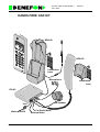
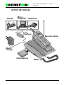
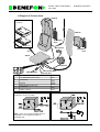
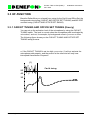
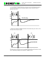
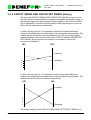
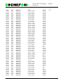
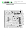
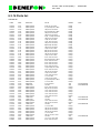
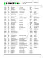
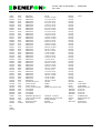
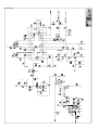
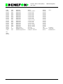
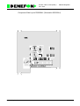
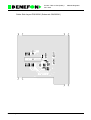
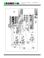
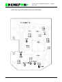
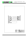
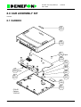
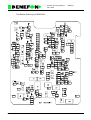
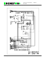
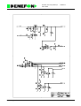
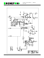
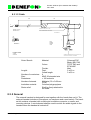
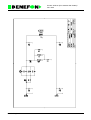
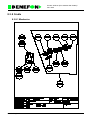
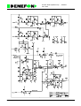
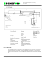
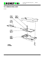
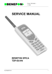
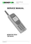
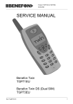
1
Product: TDP-40-TN2 (Delta) /
28.1.1999
SERVICE MANUAL
BENEFON DELTA
TDP-40-TN2
Tdp40enTOC.fm
1
Product: TDP-40-TN2 (Delta) /
28.1.1999
TDP-40-TN2
1.0 GENERAL . . . . . . . . . . . . . . . . . . . . . . . . . . . . . . . . . . 1 - 1
1.1 TECHNICAL INFORMATION . . . . . . . . . . . . . . . . . . . . 1 - 1
1.1.1 Operational System . . . . . . . . . . . . . . . . . . . . . . . . . . . . . . . . . . 1 - 1
1.1.2 Dimensions . . . . . . . . . . . . . . . . . . . . . . . . . . . . . . . . . . . . . . . . 1 - 1
1.1.3 Power Consumption . . . . . . . . . . . . . . . . . . . . . . . . . . . . . . . . . . 1 - 1
1.1.4 Accessories . . . . . . . . . . . . . . . . . . . . . . . . . . . . . . . . . . . . . . . . 1 - 1
1.1.5 Ringing Tones . . . . . . . . . . . . . . . . . . . . . . . . . . . . . . . . . . . . . . 1 - 2
1.1.6 Memory . . . . . . . . . . . . . . . . . . . . . . . . . . . . . . . . . . . . . . . . . . . 1 - 2
1.1.7 Clock . . . . . . . . . . . . . . . . . . . . . . . . . . . . . . . . . . . . . . . . . . . . . 1 - 2
1.1.8 Pager . . . . . . . . . . . . . . . . . . . . . . . . . . . . . . . . . . . . . . . . . . . . . 1 - 2
1.1.9 Other Functions . . . . . . . . . . . . . . . . . . . . . . . . . . . . . . . . . . . . . 1 - 2
1.1.10 Additional Exchange-Based Features . . . . . . . . . . . . . . . . . . . 1 - 3
1.1.11 Manufacturer . . . . . . . . . . . . . . . . . . . . . . . . . . . . . . . . . . . . . . 1 - 3
1.2 PRODUCT FAMILY CONSISTS OF . . . . . . . . . . . . . . 1 - 4
2.0 OWNER’S MANUAL . . . . . . . . . . . . . . . . . . . . . . . . . . 2 - 1
3.0 INSTALLATION INSTRUCTIONS . . . . . . . . . . . . . . . 3 - 1
3.1 Identification Memory Programming . . . . . . . . . . . . . . 3 - 2
3.1.1 Program the Subscriber Number . . . . . . . . . . . . . . . . . . . . . . . . 3 - 2
3.1.2 Program the Password Code . . . . . . . . . . . . . . . . . . . . . . . . . . . 3 - 2
3.1.3 Program the Serial Number . . . . . . . . . . . . . . . . . . . . . . . . . . . . 3 - 2
3.1.4 Program the Date of Sale . . . . . . . . . . . . . . . . . . . . . . . . . . . . . . 3 - 2
3.1.5 Program the Display-Own-Number . . . . . . . . . . . . . . . . . . . . . . 3 - 3
3.1.6 Often Used Local Commands . . . . . . . . . . . . . . . . . . . . . . . . . . 3 - 3
3.2 DELTA CAR KIT . . . . . . . . . . . . . . . . . . . . . . . . . . . . . 3 - 4
3.2.1 Antenna . . . . . . . . . . . . . . . . . . . . . . . . . . . . . . . . . . . . . . . . . . . 3 - 4
3.2.2 Phone Holder HDH-40 . . . . . . . . . . . . . . . . . . . . . . . . . . . . . . . . 3 - 4
3.2.3 Microphone . . . . . . . . . . . . . . . . . . . . . . . . . . . . . . . . . . . . . . . . 3 - 4
3.2.4 Cable . . . . . . . . . . . . . . . . . . . . . . . . . . . . . . . . . . . . . . . . . . . . . 3 - 4
3.2.5 External Handset HDS-50 . . . . . . . . . . . . . . . . . . . . . . . . . . . . . 3 - 5
3.2.6 Car Box CIU-40 . . . . . . . . . . . . . . . . . . . . . . . . . . . . . . . . . . . . . 3 - 5
3.2.7 Hf Speaker . . . . . . . . . . . . . . . . . . . . . . . . . . . . . . . . . . . . . . . . . 3 - 5
Tdp40enTOC.fm
2
Product: TDP-40-TN2 (Delta) /
28.1.1999
3.3 HF-FUNCTION . . . . . . . . . . . . . . . . . . . . . . . . . . . . . . . 3 - 7
3.3.1 CAR KIT TUNING AND OFFICE SET TUNING (theory) . . . . . . 3 - 7
3.3.2 CAR KIT SWING AND OFFICE SET SWING (theory) . . . . . . . 3 - 9
3.3.3 Voice Controlled HF Installation . . . . . . . . . . . . . . . . . . . . . . . . 3 - 10
3.4 Light Car Installation Kit . . . . . . . . . . . . . . . . . . . . . . . 3 - 12
3.5 Questions and Answers . . . . . . . . . . . . . . . . . . . . . . . 3 - 13
4.0 LOCAL SERVICE-COMMANDS . . . . . . . . . . . . . . . . . 4 - 1
4.0.1 Keyboard . . . . . . . . . . . . . . . . . . . . . . . . . . . . . . . . . . . . . . . . . . 4 - 1
4.0.2 Commands . . . . . . . . . . . . . . . . . . . . . . . . . . . . . . . . . . . . . . . . . 4 - 1
4.0.3 Error Messages . . . . . . . . . . . . . . . . . . . . . . . . . . . . . . . . . . . . 4 - 11
5.0 TUNING INSTRUCTIONS . . . . . . . . . . . . . . . . . . . . . . 5 - 1
5.0.1 Watchdog Activation . . . . . . . . . . . . . . . . . . . . . . . . . . . . . . . . . 5 - 1
5.0.2 Battery Voltage Calibration . . . . . . . . . . . . . . . . . . . . . . . . . . . . 5 - 1
5.0.3 TX-Power Level Adjustment . . . . . . . . . . . . . . . . . . . . . . . . . . . . 5 - 1
5.0.4 Frequency Adjustment . . . . . . . . . . . . . . . . . . . . . . . . . . . . . . . . 5 - 1
5.0.5 Learning the 1 kHz Frequency Shift . . . . . . . . . . . . . . . . . . . . . . 5 - 2
5.0.6 Tuning the Receiver . . . . . . . . . . . . . . . . . . . . . . . . . . . . . . . . . . 5 - 2
5.0.7 Fsk-Split Level Programming . . . . . . . . . . . . . . . . . . . . . . . . . . . 5 - 2
5.0.8 Rssi-Level Programming . . . . . . . . . . . . . . . . . . . . . . . . . . . . . . 5 - 2
5.0.9 TX Audio Tuning . . . . . . . . . . . . . . . . . . . . . . . . . . . . . . . . . . . . 5 - 3
5.0.10 Microphone Level Adjustment . . . . . . . . . . . . . . . . . . . . . . . . . 5 - 3
5.0.11 FFSKT Deviation Adjustment . . . . . . . . . . . . . . . . . . . . . . . . . . 5 - 3
5.0.12 FII Deviation Adjustment . . . . . . . . . . . . . . . . . . . . . . . . . . . . . 5 - 3
5.0.13 DTMF Deviation Adjustment . . . . . . . . . . . . . . . . . . . . . . . . . . 5 - 4
5.0.14 Subscriber Number Programming . . . . . . . . . . . . . . . . . . . . . . 5 - 4
5.0.15 Select Battery Type . . . . . . . . . . . . . . . . . . . . . . . . . . . . . . . . . 5 - 4
6.0 PHONE’S CONSTRUCTION . . . . . . . . . . . . . . . . . . . . 6 - 1
6.1 MECHANICS . . . . . . . . . . . . . . . . . . . . . . . . . . . . . . . . 6 - 2
6.1.1 Front Cover . . . . . . . . . . . . . . . . . . . . . . . . . . . . . . . . . . . . . . . . 6 - 2
6.1.2 Back Cover . . . . . . . . . . . . . . . . . . . . . . . . . . . . . . . . . . . . . . . . . 6 - 2
6.1.3 Type plate . . . . . . . . . . . . . . . . . . . . . . . . . . . . . . . . . . . . . . . . . 6 - 2
6.1.4 Antennas . . . . . . . . . . . . . . . . . . . . . . . . . . . . . . . . . . . . . . . . . . 6 - 2
6.2 LOGIC / AUDIO . . . . . . . . . . . . . . . . . . . . . . . . . . . . . . 6 - 3
Tdp40enTOC.fm
3
Product: TDP-40-TN2 (Delta) /
28.1.1999
6.2.1 General . . . . . . . . . . . . . . . . . . . . . . . . . . . . . . . . . . . . . . . . . . . 6 - 3
6.2.2 Connectors: . . . . . . . . . . . . . . . . . . . . . . . . . . . . . . . . . . . . . . . . 6 - 4
6.2.3 Circuit Diagram . . . . . . . . . . . . . . . . . . . . . . . . . . . . . . . . . . . . . 6 - 6
6.2.4 Functions . . . . . . . . . . . . . . . . . . . . . . . . . . . . . . . . . . . . . . . . . . 6 - 6
6.2.5 Function Description . . . . . . . . . . . . . . . . . . . . . . . . . . . . . . . . 6 - 10
6.2.6 Audio Module Tuning Instructions . . . . . . . . . . . . . . . . . . . . . . 6 - 14
6.2.7 Audio Locals . . . . . . . . . . . . . . . . . . . . . . . . . . . . . . . . . . . . . . . 6 - 16
6.2.8 Audio Gate Controls . . . . . . . . . . . . . . . . . . . . . . . . . . . . . . . . . 6 - 18
6.2.9 Parts list . . . . . . . . . . . . . . . . . . . . . . . . . . . . . . . . . . . . . . . . . . 6 - 22
6.3 RF MODULE . . . . . . . . . . . . . . . . . . . . . . . . . . . . . . . 6 - 37
6.3.1 General . . . . . . . . . . . . . . . . . . . . . . . . . . . . . . . . . . . . . . . . . . 6 - 37
6.3.2 Functional Description . . . . . . . . . . . . . . . . . . . . . . . . . . . . . . . 6 - 37
6.3.3 Control- and Output-Signals . . . . . . . . . . . . . . . . . . . . . . . . . . . 6 - 37
6.3.4 General . . . . . . . . . . . . . . . . . . . . . . . . . . . . . . . . . . . . . . . . . . 6 - 38
6.3.5 Function Description . . . . . . . . . . . . . . . . . . . . . . . . . . . . . . . . 6 - 38
6.3.6 Control- and Output-Signals . . . . . . . . . . . . . . . . . . . . . . . . . . . 6 - 39
6.3.7 General . . . . . . . . . . . . . . . . . . . . . . . . . . . . . . . . . . . . . . . . . . 6 - 40
6.3.8 Input- and Output-Signals . . . . . . . . . . . . . . . . . . . . . . . . . . . . 6 - 41
6.3.9 RSSI-Level Adjustment . . . . . . . . . . . . . . . . . . . . . . . . . . . . . . 6 - 41
6.3.10 General . . . . . . . . . . . . . . . . . . . . . . . . . . . . . . . . . . . . . . . . . 6 - 42
6.3.11 Function Description . . . . . . . . . . . . . . . . . . . . . . . . . . . . . . . 6 - 42
6.3.12 Control- and Output-Singnals . . . . . . . . . . . . . . . . . . . . . . . . . 6 - 42
6.3.13 Tuning . . . . . . . . . . . . . . . . . . . . . . . . . . . . . . . . . . . . . . . . . . 6 - 42
6.3.14 Parts list . . . . . . . . . . . . . . . . . . . . . . . . . . . . . . . . . . . . . . . . . 6 - 46
6.3.15 Parts list of Regulator . . . . . . . . . . . . . . . . . . . . . . . . . . . . . . . 6 - 54
6.3.16 Parts list of Antenna Switch Unit . . . . . . . . . . . . . . . . . . . . . . 6 - 59
6.4 BATTERIES . . . . . . . . . . . . . . . . . . . . . . . . . . . . . . . . 6 - 62
6.4.1 BATTERY PACK . . . . . . . . . . . . . . . . . . . . . . . . . . . . . . . . . . . 6 - 63
6.4.2 Parts list . . . . . . . . . . . . . . . . . . . . . . . . . . . . . . . . . . . . . . . . . . 6 - 64
7.0 CHARGING . . . . . . . . . . . . . . . . . . . . . . . . . . . . . . . . . 7 - 1
7.1 MAINS CHARGER CMA-50-230 . . . . . . . . . . . . . . . . . 7 - 2
7.2 LIGHTER SOCKET CHARGER CCS-50-12 . . . . . . . . 7 - 3
7.3 DESKTOP CHARGER . . . . . . . . . . . . . . . . . . . . . . . . . 7 - 4
7.3.1 General . . . . . . . . . . . . . . . . . . . . . . . . . . . . . . . . . . . . . . . . . . . 7 - 5
7.3.2 Charging the phone . . . . . . . . . . . . . . . . . . . . . . . . . . . . . . . . . . 7 - 5
Tdp40enTOC.fm
4
Product: TDP-40-TN2 (Delta) /
28.1.1999
7.3.3 Charging the spare battery . . . . . . . . . . . . . . . . . . . . . . . . . . . . . 7 - 5
7.3.4 Discharging the reserve battery . . . . . . . . . . . . . . . . . . . . . . . . . 7 - 6
7.3.5 Execution . . . . . . . . . . . . . . . . . . . . . . . . . . . . . . . . . . . . . . . . . . 7 - 7
7.3.6 Parts list of Desktop Charger . . . . . . . . . . . . . . . . . . . . . . . . . . 7 - 10
7.3.7 Parts list of Table Charger Extra Module . . . . . . . . . . . . . . . . . 7 - 12
8.0 CAR ASSEMBLY KIT . . . . . . . . . . . . . . . . . . . . . . . . . 8 - 1
8.1 CARBOX . . . . . . . . . . . . . . . . . . . . . . . . . . . . . . . . . . . 8 - 1
8.1.1 Including attached functions: . . . . . . . . . . . . . . . . . . . . . . . . . . . 8 - 2
8.1.2 Connector descriptions: . . . . . . . . . . . . . . . . . . . . . . . . . . . . . . . 8 - 2
8.1.3 Operation . . . . . . . . . . . . . . . . . . . . . . . . . . . . . . . . . . . . . . . . . . 8 - 4
8.1.4 Parts list OW0314 . . . . . . . . . . . . . . . . . . . . . . . . . . . . . . . . . . . 8 - 5
8.2 PHONE HOLDER . . . . . . . . . . . . . . . . . . . . . . . . . . . 8 - 17
8.3 EXTERNAL HANDSET WITH CRADLE HDS-50 . . . 8 - 21
8.3.1 External Handset (not serviceable) . . . . . . . . . . . . . . . . . . . . . 8 - 21
8.3.2 General . . . . . . . . . . . . . . . . . . . . . . . . . . . . . . . . . . . . . . . . . . 8 - 22
8.3.3 Connector XIN Signals . . . . . . . . . . . . . . . . . . . . . . . . . . . . . . . 8 - 23
8.3.4 Microphone . . . . . . . . . . . . . . . . . . . . . . . . . . . . . . . . . . . . . . . 8 - 23
8.3.5 Speaker . . . . . . . . . . . . . . . . . . . . . . . . . . . . . . . . . . . . . . . . . . 8 - 23
8.3.6 Hook . . . . . . . . . . . . . . . . . . . . . . . . . . . . . . . . . . . . . . . . . . . . . 8 - 23
8.3.7 Parts list OO0009 . . . . . . . . . . . . . . . . . . . . . . . . . . . . . . . . . . . 8 - 24
8.3.8 Cradle . . . . . . . . . . . . . . . . . . . . . . . . . . . . . . . . . . . . . . . . . . . . 8 - 28
9.0 OFFICE SET . . . . . . . . . . . . . . . . . . . . . . . . . . . . . . . . 9 - 1
9.1 OFFICE SET DDS-40 . . . . . . . . . . . . . . . . . . . . . . . . . 9 - 2
9.1.1 General . . . . . . . . . . . . . . . . . . . . . . . . . . . . . . . . . . . . . . . . . . . 9 - 2
9.1.2 Connectors . . . . . . . . . . . . . . . . . . . . . . . . . . . . . . . . . . . . . . . . . 9 - 3
9.1.3 Operation . . . . . . . . . . . . . . . . . . . . . . . . . . . . . . . . . . . . . . . . . . 9 - 7
9.1.4 Parts list OO0300 . . . . . . . . . . . . . . . . . . . . . . . . . . . . . . . . . . . . 9 - 9
9.1.5 Parts list OO301 . . . . . . . . . . . . . . . . . . . . . . . . . . . . . . . . . . . . 9 - 18
9.1.6 Parts list OO0302 . . . . . . . . . . . . . . . . . . . . . . . . . . . . . . . . . . . 9 - 20
9.2 EXTERNAL HANDSET HXS-40 . . . . . . . . . . . . . . . . 9 - 23
9.2.1 External Handset (not serviceable) . . . . . . . . . . . . . . . . . . . . . 9 - 23
9.2.2 General . . . . . . . . . . . . . . . . . . . . . . . . . . . . . . . . . . . . . . . . . . 9 - 24
9.2.3 Connector XIN Signals . . . . . . . . . . . . . . . . . . . . . . . . . . . . . . . 9 - 25
9.2.4 Microphone . . . . . . . . . . . . . . . . . . . . . . . . . . . . . . . . . . . . . . . 9 - 25
Tdp40enTOC.fm
5
Product: TDP-40-TN2 (Delta) /
28.1.1999
9.2.5 Speaker . . . . . . . . . . . . . . . . . . . . . . . . . . . . . . . . . . . . . . . . . . 9 - 25
9.2.6 Hook . . . . . . . . . . . . . . . . . . . . . . . . . . . . . . . . . . . . . . . . . . . . . 9 - 25
9.2.7 Parts list OO0009 . . . . . . . . . . . . . . . . . . . . . . . . . . . . . . . . . . . 9 - 26
10.0 OTHER ACCESSORIES . . . . . . . . . . . . . . . . . . . . . 10 - 1
10.1 LINE INTERFACE LIF-40 . . . . . . . . . . . . . . . . . . . . 10 - 2
10.1.1 General . . . . . . . . . . . . . . . . . . . . . . . . . . . . . . . . . . . . . . . . . 10 - 2
10.1.2 Using the line interface . . . . . . . . . . . . . . . . . . . . . . . . . . . . . . 10 - 2
10.1.3 Technical information . . . . . . . . . . . . . . . . . . . . . . . . . . . . . . . 10 - 3
10.1.4 Manufacturers Declaration for BABT/SITS/85/22 . . . . . . . . . 10 - 7
10.1.5 Parts list OO0245 . . . . . . . . . . . . . . . . . . . . . . . . . . . . . . . . . . 10 - 9
10.2 BRANCHING UNIT . . . . . . . . . . . . . . . . . . . . . . . . 10 - 16
10.2.1 General . . . . . . . . . . . . . . . . . . . . . . . . . . . . . . . . . . . . . . . . 10 - 17
10.2.2 Connectors . . . . . . . . . . . . . . . . . . . . . . . . . . . . . . . . . . . . . . 10 - 17
10.2.3 Operation . . . . . . . . . . . . . . . . . . . . . . . . . . . . . . . . . . . . . . . 10 - 18
10.2.4 Parts list OO0241 . . . . . . . . . . . . . . . . . . . . . . . . . . . . . . . . . 10 - 19
Tdp40enTOC.fm
6
Product: TDP-40-TN2 (Delta) /
General
28.1.1999
1.0 GENERAL
General
1.1 TECHNICAL INFORMATION
1.1.1 Operational System
NMT-450i
1.1.2 Dimensions
Size: 58 x 170 x 29 mm
Weight: 350 g
1.1.3 Power Consumption
- Batteries: 5 x 1.2 V NiCd (or NiMH)
- Sleep current: 2 mA
- Standby current: 65 mA
- Conversation mode, high power: app. 0.9 A
- Conversation mode, low power: app. 0.4 A
Service / charger units
- manual selection of battery charging / discharging or
- automatic charging
1.1.4 Accessories
- hands free car kit (carbox, holder, car-radio mute, external antenna,
microphone, loudspeaker, external alert)
- light holder
- line interface
- mains charger
- cigarette lighter charger
- desktop charger
- branching unit
- external handset with holder
- office set
TDP-40E2.fm
1
Product: TDP-40-TN2 (Delta) /
General
28.1.1999
1.1.5 Ringing Tones
Adjustable
- frequency
- number of ringing tones / pulse duration
- volume
- progressive or fixed
Silent alarm
- short tone and alarm text in the display
1.1.6 Memory
Alphanumeric
- 99 memory locations, 23 characters / memory location
- memory scroll and recall in alphabetical or numerical order
- writing to memory during a call
Repeat: last dialled number or one of 5 numbers from the quick-memory locations
1.1.7 Clock
- time display
- real time alarm setting
- real time power on setting
- real time power off setting
- elapsed conversation time counter
- received call counter and time display
1.1.8 Pager
- answers incoming calls and receives numeric messages
- 30 memory locations (23 characters / location)
- pre-set number of ring tones before answering (0...6)
1.1.9 Other Functions
DTMF - receiver / transmitter
DTMF - key tones
Display and key illumination
TDP-40E2.fm
2
Product: TDP-40-TN2 (Delta) /
General
28.1.1999
Volume control
- 6 levels
- level indicator
Battery charge level indicator
- battery empty alarm tone and display
- used battery capacity display
- battery specific charge memory
Field strength indicator
Battery-save function
Menu structure for user customisation
Automatic Prefix Management (APM)
Keys lockable against accidental operation
Password code to prevent unauthorised use
SIS protection function
1.1.10 Additional Exchange-Based Features
- R-key (Register recall)
- M-key (DTMF signal transmission)
1.1.11 Manufacturer
Benefon Oyj
P.O. Box 84
24101 Salo
Finland
Tel. +358 2 77400 Fax. +358 2 7332633
TDP-40E2.fm
3
Product: TDP-40-TN2 (Delta) /
General
28.1.1999
1.2 PRODUCT FAMILY CONSISTS OF
- BENEFON DELTA HANDPORTABLE
Colours: Black, Grey, Red, Green, Blue
- MAINS CHARGER
- CIGARETTE LIGHTER CHARGER
- DESKTOP CHARGER
Quick charger for Benefon Delta and extra battery.
- HANDSTRAP
- BELT CLIP
- OFFICE SET
- HANDS FREE CAR KIT
- LIGHT CAR KIT
Contains car antenna and charger.
- BRANCHING UNIT
To connect charger and line interface simultaneously or to connect extra
handset and line interface simultaneously.
- LINE INTERFACE
Interface unit for modem’s, fax machines, telephones etc.
- EXTRA HANDSET
Handset for Hands Free Car Kit.
- EXTRA ANTENNA FOR BENEFON DELTA
Quarter wave antenna.
TDP-40E2.fm
4
Product: TDP-40-TN2 (Delta) /
General
28.1.1999
HANDS FREE CAR KIT
HDH-40
HDS-50
Installation
base
Microphone
Installation
base
CIU-40
Hf Speaker
fuse
Vbatt, +12/24V
TDP-40E2.fm
Car Radio Mute
External Alert
5
Product: TDP-40-TN2 (Delta) /
General
28.1.1999
LIGTH CAR KIT
Antenna adapter
1
4
2
GHI
7 PQRS
ABC
3
DEF
MNO
5
JKL
6
8
TUV
9 WXYZ
0
RM
HF
Cigarette lighter charger
CCS-50-12
TDP-40E2.fm
6
Product: TDP-40-TN2 (Delta) /
General
28.1.1999
DESKTOP CHARGER
Mains charger
CMA-50-230
Extra battery
Desktop charger
HTP-40
Ba
TDP-40E2.fm
tte ry
Phone
M a in t e n a n c e
7
Product: TDP-40-TN2 (Delta) /
General
28.1.1999
ACCESSORIES
Line interface
LIF-40
Branching unit
DB-40
TDP-40E2.fm
8
Product: TDP-40-TN2 (Delta) /
General
28.1.1999
OFFICE SET DDS-40
Telefax
Microcomputer Telephone
Line
interface
Benefon Delta
Mains
charger
Extra battery
TDP-40E2.fm
Office set
9
2.0 OWNER’S MANUAL
1user_gb.fm
1
Product: TDP-40-TN2 (Delta) /
Installation Instructions
28.1.1999
3.0 INSTALLATION INSTRUCTIONS
Installation Instructions
PROLOGUE
These installation instructions have been prepared to assist fitters in installing the
equipment, and are as such only to serve as a guide. Nothing beats common sense
and good experience.
Installation is always based on the need of the customer to use the phone in the
environment in which it will be installed. Negotiate with the customer where the different parts will be installed. It is important that the customer tells of his own preferences and choices, and that the fitter/salesman tells where it is possible/advisable to
locate different items.
It is the salesman’s responsibility to see that the installation order is properly filled
out.
RECOMMEND
- antenna location on the roof
- handset location does not interfere with road safety
- speaker located in the driver’s side leg-room
- microphone as close as possible to the driver’s mouth
- car radio mute option
ASK IF THE USER WANTS
- additional alarm
- password code
Benefon Oy
TDP-40E6_fm5.fm
1
Product: TDP-40-TN2 (Delta) /
Installation Instructions
28.1.1999
3.1 Identification Memory Programming
Identification memory programming is performed by the dealer before the phone is
supplied to the user.
Connect a LOCAL BOX with programming rights to the phone base connector, and
turn on the phone. Check that LOCAL is displayed, and enter 0#.
3.1.1 Program the Subscriber Number
For systems with i-specification capabilities:
Enter 2#, Z X1 X2 X3 X4 X5 X6 K1 K2 K3 and finally F.
Z = country code, and X1...X6 = six digit subscriber number, and K1...K3 =
phone identification number.
Other systems:
Enter 2#, Z X1 X2 X3 X4 X5 X6 and finally F.
Z = country code, X1...X6 = six digit subscriber number
The subscriber number length may also vary from system to system.
Enter 2* to verify successful programming.
3.1.2 Program the Password Code
Enter 3#, X1 X2 X3 X4 and finally F.
X1...X4 = user defined number series
Enter 3* to verify successful programming
3.1.3 Program the Serial Number
Enter 4#, a six digit serial number, and finally F.
e.g. 1 2 3 4 5 6
Enter 4* to verify successful programming
3.1.4 Program the Date of Sale
Enter 6#, the date of sale, and finally F.
The date of sale is given in the form ddmmyy e.g. 160194
Enter 6* to verify successful programming
TDP-40E6_fm5.fm
2
Product: TDP-40-TN2 (Delta) /
Installation Instructions
28.1.1999
3.1.5 Program the Display-Own-Number
The phone’s own number will be displayed each time the power is turned on, after
the segment test. It is programmed into the phone by storing it in memory location
99. The memory location may also include a name of max. 10 characters, which will
be displayed along with the phone’s own number.
1. Turn the phone on without the LOCAL BOX.
2. Write the phone’s number to the display, including its dialling code.
3. If desired, write also the name to the upper display (see the phone’s owner’s
manual).
4. Enter * 99 (and if necessary, confirm over-write by pressing F).
5. Check the programming by switching the power off, and then on again.
3.1.6 Often Used Local Commands
0#
01#
1#
2#
2*
3#
3*
4#
4*
6#
6*
9#
95#
95*
999*
TDP-40E6_fm5.fm
Local reset
SWING level tuning
HF tuning
Subscriber number programming
Read subscriber number
Password code programming
Read password code
Series number programming
Read series number
Date of sale programming
Read date of sale
Transfer short code memory from the phone to the Local Box
Select battery type (select with +/- keys and F)
Read battery type from battery pack memory
Transfer short code memory from the Local Box to the phone
3
Product: TDP-40-TN2 (Delta) /
Installation Instructions
28.1.1999
3.2 DELTA CAR KIT
The Car Kit includes a phone holder (HDH-40), a car box (CIU-40), an antenna, an
installation base, a hf speaker, a microphone and a cable. The Car Kit sales package
also includes an installation material bag, which contains the necessary installation
equipment. On the 6th page you will find a diagram of connections explaining how to
install the Car Kit.
Caution:
The Car Kit should be installed by Benefon authorized installer only. An end user
should never attemp to install the Car Kit alone without any professional assistance.
The professional installers have the required tools and knowledge to install the Car
Kit properly and safely. Also the terms of warranty demand that the Car Kit is
installed by professional personnel. Cable routing may cause interference with the
components of the vehicle’s electronic systems (such as inginition and braking systems). It is recommended that cable is not routed next to these electronic components.
3.2.1 Antenna
Choose a suitable place for the antenna. It is recommended that you place the
antenna on the roof of the vehicle.
3.2.2 Phone Holder HDH-40
Choose such a place for the phone holder in the vehicle that will be both easy and
safe when using the phone. First, fix the installation base to the place you have chosen, and then install the phone holder in the installation base.
3.2.3 Microphone
Install the microphone so that it is aimed directly at the user, and comes as close as
possible to the user’s mouth. A good place for the microphone is near the rearview
mirror where the noise level is lower than, for example, beside a windshield pillar. It
is also possible to install the microphone on a sun visor, but then it will be inconvenient to use the sun visor and microphone at the same time. One alternative would
be a swan-neck microphone as it can be placed closest to the user’s mouth.
3.2.4 Cable
Obtain the necessary +-electricity from a suitable place, preferably directly from the
battery of the vehicle. Connect the fuse chamber to the +-wire. You will find the fuse
chamber in the installation material bag. Connect the ground lead to the frame of the
car with a short wire.
TDP-40E6_fm5.fm
4
Product: TDP-40-TN2 (Delta) /
Installation Instructions
28.1.1999
3.2.5 External Handset HDS-50
Install the external handset the same way as you installed the phone holder.
3.2.6 Car Box CIU-40
Place the car box out of sight inside the dashboard of the car or to another suitable
place. First, connect the wires to the car box. Install the car box so that the heat sink
has some space for cooling. The car box has holes which enable you to fasten the
car box with a cable tie. The installation material bag also contains adhesive band
fasteners.
3.2.7 Hf Speaker
Install the speaker in a suitable place near the floor of the car. To avoid echo remember to pay attention to the position of the microphone as well.
TDP-40E6_fm5.fm
5
Product: TDP-40-TN2 (Delta) /
Installation Instructions
28.1.1999
A Diagram of Connections:
HDH-40
How to install a cable
to a carbox.
HDS-50
Installation
base
to HDH-40
Microphone
open
Installation
base
CIU-40
Hf Speaker
fuse
Vbatt, +12/24V
PIN
1
2
Car Radio Mute
External Alert
Name
Car Radio Mute (active low)
Colour
Blue
Hf Speaker
Grey
Black
Brown
3
4
5
Ground
External Alert (active low)
Hf Speaker
6
Vbatt, +12/24 V
Car Radio Mute (See the installation
instructions of your car radio)
Grey
Red
External Alert
+ACC : to the +12 V power terminal which is
energized in the accessory position of
the ignition key
TDP-40E6_fm5.fm
6
Product: TDP-40-TN2 (Delta) /
Installation Instructions
28.1.1999
3.3 HF-FUNCTION
Benefon Delta offers you a hands free -setup for the Car Kit and Office Set: the
background noise tuning (CAR KIT AND OFFICE SET TUNING) and MIC-ERP
contrast tuning (CAR KIT AND OFFICE SET SWING).
3.3.1 CAR KIT TUNING AND OFFICE SET TUNING (theory)
You can set up the activation level of the microphone by using the CAR KIT
TUNING option. The level is correct when the microphone path is activated by
voice alone, and not, for example, by background noise in your car or office.
The following figure shows you the CAR KIT TUNING AND OFFICE SET
TUNING setup process.
a. If the CAR KIT TUNING is set too high, your voice (1) will not activate the
microphone path properly, and the person at the other end will only hear
interrupted transmission of speech.
(1)
50
Car kit tuning
40
30
TDP-40E6_fm5.fm
7
Product: TDP-40-TN2 (Delta) /
Installation Instructions
28.1.1999
b. If the CAR KIT TUNING has been set up too low, the background noise in
your car (2) will activate the microphone path, and the volume of the HFspeaker will be low.
50
(2)
40
Car kit tuning
30
c. When the CAR KIT TUNING has been set correctly only your voice (1 & 3)
will open the microphone path.
(1)
(3)
50
Car kit tuning
40
30
(2)
Benefon phones have been set in our factory so that they will function in most
cars. The factory setting for the CAR KIT TUNING is 017.
TDP-40E6_fm5.fm
8
Product: TDP-40-TN2 (Delta) /
Installation Instructions
28.1.1999
3.3.2 CAR KIT SWING AND OFFICE SET SWING (theory)
The four-step CAR KIT SWING AND OFFICE SET SWING tuning is used to
set the contrast of the microphone amplification/speaker attenuation swing. In
the following figures the swing position while listening to the Car Kit or Office
Set is indicated by a solid line and the position while speaking into Car Kit or
Office Set the indicated by a dotted line.
a. With a tuning value of 4 it is possible to obtain the smallest difference
between the amplification and attenuation of the microphone and speaker. This
means that the connection is almost bidirectional. If the HF-function easily
creates feedback, decrease the value of the CAR KIT SWING AND OFFICE
SET SWING. By turning down the volume it is possible to reduce the
occurance of feedback.
MIC
SPK
Listening
4
3
Speaking
2
1
b. With a tuning value of 1 it is possible to obtain the greatest difference
between the amplification and attenuation of the microphone and speaker. This
means that the connection is almost unidirectional.
MIC
SPK
Listening
4
3
2
1
Speaking
The factory setting for the CAR KIT SWING AND OFFICE SET SWING is 4.
TDP-40E6_fm5.fm
9
Product: TDP-40-TN2 (Delta) /
Installation Instructions
28.1.1999
3.3.3 Voice Controlled HF Installation
To ensure trouble-free HF operation, care should be taken in positioning the speaker
and microphone, as outlined above.
3.3.3.1 HF Tuning
The purpose of the tuning is to adjust the level at which the microphone is switched
on. The trigger level must be a little higher than the normal vehicle background
noise, but not more than the user’s normal voice level.
3.3.3.2 Automatic HF Tuning
When the speaker and microphone have been installed, connect the LOCAL adapter
and set the phone to LOCAL mode.
1. Turn the phone on.
2. Enter 1#
Note that the displayed value changes in response to background noise.
3. Press F when the the display shows the highest value corresponding to
background noise.
HF is now set to the level corresponding to the highest background noise. In
most cases, the recommended value will be between 16 and 18.
4. Store the value by pressing the F key again.
If the background noise can not for some reason be simulated, the average
level must be estimated, and the tuning performed manually (see Manual HF
tuning).
3.3.3.3 Manual HF Tuning
It will be necessary to set the HF tuning manually if it is not possible to run a simulation test, or if it is known by experience the desired microphone trigger level.
1. Set the phone to LOCAL mode.
2. Enter 1# and F
3. Enter the desired value and F.
The value must be three digit e.g. 018.
3.3.3.4 Swing-level Tuning
The swing-level controls the HF feedback damping (the larger the value, the smaller
the damping). In phones leaving the factory, the default value is 4.
In practice, SWING means the level to which the incoming volume level will be sup-
TDP-40E6_fm5.fm
10
Product: TDP-40-TN2 (Delta) /
Installation Instructions
28.1.1999
pressed when speaking and vice versa.
The SWING level must be decreased, if the sound in HF mode starts to feed-back
(at high volume levels) in spite of careful positioning of the speaker and microphone.
1. Set the phone to LOCAL mode.
2. Enter 01#, and the current SWING level is displayed.
3. Select a new value 1...4.
4. Store the value by pressing F.
TDP-40E6_fm5.fm
11
Product: TDP-40-TN2 (Delta) /
Installation Instructions
28.1.1999
3.4 Light Car Installation Kit
Antenna adapter
1
4
GHI
7 PQRS
2
ABC
3
DEF
5
JKL
6
MNO
8
TUV
9 WXYZ
0
RM
HF
Cigarette lighter charger
CCS-50-12
TDP-40E6_fm5.fm
12
Product: TDP-40-TN2 (Delta) /
Installation Instructions
28.1.1999
3.5 Questions and Answers
Question: The message BATT MEMO is displayed when turning the phone on or
changing the battery. What does it mean?
Answer: There is a memory circuit inside the battery pack which contains information about the battery type, charging currents, battery charge counter, etc. If the
phone is not able to read this information when being turned on, it displays the message BATT MEMO.
Question: How can the above fault be repaired?
Answer: Clean the battery contacts, set the phone to LOCAL mode, and read the
battery type with command 95*. If the type is incorrect, then programme the correct
type with the command 95#. The arrow keys can be used to select the battery type,
and pressing F will store the information in the battery pack memory. If BATT MEMO
is still displayed when turning the phone on, then the battery pack should be
replaced.
If the phone is not able to read the battery pack memory, it will assume that the battery type is 600 mAh NiMH. The phone cannot necessarily charge the battery to its
full capacity, charging currents are small, and charging times are long.
Question: The phone displays the message B BATT. What does it mean, and how
can the fault be repaired?
Answer: Inside the phone, there is a back-up battery for RAM memory. When the
phone is off and the battery pack is removed or completely empty, the back-up battery will supply RAM memory with enough current to ensure that no information is
lost. Typical information in RAM memory are quick-memory numbers, short code
memory numbers - information provided by the user.
Repair: Replace the back-up battery.
Note ! The B BATT message may be displayed after changing the program PROM.
In this case, no action is required.
Question: Can short code memories be transferred from an older Benefon phone to
a new one?
Answer: No. In new phones there are more alpha-numeric characters and the memory construction is different from older models. On the other hand, numbers can be
transferred between Benefon Beta and Benefon Delta.
TDP-40E6_fm5.fm
13
Product: TDP-40-TN2 (Delta) /
Local
28.1.1999
4.0 LOCAL SERVICE-COMMANDS
Local
4.0.1 Keyboard
HF/HS
Audio path and microphone switching between ERP,
SPK, and EXTHS
SPK is indicated by the HF symbol
EXTHS is indicated by the flashing HF symbol
ERP is indicated when the HF symbol is not visible
SND/END
termination of Local command
R
A, b, C, d, E, F input (Input is concluded by either the F
key or the next number) Note: first enter a number.
+/-
Volume etc. control and adjustment (see commands)
FR
To change to NMT mode, if the local box has already
been removed
4.0.2 Commands
(XXX)#
(XXX)*
XXXX#
executes
terminates equivalent (XXX)# command
channel command
Note: In local mode * = b and # = c in the lower display
TDP-40E3_fm5.fm
1
Product: TDP-40-TN2 (Delta) /
Local
28.1.1999
4.0.2.1 Installation and Sales.
TDP-40E3_fm5.fm
0#
Return to the local normal mode e.g. middle radio channel
01#
VOX value selection
the chosen VOX value is displayed
enter a new value 1...4
press F to enter
1#
VOX tuning
press F to stop measurement (fixing value)
press F to save tuned value
2#
Subscriber number programming
enter 7 digits number (and 3 digits password if needed) and
press F to enter
2*
Read subscriber number
3#
Password code programming
enter 4 digits and F
3*
Read password code
4#
Serial number programming
4*
Read serial number
5#
Set country of origin
country is displayed
enter new country 0...9, F to enter
6#
Date of sale programming
6*
Read date of sale
7#
Set time (hours and minutes)
7*
Read time
8#
Set date (day XX, month XX, year XX)
8*
Read date
2
Product: TDP-40-TN2 (Delta) /
Local
28.1.1999
.
TDP-40E3_fm5.fm
9#
Short code memory transfer to local box
999*
Short code memory transfer back to the radio
95*
Read battery type and capacity
also production week and year
95#
Program battery type and capacity
also production week and year
3
Product: TDP-40-TN2 (Delta) /
Local
28.1.1999
4.0.2.2 Service and Testing 0...
#port command
enter:
0
1
2
3
4
5
6
7
68HC11A1 PA
IA8000 PA
IA8000 PB
IA8000 PC
IA8000 PD
IA8000 PF
CARBOX
LIF
- The port state is shown in the upper display in hexadecimal form (0...FF)
0 = 0000
5 = 0101
A = 1010
F = 1111
1 = 0001
6 = 0110
B = 1011
2 = 0010
7 = 0111
C = 1100
3 = 0011
8 = 1000
D = 1101
4 = 0100
9 = 1001
E = 1110
- To change the port state (when the port number z is displayed) enter (z)XY
X
Y
bit number (0...7)
bit state (0 / 1)
- +/- can be used to change the active port number
02# Read the AD channel (real time)
- enter the AD channel number
0 = RSSI
4 = TEMP
TDP-40E3_fm5.fm
1 = NTC
5 = BATVOLT
2 = MICDET
6 = POTIND
3 = ERPDET
4
Product: TDP-40-TN2 (Delta) /
Local
28.1.1999
4.0.2.3 Logic Tests 1..
TDP-40E3_fm5.fm
10#
Memory test
- EPROM; if error XX1 (no error, XX0)
- EEPROM; if error X2X (no error, X0X)
- RAM; if error 3XX (no error, 0XX)
11#
COP test
- If error, then WDFAIL displayed
12#
"0" frequency transmission
- Does not set transmitter etc.
12*
End transmission
13#
"1" frequency transmission
Does not set transmitter etc.
13*
End transmission
14#
Open frame transmission
- framework specified by entering
N1 N2 N3 P(X) Y1 Y2 Z X1 X2 X3 X4 X5 X6 J1 J2 J3 #
- default value frame 15
- letters A...F are entered with the R-key
14*
End transmission
15#
Receive frame
16#
FSK-notification test (real time)
- XY displayed
X = 1, FSK level exceeds the tuned level (X = 0, below)
Y = 1, FSK signal detected (Y = 0, not detected)
18#
DTMF loop test
19#
Read machine type
96#
Start charger control test (control voltage -2.5V, I in = 1.3 A)
96*
Terminate charger control test (control voltage 0V)
5
Product: TDP-40-TN2 (Delta) /
Local
28.1.1999
4.0.2.4 Audio 2..
20#
AUDIOPOWER ON
20*
AUDIOPOWER OFF
21#
TXAUDIO ON
21*
TXAUDIO OFF
22#
RXAUDIO ON
22*
RXAUDIO OFF
23#
FIILOOP ON
23*
FIILOOP OFF
24#
FSK ON
24*
FSK OFF
25#
COMPANDER/EXPANDER ON
25*
COMPANDER/EXPANDER OFF
200#
Audio circuit SC11370 settings
1. select register (0...b) +/- keys
2. select the bit to be changed 0...7
3. select the bit logic state 0 or 1
201#
Audio circuit SC11370 tuning
1. select the register to be tuned 1...0
1 NORMDEV GC2
2 HFTXATT GC3
3 MAXDEVLO GC7
4 MAXDEVHI GC10
5 ERPVOL GC8
6 RXAUDLEV GC9
7 MICSENS GC1
8 DTMFLEV GC4
9 FFSKTXLEV GC5
0 FIILEV GC6
+/- keys to select level (0...15)
TDP-40E3_fm5.fm
6
Product: TDP-40-TN2 (Delta) /
Local
28.1.1999
203#
DTMF tone generator settings
204#
TXAUDIO and RXAUDIO ON
210#
+55 C tuning
211#
+25 C tuning
212#
0 C tuning
213#
-25 C tuning
216#
Deviation correction constant (to reduce distortion)
217#
Deviation correction limits
TDP-40E3_fm5.fm
7
Product: TDP-40-TN2 (Delta) /
Local
28.1.1999
4.0.2.5 RF 3..., 4...
30#
Transmitter ON
Note: Does not set the power level (if the transmitter was
OFF, power setting= 0)
30*
Transmitter OFF
31#
Transmitter ON low power
31*
Transmitter OFF
32#
Transmitter ON medium power
32*
Transmitter OFF
35#
Low channel
36#
Middle channel
37#
High channel
38#
RSSI level tuning
- level to be tuned shown in the upper display
PG -58, PG -68, PG -93, PG -103, PG -115
- enter F to tune the next level
- value can be saved if -58dBm> -68dBm> -93dBm> 103dBm >-115dBm
38*
Read the carrier wave level tuning levels from EEPROM
380#
RSSI correction constant
39#
Power level tuning
- power level shown in the upper display 150mW 1200mW
- power is increased with the + key and decreased with the key
- enter F to save
39*
read the tuned power levels from EEPROM
M = 1.2 W, L = 150 mW
43#
CHANNEL SCANNING
- starts from the current channel
- displays the channel in the upper display, and the TX-frequency in the lower display
TDP-40E3_fm5.fm
8
Product: TDP-40-TN2 (Delta) /
Local
28.1.1999
44#
CHANNEL STEPPING
- the +/- keys step through the channels one at a time
- displays the channel in the upper display and the TX frequency in the lower display
44*
CHANNEL STEPPING
- the +/- keys step through the channels one at a time
- displays the channel in the upper display and the RX frequency in the lower display
45#
AFC ON
45*
AFC OFF
450#
AFC 1kHz correction tuning (value 00000...65535)
- set thousands, press F
- set hundreds, press F
- set tens, press F
- set units, press F
(select with the +/- keys. shown in the upper display)
450*
Read the AFC 1kHz correction
452#
TCXO fine tuning
- enter a 5 digit number and store with F
Note: After 0# the radio is on the middle channel. The xxxx#
channel command can be used to change the tuning channel.
452*
Read the TCXO fine tuning value
453#
450 kHz intermediate frequency measurement and display
4.0.2.6 Equipment and Accessory Tests 5...
50#
Display and illumination test
50*
Display and illumination OFF
4.0.2.7 Other Commands 6..., 7...
60#
Printing out all power off counters
0
1
TDP-40E3_fm5.fm
RAM
EPROM
9
Product: TDP-40-TN2 (Delta) /
Local
28.1.1999
2
3
4
5
6
7
8
EEROM
COP
RSSI
TXON
HANDSET OFF
FSK
SIM
60*
Reset all power off counters
61*
Read the 4 digit sales codes from EEPROM
- the sales code (= local box number) is always stored
when programming the subscriber code.
- 1 = newest ... 5 = oldest (number given by corresponding number key)
- the sales code is XYZW (= 0...9 0...9 0...9 0...9)
- If the display contains odd characters, the code is
unused
62#
Read program version (ddmmyy)
70#
FSK split level tuning
- enter F to save
70*
Read FSK split level value
71#
Program basic band
- enter low channel (1...4 digits) and F
- enter high channel (1...4 digits) and F
- settings can be saved if the lower limit * upper limit
(according to their frequencies)
71*
Read the basic band
TDP-40E3_fm5.fm
10
Product: TDP-40-TN2 (Delta) /
Local
28.1.1999
4.0.2.8 Clearing Memories 8...
80#
Clear RAM
81#
Clear EEPROM (not tuning values nor sales codes)
810#
Clear the whole of EEPROM (not sales codes)
82#
Clear RAM and EEPROM (not tuning values nor salescodes)
4.0.2.9 Sleep Timer
90#
Activate the sleep timer
90*
Deactivate the sleep timer
91#
Sleep timer test
- sets phone to sleep mode after 5 seconds for approx. 5
seconds
4.0.2.10 SIS Commands
100#
SIM uses normal SAK number
- default value when phone is turned on
100*
SIM uses test SAK number
- to test signaling, remove local box and enter F R to
switch to NMT mode
101#
SIM sleep mode
101*
SIM wake-up
4.0.2.11 Updating the Local Box
900#
Re-programming of local box rights and user-time
902#
Read the local box number (xxxx) and the phone identification code (yyyyy)
- xxxx yyyyy
4.0.3 Error Messages
The upper display usually shows LOCAL, when there is no other information on display. ERROR in the upper display:
1.
TDP-40E3_fm5.fm
Incorrect local command or key-entry
11
Product: TDP-40-TN2 (Delta) /
Local
28.1.1999
2.
Fault in EEPROM programming
3.
EEPROM input entry error
- input data string too long
- incompatable characters in entry
-carrier wave levels to save are in wrong order of magnitude
- basic band limits to save are incorrect
-LOCAL BOX WITHOUT RIGHTS TO PROGRAM e.g.
SUBSCRIBER NUMBER
4.
Loop test failed to find required response in specifiedtime
UNKNOW in the upper display:
Unknown local command
LOCAL in the upper display when turning on power, although there is no local box
connected:
Subscriber number not programmed
Date of sale not programmed
BATT MEMO in upper display when turning on power:
battery type not recognised
battery pack connections loose or
battery pack damaged
TDP-40E3_fm5.fm
12
Product: TDP-40-TN2 (Delta) /
Tuning Instructions
28.1.1999
5.0 TUNING INSTRUCTIONS
Tuning Instructions
Necessary equipment: Local adapter, Local box, radio communication tester, multimeter.
5.0.1 Watchdog Activation
This operation will reset all settings !! Perform only when changing CPU.
- Connect I201 pin 25 (MODB) to ground and turn power ON. Remove the
jumper and turn the power OFF.
- Check: Local 11 # cop test.
If result is WD FAIL or the phone jams, the activation must be repeated.
- Local 0 #
5.0.2 Battery Voltage Calibration
- Adjust the operating voltage to 6.5 V, measuring from the OS-module battery
contacts.
- Local 214 #, check that "BT65V" is in the display.
- Local 0 #.
5.0.3 TX-Power Level Adjustment
- Local 0 #, 31 #, 39 #, and use the +/- keys to adjust the power to 180 mW
(22.6 dBm), and confirm with the F key; adjust with the +/- keys to 1.2 W (30.8
dBm), and confirm with the F key.
- Check that the current consumption is less than 900 mA.
- Local 0 #.
5.0.4 Frequency Adjustment
- Local 36 #, 31 # LTXON, 45* AFCOFF, 452 #, use the +/- keys to adjust the
frequency as close as possible to 455.225 MHz, and confirm with the F key.
- The adjustment can also be done by entering a 5 digit value and saving it with
the F key.
If the tuning value needs to be changed more than 2500 units, the TCXO must
also be tuned.
- Local 0 #.
TDP-40E5_fm5.fm
1
Product: TDP-40-TN2 (Delta) /
Tuning Instructions
28.1.1999
5.0.5 Learning the 1 kHz Frequency Shift
- Local 0 #, 36 #, 31 #, 450 #
Adjust the transmitter to 455.226 MHz with the +/-keys and store with the F
key.
- Local 0 #.
5.0.6 Tuning the Receiver
- Feed an RF-gen 1 kHz / 3 kHz dev. at -50 dBm on the mid-channel.
- Local 0 #, 36 #, 22 #, RXAON, 201 # 6
- Use the +/- keys to adjust the audio level reading to 220 (+/-10) mVrms or
622 (+/-30) mVpp, store with the F key, press the C key.
- Change the RF level to -113 dBm.
- Check the sensitivity: mid-channel (Local 36#), low channel (Local 35#), and
high channel (Local 37#). Minimum sensitivity 20 dB sinad (CCITT).
- Local 0 #
5.0.7 Fsk-Split Level Programming
- Local 0 #, 36 #, 22 #
- Feed an RF-gen. 1 kHz / 350 Hz dev. at -50 dB on the mid-channel.
- Local 70 #, wait until the display stabilises, store with the F key.
- Check 70 *, display shows the stored value.
- Local 0 #
5.0.8 Rssi-Level Programming
- Set the RF-gen on the mid-channel at -58 dBm.
- Local 0 #, 36 #, 38 #, and wait until the displayed value stabilises, and press
the F key.
- Change the RF level to -68 dB and wait until the displayed value stabilises,
and press the F key.
- Change the RF level to -93 dBm, press the F key.
- Change the RF level to -103 dBm, press the F key.
- Change the RF level to -115 dBm, press the F key.
- Check programming with Local 38 *, the stored values are displayed.
- Local 0 #.
TDP-40E5_fm5.fm
2
Product: TDP-40-TN2 (Delta) /
Tuning Instructions
28.1.1999
5.0.9 TX Audio Tuning
- Local 0 #, 36 #, 31 #, 21 #
- Feed via the local box GEN connector a 1 kHz sine signal at 4.0 Vrms, and
set the local box switch to the SERVICE position.
- Local 215 # (store mic level)
- Change the frequency to 2 kHz at 4 Vrms.
- Local 201 # 4 and use the +/- keys to set the deviation to 4.55 (+/- 0.15) kHz,
confirm with the F key.
- Change the signal frequency to 1 kHz at 400 mVrms.
- Press the 1 key and use the +/- keys to set the deviation to 3.00 (+/- 0.05)
kHz, confirm with the F key, and press the C key.
- Local 0#
Checking the deviation limiter:
- Local 36#, 31#, 21#
- Local 217#, change the level to 4.0 Vrms, frequency still 1 kHz. Use the +/keys to set the deviation above 3.7 kHz, and confirm with the F key.
- Local 0 #.
5.0.10 Microphone Level Adjustment
- Feed a 1 kHz sine signal acoustically to the microphone at a normal sound
level.
- Enter local 0 #, 21 #, press HF, 31 #, 201 # 7
- Use the +/- keys to set the deviation to 3.00 (+/- 0.05) kHz, confirm with the F
key, press the C key.
- Local 0 #
5.0.11 FFSKT Deviation Adjustment
- Local 0 #, 24 #, 31 #, 201 # 9
- Use the +/- keys to set the deviation to 4.20 (+/- 0.05) kHz and press F and C
keys.
- Local 0 #
5.0.12 FII Deviation Adjustment
- Set an RF-gen. mod. frequency 4 kHz / 600 Hz deviation, at - 50 dBm.
TDP-40E5_fm5.fm
3
Product: TDP-40-TN2 (Delta) /
Tuning Instructions
28.1.1999
- Local 0 #, 31 #, 23 #, 201 # 0
- Use the +/- keys to set the deviation to 600 (+/- 20) Hz, press F and C keys.
- Local 0 #.
5.0.13 DTMF Deviation Adjustment
- Local 0 #, 31 #, 21#, 203 #, choose 941 Hz with the +/- keys, and press the F
key.
- Local 201 # 8 and set the deviation with +/- keys to 1.80 (+ 0.20) kHz, press F
and C keys.
- Local 0 #.
5.0.14 Subscriber Number Programming
- Local 0 #, 2 #, enter 7 digit number (and 3 digit password if needed) and
press the f key.
- Check with 2 *.
- Local 0 #
5.0.15 Select Battery Type
- Local 95 #
- Use the +/- keys to select the battery type in use, and press the F key.
- Check with 95*
TDP-40E5_fm5.fm
4
Product: TDP- 40-TN2
28.1.1999
6.0 PHONE’S CONSTRUCTION
TDP-40E7_fm5.fm
1
Product: TDP- 40-TN2
28.1.1999
6.1 MECHANICS
6.1.1 Front Cover
MC1383 Grey
MC1384 Green
MC1382 Red
MC1381 Blue
MC1351 Black
6.1.2 Back Cover
MC1393 Grey
MC1394 Green
MC1392 Red
MC1391 Blue
MC1352 Black
6.1.3 Type plate
MC1302
6.1.4 Antennas
6.1.4.1 Helical
YA0055
TDP-40E7_fm5.fm
2
Product: TDP-40-TN2 (Delta)
/ OA0300 Processor
28.1.1999
6.2 LOGIC / AUDIO
OA0300 Processor
Processor
6.2.1 General
The entire radio audio and processor functions are found within a single PA0300
board, through which all other modules are connected. Only the RF signals have a
different path.
The processor controls the audio and radio modules, internal devices and external
accessories.
The processor includes:
CPU
PROM
RAM
68HC11A1
27C010
4465
ASIC
IA8001
TXLOG
SIS
XA0300E4_fm5.fm
68HC11A8
8-bit, 8 A/D, 512*8 EEPROM, 256*8 RAM, I/O
128*8 EEPROM, program memory
8K*8 CMOS RAM, number memory
32 pcs out and 14 pcs inp, 3 series out, 3 analog
out, frequency counter, clock
TX power adjustment and control
SIS function, 8k ROM, 512*8 EEPROM, 256*8
RAM
3
Product: TDP-40-TN2 (Delta)
/ OA0300 Processor
28.1.1999
6.2.2 Connectors:
6.2.2.1 Radio Base Connector (printed circuit)
1
2
3
V-CHARGE
V-CHARGE
VB
4
V-PROG
5
8
EXTMIC+PWR
GND
GND
EXTERPX+
HOOK
9
PTTX
10
11
12
13
14
15
I2CINTX
SCLX
SDAX
TXDX
RXDX
EXTIOX
external audio to the speaker
amplifier
external PTT, radio input 0V
active
i2c interrupt, radio input
i2c clock
i2c data
rs232 OUT
rs232 IN
reserve
16
CHGCONTX
charging control voltage
6
7
battery charging voltage IN
battery charging voltage IN
6 V output to accessories
FLASH PROM programming
voltage IN
external audio from the
microphone
2A
2A
0.5A
0.5/12 VDC
400 mVrms
220 mVrms
0/5V
0/5V
0/5V
0/5V
0/5V
0/5V
0/5V
0...5VDG
analog
The power switch is connected to the mic-line so that the switch grounds the micline.
The Extl-hook switch is connected to the erp-line so that the erp-line dc level drops
when the handset is in its holder.
XA0300E4_fm5.fm
4
Product: TDP-40-TN2 (Delta)
/ OA0300 Processor
28.1.1999
6.2.2.2 RF-Module, 24 pin Connector
1
2
3
SLEEP
TXVCO
VB
4
5
6
7
8
9
10
11
12
VB
VB
GND
GND
GND
SDATA
SCLK
STE
SRE
13
RSSI
14
15
RF-module sleep control
tx vco start up
power supply from the battery
(RF-module battery connector )
power supply from the battery
power supply from the battery
0/5V
5V
6V
0/5V
0/5V
5V
5V
RXAUDIO
RX and TX data to the splitter
RX and TX data clock
TX divider enable pulse
RX divider enable pulse
RX signal strength indicator, analog
0-5V
RX audio signal
450KHZ
450kHz for AFC measurement
approx.1Vpp
16
AFC
approx 2.5V
17
18
19
20
21
22
23
24
TXAUDIO
TXPWR
TXSENSE
TXBIAS
BNTC
BSENSEX
SPRIO
DTUNE
frequency compensation control
voltage
TX audio modulation
TX power control, analog
not connected
TX initiate, 0V = TX OFF
battery temperature data, analog
input memory data-line
no function
not connected
key matrix input
0/5V
100mVrms
550mVrms
0-5V
0/5V
6.2.2.3 Keyboard (internal)
1
2
3
4
5
7
6
8
9
10
11
XA0300E4_fm5.fm
KEY-INP4
KEY-INP0
KEY-INP3
KEY-INP2
KEY-INP1
PWS
GND
KEY-OUT0
KEY-OUT1
KEY-OUT2
KEY-OUT3
power switch
key matrix output
0/5V
5
Product: TDP-40-TN2 (Delta)
/ OA0300 Processor
28.1.1999
6.2.2.4 Display Module
1
2
3
4
VCC
LIGHTKEY
SDAL
SCLL
GND
light control, 6V = ON
0/6V
6.2.3 Circuit Diagram
The processor circuit diagram is split into three parts. The first diagram shows the
module connector pins and power supply. The second diagram shows all the processor functions. The whole audio is in a single diagram. Signals in the circuit diagrams have been given names, and signals with the same name are connected
between diagrams.
6.2.3.1 Circuit Diagram Contents
OA0300A0
OA0300B0
OA0300C0
power supply and connectors
cpu, ASIC, RAM, EPROM, SIS-function
audio parts (filters, modem, DTMF, compander)
6.2.3.2 Numbering of Components
The different modules making up the radio unit have all their components unambiguously numbered. An individual component number is used only once:
OA0300A0 has numbers 001...199
OA0300B0 has numbers 200...299
OA0300C0 has numbers 300...399
6.2.4 Functions
6.2.4.1 CPU
I201 is itself a processor circuit. It comprises CPU, 512*8bit EEPROM, timers, A/D
converters, and both series- and parallel I/O lines. The clock oscillator is located in
the audio circuit and provides the CPU with a 5.5296 MHz clock signal. The CPU
divides this by 4 to get timing signal E.
When the processor is operating, RESET = 5V, VCC = 5V, E = 1.3824 Mhz, AS, R/W
and A0...A15 pulses should be 0/5V (no intermediate values, only 0 or 5V).
6.2.4.2 Memories
Memory- and external I/O-circuit address coding is done with the ASIC circuit 203.
The circuit options CSR, CSP, and CSIO are 0-active.
XA0300E4_fm5.fm
6
Product: TDP-40-TN2 (Delta)
/ OA0300 Processor
28.1.1999
The program memory is in 128k*8 EPROM. The program uses the addresses
2100H...FFFFH. Page selection makes available another similar memory block.
RAM-memory is 8k*8 CMOS RAM at the addresses 0000H...1FFFFH. RAM
receives its power supply from its own regulator which is always operating, even
when the radio is in OFF state.
6.2.4.3 The Modem
The FFSK modem is located in the audio circuit. The modem is connected to the
CPU by a series line, input to synchronised port, and transmission is controlled by
an ASIC series output. The modem gives a 1200 Hz signal RXCLK to the processor
and TXCLK to ASIC. There is a data detector within the modem, the speed of which
is controlled by C395. D376 serves as the data detector,and the CPU A/D converter
measures the level of acceptance. The same detector also serves to control the HF
function.
6.2.4.4 AFC
The AFC function is performed by an internal ASIC frequency counter. A 450 kHz
intermediate frequency is amplified to a square-wave form by Q109. The frequency
is adjusted by ASIC pulse frequency modulated signal D/A 0, which is integrated by
C284. This approx. 2.5V DC voltage is fed to the synthesiser AFC pin.
6.2.4.5 Sleep Timer
The phone puts the central functions to sleep for a time. Although everything seems
normal to the user, most of the functions are closed down. The radio- and audiounits are closed down completely. The processor still has a power supply, but the
processor is halted and has minimal power consumption. Only the ASIC circuit sleep
timer and its 32 kHz crystal oscillator remain in active mode. The phone is "woken
up" by interrupting the sleep timer or by changing the keyboard state. The sleep
timer 32 kHz clock freqency is produced by the oscillator made by crystal X203.
6.2.4.6 Warm Start
C221 and R221 measure the length of a voltage break. The voltage drops during a
break, after which it is measured by the A/D convertor. The time constant is approx.
10 s . Thus a "warm start" is detected.
6.2.4.7 RESET
The processor voltage regulator ERROR output resets (stops) the processor and
zeroes the controls when the battery voltage drops below 5V. As the voltage rises
again, the processor restarts.
6.2.4.8 Power Switch
The power switch (PWS) is grounded, and directs the regulator I101 to conduct
when pressed. The program commences and checks the PWRSW line to ensure
XA0300E4_fm5.fm
7
Product: TDP-40-TN2 (Delta)
/ OA0300 Processor
28.1.1999
that the switch is being pressed, and sets hold on the regulator for the PWRON line.
When the switch is depressed for a longer time, the program directs power to the
PWROFF line. During a short voltage break, C124 and R123 remember the previous
control, i.e. fet Q101 conducts again when the voltage is restored within 10 seconds.
The switch-fet also serves as a watch-dog should the voltage drop or processor
error-state continue; after 10 seconds, the radio will shut down completely.
Note! The RAM and ASIC circuits have their own regulator connected to the battery
to ensure an uninterrupted power supply. RAM power supply is ensured during a
battery-pack change by the battery A100.
6.2.4.9 Battery Voltage Measurement
The battery voltage is measured by an A/D converter. The converter 256 step conversion scale is not sufficient as it stands, so the measured range is restricted to
5...8V by the operational amplifier I206. The reference voltage for the measurement
is provided by the processor regulator 5V supply. Calibration is done by the program
against a precisely known battery voltage.
6.2.4.10 I/O ports
The ASIC I/O ports PA...PF are 8-bit hold circuits. DATA is fed to the addressed output. When the RESET line is down (0V) all the ASIC ports are zeroed (0V). As
RESET rises again, all of the two-way I/O ports are inputs until the program sets
them to the desired state. With the radio in OFF state, RESET is down so all of the
controls are also down although ASIC is still provided with operational voltage
(VRAM).
6.2.4.11 Tone Generator
Tones for the internal buzzer are provided by the ASIC tone generator. The frequency can be programmed between 400...4000 Hz. The wave form is square.
6.2.4.12 SIS
SIS functions are provided by a mask-programmed single chip processor I202
(68HC11A8). It communicates with the host processor via ASIC with an RS232 bus
(5V levels). The circuit operation is not externally visible as it is a single-chip solution. User specific information is stored in EEPROM which CANNOT be read from
outside the chip. All external attempts to read the information clear both EEPROM
and RAM (fill with FF).
6.2.4.13 Power Adjustment
The transmitter control logic switches TX power and also adjusts it to the correct
level. The TXVCO signal sets the transmitter to ready-mode. Power is controlled by
the ASIC analog output D/A 1. It is a pulse frequency modulated output which is converted to a DC voltage by integrating it with C287. 0V corresponds to "no power"
state, and 5V to maximum transmitter power. The power levels are calibrated by the
program at the source of measurement.
XA0300E4_fm5.fm
8
Product: TDP-40-TN2 (Delta)
/ OA0300 Processor
28.1.1999
6.2.4.14 Charging Control
The charger is controlled by the program. The charger is detected by a voltage at the
VCHARGE pin. The charging current (0...2A) is controlled by an analog (0...5V)
CHGCONT signal which comes from the ASIC D/A 2 pulse frequency output. Charging is governed by the battery and radio temperatures, battery voltage, and time
measurement. D104 prevents the battery voltage reaching the charger.
6.2.4.15 Temperature Measurement
The radio has two separate temperature sensors, one within the battery pack, and
the other within the radio module. Inside the radio the NTC resistor R209 voltage is
measured by the processor A/D converter. This value is converted by a programmed
table to a temperature reading. The battery pack temperature is calculated in the
same way.
6.2.4.16 Real-time Clock
A real-time clock is provided within ASIC to give the time and date. The alarm function can also be programmed to the ALARM pin. This will initiate the processor regulator and thus also the radio although it was in OFF state.
The ASIC circuit has a continuous power supply and the 32 kHz clock crystal runs
constantly. Not even the RESET line stops the clock. If the power supply has
dropped too low, the clock will need to be reset with the radio butons (from the
menu).
XA0300E4_fm5.fm
9
Product: TDP-40-TN2 (Delta)
/ OA0300 Audio
28.1.1999
Audio
6.2.5 Function Description
OA0300 Audio
The audio module comprises the following functions:
1. TX-audio signal handling
2. RX-audio signal handling
3. Fii signal handling
4. FFSK modem
5. DTMF generator/receiver
6. Signal level detectors
7. Compander
8. Alarm tone buzzers
The audio functions are for the main part located in a single circuit SC11370. This
chip from Sierra Semiconductor is controlled by a n i2c bus. It is possible to shut
down parts of the circuit, one block at a time to minimise power consumption. The
circuit provides six separate clock frequencies for the processor, or alternatively the
clock frequency can be switched off entirely.
In addition to the audio circuit, the audio module uses a Phillips Semiconductor lowcurrent compander SA578, and for alarm tones the ASIC tone generator and Citizen
buzzers.
6.2.5.1 TX-Audio
The input from the microphone is fed to the audio circuit I300 pin 36, which is an
operational amplifier inverting input. The operational amplifier gain is set by resistors
R304 and R306. The amplifier is connected as a low pass filter. After the filter, the
signal is fed to the programmable amplifier GC1 (gain 0...+6dB), which sets the
microphone signal to the correct level. After GC1 comes switch t1, which selects
either the internal microphone or an audio signal via the base connector X-EXT pin 5
from an external device (HF-microphone, user equipment). The external audio signal is fed to the amplifier I310, in which the large signal peaks are limited (pre-limiter). The power supply for I310 can be switched off with the COMPWRON control
(COMPWRON = 0). The resistors R313 and R316 are used to adjust the signal to a
suitable level for the audio circut, and the signal is fed to the audio circuit pin 35. The
switch is controlled by the EXTON control so that the internal microphone is connected when EXTON = 0, and the external signal when EXTON = 1. From the
switch, the signal is fed through a high pass filter F1, and then to compressor I330 C,
which can be by-passed using the audio circuit internal switch t3, which in turn is
XA0300E4_fm5.fm
10
Product: TDP-40-TN2 (Delta)
/ OA0300 Audio
28.1.1999
directed by the COMPOFF control. The compressor is by-passed when COMPOFF
= 1. From the compressor, the signal is fed through a -6 dB pre-amplifier F2 to the
programmable amplifier GC2 (gain 0...6dB) which regulates normal deviation. After
the normal deviation regulation, the signal is fed to an amplitude limiter, and then on
to the 4 kHz band-block filter F3A. After the filter comes switch m6, which mutes the
TX audio signal using the TXMUTE control. From the switch, the signal is fed to the
programmable amplifier GC3 (gain -17...+4 dB), which is used in conjunction with
the HF function.After GC3, the signal is filtered with a 3 kHz low pass filter F3B, and
then the signal level, maximum deviation, can be regulated with the programmable
amplifier GC10 (gain 0...+6 dB). The adjustable amplifier GC7 (gain 0...+4 B) is used
to automatically regulate the signal level. The TX signal is then fed to the X-RF connector pin 17.
6.2.5.2 RX-Audio
The RX signal coming from the receiver through the X-RF pin 14 is fed to the audio
circuit I300 pin 21. Inside the circuit, the signal is fed to the programmable amplifier
GC9 (gain 0...+6 dB), which regulates the incoming signal from the receiver to the
correct level. The signal is next passed through a -6 dB muting filter F5 to the filter
chain formed by the high-pass filter F7A, the band-rejection filter F6, ja low-pass filter F7B. The signal passes from the filters through the switch m19, which is operated
by the RXMUTE control, from circuit I300 pin 23 to the expander I330B. The
expander can be by-passed using the switch t23 within the audio circuit, which is
operated by the EXPOFF control. When EXPOFF = 1, the expander is by-passed.
From the expander, the signal is fed back to circuit I300 pin 22.
Inside the circuit, the signal passes through switch t23 to the programmable amplifier GC8 (gain -8...+20 dB), which adjusts the volume. After the volume control, the
signal is fed to t20 and t21. The signal is directed to the earphone by the EARON = 1
control through switch t20 to the earphone amplifier and on to the earphone. The
signal can be directed to an external device, by the EXTLSON = 1 control through
switch t21 and the amplifier, and out of the circuit I300 from pin 24 to the base connector X-EXT pin 8.
6.2.5.3 FII Signal
The NMT system uses the FII signal to check the radio path quality. This approx. 4
kHz signal is split from the RX-audio signal after the adjustable amplifier GC9 and is
filtered through the band-pass filter F8. The signal level is regulated by the programmable amplifier GC6 (gain +2..+8 dB) and is passed through switch t11, which can
be operated by the FIION control, to be summed with the TX-audio signal before the
programmable amplifier GC10.
XA0300E4_fm5.fm
11
Product: TDP-40-TN2 (Delta)
/ OA0300 Audio
28.1.1999
6.2.5.4 FFSK Modem
The FFSK data signal to be transmitted is passed through a +6 dB pre-amplifier F10
to the programmable amplifier GC5 (gain 0...+6 dB), which adjusts its level. The data
signal is switched using m10, which is operated by the FFSKDTMFSEL control. The
data signal is summed with the TX-audio signal by the summer between GC3 and
the low pass filter F3B.
The received data signal is split from the RX-audio signal after the -6 dB muting filter
F5 and is fed to the FFSK receiver and data detector. The data detector speed is
determined by the external condenser C395.
The modem is connected to the CPU by series lines, the receiver to a synchronised
gate, and transmission is directed to an ASIC series output. The modem provides a
1200 Hz clock signal RXCLK to the processor and TXCLK to ASIC.
6.2.5.5 The DTMF Generator/Receiver
The DTMF generator provides all sixteen standard DTMF tones, and each individual
frequency separately. The generator is used to produce both key- and alarm-tones in
a car installation, and enable numeric message transmission during a call.
Key- and alarm-tones are taken from the generator to switch t14, which is operated
by the DTMFRXON control, and is the summed with the RX-audio signal before the
volume control GC8. After the volume control the signal is routed through the switch
t21 to the aplifier, and then out from the circuit pin 24 to the connector X-EXT pin 8.
Switching is directed by the EXTLSON control.
When transmitting a numeric message, the DTMF tones produced by the generator
are fed through the programmable amplifier GC4 (gain 0...+6 dB) to the switch t2,
which is operated by the DTMFTXON control, and is summed with the TX-audio signal after the filter F1.
The DTMF receiver takes in numeric messages sent to the phone. When the
receiver has captured a received number, the STD line rises to 5V, and the number
can be read through the I2C bus.
The route to the DTMF receiver splits from the RX-audio signal after the filter F5,
through switch t16 and on through switch t12.
In addition, the DTMF receiver is used to receive DTMF tones from a fax connected
to the line converter or from a conventional fixed-line telephone. In this case the
DTMF tones from the EXTMIC connector passes along the TX-audio signal path and
splits from it before the compressor to switch t15, which is operated by the
ANSLOOPON control. From the switch, the DTMF tones are passed to switch t12
and on to the DTMF receiver.
XA0300E4_fm5.fm
12
Product: TDP-40-TN2 (Delta)
/ OA0300 Audio
28.1.1999
6.2.5.6 Signal Level Detectors
Signal level detectors are required with the HF-function to measure the transmitted
and received audio signal level, and to study the data signal level. Measurement is
done by rectifying the signal, and the resultant DC voltage is read by a phones processor A/D converter. Rectifying is done by two operational amplifiers from the audio
circuit and external diodes.
The transmission side audio signal is taken from the I300 pin 33 to pin 31, which is
an operation amplifier inverting input. The signal comes out of pin 30, and is rectified
by the diode D326 and filtered by the capacitor C326. The DC voltage (MICDET) is
taken to a processor A/D converter, which measures the level.
The receiver side audio signal and data signal are taken from I300 pin 23 to pin 27,
which is an operational amplifier inverting input. The signal comes out of pin 28 and
is rectified by diode D376 and filtered by the capacitor C374. The DC voltage (ERPDET) is taken to a processor A/D converter, which measures the level.
6.2.5.7 Compander
The audio signal signal-to-noise ratio is improved by using the compander. The
transmission side signal is comressed by a 2:1 ratio, and the signal is expanded in
the receiver by the inverse 1:2 ratio. The compander specifications are outlined in
the CCITT recommendation Rec. G.162.
The compander circuit is a Phillips Signetics SA578D. The circuit has low power
consumption in operation, and additionally, can be powered down by the external
COMPWRON control (CPMPWRON = 0).
6.2.5.8 Alarm Buzzer
Tones for the internal alarm tones are provided by the ASIC tone generator, from
which the square wave is brought by the TONE signal to the base of the transistor
Q395. The alarm tone volume is adjusted by the BUZVOL0 signal fed to the transistor Q396, and the BUZVOL1 signal fed to the transistor Q394. EX-BUZZ is included
only in the loudest (HIGH) levels.
LEVEL
HIGH
MEDIUM
LOW
SILENT
XA0300E4_fm5.fm
BUZVOL0
0
1
0
0
BUZVOL1
1
0
0
0
TONE
ON
ON
ON
OFF
13
Product: TDP-40-TN2 (Delta)
/ OA0300 Audio
28.1.1999
6.2.6 Audio Module Tuning Instructions
6.2.6.1 TX-Audio
- feed a 1 kHz sine signal of 4.0Vrms to connector pin 5 (via local box, GENconnector)
- enter 0 # and 21 # and 215 # (read phone level)
- change the signal frequency to 2 kHz at 4.0Vrms
- if the RF module is present, enter also 31 #
- if the RF module is not present, connect an oscilloscope to the X-RF
connector pin 17.
- enter 201 # 4 and use the +/- keys to adjust the oscilloscope to show
2075...2125mVpp and press the F key. If the RF module is present, set the
deviation to 4,5...4,7 kHz and press the F key.
- change the input sine signal to 1 kHz at 400mVrms.
- press 1 and use the +/- keys to adjust the oscilloscope to show
1510...1530mVpp and press the F key. If the RF module is present, set the
deviation to 2,95...3,05 kHz and press the F key.
- press the C key.
Check the deviation limiter as follows and tune if necessary:
- change the signal level to 4.0Vrms keeping the frequency at 1kHz. If the
deviation does not exceed 3.7 kHz, enter 217 # and raise the tuning value
with the + key one step at a time until the deviation rises above the limit, and
press the F key. If the deviation is already above 3.7 kHz, press the F key.
- change the frequency to 650 Hz. If the deviation exceeds 4.7 kHz, use the +
key to increase the tuning value one step at a time until the deviation drops
below the limit, and press the F key. If the deviation is already below 4.7 kHz,
press the F key.
XA0300E4_fm5.fm
14
Product: TDP-40-TN2 (Delta)
/ OA0300 Audio
28.1.1999
- feed 1 kHz sine wave acoustically at a normal noise level into the
microphone.
- enter 0 #, 21 # and press the HF key. If the RF module is present, enter also
31 #.
- enter 201 # 7 and use the +/- keys to adjust the oscilloscope to show
1510...1530mVpp, and press the F key. If the RF module is present, set the
deviation to 2,95...3,05 kHz and press the F key.
- press the C key.
6.2.6.2 FFSKT
- if there is no RF module, connect the oscilloscope to the connector X-RF pin
17.
- enter 0 # and 24 #. If the RF module is present, enter also 31 #.
- enter 201 # 9 and adjust the oscilloscope to show 2120...2140mVpp and
press the F key. If the RF module is present, set the deviation to 4,15...4,25
kHz and press the F key.
- press the C key.
6.2.6.3 DTMFTX
- if there is no RF module, connect the oscilloscope to the connector X-RF pin
17.
- enter 0 # and 203 # and use the +/- keys to select 941 Hz and press the F
key. If the RF module is present, enter also 31 #.
- enter 201 # 8 and adjust the oscilloscope to show 600...620mVpp and press
the F key. If the RF module is present, set the deviation with +/- keys to
1,40 kHz (+ 0.20 kHz), and press the F key.
- press the C key.
6.2.6.4 RX-Audio
- feed a 1 kHz sine signal of 100mVrms to the connector X-RF pin 14. If the RF
module is present, feed a 1 kHz modulated signal with 3 kHz deviation, RF
level -53 dB, to the antenna connector.
- connect a voltmeter or oscilloscope to the connector X-EXT pin 8 (local box,
METER connector).
- enter 0 # and 22 #.
- enter 201 # 6 and use the +/- keys to adjust the voltmeter to show
210...230mVrms (555...615 mVpp) and press the F key.
- press the C key.
XA0300E4_fm5.fm
15
Product: TDP-40-TN2 (Delta)
/ OA0300 Audio
28.1.1999
6.2.6.5 FII
- feed a 4 kHz sine signal of 20mVrms to the X-RF connector pin 14. If the RF
module is present, feed a 4 kHz modulated signal with 600 Hz deviation, RF
level -53 dB, to the antenna connector.
- if the RF module is not present, connect an oscilloscope to the connector XRF pin 17.
- enter 0 # and 23 #. If the RF module is present, enter also 31 #.
- enter 201 # 0 and use the +/- keys to adjust the oscilloscope to show
300mVpp and press the F key. If the RF module is present, set the deviation
to 580...620 Hz and press the F key.
- press the C key.
6.2.7 Audio Locals
0#
AUDIO RESET (SET AUDIO CHIP TO DEFAULT VALUES)
18 #
DTMF LOOP TEST
20 #
20 *
AUDIOPOWER SWITCHED ON
AUDIOPOWER SWITCHED OFF
21 #
21 *
TX AUDIO PATH ON (EXTMIC INPUT)
TX AUDIO PATH OFF
22 #
22 *
RX AUDIO PATH ON (EXTERP OUTPUT)
RX AUDIO PATH OFF
23 #
23 *
FII (SAT) LOOP ON
FII (SAT) LOOP OFF
24 #
24 *
TX FFSK ON
TX FFSK OFF
25 #
25 *
COMP ON
COMP OFF
200 #
AUDIO GATE CONTROLS
XA0300E4_fm5.fm
16
Product: TDP-40-TN2 (Delta)
/ OA0300 Audio
28.1.1999
1.select gate (0...b) by +/- button
2.select bit by buttons 0...7
3.select state of the bit by 0 or 1
See the list of gate controls (file: port 2).
201 #
AUDIO TUNING COMMANDS
1. NORMAL DEVIATION ADJUST (GC2)
2. HANDSFREE TX ATTENUATOR (GC3)
3. DEVIATION CORRECTION (GC7)
4. MAXIMUM DEVIATION ADJUST (GC10)
5. ERP VOLUME CONTROL (GC8)
6. RX AUDIO LEVEL ADJUST (GC9)
7. MIC SENSITIVITY ADJUST (GC1)
8. TX DTMF LEVEL ADJUST (GC4)
9. TX FFSK LEVEL ADJUST (GC5)
0. FII (SAT) LEVEL ADJUST (GC6)
Tune by +/- button (steps 0...15).
203 #
DTMF GENERATOR CONTROL (SINGLE TONE)
DTMF OFF
697 Hz 1209 Hz
770 Hz 1336 Hz
852 Hz 1477 Hz
941 Hz 1633 Hz
Select by +/- button and push F button.
XA0300E4_fm5.fm
17
Product: TDP-40-TN2 (Delta)
/ OA0300 Audio
28.1.1999
204 #
RX AND TX AUDIO PATHS ON
210 #
+ 55 Co TUNING
211 #
+ 25 Co TUNING
212 #
0 Co TUNING
213 #
- 25 Co TUNING
214 #
STORING THE VALUE OF BATTERY VOLTAGE A/D CONVERTER
215 #
215 *
STORING THE VALUE OF MICROPHONE LEVEL A/D CONVERTER
CHECKING THE VALUE OF MICROPHONE LEVEL A/D CONVERTER
216 #
SET THE FIRST DEVIATION CORRECTION LEVEL (REDUCE
DISTORTION GC2)
217 #
SET DEVIATION CORRECTION LIMITS (GC7)
#4
#4
0
0
0
1
COMPWROFF
COMPWRON
6.2.8 Audio Gate Controls
addr
00H
XA0300E4_fm5.fm
bitnr.
0
1
2
3
4
5
6
7
name
t1
t2
m60
m61
t7
m100
m101
t11
0
EXTOFF
DTMFTXOFF
TXMUTE ON
1
fixed
EXTON
DTMFTXON
TXMUTE OFF
0
0
FFSKTXOFF
FFSKTXO
FIIOFF
FIION
0
18
Product: TDP-40-TN2 (Delta)
/ OA0300 Audio
28.1.1999
01H
0
1
2
t13
t14
t15
FFSKBPOFF
DTMFRXOFF
ANSLOOPOFF
FFSKBPON
DTMFRXON
ANSLOOPON
3
4
m190
m191
0 LPF BY0 PASSED
0 LPF
1 ACTIVE
5
6
7
t20
t21
t22
1 RX
0 MUTED
EAROFF
EXTLSOFF
OPAINP GND
1 LPF
1 ACTIVE
EARON
EXTLSON
OPAINP REF
02H
0-3
4-7
GC2[0-3]
GC3[0-3]
NORMDEVPGA06
HFTXATTPGA1704
03H
0-3
4-7
GC7[0-3]
GC10[0-3]
MAXDEVLOPGA04
MAXDEVHIPGA06
04H
0-3
4-7
GC8[0-3]
GC9[0-3]
ERPVOLPGA2010
RXAUDLEVPGA06
05H
0
1
2
3
4
5
6
7
Pref12
Pref3
Prespwr
Frxpwr
Ftxpwr
Drxpwr
Dtxpwr
Aupwr
AUDREFOFF
MODREFOFF
FDETPWROFF
FRXPWROFF
FTXPWROFF
DRXPWROFF
DTXPWROFF
AUDPWROFF
AUDREFON
MODREFON
FDETPWRON
FRXPWRON
FTXPWRON
DRXPWRON
DTXPWRON
AUDPWRON
06H
0
1
2
3
4
5
6
7
Tx[0]
Tx[1]
Tx[2]
Tx[3]
ATTPB
Rtone
Ctone
DTXCONT0
DTXCONT1
DTXCONT2
DTXCONT3
PREDTMFOFF
DLOWDISABLED
DHIGHDISABLED
DTXCONT0
DTXCONT1
DTXCONT2
DTXCONT3
PREDTMFON
DLOWENABLE
DHIGHENABLE
XA0300E4_fm5.fm
19
Product: TDP-40-TN2 (Delta)
/ OA0300 Audio
28.1.1999
07H
0
Xsel[0]
CLOCKSEL Xsel[2:0]
1
Xsel[1]
CLOCKSEL 000 = OFF
2
Xsel[2]
CLOCKSEL 001 = DIV 2
010 = DIV 8 101 = DIV 2
011 = DIV 4 110 = DIV
1.5
100 = DIV 3 111 = DIV 1
3
4
5
6
7
t23
Uopwr
Fivep
Lp255
t8
EXPON
OPAPWROFF
FIVEPWROFF
LBLOW = 3 KHZ
TXDATASEL = FFSK
EXPOFF
OPAPWRON
FIVEPWRON
LBLOW = 2.5 KHZ
TXDATASEL = TXDATA
COMPOFF
PRETXOFF
LIMOFF
PREFFSKOFF
RXDTMFSEL =
LINECONV
DEFFSKOFF
DERXOFF
RXNOTCHOFF
08H
0
1
2
3
t3
t4
t5
t9
COMPON
PRETXON
LIMON
PREFFSKON
4
t12
RXDTMFSEL = DTMF
5
6
7
t16
t17
t18
DEFFSKON
DERXON
RXNOTCHON
09H
0-3
4-7
GC1[0-3]
GC4[0-3]
MICSENS
DTMFLEV
0AH
0-3
4-7
GC5[0-3]
GC6[0-3]
FFSKTXLEV PGA06
FIILEV
PGA06
0FH
0
Proff
1
Sdet
2
Sw_dis
PGA06
PGA06
discharge capasitor (time
const.)
bypass FFSK band-pass
filter
0
0
0
GC*[3:0]
GC1,2,4,5,9,10
PGA06
GC3
PGA1704
GC7
PGA04
GC8
PGA2025
GC6
PGA28
0000
0.0
0.4
0.8
1.2
-17.0
-15.6
-14.2
-12.8
0.0
0.3
0.5
0.8
15.0
20.0
25.0
-20.0
2.0
2.4
2.8
3.2
0001
0010
0011
XA0300E4_fm5.fm
20
Product: TDP-40-TN2 (Delta)
/ OA0300 Audio
28.1.1999
0100
0101
0110
0111
1000
1001
1010
1011
1100
1101
1110
1111
XA0300E4_fm5.fm
1.6
2.0
2.4
2.8
3.2
3.6
4.0
4.4
4.8
5.2
5.6
6.0
-11.4
-10.0
-8.6
-7.2
-5.8
-4.4
-3.0
-1.6
-0.2
1.2
2.6
4
1.1
1.3
1.6
1.9
2.2
2.4
2.7
3.0
3.2
3.5
3.8
4.0
-15.0
-10.0
-8.0
-6.0
-4.0
-2.0
0.0
2.0
4.0
6.0
8.0
10.0
3.6
4.0
4.4
4.8
5.2
5.6
6.0
6.4
6.8
7.2
7.6
8.0
21
Product: TDP-40-TN2 (Delta)
/ OA0300
28.1.1999
6.2.9 Parts list
OA0300
CODE
PART
DESCRIPT.
VALUE
MANUF.
TYPE
AB0001
AE0001
CF0471
CF0471
CF0471
CF0471
CF0223
CF0471
CF0471
CF0471
CF0471
CF0471
CF0471
CF0471
CF0223
CF0223
CU1106
CU1106
CF0223
CF0103
CU1226
CF0223
CF0223
CU1106
CF0103
CF0102
CF0223
CF0223
CF0223
CF0223
CF0223
CU1106
CF0223
CF0223
CF0223
CF0223
CF0223
CF0223
CF0220
CF0220
CU1105
CH0105
CH0105
CU3475
CF0101
CF0223
CF0222
CF0680
CU1105
CF0223
CF0101
CF0223
CF0223
CF0223
CF0223
A100
BUZ
C101
C102
C103
C104
C105
C106
C107
C108
C109
C110
C111
C112
C113
C114
C122
C124
C125
C126
C127
C128
C165
C166
C191
C202
C203
C204
C205
C206
C208
C221
C222
C224
C242
C250
C251
C256
C281
C282
C284
C287
C288
C300
C302
C304
C306
C308
C309
C310
C311
C312
C313
C314
C320
Lithium battery
Buzzer 9x5,5mm
SMD capasitor
SMD capasitor
SMD capasitor
SMD capasitor
SMD capasitor
SMD capasitor
SMD capasitor
SMD capasitor
SMD capasitor
SMD capasitor
SMD capasitor
SMD capasitor
SMD capasitor
SMD capasitor
SMD tantal
SMD tantal
SMD capasitor
SMD capasitor
SMD tantal
SMD capasitor
SMD capasitor
SMD tantal
SMD capasitor
SMD capasitor
SMD capasitor
SMD capasitor
SMD capasitor
SMD capasitor
SMD capasitor
SMD tantal
SMD capasitor
SMD capasitor
SMD capasitor
SMD capasitor
SMD capasitor
SMD capasitor
SMD capasitor
SMD capasitor
SMD tantal
SMD capasitor
SMD capasitor
SMD tantal
SMD capasitor
SMD capasitor
SMD capasitor
SMD capasitor
SMD tantal
SMD capasitor
SMD capasitor
SMD capasitor
SMD capasitor
SMD capasitor
SMD capasitor
3V 35mAh
5V 25ohm 90dB
470 pF 5% 50 V NP0
470 pF 5% 50 V NP0
470 pF 5% 50 V NP0
470 pF 5% 50 V NP0
22 nF 10% 50 V X7R
470 pF 5% 50 V NP0
470 pF 5% 50 V NP0
470 pF 5% 50 V NP0
470 pF 5% 50 V NP0
470 pF 5% 50 V NP0
470 pF 5% 50 V NP0
470 pF 5% 50 V NP0
22 nF 10% 50 V X7R
22 nF 10% 50 V X7R
10uF/16V
10uF/16V
22 nF 10% 50 V X7R
10 nF 10% 50 V X7R
22uF/6.3V 20% 6x3.2mm
22 nF 10% 50 V X7R
22 nF 10% 50 V X7R
10uF/16V
10 nF 10% 50 V X7R
1 nF 5 % NP0
22 nF 10% 50 V X7R
22 nF 10% 50 V X7R
22 nF 10% 50 V X7R
22 nF 10% 50 V X7R
22 nF 10% 50 V X7R
10uF/16V
22 nF 10% 50 V X7R
22 nF 10% 50 V X7R
22 nF 10% 50 V X7R
22 nF 10% 50 V X7R
22 nF 10% 50 V X7R
22 nF 10% 50 V X7R
22 pF 5% 50 V NP0
22 pF 5% 50 V NP0
1uF/16V
1uF/-20/+80%/16V
1uF/-20/+80%/16V
4.7uF/10V 20%
100 pF 5% 50 V NP0
22 nF 10% 50 V X7R
2.2 nF 5% 50 V NP0
68 pF 5% 50 V NP0
1uF/16V
22 nF 10% 50 V X7R
100 pF 5% 50 V NP0
22 nF 10% 50 V X7R
22 nF 10% 50 V X7R
22 nF 10% 50 V X7R
22 nF 10% 50 V X7R
Matsushita
Citizen
Philips
Philips
Philips
Philips
Philips
Philips
Philips
Philips
Philips
Philips
Philips
Philips
Philips
Philips
AVX
AVX
Philips
Philips
Matsushita
Philips
Philips
AVX
Philips
Philips
Philips
Philips
Philips
Philips
Philips
AVX
Philips
Philips
Philips
Philips
Philips
Philips
Philips
Philips
AVX
TaiyoYuden
TaiyoYuden
AVX
Philips
Philips
Philips
Philips
AVX
Philips
Philips
Philips
Philips
Philips
Philips
BR-1225-1HC
CB-09GP
XA0300E4_fm5.fm
TAJB106M016R
TAJB106M016R
ECSTOJC 226R
TAJB106M016R
TAJB106M016R
TAJR105M016R
EMK212 F105Z00T
EMK212 F105Z00T
TAJA475M010R
TAJR105M016R
22
Product: TDP-40-TN2 (Delta)
/ OA0300
28.1.1999
CODE
CU1105
CH0104
CH0105
CU1105
CU1105
CF0221
CH0105
CF0223
CF0223
CU1105
CH0104
CH0104
CH0104
CF0103
CH0105
CF0101
CF0101
CU1105
CF0223
CF0223
CU1105
CF0223
CH0105
CU1225
CF0222
CF0223
CU1106
CF0223
CF0223
DS1070
DS1070
DS1070
DY0034
DY0054
DS1070
DLG170
DLG170
DLG170
DLG170
DLG170
DLG170
DLG170
DLG170
DLG170
DLG170
DLG170
DLG170
DLG170
DLG170
DLG170
DLG170
DLG170
DLG170
DLG170
DLG170
DS1056
DS1070
DS1070
AE0011
MC1356
PART
C326
C327
C330
C332
C334
C335
C336
C338
C340
C350
C351
C352
C353
C355
C360
C364
C365
C366
C368
C370
C374
C379
C380
C382
C385
C386
C388
C390
C395
D101
D102
D103
D104
D105
D106
D111
D112
D113
D114
D115
D116
D117
D118
D119
D120
D121
D122
D123
D124
D125
D126
D127
D128
D129
D130
D201
D326
D376
ERP
ERUB
XA0300E4_fm5.fm
DESCRIPT.
SMD tantal
SMD capasitor
SMD capasitor
SMD tantal
SMD tantal
SMD capasitor
SMD capasitor
SMD capasitor
SMD capasitor
SMD tantal
SMD capasitor
SMD capasitor
SMD capasitor
SMD capasitor
SMD capasitor
SMD capasitor
SMD capasitor
SMD tantal
SMD capasitor
SMD capasitor
SMD tantal
SMD capasitor
SMD capasitor
SMD tantal
SMD capasitor
SMD capasitor
SMD tantal
SMD capasitor
SMD capasitor
SMD diode pair
SMD diode pair
SMD diode pair
Schottky diode
Shottky diode
SMD diode pair
SMD led
SMD led
SMD led
SMD led
SMD led
SMD led
SMD led
SMD led
SMD led
SMD led
SMD led
SMD led
SMD led
SMD led
SMD led
SMD led
SMD led
SMD led
SMD led
SMD led
SMD diode pair
SMD diode pair
SMD diode pair
Earphone
Earphone rubber
VALUE
1uF/16V
100nF/25V X7R
1uF/-20/+80%/16V
1uF/16V
1uF/16V
220 pF 5% 50 V NP0
1uF/-20/+80%/16V
22 nF 10% 50 V X7R
22 nF 10% 50 V X7R
1uF/16V
100nF/25V X7R
100nF/25V X7R
100nF/25V X7R
10 nF 10% 50 V X7R
1uF/-20/+80%/16V
100 pF 5% 50 V NP0
100 pF 5% 50 V NP0
1uF/16V
22 nF 10% 50 V X7R
22 nF 10% 50 V X7R
1uF/16V
22 nF 10% 50 V X7R
1uF/-20/+80%/16V
2.2uF/10V
2.2 nF 5% 50 V NP0
22 nF 10% 50 V X7R
10uF/16V
22 nF 10% 50 V X7R
22 nF 10% 50 V X7R
70V/100mA common cathode
70V/100mA common cathode
70V/100mA common cathode
40V/2,6A VF=0.45V
70V/100mA common cathode
Green
Green
Green
Green
Green
Green
Green
Green
Green
Green
Green
Green
Green
Green
Green
Green
Green
Green
Green
Green
70V/100mA common anode
70V/100mA common cathode
70V/100mA common cathode
Ceramic receiver
MANUF.
AVX
TaiyoYuden
TaiyoYuden
AVX
AVX
Philips
TaiyoYuden
Philips
Philips
AVX
TaiyoYuden
TaiyoYuden
TaiyoYuden
Philips
TaiyoYuden
Philips
Philips
AVX
Philips
Philips
AVX
Philips
TaiyoYuden
AVX
Philips
Philips
AVX
Philips
Philips
Philips
Philips
Philips
Shindengen
Philips
Philips
Citizen
Citizen
Citizen
Citizen
Citizen
Citizen
Citizen
Citizen
Citizen
Citizen
Citizen
Citizen
Citizen
Citizen
Citizen
Citizen
Citizen
Citizen
Citizen
Citizen
Philips
Philips
Philips
Panasonic
Masamuovi
TYPE
TAJR105M016R
TMK212BJ104K00T
EMK212 F105Z00T
TAJR105M016R
TAJR105M016R
EMK212 F105Z00T
TAJR105M016R
TMK212BJ104K00T
TMK212BJ104K00T
TMK212BJ104K00T
EMK212 F105Z00T
TAJR105M016R
TAJR105M016R
EMK212 F105Z00T
TAJS225M010R
TAJB106M016R
BAV 70W
BAV 70W
BAV 70W
D3FS4A
BAT 54
BAV 70W
CL 170G-CD
CL 170G-CD
CL 170G-CD
CL 170G-CD
CL 170G-CD
CL 170G-CD
CL 170G-CD
CL 170G-CD
CL 170G-CD
CL 170G-CD
CL 170G-CD
CL 170G-CD
CL 170G-CD
CL 170G-CD
CL 170G-CD
CL 170G-CD
CL 170G-CD
CL 170G-CD
CL 170G-CD
CL 170G-CD
BAW 56W
BAV 70W
BAV 70W
WM-71
931580 40
23
Product: TDP-40-TN2 (Delta)
/ OA0300
28.1.1999
CODE
AE0001
AF1005
IR8850
IR8850
IP6810
IP6832
IG8001
IM1010
IM3664
IA7550
IX1370
IA7550
IX0578
LF0061
AMY063
MC1355
NF0200
NF0200
PA0300
QF7002
QS0848
QS0858
QS0858
QS0848
QS0858
QS0848
QS0848
QS0848
QS0848
QS0858
QS0848
QS0848
QS0848
QS0848
QS0848
QS0848
RF0101
RF0101
RF0101
RF0101
RF0470
RF0470
RF0101
RF0101
RF0101
RF0101
RF0101
RF0101
RF0101
RF0103
RF0103
RF0470
RF0470
RF0103
RF0101
RF0104
RF0104
RF0103
RF0104
RF0103
PART
EX-BU
F100
I101
I102
I201
I202
I203
I204
I205
I206\
I300
I310\
I330\
L101
MIC
MRUB
NUTL
NUTR
PCB
Q101
Q102
Q103
Q104
Q105
Q107
Q108
Q109
Q228
Q229
Q331
Q332
Q360
Q361
Q394
Q395
Q396
R090
R091
R092
R093
R094
R095
R096
R097
R098
R099
R100
R101
R102
R103
R104
R105
R106
R107
R108
R109
R110
R111
R112
R113
XA0300E4_fm5.fm
DESCRIPT.
Buzzer 9x5,5mm
SMD PTC Fuse
SMD regulator
SMD regulator
Prosessor (Peippo)
Processor (SIS)
ASIC
Flash PROM
8K*8 CMOS RAM
Single op.amp.
Analog prosessor
Single op.amp.
Low power compander
SMD EMI suppression filt
Microphone Omnidirectio
Microphone rubber
Nut
Nut
PCB-audio/pros
SMD n-channel FET
SMD transistor
SMD transistor
SMD transistor
SMD transistor
SMD transistor
SMD transistor
SMD transistor
SMD transistor
SMD transistor
SMD transistor
SMD transistor
SMD transistor
SMD transistor
SMD transistor
SMD transistor
SMD transistor
SMD resistor
SMD resistor
SMD resistor
SMD resistor
SMD resistor
SMD resistor
SMD resistor
SMD resistor
SMD resistor
SMD resistor
SMD resistor
SMD resistor
SMD resistor
SMD resistor
SMD resistor
SMD resistor
SMD resistor
SMD resistor
SMD resistor
SMD resistor
SMD resistor
SMD resistor
SMD resistor
SMD resistor
VALUE
5V 25ohm 90dB
0.5A
5V/30mA
5V/30mA
512 EEPROM, 8A/D, no ROM
8k maskPROM,512EEPROM
128kx8 150ns
F28GA-P 11.8mm width
Asic
4700pF/2A 1.6x6.8mm
-42-+3dB
M2 SFS2067 / DIN943
M2 SFS2067 / DIN943
52x157 Fr4 6-layer
60V 0.115A Rds7.5
NPN 0.1A/30V hFE 110-800
PNP 0.1A/30V hFE 125-800
PNP 0.1A/30V hFE 125-800
NPN 0.1A/30V hFE 110-800
PNP 0.1A/30V hFE 125-800
NPN 0.1A/30V hFE 110-800
NPN 0.1A/30V hFE 110-800
NPN 0.1A/30V hFE 110-800
NPN 0.1A/30V hFE 110-800
PNP 0.1A/30V hFE 125-800
NPN 0.1A/30V hFE 110-800
NPN 0.1A/30V hFE 110-800
NPN 0.1A/30V hFE 110-800
NPN 0.1A/30V hFE 110-800
NPN 0.1A/30V hFE 110-800
NPN 0.1A/30V hFE 110-800
100 R 5% 0.125 W
100 R 5% 0.125 W
100 R 5% 0.125 W
100 R 5% 0.125 W
47 R 5% 0.125 W
47 R 5% 0.125 W
100 R 5% 0.125 W
100 R 5% 0.125 W
100 R 5% 0.125 W
100 R 5% 0.125 W
100 R 5% 0.125 W
100 R 5% 0.125 W
100 R 5% 0.125 W
10 k 5% 0.125 W
10 k 5% 0.125 W
47 R 5% 0.125 W
47 R 5% 0.125 W
10 k 5% 0.125 W
100 R 5% 0.125 W
100 k 5% 0.125 W
100 k 5% 0.125 W
10 k 5% 0.125 W
100 k 5% 0.125 W
10 k 5% 0.125 W
MANUF.
Citizen
Raychem
SeikoInstr
SeikoInstr
Motorola
Motorola
SeikoEpson
Texas
Toshiba
Toshiba
SierraSemi
Toshiba
Signetics
Murata
Matsushita
Masamuovi
Ruuvitalo
Ruuvitalo
Metalex
Siliconix
Philips
Philips
Philips
Philips
Philips
Philips
Philips
Philips
Philips
Philips
Philips
Philips
Philips
Philips
Philips
Philips
Kamaya
Kamaya
Kamaya
Kamaya
Kamaya
Kamaya
Kamaya
Kamaya
Kamaya
Kamaya
Kamaya
Kamaya
Kamaya
Kamaya
Kamaya
Kamaya
Kamaya
Kamaya
Kamaya
Kamaya
Kamaya
Kamaya
Kamaya
Kamaya
TYPE
CB-09GP
miniSMD050-2
S-8850AF-TF
S-8850AF-TF
MC68HC11A1FU
MC68HC11A8 FU
SLA919SF1V
TMS28F010-15C4FM
TC5565AFL-15L
TA 75S01F-TE85L
SC11370ACQ
TA 75S01F-TE85L
SA578D
NFM61R30T472
WM-060AY
931579 30
2N7002-T1
BC848BW, 115
BC858BW
BC858BW
BC848BW, 115
BC858BW
BC848BW, 115
BC848BW, 115
BC848BW, 115
BC848BW, 115
BC858BW
BC848BW, 115
BC848BW, 115
BC848BW, 115
BC848BW, 115
BC848BW, 115
BC848BW, 115
24
Product: TDP-40-TN2 (Delta)
/ OA0300
28.1.1999
CODE
RF0105
RD0102
RF0224
RF0224
RF0105
RF0223
RF0104
RF0223
RF0103
RF0473
RF0104
RF0224
RF0102
RF0102
RD0101
RD0101
RF0103
RF0103
RF0103
RF0103
RF0104
RF0392
RF0101
RF0472
RF0472
RF0472
RF0472
RF0472
RF0472
RF0472
RF0332
RF0472
RF0472
RF0104
RF0104
RF0104
RF0104
RF0104
RF0105
RF0104
RF0224
RTN154
RF1104
RF1224
RF1104
RF1104
RF1104
RF0105
RF0103
RF0104
RF0103
RF0103
RF0103
RF0103
RF0104
RF0104
RF1712
RF0472
RF0102
RF0101
PART
R114
R120
R121
R122
R123
R124
R125
R126
R127
R128
R129
R130
R131
R132
R133
R134
R140
R141
R150
R151
R156
R157
R164
R171
R172
R173
R174
R175
R176
R177
R178
R179
R180
R201
R202
R203
R204
R205
R206
R207
R208
R209
R211
R212
R213
R214
R215
R221
R222
R223
R224
R225
R226
R227
R228
R229
R231
R235
R236
R237
XA0300E4_fm5.fm
DESCRIPT.
SMD resistor
SMD resistor
SMD resistor
SMD resistor
SMD resistor
SMD resistor
SMD resistor
SMD resistor
SMD resistor
SMD resistor
SMD resistor
SMD resistor
SMD resistor
SMD resistor
SMD resistor
SMD resistor
SMD resistor
SMD resistor
SMD resistor
SMD resistor
SMD resistor
SMD resistor
SMD resistor
SMD resistor
SMD resistor
SMD resistor
SMD resistor
SMD resistor
SMD resistor
SMD resistor
SMD resistor
SMD resistor
SMD resistor
SMD resistor
SMD resistor
SMD resistor
SMD resistor
SMD resistor
SMD resistor
SMD resistor
SMD resistor
SMD NTC-resistor
SMD resistor
SMD resistor
SMD resistor
SMD resistor
SMD resistor
SMD resistor
SMD resistor
SMD resistor
SMD resistor
SMD resistor
SMD resistor
SMD resistor
SMD resistor
SMD resistor
SMD resistor
SMD resistor
SMD resistor
SMD resistor
VALUE
1 M 5% 0.125 W
1 k 5% 0.125 W
220 k 5% 0.125 W
220 k 5% 0.125 W
1 M 5% 0.125 W
22 k 5% 0.125 W
100 k 5% 0.125 W
22 k 5% 0.125 W
10 k 5% 0.125 W
47 k 5% 0.125 W
100 k 5% 0.125 W
220 k 5% 0.125 W
1 k 5% 0.125 W
1 k 5% 0.125 W
100 R 5% 0.125 W
100 R 5% 0.125 W
10 k 5% 0.125 W
10 k 5% 0.125 W
10 k 5% 0.125 W
10 k 5% 0.125 W
100 k 5% 0.125 W
3.9 k 5% 0.125 W
100 R 5% 0.125 W
4.7 k 5% 0.125 W
4.7 k 5% 0.125 W
4.7 k 5% 0.125 W
4.7 k 5% 0.125 W
4.7 k 5% 0.125 W
4.7 k 5% 0.125 W
4.7 k 5% 0.125 W
3.3 k 5% 0.125 W
4.7 k 5% 0.125 W
4.7 k 5% 0.125 W
100 k 5% 0.125 W
100 k 5% 0.125 W
100 k 5% 0.125 W
100 k 5% 0.125 W
100 k 5% 0.125 W
1 M 5% 0.125 W
100 k 5% 0.125 W
220 k 5% 0.125 W
150k 5% B=4100
100 k 1% 0.125 W
220k 1% 0.125W
100 k 1% 0.125 W
100 k 1% 0.125 W
100 k 1% 0.125 W
1 M 5% 0.125 W
10 k 5% 0.125 W
100 k 5% 0.125 W
10 k 5% 0.125 W
10 k 5% 0.125 W
10 k 5% 0.125 W
10 k 5% 0.125 W
100 k 5% 0.125 W
100 k 5% 0.125 W
7.15 k 1%
4.7 k 5% 0.125 W
1 k 5% 0.125 W
100 R 5% 0.125 W
MANUF.
Kamaya
Kamaya
Kamaya
Kamaya
Kamaya
Kamaya
Kamaya
Kamaya
Kamaya
Kamaya
Kamaya
Kamaya
Kamaya
Kamaya
Kamaya
Kamaya
Kamaya
Kamaya
Kamaya
Kamaya
Kamaya
Kamaya
Kamaya
Kamaya
Kamaya
Kamaya
Kamaya
Kamaya
Kamaya
Kamaya
Kamaya
Kamaya
Kamaya
Kamaya
Kamaya
Kamaya
Kamaya
Kamaya
Kamaya
Kamaya
Kamaya
Hokuriku
Kamaya
TYPE
157-154-45001TP
Kamaya
Kamaya
Kamaya
Kamaya
Kamaya
Kamaya
Kamaya
Kamaya
Kamaya
Kamaya
Kamaya
Kamaya
Kamaya
Kamaya
Kamaya
Kamaya
25
Product: TDP-40-TN2 (Delta)
/ OA0300
28.1.1999
CODE
RF0104
RF0103
RF0103
RF0103
RF0103
RF0103
RF0103
RF0103
RF0103
RF0103
RF0103
RF0104
RF0104
RF0104
RF0104
RF0104
RF0104
RF0104
RF0104
RF0104
RF0104
RC0106
RF0103
RF0103
RF0103
RF0472
RF0472
RF0103
RF0103
RF0103
RF0222
RF0473
RF1105
RF1153
RF0104
RF1823
RF0103
RF0683
RF0104
RF0104
RF1154
RF1333
RF1104
RF1105
RF0222
RF1712
RF0102
RF0104
RD0100
RF0102
RF0102
RF1333
RF1153
RF1105
RF0222
RF0102
RF0102
RF0822
RF0103
RF0103
PART
R241
R242
R243
R244
R245
R246
R251
R252
R253
R255
R256
R257
R258
R259
R260
R261
R266
R275
R276
R277
R278
R281
R282
R283
R284
R285
R286
R287
R288
R300
R302
R304
R306
R308
R310
R311
R312
R313
R314
R315
R316
R320
R322
R324
R326
R336
R358
R359
R360
R361
R367
R370
R372
R374
R376
R377
R378
R380
R386
R387
XA0300E4_fm5.fm
DESCRIPT.
SMD resistor
SMD resistor
SMD resistor
SMD resistor
SMD resistor
SMD resistor
SMD resistor
SMD resistor
SMD resistor
SMD resistor
SMD resistor
SMD resistor
SMD resistor
SMD resistor
SMD resistor
SMD resistor
SMD resistor
SMD resistor
SMD resistor
SMD resistor
SMD resistor
SMD resistor
SMD resistor
SMD resistor
SMD resistor
SMD resistor
SMD resistor
SMD resistor
SMD resistor
SMD resistor
SMD resistor
SMD resistor
SMD resistor
SMD resistor
SMD resistor
SMD resistor
SMD resistor
SMD resistor
SMD resistor
SMD resistor
SMD resistor
SMD resistor
SMD resistor
SMD resistor
SMD resistor
SMD resistor
SMD resistor
SMD resistor
SMD resistor
SMD resistor
SMD resistor
SMD resistor
SMD resistor
SMD resistor
SMD resistor
SMD resistor
SMD resistor
SMD resistor
SMD resistor
SMD resistor
VALUE
100 k 5% 0.125 W
10 k 5% 0.125 W
10 k 5% 0.125 W
10 k 5% 0.125 W
10 k 5% 0.125 W
10 k 5% 0.125 W
10 k 5% 0.125 W
10 k 5% 0.125 W
10 k 5% 0.125 W
10 k 5% 0.125 W
10 k 5% 0.125 W
100 k 5% 0.125 W
100 k 5% 0.125 W
100 k 5% 0.125 W
100 k 5% 0.125 W
100 k 5% 0.125 W
100 k 5% 0.125 W
100 k 5% 0.125 W
100 k 5% 0.125 W
100 k 5% 0.125 W
100 k 5% 0.125 W
10 M 5% 0.125 W
10 k 5% 0.125 W
10 k 5% 0.125 W
10 k 5% 0.125 W
4.7 k 5% 0.125 W
4.7 k 5% 0.125 W
10 k 5% 0.125 W
10 k 5% 0.125 W
10 k 5% 0.125 W
2.2 k 5% 0.125 W
47 k 5% 0.125 W
1 M 1% 0.125 W
15 k 1% 0.125 W
100 k 5% 0.125 W
82 k 1% 0.125 W
10 k 5% 0.125 W
68 k 5% 0.125 W
100 k 5% 0.125 W
100 k 5% 0.125 W
150 k 1% 0.125 W
33 k 1% 0.125 W
100 k 1% 0.125 W
1 M 1% 0.125 W
2.2 k 5% 0.125 W
7.15 k 1%
1 k 5% 0.125 W
100 k 5% 0.125 W
10 R 5% 0.125 W
1 k 5% 0.125 W
1 k 5% 0.125 W
33 k 1% 0.125 W
15 k 1% 0.125 W
1 M 1% 0.125 W
2.2 k 5% 0.125 W
1 k 5% 0.125 W
1 k 5% 0.125 W
8.2 k 5% 0.125 W
10 k 5% 0.125 W
10 k 5% 0.125 W
MANUF.
Kamaya
Kamaya
Kamaya
Kamaya
Kamaya
Kamaya
Kamaya
Kamaya
Kamaya
Kamaya
Kamaya
Kamaya
Kamaya
Kamaya
Kamaya
Kamaya
Kamaya
Kamaya
Kamaya
Kamaya
Kamaya
Kamaya
Kamaya
Kamaya
Kamaya
Kamaya
Kamaya
Kamaya
Kamaya
Kamaya
Kamaya
Kamaya
KOA
KOA
Kamaya
Kamaya
Kamaya
Kamaya
Kamaya
Kamaya
KOA
KOA
Kamaya
KOA
Kamaya
Kamaya
Kamaya
Kamaya
Kamaya
Kamaya
Kamaya
KOA
KOA
KOA
Kamaya
Kamaya
Kamaya
Kamaya
Kamaya
Kamaya
TYPE
26
Product: TDP-40-TN2 (Delta)
/ OA0300
28.1.1999
CODE
RF1104
RF0104
RF0104
RD0100
RF0102
RF0102
RF0102
RF0681
RF0101
NC2004
NC2004
OO0242
VM0242
AS0230
VN0112
X32765
X11059
PART
R388
R391
R392
R393
R394
R395
R396
R397
R398
SCRL
SCRR
X-DIS
X-EXT
X-KEY
X-RF
X203
X300
DESCRIPT.
SMD resistor
SMD resistor
SMD resistor
SMD resistor
SMD resistor
SMD resistor
SMD resistor
SMD resistor
SMD resistor
Cross recessed screw
Cross recessed screw
LCD module
SMD system connector
Keyboard
SMD connector
SMD Crystal
SMD crystal
VALUE
100 k 1% 0.125 W
100 k 5% 0.125 W
100 k 5% 0.125 W
10 R 5% 0.125 W
1 k 5% 0.125 W
1 k 5% 0.125 W
1 k 5% 0.125 W
680 R 5% 0.125 W
100 R 5% 0.125 W
M2x4 SFS2976 FeZn8C2
M2x4 SFS2976 FeZn8C2
LCD+PCF8578
1x16 pin
Membrane switch
2x12 pitch 1.25mm
32.768kHz +/-20ppm
11.0592MHz
MANUF.
Kamaya
Kamaya
Kamaya
Kamaya
Kamaya
Kamaya
Kamaya
Kamaya
Kamaya
Ruuvitalo
Ruuvitalo
Elcoteg
AMP
ScreenTec
AMP
Citizen
ShowaCryst
TYPE
Pozidriv
Pozidriv
188227-1
931578 40
5-176313-4
CM200
SMX-3F
Last
update
08.02.96
XA0300E4_fm5.fm
27
Product: TDP-40-TN2 (Delta)
/ OA0300
28.1.1999
Component Side Layout PA0300A4 (Schematic OO0300A-C3)
XA0300E4_fm5.fm
28
Product: TDP-40-TN2 (Delta)
/ OA0300
28.1.1999
Solder Side Layout PA0300A4 (Schematic OA0300A-C3)
XA0300E4_fm5.fm
29
Product: TDP-40-TN2 (Delta)
/ OA0300
48 NC
47 PD0
46 IRQ
45 XIRQ
44 NC
43 RESET
42 AD7
41 AD6
40 AD5
39 AD4
38 AD3
37 AD2
36 AD1
35 NC
34 AD0
33 XTAL
28.1.1999
68HC11A1FU
QFP64
1
2
3
4
5
6
7
8
9
10
11
12
13
14
15
16
49
50
51
52
53
54
55
56
57
58
59
60
61
62
63
64
32
31
30
29
28
27
26
25
24
23
22
21
20
19
18
17
NC
EXTAL
R/W
E
AS
MODA
NC
MODB
VSS
VSS
Vrh
Vrl
PE7
PE3
PE6
PE2
75
74
73
72
71
70
69
68
67
66
65
64
63
62
61
60
59
58
57
56
55
54
53
52
51
D0
OE
CSIO1
CSIO0
CSROM
CSRAM
GND
VDD
RPAGE
AH7
AH6
AH5
AH4
AH3
AH2
AH1
AH0
AL7
AL6
AL5
AL4
AL3
AL2
AL1
AL0
PA0
NC
NC
NC
PB7
PB6
PB5
PB4
PB3
PB2
PB1
PB0
PE0
PE4
PE1
PE5
VSS
PD1
PD2
PD3
PD4
PD5
VDD
PA7
PA6
PA5
PA4
NC
NC
PA3
PA2
PA1
IG8001
QFP15-100
50
49
48
47
46
45
44
43
42
41
40
39
38
37
36
35
34
33
32
31
30
29
28
27
26
I2CINT
SCL
SDA
MCLK
MDATA
SCLK
SDATA
PF7
PF6
PF5
PF4
PF3
PF2
PF1
PF0
GND
VDD
PD7
PD6
PD5
PD4
PD3
PD2
PD1
PD0
1
2
3
4
5
6
7
8
9
10
11
12
13
14
15
16
17
18
19
20
21
22
23
24
25
76
77
78
79
80
81
82
83
84
85
86
87
88
89
90
91
92
93
94
95
96
97
98
99
100
GND
PA0
PA1
PA2
PA3
PA4
PA5
PA6
PA7
PB0
PB1
PB2
PB3
PB4
PB5
PB6
PB7
PC0
PC1
PC2
PC3
PC4
PC5
PC6
PC7
D1
D2
D3
D4
D5
D6
D7
RW
E
AS
IRQ
XIRQ
FCNT
ALARM
DA0
TONE
DA1
DA2
I2CINT2
SCL2
SDA2
RESET
SLEOUT
SLECLK
VDD
XA0300E4_fm5.fm
30
Product: TDP-40-TN2 (Delta)
/ OA0300
4
3
2
1
32
31
30
VCC
WE
A13
A8
A11
A9
OE
A10
CS
D7
D6
D5
D4
D3
A7
A6
A5
A4
A3
A2
A1
A0
D0
5
6
7
8
9
10
11
12
13
29
28
27
26
25
24
23
22
21
FLASH
1M
PLCC32
A14
A13
A8
A9
A11
OE
A10
CS
D7
14
15
16
17
18
19
20
SO28
28
27
26
25
24
23
22
21
20
19
18
17
16
15
D1
D2
GND
D3
D4
D5
D6
1
2
3
4
5
6
7
8
9
10
11
12
13
14
33
32
31
30
29
28
27
26
25
24
23
COMPO
COMPI
UOTMIN
UOTOUT
TXOUT
UOROUT
UORMIN
EP1
EP2
EXTLS
EXPO
A14
A12
A7
A6
A5
A4
A3
A2
A1
A0
D0
D1
D2
GND
RAM
A12
A15
A16
VPP
VCC
WE
PWD
28.1.1999
34
35
36
37
38
39
40
41
42
43
44
SC11370
QFP44
22
21
20
19
18
17
16
15
14
13
12
EXPI
RXAUD
REF2
REF1
VMID
REF3
AVS
AVD
STD
TEST
RESET
RXDAT
RXCLK
TXCLK
TXEA
VDD
VSS
XIN
SEL
SDA
SCL
CLKOUT
1
2
3
4
5
6
7
8
9
10
11
ADIN
EXTMIC
MICIN
MICGAIN
LIMO
LIMI
BPOUT
CEXT
DT
TXDATA
CD
XA0300E4_fm5.fm
31
Product: TDP-40-TN2 (Delta)
/ OA0300
28.1.1999
XA0300E4_fm5.fm
32
Product: TDP-40-TN2 (Delta)
/ OA0300
28.1.1999
XA0300E4_fm5.fm
33
Product: TDP-40-TN2 (Delta)
/ OA0300
28.1.1999
XA0300E4_fm5.fm
34
Product: TDP-40-TN2 (Delta)
/ OA0300
28.1.1999
XA0300E4_fm5.fm
35
Product: TDP-40-TN2 (Delta)
/ OA0300
28.1.1999
XA0300E4_fm5.fm
36
Product: TDP-40-TN2 (Delta) /
OS0320 Synthesizer
28.1.1999
6.3 RF MODULE
RX Synthesizer
OS0320 Synthesizer
6.3.1 General
The RX synthesizer generates an upper side injection frequency for the receiver.
The injection frequency is fed to the receiver’s first mixer.
Operating voltage
Current consumption
Output level to the receiver
Frequency range
4.75VDC
15 mA
+1 dBm
540,25...544,725 MHz
6.3.2 Functional Description
The RX injection frequency is generated with a phase locked loop. The VCO produces the injection frequency determined by the control voltage. After the VCO
stage comes the amplifier stage Q350. After the amplifier stage, part of the signal is
fed to the synthesizer circuits I302 divider. The synthesizer circuit contains a predivider, programmable divider, reference frequency divider, and a phase comparator.
The synthesizer circuit produces pulses at two outputs as a result of the phase-shift
comparison, which are converted to current pulses by the charge pumps Q301 and
Q302. The current pulses either charge or discharge the loop filter. The VCO control
voltage is derived from the loop filter output.
The synthesizer 25 kHz reference frequency is made by dividing the 12.8 MHz signal from the temperature compensated oscillator (TCXO). The series-form signal
which controls the channel frequency comes from the audio/processor-modules via
the X-RF connector. SDATA and SCLK signals are common to both TX- and RXsynthesizers. A positive pulse in the SRE line loads the division ratio (corresponding
to the channel frequency of the channel) fed to the SDATA line, to the synthesizer
circuit I302.
6.3.3 Control- and Output-Signals
VRX
SCLK
SDATA
SRE
RX-INJ
XS030ZE4_fm5.fm
RX synthesizer operating voltage
Clock signal for the synthesizer control data
Synthesizer control data
ENABLE pulse to the synthesizer
RX synthesizer output to the receiver
4.75V
+1 dBm
37
Product: TDP-40-TN2 (Delta) /
OS0320 Synthesizer
28.1.1999
TX-Synthesizer
6.3.4 General
The TX synthesizer generates the final modulated transmission frequency, which is
fed to the transmitter.
Operating voltage
Current consumption
Output level to the transmitter
Frequency range
4.75VDC
<30 mA
+6 dBm
453.000...457.475 MHz
6.3.5 Function Description
The TX frequency is generated with a phase locked loop (PLL). The VCO produces
the injection frequency determined by the control voltage, and the VCO also has a
modulation input. After the VCO stage comes two amplifier stages Q450 and Q470.
These ensure separation between the VCO and transmitter, and also boost the
injection level sufficient. Part of the signal is fed from between the amplifier stages to
the synthesizer circuit I402 pre-divider input. The synthesizer circuit contains a predivider, programmable divider, reference frequency divider, and a phase comparator.
The synthesizer circuit produces pulses at two outputs as a result of the phase-shift
comparison, which are converted to current pulses by the charge pumps Q401 and
Q402. The current pumps either charge or discharge the loop filter condensers. The
VCO control voltage is derived from the loop filter output.
The synthesizer 25 kHz reference frequency is made by dividing the 12,8 MHz signal from the temperature compensated oscillator (TCXO). The series-form signal
which controls the channel frequency comes from the audio/processor-modules via
the X-RF connector. SDATA and SCLK signals are common to both TX- and RXsynthesizers. A positive pulse in the STE-line loads the division ratio (corresponding
to the channel frequency of the channel) fed to the SDATA line, to the synthesizer
circuit I401.
Modulation is fed to the TX synthesizer TX-AUDIO line. The frequency response is
corrected by the components R490, R491 and C491. Modulation sensitivity is set by
the resistor R492.
XS030ZE4_fm5.fm
38
Product: TDP-40-TN2 (Delta) /
OS0320 Synthesizer
28.1.1999
6.3.6 Control- and Output-Signals
VTX
TXAUDIO
TCXO
SCLK
SDATA
STE
TX-INJ
XS030ZE4_fm5.fm
TX synthesizer operating voltage (4.75V)
Transmitter audio signal
12.8 MHz signal to the synthesizer circuit.
Clock signal for the synthesizer control data
Synthesizer control data
ENABLE pulse to the synthesizer
TX synthesizer output to the transmitter (+6 dBm)
39
Product: TDP-40-TN2 (Delta) /
OS0320 Receiver
28.1.1999
Receiver
OS0320 Receiver
6.3.7 General
The module contains all FM-receiver functional blocks.
RF-amplifier
1. mixer
1. IF-amplifier
FM IF system
CF 739
double-balanced mixer
CF 739
SA 607 includes the following blocks:
2. mixer
IF limiter
quadrature detector
RSSI (received signal strength indicator)
The RF signal being received is brought through the duplex filter to the amplifier
stage Q101. The amplified signal is passed through the band pass filter F111 to the
double-balanced mixer X 101.
The upper side injection frequency is brought from the synthesizer through a small
resistive attenuator to the mixer LO pin 1 (LO = local oscillator). The 77.25 MHz
intermediate frequency from the mixer output is fed through the IF-SAW filter F102
to the FM VT-circuit I101.
RX injection frequency 540,250...544,725 MHz
RF-level/impedence +1 dBm / 50 ohm
The second intermediate-freqency local-oscillator-frequency required by the FM IFcircuit is generated by multiplying the 12.8 MHz reference-oscillator frequency by
six. The multiplier circuit is made with transistor Q201.
The other intermediate frequency is 450 kHz. The phase-shift required by the
quadrature detector is made with the parallel-circuit L204. The detected AF-signal
temperature correction is done in the buffer amplifier stage. The RX module is gets
the supply voltage from the regulatorboard OQ0300.
XS030ZE4_fm5.fm
40
Product: TDP-40-TN2 (Delta) /
OS0320 Receiver
28.1.1999
6.3.8 Input- and Output-Signals
RF input from the duplex filter
2.LOCAL
VRX
450 kHz
RXAUDIO
RSSI
463,000...467,475 MHz
12.8 MHz signal to the multiplier for the
2.mixer
RX module 4.75 V operating voltage from
the regulator module
Output from 2. IF to the AFC detector
Receiver audio output 100mVrms
Received signal strength indicator output
0,5...2V
SENSITIVITY CHECK
channel
RF input
SINAD psof.
001
180
-113 dBm
-113 dBm
20 dB
20 dB
6.3.9 RSSI-Level Adjustment
Feed a 465.225 MHz RF-signal of -58dBm to the receiver. Set the AFC ON (LOCAL
45#) and commence RSSI programming (LOCAL 38#). Wait until the display stabilises, and press the F key. Change the level to -68 dBm and press F; -93 dBm and
press F; -103 dBm and press F; -115 dBm and press F; LOCAL 0#.
XS030ZE4_fm5.fm
41
Product: TDP-40-TN2 (Delta) /
OS0320 Transmitter
28.1.1999
Transmitter
OS0320 Transmitter
6.3.10 General
Operating voltage
Current consumption
Input level from the synthesizer
Output level to the duplex filter
Frequency range
5,7...8,0 VDC
mid power max. 1.0 A
low power max. 0.45 A
+6 dBm
mid power 33 dBm (2.0W)
low power 24.7 dBm (0.3W)
453,000...457,475 MHz
6.3.11 Function Description
The transmitter unit comprises three amplifier stages and two attenuator stages. The
pre-amplifier Q601 and power module I601 form the transmitter amplifier chain. The
attenuators surrounding the pre-amplifier are included to enhance the electric separation between the TX synthesizer and the transmitter. C604 enhances power module efficiency.
The operational amplifier I620 and transistors Q620 and Q621 serve as a power regulator circuit, which adjusts the power level so that the voltage from the transmitter
power detector (D640), and the control voltage TXPWR from the audio/processor
unit are equal. The power-module power-control voltage must not exceed 4V.
When the phone is connected to an external voltage supply, the audio/processor unit
raises the transmitter power by approx 1.0 dB using the TXPWR control.
6.3.12 Control- and Output-Singnals
VBat
VBTX
TXPWR
TXINJ
TXDUPLEX
Transmitter operating voltage from the
battery-pack (fused)
Power control and amplifier supply
Power level control signal from the D/A
converter
RF signal from the TX synthesizer
Transmitter output to the duplex filter
0...5V
+6dBm
6.3.13 Tuning
The transmitter power is set on mid-channel with a fully charged battery pack or
external power supply. (U = 6.2V)
Connect a power meter to the antenna connector.
Select low power (LOCAL 31#)
XS030ZE4_fm5.fm
42
Product: TDP-40-TN2 (Delta) /
OS0320 Transmitter
28.1.1999
Power adjustment (LOCAL 39#)
With "150" in the display, use the +/- keys to adjust power to
150 mW (21.8 dBm)
With "1.2" in the display, use the +/- keys to adjust power to
1.2 W (30.8 dBm)
XS030ZE4_fm5.fm
43
Product: TDP-40-TN2 (Delta) /
OS0320
28.1.1999
Component Side Layout PS0300A1
OS0320
XS030ZE4_fm5.fm
44
Product: TDP-40-TN2 (Delta) /
OS0320
28.1.1999
Solder Side Layout PS0300A1
XS030ZE4_fm5.fm
45
Product: TDP-40-TN2 (Delta) /
OS0320-RF
28.1.1999
6.3.14 Parts list
OS0320-RF
CODE
PART
DESCRIPT.
VALUE
MANUF.
CF0330
CF0479
CF0101
CF0569
CF0101
CF0101
CF0229
CF0101
CF0150
CF0103
CF0101
CF0829
CF0101
CF0180
CF0821
CF0821
CF0101
CF0180
CF0223
CF0689
CF0223
CF0223
CF0223
CF0223
CF0100
CF0223
CF0101
CF0150
CF0103
CF0102
CF0150
CF0479
CF0102
CU3475
CU1105
CF0223
CF0331
CF0103
CF0103
CF0103
CF0103
CU1105
CU1105
CF0103
CF0101
CU1105
CF0102
CF0101
CF0101
CF0101
CF0102
CD0104
CU1105
CC0103
CC0223
C101
C102
C103
C104
C105
C106
C107
C108
C109
C110
C112
C113
C114
C115
C116
C117
C118
C119
C202
C203
C204
C205
C206
C207
C208
C209
C211
C212
C213
C214
C215
C216
C217
C218
C219
C220
C231
C232
C233
C240
C241
C300
C301
C302
C303
C305
C306
C307
C308
C309
C310
C320
C321
C322
C323
SMD capasitor
SMD capasitor
SMD capasitor
SMD capasitor
SMD capasitor
SMD capasitor
SMD capasitor
SMD capasitor
SMD capasitor
SMD capasitor
SMD capasitor
SMD capasitor
SMD capasitor
SMD capasitor
SMD capasitor
SMD capasitor
SMD capasitor
SMD capasitor
SMD capasitor
SMD capasitor
SMD capasitor
SMD capasitor
SMD capasitor
SMD capasitor
SMD capasitor
SMD capasitor
SMD capasitor
SMD capasitor
SMD capasitor
SMD capasitor
SMD capasitor
SMD capasitor
SMD capasitor
SMD tantal
SMD tantal
SMD capasitor
SMD capasitor
SMD capasitor
SMD capasitor
SMD capasitor
SMD capasitor
SMD tantal
SMD tantal
SMD capasitor
SMD capasitor
SMD tantal
SMD capasitor
SMD capasitor
SMD capasitor
SMD capasitor
SMD capasitor
SMD capasitor
SMD tantal
SMD capasitor
SMD capasitor
33 pF 5% 50 V NP0
4.7 pF/0.25pF 50 V NP0
100 pF 5% 50 V NP0
5.6 pF/0.25pF 50 V NP0
100 pF 5% 50 V NP0
100 pF 5% 50 V NP0
2.2pF +-0.25pF 50V NPO
100 pF 5% 50 V NP0
15 pF 5% 50 V NP0
10 nF 10% 50 V X7R
100 pF 5% 50 V NP0
8p2/0.25pF 50V NP0
100 pF 5% 50 V NP0
18 pF 5% 50 V NPO
820 pF 5% 50 V X7R
820 pF 5% 50 V X7R
100 pF 5% 50 V NP0
18 pF 5% 50 V NPO
22 nF 10% 50 V X7R
6.8 pF/0.25pF 50 V NP0
22 nF 10% 50 V X7R
22 nF 10% 50 V X7R
22 nF 10% 50 V X7R
22 nF 10% 50 V X7R
10 pF/0.25pF 50 V NP0
22 nF 10% 50 V X7R
100 pF 5% 50 V NP0
15 pF 5% 50 V NP0
10 nF 10% 50 V X7R
1 nF 5 % NP0
15 pF 5% 50 V NP0
4.7 pF/0.25pF 50 V NP0
1 nF 5 % NP0
4.7uF/10V 20%
1uF/16V
22 nF 10% 50 V X7R
330 pF 5% 50 V NP0
10 nF 10% 50 V X7R
10 nF 10% 50 V X7R
10 nF 10% 50 V X7R
10 nF 10% 50 V X7R
1uF/16V
1uF/16V
10 nF 10% 50 V X7R
100 pF 5% 50 V NP0
1uF/16V
1 nF 5 % NP0
100 pF 5% 50 V NP0
100 pF 5% 50 V NP0
100 pF 5% 50 V NP0
1 nF 5 % NP0
100 nF 10% 50 V X7R
1uF/16V
10 nF 10% 50V X7R
22 nF 10% 50 V X7R
Philips
Philips
Philips
Philips
Philips
Philips
Philips
Philips
Philips
Philips
Philips
Philips
Philips
Philips
Philips
Philips
Philips
Philips
Philips
Philips
Philips
Philips
Philips
Philips
Philips
Philips
Philips
Philips
Philips
Philips
Philips
Philips
Philips
AVX
AVX
Philips
Philips
Philips
Philips
Philips
Philips
AVX
AVX
Philips
Philips
AVX
Philips
Philips
Philips
Philips
Philips
Philips
AVX
Philips
Philips
XS0320E4_fm5.fm
TYPE
TAJA475M010R
TAJR105M016R
TAJR105M016R
TAJR105M016R
TAJR105M016R
TAJR105M016R
46
Product: TDP-40-TN2 (Delta) /
OS0320-RF
28.1.1999
CODE
CD0473
CF0680
CF0150
CF0399
CF0180
CF0150
CF0180
CF0102
CF0680
CU1106
CF0109
CF0569
CF0102
CF0680
CF0680
CF0680
CF0103
CF0680
CF0680
CF0102
CF0102
CU1105
CF0101
CU3475
CF0102
CD0104
CU1105
CC0103
CC0223
CF0680
CF0220
CF0229
CF0399
CF0180
CF0150
CF0390
CF0102
CF0680
CU1106
CF0399
CF0390
CF0102
CF0680
CF0680
CF0101
CF0101
CF0229
CF0829
CF0102
CF0332
CF0680
CF2109
CF0101
CF0101
CF0569
CF0229
CF0103
CF0332
CU1105
CF0102
PART
C326
C330
C331
C334
C340
C341
C342
C351
C352
C353
C354
C355
C361
C380
C381
C382
C383
C384
C385
C386
C387
C400
C403
C405
C406
C420
C421
C422
C423
C430
C431
C433
C434
C440
C441
C442
C451
C452
C453
C454
C455
C461
C470
C471
C472
C473
C475
C476
C490
C491
C493
C494
C601
C602
C603
C604
C620
C621
C622
C624
XS0320E4_fm5.fm
DESCRIPT.
SMD capasitor
SMD capasitor
SMD capasitor
SMD capasitor
SMD capasitor
SMD capasitor
SMD capasitor
SMD capasitor
SMD capasitor
SMD tantal
SMD capasitor
SMD capasitor
SMD capasitor
SMD capasitor
SMD capasitor
SMD capasitor
SMD capasitor
SMD capasitor
SMD capasitor
SMD capasitor
SMD capasitor
SMD tantal
SMD capasitor
SMD tantal
SMD capasitor
SMD capasitor
SMD tantal
SMD capasitor
SMD capasitor
SMD capasitor
SMD capasitor
SMD capasitor
SMD capasitor
SMD capasitor
SMD capasitor
SMD capasitor
SMD capasitor
SMD capasitor
SMD tantal
SMD capasitor
SMD capasitor
SMD capasitor
SMD capasitor
SMD capasitor
SMD capasitor
SMD capasitor
SMD capasitor
SMD capasitor
SMD capasitor
SMD capasitor
SMD capasitor
SMD capasitor
SMD capasitor
SMD capasitor
SMD capasitor
SMD capasitor
SMD capasitor
SMD capasitor
SMD tantal
SMD capasitor
VALUE
47 nF 10% 50 V X7R
68 pF 5% 50 V NP0
15 pF 5% 50 V NP0
3.9pF 0.25 50V NP0
18 pF 5% 50 V NPO
15 pF 5% 50 V NP0
18 pF 5% 50 V NPO
1 nF 5 % NP0
68 pF 5% 50 V NP0
10uF/16V
1 pF/0.25pF 50 V NP0
5.6 pF/0.25pF 50 V NP0
1 nF 5 % NP0
68 pF 5% 50 V NP0
68 pF 5% 50 V NP0
68 pF 5% 50 V NP0
10 nF 10% 50 V X7R
68 pF 5% 50 V NP0
68 pF 5% 50 V NP0
1 nF 5 % NP0
1 nF 5 % NP0
1uF/16V
100 pF 5% 50 V NP0
4.7uF/10V 20%
1 nF 5 % NP0
100 nF 10% 50 V X7R
1uF/16V
10 nF 10% 50V X7R
22 nF 10% 50 V X7R
68 pF 5% 50 V NP0
22 pF 5% 50 V NP0
2.2pF +-0.25pF 50V NPO
3.9pF 0.25 50V NP0
18 pF 5% 50 V NPO
15 pF 5% 50 V NP0
39pF 5% 50V NP0
1 nF 5 % NP0
68 pF 5% 50 V NP0
10uF/16V
3.9pF 0.25 50V NP0
39pF 5% 50V NP0
1 nF 5 % NP0
68 pF 5% 50 V NP0
68 pF 5% 50 V NP0
100 pF 5% 50 V NP0
100 pF 5% 50 V NP0
2.2pF +-0.25pF 50V NPO
8p2/0.25pF 50V NP0
1 nF 5 % NP0
3.3 nF 5% 50 V NP0
68 pF 5% 50 V NP0
1pF +-0.1pF 50V NPO
100 pF 5% 50 V NP0
100 pF 5% 50 V NP0
5.6 pF/0.25pF 50 V NP0
2.2pF +-0.25pF 50V NPO
10 nF 10% 50 V X7R
3.3 nF 5% 50 V NP0
1uF/16V
1 nF 5 % NP0
MANUF.
Philips
Philips
Philips
Philips
Philips
Philips
Philips
Philips
Philips
AVX
Philips
Philips
Philips
Philips
Philips
Philips
Philips
Philips
Philips
Philips
Philips
AVX
Philips
AVX
Philips
Philips
AVX
Philips
Philips
Philips
Philips
Philips
Philips
Philips
Philips
Philips
Philips
Philips
AVX
Philips
Philips
Philips
Philips
Philips
Philips
Philips
Philips
Philips
Philips
Philips
Philips
AVX/Kyocer
Philips
Philips
Philips
Philips
Philips
Philips
AVX
Philips
TYPE
TAJB106M016R
TAJR105M016R
TAJA475M010R
TAJR105M016R
TAJB106M016R
06031J1R0BAW
TAJR105M016R
47
Product: TDP-40-TN2 (Delta) /
OS0320-RF
28.1.1999
CODE
CF0102
CU3475
CF0101
CF0101
CF0101
DC0229
DC0229
DC0229
DP3880
DY0071
PART
C635
C636
C640
C641
C642
D330
D430
D490
D601
D640
DESCRIPT.
SMD capasitor
SMD tantal
SMD capasitor
SMD capasitor
SMD capasitor
SMD silicon tuning diode
SMD silicon tuning diode
SMD silicon tuning diode
SMD pin diode
SMD shottky diode
VALUE
1 nF 5 % NP0
4.7uF/10V 20%
100 pF 5% 50 V NP0
100 pF 5% 50 V NP0
100 pF 5% 50 V NP0
1V/19pF...4V/11pF
1V/19pF...4V/11pF
1V/19pF...4V/11pF
DY0071
D641
SMD shottky diode
70V 15mA
XW7725
LH1465
AF1103
IV6070
XO3128
IS1511
IS1511
IW8710
IA7550
LC2334
LC2334
LC2224
LC2104
LI1687
LC2334
LC0334
LC0334
MD0311
MD0301
MD0303
MD0304
ME1008
MD0306
NC2005
NC2005
MD0305
QFB739
QFB739
QAA193
QS0012
QS0848
QA4926
QA4926
QS0012
QS0848
QA4926
QA4926
QFA739
QA3606
QS0848
QS0858
RF0100
RF0471
RF0102
RF0101
RF0471
RF0471
F102
F111
F380
I101
I301
I302
I402
I601
I620\
L111
L201
L202
L203
L204
L211
L330
L430
P101
P102
P330
P430
P601
P602
P603
P604
P605
Q101
Q102
Q201
Q301
Q302
Q340
Q350
Q401
Q402
Q440
Q450
Q470
Q601
Q620
Q621
R103
R104
R106
R107
R109
R111
SAW IF-filter
SMD H-filt.MY,HU,SK,CZ,
SMD fuse
FM IF-system
SMD VCTCXO
PLL freg.synthesiz
PLL freg.synthesiz
RF-power amplifier
Single op.amp.
SMD inductor
SMD inductor
SMD inductor
SMD inductor
SMD Quad. coil
SMD inductor
SMD inductor
SMD inductor
Shield plate for IF
IF-shield plate 2
Shield case for Rx/VCO
Shield case for Tx/VCO
Casting body
Tx-fastening plate
Cross recessed screw
Cross recessed screw
Shield plate for Tx
GaAs MES FET
GaAs MES FET
SMD RF-transistor
SMD-low-power switc.tra.
SMD transistor
SMD NPN RF-transistor
SMD NPN RF-transistor
SMD-low-power switc.tra.
SMD transistor
SMD NPN RF-transistor
SMD NPN RF-transistor
GaAs MES FET
SMD RF-transistor
SMD transistor
SMD transistor
SMD resistor
SMD resistor
SMD resistor
SMD resistor
SMD resistor
SMD resistor
77.25MHZ, I/O 1.6K//2.3pF
NORD.MOSK. 465MHz
3.5A nanofuce
XS0320E4_fm5.fm
70V 15mA
12.8 MHZ
430-460 MHz
330 nH/+-10%
330 nH/+-10%
220 nH/+-10%
100 nH/+-10%
680uH/180pF 455kHz
330 nH/+-10%
330 nH
330 nH
M2x5 SFS2977 DIN9652
M2x5 SFS2977 DIN9652
2 GHz 240mW N1.8dB/1.75GHz
2 GHz 240mW N1.8dB/1.75GHz
6GHz/300mW F=1.9dB
PNP 15V/250mW
NPN 0.1A/30V hFE 110-800
G=16.5dB/900MHz NF=1.1
G=16.5dB/900MHz NF=1.1
PNP 15V/250mW
NPN 0.1A/30V hFE 110-800
G=16.5dB/900MHz NF=1.1
G=16.5dB/900MHz NF=1.1
2 GHz 240mW N1.8dB/1.75GHz
NPN 7GHz NF=1.1dB
NPN 0.1A/30V hFE 110-800
PNP 0.1A/30V hFE 125-800
10 R 5% 0.125 W
470 R 5% 0.125 W
1 k 5% 0.125 W
100 R 5% 0.125 W
470 R 5% 0.125 W
470 R 5% 0.125 W
MANUF.
Philips
AVX
Philips
Philips
Philips
Toshiba
Toshiba
Toshiba
HP
SGSThomso
SGSThomso
Murata
Neosid
Littelfuse
Philips
TEW
Fujitsu
Fujitsu
Mitsubishi
Toshiba
TDK
TDK
TDK
TDK
Toko
TDK
Siemens
Siemens
Telemetall
Telemetall
Telemetall
Telemetall
Jysk„nmeta
Telemetall
Ruuvitalo
Ruuvitalo
Telemetall
Siemens
Siemens
Philips
Philips
Philips
Hitachi
Hitachi
Philips
Philips
Hitachi
Hitachi
Siemens
Toshiba
Philips
Philips
Kamaya
Kamaya
Kamaya
Kamaya
Kamaya
Kamaya
TYPE
TAJA475M010R
1SV229
1SV229
1SV229
HSMP-3880-L31
BAS 70-04
BAS 70-04
SAFC77.250MA53X
SM-H80056 1522
R271 03.5
SA607DK
TXS 1144M
MB1511
MB1511
M68710H
TA 75S01F-TE85L
MLF2012DR33KT
MLF2012DR33KT
MLF2012DR22KT
MLF2012DR10KT
303LC-1150
MLF2012DR33KT
B82412A3331M
B82412A3331M
931605 40
931606 40
931585 41
931586 41
931534 10
931584 41
Pozidriv
Pozidriv
931583 41
CF 739 B
CF 739 B
BFR93AW
BSR12-215
BC848BW, 115
2SC4926YD-TL
2SC4926YD-TL
BSR12-215
BC848BW, 115
2SC4926YD-TL
2SC4926YD-TL
CF 739 A
2SC3606
BC848BW, 115
BC858BW
48
Product: TDP-40-TN2 (Delta) /
OS0320-RF
28.1.1999
CODE
RF0100
RF0472
RF0220
RF0271
RF0102
RF0100
RF0100
RF0102
RF0472
RF0102
RF0242
RF0333
RF0103
RF0393
RF0102
RF0683
RF0102
RF0683
RTN223
RF0332
RF0473
RF0822
RF0100
RF0220
RF0103
RF0220
RF0221
RF0103
RF0103
RF0103
RF0822
RF0392
RF0221
RF0822
RF0822
RF0221
RF0182
RF0472
RF0472
RF0100
RF0822
RF0222
RF0151
RF0472
RF0152
RF0150
RF0331
RF0100
RF0331
RF0221
RF0102
RF0470
RF0103
RF0103
RF0103
RF0472
RF0222
RF0271
RF0472
RF0332
PART
R112
R115
R116
R117
R119
R120
R121
R122
R201
R202
R203
R205
R206
R207
R208
R211
R212
R213
R214
R215
R221
R222
R223
R224
R301
R302
R305
R306
R307
R308
R310
R311
R312
R313
R314
R315
R320
R321
R322
R323
R340
R341
R342
R350
R351
R352
R360
R361
R363
R380
R381
R405
R406
R407
R408
R410
R411
R412
R413
R414
XS0320E4_fm5.fm
DESCRIPT.
SMD resistor
SMD resistor
SMD resistor
SMD resistor
SMD resistor
SMD resistor
SMD resistor
SMD resistor
SMD resistor
SMD resistor
SMD resistor
SMD resistor
SMD resistor
SMD resistor
SMD resistor
SMD resistor
SMD resistor
SMD resistor
SMD-NTC resistor
SMD resistor
SMD resistor
SMD resistor
SMD resistor
SMD resistor
SMD resistor
SMD resistor
SMD resistor
SMD resistor
SMD resistor
SMD resistor
SMD resistor
SMD resistor
SMD resistor
SMD resistor
SMD resistor
SMD resistor
SMD resistor
SMD resistor
SMD resistor
SMD resistor
SMD resistor
SMD resistor
SMD resistor
SMD resistor
SMD resistor
SMD resistor
SMD resistor
SMD resistor
SMD resistor
SMD resistor
SMD resistor
SMD resistor
SMD resistor
SMD resistor
SMD resistor
SMD resistor
SMD resistor
SMD resistor
SMD resistor
SMD resistor
VALUE
10 R 5% 0.125 W
4.7 k 5% 0.125 W
22 R 5% 0.125 W
270 R 5% 0.125 W
1 k 5% 0.125 W
10 R 5% 0.125 W
10 R 5% 0.125 W
1 k 5% 0.125 W
4.7 k 5% 0.125 W
1 k 5% 0.125 W
2.4 k 5% 0.125 W
33 k 5% 0.125 W
10 k 5% 0.125 W
39 k 5% 0.125 W
1 k 5% 0.125 W
68 k 5% 0.125 W
1 k 5% 0.125 W
68 k 5% 0.125 W
22k 10% B=3924
3.3 k 5% 0.125 W
47 k 5% 0.125 W
8.2 k 5% 0.125 W
10 R 5% 0.125 W
22 R 5% 0.125 W
10 k 5% 0.125 W
22 R 5% 0.125 W
220 R 5% 0.125 W
10 k 5% 0.125 W
10 k 5% 0.125 W
10 k 5% 0.125 W
8.2 k 5% 0.125 W
3.9 k 5% 0.125 W
220 R 5% 0.125 W
8.2 k 5% 0.125 W
8.2 k 5% 0.125 W
220 R 5% 0.125 W
1.8 k 5% 0.125 W
4.7 k 5% 0.125 W
4.7 k 5% 0.125 W
10 R 5% 0.125 W
8.2 k 5% 0.125 W
2.2 k 5% 0.125 W
150 R 5% 0.125 W
4.7 k 5% 0.125 W
1.5 k 5% 0.125 W
15 R 5% 0.125 W
330 R 5% 0.125 W
10 R 5% 0.125 W
330 R 5% 0.125 W
220 R 5% 0.125 W
1 k 5% 0.125 W
47 R 5% 0.125 W
10 k 5% 0.125 W
10 k 5% 0.125 W
10 k 5% 0.125 W
4.7 k 5% 0.125 W
2.2 k 5% 0.125 W
270 R 5% 0.125 W
4.7 k 5% 0.125 W
3.3 k 5% 0.125 W
MANUF.
Kamaya
Kamaya
Kamaya
Kamaya
Kamaya
Kamaya
Kamaya
Kamaya
Kamaya
Kamaya
Kamaya
Kamaya
Kamaya
Kamaya
Kamaya
Kamaya
Kamaya
Kamaya
Hokuriku
Kamaya
Kamaya
Kamaya
Kamaya
Kamaya
Kamaya
Kamaya
Kamaya
Kamaya
Kamaya
Kamaya
Kamaya
Kamaya
Kamaya
Kamaya
Kamaya
Kamaya
Kamaya
Kamaya
Kamaya
Kamaya
Kamaya
Kamaya
Kamaya
Kamaya
Kamaya
Kamaya
Kamaya
Kamaya
Kamaya
Kamaya
Kamaya
Kamaya
Kamaya
Kamaya
Kamaya
Kamaya
Kamaya
Kamaya
Kamaya
Kamaya
TYPE
157-223-45001TP
49
Product: TDP-40-TN2 (Delta) /
OS0320-RF
28.1.1999
CODE
RF0271
RF0122
RF0222
RF0222
RF0100
RF0822
RF0222
RF0221
RF0472
RF0152
RF0150
RF0121
RF0151
RF0220
RF0680
RF0100
RF0181
RF0221
RF0823
RF0184
RF0123
RF0103
RF0100
RF0470
RF0102
RF0392
RF0391
RF0100
RF0391
RF0104
RF0102
RF0152
RF0471
RF0184
RF0103
RF0103
RF0104
XM0006
XC3450
XC4450
XR1650
MD0309
MD0309
MD0309
MD0309
LF0061
XR1550
OD0320
XI0005
VN0008
PART
R415
R420
R421
R422
R423
R440
R441
R442
R450
R451
R452
R460
R461
R462
R470
R472
R473
R474
R490
R491
R492
R493
R601
R603
R604
R605
R606
R607
R608
R620
R621
R622
R623
R640
R641
R642
R643
X101
X201
X202
X330
X380
X381
X382
X383
X390
X430
X600
X601
XOSOQ
DESCRIPT.
SMD resistor
SMD resistor
SMD resistor
SMD resistor
SMD resistor
SMD resistor
SMD resistor
SMD resistor
SMD resistor
SMD resistor
SMD resistor
SMD resistor
SMD resistor
SMD resistor
SMD resistor
SMD resistor
SMD resistor
SMD resistor
SMD resistor
SMD resistor
SMD resistor
SMD resistor
SMD resistor
SMD resistor
SMD resistor
SMD resistor
SMD resistor
SMD resistor
SMD resistor
SMD resistor
SMD resistor
SMD resistor
SMD resistor
SMD resistor
SMD resistor
SMD resistor
SMD resistor
Dual balanced mixcer
Ceramic IF-filter
Ceramic IF-filter
Ceramic coaxial resonato
Contactplate
Contactplate
Contactplate
Contactplate
SMD EMI suppression filt
Ceramic coaxial resonato
Duplexer Nord.
Directional coupler
Katso VN0115
VALUE
270 R 5% 0.125 W
1.2 k 5% 0.125 W
2.2 k 5% 0.125 W
2.2 k 5% 0.125 W
10 R 5% 0.125 W
8.2 k 5% 0.125 W
2.2 k 5% 0.125 W
220 R 5% 0.125 W
4.7 k 5% 0.125 W
1.5 k 5% 0.125 W
15 R 5% 0.125 W
120 R 5% 0.125 W
150 R 5% 0.125 W
22 R 5% 0.125 W
68 R 5% 0.125 W
10 R 5% 0.125 W
180 R 5% 0.125 W
220 R 5% 0.125 W
82 k 5% 0.125 W
180 k 5% 0.125 W
12 k 5% 0.125 W
10 k 5% 0.125 W
10 R 5% 0.125 W
47 R 5% 0.125 W
1 k 5% 0.125 W
3.9 k 5% 0.125 W
390 R 5% 0.125 W
10 R 5% 0.125 W
390 R 5% 0.125 W
100 k 5% 0.125 W
1 k 5% 0.125 W
1.5 k 5% 0.125 W
470 R 5% 0.125 W
180 k 5% 0.125 W
10 k 5% 0.125 W
10 k 5% 0.125 W
100 k 5% 0.125 W
450 MHz
450Khz
450kHz
650MHz 4x4x13mm Q>250
4700pF/2A 1.6x6.8mm
550MHz 4x4x14,5mm Q>250
Rx465,Tx455MHz
NMT450
Katso VN0115
MANUF.
Kamaya
Kamaya
Kamaya
Kamaya
Kamaya
Kamaya
Kamaya
Kamaya
Kamaya
Kamaya
Kamaya
Kamaya
Kamaya
Kamaya
Kamaya
Kamaya
Kamaya
Kamaya
Kamaya
Kamaya
Kamaya
Kamaya
Kamaya
Kamaya
Kamaya
Kamaya
Kamaya
Kamaya
Kamaya
Kamaya
Kamaya
Kamaya
Kamaya
Kamaya
Kamaya
Kamaya
Kamaya
MiniCircui
Murata
Murata
Siemens
Telemetall
Telemetall
Telemetall
Telemetall
Murata
Siemens
Solitra
MKT Taisei
TYPE
RMS-1LL
CFUCG450E
CFUCG450F
B69610-G6506-A41
941770 40
941770 40
941770 40
941770 40
NFM61R30T472
B69610-G5506-A41
NBS4401
DCS3120-09
Katso VN0115
Last
update
29.08.96
XS0320E4_fm5.fm
50
Product: TDP-40-TN2 (Delta) /
OQ0300 Regulator
28.1.1999
Regulator
6.3.15 Parts list of Regulator
OQ0300 Regulator
CODE
PART
DESCRIPT.
VALUE
MANUF.
CF0102
CF0102
CF0102
CD0104
CF0102
CF0680
CF0102
CF0102
CF0221
CF0221
CF0221
CF0221
CF0221
CF0102
CF0102
CF0102
CF0102
CF0221
CU3475
CF0102
CU3475
CF0102
CU3475
CU1105
CF0102
CF0102
CF0102
MG1104
IR1547
IR1547
IR1547
MC1399
LC0105
PQ0300
RF0102
RF0102
RF0221
RF0102
RF0102
RF0102
RF0102
RF0102
RF0102
RF0100
RF0102
RF0102
RF0102
RF0102
RF0102
RF0102
RF0102
RF0102
C501
C502
C503
C504
C505
C506
C507
C508
C509
C510
C511
C512
C513
C515
C516
C517
C518
C519
C523
C524
C525
C526
C527
C530
C631
C632
C633
CASE5
I501
I502
I631
INSUL
L501
PCB
R501
R502
R503
R504
R505
R506
R507
R508
R509
R510
R511
R512
R513
R514
R515
R516
R551
R552
SMD capasitor
SMD capasitor
SMD capasitor
SMD capasitor
SMD capasitor
SMD capasitor
SMD capasitor
SMD capasitor
SMD capasitor
SMD capasitor
SMD capasitor
SMD capasitor
SMD capasitor
SMD capasitor
SMD capasitor
SMD capasitor
SMD capasitor
SMD capasitor
SMD tantal
SMD capasitor
SMD tantal
SMD capasitor
SMD tantal
SMD tantal
SMD capasitor
SMD capasitor
SMD capasitor
RF-contact strip
Voltage regulator
Voltage regulator
Voltage regulator
Insulator foil
SMD inductor
Tavi PCB-reg./conn.
SMD resistor
SMD resistor
SMD resistor
SMD resistor
SMD resistor
SMD resistor
SMD resistor
SMD resistor
SMD resistor
SMD resistor
SMD resistor
SMD resistor
SMD resistor
SMD resistor
SMD resistor
SMD resistor
SMD resistor
SMD resistor
1 nF 5 % NP0
1 nF 5 % NP0
1 nF 5 % NP0
100 nF 10% 50 V X7R
1 nF 5 % NP0
68 pF 5% 50 V NP0
1 nF 5 % NP0
1 nF 5 % NP0
220 pF 5% 50 V NP0
220 pF 5% 50 V NP0
220 pF 5% 50 V NP0
220 pF 5% 50 V NP0
220 pF 5% 50 V NP0
1 nF 5 % NP0
1 nF 5 % NP0
1 nF 5 % NP0
1 nF 5 % NP0
220 pF 5% 50 V NP0
4.7uF/10V 20%
1 nF 5 % NP0
4.7uF/10V 20%
1 nF 5 % NP0
4.7uF/10V 20%
1uF/16V
1 nF 5 % NP0
1 nF 5 % NP0
1 nF 5 % NP0
2.0x4.1x610mm
4.75V/ 180mA
4.75V/ 180mA
4.75V/ 180mA
1.0 uH
Philips
Philips
Philips
Philips
Philips
Philips
Philips
Philips
Philips
Philips
Philips
Philips
Philips
Philips
Philips
Philips
Philips
Philips
AVX
Philips
AVX
Philips
AVX
AVX
Philips
Philips
Philips
Instr.Spec
Toko
Toko
Toko
Sreenhouse
Siemens
??
1 k 5% 0.125 W
1 k 5% 0.125 W
220 R 5% 0.125 W
1 k 5% 0.125 W
1 k 5% 0.125 W
1 k 5% 0.125 W
1 k 5% 0.125 W
1 k 5% 0.125 W
1 k 5% 0.125 W
10 R 5% 0.125 W
1 k 5% 0.125 W
1 k 5% 0.125 W
1 k 5% 0.125 W
1 k 5% 0.125 W
1 k 5% 0.125 W
1 k 5% 0.125 W
1 k 5% 0.125 W
1 k 5% 0.125 W
Kamaya
Kamaya
Kamaya
Kamaya
Kamaya
Kamaya
Kamaya
Kamaya
Kamaya
Kamaya
Kamaya
Kamaya
Kamaya
Kamaya
Kamaya
Kamaya
Kamaya
Kamaya
XQ0300E4_fm5.fm
TYPE
TAJA475M010R
TAJA475M010R
TAJA475M010R
TAJR105M016R
0097-T551-02
TK 11547 MTL
TK 11547 MTL
TK 11547 MTL
941785 40
B82412-A1102-M
54
Product: TDP-40-TN2 (Delta) /
OQ0300 Regulator
28.1.1999
CODE
RF0221
RF0102
RF0102
RF0102
RF0102
RF0102
RF0102
RF0102
RF0100
RF0102
RF0102
RF0102
RF0104
RF0104
RF0104
VM0112
VM0018
LF0061
PART
R553
R554
R555
R556
R557
R559
R560
R561
R562
R563
R565
R566
R631
R638
R639
X
X-RF
X501
DESCRIPT.
SMD resistor
SMD resistor
SMD resistor
SMD resistor
SMD resistor
SMD resistor
SMD resistor
SMD resistor
SMD resistor
SMD resistor
SMD resistor
SMD resistor
SMD resistor
SMD resistor
SMD resistor
SMD connector
SMD B/B-connector
SMD EMI suppression filt
VALUE
220 R 5% 0.125 W
1 k 5% 0.125 W
1 k 5% 0.125 W
1 k 5% 0.125 W
1 k 5% 0.125 W
1 k 5% 0.125 W
1 k 5% 0.125 W
1 k 5% 0.125 W
10 R 5% 0.125 W
1 k 5% 0.125 W
1 k 5% 0.125 W
1 k 5% 0.125 W
100 k 5% 0.125 W
100 k 5% 0.125 W
100 k 5% 0.125 W
2x12 male
2x15 vertical male
4700pF/2A 1.6x6.8mm
MANUF.
Kamaya
Kamaya
Kamaya
Kamaya
Kamaya
Kamaya
Kamaya
Kamaya
Kamaya
Kamaya
Kamaya
Kamaya
Kamaya
Kamaya
Kamaya
AMP
SuyinConne
Murata
TYPE
5-175643-4
12753A-30G
NFM61R30T472
Last
update
09.05.96
XQ0300E4_fm5.fm
55
Product: TDP-40-TN2 (Delta) /
OQ0300 Regulator
28.1.1999
Component Side Layout PQ0300A1 (Schematic OQ0300A1)
XQ0300E4_fm5.fm
56
Product: TDP-40-TN2 (Delta) /
OQ0300 Regulator
28.1.1999
Solder Side Layout PQ0300A1 (Schematic OQ0300A1)
XQ0300E4_fm5.fm
57
Product: TDP-40-TN2 (Delta) /
OQ0300 Regulator
28.1.1999
XQ0300E4_fm5.fm
58
Product: TDP-40-TN2 (Delta) /
OT0300 Antenna Switch
28.1.1999
Antenna Switch Unit
OT0300 Antenna Switch
6.3.16 Parts list of Antenna Switch Unit
CODE
PART
DESCRIPT.
PT0300
VR0242
VR0155
PCB
X701
X702
PCB-antenna switch
Antenna switch
TNC-connector
VALUE
MANUF.
TYPE
IMS
Rosenberge
939.99.2520.009
56K101-400 A4
Last
update
18.03.94
XT0300E4_fm5.fm
59
Product: TDP-40-TN2 (Delta) /
OT0300 Antenna Switch
28.1.1999
Component Side Layout PT0300A0 (Schematic OT0300A0)
Solder Side Layout PT0300A0 (Schematic OT0300A0)
XT0300E4_fm5.fm
60
Product: TDP-40-TN2 (Delta) /
OT0300 Antenna Switch
28.1.1999
XT0300E4_fm5.fm
61
Product: TDP-40-TN2 (Delta) /
YO0300 Batteries
28.1.1999
6.4 BATTERIES
YO0300 Batteries
XO0300E4_fm5.fm
62
Product: TDP-40-TN2 (Delta) /
YO0300 Batteries
28.1.1999
6.4.1 BATTERY PACK
The battery pack module contains five NiCd or NiMH cells, short protection circuit,
NTC termistor and a Memory chip. NTC termistor, Memory chip and its components
are located on a PC-Board inside the battery pack.
6.4.1.1 Connectors
VBAT GND
VBAT
GND
NTC
SDAT
NTC
SDAT
Battery voltage 6.4 - 7.2 V
Ground
NTC termistor output
Serial data-bus for Memory chip
6.4.1.2 Battery pack Memory board
Memory chip contains an id for the battery pack, battery type, used capacity and
some other information about the batteries. The Memory chip is protected against
static voltages by two zener diodes. A capasitor is used to stabilize supply voltage.
The memory chip communicates with main CPU through single wire asyncronous
serial bus. The CPU controls charging by using the parameter’s in Battery pack
Memory.
Memory chip can be reprogrammed in LOCAL-state. Local command 95# sets the
battery type.
XO0300E4_fm5.fm
63
Product: TDP-40-TN2 (Delta) /
YO0300 Batteries
28.1.1999
6.4.2 Parts list
CODE
PART
DESCRIPT.
VALUE
MANUF.
CD0473
DZ0569
DZ0569
IM2224
PO0403
RF0101
RF0101
RT0223
C901
D901
D902
I901
MEC1
R902
R903
R904
SMD capasitor
SMD zener
SMD zener
EconoRAM
PCB for battery pack
SMD resistor
SMD resistor
NTC-resistor
47 nF 10% 50 V X7R
5V6 5% 300mW
5V6 5% 300mW
32B ROM, 224B RAM
7x43x0.6mm FR4
100 R 5% 0.125 W
100 R 5% 0.125 W
22k
Philips
Philips
Philips
Dallas
Ascomp
Kamaya
Kamaya
Philips
TYPE
BZX84C5V6
BZX84C5V6
DS2224Z
2322 640 63223
Last
update
20.05.94
XO0300E4_fm5.fm
64
Product: TDP-40-TN2 (Delta) /
PO0403
28.1.1999
PO0403
Component Side Layout
Solder Side Layout
XO0300E4_fm5.fm
65
Product: TDP-40-TN2 (Delta) /
PO0403
28.1.1999
XO0300E4_fm5.fm
66
28.1.1999
7.0 CHARGING
CHARGING
8HAR_GB.fm
1
Product: CMA-50-230 (Mains Charger) /
28.1.1999
7.1 MAINS CHARGER CMA-50-230
The charger provides functions for charging Benefon brand mobile phones from a
mains supply.
Connector A
YO0240
YC0055
CONNECTOR A
1
8CMA50GB_fm5.f
16
PIN CONFIGURATION:
1,2
charge current
3-5
nc
6,7
ground
8 - 15 nc
16
control voltage
max. 10V, 1,5A
0-5 VDC
2
Product: CCS-50-12 (Light Socket Charger) /
28.1.1999
7.2 LIGHTER SOCKET CHARGER CCS-50-12
The charger includes functions for using the handportable and for charging its batteries from the car battery.
Connector A
YO0243
YC0058
CONNECTOR A
1
8CCS50GB_fm5.f
16
PIN CONFIGURATION:
1,2
charge current
3-5
nc
6,7
ground
8 - 15 nc
16
control voltage
max. 10V, 1,5A
0-5 VDC
3
Product: HPT-40 (Desktop Charger) /
YO0244
28.1.1999
7.3 DESKTOP CHARGER
YO0244
XO0244E4_fm5.fm
4
Product: HPT-40 (Desktop Charger) /
YO0244
28.1.1999
7.3.1 General
The desktop charger is designed for charging NiCd or NiMH batteries when connected to either a lighter socket charger or a 220 V mains charger. The desktop
charger has two units. The first unit is for the phone, and the second is for a reserve
battery pack. The additional battery pack can also be discharged to improve its performance. The battery capacity and type are read from the memory within the battery pack before charging commences. If the battery memory is missing, empty, or
faulty, the charger will use the default values stored in the processor EEPROM.
7.3.2 Charging the phone
The desktop charger detects the phone by measuring a voltage in the VBAT line
voltage split. The charging process for the phone is such that the phone controls the
desktop charger processor, which in turn controls the charger connected to the
holder (lighter socket or mains). If the reserve battery pack is also being charged,
then the desktop charger splits the charging current between the phone and the battery. The phone is always assured of its required current (max. 1500 mA).
7.3.2.1 Discharging the phone battery
The phone indicates discharge state to the desktop charger by a control voltage
below 4.0 V. The charger will not then supply any current to the phone, and a red led
is illuminated in the phone charging indicator. The charger takes no other part in the
discharging process.
7.3.3 Charging the spare battery
The spare battery charging process has three phases: quick charge, continuous
charge, and stand-by charge. The charging sequence starts with quick-charge, and
ends with stand-by charging. The sequence is re-started only if there is a break in
the power supply or the battery is removed from its holder. Accidental shorting of the
charger contacts is prevented by the charging current being supplied to the contacts
after the battery has been in the holder for approx. 1s. Battery recognition is done
with the NTC line. During charging, the desktop charger updates the charge-indicator counter in the battery-pack memory.
7.3.3.1 Quick-charge
The battery is detected in its holder when the A/D converter value is below 162
(U = 3.32 V). This corresponds to an NTC resitance value of 181 kohm, i.e. -20 C
temperature.
Quick charge only functions if the temperature is +10...+40 (A/D 75...28;
U = 1,46...0,55 and NTC resistance 41,8...12,2 kohm). Charging is accomplished by
directing the charger to give a 1500 mA current. The current is split by the switches
Q101 and Q102 in turn, according to the relative requirements of the phone and
XO0244E4_fm5.fm
5
Product: HPT-40 (Desktop Charger) /
YO0244
28.1.1999
reserve battery. The phone is provided with its full requirement, so that the remaining
current is avilable to charge the reserve battery (1500 mA - current called for by
phone). When charging only the reserve battery, current equivalent to its capacity is
supplied.
The charging indicator (green led) flashes during the whole of the quick-charge
phase. After quick-charge the battery capacity has been charged 70...80%. The
change is made from quick-charge to continuous charge when one of the following
terms is fulfilled:
a) The battery voltage exceeds its instantaneous correspondingtemperature
limit, according to the following formula: V = 7.5 -11.25 mV x (T-20), where T is
the battery temperature (+10...+40 C)
b) The battery has been charged to its nominal capacity.
7.3.3.2 Continuous charging
When changing to continuous charging, there is approx. 20...30% of battery capacity
left to charge. The continuous charge duration depends on the total capacity of the
battery under charge. The battery is charged with a current corresponding to 1/4 of
its capacity. If the temperature rises above +55 C, then a NiMH battery is charged
with a current 1/30 of its capacity, and a NiCd battery with a current 1/10 of its capacity, until the battery temperature returns to +40 C.
The change to stand-by charging takes place when the last of the battery capacity
has been charged. The charging indicator (green led) flashes throughout the continuous charging phase. The battery capacity after continuous charging is 100%.
7.3.3.3 Stand-by charging
The charging current during stand-by charging depends on the type of battery under
charge (1/10 NiCd capacity; 1/30 NiMH capacity). Stand-by charging is the last
phase in the charging sequence, and continues as long as the battery remains in its
holder. The charging indicator (green led) is now lit continuously.
7.3.4 Discharging the reserve battery
The discharge sequence is initiated by pressing the discharge button on the holder
for approx. 1 s. with the battery in its holder. The battery is discharged until its voltage drops to approx. 4.5 V (or the battery is removed from the holder). This is followed by the charging sequence 1..3. During the discharge sequence, the discharge
indicator (red led) is lit. The battery voltage is measured under load. During discharge, the desktop charger up-dates the battery charge counter in the memory
within the battery pack.
XO0244E4_fm5.fm
6
Product: HPT-40 (Desktop Charger) /
YO0244
28.1.1999
7.3.5 Execution
7.3.5.1 Processor
The processor I103 is Motorola 68HC11, 512b EEPROM, 512b RAM, crystal frequency 3.57 MHz. The A/D convertor inputs are used as follows:
0. charging current required by the phone
1. reserve battery temperature
2. phone battery voltage
3. reserve battery voltage
4. control voltage to the charger
B-port I/Os are used as follows:
0. Q103 control (switches charging current to the phone)
1. Q104 control (switches charging current to the reserve battery)
2. Q105 control (switches the reserve battery discharge ON)
3. n.a.
4. Q107 control (green led to indicate phone charging)
5. Q110 control (red led to indicate phone discharge)
6. Q109 control (green led to indicate reserve battery charging)
7. Q108 control (red led to indicate reserve battery discharge)
A-port I/Os are used as follows:
0. discharge button
1. tuning state control
2. n.a.
3. n.a.
4. n.a.
5 n.a.
6 n.a.
7 data line for the memory in the reserve battery.
Interrupt pins are drawn at the resistor R111 (100 kohm). The analog converter referenve voltage is 5.0 V and it is brought through the small filter R110 and C1209 from
normal 5 V operating voltage.
XO0244E4_fm5.fm
7
Product: HPT-40 (Desktop Charger) /
YO0244
28.1.1999
7.3.5.2 RESET and +5V
The processor and measurement amplifier operating voltage 5V is regulated from
the mains charger output voltage from the I102 connector V101 pins 1 and 2. the
I101 error output serves as a RESET for the processor. The error pin draws the
RESET line via R101 when the 5V voltage has dropped to approx. 4.75V.
7.3.5.3 Reserve battery analog measurements
The reserve battery pack temperature is measured by the NTC-resistance as a voltage by the A/D converter on PE1 channel. The line has a pull-up resistor R117 and
RC-filter R133 and C113.
For the voltage measurement, the 4,5...9V battery voltage is converted to 0...5V A/D
input voltage by the non inverting amplifier connection of I102A.
7.3.5.4 Charger outputs
The pair of p-channel FETs Q101 and Q102 (SI9953DY) serve as the charger
switch, and are controlled from the processor B-port by N-channel FETs Q103 and
Q104 (2N7002). The control works by switching the transistors in turn at about a 100
Hz frequency. The desired charging current is achieved by a suitable pulse ratio.
7.3.5.5 Reserve battery discharge function
The reserve battery discharge is initiated when the push button S101 is pressed for
approx. 1 s. while the battery is in its holder. The processor pin PB2 rises and Q105
causes the battery voltage to be discharged through Q106 (IRFR9024) to resistor
R145. The resistor is attached to the metal base plate so that the resulting heat can
be dissipated.
7.3.5.6 Charging/discharging indicators
Operating functions are indicated by two two-color leds D102 and D103. The leds
are controlled by processor ports PB7, PB6, PB5 and PB4 via the transistors Q107,
Q108, Q109, and Q110. Both quick-charge and continuous charge are indicated by
a flashing green light, and stand-by charge by a steady green light. Discharging is
indicated by a steady red light. If the phone is discharging its battery (control voltage
to the charger above 4V) then the led is red.
7.3.5.7 Setting the quick-charge trigger voltage.
The Vb voltage brought to the charger is the quick-charge trigger voltage (7.2V) and
the processor port PA1 is drawn up. The processor lights both red leds, and switches
Q102 to conduct. The processor measures the voltage coming to the reserve battery
contacts and stores it in EEPROM. When the measured value is stored, the leds
change to green. NOTE! THE RESERVE BATTERY MUST NOT BE CONNECTED.
XO0244E4_fm5.fm
8
Product: HPT-40 (Desktop Charger) /
YO0244
28.1.1999
7.3.5.8 Reserve battery default values
If the attempt to read the reserve battery type and capacity are unsuccessful, the
charging perameters are taken from the default values programmed in EEPROM.
EEPROM data:
e.g.
$b600
$b601
$b602
$b603
quick-charging trigger voltage
reserve battery upper capacity
reserve battery lower capacity
reserve battery type
$a8
$02
$58
$00
The processor itself programmes the quick-charge trigger voltage (memory location
$b600) while in tuning mode. Other reserve battery default values must be programmed. The capacity is measured in milli-ampere-hours and coded hexadecimally
in memory locations $b601 and $b602. The reserve battery type is in the address
$b603, coded as follows: NiMH = $00 and NiCd = $01.
7.3.5.9 Error situations
The charger will not commence charging if the trigger voltage has not been set or
the reserve battery default values have not been programmed (Red leds flash in
turn).
If the charger does not recognise the reserve battery, it will not update the memory
within the battery pack.
XO0244E4_fm5.fm
9
Product: HPT-40 (Desktop Charger) /
OO0244
28.1.1999
7.3.6 Parts list of Desktop Charger
OO0244
CODE
PART
DESCRIPT.
VALUE
MANUF.
CD0473
CD0223
CU0226
CD0223
CD0221
CD0223
CD0223
CD0220
CD0220
CD0473
CD0473
CD0223
CD0223
CD0223
CD0121
CD0680
CD0121
CD0121
CD0121
CD0121
CD0121
CD0121
CD0121
CD0223
CH0105
CD0223
DY0006
DL5300
DL5300
IR2952
IA0272
IP6871
LF0061
LF0061
LF0061
PO0244
VI1052
VI0040
NC2006
NC2006
NF0200
NF0200
QF9953
QF9953
QF7002
QF7002
QF7002
QF9024
QSB848
QSB848
QSB848
QSB848
RD0103
RD0104
RD0102
C101
C102
C103
C104
C110
C111
C112
C140
C141
C142
C143
C144
C150
C151
C160
C161
C170
C171
C172
C173
C174
C175
C180
C181
C182
C183
D101
D102
D103
I101
I102\
I103
L101
L102
L103
MEK1
MEK2
MEK3
MEK4
MEK5
MEK6
MEK7
Q101
Q102
Q103
Q104
Q105
Q106
Q107
Q108
Q109
Q110
R101
R110
R111
SMD capasitor
SMD capasitor
SMD tantal
SMD capasitor
SMD capasitor
SMD capasitor
SMD capasitor
SMD capasitor
SMD capasitor
SMD capasitor
SMD capasitor
SMD capasitor
SMD capasitor
SMD capasitor
SMD capasitor
SMD capasitor
SMD capasitor
SMD capasitor
SMD capasitor
SMD capasitor
SMD capasitor
SMD capasitor
SMD capasitor
SMD capasitor
SMD capasitor
SMD capasitor
Shottky diode
Bicolor led
Bicolor led
Regulator
2 x op.amp.
OTP prosessor
SMD EMI suppression filt
SMD EMI suppression filt
SMD EMI suppression filt
PCB for OO0244
SMD IC-socket PLCC-52
Component base
Cross recessed screw
Cross recessed screw
Nut
Nut
SMD Dual p-channel fets
SMD Dual p-channel fets
SMD n-channel FET
SMD n-channel FET
SMD n-channel FET
SMD p-channel FET
SMD transistor
SMD transistor
SMD transistor
SMD transistor
SMD resistor
SMD resistor
SMD resistor
47 nF 10% 50 V X7R
22 nF 10% 50 V X7R
22uF/16V 10% 7.3x4.3mm
22 nF 10% 50 V X7R
220 pF 5% 50 V NP0
22 nF 10% 50 V X7R
22 nF 10% 50 V X7R
22 pF 5% 50 V NP0
22 pF 5% 50 V NP0
47 nF 10% 50 V X7R
47 nF 10% 50 V X7R
22 nF 10% 50 V X7R
22 nF 10% 50 V X7R
22 nF 10% 50 V X7R
120pF 5% 50V NPO
68 pF 5% 50 V NP0
120pF 5% 50V NPO
120pF 5% 50V NPO
120pF 5% 50V NPO
120pF 5% 50V NPO
120pF 5% 50V NPO
120pF 5% 50V NPO
120pF 5% 50V NPO
22 nF 10% 50 V X7R
1uF/-20/+80%/16V
22 nF 10% 50 V X7R
60V/3.3A
Green/Orange-red D=5mm
Green/Orange-red D=5mm
100mA 5V adj. 0.5%
LinCMOS Low noise,power
Philips
Philips
Kyocera
Philips
Philips
Philips
Philips
Philips
Philips
Philips
Philips
Philips
Philips
Philips
Philips
Philips
Philips
Philips
Philips
Philips
Philips
Philips
Philips
Philips
TaiyoYuden
Philips
I&R
Telefunken
Telefunken
Micrel
Texas
Motorola
Murata
Murata
Murata
Metalex
Yamaichi
Perlos
Ruuvitalo
Ruuvitalo
Ruuvitalo
Ruuvitalo
Siliconix
Siliconix
Siliconix
Siliconix
Siliconix
I&R
Philips
Philips
Philips
Philips
Kamaya
Kamaya
Kamaya
XO0244E4_fm5.fm
4700pF/2A 1.6x6.8mm
4700pF/2A 1.6x6.8mm
4700pF/2A 1.6x6.8mm
87x65 FR4
25.22x25,22x5mm
1 base = 40 holes
M2x6 SFS2976 FeZn8CZ
M2x6 SFS2976 FeZn8CZ
M2 SFS2067 / DIN943
M2 SFS2067 / DIN943
20V/2.3A Rds=0.25
20V/2.3A Rds=0.25
60V 0.115A Rds7.5
60V 0.115A Rds7.5
60V 0.115A Rds7.5
60V 9A Rds=0.28
NPN 0.1A/30V F=2dB
NPN 0.1A/30V F=2dB
NPN 0.1A/30V F=2dB
NPN 0.1A/30V F=2dB
10 k 5% 0.125 W
100 k 5% 0.125 W
1 k 5% 0.125 W
TYPE
TAJD226K016R
EMK212 F105Z00T
30WQ06F
TLUV 5300
TLUV 5300
MIC2951-02BM
TLC27M2ID
MC68HC711E9CFN2
NFM61R30T472
NFM61R30T472
NFM61R30T472
IC 160-0524-201
Si9953DY
Si9953DY
2N7002-T1
2N7002-T1
2N7002-T1
IRFR9024TR
BC 848 B
BC 848 B
BC 848 B
BC 848 B
10
Product: HPT-40 (Desktop Charger) /
OO0244
28.1.1999
CODE
RD0104
RD0104
RD0823
RM4752
RD0103
RD0471
RD0471
RD0103
RD0471
RD0471
RD0103
RD0103
RD0105
RD0102
RD0104
RD0103
RD0104
RD0103
RD0103
RD0103
RD0103
RD0104
RD0104
RD0562
RD0221
RD0104
RD0104
RL0479
RD0104
RD0104
RD0104
RD0104
RD0100
RD0104
RD0104
RD0103
RD0472
AS0105
VN0242
X35796
PART
R112
R113
R114
R115
R120
R121
R122
R123
R130
R131
R132
R133
R140
R141
R142
R143
R144
R145
R150
R151
R160
R161
R162
R163
R164
R165
R166
R167
R170
R171
R172
R173
R180
R181
R182
R183
R184
S101
V102
X101
DESCRIPT.
SMD resistor
SMD resistor
SMD resistor
Mini-Melf resistor
SMD resistor
SMD resistor
SMD resistor
SMD resistor
SMD resistor
SMD resistor
SMD resistor
SMD resistor
SMD resistor
SMD resistor
SMD resistor
SMD resistor
SMD resistor
SMD resistor
SMD resistor
SMD resistor
SMD resistor
SMD resistor
SMD resistor
SMD resistor
SMD resistor
SMD resistor
SMD resistor
Wirewound resistor
SMD resistor
SMD resistor
SMD resistor
SMD resistor
SMD resistor
SMD resistor
SMD resistor
SMD resistor
SMD resistor
Tact switch
SMD system conn.
DTMF-quartz crystal
VALUE
100 k 5% 0.125 W
100 k 5% 0.125 W
82 k 5% 0.125 W
47k5 1% 0.25W
10 k 5% 0.125 W
470 R 5% 0.125 W
470 R 5% 0.125 W
10 k 5% 0.125 W
470 R 5% 0.125 W
470 R 5% 0.125 W
10 k 5% 0.125 W
10 k 5% 0.125 W
1 M 5% 0.125 W
1 k 5% 0.125 W
100 k 5% 0.125 W
10 k 5% 0.125 W
100 k 5% 0.125 W
10 k 5% 0.125 W
10 k 5% 0.125 W
10 k 5% 0.125 W
10 k 5% 0.125 W
100 k 5% 0.125 W
100 k 5% 0.125 W
5.6 k 5% 0.125 W
220 R 5% 0.125 W
100 k 5% 0.125 W
100 k 5% 0.125 W
4R7/10W/5% alumin.housed
100 k 5% 0.125 W
100 k 5% 0.125 W
100 k 5% 0.125 W
100 k 5% 0.125 W
10 R 5% 0.125 W
100 k 5% 0.125 W
100 k 5% 0.125 W
10 k 5% 0.125 W
4.7 k 5% 0.125 W
h=9,5mm
(holder)
3.579545 MHZ +-30PPM
MANUF.
Kamaya
Kamaya
Kamaya
Beyschlag
Kamaya
Kamaya
Kamaya
Kamaya
Kamaya
Kamaya
Kamaya
Kamaya
Kamaya
Kamaya
Kamaya
Kamaya
Kamaya
Kamaya
Kamaya
Kamaya
Kamaya
Kamaya
Kamaya
Kamaya
Kamaya
Kamaya
Kamaya
Vitrohm
Kamaya
Kamaya
Kamaya
Kamaya
Kamaya
Kamaya
Kamaya
Kamaya
Kamaya
Alps
AMP
Meiden
TYPE
MMA 0204-50
SKHHAP
Last
update
03.06.94
XO0244E4_fm5.fm
11
Product: HPT-40 (Desktop Charger) /
OO0244
28.1.1999
7.3.7 Parts list of Table Charger Extra Module
CODE
PART
DESCRIPT.
VALUE
MANUF
TYPE
NC2015
NC2015
NF0200
NF0200
PO0242
VM0242
AC0046
M201
M202
M203
M204
MEK1
X\IN
X\OUT
Cross recessed screw
Cross recessed screw
Nut
Nut
PCB for table charger
SMD system connector
Flat cable jumper
M2x5 DIN7985A pozidrive
M2x5 DIN7985A pozidrive
M2 SFS2067 / DIN943
M2 SFS2067 / DIN943
connector (Tavi)
1x16 pin
10x 0.5mm, pitch 2,54mm
Ruuvitalo
Ruuvitalo
Ruuvitalo
Ruuvitalo
Metalex
AMP
188227-1
Last
update
17.05.95
XO0244E4_fm5.fm
12
Product: HPT-40 (Desktop Charger) /
OO0244
28.1.1999
Component Side Layout PO0244A0 (Schematic OO0244A0)
XO0244E4_fm5.fm
13
Product: HPT-40 (Desktop Charger) /
OO0244
28.1.1999
Solder Side Layout PO0244A0 (Schematic OO0244A0)
XO0244E4_fm5.fm
14
Product: HPT-40 (Desktop Charger) /
OO0244
28.1.1999
Component Side layout PO0247A0 (Schematic OO0247A0)
XO0244E4_fm5.fm
15
Product: HPT-40 (Desktop Charger) /
OO0244
28.1.1999
Solder Side Layout PO0247A0 (Schematic OO0247A0)
XO0244E4_fm5.fm
16
Product: HPT-40 (Desktop Charger) /
OO0244
28.1.1999
XO0244E4_fm5.fm
17
Product: HPT-40 (Desktop Charger) /
OO0244
28.1.1999
XO0244E4_fm5.fm
18
Product: CIU-40 (Carbox) /
YO0314
28.1.1999
8.0 CAR ASSEMBLY KIT
YO0314
8.1 CARBOX
MF
1502
MD
0702
NC
2008 8 pcs
OW
0314
NC
2066
NG
1015
NF
0200 2 pcs
NG
0011
NC
2010
NG
0012
MF
1140
MD
0703
CIU-40
Carbox
YO0314
Xo0314e4_fm5.fm
1
Product: CIU-40 (Carbox) /
YO0314
28.1.1999
8.1.1 Including attached functions:
- power supply filter
- voltage regulators
- processor controlled battery charger
- controls for external relays (AL, MUTE)
- handsfree amplifiers
- PC/HANDSET connector.
8.1.2 Connector descriptions:
8.1.2.1 EXTVB
1
2
3
4
5
6
MUTE
SPKRGND
GND
AL
SPKR
VBATT
car radio mute
speaker ground
ground
external alarm control
HF-speaker
operating voltage
max 500mA
max 500mA
4 ohm 1.5 W
10.8-31V max 3A
8.1.2.2 EXTMIC
1 GND
2 HFMIC
Xo0314e4_fm5.fm
ground
HF-microphone
2
Product: CIU-40 (Carbox) /
YO0314
28.1.1999
8.1.2.3 PC/EXTHS
1 NC
2 NC
3 9V
4 NC
5 HSMIC
6 GND
7 GND
8 HSERP
9 PTT
10 I2CINT
11 SCL
12 SDA
13 TXD
14 RXD
15 EXTIO
16 NC
not connected
PC/handset operating voltage
9V 500mA
handset microphone
ground
ground
handset earphone
external tangent
I2C interrupt
I2C clock
I2C data
RS232
RS232
extra-IO
400mV RMS
200mV RMS
8.1.2.4 BOX
1 V-CHARGE
2 V-CHARGE
3 V-BAT
4 NC
5 EXTMIC
6 GND
7 GND
8 EXTERP
9 PTT
10 I2CINT
11 SCL
12 SDA
13 TXD
14 RXD
15 EXTIO
16 CHGCONT
Xo0314e4_fm5.fm
battery charging current
max 2A/9V
battery voltage
external microphone signal
ground
400mV RMS
external ERP-signal
external tangent
I2C interrupt
I2C clock
I2C DATA
RS232
RS232
extra- IO
charging control from the processor
200mV RMS
3
Product: CIU-40 (Carbox) /
YO0314
28.1.1999
8.1.3 Operation
Operating voltage is fed to pin EXTVB/6. L001/C005 filters the power supply, and
D001 limits any voltage peaks. When the handportable is placed in its handset, a
voltage occurs at the BOX/3 pin which triggers Q101 and Q102 open.
The regulator I101 feeds 9V to the audio stage and PC/EXTHS pin, and I102 feeds
5V to other functions. External relay controls Q104 and and Q106 get their control
from the circuit I103.
The HF microphone gets its bias voltage throuh resistors R311 and R212. I304
serves as the microphone amplifier and I105 as a low-pass filter with a border frequency of 3.3 kHz.
The analog switch I302 connects the HF microphone or external device microphone
signal to the EXTMIC-line.
The analog switch I307 connects the audio signal from the EXTERP-line to either
the external device HSERP line or to the audio stage I309.
Xo0314e4_fm5.fm
4
Product: CIU-40 (Carbox) /
OW0314
28.1.1999
8.1.4 Parts list OW0314
OW0314
CODE
CD0222
CD0222
CD0223
CD0223
CE0109
CD0222
CD0222
CD0102
CD0102
CD0471
CD0101
CD0101
CD0101
CD0101
CD0101
CD0101
CD0101
CD0101
CD0101
CD0101
CD0101
CD0101
CD0101
CD0101
CD0101
CD0101
CD0101
CD0101
CD0223
CD0223
CU1106
CH0105
CH0105
CD0223
CD0223
CU1106
CD0223
CD0222
CD0222
CU0105
CD0223
CD0222
CD0223
CD0680
CD0270
CD0270
CD0101
CD0223
CH0105
CD0471
CD0270
CD0270
CD0270
CD0270
CD0223
CD0104
PART
C100
C101
C102
C103
C104
C105
C106
C110
C111
C112
C120
C121
C122
C123
C124
C125
C130
C131
C132
C133
C134
C135
C136
C137
C138
C139
C140
C141
C200
C201
C202
C203
C204
C205
C210
C211
C220
C230
C240
C300
C301
C302
C303
C304
C306
C307
C320
C321
C322
C323
C324
C325
C326
C327
C328
C329
Xo0314e4_fm5.fm
DESCRIPT.
SMD capasitor
SMD capasitor
SMD capasitor
SMD capasitor
Al-elko
SMD capasitor
SMD capasitor
SMD capasitor
SMD capasitor
SMD capasitor
SMD capasitor
SMD capasitor
SMD capasitor
SMD capasitor
SMD capasitor
SMD capasitor
SMD capasitor
SMD capasitor
SMD capasitor
SMD capasitor
SMD capasitor
SMD capasitor
SMD capasitor
SMD capasitor
SMD capasitor
SMD capasitor
SMD capasitor
SMD capasitor
SMD capasitor
SMD capasitor
SMD tantal
SMD capasitor
SMD capasitor
SMD capasitor
SMD capasitor
SMD tantal
SMD capasitor
SMD capasitor
SMD capasitor
SMD tantal
SMD capasitor
SMD capasitor
SMD capasitor
SMD capasitor
SMD capasitor
SMD capasitor
SMD capasitor
SMD capasitor
SMD capasitor
SMD capasitor
SMD capasitor
SMD capasitor
SMD capasitor
SMD capasitor
SMD capasitor
SMD capasitor
VALUE
2.2 nF 5% 50 V NP0
2.2 nF 5% 50 V NP0
22 nF 10% 50 V X7R
22 nF 10% 50 V X7R
1000uF/40V 12.5x30mm
2.2 nF 5% 50 V NP0
2.2 nF 5% 50 V NP0
1 nF 5 % NP0
1 nF 5 % NP0
470 pF 5% 50 V NP0
100 pF 5% 50 V NP0
100 pF 5% 50 V NP0
100 pF 5% 50 V NP0
100 pF 5% 50 V NP0
100 pF 5% 50 V NP0
100 pF 5% 50 V NP0
100 pF 5% 50 V NP0
100 pF 5% 50 V NP0
100 pF 5% 50 V NP0
100 pF 5% 50 V NP0
100 pF 5% 50 V NP0
100 pF 5% 50 V NP0
100 pF 5% 50 V NP0
100 pF 5% 50 V NP0
100 pF 5% 50 V NP0
100 pF 5% 50 V NP0
100 pF 5% 50 V NP0
100 pF 5% 50 V NP0
22 nF 10% 50 V X7R
22 nF 10% 50 V X7R
10uF/16V
1uF/-20/+80%/16V
1uF/-20/+80%/16V
22 nF 10% 50 V X7R
22 nF 10% 50 V X7R
10uF/16V
22 nF 10% 50 V X7R
2.2 nF 5% 50 V NP0
2.2 nF 5% 50 V NP0
1uF/16V 20% 3.2x1.6mm
22 nF 10% 50 V X7R
2.2 nF 5% 50 V NP0
22 nF 10% 50 V X7R
68 pF 5% 50 V NP0
27pF 5% 50V NPO
27pF 5% 50V NPO
100 pF 5% 50 V NP0
22 nF 10% 50 V X7R
1uF/-20/+80%/16V
470 pF 5% 50 V NP0
27pF 5% 50V NPO
27pF 5% 50V NPO
27pF 5% 50V NPO
27pF 5% 50V NPO
22 nF 10% 50 V X7R
100 nF 10% 50 V X7R
MANUF.
Philips
Philips
Philips
Philips
Philips
Philips
Philips
Philips
Philips
Philips
Philips
Philips
Philips
Philips
Philips
Philips
Philips
Philips
Philips
Philips
Philips
Philips
Philips
Philips
Philips
Philips
Philips
Philips
Philips
Philips
AVX
TaiyoYuden
TaiyoYuden
Philips
Philips
AVX
Philips
Philips
Philips
Matsushita
Philips
Philips
Philips
Philips
Philips
Philips
Philips
Philips
TaiyoYuden
Philips
Philips
Philips
Philips
Philips
Philips
Philips
TYPE
2222 021 17102
TAJB106M016R
EMK212 F105Z00T
EMK212 F105Z00T
TAJB106M016R
ECST1CY 105R
EMK212 F105Z00T
5
Product: CIU-40 (Carbox) /
OW0314
28.1.1999
CODE
CU0105
CD0104
CD0222
CD0680
CD0223
CD0221
CD0270
CD0270
CU0105
CD0223
CH0105
CU0226
CU0226
CD0104
CE0476
CD0104
CU1106
CU0225
CH0105
CH0105
CH0105
CH0105
CH0105
CD0270
CD0270
CD0101
CD0104
CD0220
CD0220
CH0105
CH0105
CU0225
CU1106
CD0104
CE0337
CE0476
CE0337
CD0104
CD0103
CU0105
CD0473
CE3106
CP0155
CD0473
CU1106
CD0101
CD0104
CD0473
CD0101
CD0101
CD0101
CD0101
CD0103
CD0103
CD0101
CD0473
CD0101
CD0103
CD0103
CD0102
PART
C330
C331
C332
C333
C334
C335
C336
C337
C340
C401
C402
C411
C413
C414
C415
C416
C417
C418
C419
C420
C421
C430
C431
C432
C433
C440
C441
C443
C444
C460
C461
C462
C463
C464
C465
C466
C467
C468
C469
C480
C500
C501
C502
C503
C504
C505
C506
C510
C511
C512
C513
C514
C515
C516
C517
C518
C519
C520
C521
C522
Xo0314e4_fm5.fm
DESCRIPT.
SMD tantal
SMD capasitor
SMD capasitor
SMD capasitor
SMD capasitor
SMD capasitor
SMD capasitor
SMD capasitor
SMD tantal
SMD capasitor
SMD capasitor
SMD tantal
SMD tantal
SMD capasitor
Al elko
SMD capasitor
SMD tantal
SMD tantal
SMD capasitor
SMD capasitor
SMD capasitor
SMD capasitor
SMD capasitor
SMD capasitor
SMD capasitor
SMD capasitor
SMD capasitor
SMD capasitor
SMD capasitor
SMD capasitor
SMD capasitor
SMD tantal
SMD tantal
SMD capasitor
Al elko
Al elko
Al elko
SMD capasitor
SMD capasitor
SMD tantal
SMD capasitor
Al-elko
Polyester cap
SMD capasitor
SMD tantal
SMD capasitor
SMD capasitor
SMD capasitor
SMD capasitor
SMD capasitor
SMD capasitor
SMD capasitor
SMD capasitor
SMD capasitor
SMD capasitor
SMD capasitor
SMD capasitor
SMD capasitor
SMD capasitor
SMD capasitor
VALUE
1uF/16V 20% 3.2x1.6mm
100 nF 10% 50 V X7R
2.2 nF 5% 50 V NP0
68 pF 5% 50 V NP0
22 nF 10% 50 V X7R
220 pF 5% 50 V NP0
27pF 5% 50V NPO
27pF 5% 50V NPO
1uF/16V 20% 3.2x1.6mm
22 nF 10% 50 V X7R
1uF/-20/+80%/16V
22uF/16V 10% 7.3x4.3mm
22uF/16V 10% 7.3x4.3mm
100 nF 10% 50 V X7R
47 uF/25 V 7x7mm
100 nF 10% 50 V X7R
10uF/16V
2.2uF/16V 20% 4.7x2.6mm
1uF/-20/+80%/16V
1uF/-20/+80%/16V
1uF/-20/+80%/16V
1uF/-20/+80%/16V
1uF/-20/+80%/16V
27pF 5% 50V NPO
27pF 5% 50V NPO
100 pF 5% 50 V NP0
100 nF 10% 50 V X7R
22 pF 5% 50 V NP0
22 pF 5% 50 V NP0
1uF/-20/+80%/16V
1uF/-20/+80%/16V
2.2uF/16V 20% 4.7x2.6mm
10uF/16V
100 nF 10% 50 V X7R
330uF/16V 20% 15x8mm
47 uF/25 V 7x7mm
330uF/16V 20% 15x8mm
100 nF 10% 50 V X7R
10 nF 10% 50 V X7R
1uF/16V 20% 3.2x1.6mm
47 nF 10% 50 V X7R
10uF/63V -+20% 11x5mm
1.5uF 20% 50V
47 nF 10% 50 V X7R
10uF/16V
100 pF 5% 50 V NP0
100 nF 10% 50 V X7R
47 nF 10% 50 V X7R
100 pF 5% 50 V NP0
100 pF 5% 50 V NP0
100 pF 5% 50 V NP0
100 pF 5% 50 V NP0
10 nF 10% 50 V X7R
10 nF 10% 50 V X7R
100 pF 5% 50 V NP0
47 nF 10% 50 V X7R
100 pF 5% 50 V NP0
10 nF 10% 50 V X7R
10 nF 10% 50 V X7R
1 nF 5 % NP0
MANUF.
Matsushita
Philips
Philips
Philips
Philips
Philips
Philips
Philips
Matsushita
Philips
TaiyoYuden
Kyocera
Kyocera
Philips
Philips
Philips
AVX
Matsushita
TaiyoYuden
TaiyoYuden
TaiyoYuden
TaiyoYuden
TaiyoYuden
Philips
Philips
Philips
Philips
Philips
Philips
TaiyoYuden
TaiyoYuden
Matsushita
AVX
Philips
Philips
Philips
Philips
Philips
Philips
Matsushita
Philips
Panasonic
Roeredstei
Philips
AVX
Philips
Philips
Philips
Philips
Philips
Philips
Philips
Philips
Philips
Philips
Philips
Philips
Philips
Philips
Philips
TYPE
ECST1CY 105R
ECST1CY 105R
EMK212 F105Z00T
TAJD226K016R
TAJD226K016R
2222 097 56479
TAJB106M016R
ECST1CB 225R
EMK212 F105Z00T
EMK212 F105Z00T
EMK212 F105Z00T
EMK212 F105Z00T
EMK212 F105Z00T
EMK212 F105Z00T
EMK212 F105Z00T
ECST1CB 225R
TAJB106M016R
222213555331
2222 097 56479
222213555331
ECST1CY 105R
ECEA1JU100
MKT 1826-515/05
TAJB106M016R
6
Product: CIU-40 (Carbox) /
OW0314
28.1.1999
CODE
CD0101
CD0471
CD0101
CE0127
DT0033
PART
C523
C530
C531
C532
D100
DESCRIPT.
SMD capasitor
SMD capasitor
SMD capasitor
Al elko
SMD Transil
VALUE
100 pF 5% 50 V NP0
470 pF 5% 50 V NP0
100 pF 5% 50 V NP0
120uF/16V 6.3x11,5
33V71500W
DZ0180
DT0033
D200
D230
SMD zener
SMD Transil
18V 5% 300mW
33V71500W
DT0033
D240
SMD Transil
33V71500W
DZ0569
DS0056
DS0099
DS0099
DS0099
IR1317
IR2951
II8574
IA7550
IC0453
IA7550
IC0453
IA7550
IA1905
D500
D501
D510
D511
D530
I200
I210
I220
I300
I320
I321
I322
I330
I410
SMD zener
SMD diode pair
SMD diode
SMD diode
SMD diode
Adjustable regulator
Regulator
8 bit I/O
Single op.amp.
SMD 2x multip./demultip.
Single op.amp.
SMD 2x multip./demultip.
Single op.amp.
Audio power amplifier
5V6 5% 300mW
70V/100mA common anode
70 V 200 mA
70 V 200 mA
70 V 200 mA
1.2-37V 1.5A
100mA 5V adj. 5%
I2C
IC0453
IC0453
IA7550
IA1905
I430
I431
I440
I460
SMD 2x multip./demultip.
SMD 2x multip./demultip.
Single op.amp.
Audio power amplifier
IA2902
IC0011
LA3117
LA1391
LA1391
PO0314
I500
I510
L100
L500
L501
PCB1
QF9024
QF7002
QSB858
QS1054
QSB858
QS1054
QSB848
QF7002
QSB848
QSB848
QSB848
QSB858
QSB858
QSB858
QSB848
QSB858
QF7002
000000
Q200
Q201
Q230
Q231
Q240
Q241
Q400
Q401
Q402
Q450
Q500
Q520
Q521
Q522
Q523
Q530
Q531
Q532
QSB858
RD0101
RD0101
RD0224
Q533
R100
R101
R200
Low power quar op-amp.
4x2-input nand
Inductor
Choke horizintal
Choke horizintal
*** EI KOODATTU VARASTOON ***
SMD p-channel FET
SMD n-channel FET
SMD transistor
SMD transistor
SMD transistor
SMD transistor
SMD transistor
SMD n-channel FET
SMD transistor
SMD transistor
SMD transistor
SMD transistor
SMD transistor
SMD transistor
SMD transistor
SMD transistor
SMD n-channel FET
*** EI KOODATTU VARASTOON ***
SMD transistor
SMD resistor
SMD resistor
SMD resistor
Xo0314e4_fm5.fm
5W/20V/4ohm
5W/20V/4ohm
MANUF.
Philips
Philips
Philips
NCC
SGSThomso
Philips
SGSThomso
SGSThomso
Philips
Philips
Philips
Philips
Philips
National S
National
Philips
Toshiba
Toshiba
Toshiba
Toshiba
Toshiba
SGS/
Thomso
Toshiba
Toshiba
Toshiba
SGS/
Thomso
NationalSe
TYPE
SXE16VB120MJF11
SM15T33A
BZX84C18
SM15T33A
SM15T33A
BZX84C5V6
BAW 56
BAV 99
BAV 99
BAV 99
LM317AT
LP2951CM
PCF8574T
TA 75S01F-TE85L
TC4W53F-TE 12L
TA 75S01F-TE85L
TC4W53F-TE 12L
TA 75S01F-TE85L
TDA1905
TC4W53F-TE 12L
TC4W53F-TE 12L
TA 75S01F-TE85L
TDA1905
CMOS
110uH 3A R=0.07ohm
90uH +-10%
90uH +-10%
Fuji
Trafocomp
Trafocomp
LM2902M
4011 B
SL03B111BE
TJ1391
TJ1391
60V 9A Rds=0.28
60V 0.115A Rds7.5
PNP 0.1A/30V F<10dB
NPN 1.5A/45V
PNP 0.1A/30V F<10dB
NPN 1.5A/45V
NPN 0.1A/30V F=2dB
60V 0.115A Rds7.5
NPN 0.1A/30V F=2dB
NPN 0.1A/30V F=2dB
NPN 0.1A/30V F=2dB
PNP 0.1A/30V F<10dB
PNP 0.1A/30V F<10dB
PNP 0.1A/30V F<10dB
NPN 0.1A/30V F=2dB
PNP 0.1A/30V F<10dB
60V 0.115A Rds7.5
I&R
Siliconix
Philips
Philips
Philips
Philips
Philips
Siliconix
Philips
Philips
Philips
Philips
Philips
Philips
Philips
Philips
Siliconix
IRFR9024TR
2N7002-T1
BC 858 B
BCP 54
BC 858 B
BCP 54
BC 848 B
2N7002-T1
BC 848 B
BC 848 B
BC 848 B
BC 858 B
BC 858 B
BC 858 B
BC 848 B
BC 858 B
2N7002-T1
PNP 0.1A/30V F<10dB
100 R 5% 0.125 W
100 R 5% 0.125 W
220 k 5% 0.125 W
Philips
Kamaya
Kamaya
Kamaya
BC 858 B
7
Product: CIU-40 (Carbox) /
OW0314
28.1.1999
CODE
RD0103
RD0104
RD0103
RD0152
RD1241
RD0103
RD0101
RD0101
RD0103
RD0102
RD0103
RD0103
RD0102
RD0103
RD0103
RD0102
RD0103
RD0224
RD0153
RD0103
RD0103
RD0333
RD0224
RD0103
RD0224
RD0103
RD0103
RD0102
RD0183
RD0224
RD0153
RD0103
RD0103
RD0333
RD0104
RD0683
RD0473
RD0104
RD0104
RD0104
RD0333
RD0103
RD0103
RD0103
RD0101
RD0103
RD0339
RD0102
RD0102
RD0183
RD0104
RD0333
RD0333
RD0333
RD0104
RD0104
RD0473
RD0103
RD0473
RD0103
PART
R201
R202
R203
R204
R205
R210
R220
R221
R230
R231
R232
R240
R241
R242
R300
R301
R302
R303
R304
R305
R306
R307
R320
R321
R322
R323
R330
R331
R332
R333
R334
R335
R336
R337
R340
R341
R400
R401
R402
R403
R404
R405
R406
R407
R410
R411
R412
R413
R414
R415
R416
R430
R431
R432
R440
R441
R442
R443
R450
R451
Xo0314e4_fm5.fm
DESCRIPT.
SMD resistor
SMD resistor
SMD resistor
SMD resistor
SMD resistor
SMD resistor
SMD resistor
SMD resistor
SMD resistor
SMD resistor
SMD resistor
SMD resistor
SMD resistor
SMD resistor
SMD resistor
SMD resistor
SMD resistor
SMD resistor
SMD resistor
SMD resistor
SMD resistor
SMD resistor
SMD resistor
SMD resistor
SMD resistor
SMD resistor
SMD resistor
SMD resistor
SMD resistor
SMD resistor
SMD resistor
SMD resistor
SMD resistor
SMD resistor
SMD resistor
SMD resistor
SMD resistor
SMD resistor
SMD resistor
SMD resistor
SMD resistor
SMD resistor
SMD resistor
SMD resistor
SMD resistor
SMD resistor
SMD resistor
SMD resistor
SMD resistor
SMD resistor
SMD resistor
SMD resistor
SMD resistor
SMD resistor
SMD resistor
SMD resistor
SMD resistor
SMD resistor
SMD resistor
SMD resistor
VALUE
10 k 5% 0.125 W
100 k 5% 0.125 W
10 k 5% 0.125 W
1.5 k 5% 0.125 W
240R 1% 0.125 W
10 k 5% 0.125 W
100 R 5% 0.125 W
100 R 5% 0.125 W
10 k 5% 0.125 W
1 k 5% 0.125 W
10 k 5% 0.125 W
10 k 5% 0.125 W
1 k 5% 0.125 W
10 k 5% 0.125 W
10 k 5% 0.125 W
1 k 5% 0.125 W
10 k 5% 0.125 W
220 k 5% 0.125 W
15 k 5% 0.125 W
10 k 5% 0.125 W
10 k 5% 0.125 W
33 k 5% 0.125 W
220 k 5% 0.125 W
10 k 5% 0.125 W
220 k 5% 0.125 W
10 k 5% 0.125 W
10 k 5% 0.125 W
1 k 5% 0.125 W
18 k 5% 0.125 W
220 k 5% 0.125 W
15 k 5% 0.125 W
10 k 5% 0.125 W
10 k 5% 0.125 W
33 k 5% 0.125 W
100 k 5% 0.125 W
68 k 5% 0.125 W
47 k 5% 0.125 W
100 k 5% 0.125 W
100 k 5% 0.125 W
100 k 5% 0.125 W
33 k 5% 0.125 W
10 k 5% 0.125 W
10 k 5% 0.125 W
10 k 5% 0.125 W
100 R 5% 0.125 W
10 k 5% 0.125 W
3.3 R 5% 0.125 W
1 k 5% 0.125 W
1 k 5% 0.125 W
18 k 5% 0.125 W
100 k 5% 0.125 W
33 k 5% 0.125 W
33 k 5% 0.125 W
33 k 5% 0.125 W
100 k 5% 0.125 W
100 k 5% 0.125 W
47 k 5% 0.125 W
10 k 5% 0.125 W
47 k 5% 0.125 W
10 k 5% 0.125 W
MANUF.
Kamaya
Kamaya
Kamaya
Kamaya
Kamaya
Kamaya
Kamaya
Kamaya
Kamaya
Kamaya
Kamaya
Kamaya
Kamaya
Kamaya
Kamaya
Kamaya
Kamaya
Kamaya
Kamaya
Kamaya
Kamaya
Kamaya
Kamaya
Kamaya
Kamaya
Kamaya
Kamaya
Kamaya
Kamaya
Kamaya
Kamaya
Kamaya
Kamaya
Kamaya
Kamaya
Kamaya
Kamaya
Kamaya
Kamaya
Kamaya
Kamaya
Kamaya
Kamaya
Kamaya
Kamaya
Kamaya
Kamaya
Kamaya
Kamaya
Kamaya
Kamaya
Kamaya
Kamaya
Kamaya
Kamaya
Kamaya
Kamaya
Kamaya
Kamaya
Kamaya
TYPE
RGC 1/10
8
Product: CIU-40 (Carbox) /
OW0314
28.1.1999
CODE
RD0223
RD0223
RD0102
RD0223
RD0101
RD0103
RD0561
RD0339
RD0104
RD0683
RC0108
RD0103
RD0103
RD0560
RD0272
RD0332
RD0332
RD0222
RD0332
RD0683
RD0683
RD0122
RD0272
RD0224
RD0154
RD0105
RD0224
RD0103
RD0332
RD0685
RD0332
RD0471
RD0470
RD0271
RD0104
RD0103
RD0564
RD0102
RD0224
RC0108
VW0106
VN0003
VN0005
VM0242
VM0116
LF0061
LF0061
PART
R452
R460
R461
R462
R463
R464
R465
R466
R480
R481
R500
R501
R502
R503
R504
R505
R506
R507
R510
R511
R512
R520
R521
R522
R523
R524
R525
R526
R527
R528
R529
R530
R531
R532
R533
R534
R535
R536
R537
R538
V100
V102
V103
V104
V105
X100
X101
DESCRIPT.
SMD resistor
SMD resistor
SMD resistor
SMD resistor
SMD resistor
SMD resistor
SMD resistor
SMD resistor
SMD resistor
SMD resistor
SMD resistor
SMD resistor
SMD resistor
SMD resistor
SMD resistor
SMD resistor
SMD resistor
SMD resistor
SMD resistor
SMD resistor
SMD resistor
SMD resistor
SMD resistor
SMD resistor
SMD resistor
SMD resistor
SMD resistor
SMD resistor
SMD resistor
SMD resistor
SMD resistor
SMD resistor
SMD resistor
SMD resistor
SMD resistor
SMD resistor
SMD resistor
SMD resistor
SMD resistor
SMD resistor
Connector
Modular jack
Stereo jack
SMD system connector
Contact strip angle
SMD EMI suppression filt
SMD EMI suppression filt
VALUE
22 k 5% 0.125 W
22 k 5% 0.125 W
1 k 5% 0.125 W
22 k 5% 0.125 W
100 R 5% 0.125 W
10 k 5% 0.125 W
560 R 5% 0.125 W
3.3 R 5% 0.125 W
100 k 5% 0.125 W
68 k 5% 0.125 W
0.1 R 5% 0.25W
10 k 5% 0.125 W
10 k 5% 0.125 W
56 R 5% 0.125 W
2.7 k 5% 0.125 W
3.3 k 5% 0.125 W
3.3 k 5% 0.125 W
2.2 k 5% 0.125 W
3.3 k 5% 0.125 W
68 k 5% 0.125 W
68 k 5% 0.125 W
1.2 k 5% 0.125 W
2.7 k 5% 0.125 W
220 k 5% 0.125 W
150 k 5% 0.125 W
1 M 5% 0.125 W
220 k 5% 0.125 W
10 k 5% 0.125 W
3.3 k 5% 0.125 W
6.8 M 5% 0.125 W
3.3 k 5% 0.125 W
470 R 5% 0.125 W
47 R 5% 0.125 W
270 R 5% 0.125 W
100 k 5% 0.125 W
10 k 5% 0.125 W
560 k 5% 0.125 W
1 k 5% 0.125 W
220 k 5% 0.125 W
0.1 R 5% 0.25W
male 6-pin
4-pin
3.5mm
1x16 pin
2x8
4700pF/2A 1.6x6.8mm
4700pF/2A 1.6x6.8mm
MANUF.
Kamaya
Kamaya
Kamaya
Kamaya
Kamaya
Kamaya
Kamaya
Kamaya
Kamaya
Kamaya
Philips
Kamaya
Kamaya
Kamaya
Kamaya
Kamaya
Kamaya
Kamaya
Kamaya
Kamaya
Kamaya
Kamaya
Kamaya
Kamaya
Kamaya
Kamaya
Kamaya
Kamaya
Kamaya
Kamaya
Kamaya
Kamaya
Kamaya
Kamaya
Kamaya
Kamaya
Kamaya
Kamaya
Kamaya
Philips
Molex
AMP
Zupami
AMP
NB-electr.
Murata
Murata
TYPE
232272496002
232272496002
5569-06-A1
215875-1
3.5 EJW-C386
188227-1
H4-6-16G
NFM61R30T472
NFM61R30T472
Last
update
19.09.97
Xo0314e4_fm5.fm
9
Product: CIU-40 (Carbox) /
OW0314
28.1.1999
The Top Side Layout PW0314A1
Xo0314e4_fm5.fm
10
Product: CIU-40 (Carbox) /
OW0314
28.1.1999
The Bottom Side Layout PW0314A1
Xo0314e4_fm5.fm
11
Product: CIU-40 (Carbox) /
OW0314
28.1.1999
Xo0314e4_fm5.fm
12
Product: CIU-40 (Carbox) /
OW0314
28.1.1999
Xo0314e4_fm5.fm
13
Product: CIU-40 (Carbox) /
OW0314
28.1.1999
Xo0314e4_fm5.fm
14
Product: CIU-40 (Carbox) /
OW0314
28.1.1999
Xo0314e4_fm5.fm
15
Product: CIU-40 (Carbox) /
OW0314
28.1.1999
Xo0314e4_fm5.fm
16
Product: HDH-40 (Phone holder) /
YM0024
28.1.1999
8.2 PHONE HOLDER
YM0024
XMOO24E4_fm5.f
17
Product: HDH-40 (Phone holder) /
PO0243
28.1.1999
Component Side Layout
PO0243
XMOO24E4_fm5.f
18
Product: HDH-40 (Phone holder) /
PO0243
28.1.1999
Solder Side Layout
XMOO24E4_fm5.f
19
Product: HDH-40 (Phone holder) /
OO0343-module
28.1.1999
OO0343-module
XMOO24E4_fm5.f
20
Product: HDS-50 (Ext. Handset With Cradle) /
28.1.1999
8.3 EXTERNAL HANDSET WITH CRADLE HDS-50
8.3.1 External Handset (not serviceable)
8.3.1.1 Mechanics
External Handset
HDS-50
YH0442
8HDS50GB_fm5.f
21
Product: HDS-50 (Ext. Handset With Cradle) /
28.1.1999
8.3.1.2 Cable
1500
4
F14
1
X
360
COILED FLAT CABLE (4.8x2.6) 4 POS.
Modular connector
AMP #641334-2
100
24 AWG STRANDED WIRE, COLOR BLACK
FLAT UNDERSIDE
red
blue
+5
123 4
4 MIC
3 MGND
2 EGND
1 EAR
Direction X
20
green
white
90123
4321
white
green
red
blue
Handset cable
YC0056
951980-34
CONNECTOR HOUSING: MOLEX 90123-0104 OR SIMILAR
CONTACTS: MOLEX 90119-2110 OR SIMILAR
Outer Sheath
Material:
Colour:
Length:
Number of conductors:
Size:
Resistance:
Number of strands
Insulation material:
Strain relief:
Finnish:
Total:
Coiled length:
4
AWG 26 stranded wire
< 100 mohm/m
Multiwire (30 x 0.08 mm
PCW)
Coloured polypropylene
Shall be firmly attached to
the cable
Coloured PVC
Black, BS 6748
TYPE TM2 and
BT M140C
Matt
5 ±0,2 m
3 ±0,2 m
8.3.2 General
The external handset is designed for use together with the hands-free car kit. The
external handset includes a microphone, an earphone and a reed switch. The handset kit contains a handset with a cable and a modular connector, a cradle, and
mounting devices. A reed element shall be used to switch the audio signals to the
handset when the handset is hooked off.
8HDS50GB_fm5.f
22
Product: HDS-50 (Ext. Handset With Cradle) /
28.1.1999
8.3.3 Connector XIN Signals
1
2
3
4
ERP
GND
GND
MIC
earphone input, HOOK state
ground
ground
microphone output
8.3.4 Microphone
Sensitivity:
-43 dB ± 6 dB
Vendor and part no:
Hosiden KUC2023 or KUB2023
33 pF; Size: 0805; Mounted on the microphone
element.
RF decoupling capacitor:
8.3.5 Speaker
Sensitivity
95 dB ± 5 dB
Vendor and part no:
Impedance:
Resistance (DC):
Hosiden KDR0928-IE-0030
min 120 ohm
max 3 kohm
8.3.6 Hook
The hook operation is done by use of a reed switch. Hook operation is connected to
the handset earphone terminal.
The operation is as follows:
ON_HOOK
OFF_HOOK
8HDS50GB_fm5.f
HIGH DC IMPEDANCE (SWITCH OPEN)
LOW DC IMPEDANCE (SWITCH CLOSED), 2.2 KOHM RESISTANCE
23
Product: HDS-50 (Ext. Handset With Cradle) /
28.1.1999
8.3.7 Parts list OO0009
CODE
PART
DESCRIPT.
VALUE
MANUF.
TYPE
CU0475
CD0221
CD0221
CD0221
CD0221
PO0009
RP0222
RD0222
AR0016
AE0018
AM2024
VM0204
C106
C108
C110
C112
C114
M100
R100
R102
S102
XERP
XMIC
XIN
SMD tantal
SMD capasitor
SMD capasitor
SMD capasitor
SMD capasitor
PCB for OO0900
Edge control pot.
SMD resistor
Reed-relay
Assembled earphone unit
Assembled microphone unit
Contact strip angle
4.7uF/16V 20% 4.7X2.6MM
220 pF 5% 50 V NP0
220 pF 5% 50 V NP0
220 pF 5% 50 V NP0
220 pF 5% 50 V NP0
Matsushita
Philips
Philips
Philips
Philips
ECST1CB 475R
2.2k 0.1W LOG.
2.2 k 5% 0.125 W
Ruwido
Kamaya
Hamlin
Hoside
Hoside
0037-006 2k2 log
150ohm/94-+3dB/60mW
Electret condenser -43-+4dB
1x4
59160-031
KDR0928-1E-0300
KUB2023-030444SB
Last
update
16.05.97
8HDS50GB_fm5.f
24
Product: HDS-50 (Ext. Handset With Cradle) /
28.1.1999
The Top Side Layout PO0009A1 (Schematic OO0009A1)
8HDS50GB_fm5.f
25
Product: HDS-50 (Ext. Handset With Cradle) /
28.1.1999
The Bottom Side Layout PO0009A1 (Schematic OO0009A1)
8HDS50GB_fm5.f
26
Product: HDS-50 (Ext. Handset With Cradle) /
HLS-41, HDS-50, HXS-40
28.1.1999
8HDS50GB_fm5.f
27
Product: HDS-50 (Ext. Handset With Cradle) /
28.1.1999
8.3.8 Cradle
8.3.8.1 Mechanics
8HDS50GB_fm5.f
28
28.1.1999
9.0 OFFICE SET
OFFICE SET
8OSET_GB.fm
1
Product: DDS-40(Office set) /
YO0310
28.1.1999
9.1 OFFICE SET DDS-40
YO0310
9.1.1 General
Main features of the office set are:
- Hands Free microphone and speaker
- Handset
- connection for external antenna
- intelligent charge functions for both the phone battery and the spare battery
- connection for additional accessories
Office set DDS-40
The office set is designed to make the use of the mobile phone easier and more
effective both at home and at workplace.
You can charge the phone battery and charge and discharge the spare battery in the
desk top stand. The desk top stand also offers a fixed microphone and loudspeaker
for a hands free function. An external antenna and various terminal appliances can
also be connected to the desk top stand. A handset guarantees privacy for your conversation and improves audibility in a noisy environment.
8dds40gb_fm5.fm
2
Product: DDS-40(Office set) /
YO0310
28.1.1999
9.1.2 Connectors
9.1.2.1 Main module OO0300
AUX/PWR_IN_1, AUX/PWR_IN_2
PIN #
1,2
3
4
5
6,7
8
9
10
11
12
13
14
15
16
NAME
VB
PH_VOLT
nc
AUX_MIC
GND
AUX_ERP
nc
I2CINT
SCL
SDA
TxD
RxD
nc
VB_CTRL
PIN #
1
2
3
4
5
6
7
8
NAME
GND
HS_MIC
HS_ERP
PH_R
PH_G
B_R
B_G
SWITCH
DESCRIPTION
power in
mobile battery voltage
LEVEL
max. 10 V, 1,5 A
auxiliary microphone signal
ground
auxiliary earphone signal
I2C bus interrupt
I2C bus clock
I2C bus data
RS-232 TxD
RS-232 RxD
power supply control
0 - 5 VDC
V2
8dds40gb_fm5.fm
DESCRIPTION
ground
Handset microphone signal
Handset earphone signal
phone charge indicator led, red
phone charge indicator led, green
battery charge indicator led, red
battery charge indicator led, green
battery discharge switch
LEVEL
0 / 5 VDC
0 / 5 VDC
0 / 5 VDC
0 / 5 VDC
0/ 5 VDC
3
Product: DDS-40(Office set) /
YO0310
28.1.1999
V4
PIN #
1
2
3
4
5
6
7
8
9
10
11
12
NAME
V_CHG
V_BATT
EXTMIC
GND
EXTERP
CADET
I2CINT
SCL
SDA
TxD
RxD
PH_CTRL
DESCRIPTION
charge current for phone
mobile battery voltage
microphone signal
ground
earphone signal
office kit indicator for phone
LEVEL
max. 10 V, 1.5 A
charger control from phone
PIN #
NAME
I_BATT
DESCRIPTION
charge current for battery
LEVEL
max. 10 V, 1.5 A
PIN #
NAME
BMEM
DESCRIPTION
battery pack data
LEVEL
PIN #
NAME
B_TEMP
DESCRIPTION
battery pack temperature
LEVEL
0 - 5 VDC
PIN #
NAME
GND
DESCRIPTION
ground for battery pack
LEVEL
PIN #
1
2
NAME
HF_MIC
GND
DESCRIPTION
Hands Free microphone
ground
LEVEL
5 VDC
I2C bus interrupt
I2C bus clock
I2C bus data
RS-232 TxD
RS-232 RxD
0 - 5 VDC
V5, V13
V6, V11
V7
V8, V12
V9
8dds40gb_fm5.fm
4
Product: DDS-40(Office set) /
YO0310
28.1.1999
V10
PIN #
1
2
NAME
HF_SPKR
GND
DESCRIPTION
Hands Free speaker
ground
LEVEL
9.1.2.2 Led module OO0301
V1
PIN #
1
2
3
4
5
6
7
8
NAME
GND
HS_MIC
HS_ERP
PH_R
PH_G
B_R
B_G
SWITCH
DESCRIPTION
ground
Handset microphone signal
Handset earphone signal
phone charge indicator led, red
phone charge indicator led, green
battery charge indicator led, red
battery charge indicator led, green
battery discharge switch
PIN #
1
2
3
NAME
GND
HS_ERP
HS_MIC
DESCRIPTION
ground
Handset earphone signal
Handset microphone signal
LEVEL
0 / 5 VDC
0 / 5 VDC
0 / 5 VDC
0 / 5 VDC
0 / 5 VDC
V2
9.1.2.3 Connector module OO0302
V1
PIN #
1
2
3
4
5
6
7
8
9
10
11
12
8dds40gb_fm5.fm
NAME
V_CHG
V_BATT
EXTMIC
GND
EXTERP
CADET
I2CINT
SCL
SDA
TxD
RxD
PH_CTRL
DESCRIPTION
charge current for phone
mobile battery voltage
microphone signal
ground
earphone signal
office kit indicator for phone
I2C bus interrupt
I2C bus clock
I2C bus data
RS-232 TxD
RS-232 RxD
charger control from phone
LEVEL
max. 10 V, 1.5 A
5 VDC
0 - 5 VDC
5
Product: DDS-40(Office set) /
YO0310
28.1.1999
V2
PIN #
1,2
3
4
5
6,7
8
9
10
11
12
13
14
15
16
8dds40gb_fm5.fm
NAME
V_CHG
V_BATT
nc
EXTMIC
GND
EXTERP
CADET
I2CINT
SCL
SDA
TxD
RxD
nc
PH_CTRL
DESCRIPTION
charge current for phone
mobile battery voltage
microphone signal
ground
earphone signal
office kit indicator for phone
I2C bus interrupt
I2C bus clock
I2C bus data
RS-232 TxD
RS-232 RxD
power supply control
LEVEL
max. 10 V, 1.5 A
5 VDC
0 - 5 VDC
6
Product: DDS-40(Office set) /
YO0310
28.1.1999
9.1.3 Operation
9.1.3.1 General
Power supply unit is connected to one of the connectors on the back of the unit.
Connections on these two connectors are identical to each other. Supply voltage
(VB) turns on regulator I124 which is used to generate +5 VDC supply (VCC) for processor and other electronics. Note that the power amplifiers of the earphone signal,
I499 and I528 do not use VCC but VB instead. Once the VCC signal has risen, also
the signal CADET is activated. This makes the phone communicate with the I2C circuit and find out that office kit is present.
9.1.3.2 Processor / charging
The processor I264 is National Semiconductor COPCF888. Used crystal frequency
is 8,00 MHz.
I/O pins/signals are as follows:
I/O SIGNALS
C0
C7
D0
D1
D2
D3
D4
D5
D6
D7
G3
I0
I1
I2
I3
I4
spare battery discharge switch
battery pack memory
phone charge fet control
spare battery charge fet control
spare battery discharge control
phone detect current control
phone charge indicator (red) controlOUT
phone charge indicator (green) control
spare battery charge indicator (red) control
spare battery charge indicator (green) control
power supply control
charger control from phone
spare battery temperature
phone battery voltage
spare battery voltage
PWM_CHK (not used)
DIRECTION
IN
IN / OUT
OUT
OUT
OUT
OUT
OUT
OUT
OUT
OUT
IN
IN
IN
IN
IN
A/D input I3 is used to measure the voltage of the spare battery. Amplifier I277 converts the input voltage level into new range which is suitable for the A/D input. Output G3 is a PWM signal which is converted with R291 and C293 into analog DC
signal. This signal is used to control the output current of the power supply unit. Outputs D0 and D1 are used to turn on charging current for phone and spare battery. Pchannel fets Q211 and Q221 are normally in non-conducting state (gate voltage tied
to VB) and are turned on with fets Q212 and Q222 as the control signal has been
activated. In normal operation fets Q211 and Q221 are never simultaneously in conducting state.
8dds40gb_fm5.fm
7
Product: DDS-40(Office set) /
YO0310
28.1.1999
Spare battery discharge is controlled with signal D2. High level on output switches
transistors Q287 and Q285 into conducting state which makes current flow through
resistors R280-283 and transistor Q285. Nominal value of discharge current is ~ 180
mA.
Signal D3 is used to turn on/off the detect current supply I234. Logic high signal
turns the regulator off and logic low on. When the phone is present, the state of this
pin is usually low. Only when the charge control line I0 has a value greater than 4
VDC is this output turned to high state. Regulator I234 output is ~ 7 VDC, Imax 150
mA.
Charge indicator leds are turned on using the signals D4 to D7. Logic high signals
switch transistors Q303, Q305, Q313 and Q315 into conducting state. The emitter
pins of the transistors are directly connected to the anode pins of the leds.
9.1.3.3 Audio
The signal P1 (HF_OFF) of the I2C circuit I203 is used to control the analog
switches I435 and I437. Q512 inverts this signal for switch I484. The inverted signal
is also used for controlling the MUTE pin of the power amplifier I528. Low level signal turns MUTE on and high level signal (3 V) off respectively. Switch I481 and
MUTE pin of power amplifier I499 are controlled with signal HS_CTRL. This signal is
inverted from the DC level of the handset earphone signal.
HOOK signal is controlled with the handset. Whenever the handset has been placed
on the holder, the DC level of the HS_ERP signal should be ~ 4,2 V. Removing the
handset from the holder makes the voltage drop to a value of 0,4 VDC. This signal
and the transistors Q474 and Q475 are used to control the DC level of the EXTERP
signal. ON_HOOK level is ~ 5 VDC, OFF_HOOK ~ 0,6 VDC.
8dds40gb_fm5.fm
8
Product: DDS-40(Office set) /
OO0300
28.1.1999
9.1.4 Parts list OO0300
OO0300
CODE
PART
DESCRIPT.
VALUE
MANUF.
CD0101
CD0101
CD0101
CD0101
CD0101
CD0101
CD0101
CD0101
CD0101
CD0101
CD0101
CD0101
CD0101
CD0101
CD0101
CD0101
CD0101
CD0101
CD0101
CD0473
CU0226
CD0223
CU0226
CD0223
CD0104
CD0101
CD0101
CD0101
CD0101
CD0101
CD0101
CD0101
CD0101
CD0101
CD0101
CD0101
CD0101
CD0680
CD0680
CD0223
CU1106
CD0223
CU1106
CD0680
CD0223
CD0223
CD0223
CD0223
CD0220
CD0220
CD0473
CD0473
CD0223
CD0101
CD0223
C100
C101
C102
C103
C104
C105
C106
C107
C108
C109
C111
C112
C113
C114
C115
C116
C117
C118
C119
C120
C121
C123
C125
C126
C127
C130
C131
C140
C141
C142
C143
C144
C145
C146
C147
C148
C149
C160
C161
C202
C232
C233
C235
C242
C247
C252
C255
C258
C260
C263
C265
C267
C272
C275
C279
SMD capasitor
SMD capasitor
SMD capasitor
SMD capasitor
SMD capasitor
SMD capasitor
SMD capasitor
SMD capasitor
SMD capasitor
SMD capasitor
SMD capasitor
SMD capasitor
SMD capasitor
SMD capasitor
SMD capasitor
SMD capasitor
SMD capasitor
SMD capasitor
SMD capasitor
SMD capasitor
SMD tantal
SMD capasitor
SMD tantal
SMD capasitor
SMD capasitor
SMD capasitor
SMD capasitor
SMD capasitor
SMD capasitor
SMD capasitor
SMD capasitor
SMD capasitor
SMD capasitor
SMD capasitor
SMD capasitor
SMD capasitor
SMD capasitor
SMD capasitor
SMD capasitor
SMD capasitor
SMD tantal
SMD capasitor
SMD tantal
SMD capasitor
SMD capasitor
SMD capasitor
SMD capasitor
SMD capasitor
SMD capasitor
SMD capasitor
SMD capasitor
SMD capasitor
SMD capasitor
SMD capasitor
SMD capasitor
100 pF 5% 50 V NP0
100 pF 5% 50 V NP0
100 pF 5% 50 V NP0
100 pF 5% 50 V NP0
100 pF 5% 50 V NP0
100 pF 5% 50 V NP0
100 pF 5% 50 V NP0
100 pF 5% 50 V NP0
100 pF 5% 50 V NP0
100 pF 5% 50 V NP0
100 pF 5% 50 V NP0
100 pF 5% 50 V NP0
100 pF 5% 50 V NP0
100 pF 5% 50 V NP0
100 pF 5% 50 V NP0
100 pF 5% 50 V NP0
100 pF 5% 50 V NP0
100 pF 5% 50 V NP0
100 pF 5% 50 V NP0
47 nF 10% 50 V X7R
22uF/16V 10% 7.3x4.3mm
22 nF 10% 50 V X7R
22uF/16V 10% 7.3x4.3mm
22 nF 10% 50 V X7R
100 nF 10% 50 V X7R
100 pF 5% 50 V NP0
100 pF 5% 50 V NP0
100 pF 5% 50 V NP0
100 pF 5% 50 V NP0
100 pF 5% 50 V NP0
100 pF 5% 50 V NP0
100 pF 5% 50 V NP0
100 pF 5% 50 V NP0
100 pF 5% 50 V NP0
100 pF 5% 50 V NP0
100 pF 5% 50 V NP0
100 pF 5% 50 V NP0
68 pF 5% 50 V NP0
68 pF 5% 50 V NP0
22 nF 10% 50 V X7R
10uF/16V
22 nF 10% 50 V X7R
10uF/16V
68 pF 5% 50 V NP0
22 nF 10% 50 V X7R
22 nF 10% 50 V X7R
22 nF 10% 50 V X7R
22 nF 10% 50 V X7R
22 pF 5% 50 V NP0
22 pF 5% 50 V NP0
47 nF 10% 50 V X7R
47 nF 10% 50 V X7R
22 nF 10% 50 V X7R
100 pF 5% 50 V NP0
22 nF 10% 50 V X7R
Philips
Philips
Philips
Philips
Philips
Philips
Philips
Philips
Philips
Philips
Philips
Philips
Philips
Philips
Philips
Philips
Philips
Philips
Philips
Philips
Kyocera
Philips
Kyocera
Philips
Philips
Philips
Philips
Philips
Philips
Philips
Philips
Philips
Philips
Philips
Philips
Philips
Philips
Philips
Philips
Philips
AVX
Philips
AVX
Philips
Philips
Philips
Philips
Philips
Philips
Philips
Philips
Philips
Philips
Philips
Philips
8dds40gb_fm5.fm
TYPE
TAJD226K016R
TAJD226K016R
TAJB106M016R
TAJB106M016R
9
Product: DDS-40(Office set) /
OO0300
28.1.1999
CODE
CD0223
CH0105
CH0105
CD0104
CD0222
CD0680
CD0223
CH0105
CD0104
CD0222
CD0680
CD0223
CD0101
CD0223
CD0104
CD0104
CU2105
CU2105
CD0101
CD0223
CD0223
CD0104
CH0105
CU0226
CU0226
CD0104
CD0104
CE0476
CU1106
CU0225
CE0337
CH0105
CH0105
CH0105
CD0222
CH0105
CH0105
CD0104
CU0225
CE0476
CU1106
CE0337
CE0337
CD0104
DY0006
DS0070
IR2952
II8574
IR2952
IP8880
IA7550
IA7550
IA7550
IC0453
IC0453
IA7550
IA7550
IC0453
IC0453
PART
C292
C293
C402
C403
C406
C408
C409
C422
C423
C426
C428
C429
C441
C442
C445
C446
C452
C455
C461
C463
C472
C477
C485
C490
C491
C492
C496
C498
C500
C501
C502
C503
C506
C507
C520
C523
C526
C527
C529
C531
C532
C535
C536
C537
D224
D236
I124
I203
I234
I264
I277
I410
I430
I435
I437
I443
I464
I481
I484
8dds40gb_fm5.fm
DESCRIPT.
SMD capasitor
SMD capasitor
SMD capasitor
SMD capasitor
SMD capasitor
SMD capasitor
SMD capasitor
SMD capasitor
SMD capasitor
SMD capasitor
SMD capasitor
SMD capasitor
SMD capasitor
SMD capasitor
SMD capasitor
SMD capasitor
SMD tantal
SMD tantal
SMD capasitor
SMD capasitor
SMD capasitor
SMD capasitor
SMD capasitor
SMD tantal
SMD tantal
SMD capasitor
SMD capasitor
Al elko
SMD tantal
SMD tantal
Al elko
SMD capasitor
SMD capasitor
SMD capasitor
SMD capasitor
SMD capasitor
SMD capasitor
SMD capasitor
SMD tantal
Al elko
SMD tantal
Al elko
Al elko
SMD capasitor
Shottky diode
SMD diode pair
Regulator
8 bit I/O
Regulator
Microcontroller
Single op.amp.
Single op.amp.
Single op.amp.
SMD 2x multip./demultip.
SMD 2x multip./demultip.
Single op.amp.
Single op.amp.
SMD 2x multip./demultip.
SMD 2x multip./demultip.
VALUE
22 nF 10% 50 V X7R
1uF/-20/+80%/16V
1uF/-20/+80%/16V
100 nF 10% 50 V X7R
2.2 nF 5% 50 V NP0
68 pF 5% 50 V NP0
22 nF 10% 50 V X7R
1uF/-20/+80%/16V
100 nF 10% 50 V X7R
2.2 nF 5% 50 V NP0
68 pF 5% 50 V NP0
22 nF 10% 50 V X7R
100 pF 5% 50 V NP0
22 nF 10% 50 V X7R
100 nF 10% 50 V X7R
100 nF 10% 50 V X7R
1uF/10V
1uF/10V
100 pF 5% 50 V NP0
22 nF 10% 50 V X7R
22 nF 10% 50 V X7R
100 nF 10% 50 V X7R
1uF/-20/+80%/16V
22uF/16V 10% 7.3x4.3mm
22uF/16V 10% 7.3x4.3mm
100 nF 10% 50 V X7R
100 nF 10% 50 V X7R
47 uF/25 V 7x7mm
10uF/16V
2.2uF/16V 20% 4.7x2.6mm
330uF/16V 20% 15x8mm
1uF/-20/+80%/16V
1uF/-20/+80%/16V
1uF/-20/+80%/16V
2.2 nF 5% 50 V NP0
1uF/-20/+80%/16V
1uF/-20/+80%/16V
100 nF 10% 50 V X7R
2.2uF/16V 20% 4.7x2.6mm
47 uF/25 V 7x7mm
10uF/16V
330uF/16V 20% 15x8mm
330uF/16V 20% 15x8mm
100 nF 10% 50 V X7R
60V/3.3A
70V/100mA common cathode
100mA 5V adj. 0.5%
I2C
100mA 5V adj. 0.5%
Single-Chip CMOS
MANUF.
Philips
TaiyoYuden
TaiyoYuden
Philips
Philips
Philips
Philips
TaiyoYuden
Philips
Philips
Philips
Philips
Philips
Philips
Philips
Philips
AVX
AVX
Philips
Philips
Philips
Philips
TaiyoYuden
Kyocera
Kyocera
Philips
Philips
Philips
AVX
Matsushita
Philips
TaiyoYuden
TaiyoYuden
TaiyoYuden
Philips
TaiyoYuden
TaiyoYuden
Philips
Matsushita
Philips
AVX
Philips
Philips
Philips
I&R
Philips
Micrel
Philips
Micrel
NationalSe
Toshiba
Toshiba
Toshiba
Toshiba
Toshiba
Toshiba
Toshiba
Toshiba
Toshiba
TYPE
EMK212 F105Z00T
EMK212 F105Z00T
EMK212 F105Z00T
TAJR105M010R
TAJR105M010R
EMK212 F105Z00T
TAJD226K016R
TAJD226K016R
2222 097 56479
TAJB106M016R
ECST1CB 225R
222213555331
EMK212 F105Z00T
EMK212 F105Z00T
EMK212 F105Z00T
EMK212 F105Z00T
EMK212 F105Z00T
ECST1CB 225R
2222 097 56479
TAJB106M016R
222213555331
222213555331
30WQ06F
BAV 70
MIC2951-02BM
PCF8574T
MIC2951-02BM
COP888CF-XXX/V
TA 75S01F-TE85L
TA 75S01F-TE85L
TA 75S01F-TE85L
TC4W53F-TE 12L
TC4W53F-TE 12L
TA 75S01F-TE85L
TA 75S01F-TE85L
TC4W53F-TE 12L
TC4W53F-TE 12L
10
Product: DDS-40(Office set) /
OO0300
28.1.1999
CODE
IA1905
PART
I499
DESCRIPT.
Audio power amplifier
VALUE
5W/20V/4ohm
IA1905
I528
Audio power amplifier
5W/20V/4ohm
LF0061
LF0061
QF9430
QF7002
QF9430
QF7002
QS0054
QSB848
QSB848
QSB848
QSB848
QSB848
QF7002
QSB848
QSB848
QSB848
RD0474
RD0103
RD0104
RD0103
RD0101
RD0101
RD0104
RD0104
RD0104
RD0104
RD0473
RD0103
RD0100
RD0562
RD0104
RD0103
RD0103
RD0104
RD0104
RD0223
RD0103
RD0105
RD0104
RD0473
RD0104
RD0823
RD0473
RD0103
RK0131
RK0131
RK0131
RK0131
RD0102
RD0471
RD0103
RD0103
RD0103
RD0103
RD0103
RD0471
L109
L110
Q211
Q212
Q221
Q222
Q285
Q287
Q303
Q305
Q313
Q315
Q474
Q475
Q479
Q512
R100
R113
R119
R122
R200
R201
R210
R213
R220
R223
R230
R231
R240
R241
R245
R246
R251
R253
R254
R256
R257
R262
R270
R271
R273
R274
R276
R278
R280
R281
R282
R283
R286
R288
R289
R290
R291
R300
R301
R302
SMD EMI suppression filt
SMD EMI suppression filt
SMD p-channel MOSFET
SMD n-channel FET
SMD p-channel MOSFET
SMD n-channel FET
SMD transistor
SMD transistor
SMD transistor
SMD transistor
SMD transistor
SMD transistor
SMD n-channel FET
SMD transistor
SMD transistor
SMD transistor
SMD resistor
SMD resistor
SMD resistor
SMD resistor
SMD resistor
SMD resistor
SMD resistor
SMD resistor
SMD resistor
SMD resistor
SMD resistor
SMD resistor
SMD resistor
SMD resistor
SMD resistor
SMD resistor
SMD resistor
SMD resistor
SMD resistor
SMD resistor
SMD resistor
SMD resistor
SMD resistor
SMD resistor
SMD resistor
SMD resistor
SMD resistor
SMD resistor
SMD resistor
SMD resistor
SMD resistor
SMD resistor
SMD resistor
SMD resistor
SMD resistor
SMD resistor
SMD resistor
SMD resistor
SMD resistor
SMD resistor
4700pF/2A 1.6x6.8mm
4700pF/2A 1.6x6.8mm
20V/4,8A/Rds=0.06
60V 0.115A Rds7.5
20V/4,8A/Rds=0.06
60V 0.115A Rds7.5
NPN 1.5A/45V
NPN 0.1A/30V F=2dB
NPN 0.1A/30V F=2dB
NPN 0.1A/30V F=2dB
NPN 0.1A/30V F=2dB
NPN 0.1A/30V F=2dB
60V 0.115A Rds7.5
NPN 0.1A/30V F=2dB
NPN 0.1A/30V F=2dB
NPN 0.1A/30V F=2dB
470 k 5% 0.125 W
10 k 5% 0.125 W
100 k 5% 0.125 W
10 k 5% 0.125 W
100 R 5% 0.125 W
100 R 5% 0.125 W
100 k 5% 0.125 W
100 k 5% 0.125 W
100 k 5% 0.125 W
100 k 5% 0.125 W
47 k 5% 0.125 W
10 k 5% 0.125 W
10 R 5% 0.125 W
5.6 k 5% 0.125 W
100 k 5% 0.125 W
10 k 5% 0.125 W
10 k 5% 0.125 W
100 k 5% 0.125 W
100 k 5% 0.125 W
22 k 5% 0.125 W
10 k 5% 0.125 W
1 M 5% 0.125 W
100 k 5% 0.125 W
47 k 5% 0.125 W
100 k 5% 0.125 W
82 k 5% 0.125 W
47 k 5% 0.125 W
10 k 5% 0.125 W
130 ohm 1W 5%
130 ohm 1W 5%
130 ohm 1W 5%
130 ohm 1W 5%
1 k 5% 0.125 W
470 R 5% 0.125 W
10 k 5% 0.125 W
10 k 5% 0.125 W
10 k 5% 0.125 W
10 k 5% 0.125 W
10 k 5% 0.125 W
470 R 5% 0.125 W
8dds40gb_fm5.fm
MANUF.
SGS/
Thomso
SGS/
Thomso
Murata
Murata
Siliconix
Siliconix
Siliconix
Siliconix
Philips
Philips
Philips
Philips
Philips
Philips
Siliconix
Philips
Philips
Philips
Kamaya
Kamaya
Kamaya
Kamaya
Kamaya
Kamaya
Kamaya
Kamaya
Kamaya
Kamaya
Kamaya
Kamaya
Kamaya
Kamaya
Kamaya
Kamaya
Kamaya
Kamaya
Kamaya
Kamaya
Kamaya
Kamaya
Kamaya
Kamaya
Kamaya
Kamaya
Kamaya
Kamaya
Vitrohm
Vitrohm
Vitrohm
Vitrohm
Kamaya
Kamaya
Kamaya
Kamaya
Kamaya
Kamaya
Kamaya
Kamaya
TYPE
TDA1905
TDA1905
NFM61R30T472
NFM61R30T472
Si9430DY
2N7002-T1
Si9430DY
2N7002-T1
BCX 54
BC 848 B
BC 848 B
BC 848 B
BC 848 B
BC 848 B
2N7002-T1
BC 848 B
BC 848 B
BC 848 B
509-0
509-0
509-0
509-0
11
Product: DDS-40(Office set) /
OO0300
28.1.1999
CODE
RD0471
RD0103
RD0103
RD0471
RD0471
RD0103
RD0102
RD0183
RD0224
RD0153
RD0103
RD0223
RD0103
RD0102
RD0183
RD0224
RD0153
RD0103
RD0333
RD0224
RD0224
RD0103
RD0104
RD0683
RD0104
RD0683
RD0103
RD0104
RD0104
RD0333
RD0223
RD0104
RD0104
RD0103
RD0104
RD0223
RD0333
RD0333
RD0333
RD0333
RD0339
RD0103
RD0102
RD0101
RD0104
RD0102
RD0183
RD0104
RD0103
RD0223
RD0104
RD0102
RD0153
RD0101
RD0103
RD0471
RD0339
VM0242
VM0242
NI0507
PART
R304
R310
R311
R312
R314
R400
R401
R404
R405
R407
R411
R412
R420
R421
R424
R425
R427
R431
R432
R436
R440
R444
R450
R451
R453
R454
R460
R462
R465
R466
R470
R471
R473
R476
R477
R478
R480
R482
R483
R485
R493
R494
R495
R497
R505
R508
R509
R510
R511
R513
R521
R524
R525
R530
R533
R534
R538
V1
V3
V5
8dds40gb_fm5.fm
DESCRIPT.
SMD resistor
SMD resistor
SMD resistor
SMD resistor
SMD resistor
SMD resistor
SMD resistor
SMD resistor
SMD resistor
SMD resistor
SMD resistor
SMD resistor
SMD resistor
SMD resistor
SMD resistor
SMD resistor
SMD resistor
SMD resistor
SMD resistor
SMD resistor
SMD resistor
SMD resistor
SMD resistor
SMD resistor
SMD resistor
SMD resistor
SMD resistor
SMD resistor
SMD resistor
SMD resistor
SMD resistor
SMD resistor
SMD resistor
SMD resistor
SMD resistor
SMD resistor
SMD resistor
SMD resistor
SMD resistor
SMD resistor
SMD resistor
SMD resistor
SMD resistor
SMD resistor
SMD resistor
SMD resistor
SMD resistor
SMD resistor
SMD resistor
SMD resistor
SMD resistor
SMD resistor
SMD resistor
SMD resistor
SMD resistor
SMD resistor
SMD resistor
SMD system connector
SMD system connector
Battery contact spring
VALUE
470 R 5% 0.125 W
10 k 5% 0.125 W
10 k 5% 0.125 W
470 R 5% 0.125 W
470 R 5% 0.125 W
10 k 5% 0.125 W
1 k 5% 0.125 W
18 k 5% 0.125 W
220 k 5% 0.125 W
15 k 5% 0.125 W
10 k 5% 0.125 W
22 k 5% 0.125 W
10 k 5% 0.125 W
1 k 5% 0.125 W
18 k 5% 0.125 W
220 k 5% 0.125 W
15 k 5% 0.125 W
10 k 5% 0.125 W
33 k 5% 0.125 W
220 k 5% 0.125 W
220 k 5% 0.125 W
10 k 5% 0.125 W
100 k 5% 0.125 W
68 k 5% 0.125 W
100 k 5% 0.125 W
68 k 5% 0.125 W
10 k 5% 0.125 W
100 k 5% 0.125 W
100 k 5% 0.125 W
33 k 5% 0.125 W
22 k 5% 0.125 W
100 k 5% 0.125 W
100 k 5% 0.125 W
10 k 5% 0.125 W
100 k 5% 0.125 W
22 k 5% 0.125 W
33 k 5% 0.125 W
33 k 5% 0.125 W
33 k 5% 0.125 W
33 k 5% 0.125 W
3.3 R 5% 0.125 W
10 k 5% 0.125 W
1 k 5% 0.125 W
100 R 5% 0.125 W
100 k 5% 0.125 W
1 k 5% 0.125 W
18 k 5% 0.125 W
100 k 5% 0.125 W
10 k 5% 0.125 W
22 k 5% 0.125 W
100 k 5% 0.125 W
1 k 5% 0.125 W
15 k 5% 0.125 W
100 R 5% 0.125 W
10 k 5% 0.125 W
470 R 5% 0.125 W
3.3 R 5% 0.125 W
1x16 pin
1x16 pin
for DDS-40
MANUF.
Kamaya
Kamaya
Kamaya
Kamaya
Kamaya
Kamaya
Kamaya
Kamaya
Kamaya
Kamaya
Kamaya
Kamaya
Kamaya
Kamaya
Kamaya
Kamaya
Kamaya
Kamaya
Kamaya
Kamaya
Kamaya
Kamaya
Kamaya
Kamaya
Kamaya
Kamaya
Kamaya
Kamaya
Kamaya
Kamaya
Kamaya
Kamaya
Kamaya
Kamaya
Kamaya
Kamaya
Kamaya
Kamaya
Kamaya
Kamaya
Kamaya
Kamaya
Kamaya
Kamaya
Kamaya
Kamaya
Kamaya
Kamaya
Kamaya
Kamaya
Kamaya
Kamaya
Kamaya
Kamaya
Kamaya
Kamaya
Kamaya
AMP
AMP
TYPE
188227-1
188227-1
95196740
12
Product: DDS-40(Office set) /
OO0300
28.1.1999
CODE
NI0507
NI0507
NI0507
X80006
X80007
PO0300
NC2015
NC2015
NC2015
NC2015
NF0200
NF0200
NF0200
NF0200
PART
V6
V7
V8
X1
X261
Y15
Y16
Y17
Y18
Y19
Y20
Y21
Y22
Y23
DESCRIPT.
Battery contact spring
Battery contact spring
Battery contact spring
Crystal
SMD crystal
PCB for the office kit
Cross recessed screw
Cross recessed screw
Cross recessed screw
Cross recessed screw
Nut
Nut
Nut
Nut
VALUE
for DDS-40
for DDS-40
for DDS-40
8.0000 MHz
8.000MHz Hold.HC-49/USMD-B
Delta DDS-40
M2x5 DIN7985A pozidrive
M2x5 DIN7985A pozidrive
M2x5 DIN7985A pozidrive
M2x5 DIN7985A pozidrive
M2 SFS2067 / DIN943
M2 SFS2067 / DIN943
M2 SFS2067 / DIN943
M2 SFS2067 / DIN943
MANUF.
Telequartz
Toyocom
TYPE
95196740
95196740
95196740
8.00MHZ/B
TQC-210C-6RB
Ruuvitalo
Ruuvitalo
Ruuvitalo
Ruuvitalo
Ruuvitalo
Ruuvitalo
Ruuvitalo
Ruuvitalo
Last
update
13.11.96
8dds40gb_fm5.fm
13
Product: DDS-40(Office set) /
OO0300
28.1.1999
The Top Side Layout PO0300A0
The Bottom Side Layout PO0300A0
8dds40gb_fm5.fm
14
Product: DDS-40(Office set) /
OO0300
28.1.1999
8dds40gb_fm5.fm
15
Product: DDS-40(Office set) /
OO0300
28.1.1999
8dds40gb_fm5.fm
16
Product: DDS-40(Office set) /
OO0300
28.1.1999
8dds40gb_fm5.fm
17
Product: DDS-40(Office set) /
OO0301
28.1.1999
9.1.5 Parts list OO301
OO0301
CODE
PART
DESCRIPT.
VALUE
MANUF.
TYPE
CD0221
CD0221
CD0223
DLG155
DLG155
VN0005
AS0105
PO0301
C1
C2
C3
D1
D2
V2
V3
Y8
SMD capasitor
SMD capasitor
SMD capasitor
SMD bicolor
SMD bicolor
Stereo jack
Tact switch
Connector PCB for office
220 pF 5% 50 V NP0
220 pF 5% 50 V NP0
22 nF 10% 50 V X7R
Green/red 25mcd/20mA
Green/red 25mcd/20mA
3.5mm
h=9,5mm
kit Delta DDS-40
Philips
Philips
Philips
Citizen
Citizen
Zupami
Alps
CL-155UR/G
CL-155UR/G
3.5 EJW-C386
SKHHAP
Last
update
12.11.96
The Top Side and the Bottom Side Layouts PO0301A3
8dds40gb_fm5.fm
18
Product: DDS-40(Office set) /
OO0301
28.1.1999
8dds40gb_fm5.fm
19
Product: DDS-40(Office set) /
OO0302
28.1.1999
9.1.6 Parts list OO0302
OO0302
CODE
PART
DESCRIPT.
VALUE
MANUF.
VN0242
PO0302
V2
Y1
SMD system conn.
Flexible PCB for OO0302
(holder)
DDS-40
AMP
Simflex
TYPE
Last
update
12.11.96
The Bottom Side Layout PO0302A1
8dds40gb_fm5.fm
20
Product: DDS-40(Office set) /
OO0302
28.1.1999
8dds40gb_fm5.fm
21
Product: DDS-40(Office set) /
OO0302
28.1.1999
8dds40gb_fm5.fm
22
Product: HXS-40 (External Handset) /
28.1.1999
9.2 EXTERNAL HANDSET HXS-40
9.2.1 External Handset (not serviceable)
9.2.1.1 Mechanics
External Handset
HXS-40
YH0443
8hxs40gb_fm5.fm
23
Product: HXS-40 (External Handset) /
28.1.1999
9.2.1.2 Cable
100
360
F 17±1
COILED FLAT CABLE (4.8x2.6) 4 POS.
GND
24 AWG STRANDED WIRE, COLOR BLACK
FLAT UNDERSIDE
EAR
+5
MIC
CONNECTOR: 3.5 mm stereo plug
4 MIC
3 MGND
2 EGND
1 EAR
90123
4321
white
red
green
blue
Handset coil cord
YC0049
951916-35
CONNECTOR HOUSING: MOLEX 90123-0104 OR SIMILAR
CONTACTS: MOLEX 90119-2110 OR SIMILAR
Outer Sheath
Material:
Colour:
Length:
Number of conductors:
Size:
Resistance:
Number of strands
Insulation material:
Strain relief:
Finnish:
Total:
Coiled length:
4
AWG 26 stranded wire
< 100 mohm/m
Multiwire (30 x 0.08 mm
PCW)
Coloured polypropylene
Shall be firmly attached to
the cable
Coloured PVC
Black, BS 6748
TYPE TM2 and
BT M140C
Matt
5 ±0,2 m
3 ±0,2 m
9.2.2 General
The external handset is designed for use together with the office set. The external
handset includes a microphone, an earphone and a reed switch. A reed element
shall be used to switch the audio signals to the handset when the handset is hooked
off.
8hxs40gb_fm5.fm
24
Product: HXS-40 (External Handset) /
28.1.1999
9.2.3 Connector XIN Signals
1
2
3
4
ERP
GND
GND
MIC
earphone input, HOOK state
ground
ground
microphone output
9.2.4 Microphone
Sensitivity:
-43 dB ± 6 dB
Vendor and part no:
Hosiden KUC2023 or KUB2023
33 pF; Size: 0805; Mounted on the microphone
element.
RF decoupling capacitor:
9.2.5 Speaker
Sensitivity
95 dB ± 5 dB
Vendor and part no:
Impedance:
Resistance (DC):
Hosiden KDR0928-IE-0030
min 120 ohm
max 3 kohm
9.2.6 Hook
The hook operation is done by use of a reed switch. Hook operation is connected to
the handset earphone terminal.
The operation is as follows:
ON_HOOK
OFF_HOOK
8hxs40gb_fm5.fm
HIGH DC IMPEDANCE (SWITCH OPEN)
LOW DC IMPEDANCE (SWITCH CLOSED), 2.2 KOHM RESISTANCE
25
Product: HXS-40 (External Handset) /
28.1.1999
9.2.7 Parts list OO0009
CODE
PART
DESCRIPT.
VALUE
MANUF.
TYPE
CU0475
CD0221
CD0221
CD0221
CD0221
PO0009
RP0222
RD0222
AR0016
AE0018
AM2024
VM0204
C106
C108
C110
C112
C114
M100
R100
R102
S102
XERP
XMIC
XIN
SMD tantal
SMD capasitor
SMD capasitor
SMD capasitor
SMD capasitor
PCB for OO0900
Edge control pot.
SMD resistor
Reed-relay
Assembled earphone unit
Assembled microphone unit
Contact strip angle
4.7uF/16V 20% 4.7X2.6MM
220 pF 5% 50 V NP0
220 pF 5% 50 V NP0
220 pF 5% 50 V NP0
220 pF 5% 50 V NP0
Matsushita
Philips
Philips
Philips
Philips
ECST1CB 475R
2.2k 0.1W LOG.
2.2 k 5% 0.125 W
Ruwido
Kamaya
Hamlin
Hoside
Hoside
0037-006 2k2 log
150ohm/94-+3dB/60mW
Electret condenser -43-+4dB
1x4
59160-031
KDR0928-1E-0300
KUB2023-030444SB
Last
update
16.05.97
8hxs40gb_fm5.fm
26
Product: HXS-40 (External Handset) /
28.1.1999
The Top Side Layout PO0009A1 (Schematic OO0009A1)
8hxs40gb_fm5.fm
27
Product: HXS-40 (External Handset) /
28.1.1999
The Bottom Side Layout PO0009A1 (Schematic OO0009A1)
8hxs40gb_fm5.fm
28
Product: HXS-40 (External Handset) /
HLS-41, HDS-50, HXS-40
28.1.1999
8hxs40gb_fm5.fm
29
28.1.1999
10.0 OTHER ACCESSORIES
OTHER ACCESSORIES
8OTHE_GB.fm
1
Product: LIF-40 (Line Interface) /
YO0245
28.1.1999
10.1 LINE INTERFACE LIF-40
YO0245
10.1.1 General
The line interface is an accessory for a Benefon phone to enable a tele-device
approved for the general network to be connected to the handportable. The teledevice should be approved for connection to a fixed line network.
10.1.1.1 Telefax devices and modems
An error correcting modem (e.g. MNP, LAPM), and telefax (Level III or newer) are
recommended for data transfer. Check that the recipient also uses an equivalent
protocol, otherwise the error correction feature will not operate.
The data transfer speed will depend on the quality of the call. Whenever possible,
use a fixed baud rate. An automatic baud rate selector does not necessarily work
with a cellular phone.
The modem/telefax may suffer interference from a powerful radio field. Check this by
testing with e.g. a magnetic antenna.
10.1.1.2 Fixed line telephones
Check that the telephone does not suffer interference from the handportable radio
field. Connect the line interface to the desired tele-device. Make a call from the
device and move the hand-phone antennna around the vicinity of the device.
10.1.1.3 Cordless telephones
These are not recommended for use with the line interface.
10.1.1.4 Other tele-devices
Before connecting the device to the line interface, make sure that the device has
been type-approved and meets the standards required for connection to a fixed line
network.
10.1.2 Using the line interface
10.1.2.1 Calling from the tele-device
When the dialling tone is heard through the tele-device handset, dial the area code
and number (max.23digits). The number dialled will appear in the handportable display.
About 7 s. after the last entry, the hand-phone will initiate the call. If the call is unsuccessful, a busy tone will be heard from the handset.
Xo0245e4_fm5.fm
2
Product: LIF-40 (Line Interface) /
YO0245
28.1.1999
When the dialling tone is heard, there is approx. 30 s. time to start dialling the number.
The number may also be dialled from the handportable keyboard.
10.1.2.2 Answering a call with the tele-device.
A call is answered normally by lifting the tele-device handset or allowing the device
to answer automatically.
If the call has been answered by the handportable , it can be transferred to the teledevice as follows: Lift the tele-device handset (or press ON LINE from the telefax),
and press the handportable HF key.
10.1.2.3 Terminating a call.
The call is terminated normally by returning the handset to its cradle.
The call may also be terminated by pressing the lightning key on the handportable.
The busy signal will then be heard from the tele-device handset. Do not forget to
replace the tele-device handset, as the line interface uses power from the handportable battery.
10.1.2.4 Making and receiving a call with the hand-phone
A call can be made and received normally from the handportable as long as the teledevice handset has not been lifted.
10.1.3 Technical information
The line interface only consumes power when the tele-device handset is lifted.
The phone battery can be charged and the line interface used simultaneously by
connecting the charger and line interface to the handportable through a branching
unit.
Performance values:
Current consumption
Line current
Line impedance
Dialling/busy tone
Frequency range
Ring voltage
Xo0245e4_fm5.fm
200 mA
25 mA
860 ohm / 39 nF
400 Hz
300...3400 Hz ± 1 dB
60 VAC
3
Product: LIF-40 (Line Interface) /
YO0245
28.1.1999
10.1.3.1 TROUBLE SHOOTING
When moving about or in an area with poor reception, radio fade and changes
between base stations will interrupt radio contact. Typical symptoms of data transfer
errors are random characters, missing characters, loss of contact, drop in data transfer speed, missing lines and error lines in telefaxes.
The data transfer device and program should withstand momentary breaks.
An error correcting modem is only of value if it is available at both ends of the transmission.
It is recommended to stay in one place during data transfer, and to select a location
with as strong field strength as possible.
The line interface takes its power from the hand-phone battery, so allow for the
increased consumption by first charging the battery or by connecting the charger
using the branching unit.
Use the cellular phone exchange data transfer service to eliminate problems caused
by channel changing.
Modem settings:
- long elapsed time range for carrier wave control (ATS10=30)
- short data blocks (AT&BS0)
- error correction ON (AT&E2)
- speed select (AT$MB2400)
There are tele-devices that take their power from the telephone line, in which case
the line interface supply of 25 mA will not be enough. These, generally nonapproved devices are not recommended for use with the line interface.
Typically, problems arise from modem or telefax internal settings (see tele-device
operating manual). Data transfer may function normally with a fixed telephone line,
but not with the handportable. Frequently the settings for radio transmission have to
be found by experimentation.
10.1.3.2 Functional Description
You can use the line converter for connecting your Benefon handportable to any
two-wire data terminal approved for use in the public telephone network. The line
converter receives its operation power from the handportable battery; a separate
branching unit enables a charging device to be simultaneously connected to the
handportable. The line converter consists of the following operations: ring voltage
and line current generation, audio input and output, line current detection (HOOK),
and low-power standby mode.
The line converter can be divided into seven different functional units: audio, frequency divider, chopper, current sink, I2C connection, free/reserved tone generation, line switches for ring signal, and HOOK detection.
Xo0245e4_fm5.fm
4
Product: LIF-40 (Line Interface) /
YO0245
28.1.1999
10.1.3.3 Connectors
X120
1
2
3
4
5
6
7
EXTMIC
GND
EXTERp
VBAT
I2CDAT
I2CCLK
I2CINT
MIC input for hand-portable
Signal ground
ERP output from hand-portable
NiCd battery voltage
I2C-connection data line
I2C-connection clock line
I2C-connection interrupt
400 mVrms
200 mVrms
7.2 V
0/5 V
0/5 V
0/5 V
X121
1
2
LB
LA
Two-wire connection to data terminal
10.1.3.4 Audio
The audio unit consists of operation amplifiers I100C and I100D and their peripheral
components. The low-frequency alternating current passing through the two-wire
data terminal is formed by a current coming from the I100D output through resistor
R109 (signal received by the data terminal) and by a current coming through resistor
R109 to I100C (signal transmitted by the data terminal). R109/C111 is used for generating the line impedance appropriate to the data terminal.
The -3 dBm level (549 mVrms / 600 ohm) causes a 400 mVrms voltage in the EXTMIC line and a ±3 kHz deviation in the transmitter. Likewise, the ±3 kHz deviation in
the receiver causes a 400 mVrms voltage in the EXTERP line and a -16 dBm level
(123 mVrms / 600 ohm) in the data terminal.
10.1.3.5 Basic Frequencies
Components R114, R115, C109 and I105 form an oscillator vibrating at a frequency
of approx 220 kHz. This frequency is divided within I105 into frequencies 430 Hz
(free/reserved tone) and 26 Hz (ring frequency).
10.1.3.6 Switched Mode Voltage Converter
The basic chopper connection consists of operation amplifier I100A, quad NAND
I101, MOSFET Q100, and coil L100. Saw wave to the I101A input pin 2 is generated
from the basic frequency 220 kHz by using resistor R131 and capacitor C121. By
changing the dc-level of the saw wave, the operation amplifier I100A controls the
pulse width at gate Q100.
An extended width pulse from the basic frequency is brought to the I101A input pin 1
in order to make sure that the MOSFET is led to be momentarily non-conductive in
every cycle.
Xo0245e4_fm5.fm
5
Product: LIF-40 (Line Interface) /
YO0245
28.1.1999
While Q100 is conducting, the energy flows through resistor R108 to the coil L100.
When the switch Q100 stops conducting, the energy received by L100 is discharged
through the rectifier diode D100 to the capacitor C106. The fet is protected by C122
and C123 against excessive voltage peaks, while L101/C107 functions as a lowpass filter for filtering the ripple voltage. The output voltage in capacitor C107 pins
depends on the RINGON signal mode, being approx 50V in the ring mode (RINGON=1) and 15 ±3 VDC in the normal mode (RINGON=0).
10.1.3.7 Current Sink
The current passing through the two-wire data terminal is kept constant by a constant-current load formed by I103A, Q101 and Q102. The closed-loop current is 25
±5 mA.
10.1.3.8 Connection of I2C
The control connection is made with the I2C circuit I104, which controls the switching-on of the voltage, call and free/reserved tone according to the commands coming from the portable. Data received by the portable is a HOOK mode, the change of
which is identified by the portable as interruption.
In addition, one of the I104 inputs (pin 7) has been connected to the ground so that
the portable receives interruption every time the voltage is switched on.
10.1.3.9 Free/Reserved Tone
The free/reserved tone is connected by transistor Q106 to a filter consisting of the
operation amplifier I100B. In this filter, the tone is reduced to a suitable level, and the
square wave received from Q106 is made more gentle.
10.1.3.10 Line Switches
The double fet switches Q107/Q110 and Q109/Q108 form the line switches which
switch on the ring voltage to the two-wire connection. While conducting, Q104
switches the double fet Q107/Q110 to conduct, whereby the current passes in line
connection from pin LB to pin LA. While conducting, Q103 switches the double fet
Q109/Q108 to conduct, whereby the current passes in line connection from pin LA to
pin LB.
Q111 ensures that only one of the switches Q103 and Q104 is conducting and that
R144/R145 form the voltage distribution which will prevent the VDD from overflowing
through VCC 1102 in standby mode.
10.1.3.11 HOOK Detection
HOOK detection is carried out by operation amplifier I103B which controls the data
terminal current coming from resistors R123/R124. The threshold level is changed
according to the power mode in order to detect the OFF-HOOK mode using a low
battery voltage and to make sure the OFF-HOOK mode is not switched on too easily
during a call.
Xo0245e4_fm5.fm
6
Product: LIF-40 (Line Interface) /
YO0245
28.1.1999
10.1.4 Manufacturers Declaration for BABT/SITS/85/22
a) The electrical conditions present at the terminal apparatus connector are as follows:
i) 5-10 VDC depending on the battery voltage of the portable
ii) as above
iii) ringing voltage 50 Vrms, f = 26 Hz
maximum REN driving capability = 1
iv) free/reserved tone 430 Hz, I = 25 ±5 mA
b) Maximum loop resistance of possible extension cable between line interface and
terminal apparatus is 25 ohms.
c) This line interface apparatus does not cause the Mobile Station to operate contrary to the requirements of BABT/SITS/84/13.
Xo0245e4_fm5.fm
7
Xo0245e4_fm5.fm
TXAUDIO
RXAUDIO
SCL
SDA
IICINT
VB
I2C address 4AH
PCF 8574
REG.
+5V
P2/400HZ_OFF
OSCILLATOR/
DIVIDER
(74HC4060)
P4/HOOK_DET (+5V=ON HOOK)
P1/PWR_OFF
P0/RING_OFF
Input: 5.5V - 10V
Out: 15V +- 3V
/ 60V+- 10V
400Hz
.220kHz
25Hz
DC/DC Converter
4/2-WIRE
AUDIO
CONV.
HOOK DET.
LPF
Title: Line interface
Date: 21.4.1993 / HJo
BENEF
Current sink
LA
LB
N
Product: LIF-40 (Line Interface) /
YO0245
28.1.1999
8
Product: LIF-40 (Line Interface) /
OO0245
28.1.1999
10.1.5 Parts list OO0245
OO0245
CODE
PART
DESCRIPT.
VALUE
MANUF.
CF0680
CF0680
CF0680
CF0223
CF0223
CF0223
CP0105
CP0105
CB0224
CF0151
CF0222
CC0393
CB0224
CF0223
CE0105
CU0106
CF0223
CU0106
CB0224
CF0680
CC0473
CF0151
CK0680
CK0680
CU0106
CK0680
CF0680
CF0680
CF0680
CF0680
CF0822
CF0680
CF0223
CC0103
DS0070
DS0032
DS0032
DS0032
DS0032
AF1103
IA0324
IH0000
IC7S08
IA0272
II8574
IH4060
IR2951
YC0206
LF0157
LF0157
PO0245
NE1014
NE1014
NE1014
NE1014
C100
C101
C102
C103
C104
C105
C106
C107
C108
C109
C110
C111
C112
C113
C114
C115
C116
C117
C118
C119
C120
C121
C122
C123
C124
C125
C126
C127
C128
C129
C130
C131
C132
C222
D100
D101
D102
D103
D104
F100
I100\
I101\
I102\
I103\
I104
I105
I106
IN
L100
L101
M100
M101
M102
M103
M104
SMD capasitor
SMD capasitor
SMD capasitor
SMD capasitor
SMD capasitor
SMD capasitor
Polyester cap
Polyester cap
SMD capasitor
SMD capasitor
SMD capasitor
SMD capasitor
SMD capasitor
SMD capasitor
Al elko
SMD tantal
SMD capasitor
SMD tantal
SMD capasitor
SMD capasitor
SMD capasitor
SMD capasitor
Cer capasitor
Cer capasitor
SMD tantal
Cer capasitor
SMD capasitor
SMD capasitor
SMD capasitor
SMD capasitor
SMD capasitor
SMD capasitor
SMD capasitor
SMD capasitor
SMD diode pair
SMD diode
SMD diode
SMD diode
SMD diode
SMD fuse
4 x opamp
4x2-inp NAND
2-input and
2 x op.amp.
8 bit I/O
14-bit bin.counter
Regulator
Line converter cable
RF-inductor
RF-inductor
PCB for OO0245
PT-screw
PT-screw
PT-screw
PT-screw
68 pF 5% 50 V NP0
68 pF 5% 50 V NP0
68 pF 5% 50 V NP0
22 nF 10% 50 V X7R
22 nF 10% 50 V X7R
22 nF 10% 50 V X7R
1uF 20% 50V
1uF 20% 50V
220 nF 20% 50 V X7R
150pF 5% 50V NP0
2.2 nF 5% 50 V NP0
39 nF 10% 50V X7R
220 nF 20% 50 V X7R
22 nF 10% 50 V X7R
1uF/63V 4x7mm
10uF/16V 20% 6x3.2mm
22 nF 10% 50 V X7R
10uF/16V 20% 6x3.2mm
220 nF 20% 50 V X7R
68 pF 5% 50 V NP0
47 nF 10% 50 V X7R
150pF 5% 50V NP0
68pF 100V +-10%
68pF 100V +-10%
10uF/16V 20% 6x3.2mm
68pF 100V +-10%
68 pF 5% 50 V NP0
68 pF 5% 50 V NP0
68 pF 5% 50 V NP0
68 pF 5% 50 V NP0
8.2nF 10% 50V
68 pF 5% 50 V NP0
22 nF 10% 50 V X7R
10 nF 10% 50V X7R
70V/100mA common cathode
75V/0.45A
75V/0.45A
75V/0.45A
75V/0.45A
3.5A nanofuce
Philips
Philips
Philips
Philips
Philips
Philips
Wima
Wima
Philips
Philips
Philips
Philips
Philips
Philips
Philips
Matsushita
Philips
Matsushita
Philips
Philips
Philips
Philips
Philips
Philips
Matsushita
Philips
Philips
Philips
Philips
Philips
Philips
Philips
Philips
Philips
Philips
Philips
Philips
Philips
Philips
Littelfuse
Xo0245e4_fm5.fm
HCMOS
C2MOS
LinCMOS Low noise,power
I2C
Si-gate CMOS
100mA 5V adj. 5%
6-100611-2+cable
100uH/1.13A/0.221ohm/20Q
100uH/1.13A/0.221ohm/20Q
50x60mm/4-layer FR4
2,2x8 FeZnA
2,2x8 FeZnA
2,2x8 FeZnA
2,2x8 FeZnA
Toshiba
Texas
Philips
Philips
National
Toko
Toko
Metalex
Konetuote
Konetuote
Konetuote
Konetuote
TYPE
MK5
MK5
2222 097 58108
ECST1CC 106R
ECST1CC 106R
ECST1CC 106R
BAV 70
BAS32L
BAS32L
BAS32L
BAS32L
R271 03.5
LM324
74HC00
TC7S08F
TLC27M2ID
PCF8574T
74HC4060T
LP2951CM
931549 30
262LYF-0092K
262LYF-0092K
KB22x8 WN1442
KB22x8 WN1442
KB22x8 WN1442
KB22x8 WN1442
9
Product: LIF-40 (Line Interface) /
OO0245
28.1.1999
CODE
MC1280
MF1405
QF0024
QF7002
QS1054
QF7002
QF7002
QF0610
QSB858
QF0610
QF0610
QF0610
QF0610
QSB858
QSB858
RF0103
RF0103
RF0562
RF0103
RF0103
RF0103
RF0103
RF0103
RC0229
RF0102
RF0223
RF0103
RF0104
RF0104
RF0123
RF0223
RF0472
RF0222
RF0104
RF0103
RF0563
RF0104
RF0103
RC0151
RC0151
RF0221
RF0221
RF0221
RF0153
RF0183
RF0473
RF0223
RF0103
RF0272
RF0473
RF0154
RF0104
RF0104
RF0104
RF0104
RF0104
RF0473
RF0473
RF0472
RF0473
PART
M105
M108
Q100
Q101
Q102
Q103
Q104
Q105
Q106
Q107
Q108
Q109
Q110
Q111
Q112
R100
R101
R102
R103
R104
R105
R106
R107
R108
R109
R110
R111
R112
R113
R114
R115
R116
R117
R118
R119
R120
R121
R122
R123
R124
R125
R126
R127
R128
R129
R130
R131
R132
R133
R134
R135
R136
R137
R138
R139
R140
R141
R142
R143
R144
Xo0245e4_fm5.fm
DESCRIPT.
Charger case
Type plate
SMD n-channel
SMD n-channel FET
SMD transistor
SMD n-channel FET
SMD n-channel FET
SMD p-channel fet
SMD transistor
SMD p-channel fet
SMD p-channel fet
SMD p-channel fet
SMD p-channel fet
SMD transistor
SMD transistor
SMD resistor
SMD resistor
SMD resistor
SMD resistor
SMD resistor
SMD resistor
SMD resistor
SMD resistor
SMD resistor
SMD resistor
SMD resistor
SMD resistor
SMD resistor
SMD resistor
SMD resistor
SMD resistor
SMD resistor
SMD resistor
SMD resistor
SMD resistor
SMD resistor
SMD resistor
SMD resistor
SMD resistor
SMD resistor
SMD resistor
SMD resistor
SMD resistor
SMD resistor
SMD resistor
SMD resistor
SMD resistor
SMD resistor
SMD resistor
SMD resistor
SMD resistor
SMD resistor
SMD resistor
SMD resistor
SMD resistor
SMD resistor
SMD resistor
SMD resistor
SMD resistor
SMD resistor
VALUE
LIF-40
60V/15A/Rds=0.1
60V 0.115A Rds7.5
NPN 1.5A/45V
60V 0.115A Rds7.5
60V 0.115A Rds7.5
Rds=10R max, IDmax=120mA
PNP 0.1A/30V F<10dB
Rds=10R max, IDmax=120mA
Rds=10R max, IDmax=120mA
Rds=10R max, IDmax=120mA
Rds=10R max, IDmax=120mA
PNP 0.1A/30V F<10dB
PNP 0.1A/30V F<10dB
10 k 5% 0.125 W
10 k 5% 0.125 W
5.6 k 5% 0.125 W
10 k 5% 0.125 W
10 k 5% 0.125 W
10 k 5% 0.125 W
10 k 5% 0.125 W
10 k 5% 0.125 W
2R2 5% 0.125 W
1 k 5% 0.125 W
22 k 5% 0.125 W
10 k 5% 0.125 W
100 k 5% 0.125 W
100 k 5% 0.125 W
12 k 5% 0.125 W
22 k 5% 0.125 W
4.7 k 5% 0.125 W
2.2 k 5% 0.125 W
100 k 5% 0.125 W
10 k 5% 0.125 W
56 k 5% 0.125 W
100 k 5% 0.125 W
10 k 5% 0.125 W
150 R 5% 0.125 W
150 R 5% 0.125 W
220 R 5% 0.125 W
220 R 5% 0.125 W
220 R 5% 0.125 W
15 k 5% 0.125 W
18 k 5% 0.125 W
47 k 5% 0.125 W
22 k 5% 0.125 W
10 k 5% 0.125 W
2.7 k 5% 0.125 W
47 k 5% 0.125 W
150 k 5% 0.125 W
100 k 5% 0.125 W
100 k 5% 0.125 W
100 k 5% 0.125 W
100 k 5% 0.125 W
100 k 5% 0.125 W
47 k 5% 0.125 W
47 k 5% 0.125 W
4.7 k 5% 0.125 W
47 k 5% 0.125 W
MANUF.
Tamplast
ScreenHous
I&R
Siliconix
Philips
Siliconix
Siliconix
Siliconix
Philips
Siliconix
Siliconix
Siliconix
Siliconix
Philips
Philips
Kamaya
Kamaya
Kamaya
Kamaya
Kamaya
Kamaya
Kamaya
Kamaya
Kamaya
Kamaya
Kamaya
Kamaya
Kamaya
Kamaya
Kamaya
Kamaya
Kamaya
Kamaya
Kamaya
Kamaya
Kamaya
Kamaya
Kamaya
Kamaya
Kamaya
Kamaya
Kamaya
Kamaya
Kamaya
Kamaya
Kamaya
Kamaya
Kamaya
Kamaya
Kamaya
Kamaya
Kamaya
Kamaya
Kamaya
Kamaya
Kamaya
Kamaya
Kamaya
Kamaya
Kamaya
TYPE
931652 40
IRFR024
2N7002-T1
BCP 54
2N7002-T1
2N7002-T1
TP0610T
BC 858 B
TP0610T
TP0610T
TP0610T
TP0610T
BC 858 B
BC 858 B
10
Product: LIF-40 (Line Interface) /
OO0245
28.1.1999
CODE
RF0103
RF0104
RF0103
RF0103
RF0103
RF0223
RF0103
RF0223
RF0103
RF0275
RC0562
VR0407
PART
R145
R146
R147
R148
R149
R150
R151
R152
R153
R201
R203
TEL
DESCRIPT.
SMD resistor
SMD resistor
SMD resistor
SMD resistor
SMD resistor
SMD resistor
SMD resistor
SMD resistor
SMD resistor
SMD resistor
SMD resistor
Line conv.modular cable
VALUE
10 k 5% 0.125 W
100 k 5% 0.125 W
10 k 5% 0.125 W
10 k 5% 0.125 W
10 k 5% 0.125 W
22 k 5% 0.125 W
10 k 5% 0.125 W
22 k 5% 0.125 W
10 k 5% 0.125 W
2.7 M 5% 0.125 W
5.6 k 5% 0.125 W
MANUF.
Kamaya
Kamaya
Kamaya
Kamaya
Kamaya
Kamaya
Kamaya
Kamaya
Kamaya
Kamaya
Kamaya
TYPE
Last
update
07.03.96
Xo0245e4_fm5.fm
11
Product: LIF-40 (Line Interface) /
OO0245
28.1.1999
OO0245
Component Side Layout PO0245A0
Xo0245e4_fm5.fm
12
Product: LIF-40 (Line Interface) /
OO0245
28.1.1999
Solder Side Layout PO0245A0
Xo0245e4_fm5.fm
13
Product: LIF-40 (Line Interface) /
OO0245
28.1.1999
Xo0245e4_fm5.fm
14
Product: LIF-40 (Line Interface) /
OO0245
28.1.1999
Xo0245e4_fm5.fm
15
Product: DB-40 (Branching Unit) /
YO0236
28.1.1999
10.2 BRANCHING UNIT
YO0236
Xo0236e4_fm5.fm
16
Product: DB-40 (Branching Unit) /
YO0236
28.1.1999
10.2.1 General
With the branching box you can simultaneously connect several accessories, such
as an external handset and a line converter, to the car installation kit and the handportable.
10.2.2 Connectors
10.2.2.1 Connector PC/HS Signals
1 and 2
3
4
V-CHARGE
+9V
TXD
5
HSMIC
6and 7
8
9
10
11
12
GND
HSERP
RXD
I2CINT
SCL
SDA
13
CHCONT
14
EXTIO
Battery charging voltage 2 A in
Operation voltage for accessories 0.5 A in
Rs232 0/5V out
Ext audio from microphone 1 kHz/ 400
mVrms
Ground
Ext audio for earphone 1 kHz/200 mVrms
Rs232 0/5 V in
I2c interruption, input to radio 0/5 V
I2c clock 0/5 V
I2c data 0/5 V
Voltage for controlling charger current
0...5 VDC analog
Extra-IO
10.2.2.2 CONNECTOR HS SIGNALS
1 and 2
V-CHARGE
3
9V
5
HSMIC
6 and 7
GND
8
HSERP
10
11
12
13
14
I2CINT
SCL
SDA
TXD
RXD
16
CHCGONT
Xo0236e4_fm5.fm
Battery charging voltage 2A in
Operation voltage for accessories 0.5 A
out
Ext audio from microphone 1 kHz / 400
mVrms
Ground
Ext audio for loudspeaker amplifier 1 kHz
/ 200 mVrms
I2c interruption, input to radio 0/5 V
I2c clock 0/5 V
I2c data 0/5 V
Rs232 0/5 V out
Rs232 0/5 V in
Voltage for controlling charger current
0...5 VDC analog
17
Product: DB-40 (Branching Unit) /
YO0236
28.1.1999
10.2.2.3 Connector PC Signals
1 and 2
3
V-CHARGE
9V
5
PCMIC
6 and 7
GND
8
PCERP
10
11
12
13
14
I2CINT
SCL
SDA
TXD
RXD
16
CHCGONT
Battery charging voltage 2 A in
Operation voltage for accessories 0.5 A out
Ext audio from microphone1 kHz / 400
mVrms
Ground
Ext audio for loudspeaker amplifier 1 kHz /
200 mVrms
I2c interruption, input to radio 0/5 V
I2c clock 0/5 V
I2c data 0/5 V
Rs232 0/5 V out
Rs232 0/5 V in
Voltage for controlling charger current 0...5
VDC analog
10.2.3 Operation
Audio routes for either an external handset or a line converter are selected
using audio switches I201 (mic) and I202 (erp). The operation is controlled by
the HOOK data coming from the XHSERP line. OFF HOOK audio signals have
been routed to connector HS, and ON HOOK audio signals to connector PC.
Voltage regulation is done by components R205, C207 and D201.
Xo0236e4_fm5.fm
18
Product: DB-40 (Branching Unit) /
OO0241
28.1.1999
10.2.4 Parts list OO0241
OO0241
CODE
PART
DESCRIPT.
VALUE
MANUF.
TYPE
CH0105
CH0105
CH0105
CH0105
CH0105
CH0105
CH0105
CD0180
CD0180
CD0180
DZ0519
VM0242
IC0453
IC0453
PO0241
NC2005
NC2005
NC2005
NC2005
NF0200
NF0200
NF0200
NF0200
VM0242
VM0116
RD0103
RD0103
RD0103
RD0103
RD0102
C201
C202
C203
C204
C205
C206
C207
C208
C209
C210
D201
HS
I201
I202
M200
M201
M202
M203
M204
M205
M206
M207
M208
PC
PC/HS
R201
R202
R203
R204
R205
SMD capasitor
SMD capasitor
SMD capasitor
SMD capasitor
SMD capasitor
SMD capasitor
SMD capasitor
SMD capasitor
SMD capasitor
SMD capasitor
SMD zener
SMD system connector
SMD 2x multip./demultip.
SMD 2x multip./demultip.
PCB for juction box
Cross recessed screw
Cross recessed screw
Cross recessed screw
Cross recessed screw
Nut
Nut
Nut
Nut
SMD system connector
Contact strip angle
SMD resistor
SMD resistor
SMD resistor
SMD resistor
SMD resistor
1uF/-20/+80%/16V
1uF/-20/+80%/16V
1uF/-20/+80%/16V
1uF/-20/+80%/16V
1uF/-20/+80%/16V
1uF/-20/+80%/16V
1uF/-20/+80%/16V
18 pF 5% 50 V NPO
18 pF 5% 50 V NPO
18 pF 5% 50 V NPO
5V1 5% 300mW
1x16 pin
TaiyoYuden
TaiyoYuden
TaiyoYuden
TaiyoYuden
TaiyoYuden
TaiyoYuden
TaiyoYuden
Philips
Philips
Philips
Philips
AMP
Toshiba
Toshiba
Metalex
Ruuvitalo
Ruuvitalo
Ruuvitalo
Ruuvitalo
Ruuvitalo
Ruuvitalo
Ruuvitalo
Ruuvitalo
AMP
NB-electr.
Kamaya
Kamaya
Kamaya
Kamaya
Kamaya
EMK212 F105Z00T
EMK212 F105Z00T
EMK212 F105Z00T
EMK212 F105Z00T
EMK212 F105Z00T
EMK212 F105Z00T
EMK212 F105Z00T
60x40mm FR4
M2x5 SFS2977 DIN9652
M2x5 SFS2977 DIN9652
M2x5 SFS2977 DIN9652
M2x5 SFS2977 DIN9652
M2 SFS2067 / DIN943
M2 SFS2067 / DIN943
M2 SFS2067 / DIN943
M2 SFS2067 / DIN943
1x16 pin
2x8
10 k 5% 0.125 W
10 k 5% 0.125 W
10 k 5% 0.125 W
10 k 5% 0.125 W
1 k 5% 0.125 W
BZX84C5V1
188227-1
TC4W53F-TE 12L
TC4W53F-TE 12L
Pozidriv
Pozidriv
Pozidriv
Pozidriv
188227-1
H4-6-16G
Last
update
12.12.94
Xo0236e4_fm5.fm
19
Product: DB-40 (Branching Unit) /
OO0241
28.1.1999
OO0241
Component Side Layout PO0241A3 (Schematic OO0241A3)
Xo0236e4_fm5.fm
20
Product: DB-40 (Branching Unit) /
OO0241
28.1.1999
Solder Side Layout PO0241A3 (Schematic OO0241A3)
Xo0236e4_fm5.fm
21
Product: DB-40 (Branching Unit) /
OO0241
28.1.1999
Xo0236e4_fm5.fm
22