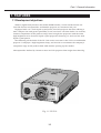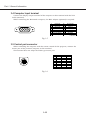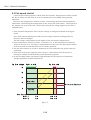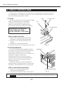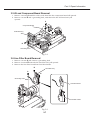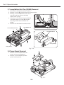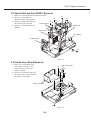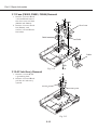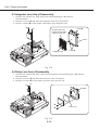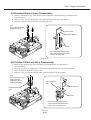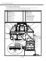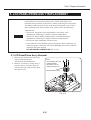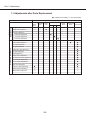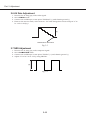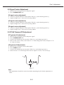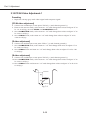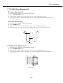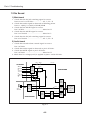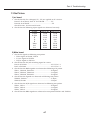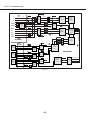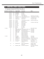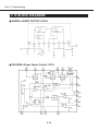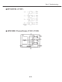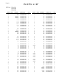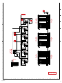
1
English Edition
SERVICE MANUAL
By Portable Document Format
0 PREFACE
1 General
2 Repair
3 Adjustment
LV-5110U/D78-5152
LV-5110E/D78-5153
4 Troubleshooting
5 Parts Catalog
6 Electrical Diagrams
Return to Contents
DY8-1785-151 500
CANON Multimedia Projector
LV-5110U
D78-5152
LV-5110E
D78-5153
SERVICE
SMANUAL
Technical Documents
Application
This CD-ROM is issued by Canon Inc. for qualified persons to learn technical theory and product
repair. This CD-ROM covers all localities where the products are sold. For this reason, there
may be information in this CD-ROM that does not apply to the product sold in your locality.
The following paragraph does not apply to any countries where such provisions are
inconsistent with local law.
Trademarks
The product names and company names described in this CD-ROM are the registered
trademarks of the individual companies.
Copyright
Canon Inc. retains the copyright to all data contained on this CD-ROM.
Reproduction, publication (including on the World Wide Web) alteration, translation into another
language, or other use of the data in whole or part, contained on this CD-ROM without the
written consent of Canon Inc., is prohibited.
PDF Files
This CD-ROM contains PDF files created using Adobe® Acrobat® 4.0J. PDF files can be viewed
using Adobe® Acrobat® Reader 4.0 or later.
Copyright © 2001 by Canon Inc.
CANON INC.
30-2 Shimomaruko 3-Chome, Ohta-ku,
Tokyo 146-8501, Japan
First published July, 2001
PREFACE
1. Service Manual Composition
This manual contains information on servicing the product. It has the following sections.
Part 1 General Information
Provides the basic information needed to understand the product.
(Operating instructions are not included. Refer to the product's instruction book if
necessary.)
Part 2 Repair Information
Provides information for disassembly, reassembly, and adjustment of the product, about
the tools required, and their application.
Part 3 Adjustment
Provides information for disassembly, reassembly, and adjustment of the product, about
the tools required, and their application.
Part 4 Troubleshooting
Part 5 Parts Catalog
Part 6 Electrical Diagrams
2. Model Differences
In this series of products, there are models suffixed “J”, “U”, and “E”. The only
differences between the models are cosmetic, mainly the designation and rating plates.
Internally, they are identical.
Main Marketing Area
Model Name
Japan
North America
Europe
POWER PROJECTOR MULTIMEDIA PROJECTOR MULTIMEDIA PROJECTOR
LV-5110J
LV-5110U
LV-5110E
I
3. Tools & Test Equipment
1) General Purpose Tools
Description
Ball Driver, 2.0mm hex
Hex Key Set (w/2.0mm)
Driver, Ceramic Tip (1.8mm)
Driver, Slot (4.0mm)
Driver, Cross-point (#2)
Tool No.
CY9-5002-000
CY9-5007-000
CY9-5003-000
CY9-5004-000
CY9-5005-000
Remarks
Optical Parts Removal & Adjustment
Optical Parts Removal & Adjustment
Electrical Adjustments
Optical Parts Adjustment
Assembly & Disassembly
2) Test Equipment (Local Purchase)
Description
Digital Multi-meter
Video Signal Generator
Computer Signal Generator
Oscilloscope
Specifications
1mV – 500V DC
Color Bars and Gray Scale
Gray Scale
100MHz response or over
Remarks
Electrical Adjustment
Electrical Adjustment
Electrical Adjustment
Waveform checks
3) Other Equipment (Local Purchase)
Description
Screen
Personal Computer
Specifications
Over 40”
Windows 95 OS
Remarks
All Adjustment
All Adjustment
4) Chart/Software (Attached with this manual)
Description
Monitor Tester
Gray Scale Chart
Color Shading Correction Tool
Specifications
XGA and SVGA
Bitmap Data
Ver. 2.0.2
II
Remarks
Electrical Adjustment
Electrical Adjustment
White Uniformity Adjustment
CONTENTS
Page
Part 1: General Information
1. FEATURES.......................................................................................................1-1
1.1 Development objectives............................................................................1-1
1.2 Major Features..........................................................................................1-2
1.3 LV-5110 Features (Details).......................................................................1-3
2. LV-5110 SPECIFICATIONS .............................................................................1-5
2.1 Main unit ...................................................................................................1-5
2.2 Connectors ...............................................................................................1-6
2.3 Accessories ..............................................................................................1-6
2.4 Other specifications ..................................................................................1-6
3. NOMENCLATURE............................................................................................1-7
3.1 Main unit ...................................................................................................1-7
3.2 Top controls ..............................................................................................1-8
3.3 Rear panel terminals.................................................................................1-9
3.4 Computer Input terminal ...........................................................................1-10
3.5 Control port connector ..............................................................................1-10
3.6 Remote control .........................................................................................1-11
3.7 Operating range ........................................................................................1-12
4. COMMENTARY ................................................................................................1-13
4.1 External appearance design .....................................................................1-13
4.2 Hybrid gamma correction..........................................................................1-13
4.3 Fan speed control .....................................................................................1-14
5. CONNECTING..................................................................................................1-15
5.1 Connection to the computer......................................................................1-15
5.2 Connecting to the video equipment ..........................................................1-16
6. SETTING-UP THE PROJECTOR.....................................................................1-17
6.1 Positioning the projector ...........................................................................1-17
6.2 Installation precautions .............................................................................1-17
7. SUPPORTED COMPUTER SYSTEM MODE ..................................................1-19
Part 2: Repair Information
1. SAFETY INSTRUCTIONS ................................................................................2-1
2. CIRCUIT PROTECTIONS ................................................................................2-2
2.1 Fuse ..........................................................................................................2-2
2.2 Thermal Switch .........................................................................................2-2
2.3 Warning Temperature and Power Failure Protection ...............................2-3
2.4 Air Filter Care and Cleaning .....................................................................2-3
3. MECHANICAL DISASSEMBLIES.....................................................................2-5
3.1 Cabinet Top Removal ...............................................................................2-5
3.2 Cabinet Front and Speaker Removal .......................................................2-5
3.3 Main Board Removal ................................................................................2-6
3.4 Fuse Removal...........................................................................................2-6
3.5 AV and Component Board Removal.........................................................2-7
3.6 Line Filter Board Removal ........................................................................2-7
III
3.7 Lamp Ballast Unit Fan (FN905) Removal .................................................2-8
3.8 Power Board Removal ..............................................................................2-8
3.9 Optical Unit and Fan (FN901) Removal....................................................2-9
3.10 Audio Amp. Board Removal ...................................................................2-9
3.11 Fans (FN902, FN903, FN904) Removal .................................................2-10
3.12 AC Inlet Ass’y Removal ..........................................................................2-10
4. OPTICAL PARTS DISASSEMBLIES................................................................2-11
4.1 Projection Lens Removal ..........................................................................2-11
4.2 Optical Unit Top Removal .........................................................................2-11
4.3 Integrator Lens Ass’y Disassembly...........................................................2-12
4.4 Relay Lens Ass’y Disassembly .................................................................2-12
4.5 Polarized Glass-in Ass’y Disassembly......................................................2-13
4.6 Polarized Glass-out Ass’y Disassembly....................................................2-13
4.7 Locations and Directions ..........................................................................2-14
5. LCD PANEL/PRISM ASS’Y REPLACEMENT ..................................................2-15
5.1 LCD Panel/Prism Ass’y Removal..............................................................2-15
5.2 Note on LCD Panel/Prism Ass’y Mounting ...............................................2-16
6. CLEANING........................................................................................................2-17
7. LAMP REPLACEMENT ....................................................................................2-18
Part 3: Adjustment
1. BEFORE ADJUSTMENTS................................................................................3-1
1.1 Adjustments after Parts Replacement ......................................................3-2
1.2 Service Adjustment Menu Operation ........................................................3-3
1.3 Service Conditions ....................................................................................3-4
1.4 Service Adjustment Data Table ................................................................3-5
2. ELECTRICAL ADJUSTMENTS ........................................................................3-7
2.1 Output Voltage Adjustment .......................................................................3-7
2.2 Fan Voltage Adjustment ...........................................................................3-7
2.3 PC-Offset Adjustment ...............................................................................3-8
2.4 PC Gain Adjustment .................................................................................3-8
2.5 Component Gain Adjustment....................................................................3-9
2.6 AV Gain Adjustment .................................................................................3-10
2.7 NRS Adjustment .......................................................................................3-10
2.8 Signal Center Adjustment .........................................................................3-11
2.9 PC/AV Gamma Off Adjustment ................................................................3-11
2.10 PC/AV-Video Adjustment-1 ....................................................................3-12
2.11 PC/AV-Video Adjustment-2 ....................................................................3-13
2.12 S/H Clock Adjustment .............................................................................3-13
2.13 Common Center Adjustment ..................................................................3-14
2.14 White Balance Adjustment......................................................................3-14
2.15 Black Balance Adjustment ......................................................................3-15
2.16 Note on White Uniformity Adjustment .....................................................3-15
3. OPTICAL ADJUSTMENTS ...............................................................................3-16
3.1 Contrast Adujstment .................................................................................3-16
3.2 Integrator Lens Adujstment.......................................................................3-17
3.3 Relay Lens Adjustment .............................................................................3-19
4. TEST POINTS AND LOCATIONS ....................................................................3-20
IV
Part 4: Troubleshooting
1. TROUBLESHOOTING......................................................................................4-1
1.1 No Power ..................................................................................................4-1
1.2 No Sound ..................................................................................................4-6
1.3 No Picture .................................................................................................4-7
2. CONTROL PORT FUNCTIONS .......................................................................4-9
2.1 System Control & I/O Port Functions ........................................................4-9
3. WAVEFORMS ..................................................................................................4-11
4. IC BLOCK DIAGRAMS .....................................................................................4-14
Part 5: Parts Catalog
Part 6: Electrical Diagrams
1. PARTS DESCRIPTION AND READING IN SCHEMATIC DIAGRAM..............6-1
2. PIN DESCRIPTION OF DIODE, TRANSISTOR AND IC..................................6-3
Circuit Block Diagram........................................................................................A1
Power Supply Lines ..........................................................................................A2
Schematic Diagrams .........................................................................................A3
Printed Wiring Board Diagrams.........................................................................A10
V
Part 1
General
Information
Part 1: General Information
1. FEATURES
1.1 Development objectives
With its sights firmly fixed on the SOHO-HOME market, Canon introduced the LV5100 B5 file size microportable* multimedia projector to consumers last year.
Equipped with a 0.7-inch liquid crystal panel, this LCD projector has been offering a
more compact size and greater portability at an even lower cost than before. In contrast,
Canon's competitors in this product range have brought out projectors with the same
high brightness to be found in liquid crystal projectors featuring 1.3-inch and 0.9-inch
liquid crystal panels.
Now following on the heels of the LV-5100 as its successor is the LV-5110 multimedia
projector. It employs a high-brightness lamp, and its aim is to maintain the company's
competitive edge in this product field while further opening up the market.
*Microportable: Defined by Canon to mean an LCD projector that weighs less than 3kg.
Fig. 1-1 LV-5110
1-1
Part 1: General Information
1.2 Major Features
● Compact, lightweight 2.7kg/B5 file size micro-portable type
Real SVGA compatible, class-leading 850 ANSI lumen output
● Supports HDTV&DVD component input
Beautiful image reproduction with minimal burring of color
● Equiped with Digital Keystone function
Smoothly corrects for "keystone" effect caused by projector tilt, giving a square image
with up to 15 degrees tilt.
● Plug and Play: Simply plug in computer or AV components and start - no adjustments
required.
1) Multiscan System automatically detects PC vertical and horizontal scan
frequencies
2) Video color system: Automatically detects system (NTSC/PAL; SECAM/NTSC4.43)
PAL-M/PAL-N can be selected from menu bar)
3) Tracking: Auto Imaging function automatically tracks and optimally positions
image
4) Graphic User Interface (GUI): The graphic user interface simplifies image
adjustments in varying environments.
5) Six Language support: English, French, German, Italian, Spanish and Japanese
are supported
6) Wireless Remote Control: Remote control has mouse control functions
● Temperature-sensing Real Time Fan Control: Unobtrusive sound level for conferences
● Gamma Correction: Gives high quality reproduction of gradation
1-2
Part 1: General Information
1.3 LV-5110 Features (Details)
● Brightest in the SVGA Micro Projector class - 850 ANSI Lumens
1) Large screen presentation even in brightly lit conference rooms
2) 132W UHP short arc lamp for bright images with great color balance
● Real projection SVG (800 x 600 dot) Digital compression XGA/SXGA high-definition
projection *
0.7" LCD Panels used (for the first time)
● Supports input from HDTV&DVD components
Color defference signal (Y, Pb/Cb, Pr/Cr) input reproduces the images with minimal
burring of color.
* Composite (Video) input is common to the Brightness (Y) input.
● Digital Keystone distortion compensation
When the projected image surface and the projector are offset, the image has a
trapezoidal shape, but this can be smoothly compensated with offsets up to 15
degrees.
A simple operation gives a square image without adjusting the height of the projector.
● Gamma Correction
To avoid washed-out whites and murky blacks the user can control the middle
brightness.
● Plug and Play: Simply plug in computer or AV equipments and start - no adjustments
required.
● Power Management: improves lamp life
After a predetermined time (5' 30") with no input signal, the lamp is turned off. When
a signal is input, it turns back on.
● Simple wireless remote control
1) Supports all remote functions
2) P-Timer button supplies presentation elapsed time
3) Functions as the mouse control for connected PC
● Manual zoom and focus controls included
● Digital zoom enlarges any selected part of the presentation image
● Cues up the next screen without pausing or projecting an unnecessary operation
screen. (Freeze function)
● The image can be turned off without turning the power off and immediately turned back
on - Image shut-off function.
● Noise is cut in the absence of a signal - Blue Back function.
1-3
Part 1: General Information
● Impressive image size - up to 200 inches.
● Reverse image function allows the unit to be suspended from the ceiling or used as a
rear-screen projector.
● Reduced lamp problems (Replace Lamp Indication)
1) The replace lamp indicator shows when it is time for a change.
2) Lamp replacement by the user is simple.
● The design emphasizes the lens, as you would expect from a Canon product.
* With digital compression projection, some information is lost.
XGA: 1024 x 768 dot → 800 x 600 dot when digitally compressed
SXGA: 1280 x 1024 dot → 750 x 600 dot when digitally compressed
1-4
Part 1: General Information
2. LV-5110 SPECIFICATIONS
2.1 Main unit
1. Type:
Micro-portable LCD Projector
2. LCD panel:
0.7" polysilicon active matrix TFT x 3
4:3 aspect ratio
3. Number of pixels:
480,000 pixels (800 H x 600 V) x 3
4. Resolution of display supported:
SXGA & XGA (compression)/SVGA/VGA
5. Light source:
132W UHP lamp
6. Brightness:
850 ANSI lumens
7. Illuminance ratio at
edges of image field:
90%
8. Contrast ratio:
300:1
9. Horizontal resolution:
500 TV lines
10. Projection lens:
28 to 33.6mm, 1:2.0 to 2.3, x1.2
11. Lens shifting (U/D ratio):
12:1
12. Elevation adjustment:
UP by 7.5˚
13. Size of projection image(in.)/
projection distance(m):
36" (1.4m), 60" (2.4m), 100" (4.0m), 150" (6.0m),
200" (8.0m) in WIDE mode
30" (1.4m), 50" (2.4m), 83" (4.0m), 125" (6.0m), 167"
(8.0m) in TELE mode
14. Digital keystone distortion
compensation angle:
±15˚
15. Noise:
39dB (normal temperature)
16. Color system:
NTSC, PAL, SECAM, NTSC4.43, PAL-M, PAL-N
17. Computer supported:
IBM PC or compatible, Macintosh, PC98, Workstations
Note: Some workstations are not supported.
1-5
Part 1: General Information
18. Scanning frequency:
15KHz to 80KHz for horizontal sync.
50Hz to 100Hz for vertical sync.
Up to 100MHz for dot clock
19. Audio output:
1W monaural
20. Built-in speaker:
40mm x 30mm (1.57" x 1.18"), x 1
21. Rated supply voltage:
100V AC, 50 / 60Hz (Japan)
100 to 120V AC / 200 to 240V AC, 50 / 60Hz (overseas)
22. Power consumption:
210W
23. Operating temperature:
5 to 35˚C (41 to 91˚F)
24. Storage temperature:
–10 to 60˚C (14 to 140˚F)
25. Dimensions (W x H x D)
189mm x 75.5mm x 310.8mm (7.44" x 2.97" x 12.24")
(Not including adjustment feet)
189mm x 90.5mm x 310.8mm (7.44" x 3.56" x 12.24")
(Including adjustable feet)
26. Net Weight:
2.7Kg (5.95 lbs)
2.2 Connectors
1. Computer input
Signal input:
Audio input:
Control port:
2. Audio/Video input
Video input:
Audio input:
3. Audio output:
HDB 15-pin x 1
Mini stereo jack x 1
Mini DIN 8-pin x 1
Mini DIN 4-pin x 1 (S-Video)
RCA type x 3 (Video/Y, Pb/Cb, Pr/Cr)
Mini stereo jack x 1
Mini stereo jack x 1
2.3 Accessories
1.
2.
3.
4.
5.
6.
7.
8.
9.
Remote Control Transmitter with two AA alkaline batteries
VGA Cable
Control Cable for PS/2 port
Lens Cover
Carry Bag
AC Power Cord
Plug Adapter (Japan model only)
Warranty Card
Owner's Manual
2.4 Other specifications
Service life of lamp:
Approx. 1000 hours
1-6
Part 1: General Information
3. NOMENCLATURE
3.1 Main unit
Zoom Ring
Projection Lens
Focus Ring
Speaker
Air Intake Vent
Power Cord Connector
Lens Cover
Infrared Remote Receiver
Foot Lock Latch
Air Intake Vent
Terminals and Connectors
Air Intake Vent
Exhaust Vent
Lamp Cover
Adjustable Foot
Air Filter
Fig. 1-2
1-7
Part 1: General Information
3.2 Top controls
POWER ON-OFF BUTTON
FOCUS RING
WARNING TEMP. INDICATOR
Used to turn on the projector on
or off.
Turn this ring to adjust the
projected picture focus.
This indicator flashes red when internal
projector temperature is too high.
MENU BUTTON
ZOOM RING
READY INDICATOR
Use to open or close
the Menu operation.
Turn this ring to adjust the
projected picture size.
This indicator lights green when
the projector is ready to be turn on.
And it flashes green in Power
Management mode.
WIDE
POWER
MENU
NORMAL
MODE
TELE
LAMP WARNING
READY
REPLACE TEM
P.
LAMP
MODE BUTTON
POINT BUTTON
LAMP INDICATOR
Use to select input source
either Computer or Video.
Use to select an item of adjust
the value in the menu.
It is also used to pan the image
in Digital Zoom mode.
This indicator is dim when
the projector is turn on.
And bright when the projector
is stand-by mode.
NORMAL BUTTON
SELECT BUTTON
LAMP REPLACE INDICATOR
Used to rest to normal picture
adjustment preset by factory.
Used to execute the item selected.
It is also used to expand the image
in Digital Zoom mode.
This indicator turns to yellow when
the life of the projection lamp draws
to an end.
Fig. 1-3
1-8
Part 1: General Information
3.3 Rear panel terminals
VIDEO INPUTS
(Y/VIDEO, Pb/Cb, Pr/Cr)
RCA type jacks
Connect the composite video
output signal to the Y/Video
jack or connect the component
Y output signals to the Y/Video,
Pb/Cb and Pr/Cr jacks.
S-VIDEO INPUT
VIDEO
Y – Pb/Cb – Pr/Cr
Mini DIN 4-pin type
Connect the S-Video output
from the video equipment
to this terminal.
AUDIO INPUT
RESET
AV
AUDIO OUT
COMPUTER
AUDIO
IN
RESET BUTTON
The micro processor may
malfunction and need to rest.
This can be done by pressing
the Reset button with a pen,
which will shut down and
restart the projector.
S – VIDEO
Mini stereo jack
Connect the audio output
from the video equipment
to this terminal.
CONTROL PORT
COMPUTER IN
COMPUTER AUDIO INPUT
Mini stereo jack
Connect the audio output
signal from the computer
to this terminal
AUDUO OUTPUT
COMPUTER INPUT
CONTROL PORT
Mini stereo Jack
Connect the external audio
amplifier to this terminal.
HDB 15-pin type
Connect the computer output
signal to this terminal.
Mini DIN 8-pin type
When controlling the computer
with the Remote Control of this
projector, connect the mouse
port of the computer to this
terminal.
Fig. 1-4
1-9
Part 1: General Information
3.4 Computer Input terminal
Connect the display output terminal of the computer to this terminal with the VGA
Cable (attached).
When connecting the Macintosh computer, the MAC Adapter (optional) is required.
4
5
10
15
14
2
3
9
8
13
1
7
12
1
2
3
4
5
6
7
8
6
11
Red Input
Green Input
Blue Input
Sense 2
Ground (Horiz.sync.)
Ground (Red)
Ground (Green)
Ground (Blue)
9
10
11
12
13
14
15
No Connect
Ground (Vert.sync.)
Sense 0
Sense 1
Horiz. sync.
Vert. sync.
Reserved
Fig. 1-5
3.5 Control port connector
When controlling the computer with the remote control of this projector, connect the
mouse port of the personal computer to this terminal.
This terminal does not adapt the PC98 type mouse port.
8
5
1
2
3
4
5
6
7
8
7 6
4 3
2 1
Fig. 1-6
1-10
PS/2
----CLK
DATA
GND
--------GND
-----
Serial
RXD
--------GND
RTS
TXD
GND
GND
ADB
----ADB
----GND
------------GND
Part 1: General Information
3.6 Remote control
ALL-OFF SWITCH
When using the Remote Control
Unit, turn this switch to "ON".
And turn it to "ALL OFF" when
it is not used.
POWER BUTTON
D.ZOOM BUTTON
POWER
Used to correct the keystone
distortion.
VOLUME BUTTON
KEYSTONE D.ZOOM VOLUME
MUTE
COMPUTER
MENU
VIDEO
Use to select Computer input
source.
VIDEO BUTTON
Use to select Video source.
POINT BUTTON
Used to move a pointer
on the menu, to adjust the
item, or to pan the image
in Digital Zoom mode.
RIGHT CLICK BUTTON
Use to compress the image in
Digital Zoom mode.
It is also used as a PC mouse
in Wireless Mouse operation.
P-TIMER
SELECT BUTTON
Used to execute the item
selected or to expand the image
in Digital Zoom mode.
NO SHOW
FREEZE
P-TIMER BUTTON
Used to operate P-timer function.
AUTO IMAGE
NORMAL
NO SHOW BUTTON
FREEZE BUTTON
Used to turn the picture into
black image.
AUTO IMAGE BUTTON
NORMAL BUTTON
Used to operate Auto Image function.
Used to reset to normal picture
position preset by factory.
Fig. 1-7
1-11
F
ALL OF
COMPUTER BUTTON
MUTE BUTTON
MENU BUTTON
ON
KEYSTONE BUTTON
Part 1: General Information
3.7 Operating range
Point the remote control toward the projector (receiver's window) when pressing the
buttons.
Maximum operating range for the remote control is approximately 5m (16.4') and 60˚ in
front of the projector.
Precautions
• Prevent the direct sunlight or strong light from lighting apparatus from striking the
infrared remote receiver on the projector.
• Do not look into the laser pointer exit or point it at others.
• Do not dismantle the remote control.
30˚
5m
30˚
Fig. 1-8
1-12
Part 1: General Information
4. COMMENTARY
4.1 External appearance design
This product follows the same design concept and coloring as the earlier models, LV7325/LV-7320 to establish a unified image for Canon Multimedia Projectors. Some of
the major design points, which are basically the same as the other Canon Multimedia
Projectors, are outlined below.
● External Styling
The body is designed with subtle curves and the coloring and semi-transparent body
panels follow the lead of the LV-7300 series. Indications of the excellent lens
performance are printed around the lens to convey an impression of high picture
quality.
● Operating Keys
The operation and cursor key layout is a simple, intuitive layout with grouping to
insure ease of use.
● Coloring
The body of the projector is colored glacial blue. The front of the unit, with an
appearance fittimg a product from an optical equipment manufacturer, has an
aluminum lens ring and is colored arctic silver. The overall effect is to emphasize the
lens and evoke a sophisticated image.
The operating keys are a special "mercury silver" color that is easy to see in dim light
and also serves as a design accent point.
4.2 Hybrid gamma correction
Hybrid gamma correction is a new feature. It combines digital gamma correction and
analog gamma correction, and takes advantage of the characteristics* of both. Using the
on-screen menu, the user can take advantage of this new feature to control image
gradation.
* Analog gamma correction: analogue correction is applied to the non-linear analog
circuit. In analog correction transitions between gradations
are smooth.
* Digital gamma correction: Correction is applied through digital processing of the X/Y
gamma curve. Using a digital signal, varying the
characteristics curve, for example, is simple. Because
digital processing is involved, however, transitions between
gradations can be abrupt.
1-13
Part 1: General Information
4.3 Fan speed control
A new feature of this projector is Real Time Fan Control. Temperature sensors control
the fan to reduce the fan noise level to an unobtrusive level (39dB) during normal
operation.
There are two temperature sensors, sensor 1 measuring ambient room temperature
and sensor 2 measuring the temperature in the area of the LCD panels. The outputs of
the sensors are sent to the CPU, which then controls the voltage applied to the fan as
outlined below.
1. If the internal temperature rises, the fan voltage is changed as shown in the figure
below.
But, if the internal temperature falls, the fan voltage remains unchanged for five
minutes, then is changed
The fan voltage is determined by the higher of the two sensor temperatures.
2. If the temperature sensed by sensor 1 exceeds 51˚C, or the temperature sensed by
sensor 2 exceeds 57˚C, the lamp is extinguished. In this case, the main power switch
must be turned off and then back on to resume operation.
3. The fan will continue to run for a maximum of 90 seconds after the power switch is
turned off.
4. If the CPU receives no response from a sensor, it determines that the sensor is
missing or broken and immediately shuts down the projector.
5. In Service Mode (when operating at high altitude) the fan operates at maximum
voltage regardless of room temperature.
Fan Drive Voltage
Fan Noise: 39dB
Fan Noise: 43dB
13V
12V
11V
10V
9V
Exhaust Fan
Unit shutdown Temperature
Intake Fan
Room Temperature:
Sensor 1:
Sensor 2:
35ûC 37ûC
49ûC 51ûC
55ûC 57ûC
27ûC
41ûC
47ûC
Fig. 1-9
1-14
Part 1: General Information
5. CONNECTING
5.1 Connection to the computer
IBM-compatible computers or Macintosh computers (VGA/SVGA/XGA/SXGA)
Desktop type
Laptop type
Monitor Output
Serial Port
PS/2 Port
ADB Port
Control Cable
for Serial Port
(Optional)
Control Cable
for PS/2 Port
(Attached)
Control Cable
for ADB Port
(Optional)
Audio Output
MAC Adapter
(Optional)
Set the slide
switches following
the chart bellow.
Terminal
Terminal
Terminal
Audio Cable
Mini Stereo type
(Not supplied)
VGA Cable
(Attached)
Use one of these Control
Cables corresponding
with the terminal of your
computer.
VIDEO
Y – Pb/Cb – Pr/Cr
RESET
AUDIO OUT
S – VIDEO
AV
COMPUTER
COMPUTER AUDIO IN
AUDIO
IN
AUDIO OUT
CONTROL PORT
COMPUTER IN
CONTROL PORT
COMPUTER IN
Audio Cable
Mini Stereo type
(Not supplied)
MAC Adapter
Audio Input
Audio Amplifier
Set the switches as shown in the table below depending on the Display
Resolution that you want to use before you turn-on the projector and computer.
Speaker (Stereo)
1
ON
ON
DIP
1 2 3 4 5 6
OFF
Fig. 1-10
1-15
13" MODE (640 x 480)
ON
16" MODE (832 x 624) OFF
19" MODE (1024 x 768) OFF
21" MODE (1152 x 870) ON
2
ON
ON
ON
ON
3
4
5
6
OFF OFF OFF OFF
OFF ON OFF OFF
ON OFF OFF OFF
ON ON OFF OFF
Part 1: General Information
5.2 Connecting to the video equipment
Video Source (example)
Video Cassette Recorder
Component video output equipment
(DVD Player, HDTV, etc.)
Video Disc Player
Composite
Video Output
Component
Video Output
S-VIDEO Output
Audio Output
Y Pb/Cb Pr/Cr
When several display signals are input,
the projector assigns priority in this order:
(1) Y, Pb/Cb, Pr/Cr, (2) S-Video, (3) Video.
If the desired input is not selected
automatically, use the video input menu
to select it.
R
L
S-Vdeo Cable
Audio Cable
(Not supplied)
RCA-Mini Stereo Type
(Not supplied)
Video Cable
(Not supplied)
Y-Pb/Cb-Pr/Cr
VIDEO
Y — Pb/Cb —Pr/Cr
S-VIDEO
S —VIDEO
VIDEO
AUDIO OUT
RESET
AUDIO OUT
AV
COMPUTER
AUDIO
IN
CONTROL PORT
COMPUTER IN
Audio Cable
Mini Stereo type
(Not supplied)
Audio Input
Speaker (Stereo)
Audio Amplifier
Fig. 1-11
1-16
AV AUDIO IN
Part 1: General Information
6. SETTING-UP THE PROJECTOR
6.1 Positioning the projector
This projector is designed to project on a flat projection surface.
The projector can be focused from 1.4m (4.6') to 8.0m (26.3').
Refer to the figure below to adjust the screen size.
8.0m
200”
6.0m
4.0m
150”
2.4m
WIDE END
167”
100”
1.4m
H1
125”
60”
TELE END
83”
36”
50”
H2
30”
Screen Size
(W x H) mm
30”
60”
100”
150”
200”
610 x 457
1219 x 914
2032 x 1524
3048 x 2286
4064 x 3048
Height (H1)
422mm
844mm
1407mm
2110mm
2814mm
Height (H2)
35mm
70mm
117mm
176mm
234mm
Fig. 1-12
6.2 Installation precautions
1) Temperature of air discharged from exhaust vent
Hot air is discharged from the exhaust vent. Do not put the object in the way of this
hot air.
2) Installation site
Do not install the projector in humid or duty locations, or locations subject to a lot of
oil mist or cigarette smoke. Doing so may cause dirt to adhere to the lenses, mirrors
and other optical parts, resulting in impaired image quality. Also, do not install the
projector in high- or low-temperature locations.
3) Operating temperature range: 5˚C to 35˚C
4) Storage temperature range: –10˚C to 60˚C
5) Condensation
Do not move the projector suddenly from a low-temperature location to a hightemperature location, or suddenly raise the room temperature. Doing so can cause
moisture in the air to condense on the lenses and mirrors of the projector, resulting
1-17
Part 1: General Information
in blurred images.
6) Screen and room brightness
Do not install the projector where sunlight or lighting directly strikes on the screen. If
sunlight or light from lighting strikes on the screen, image will appear whitish and
difficult-to-view.
1-18
Part 1: General Information
7. SUPPORTED COMPUTER SYSTEM MODE
The projector judges the incoming signal from the connected personal computer and
automatically selects the appropriate system mode. Some models cannot be selected
depending on the computer. In this case, the message Go to PC adj. is displayed at the
system box on the menu bar. (Adjust and set the computer system manually.)
Table 1-1
On-Screen
Display
VGA 1
VGA 2
VGA 3
VGA 4
VGA 5
VGA 6
VGA 7
MAC LC13
MAC 13
RGB
RGB
SVGA 1
SVGA 2
SVGA 3
SVGA 4
SVGA 5
SVGA 6
SVGA 7
SVGA 8
SVGA 9
SVGA 10
SVGA 11
MAC1 6
XGA 1
XGA 2
Resolution
640 x 480
720 x 400
640 x 400
640 x 480
640 x 480
640 x 480
640 x 480
640 x 480
640 x 480
ÐÐÐÐÐ
ÐÐÐÐÐ
800 x 600
800 x 600
800 x 600
800 x 600
800 x 600
800 x 600
800 x 600
800 x 600
800 x 600
800 x 600
800 x 600
832 x 624
1024 x 768
1024 x 768
H-Frequency V-Frequency On-Screen
(KHz)
(Hz)
Display
31.47
31.47
31.47
37.86
37.86
37.50
43.269
34.97
35.00
15.734
15.625
35.156
37.88
46.875
53.674
48.08
37.90
34.50
38.00
38.60
32.70
38.00
49.72
48.36
68.677
59.88
70.09
70.09
74.38
72.81
75.00
85.00
66.60
66.67
30
25
56.25
60.32
75.00
85.06
72.19
61.03
55.38
60.51
60.31
51.09
60.51
74.55
60.00
84.997
XGA 3
XGA 4
XGA 5
XGA 6
XGA 7
XGA 8
XGA 9
XGA 10
XGA 11
XGA 12
XGA 13
XGA 14
XGA15
MAC 19
MAC 21
SXGA 1
SXGA 11
SXGA 13
SXGA 14
SXGA 17
SXGA 18
HDTV720p
HDTV1035i
HDTV1080i
Resolution
1024 x 768
1024 x 768
1024 x 768
1024 x 768
1024 x 768
1024 x 768
1024 x 768
(Interlace)
1024 x 768
1024 x 768
1024 x 768
(Interlace)
1024 x 768
1024 x 768
1024 x 768
1152 x 870
1152 x 864
1152 x 900
1280 x 1024
(Interlace)
1280 x 1024
(Interlace)
1152 x 900
1280 x 1024
(Interlace)
ÐÐÐÐÐ
ÐÐÐÐÐ
ÐÐÐÐÐ
H-Frequency V-Frequency
(KHz)
(Hz)
60.023
56.476
60.31
48.50
44.00
63.48
36.00
62.04
61.00
35.522
46.90
47.00
58.03
60.24
68.68
64.20
61.20
50.00
50.00
61.85
46.43
45.00
33.75
33.75
75.03
70.07
74.92
60.02
54.58
79.35
43.59
77.07
75.70
43.48
58.20
58.30
72.00
75.08
75.06
70.40
65.20
43.00
47.00
66.00
43.35
60.00
60.00
60.00
NOTE: Specifications are subject to change without notice.
When these signals (marked in yellow): XGA, SXGA, Mac16, Mac19, Mac21, HDTV720p, HDTV1035i, HDTV1080i, are projected there will be some difference in lines and characters because the signals are digitally compressed.
The dot clock is not compatible with computer signals higher than 100MHz.
1-19
Part 2
Repair
Information
Part 2: Repair Information
1. SAFETY INSTRUCTIONS
WARNING:
The chassis of this projector is isolated (COLD) from AC line by using the converter transformer. Primary
side of the converter and lamp power supply unit circuit is connected to the AC line and it is hot, which hot
circuit is identified with the line (
) in the schematic diagram. For continued product safety and
protection of personnel injury, servicing should be made with qualified personnel.
The following precautions must be observed.
1: An isolation transformer should be connected in the power line between the projector and the AC line
before any service is performed on the projector.
2: Comply with all caution and safety-related notes provided on the cabinet back, cabinet bottom, inside
the cabinet or on the chassis.
3: When replacing a chassis in the cabinet, always be certain that all the protective devices are installed
properly, such as, control knobs, adjustment covers or shields, barriers, etc.
DO NOT OPERATE THIS PROJECTOR WITHOUT THE PROTECTIVE SHIELD IN POSITION AND
PROPERLY SECURED.
4: Before replacing the cabinet cover, thoroughly inspect the inside of the cabinet to see that no stray
parts or tools have been left inside.
Before returning any projector to the customer, the service personnel must be sure it is completely safe to
operate without danger of electric shock.
Product safety should be considered when a component replacement is made in any area of the
projector. Components indicated by mark
in the parts list and the schematic diagram designate
components in which safety can be of special significance. It is, therefore, particularly recommended that
the replacement of there parts must be made by exactly the same parts.
Eye damage may result from directly viewing the light produced by the Lamp used in this equipment.
Always turn off Lamp before opening cover. The Ultraviolet radiation eye protection required during this
servicing.
Never turn the power on without the lamp to avoid electric-shock or damage of the devices since the
stabilizer generates high voltages (15kV - 25kV) at its starts.
Since the lamp is very high temperature during units operation replacement of the lamp should be done
at least 45 minutes after the power has been turned off, to allow the lamp cool-off.
2-1
Part 2: Repair Information
2. CIRCUIT PROTECTIONS
This projector is equipped with the following circuit protections to operate in safety. If
the abnormality occurs inside the projector, it will automatically turn off by operating
one of the following protection circuits.
Screw
2.1 Fuse
The fuse is located inside of the projector. When
either the LAMP indicator or the READY
indicator is not illuminated, fuse may be
opened. Check the fuse as following steps.
It should be used the specified fuse as follows;
Line Filter Cover
Fuse
Line Filter Board
Fuse Part No.: CY2-8376-000
TYPE T4.0AH 250V FUSE
LITTEL FUSE INC. TYPE 215004
[How to replace the fuse]
1. Remove the cabinet top and main board
following to “Mechanical Disassemblies”.
2. Remove a screw and the line filter cover
upward.
3. Remove the fuse from fuse holder.
To install the fuse, take reversed step in the above.
Fig. 2-1
2.2 Thermal Switch
There is the thermal switch (SW902) inside of
the projector to prevent the internal temperature
from rising abnormally. When the internal
temperature reaches near 100˚C, turn off the AC
main power supply automatically.
The thermal switch is not reset to normal
automatically even if the internal temperature
becomes normal. Reset the thermal switch
following procedure.
Check the resistance between terminals of
thermal switch by using the tester. If it has high
impedance, thermal switch may be in operative.
Reset Button
[How to reset the thermal switch]
1. Remove the cabinet top following to
“Mechanical Disassemblies”.
2. Press the reset button on the thermal switch.
CAUTION
Thermal switch (SW902)
Fig. 2-2
Before press the reset button, disconnect the AC cord from the projector.
2-2
Part 2: Repair Information
2.3 Warning Temperature and Power Failure Protection
The TEMP WARNING indicator flashes red and the projector will automatically turn off
when the internal temperature of the projector exceeds the normal temperature or when
stopping cooling fans or when the internal power supply lines are failed.
Check the following possible causes and wait until stopping the TEMP WARNING
indicator flashing.
Possible causes
• Air filter is clogged with dust particles. Remove dust from the air filter by following
instructions in the “Air filter care and cleaning” below.
• Ventilation slots of the projector are blocked. In such an event, reposition the
projector so that ventilation slots are not obstructed.
• Check if projector is used at higher temperature place (Normal operating temperature
is 5 to 35 ˚C or 41 to 95 ˚F)
If the TEMP WARNING indicator still continues to flash, there may be defects on
cooling fans or power supply circuits. Please check fan operation and power supply lines
referring to the “Power Supply Lines Chart”.
2.4 Air Filter Care and Cleaning
The removable air filters prevents dust from
accumulation on the surface of the projection
lens and projection mirror. Should the air
filter become clogged with dust particles, it will
reduce the cooling fan’s effectiveness and may
result in internal heat build up and reduce the
life of the projector.
To clean up the air filters, follow the cleaning
procedure below:
1. Turn the power off, and disconnect the AC
power cord from the AC outlet.
2. Turn the projector up side down and
remove 2 air filters (Large and Small) by
pulling the latches of them upward.
3. Clean the air filters with brush or wash out
the dust and particles.
4. Replace each air filter properly. Make sure
that the air filters are fully inserted.
2-3
Air filters
Air filters
(Small)
(Large)
Fig. 2-3
Part 2: Repair Information
CAUTION
Do not operate the projector with the air filter removed. The dust is
stuck on the LCD panel and the mirror, and it may spoil the fine
picture image.
Do not put the small parts into the air filter intake vents. It result in
the malfunction of the projector. The air filter is small parts. Take care
that children don’t eat or swallow it.
We recommend to avoid dusty, smoky place for operating the projector.
Using in dusty place may cause the picture of poor quality.
When using under the dusty or smoky conditions, dust may
accumulate on the LCD panel and lens inside it, and may resultantly
be projected on the screen together with the picture.
When the above symptoms are noticed, please clean up the LCD panel
and lens following to the “Cleaning Method”.
2-4
Part 2: Repair Information
3. MECHANICAL DISASSEMBLIES
Mechanical disassemble should be made following procedures in numerical order.
Following steps show the basic procedures, therefore unnecessary step may be
ignored.
CAUTION
The parts and screws should be placed exactly the same position as
the original otherwise it may cause loss of performance and product
safety.
3.1 Cabinet Top Removal
(1) Remove 5 screws.
(2) Remove 2 screws A of the
Cabinet Front (bottom
part). See Fig. 2-5
(3) Pull the lower part of the
Cabinet Front off forward.
(4) Pull the Cabinet Top upward
while opening the
arrow indicated part of it
toward outside.
Fig. 2-4
3.2 Cabinet Front and Speaker Removal
1. Remove 4 screws (2 top and 2 bottom) A and take the cabinet front off forward.
2. Remove 2 screws B and then remove RC board and temp board.
3. Remove 4 screws C and the speaker.
RC Board
Temp Board
A
B
B
A
A
C
Fig. 2-5
2-5
A
Part 2: Repair Information
3.3 Main Board Removal
1. Remove 9 screws and remove the main board upward.
Main Board
Fig. 2-6
3.4 Fuse Removal
1. Remove a screw and pull the line filter cover upward and then replace the fuse if
required.
Line Filter Cover
Fuse
Fig. 2-7
2-6
Part 2: Repair Information
3.5 AV and Component Board Removal
1. Remove 3 screws A and FPC cables, and then take the component board off upward.
2. Remove a screw B and a grounding lead, and then take the AV board ass’y off
upward.
A
Component Board
A
A
AV Board Ass’y
B
Grounding Lead
Fig. 2-8
3.6 Line Filter Board Removal
1. Remove a screw A and remove a grounding lead.
2. Remove 2 screws B and take the line filter ass’y off upward.
3. Remove the line filter board from line filter holder.
B
Line Filter Ass’y
A
B
Grounding Lead
Line Filter Board
Line Filter Holder
Fig. 2-9
2-7
Part 2: Repair Information
3.7 Lamp Ballast Unit Fan (FN905) Removal
1. Disconnect the thermal switch sockets.
2. Remove a screw A and disconnect the lamp socket.
3. Remove 2 screws B (bottom side) and a
screw C, and the remove the lamp
ballast unit upward.
4. Take the cover off from the lamp ballast
unit and remove 4 screws D and take
the lamp ballast board off from the
holder.
5. Remove the fan FN905 from the holder.
C
Blue
Lamp Ballast Unit
Thermal Switch Sockets
Brown
A
D
Lamp Ballast Board
D
D
D
B
Lamp Socket
Fan (FN905)
B
Fig. 2-10
3.8 Power Board Removal
A
1. Remove 2 screws A and take the
power unit cover off upward.
2. Remove 3 screws B and pull the
power board upward..
A
B
B
B
Fig. 2-11
2-8
Part 2: Repair Information
3.9 Optical Unit and Fan (FN901) Removal
1. Remove 2 screws A and the thermal switch.
2. Remove a screw B and
C
disconnect the lamp socket.
C
3. Remove 7 screws C and pull
A
A
Thermal Switch
the optical unit upward.
4. Remove 2 screws D and fan
(FN901).
B
Lamp Socket
C
C
C
Optical Unit
C
C
Fan (FN901)
AV Board Ass’y
D
Fig. 2-12
3.10 Audio Amp. Board Removal
1. Remove a screw A (bottom
side) and 2 screws B, and
then pull the power unit
holder upward.
2. Remove 2 screws C and take
the audio amp. board off from
the power unit holder
Audio Amp. Board
C
C
B
Power Unit Holder
A
Fig. 2-13
2-9
B
D
Part 2: Repair Information
3.11 Fans (FN902, FN903, FN904) Removal
1. Remove 4 screws A and
3 screws B and remove
the duct cover and fans
(FN902 and FN903).
2. Remove 2 screws C and
fan (FN904), and
remove 2 screws D and
fan holder.
A
B
A
B
B
Duct Cover
A
A
FN902
FN903
C
D
Fig. 2-14
D
3.12 AC Inlet Ass’y Removal
1. Remove a screw A and
a grounding lead.
2. Remove 2 screws B and
pull the AC inlet ass’y
upward.
B
B
A
AC Inlet
Grounding Lead
Fig. 2-15
2-10
C
FN904
Part 2: Repair Information
4. OPTICAL PARTS DISASSEMBLIES
4.1 Projection Lens Removal
1. Remove the Cabinet top and cabinet front following to “Mechanical Disassemblies”.
2. Remove 4 screws and remove the Projection Lens.
Fig. 2-16
4.2 Optical Unit Top Removal
1. Remove the Cabinet top, front, main board, component boards and power unit cover
following to “Mechanical Disassemblies”.
2. Remove 6 screws and take the optical unit top off upward.
Optical Unit Top
Fig. 2-17
2-11
Part 2: Repair Information
4.3 Integrator Lens Ass’y Disassembly
1. Remove the cabinet top, front and main board following to “Mechanical
Disassemblies”.
2. Remove 2 screws A and take the integrator lens ass’y off upward.
3. Release 4 hooks B on the holder and remove the integrator lens.
A
A
Hooks B
* Should be place the
rugged surface of lens
comes to holder side.
Holder
Integrator Lens
Hooks B
Fig. 2-18
4.4 Relay Lens Ass’y Disassembly
1. Remove the cabinet top, front, main and component boards following to “Mechanical
Disassemblies”.
2. Remove 2 screws A and take the relay lens ass’y off upward.
3. Remove 2 screws B on the holder and take the relay lens off.
A
A
Holder
B
Relay Lens
B
Fig. 2-19
2-12
Part 2: Repair Information
4.5 Polarized Glass-in Ass’y Disassembly
1. Remove the cabinet top, front, main and component boards following to “Mechanical
Disassemblies”.
2. Remove each screw and take the each polarized glass-in ass’y off upward.
3. Release 2 hooks and remove the polarized glass-in.
Note:
Each polarized glasses
are defferent parts.
Phase Sheet
Polarized Glass-In
Hook
* Mount the polarized glass as the
surface attached the phase sheet
comes to the prism side.
Fig. 2-20
4.6 Polarized Glass-out Ass’y Disassembly
1. Remove the cabinet top, front and main boards following to “Mechanical
Disassemblies”.
2. Remove 4 screws by using the 2.0 mm hex driver and take the LCD Panel/Prism
ass’y off upward from the optical unit.
3. Remove each screw and take the each polarized glass-out off upward.
Note:
Do not replace the LCD
panel separately
otherwise it can not
obtain proper picture.
LCD Panel/Prism
Ass’y
Polarized Glass-Out
LCD Panel/Prism
Ass’y
LCD Panel
* Mount the polarized glass as the
surface attached the phase sheet
comes to the LCD panel side.
Fig. 2-21
2-13
Part 2: Repair Information
4.7 Locations and Directions
When the optical parts mounting or assembling, the parts must be mounted in the
specified location and direction. Please follow to the figure below.
No.
Part name
No.
Part name
1
2
3
4
5
6
7
8
9
10
11
Prism ass’y
Integrator lens (IN)
Integrator lens (OUT)
Prism Ass’y (PBS)
Condenser lens (OUT)
Dichroic mirror (R)
Mirror (R)
Condenser lens (R)
Condenser lens (B)
Mirror (B)
Optical Filter (UV cut)
12
13
14
15
16
17
18
19
20
21
Relay lens (OUT)
Relay lens (IN)
Dichroic mirror (G)
Condenser lens
Polarized glass (OUT/R)
Polarized glass (OUT/G)
Polarized glass (OUT/B)
Polarized glass (IN/R)
Polarized glass (IN/G)
Polarized glass (IN/B)
10
9
8
1
11
7
18 16
21
19
17
20
6
12
15
A cutting corner
comes this side up.
14
10
5
13
A cutting corner
comes this side up.
4
Dot marker
3
2
Light Source
Fig. 2-22
2-14
Part 2: Repair Information
5. LCD PANEL/PRISM ASS’Y REPLACEMENT
WARNING
LCD panels used for this model can not be replaced separately. Do not
disassemble the LCD Panel/Prism Ass’y. These LCD panels are
installed with precision at the factory. When replacing the LCD panel,
should be replaced whole of the LCD panels and prism ass’y at once.
After replacing LCD Panel/Prism ass’y, please check the following
adjustments.
• Check the “Integrator Lens Adjustment” and “Relay Lens
Adjustment” following to chapter “Optical Adjustment”.
• Check the “White Balance Adjustment” and “Black Balance
Adjustment” following to chapter “Electrical Adjustment”.
• Check the white uniformity on the screen.
• If you find the color shading, please adjust the white uniformity by
using the proper computer and “Color Shading Correction” software
attached with this manual.
COLOR SHADING CORRECTION (Ver. 2.0.2)
5.1 LCD Panel/Prism Ass’y Removal
1. Remove the cabinet top, front and
main board following to
“Mechanical Disassemblies”.
2. Remove 4 screws by using the 2.0
mm hex driver and take the LCD
Panel/Prism ass’y off upward from
the optical unit.
Note:
Do not replace the LCD
panel separately
otherwise it can not
obtain proper picture.
LCD Panel/Prism Ass’y
Fig. 2-23
2-15
Part 2: Repair Information
5.2 Note on LCD Panel/Prism Ass’y Mounting
After replacing or installing the LCD Panel/Prism ass'y, please make sure to obtain the
best focus in both TELE and WIDE zoom. If the focus adjustment is required, please
adjust the positioning of LCD Panel/Prism Ass’y by following the below procedure.
Mounting Procedure
1. Loosen 4 screws A on the LCD
Panel/Prism ass'y with 2.0 mm hex
driver.
2. Turn the projector on and project
the image with WIDE zoom, and
adjust the FOCUS control to obtain
the best focus.
3. Turn the ZOOM control to the TELE
position.
4. Move the LCD Panel/Prism Ass’y
backward or forward (about 0mm 0.8mm) to obtain the proper focus.
Confirm the focus at TELE and
WIDE zoom.
5. Tighten 4 screws A to fix the LCD
Panel/Prism ass'y.
Top View
A
A
A
A
LCD Panel/Prism Ass’y
Fig. 2-24
2-16
Part 2: Repair Information
6. CLEANING
WARNING
After long periods of use, dust and other particles will accumulate on
the LCD panel, prism, mirror, polarized glass, lens, etc., causing the
picture to darken or color to blur. If this occurs, clean the inside of
optical unit.
Remove dust and other particles using air spray. If dirt cannot be
removed by air spray, disassemble and clean the optical unit.
Cleaning with air spray
1. Remove the cabinet top following to “Mechanical Disassemblies”.
2. Clean up the LCD panel and polarizing plate by using the air spray from the cabinet
top opening.
CAUTION
Use a commercial (inert gas) air spray designed for cleaning camera
and computer equipment. Use a resin-based nozzle only. Be vary
careful not to damage optical parts with the nozzle tip. Never use any
kind of cleanser on the unit. Also, never use abrasive materials on the
unit as this may cause irreparable damage.
Disassembly cleaning
Disassembly cleaning method should only be performed when the unit is considerable
dirty and cannot be sufficiently cleaned by air spraying alone.
Be sure to readjust the optical system after performing disassembly cleaning.
1. Remove the cabinet top and main units following to “Mechanical Disassemblies”.
2. Remove the optical base top following to “Optical Unit Disassemblies”. If the LCD
panel needs cleaning, remove the LCD panel unit following to “LCD panel
replacement”.
3. Clean the optical parts with a soft cloth. Clean extremely dirty areas using a cloth
moistened with alcohol.
CAUTION
The surface of the optical components consists of multiple dielectric
layers with varying degrees of refraction. Never use organic solvents
(thinner, etc.) or any kind of cleanser on these components.
Since the LCD panel is equipped with an electronic circuit, never use
any liquids (water, etc.) to clean the unit. Use of liquid may cause the
unit to malfunction.
2-17
Part 2: Repair Information
7. LAMP REPLACEMENT
WARNING
• For continued safety, replace with a lamp assembly of the same type.
• Allow the projector to cool for at least 45 minutes before you open
the lamp cover. The inside of the projector can become very hot.
• Do not drop the lamp module or touch the glass bulb! The glass can
shatter and cause injury.
Procedure
1. Turn off the projector and disconnect the AC
cord. Allow the projector to cool for at lease 45
minutes.
2. Remove a screw with a screwdriver and remove
the lamp cover.
3. Remove 2 screws and pull out the lamp
assembly by grasping the handle.
4. Replace the lamp assembly securely and
tighten 2 screws.
5. Place the lamp cover and tighten a screw.
6. Connect the AC cord to the projector and turn
on.
7. Reset the lamp replacement monitor timer, see
below explanation.
Service Parts No.: DY4-6108-000
Description: Lamp A’ssy LV-LP10
Lamp cover
Handle
Lamp Assembly
Fig. 2-25
CAUTION
• Do not reset the Lamp Replacement Monitor Timer, except after the
lamp is replaced.
• The projector can not be turned-on with the lamp cover removed,
because when the lamp cover is removed, the interlock switch is also
released to switch off the mains power for safety.
How to reset the lamp replacement monitor timer
1. Turn the projector on, and press the MENU button and the ON-SCREEN MENU will
appear. Press the POINT LEFT/RIGHT buttons to select SETTING and press the
SELECT button. Another dialog box SETTING MENU will appear.
2. Press the POINT DOWN button and a red arrow icon will appear. Move the arrow to
“Lamp age”, and then press the SELECT button. The message “Lamp replace monitor
Reset?” is displayed.
3. Select [Yes] to reset the Timer.
Please refer to the owners manual for further information.
2-18
Part 2: Repair Information
Recommendation
Should the air filter become clogged with dust particles, it will reduce the cooling fan’s
effectiveness and may result in internal heat build up and short lamp life. We
recommend cleaning the air filter after the projection lamp is replaced.
Refer to “Air Filter Cleaning”.
How to check the accumulated illumination time
The LAMP REPLACEMENT indicator will illuminate when the accumulated
illumination time of the lamp reaches 1000 hours. This is to indicate that lamp
replacement is required.
You can check the accumulated illumination time of the lamp by following procedure.
1. Press and hold the pointer
on the projector for more than 20 seconds.
2. The accumulated illumination time is displayed on the right bottom corner of the
screen. For example, when “Lamp Age 123 hours” is displayed, the accumulated
illumination time of the lamp is 123 hours. This will disappear in 5 seconds.
Lamp Age
0123 Hours
Accumulated Illumination Time
2-19
Part 3
Adjustment
Part 3: Adjustment
1. BEFORE ADJUSTMENTS
IC302 on the main board stores the data for the service adjustments,
and should not be replaced except for the case of defective device.
If replaced, it should be performed the re-adjustments following to the
“Electrical Adjustments”.
The data of lamp replacement monitor timer is stored in the IC302.
Please note that the lamp replacement monitor timer is reset when the
memory IC (IC302) is replaced.
(Lamp replacement monitor time can not be set to the previous value.)
Caution to memory IC replacement
CAUTION
When IC302 is replaced with new one, the CPU writes down the default
data of the service adjustments to the replaced IC, refer to the service
adjustment table. As these data are not the same data as factory
shipped data, it should be required to perform the re-adjustments
following to the “Electrical Adjustments”.
Please note that the lamp replacement monitor timer is reset.
Caution of Main Board replacement (in the case IC302 is not
defective)
When the main board is replaced, IC302 should be replaced with the
one on previous main board. After replacement, it should be required
to perform the re-adjustments following to the “Electrical
Adjustments”.
In this case, the lamp replacement monitor timer can be kept the value
as before.
3-1
Part 3: Adjustment
1.1 Adjustments after Parts Replacement
● : Adjustment necessary ❍ : Check necessary
Optical
Adjustments
Disassembly / Replaced Parts
LCD/
Prism
Ass’y
Integrator
lens
Integrator Lens Adjustment
❍
●
Relay Lens Adjustment
❍
Relay
Lens
R
G
B
Power
Board
Component
Main Board
Board
●
Contrast Adjustment
●
R-Contrast adjustment
●
G-Contrast adjustment
●
B-Contrast adjustment
●
Output voltage adjustment
●
FAN voltage adjustment
Electrical Adjustments
Polarized glass
●
PC offset adjustment
●
PC gain adjustment
●
Component gain adjustment
●
AV gain adjustment
●
PSIG Adjustment
●
Signal center adjustment
●
PC Gamma off video adjustment
●
PC/AV signal adjustment-1
●
PC/AV signal adjustment-2
●
●
S/H clock adjustment
Common center adjustment
●
●
White balance adjustment
❍
❍
Black balance adjustment
❍
❍
3-2
Part 3: Adjustment
1.2 Service Adjustment Menu Operation
To enter the service mode
To enter to the “Service Mode”, press and hold the MENU and NORMAL button on
the projector at the same time for more than 3 seconds. The service mode display
appears on the screen as follows.
To adjust service data
Select the adjustment item no. by pressing the pointer
or
button, and change
the data value by pressing the pointer
or
button. Refer to the “Service Adjustment
Data Table” for further description of adjustment item no. and data value.
To return to the normal mode
To exit the service mode, press the POWER button on the projector or remote control
unit.
Normal mode
Service mode
Service Mode
WIDE
TELE
Video
Item
Data
10
15
POWER
MENU
NORMAL
MODE
Version : 1.0
Item
10
Adjustment
Item No.
Data
15
Adjustment
Data Value
Fig. 3-1
3-3
LAMP WARNING
READY
REPLACE TEMP.
LAMP
Part 3: Adjustment
1.3 Service Conditions
When you carry out the electrical, optical service adjustment or repairing with cabinet
top removal, it should be done under the service conditions listed below. If you can not
keep the one of following conditions, the projector turns off automatically by operating
the protection circuit.
Service Conditions:
Operating Temperature : 41°F ~ 81°F (5°C ~ 30°C)
Fans Control
: Maximum
AC Power Supply
: 100 ~ 120V or 200V ~ 240V
To set the Fan Control to maximum, follow the Fan Control Setting Procedure below;
Fan Control Setting Procedure
1. Enter to the service mode.
2. Select adjustment item no.<29> and change data value to <0> to <1>. Now the cooling
fans operate in maximum.
3. Exit from the service mode.
After finishing the works, restore the service data to <0> following to the steps 1 to 3.
*Please refer to the “Service Adjustment Menu Operation” described on page 23 for how
to entering the service mode and changing the service data.
3-4
Part 3: Adjustment
1.4 Service Adjustment Data Table
No. Adjustment Item
0
1
RGB AMP (Gamma OFF)
RGB AMP (Gamma ON)
2
S&H Test pattern display position
Initial Value
✻
3
4
5
6
7
8
9
10
11
12
13
14
15
16
17
18
19
20
21
22
23
24
25
26
27
28
29
GAMMA DLY CNT
GAMMA G BIAS
Not used
GAMMA R BIAS
Not used
GAMMA B BIAS
GAMMA R-B1P
GAMMA B-B1P
GAMMA G-B1P
DAC CLAMP LEVEL(SUB BRIGHT)
GAMMA R GAIN
GAMMA B GAIN
DAC RGB BIAS
DAC R BIAS
DAC B BIAS
DAC RGB GAIN(SUB CONTRAST)
S&H B-CK
S&H G-CK
S&H R-CK
Setting for Shoot out mode
Serial baud rate setting
Lamp life time display
S&H HCK PHASE adjust
GAMMA R_WHP
GAMMA G_WHP
GAMMA B_WHP
Fan Control
✻
30
D/A gain
✻
36
37
42
43
64
VD Analog Cont3(CV)
VD Analog Cont4
VD Bright
VD Contrast
VD Analog Cont3(S-Video)
✻
✻
✻
✻
✻
✻
✻
✻
PC
30
30
CV or S
REDGAIN
GRNGAIN
BLUGAIN
REDOFST
GRNOFST
BLUOFST
CLDUR
CLPLACE
25
5
0 - 63
0 - 63
5
0 - 63
28
28
28
30
30
30
50
50
50
50
50
30
12
12
12
0
1
0
4
57
57
57
0
✻
128
57
57
57
128
128
148
68
130
68
72
PC
96
96
96
Y/Cb/Cr
96
96
96
32
32
32
---
0 - 63
0 - 63
0 - 63
0 - 63
0 - 63
0 - 63
0 - 63
0 - 125
0 - 125
0 - 125
0 - 63
0 - 255
0 - 255
0 - 255
0-2
0-2
0 - 15
0 - 63
0 - 63
0 - 63
0 or 1
0 - 255
PAL
72
0
✻
✻
✻
✻
✻
0 - 63
0 - 12
5
28
28
28
57
57
57
Description
Y/Cb/Cr
3
NTSC
272
273
274
275
276
277
278
279
Range
30
30
27
27
27
30
30
30
50
50
50
20
These initial values are the reference data written from the
CPU ROM to the memory IC when the new memory IC
replaced. The adjustment items indicated with “✻” are
required to readjust following to the “Electrical adjustments”.
Other items should be used with the initial data value.
---
0 - 255
0 - 255
0 - 255
0 - 255
0 - 255
0 - 255
0 - 255
0 - 255
0 - 63
0 - 63
0 - 63
0 - 255
0 - 255
3-5
Same as No.1of RGB AMP(Gamma ON)
To up/down R/G/B of Gamma at same time system stop up/down, when R, G or B
value reached Max or Min value.
Test pattern display depend on setting value,test pattern move to right, 1 dot each by
increasing data value.
Display Green test pattern where Service No2 setting position.
White balance adjustment of Black portion in AV mode for Red
White balance adjustment of Black portion in AV mode for Blue
White balance adjustment of Black portion in AV mode for Green
Sub-Bright(refer to DAC IC Control and User control spec)
G-Bias adjust value(refer to DAC IC Control and User control spec)
R-Bias adjust value(refer to DAC IC Control and User control spec)
B-Bias adjust value(refer to DAC IC Control and User control spec)
Sub-CONT(refer to DAC IC Control and User control spec)
Display Blue test pattern where Service No2 setting position.
Display Green test pattern where Service No2 setting position.
Display Red test pattern where Service No2 setting position.
0;Normal/ 1;Shoot out1/ 2;Shoot out2
0;9600/ 1;19200/ 2;38400
Read Only
Display Green test pattern where Service No2 setting position.
Fans control for high land, control FAN_CONT1/FAN_CONT2.
0 : automatic, 1 : Forced High speed
Part 3: Adjustment
No. Adjustment Item
283
284
285
286
287
288
289
290
291
292
293
294
295
296
297
298
299
300
301
302
303
304
305
306
307
308
309
310
311
312
313
314
315
316
317
318
319
320
321
322
323
324
325
326
327
328
329
330
331
332
For Fan Control
Ter
t
TaH
TaL
TbH
TbL
Th
Not used
Sub Sharpness (YCbCr)
Sub Tint (Video)
Sub Color (Video)
Sub Sharpness ( Video)
Sub Color (YCbCr)
Not used
Expand Ratio (Vertical) 60Hz
Expand Ratio (Horizontal) 60Hz
Position (Horizontal) 60Hz
Position (Vertical) 60Hz
Expand Ratio (Vertical) 50Hz
Expand Ratio (Horizontal) 50Hz
Position (Horizontal) 50Hz
Position (Vertical) 50Hz
Expand Ratio (Vertical) 480i
Expand Ratio (Horizontal) 480i
Position (Horizontal) 480i
Position (Vertical) 480i
Expand Ratio (Vertical) 575i
Expand Ratio (Horizontal) 575i
Position (Horizontal) 575i
Position (Vertical) 575i
Expand Ratio (Vertical) 480p
Expand Ratio (Horizontal) 480p
Position (Horizontal) 480p
Position (Vertical) 480p
Expand Ratio (Vertical) 575p
Expand Ratio (Horizontal) 575p
Position (Horizontal) 575p
Position (Vertical) 575p
Expand Ratio (Vertical) 720p
Expand Ratio (Horizontal) 720p
Position (Horizontal) 720p
Position (Vertical) 720p
Expand Ratio (Vertical) 1035i
Expand Ratio (Horizontal) 1035i
Position (Horizontal) 1035i
Position (Vertical) 1035i
Expand Ratio (Vertical) 1080i
Expand Ratio (Horizontal) 1080i
Position (Horizontal) 1080i
Position (Vertical) 1080i
Initial Value
Range
2
1
52
46
44
38
15
0 - 31
2-5
0 - 255
0 - 255
0 - 255
0 - 255
0 - 255
8
0
26
4
8
0 - 15
0 - 191
0 - 63
0-4
0 - 15
3
11
402
300
6
12
403
300
13
17
407
308
21
25
408
313
9
10
409
300
22
26
406
308
12
20
406
296
13
31
403
303
15
31
403
304
-------------------------------------
3-6
Description
Temperature checking period, 0.5/1.0/1.5/2.0/2.5/3.0 sec.
Refer to User control spec
Refer to User control spec
Select the PW Filter
Refer to Use control spec.
Video and S-Video mode only.
For Component mode and RGB NTSC
For Component mode and RGB PAL
For Component mode
For Component mode
For Component mode
For Component mode and RGB HDTV 1035i
For Component mode and RGB HDTV 1080i
Part 3: Adjustment
2. ELECTRICAL ADJUSTMENTS
CAUTION
The each circuit has been made by the fine adjustment at factory. Do
not attempt to adjust the following adjustments except requiring the
readjustments in servicing otherwise it may cause loss of performance
and product safety.
[Adjustment condition]
• Input signal
Video signal:
1.0Vp-p/75Ω terminated, 16 steps gray scale (Composite
video signal)
Component Video signal: 0.7Vp-p/75Ω terminated, 16 steps gray scale (Component
video signal with 480i, 480p, 575p, 720p, 1035i or 1080i
format)
Computer signal:
0.7Vp-p/75Ω terminated, 16 steps gray scale pattern
(SVGA)
• Picture control mode
“NORMAL” mode unless otherwise noted.
Note:
* Please refer to “Service Adjustment Menu Operation” for entering to the service mode
and adjusting the service data.
2.1 Output Voltage Adjustment
After replacing the Power Board, PF.C. Board, readjust the Output voltage adjustment
as follows.
1. Connect a digital voltmeter to pins 1 (+) and 3 (-) of K6C.
2. Adjust the voltage by using VR01 as following.
AC Input
230V
120V
CAUTION
Reading
380V ±2V
372V ±2V
Be sure to connect the lamp when taking this adjustment.
2.2 Fan Voltage Adjustment
1.
2.
3.
4.
Connect a digital voltmeter to test point “TP6602” (+) and chassis ground (-).
Enter to the service mode, select item no. “29” and set data value to “1”.
Adjust the voltage to be 12.1 ±0.1Vdc by using VR6601.
Check that the voltages at test points “ TP6601” (+), “TP6603” (+) and chassis ground
(-) are 13.0 to 13.5Vdc.
5. Select item no. “29” and set data value to “0”.
3-7
Part 3: Adjustment
2.3 PC-Offset Adjustment
1. Receive the 16-step gray scale computer signal.
2. Set to COMPUTER mode.
[R-Offset adjustment]
3. Connect an oscilloscope to test point “TP2212R” (+) and chassis ground (-).
4. Enter to the service mode, select item no. “275” and change data value to adjust the
pedestal level and black level to be same level.
[G-Offset adjustment]
5. Connect an oscilloscope to test point “TP2222G” (+) and chassis ground (-).
6. Select item no. “276” and change data value to adjust the pedestal level and black
level to be same level.
[B-Offset adjustment]
7. Connect an oscilloscope to test point “TP2232B” (+) and chassis ground (-).
8. Select item no. “277” and change data value to adjust the pedestal level and black
level to be same level.
Pedestal level = Black level
Fig. 3-2
2.4 PC Gain Adjustment
1. Receive the 16-step gray scale computer signal.
2. Set to COMPUTER mode.
[PC-R gain adjustment]
3. Connect an oscilloscope to test point “TP2212R” (+) and chassis ground (-).
4. Enter to the service mode, select item no. “30” and change data value to adjust “a” to
be 1.13 ±0.01Vp-p.
[PC-G gain adjustment]
5. Connect an oscilloscope to test point “TP2222G” (+) and chassis ground (-).
6. Select item no. “273” and change data value to adjust “a” to be 1.13 ±0.01Vp-p.
[PC-B gain adjustment]
7. Connect an oscilloscope to test point “TP2232B ” (+) and chassis ground (-).
8. Select item no. “274” and change data value to adjust “a” to be 1.13 ±0.01Vp-p.
3-8
Part 3: Adjustment
(a)
Pedestal level = Black level
Fig. 3-3
2.5 Component Gain Adjustment
1. Receive the 16-step gray scale component video signal.
2. Set to VIDEO (Component) mode.
[Component-R gain adjustment]
3. Connect an oscilloscope to test point “TP2212R” (+) and chassis ground (-).
4. Enter to the service mode, select item no. “30” and change data value to adjust “a” to
be 1.05 ±0.01Vp-p.
[Component-G gain adjustment]
5. Connect an oscilloscope to test point “TP2222G” (+) and chassis ground (-).
6. Select item no. “273” and change data value to adjust “a” to be 1.05 ±0.01Vp-p.
[Component-B gain adjustment]
7. Connect an oscilloscope to test point “TP2232B ” (+) and chassis ground (-).
8. Select item no. “274” and change data value to adjust “a” to be 1.05 ±0.01Vp-p.
(a)
Pedestal level = Black level
Fig. 3-4
3-9
Part 3: Adjustment
2.6 AV Gain Adjustment
1.
2.
3.
4.
Receive the 16-step gray scale video signal.
Set to VIDEO mode.
Connect an oscilloscope to test point “TP2222G” (+) and chassis ground (-).
Enter to the service mode, select item no. “30” and change data value to adjust “a” to
be 1.05 ±0.01Vp-p.
(a)
Pedestal level = Black level
Fig. 3-5
2.7 NRS Adjustment
1.
2.
3.
4.
Receive the 16-step gray scale computer signal.
Set to COMPUTER mode.
Connect an oscilloscope to test point “TP3581” (+) and chassis ground (-).
Adjust “a” to be 5.0 ±0.1V by using VR3561.
(a)
Fig. 3-6
3-10
Part 3: Adjustment
2.8 Signal Center Adjustment
1. Receive the 16-step gray scale computer signal.
2. Set to COMPUTER mode.
[R-signal cneter adjustment]
3. Connect a digital voltmeter to test point “TP511” (+) and chassis ground (-).
4. Adjust voltage to be 7.30 ±0.05V by using VR521.
[G-signal cneter adjustment]
5. Connect a digital voltmeter to test point “TP512” (+) and chassis ground (-).
6. Adjust voltage to be 7.30 ±0.05V by using VR551.
[B-signal cneter adjustment]
7. Connect a digital voltmeter to test point “TP513” (+) and chassis ground (-).
8. Adjust voltage to be 7.30 ±0.05V by using VR581.
2.9 PC/AV Gamma Off Adjustment
[PC-gamma off adjustment]
1.
2.
3.
4.
Receive the 16-step gray scale computer signal.
Set to COMPUTER mode.
Connect an oscilloscope to test point “TP512” (+) and chassis ground (-).
Enter to the service mode, select item no. “0” and change data value to adjust “a” to
be 1.60 ±0.01Vp-p.
[AV-gamma off adjustment]
5.
6.
7.
8.
Receive the 16-step gray scale video signal.
Set to VIDEO mode.
Connect an oscilloscope to test point “TP512” (+) and chassis ground (-).
Select item no. “0” and change data value to adjust “a” to be 1.70 ±0.01Vp-p.
(a)
Fig. 3-7
Note:
* This adjustment should be carried out before adjusting PC/AV-Video Adjustment-1
and 2.
3-11
Part 3: Adjustment
2.10 PC/AV-Video Adjustment-1
Presetting
1. Input the 16-step gray scale video signal and computer signal.
[PC/AV-video adjustment]
2. Connect an oscilloscope to test point “TP512” (+) and chassis ground (-).
3. Enter to the service mode, select item no. “15” and change data value to adjust “b” to
be 1.8 ±0.01Vp-p at each VIDEO and COMPUTER mode.
4. Set to COMPUTER mode, select item no. “12” and change data value to adjust “a” to
be 4.00 ±0.01Vp-p.
5. Set to VIDEO mode, select item no. “12” and change data value to adjust “a” to be
4.00 ±0.01Vp-p.
[R-video adjustment]
6. Connect an oscilloscope to test point “TP511” (+) and chassis ground (-).
7. Set to COMPUTER mode, select item no. “13” and change data value to adjust “a” to
be 4.00 ±0.01Vp-p.
8. Set to VIDEO mode and item no. “13” and change data value to adjust “a” to be 4.00
±0.01Vp-p.
[B-video adjustment]
9. Connect an oscilloscope to test point “TP513” (+) and chassis ground (-).
10. Set to COMPUTER mode, select item no. “14” and change data value to adjust “a” to
be 4.00 ±0.01Vp-p.
11. Set to VIDEO mode and item no. “14” and change data value to adjust “a” to be 4.00
±0.01Vp-p.
white level
(b)
white level
(a)
black level
Fig. 3-8
3-12
Part 3: Adjustment
2.11 PC/AV-Video Adjustment-2
[PC-video adjustment-2]
1.
2.
3.
4.
Receive the 16-step gray scale computer signal.
Set to COMPUTER mode.
Connect an oscilloscope to test point “TP512” (+) and chassis ground (-).
Enter to the service mode, select item no. “15” and change data value to adjust “b” to
be 1.90 ±0.01Vp-p.
[AV-video adjustment-2]
5.
6.
7.
8.
Receive the 16-step gray scale video signal.
Set to VIDEO mode.
Connect an oscilloscope to test point “TP512” (+) and chassis ground (-).
Select item no. “15” and change data value to adjust “b” to be 2.00 ±0.01Vp-p.
white level
(b)
white level
(a)
black level
Fig. 3-9
2.12 S/H Clock Adjustment
1.
2.
3.
4.
Receive the 16-step gray scale computer signal.
Set to COMPUTER mode.
Connect an oscilloscope to test point “TP512” (+) and chassis ground (-).
Enter to the service mode, select item no. “3” and change data value to adjust “a” to
be maximum.
(a)
Fig. 3-10
3-13
Part 3: Adjustment
2.13 Common Center Adjustment
1. Receive the 1 dot line computer signal.
2. Set to COMPUTER mode.
[R-common center adjustment]
3. Cover the G and B panel to block the light transit.
4. Adjust VR2561 to obtain the minimum flicker on the picture.
[G-common center adjustment]
5. Cover the R and B panel to block the light transit.
6. Adjust VR2571 to obtain the minimum flicker on the picture.
[B-common center adjustment]
7. Cover the G and R panel to block the light transit.
8. Adjust VR2581 to obtain the minimum flicker on the picture.
2.14 White Balance Adjustment
[PC white balance adjustment]
1. Receive the 16-step gray scale computer signal.
2. Set to COMPUTER mode.
3. Enter to the service mode, select item no. “16” (Red) or “17” (Blue), and change data
values respectively to make a proper white balance.
[AV white balance adjustment]
4. Receive the 16-step gray scale video signal.
5. Set to VIDEO mode.
6. Select item no. “16” (Red) or “17” (Blue), and change data values respectively to make
a proper white balance.
[Component white balance adjustment]
7. Receive the 16-step gray scale component video signal.
8. Set to VIDEO (Component) mode.
9. Select item no. “16” (Red) or “17” (Blue), and change data values respectively to make
a proper white balance.
Confirm that the same white balance is obtained in video, computer and component
input.
3-14
Part 3: Adjustment
2.15 Black Balance Adjustment
[PC black balance adjustment]
1. Receive the 16-step gray scale computer signal.
2. Set to COMPUTER mode.
3. Enter to the service mode, select item no. “9” (Red) or “10” (Blue), and change data
values respectively to make a proper white balance at darker portion of the screen.
[AV black balance adjustment]
4. Receive the 16-step gray scale video signal.
5. Set to VIDEO mode.
6. Select item no. “9” (Red) or “10” (Blue), and change data values respectively to make
a proper white balance at darker portion of the screen.
[AV black balance adjustment]
7. Receive the 16-step gray scale component video signal.
8. Set to VIDEO (Component) mode.
9. Select item no. “9” (Red) or “10” (Blue), and change data values respectively to make
a proper white balance at darker portion of the screen.
Confirm that the same white balance is obtained at darker portion of the screen in
video, computer and component input.
2.16 Note on White Uniformity Adjustment
If you find the color shading, please adjust the white uniformity by using the proper
computer and “Color Shading Correction” software.
COLOR SHADING CORRECTION (Ver. 2.0.2)
Attached with this manual
3-15
Part 3: Adjustment
3. OPTICAL ADJUSTMENTS
3.1 Contrast Adujstment
[Before adjustment]
• Adjustment requires a 2.0mm hex wrench and a
slot screwdriver.
• Remove cabinet top following to “Mechanical
Disassemblies”.
• Input a 100% of black raster signal.
CAUTION
Do not disconnect the
connectors on main and
component boards
otherwise the projector can
not be turned on.
A
Slot B
Polarized glass
mounting base
Fig. 3-11
[R/G/B-contrast adujstment]
1. Shield the unnecessary lights by inserting the thick paper etc. in front of the LCD
panels .
When adjusting the R-Contrast, project red light only.
When adjusting the G-Contrast, project green light only.
When adjusting the B-Contrast, project blue light only.
2. Loosen a screw A (Fig.3-11/3-12) on the polarized glass mounting base which you
intend to adjust.
3. Adjust a slots B as shown in Fig.3-11 to obtain the darkest brightness on the screen
by turning a slot screwdriver.
4. Tighten the screw A to fix the polarized glass mounting base.
Repeat steps 1 to 4 for remaining polarized glasses.
R-Polarized Glass
Mounting Base
A
A
Main Board
B-Polarized Glass
Mounting Base
A
G-Polarized Glass
Mounting Base
Fig. 3-12
3-16
Part 3: Adjustment
3.2 Integrator Lens Adujstment
[Before adjustment]
• Adjustment requires a 2.0mm hex driver and a slot screwdriver.
• Remove cabinet top following to “Mechanical Disassemblies”.
CAUTION
Do not disconnect the connectors on main and component boards
otherwise the projector can not be turned on.
[Adjustment]]
1. Turn on lamp by a state of without FPC cable of LCD panels.
2. Shield the red and blue lights by inserting thick papers etc. in front of Red and Blue
LCD panels to project only green light and make a fine focus.
3. Remove the shield in front of Red LCD panel to project green and blue light.
4. Adjust the adjustment base of integrator lens ass’y to make color uniformity in
yellow.
1) If the color shade appears on the left or right of the screen as shown in Fig.3-13,
loosen 1 screw A with the 2.0mm hex driver and adjust a slot B to make color
uniformity in yellow by turning a slot screwdriver.
2) If the color shade appears on the top or bottom of the screen as shown in Fig.314, loosen 2 screws C with the 2.0mm hex driver and adjust a slots D to make
color uniformity in yellow by turning a slot screwdriver.
5. Tighten 1 screw A and 2 screws C to fix the integrator lens unit.
6. Remove the shield in front of Blue LCD panel and project red, green and blue light.
Check that there is no color shade on the left or right of the screen. If you recognise
the color shade, the “Relay Lens Adjustment” should be carried out to obtain the
proper color uniformity.
3-17
Part 3: Adjustment
x
Yellow
y
a
Yellow
b
C
C
b
a
x
Slot D
y
A
Slot D
Slot B
Moving of Slots D
Moving of slot B
Fig. 3-13
Fig. 3-14
3-18
Part 3: Adjustment
3.3 Relay Lens Adjustment
[Before adjustment]
• Adjustment requires a 2.0mm hex driver and a slot screwdriver.
• Remove cabinet top following to “Mechanical Disassemblies”.
CAUTION
Do not disconnect the connectors on main and component boards
otherwise the projector can not be turned on.
[Adjustment]
1. Turn on lamp by a state of without FPC
cable of LCD panels.
2. Adjust the adjustment base of relay lens
ass’y to make color uniformity in white.
If the color shade appears on the left or right
of the screen as shown in Fig.3-15, loosen a
screw A with the 2.0mm hex driver and
adjust the slot B to make color uniformity in
white by using a slot screwdriver.
3. Tighten the 1 screw A to fix the relay lens
unit.
b
White
a
b
a
A
Slot B
Moving of slot B
Fig. 3-15
3-19
Part 3: Adjustment
4. TEST POINTS AND LOCATIONS
● Main Board
TP3331
IC3301
VR2581
TP3322
VR3561
IC561
TP562
TP3321
VR501
VR581
TP502
TP513
VR531
TP501
TP3581
TP6603
VR521
TP6602
TP511
TP531
TP561
TP532
IC501
IC531
VR561
VR2561
TP802
VR551
TP3582
VR2571
IC811
TP512
TP801
TPDHS
VR6601
TP5111
TP2211R
TP2222G
IC301
TP2212R
TPDVS
TP6601
IC2200
TP5112
TP2221G
TP5101
VR2201
TP5103
IC6101
TP7224
K5C
IC202
TP2231B
TP2232B
TP5113
● Power Board
TP207
K6C
TP221R
TP7223
D652
IC6901
T651
K1
TP217
TP219
TP213
TP212
IC631
TP211
TP208
D651
K6J
K6K
K6M
K6D
Fig. 3-16
3-20
Part 4
Troubleshooting
Part 4: Troubleshooting
1. TROUBLESHOOTING
1.1 No Power
1) Periphery of chassis
1. Is fuse (F901) blown?
Fuse may be opened when either the LAMP indicator or the READY indicator isn't
Illuminated. Check the fuse.
• For continued safety, replace with a fuse of the same type.
TYPE T4.0AH 250V FUSE. (LITTLE FUSE INC. TYPE 215004)
2. Is projection of lamp cover inside broken or not fitting?
Check the INTER LOCK switch(SW904) and lamp cover.
SW904 ...............................................OPEN : abnormal
3. Is thermal switch(SW902) operating?
If temperatures periphery of lamp house reaches 100˚C, the thermal switch will be
turned off automatically.
SW902 ...............................................OPEN : abnormal
4. Is the WARNING TEMP. indicator flashing ? The thermal sensor IC (IC2832) on the
Temp. board or IC2831 on the main board may detect the abnormal temperature
inside of the projector. If one of these ICs detects the abnormal temperature, this
projector will be turned off automatically.
2) Power board
1. Are the LAMP indicator(red) and READY indicator(green) light?
If the LAMP and READY indicators do not illuminated, check the primary circuit and
S6V of standby power supply circuit.
2. Check that the LAMP BST-SW signal is correct.
Pin 12 of K6K .....................................H : ON
3. Check that the 5V_SW signal is correct.
Pin 11 of K6K .....................................H : ON
4. Check that the POWER FAIL signal is correct.
Pin 13 of K6K .....................................L : abnormal
5. Is thermal switch(TSW611) operating?
If temperatures periphery of P.F.C. circuit reaches 95˚C, the thermal switch will be
turned on automatically.
TSW611 .............................................SHORT : abnormal
6. Check the signal at pin 5 of T651. (Switching power IC output signal)
4-1
Part 4: Troubleshooting
3) Main board
1.
2.
3.
4.
5.
6.
7.
Check that the 15.5V is observed at pins 1-3 of K3C.
Check that the 6V is observed at pins 6-8 of K3C.
Check that the -5V is observed at pin 9 of K3C.
Check that the 5V is observed at pins 10-11 of K3C.
Check that the 6V is observed at pins 2-4 of K3D.
Check that the 15.5V is observed at pins 7-8 of K3D.
Check that the 5V_SW signal is correct.
Pin 11 of K3D.....................................H : ON
8. Check that the LAMP BST_SW signal is correct.
Pin 12 of K3D.....................................H : ON
9. Check that the POWER FAIL signal is correct.
Pin 13 of K3D.....................................L : abnormal
10. Check that the 12V is observed at test points TP6101. TP6102 and TP6103.
11. Check that the LAMP_SW signal is correct.
Pin 4 of K8CC.....................................H : On
12. Check that the LAMP_ERR signal is correct.
Pin 1 of K8CC.....................................L : On
13. Check that the POWER FAIL signal is correct.
Pin 2 of IC1851 ..................................L : abnormal
14. Check that the Sensor IC(IC2831) detects abnormal temperature inside the projector.
4) Component board
1. Check Power Supply and switching circuit
Check ICs IC2641 to IC2691
2. Check that the POWER FAIL signal is correct.
Pin 11-12 of K3A ................................L : abnormal
3. Check that the FAN_DRIVE signal is correct.
Pin 7-8 of K3A ....................................H : On
4-2
Part 4: Troubleshooting
<Memo>
4-3
Part 4: Troubleshooting
IIC BUS
PSDA
PSDA
KEY SWITCHES
ON/OFF BUTTON
17-18 KEY SW
16
POWER LED
14
READY LED
15
TEMP LED
13
LAMP REP. LED
19
FAN_DRIVE
18
FAN CONT1
6
POWER_FAIL
INDICATOR
IC301
SYSTEM
CONTROL
206
146
(Power-On: H) LAMP BST_SW.
5V_SW.
IC1806
READY
TEMP
WARNING
LAMP
REPLACE
(Power-On: H)
IC1851
IC1808
(Abnormal: L)
POWER_FAIL
LAMP_ERR
8
(Abnormal: H)
Check that the
POWER FAIL signal
at pin 6 of IC1808 is
correct.
L : abnormal
5V_SW.
2-5 KEY SW.
(Power-On: H)
(Power-On: H)
LAMP POWER
2
IC1804
Check that the LAMP
indicator and READY
indicator are lighting.
If both of indicators
are not lighting,check
the primary side of
the power supply
circuit or S6V of
standby power supply
circuit.
LAMP
IC1803
POWER_FAIL
Check that the 5V_SW signal
at pin 11 of K3D is correct.
H : Power ON
FAN
Is fuse (F601) blown?
Check that the LAMP_BST_SW
signal at pin 12 of K3D is correct.
H : Power ON
AC INPUT
F601
FUSE
LAMP_BST_SW
IC2882
2
IC2883
4
LAMP_ERR
LAMP_SW
Check that the LAMP_POW
signal at pin 2 of IC2882 is
correct.
Fig. 4-1
4-4
SW904
SW902
INTER LOCK THERMAL SW.
SW.
Part 4: Troubleshooting
IIC BUS
PSDA
PSDA
TEMP. BOARD
TEMP.
SENSOR
TEMP.
SENSOR
IC2831
IC2832
Abnormal temperature detection on
the Main board.
Abnormal temperature detection inside
of the projector.
Is projection of lamp cover inside
broken or not fitting correctry ?
Check the interlock switch (SW904)
and lamp cover.
SW904 -- OPEN : abnormal
Check that the FAN DRIVE
signal at pin 19 of IC1804 is
correct.
H : Power ON
SW904
Interlock switch
SW902
S6V
15V
5V
5V_SW.
FAN_DRIVE
FAN CONT1
Q671, Q681
Is thermal switch (SW902) operating ?
If peripheral temperatures at the lamp
house reaches 100˚C, the thermal
switch turns off.
SW902 -- OPEN: abnormal
Check signal at pin 5
of T651
Abnormal temperature
detection at the
periphery of P.F.C.
circuit
Switching power
supply
IC2641 ~ IC2681
7
TSW611
P.F.C.
control
CB1
P.F.C.
LAMP BALLAST UNIT
LAMP.DET
LAMP_BST_SW
CB2
LAMP
SW.
(Error: H)
LAMP_ERR
CB2
K8CC-1
LAMP_SW
K8CC-4
(Power-On: H)
When an abnormal
temperature is detected at
the periphery of lamp
driver circuit, the voltage of
this line comes HIGH.
Check that the thermal switch (TSW611)
is operating.
If temperature at peraiphery of P.F.C.
circuit reaches 95˚C, TSW611 turns on.
TSW611 -- OPEN: Normal
4-5
LAMP
Part 4: Troubleshooting
1.2 No Sound
1) Main board
1. Check that the PC/AV switching signal is correct.
Pins 10 and 11 of IC5001 ...................AV : L, PC : H
2. Check that audio signal is observed at following points.
Pins 11-12(PC)/13-14(AV) of K10B/K50B
3. Check that the MUTE signal is correct.
Pin 5 of K5A .......................................Mute-On: H
4. Check that the MUTE signal is correct.
Pin 12 of IC1803 ................................Mute-On: L
5. Check that the PC/AV switching signal is correct.
Pin 16 of IC1804 ................................AV : L, PC : H
2) Audio board
1. Check that sound volume control signal is correct.
Pin 4 of IC001
2. Check that audio signal is observed at pin 2 of IC001.
3. Check the MUTE signal at pin 3 of IC001.
Pin 3 of IC001 ....................................Mute-On: H
4. Check that Vcc-voltage(+12V) is applied at pins 1 and 9 of IC001.
Q5041 Q5042
PC/AV-SW
10,11
PC L
1
PC R
13
2
AV L
12
AV R
AUDIO
OUT
AUDIO IN
AV BOARD
PC/AV 15
SUDIO
SW
Q5007
L
MAIN BOARD
IC5001 14
R
Q5008
Q5001
R
Q5003
Q5004
L
Q5002
16
I/O
EXPAND.
IC1804
2 AUDIO
8
AUDIO
OUTPUT 3 MUTE
SP901
SPEAKER
IC001
MUTE
12
IC1803
Q1801
4 VOL
I/O
EXPAND.
BUS
SYSTEM
CONTROL
&
SCAN CONV.
IC301
1
4
AUDIO BOARD
DAC
IC431
DAC
16
3 SDATA 14
2 SCLK
Fig. 4-2
4-6
12
4
DAC
16
I/O
BUFFER 6 SDATA 13 EXPAND.
IC851
8 SCLK 12 IC1806
Part 4: Troubleshooting
1.3 No Picture
1) AV board
1. Check that the Vcc-voltages(+5V, -5V) are applied to AV circuits.
Pins 47-50 of K10A, Pins 47-54 of K10B ..............5V
Pins 39-42 of K10B ..............................................-5V
Check IC1001, IC1002 and IC1021.
2. Check that the following input signals are observed correctly.
SIGNAL
V-Sync
H-Sync
B
G
R
Video
S-C
S-Y
K10A-pin No. K50A-pin No.
17-18
17-18
15-16
15-16
11-12
11-12
9-10
9-10
7-8
7-8
33-34
33-34
29-30
29-30
25-26
25-26
2) Main board
1. Check the signals at following test points.
• Video signal at TP208, TP218
• V-sync signal at TP7224
• H-sync signal at TP7223
2. Check that the PC/AV switching signal is correct.
Pin 16 of IC5201 .................................................AV: H, PC: L
Pin 5 of IC5282 ....................................................AV: H, PC: L
3. Check that the RGB signals are observed at following test points.
TP211, TP221R, TP2211R ....................................R-signal
TP212, TP221G, TP2221G....................................G-signal
TP213, TP221B, TP2231B ....................................B-signal
4. Check that the signals are observed at following test points.
TPDHS, TP3322 ...................................................V-Sync,
TPDVS, TP3321 ...................................................H-Sync
5. Check that the S/H signals are observed at following test points.
TP501, TP511 ......................................................R-signal
TP531, TP512 ......................................................G-signal
TP561, TP513 ......................................................B-signal
6. Check that the NRS signals are observed at test points TP3581 and TP3582.
4-7
Part 4: Troubleshooting
PC/AV
Q5112
3
R
G
B
PC_R
TP211
PC_G
TP212
PC_B
TP213
4
6
5
12
11
16
1
R/Cr/Pr
PC/AV
SW
8
IC5201
G/Y
9
B/Cb/Pb
IC1001
18
H-SYNC
4
G-SYNC
SEP. 21
1
IC1021
V-SYNC
IC1002
H-SYNC
TP7223
V-SYNC
TP7224
IC5251
TP221R
7
IC5252
TP221G
15
IC5253
TP221B
22
28
IC5282
90
A/D
DIGITAL
RGB
MATRIX
IC6101
IC202
18
SYNC
SEP.
IC6901
49
7
7
TP218
VIDEO
8
TP5112
VIDEO
18
S/VIDEO
-SW 1
3
IC5281
TP5113
S-Y
20
TP5111
S-C
16
5
VIDEO/S-VIDEO
S-Y
9
12
S-C
TP219
16
R
G
AV BOARD
B
TP502
TP511
R-S/H
RLEVEL
SHIFT
IC3501
IC301
S/VIDEO
TP217
RLCD
PANEL
TPDHS
Q5211
Cb/Pb
COMPONENT
BOARD
TPDVS
22
TP501
IC501 47
18
R
24
TP2211R
IC2211 46
TP2221G
IC2221 43
TP2231B
IC2231 40
D/A
IC2200
26
16
LCD
DRIVER
14
IC401
TP532
MAIN BOARD
TP512
G-S/H
GLCD
PANEL
IC3582
TP3582
GLEVEL
SHIFT
IC3531
TP531
G
IC531 47
DCLK/DHS/DVS
TP562
NRS
TP513
B-S/H
BLCD
PANEL
IC3581
TP3581
NRS
BLEVEL
SHIFT
IC3561
TP561
IC561 47
B
HCLK/STV/HST/ENB
FRP
Fig. 4-3
4-8
TIMING
CONTROL
IC3301
5
TP3321
6
TP3332
BUFFER
IC3321
DCLK/DHS/DVS
Cr/Pr
SYSTEM
CONTROL
&
SCAN CONV.
DIGITAL
VIDEO
DECODER
IC5101
Part 4: Troubleshooting
2. CONTROL PORT FUNCTIONS
2.1 System Control & I/O Port Functions
IC Ref. No Pin/Name I/O
IC301
PortA0
I/O
PortA1
I/O
PortA2
I/O
PortA3
I/O
PortA4
O
PortA5
O
PortA6
O
PortA7
O
PortB0
I/O
PortB1
I/O
PortB2
I/O
PortB3
I/O
PortB4
I/O
PortB5
I/O
PortB6
I/O
PortB7
I/O
IC1803
12
O
13
O
14
O
15
O
16
O
17
O
18
O
19
O
IC1804
12
O
13
O
14
O
15
O
16
O
17
O
Signal Name
ROMWEL
ROMWEH
BOOTWE
Not used
5V_SW
LAMP_BST_SW
IO_Reset
LAMP_POW
3L_EN
PortB1
Mouse1
Not used
SCL_IN
Not used
M_SCL
M_SDA
Mute
LAMP_REP_LED
READY_LED
TEMP_LED
POW_LED
KO3
KO2
KO1
CG_Filter
VHDREN
VFIELD_SW
Y/G_SW
PC/AV _SW
C/V_SW
18
O
PeriPow_SW
19
O
FanDrive_SW
Function
For ICE
For ICE
For ICE
Fixed High
Power ON/OFF
Lamp Ballast ON/OFF
Initialize I/O
Lamp-ON
3-Line Serial ON/OFF
MatrixSDA
Mouse Control
Fixed High
Fixed High
Fixed High
IIC CLK
IIC DATA
Mute
Lamp Replace LED Drive
Ready LED Drive
Temp Warning LED Drive
Power LED Drive
Main Key Switch
Main Key Switch
Main Key Switch
CG Filter ON/OFF
Philips chip Enable
VField PC/AV Selection
Sync Sep. Y/G Selection
PC/AV Selection
Video/Component
Selection
Power consumption
SW in ST
Fan Drive ON/OFF
4-9
Note
MainPower-ON: High
Lamp Ballast-ON: High
I/O Active: Low
Lamp-ON: High
Serial Line-ON: Low
Air Mouse-ON: High
Mute-OFF: High
ON: High
ON: High
ON: High
ON: High
ON: High
ON: High
Video V Field: High
Y: High G: Low
PC: High AV: Low
Video: Low
Component: High
Normal: High
Standby: Low
Fan Drive ON: High
OFF: Low
Part 4: Troubleshooting
IC Ref. No
IC1806
IC1807
IC1808
IC1809
Pin/Name I/O
12
O
13
O
14
O
15
O
16
O
17
O
18
O
19
O
12
O
13
O
14
O
15
O
16
O
17
O
18
O
19
O
2
I
3
I
4
I
5
I
6
I
Signal Name
SCLK
SDATA
DAC_STLOBE
S&H_STLOBE
IRM_STLOBE
FAN_CONT2
FAN_CONT1
Not used
Not used
DVS2
LAMP_ON
LIM-OFF
PWDN
NYSE
CTS33
Not used
KI1
KI2
KI3
KI4
Power_fail
7
8
I
I
Not used
Lamp_ERR
9
2
3
4
5
6
7
8
9
I
I
I
I
I
I
I
I
I
Not used
S_IN
CB_SW
CR_SW
CTS/V
Function
3-Line Serial Clock
3-Line Serial Data
DAC
S&H
White Uniformity
Digital Pot.Chip Enabnle
Fan Voltage Enable
Vsync x 2Hz Output
Output Clock ON/OFF
Note
Data Effective: Low
Data Effective: High
Data Effective: Low
Data Effective: Low
Fan Control ON: High
Output Clock ON: High
For AD9884 Power Down AD Power Down: High
RS232C Relation
Main Key Switch
Main Key Switch
Main Key Switch
Main Key Switch
Power Fail Detection
Lamp Fail
Abnormal: Low
Normal: High
Abnormal: Low
Normal: High
Component
Component
OEM Option
OEM Option
OEM Option
SVGA/Video grade SW
4-10
SVGA: Low Video
Grade: High
Part 4: Troubleshooting
3. WAVEFORMS
TP218
TP208
AV VIDEO
TP207
TP7223
AV
H-SYNC
TP7224
AV
V-SYNC
TPDHS
TP3322
DHS
TPDVS
TP3321
DVS
TP3581
NRS
for R/B
TP3582
NRS
for G
TP2211R
TP2212R
D/A
R-OUTPUT
4-11
Part 4: Troubleshooting
TP2221G
TP2222G
D/A
G-OUTPUT
TP2231B
TP2232B
D/A
B-OUTPUT
TP501
S&H
R-INPUT
TP531
S&H
G-INPUT
TP502
S&H
R-OUTPUT
TP532
S&H
G-OUTPUT
TP511
S&H
R-OUTPUT
TP512
S&H
G-OUTPUT
4-12
Part 4: Troubleshooting
TP561
S&H
B-INTPUT
TP562
S&H
B-OUTPUT
TP513
S&H
B-OUTPUT
4-13
Part 4: Troubleshooting
4. IC BLOCK DIAGRAMS
● AN5265 <AUDIO OUTPUT, IC001>
● FA5332M <Power Factor Control, IC01>
4-14
Part 4: Troubleshooting
● PW164-10RK <System Control/Scan Converter, IC301>
● CXA2111R <LCD Driver, IC401>
4-15
Part 4: Troubleshooting
● M62358FP <DAC, IC431>
● CXD3503R <White Uniformity Compensation, IC471>
4-16
Part 4: Troubleshooting
● CXA2112R <Sample & Hold, IC501, IC531, IC561>
● STR-Z2156 <Power Switching Control, IC631>
4-17
Part 4: Troubleshooting
● IDT71V016S <RAM, IC811>
● CXA2016S <Sync Separator, IC1021>
4-18
Part 4: Troubleshooting
● MC10H351ML <IC1501>
● LM76CHMX <Thermal Sensor, IC1831, IC1832>
4-19
Part 4: Troubleshooting
● AV9155C <PLL, IC1961>
SCLK20-22
11
19
20
17
3
CPU
CLOCK
OUTPUT
BUFFERS
18
CPU
2
14.318MHz
crystal
14.318MHz
14.318MHz
10
3
13
2XCPU
REFERENCE
CLOCK
8
14
PERIPHERAL
CLOCK
OUTPUT
BUFFERS
6
7
1
16
15
VDD
GND
12
POWER-DOWN
● MB40988PFQ<D/A COnverter, IC2200>
4-20
9
AGND
OE
KBCLK
BUSCLK
FDCLK
COMMCLK
Part 4: Troubleshooting
● ET1030F0A <Level Shift, IC3501, IC3531, IC3561>
● TC4053BF <Switching, IC5001>
4-21
Part 4: Troubleshooting
● SAA7114H <Digital Video Processor, IC5101>
4-22
Part 5
Parts
Catalog
Multimedia Projector
LV-5110U
LV-5110E
Power Projector
LV-5110J
REF.NO.D78-5152
D78-5153
PARTS
CATALOG
D78-5151
Page 1
CANON
LV-5110J
LV-5110U
LV-5110E
REF. No. D78-5151
D78-5152
D78-5153
42
42
1
12
42
d
46
46
46
25
42
42
46
46
46
c
6
47
b
a
47
36
35
e
47
46
46
46
46
29
47
47
49
49
8
31
4
47
30
41
41
24
28
14
47
41
26
52
11
47
13
52
47
5
42
41
42
34
27
41
7
37
32
23
43
51
2
43
53
33
43
10
3
9
g
3
f
PA R T S L I S T
Page 1
REF.NO. D78-5151
D78-5152
D78-5153
NEW
*
*
*
SYMBOL
1
2
3
4
5
PARTS NO.
DY4-6122-000
DY4-6098-000
DY4-6017-000
DY4-6018-000
DY4-6019-000
CLASS
C
C
C
C
C
QTY
1
1
2
1
1
DESCRIPTION
COVER, TOP
COVER, BOTTOM
LEG, ASS'Y
RING, NAME
COVER, FRONT
6
7
8
9
10
DY4-6120-000
DY4-6021-000
DY4-6022-000
DY4-6023-000
DY4-6024-000
B
C
C
E
E
1
1
1
1
1
CAP, LENS
PLATE, AV
WINDOW, R/C SENSOR
FILTER, DUST, L
FILTER, DUST, R
11
12
13
14
23
DY4-6025-000
DY4-6026-000
DY4-6027-000
DY4-6028-000
DY4-6031-000
C
C
C
C
C
1
1
1
1
1
PANEL, AV
PANEL, TOP COVER
PLATE, LIGHT SHIELD
HOLDER, SENSOR
HOLDER, LAMP BALLAST
24
25
26
27
28
DY4-6032-000
DY4-6033-000
DY4-6034-000
DY4-6035-000
DY4-6036-000
C
C
C
C
C
1
1
1
1
1
HOLDER, POWER CBA, BOTTOM
HOLDER, POWER CBA, TOP
HOLDER, AC INLET
HOLDER, LINE FILTER, BOTTOM
HOLDER, LINE FILTER, TOP
29
30
31
32
33
DY4-6037-000
DY4-6038-000
DY4-6039-000
DY4-6101-000
DY4-6041-000
C
C
C
C
C
1
1
1
1
1
DUCT, L, TOP
DUCT, L, BOTTOM
DUCT, R
SPACER, LAMPBALLAST, R
SPACER, LAMPBALLAST, L
34
35
36
37
41
DY4-6042-000
DY4-6043-000
DY4-6044-000
DY4-6102-000
CY2-8329-000
C
C
C
C
F
1
1
1
1
6
SPACER, LINE FILTER
BASE, OPTICAL BLOCK, BOTTOM
BASE, OPTICAL BLOCK, TOP
DUCT, FN904
SCREW
42
43
46
47
49
DY4-6045-000
DY4-6046-000
DY4-5802-000
DY4-5803-000
DY4-5801-000
F
F
F
F
F
7
3
11
11
2
SCREW
SCREW
SCREW
SCREW
SCREW
51
52
53
a
b
CY2-8332-000
DY4-5988-000
CY2-8231-000
DY4-5988-000
DY4-6010-000
F
F
F
F
C
1
2
2
9
1
SCREW
SCREW
SCREW
SCREW
BUTTON ASS'Y, POWER
c
e
f
g
DY4-6097-000
DY4-6013-000
DY4-6045-000
DY4-6016-000
C
C
F
C
1
1
1
1
BUTTON ASS'Y, CURSOR
WINDOW, LED INDICATOR
SCREW
COVER, LAMP
REMARKS
Page 2
CANON
LV-5110J
LV-5110U
LV-5110E
REF. No. D78-5151
D78-5152
D78-5153
45
77
75
76
45
45
48
44
44
44
80
44
48
45
22
45
48
79
78
50
62
50
69
50
48
48
50
70
45
45
21
63
PA R T S L I S T
Page 2
REF.NO. D78-5151
D78-5152
D78-5153
NEW
SYMBOL
21
22
44
45
48
PARTS NO.
DY4-6029-000
DY4-6030-000
DY4-6047-000
DY4-6048-000
DY4-6049-000
CLASS
C
C
F
F
F
QTY
1
1
4
7
5
DESCRIPTION
HOLDER, INTEGRATOR IN
HOLDER, RELAY OUT
SCREW
SCREW
SCREW
50
62
63
69
70
CY2-8232-000
DY4-6051-000
DY4-6052-000
DY4-6058-000
DY4-6059-000
F
C
C
C
C
4
1
1
1
1
SCREW
PRISM/LCD ASS'Y
LENS, INTEGRATOR IN
LENS, RELAY OUT
LENS, PROJECTION
75
76
77
78
79
DY4-6064-000
DY4-6065-000
DY4-6066-000
DY4-6067-000
DY4-6068-000
C
C
C
C
C
1
1
1
1
1
GLASS, PL IN, R
GLASS, PL IN, G
GLASS, PL IN, B
GLASS, PL OUT, R
GLASS, PL OUT, G
80
DY4-6069-000
C
1
GLASS, PL OUT, B
REMARKS
Page 3
CANON
LV-5110J
LV-5110U
LV-5110E
REF. No. D78-5151
D78-5152
D78-5153
73
72
(78)
(80)
(75)
(77)
67
71
74
(76)
(79)
(69)
66
73
68
81
82
65
61
64
(63)
PA R T S L I S T
Page 3
REF.NO. D78-5151
D78-5152
D78-5153
NEW
SYMBOL
61
(63)
64
65
66
PARTS NO.
DY4-6050-000
DY4-6052-000
DY4-6053-000
DY4-6054-000
DY4-6055-000
CLASS
C
C
C
C
C
QTY
1
1
1
1
1
DESCRIPTION
PRISM, PBS
LENS, INTEGRATOR IN
LENS, INTEGRATOR OUT
LENS, CONDENSER OUT
LENS, CONDENSER, G
67
68
(69)
71
72
DY4-6056-000
DY4-6057-000
DY4-6058-000
DY4-6060-000
DY4-6061-000
C
C
C
C
C
1
1
1
1
1
LENS, CONDENSER, B
LENS, RELAY IN
LENS, RELAY OUT
LENS, CONDENSER, R
MIRROR, R
73
74
(75)
(76)
(77)
DY4-6062-000
DY4-6063-000
DY4-6064-000
DY4-6065-000
DY4-6066-000
C
C
C
C
C
2
1
1
1
1
MIRROR, B
FILTER, UV
GLASS, PL IN, R
GLASS, PL IN, G
GLASS, PL IN, B
(78)
(79)
(80)
81
82
DY4-6067-000
DY4-6068-000
DY4-6069-000
DY4-6070-000
DY4-6071-000
C
C
C
C
C
1
1
1
1
1
GLASS, PL OUT, R
GLASS, PL OUT, G
GLASS, PL OUT, B
MIRROR, DICHROIC, R
MIRROR, DICHROIC, G
REMARKS
Page 4
CANON
LV-5110J
LV-5110U
LV-5110E
REF. No. D78-5151
D78-5152
D78-5153
A100
A200
POWER
P.C.B.
A001
FN905
A901
SW902
SW904
A1000
A2800
IL901
A1800
F601
A600
L901
FN901
FN902
SP901
FN903
FN904
LP900
Page 4
PA R T S L I S T
REF.NO. D78-5151
D78-5152
D78-5153
NEW
*
*
*
*
SYMBOL
A001
A100
A200
A600
A901
PARTS NO.
DY4-6088-000
DY4-6123-000
DY4-6121-000
DY4-6089-000
DY4-6106-000
CLASS
C
C
C
D
D
QTY
1
1
1
1
1
DESCRIPTION
PCB ASS'Y, AUDIO
PCB ASS'Y, MAIN
PCB ASS'Y, COMPONENT
PCB ASS'Y, LINE FILTER
LAMP BALLAST ASS'Y
A1000
A1800
A2800
POWER
F601
DY4-6085-000
DY4-6084-000
DY4-6087-000
DY4-6090-000
CY2-8376-000
C
C
C
D
D
1
1
1
1
1
PCB ASS'Y, AV
PCB ASS'Y, TEMP
PCB ASS'Y, R/C
PCB ASS'Y, POWER
FUSE
FN901
FN902
FN903
FN904
FN905
DY4-6075-000
DY4-6124-000
DY4-6124-000
DY4-6107-000
DY4-6078-000
D
D
D
D
D
1
1
1
1
1
FAN, FN901
FAN, FN902/FN903
FAN, FN902/FN903
FAN, FN904
FAN, FN905
IL901
L901
LP900
SP901
SW902
DY4-6079-000
DY4-6081-000
DY4-6108-000
CY2-8274-000
CY2-8382-000
D
C
E
C
D
1
1
1
1
1
SOCKET, AC INLET
FERRITE CORE
LAMP ASS'Y, LV-LP10
SPEAKER
SWITCH, THERMAL
SW904
CY2-8277-000
D
1
SWITCH, PUSH
REMARKS
250V 4A
Page 5
CANON
LV-5110J
LV-5110U
LV-5110E
REF. No. D78-5151
D78-5152
D78-5153
U-1
V-1
V-2
U-2
W-1
Z
X-1
PA R T S L I S T
Page 5
REF.NO. D78-5151
D78-5152
D78-5153
NEW
SYMBOL
U-1
U-2
V-1
V-1
V-1
PARTS NO.
DY4-6072-000
DY4-5859-000
CY2-8293-000
CY2-8295-000
CY2-8299-000
CLASS
C
B
D
D
D
QTY
1
1
1
1
1
V-2
W-1
X-1
Z
CY2-8288-000
CY2-8298-000
DY4-5909-000
DY4-6105-000
C
C
C
C
1
1
1
1
DESCRIPTION
REMOTE CONTROLLER, LV-5100
COVER, REMO-CON BATTERY
POWER CORD, AC120V
POWER CORD, AC240V
POWER CORD, AC100V
ADAPTER, POWER PLUG
INTERFACE CABLE, VGA
CABLE, MOUSE CONTROL PS/2
BAG, CARRYING
REMARKS
FOR LV-5110U
FOR LV-5110E
FOR LV-5110J
FOR LV-5110J
Page 6
PA R T S L I S T
REF.NO. D78-5151
D78-5152
D78-5153
PAGE
1
2
4
4
5
NEW
SYMBOL
53
50
SP901
SW904
V-2
PARTS NO.
CY2-8231-000
CY2-8232-000
CY2-8274-000
CY2-8277-000
CY2-8288-000
QTY
2
4
1
1
1
PAGE
1
1
1
1
1
5
5
5
5
1
V-1
V-1
W-1
V-1
41
CY2-8293-000
CY2-8295-000
CY2-8298-000
CY2-8299-000
CY2-8329-000
1
1
1
1
6
1
4
4
1
1
51
F601
SW902
49
46
CY2-8332-000
CY2-8376-000
CY2-8382-000
DY4-5801-000
DY4-5802-000
1
5
5
1
1
47
U-2
X-1
52, a
b
1
1
1
1
1
NEW
SYMBOL
28
29
30
31
33
PARTS NO.
DY4-6036-000
DY4-6037-000
DY4-6038-000
DY4-6039-000
DY4-6041-000
QTY
1
1
1
1
1
1
1
1
1
1
34
35
36
42, f
43
DY4-6042-000
DY4-6043-000
DY4-6044-000
DY4-6045-000
DY4-6046-000
1
1
1
8
3
1
1
1
2
11
2
2
2
2
2
44
45
48
61
62
DY4-6047-000
DY4-6048-000
DY4-6049-000
DY4-6050-000
DY4-6051-000
4
7
5
1
1
DY4-5803-000
DY4-5859-000
DY4-5909-000
DY4-5988-000
DY4-6010-000
11
1
1
11
1
3
3
3
3
3
63
64
65
66
67
DY4-6052-000
DY4-6053-000
DY4-6054-000
DY4-6055-000
DY4-6056-000
1
1
1
1
1
e
g
3
3
5
DY4-6013-000
DY4-6016-000
DY4-6017-000
DY4-6018-000
DY4-6019-000
1
1
2
1
1
2
2, (3)
2
3
3
68
69
70
71
72
DY4-6057-000
DY4-6058-000
DY4-6059-000
DY4-6060-000
DY4-6061-000
1
1
1
1
1
1
1
1
1
1
7
8
9
10
11
DY4-6021-000
DY4-6022-000
DY4-6023-000
DY4-6024-000
DY4-6025-000
1
1
1
1
1
3
3
2, (3)
2, (3)
2, (3)
73
74
75
76
77
DY4-6062-000
DY4-6063-000
DY4-6064-000
DY4-6065-000
DY4-6066-000
2
1
1
1
1
1
1
1
2
2
12
13
14
21
22
DY4-6026-000
DY4-6027-000
DY4-6028-000
DY4-6029-000
DY4-6030-000
1
1
1
1
1
2, (3)
2, (3)
2, (3)
3
3
78
79
80
81
82
DY4-6067-000
DY4-6068-000
DY4-6069-000
DY4-6070-000
DY4-6071-000
1
1
1
1
1
1
1
1
1
1
23
24
25
26
27
DY4-6031-000
DY4-6032-000
DY4-6033-000
DY4-6034-000
DY4-6035-000
1
1
1
1
1
5
4
4
4
4
U-1
FN901
FN905
IL901
L901
DY4-6072-000
DY4-6075-000
DY4-6078-000
DY4-6079-000
DY4-6081-000
1
1
1
1
1
PA R T S L I S T
REF.NO. D78-5151
D78-5152
D78-5153
PAGE
4
4
4
4
4
SYMBOL
A1800
A1000
A2800
A001
A600
PARTS NO.
DY4-6084-000
DY4-6085-000
DY4-6087-000
DY4-6088-000
DY4-6089-000
QTY
1
1
1
1
1
4
1
1
1
1
POWER
c
2
32
37
DY4-6090-000
DY4-6097-000
DY4-6098-000
DY4-6101-000
DY4-6102-000
1
1
1
1
1
5
4
4
4
1
Z
A901
FN904
LP900
6
DY4-6105-000
DY4-6106-000
DY4-6107-000
DY4-6108-000
DY4-6120-000
1
1
1
1
1
A200
*
1
*
A900
* FN902/FN903
*
DY4-6121-000
DY4-6122-000
DY4-6123-000
DY4-6124-000
1
1
1
1
4
1
4
4
NEW
*
Page 7
Part 6
Electrical
Diagrams
Part 6: Electrical Diagrams
1. PARTS DESCRIPTION AND READING IN SCHEMATIC DIAGRAM
1. The parts specification of resistors, capacitors and coils are expressed in designated
code. Please check the parts description by the following code table.
2. Some of transistors and diodes are indicated in mark for the substitution of parts
name. Please check the parts name by the following code table.
3. Voltages and waveforms were taken with a video color bar signal (1Vp-p at 75 ohms
terminated) and controls to normal.
4. Voltages were taken with a high-impedance digital voltmeter.
Capacitor Reading
Example 2000 K K 1000 BG
Characteristic
Example
160
E M 10
Capacitance value
Excepting electric capacitors,
all capacitance values of less
than 1 are expressed in µF
and more than 1 are in pF.
Tolerance
Type
Rated voltage
● Material table
● Tolerance table
Mark
E
P
C
K
F
N
M
H
B
G
Y
S
T
U
D
Mark
A
B
C
D
F
G
E
H
J
K
M
N
P
Q
T
U
V
W
X
Y
Z
Material
Electrolytic
Electrolytic (non-polarized)
Ceramic (temperature compensation)
Ceramic
Polyester
Polypropylene
Metalized polypropylene
Metalized polypromylar
Ceramic (semiconductor)
Metalized polyestel
Composite film
Styrol
Tantalum oxide solid electrolytic
Organic semiconductive electrolyte
Electric double layer electrolytic
Coil Reading
Example
L2
C1 4R7 K
N
Tolerance
Inductance value
Manufacture code
Unique code
Mark
C
D
S
A
Tolerance (nH)
±0.25
±0.5
±0.3
±0.2
Mark
G
J
K
L
M
Tolerance (%)
±2
±5
±10
±15
±20
6-1
Tolerance
not specified
±0.1
±0.25
±0.5
±1
±2
±2.5
±3
±5
±0
±20
±30
+100
-0
+30
-10
+50
-10
+75
-10
+20
-10
+100
-10
+40
-20
+150
-10
+80
-20
Part 6: Electrical Diagrams
Resistor Reading
Example 1/2 D J
10K B
Characteristic
Example
6
W K 8.2
Z (Carbon fuse)
B (Non-burnable)
Example 1/2 C K 1M
K indicates in KΩ
M indicate in MΩ
Resistance value
Tolerance (see below table)
Material (see below table)
Rated wattage (W)
● Material table
● Tolerance table
Mark
D
N
S
C
G
W
H
F
Mark
A
B
C
D
F
G
J
K
M
P
Z
Material
Carbon
Metal film
Oxide metal film
Solid
Metal glaze
Wire wounding or cement
Ceramic
Fusible
Note: Resistor which is indicated with resistance value only are
1/6W carbon resistor. Resistor which is indicated with
material, tolerance and value are 1/4W rated wattage.
Diode/Transistor Type Reading
● Diode
Mark Type number
R
1S2076A,1S2473,1N4148
AA 1S2076A,1S2473,1SS133,1N4148
● Transistor
(1) NPN type
Mark
-AD
AE
2SC536
NF, NG
NF, NG
Type number
2SC945A
2SC1815
PA, QA, RA
Y, GR
PA, QA
O, Y, GR
2SC1740S
Q, R, S
Q, R, S
(2) PNP type
Mark
-AB
AC
2SA608
NF
NF
2SA564A
R
Q, R
Type number
2SA1015
Y, GR
O, Y, GR
2SA933S
R
Q, R
(3) Chip type
Mark
-AJ
AH
2SA1179
M6, M7
Type number
2SA1037K 2SA1037AK
R, S
R, S
2SC2812
2SC2412K
L6, L7
R, S
6-2
Tolerance
±0.05
±0.1
±0.25
±0.5
±1
±2
±5
±10
±20
+5
-15
used in 0 ohm
Part 6: Electrical Diagrams
2. PIN DESCRIPTION OF DIODE, TRANSISTOR AND IC
● Diode
● Diode
K
K
K
A
A
K
K
A
K: Cathode
A: Anode
A
A
K
K
A
A
● Transistor/FET
● Transistor/FET
C
C1 C2
C
C2 B1 E1
C: Collector
B: Base
E: Emitter
Index
E
E
C
C
B
E
B
B1 E B2
E2 B2 C1
FET
E
E1
B2 B1
B1
B
B
E
E
C1 C2
E
C
B
B C E
C
B
D: Drain
G: Gate
S: Source
E
C
B2
C1 C2
S
B1
G
C1
C2
B2
D
S
E2
D
G
● IC● IC
2
(GND)
2
Vdd
3
3
2
3
1
2
3
1
1
Index
3
RESET
2
1
GND
Index
12
3
(OUT)
1
(IN)
4
3
5
2
6
1
12
N
Index
N
N
Index
N
1
N
1
1
Index
Index
Index
1 N
N
N
1
1
Index
Index
6-3
1
2
4
5
■ Circuit Block Diagram (LV-5110E/LV-5110U)
IC5201
PC/AV-SW
RGB
H-SYNC
V-SYNC
4
5
11
RGB
H-SYNC
IC1001
IC1002
D-SUB 15PIN
IC102118
G-SYNC
1 SEP. 21
Cr/Pr
7
Cb/Pb
4
V-SYNC
IC5282
G-SYNC.
SW.
COMPUTER IN
Y
1
6
8
IC5252
3
9
IC5253
12
6
IC6101
36 37 102
5
CR-SW
Cr/Pr
CB-SW
Cb/Pb
IC5101 72|
25
54
25
S-C
9
1
13
10
2
12
15
14
31 32
28
B
IC2231
PSCL
PSDA
PC/AV-SW
11
IC1832
TEMP.
SENSOR.
Q5007
Q5008
BUFFER
MUTE
IC001
AUDIO AMP.
4
A1-A18
D0-D15
IC806
FLASH ROM
M_SCL
6
IC805
RAM
46
16
18
7
A1-A18
D0-D15
AIN_CLK
7
8
14
1
2
4
5
18
19
B-SAMPLE & HOLD
15
I
24
AIR MOUSE
CONTROL
PORT
14
I
7
5
I
12
GMCKI/GMCK
UDOUT
LROUT
18
4
IC3871
RS232C
DRIVER
10
11
9
15
5
17
3
4
TXD
SEL0
3
8
NRSG
7 - 15
B-LCD
PANEL
DY DX
CLY DIR
31 - 43
IC3561
DWN
3
8
7 - 15
RGT
LEVEL
SHIFT
6
IROMURA
48
43
38
IC1803
13
NRS
IC3581
NRS
5
IC471
3
4
12
WHITE
UNIFOMITY
CORR.
PRG
19
3
17
D7-D15
41
16
DCLK
IC861
BUFFER
18
17
DVS
DHS
D0-D7
14-12
I/O EXPAND
IC3391
BUFFER
71 70
11
9
15
5
17
3
SDAT, S.H, SCLK
23
5
6
2
|
4
IC3301
TIMING
CONTROLLER
11 17
29
15
13
46
54
62
6
4
2
7
14
16
18
2
4
6
8
11
13
16
18
12
14
7
9
4
16
8
12
13
7
IC3371
BUFFER
69 68
57 58
47
55
63
9
27
49 50
14
KEY SW
TEMP WARR
LAMP ERR
IC3532
NRS
φ6
ENB
14
BHCLK
GHCLK
RHCLK
I/O EXPAND
RC SIGNAL IN
46
31
I
17
35
D0-D7
IC1806
5
IC3381
BUFFER
FRP
STV
VCK
HST
B ENB
G ENB
R ENB
BHCLK
GHCLK
RHCLK
1-5
7
D0-D7
8
IC1808
IC3861
SUB CPU
SEL1
12
25
RC INPUT
IC561
BMCKI/BMCK
15
FAN CONTROL1
FAN CONTROL2
MOUSE
47
RMCKI/RMCK
IC3321
BUFFER
HPBC
IC1807
19
DY DX
CLY DIR
LEVEL
SHIFT
VR581
A1-A18
D0-D15
D7-D15
IC3801
AIR MOUSE CONT.1
G-LCD
PANEL
IC3531
IC1501
TTL/PECL
14
16
LAMP ON
IC3841
AIR MOUSE CONT.2
φ6
13
I/O EXPAND
KEY CONTROL
P-UP
P-DOWN
P-LEFT
P-RIGHT
ENTER
31
I
17
35
VR551
IC1804
POWER
NORMAL
VOLUME (+/-)
AUTO IMAGE
MENU
MODE
13
2
17-19
LAMP REP LED I/O EXPAND
FAN DRIVE-SW
S/VIDEO-SW
PC/AV-SW
MUTE
7
IC531
31 - 43
M_SDA
LAMP REP LED
MUTE
VOLUME
47
1-6
DAC_ST
SCLK
SDATA
VOL
VIDEO_DAC
7 -15
LEVEL
SHIFT
FRP
LAMP
REPLACE
4
G-SAMPLE & HOLD
IC3392
READY
2
3
DY DX
CLY DIR
IC3501
DCLK
DVS
KEY SW
POWER LED
TEMP LED
READY LED
POWER
R-LCD
PANEL
VR521
16-21
IC3321 BUFFER
5
φ6
26
51
52 27-32
IC431
DAC
I/O EXPAND
WARNING
8
52
IC302
MEMORY
IC401
31
I
17
35
31 - 43
GHS
IC6901
IC501
46
PSCL
PSDA
IC301
DIGITAL
VIDEO
DECODER
IC1831
TEMP.
SENSOR.
Q5002
Q5004
24
47
VHS
VVS
49
90
SYNC
SEPARATOR
BUFFER
Q5001
Q5003
RXD
IC2221
SYSTEM CONTROL
&
SCAN
CONVERSION
VUVO-7
VY0-7
53
H-SYNC
AV-AUDIO-L/R
TXD
G
DHS
CG-AUDIO-L/R
SPEAKER
GVS
40
22
1
25
IC5001
AUDIO-SW
AUDIO-L/R
GRO0-7/GRE0-7
GGO0-7/GGE0-7
GBO0-7/GBE0-7
SCL/SDA
S-Y
1
VIDEO
AUDIO OUT
26
|
99
43
IC2200
R-SAMPLE & HOLD
18
16
14
IC2211
46
4
I
31
DRE0-7
DGE0-7
DBE0-7
VIDEO
8
3
12
S/VIDEO-SW
AV-AUDIO
22
PC/AV-SW
V-SYNC
CG-AUDIO
IC202
122
55 DRA0-7/B0-7 |
160
|
DGA0-7/B0-7 1
112
DBA0-7/B0-7 |
19
29 30
IC5281
S/VIDEO-SW
Y/C
Cb/Pb
15
16
1
S-SW
Cr/Pr
7
LCD
DRIVER
R
7
S-VIDEO
VIDEO
IC5251
D/A
CONVERTER
DIGITAL
RGB
MATRIX
A/D
CONVERTER
I/O EXPAND
12
13
11
RXD
S-SW
2
CB-SW
CR-SW
3
D7-D15
4
IC1809
TXD
RC
PREAMP.
A1
■ Power Supply Lines (LV-5110E/LV-5110U)
ASSY PWB, LINE FILTER
F601
FUSE
AC CORD
VA601
L601
IC631
SWITCHING
POWER SUPPLY
SW902
SW904
INTER LOCK THERMAL
SW.
SW.
L602
DB611
L611
D651
D632
1 8
K6C
K6A
Q611
9
3
11
7
C636
5
8
4
10
Q671
9
D665
10-11
L671
S-5V
S6V
5V
L683
5V
IC01
P.F.CONTROL
Q681
FEED BACK
K6K
L685
PC641
K3D
2-4
5VD
7-8
VR01
D660
OVER VOLT._DET.
OVER VOLT._DET.
5VD
IC656
1
Q661/
Q662
PC642
S-5V
15.5V
11
5V_SW
D634
13
PC643
LAMP BALLAST
UNIT
S6V
D653
Q641
3
15.5V1
D652
D634
K6F
6-8
15.5V
7
12 14
TSW611
2
5
C618
R612/
R613
K3C
1-3
15.5V1
6
D635
D612
K6J
T651
CONVERTER
TRANSFORMER
LAMP BALLAST SW.
12
PC644
P-FAIL
LAMP_BST_SW
Q663
ASSY PWB, POWER
Q3501
K10A
15VL
K50A
47-50
5V
K10B
S5V
15.5V
39-42
S-5V
6VD
9V
IC2631
3
Q371
IC301
SYSTEM
CONTROL
D2631
IC1804
I/O EXPANDER
D471
3.3V REG.
3.3V
9V REG.
5VD
IC2643
FAN DRIVE
D3301
5V_SW
148
6
IC471
IC3302
ASSY PWB, AV
2
P-FAIL
9V REG.
5V REG.
S-5V
IC1808
IC1851 I/O EXPANDER
COMP.
5V
K50B
47-54
S5V
D3501
LAMP_BST_SW
208
19
D2643
5V REG.
S6V
S5VD
IC2642
K3A
IC451
5V
1
K28Q K8Q
5V_DV
5V
K8A
D451
15.5V
D2501
35-38
ASSY PWB, R/C
15.5V1
R1971
3.3V REG.
S5V
IC2601
15-20
15.5V1
IC2651
12V1
1-2
D003
S2.5V
3
IC2621
12V2
S3.3V
D2691
K3N
FN904
A2
S5V
REG.&SW
IC2681
12V
G-LCD
PANEL
K8G
D6612
K3M
12V
K5GG
ASSY PWB, TEMP
K3L
REG.&SW
IC2691
R-LCD
PANEL
5
53-56
D2661
FN902
ASSY PWB, AUDIO
1
K3K
FN905
K5RR
S5V
29-32
D2671
REG.&SW
IC2661
P-FAIL
12V3
K8H
K3J
D6613
REG.&SW
IC2671
3.3V REG.
12V
23-26
D2651
FN903
12V
12V
D2641
FN901
IC2612
K5A
47-50
12V
REG.&SW
2.5V REG.
K6P
P-FAIL
IC2641
7-8
S3.3V
11-12
15.5V
Q671
5V_SW
K8A
K3A
D2681
REG.&SW
D6611
K5BB
D1831
ASSY PWB, MAIN
B-LCD
PANEL
Q6611
ASSY PWB, COMPONENT
Q6612
■ Schematic Diagrams LV-5110U/E
LINE FILTER MK6A
ASSY,PWB,
1AA0B10C2920B
A
THERMOSTAT
SW
INTER LOCK
SW
SW904
1
(LIVE)
F601A
J20B
00100
C901
400KK
470X
C902
400KK
470X
(LIVE)
VA601
VEV
0043
F601
4A250V
TCSL
C602
275GM
0.22
UVCA
C601
275GM
0.22
UVCA
R601
1/2DJ
220K
L601
F35B
0880N
C603
275GM
0.22
UVCA
1
1
C606
250KK1000XH
:400KM1000XH
K6A
J10EM
020N
J11EA300G
S10B3590N
;S10B5070N
R
LCD
PANEL
3
K6B
K902S
J11B
2450N
J10EM
020N
K600G
J30B1260N
K904S
J11B
2450N
F.G.
IL901
A
K5RR
SW902
K903S
J11B
2450N
S10B3370N
K901S
J11B
2450N
F601B
J20B
00100
(NEUT)
3
(NEUT)
C604
275GM
0.22
UVCA
L602
F35B
0880N
COLD SIDE
HOT SIDE
(SET TO OPEN
AT 100+/-5˚C)
AV BOARD
J11B4160N
30
TO F.G.
1
COMPONENT BOARD
B
B
K5GG
J11EA300G
ASSY,PWB,AV MK6A
1AA0B10C2820A
AC CORD
AC100-120V
AC200-240V
RUSH CURRENT SUPPRESSION
C
G
LCD
PANEL
ASSY,PWB,COMPONENT M4GAA
1AA0B10C282AB
POWER FACTOR CORRECTION
(PTH611)
30
1
K5BB
(L611,Q611,D612,HB---)
C611
1000KK
1000AHH
C616
400GJ
1.5P
D612
FML-G16S
L611
L26B3410N
(1800UH)
R614~R617
1GJ47K
FB611
Z20051---
C
J11EA300G
C619
450GK
0.047DK
1
CB1
1
X
B
LCD
PANEL
400V 120W
DB611
D10XB60
R614
R616
R615
R617
R618
1/10GJ
4.7
1GJ47K
1GJ47K
1
FB612
Z20051---
2
1
D
G
S
3
Q611
2SK
2698
1GJ47K
C617
25EM
470T
3
K6D
C618
450EM
120VCB
3
J10EM
020N
D611
AK06
LAMP BALLAST
A901
1AV4U20B35800
3
K6C
J10EM
020N
C612
1000KK
1000AHH
R612
2XJ
0.1VB
PTH611
DHXAVB
004
D
K10A
J11MD540G
C620
450GK
0.047DK
TSW611
S40B0060N
;S10B3560N
LP900
1
53
2
54
2
54
1AV4Z10B18300
1
53
1
53
54
2
2
1
R620
1/2GJ
240K
6
C02
KZ
0.068
FA
C08
KZ
0.047
FA
C01
KK680
BA
R05
1/10
GZ
0.0
15
IDET
14
12
11
CS
ON
OFF
IC01
FA5332M
IFB
IIN-
1
2
OVP
VFB
3
4
5
C06
KK470
BA
2
VCC
VIN-
GND
OUT
7
8
6
R09
1/10GJ
1.5K
5
K8C
X
1
R627
1GJ
100K
R629
1GJ
100K
R632
1GJ
100K
R13
1/10GF
1.1K
R625
1/2GF
150K
R623
1/2GF
150K
R14
1/10GF
1.2K
K6M 1
X
C648
250KK
1000XH
:400KM
1000XH
R647
X
R634
1/3GJ
47
9
11
3
5
7
9
11
14
GND
CONT
CD
DRI
OC
OUT
14
1
6
2
9
4
1
59
60
2
60
2
60
2
K33R
J10DT600G
60
K33G
J10DT600G
K33B
J10DT600G
K3J
J10EG 1
030G
6
8
10
12
15
4
6
8
10
12
15
FN901
M10B15800
FN903
M10B12103
INTAKE FAN
F
3
15.5V
( . A)
K3L
J10EG 1
030G
FN905
M10B17200
C651
25EM
1000
2F
11
D652
FMB-24L
C654
500KK
330A
8
C652
10EM
3900
2F
10
PC641
EL0205
(TLP721F
-GB)
6.0V
( . A)
S-5V
( . A)
6.0V
K8B
X
1
C655
500KK
330A
C653
10EM
220T
S-5V
G
4
C636
630NJ
6800EAQ
C641
16KK
0.22BA
PC642
EL0205
(TLP721F
-GB)
4
PC643
EL0205
(TLP721F
-GB)
R637
1/10GJ
10K
D642
UDZ5.1BG
:UDZS5.1BG
2
R658
1/10
GJ10
D656
UDZ
6.8BG
:UDZS
6.8BG
1
Q641
2SA
1037
AKR
D641
1SS355
R644
1/10GJ
220K
C643
25TM
0.47DA
PC644
EL0205
(TLP721F
-GB)
C642
KZ0.1
FA
R643
1/10GJ
15K
R654
1/10
GJ270
C656
HJ
0.47G
1
R655
1/10
GJ1K
1 REF
R660
1/10
GJ
820
MAIN BOARD
2 ANODE
3 CATHODE
R657
1/10
GJ
6.8K
D661
1SS355
ASSY,PWB,R/C MK6A
1AA0B10C2820C
2
K8D
1 J10EG
030G
1
K28D1
VCC
K28D2
R662
1/10GJ
5.6K
Q661
2SC
2412
KR
VOUT
GND
RC
PRE AMP
ASSY,PWB,MAIN MK6PA
1AA0B10C293TA
R661
1/10GJ
10K
1
R667
1/10GJ
2.2K
K28D
J10EG
030G
R2801
1/16GJ220C
3
P-FAIL
4
R2803
1/16GJ220C
RC2801
U20B24400
D660
UDZ
4.7BG
R663
1/10
GJ
6.8K
H
K5S 3
J10EG
030G
IC656
UPC1093T-E1
R664
1/10
GJ
1.5K
4
Q663
2SC
2412
KR
R642
1/10GJ
100K
R656
1/10
GJ
10K
Q662
2SC
2412
KR
3
CURRENT
RESONANSE TYPE
POWER SUPPLY
O/V DET
1
2
R645
1/10GJ
68K
2
3
R646
1/10
GJ
6.8K
A10B14200
3
1
O/V DET
4
3
C637
KK680
BA
SP901
F/B DET
R659
1/10
GJ1K
I
59
K5P
J10EP
030G 1
3
4
2
C640
KZ0.1
FA
1
R635
1/10GJ
470
VB
2
C639
35EM
220T
59
EXHAUST FAN
D653
SFPL-52V
H
C638
EM1T
1
C635
2000KK
100CTB
R636
1/3
GJ
200
IC631
STR-Z2156
OS
59
3
7
R641
1/10
GJ1K
1
VCC
1
D651
FMB-26L
C633
2000KK330
AHH
VIN
CSS
60
T651
L51B3560N
R633
1/4FJ
22VRH
C634
KZ0.1FA
CT
59
2
C649
250KK
1000XH
:400KM
1000XH
D635
SFPL-52V
D631
UDZ12B
7
1
60
3
R638
1/10GJ
100
C632
KK1000
BA
5
59
2
K3K
J10EP 1
030G
D647
X
C647
X
D633
AG01A
3
1
60
KZ0.1FA
C631
HJ0.22G
1
59
2
C10
5
G
1
60
2
4
D632
SFPL-52V
C630
EM2.2T
59
2
K8A
J10DT600G
3
D634
02CZ27G
:RD27MBP
K3B
J11LP600G
1
2
5
15.5V
R631
1GJ
100K
K3G
J11LP600G
3
VR01
R628
1GJ
100K
K3R
J11LP600G
E
R624
1/2GF
150K
L615
L3004
F
INTAKE FAN
5
R622
1/2GF
150K
R08
1/10
GJ
100
VR01
R3L7
102MN
<B-1K>
FN904
M10B05902
3
GND
Q02
2SA
1037
AKR
R12
1/10GJ
47K
C07
KZ0.1FA
R626
1GJ
100K
K3N
J10EG 1
030G
K3A
J11LP600G
7
R06
1/10GZ
0.0
VC
R11
1/10GJ
470K
R02
1/10GJ
10K
3
GND
9
P.F.CONTROL
VDET
C04
CJ68
GA
INTAKE FAN
54
K50B
J10ML540G
GND
R07
1/10GJ
330
10
D
FN902
M10B12103
LAMP ON/OFF
Q01
2SC
2412
KR
C11
KZ0.1FA
REF
1
X
R20
X
13
SYNC
CT
K1
X
CB2
K50A
J10ML540G
K3M
J10EP 1
030G
LAMP SENS.
R04
1/10GJ22
C03
KZ0.1FA
C05
KK
0.01
BA
R01
1/10GJ22K
16
K8CC
J10EZ
050G
1
ASSY,PWB,HIC MK6A
10
8
R03
1/10GJ
1.8M
R621
1/2GJ
240K
E
3
30
53
LENS
(SET TO SHORT
AT 95˚C)
D01 / D02
DCC010P
K10B
J11MD540G
1
R665
1/10GJ
2.2K
K28D3
R2802
1/16GJ100C
1
3
3
C2803
10EM
100WM
C2801
10KZ1U
GQFY
C2802
KK470
GQBY
I
LAMP_BST-SW
R666
1/10
GJ
18K
15.5V
ASSY,PWB,POWER MK6A SERVICE
1AASB10C2920A
6.0V
ASSY,PWB,AUDIO AMP MK6A
1AA0B10C2920C
S-5V
12V
AUDIO
R007
2SJ6.8
;2SJ6.8C
AUDIO AMP
DC VOLUME
CONTROL
J
CAUTION
P-FAIL
15.5V
6.0V
1
CAUTION
Components indicated by a mark
in this schematic diagram designate
components in which safety can be of special significance. It is, therefore,
particularly recommended that the replacement of these parts must be
made by exactly the same parts.
R672
1/3GJ
1500
Q681
2SK
2312
R682
1/10
GJ
100K
1
(SCH_MK6PA/PK6PA)
MK6PA-01
2
3
4
12V
AUDIO
R681
1/10
GJ
22K
C001
16EM
470T
C671
25EM
1000CD
R674
1/10GJ
10K
4
C002
EM1
C687
6.3EM
2200CD
C683
6.3EM
2200CD
L685
L2E6101KN
(100UH)
7
VCC2
OUT
GND
6
8
IC001
AN5265
9
R011
1/10
GZ
0.0
R001
1/10GZ
0.0
J
D002
UDZ5.1BG
:UDZS5.1BG
R003
1/10GJ
1.5K
C008
25EM
100
R006
1/10
GJ
1K
C006
25EM
100
R004
1/10GJ
27K
R005
1/10GJ
1
P-FAIL
D003
1SS355
K6T
J10AS
030N
1
SP-OUT
SP-RET.
R002
1/10GJ
18K
C003
EM1
8
GND
L683
L2E6101KN
(100UH)
5
C004
16EM
10
VOL_CONT
GND
L687
L2E6101KN
(100UH)
F.B.
VOL
3
15.5V1( . A)
8
FILTER
IN
2
D001
UDZ9.1BG
:UDZS9.1BG
P-FAIL
AUDIO_IN
6V
R673
1/10GJ
4.7K
1
MUTE
R012
1/10GZ
0.0
C005
16EM
10
C007
KZ0.1
FA
3
S6V( . A)
S-5V( . A)
K
5V( . A)
5V
C685
6.3EM
2200CD
This projector is isolated from AC line by using the internal converter
transformer.
Please pay attention to the following notes in servicing.
1 Do not touch the part on hot side (primary circuit) or both parts on
hot and cold sides (secondary circuit) at the same time.
2 Do not shorten the circuit between hot and cold sides.
3 The grounding lead must be connected to the ground of the same
circuit when measuring of voltages and waveforms.
L
1
L671
L2E6470KN
(47UH)
Q672
2SC2412
KR
K
K3C
J10EG
120G
1
K6J
J10AS
120N
Q671
2SB1565E
;2SB1565F
K5A
J10EG 1
080G
R008
1/10GJ
180
K6P
J10AS
080N
S-5V
Fuse of the specified parts number must be used.
Unauthorized substitutions may result in fire or accident.
R671
1/3GJ
2700
MUTE
VCC1
LAMP_BST-SW
AUDIO
OUTPUT
K6K
J10AS
130N
12
K3D
J10EG
130G
1
12
1
ASSY,PWB,TEMP MK6A
1AA0B10C2930B
K8G
J10EG 1
050G
5VD( . A)
5VD
S5V
1
R1871
1/16GJ
10C
K8H1
K8H2
IC1832
LM76CHMX-5
S5V
C1833
16TM
2.2FD
1
SDA
+VS
8
2
SCL
A0
7
3
O.S.
A1
6
4
GND
K8H3
K8H4
15.5V( . A)
D665
1SS355
5
5V_SW
K8H
J10EG
050G
LAMP_BST-SW
P-FAIL
5
6
7
R1870
1/16
GZ0C
5
R1875
X
R1872
1/16GJ
10C
TEMP.
SENSOR
INT OUT
5
R1874
1/16
GZ0C
13
13
8
9
10
11
12
13
14
15
16
A3
A
5.3V
Q303
AH
0V
0V
R305
1/16GJ
10KC
C303
KZ0.01
GQFZ
RESET_M
R304
1/16GJ
2.2KC
1,2
SW10_1
SW1001
R1011
1/16GJ100C
R7288
1/16GJ
22C
R
TP208
SW10_3
S10B5110N
B
C1001
X
3,4
L1001
F34DA200G
12
9
K1001_14
V-SYNC
10
5
D1006
UDZ12B
K1001
L1003
F34DA200G
L1007
F34DA
191G
15
K1001_5
C
H-SYNC
D1007
UDZ12B
S5V
D1014
1SS355
R1036
1/16GJ100C
C1038
16KK0.1
GQBY
C1011
1/16GZ
0C
R1032
1/16GJ
1KC
C1028
V-SYNC
VS IN
VCC
C1029
10KK
0.22KGQBY
C1031
10KK
0.22KGQBY
C1032
D1012
1SS355
D1013
1SS355
R1037
1/16GJ100C
2
3
16TM1DA
PVC
VD
R6232
1/16GJ
10KC
VSS
IN
EVC
20
1
R1024
1/16GJ
1KC
C1007
10KK0.47U
GQBY
V+
5
V-
2
H-SYNC
+
4
IN
D1010
1SS355
D1009
1SS355
D1008
1SS355
Q1001
DTC114EKAP
C1009
CD10
CGQY
-
3
C1006
CJ100
CGQY
C1033
16KK
0.1GQBY
4
HS IN
(CS IN)
VSS
OUT
19
5
PHC
HD
18
I-IN
V-SYNC
R1026
1/16
GF2.7KC
IC1001
AD8057ART
R1043
1/16GZ0C
C1034
10KK
0.22KGQBY
6
EHC
PV
17
R1049
1/16GJ33KC
R1051
1/16GJ220C
7
R1027
1/16
GF3.9KC
C1036
R1053
16TM
1/16GZ0C
1DA
AV=HIGH
PC=LOW
8
R1054
1/16GF12KC
9
S5V
G-SYNC IN
(VIDEO IN)
HD SEL
ISC
PH
CLP OUT
R5286
1/16
GZ0C
D2001
UDZ12B
KK3300GQBY
C2001
16KK0.1
GQBY
1
K10A
J11MD
540G
1
15
G-SYNC/Y
C1044
16KK
0.1GQBY
S-Y
C2005
10KZ
22MNF
S-C
C2008
10KZ
22MNF
K2001_3
K2001_4
R2007
1/16GJ
75C
R2088
1/16GJ
75C
R2008
1/16GJ
75C
R2089
1/16GJ
75C
K2001_5
11
GND
VSS REF
L2004
F34A5506G
13
12
R1068
1/16GJ220C
1
R-IN
K10A_8
G-IN
K10A_10
K50A4
K2002_1
Cb/Pb
K2002_3
R2013
1/16GJ
75C
R2063
1/16GJ
75C
R2014
1/16GJ
75C
R2064
1/16GJ
75C
Cr/Pr
K2002_6
R2016
1/16GJ
75C
R2066
1/16GJ
75C
K2002_7
Cr/Pr
K2002_8
K50A12
PC B-IN
K10A_16
K50A16
H-SY
V-SY
K10A_18
K50A18
V-SY
S-Y
K10A_26
K50A26
S-Y
K10A_28
K50A28
S-SW
S-C
K10A_30
K50A30
30
Cb/Pb
K10A_38
Cr/Pr
K10A_40
K50A34
R6201
1/16GJ
75C
R6203
1/16GJ
75C
S-C
Cr_SW
L2007
F34A5506G
K10A_44
C2014
10KZ
22MNF
Cb/Pb
K50A38
Cr/Pr
K50A44
K10A_46
K50A46
0.6V
K10A_48
K50A48
K10A_50
K50A50
Cb_SW
R6202
1/16GJ
75C
R6204
1/16GJ
75C
R6206
1/16GJ
75C
R6208
1/16GJ
75C
R6207
1/16GJ
75C
R6209
1/16GJ
75C
R6211
1/16GJ
75C
R6213
1/16GJ
75C
50
R6212
1/16GJ
75C
Cr_SW
5V
49
-5.6V
C5202
6.3EM220WM
;6.3EM220F1
R5211
1/16
GF62C
R5201
1/16GJ
1KC
0V
K10A_54
R5203
1/16
GJ10C
54
53
D2011
UDZ6.2B
C2016
10KZ
22MNF
AV1-VIDEO
R2017
1/16GJ
75C
R2067
1/16GJ
75C
B/Cb/Pb
0V
0.1V
B_IN
D5231
1SS
355
0V
R5206
1/16GJ
1KC
R5207
1/16
GJ10C
J30A
00102
0V
TP213
R7263
1/16GF
1.8KC
R7264
1/16GF
2.2KC
R5236
CJ56
CGQY
Q5203
AJ
+
4
IN
I-IN
R7266
1/16GF
2.7KC
R7267
1/16GF
470C
R7268
1/16GF
2.2KC
R7269
1/16GF
5.6KC
OUT
R6214
1/16GJ
75C
+
TP218
R7256
1/16GJ10C
0.2V
TP217
R7251
1/16GF
1KC
I-IN
0V
3
F
R7253
1/16GZ0C
V+
1
R7244
1/16GF
2.2KC
5
+
-
R7246
1/16GJ
180C
R7242
1/16GF
560C
I-IN
IC7241
AD8057ART
R7247
1/16GF
1.2KC
C7241
CD10CGQY
4
IN
J30A
00102
R7241
1/16GF
1KC
V-
2
3
TE215
D2013
UDZ6.2B
C7251
CD10CGQY
R7252
1/16
GF470C
AV
R_IN
TP217
J30A
00102
R7260
1/16
GZ0C
IC7251
AD8057ART
R7257
1/16GF
1.2KC
TP219
0V
54
E
4
IN
J30A
00102
C7273
6.3EM
220WM
;6.3EM
220F1
5
V-
2
3
TP218
R7262
1/16GF
3.3KC
C7274
25KZ0.1
GQFZ
V+
1
R7254
1/16GF
2.2KC
R5228
1/16
GZ0C
C7261
CD10CGQY
R7261
1/16GF
1.5KC
IC7261
AD8057ART
R5232
1/16
GJ100C
-5.6V
R5270
1/16
GZ0C
5V
5
2
R5231
1/16
GF62C
0.6V
V+
V-
-5.6V
AJ
TP213
L7272
L2A9R47MG
OUT
1
R7265
1/16GJ
220C
Q5202
2
D2012
UDZ6.2B
G_IN
B-OUT
OUT
1
R5235
1/16
GZ0C
R5222
1/16
GJ100C
R5226
CJ56
CGQY
K50A
J10ML540G
L2009
F34A5506G
0.6V
G/Y
10
9
G-OUT
2
D2009
UDZ6.2B
11
8
C7272
6.3EM
220WM
;6.3EM
220F1
R5221
1/16
GF62C
0.6V
K50AGND
53
7
+
3
-5.6V
R5204
1/16GJ
1KC
TP212
R5212
1/16
GJ100C
R5216
CJ56
CGQY
AJ
J30A
00102
C7271
25KZ0.1
GQFZ
0.6V
J30A
00102
3
PC
+
R5233
1/16GJ
1KC
AV
B_IN
TP219
L2008
F34A5506G
AV
C
R_IN
C5231
CD10
CGQ
L7271
L2A9
R47MG
S-5V
Q5201
0V
R5296
1/16GZ0C
5V
3
2
D2008
UDZ6.2B
K50A40
39
B-SW
AV
G_IN
R5227
1/16
GF62C
R5209
1/16GJ
1KC
TP212
0V
Y/VIDEO
AV
G-SW
6
-5.6V
0V
12
5V
S-C
AJ
0V
29
K10A_34
PC
R/Cr/Pr
13
-5V
PC
AH
R5219
1/16GJ
10KC
C5217
10KZ1U
GQFZ
D
R5202
1/16
GJ10C
J30A
00102
R6210
X
14
R-SW
(IC1804 16P)
R5218
1/16
GJ22KC
Q5211
R5288
1/16GJ
75C
TP211
V-TH
K10A_22
5
AV
D5221
1SS
355
0V
19
V-TH
3
R5291
1/16GJ
75C
Q5204
9
K10A_12
S-SW
L2006
F34A5506G
1
K2002_4
PC G-IN
C5218
6.3EM
22D
5.0V
3
PC/AV_SW
0V
15
+5V
+
0V
S-C
R5208
1/16
GJ10C
K50A22
R1069
X
1
Cb/Pb
PC R-IN
K50A10
2
PC=HIGH
AV=LOW
0V
5.1V
C5214
10KZ1U
GQFZ
C5201
25KZ0.1
GQFZ
3
D2006
UDZ6.2B
D2007
UDZ6.2B
8
16
5.1V
PC=LOW
AV=HIGH
C5212
10KZ1U
GQFZ
R5217
1/16GJ
2.2KC
D5283
1SS355
D5282
1SS355
K50A32
C2009
16EM
470CD
R2012
1/16GJ
75C
R2062
1/16GJ
75C
0V
0V
10
R6237
1/16GJ
10KC
G-SYNC/Y
K50A8
H-SY
Y/VIDEO
F
R2011
1/16GJ
75C
R2061
1/16GJ
75C
R5225
1/16
GZ0C
R5289
1/16
9 GZ0C
K50A6
B-IN
Cb_SW
K2002_2
2
K10A_4
40
Y/VIDEO
+
0V
0.4V
C5284
25KZ0.1
GQFZ
R6236
1/16
GZ0C
K50A2
20
K2001
J11B0850N
Y/VIDEO
+
R5223
1/16
GJ1KC
R5287
1/16GJ
1KC
11
TP211
D2004
UDZ6.2B
D2003
UDZ6.2B
0.6V
L5201
L2A7
3R3MG
C5216
KZ0.01
GQFZ
SW
1
0.6V 4
C5221
CD10
CGQ 0V
0V
IC5281
EL4332CS
2
D2002
UDZ6.2B
12
K10A_14
R1067
1/16GZ0C
2
1
S-VIDEO
2
K10A_2
K10A_6
14
C1046
16KK0.1GQBY
3
1
R2004
1/16GJ
75C
R2087
1/16GJ
75C
CLP OUT
-5V
R1071
1/16GJ2.2KC
H-SYNC
2
R2002
1/16
GJ100C
R2003
1/16GJ
75C
R2086
1/16GJ
75C
ISJ
4
-5.6V
13
7
0.4V
16
L2003
F34A5106G
S-SW
14
6
0V
0V
C5211
CD10
CGQ
C5288
6.3EM
22D
C5283
25KZ0.1
GQFZ
3
5
V-SYNC
10
10
R2001
R5282
1/16GZ
0C
15
+5V
+
0.1V
0V
R5214
1/16GJ
1KC
C5282
KZ0.01
GQFZ
0.2V
VIDEO
R-OUT
R5215
1/16
GZ0C
PC/AV
SWITCH
L5281
L2A7
3R3MG
R5213
1/16
GZ0C
IC5201
EL4332CS
5V
S=HIGH
0V OTHER=LOW
SW
C1043
R1056
1/16GF12KC
1/16GJ
33KC
S-5V
C5289
6.3EM
220WM
;6.3EM
220F1
16
0V 2
R5283V
1/16GJ
1KC 0V
RESET
CLP SEL
B
5V
D5211
1SS
355
R5281
1/16GJ
75C
VIDEO
H-SYNC
OUT
S/CV_SW
(IC1804 17P)
R5299
1/16
GF62C
1
R5283Y
1/16GJ
1KC 0V
22
21
(IC5101 18P)
S=HIGH
OTHER=LOW
5.1V
R5298
1/16GJ
1KC
S-Y
0V
S-Y
R6231
1/16
GZ0C
R1075
1/16GJ1KC
V-SYNC
C1017
6.3EM
22D
VIDEO
VIDEO
R5285
1/16GJ
120C
5.1V
16TM2.2FD
1
R1035
1/16GZ
0C
R1031
1/16GJ
10KC
D
D5281
1SS355
R5284
1/16GZ0C
IC1021
CXA2016S
C1018
16KK0.1
GQBY
C1014
6.3EM
22D
Q1002
DTC114EKAP
S-V
R5297
X
5V
C1039
6.3EM
22D
S-5V
R1028
1/16GJ
100C
C5287
CJ220
CGQY
PC=LOW
AV=HIGH
AJ
G-SYNC
SEP.
D1003
UDZ6.2B
C1016
16KK0.1
GQBY
K2001_6
H
5
S-C
(IC5101 16P)
S-VIDEO SWITCH
Y
0.8V
G-SYNC/Y
COMPUTER IN
E
VSS
0V
J11B0990N
R1021
1/16GJ
100C
4
C5281
25KZ0.1
GQFZ
D1002
UDZ6.2B
GONSYNC
7
6
B
H-SYNC
14
0.6V
Q5296
L1006
F34DA191G
K1001_3
K1001_13
13
4
VEE
L1002
F34DA200G
K1001_2
8
3
3
G-SYNC/Y
RESET
2
CG
L
INM
Y
11
S-C
R5280
1/16GJ
10C
S-5V
K1001_1
7
S-Y
(IC5101 20P)
S-5V
G
D1001
UDZ6.2B
C5213
KZ0.01
GQFZ
8
VDD
-5.6V
0V
S-Y
5V
5.1V
1
2
R7286
1/16GJ
1KC
TP208
J30A
00102
6
1
0.8V
0.8V
R5205
1/16
GZ0C 0V
R7283
1/16
GZ0C
(IC312)
IC5282
TC7W53FU-(TE12L)
R7281
1/16
GJ22C
Q7281
AH
S5V
RESET SW
A
Y/G-SYNC
SWITCH
S5V
R303
1/16GJ
100C
H-SYNC
R7243
1/16
GZ0C
K2002
J12B2761N
G
H-SY
(IC7221 1P)
V-SY
(IC7221 11P)
V-TH
(IC7221 ? P)
G
V-SYNC
S-SW
(IC1809 2P)
CB_SW (IC1809 3P)
R2093
R2094
1/16GJ
100C
1/16GJ
100KC
K2005_3
1
D2091
UDZ12B
AV
L/R-IN
D2093
UDZ12B
C2091
CJ100
CGQ
F34A5106G
R OUT
L OUT
K10B_4
K50B4
L OUT
PC/AV
K10B_8
K50B8
0V
PC/AV
AV L
3
AV L
0V
9
K10B_12
K50B12
D2017
UDZ12B
R2022
1/16
GJ100C
L2017
RXD
K10B_14
K50B14
K10B_18
K50B18
F34A5106G
AV R
3
RTS
2
R2021
1/16GJ
470KC
D2018
UDZ12B
D2019
UDZ12B
DTR
CTS/V
R2024
1/16GJ
100C
L2021
TXD
F34A5106G
PC L
3
CLK
2
K2004_2
R2023
1/16GJ
470KC
K2004_1
D2021
UDZ12B
D2022
UDZ12B
R2027
1/16GJ
100C
K2004
J12A
00400
DATA/ADB
AV-R
R2026
1/16GJ
470KC
K1002_1
SERIAL PORT
K1002_2
K1002
J11A00300
K1002_3
1
D2023
UDZ12B
D2024
UDZ12B
D1022
UDZ20BG
1
UDZ20BG
D1023
UDZ20BG
K1002_8
0V
Q5004
AH
K50B30
30
29
3
L1022
1
UDZ20BG
3
1
UDZ20BG
UDZ20BG
PC L
K50B36
PC-R
PC-L
R5002
1/16GJ
100KC
R5004
1/16GJ
100KC
R5001
1/16GJ
100KC
R5021
1/16GZ0C
C5001
16TM2.2FD
R5022
1/16GZ0C
C5002
16TM2.2FD
R5023
1/16GZ0C
C5003
16TM2.2FD
R5024
1/16GZ0C
K50B40
40
R5006
1/16GJ
6.8KC
C5006
16TM
2.2FD
C5011
16KZ
0.47
MZFY
C5009
16EM
10D
R5007
1/16GJ
12KC
C5008
16KZ
0.47MZFY
1/16
GZ0C
3
39
K10B_48
K50B48
K10B_50
K50B50
4.2V
9.1V
Q5007
50
H
2
AUDIO
SWITCH
49
K50B52
16
B
L
5
4.2V
3.6V
R5009
1/16
GJ2.2KC
R5011
1/16
GJ1.5KC
I
15
4.2V
AUDIO SW
4
0V
VCC
AH
C5007
16KZ
0.47MZFY
9.1V
1
3
S5V
K10B_16
53
54
53
F34A
5106G
54
K50BGND
F34A
5106G
F34A
5106G
K100G
3
C5010
6.3EM220WM
;6.3EM220F1
K50B
J10ML540G
2
L1024
1
0V
C5004
16TM2.2FD
S-5V
K50B42
2
L1023
D1029
K50B34
2
D1028
D1031
K10B_34
K10B_36
2
UDZ20BG
DATA/ADB
PC R
3
1
CLK
D5002
1SS355
L-OUT
R5003
1/16GJ
100KC
A
9.1V
14
Y
C
H
L
13
R5013 4.2V
1/16GZ0C
5.6V
12
4.3V
A
11
0V
B
10
0V
C
9
L
R5014
1/16GJ
2.2KC
Q5008
AH
3.6V
AUDIO_IN
R5017
1/16
GJ1.8KC
R5016
1/16
GJ1.5KC
K50B54
L1021
UDZ20BG
4.2V
R5029
1/16GJ
2.2KC
0.2V
DATA/ADB
S5V
F34A
5106G
UDZ20BG
CTS/V
TXD
R5037
1/16GZ
0C
AH
R5008
K10B_30
H
MUTE
(IC1803)
9.1V
3
1
D1027
K1002_7
CLK
2
L1019
D1026
K1002_6
TXD
K50B28
F34A
5106G
1
DTR
8
K50B26
CTS/V
R5031
1/16GJ
470C
Q5003
C5013
16EM
10D
C5014
6.3EM220WM
;6.3EM220F1
3
L1018
RTS
D1024
K1002_5
K10B_26
K10B_28
K10B_42
2
4
2
0V
DTR
K50B24
S-5V
L1017
F34A5106G
RXD
1
RST
K50B22
K10B_40
AUDIO-IN
D1021
D5001
3.6V
19
K10B_22
R-OUT
9V
R5027
1/16GJ
2.2KC
1SS355
RX2
K10B_24
R5036
1/16GZ0C
4.3V
0.2V
R5028
1/16GJ
2.2KC
AV-L
Q5001
AH
9.1V
K50B32
PC R
3
2
C2021
CJ100
CGQ
K50B20
20
Q5002
AH
L2022
F34A5106G
1
C2022
CJ100
CGQ
K10B_20
C5012
16EM
10D
3.6V
K50B6
10
1
5
K50B2
AV R
L2016
F34A5106G
1
C2011
CJ100
CGQ
K2004_3
J
R5026
1/16GJ
2.2KC
2
2
D2016
UDZ12B
C2012
CJ100
CGQ
3
1
K10B_2
K10B_6
K2003
J12A
00400
CG
L/R-IN
2
R OUT
K10B_10
1
8
1
D2094
UDZ12B
R2019
1/16
GJ100C
K2003_1
6
K10B
J11MD
540G
R OUT
3
K2003_2
7
AUDIO-OUT
L2092
R2096
1/16GJ
100KC
R2018
1/16GJ
470KC
K2003_3
CG
L/R-IN
R2097
1/16GJ
100C
2
C2092
CJ100
CGQ
I
D2092
UDZ12B
1
H
AV
L/R-IN
L OUT
3
2
K2005_1
K2005
J12A
00400
CG/AV
L/R-OUT
L2091
F34A5106G
K2005_2
TO CHASSI EARTH
CG/AV
L/R-OUT
CR_SW (IC1809 4P)
F34A
5106G
J30B1260N
2
K5001A
SHIELD PLATE
0V
6
0V
7
0V
8
GND
R5041
1/16GJ
10KC
R5018
1/16GZ
0C
0V
0V
0.7V
0V
9.1V
Q5006
AH
Q5042
AH
6.4V
0V
R5043
1/16GJ
10KC
0V
6.4V
5.7V
R5044
1/16GJ
10KC
Q5041
AH
IC5001
TC4053BF(EL)
R5046
1/16GJ
4.7KC
R5015
1/16GZ0C
R5010
1/16GJ
2.2KC
R5048
1/16GJ
22KC
J
PC=HIGH
AV=LOW
R5047
1/16GJ
10KC
X
RXD2 (IC3871 13P)
RTS
(IC3841 18 22 24P)
DTR
(IC3841 17 21P)
CTS/V
(IC3841 3P)
TXD2
(IC3871 7P)
CLK2
K
(IC3861 15P)
DATA/ADB
VOL_CONT
K
(IC1808 6P)
(IC431 4P)
AUDIO
VOL_CONT
POWER_FAIL
AUDIO_IN
MAIN BOARD
MUTE
POWER_FAIL
AV BOARD
(IC3861 5P)
C5015
X
12V
ASSY,PWB AV MK6A
1AA0B10C2820A
L
K5A1
K5S
J10EG030G
K5P
J10EP030G
1
AUDIO AMP.
BORD "K6T"
1
A4
MK6AA-02
2
3
4
5
6
7
8
9
10
11
SPEAKER
12
K5A2
K5A3
K5A4
K5A5
K5A6
3
4
5
6
7
K5A
J10EG080G
2
AUDIO
13
8
AUDIO AMP.
BOARD "K6P"
14
15
16
(SCH_MK6PA/PK6PA)
IC3861
TMP47C101M-JV45
M2/PIN7
-5.1V
5
RXD2
RXD2
C2+
13
R1
IN
RTS
DTR
14
CTS/V
(K50B)
B
4
CLK2
DATA/ADB
VCC
16
2
C1+
5.3V
12
0V
SUB
CPU
6
RS232C
DRIVER
M1/PIN7
RB3861
R1EA
1034G
;R1A4
1034G
5.3V
7
11
0V
K5C
J11EA120G
0V
R6961
1/16
GZ0C
10
0V 8
IC3801
TWM7000-162020
RXD
R3864
1/16
GZ0C
M2/SEL1
R3882
1/16
GJ100C
M2/SEL0
C3864
EM1D
0V
IC3841
TWM7000-151020
C3841
10KZ
1UGQFZ
1
2
15
YB
RD14 14
16
YA
RD15 13
0.1V 4
5.3V17
XB
RD16 12
0.9V 5
RB3841
R1EA1034G
;R1A41034G
3
X3801
V11B0770P
;V11B1240G
24
0V
SRC11
0.7V
SRC10
23
22
C3802
10KZ
1UGQFZ
R6902
1/16GJ1KC
5.3V
K5C8
TDO
K5C9
TCK
75
HS_SW
3
VCCIO
4
TDI
GREF
8
9
R3812
1/16
GJ10KC
74
TDO
73
CR7
IC6901
EPM3128ATC100-10
7
10
11
21
GND
70
69
25KZ
67 0.1
VCCIO
OE1
TCK
62
15
TMS
GND
59
64
5.3V23
RC10
5.3V24
8
0.9V 9
SRD00
16
RD13
7
0.9V 10
SRD01
15
6
0.9V 11
RC00
SDATA INT
RC01
0.5V25
R3886
1/16GZ0C
0.9V 12
5
TXD 4
5.3V
SRC01
SRD02
R6963
1/16GZ0C
R3814
1/16
GJ10KC
20
CB7
21
CB6
22
COASTIN
23
Y7
24
Y6
13
R3816
1/16
GJ10KC
C
S3.3V3
C2627
25KZ0.1
GQFZ
C2623
25KZ
0.1GQFZ
C2630
16EM
100D
C2628
6.3EM
220WM
;6.3EM
220F1
C2629
25KZ
0.1GQFZ
R6964
1/16GZ0C
COASTOUT
57
(IC202 41P)
IC6901_56
56
55
CRO7
54
GND
53
R6921
1/16GZ0C
PC/AV_SW
(IC1804 16P)
52
VCCIO
5.3V
SRC00
SRD03
C2622
6.3EM
220WM
;6.3EM
220F1
TCK
58
COASTOUT
25
14
C3842
10KZ
1UGQFZ
5.1V
VCCIO
19
51
GBLKSPL (IC301 98P)
C6906
25KZ0.1
GQFZ
26 27 28 29 30 31 32 33 34 35 36 37 38 39 40 41 42 43 44 45 46 47 48 49 50
R6117
1/16
GZ0C
GCLK (IC301 100P)
IC6901_46
0.7V
26
0.7V
27
R3852
1/16GJ
33KC
0.6V
H-SY
14
1/16GJ100C
R7226
R254
VSYNC
C251
CJ121
CGQY
1/16GZ0C
GRO7
R6119
1/16
GZ0C
GRO6
GRO4
CLPB
GRO3
GRO2
0V
59
18
AI12
25
V DDE
RTS1
RTC0
29
RTS0
28
V DDI
27
SDA
26
30
31
32
33
34
35
36
37
38
39
40
57
IPD5
56
IPD6
55
IPD7
54
IGPH
53
IGPV
52
41
42
43
44
45
46
47
48
49
50
R5113
1/16GJ
10KC
X
TE5101
J30A
00102
GA-IN
16
VD
17
GND
18
19
DGA4
88
DGA5
87
RB6107
147 Y5
DGA6
86
R1EA1014G
;R1A41014G
148 Y6
VD
DGA7
85
VD
VDD
84
146 Y4
R6167
1/16
GZ0C
C254
25KZ
0.1
GQFZ
149 Y7
150 (VCC)
58
ADCDE (IC301 222P)
R6136
1/16
GJ47C
ODRZ3
GND
56
ODEV (IC321 7P)
55
(COASTOUT)
ODB0
54
GBE0
ODB1
53
GBE1
ODB2
52
GND
51
151 GND (SW480I)
(VCC)
50
152 YZ0
ODB3
49
GBE2
GBE3
R6157
1/16
GZ0C
RB6128
R1EA1014G
;R1A41014G
GND
21
GND
DGB0
82
22
BA-IN
DGB1
81
RB6108
153 YZ1
23
VD
DGB2
80
R1EA1014G
;R1A41014G
154 YZ2
ODB4
47
GBE4
24
GND
DGB3
79
155 YZ3
ODB5
46
GBE5
25
VD
DGB4
78
156 YZ4
ODB6
45
DGB5
77
RB6109
157 YZ5
ADCDEI
44
DGB6
76
R1EA1014G
;R1A41014G
158 YZ6
DGB7
75
VDD
74
A/D
CONVERTER
71
70
34
PVD
DBA3
69
35
GND
DBA4
68
36
NC
DBA5
67
37
NC
DBA6
66
38
NC
DBA7
65
159
160
C6105
16EM
100D
GND 73
YZ7
C6104
25KZ0.1
GQFZ
1
2
3
4
5
6
7
8
9
10
11
12
13
14
15
16
17
18
19
20
21
39
40
41
42
43
44
45
46
47
48
49
50
51
52
53
54
55
56
57
58
59
60
61
62
63
23
24
25
ODB7
26
27
28
29
30
31
32
33
34
35
36
37
GBE6
R6135
GBE7
1/16GZ0C
43
RB6129
R1EA1014G
;R1A41014G
42
38
39
40
41
R6174
1/16
GZ0C
C6116
25KZ0.1
GQFZ
R6146
1/16
GZ0C
RB6116
R1EA1014G
;R1A41014G
J
RB6117
R1EA1014G
;R1A41014G
RB6118
R1EA1014G
;R1A41014G
TP207
J30A
00102
22
64
R6150
1/16
GZ0C
RB6119
R1EA1014G
;R1A41014G
RB6121
R1EA1014G
;R1A41014G
RB6122
R1EA1014G
;R1A41014G
GBO0
R248
1/16GJ
10KC
0.3V
VY7
I
(IC301)
48
ADCDEO(/LDC)
GBO1
GBO2
GBO3
R255
1/16GJ
100C
1/16GJ47C
R5138
1/16GJ47C
R5139
1/16GJ47C
R5141
1/16GJ47C
VVS (IC301 14P)
VFIELD
TP207
C241
KK
0.01
GQBZ
(IC301)
GBO4
PDEN
GBO5
R6172
1/16
GZ0C
GBO6
K
GBO7
R6158
1/16
GZ0C
C242
16KK0.1
(GQBY:MABY)
VHS
(IC321 6P)
R249
1/16GJ
1.5KC
C253
25KZ
0.1
GQFZ
C243
16KK0.1
(GQBY:MABY)
VHS
VHS (IC301 89P)
R5137
R256
1/16GJ
100C
R218
1/16GJ
100C
VPEN (IC301 155P)
VCLK (IC301 213P)
RTS0(VHS)
1/16GJ47C
VHDREN (IC1804 13P)
TE6101
R6154
1/10GZ0.0
2
3
5
6
7
PDEN
COASTOUT
GND4
MAIN BOARD
(IC301 25P)
M_SCL
M_SDA
(IC301 5P)
4
(IC301 80P)
M_SDA
(IC301 5P)
M_SCL
(IC301 80P)
L
X
(IC301 147P)
GND2
M_SCL1
R5144
PORTB1
R5115
1/16GJ
10C
R5146
1/10GZ0.0
(SCH_MK6PA/PK6PA)
ODGZ7
GGO7
RB6127
R1EA1014G
;R1A41014G
57
LLC(CLK)
MK6AA-03
59
H
SW480I
R5110
1/16GJ
10C
1
ODRZ2
O
RO DR
G Z1
R
A
(V VCC M
C
(
C
)D GN
G ON D)
N
D E
)/P
ODR0
ODRZ4
Z0
R
ODR1
ODRZ5
D
(O
ODR2
ODRZ6
ODR3
ODRZ7
ODR4
(VCC)ODRZ0
ODR5
VCC
GND
CLPR
VSYNCO
HSYNCO
CLPB
CLPG
CTRL2
GND
CLKO
(VCC)
144 Y2
(DCLK)
GND 83
DIGITAL
RGB
MATRIX
143 Y1
145 Y3
/1NIT
GGO2
20
DBA2
VY6
(IGPH)
CR7
Y7
Y6
CB7
CB6
GND
VDD
DRA7
DRA6
DRA5
DRA4
DRA3
DRA2
GND
DRA1
DRA0
VDD
DATACK
DATACK/
HSOUT
SOGOUT
89
DBA1
VY5
HSYNC
(GATEHS)
VSYNC
CLAMPI
RST
DIN
CLK
60
DGA3
PVD
TO: SCAN
CONVERTER
IC302
61
VCC
RB6106
A1
C239
6.3EM
22D
GND
140 VCC
142 Y0
R1EA1014G
;R1A41014G
33
C238
25KZ0.1
GQFZ
GGO6
90
32
R5136
1/16GJ
47C
C5119
25KZ0.1
GQFZ
15
62
91
72
L211
L2A7
3R3MG
1/16GJ47C
1/16GJ47C
1/16GJ47C
SOG-IN
ODGZ6
DGA2
DBA0
VY4
R5134
14
139 CRZ7
DGA1
IC202
AD9884AKS-100
A0
1/16GJ47C
R5133
GND
GGO5
92
31
VY3
R5132
GND
13
63
141 GND
GND 93
SCL
58
IPD4
12
ODGZ5
DGA0
SDA
VY2
R5131
94
VD
CLAMP
V DDE 51
IGP1
V SSA0
V SSE
24
IGP0
V DDA0
ITRI
AOUT
23
IDQ
22
TEST0
AGND
ICLK
AI11
21
AMXCLK
20
ITRDY
AI1D
V DDI
19
DIGITAL
VIDEO
DECODER
V DDI
1/16GJ47C
1/16GJ47C
VDD
VD
30
VY1
R5129
GND
29
VY0
R5128
9
138 CRZ6
SCL
60
IPD3
95
GGO4
SDA
IPD2
V DDA1
DRB7
GGO3
64
ODBZ0
AI21
17
VD
VUV3
(IC301)
1/16GJ47C
1/16GJ47C
8
28
VUV7
R5127
R1EA1014G
;R1A41014G
CKINV
VUV6
R5126
96
65
ODGZ4
ODBZ1
16
63
DRB6
ODGZ3
136 CRZ4
ODBZ2
61
V SSI
1/16GJ47C
1/16GJ47C
RA-IN
GND
VUV5
R5124
7
27
1/16GJ47C
R5123
137 CRZ5
ODBZ3
62
IPD1
64
RB6104
ODBZ4
IPD0
V SSA1
65
HPD7
97
66
ODBZ5
AI22
15
HPD6
AI23
98
DRB5
67
GND
AI2D
14
V DDA2
DRB4
GND
26
VUV4
R5122
GND
6
ODGZ1
ODGZ2
(VCC)
13
66
1/16GJ47C
5
IC6101
LC-24193AT-TH5
134 CRZ2
135 CRZ3
ODBZ6
12
HPD5
R5121
99
ODBZ7
11
67
R1EA1014G
;R1A41014G
DRB3
GND
AI24
68
1/16GJ47C
GGO0
GGO1
DRB2 100
VCC
10
V DDI
HPD4
R5119
R244
1/16
GZ0C
68
CBZ7
V SSA2
L212
L2A7
3R3MG
69
VD
11
RB6126
R1EA1014G
;R1A41014G
(VCC)
NC
10
RB6124
R1EA1014G
;R1A41014G
GGE7
ODGZ0
4
VUV2
VUV1
GGE6
C6114
25KZ0.1
GQFZ
132 CRZ0
CBZ6
V XDD
9
1/16GJ47C
TO:
SCAN
CONVERTER G
IC301
GGE5
R6156
1/16
GZ0C
133 CRZ1
3
R6165
1/16
GZ0C
CBZ5
IC5101
SAA7114H
XTALI
8
1/16GJ47C
R5118
70
CBZ4
HPD3
69
7
S3.3V2
VUV0
R5117
GGE2
GND
131 GND (GREF)
CBZ3
70
GGE1
76
71
CBZ2
71
HPD2
77
ODG2
72
CBZ1
72
HPD1
XTAL
C235
25KZ
0.1GQFZ
GGE0
ODG1
73
CBZ0
HPD0
V XSS
6
C234
16EM
10D
1/16GJ47C
78
ODG7
VCC
XTOUT
5
R5116
RB6123
R1EA1014G
;R1A41014G
79
ODG0
ODG6
(COASTIN)
4
C5118
25KZ0.1
GQFZ
80
ODG5
GND
73
B/Cb/Pb
75
R6131
1/16
GZ0C
81
128 CR6
CB7
R246
1/16
GZ0C
82
129 CR7
CB6
76
V SSE
77
TEST3
XTRI
TEST4
TEST5
V DDI
XPD7
XPD6
XPD5
XPD4
VSSI
XPD3
XPD2
XPD1
XPD0
XRV
XRH
V DDI
XDQ
XCLK
XRDY
78
74
TP5103
R5142
1/10GZ0.0
79
TEST1
RESON
C5117
25KZ0.1
GQFZ
80
TEST2
LLC2
K
81
TDI
X
R5108
1/16GJ
56C
82
TDO
ALRCLK
TP5101
83
3
SCL
R5109
1/16GJ
56C
84
2
LLC
R5107
1/16GJ
56C
C5109
25KK
0.047
GQBY
85
V DDE
ASCLK
C5108
25KK0.047
GQBY
86
AMCLK
R5106
1/16GJ
18C
87
V DDE
CE
TP513
C5107
25KK0.047GQBY
88
1
V SSE
J30A
00102
R5104
1/16GJ
18C
89
83
C
TP5113
0V
C5106
25KK0.047GQBY
TP512
90
84
D
0.2V
J30A
00102
91
85
2
J30A
00102
TP5112
C5104
25KK
0.047
GQBY
R5103
1/16GJ
18C
TP5111
92
86
D
N
G
1
M
C5111
16EM
100D
TP511
0V
C5112
25KZ0.1
GQFZ
93
87
VC
L5102
L2A73R3MG
S3.3V3
94
88
N
G
C5102
CJ18
CGQY
95
89
M
C5101
CJ18
CGQY
96
V SSI
X5101
V10B
4400G
97
TRSTN
VSSE
C5116
25KZ0.1
GQFZ
98
TCK
I
TMS
100 99
90
130 VCC
CB5
1/16GJ10KC
91
GGE4
CB4
R5114
C5114
25KZ0.1
GQFZ
92
GGE3
CB3
G/Y
C5113
16EM
100D
93
74
CB2
L5103
L2A73R3MG
S3.3V3
94
ODG4
CB1
R243
X
95
127 CR5
VC
C
N
D
B0
IC5253
AD8057ART
96
75
G
TP221B
R5249
1/16GJ
680C
R5277
1/16GJ
3.9KC
97
ODG3
C
R/Cr/Pr
98
126 CR4
VDD
C5273
CD10
CGQY
0.5V
0V
T221B
124 CR2
RB6103
GND
I-IN
J30A
00102
CR1
DRB1 101
DBB0
IN
CR0
123
DRB0 102
DBB1
4
122
NC
DBB2
-
0V
R5279
1/16GJ
33C
TP221B
(IC301)
R6128
120 119 118 117 116 115 114 113 112 111 110 109 108 107 106 105 104 103 102 101 100 99
121
NC
DBB3
R5275
1/16GJ
390C
C5275
1/16GZ0C
+
R6104
1/16GZ
0C
2
DBB4
R5273
1/16GJ
120C
R5276
1/16
GJ1KC
V-
0.7V
C5279
25KK0.022
GQBY
R6120
1/16
GZ0C
1
DBB5
R5272
1/16GJ
200C
5
CR6
R1EA1014G
;R1A41014G
DBB6
R5271
L26B
2480G
5.0V
V+
5.0V
C6106
25KZ0.1
GQFZ
R6126
1/16
GZ0C
1/16
GZ0C
RB6102
DBB7
B_IN
OUT
TP221G
R5247
1/16GJ
680C
R5279B
1/16GZ
0C
C6102
25KZ0.1
GQFZ
R6123
1/16GZ
0C
128 127 126 125 124 123 122 121 120 119 118 117 116 115 114 113 112 111 110 109 108 107 106 105 104 103
VDD
IC5252
AD8057ART
0.6V 1
-5.6V
2
0.5V 3
C236
16KK0.1
(GQBY
:MABY)
R5267
1/16
GJ3.9KC
Q5253
AH
B/Cb/Pb
0V
GND
C5265
1/16GZ0C
R5263
1/16GJ
120C
J30A
00102
T221G
GND
H
R5262
1/16GJ
200C
R5269
1/16GJ
33C
TP221G
R241
1/16GJ
100C
GND
R5261
L26B
2480G
C5269
25KK0.022
GQBY
0.2V
R242
1/16GJ
100C
PVD
G_IN
0.5V
I-IN
3
125 CR3
GND
4
IN
0.8V
C5263
CD10
CGQY
VSS
R1EA1014G
;R1A41014G
GND
+
3
R5265
1/16GJ
390C
5.0V
C252
25KZ
0.1
GQFZ
VDD
R5266
1/16
GJ1KC
V-
2
C6113
25KZ0.1
GQFZ
R6122
1/16
GZ0C
R6118
1/16
GZ0C
R6101
1/16
GZ0C
RB6101
GND
G/Y
5
1
VDD
C6103
25KZ0.1
GQFZ
R6106
1/16GZ
0C
R258
1/16
GZ0C
R5269G
1/16GZ
0C
5.0V
V+
OUT
C232
16EM
22D
PVD
C5255
1/16GZ0C
OUT
S3.3VD
2
R5257
1/16
GJ3.9KC
Q5252
AH
0.6V 1
-5.6V 2
0.5V
3
25KZ0.1
GQFZ
TP221R
R5245
1/16GJ
680C
R_IN
R5253
1/16GJ
120C
1
T221R
ADCDE1
GND
0.5V
I-IN
IC5251
AD8057ART
C233
IC231
BA033FP-E2
NC
IN
C231
25KZ
0.1GQFZ
VD
R5255
1/16GJ
390C
R/Cr/Pr
4
0.2V
J30A
00102
R5259
1/16GJ
33C
S6V
0V
C5253
CD10
CGQY
R5256
1/16
GJ1KC
-
TP221R
GND
+
C5259
25KK0.022
GQBY
GND
5
V-
5.0V
0.6V
R5259R
1/16GZ
0C
5.0V
V+
3
R5252
1/16GJ
200C
GRO0
S3.3VD
C6101
10KZ1U
GQFZ
LK
C
)
C
D
N
C
VC O(G
TD
OUT
470C
Q5251
AH
FILT
0V
PWRDN/
8
GND
S5V
IC6102
R6103
MN1382-Q-TX 1/16GJ
CKEXT
7
C5252
6.3EM
220WM
;6.3EM
220F1
C5251
25KZ0.1
GQFZ
R7224
1/16GZ0C
GREF
PVD
3.3V
5V
L5252
L2A9R47MG
GND
9
C6112
25KZ0.1
GQFZ
CLK
C5257
6.3EM
220WM
;6.3EM
220F1
L5251
L2A9
R47MG
VD
6
C5258
25KZ0.1
GQFZ
S-5V
C7225
CJ121
CGQY
3.3V
F
GRO1
RB6113
R1EA1014G
;R1A41014G
RTS0(VHS)
REF-IN
10
RB6112
R1EA1014G
;R1A41014G
RB6114
R1EA1014G
;R1A41014G
REF-OUT
5
0V
R5251
L26B
2480G
RB6111
R1EA1014G
;R1A41014G
COAST
4
G
S-Y
HSYNC
CLPG
0.6V 1
-5.6V 2
0.5V
S-Y
(K5DA)
GRE2
GRO5
3.3V
3.3V
0.4V
11
0V
VIDEO
VIDEO(IC5281
8P)
GRE3
GVS
3.3V
C7226
CJ121
CGQY
R5191
1/16GZ0C
GRE4
CLPR
C7222
KZ0.01
GQFZ
0.3V
V-TH
S-C
(K5DA)
R6917
1/16GZ
0C
R6955
1/16
GZ0C
E
GRE5
ODR6
12
GVS
GRE7
ODR7
3
GHS
GPENDOG
HSYNC
R7222
1/16GJ
10KC
13
(IC301 223P)
GRE6
GND
R7221
1/16
GJ100C
2
(IC301 99P)
GVS
GRE1
CLPB
3.1V
S-C
C6904
25KZ0.1
GQFZ
R6946
1/16
GZ0C
GHS
HS
CLPG
C7221
CJ121
CGQY
V-SY
J
R6918
1/16GZ
0C
R6916
1/16
GZ0C
3.1V
V-SYNC
(K50A)
VCC
R6909
1/16
GZ0C
AIR MOUSE
CONTROLLER-1
0V
1/16GZ0C
R7228
TP7224
0V
C6903
25KZ0.1
GQFZ
GRE0
CLPR
F
1
C3844
10KZ
1UGQFZ
1
0.3V
TP7224
J30A
00102
R7225
1/16
GZ0C
R6908
1/16
GZ0C
2
R6952
1/16
GZ0C
TP7223
TP7223
X
IC7221
TC74LCX14FT
HD74LVC14T
RC11
R3841
1/16
GZ0C
0V
D3851
UDZ5.1BG
S3.3V2
H-SYNC
3
X3841
V11B0770P;
V11B1240G 0V 28
R3851
1/16GJ
10KC
E
Ready
D
GREF (IC301 165P)
GPENSOG (IC301 26P)
OEDV
5.3V22
RD12
C6902
25KZ0.1
GQFZ
R3813
1/16
GJ10KC
GHS
DATA IN
18
5.2V
OE
17
GATEHS
SRD07
HG
0.9V 8
ODEVFF
RD11
3
60
GND
SEL0
CBO7
0V20
17
1
S5V
S3.3V2
2
C2626
16EM
100D
C2621
25KZ0.1
GQFZ
R6922
1/16GJ
1KC
R6947
1/16
GZ0C
61
SYNC
SEPARATOR
COMPOSITE
INPUT
16
TMS
VCCINT
18
GND
SRD06
VCCIO
0.9V 7
GND
RD10 10
MOUSE
/CPU-SW
R/C
IC2622
BA033FP-E2
3
2
63
YO7
SEL1
9
0V
5.2V
GQFZ
IC6901_14
ADCDEI
D
19
SRD05
0V 19
5.3V21
AIR MOUSE
CONTROLLER-2
0.9V 6
RD17 11
1
S5V
65
14
13
R6904
1/16
GJ1KC
66
GND
HSYNC
R3842
1/16
GZ0C
SA
R3806
1/16GJ
100C
IC2621
BA033FP-E2
68 C6912
GND
GND
5.3V18
CLK/SDATA
20
SRD04
12
K5CGND
TDO
71
CR6
CLAMP
12
DATA
R6924
1/16GJ
1KC
72
DEC0
6
R3811
1/16
GJ10KC
B
K5C6
TDI
TMS
5
TDI
5.3V
5.3V
R6948
1/16
GZ0C
2
R3801
1/16
GZ0C
S3.3V2
100 99 98 97 96 95 94 93 92 91 90 89 88 87 86 85 84 83 82 81 80 79 78 77 76
1
C6901
25KZ0.1
GQFZ
C6907
25KZ0.1
GQFZ
1
K5C2
K5C7
R6958
1/16
GZ0C
MOUSE-TXD
R6928
1/16
GZ0C
R6951
1/16GJ
10KC
IC6901_96
R6942
1/16
GZ0C
D3882
1SS355
S5V
C6908
25KZ0.1
GQFZ
9
C3882
EM1D
C6911
16EM
100D
R6927
1/16GZ0C
R6956
1/16
GZ0C
1
7.6V
DCLK (IC301 118PIN)
S3.3VD
5
M1/PIN8
R6949
1/16
GZ0C
M2/RESET
0.1V
R3871
1/16
GZ0C
R3884
1/16GJ
100C
C
3
V+
10V
C3871
10KZ1U
GQFZ
R3883
1/16GJ
10KC
C1-
1D
GND
13
5.3V
3
R3867
1/16
GZ0C
4.8V
C3883
EM1D
C3881
2.5V
EM
T1
OUT
0V 15
TXD2
4
M2/PIN8
GND
R3862
1/16GJ
10KC
0V
2
0V
0V
GND
C2-
12
M1/RESET
14
VCCIO
VDD
6
R1
OUT
3
GND
R3891
1/16
GJ100C
V-
M2/PIN7
0V
SCPU/RESET
C3867
10KZ
1UGQFZ
C3884
EM1D
-9.8V
T1
IN
11
R3866
1/16
GZ0C
1
CLK
OUT
XRST
7
VSYNC
T2
OUT
R3863
1/16
GJ10KC
5.3V 15
SW_480i
T2
IN
A
RC (QI351 1P)
2.2V
2
VCCINT
10
IC3862
MN1382-Q-TX
(QI301 204P)
(QI301 75P)
MOUSE1 (QI301 207P)
GND
8
RXD
VHS
4.3V
R2
IN
TXD
R3861
1/16
GZ0C
DATA
TXD2-DRV
R2
OUT
5.3V 16
1
EDGE
"K50B"
9
C3861
10KZ
1UGQFZ
2.5V
DEC1
A
X3861
V11B
0930G;
V11B
1250G
OE_POL
IC3871
HIN232CB
SP232ACT
M2/PIN8
8
9
10
11
12
13
14
15
16
A5
TEMP. BOARD
"K6P"
D9
3
18
D10
4
17
D11
5
16
D12
6
15
D13
7
14
D14
8
13
D15
9
12
10
11
(IC301)
F
FANDRIVE_SW
S/CV_SW
VFIELD_SW
IC1806
TC74LCX574FT
G
D0
2
19
D1
3
18
D2
4
17
D3
5
16
D4
6
15
D5
7
14
(IC301)
D6
D7
8
13
9
12
10
11
3.4V
0V
0V
3.4V
3.4V
0V
3.4V
0V
0V
3.4V
6
4
REF
CLK
5
(IC451,K8A)
(IC5101 27P)
(IC5201)
S5VD
G
R1884
1/16GJ
10KC
S
RB304
R1EA4704G
;R1A44704G
20
D/A
CONVERTER
(IC2200)
39
Y/G_SW
(IC5282 5P)
38
IC1806_19
FAN_CONT2
(IC851 11P)
IRM_STLOBE
(IC851 2P)
S&H_STLOBE
(IC861 6P)
DAC_STLOBE
(IC851 4P)
SDATA
(IC851 6P IC861 4P)
SCLK
(IC851 8P IC861 2P)
S3.3V1
18
17
41
42
16
43
15
44
14
45
13
46
112
113
114
115
116
117
3
18
D10
4
17
D11
5
16
D12
6
15
D13
7
14
D14
8
13
9
12
10
11
(IC301)
S3.3V1
D15
C1852
10KZ1U
GQFZ
(IC202 125P)
LIM_OFF
LAMP_ON
TPDVS2
(IC401 12PIN)
11
47
10
48
9
49
50
8
TPDVS2
J30A
00102
(IC2881 7PIN)
52
1
VREF
NC
8
2
VIN
NC
7
3
OUT
VCC
NC
6
GND
5
R1807
1/16GJ
10KC
(IC201 55P)
54
R311
1/16
GZ0C
(IC6101)
(IC6101 103P)
GHS
(IC7221 4P)
R1843
1/16GJ
10KC
2
56
57
(IC201 28P)
(IC6101 113P)
R1846
X
119
120
121
122
123
124
125
126
127
128
59
182
183
184
185
186
187
188
189
190
129
60
36
109
174
231
232
233
234
235
236
237
238
239
240
241
242
243
244
191
130
61
108
173
230
107
172
245
229
R1847
X
246
K11
131
192
105
170
227
30
29
(IC6101)
17
D1
5
16
D2
6
15
D3
7
14
D4
8
13
D5
9
12
D6
10
11
D7
(IC301)
102
C312
25KZ
0.1
GQFZ
225
167
28
101
C311
6.3EM
220WM
;6.3EM
220F1
224
166
27
100
165
222
26
99
164
221
C313
6.3EM
220WM
;6.3EM
220F1
SCAN
CONVERTER
&
SYSTEM CONTROL
223
GFBK
GCLK
GGE4
64
248
195
134
65
249
C314
25KZ
0.1
GQFZ
25
98
163
220
GBE7
GGO6
GGO7
23
22
GGO2
21
136
67
251
198
137
68
N
139
70
254
201
140
71
141
202
97
162
219
256
D0
D9
D8
(IC301 133P)
A1
25
26
27
28
29
30
31
A0
CE
D0
OE
VSS
D8
D1
A17
A7
A6
A5
A4
A3
A2
A1
17
18
19
20
21
22
23
24
A2
A3
A4
A5
A6
A19
ROMWE
(IC301 136P)
A9
A12
A9
A11
A10
D9
D10
D11
D13
D14
D15
D12
A10
A11
A13
A12
RAMOE
(IC301 67P)
BHEN
(IC301 134P)
A0
A8
A7
(IC301)
C812
25KZ0.1
GQFZ
96
161
218
217
216
215
214
95
160
159
158
157
156
155
212
154
94
93
92
91
90
89
88
153
87
20
21
86
211
210
209
208
207
206
152
151
150
149
148
205
A13
A14
A15
A16
RAMWE
D7
D6
D5
D4
D3
D2
D1
D0
A1
A2
A3
K01
85
84
83
82
81
16
15
14
13
12
11
10
9
8
7
6
79
5
4
(IC301)
R340
1/16GJ
10KC
PW_VFIELD
(IC301 15P)
0V
1
0V
2
INM
0V
3
VEE
0V
4
VDD
L
VSS
4
5
SW6802
LEFT
K02
SW6803
UP
SW6804
SELECT
SW6806
DOWN
SW6807
RIGHT
SW6808
MENU
SW6809
MODE
SW6871
E
K03
SW6801
S10B
3530G
SW6806
S10B
3530G
SW6802
S10B
3530G
SW6807
S10B
3530G
SW6803
S10B
3530G
SW6808
S10B
3530G
SW6804
S10B
3530G
SW6809
S10B
3530G
SW6871
S10B
3530G
K12
K12
K14
R346
1/16
GZ0C
F
KEY SWITCHES
R349
1/16GJ
10KC
R351
1/16GJ
10KC
R359
1/16GJ
10KC
K8D
J10EG030G
INTR
(IC301 142PIN)
K8D1
IC351
TC74LCX14FT
HD74LVC14T
1
K8D2
R/C
VCC
S5V
S3.3V1
14
C351
25KZ0.1
GQFZ
2
13
3
12
R2872
1/16
GZ0C
11
5
10
6
9
143
204
145
J
H
(IC1803 13P)
8
GND
S3.3V1
IC311
PST573IM
C316
10KZ1U
GQFZ
R318
1/16GJ
470KC
3
VCC
IC312
TC7W126FU
GND
0V
C315
25KZ0.1
GQFZ
R317 0V
1/16
GZ0C
3
VCC
8
2
RESET
(K8F 1P)
I
LAMP_ERR
(IC1808 8P)
S5V
S3.3V1
6
5
C309
25KZ0.1
GQFZ
IC2881
PIC12C508A-04/SM A
1
C2882
CJ12
CGQY
G
D851
1SS355
D
A
R873
1/16GJ
680C
(IC3871 10P)
(IC3841 4P)
R334
1/16GJ
10KC
LAMP_POW
MEMORY
LAMP_POW
C301
16EM
10D
8
7
6
5
3.4V
0V
1.7V
0V
ODEV
(IC6101 56P)
VFIELD
(IC5101 49P)
VFIELD_SW
(IC1804 14P)
DIGITAL
RGB
MATRIX
(IC1601)
VUV1
VUV0
VY6
VY5
VY7
VY4
VY1
VY0
VY3
VY2
VUV4
VUV3
VUV2
VUV6
VCLK
VUV5
R329
1/16GJ
10KC
PORTB1
6
8
1 A0
DEC0
(IC6901 6P)
IIC_SW
9
A1
7
SCL 6
4
SDA 5
VSS
R336
1/16GJ
10C
LAMP_SW
1/16GZ0C
K8CC
J10EZ050G
K8CC1
1
K8CC2
2
R2879
1/16GZ0C
LAMP_BALLAST
K8CC3
3
K8CC4
4
3
6
4
5
R2896
1/16GZ
0C
R2891
1/16GJ
1KC
C2891
25KK
0.047
GQBY
5
R2880
1/16GZ0C
J
R2897
1/16GZ
0C
LAMP
BALLAST
5V
R2892
1/16GZ
0C
1
VCC
C2892
25KZ0.1
GQFZ
5
2
GND
R2887
1/16GJ
100C
R2893
1/16GJ
10KC
R302
1/16GJ
10KC
K
S5VD
R337
1/16GJ
10C
G
S
Q1822
2SK
536P
Q1821
2SK
536P
R1823
1/16GJ
4.7KC
PSDA
(IC1831 1P)
(IC401 52P)
(K8A)
D
R1826
1/16GJ
4.7KC
R324
1/10GZ0.0
PSCL
(IC1831 2P)
(IC401 51P)
(K8A)
D
SCL_IN
GND5
R1828
1/16GJ
68KC
Q371
AH
5V_SW
(K3D)(IC451)
MAIN BOARD
R373
1/16GJ
2.2KC
10
R2884
1/16GJ
100C
S3.3V1
R301
1/16GJ
10KC
G
R371
1/16GJ
10C
R2877
R2878
1/16GJ
100C
4
VDD 8
TEST
3 A2
R2881
1/16GJ
10KC
SCHMITT
S
S5V
S3.3V1
2
7
3
C302
25KZ
0.1
GQFZ
IC302
24LC16BT/SN-T
DIGITAL
RGB
DECODER
(IC1601)
(IC301 147PIN)
7
R327
1/16GJ
10KC
2
IC2882
SN74AHCT1G14DBVR
RXD
(IC3871 12P)
R874
1/16GJ
330C
8
R2876
1/16
GZ0C
K8CC5
C2881
CJ12
CGQY
PORTA3
1
V10B3030G
R307
1/16GJ
10C
TXD
R2870
1/16GJ
22KC
R2883
1/16GJ
10KC
GND
X2881
B
C2852
25KZ0.1
GQFZ
RESET_M
(K50A 1P,2P)
R309
1/16GJ
1.3KC
S3.3V1
Q851
2SK536P
R2861
1/16GJ
3.9KC
7
4
NMI
(K8F 2P)
(RED)
D2865
SML-210
LTMG
R308
1/16GJ
560C
RESET
1
H
(GREEN)
D2864
SML-210
PTKG
;SML-210
PTJG
LAMP
D2854
UDZ12B
(IC1803 16P)
C308
KZ0.01
GQFZ
ROMWEL
2
R2874
1/16
GZ0C
R2859
1/16GJ
1KC
Q2854
AJ
POW_LED
3.4V
2
C
PORTA1
D2851
UDZ12B
Q2851
AH
R2862
1/16GJ
4.7KC
BOOTWE
ROMWEH
(RED)
READY
R2852
1/16GJ
390C
READY_LED
INTR
D2
76
WARNING
TEMP.
D2863
SML-210
LTMG
R2871
1/16
GZ0C
R2851
1/16GJ
390C
75
77
D2853
UDZ12B
(IC1803 14P)
TPRESET
X
PORTA2
78
PORTA6
(YELLOW)
(IC1803 15P)
M_SCL1
R2853
1/16GJ
4.7KC
1
F
RXD
R2857
1/16GJ
1KC
Q2853
DTC114
EKAP
LAMP
REPLACE
D2861
SML-210
YTLG
;SML-210
YTKG
R2873
1/16
GZ0C
(IC301 80P)
R350
1/16GJ
10C
D5
D6
D0
D1
D3
D4
G
D2852
UDZ12B
Q2852
DTC114
EKAP
LAMP_REP_LED
M_SCL
74
144
R2864
1/16GJ
1KC
R2855
1/16GJ
1KC
R356
1/16
GZ0C
4
RC BOARD G
"K28D"
R2875
1/16
GZ0C
C2851
25KZ0.1
GQFZ
TPNMI
J30A
00102
IO_RESET
(IC1803)
IC321
S3.3V1
TC7W53FU-(TE12L)
D15
11
SW6801
NORMAL
TEMP_LED
RAMWE
D15
D13
D14
D12
D11
D8
D9
D10
D7
K
73
R339
1/16GJ
10C
M_SDA
M_SCL
PORTB1
LAMP_BST-SW
D14
(IC301)
R338
1/16GJ
10C
DTMB
12
D6803
1SS355
(IC301 80P)
PORTA0
146
80
DTCLK
D13
ON-OFF
K13
7
ROMWE
RAMOE
(IC5101)
D12
13
D6802
1SS355
K01
IC351_4
D
147
PORTB5
17
(IC5101 65P)
(IC5101 45P)
D11
14
(IC1806 17P)
RB851
R1EA1034G
;R1A41034G
K02
R343
1/16GJ
10KC
R354
1/16
GZ0C
S
18
S2.5V
15
FAN_CONT2
22
S3.3V1
19
SCANMODE
VUV7
VPEN
D10
(IC431 2P IC471 58P)
SCLK5
R871
1/16
GZ0C
R353
1/16
GZ0C
TXD
213
(IC5101 64P)
(IC5101 46P)
D9
16
1/16GJ100C
R857
D
K11
CS0 (IC1802 1P 6P)
ROMOE
L
72
142
203
PORTA7
GBE6
17
11
IC351_6
S3.3V1
19
R1877
X
3
19
1
WR
M
69
200
(K3D)
A6
138
199
253
PORTB3
R1809
1/16GZ0C
L
2
C811
16EM
47D
D6801
1SS355
RC
(IC851 861)
D8
12
R851
1/16GJ
10KC
3
H
MK6PA-04
23
(IC3801 17,18P)
3L_EN
R1876
X
R1878
X
18
R361
1/16GJ
100C
R332
1/16GJ
10KC
18
9
10
C
(IC1806 18P)
3
MOUSE1
(IC3801 19P)
FAN_CONT1
(IC431 1P)
(IC431 3P IC471 59P)
RC
A1
A0
A3
A2
BHEN
CS1 (IC1808,IC1809 1P)
P
66
197
255
VHS
R1879
X
17
TP312
X
EXTINT
24
GGO1
GGO3
DIGITAL
RGB
MATRIX
(IC1601)
13
RC
A12
A7
A6
A11
A8
A5
A4
R
GGO5
GGE0
(IC6101)
CTS/V
R1811
1/16GZ
0C
1
135
196
250
252
R367
1/16GJ
10KC
20
16
RD
226
168
133
B1
CR_SW
(K50B)
103
194
A4
RT
PO
4
3.4V 1
5.3V 2
0V 3
0V 4
RTS50V
5
3.4V 6
3.4V 7
3.4V 8
3.4V 9
0V 10
CB_SW
15
A17
A10
A9
A16
T
IC1809
TC74LCX541FT
S-SW
(K50A)
169
D0
R1848
1/16
GZ0C
RB1802
R1EA1034G
;R1A41034G
R1841
1/16GJ
10KC
K
104
IC301
PW164-10RK
S3.3V1
20
R1842
1/16GJ
10KC
24
E
R1808
1/16GZ0C
8
A15
A13
U
63
247
RT
PO
R1849
X
18
14
A14
V
62
132
193
A5
RT
TEMP_WRR
LAMP_ERR
3
32
2
(K8B)
R316
1/16GZ0C
SDATA5
1/16GJ100C
S5V
W
PO
K13
K14
19
228
B
RT
(KEW SW)
20
2
171
PO
K12
1
106
<TOP_VIEW>
GCOAST
IC1808
TC74LCX541FT
3.4V
3.4V
3.4V
3.4V
3.4V
3.4V
3.4V
0.1V
0.1V
0V
CS1
33
31
GGO0
GGO4
GGE1
GGE2
PDEN
13
DTMB
(IC301 81PIN)
GBLKSPL
(IC201 141P)
14
(IC1807 18P)
CTS33
DAC_ST5
SRAM
Y
58
181
GHS
(IC6101)
12
1
TP311
X
GRE7
GRE6
GRE5
GRE3
GRE2
GRE1
GRE4
GRO6
GRO5
GRO7
GRE0
GRO1
GRO2
GRO3
GRO4
GPENSOG
R314
1/16GZ0C
R1844
1/16
GZ0C
(IC6101 108P)
D9
D2
NC
R803
1/16GJ
10KC
R806
1/16GZ
0C
R807
1/16GJ
10KC
55
3
180
ADCDE
GCLK
32
33
34
35
36
D3
D4
R808
1/16GZ
0C
53
4
179
VVS
4
(K8C)
A14
(IC301)
5
178
35
GGE7
GRO0
GVS
GGE3
GGE5
GGE6
GREF
(IC6101 131P)
(IC6901 8P)
11
SCANMODE
(IC301 13PIN)
S2.5V
IC1851
M51206FP
RB1801
R1EA1034G
;R1A41034G
J
A15
A16
A6
6
7
51
IC1807_12
C1853
10KZ1U
GQFZ
(IC301 65P)
(IC6101)
25
K14
177
GBO1
GBO4
GBO6
GBE0
(IC321 1P)
PW_VFIELD
GBO0
(IC6101)
GBO2
GBO3
(IC5101 52P)
VVS
(IC5101 53P)
VHS
S5V
I
(IC2881 4P)
PWRDN
10
DTCLK
(IC301 6PIN)
176
GBO5
GBO7
GBE2
R1858
1/16GZ
0C
C1851
10KZ1U
GQFZ
NYCE
9
PTSTEN
(IC301 127PIN)
175
GBE1
GBE3
R1854
1/16GJ
20KC
R1853
1/16GJ
100C
POWER_FAIL
(IC851 17P)
CS0_B
R1852
1/16GJ
12KC
R1851
1/16GJ
10KC
CTS33
DIGITAL
RGB
MATRIX
(IC1601)
26
(IC1808)
RB301
R1EA4704G
;R1A44704G
(IC6102 3P)
27
K13
110
34
480I_SW
28
IIC_SW
(IC301 148P)
PORTB0
D9
3.4V
0V
0V
0V
3.4V
0V
3.4V
3.3V
0V
3.4V
15
7
1/16GJ100C
K11
PORTB4
19
29
S3.3V1
PORTB7
PORTB6
20
2
30
R321
1/16GJ
10KC
37
GBE4
GBE5
H
1
8
K8F6
TPDHS
12
118
VCLKEN
IO_RESET
7
6
CS0_B
D8
31
(IC301)
DCLK
DRE3
DRE2
DRE1
DRE0
IC1807
TC74LCX574FT
6
S3.3V1
DRE4
(IC2200)
6
(IC471 57P)
IRM_ST5
1/16GZ0C
R854
K8D3
RB302
R1EA4704G
;R1A44704G
DRE7
DRE6
DRE5
(IC851 13P)
111
5
ROMWEL
5
DGE1
DGE0
(IC2200)
FAN_CONT1
40
4
R335
1/16GJ
10C
RB303
R1EA4704G
;R1A44704G
DGE3
DGE2
D
19
3
K8F5
TPDHS
J30A
00102
RB307
R1EA4704G
;R1A44704G
(IC321 5P)
CG_FILT
32
ROMWEH
4
TPDVS
J30A
00102
(IC5201)
VHDREN
33
K8F4
RB306
R1EA4704G
;R1A44704G
R1957
1/16
GZ0C
34
K8F3
3
(IC2200)
R1953
1/16GJ
10KC
35
(IC301 137P)
SD
(IC5282 16P)
PC/AV_SW
Q1881
2SK536P
20
7
GND
PERIPOW_SW
S3.3V1
1
8
S1
3
R1952
1/16GJ
10KC
R1955
1/16GJ
100C
CS0_A
IO_RESET
X2
2 VDD
TPDVS
NMI
2
ICE
PTSTEN
19
3.4V
3.4V
3.4V
0V
0V
0V
0V
3.4V
0V
3.4V
C1951
25KZ0.1
GQFZ
1 X1
16
K03
IC301_189
2
R1803
1/16GZ
0C
36
(IC1803)
K8F2
S3.3V1
D8
20
Q1801
AH
R1802
1/16GJ
2.2KC
37
RESET
IC301_56
IC1804
TC74LCX574FT
MUTE
(K5A K50B)
5
1/16GJ100C
R853
R872
R856
R869
1/16GJ
100C
X
DBO5
R1801
1/16GJ
2.2KC
S3.3V1
17
SCLK
K8F
1
S3.3V1
IC1951
ER-ICS502MT
18
4
K8F1
R1964
1/16GJ
10KC
V10B4470G
S5V
CS0_A
R1810
1/10GJ
430
1
11
X1951
E
IO_RESET
10
1/16GZ0C
19
3
50
R1963
READY_LED
LAMP_REP_LED
2
A4
LAMP_ON
1
DBO6
9
10
TEMP_LED
20
2
D0
IC301_125
8
POW_LED
38
C851
25KZ0.1
GQFZ
D8
49
IC301_188
7
D6
12
RB852
R1EA1034G
;R1A41034G
(IC301)
D1
47
D/A
CONVERTER
(IC2200)
13
9
IC861_12
R864
1/16
GZ0C
D9
IC301_55
6
D5
(KEW SW)
K03
R863
1/16
GZ0C
45
1/16GJ
47C
DBO3
D4
(IC301)
K02
(IC3301)
S&H_STL
1
FAN_CONT2_5
(K8A)
IC811
IDT71V016S15PHTR
IC301_187
5
39
R1995
IC301_242
4
D3
PLL
R1962
1/16GZ
0C
40
D2
14
8
41
D10
43
IC301_54
3
D2
7
K01
42
D3
GND
DBO0
DBO1
DGO7
DBO2
DBO4
19
4
3
IC301_47
20
2
D1
D7
3.4V
3.3V
3.3V
18
0.1V
17
3.4V
16
0V
15
3.4V
14
0V
13
0V
12
3.4V
11
1
15
S_DATA
D11
41
C1966
25KZ
0.1
GQFZ
DGE4
DGE5
DGE6
DGE7
D0
6
R867
1/16GJ100C
1/16GJ100C
R868
FAN_CONT1_5
(K8A)
5
2
R1992
1/16GJ
10C
R829
X
39
43
A5
IC1803
TC74LCX574FT
11
SDATA
(IC1806 13P)
A18
(IC301 78P)
10
R852
1/16GJ
10KC
44
A19
16
R828
X
D4
IC301_123
D
5
12
DAC_STLOBE
(IC1806 12P)
IC301_57
C1965
25KZ
0.1
GQFZ
1
VCC
17
(IC1806 14P)
R825
1/16GZ
0C
D12
37
C1991
25KZ0.1
GQFZ
IC301_52
R1839
1/16GZ
0C
IO_RESET
18
4
13
9
R862
1/16
GZ0C
IC851_5
DBO7
R1960
1/16GJ
6.8KC
1.4V
IC1991
TC7SZ125FU
IC301_122
R1836
1/16GZ
0C
IC1961
AV9155C
3
5
GND
R1996
1/16
GZ0C
R1967
1/16GJ
10KC
IC301_240
R1833
1/16GZ
0C
19
IC301_51
3.4V
0V 4
2
C1964
CJ15
CGQY
1.4V
IC301_185
6
CS0_A
8
IRM_STLOBE
D5
DGO4
DGO1
DGO2
DGO3
DGO5
DGO6
3
X1961
V10B4140G
IC301_121
7
IC301_120
2
(IC1806 16P)
D13
35
IC301_238
2.0V
20
IC301_50
4
14
B
S3.3V1
5VD
IC301_49
3
1
3.4V CS0_B
R1994
1/16
GZ0C
IC301_183
2
D6
33
R1969
1/16GJ
10KC
8
VCC
DRO6
DRO5
DRO4
DRO3
DGO0
DRO7
1
DHS
3.4V
IC301_48
C2656
25KZ0.1
GQFZ
C1801
16EM
10D
3.4V
3.4V
IC301_119
C2654
6.3EM
220WM
;6.3EM
220F1
5
D14
DRO2
DRO1
C2658
16EM
100D
A1
1
D7
31
DVS
C2657
16EM
100D
(IC301 133P)
1.4V
0V
D15
L1961
L2A7
3R3MG
DCLK
C2659
10KZ1U
GQFZ
C1802
25KZ0.1
GQFZ
IC1802
TC7W32FU(TE12L)
IC1801
TC7SH04FU
SN74AHC1G04HDCKR
CS0
5VD
6VD
ROMOE (IC301 66P)
29
DVS (IC3321 2P)
DHS (IC3321 4P)
5
S3.3V1
1/16GZ0C
ROMWE (IC301 136P)
DRO0
4
C1963
25KZ0.1
GQFZ
DCKEXT
3
A18
1/16GZ0C
BOOTWE (IC301 77P)
27
MCKEXT
2
R826
A7
A19
R827
DBE4
DBE6
DBE5
DBE7
DEN
1
(IC301 135P)
15
7
R859
1/16GZ0C
IC851
MC74HCT244ADT
HD74HCT244TV
SN74HCT244PWR
A8
23
S3.3V1
POWER_FAIL
D2643
1SS355
IC861_7
R804
X
(IC301)
D8
A17
A18
21
25
DBE0
DBE1
DBE2
DBE3
IC2643
L88MS05T-TL
C
C1961
25KZ0.1
GQFZ
16
6
S_CLK
R866
1/16GJ100C
S5VD
TEMP.
SENSOR
S3.3V1
5
R865
1/16GJ100C
R861
1/16
GZ0C
IC861_5
A15
R1864
1/16
GZ0C
A16
C1962
6.3EM
220WM
;6.3EM
220F1
D1
D2
D10
D4
D5
D13
D6
D7
D15
D12
38
39
40
42
43
41
D5
D10
NC
RY/BY
19
IC1831
LM76CHMX-5
44
A13
16
INT OUT
17
FRASH ROM
15
GND
(IC301)
5
14
4
NC
A14
17
C2615
25KZ
0.1GQFZ
IC801
MBM29LV800TA90NB896
S3.3V1
13
A12
1/16GZ0C
D12
1/16GZ0C
R824
D13
R823
15
RESET
6
12
7
A1
WE
A0
TEMP.SENS
NC
O.S.
11
SCL
3
10
C2614
6.3EM
220WM
;6.3EM
220F1
2
NC
R1857
1/16GJ
10C
9
PSCL
X
A8
(Q1822)
S2.5V
C2613
25KZ0.1
GQFZ
C1831
25KZ0.1
GQFZ
8
0V
18
4
IC861_9
D6
R822
45
C806
6.3EM
220WM
;6.3EM
220F1
A10
13
46
R820
1/16GZ
0C
R821
X
A11
11
8
+VS
A9
SDA
7
1
PSDA
D7
0.5V
(Q1821)
D14
5
D15
4
A10
R2611
1/16GJ
100C
C2612
25KZ
0.1GQFZ
3
19
3
A
C861
25KZ0.1
GQFZ
IC861_3
SDATA
S&H_STLOBE
A11
4.0V
S5V
C2611
25KZ
0.1GQFZ
2
2
SCLK
(IC1806 12P)
(IC1806 15P)
A12
C2603
25KZ
0.1GQFZ
C2602
6.3EM
220WM
;6.3EM
220F1
1
20
S3.3V1
6
C2606
16EM
100D
C2601
25KZ
0.1GQFZ
C2618
16EM
100D
4.0V
C2616
16EM
100D
1GJ27
R2618
5VD
1
3L_EN
(IC1806 13P)
A8
R1862
1/16GJ
10KC
47
1GJ27
A7
(IC301 3P)
A9
9
R1856
1/16GJ
10C
48
R2617
IC2612
PQ2TZ15
2
R2608
1GJ22
B
S3.3V1
1GJ27
5
3
1GJ27
R2616
4
1
S5V
R2613
VSS
IC2601
BA033FP-E2
S5V
A16
R2607
1GJ22
1GJ27
TP802
J30A
00102
R802
1/16GJ
10KC
BYTE
R2606
1GJ22
R2612
R809
1/16GZ
0C
7
A17
C807
25KZ
0.1
GQFZ
A5
R1868
1/16GJ
4.7KC
D14
S3.3V1
A6
5
POWER_FAIL
R2604
1GJ22
TP801
J30A
00102
A13
K8G5
(IC301)
A3
A14
K8G4
K8G3
A4
3
D1831
1SS355
D3
5
A15
K8G2
4
3
K8G1
R2603
1GJ22
3
2
2
1
1
S3.3V1
IC861
TC74LCX244FT
R801
X
A1
ROMOE (IC301 66P)
(IC301)
A2
D11
1
D11
A
K8Y
J11B2940G
37
K8G
J10EG050G
VCC
TEMP.SENS IC
11
12
13
14
15
16
(SCH_MK6PA/PK6PA)
40
B5
B6
B7
B8(LSB)
N.C.
N.C.
VCCD
25
27
28
29
30
31
32
33
34
DBE7
DBE6
DBE5
DBE4
DBE3
DBE2
DBE1
DBE0
35
4
IN
I-IN
4.2VC2221
TP221B
CC10
CGQY
38
TP2232B
R2203
1/16GJ
3.3KC
37
4.2V
T2232B
R2232
1/16GJ
470C
R2201
1/16GF
8.2KC
36
4.2V 1
0V 2
TP2232B
J30A
00102
39
4.2V
OUT
4.2V
5
9.1V
+
-
3
4
IN
I-IN
L501
L2A6R47JG
(IC1501 4P)
RMCLK
B
C502 C503
16EM 25KZ
0.1
10D
GQFZ
R500
1/16
GZ0C
RMCLKI
(IC1501 5P)
T2231B
GQFZ
V+
V-
4.2VC2231
R2238
1/16GJ
75C
R506
1/16GZ
0C
R2233
1/16GJ
390C
C504
25KZ0.1
GQFZ
CC10
CGQY
_I
52
VDD
53
DGND
MCLK
55
MCLKX
56
GND
57
GND
58
59
60
CLKOUTX
N.C
28
VSIG6R
30
VSIG5R
(K33R)
GND
N.C
26
25
GND
24
DLYCTR
PGND
23
CLKOUT
N.C
22
SHOUT4
21
N.C
SHOUT5
20
R-SAMPLE
& HOLD
IN
62
CLK
63
INX
CLK
T
_CN
F/H
1
2
3
4
5
6
R511
1/16
GZ0C
7
8
9
VSIG4R
29
GND
VSIG3R
RB502
R1EA0R04G
;R1A40R04G
C
18
17
R518
1/16
GZ0C
C1502
6.3EM220WM
;6.3EM220F1
R516
1/16
GZ0C
5VD
NC
22
A07
A06
21
5
A08
A05
20
6
A09
A04
19
7
A10
A03
18
1/16GJ33KC
1/16GJ33KC
1/16GJ33KC
1/16GJ10KC
1/16GJ12KC
R443
1/16GJ12KC
R442
1/16GJ12KC
C544
25KZ0.1
GQFZ
5V
C416
C415
C414
C413
R454
1/16GJ
4.7KC
C412
C411
AH
C409
25KZ0.1
GQFZ
R406
1/16GZ
0C
R411
1/16GJ
39KC
R407
1/16GJ
1KC
41
G
BIN
25
GIN
24
ATT
23
RIN
22
VCC
21
20
44
GAMR_WHG
GAMG_WHG
GAMB_WHG
45
GAMR_B1G
46
GAMG_B1G
CLPPLS
47
GAMB_B1G
GND
19
ROUT
18
PVCC
17
GOUT
16
PGND
15
BOUT
14
52
SDA
R424
1/16GJ
10C
1
2
3
4
5
6
7
8
9
PRGLEV
BLKLIM
GAMOFF
PSDA
SIDLEV
(Q1821)
V33
SCL
DATEST
51
SIDOUT
PSCL
INV_CNT
(Q1822)
LCD
DRIVER
DIR_CNT
GAMG_B2G
GAMB_B2G
50
DLY_CNT
49
POS_CNT2
GAMR_B2G
POS_CNT1
R423
1/16GJ
10C
48
IC401
CXA2111R
PRGPLS
43
R463
1/16GZ0C
TP402_A
R536
1/16GZ
0C
C534
25KZ0.1
GQFZ
26
CLPLEV
42
C408
25KZ0.1
GQFZ
R461
1/16GZ0C
TP401_A
C435
16KK0.1GQBY
:16KK0.1MABY
C407
6.3EM
220WM
;6.3EM
220F1
R537
1/16
GZ0C
TE531
J30A
00102
R
C405
6.3EM
220WM
;6.3EM
220F1
R419
1/16GJ
10C
C406
25KZ0.1
GQFZ
GND
SID_O
_R
_O
CAL
_I
FRP
SIG
CNT
VC
OM
VC OFF
OM
OU
T
CAL
SID_R
CAL
50
IC531
CXA3512R
T1
OU
SH
N.C
SHOUT2
N.C
32
SHOUT3
28
N.C
27
MCLK
55
MCLKX
PVCC
26
56
GND
GND
25
57
GND
GND
24
58
DLYCTR
PGND
23
59
CLKOUT
60
61
CLKOUTX
N.C
62
CLK
63
INX
CLK
T
_CN
F/H
64
G-SAMPLE
& HOLD
IN
1
2
3
4
5
N.C
22
SHOUT4
21
N.C
20
SHOUT5
19
N.C
6
7
8
9
R541
1/16
GZ0C
R545
1/16
GZ0C
C536
CJ56
CGQY
R539
1/16GJ
330C
C403
KZ
0.01
GQFZ
C404
KZ
0.01
GQFZ
R581
1/16GJ
8.2KC
SH
OU
T6
R547
1/16
GZ0C
(K33G)
RGT
AOUT1
43
7
CTRL
DACI1
42
DOUT02
14
DOUT03
15
16
AVSS
39
AOUT2
38
DACI2
37
DACO2
36
DVSS1
35
DVDD1
34
33
DACKO
KI
C
DA
13
DOUT25
DOUT01
DOUT24
12
WHITE
UNIFORMITY
CORRECTION
DOUT23
DOUT00
R_IROMURA
VSIG1G
"K33G"
R488
1/16
GZ0C
G_IROMURA
R479
1/16
GJ1KC
54
MCLK
55
MCLKX
56
GND
57
GND
58
DLYCTR
R489
1/16
GZ0C
(IC3391 3P)
CLKOUT
60
61
CLKOUTX
N.C
62
CLK
I
R584
1/16GJ
15KC
RB561
R1EA0R04G
;R1A40R04G
SID_O
FRP
SIG
CNT
VC
OM
VC OFF
OM
OU
T
GND
SID_R
GND
VCC
N.C
B-SAMPLE
& HOLD
IN
INX
CLK
T
_CN
F/H
1
2
3
4
R571
1/16
GZ0C
5
6
7
8
9
R572
1/16
GZ0C
TP513
J30A
00102
7.3V
T1
OU
SH
N.C
SHOUT2
N.C
32
29
VSIG6B
SHOUT3
28
VSIG5B
N.C
27
PVCC
26
T513
31
TP513
30
VSIG4B
(K33B)
GND
25
GND
24
PGND
23
N.C
22
SHOUT4
21
N.C
SHOUT5
20
VSIG3B
L567
L2A6R47JG
C579
25KZ
0.1
GQFZ
RB562
R1EA0R04G
;R1A40R04G
J
B
VSIG2B
VSIG1B
C581
16EM
100D
"K33B"
19
N.C
SH
OU
T6
18
17
10 11 12 13 14 15 16
R575
1/16
GZ0C
R577
1/16
GZ0C
K
R578
1/16
GZ0C
PRG
R569
1/16GJ
330C
B_IROMURA
IC561
CXA3512R
59
R568
1/16GZ0C
R481
1/16GJ
1.5KC
I
_I
VDD
DGND
R567
1/16
GZ0C
TE561
J30A
00102
VR581
R588
1/16GJ
10KC
_O
53
64
SID_IN
CAL
SH_IN
51
_R
VIDEO_O
CAL
VIDEO_
CAL
50
63
R478
1/16GJ
1KC
C566
CJ56
CGQY
R576
1/16
GZ0C
R570
1/16GZ
0C
C483
25KZ
0.1GQFZ
M
TEST2
11
40
C564
25KZ0.1
GQFZ
R477
1/16
GJ390C
41
VRL
LI
10
DACO1
O
TEST1
NC
6
TEST0
NC
NC
D
AO VS
U S2
T0
44
9
NC
VRH
8
NC
DWN
X
NC
DVDD2
5
X
R491
1/16GZ
0C
SCTR
45
IC471
CXD3503R
DOUT22
RGT
R482
K
SCLK
AVDD
SDAT
HST
DOUT21
(IC3331 3P)
R483
HSYNC
4
DOUT20
DWN
XCLR
46
CKI1
47
DACO0
DVSS3
DACI0
DVDD0
(IC3331 5P)
SCLK
NC
VST
DOUT15
GHST
R487
1/16
GZ0C
3
DOUT14
(IC3391 16P)
G
VSIG2G
VR581
R3L5103SG
B-10K
N.C W
S
FB
DC
R566
1/16GZ
0C
2
DOUT13
1/16GZ0C
DOUT12
1/16GZ0C
R484
DOUT11
R486
STV
D D
O O
DV U U
SS T05 T04
0
DOUT10
(IC3391 5P)
RB532
R1EA0R04G
;R1A40R04G
R548
1/16
GZ0C
R587
1/16
GZ0C
N.C
BMCLKI
(IC1501 19P)
C473
16EM10D
48
NC
N.C
(IC1501 18P)
BMCLK
C562
16EM
10D
49
52
25KZ0.1GQFZ
L561
L2A6R47JG
R560
1/16
GZ0C
R474
1/16
GJ
10KC
C561
25KZ0.1
GQFZ
C563
5V
C474
25KZ
0.1GQFZ
64 63 62 61 60 59 58 57 56 55 54 53 52 51 50 49
1
G
VSIG6G
VSIG5G
48 47 46 45 44 43 42 41 40 39 38 37 36 35 34 33
VIDEO_R
R563
1/16GJ
2.2KC
R562
1/16GJ
1KC
R565
1/16GZ
0C
R564
1/16GZ
0C
R585
1/16GJ
10KC
R582
1/16
GZ0C
C567
CJ33
CGQY
D1OR2
DIRCTR
R473
1/16
GZ0C
R471
1/16
GJ1KC
C471
6.3EM220WM
;6.3EM220F1
R579
1/16
GZ0C
ENB
C476
6.3VM
100E
7.3V
T512
5V
2.9V
VR561
X
R492
1/16
GZ0C
R476
1/16
GZ0C
C472
25KZ0.1
GQFZ
TP512
17
C577
25KZ
0.1
GQFZ
STATUS
C478
25KZ0.1
GQFZ
IRM_CLK
7.3V
GND
0V
C470
6.3EM
220WM
;6.3EM
220F1
C571
KK1000
GQBZ
GND
5.0V
RB531
R1EA0R04G
;R1A40R04G
TP512
J30A
00102
R583
1/16GJ
15KC
R586
1/16GJ
1KC
N.C
5
C475
10KZ1UGQFZ
R470
1/16GZ
0C
C569
CJ390
CGQY
TP562
J30A
00102
POSCTR2
5.7V
6VD
4
C551
16EM
100D
15.5V
POSCTR1
3
TP561
R561
1/16GJ
1.8KC
R493
1/16GZ
0C
R494
1/16GZ
0C
R475
1/16GJ
10KC
L537
L2A6R47JG
C549
25KZ
0.1
GQFZ
18
C576
16EM
100D
TP562
N.C
N.C
2
R580
1/16
GZ0C
PR
GP
OL
PR
G
1
1.1V
J
R1570
1/16GJ
560C
R1560
1/16GJ
100C
IRM_ST5
POWER_FAIL
(IC1808 6P)
F
FRP
TP561
J30A
00102
D471
1SS355
E
VR551
C574
25KZ0.1
GQFZ
IC411
TC7SH04FU-(TE85L)
SN74AHC1G04HDCKR
IC472
L88MS05T-TL
11
(IC3391 9P)
DIRC1
IRM_HSYNC
12
V33
GND
(IC3321)
DIN
TTL
VCC
(IC3331 9P)
C417
25KZ0.1
GQFZ
(IC3391 4P)
13
GND
H
R404
1/16GF
24KC
4
(IC3301 34P 54P)
N.C.
STB
R546
1/16
GZ0C
DLY_CNT
SCLK5
AIN
9
R1523
1/16GJ
330C
PRG
POS1
SDATA5
8
10
R1516
1/16GZ
0C
ENB
1
(IC851 18P)
14
10 11 12 13 14 15 16
R542
1/16
GZ0C
DIRC
(IC851 12P)
15
CIN
(IC561 54P)
VSIG3G
POS2
(IC851 14P)
VCC2
BIN
BMCLK
29
VDD
DGND
5V_DV
3
DOUT 16
VCC
7
BMCLKI (IC561 55P)
R1522
1/16GJ
330C
B
C401
25KZ0.1
GQFZ
I
AOUT
6
1/16GZ
0C
30
54
R403
1/16GF
51KC
R402
1/16GJ
10KC
C402
KZ
0.01
GQFZ
5
5
R1518
R540
1/16GZ
0C
5V_DV
R405
1/16GJ
1KC
R401
1/16GJ
10KC
VCC
DOUT 17
R422
1/16GJ10C
2
AOUT
1/16GZ
0C
31
53
R421
1/16GJ10C
10 11 12 13
4
R1517
VSIG4G
(IC3391 3P)
G
COUT 18
5V
SID_IN
49
R538
1/16GZ0C
PRG
(IC3391 3P)
GMCLKI
(IC1501 1P)
C436
16KK0.1GQBY
:16KK0.1MABY
AMPR
AMPG
AMPB
RBIAS
GBIAS
40
TE401
J30A
00102
P P
B2 B2 P
B_ G_ B2
_ P
AM M
G GA MR B1
A _
G B
AM
G
GAMG_B1P
GAMR_B1P
GAMB_WHP
GAMG_WHP
39 38 37 36 35 34 33 32 31 30 29 28 27
C533
25KZ
0.1
GQFZ
C532
16EM
10D
R530
1/16
GZ0C
ECL
VCC 20
COUT 19
N.C.
48 47 46 45 44 43 42 41 40 39 38 37 36 35 34 33
52
L531
L2A6R47JG
(IC1501 2P)
GMCLK
C437
16KK0.1GQBY
:16KK0.1MABY
BOUT
3
R558
1/16GJ
10KC
N.C W
S
FB
DC
TP403_A
BOUT
2
R554
1/16GJ
15KC
R557
1/16
GZ0C
R555
1/16GJ
10KC
N.C
R409
1/16GJ
68KC
Q451
H
1/16GZ
0C
R1514
1/16GJ
330C
1
C537
CJ33
CGQY
51
R466
1/16GZ0C
R552
1/16
GZ0C
D1OR2
DIRCTR
KZ0.01GQFZ
KZ0.01GQFZ
KZ0.01GQFZ
R452
1/16GJ
10KC
C454
25KZ0.1
GQFZ
C531
25KZ0.1
GQFZ
R533
1/16GJ
2.2KC
R532
1/16GJ
1KC
R412
1/16GJ
56KC
C547
25KZ
0.1
GQFZ
ENB
R441
R439
R438
R437
5V_DV
C452
6.3EM
220WM
;6.3EM
220F1
R453
1/16GJ
10KC
R549
1/16
GZ0C
R553
1/16GJ
15KC
R556
1/16GJ
1KC
7.3V
R535
1/16GZ
0C
R534
1/16GZ0C
VR531
X
C453
10KZ1U
GQFZ
TP532
J30A
00102
STATUS
5.0V
BBIAS
5V_SW
(IC301 146P)
POWER_FAIL
(IC1808 6P)
5
GAMR_WHP
C450
16EM
100D
4
KZ0.01GQFZ
C456
25KZ
0.1
GQFZ
R451
1/16GZ
0C
3
C541
KK1000
GQBZ
0V
R531
1/16GJ
1.8KC
(IC3331 12P)
CLP2A
KZ0.01GQFZ
S6V
2
1.1V
0V
0V
F
1
5.6V
D451
1SS355
KZ0.01GQFZ
C451
16EM
100D
TP531
R550
1/16
GZ0C
C539
CJ390
CGQY
GND
IC451
L88MS05T-TL
R436
R435
TP531
J30A
00102
R1540
1/16GJ
560C
GND
R1530
1/16GJ
100C
GND
9V
C431
16EM
100D
VCC
13
R1509
1/16GZ
0C
1/16GZ
0C
VR551
R3L5103SG
B-10K
N.C
14
VCC
N.C
VCC
VSS
POSCTR2
VSS
12
SH_IN
11
RMCLKI
R1512
R1513
1/16GJ 1/16GJ
330C
330C
C546
16EM
100D
TP532
VIDEO_O
15
POSCTR1
NC
R551
1/16GJ
8.2KC
N.C
N.C
NC
R434
1/16GZ
0C
I
10
C432
KZ0.01
GQFZ
(IC501 55P)
1/16GZ
0C
15.5V
N.C
16
A01
RMCLK
R1511
1/16GJ
330C
17
A02
A12
1/16GJ10KC
R445
R444
VIDEO_
9
R446
VIDEO_R
A11
1/16GJ10KC
OL
8
R447
(IC501 54P)
FRPI
(IC3392 2P)
DAC3
GP
4
G
3
R415
23
PR
X
IC431_6
DAC
CONTROL
(PICTURE
SOUND)
VDD
PR
R449
IC431_5
DAC2
R1507
R1508
(IC3331 9P)
1/16GJ6.8KC
1/16GJ2.7KC
X
2
C434
6.3EM
47D
24
VDD
R414
1/16GJ100C
R448
DAC1
R413
R432
R433
1
1/16GJ6.8KC
SDATA5
VOL_CONT
1/16GJ100C
GMCLK
ENB
1/16GJ6.8KC
(K5A)
1/16GJ100C
R431
1/16GJ8.2KC
(IC851 14P)
SCLK5
R430
GMCLKI
(IC531 54P)
5V_DV
1/16GJ8.2KC
(IC851 12P)
DAC_ST5
(IC531 55P)
D
IC1501
MC10H351ML1
R1506
1/16GJ8.2KC
(IC851 16P)
C1504
6.3EM
220WM
;6.3EM
220F1
C1501
25KZ0.1
GQFZ
R510
1/16GZ
0C
L431
L2PD
3R3MG
"K33R"
C521
16EM
100D
19
N.C
SH
OU
T6
R517
1/16
GZ0C
R515
1/16
GZ0C
D
IC431 C433
25KZ0.1
M62358FP GQFZ
VSIG1R
L507
L2A6R47JG
C519
25KZ
0.1
GQFZ
R
VSIG2R
10 11 12 13 14 15 16
R512
1/16
GZ0C
C506
CJ56
CGQY
R509
1/16GJ
330C
E
SHOUT3
0.9V
T511
31
PVCC
PRG
(IC3391 3P)
32
27
R508
1/16GZ0C
5VD
T1
OU
SH
N.C
SHOUT2
N.C
N.C
GP
C2202
25TM
1FD
L2202
L2A7
3R3MG
GND
IC501
CXA3512R
54
R507
1/16
GZ0C
TE501
J30A
00102
TE2201
J30A
00102
VCC
_O
64
R2202
1/16GJ
10KC
25KZ
0.1GQFZ
SID_O
CAL
FRP
SIG
CNT
VC
OM
VC OFF
OM
OU
T
51
_R
SID_R
CAL
SID_IN
CAL
50
61
C2203
C2201
25KZ
0.1GQFZ
49
SH_IN
C501
25KZ0.1
GQFZ
5V
TP2231B
J30A
00102
IC2231
AD8057ARTC2232
25KZ0.1
R503
1/16GJ
2.2KC
TP511
J30A
00102
(IC3321)
41
BOUT
+
3
R2223
1/16GJ
390C
R502
1/16GJ
1KC
B
TP511
AIN_CLK
VCCA
C2204
25KZ
0.1GQFZ
4.2V
9.1V
R2237
1/16GJ
75C
RB501
R1EA0R04G
;R1A40R04G
48 47 46 45 44 43 42 41 40 39 38 37 36 35 34 33
N.C W
S
FB
DC
42
R2222
1/16GJ
470C
5
V-
VR501
X
T2221G
4.2V
25KZ0.1
GQFZ
V+
R505
1/16GZ
0C
N.C
4.2V
OUT
R504
1/16GZ
0C
C507
CJ33
CGQY
R528
1/16GJ
10KC
D1OR2
DIRCTR
TP2222G
4.2V 1
0V 2
R519
1/16
GZ0C
R501
1/16GJ
1.8KC
R524
1/16GJ
15KC
R527
1/16
GZ0C
R525
1/16GJ
10KC
R522
1/16
GZ0C
VIDEO_O
TP2222G
J30A
00102
43
COMP
B4
N
(M .C.
SB
)
26
B1
B3
24
2.8V
G
VR521
R3L5103SG
B-10K
C517
25KZ
0.1
GQFZ
5V
TP501
STATUS
44
A.GND
VROUT2
B2
PW
D/A
CONVERTER
N.C.
23
TP2221G
J30A
00102
IC2221
AD8057ARTC2222
45
IN UT1
VR O
VR
DGE7
DGE6
DGE5
DGE4
DGE3
DGE2
DGE1
DGE0
I-IN
TP501
J30A
00102
TP221G
R2214
X
GND
G8(LSB)
IN
4.2VC2211
CC10
CGQY
46
A.GND
G7
4
N.C
ROUT
A.GND
21
-
47
IC2200
VCCA
MB40988PEQ-G-MSBND GOUT
20
+
3
VCCA
G6
19
DRE7
DRE6
DRE5
DRE4
DRE3
DRE2
DRE1
DRE0
R2213
1/16GJ
390C
9.1V
V-
2
VR521
7.2V
I
VIDEO_
4.2V
T2212R
C512
X
C511
KK1000
GQBZ
VIDEO_R
N.C.
R2212
1/16GJ
470C
48
N.C.
D. C
G LK
N
D
R2
R3
R4
R5
R6
R7
4.2V
T2222G
22
C
TP2212R
1
C509
CJ390
CGQY
GND
G5
2
R2236
1/16GJ
75C
N.C
18
3
5
POSCTR1
G4
4
T2211R
4.2V
GQFZ
V+
N.C
N.C
17
5
OUT
1
R526
1/16GJ
1KC
TP502
J30A
00102
OL
G3
6
4.2V
0V
R523
1/16GJ
15KC
C516
16EM
100D
TP502
R520
1/16
GZ0C
G
16
7
)
G2
8
TP2212R
J30A
00102
R1510
1/16GJ
560C
R1500
1/16GJ
100C
PR
SB
M
1(
15
9
R1(MSB)
G
14
R8(LSB)
13
SCAN
CONVERTER
(IC301)
10
.
.C
N .C.
N
B
11
C2206
6.3EM220WM
;6.3EM220F1
R521
1/16GJ
8.2KC
R
POSCTR2
TP2211R
J30A
00102
IC2211
AD8057ARTC2212
25KZ0.1
C2207
25KZ
0.1GQFZ
15.5V
TP221R
ENB
9V
L2204
L2A73R3MG
PR
DCLK
FRP
C514
25KZ0.1
GQFZ
5V_DV
R2207
1/16GJ
47C
12
A
(IC3391 9P)
(IC301 118P)
A
MAIN BOARD
17 18 19 20 21 22 23 24 25 26 27 28 29 30 31 32
ENB
(IC3331 9P)
L
C484
25KZ
0.1GQFZ
1
(SCH_MK6PA/PK6PA)
MK6AA-05
2
3
4
C481
CJ47
CGQY
5
6
7
8
9
10
11
12
13
14
15
16
A7
POWER
BOARD "K6K"
(IC301 146P)
R1974
1/4FJ
4.7VRH
R1973
1/4FJ
4.7VRH
20
19
18
17
16
15
14
13
12
C3503
25KZ
0.1GQFZ
12
11
IC3381
MC74ACT244DT
VCC
1
IC3371
MC74ACT244DT
13
R3506
1/16GZ0C
ENB2R
ENB1R
R3507
1/16GZ0C
20
2
19
3
18
11
10
14
ENBX4IN
15
ENBX3IN
16
ENBX2IN
17
ENBX1IN
18
DIRXIN
9
8
7
6
R3513
1/16GZ
0C
5
4
3
2
C3506
16EM
100D
1
48
VDD2
47
VDD2
C3381
25KZ0.1
GQFZ
IC3501
ET1030F0A
46
ENBY2
45
ENBY1
44
DY
43
B
R3521
10
R3383
1/16GJ47C
5
NRS
24
14
K33R54
NRG
40
CLX2
39
K33R50
K33R48
CLX2
38
VSIG6R
K33R46
VSIG5R
K33R44
VSIG4R
K33R42
VSIG3R
K33R40
VSIG2R
K33R38
VSIG1R
K33R36
VSIG5R
37
VSIG4R
(IC501)
25
26
27
28
29
30
31
32
33
34
35
36
13
VSIG2R
R3386
1/16GJ47C
9
GHCLK1
12
VSIG1R
C3504
25KZ
0.1GQFZ
K33R34
(IC3531 7P)
GND
10
K33R32
IC501
11
K33R30
D2631
1SS355
IC2631
L78M09T-TR
K33R28
3
9V
2
IC3391
MC74ACT244DT
UDOUT
VSS
30
VSS
VCKA
29
73
VDD
FRPA
28
74
PFHD
VST
27
VRST
PRST
SSS
DDD
OOO
4
5
6
7
8
9
26
THL1
25
THL2
24
DCKC
23
22
TOUT
O
LK
PC K
L
PC
SCK
2
R3308
1/16GJ10C
R3346
1/16GJ
10C
ENB1R
K33R16
6
5
4
3
ENBY2IN
7
ENBY1IN
8
DIRYIN
DIRXIN
(IC531 36P)
R3533
1/16GZ0C
R3532
1/16GZ0C
2
C3331
25KZ
0.1GQFZ
C3305
25KZ0.1
GQFZ
5
GND
VC
D C
G
N
D
IC3531
ET1030F0A
TP3322
J30A
K33R8
CLY(R)
K33R6
CLY(R)
K33R4
VDD2
47
VDD2
46
ENBY2
45
ENBY1
44
DY
43
C3536
16EM
100D
CLY
42
NRSA
CLY
41
22
NRS
G-LEVEL
SHIFT
NRG
40
CLX2
39
C2562
25KZ
0.1GQFZ
C3537
25KZ
0.1GQFZ
R2562
1/16GJ
820C
R3360
1/16GJ
47C
GND
4.6V
N.C
27
4.6V 2
-
3
CLP2A
(IC401 20P)
R3364
1/16GJ
10C
C3541
CJ100
CGQY
4
V
+
K33G60
K33G58
1/16GJ10C
1/16GJ10C
NRSG
K33G54
NRS
K33G52
K33G50
38
VSIG6G
K33G46
VSIG5G
K33G44
VSIG4G
K33G42
VSIG3G
K33G40
VSIG2G
K33G38
VSIG1G
K33G36
VSIG5G
37
VSIG4G
(IC531)
28
29
30
31
32
33
34
35
36
K33G34
K33G32
IC531
15VL
V-
TP3582
15.7V
N.C
K33G30
K33G28
R3554
1/16GJ10C
DX(G)
K33G26
R3556
1/16GJ10C
CLX(G)
K33G24
R3557
1/16GJ10C
CLX(G)
K33G22
DIRX
K33G20
R3558
1/16GJ10C
ENB2G
K33G18
R3559
1/16GJ10C
ENB1G
K33G16
4.6V
7
6
+
TP3582
J30A
00102
4.6V
R3549
1/16GZ0C
LCCOM
K33G14
DIRY
K33G12
NRG(G)
K33G10
1/16GJ10C
18
17
16
15
14
13
12
R2571
1/16GJ
1.5KC
15V
K33G8
CLY(G)
K33G6
CLY(G)
K33G4
(IC3331 5P)
GND
20 19 18 17 16 15 14 13 12 11
(IC3381 16P)
2
3
4
5
6
14
ENBX4IN
ENB1B
15
ENBX3IN
16
ENBX2IN
17
ENBX1IN
18
DIRXIN
9
8
7
6
5
4
3
2
DIRY/
R3567
1/16GZ0C
9V
VR3561
R3L5103SG
R3561
1/16GJ
33KC
R3562
1/16GJ
8.2KC
47
VDD2
46
ENBY2
45
ENBY1
44
DY
43
R2536
X
R2517
1/16GJ
33KC
CLY
42
20
NRSA
CLY
41
DY(B)
1/16GJ10C
K33B58
1/16GJ10C
K33B54
NRS
DGND
40
CLX2
39
CLX2
38
K33B50
VSIG6B
K33B46
VSIG5B
K33B44
VSIG4B
K33B42
VSIG3B
K33B40
VSIG2B
K33B38
VSIG1B
K33B36
VSIG6B
CLX1
23
NRG
K33B52
K33B48
CLX1
NRS
DX
22
B-LEVEL
SHIFT
ENBX4
NRSB
ENBX3
21
ENBX2
C3561
25KZ
0.1GQFZ
ENBX1
C3568
25KZ
0.1GQFZ
K33B60
1/16GJ10C
K33B56
R3593
D
N
G
D D1
VD
K3J1
FAN
FN901
26
27
28
29
30
31
32
33
34
VSIG5B
37
VSIG4B
(IC561)
35
36
VR6601
R3L5
102SG
R6656
1/16
GZ0C
K3J2
K3J3
K3J
J10EG030G
J30A
00102
TP6602
R6603
1/16GJ
10C
12V2
FAN
FN903
FAN
SDATA5
K3K2
K3K3
K3K
J10EP030G
R6650
1/16GJ
1.2KC
TP6602
K3K1
C6612
16EM
100D
J30A
00102
TP6603
R6600
1/16GJ
620C
1
B1
2
GND
3
CS
A1
8
W1
7
VDD
6
4
SDI
CLK
5
SCLK5
(IC3391 9P)
R2541
R2547
FRP
R3578
1/16GJ
1KC
R3576
1/16GZ
0C
C6601
25KZ0.1
GQFZ
R6658
1/16
GZ0C
2
4
6
3
5
8
10
12
14
16
18
20
22
24
26
28
30
32
34
36
38
40
42
44
46
48
50
52
54
56
58
1
7
K8A3
9
K8A7
11
13
K8A11
K8A5
K8A1
C6613
16EM
100D
R6606
1/16GJ
10KC
FAN_CONT1_5
K3L
J10EG030G
15
17
K8A15
19
K8A19
K8A17
21
23
25
27
29
31
K8A23
33
K8A31
K8A25
K8A29
35
37
39
41
K8A35
43
K8A43
K8A37
45
47
49
51
53
55
K8A55
K8A47
K8A41
57
K8A49
K8A53
IC3581
LT1206CS8
K8A59
K8A57
15.5V
12V2
S5V
12V
12V3
R3582
1/16GJ
1KC
POWER_FAIL
PSCL
FANDRIVE_SW
12V1
1
R3581
1/16GJ
2.2KC
R3597
1/16GJ10C
DX(B)
K33B26
R3598
1/16GJ10C
CLX(B)
K33B24
R3599
1/16GJ10C
CLX(B)
K33B22
DIRX
K33B20
R3594
1/16GJ10C
ENB2B
K33B18
R3596
1/16GJ10C
ENB1B
K33B16
13
12
COMPONENT
BOARD
"K3R"
D
11
10
9
8
6
5
4
3
2
1
60
59
58
57
56
55
54
53
52
51
50
49
48
47
46
45
44
43
42
41
40
39
38
37
36
F
35
34
33
32
31
30
29
28
27
26
25
24
23
22
21
20
19
18
17
16
15
14
13
12
11
10
COMPONENT
BOARD
"K3G"
9
8
6
G
5
4
3
2
1
60
59
58
57
56
55
54
53
52
LCCOM
K33B14
DIRY
K33B12
NRG(B)
K33B10
15V
K33B8
GLY(B)
K33B6
GLY(B)
K33B4
4.6V
4.6V
8
49
48
47
46
45
44
43
42
41
40
39
38
37
36
35
34
33
32
31
30
29
28
27
26
25
24
2
-
7
3
+
6
16.0V
4.6V
0V
C3582
25KZ
0.1GQFZ
C3583
16EM
100D
R2581
1/16GJ
1.5KC
T3581
R2519
1/16GJ
47KC
21
20
19
18
17
16
15
4
5
0V
14
13
12
11
10
TP3581
J30A
00102
9
8
6
5
4
3
2
1
J10DT600G
K
R3L5
102SG
TP3581
C2582
25KZ
0.1GQFZ
1/16GJ
820C
4.6V
C3581
CJ100CGQY
COMPONENT
BOARD
"K3B"
K33B
VR2581
C3584
KZ0.01
GQFZ
J
23
22
7
15VL
4.6V
I
51
50
15VC
VR2581
C2581
25EM10WR
NRS
DRIVER
L
MAIN BOARD
1
A8
K33B28
R2582
(IC1808 6P)
R6622
1/16GZ
0C
FCNT2
FCNT1
R6607
1/16
GZ0C
(IC1804 19P)
FAN_CONT2_5
(IC851 7P)
R6621
1/16GJ
5.6KC
R6655
1/16GJ
10KC
POWER_FAIL
Q6612
AH
FCNT1
D6613
DCB015P
(Q1822)
D6612
DCB015P
IC561
1/16GJ10C
59
Q6602
AH
15.5V1
K
K33B30
K33B2
(IC851 9P)
K3L3
R6602
1/16GJ
1KC
R6615
1/16GZ
0C
1/16GJ10C
K8A
J10DT600G
R6605
1/16GJ
1KC
12V3
K3L2
15
14
60
K3L1
FAN
FN905
17
16
K8A6
Q6601
AH
R6604
1/16GJ
1KC
IC6601
AD8400AR1
R6613
1/16GJ
10C
TP6603
S5V
COMPONENT
BOARD "K3A"
K33B32
C3564
25KZ
0.1GQFZ
R3577
1/16GZ
0C
PSDA
VR6601
12V1
C6611
16EM
100D
(Q1821)
5V
J
19
18
H
K33B34
R6617
1/16GJ
10KC
21
20
Q2501
AH
VSIG1B
R6612
1/16GJ
10KC
23
22
R2533
1/16GJ
47KC
VSIG2B
R6611
1/16GJ
10KC
25
24
J10DT600G
VSIG3B
TP6601
27
26
R2518
1/16GJ
10KC
R3591
NRSC
DIRX
ENB
DWN
(IC471 5P)
(IC3561 5P)
RGT
R3563
1/16GJ
10KC
IC3561
ET1030F0A
19
25
J30A
00102
29
28
48
VDD2
R3592
24
TP6601
31
30
R2534
X
R2537
1/16GZ0C
1
GND
VC
D C
G
N
D
10
ENBY2IN
ENB2B
VR3561
(IC471 6P)
(IC3531 18P)
(IC301 180P)
DVS
13
R3566
1/16GZ0C
R3329
1/16GJ
10C
I
11
DIRX
R3328
1/16GJ
10C
GND6
5V
R3363
1/16GJ
10C
33
32
(IC3371)
DHS
C2639
25KZ0.1
GQFZ
DVS
C2638
6.3EM
220WM
;6.3EM
220F1
R3362
1/16GJ
10C
DCLK
C2636
16EM
100D
R3397
1/10GZ0.0
R3361
1/16GJ
10C
R3331
1/16GJ
10C
TE3301
J30A
00102
DHS
C2637 1.1V
10KZ1UGQFZ
VR2571
C3567
25KZ
0.1GQFZ
R3573
1/16
GZ0C
12
C
S5VD
C3563
25KZ
0.1GQFZ
ENBY1IN
5
L3562
L2B11R2KG
DIRYIN
10
CLX2IN
9
DXIN
8
CLX1IN
7
CLYIN
6
DYIN
5
34
STV
PCG
(IC3391 12P)
NRGIN
4
C3562
6.3EM
220WM
;6.3EM
220F1
DIRY
3
R3337
1/16GJ
10C
R3334
1/16GZ
0C
VD
D
1
D
IR
Y
2
5.0V
0V
C2635
16EM
100D
1
(IC301 235P)
4
(IC3391 5P)
R3336
1/16GZ
0C
R3333
1/16GZ
0C
VC
3
C3566
16EM
100D
VCK
D
N
2
R3572
1/16GZ
0C
BHST
10
G
1
5.7V
9
DWN
IC2642
L88MS05TL-TL
S6V
8
(IC3391 7P)
IC3321
MC74LCX244FT
H
7
35
C2571
25EM
10WR
R2572
1/16GJ
820C
DWN
BHCLK1
(IC3391 18P)
1
37
36
K33G
C2572
25KZ
0.1GQFZ
VR2571
R3L5
102SG
15VL
IC3331
MC74ACT244DT
C
39
38
7
5
NRS
DRIVER
11
VCC
19
R3327
R3326
1/16GJ10C
1/16GZ0C
20
R3324
C3307
25KZ0.1
GQFZ
1/16GJ10C
R3321
1/16GJ
10C
R3354
1/16GJ47C
R3323
IRM_CLK
1/16GJ10C
TP3322
AIN_CLK
R3322
(IC1501)
(IC471 63P)
00102
41
40
15VC
K33G2
R3351
1/16GJ47C
43
42
E
DY(G)
1/16GJ10C
VSIG1G
8
N.C
45
44
C2561
25EM10WR
VSIG6G
CLX2
R3546
1/16GZ0C
1
47
46
R2516
1/16GJ
47KC
K33G48
DGND
26
49
48
K33R
K33G56
R3553
NRSB
51
50
VR2561
R3552
NRSC
21
53
52
VR2561
R3L5
102SG
48
20
1/16GZ0C
IC3532
LM7171AIMX
LM7171BIMX
FRPI
R3538
1/16GJ
1KC
R3338
X
15V
55
54
J10DT600G
C3534
25KZ
0.1GQFZ
2
R3339
1/16GJ
10C
K33R10
VSIG2G
R3539
1/16GJ
2.2KC
IC3331_14
NRG(R)
VSIG3G
4
5VD
K33R12
1
19
25
1
VCC
K33R14
57
56
7
5VD
FRP
LCCOM
DIRY
K33R2
R3551
FRPI
IC3392
TC7SH04FU-(TE85L)
SN74AHC1G04HDCKR
TP3331
X
DCLK
ENBX1IN
18
24
21
R3314
1/16GJ
10C
G
17
R3310
1/16GZ
0C
3
TP3321
J30A
00102
1/16GJ10C
1/16GZ0C
RGT
PCG (IC3501 11P)
R3390
1/16GJ
10C
11
R3319
1/16GJ
10C
R3316
1/16GJ
10C
R3315
1/16GJ
10KC
TP3321
ENBX2IN
R3534
12
R3317
1/16GJ
10C
R3343
1/16GJ10C
R3307
1/16GJ
10C
16
R3537
1/16GZ0C
23
10 11 12 13 14 15 16 17 18 19 20
S_CLK
S_DATA
ENBX3IN
R3402
1/16GJ
10KC
R3309
1/16GJ
10C
S&H_STL
ENBX4IN
15
R3531
IC3301_24
PCLK2
STB
3
S
1
THL0
R3529
D
N
G 1
D
VD
80
14
ENB1G
RHST (IC3501 8P)
R3349
1/16GJ10KC
GND
ENB2G
R3389
1/16GJ
10C
(IC3331 3P)
9
9
IC3301_25
PCLK2O
78
TCLK
CLB
PRSTO
PCLK1O
77
R3391
1/16GJ
10C
13
10
K33R18
(IC3371)
14
8
R3396
1/16GJ
47C
(IC3561 19P)
(IC501 531 561,36P)
FRP
K33R20
15VL
13
R3536
1/16GZ0C
IC3301_26
TIMING
CONTROLLER
VSS
VRSTO
VDD
PFHDO
76
7
10
CLX2IN
15
R3388
VCK
(IC3501 3531 3561,9P)
DIRX
D
75
R3404
1/16
GZ0C
R3348
1/16GJ10C
K33R22
ENB2R
CLX1
31
72
1/16GJ
10KC
F
32
VDD
S
VS VDD
R3306
HPAA
71
IC3301_76
R3304
1/16GJ10KC
33
CLX(R)
1/16GJ10C
CLX1
LROUT
34
HPAB
1/16GJ10C
R3528
DX
BENB
70
35
HPAC
R3527
R3543
1/16GZ
0C
ENBX4
6
L3532
L2B11R2KG
GHST (IC3531 8P IC471 4P)
1/16GJ10C
11
ENBX3
16
12
DXIN
5
C3533
25KZ
0.1GQFZ
DIRX
69
CLP2
K33R24
59
58
R2561
1/16GJ
1.5KC
CLX1IN
17
C3532
6.3EM
220WM
;6.3EM
220F1
DIRX
BENA
CLX(R)
R3542
1/16GZ
0C
STV
DIRY
VDD
68
79
(IC861)
4
R3387
1/16GJ
10C
(IC3501 3531 3561,10P)
R3394
1/16GJ
10C
1/16GJ10C
60
15VC
ENBX2
VDD
VSS
C
KO
H 4
PB
H H C
PB PB
A
B
CKI4
RSTH
RHC1
RHC2
RENA
VSS
RENB
VDD
CKO5
GSTH
GHC1
GHC2
GENA
D
VD
S
VS
GENB
VSS
67
T
VD ES
D T
C3302
6.3EM220WM
;6.3EM220F1
1/16GJ10C
IC3301
LC24049A-TA7
66
PCLK1
C3306
6.3EM
220WM
;6.3EM
220F1
36
VS
C3301
6.3EM220WM
;6.3EM220F1
R3342
C3303
25KZ
0.1GQFZ
2
37
VSS
PFH
3.3V
VDD
CKO6
SD
T
POWER_FAIL
(IC1808 6P)
R3341
1/16GJ10KC
R3400
1/16
GZ0C
3
BHC2
65
R3526
PCG
(IC3391 12P)
C
VC
1
D3301
1SS355
64
K33R26
VCK
(IC3391 7P)
BHST (IC3561 8P)
5V
STV
38
18
(IC3391 5P)
R3393
1/16GJ
10C
39
DX(R)
GHST
D
N
IC3302
BA033FP-E2
CKI3
19
3
(IC471 3P)
E
6VD
BHC1
IC3301_40
40
1/16GJ10C
GHCLK1
(IC3391 16P)
G
63
H
5
KI ST
B
62
C
61
2
C3391
25KZ0.1
GQFZ
ENBX1
R3392
1/16GJ
10C
PRG
(IC401 10P)
(IC501 531 561,2P)
60 59 58 57 56 55 54 53 52 51 50 49 48 47 46 45 44 43 42 41
(IC3381 12P)
20
CLYIN
VCC
1
DYIN
D
R3524
5VD
NRGIN
C2633
25KZ
0.1GQFZ
VD
D
1
D
IR
Y
C2632
16EM
100D
K33R52
VSIG3R
POWER_FAIL
C2631
25KZ
0.1GQFZ
1/16GJ10C
NRS
DGND
RHCLK1
(IC3501 7P)
IC3381_9
R2633
1GJ47
K33R56
VSIG6R
IC3381_14
7
ENB2R
22
23
(IC3501)
1
41
K33R60
K33R58
15
8
15.5V
CLY
D
N
G 1
D
VD
ENB1R
6
R3381
1/16GJ
47C
42
DY(R)
1/16GJ10C
1/16GJ10C
D
C
R3384
1/16GJ10C
R3379
1/16GJ
47C
NRSB
1
R3378
1/16GJ
47C
21
(IC3561 7P)
D
5V
BHCLK1
16
R-LEVEL
SHIFT
CLX1
9
CLX1
8
DX
7
ENBX4
6
ENBX3
5
ENBX2
4
NRSA
ENBX1
3
20
CLY
R3523
17
DIRX
2
NRSC
DIRX
1
4
19
DIRY
(IC1808 6P)
D1971
1SS355
R3382
1/16GJ10C
VD
D
POWER_FAIL
C1972
16EM
100D
R3522
IR
Y
GND
IC3381_18
R3399
1/16
GJ10C
C3507
25KZ
0.1GQFZ
(IC3371)
5VD
S6V
S5V
L3502
L2B11R2KG
R3512
1/16GZ
0C
R3511
1/16GZ
0C
C
C1971
16EM
100D
C3371
25KZ0.1
GQFZ
R3504
1/16GJ
10KC
C3502
6.3EM
220WM
;6.3EM
220F1
5V
R3377
1/16GJ
47C
R3376
1/16GJ
47C
AH
VC
S-5V
R3372
1/16GJ
10C
Q3502
R3503
1/16GJ
4.7KC
VCK
STV
(IC3391 5P)
PCG
(IC3391 12P)
D
B
R3371
1/16GJ
10C
R3373
1/16GJ
47C
R3374
1/16GJ
47C
RHST
(IC3391 7P)
N
G
15.5V
C1973
6.3EM220WM
;6.3EM220F1
R1972
1/4FJ
1.8VRH
K3D13
K3D12
5VD
R1971
1/4FJ
1.8VRH
RHCLK1
GND
VC
C
G
N
D
K3D11
K3D10
L1971
L2A7
3R3MG
6VD
(IC3381 7P)
(IC3391 14P)
R3502
1/16GJ
4.7KC
C3501
16EM10D
D
K3D9
K3D8
(IC3531)
10 11 12 13
ENBY2IN
K3D7
K3D6
9
DIRYIN
K3D5
K3D4
8
ENBY1IN
7
CLX2IN
K3D3
K3D2
6
DXIN
5
CLX1IN
K3D1
4
(IC471 60P)
3
IRM_HSYNC
K3D
J10EG130G
K3C12
K3C11
2
ENB2G
K3C10
K3C9
1
ENB1B
10 11 12
ENB2B
9
K3C8
K3C7
R1975
1/4FJ
1.8VRH
15.5V1
8
VCC
K3C6
K3C5
7
5V_SW
K3C4
K3C3
6
POWER_FAIL
K3C2
K3C1
5
LAMP_BST-SW
4
(IC1808 6P)
3
(IC301 206P)
K3C
J10EG
120G
2
15VL
R3501
1/16GJ
1.5KC
DYIN
(IC3561)
1
15VL
CLYIN
POWER
A
POWER_FAIL
(IC1808 6P)
L3501
1/8GJ10
15.5V
ENB1G
POWER
D3501
1SS355
Q3501
2SA1203Y
NRGIN
POWER
BOARD "K6J"
A
MK6AA-06
2
3
4
5
6
7
8
9
10
11
12
13
14
15
16
(SCH_MK6PA/PK6PA)
A
A
15.5V
AFTER SW
B
C2501
16EM100D
;16EM100F1
R2501
1/8GZ
000
D2502
1SS355
15.5V
B
POWER_FAIL
FANDRIVE_SW
L2501
1/8GJ5.6
R2502
1/8GZ
000
FAN DRIVE SW
59
60
57
58
51
52
48
45
IC2641
PQ20WZ11
5
R2642
1/16
GJ
5.6KC
5
4
3
2
R2701
1/16GJ
2.7KC
1
R2643
1/16GJ
2KC
POWER_FAIL
C2641
16EM100D
;16EM100F1
D2641
1SS355
R2648
1GJ22
C2643
C2642
KZ0.01
GQFY
KZ0.01
GQFY
R2649
1GJ22
Q2702
AH
37
38
15.5V
35
36
MAIN
BOARD
"K33R"
R2703
1/16GJ
2.4KC
23
24
21
22
19
17
15
13
14
11
12
9
10
R2655
1/16GJ
5.6KC
D2651
1SS355
R6653
1/16GZ
0C
Q2651
AH
R2651
1/16GJ
1KC
R2654
1/16
GZ0C
IC2651
PQ20WZ11
5
R6651
1/16GJ
1KC
5
4
3
2
R2663
1GJ470
3
1
2
K5R25
24 VSSX
VSIG6R
K3R43
VSIG5R
K3R41
VSIG4R
K3R39
VSIG3R
23 VSIG6
C
22 VSIG5
21 VSIG4
20 VSIG3
K3R37
VSIG2R
K3R35
VSIG1R
R
19 VSIG2
18 VSIG1
K5R17
17 VSSX
C2502
25KZ
0.1GQFY
16 N.C.
15 N.C.
K5R14
K3R25
DX(R)
K3R23
CLX(R)
R2506
14 VDDX
1/16GJ10C
K5R13
13 DX
K3R21
CLX(R)
12 CLX
11 CLX
K3R19
DIRX
R2500
1/16GJ10C
K5R10
K3R17
ENB2R
R2507
1/16GJ10C
K5R9
K3R15
ENB1R
R2508
1/16GJ10C
K5R8
K3R13
LCCOM
R-LCD
PANEL
10 DIRX
K3R11
K3R9
DIRY
NRG(R)
R2509
1/16GJ10C
1/16GJ10C
K3R7
15V
K3R5
CLY(R)
R2511
CLY(R)
R2512
K3R3
9
ENB2
8
ENB1
7
LCCOM
6
DIRY
5
NRG
4
VDDY
3
CLY
2
CLY
1
DY
D
K5R6
K5R5
K5R4
K5R3
1/16GJ10C
K5R2
K3R1
K3R
1
1/16GJ2.2C
25 LCCOM
K3R45
C2511
25EM
10WR
J11LP600G
1
R2664
1GJ15
C2512
25KZ0.1
GQFY
C2503
25KZ
0.1GQFY
R2665
1GJ15
R2659
1/16GJ
2KC
E
5
6
4
R2653
1/16GJ
3.6KC
FCNT1
7
8
R2662
1GJ470
26 NRS1
R2514
27
25
16
POWER_FAIL
27 NRS2
NRS
K5R26
29
30
28
26
18
R2661
1GJ470
28 VSSY
1/16GJ2.2C
31
32
20
D
29 VSSY
R2513
K3R51
33
34
R2704
1/16GJ
1KC
R2647
1GJ22
39
40
R2702
1GJ680
1
41
42
15.5V1
R2641
1/16
GJ
1.5KC
43
44
12V
30 DY
47
46
12V
K5R30
K5R29
49
50
BEFORE SW
K5RR
J11EA300G
1/16GJ10C
53
54
Q2701
2SB1204SP
;2SB1204TP
R2504
DY(R)
K3R57
55
56
C
K3R59
E
C2653
KZ0.01
GQFY
R2666
1GJ15
12V1
C2651
16EM100D
;16EM100F1
12V1
C2652
KZ0.01
GQFY
59
60
R2677
1GJ330
12V2
57
58
R2672
1/16GJ
4.7KC
12V2
1GJ330
D2671
1SS355
R6673
1/16GZ
0C
Q2671
R2667
1/16GJ
1KC
AH
R2669
1/16GJ
1KC
R6671
1/16GJ
1KC
FAN
F
R2671
1/16
GZ0C
5
5
53
54
R2678
51
52
IC2671
PQ20WZ11
4
3
2
1GJ330
45
46
1
43
44
R2681
1GJ22
41
42
39
40
37
38
R2676
1/16GJ
2KC
R2682
1GJ22
35
36
C2673
KZ0.01
GQFY
12V3
MAIN
BOARD
"K33G"
C2672
KZ0.01
GQFY
R6644
1GJ750
12V3
R6641
1/16GJ
3KC
POWER_FAIL
G
R6635
1/16GJ
4.7KC
Q2661
R6631
1/16GJ
1KC
R6645
R6642
1/16GJ
3.9KC
R6634
1/16GJ
3.6KC
25
26
23
24
21
22
19
20
17
18
5
R6633
1/16GJ
1KC
5
15
4
3
2
13
14
R6646
IC2661
PQ20WZ11
1GJ750
11
12
9
10
1
1
7
8
R6647
1GJ47
5
6
3
4
R6643
1/16GJ
2KC
R6648
FAN
FN902
H
POWER_FAIL
K3N
J10EG
030G
R6616
1/16GJ
10KC
D2691
1SS355
R6697
1/16GZ
0C
C6614
16EM100D
;16EM100F1
1
FAN
FN904
R6693
1/16GZ
0C
Q2691
AH
R2684
1/16GJ
1KC
K3N2
K3N3
3
5
R6691
1/16GJ
1KC
5
IC2691
PQ20WZ11
4
3
2
59
53
54
1
51
52
R2697
1GJ22
R2693
1/16GJ
2KC
47
46
43
44
KZ0.01
GQFY
R6619
1/16GZ0C
45
1GJ22
C2693
41
42
R2699
1GJ22
39
40
37
38
C2691
16EM100D
;16EM100F1
C2692
KZ0.01
GQFY
35
36
R6681
1/16GJ
5.6KC
POWER_FAIL
D2681
1SS355
PSDA
MAIN BOARD
"K8A"
Q2681
AH
R6661
1/16GJ
1KC
R6665
1/16GZ
0C
R6664
1/16GJ
3.6KC
R6663
1/16GJ
1KC
K3A6
14
16
18
20
22
24
26
28
30
32
34
36
38
40
42
44
46
48
50
52
54
56
58
MAIN
BOARD
"K33B"
R6685
1GJ330
R6682
1/16
GZ0C
5
5
R6686
IC2681
PQ20WZ11
4
3
2
32
25
26
23
24
21
22
19
20
17
1
15
16
1
R6687
1GJ47
13
14
11
7
K3A3
9
K3A7
K3A5
11
13
K3A11
K3A9
15
17
K3A19
K3A15
K3A13
19
21
23
25
27
29
31
K3A23
K3A17
K3A31
K3A25
K3A29
33
35
37
39
41
K3A35
43
K3A43
K3A37
45
47
49
51
53
57
59
KZ0.01
GQFY
K3A49
7
8
1GJ47
K3A55
K3A47
K3A41
55
9
10
5
6
C2683
5
VSIG4G
K3G39
VSIG3G
K3G37
VSIG2G
K3G35
VSIG1G
23 VSIG6
22 VSIG5
21 VSIG4
F
20 VSIG3
19 VSIG2
18 VSIG1
G
K5G17
17 VSSX
C2504
25KZ
0.1GQFY
16 N.C.
15 N.C.
K5G14
K3G25
DX(G)
K3G23
CLX(G)
K3G21
CLX(G)
K3G19
DIRX
14 VDDX
R2522
1/16GJ10C
K5G13
R2523
13 DX
12 CLX
11 CLX
1/16GJ10C
K5G10
K3G17
ENB2G
R2524
1/16GJ10C
K5G9
K3G15
ENB1G
R2526
1/16GJ10C
K5G8
K3G13
LCCOM
10 DIRX
K3G11
K3G9
K3G7
DIRY
9
ENB2
8
ENB1
7
LCCOM
6
DIRY
5
NRG
4
VDDY
3
CLY
2
CLY
1
DY
G-LCD
PANEL
K5G6
NRG(G)
R2525
1/16GJ10C
G
K5G5
15V
K5G4
K3G5
CLY(G)
R2528
1/16GJ10C
K5G3
K3G3
CLY(G)
R2529
1/16GJ10C
K5G2
K3G1
R6689
1GJ47
3
4
1
2
K3A53
C2681
16EM100D
;16EM100F1
K3A1
C2682
KZ0.01
GQFY
K3B59
R2542
DY(B)
C2506
25KZ
0.1GQFY
H
K5BB
J11EA300G
1/16GJ10C
K5B30
30 DY
K5B29
29 VSSY
28 VSSY
R2538
K3B53
1/16GJ2.2C
27 NRS2
K3B51
NRS
K5B26
26 NRS1
R2539
1/16GJ2.2C
K5B25
25 LCCOM
K3B47
24 VSSX
K3B45
VSIG6B
K3B43
VSIG5B
K3B41
VSIG4B
K3B39
VSIG3B
K3B37
VSIG2B
K3B35
VSIG1B
23 VSIG6
22 VSIG5
21 VSIG4
20 VSIG3
19 VSIG2
B
18 VSIG1
I
K5B17
17 VSSX
16 N.C.
C2507
25KZ
0.1GQFY
27
28
R6688
J11LP600G
3
K3G41
29
30
18
R6683
1/16GJ
2KC
1
VSIG5G
31
1GJ330
60
K3A
J
K3G43
33
12
12
24 VSSX
VSIG6G
49
50
R6684
1GJ330
10
25 LCCOM
K3G45
55
56
1
34
8
K5G25
57
58
R2696
1GJ330
R2698
Q6611
AH
I
6
26 NRS1
1/16GJ2.2C
C2514
25KZ0.1
GQFY
48
R6618
1/16GJ
5.6KC
4
27 NRS2
K5G26
R2532
J11LP600G
60
D6611
DCB015P
POWER_FAIL
2
X
C2513
25EM
10WR
R2695
1GJ330
R2687
1/16
GZ0C
R2686
1/16GJ
1KC
K3N1
C6616
16EM100D
;16EM100F1
1
2
R6649
1GJ47
R2688
1/16GJ
4.7KC
K3M2
K3M3
R2530
1/16GJ2.2C
R2694
1GJ330
K3M1
3
NRS
R2531
C2662
KZ0.01
GQFY
R6614
1/16GJ
10KC
1
K3G51
K3G
KZ0.01
GQFY
K3M
J10EP
030G
1/16GZ0C
1GJ47
C2663
C2661
16EM100D
;16EM100F1
R2520
27
28
16
AH
28 VSSY
NRSG
29
1GJ750
D2661
1SS355
29 VSSY
K3G53
31
32
30
C2671
16EM100D
;16EM100F1
30 DY
K5G29
33
34
R2683
1GJ22
K5G30
47
48
1
1/16GJ10C
49
50
R2679
R2521
DY(G)
K3G57
55
56
POWER_FAIL
K3G59
K5GG
J11EA300G
K3B25
DX(B)
K3B23
CLX(B)
K3B21
CLX(B)
R2543
15 N.C.
K5B14
14 VDDX
1/16GJ10C
K5B13
13 DX
12 CLX
11 CLX
K3B19
DIRX
R2540
1/16GJ10C
K5B10
K3B17
ENB2B
R2544
1/16GJ10C
K5B9
K3B15
ENB1B
R2546
1/16GJ10C
K5B8
K3B13
LCCOM
K3B11
B-LCD
PANEL
10 DIRX
DIRY
K3B9
NRG(B)
K3B7
15V
9
ENB2
8
ENB1
7
LCCOM
6
DIRY
K5B6
R2545
1/16GJ10C
K5B5
5
NRG
K5B4
K3B5
CLY(B)
R2548
1/16GJ10C
K5B3
K3B3
CLY(B)
R2549
1/16GJ10C
K5B2
4
VDDY
3
CLY
2
CLY
1
DY
J
K3B1
C2508
25KZ
0.1GQFY
C2516
25EM
10WR
K3B
J11LP600G
C2517
25KZ0.1
GQFY
12V1
12V2
15.5V
S5V
12V
12V3
POWER_FAIL
PSCL
FCNT2
FANDRIVE_SW
FCNT1
15.5V1
K
K
COMPONENT BOARD
L
1
(SCH_MK6PA/PK6PA)
MK6AA-07
2
3
4
5
6
7
8
9
10
11
12
13
14
15
16
A9
■ Printed Wiring Board Diagrams
(LV-5110U/E)
CAUTION
This projector is isolated from AC line by using the internal converter transformer.
Please pay attention to the following notes in servicing
1. Do not touch the part on hot side (primary circuit) or both parts on hot and cold sides (secondary
circuit) at the same time.
2. Do not shorten the circuit between hot and cold sides.
3. The grounding lead must be connected to the ground of the same circuit when measuring of voltages and waveforms.
Power Board (SIDE:A)
Power Board (SIDE:B)
SW902
(Thernal SW)
HIC Board “K1A”
Main Board
“K3C”
Main Board
“K3D”
Lamp
Ballast
Unit
Line Filter Board (SIDE:A)
Audio Amp Board (SIDE:A)
Line Filter Board (SIDE:B)
Audio Amp Board (SIDE:B)
HIC Board (SIDE:B)
Temp Board (SIDE:B)
Interlock
Switch
SW904
Main Board
“K5S”
AC Cord
Main Board
“K5A”
HIC Board (SIDE:A)
Temp Board (SIDE:A)
Main Board
“K8D”
Main Board “K1”
A10
AV Board (SIDE:A)
R/C Board (SIDE:A)
AV Board (SIDE:B)
R/C Board (SIDE:B)
“K50B”
“K50A”
Main Board
Main Board
“K8D”
Component Board (SIDE:A)
Component Board (SIDE:B)
Main Board
“K33B”
R-LCD
B-LCD
G-LCD
Panel
Main Board
“K33R”
FN902
FN904
“K33G”
“K8A”
Main Board
A11
Main Board (SIDE:A)
Main Board (SIDE:B)
Audio Amp
Board “K6P”
Component
Board
“K3B”
FN905
R/C
Board
“K28D”
Component
Board
“K3R”
Temp
Board
“K8H”
FN903
Lamp
Ballast
Unit
Audio Amp
Board
“K6P”
Component
Board
“K3G”
Component
Board
“K3A”
Power
Board
“K6J”
FN901
Power
Board
“K6K”
“K10B”
AV Board
A12
“K10A”