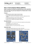
1
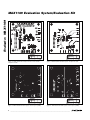
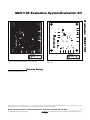
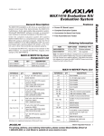
19-2996; Rev 1; 12/06
MAX1169 Evaluation System/Evaluation Kit
The MAX1169 evaluation system (EV system) is a complete high-speed I2C-compatible 16-bit data-acquisition system consisting of a MAX1169 evaluation kit (EV
kit), Maxim 68HC16MODULE-DIP microcontroller (µC)
module, USBTO232, and a HS I2C-compatible module.
The HSI2CMOD has a proven HS-mode I2C-compatible
interface that supports the MAX1169’s maximum 2-wire
serial clock frequency of 1.7MHz. This solution is
implemented on this module by using an Altera
EPM3256AQC208-10-programmable logic device (PLD)
and a DI2CM core from Digital Core Design.
Order the complete EV system (MAX1169EVC16) for a
comprehensive evaluation of the MAX1169 using a personal computer (PC). Order the EV kit (MAX1169EVKIT)
separately to evaluate the MAX1169 with a user-supplied
HS/fast/standard- mode I2C-compatible interface.
To evaluate the MAX1169A_UD or MAX1169B_UD,
request a free sample of the MAX1169A_UD or
MAX1169B_UD when ordering the MAX1169 EV kit.
Windows is a registered trademark of Microsoft Corp.
Features
♦ HS I2C-Compatible Interface (1.7MHz)
♦ Fast I2C-Compatible Interface (400kHz)
♦ Standard I2C-Compatible Interface (100kHz)
♦ Proven PCB Layout
♦ Fully Assembled and Tested
♦ Fully Assembled and Tested
♦ EV Kit Software Supports Windows® 98/2000/XP
with RS-232/COM Ports
♦ EV Kit Software Supports Windows 2000/XP with
USB Ports
Ordering Information
PART
INTERFACE
MAX1169EVKIT
User-supplied HS/fast/standard
I2C-compatible
MAX1169EVC16
Windows GUI and HS I2C compatible
Note: The MAX1169 software is included with the MAX1169 EV
kit, but is designed for use with the complete EV system. The EV
system includes the EV kit, the 68HC16 µC module, USBTO232,
and the HS I2C-compatible module. If the Windows software or
HS I 2 C-compatible module is not required, order only the
MAX1169 EV kit (instead of the entire EV system).
MAX1169EVKIT Component List
DESIGNATION
QTY
C1
1
C2, C4, C7, C9, C11
C3, C5, C6, C8, C10
FB1
J1
5
5
1
1
DESCRIPTION
0.01µF ±10%, 50V X7R
ceramic capacitor (0603)
TDK C1608X7R1H103K
10µF ±20%, 6.3V X5R ceramic
capacitors (0805)
TDK C2012X5R0J106M
0.1µF ±10%, 16V X7R ceramic
capacitors (0603)
TDK C1608X7R1C104KT
Surface-mount ferrite bead
(0603)
TDK MMZ1608B601C
2 x 10 right-angle female
connector
DESIGNATION
QTY
JU0–JU3
4
3-pin headers
DESCRIPTION
JU4, JU5
2
2-pin headers
R1
1
4.7Ω ±5% resistor (0603)
R2
1
10Ω ±5% resistor (0603)
R3, R4
0
Not installed, resistors
R5
1
4.7kΩ ±5% resistor (0603)
U1
1
16-bit ADC (14-pin TSSOP)
Maxim MAX1169CCUD
U2
1
Op amp (5-pin SOT23)
Maxim MAX4430EUK
—
1
PCB: MAX1169EVKIT
—
1
MAX1169 EV kit software
CD ROM
—
6
Shunts
________________________________________________________________ Maxim Integrated Products
For pricing, delivery, and ordering information, please contact Maxim/Dallas Direct! at
1-888-629-4642, or visit Maxim’s website at www.maxim-ic.com.
1
Evaluate: MAX1169
General Description
Evaluate: MAX1169
MAX1169 Evaluation System/Evaluation Kit
MAX1169EVC16 System
Component List
PART
QTY
MAX1169EVKIT Files
FILE
DESCRIPTION
HELPFILE.HTM
DESCRIPTION
MAX1169 EV kit help file
MAX1169EVKIT
1
MAX1169 EV kit
INSTALL.EXE
Installs the EV kit files on your computer
68HC16MODULE-DIP
1
68HC16 µC module
KIT1169.C16
Software loaded into the 68HC16 µC
HSI2CMOD
1
HS I2C-compatible module
MAX1169.EXE
USBTO232+
1
USB-to-COM port adapter
board
UNINST.INI
Application program
Uninstalls the EV kit software
Component Suppliers
SUPPLIER
PHONE
Altera Corporation
800-800-3753
Digital Core Design
(48) 32-282-82-66
WEBSITE
www.altera.com
www.digitalcoredesign.com
Fairchild Semiconductor
888-522-5372
www.fairchildsemi.com
TDK Corp.
847-803-6100
www.component.tdk.com
Note: Indicate that you are using the MAX1169 when contacting these component suppliers.
Quick Start
Recommended Equipment—USB Port PC
Connection Option
• MAX1169EVC16 (MAX1169EVKIT, 68HC16MODULEDIP, USBTO232, HSI2CMOD)
• Two DC power supplies:
+8V to +20V at 0.5A
+5V at 0.2A
• Analog signal source: 0 to +4.096V
• Windows 2000/XP computer with an available USB
port to connect to the USBTO232 board
• USB cable included with the USBTO232
Procedure
Caution: Do not turn on the power until all the connections are completed.
1) Visit the Maxim website (www.maxim-ic.com) to
download the latest version of the USBTO232 User
Guide. Follow the steps in the USBTO232 User
Guide Quick Start section, and return to step 2 of
this Quick Start section when finished.
2) Verify that jumpers JU0–JU3 are connected to pins
1-2. This sets the I2C-compatible slave address of
the MAX1169 to 0x7F.
3) Verify that jumper JU4 is OFF. This enables the
internal 4.096V (typ) reference.
4) Verify that jumper JU5 is OFF. This disconnects the
analog input buffer (U2) from AIN.
2
5) Carefully connect the 68HC16 module board to the
HS I2C-compatible module board by aligning the
40-pin connector. Gently press them together. The
two boards should be flush against one another.
6) Ensure that the ON/OFF switch (SW1) of the
68HC16 module is in the OFF position.
7) Connect the +8V to +20V power supply to the terminal block of the 68HC16 module (J2) located next
to SW1 at the top of the µC module. Observe the
polarity marked on the board.
8) Carefully connect the HS I2C-compatible module to
the MAX1169 EV kit board by aligning the 20-pin
connector. Gently press them together. The two
boards should be flush against one another.
9) Connect the +5V power supply between the AVDD
and AGND pads on the MAX1169 EV kit board.
10) Connect the USBTO232 board to the 68HC16MODULE-DIP module if you have not done so already.
11) The MAX1169 EV kit software should have already
been downloaded and installed in the USBTO232
Quick Start.
12) Turn on the 68HC16 module by sliding SW1 to the
ON position, and turn on all the power supplies.
13) Start the MAX1169 EV kit program by clicking on its
icon in the programs section of the Windows Start |
Programs menu.
14) Press the OK button to automatically connect and
download the KIT1169.C16 file to the module.
_______________________________________________________________________________________
MAX1169 Evaluation System/Evaluation Kit
Recommended Equipment—RS-232/COM
Port PC Connection Option
• MAX1169EVC16 (MAX1169EVKIT, 68HC16MODULEDIP, HSI2CMOD)
• Two DC power supplies:
+8V to +20V at 0.5A
+5V at 0.2A
• Analog signal source: 0 to +4.096V
• Windows 98/2000/XP computer with an available serial
(COM) port
• 9-pin I/O extension cable (straight-through, femaleto-male)
Procedure
Caution: Do not turn on the power until all the connections are completed.
1) Visit the Maxim website (www.maxim-ic.com/evkitsoftware) to download the latest version of the EV
kit software. Save the EV kit software to a temporary
folder and uncompress the file (if it is a .zip file).
2) Install the MAX1169 EV kit software on your computer by running the INSTALL.EXE program. The
program files are copied and icons are created for
them in the Windows Start | Programs menu.
3) Verify that jumpers JU0–JU3 are connected to pins
1-2. This sets the I2C-compatible slave address of
the MAX1169 to 0x7F.
4) Verify that jumper JU4 is OFF. This enables the
internal 4.096V (typ) reference.
5) Verify that jumper JU5 is OFF. This disconnects the
analog input buffer (U2) from AIN.
6) Carefully connect the 68HC16 module board to the
HS I2C-compatible module board by aligning the
40-pin connector. Gently press them together. The
two boards should be flush against one another.
7) Ensure that the ON/OFF switch (SW1) of the
68HC16 module is in the OFF position.
8) Connect the +8V to +20V power supply to the terminal block of the 68HC16 module (J2) located next
to SW1 at the top of the µC module. Observe the
polarity marked on the board.
9) Carefully connect the HS I2C-compatible module to
the MAX1169 EV kit board by aligning the 20-pin
connector. Gently press them together. The two
boards should be flush against one another.
10) Connect the +5V power supply between the AVDD
and AGND pads on the MAX1169 EV kit board.
11) Connect the 9-pin serial cable from the computer’s
serial port to the DB9 connector of the 68HC16
module (J3).
12) Turn on the 68HC16 module by sliding SW1 to the
ON position, and turn on all the power supplies.
13) Start the MAX1169 EV kit program by clicking on its
icon in the programs section of the Windows Start |
Programs menu.
14) Press the OK button to automatically connect and
download the KIT1169.C16 file to the module.
15) The EV kit software uses the value typed in the
VREF field to translate the digital code to a voltage.
The default is a +4.096V reference value. First,
measure the reference voltage of the MAX1169.
Then, after typing the measured reference value
into the VREF field, press the Set VREF button.
16) Apply an analog input signal (0V to VREF) between
AIN and AGND. Observe the AIN voltage and code
labels on the Windows program.
_______________________________________________________________________________________
3
Evaluate: MAX1169
15) The EV kit software uses the value typed in the
VREF field to translate the digital code to a voltage.
The default is a +4.096V reference value. First,
measure the reference voltage of the MAX1169.
Then, after typing the measured reference value
into the VREF field, press the Set VREF button.
16) Apply an analog input signal (0V to VREF) between
AIN and AGND. Observe the AIN voltage and code
labels on the Windows program.
Evaluate: MAX1169
MAX1169 Evaluation System/Evaluation Kit
Detailed Description
of Software
The main window of the evaluation software is shown in
Figure 1. This window displays the voltage and code of
the analog input signal AIN. The software supports both
manual read or automatic read operations. The I2Ccompatible serial-clock (SCL) frequency is selectable:
HS mode (1.7MHz), fast mode (400kHz), or standard
mode (100kHz). In HS-mode I2C-compatible systems,
the communication and arbitration are always done in
either fast mode or standard mode. Only data can be
transmitted or received at HS-mode speeds. The software expects the use of a 4.096V reference on execution; however, this value can be changed in the software to accommodate a different reference value.
Table 1 describes the controls in the main window of
the evaluation software.
External Reference
To disable the MAX1169’s internal +4.096V (typ) reference, select external reference mode with a shunt on
JU4. Apply the new external reference voltage between
the REF and GND pads on the MAX1169 EV kit board.
After measuring the external reference voltage, enter it
into the VREF field of the software (without the volt unit)
and press the Set VREF button.
Detailed Description
of Hardware
MAX1169 EV System
The MAX1169 EV system is a complete 16-bit dataacquisition system consisting of a MAX1169 EV kit, a
68HC16 µC module, USBTO232, and an HS I2C-compatible module.
The complete MAX1169 EV system is used to evaluate
the MAX1169 16-bit, I2C-compatible, analog-to-digital
converter (ADC). See the Quick Start section for setup
and operating instructions.
4
68HC16 Module
The 68HC16 µC module utilizes Motorola’s
MC68HC16Z1 µC and is fully assembled and tested.
This module provides a working example of a µC
design for customers who have not yet chosen one for
their system or who do not have the ability to connect
the MAX1169 EV kit to their own system. The Windows
software downloads an assembled program to the onboard random-access memory of the 68HC16 module.
For more information, refer to the 68HC16 module data
sheet.
HS I2C-Compatible Module
The HS I2C-compatible module provides a 2-wire interface peripheral for the 68HC16 µC module using an
Altera EPM3256AQC208-10 PLD. This peripheral is
implemented in the PLD by utilizing the DI2CM core
from Digital Core Design. The HS I2C-compatible module allows the 68HC16 module to be compatible with
HS mode (1.7MHz), fast mode (400kHz), and standard
mode (100kHz). This module is not required when evaluating the MAX1169 EV kit with a user-supplied I2Ccompatible interface. For more information, refer to the
HS I2C-compatible module data sheet.
MAX1169 EV Kit
The MAX1169 EV kit board provides a proven layout for
evaluating the MAX1169 16-bit, I2C-compatible ADC
and can be obtained separately without the 68HC16
module, USBTO232, and HS I2C-compatible module.
The MAX1169 EV kit contains a 16-bit accurate analog
input buffer (U2), connected in the unity-gain configuration. A REF pad has been provided on the MAX1169 EV
kit board for evaluating the MAX1169 with an external
reference. Refer to the MAX1169 data sheet to ensure
all interface timing specifications are met when a usersupplied I2C-compatible interface is used.
_______________________________________________________________________________________
MAX1169 Evaluation System/Evaluation Kit
CONTROL
DESCRIPTION
Allows the COM port (virtual COM port) debug form to be visible or
checks for module status
Allows the user to view the help file or the software’s about box
Displays the AIN voltage and code
Selects the I2C-compatible slave address while reading
Allows the user to specify the actual reference value in the software.
The EV kit software uses the value typed in the VREF field to translate
the digital code to a voltage. The default is a +4.096V reference value.
First measure the reference voltage of the MAX1169. Then, after typing
in the measured reference value into the VREF field, press the Set
VREF button.
Performs a single-shot read operation
Performs a read operation specified by the control byte every 250ms.
A blinking asterisk indicates AutoRead is active.
Selects the I2C-compatible SCL frequency for data reception
Selects the I2C-compatible SCL frequency for communication and
arbitration
Displays the status of the 68HC16 module and HS I2C-compatible
module when the module status is requested in the View menu
_______________________________________________________________________________________
5
Evaluate: MAX1169
Table 1. Software-Control Descriptions
Evaluate: MAX1169
MAX1169 Evaluation System/Evaluation Kit
Table 2. Slave Address Bit 0 (ADD0)
JUMPER
JU0
SHUNT
POSITION
DESCRIPTION
1-2*
DVDD. ADD0 = 1.
2-3
DGND. ADD0 = 0.
*Default configuration.
Table 6. Reference Mode Select
JUMPER
JU1
SHUNT
POSITION
DESCRIPTION
1-2*
DVDD. ADD1 = 1.
2-3
DGND. ADD1 = 0.
DESCRIPTION
ON
External reference mode enabled.
Connect an external reference to
REF.
OFF*
Internal +4.096V reference mode
enabled.
JU4
Table 3. Slave Address Bit 1 (ADD1)
JUMPER
SHUNT
POSITION
*Default configuration.
Table 7. Analog Input Buffer
*Default configuration.
Table 4. Slave Address Bit 2 (ADD2)
JUMPER
JU2
SHUNT
POSITION
JUMPER
SHUNT
POSITION
DESCRIPTION
ON
The analog input buffer is connected
to AIN. Ensure +5V is applied to the
BUF+5 pad and -5V is applied to the
BUF-5 pad. Ensure that the
noninverting (+) input to the analog
input buffer is not left floating.
DESCRIPTION
1-2*
DVDD. ADD2 = 1.
2-3
DGND. ADD2 = 0.
*Default configuration.
JU5
Table 5. Slave Address Bit 3 (ADD3)
JUMPER
JU3
SHUNT
POSITION
OFF*
DESCRIPTION
The analog input buffer is
disconnected from AIN.
*Default configuration.
1-2*
DVDD. ADD3 = 1.
2-3
DGND. ADD3 = 0.
*Default configuration.
Figure 1. Main Window of the MAX1169 Evaluation Software
6
_______________________________________________________________________________________
MAX1169 Evaluation System/Evaluation Kit
Evaluate: MAX1169
DVDD
DVDD
1
DGND
ADD3
1
2
3
14 JU3
R3
OPEN
SCL
2
SCL
REF
DVDD
SCL
AGND
REF
13
C2
10μF
R4
OPEN
SDA
AVDD
3
SDA
DVDD
SDA
REFADJ
JU4
12
C3
0.1μF
U1
DGND
DVDD
R2
10Ω
J1
J1-2
J1-1
J1-4
J1-3
J1-6
J1-5
J1-8
J1-7
J1-10
J1-9
J1-12
J1-11
1
2
3
JU2
4
ADD2
MAX1169
AGNDS
R1
4.7Ω
DVDD
1
2
3
5
JU1
ADD1
AIN
DVDD
1
2
3
SCL
N.C.
J1-14
J1-13
N.C.
J1-16
J1-15
N.C.
J1-18
J1-17
N.C.
J1-19
J1-20
N.C.
JU0
6
ADD0
AGND
9
JU5
DVDD
DVDD
DGND
AVDD
7
C4
10μF
AIN
10
C1
0.01μF
SDA
N.C.
AGND
11
DVDD
AVDD
C5
0.1μF
AVDD
8
C6
0.1μF
C7
10μF
AGND
FB1
FERRITE
BUF+5
C8
0.1μF
4
BUFIN
3
C9
10μF
5
1
U2
2
BUF-5
R5
4.7kΩ
C10
0.1μF
C11
10μF
Figure 2. MAX1169EV Kit Schematic
_______________________________________________________________________________________
7
Evaluate: MAX1169
MAX1169 Evaluation System/Evaluation Kit
Figure 3. MAX1169 EV Kit Component Placement Guide—
Component Side
Figure 4. MAX1169 EV Kit PCB Layout—Component Side
Figure 5. MAX1169 EV Kit PCB Layout—Inner Layer 2 (GND)
Figure 6. MAX1169 EV Kit PCB Layout—Inner Layer 3 (VDD)
8
_______________________________________________________________________________________
MAX1169 Evaluation System/Evaluation Kit
Evaluate: MAX1169
Figure 7. MAX1169 EV Kit PCB Layout—Solder Side
Figure 8. MAX1169 EV Kit Component Placement Guide—
Solder Side
Revision History
Pages changed at Rev 1: 1–8
Maxim cannot assume responsibility for use of any circuitry other than circuitry entirely embodied in a Maxim product. No circuit patent licenses are
implied. Maxim reserves the right to change the circuitry and specifications without notice at any time.
Maxim Integrated Products, 120 San Gabriel Drive, Sunnyvale, CA 94086 408-737-7600 _____________________ 9
© 2006 Maxim Integrated Products
is a registered trademark of Maxim Integrated Products, Inc.