1
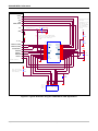
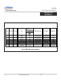
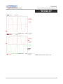
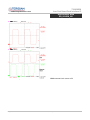
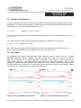
A Maxim Integrated Products Brand 73S8024RN Low Cost Smart Card Interface IC Application Note AN_8024RN_001 April 2007 Implementing the Teridian 73S8024RN in NDS Applications 1 Introduction This application note highlights particular design considerations required to implement Conditional Access smart card interfaces in compliance with the NDS specification LC-T056I, when using the TERIDIAN 73S8024RN integrated circuit. This note details in particular the design constraints related to the PCB layout and external components (choice and placement), and the typical tests that should be performed prior to submitting an application to NDS certification testing. Reference document is the “IRD Interface Specifications for Use with NDS Smart Cards”, NDS document referenced LC-T056 Rev. I. 2 Demo Board The data and chart measurements presented herein have been measured on a TERIDIAN 73S8024RN Demonstration Board, modified to meet NDS LC-T056I requirements. Refer to the “73S8024RN Demo Board User’s Manual” for general information about this board. Note that the electrical schematic of this board is by default designed to meet compliance with EMV4.0 specification. As a result, there are some minor differences between both electrical schematics. The TERIDIAN 73S8024RN configuration does not install components L1, C6 and C7. Other component differences are described in this note, and the NDS-compliant electrical schematic is described in the Figure 3.1 Note that the 73S8024RN Demo Board is available. Contact your TERIDIAN Semiconductor representative for further information concerning its availability. 3 Design Guide 3.1 Typical Electrical Schematic and Bill of Materials The electrical schematic recommended for a typical NDS LC-T056I compliant smart card interface implementation is given in Figure 3-1, and its corresponding Bill of Materials is in Table 3-1. The jumpers represent the different configuration options for use with the 73S8024RN, and components references correspond to the Demo Board references. Page 1 © 2007 TERIDIAN Semiconductor Corporation Rev 1.2 AN 8024R NDS Conformance SCLK SIO Values are set for VDD fault threshold of 2.7V. See section 3.7 If 2.3V threshold is acceptable, don't install R1 and R3 SC4 SC8 OFFB/INTB C1 See section 3.2.1 10uF PGND + +5V VDD C2 GND 0.1uF VPC R1 VDD C1 and C2 must be placed within 5mm of the U1 pins and connected by thick track (wider than 0.5mm) 57.6k R3 +3.3V U1 42.2k 1 2 3 4 5 6 7 8 9 10 11 12 13 14 CLKDIV1/SAD0 CLKDIV2/SAD1 5V3VB/SAD2 CLKSTOP CLKLVL CMDVCCB RSTIN CLKDIV1 CLKDIV2 5V3V GND_4 NC VPC CLKSTOP CLKLVL PRES PRES IO AUX2 AUX1 GND_14 AUX2UC AUX1UC IOUC XTALOUT XTALIN OFF GND VDD RSTIN CMDVCC EXTRST VCC RST CLK 28 27 26 25 24 23 22 21 20 19 18 17 16 15 VDD C8 0.1uF System Interface 73S8024RN VDD Note: R4 should be added for increased noise immunity. R4 20k J5 8 7 6 5 4 3 2 1 C8 I/O VPP GND C4 CLK RST VCC SW1 and SW2 are Normally Closed SW-2 SW-1 10 9 C11 1.0uF Smart Card Connector Figure 3-1: Typical Schematic using the 73S8024RN for NDS Applications Page 2 © 2007 TERIDIAN Semiconductor Corporation Rev 1.2 73S8024RN Low Cost Smart Card Interface IC A Maxim Integrated Products Brand Application Note AN_8024RN_001 Item Quantity Reference 1 1 C1 2 3 4 5 6 1 2 1 1 1 C11 C2,C8 J5 R4 U1 Part PCB Foot pr i nt ( see at t ached zi p f i l e) Digikey part number Part number Manufactuer 10µF 805 445-1363-1-ND C2012X5R0J106M TDK 1µF (1) 0.1µF Smart Card Connector 20k 73S8024RN 603 603 ITT_CCM02-2504 603 28SOP 445-1322-1-ND 445-1317-1-ND ccm02-2504-ND P20KGCT-ND X C1608X5R0J105K C1608X7R1C104K ccm02-2504 ERJ-3GEYJ203V 73S8024RN TDK TDK ITTCannon Panasonic TERIDIAN Table 3-1: BOM for NDS-compliant configuration Page 3 © 2007 TERIDIAN Semiconductor Corporation Rev 1.2 A Maxim Integrated Products Brand 73S8024RN Low Cost Smart Card Interface IC Application Note AN_8024RN_001 3.2 3.2.1 Power Supply: Analog Power Supply VPC: The 73S8024RN incorporates a Low-Drop-Out voltage regulator to generate the card power supply VCC. The VPC pin is the power supply input of this regulator, and the correct VPC voltage must be asserted on this pin in order to ensure proper generation of VCC to the card. Depending on the card voltage required, the VPC power supply input can eventually be different, as follows: Power supply VPC, to support both 3V and 5V smart cards: VPC must be 5V nominal, and the following condition must be respected: 4.85V ≤VPC ≤ 5.5V Decoupling and PCB Layout: The 73S8024R Demo Board and the recommended Electrical Schematic has 2 decoupling capacitors on VPC. The larger capacitor is 10 µF and the small capacitor is 0.1µF (respectively C1 and C2). The smaller capacitor should be placed very close to the 73S8024RN. VPC should be routed on a plane for best results. If no plane is possible, the larger capacitor should be as close as possible to the 73S8024RN. 3.2.2 Digital Power Supply: The 73S8024RN has a separate power supply input VDD, that powers the internal digital circuitry. VDD is also the reference voltage to interface with the host microcontroller. Operating VDD voltage for implementing the 73S8024RN in NDS applications is 2.7V ≤VDD ≤ 5.5V 3.3 Operating Temperature The operating temperature range for implementing the 73S8024RN in NDS applications is between -40°C and 85°C. Page 4 © 2007 TERIDIAN Semiconductor Corporation Rev 1.2 73S8024RN Low Cost Smart Card Interface IC A Maxim Integrated Products Brand Application Note AN_8024RN_001 3.4 3.4.1 Generation of the Smart Card Clock – CLK Signal General The 73S8024RN provides an oscillator that can generate a clock signal from an external crystal, connected to the pins XTALIN and XTALOUT. Alternatively, it can also accept an external clock signal presented on the XTALIN pin. When the external clock signal is used, XTALOUT must be left unconnected. 3.4.2 NDS Adherence In order to use the 73S8024RN and meet full NDS compliance, typical hardware must be set up identically for all configurations. Typical NDS Conditional Access applications require card clock frequencies of 4.5MHz, 6.75MHz and 13.5MHz to be supported. The same hardware configuration is required for both Class A and Class B (5V and 3V smart card) operation. The NDS specification also requires the card clock duty-cycle to be in the range 45% to 55%. 3.4.3 73S8024RN Operational Configuration The typical NDS card clock frequencies of 4.5, 6.75 and 13.5MHz are derived from the maximum frequency of 13.5MHz divided by 1, 2 and 3 (13.5, 6.75 and 4.5). The 73S8024R supports a divide by 1, 2, 4 and 8 internal clock divider, but not divide by 3. As a result, a crystal that is used with the oscillator circuit will not be able to generate all three frequencies. If all three frequencies are required then an external clock source must be provided to generate them. If the clock divider rates of 1,2,4 and 8 are acceptable for a particular application then a crystal may be used. Generation of the smart card clock signal (CLK) at the above-mentioned three NDS frequencies can be done in one of two ways, as long as the frequency of the signal applied on XTALIN is stable and doesn’t exceed 27MHz. The first way uses the NDS clock frequencies of 4.5, 6.75 and 13.5 input directly to the 8024RN using the divide by one divider. The second way is to use of an external clock source that provides frequencies of 9, 13.5 and 27MHz. When the divide by 2 clock divider is configured, the NDS operational frequencies of 4.5, 6.75 and 13.5MHz are output to the smart card. For applications that require higher smart card clock frequencies, the maximum external input clock/crystal speed is 27MHz. Between 20 and 27MHz the divide by 1 clock divider is not recommended. In order to get smart card frequencies up to 20MHz, use the divide by 1 divider for either the crystal oscillator or external clock input. The following scope capture diagrams show the smart card CLK for each configuration running at 20MHz. Page 5 © 2007 TERIDIAN Semiconductor Corporation Rev 1.2 A Maxim Integrated Products Brand 73S8024RN Low Cost Smart Card Interface IC Application Note AN_8024RN_001 20MHz crystal clock source at 3V Page 6 20MHz external clock source at 3V © 2007 TERIDIAN Semiconductor Corporation Rev 1.2 A Maxim Integrated Products Brand 73S8024RN Low Cost Smart Card Interface IC Application Note AN_8024RN_001 20MHz crystal source at 5V Page 7 20MHz external clock source at 5V © 2007 TERIDIAN Semiconductor Corporation Rev 1.2 73S8024RN Low Cost Smart Card Interface IC A Maxim Integrated Products Brand Application Note AN_8024RN_001 3.5 Crystal Load Capacitors In order to insure the proper operation of the crystal oscillator circuit, the crystal load capacitors must be chosen appropriately. The crystal load capacitance (CL as specified by the crystal manufacturer) must equal the series load capacitance (CP) plus the stray board capacitance (CS). CL = CS + CP. Where CP = (1 / (1/C1 + 1/C2)) C1 and C2 are the load capacitors. If a balanced crystal load capacitors are used (recommended) then C1 = C2 and CP = C1 / 2. If CL = 20 pF (from the crystal mfr spec) and the stray capacitance is assumed to be 5.0 pF, then C1 = 2 * (CL - CS) = 2 * (20pF – 5pF) = 30pF. Note: If the loading is any higher then the oscillator circuit may not generate the output clock properly. As a result, it is not recommended to use this oscillator circuit to drive any other circuitry. 3.6 VCC Output The 73S8024RN Demo Board is configured with 2 output capacitors on the VCC output, C9 and C11. A typical NDS implementation only requires 1 capacitor. C9 is not necessary and the value of C11 must be 1µF ± 50%. (If fitting the 1µF capacitor into an existing application is problematic, both C9 and C11 can be populated with 0.47µF ± 50% capacitors.) This capacitor should be placed as close to the card connector. This VCC output configuration meets the NDS specifications for both voltage and current consisting of constant and dynamic loads. The ripple is shown to be less than 35 mV for DC loads and less than 60 mV for dynamic loads (typical). Figures 3.2 and 3.3 show VCC ripple for 5V and 3V interfaces respectively. Figure 3-2: C11 (5V) w/65mA dc load current Page 8 Figure 3-3: C11 (3V) w/65mA dc load current © 2007 TERIDIAN Semiconductor Corporation Rev 1.2 73S8024RN Low Cost Smart Card Interface IC A Maxim Integrated Products Brand Application Note AN_8024RN_001 According to NDS LC-T056I specification, deactivation time for VCC must be less than 100µs. Figures 3.4 and 3.5 show actual measurements carried out on the 73S8024RN Demo Board using capacitor values of 0.47µF and 1.47µF for VCC output decoupling (C11). The deactivation time is less than 80µs. It demonstrates that C11 = 1µF ±50% allows the 73S8024RN to meet the 100µs requirement. Figure 3-4: Deactivation time (0.47µF @VCC) Figure 3-5: Deactivation time (1.47µF @VCC) 3.7 Power Supply Threshold Detection The 73S8024RN contains 3 different voltage supervisors. They monitor the voltages on VPC, VCC and VDD. . Any voltage drop on any of these 3 signals is immediately detected and it initiates an automated card deactivation sequence that protects the card. VPC and VCC threshold voltages (also called fault voltages) are internally set. The voltage threshold of the VDD voltage supervisor is internally set by default to 2.3V nominal. However, it may be desirable, in some applications, to modify this threshold value. For instance, when using a host controller that has a voltage operating range of 2.7V to 3.6V, the 73S8024RN will be, by default, still expecting the host to be able to exchange information with him whereas the host is actually powered down,. In such a case, the VDD fault threshold voltage should be set to 2.7V, to automatically deactivate the smart card at the same time that the host is down. The pin VDDF_ADJ is used to connect an external resistor divider between VDD and GND to modify VDD-Fault. Figure 3.12 shows the connection of the external resistors. VDD 73S8024R R1 VDDF_ADJ R3 Page 9 © 2007 TERIDIAN Semiconductor Corporation Rev 1.2 73S8024RN Low Cost Smart Card Interface IC A Maxim Integrated Products Brand Application Note AN_8024RN_001 Figure 3-6: External resistor divider for setting VDDTH In order to set the new threshold voltage, the equivalent resistance must be determined. This resistance value will be designated Kx which is defined as R3 / (R1+R3), and is calculated as: Kx = (2.789 / VTH) - 0.6125 where VTH is the desired new threshold voltage. To determine the values of R1 and R3, use the following formulas: R1 = 24000 / Kx R3 = R1*(Kx / (1 – Kx)) Taking the example above, where a VDD fault threshold voltage of 2.7V is desired, solving for Kx gives: Kx = (2.789 / 2.7) - 0.6125 = 0.42046. Solving for R1 gives: R1 = 24000 / 0.42046 = 57080. Solving for R3 gives: R3 = 57080 *(0.42046 / (1 – 0.42046)) = 41412. Using standard 1 % resistor values gives R1 = 57.6KΩ and R3 = 42.4KΩ. These values give an equivalent resistance of Kx = 0.4228, a 0.6% error. If the 2.3V default threshold is acceptable, this pin must be left unconnected. Page 10 © 2007 TERIDIAN Semiconductor Corporation Rev 1.2