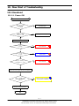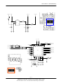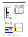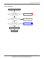
1
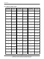
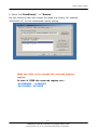
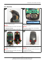
GSM TELEPHONE
SGH-X500
GSM TELEPHONE
CONTENTS
1.
Safety Precautions
2.
Specification
3.
Product Function
4.
Array course control
5.
Exploded View and Parts List
6.
Disassembly and Assembly
instructions
7.
MAIN Electrical Parts List
8.
Block Diagrams
9.
PCB Diagrams
10.
Flow Chart of Troubleshooting
11.
Reference data
Contents
1. Safety Precautions
1-1. Repair Precaution ...........................................................................1-1
1-2. ESD(Electrostatically Sensitive Devices) Precaution ...........................1-2
2. Specification
2-1. GSM General Specification ..............................................................2-1
2-2. GSM Tx Power Class ......................................................................2-2
3. Product Function
3-1. Main Function ................................................................................3-1
4. Array course control
Software Downloading
4-1. Downloading Binary Files ................................................................4-2
4-2. Pre-requsite for Downloading ..........................................................4-2
4-3. S/W Downloader Program ...............................................................4-3
5. Exploded View and Parts List
5-1. Cellular phone Exploded View .........................................................5-1
5-2. Cellular phone Part list ...................................................................5-2
6. Disassembly and Assembly instructions
6-1. Disassembly ..................................................................................6-1
6-2. Assembly ......................................................................................6-3
6-3. LCD KIT ........................................................................................6-6
7. MAIN Electrical Parts List
8. Block Diagrams
8-1. RF PART .......................................................................................8-1
8-2. ROGIC PART ..................................................................................8-2
8-3. BT Block .......................................................................................8-3
9. PCB Diagrams
Contents
10. Flow Chart of Troubleshooting
10-1. Baseband
10-1-1. Power ON ..............................................................................10-1
10-1-2. Initial ....................................................................................10-4
10-1-3. Sim Part ...............................................................................10-6
10-1-4 Microphone Part ......................................................................10-8
10-1-5. Speaker Part ........................................................................10-10
10-2. RF
10-2-1. EGSM RX .............................................................................10-13
10-2-2. DCS RX ...............................................................................10-14
10-2-3. PCS RX ...............................................................................10-15
10-2-4. EGSM TX .............................................................................10-17
10-2-5. DCS/PCS TX ........................................................................10-18
11. Reference data
1. Safety Precautions
1-1. Repair Precaution
● Repair in Shield Box, during detailed tuning.
Take specially care of tuning or test,
because specipicty of cellular phone is sensitive for surrounding interference(RF noise).
● Be careful to use a kind of magnetic object or tool,
because performance of parts is damaged by the influence of manetic force.
● Surely use a standard screwdriver when you disassemble this product,
otherwise screw will be worn away.
● Use a thicken twisted wire when you measure level.
A thicken twisted wire has low resistance, therefore error of measurement is few.
● Repair after separate Test Pack and Set because for short danger (for example an
overcurrent and furious flames of parts etc) when you repair board in condition of
connecting Test Pack and tuning on.
● Take specially care of soldering, because Land of PCB is small and weak in heat.
● Surely tune on/off while using AC power plug, because a repair of battery charger is
dangerous when tuning ON/OFF PBA and Connector after disassembing charger.
● Don't use as you pleases after change other material than replacement registered on SEC
System.
Otherwise engineer in charge isn't charged with problem that you don't keep this rules.
1-1
SAMSUNG Proprietary-Contents may change without notice
This Document can not be used without Samsung's authorization
Safety Precautions
1-2. ESD(Electrostatically Sensitive Devices) Precaution
Several semiconductor may be damaged easilly by static electricity. Such parts are called by
ESD(Electrostatically Sensitive Devices), for example IC,BGA chip etc. Read Precaution below.
You can prevent from ESD damage by static electricity.
● Remove static electricity remained your body before you touch semiconductor or parts with
semiconductor. There are ways that you touch an earthed place or wear static electricity
prevention string on wrist.
● Use earthed soldering steel when you connect or disconnect ESD.
● Use soldering removing tool to break static electricity. , otherwise ESD will be damaged by
static electricity.
● Don't unpack until you set up ESD on product. Because most of ESD are packed by box
and aluminum plate to have conductive power,they are prevented from static electricity.
● You must maintain electric contact between ESD and place due to be set up until ESD is
connected completely to the proper place or a circuit board.
1-2
SAMSUNG Proprietary-Contents may change without notice
This Document can not be used without Samsung's authorization
2. Specification
2-1. GSM General Specification
GSM900
Phase 1
EGSM 900
Pha s e 2
DC S1800
Phase 1
PCS1900
Freq. Ban d [M Hz ]
Upl in k/Downl in k
890~915
935~960
880~915
925~960
1710~1785
1805~1880
1850~1910
1930~1990
A RF CN ra ng e
1~124
0~124 &
975~1023
512~885
512~810
Tx/R x sp aci ng
45 MHz
45 MHz
95 MHz
80 MHz
Mod. Bit rat e/
Bit Period
270.833 kbps
3.692 us
270.833 kbps
3.692 us
270.833 kbps
3.692 us
270.833 kbps
3.692 us
Tim e Sl ot
P eri od /F rame
Peri od
576.9 us
4.615 ms
576.9 us
4.615 ms
576.9 us
4.615 ms
576.9 us
4.615 ms
Modu la t ion
0.3 GMSK
0.3 GMSK
0.3 GMSK
0.3 GMSK
M S Power
33 dBm~5 dBm 33 dBm~5 dBm 30 dBm~0 dBm 30 dBm~0 dBm
P ow er Cl a ss
5 pcl ~ 19 pcl
5 pcl ~ 19 pcl
0 pcl ~ 15 pcl
0 pcl ~ 15 pcl
S ensi ti vit y
-102 dBm
-102 dBm
-100 dBm
-100 dBm
TDM A Mu x
8
8
8
8
Cell Radiu s
35 Km
35 Km
2 Km
-
2-1
SAMSUNG Proprietary-Contents may change without notice
This Document can not be used without Samsung's authorization
Specification
2-2. GSM TX power class
TX Power
control level
GSM900
TX Power
control level
DCS1800
TX Power
control level
PCS1900
5
33±2 dBm
0
30±3 dBm
0
30±3 dBm
6
31±2 dBm
1
28±3 dBm
1
28±3 dBm
7
29±2 dBm
2
26±3 dBm
2
26±3 dBm
8
27±2 dBm
3
24±3 dBm
3
24±3 dBm
9
25±2 dBm
4
22±3 dBm
4
22±3 dBm
10
23±2 dBm
5
20±3 dBm
5
20±3 dBm
11
21±2 dBm
6
18±3 dBm
6
18±3 dBm
12
19±2 dBm
7
16±3 dBm
7
16±3 dBm
13
17±2 dBm
8
14±3 dBm
8
14±3 dBm
14
15±2 dBm
9
12±4 dBm
9
12±4 dBm
15
13±2 dBm
10
10±4 dBm
10
10±4 dBm
16
11±3 dBm
11
8±4 dBm
11
8±4 dBm
17
9± 3dBm
12
6±4 dBm
12
6±4 dBm
18
7±3 dBm
13
4±4 dBm
13
4±4 dBm
19
5±3 dBm
14
2±5 dBm
14
2±5 dBm
15
0±5 dBm
15
0±5 dBm
2-2
SAMSUNG Proprietary-Contents may change without notice
This Document can not be used without Samsung's authorization
3. Product Function
Main Function
-My mane card
-Java world
-Voice memo
-Stopwatch
-SIM service
-Access the homepage
-SMS and MMS
-Bluetooth
-Set Quiet mode
-Network services
3-1
SAMSUNG Proprietary-Contents may change without notice
This Document can not be used without Samsung's authorization
4. Array course control
Test Jig (GH80-03307A)
Test Cable (GH39-00127A)
RF Test Cable (GH39-00397A)
4-1
SAMSUNG Proprietary-Contents may change without notice
This Document can not be used without Samsung's authorization
Array course control
Software Downloading
4-1. Downloading Binary Files
• Three binary files for downloading X500 .
– X500XXYY.s3 : Main source code binary.
4-2. Pre-requsite for Downloading
• Downloader Program(OptiFlash.exe)
• X500 Mobile Phone
• Data Cable
• Binary files
4-2
SAMSUNG Proprietary-Contents may change without notice
This Document can not be used without Samsung's authorization
Array course control
4-3. S/W Downloader Program
1. Load the binary download program by executing the “OptiFlash.exe”
2. Select the “Options” -> “Settings” -> “Generic” -> “Specify hardware
platform”.
Choose hardware platform for the downloader file setting.
Set the everything else as the default values which are shown below
4-3
SAMSUNG Proprietary-Contents may change without notice
This Document can not be used without Samsung's authorization
Array course control
3. Select the COM port when the download cable is connected
Up to twelve ports are supported. Additionally you can select the
maximum
transfer speed OptiFlash will use to communicate with
the phone. However, OptiFlash will use a slower speed if either the
PC’s or the phone’s serial hardware is incapable of handling the
selected speed
4-4
SAMSUNG Proprietary-Contents may change without notice
This Document can not be used without Samsung's authorization
Array course control
4. Select the“Flash&Verify” -> “Browse”
Set the directory path and choose the latest s/w binary, for example
“X500XXYY.s3”, for the downloader binary setting.
Make sure that not to change the reserved memory
regions.
In case of X500 the reserved regions are :
-0x20000000 – 0x2000ffff
-0x21fc0000– 0x21ffffff
4-5
SAMSUNG Proprietary-Contents may change without notice
This Document can not be used without Samsung's authorization
Array course control
5. Click “OK” button then press “Flash”.
(Before pressing ‘Flash’ button, push the button ‘*’and ‘END’ at the same
time. Then press ‘Flash’.)
Downloader will upload the binary file as below for the downloading.
6. When downloading is finished successfully, there is a “All is well” message.
7. After finishing downloading, Certain memory resets should be done to
guarantee the normal performance.
8. Confirm the downloaded version name and etc. :
*#1234#
Full Reset :
*2767*3855#
4-6
SAMSUNG Proprietary-Contents may change without notice
This Document can not be used without Samsung's authorization
5. Exploded View and Parts List
5-1. Cellular phone Exploded View
QFR01
QFU01
QIF01
QLC01
QKP01
QSP01
QME03
QMP01
QMO01
QMI01
QME01
QFL01
QAN05
QCR05
QAN02
QSC11
QMW02
QRE01
QRF03
QVO01
QRF01
QBA01
QCR05
QBA00
5-1
SAMSUNG Proprietary-Contents may change without notice
This Document can not be used without Samsung's authorization
Exploded View and Parts List
5-2. Cellular phone Parts list
Design LOC
Discription
SEC CODE
QAN02
INTENNA-SGHX500
GH42-00829A
QAN05
ASSY MEC-INTENNA CONTACT
GH75-08168A
QBA00
PMO-COVER BATT
GH72-30639A
QBA01
INNER BATTERY PACK-750MAH,BLK,
GH43-02483A
QCR05
SCREW-MACHINE
6001-001478
QCR05
SCREW-MACHINE
6001-001478
QFL01
ASSY-CASE-LOWER
GH98-00893A
QFU01
ASSY-CASE-UPPER
GH98-00894A
QKP01
ASSY-KEY-KEYPAD(XEF/CDA)
GH98-00896A
QLC01
MEA-LCD MODULE KIT
GH97-06021A
QME01
UNIT-METAL DOME
GH59-03100A
QME03
UNIT-CON TO CON
GH59-03148A
QMI01
MICROPHONE-ASSY-6.25MM
GH30-00177F
QMO01
MOTOR DC-SGHZ130
GH31-00154C
QMP01
PBA MAIN-SGHX500
GH92-02716A
QMW02
PMO-COVER MAIN WINDOW
GH72-30637A
QRF01
MPR-TAPE RF
GH74-22888A
QSC11
RMO-COVER FOLDER SCREW
GH73-06994A
QSP01
SPEAKER
3001-001963
QVO01
ASSY KEY-VOLUME
GH98-01510A
QFR01
QRE01
ASSY-CASE-FRONT
GH98-00892A
QIF01
PMO-COVER IF
GH72-30580A
ASSY-CASE-REAR
GH98-00895A
QRF03
PMO-COVER EARJACK
GH72-30586A
5-2
SAMSUNG Proprietary-Contents may change without notice
This Document can not be used without Samsung's authorization
Exploded View and Parts List
Discription
SEC CODE
CARD-WARRANTY
6801-001501
BAG PE
6902-000297
ADAPTOR-SGHN288 TAD
GH44-00184A
LABEL(P)-IMEI
GH68-01335D
LABEL(P)-WATER SOAK
GH68-02026A
LABEL(P)-WATER SOAK
GH68-02026A
MANUAL USERS-EU FRENCH
GH68-09788A
LABEL(R)-MAIN(EU)
GH68-10707A
CUSHION-CASE TA2 220V
GH69-03307A
BOX(P)-UNIT MAIN(EU)
GH69-03892A
MPR-BOHO VINYL LCD CONN
GH74-15350A
MPR-TAPE PCB INSULATION2
GH74-17633A
MPR-TAPE LCD FPCB
GH74-22887A
MPR-TAPE LCD GASKET A
GH74-23216A
MPR-TAPE LCD A
GH74-23220A
MPR-TAPE LCD C
GH74-23222A
MPR-TAPE PBA A
GH74-23223A
MPR-TAPE PBA B
GH74-23224A
MPR-TAPE PBA C
GH74-23225A
MPR-VINYL BOHO MAIN WINDOW
GH74-23229A
MPR-TAPE LCD CONN
GH74-23517A
MPR-VINYL BOHO WINDOW PRESS
GH74-23519A
MPR-TAPE INTENNA GASKET
GH74-23811A
MPR-TAPE LCD SIDE
GH74-23812A
MPR-TAPE INTENNA REAR
GH74-23813A
MPR-TAPE PBA D
GH74-24143A
MPR-CUSHION LCD
GH74-24319A
MPR-CUSHION INTENNA
GH74-24320A
MPR-TAPE IF COVER
GH74-24740A
MPR-VINYL BOHO SUB WINDOW B
GH74-24835A
MPR-TAPE REAR BOSS
GH74-25692A
5-3
SAMSUNG Proprietary-Contents may change without notice
This Document can not be used without Samsung's authorization
6. Disassembly and Assembly instructions
6-1. Disassembly
1
2
1) Dissolve Hook Part with dissolving stick.
2) Dissolve from IF CONNECTOR.
1) Unscrew 4 point screw.
※ caution
1) Be careful about the scratch occurrence or
2) Extract EAR COVER.
Framework demage.
※ caution
1) Be careful about the scratch occurrence or
2) Be careful about bending of REAR, so
please insert finger to REAR inside.
Framework deage.
3
4
1) Remove LCD CONNECTOR
2) Remove side VOLUME KEY
3) Disassemble MAIN PBA from FRONT ASS'Y
4) Remove FRONT strange material protecting 1) Push FOLDER HINGE , separate FOLDER
ASS'Y from FRONT
tape with pincette.
5) Remove KEYPAD.
※ caution
※ caution
1) Be careful a demage of PBA components.
1) Be careful about the scratch occurrence or
2) Be careful about the tear of LCD FPCB
molding damage!
Framework demage.
2) Be careful about the tear of LCD FPCB
6-1
SAMSUNG Proprietary-Contents may change without notice
This Document can not be used without Samsung's authorization
Disassembly and Assembly instructions
5
6
1
2
SCREW CAP POINTS
1) Dissolve FOLDER HOOK using dissolving
stick,please follow arrow direction.
1) Remove SCREW CAP from FOLDER ASS'Y
2) Dissolve FOLDER SIDE HOOK using
2) Remove SCREW form FOLDER ASS'Y
dissolving stick.
※ caution
1) Be careful about the scratch occurrence or
※ caution
1) Be careful about the scratch occurrence or
Framework demage.
Framework demage.
2) Be careful about the tear of LCD FPCB
7
8
1) Using pincette , Seperate MOTOR from
FOLDER LOWER
2) Using pincette , Seperate SPEAKER from
FOLDER LOWER
※ caution
1) Be careful about the scratch occurrence or
Framework demage.
2) When you dissolve Motor and Speaker, you
have to use pincette in the Hook(above
blue Circle).
6-2
SAMSUNG Proprietary-Contents may change without notice
This Document can not be used without Samsung's authorization
Disassembly and Assembly instructions
6-2. Assembly
1
2
loacte Motor wire between
Speaker and Motor
1) Insert FPCB to FOLDER LOWER,please
1) Insert SPEAKER and MOTOR to LWOER's
caution FPCB insert part.
each part location.
※ caution
1) Be careful about the scratch occurrence or
※ caution
1) You have to loacte Motor wire between
Framework demage.
Speaker and Motor
2) Be careful about the tear of LCD FPCB
3
4
4
3
2
1
1) please lock FOLDER UPPER with following
1) Screw down below red circle.(M1.4xL3)
locking order(1->2->3->4)
※ caution
1) Be careful about the scratch occurrence or
※ caution
Framework demage.
1) Be careful about the scratch occurrence or
Framework demage.
2) Using (1.0 ± 0.1 Kgf/㎠)
6-3
SAMSUNG Proprietary-Contents may change without notice
This Document can not be used without Samsung's authorization
Disassembly and Assembly instructions
5
6
1) Insert LCD FPCB between FRONT HINGE
Hole Side.
2) Assemble FOLDER and Front.please push
FOLDER's hinge boss , insert the boss into
1) Insert SCREW CAP below red circle.
FRONT hinge Hole.
※ caution
※ caution
1) Be careful about the scratch occurrence or
1)
Framework demage.
Be careful about the scratch occurrence or
Framework demage.
8
7
Taping
FRONT
strange
protecting
Tape
1) Taping FRONT strange protecting tape.
1) Insert KEYPAD.
※ caution
※ caution
1) Be careful about the tear of LCD FPCB
1) You have to caution KEYPAD Hole.
6-4
SAMSUNG Proprietary-Contents may change without notice
This Document can not be used without Samsung's authorization
Disassembly and Assembly instructions
9
10
1) Insert MAIN PBA.
2) Connect LCD FPCB with MAIN PBA
※ caution
1) Be careful about the tear of LCD FPCB
2) Be careful a demage of PBA components.
1) Insert SIDE KEY below blue Position.
11
12
1
2
1) Please open EAR COVER from REAR
2) Assemble FRONT with REAR.
3) You have to follow assembling order
(below yellow circle 1 -> 2 )
※ caution
1) Be careful about the scratch occurrence or
1) SCREW 4POINT ( below 4 points )
M1.4* L3
Framework demage.
2) When you assemble REAR , you have to
check VOLUME KEY omitting.
※ caution
1) Be careful about the scratch occurrence
6-5
SAMSUNG Proprietary-Contents may change without notice
This Document can not be used without Samsung's authorization
Disassembly and Assembly instructions
6-3. LCD KIT
1
2
+
-
1) Check LCD .
. Check LCD protecting vinyl
(Front / Back)
. Check LCD connector's soldering
condition and strange material.
1) Put LCD on SPEAKER soldering JIG.
2) Solder 2 SPEAKER soldering point.
Solder red wire at + indication.
. soldering temperature : 350 ~380℃
. soldering time : MAX 2 secs
※ caution
1) Follow LCD using consideration
2) Check SPEAKER WIRE bonding condition
※ caution
1) Follow LCD using consideration
and external appearance.
4
3
-
+
1) Put LCD on Motor soldering JIG.
2) Solder 2 Motor soldering point.
Solder red wire at + indication.
. soldering temperature : 350 ~380℃
. soldering time : MAX 2 secs
※ caution
1) Follow LCD using consideration
2) Check Motor WIRE bonding condition and
external appearance.
1) Do bonding on 2 soldering point.
※ caution
1) Follow LCD using consideration
2) Be careful that BONDING Height is too
high.
3) BOND is prohibitted over SILK line.
4) Do bonding SPK, MOTOR soldering part
and some wire.
6-6
SAMSUNG Proprietary-Contents may change without notice
This Document can not be used without Samsung's authorization
Disassembly and Assembly instructions
5
6
1) Connect CON TO CON with LCD
1) Bandage CON TO CON TAPE from topside
to Bottomside (Bandage CON TO CON TAPE
from SUB LCD to MAIN LCD)
※ caution
※ caution
1) Follow LCD using consideration
1) Follow LCD using consideration
8
7
1) Post LCD GASKET to the middle upper of
1) Post 3 insulation TAPE
see below picture.
CON TO CON TAPE
※ caution
※ caution
1) Follow LCD using consideration
1) Be careful strange material or finger mark.
6-7
SAMSUNG Proprietary-Contents may change without notice
This Document can not be used without Samsung's authorization
Disassembly and Assembly instructions
9
10
1) Following silk line, post 2 electric
conduction TAPE, please fold TAPE
following silk line .
※ caution
1)
Do not go over MAIN LCD part.
2)
Do not touch to insulation TAPE.
3)
Be careful strange material or finger mark. ※ caution
1) Post 2 sponge PORON following below
blue line.
1) Be careful strange material or finger mark.
■ LCD using consideration
- Please do not touch LCD both sides. (Seize side part )
×
○
- please don't give any impact to LCD ( finger or pincette)
- When you seize the corner of LCD , please don't give too much force.
- please don't touch LCD FPCB part.
- if there are any kinds of stain/air bubble/bow/dust, rinse LCD surface with Alcohol
and cotton stick.
- if there are any strange spots in LCD surface , please don't use those LCD.
those LCD are faulty LCD
- if there are any kinds of tear/split/demage/short in FPCB, please don't
use those LCD.
6-8
SAMSUNG Proprietary-Contents may change without notice
This Document can not be used without Samsung's authorization
7. MAIN Electrical Parts List
SEC CODE
Design LOC
Discription
4202-001153
ANT201
ANTENNA-CHIP
SA
4302-001158
BAT101
BATTERY-LI(2ND)
SA
3711-006228
BTC504
HEADER-BATTERY
SA
2203-006562
C100
C-CER,CHIP
SA
2203-006377
C101
C-CER,CHIP
SA
2203-000189
C102
C-CER,CHIP
SA
2203-000254
C103
C-CER,CHIP
SA
2203-000254
C104
C-CER,CHIP
SA
2203-002709
C105
C-CER,CHIP
SNA
2203-006837
C106
C-CER,CHIP
SA
2203-002709
C107
C-CER,CHIP
SNA
2203-000940
C108
C-CER,CHIP
SA
2203-006048
C109
C-CER,CHIP
SA
2203-000812
C110
C-CER,CHIP
SA
2203-000812
C111
C-CER,CHIP
SA
2203-000812
C112
C-CER,CHIP
SA
2203-000233
C113
C-CER,CHIP
SA
2203-006324
C114
C-CER,CHIP
SA
2203-006348
C115
C-CER,CHIP
SA
2203-006837
C116
C-CER,CHIP
SA
2203-006348
C117
C-CER,CHIP
SA
2203-006348
C118
C-CER,CHIP
SA
2203-002709
C119
C-CER,CHIP
SNA
2203-006348
C120
C-CER,CHIP
SA
2203-000254
C121
C-CER,CHIP
SA
2203-001405
C122
C-CER,CHIP
SA
2203-001405
C123
C-CER,CHIP
SA
2203-002709
C124
C-CER,CHIP
SNA
2203-006348
C125
C-CER,CHIP
SA
2203-006361
C126
C-CER,CHIP
SA
2203-006825
C127
C-CER,CHIP
SA
2404-001268
C128
C-TA,CHIP
SA
2203-006048
C200
C-CER,CHIP
SA
2203-006048
C201
C-CER,CHIP
SA
2203-000254
C202
C-CER,CHIP
SA
2203-000254
C203
C-CER,CHIP
SA
2203-006048
C204
C-CER,CHIP
SA
2203-000254
C205
C-CER,CHIP
SA
2203-000254
C206
C-CER,CHIP
SA
7-1
SAMSUNG Proprietary-Contents may change without notice
This Document can not be used without Samsung's authorization
STATUS
Main Electrical Parts List
SEC CODE
Design LOC
Discription
2203-006048
C207
C-CER,CHIP
SA
2203-000254
C208
C-CER,CHIP
SA
2203-006048
C209
C-CER,CHIP
SA
2203-001432
C210
C-CER,CHIP
SA
2203-006048
C213
C-CER,CHIP
SA
2203-006562
C214
C-CER,CHIP
SA
2203-006048
C215
C-CER,CHIP
SA
2203-000995
C216
C-CER,CHIP
SA
2203-006048
C217
C-CER,CHIP
SA
2203-006562
C218
C-CER,CHIP
SA
2203-006562
C219
C-CER,CHIP
SA
2203-002709
C220
C-CER,CHIP
SNA
2203-006348
C221
C-CER,CHIP
SA
2203-000386
C223
C-CER,CHIP
SA
2203-000386
C224
C-CER,CHIP
SA
2203-002709
C225
C-CER,CHIP
SNA
2203-002709
C226
C-CER,CHIP
SNA
2203-006562
C300
C-CER,CHIP
SA
2203-000233
C301
C-CER,CHIP
SA
2203-000812
C302
C-CER,CHIP
SA
2203-005481
C303
C-CER,CHIP
SA
2203-006824
C304
C-CER,CHIP
SA
2203-002709
C305
C-CER,CHIP
SNA
2404-001225
C306
C-TA,CHIP
2203-002709
C307
C-CER,CHIP
SNA
2203-002709
C308
C-CER,CHIP
SNA
2203-005481
C309
C-CER,CHIP
SA
2203-000628
C310
C-CER,CHIP
SA
2203-002709
C311
C-CER,CHIP
SNA
2203-000812
C312
C-CER,CHIP
SA
2203-006348
C313
C-CER,CHIP
SA
2203-002709
C314
C-CER,CHIP
SNA
2404-001381
C315
C-TA,CHIP
SA
2203-006562
C316
C-CER,CHIP
SA
2203-000311
C317
C-CER,CHIP
SA
2203-000311
C318
C-CER,CHIP
SA
2203-000940
C319
C-CER,CHIP
SA
2203-006562
C320
C-CER,CHIP
SA
7-2
SAMSUNG Proprietary-Contents may change without notice
This Document can not be used without Samsung's authorization
STATUS
SA
Main Electrical Parts List
SEC CODE
Design LOC
Discription
2203-000311
C321
C-CER,CHIP
SA
2203-000940
C322
C-CER,CHIP
SA
2404-001151
C323
C-TA,CHIP
SA
2203-000628
C324
C-CER,CHIP
SA
2203-006562
C325
C-CER,CHIP
SA
2203-000940
C327
C-CER,CHIP
SA
2203-001405
C328
C-CER,CHIP
SA
2404-001225
C329
C-TA,CHIP
SA
2203-000278
C330
C-CER,CHIP
SA
2203-006562
C331
C-CER,CHIP
SA
2203-000654
C332
C-CER,CHIP
SA
2203-000940
C334
C-CER,CHIP
SA
2404-001225
C335
C-TA,CHIP
SA
2203-000278
C336
C-CER,CHIP
SA
2203-000654
C337
C-CER,CHIP
SA
2203-001072
C338
C-CER,CHIP
SA
2203-000438
C339
C-CER,CHIP
SA
2203-000438
C340
C-CER,CHIP
SA
2203-000812
C341
C-CER,CHIP
SA
2203-000812
C342
C-CER,CHIP
SA
2203-000812
C343
C-CER,CHIP
SA
2203-000812
C344
C-CER,CHIP
SA
2203-000438
C346
C-CER,CHIP
SA
2203-000438
C347
C-CER,CHIP
SA
2203-006048
C400
C-CER,CHIP
SA
2203-000812
C401
C-CER,CHIP
SA
2203-000812
C402
C-CER,CHIP
SA
2203-006562
C403
C-CER,CHIP
SA
2203-006562
C404
C-CER,CHIP
SA
2203-006048
C405
C-CER,CHIP
SA
2203-006562
C406
C-CER,CHIP
SA
2404-001381
C407
C-TA,CHIP
SA
2203-006194
C500
C-CER,CHIP
SA
2203-006423
C501
C-CER,CHIP
SA
2203-000254
C502
C-CER,CHIP
SA
2203-006048
C503
C-CER,CHIP
SA
2203-006048
C504
C-CER,CHIP
SA
2203-000254
C505
C-CER,CHIP
SA
2203-006681
C506
C-CER,CHIP
SA
7-3
SAMSUNG Proprietary-Contents may change without notice
This Document can not be used without Samsung's authorization
STATUS
Main Electrical Parts List
SEC CODE
Design LOC
Discription
STATUS
2203-002709
C507
C-CER,CHIP
2404-001274
C508
C-TA,CHIP
SA
2203-006048
C509
C-CER,CHIP
SA
2203-005777
C600
C-CER,CHIP
SA
2203-005731
C601
C-CER,CHIP
SA
2203-005777
C602
C-CER,CHIP
SA
2203-006556
C604
C-CER,CHIP
SA
2203-006410
C606
C-CER,CHIP
SA
2203-006318
C607
C-CER,CHIP
SA
2203-006556
C608
C-CER,CHIP
SA
2203-005682
C609
C-CER,CHIP
SA
2203-005736
C610
C-CER,CHIP
SA
2203-005682
C611
C-CER,CHIP
SA
2203-006318
C612
C-CER,CHIP
SA
2203-005736
C613
C-CER,CHIP
SA
2203-006194
C614
C-CER,CHIP
SA
2203-006194
C615
C-CER,CHIP
SA
2203-006318
C616
C-CER,CHIP
SA
2203-005736
C617
C-CER,CHIP
SA
2203-006318
C618
C-CER,CHIP
SA
2203-006194
C619
C-CER,CHIP
SA
2203-006194
C620
C-CER,CHIP
SA
2203-006423
C621
C-CER,CHIP
SA
2203-006423
C622
C-CER,CHIP
SA
2203-006648
C623
C-CER,CHIP
SA
2203-006423
C624
C-CER,CHIP
SA
2203-006423
C625
C-CER,CHIP
SA
2404-001374
C626
C-TA,CHIP
SA
2203-005682
C627
C-CER,CHIP
SA
2203-005736
C628
C-CER,CHIP
SA
2203-005682
C629
C-CER,CHIP
SA
2203-005682
C630
C-CER,CHIP
SA
2203-005682
C631
C-CER,CHIP
SA
2203-002668
C632
C-CER,CHIP
SA
2203-005234
C633
C-CER,CHIP
SA
SNA
0404-001172
D1
DIODE-SCHOTTKY
SA
3722-002067
EAR302
JACK-EAR PHONE
SA
1405-001161
F401
VARISTOR
SA
7-4
SAMSUNG Proprietary-Contents may change without notice
This Document can not be used without Samsung's authorization
Main Electrical Parts List
SEC CODE
Design LOC
Discription
1405-001161
F402
VARISTOR
SA
1405-001161
F404
VARISTOR
SA
1405-001161
F405
VARISTOR
SA
1405-001161
F407
VARISTOR
SA
2904-001592
F601
FILTER-SAW
SA
2904-001599
F602
FILTER-SAW
SA
2904-001600
F603
FILTER-SAW
SA
3711-005793
HEA1
HEADER-BOARD TO BOARD
SA
3710-001611
IFC501
CONNECTOR-INTERFACE
SA
2703-002734
L100
INDUCTOR-SMD
SA
3301-001438
L200
BEAD-SMD
SA
3301-001534
L203
BEAD-SMD
SA
3301-001534
L300
BEAD-SMD
SA
2703-002313
L301
INDUCTOR-SMD
SA
2703-002313
L302
INDUCTOR-SMD
SA
3301-001158
L303
BEAD-SMD
SA
3301-001158
L304
BEAD-SMD
SA
GH71-06338A
L600
NPR-BRACKET ANT CONTACT
SA
2703-002485
L601
INDUCTOR-SMD
SA
2703-002858
L603
INDUCTOR-SMD
SA
2703-002858
L604
INDUCTOR-SMD
SA
GH71-06338A
L605
NPR-BRACKET ANT CONTACT
SA
2703-002313
L606
INDUCTOR-SMD
SA
2703-002544
L608
INDUCTOR-SMD
SA
2703-002544
L609
INDUCTOR-SMD
SA
2703-002558
L610
INDUCTOR-SMD
SA
2703-002608
L611
INDUCTOR-SMD
SA
2703-001868
L612
INDUCTOR-SMD
SA
0601-002053
LED401
LED
SA
0601-002053
LED402
LED
SA
0601-002053
LED403
LED
SA
0601-002053
LED404
LED
SA
0601-002053
LED405
LED
SA
0601-002053
LED406
LED
SA
0601-002053
LED407
LED
SA
0601-002053
LED408
LED
SA
0601-002053
LED409
LED
SA
0601-002053
LED410
LED
SA
0601-002053
LED411
LED
SA
7-5
SAMSUNG Proprietary-Contents may change without notice
This Document can not be used without Samsung's authorization
STATUS
Main Electrical Parts List
SEC CODE
Design LOC
Discription
0601-002053
LED412
LED
SA
0601-002053
LED413
LED
SA
0601-002053
LED414
LED
SA
2801-004466
OSC202
CRYSTAL-SMD
SA
2801-004455
OSC601
CRYSTAL-SMD
SA
1203-003432
Q200
IC-POSI.FIXED REG.
SA
0501-000225
Q300
TR-SMALL SIGNAL
SA
2007-008483
R100
R-CHIP
SA
2007-009160
R101
R-CHIP
SA
2007-008137
R102
R-CHIP
SA
2007-000157
R103
R-CHIP
SA
2007-000141
R104
R-CHIP
SA
2007-008419
R107
R-CHIP
SA
2007-008055
R108
R-CHIP
SA
2007-008055
R109
R-CHIP
SA
2007-007308
R112
R-CHIP
SA
2007-007314
R113
R-CHIP
SA
2007-007136
R114
R-CHIP
SA
2007-000157
R116
R-CHIP
SA
2007-000138
R117
R-CHIP
SA
2007-000146
R201
R-CHIP
SA
2007-000162
R202
R-CHIP
SA
2007-000171
R203
R-CHIP
SA
2007-000171
R204
R-CHIP
SA
2007-000171
R205
R-CHIP
SA
2007-000171
R206
R-CHIP
SA
2007-000171
R207
R-CHIP
SA
2007-000157
R208
R-CHIP
SA
2007-000162
R210
R-CHIP
SA
2007-008483
R211
R-CHIP
SA
2007-007142
R212
R-CHIP
SA
2007-000157
R213
R-CHIP
SA
2007-007528
R214
R-CHIP
SA
2007-000139
R215
R-CHIP
SA
2007-000139
R216
R-CHIP
SA
2007-001290
R217
R-CHIP
SA
2007-001290
R218
R-CHIP
SA
2007-000171
R219
R-CHIP
SA
7-6
SAMSUNG Proprietary-Contents may change without notice
This Document can not be used without Samsung's authorization
STATUS
Main Electrical Parts List
SEC CODE
Design LOC
Discription
2007-000171
R223
R-CHIP
SA
2007-000157
R224
R-CHIP
SA
2007-007306
R300
R-CHIP
SA
2007-000137
R301
R-CHIP
SA
2007-000172
R302
R-CHIP
SA
2007-000146
R303
R-CHIP
SA
2007-000171
R304
R-CHIP
SA
2007-000146
R305
R-CHIP
SA
2007-000148
R306
R-CHIP
SA
2007-000172
R307
R-CHIP
SA
2007-000148
R308
R-CHIP
SA
2007-000157
R309
R-CHIP
SA
2007-000148
R310
R-CHIP
SA
2007-000171
R311
R-CHIP
SA
2007-000171
R312
R-CHIP
SA
2007-007142
R313
R-CHIP
SA
2007-000159
R314
R-CHIP
SA
2007-007142
R315
R-CHIP
SA
2007-000171
R316
R-CHIP
SA
2007-000159
R317
R-CHIP
SA
2007-000141
R318
R-CHIP
SA
2007-000141
R319
R-CHIP
SA
2007-001119
R320
R-CHIP
SA
2007-000162
R321
R-CHIP
SA
2007-000171
R322
R-CHIP
SA
2007-001323
R323
R-CHIP
SA
2007-007155
R324
R-CHIP
SA
2007-000171
R325
R-CHIP
SA
2007-007142
R326
R-CHIP
SA
2007-000831
R327
R-CHIP
SA
2007-000173
R328
R-CHIP
SA
2007-007142
R329
R-CHIP
SA
2007-000831
R330
R-CHIP
SA
2007-000831
R331
R-CHIP
SA
2007-000171
R333
R-CHIP
SA
2007-000171
R335
R-CHIP
SA
2007-000171
R336
R-CHIP
SA
2007-000173
R337
R-CHIP
SA
2007-000153
R338
R-CHIP
SA
7-7
SAMSUNG Proprietary-Contents may change without notice
This Document can not be used without Samsung's authorization
STATUS
Main Electrical Parts List
SEC CODE
Design LOC
Discription
2007-000242
R339
R-CHIP
SA
2007-008516
R340
R-CHIP
SA
2007-008516
R341
R-CHIP
SA
2007-000171
R400
R-CHIP
SA
2007-000162
R401
R-CHIP
SA
2007-000162
R402
R-CHIP
SA
2007-000157
R403
R-CHIP
SA
2007-000157
R404
R-CHIP
SA
2007-000174
R405
R-CHIP
SA
2007-000174
R406
R-CHIP
SA
2007-000174
R407
R-CHIP
SA
2007-000174
R408
R-CHIP
SA
2007-000174
R409
R-CHIP
SA
2007-001290
R410
R-CHIP
SA
2007-001301
R411
R-CHIP
SA
2007-001301
R412
R-CHIP
SA
2007-001301
R413
R-CHIP
SA
2007-001301
R414
R-CHIP
SA
2007-001301
R415
R-CHIP
SA
2007-001292
R416
R-CHIP
SA
2007-001292
R417
R-CHIP
SA
2007-001301
R418
R-CHIP
SA
2007-001301
R419
R-CHIP
SA
2007-001301
R420
R-CHIP
SA
2007-001301
R421
R-CHIP
SA
2007-001290
R423
R-CHIP
SA
2007-001301
R425
R-CHIP
SA
2007-000174
R426
R-CHIP
SA
2007-000174
R427
R-CHIP
SA
2007-000174
R428
R-CHIP
SA
2007-000174
R429
R-CHIP
SA
2007-000174
R430
R-CHIP
SA
2007-008483
R501
R-CHIP
SA
2007-008542
R502
R-CHIP
SA
2007-008419
R503
R-CHIP
SA
2007-008419
R505
R-CHIP
SA
2007-008419
R506
R-CHIP
SA
2007-008419
R507
R-CHIP
SA
7-8
SAMSUNG Proprietary-Contents may change without notice
This Document can not be used without Samsung's authorization
STATUS
Main Electrical Parts List
SEC CODE
Design LOC
Discription
STATUS
2007-008419
R508
R-CHIP
SA
2007-008419
R509
R-CHIP
SA
2007-000162
R511
R-CHIP
SA
2007-000171
R512
R-CHIP
SA
2007-000171
R513
R-CHIP
SA
2007-008548
R600
R-CHIP
SA
2007-008587
R601
R-CHIP
SA
2007-008045
R602
R-CHIP
SA
2007-008516
R603
R-CHIP
SA
2007-008516
R604
R-CHIP
SA
3705-001358
RFS601
CONNECTOR-COAXIAL
SA
3709-001384
SIM103
CONNECTOR-CARD EDGE
SA
3404-001152
TAC402
SWITCH-TACT
SA
3404-001152
TAC403
SWITCH-TACT
SA
1404-001165
TH101
THERMISTOR-NTC
SA
0801-002529
U103
IC-CMOS LOGIC
SA
1203-003434
U105
IC-DC/DC CONVERTER
SA
1203-003663
U106
IC-BATTERY
SA
1205-002272
U202
IC-TRANSCEIVER
SA
1009-001027
U203
IC-HALL EFFECT S/W
SA
4709-001374
U255
BLUETOOTH MODULE
SA
1201-002240
U301
IC-AUDIO AMP
SA
1001-001306
U303
IC-ANALOG MULTIPLEX
SA
1203-002557
U402
IC-POSI.FIXED REG.
SA
1203-003058
U405
IC-POSI.FIXED REG.
SA
1201-002278
U601
IC-POWER AMP
SA
1205-002683
U602
IC-TRANSCEIVER
SA
1203-004272
UCD102
IC-POWER SUPERVISOR
SA
1002-001441
UCD302
IC-D/A CONVERTER
SA
GH09-00047A
UCP201
IC MICOM
SA
1108-000036
UME501
IC-MCP
SA
1405-001082
VR201
VARISTOR
SA
1405-001082
VR302
VARISTOR
SA
1405-001082
VR305
VARISTOR
SA
1405-001082
VR306
VARISTOR
SA
1405-001082
VR307
VARISTOR
SA
1405-001082
VR308
VARISTOR
SA
1405-001108
VR402
VARISTOR
SA
1405-001108
VR404
VARISTOR
SA
7-9
SAMSUNG Proprietary-Contents may change without notice
This Document can not be used without Samsung's authorization
Main Electrical Parts List
SEC CODE
Design LOC
Discription
1405-001108
VR405
VARISTOR
SA
1405-001108
VR406
VARISTOR
SA
1405-001108
VR407
VARISTOR
SA
1405-001108
VR410
VARISTOR
SA
1405-001108
VR411
VARISTOR
SA
1405-001108
VR418
VARISTOR
SA
1405-001108
VR419
VARISTOR
SA
1405-001108
VR420
VARISTOR
SA
1405-001108
VR421
VARISTOR
SA
1405-001082
VR502
VARISTOR
SA
1405-001082
VR503
VARISTOR
SA
0406-001150
ZD106
DIODE-TVS
SA
0406-001201
ZD401
DIODE-TVS
SA
0406-001201
ZD402
DIODE-TVS
SA
0406-001201
ZD403
DIODE-TVS
SA
0406-001201
ZD404
DIODE-TVS
SA
0406-001201
ZD405
DIODE-TVS
SA
0406-001201
ZD408
DIODE-TVS
SA
0406-001201
ZD420
DIODE-TVS
SA
0406-001201
ZD421
DIODE-TVS
SA
0403-001547
ZD501
DIODE-ZENER
SA
0406-001208
ZD504
DIODE-TVS
SA
0406-001208
ZD505
DIODE-TVS
SA
7-10
SAMSUNG Proprietary-Contents may change without notice
This Document can not be used without Samsung's authorization
STATUS
8. Block Diagrams
8-1. RF PART
8-1
SAMSUNG Proprietary-Contents may change without notice
This Document can not be used without Samsung's authorization
Block Diagrams
8-2. LOGIC PART
8-2
SAMSUNG Proprietary-Contents may change without notice
This Document can not be used without Samsung's authorization
Block Diagrams
8-3. BT Block
8-3
SAMSUNG Proprietary-Contents may change without notice
This Document can not be used without Samsung's authorization
9. PCB Diagrams
VR308
VR305
VR402
G4
VR307
H E A1
V R404
Q300
EAR302
F402 F405
VR306
F407 F404 F401
RFS601
TAC403
ZD404
UCD102
U255
ZD403
TP101
D1
TH101
VR201
U105
ZD106
Q200
OSC202
ANT201
CP_W EN
RAM1_CS
ROM1_CS
TAC402
U405
U202
U602
OSC601
ZD405
U303
U301
U601
F601F602F603
UCD302
G3
VR407
UCP201
VR406
VR405
ZD402
VR421
VR419
CP_OEN
VR420
ZD401
A(1) D(0)
VR411
VR410
UME501
BAT101
U106
SIM103
U103
VR503
ZD503
BTC504
ZD505
ZD501
G1
ZD504
MIC301
VR502
G2
IFC501
9-1
SAMSUNG Proprietary-Contents may change without notice
This Document can not be used without Samsung's authorization
ZD420
ZD421
ZD408
U402
PCB Diagrams
U203
UP
LED410
LED406
MENU
LEFT
I
RIGHT
STO
LED411
LED409
VR408
DOWN
VR409
SEND
PWR
CLEAR
1
3
TP203 TP201
LED402
LED412
LED413
2
V R4 1 8
LED405
LED401
4
6
5
ZD419
LED407
LED408
7
9
A(0)_TP
TP506
FLASH_RESET
TP507
TP502
TP512
TP508
TP511
LED404
LED403
0
*
LED414
SHARP
8
9-2
SAMSUNG Proprietary-Contents may change without notice
This Document can not be used without Samsung's authorization
10. Flow Chart of Troubleshooting
10-1.Baseband
10-1-1. Power ON
'Power On' does not work
Check the Current
consumption
>= 100mA
No
Download again
Yes
Check the Vbat
Voltage >=3.4V
No
Charge the Battery
Yes
Check the pin of UCD102
VCCD_2.9 of UCD102
>=2.9V
No
Check UCD102
1
Yes
VCCD_1.6 of U105
>=1.6V
No
VRF_2.9, VCCA_2.9
of UCD102 >= 2.9V
No
Check U105
Check UCD102
2
1
Yes
Check the clock signal at pin#3 of OSC601
There is 26MHz wave
form at the OSC601
pin#1,3
No
Check the clock generation
circuit(related to OSC601)
3
Yes
Check the initial operation
END
10-1
SAMSUNG Proprietary-Contents may change without notice
This Document can not be used without Samsung's authorization
DSP_AB(0:8)
SERLE
SERDAT
SERCLK
XOENA
VMOD_EN
RF_EN
TX_EN
RTX_IP
RTX_IN
RTX_QP
RTX_QN
AFC
TX_PWR
DB15
DB14
DB13
DB12
DB11
DB10
DB9
DB8
DB7
DB6
DB5
DB4
DB3
DB2
DB1
DB0
AB8
AB7
AB6
AB5
AB4
AB3
AB2
AB1
AB0
I|O
RWN
RESETN_CSP
OCTL0
OCTL1
OCTL2
OCTL3
OCTL4
OCTL5
OCTL6
OCTL7
SERLE1
SERLE2
SERDA
SERCK
E6
C5
F5
E5
A4
G6
B3
A3
B1
A2
C1
C2
C124
D9 A FC
E7 TXP
D2
D3
E3
E2
F3
F2
F1
F4
G4
G3
H5
J6
J5
K3
K2
K1
K5
K7
M1
M2
N2
N1
L5
P1
K6
L3
L2
R3
UCD102
A OUTA P
A OUTA N
A OUTB P
A OUTB N
MICINP
MICINN
MICOUTP
MICOUTN
A UXINP
A UXINN
A UXOUTP
A UXOUTN
DSP_IO
DSP_RWN
FLASH_RESET
DSP_AB(8)
DSP_AB(7)
DSP_AB(6)
DSP_AB(5)
DSP_AB(4)
DSP_AB(3)
DSP_AB(2)
DSP_AB(1)
DSP_AB(0)
DSP_DB(15)
DSP_DB(14)
DSP_DB(13)
DSP_DB(12)
DSP_DB(11)
DSP_DB(10)
DSP_DB(9)
DSP_DB(8)
DSP_DB(7)
DSP_DB(6)
DSP_DB(5)
DSP_DB(4)
DSP_DB(3)
DSP_DB(2)
DSP_DB(1)
DSP_DB(0)
B5
B6
D7
D6
C7
C6
AGND
C104
A OUTA P
A OUTA N
A OUTB P
A OUTB N
MICINP
MICINN
MICOUTP
MICOUTN
A UXINP
A UXINN
A UXOUTP
A UXOUTN
VXVCM
VREGP
VREGN
DA ICK
DA IRN
DA IDI
DA IDO
AGND
C125
P11
N12
R12
P12
N14
M 14
N15
P15
M 15
L 14
K 13
L 13
R13
M 13
R14
R4
P4
L6
M6
DSP_DB(0:15)
C103
VCCA_2.9
VCCD_1.8
DSP_INT
RA REF2
RA REF1
RXTXIP
RXTXIN
RXTXQP
RXTXQN
VCCD_2.9
K12
H11
G12
G13
F13
F15
C12
A14
C9
D10
B10
B11
A12
B12
A13
J12
G11
F14
N9
R10
P10
J11
K11
K14
R117
ADC_AUX2
ADC_AUX1
VREF
CREF
RTC_ALMN
C123
D15
E10
A10
E9
H10
VEXT E14
VBAT E13
CH_BDRV E11
CH_ISEN F12
CH_RES D14
CSN_PSC K8
SCLK_PSC L8
SDO_PSC N7
SDI_PSC M7
VSIM
VRTC
LED2_DRV
LED1_DRV
RING_DRV
VIB_DRV
VLDO_7
VLDO_6
VL5S_B
VL5S_A
VLDO_5
VL4S_B
VL4S_A
VLDO_4
VLDO_3
VLDO_2
VLDO_1
VACC
UP_CLK
UP_RST
UP_IO
SIM_IO
SIM_RST
SIM_CLK
VDD34 C11
VDD12 J13
C105
2
1
K 10
J 10
J9
J8
J7
H9
H8
H7
H6
G10
G9
G8
G7
F10
F9
F8
F7
D13
NC6
NC5
GNDS17
GNDS16
GNDS15
GNDS14
GNDS13
GNDS12
GNDS11
GNDS10
GNDS9
GNDS8
GNDS7
GNDS6
GNDS5
GNDS4
GNDS3
GNDS2
GNDS1
A UX_A DC3
N4
D1
R6
P5
P3
CL K 32K
XOENA Q
CL K 13M_MC
PWR_SW2
PWR_SW1N
PSW1_B UF
RESET_O
MODE
PWR_K EEP
INTRQ
VIB _RNG_EN
C14
C15
L7
K9
N10
M9
L 10
L9
J IG_ON
PWR_ON
PSW1_B UF
RTC_CL K
XOENA Q
MC
A DC_A UX4
DINTR
B4
C4
P13
L 11
F6
A6
M10
N11
P6
R2
K4
G5
J4
N5
N6
M3
J3
F11
K 15
B 15
E8
B 13
C10
GND_OCTL
VDD_OCTL
GNDV
VDDV
GNDB
VDDB
GNDD
VDDD
VSS4
VSS3
VSS2
VSS1
VDD_IO2
VDD_IO1
VDD3
VDD2
VDD1
GND_HCUR
GND_PSC2
GND_PSC1
GNDQ
VDD67
VDD5
VCCD_2.9
R114
ZD106
R115
TP101
C107
100NF
16V
VBAT
VBAT
ICHRG
RTCALARM
RST
BP_VF
C117
VCCB_2.9
R110
VCCB_2.9
PWR_KEEP
INTRQ
R111
VBAT
UP_CS
UP_SCLK
UP_SDO
UP_SDI
BAND_SEL2
BAND_SEL1
KEY_BACKLIGHT
VSIM
SIMCLK
SIMRST
SIMDATA
SIM_IO
SIM_RST
SIM_CLK
C106
C121
C118
VCCD_1.8
R113
C116
VCCA_2.9
R112
TH101
C119
C114
VRF_2.9
C122
VCCB_2.9
C120
VCCD_PLL
C115
VCCD_2.9
C113
VRTC_1.5
R104
NEG
POS
1
2
BAT101
Flow Chart of Troubleshooting
①
10-2
This Document can not be used without Samsung's authorization
SAMSUNG Proprietary-Contents may change without notice
Flow Chart of Troubleshooting
VCCD_2.9
VBAT
VCCD_1.6
R116
VCCD_PLL
U105
1
2
VIN
SW
L100
5
GND
3 EN
FB
4
D1
C126
C127
C128
VCCD_2.9 VRF_2.9
C608
GSM_PAM_IN
C609
RFOL
15
DPCS_PAM_IN
16
RFOH
VDD
GND
VIO
14
RFIPP
7 BIP
6 BIN
RTX_QP
RFIDP
5 BQP
RTX_QN
U602
RFIDN
4 BQN
SERLE
SERCLK
3 SDIO
RFIEN
2 _SEN
RFIAP
35 34 33
32
31
30
RFIAN
29
28
A FC
NC
NC
GND
1 SCLK
27
XDIV
SERDAT
RFIEP
26
XMODE
RTX_IN
RFIPN
VDD
R602
8 XOUT
RTX_IP
13
VDD
C615
CLK13M_WM
12
VDD
C614
11
XTA L 2
R601
10
XTA L 1
C613
_PDN
9
_RESET
CLK13M_MC
C611
RF_EN
XEN
CLK13M_TR
R600
PCS_LNA_IN_P
17
PCS_LNA_IN_N
18
DCS_LNA_IN_P
19
DCS_LNA_IN_N
20
GSM_LNA_IN_P
21
GSM_LNA_IN_N
22
23
24
25
R603
AFC
XOENA
C619
OSC601
C622
3
4
2
1
C623
C624
10-3
SAMSUNG Proprietary-Contents may change without notice
This Document can not be used without Samsung's authorization
Flow Chart of Troubleshooting
10-1-2. Initial
Initial Failure
Yes
IS the pin #K9 of UCD102
No
"Low → High" ?
1
Check the UCD102
(if it has some problem, it is to be replaced.)
Yes
There is 32.768kHz wave
No
form at the C223 & C224
Check the OSC202
2
Yes
There is 26MHz wave form
No
at the OSC601 pin#1,3
Check the OSC601
3
Yes
LCD display is O.K
No
Check the LCD part
Yes
Sound operation O.K
No
Check the Audio part
Yes
END
10-4
SAMSUNG Proprietary-Contents may change without notice
This Document can not be used without Samsung's authorization
J 13
K 13
L 12
L 13
L 15
L 14
M14
N14
H19
F19
H17
G16
P15
P19
G5
V17
V19
U16
U19
W17
R13
PIO38_MCI_CL K
PIO08_MCI_CMD
PIO21_MCI_DA T0
PIO22_MCI_DA T1
PIO23_MCI_DA T2
PIO24_MCI_DA T3
PIO39_MCI_CMD_EN
PIO40_MCI_DA T_EN
PIO43_MCI_DA T0_EN
X1RTC
X2RTC
RTCA L A RMN
OSC32OUT
PIO19_PWRK EEP
PIO20_SYSCL K REQ
PWM1_PIO46
PIO10
PIO25
PIO26
PIO27
PIO28
PIO32
Flow Chart of Troubleshooting
C224
IRQ1
PIO47
PIO34
PIO33
M16
J16
R14
U18
1
OSC202
C223
VCCD_1.8
R222
R223
AUDIO_EN
BP_VF
VIB_EN
VBT_EN
R224
10-5
This Document can not be used without Samsung's authorization
SAMSUNG Proprietary-Contents may change without notice
Flow Chart of Troubleshooting
10-1-3. Sim Part
"Insert SIM" is displayed on the LCD
Yes
Check the SIM
connector's (SIM103)
connection to SIM Card
No
Resolder or change SIM103
Yes
Check the voltage at
SIM103 pin #1 ≥ 2.8V
No
There is any signal
pin#2,#3,#4 of SIM103
No
Check the UCD102
2
check the UCD102 & UCP201
Yes
Check the SIM Card
END
10-6
SAMSUNG Proprietary-Contents may change without notice
This Document can not be used without Samsung's authorization
1
Flow Chart of Troubleshooting
1
2
3
4
5
6
7
8
9
10
VCC
VCC
CL K
GND
VPP
I/O
NC
NC
NC
NC
SIM103
VSIM
SIM_RST
SIM_CLK
SIM_IO
C108 C109 C110 C111
C112
10-7
SAMSUNG Proprietary-Contents may change without notice
This Document can not be used without Samsung's authorization
Flow Chart of Troubleshooting
10-1-4. Microphone Part
Microphone does not work
Yes
No
The assembled status of
microphone is O.K
Reassembled the microphone
Yes
Check the reference voltage on mic path
Yes
No
The Voltage @ C318 is
about 2.0V
Resolder or change
Check component of mic path.
Yes
No
The microphone is O.K
Check UCD102
Yes
END
10-8
SAMSUNG Proprietary-Contents may change without notice
This Document can not be used without Samsung's authorization
1
Flow Chart of Troubleshooting
MIC301
R312
0
MICINP
R313
MICOUTP
C316
R314
C317
C318
C319
AGND
C320
R315
R316
MICINN
C321
MICOUTN
R317
R318
R319
C322
VCCA_2.9
R320
C323
C324
R322
R323
R324
AGND
10-9
SAMSUNG Proprietary-Contents may change without notice
This Document can not be used without Samsung's authorization
Flow Chart of Troubleshooting
10-1-5. Speaker Part
There is no sound from the Speaker
No
The terminal of Speaker is
O.K
Replace the Speaker
Yes
Yes
There is any signal @ the
C401,C402
Check LCD or Replace HEA1
1
No
The type of sound
from the Speaker is
Melody
Yes
No
There is any signal
@ R302,R307
There is any signal
@ C403, C404
Yes
Check the
UCD302, U303
2
3 The pin#4 of
No
No
Yes
No
Check the
U301 is "High"
UCD102
Yes
Check the UCP201
Check the U303
END
10-10
SAMSUNG Proprietary-Contents may change without notice
This Document can not be used without Samsung's authorization
Flow Chart of Troubleshooting
VCCD_1.8 VBAT
VCCD_2.9
VCCD_1.8
R400
C400
R402
R401
HEA1
LCDVIB_EN
LCD_DO(1)
LCD_DO(3)
LCD_DO(5)
LCD_DO(7)
LCD_DO(9)
LCD_DO(11)
LCD_DO(13)
LCD_DO(15)
LCD_RS_O
SLCD_CS_O
SUB_EL_EN
MLCD_CS_O
LCD_DO(0)
LCD_DO(2)
LCD_DO(4)
LCD_DO(6)
LCD_DO(8)
LCD_DO(10)
LCD_DO(12)
LCD_DO(14)
LCD_WEN_O
TR_RST
LED_EN
SPK1N
SPK1P
C401
C403
C402
VR404
VR402
VBAT
2
C309
R305
3
VDD
VDD
GND
VDD
AMP_OUT_N
VSS 11
U301
VIM
VSS 10
VIP
L304
VOP 9
6
7
R341
8
R340
AMP_OUT_P
C346
5
VDD
EN
VDD
4
AMP_EN
L303
C347
R303
VSS
AMP_IN_P
C303
13
14
VOM 12
VSS
AMP_IN_N
15
VDD
16
17
18 NC
19 NC
1
VREF
C339
C340
R309
C313
C314
C315
10-11
SAMSUNG Proprietary-Contents may change without notice
This Document can not be used without Samsung's authorization
SPK 1P
Flow Chart of Troubleshooting
C342
VBAT
C300
R302
AOUTAP
WM_OUT_N
V+
4S2
3S2
5
6
7
AOUTBN
10
AMP_IN_SEL
9
WM_OUT_P
8
VCCD_1.8
CODEC_3.3V
C343
R 311
AMP_OUT_N
WM_OUT_N
D2
AMP_IN_N
R304
WM_OUT_P
D1
2S1
12
11
C344
C341
HPGND
15
16
L OUT2
14
L OUT1
13
ROUT2
OUT3
ROUT1
8 CLKOUT
7 DACLRC
PL L GND
R301
R300
WM_LRC
WM_DACDAT
12
11
10
MONOOUT
A OUTB P
A MP_IN_P
L300
9
HPVDD
WM_BCLK
18
AGND
5 BCLK
20
VMID
3 DBVDD
NC2
2 DCVDD
R306
30
31
29
28
MONOIN+
L INEINL
L INEINR
CSB
SDIN
GND
GND
GND
SCL K
NC4
38
NC5
37 GND
36
3534 33 32
MODE
1 MCLK
C310
21
22
HPDETECT
27
26
MONOIN-
C301
19
VREF
UCD302
4 DGND
CLK13M_WM
17
AVDD
6 DACDAT
23
NC3
25
C311
R308
VCCD_1.8
WM_CSB
WM_SCL K
R310
WM_SDIN
C312
3-4IN
1-2IN
3S1
4
SPK1N
4S1
D3
3
R307
AOUTAN
D4
GND
2
SPK_OUT_SEL
13
U303
1S2
2S2
1
AMP_OUT_P
14
15
16
GND
21
NC
22
NC
1S1
17
C302
10-12
SAMSUNG Proprietary-Contents may change without notice
This Document can not be used without Samsung's authorization
24
C304
C305
C306
C307
C308
Flow Chart of Troubleshooting
10-2.RF
CONTINUOUS RX ON
10-2-1. EGSM RX
RF INPUT : 62CH
AMP : -50dBm
NORMAL CONDITION
catch the channel
NO
Check soldered status of
L611, C633, Ant.
1
NO
RFS601, L604, L603, C604
resolder or change
2
YES
U601 CHECK
pin#12 ≥ -65dBm
YES
U601 CHECK
pin#16 ≥ -65dBm
NO
U601
resolder or change
NO
C701, C702, C703, F701
resolder or change
3
YES
U602 CHECK
pin#21,#22 ≥ -65dBm
YES
U602
pin #12, #13 = 2.9V
NO
5
Check the VRF_2.9
of the UCD102
YES
OSC601 CHECK
pin #1 : 26MHz &
Vp-p : 900mV
NO
OSC601
change or resolder
6
U602
resolder or change
7
YES
U602
pin#1,#2,#3,#28
Vp-p = 100mV
NO
YES
UCD102 CHECK!!
10-13
SAMSUNG Proprietary-Contents may change without notice
This Document can not be used without Samsung's authorization
4
Flow Chart of Troubleshooting
10-2-2. DCS RX
CONTINUOUS RX ON
RF INPUT : 660CH
AMP : -50dBm
NORMAL CONDITION
catch the channel
NO
1
Check soldered status of
L611, C633, Ant.
YES
U601 CHECK
pin#12 ≥ -65dBm
NO
RFS601, L604, L603, C604 2
resolder or change
YES
U601 CHECK
pin#18 ≥ -65dBm
NO
U601
3
resolder or change
YES
U602 CHECK
pin#19,#20 ≥ -65dBm
NO
C607, C612, L608, F602
resolder or change
4
NO
Check the VRF_2.9
of the UCD102
5
YES
U602
pin #12, #13 = 2.9V
YES
OSC601 CHECK
pin #1 : 26MHz &
Vp-p : 900mV
NO
6
OSC601
change or resolder
YES
U602
pin#1,#2,#3,#28
Vp-p = 100mV
NO
U602
7
resolder or change
YES
UCD102 CHECK!!
10-14
SAMSUNG Proprietary-Contents may change without notice
This Document can not be used without Samsung's authorization
Flow Chart of Troubleshooting
10-2-3. PCS RX
CONTINUOUS RX ON
RF INPUT : 660CH
AMP : -50dBm
NORMAL CONDITION
catch the channel
1
NO
Check soldered status of
L611, C633, Ant.
NO
RFS601, L604, L603, C604
resolder or change
YES
U601 CHECK
pin#12 ≥ -65dBm
YES
U601 CHECK
pin#20 ≥ -65dBm
NO
U601
3
resolder or change
YES
U602 CHECK
pin#17,#18 ≥ -65dBm
NO
C616, C618, L609, F603
resolder or change
4
YES
U602
pin #12, #13 = 2.9V
NO
Check the VRF_2.9
of the UCD102
5
YES
OSC601 CHECK
pin #1 : 26MHz &
Vp-p : 900mV
NO
6
OSC601
change or resolder
YES
U602
pin#1,#2,#3,#28 Vpp = 100mV
NO
U602
7
resolder or change
YES
UCD102 CHECK!!
10-15
SAMSUNG Proprietary-Contents may change without notice
This Document can not be used without Samsung's authorization
2
Flow Chart of Troubleshooting
10-16
SAMSUNG Proprietary-Contents may change without notice
This Document can not be used without Samsung's authorization
Flow Chart of Troubleshooting
10-2-4. EGSM TX
U601 pin #12
= about
32~33 dBm
NO
U601
pin #6, #9
= 2.9V
NO
UCD102
check & change
CONTINOUS TX ON CONDITION
TX POWER DAC: 500 CODE APPLIED
CH : 30
RBW : 100KHz
VBW : 100KHz
SPAN : 10MHz
REF LEV. : 10dBm
ATT. : 20dB
2
YES
YES
C604, L603, L604, RFS601
check&change
1
NO
The voltage of
C626 ≥ 3.7v
BATTERY
check & change
3
YES
NO
U601
pin #8 = 1.2V
UCD102
check
2
YES
U601
pin #4 : Low
pin #5 : Low
NO
UCD102
check
2
YES
U601
pin #11 = about
4~5dBm
YES
U601
check & change
4
NO
U602
pin#12, 13 =
2.9V
NO
U602
check
2
YES
U602
pin#30 : 26MHz
&
Vp-p : 900mV?
NO
OSC601
change or resolder
5
YES
U602
pin#4,#5,#6,#7
= 1.5V
NO
UCD102
change or resolder
2
YES
U602
change or resolder
6
10-17
SAMSUNG Proprietary-Contents may change without notice
This Document can not be used without Samsung's authorization
Flow Chart of Troubleshooting
10-2-5. DCS/PCS TX
U601 pin #12
= about
29~30 dBm
NO
U601
pin #6, #9
= 2.9V
NO
UCD102
check & change
CONTINOUS TX ON CONDITION
TX POWER DAC: 500 CODE APPLIED
CH : 30
RBW : 100KHz
VBW : 100KHz
SPAN : 10MHz
REF LEV. : 10dBm
ATT. : 20dB
2
YES
YES
C604, L603, L604, RFS601
check&change
1
NO
The voltage of
C626 ≥ 3.7v
BATTERY
check & change
3
YES
NO
U601
pin #8 = 1.2V
UCD102
check
2
YES
U601
pin #4 : High
pin #5 : Low
NO
UCD102
check
2
YES
U601
pin #11 = about
4~5dBm
YES
U601
check & change
4
NO
U602
pin#12, 13 =
2.9V
NO
UCD102
check
2
YES
U602
pin#30 : 26MHz
&
Vp-p : 900mV?
NO
OSC601
change or resolder
5
YES
U602
pin#4,#5,#6,#7
= 1.5V
NO
UCD102
change or resolder
2
YES
U602
change or resolder
6
10-18
SAMSUNG Proprietary-Contents may change without notice
This Document can not be used without Samsung's authorization
Flow Chart of Troubleshooting
RFS601
F601
C600
GSM_LNA_IN_N
3
4
OUT
OUT
IN
G
L601
L600
1
G
GND C
4
3
C601
1
1
2
2
3
3
4
4
A GND
2
1
2
5
C602
GSM_LNA_IN_P
L603
C603
L602
ANT
L604
OUT
IN
C612
DCS_LNA_IN_P
C610
2
0.0012NF
25V
F603
3 OUT
4
OUT
C616
IN
G
L609
5
C617
2
A N T 12
3
10
GSM850| 900TXIN
V B S1
V B S2
VMOD_EN
L610
VCC1
V1
2
RX3 16
RX4 14
VCC2
U601
VRA MP
VTX
C621
11
GND5
GND4
GND3
GND2
GND1
V B A TT
21
19
17
15
13
RX2 18
RX1 20
C618
1 DCS|PCSIN
PCS_LNA_IN_P
1
G
7
8
6
4
5
9
PCS_LNA_IN_N
C620
DPCS_PAM_IN
VBAT
GSM_PAM_IN
C626
C625
R604
VMOD_EN
BAND_SEL2
BAND_SEL1
TX_PWR
TX_EN
C627
C628
C629
C630
L605
1
1
2
2
3
3
4
4
1
G
5
C605
C606
OUT
G
L608
L606
C604
F602
3
4
C607
DCS_LNA_IN_N
C632
C631
10-19
SAMSUNG Proprietary-Contents may change without notice
This Document can not be used without Samsung's authorization
Flow Chart of Troubleshooting
10-20
SAMSUNG Proprietary-Contents may change without notice
This Document can not be used without Samsung's authorization
11. Reference data
11-1. Reference Abbreviate
AAC: Advanced Audio Coding.
AVC : Advanced Video Coding.
BER : Bit Error Rate
BPSK: Binary Phase Shift Keying
CA : Conditional Access
CDM : Code Division Multiplexing
C/I : Carrier to Interference
DMB : Digital Multimedia Broadcasting
EN : European Standard
ES : Elementary Stream
ETSI: European Telecommunications Standards Institute
MPEG: Moving Picture Experts Group
PN : Pseudo-random Noise
PS : Pilot Symbol
QPSK: Quadrature Phase Shift Keying
RS : Reed-Solomon
SI : Service Information
TDM : Time Division Multiplexing
TS : Transport Stream
11-1
SAMSUNG Proprietary-Contents may change without notice
This Document can not be used without Samsung's authorization
This Service Manual is a property of Samsung Electronics Co.,Ltd.
Any unauthorized use of Manual can be punished under applicable
International and/or domestic law.
ⓒ Samsung Electronics Co.,Ltd.
Code No.: GH68-10801A
2006. 07. Rev.1.0