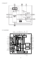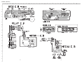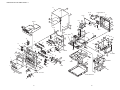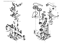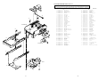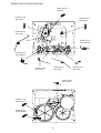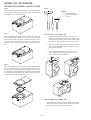
1
XR-H560MD EZ,K
SERVICE MANUAL
MD / CD STEREO SYSTEM
BASIC TAPE MECHANISM : 6ZM-1 AR3
BASIC CD MECHANISM : 4ZG-1 Z3RNSMDJM
BASIC MD MECHANISM : ZZG-6 D
This Service Manual is the "Revision Publishing" and replaces "Simple Manual"
(S/M Code No. 09-993-412-1T2).
SYSTEM
CD–CASSEIVER
SPEAKER
XR-H560MD
CX-NH560MD
SX-WNH898
S/M Code No. 09-993-412-1R2
DA
TA
RE
VI
SIO
N
If requiring information about the CD mechanism, see Service Manual of 4ZG-1, S/M
Code No.09-992-325-4N2.
TABLE OF CONTENTS
SPECIFICATIONS .................................................................................................................................. 3
ACCESSORIES/PACKAGE LIST ........................................................................................................... 3
PROTECTION OF EYES FROM LASER BEAM DURING SERVICING ................................................ 4
Precaution to replace Optical block......................................................................................................... 5
DISASSEMBLY INSTRUCTIONS ...................................................................................................... 6-13
CASSETTE MECHANISM DISASSEMBLY INSTRUCTIONS .............................................................. 14
NOTE ON BEFORE STARTING REPAIR ...................................................................................... 15, 16
ELECTRICAL MAIN PARTS LIST ................................................................................................... 17-23
TRANSISTOR ILLUSTRATION ............................................................................................................ 24
IC BLOCK DIAGRAM ....................................................................................................................... 25-28
BLOCK DIAGRAM-1 (MAIN) ........................................................................................................... 29, 30
BLOCK DIAGRAM-2 (MD) .............................................................................................................. 31, 32
WIRING-1 (MAIN) ........................................................................................................................... 33, 34
SCHEMATIC DIAGRAM-1 (MAIN 1/2) ............................................................................................ 35, 36
WIRING-2 (PT) ...................................................................................................................................... 37
SCHEMATIC DIAGRAM-2 (PT) ............................................................................................................ 38
SCHEMATIC DIAGRAM-3 (MAIN 2/2) ............................................................................................ 39, 40
WIRING-3 (FRONT) ........................................................................................................................ 41, 42
SCHEMATIC DIAGRAM-4 (FRONT) .............................................................................................. 43, 44
WIRING-4 (INTERFACE) ................................................................................................................ 45, 46
SCHEMATIC DIAGRAM-5 (INTERFACE) ...................................................................................... 47, 48
WIRING-5 (MD) ............................................................................................................................... 49, 50
SCHEMATIC DIAGRAM-6 (MD) ..................................................................................................... 51, 52
WIRING-6 (TUNER) ........................................................................................................................ 53, 54
SCHEMATIC DIAGRAM-7 (TUNER) .............................................................................................. 55, 56
WIRING-7 (MECHA) ....................................................................................................................... 57, 58
FL GRID ASSIGNMENT/ANODE CONNECTION .......................................................................... 59, 60
TEST MODE .................................................................................................................................... 61-67
ELECTRICAL ADJUSTMENT/PRACTICAL SERVICE FIGURE ..................................................... 68-71
IC DESCRIPTION ............................................................................................................................ 72-79
MECHANICAL PARTS LIST 1/1 ........................................................................................................... 80
MECHANICAL EXPLODED VIEW 1/1 ............................................................................................ 81, 82
MD MECHANISM EXPLODED VIEW 1/4 ............................................................................................. 83
MD MECHANISM PARTS LIST 1/4 ...................................................................................................... 83
MD MECHANISM EXPLODED VIEW 2/4 ............................................................................................. 84
MD MECHANISM PARTS LIST 2/4 ...................................................................................................... 84
MD MECHANISM EXPLODED VIEW 3/4 ............................................................................................. 85
MD MECHANISM PARTS LIST 3/4 ...................................................................................................... 86
MD MECHANISM EXPLODED VIEW 4/4 ............................................................................................. 87
MD MECHANISM PARTS LIST 4/4 ...................................................................................................... 88
TAPE MECHANISM EXPLODED VIEW 1/1 .................................................................................... 89-91
TAPE MECHANISM PARTS LIST 1/1 .................................................................................................. 92
SPRING APPLICATION POSITION ..................................................................................................... 93
SPEAKER DISASSEMBLY INSTRUCTIONS ....................................................................................... 94
SPEAKER PARTS LIST 1/1 .................................................................................................................. 95
2
SPECIFICATIONS
•
•
•
ACCESSORIES/PACKAGE LIST
REF. NO
1
1
2
3
4
PART NO.
KANRI
DESCRIPTION
NO.
8Z-NB6-905-010
IB,K(E)I<KS>
8Z-NB6-906-010
IB,EZ(9L)I<EZS>
87-A90-030-010
ANT,LOOP AM-NC C
87-043-106-010
WIRE, FM ANT (Z)
8Z-NB5-703-010
RC UNIT,RC-ZAS18
3
Design and specifications are subject to change without
notice.
Dolby noise reduction manufactured under license from
Dolby Laboratories Licensing Corporation.
“DOLBY” and the double-D symbol
are trademarks
of Dolby Laboratories Licensing Corporation.
The word “BBE” and the “BBE symbol” are trademarks
of BBE Sound,Inc.
Under license from BBE Sound,Inc.
PROTECTION OF EYES FROM LASER BEAM DURING SERVICING
This set employs laser. Therefore, be sure to follow carefully the
instructions below when servicing.
CAUTION
Use of controls or adjustments or performance of procedures
other than those specified herein may result in hazardous
radiation exposure.
WARNING!
WHEN SERVICING, DO NOT APPROACH THE LASER EXIT
WITH THE EYE TOO CLOSELY. IN CASE IT IS NECESSARY TO
CONFIRM LASER BEAM EMISSION. BE SURE TO OBSERVE
FROM A DISTANCE OF MORE THAN 30cm FROM THE
SURFACE OF THE OBJECTIVE LENS ON THE OPTICAL
PICK-UP BLOCK.
ATTENTION
L'utilisation de commandes, réglages ou procédures autres que
ceux spécifiés peut entraîner une dangereuse exposition aux
radiations.
ADVARSEL!
Caution: Invisible laser radiation when
open and interlocks defeated avoid exposure to beam.
Advarsel:Usynling laserståling ved åbning,
når sikkerhedsafbrydere er ude af funktion.
Undgå udsættelse for stråling.
Usynlig laserståling ved åbning, når sikkerhedsafbrydereer ude
af funktion. Undgå udsættelse for stråling.
This Compact Disc player is classified as a CLASS 1 LASER
product.
The CLASS 1 LASER PRODUCT label is located on the rear
exterior.
VAROITUS!
Laiteen Käyttäminen muulla kuin tässä käyttöohjeessa mainitulla tavalla saattaa altistaa käyt-täjän turvallisuusluokan 1 ylittävälle näkymättömälle lasersäteilylle.
CLASS 1
KLASSE 1
LUOKAN 1
KLASS 1
VARNING!
Om apparaten används på annat sätt än vad som specificeras i
denna bruksanvising, kan användaren utsättas för osynling
laserstrålning, som överskrider gränsen för laserklass 1.
4
LASER PRODUCT
LASER PRODUKT
LASER LAITE
LASER APPARAT
Precaution to replace Optical block
(KSS-213F)
Body or clothes electrostatic potential could ruin
laser diode in the optical block. Be sure ground
body and workbench, and use care the clothes
do not touch the diode.
1) After the connection, remove solder shown in
the right figure.
Precaution to replace Optical block
(KMS-260A)
Body or clothes electrostatic potential could ruin
laser diode in the optical block. Be sure ground
body and workbench, and use care the clothes
do not touch the diode.
1) After the connection, remove solder shown in
the right figure.
1 VEE
¡ TRK –
5
DISASSEMBLY INSTRUCTIONS
1. Disassembling the MD block
Remove the CABI, STEEL. (Screws: 4 pcs on the right side, 4 pcs on the left side and 7 pcs on the rear: Total 15 screws)
Remove the 13 screws (UTT2+3-8) A and remove the rear panel.
A
A
After removing the connectors from the TUNER C.B and the FUN, remove the rear panel.
Remove the two screws (QT2+3-10) B. Open the rack and remove the HLDR, MD.
B
HOOK
B
HOOK
6
Remove the four screws (BVT2+3-10) C. Remove the ZZG-2.
HLDR, MD
CC
C
CC
ZZG-2
C
2. Disassembling the MD block and the service position
Remove the ZZG-2.
Remove the two screws (UT2+2.6-6 GLD) D from the PLATE, SHLD REAR. Remove the PLATE, SHLD REAR.
Remove the four screws (U+2+2.6-6) E from the PLATE, SHLD TOP. Remove the PLATE, SHLD TOP.
E
E
E
PLATE, SHLD TOP
D
E
PLATE, SHLD REAR
D
7
Remove the four screws (UT2+2.6-6 GLD) F and remove the PLATE, SHLD BOTTOM.
F
F
F
PLATE, SHLD BOTTOM
F
The MD block is ready to be placed in the service position. Connect the MD block with the interface board using the extension FFC as
shown below.
8
3. Disassembling the elevator
Rotate the WORM-WHL, JT (the gear shown by the arrow below) counterclockwise to move the elevator to the top position.
Note: If the PANEL, SHLD BOTTOM is not removed, the elevator cannot be removed.
WORM-WHL, JT
Remove the FF-CABLE, 9P 1.0 from the LOAD C.B.
FF-CABLE, 9P 1.0
9
While lifting up the elevator slightly, remove an end of the shaft of the elevator from the guide hole of the CHAS ASSY, SHLD.
Remove the other end of the shaft and tilt the elevator as shown below.
While tilting the elevator, short the shorting land.
SHAFT
CHAS ASSY, SHLD
Remove the PICK UP, FFC and the MECHA C.B, FFC, then remove the elevator block.
10
4. Disassembling the elevator block
Remove the screw (UT2+2.6-6 GLD) G and the screw (VTT+2-4) H. Then remove the HLDR, MECHA SUB.
G
HLDR, MECHA SUB
H
Remove the four screws (S-SCREW, MD T) I and remove the ZZG-1 from the HLDR ASSY, MECHA.
I
ZZG-1
I
I
I
HLDR ASSY, MECHA
11
5. Remove the two screws (VTT+2-4) A.
Remove the PLATE ASSY, SLIDE L and the PLATE, SLIDE R in the direction of the arrow.
Remove the screw (VW+1.7-5 W/O MFZN2C) B.
Remove the HEAD, OWH RF325-74A.
Re-assembling: Align the axis of the PLATE ASSY, SLIDE L with the arrow mark of the CAM, LOAD.
CAM, LOAD
HEAD, OWH RF325-74A
B
A
A
PLATE ASSY,
SLIDE L
PLATE, SLIDE R
6. Move the 7ZG-3 A1 in the direction of (a).
While pressing the BOSS in the direction of (b), remove the 7ZG-3 A1 in the direction of (c).
BOSS
b
b
a
7ZG-3 A1
c
12
7. Remove the CAM, LOAD in the direction of the arrow.
Re-assembling: Move the LEVER ASSY, CAM in the direction of the arrow mark as much as it can be moved.
Move the reference hole of the CAM, LOAD closer to the axis of the LEVER, SW H as close as possible.
Align the CAM, LOAD with the gear of the GEAR, IDLER2.
LEVER ASSY, CAM
Reference hole of CAM, LOAD
GEAR, IDLER2
Axis of LEVER, SW H
CAM, LOAD
13
OPEN
CASSETTE MECHANISM DISASSEMBLY INSTRUCTIONS
CLOSE
Azimuth
adjustment
•
Remove the three 3 screws (VT3-5) and open the cassette
tray halfway. After pulling up the XR-H560MD and closing
the tray again, remove it.
•
Perform the azimuth adjustment through the hole on the top
surface.
•
Perform the motor speed adjustment through the hole at the
bottom of the amplifier chassis using the clock screwdriver
“d”.
•
The tray of the cassette deck cannot be operated without the
CD board. Open/close the tray with hand.
14
NOTE ON BEFORE STARTING REPAIR
• CD service position
Remove the CABI, STEEL.
Remove the three screws (BVT2+3-10) A.
Turn over the unit and remove the CABI, BOTTOM.
A
A
Remove the two FFCs (13P and 6P) the CD block from the hook of the CABI, BOTTOM.
Loosen the two screws (QT2+3-12) B of the 4ZG-1 CABI, FR. (The screws are used at the both sides.)
B
15
Remove the hooks in the direction of the arrow. (The hooks are used at the both sides.) Pull the CABI, BOTTOM up to the
diagonally top right and remove it.
HOOK
Lay down the unit and remove the 3ZG-2 mechanism.
Extend the 3ZG-2 mechanism using the respective extension jigs.
Service position
16
ELECTRICAL MAIN PARTS LIST
REF. NO
PART NO.
KANRI
NO.
DESCRIPTION
REF. NO
IC
8Z-NB6-615-010
87-A20-914-010
87-A20-783-040
87-A21-022-040
87-A21-021-040
C-IC,LC876580A
IC,SPS-442-1-F
C-IC,BA7762AFS
C-IC,BA3880FS
C-IC,BU2099FV
87-A21-031-040
87-A21-202-040
87-A21-023-040
87-A21-103-040
87-A20-707-010
C-IC,BU4551BF
C-IC,M62445AFP
C-IC,BA3835F
C-IC,MM1454XFBE
C-IC,CXA2523AR
87-A20-708-010
87-A20-709-040
8Z-ZG2-606-010
87-ZG9-606-040
87-A20-755-080
C-IC,CXD2652AR
C-IC,BD7910FV
C-IC,CXP81952
C-IC,MN41V4400SJ-08
C-IC,AK93C45AF
87-A20-710-040
87-A20-711-040
87-A20-712-040
87-A21-078-080
87-017-853-040
C-IC,S-8110AMP
C-IC,BA5970FP
C-IC,BA6417F
C-IC,PCM3003E
IC,NJM2100V
87-A20-797-040
87-A20-798-040
87-A20-714-040
C-IC,NJU7221U30
C-IC,NJU7221U35
C-IC,NJM2370U33
TR,DTC114ES
TR,KTA1266GR
TR,KTC3199GR
TR,2SB1370 (1.8W)
TR,KTC3198GR
87-A30-076-080
87-A30-075-080
87-A30-234-080
87-A30-072-080
87-A30-162-010
C-TR,2SC3052F
C-TR,2SA1235F
TR,CSC4115BC
C-TR,RT1P 144C
FET,2SK2937
87-A30-074-080
87-A30-268-040
87-A30-240-080
87-A30-086-080
87-A30-190-080
C-TR,RT1P 141C
C-TR,2SA1514K(S)
TR,CSA1585BC
C-TR,CSD1306E
TR,CC5551
87-A30-137-010
87-A30-138-010
87-A30-119-040
87-A30-087-080
87-A30-071-080
TR,2SD2494
TR,2SB1625
C-TR,2SC3906K R
C-FET,2SK2158
C-TR,RT1N 144C
87-A30-257-080
87-A30-109-010
87-A30-108-010
87-A30-073-080
87-A30-159-080
C-TR,2SD1306E
TR,2SD 2495
TR,2SB1626
C-TR,RT1N 141C
C-TR,KTA1298Y
87-A30-047-080
87-A30-202-080
87-A30-142-040
87-026-423-080
89-115-884-080
TR,CSD655E
C-TR,RT1P441C
C-TR,DTA123EKA
C-TR RN2305
CHIP -TRANSISTER 2SA1588Y
89-341-164-080
87-026-412-080
CHIP-TRANSISTOR,2SC4116 Y
C-TR RN1305
DIODE
87-020-465-080
87-A40-548-090
87-070-274-080
87-A40-435-080
87-A40-345-080
DIODE,1SS133 (110MA)
DIODE,D3SBA20
DIODE,1N4003 SEM
ZENER,MTZJ30D
ZENER,MTZJ10C
87-A40-183-090
87-070-136-080
DIODE,RK36(F)
ZENER,MTZJ5.1B
KANRI
DESCRIPTION
NO.
87-A40-270-080
C-DIODE,MC2838
87-A40-269-080
C-DIODE,MC2836
87-A40-488-080
DIODE,1SS244
87-A40-509-080
ZENER,MTZJ6.8C
87-A40-469-080
C-DIODE,HSM2838CTR
87-A40-468-080
87-A40-002-080
87-A40-438-080
87-A40-234-080
87-017-932-080
C-DIODE,HSM2836CTR
ZENER,MTZJ5.1C
ZENER,MTZJ4.7A
ZENER,MTZJ5.6A
ZENER,MTJ6.2B
87-001-166-080
87-A40-412-040
87-020-764-080
DIODE,1SS301
C-DIODE,SB05-05CP
CHIP-ZENER,02CZ4.7X
C1
C2
C3
C4
C5
87-012-369-080
87-012-369-080
87-012-368-080
87-012-368-080
87-012-368-080
C-CAP,S
C-CAP,S
C-CAP,S
C-CAP,S
C-CAP,S
C6
C9
C10
C21
C22
87-012-368-080
87-016-658-090
87-016-658-090
87-010-247-080
87-010-247-080
C-CAP,S 0.1-50 F
CAP,E 4700-35 SMG
CAP,E 4700-35 SMG
CAP, ELECT 100-50V
CAP, ELECT 100-50V
C23
C24
C25
C26
C27
87-010-247-080
87-010-247-080
87-010-430-080
87-010-263-080
87-012-140-080
CAP, ELECT
CAP, ELECT
CAP, ELECT
CAP, ELECT
CAP 470P
C28
C29
C30
C31
C32
87-010-263-080
87-010-408-080
87-010-112-080
87-010-235-080
87-012-368-080
CAP, ELECT 100-10V
CAP, ELECT 47-50V
CAP, ELECT 100-16V
CAP,E 470-16 SME
C-CAP,S 0.1-50 F
C33
C34
C61
C62
C91
87-016-299-080
87-016-299-080
87-010-260-080
87-010-403-080
87-010-401-080
CAP,E 10-100 SME
CAP,E 10-100 SME
CAP, ELECT 47-25V
CAP, ELECT 3.3-50V
CAP, ELECT 1-50V
C92
C93
C101
C102
C103
87-010-263-080
87-010-380-080
87-010-178-080
87-010-178-080
87-010-405-080
CAP,
CAP,
CHIP
CHIP
CAP,
C104
C107
C108
C109
C110
87-010-405-080
87-010-408-080
87-010-408-080
87-010-322-080
87-010-322-080
CAP, ELECT 10-50V
CAP, ELECT 47-50V
CAP, ELECT 47-50V
C-CAP,S 100P-50 CH
C-CAP,S 100P-50 CH
C111
C112
C113
C114
C117
87-010-260-080
87-010-260-080
87-A10-946-080
87-A10-946-080
87-A11-185-080
CAP, ELECT 47-25V
CAP, ELECT 47-25V
C-CAP,S 220P-100 J CH
C-CAP,S 220P-100 J CH
C-CAP, 0.47-50 F Z
C118
C121
C122
C123
C124
87-A11-185-080
87-010-178-080
87-010-178-080
87-012-156-080
87-012-156-080
C-CAP, 0.47-50 F Z
CHIP CAP 1000P
CHIP CAP 1000P
C-CAP,S 220P-50 J CH GRM
C-CAP,S 220P-50 J CH GRM
C125
C126
C127
C128
C131
87-012-368-080
87-012-368-080
87-012-368-080
87-012-368-080
87-010-197-080
C-CAP,S 0.1-50
C-CAP,S 0.1-50
C-CAP,S 0.1-50
C-CAP,S 0.1-50
CAP, CHIP 0.01
C132
C133
C136
C203
87-010-197-080
87-010-197-080
87-010-196-080
87-010-177-080
CAP, CHIP 0.01 DM
CAP, CHIP 0.01 DM
CHIP CAPACITOR,0.1-25
C-CAP,S 820P-50 SL
MAIN C.B
TRANSISTOR
87-026-245-080
87-026-609-080
87-A30-198-080
89-213-702-010
87-026-610-080
PART NO.
17
0.047-50F
0.047-50F
0.1-50 F
0.1-50 F
0.1-50 F
100-50V
100-50V
100-63
100-10V
ELECT 100-10V
ELECT 47-16V
CAP 1000P
CAP 1000P
ELECT 10-50V
F
F
F
F
DM
REF. NO
PART NO.
C204
C209
C210
C211
C212
KANRI
DESCRIPTION
NO.
87-010-177-080
C-CAP,S 820P-50 SL
87-010-403-080
CAP, ELECT 3.3-50V
87-010-403-080
CAP, ELECT 3.3-50V
87-010-181-080
CAP,CHIP S 1800P
87-010-181-080
CAP,CHIP S 1800P
REF. NO
C405
C406
C407
C408
C409
KANRI
DESCRIPTION
NO.
87-010-404-080
CAP, ELECT 4.7-50V
87-010-404-080
CAP, ELECT 4.7-50V
87-010-188-080
CAP,CHIP 6800P
87-010-188-080
CAP,CHIP 6800P
87-012-140-080
CAP 470P
C213
C214
C215
C216
C217
87-010-401-080
87-010-401-080
87-010-322-080
87-010-322-080
87-010-401-080
CAP, ELECT 1-50V
CAP, ELECT 1-50V
C-CAP,S 100P-50 CH
C-CAP,S 100P-50 CH
CAP, ELECT 1-50V
C410
C411
C412
C413
C414
87-012-140-080
87-010-404-080
87-010-404-080
87-010-404-080
87-010-404-080
CAP 470P
CAP, ELECT
CAP, ELECT
CAP, ELECT
CAP, ELECT
C218
C219
C220
C225
C226
87-010-401-080
87-A10-946-080
87-A10-946-080
87-012-368-080
87-012-368-080
CAP, ELECT 1-50V
C-CAP,S 220P-100 J CH
C-CAP,S 220P-100 J CH
C-CAP,S 0.1-50 F
C-CAP,S 0.1-50 F
C415
C416
C417
C418
C419
87-010-197-080
87-010-197-080
87-010-956-080
87-010-956-080
87-010-260-080
CAP, CHIP 0.01 DM
CAP, CHIP 0.01 DM
CHIP-CAP,S 0.068-25B
CHIP-CAP,S 0.068-25B
CAP, ELECT 47-25V
C227
C228
C229
C230
C231
87-010-186-080
87-010-186-080
87-010-993-080
87-010-993-080
87-010-196-080
CAP,CHIP 4700P
CAP,CHIP 4700P
C-CAP,S 0.056-25 B
C-CAP,S 0.056-25 B
CHIP CAPACITOR,0.1-25
C421
C422
C451
C452
C457
87-012-156-080
87-012-156-080
87-010-401-080
87-010-401-080
87-010-196-080
C-CAP,S 220P-50 J CH GRM
C-CAP,S 220P-50 J CH GRM
CAP, ELECT 1-50V
CAP, ELECT 1-50V
CHIP CAPACITOR,0.1-25
C232
C233
C234
C235
C236
87-010-196-080
87-010-190-080
87-010-190-080
87-016-285-080
87-016-285-080
CHIP CAPACITOR,0.1-25
S CHIP F 0.01
S CHIP F 0.01
CAP,E 47-100SME
CAP,E 47-100SME
C458
C461
C601
C602
C605
87-010-196-080
87-010-544-080
87-010-180-080
87-010-180-080
87-010-318-080
CHIP CAPACITOR,0.1-25
CAP, ELECT 0.1-50V
C-CER 1500P
C-CER 1500P
C-CAP,S 47P-50 CH
C239
C303
C304
C307
C309
87-010-196-080
87-012-157-080
87-012-157-080
87-010-196-080
87-010-196-080
CHIP CAPACITOR,0.1-25
C-CAP,S 330P-50 CH
C-CAP,S 330P-50 CH
CHIP CAPACITOR,0.1-25
CHIP CAPACITOR,0.1-25
C606
C607
C608
C613
C614
87-010-318-080
87-010-318-080
87-010-318-080
87-016-081-080
87-016-081-080
C-CAP,S
C-CAP,S
C-CAP,S
C-CAP,S
C-CAP,S
C310
C311
C312
C315
C316
87-010-196-080
87-010-198-080
87-010-198-080
87-010-178-080
87-010-178-080
CHIP
CAP,
CAP,
CHIP
CHIP
C619
C620
C621
C622
C623
87-010-185-080
87-010-185-080
87-010-401-080
87-010-401-080
87-A10-773-080
C-CAP,S 3900P-50 B
C-CAP,S 3900P-50 B
CAP, ELECT 1-50V
CAP, ELECT 1-50V
CAP,M 0.10-50 J
C321
C322
C324
C325
C327
87-016-492-080
87-016-492-080
87-010-260-080
87-010-370-080
87-010-404-080
C-CAP,S 0.33-16 FZ
C-CAP,S 0.33-16 FZ
CAP, ELECT 47-25V
CAP,E 330-6.3 SME
CAP, ELECT 4.7-50V
C624
C625
C626
C627
C629
87-A10-773-080
87-010-401-080
87-010-401-080
87-010-196-080
87-010-405-080
CAP,M 0.10-50 J
CAP, ELECT 1-50V
CAP, ELECT 1-50V
CHIP CAPACITOR,0.1-25
CAP, ELECT 10-50V
C328
C332
C335
C336
C337
87-010-404-080
87-010-196-080
87-010-401-080
87-010-401-080
87-010-196-080
CAP,
CHIP
CAP,
CAP,
CHIP
ELECT 4.7-50V
CAPACITOR,0.1-25
ELECT 1-50V
ELECT 1-50V
CAPACITOR,0.1-25
C630
C631
C632
C633
C634
87-010-213-080
87-010-992-080
87-010-263-080
87-010-263-080
87-010-196-080
C-CAP,S 0.015-50 B
C-CAP,S 0.047-25 B
CAP, ELECT 100-10V
CAP, ELECT 100-10V
CHIP CAPACITOR,0.1-25
C339
C340
C351
C352
C354
87-010-196-080
87-010-196-080
87-012-140-080
87-012-140-080
87-010-175-080
CHIP CAPACITOR,0.1-25
CHIP CAPACITOR,0.1-25
CAP 470P
CAP 470P
CAP 560P
C635
C638
C641
C677
C957
87-010-196-080
87-012-157-080
87-010-196-080
87-010-196-080
87-010-405-080
CHIP CAPACITOR,0.1-25
C-CAP,S 330P-50 J CH GRM
CHIP CAPACITOR,0.1-25
CHIP CAPACITOR,0.1-25
CAP, ELECT 10-50V
C355
C356
C357
C358
C359
87-012-349-080
87-010-260-080
87-010-197-080
87-010-183-080
87-010-183-080
C-CAP,S 1000P-50 CH
CAP, ELECT 47-25V
CAP, CHIP 0.01 DM
C-CAP,S 2700P-50 B
C-CAP,S 2700P-50 B
CN91
CN92
CN351
CN601
CN603
87-009-030-010
87-009-030-010
87-099-832-010
87-A60-349-010
87-A60-054-010
CONNECTOR 2P PH M
CONNECTOR 2P PH M
CONN,8P V S2M-8W
CONN 30P DF8A-30S
CONN,14P V 9604S-14C
C360
C370
C373
C374
C378
87-010-183-080
87-010-196-080
87-016-083-080
87-016-083-080
87-010-196-080
C-CAP,S 2700P-50 B
CHIP CAPACITOR,0.1-25
C-CAP,S 0.15-16 RK
C-CAP,S 0.15-16 RK
CHIP CAPACITOR,0.1-25
CN605
CN901
CNA1
FB301
J202
87-099-781-010
87-099-566-010
8Z-NB6-617-010
87-008-372-080
87-A60-483-010
CONN,16P V B16B-PH-K-S
CONN,7P TUC-P7P-B1
CONN ASSY,9P P-SPLY
FLTR,EMI BL01 RN1
JACK,DIA6.3 BLK ST W/S KM
C379
C380
C386
C388
C393
87-010-406-080
87-010-406-080
87-010-196-080
87-012-156-080
87-010-319-080
CAP, ELECT 22-50
CAP, ELECT 22-50
CHIP CAPACITOR,0.1-25
C-CAP,S 220P-50 CH
C-CAP,S 56P-50 CH
J203
J204
J602
L101
L102
87-033-240-010
87-A60-750-010
87-A60-425-010
87-003-383-010
87-003-383-010
TERMINAL,SP 4P32SV1-05
JACK,PIN 4P R/W BLUE
JACK,PIN 2P YKC21-3838
COIL,1UH-S
COIL,1UH-S
C394
C401
C402
C403
C404
87-010-319-080
87-010-196-080
87-010-260-080
87-010-404-080
87-010-404-080
C-CAP,S 56P-50 CH
CHIP CAPACITOR,0.1-25
CAP, ELECT 47-25V
CAP, ELECT 4.7-50V
CAP, ELECT 4.7-50V
L201
L202
L301
L302
L351
87-003-383-010
87-003-383-010
87-A50-049-010
87-A50-049-010
87-007-342-010
COIL,1UH-S
COIL,1UH-S
COIL,TRAP 85K(COI)
COIL,TRAP 85K(COI)
COIL,OSC 85K BIAS
CAPACITOR,0.1-25
CHIP 0.022
CHIP 0.022
CAP 1000P
CAP 1000P
18
PART NO.
4.7-50V
4.7-50V
4.7-50V
4.7-50V
47P-50
47P-50
47P-50
0.1-16
0.1-16
CH
CH
CH
RK
RK
REF. NO
PART NO.
SFR351
SFR352
TH101
TH102
TH201
KANRI
DESCRIPTION
NO.
87-024-436-080
SFR,47K RH063EC
87-024-436-080
SFR,47K RH063EC
87-A91-042-080
C-THMS,100K 55001
87-A91-042-080
C-THMS,100K 55001
87-A91-042-080
C-THMS,100K 55001
TH202
WH1
87-A91-042-080
87-A90-510-010
C141
C143
C151
C152
C153
REF. NO
LED408
LED409
LED411
LED412
LED413
KANRI
DESCRIPTION
NO.
87-A40-451-080
LED,SEL6510C-TP7 GRN
87-A40-451-080
LED,SEL6510C-TP7 GRN
87-A40-619-040
LED,SLR-56PT-T31-W GRN
87-A40-619-040
LED,SLR-56PT-T31-W GRN
87-A40-619-040
LED,SLR-56PT-T31-W GRN
C-THMS,100K 55001
HLDR,WIRE 2.5-9P
LED414
LED415
LED416
LED417
LED418
87-A40-619-040
87-A40-619-040
87-A40-619-040
87-A40-619-040
87-A40-619-040
LED,SLR-56PT-T31-W
LED,SLR-56PT-T31-W
LED,SLR-56PT-T31-W
LED,SLR-56PT-T31-W
LED,SLR-56PT-T31-W
87-010-263-040
87-010-194-080
87-010-264-040
87-010-196-080
87-010-493-040
CAP,E 100-10
CAP, CHIP 0.047
CAP,E 100-10 5L
CHIP CAPACITOR,0.1-25
CAP,E 0.47-50 GAS
LED419
LED421
LED422
LED423
LED424
87-A40-589-040
87-A40-380-080
87-017-980-080
87-A40-380-080
87-017-980-080
LED,SLR-56VCT31 RED
LED,SEL6510C-TP5 GRN
LED,SEL6210S
LED,SEL6510C-TP5 GRN
LED,SEL6210S
C154
C155
C156
C158
C159
87-A10-189-040
87-010-154-080
87-010-854-080
87-010-178-080
87-010-196-080
CAP,E 220-10
CAP CHIP 10P
C-CAP,S 560PCH
CHIP CAP 1000P
CHIP CAPACITOR,0.1-25
LED425
LED426
LED427
LED428
LED429
87-A40-380-080
87-017-980-080
87-A40-380-080
87-017-980-080
87-A40-380-080
LED,SEL6510C-TP5 GRN
LED,SEL6210S
LED,SEL6510C-TP5 GRN
LED,SEL6210S
LED,SEL6510C-TP5 GRN
C160
C161
C162
C163
C165
87-010-196-080
87-010-196-080
87-010-178-080
87-A10-189-040
87-012-157-080
CHIP CAPACITOR,0.1-25
CHIP CAPACITOR,0.1-25
C-CAP,S 1000P-50 K B C2012
CAP,E 220-10
C-CAP,S 330P-50 CH
LED430
LED441
LED442
LED443
!PR251
87-017-980-080
87-A40-451-080
87-A40-451-080
87-A40-451-080
87-A90-247-080
LED,SEL6210S
LED,SEL6510C-TP7
LED,SEL6510C-TP7
LED,SEL6510C-TP7
PROTECTOR,0.315A
C166
C171
C172
C173
C174
87-010-075-040
87-010-194-080
87-010-408-040
87-010-981-040
87-010-406-040
CAP,E 10-16 5L
CAP, CHIP 0.047
CAP,E 47-50 SME
CAP,E 22-35 5L SRE
CAP,E 22-50 SME
!PR451
S301
S302
S303
S304
87-A90-247-080
87-A90-095-080
87-A90-095-080
87-A90-095-080
87-A90-095-080
PROTECTOR,0.315A 60V 491
SW,TACT EVQ11G04M
SW,TACT EVQ11G04M
SW,TACT EVQ11G04M
SW,TACT EVQ11G04M
C180
C183
C184
C185
C187
87-010-194-080
87-010-197-080
87-010-197-080
87-010-182-080
87-010-182-080
CAP, CHIP 0.047
CAP, CHIP 0.01 DM
CAP, CHIP 0.01 DM
C-CAP,S 2200P-50 K B C2012
C-CAP,S 2200P-50 K B C2012
S305
S306
S307
S308
S309
87-A90-095-080
87-A90-095-080
87-A90-095-080
87-A90-095-080
87-A90-095-080
SW,TACT
SW,TACT
SW,TACT
SW,TACT
SW,TACT
EVQ11G04M
EVQ11G04M
EVQ11G04M
EVQ11G04M
EVQ11G04M
C191
C192
C281
C401
C402
87-012-368-080
87-010-196-080
87-010-561-040
87-010-560-040
87-010-196-080
C-CAP,S 0.1-50 F
CHIP CAPACITOR,0.1-25
CAP,E 100-16 GAS
CAP,E 10-50 GAS
CHIP CAPACITOR,0.1-25
S310
S312
S313
S321
S322
87-A90-095-080
87-A90-095-080
87-A90-095-080
87-A90-095-080
87-A90-095-080
SW,TACT
SW,TACT
SW,TACT
SW,TACT
SW,TACT
EVQ11G04M
EVQ11G04M
EVQ11G04M
EVQ11G04M
EVQ11G04M
C403
C404
C406
C407
C408
87-010-318-080
87-010-318-080
87-010-318-080
87-010-318-080
87-010-318-080
C-CAP,S
C-CAP,S
C-CAP,S
C-CAP,S
C-CAP,S
S323
S324
S325
S326
S327
87-A90-095-080
87-A90-095-080
87-A90-095-080
87-A90-095-080
87-A90-095-080
SW,TACT
SW,TACT
SW,TACT
SW,TACT
SW,TACT
EVQ11G04M
EVQ11G04M
EVQ11G04M
EVQ11G04M
EVQ11G04M
C410
C411
C412
C413
C451
87-010-196-080
87-010-318-080
87-010-318-080
87-010-318-080
87-010-412-040
CHIP CAPACITOR,0.1-25
C-CAP,S 47P-50 CH
C-CAP,S 47P-50 CH
C-CAP,S 47P-50 CH
CAP,E 10-25 M 5L SRE
S328
S329
S330
S330
S331
87-A90-095-080
87-A90-095-080
87-A90-095-080
87-A90-095-080
87-A90-095-080
SW,TACT
SW,TACT
SW,TACT
SW,TACT
SW,TACT
EVQ11G04M
EVQ11G04M
EVQ11G04M
EVQ11G04M
EVQ11G04M
C501
C502
C503
C701
C702
87-010-322-080
87-010-322-080
87-010-322-080
87-010-196-080
87-012-158-080
C-CAP,S 100P-50 CH
C-CAP,S 100P-50 CH
C-CAP,S 100P-50 CH
CHIP CAPACITOR,0.1-25
C-CAP,S 390P-50 CH
S341
S342
S343
S344
S345
87-A90-095-080
87-A90-095-080
87-A90-095-080
87-A90-095-080
87-A90-095-080
SW,TACT
SW,TACT
SW,TACT
SW,TACT
SW,TACT
EVQ11G04M
EVQ11G04M
EVQ11G04M
EVQ11G04M
EVQ11G04M
C703
C704
C705
C706
C707
87-010-196-080
87-010-196-080
87-010-196-080
87-010-196-080
87-010-196-080
CHIP
CHIP
CHIP
CHIP
CHIP
S346
SW162
SW163
87-A90-095-080
87-A90-535-010
87-A91-076-010
SW,TACT EVQ11G04M
SW,RTRY EC16B24304
SW,RTRY REO121PVB25FINA1
CN101
CN102
CN252
CN351
CN451
87-A60-350-010
87-099-030-010
87-099-209-010
87-099-031-010
87-099-209-010
CONN 30P DF8A-30P
CONN,13P 6216H
CONN,4P 6216H
CONN,14P 6216 H
CONN,4P 6216H
CN352
LED401
LED402
LED403
LED404
87-099-031-010
87-A40-619-040
87-A40-619-040
87-A40-619-040
87-A40-619-040
CONN,14P 6216 H
LED,SLR-56PT-T31-W
LED,SLR-56PT-T31-W
LED,SLR-56PT-T31-W
LED,SLR-56PT-T31-W
CN502
CNA251
FL101
L151
LED407
87-099-200-010
88-803-091-690
8Z-NB6-601-010
87-A50-333-010
87-A40-451-080
CONN,7P 6216H
CONN ASSY,9P
FL,BJ698GNK
COIL,OSC 9.43MHZ
LED,SEL6510C-TP7 GRN
LED405
LED406
LED437
LED438
87-A40-619-040
87-A40-619-040
87-A40-451-080
87-A40-451-080
LED,SLR-56PT-T31-W GRN
LED,SLR-56PT-T31-W GRN
LED,SEL6510C-TP7 GRN
LED,SEL6510C-TP7 GRN
FRONT C.B
47P-50
47P-50
47P-50
47P-50
47P-50
CH
CH
CH
CH
CH
CAPACITOR,0.1-25
CAPACITOR,0.1-25
CAPACITOR,0.1-25
CAPACITOR,0.1-25
CAPACITOR,0.1-25
PART NO.
GRN
GRN
GRN
GRN
GRN
GRN
GRN
GRN
60V 491
SWITCH C.B
19
GRN
GRN
GRN
GRN
REF. NO
PART NO.
LED439
LED444
LED445
LED446
S347
KANRI
DESCRIPTION
NO.
87-A40-451-080
LED,SEL6510C-TP7 GRN
87-A40-451-080
LED,SEL6510C-TP7 GRN
87-A40-451-080
LED,SEL6510C-TP7 GRN
87-A40-451-080
LED,SEL6510C-TP7 GRN
87-A90-095-080
SW,TACT EVQ11G04M
REF. NO
C721
C722
C723
C725
C727
87-012-176-080
87-012-176-080
87-012-274-080
87-018-131-080
87-010-196-080
CAP 15P
CAP 15P
CHIP CAP,U 1000P-50B
CAP, CER 1000P-50V
CHIP CAPACITOR,0.1-25
S348
S349
S350
S351
S352
87-A90-095-080
87-A90-095-080
87-A90-095-080
87-A90-095-080
87-A90-095-080
SW,TACT
SW,TACT
SW,TACT
SW,TACT
SW,TACT
EVQ11G04M
EVQ11G04M
EVQ11G04M
EVQ11G04M
EVQ11G04M
C728
C729
C731
C733
C734
87-010-248-080
87-012-274-080
87-012-286-080
87-012-280-080
87-012-280-080
CAP,
CHIP
CAP,
CAP,
CAP,
S371
S372
S373
S374
S375
87-A90-095-080
87-A90-095-080
87-A90-095-080
87-A90-095-080
87-A90-095-080
SW,TACT
SW,TACT
SW,TACT
SW,TACT
SW,TACT
EVQ11G04M
EVQ11G04M
EVQ11G04M
EVQ11G04M
EVQ11G04M
C752
C753
C755
C756
C757
87-012-282-080
87-012-195-080
87-012-286-080
87-012-286-080
87-012-188-080
CAP, U 4700P-50
C-CAP,U 100P-50CH
CAP, U 0.01-25
CAP, U 0.01-25
C-CAP,U 47P-50 CH
S376
S377
S378
S379
S380
87-A90-095-080
87-A90-095-080
87-A90-095-080
87-A90-095-080
87-A90-095-080
SW,TACT
SW,TACT
SW,TACT
SW,TACT
SW,TACT
EVQ11G04M
EVQ11G04M
EVQ11G04M
EVQ11G04M
EVQ11G04M
C758
C761
C762
C763
C765
87-012-167-080
87-010-196-080
87-012-286-080
87-010-829-080
87-012-286-080
C-CAP,U 5P-50 CH
CHIP CAPACITOR,0.1-25
CAP, U 0.01-25
CAP, U 0.047-16
CAP, U 0.01-25
C766
C768
C769
C770
C771
87-010-197-080
87-012-286-080
87-010-260-080
87-010-829-080
87-010-383-080
CAP,
CAP,
CAP,
CAP,
CAP,
CHIP 0.01 DM
U 0.01-25
ELECT 47-25V
U 0.047-16
ELECT 33-25V
C772
C773
C774
C775
C776
87-010-829-080
87-010-196-080
87-010-263-080
87-010-404-080
87-012-286-080
CAP,
CHIP
CAP,
CAP,
CAP,
U 0.047-16
CAPACITOR,0.1-25
ELECT 100-10V
ELECT 4.7-50V
U 0.01-25
C777
C778
C779
C780
C781
87-010-493-080
87-010-401-080
87-010-401-080
87-010-196-080
87-010-405-080
CAP,E 0.47-50 GAS
CAP, ELECT 1-50V
CAP, ELECT 1-50V
CHIP CAPACITOR,0.1-25
CAP, ELECT 10-50V
C782
C783
C784
C785
C786
87-010-405-080
87-012-286-080
87-012-286-080
87-010-405-080
87-010-405-080
CAP,
CAP,
CAP,
CAP,
CAP,
C787
C788
C789
C790
C791
87-012-275-080
87-012-275-080
87-012-275-080
87-012-275-080
87-010-405-080
C-CAP,U 1200P-50 B
C-CAP,U 1200P-50 B
C-CAP,U 1200P-50 B
C-CAP,U 1200P-50 B
CAP, ELECT 10-50V
C793
C794
C795
C796
C797
87-012-273-080
87-010-406-080
87-010-596-080
87-010-403-080
87-012-276-080
C-CAP,U 820P-50 B
CAP, ELECT 22-50
CAP, S 0.047-16
CAP, ELECT 3.3-50V
CAP, CHIP SS 1500 PBK
C798
C799
C812
C814
C820
87-012-276-080
87-010-829-080
87-012-286-080
87-012-286-080
87-010-260-080
CAP,
CAP,
CAP,
CAP,
CAP,
CHIP SS 1500 PBK
U 0.047-16
U 0.01-25
U 0.01-25
ELECT 47-25V
C821
C822
C823
C828
C829
87-012-286-080
87-012-286-080
87-012-286-080
87-010-196-080
87-010-196-080
CAP,
CAP,
CAP,
CHIP
CHIP
U 0.01-25
U 0.01-25
U 0.01-25
CAPACITOR,0.1-25
CAPACITOR,0.1-25
C859
C861
C862
C863
C864
87-012-286-080
87-012-199-080
87-012-199-080
87-012-270-080
87-010-405-080
CAP,
CAP
CAP
CAP,
CAP,
U 0.01-25
220P
220P
U 470P-50
ELECT 10-50V
C865
C866
C867
C868
C869
87-010-196-080
87-010-405-080
87-012-286-080
87-012-184-080
87-012-180-080
CHIP CAPACITOR,0.1-25
CAP, ELECT 10-50V
CAP, U 0.01-25
C-CAP,U 33P-50 CH
C-CAP,U 22P-50 CH
PT C.B
C1
C4
C5
C8
C9
87-010-387-080
87-010-403-080
87-A10-479-080
87-010-917-090
87-010-917-090
CAP,E 470-25 SME
CAP, ELECT 3.3-50V
CAP,CER 2200P-250 M E KH
CAP,E 3300-50 M SMG
CAP,E 3300-50 M SMG
C10
C11
CN1
!PT1
!PT2
87-018-209-080
87-018-209-080
87-A60-851-010
8Z-NB6-608-010
8Z-NF8-662-110
CAP, CER 0.1-50V
CAP, CER 0.1-50V
CONN,9P V VH
PT,ZNB-6 E
PT,SUB ZNF-8(E)
RY1
!T1
!T2
87-A90-976-010
87-A60-317-010
87-A60-317-010
RELAY,AC12V SDT-S-112LMR
TERMINAL, 1P MSC
TERMINAL, 1P MSC
Q-SUR C.B
C952
C953
C954
C955
C971
87-010-112-080
87-010-260-080
87-010-197-080
87-010-197-080
87-010-402-080
CAP,
CAP,
CAP,
CAP,
CAP,
ELECT 100-16V
ELECT 47-25V
CHIP 0.01 DM
CHIP 0.01 DM
ELECT 2.2-50V
C972
C973
C974
C975
CN951
87-010-402-080
87-010-405-080
87-010-405-080
87-010-322-080
87-A60-689-010
CAP, ELECT 2.2-50V
CAP, ELECT 10-50V
CAP, ELECT 10-50V
C-CAP,S 100P-50 CH
CONN,7P H GRY TUC-P07X-C1
PART NO.
KANRI
NO.
DESCRIPTION
ELECT 220-10V
CAP,U 1000P-50B
U 0.01-25
U 3300P-50
U 3300P-50
ELECT 10-50V
U 0.01-25
U 0.01-25
ELECT 10-50V
ELECT 10-50V
MD DOOR C.B
CN452
S451
M451
87-A60-083-010
87-036-109-010
87-A90-036-010
CONN,04P H 9604S-04F
PUSH SWITCH
MOT ASSY,RF-300CA-11440
TUNER C.B
C701
C702
C703
C704
C709
87-010-381-080
87-010-404-080
87-012-286-080
87-012-286-080
87-012-195-080
CAP, ELECT 330-16V
CAP, ELECT 4.7-50V
CAP, U 0.01-25
CAP, U 0.01-25
C-CAP,U 100P-50CH
C711
C712
C713
C714
C715
87-010-260-080
87-010-831-080
87-012-286-080
87-012-286-080
87-012-195-080
CAP, ELECT 47-25V
C-CAP,U,0.1-16F
CAP, U 0.01-25
CAP, U 0.01-25
C-CAP,U 100P-50CH
C717
C719
C720
87-012-286-080
87-012-286-080
87-012-195-080
CAP, U 0.01-25
CAP, U 0.01-25
C-CAP,U 100P-50CH
20
REF. NO
PART NO.
C940
C942
C947
C949
C952
KANRI
DESCRIPTION
NO.
87-012-286-080
CAP, U 0.01-25
87-012-168-080
C-CAP,U 6P-50 CH
87-012-286-080
CAP, U 0.01-25
87-A10-039-080
C-CAP,U 470P-50 J CH
87-012-286-080
CAP, U 0.01-25
REF. NO
C103
C104
C105
C106
C107
KANRI
DESCRIPTION
NO.
87-010-787-080
CAP, U 0.022-25
87-010-662-080
C-CAP,E 22-6.3
87-010-831-080
C-CAP,U,0.1-16F
87-A11-067-080
C-CAP,S 1-10 K B
87-012-195-080
C-CAP,U 100P-50CH
C958
C959
C960
C962
CF801
87-010-197-080
87-010-831-080
87-010-196-080
87-010-401-080
87-008-423-010
CAP, CHIP 0.01 DM
C-CAP,U,0.1-16F
CHIP CAPACITOR,0.1-25
CAP, ELECT 1-50V
CERAMIC FILTER, SFE10.7
C108
C109
C111
C112
C113
87-012-274-080
87-A11-033-080
87-016-296-080
87-012-286-080
87-012-284-080
CHIP CAP,U 1000P-50B
C-CAP,TN 47U-4
C-CAP,TN 22-4SV(A)
CAP, U 0.01-25
CAP, U 6800P-50
CF802
CN701
FFE801
J801
L771
82-785-747-010
87-A60-650-010
A8-6ZA-191-130
87-033-241-010
87-A50-266-010
CF MS2 GHY R
CONN,16P H GRY TUC-P16X-C1
6ZA-1 FEENM
TERMINAL,ANT AJ-2039
COIL,FM DET-2N(TOK)
C114
C115
C116
C117
C118
87-010-828-080
87-A10-369-080
87-012-282-080
87-A11-067-080
87-012-282-080
CHIP CAPACITOR,U 0.033-25F
C-CAP,S 0.47-16 K B
CAP, U 4700P-50
C-CAP,S 1-10 K B
CAP, U 4700P-50
L772
L781
L791
L792
L832
87-A91-110-010
87-005-847-080
87-A50-027-010
87-A50-027-010
87-005-847-080
FLTR,PCFJZH-450 (TOK)
COIL,2.2UH(CECS)
COIL,1 POLE MPX(TOK)
COIL,1 POLE MPX(TOK)
COIL,2.2UH(CECS)
C119
C120
C121
C122
C123
87-016-491-080
87-010-787-080
87-012-286-080
87-010-829-080
87-012-286-080
C-CAP,S 0.22-16 FZ
CAP, U 0.022-25
CAP, U 0.01-25
CAP, U 0.047-16
CAP, U 0.01-25
L851
L941
L942
L981
TC942
87-005-847-080
87-A50-020-010
87-A50-019-010
8Z-ZA1-665-010
87-011-164-010
COIL,2.2UH(CECS)
COIL,ANT LW(COI)
COIL,OSC LW(COI)
COIL,AM PACK 2(TOK)
CAPACITOR,TRIMMER 30P
C124
C125
C201
C202
C203
87-010-662-080
87-010-662-080
87-010-831-080
87-010-831-080
87-010-785-080
C-CAP,E 22-6.3
C-CAP,E 22-6.3
C-CAP,U,0.1-16F
C-CAP,U,0.1-16F
C-CAP,U0.015-25BK
X721
X851
87-A70-061-010
87-A70-091-010
VIB,XTAL 4.500MHZ CSA-309
VIB,XTAL 4.332MHZ CSA-309
C204
C205
C206
C207
C208
87-016-461-080
87-010-831-080
87-012-270-080
87-016-461-080
87-012-286-080
C-CAP,S 0.47-16F
C-CAP,U,0.1-16F
CAP, U 470P-50
C-CAP,S 0.47-16F
CAP, U 0.01-25
CONN,16P PH H
CONN,16P TUC-P16P-B1
C209
C210
C211
C212
C213
87-010-831-080
87-012-172-080
87-012-172-080
87-012-195-080
87-010-662-080
C-CAP,U,0.1-16F
CAPACITOR CHIP U 10P CH
CAPACITOR CHIP U 10P CH
C-CAP,U 100P-50CH
C-CAP,E 22-6.3
TUNER ADAPTER C.B
CN801
CN802
87-009-757-010
87-A60-189-010
INTERFACE C.B
PART NO.
C101
C102
C104
C105
C106
87-010-196-080
87-010-101-080
87-010-370-040
87-010-380-080
87-010-101-080
CHIP CAPACITOR,0.1-25
CAP, ELECT 220-16
CAP,E 330-6.3 SME
CAP, ELECT 47-16V
CAP, ELECT 220-16
C214
C217
C218
C219
C220
87-012-274-080
87-012-188-080
87-012-172-080
87-016-296-080
87-010-662-080
CHIP CAP,U 1000P-50B
C-CAP,U 47P-50 CH
CAPACITOR CHIP U 10P CH
C-CAP,TN 22-4SV(A)
C-CAP,E 22-6.3
C121
C201
C202
C203
C204
87-016-462-080
87-010-402-080
87-010-402-080
87-012-156-080
87-012-156-080
C-CAP,S 1-16 F
CAP, ELECT 2.2-50V
CAP, ELECT 2.2-50V
C-CAP,S 220P-50 CH
C-CAP,S 220P-50 CH
C221
C222
C223
C224
C225
87-010-831-080
87-016-444-080
87-010-831-080
87-A10-685-080
87-010-831-080
C-CAP,U,0.1-16F
C-CAP,TN 47-10 F95E
C-CAP,U,0.1-16F
C-CAP,S 470P-100 J CH
C-CAP,U,0.1-16F
C205
C206
C207
C208
C251
87-010-180-080
87-010-180-080
87-010-404-080
87-010-404-080
87-010-408-080
C-CER 1500P
C-CER 1500P
CAP, ELECT 4.7-50V
CAP, ELECT 4.7-50V
CAP, ELECT 47-50V
C226
C227
C228
C229
C232
87-010-831-080
87-012-274-080
87-012-274-080
87-012-274-080
87-012-274-080
C-CAP,U,0.1-16F
CHIP CAP,U 1000P-50B
CHIP CAP,U 1000P-50B
CHIP CAP,U 1000P-50B
CHIP CAP,U 1000P-50B
C252
C401
C402
C403
C404
87-010-196-080
87-010-178-080
87-010-178-080
87-010-196-080
87-010-196-080
CHIP
CHIP
CHIP
CHIP
CHIP
CAPACITOR,0.1-25
CAP 1000P
CAP 1000P
CAPACITOR,0.1-25
CAPACITOR,0.1-25
C233
C300
C301
C302
C305
87-012-274-080
87-010-831-080
87-010-831-080
87-010-831-080
87-A11-067-080
CHIP CAP,U 1000P-50B
C-CAP,U,0.1-16F
C-CAP,U,0.1-16F
C-CAP,U,0.1-16F
C-CAP,S 1-10 K B
C411
C421
CON901
CON902
CON903
87-012-140-080
87-010-196-080
87-A60-139-010
87-A60-060-010
87-009-030-010
CAP 470P
CHIP CAPACITOR,0.1-25
CONN,14P V FE
CONN,07P V 9604S-07C
CONNECTOR 2P PH M
C307
C308
C311
C312
C320
87-010-831-080
87-010-831-080
87-010-662-080
87-012-195-080
87-A90-399-080
C-CAP,U,0.1-16F
C-CAP,U,0.1-16F
C-CAP,E 22-6.3
C-CAP,U 100P-50CH
C-FLTR,EMI NFM40R01C
CON904
CON905
CON906
FB401
87-A60-061-010
87-A60-423-010
87-A60-422-010
87-A50-189-080
CONN,06P V 9604S-06C
CONN,14P V TOC-B
CONN,8P V TOC-B
C-COIL,S BLM21B272S
C321
C322
C323
C324
C325
87-012-274-080
87-012-274-080
87-012-274-080
87-012-274-080
87-012-274-080
CHIP
CHIP
CHIP
CHIP
CHIP
C400
C401
C402
C403
C404
87-010-831-080
87-010-831-080
87-010-831-080
87-010-831-080
87-010-831-080
C-CAP,U,0.1-16F
C-CAP,U,0.1-16F
C-CAP,U,0.1-16F
C-CAP,U,0.1-16F
C-CAP,U,0.1-16F
MD C.B
C100
C101
C102
87-016-296-080
87-016-296-080
87-012-286-080
C-CAP,TN 22-4SV(A)
C-CAP,TN 22-4SV(A)
CAP, U 0.01-25
21
CAP,U
CAP,U
CAP,U
CAP,U
CAP,U
1000P-50B
1000P-50B
1000P-50B
1000P-50B
1000P-50B
REF. NO
PART NO.
C405
C406
C407
C408
C411
KANRI
DESCRIPTION
NO.
87-010-661-080
C-CAP,E 10-16
87-010-779-080
C-CAP,E 100-6.3
87-012-197-080
C-CAP,U 150P-50 CH
87-012-197-080
C-CAP,U 150P-50 CH
87-012-271-080
CAP, U 560P-50
REF. NO
L103
L201
L202
L203
L301
KANRI
DESCRIPTION
NO.
87-A50-117-080
C-COIL,10UHLQH3C
87-A50-117-080
C-COIL,10UHLQH3C
87-A50-117-080
C-COIL,10UHLQH3C
87-A50-116-080
C-COIL,4.7UHLQH3C
87-A50-117-080
C-COIL,10UHLQH3C
C412
C413
C414
C417
C418
87-012-271-080
87-012-197-080
87-012-197-080
87-012-268-080
87-012-268-080
CAP, U 560P-50
C-CAP,U 150P-50
C-CAP,U 150P-50
C-CAP,U 330P-50
C-CAP,U 330P-50
L501
L502
L503
L504
L505
87-A50-116-080
87-A50-116-080
87-A50-116-080
87-005-774-080
87-005-774-080
C-COIL,4.7UHLQH3C
C-COIL,4.7UHLQH3C
C-COIL,4.7UHLQH3C
C-COIL,4BLH
C-COIL,4BLH
C423
C424
C429
C430
C431
87-012-286-080
87-012-286-080
87-012-286-080
87-012-286-080
87-010-779-080
CAP, U 0.01-25
CAP, U 0.01-25
CAP, U 0.01-25
CAP, U 0.01-25
C-CAP,E 100-6.3
L611
L612
L613
L614
L615
87-A50-163-080
87-005-512-080
87-005-512-080
87-A50-163-080
87-A90-034-080
C-COIL,ZBFS5101-PT
C-COIL,BLM21A05
C-COIL,BLM21A05
C-COIL,ZBFS5101-PT
C-FLTR,EMI BLM41P750
C434
C500
C501
C502
C503
87-010-831-080
87-010-661-080
87-010-831-080
87-010-831-080
87-010-846-080
C-CAP,U,0.1-16F
C-CAP,E 10-16
C-CAP,U,0.1-16F
C-CAP,U,0.1-16F
C-CAP,E 4.7-35V
L616
R315
R423
R424
R425
87-A50-163-080
87-022-239-080
87-025-564-080
87-025-564-080
87-022-583-080
C-COIL,ZBFS5101-PT
C-RES U 10K-1/16WF
C-RES,U M/F 47K D
C-RES,U M/F 47K D
C-RES,U M/F 12K D
C504
C505
C506
C507
C508
87-010-831-080
87-010-846-080
87-010-831-080
87-010-661-080
87-010-831-080
C-CAP,U,0.1-16F
C-CAP,E 4.7-35V
C-CAP,U,0.1-16F
C-CAP,E 10-16
C-CAP,U,0.1-16F
R426
S701
S702
X200
X301
87-022-583-080
87-A90-947-080
87-A90-947-080
87-A70-105-080
87-A70-100-080
C-RES,U M/F 12K D
C-SW,MICRO SPPB63
C-SW,MICRO SPPB63
C-VIB,XTAL 22.5792MHZ SMD-49
C-VIB,CER 12.0MHZ PBRC-BR-A
C509
C510
C511
C513
C514
87-010-846-080
87-010-831-080
87-010-661-080
87-010-661-080
87-010-661-080
C-CAP,E 4.7-35V
C-CAP,U,0.1-16F
C-CAP,E 10-16
C-CAP,E 10-16
C-CAP,E 10-16
C515
C516
C517
C518
C519
87-012-337-080
87-012-337-080
87-012-278-080
87-012-278-080
87-010-831-080
C-CAP,U 56P-50 CH
C-CAP,U 56P-50 CH
C-CAP,U 2200P-50 B
C-CAP,U 2200P-50 B
C-CAP,U,0.1-16F
C520
C521
C522
C523
C524
87-010-661-080
87-010-831-080
87-010-661-080
87-010-662-080
87-010-662-080
C-CAP,E 10-16
C-CAP,U,0.1-16F
C-CAP,E 10-16
C-CAP,E 22-6.3
C-CAP,E 22-6.3
C525
C526
C527
C528
C530
87-012-274-080
87-012-274-080
87-010-661-080
87-010-661-080
87-010-831-080
CHIP CAP,U 1000P-50B
CHIP CAP,U 1000P-50B
C-CAP,E 10-16
C-CAP,E 10-16
C-CAP,U,0.1-16F
C531
C600
C601
C602
C603
87-010-831-080
87-010-662-080
87-010-779-080
87-010-779-080
87-010-662-080
C-CAP,U,0.1-16F
C-CAP,E 22-6.3
C-CAP,E 100-6.3
C-CAP,E 100-6.3
C-CAP,E 22-6.3
C604
C605
C607
C701
C702
87-010-779-080
87-012-286-080
87-A10-711-080
87-010-779-080
87-012-286-080
C-CAP,E 100-6.3
CAP, U 0.01-25
C-CAP,E 100-6.3 M MF
C-CAP,E 100-6.3
CAP, U 0.01-25
C703
C706
CN100
CN200
CN300
87-012-286-080
87-010-831-080
87-A60-537-080
87-A60-816-080
87-A60-518-080
CAP, U 0.01-25
C-CAP,U,0.1-16F
C-CONN,21P H CFP55
C-CONN,9P V 6232
C-CONN,8P H 6232
CN400
CN600
CN700
CN900
FB501
87-A60-714-080
87-A60-519-080
87-A60-814-080
87-A60-817-010
87-A90-828-080
C-CONN,8P V FMN-BMTR
C-CONN,14P H 6232
C-CONN,4P H 6232
CONN,4P V 52806-0410
C-F-BEAD, BK1608LM182
FC201
FC700
L100
L101
L102
8Z-ZG2-612-010
8Z-ZG2-613-010
87-A50-117-080
87-A50-012-080
87-A50-117-080
FF-CABLE, 9P 1.0 90MM
FF-CABLE, 4P 1.0 70MM
C-COIL,10UHLQH3C
C-COIL,100UH LQH3C
C-COIL,10UHLQH3C
CH
CH
B
B
PART NO.
DISC SW C.B
R900
R901
R902
S900
S901
87-022-361-080
87-022-359-080
87-022-355-080
87-A90-948-010
87-A90-948-010
C-RES,S 47K-1/10W F
C-RES,S22K-1/10WF
C-RES,S10K-1/10W F
SW,LVR 2-1-2 MPU11263MLB0
SW,LVR 2-1-2 MPU11263MLB0
S902
87-A90-948-010
SW,LVR 2-1-2 MPU11263MLB0
87-A91-054-010
MOT,FF-050SK
CN100
CN101
FC100
FC101
M100
87-A60-818-010
87-099-047-010
8Z-ZG1-605-010
8Z-ZG1-606-010
87-A90-672-010
CONN,9P H 52807-0910
CONN,04FM-1.0ST
FF-CABLE, 21P 0.5 100MM
FF-CABLE, 8P 1.0 115MM
MOT,M25E-4
S100
S101
87-036-109-010
87-A90-117-010
PUSH SWITCH
SW,PUSH 1-1-1 MPU103
87-A90-611-010
87-A90-612-010
SW,PUSH 3-2-2 MPU20300MLB0
SW,PUSH 2-1-1 MPU10371MLB1
SFR1
SOL1
SW2
SW3
SW4
87-024-581-010
82-ZM1-618-310
87-A90-248-010
87-A90-248-010
87-A90-248-010
SFR,3.3KH KVSF 637A
SOL ASSY,27
SW,MICRO ESE11SH2CXQ
SW,MICRO ESE11SH2CXQ
SW,MICRO ESE11SH2CXQ
SW5
SW6
87-A90-248-010
87-A90-248-010
SW,MICRO ESE11SH2CXQ
SW,MICRO ESE11SH2CXQ
87-A90-346-010
87-036-110-010
MOT,RF-500TB 12560
SW,MICRO SPPB62
MOTOR C.B
M900
LOAD C.B
MECHA C.B
SW400
SW401
DECK C.B
MOTOR-1
M2
SW7
RELAY C.B
22
• Regarding connectors, they are not stocked as they are not the initial order items.
The connectors are available after they are supplied from connector manufacturers upon the order is received.
CHIP RESISTOR PART CODE
Chip Resistor Part Coding
8 8
A
Figure
Resistor Code
Value of resistor
Chip resistor
L
W
t
:A
Resistor Code : A
1.0
0.5
0.35
104
1.6
0.8
0.45
108
2
1.25
0.45
118
3.2
1.6
0.55
128
Dimensions (mm)
Wattage
1/16W
Type
1005
Tolerance
5%
Symbol
CJ
1/16W
1/10W
1608
2125
5%
5%
CJ
CJ
1/8W
3216
5%
CJ
Form
L
t
W
23
TRANSISTOR ILLUSTRATION
C
D
B
E
2SA1235
2SA1514
2SA1588
2SC3052
2SC3906
2SC4116
2SD1306
CSD1306
DTA123EKA
KTA1298
RN1305
RN2305
RT1N141C
RT1N144C
RT1P141C
RT1P144C
RT1P441C
BCE
BC E
BC E
2SB1370
2SB1625
2SD2494
2SB1626
2SD2495
G
S
2SK2158
GD S
ECB
EC B
ECB
ECB
2SK2937
CC5551
CSD655
KTC3199
CSA1585
CSC4115
DTC114ES
KTA1266
KTC3198
24
IC BLOCK DIAGRAM
IC, BA7762AFS
IC, BU2099FV
1
20
NC 2
19
3
18
4
17
5
LPF
16
6
15
7
14
8
13
9
12
10
11
IC, MM1454XFBE
VCC
LIN
VREF
QF1
QF2
QF3
QF4
QF5
16
15
14
13
12
11
10
9
+
–
+
–
QSurround
BIAS
+
–
1
2
3
4
5
6
7
8
RIN
PNR
B/Q
DET
QF6
ROUT
LOUT
GND
25
IC, BA6417F
BOTM
ABCD
FE
AUX
ADFG
ADAGC
ADIN
ADFM
SE
CSLED
TE
WBLADJ
IC, CXA2523AR
36
35 34
33
32
31
30
29
28
27
26
25
PEAK. BOTTOM DETECTOR
ADIP AMP
PEAK 37
AGC I 40
COMPO 41
COMPP 42
USER
COMP
RF AGC 39
AGC. EQ
RF 38
24 VCC
TE/SE AMP
23 3TADJ
MUX
22 EQADJ
FE AMP
21 VREF
20 FOCNT
19 XSTBY
18 XLAT
CPU
ADDC 43
14 TEMP 1
13 GND
A
B
C
7
8
9
10
11
12
APCREF
6
APC
5
PD
4
F
3
E
2
APC
D
1
VC
I-V AMP
J
MORFO 48
15 TEMP R
TEMP AMP
I
MORFI 47
RF AMP
RFO 46
ABCD AMP
OPN 45
17 SCLK
16 SWDT
3T DETECTOR
OPO 44
USER
OP AMP
COMMAND I/F
26
AUX
ADFG
ADAGC
ADIN
ADFM
SE
CSLED
TE
WBLADJ
IC, BD7910FV
FE
IC, CXA2523AR
ABCD
IC, BA3880FS
BOTM
IC, BA6417F
36
35 34
33
32
31
30
29
28
27
26
25
PEAK. BOTTOM DETECTOR
ADIP AMP
PEAK 37
AGC I 40
COMPO 41
COMPP 42
USER
COMP
RF AGC 39
AGC. EQ
RF 38
24 VCC
TE/SE AMP
23 3TADJ
MUX
22 EQADJ
FE AMP
21 VREF
20 FOCNT
19 XSTBY
18 XLAT
CPU
ADDC 43
14 TEMP 1
13 GND
A
B
C
7
8
9
10
11
12
APCREF
6
APC
5
PD
4
F
3
E
2
APC
D
1
VC
I-V AMP
J
MORFO 48
15 TEMP R
TEMP AMP
I
MORFI 47
RF AMP
RFO 46
ABCD AMP
OPN 45
17 SCLK
16 SWDT
3T DETECTOR
OPO 44
USER
OP AMP
COMMAND I/F
27
28
MW/LW
BLOCK DIAGRAM-1 (MAIN)
J602
T BASS
WIN
WIN
SURR
J202
TRAY
CNO91
1
29
30
OSCI
OSCO
RF
AGCI
RFO
MORFI
MORFO
BLOCK DIAGRAM-2 (MD)
NNS1V4400ZJ-80
I
XRAS
XCAS
XWE
XOE
J
A
B
C
ADIN
D
ADFM
E
F
PD
APC
APCREF
PCM3003
XSTBY
SDTO
AINR
AOUTL
SDTI
AOUTR
TO MAIN C.B CN600
AINL
FCS+
FCS–
TRK+
TRK–
LOADING
MOTOR
DRIVER
FC400
CON400
SP+
SP–
SL+
SL–
XSTBY
FC451
CN100
LDOUT
M100
EJOUT
TO FR C.B CN103
M400
M401
S101
S100
Q701
ELV
SPEED
CONT
28
26
27
54
SLOW 2
UP
DOWN
DICC-AD
EFM
FC201
HEAD A
HEAD B
CN900
DISC SW C.B
M900
FLEVATOR
MOTOR
S900 C1
S901 C2
S902 C3
CNA900
CNA900
1
1
MOTOR C.B
31
CN700
2
3
1
4
4
1
OUT 1
UP
DOWN
OUT 2
DICC-AD
IC701
BA6417F
ELEVATOR
MOTOR DRIVE
32
WIRING-1 (MAIN)
1
2
3
4
5
6
7
8
9
10
11
12
A
B
C
D
E
F
G
H
I
J
K
33
34
13
14
SCHEMATIC DIAGRAM-1 (MAIN 1/2)
C422
220p
3.3k
C422
220p
C421
220p
C638
330p
3.3k
C123
220p
TO TUNER ADAPTER C.B CON801
3.3k
3.3k
SIG/MS
JR662
C124
220p
FMVSM
RDS-DATA
RDS-CLK
CN605
CONN
16p
180k
180k
68
68
R684
1M
35
36
WIRING-2 (PT)
1
SCHEMATIC DIAGRAM-2 (PT)
2
3
4
5
6
7
A
B
C
D
E
F
G
H
I
230
J
K
37
38
1
SCHEMATIC DIAGRAM-3 (MAIN 2/2)
R365
10k
Q356
2SC3052
R362
4.7k
TUNER
ADAPTER C.B
9
9
10
10
11
11
12
12
13
13
14
14
15
15
16
16
CON802
BEAT SW
40
VCC
39
TO / FROM TUNER C.B CN701
FB301 BLO1
RN1
TO / FROM MAIN C.B CN604
CON801
WIRING-3 (FRONT)
1
2
3
4
5
6
7
8
9
10
11
12
A
B
C
D
E
F
G
H
I
J
K
41
42
13
14
TO/FROM CD UNIT
P22
P25
D373
D376
LW
RDS
SCHEMATIC DIAGRAM-4 (FRONT)
CN1
CN2
7
2
CN2
RT
S352
PTY
S351
R351
5.6k
43
AG
S350
R350
4.7k
R349
3.3k
44
1
WIRING-4 (INTERFACE)
1
2
3
4
5
6
7
8
9
10
11
12
A
B
C
D
E
F
G
H
I
J
K
45
46
13
14
SCHEMATIC DIAGRAM-5 (INTERFACE)
Q404
CD DIGITAL
ON/OFF
INVERTER
Q401-403
DIGITAL IN
SW
CONST.VOLT.REG
47
48
WIRING-5 (MD)
7
6
5
4
TO INTERFACE C.B
CON905
3
TO INTERFACE C.B
CON906
49
2
1
1
A
A
B
B
C
C
D
D
E
E
F
F
G
G
H
H
I
I
J
J
2
3
4
5
50
6
7
TO MAIN C.B
CN600
TO/FROM
MD C.B CN700
TO FR C.B
CN103
TO MECHA C.B
CN400
TO MD C.B
CN400
TO/FROM
MOTOR C.BCN900
SCHEMATIC DIAGRAM-6 (MD)
FC400
TO LOAD C.B
CN100
51
52
WIRING-6 (TUNER)
1
2
3
4
5
6
7
8
9
10
11
12
13
14
A
TO/FROM
TUNER ADAPTER C.B
CON802
B
J
C
D
MW / LW
E
F
G
H
I
J
K
53
54
SCHEMATIC DIAGRAM-7 (TUNER)
BAND
SW
BUFFER
AMP
LOOP
BAND SW
TO/FROM
TUNER ADAPTER C.B
CON802
TU+B
SW
AMP
MW TRACKING
ADJ
BAND
SW
LW TRACKING
ADJ
L941,TC942
L771
DC BALLANCE /
MONO DISTORTION
ADJ
L772
MW IF ADJ
SIGNAL
: FM
:MW/LW
TUNER C.B
55
56
WIRING-7 (MECHA)
1
2
3
4
5
6
7
8
9
10
11
12
A
251
B
C
D
8
RED
CN351
E
GRN
252
F
1
G
7
H
2
I
J
K
57
58
13
14
FL (BJ698GNK) GRID ASSIGNMENT/ANODE CONNECTION
59
60
TEST MODE < MD >
1. How to Start Up the MD Test Mode
7. Checking the Operation of Loading Mechanism/OWH
While pressing the MD function key, insert the AC plug to the power outlet.
Note: 1) The CX-NH560 can start up the test mode ignoring the mechanism abnormality even if any abnormality is occurring. If
the abnormality occurs, disconnect the AC plug quickly.
2) Normal playback/recording cannot be performed while the test mode is in progress.
The operations of the loading mechanism and the OWH are checked by the procedure below.
Method 1: Insert a MO disc to the desired slot among the magazines 1 to 3, and press the MD direct play key of the slot. After
loading, confirm that the EON and the AG on the display lights off and the OWH moves up.
Method 2: Loading is started by pressing the 1CD ™ 1MD key in the “ALL SVoFF”. The loading can be performed without a
disc. When a disc is loaded, insert the disc into the slot that the elevator stops at. The OWH moves down by pressing
the 1CD ™ 1MD key in the loading status, and the OWH moves up by pressing the MD EJECT key.
2. Checking the MD Test Mode
1CD ™ 1MD key..........Loading/OWH DOWN
Indication on display
*
The status of the loading mechanism and OWH can be checked by FL indication.
*
About five seconds later after the test mode has started up, the following message appears and the test mode becomes ready to be
operated.
3. How to Exit the MD Test Mode
1)
2)
*
Press the “MD EJECT” key and remove the disc.
Disconnect the AC plug.
If the machine exits the MD test mode by any methods other than the procedure as described above, the machine may operate
abnormally when the POWER is turned on next time. In such a case, disconnect the AC plug.
4. How to Switch to Servo Standby Mode
When the test mode has been established, the mode is switched to the servo standby mode by pressing the STOP key. (“ALL SVoFF”
is displayed.) Switch this mode to each mode.
Returns to “ALL SVoFF” by pressing the STOP key from each operation.
Status of each indication
Status of loading mechanism and OWH
EON is displayed only
Loading/OWH DOWN
Both AG and EON lights off
Loading/OWH UP
Both AG and EON lights on
Unloading/OWH UP
The AG indicates the loading SW. The EON and REC SW indicate the status of the REC SW.
Note: The loading cannot be performed by the MD direct play key without a disc (The disc switch is off.). (The loading can be
performed by 1CD ™ 1MD key.)
8. Checking the Indication and Turning On/Off of Each Switch
The status of each switch can be confirmed by the indication on the display.
Light on
Function name
1
T-BASS
Laser power
2
AUTO MARK
Disc mode
MO DISC (GROOVE)
3
TIME MARD
Disc mode
PIT DISC (PIT)
4
ROCK
Write-protection detection SW
REC protection
REC OK
5
POP
Reflectance detection SW
High reflectance (PIT DISC)
Low reflectance (MO DISC)
6
CLASSIC
INSIDE LIMIT SW
SW ON (innermost track)
SW OFF
7
AG
LOADING SW
SW OFF
SW ON
8
EON
REC SW
SW OFF
SW ON
9
RT
Elevator SW (S701)
SW OFF
SW ON
0
TRAF
Elevator SW (S702)
SW OFF
SW ON
Indicated by the level meter of the three steps
(READ-1/2-WRITE)
Pickup moves to the outmost track by pressing the F.SKIP key in the “ALL SVoFF”. The message “T.SLEDfwd” is displayed.
Pickup moves to the innermost track by pressing the B.SKIP key in the “ALL SVoFF”. The message “T.SLEDrvs” is displayed.
The graphics equalizer “CLASSIS” on the display lights by turning on the INSIDE LIMIT switch.
6. Checking the Laser Output
1)
The laser power output level can be switched by every pressing of the EDIT key in the “ALL SVoFF”. The indication is switched
as shown below.
2)
After confirming the message, press the STOP key to display the “ALL SVoFF”.
61
Light off
Indication on the display
Note: The SW ON indicates the status when the switch is pressed.
The loading status is shown by the combination of the AG and EON.
The elevator status is shown by the combination of the RT and TRAF.
5. Checking the Sled Operation
1)
2)
MD EJECT key..........Unloading/OWH UP
62
9. Checking the Servo Operation
9-1. Checking the Focus Search/Spindle Kick 1 (Check of S-Curve)
1) The focus search operation and the spindle kick operation can be performed continuously by pressing the REPEAT key in
the “ALL SVoFF” state. During this check, the message “FOCUS CHK” is displayed under this conditions. Because these
operations are repeated in this setup regardless whether a disc is inserted or not, the S-curve can be checked when a disc is
inserted.
2) After checking these operations, press the STOP key to show the message “ALL SVoFF”.
9-2. Checking the Focus Search/Spindle Kick 2
1) The focus search operation and the spindle kick operation can be performed continuously by pressing the PLAY key in the
“ALL SVoFF” without the inserted disc. During this check, the message “FOCUS SCH” is displayed.
2) After checking these operations, press the STOP key to show the message “ALL SVoFF”.
9-3. Checking the Focus Servo
1) Insert a disc.
2) Press the MODE (MD) key until the following servo mode is selected in accordance with the inserted disc.
•
•
MO disc.......... “SEL GRV” indication on the display and “AUTO MARK” lights
PIT disc .......... “SEL PIT” indication on the display and “TIME MARK” lights
3) Press the PLAY key.
When the focus servo is operating normally, the message “FOCUS ON!” is displayed after “FOCUS SCH”.
4) After the checking is complete, press the STOP key to display “ALL SVoFF”.
9-4. Checking the Conditions That All Servos Are ON
1) When the ENTER key is pressed while the focus servo is locked to ON, the tracking servo is turned on and all servos work.
When all servos are normal, the message “ALL SV ON” is displayed.
2) After the check is complete, press the STOP key to display “ALL SVoFF’.
63
(ELECTRICAL ADJUSTMENT )
All adjustments and checks of the MD disc are performed using the test mode.
1. Temperature Compensation Adjustment
*
In principle, do not perform the temperature compensation adjustment during the normal maintenance or repair work. If the
adjustment value is found out that it is far out of the specification values shown in this service manual, perform the temperature
compensation adjustment under the environment where the ambient temperature can be precisely measured.
• Test Point: Indication on the display
• Jig: Thermometer
• Adjustment procedure
1) Start up the MD test mode then press the STOP key to display the message “ALL SVoFF”.
2) Press the DISPLAY key to switch the display to “TEMP=$**”.
3) Press the PAUSE key to switch the display to “T+**C:+00”.
4) Place the thermometer near the MD mechanism to measure the room temperature.
5) Press the B.SKIP and F.SKIP keys until the indication value on the thermometer and the indication value ** on the display are the
same. After the two values are adjusted for the unity value, press the ENTER key to set the value.
6) Press the STOP key to display the message “ALL SVoFF”.
2. Laser Power Adjustment
• Test Point: Pickup laser output
• Jig: Laser power meter (The meter capable of measuring up to 10 mW)
2-1. Playback Laser Power Adjustment
• Adjustment procedure
1) Press the EDIT key while the message “ALL SVoFF” appears, to change the display to “LA READ”.
2) Press the PAUSE key once to display the “LASER = $**”.
3) Measure the laser output of the pickup unit using a laser power meter. Adjust the laser output value for 0.68±0.003 mW by
pressing the B.SKIP and F.SKIP keys, and press the ENTER key.
4) After the adjustment is complete, press the STOP key to display “ALL SVoFF”.
2-2. Recording Laser Power Adjustment
1) Press the EDIT key three times while the message “ALL SVoFF” appears, to change the display to “LA WRITE”.
2) Press the PAUSE key once to display “LASER=$**”.
3) Measure the laser output of the pickup unit using a laser power meter. Adjust the laser output value for 6.8±0.03 mW by
pressing the B.SKIP and F.SKIP keys. Press the ENTER key.
4) After the adjustment is complete, press the STOP key to display “ALL SVoFF”.
Note: If the laser output exceeds 7.0 mW, the pickup may be damaged.
3. Auto Sequence Adjustment (EFB/IVR/Focus AGC/Tracking AGC Adjustments)
• Test Point: Indication on the display
• Test Disc: MDW-60, TGYS-1 or equivalent
3-1. Adjusting the MO Disc
• Adjustment procedure
1) Load the MDW-60.
2) Press the MODE (MD) key to display “SEL GRV”.
3) When the MD function key is pressed, “AUTO ADJ” is displayed and the adjustment is started. When the adjustment is
complete, the message “DONE” is displayed. (If “FAILD” is displayed, it shows that the adjustment has failed.)
4) After the adjustment is complete, press the STOP key to display “ALL SVoFF”.
64
3-2. Checking the IVR, EFB, Focus/Tracking/Sled Gains of the MO Disc
• Adjustment procedure
1) Move the pickup to the center track or around the center track of a disc using the B.SKIP and F.SKIP keys.
2) Press the PLAY key to display “FOCUS ON!”.
3) Press the ENTER key to switch the mode to “ALL SV ON”.
4) Press the STOP key and press the DISPLAY key twice. Confirm that the indication value on the display “I$**:E$!!” is
within the range as follows. (hexadecimal)
I$ “**” ........................................... 03 to 09
E$ “⁄⁄” ........................................ 09 to 15
5) Press the DISPLAY key again.
Confirm that the indication value on the display “f**t##s!!” is within the range as follows. (hexadecimal)
f “**” ............................................. 1A to 45
t “##” ............................................. 15 to 40
s “33” .......................................... 15 to 40
6) After the adjustment is complete, press the STOP key to display “ALL SVoFF”.
3-3. Adjusting the PIT Disc
• Adjustment procedure
1) Load the TGYS-1.
2) Press the MODE (MD) key to display “SEL PIT”.
3) Press the MD function key to display “AUTO ADJ”. After the adjustment is complete, “DONE” is displayed. (If “FAILD”
is displayed, it shows that the adjustment has failed.)
4) After the adjustment is complete, press the STOP key to display “ALL SVoFF”.
3-4. Checking the IVR, EFB, and the Focus/Tracking/Sled Gains
• Adjustment procedure
1) Move the pickup to the center track or around the center track of a disc using the B.SKIP and F.SKIP keys.
2) Press the PLAY key to display “FOCUS ON!”.
3) Press the ENTER key to switch the mode to “ALL SV ON”.
4) Press the STOP key and press the DISPLAY key twice. Confirm that the indication value on the display “I$**:E$!!” is
within the range as follows. (hexadecimal)
I$ “**” ........................................... 14 to 19
E$ “⁄⁄” ........................................ 09 to 15
5) Press the DISPLAY key again.
Confirm that the indication value on the display “f**t##s33” is within the range as follows. (hexadecimal)
f “**” ............................................. 1A to 45
t “##” ............................................. 15 to 40
s “33” .......................................... 15 to 40
6) After the adjustment is complete, press the STOP key to display “ALL SVoFF”.
Focus Gain
Tracking Gain
65
Sled Gain
4. Error Rate Check (PIT Disc)
• Test Point: Check the indication on the display
• Test Disc: TGYS-1 or equivalent
• Adjustment procedure
1) Load the TGYS-1.
2) Move the pickup to the center track or around the center track of a disc using the B.SKIP and F.SKIP keys.
3) Press the MODE (MD) key to display “SEL PIT”.
4) Press the PLAY key to display “FOCUS ON!”.
5) Press the ENTER key to display “ALL SV ON”. Press the DISPLAY key once to confirm that the address indication advances
constantly.
6) Press the DISPALY key again to display the playback error rate. Confirm that the data [****:***] of the underlined portion is
“0030” or less.
7) After the check is complete, press the STOP key to display “ALL SVoFF”.
Cluster
Sector
5. Recording/Playback Error Rate Check (MO Disc)
• Test Point: Indication on the display
• Test Disc: MDW-60
• Adjustment procedure
1) Load the MDW-60.
2) Move the pickup to the center track or around the center track of a disc using the B.SKIP and F.SKIP keys.
3) Press the CD function key. The recording starts automatically from the 600 cluster.
4) After the recording is performed for about 15 seconds, press the STOP key.
5) When the VIDEO/AUX function key is pressed, the pickup moves to the 600 cluster or its around and the mode is switched to
“ALL SV ON” (address is shown on the display.) Therefore, press the DISPLAY key after the address indication is changed to
the 600 cluster or higher. Confirm that the data [****:***] of the underlined portion is “0030” or less.
6) After the adjustment is complete, press the STOP key to return to “ALL SVoFF”.
66
TEST MODE < CD >
1. How to Start the CD Test Mode
2. How to Exit the CD Test Mode
While pressing the function CD button, insert the AC plug to
the wall outlet. The message “CD TEST” appears on the FL
tube and the test mode starts.
Exit the CD test mode by any of the following procedures.
• Press the function button (except the CD function button.)
• Press the main power switch.
• Disconnect the AC plug.
3. Function Descriptions on the CD Test Mode
After starting the test mode, press the desired button to check the following items.
Mode
Operation
(Sled mode)
FL indication
Lights
Start mode
∞
Contents
• The pickup moves to the
§
button
Function
• Initial status
outermost track
CD TEST
• Sled servo
• Sled operation check
• The pickup moves to the
innermost track
* Note 1
(Normal operation as long as the
message CD is being played)
Search mode
9 button
• Normal luminescence of laser
diode (CD block power ON)
• Continuos focus searching
* Note 2
CD
(The pick-up lens repeats the
• APC circuit check
• Laser current measurement
Focus servo
• Focus search waveform check
• Focus error waveform check
full-swing up and down
(FOK/FZC does not monitor in
motions.)
search mode)
• Spindle motor continuos kick
rotation.
Play mode
2 button
• Normal playback
• Focus servo/tracking servo
• When the TOC reading is not
• CLV servo/Sled servo
• FOK (DRF) check
possible,
CD1Tr
Focus search is continued
* Note 2
• Spindle motor kick rotation
continues.
Traverse mode
; button
• Turn off the tracking servo
CD1Tr
• Tracking servo OFF
• Tracking balance (radial balance)
check
* Note 1: Be careful not to damage the gear because the sled motor rotates when the ∞ or § button is pressed even if the pick-up is
located in the innermost track or the outermost track.
The sled movement in the test mode is different from the normal operation. The sled moves to the outer track by pressing
the ∞ button and moves to the inner track by pressing the § button.
* Note 2: The driver IC (IC501) heats up so that the protection circuit starts working when the focus search is continued for 10
minutes or longer. There can be a case that the tracking servo cannot be locked-in under such circumstance.
In such a case, turn off the main power. After cooling down the machine for 10 minutes heat dissipation, restart the
machine.
4. Overview of Operation
The each mode can be operated one after another in the order that is shown by the arrow mark in the illustration from the “Start” mode.
Change the modes as shown.
Start mode
CD TEST indication
Traverse mode
Search mode
Play mode
67
ELECTRICAL ADJUSTMENT
< DECK SECTION >
SFR1
DECK C.B
1
R.P.E HEAD
2
2
MAIN C.B
L351
SFR352
TP2
TP-1
4
C352
SFR351
SFR303
GLR
IC301
SFR304
SFR305
SFR306
5
68
6
3
1. Tape Speed Adjustment
Settings:
• Test tape: TTA-100
• Test point: TP8, 9
• Adjustment location: SFR1
Method:
Playback the test tape by DECK2 and adjust
SFR1 so that the frequency counter reads
3000Hz±5Hz. Check that the counter reading
in the REV mode is within the range of ±45Hz
of that in the FWD mode.
4. REC/PB Frequency Response Adjustment
Settings:
• Test tape: TTA-602
• Test point: TP8, 9
• Input signal: 315Hz/10kHz (LINE IN)
• Adjustment location: SFR351 (Lch)
SFR352 (Rch)
Method:
Establish the record mode. Input the 315Hz
and the 10kHz signals from LINE IN with the
input level so that TP1 has the signal level of
12mV. Record the 1kHz and the 10kHz
signals, then play them back. Adjust SFR so
that the output difference between the 315Hz
and the 10kHz signals becomes 0dB±0.5dB.
2. Azimuth Adjustment
Settings:
• Test tape: TTA-330
• Test point: TP8, 9
• Adjustment location: Head azimuth
adjustment screw
Method:
Playback the 10kHz signal of the test tape and
adjust the adjustment screw so that the output
becomes the -5dB point below the maximum
reading. The adjustment must ends with the
clockwise rotation of the adjustment screw.
Perform this adjustment in both FWD and
REV directions. Fix the adjustment screw with
adhesive agent upon completion of adjustment.
5. REC/PB Sensitivity Check
Settings:
• Test tape: TTA-602
• Test point: TP8, 9
• Input signal: 1kHz /10kHz (LINE IN)
Method:
Establish the record mode. Input the 1kHz
signal from LINE IN with the input level so
that TP1 has the signal level of 12mV. Record
the 1kHz signal, then play it back. Check SFR
so that the output level becomes -1dB±0.5dB.
3. PB Sensitivity Check
Settings:
• Test tape: TTA-200
• Test point: TP8, 9
Method:
Play back the test tape and check SFRs so that
the output level of the TP1 becomes
280mV±3mV.
PRACTICAL SERVICE FIGURE
< DECK SECTION >
Tape speed:
Wow & flutter:
(W.R.M.S)
Distortion (REC/PB):
Noise level (PB):
Erasing ratio:
Test tape:
3000Hz±5Hz
Less than 0.18%
Less than 2%
(NORM, CrO2)
Less than 20mV
(DOLBY NR OFF, NORM)
Less than 35mV
More than 60dB
(DOLBY NR ON, CrO2)
NORMAL TTA-100
TTA-330
TTA-602
TTA-200
CrO2
69
< TUNER SECTION >
3
8
TUNER C.B
TP1
4
FFE801
L772
TC942
L771
L941
L942
IC771
TP4
TP3
7
30
7
TP2
R785
4
L981
GND
TP6
TP5
CN701
12
6
70
11 10
PRACTICAL SERVICE FIGURE
< TUNER SECTION >
1. Clock Frequency Check
Settings:
• Test point: TP2 (CLK IC770 pin30)
Method:
Set to MW 1602kHz and check that the test
point becomes 2052kHz±45Hz (EZ).
< FM SECTION >
IHF Sensitiviy:
(THD 3%)
2. MW VT Check
Settings:
• Test point: TP1 (VT)
Method:
Set to MW 1602kHz and check that the test
point is less than 8.0V.
Then set to MW 531kHz and check that the
test point is more than 0.6V.
Distortion:
Stereo separation:
Intermediate frequency:
< MW SECTION >
Sensitivity:
(S/N 20dB)
3. MW IF Adjustment
Settings:
• Test point: TP5, TP6
L772 .............................................. 450kHz
Distortion:
4. MW Tracking Adjustment
Settings:
• Test point: TP5, TP6
• Adjustment location: L981
Method:
Set to MW 999kHz and adjust L981 so that the
test point becomes maximum.
< LW SECTION >
Sensitivity:
5. FM VT Check
Settings:
• Test point: TP1 (VT)
Method:
Set to FM 87.5MHz, 108.0MHz and check that
the test point is more than 0.5V (87.5MHz) and
less than 8.0V (108.0MHz).
6. LW VT Adjustment
Settings:
• Test point: TP2 (VT)
• Adjustment location: L942
Method:
Set to LW 144kHz and adjust L942 so that the
test point becomes 1.3V±0.05V.
Then set to LW 290kHz and check that the test
point is less than 8.0V.
7. LW Tracking Adjustment
Settings:
• Test point: TP5, TP6
• Adjustment location:
L941 .............................................. 144kHz
TC942 ........................................... 290kHz
Method:
Set up TC942 to center before adjustment.
The level at 144kHz is adjusted to MAX by
L941. Then the level at 290kHz is adjusted to
MAX by TC942.
8. DC Balance/Mono Distortion Adjustment
Settings:
• Test point: TP3, TP4
• Adjustment location: L771
• Input level: 54dB
Method:
Set to FM 98.0MHz and adjust L771 so that
the voltage between TP3 and TP4 becomes
0V±0.04V.
Next, check that the distortion is less than
1.3%.
71
Less than 13dB
(at 108.0/98.0MHz)
Less than 14dB
(at 98.0MHz)
Less than 1.2% (98.0MHz)
More than 12dB (98.0MHz)
10.7MHz
Less than 60dB (at 600kHz)
Less than 58dB
(at 1000/1400kHz)
Less than 1.5%
(at 1000kHz)
Less than 70dB (at 144kHz)
Less than 68dB (at 198kHz)
Less than 66dB (at 290kHz)
IC DESCRIPTION
IC, LC876580W
Pin No.
Pin Name
I/O
1
I-DISH
I
CD DISH No. detection input.
2
I-MD1
I
MD door SW input.
I-MD2
—
3
Description
Not used.
_______________
4
I-STEREO/I-DRF
I
5
O-DATA
O
Connected to tuner/stereo detection and CD ASP LA9240M pin-54 DRF.
Connected to the front shift resistor BU2099 3 DATA, main shift resistor 4094 2
DATA, and tuner PLL IC LC72131 4 DI.
6
O-CLK
O
Connected to the front shift resistor BU2099 4 DATA, main shift resistor 4094 3
CLK, and tuner PLL IC LC72131 5 DI.
7
8
I-TRAY
O-CDDATA/
I
O
I-RDSDATA
Deck door SW input.
Connected to CD DSP LC78622E 56-pin COIN and ASP LA9240M 52-pin DAT.
RDS data input.
9
O-MUTE
O
Main mute output.
10
O-POWER
O
Unit power supply control output.
—
Microprocessor reset.
_________
______
11
RESET
______________
12
I-TU.IFC/I-SUBQ
I
Connected to tuner PLL IC LC72131 5.
13
I-TU-SIG/I-MS
I
RDS signal level AD value input (A/D) and tape music sensor input (A/D).
14
VSS1
—
15
CF1
I
16
CF2
O
17
VDD1
—
Ground.
Connected to 5.76 MHz oscillator.
Microprocessor power supply. (µ-com 5 V)
___________
18
I-HOLD
I
Hold status detection.
19-22
I-KEY1-4
I
Key input.
23
I-CDSW
I
CD frame open/close status detection input.
24
I-RE-VOL
I
AD value input to electronic volume control from the rotary encoder outputs A and B.
25
I-RE-MULTI
I
AD value input to multi jog from the rotary encoder outputs A and B.
26
I-SPEANA
I
Input from spectrum analyzer.
27
I-RDSCLK/I-WRQ
I
Connected to RDS CLK input and CD DSP LC78622E pin-53 WRQ.
28
I-TMBASE
I
Connected to reference clock input for watch PLL IC LC72131 7.
29
I-RMC
I
Remote control input.
30-42
13G-1G
O
FL tube grid output.
43-45
P37-P35
O
FL tube anode output.
46
VDD3
—
Microprocessor power supply. (µ-com 5 V)
47
P34
O
48-50
SPEANA/P31-P33
O
51
VP
—
Connected to minus power supply -VFL for FL.
P30, P29
O
FL tube anode output.
52, 53
FL tube anode output.
_________
54
DSP/P28
I
___________
55
DEMO/P27
I
56
AMST/P26
O
57
LW/P25
O
58
SW/P24
O
FL tube anode output and INT.diode matrix input.
72
Pin No.
Pin Name
I/O
59
FM1/P22
O
60
RDS/P22
O
AM9K/P21
O
61
Description
FL tube anode output and INT.diode matrix input.
_______________
62
Q-SURR/P20
O
________
63
BBE/P19
O
_________
64
REB/P18
I
_________
65
REA/P17
I
_________
66
CST/P16
I
FL tube anode output and deck MECHA status detection input.
67
AUTO/P15
I
68
CAM/P14
I
69-71
P13-P11
O
FL tube anode output.
72
VDD4
—
Microprocessor power supply. (µ-com 5 V)
73-82
P10-P1
O
FL tube anode output.
83
O-KSCAN
O
Key scan detection output.
84
O-LEDSTB
O
Connected to front LED driver BU2099 5.
85
O-DISH FWD
O
CD flame and dish FWD control output.
86
O-DISH REV
O
CD flame and dish REV control output.
87
O-PLLCE
O
Connected to tuner PLL IC LC72131 3.
88
O-STB
O
Connected to º latch of M62445FP.
89
VSS2
—
Ground.
90
VDD2
—
Microprocessor power supply. (µ-com 5 V)
91
O-CDCE
O
CD IC control output.
92
O-CDCLK
O
CD IC control output. Clock output.
O
Deck MECHA plunger control output.
___________
93
O-SOL2
______________
94
O-MDRES
O
MD unit ZZG-2A reset signal output.
95
O-SOUT
O
Serial data output to MD unit control.
96
I-SIN
I
Serial data input to MD unit control.
97
I-ACLK
I
Serial clock input to MD unit control.
98
O-ARDY
O
Serial data send/receive ready output to MD unit control.
99
O-SREQ
O
100
I-MREQ
I
Serial data transfer request to MD unit control.
73
IC, CXD2652AR
Pin No.
Pin Name
I/O
Description
1
MNT0
O
Monitor output terminal.
2
MNT1
O
Monitor output terminal.
3
MNT2
O
Monitor output terminal.
4
MNT3
O
Monitor output terminal.
5
SWDT
I
Microprocessor serial interface data input.
6
SCLK
I
Microprocessor serial interface shift clock input.
7
XLAT
I
Microprocessor serial interface latch input. Latched at falling down edge.
8
SRDT
O
Microprocessor serial interface data output.
9
SENS
O
The terminal which outputs internal status in accordance with the address of the
microprocessor serial interface.
10
XRST
I
Reset input. L: reset.
11
SQSY
O
Disc sub code Q sync/ADIP sync output.
12
DQSY
O
Subcode Q sync output of U-bit CD or MD format when the DIGITAL IN source is
CD or MD.
13
RECP
I
Laser power selection input. H: Recording power, L: Playback power.
14
XINT
O
Interrupt request output terminal. L is output when interrupt status is generated.
15
TX
I
Record data output enable signal input terminal. H: enable.
16
OSCI
I
Crystal oscillator circuit input terminal.
17
OSCO
O
Crystal oscillator circuit output terminal. (Inverted output of OSCI).
18
XTSL
I
OSCI terminal input frequency selection. H: 512 Fs (22.5792 MHz), L: 1024 Fs
(45.1584 MHz).
19
NC
—
Not connected.
20
DVSS
—
Digital GND.
21
DIN
I
Digital audio interface signal input.
22
DOUT
O
Digital audio interface signal output.
23
ADDT
I
Analog recording signal input terminal. (External A/D converter output is connected to
this terminal).
24
DADT
O
RECORD monitor output/decode audio data output.
25
LRCK
O
LRCK (44.1 kHz) output terminal to external audio block.
26
XBCK
O
Bit clock output (2.8224 kHz) output terminal to external audio block.
27
FS256
O
256 Fs output. (11.2896 MHz).
28
DVDD
—
Digital power supply.
29
A03
O
Address output to external DRAM.
30
A02
O
Address output to external DRAM.
31
A01
O
Address output to external DRAM.
32
A00
O
Address output to external DRAM.
33
A10
O
Address output to external DRAM. (Not used).
34
A04
O
Address output to external DRAM.
35
A05
O
Address output to external DRAM.
36
A06
O
Address output to external DRAM.
37
A07
O
Address output to external DRAM.
74
Pin No.
Pin Name
I/O
Description
38
A08
O
Address output to external DRAM.
39
A11
O
Address output to external DRAM. (Not used).
40
DVSS
—
Digital GND.
41
XOE
O
External DRAM output enable.
42
XCAS
O
CAS output to external DRAM.
43
A09
O
Address output to external DRAM.
44
XRAS
O
RAS output to external DRAM.
45
XWE
O
Write enable for external DRAM.
46
D1
I/O
Data bus for external DRAM.
47
D0
I/O
Data bus for external DRAM.
48
D2
I/O
Data bus for external DRAM.
49
D3
I/O
Data bus for external DRAM.
50
MVCI
I
External VCO (784 fs) clock input.
51
ASYO
O
Playback EFM full swing output. (L: VSS, H: VDD).
52
ASYI
I
Playback EFM comparator slice voltage input.
53
AVDD
—
54
BIAS
I
Playback EFM comparator bias current input.
55
RFI
I
Playback EFM RF signal input.
56
AVss
—
Analog power supply.
57
PDO
O
Phase comparison output to EFM decoder analog PLL.
58
PCO
O
________
________
Analog GND.
Phase comparison output to the master PLL of playback digital PLL and to the
recording EFM PLL.
59
FILI
I
60
FILO
O
Filter input to the master PLL of playback digital PLL and to the recording EFM PLL.
Filter output to the master PLL of playback digital PLL and to the recording EFM
PLL.
61
CLTV
I
Internal VCO control voltage of the master PLL of playback digital PLL and of the
recording EFM PLL.
62
PEAK
I
Optical light volume’s peak hold signal input.
63
BOTM
I
Optical light volume’s bottom hold signal input.
64
ABCD
I
Optical light volume signal input.
65
FE
I
Focus error signal input.
66
AUX1
I
Auxiliary input 1.
67
VC
I
Center terminal voltage input.
68
ADIO
O
Monitor output of A/D converter input signal.
69
AVDD
—
Analog power supply.
70
ADRT
I
Voltage input of the upper limit of the A/D converter operation range.
71
ADRB
I
Voltage input of the lower limit of the A/D converter operation range.
72
AVSS
—
73
SE
I
Sled error signal input.
74
TE
I
Tracking error signal input.
75
AUX2
I
Auxiliary input 2.
Analog GND.
75
Pin No.
Pin Name
I/O
Description
76
DCHG
I
Connected to the low impedance power supply.
77
APC
I
Error signal input to the laser digital APC.
78
ADFG
I
ADIP2 binary-converted FM signal (22.05±1 kHz) input.
79
F0CNT
O
Current source setting output terminal to CXA2523.
80
XLRF
O
Latch output for CXA2523 control. Latched at rise-up.
81
CKRF
O
Shift clock output for CXA2523 control.
82
DTRF
O
Data output for CXA2523 control.
83
APCREF
O
Reference PWM output to laser APC.
84
LDDR
O
PWM output to laser digital APC. (Not used).
85
TRDR
O
Tracking servo drive PWM output. (-).
86
TFDR
O
Tracking servo drive PWM output. (+).
87
DVDD
—
Digital power supply.
88
FFDR
O
Focus servo drive PWM output. (+).
89
FRDR
O
Focus servo drive PWM output. (-).
90
FS4
O
4 fs output. (176.4 kHz).
91
SRDR
O
Sled servo drive PWM output. (-).
92
SFDR
O
Sled servo drive PWM output. (+).
93
SPRD
O
Spindle servo drive PWM output. (PWM (-) or negative polarity).
94
SPFD
O
Spindle servo drive PWM output. (PWM (+) or PWM absolute value).
95
FGIN
I
FG input to spindle CAV servo.
96
TEST1
I
Test pin. Connected to GND.
97
TEST2
I
Test pin. Connected to GND.
98
TEST3
I
Test pin. Connected to GND.
99
DVSS
—
Digital GND.
100
EFMO
O
Low signal during playback. EFM (encode data) output: during recording.
76
IC, CXP81952
Pin No.
Pin Name
I/O
Description
1
MCAS
—
2
MRAS
—
3
BUP
—
4
AMUTE
O
Audio mute signal output.
5
ESK
O
Serial clock output for EEPROM interface.
6
EDO
O
Serial data output for EEPROM interface.
7
EDI
I
Serial data input for EEPROM interface.
8
ECS
O
EEPROM interface chip select signal output.
9
—
—
Not used.
10
RFLCT
I
11
—
—
12
LS
I
Optical pickup inner circumference detection switch input.
13
LDSW
I
Loading mechanism, EJECT position detection switch input.
14
PBSW
I
Loading mechanism, PB position detection switch input.
15
RECSW
I
Loading mechanism, RECORD position detection switch input.
16
—
—
17
—
—
18
ACOFF
—
19
SREQ
I
System control send request signal input for system control interface.
20
EXTDIN
O
External DIGITAL-IN enable signal output.
21
SLOW
O
Loading mechanism speed control signal input.
22
LOAD
O
Loading mechanism operational direction control signal input 1.
23
EJECT
O
Loading mechanism operational direction control signal input 2.
24
MREQ
O
MD microprocessor send request signal output for system control interface.
25
DRIVE
O
EFM driver ON/OFF signal output.
26
—
—
27
—
—
28
—
—
29
—
—
30
—
—
31
—
—
32
—
—
33
—
—
34
—
—
35
—
—
36
—
—
37
MP
—
38
SRST
I
39
DGND
—
Connected to VSS.
40
XTALO
O
External system clock oscillation crystal connection terminal 1.
41
XTALI
I
External system clock oscillation crystal connection terminal 2.
Not used.
DISC reflectance factor detection switch input.
Not used.
Not used.
Not used.
Connected to VSS.
MD microprocessor reset signal input.
77
Pin No.
Pin Name
I/O
Description
42
ARDY
I
Ready signal input for system control interface.
43
SIN
I
Serial data input for system control interface.
44
SOUT
O
Serial data output for system control interface.
45
ACLK
O
Serial clock output for system control interface.
46
XLAT
O
CXD2652 interface latch signal output.
47
XRST
O
CXD2652 reset signal output.
48
XSTBY
O
CXA2523 standby signal output.
49
—
—
Not used.
50
AVSS
—
Connected to VSS.
51
AVREF
—
52
AVDD
—
53
—
—
54
—
—
55
—
—
56
SLF
—
57
SRF
—
58
TEMP
—
59
MAGIC
—
60
—
—
61
TEST
—
62
DISCPRO
I
DISC write-protection switch input.
63
MNT3
I
CXD2652 monitor signal input 3.
64
MNT2
I
CXD2652 monitor signal input 2.
65
MNT1
I
CXD2652 monitor signal input 1.
66
MNT0
I
CXD2652 monitor signal input 0.
67
SENS
I
CXD2652 SENS signal input.
68
FLG
I
The terminal monitoring the flag included in the SRDT of the CXD2652 interface.
69
—
—
70
—
—
71
P-CONT
—
72
RFSW
—
73
—
—
74
—
—
75
DQSY
I
DIGITAL-IN SUB-Q sync input.
76
XINT
I
CXD2652 status sync input.
77
SRDT
I
CXD2652 interface serial data input.
78
SWDT
O
CXD2652 interface serial data output.
79
SCLK
O
CXD2652 interface serial clock output.
80
SQSY
I
SUB-Q, ADIP sync input.
81
—
—
82
—
—
Connected to VDD.
Not used. (PLL UP)
Not used.
Not used.
78
Pin No.
Pin Name
I/O
Description
83
—
—
Not used.
84
TXI
—
Connected to VSS.
85
TXO
—
Open. (Not used)
86
VSS
—
Connected to VSS.
87
VDD
—
88
NC
—
89
—
—
Not used.
90
DRVMUTE
O
BA5970FP mute signal output.
91
—
—
92
—
—
93
—
—
94
—
—
95
RECP
O
Laser power selection signal output.
96
TX
O
Record data output enable signal output.
97
MOD
O
RF modulation circuit ON/OFF signal output.
98
OPMUTE
O
Laser mute signal output.
99
ARST
O
AK4512 reset signal output.
100
DENF
O
De-emphasis ON/OFF signal output.
Connected to VDD.
Not used.
79
MECHANICAL PARTS LIST 1/1
REF. NO
1
2
3
4
5
PART NO.
KANRI
DESCRIPTION
NO.
8Z-NB6-002-010
WINDOW,MD
8Z-NB6-005-010
PANEL,TRAY DECK
8Z-NB6-004-010
PANEL,TRAY CD
8Z-NB6-034-010
KNOB,RTRY JOG
8Z-NB6-006-010
PANEL,JOG
REF. NO
PART NO.
36
37
38
39
40
KANRI
DESCRIPTION
NO.
8Z-NB6-223-010
GUIDE,DIRECT CD
88-914-201-110
FF-CABLE, 14P 1.25 200MM
88-904-351-110
FF-CABLE, 4P 1.25
88-907-351-110
FF-CABLE, 7P 1.25 350MM
88-913-451-110
FF-CABLE, 13P 1.25
41
42
43
44
45
8Z-NB6-038-010
87-NF4-221-010
8Z-NB6-221-010
8Z-NB6-202-010
87-085-185-010
CABI,STEEL
HLDR,CABLE
GUIDE,OPE
HLDR,PT
BUSHING, AC CORD (E)
46
47
47
48
49
87-050-079-010
8Z-NB6-047-010
8Z-NB6-046-010
87-A90-796-010
88-NF5-208-010
AC-CORD ASSY,E
CABI,REAR EZS<EZS>
CABI,REAR KS<KS>
FAN,F614R-12MC-15-300MM
HLDR,PWB-M N
6
7
8
9
10
8Z-NB6-035-010
8Z-NB6-061-010
8Z-NB6-033-010
8Z-NB6-007-010
82-NE6-067-010
REFLECTOR,JOG
CABI,FR EZ
KNOB,RTRY VOL
RING,VOL
BADGE,AIWA 30N
11
12
13
14
15
8Z-NB6-003-010
8Z-NB6-037-010
8Z-NB6-017-010
8Z-NB6-016-010
8Z-NB6-008-010
WINDOW,DISPLAY
REFLECTOR,ECO
KEY,BBE
KEY,POWER
KEY,ASSY FUN
16
17
18
19
20
8Z-NB6-014-010
8Z-NB6-011-010
8Z-NB6-222-010
8Z-NB6-024-010
8Z-NB6-015-010
KEY,DISC CHANGE MD
KEY,ASSY DIRECT MD
GUIDE,DIRECT MD
KEY,DEMO
KEY,OPEN MD
50
51
52
53
54
88-914-201-110
84-ZG1-245-210
8Z-NB6-203-010
88-904-101-110
87-A90-296-210
FF-CABLE, 14P 1.25 200MM
CAP,OPTICAL
HLDR,DECK
FF-CABLE, 4P 1.25 100MM
MOT ASSY,F614R-12MC-15
21
22
23
24
25
8Z-NB6-018-010
8Z-NB6-026-010
8Z-NB6-036-010
8Z-NB6-029-010
8Z-NB6-027-010
KEY,ASSY OPE1
KEY,OPEN DECK
KEY,ENTER
KEY,ASSY DIRECT CD
KEY,TIMER
55
56
57
58
59
8Z-NB6-025-010
8Z-NB5-205-010
8Z-NB6-624-010
88-906-501-110
8Z-NB6-211-010
KEY,RDS
CAP,CHAS
CONN ASSY,16P ZNB6
FF-CABLE, 6P 1.25
HLDR,MECHA
26
27
28
29
30
8Z-NB6-028-010
8Z-NB6-032-010
8Z-NB6-021-010
8Z-NB6-215-010
8Z-NB6-212-010
KEY,DUB
KEY,OPEN CD
KEY,ASSY OPE2
LEVER,SW
GEAR,WINDOW
A
B
C
D
E
87-B10-190-010
87-067-703-010
87-721-096-410
87-078-019-010
87-067-758-010
BVT2+3-22 W/O SLOT
TAPPING SCREW, BVT2+3-10
QT2+3-10 GLD
S-SCREW,IT+4-6
BVT2+3-12 W/O SLOT
31
32
33
34
35
8Z-NB6-213-010
8Z-NB6-214-010
8Z-NB6-216-010
87-NF5-203-010
8Z-NB6-224-010
GEAR,RELAY
PULLEY,RELAY
BELT,SQ1.4-99.2
GUIDE,FL
GUIDE,FUN
F
G
H
J
K
87-NF4-224-010
87-067-584-010
87-067-579-010
87-721-097-410
87-067-641-010
S-SCREW,IT3B+3-8 CU
TAPPING SCREW, BVT2+3-6
TAPPING SCREW, BVT2+3-8
QT2+3-12 GLD
UTT2+3-8(W/O SLOT)BL
!
COLOR NAME TABLE
Basic color symbol
Color
Basic color symbol
Color
Basic color symbol
Color
B
Black
C
Cream
D
Orange
G
Green
H
Gray
L
Blue
LT
Transparent Blue
N
Gold
P
Pink
R
Red
S
Silver
ST
Titan Silver
T
Brown
V
Violet
W
White
WT
Transparent White
Y
Yellow
YT
Transparent Yellow
LM
Metallic Blue
LL
Light Blue
GT
Transparent Green
LD
Dark Blue
DT
Transparent Orange
80
MECHANICAL EXPLODED VIEW 1/1
41
K
PLATE,SHLD TU
P.C.B
K
47
P.C.B
B
K
ZZG-6
B
PT1
K
54
D
B
A
D
A
K
B
42
P.C.B
K
B
B
WH 1
G
G
44
53
48
46
CHAS, MAIN
35
34
15
P.C.B
P.C.B
45
B
B
39
16
14
18
40
10
C
13
J
12
49
B
20
21
17
19
B
43
C
23
28
11
24 55
56
H
B
P.C.B
36
22
29 31
H
B
37
FL
50
F
38
32
HT- SINK
B
58
33
B
B
E
1
C
30
P.C.B
25
C
59
B
J
53
4ZG-1
6ZM-1
B
H
B
26
2
M451
52
9
CUSH, 12.5-15.5-2
8
CABI, BOTTOM
6
4
5
81
H
27
7
3
57
82
MD MECHANISM EXPLODED VIEW 1/4
MD MECHANISM EXPLODED VIEW 2/4
CUSH-R, MECHA RE
ZZG-2 A
E
E
A
ZZG-1 A
PLATE, SHLD TOP
A
CUSH-R,
MECHA FR
A
A
CUSH-R,
MECHA RE
B
A
B
A
22
CUSH-R,
MECHA FR
PLATE, PROTECT PIC
B
B
18
20
21
P.C.B
19
D
23
17
24
25
D
B
26
12
A
MOT, FF-050SK SA
11
27
10
A
8
P.C.B
C
15
8
A
9
13
29
A
9
16
7
8
31
28
PLATE, SHLD REAR
30
A
9
1
B
14
2
6
CHAS ASSY, SHLD
32
5
3
P.C.B
2
3
A
4
1
P.C.B
REF. NO
1
2
3
4
5
1
2
3
A
PART NO.
KANRI
DESCRIPTION
NO.
87-ZGA-611-010
FF-CABLE, 8P 1.0 100MM
87-ZGA-612-010
FF-CABLE, 14P 1.0 100MM
8Z-NB6-204-010
HLDR,MD
87-067-703-010
TAPPING SCREW, BVT2+3-10
83
PLATE, SHLD BOTTOM
A
MD MECHANISM PARTS LIST 2/4
REF. NO
MD MECHANISM PARTS LIST 1/4
33
B
PART NO.
KANRI
DESCRIPTION
NO.
8Z-ZG2-221-010
LEVER,SW RACK B
8Z-ZG2-220-010
LEVER,SW RACK A
8Z-ZG1-606-010
FF-CABLE,8P 1.0 115MM
8Z-ZG2-613-010
FF-CABLE, 4P 1.0 70MM
8Z-ZG2-213-010
SLIDER ASSY,CAM R
REF. NO
PART NO.
21
22
23
24
25
KANRI
DESCRIPTION
NO.
8Z-ZG2-238-010
HLDR,MECHA STOP
8Z-ZG2-241-010
HLDR,ASSY M SUB L
8Z-ZG2-243-010
HLDR,ASSY M SUB R
8Z-ZG2-235-010
HLDR,MECHA
8Z-ZG2-239-010
STOPPER,HLDR M
6
7
8
9
10
8Z-ZG2-210-010
8Z-ZG2-233-010
8Z-ZG2-245-010
8Z-ZG2-230-010
8Z-ZG2-231-010
SLIDER ASSY,CAM L
SPR-P,STOPPER R
SPR-T,LVR PUSH
LEVER,PUSH R
HLDR,LEVER R
26
27
28
29
30
8Z-ZG2-207-010
8Z-ZG2-219-010
8Z-ZG2-218-010
8Z-ZG2-244-010
8Z-ZG2-217-010
JOINT ASSY,SLIDER
GEAR,RACK JT
GEAR,JT B
PLATE,PROTECTOR
GEAR,JT A
11
12
13
14
15
8Z-ZG2-229-010
8Z-ZG2-225-010
8Z-ZG2-223-010
8Z-ZG2-001-010
8Z-ZG2-247-010
LEVER,STOPPER R
MAGAZINE,R
HLDR,MAGAZINE
MAGAZINE,F
PLATE,MAGAZINE F
31
32
33
A
B
8Z-ZG2-216-010
8Z-ZG2-612-010
8Z-ZG1-605-010
87-741-073-410
87-743-073-410
WORM-WHL,JT
FF-CABLE, 9P 1.0 90MM
FF-CABLE, 21P 0.5 100MM
UT2+2.6-6 GLD
UT2+2.6-6
16
17
18
19
20
8Z-ZG2-215-010
8Z-ZG2-227-010
8Z-ZG2-228-010
8Z-ZG2-224-010
8Z-ZG2-232-010
GEAR,WORM JT
STOPPER,L
LEVER,STOPPER L
MAGAZINE,L
SPR-P,STOPPER L
C 87-262-545-310
D 87-067-421-010
E 87-ZG9-208-010
84
V+2-2.5
VTT+2-4
S-SCREW,MD T
MD MECHANISM EXPLODED VIEW 3/4
MD MECHANISM PARTS LIST 3/4
A
REF. NO
17
14
18
20
21
16
15
19
26
B
22
25
23
13
12
24
C
1
2
3
4
5
PART NO.
KANRI
DESCRIPTION
NO.
87-ZG8-257-210
LEVER ASSY,REC
8Z-ZG1-220-010
LEVER,SW EJECT
8Z-ZG1-201-010
CHAS ASSY,MAIN
8Z-ZG1-248-010
PLATE,CTRG
8Z-ZG1-210-010
HLDR ASSY,CTRG
6
7
8
9
10
8Z-ZG1-209-010
8Z-ZG1-206-010
8Z-ZG1-208-010
87-B10-193-010
8Z-ZG1-223-010
SPR-T,LOAD
PLATE ASSY,EJECT
LEVER,LOAD
W-P,1.76-4.5-0.3 SLIT W/O ADH
LEVER ASSY,LOAD M
11
12
13
14
15
8Z-ZG1-222-010
8Z-ZG1-245-010
8Z-ZG1-216-010
8Z-ZG1-214-010
87-ZG8-232-110
SLIDER,OPEN
SPR-E,SL OPEN
PLATE ASSY,SLIDE R
PLATE ASSY,SLIDE L
SPR-E,SHUTTER
16
17
18
19
20
87-ZG8-231-010
87-B10-130-010
8Z-ZG1-221-010
8Z-ZG1-218-010
87-B10-267-010
LEVER,SHUTTER
W-P,1.23-3.1-0.25 SLIT
LEVER,SW PLAY
LEVER ASSY,CAM
W-P,1.74-4-0.2 BLKSLIT W/O
REF. NO
11
3
MOT, M25E-4
10
4
A
CHAS MAIN SUB
9
6
D
5
1
P.C.B
8
7
2
7ZG-3 A1
85
86
PART NO.
21
22
23
24
25
KANRI
DESCRIPTION
NO.
87-ZG8-239-010
CAM,LOAD
87-A90-605-010
HEAD,OWH RF325-74A
8Z-ZG1-243-010
GEAR,IDLER
87-ZG8-242-010
GEAR,MOT
8Z-ZG1-226-010
GEAR,REDUCTION S
26
A
B
C
D
8Z-ZG1-225-010
87-067-421-010
87-B10-131-010
87-B10-128-010
87-B10-129-010
GEAR,REDUCTION L
VTT+2-4
VW+1.7-5 W/O MFZN2C
V+1.7-2 W/O MFZN2-C
VTT+1.7-3.5 W/O MFZN2-C
MD MECHANISM EXPLODED VIEW 4/4
MD MECHANISM PARTS LIST 4/4
6
REF. NO
PLATE,YOKE
1
2
3
4
5
D
5
C
10
HLDR LED
8
4
GEAR,
LEAD
3
7
2
PART NO.
KANRI
DESCRIPTION
NO.
87-ZG3-202-010
CHAS ASSY,OUT-SERT
87-ZG3-214-010
SPR-T,SPINDLE-A
83-ZG5-308-010
BRG,1.5-2
83-ZG5-305-010
SPR-P,DISC
83-ZG5-302-010
TURN TABLE,MD1
6
7
8
9
10
83-ZG5-605-010
87-ZG3-212-010
87-ZG3-211-010
87-A90-613-010
87-ZG3-216-010
MAGNET,CHUCK
SHAFT,LEAD
SHAFT,GUIDE
PICKUP,KMS-260A
SPR-P,RACK
11
12
13
14
15
87-ZG3-213-010
87-A90-413-010
87-ZG3-206-010
87-ZG3-205-010
87-ZG3-208-010
SPR-P,LEAD
MOT,FF-110PH 9
GEAR,A
GEAR,MOT SL
HLDR ASSY,MOTOR
REF. NO
16
A
B
C
D
A
B
1
11
12
E
16
16
13
14
E
F
A
P.C.B
G
87
KANRI
DESCRIPTION
NO.
87-A90-616-010
MOT,FF-N30VA
87-261-547-310
V+2-3 BLK (1)
87-263-523-310
SCREW, V+1.7-2
87-261-509-310
SCREW, V+1.4-4
87-067-393-010
SCREW +1.4-1.4
E 87-261-503-310
F 87-078-033-010
G 87-341-035-210
9
SW
PART NO.
88
PRECISION SCREW, V+1.4-2
PW 1.2-2.5-0.25 SLT
SCREW,UT1+2-6
TAPE MECHANISM EXPLODED VIEW 1/1
14
B
15
30
DECK C.B
49
B
23
A
47
16
SOL2
D
12
48
13
17
C
52
36
10
11
54
50
C
B
C
44
D
41
42
9
7
37
22
46
51
8
41
19
43
C
A
CUSH-G DIA
3.7-9-3.2
22
35
F
SHAFT,REEL
A
8
45
55
4
33
H
5
6
20
53
21
34
3
40
21
RELAY C.B
2
E
25
24
32
29
26
G
18
HLDR WIRE 3
39
PLATE,
SHLD
B
29
38
31
C
A
1
27
A
SH,1.75-3.6
-0.5 SLT
28
89
SH,1.63-3.2
-0.5 SLT
90
TAPE MECHANISM PARTS LIST 1/1
REF. NO
62
1
2
3
4
5
63
64
PART NO.
KANRI
DESCRIPTION
NO.
86-ZM1-218-010
CHAS ASSY,R
82-ZM1-258-110
SPR-T,PINCH L
86-ZM4-202-019
LVR ASSY,PINCH L3
82-ZM1-333-010
PLATE,LINK2
82-ZM1-266-110
LVR,DIR
REF. NO
PART NO.
41
42
43
44
45
KANRI
DESCRIPTION
NO.
82-ZM1-216-310
GEAR,REEL
82-ZM1-236-010
CAPSTAN,2-41.5
82-ZM1-225-210
GEAR,FR
82-ZM1-226-010
GEAR,REW
82-ZM3-333-210
SLIP DISK ASSY 2
6
7
8
9
10
82-ZM1-214-010
82-ZM1-206-910
86-ZM1-219-010
82-ZM1-269-210
82-ZM3-323-010
SPR-T,DIR
CHAS,HEAD
CLR,REEL SLIP
SPR-T,BRG
SPR-T,LINK 3
46
47
48
49
50
82-ZM1-338-110
86-ZM1-216-210
82-ZM3-330-010
86-ZM1-206-010
82-ZM1-245-210
BELT,FR 4
FLY-WHL,R L
FLY-WHL,L2 W
BELT,MAIN L
HLDR,IC
11
12
13
14
15
82-ZM1-210-110
82-ZM1-213-010
82-ZM1-207-710
82-ZM1-283-310
82-ZM1-314-110
GEAR,H T
SPR-T,HEAD
GUIDE,TAPE
S-SCREW,AZIMUTH
PLATE,HEAD
51
52
53
54
55
86-ZM1-215-010
82-ZM1-247-210
82-ZM3-335-010
86-ZM1-217-010
87-A90-343-010
HLDR,MOT L
PULLEY,MOTOR
PULLEY,COUPLER M3
BELT,MOT
MOT,SHU2R 70
16
17
18
19
20
82-ZM1-208-310
82-ZM1-218-010
82-ZM3-327-010
82-ZM1-222-210
86-ZM1-203-010
HLDR,HEAD
SPR-E,HB
SHAFT,COUPLER N2
LVR,PLAY
CAP,REEL
56
57
58
59
60
86-ZL1-203-010
86-ZL1-204-010
86-ZL1-205-010
86-ZL1-202-010
86-ZL1-209-010
TRAY,CAS
LEVER,SLIDE L
LEVER,SLIDE R
FRAME,CAS
LEVER,LOCK
21
22
23
24
25
86-ZM1-221-010
86-ZM1-220-010
87-046-399-110
82-ZM1-241-310
82-ZM1-242-010
SPR-C,BT 2L
FELT,DIA 5.3-14-0.8
HEAD,RPH YK56R-BS409
LVR,MC
LVR,CAS
61
62
63
64
65
86-ZL1-214-010
86-ZL1-211-010
86-ZL1-206-010
86-ZL1-213-010
86-ZL1-208-010
SPR-P,CAS
ARM,CLAMP
GEAR,TRAY
SPR-E,CLAMP
LEVER,SW
26
27
28
29
30
82-ZM1-243-010
86-ZM4-204-019
82-ZM1-259-110
82-ZM1-240-110
82-ZM1-298-010
LVR,STOP
LVR ASSY,PINCH R3
SPR-T,PINCH R
LVR,REC
SPR-P EARTH
66
67
68
A
B
86-ZL1-207-010
86-ZL1-212-010
86-ZL1-210-010
82-ZM1-315-010
80-ZM6-207-010
GEAR,PULLEY
BELT,L
PULLEY,MOT
S-SCREW GUIDE TAPE
V+1.6-7
31
32
33
34
35
82-ZM1-255-310
82-ZM1-221-110
82-ZM1-227-210
82-ZM1-224-410
86-ZM4-201-010
SPR-E,LVR DIR
GEAR,CAM
LVR,TRIG
LVR,FR
SPR-E,TRIG 3
C
D
E
F
G
82-ZM3-318-110
87-067-178-010
87-B10-008-010
82-ZM3-334-010
87-571-032-410
S-SCREW MOTOR M2
VTT+2.6-3
W-P,2.08-8-0.4 SLIT
PW,2.16-6-0.4
VIT+2-3
36
37
38
39
40
82-ZM1-239-010
82-ZM1-223-010
82-ZM1-322-010
82-ZM1-220-210
82-ZM1-316-010
CAPSTAN,2.2-41.7
GEAR,PLAY
SPR-T,FR 60
GEAR,IDLER
RING,MAGNET 3
H
I
J
K
87-B10-043-010
83-ZG3-217-010
87-251-072-410
87-067-660-010
W-P,0.99-4-0.25 SLT
S-SCREW,GEAR D
U+2.6-5
BVT2+3-8 W/0 SL0T BLK
61
BASE,MECHA
a
60
J
65
66
I
59
67
a
MOTOR C.B
68
57
58
6ZM-4
56
K
91
K
92
SPRING APPLICATION POSITION
82-ZM1-218-010
SPR-E,HB
86-ZM1-221-010
SPR-C,BT2 L
86-ZM1-221-010
SPR-C,BT2 L
82-ZM3-323-010
SPR-T,LINK
82-ZM1-259-110
SPR-T,PINCH R
82-ZM1-258-110
SPR-T,PINCH L
82-ZM1-269-010
SPR-T,BRG
82-ZM1-213-010
SPR-T,HEAD
82-ZM1-322-010
SPR-T,FR 60
86-ZM4-201-010
SPR-E.TRIG 3
82-ZM1-255-310
SPR-E,LER DIR
93
82-ZM1-214-010
SPR-T,DIR
MODEL NO. SX-WNH898
SPEAKER DISASSEMBLY INSTRUCTIONS
Type.1
Type.4
TOOLS
Insert a flat-bladed screwdriver into the position indicated by the
arrows and remove the panel. Remove the screws of each speaker
unit andthen remove the speaker units.
1 Plastic head hammer
2 (-) flat head screwdriver
3 Cut chisel
1
Type.2
2
3
How to Remove the PANEL, FR
Remove the grill frame and four pieces of rubber caps by pulling
out with a flat-bladed screwdriver. Remove the screws from hold
where installed rubber caps. Insert a flat-bladed screwdriver into
the position indicated by the arrows and remove the panel. Remove the screws of each speaker unit and then remove the speaker
units.
1.
Insert the (-) flat head screwdriver tip into the gap
between the PANEL, FR and the PANEL, SPKR. Tap
the head of the (-) flat head screwdriver with the plastic
hammer head, and create the clearance as shown in Fig-1.
2.
Insert the cut chisel in the clearance, and tap the head of
the cut chisel with plastic hammer as shown in Fig-2, to
remove the PANEL, FR.
3.
Place the speaker horizontally. Tap head of the cut
chisel with plastic hammer as shown in Fig-3, and
remove the PANEL, FR completely.
Type.3
Insert a flat-bladed screwdriver into the position indicated by the
arrows and remove the panel. Turn the speaker unit to counterclockwise direction while inserting a flat-bladed screwdriver into
one of the hollows arround speaker unit, and then remove the speaker
unit. After replacing the speaker unit, install it turnning to clockwise direction unitil "click" sound comes out.
Fig-1
Fig-2
Fig-3
How to Attach the PANEL, FR
Attach the PANEL, FR to the PANEL, SPKR. Tap the four
corners of the PANEL, FR with the plastic hammer to fit the
PANEL, FR into the PANEL, SPKR completely.
94
SPEAKER PARTS LIST 1/1
REF. NO
1
2
3
4
5
PART NO.
KANRI
DESCRIPTION
NO.
8Z-NSZ-001-010
PANEL,FR
8Z-NSZ-003-010
GRILLE,FRAME ASSY
8Z-NS6-602-010
SPKR, W 160 WNS777
8Z-NS6-604-010
SPKR, M 120 WNS888
8Z-NSY-608-010
SPKR, CERAMIC ASSY (SWNH33)
6 88-NS5-610-010
7 88-NS5-611-010
CORD,SPKR
CORD,SPKR B/L
95
2–11, IKENOHATA 1–CHOME, TAITO-KU, TOKYO 110-8710, JAPAN TEL:03 (3827) 3111
737004
Printed in Singapore