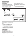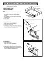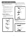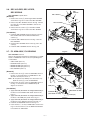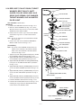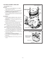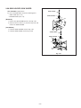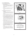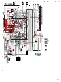
1
2002 MITSUBISHI VIDEO CASSETTE RECORDER MODEL HS-HD1100U Only cassettes marked D-VHS or VHS can be used with this video cassette recorder. SPECIFICATIONS Tape Format Power Source Power Consumption Video Signal System Video Recording System Luminance Color Signal Hi-Fi Audio Recording System Linear Audio Track Maximum Recording Time D-VHS VHS : VHS NTSC standard with Hi-Fi audio and D-VHS standard : 120 V AC ; 60 Hz : Approx. 25 W (standby 6.0 W) : EIA standard ; NTSC color : VHS standard/D-VHS standard : Frequency modulation recording : Low frequency conversion sub-carrier phase shift recording : VHS standard Azimuth helical scanning system : 1 track : 150 min. with DF-300 video cassette (HS) 300 min. with DF-300 video cassette (STD) : 120 min. with T-120 video cassette (SP) 360 min. with T-120 video cassette (EP) Record/Playback System Video : 4 heads Audio : 2 Hi-Fi channels and 1 monoral audio control Digital : HS 4 heads STD 2 heads : Approx. 43 seconds for T-120 cassette Rewind Time : 0.5 to 2.0 V(p-p), 75 Ω unbalanced RCA pin Jack : 346 mV(rms), 47 kΩ Audio Input unbalanced RCA pin Jack : 1.0 V(p-p), 75 Ω unbalanced Video Output RCA pin Jack : 346 mV(rms), 1 kΩ unbalanced Audio Output RCA pin Jack : based on IEEE 1394 digital Digital Interface interface, 4 pin, corresponds to S400 Input/Output : 54 to 88 MHz, 174 to 216 MHz Tuner VHF : 470 to 806 MHz UHF CATV : 54 to 88 MHz, 90 to 804 MHz Operating Temperature : 41 °F to 104 °F : 30 % to 80 % Relative Humidity : Channel 3 or 4 switchable RF Channel Output : Approx. 9.5 lbs (4.3 kg) Weight : 16.7”(W) × 3.7”(H) × 12.0”(D) Dimensions Timer Program Capacity : 1 month programmable / 16 programs : Approx. 30 minutes Memory Backup Time : α Deck Deck Video Input • Weight and dimensions shown are approximate. • Design and specifications are subject to change without notice. MITSUBISHI DIGITAL ELECTRONICS AMERICA, INC. 9351 Jeronimo Ave. Irvine, California 92618 U.S.A. Copyright C 2002 Mitsubishi Digital Electronics America, Inc. All Rights Reserved. CONTENTS SPECIFICATIONS ...........................................................1 CONTENTS......................................................................2 GLOSSARY OF ABBREVIATIONS ................................4 2-15. SAFETY PRECAUTIONS ................................................1 CONNECTION .................................................................3 WARNING........................................................................3 DISASSEMBLY ...............................................................4 HOW TO EXECUTE CIRCUIT BOARD SERVICE ..........7 CHIP PARTS REPLACEMENT .....................................11 2-16 2-17 2-18 2-19 2-20 2-21 HOW TO INITIALIZE THE E2PROM ................................1 WHEN REPLACING IC5A0 .............................................1 ELECTRICAL ADJUSTMENTS.......................................1 Servo circuit Adjustment...............................................3 D-VHS signal circuit Adjustment ..................................4 2-22 2-23 BRAKE BELT (SP), BELT HOLDER ...........17 2-24 BELT LEVER, BELT ADJUSTER................18 2-25 TENSION ARM, TENSION LEVER, TENSION SPRING, TENS AXIS HOLDER, REEL DISK (SP side) ..................................18 2-26 BRAKE BELT (TU) ......................................19 2-27 BRAKE (TU), REEL DISK (TU side)............19 2-28 SHIFT LEVER .............................................20 2-29 CHARGE SPRING, SWING LEVER, CHARGE ASSY...........................................21 2-30 LOADING ARM ASSY (SP), LOADING ARM ASSY (TU).........................21 2-31 A/L LEVER ..................................................22 2-32 TAPE GUIDE ASSY (SP), TAPE GUIDE ASSY (TU) ............................24 2-33 DRUM CLAMPER, DRUM ASSY ................25 2-34 DRUM MOTOR STATOR, BRUSH SPRING, SPACER, ROTOR CASE, END RING, BRUSH, UPPER DRUM ASSY ...................26 2-35 CAPSTAN MOTOR .....................................27 2-36 SSW HOLDER, SSW SLIDER.....................29 MECHANICAL ADJUSTMENT AND REPLACEMENT ..............................1 1. DECK Cleaning...................................................1 1-1 VIDEO HEAD .................................................1 1-2 Tape Running System....................................1 1-3 REEL DISK Drive System ..............................1 2. PULLEY GEAR ASSY, SLIP GEAR, SLIP SPRING, THRUST WASHER, SLIP WASHER, SLIP ADJUSTER, IDLER 2 UNIT................................................9 CAPSTAN BRAKE SPRING, CAPSTAN BRAKE ASSY............................11 FC HOLDER, MOTOR HOLDER, LOADING WORM, LOADING MOTOR ASSY, WORM WHEEL ...........................................12 PINCH ARM CAP, PINCH UNIT .................13 F/L PLATE, DOOR ARM .............................13 BRAKE CAM PLATE ...................................14 GUIDE LAMP ..............................................15 MAIN CAM, GUIDE ARM (TU), BRAKE LEVER............................................16 L/D LOCK LEVER .......................................17 Replacement of Major Parts ..............................2 2-1 CLEANING ARM, FELT RING ......................2 2-2 STAY PLATE.................................................2 2-3 BOTTOM ASSY.............................................3 2-4 INSERT GUIDE (TU).....................................4 2-5 INSERT GUIDE (SP).....................................4 2-6 REC HOLDER, REC LEVER, REC SPRING ................................................5 2-7 F/L ARM ASSY, F/L BEARING .....................5 2-8 A/C HEAD UNIT ............................................6 2-9 F/E HEAD UNIT.............................................6 2-10 SENSOR COVER (TU) .................................7 2-11 SENSOR COVER (SP) .................................7 2-12 REV UNIT (TU), REV UNIT (SP)..............................................8 2-13 MODE POSITION UNIT ................................8 2-14 REEL BELT, PULLEY BUSH, THRUST WASHER, BELT PULLEY, SHIFT SLIDER, 3. -2- Interchangeability Adjustment of the Mechanism.............................................30 3-1 Adjustment of BACK TENSION and TENSION POLE's Position ..........................30 CONTENTS 3-2 Check and Adjustment of FM Envelope ................................................31 3-2-1 GUIDE ROLLER Adjustment Check ............31 3-2-2 Height Adjustment of GUIDE ROLLER (SP) ..................................31 3-2-3 Height Adjustment of GUIDE ROLLER (TU) ..................................31 3-2-4 Coarse Adjustment of Phase .......................32 3-2-5 Flatness Check of FM Waveform.................32 3-2-6 Tape Running Condition at the GUIDE ROLLERs (Check1) ...............33 3-2-7 Tape Running Condition at the GUIDE ROLLERs (Check 2) ..............33 3-3 A/C HEAD Adjustment .................................34 3-3-1 Slant Adjustment of A/C HEAD ....................34 3-3-2 Azimuth and Height Adjustment of A/C HEAD ....................................................34 3-4 Phase Adjustment ........................................35 3-5 Tape wrinkle check ......................................35 4. Servicing for Tape Jam during the Loading Process..................................36 SERVICE CAN BE EXECUTED WITH THE EE PICTURE DISPLAYED........................37 DECK OPERATION CHECK .........................................37 PARTS LIST ....................................................................1 1. CABINET ASSEMBLY........................................1 2. PACKING PARTS...............................................3 3. ELECTRICAL PARTS.........................................5 DECK ASSEMBLY-1........................................................1 DECK ASSEMBLY-1 P/L ................................................2 DECK ASSEMBLY-2........................................................4 DECK ASSEMBLY-2 P/L ................................................5 BLOCK DIAGRAMS SCHEMATIC DIAGRAMS PRINTED CIRCUIT BOARD PARTS LAYOUT -3- GLOSSARY OF ABBREVIATIONS A/C A-PB A-REC AE AENV AFC AFF AFTV ALC AMODE AMPC APC ATFN ATT : Audio/Control : Audio Play Back : Audio Recording : Audio Erase : Audio Envelope : Automatic Frequency Control : Audio Flip Flop : Auto Fine Tuning Voltage : Automatic Level Control : Audio Mode : Amplifier Alternating Current Ground : Automatic Phase Control : Auto Fine : Attenuator BLMUTE : Blue Back Mute C/N CCD CG-CS CHSW CLKSEL CNTR COM CONV SW CP-FG CP-REV CPMOTORV CROT CSYNC CTL : Carrier/Noise Ratio : Charge Coupled Device : Character Generator-Chip Slect : Channel Switch : Clock Select : Counter : Comparator : Converter Switch : Capstan-Frequency Generator : Capstan-Reverse : Capstan Motor Voltage : Chroma Rotation : Composite Synchronizing Signal : Control D.E. D-FF DEMOD DET DLY DOC DOCSTOP DR-FG DR-OUT DR-PG : Detail Enhancer : Drum Flip Flop : Demodulator : Detector : Delay : Drop Out Compensator : Drop Out Control Stop : Drum-Frequency Generator : Drum Control Out : Drum-Phase Generator EE EMPH EP EQ ES : Electronic-Electronic : Emphasis : Extended Play : Equalizer : End Sensor FBC FE FF FG FLDCS FM FSC : Feed Back Clamp : Full Erase : Fast Forward : Frequency Generator : Fluorescent Tube Driver Chip Slect : Frequency Modulation : Frequency of Color Subcarrier G : Ground HASW HFR400 HFRSS HSYNC : Head Amplifier Switch : Hi-Fast Forward/Rewind 400 : Hi-Fast Forward/Reverse Speed Search : Horizontal Synchronizing Signal I-LIMIT : I(Current)-Limitter JSTCLK : Just Clock LIN-IN LIN-OUT LMUTE LP : Linear Audio In : Linear Audio Out : Linear Mute : Long Play MOD MOTORV : Modulator : Motor Voltage NL : Non Linear OSC : Oscillator PB PC PCB PG PLL PRT PSAVE PSLED PSYNC PWSV PWV : Play Back : Position Control : Printed Circuit Board : Pulse Generator : Phase Locked Loop : Protect : Power Save : Power Save Light Emitting Diode : Pretened Vartical Synchronizing Signal : Power Save : ON/OFF Command to supply B + Power QH QV : Cue Horizontal Signal : Cue Vertical Signal REC REC2 RECPBC RES RESPCM REW RIS RMSDET RXD : Recording : Record Command for the PB/REC Control Circuit : Record/Play Back Chroma Signal : Reset : Reset Pulse Code Modulation : Rewind : Record Inhibit Switch : Root Mean Square Detector : Read X Data SAPIND SCLK SCR SI SLD SP SS SSVSYNC STRB SU-SENS : SAP carrier detect Indicator : Serial Clock : Scramble : Serial control data Input : Side Lock Detector : Standard Play : Start Sensor : Speed Search Vertical Synchronizing Signal : Strobe : Supply Reel Sensor TSREC TSSW TU-SENS : Tape Simulate Recording : Tape Simulator Switch : Take Up Reel Sensor V-REF VBUSY VCA VCO VENV VSETCLK VSETCS : Voltage Referrence : VSET Busy : Voltage Control Amplifier : Voltage Controlled Oscillator : Video Envelope : VSET Clock : VSET Chip Select YNR : Y(Luminance) Signal Noise Reduction -4- SAFETY PRECAUTIONS INTRODUCTION SAFETY NOTICE This manual provides service information for the adjustments of mechanical and electrical operations. Due to design modifications, the servicing procedures and data given in this manual are subject to possible change without prior notice. Before returning VCR to the customer a safety check of the entire VCR should be made. The service technician must be sure that no protective device built into the instrument by the manufacturer has become defective or inadvertently damaged during servicing. Observe all caution and safety related notes located on or inside the VCR cabinet. WARNING : Alterations of the design or circuitry of this VCR should not be made. Any design alterations or additions, such as circuit modifications, auxiliary speaker jacks, switches, grounding, active or passive circuitry, etc., or use of unauthorized camera, cables, accessories, etc. may alter the safety characteristics of this VCR and potentially create a hazardous situation for the user. Any design alterations or unauthorized additions will invalidate the manufacturer’s warranty and will further relieve the manufacturer of responsibility for personal injury or property damage resulting from them. Do not lubricate any motors. When reassembling the VCR, always be certain that all the protective devices are put back in place, such as non-metallic control knobs, shield plates, etc. When service is required, observe the original lead dress. Components that show evidence of overheating or other electrical or mechanical damage should be replaced. WARNING : Many of the programs broadcast by television stations are protected by copyright and Federal law imposes strict penalties for copyright infringement. Some motion picture companies have taken the position that home recording for noncommercial purposes is an infringement of their copyrights. Until the courts have ruled on the proper interpretation of the law as applied to home video recording, this equipment, if used to record copyrighted material, should be operated at the user’s own risk. WARNING : TO PREVENT FIRE OR SHOCK HAZARD, DO NOT EXPOSE THIS APPLIANCE TO RAIN OR MOISTURE. This video cassette recorder should be used with AC 120V, 60Hz only. WARNING : Replace with same type 1.6A, 125V FUSE. LEAKAGE CURRENT CHECK Before returning the VCR to the customer, it is recommended the leakage current be measured by the following methods. 1. Cold Check With the AC plug removed from the 120V AC source, place a jumper across the two AC plug prongs. Turn the AC switch on. Using an ohmmeter, connect one lead to the jumpered AC plug and touch the other lead to each exposed metal part (metal cabinet, screwheads, metal overlays, control shafts, etc.), particularly any exposed metal part having a return path to the chassis. Exposed metal parts having a return path to the chassis should have a minimum resistance reading of 1 MΩ. Any resistance below this value indicates an abnormality which requires corrective action. Exposed metal parts not having a return path to the chassis will indicate an open circuit. -1- 2. Hot Check The test sequence, with reference to the measuring circuit in the figure is as follows: (1) With switch S1 open, connect the VCR to the measuring circuit. Immediately after connection, measure the leakage current using both positions of switch S2 and with the switching devices in the VCR in all of their operating positions. (2) Close switch S1, energizing the VCR, and immediately after closing the switch, measure leakage current using both positions of switch S2, and with the switching devices in the VCR in all of their operating positions. Repeat the current measurements of items (1) and (2) after the VCR has reached thermal stabilization. The leakage current should not be more than 0.5 mA. VCR S2 AC MILLIAMMETER A 120V S1 GH (GROUNDING) OPEN GROUNDING SUPPLY CONDUCTOR INSULATING TABLE B AC Leakage Test Avoid shock hazards. Do not connect this VCR to a TV antenna, cable or accessory that exhibits excessive leakage currents. If available, the television instrument or cable to which this VCR is connected should have the antenna cold check and leakage current hot check performed. PRECAUTIONS Handling and storage • Avoid using the VCR in the following places: - extremely hot, cold or humid places, - dusty places, - near appliances generating strong magnetic fields, - places subject to vibration, - poorly ventilated areas. • Be careful of moisture condensation. • If you pour a cold liquid into a glass, water vapor in the air will condense on the surface of the glass. This is called moisture condensation. • Moisture condensation on the head drum, one of the most critical parts of the VCR, will cause damage to the tape. • The VCR is equipped with a moisture condensation prevention circuit. This circuit operates only when the unit is attached to an AC outlet. • Handle the VCR carefully. • Do not block the ventilation openings. • Do not place anything heavy on the recorder. • Do not place liquids on the top cover of the recorder. • Use the Recorder in horizontal (flat) position only. -2- • Avoid violent shocks to the recorder during packing and transportation. • Before packing, be sure to remove the cassette from the recorder. CONNECTION Now that you’ve completed the antenna connections to your VCR, you’re ready to connect the VCR to the TV. Because every television is different (especially older model TVs), your VCR may need to be connected in a variety of ways. See the Owner’s Manual for Instruction Information ON: • Determining if you need a splitter, • Connecting TVs with audio and video inputs. Connecting separate antennas (UHF/VHF) Connecting the Television To connect separate UHF/VHF antennas to the VCR: 1. Disconnect the antennas from the back of your TV. 2. Connect the antenna leads to the combiner. 3. Screw or push the combiner onto the ANTENNA terminal on the VCR labeled ANTENNA IN. 4. When you are finished, refer to “Connecting the Television” to complete your connections. Antenna UHF Antenna VHF 300 Ohm Flat Twin Lead 300 Ohm Flat Twin Lead 75 Ohm Coaxial Cable ANTENNA 3 2 x x UHF VHF TV ANTENNA TERMINAL IN IN 1 ANTENNA OUT x OUT 300 Ohm Transformer 2 ANTENNA OUT x ANTENNA IN Combiner ANTENNA IN VCR ANTENNA TERMINAL TV without ANTENNA IN terminal (single antenna terminal for VHF and UHF) -3- ▲ ▲ WARNING Use the specified batteries. Batteries of wrong type can lead to explosion. Be sure to replace with batteries of the same type or equivalent batteries. Use the parts specified in the circuit diagram or parts list. Confirm that the batteries are placed with their positive (+) and negative (-) in the correct position. ▲ Connecting a regular TV to the VCR Before connecting the VCR to the TV, complete the cable or antenna connections to the VCR. (If you have not already done so.) To connect a regular TV to the VCR: 1. Take the black cable that is supplied with your VCR (called a coaxial cable) and connect it to the ANTENNA terminal on the VCR labeled ANTENNA OUT. 2. Connect the other end of this cable to the terminal on your TV labeled ANTENNA IN. (This terminal may also be labeled VHF IN.) If you have an older TV without this kind of terminal, you will have to use a splitter and then connect the splitter to the television. ▲ Connect to VHF IN on TV. ▲ ▲ ▲ UHF/VHF Splitter ▲ ▲ From ANTENNA OUT on VCR Connect to UHF IN on TV. ▲ ▲ ▲ UHF/VHF Splitter From ANTENNA OUT on VCR Connect to UHF IN on TV. Connect to VHF IN on TV. DISASSEMBLY 1. Removal of Top Cover 1. Remove the two Top Cover fastening screws (a) shown in Fig. 1 and remove the Top Cover in the direction shown by arrow. a 2. Removal of Front Panel 1. Remove the Top Cover. (Refer to Para. 1 of the DISASSEMBLY.) 2. Remove the Jog Dial and the Shuttle Ring. 3. Unfasten the seven catches (b) shown in Fig. 1 and remove the Front Panel in the direction shown by arrows. 4. Disconnect the Connector OG inFig.1. a Top Cover b b Connector OG b Front Panel b Shuttle Ring Jog Dial Fig. 1 -4- 3. Removal of Bottom Panel 1. Remove the Top Cover. (Refer to Para. 1 of the DISASSEMBLY.) 2. Remove the two fastening screws (a) shown in Fig. 2. 3. Turn the set upside down as shown in Fig. 3. 4. Slide and lift the Bottom Panel in the direction of the arrows paying attention to the four catches (b) to remove it. a Fig. 2 b Bottom Panel Fig. 3 -5- 4. Removal of DECK ASSY a 1. Remove the Top Cover. (Refer to Para. 1 of the DISASSEMBLY.) 2. Remove the Front Panel. (Refer to Para. 2 of the DISASSEMBLY.) 3. Short-circuit the cathode side of D927 and the GND of the DECK ASSY using the jig shown below. Note: The CAPSTAN MOTOR may be damaged without above short circuit. 4. Remove the one screw (a) and remove PCB HA Holder. 5. Disconnect the Connectors HH and HK on PCB-HEAD AMP. 6. Remove the two screws (b) shown in Fig. 4 and raise the PCB-HEAD AMP to remove it. 7. Remove the four screws (c) shown in Fig. 5. 8. Disconnect the Connectors MA, MD and ML on PCBMAIN. 9. Release the two catches (d) shown in Fig.5 and raise the DECK ASSY to remove it. PCB HA Holder b HK HH PCB-HEAD AMP Note1:Remove the DECK ASSY paying attention to the Connectors MC and MF under it. Note2:Short-circuit the cathode side of D927 and the Shield Plate using the jig shown below before attaching the DECK ASSY. Fig. 4 c Jig (Part No. : 859C548O10) 3W 330Ω DECK ASSY d Connector MF Connector MC c Fig. 5 -6- HOW TO EXECUTE CIRCUIT BOARD SERVICE CAUTION: BEFORE ATTEMPTING TO REMOVE OR REPAIR ANY PCB, UNPLUG THE POWER CORD FROM THE A.C. SOURCE. PCB-1394/D-VHS PCB-HEAD AMP LOCATION OF PRINT CIRCUIT BOARDS PCB-MAIN Note : • Take caution when removing flat cables to prevent any contact problem. • Connect and disconnect the flat cables at right angles to the connector and make sure that it is completely secured. • After servicing the PCB, restore the flat cable and leads to their former state. PCB-OPE L PCB-OPE R PCB-JOG Fig. 6 1. PCB-OPE L Connector OS 1. Remove the Top Cover. (Refer to Para. 1 of the DISASSEMBLY.) 2. Remove the Front Panel. (Refer to Para. 2 of the DISASSEMBLY.) 3. Remove the Connector OS. 4. Unfasten the two catchs (a) shown in Fig. 7 and rotate the PCB-OPE L in the direction shown by arrow (b) and remove it in the direction shown by arrow (c). PCB-OPE L a c b Fig. 7 2. PCB-OPE R Connector OJ 1. Remove the Top Cover. (Refer to Para. 1 of the DISASSEMBLY.) 2. Remove the Front Panel. (Refer to Para. 2 of the DISASSEMBLY.) 3. Remove the Connector OJ. 4. Unfasten the two catchs (a) shown in Fig. 8 and rotate the PCB-OPE R in the direction shown by arrow (b) and remove it in the direction shown by arrow (c). PCB-OPE R a c b Fig. 8 -7- 3. PCB-JOG 1. Remove the Top Cover. (Refer to Para. 1 of the DISASSEMBLY.) 2. Remove the Front Panel. (Refer to Para. 2 of the DISASSEMBLY.) 3. Unfasten the three screws (a) shown in Fig. 9 and remove the PCB-JOG. Front Panel PCB-JOG a Fig. 9 -8- 4. PCB-1394/D-VHS 1. Remove the Top Cover. (Refer to Para. 1 of the DISASSEMBLY.) 2. Lift and remove the Cover D VHS as shown in Fig.10. 3. Remove the one screw (a) and remove the PCB HOLDER shown in fig. 10. 4. Disconnect the connectors EE ,EK and EX on the PCB1394/D-VHS . 5. Pull out the Part A,lift and remove the Spring Earth EMC as shown in Fig. 10. 6. Unfasten the one screws (b) shown in Fig. 10 and remove the ASSY PCB-1394/D-VHS. 7. Separate the bottom of the Shield Cover from the ASSY PCB-1394/D-VHS first. Remove the Shield Cover moving the bottom in the direction shown by the arrow (A) as shown in Fig. 10. 8. Disconnect thirteen soldering connections and remove the PCB-1394/D-VHS as shown in Fig. 11. Cover D VHS Part A PCB HOLDER a Spring Earth EMC b ASSY PCB-1394/D-VHS Shield Cover A Fig. 10 Soldered part PCB-1394/D-VHS Soldered part Soldered part Soldered part Soldered part Fig. 11 -9- 5. PCB-MAIN 1. Carry out steps 1 and 2 of “3.Removal of Bottom Panel” of “DISASSEMBLY” 2. Remove the Front Panel. (Refer to Para. 2 of the DISASSEMBLY.) 3. Remove the DECK ASSY. (Refer to Para. 4 of the DISASSEMBLY.) 4. Lift and remove the Cover D VHS as shown in Fig.10. 5. Disconnect the connectors EE and EX on the PCB1394/D-VHS . 6. Pull out the Part A,lift and remove the Spring Earth EMC as shown in Fig. 10. (Refer to Para. 4 of the HOW TO EXECUT CIRCUIT BOARD SERVICE.) 7. Remove the two screws (a) shown in Fig. 12. 8. Remove the Holder for the AC Power Cord from the Base Chassis shown in Fig. 13. 9. Disconnect the connectors ME,MJ and MS on the PCBMAIN . 10. Release the two fastening catches (b) shown in Fig. 12. Raise the PCB-MAIN to remove it. 11. Release the three fastening catches (c) and remove the Antenna Cover shown in Fig. 14. a PCB-MAIN b b Fig. 12 Holder for the AC Power Cord Base chassis Fig. 13 c c PCB-MAIN Fig. 14 - 10 - Antenna Cover CHIP PARTS REPLACEMENT CHIP PARTS REPLACEMENT 2. Removal of Chip Parts (Transistors) Some resistors, shorting jumpers (0Ω resistor), ceramic capacitors, transistors and diodes are chip parts. When replacing these parts, note the following cautions. A. Melt the solder of one lead. Lift the side of that lead upward. B. Simultaneously melt the solder of the two remaining leads and lift the part from the PCB. Cautions : A. Use fine tipped, well insulated soldering pencil (iron), about 30 watts, and tweezers. B. Melt the solder and remove the Chip Parts carefully not to tear off the copper foil of the printed circuit board. C. Discard removed chips ; do not reuse them. D. Do not apply heat for more than 3 seconds to new Chip Parts. E. Avoid using a rubbing stroke when soldering. F. Take care not to scratch, or damage the Chip Parts when soldering. G. Supplementary cementing is not required. Chip Lead Pattern Soldering Pencil Tweezers Chip Pattern PCB 1. Removal of Chip Parts (Resistors, capacitors, etc.) A. Grasp the part with tweezers. Melt the solder at both sides alternately, remove one side of the part with a twisting motion. B. Melt the solder at the other side and remove the part. Soldering Pencil Fig. 2 Chip Solder 3. Replacement A. Presolder the contact points of the circuit pattern. B. Press the part downward with tweezers and apply the soldering pencil as shown in Fig. 3. Pattern Tweezers Solder Soldering Pencil Pattern PCB Tweezers Soldering Pencil Chip Fig. 1 Fig. 3 - 11 - MECHANICAL ADJUSTMENT AND REPLACEMENT 1-2. Tape Running System 1. DECK Cleaning Clean the following Parts of the Tape Running System. 1. TENSION PIN 2. F/E HEAD 3. SLANT POLE (SP) 4. SLANT POLE (TU) 5. A/C HEAD 6. GUIDE POLE (TU) 7. PINCH ROLLER 8. GUIDE PIN (TU) 9. GUIDE ROLLER (SP) 10. UPPER / LOWER DRUM ASSY 11. GUIDE ROLLER (TU) 12. CAPSTAN SHAFT 1. Clean the Tape Running System, using a piece of gauze dampened with alcohol, except for the GUIDE ROLLER (SP), GUIDE ROLLER (TU), and PINCH ROLLER which require to be cleaned with a piece of dry gauze. 2. Allow the residual alcohol to dry thoroughly before running the tape. The residual alcohol on the SYSTEM may damage the tape if not dried completely. The following Parts require cleaning whenever serviced in order to maintain satisfactory performance. 1-1. VIDEO HEAD 1. Clean the VIDEO HEAD according to the following method. Dust and other foreign objects on the VIDEO HEAD disturb the normal PLAYBACK picture. To clean the VIDEO HEAD, hold a VIDEO HEAD cleaning cloth dampened with alcohol against the DRUM and slowly turn the DRUM counter-clockwise. Note : Do not directly touch the HEADS installed to the UPPER DRUM ASSY. The HEADS are very hard but brittle to shock (especially to shock in the vertical direction) and easily breakable. Never apply force to it in the vertical direction. 2. Allow the residual alcohol to dry thoroughly before running a tape. The residual alcohol on the HEADs may damage the tape if not dried completely. UPPER DRUM ASSY cleaning Lightly apply the cloth on the UPPER DRUM ASSY. Do not move the cloth. Video Head Cleaning Cloth 1-3. REEL DISK Drive System 1. Clean the BRAKE side and REEL BELT of the REEL DISK Drive System. 2. Clean the REEL DISK Drive System, using a piece of gauze dampened with alcohol, except for the REEL BELT which requires cleaning with a piece of dry gauze. 3. Allow the residual alcohol to dry thoroughly before operation. Fig. 1-1 r t e w y q o !0 !1 !2 Fig. 1-2 -1- u i 2. Replacement of Major Parts 2-1. CLEANING ARM, FELT RING b FELT RING SET POSITION : Normal b (Removal) a 1. Release the two catches (a) of the CLEANING ARM shown in the Fig. 2-1 to remove the CLEANING ARM. 2. Release the two catches (b) of the CLEANING ARM shown in the Fig. 2-1 to remove the FELT RING. CLEANING ARM a (Installation) 1. Install the FELT RING shown in the Fig. 2-1 to the CLEANING ARM. 2. Install the CLEANING ARM shown in the Fig. 2-1. Fig. 2-1 2-2. STAY PLATE a SET POSITION : Normal (Removal) STAY PLATE 1. Remove the two screws (a) fastening the STAY PLATE shown in the Fig. 2-2 to remove the STAY PLATE. a (Installation) 1. Install the STAY PLATE shown in the Fig. 2-2. Fig. 2-2 -2- 2-3. BOTTOM ASSY Hole in MAIN PLATE ASSY SET POSITION : Normal Remove the following part before replacing the BOTTOM ASSY. Refer to the corresponding item to install it. • STAY PLATE (Item 2-2) (Removal) 1. Move the WORM WHEEL in the Fig. 2-3-1 in the direction shown by the arrow A. And match the Boss a of the BOTTOM ASSY with the Hole in the MAIN PLATE ASSY. 2. Lift the BOTTOM ASSY in the Fig. 2-3-1 in the direction shown by the arrow B and pull it out in the direction shown by the arrow C. a Lift B C BOTTOM ASSY Pull out WORM WHEEL A (Installation) 1. Apply GREASE (MULTEMP AC-DM)[859D055O90] to the Grooves of the MAIN PLATE ASSY shown in the Fig. 2-3-2. 2. Apply GREASE (MULTEMP AC-DM)[859D055O90] to the Bosses of the BOTTOM ASSY shown in the Fig. 2-3-2. 3. Rotate the WORM WHEEL shown in the Fig. 2-3-1 so that the ARM (SP) stands vertically. 4. Insert the Boss b of the BOTTOM ASSY shown in the Fig. 2-3-2 in the Upper Groove of the MAIN PLATE and the Boss c in the Lower Groove. 5. Insert the Boss d of the BOTTOM ASSY to the Upper Groove through the Hole in the MAIN PLATE ASSY shown in the Fig. 2-3-1 and the Boss e to the Lower Groove through the slot in the ARM (SP). ARM (SP) Fig. 2-3-1 MAIN PLATE ASSY Groove of MAIN PLATE ASSY Groove of MAIN PLATE ASSY Side View Side View d e b c GREASE (MULTEMP AC-DM) ARM (SP) GREASE (MULTEMP AC-DM) BOTTOM ASSY Fig. 2-3-2 -3- ARM (TU) 2-4. INSERT GUIDE (TU) a SET POSITION : Normal Remove the following parts before replacing the INSERT GUIDE (TU). Refer to the corresponding items to install them. • STAY PLATE (Item 2-2) • BOTTOM ASSY (Item 2-3) INSERT GUIDE (TU) (Removal) 1. Remove the screw (a) fastening the INSERT GUIDE (TU) shown in the Fig. 2-4 to remove the INSERT GUIDE (TU). (Installation) 1. Install the INSERT GUIDE (TU) shown in the Fig. 2-4. Fig. 2-4 2-5. INSERT GUIDE (SP) a SET POSITION : Normal Remove the following parts before replacing the INSERT GUIDE (SP). Refer to the corresponding items to install them. • STAY PLATE (Item 2-2) • BOTTOM ASSY (Item 2-3) INSERT GUIDE (SP) (Removal) 1. Remove the screw (a) fastening the INSERT GUIDE (SP) shown in the Fig. 2-5 to remove the INSERT GUIDE (SP). (Installation) 1. Install the INSERT GUIDE (SP) shown in the Fig. 2-5. Fig. 2-5 -4- 2-6. REC HOLDER, REC LEVER, REC SPRING REC SPRING c REC LEVER SET POSITION : Upside down (Removal) 1. Remove the screw (a) fastening the REC HOLDER shown in the Fig. 2-6 to remove the REC HOLDER. 2. Release the REC SPRING shown in the Fig. 2-6 from the catch (b) of the REC HOLDER to remove the REC LEVER. 3. Release the two catches (c) of the REC LEVER shown in the Fig. 2-6 to remove the REC SPRING. a b REC HOLDER (Installation) 1. Install the REC SPRING shown in the Fig. 2-6 to the REC LEVER and hook the REC SPRING to the catches (c). 2. Install the REC LEVER shown in the Fig. 2-6 to the REC HOLDER. 3. Hook the REC SPRING shown in the Fig. 2-6 to the catch (b). 4. Install the REC HOLDER shown in the Fig. 2-6. 2-7. F/L ARM ASSY, F/L BEARING SET POSITION : Normal Remove the following parts before replacing the F/L ARM ASSY, F/L BEARING. Refer to the corresponding items to install them. • STAY PLATE (Item 2-2) • BOTTOM ASSY (Item 2-3) • INSERT GUIDE (TU) (Item 2-4) • INSERT GUIDE (SP) (Item 2-5) • REC HOLDER (Item 2-5) Fig. 2-6 MAIN PLATE ASSY A (Removal) 1. Release the catch (a) of the F/L BEARING shown in the Fig. 2-7 and pull out the F/L ARM ASSY in the direction shown by the arrow A. Note : Do not pull the F/L ARM by force because it may break the catch (a) of the F/L BEARING. 2. Release the catch (b) of the F/L BEARING shown in the Fig. 2-7 and rotate the F/L BEARING by 90 degrees to remove it. F/L ARM ASSY b a F/L BEARING ARM (SP) c d GREASE (MULTEMP AC-DM) (Installation) 1. Apply GREASE (MULTEMP AC-DM)[859D055O90] to the Groove of the MAIN PLATE ASSY shown in the Fig. 2-7. 2. Apply GREASE (MULTEMP AC-DM)[859D055O90] to the Boss of the ARM (SP) shown in the Fig. 2-7. 3. Apply GREASE (MULTEMP AC-DM)[859D055O90] to the Bosses of the ARM (TU) shown in the Fig. 2-7. 4. Install the F/L BEARING shown in the Fig. 2-7. 5. Insert the Boss c of the F/L ARM ASSY shown in the Fig. 2-7 into the Groove d of the MAIN PLATE ASSY to install the F/L ARM ASSY. GREASE (MULTEMP AC-DM) ARM (TU) Fig. 2-7 -5- 2-8. A/C HEAD UNIT LEAD CONNECTOR SET POSITION : Normal (Removal) a 1. Remove the LEAD CONNECTOR of the A/C HEAD UNIT shown in the Fig. 2-8. 2. Remove the two screws (a) fastening the A/C HEAD UNIT shown in the Fig. 2-8 to remove the A/C HEAD UNIT. a A/C HEAD UNIT Head (Installation) 1. Install the A/C HEAD UNIT shown in the Fig. 2-8. Note : Never touch the Head of the A/C HEAD UNIT shown in the Fig. 2-8. Clean the dirt on the Head with alcohol if necessary. 2. Install the LEAD CONNECTOR of the A/C HEAD UNIT shown in the Fig. 2-8. 3. Perform the Item 3-3. "A/C HEAD Adjustment" and Item 3-4. "Phase Adjustment" of the "Interchangeability Adjustment of the Mechanism". Fig. 2-8 2-9. F/E HEAD A F/E HEAD SET POSITION : Normal (Removal) Counterclockwise 1. Lift the F/E HEAD shown in the Fig. 2-9-1 in the direction by the arrow A to remove it. Note : Be sure to replace the removed F/E HEAD with a new one. (Installation) 1. Install the F/E HEAD shown in the Fig. 2-9-1. Note : Never touch the Head shown in the Fig. 2-9-2. Clean it with alcohol if necessary. Fig. 2-9-1 F/E HEAD Head Part Never touch the Head Part. Fig. 2-9-2 -6- 2-10.SENSOR COVER (TU) SET POSITION : Normal (Removal) 1. Release the catch (a) of the SENSOR COVER (TU) shown in the Fig. 2-10 to remove the SENSOR COVER (TU). (Installation) 1. Install the SENSOR COVER (TU) shown in the Fig. 210. a SENSOR COVER (TU) Fig. 2-10 2-11.SENSOR COVER (SP) SET POSITION : Normal (Removal) 1. Remove the catch (a) of the SENSOR COVER (SP) shown in the Fig. 2-11 to remove the SENSOR COVER (SP). (Installation) 1. Install the SENSOR COVER (SP) shown in the Fig. 211. a SENSOR COVER (SP) Fig. 2-11 -7- 2-12.REV UNIT (TU), REV UNIT (SP) REV UNIT (TU) a SET POSITION : Upside down a (Removal) REV UNIT (SP) 1. Release the two catches (a) of the REV UNIT (TU) shown in the Fig. 2-12 to remove the REV UNIT (TU). 2. Release the two catches (b) of the REV UNIT (SP) shown in the Fig. 2-12 to remove the REV UNIT (SP). b (Installation) 1. Clean the dirt on the transparent part of the REV UNIT (TU) with a VIDEO HEAD cleaning cloth. Note : Never use solvent such as alcohol to clean the REV UNIT (TU). 2. Install the REV UNIT (TU) shown in the Fig. 2-12. 3. Clean the dirt on the transparent part of the REV UNIT (SP) with a VIDEO HEAD cleaning cloth. Note : Never use solvent such as alcohol to clean the REV UNIT (SP). 4. Install the REV UNIT (SP) shown in the Fig. 2-12. Fig. 2-12 2-13.MODE POSITION UNIT SET POSITION: Upside down (Removal) 1. Release the two catches (a, b) of the MODE POSITION UNIT shown in the Fig. 2-13 to remove the MODE POSITION UNIT. MODE POSITION UNIT (Installation) 1. Install the catch (b) of the MODE POSITION UNIT shown in the Fig. 2-13. 2. Install the catch (a) of the MODE POSITION UNIT shown in the Fig. 2-13. a Fig. 2-13 -8- b b 2-14.REEL BELT, PULLEY BUSH, THRUST WASHER, BELT PULLEY, SHIFT SLIDER, PULLEY GEAR ASSY, SLIP GEAR, SLIP SPRING, SLIP WASHER, THRUST WASHER, SLIP ADJUSTER, IDLER 2 UNIT REEL BELT a PULLEY BUSH THRUST WASHER BELT PULLEY SET POSITION : Upside down Pull in the direction (Removal) A of the Arrow (A) to remove it from the SHIFT LEVER. 1. Remove the REEL BELT shown in the Fig. 2-14-1. 2. Move the SHIFT SLIDER in the Fig. 2-14-1 in the direction shown of the arrow A to remove the SHIFT SLIDER from the SHIFT LEVER. 3. Release the two catches (a) of the PULLEY BUSH shown in the Fig. 2-14-1 to remove the PULLEY BUSH. Note : Be sure to replace the removed PULLEY BUSH with a new one. 4. Remove the units from the THRUST WASHER to IDLER 2 UNIT shown in the Fig. 2-14-1. SHIFT SLIDER PULLEY GEAR ASSY SLIP GEAR GREASE (PG-641) SLIP SPRING SLIP WASHER THRUST WASHER SLIP ADJUSTER (Installation) Note : Be careful so that GREASE and OIL does not adhere on the Felt Side of the PULLEY GEAR ASSY or the Grooved Side of the SLIP GEAR shown in the Fig. 2-14-4. 1. Apply OIL (FLOIL 948P) [859D154O20] to the SHAFT for the IDLER 2 UNIT shown in the Fig. 2-14-1. 2. Apply GREASE (PG-641) [859D055O30] to the parts on the IDLER 2 UNIT specified in the Fig. 2-14-1. 3. Apply GREASE (MULTEMP AC-DM) [859D055O90] to the parts on the MAIN PLATE ASSY specified in the Fig. 2-14-1. 4. Apply GREASE (PG-641) [859D055O30] to the parts on the new SHIFT SLIDER specified in the Fig. 2-142. 5. Apply GREASE (PG-641) [859D055O30] to the parts on the new SLIP ADJUSTER specified in the Fig. 214-2. 6. Apply GREASE (PG-641) [859D055O30] to the parts on the new BELT PULLEY specified in the Fig. 2-14-3. 7. Install the IDLER 2 UNIT shown in the Fig. 2-14-1. 8. Install the SLIP ADJUSTER shown in the Fig. 2-14-3, matching the Lug of the SLIP ADJUSTER with the Center Notch of the IDLER 2 UNIT. GREASE (PG-641) IDLER 2 UNIT OIL (FLOIL 948P) GREASE (MULTEMP AC-DM) SHIFT LEVER Fig. 2-14-1 SLIP ADJUSTER SHIFT SLIDER Apply GREASE (PG-641) to the parts Fig. 2-14-2 -9- . 9. Install the units from the SLIP WASHER to REEL BELT shown in the Fig. 2-14-1. Note1 : Be sure to replace the removed PULLEY BUSH with a new one. Note2 : Attach the SLIP SPRING with its straight end facing the SLIP GEAR side. Note3 : Attach the SLIP WASHER with its position set as shown in the Fig. 2-14-5. Note4 : Apply GREASE (PG-641) [859D055O30] to the part on the SLIP WASHER specified in the Fig. 214-5. 10. Install the SHIFT SLIDER to the SHIFT LEVER shown in the Fig. 2-14-1. SLIP ADJUSTER Center of the BELT PULLEY IDLER UNIT Match the Lug of the SLIP ADJUSTER with the Center Notch of the IDLER UNIT. Apply GREASE (PG-641) to the parts . Fig. 2-14-3 PULLEY GEAR ASSY Felt Side SLIP GEAR Grooved Side Fig. 2-14-4 [SLIP GEAR side] Straight end SLIP SPRING SLIP WASHER [THRUST WASHER side] Apply GREASE (PG-641) to the parts Fig. 2-14-5 - 10 - . 2-15.CAPSTAN BRAKE SPRING, CAPSTAN BRAKE ASSY SET POSITION : Upside down CAPSTAN BRAKE ASSY a (Removal) 1. Remove the CAPSTAN BRAKE SPRING shown in the Fig. 2-15. 2. Remove the catch (a) of the CAPSTAN BRAKE ASSY shown in the Fig. 2-15 to remove the CAPSTAN BRAKE ASSY. CAPSTAN MOTOR CAPSTAN BRAKE SPRING (Installation) 1. Install the CAPSTAN BRAKE ASSY shown in the Fig. 2-15. 2. Install the CAPSTAN BRAKE SPRING shown in the Fig. 2-15. Fig. 2-15 - 11 - 2-16.FC HOLDER, MOTOR HOLDER, LOADING WORM, LOADING MOTOR ASSY, WORM WHEEL LOADING MOTOR ASSY b b SET POSITION : Normal a a (Removal) 1. Release the two catches (a) of the FC HOLDER shown in the Fig. 2-16-1 to remove the FC HOLDER. 2. Remove the two screws (b) fastening the MOTOR HOLDER shown in the Fig. 2-16-1 to remove the MOTOR HOLDER. 3. Remove the two screws (c) fastening the LOADING MOTOR ASSY shown in the Fig. 2-16-1 to remove the LOADING MOTOR ASSY and LOADING WORM. 4. Remove the WORM WHEEL. LOADING WORM FC HOLDER MOTOR HOLDER c LUG TERMINAL (Installation) 1. Apply GREASE (MULTEMP AC-DM)[859D055O90] to the LOADING WORM shown in the Fig. 2-16-2. 2. Apply GREASE (MULTEMP AC-DM)[859D055O90] to the WORM WHEEL shown in the Fig. 2-16-2. 3. Install the WORM WHEEL. 4. Install the LOADING WORM, LOADING MOTOR ASSY to the MOTOR HOLDER. Note : Tighten the screw (c) shown in the Fig. 2-16-1 after putting the LUG TERMINAL on the screw. 5. Install the MOTOR HOLDER. 6. Install the FC HOLDER. WORM WHEEL Fig. 2-16-1 WORM WHEEL LOADING WORM Apply GREASE (MULTEMP AC-DM) to the parts Fig. 2-16-2 - 12 - . 2-17.PINCH ARM CAP, PINCH UNIT a SET POSITION : Normal PINCH ARM CAP (Removal) 1. Release the two catches (a) of the PINCH ARM CAP shown in the Fig. 2-17 to remove the PINCH ARM CAP. 2. Remove the PINCH UNIT shown in the Fig. 2-17. Part B Part A PINCH ASSY (Installation) 1. Insert Part A of the PINCH UNIT shown in the Fig. 217 in the most external groove of the MAIN CAM. 2. Install the PINCH ARM CAP matching the Part B of the PINCH ARM CAP with the Rib of the MAIN PLATE ASSY. MAIN CAM Rib Fig. 2-17 2-18.F/L PLATE, DOOR ARM MAIN CAM SET POSITION : Normal Remove the following parts before replacing the F/L PLATE, DOOR ARM. Refer to the corresponding items to install them. • STAY PLATE (Item 2-2) • BOTTOM ASSY (Item 2-3) • SENSOR COVER (TU) (Item 2-10) • MOTOR HOLDER (Item 2-16) • PINCH ARM CAP (Item 2-17) • PINCH UNIT (Item 2-17) GREASE (MULTEMP AC-DM) F/L PLATE GREASE (MOLYKOTE G PASTE) DOOR ARM (Removal) Back 1. Slightly lift the back of the F/L PLATE (MAIN CAM side) shown in the Fig. 2-18-1 to remove the F/L PLATE. 2. Remove the DOOR ARM. GREASE (MOLYKOTE G PASTE) ARM (TU) MAIN PLATE ASSY (Installation) 1. Apply GREASE (MULTEMP AC-DM)[859D055O90] to the points on the new F/L PLATE specified in the Fig. 2-18-1. 2. Apply GREASE (MOLYKOTE G PASTE) [859D055O50] to the points on the new F/L PLATE specified in the Fig. 2-18-1. - 13 - GREASE (MULTEMP AC-DM) GREASE (MULTEMP AC-DM) Fig. 2-18-1 3. Apply GREASE (MULTEMP AC-DM)[859D055O90] to the points on the MAIN PLATE ASSY specified in the Fig. 2-18-1. 4. Apply GREASE (MULTEMP AC-DM)[859D055O90] to the points on the DOOR ARM specified in the Fig. 218-1. 5. Install the DOOR ARM. 6. Match the Hole in the MAIN CAM with the Hole in the MAIN PLATE ASSY shown in the Fig. 2-18-2. 7. Install the F/L PLATE shown in the Fig. 2-18-1 from the front side (ARM (TU) side). 8. Insert the Boss of the F/L PLATE shown in the Fig. 218-2 into the Groove of the MAIN CAM. Hole MAIN CAM F/L PLATE Boss Fig. 2-18-2 2-19.BRAKE CAM PLATE SET POSITION : Normal Remove the following parts before replacing the BRAKE CAM PLATE. Refer to the corresponding items to install them. • STAY PLATE (Item 2-2) • BOTTOM ASSY (Item 2-3) • MOTOR HOLDER (Item 2-16) • PINCH ARM CAP (Item 2-17) • PINCH UNIT (Item 2-17) BRAKE CAM PLATE a b b MAIN CAM B A (Removal) 1. Rotate the MAIN CAM in the Fig. 2-19-1 in the direction shown by the arrow A. And move the BRAKE CAM PLATE so that the three catches (a) of the MAIN PLATE ASSY can be released. 2. Remove the BRAKE CAM PLATE. b a b (Installation) a 1. Apply GREASE (MOLYKOTE G PASTE) [859D055O50] to the points on the BRAKE CAM PLATE specified in the Fig. 2-19-2. 2. Hook the BRAKE SPRING shown in the Fig. 2-19-3 to the catch of the BRAKE (TU). 3. Install the BRAKE CAM PLATE, inserting the six Guide Pins (b) shown in the Fig. 2-19-1 into the slits of the BRAKE CAM PLATE. 4. Move the BRAKE SPRING in the Fig. 2-19-3 in the direction of the arrow C to release the Catch of the BRAKE (TU) and insert the BRAKE SPRING under the Catch. 5. Rotate the MAIN CAM shown in the Fig. 2-19-1 in the direction shown of the arrow B. And move the BRAKE CAM PLATE to hook it to the three catches (a) of the MAIN PLATE ASSY. - 14 - Fig. 2-19-1 BRAKE CAM PLATE Back 70mm 40mm Back Back 99mm Back 130mm Apply GREASE (MOLYKOTE G PASTE) to the points Fig. 2-19-2 . BRAKE SPRING C Insert the BRAKE SPRING under the Catch. Catch BRAKE (TU) Fig. 2-19-3 2-20.GUIDE LAMP SET POSITION : Normal Remove the following parts before replacing the GUIDE LAMP. Refer to the corresponding items to install them. • STAY PLATE (Item 2-2) • BOTTOM ASSY (Item 2-3) • MOTOR HOLDER (Item 2-16) • PINCH ARM CAP (Item 2-17) • PINCH UNIT (Item 2-17) • BRAKE CAM PLATE (Item 2-19) (Removal) 1. Release the catch (a) of the GUIDE LAMP shown in the Fig. 2-20. 2. Rotate the GUIDE LAMP in the direction shown by the arrow A (counterclockwise, when viewed from the bottom) to match the longest slit (c) of the MAIN PLATE ASSY with the longest arm (b) of the GUIDE LAMP shown in the Fig. 2-20. Pull it out downward to remove it. c MAIN PLATE ASSY GUIDE LAMP a A (Installation) 1. Clean the dirt on the GUIDE LAMP with a VIDEO HEAD cleaning cloth. Note: Never use solvent such as alcohol to clean the GUIDE LAMP. 2. Insert the GUIDE LAMP in the Fig. 2-20, matching the longest arm (b) of the GUIDE LAMP with the longest slit (c) of the MAIN PLATE ASSY. 3. Rotate the GUIDE LAMP in the direction shown by the arrow B (clockwise, when viewed from the bottom) to match the arm (a) of the GUIDE LAMP shown in the Fig. 2-20 with the longest slit (c) of the MAIN PLATE ASSY. Note : Clean the dirt on the GUIDE LAMP with a VIDEO HEAD cleaning cloth if necessary. - 15 - b B Removing Direction Fig. 2-20 Installing Direction 2-21.MAIN CAM, GUIDE ARM (TU), BRAKE LEVER MAIN CAM SET POSITION : Normal Remove the following parts before replacing the MAIN CAM, GUIDE ARM (TU), BRAKE LEVER. Refer to the corresponding items to install them. • STAY PLATE (Item 2-2) • BOTTOM ASSY (Item 2-3) • SENSOR COVER (TU) (Item 2-10) • MOTOR HOLDER (Item 2-16) • WORM WHEEL (Item 2-16) • PINCH ARM CAP (Item 2-17) • PINCH UNIT (Item 2-17) • F/L PLATE (Item 2-18) BRAKE LEVER GREASE (MULTEMP AC-DM) A GUIDE ARM (TU) a LB PIN B (Removal) 1. Remove the MAIN CAM shown in the Fig. 2-21-1. 2. Remove the GUIDE ARM (TU) shown in the Fig. 2-211. 3. Move the BRAKE LEVER in the Fig. 2-21-1 in the direction shown by the arrow A and release the catch (a) to remove the BRAKE LEVER. Back GREASE (MULTEMP AC-DM) MAIN PLATE ASSY Fig. 2-21-1 (Installation) 1. Apply GREASE (MULTEMP AC-DM)[859D055O90] to the points on the new GUIDE ARM (TU) specified in the Fig. 2-21-1. 2. Apply GREASE (MULTEMP AC-DM)[859D055O90] to the points on the MAIN PLATE ASSY specified in the Fig. 2-21-1. 3. Install the GUIDE ARM (TU), matching the Hole in the GUIDE ARM (TU) shown in the Fig. 2-21-2 with the Hole in the MAIN PLATE ASSY. Note : Install the GUIDE ARM (TU) so that the Part specified with the Oblique Lines of the GUIDE ARM (TU) will be under the SHAFT FLANGE of the PINCH UNIT. 4. Install the BRAKE LEVER shown in the Fig. 2-21-2 so that the Hole in the BRAKE LEVER overlaps the Hole in the MAIN PLATE ASSY. 5. Apply GREASE (MULTEMP AC-DM)[859D055O90] to the points on the new MAIN CAM specified in the Fig. 2-21-3. 6. Install the MAIN CAM so that the Hole in the MAIN CAM shown in the Fig. 2-21-2 overlaps with the Hole in the MAIN PLATE ASSY. Note : Install the MAIN CAM inserting the Pins of the CAPSTAN BRAKE ASSY, GUIDE ARM (TU), BRAKE LEVER into the Grooves on the back of the MAIN CAM for sure. Set the Main Cam while pulling the Guide Pin (on the CAPSTAN BRAKE ASSY) in the direction indicated by the arrow B (toward the deck front) using tweezers as shown in Fig. 2-21-1. Be careful that GREASE does not adhere on the Wall when applying GREASE to the most external circle on the back of the MAIN CAM (4 parts) shown in the Fig. 2-21-3. - 16 - Hole MAIN PLATE ASSY MAIN CAM SHAFT FLANGE of the PINCH ASSY GUIDE ARM (TU) Part with Oblique Lines Hole BRAKE LEVER Fig. 2-21-2 MAIN CAM Front Back Wall Apply GREASE (MULTEMP AC-DM) to the parts Fig. 2-21-3 . 2-22.L/D LOCK LEVER SET POSITION : Normal Remove the following parts before replacing the L/D LOCK LEVER. Refer to the corresponding items to install them. • STAY PLATE (Item 2-2) • BOTTOM ASSY (Item 2-3) • MOTOR HOLDER (Item 2-16) • PINCH ARM CAP (Item 2-17) • PINCH UNIT (Item 2-17) • BRAKE CAM PLATE (Item 2-19) L/D LOCK LEVER (Removal) 1. Remove the L/D LOCK LEVER shown in the Fig. 222. (Installation) 1. Install the L/D LOCK LEVER shown in Fig. 2-22. 2-23.BRAKE BELT (SP), BELT HOLDER SET POSITION : Normal Remove the following parts before replacing the BRAKE BELT (SP), BELT HOLDER. Refer to the corresponding items to install them. • STAY PLATE (Item 2-2) • BOTTOM ASSY (Item 2-3) Fig. 2-22 b BELT HOLDER c (Removal) BRAKE BELT (SP) 1. Lift the BRAKE BELT (SP) shown in the Fig. 2-23 to remove it from the REEL DISK (SP side). 2. Release the BRAKE BELT (SP) from the catch (a) of the BELT LEVER shown in the Fig. 2-23. 3. Release the two catches (b) of the BELT HOLDER shown in the Fig. 2-23 and separate the BELT HOLDER from the BRAKE BELT (SP). 4. Release the catch (c) of the BELT HOLDER shown in the Fig. 2-23 to remove the BRAKE BELT (SP). BELT LEVER a (Installation) Note : Install the BRAKE BELT (SP) so that its Felt Side touches the REEL DISK (SP side). GREASE applied to the BRAKE CAM PLATE and MAIN PLATE ASSY should not adhere on the Felt Side of the BRAKE BELT (SP). 1. Install the BRAKE BELT (SP) shown in the Fig. 2-23 to the catch (c) of the BELT HOLDER. 2. Install the BELT HOLDER shown in the Fig. 2-23. 3. Install the BRAKE BELT (SP) shown in the Fig. 2-23 to the catch (a) of the BELT LEVER. 4. Hook the BRAKE BELT (SP) shown in the Fig. 2-23 to the REEL DISK (SP side). - 17 - REEL DISK (SP side) Fig. 2-23 2-24. BELT LEVER, BELT ADJUSTER a SET POSITION : Normal Remove the following parts before replacing the BELT LEVER, BELT ADJUSTER. Refer to the corresponding items to install them. • STAY PLATE (Item 2-2) • BOTTOM ASSY (Item 2-3) • MOTOR HOLDER (Item 2-16) • PINCH ARM CAP (Item 2-17) • PINCH UNIT (Item 2-17) • BRAKE CAM PLATE (Item 2-19) • BRAKE BELT (SP) (Item 2-23) • BELT HOLDER (Item 2-23) BELT LEVER BELT ADJUSTER (Removal) 1. Release the catch (a) of the BELT LEVER shown in the Fig. 2-24 to remove the BELT LEVER. 2. Remove the BELT ADJUSTER shown in the Fig. 2-24. (Installation) 1. Install the BELT ADJUSTER shown in the Fig. 2-24. 2. Install the BELT LEVER shown in the Fig. 2-24. 2-25 TENSION ARM, TENSION LEVER, TENSION SPRING, TENS AXIS HOLDER, REEL DISK (SP side) Fig. 2-24 SET POSITION : Normal Remove the following parts before performing this Item. Refer to the corresponding items to install them. • STAY PLATE (Item 2-2) • BOTTOM ASSY (Item 2-3) • MOTOR HOLDER (Item 2-16) • PINCH ARM CAP (Item 2-17) • PINCH UNIT (Item 2-17) • BRAKE CAM PLATE (Item 2-19) • BRAKE BELT (SP) (Item 2-23) • BELT HOLDER (Item 2-23) • BELT LEVER (Item 2-24) TENSION ARM REEL DISK (SP side) THRAUST WASHER TENSION SPRING TENSION LEVER a A (Removal) b 1. Remove the TENSION SPRING shown in the Fig. 225. 2. Release the catch (a) of the TENS AXIS HOLDER shown in the Fig. 2-25 to remove the TENSION ARM. 3. Remove the TENSION LEVER shown in the Fig. 2-25. 4. Release the catch (b) of the TENS AXIS HOLDER shown in the Fig. 2-25. Move the TENS AXIS HOLDER in the direction shown by the arrow A to remove it. 5. Remove the REEL DISK (SP side). TENS AXIS HOLDER GREASE (MULTEMP AC-DM) MAIN PLATE ASSY Fig. 2-25 - 18 - (Installation) 1. Apply GREASE (MULTEMP AC-DM) [859D055O90] to the parts on the MAIN PLATE ASSY specified in the Fig. 2-25. 2. Install the REEL DISK (SP side). 3. Install the TENS AXIS HOLDER. Note : Install the TENS AXIS HOLDER so that the catch (a) for the TENSION ARM will be positioned on the front (F/L ARM ASSY side). 4. Install the TENSION LEVER. 5. Install the TENSION ARM. 6. Install the TENSION SPRING. Note : Install the longer hook of the TENSION SPRING to the TENSION ARM. BRAKE BELT (TU) 2-26.BRAKE BELT (TU) SET POSITION : Normal Remove the following parts before replacing the BRAKE BELT. Refer to the corresponding items to install them. • STAY PLATE (Item 2-2) • BOTTOM ASSY (Item 2-3) BRAKE (TU) a a (Removal) 1. Lift the BRAKE BELT (TU) shown in the Fig. 2-26 to remove it from the REEL DISK (TU side). 2. Release the two catches (a) of the BRAKE (TU) shown in the Fig. 2-26 to remove the BRAKE BELT (TU). (Installation) 1. Install the BRAKE BELT (TU) shown in the Fig. 2-26 to the BRAKE (TU). 2. Hook the BRAKE BELT (TU) shown in the Fig. 2-26 to the REEL DISK (TU side). Note : Install the BRAKE BELT (TU) so that its Felt Side touches the REEL DISK (TU side). 2-27.BRAKE (TU), REEL DISK (TU side) REEL DISK (TU side) Fig. 2-26 BRAKE BELT (TU) REEL DISK (TU side) BRAKE (TU) SET POSITION : Normal Remove the following parts before replacing the BRAKE (TU), REEL DISK (TU side). Refer to the corresponding items to install them. • STAY PLATE (Item 2-2) • BOTTOM ASSY (Item 2-3) • MOTOR HOLDER (Item 2-16) • PINCH ARM CAP (Item 2-17) • PINCH UNIT (Item 2-17) • BRAKE CAM PLATE (Item 2-19) A WASHER MAIN PLATE ASSY (Removal) 1. Move the BRAKE (TU) in the Fig. 2-27 in the direction shown by the arrow A to remove it. 2. Remove the BRAKE BELT (TU) from the BRAKE (TU). 3. Remove the REEL DISK (TU). - 19 - GREASE (MULTEMP AC-DM) Fig. 2-27 (Installation) Note : Install the BRAKE BELT (TU) so that its Felt Side touches the REEL DISK (TU side). The GREASE applied to the BRAKE CAM PLATE and the MAIN PLATE ASSY should not adhere on the Felt Side of the BRAKE BELT (SP). 1. Apply GREASE (MULTEMP AC-DM)[859D055O90] to the parts on the MAIN PLATE ASSY specified in the Fig. 2-27. 2. Install the REEL DISK (TU side). 3. Install the BRAKE BELT (TU) to the BRAKE (TU). 4. Install the BRAKE (TU). 5. Hook the BRAKE BELT (TU) to the REEL DISK (TU side). 2-28.SHIFT LEVER Back SET POSITION : Normal Remove the following parts before replacing the SHIFT LEVER. Refer to the corresponding items to install them. • STAY PLATE (Item 2-2) • BOTTOM ASSY (Item 2-3) • MOTOR HOLDER (Item 2-16) • PINCH ARM CAP (Item 2-17) • PINCH UNIT (Item 2-17) • BRAKE CAM PLATE (Item 2-19) • BRAKE (TU) (Item 2-27) • REEL DISK (TU side) (Item 2-27) SHIFT LEVER a B Back (Removal) 1. Move the SHIFT SLIDER in the Fig. 2-28 in the direction shown by the arrow A to release it from the SHIFT LEVER. 2. Move the SHIFT LEVER in the Fig. 2-28 in the direction shown by the arrow B to remove it. A (Installation) Back SHIFT SLIDER 1. Apply GREASE (MULTEMP AC-DM)[859D055O90] to the parts on the new SHIFT LEVER specified in the Fig. 2-28. 2. Apply GREASE (MULTEMP AC-DM)[859D055O90] to the parts on the MAIN PLATE ASSY specified in the Fig. 2-28. 3. Install the SHIFT LEVER so that its Part (a) shown in the Fig. 2-28 will be positioned under the MAIN PLATE ASSY. 4. Install the SHIFT SLIDER to the SHIFT LEVER. - 20 - MAIN PLATE ASSY Apply GREASE (MULTEMP AC-DM) to the parts Fig. 2-28 . 2-29.CHARGE SPRING, SWING LEVER, CHARGE ASSY a CHARGE SPRING SET POSITION : Normal Remove the following parts before replacing the CHARGE SPRING, SWING LEVER, CHARGE ASSY. Refer to the corresponding items to install them. • STAY PLATE (Item 2-2) • BOTTOM ASSY (Item 2-3) • MOTOR HOLDER (Item 2-16) • PINCH ARM CAP (Item 2-17) • PINCH UNIT (Item 2-17) • BRAKE CAM PLATE (Item 2-19) c CHARGE ASSY SWING LEVER b Front Back Both Sides (Front/Back) (Removal) 1. Remove the CHARGE SPRING shown in the Fig. 229 from the SWING LEVER. 2. Remove the SWING LEVER shown in the Fig. 2-29. 3. Release the Part a of the CHARGE ASSY shown in the Fig. 2-29 from the Part b of the MAIN PLATE ASSY to remove the CHARGE ASSY. MAIN PLATE ASSY (Installation) 1. Apply GREASE (MULTEMP AC-DM)[859D055O90] to the parts on the MAIN PLATE ASSY specified in the Fig. 2-29. 2. Install the CHARGE ASSY. 3. Install the SWING LEVER inserting the Part c of the SWING LEVER in the Fig. 2-29 into the groove in the MAIN PLATE ASSY. 4. Install the CHARGE SPRING to the SWING LEVER. REEL DISK (SP side) Fig. 2-29 2-30.LOADING ARM ASSY (SP), LOADING ARM ASSY (TU) b SPACER PLATE SET POSITION : Upside down LOADING ARM ASSY (TU) (Removal) 1. Release the catch (a) of the LOADING ARM ASSY (SP) shown in the Fig. 2-30-1 to remove the LOADING ARM ASSY (SP). Note : Be sure to replace the removed LOADING ARM ASSY (SP) with a new one. 2. Remove the screw (b) fastening the SPACER PLATE shown in the Fig. 2-30-1 to remove the SPACER PLATE. 3. Remove the LOADING ARM ASSY (TU) shown in the Fig. 2-30-1. LOADING ARM a ASSY (SP) MAIN PLATE ASSY GREASE (MULTEMP AC-DM) Fig. 2-30-1 - 21 - (Installation) 1. Apply GREASE (MULTEMP AC-DM)[859D055O90] to the parts on the MAIN PLATE ASSY specified in the Fig. 2-30-1. 2. Apply GREASE (MULTEMP AC-DM)[859D055O90] to the parts on the LOADING ARM ASSY (TU) specified in the Fig. 2-30-2. 3. Install the LOADING ARM ASSY (SP) and LOADING ARM ASSY (TU) so that the Marks on the both UNITs face each other, as shown in the Fig. 2-30-3. Note : Be sure to replace the removed LOADING ARM ASSY (SP) with a new one. LOADING ARM ASSY (TU) Apply GREASE (MULTEMP AC-DM) to the parts . Fig. 2-30-2 LOADING ARM ASSY (TU) Mark LOADING ARM ASSY (SP) Fig. 2-30-3 2-31.A/L LEVER CUT WASHER SET POSITION: Upside down Remove the following parts before replacing the A/L LEVER. Refer to the corresponding items to install them. • STAY PLATE (Item 2-2) • BOTTOM ASSY (Item 2-3) • MOTOR HOLDER (Item 2-16) • PINCH ARM CAP (Item 2-17) • PINCH UNIT (Item 2-17) • BRAKE CAM PLATE (Item 2-19) • LOADING ARM ASSY (SP) (Item 2-30) • LOADING ARM ASSY (TU) (Item 2-30) A/L LEVER WASHER (Removal) 1. Remove the CUT WASHER and WASHER shown in the Fig. 2-31-1. Then, remove the A/L LEVER. MAIN PLATE ASSY GREASE (MOLYKOTE G PASTE) Fig. 2-31-1 - 22 - (Installation) A/L LEVER Note : Install the LOADING ARM ASSY (TU) and LOADING ARM ASSY (SP), according to the following procedure, after installing the A/L LEVER. 1. Apply GREASE (MOLYKOTE G PASTE) [859D055O50] to the parts on the MAIN PLATE ASSY specified in the Fig. 2-31-1. 2. Apply GREASE (MOLYKOTE G PASTE) [859D055O50] to the parts on the A/L LEVER specified in the Fig. 2-31-2. 3. Install the A/L LEVER so that the Mark on the A/L LEVER faces to the FLANGE of the LOADING ARM ASSY (SP), as shown in the Fig. 2-31-3. Note : The Part specified with Oblique Lines on the A/L LEVER should be under the FLANGE of the LOADING ARM ASSY (SP). 4. Install the LOADING ARM ASSY (TU) so that the Marks on the LOADING ARM ASSY (TU) and on the A/L LEVER will face each other, as shown in the Fig. 2-31-4. 5. Install the LOADING ARM ASSY (SP) so that the mark on the LOADING ARM ASSY (SP) and the Reinforcement Rib of the LOADING ARM ASSY (TU) will face each other, as shown in the Fig. 2-31-4. Note : Be sure to replace the removed LOADING ARM ASSY (SP) with a new one. Back Apply GREASE (MOLYKOTE G PASTE) to the parts Fig. 2-31-2 A/L LEVER Boss FLANGE of LOADING ARM ASSY (SP) Part with Oblique Lines Mark Fig. 2-31-3 LOADING ARM ASSY (SP) LOADING ARM ASSY (TU) Reinforcement Rib Mark A/L LEVER Mark Fig. 2-31-4 - 23 - . 2-32.TAPE GUIDE ASSY (SP), TAPE GUIDE ASSY (TU) TAPE GUIDE ASSY (TU) TAPE GUIDE ASSY (SP) SET POSITION : Normal Remove the following parts before replacing the TAPE GUIDE ASSY (SP), (TU). Refer to the corresponding items to install them. • STAY PLATE (Item 2-2) • BOTTOM ASSY (Item 2-3) • MOTOR HOLDER (Item 2-16) • PINCH ARM CAP (Item 2-17) • PINCH UNIT (Item 2-17) • BRAKE CAM PLATE (Item 2-19) • BRAKE BELT (SP) (Item 2-23) • BELT HOLDER (Item 2-23) • BELT LEVER (Item 2-24) • TENSION ARM (Item 2-25) Fig. 2-32-1 (Removal) 1. Loosen the TAPE GUIDE ASSY (SP) shown in the Fig. 2-32-1 (turn it fully in the Unloading direction) to remove it. 2. Loosen the TAPE GUIDE ASSY (TU) shown in the Fig. 2-32-1 (turn it fully in the Unloading direction) to remove it. GUIDE CATCHER (SP) GUIDE CATCHER (TU) (Installation) 1. Apply GREASE (MULTEMP AC-DM)[859D055O90] to the parts on the MAIN PLATE ASSY specified in the Fig. 2-32-2. 2. Install the TAPE GUIDE ASSY (SP) shown in the Fig. 2-32-1. 3. Install the TAPE GUIDE ASSY (TU) shown in the Fig. 2-32-1. 4. Perform the Item 3-2-1. "GUIDE ROLLER Check" to the Item 3-2-5. "Flatness Check of FM Waveform" of the "Interchangeability Adjustment of the Mechanism". - 24 - Back of MAIN PLATE ASSY Front of MAIN PLATE ASSY Apply GREASE (MULTEMP AC-DM) to the parts Fig. 2-32-2 . 2-33.DRUM CLAMPER, DRUM ASSY LEAD CONNECTOR SET POSITION : Normal b a (Removal) 1. Disconnect the LEAD CONNECTOR of the DRUM ASSY shown in the Fig. 2-33-1. 2. Remove the two screws (a, b) fastening the DRUM CLAMPER shown in the Fig. 2-33-1 to remove the DRUM ASSY with the DRUM CLAMPER. 3. Rotate the DRUM CLAMPER in the Fig. 2-33-2 in the direction shown by the arrow A to remove it from the DRUM ASSY. DRUM ASSY with DRUM CLAMPER (Installation) 1. Install the DRUM CLAMPER in the Fig. 2-33-2 to the DRUM ASSY by rotating it in the direction shown of the arrow B. 2. Hook the Catch of the DRUM CLAMPER shown in the Fig. 2-33-3 to the Reference Pin. 3. Fasten the screw (b) while pushing the Part A in the direction shown by the arrow C (clockwise when viewed from the top) as shown in the Fig. 2-33-3. Note : Confirm at this time that the Catch of the DRUM CLAMPER touches the side of the Reference Pin. 4. Fasten the screw (a) shown in the Fig. 2-33-3. Note : Confirm at this time that the Catch of the DRUM CLAMPER touches the side of the Reference Pin. 5. Connect the LEAD CONNECTOR of the DRUM ASSY with the DRUM CLAMPER shown in the Fig. 2-33-1. 6. Connect the LEAD CONNECTOR of the DRUM ASSY shown in the Fig. 2-33-1. 7. Perform the Item "PLAYBACK Switching Point" of the "Circuit Adjustment" in this service manual. 8. Perform the Item "Interchangeability Adjustment of the Mechanism". 9. Clean the DRUM ASSY shown in the Fig. 2-33-1 with alcohol. MAIN PLATE ASSY Fig. 2-33-1 Removing Installing DRUM CLAMPER Direction Direction A B Hook here to attach DRUM CLAMPER to DRUM ASSY. DRUM ASSY Fig. 2-33-2 - 25 - b Part A a C Reference Pin Reference Pin and Catch have to touch each other. Catch Fig. 2-33-3 2-34.DRUM MOTOR STATOR, BRUSH SPRING, SPACER, ROTOR CASE, END RING, BRUSH, UPPER DRUM ASSY Side View of END RING a DRUM MOTOR STATOR This side down. SET POSITION : Normal LEAD CONNECTOR (Removal) 1. Disconnect the LEAD CONNECTOR of the DRUM ASSY shown in the Fig. 2-34-1. 2. Remove the two screws (a) fastening the DRUM MOTOR STATOR shown in the Fig. 2-34-1 to remove the DRUM MOTOR STATOR. 3. Remove the two screws (b) fastening the ROTOR CASE shown in the Fig. 2-34-1 to remove the ROTOR CASE. Note : Mark on the END RING and UPPER DRUM ASSY shown in the Fig. 2-34-1 using a pen, etc. for convenience in installing them. 4. Loosen the hexagon screw (c) fastening the END RING shown in the Fig. 2-34-1 to remove the END RING. 5. Remove the BRUSH SPRING shown in the Fig. 2-341. 6. Remove the BRUSH shown in the Fig. 2-34-1. 7. Remove the UPPER DRUM ASSY shown in the Fig. 2-34-1. 8. Remove the SPACER shown in the Fig. 2-34-1. b ROTOR CASE b END RING BRUSH SPRING BRUSH c UPPER DRUM ASSY SPACER LOWER DRUM ASSY Mark using a pen, etc. for convenience in attachment. Fig. 2-34-1 - 26 - (Installation) 1. Install the SPACER shown in the Fig. 2-34-1. Note : Be sure to use the new SPACER packed with the new UPPER DRUM ASSY. 2. Install the UPPER DRUM ASSY shown in the Fig. 234-1. 3. Install the END RING so that the reference hole (A) of the END RING shown in the Fig. 2-34-2 will be placed in parallel with the Rear Line of the MAIN PLATE ASSY. (The reference hole (A) should be on the right when viewed from the bottom.) 4. Apply the screw-sealing agent to the hexagon screw (c) fastening the END RING shown in the Fig. 2-341. 5. Install the ROTOR CASE shown in the Fig. 2-34-3, matching its Holes with the three reference holes (B) of the UPPER DRUM ASSY. 6. Install the BRUSH shown in the Fig. 2-34-1. 7. Install the BRUSH SPRING shown in the Fig. 2-34-1. 8. Install the DRUM MOTOR STATOR shown in the Fig. 2-34-1. 9. Connect the LEAD CONNECTOR of the DRUM ASSY shown in the Fig. 2-34-1. 10. Perform the Item "PLAYBACK Switching Point" adjustment. 11. Perform the Item "Interchangeability Adjustment of the Mechanism". 12. Clean the DRUM ASSY with alcohol. A END RING Rear Line of MAIN PLATE ASSY Fig. 2-34-2 ROTOR CASE B UPPER DRUM ASSY Fig. 2-34-3 Lock Lock 2-35.CAPSTAN MOTOR SET POSITION : Normal Remove the following part before replacing the CAPSTAN MOTOR. Refer to the corresponding item to install it. • REEL BELT (Item 2-14.) STAY PLATE WORM WHEEL A (Removal) 1. Rotate the WORM WHEEL in the Fig. 2-35-1 in the direction shown by the arrow A to release the Hooks of the BOTTOM ASSY from the Locks of the STAY PLATE. 2. Rotate the WORM WHEEL in the Fig. 2-35-2 in the direction shown by the arrow A so that the GUIDE ARM (TU) moves in the direction of arrow B and expose the three screws (a) fastening the CAPSTAN MOTOR. 3. Remove the three screws (a) fastening the CAPSTAN MOTOR shown in the Fig. 2-35-2 to remove the CAPSTAN MOTOR. Hook of BOTTOM ASSY Fig. 2-35-1 - 27 - (Installation) 1. Apply SILICON COMPOUND (SC102) [859D164O10] to the parts on the MAIN PLATE ASSY specified in the Fig. 2-35-3. 2. Install the CAPSTAN MOTOR. a WORM WHEEL A GUIDE ARM (TU) Arrow B CAPSTAN MOTOR Fig. 2-35-2 SILICON COMPOUND (SC102) MAIN PLATE ASSY Fig. 2-35-3 - 28 - 2-36.SSW HOLDER, SSW SLIDER SSW SLIDER SET POSITION : Upside down To access the SSW UNIT, remove the following parts : • STAY PLATE (Para. 2-2) • BOTTOM ASSY (Para. 2-3) SSW HOLDER a a (Removal) 1. Remove the SSW SLIDER shown in the Fig. 2-36 . 2. Unfasten the two catches (a) shown in Fig. 2-36, and remove the SSW HOLDER. (Installation) 1. Install the SSW HOLDER shown in Fig. 2-36. 2. Install the SSW SLIDER shown in Fig. 2-36. SSW SLIDER SSW HOLDER a Fig. 2-36 - 29 - a 3. Interchangeability Adjustment of the Mechanism Note 1 : Tracking may need to be preset during interchangeability adjustment of the mechanism. Digital tracking is preset by short circuiting TP5A and TP5B on the PCB-MAIN. Note 2 : The adjustments are performed in the PLAYBACK mode, using the staircase signal of an alignment tape,unless otherwise specified.Connect an oscilloscope to TP2A and externally trigger from TP2H. TENSION ARM TENSION POLE A 3-1. Adjustment of BACK TENSION and TENSION POLE's Position Run a Blank Tape for several minutes to break in the REEL DISKs and the Tape Running System before the adjustment. 1. Play back a dummy Tape. 2. Confirm that "A", the distance between the Holes in the TENSION ARM and the MAIN PLATE ASSY shown in the Fig. 3-1-1, is 0.6 ± 0.5mm. 3. If "A" is not 0.6 ± 0.5mm, move the Hole in the BELT ADJUSTER in the Fig. 3-1-2 within the range shown by the arrow A to set "A" at 0.3 ± 0.3mm. 4. Set the BACK TENSION measuring jig (Code: 859C345O80) and play-back the tape. 5. Confirm that "A" shown in the Fig. 3-1-1 is 0.0 ± 0.5mm. 6. If "A" is not 0.0 ± 0.5mm at step 5, repeat the adjustment from step 1. 7. Confirm that the indicated value of the BACK TENSION measuring jig is within 55 ± 6 g/cm. Note 1 : Check the indicated value of the BACK TENSION measuring jig when the tape running condition becomes steady. Note 2 : Replace the TENSION SPRING if the indicated value exceeds the specified value. Note 3 : Swing of the finger of the back tension measuring jig within ± gfcm can be ignored. 8. While the tape is running steadily, check visually that the vibration range of the TENSION POLE is 1mm or less. If the vibration range exceeds 1mm, replace the REEL DISK. - 30 - BELT ADJUSTER Fig. 3-1-1 A Hole BELT ADJUSTER Fig. 3-1-2 3-2. Check and Adjustment of the FM Envelope 3-2-1. GUIDE ROLLER Adjustment check 1. 2. 3. 4. Play back an alignment tape (NM6KE2 : 859C339O90). Preset the tracking. Confirm that the FM Waveform is flat such as in (A). Perform the Item 3-2-2. "Height Adjustment of GUIDE ROLLER (SP) " if the leading edge (the DRUM entry side) of the FM Waveform is not flat (Waveform (B) or (C)). Perform the Item 3-2-3. "Height Adjustment of GUIDE ROLLER (TU)" if the trailing edge (the DRUM exit side) is not flat (Waveform (D) or (E)). (A) (B) 3-2-2. Height Adjustment of GUIDE ROLLER (SP) 1. Loosen the height adjustment screw at the top of the GUIDE ROLLER (SP) so that the GUIDE ROLLER (SP) will rotate smoothly. 2. Observe the leading edge (DRUM entry side) of the FM Waveform. If it looks like (B), the GUIDE ROLLER may be set too low. If it looks like (C), the GUIDE ROLLER may be set too high. To adjust it, turn the height adjustment screw at the top of the GUIDE ROLLER (SP) so that the FM Waveform becomes flat such as in (A). • Turn the screw counter-clockwise if the position of the GUIDE ROLLER is lower than specified. • Turn the screw clockwise if the position of the GUIDE ROLLER is higher than specified. 3. Perform the Item 3-2-4. "Coarse Adjustment of Phase". (C) (D) (E) 3-2-3. Height Adjustment of GUIDE ROLLER (TU) 1. Loosen the height adjustment screw at the top of the GUIDE ROLLER (TU) so that the GUIDE ROLLER (TU) will rotate smoothly. 2. Observe the trailing edge (DRUM exit side) of the FM Waveform. If it looks like (D), the GUIDE ROLLER may be set too low. If it looks like (E), the GUIDE ROLLER may be set too high. To adjust it, turn the height adjustment screw at the top of the GUIDE ROLLER (TU) so that the FM Waveform becomes flat as in (A). • Turn the screw counter-clockwise if the position of the GUIDE ROLLER is too low. • Turn the screw clockwise if the position of the GUIDE ROLLER is too high. 3. Perform the Item 3-2-4. "Coarse Adjustment of Phase". Fig. 3-2-1 GUIDE ROLLER Height Adjustment Driver (859C259O80) GUIDE ROLLER (TU) GUIDE ROLLER (SP) Fig. 3-2-2 - 31 - 3-2-4. Coarse Adjustment of Phase 1. Play back an alignment tape (NM6KE2 : 859C339O90). 2. Preset the tracking. 3. Observe the FM Waveform after performing Item 3-21. "GUIDE ROLLER Check". 4. If the amplitude level of the FM Waveform is low such as in (F) in Fig. 3-2-4 set it at the maximum level such as in (G), according to the following procedure. Loosen the Screws D and E and insert a screw driver (+) into the Hole in the MAIN PLATE ASSY (Part A). Then, move the A/C PLATE to the right and left to set the amplitude level to maximum. 5. Tighten the Screws D and E. Screw D Tape Screw E Part A Fig. 3-2-3 3-2-5. Flatness Check of FM Waveform 1. Play back an alignment tape (NM6KE2 : 859C339O90). 2. Adjust the tracking and confirm that the amplitude of the FM signal remains flat. Note : Adjust the tracking manually, according to the following procedure. • Press the Channel UP/DOWN button during PLAYBACK for manual tracking adjustment. • Press the Channel UP and DOWN buttons at the same time to switch the tracking adjustment from "Manual" to "Auto". 3. Adjust the tracking so that the amplitude level of the FM Waveform will be at the maximum. Set the oscilloscope so that the amplitude level of the FM Waveform is 5 divisions on the oscilloscope. 4. Adjust the tracking so that the peak of the FM Output Waveform is 4 divisions. Confirm that the FM Waveforms (B), (C), (D) and (E) are within the range of the specified values in the Fig. 3-2-5. 5. If the Waveforms are out of the specified values in step 4, repeat the Item 3-2. "Check and Adjustment of FM Envelope" from the beginning. (F) (G) Fig. 3-2-4 B D E C 4 divisions 0.2 division 0.2 division In VHS mode B, C 2.7 divisions or more D, E 1.0 division or more Fig. 3-2-5 - 32 - 3-2-6. Tape Running Condition at the GUIDE ROLLERs (Check 1) GUIDE ROLLER 1. Play back an Alignment Tape. [NM6KE2: 859C339O90] 2. Confirm visually that there is a space between the Tape and the Lower FLANGE of the GUIDE ROLLER (SP) and the GUIDE ROLLER (TU). 3. If there is no space in step 2, replace the TAPE GUIDE ASSY (SP) and TAPE GUIDE ASSY (TU), according to the Item 2-32. "TAPE GUIDE ASSY (SP), TAPE GUIDE ASSY (TU)". 4. Alternately load and unload the tape several times and confirm that the FM Waveform remains flat. 5. If the flatness is affected, check the position of the A/C HEAD. If it is installed incorrectly, correct it according to the Item 2-8. "A/C HEAD UNIT" and repeat Item 32-4. "Coarse Adjustment of Phase". 3-2-7. Tape Running Condition at the GUIDE ROLLERs (Check 2) 1. Play back an alignment tape (NM6KE2 : 859C339O90). 2. Check that the FM Waveform is quickly restored to the previous level, after lightly pressing and releasing the tops of the GUIDE ROLLER (SP) and GUIDE ROLLER (TU). 3. If the FM Waveform is not restored immediately, replace the TAPE GUIDE ASSY (SP) and TAPE GUIDE ASSY (TU) according to the Item 2-32. "TAPE GUIDE ASSY (SP), TAPE GUIDE ASSY (TU)". - 33 - Tape Lower FLANGE of GUIDE ROLLER Fig. 3-2-6 3-3. A/C HEAD Adjustment 3-3-1. Slant Adjustment of A/C HEAD Screw C A b 1. Play back a blank tape. 2. Slowly turn the slant adjustment Screw C shown in the Fig. 3-3-1 counter-clockwise to slightly crease the bottom of the tape at the Lower FLANGE of the GUIDE POLE (TU). 3. Slowly return the slant adjustment Screw C to remove the crease. 4. Slowly turn the slant adjustment Screw C counterclockwise again and stop just before the tape is creased. Tape Screw A a A' 3-3-2. Azimuth and Height Adjustment of Screw B A/C HEAD 1. If the height of the CONTROL HEAD is shifted from the specified value in the Fig. 3-3-2, adjust it with the Height Adjustment Screws A, B and C shown in the Fig. 3-3-1. 2. After adjustment with the Screws A, B or C, repeat the Item 3-3-1. "Slant Adjustment of A/C HEAD". 3. Connect the oscilloscope to the audio output terminal. 4. Play back an alignment tape (NM6KE2 : 859C339O90). 5. Turn the Azimuth Adjustment Screw B in the Fig. 3-31 to set the audio output level in the Fig. 3-3-1 at the maximum. After the adjustment, remove the screw driver and confirm that the audio output level is 4.6 divisions or more when the maximum audio output level is set to 5. If the audio output level is less than 4.6, repeat steps 1 ~ 5. 6. Push the A/C HEAD to the right and left (in the direction of A-A' in the Fig. 3-3-1) and release it. And confirm that the audio output level does not change. (Do not push the A/C HEAD until the audio output level is reduced to 3/4 or less of its maximum level.) 7. Confirm that changes in the audio output level are 2dB or less in the PLAYBACK mode. 8. If the change in the audio output level exceeds 2dB, repeat the Item 3-3-1. "Slant Adjustment of A/C HEAD". 9. If the above procedure steps 1 ~ 8 proves to be unsatisfactory, replace the TAPE GUIDE ASSY (SP) and the TAPE GUIDE ASSY (TU), according to the Item 2-32. "TAPE GUIDE ASSY (SP), TAPE GUIDE ASSY (TU)". Fig. 3-3-1 AE HEAD AUDIO HEAD 0.0 mm 0.25±0.03 mm CONTROL HEAD Reference Line Fig. 3-3-2 6kHz Audio Output Signal Maximum Fig. 3-3-3 - 34 - 3-4. Phase Adjustment Screw D A b 1. Play back an alignment tape (NM3KE6 : 859C339O50). 2. Preset the tracking. 3. Loosen the Screws D and E shown in the Fig. 3-4-1. Insert a screw driver (+) into the Hole in the MAIN PLATE ASSY (Part A) and move the A/C PLATE to the right and left to set the amplitude level of the FM Waveform to maximum. 4. Tighten the Screws D and E. 5. Play back an alignment tape [NMX : 859C568O60]. 6. Confirm the Missing Portions of the FM Waveform and Audio Waveform are as shown in the Fig. 3-4-2. 7. If the Missing Portions differ from the Fig. 3-4-2, repeat the procedure 3. 8. Adjust the tracking so that the amplitude level of the FM Waveform will be at the maximum. And set the oscilloscope so that the Waveform will be 5 divisions of the oscilloscope. 9. Preset the tracking. 10. Confirm that the FM Waveform on the oscilloscope is 4.8 divisions or more. 11. If the FM Waveform is below 4.8 divisions, preset the tracking and repeat steps 3~10. 12. Push the A/C HEAD to the right and left (in the direction of A-A' in the Fig. 3-4-1) and release it. Confirm that the amplitude of the FM Waveform does not change, compared to before the A/C HEAD was shifted. 13. If the amplitude level of the FM Waveform changes, check the set position of the A/C HEAD. If the A/C HEAD is installed incorrectly, correct the position according to the Item 2-8. "A/C HEAD UNIT" and 3-3. "A/C HEAD Adjustment", and then repeat this item from the beginning. 14. Alternately load and unload the tape several times. Confirm that the amplitude of the FM Waveform does not change. Tape Part A a A' Screw E Fig. 3-4-1 Missing Portion FM Waveform Audio Waveform Output Fig. 3-4-2 3-5. Tape wrinkle check 1. Confirm that there is no wrinkle at the lower edge of GUIDE POLE(TU) in PB/FS mode with T-160 tape beginning and ending. 2. Confirm that there is no wrinkle at the upper edge of GUIDE POLE(TU) in RS mode with T-160 tape beginning and ending. Tape GUIDE POLE (TU) GUIDE PIN (TU) Fig. 3-5 - 35 - 4. Servicing for Tape Jam during the Loading Process WORM WHEEL 1. Remove the tape if the mechanism part is locked due tangled tape. 2. Rotate the WORM WHEEL of the LOADING MOTOR ASSY shown in the Fig. 4 in the direction of the arrow A to eject the cassette tape. Fig. 4 - 36 - A SERVICE CAN BE EXECUTED WITH THE EE PICTURE DISPLAYED 1. Short-circuit the cathode side of D927 and the GND of the DECK ASSY using the jig shown in Fig. 2. 2. Remove the DECK ASSY. 3. Connect TP5X and TP5Y with a jumper. Note1: Short-circuit the test points before turning on the power. Note2: Short-circuit the Shield Plate and the cathode side of D927 using the jig shown in Fig. 2 before attaching the DECK ASSY. PCB-MAIN (Component side) [Rear Side] Jig (Part No. : 859C548O10) 3W 330Ω Cathode side of D927 Fig. 2 TP5Y TP5T TP5X [Front Side] Fig. 1 DECK OPERATION CHECK Check the DECK position and the operation of the Tape Running System, according to the following procedure. 1. Short-circuit TP5T and TP5Y shown in the Fig. 1. 2. Initialize the E2PROM. 3. Check the operation of the Tape Running System by pressing the FF button, REW button on the PCB-MAIN. FF button : For forward rotation of the CAPSTAN MOTOR REW button : For reverse rotation of the CAPSTAN MOTOR 4. Check the DECK position by pressing the CH-UP button, CH-DOWN button on the PCB-MAIN. CH-UP button : DECK operation in the Loading direction CH-DOWN button : DECK operation in the Unloading direction - 37 - HOW TO INITIALIZE THE E2PROM A replacement E2PROM is not initialized before shipping, so the E2PROM must be initialized when replaced. Initialize the E2PROM by following the steps below. 1. Press and hold the POWER button on the set for 8 seconds. 2. E2PROM initial setting is completed. WHEN REPLACING IC5A0 When replacing IC5A0, be sure to press the RESET button after turning on the power. ELECTRICAL ADJUSTMENTS Perform only the alignments required. If proper equipment is not available, do not attempt an alignment. ¢ PRE-ADJUSTMENT SETTINGS • Set the PerfecTape to “MANUAL” mode. ¢ TEST EQUIPMENT • Miscellaneous electrical tools • Oscilloscope (10:1 probe unless 1:1 specified.) ¢ ALIGNMENT TAPES • NS1...................Part No.859C339O00 Stair step, Color Bars, RF, 1kHz audio (SP) • NM6KE2...........Part No.859C339O90 Monoscope, 6kHz audio (SP) • NC1KS⋅⋅⋅⋅⋅⋅⋅⋅⋅⋅⋅⋅⋅⋅⋅⋅⋅Part No.859C339O80 Color Bars, 1kHz audio (SP) • NM3KE6...........Part No.859C339O50 Monoscope, 3kHz audio (EP) • NMX.................Part No.859C568O60 Monoscope, 3kHz audio (SP) • D-VHS (HS/STD)⋅⋅⋅⋅⋅⋅⋅⋅⋅⋅⋅⋅⋅⋅⋅⋅⋅Part No.859C340O00 -1- LOCATIONS PCB-MAIN (Component side) REAR TP2H TP5A TP5B TP3Y PCB-HEAD AMP (Component side) TPHSL TPHSR -2- [ Servo circuit ] 1. Playback Switching Point Adjustment purpose Video switch over timing during playback. Symptom when incorrectly adjusted Switching noise or jitter in the playback picture. Measuring instrument and condition VCR set up condition ––– Input signal – – – Test point ––– Using tape Alignment Tape ( NS1, stair step ) EXT trigger ––– VCR condition Playback Measurement range ––– Using Jig ––– PCB-MAIN (Component side) TP5A TP5B -3- 1. Play back an Alignment Tape. (NS1, stair step) 2. Short-circuit TP5A to TP5B. 3. Push the SP / EP buttons. (The adjustment will finish in about six seconds.) 4. The automatic adjustment will finish in about 6 seconds. A value between 55 and 75 will be displayed on the fluorescent display. 5. Open-circuit TP5A to TP5B. [ D-VHS signal circuit] 2. D-VHS switching point Adjustment purpose To adjust the timing for switching the video head during playback. Symptom when incorrectly adjusted Images may not be displayed or block noise may appear. Measuring instrument and condition Oscilloscope VCR set up condition Input signal – – – Alignment Tape Test point TPHSL,TPHSR Using tape EXT trigger TP2H,TP3Y VCR condition Playback Measurement range DIV TIM Using Jig ––– 10 mV 50 µs PCB-MAIN (Component side) TP2H TP5A TP5B TP3Y PCB-HEAD AMP (Component side) TPHSL TPHSR 1. Playback an alignment tape (D-VHS [HS/STD] : STD part). 2. Connect TP5A and TP5B for short circuit. 3. Press the SP/EP button. 4. Connect the CH1 of the oscilloscope with TPHSL, and connect the CH2 with TP2H. 5. Trigger at the rising edge of the waveform of TP2H. Set the period from the trigger point of TPHSL to the specified value as shown in the figure below by pressing the JOG +/- button or the CH UP/DOWN button on the remote hand unit. 6. Disconnect TP5A and TP5B. 7. Playback an alignment tape (D-VHS [HS/STD] : HS part). 8. Carry out step 2 and 3. 9. Press the PLAY button to switch to display "AM" on the fluorescent display. 10. Carry out step 4 and 5. 11. Press the PLAY button to switch to display "PM" on the fluorescent display. 12. Connect the CH1 of the oscilloscope with TPHSR, and connect the CH2 with TP3Y. 13. Trigger at the rising edge of the waveform of TP3Y. Set the period from the trigger point of TPHSR to the specified value as shown in the figure below by pressing the JOG +/- button or the CH UP/DOWN button on the remote hand unit. 14. Disconnect TP5A and TP5B. CH1 234 ± 15µs CH2 421 ± 15µs -4- PARTS LIST 1. CABINET ASSEMBLY 1 o !4 !3 2 t 3 !2 r !1 i 6 7 -1- !0 : Critical Component ITEM NO. PARTS NO. PARTS NAME DESCRIPTION CABINET ASSEMBLY 1 968C050O04 TOP COVER ASSY 2 669D221O40 SCREW 3 572D385O10 F/L SPRING 4 752C672O60 CASSETTE DOOR ASSY 5 701B416O40 FRONT UNIT 6 752C671O40 TIMER PANEL 7 701C081O40 JOG SHUTTLE ASSY 8 246C324O10 AC POWER CORD 9 669D501O10 SCREW 10 761B371O90 ANTENNA COVER 11 752C677O00 DOOR PANEL ASSY 4 × 12 46LA005 3 × 10 12 669D531O10 SCREW 2.6 × 8 13 669D229O90 SCREW M3.0 × 4 46LA005 14 669D500O30 SCREW 3 × 10 -2- 2. PACKING PARTS ACCESSORY A w w A q D C ACCESSORY B B q How to pack product Pack with gloss side out. Fold the corners A, B, C, and D in order not including the AC POWER CORD. e A ACCESSORY B !4 !3 !1 @0 !2 !5 !9 -3- !8 !7 !6 ITEM NO. PARTS NO. PARTS NAME DESCRIPTION PACKING PARTS 1 831D190O30 PACKING SHEET 2 803A570O10 CUSHION 3 802B797O20 PACKING CASE 800X800 ACCESSORY 11 872C246O50 INSTRUCTION BOOK 12 ––––––– REGISTRATION CARD 13 831D337O10 PACKING BAG 14 ––––––– ACCESSORY BOARD 15 939P755O40 REMOTE HAND UNIT 16 243C273O40 CABLE 17 242C247O30 CABLE 18 ––––––– 19 242P021O10 20 ––––––– (FOR ACCESSORY A) PACKING BAG (FOR CABLE) CABLE IEEE1394 BATTERY -4- DECK ASSEMBLY A 1 B C D E DECK ASSEMBLY DECK ASSEMBLY-1 F G H N-011 N-013 G-072 G-201 B-015 M-037 A-026 S-011 T-011 H-021 H-031 M-025 M-022 M-021 G-049 M-026 G-064 G-077 G-080 G-032 G-104 4 G-089 G-047 G-045 G-054 P-012 5 G-012 H-011 H-012 M-033 M-033 M-013 H-051 G-079 A-023 G-071 G-201 C-011 C-010 G-091 2 G-067 A-025 G-074 G-201 M-012 K A-022 B-025 B-010 G-075 G-072 J G-022 N-012 G-201 3 I G-024 G-212 P-011 P-021 G-083 M-011 G-048 6 M-032 G-062 G-078 G-203 G-201 7 G-065 M-023 I-031 I-011 G-033 G-082 G-084 G-054 I-021 G-063 G-016 8 I-012 G-201 G-212 I-031 O-021 O-031 O-011 G-015 G-023 A-1 DECK ASSEMBLY-1 ∗ Settled Service Parts ITEM PARTS NO. ∗ Settled Service Parts ∗ ADDRESS PARTS NAME ∗ ADDRESS PARTS NAME 573D004O10 K B-7 D-8 ARM SPRING 948B403O01 G-5 MAIN PLATE ASSY 948D084O01 K A-3 TAPE GUIDE ASSY (SP) 948D086O01 K B-3 TAPE GUIDE ASSY (TU) 594C258O10 F-3 GUIDE CATCHER (SP) LOWER DRUM ASSY DRUM MOTOR CLEANING ARM FELT RING LOADING MOTOR ASSY 1 1 1 1 1 M-022 M-023 M-025 M-026 M-032 594C259O10 622D799O10 622D820O10 621C944O10 622D791O10 F/L ARM ASSY F/L BOTTOM ASSY TENSION BELT ASSY BRAKE ASSY (TU) CHARGE ASSY 1 1 1 1 1 M-033 669D224O90 K F-3 H-2 SCREW M-037 622D792O10 K C-2 TENS AXIS HOLDER S-011 522B061O10 K A-3 GUIDE ROLLER (SP) T-011 522B061O10 K B-3 GUIDE ROLLER (TU) N-011 621C759O10 K E-1 BELT LEVER PINCH UNIT A/C HEAD UNIT MAIN CAM SENSER COVER (SP) SENSER COVER (TU) 1 1 1 1 1 N-012 N-013 O-011 O-021 O-031 622D790O10 554D103O10 621C760O10 572D975O10 554D103O10 1 2 1 1 1 P-011 P-012 P-021 640C187O10 640C188O20 572D983O20 B-015 B-025 C-010 C-011 G-012 925B140O01 288P158O30 641B903O10 554D104O20 928D472O11 G-015 G-016 G-022 G-023 G-024 948D088O03 D-8 948B406O03 K B-8 948D095O01 F-1 948D096O01 F-8 948D097O02 K A-5 G-032 G-033 G-045 G-047 G-048 594C260O40 460C007O10 621C769O20 621C783O10 621C784O10 K K K K K K-4 E-7 I-4 E-4 G-6 G-049 G-054 G-062 G-063 G-064 621C794O10 640C181O20 621C789O10 621C790O10 641B902O10 K K K K K J-3 WROM WHEEL D-4 D-7 REEL DISK C-6 INSERT GUIDE (SP) D-7 INSERT GUIDE (TU) K-3 PINCH ARM CAP G-065 G-067 G-071 G-072 G-074 641B908O10 K H-6 DOOR ARM 621C804O10 J-1 FC HOLDER 592B549O10 K B-3 STAY PLATE 640D852O20 B-1 B-2 SPACER 594C217O10 K E-2 TENSION LEVER G-075 G-077 G-078 G-079 G-080 594C218O10 594C222O10 594C223O10 594C224O20 594C225O30 K K K K K G-082 G-083 G-084 G-089 G-091 594C229O10 594C230O10 597D866O10 622D829O10 572D974O10 K E-7 K C-5 K G-7 I-4 K D-2 G-104 G-201 G-203 G-212 H-011 460D018O10 K C-4 F/E HEAD 669D224O90 K A-1 C-2 SCREW D-7 I-1 J-2 669D476O30 K E-7 SCREW 552C017O30 K C-5 E-8 THRUST WASHER 621C758O10 K J-2 LOADING WORM H-012 H-021 H-031 H-051 I-011 622D788O10 J-2 594C216O10 J-2 288P090O10 J-2 669D173O80 K H-2 641B913O10 K B-7 COUPLING WORM MOTOR HOLDER LOADING MOTOR SCREW ARM (SP) I-012 I-021 641B911O20 K C-8 631D823O10 K C-7 ARM (TU) F/L SHAFT D-1 I-3 I-6 H-2 D-4 PARTS NO. I-031 M-011 M-012 M-013 M-021 948B419O01 G-1 592B552O10 F-2 927D027O01 H-2 669D556O10 K F-2 925B139O21 K G-1 G-1 G-1 G-2 H-2 K-2 ITEM 1 1 1 2 1 A-022 A-023 A-025 A-026 B-010 K K K K K DESCRIPTION Qt. DRUM ASSY DRUM CLAMPER CLEANING ASSY SCREW UPPER DRUM ASSY 2.6 × 4 SUPPLY TAKE UP SUPPLY TAKE UP 1 1 1 2 1 TENSION ARM BRAKE LEVER F/L PLATE GUIDE ARM (TU) BRAKE CAM PLATE 1 1 1 1 1 SHIFT LEVER SWING LEVER L/D LOCK LEVER LB PIN TENSION SPRING 1 1 1 1 1 2.6 × 5 2.6 × 6 2.5 × 6.0 × 0.13 M3 × 0.5-4 1 6 2 4 1 1 1 1 2 1 1 1 K K K K K K K K K H-3 B-7 G-3 G-3 D-6 GUIDE CATCHER (TU) F/L BEARING GUIDE PIN COVER GUIDE PIN COVER 2 BELT ADJUSTER DESCRIPTION Qt. SUPPLY TAKE UP SUPPLY 2 1 1 1 1 TAKE UP 1 1 1 1 1 M2.6 × 5 2 1 1 1 1 SUPPLY TAKE UP D-1 E-1 F-8 F-8 F-8 BELT HOLDER BRAKE BELT (SP) BRAKE (TU) BRAKE SPRING BRAKE BELT (TU) 1 1 1 1 1 B-5 B-5 B-5 CHARGE BASE CHARGE TIP CHARGE SPRING 1 1 1 A B C D E F G H I DECK ASSEMBLY DECK ASSEMBLY-2 1 G-101 M-031 G-093 M-014 2 G-201 G-088 G-060 G-031 G-212 G-214 G-056 3 G-043 G-018 G-215 G-057 G-025 G-061 4 A-029 A-028 G-096 G-211 G-035 G-017 G-081 G-216 G-066 5 G-044 G-034 G-019 G-094 G-201 6 A-029 G-042 A-028 7 8 A-2 M-034 DECK ASSEMBLY-2 ∗ Settled Service Parts ITEM PARTS NO. ∗ ADDRESS PARTS NAME DESCRIPTION Qt. A-028 A-029 G-017 G-018 G-019 621C810O10 A-5 H-7 SSW HOLDER 622D837O10 A-4 H-6 SSW SLIDER 948D089O01 K H-4 LOADING ARM ASSY (SP) SUPPLY 948D090O01 K G-3 LOADING ARM ASSY (TU) TAKE UP 622D916O10 K B-5 IDLER 2 UNIT G-025 G-031 G-034 G-035 G-042 948D098O03 622D800O10 622D801O10 622D802O10 621C807O10 K K K K B-4 E-3 F-5 C-4 I-6 PULLEY GEAR ASSY MODE POSITION UNIT REV UNIT (SP) REV UNIT (TU) REC HOLDER G-043 G-044 G-056 G-057 G-060 621C765O10 621C766O20 640C185O30 640C186O10 640D948O10 K K K K K C-3 H-5 B-3 B-3 B-2 LAMP GUIDE REC LEVER BELT PULLEY SHIFT SLIDER PULLEY BUSH 1 1 1 1 1 G-061 G-066 G-081 G-088 G-093 640D949O10 640C189O20 594C228O10 594C304O10 572D976O10 K K K K K B-4 B-5 G-4 G-2 E-2 SLIP GEAR SLIP ADJUSTER A/L LEVER SPACER PLATE CAPSTAN BRAKE SPRING 1 1 1 1 1 G-094 G-096 G-101 G-201 G-211 572D977O10 573D073O10 521D102O10 669D224O90 597D997O10 K K K K K I-6 REC SPRING B-4 SLIP SPRING B-1 REEL BELT G-2 I-6 SCREW B-4 SLIP WASHER 2 G-212 G-214 G-215 G-216 M-014 552C017O30 K B-3 552C022O10 F-3 680P140O10 F-3 552C012O50 B-5 948D094O01 K F-2 M-031 288P213O20 K E-2 M-034 669D285O10 D-8 THRUST WASHER CUT WASHER WASHER THRUST WASHER CAPSTAN BRAKE ASSY CAPSTAN MOTOR SCREW SUPPLY TAKE UP 2.6 × 5 2.5 × 6.0 × 0.13 4.0 × 8.0 × 0.5 5.6 × 9.5 × 0.2 F2QSB54 M2.6 × 6 2 2 1 1 1 1 1 1 1 1 1 1 1 2 1 1 1 1 1 1 1 3 3. ELECTRICAL PARTS SYMBOL PARTS No. No. PARTS NAME DESCRIPTION SYMBOL PARTS No. No. INTEGRATED CIRCUITS IC2A0 IC2001 IC2002 IC3A0 IC5A0 270P785O10 270P671O10 270P671O10 275P410O10 275P824O10 IC IC IC IC MOS IC HA118217NF AN3360SB AN3360SB AN3662FBP M37760MFH7B9GP IC5A1 IC5A4 IC5A5 IC5D01 IC5D02 274P670O60 272P235O10 263P653O10 275P825O10 275P700O20 IC IC MOS IC MOS IC MOS IC CAT24WC16J-TE13 TA7291S TC4053BF M37777MFH101GP SN74ACT244NSR IC5D03 275P649O20 MOS IC IC8A0 275P345O20 IC IC901 272P500O20 IC SN74LVTH541NSR PT6312LQ/µPD16312GB HA17431PA TRANSISTORS Q2A0 Q2A2 Q2A7 Q2C0 Q2C2 260P818O30 260P818O30 261P067O30 260P560O40 261P067O30 CHIP TRANSISTOR CHIP TRANSISTOR CHIP TRANSISTOR TRANSISTOR CHIP TRANSISTOR 2SC2412K-S 2SC2412K-S DTC124EKA 2SA933S-S DTC124EKA Q2V1 Q2009 Q2011 Q2012 Q2013 261P066O10 260P818O30 260P818O30 260P818O30 261P066O10 CHIP TRANSISTOR CHIP TRANSISTOR CHIP TRANSISTOR CHIP TRANSISTOR CHIP TRANSISTOR 2SA1037AK 2SC2412K-S 2SC2412K-S 2SC2412K-S 2SA1037AK Q2014 Q2015 Q2016 Q2017 Q2018 260P818O30 261P819O10 261P819O10 260P844O10 261P819O10 CHIP TRANSISTOR CHIP TRANSISTOR CHIP TRANSISTOR CHIP TRANSISTOR CHIP TRANSISTOR 2SC2412K-S 2SA1532-C 2SA1532-C FMW1 2SA1532-C Q2019 Q2020 Q2023 Q2031 Q2032 261P819O10 260P844O10 261P065O30 260P818O30 261P065O30 CHIP TRANSISTOR CHIP TRANSISTOR CHIP TRANSISTOR CHIP TRANSISTOR CHIP TRANSISTOR 2SA1532-C FMW1 DTA124EKA 2SC2412K-S DTA124EKA Q2034 Q2035 Q2036 Q2038 Q2039 260P818O30 261P066O10 260P818O30 261P065O30 261P819O10 CHIP TRANSISTOR CHIP TRANSISTOR CHIP TRANSISTOR CHIP TRANSISTOR CHIP TRANSISTOR 2SC2412K-S 2SA1037AK 2SC2412K-S DTA124EKA 2SA1532-C Q2040 Q2042 Q2043 Q2044 Q2045 261P819O10 260P844O10 261P065O30 260P844O10 260P844O10 CHIP TRANSISTOR CHIP TRANSISTOR CHIP TRANSISTOR CHIP TRANSISTOR CHIP TRANSISTOR 2SA1532-C FMW1 DTA124EKA FMW1 FMW1 Q2046 Q2047 Q2048 Q2049 Q2050 260P844O10 261P065O30 260P562O40 260P562O40 261P067O30 CHIP TRANSISTOR CHIP TRANSISTOR TRANSISTOR TRANSISTOR CHIP TRANSISTOR FMW1 DTA124EKA 2SA952-K 2SA952-K DTC124EKA Q2051 Q2053 Q2054 Q2055 Q2056 261P067O30 260P818O30 260P818O30 260P818O30 260P818O30 CHIP TRANSISTOR CHIP TRANSISTOR CHIP TRANSISTOR CHIP TRANSISTOR CHIP TRANSISTOR DTC124EKA 2SC2412K-S 2SC2412K-S 2SC2412K-S 2SC2412K-S PARTS NAME DESCRIPTION Q2057 Q2060 Q2061 Q2062 Q351 260P818O30 261P065O30 261P065O30 261P067O30 261P056O10 CHIP TRANSISTOR CHIP TRANSISTOR CHIP TRANSISTOR CHIP TRANSISTOR TRANSISTOR 2SC2412K-S DTA124EKA DTA124EKA DTC124EKA 2SD734F Q352 Q353 Q354 Q355 Q356 260P629O60 260P629O60 261P065O30 260P562O40 261P067O30 TRANSISTOR TRANSISTOR CHIP TRANSISTOR TRANSISTOR CHIP TRANSISTOR 2SC3331-T 2SC3331-T DTA124EKA 2SA952-K DTC124EKA Q3A0 Q3A1 Q3A2 Q3A4 Q5A3 261P065O30 260P818O30 260P818O30 261P067O30 260P802O20 CHIP TRANSISTOR CHIP TRANSISTOR CHIP TRANSISTOR CHIP TRANSISTOR CHIP TRANSISTOR DTA124EKA 2SC2412K-S 2SC2412K-S DTC124EKA 2SA1235-F Q5A5 Q5B1 Q5L0 Q5M0 Q5P0 260P818O30 261P066O60 260P818O30 260P804O30 260P818O30 CHIP TRANSISTOR CHIP TRANSISTOR CHIP TRANSISTOR CHIP TRANSISTOR CHIP TRANSISTOR 2SC2412K-S 2SA1037AK-S 2SC2412K-S 2SC3052-G 2SC2412K-S Q5P1 Q5D01 Q901 Q903 Q904 261P067O30 261P067O30 261P116O10 260P629O60 261P036O10 CHIP TRANSISTOR CHIP TRANSISTOR TRANSISTOR TRANSISTOR TRANSISTOR DTC124EKA DTC124EKA 2SK3199 2SC3331-T 2SB1548 Q905 Q906 Q907 Q908 Q909 260P559O50 260P630O10 260P559O50 260C628O10 260P559O50 TRANSISTOR TRANSISTOR TRANSISTOR TRANSISTOR TRANSISTOR 2SC1740S-E 2SD2012 2SC1740S-E 2SA1619A-Q 2SC1740S-E Q910 Q925 Q985 Q990 Q991 260C560O10 260C560O10 260P585O30 260P559O50 261P036O10 TRANSISTOR TRANSISTOR TRANSISTOR TRANSISTOR TRANSISTOR 2SA933S-R,S 2SA933S-R,S 2SD1682-T,U 2SC1740S-E 2SB1548 Q9P3 Q9P4 260P559O30 TRANSISTOR 260P559O30 TRANSISTOR 2SC1740S-S 2SC1740S-S DIODES -5- D2001 D2002 D3A2 D5A2 D5A9 264P807O10 264P807O10 264P568O30 264P568O30 264P795O20 CHIP DIODE CHIP DIODE DIODE DIODE LIGHT EMITTING DIODE DAP202K DAP202K 1SS254 1SS254 SID1050CMMTP5 D5B4 D5B5 D5C0 D5D0 D5R0 264P795O20 264P795O20 264P795O20 264P342O70 264P568O30 LIGHT EMITTING DIODE LIGHT EMITTING DIODE LIGHT EMITTING DIODE DIODE DIODE SID1050CMMTP5 SID1050CMMTP5 SID1050CMMTP5 HZ4C2 1SS254 D5R2 D5R3 D801 D802 D803 264P568O30 264P568O30 264P568O30 264P568O30 264P568O30 DIODE DIODE DIODE DIODE DIODE 1SS254 1SS254 1SS254 1SS254 1SS254 D804 D805 264P568O30 DIODE 264P568O30 DIODE 1SS254 1SS254 : Critical Components SYMBOL PARTS No. No. PARTS NAME DESCRIPTION D809 D810 D811 264P621O20 LIGHT EMITTING DIODE 264P621O20 LIGHT EMITTING DIODE 264P568O30 DIODE SEL2410E TP2 SEL2410E TP2 1SS254 D812 D813 D814 D821 D822 264P568O30 264P568O30 264P568O30 264P568O30 264P568O30 DIODE DIODE DIODE DIODE DIODE 1SS254 1SS254 1SS254 1SS254 1SS254 D823 D824 D8G5 D8G6 D8G7 264P568O30 264P568O30 264P568O30 264P568O30 264P568O30 DIODE DIODE DIODE DIODE DIODE 1SS254 1SS254 1SS254 1SS254 1SS254 D901 D902 D905 D907 D908 264P508O70 264P687O20 264P774O70 264P670O10 264P695O70 DIODE DIODE DIODE DIODE DIODE S1WB(A)60F4072 AG01 MTZJ5.1A D5S4M RK39 D909 D910 D911 D912 D913 264P687O20 264P687O20 264P527O30 264P456O80 264P783O60 DIODE DIODE DIODE DIODE DIODE AG01 AG01 D1NS4/AK04 RD2.4EB1 MTZJ30D D914 D917 D918 D919 D920 264P783O10 264P452O30 264P568O30 264P568O30 264P500O20 DIODE DIODE DIODE DIODE DIODE MTZJ27D HZ5C3 1SS254 1SS254 EM01Z D921 D926 D927 D931 D940 264P568O30 264P488O90 264P695O70 264P568O30 264P568O30 DIODE DIODE DIODE DIODE DIODE 1SS254 RD16FB RK39 1SS254 1SS254 D941 D942 D943 D950 D951 264P568O30 264P483O30 264P774O70 264P773O60 264P500O20 DIODE DIODE DIODE DIODE DIODE 1SS254 RD4.7FB1 MTZJ5.1A MTZJ3.9B EM01Z D985 D990 D991 264P783O60 DIODE 264P695O80 DIODE 264P568O30 DIODE MTZJ30D RK36 1SS254 SYMBOL PARTS No. No. 351P172O10 LINE FILTER DESCRIPTION L2002 L2003 L2004 L301 L350 325C472O50 325C472O50 325C472O50 321C114O80 325C472O50 PEAKING COIL PEAKING COIL PEAKING COIL RF COIL PEAKING COIL 100µH-J 100µH-J 100µH-J 8200µH-J 100µH-J L3A0 L3A1 L3A2 L5A0 L5D01 325C472O50 325C472O50 325C122O50 325C472O50 325C471O90 PEAKING COIL PEAKING COIL PEAKING COIL PEAKING COIL PEAKING COIL 100µH-J 100µH-J 100µH-K 100µH-J 33µH-J L8A0 L902 L903 L904 L990 325C122O50 321C141O90 321C141O30 321C141O90 321C141O90 PEAKING COIL RF COIL RF COIL RF COIL RF COIL 100µH-K 33µH-K 10µH-K 33µH-K 33µH-K T350 409P880O30 BIAS OSCILLATOR COIL 960720174/B-161-001 TRANSFORMERS T901 350P717O90 POWER TRANSFORMER SRW2929ED-686V0110 VARIABLE RESISTORS R901 R930 109C010O50 SOLID RESISTOR 109C010O10 SOLID RESISTOR 1/2W 2.2MΩ-K(UL) 1/2W 1MΩ-K RESISTORS FILTERS L901 PARTS NAME SS11V-10062 JP2B5 R2A0 R2A1 R2A2 R2A4 103P509O50 103P503O50 103P502O60 103P503O00 103P503O10 CHIP RESISTOR CHIP RESISTOR CHIP RESISTOR CHIP RESISTOR CHIP RESISTOR 0Ω(RM1608) 1/16W 6.8kΩ-J 1/16W 1.2kΩ-J 1/16W 2.7kΩ-J 1/16W 3.3kΩ-J R2A7 R2A8 R2A9 R2B1 R2B7 103P502O90 103P504O20 103P502O50 103P501O80 103P502O50 CHIP RESISTOR CHIP RESISTOR CHIP RESISTOR CHIP RESISTOR CHIP RESISTOR 1/16W 2.2kΩ-J 1/16W 27kΩ-J 1/16W 1kΩ-J 1/16W 270Ω-J 1/16W 1kΩ-J R2B9 R2C4 R2C5 R2C6 R2D1 103P502O50 103P509O50 103P500O10 103P500O10 103P504O00 CHIP RESISTOR CHIP RESISTOR CHIP RESISTOR CHIP RESISTOR CHIP RESISTOR 1/16W 1kΩ-J 0Ω(RM1608) 1/16W 10Ω-J 1/16W 10Ω-J 1/16W 18kΩ-J R2D3 R2E1 R2F4 R2V6 R2V7 103P503O60 103P501O70 103P509O90 103P501O70 103P502O90 CHIP RESISTOR CHIP RESISTOR CHIP RESISTOR CHIP RESISTOR CHIP RESISTOR 1/16W 8.2kΩ-J 1/16W 220Ω-J 1/16W 75Ω-J 1/16W 220Ω-J 1/16W 2.2kΩ-J R2014 R2016 R2017 R2020 R2021 103P502O70 103P491O10 103P502O70 103P502O50 103P502O50 CHIP RESISTOR CHIP METAL RESISTOR CHIP RESISTOR CHIP RESISTOR CHIP RESISTOR 1/16W 1.5kΩ-J 1/16W 270Ω-F 1/16W 1.5kΩ-J 1/16W 1kΩ-J 1/16W 1kΩ-J R2022 R2023 R2024 R2025 R2026 103P509O90 103P509O90 103P501O50 103P501O30 103P500O30 CHIP RESISTOR CHIP RESISTOR CHIP RESISTOR CHIP RESISTOR CHIP METAL RESISTOR 1/16W 75Ω-J 1/16W 75Ω-J 1/16W 150Ω-J 1/16W 100Ω-J 1/16W 15Ω-J COILS L01 L03 L04 L2A0 L2A1 325C472O50 325C471O70 325C472O50 325C167O30 325C166O40 PEAKING COIL PEAKING COIL PEAKING COIL PEAKING COIL PEAKING COIL 100µH-J 22µH-J 100µH-J 68µH-J 12µH-J L2A3 L2A5 L2A8 L2V6 L2001 325C472O50 325C472O50 325C472O70 325C472O50 325C472O50 PEAKING COIL PEAKING COIL PEAKING COIL PEAKING COIL PEAKING COIL 100µH-J 100µH-J 150µH-J 100µH-J 100µH-J R2027 103P501O60 CHIP RESISTOR -6- 1/16W 180Ω-J : Critical Components SYMBOL PARTS No. No. PARTS NAME DESCRIPTION R2028 R2029 R2030 R2031 103P502O20 103P501O50 103P501O30 103P502O70 CHIP RESISTOR CHIP RESISTOR CHIP RESISTOR CHIP RESISTOR 1/16W 560Ω-J 1/16W 150Ω-J 1/16W 100Ω-J 1/16W 1.5kΩ-J R2032 R2033 R2034 R2035 R2036 103P504O20 103P504O50 103P504O20 103P502O90 103P502O90 CHIP RESISTOR CHIP RESISTOR CHIP RESISTOR CHIP RESISTOR CHIP RESISTOR 1/16W 27kΩ-J 1/16W 47kΩ-J 1/16W 27kΩ-J 1/16W 2.2kΩ-J 1/16W 2.2kΩ-J R2037 R2038 R2039 R2040 R2041 103P501O80 103P502O80 103P502O80 103P501O80 103P501O80 CHIP RESISTOR CHIP RESISTOR CHIP RESISTOR CHIP RESISTOR CHIP RESISTOR 1/16W 270Ω-J 1/16W 1.8kΩ-J 1/16W 1.8kΩ-J 1/16W 270Ω-J 1/16W 270Ω-J R2042 R2043 R2044 R2045 R2046 103P502O80 103P502O80 103P501O80 103P500O10 103P502O10 CHIP RESISTOR CHIP RESISTOR CHIP RESISTOR CHIP RESISTOR CHIP RESISTOR 1/16W 1.8kΩ-J 1/16W 1.8kΩ-J 1/16W 270Ω-J 1/16W 10Ω-J 1/16W 470Ω-J R2047 R2048 R2049 R2050 R2051 103P502O10 103P500O10 103P502O90 103P502O90 103P509O50 CHIP RESISTOR CHIP RESISTOR CHIP RESISTOR CHIP RESISTOR CHIP RESISTOR 1/16W 470Ω-J 1/16W 10Ω-J 1/16W 2.2kΩ-J 1/16W 2.2kΩ-J 0Ω(RM1608) R2052 R2053 R2054 R2055 R2056 103P500O10 103P502O10 103P502O10 103P500O10 103P502O90 CHIP RESISTOR CHIP RESISTOR CHIP RESISTOR CHIP RESISTOR CHIP RESISTOR 1/16W 10Ω-J 1/16W 470Ω-J 1/16W 470Ω-J 1/16W 10Ω-J 1/16W 2.2kΩ-J R2057 R2058 R2072 R2075 R2077 103P502O90 103P503O30 103P491O10 103P502O50 103P503O30 CHIP RESISTOR CHIP RESISTOR CHIP METAL RESISTOR CHIP RESISTOR CHIP RESISTOR 1/16W 2.2kΩ-J 1/16W 4.7kΩ-J 1/16W 270Ω-F 1/16W 1kΩ-J 1/16W 4.7kΩ-J R2078 R2079 R2080 R2081 R2082 103P503O70 103P503O30 103P503O70 103P502O90 103P501O80 CHIP RESISTOR CHIP RESISTOR CHIP RESISTOR CHIP RESISTOR CHIP RESISTOR 1/16W 10kΩ-J 1/16W 4.7kΩ-J 1/16W 10kΩ-J 1/16W 2.2kΩ-J 1/16W 270Ω-J R2083 R2084 R2085 R2086 R2087 103P502O80 103P502O80 103P501O80 103P500O10 103P502O10 CHIP RESISTOR CHIP RESISTOR CHIP RESISTOR CHIP RESISTOR CHIP RESISTOR 1/16W 1.8kΩ-J 1/16W 1.8kΩ-J 1/16W 270Ω-J 1/16W 10Ω-J 1/16W 470Ω-J R2088 R2089 R2090 R2091 R2092 103P502O10 103P500O10 103P502O90 103P502O90 103P503O30 CHIP RESISTOR CHIP RESISTOR CHIP RESISTOR CHIP RESISTOR CHIP RESISTOR 1/16W 470Ω-J 1/16W 10Ω-J 1/16W 2.2kΩ-J 1/16W 2.2kΩ-J 1/16W 4.7kΩ-J R2093 R2094 R2095 R2096 R2097 103P503O30 103P503O30 103P502O90 103P502O90 103P502O90 CHIP RESISTOR CHIP RESISTOR CHIP RESISTOR CHIP RESISTOR CHIP RESISTOR 1/16W 4.7kΩ-J 1/16W 4.7kΩ-J 1/16W 2.2kΩ-J 1/16W 2.2kΩ-J 1/16W 2.2kΩ-J R2098 103P502O90 CHIP RESISTOR R2099 103P502O90 CHIP RESISTOR R2100 103P502O90 CHIP RESISTOR 1/16W 2.2kΩ-J 1/16W 2.2kΩ-J 1/16W 2.2kΩ-J SYMBOL PARTS No. No. -7- PARTS NAME DESCRIPTION R2101 103P509O50 CHIP RESISTOR R2102 103P501O50 CHIP RESISTOR 0Ω(RM1608) 1/16W 150Ω-J R2103 R2104 R2105 R2106 R2107 103P500O30 103P501O60 103P501O50 103P501O30 103P502O70 CHIP METAL RESISTOR CHIP RESISTOR CHIP RESISTOR CHIP RESISTOR CHIP RESISTOR 1/16W 15Ω-J 1/16W 180Ω-J 1/16W 150Ω-J 1/16W 100Ω-J 1/16W 1.5kΩ-J R2108 R2111 R2113 R2114 R2115 103P502O20 103P509O50 103P501O30 103P504O50 103P504O20 CHIP RESISTOR CHIP RESISTOR CHIP RESISTOR CHIP RESISTOR CHIP RESISTOR 1/16W 560Ω-J 0Ω(RM1608) 1/16W 100Ω-J 1/16W 47kΩ-J 1/16W 27kΩ-J R2116 R2117 R2134 R2135 R2136 103P501O30 103P501O30 103P491O10 103P503O70 103P502O50 CHIP RESISTOR CHIP RESISTOR CHIP METAL RESISTOR CHIP RESISTOR CHIP RESISTOR 1/16W 100Ω-J 1/16W 100Ω-J 1/16W 270Ω-F 1/16W 10kΩ-J 1/16W 1kΩ-J R2137 R2138 R2139 R2140 R2141 103P502O50 103P502O50 103P504O20 103P503O70 103P503O70 CHIP RESISTOR CHIP RESISTOR CHIP RESISTOR CHIP RESISTOR CHIP RESISTOR 1/16W 1kΩ-J 1/16W 1kΩ-J 1/16W 27kΩ-J 1/16W 10kΩ-J 1/16W 10kΩ-J R2144 R2145 R2146 R2147 R2150 103P492O30 103P491O10 103P492O30 103P490O80 103P502O10 CHIP METAL RESISTOR CHIP METAL RESISTOR CHIP METAL RESISTOR CHIP METAL RESISTOR CHIP RESISTOR 1/16W 820Ω-F 1/16W 270Ω-F 1/16W 820Ω-F 1/16W 200Ω-F 1/16W 470Ω-J R2151 R2152 R301 R302 R303 103P502O10 103P492O10 103P505O50 103P503O80 103P490O80 CHIP RESISTOR CHIP METAL RESISTOR CHIP RESISTOR CHIP RESISTOR CHIP METAL RESISTOR 1/16W 470Ω-J 1/16W 680Ω-F 1/16W 330kΩ-J 1/16W 12kΩ-J 1/16W 200Ω-F R304 R351 R352 R357 R358 103P504O10 103P503O70 103P503O30 103P502O50 103P502O50 CHIP RESISTOR CHIP RESISTOR CHIP RESISTOR CHIP RESISTOR CHIP RESISTOR 1/16W 22kΩ-J 1/16W 10kΩ-J 1/16W 4.7kΩ-J 1/16W 1kΩ-J 1/16W 1kΩ-J R365 R366 R367 R368 R3A1 103P500O90 103P503O30 103P508O40 103P503O20 103P503O50 CHIP RESISTOR CHIP RESISTOR CHIP RESISTOR CHIP RESISTOR CHIP RESISTOR 1/20W 47Ω-J 1/16W 4.7kΩ-J 1/16W 2.2Ω-K 1/16W 3.9kΩ-J 1/16W 6.8kΩ-J R3A3 R3A4 R3A5 R3A7 R3B2 103P503O50 103P504O50 103P503O50 103P503O50 103P504O30 CHIP RESISTOR CHIP RESISTOR CHIP RESISTOR CHIP RESISTOR CHIP RESISTOR 1/16W 6.8kΩ-J 1/16W 47kΩ-J 1/16W 6.8kΩ-J 1/16W 6.8kΩ-J 1/16W 33kΩ-J R3B3 R3B4 R3B6 R3B8 R3B9 103P503O10 103P503O10 103P502O30 103P502O30 103P503O50 CHIP RESISTOR CHIP RESISTOR CHIP RESISTOR CHIP RESISTOR CHIP RESISTOR 1/16W 3.3kΩ-J 1/16W 3.3kΩ-J 1/16W 680Ω-J 1/16W 680Ω-J 1/16W 6.8kΩ-J R3C0 R3C1 R3C2 R3C4 R3C5 103P503O80 103P504O50 103P502O30 103P503O10 103P509O50 CHIP RESISTOR CHIP RESISTOR CHIP RESISTOR CHIP RESISTOR CHIP RESISTOR 1/16W 12kΩ-J 1/16W 47kΩ-J 1/16W 680Ω-J 1/16W 3.3kΩ-J 0Ω(RM1608) : Critical Components SYMBOL PARTS No. No. PARTS NAME DESCRIPTION R3C9 R3G1 R5A1 R5A3 R5A6 103P493O50 103P505O60 103P504O00 103P504O00 103P503O70 CHIP METAL RESISTOR CHIP RESISTOR CHIP RESISTOR CHIP RESISTOR CHIP RESISTOR 1/16W 2.7kΩ-F 1/16W 390kΩ-J 1/16W 18kΩ-J 1/16W 18kΩ-J 1/16W 10kΩ-J R5A8 R5A9 R5B0 R5B2 R5B3 103P501O70 103P502O50 103P502O80 103P503O30 103P503O70 CHIP RESISTOR CHIP RESISTOR CHIP RESISTOR CHIP RESISTOR CHIP RESISTOR 1/16W 220Ω-J 1/16W 1kΩ-J 1/16W 1.8kΩ-J 1/16W 4.7kΩ-J 1/16W 10kΩ-J R5B5 R5B6 R5B8 R5B9 R5C0 103P505O30 103P505O30 103P505O00 103P505O00 103P505O00 CHIP RESISTOR CHIP RESISTOR CHIP RESISTOR CHIP RESISTOR CHIP RESISTOR 1/16W 220kΩ-J 1/16W 220kΩ-J 1/16W 120kΩ-J 1/16W 120kΩ-J 1/16W 120kΩ-J R5C6 R5C7 R5D4 R5D5 R5D6 103P501O70 103P504O50 103P499O40 103P506O70 103P506O10 CHIP RESISTOR CHIP RESISTOR CHIP METAL RESISTOR CHIP RESISTOR CHIP RESISTOR 1/16W 220Ω-J 1/16W 47kΩ-J 1/16W 750kΩ-F 1/16W 3.3MΩ-K 1/16W 1MΩ-J R5D7 R5E5 R5E7 R5F7 R5F8 103P503O70 103P502O40 103P509O50 103P502O90 103P502O90 CHIP RESISTOR CHIP RESISTOR CHIP RESISTOR CHIP RESISTOR CHIP RESISTOR 1/16W 10kΩ-J 1/16W 820Ω-J 0Ω(RM1608) 1/16W 2.2kΩ-J 1/16W 2.2kΩ-J R5G5 R5G6 R5G7 R5G8 R5K0 103P502O50 103P502O50 103P502O50 103P502O50 103P502O50 CHIP RESISTOR CHIP RESISTOR CHIP RESISTOR CHIP RESISTOR CHIP RESISTOR 1/16W 1kΩ-J 1/16W 1kΩ-J 1/16W 1kΩ-J 1/16W 1kΩ-J 1/16W 1kΩ-J R5K1 R5K2 R5K3 R5K7 R5K8 103P504O90 103P504O90 103P502O50 103P504O30 103P504O30 CHIP RESISTOR CHIP RESISTOR CHIP RESISTOR CHIP RESISTOR CHIP RESISTOR 1/16W 100kΩ-J 1/16W 100kΩ-J 1/16W 1kΩ-J 1/16W 33kΩ-J 1/16W 33kΩ-J R5L0 R5L2 R5M0 R5M2 R5M3 103P505O30 103P503O30 103P504O10 103P503O70 103P503O20 CHIP RESISTOR CHIP RESISTOR CHIP RESISTOR CHIP RESISTOR CHIP RESISTOR 1/16W 220kΩ-J 1/16W 4.7kΩ-J 1/16W 22kΩ-J 1/16W 10kΩ-J 1/16W 3.9kΩ-J R5M4 R5M5 R5P0 R5P1 R5P2 103P503O40 103P502O50 103P502O70 103P502O30 103P506O10 CHIP RESISTOR CHIP RESISTOR CHIP RESISTOR CHIP RESISTOR CHIP RESISTOR 1/16W 5.6kΩ-J 1/16W 1kΩ-J 1/16W 1.5kΩ-J 1/16W 680Ω-J 1/16W 1MΩ-J R5P3 R5P6 R5P8 R5R2 R5R3 103P501O70 103P502O50 103P502O50 103P502O60 103P503O90 CHIP RESISTOR CHIP RESISTOR CHIP RESISTOR CHIP RESISTOR CHIP RESISTOR 1/16W 220Ω-J 1/16W 1kΩ-J 1/16W 1kΩ-J 1/16W 1.2kΩ-J 1/16W 15kΩ-J R5R5 R5R7 R5S0 R5S3 R5S4 103P503O30 103P503O30 103P504O30 103P503O90 103P504O40 CHIP RESISTOR CHIP RESISTOR CHIP RESISTOR CHIP RESISTOR CHIP RESISTOR 1/16W 4.7kΩ-J 1/16W 4.7kΩ-J 1/16W 33kΩ-J 1/16W 15kΩ-J 1/16W 39kΩ-J R5S8 103P493O70 CHIP METAL RESISTOR SYMBOL PARTS No. No. PARTS NAME DESCRIPTION R5T5 R5T6 R5Y0 R5D07 103P504O30 103P504O30 103P503O70 103P506O10 CHIP RESISTOR CHIP RESISTOR CHIP RESISTOR CHIP RESISTOR 1/16W 33kΩ-J 1/16W 33kΩ-J 1/16W 10kΩ-J 1/16W 1MΩ-J R5D08 R5D10 R5D22 R5D23 R5D24 103P502O40 103P503O70 103P503O10 103P503O70 103P504O90 CHIP RESISTOR CHIP RESISTOR CHIP RESISTOR CHIP RESISTOR CHIP RESISTOR 1/16W 820Ω-J 1/16W 10kΩ-J 1/16W 3.3kΩ-J 1/16W 10kΩ-J 1/16W 100kΩ-J R5D25 R5D86 R8A0 R8A1 R8A2 103P504O90 103P504O90 103P504O30 103P504O30 103P504O30 CHIP RESISTOR CHIP RESISTOR CHIP RESISTOR CHIP RESISTOR CHIP RESISTOR 1/16W 100kΩ-J 1/16W 100kΩ-J 1/16W 33kΩ-J 1/16W 33kΩ-J 1/16W 33kΩ-J R8A3 R8A4 R8A5 R8A6 R8A7 103P504O30 103P503O10 103P504O50 103P401O70 103P401O70 CHIP RESISTOR CHIP RESISTOR CHIP RESISTOR CHIP RESISTOR CHIP RESISTOR 1/16W 33kΩ-J 1/16W 3.3kΩ-J 1/16W 47kΩ-J 1/10W 220Ω-J 1/10W 220Ω-J R910 R911 R920 R921 R925 103P503O70 103P492O90 103P503O20 103P751O30 103P502O90 CHIP RESISTOR CHIP RESISTOR CHIP RESISTOR FUSE RESISTOR CHIP RESISTOR 1/16W 10kΩ-J 1/16W 1.5kΩ-F 1/16W 3.9kΩ-J 1/4W 100Ω-J 1/16W 2.2kΩ-J R952 R974 R990 R9D1 R9L1 103P503O70 103P504O50 103P503O70 103P758O00 103P505O50 CHIP RESISTOR CHIP RESISTOR CHIP RESISTOR FUSE RESISTOR CHIP RESISTOR 1/16W 10kΩ-J 1/16W 47kΩ-J 1/16W 10kΩ-J 1/4W 1Ω-J 1/16W 330kΩ-J RJ2 RJ3 RJ4 RJ5 103P509O50 103P509O50 103P509O50 103P509O50 CHIP RESISTOR CHIP RESISTOR CHIP RESISTOR CHIP RESISTOR 0Ω(RM1608) 0Ω(RM1608) 0Ω(RM1608) 0Ω(RM1608) CAPACITORS AND TRIMMERS 1/16W 3.3kΩ-F -8- C10 C2A0 C2A2 C2A3 C2A4 141P141O20 141P142O10 141P142O10 141P142O10 141P142O10 CHIP CAPACITOR CHIP CAPACITOR CHIP CAPACITOR CHIP CAPACITOR CHIP CAPACITOR B50V 1800pF-K B25V 0.01µF-K B25V 0.01µF-K B25V 0.01µF-K B25V 0.01µF-K C2A6 C2A7 C2A8 C2B9 C2C0 141P142O10 141P142O10 141P142O10 154P343O90 154P343O90 CHIP CAPACITOR CHIP CAPACITOR CHIP CAPACITOR CHIP CAPACITOR CHIP CAPACITOR B25V 0.01µF-K B25V 0.01µF-K B25V 0.01µF-K CH50V 150pF-J CH50V 150pF-J C2C1 C2C2 C2C3 C2C4 C2C5 141P144O20 154P343O10 141P143O80 141P144O20 141P144O20 CHIP CAPACITOR CHIP CAPACITOR CHIP CAPACITOR CHIP CAPACITOR CHIP CAPACITOR F16V 0.1µF-Z CH50V 68pF-J F50V 0.01µF-Z F16V 0.1µF-Z F16V 0.1µF-Z C2C6 C2C7 C2C8 C2C9 C2D0 141P144O20 141P144O20 141P140O30 141P142O10 141P144O20 CHIP CAPACITOR CHIP CAPACITOR CHIP CAPACITOR CHIP CAPACITOR CHIP CAPACITOR F16V 0.1µF-Z F16V 0.1µF-Z B50V 330pF-K B25V 0.01µF-K F16V 0.1µF-Z C2D1 C2D2 141P142O10 CHIP CAPACITOR 141P144O20 CHIP CAPACITOR B25V 0.01µF-K F16V 0.1µF-Z : Critical Components SYMBOL PARTS No. No. PARTS NAME DESCRIPTION C2D3 C2D4 C2D6 141P142O10 CHIP CAPACITOR 141P142O10 CHIP CAPACITOR 154P340O50 CHIP CAPACITOR B25V 0.01µF-K B25V 0.01µF-K CH50V 4pF-C C2D7 C2D8 C2D9 C2E0 C2E1 141P144O20 141P142O50 141P141O80 141P142O10 141P142O70 CHIP CAPACITOR CHIP CAPACITOR CHIP CAPACITOR CHIP CAPACITOR CHIP CAPACITOR F16V 0.1µF-Z B25V/16V 0.022µF-K B50V 5600pF-K B25V 0.01µF-K B25V/16V 0.033µF-K C2E2 C2E5 C2E6 C2E7 C2E9 141P144O20 141P144O20 141P143O80 141P144O30 154P342O30 CHIP CAPACITOR CHIP CAPACITOR CHIP CAPACITOR CHIP CAPACITOR CHIP CAPACITOR F16V 0.1µF-Z F16V 0.1µF-Z F50V 0.01µF-Z F16V 0.22µF-Z CH50V 33pF-J C2G0 C2H6 C2001 C2004 C2005 181P350O50 141P143O30 141P143O80 141P143O80 141P143O80 ELECTROLYTIC CAPACITOR CHIP CAPACITOR CHIP CAPACITOR CHIP CAPACITOR CHIP CAPACITOR 04W 6.3V 470µF-M B16V 0.1µF-K F50V 0.01µF-Z F50V 0.01µF-Z F50V 0.01µF-Z C2008 C2009 C2010 C2011 C2012 141P143O80 141P144O20 141P144O60 141P144O20 141P144O60 CHIP CAPACITOR CHIP CAPACITOR CHIP CAPACITOR CHIP CAPACITOR CHIP CAPACITOR F50V 0.01µF-Z F16V 0.1µF-Z F16/10V 1µF-Z F16V 0.1µF-Z F16/10V 1µF-Z C2013 C2014 C2015 C2016 C2017 141P141O70 141P143O30 141P140O90 141P140O90 154P343O10 CHIP CAPACITOR CHIP CAPACITOR CHIP CAPACITOR CHIP CAPACITOR CHIP CAPACITOR B50V 4700pF-K B16V 0.1µF-K B50V 1000pF-K B50V 1000pF-K CH50V 68pF-J C2018 C2019 C2020 C2021 C2022 141P144O20 141P143O80 141P143O80 154P343O10 141P144O20 CHIP CAPACITOR CHIP CAPACITOR CHIP CAPACITOR CHIP CAPACITOR CHIP CAPACITOR F16V 0.1µF-Z F50V 0.01µF-Z F50V 0.01µF-Z CH50V 68pF-J F16V 0.1µF-Z C2023 C2024 C2025 C2026 C2027 141P144O20 154P343O10 141P143O80 141P143O80 154P343O10 CHIP CAPACITOR CHIP CAPACITOR CHIP CAPACITOR CHIP CAPACITOR CHIP CAPACITOR F16V 0.1µF-Z CH50V 68pF-J F50V 0.01µF-Z F50V 0.01µF-Z CH50V 68pF-J C2028 C2029 C2030 C2031 C2033 141P144O20 141P144O60 141P144O60 141P143O80 141P143O80 CHIP CAPACITOR CHIP CAPACITOR CHIP CAPACITOR CHIP CAPACITOR CHIP CAPACITOR F16V 0.1µF-Z F16/10V 1µF-Z F16/10V 1µF-Z F50V 0.01µF-Z F50V 0.01µF-Z C2034 C2036 C2037 C2038 C2039 141P143O80 141P144O60 141P143O80 141P144O20 141P144O60 CHIP CAPACITOR CHIP CAPACITOR CHIP CAPACITOR CHIP CAPACITOR CHIP CAPACITOR F50V 0.01µF-Z F16/10V 1µF-Z F50V 0.01µF-Z F16V 0.1µF-Z F16/10V 1µF-Z C2040 C2041 C2042 C2043 C2044 141P144O60 141P141O70 141P143O30 141P140O90 154P343O10 CHIP CAPACITOR CHIP CAPACITOR CHIP CAPACITOR CHIP CAPACITOR CHIP CAPACITOR F16/10V 1µF-Z B50V 4700pF-K B16V 0.1µF-K B50V 1000pF-K CH50V 68pF-J C2045 C2046 C2047 C2048 141P143O30 141P143O80 141P143O80 141P143O30 CHIP CAPACITOR CHIP CAPACITOR CHIP CAPACITOR CHIP CAPACITOR B16V 0.1µF-K F50V 0.01µF-Z F50V 0.01µF-Z B16V 0.1µF-K SYMBOL PARTS No. No. -9- PARTS NAME DESCRIPTION C2049 154P343O10 CHIP CAPACITOR CH50V 68pF-J C2050 C2051 C2052 C2054 C2055 141P143O80 141P143O80 141P143O80 141P144O60 141P144O20 CHIP CAPACITOR CHIP CAPACITOR CHIP CAPACITOR CHIP CAPACITOR CHIP CAPACITOR F50V 0.01µF-Z F50V 0.01µF-Z F50V 0.01µF-Z F16/10V 1µF-Z F16V 0.1µF-Z C2056 C2057 C2059 C2063 C300 141P143O80 141P143O80 141P143O80 141P143O80 141P143O80 CHIP CAPACITOR CHIP CAPACITOR CHIP CAPACITOR CHIP CAPACITOR CHIP CAPACITOR F50V 0.01µF-Z F50V 0.01µF-Z F50V 0.01µF-Z F50V 0.01µF-Z F50V 0.01µF-Z C301 C302 C303 C305 C307 141P142O10 141P140O60 141P141O60 141P144O20 141P142O10 CHIP CAPACITOR CHIP CAPACITOR CHIP CAPACITOR CHIP CAPACITOR CHIP CAPACITOR B25V 0.01µF-K B50V 560pF-K B50V 3900pF-K F16V 0.1µF-Z B25V 0.01µF-K C350 C357 C358 C379 C3A2 141P140O10 141P142O50 141P141O70 181P351O30 141P143O30 CHIP CAPACITOR CHIP CAPACITOR CHIP CAPACITOR ELECTROLYTIC CAPACITOR CHIP CAPACITOR B50V 220pF-K B25V/16V 0.022µF-K B50V 4700pF-K 10V 47µF-M B16V 0.1µF-K C3B8 C3B9 C3C0 C3C1 C3C2 141P143O30 141P142O10 141P142O10 141P143O30 141P143O80 CHIP CAPACITOR CHIP CAPACITOR CHIP CAPACITOR CHIP CAPACITOR CHIP CAPACITOR B16V 0.1µF-K B25V 0.01µF-K B25V 0.01µF-K B16V 0.1µF-K F50V 0.01µF-Z C3C3 C3D1 C3D2 C3D9 C3E1 141P146O40 141P144O20 141P143O80 141P143O80 141P143O30 CHIP CAPACITOR CHIP CAPACITOR CHIP CAPACITOR CHIP CAPACITOR CHIP CAPACITOR B10V 0.22µF-K F16V 0.1µF-Z F50V 0.01µF-Z F50V 0.01µF-Z B16V 0.1µF-K C3E4 C3E6 C3E7 C3E8 C3E9 141P143O80 141P146O40 141P143O30 141P143O30 141P143O30 CHIP CAPACITOR CHIP CAPACITOR CHIP CAPACITOR CHIP CAPACITOR CHIP CAPACITOR F50V 0.01µF-Z B10V 0.22µF-K B16V 0.1µF-K B16V 0.1µF-K B16V 0.1µF-K C3F0 C3F2 C3F6 C3F7 C5A0 141P143O30 141P142O50 141P142O90 141P143O30 189P197O20 CHIP CAPACITOR CHIP CAPACITOR CHIP CAPACITOR CHIP CAPACITOR ELE DOUBLE LAYER CAPACITOR B16V 0.1µF-K B25V/16V 0.022µF-K B25V/16V 0.047µF-K B16V 0.1µF-K FM0H473Z C5A6 C5A7 C5B5 C5B6 C5B7 141P143O80 141P143O80 141P143O80 154P341O90 154P341O90 CHIP CAPACITOR CHIP CAPACITOR CHIP CAPACITOR CHIP CAPACITOR CHIP CAPACITOR F50V 0.01µF-Z F50V 0.01µF-Z F50V 0.01µF-Z CH50V 22pF-J CH50V 22pF-J C5B8 C5B9 C5C1 C5D2 C5D3 154P341O70 154P341O70 154P342O70 141P141O70 141P142O10 CHIP CAPACITOR CHIP CAPACITOR CHIP CAPACITOR CHIP CAPACITOR CHIP CAPACITOR CH50V 18pF-J CH50V 18pF-J CH50V 47pF-J B50V 4700pF-K B25V 0.01µF-K C5D4 C5E0 C5E2 C5E3 C5E4 141P142O10 141P143O90 141P140O90 141P143O30 154P343O90 CHIP CAPACITOR CHIP CAPACITOR CHIP CAPACITOR CHIP CAPACITOR CHIP CAPACITOR B25V 0.01µF-K F50V 0.022µF-Z B50V 1000pF-K B16V 0.1µF-K CH50V 150pF-J : Critical Components SYMBOL PARTS No. No. PARTS NAME DESCRIPTION C5E5 C5E6 C5J9 C5L0 C5M2 141P140O60 141P143O30 141P143O90 141P142O90 141P142O10 CHIP CAPACITOR CHIP CAPACITOR CHIP CAPACITOR CHIP CAPACITOR CHIP CAPACITOR B50V 560pF-K B16V 0.1µF-K F50V 0.022µF-Z B25V/16V 0.047µF-K B25V 0.01µF-K C5M3 C5P0 C5R1 C5S0 C5S1 141P142O10 141P142O10 141P140O80 141P141O70 141P142O20 CHIP CAPACITOR CHIP CAPACITOR CHIP CAPACITOR CHIP CAPACITOR CHIP CAPACITOR B25V 0.01µF-K B25V 0.01µF-K B50V 820pF-K B50V 4700pF-K B25V/16V 0.012µF-K C5S3 C5S4 C5S5 C5S6 C5S9 141P143O00 141P143O00 141P140O90 141P141O30 141P143O30 CHIP CAPACITOR CHIP CAPACITOR CHIP CAPACITOR CHIP CAPACITOR CHIP CAPACITOR B25/16V 0.056µF-K B25/16V 0.056µF-K B50V 1000pF-K B50V 2200pF-K B16V 0.1µF-K C5T5 C5T6 C5V2 C5V5 C5D01 141P142O10 141P142O10 154P344O30 141P143O80 141P144O20 CHIP CAPACITOR CHIP CAPACITOR CHIP CAPACITOR CHIP CAPACITOR CHIP CAPACITOR B25V 0.01µF-K B25V 0.01µF-K CH50V 220pF-J F50V 0.01µF-Z F16V 0.1µF-Z C5D02 C5D04 C5D15 C5D16 C8A1 141P144O20 141P143O90 154P341O70 154P341O90 141P142O10 CHIP CAPACITOR CHIP CAPACITOR CHIP CAPACITOR CHIP CAPACITOR CHIP CAPACITOR F16V 0.1µF-Z F50V 0.022µF-Z CH50V 18pF-J CH50V 22pF-J B25V 0.01µF-K C901 C902 C908 C912 C915 189P193O30 189P193O30 189P215O90 181P732O10 181P355O10 C-M-P-AC C-M-P-AC AC CERAMIC CAPACITOR ELECTROLYTIC CAPACITOR ELECTROLYTIC CAPACITOR AC125V 0.068µF-M AC125V 0.068µF-M AC250V E2200pF-M 04W 10V 1000µF-M 04W 50V 1µF-M C916 C917 C918 C919 C920 181P734O30 181P737O50 181P737O50 141P143O80 181P731O90 ELECTROLYTIC CAPACITOR ELECTROLYTIC CAPACITOR ELECTROLYTIC CAPACITOR CHIP CAPACITOR ELECTROLYTIC CAPACITOR 04W 16V 680µF-M 04W 50V 22µF-M 04W 50V 22µF-M F50V 0.01µF-Z 04W 10V 470µF-M C921 C926 C927 C929 C930 181P350O40 181P352O30 181P352O30 181P352O80 181P736O70 ELECTROLYTIC CAPACITOR ELECTROLYTIC CAPACITOR ELECTROLYTIC CAPACITOR ELECTROLYTIC CAPACITOR ELECTROLYTIC CAPACITOR 6.3V 330µF-M 16V 47µF-M 16V 47µF-M 04W 16V 1000µF-M 04W 35V 330µF-M C936 C950 C990 C991 C992 181P351O50 181P355O10 181P732O10 181P350O40 181P351O50 ELECTROLYTIC CAPACITOR ELECTROLYTIC CAPACITOR ELECTROLYTIC CAPACITOR ELECTROLYTIC CAPACITOR ELECTROLYTIC CAPACITOR 10V 220µF-M 04W 50V 1µF-M 04W 10V 1000µF-M 6.3V 330µF-M 10V 220µF-M C9Y1 C9Y2 189P215O90 AC CERAMIC CAPACITOR 189P215O90 AC CERAMIC CAPACITOR AC250V E2200pF-M AC250V E2200pF-M SYMBOL PARTS No. No. PARTS NAME S811 S812 432P203O30 KEY BOARD SWITCH 432P203O30 KEY BOARD SWITCH D-VHS EJECT S813 S814 S820 432P203O30 KEY BOARD SWITCH 432P203O30 KEY BOARD SWITCH 439P041O10 JOG SWITCH SP/EP POWER JOG/SHUTTLE MISCELLANEOUS 621C525O10 621C564O10 621C564O10 621C527O10 243C160O30 LED HOLDER LED HOLDER R LED HOLDER R PHOTO HOLDER CARD LEAD WIRE (D5B4) (Q5A0) (Q5A1) (Q5A2) (EX MX) 19PIN L=120 243C155O10 243C193O50 243C193O30 243C157O20 243C158O30 CARD LEAD WIRE CARD LEAD WIRE CARD LEAD WIRE CARD LEAD WIRE CARD LEAD WIRE (JG OG) 9PIN L=85 (MA DA) 7PIN L=160 (MD DD) 7PIN L=120 (MJ OJ) 13PIN L=100 (MS OS) 15PIN L=120 F901 J2A1 J801 PC901 PC902 283D130O30 440B134O10 451C207O30 268P058O10 268P058O10 FUSE PIN JACK BOARD RCA PIN JACK PHOTO COUPLER PHOTO COUPLER S1.6A 125V 6PIN Q5A0 Q5A1 Q5A2 Q5A6 Q5A7 268P076O20 268P076O20 268P076O20 268P092O10 268P092O10 PHOTO TRANSISTOR PHOTO TRANSISTOR PHOTO TRANSISTOR PHOTO TRANSISTOR PHOTO TRANSISTOR SPS-1119C-BC-T SPS-1119C-BC-T SPS-1119C-BC-T PT492FK1 PT492FK1 Q5A8 Q5A9 Q5B0 RV901 TU01 268P076O20 268P076O20 268P076O20 265P100O20 295P515O10 PHOTO TRANSISTOR PHOTO TRANSISTOR PHOTO TRANSISTOR VARISTOR TUNER SPS-1119C-BC-T SPS-1119C-BC-T SPS-1119C-BC-T ERZV10D271CS VD025AW V8A0 X2A0 X5A0 X5A1 X5D01 253P157O10 285P147O60 285P054O10 285P368O40 285P368O40 FLUOR DISPLAY TUBE CRYSTAL RESONATOR CRYSTAL RESONATOR CRYSTAL RESONATOR CRYSTAL RESONATOR HNV-10SS20T 3.579545MHz 32.768kHz 12.000MHz 12.000MHz Z5A1 939P662O20 PREAMP UNIT PRINTED CIRCUIT BOARD ASSY’S 927C338O02 927C336O01 925B159O02 928D600O01 928D601O01 SWITCHES S5B1 S5K0 S5K1 S801 S802 432P166O10 439P045O10 439P045O10 432P203O30 432P203O30 KEY BOARD SWITCH SWITCH SWITCH KEY BOARD SWITCH KEY BOARD SWITCH S803 S804 S805 432P203O30 KEY BOARD SWITCH 432P203O30 KEY BOARD SWITCH 432P203O30 KEY BOARD SWITCH DESCRIPTION RESET S-SW MPU10184MLBO D-SW MPU10184MLBO LINK REC PAUSE PLAY STOP - 10 - 1394/D-VHS PCB ASSY HEAD AMP PCB ASSY MAIN PCB ASSY OPE L PCB ASSY OPE R PCB ASSY ON3131-R ON3131-R GP1U293Q IEEE1394 I/O J7A00 IEEE1394 I/O J7A01 PCB-MAIN IC7A04 EDODRAM IC7A01 3V IC7A03 FLASH ROM (BOOT) IC7A02 141 IC7A05 142 MICRO59 COMPUTER IC5D03 EX MX 17 3 L-TXD 16 4 L-RXD 15 5 LRESET IC7A13 11 9 12 15 5 65 12 8 54 14 6 67 13 7 56 1 19 TSVALID Q5D01 7 13 (DTIL)DDATAO 3V 5V IC5D02 IC5A0 IC5D01 55 Control of IC7A05 and PCB-1394/DVHS 9 11 (CLK)DSCLK 13 7 75 Communication with the Microcomputer (IC5A0) 10 10 MAINREQ 17 3 72 Expander 8 12 53 6 14 66 12 8 IC7A12 5V 11 9 RESET3V MAINACK 8 12 (DTO)DDATAIN 69 SUB-DATA 65 71 SUB-CLK 67 68 SUB-SI 66 82 M2CS 75 Control of the analog systems Management of the control systems in the unit Q2039 HSR1 HH Rotary Trans Q2042 18 17 HSRC IC2002 SP(L) 13 REC 6.75MHz 9 1~8 Q2031 16 Q2042 REC2 Q2032 30 H TPHSR DIGITAL INTERFACE PLAY EQUALIZER ERROR CORRECTOR CPU INTERFACE HS H L Q2019 PB HSL1 EK HK HSR/REC SW5 7 7 HSL/STDREC 1 1 HSR/PB 5 5 HSL/STDPB 15 36 Q2048 Q2050 HSLC HSLREC Q2009 HSL2 IC2001 D/HSLFF H IC7004 IC3802 PB 4 PCB-1394/D-VHS 16M bit 2SDRAM IC5003 IC5004 IC5001 TPHSL 6dB R2092 Q2016 PB STD-L L 32 Q2017 12 AGC H 2 STD STD-C STDREC H PB 11 Q2011 10 Q2015 9 REC 13 STD-R Video Heads STD-R PB D2001 SP(L) Rotary Trans STD-L 10 EP L HSL2 Video Heads Q2020 HS Q2043 L 30 SH3 CPU 13 Q2018 36 HSL1 14 PB 5 4M bit flash Rotary Trans Q2020 SP 64M bit SDRAM R2151 5 1 TRICK PROCESSOR 4 Q2061 AGC 2 REC EQUALIZER viter bi PB L 32 6dB 3 3 REC/PLAY DIGITAL SIGNAL PROSECESSOR D2002 EP(H) A/HSRFF IC3803 Signal Processor LSI Video Heads HSR2 12 REC 1 HSR2 Q2040 27 MPEG2-TS 8 bit 1394IN(I/O) 11 HSR1 Q2017 REC2 Q2047 STD 27 REC EP(H) Q2060 12 Q2023 HS-HD1100U BLOCK DIAGRAM (Digital Signal) R2150 STD R2058 Deck PCB-HEAD AMP (HD1100U02051) B-1 Luminance Record, Chroma Record HS-HD1100U (Analog Signal) VHF/UHF OUTPUT VHF/UHF INPUT TU01 TUNER V-IN CONT CH-SW SCL SDA V-OUT 24 VIDEO-IN J2A1 Filter constant Q2A2 A-IN 31 18 30 19 Y LPF 13 CLAMP Detail emphancer YNR 28 11 MS 5 OS J801 CONV-A-OUT From IC3A0 AGC F-V-IN R CONV SW P IC2A0 Luminance/ Color Signal RAG LEAD LPF HPF LPF ACC 72 25 1 Main emphasis FM MOD I2C-DATA I2C-CLK 71 FBC ALC nonlinear emphasis Y/C PCB-OPE L CH SW 14 HPF MM HM ALC IC5A0 MICON 2H-R 629 TRAP SP 2H-L CH Selection CHARACTER GENERATOR SS-VSYNC 13 (P SYNC) BPF 51 Head AMP MIX REC AMP 6H-R Q2V1 V-OUT 52 CHARACTER overlay circiut 50 CV-IN Buffer 52 6H-L SQUELCH LPF Q2C0 J2A1 VIDEO OUT EP SYNC TIMING 48 FSC-IN 11 11 9 10 10 8 9 9 7 8 8 6 87 86 94 93 7 7 92 91 Rotary Trans 5 6 6 4 Video Heads TRAP 71 L-DET Main CONV1 MIX LEVEL ADJ X2A0 3.58MHz VCO 73 BE CK Main CONV2 CLPF VCA 60 CCD LPF 58 CCD delay 35 DVHS2 Q2038 Q2044 Q2045 Q2055 Q2056 CLPF SW Q2A0 46 PCB-MAIN B-2 89 88 HH PCBHEAD AMP Deck (HD1100U02052) Luminance Playback, Chroma Playback HS-HD1100U (Analog Signal) Q2A2 Video Heads Deck HH 18 Rotary Trans 9 8 7 6 5 4 PCBHEAD AMP 19 IC2A0 Luminance / Color Signal Q2038,Q2044 Q2045,Q2055 Q2056 Trap PEQ FM AGC SIMPLE SDL G,EQ DVHS2 DLIM HM 11 10 9 MM 11 2H -R 10 2HCOM 9 8 7 6 2H-L 6H -R 6HCOM 6H-L 89 88 87 86 8 94 93 7 6 92 91 DEMO 79 78 SUB LPF MAIN DEEMPH Head Amp NL DEEMPH YLPF SQPB EQUALIZER YNR CLAMP NC 2M LPF OUTLINE EMPH APC/ACC DET ACC FEEDBACK CLAMP CTL Trap fn HPF HiFi Trap VIDEO ALC L-DET CLPF Delay BPF VCA CCD LPF BD NP CHANGE 52 CK MAIN CONV2 60 58 55 J2A1 VIDEO OUT VIDEO OUT 6dB AMP MIX AMP 46 Q2C0 Q2V1 CLEAR SYNC CCD 35 To TUNER SQUELCH MAIN CONV1 50 52 IC5A0 MICON 54 PCB-MAIN (HD1100U02053) B-3 Hi-Fi and Linear Sound HS-HD1100U (Analog Signal) IC3A0 Hi-Fi Sound and Linear Selector CONV-AUDIO (TU01 2 ) 59 43 J2A1 I2C-DATA 42 53 A-OUT1-R (From IC5A0) I2C-CLK R-ch BPF Q2038,Q2046 Q2057 R-CHANNEL R-OUT HM OUTPUT SELECT (REAR) DVHS2 HH 24 A-L 5 5 3 22 A-R 3 3 1 L-CHANNEL L-OUT 57 A-OUT1-L L-ch PNR SW NOISE PB LPF PC H L-ch BPF REC ON FM LIM L PCB-OPE L HOLD TIMING R-IN L-IN OS MS 1 A-IN-R AGC 15 2 REC AMP 21 Rotary Trans. 4 4 A-COM PCBHEAD AMP (FRONT) 3 PB ON 13 27 A-IN-L J801 A-IN1-R F-A-IN-R 2 R-A-IN-R 9 A-FF (From IC5A0) R-ch INPUT SELECT IC2A0 Linear Rec and PB NORMAL AUDIO SW (REAR) A-IN1-L F-A-IN-L 4 R-A-IN-L 14 Hi-Fi Heads 61 L-ch INPUT SELECT 9 L1 20kHz LPF 2 VCA LINEAR PLAY 62 PB REC EQUALIZER 11 4 LINEAR REC J2A1 SIF (TU01 22 ) 48 Pilot DET DEM-BLOCK REC 75µS De-Modu Audio Heads (Linear) PLAY MA DA 6 Stereo PLL Input VCA HI-FI REC L-R Demod Stereo Filter R R-CHANNEL R-IN Audio Bias LPF SAP Demod MIX (L-R)/SAP Switch dbx Noise Reduction A-REC 6 2 A-PB 7 1 A-E 5 3 T350 L-CHANNEL L-IN L-ch PNR LIMITTER VCO REC LPF 1 1 5 L FE MF FE Head Matrix PCB-MAIN (HD1100U02054) B-4 HEATER + HEATER - 45 V8A0 1 Display -30V D951 D990 Q991,Q990 D911 17 T901 10 + 11 D927 12 D908 D913 2 AC 120V ~ D910 +30V MOTOR-V Q908 6 STBY5 D914 D909 Q901 Q903 D926 15 D907 Q5A5 + DECK 85 PWSV 37 Vcc from IC2A0 84 34 RESET MD DD VENV 8 Q904 Q909 3 1 Photo-coupler 3 2 PC901 C5A2 BACKUP PWV 84 D5 (PCB-1394/D-VHS) PWV STBY5 4 4 SW9 D917 D920 Q5A3 Q907 D918 16 7 Q9P3 Q9P4 Q906 Q910 Q905 13 RESET S5B1 Q5B1 D5D0 14 Protector TU01 D912 4 Switching Regulator PCB-MAIN CP-MOTOR-V ~ D901 - STBY3.3 (PCB-1394/D-VHS) Power,Timer,Mechanical Control HS-HD1100U (Analog Signal) Q985 18 BB IC8A0 27 SW5 1 DR-FG DR-PG IC901 2 DR-OUT 1 D-FG 5 3 90 D-PG 3 5 76 D-OUT 7 1 CP-OUT EJECT D-VHS EP/SP JG OG 2 8 6 4 JOG1 KEY1 KEY2 KEY3 KEY4 JOG2 6 4 IC5A0 MICROCOMPUTER OJ MJ 2 12 3 11 4 CP-FG PC0 70 JOG1 69 JOG2 10 IC2A0 62 SHT1~4 P11 IC3A0 42 7 OS 9 MS TU01 6 PCB-JOG IC5A1 28~37 15~26 10~13 KEY1 P9 KEY4 P10 Memory 1G~10G Display 8 6 7 4 V8A0 11 6 8 7 10 14,38 VDD KEY1~KEY4 STRB MJ OJ STBY5 IC2A0 63 9 PC0 : Q5A8 PC1 : Q5A9 PC2 : Q5B0 STBY5 32 SCLK 8 O-L 63 FLDCS O-UL 5 5 Mode SW 7 7 17 9 SIN SOUT 67 Sub-CLK RIS CTL(+) 6 65 5 66 STBY5 Front Key DEMO 14 from IC3A0 28 2 1 from IC3A0 56 Protect of Power Z5A1 3 (SW9,SW5) CP-FG CP-M-V CP-REV ML 16 1 IN 1 OUT 1 IN 2 OUT 2 7 2 3 1 LM IC5A4 VEE PAUSE/ START TIME CP-OUT Capstan Motor 2,6,8 TU01 from IC5D01 68 PCB-OPE R 33 31 PC2 CP-REV 63 CTL(-) REC/ OTR/ REC LENGTH 6 6 Loading Motor M571 IC8A0 27 STOP 87 M572 71 I2C-CLK 72 I2C-DATA IC5D01 69 PLAY 4 4 IC5D01 71 -30V IEEE 1394 77 IC3A0 43 P1~P12 KEY2 3 5 PC1 Drum Motor M570 MC DC Jog Dial/ Shuttle ring PCB-OPE L 4 89 Photo-coupler 3 2 PC902 POWER 4 7 Q5A2 REC Inhibit 95 94 MA DA CTL+ 2 6 CTL- 1 7 Control Head Sub-DATA Sub-SI REMO A-ENV 6 AMODE 29 SW5 5 SS ES SU-SENS PRT TU-SENS 2 Q5A7 Start Sensor 4 Q5A6 End Sensor 79 80 Photo-recepter Q5A1 Q5A0 Take Up Sensor Supply Sensor (HD1100U02055) B-5 SCHEMATIC DIAGRAMS NOTE 1. Each voltage should be within ± 20% of the DC voltages measured with a digital voltmeter. 2. The voltages parenthesised on SP recording mode. While those without parenthesised on SP play back mode. 3. Waveforms were taken with standard color bar signal. 4. TP6A, etc. show Test Points. 5. Capacitors Value Dielectric Strength EK pF, for numbers more than 1 µF, for numbers less than 1 Not indicated Not indicated : 50V EX Not indicated = ± 10 % Tolerance G J K M = = = = ± ± ± ± No Tolerance is indicated for electrolytic capacitors and ± 20 % N = ± 30 % 2% 5% 10 % 20 % P = + 100 % 0% – Not indicated Parts except for chips EE I Sort MX ME 30 % 10 % 80 % 20 % C D F G = = = = ± ± ± ± 0.25 pF 0.5 pF 1 pF 2 pF : Ceramic capacitor MF : Polyester capacitor PP : Polypropylene film capacitor ALM PG5003 Q=+ – Z =+ – : Aluminus electrolytic capacitor TF : Twin film capacitor SC : Semiconductor ceramic capacitor MP : Metalized paper capacitor MPP : Metalized plastic film capacitor MMF : Metalized polyester capacitor MF,PP : Polyester polypropylene film capacitor PS : Styrol capacitor TAN or TANT : Tantalum capacitor : Electrolytic capacitor : Non polarized electrolytic capacitor Not indicated : Ceramic capacitor chip BB BP or NP Chips II : Electrolytic capacitor chip BP or NP MF Characteristic (only ceramic capacitor) : Non polarized electrolytic capacitor chip Not indicated : F or B (high dielectric percentage) CH,SL,etc : Temperature compensating types 6. Resistors Not indicated = Ω K = kΩ (1000Ω) M = MΩ (1000kΩ) DD MD Value Wattage Parts except for chips Chips Not indicated = 1/10W Not indicated = ± 5 % D = ± 0.5 % F = ± 1% Tolerance MA DA Not indicated = 1/4W or 1/6W J = ± 5% K = ± 10 % Not indicated S I Sort Parts except for chips MC DC : Fixed composition resistor MB : Metal oxide film resistor (type B) CE : Cemented resistor W : Wire wound resistor M : Metal film resistor MPC : Metal plate cement resistor : Metal liner resistor ML II MS Chips : Carbon resistor Not indicated : Chip resistor 7. This is basic schematic diagram. Some sets may be subject to modification according to engineering imporovement. MJ SPECIFIC SYMBOL OS Zener Diode Fusible Resistor Varicap Crystal unit P Positive Thermistor Air Gap T Thermistor Part (resistor) attached on the copper-foil side of PCB ML OJ Photo Diode HM Ceramic filter LED JG MM HY OG MY 8. Correspondence of the units in the Schematic Diagrams to the SI units. TPDREC Schematic Diagram CONTENTS i PCB-MAIN [ D-IF ] o PCB-1394/D-VHS [ 1394(1/2) ] !0 PCB-1394/D-VHS [ 1394(2/2) ] q PCB-INTERCONNECT HH e PCB-HEAD AMP r PCB-MAIN [ HIFI ] !1 PCB-1394/D-VHS [ D-VHS(1/3) ] t PCB-MAIN [ Y/C/A ] !2 PCB-1394/D-VHS [ D-VHS(2/3) ] y PCB-MAIN [ CONTROL ] REMOTE HAND UNIT !3 PCB-1394/D-VHS [ D-VHS(3/3) ] PCB-MAIN [ TIMER ] u PCB-OPE L PCB-OPE R PCB-JOG !4 ~ HK PCB-MAIN w [ POWER ] !5 SI Kiro K k Hertz HZ Hz Pico P p SHADED COMPONENTS HAVE SPECIAL CHARACTERISTICS IMPORTANT TO SAFETY. B E F O R E R E P L AC I N G A N Y O F T H E S E C O M P O N E N T S R E A D C A R E F U L LY T H E PRODUCT SAFETY NOTICE IN THE SERVICE MANUAL. DON'T DEGRADE THE SAFETY OF THE RECEIVERS THROUGH IMPROPER SERVICING. PRINTED CIRCUIT BOARD PARTS LAYOUT HS-HD1100U N1 STBY3.3 STBY5V SW5V STBY5V -30V HEATER- HEATER+ SW5V SW9V SW5V SW9V +30V T901 D911 R9D1 C920 F901 C902 BB RV901 D910 R930 C9Y2 D912 R922 JP930 L901 R923 C922 C924 C901 C919 C918 Q908 D901 D909 C917 D913 R920 D914 Q991 C905 R921 R901 C925 C908 R985 C906 C990 R904 Q985 D902 R993 C950 D927 C992 D950 R908 Q901 400V(p-p) D991 Q990 C991 R903 Q901 DRAIN POWER ON R990 L990 D990 R924 D951 R950 ME C9Y1 JP926 (TIME/DIV 5µs) JP921 MOTORV JP922 TPCPMV D941 Q903 C910 Q906 CPMOTORV D905 D942 R970 C923 R907 D940 L903 D908 R918 G12 Q910 C930 C985 C913 R981 R905 R906 R971 JP910 R9L1 D943 SW5V R919 R928 C916 C929 R917 D931 D926 Q905 D918 PWV D985 Q9P3 Q9P4 D917 R914 C915 Q907 D920 R916 D919 C926 R952 R913 PRT STBY5V L902 D907 Q904 R909 R974 R926 R927 R910 JP913 R925 R972 PC901 C912 R973 N2 C927 C921 IC901 HS-HD1100U D921 R912 L904 C936 PC902 C914 R911 Q909 R915 HY L2001 C2001 Q2049 C2002 Q2048 C2063 R2080 R2093 Q2011 C2011 C2039 R2134 C2040 R2078 R2079 R2021 R2140 C2012 Q2047 R2077 Q2051 Q2062 Q2050 R2152 R2144 C2004 C2033 R2145 R2146 R2147 C2034 L2002 D2002 R2094 Q2014 Q2013 Q2012 R2027 R2029 R2108 Q2034 Q2035 R2031 R2114 R2104 R2105 C2008 C2009 C2042 R2017 R2016 C2041 C2057 R2032 R2107 D2001 R2102 Q2009 R2014 TPHSR Q2036 R2113 C2013 Q2032 Q2054 R2117 C2059 C2014 R2034 R2024 C2005 C2006 R2116 R2030 R2025 R2023 C2058 TPHSL R2033 R2141 R2103 Q2053 R2115 R2028 R2106 R2026 L2004 R2139 R2020 R2136 C2010 HK Q2044 Q2055 C2038 R2022 C2037 IC2001 R2095 Q2031 R2072 IC2002 R2075 C2036 R2096 C2016 R2036 C2045 C2022 C2018 C2028 C2023 R2035 R2041 C2017 C2051 C2052 R2081 R2111 C2024 C2027 R2040 R2037 C2050 C2048 Q2060 R2150 C2043 R2044 C2053 C2044 R2082 R2085 Q2056 R2089 R2086 C2021 C2020 C2025 C2019 R2048 C2026 R2045 R2052 C2047 R2055 R2042 R2039 R2038 R2088 R2151 R2083 R2053 R2046 R2043 R2135 Q2040 R2087 R2084 Q2061 R2097 C2046 Q2019 Q2016 R2137 Q2045 C2049 R2051 C2015 Q2038 L2003 C2054 Q2015 R2101 R2054 R2047 Q2039 C2029 Q2018 R2098 C2030 C2056 Q2023 R2138 Q2057 Q2017 C2031 Q2020 R2058 Q2042 R2090 Q2046 R2092 C2055 Q2043 R2099 R2057 R2049 R2050 R2056 R2091 R2100 TPDREC Main Vcc (Audio) Audio Rec Curr Moni / Ctrl Audio Head SW / D-REC SW Audio PB Out /Curr Emph Audio Rec Input GND (Audio) Audio Rec C Rec Vcc (Video) Video Rec Input / AT D Sel AT Out AT GCA Ctrl GND (Video) Audio Rec Out Audio Rec AGC Det Video Chroma Out / Rec Moni Video RF AGC Out Env Comparator (Select) Out Video Head Amp SW Video Head Amp dumping CH1 Video Head Amp Input CH1 Video Head Amp Input CH2 Video Head Amp dumping CH2 GND (Video Small Signal) Video Head Amp dumping CH3 Video Head Amp Input CH3 Video Head Amp Input CH4 Video Head Amp dumping CH4 Video Rec Out EP (CH3,CH4) Video Rec Out SP (CH1,CH2) Audio Head Amp Input CH1 GND (Audio Small Signal) Audio Head Amp Input CH2 Video RF AGC Det PB Vcc (Video) Video Head SW Env Comparator C IC2001,IC2002 AN3360SB HH HM HS-HD1100U N3 AUDIO/SAP I2C-DATA I2C-CLK L3A1 SW5V C3E5 C3E4 SW9V R3G0 C3E6 L3A0 C3D3 C3D2 C3D1 C3E7 C3D0 C3C8 C3C6 R3B2 R3C4 C3C5 C3C7 SIF R3G1 CONV-A-IN C3E8 C3C4 MUTE C3F7 C3C3 C3E9 AMODE C3F0 R3C5 R3C6 TP3N D3A2 R3C2 R3C7 C3D5 REC2 TP3X AENV C3C2 Q3A0 A-OUT-R TP3Y R3D0 A/HSRFF R3B3 TP3S R3C8 C3F1 TP1AM Q3A1 A-OUT-L C3C1 C3D6 R-A-IN-R R3B4 R-A-IN-L Q3A2 R3B6 L3A2 C3C0 A-L C3E0 C3D9 R3B8 C3D7 A-R Q3A4 C3F6 C3B9 R3B9 A-C C3D8 R3C9 R3C1 C3E1 C3B8 C3F2 C3B7 R3C0 LIN-OUT C3B6 LIN-IN C3B5 C3E3 IC3A0 C3B2 C3A2 C3A3 C3A4 C3F3 R3A4 R3A5 R3A6 R3A7 C3A7 C3F4 F-A-IN-R R3A0 R3A1 F-A-IN-L R3A2 R3A3 IC3A0 HS-HD1100U N4 CHSW CONVSW TP2B AFTV 2.2V(p-p)(H) CONV-A-IN 0.7V(p-p)(H) SIF 0.5V(p-p)(H) +30V IC2A0 %2 PLAY SW9V IC2A0 %5 PLAY SW5V IC2A0 &1 PLAY TU01 C307 JP2A3 L301 Q2A0 TP2A PLAY TP2H L01 JP2A6 TP2A C03 R2A6 R2B0 0.64V(p-p)(H) TSREC C2E0 R2B1 R03 C2B9 D/HSLFF X2A0 C2H6 C2E7 R2A7 C2G6 VENV C2D1 HSEL C2F9 C2D7 C2G7 C2F8 R2C4 R2A8 C2D6 R2A9 C2E2 JP2H0 L2A1 JP2H1 L2A8 R2V7 C2D4 C2D3 TPCLK R04 C2D0 C2D2 R2V6 C2D9 C2D8 Q2V1 R05 MM IC2A0 R2G0 TP2S TPDAT L03 C09 C2E1 C10 L04 L2A3 C12 C2G1 C2G2 C2A8 C2A0 C2C9 R2C5 TP11 R10 C2A2 C2E6 C2A3 C2G5 JP2A7 JP04 C2A4 R2C6 A-R C2A6 A-C TP12 L2V6 C2A7 A-L C2H4 J2A1 L2A5 C310 JP300 R2E2 R2F4 TP2J C300 C317 C2C8 JP2B5 R2E3 C2G0 R2E1 Q2C0 LMUTE REC2 C2F6 Q355 R301 R302 Q356 R352 C303 C311 C312 C313 C305 C315 C316 C2F5 L2A0 R2A0 C314 C2F1 C2F2 C2C1 Q351 L350 TP2J PLAY Q2C2 C301 R351 C2C0 2V(p-p)(H) TP2G C2F3 C2C5 R2A2 C2C6 C2C7 C2F4 R304 R303 R365 R2A1 R366 C302 R305 C357 C2E5 C379 C358 R367 R2A4 C2C2 C2G3 C2G4 JP2A4 R2D0 Q2A7 R2A3 T350 C350 Q352 C2C3 R2D1 R2D3 A-OUT-R A-OUT-L R-A-IN-R R-A-IN-L F-V-IN CVOUT CVIN C2C4 FSC Q2A2 SSVSYNC R2B7 I2C-DATA 2H Q354 C359 I2C-CLK R357 CSYNC R368 R358 C2E9 Q353 R2B9 LIN-OUT LIN-IN CTL+ CTL- IC2A0 #0 REC 0.85V(p-p)(H) MA DA MF IC2A0 !3 REC IC2A0 !8 PLAY IC2A0 !8 REC 1.2V(p-p)(H) 0.58V(p-p)(H) 0.5V(p-p)(H) HS-HD1100U N5 JOG2 JOG1 FLDCS FSC CVIN CVOUT I2C-CLK I2C-DATA 2H CSYNC LSMKPB ERR_R SREF ERR DSYNCR DSYNCL DVHS SUB-SI SSVSYNC Q5B0 SUB-DATA Q5A9 SUB-CLK MC2CS Q5A8 R5F7 D5B5 R5F8 C5J9 R5M2 TP5P0 TP5P1 D5R2 Q5M0 TP5P2 C5M1 R5M3 R5M4 D5R3 R5R5 D5R0 R5G6 R5G7 R5B8 TP5LM R5B7 R5B9 R5G8 R5C0 R5M0 TP5F C5M2 C5M3 R5R4 R5R7 R5M5 IC5A1 R5A6 C5C1 Q5A0 Q5A2 IC5A5 Q5A1 D5C0 D5A2 D5A9 R5K7 R5K8 AUDIO/SAP R5A1 R5A5 R5A3 R5A2 R5A0 TP5LS I2C-DATA TP5LT R5G3 R5G1 TP5SU I2C-CLK R5G2 TP5RI TP5TU L5A0 C5E1 C5E0 R5E7 C5E2 R5P1 R5P0 R5S3 R5S0 R5S1 C5S0 C5S3 Q5A6 R5P2 LMUTE TP5SP C5S1 C5S4 C5E4 R5Z0 R5P3 REC2 TP5ES TP5SS R5G5 C5P0 Q5P0 C5E3 Q5A7 D5B4 C5E6 C5E5 R5S4 Q5A3 C5D4 C5D2 R5P8 R5P6 R5B4 R5G4 R5B5 TP5LC R5S6 C5T6 C5T5 JP5A0 R5B3 R5B6 C5D3 D5D0 R5B0 R5B2 C5S6 C5A6 R5A9 IC5A0 C5A7 R5E5 C5B9 C5A0 D6 D5 D4 D3 D2 HS-HD1100U REMOTE HAND UNIT C5B8 C5S9 D1 X5A1 C5S8 Q5A5 R5A8 D0 IC5A4 K01 K02 K03 K04 K05 K06 K07 K09 K10 K11 K12 K13 K14 K15 K17 K18 K19 K20 K21 K22 K23 K25 K26 K27 K28 K29 K30 K31 K33 K34 K35 K36 K37 K38 K39 K41 K42 K43 K44 K45 K46 K47 Q5B1 R5L2 R5D4 C5B7 C5A2 R5L4 IC1 M34570M4-095FP TP-RESET C5T8 C5S2 X5A0 C5L0 Q5L0 C5B5 C5B6 R5L0 R5R2 TP5C TP5A TP4C R5R3 R5D7 S5B1 R5H0 C5R1 C5T3 R5D6 R5D5 TP5B ML R5Y0 Q5P1 Z5A1 TP5C1 S5K1 R5G9 R5C6 BATT 1.5VX2 D1 EL-1L7 /SID303C + R1 1.8 R5K3 C5S5 R5K2 C5V2 TP5SSV C1 6.3V 100µ S5K0 TP5RM R5K0 C5V5 R5K1 R2 220 D1 36 1 D2 2 D3 D0 35 3 D4 P13 34 4 D5 P12 33 5 D6 P11 32 6 D7 P10 31 7 D8 P03 30 8 D9/TOUT P02 29 9 P20 P01 28 10 P21/INT P00 27 11 RESET P43 26 12 CNVSS P42 25 13 XOUT P41 24 14 XIN P40 23 15 VSS P33 22 16 VDCE P32 21 17 VDD P31 20 18 CARR P30 19 SW JS3 OFF:VTR ON:TV JS2 JS1 Q1 2SD596 /2SC3440 C2 0.47µ TPPB C3 0.1µ X1 4MHz KEY No. No. C5T7 R5S7 R5T5 KEY NO. K01 K02 K03 K04 K05 K06 K07 K08 K09 K10 K11 K12 K13 K14 K15 K16 K17 K18 K19 K20 K21 K22 K23 K24 MD DVHS2 STD HS PB RESET CHSW AFTV CONVSW D/HSLFF TSREC HSEL VENV REC2 A/HSRFF MUTE AMODE AENV CTL+ R5S8 CTL- CPMOTORV G12 PRT PWV SW5V STBY5V MOTORV R5C7 R5T6 MC DD DC MY CONNECTOR MC y PLAY 4.6V(p-p) (TIME/DIV 0.2ms) CONNECTOR MD t PLAY CONNECTOR MD e PLAY IC5A4 TA7291S Vcc VREF 2 8 IC5A1 BR24C16F-E2/CAT24WC16J-TE13 A0 4.3V(p-p) 4.4V(p-p) (TIME/DIV 0.5ms) (TIME/DIV 10ms) 6 INPUT Vs OUTPUT 4 CAPSTAN MOTOR MOTOR CURRENT OUT 180 0.063W 0.1µ 25V 7 6 Vcc (+5V) 0.1µ 25V HW 108A 36 35 34 33 32 31 30 29 HW 108A 28 27 26 25 24 23 22 21 20 19 HW 108A M56747AFP 1 5 VCTL 1 PG 2 3 4 5 6 7 8 9 10 11 12 13 14 180 HE HE 0.47 0.5W HE 180 3 2 FG 0.1µ 25V 0.1µ 25V 0.1µ 25V CORE MOTOR GND 150 150 150 15 16 17 18 2 U- Vcc 35 3 V+ FGOUT 34 4 V- IN2 OUT1 OUT2 0 0 ∞ ∞ STOP 1 0 H L CW/CCW 5 W+ FGIN 32 6 W- OSC 31 7 N.C. SGND 30 8 MGND MGND 29 9 MGND MGND 28 10 MGND MGND 27 11 MGND MGND 26 12 U OSCR 25 13 V VCTL 24 14 W N.C. 23 15 N.C. Vcod 22 16 N.C. VLIM 21 17 N.C. Vco 20 18 RS RSm 19 1µ 10V 0 1 L H CCW/CW 1 1 L L BRAKE A2 2 3 Address Decoder 8bit 11bit Slave Word Address Resister START STOP Data Resister 7 6 Control Logic RL WP SCL ACX GND 4 High-Voltage Generation Logic Power-Voltage Detect 5 Limiter B.P.F Demodulator Integrator Comparator SDA ∞ : High impedance. Note : Input signal activate at "H". MR 56k 0.063W OUT1 OUT2 A1 VCC Vcc AMP THERMAL PROTECTION 6 FGOUT 470p 50V AOUT 33 0.47 0.5W N6 7 F/R 8 Vcc (5V) F/R 36 12k 0.063W HS-HD1100U 7 3 IC M63012AFP 1 U+ 0.1µ 25V B0.01µ 50V GND 180 0.063W IN1 Reg. 8 16kbit EEPROM ARRAY 11bit MODE DRUM MOTOR 1 Z5A0 GP1U293Q 9 1 5 IN1 IN2 GND 3 2 1 1.8k 0.063W GND 1 SGND 2 MGND 1000p 50V 12k 0.063W 1µ 35V 4 VCTL 1000p 50V 3 V LIMIT 5 Vco (12V) V CC V OUT FUNCTION VCR POWER EJECT CH CH VOL VOL TV POWER 1 4 5/CM SKIP 2 6 3 MUTE 7 QUICK PROGRAM/VCR Plus+ PLAY 8 10 9 INPUT KEY NO. K25 K26 K27 K28 K29 K30 K31 K32 K33 K34 K35 K36 K37 K38 K39 K40 K41 K42 K43 K44 K45 K46 K47 K48 FUNCTION REC REW PAUSE STOP DISPLAY FF IEEE1394 INPUT AUDIO/VIDEO CANCEL INDEX ADJ + INDEX + ENTER MENU VCR/TV ADJ SP/EP D810 S813 S811 V8A0 S820 D813 D811 R8A8 S814 HEATER- S812 HEATER+ D812 -30V OS D814 STBY5V C8A3 JG J801 R801 OG C8A2 TP5Y C801 D809 R5X0 L8A0 D821 D822 D823 D824 IC8A0 R8A7 C8A1 D8G0 D8G1 D8G2 D8G4 D8G3 JP801 C8A0 OJ TP2T R8A5 R8A2 S801 R8A3 S802 S804 S803 S805 D8G5 D801 D802 D803 D804 D805 TP5X D8G6 R8A6 TP5T D8G7 R8A1 R8A4 MJ MS R8A0 JOG1 JOG2 FLDCS SUB-CLK SUB-DATA SUB-SI IC8A0 µPD16312GB-3BS COMMAND DECODER D IN D OUT CLK STB DIMMING CIRCUIT 6 15 5 SERIAL I/F 8 DISPLAY MEMORY 16Bits 5 11Words 16 Bit OUTPUT LATCH 16 11 SEGMENT DRIVER 9 25 OSC 44 5 DATA SELECTOR TIMING GENERATOR KEY SCAN OSC DUAL PURPOSE DRIVER 28 31 KEY DATA MEMORY (4 5 6) ~ KEY 1 SW 4 SEG11 SEG12/GRID11 SEG13/GRID10 SEG16/GRID7 5 37 11 Bit 11 SHIFT REGISTER 4 10~13 KEY 4 SW 1 SEG1 5 26 ~ F-V-IN F-A-IN-L F-A-IN-R JP8A2 6 GRID DRIVER 32 GRID1 GRID6 4 Bit LATCH 1~4 4 4 Bit LATCH 42 LED 1 39 LED 4 14,38 VDD (+5V) 7,43 VSS (0V) 27 VEE (–30V) HS-HD1100U N7 A/HSRFF D/HSLFF STBY3.3 STBY5V SW5V DSYNCR LSMKPB SREF DSYNCL ERR_R ERR RESET STD HS DVHS2 PB DVHS SUB-SI SUB-DATA SUB-CLK MC2CS R5D28 L5D01 R5D23 R5D25 R5D24 R5D85 R5D86 R5D13 C5D01 JP5D01 IC5D03 IC5D02 IC5D01 C5D02 R5D10 R5D08 R5D07 X5D01 C5D16 C5D15 C5D04 R5D03 C5D03 C5D08 Q5D01 R5D22 MX IC5D02 SN74ACT244NSR HS-HD1100U N8 1OE 1 20 Vcc 1A1 2 19 2OE 2Y4 3 18 1Y1 1A2 4 17 2A4 2Y3 5 16 1Y2 1A3 6 15 2A3 2Y2 7 14 1Y3 1A4 8 2Y1 9 GND 10 IC5D03 SN74LVTH541NSR FUNCTION TABLE INPUT OUTPUT Y OE A OE1 1 20 Vcc A1 2 19 OE2 A2 3 18 Y1 A3 4 17 Y2 A4 5 16 Y3 A5 6 15 Y4 A6 7 14 Y5 13 2A2 A7 8 13 Y6 12 1Y4 A8 9 12 T7 11 2A1 GND 10 11 Y8 L L H H L X Z H L X H L Z : HIGH LEVEL : LOW LEVEL : IMMATERIAL : HIGH IMPEDANCE FUNCTION TABLE INPUT OUTPUT Y OE1 OE2 A L L H X H L X Z L L X H L H X X : HIGH LEVEL : LOW LEVEL : IMMATERIAL : HIGH IMPEDANCE L H Z Z C7A79 IC7A12 L7A03 C7A18 C7A30 C7A19 C7A22 C7A29 C7A26 X7A01 LIEN LICK27 LITS0 LITS1 LITS2 LITS3 LITS4 LITS5 C7A23 C7A05 R7A03 L7A01 C7A32 R7C38 R7C37 R7C36 R7C35 R7C34 R7C33 R7C32 C7A44 R7B97 R7A04 C7A24 J7A00 1394IN R7A44 R7C31 SREF C7A25 C7A31 R7C51 D/HSLFF R7C50 R7C52 A/HSRFF C7A27 C7A45 R7B98 C7A43 C7A42 R7B99 R7C01 R7A46 R7C02 R7A06 R7A05 C7A06 R7A07 C7A07 R7C15 R7A47 C7A33 R7A48 R7C03 C7D01 C7D02 C7D03 C7D04 C7D05 C7D06 C7D07 C7D08 C7A80 R7A49 R7C04 C7A08 R7A50 R7A51 R7C05 R7A52 R7A53 R7C06 C7A09 IC7A01 R7A09 R7A08 L7A02 LITS7 R7C07 J7A01 LITS6 R7C08 IC7A02 C7A41 R7A11 R7A10 C7A10 C7A35 C7A34 R7B94 C7A40 R7C53 R7A22 R7A58 R7A21 R7D07 R7A45 R7B96 R7D06 R7A13 R7A12 C7A11 R7A14 R7A63 C7A21 IC7A13 C7A12 C7A36 C7A39 R7A20 R7A17 C7A13 C7A20 R7A16 R7C14 R7D05 R7A15 R7A18 C7A15 C7A14 C7A16 R7A19 C7A17 DSYNCL DSYNCR C7A38 C7A37 LSMKPB R/W R7D04 DTIL CS1 DTO R7D01 R7D02 R7D03 CLK R7A71 MAINREQ MAINACK RESET3V SWTR C7A73 D5 C7A74 STBY3.3 R7C09 R7C19 C7A71 IC7A09 C7A70 IC7A07 R7C13 OE 1 1D 2 20 Vcc 19 1Q 2D 3 18 2Q 3D 4 17 3Q 4D 5 16 4Q 5D 6 15 5Q 6D 7 14 6Q 7D 8 13 7Q 8D 9 12 8Q GND 10 11 CLK INPUTS OE CLK D L L L H or L H X H L X X 20 Vcc OUTPUT Q A1 2 A2 3 18 Y1 H L Q0 Z A3 4 17 Y2 A4 5 16 Y3 A5 6 15 Y4 : HIGH LEVEL : LOW LEVEL : IMMATERIAL : HIGH IMPEDANCE : LOW-to-HIGH TRANSITION Q0 : PREVIOUS STATUS IS OUTPUT H L X Z OE1 1 19 OE2 A6 7 14 Y5 A7 8 13 Y6 A8 9 12 Y7 GND 10 11 Y8 FUNCTION TABLE INPUT OUTPUT Y OE1 OE2 A L L H X H L X Z L L X H L H X X : HIGH LEVEL : LOW LEVEL : IMMATERIAL : HIGH IMPEDANCE L H Z Z TRUTH TABLE INPUT CLR PR D L H X H L X L L X H H L H H H H H X CK X X X OUTPUT Q Q H L L H H H H L L H Qn Qn L7A23 C7A75 C7A76 L7A29 L-RXD L-TXD L7A27 L7A26 C7A77 EE IC7A06,IC7A10 TC7SZ126FU IC7A07 TC7WH74FK IC7A13 SN74LVTH541PWR L7A35 L7A25 L_RST LINK_INT TA W/R DRLED EX FUNCTION TABLE (each flip-flop) L7A33 L7A31 IC7A06 IC7A12 SN74LVTH574PWR L7A22 L7A21 L7A20 L7A19 L7A18 L7A17 L7A16 L7A40 L7A14 L7A13 IC7A10 L7A12 L7A11 R7C70 Vcc OUT Y FUNCTION 5 CLEAR PRISET Don't Care 4 TRUTH TABLE INPUT A G X L H 1 2 3 L H H OUTPUE Y Z L H X : IMMATERIAL Z : HIGH IMPEDANCE X : Immaterial G IN A GND HS-HD1100U N9 L-RXD L-TXD CON7A03 R7B53 R7A85 R7B54 R7A86 R7B56 R7A87 R7B60 R7A88 R7B61 R7B62 TPNABE R7B63 R7B64 R7B65 R7B66 R7B67 R7B68 R7B69 C7A69 C7A53 C7A68 C7A67 C7A66 R7A89 R7A84 C7A52 C7A54 C7A46 R7A92 R7B72 C7A65 R7B73 R7A93 X7A02 R7A94 R7B74 R7A95 R7B75 R7A96 R7B76 J7A05 C7A47 R7A91 R7B71 Not Employed C7A51 R7A90 R7A97 R7B77 C7A55 R7B78 R7A98 C7A49 C7A48 R7A99 R7B79 C7A64 R7A69 R7B01 R7B80 R7B02 R7B81 R7B03 R7B82 R7B04 R7B83 R7B05 R7B84 R7B06 R7B85 R7B07 R7B86 IC7A05 R7B08 R7B87 R7B09 R7B88 R7B10 R7B89 R7B11 R7B90 R7B12 R7B13 R7B14 C7A56 R7B15 R7B16 R7B17 R7B18 C7A63 R7B19 R7B20 C7A62 R7B21 R7B22 IC7A03 C7A57 R7A68 C7A61 C7A60 IC7A04 C7A58 C7A59 R7B33 R7B35 R7B32 R7B34 R7B29 R7C20 R7B36 R7B23 R7B37 R7B38 R7C21 R7B39 R7B49 R7B41 R7B50 R7B42 R7B24 R7B27 R7B43 HS-HD1100U N 10 W/R LINK_INT L_RST R/W TA CS1 DRLED R7B44 R5083 R7002 TL7001 TL7048 TL7002 TL7047 TL7003 TL7046 TL7004 TL7045 TL7005 TL7044 TL7006 TL7043 TL7007 TL7042 TL7008 TL7041 TL7009 TL7040 TL7010 TL7039 TL7011 TL7038 TL7012 TL7037 TL7013 TL7036 TL7014 TL7035 TL7015 TL7034 TL7016 TL7033 TL7017 TL7032 TL7018 TL7031 TL7019 TL7030 TL7020 TL7029 TL7021 TL7028 TL7022 TL7027 TL7023 TL7026 TL7024 TL7025 R5084 R5085 R5086 R5087 R5088 R5089 R5090 TLF001 IC5010 R5004 IC5005 R5002 R5008 R5007 R5009 R5005 R5001 C3898 C5008 C5007 C5005 C5006 C5095 C7003 R38F1 R7003 C5098 TLE037 R5011 R5050 TLE143 R5096 TLE142 R5097 TLE141 TLF013 C5009 IC7004 R5099 R5012 C5023 R5078 TL5031 TLF012 TLE140 TL5026 TLG018 RESETB TL5015 TL5032 TLC042 TL5016 TLC040 C5022 C5010 R5076 WAIT TLE132 R5032 C5053 TLC035 R5075 TLC039 TLC036 TLC043 R5095 R5047 R5046 R5015 C5011 C5028 C5021 TLG013 R5045 IC5001 C5029 TLE125 C5012 R5016 C5020 R5017 TLJ005 TL5014 TL5013 TLJ006 TLE064 TLJ007 IC5003 TLE065 TL5001 R5018 C5019 TL5002 C5081 C5013 R5042 R5006 TL5003 TL5004 C5027 C5024 C5025 TL5005 C5026 TLE109 R5041 TLE093 TLE091 R5093 R5024 CS6 DVHSIRL TL5012 C5018 CLK27SH SWTR-D WE0 R5021 TLD034 C5051 R5023 C5052 C5032 R5039 RD R5035 R5066 R5081 IC5006 R5072 R5062 C5080 R5040 R5079 R5022 R5061 R5025 C5042 TL5011 TL5010 TL5009 TL5007 R5003 C5017 TL5008 TLE087 TL5006 R5034 C5016 C5015 C5014 R5033 TLD036 C5002 C5001 TLC014 TLC012 TLC011 TLC009 TLC008 TLC006 TLC005 TLC003 R5074 TLC002 R5073 R5082 TLE112 R5098 C5031 IC5004 WP CS1 RY/BY FLASHIN C5030 TLD018 R5060 TLD017 C5039 TLD015 C5038 R5059 TLD016 C5037 IC5005 SN74LVTH574PWR R5094 C50A1 D3 C5092 RESET3V C5091 D5 TL5030 TL5028 D5 TL5029 TL5027 STBY3.3 TL5019 SWTR TL5020 RESET3V TL5021 MAINACK TL5022 MAINREQ TL5023 CLK TL5024 DTO DTIL LSMKPB BMA20 BMA19 BMA18 BMA17 BMA16 BMA15 BMA14 BMA13 BMA12 BMA11 BMA10 BMA9 BMA8 BMA7 BMA6 BMA5 BMA4 BMA3 BMA2 BMA1 BMD15 BMD14 BMD13 BMD12 BMD11 BMD10 BMD9 BMD8 BMD7 BMD6 BMD5 BMD4 BMD3 BMD2 BMD1 BMD0 TL5025 L5001 OE 1 20 Vcc 1D 2 19 1Q 2D 3 18 2Q 3D 4 17 3Q 4D 5 16 4Q 5D 6 15 5Q 6D 7 14 6Q 7D 8 13 7Q 8D 9 12 8Q GND 10 11 CLK FUNCTION TABLE (each flip-flop) INPUTS OE CLK D L L L H or L X H H L X X OUTPUT Q H L Q0 Z : HIGH LEVEL : LOW LEVEL : IMMATERIAL : HIGH IMPEDANCE : LOW-to-HIGH TRANSITION Q0 : PREVIOUS STATUS IS OUTPUT H L X Z HS-HD1100U N 11 TL3851 L7D04 TL3852 TP5017 EK TP5016 TL3853 L7D03 TL3855 C3866 TLB191 L3881 R3898 TLB172 TLB176 TL3854 TP5014 C3880 R38A0 C3876 R38D6 C3879 R38D0 R38C0 C3875 R38B9 R38D2 R3802 Q3818 R38A9 C3867 C3890 C3842 R3871 R38A8 C3844 R3876 C3845 R3879 C3847 C3848 C3849 C3850 C3853 C38A5 C3886 R3878 C3846 C3840 R3868 TLB007 X3801 TL3809 TL3811 R3867 C3814 R3873 TL3812 TLB015 R3880 C3839 R3823 BMA1 BMA2 BMA3 BMA4 BMA5 BMA6 C3891 C3816 C3817 TP5001 C3818 C3819 R3824 C3820 IC3802 BMA7 BMA8 BMA9 BMA10 BMA11 BMA12 C3807 TLA053 TLB024 R3825 TLB025 C3808 TLA050 C3883 D3 RESET3V BMD15 BMD14 BMD13 BMD12 BMD11 BMD10 BMD9 BMD8 BMD7 BMD6 BMD5 BMD4 BMD3 BMD2 BMD1 BMD0 R3869 TL3830 R3875 R3881 TL3831 C3885 TL3810 C3815 C3843 C3852 R3883 C3855 C3856 C3862 TLB009 R3877 R3874 C3874 R38F4 TL3835 TL0002 C3851 L3802 C3873 C3841 C3870 R38C3 R38C2 R38B8 R3805 IC3810 IC3809 R38C1 R38D3 R38C9 R38B1 TL3834 R38C4 Q3811 R38D4 R38A2 R38E4 R38D1 R3804 R38A7 R38C5 R38D5 Q3813 Q3817 C38A4 R38B7 R3885 C3864 R38C7 C3877 R38C6 C3854 R38B5 R38B3 C3881 R38A4 R3801 R38D8 R3895 TLB179 Q3803 C3865 C3871 R38A6 R38D7 C3863 C3868 Q3801 C3857 R3866 C3872 Q3809 Q3810 R3884 R38C8 R38B4 R38B2 Q3808 R3887 Q3812 R38B0 C3869 Q3806 Q3807 R3888 R38D9 Q3814 R38A5 R38A3 Q3805 R3886 R3890 C3887 R3821 R3892 C3858 R3897 R3891 R3893 L7D01 R3896 R3882 RJ3802 RJ3803 R3870 R3899 Q3802 R38A1 R38F3 C3878 R38E0 C3882 C3888 R38E2 L7D02 D5 IC3818 TP5015 Q3804 TLB027 TLA051 IC3803 BMA13 BMA14 DVHSIRL TLB028 TLB029 TLA013 TLA011 TLA010 C3809 CS6 TLB125 TLA008 C3812 C3821 WAIT R3826 TLA007 R3827 R3860 C838 TLA005 SWTR-D TLA004 C3813 TLA002 R3861 TL3806 TLA016 TL3807 RESETB R3859 R3855 R3828 TLA038 C3822 CLK27SH R3857 C3837 C38K1 C3810 X3811 TLA018 TL3808 TLA037 TLA035 RD TLA034 TLB046 TLA033 R38K5 R3829 TLA032 R3831 TLA031 WE0 R38K6 R38K7 R3830 TLB049 TLA030 TLB050 TLA029 TLA020 C3811 C38K4 TP5013 TL3820 IC3819 C3836 R38K1 C3834 R3849 C3828 C3829 C38K3 C3831 R3835 R3834 R3832 TLB076 C3825 R3843 C3826 R3841 C3824 TLB0E2 C3835 TL27M R3833 TLB090 R3840 IC3814 C3899 C3830 R38K2 X3802 R3845 R3842 R3838 TLB0E1 TLB0E0 TL3817 TP5012 TLA023 C38K2 L3801 R38H4 R3848 TLB091 TL3836 TL38E1 TP5010 DSYNCR DSYNCL TL38E2 TL38E3 TL38E4 TL38E5 TL38E6 TL38E7 TL38E8 TL38E9 TL38EA TL38EB TL38EC TL38ED A/HSRFF D/HSLFF SREF LITS7 LITS6 LITS5 LITS4 LITS3 LITS2 LITS1 LITS0 LICK27 LIEN 1394IN TL38EE TP5011 IC3819 NJU7018M IC3818 SI-3033LSA-TL IN(PTr) OUT1 IN(MIC) 1 3 7,8 IN 1 VSS 4 T S D 5,6 HS-HD1100U N 12 GND 8 7 Vout IN 1 Vc 1 VDD OUT2 2 3 6 4 5 IN 2 IN 2 BMD15 BMD14 BMD13 BMD12 BMD11 BMD10 BMD9 BMD8 BMD7 BMD6 BMD5 BMD4 BMD3 BMD2 BMD1 BMD0 BMA20 BMA19 BMA18 BMA17 BMA16 BMA15 BMA14 BMA13 BMA12 BMA11 BMA10 BMA9 BMA8 BMA7 BMA6 BMA5 BMA4 BMA3 BMA2 BMA1 WE0 RD D3 RESET3V PG5003 TLQ002 CS1 RY/BY WP FLASHIN HS-HD1100U N 13 PCB-HEAD AMP [ SOLDER SIDE ] 1 2 PCB-HEAD AMP [ SOLDER SIDE ] 3 1 SYMBOL NO. C2002 C2006 C2008 C2009 C2011 C2013 C2014 C2017 C2018 C2019 C2020 C2021 C2022 C2023 C2024 C2025 C2026 C2027 C2028 C2038 C2039 C2040 C2041 C2042 C2044 C2045 C2046 C2047 C2048 C2049 HK TPHSL TPHSR B 8 0 Q2049 04 L2003 E R2080 Q2051 L2004 + 9 R2079 C2006 05 + B C2039 Q2048 L2002 R2078 E C2002 L2001 + R2116 HY Q2050 12 1 PCB-HEAD AMP [ COMPONENT SIDE ] 1 2 3 1 SYMBOL NO. C2001 C2002 C2004 C2005 C2006 C2010 C2012 C2015 C2016 C2029 C2030 C2031 C2033 C2034 C2036 C2037 C2043 C2053 C2054 C2055 C2057 C2058 2 C2 C2036 R2048 Q2016 Q2018 R2045 Q2015 Q2017 1 6 04 R2111 R2 R2150 Q2062 R2050 C2001 C2057 R2035 R2144 C2004 R2145 R2152 R2049 R2092 Q2060 HA HM 12 927C336 HY R2047 C2029 R2056 R2057 R2051 C2055 Q2043 D2002 Q2023 01,02,03,04,05 R2052 R2055 Q2040 Q2019 C2037 C2030 R2036 C2016 C2015 C2058 D2001 1 12 1 2 B–2 B–1 B–2 B–1 A–1 A–2 A–2 B–2 B–2 A–2 A–2 B–1 B–1 B–2 A–2 A–2 B–1 A–1 A–1 B–2 B–2 B–2 D2001 D2002 B–1 B–2 HH HK HM HY A–3 A–1 B–2 B–2 3 PCB-JOG HH HK HM HY A–1 A–3 B–1 B–2 IC2001 IC2002 B–2 B–2 L2001 L2002 L2003 L2004 B–3 B–3 A–3 B–3 Q2012 Q2013 Q2014 Q2034 Q2035 Q2036 Q2044 Q2045 A–3 B–3 B–2 A–2 A–2 A–2 A–1 A–1 SYMBOL NO. Q2046 Q2048 Q2049 Q2050 Q2051 Q2053 Q2054 Q2055 Q2056 Q2057 SYMBOL NO. R2038 R2039 R2040 R2041 R2042 R2043 R2044 R2075 R2078 R2079 R2080 R2082 R2083 R2084 R2085 R2094 R2095 R2096 R2097 R2098 R2099 R2100 R2101 R2102 R2103 R2104 R2105 R2106 R2107 R2108 ADDRESS B–1 B–3 A–3 B–3 B–3 B–3 A–2 B–2 B–1 B–1 R2014 R2016 R2017 R2020 R2021 R2022 R2023 R2024 R2025 R2026 R2027 R2028 R2029 R2030 R2031 R2032 R2033 R2034 R2037 B–2 B–1 B–2 A–2 A–2 A–3 A–3 A–2 A–3 B–3 B–3 B–2 B–2 B–2 B–2 B–1 B–1 B–1 A–2 ADDRESS A–2 A–2 A–2 A–1 A–1 A–1 A–1 A–2 B–3 A–3 A–3 A–2 A–2 A–2 A–2 B–2 A–1 A–1 A–1 A–1 B–1 B–1 B–1 A–3 A–2 A–2 A–2 B–2 A–3 A–2 SYMBOL NO. R2113 R2114 R2115 R2116 R2117 R2134 R2136 R2137 R2138 R2139 TPDREC TPHSL TPHSR SYMBOL NO. ADDRESS L2001 L2002 L2003 L2004 B–1 B–1 A–1 B–1 Q2009 Q2011 Q2015 Q2016 Q2017 Q2018 Q2019 Q2020 Q2023 Q2031 Q2032 Q2038 Q2039 Q2040 Q2042 Q2043 Q2047 Q2048 Q2049 Q2060 Q2061 Q2062 A–2 A–2 A–2 A–2 A–2 A–2 A–2 A–2 B–1 A–2 A–1 B–1 A–1 A–2 A–2 B–2 A–1 B–1 A–1 B–3 A–1 B–2 R2035 B–2 SYMBOL NO. R2036 R2045 R2046 R2047 R2048 R2049 R2050 R2051 R2052 R2053 R2054 R2055 R2056 R2057 R2058 R2072 R2077 R2081 R2086 R2087 R2088 R2089 R2090 R2091 R2092 R2093 R2111 R2135 R2140 R2141 SYMBOL NO. R2144 R2145 R2146 R2147 R2150 R2151 R2152 ADDRESS B–2 A–2 A–2 A–2 A–2 A–2 A–2 A–2 A–2 A–2 A–2 A–2 A–2 A–2 B–1 A–2 B–1 B–1 A–1 A–1 A–2 A–2 A–2 A–2 B–2 A–1 A–3 B–1 A–1 A–1 5 TPDREC TPHSL TPHSR 6 D813 S820 216B04601 1 L801 S812 S814 DVHS OG D812 1 EJECT D811 2 S811 POWER S801 15 14 1 2 D814 12 OS LED-DVHS D810 13 2 1394 8 OJ 1 SP/EP D805 D804 D802 216B04601 D822 D823 S813 C801 R801 C805 9 D803 8 D824 C S803 S802 S805 B PLAY J801 OPE-R HS-HD1100U STOP C804 S804 PAUSE REC N 14 A–2 A–3 A–3 A–2 A–1 A–1 ADDRESS B–6 B–5 B–5 GREEN C D809 A–2 B–2 B–2 B–3 A–2 A–1 B–2 B–1 B–1 B–2 B–2 B–2 B–2 B–2 B–2 A–1 B–2 SYMBOL NO. C801 C804 C805 PCB-OPE L 9 D821 D801 1394 GREEN A ADDRESS ADDRESS 8 JOG PCB-OPE R A–2 A–2 A–2 A–3 B–1 B–2 A–3 A–1 4 2 R2058 C2031 R2135 Q2038 Q2020 R2053 R2090 C2043 R2146 R2147 C2034 C2033 E R2089 Q2039 Q2061 R2081 R2151 C2054 L2002 C2005 L2004 R2077 1 B 09 Q2048 R2072 C2002 L2001 2 18 Q2009 R2088 R2054 R2 C2006 1 1 C2010 R2140 R2141 Q2032 R2093 C2053 Q2042 HH 19 ADDRESS JG 01 TPHSR TPHSL HK B Q2049 L2003 E R2086 R2087 B Q2031 8 A Q2011 Q2047 1 ADDRESS PCB-HEAD AMP [ COMPONENT SIDE ] TPDREC 5 B–3 A–3 B–1 A–2 A–2 B–2 B–1 A–2 A–2 A–2 A–2 A–2 A–2 A–1 A–1 A–1 A–1 A–1 A–1 A–2 B–3 A–3 B–2 B–2 A–2 A–2 A–2 A–2 A–2 A–2 SYMBOL NO. C2050 C2051 C2052 C2053 C2056 C2058 C2059 C2063 1 1 C2 C2053 Q2053 R2031 R2094 12 R2027 R2029 C2041 C2042 R2106 R2017 R2115 R2114 C2013 R2030 R2014 R2034 R2032 C2014 R2136 Q2055 R2137 Q2056 R2138 HM C2 Q2013 36 R2139 R2033 C2056 R2101 + 19 R2022 R2028 Q2014 R2026 IC2002 C2058 IC2001 R2099 R2100 Q2057 R2023 R2117 R2107 R2082 C2046 C2044 C2047 1 36 19 R2024 Q2012 R2025 18 R2016 R2113 R2103 C2008 1 R2102 R2105 R2104 C2050 C2020 18 Q2054 R2084 C2045 C2048 C2019 C2051 8 215C85001 Q2046 C2017 C2018 09 C2063 Q2045 R2097 C2022 C2024 R2 D R2134 C2027 C2023 C2028 C2026 R2075 R2037 R2039 R2038 C2021 R2041 R2095 R2044 R2042 R2096 Q2044 C2009 R2043 R2040 C2025 Q2034 5 Q2036 R2083 R2085 R2020 18 2 HA 1 C2049 C2052 HH A B C2038 19 1 Q2035 R2108 TPDREC R2021 C2011 ADDRESS OPE-L F-A-IN-R F-A-IN-L F-V-IN C 216B04601 D801 D802 D803 D804 D805 D809 D810 D811 D812 D813 D814 D821 D822 D823 D824 A–1 A–2 A–2 A–2 A–2 A–1 A–5 A–5 A–6 A–6 A–6 A–2 A–2 A–2 A–2 J801 B–5 JG A–4 L801 A–6 OG OJ OS A–1 A–2 A–5 SYMBOL NO. R801 S801 S802 S803 S804 S805 S811 S812 S813 S814 S820 ADDRESS B–6 A–1 B–1 B–2 B–3 B–2 A–5 A–5 B–6 A–6 A–3 PCB-MAIN PCB-MAIN 1 2 3 4 5 6 7 SYMBOL NO. BB 1.6A AC125V F901 19 18 C05 C17 C18 Q5D01 1 C2G9 C2G8 JP2A7 C2F6 Q2V1 TP5B + 20 R2V7 TP5C 2 MF 20 R5D03 R5 TP3Y 9 TPPB JP2A3 D2 R5D28 TP5P2 TP5P1 TP5P0 C7A49 C7A48 X7A02 C7A51 49 48 1 C7A10 2 L7A02 C7A18 C7A19 1 R7A12 L7A03 J7A05 C7A11 32 R7D07 64 IC7A01 17 65 R7A14 R7A13 16 32 33 L5001 L7A01 R7C15 96 C50A1 C7A05 C7A09 C7A08 C7A07 97 J7A00 R7A06 R7A05 C7A06 R7A07 C7A22 C7A23 C7A24 64 1 L7A33 L7A26 L7A25 L7A23 R7A04 R7A03 L7A14 L7A13 L7A12 L7A11 C7A29 C7A30 X7A01 L7A22 L7A21 L7A20 L7A19 L7A18 L7A17 L7A16 L7A40 C7A28 IC7A02 C7A75 R7A10 R7A11 128 D7A01 C7A43 R7C60 R7A70 L7A27 R7A71 R7C13 R7A46 R7C52 R7D01 R7D02 R7D03 R7D04 R7D05 R7D06 59 IC7A12 11 C7A66 IC7A05 R7B68 C7A46 5 4 R38K6 C38K2 C38K3 IC3819 R7A87 R7A89 R7A85 R7A86 R7A88 R7B53 R7B54 R7A84 RJ3803 C3836 R38K8 R38K7 L3801 R3861 C3835 C38K4 R7C70 R7A47 R7A48 R7A49 R7A50 R7A51 R7A52 R7A53 R7B96 R7C53 1 160 121 R7B61 R7A92 R7A91 R7A90 R7B62 R7B63 R7B64 R7B65 R7B66 R7B67 8 C38K1 R7B60 R3857 120 R7B90 R7B89 R7B88 R7B87 R7B86 R7B85 R7B84 R7B83 R7B82 R7B81 R7B80 R7B79 R7B78 R7B77 R7B76 R7B75 R7B74 R7B73 R7B72 R7B71 2 L7A29 20 1 54 R7A96 C3838 R3866 1 10 40 R7A98 1 R3860 C3839 1 L7A31 L3802 80 X3811 R38K2 C3825 X3802 R3849 R3833 C3831 C3837 C3840 C3834 C38A3 L7A28 R7C01 R7C02 R7C03 R7C04 R7C05 R7C06 R7C07 R7C08 R7B97 C3874 C3873 L7D01 L7D03 R7B21 R7B27 R7B24 R7B23 R7B29 R7C21 18 C3883 41 R7A94 EE 1 6 C3824 C3816 C3830 19 4 C7A79 C3826 C3828 C3829 5 C3885 7 8 1 C38A5 R7C20 IC3802 C3817 C3818 C3814 C3856 C3815 1 R3832 R3899 C3858 C3857 27 28 R7B50 R7B49 C3887 8 6 EX IC3818 81 X3801 C3848 R3897 R3871 R38F4 C3849 R3896 R3895 C3854 C3852 Q3802 C5027 R5006 R5082 4 1 4 1 C3844 C3847 Q3804 C3853 R3886 C5026 C5025 C5024 R3898 R5090 R5050 C5053 5 8 5 8 5 L7D02 R7B16 R7B17 R7B18 R7B19 R7B20 R7B22 R7B32 R7B33 R7B34 R7B35 R7B36 R7B44 R7B43 R7B42 R7B41 R7B39 R7B38 R7B37 PG5003 C5028 1 C5029 R7002 C7027 R7003 IC5005 R5045 R5024 10 R5041 R5042 R5021 R5022 R5023 R5093 R5066 26 C5031 C5032 C5014 C5018 C7003 R5079 C5013 C5015 C5051 1394/D-VHS C5012 C5011 C5010 C5009 R5061 R5062 48 R5025 C5008 C5016 C5017 50 C5042 C5020 R5035 C5019 C5021 20 25 R5076 26 C5022 11 R5099 R5096 25 R5003 R5075 C5006 C5007 C5023 1 R38A9 R38B0 IC5001 50 25 R3804 R5017 C5W5 7 R5098 R3884 R3885 1 R5W2 C5W3 R5W1 C5W0 C5W1 R5073 R5074 R5059 R5060 R38B2 24 C5D16 C5D03 R5D04 R5W3 1 R38F3 R3869 R5011 R5D10 R5D05 C5098 IC5010 R3870 R5012 MAIN R5D23 R5D22 C5D08 Q5W2 R5W4 C5W8 IC5003 IC5004 R3883 R3888 R3882 R3878 C3845 R3875 R38A8 14 R38B1 R3805 R5016 R5015 Q5D02 C5P0 C5M0 R5M5 C3891 R38C9 C3879 R38D1 R3821 R38E0 C5095 C5030 Q3813 R5097 R5081 R7B15 R7B14 R7B13 R7B12 R7B11 R7B10 R7B09 R7B08 R7B07 R7B06 R7B05 R7B04 R7B03 R7B02 R7B01 R7A99 R7A97 R7A95 R38D0 R38D2 R38D3 R38D4 IC5006 R38D5 R5040 R5039 R5072 TP5011 C3822 C3819 C3821 R3823 C38A4 C3841 C38B3 R3867 R38B3 C5080 IC5007 C5038 C5081 C5039 C3880 R38D7 R38D6 R38E4 R38E2 R3872 8 R38B5 C3 C 84 3 8 C3872 R38B4 3 70 C3871 R3806 C5005 R5032 C5052 R5033 R3868 Q3808 Q3818 Q3810 Q3809 C3886 C3820 C5037 2 80 8A2 R3 R3 1 7 RJ3802 R38A0 C3888 RJ3804 C3882 R3873 C3842 R3855 38 Q3 R3801 17 80 Q3805 6 IC3810 R3881 C3850 R3893 C3890 108 927C338 01,02,03,04 R3874 Q 157 156 104 105 R38A3 109 IC7004 1 EK Q3801 Q3803 208 4 L3881 C3866 1 14 R3887 C3862 C3865 R38A1 R5078 R5047 R5095 R5046 73 R38B8 C3875 R38C0 144 72 R3880 C3851 3 C5097 1 D3A2 D5A1 D5A2 D5A9 D5B4 D5B5 D5C0 D5D0 D5D01 D5M0 D5R0 D5R2 D5R3 D8G0 D8G1 D8G2 D8G3 D8G4 D8G5 D8G6 D8G7 D901 D902 D905 D907 D908 D909 D910 D911 D912 D913 D914 D915 D916 D917 D918 D919 D920 D921 D926 D927 D931 D940 D941 D942 ADDRESS C–1 E–1 D–1 D–1 D–1 D–1 E–1 D–2 D–1 D–1 D–1 D–2 A–1 A–2 A–3 E–2 D–6 D–3 D–4 B–2 D–5 E–2 D–6 D–6 C–4 D–2 D–2 E–6 E–6 E–5 E–5 E–2 E–2 E–2 E–2 B–1 B–1 B–1 C–1 C–1 C–1 C–2 C–1 D–1 C–1 D–1 D–1 D–1 E–1 E–1 E–5 D–1 E–1 D–1 C–1 E–1 B–1 B–1 B–1 SYMBOL NO. D943 D950 D951 D952 D953 D970 D971 D985 D990 D991 ADDRESS B–1 D–2 D–1 D–1 D–2 D–2 D–1 D–1 C–1 D–2 F902 F903 D–1 C–1 FC11 FC12 A–1 A–2 IC2A0 IC3A0 IC5A0 IC5A1 IC5A2 IC5A4 IC5A5 IC5A7 IC5A8 IC5D01 IC5D02 IC5D03 IC8A0 IC901 B–5 B–3 D–3 D–5 E–6 A–3 D–6 E–6 E–6 D–6 C–7 C–7 E–4 D–1 J2A1 A–5 JP04 JP06 JP07 JP2A3 JP2A4 JP2A6 JP2A7 JP2B5 JP2H0 JP2H1 JP300 JP3A1 JP5A0 JP5D01 JP8A0 JP8A1 JP8A2 JP910 JP911 JP912 JP913 JP921 JP922 JP925 JP926 JP930 E–5 A–6 A–6 C–4 B–4 B–6 B–5 B–4 B–5 B–5 B–4 C–3 E–2 D–6 E–5 E–5 E–3 B–1 B–1 B–1 B–1 D–1 D–1 D–1 D–1 A–1 SYMBOL NO. JP931 ADDRESS D–1 L01 L03 L04 L2A0 L2A1 L2A3 L2A4 L2A5 L2A6 L2A7 L2A8 L2J0 L2V6 L300 L301 L350 L3A0 L3A1 L3A2 L5A0 L5D01 L8A0 L901 L902 L903 L904 L990 A–6 A–6 B–7 C–4 B–6 B–5 B–4 C–5 B–6 C–5 B–5 B–5 A–4 B–4 A–7 B–4 B–3 A–3 C–3 D–2 D–6 E–5 A–1 D–1 D–1 D–1 D–1 MA MB MC MD ME MF MJ ML MM MS MX MY A–3 E–7 D–2 A–4 A–3 C–6 E–1 A–2 A–4 E–7 B–7 A–5 PC901 PC902 B–2 B–2 Q2A0 Q2A2 Q2A7 Q2B0 Q2C0 Q2C2 Q2V1 Q351 Q352 Q353 Q354 Q355 Q356 Q3A0 B–6 C–4 B–4 C–4 A–4 C–5 B–5 A–4 A–3 A–3 B–4 B–4 B–4 B–2 SYMBOL NO. Q3A1 Q3A2 Q3A4 Q5A0 Q5A1 Q5A2 Q5A3 Q5A5 Q5A6 Q5A7 Q5A8 Q5A9 Q5B0 Q5B1 Q5D01 Q5D02 Q5D05 Q5D80 Q5L0 Q5M0 Q5P0 Q5P1 Q5W1 Q5W2 Q5Y0 Q901 Q903 Q904 Q905 Q906 Q907 Q908 Q909 Q910 Q925 Q926 Q985 Q990 Q991 Q9P3 Q9P4 R03 R04 R05 R10 R2A0 R2A1 R2A2 R2A3 R2A4 R2A5 R2A6 R2A7 R2A8 R2A9 R2B0 R2B1 R2B7 R2B9 ADDRESS B–2 C–2 C–3 D–5 D–3 E–5 E–2 E–2 C–6 C–2 B–2 B–2 B–2 E–2 A–7 C–7 D–6 D–7 D–4 D–6 D–2 C–4 E–6 E–6 C–4 B–1 B–1 E–1 E–1 E–1 E–1 D–1 E–1 E–1 D–2 D–2 D–2 D–1 D–1 B–1 B–1 A–6 A–7 A–7 B–6 B–5 B–4 C–4 C–5 C–5 B–6 B–6 B–6 B–5 B–5 B–6 B–5 C–4 C–5 SYMBOL NO. R2C3 R2C4 R2C5 R2C6 R2D0 R2D1 R2D3 R2E1 R2E2 R2E3 R2F4 R2G0 R2H0 R2H1 R2V6 R2V7 R301 R302 R303 R304 R305 R306 R307 R309 R351 R352 R357 R358 R365 R366 R367 R368 R3A0 R3A1 R3A2 R3A3 R3A4 R3A5 R3A6 R3A7 R3B2 R3B3 R3B4 R3B6 R3B8 R3B9 R3C0 R3C1 R3C2 R3C4 R3C5 R3C6 R3C7 R3C8 R3C9 R3D0 R3G0 R3G1 R5A0 R5A1 ADDRESS B–4 B–6 B–5 B–4 C–4 B–4 C–4 A–4 A–4 A–5 A–6 A–5 B–6 B–6 B–5 C–5 B–4 B–4 B–4 B–4 B–4 B–4 B–4 B–4 B–4 B–4 B–3 B–3 B–4 A–4 A–4 A–3 C–3 B–3 C–3 B–3 B–3 B–3 B–4 B–4 B–3 B–2 C–2 C–2 C–3 C–2 C–3 C–3 B–2 B–3 B–3 A–3 B–2 C–2 C–3 B–3 B–3 A–3 D–3 E–5 SYMBOL NO. R5A2 R5A3 R5A5 R5A6 R5A8 R5A9 R5B0 R5B2 R5B3 R5B4 R5B5 R5B6 R5B7 R5B8 R5B9 R5C0 R5C6 R5C7 R5C8 R5D03 R5D04 R5D05 R5D06 R5D07 R5D08 R5D10 R5D13 R5D22 R5D23 R5D24 R5D25 R5D28 R5D29 R5D4 R5D5 R5D6 R5D7 R5D80 R5D81 R5D85 R5D86 R5E3 R5E4 R5E5 R5E6 R5E7 R5F7 R5F8 R5G1 R5G2 R5G3 R5G4 R5G5 R5G6 R5G7 R5G8 R5G9 R5H0 R5K0 R5K1 ADDRESS E–3 E–5 D–5 D–6 E–2 E–2 E–2 E–2 E–2 D–4 D–6 D–2 B–2 B–2 B–2 B–2 D–4 C–4 C–4 C–7 D–6 D–6 D–6 D–7 D–7 D–7 D–7 D–6 D–7 C–7 C–7 C–7 C–6 E–2 E–2 E–2 E–2 D–6 D–6 C–7 C–7 D–3 D–3 D–3 D–3 E–3 D–5 D–5 E–5 E–3 E–5 D–6 E–3 B–2 B–2 B–2 E–3 D–2 E–2 E–2 SYMBOL NO. R5K2 R5K3 R5K7 R5K8 R5L0 R5L2 R5L4 R5M0 R5M1 R5M2 R5M3 R5M4 R5M5 R5P0 R5P1 R5P2 R5P3 R5P6 R5P8 R5R2 R5R3 R5R4 R5R5 R5R7 R5S0 R5S1 R5S3 R5S4 R5S6 R5S7 R5S8 R5T5 R5T6 R5W0 R5W1 R5W2 R5W3 R5W4 R5W5 R5W6 R5W7 R5W8 R5X0 R5Y0 R5Z0 R5Z8 R8A0 R8A1 R8A2 R8A3 R8A4 R8A5 R8A6 R8A7 R8A8 R8Z0 R901 R902 R903 R904 ADDRESS E–6 E–6 E–3 E–3 D–4 D–4 D–4 D–6 D–6 D–6 D–6 D–5 D–6 D–3 D–3 D–3 D–2 D–2 D–2 D–4 D–4 C–4 C–2 D–3 E–3 E–3 E–3 E–3 E–3 D–3 D–3 A–3 A–3 E–6 E–6 E–6 E–6 E–6 E–6 E–6 E–6 E–6 E–5 D–3 E–3 E–2 E–4 E–4 E–4 E–4 E–4 E–4 E–4 E–4 E–5 E–3 A–2 A–1 B–1 B–1 SYMBOL NO. R905 R906 R907 R908 R909 R910 R911 R912 R913 R914 R915 R916 R917 R918 R919 R920 R921 R922 R923 R924 R925 R926 R927 R928 R930 R950 R952 R970 R971 R972 R973 R974 R975 R976 R977 R980 R981 R982 R985 R990 R993 R9D1 R9L1 ADDRESS B–1 B–1 B–1 B–1 C–2 E–1 D–1 E–1 E–5 E–1 E–1 E–1 E–1 E–1 E–1 D–1 D–1 D–2 C–1 B–1 D–1 E–1 C–2 E–1 A–1 D–2 E–1 B–1 B–1 B–1 B–2 D–2 D–2 D–2 D–2 B–1 B–1 B–1 D–2 D–1 D–1 C–1 D–2 RJ1 RJ2 RJ3 RJ4 RJ5 RJ5A0 E–3 E–3 E–3 C–7 E–3 C–3 RV901 RV902 RV903 A–1 A–2 A–2 S5B1 S5K0 S5K1 A–6 E–2 E–6 T350 A–3 SYMBOL NO. T901 ADDRESS C–1 TP-RESET TP11 TP12 TP1AM TP2A TP2B TP2G TP2H TP2J TP2S TP2T TP3N TP3S TP3X TP3Y TP4C TP5A TP5B TP5C TP5C1 TP5ES TP5F TP5LC TP5LM TP5LS TP5LT TP5P0 TP5P1 TP5P2 TP5RI TP5RM TP5SP TP5SS TP5SSV TP5SU TP5T TP5TU TP5X TP5Y TPCLK TPCPMV TPDAT TPPB D–2 B–6 C–6 C–4 B–6 A–7 B–5 B–6 A–5 D–5 E–2 B–6 B–6 B–3 B–6 D–4 B–6 B–6 C–6 C–4 D–6 C–6 D–4 B–2 D–5 D–3 C–3 C–3 C–3 E–5 E–3 D–5 D–4 D–4 E–5 E–2 E–3 E–2 E–5 B–6 D–2 B–6 C–5 TU01 A–6 V8A0 E–5 X2A0 X5A0 X5A1 X5D01 X5W0 B–5 D–3 D–3 D–7 E–6 Z5A0 Z5A1 E–3 E–3 SYMBOL NO. C3807 C3808 C3809 C3810 C3811 C3812 C3813 C3827 C3842 C3843 C3845 C3846 C3851 C3855 C3862 C3863 C3864 C3865 C3867 C3868 C3869 C3870 C3871 C3872 C3875 C3876 C3877 C3878 C3879 C3880 ADDRESS B–4 A–4 A–4 A–4 A–4 A–4 A–4 B–4 B–5 B–4 B–5 B–5 B–4 A–5 A–5 A–5 A–5 A–5 B–4 B–4 B–4 B–5 B–5 B–5 A–4 A–4 A–4 A–4 A–5 A–5 SYMBOL NO. C3881 C3882 C3890 C3891 C3892 C3898 C3899 C38B3 C5005 C5006 C5007 C5008 C5009 C5010 C5011 C5012 C5013 C5014 C5015 C5016 C5017 C5018 C5019 C5020 C5021 C5022 C5023 C5042 C5051 C5052 ADDRESS A–5 A–5 A–4 A–5 B–4 A–5 B–4 B–5 A–6 A–6 A–6 A–6 A–6 A–6 A–6 B–6 B–6 B–6 B–6 B–6 B–6 B–6 B–6 B–6 A–6 A–6 A–6 B–6 B–6 B–6 SYMBOL NO. C5091 C5092 C5098 C7003 C7027 C7A20 C7A21 C7A25 C7A26 C7A27 C7A31 C7A32 C7A33 C7A34 C7A35 C7A36 C7A37 C7A38 C7A39 C7A40 C7A41 C7A42 C7A44 C7A45 C7A47 C7A52 C7A53 C7A54 C7A55 C7A56 ADDRESS A–1 A–1 A–5 B–6 B–6 B–2 B–2 B–1 A–1 A–1 A–1 A–1 A–2 B–2 B–2 B–2 B–2 B–2 B–2 B–2 B–2 A–2 A–2 A–2 B–3 B–3 B–3 B–3 B–3 A–3 SYMBOL NO. C7A57 C7A58 C7A59 C7A60 C7A61 C7A62 C7A63 C7A64 C7A65 C7A67 C7A68 C7A69 C7A70 C7A71 C7A73 C7A74 C7A76 C7A77 C7A80 C7D01 C7D02 C7D03 C7D04 C7D05 C7D06 C7D07 C7D08 CON7A03 ADDRESS A–3 A–3 A–3 A–3 A–3 A–3 A–3 B–3 B–3 B–2 B–3 B–3 B–2 B–1 B–2 B–1 A–1 A–1 A–2 A–1 A–1 A–1 A–1 B–1 B–1 B–1 B–1 B–2 SYMBOL NO. EE EK EX ADDRESS A–1 A–3 A–1 IC3803 IC3809 IC3810 IC3814 IC5003 IC5004 IC5005 IC5010 IC7A03 IC7A04 IC7A06 IC7A07 IC7A09 IC7A10 IC7A13 B–5 B–4 B–5 B–4 A–5 B–5 B–6 A–5 A–3 B–2 B–1 B–1 B–2 B–1 A–2 J7A00 J7A01 A–1 B–1 L7A35 L7D04 A–1 A–4 Q3805 Q3806 Q3807 Q3808 B–4 B–4 B–4 B–5 SYMBOL NO. Q3809 Q3810 Q3811 Q3812 Q3813 Q3814 Q3817 Q3818 R3801 R3802 R3803 R3804 R3805 R3806 R3821 R3824 R3825 R3826 R3827 R3828 R3829 R3830 R3831 R3834 R3835 R3838 R3840 R3841 R3842 ADDRESS B–5 B–5 A–4 A–4 A–5 A–5 B–4 B–5 B–4 B–4 B–4 B–5 B–5 B–5 A–5 A–5 A–5 A–4 A–4 A–4 A–4 A–4 A–4 B–4 B–4 A–4 A–4 A–4 A–4 SYMBOL NO. R3843 R3845 R3848 R3855 R3859 R3867 R3868 R3869 R3870 R3873 R3874 R3875 R3876 R3877 R3878 R3879 R3880 R3882 R3883 R3884 R3885 R3887 R3888 R3890 R3891 R3892 R3893 R38A0 R38A1 R38A2 ADDRESS A–4 B–4 B–4 B–4 B–4 B–5 B–5 B–5 B–5 B–5 B–4 B–5 B–5 B–4 A–5 A–5 B–4 A–5 A–5 A–5 A–5 A–5 A–5 A–5 A–5 A–4 A–5 B–4 B–4 B–4 SYMBOL NO. R38A3 R38A4 R38A5 R38A6 R38A7 R38A8 R38A9 R38B0 R38B1 R38B2 R38B3 R38B4 R38B5 R38B7 R38B8 R38B9 R38C0 R38C1 R38C2 R38C3 R38C4 R38C5 R38C6 R38C7 R38C8 R38C9 R38D0 R38D1 R38D2 R38D3 ADDRESS B–4 B–4 B–4 B–4 B–4 B–5 B–5 B–5 B–5 B–5 B–5 B–5 B–5 A–3 A–4 A–4 A–4 A–4 A–4 A–4 A–4 A–4 A–4 A–4 A–4 A–5 A–5 A–5 A–5 A–5 SYMBOL NO. R38D4 R38D5 R38D6 R38D7 R38D8 R38D9 R38E0 R38E2 R38E4 R38F1 R38F3 R38H4 R38K1 R38K5 R5021 R5022 R5023 R5024 R5032 R5033 R5035 R5059 R5060 R5061 R5062 R5066 R5073 R5074 R5075 R5076 ADDRESS A–5 A–5 A–5 A–5 A–5 A–5 A–5 A–5 A–5 A–5 A–5 B–4 B–4 B–4 B–6 B–6 B–6 B–6 A–6 B–6 B–6 B–5 B–5 B–6 B–6 B–6 A–5 A–5 A–6 A–6 SYMBOL NO. R5093 R5094 R5096 R5098 R5099 R7002 R7003 R7A08 R7A09 R7A15 R7A16 R7A17 R7A18 R7A20 R7A21 R7A22 R7A44 R7A45 R7A58 R7A63 R7A68 R7A69 R7A93 R7B56 R7B69 R7B94 R7B98 R7B99 R7C09 R7C19 ADDRESS B–6 B–4 B–5 B–6 B–5 B–6 B–6 B–1 B–1 B–1 B–1 B–1 B–1 B–1 B–1 B–2 B–2 B–1 B–2 B–2 A–3 B–3 B–3 B–3 B–3 B–2 B–1 B–1 B–2 B–1 SYMBOL NO. R7C31 R7C32 R7C33 R7C34 R7C35 R7C36 R7C37 R7C38 R7C50 R7C51 ADDRESS A–2 A–2 A–2 A–2 A–2 A–2 A–2 A–2 B–2 B–2 RJ3802 B–4 TP5010 TP5011 A–4 A–4 PCB-1394/D-VHS [COMPONENT SIDE] TP5010 R5002 37 R38B9 R38C1 R38C2 R38C3 Q3811 R5005 36 8 5 R38H4 R38K5 Q3807 R5008 R5001 R5004 R3891 R3890 R3824 R3845 1 R5094 R3859 R5007 R5089 MB R38F1 C3898 R3879 14 R3877 8 R38A7 R38A4 C3867 R3803 R38A6 C3869 C3868 R38A5 C7A52 8 C3846 R3876 7 1394/D-VHS 2 R5087 R5088 R3829 R3830 C3876 R38C6 R5086 1 1 7 C3855 C3864 C3863 C3892 R5009 R5085 C3827 C7A47 R7B69 R5084 R3825 C3899 R3848 25 24 60 R3835 R3834 50 C7A53 CON7A03 R5083 Q3814 IC3803 R3828 IC3809 PCB-1394/D-VHS [COMPONENT SIDE] 1 2 R38D9 R3827 R38K1 1 R7B94 C7A67 1 1 2 C5W4 6 R3843 C7A54 C7A55 48 1 4 2 59 R38C5 Q3812 C7A57 C7A56 25 R7A69 IC3814 C7A69 R7B98 26 25 1 D–6 D–6 D–5 D–5 D–6 D–4 E–3 E–3 D–4 D–3 D–3 C–4 E–3 D–4 D–4 D–4 A–2 D–3 D–3 C–2 D–4 E–3 E–3 E–6 E–6 E–6 E–6 E–6 E–6 E–5 E–5 E–6 E–3 E–4 E–5 E–3 E–4 A–1 A–1 A–2 A–1 A–1 B–2 B–1 B–1 C–1 B–1 D–1 B–1 D–1 E–1 D–1 D–1 C–2 D–1 D–1 D–1 C–1 B–1 C–2 SYMBOL NO. C925 C926 C927 C929 C930 C935 C936 C950 C985 C990 C991 C992 C9Y1 C9Y2 20 C3813 C3812 C3809 R7A93 R7B56 R38D8 C3881 52 C3807 C7A68 R7C19 3 ADDRESS IC5A7 53 C3810 C3808 C7A39 C7A38 C7A37 2 4 B–2 B–3 C–3 B–3 B–3 B–3 B–2 C–2 C–3 C–2 C–3 B–3 C–3 C–3 B–3 B–3 B–3 B–3 B–3 B–3 B–3 B–3 B–2 C–3 B–3 B–4 C–3 B–3 E–2 D–3 D–3 D–4 D–4 D–3 D–3 D–3 D–3 D–3 D–6 C–7 C–7 D–7 D–7 D–6 D–7 D–7 D–2 D–3 D–2 D–2 D–2 D–3 D–3 D–3 D–3 D–3 E–3 D–5 D–4 D–6 SYMBOL NO. C5M1 C5M2 C5M3 C5M4 C5P0 C5R1 C5S0 C5S1 C5S2 C5S3 C5S4 C5S5 C5S6 C5S7 C5S8 C5S9 C5T3 C5T5 C5T6 C5T7 C5T8 C5V2 C5V5 C5W0 C5W1 C5W2 C5W3 C5W4 C5W5 C5W6 C5W7 C5W8 C8A0 C8A1 C8A2 C8A3 C8Z1 C901 C901 C902 C902 C903 C904 C905 C906 C908 C910 C912 C913 C914 C915 C916 C917 C918 C919 C920 C921 C922 C923 C924 R5W8 R3826 R7A68 C7A64 IC7A04 C7A65 R38C4 C7A58 IC7A03 26 C7A62 C7A63 R7A63 R7A58 C7A59 11 10 C7A41 R7A22 C7A36 R7B99 C7A34 4 4 3 C7A40 C7A73 MS 15 + A–6 A–6 A–6 A–6 A–7 A–6 A–6 A–6 B–7 B–7 B–6 A–7 A–7 A–6 A–5 B–5 A–5 B–5 B–4 B–4 B–5 C–4 C–4 B–5 B–5 B–4 B–4 B–4 C–5 C–5 C–5 C–5 B–5 C–5 B–5 B–5 B–5 B–5 B–5 B–5 B–5 B–5 B–5 B–5 B–5 B–5 B–5 B–4 B–5 B–5 C–4 C–5 C–5 C–5 C–5 C–5 ADDRESS 8 TP5010 R38C7 C3877 216B04401 IC7A09 C7A70 5 IC7A10 5 1 C7A20 R7C09 3 R7A20 1 R7A18 IC7A06 R7A17 C7A71 R7A16 IC7A07 R7A15 C7A74 J7A01 R7A45 R7A08 R7A09 C7D05 C7D06 C7D07 C7D08 R7A21 C7A21 IC7A13 R7A44 R7C51 R7C50 C7A25 R3892 20 D C7A45 C7A44 C7A33 C7A35 C7A31 C7A32 R38C8 R3831 C3878 R3838 R3840 R3841 R3842 C3811 1 R7C31 R7C32 R7C33 R7C34 R7C35 R7C36 R7C37 R7C38 C7A42 C7A27 C7A26 C5D15 + 5 8 L7D04 C7A61 C7A60 C7D01 C7D02 C7D03 C7D04 EK R38B7 C7A80 J7A00 4 C01 C02 C03 C04 C05 C08 C09 C10 C11 C12 C13 C14 C17 C18 C2A0 C2A2 C2A3 C2A4 C2A6 C2A7 C2A8 C2B4 C2B7 C2B9 C2C0 C2C1 C2C2 C2C3 C2C4 C2C5 C2C6 C2C7 C2C8 C2C9 C2D0 C2D1 C2D2 C2D3 C2D4 C2D5 C2D6 C2D7 C2D8 C2D9 C2E0 C2E1 C2E2 C2E5 C2E6 C2E7 C2E9 C2F1 C2F2 C2F3 C2F4 C2F5 C–5 B–6 B–6 B–5 A–4 B–5 B–5 B–4 C–4 B–5 B–5 B–5 B–6 B–6 A–5 A–5 A–4 B–5 C–5 B–5 B–4 B–4 B–4 B–4 C–5 B–4 A–7 B–4 B–4 B–4 B–4 C–5 B–4 B–4 B–4 A–3 A–4 A–4 A–3 A–3 A–4 C–3 C–3 C–3 B–3 B–3 B–4 B–3 B–3 B–3 B–3 B–3 B–3 B–3 A–3 A–3 B–3 A–3 B–3 B–3 SYMBOL NO. C3C9 C3D0 C3D1 C3D2 C3D3 C3D4 C3D5 C3D6 C3D7 C3D8 C3D9 C3E0 C3E1 C3E2 C3E3 C3E4 C3E5 C3E6 C3E7 C3E8 C3E9 C3F0 C3F1 C3F2 C3F3 C3F4 C3F6 C3F7 C5A0 C5A2 C5A3 C5A6 C5A7 C5B5 C5B6 C5B7 C5B8 C5B9 C5C1 C5D01 C5D02 C5D03 C5D04 C5D08 C5D15 C5D16 C5D2 C5D3 C5D4 C5E0 C5E1 C5E2 C5E3 C5E4 C5E5 C5E6 C5E7 C5J9 C5L0 C5M0 PCB-1394/D-VHS [SOLDER SIDE] L7A35 C5091 C7A77 C7A76 C5W2 E–2 ADDRESS 1 4 19 18 2 D8G1 1 3 EX C5092 R5W7 1 11 10 R5D07 14 + BT5A0 SYMBOL NO. C2F6 C2F7 C2F8 C2F9 C2G0 C2G1 C2G2 C2G3 C2G4 C2G5 C2G6 C2G7 C2G8 C2G9 C2H1 C2H2 C2H4 C2H6 C2H8 C2J0 C300 C301 C302 C303 C304 C305 C307 C310 C311 C312 C313 C314 C315 C316 C317 C350 C357 C358 C359 C359 C379 C3A2 C3A3 C3A4 C3A7 C3B2 C3B5 C3B6 C3B7 C3B8 C3B9 C3C0 C3C1 C3C2 C3C3 C3C4 C3C5 C3C6 C3C7 C3C8 R8A8 JP8A0 R8A1 V8A0 5 1 1 11 D8G0 D8G2 D8G3 22 R8A3 21 1 1 6 1 X5W0 D919 12 R8A2 4 C5W7 TP5011 B D5M0 R913 20 10 32 11 31 R8A0 D-SW S5K1 IC5A2 10 C5W6 JP8A1 L8A0 TP5Y C8A1 R8A5 RJ3 C5V5 46 45 52 22 1 R5K3 X5D01 C5D04 Q5D05 R5W0 R5K2 C8A2 + C8Z1 5 IC5A8 TP5RI R5X0 1 R5A6 K Q5A2 E 215A39601 31 R5D81 Q5D80 R5W5 Q5W1 8 JP04 C8A3 R5K7 R5G9 R8Z0 JP8A2 F 23 30 R5D06 R5D80 D5C0 R5G3 TP5SU 30 R8A4 D5D01 C R5A3 R5G1 33 40 44 C8A0 TP5RM R5S0 R5K8 R5K0 IC8A0 34 41 40 + L5D01 R5B5 TP5ES A R5A1 R8A7 C5S0 D5D0 D8G4 D8G6 D8G5 D8G7 3 R5F7 C5V2 Z5A1 RJ2 RJ1 E C5T5 C5S3 C5S1 R8A6 C5J9 50 R5D08 R5W6 R5S3 R5S4 C5S6 R5Z0 R5S6 R5S1 R5A2 RJ5 C5E7 Q5A3 Z5A0 R5G4 8 5 R5F8 C5T6 TP5SS E K R5R3 C5S8 TP5SP 1 D5A2 JP5D01 C C5R1 IC5A5 8 Q5A0 IC5A1 R5R2 Q5A1 + C5S4 Q5L0 C5S7 81 TP5TU EE R5018 C5001 C5002 R5034 100 C5C1 R5A5 1 4 PCB-1394/D-VHS [SOLDER SIDE] 1 2 A R5M0 C5S9 C5L0 C A 80 + R5G5 1 B 9 51 C5S2 R5L2 90 85 R5L4 75 IC5D01 R5M2 16 1 TP5LS 100 95 C5T8 + 70 80 81 R5D13 R5L0 TP4C C5E4 65 3 A C5M1 TP2S Q5M0 + C5M2 C5M4 Q5A6 + R5M1 C5A7 C5E3 60 R5D7 Q5B1 S-SW A R5M3 C5M3 TP5LC X5A1 R5E5 C5E2 C5E5 R5P1 R5P2 R950 S5K0 TP5X TP2T Q5P1 R5C7 R5C8 C5S5 Q5Y0 RJ5A0 X5A0 C5D2 Q5P0 C992 C950 R5E7 RJ4 E R5M4 K R5C6 TP5SSV 10 R5G2 R5D6 R5D5 - R5B4 15 D5A9 TP5LT R5R7 R5D4 R5A9 20 51 55 R5Z8 BT5A0 R5Y0 40 R5A0 R5A8 R5D24 C5A6 R5P0 10 R5D86 1 1 C5E6 11 IC5D03 C5D02 C2F5 10 1 TP2H 1 Q2C2 + IC5D02 TP5F TP12 C2F2 C2H8 C2F4 R2A4 + 11 C5D01 C304 C314 R2B9 C2C7 C2C4 R2B7 Q2A2 + V-OUT 25 L2A5 C2F1 TP2A N.C TP3Y R2B0 TP2G + 2 R2A5 C2D3 C2D1 C2G5 C2C8 R2A7 TP2H AFTV TP2A TP5A TP5B R2H1 MX L2A1 R2A6 N.C N.C N.C SIF TP3S TP2H R2H0 JP2H1 C2C9 C2F3 C13 TP11 C2F8 C2D6 C2E7 R2A0 R2A1 C2C2 + + R2C4 C11 19 TP3N Q2A0 C2D2 C2D5 C2D0 R2V6 L2A7 18 IF-OUT R10 C2F7 + JP2H0 + C2E6 + L04 L2A6 A–2 L301 TU01 C2G6 R2A8 JP2A6 + X2A0 C2C0 C2E5 R2A2 R2D3 Q2A7 TP1AM TP5C1 D5R0 R3A2 R3A0 C2C5 + ADRS L2J0 C2F9 C2G7 C2D8 C2D9 R306 C2C3 R2D1 R307 R309 R2A3 C2B4 C2C6 C04 C10 L2A8 R2A9 C2B9 D5B4 30 25 C5D3 R9L1 R5B6 B R5P3 31 35 5 R5K1 Q5A5 1 C2D7 TPCLK TPDAT C12 R5D25 + MJ 30 C2B7 + C2G4 JP07 TPDAT IF-IN C2D4 31 C2E9 R04 R05 R5D85 45 50 2 13 11 + 1 L2A0 JP06 FSC 30V BTL C5B5 C C5B9 C5E0 TP5T R914 E R5B0 R5B3 C5A0 + R5E4 R5E6 IC5A0 D5R3 D5R2 D5A1 Q906 D917 R928 D918 Q907 + R5B2 E B R5S7 E Q5A7 R977 D970 D950 D953 D991 JP922 D916 E R917 R952 Q905 C317 R302 R305 Q3A4 JP3A1 R5R4 R5E3 C5A2 + C5E1 R5P8 + R993 Q990 B B B R919 D931 C915 L5A0 B E B R910 D921 Q909 B 12 10 E Q991 E B 2 C5D4 JP5A0 R918 E Q925 D971 R976 C926 IC2A0 C2C1 AGC BT C C5B7 C5B8 R5P6 R974 R975 R990 E + 80 + 51 Q2B0 R3C9 C918 C921 C935 L902 JP925 1 R912 C936 R911 E MC + TPCPMV Q985 E JP921 D915 L903 R925 B 3 L904 D912 JP931 Q910 B 8 E C929 D926 C991 E R921 R920 R926 D952 C927 81 + 50 C2G3 + C3F6 R5R5 C924 C930 C916 L990 D914 C919 F902 62mA/63mA JP926 + Q904 + R985 + C300 C311 C303 C302 R304 R2D0 R3C0 C5B6 C5A3 TP-RESET B D951 1 R5H0 D985 C310 R2C3 Q356 Q355 R3A6 + + C2G1 B C3B5 JP2A4 R3C1 C3A2 C2A0 C2A4 R366 Q351 C358 B R351 R352 E L350 R357 C3B6 R3A5 C3F3 R5S8 Q926 D920 C5T7 7 + + C914 IC901 R916 R915 R922 C917 C985 + + + + + C920 Q908 D913 C912 D907 C990 D909 + D D927 D908 C925 D990 R9D1 C922 R923 D911 + + CHSW E E B C3B7 C3E2 L2A4 C3A4 + C3A3 L3A2 C3D9 C3E1 C3F2 C316 + R3A4 C09 + TPCLK 8 SCL SDA N.C 100 C305 7 12 BPL 5V C2E0 R301 + C313 C2J0 R2B1 C2E1 + C301 C307 TP2B CONT V-IN N.C C03 + C08 R5T5 B Q353 R3A3 R3A1 C3E0 C3E3 C315 + F903 500mA + E C3E9 + + + + + C312 C3A7 IC3A0 1 D910 C908 10 C 64 C2A8 C2A6 C2G2 JP2B5 + + C2H6 + R2C6 A-IN C14 BC 5V R2G0 C2A2 C2E2 L2A3 R303 + C3F4 + + L01 12 MM R2C5 JP300 L300 + + + C3B2 C2A3 C2A7 16 C3D1 C3D8 Q354 C3B8 49 + C3F0 C3D7 R3B8 R3B9 + + 18 C3E8 C3F7 C3C9 C3D6 R3B6 Q3A2 R909 32 17 1 R3A7 C3F1 + R3B4 R3C8 33 48 C3D4 Q3A0 R927 9 R3C2 R358 MY 1 C3D0 + + C3D5 Q3A1 R924 R3C7 C357 R365 Q352 C3B9 C3C8 C3E6 R5C0 R3B3 PC902 2 C379 C3C1 C3C0 K R5B7 1 3 C3C2 D5B5 E C3E7 + R973 R972 1 Q5B0 R907 G 3 TP3X C3D3 + + + R3D0 C3D2 R367 1 R3C4 1 PC901 2 4 D940 T901 A R981 Q903 D943 C910 Q901 4 R980 D902 D905 L3A0 R5B9 C E B B S TP5LM JP R982 91 3 Q5A9 JP912 R908 R971 R5G8 C913 TP3Y R3C5 R3B2 R5B8 R5G7 + R3G0 Q5A8 C02 R03 3 + C3E4 C3C5 C3C7 C Q9P4 E E E C923 JP910 C E A-IN-R J2A1 1 E + A-OUT1-R 2 7 4 T350 6 R368 C3C4 + C904 R5G6 B R970 C906 B D941 R905 R903 R9 04 ~ JP911 Q9P3 R906 C905 D942 C3E5 R3G1 + - C350 C3C3 C9Y2 1 C359 R3C6 C902 D3A2 1 RESET A-IN-L L03 TP3N ML 3 C3C6 ~ MD 6 V-IN Q2C0 R2E1 N.C C01 2 7 L3A1 JP930 + D901 1 MA 6 + C2H1 TP2J E 1 C2H2 G 1 RV902 R930 R902 ME 6 R5T6 L901 B S5B1 R2F4 C2H4 1 R901 V-OUT A-OUT1-L IC5A4 L2V6 RV903 R2E3 C2G0 9 L C901 + R2E2 + BB HOT A RV901 C5T3 3 C9 03 FC12 C9Y1 FC11 ADDRESS J7A01 R7C14 C7A15 C7A12 R7A19 C7A16 C7A13 C7A17 C7A14 26 25 60 2 1 CON7A03 SYMBOL NO. C3814 C3815 C3816 C3817 C3818 C3819 C3820 C3821 C3822 C3824 C3825 C3826 C3828 C3829 C3830 C3831 C3834 C3835 C3836 C3837 C3838 C3839 C3840 C3841 C3844 C3847 C3848 C3849 C3850 C3852 ADDRESS A–2 A–2 A–3 A–3 A–2 A–3 A–3 A–3 A–3 A–3 A–3 B–3 B–3 B–3 B–3 B–3 B–3 B–3 B–3 B–3 B–3 B–2 B–2 B–2 B–2 A–2 A–2 A–2 A–2 A–2 SYMBOL NO. C3853 C3854 C3856 C3857 C3858 C3866 C3873 C3874 C3883 C3885 C3886 C3887 C3888 C38A3 C38A4 C38A5 C38K1 C38K2 C38K3 C38K4 C5001 C5002 C5024 C5025 C5026 C5027 C5028 C5029 C5030 C5031 ADDRESS A–2 A–2 A–2 A–2 A–2 A–2 A–4 A–4 A–5 A–5 A–5 A–3 A–2 B–2 B–3 A–4 B–4 B–3 B–3 B–4 B–1 B–1 A–2 A–2 A–2 A–2 A–2 A–2 B–2 B–2 SYMBOL NO. C5032 C5037 C5038 C5039 C5053 C5080 C5081 C5095 C5097 C50A1 C7A05 C7A06 C7A07 C7A08 C7A09 C7A10 C7A11 C7A12 C7A13 C7A14 C7A15 C7A16 C7A17 C7A18 C7A19 C7A22 C7A23 C7A24 C7A28 C7A29 ADDRESS B–2 B–2 B–2 B–2 A–2 B–2 B–2 B–2 A–2 A–6 A–6 A–6 B–6 B–6 B–6 B–6 B–6 B–6 B–6 B–6 B–6 B–6 B–6 B–6 B–6 A–6 A–6 A–6 A–5 A–6 SYMBOL NO. C7A30 C7A43 C7A46 C7A48 C7A49 C7A51 C7A66 C7A75 C7A79 ADDRESS A–6 A–6 B–4 B–4 B–4 B–4 B–5 A–6 A–5 CON7A03 B–6 D7A01 A–5 EE EK EX A–6 A–4 A–6 IC3802 IC3818 IC3819 IC5001 IC5006 IC5007 IC7004 IC7A01 IC7A02 IC7A05 IC7A12 A–3 A–5 B–3 A–1 B–2 B–2 B–1 B–6 B–5 A–4 A–5 SYMBOL NO. J7A00 J7A01 J7A05 L3801 L3802 L3881 L5001 L7A01 L7A02 L7A03 L7A11 L7A12 L7A13 L7A14 L7A16 L7A17 L7A18 L7A19 L7A20 L7A21 L7A22 L7A23 L7A25 L7A26 L7A27 L7A28 L7A29 L7A31 L7A33 ADDRESS A–7 B–7 B–5 B–3 A–4 A–3 A–6 A–6 B–6 B–6 A–6 A–6 A–6 A–6 A–6 A–6 A–6 A–6 A–6 A–5 A–5 A–5 A–5 A–5 A–5 A–5 A–5 A–6 A–6 SYMBOL NO. L7A40 L7D01 L7D02 L7D03 ADDRESS A–6 A–4 A–3 A–4 PG5003 A–1 Q3801 Q3802 Q3803 Q3804 A–2 A–2 A–2 A–2 R3823 R3832 R3833 R3849 R3857 R3860 R3861 R3866 R3871 R3872 R3881 R3886 R3895 R3896 R3897 R3898 R3899 R38F4 A–3 B–3 B–3 B–3 B–3 B–3 B–3 B–3 B–2 B–2 A–2 A–2 A–2 A–2 A–2 A–2 B–2 B–2 SYMBOL NO. R38K2 R38K6 R38K7 R38K8 R5001 R5002 R5003 R5004 R5005 R5006 R5007 R5008 R5009 R5011 R5012 R5015 R5016 R5017 R5018 R5025 R5034 R5039 R5040 R5041 R5042 R5045 R5046 R5047 R5050 R5072 ADDRESS B–3 B–3 B–3 B–3 A–2 A–1 B–1 A–1 A–1 B–2 A–1 A–1 A–1 A–1 A–1 A–1 A–1 B–1 B–1 B–1 B–1 B–2 B–2 B–2 B–2 A–2 A–2 A–2 A–2 B–2 SYMBOL NO. R5078 R5079 R5081 R5082 R5083 R5084 R5085 R5086 R5087 R5088 R5089 R5090 R5095 R5097 R7A03 R7A04 R7A05 R7A06 R7A07 R7A10 R7A11 R7A12 R7A13 R7A14 R7A19 R7A46 R7A47 R7A48 R7A49 R7A50 ADDRESS A–2 B–2 B–2 B–2 A–1 A–1 A–1 A–1 A–1 A–1 A–2 A–2 A–2 B–2 A–6 A–6 A–6 A–6 A–6 B–6 B–6 B–6 B–6 B–6 B–6 A–5 A–5 A–5 A–5 A–5 SYMBOL NO. R7A51 R7A52 R7A53 R7A70 R7A71 R7A84 R7A85 R7A86 R7A87 R7A88 R7A89 R7A90 R7A91 R7A92 R7A94 R7A95 R7A96 R7A97 R7A98 R7A99 R7B01 R7B02 R7B03 R7B04 R7B05 R7B06 R7B07 R7B08 R7B09 R7B10 ADDRESS B–5 B–5 B–5 A–5 A–5 B–4 B–4 B–4 B–4 B–4 B–4 B–4 B–4 B–4 B–4 B–4 B–4 B–4 B–4 B–4 B–4 B–4 B–4 B–4 A–4 A–4 A–4 A–4 A–4 A–4 SYMBOL NO. R7B11 R7B12 R7B13 R7B14 R7B15 R7B16 R7B17 R7B18 R7B19 R7B20 R7B21 R7B22 R7B23 R7B24 R7B27 R7B29 R7B32 R7B33 R7B34 R7B35 R7B36 R7B37 R7B38 R7B39 R7B41 R7B42 R7B43 R7B44 R7B49 R7B50 ADDRESS A–4 A–4 A–4 A–4 A–4 A–4 A–4 A–4 A–4 A–4 A–4 A–4 A–4 A–4 A–4 A–4 A–4 A–4 A–4 A–4 A–4 A–4 A–4 A–4 A–4 A–4 A–4 A–4 A–5 A–5 SYMBOL NO. R7B53 R7B54 R7B60 R7B61 R7B62 R7B63 R7B64 R7B65 R7B66 R7B67 R7B68 R7B71 R7B72 R7B73 R7B74 R7B75 R7B76 R7B77 R7B78 R7B79 R7B80 R7B81 R7B82 R7B83 R7B84 R7B85 R7B86 R7B87 R7B88 R7B89 ADDRESS B–4 B–4 B–4 B–4 B–4 B–4 B–4 B–4 B–5 B–5 B–5 B–5 B–5 B–5 B–5 B–5 B–5 B–5 B–5 B–5 B–5 B–5 A–5 A–5 A–5 A–5 A–5 A–5 A–5 A–5 SYMBOL NO. R7B90 R7B96 R7B97 R7C01 R7C02 R7C03 R7C04 R7C05 R7C06 R7C07 R7C08 R7C13 R7C14 R7C15 R7C20 R7C21 R7C52 R7C53 R7C60 R7C70 R7D01 R7D02 R7D03 R7D04 R7D05 R7D06 R7D07 RJ3803 RJ3804 ADDRESS A–5 B–5 A–5 A–5 A–5 A–5 A–5 A–5 A–5 A–5 A–5 A–5 B–6 A–6 A–4 A–4 A–5 B–5 A–5 A–5 B–5 B–5 B–5 B–6 B–6 B–6 B–6 SYMBOL NO. ADDRESS TP5010 TP5011 A–3 A–3 X3801 X3802 X3811 X7A01 X7A02 A–3 B–3 B–3 A–6 B–4 B–3 B–2 HS-HD1100U N 15