
1
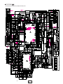
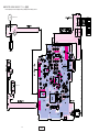
Clarion Co., Ltd.
Published by Service Dept.
298-5960-00 Dec.2001 P
5-35-2, Hakusan, Bunkyouku, Tokyo, 112-8608 Japan
Service Dept.- 50 kamitoda,Toda-shi,Saitama,335-8511 Japan Tel: 048-443-1111 FAX:048-433-6996
Printed in Japan
Service Manual
6 Disc CD Changer with CD text
Model
6 - DI SC
OP T I CA L
CD
(PE-2433B/for U.S.A.)
(PE-2433K/for Other Countries)
CHA NGE R
DI GI T A L
OUT P UT
TEXT
Model
(PE-2433E/for Europe)
■ SPECIFICATIONS
■ COMPONENTS
Frequency response:
Signal to noise ratio:
Wow and flutter:
Power supply voltage:
5Hz to 20kHz(±1dB)
105dB(1kHz)IHF-A
Below measurement limits
14.4V DC
(10.8 to 15.6V allowable)
Ground:
Negative
Current consumption: 1A
Dimensions(mm):
225(W)×63(H)×167(D)
Weight:
1.65kg
PE-2433B-A/K-A/E-A
■ NOTES
※ Use a CeNET extension cable that is less than 20m in
length.
※ CD singles cannot be used.
※ This unit is compatible with CD text.When it is connected
※
※
※
※
to a center unit suitable for CD text display, CD text can
be displayed.(When it is connected to a center unit without CD text function,CD text cannot be displayed.)
The following magazines cannot be used for this
unit.Using them will result in a damage to hte mechanism and cause the magazine not to eject.
1.Magazine(CAA-122) for the 12-disc CD chnager
2.Magazine(CAA-355) for the 6-disc CD changer
Do not play heart-shaped, octagonal, or other specially
shaped CDs.
We cannot supply PWB with component parts in principle. When a circuit on PWB has failure , please repair
it by component parts base. Parts which are not mentioned in service manual are not supplied.
Specifications and design are subject to change without
notice for further improvement.
-1-
Main unit
CD magazine
Mounting bracket
Mounting bracket(with bolt)
Lock pin
Extension lead(13P)
Parts bag
Cushion rubber
Parts bag
Cord clamp
Wing nut
Hex-bolt
−−−−−
CAA-397-900
300-9873-20
300-9874-20
335-0594-20
855-3416-50
1
1
2
2
3
1
−−−−−
345-8653-00
2
−−−−−
335-0833-01
722-0545-00
734-5008-37
2
4
4
■ To engineers in charge of repair or
inspection of our products.
Before repair or inspection, make sure to follow
the instructions so that customers and Engineers
in charge of repair or inspection can avoid suffering any risk or injury.
1. Use specified parts.
The system uses parts with special safety features against
fire and voltage. Use only parts with equivalent characteristics when replacing them.
The use of unspecified parts shall be regarded as remodeling for which we shall not be liable. The onus of
product liability (PL) shall not be our responsibility in cases
where an accident or failure is as a result of unspecified
parts being used.
2. Place the parts and wiring back in their original positions
after replacement or re-wiring.
For proper circuit construction, use of insulation tubes,
bonding, gaps to PWB, etc, is involved. The wiring con-
DCZ625
DCZ628
nection and routing to the PWB are specially planned
using clamps to keep away from heated and high voltage
parts. Ensure that they are placed back in their original
positions after repair or inspection.
If extended damage is caused due to negligence during
repair, the legal responsibility shall be with the repairing
company.
3. Check for safety after repair.
Check that the screws, parts and wires are put back securely in their original position after repair. Ensure for
safety reasons there is no possibility of secondary
ploblems around the repaired spots.
If extended damage is caused due to negligence of repair, the legal responsibility shall be with the repairing
company.
4. Caution in removal and making wiring connection to the
parts for the automobile.
Disconnect the battery terminal after turning the ignition
key off. If wrong wiring connections are made with the
battery connected, a short circuit and/or fire may occur.
If extensive damage is caused due to negligence of repair, the legal responsibility shall be with the repairing
company.
5. Cautions regarding chips.
Do not reuse removed chips even when no abnormality
is observed in their appearance. Always replace them
with new ones. (The chip parts include resistors, capacitors, diodes, transistors, etc). The negative pole of tantalum capacitors is highly susceptible to heat, so use special care when replacing them and check the operation
afterwards.
6. Cautions in handling flexible PWB
Before working with a soldering iron, make sure that the
iron tip temperature is around 270℃. Take care not to
apply the iron tip repeatedly(more than three times)to the
same patterns. Also take care not to apply the tip with
force.
7. Turn the unit OFF during disassembly and parts replacement. Recheck all work before you apply power to the
unit.
8. Cautions in checking that the optical pickup lights up.
The laser is focused on the disc reflection surface through
the lens of the optical pickup. When checking that the
laser optical diode lights up, keep your eyes more than
30cms away from the lens. Prolonged viewing of the laser within 30cms may damage your eyesight.
9. Cautions in handling the optical pickup
The laser diode of the optical pickup can be damaged by
electrostatic charge caused by your clothes and body.
Make sure to avoid electrostatic charges on your clothes
or body, or discharge static electricity before handling the
optical pickup.
9-1. Laser diode
The laser diode terminals are shorted for transportation in order to prevent electrostatic damage.
After replacement, open the shorted circuit. When
removing the pickup from the mechanism, short
the terminals by soldering them to prevent this
damage.
9-2. Actuator
The actuator has a powerful magnetic circuit. If a
magnetic material is put close to it. Its characteristics will change. Ensure that no foreign substances
DCZ625
DCZ628
enter through the ventilation slots in the cover.
9-3. Cleaning the lens
Dust on the optical lens affects performance. To
clean the lens, apply a small amount of
isopropyl alcohol to lens paper and wipe the lens
gently.
■CAUTIONS
Use of controls,adjustment or performance of procedures
other than those specified herein,may result in hazardous
radiation exposure.
The COMPACT DISC player and MINI DISC player should
not be adjusted or repaired by anyone except properly qualified service personnel.
This appliance contains a laser system and is classified as
a "CLASS 1 LASER PRODUCT".To use this model
properly,read this Owner's Manual carefully and kep this
manual for your future reference.In case of any trouble with
this player,please contact your nearest"AUTHORIZED service station".To prevent direct exposure to the laser beam,do
not to open the enclosure.
X
-2-
■ HOW TO CHANGE THE ADDRESS
pin 20: ADDRESS
: IN : The address input for the CD auto changer.
SWITCH
pin 21: WRITE
: IN : The write command input.
pin 22: RX
: IN : Serial data input of IE BUS.
When connecting an CD changer and MD changer by CeNET,no more than 2 units can be connected.When both of
them are CD,the address switch needs to be reset so that
the address switch number is not the same for each.
pin 23: TX
: O : Serial data output of IE BUS.
pin 24: NU
: - : Not in use.
pin 25: NU
: - : Not in use.
pin 26: NU
: - : Not in use.
pin 27: NU
: - : Not in use.
pin 28: NU
pin 29: NU
: - : Not in use.
: - : Not in use.
pin 30: NU
: - : Not in use.
pin 31: NU
: - : Not in use.
pin 32: NU
: - : Not in use.
pin 33: NU
: - : Not in use.
pin 34: NU
: - : Not in use.
How to change the address switch
Switch the address by using a plastic stick with a sharp
tip or equivalent.
pin 35: NU
: - : Not in use.
pin 36: DATUM
pin 37: D No TR
: IN : The datum point signal input for counting
the disk number.
: IN : Disk number detect pulse input.
pin 38: NU
: - : Not in use.
pin 39: CE
: IN : Chip enable signal input.
pin 40: NU
: - : Not in use.
pin 41: PW ON INV
: O : The inverted signal of "POWER ON 1(pin
1)".
pin 42: POWER ON 2 : O : The power ON signal output to the power
supply section.
Caution
・ The unit may not operate when both CD changers are
set to the same address switch number.
・ Never change the address switch during operation.Doing
sp can cause malfunction or breakdown.Do not change
the address switch forcibly,because this may also cause
malfunction.
・ The Ce-NET cable wiring must be less than
20m(65.62ft)in length.
・ Be sure that the CD changer numbers are not the same.
・ Do not use the address switch numbers "3" and "4" for
the MD changer.
■ EXPLANATION OF IC
052-5046-01 M30621M8A-F27GP
CD Auto Changer Control
1.Terminal Description
pin 1: POWER ON 1 : O : The power ON signal output to the power
supply section.
pin
2: SB SYNC
: IN : Sub code data sync.
pin
3: A MUTE
: O : Audio mute signal output.
pin
pin
4: CD AC FLAG
5: NU
: O : The CD auto changer active flag output.
: - : Not in use.
pin
6: CN VSS
: IN : Inputting "L" at single mode operation.
pin
7: NU
: - : Not in use.
pin
8: NU
: - : Not in use.
pin
9: RESET
: IN : Reset signal input.
pin 10: X OUT
: O : Crystal connection.
pin 11: VSS
: - : Negative supply voltage.
pin 43: NU
: - : Not in use.
pin 44: LIMIT
: IN : Limiting switch signal input.
pin 45: HOLD IN
: IN : "L"= The magazine is charged.
pin 46: LOAD END
: O : The loading end signal output.
pin 47: 8cm/12cm
: IN : 8cm/12cm
pin 48: UD CW
: O : Up/down motor control signal output.
pin 49: UD CCW
: O : Up/down motor control signal output.
pin 50: LD CW
: O : Loading motor control signal output.
pin 51: LD CCW
: O : Loading motor control signal output.
pin 52: NU
pin 53: T CLK
: - : Not in use.
: O : "Test mode display" clock output.
pin 54: T DATA
: O : The serial data output for the test mode
indication.
pin 55: T CLR
pin 56: NU
: O : The clear signal output for the test mode
indication.
: - : Not in use.
pin 57: NU
: - : Not in use.
pin 58: NU
: - : Not in use.
pin 59: DR MUTE
: O : The muting pulse output to the CD driver.
pin 60: GV SW
: O : The reset pulse output to the digital servo
IC.
pin 61: RST
: IN : Reset signal input.
pin 62: CCE
: O : Chip enable signal output to CD IC.
pin 63: BUC CLOCK
pin 64: BUS 3
: O : CD IC clock pulse output.
:I/O: CD IC Data input / output.
pin 65: BUS 2
:I/O: CD IC Data input / output.
pin 66: BUS 1
:I/O: CD IC Data input / output.
pin 67: BUS 0
:I/O: CD IC Data input / output.
pin 68: NU
: - : Not in use.
pin 69: NU
: - : Not in use.
pin 70: NU
: - : Not in use.
pin 71: EJECT
: IN : Eject signal input.
pin 72: TEST 4
: IN : For the test.
pin 73: TEST 3
: IN : For the test.
pin 74: TEST 2
: IN : For the test.
pin 75: A VSS
pin 76: TEST 1
: - : Analog ground.
: IN : For the test.
pin 77: Vref
: - : Reference voltage
pin 78: A VCC
: - : Positive supply voltage for the internal analog section.
pin 12: X IN
: IN : Crystal connection.
pin 13: VDD
: - : Positive supply voltage.
pin 79: NU
: - : Not in use.
pin 14: NMI
: IN : Connect to VDD.
pin 80: D STOP
: O : Digital output control. Outputs "H" at Play.
pin 15: B/U DET
: IN : Backup voltage ON signal input.
pin 16: SYS ACC
pin 17: MAG SW
: IN : ACC detect signal input.
: IN : The inserted flag input for the magazine.
pin 18: CONNECT
: IN : IE-BUS input.
pin 19: NU
: - : Not in use.
-3-
DCZ625
DCZ628
DCZ625
DCZ628
LIMIT SW
SLED
MOTOR
-4-
UP/DOWN MOTOR
12/8 DISC SENSOR
HOLDER-IN SW
LOAD-END SW
LOADING MOTOR
LOADING FPC
DRIVE FPC
SPINDLE
MOTOR
PICK UP
DRIVE UNIT
MOTOR
DRIVER
5V
REG
3.3V
REG
SERVO DRIVER
IC2
BD7961
RF AMP
IC1
TA2157F
EJECT SW
S2
RESET
IC8
S-80721
MUTE
Q4,5
2SD1306
MAGAZINE SW
S3
B/U DET
IC10
S-80843
MAIN CONTROLLER
IC7
M30621M8A
DSP & DAC
IC5
TC94A14FA
MAIN PWB
ANALOG SW
IC12
74VHC4066
DISC NO. TR
IC3
GP1S94
MEMO-VDD
VDD 5V
ACC-DET
BUS DRIVER
IC6
CA0008
B.T.L.
IC11
NJM4558
POSITION SW
S1
VDD REF
5V
LPF
IC9
NJM4558
CD 9V
IC4
BA09ST
POWER 5V
B/U 12V
SYS-ACC
BUS+/BUS-
ADRS
R +/-
L +/-
D-OUT
14P CONNECTOR
J4
ADDRESS SW
S301
13P DIN
J301
D-OUT
P301
CONNECTOR
FPC
■ BLOCK DIAGRAM
■ EXPLODED VIEW・PARTS LIST
Main section
B6
17
6
3
B4
14
4
13
5
8
12
B4
B5
B2
B3
B1
21
B5
B3
12
B6
A4
1
10
12
A3
19
15
16
11
A4
20
12
A2
18
A3
14
2-1
A1
12
B2
B1
A2
9
7
22
2
A1
12
Note)Some parts depend on each model.The model name is specified in the description.
NO.
PART NO.
DESCRIPTION
1
−−−−−
CHANGER MECHANISM
(025020)
2
2-1
940-7965-63 ESCUTCHEON ASSY(DCZ625)
940-7965-60 ESCUTCHEON ASSY(DCZ628)
Q'TY
NO.
1
11
750-3459-21 FL-SPRING R
1
12
716-1716-00 SCREW
11
13
716-0484-00 SPECIAL SCREW
1
1
1
PART NO.
DESCRIPTION
Q'TY
716-0872-00 PAD SCREW
1
14
629-0080-00 DAMPER GS-6
4
3
013-3968-00 SWITCH
1
15
371-5693-22 TRIM PLATE
1
4
039-1948-20 CONNECTOR PWB
(WITHOUT COMPONENT)
1
16
382-6254-20 BUTTON
1
5
074-1194-00 OUTLET SOCKET
1
17
620-1088-20 CE-NET HOLDER
1
6
075-0305-00 JACK
1
18
620-0996-21 DAMPER PLATE R
1
7
286-9860-00 SETPLATE(DCZ625/U.S.A)
286-9858-00 SETPLATE(DCZ628)
286-9861-00 SETPLATE(DCZ625/OTHER)
1
19
620-0997-20 DAMPER PLATE F
1
20
622-1545-20 FL PIN R
1
8
310-1742-21 UPPER CASE
1
21
622-1546-20 FL PIN L
1
9
311-1838-20 LOWER CASE
1
22
348-0331-00 TAPE
1
10
750-3460-21 FL-SPRING L
1
-5-
DCZ625
DCZ628
Changer mechanism section
55
10
B3
B3
55
55
36
A7
B2
B2
A4
62
B10
62
55
A6
55
B1
B7 B6
B1
B7 B6
A5
B5
B10
33
A2
67
C3
B4
D2
44
12
B4
B9
C2
71
19
B8
B5
55
C1
A3
30
34
32
D1
55
A11
A14
A1
A7
E1
B9
67
E
12
B8
31
A10
N1
1
2
55
3
4
5
6
A6
A14
A12 A9
A13
A10
A4
62
9
A5
55
A3
A8
E
1
8
A2
2
3
4
5
A9
6
51
65 45
65
A1
A13
57
69
68
N1
A8
12
54
57
A12
16
57
C1
11
59
A11
63
D2
NO.
Q'TY
NO.
1
966-0582-22 DRIVE-P-ASSY
1
12
966-0594-24 V-CHASSIS ASSY
1
2
966-0583-20 DISC HOLD ASSY
1
13
966-0454-00 SH-RACK-ASSY
1
3
966-0584-23 CLAMP-P-ASSY F
1
14
966-0623-23 L-LOWER-P-ASSY
1
4
966-0585-22 CAM GEAR ASSY
1
15
969-0061-30 PICK UP-ASSY
1
5
966-0586-22 MOTOR-P-ASSY
1
16
966-0588-21 HOLDER-L-ASSY
1
039-1947-20 MAIN PWB
(WITHOUT COMPONENT)
1
6
7
966-0589-23 L-UPPER-P-ASSY
1
17
001-0563-00 LED
1
8
966-0590-20 MG-LO-P-ASSY
1
18
013-7413-50 DETECTOR SWITCH
3
9
966-0591-21 REAR PANEL ASSY
1
19
SMA-180-100 MOTOR ASSY(UP/DOWN)
1
10
966-0592-20 UP-PLATE ASSY
1
20
SMA-181-100 MOTOR ASSY(SLED)
1
11
966-0593-20 UD-GEAR-P-ASSY
1
21
SMA-179-100 MOTOR ASSY(SPINDLE)
1
DCZ625
DCZ628
PART NO.
DESCRIPTION
-6-
PART NO.
DESCRIPTION
Q'TY
35
29
O1
65
65
4
F2
F1
66
G1
G1
70
O1
C2
28
7
26
C3
H2
46
F2
I1
2
H1
K2
G2
F1
I1
N2
M2
M1
55
47
G2
6
52
J1
F4
H1
D1
41
F5
K2
60
3
55
18
24
17
57
60
65
65 49
E1
L1
1
P1
K3
K1
48
61
27
72
57
43
57 20
J2
J4 N2
N1
F4
23
L1
J4
64
63
J1
J2
55
21
61 58
37
57 39
25
56
40
H2 M2
F5
J3
55
57
Q1
K1
55
38
42
N1
M1
5
55
K3
14
65
13
15
P1
55
Q1
J3
55
50
53
22
57
18
NO.
PART NO.
22
23
DESCRIPTION
Q'TY
NO.
PART NO.
DESCRIPTION
Q'TY
039-1949-20 DRIVE PWB
(WITHOUT COMPONENT)
1
38
801-4912-60 VINYL-COAT-WIRE(BRN)
1
039-1950-20 LOADING PWB
(WITHOUT COMPONENT)
1
39
621-0589-20 SECOND GEAR
1
40
621-0590-20 LS GEAR
1
621-0591-20 PICK UP GUIDE
1
621-0592-21 LS-HOLDER
1
24
060-0252-01 PHOTO-TR
1
41
25
620-0999-21 LS-SPRING
1
42
26
620-1575-21 SWITCH PLATE
1
43
621-0593-20 LS GUIDE
1
27
620-1007-22 CLAMP PLATE M
1
44
802-4906-60 VINYL-COAT-WIRE(RED)
1
28
620-1008-24 CLAMP PLATE R
1
45
621-0597-20 V-GEAR A
1
621-0630-22 HOLDER-G-RAIL R
1
29
620-1009-21 CLAMPER PLATE
1
46
30
620-1016-20 GAP PLATE R
1
47
621-0631-21 HOLDER-G-RAIL L
1
31
620-1017-20 GAP PLATE F
1
48
621-0703-20 L-GEAR A
1
32
620-1018-20 MG EJECT PLATE
1
49
621-0633-20 L-GEAR B
1
33
620-1019-20 SLIDE PLATE R
1
50
805-4912-60 VINYL-COAT-WIRE(GRN)
1
621-0635-20 V-HELICAL GEAR
1
34
620-1020-20 SLIDE PLATE F
1
51
35
620-1031-21 LOADING ARM
1
52
621-0636-21 CLAMPER RING
1
36
620-1034-23 SIDE PANEL
1
53
624-3022-00 LEAD SCREW
1
37
621-0587-21 SCREW HOLD BASE
1
54
629-0061-00 GEAR DAMPER
1
-7-
DCZ625
DCZ628
NO.
PART NO.
55
56
DESCRIPTION
Q'TY
NO.
716-0484-00 SCREW(M2×2.5)
23
64
745-0789-01 DRIVE WASHER
1
716-0675-00 SCREW(M2×5.5)
1
65
746-0761-00 WASHER
7
57
716-1716-00 SCREW(M2×3)
10
66
750-3461-21 DISC-H-SPRING
1
58
716-3469-00 SCREW
2
67
750-3462-20 GAP SPRING
2
59
735-2006-11 D-SEMS-SCREW(M2×6)
1
68
750-3463-20 MG LOCK SPRING
1
60
739-1722-17 SCREW(M1.7×2.2)
2
69
750-3464-20 MG EJECT SPRING
1
61
739-2022-17 SCREW(M2×2.2)
2
70
750-3492-22 CLAMPER SPRING
1
62
743-1500-10 E-RING
3
71
800-4906-60 VINYL-COAT-WIRE(BLK)
1
63
743-2000-10 E-RING
2
72
SMA-188-100 MOTOR ASSY(LOADING)
1
■ ELECTRICAL PARTS LIST
Main PWB(B1) section
PART NO.
DESCRIPTION
Q'TY
Note) Several different parts of the same reference number are alternative parts.
One of those parts is used in the set.
REF No. PART No.
DESCRIPTION
REF No. PART No.
DESCRIPTION
REF No. PART No.
DESCRIPTION
C1
C2
C3
C4
C5
C6
C7
C8
C9
C10
C11
C12
C13
C14
C16
C17
C18
C19
C20
C21
C22
C23
C24
C25
C26
C27
C28
C29
C30
C31
C33
C34
C36
C37
C38
C39
C40
C41
C42
C43
C44
C45
C47
C48
C49
C50
C51
C52
C53
C54
C55
C56
C58
C59
C60
C61
16V1uF
0.047uF
6.3V100uF
6.3V100uF
6800pF
16V1uF
16V0.1uF
10V33uF
10V33uF
16V0.1uF
16V0.1uF
5pF
10V33uF
16V1uF
0.01uF
56pF
100pF
0.01uF
0.047uF
0.015uF
47pF
0.047uF
1500pF
4700pF
0.01uF
0.047uF
0.033uF
0.033uF
470pF
47pF
0.047uF
0.047uF
10V220uF
16V0.1uF
16V0.1uF
18pF
18pF
0.01uF
16V0.1uF
10V33uF
0.01uF
0.01uF
100pF
10V33uF
16V10uF
16V10uF
5.5V0.1F
16V10uF
16V10uF
16V10uF
0.047uF
0.01uF
0.01uF
16V10uF
68pF
68pF
C62
C64
C65
C66
C67
C69
C70
C71
C74
C75
C76
C77
C78
C79
C80
C81
D1
D2
D3
D4
D5
D6
D7
D8
IC1
IC2
IC3
IC4
IC5
IC6
IC7
IC8
IC9
IC10
IC11
IC12
J1
J2
J3
J4
L1
L2
L3
L4
L5
Q1
Q2
Q3
Q4
Q5
Q6
Q7
Q8
Q9
Q10
Q11
6.3V100uF
0.01uF
22pF
22pF
16V22uF
16V22uF
16V470uF
0.01uF
6.3V100uF
16V22uF
16V22uF
16V22uF
16V22uF
16V22uF
16V22uF
0.33uF
MA111
DAN217U
DAN202U
S5688B
S5688B
MA111
HZS6C2L
MA111
TA2157F
BD7961FM
GP1S94
BA09ST
TC94A14FA
CA0008AM
M30621M8A-F27GP
S-80721AN
NJM4558M
S-80843ALNP-EA7
NJM4558M
74VHC4066M
15P
6P
8P
14P
10uH
BLM21B102
BLM21B102
BLM21B102
BLM21B102
2SB1237
2SB1237
2SB1237
2SD1306
2SD1306
RN1402
2SA1048
RN1402
DTA114
2SA1162
2SD1858
Q12
R1
R2
R3
R4
R5
R6
R7
R8
R9
R10
R11
R12
R13
R14
R15
R16
R17
R18
R19
R20
R21
R22
R23
R24
R25
R26
R27
R28
R29
R31
R32
R33
R34
R35
R36
R37
R38
R39
R40
R41
R42
R43
R44
R45
R46
R47
R48
R49
R50
R51
R52
R53
R54
R55
R56
RN1402
1/16W 100kΩ
1/16W 100kΩ
1/16W 100kΩ
1/16W 100kΩ
1/16W 100kΩ
1/16W 100kΩ
1/16W 220Ω
1/16W 270Ω
1/16W 68kΩ
1/4WS 22Ω
1/4WS 22Ω
1/16W 10kΩ
1/16W 22kΩ
1/16W 820Ω
1/4WS 10Ω
1/16W 10kΩ
1/16W 15kΩ
1/16W 68kΩ
1/16W 2.7kΩ
1/16W 100Ω
1/16W 1kΩ
1/16W 10kΩ
1/16W 18kΩ
1/16W 15kΩ
1/16W 10kΩ
1/16W 47kΩ
1/16W 100kΩ
1/16W 5.6kΩ
1/16W 100kΩ
1/16W 270Ω
1/16W 100kΩ
1/16W 33kΩ
1/16W 1MΩ
1/16W 470Ω
1/16W 220Ω
1/16W 3.3kΩ
1/16W 47kΩ
1/16W 47kΩ
1/16W 100kΩ
1/16W 47kΩ
1/16W 47kΩ
1/16W 100Ω
1/16W 100Ω
1/16W 10kΩ
1/16W 10kΩ
1/16W 5.6kΩ
1/16W 10kΩ
1/16W 47kΩ
1/16W 470Ω
1/16W 100kΩ
1/16W 100kΩ
1/16W 15kΩ
1/16W 15kΩ
1/16W 22kΩ
1/16W 1kΩ
178-1052-78
043-0533-50
042-0426-31
183-1073-17
046-6822-58
178-1052-78
168-1042-78
183-3363-27
183-3363-27
168-1042-78
168-1042-78
045-5096-50
183-3363-27
178-1052-78
168-1032-55
045-5601-50
045-1011-50
168-1032-55
043-0533-50
046-1532-78
045-4701-50
043-0533-50
046-1522-58
046-4722-58
046-1032-78
043-0533-50
046-3332-78
046-3332-78
046-4712-58
045-4701-50
043-0533-50
043-0533-50
042-0452-81
168-1042-78
168-1042-78
166-1801-50
166-1801-50
168-1032-55
168-1042-78
183-3363-27
168-1032-55
168-1032-55
166-1011-50
183-3363-27
183-1063-37
183-1063-37
042-0576-00
183-1063-37
183-1063-37
183-1063-37
043-0533-50
046-1032-78
046-1032-78
183-1063-37
045-6801-50
045-6801-50
DCZ625
DCZ628
183-1073-17
046-1032-78
045-2201-50
045-2201-50
183-2263-37
183-2263-37
184-4773-31
046-1032-78
183-1073-17
183-2263-37
183-2263-37
183-2263-37
183-2263-37
183-2263-37
183-2263-37
178-3342-78
001-0516-90
001-1305-90
001-1304-90
001-0466-90
001-0466-90
001-0516-90
001-0504-35
001-0516-90
051-5710-90
051-6060-08
051-5806-00
051-3289-00
051-6376-00
051-6600-38
052-5046-01
051-5407-08
051-0350-93
051-5434-08
051-0350-93
051-7232-08
074-1138-65
074-1158-56
074-1158-58
074-1158-64
010-3050-93
010-2285-57
010-2285-57
010-2285-57
010-2285-57
191-1237-50
191-1237-50
191-1237-50
193-1306-00
193-1306-00
125-2004-92
190-1048-50
125-2004-92
125-0014-92
190-1162-00
193-1858-50
-8-
125-2004-92
033-1041-15
033-1041-15
033-1041-15
033-1041-15
033-1041-15
033-1041-15
033-2211-15
111-2711-98
033-6831-15
111-2201-98
111-2201-98
119-1031-15
119-2231-15
033-8211-15
111-1001-98
119-1031-15
119-1531-15
033-6831-15
033-2721-15
033-1011-15
033-1021-15
033-1031-15
033-1831-15
033-1531-15
033-1031-15
033-4731-15
033-1041-15
033-5621-15
033-1041-15
111-2711-98
033-1041-15
033-3331-15
033-1051-15
033-4711-15
119-2211-15
033-3321-15
119-4731-15
033-4731-15
033-1041-15
033-4731-15
033-4731-15
033-1011-15
033-1011-15
033-1031-15
033-1031-15
033-5621-15
033-1031-15
033-4731-15
033-4711-15
033-1041-15
119-1041-15
033-1531-15
033-1531-15
033-2231-15
033-1021-15
REF No. PART No.
DESCRIPTION
R57
033-4731-15 1/16W 47kΩ
R58
033-2731-15 1/16W 27kΩ
R59
033-2731-15 1/16W 27kΩ
R60
033-1031-15 1/16W 10kΩ
R61
033-1031-15 1/16W 10kΩ
R62
033-1031-15 1/16W 10kΩ
R63
033-1031-15 1/16W 10kΩ
R64
033-1021-15 1/16W 1kΩ
R65
033-1531-15 1/16W 15kΩ
R66
033-4731-15 1/16W 47kΩ
REF No. PART No.
DESCRIPTION
REF No. PART No.
DESCRIPTION
R67
R68
R69
R70
R71
R72
R73
R74
R75
R76
1/16W
1/16W
1/16W
1/16W
1/16W
1/16W
1/16W
1/16W
1/16W
1/16W
R77
R78
R79
R80
S1
S2
S3
T1
X1
X2
1/16W 100Ω
1/16W 100Ω
1/16W 4.7kΩ
1/16W 220Ω
00110676
SKHLLD
00110676
E1-19
16.9344MHz
CSTCC10MG
033-1031-15
033-1031-15
033-8221-15
119-1041-15
119-1041-15
119-1041-15
119-1041-15
033-1031-15
119-1011-15
119-1011-15
10kΩ
10kΩ
8.2kΩ
100kΩ
100kΩ
100kΩ
100kΩ
10kΩ
100Ω
100Ω
119-1011-15
119-1011-15
033-4721-15
033-2211-15
013-7404-50
013-6100-10
013-7404-50
009-0679-00
061-3038-00
060-1505-50
Connector PWB(B2) section
REF No. PART No.
J301
DESCRIPTION
074-1194-00 13P
REF No. PART No.
P301
DESCRIPTION
075-0305-00 DIGITAL OUT
REF No. PART No.
S301
DESCRIPTION
013-3968-00 SSSS2
Loading PWB(B3) section
REF No. PART No.
DESCRIPTION
D501
001-0563-00 GL380
Q501
060-0252-01 PT4850F
REF No. PART No.
DESCRIPTION
S501
013-7413-50 SPVG12
S502
013-7413-50 SPVG12
Drive PWB(B4) section
REF No. PART No.
DESCRIPTION
S503
013-7413-50 SPVG12
-9-
DCZ625
DCZ628
CIRCUIT DIAGRAM /
Main PWB(B1)/Connector PWB(B2)/Loading PWB(B3)/Drive PWB(B4) section
1
2
3
4
5
6
7
8
9
10
11
12
13
- 10 -
DCZ625
DCZ628
G ND
B AC K UP
L -C H (+)
NC
NC
B U S (+)
R -C H (+)
R -C H (-)
S Y S AC C
B U S (-)
L -C H (-)
NC
NC
■ PRINTED WIRING BOARD / プリント基板図
Main PWB(B1)/Connector PWB(B2)/Loading PWB(B3)/Drive PWB(B4) section
1
2
3
4
5
6
7
8
9
10
11
12
13
RED
BLK
SPINDLE MOTOR
BRN
GRN
S 503
SLED MOTOR
S 502
S 501
Q501
LOADING MOTOR
D501
- 11 -
DCZ625
DCZ628
GND
BACK UP
L-CH(+)
NC
NC
BUS(+)
R-CH(+)
R-CH(-)
SYS ACC
BUS(-)
L-CH(-)
NC
NC


![Hire And Sales Catalogue V4.40 [april2013].](http://vs1.manualzilla.com/store/data/005975062_1-8950e43f7cbe305f577dc550ee5fbd1b-150x150.png)

