1
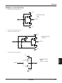
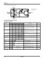
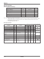
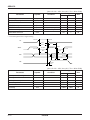
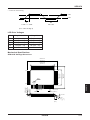
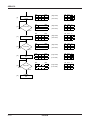
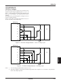
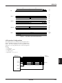
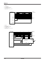
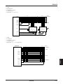
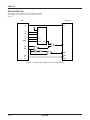
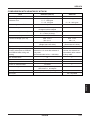
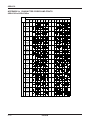
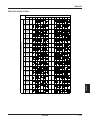
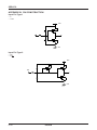
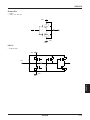
SED1278
LCD Controller/Drivers
Technical Manual
Contents
OVERVIEW ......................................................................................................................................................... 9–1
FEATURES .......................................................................................................................................................... 9–1
BLOCK DIAGRAM ............................................................................................................................................... 9–2
PACKAGE OUTLINE ........................................................................................................................................... 9–2
PINOUT ............................................................................................................................................................... 9–3
PIN DESCRIPTION ............................................................................................................................................. 9–4
TERMINAL CONFIGURATION ........................................................................................................................... 9–5
INSTRUCTION DESCRIPTION ........................................................................................................................... 9–6
SPECIFICATIONS ............................................................................................................................................. 9–10
OPERATION ...................................................................................................................................................... 9–16
THE CHARACTER GENERATOR .................................................................................................................... 9–21
LCD INTERFACE .............................................................................................................................................. 9–23
MPU INTERFACE ............................................................................................................................................. 9–30
COMPARISON WITH HD44780 BY HITACHI ................................................................................................... 9–31
APPENDIX A: CHARACTER CODES AND FONTS ........................................................................................ 9–32
SED1278
APPENDIX B: PIN CONSTRUCTION .............................................................................................................. 9–38
–i–
SED1278
OVERVIEW
FEATURES
The SED1278 is a dedicated character display controller/
driver which, when used with the SED1181F or the
SED1681 segment drivres, is able to display up to 80
characters under 4- or 8-bit MPU control.
The internal character generator (CG) ROM has an
extended 240, 5×10 pixel, character set, plus CGRAM
space for an additional eight user definable 5×8 pixel
characters. These memory features combined with the
rich set of control instructions offer the potential for a
highly flexible character display system.
The SED1278 features a guaranteed minimum LCD
drive voltage of 3 V making it suitable for use with low
voltage LCD panels.
• Interface for 4- and 8-bit MPUs
• Display RAM – 80 bytes (80 characters)
• Character generator ROM – 240 characters
– 5×8 pixel font
• Character genrator RAM – 64 bytes
– 5×8 pixel font, 8 characters.
– 5×10 pixel font, 4 characters.
• Number of characters used
Duty SED1278F SED1181FLA
One-line 1/8,
display
1/11
1
0
6
Two-line 1/16
display
1
0
3
No. of
characters used
8 columns
× 1 line
80 columns
× 1 line
8 columns
× 2 lines
40 columns
× 2 lines
• Powerful display control instructions
• LCD driver outputs
– 40 segment driver outputs
– 16 common driver outputs
• Low LCD drive voltage – 3 V minimum (VDD–V5)
• Dual-frame AC drive
• On-chip power-on reset
• On-chip RC oscillator
• Single 5 V operation
• Chip (SED1278D) and 80-pin QFP (SED1278F)
packages
(Compatible with HD 44780 and HD 66780 by Hitachi
Limited)
SED1278
The SED1278 is equivalent to the HD 44780 and HD
66780 by Hitachi Limited. Before use, make sure that
there is no problem for practical use. It should be
noted that this is not intended to guarantee enforcement
of industrial property and other rights, or to grant
license for the use of this product.
EPSON
9–1
SED1278
BLOCK DIAGRAM
OSC1
Instruction Decoder
Cursor/ Printer Control
Address
Counter ACC
I/O Buffer
Instruction Register
DB 0
to
DB 7
I/O Control
R/W
RS
Oscillation
Circuit
Refresh Address Counter
7
Daia Register
E
OSC2
7
MPX
Timing Generator
Display Data RAM
DDRAM
80 Bytes
Shift Register 16 Bits
XSCL
LP
FR
Common Driving
Output Circuit
8
MPX
Character Generator
RAM
(CGRAM)
64 Bits
VSS
VDC
V1
Character Generator
RAM
(CGROM)
5 x 10 x 240 Bits
5
COM 1 to
COM 16
SEG 1 to
SEG 40
Segment Driving
Output Circuit
5
V2
Latch Circuit
40 Bits
MPX
V3
5
V4
Parallel/Serial
Data Converter
V5
Shift Register
40 Bits
DO
PACKAGE OUTLINE
64
41
65
40
80
25
1
9–2
24
EPSON
SED1278
24
1
25
80
SED1278D
40
65
41
64
PINOUT
Name
SEG22
SEG21
SEG20
SEG19
SEG18
SEG17
SEG16
SEG15
SEG14
SEG13
SEG12
SEG11
SEG10
SEG9
SEG8
SEG7
SEG6
SEG5
SEG4
SEG3
Number
21
22
23
24
25
26
27
28
29
30
31
32
33
34
35
36
37
38
39
40
Pin
Pin
Name
SEG2
SEG1
GND
OSC1
OSC2
V1
V2
V3
V4
V5
LP
XSCL
VDD
FR
DO
RS
R/W
E
DB0
DB1
Number
41
42
43
44
45
46
47
48
49
50
51
52
53
54
55
56
57
58
59
60
EPSON
Name
DB2
DB3
DB4
DB5
DB6
DB7
COM1
COM2
COM3
COM4
COM5
COM6
COM7
COM8
COM9
COM10
COM11
COM12
COM13
COM14
Number
61
62
63
64
65
66
67
68
69
70
71
72
73
74
75
76
77
78
79
80
Name
COM15
COM16
SEG40
SEG39
SEG38
SEG37
SEG36
SEG35
SEG34
SEG33
SEG32
SEG31
SEG30
SEG29
SEG28
SEG27
SEG26
SEG25
SEG24
SEG23
9–3
SED1278
Pin
Pin
Number
1
2
3
4
5
6
7
8
9
10
11
12
13
14
15
16
17
18
19
20
SED1278
PIN DESCRIPTION
MPU Interface
RS
R/W
E
Register select signal input. Selects
between the data and instruction registers
during CPU access.
RS = 0: Instruction register access cycle
RS = 1: Data register access cycle
This input selects between SED1278
register read and write cycles.
R/W = 0: Register write cycle
R/W = 1: Register read cycle
Read/write execute signal input.
DB0 to DB7 TTL level data input/output lines, for
connection to the system MPU data bus.
TABLE 1 The Function of the E Signal
RS
R/W
0
0
0
1
1
0
1
1
Operation
E
Instruction write cycle
Busy flag read cycle
Address counter read cycle
1
DDRAM or CGRAM data write cycle
1
DDRAM or CGRAM data read cycle
LCD Panel Interface
External Segment Driver Interface
COM1 to COM16 Common driver outputs to the
LCD panel.
SEG1 to SEG40 Segment driver outputs to the LCD
panel.
OSC1
If the internal RC oscillator is used
to generate the LCD drive signals,
the feedback resistor, R f , is
connected to this pin. If an external
clock source is used, the clock is
connected to this pin.
OSC2
If the internal RC oscillator is used
to generate the LCD drive signals,
the feedback resistor, R f , is
connected to this pin. If an external
clock source is used, this pin is left
open.
LP
9–4
XSCL
FR
DO
EPSON
Data latch pulse output for an external
X-driver.
Data shift clock output for an external
X-driver.
LCD AC-drive waveform for an external
X-driver.
Display data output for an external X-driver.
SED1278
TERMINAL CONFIGURATION
1.
Input terminal configuration (1)
VDD
Applicable terminal
·E
· OSCI
Internal
VSS
2.
Input terminal configuration (2)
With pull-up MOS resistor
VDD
Applicable terminal
· RS, R/W
Internal
VSS
Output terminal configuration
VDD
Applicable terminal
· OSC2
· XSCL, LP, FR, DO
SED1278
3.
Internal
VSS
EPSON
9–5
SED1278
4.
Input/Output terminal configuration
VDD
Applicable terminal
· DBO to DB7
Internal
VSS
INSTRUCTION DESCRIPTION
Instruction Summary
Instruction
Clear Display
Code
RS R/W DB7 DB6 DB5 DB4 DB3 DB2 DB1 DB0
0
0
0
0
0
0
0
0
0
Description
Cycle Time
(max.)
1
Clears all display data and sets DDRAM
address 0 in the address counter.
410 clocks
410 clocks
Return Home
0
0
0
0
0
0
0
0
1
*
Set DDRAM address 0 in the address
counter. Also returns any shifted data to
home. The contents of DDRAM remain
unchanged.
Entry Mode Set
0
0
0
0
0
0
0
1
I/D
S
Specifies the direction in which the cursor
moves and whether the display is to be
shifted or not, when data is writen to or read
from memory
10 clocks
Display ON/OFF
0
0
0
0
0
0
1
D
C
B
Sets all display on/off (D) cursor on/off (C),
and character blinking in the cursor position
(B).
10 clocks
Cursor or
Display Shift
0
0
0
0
0
1
*
*
Moves the cursor and shifts the display
without changing the contents of DDRAM.
System Set
0
0
0
0
1
IF
*
*
Sets the interface data length (IF), number of
characters to be displayed (N), and character
font (F).
10 clocks
Set CGRAM
Address
0
0
0
1
Set CGRAM addresses, followed by
transfer of CGRAM data.
10 clocks
Set DDRAM
Address
0
0
1
ADD
Sets DDRAM address, followed by
transfer of DDRAM data.
10 clocks
Read Busy Flag
and Address
0
1
BF
ACC
Reads the busy flag (BF) which indicates
internal operation and the contents of the
address counter.
Write Data to
CG or DDRAM
1
0
Write Data
Writes data to DDRAM or CGRAM.
10 clocks
Read Data from
CG or DDRAM
1
1
Read Data
Reads data from DDRAM or CGRAM.
10 clocks
S/C R/L
N
F
ACG
* Don’t care
9–6
EPSON
10 clocks
0
SED1278
Write Only Instructions
writing the CGRAM always shifts the cursor. Note
that if a two line display is used both lines will be
shifted simultaneously.
Clear Display
DB7 DB6 DB5 DB4 DB3 DB2 DB1 DB0
0
0
0
0
0
0
1
01H
Display ON/OFF
This instruction
1. loads all locations in the display data (DD) RAM
with 20H.
2. clears the contents of the address counter to 0H.
3. sets the display for zero character shift.
4. sets the address counter to point to the DDRAM.
5. , if the cursor is displayed, moves the cursor to the
left most character in the display or, if a two line
display is used, moves the cursor to the leftmost
character in the top line (line 1).
6. sets the address counter to increment on each access
of DDRAM or CGRAM.
DB7 DB6 DB5 DB4 DB3 DB2 DB1 DB0
Cursor Home
DB7 DB6 DB5 DB4 DB3 DB2 DB1 DB0
0
0
0
0
0
0
1
*
02H, 03H
RS = 0
This instruction
1. clears the contents of the address counter to 0H.
2. sets the address counter to point to the DDRAM.
3. sets the display for zero character shift.
4. , if the cursor is displayed, moves the cursor to the
left most character in the display or, if a two line
display is used, the left most character in the top line
(line 1).
Entry Mode Set
DB7 DB6 DB5 DB4 DB3 DB2 DB1 DB0
0
0
0
0
0
1
I/D
S
04H to 07H
RS = 0
• The I/D bit selects the way in which the contents of the
address counter are modified after every access to
DDRAM or CGRAM.
• I/D = 1: The address counter is incremented.
• I/D = 0: The address counter is decremented.
• The S bit enables display shift, instead of cursor shift,
after each write or read to the DDRAM.
• S = 1: Display shift enabled.
• S = 0: Cursor shift enabled.
The direction in which the display is shifted is opposite
in sense to that of the cursor. For example if S = 0 and
I/D = 1 the cursor would shift one character to the right
after an MPU write to DDRAM. However if S = 1 and
I/D = 1, the display would shift one character to the left
and the cursor would maintain its position on the
panel.
The cursor will already be shifted in the direction
selected by I/D during reads of the DDRAM,
irrespective of the value of S. Similarly reading and
0
0
0
0
1
D
C
B
08H to 0FH
RS = 0
This instruction controls various features of the display.
• The D bit turns the entire display on or off.
• D = 1: Display on
• D = 0: Display off
• The C bit turns the cursor on or off.
• C = 1: Cursor on
• C = 0: Cursor off
• The B bit enables blinking of the character the cursor
coincides with.
• B = 1: Blinking on
• B = 0: Blinking off
Blinking is achieved by alternating between a normal
and all dark display of a character. The blinking
period is set at 204800 fOSC. For example if fOSC = 250
kHz the cursor will blink with a period of 0.8192
seconds, or about 1.2 Hz.
Cursor/Display Shift
DB7 DB6 DB5 DB4 DB3 DB2 DB1 DB0
0
0
0
1
S/C R/L
*
*
10H to 1FH
RS = 0
This instruction shifts the display and/or moves the
cursor, on character to the left or right, regardless of a
DDRAM ready/write.
• The S/C bit selects movement of the cursor or
movement of both the cursor and the display.
• S/C = 1: Shift both cursor and display
• S/C = 0: Shift cursor only
• The R/L bit selects leftward or rightward movement of
the display and/or cursor.
• R/L = 1: Shift one character right
• R/L = 0: Shift one character left
System Set
DB7 DB6 DB5 DB4 DB3 DB2 DB1 DB0
0
0
1
IF
N
F
*
*
20H to 3FH
RS = 0
This instruction initializes the system, and must be the
first instruction executed after power-on.
• The IF bit selects between an 8-bit or a 4-bit MPU
interface.
• IF = 1: 8-bit MPU interface using DB7 to DB0.
• IF = 0: 4-bit MPU interface using DB7 to DB4.
• The N and F bits select the number of display lines and
the corresponding duty cycle, as listed in table 2.
EPSON
9–7
SED1278
0
RS = 0
SED1278
TABLE 2 Combinations of Display Lines and Duty Cycle
N
F
Number of
Line
Duty
Ratio
Common Output
Signal
0
0
1 line
1/8
COM1 to COM8
COM9 to COM16
0
1
1 line
1/11
COM1 to COM11
COM12 to COM16
1
*
2 lines
1/16
COM1 to COM16
—
TABLE 3 Valid CGRAM Address Ranges
Set CGRAM Address
DB7 DB6 DB5 DB4 DB3 DB2 DB1 DB0
0
1
ACR
This instruction
1. loads a new 6-bit address into the address counter.
2. sets the address counter to address CGRAM.
Once “Set CGRAM Address” has been executed, the
contents of the address counter will be automatically
modified after every access of CGRAM, as determined
by the “Entry Mode Set” instruction.
If the “Set CGRAM Address” instruction is issued by the
system MPU while the display is enabled, and if either
the cursor is on or blink is on, pseudo-cursor or pseudoblink appears. To prevent this, turn both the cursor and
display blink off before loading a new CGRAM address.
The active width of the address counter, when it is
addressing CGRAM, is 6-bits so the counter will wrap
around to 00H from 3FH if more than 64 bytes of data are
written to CGRAM.
Set DDRAM Address
DB7 DB6 DB5 DB4 DB3 DB2 DB1 DB0
1
Characters
ADR
1-line
2-line
80
00H to 4FH
1st line
40
00H to 27H
2nd line
40
40H to 67H
Write Data
DB7 DB6 DB5 DB4 DB3 DB2 DB1 DB0
DATA
RS = 1
This instruction writes the data in DB7 to DB0 into either
the CGRAM or the DDRAM. The RAM space (CG or
DD), and the address in that space, that is accessed
depends on whether a “Set CGRAM Address” or a “Set
DDRAM Address” instruction was last executed, and on
the parameters of that instruction.
The contents of the address counter will be automatically
modified after each “Write Data”, as determined by
“Entry Mode Set”. When data is written to the CGRAM,
the DB7, DB6 and DB5 bits are not displayed directly as
characters.
ADD
80H to CFH … 1 line
80H to A7H line 1 … 2 line
C0H to E7H line 2 … 2 line
This instruction
1. loads a new 7-bit address into the address counter.
2. sets the address counter to point to the DDRAM.
Once the “Set DDRAM Address” instruction has been
executed, the contents of the address counter will be
automatically modified after each access of DDRAM, as
selected by the “Entry Mode Set” instruction.
The SED1278 has only 80 DDRAM locations. The valid
address spaces for various display configurations are
listed in table 3.
9–8
Number of Lines
40H to 7FH
RS = 0
RS = 0
Non-Selected Common
Output Signal
EPSON
SED1278
Read Only Instructions
Read Busy Flag/Address Counter
Read Data
DB7 DB6 DB5 DB4 DB3 DB2 DB1 DB0
DB7 DB6 DB5 DB4 DB3 DB2 DB1 DB0
BF
ACC
DATA
RS = 1
Reading the instruction register yields the current value
of the address counter and the busy flag. This instruction
must be executed prior to any other instructions.
• ACC, the address counter value, will point to a location
in either CGRAM or DDRAM, depending on the type
of “Set RAM Address” instruction last sent.
In “Busy Flag Check” immediately after executing
“RAM Address Set” instruction, a valid address counter
value can be read 5 clock cycles after the busy flag
(BF) goes low.
In “Busy Flag Check” immediately after executing
“Write Data” instruction, a valid address counter
value can be ready as soon as BF goes low.
• The BF bit shows the status of the busy flag.
• BF = 1: SED1278 busy.
• BF = 0: SED1278 ready for next instruction.
This instruction reads data from either CGRAM or
DDRAM, depending on the type of “Set RAM Address”
instructions last sent. The address in that space depends
on the “Set RAM Address” instructions parameters.
Immediately before executing “Read Data”, “Set
CGRAM Address” or “Set DDRAM Address” must be
executed.
The contents of the address counter are modified after
each “Read Data”, as determined by “Entry Mode Set”.
Display shift is not executed, independently of “Entry
Mode Set”.
SED1278
RS = 1
EPSON
9–9
SED1278
SPECIFICATIONS
Absolute Maximum Ratings
Parameter
Symbol
Rating
Unit
Supply voltage (1)
VDD
–3 to +7.0
V
Supply voltage (2)*
V1 to V5
–0.3 to VDD+0.3
V
Input voltage
VIN
–0.3 to VDD+0.3
V
Operating temperature
Topr
–20 to +75
°C
Storage temperature
Tstg
–65 to +150
°C
Soldering temperature × time**
Tsol
260, 10
°C, s
Power dissipation
PD
300
mW
Notes: 1. VDD > V1 > V2 > V3 > V4 > V5 > VSS
2. A flat package product can become less resistant to moisture if exposed to extreme temperatures. When
mounting this package on a printed circuit board, use a soldering technique which avoids excessive
thermal loading of the package resin.
3. All voltages assume VSS = 0 V.
DC Characteristics
(VDD = 5.0 V ± 10%, VSS = 0 V, Ta = –20 to +75°C)
Parameter
Symbol
Condition
Rating
min
typ
max
Unit
Applicable Pins
“H” level input voltage (1) (TTL)
VIH1
2.0
—
VDD
V
DB0 to DB7, RS,
“L” level input voltage (1) (TTL)
VIL1
VSS
—
0.8
V
R/W, E
“H” level input voltage (2) (CMOS)
VIH2
VDD–1.0
—
VDD
V
“L” level input voltage (2) (CMOS)
VIL2
VSS
—
1.0
V
“H” level output voltage (1) (TTL)
VOH1
–IOH = 0.205 mA
2.4
—
—
V
“L” level output voltage (1) (TTL)
VOL1
IOL = 1.6 mA
—
—
0.4
V
“H” level output voltage (2)
(CMOS)
VOH2
–IOH = 0.04 mA
0.9VDD
—
—
V
“L” level output voltage (2)
(CMOS)
VOL2
IOL = 0.04 mA
—
—
0.1VDD
V
Driver-on resistor (COM)
RCOM
| VCOM–Vn | = 0.5 V
—
2
10
kΩ
COM1 to COM16
Driver-on resistor (SEG)
RSEG
| VSEG–Vn | = 0.5 V
—
2.5
10
kΩ
SEG1 to SEG40
VIN = 0 to VDD
—
—
1
µA
OSC1
DB0 to DB7
XSCL, LP, DO
I/O leakage current
IIL
Pull-up MOS current
–IP
VDD = 5 V
50
125
250
µA
DB0 to CB7, RS,
R/W
Supply current
IOP
Rf oscillation, from
external clock
VDD = 5 V, fOSC = fCP = 270 kHz
—
0.5
0.8
mA
VDD
9–10
EPSON
SED1278
AC Characteristics
• MPU write cycle timing (write to SED1278)
RS
VIH1
VIL1
tAH
tAS
R/W
VIL1
tWEH
tAH
tFE
VIH1
E
VIL1
tDS
trE
VIH1
VIL1
DB0 to DB7
tDH
Valid Data
tcycE
(VDD = 5.0 V ± 10%, VSS = 0 V, Ta = –20 to 70°C)
Parameter
Symbol
Rating
Condition
tcycE
tWEH
trE, tfE
tAS
tAH
tDS
tDH
Enable cycle time
Enable “H” level pulsewidth
Enable rise/fall time
RS, R/W setup time
RS, R/W address hold time
Data setup time
Write data hold time
Unit
min
max
500
—
ns
220
—
ns
—
25
ns
40
—
ns
10
—
ns
60
—
ns
10
—
ns
• MPU read cycle timing (read from SED1278)
VIH1
VIL1
tAS
R/W
tAH
VIH1
SED1278
RS
tAH
tWEH
tfE
E
VIH1
VIL1
trE
tDHR
tRD
DB0 to DB7
VOH1
VOL1
Valid Data
tcycE
EPSON
9–11
SED1278
(VDD = 5.0 V ± 10%, VSS = 0 V, Ta = –20 to 75°C)
Parameter
Enable cycle time
Enable “H” level pulsewidth
Enable rise/fall time
RS, R/W setup time
RS, R/W address hold time
Read data setup time
Read data hold time
Symbol
Rating
Condition
tcycE
tWEH
trE, tfE
tAS
tAH
tRD
tDHR
CL = 100 pF
Unit
min
max
500
—
ns
220
—
ns
—
25
ns
40
—
ns
10
—
ns
—
120
ns
20
—
ns
• External segment driver signal timing
LP
0.9 VDD
0.9 VDD
tWCLH
tWCLH
tDSLP
XSCL
0.1 VDD
0.9 VDD
0.1 VDD
0.9 VDD
0.1 VDD
tWCLL
tDSLP
0.9 VDD
0.1 VDD
DO
tOSX
FR
0.9 VDD
0.1 VDD
tDHX
0.1 VDD
tDFR
(VDD = 5.0 V ± 10%, VSS = 0 V, Ta = –20 to 70°C)
Parameter
Symbol
Condition
Rating
min
max
Unit
Clock pulsewidth: High level
tWCLH
0.8/2fOSC
—
ns
Clock pulsewidth: Low level
tWCLL
0.8/2fOSC
—
ns
Latch pulse setup time
tDSLP
0.7/2fOSC
—
ns
Data setup time
tOSX
0.7/2fOSC
—
ns
Data hold time
tDHX
0.7/2fOSC
—
ns
FR delay
tDFR
–1000
1000
ns
9–12
EPSON
SED1278
• Power-on reset timing
4.5V
0.2V
tr
toff
0.1ms ≤ tr ≤ 10ms
toff ≥ 1ms
(Ta = –20 to 75 deg. C)
LCD Drive Voltages
Pin
Duty 1/8 or 1/11
Duty 1/16
V1
3/4 (VDD – V5)
4/5 (VDD – V5)
V2
2/4 (VDD – V5)
3/5 (VDD – V5)
V3
2/4 (VDD – V5)
2/5 (VDD – V5)
V4
1/4 (VDD – V5)
1/5 (VDD – V5)
V5
V5
V5
Mechanical Specifications
SED1278F Package Dimensions
0.992±0.016
(25.2±0.4)
0.787±0.004
(20.0±0.1)
64
41
Index
25
1
0.031±0.006
(0.8±0.15)
SED1278
0.006±0.002
(0.15±0.05)
0.079±0.004
(2.0±0.1)
80
0.756±0.016
(19.2±0.4)
40
0.551±0.004
(14.0±0.1)
65
24
0.014±0.004
(0.35±0.1)
0 to 12°
0.102
(2.6)
EPSON
0.0
(1. 47±0
2±0 .01
2
.3)
9–13
SED1278
SED1278D Package Dimensions
Chip size:
4.50 mm × 3.67 mm
Chip thickness:
400 µm
Pad size:
109 µm × 109 µm
Pad pitch:
182 µm
24
1
25
80
Y
X
40
65
41
9–14
64
EPSON
Pad
X (µm)
Y (µm)
Pad
X (µm)
Y (µm)
DB2
–2087
–1671
42
DB3
–1905
–1671
43
DB4
–1723
–1671
1671
44
DB5
–1541
–1671
1671
45
DB6
–1359
–1671
1177
1671
46
DB7
–1177
–1671
995
1671
47
COM1
–995
–1671
SEG15
814
1671
48
COM2
–814
–1671
SEG14
633
1671
49
COM3
–633
–1671
10
SEG13
452
1671
50
COM4
–452
–1671
11
SEG12
272
1671
51
COM5
–272
–1671
Number
Name
Number Name
1
SEG22
2087
1671
41
2
SEG21
1905
1671
3
SEG20
1723
1671
4
SEG19
1541
5
SEG18
1359
6
SEG17
7
SEG16
8
9
12
SEG11
91
1671
52
COM6
–91
–1671
13
SEG10
–91
1671
53
COM7
91
–1671
14
SEG9
–272
1671
54
COM8
272
–1671
15
SEG8
–452
1671
55
COM9
452
–1671
16
SEG7
–633
1671
56
COM10
633
–1671
17
SEG6
–814
1671
57
COM11
814
–1671
18
SEG5
–995
1671
58
COM12
995
–1671
19
SEG4
–1177
1671
59
COM13
1177
–1671
20
SEG3
–1359
1671
60
COM14
1359
–1671
21
SEG2
–1541
1671
61
COM15
1541
–1671
22
SEG1
–1723
1671
62
COM16
1723
–1671
23
GND
–1905
1671
63
SEG40
1905
–1671
24
OSC1
–2087
1671
64
SEG39
2087
–1671
25
OSC2
–2087
1365
65
SEG38
2087
–1365
26
V1
–2087
1183
66
SEG37
2087
–1183
27
V2
–2087
1001
67
SEG36
2087
–1001
28
V3
–2087
819
68
SEG35
2087
–819
29
V4
–2087
637
69
SEG34
2087
–637
30
V5
–2087
455
70
SEG33
2087
–455
31
LP
–2087
273
71
SEG32
2087
–273
32
XSCL
–2087
91
72
SEG31
2087
–91
33
VDD
–2087
–91
73
SEG30
2087
91
34
FR
–2087
–273
74
SEG29
2087
273
35
DO
–2087
–455
75
SEG28
2087
455
36
RS
–2087
–637
76
SEG27
2087
637
37
R/W
–2087
–819
77
SEG26
2087
819
38
E
–2087
–1001
78
SEG25
2087
1001
39
DB0
–2087
–1183
79
SEG24
2087
1183
40
DB1
–2087
–1365
80
SEG23
2087
1365
EPSON
SED1278
SED1278
9–15
SED1278
OPERATION
The Busy Flag
System Initialization
The SED1278 takes between 10 and 410 clock cycles to
execute instructions. During that period additional
instructions should not be issued. The device is provided
with a busy flag to let the user check the internal state of
the chip. BF should be 0 before another instruction is
issued.
If the busy flag is not checked between instructions the
user must arrange for a guaranteed delay of more than the
instruction execution time, before issuing the next
instruction.
Power-on reset
Although the SED1278 has no external reset input, it will
automatically reset on system power-on. The sequence
starts once VDD < 4.5 V.
While the SED1278 is resetting the busy flag is set to 1.
The reset takes about 3,750 clock cycles. For example if
fOSC = 250 kHz, the reset sequence takes about 30 ms.
Reset places the SED1278 in a state where
• the display is clear.
• the system configuration corresponds to
• IF = 1: 8-bit MPU interface
• N = 0: 1-line display
• F = 0: 1/8 duty cycle
• the display configuration corresponds to
• D = 0: Display off
• C = 0: Cursor off
• B = 0: Blink off
• the entry mode is set to
• I/D = 1: Increment
• S = 1: No display shift
4-Bit MPU Interface
If a “System Set” instruction is issued with bit 4 set to 0,
then the SED1278 will operate with a 4-bit MPU data bus
interface.
If a 4-bit interface is used, the 8-bit instructions are
written nibble by nibble; the high-order nibble being
written first, followed by the low-order nibble. It is not
necessary to check the busy flag between writing separate
nibbles of individual instructions.
Reading the Busy Flag/Address Counter yields the highorder nibble first, followed by the low-order nibble.
9–16
EPSON
SED1278
Software initialization
Initialization during power-on reset involves several
unstable factors related to power-supply output
fluctuations. For this reason it is strongly recommended
that a software initialization sequence is followed.
• Software Initialization (8-bit MPU bus, fOSC = 250 kHz)
Power-on
[1]
30 ms or more
[2]
System set
DB7
0
·
·
·
·
·
·
0
1
1
*
*
*
DB0
*
RS
0
R/W
0
E
DB0
*
RS
0
R/W
0
E
4.1 ms or more
[3]
System set
DB7
0
·
·
·
·
·
·
0
1
1
*
*
*
100 µs or more
[4]
System set
DB7
0
·
·
·
·
·
·
1
1
*
*
*
DB0
*
RS
0
R/W
0
E
0
·
·
·
·
·
·
DB0
RS
0
R/W
1
E
1
40 µs or more
Busy flag
[5]
BF=1
DB7
BF
ACC
BF=0
[6]
System set
DB7
0
[7]
Busy flag
DB7
BF
BF=1
·
·
·
·
·
·
1
1
N
F
*
DB0
*
RS
0
R/W
0
E
0
·
·
·
·
·
·
DB0
RS
0
R/W
1
E
1
ACC
SED1278
BF=0
EPSON
9–17
SED1278
DB7
0
Display
on/off
[8]
·
·
·
·
·
·
0
0
1
0
0
DB0
0
RS
0
R/W
0
E
0
·
·
DB0
RS
0
R/W
0
E
Display off
Busy flag
[9]
BF=1
DB7
BF
·
·
·
·
ACC
BF=0
[10]
Display Clear
DB7
0
[11]
Busy flag
DB7
BF
BF=1
·
·
·
·
·
·
0
0
0
0
0
DB0
1
RS
0
R/W
0
E
0
·
·
·
·
·
·
DB0
RS
0
R/W
1
E
1
ACC
BF=0
[12]
Entry Mode
set
DB7
0
[13]
Busy flag
DB7
BF
BF=1
·
·
·
·
·
·
0
0
0
1
I/D
DB0
S
RS
0
R/W
0
E
0
·
·
·
·
·
·
DB0
RS
0
R/W
1
E
1
ACC
BF=0
[14]
9–18
Initialize
end
EPSON
SED1278
• Software Initialization (4-bit MPU bus, fOSC = 250 kHz)
Power-on
[1]
30 ms or more
[2]
System set
DB7
0
·
·
0
1
DB4
1
RS
0
R/W
0
E
DB4
1
RS
0
R/W
0
E
DB4
1
RS
0
R/W
0
E
RS
0
R/W
0
E
4.1 ms or more
[3]
System set
DB7
0
·
·
0
1
100 µs or more
[4]
System set
DB7
0
·
·
0
1
40 µs or more
[5]
System set
DB7
0
·
·
0
1
DB4
0
·
DB4
40 µs or more
Busy flag
[6]
DB7
BF
·
BF=1
ACC
(High-order)
RS
0
R/W
1
E
1
ACC
(Low-order)
0
1
1
E
BF=0
[7]
DB7
0
·
·
0
1
DB4
0
(High-order)
RS
0
R/W
0
N
F
*
*
(Low-order)
0
0
DB7
BF
·
·
DB4
ACC
(High-order)
RS
0
R/W
1
E
1
ACC
(Low-order)
0
1
1
System set
Busy flag
BF=1
BF=0
SED1278
[8]
EPSON
9–19
SED1278
Display
on/off
[9]
[10]
Busy flag
DB7
0
·
·
0
0
DB4
0
(High-order)
RS
0
R/W
0
1
0
0
0
(Low-order)
0
0
DB7
BF
·
·
DB4
ACC
(High-order)
RS
0
R/W
1
E
1
ACC
(Low-order)
0
1
1
E
BF=1
E
BF=0
[11]
[12]
DB7
0
·
·
0
0
DB4
0
(High-order)
RS
0
R/W
0
0
0
0
1
(Low-order)
0
0
DB7
BF
·
·
DB4
ACC
(High-order)
RS
0
R/W
1
E
1
ACC
(Low-order)
0
1
1
E
Display clear
Busy flag
BF=1
BF=0
[13]
[14]
Entry Mode
set
DB7
0
·
·
0
0
DB4
0
(High-order)
RS
0
R/W
0
0
1
I/D
S
(Low-order)
0
0
DB7
BF
·
·
DB4
ACC
(High-order)
RS
0
R/W
1
E
1
ACC
(Low-order)
0
1
1
Busy flag
BF=1
BF=0
[15]
9–20
Initialize
end
EPSON
SED1278
THE CHARACTER GENERATOR
Character Generator ROM (CGROM)
Character Generator RAM (CGRAM)
The SED1278 contains a 240 character, masked CGROM.
Each character is 5×10 pixels, for 1/11 duty cycle
compatibility. Refer to Appendix A for available codes
and their corresponding fonts.
Because the CGROM is masked, customers may arrange
to have their own CGROM masks made.
A custom mask allows the user to have
• their own character set.
• a character set of up to 256 characters.
The SED1278 has 64 bytes of CGRAM, allowing the
user to program up to 8 characters.
Please contact the SEIKO EPSON Marketing Department
for further information.
If a custom CGROM is used, two things should be noted.
1. The “Clear Display” instruction relies on the character
whose code is 20H being a blank.
2. If more than 240 ROMed characters are specified,
then the number of CGRAM characters available is
correspondingly reduced. The physical RAM space is
still available, and is available for use as memory,
however it will no longer have an associated character
code.
3. The character ROM implemented in a particular chip
is indicated by a two character suffix attached to the
device number, for example SED1278F0A.
5×8 pixel font (1/8 or 1/16 duty cycle)
The maximum character height is 8 pixels, however if a
cursor is used row 7 should be all zeros. 8 such characters
are available to the user.
The CGRAM address is made up of the following
components.
• The least significant three bits, a2 to a0, specify the
row number of the character data.
• Bits a5 to a3 are made up of the least significant three
bits of the character code.
• The most significant bit, a7, is ignored.
Figure 1 shows an example 5×8 pixel font.
CGRAM data
(Character pattern)
CGRAM address
·
·
·
·
A0
DB7
·
·
·
·
·
·
DB0
0
0
0
0
0
0
*
*
*
0
0
0
0
1
0
0
0
0
0
1
*
*
*
0
0
0
0
1
0
0
0
0
1
0
*
*
*
0
1
0
0
1
0
0
0
0
1
1
*
*
*
1
1
1
1
1
0
0
0
1
0
0
*
*
*
0
1
0
0
0
0
0
0
1
0
1
*
*
*
0
0
0
0
0
0
0
0
1
1
0
*
*
*
0
0
0
0
0
0
0
0
1
1
1
*
*
*
0
0
0
0
0
SED1278
A5
Figure 1 A 5×8 Pixel Font
EPSON
9–21
SED1278
5×11 pixel font (1/11 duty cycle)
The maximum character height is 11 pixels, however if
a cursor is used row 10 must be left blank.
The SED1278 requires that, although the maximum
character height is 11 rows, each character is allocated 16
rows (bytes) of address space. The last five bytes are
ignored.
The CGRAM address is made up of the following
components.
• The least significant 4 bits, a3 to a0, specify the row
number of the character data.
• Bits a5 and a4 correspond to bits 2 and 3, respectively,
of the character code.
• The most significant bit, a7, is ignored.
Figure 2 shows an example 5×11 pixel font.
CGRAM address
CGRAM data
A5
·
·
·
·
A0
DB7
·
·
·
·
·
·
DB0
0
0
0
0
0
0
*
*
*
0
0
0
0
1
0
0
0
0
0
1
*
*
*
0
0
0
0
1
0
0
0
0
1
0
*
*
*
0
0
0
0
1
0
0
0
0
1
1
*
*
*
0
0
1
0
1
0
0
0
1
0
0
*
*
*
0
1
0
0
1
0
0
0
1
0
1
*
*
*
1
1
1
1
1
0
0
0
1
1
0
*
*
*
0
1
0
0
0
0
0
0
1
1
1
*
*
*
0
0
1
0
0
0
0
1
0
0
0
*
*
*
0
0
0
0
0
0
0
1
0
0
1
*
*
*
0
0
0
0
0
0
0
1
0
1
0
*
*
*
0
0
0
0
0
0
0
1
0
1
1
*
*
*
*
*
*
*
*
0
0
1
1
0
0
*
*
*
*
*
*
*
*
0
0
1
1
0
1
*
*
*
*
*
*
*
*
0
0
1
1
1
0
*
*
*
*
*
*
*
*
0
0
1
1
1
1
*
*
*
*
*
*
*
*
Figure 2 A 5×11 Pixel Font
9–22
EPSON
SED1278
LCD INTERFACE
LCD Drive Voltages
The SED1278 generates segment and common drive
signals using the voltages supplied to pins V1, V2, V3, V4
and V5. The voltage levels at these pins depend on the
duty cycle of the display. The specifications of these
voltages.
The simplest way of producing these voltages is to use a
resistive dividing network.
Figures 3 and 4 show examples of networks for 1/8, or 1/
11, and 1/16 duty cycles respectively.
SED1278
VDD
R
V1
C
R
CO
V2
VR
R
C
V3
V4
C
R
V5
C
VSS
Figure 3 LCD Drive Voltage Network – 1/8 or 1/11 Duty Cycle
SED1278
VDD
V1
V2
R
C
R
CO
VR
V4
V5
R
C
C
R
SED1278
V3
C
R
C
VSS
Figure 4 LCD Drive Voltage Network – 1/16 Duty Cycle
Notes: 1. V5 is set using a potentiometer and (VDD–VSS).
2. The power supply to the SED1278 should be bypassed with a capacitor, CO, of at least 0.1 µF placed as
close to the chip as possible.
EPSON
9–23
SED1278
LCD Drive Signal Waveforms
The segment and common drive waveforms generated
by the SED1278, for various duty cycle ratios, are shown
in figures 5, 6 and 7.
tFR
tFR
.... VDD
.... VSS
FR
....
....
....
....
VDD
V1
V4
V5
COM 2
....
....
....
....
VDD
V1
V4
V5
....
....
....
....
VDD
V1
V4
V5
······
COM 1
COM 8
.... VDD
.... V2, V3
SEG 1
.... V5
Figure 5 1/8 Duty Cycle Drive Waveforms
tFR
tFR
FR
COM 1
······
COM 2
COM 11
SEG 1
Figure 6 1/11 Duty Cycle Drive Waveforms
9–24
EPSON
....
....
VDD
VSS
....
....
....
....
VDD
V1
V4
V5
....
....
....
....
VDD
V1
V4
V5
....
....
....
....
VDD
V1
V4
V5
....
VDD
....
V5, V3
....
V5
SED1278
tFR
tFR
.... VDD
.... VSS
FR
....
....
....
....
VDD
V1
V4
V5
COM 2
....
....
....
....
VDD
V1
V4
V5
COM 16
....
....
....
....
VDD
V1
V4
V5
SEG 1
.... VDD
.... V5, V3
.... V5
······
COM 1
Figure 7 1/16 Duty Cycle Drive Waveforms
LCD Interface Configurations
The SED1278 has 16 common and 40 segment drive
outputs, enabling the chip to drive up to 16 characters by
itself. The drive capability can be expanded to 80
characters, by using SED1181FLA external segment
drivers.
• 1 line
• 8 characters
• 5×7 pixels + cursor
• 1/8 duty cycle
• System set: N = 0, F = 0
1
SED1278
· · · · · · · · · · · · ·
........
No. of
characters
SED1278
····
COM 1
8
COM 7
LCD panel
COM 8
····
····
SEG 1
· · · · · · · · · · · · ·
SEG 40
EPSON
9–25
SED1278
•
•
•
•
•
1 line
8 characters
5×10 pixels + cursor
1/11 duty cycle
System set: N = 0, F = 1
1
SED1278
· · · · · · · · · · · · ·
8
........
No. of
characters
·······
COM 1
COM 10
LCD panel
COM 11
· · · · · · · · · · · · ·
····
····
SEG 1
SEG 40
•
•
•
•
•
1 line
20 characters
5×7 pixels + cursor
1/8 duty cycle
System set: N = 0, F = 0
SED1278
1
· · ·
9
8
· · · · ·
20
........
No. of
characters
····
COM 1
COM 7
COM8
LCD panel
··
··
SEG 1
· · · · · ·
NC
SEG40
SEG 0
DO
DO0
D1
XSCL
LP
FR
9–26
SEG59
D0
EPSON
SED1181FLA
XSCL
LP
SEG60
to
SEG63
DO1
FR
Open
SED1278
•
•
•
•
•
1 line
80 characters
5×7 pixels + cursor
1/8 duty cycle
System set: N = 0, F = 0
1
........
9
8
........
80
........
No. of
characters
........
COM 1
COM 7
COM8
LCD panel
...
SEG 1
SEG40
SEG 0
.......SEG63
DO1
D0
DO0 SED1181FLA
D1
XSCL LP
FR
DO
....
....
....
(1)
XSCL
LP
FR
....... SEG39
D0
Open
DO1
DO0 SED1181FLA
D1
XSCL LP
FR
(6)
2 line
8 characters
5×7 pixels + cursor
1/16 duty cycle
System set: N = 1, F = don’t care
SED1278
1
· · · · · · · · · · · · ·
····
COM1
8
........ No. of
characters
1st line
COM7
COM8
COM9
····
2nd line
COM15
··
SEG 1
SED1278
LCD panel
COM16
··
•
•
•
•
•
SEG 0
....
· · · · · · · · · · · · ·
SEG40
EPSON
9–27
SED1278
•
•
•
•
•
2 line
20 characters
5×7 pixels + cursor
1/16 duty cycle
System set: N = 1, F = don’t care
SED1278
1
· · ·
8
9
· · · · ·
20
........
No. of
characters
····
COM1
1st line
COM7
COM8
····
COM9
2nd line
COM15
COM16
LCD panel
··
··
SEG 1
· · · · · ·
· · ·
NC
SEG40
DO
SEG0
D0
DO0
D1
· · · · ·
XSCL
LP
FR
9–28
EPSON
SEG59
SEG60
XSCL
LP
... SEG63
DO1
SED1181FLA
FR
Open
SED1278
2 line
40 characters
5×7 pixels + cursor
16 duty cycle
System set: N = 1, F = don‘t care
1
· · · ·
9
8
· · · · · · · · ·
40
........
····
SED1278
COM 1
No. of
characters
1st line
COM 7
COM 8
COM 9
····
2nd line
COM15
COM16
···
LCD panel
SEG 1
···
· · · · · · · · ·
SEG40
NC
SEG 0
DO
XSCL
· · ·
SEG 0 ..SEG31 SEG32
SEG63
DO1
D0
DO0
LA
D 1 SED1181F
XSCL LP
FR
(1)
......
to
D0
SEG63
Open
DO0
DO1
D 1 SED1181FLA
XSCL LP
FR
(3)
LP
FR
SED1278
•
•
•
•
•
EPSON
9–29
SED1278
MPU INTERFACE
The SED1278 has selectable 8- or 4-bit MPU interface.
An example of a typical 8-bit MPU interface is shown
figure 8.
Z80
SED1278
RS
A0
G1
A4
A
A5
B
A6
C
A7
G2A
IORQ
G2B
Y0
E
RD
WR
R/W
D0
to
D7
DB0
to
DB7
Figure 8 Interfacing the SED1278 to the Zilog Z80®
9–30
EPSON
SED1278
COMPARISON WITH HD44780 BY HITACHI
Item
Data display RAM
Character generator ROM
Character font
Character generator RAM
LCD drive output
Character font (with cursor)
Conversion to duty
LCD drive voltage (VDD–V5)
LCD drive waveform
E pulse width
Timing to change the address
counter subsequent to CGRAM
and DDRAM data writing and
reading
HD44780 (Hitachi)
SED1278
80 bytes
←
192 types
5 × 7: 160 types
5 × 10: 32 types
240 types
5 × 10: 240 types
64 bytes
←
16 common driver outputs
40 segment drive outputs
←
5 × 8 dots (1/8 and 1/16 duty)
5 × 11 dots (1/1 duty)
←
1/8, 1/11, 1/16
←
Max. 13.5 V
Min. 4.6 V
Max. 1 VDD
Min. 3 V
Waveform A
(Single frame AC drive)
Waveform D
(Dual frame AC drive)
450 nsec
The contents of address counter are
determined 1.5 clock after release of
busy state
(6 microseconds at fOSC = 250 kHz).
220 nsec
The contents of address
counter are determined
immediately after release
of busy state.
11
←
Reset terminal
Not provided
←
Chip selector terminal
Not provided
←
Provided
←
Hitachi HD44100: 40 outputs
SED1181FLA: 64 outputs
←
80-pin plastic flat package
←
No. of instructions
Power-on reset terminal
Extension segment driver
Package
Pin compatible
SED1278
Pin layout
EPSON
9–31
SED1278
APPENDIX A: CHARACTER CODES AND FONTS
SED1278F0A/SED1278D0A
Higher 4-bit (D4 to D7) of Character Code (Hexadecimal)
Lower 4-bit (D0 to D3) of Character Code (Hexadecimal)
0
9–32
0
CG
RAM
(1)
1
CG
RAM
(2)
2
CG
RAM
(3)
3
CG
RAM
(4)
4
CG
RAM
(5)
5
CG
RAM
(6)
6
CG
RAM
(7)
7
CG
RAM
(8)
8
CG
RAM
(1)
9
CG
RAM
(2)
A
CG
RAM
(3)
B
CG
RAM
(4)
C
CG
RAM
(5)
D
CG
RAM
(6)
E
CG
RAM
(7)
F
CG
RAM
(8)
1
2
3
4
5
6
7
EPSON
8
9
A
B
C
D
E
F
SED1278
SED1278F0B/SED1278D0B
Higher 4-bit (D4 to D7) of Character Code (Hexadecimal)
0
1
CG
RAM
(2)
2
CG
RAM
(3)
3
CG
RAM
(4)
4
CG
RAM
(5)
5
CG
RAM
(6)
6
CG
RAM
(7)
7
CG
RAM
(8)
8
CG
RAM
(1)
9
CG
RAM
(2)
A
CG
RAM
(3)
B
CG
RAM
(4)
C
CG
RAM
(5)
D
CG
RAM
(6)
E
CG
RAM
(7)
F
CG
RAM
(8)
1
2
3
4
5
6
7
8
9
A
B
C
D
E
F
SED1278
Lower 4-bit (D0 to D3) of Character Code (Hexadecimal)
0
CG
RAM
(1)
EPSON
9–33
SED1278
SED1278F0C/SED1278D0C
Higher 4-bit (D4 to D7) of Character Code (Hexadecimal)
Lower 4-bit (D0 to D3) of Character Code (Hexadecimal)
0
9–34
0
CG
RAM
(1)
1
CG
RAM
(2)
2
CG
RAM
(3)
3
CG
RAM
(4)
4
CG
RAM
(5)
5
CG
RAM
(6)
6
CG
RAM
(7)
7
CG
RAM
(8)
8
CG
RAM
(1)
9
CG
RAM
(2)
A
CG
RAM
(3)
B
CG
RAM
(4)
C
CG
RAM
(5)
D
CG
RAM
(6)
E
CG
RAM
(7)
F
CG
RAM
(8)
1
2
3
4
5
6
7
EPSON
8
9
A
B
C
D
E
F
SED1278
SED1278F0E/SED1278D0E
Higher 4-bit (D4 to D7) of Character Code (Hexadecimal)
0
1
CG
RAM
(2)
2
CG
RAM
(3)
3
CG
RAM
(4)
4
CG
RAM
(5)
5
CG
RAM
(6)
6
CG
RAM
(7)
7
CG
RAM
(8)
8
CG
RAM
(1)
9
CG
RAM
(2)
A
CG
RAM
(3)
B
CG
RAM
(4)
C
CG
RAM
(5)
D
CG
RAM
(6)
E
CG
RAM
(7)
F
CG
RAM
(8)
1
2
3
4
5
6
7
8
9
A
B
C
D
E
F
SED1278
Lower 4-bit (D0 to D3) of Character Code (Hexadecimal)
0
CG
RAM
(1)
EPSON
9–35
SED1278
SED1278F0G/SED1278D0G
Higher 4-bit (D4 to D7) of Character Code (Hexadecimal)
Lower 4-bit (D0 to D3) of Character Code (Hexadecimal)
0
9–36
0
CG
RAM
(1)
1
CG
RAM
(2)
2
CG
RAM
(3)
3
CG
RAM
(4)
4
CG
RAM
(5)
5
CG
RAM
(6)
6
CG
RAM
(7)
7
CG
RAM
(8)
8
CG
RAM
(1)
9
CG
RAM
(2)
A
CG
RAM
(3)
B
CG
RAM
(4)
C
CG
RAM
(5)
D
CG
RAM
(6)
E
CG
RAM
(7)
F
CG
RAM
(8)
1
2
3
4
5
6
7
EPSON
8
9
A
B
C
D
E
F
SED1278
SED1278F0H/SED1278D0H
Higher 4-bit (D4 to D7) of Character Code (Hexadecimal)
0
CG
RAM
(1)
1
CG
RAM
(2)
2
CG
RAM
(3)
3
CG
RAM
(4)
4
CG
RAM
(5)
5
CG
RAM
(6)
6
CG
RAM
(7)
7
CG
RAM
(8)
8
CG
RAM
(1)
9
CG
RAM
(2)
A
CG
RAM
(3)
B
CG
RAM
(4)
C
CG
RAM
(5)
D
CG
RAM
(6)
E
CG
RAM
(7)
F
CG
RAM
(8)
1
2
3
4
5
6
7
8
9
A
B
C
D
E
F
SED1278
Lower 4-bit (D0 to D3) of Character Code (Hexadecimal)
0
EPSON
9–37
SED1278
APPENDIX B: PIN CONSTRUCTION
Input Pin Type 1
• E
• OSC1
VDD
VSS
Input Pin Type 2
• RS
• R/W
VDD
Pin
VSS
9–38
EPSON
SED1278
Output Pin
• OSC2
• XSCL, LP, FR, DO
VDD
VSS
I/O Pin
• DB0 to DB7
VDD
Pin
SED1278
VSS
EPSON
9–39