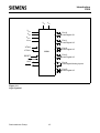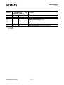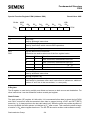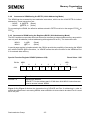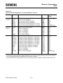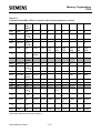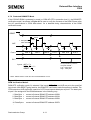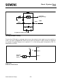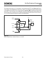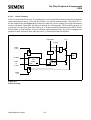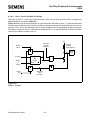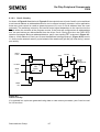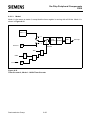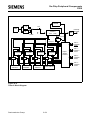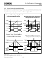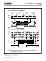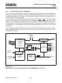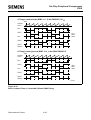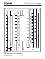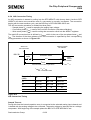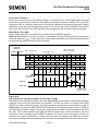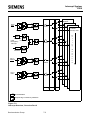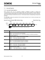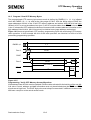
1
SAB-C501 Since April 1, 1999, Siemens Semiconductor is Infineon Technologies. The next revision of this document will be updated accordingly. C508 8-Bit CMOS Microcontroller User’s Manual 06.99 h de . s n e r/ m to e c i .s du w n o w c /: /w emi ttp S / Since April 1, 1999, Siemens Semiconductor is Infineon Technologies. The next revision of this document will be updated accordingly. Edition 06.99 This edition was realized using the software system FrameMaker. Published by Siemens AG, Bereich Halbleiter, MarketingKommunikation, Balanstraße 73, 81541 München © Siemens AG 97. All Rights Reserved. Attention please! As far as patents or other rights of third parties are concerned, liability is only assumed for components, not for applications, processes and circuits implemented within components or assemblies. The information describes the type of component and shall not be considered as assured characteristics. Terms of delivery and rights to change design reserved. For questions on technology, delivery and prices please contact the Semiconductor Group Offices in Germany or the Siemens Companies and Representatives worldwide (see address list). Due to technical requirements components may contain dangerous substances. For information on the types in question please contact your nearest Siemens Office, Semiconductor Group. Siemens AG is an approved CECC manufacturer. Packing Please use the recycling operators known to you. We can also help you – get in touch with your nearest sales office. By agreement we will take packing material back, if it is sorted. You must bear the costs of transport. For packing material that is returned to us unsorted or which we are not obliged to accept, we shall have to invoice you for any costs incurred. Components used in life-support devices or systems must be expressly authorized for such purpose! Critical components1 of the Semiconductor Group of Siemens AG, may only be used in life-support devices or systems2 with the express written approval of the Semiconductor Group of Siemens AG. 1 A critical component is a component used in a life-support device or system whose failure can reasonably be expected to cause the failure of that life-support device or system, or to affect its safety or effectiveness of that device or system. 2 Life support devices or systems are intended (a) to be implanted in the human body, or (b) to support and/or maintain and sustain human life. If they fail, it is reasonable to assume that the health of the user may be endangered. C508 User’s Manual Revision History : Current Version : 06.99 Previous Releases : (Original Version) We Listen to Your Comments Any information within this document that you feel is wrong, unclear or missing at all? Your feedback will help us to continuously improve the quality of this document. Please send your proposal (including a reference to this document) to: [email protected] General Information C508 Semiconductor Group I-4 General Information C508 Contents Page 1 1.1 1.2 Introduction . . . . . . . . . . . . . . . . . . . . . . . . . . . . . . . . . . . . . . . . . . . . . . . . . . . . . . . .1-1 Pin Configuration . . . . . . . . . . . . . . . . . . . . . . . . . . . . . . . . . . . . . . . . . . . . . . . . . . . .1-4 Pin Definitions and Functions . . . . . . . . . . . . . . . . . . . . . . . . . . . . . . . . . . . . . . . . . . . .1-6 2 2.1 2.2 Fundamental Structure . . . . . . . . . . . . . . . . . . . . . . . . . . . . . . . . . . . . . . . . . . . . . . .2-1 CPU . . . . . . . . . . . . . . . . . . . . . . . . . . . . . . . . . . . . . . . . . . . . . . . . . . . . . . . . . . . . . .2-3 CPU Timing . . . . . . . . . . . . . . . . . . . . . . . . . . . . . . . . . . . . . . . . . . . . . . . . . . . . . . . .2-5 3 3.1 3.2 3.3 3.4 3.4.1 3.4.2 3.4.3 3.4.4 3.4.5 3.5 Memory Organization . . . . . . . . . . . . . . . . . . . . . . . . . . . . . . . . . . . . . . . . . . . . . . .3-1 Program Memory, "Code Space" . . . . . . . . . . . . . . . . . . . . . . . . . . . . . . . . . . . . . . . .3-2 Data Memory, "Data Space" . . . . . . . . . . . . . . . . . . . . . . . . . . . . . . . . . . . . . . . . . . .3-2 General Purpose Registers . . . . . . . . . . . . . . . . . . . . . . . . . . . . . . . . . . . . . . . . . . . .3-2 XRAM Operation . . . . . . . . . . . . . . . . . . . . . . . . . . . . . . . . . . . . . . . . . . . . . . . . . . . .3-3 XRAM Controller Access Control . . . . . . . . . . . . . . . . . . . . . . . . . . . . . . . . . . . . . .3-3 Accesses to XRAM using the DPTR (16-bit Addressing Mode) . . . . . . . . . . . . . . . .3-5 Accesses to XRAM using the Registers R0/R1 (8-bit Addressing Mode) . . . . . . . . .3-5 Reset Operation of the XRAM . . . . . . . . . . . . . . . . . . . . . . . . . . . . . . . . . . . . . . . . . . .3-9 Behaviour of Port 0 and Port 2 . . . . . . . . . . . . . . . . . . . . . . . . . . . . . . . . . . . . . . . . . .3-9 Special Function Registers . . . . . . . . . . . . . . . . . . . . . . . . . . . . . . . . . . . . . . . . . . .3-11 4 4.1 4.1.1 4.1.2 4.1.3 4.2 4.3 4.4 4.5 4.6 4.6.1 4.6.2 4.6.3 4.6.4 4.7 4.7.1 4.7.2 4.8 External Bus Interface . . . . . . . . . . . . . . . . . . . . . . . . . . . . . . . . . . . . . . . . . . . . . .4-1 Accessing External Memory . . . . . . . . . . . . . . . . . . . . . . . . . . . . . . . . . . . . . . . . . . . . .4-1 Role of P0 and P2 as Data/Address Bus . . . . . . . . . . . . . . . . . . . . . . . . . . . . . . . . . .4-1 Timing . . . . . . . . . . . . . . . . . . . . . . . . . . . . . . . . . . . . . . . . . . . . . . . . . . . . . . . . . . . . .4-3 External Program Memory Access . . . . . . . . . . . . . . . . . . . . . . . . . . . . . . . . . . . . . .4-3 PSEN, Program Store Enable . . . . . . . . . . . . . . . . . . . . . . . . . . . . . . . . . . . . . . . . .4-3 Overlapping External Data and Program Memory Spaces . . . . . . . . . . . . . . . . . . . .4-3 ALE, Address Latch Enable . . . . . . . . . . . . . . . . . . . . . . . . . . . . . . . . . . . . . . . . . .4-4 Enhanced Hooks Emulation Concept . . . . . . . . . . . . . . . . . . . . . . . . . . . . . . . . . . . .4-5 Eight Datapointers for Faster External Bus Access . . . . . . . . . . . . . . . . . . . . . . . . . .4-6 The Importance of Additional Datapointers . . . . . . . . . . . . . . . . . . . . . . . . . . . . . . . . .4-6 How the eight Datapointers of the C508 are implemented . . . . . . . . . . . . . . . . . . . .4-6 Advantages of Multiple Datapointers . . . . . . . . . . . . . . . . . . . . . . . . . . . . . . . . . . . . . .4-7 Application Example and Performance Analysis . . . . . . . . . . . . . . . . . . . . . . . . . . . .4-7 ROM/OTP Protection for the C508-4R / C508-4E . . . . . . . . . . . . . . . . . . . . . . . . . . .4-10 Unprotected ROM Mode . . . . . . . . . . . . . . . . . . . . . . . . . . . . . . . . . . . . . . . . . . . . .4-10 Protected ROM/OTP Mode . . . . . . . . . . . . . . . . . . . . . . . . . . . . . . . . . . . . . . . . . . .4-11 Version Registers . . . . . . . . . . . . . . . . . . . . . . . . . . . . . . . . . . . . . . . . . . . . . . . . . . .4-14 5 5.1 5.2 5.3 5.4 5.5 5.6 Reset and System Clock Operation . . . . . . . . . . . . . . . . . . . . . . . . . . . . . . . . . . . . .5-1 Hardware Reset Operation . . . . . . . . . . . . . . . . . . . . . . . . . . . . . . . . . . . . . . . . . . .5-1 Fast Internal Reset after Power-On . . . . . . . . . . . . . . . . . . . . . . . . . . . . . . . . . . . . . .5-3 Hardware Reset Timing . . . . . . . . . . . . . . . . . . . . . . . . . . . . . . . . . . . . . . . . . . . . . . .5-5 Clock Generation . . . . . . . . . . . . . . . . . . . . . . . . . . . . . . . . . . . . . . . . . . . . . . . . . . . . .5-7 PLL Operation . . . . . . . . . . . . . . . . . . . . . . . . . . . . . . . . . . . . . . . . . . . . . . . . . . . . . . .5-7 Oscillator and Clock Circuit . . . . . . . . . . . . . . . . . . . . . . . . . . . . . . . . . . . . . . . . . . . . .5-8 6 On-Chip Peripheral Components . . . . . . . . . . . . . . . . . . . . . . . . . . . . . . . . . . . . . . .6-1 Semiconductor Group I-1 General Information C508 Contents 6.1 6.1.1 6.1.2 6.1.2.1 6.1.2.2 6.1.2.3 6.1.3 6.1.3.1 6.1.3.2 6.1.4 6.1.5 6.1.6 6.2 6.2.1 6.2.1.1 6.2.1.2 6.2.1.3 6.2.1.4 6.2.1.5 6.2.2 6.2.2.1 6.2.2.2 6.2.2.3 6.2.2.4 6.2.2.5 6.3 6.3.1 6.3.2 6.3.2.1 6.3.2.2 6.3.2.3 6.3.2.4 6.3.2.5 6.3.2.6 6.3.2.7 6.3.2.8 6.3.3 6.3.3.1 6.3.4 6.3.4.1 6.3.4.2 6.3.4.3 6.3.4.4 6.3.4.5 6.3.4.6 Page Parallel I/O . . . . . . . . . . . . . . . . . . . . . . . . . . . . . . . . . . . . . . . . . . . . . . . . . . . . . . . . .6-1 Port Structures . . . . . . . . . . . . . . . . . . . . . . . . . . . . . . . . . . . . . . . . . . . . . . . . . . . . . .6-1 Standard I/O Port Circuitry . . . . . . . . . . . . . . . . . . . . . . . . . . . . . . . . . . . . . . . . . . . . .6-3 Port 0 Circuitry . . . . . . . . . . . . . . . . . . . . . . . . . . . . . . . . . . . . . . . . . . . . . . . . . . . . . .6-5 Port 1, Port 3 and Port 5 Circuitry . . . . . . . . . . . . . . . . . . . . . . . . . . . . . . . . . . . . . . .6-6 Port 2 Circuitry . . . . . . . . . . . . . . . . . . . . . . . . . . . . . . . . . . . . . . . . . . . . . . . . . . . . . .6-7 Detailed Output Driver Circuitry . . . . . . . . . . . . . . . . . . . . . . . . . . . . . . . . . . . . . . . . .6-9 Type B Port Driver Circuitry . . . . . . . . . . . . . . . . . . . . . . . . . . . . . . . . . . . . . . . . . . . .6-9 Type D Port Driver Circuitry . . . . . . . . . . . . . . . . . . . . . . . . . . . . . . . . . . . . . . . . . . .6-11 Port Timing . . . . . . . . . . . . . . . . . . . . . . . . . . . . . . . . . . . . . . . . . . . . . . . . . . . . . . .6-12 Port Loading and Interfacing . . . . . . . . . . . . . . . . . . . . . . . . . . . . . . . . . . . . . . . . . .6-13 Read-Modify-Write Feature of Ports 0 to 5 (Except Port 4) . . . . . . . . . . . . . . . . . . . .6-14 Timers/Counters . . . . . . . . . . . . . . . . . . . . . . . . . . . . . . . . . . . . . . . . . . . . . . . . . . . .6-15 Timer/Counter 0 and 1 . . . . . . . . . . . . . . . . . . . . . . . . . . . . . . . . . . . . . . . . . . . . . .6-15 Timer/Counter 0 and 1 Registers . . . . . . . . . . . . . . . . . . . . . . . . . . . . . . . . . . . . . .6-16 Mode 0 . . . . . . . . . . . . . . . . . . . . . . . . . . . . . . . . . . . . . . . . . . . . . . . . . . . . . . . . . . .6-19 Mode 1 . . . . . . . . . . . . . . . . . . . . . . . . . . . . . . . . . . . . . . . . . . . . . . . . . . . . . . . . . .6-20 Mode 2 . . . . . . . . . . . . . . . . . . . . . . . . . . . . . . . . . . . . . . . . . . . . . . . . . . . . . . . . . .6-21 Mode 3 . . . . . . . . . . . . . . . . . . . . . . . . . . . . . . . . . . . . . . . . . . . . . . . . . . . . . . . . . .6-22 Timer/Counter 2 with Additional Compare/Capture/Reload . . . . . . . . . . . . . . . . .6-23 Timer 2 Registers . . . . . . . . . . . . . . . . . . . . . . . . . . . . . . . . . . . . . . . . . . . . . . . . . . .6-25 Timer 2 Operation . . . . . . . . . . . . . . . . . . . . . . . . . . . . . . . . . . . . . . . . . . . . . . . . . .6-30 Compare Function of Registers CRC, T2CC1 to T2CC3 . . . . . . . . . . . . . . . . . . . .6-32 Using Interrupts in Combination with the Compare Function . . . . . . . . . . . . . . . . .6-38 Capture Function . . . . . . . . . . . . . . . . . . . . . . . . . . . . . . . . . . . . . . . . . . . . . . . . . . .6-40 Capture / Compare Unit (CCU) . . . . . . . . . . . . . . . . . . . . . . . . . . . . . . . . . . . . . .6-43 General Capture/Compare Unit Operation . . . . . . . . . . . . . . . . . . . . . . . . . . . . . . . .6-44 CAPCOM Unit Operation . . . . . . . . . . . . . . . . . . . . . . . . . . . . . . . . . . . . . . . . . . . . .6-46 CAPCOM Unit Clocking Scheme . . . . . . . . . . . . . . . . . . . . . . . . . . . . . . . . . . . . . . . .6-46 CAPCOM Unit Operating Mode 0 . . . . . . . . . . . . . . . . . . . . . . . . . . . . . . . . . . . . . . .6-47 CAPCOM Unit Operating Mode 1 . . . . . . . . . . . . . . . . . . . . . . . . . . . . . . . . . . . . . .6-50 CAPCOM Unit Timing Relationships . . . . . . . . . . . . . . . . . . . . . . . . . . . . . . . . . . . . .6-51 Burst Mode of CAPCOM / COMP Unit . . . . . . . . . . . . . . . . . . . . . . . . . . . . . . . . . . . .6-53 CAPCOM Unit in Capture Mode . . . . . . . . . . . . . . . . . . . . . . . . . . . . . . . . . . . . . .6-54 Trap Function of the CAPCOM Unit in Compare Mode . . . . . . . . . . . . . . . . . . . . . .6-55 CAPCOM Registers . . . . . . . . . . . . . . . . . . . . . . . . . . . . . . . . . . . . . . . . . . . . . . . . .6-57 Compare (COMP) Unit Operation . . . . . . . . . . . . . . . . . . . . . . . . . . . . . . . . . . . . . .6-74 COMP Registers . . . . . . . . . . . . . . . . . . . . . . . . . . . . . . . . . . . . . . . . . . . . . . . . . .6-75 Combined Multi-Channel PWM Modes . . . . . . . . . . . . . . . . . . . . . . . . . . . . . . . . . .6-80 Control Register BCON . . . . . . . . . . . . . . . . . . . . . . . . . . . . . . . . . . . . . . . . . . . . . .6-82 Signal Generation in Multi-Channel PWM Modes . . . . . . . . . . . . . . . . . . . . . . . . . . .6-84 Block Commutation PWM Mode . . . . . . . . . . . . . . . . . . . . . . . . . . . . . . . . . . . . . . .6-87 Phase Delay Timer . . . . . . . . . . . . . . . . . . . . . . . . . . . . . . . . . . . . . . . . . . . . . . . . . . .6-90 Compare Timer 1 Controlled Multi-Channel PWM Modes . . . . . . . . . . . . . . . . . . . .6-91 Software Controlled State Switching in Multi-Channel PWM Modes . . . . . . . . . . . .6-96 Semiconductor Group I-2 General Information C508 6.3.4.7 6.4 6.4.1 6.4.2 6.4.3 6.4.3.1 6.4.3.2 6.4.3.3 6.4.4 6.4.5 6.4.6 6.5 6.5.1 6.5.2 6.5.3 6.5.4 6.5.5 Trap Function in Multi-Channel Block Commutation Mode . . . . . . . . . . . . . . . . . .6-97 Serial Interface . . . . . . . . . . . . . . . . . . . . . . . . . . . . . . . . . . . . . . . . . . . . . . . . . . . . .6-98 Multiprocessor Communication . . . . . . . . . . . . . . . . . . . . . . . . . . . . . . . . . . . . . . . .6-99 Serial Port Registers . . . . . . . . . . . . . . . . . . . . . . . . . . . . . . . . . . . . . . . . . . . . . . . .6-99 Baud Rate Generation . . . . . . . . . . . . . . . . . . . . . . . . . . . . . . . . . . . . . . . . . . . . . .6-101 Baud Rate in Mode 0 . . . . . . . . . . . . . . . . . . . . . . . . . . . . . . . . . . . . . . . . . . . . . . . .6-102 Baud Rate in Mode 2 . . . . . . . . . . . . . . . . . . . . . . . . . . . . . . . . . . . . . . . . . . . . . . . .6-102 Baud Rate in Mode 1 and 3 . . . . . . . . . . . . . . . . . . . . . . . . . . . . . . . . . . . . . . . . . . .6-103 Details about Mode 0 . . . . . . . . . . . . . . . . . . . . . . . . . . . . . . . . . . . . . . . . . . . . . . .6-106 Details about Mode 1 . . . . . . . . . . . . . . . . . . . . . . . . . . . . . . . . . . . . . . . . . . . . . .6-109 Details about Modes 2 and 3 . . . . . . . . . . . . . . . . . . . . . . . . . . . . . . . . . . . . . . . .6-112 A/D Converter . . . . . . . . . . . . . . . . . . . . . . . . . . . . . . . . . . . . . . . . . . . . . . . . . . . .6-115 A/D Converter Operation . . . . . . . . . . . . . . . . . . . . . . . . . . . . . . . . . . . . . . . . . . . .6-115 A/D Converter Registers . . . . . . . . . . . . . . . . . . . . . . . . . . . . . . . . . . . . . . . . . . .6-117 A/D Converter Clock Selection . . . . . . . . . . . . . . . . . . . . . . . . . . . . . . . . . . . . . . . .6-121 A/D Conversion Timing . . . . . . . . . . . . . . . . . . . . . . . . . . . . . . . . . . . . . . . . . . . . .6-122 A/D Converter Calibration . . . . . . . . . . . . . . . . . . . . . . . . . . . . . . . . . . . . . . . . . . .6-126 7 7.1 7.2 7.2.1 7.2.2 7.2.3 7.3 7.4 7.5 7.6 Interrupt System . . . . . . . . . . . . . . . . . . . . . . . . . . . . . . . . . . . . . . . . . . . . . . . . . . .7-1 Structure of the Interrupt System . . . . . . . . . . . . . . . . . . . . . . . . . . . . . . . . . . . . . . . . .7-1 Interrupt Registers . . . . . . . . . . . . . . . . . . . . . . . . . . . . . . . . . . . . . . . . . . . . . . . . . . . .7-7 Interrupt Enable Registers . . . . . . . . . . . . . . . . . . . . . . . . . . . . . . . . . . . . . . . . . . . .7-7 Interrupt Request Flags . . . . . . . . . . . . . . . . . . . . . . . . . . . . . . . . . . . . . . . . . . . . .7-12 Interrupt Priority Registers . . . . . . . . . . . . . . . . . . . . . . . . . . . . . . . . . . . . . . . . . . .7-21 Interrupt Priority Level Structure . . . . . . . . . . . . . . . . . . . . . . . . . . . . . . . . . . . . . . .7-22 How Interrupts are Handled . . . . . . . . . . . . . . . . . . . . . . . . . . . . . . . . . . . . . . . . . . .7-24 External Interrupts . . . . . . . . . . . . . . . . . . . . . . . . . . . . . . . . . . . . . . . . . . . . . . . . . .7-26 Interrupt Response Time . . . . . . . . . . . . . . . . . . . . . . . . . . . . . . . . . . . . . . . . . . . . .7-27 8 8.1 8.1.1 8.1.2 8.1.3 8.1.4 8.1.5 8.2 8.2.1 Fail Save Mechanisms . . . . . . . . . . . . . . . . . . . . . . . . . . . . . . . . . . . . . . . . . . . . . . .8-1 Programmable Watchdog Timer . . . . . . . . . . . . . . . . . . . . . . . . . . . . . . . . . . . . . . . .8-1 Input Clock Selection . . . . . . . . . . . . . . . . . . . . . . . . . . . . . . . . . . . . . . . . . . . . . . . .8-2 Watchdog Timer Control / Status Flags . . . . . . . . . . . . . . . . . . . . . . . . . . . . . . . . . .8-3 Starting the Watchdog Timer . . . . . . . . . . . . . . . . . . . . . . . . . . . . . . . . . . . . . . . . . .8-4 Refreshing the Watchdog Timer . . . . . . . . . . . . . . . . . . . . . . . . . . . . . . . . . . . . . . . .8-4 Watchdog Reset and Watchdog Status Flag . . . . . . . . . . . . . . . . . . . . . . . . . . . . . . .8-5 Oscillator Watchdog Unit . . . . . . . . . . . . . . . . . . . . . . . . . . . . . . . . . . . . . . . . . . . . . .8-6 Detailed Description of the Oscillator Watchdog Unit . . . . . . . . . . . . . . . . . . . . . . . . .8-7 9 9.1 9.2 9.3 9.4 9.4.1 9.4.2 9.5 Power Saving Modes . . . . . . . . . . . . . . . . . . . . . . . . . . . . . . . . . . . . . . . . . . . . . . . .9-1 Power Saving Mode Control Registers . . . . . . . . . . . . . . . . . . . . . . . . . . . . . . . . . .9-1 Idle Mode . . . . . . . . . . . . . . . . . . . . . . . . . . . . . . . . . . . . . . . . . . . . . . . . . . . . . . . . .9-3 Slow Down Mode Operation . . . . . . . . . . . . . . . . . . . . . . . . . . . . . . . . . . . . . . . . . . .9-5 Software Power Down Mode . . . . . . . . . . . . . . . . . . . . . . . . . . . . . . . . . . . . . . . . . . .9-6 Invoking Software Power Down Mode . . . . . . . . . . . . . . . . . . . . . . . . . . . . . . . . . . .9-6 Exit from Software Power Down Mode . . . . . . . . . . . . . . . . . . . . . . . . . . . . . . . . . . .9-7 State of Pins in Software Initiated Power Saving Modes . . . . . . . . . . . . . . . . . . . . . .9-8 10 OTP Memory Operation Semiconductor Group . . . . . . . . . . . . . . . . . . . . . . . . . . . . . . . . . . . . . . . . . . . .10-1 1-3 General Information C508 10.1 10.2 10.3 10.4 10.4.1 10.4.2 10.5 10.6 10.7 Programming Configuration . . . . . . . . . . . . . . . . . . . . . . . . . . . . . . . . . . . . . . . . . . .10-1 Pin Configuration . . . . . . . . . . . . . . . . . . . . . . . . . . . . . . . . . . . . . . . . . . . . . . . . . . . .10-2 Pin Definitions . . . . . . . . . . . . . . . . . . . . . . . . . . . . . . . . . . . . . . . . . . . . . . . . . . . . . .10-4 Programming Mode Selection . . . . . . . . . . . . . . . . . . . . . . . . . . . . . . . . . . . . . . . . . .10-6 Basic Programming Mode Selection . . . . . . . . . . . . . . . . . . . . . . . . . . . . . . . . . . . . .10-6 OTP Memory Access Mode Selection . . . . . . . . . . . . . . . . . . . . . . . . . . . . . . . . . . . .10-7 Program / Read OTP Memory Bytes . . . . . . . . . . . . . . . . . . . . . . . . . . . . . . . . . . . .10-8 Lock Bits Programming / Read . . . . . . . . . . . . . . . . . . . . . . . . . . . . . . . . . . . . . . . .10-10 Access of Version Bytes . . . . . . . . . . . . . . . . . . . . . . . . . . . . . . . . . . . . . . . . . . . . .10-12 11 Index . . . . . . . . . . . . . . . . . . . . . . . . . . . . . . . . . . . . . . . . . . . . . . . . . . . . . . . . . . . . .11-1 Semiconductor Group 1-4 Introduction C508 1 Introduction The C508 is a member of the Siemens C500 family of 8-bit microcontrollers. It is fully compatible to the standard 8051 microcontroller. Its features include the capture compare unit (CCU) which is useful in motor control applications, extended power saving provisions, 256x8 on-chip RAM, 32Kx8 on-chip program memory, and RFI related improvements. The C508 has an internal PLL and with a maximum CPU clock rate of 20 MHz it achieves a 300 ns instruction cycle time. The C508 basically operates with internal and/or external program memory. The C508-4R contains 32Kx8 on-chip program memory (ROM version) while the C508-4E has 32Kx8 one-time programmable program memory (OTP version). In this documentation the term C508 refers to both versions unless otherwise noted. On-Chip Emulation Support Module Figure 1-1 shows the different functional units of the C508 and Figure 1-2 shows the simplified logic symbol of the C508. Oscillator Watchdog RAM 256 × 8 XRAM 1k × 8 10-bit ADC Timer 2 16-bit Capture/Compare Unit CPU 8-bit 8 Datapointers USART T1 ROM / OTP 32k × 8 Figure 1-1 C508 Functional Units Semiconductor Group I/O Port 1 I/O Port 2 I/O Port 3 I/O Port 4 8 Digital/Analog Inputs Port 5 I/O T0 10-bit Compare Unit Watchdog Timer Port 0 1-1 Introduction C508 Listed below is a summary of the main features of the C508: • Fully compatible to standard 8051 microcontroller • Superset of the 8051 architecture with 8 datapointers • 10 to 20 MHz internal CPU clock (using built-in PLL with a factor of 2) • • • • • • • • • • • • • • • • – external clock of 5 - 10 MHz at 50% duty cycle – 300 ns instruction cycle time for P-MQFP-64-1 (@ 20 MHz CPU clock) – 375 ns instruction cycle time for P-SDIP-64-2 (@ 16 MHz CPU clock) 32 Kbyte on-chip ROM/OTP (with optional ROM protection) 256 byte on-chip RAM 1024 byte on-chip XRAM Five 8-bit ports, (Port 4 with pure analog/digital input channels) – Port 1 and 2 with enhanced current sinking capabilities of 10 mA (total max. of 100mA) Three 16-bit timers/counters – Timer 0 / 1 (C501 compatible) – Timer 2 with 4 channels for 16-bit capture/compare operation Capture/compare unit for PWM signal generation – 3-channel, 16-bit capture/compare unit – 1-channel, 10-bit compare unit Full duplex serial interface with programmable baudrate generator (USART) 8 channel 10-bit A/D Converter 19 interrupt vectors with four priority levels On-chip emulation support logic (Enhanced Hooks Technology TM) Programmable 15-bit Watchdog Timer Oscillator Watchdog Fast Power On Reset Power Saving Modes – Slow-down mode – Idle mode (can be combined with slow-down mode) – Software power-down mode with wake up capability through INT0 or INT7 P-MQFP-64-1, P-SDIP-64-2 packages Temperature ranges: SAB-C508 TA = 0 to 70 °C SAF-C508 TA = – 40 to 85°C Semiconductor Group 1-2 Introduction C508 VDD VSS VDDA Port 0 8-bit Digital I/O VSSA VAREF VAGND Port 1 8-bit Digital I/O XTAL1 XTAL2 C508 Port 2 8-bit Digital I/O Port 3 8-bit Digital I/O RESET EA ALE Port 4 8-bit Digital/Analog Inputs PSEN Port 5 8-bit Digital I/O Figure 1-2 Logic Symbol Semiconductor Group 1-3 Introduction C508 1.1 Pin Configuration P3.0/RXD P3.3/INT1 P3.2/INT0 P3.1/TXD P3.5/T1 P3.4/T0 VSS XTAL1 XTAL2 P3.7/RD P3.6/WR VDD P2.6/A14 P2.7/A15 PSEN ALE This section shows the pin configuration of the C508 in both P-MQFP-64-1 and P-SDIP-64-2 packages. 48 47 46 45 44 43 42 41 40 39 38 37 36 35 34 33 49 32 P2.5/A13 P2.4/A12 P2.3/A11 50 51 30 P2.2/A10 52 29 P2.1/A9 P2.0/A8 VSS 53 28 54 27 55 26 VDD 31 56 25 C508 P0.0/AD0 P0.1/AD1 P0.2/AD2 57 P0.3/AD3 60 P0.4/AD4 P0.5/AD5 P0.6/AD6 61 20 P0.7/AD7 64 24 P1.0/COUT3 P1.1/CTRAP P1.2/CC0 P1.3/COUT0 P1.4/CC1 P1.5/COUT1 P1.6/CC2 P1.7/COUT2 VSS 58 23 VDD 59 22 P5.0/T2CC0/INT3 21 P5.1/T2CC1/INT4 P5.2/T2CC2/INT5 62 19 63 18 8 9 10 11 12 13 14 15 16 Figure 1-3 Pin Configuration for P-MQFP-64-1 Package (Top View) Semiconductor Group 1-4 P5.7/INT7 P5.6/INT8 7 VAGND 6 P4.6/AN6 P4.7/AN7 VAREF VDDA VSSA 5 P4.5/AN5 EA 4 P4.1/AN1 P4.2/AN2 P4.3/AN3 P4.4/AN4 3 P4.0/AN0 2 RESET 17 1 P5.3/T2CC3/INT6 P5.4/INT2 P5.5/INT9 Introduction C508 The figure below shows the pin configuration of the C508 in the P-SDIP-64-2 package. P0.0/AD0 P0.1/AD1 1 64 2 63 P0.2/AD2 3 62 P0.3/AD3 P0.4/AD4 4 61 5 60 P0.5/AD5 P0.6/AD6 P0.7/AD7 RESET 6 59 7 58 8 57 9 56 P2.5/A13 P2.6/A14 EA 10 55 P2.7/A15 VDDA VSSA 11 54 12 53 P4.0/AN0 P4.1/AN1 P4.2/AN2 P4.3/AN3 P4.4/AN4 13 52 14 51 PSEN ALE VDD VSS 17 48 P4.5/AN5 P4.6/AN6 18 47 19 46 P4.7/AN7 VAREF 20 45 21 44 VAGND 22 43 P5.7/INT7 P5.6/INT8 P5.5/INT9 P5.4/INT2 23 42 24 41 25 40 26 39 P5.3/T2CC3/INT6 P5.2/T2CC2/INT5 P5.1/T2CC1/INT4 P5.0/T2CC0/INT3 VDD VSS 27 38 28 29 37 30 35 31 34 32 33 15 16 50 C508 49 36 Figure 1-4 Pin Configuration for P-SDIP-64-2 Package (Top View) Semiconductor Group 1-5 VDD VSS P2.0/A8 P2.1/A9 P2.2/A10 P2.3/A11 P2.4/A12 XTAL1 XTAL2 P3.7/RD P3.6/WR P3.5/T1 P3.4/T0 P3.3/INT1 P3.2/INT0 P3.1/TXD P3.0/RXD P1.0/COUT3 P1.1/CTRAP P1.2/CC0 P1.3/COUT0 P1.4/CC1 P1.5/COUT1 P1.6/CC2 P1.7/COUT2 Introduction C508 1.2 Pin Definitions and Functions This section describes all external signals of the C508 with its function. Table 1-1 : Pin Definitions and Functions Symbol Pin Numbers I/O*) Function I/O Port 1 is an 8-bit quasi-bidirectional port with internal pull-up transistors. Port 1 pins can be used for digital input/ output. Port 1 pins that have 1’s written to them are pulled high by the internal pull-up transistors and in that state can be used as inputs. As inputs, port 3 pins being externally pulled low will source current (IIL, in the DC characteristics) because of the internal pullup transistors. The output latch corresponding secondary function must be programmed to a one (1) for that function to operate. As secondary functions, port 1 contains the capture/compare inputs/outputs as well as the CCU trap input. P-MQFP-64 P-SDIP-64 P1.0-P1.7 25 - 32 33 - 40 Port 1 pins (except P1.1) have LED drive capability of up to 10mA sinking current per pin. The secondary functions from the CCU unit are assigned to the pins of port 1 as follows : 32 31 30 40 39 38 P1.0 / COUT3 P1.1 / CTRAP P1.2 / CC0 29 28 37 36 P1.3 / COUT0 P1.4 / CC1 27 26 35 34 P1.5 / COUT1 P1.6 / CC2 25 33 P1.7 / COUT2 *) I = Input O = Output Semiconductor Group 1-6 10-bit compare channel output CCU trap input Input/Output of capture/compare channel 0 Output of capture/compare channel 0 Input/Output of capture/compare channel 1 Output of capture/compare channel 1 Input/Output of capture/compare channel 2 Output of capture/compare channel 2 Introduction C508 Symbol Pin Numbers I/O*) Function P-MQFP-64 P-SDIP-64 RESET 1 9 I RESET A high level on this pin for one machine cycle while the oscillator is running resets the device. An internal diffused resistor to VSS permits power-on reset using only an external capacitor to VDD. P3.0-P3.7 33 - 40 41 - 48 I/O Port 3 is an 8-bit quasi-bidirectional port with internal pull-up transistors. Port 3 pins that have 1’s written to them are pulled high by the internal pull-up transistors and in that state can be used as inputs. As inputs, port 3 pins being externally pulled low will source current (IIL, in the DC characteristics) because of the internal pullup transistors. The output latch corresponding secondary function must be programmed to a one (1) for that function to operate (except for TxD and WR). The secondary functions are assigned to the pins of port 3 as follows: 33 41 P3.0 / RxD 34 42 P3.1 / TxD 35 43 P3.2 / INT0 36 44 P3.3 / INT1 37 38 39 45 46 47 P3.4 / T0 P3.5 / T1 P3.6 / WR 40 48 P3.7 / RD *) I = Input O = Output Semiconductor Group 1-7 Receiver data input (asynch.) or data input/output (synch.) of serial interface Transmitter data output (asynch.) or clock output (synch.) of serial interface External interrupt 0 input / timer 0 gate control input External interrupt 1 input / timer 1 gate control input Timer 0 counter input Timer 1 counter input WR control output; latches the data byte from port 0 into the external data memory RD control output; enables the external data memory Introduction C508 Symbol Pin Numbers I/O*) Function I/O Port 2 is an 8-bit quasi-bidirectional I/O port with internal pullup transistors. Port 2 pins that have 1’s written to them are pulled high by the internal pullup resistors, and in that state can be used as inputs. As inputs, port 2 pins being externally pulled low will source current (IIL, in the DC characteristics) because of the internal pullup transistors. P-MQFP-64 P-SDIP-64 P2.0-P2.7 47 - 54 55 - 62 Port 2 emits the high-order address byte during fetches from external program memory and during accesses to external data memory that use 16-bit addresses (MOVX @DPTR). In this application it uses strong internal pullup transistors when issuing 1s. During accesses to external data memory that use 8bit addresses (MOVX @Ri), port 2 issues the contents of the P2 special function register and uses only the internal pullup transistors. As I/O functions, port 2 pins also have LED drive capability of up to 10mA sinking current per pin. XTAL1 42 50 I XTAL1 Input to the inverting oscillator amplifier and input to the internal clock generator circuits. To drive the device from an external clock source, XTAL 1 sh ould be d ri ven, wh ile XTAL2 i s left unconnected. Minimum and maximum high and low times as well as rise/fall times specified in the AC characteristics must be observed. XTAL2 41 49 O XTAL2 Output of the inverting oscillator amplifier. *) I = Input O = Output Semiconductor Group 1-8 Introduction C508 Symbol Pin Numbers I/O*) Function P-MQFP-64 P-SDIP-64 P4.0-P4.7 5 - 12 13 - 20 I Port 4 is an 8-bit uni-directional input port to the A/D converter. Port pins can be used for digital input, if voltage levels simultaneously meet the specifications for hi gh/lo w input vo ltages and for the eight multiplexed analog inputs. PSEN 46 54 O The Program Strobe Enable output is a control signal that enables the external program memory to the bus during external fetch operations. It is activated every one and a half oscillator periods except during external data memory accesses. Remains high during internal program execution. This pin should not be driven during reset operation. ALE 45 53 O The Address Latch Enable output is used for latching the low-byte of the address into external memory during normal operation. It is activated every one and a half oscillator periods except during an external data memory access. When instructions are executed from internal ROM (EA=1) the ALE generation can be disabled by bit EALE in SFR SYSCON. This pin should not be driven during reset operation. EA 2 10 I External Access Enable When held at high level, instructions are fetched from the internal ROM when the PC is less than 8000H. When held at low level, the C508 fetches all instructions from external program memory. This pin should not be driven during reset operation. *)I=Input O=Output Semiconductor Group 1-9 Introduction C508 Symbol Pin Numbers I/O*) Function I/O Port 0 is an 8-bit open-drain bidirectional I/O port. Port 0 pins that have 1’s written to them float, and in that state can be used as high-impendance inputs. Port 0 is also the multiplexed low-order address and data bus during accesses to external program or data memory. In this application it uses strong internal pullup transistors when issuing 1’s. P-MQFP-64 P-SDIP-64 P0.0-P0.7 57 - 64 1-8 Port 0 also outputs the code bytes during program verification in the C508-4R. External pullup resistors are required during program verification. P5.0-P5.7 15 - 22 23 - 30 I/O Port 5 is a an 8-bit quasi-bidirectional I/O port with internal pullup transistors. Port 2 pins that have 1’s written to them are pulled high by the internal pullup resistors, and in that state can be used as inputs. As inputs, port 2 pins being externally pulled low will source current (IIL, in the DC characteristics) because of the internal pullup transistors. As secondary functions, port 5 contains the interrupt and Timer 2 capture/compare pins. They are assigned to the pins as follows: T2 Compare/Capture output 0 / Interrupt 3 input P5.1/T2CC1/INT4 T2 Compare/Capture output 1/ Interrupt 4 input P5.2/T2CC2/INT5 T2 Compare/Capture output 2 / Interrupt 5 input P5.3/T2CC3/INT6 T2 Compare/Capture output 3 / Interrupt 6 input Interrupt 2 input P5.4/INT2 P5.5/INT9 Interrupt 9 input P5.6/INT8 Interrupt 8 input P5.7/INT7 Interrupt 7 input P5.0/T2CC0/INT3 *) I = Input O = Output Semiconductor Group 1-10 Introduction C508 Symbol Pin Numbers I/O*) Function P-MQFP-64 P-SDIP-64 VSS 24, 43, 55 32, 51, 63 – Ground (0V) VDD 23, 44, 56 31, 52, 64 – Power Supply (+5V) VDDA 3 11 – Analog Power Supply (+5V) VSSA 4 12 – Analog Ground (0V) VAREF 13 21 – Reference voltage for the A/D converter. VAGND 14 22 – Reference ground for the A/D converter. *) I = Input O = Output Semiconductor Group 1-11 Introduction C508 Semiconductor Group 1-12 Fundamental Structure C508 2 Fundamental Structure The C508 is fully compatible to the architecture of the standard 8051/C501 microcontroller family. While maintaining all architectural and operational characteristics of the C501, the C508 incorporates a CPU with 8 datapointers, a 10-bit A/D converter, a 16-bit capture/compare unit, a timer 2 with capture/compare functions, an improved interrupt structure with 4 priority levels, builtin PLL with a fixed factor of 2, an XRAM data memory as well as some enhancements in the Fail Save Mechanism Unit. Figure 2-1 shows a block diagram of the C508. Semiconductor Group 2-1 Fundamental Structure C508 VDD C508 VSS Oscillator Watchdog XTAL1 XTAL2 RESET OSC & Timing PLL, factor of 2 XRAM RAM ROM/ OTP 1024 x 8 256 x 8 32k x 8 CPU 8 datapointers ALE PSEN EA Programmable Watchdog Timer Port 0 Port 0 8-bit digital I/O Port 1 Port 1 8-bit digital I/O Port 2 Port 2 8-bit digital I/O Port 3 Port 3 8-bit digital I/O Capture/Compare Unit Port 4 Port 4 8-bit analog/ digital Input Interrupt Unit Port 5 Port 5 8-bit digital I/O Timer 0 Timer 1 Timer 2 with 4 PWM Channels USART Baudrate generator VAREF VAGND A/D Converter 10-Bit S&H Emulation Support Logic MUX Figure 2-1 Block Diagram of the C508 Semiconductor Group 2-2 Fundamental Structure C508 2.1 CPU The C508 is efficient both as a controller and as an arithmetic processor. It has extensive facilities for binary and BCD arithmetic and excels in its bit-handling capabilities. Efficient use of program memory results from an instruction set consisting of 44% one-byte, 41% two-byte, and 15% threebyte instructions. With a 10 MHz external crystal (giving a 20MHz CPU clock), 58% of the instructions execute in 300 ns. For an 8 MHz crystal, the corresponding time is 375 ns. The CPU (Central Processing Unit) of the C508 consists of the instruction decoder, the arithmetic section and the program control section. Each program instruction is decoded by the instruction decoder. This unit generates the internal signals controlling the functions of the individual units within the CPU. These internal signals have an effect on the source and destination of data transfers and control the ALU processing. The arithmetic section of the processor performs extensive data manipulation and is comprised of the arithmetic/logic unit (ALU), an A register, B register and PSW register. The ALU accepts 8-bit data words from one or two sources and generates an 8-bit result under the control of the instruction decoder. The ALU performs the arithmetic operations add, substract, multiply, divide, increment, decrement, BDC-decimal-add-adjust and compare, and the logic operations AND, OR, Exclusive OR, complement and rotate (right, left or swap nibble (left four)). Also included is a Boolean processor performing the bit operations as set, clear, complement, jumpif-set, jump-if-not-set, jump-if-set-and-clear and move to/from carry. Between any addressable bit (or its complement) and the carry flag, the ALU can perform the bit operations of logical AND or logical OR with the result returned to the carry flag. The program control section controls the sequence in which the instructions stored in program memory are executed. The 16-bit program counter (PC) holds the address of the next instruction to be executed. The conditional branch logic enables internal and external events to the processor to cause a change in the program execution sequence. Additionally to the CPU functionality of the C501/8051 standard microcontroller, the C508 contains 8 datapointers. For complex applications with peripherals located in the external data memory space or extended data storage capacity, this turned out to be a "bottle neck" for the 8051’s communication to the external world. Especially programming in high-level languages (PLM51, C51, PASCAL51) requires extended RAM capacity and at the same time a fast access to this additional RAM because of the reduced code efficiency of these languages. Accumulator ACC is the symbol for the accumulator register. The mnemonics for accumulator-specific instructions, however, refer to the accumulator simply as A. Program Status Word The Program Status Word (PSW) contains several status bits that reflect the current state of the CPU. Semiconductor Group 2-3 Fundamental Structure C508 Special Function Register PSW (Address D0H) Reset Value : 00H Bit No. MSB D0H LSB D7H D6H D5H D4H D3H D2H D1H D0H CY AC F0 RS1 RS0 OV F1 P Bit Function CY Carry Flag Used by arithmetic instructions. AC Auxiliary Carry Flag Used by instructions which execute BCD operations. F0 General Purpose Flag RS1 RS0 Register Bank select control bits These bits are used to select one of the four register banks. PSW RS1 RS0 Function 0 0 Bank 0 selected, data address 00H-07H 0 1 Bank 1 selected, data address 08H-0FH 1 0 Bank 2 selected, data address 10H-17H 1 1 Bank 3 selected, data address 18H-1FH OV Overflow Flag Used by arithmetic instructions. F1 General Purpose Flag P Parity Flag Set/cleared by hardware after each instruction to indicate an odd/even number of "one" bits in the accumulator, i.e. even parity. B Register The B register is used during multiply and divide and serves as both source and destination. For other instructions it can be treated as another scratch pad register. Stack Pointer The stack pointer (SP) register is 8 bits wide. It is incremented before data is stored during PUSH and CALL executions and decremented after data is popped during a POP and RET (RETI) execution, i.e. it always points to the last valid stack byte. While the stack may reside anywhere in the on-chip RAM, the stack pointer is initialized to 07H after a reset. This causes the stack to begin a location = 08H above register bank zero. The SP can be read or written under software control. Semiconductor Group 2-4 Fundamental Structure C508 2.2 CPU Timing The C508 has no clock prescaler. Therefore, a machine cycle of the C508 consists of 6 states (3 oscillator periods). Each state is divided into a phase 1 half and a phase 2 half. Thus, a machine cycle consists of 3 oscillator periods, numbererd S1P1 (state 1, phase 1) through S6P2 (state 6, phase 2). Each state lasts half an oscillator period. Typically, arithmetic and logic operations take place during phase 1 and internal register-to-register transfers take place during phase 2. The diagrams in Figure 2-2 show the fetch/execute timing related to the internal states and phases. Since these internal clock signals are not user-accessible, the XTAL1 oscillator signals and the ALE (address latch enable) signal are shown for external reference. ALE is normally activated twice during each machine cycle: once during S1P2 and S2P1, and again during S4P2 and S5P1. Execution of a one-cycle instruction begins at S1P2, when the op-code is latched into the instruction register. If it is a two-byte instruction, the second reading takes place during S4 of the same machine cycle. If it is a one-byte instruction, there is still a fetch at S4, but the byte read (which would be the next op-code) is ignored (discarded fetch), and the program counter is not incremented. In any case, execution is completed at the end of S6P2. Figure 2-2 (a) and (b) show the timing of a 1-byte, 1-cycle instruction and for a 2-byte, 1-cycle instruction. Most C508 instructions are executed in one cycle. MUL (multiply) and DIV (divide) are the only instructions that take more than two cycles to complete; they take four cycles. Normally two code bytes are fetched from the program memory during every machine cycle. The only exception to this is when a MOVX instruction is executed. MOVX is a one-byte, 2-cycle instruction that accesses external data memory. During a MOVX, the two fetches in the second cycle are skipped while the external data memory is being addressed and strobed. Figure 2-2 (c) and (d) show the timing for a normal 1-byte, 2-cycle instruction and for a MOVX instruction. Semiconductor Group 2-5 Fundamental Structure C508 S1 S2 S1 S2 S3 S4 S5 S6 S3 S4 S5 S6 P1 P2 P1 P2 P1 P2 P1 P2 P1 P2 P1 P2 P1 P2 P1 P2 P1 P2 P1 P2 P1 P2 P1 P2 OSC (XTAL2) ALE Read Opcode S1 S2 S3 Read Next Opcode (Discard) S4 S5 Read Next Opcode Again S6 (a) 1-Byte, 1-Cycle Instruction, e.g. INC A Read Opcode S1 S2 S3 Read 2nd Byte S4 S5 Read Next Opcode S6 (b) 2 Byte, 1-Cycle Instruction, e.g. ADD A #Data Read Next Opcode Again Read Next Opcode (Discard) Read Opcode S1 S2 S3 S4 S5 S6 S1 S2 S3 S4 S5 S6 (c) 1-Byte, 2-Cycle Instruction, e.g. INC DPTR Read Opcode (MOVX) S1 S2 S3 Read Next Opcode Again No No Fetch Fetch No ALE Read Next Opcode (Discard) S4 (d) MOVX (1-Byte, 2-Cycle) S5 S6 ADDR S1 S2 S3 DATA Access of External Memory Figure 2-2 Fetch Execute Sequence Semiconductor Group 2-6 S4 S5 S6 Fundamental Structure C508 Semiconductor Group 2-7 Memory Organization C508 3 Memory Organization The C508 CPU manipulates operands in the following five address spaces: – up to 64 Kbytes of program memory : 32K ROM for C508-4R : 32K OTP for C508-4E – up to 64 Kbytes of external data memory – 256 bytes of internal data memory – 1024 bytes of internal XRAM data memory – a 128 byte special function register area Figure 3-1 illustrates the memory address spaces of the C508. Alternatively FFFFH FFFFH Ext. Data Memory Ext. Internal XRAM (1KByte) FC00H FBFFH indirect addr. 8000H 7FFFH Int. Ext. (EA = 1) (EA = 0) Ext. Data Memory 0000H "Code Space" 0000H "Data Space" Figure 3-1 C508 Memory Map Semiconductor Group Internal RAM 3-1 direct addr. Special FFH Function Regs. 80H Internal RAM 7FH 00H "Internal Data Space" Memory Organization C508 3.1 Program Memory, "Code Space" The C508-4R has 32 Kbytes of read-only program memory (ROM), while the C508-4E provides 32Kbytes of OTP program memory. The program memory can be externally expanded up to 64 Kbytes. If the EA pin is held high, the C508-4R executes program code out of the internal ROM unless the program counter address exceeds 7FFF H. Address locations 8000H through FFFFH are then fetched from the external program memory. If the EA pin is held low, the C508 fetches all instructions from the external program memory. 3.2 Data Memory, "Data Space" The data memory address space consists of an internal and an external memory space. The internal data memory is divided into three physically separate and distinct blocks : the lower 128 bytes of RAM, the upper 128 bytes of RAM, and the 128 byte special function register (SFR) area. While the upper 128 bytes of data memory and the SFR area share the same address locations, they are accessed through different addressing modes. The lower 128 bytes of data memory can be accessed through direct or register indirect addressing; the upper 128 bytes of RAM can be accessed through register indirect addressing; the special function registers are accessible through direct addressing. Four 8-register banks, each bank consisting of eight 8-bit general-purpose registers, occupy locations 0 through 1FH in the lower RAM area. The next 16 bytes, locations 20H through 2FH, contain 128 directly addressable bit locations. The stack can be located anywhere in the internal RAM area, and the stack depth can be expanded up to 256 bytes. The external data memory can be expanded up to 64 Kbytes and can be accessed by instructions that use a 16-bit or an 8-bit address. The internal XRAM is located in the external address memory area at addresses FC00H to FFFFH. Using MOVX instruction with addresses pointing to this address area, alternatively internal XRAM or external data RAM are accessed. 3.3 General Purpose Registers The lower 32 locations of the internal RAM are assigned to four banks of eight general purpose registers (GPRs) each. Only one of these banks may be enabled at a time. Two bits in the program status word, RS0 (PSW.3) and RS1 (PSW.4), select the active register bank (see description of the PSW in chapter 2). This allows fast context switching, which is useful when entering subroutines or interrupt service routines. The eight general purpose registers of the selected register bank may be accessed by register addressing. With register addressing the instruction op code indicates which register is to be used. For indirect addressing R0 and R1 are used as pointer or index register to address internal or external memory (e.g. MOV @R0). Reset initializes the stack pointer to location 07 H and increments it once to start from location 08H which is also the first register (R0) of register bank 1. Thus, if one is going to use more than one register bank, the SP should be initialized to a different location of the RAM which is not used for data storage. Semiconductor Group 3-2 Memory Organization C508 3.4 XRAM Operation The XRAM in the C508 is a memory area that is logically located at the upper end of the external data memory space, but is integrated on the chip. Because the XRAM is used in the same way as external data memory the same instruction types (MOVX) must be used for accessing the XRAM. 3.4.1 XRAM Controller Access Control Two bits in SFR SYSCON, XMAP0 and XMAP1, control the accesses to XRAM. XMAP0 is a general access enable/disable control bit and XMAP1 controls the external signal generation during XRAM accesses. Special Function Register SYSCON (Address B1H) Bit No. MSB 7 B1H – Reset Value : XX10XX01B 6 5 4 3 2 – EALE RMAP – – 1 LSB 0 XMAP1 XMAP0 SYSCON The functions of the shaded bits are not described here. Bit Function XMAP1 XRAM visible access control Control bit for RD/WR signals during XRAM accesses. If addresses are outside the XRAM address range or if XRAM is disabled, this bit has no effect. XMAP1 = 0 : The signals RD and WR are not activated during accesses to the XRAM. XMAP1 = 1 : Ports 0, 2 and the signals RD and WR are activated during accesses to XRAM. In this mode, address and data information during XRAM accesses are visible externally. XMAP0 Global XRAM access enable/disable control XMAP0 = 0 : The access to XRAM is enabled. XMAP0 = 1 : The access to XRAM is disabled (default after reset). All MOVX accesses are performed via the externl bus. Further, this bit is hardware protected. – Reserved bits for future use. Read by CPU returns undefined values. When bit XMAP1 in SFR SYSCON is set, during all accesses to XRAM, RD and WR become active and port 0 and 2 drive the actual address/data information which is read/written from/to XRAM. This feature allows to check the internal data transfers to XRAM. When port 0 and 2 are used for I/O purposes, the XMAP1 bit should not be set. Otherwise the I/O function of the port 0 and port 2 lines is interrupted. Semiconductor Group 3-3 Memory Organization C508 After a reset operation, bit XMAP0 is set. This means that the accesses to XRAM are generally disabled. In this case, all accesses using MOVX instructions within the address range of FC00H to FFFFH generate external data memory bus cycles. When XMAP0 is cleared, the access to XRAM is enabled and all accesses using MOVX instructions with an address in the range of FC00H to FFFFH will access the internal XRAM. Bit XMAP0 is hardware protected. If it is cleared once (i.e. if internal XRAM access enabled), it cannot be set by software. Only a reset operation will set the XMAP0 bit again. This hardware protection mechanism is done by an asymmetric latch at XMAP0 bit. An unintentional disabling of XRAM could be dangerous since indeterminate values could be read from the external bus. To avoid this the XMAP0 bit is forced to ’1’ only by a reset operation. Additionally, during reset an internal capacitor is charged. So the reset status is a disabled XRAM. Once a ‘0’ is written to XMAP0 bit (i.e. discharging the capacitor), it is not possible to set it back again to ‘1’ due to the charge time of the capacitor. On the other hand, any distortion (viz. software hang up, noise ..etc.) also can not charge this capacitor. Thus the stable status is the enabled XRAM. The clear instruction for the XMAP0 bit should be integrated in the program initialization routine before XRAM is used. In extremely noisy systems the user may have redundant clear instructions. Semiconductor Group 3-4 Memory Organization C508 3.4.2 Accesses to XRAM using the DPTR (16-bit Addressing Mode) The XRAM can be accessed by two read/write instructions, which use the 16-bit DPTR for indirect addressing. These instructions are : – MOVX – MOVX A, @DPTR @DPTR, A (Read) (Write) For accessing the XRAM, the effective address stored in DPTR must be in the range of FC00H to FFFFH. 3.4.3 Accesses to XRAM using the Registers R0/R1 (8-bit Addressing Mode) The 8051 architecture provides also instructions for accesses to external data memory range which use only an 8-bit address (indirect addressing with registers R0 or R1). The instructions are: MOVX MOVX A, @Ri @Ri, A (Read) (Write) A special page register is implemented in the C508 to provide the possibility of accessing the XRAM also with the MOVX @Ri instructions, i.e. XPAGE serves the same function for the XRAM as Port 2 for external data memory. Special Function Register XPAGE (Address 91H) Reset Value : 00H Bit No. MSB 7 6 5 4 3 2 1 LSB 0 91H .6 .5 .4 .3 .2 .1 .0 .7 XPAGE Bit Function XPAGE.7-0 XRAM high address XPAGE.7-0 is the address part A15-A8 when 8-bit MOVX instructions are used to access internal XRAM. Figure 3-2 to Figure 3-4 show the dependencies of XPAGE and Port 2 addressing in order to explain the differences in accessing XRAM, external RAM or to show what to do when Port 2 is used as an I/O-port. Semiconductor Group 3-5 Memory Organization C508 Address/Data Port 0 XRAM XPAGE Write to Port 2 Page Address Port 2 MCB02112 Figure 3-2 Write Page Address to Port 2 Moving the page address to Port 2 by either immediate addressing instruction (MOV P2,#pageaddress) or direct addressing instruction (MOV P2,PAL; where ‘PAL’ is internal RAM location containing the page address) will write the page address to port 2 and also to XPAGERegister. When external RAM is to be accessed in the XRAM address range, the XRAM has to be disabled. When the additional external RAM is to be addressed in an address range 0000H to FC00H, the XRAM may remain enabled. Semiconductor Group 3-6 Memory Organization C508 Address/Data Port 0 XRAM XPAGE Write to XPAGE Address/ I/O-Data Port 2 MCB02113 Figure 3-3 Write Page Address to XPAGE “MOV XPAGE,#pageaddress“ or “MOV XPAGE,PAL”, where ‘PAL’ is internal RAM location containing the page address, will write the page address only to the XPAGE register. Port 2 is available for addresses or I/O data. Semiconductor Group 3-7 Memory Organization C508 Address/Data Port 0 XRAM XPAGE Write I/O Data to Port 2 Port 2 I/O-Data MCB02114 Figure 3-4 Use of Port 2 as I/O Port At a write to port 2, the XRAM address in XPAGE register will be overwritten because of the concurrent write to port 2 and XPAGE register. So, whenever XRAM is used and the XRAM address differs from the byte written to port 2 latch, then it is absolutely necessary to rewrite XPAGE with the page address. Example : I/O data at port 2 shall be AAH. A byte shall be fetched from XRAM at address FF30H. MOV MOV MOV MOVX R0, #30H P2, #0AAH XPAGE, #0FFH A, @R0 Semiconductor Group ; ; P2 shows AAH and XPAGE contains AAH ; P2 still shows AAH but XRAM is addressed ; the contents of XRAM at FF30H is moved to accumulator 3-8 Memory Organization C508 The register XPAGE provides the upper address byte for accesses to XRAM with MOVX @Ri instructions. If the address formed by XPAGE and Ri points outside the XRAM address range, an external access is performed. For the C508 the content of XPAGE must be FCH - FFH in order to use the XRAM. The software has to distinguish two cases, if the MOVX @Ri instructions with paging shall be used : a) Access to XRAM : The upper address byte must be written to XPAGE or P2; both writes select the XRAM address range. b) Access to external memory : The upper address byte must be written to P2; XPAGE will be automatically loaded with the same address in order to deselect the XRAM. 3.4.4 Reset Operation of the XRAM The contents of the XRAM are not affected by a reset. After power-up the contents are undefined, while they remain unchanged during and after a reset as long as the power supply is not turned off. If a reset occurs during a write operation to XRAM, the content of a XRAM memory location depends on the cycle in which the active reset signal is detected (MOVX is a 2-cycle instruction): Reset during 1st cycle : The new value will not be written to XRAM. The old value is not affected. Reset during 2nd cycle : The old value in XRAM is overwritten by the new value. 3.4.5 Behaviour of Port 0 and Port 2 The behaviour of port 0 and port 2 during a MOVX access depends on the control bits in register SYSCON and on the state of pin EA. The Table 3-1 lists the various operating conditions. It shows the following characteristics: a) Use of P0 and P2 pins during the MOVX access. Bus:The pins work as external address/data bus. If (internal) XRAM is accessed, the data written to the XRAM can be seen on the bus in debug mode. I/0:The pins work as Input/Output lines under control of their latch. b) Activation of the RD and WR pin during the access. c) Use of internal (XRAM) or external XDATA memory. The shaded areas describe the standard operation as each C5xx device without on-chip XRAM behaves. Semiconductor Group 3-9 Semiconductor Group MOVX @DPTR 3-10 MOVX @ Ri EA = 0 EA = 1 XMAP1, XMAP0 XMAP1, XMAP0 00 10 X1 00 10 X1 a)P0/P2→Bus b)RD/WR active c)ext.memory is used a)P0/P2→Bus b)RD/WR active c)ext.memory is used a)P0/P2→Bus b)RD/WR active c)ext.memory is used a)P0/P2→Bus b)RD/WR active c)ext.memory is used a)P0/P2→Bus b)RD/WR active c)ext.memory is used a)P0/P2→Bus b)RD/WR active c)ext.memory is used DPTR ≥ XRAM address range a)P0/P2→Bus (RD/WR-Data) b)RD/WR inactive c)XRAM is used a)P0/P2→Bus a)P0/P2→Bus a)P0/P2→I/O (RD/WR-Data) b)RD/WR active b)RD/WR active b)RD/WR inactive c)XRAM is used c) ext.memory c)XRAM is used is used a)P0/P2→Bus a)P0/P2→Bus (RD/WR-Data) b)RD/WR active b)RD/WR active XPAGE < XRAM addr.page range a)P0→Bus P2→I/O b)RD/WR active c)ext.memory is used a)P0→Bus P2→I/O b)RD/WR active c)ext.memory is used a)P0→Bus P2→I/O b)RD/WR active c)ext.memory is used XPAGE ≥ XRAM addr.page range a)P0→Bus (RD/WR-Data) P2→I/O b)RD/WR inactive c)XRAM is used a)P0→Bus a)P0→Bus a)P0/P2→I/O (RD/WR-Data) P2→I/O P2→I/O b)RD/WR active b)RD/WR active b)RD/WR inactive c)XRAM is used c)ext.memory is c)XRAM is used used DPTR < XRAM address range a)P0→Bus P2→I/O b)RD/WR active c)ext.memory is used Table 3-1 - Behaviour of P0/P2 and RD/WR During MOVX Accesses a)P0→Bus P2→I/O b)RD/WR active c)ext.memory is used a)P0→Bus a)P0→Bus (RD/WR-Data) P2→I/O P2→I/O b)RD/WR active b)RD/WR active c)XRAM is used c)ext.memory is used Memory Organization C508 modes compatible to 8051/C501 family a)P0→Bus P2→I/O b)RD/WR active c)ext.memory is used c)XRAM is used c) ext.memory is used Memory Organization C508 3.5 Special Function Registers The registers, except the program counter and the four general purpose register banks, reside in the special function register area. The special function register area consists of two portions : the standard special function register area and the mapped special function register area. One special function register of the C508 (PCON1) is located in the mapped special function register area. For accessing the mapped special function register area, bit RMAP in special function register SYSCON must be set. All other special function registers are located in the standard special function register area which is accessed when RMAP is cleared (“0“). Special Function Register SYSCON (Address B1H) Bit No. MSB 7 B1H – Reset Value : XX10XX01B 6 5 4 3 2 – EALE RMAP – – 1 LSB 0 XMAP1 XMAP0 SYSCON The functions of the shaded bits are not described here. Bit Function RMAP Special function register map bit RMAP = 0 : The access to the non-mapped (standard) special function register area is enabled. RMAP = 1 : The access to the mapped special function register area is enabled. – Reserved bits for future use. Read by CPU returns undefined values. As long as bit RMAP is set, mapped special function register area can be accessed. This bit is not cleared by hardware automatically. Thus, when non-mapped/mapped registers are to be accessed, the bit RMAP must be cleared/set respectively by software. All SFRs with addresses where address bits 0-2 are 0 (e.g. 80H, 88H, 90H, 98H, ..., F8H, FFH) are bitaddressable. The 79 special function registers (SFRs) in the standard and mapped SFR area include pointers and registers that provide an interface between the CPU and the other on-chip peripherals. The SFRs of the C508 are listed in Table 3-2 and Table 3-3. In Table 3-2 they are organized in groups which refer to the functional blocks of the C508. Table 3-3 illustrates the contents of the SFRs in numeric order of their addresses. Semiconductor Group 3-11 Memory Organization C508 Table 3-2 Special Function Registers - Functional Blocks Block Symbol Name Address Contents after Reset CPU ACC B DPH DPL DPSEL PSW SP SYSCON2) VR04) VR14) VR24) Accumulator B-Register Data Pointer, High Byte Data Pointer, Low Byte Data Pointer Select Register Program Status Word Register Stack Pointer System Control Register Version Register 0 Version Register 1 Version Register 2 E0H 1) F0H 1) 83H 82H 92H D0H 1) 81H B1H FCH FDH FEH 00H 00H 00H 00H XXXXX000B 3) 00H 07H XX10XX01B 3) C5H 08H A/D Converter Control Register 0 A/D Converter Control Register 1 A/D Converter Data Register High Byte A/D Converter Start Register Low Byte D8H 1) DCH D9H DAH 00X00000B 3) 01XXX000B 3) 00H 00XXXXXXB 3) A8H1) B8H 1) 9AH BEH A9H B9H 88H 1) C8H 1) 98H 1) C0H 1) FBH 00H X0000000B XX0000XXB XXX000XXB 00H XX000000B 3) 00H 0000X0X0B 00H X0000000B XX000000B A/DADCON0 2) Converter ADCON1 ADDATH ADDATL Interrupt System IEN0 2) IEN1 2) IEN2 IEN3 IP0 2) IP1 TCON 2) T2CON 2) SCON 2) IRCON EINT Interrupt Enable Register 0 Interrupt Enable Register 1 Interrupt Enable Register 2 Interrupt Enable Register 3 Interrupt Priority Register 0 Interrupt Priority Register 1 Timer Control Register Timer 2 Control Register Serial Channel Control Register Interrupt Request Control Register External Interrupt Control Register XRAM XPAGE Page Address Register for Extended on-chip 91H XRAM and CAN Controller System Control Register B1H Port 0 80H 1) 90H 1) Port 1 A0H 1) Port 2 B0H 1) Port 3 DBH Port 4, Analog/Digital Input F8H 1) Port 5 SYSCON2) Ports P0 P1 P2 P3 P4 P5 5) 00H XX10XX01B 3) FFH FFH FFH FFH FFH 1) Bit-addressable special function registers 2) This special function register is listed repeatedly since some bits of it also belong to other functional blocks. 3) “X“ means that the value is undefined and the location is reserved 4) This SFR is a mapped SFR. For accessing this SFR, bit RMAP in SFR SYSCON must be set. 5) The content of this SFR varies with the actual step of the C508 (eg. 01H for the first step) Semiconductor Group 3-12 Memory Organization C508 Table 3-2 Special Function Registers - Functional Blocks (cont’d) Block Symbol Name Address Contents after Reset Serial Channel ADCON0 2) PCON 2) SBUF SCON SRELL SRELH A/D Converter Control Register 0 Power Control Register Serial Channel Buffer Register Serial Channel Control Register Serial Channel Reload Register, low byte Serial Channel Reload Register, high byte D8H 1) 87H 99H 98H 1) AAH BAH 00X00000B 3) 00H XXH 3) 00H D9H XXXXXX11B 3) Timer 0/ Timer 1 TCON TH0 TH1 TL0 TL1 TMOD Timer 0/1 Control Register Timer 0, High Byte Timer 1, High Byte Timer 0, Low Byte Timer 1, Low Byte Timer Mode Register 88H 1) 8CH 8DH 8AH 8BH 89H 00H 00H 00H 00H 00H 00H Timer 2 CCEN T2CCH1 T2CCH2 T2CCH3 T2CCL1 T2CCL2 T2CCL3 CRCH CRCL TH2 TL2 T2CON Compare/Capture Enable Register Compare /Capture Register 1, High Byte Compare /Capture Register 2, High Byte Compare /Capture Register 3, High Byte Compare /Capture Register 1, Low Byte Compare /Capture Register 2, Low Byte Compare /Capture Register 3, Low Byte Comp./Rel./Capt. Register, High Byte Comp./Rel./Capt. Register, Low Byte Timer 2, High Byte Timer 2, Low Byte Timer 2 Control Register C1H C3H C5H C7H C2H C4H C6H CBH CAH CDH CCH C8H 1) 00H 00H 00H 00H 00H 00H 00H 00H 00H 00H 00H 0000X0X0B 1) Bit-addressable special function registers 2) This special function register is listed repeatedly since some bits of it also belong to other functional blocks. 3) “X” means that the value is undefined and the location is reserved 4) SFR is located in the mapped SFR area. For accessing this SFR, bit RMAP in SFR SYSCON must be set. Semiconductor Group 3-13 Memory Organization C508 Table 3-2 Special Function Registers - Functional Blocks (cont’d) Block Name Address Contents after Reset Compare/ CT1CON Capture CCPL Unit CCPH CT1OFL CT1OFH CMSEL0 CMSEL1 COINI CCL0 CCH0 CCL1 CCH1 CCL2 CCH2 TRCON COTRAP CCIR CCIE 2) CT2CON CP2L CP2H CMP2L CMP2H BCON Compare timer 1 control register Compare timer 1 period register, low byte Compare timer 1 period register, high byte Compare timer 1 offset register, low byte Compare timer 1 offset register, high byte Capture/compare mode select register 0 Capture/compare mode select register 1 Compare output initialization register Capture/compare register 0, low byte Capture/compare register 0, high byte Capture/compare register 1, low byte Capture/compare register 1, high byte Capture/compare register 2, low byte Capture/compare register 2, high byte Trap enable control register Compare output in trap state register Capture/compare interrupt request flag reg. Capture/compare interrupt enable register Compare timer 2 control register Compare timer 2 period register, low byte Compare timer 2 period register, high byte Compare timer 2 compare register, low byte Compare timer 2 compare register, high byte Block commutation control register E1H DEH DFH E6H E7H E3H E4H E2H F2H F3H F4H F5H F6H F7H FFH F9H E5H D6H F1H D2H D3H D4H D5H D7H 00010000B 00H 00H 00H 00H 00H 00H FFH 00H 00H 00H 00H 00H 00H 00H 0X000000B 00H 00H 00010000B 00H XXXXXX00B 3) 00H XXXXXX00B 3)) 00H Watchdog WDTREL IEN0 2) IEN1 2) IP0 2) Watchdog Timer Reload Register Interrupt Enable Register 0 Interrupt Enable Register 1 Interrupt Priority Register 0 86H A8H1) B8H 1) A9H 00H 00H 00H 00H Power Control Register Power Control Register 1 87H 88H 1) 00H 0XX0XXXXB 3) Power Save Modes Symbol PCON 2) PCON14) 1) Bit-addressable special function registers 2) This special function register is listed repeatedly since some bits of it also belong to other functional blocks. 3) “X” means that the value is undefined and the location is reserved 4) SFR is located in the mapped SFR area. For accessing this SFR, bit RMAP in SFR SYSCON must be set. Semiconductor Group 3-14 Memory Organization C508 Table 3-3 Contents of the SFRs, SFRs in numeric order of their addresses Addr Register Content Bit 7 after Reset1) Bit 6 Bit 5 Bit 4 Bit 3 Bit 2 Bit 1 Bit 0 80H 2) P0 81H SP FFH .7 .6 .5 .4 .3 .2 .1 .0 07H .7 .6 .5 .4 .3 .2 .1 .0 82H 83H DPL 00H .7 .6 .5 .4 .3 .2 .1 .0 DPH 00H .7 .6 .5 .4 .3 .2 .1 .0 86H WDTREL 00H WDT PSEL .6 .5 .4 .3 .2 .1 .0 87H PCON 88H 2) TCON 00H SMOD PDS IDLS SD GF1 GF0 PDE IDLE 00H TF1 TF0 TR0 IE1 IT1 IE0 IT0 TR1 88H 3) PCON1 0XX0- EWPD – XXXXB – WS – – – – 89H 8AH TMOD 00H GATE C/T M1 M0 GATE C/T M1 M0 TL0 00H .7 .6 .5 .4 .3 .2 .1 .0 8BH TL1 00H .7 .6 .5 .4 .3 .2 .1 .0 8CH 8DH TH0 00H .7 .6 .5 .4 .3 .2 .1 .0 TH1 00H .7 .6 .5 .4 .3 .2 .1 .0 P1 FFH .7 .6 .5 .4 .3 .2 .1 .0 XPAGE 00H .7 .6 .5 .4 .3 .2 .1 .0 DPSEL XXXXX000B 00H – – – – – .2 .1 .0 SM0 SM1 SM2 REN TB8 RB8 TI RI XXH .7 .6 .5 .4 .3 .2 .1 .0 90H 91H 2) 92H 98H 2) SCON 99H SBUF 9A IEN2 XX0000XXB – – ECT1 ECCM ECT2 ECEM – – A0H2) A8H2) P2 FFH .7 .6 .5 .4 .3 .2 .1 .0 IEN0 00H EA WDT ET2 ES ET1 EX1 ET0 EX0 A9H AAH IP0 00H OWDS WDTS .5 .4 .3 .2 .1 .0 SRELL D9H .7 .4 .3 .2 .1 .0 .6 .5 1) X means that the value is undefined and the location is reserved 2) Bit-addressable special function registers 3) SFR is located in the mapped SFR area. For accessing this SFR, bit RMAP in SFR SYSCON must be set. Semiconductor Group 3-15 Memory Organization C508 Table 3-3 Contents of the SFRs, SFRs in numeric order of their addresses (cont’d) Addr Register Content Bit 7 after Reset1) Bit 6 Bit 5 Bit 4 Bit 3 Bit 2 Bit 1 Bit 0 B0H2) B1H P3 RD WR T1 T0 INT1 INT0 TxD RxD SYSCON XX10XX01B – – EALE RMAP – – XMAP1 XMAP0 B8H2) IEN1 X0000000B – SWDT EX6 EX5 EX4 EX3 EX2 EADC B9H IP1 – – .5 .4 .3 .2 .1 .0 BAH SRELH XX000000B XXXXXX11B – – – – – – .1 .0 BEH IEN3 XXX000XXB – – – EX9 EX8 EX7 – – C0H2) IRCON X0000000B – TF2 IEX6 IEX5 IEX4 IEX3 IEX2 IADC C1H CCEN 00H COCA H3 COCAL COCA 3 H2 COCAL COCA 2 H1 COCAL COCA COCAL 1 H0 0 C2H C3H T2CCL1 00H .7 .6 .5 .4 .3 .2 .1 .0 T2CCH1 00H T2CCL2 00H .7 .6 .5 .4 .3 .2 .1 .0 .7 .6 .5 .4 .3 .2 .1 .0 T2CCH2 00H T2CCL3 00H .7 .6 .5 .4 .3 .2 .1 .0 .7 .6 .5 .4 .3 .2 .1 .0 T2CCH3 00H T2CON 0000X0X0B .7 .6 .5 .4 .3 .2 .1 .0 T2PS I3FR I2FR T2R – T2CM – T2I CRCL 00H .7 .6 .5 .4 .3 .2 .1 .0 CRCH 00H .7 .6 .5 .4 .3 .2 .1 .0 TL2 00H .7 .6 .5 .4 .3 .2 .1 .0 TH2 00H .7 .6 .5 .4 .3 .2 .1 .0 00H CY AC F0 RS1 RS0 OV F1 P C4H C5H C6H C7H C8H2) CAH CBH CCH CDH D0H2) PSW FFH 1) X means that the value is undefined and the location is reserved 2) Bit-addressable special function registers Semiconductor Group 3-16 Memory Organization C508 Table 3-3 Contents of the SFRs, SFRs in numeric order of their addresses (cont’d) Addr Register Content Bit 7 after Reset1) Bit 6 Bit 5 Bit 4 Bit 3 Bit 2 Bit 1 Bit 0 D2H D3H CP2L 00H .7 .6 .5 .4 .3 .2 .1 .0 CP2H XXXX. XX00B – – – – – – .1 .0 D4H D5H CMP2L 00H .7 .6 .5 .4 .3 .2 .1 .0 CMP2H XXXX. XX00B – – – – – – .1 .0 D6H CCIE 00H ECTP ECTC CC2 FEN CC2 REN CC1 FEN CC1 REN CC0 FEN CC0 REN D7H BCON 00H BCMP BCEM PWM1 PWM0 EBCE BCERR BCEN BCM1 BCM0 BD CLK – BSY ADM MX2 MX1 MX0 .9 .8 .7 .6 .5 .4 .3 .2 DAH ADDATL 00XX- .1 XXXXB .0 – – – – – – DBH DCH P4 .6 .5 .4 .3 .2 .1 .0 ADCON1 01XXX000B ADCL1 ADCL0 – – – MX2 MX1 MX0 DEH DFH CCPL 00H .7 .6 .5 .4 .3 .2 .1 .0 CCPH 00H .7 .6 .5 .4 .3 .2 .1 .0 E0H2) E1H ACC 00H .7 .6 .5 .4 .3 .2 .1 .0 CT1CON 00010000B CTM ETRP STE1 CT1 RES CT1R CLK2 CLK1 CLK0 E2H COINI COUT 3I COUTX COUT I 2I CC2I COUT 1I CC1I COUT 0I CC0I E3H CMSEL0 00H CMSEL CMSEL CMSEL CMSEL CMSEL CMSEL CMSEL CMSEL 13 12 11 10 03 02 01 00 E4H CMSEL1 00H ESMC NMCS 0 0 CMSEL CMSEL CMSEL CMSEL 23 22 21 20 E5H CCIR CT1FP CT1FC CC2F CC2R CC1F D8H2) ADCON0 00X00000B D9H ADDATH 00H – FFH 00H .7 1) X means that the value is undefined and the location is reserved 2) Bit-addressable special function registers Semiconductor Group 3-17 CC1R CC0F CC0R Memory Organization C508 Table 3-3 Contents of the SFRs, SFRs in numeric order of their addresses (cont’d) Addr Register Content Bit 7 after Reset1) Bit 6 Bit 5 Bit 4 Bit 3 Bit 2 Bit 1 Bit 0 E6H E7H CT1OFL 00H CT1OFH 00H .7 .6 .5 .4 .3 .2 .1 .0 .7 .6 .5 .4 .3 .2 .1 .0 B .7 .6 .5 .4 .3 .2 .1 .0 CT2CON 00010000B CT2P ECT2O STE2 CT2 RES CT2R CLK2 CLK1 CLK0 CCL0 00H .7 .6 .5 .4 .3 .2 .1 .0 CCH0 00H .7 .6 .5 .4 .3 .2 .1 .0 CCL1 00H .7 .6 .5 .4 .3 .2 .1 .0 CCH1 00H .7 .6 .5 .4 .3 .2 .1 .0 CCL2 00H .7 .6 .5 .4 .3 .2 .1 .0 CCH2 00H .7 .6 .5 .4 .3 .2 .1 .0 F8H2) F9H P5 FFH .7 .6 .5 .4 .3 .2 .1 .0 COTRAP 00H BCT SEL PDTEN COUT2 CC2T T COUT1 CC1T T COUT0 CC0T T FBH EINT F0H F1H 2) F2H F3H F4H F5H F6H F7H FCH3)4) VR0 FDH3)4) VR1 FEH3)4) VR2 FFH TRCON 00H XX000000B C5H – – IEX9 I9FR IEX8 I8FR IEX7 I7FR 1 1 0 0 0 1 0 1 08H 0 0 0 0 1 0 0 0 5) .7 .6 .5 .4 .3 .2 .1 .0 00H TRPEN TRF TREN5 TREN4 TREN3 TREN2 TREN1 TREN0 1) X means that the value is undefined and the location is reserved. 2) Bit-addressable special function registers. 3) SFR is located in the mapped SFR area. For accessing this SFR, bit RMAP in SFR SYSCON must be set. 4) These are read-only registers. 5) The content of this SFR varies with the actual step of the C508 (eg. 01H for C508-4E, first step and 11H for C508-4R, first step). Semiconductor Group 3-18 Memory Organization C508 Semiconductor Group 3-19 External Bus Interface C508 4 External Bus Interface The C508 allows for external memory expansion. The functionality and implementation of the external bus interface is identical to the common interface for the 8051 architecture with one exception. It is the suppression of the ALE signal generation when C508 is used in systems with no external memory. Resetting EALE bit in SFR SYSCON will be gated off the ALE signal. This feature reduces RFI emissions of the system. 4.1 Accessing External Memory It is possible to distinguish between accesses to external program memory and external data memory or other peripheral components respectively. This distinction is made by hardware accesses to external program memory use the signal PSEN (program store enable) as a read strobe. Accesses to external data memory use RD and WR to strobe the memory (alternate functions of P3.7 and P3.6). Port 0 and port 2 (with exceptions) are used to provide data and address signals. In this section only the port 0 and port 2 functions relevant to external memory accesses are described. Fetches from external program memory always use a 16-bit address. Accesses to external data memory can use either a 16-bit address (MOVX @DPTR) or an 8-bit address (MOVX @Ri). 4.1.1 Role of P0 and P2 as Data/Address Bus When used for accessing external memory, port 0 provides the data byte time-multiplexed with the low byte of the address. In this state, port 0 is disconnected from its own port latch, and the address/ data signal drives both FETs in the port 0 output buffers. Thus, in this application, the port 0 pins are not open-drain outputs and do not require external pullup resistors. During any access to external memory, the CPU writes FF H to the port 0 latch (the special function register), thus obliterating whatever information the port 0 SFR may have been holding. Whenever a 16-bit address is used, the high byte of the address comes out on port 2, where it is held for the duration of the read or write cycle. During this time, the port 2 lines are disconnected from the port 2 latch (the special function register). Thus the port 2 latch does not have to contain 1s, and the contents of the port 2 SFR are not modified. If an 8-bit address is used (MOVX @Ri), the contents of the port 2 SFR remain at the port 2 pins throughout the external memory cycle. This will facilitate paging. It should be noted that, if a port 2 pin outputs an address bit that is a 1, strong pullups will be used for the entire read/write cycle and not only for two oscillator periods. Semiconductor Group 4-1 External Bus Interface C508 Figure 4-1 External Program Memory Execution Semiconductor Group 4-2 External Bus Interface C508 4.1.2 Timing The timing of the external bus interface, in particular the relationship between the control signals ALE, PSEN, RD, WR and information on port 0 and port 2, is illustated in Figure 4-1 a) and b). Data memory: in a write cycle, the data byte to be written appears on port 0 just before WR is activated and remains there until after WR is deactivated. In a read cycle, the incoming byte is accepted at port 0 before the read strobe is deactivated. Program memory: Signal PSEN functions as a read strobe. 4.1.3 External Program Memory Access The external program memory is accessed under two conditions: - whenever signal EA is active (low) or - whenever the program counter (PC) content is greater than 7FFFH When the CPU is executing out of external program memory, all 8 bits of port 2 are dedicated to an output function and must not be used for general-purpose I/O. The content of the port 2 SFR however is not affected. During external program memory fetches port 2 lines output the high byte of the PC, and during accesses to external data memory they output either DPH or the port 2 SFR (depending on whether the external data memory access is a MOVX @DPTR or a MOVX @Ri). 4.2 PSEN, Program Store Enable The read strobe for external program memory fetches is PSEN. It is not activated for internal program memory fetches. When the CPU is accessing external program memory, PSEN is activated twice every instruction cycle (except during a MOVX instruction) no matter whether or not the byte fetched is actually needed for the current instruction. When PSEN is activated its timing is not the same as for RD. A complete RD cycle, including activation and deactivation of ALE and RD, takes 3 oscillator periods. A complete PSEN cycle, including activation and deactivation of ALE and PSEN, takes 1.5 oscillator periods. (The execution sequence for these two types of read cycles is shown in Figure 4-1 a) and b). 4.3 Overlapping External Data and Program Memory Spaces In some applications it is desirable to execute a program from the same physical memory that is used for storing data. In the C508 the external program and data memory spaces can be combined by the logical-AND of PSEN and RD. A positive result from this AND operation produces a low active read strobe that can be used for the combined physical memory. Since the PSEN cycle is faster than the RD cycle, the external memory needs to be fast enough to adapt to the PSEN cycle. Semiconductor Group 4-3 External Bus Interface C508 4.4 ALE, Address Latch Enable The C508 allows to switch off the ALE output signal. If the internal ROM is used (EA=1 and PC ≤ 7FFFH) and ALE is switched off by EALE=0, then, ALE will only go active during external data memory accesses (MOVX instructions). If EA=0, the ALE generation is always enabled and the bit EALE has no effect. After a hardware reset the ALE generation is enabled. Special Function Register SYSCON (Address B1H) Bit No. MSB 7 B1H – Reset Value : XX10XX01B 6 5 4 3 2 – EALE RMAP – – 1 LSB 0 XMAP1 XMAP0 SYSCON The shaded bits are not described in this section. Bit Function EALE Enable ALE output EALE = 0 : ALE generation is disabled; disables ALE signal generation during internal code memory accesses (EA=1). With EA=1, ALE is automatically generated at MOVX instructions. EALE = 1 : ALE generation is enabled If EA=0, the ALE generation is always enabled and the bit EALE has no effect on the ALE generation. – Reserved bits for future use. Read by CPU returns undefined values. Semiconductor Group 4-4 External Bus Interface C508 4.5 Enhanced Hooks Emulation Concept The Enhanced Hooks Emulation Concept of the C500 microcontroller family is a new, innovative way to control the execution of C500 MCUs and to gain extensive information on the internal operation of the controllers. Emulation of on-chip ROM based programs is possible, too. Each C500 production chip has built-in logic for the support of the Enhanced Hooks Emulation Concept. Therefore, no costly bond-out chips are necessary for emulation. This also ensure that emulation and production chips are identical. The Enhanced Hooks TechnologyTM1), which requires embedded logic in the C500 allows the C500 together with an EH-IC to function similar to a bond-out chip. This simplifies the design and reduces costs of an ICE-system. ICE-systems using an EH-IC and a compatible C500 are able to emulate all operating modes of the different versions of the C500 microcontrollers. This includes emulation of ROM, ROM with code rollover and ROMless modes of operation. It is also able to operate in single step mode and to read the SFRs after a break. ICE-System Interface to Emulation Hardware RESET EA ALE PSEN SYSCON PCON TCON C500 MCU RSYSCON RPCON RTCON EH-IC Enhanced Hooks Interface Circuit Port 0 Port 2 Optional I/O Ports Port 3 Port 1 RPort 2 RPort 0 Target System Interface TEA TALE TPSEN MCS02647 Figure 4-2 Basic C500 MCU Enhanced Hooks Concept Configuration Port 0, port 2 and some of the control lines of the C500 based MCU are used by Enhanced Hooks Emulation Concept to control the operation of the device during emulation and to transfer informations about the program execution and data transfer between the external emulation hardware (ICE-system) and the C500 MCU. 1) “Enhanced Hooks Technology” is a trademark and patent of MetaLink Corporation licenced to Siemens. Semiconductor Group 4-5 External Bus Interface C508 4.6 Eight Datapointers for Faster External Bus Access 4.6.1 The Importance of Additional Datapointers The standard 8051 architecture provides just one 16-bit pointer for indirect addressing of external devices (memories, peripherals, latches, etc.). Except for a 16-bit "move immediate" to this datapointer and an increment instruction, any other pointer handling is to be handled bytewise. For complex applications with peripherals located in the external data memory space or extended data storage capacity this turned out to be a "bottle neck" for the 8051’s communication to the external world. Especially programming in high-level languages (PLM51, C51, PASCAL51) requires extended RAM capacity and at the same time a fast access to this additional RAM because of the reduced code efficiency of these languages. 4.6.2 How the eight Datapointers of the C508 are implemented Simply adding more datapointers is not suitable because of the need to keep up 100% compatibility to the 8051 instruction set. This instruction set, however, allows the handling of only one single 16bit datapointer (DPTR, consisting of the two 8-bit SFRs DPH and DPL). To meet both of the above requirements (speed up external accesses, 100% compatibility to 8051 architecture) the C508 contains a set of eight 16-bit registers from which the actual datapointer can be selected. This means that the user’s program may keep up to eight 16-bit addresses resident in these registers, but only one register at a time is selected to be the datapointer. Thus the datapointer in turn is accessed (or selected) via indirect addressing. This indirect addressing is done through a special function register called DPSEL (data pointer select register). All instructions of the C508 which handle the datapointer therefore affect only one of the eight pointers which is addressed by DPSEL at that very moment. Figure 4-3 illustrates the addressing mechanism. A 3-bit field in register DPSEL points to the currently used DPTRx. Any standard 8051 instruction (e.g. MOVX @DPTR, A - transfer a byte from accumulator to an external location addressed by DPTR) now uses this activated DPTRx. Special Function Register DPSEL (Address 92H) Reset Value : XXXXX000B Bit No. MSB 7 6 5 4 3 2 1 LSB 0 92H – – – – .2 .1 .0 – DPSEL Bit Function DPSEL.2-0 Data pointer select bits DPSEL.2-0 defines the number of the actual active data pointer.DPTR0-7. Semiconductor Group 4-6 External Bus Interface C508 - - - - - .2 .1 .0 DPSEL(92 H) DPSEL DPTR7 Selected Data- .2 .1 .0 pointer 0 0 0 DPTR 0 0 0 1 DPTR 1 0 1 0 DPTR 2 0 1 1 DPTR 3 1 0 0 DPTR 4 1 0 1 DPTR 5 1 1 0 DPTR 6 1 1 1 DPTR 7 DPTR0 DPH(83 H ) DPL(82 H) External Data Memory MCD00779 Figure 4-3 Accessing of External Data Memory via Multiple Datapointers 4.6.3 Advantages of Multiple Datapointers Using the above addressing mechanism for external data memory results in less code and faster execution of external accesses. Whenever the contents of the datapointer must be altered between two or more 16-bit addresses, one single instruction, which selects a new datapointer, does this job. lf the program uses just one datapointer, then it has to save the old value (with two 8-bit instructions) and load the new address, byte by byte. This not only takes more time, it also requires additional space in the internal RAM. 4.6.4 Application Example and Performance Analysis The following example shall demonstrate the involvement of multiple data pointers in a table transfer from the code memory to external data memory. Start address of ROM source table: Start address of table in external RAM: Semiconductor Group 1FFFH 2FA0H 4-7 External Bus Interface C508 Example 1 : Using only One Datapointer (Code for a C501) Initialization Routine MOV MOV MOV MOV LOW(SRC_PTR), #0FFH HIGH(SRC_PTR), #1FH LOW(DES_PTR), #0A0H HIGH(DES_PTR), #2FH ;Initialize shadow_variables with source_pointer ;Initialize shadow_variables with destination_pointer Table Look-up Routine under Real Time Conditions PUSH PUSH MOV MOV ;INC ;CJNE MOVC MOV MOV MOV MOV INC DPL DPH DPL, LOW(SRC_PTR) DPH, HIGH(SRC_PTR) DPTR … A,@DPTR LOW(SRC_PTR), DPL HIGH(SRC_PTR), DPH DPL, LOW(DES_PTR) DPH, HIGH(DES_PTR) DPTR MOVX MOV MOV POP POP @DPTR, A LOW(DES_PTR), DPL HIGH(DES_PTR),DPH DPH DPL ; Semiconductor Group ; Number of cycles ;Save old datapointer 2 ; 2 ;Load Source Pointer 2 ; 2 Increment and check for end of table (execution time not relevant for this consideration) – ;Fetch source data byte from ROM table 2 ;Save source_pointer and 2 ;load destination_pointer 2 ; 2 ; 2 ;Increment destination_pointer ;(ex. time not relevant) – ;Transfer byte to destination address 2 ;Save destination_pointer 2 ; 2 ;Restore old datapointer 2 ; 2 Total execution time (machine cycles) : 4-8 28 External Bus Interface C508 Example 2 : Using Two Datapointers (Code for a C508) Initialization Routine MOV MOV MOV MOV DPSEL, #06H DPTR, #1FFFH DPSEL, #07H DPTR, #2FA0H ;Initialize DPTR6 with source pointer ;Initialize DPTR7 with destination pointer Table Look-up Routine under Real Time Conditions PUSH MOV ;INC ;CJNE MOVC MOV DPSEL DPSEL, #06H DPTR … A,@DPTR DPSEL, #07H MOVX POP @DPTR, A DPSEL ; ; Number of cycles ;Save old source pointer 2 ;Load source pointer 2 Increment and check for end of table (execution time not relevant for this consideration) – ;Fetch source data byte from ROM table 2 ;Save source_pointer and ;load destination_pointer 2 ;Transfer byte to destination address 2 ;Save destination pointer and ;restore old datapointer 2 Total execution time (machine cycles) : 12 The above example shows that utilization of the C508’s multiple datapointers can make external bus accesses two times as fast as with a standard 8051 or 8051 derivative. Here, four data variables in the internal RAM and two additional stack bytes were spared, too. This means for some applications where all eight datapointers are employed that a C508 program has up to 24 byte (16 variables and 8 stack bytes) of the internal RAM free for other use. Semiconductor Group 4-9 External Bus Interface C508 4.7 ROM/OTP Protection for the C508-4R / C508-4E The C508-4R allows to protect the contents of the internal ROM against unauthorized read out. The type of ROM protection (protected or unprotected) is fixed with the ROM mask. Therefore, the customer of a C508-4R version has to define whether ROM protection has to be selected or not. The C508-4E OTP version allows also program memory protection in several levels (see chapter 10.6). The program memory proctection for the C508-4E can be activated after programming of the device. The C508-4R devices, which operate from internal ROM, are always checked for correct ROM contents during production test. Therefore, unprotected as well as protected ROMs must provide a procedure to verify the ROM contents. In ROM verification mode 1, which is used to verify unprotected ROMs, a ROM address is applied externally to the C508-4R and the ROM data byte is output at port 0. ROM verification mode 2, which is used to verify ROM protected devices, operates differently. In this mode, ROM addresses are generated internally and the expected data bytes must be applied externally to the device (by the manufacturer or by the customer) and are compared internally with the data bytes from the ROM. After 16 byte verify operations the state of the P3.5 pin shows whether the last 16 bytes have been verified correctly. This mechanism provides a very high security of ROM protection. Only the owner of the ROM code and the manufacturer who know the contents of the ROM can read out and verify it with less effort. The behaviour of the move code instruction, when the code is executed from the external ROM, is in such a way that accessing a code byte from a protected on-chip ROM address is not possible. In this case the byte accessed will be invalid. 4.7.1 Unprotected ROM Mode If the ROM is unprotected, the ROM verification mode 1 as shown in Figure 4-4 is used to read out the contents of the ROM. Please refer to the AC specifications in C508 data sheet for the AC timing characteristics of the ROM verification mode. P1.0-P1.7 P2.0-P2.6 Port 0 Address 1 Address 2 Inputs : PSEN, P2.7 = VSS ALE, EA = VIH / VIH2 RESET = VIH1 Data 1 Out Data 2 Out Figure 4-4 ROM Verification Mode 1 ROM verification mode 1 is selected if the inputs PSEN, ALE, EA, and RESET are put to the specified logic level. Then the 15-bit address of the internal ROM byte to be read is applied to the port 1 and port 2 lines. After a delay time, port 0 outputs the content of the addressed ROM cell. In ROM verification mode 1, the C508 must be provided with a system clock at the XTAL pins and pullup resistors on the port 0 lines. Semiconductor Group 4-10 External Bus Interface C508 4.7.2 Protected ROM/OTP Mode If the C508-4R ROM is protected by mask (or C508-4E OTP in protection level 1), the ROM/OTP verification mode 2 as shown in Figure 4-5 is used to verify the contents of the ROM. Please refer the AC specifications in C508 data sheet for a detailed timing characteristics of the ROM verification mode. RESET 12TCL ALE 1. ALE pulse after reset Latch Data for Addr. 0 Port 0 6TCL Latch Data for Addr. 1 Latch Latch Data for Addr. 2 Data for Ad. X·16 -1 Data for Addr. X·16 Latch Data for Ad. X·16 +1 P3.5 Inputs : ALE = VSS PSEN, EA = VIH RESET = Verify Result for previous 16 bytes of data :Low : Verify Error High : Verify OK * Note : Please refer to C508 data sheet for the definition of TCL. Figure 4-5 ROM Verification Mode 2 ROM/OTP verification mode 2 is selected if the inputs PSEN, EA, and ALE are put to the specified logic levels. With RESET going inactive, the ROM/OTP verification mode 2 sequence is started. The C508 outputs an ALE signal with a period of 12TCL and expects data bytes at port 0. The data bytes at port 0 are assigned to the ROM addresses in the following way : 1. Data Byte = 2. Data Byte = 3. Data Byte = : 16. Data Byte = : Semiconductor Group content of internal ROM/OTP address 0000H content of internal ROM/OTP address 0001H content of internal ROM/OTP address 0002H content of internal ROM/OTP address 000FH 4-11 External Bus Interface C508 The C508 does not output any address information during the ROM/OTP verification mode 2. The first data byte to be verified is always the byte which is assigned to the internal ROM address 0000H and must be put onto the data bus with the falling edge of RESET. With each following ALE pulse the ROM/OTP address pointer is internally incremented and the expected data byte for the next ROM address must be delivered externally. Between two ALE pulses the data at port 0 is latched (at 6TCL after ALE rising edge) and compared internally with the ROM/OTP content of the actual address. If a verify error is detected, the error condition is stored internally. After each 16th data byte the cumulated verify result (pass or fail) of the last 16 verify operations is output at P3.5. This means that P3.5 stays at a static level (low for fail and high for pass) while the next 16 bytes are checked. The output of P3.5 will be updated according to the cumulated verify result of the previous 16 bytes of data. In ROM verification mode 2, the C508 must be provided with a system clock at the XTAL pins. Figure 4-6 shows an application example of an external circuitry which allows to verify a protected ROM inside the C508-4R in ROM/OTP verification mode 2. With RESET going inactive, the C508 starts the ROM/OTP verify sequence. Its ALE is clocking a 15-bit address counter. This counter generates the addresses for an external EPROM which is programmed with the contents of the internal (protected) ROM/OTP. The verify detect logic typically displays the state of the verify error output P3.5. P3.5 can be latched with the falling edge of ALE. The CY signal of the address counter indicates to the verify detect logic the end of the internal ROM verification. Semiconductor Group 4-12 External Bus Interface C508 P3.5 Verify Detect Logic CY ALE CLK 2K 15-Bit Address Counter C508-4R C508-4E A0-A14 S & VDD Compare Code ROM & RESET Port 0 D0-D7 VDD EA CS PSEN Figure 4-6 ROM/OTP Verification Mode 2 - External Circuitry Example Semiconductor Group 4-13 OE External Bus Interface C508 4.8 Version Registers Version registers are typically used for adapting the programming firmware to specific device characteristics such as ROM / OTP size etc. Three version registers are implemented in the C508. They can be read during normal program execution mode as mapped SFRs when the bit RMAP in SFR SYSCON is set. The first step of the C508 will contain the following information in the version registers. Version register 2 will be incremented with each new step of the C508. Contents of Version registers Name Address C508 Version Register 0 FCH Version Register 1 FDH C5H 08H Version Register 2 FEH 01H Semiconductor Group 4-14 External Bus Interface C508 Semiconductor Group 4-15 Reset / System Clock C508 5 Reset and System Clock Operation 5.1 Hardware Reset Operation The hardware reset function incorporated in the C508 allows for an easy automatic start-up at a minimum of additional hardware and forces the controller to a predefined default state. The hardware reset function can also be used during normal operation in order to restart the device. This is particularly done when the power-down mode is to be terminated. Additional to the hardware reset, which is applied externally to the C508, there are three internal reset sources, the watchdog timer, the oscillator watchdog and the PLL. This chapter deals only with the external hardware reset. The reset input is an active high input. An internal Schmitt trigger is used at the input for noise rejection. Since the reset is synchronized internally, the RESET pin must be held high for at least two machine cycles (6 oscillator periods) while the oscillator is running. With the oscillator running the internal reset is executed during the second machine cycle and is repeated every cycle until RESET goes low again. During reset, pins ALE and PSEN are configured as inputs and should not be stimulated externally. (An external stimulation at these lines during reset activates several test modes which are reserved for test purposes. This in turn may cause unpredictable output operations at several port pins). At the reset pin, a pulldown resistor is internally connected to VSS to allow a power-up reset with an external capacitor only. An automatic power-up reset can be obtained, when VDD is applied, by connecting the reset pin to VDD via a capacitor. After VDD has been turned on, the capacitor must hold the voltage level at the reset pin for a specific time to effect a complete reset. Semiconductor Group 5-1 Reset / System Clock C508 The time required for a reset operation inlcudes the oscillator start-up time, the PLL lock time and the time for 2 machine cycles, which, under normal conditions, must be at least 10 - 20 ms. This requirement is typically met using a capacitor of 4.7 to 10 µF. The same considerations apply if the reset signal is generated externally (Figure 5-1 b). In each case it must be assured that the oscillator has started up properly and that at least two machine cycles have passed before the reset signal goes inactive. VDD b) a) C508 C508 RESET & RESET c) VDD C508 RESET Figure 5-1 Reset Circuitries A correct reset leaves the processor in a defined state. The program execution starts at location 0000H. After reset is internally accomplished the port latches of ports 0,1,2,3 and 5 default in FFH. This leaves port 0 floating, since it is an open drain port when not used as data/address bus. All other I/O port lines (ports 1,3 and 5) output a one (1). Port 2 lines output a zero (or one) after reset, if the EA is held low (or high). Port 4 is a uni-directional input port. It has no internal latch and therefore the contents of the special function register P4 depend on the levels applied to port 4. The internal SFRs are set to their initial states as defined in table 3-2. The contents of the internal RAM and XRAM of the C508 are not affected by a reset. After powerup the contents are undefined, while it remains unchanged during a reset if the power supply is not turned off. Semiconductor Group 5-2 Reset / System Clock C508 5.2 Fast Internal Reset after Power-On The C508 uses the oscillator watchdog unit for a fast internal reset procedure after power-on. The clock source is provided by the RC oscillator during the internal reset procedure. When the on-chip oscillator is stabilised, its clock output is multiplied by a fixed factor of 2 by the on-chip PLL. The clock from the PLL is then provided as the system clock. Thus the system clock frequency is twice the external oscillator frequency. Figure 5-1 shows the power-on sequence under the control of the oscillator watchdog. Normally the devices of the 8051 family do not enter their default reset states before the on-chip oscillator starts. The reason is that the external reset signal must be internally synchronized and processed in order to bring the device into the correct reset state. Especially if a crystal is used the start up time of the oscillator is relatively long (typ. 10 ms). During this time period the pins have an undefined state which could have severe effects especially to actuators connected to port pins. In the C508 the oscillator watchdog unit avoids this situation, because its RC oscillator starts working within a very short start-up time (typ. less than 2 microseconds) after power-on. The on-chip oscillator which feeds the PLL has not started yet, and thus the PLL remains unlocked. As long as the PLL is not locked the watchdog uses the RC oscillator output as the clock source for the chip. This allows correct resetting of the part and brings also all ports to the defined state (see Figure 52, II). The exception is port 1 (except P1.1) which is used as compare/capture outputs. These pins will be set to their default levels as soon as the external reset is active. This is illustrated further in Figure 5-3. Under worst case conditions (fast VDD rise time - e.g. 1µs, measured from VDD = 4.25 V up to stable port condition), the delay between power-on and the correct port reset state is : – Typ.: – Max.: 18 µs 34 µs The RC oscillator will already run at a VDD below 4.25V (lower specification limit). Therefore, at slower VDD rise times the delay time will be less than the two values given above. After the on-chip oscillator has finally started (Figure 5-2, III) and the PLL locked, the oscillator watchdog detects the correct function; then the watchdog still holds the reset active for a time period of max. 768 cycles of the RC oscillator clock in order to ensure a stable clock is available from the PLL (Figure 5-2, IV). Subsequently the system clock is supplied by the PLL and the oscillator watchdog’s reset is released (Figure 5-2, V). However, an externally applied reset still remains active and the device does not start program execution before the external reset is also released (Figure 5-2, VI). Although the oscillator watchdog provides a fast internal reset it is additionally necessary to apply the external reset signal when powering up. The reasons are as follows: – Termination of Software Power-Down Mode – Reset of the status flag OWDS that is set by the oscillator watchdog during the power up sequence. – Fast reset of Compare/Capture output pins during power-on. Semiconductor Group 5-3 Figure 5-2 Power-On Reset of the C508 Semiconductor Group Ports (except P1) undef. Reset On-chip Osc. PLL RC Osc. 5-4 VDD RESET Power On undef.Port typ.18µs max.34µs II Clock from RC-Oscillator, Reset at Ports, PLL starts with base frequency but still unlocked III OnChip Osc starts IV V VI Port remains PLL in Reset locks; Final Reset because of Start of Sequence active ext. program by Osc.WD; Reset Signal execution (max. 768 RC Clock Cycles) Reset / System Clock C508 I Reset / System Clock C508 Using a crystal or ceramic resonator for clock generation, the external reset signal must be held active at least until the on-chip oscillator has started and the internal watchdog reset phase is completed (after phase IV in Figure 5-2). When an external clock generator is used, phase II is very short. Therefore, an external reset time of typically 1 ms is sufficent in most applications. Generally, for reset time generation at power-on an external capacitor can be applied to the RESET pin. Figure 5-3 is a close-up view of phase 1 in Figure 5-2. When RESET is high after VDD is stable, Port 1 will be defined with its default value, ie high. All other ports will still remain undefined for at most 34 µs. VDD RESET Port 1 Other Ports undefined (typ. 18 µs max. 34 µs) Note : Except for P1.1, port 1 pins will be raised high when RESET is active. Figure 5-3 Fast Reset of Compare/Capture Output Pins (Port 1) 5.3 Hardware Reset Timing This section describes the timing of the hardware reset signal. The input pin RESET is sampled once during each machine cycle. This happens in state 5 phase 2. Thus, the external reset signal is synchronized to the internal CPU timing. When the reset is found active (high level) the internal reset procedure is started. It needs two complete machine cycles to put the complete device to its correct reset state, i.e. all special function registers contain their default values, the port latches contain 1’s etc. Note that this reset procedure is also performed if there is no clock available at the device. (This is done by the oscillator watchdog, which provides an auxiliary clock for performing a perfect reset without clock at the XTAL1 and XTAL2 pins). The RESET signal must be active for at least two machine cycles; after this time the C508 remains in its Semiconductor Group 5-5 Reset / System Clock C508 reset state as long as the signal is active. When the signal goes inactive this transition is recognized in the following state 5 phase 2 of the machine cycle. Then the processor starts its address output (when configured for external ROM) in the following state 5 phase 1. One phase later (state 5 phase 2) the first falling edge at pin ALE occurs. Figure 5-4 shows this timing for a configuration with EA = 0 (external program memory). Thus, between the release of the RESET signal and the first falling edge at ALE there is a time period of at least one machine cycle but less than two machine cycles. One Machine Cycle S4 S5 S6 S1 S2 S3 S4 S5 S6 S1 S2 S3 S4 S5 S6 S1 S2 P1 P2 RESET PCL OUT P0 Inst. in PCH OUT P2 PCL OUT PCH OUT ALE MCT02092 Figure 5-4 CPU Timing after Reset Semiconductor Group 5-6 Reset / System Clock C508 5.4 Clock Generation The top-level view of the system clock generation of the C508 is shown in Figure 5-5. fRC or fOSC fRC Freq Comp. PLL clkin clkout fPLL Control Logic system clock lock RC Osc XTAL1 On-Chip Osc fOSC lock XTAL2 Figure 5-5 Block Diagram of the Clock Generation The clock generation block consists of the RC oscillator, the on-chip oscillator and the PLL. At power on reset, the RC oscillator takes a shorter time to start compared to the on-chip oscillator (typ. 2 µs compared to 10 ms). While the on-chip oscillator is still unstable, the PLL remains unlocked. Thus the RC clock is provided as the system clock. When the on-chip oscillator has stabilised, the PLL locks within 1ms, providing a clock frequency twice that of the on-chip oscillator’s frequency. The system clock source is now switched to the PLL clock. External reset from the pin should only be released after this stage. 5.5 PLL Operation Within 1ms after stable oscillations of the input clock within the specified frequency range, the PLL will be synchronous with this clock at a frequency which is twice the input frequency. In other words, the PLL locks to its input clock. Since the PLL is constantly adapting to the external clock so as to remain locked, the CPU clock generated has a slight variation known as jitter. This jitter is irrelevant for longer time periods. For short periods (1 to 4 CPU clock cycles) it remains below 4%. When the PLL detects a missing input clock signal, it releases the lock signal. As a result an internal reset will be active until the PLL is locked again. This may occur if the input clock is unstable or fails completely, for example due to a broken crystal. In this case, an oscillator watchdog reset will also occur. When software power down mode is entered, the PLL is powered down together with the RC oscillator and the on-chip oscillator. In this mode, the PLL is marked unlocked. However no internal resets will be generated. Semiconductor Group 5-7 Reset / System Clock C508 5.6 Oscillator and Clock Circuit XTAL1 and XTAL2 are the input and output of a single-stage on-chip inverter which can be configured with off-chip components as a Pierce oscillator. The oscillator, in any case, drives the internal clock generator. The clock generator provides the internal clock signals to the chip. These signals define the internal phases, states and machine cycles. Figure 5-6 shows the recommended oscillator circuit. Driving from External Source Crystal Oscillator Mode External Oscillator Signal XTAL1 5-10 MHz XTAL1 C508 N.C. XTAL2 XTAL2 C = 20pF + 10pF for crystal operation (incl. StrayCapacitance) Figure 5-6 Recommended Oscillator Circuit In this application the on-chip oscillator is used as a crystal-controlled, positive-reactance oscillator (a more detailed schematic is given in Figure 5-7). lt is operated in its fundamental response mode as an inductive reactor in parallel resonance with a capacitor external to the chip. The crystal specifications and capacitances are non-critical. In this circuit 20 pF can be used as single capacitance at any frequency together with a good quality crystal. A ceramic resonator can be used in place of the crystal in cost-critical applications. If a ceramic resonator is used, the two capacitors normally have different values depending on the oscillator frequency. We recommend consulting the manufacturer of the ceramic resonator for value specifications of these capacitors. Semiconductor Group 5-8 Reset / System Clock C508 To internal timing circuitry XTAL1 XTAL2 C508 *) C1 C2 *) Crystal or ceramic resonator Figure 5-7 On-Chip Oscillator Circuiry To drive the C508 with an external clock source, the external clock signal has to be applied to XTAL1, as shown in Figure 5-8. XTAL2 has to be left unconnected. A pullup resistor is suggested (to increase the noise margin), but is optional if VOH of the driving gate corresponds to the VIH2 specification of XTAL1. C508 VDD N.C. External Clock Signal XTAL1 Figure 5-8 External Clock Source Semiconductor Group XTAL2 5-9 On-Chip Peripheral Components C508 6 On-Chip Peripheral Components This chapter gives detailed information about all on-chip peripherals of the C508 except for the integrated interrupt controller, which is described separately in chapter 7. 6.1 Parallel I/O The C508 has one 8-bit analog or digital input port and five 8-bit I/O ports. Port 4 is an uni-directional input port. Port 0 is an open-drain bidirectional I/O port, while ports 1 to 3 and 5 are quasibidirectional I/O ports with internal pullup transistors. That means, when configured as inputs, these ports will be pulled high and will source current when externally pulled low. Port 0 will float when configured as input. The output drivers of port 0 and 2 and the input buffers of port 0 are also used for accessing external memory. In this application, port 0 outputs the low byte of the external memory address, time multiplexed with the byte being written or read. Port 2 outputs the high byte of the external memory address when the address is 16 bits wide. Otherwise, the port 2 pins continue emitting the P2 SFR contents. In this function, port 0 is not an open-drain port, but uses a strong internal pullup FET . Port 4 provides the analog input channels to the A/D converter. 6.1.1 Port Structures The C508 generally allows digital I/O on 32 lines grouped into 4 bidirectional 8-bit ports and analog/ digital input on one unidirectional 8-bit port. Except for port 4 which is the unidirectional input port, each port bit consists of a latch, an output driver and an input buffer. Read and write accesses to the I/O ports P0-P5 (except P4) are performed via their corresponding special function registers. When port 4 is used as analog input, an analog channel is switched to the A/D converter through a 3-bit multiplexer, which is controlled by three bits in SFR ADCON (see chapter 6.5). Port 4 lines may also be used as digital inputs. In this case they are addressed as an input port via SFR P4. Since port 4 has no internal latch, the contents of SFR P4 only depends on the levels applied to the input lines. It makes no sense to output a value to these input-only port by writing to the SFR P4. This will have no effect. The parallel I/O ports of the C508 can be grouped into four different types which are listed in Table 6-1. Table 6-1 C508 Port Structure Types Type Description A Standard digital I/O ports which can also be used for external address/data bus. B Standard multifunctional digital I/O port lines. C Digital/analog unidirectional input port. D Standard digital I/O with push-pull drive capability. Type A and B port pins are standard C501 compatible I/O port lines, which can be used for digital I/O. Type A port (port 0) is also designed for accessing external data or program memory. Type B port lines are located at port 2, port 3 and port 5 to provide alternate functions for the serial interface, Semiconductor Group 6-1 On-Chip Peripheral Components C508 LED drive interface, PWM signals, or are used as control outputs during external data memory accesses. Type C port (port 4) provides the analog input port. Type D port lines can be switched to push-pull drive capability when they are used as compare outputs of the CAPCOM unit. As already mentioned, port 1, 3 and 5 are provided for multiple alternate functions. These functions are listed in Table 6-2: Table 6-2 Alternate Functions of Port 1, 3 and 5 Port Alternate Function Port Function Type P1.0 P1.1 P1.2 P1.3 P1.4 P1.5 P1.6 P1.7 P3.0 COUT3 CTRAP CC0 COUT0 CC1 COUT1 CC2 COUT2 RxD D D D D P3.1 TxD B P3.2 P3.3 P3.4 P3.5 P3.6 P3.7 P5.0 P5.1 P5.2 P5.3 P5.4 P5.5 P5.6 P5.7 INT0 INT1 T0 T1 WR RD T2CC0 / INT3 T2CC1 / INT4 T2CC2 / INT5 T2CC3 / INT6 INT2 INT9 INT8 INT7 B B B B B B B B B B B B B B D D D B 10-bit compare channel output CCU trap input CAPCOM channel 0 input/output CAPCOM channel 0 output CAPCOM channel 1 input/output CAPCOM channel 1 output CAPCOM channel 2 input/output CAPCOM channel 2 output Serial port’s receiver data input (asynchronous) or data input/ output (synchronous) Serial port’s transmitter data output (asynchronous) or data clock output (synchronous) External interrupt 0 input External interrupt 1 input Timer 0 external counter input Timer 1 external counter input External data memory write strobe External data memory read strobe T2 compare/capture output 0 / External interrupt 3 input T2 compare/capture output 1 / External interrupt 4 input T2 compare/capture output 2 / External interrupt 5 input T2 compare/capture output 3 / External interrupt 6 input External interrupt 2 input External interrupt 9 input External interrupt 8 input External interrupt 7 input Prior to the description of the port type, specific port configurations the general port structure is described in the next section. Semiconductor Group 6-2 On-Chip Peripheral Components C508 6.1.2 Standard I/O Port Circuitry Figure 6-1 shows a functional diagram of a typical bit latch and I/O buffer, which is the core of each of the five I/O-ports. The bit latch (one bit in the port’s SFR) is represented as a type-D flip-flop, which will clock in a value from the internal bus in response to a "write-to-latch" signal from the CPU. The Q output of the flip-flop is placed on the internal bus in response to a "read-latch" signal from the CPU. The level of the port pin itself is placed on the internal bus in response to a "read-pin" signal from the CPU. Some instructions that read from a port (i.e. from the corresponding port SFR P0 to P4) activate the "read-latch" signal, while others activate the "read-pin" signal. Read Latch Int. Bus Write to Latch D Q Port Latch CLK Q Read Pin Figure 6-1 Basic Structure of a Port Circuitry Semiconductor Group 6-3 Port Driver Circuit Port Pin On-Chip Peripheral Components C508 The output drivers of port 1 to 5, except port 4, have internal pullup FET’s (see Figure 6-2). Each I/ O line can be used independently as an input or output. To be used as an input, the port bit stored in the bit latch must contain a one (1) (that means for Figure 6-2: Q=0), which turns off the output driver FET n1. Then, for ports 1 to 5, except port 4, the pin is pulled high by the internal pullups, but can be pulled low by an external source. When externally pulled low the port pins source current (IIL or ITL). For this reason these ports are called "quasi-bidirectional". VDD Read Latch Int. Bus Write to Latch Internal Pull Up Arrangement D Bit Latch CLK Q Read Pin Figure 6-2 Basic Output Driver Circuit of Ports 1, 2, 3 and 5 Semiconductor Group Port Pin Q 6-4 n1 On-Chip Peripheral Components C508 6.1.2.1 Port 0 Circuitry Port 0, in contrast to ports 1 to 4, is considered as "true" bidirectional, because the port 0 pins float when configured as inputs. Thus, this port differs in not having internal pullups. The pullup FET in the P0 output driver (see Figure 6-3) is used only when the port is emitting 1’s during the external memory accesses. Otherwise, the pullup is always off. Consequently, P0 lines that are used as output port lines are open drain lines. Writing a "1" to the port latch leaves both output FETs off and the pin floats. In that condition it can be used as high-impedance input. If port 0 is configured as general I/O port and has to emit logic high-level (1), external pullups are required. VDD Addr./Data Control & Read Latch =1 Port Pin Int. Bus Write to Latch D Q Bit Latch CLK Q MUX Read Pin Figure 6-3 Port 0 Circuitry Semiconductor Group 6-5 On-Chip Peripheral Components C508 6.1.2.2 Port 1, Port 3 and Port 5 Circuitry The pins of ports 1, 3 and 5 are multifunctional. They are port pins and also serve to implement special features as listed in Table 6-2. Figure 6-4 shows a functional diagram of a port latch with alternate function. To pass the alternate function to the output pin and vice versa, however, the gate between the latch and driver circuit must be open. Thus, to use the alternate input or output functions, the corresponding bit latch in the port SFR has to contain a one (1); otherwise the pulldown FET is on and the port pin is stuck at 0. After reset all port latches contain ones (1). VDD Alternate Output Function Read Latch Internal Pull Up Arrangement Port Pin Int. Bus Write to Latch Read Pin & D Q Bit Latch CLK Q Alternate Input Function Figure 6-4 Ports 1, 3 and 5 Semiconductor Group 6-6 On-Chip Peripheral Components C508 6.1.2.3 Port 2 Circuitry As shown in Figure 6-3 and below in Figure 6-5, the output drivers of ports 0 and 2 can be switched to an internal address or address/data bus for use in external memory accesses. In this application these two ports cannot be used as general purpose I/O, even if not all address lines are used externally. The switching is done by an internal control signal dependent on the input level at the EA pin and/or the contents of the program counter. If the ports are configured as an address/data bus, the port latches are disconnected from the driver circuit. During this time, the P0/P2 SFR remains unchanged. Being an address/data bus, port 0 uses a pullup FET as shown in Figure 6-3. When a 16-bit address is used, port 2 uses the additional strong pullups p1 (Figure 6-5a) to emit 1’s for the entire external memory cycle instead of the weak ones (p2 and p3) used during normal port activity. Read Latch Control Addr. VDD Internal Pull Up Arrangement Int. Bus Write to Latch D Q Bit Latch CLK Q Port Pin MUX =1 Read Pin Figure 6-5 Port 2 Circuitry If no external bus cycles are generated using data or code memory accesses, port 0 can be used for I/O functions. Semiconductor Group 6-7 On-Chip Peripheral Components C508 Control Addr. Q VDD MUX ≥1 Delay ≥1 p1 p2 p3 1 state Port Pin =1 n1 VSS =1 Input Data (Read Pin) =1 Figure 6-5a Port 2 pull-up arrangement Port 2 in I/O function works similar to the Type B port driver circuitry (section 6.1.3.1) whereas in address output function it works similar to Port 0 circuitry. Semiconductor Group 6-8 On-Chip Peripheral Components C508 6.1.3 Detailed Output Driver Circuitry In fact, the pullups mentioned before and included in Figure 6-2, Figure 6-4 and Figure 6-5 are pullup arrangements. The differences of the port types available in the C508 are described in the next sections. 6.1.3.1 Type B Port Driver Circuitry Figure 6-6 shows the output driver circuit of the type B multifunctional digital I/O port lines. The basic circuitry of these ports is shown in Figure 6-4. The pullup arrangement of type B port lines has one n-channel pulldown FET and three pullup FETs: VDD Delay = 1 state =1 ≥1 p1 p2 p3 Port Pin n1 Q VSS =1 Input Data (Read Pin) =1 Figure 6-6 Driver Circuit of Type B Port Pins – The pulldown FET n1 is of n-channel type. It is a very strong driver transistor which is capable of sinking high currents (IOL); it is only activated if a "0" is programmed to the port pin. A short circuit to VDD must be avoided if the transistor is turned on, since the high current might destroy the FET. This also means that no “0“ must be programmed into the latch of a pin that is used as input. – The pullup FET p1 is of p-channel type. It is activated for two oscillator periods (S1P1 and S1P2) if a 0-to-1 transition is programmed to the port pin, i.e. a "1" is programmed to the port latch which contained a "0". The extra pullup can drive a similar current as the pulldown FET n1. This provides a fast transition of the logic levels at the pin. – The pullup FET p2 is of p-channel type. It is always activated when a "1" is in the port latch, thus providing the logic high output level. This pullup FET sources a much lower current than p1; therefore the pin may also be tied to ground, e.g. when used as input with logic low input level. Semiconductor Group 6-9 On-Chip Peripheral Components C508 – The pullup FET p3 is of p-channel type. It is only activated if the voltage at the port pin is higher than approximately 1.0 to 1.5 V. This provides an additional pullup current if a logic high level shall be output at the pin (and the voltage is not forced lower than approximately 1.0 to 1.5 V). However, this transistor is turned off if the pin is driven to a logic low level, e.g when used as input. In this configuration only the weak pullup FET p2 is active, which sources the current IIL . If, in addition, the pullup FET p3 is activated, a higher current can be sourced (ITL). Thus, an additional power consumption can be avoided if port pins are used as inputs with a low level applied. However, the driving capability is stronger if a logic high level is output. The described activating and deactivating of the four different transistors translates into four states the pins can be: – – – – input low state (IL), p2 active only input high state (IH) = steady output high state (SOH) p2 and p3 active forced output high state (FOH), p1, p2 and p3 active output low state (OL), n1 active If a pin is used as input and a low level is applied, it will be in IL state, if a high level is applied, it will switch to IH state. If the latch is loaded with "0", the pin will be in OL state. If the latch holds a "0" and is loaded with "1", the pin will enter FOH state for two cycles and then switch to SOH state. If the latch holds a "1" and is reloaded with a "1" no state change will occur. At the beginning of power-on reset the pins will be in IL state (latch is set to "1", voltage level on pin is below of the trip point of p3). Depending on the voltage level and load applied to the pin, it will remain in this state or will switch to IH (=SOH) state. If it is used as output, the weak pull-up p2 will pull the voltage level at the pin above p3’s trip point after some time and p3 will turn on and provide a strong "1". Note, however, that if the load exceeds the drive capability of p2 (IIL), the pin might remain in the IL state and provide a week "1" until the first 0-to-1 transition on the latch occurs. Until this the output level might stay below the trip point of the external circuitry. The same is true if a pin is used as bidirectional line and the external circuitry is switched from output to input when the pin is held at "0" and the load then exceeds the p2 drive capabilities. If the load exceeds IIL the pin can be forced to "1" by writing a "0" followed by a "1" to the port pin. Semiconductor Group 6-10 On-Chip Peripheral Components C508 6.1.3.2 Type D Port Driver Circuitry The driver and control structure of the port pins used for compare output functions have a port structure which allows a true push-pull output driving capability (Type D). This output driver characteristics is only enabled/used when the corresponding port lines are used as compare outputs. The push-pull port structure is illustrated in Figure 6-7. VDD Delay = 1 State Enable Push-Pull =1 & ≥1 p1 p2 p3 ≥1 Port Pin Q n1 ≥1 VSS Input Data (Read Pin) =1 Figure 6-7 Driver Circuit of Type D Port Pins Semiconductor Group 6-11 =1 On-Chip Peripheral Components C508 6.1.4 Port Timing When executing an instruction that changes the value of a port latch, the new value arrives at the latch during S6P2 of the final cycle of the instruction. However, port latches are only sampled by their output buffers during phase 1 of any clock period (during phase 2 the output buffer holds the value it noticed during the previous phase 1). Consequently, the new value in the port latch will not appear at the output pin until the next phase 1, which will be at S1P1 of the next machine cycle. When an instruction reads a value from a port pin (e.g. MOV A, P1) the port pin is actually sampled in state 5 phase 1 or phase 2 depending on port and alternate functions. Figure 6-8 illustrates this port timing. It must be noted that this mechanism of sampling once per machine cycle is also used if a port pin is to detect an "edge", e.g. when used as counter input. In this case an "edge" is detected when the sampled value differs from the value that was sampled the cycle before. Therefore, there must be met certain reqirements on the pulse length of signals in order to avoid signal "edges" not being detected. The minimum time period of high and low level is one machine cycle, which guarantees that this logic level is noticed by the port at least once. S4 S5 S6 S1 S2 S3 P1 P2 P1 P2 P1 P2 P1 P2 P1 P2 P1 P2 XTAL2 Input sampled: e.g.: MOV A, P1 p1 active (driver transistor) or Port Old Data New Data Figure 6-8 Port Timing Semiconductor Group 6-12 On-Chip Peripheral Components C508 6.1.5 Port Loading and Interfacing The output buffers of ports 1 to 5, except port 4 can drive TTL inputs directly. The maximum port load which still guarantees correct logic output levels can be be looked up in the DC characteristics in the Data Sheet of the C508. The corresponding parameters are VOL and VOH. The same applies to port 0 output buffers. They do, however, require external pullups to drive floating inputs, except when being used as the address/data bus. When used as inputs it must be noted that the ports 1 to 5 (except 4) are not floating but have internal pullup transistors. The driving devices must be capable of sinking a sufficient current if a logic low level shall be applied to the port pin (the parameters ITL and IIL in the DC characteristics specify these currents). Port 0 however, has floating inputs when used for digital input. Semiconductor Group 6-13 On-Chip Peripheral Components C508 6.1.6 Read-Modify-Write Feature of Ports 0 to 5 (Except Port 4) Some port-reading instructions read the latch and others read the pin. The instructions reading the latch rather than the pin read a value, possibly change it, and then rewrite it to the latch. These are called "read-modify-write"- instructions, which are listed in Table 6-3. If the destination is a port or a port pin, these instructions read the latch rather than the pin. Note that all other instructions which can be used to read a port, exclusively read the port pin. In any case, reading from latch or pin, resp., is performed by reading the SFR P0, P2 and P3; for example, "MOV A, P3" reads the value from port 3 pins, while "ANL P3, #0AAH" reads from the latch, modifies the value and writes it back to the latch. It is not obvious that the last three instructions in Table 6-3 are read-modify-write instructions, but they are. The reason is that they read the port byte, all 8 bits, modify the addressed bit, then write the complete byte back to the latch. Table 6-3 "Read-Modify-Write"-Instructions Instruction Function ANL Logic AND; e.g. ANL P1, A ORL Logic OR; e.g. ORL P2, A XRL Logic exclusive OR; e.g. XRL P3, A JBC Jump if bit is set and clear bit; e.g. JBC P1.1, LABEL CPL Complement bit; e.g. CPL P3.0 INC Increment byte; e.g. INC P4 DEC Decrement byte; e.g. DEC P5 DJNZ Decrement and jump if not zero; e.g. DJNZ P3, LABEL MOV Px.y,C Move carry bit to bit y of port x CLR Px.y Clear bit y of port x SETB Px.y Set bit y of port x The reason why read-modify-write instructions are directed to the latch rather than the pin is to avoid a possible misinterpretation of the voltage level at the pin. For example, a port bit might be used to drive the base of a transistor. When a "1" is written to the bit, the transistor is turned on. If the CPU then reads the same port bit at the pin rather than the latch, it will read the base voltage of the transitor (approx. 0.7 V, i.e. a logic low level!) and interpret it as "0". For example, when modifying a port bit by a SETB or CLR instruction, another bit in this port with the above mentioned configuration might be changed if the value read from the pin were written back to th latch. However, reading the latch rater than the pin will return the correct value of "1". Semiconductor Group 6-14 On-Chip Peripheral Components C508 6.2 Timers/Counters The C508 contains three 16-bit timers/counters, timer 0, timer 1 and timer 2, which are useful in many applications for timing and counting. In "timer" function, the timer register is incremented every machine cycle. Thus one can think of it as counting machine cycles. Since a machine cycle consists of 3 oscillator periods, the counter rate is 1/3 of the oscillator frequency. In "counter" function, the timer register is incremented in response to a 1-to-0 transition (falling edge) at its corresponding external input pin, T0 or T1 (alternate functions of P3.4 or P3.5 respectively). In this function the external input is sampled during S5P2 of every machine cycle. When the samples show a high in one cycle and a low in the next cycle, the count is incremented. The new count value appears in the register during S3P1 of the cycle following the one in which the transition was detected. Since it takes two machine cycles (6 oscillator periods) to recognize a 1-to0 transition, the maximum count rate is 1/6 of the oscillator frequency. There are no restrictions on the duty cycle of the external input signal, but to ensure that a given level is sampled at least once before it changes, it must be held for at least one full machine cycle. 6.2.1 Timer/Counter 0 and 1 Timer / counter 0 and 1 of the C508 are fully compatible with timer / counter 0 and 1 of the C501 and can be used in the same four operating modes: Mode 0: 8-bit timer/counter with a divide-by-32 prescaler Mode 1: 16-bit timer/counter Mode 2: 8-bit timer/counter with 8-bit auto-reload Mode 3: Timer/counter 0 is configured as one 8-bit timer/counter and one 8-bit timer. Timer/ counter 1 in this mode holds its count. The effect is the same as setting TR1 = 0. External inputs INT0 and INT1 can be programmed to function as a gate for timer/counters 0 and 1 to facilitate pulse width measurements. Each timer consists of two 8-bit registers (TH0 and TL0 for timer/counter 0, TH1 and TL1 for timer/ counter 1) which may be combined to one timer configuration depending on the mode that is established. The functions of the timers are controlled by two special function registers TCON and TMOD. In the following descriptions the symbols TH0 and TL0 are used to specify the high-byte and the low-byte of timer 0 (TH1 and TL1 for timer 1, respectively). The operating modes are described and shown for timer 0. If not explicity noted, this applies also to timer 1. Semiconductor Group 6-15 On-Chip Peripheral Components C508 6.2.1.1 Timer/Counter 0 and 1 Registers Totally seven special function registers control the timer/counter 0 and 1 operation : – TL0/TH0 and TL1/TH1 - counter registers, low and high part – TCON and IEN0 - control and interrupt enable – TMOD - mode select Special Function Register TL0 (Address 8AH) Special Function Register TH0 (Address 8CH) Special Function Register TL1 (Address 8BH) Special Function Register TH1 (Address 8DH) Bit No. MSB 7 6 5 4 3 2 1 LSB 0 8AH .7 .6 .5 .4 .3 .2 .1 .0 TL0 8CH .7 .6 .5 .4 .3 .2 .1 .0 TH0 8BH .7 .6 .5 .4 .3 .2 .1 .0 TL1 8DH .7 .6 .5 .4 .3 .2 .1 .0 TH1 Bit Function TLx.7-0 x=0-1 Timer/counter 0/1 low register THx.7-0 x=0-1 Reset Value : 00H Reset Value : 00H Reset Value : 00H Reset Value : 00H Operating Mode Description 0 "TLx" holds the 5-bit prescaler value. 1 "TLx" holds the lower 8-bit part of the 16-bit timer/counter value. 2 "TLx" holds the 8-bit timer/counter value. 3 TL0 holds the 8-bit timer/counter value; TL1 is not used. Timer/counter 0/1 high register Operating Mode Description 0 "THx" holds the 8-bit timer/counter value. 1 "THx" holds the higher 8-bit part of the 16-bit timer/counter value 2 "THx" holds the 8-bit reload value. 3 TH0 holds the 8-bit timer value; TH1 is not used. Semiconductor Group 6-16 On-Chip Peripheral Components C508 Special Function Register TCON (Address 88H) Special Function Register IEN0 (Address A8H) Bit No. MSB 7 88H A8H Reset Value : 00H Reset Value : 00H LSB 0 6 5 4 3 2 1 8FH 8EH 8DH 8CH 8BH 8AH 89H 88H TF1 TR1 TF0 TR0 IE1 IT1 IE0 IT0 AFH AEH ADH ACH ABH AAH A9H A8H EA WDT ET2 ES0 ET1 EX1 ET0 EX0 TCON IEN0 The shaded bits are not used for controlling timer/counter 0 and 1. Bit Function TF1 Timer 1 overflow flag Set by hardware on timer/counter overflow. Cleared by hardware when processor vectors to interrupt routine. TR1 Timer 1 run control bit Set/cleared by software to turn timer/counter 1 ON/OFF. TF0 Timer 0 overflow flag Set by hardware on timer/counter overflow. Cleared by hardware when processor vectors to interrupt routine. TR0 Timer 0 run control bit Set/cleared by software to turn timer/counter 0 ON/OFF. ET1 Timer 1 overflow interrupt enable. If ET1 = 0, the timer 1 interrupt is disabled. ET0 Timer 0 overflow interrupt enable. If ET0 = 0, the timer 0 interrupt is disabled. Semiconductor Group 6-17 On-Chip Peripheral Components C508 Special Function Register TMOD (Address 89H) Bit No. MSB 7 89H Gate 6 5 4 C/T M1 M0 Reset Value : 00H 3 Timer 1 Control Gate 2 1 C/T M1 LSB 0 M0 TMOD Timer 0 Control Bit Function GATE Gating control When set, timer/counter "x" is enabled only while "INT x" pin is high and "TRx" control bit is set. When cleared timer "x" is enabled whenever "TRx" control bit is set. C/T Counter or timer select bit Set for counter operation (input from "Tx" input pin). Cleared for timer operation (input from internal system clock). M1 M0 Mode select bits M1 M0 Function 0 0 8-bit timer/counter: "THx" operates as 8-bit timer/counter "TLx" serves as 5-bit prescaler 0 1 16-bit timer/counter. "THx" and "TLx" are cascaded; there is no prescaler 1 0 8-bit auto-reload timer/counter. "THx" holds a value which is to be reloaded into "TLx" each time it overflows 1 1 Timer 0 : TL0 is an 8-bit timer/counter controlled by the standard timer 0 control bits. TH0 is an 8-bit timer only controlled by timer 1 control bits. Timer 1 : Timer/counter 1 stops Semiconductor Group 6-18 On-Chip Peripheral Components C508 6.2.1.2 Mode 0 Putting either timer/counter 0,1 into mode 0 configures it as an 8-bit timer/counter with a divide-by32 prescaler. Figure 6-9 shows the mode 0 operation. In this mode, the timer register is configured as a 13-bit register. As the count rolls over from all 1’s to all 0’s, it sets the timer overflow flag TF0. The overflow flag TF0 then can be used to request an interrupt. The counted input is enabled to the timer when TR0 = 1 and either Gate = 0 or INT0 = 1 (setting Gate = 1 allows the timer to be controlled by external input INT0, to facilitate pulse width measurements). TR0 is a control bit in the special function register TCON; Gate is in TMOD. The 13-bit register consists of all 8 bits of TH0 and the lower 5 bits of TL0. The upper 3 bits of TL0 are indeterminate and should be ignored. Setting the run flag (TR0) does not clear the registers. Mode 0 operation is the same for timer 0 as for timer 1. Substitute TR0, TF0, TH0, TL0 and INT0 for the corresponding timer 1 signals in Figure 6-9. There are two different gate bits, one for timer 1 (TMOD.7) and one for timer 0 (TMOD.3). OSC ÷ 3 C/T = 0 TH0 TL0 (5 Bits) (8 Bits) P3.4/T0 C/T = 1 Pin Control TR0 =1 Gate P3.2/INT0 & ≥1 Pin Figure 6-9 Timer/Counter 0, Mode 0: 13-Bit Timer/Counter Semiconductor Group 6-19 TF0 Interrupt On-Chip Peripheral Components C508 6.2.1.3 Mode 1 Mode 1 is the same as mode 0, except that the timer register is running with all 16 bits. Mode 1 is shown in Figure 6-10. OSC ÷ 3 C/T = 0 TH0 TL0 (8 Bits) (8 Bits) C/T = 1 P3.4/T0 Pin Control TR0 =1 Gate P3.2/INT0 & ≥1 Pin Figure 6-10 Timer/Counter 0, Mode 1: 16-Bit Timer/Counter Semiconductor Group 6-20 TF0 Interrupt On-Chip Peripheral Components C508 6.2.1.4 Mode 2 Mode 2 configures the timer register as an 8-bit counter (TL0) with automatic reload, as shown in Figure 6-11. Overflow from TL0 not only sets TF0, but also reloads TL0 with the contents of TH0, which is preset by software. The reload leaves TH0 unchanged. OSC ÷ 3 C/T = 0 TL0 (8 Bits) TF0 C/T = 1 P3.4/T0 Pin Control TR0 =1 Gate P3.2/INT0 Reload & ≥1 TH0 (8 Bits) Pin Figure 6-11 Timer/Counter 0,1, Mode 2: 8-Bit Timer/Counter with Auto-Reload Semiconductor Group 6-21 Interrupt On-Chip Peripheral Components C508 6.2.1.5 Mode 3 Mode 3 has different effects on timer 0 and timer 1. Timer 1 in mode 3 simply holds its count. The effect is the same as setting TR1=0. Timer 0 in mode 3 establishes TL0 and TH0 as two seperate counters. The logic for mode 3 on timer 0 is shown in Figure 6-12. TL0 uses the timer 0 control bits: C/T, Gate, TR0, INT0 and TF0. TH0 is locked into a timer function (counting machine cycles) and takes over the use of TR1 and TF1 from timer 1. Thus, TH0 now controls the "timer 1" interrupt. Mode 3 is provided for applications requiring an extra 8-bit timer or counter. When timer 0 is in mode 3 and when TR1 is set, timer 1 can be turned on by switching it to any mode other than 3 and off by switching it into its own mode 3, or can still be used by the serial channel as a baud rate generator, or in fact, in any application not requiring an interrupt from timer 1 itself. Timer Clock OSC ÷ 3 C/T = 0 TL0 (8 Bits) TF0 Interrupt TH0 (8 Bits) TF1 Interrupt C/T = 1 P3.4/T0 Pin Control & TR0 =1 Gate P3.2/INT0 TR0 ≥1 Pin TR1 Figure 6-12 Timer/Counter 0, Mode 3: Two 8-Bit Timers/Counters Semiconductor Group 6-22 On-Chip Peripheral Components C508 6.2.2 Timer/Counter 2 with Additional Compare/Capture/Reload The timer 2 with additional compare/capture/reload features is one of the most powerful peripheral units of the C508. lt can be used for all kinds of digital signal generation and event capturing like pulse generation, pulse width modulation, pulse width measuring etc. Timer 2 is designed to support various automotive control applications as well as industrial applications (frequency generation, digital-to-analog conversion, process control ..etc.). Please note that the functionality of this timer is not equivalent to timer 2 of the C501. The C508 timer 2 in combination with the compare/capture/reload registers allows the following operating modes: – Compare – Capture – Reload : up to 4 PWM output signals with 65535 steps at maximum, and 300 ns resolution : up to 4 high speed capture inputs with 300 ns resolution : modulation of timer 2 cycle time The block diagram in Figure 6-13 shows the general configuration of timer 2 with the additional compare/capture/reload registers. The I/O pins which can be used for timer 2 control are located as multifunctional port functions at port 1 (see Table 6-4). Table 6-4 Alternate Port Functions of Timer 2 Pin Symbol Function P5.0 / T2CC0 / INT3 Compare output / capture input for CRC register P5.1 / T2CC1 / INT4 Compare output / capture input for CC register 1 P5.2 / T2CC2 / INT5 Compare output / capture input for CC register 2 P5.3 / T2CC3 / INT6 Compare output / capture input for CC register 3 Semiconductor Group 6-23 On-Chip Peripheral Components C508 Reload ÷3 T2I OSC ÷6 Interrupt Request Timer 2 TL2 TH2 T2PS TF2 Reload Compare 16-Bit Comparator 16-Bit Comparator 16-Bit Comparator P5.0 / T2CC0 / INT3 16-Bit Comparator Capture T2CCL3/ T2CCH3 T2CCL2/ T2CCH2 T2CCL1/ T2CCH1 P5.2 / T2CC2 / INT5 P5.3 / T2CC3 / INT6 CRCL/CRCH Figure 6-13 Timer 2 Block Diagram Semiconductor Group Input / Output Control P5.1 / T2CC1 / INT4 6-24 On-Chip Peripheral Components C508 6.2.2.1 Timer 2 Registers This chapter describes all timer 2 related special function registers of timer 2. The interrupt related SFRs are also included in this section. Table 6-5 summarizes all timer 2 SFRs. Table 6-5 Special Function Registers of the Timer 2 Unit Symbol Description Address T2CON TL2 TH2 CCEN CRCL CRCH T2CCL1 T2CCH1 T2CCL2 T2CCH2 T2CCL3 T2CCH3 IEN0 IEN1 IRCON Timer 2 control register Timer 2, low byte Timer 2, high byte Compare / capture enable register Compare / reload / capture register, low byte Compare / reload / capture register, high byte Compare / capture register 1, low byte Compare / capture register 1, high byte Compare / capture register 2, low byte Compare / capture register 2, high byte Compare / capture register 3, low byte Compare / capture register 3, high byte Interrupt enable register 0 Interrupt enable register 1 Interrupt control register C8H CCH CDH C1H CAH CBH C2H C3H C4H C5H C6H C7H A8H B8H C0H Semiconductor Group 6-25 On-Chip Peripheral Components C508 The T2CON timer 2 control register is a bit-addressable register which controls the timer 2 function and the compare mode of registers CRC, T2CC1 to T2CC3. Special Function Register T2CON (Address C8H) Bit No. MSB 7 C8H Reset Value : 0000X0X0B LSB 0 6 5 4 3 2 1 CFH CEH CDH CCH CBH CAH C9H C8H T2PS I3FR I2FR T2R T2CM − T2I − T2CON The shaded bits are not used for controlling timer/counter 2. Bit Function T2PS Prescaler select bit When set, timer 2 is clocked with 1/6 of the oscillator frequency. When cleared, timer 2 is clocked with 1/3 of the oscillator frequency. I3FR External interrupt 3 falling / rising edge flag Used for capture function in combination with register CRC. If set, a capture to register CRC (if enabled) will occur on a positive transition at pin P5.0/T2CC0/ INT3. T2R Timer 2 reload enable T2R Function 0 Reload disabled 1 Auto-reload upon timer 2 overflow (TF2) T2CM Compare mode bit for registers CRC, T2CC1 through T2CC3 When set, compare mode 1 is selected. T2CM = 0 selects compare mode 0. T2I Timer 2 input selection T2I Function 0 No input selected, timer 2 stops 1 Timer function : input frequency = fosc/3 (T2PS = 0) or fosc/6 (T2PS = 1) Semiconductor Group 6-26 On-Chip Peripheral Components C508 Special Function Register TL2 (Address CCH) Special Function Register TH2 (Address CDH) Special Function Register CRCL (Address CAH) Special Function Register CRCH (Address CBH) Bit No. Reset Value : 00H Reset Value : 00H Reset Value : 00H Reset Value : 00H MSB 7 6 5 4 3 2 1 LSB 0 CCH .7 .6 .5 .4 .3 .2 .1 LSB TL2 CDH MSB .6 .5 .4 .3 .2 .1 .0 TH2 CAH .7 .6 .5 .4 .3 .2 .1 LSB CRCL CBH MSB .6 .5 .4 .3 .2 .1 .0 CRCH Bit Function TL2.7-0 Timer 2 value low byte The TL2 register holds the 8-bit low part of the 16-bit timer 2 count value. TH2.7-0 Timer 2 value high byte The TH2 register holds the 8-bit high part of the 16-bit timer 2 count value. CRCL.7-0 Reload register low byte CRCL is the 8-bit low byte of the 16-bit reload register of timer 2. It is also used for compare/capture functions. CRCH.7-0 Reload register high byte CRCH is the 8-bit high byte of the 16-bit reload register of timer 2. It is also used for compare/capture functions. Semiconductor Group 6-27 On-Chip Peripheral Components C508 Special Function Register IEN0 (Address A8H) Special Function Register IRCON (Address C0H) Bit No. MSB AFH A8H EA Bit No. C0H AEH WDT C7H − C6H TF2 ADH ACH ET2 ES C5H IEX6 Reset Value : 00H Reset Value : X0000000B ABH ET1 C4H IEX5 C3H IEX4 AAH A9H LSB A8H EX1 ET0 EX0 C2H C1H C0H IEX3 IEX2 IADC IEN0 IRCON The shaded bits are not used in timer/counter 2 interrupt control. Bit Function ET2 Timer 2 overflow / external reload interrupt enable. If ET2 = 0, the timer 2 interrupt is disabled. If ET2 = 1, the timer 2 interrupt is enabled. TF2 Timer 2 overflow flag Set by a timer 2 overflow and must be cleared by software. If the timer 2 interrupt is enabled, TF2 = 1 will cause an interrupt. Semiconductor Group 6-28 On-Chip Peripheral Components C508 Special Function Register CCEN (Address C1H) Bit No. C1H MSB 7 6 5 4 Reset Value : 00H 3 Function COCAH3 COCAL3 Compare/capture mode for CC register 3 COCAH1 COCAL1 COCAH0 COCAL0 1 COCAH3 COCAL3 COCAH2 COCAL2 COCAH1 COCAL1 COCAH0 COCAL0 Bit COCAH2 COCAL2 2 LSB 0 CCEN COCAH3 COCAL3 Function 0 0 Compare/capture disabled 0 1 Capture on rising edge at pin P5.3 / T2CC3 / INT6 1 0 Compare enabled 1 1 Capture on write operation into register CCL3 Compare/capture mode for CC register 2 COCAH2 COCAL2 Function 0 0 Compare/capture disabled 0 1 Capture on rising edge at pin P5.2 / T2CC2 / INT5 1 0 Compare enabled 1 1 Capture on write operation into register CCL2 Compare/capture mode for CC register 1 COCAH1 COCAL1 Function 0 0 Compare/capture disabled 0 1 Capture on rising edge at pin P5.1 / T2CC1 / INT4 1 0 Compare enabled 1 1 Capture on write operation into register CCL1 Compare/capture mode for CRC register COCAH0 COCAL0 Function 0 0 Compare/capture disabled 0 1 Capture on falling/rising edge at pin P5.0/ T2CC0 / INT3 1 0 Compare enabled 1 1 Capture on write operation into register CRCL Semiconductor Group 6-29 On-Chip Peripheral Components C508 6.2.2.2 Timer 2 Operation The timer 2, which is a 16-bit-wide register, operates as a timer with its count rate derived from the oscillator frequency. A prescaler offers the possibility of selecting a count rate of 1/3 or 1/6 of the oscillator frequency. Thus, the 16-bit timer register (consisting of TH2 and TL2) is either incremented in every machine cycle or in every second machine cycle. The prescaler is selected by bit T2PS in special function register T2CON. lf T2PS is cleared, the input frequency is 1/3 of the oscillator frequency. If T2PS is set, the 2:1 prescaler gates 1/6 of the oscillator frequency to the timer. The timer overflow flag TF2 in SFR IRCON is set when there is a roll-over of the count from all 1’s to all 0’s. This flag TF2 can generate an interrupt and it must be cleared by the interrupt service routine. Semiconductor Group 6-30 On-Chip Peripheral Components C508 Reload of Timer 2 The reload mode for timer 2 is selected by bit T2R in SFR T2CON. Figure 6-14 shows the configuration of timer 2 in reload mode. When timer 2 rolls over from all l’s to all 0’s, it not only sets TF2 but also causes the timer 2 registers to be loaded with the 16-bit value in the CRC registers, which are preset by software. The reload will happen in the same machine cycle in which TF2 is set, thus overwriting the count value 0000H. Input Clock TL2 TH2 T2R Timer 2 Interrupt Request Reload CRCL CRCH Figure 6-14 Timer 2 in Reload Mode Semiconductor Group 6-31 TF2 On-Chip Peripheral Components C508 6.2.2.3 Compare Function of Registers CRC, T2CC1 to T2CC3 The compare function of a timer/register combination can be described as follows. The 16-bit value stored in a compare/capture register is compared with the contents of the timer register. lf the count value in the timer register matches the stored value, an appropriate output signal is generated at a corresponding port pin, and an interrupt is requested. The contents of a compare register can be regarded as ’time stamp’ at which a dedicated output reacts in a predefined way (either with a positive or negative transition). Variation of this ’time stamp’ somehow changes the wave of a rectangular output signal at a port pin. This may - as a variation of the duty cycle of a periodic signal - be used for pulse width modulation as well as for a continually controlled generation of any kind of square wave forms. Two compare modes are implemented to cover a wide range of possible applications. The compare modes 0 and 1 are selected by bit T2CM in special function register T2CON. In both compare modes, the new value arrives at the port pin 1 within the same machine cycle in which the internal compare signal is activated. The four registers CRC, T2CC1 to T2CC3 are multifunctional as they additonally provide a capture, compare or reload capability (reload capability for CRC register only). A general selection of the function is done in register CCEN. Please note that the compare interrupt CC0 can be programmed to be negative or positive transition activated. The internal compare signal (not the output signal at the port pin!) is active as long as the timer 2 contents is equal to the one of the appropriate compare registers, and it has a rising and a falling edge. Thus, when using the CRC register, it can be selected whether an interrupt should be caused when the compare signal goes active or inactive, depending on bit I3FR in T2CON. For the CC registers 1 to 3 an interrupt is always requested when the compare signal goes active (see Figure 6-16). 6.2.2.3.1 Compare Mode 0 In mode 0, upon matching the timer and compare register contents, the output signal changes from low to high. lt goes back to a low level on timer overflow. As long as compare mode 0 is enabled, the appropriate output pin is controlled by the timer circuit only, and not by the user. Writing to the port will have no effect. Figure 6-15 shows a functional diagram of a port latch in compare mode 0. The port latch is directly controlled by the two signals timer overflow and compare. The input line from the internal bus and the write-to-latch line are disconnected when compare mode 0 is enabled. Compare mode 0 is ideal for generating pulse width modulated output signals, which in turn can be used for digital-to-analog conversion via a filter network or by the controlled device itself (e.g. the inductance of a DC or AC motor). Mode 0 may also be used for providing output clocks with initially defined period and duty cycle. This is the mode which needs the least CPU time. Once set up, the output goes on oscillating without any CPU intervention. Figure 6-16 and Figure 6-17 illustrate the function of compare mode 0. Semiconductor Group 6-32 On-Chip Peripheral Components C508 Port Circuit Compare Register Circuit Read Latch VDD Compare Reg. 16-Bit S Comparator 16-Bit Compare Match Q Internal Bus D Write to Latch CLK Port Latch Port Pin Q R Timer Register Timer Overflow Timer Circuit Read Pin Figure 6-15 Port Latch in Compare Mode 0 I3FR IEXx Compare Register CCx Shaded function for CRC only 16-Bit Set Latch Comparator Compare Signal Reset Latch 16-Bit TH2 Timer 2 S R R Overflow Q TL2 S R Q S Q P5.0/ P5.3/ P5.2/ P5.1/ T2CC0/ T2CC3/ T2CC2/ T2CC1/ Interrupt INT5 INT6 INT4 INT3 (CCx stands for CRC, T2CC1 to T2CC3, IEXx stands for IEX3 to IEX6) Figure 6-16 Timer 2 with Registers CCx in Compare Mode 0 Semiconductor Group S R Q 6-33 Interrupt On-Chip Peripheral Components C508 Timer Count = FFFFH Timer Count = Compare Value Contents of Timer 2 Timer Count =Reload Value Interrupt can be generated on overflow Compare Output (P5.x/T2CCx) Interrupt can be generated on compare-match Figure 6-17 Function of Compare Mode 0 6.2.2.3.2 Modulation Range of a PWM Signal in Compare Mode 0 Generally it can be said that for every PWM generation in compare mode 0 with n-bit wide compare registers there are 2n different settings for the duty cycle. Starting with a constant low level (0% duty cycle) as the first setting, the maximum possible duty cycle would then be : (1 - 1/2n) x 100% This means that a variation of the duty cycle from 0% to real 100% can never be reached if the compare register and timer register have the same length. There is always a spike which is as long as the timer clock period. This “spike“ may either appear when the compare register is set to the reload value (limiting the lower end of the modulation range) or it may occur at the end of a timer period. This spike in CCx register configuration of timer 2 in compare mode 0 is divided into two halves. One at the beginning when the contents of the compare register is equal to the reload value of the timer and the other half when the compare register is equal to the maximum value of the timer register (i.e. FFFFH). Please refer to Figure 6-18 where the maximum and minimum duty cycle of a compare output signal are illustrated. Timer 2 is incremented with every machine clock (fosc/6), thus both these spikes are approximately 150 ns long at 20-MHz operational frequency. Semiconductor Group 6-34 On-Chip Peripheral Components C508 a) CCHx/CCLx = 0000H or = CRCH/CRCL (maximum duty cycle) H P5.x L Appr. 1/2 Machine Cycle b) CCHx/CCLx = FFFF H (minimum duty cycle) Appr. 1/2 Machine Cycle H P5.x L Figure 6-18 Modulation Range of a PWM Signal, generated with a Timer 2/CCx Register Combination in Compare Mode 0* The following example shows how to calculate the modulation range for a PWM signal. To calculate with reasonable numbers, a reduction of the resolution to 8-bit is used. Otherwise (for the maximum resolution of 16-bit) the modulation range would be so severely limited that it would be negligible. Example: Case : Timer 2 in auto-reload mode. Contents of reload register CRC = FF00H Restriction of modulation range = 1 / (256 x 2) x 100% = 0.195% This leads to a variation of the duty cycle from 0.195% to 99.805% for a timer 2/CCx register configuration when 8 of 16 bits are used. Semiconductor Group 6-35 On-Chip Peripheral Components C508 6.2.2.3.3 Compare Mode 1 In compare mode 1, the software adaptively determines the transition of the output signal. lt is commonly used when output signals are not related to a constant signal period (as in a standard PWM Generation) but must be controlled very precisely with high resolution and without jitter. In compare mode 1, both transitions of a signal can be controlled. Compare outputs in this mode can be regarded as high speed outputs which are independent of the CPU activity. lf compare mode 1 is enabled and the software writes to the appropriate output latch at the port, the new value will not appear at the output pin until the next compare match occurs. Thus, one can choose whether the output signal is to make a new transition (1-to-0 or 0-to-1, depending on the actual pin level) or should keep its old value at the time the timer 2 count matches the stored compare value. Figure 6-19 and Figure 6-20 show functional diagrams of the timer/compare register/port latch configuration in compare mode 1. In this function, the port latch consists of two separate latches. The upper latch (which acts as a “shadow latch“) can be written under software control, but its value will only be transferred to the output latch (and thus to the port pin) in response to a compare match. Note that the double latch structure is transparent as long as the internal compare signal is active. While the compare signal is active, a write operation to the port will then change both latches. This may become important when driving timer 2 with a slow external clock. In this case the compare signal could be active for many machine cycles in which the CPU could unintentionally change the contents of the port latch. A read-modify-write instruction will read the user-controlled “shadow latch“ and write the modified value back to this “shadow-latch“. A standard read instruction will - as usual - read the pin of the corresponding compare output. Semiconductor Group 6-36 On-Chip Peripheral Components C508 Read Latch Compare Register Circuit Port Circuit VDD Compare Reg. 16-Bit Internal Bus D 16-Bit Write to Latch Q Port Latch Shadow Latch Comparator Compare Match D Q CLK CLK Port Pin Q Timer Register Timer Circuit Read Pin Figure 6-19 Port Latch in Compare Mode 1 I3FR IEXx Interrupt Compare Register CCx Shaded function for CRC only 16-Bit Comparator Compare Signal 16-Bit Port Latch Circuit Shadow Latch Overflow TH2 TL2 Output Latch Interrupt Timer 2 P5.7 P5.0 / P5.3 / T2CC3 / ...... T2CC0 / INT3 / INT6 / (CCx stands for CRC, T2CC1 to T2CC3, IEXx stands for IEX3 to IEX6) Figure 6-20 Timer 2 with Registers CCx in Compare Mode 1 Semiconductor Group 6-37 On-Chip Peripheral Components C508 6.2.2.4 Using Interrupts in Combination with the Compare Function The compare service of registers CRC, T2CC1, T2CC2 and T2CC3 are assigned to alternate output functions at port pins P5.0 to P5.3. Another option of these pins is that they can be used as external interrupt inputs. However, when using the port lines as compare outputs then the input line from the port pin to the interrupt system is disconnected (but the pin’s level can still be read under software control). Thus, a change of the pin’s level will not cause a setting of the corresponding interrupt flag. In this case, the interrupt input is directly connected to the (internal) compare signal thus providing a compare interrupt. The compare interrupt can be used very effectively to change the contents of the compare registers or to determine the level of the port outputs for the next “compare match“. The principle is, that the internal compare signal (generated at a match between timer count and register contents) not only manipulates the compare output but also sets the corresponding interrupt request flag. Thus, the current task of the CPU is interrupted - of course provided the priority of the compare interrupt is higher than the present task priority - and the corresponding interrupt service routine is called. This service routine then sets up all the necessary parameters for the next compare event. Advantages when using compare interrupts First one is that there is no danger of unintentional overwriting a compare register before a match has been reached. This could happen when the CPU writes to the compare register without knowing about the actual timer 2 count. Second and the most interesting advantage of the compare feature is that the output pin is exclusively controlled by hardware therefore completely independent from any service delay which in real time applications could be disastrous. The compare interrupt in turn is not sensitive to such delays since it loads the parameters for the next event. This in turn is supposed to happen after a sufficient amount of time. Please note the following special case where a program using compare interrupts could show a “surprising“ behavior. The configuration has already been mentioned in the description of compare mode 1. The fact that the compare interrupts are transition activated becomes important when driving timer 2 with a slow external clock. In this case it should be carefully considered that the compare signal is active as long as the timer 2 count is equal to the contents of the corresponding compare register, and that the compare signal has a rising and a falling edge. Furthermore, the “shadow latches“ used in compare mode 1 are transparent while the compare signal is active. Thus, with a slow input clock for timer 2, the comparator signal is active for a long time (i.e. high number of machine cycles) and therefore a fast interrupt controlled reload of the compare register could not only change the “shadow latch“ - as probably intended - but also the output buffer. When using the CRC, you can select whether an interrupt should be generated when the compare signal goes active or inactive, depending on the status of bit I3FR in T2CON. Initializing the interrupt to be negative transition triggered is advisable in the above case. Then the compare signal is already inactive and any write access to the port latch just changes the contents of the “shadow-latch“. Please note that for T2CC1 to T2CC3 registers an interrupt is always requested when the compare signal goes active. Semiconductor Group 6-38 On-Chip Peripheral Components C508 The second configuration which should be noted is when compare function is combined with negative transition activated interrupts. lf the port latch of port P5.0 contains a 1, the interrupt request flags IEX3 will immediately be set after enabling the compare mode for the CRC register. The reason is that first the external interrupt input is controlled by the pin’s level. When the compare option is enabled the interrupt logic input is switched to the internal compare signal, which carries a low level when no true comparison is detected. So the interrupt logic sees a 1-to-0 edge and sets the interrupt request flag. An unintentional generation of an interrupt during compare initialization can be prevented. lf the request flag is cleared by software after the compare is activated and before the external interrupt is enabled. Semiconductor Group 6-39 On-Chip Peripheral Components C508 6.2.2.5 Capture Function Each of the compare/capture registers T2CC1 to T2CC3 and the CRC register can be used to latch the current 16-bit value of the timer 2 registers TL2 and TH2. Two different modes are provided for this function. In mode 0, an external event latches the timer 2 contents to a dedicated capture register. In mode 1, a capture will occur upon writing to the low order byte of the dedicated 16-bit capture register. This mode is provided to allow the software to read the timer 2 contents “on-thefly“. In mode 0, the external event causing a capture is : – for T2CC registers 1 to 3:a positive transition at pins T2CC1 to T2CC3 of port 5 – for the CRC register: a positive or negative transition at the corresponding pin, depending on the status of the bit I3FR in SFR T2CON. lf the edge flag is cleared, a capture occurs in response to a negative transition. lf the edge flag is set a capture occurs in response to a positive transition at pin P5.0 / T2CC0 / INT3. In both cases the appropriate port 5 pin is used as input and the port latch must be programmed to contain a one (1). The external input is sampled in every machine cycle. When the sampled input shows a low (high) level in one cycle and a high (low) in the next cycle, a transition is recognized. The timer 2 contents is latched to the appropriate capture register in the cycle following the one in which the transition was identified. In mode 0 a transition at the external capture inputs of registers T2CC1 to T2CC3 will also set the corresponding external interrupt request flags IEX3 to IEX6. lf the interrupts are enabled, an external capture signal will cause the CPU to vector to the appropriate interrupt service routine. In mode 1 a capture occurs in response to a write instruction to the low order byte of a capture register. The write-to-register signal (e.g. write-to-CRCL) is used to initiate a capture. The value written to the dedicated capture register is irrelevant for this function. The timer 2 contents will be latched into the appropriate capture register in the cycle following the write instruction. In this mode no interrupt request will be generated. Figure 6-21 illustrates the operation of the CRC register, while Figure 6-22 shows the operation of the compare/ capture registers 1 to 3. The two capture modes can be established individually for each capture register by bits in SFR CCEN (compare/capture enable register). That means, in contrast to the compare modes, it is possible to simultaneously select mode 0 for one capture register and mode 1 for another register. Semiconductor Group 6-40 On-Chip Peripheral Components C508 Input Clock Write to CRCL TL2 TH2 TF2 Timer 2 Interrupt Request IEX3 External Interrupt 3 Request Mode 1 Capture T2CON.6 Mode 0 CRCL CRCH P5.0 / T2CC0 / INT3 Figure 6-21 Timer 2 - Capture with Register CRC Semiconductor Group 6-41 On-Chip Peripheral Components C508 Input Clock TL2 TH2 TF2 Timer 2 Interrupt Request IEX4 External Interrupt 4 Request Write to CCL1 Mode 1 Mode 0 Capture T2CCL1 T2CCH1 P5.1 / T2CC1/ INT4 Figure 6-22 Timer 2 - Capture with Registers T2CC1 to T2CC3 Semiconductor Group 6-42 On-Chip Peripheral Components C508 6.3 Capture / Compare Unit (CCU) The Capture / Compare Unit (CCU) of the C508 has been designed for applications which have a demand for digital signal generation and/or event capturing (e.g. pulse width modulation, pulse width measuring). It consists of a 16-bit 3-channel capture/compare unit (CAPCOM) and a 10-bit 1-channel compare unit (COMP). In compare mode, the CAPCOM unit provides two output signals per channel, which can have inverted signal polarity and non-overlapping pulse transitions. The COMP unit can generate a single PWM output signal and is further used to modulate the CAPCOM output signals. For motor control applications, both units (CAPCOM and COMP) may generate versatile multichannel PWM signals. For brushless DC motors dedicated control modes are supported which are either controlled by software or by hardware (hall sensors). 16-Bit Capture/Compare Unit (CAPCOM) Period Register (CCPH,CCPL) Mode Select Register (CMSEL0, CMSEL1) Compare Timer 1 (16-Bit) CC Channel 1 (CCH1, CCL1) CTRAP CC0 CC Channel 0 (CCH0, CCL0) Control 2fOSC Prescalar Offset Register (CT1OFH,CT1OFL) Trap/Initialization Registers (COINI,COTRAP,TREN) COUT0 Port Control Logic CC Channel 2 (CCH2, CCL2) CC1 COUT1 CC2 COUT2 Cntrl. Register (CT1CON) 10-Bit Compare Unit (COMP) 2fOSC Prescalar Period Register (CP2H, CP2L) Compare Timer 2 (10-Bit) Compare Reg. (CMP2H, CMP2L) COUT3 Block Commutation Cntrl. Register (CT2CON) Control (BCON) Figure 6-23 Block Diagram of the Capture/Compare Unit CCU Semiconductor Group 6-43 INT0 INT1 INT2 On-Chip Peripheral Components C508 6.3.1 General Capture/Compare Unit Operation The compare timer 1 and 2 are free running, processor clock coupled 16-bit / 10-bit timers which have each a count rate with a maximum of 2fOSC up to fOSC/64. The compare timer operations with its possible compare output signal waveforms are shown in Figure 6-24. Compare Timer 1 Operating Mode 0 b) Standard PWM (Single Edge Aligned) with programmable dead time (tOFF) a) Standard PWM (Edge Aligned) Period Value Period Value Compare Value Compare Value Offset 0000H tOFF CCx CCx COUTx COUTx Compare Timer 1 Operating Mode 1 d) Symetrical PWM (Center Aligned) with programmable dead time (tOFF) c) Symetrical PWM (Center Aligned) Period Value Period Value Compare Value Compare Value Offset 0000H CCx COINI=0 CCx COINI=0 COUTx COINI=1 COUTx COINI=1 : Interrupts can be generated Figure 6-24 Basic Operating Modes of the CAPCOM Unit Semiconductor Group 6-44 tOFF tOFF On-Chip Peripheral Components C508 Both compare timers start counting upwards from 0000H up to a count value stored in the period registers. If the value stored in the period register is reached, they are reset (operating mode 0, both compare timers) or the count direction is changed from up-counting to down-counting (operating mode 1, only compare timer 1) Using operating mode 0, edge aligned PWM signals can be generated. Using operating mode 1, center aligned PWM signals can be generated. Compare timer 1 can be programmed for both operating modes while compare timer 2 always works in operating mode 0 with one output signal COUT3. Figure 6-24 a) and c) shows the function of these basic operating modes. Compare timer 1 has an additional 16-bit offset register, which consists of the high byte stored in CT1OFH and the low byte stored in CT1OFL. If the value stored in CT1OFF is 0, the compare timer operates as shown in Figure 6-24 a) and c). If the value stored in CT1OFF is not zero, the compare timer operates as shown in Figure 6-24 b) and d). In operating mode 0, compare timer 1 is always reset after its value has been equal to the value stored in period register. In operating mode 1, the count direction of the compare timer is changed from up- to down-counting when its value has reached the value stored in the period register. The count direction is changed from down- to upcounting when the compare timer value has reached 0000H. Generally, the compare outputs CCx are always assigned to a match condition with the compare timer value directly, where as the compare outputs COUTx are assigned to a match condition with the compare timer value plus the offset value. Therefore, signal waveforms with non-overlapping signal transitions as shown in Figure 6-24 b) and d) can be generated. Further, the initial logic output level of the CAPCOM channel outputs can be selected in compare mode. This allows to generate waveforms with inverting signal polarities. In capture mode of the CAPCOM unit, the value of compare timer 1 is stored in the capture registers on a signal transition at pins CCx. The compare unit COMP is a 10-bit compare unit which can be used to generate a pulse width modulated signal. This PWM output signal drives the output pin COUT3. In burst mode and in the PWM modes the output of the COMP unit can be switched to the COUTx outputs. The block commutation control logic allows to generate versatile multi-channel PWM output signals. In one of these modes, the block commutation mode, signal transitions at the three external interrupt inputs are used to trigger the PWM signal generation logic. Depending on these signal transitions, the six I/O lines of the CAPCOM unit, which are decoupled in block commutation mode from the three capture/compare channels, are driven as static or PWM modulated outputs. CAPCOM channel 0 can be used in block commutation mode for a capture operation (speed measurement) which is triggered by each transition at the external interrupt inputs. Further, the multi-channel PWM mode signal generation can be also triggered by the period of compare timer 1. These operating modes are referenced as multi-channel PWM modes. Using the CTRAP input signal of the C508, the compare outputs can be put immediately into their state as defined in COTRAP register. The CCU unit has four main interrupt sources with their specific interrupt vectors. Interrupts can be generated at the compare timer 1 period match or count-change events, at the compare timer 2 period match event, at a CAPCOM compare match or capture event, and at a CAPCOM emergency event. An emergency event occurs if an active CTRAP signal is detected or if an error condition in block commutation mode is detected. All interrupt sources can be enabled/disabled individually. Semiconductor Group 6-45 On-Chip Peripheral Components C508 6.3.2 CAPCOM Unit Operation 6.3.2.1 CAPCOM Unit Clocking Scheme The CAPCOM unit is basically controlled by the 16-bit compare timer 1. Compare timer 1 is the timing base for all compare and capture capabilities of the CAPCOM unit. The input clock for compare timer 1 is directly coupled to the system clock of the C508. Its frequency can be selected via three bits of the CT1CON register in a range of 2fOSC up to fOSC/64. For the understanding of the following timing diagrams, Figure 6-25 shows the internal clocking scheme of the CAPCOM unit. The internal input clock of the CAPCOM unit is a symmetrical clock with 50% duty cycle. The clock transitions (edges) of the CAPCOM internal input clock are used for different actions. At clock edge 1, the compare timer 1 is clocked to the next count value and with clock edge 2, the compare outputs CCx and COUTx are toggled/set to the new logic level if required. min. 50ns (@ 10MHz oscillator clock) Input clock of CT1 1 2 2fOSC 1 2 fOSC 2 1 fOSC/2 1 2 fOSC/4 1 increment/decrement of compare timer 1 2 change/modify logic level at CCx/COUTx Figure 6-25 CAPCOM Unit Clocking Scheme Generally, the CAPCOM clocking scheme shown above is also valid for the COMP (compare timer 2) unit. Semiconductor Group 6-46 On-Chip Peripheral Components C508 6.3.2.2 CAPCOM Unit Operating Mode 0 Figure 6-26 shows the CAPCOM unit timing in operating mode 0 in detail. CT1 Value CCP=7 Period Reg. 7 7 6 6 5 5 4 Offset Reg. CT1OFF=0 3 2 1 CCx or COUTx COINI bit is “0“ (active high signals) CCx or COUTx COINI bit is “1“ (active low signals) 3 3 2 2 1 0 Start of CT1 4 4 0 1 Time 0 Duty Cycles : (CC=0) 100% (CC=1) 87.5% (CC=4) 50% (CC>=7) “0” 0% (CC=0) 100% (CC=1) 87.5% (CC=4) 50% (CC>=7) “1” CC CCP CT1O 0% : content of the CCxH/CCxL compare registers : content of the CCPH/CCPL period register : content of the CT1OFH/CT1OFL offset register Figure 6-26 Compare Timer 1 Mode 0 In the example above compare timer 1 counts from 0000H up to 0007H (value stored in CCPH/ CCPL). The offset registers CT1OFH/CT1OFL have a value of 0000 H. If programmed in compare mode, two output signals(CCx and COUTx) are assigned to the related CAPCOM channel x. The mode select bits in the SFRs CMSEL0 and CMSEL1 define which of these two outputs will be Semiconductor Group 6-47 On-Chip Peripheral Components C508 controlled by the CAPCOM channel. In Figure 6-26 only the CCx signal is shown, but the same or the inverted waveform can be generated at the COUTx outputs. After reset all CCx/COUTx pins are at high level, driven by a weak pullup. With the programming of the CMSEL1 or CMSEL0 registers, all affected compare outputs are switched to push-pull mode and start driving an initial level which is defined by the bits in SFR COINI. In Figure 6-26 the upper five waveforms are assigned to a CCx pin with the appropriate bit in COINI cleared while the lower five waveforms are assigned to a CCx pin with the appropriate bit in COINI set. When the count value of the compare timer 1 is incremented and the new value matches with the value stored in the corresponding compare register, the related compare output changes its logic state. When the compare timer is reset to 0000H the related compare output changes its logic state again. With the scheme shown in Figure 6-26 output waveforms with duty cycles between 0% and 100% can be generated. For a compare register value of 0000H the output will remain at high level (COINI bit = 0) or low level (COINI bit = 1) representing a duty cycle of 100%. If the value stored in the compare register is greater than or equals to the value of the period register, a low level (COINI bit = 0) or high level (COINI bit = 1) corresponds to a duty cycle of 0%. Figure 6-27 shows the waveform generation in operating mode 0 when the offset register has a value which is not equal 0000H (example: CT1OFH/CT1OFL = 0002H). Using compare timer 1 with an offset value not equal 0 is used to generate single edge aligned signals with a constant delay between one of the two signal transitions. Compare timer 1 always counts from 0000H up to the value stored in CCP, also if the value in the offset register is not equal 0. With reset (count value 0000H) of the compare timer 1 the CCx and COUTx will always change their logic state. During the up-counting phase CCx will change the logic state when the compare timer value is equal to the compare register value and COUTx will change the logic state when the compare timer value plus the offset value matches the value stored in the compare register. In Figure 6-27 the waveforms a) and b) show an example for a waveform of two signals with a constant delay of their rising edge. A compare register value of 3 is assumed. Using inverted signal polarity (SFR COINI), signal c) can be generated at COUTx. If the value in the offset register plus the value of the period register is less than or equal to the value stored in the compare register, a static “1“ or a static “0“ (depending on COINI content) will be generated at COUTx (see Figure 627 d) and e)). Therefore, CCx will also stay at a static level if the compare register value is greater than the value stored in the period register. Semiconductor Group 6-48 On-Chip Peripheral Components C508 CT1+CT1OFF Count Value 9 3 Start of CT1 1 3 2 5 4 0 4 4 CT1 3 3 2 2 1 1 0 t OFF CC 3 2 6 5 5 4 CT1 6 6 4 3 2 7 7 6 5 5 4 2 8 7 7 6 CT1OF = 2 Offset Reg. 9 8 CCP = 7 Period Reg. 0 t OFF Time t OFF COINI Pin 3 0 CCx a) 3 0 COUTx b) 3 1 COUTx c) > CT1OF + CCP 0 COUTx = CT1OF 0 COUTx "0" CC : content of the CCxH/CCxL compare registers CCP : content of the CCPH/CCPL period register CT1OF : content of the CT1OFH/CT1OFL offset registers Figure 6-27 Compare Timer 1 with Offset not equal 0 - Mode 0 Semiconductor Group 6-49 0% d) 100% e) MCT02602 On-Chip Peripheral Components C508 6.3.2.3 CAPCOM Unit Operating Mode 1 Using compare timer 1 in operating mode 1, two symmetric output signals with constant dead time tOFF at each signal transition can be generated per channel. Figure 6-28 shows the operating mode 1 timing in detail. Count Value CT1+CT1OFF 9 8 CCP = 7 Period Reg. 6 6 Start of CT1 6 4 7 6 5 CT1 6 5 4 3 3 CT1OF = 2 Offset Reg. 7 5 5 4 8 7 7 4 3 1 3 3 2 2 1 0 4 4 3 2 2 2 5 5 1 0 t OFF t OFF t OFF Time Duty Cycles: CCx (CC = 5) COINI Bit = 0 29% COUTx (CC = 5) COINI Bit = 0 57% COUTx (CC = 5) COINI Bit = 1 57% CC : content of the CCxH/CCxL compare registers CCP : content of the CCPH/CCPL period register CT1OF : content of the CT1OFH/CT1OFL offset registers MCT02603 Figure 6-28 Compare Timer 1 with Offset # 0 (Dead Time) - Mode 1 In the example above compare timer 1 counts from 0000 H up to 0007H (value stored in period register CCPH/CCPL) and then counts down again to 0000H. The maximum and minimum (0000H) values of the compare timer 1 occur always once in the count value sequence. In the example shown in Figure 6-28, the offset registers have a value of 0002H. With the programming of the CMSEL1 or CMSEL0 registers, all affected compare outputs are switched to push-pull mode and start driving an initial level which is defined by the bits in SFR COINI. In operating mode 0, two compare output signals, CCx and COUTx, are assigned to the related CAPCOM channel. The compare outputs CCx change their state if a match of compare timer 1 content and the corresponding compare register occurs. The compare outputs COUTx change their state when a match of compare timer 1 content plus the value stored in the offset registers and the corresponding compare register has occurred. If the value in the offset register plus the value of the period register is less than or equal to the value stored in the compare register, a static “1“ or a static “0“ (depending on COINI content) will be generated at COUTx. In the same way, CCx will also stay at a static level is the compare register value is greater than the value stored in the period register. Semiconductor Group 6-50 On-Chip Peripheral Components C508 6.3.2.4 CAPCOM Unit Timing Relationships Depending on the operating mode of the compare timer 1, compare output signals can be generated with a maximum period and resolution as shown in Figure 6-29. This example also demonstrates the reloading of the compare and period registers which occurs when compare timer 1 reaches the count value 0000H. Operating Mode 0: Load Reg. with CCxReg. = 2 CCP = 5 2 Load Reg. with CCxReg. = 2 CCP = 3 1 Count Value 3 3 Start of CT1 CCxReg. = 1 CCP = 2 2 2 0 1 0 3 2 2 2 1 1 5 4 1 1 0 0 0 Time CCx/ COUTx min. 150ns (@ 10MHz clock rate) Load Reg. with CCxReg. = 1 CCP = 4 Operating Mode 1: Count Value 1 4 3 Start of CT1 CCxReg. = 1 CCP = 2 2 1 0 2 2 1 1 1 1 0 0 CCx/ COUTx min. 200ns (@ 10MHz clock rate) Figure 6-29 Maximum Period and Resolution of the Compare Timer 1 Unit Semiconductor Group 6-51 3 3 2 2 1 1 0 Time On-Chip Peripheral Components C508 Figure 6-29 shows the resolution and the period value range which depends on the selected compare timer 1 input clock prescaler ratio. Table 6-6 Resolution and Period of the Compare Timer 1 (at fOSC = 10 MHz) Compare Timer 1 Input Clock Operating Mode 0 Operating Mode 1 Resolution Period Resolution Period 2fOSC fOSC fOSC / 2 fOSC / 4 fOSC / 8 fOSC / 16 fOSC / 32 fOSC / 64 50 ns 100 ns 200 ns 400 ns 800 ns 1.6 µs 3.2 µs 6.4 µs 100ns - 3.28 ms 200 ns - 6.55 ms 400 ns - 13.11 ms 800 ns - 26.21 ms 1.6 µs - 52.43 ms 3.2 µs - 104.86 ms 6.4 µs - 209.72 ms 12.8 µs - 419.43 ms 50 ns 100 ns 200 ns 400 ns 800 ns 1.6 µs 3.2 µs 6.4 µs 200 ns - 6.55 ms 400 ns - 13.11 ms 800 ns - 26.21 ms 1.6 µs - 52.43 ms 3.2 µs - 104.86 ms 6.4 µs - 209.71 ms 12.8 µs - 419.42 ms 25.6 µs - 838.85 ms Compare timer 1 period and duty cycle values can be calculated using the formulas given below. Following abbreviations are used. pv = period value, stored in the period registers CCPH/CCPL ov = offset value, stored in the offset registers CT1OFH/CT1OFL cv = compare value, stored in the capture/compare registers CCHx/CCLx Operating Mode 0 : Period value = pv + 1 Duty cycle of CCx outputs = 1 Duty cycle of COUTx outputs = 1 _ cv pv + 1 x 100 % _ cv - ov x 100 % pv + 1 Operating Mode 1 : Period value = 2 x pv Duty cycle of CCx outputs = 1 Duty cycle of COUTx outputs = 1 Semiconductor Group 6-52 _ cv pv x 100 % _ cv - ov x 100 % pv On-Chip Peripheral Components C508 6.3.2.5 Burst Mode of CAPCOM / COMP Unit In the burst mode, both units of the CCU are combined in a way that the CAPCOM outputs COUTx or CCx and COUTx (controlled by bit BCMP in SFR BCON) are modulated by the output signal of the COMP unit. Using the burst mode, the CAPCOM unit operates in compare mode and the COMP unit provides a PWM signal which is switched to the COUTx outputs. This PWM signal typically has a higher frequency than the compare output signal of the CAPCOM unit. Figure 6-30 shows the waveform generation using the burst mode. Count Value Period Register Compare Timer 1 (CT1OFF = 0) Compare Register Start of CT1 Time COUTx (COINI = 1) CMSELx3 = 0 Burst Mode Disabled COUTx (COINI = 0) Compare Timer 2 COUT3 COUT3I = 0 COUTXI = 0 COUTx (COINI = 1) COUT3I = 0 COUTXI = 1 COUT3I = 1 COUTXI = 1 COUTx (COINI = 0) COUT3I = 1 COUTXI = 0 Note: If the Bits COUT3I and COUTXI in the COINI register are identical, COUT3 and the burst signals at COUTx have the same polarity. MCT02605 Figure 6-30 Burst Mode Operation The burst mode of a COUTx output is enabled by the bit CMSELx3 which is located in the mode select registers CMSEL0 and CMSEL1. Figure 6-30 shows four CAPCOM output signals with different initial logic states with burst mode disabled (CMSELx3=0) and burst mode enabled (CMSELx3=1). Generally, the CCx outputs cannot operate in burst mode. Optionally, the signal at COUTx may have inverted polarity than the PWM signal which is available at pin COUT3. Semiconductor Group 6-53 On-Chip Peripheral Components C508 Depending on the corresponding initial compare output level bit in COINI, either a low or high level for the non-modulated state at the COUTx pins can be selected. Burst mode can be enabled in both operating modes of the compare timer 1. The burst mode as shown in Figure 6-30 is only valid if the block commutation mode of the CCU is disabled (bit BCEN of SFR BCON cleared). The modulation of the compare output signals at COUTx is switched on (COUT3 signal is switched to COUTx) when the compare timer 1 content plus the value stored in the compare timer 1 offset register is equal or greater than the value stored in the compare register of CAPCOM channel x. 6.3.2.6 CAPCOM Unit in Capture Mode The three channels of the CAPCOM unit can be individually programmed to operate in capture mode. In capture mode each CAPCOM channel offers one capture input at pin CCx. Compare timer 1 runs either in operating mode 0 or 1. A rising or/and falling edge at CCx will copy the actual value of the compare timer 1 into the compare/capture registers. Interrupts can be generated selectively at each transition of the capture input signal. The capture mode is selected by writing the mode select registers CMSEL1 and CMSEL0 with the appropriate values. The bit combinations in CMSEL0 and CMSEL1 also define the signal transition type (falling/rising edge) which generates a capture event. If a CAPCOM channel is enabled for capture mode, its CCx input is sampled with 1/(4TCL) (i.e 2fOSC = twice external oscillator clock rate). Consecutive capture events, generated through signal transitions at a CCx capture input, overwrite the corresponding 16-bit compare/capture register contents. This must be regarded when successive signal transitions are processed. Semiconductor Group 6-54 On-Chip Peripheral Components C508 6.3.2.7 Trap Function of the CAPCOM Unit in Compare Mode When a channel of the CAPCOM unit operates in compare mode its output lines can be decoupled in trap mode from the CAPCOM pulse generation. The trap mode is controlled by the external signal CTRAP. The CTRAP signal is sampled at each phase of the oscillator clock cycle. If a low is detected, the trap flag TRF of register TRCON is set and CCx or COUTx compare outputs are switched immediately to the logic state as defined by the bits in COTRAP if that particular channel has been enabled for trap function. The compare outputs of the channels which are not enabled for trap function will have their last output levels maintained. For safety reasons, it is recommended that trap function is enabled. If CT1RES = 0, compare timer 1 continues its operation but no compare output signal will be generated. If CT1RES = 1, compare timer 1 is reset when CTRAP becomes active. When CTRAP is sampled inactive (high) again, the compare channel outputs are synchronously switched to the compare channel output signal generation when compare timer 1 has reached the count value 0000H. The trap function is controlled by bits in the TRCON register. The general enable function of the external CTRAP signal is controlled by one bit (TRPEN). Further, each CAPCOM compare channel output can be enabled/disabled selectively for trap function. Figure 6-31 shows the trap function for the two outputs CCx and COUTx of one compare channel x. The timing diagram implies that the trap function is enabled at the CCx and COUTx outputs. At reference point 1) in Figure 6-31 CTRAP becomes active and at reference point 2) the trap state is released again synchronously to the compare timer 1 count state 0000H. If the trap function is enabled and CTRAP becomes active, bit TRF (trap flag) in SFR TRCON is set and a CCU emergency interrupt will be generated if the related interrupt enable bits are set. The flag TRF is level sensitive and must be cleared by software. The trap function used in block commutation mode differs from the trap function described above. Especially the synchronization scheme is different (see section 6.3.4.7). Semiconductor Group 6-55 On-Chip Peripheral Components C508 a) Trap Function in CAPCOM Operating Mode 0 CT1+CT1OFF Period Value Compare Value CT1 Offset 2) CCx Trap State COUTx Trap State 1) CTRAP b) Trap Function in CAPCOM Operating Mode 1 CT1+CT1OFF Period Value Compare Value CT1 Offset 2) CCx Trap State COUTx Trap State 1) CTRAP MCT02606 Note : The state of the CCx and COUTx signals in trap state is defined by the corresponding bits in COTRAP. Figure 6-31 Trap Function of the CAPCOM Unit Semiconductor Group 6-56 On-Chip Peripheral Components C508 6.3.2.8 CAPCOM Registers The CAPCOM unit of the C508 contains several special function registers. Table 6-7 gives an overview of the CAPCOM related registers Table 6-7 Special Function Registers of the CAPCOM Unit Unit Symbol Description Address CAPCOM Capture / Compare Unit CT1CON CCPL CCPH CT1OFL CT1OFH CMSEL0 CMSEL1 CCL0 CCH0 CCL1 CCH1 CCL2 CCH2 CCIR CCIE COINI TRCON COTRAP Compare timer 1 control register Compare timer 1 period register, low byte Compare timer 1 period register, high byte Compare timer 1 offset register, low byte Compare timer 1 offset register, high byte Capture/compare mode select register 0 Capture/compare mode select register 1 Capture/compare register 0, low byte Capture/compare register 0, high byte Capture/compare register 1, low byte Capture/compare register 1, high byte Capture/compare register 2, low byte Capture/compare register 2, high byte Capture/compare interrupt request flag register Capture/compare interrupt enable register Compare output initialization register Trap enable register Compare output in trap state register E1H DEH DFH E6H E7H E3H E4H F2H F3H F4H F5H F6H F7H E5H D6H E2H FFH F9H The following sections describe the CAPCOM registers in detail. Semiconductor Group 6-57 On-Chip Peripheral Components C508 Writing the CAPCOM Period/Offset/Compare Registers on-the-Fly If compare timer 1 is running, period, offset or compare registers can be written with modified values for generating new periods or duty cycles of the compare output signals. For proper synchronization purposes a special mechanism for updating of the 16-bit offset, period, and compare registers is implemented in the C508. This mechanism is based on shadow latches. When new values for offset, period, or compare registers have been written into the shadow latches, the real register update operation must be initiated by setting bit STE1 (shadow transfer enable) in SFR CT1CON. When this bit is set, the content of the shadow latches is transferred to the real registers when compare timer 1 has reached its period value or zero value. This applies to both operating modes 0 and 1. When the register transfer has been executed, STE1 is reset by hardware. So the software can recognize when the register transfer has occurred. When compare timer 1 is started by setting the run bit CT1R the first time after reset, a shadow register transfer into the real registers is automatically executed. In this case STE1 must not be set. Care must be taken when programming a new compare value. If the new compare value is greater than or equal to the period value, the reload should be delayed till the next zero match (compare timer 1 reaches 0000H) instead of the approaching period match (compare timer 1 reaches period value). This can be achieved by setting bit STE1 only in the period match interrupt service routine. If the desired compare value is less than the offset value, then the COUT bits in COINI register have to be inverted first, before the reload is allowed. Semiconductor Group 6-58 On-Chip Peripheral Components C508 Compare Timer 1 Control Register The 16-bit compare timer 1 is controlled by the bits of the CT1CON register. With this register the count mode, the trap interrupt enable, the compare timer start/stop and reset, and the timer input clock rate is controlled. Special Function Register CT1CON (Address E1H) Bit No. MSB 7 E1H CTM 6 5 ETRP 4 Reset Value : 00010000B 2 1 LSB 0 CLK2 CLK1 CLK0 3 STE1 CT1RES CT1R CT1CON Bit Function CTM Compare timer 1 operating mode selection CTM=0 selects operating mode 0 (up count) and CTM=1 selects operating mode 1 (up/down count) for compare timer 1. ETRP CCU emergency trap interrupt enable If ETRP = 1, the emergency interrupt for the CCU trap signal is enabled. STE1 CAPCOM unit shadow latch transfer enable When STE1 is set, the content of the compare timer 1 period, compare and offset registers (CCPH, CCPL, CCHx, CCLx, CT1OFH, CT1OFL) is transferred to its real registers when compare timer 1 reaches the next time the period value or value 0000H. After the shadow transfer event, STE1 is reset by hardware. CLK2 CLK1 CLK0 Compare timer 1 input clock selection The input clock for the compare timer 1 is derived from the clock rate fOSC of the C508 via a programmable prescaler. The following table shows the programmable prescaler ratios. CLK2 CLK1 CLK0 Function 0 0 0 Compare timer 1 input clock is 2fOSC 0 0 1 Compare timer 1 input clock is fOSC 0 1 0 Compare timer 1 input clock is fOSC/2 0 1 1 Compare timer 1 input clock is fOSC/4 1 0 0 Compare timer 1 input clock is fOSC/8 1 0 1 Compare timer 1 input clock is fOSC/16 1 1 0 Compare timer 1 input clock is fOSC/32 1 1 1 Compare timer 1 input clock is fOSC/64 Semiconductor Group 6-59 On-Chip Peripheral Components C508 Bit Function CT1RES CT1R Compare timer 1 reset control Compare timer 1 run/stop control These two bits control the start, stop, and reset function of compare timer 1. CT1RES is used to reset the compare timer and CT1R is used to start and stop the compare timer 1. The following table shows the functions of these two bits : CT1RES CT1R Function 0 0 Compare timer 1 is stopped and holds its value; the compare outputs stay in the logic state as they are. 1 0 Compare timer 1 is stopped and reset; compare outputs are set to the logic state as defined in SFR COINI (default after reset). 0 0→ 1 Compare timer 1 starts. Before CT1R is set the first time, the CMSEL register should be programmed (enable capture/compare functions). 1 0→1 Compare timer 1 starts running from count value 0000H; compare outputs are set to the logic state as defined in SFR COINI. 0 1→ 0 Compare timer 1 is stopped and holds its value; the compare outputs drive their actual logic state. 1 1→ 0 Compare timer 1 is stopped and reset to 0000 H ; compare outputs are set to the logic state as defined in SFR COINI. Note for capture mode : Setting CT1R=0 and CT1RES=1 after a capture event will destroy the value stored in the capture register CCx. Therefore, CT1RES should be set to 0 in capture mode. Reason : if CT1R=0 and CT1RES=1 all shadow registers are transparent (switched directly) to the real registers. Note : When software power down mode is entered with CT1RES bit of SFR CT1CON set, the compare timer 1 is reset after the execution of a wake-up from power-down mode procedure. When CT1RES is cleared before software power down mode is entered and a wake-up from power-down mode procedure has been executed, the compare timer 1 is not reset. Depending on the state of bit CT1R at power down mode entry, the compare timer 1 either stops (CT1R=0) or continues (CT1R=1) counting after a wake-up from power-down mode procedure. Further details of the power down mode are described in chapter 9.2 . Semiconductor Group 6-60 On-Chip Peripheral Components C508 Compare Timer 1 Period Registers The compare timer 1 period registers CCPH and CCPL store the 16-bit value for the compare timer 1 count period. CCPH holds the high byte of the 16-bit period value and CCPL holds the low byte. If CCPH/CCPL is written, always shadow latches are loaded. The content of these shadow latches is transferred to the real registers when STE1 is set and the compare timer 1 reaches its period value (operating mode 0) or count value 0000 H (operating mode 1). When the compare timer 1 period registers are read, always shadow latches are accessed. Special Function Register CCPL (Address DEH) Special Function Register CCPH (Address DFH) Reset Value : 00H Reset Value : 00H Bit No. MSB 7 6 5 4 3 2 1 LSB 0 DEH .7 .6 .5 .4 .3 .2 .1 LSB CCPL DFH MSB .6 .5 .4 .3 .2 .1 .0 CCPH Bit Function CCPL.7 - 0 Compare timer 1 period value low byte The 8-bit value in the CCPL register is the low byte of the 16-bit period value of compare timer 1 (shadow latch). CCPH.7 - 0 Compare timer 1 period value high byte The 8-bit value in the CCPH register is the high byte of the 16-bit period value of compare timer 1 (shadow latch). Semiconductor Group 6-61 On-Chip Peripheral Components C508 Compare Timer 1 Offset Registers The CT1OFH and CT1OFL registers contain the value for the compare timer 1. CT1OFH holds the high byte of the 16-bit offset value and CT1OFL holds the low byte. For the detection of a compare match event, which results in changing polarity of a COUTx compare output signal, the content of CT1OFH/CT1OFL is always added to the actual value of the compare timer 1. The value stored in the offset registers has no effect on the signal generation at the CCx compare outputs. If the compare timer 1 offset registers are written, always shadow latches are loaded. The content of these shadow latches is transferred to the real registers when STE1 is set and the compare timer 1 reaches its period value or count value 0000H. When the compare timer 1 offset registers are read, always shadow latches are accessed. Special Function Register CT1OFL (Address E6H) Special Function Register CT1OFH (Address E7H) Reset Value : 00H Reset Value : 00H Bit No. MSB 7 6 5 4 3 2 1 LSB 0 E6H .7 .6 .5 .4 .3 .2 .1 LSB CT1OFL E7H MSB .6 .5 .4 .3 .2 .1 .0 CT1OFH Bit Function CT1OFL.7 - 0 8-bit compare timer 1 offset value low byte The 8-bit value in the CT1OFL register is the low part of the offset value for compare timer 1 (shadow latch). CT1OFH.7 - 0 8-bit compare timer 1 offset value high byte The 8-bit value in the CT1OFH register is the high part of the offset value for compare timer 1 (shadow latch). In order to generate correct dead times for PWM signals the offset value stored in CT1OFH/ CT1OFL must be lower than the values stored in the compare registers. Semiconductor Group 6-62 On-Chip Peripheral Components C508 Capture/Compare Channel Mode Select Registers The capture/compare channels of the CAPCOM unit can operate individually either in compare mode or in capture mode. The CMSEL0 and CMSEL1 registers contain the mode select bits for the CAPCOM unit. Special Function Register CMSEL0 (Address E3H) Special Function Register CMSEL1 (Address E4H) Bit No. MSB 7 E3H 6 5 4 3 2 1 LSB 0 CMSEL CMSEL CMSEL CMSEL CMSEL CMSEL CMSEL CMSEL 12 11 13 02 01 00 10 03 CAPCOM Channel 1 7 E4H Reset Value : 00H Reset Value : 00H 6 ESMC NMCS CMSEL0 CAPCOM Channel 0 5 4 0 0 3 2 1 0 CMSEL CMSEL CMSEL CMSEL 23 22 21 20 CMSEL1 CAPCOM Channel 2 Bit Function ESMC Enable software controlled multi-channel PWM modes If ESMC=0, switching of the follower state in 4-/5-/6-phase multi-channel PWM mode is controlled by compare timer 1 reaching its period value. If ESMC=1, switching of the follower state in 4-/5-/6-phase multi-channel PWM mode is controlled by bit NMCS. NMCS Next multi-channel PWM state Setting bit NMCS (with ESMC set) will select the follower state in the 4/5/6-phase multi-channel PWM mode, which is taken into account at the output pins, when compare timer 1 is 0. Bit NMCS is reset by hardware in the next clock cycle after it has been set. CMSELx3 x=0-2 Switching compare timer 2 output signal to COUTx If CMSELx3 is set and compare mode is selected for the outputs COUTx, the output signal of the 10-bit compare unit, typically a higher frequency signal, is switched (modulated) to the COUTx pin. The state of the corresponding COINI bit at the start of compare timer 1 defines the logic level of the CAPCOM channel output signal at which the COMP output signal is output to COUTx. COINI is set : The COMP output is switched to COUTx during the low phase of the CAPCOM channel X signal. COINI is cleared : The COMP output is switched to COUTx during the high phase of the CAPCOM channel X signal. Semiconductor Group 6-63 On-Chip Peripheral Components C508 Bit Function CMSELx2- 0 x=0-2 CAPCOM capture / compare mode enable bits The CMSEL registers are used to select/enable the operating mode and the output/input pin configuration of the capture/compare channels. Each CAPCOM channel can be programmed individually either for compare or capture operation. CMSEL x2 CMSEL CMSEL Mode x1 x0 0 0 0 Compare outputs disabled; No compare output signal is generated; CCx and COUTx are normal I/O pins. 0 0 1 Compare output on pin CCx enabled; COUTx is normal I/O pin. 0 1 0 Compare output on pin COUTx enabled; CCx is normal I/O pin. 0 1 1 Compare outputs on pins CCx and COUTx enabled. 1 0 0 Capture mode enabled; signal transitions at CCx do not generate a capture event. COUTx is a normal I/O pin or analog input pin. 1 0 1 Capture mode enabled; CCx is configured as a capture input and a rising edge at CCx transfers compare timer 1 content into the capture register. COUTx is a normal I/O pin or analog input pin. 1 1 0 Capture mode enabled; CCx is configured as a capture input and a falling edge at CCx transfers compare timer 1 content into the capture register. COUTx is a normal I/O pin or analog input pin. 1 1 1 Capture mode enabled; CCx is configured as a capture input. Rising and falling edge at CCx transfer the compare timer 1 content into the capture register. COUTx is a normal I/O pin or analog input pin. Note : only CC0 / COUT0 can be analog inputs if not selected as compare output. In compare mode the two output signals of a CAPCOM channel can be enabled selectively. In capture mode the type of signal transition which will generate a capture event can be chosen. Semiconductor Group 6-64 On-Chip Peripheral Components C508 Capture / Compare Registers of CAPCOM Unit The capture/compare registers are 16-bit registers, organized as two 8-bit byte-wide registers. Each of the three CAPCOM channels has one capture/compare register. In compare mode they hold a compare value which typically defines the duty cycle of the output signals. In capture mode, the actual compare timer 1 value is transferred into the capture/compare registers at a capture event. If CCLx/CCHx is written, always shadow latches are loaded. The content of these shadow latches is transferred to the real registers when STE1 is set and the compare timer 1 reaches its period value (operating mode 0) or count value 0000H (operating mode 1). When the capture/compare registers are read, always the real registers are accessed because of capture mode. Special Function Registers CCL0/CCH0 (Addresses F2H/F3H) Special Function Registers CCL1/CCH1 (Addresses F4H/F5H) Special Function Registers CCL2/CCH2 (Addresses F6H/F7H) Reset Value : 00H Reset Value : 00H Reset Value : 00H Bit No. MSB 7 6 5 4 3 2 1 LSB 0 F2H .7 .6 .5 .4 .3 .2 .1 LSB CCL0 F3H MSB .6 .5 .4 .3 .2 .1 .0 CCH0 F4H .7 .6 .5 .4 .3 .2 .1 LSB CCL1 F5H MSB .6 .5 .4 .3 .2 .1 .0 CCH1 F6H .7 .6 .5 .4 .3 .2 .1 LSB CCL2 F7H MSB .6 .5 .4 .3 .2 .1 .0 CCH2 Bit Function CCLx.7 - 0 x=0-2 Capture/compare value low byte The 8-bit value in the CCLx register is the low part of the 16-bit capture/ compare value of channel x. CCHx.7 - 0 x=0-2 Capture/compare value high byte The 8-bit value in the CCHx register is the low part of the 16-bit capture/ compare value of channel x. Semiconductor Group 6-65 On-Chip Peripheral Components C508 Capture / Compare Interrupt Request Flags / Register The interrupt flags of the CAPCOM capture/compare match and compare timer 1 interrupt are located in the register CCIR. All CAPCOM capture/compare match interrupt flags are set by hardware and must be cleared by software. A capture/compare match interrupt is generated with the setting of a CCxR bit (x=0-2) if the corresponding enable bits are set. The compare timer 1 interrupt is triggered by the CT1FP or CT1FC bits of SFR CCIR. Special Function Register CCIR (Address E5H) Bit No. MSB 7 E5H 6 5 CT1FP CT1FC CC2F Reset Value : 00H 4 3 2 1 LSB 0 CC2R CC1F CC1R CC0F CC0R CAPCOM Channel 2 CAPCOM Channel 1 CCIR CAPCOM Channel 0 Bit Function CT1FP Compare timer 1 period flag Compare timer 1 operating mode 0 : CT1FP is set if compare timer 1 reaches the period value. Compare timer 1 operating mode 1 : CT1FP is set if compare timer 1 reaches the period value and changes the count direction from up- to down counting. Bit CT1FP must be cleared by software. If compare timer 1 interrupt is enabled, the setting of CT1FP will generate a compare timer 1 interrupt. CT1FC Compare timer 1 count direction change flag This flag can only be set if compare timer 1 runs in operating mode 1 (CTM=1). CT1FC is set when compare timer 1 reaches count value 0000H and changes the count direction from down- to up-counting. If compare timer 1 interrupt is enabled, the setting of CT1FC will generate a compare timer 1 interrupt. Bit CT1FC must be cleared by software. CCxR x=0-2 Capture/compare match on up-count flag Capture Mode : CCxR is set at a low-to-high transition (rising edge) of the corresponding CCx capture input signal. Compare Mode : CCxR is set if the compare timer 1 value matches the compare register CCx value during the up-count phase. Semiconductor Group 6-66 On-Chip Peripheral Components C508 Bit Function CCxF x=0-2 Capture/compare match on down-count flag Capture Mode : CCxF is set at a high-to-low transition (falling edge) of the corresponding CCx capture input signal. Compare Mode : CCxF is set if the compare timer 1 value matches the compare register CCx value during the down-count phase (only in compare timer 1 operating mode 1). Semiconductor Group 6-67 On-Chip Peripheral Components C508 Capture / Compare Interrupt Enable Register The bits of the interrupt enable register CCIE control the specific interrupt enable/disable functions of the CAPCOM part of the capture/compare unit. The bits ECTP and ECTC control the compare timer 1 period/count change interrupt. Depending on the mode in which compare timer 1 is running, interrupts can be generated at a period match or a count direction change event. The lower 6 bits of CCIE are the CAPCOM channel specific interrupt enable/disable control bits for the capture or compare match interrupt. The functions of these bits depend on the selected mode (capture or compare) of a capture/compare channel. In compare mode, compare channel specific interrupts can be generated at a match event between compare register content and compare timer 1 count value during the up- or down-counting phase of compare timer 1. In capture mode, capture channel specific interrupts can be generated selectively at rising or falling or both edges of the capture input signals at CCx. Special Function Registers CCIE (Address D6H) Bit No. D6H Reset Value : 00H LSB MSB 7 6 ECTP ECTC 5 4 3 2 1 0 CC2FEN CC2REN CC1FEN CC1REN CC0FEN CC0REN CCIE Bit Function ECTP Enable compare timer 1 period interrupt If ECTP = 0, the compare timer 1 period interrupt is disabled. Compare timer 1 operating mode 0 : If ECTP = 1, an interrupt is generated when compare timer 1 reaches the period value. Compare timer 1 operating mode 1 : If ECTP = 1, an interrupt is generated when compare timer 1 reaches the period value and changes the count direction from up- to downcounting. ECTC Enable compare timer 1 count direction change interrupt status If ECTC = 0, the compare timer 1 count change interrupt is disabled. Compare timer 1 operating mode 0 : Bit has no effect on the interrupt generation. Compare timer 1 operating mode 1 : If ECTC = 1, an interrupt is generated when compare timer 1 reaches count value 0000H and changes its count direction from down- to upcounting. Semiconductor Group 6-68 On-Chip Peripheral Components C508 Bit Function CCxREN (x=0-2) Capture / compare rising edge interrupt enable Capture Mode : If CCxREN is set, an interrupt is generated at a low-to-high transition (rising edge) of the corresponding CCx input signal. Compare Mode : If CCxREN is set, an interrupt is generated if the compare timer 1 value matches the compare register CCx value during the up-counting phase of the compare timer 1. This function is available in both compare timer 1 operating modes.. CCxFEN (x=0-2) Capture / compare falling edge interrupt enable Capture Mode : If CCxFEN is set, an interrupt is generated at a high-to-low transition (falling edge) of the corresponding CCx input signal. Compare Mode : If CCxFEN is set, an interrupt is generated only in compare timer mode 1 if the compare timer 1 value matches the compare register CCx value during the down-counting phase of the compare timer 1. This function is available only in compare timer 1 operating mode 1. Semiconductor Group 6-69 On-Chip Peripheral Components C508 Compare Output Initialization Register COINI The six lower bits of the COINI register define the initial values (passive levels) of the port 1 lines, which are programmed to be used as a compare output. If an output of the CAPCOM unit is enabled for compare mode operation by writing the corresponding bit combination into the CMSEL0/ CMSEL1 registers, the compare output is switched into push-pull mode and starts driving an initial logic level as defined by the bits of the COINI register. Bit COUTXI controls an inverter for the COMP unit output signal, when it is wired to the CCx and COUTx outputs in burst or multi-channel PWM mode. COUT3I defines the initial logic level at COUT3 before compare timer 2 is started as well as the logic state when COUT3 is disabled by setting bit ECT2O in SFR CT2CON (see Figure 6-32). The COINI register should be written prior to the starting of the compare timers. Any write operation to the COINI register when the compare timer is running will affect the compare output signals immediately and drive the logic value as defined by the bits of COINI. A PWM output signal of the C508 basically consists of two phases, an inactive phase and an active phase. The inactive phase of a PWM output signal is defined by the bit in the register COINI. A 1 in a bit location 0 to 5 of COINI defines the high level of the corresponding PWM compare output signal as its inactive phase. With a 0 in a bit location of COINI a low level is selected as inactive phase. Special Function Register COINI (Address E2H) Bit No. MSB 7 E2H 6 5 COUT3I COUTXI COUT2I Reset Value : FFH 4 3 2 1 CC2I COUT1I CC1I COUT0I CAPCOM Channel 2 CAPCOM Channel 1 LSB 0 CC0I COINI CAPCOM Channel 0 Bit Function COUT3I COUT3 initial logic level This bit defines the initial logic state of the output COUT3 before compare timer 2 is started the first time. Further, COUT3I defines the logic state of output COUT3 when bit ECT2O (CT2CON.6) is reset (COUT3 disabled). COUTXI Compare timer 1 output signal inversion in burst and block commutation When COUTXI is set, the output signal of compare timer 2, which is wired to the compare outputs COUTx (x=0-2) in burst or block commutation mode is inverted. Semiconductor Group 6-70 On-Chip Peripheral Components C508 Bit Function CCxI, COUTxI (x=0-2) Compare output initial value Bits at even bit positions (0,2,4) are assigned to the CCx compare outputs. Bits at odd bit positions (1,3,5) are assigned to the COUTx compare outputs. CCxI, COUTxI = 0 : If compare timer 1 is not running (after reset), an output CCx/COUTx (x=0-2) is switched into push-pull mode and starts driving an initial value of “0“ when this CCx/ COUTx output is programmed as compare output by writing the corresponding bit combination into the CMSEL0/CMSEL1 registers. CCxI, COUTxI = 1 : If compare timer 1 is not running (after reset), an output CCx/COUTx (x=0-2) is switched into push-pull mode and starts driving an initial value of “1“ when this CCx/ COUTx output is programmed as compare output by writing the corresponding bit combination into the CMSEL0/CMSEL1 registers. The COINI values are only valid for capture/compare outputs, which are enabled for compare mode operation. Semiconductor Group 6-71 On-Chip Peripheral Components C508 Trap Enable Register The trap enable register TREN is used to enable selectively the compare outputs of the three CAPCOM channels for switching it into high or low level in the trap state as defined by the bits of the COTRAP register. Additionally, for a general enable of the trap function, bit TRPEN must be set. The TRF flag indicates when a low level is detected at the CTRAP input signal. Special Function Register TRCON (Address F9H) Bit No. MSB 7 F9H TRPEN 6 TRF 5 4 Reset Value : 00H 3 2 1 LSB 0 TREN5 TREN4 TREN3 TREN2 TREN1 TREN0 TRCON CAPCOM Channel 2 CAPCOM Channel 1 CAPCOM Channel 0 Bit Function TRPEN External CTRAP trap function enable bit This bit is a general enable bit for the trap function of the CTRAP input signal. TRPEN = 0 : External trap input CTRAP is disabled (default after reset). TRPEN = 1 : External trap input CTRAP is enabled; TRF Trap flag TRF is set by hardware if the trap function is enabled (TRPEN=1) and the CTRAP level becomes active (low). If enabled, an interrupt is generated when TRF is set. TRF must be reset by software. TREN5-0 Trap enable control bits Bits at even bit positions (0,2,4) are assigned to the CCx compare outputs. Bits at odd bit positions (1,3,5) are assigned to the COUTx compare outputs. TRENx = 0 : Compare channel output provides CAPCOM output signal in trap state. TRENx = 1 : Compare channel output is enabled to set the logic level of the compare output CCx or COUTx in the trap state to a logic state as defined by the corresponding bits of the COTRAP register. When writing TREN0-5, bit TRF should be reset to 0. Otherwise, setting TREN0-5 will generate a software trap interrupt. Semiconductor Group 6-72 On-Chip Peripheral Components C508 Compare Output in Trap State Register The six lower bits of the COTRAP register define the values of port 1 pins 2 to 7, which are programmed to be used as compare outputs, when a trap state is entered. Bit 6 enables the phase delay timer for block commutation mode when set. Bit 7 selects either one of the two block commutation tables for rotate left that is provided. Special Function Register COTRAP (Address F9H) Bit No. MSB 7 F9H 6 5 4 3 Reset Value : 00H 2 1 LSB 0 BCTSEL PDTEN COUT2T CC2T COUT1T CC1T COUT0T CC0T CAPCOM Channel 2 CAPCOM Channel 1 COTRAP CAPCOM Channel 0 Bit Function BCTSEL Block Commutation Table (Rotate Left) Select BCTSEL = 0 : The table for 60° phase angle will be selected. BCTSEL = 1 : The table for 0° phase angle will be selected. PDTEN Phase Delay Timer Enable When set, phase delay timer for block commutation mode will be enabled. CCxT, COUTxT (x=0-2) Compare output level in trap condition Bits at even bit positions (0,2,4) are assigned to the CCx compare outputs. Bits at odd positions (1,3,5) are assigned to the COUTx compare outputs. CCxT, COUTxT = 0 : If the compare timer is running, the compare channel output CCx, COUTx (x=0-2) will be switched to “0“ level in trap state if the channel is enabled for trap function. CCxT, COUTxT = 1 : If the compare timer is running, the compare channel output CCx, COUTx (x=0-2) will be switched to “1“ level in trap state if the channel is enabled for trap function. Semiconductor Group 6-73 On-Chip Peripheral Components C508 6.3.3 Compare (COMP) Unit Operation The Capture/Compare Unit CCU of the C508 also provides an 10-bit Compare Unit (COMP) which operates as a single channel pulse generator with a pulse width modulated output signal. This output signal is available at the output pin COUT3 of the C508. In the combined multi-channel PWM modes and in burst mode of the CAPCOM unit the output signal of the COMP unit can also be switched to the output signals COUTx or CCx. Figure 6-32 shows the block diagram and the pulse generation scheme of the COMP unit (e.g. initial value of COUT3 is set to 0). To CAPCOM Output Control Compare Registers CMP2H/CMP2L 2fOSC COUTXI (COINI.6) Match Comparator Programmable Prescalar Port Pin COUT3 Pulse Generation Compare Timer 2 10-Bit Up Counter Period Registers CP2H/CP2L COUT3I (COINI.7) Control Register CT2CON ECT20 CT2 Value Reset of CT2 CP2H/CP2L CMP2H/CMP2L Start of CT2 0 0 COUT3 (COUT3I=0) COUT3 (COUT3I=1) Figure 6-32 COMP Unit : Block Diagram and Pulse Generation Scheme Semiconductor Group 6-74 0 Time On-Chip Peripheral Components C508 The COMP unit has a 10-bit up-counter (compare timer 2, CT2) which starts counting from 000H up to the value stored in the period register and then is again reset. This compare timer 2 operation is equal to the operating mode 0 of compare timer 1. When the count value of CT2 matches the value stored in the compare registers CMP2H/CMP2L, COUT3 toggles its logic state. When compare timer 2 is reset to 000H, COUT3 toggles again its logic state. COUT3 is only an output pin. After a reset operation COUT3 drives a high level as defined by the reset value (=1) of bit COUT3 I of SFR COINI. When compare timer 2 is running (bit CT2R in SFR CT2CON is set), bit ECT2O in SFR CT2CON allows the disconnection of COUT3 from compare timer 2 signal generation. In this case, the logic value of COUT3I (bit COINI.7) is put to the COUT3 output. When ECT2O is set thereafter, the compare timer 2 output signal is again switched to the COUT3 output. In the combined multi-channel PWM modes and in the burst mode the compare timer 2 output signal can be also switched to the CAPCOM output pins COUT0, COUT1, and COUT3. In these modes, the polarity of the modulated output signal at COUT2-0 can be inverted by setting bit COUTXI (COINI.6) 6.3.3.1 COMP Registers The COMP unit has five SFRs which are listed in Table 6-8. Table 6-8 Special Function Registers of the COMP Unit Unit Symbol Description Address COMP Compare Unit CT2CON CP2L CP2H CMP2L CMP2H Compare timer 2 control register Compare timer 2 period register, low byte Compare timer 2 period register, high byte Compare timer 2 compare register, low byte Compare timer 2 compare register, high byte F1H D2H D3H D4H D5H The compare timer 2 period and compare registers store a 10-bit value, organized in two bytes. For proper synchronization purposes, these registers are not written directly. Each value of a write operation to these registers is stored in shadow latches. The transfer of these shadow latches into the real registers is synchronized with the compare timer 2 value 000 H and controlled by bit STE2. When the period or compare value is changed by writing the corresponding SFR, the setting of bit STE2 (CT2CON.5) enables the write transfer of the shadow registers into the real registers. This shadow latch transfer happens when the compare timer 2 reaches the count value 000H the next time after STE2 has been set. With the automatic transfer of the shadow latches to the real registers, bit STE2 is reset by hardware. When the compare timer 2 period and compare registers are initialized after reset, bit STE2 must also be set to enable the shadow latch transfer when compare timer 2 is started the first time. Note : Read operations with the compare timer 2 period and compare registers always access the shadow registers and not the real registers. Semiconductor Group 6-75 On-Chip Peripheral Components C508 Compare Timer 2 Control Register The 10-bit compare timer 2 is controlled by the bits of the CT2CON register. With this register the count mode, the timer input clock rate, and the compare timer reset function is controlled. Special Function Register CT2CON (Address C1H) Bit No. MSB 7 C1H 6 5 4 3 CT2P ECT2O STE2 CT2RES CT2R Reset Value : 00010000B 2 1 LSB 0 CLK2 CLK1 CLK0 CT2CON Bit Function CT2P Compare timer 2 period flag When the compare timer 2 value matches with the compare timer 2 period register value bit CT2P is set. If the compare timer 2 interrupt is enabled, the setting of CT2P will generate a compare timer 2 interrupt. Bit CT2P must be cleared by software. ECT2O Enable compare timer 2 output When ECT2O is cleared and compare timer 2 is running, output COUT3 is put into the logic state as defined by bit COUT3I which is located in SFR COINI.6. When ECT2O is set and compare timer 2 is running, the compare timer 2 output COUT3 is enabled and outputs the PWM signal of the COMP unit. STE2 COMP unit shadow latch transfer enable When STE2 is set, the content of the compare timer 2 period and compare latches (CP2H, CP2L, CMP2H, CMP2L) is transferred to its real registers when compare timer 2 reaches the next time the period value. After the shadow transfer event, STE2 is reset by hardware. Semiconductor Group 6-76 On-Chip Peripheral Components C508 Bit Function CT2RES CT2R Compare timer 2 reset control Compare timer 2 run/stop control These two bits controls the start, stop, and reset function of the compare timer 2. CT2RES is used to reset the compare timer and CT2R is used to start and stop the compare timer 2. The following table shows the functions of these two bits : CT2RES CT2R Function 0 0 Compare timer 2 is stopped; compare output COUT3 stays in the logic state as it is. 0 1 Compare timer 2 is running. If CT2R is set the first time after reset, COUT3 is set to the logic state as defined by bit COUT3I of SFR COINI. 1 0 Compare timer 2 is stopped and reset. The output COUT3 is set to the logic state as defined by bit COUT3I of SFR COINI (default after reset). 1 1 Compare timer 2 is further running. Note : ECT2O must be set for COUT3 signal output enable. CLK2 CLK1 CLK0 Compare timer 2 input clock selection The input clock for the compare timer 2 is derived from the clock rate fOSC of the C508 via a programmable prescaler. The following table shows the programmable prescaler ratios. CLK2 CLK1 CLK0 Function 0 0 0 Compare timer 2 input clock is 2 fOSC 0 0 1 Compare timer 2 input clock is fOSC 0 1 0 Compare timer 2 input clock is fOSC/2 0 1 1 Compare timer 2 input clock is fOSC/4 1 0 0 Compare timer 2 input clock is fOSC/8 1 0 1 Compare timer 2 input clock is fOSC/16 1 1 0 Compare timer 2 input clock is fOSC/32 1 1 1 Compare timer 2 input clock is fOSC/64 Note :With a reset operation (external or internal) compare timer 2 is reset (000H) and stopped. When software power down mode is entered with CT2RES bit of SFR CT2CON set, the compare timer 2 is reset after the execution of a wake-up from power-down mode procedure. When CT2RES is cleared before software power down mode is entered and a wake-up from power-down mode procedure has been executed, the compare timer 2 is not reset. Depending on the state of bit CT2R at power down mode entry, the compare timer 2 either stops (CT2R=0) or continues (CT2R=1) counting after a wake-up from power-down mode procedure. Further details of the power down mode are described in chapter 9.2 . Semiconductor Group 6-77 On-Chip Peripheral Components C508 Compare Timer 2 Period Registers The compare timer 2 period registers CP2L/CP2H hold the 10-bit value for the compare timer 2 period. When the compare timer 2 value is equal to the value stored in the period register, the COUT3 signal changes from inactive to active state. If CP2H/CP2L is written, only shadow latches are written. The content of these latches is transferred to the real registers at compare timer count value 000H using bit STE2 of SFR CT2CON. When the compare timer 2 period registers CP2L/CP2H are read, always the shadow registers are accessed. Special Function Register CP2L (Address D2H) Special Function Register CP2H (Address D3H) Reset Value : 00H Reset Value : XXXXXX00B Bit No. MSB 7 6 5 4 3 2 1 LSB 0 D2H .7 .6 .5 .4 .3 .2 .1 .0 CP2L D3H – – – – – – .1 .0 CP2H Bit Function CP2L.7 - 0 Compare timer 2 period low byte The CMP2L register holds the lower 8 bits of the 10-bit compare value for compare timer 2 (shadow latch). CP2H.1 - 0 Compare timer 2 period high bits The CMP2H register holds most significant two bits of the 10-bit compare value for compare timer 2 (shadow latch). – Reserved bits Semiconductor Group 6-78 On-Chip Peripheral Components C508 Compare Timer 2 Compare Registers The compare registers CMP2H/CMP2L of compare timer 2 hold the 10-bit compare value which defines the duty cycle of the output signal at COUT3. When the compare timer 2 value is equal to the value stored in the CMP2H/CMP2L register, the COUT3 signal changes from passive to active state. If CMP2H/CMP2L is written, only shadow latches are written. The content of these latches is transferred to the real registers when compare timer count value 000 H is reached and bit STE2 of SFR CT2CON has been set. When the compare CMP2H/CMP2L registers are read, always the shadow registers are accessed. Special Function Registers CMP2L (Address D4H) Special Function Registers CMP2H (Address D5H) Reset Value : 00H Reset Value : XXXXXX00B Bit No. MSB 7 6 5 4 3 2 1 LSB 0 D4H .7 .6 .5 .4 .3 .2 .1 .0 CMP2L D5H – – – – – – .1 .0 CMP2H Bit Function CMP2L.7 - 0 Compare value low byte for compare timer 2 The CMP2L register holds the lower 8 bits of the 10-bit compare value for compare timer 2. CMP2H.1 - 0 Compare value high bits for compare timer 2 The CMP2H register holds most significant two bits of the 10-bit compare value for compare timer 2. – Reserved bits Semiconductor Group 6-79 On-Chip Peripheral Components C508 6.3.4 Combined Multi-Channel PWM Modes The CCU of the C508 has been designed to support also motor control or inverter applications which have a demand for specific multi-channel PWM signal generation. In these combined multichannel PWM modes the CAPCOM unit (compare timer 1) and the COMP unit (compare timer 2) of the C508 CCU are working together. In the combined multi-channel PWM modes the signal generation of the CCx and COUTx PWM outputs can basically be controlled either by the interrupt inputs INT0 to INT2 (block commutation mode) or by the operation of compare timer 1 or by software (multi-channel PWM mode). In the active phase of a combined multi-channel PWM mode, compare timer 1 compare output signal or the compare timer 2 output signal or both can be switched selectively to the CCx or COUTx PWM output lines. The combined multi-channel PWM modes are controlled by the BCON (block commutation control) register. Figure 6-33 shows the block diagram of the multi-channel PWM mode logic which is integrated in the C508. CCU Emergency Interrupt Trap Control Combined Multi-Channel PWM Control INT0 INT1 INT2 (BCON) Phase Delay Timer PWM Port 1 Control Logic CTRAP CC0 CC1 CC2 COUT0 COUT1 COUT2 Capture Interrupt Channel 0 Capture Mode Period/ Comp. Match Interrupt 16-Bit Compare Timer 1 10-Bit Compare Timer 2 Figure 6-33 Block Diagram of the Combined Multi-Channel PWM Modes in the C508 Semiconductor Group 6-80 COUT3 On-Chip Peripheral Components C508 In block commutation mode, a well defined incoming digital signal pattern of e.g. hall sensor signals, which are applied to the INT0-2 inputs, is sampled. Each transition at the INT0-2 inputs results in a change of the state of the PWM outputs. In block commutation mode, all six PWM output signals CCx and COUTx (x=0-2) are outputs. According to a block commutation table (Table 6-10), the outputs CCx are put either to a low or high state while the outputs COUTx are switched to the PWM signal which is generated by the 10-bit compare timer 2 (COMP unit). The interval between a change of state of the PWM outputs and a transition at the INT0-2 inputs can be controlled by a phase delay timer. If the phase delay timer is enabled, the desired interval can be programmed. If it is disabled, then every transition will be followed by an immediate change in state of the PWM outputs. This feature is described further in Section 6.3.4.4. For monitoring of sensor input signal timing in block commutation mode, the signal transitions at INT0-2 can also generate an interrupt (if enabled) and a capture event at channel 0 of the CAPCOM unit (compare timer 1). For emergency cases (trap function of CTRAP input signal) the six outputs CCx and COUTx can be put selectively to the levels as defined by the first six bits in COTRAP register. At the multi-channel PWM modes of the C508, a change of the PWM output states (active or inactive) is triggered by compare timer 1, which is running either in operating mode 0 or 1. If its count value reaches 0000H, the PWM output signal changes its state according to a well defined state table. The multi-channel PWM modes are split up into three modes: – 4-phase multi-channel PWM mode (4 PWM output signals) – 5-phase multi-channel PWM mode (5 PWM output signals) – 6-phase multi-channel PWM mode (6 PWM output signals) Semiconductor Group 6-81 On-Chip Peripheral Components C508 6.3.4.1 Control Register BCON The BCON register controls the selection of multi-channel PWM modes. It also contains the block commutation interrupt enable and status bit/flag. Special Function Register BCON (Address D7H) Reset Value : 00H Bit No. MSB LSB 7 6 5 4 3 2 1 0 BCMP D7H PWM1 PWM0 EBCE BCERR BCEN BCM1 BCM0 BCEM BCON Bit Function BCMP In multi-channel PWM mode : Machine polarity If BCMP is set and multi-channel PWM mode is selected (PWM1,0 ≠ 0,0), all enabled compare outputs COUTx and CCx are switched to the compare timer 2 output signal during their active phase. If BCMP is cleared, only the COUTx outputs are switched to the compare timer 2 output signal during the active phase in multi-channel PWM mode. CMSELx3 must be set for that functionality. In block commutation mode : Error mode select bit If BCEM is set in block commutation mode, in rotate right or rotate left mode additionally a “wrong follower“ condition causes the setting of BCERR if EBCE is set. BCEM PWM1 PWM0 EBCE Multi-channel PWM mode selection These bits select the operating mode of the multi-channel PWM modes. PWM1 PWM0 Function 0 0 Block commutation mode (for hall sensor inputs) 0 1 4-phase multi-channel PWM mode 1 0 5-phase multi-channel PWM mode 1 1 6-phase multi-channel PWM mode Enable interrupt of block commutation mode error If EBCE is set, the emergency interrupt for a block commutation mode error condition of the CCU is enabled. In block commutation mode, an emergency error condition occurs if a false signal state at INT2 - INT0 or a wrong follower state (if selected by bit BCEM) is detected (see also Table 6-10). Semiconductor Group 6-82 On-Chip Peripheral Components C508 Bit Function BCERR Block commutation mode error flag In block commutation mode BCERR is set in rotate right or rotate left mode if after a transition at INTx all INTx inputs are at high or low level. Additionally, in rotate right or rotate left mode a “wrong follower“ condition according to Table 6-10 can cause the setting of BCERR (see description of bit BCEM). If the block commutation interrupt is enabled (EBCE=1), the setting of BCERR will generate a CCU emergency interrupt. BCERR must be reset by software. BCEN Block commutation enable If BCEN is set, the multi-channel PWM modes of the CAPCOM unit as selected by the bits PWM1/PWM0 are enabled for operation. Before BCEN bit is set, all required PWM compare outputs should be programmed to operate as compare outputs by writing the registers CMSEL1/CMSEL0. BCM1 BCM0 Multi-channel PWM mode output pattern selection Additionally to bits PWM1 and PWM0, these two control bits select the output signal pattern in all multi-channel PWM modes. The detailed signal pattern information is given in Table 6-10 to Table 6-13. BCM1 BCM0 Function 0 0 Idle mode 0 1 Rotate right mode 1 0 Rotate left mode 1 1 Slow down mode Note : When a multi-channel PWM mode is initiated the first time after reset, BCON must be written twice : first write operation with bit BCEN cleared and all other bits set/cleared as required (BCM1,0´must be 0,0 for idle mode), followed by a second write operation with the same BCON bit pattern of the first write operation but with BCEN set. After this second BCON write operation, compare timer 1 can be started (setting CT1R in CT1CON) and thereafter BCM1,0 can be put into another mode than idle mode. Semiconductor Group 6-83 On-Chip Peripheral Components C508 6.3.4.2 Signal Generation in Multi-Channel PWM Modes The multi-channel PWM modes of the C508 use the pins CCx and COUTx for compare output signal generation. Before signal generation of a multi-channel PWM mode can be started, the COINI register should be programmed with the logic value of the multi-channel PWM inactive phase. After this, the output pins which are required for the multi-channel PWM signal generation must be programmed to operate as compare outputs by writing the mode select registers CMSEL0 and CMSEL1. Table 6-9 shows the CMSEL0/CMSEL1 register bits which are required for the full operation of the multi-channel PWM modes. Table 6-9 Programming of Multi-Channel PWM Compare Outputs Multi-Channel PWM Mode CMSEL1 CMSEL0 Block commutation / 6-phase multi-channel PWM XXXX Y011B Y011 Y011B 5-phase multi-channel PWM Y010 Y011B 4-phase multi-channel PWM Y010 Y001B Note : The abbreviation “X“ means don’t care. The abrevation “Y“ (bit CMSELx.3) represents the burst mode bit. If Y=0 the signal generation at the COUTx pins is controlled by compare timer 1. If Y=1 the signal generation at the COUTx pins is also controlled by compare timer 1 but modulated by compare timer 2. Output signals during the active phase An active phase of a compare output signal in multi-channel PWM mode can be controlled either by the CAPCOM unit (compare timer 1) and/or modulated by compare timer 2. The selection is done by bit CMSELx.3 (see note below Table 6-9). Figure 6-34 shows the different possibilities for controlling the active phase of a compare output signal using compare timer 1. Compare timer 1 may operate either in mode 0 or mode 1. In multuíphase mode, the block commutation logic switches from one state to the next state when compare timer 1 reaches the value 0000H. As an active phase lasts always two states, the duration of an active phase is determined by compare timer 1 reaching 0000H twice. As shown in Figure 6-34a, a compare output signal CCx or COUTx of a CAPCOM channel is either at low or high level during the whole active phase when the value stored in the compare timer 1 offset registers (CT1OFH, CT1OFL) and the value stored in its compare registers (CCHx, CCLx) is equal 0000H. When the compare value is not equal 0000H and less or equal the period value, the active phase of the related compare output signal CCx or COUTx is controlled by the CAPCOM unit as shown in Figure 6-34b. Semiconductor Group 6-84 On-Chip Peripheral Components C508 a) No transitions in active phase (offset and compare value = 0) COINI Bit = 1 COINI Bit = 0 Compare Timer 1 Mode 0 Compare Timer 1 Mode 0 CCx COUTx CCx COUTx Compare Timer 1 Mode 1 Compare Timer 1 Mode 1 CCx COUTx CCx COUTx b) CAPCOM transitions in active phase (0 < compare value <_ period value; offset value = 0) COINI Bit = 1 COINI Bit = 0 Compare Timer 1 Mode 0 Compare Timer1 Mode 0 CCx COUTx CCx COUTx Compare Timer 1 Mode 1 Compare Timer 1 Mode 1 CCx COUTx CCx COUTx : Active Phase MCT02609 Figure 6-34 Compare Timer 1 Controlled Active Phase of the Multi-Channel PWM Modes (with CMSELx.3 = 0) Semiconductor Group 6-85 On-Chip Peripheral Components C508 Figure 6-35 shows the different possibilities for controlling the active phase of a compare output signal using compare timer 2. In this operating mode, which is selected when bit CMSELx.3 is set, the compare timer 2 output signal is switched to the COUTx or CCx outputs during the active phase of a multi-channel PWM signal. Bit BCMP (BCON.7) defines whether only COUTx or COUTx and CCx are modulated by the compare timer 2 output signal. Depending on the bits COUT3I and COUTXI of COINI, the polarity of COUT3 and the switched CCx/ COUTx active phase signal can be identical or inverted. Bit CMSELx.3 = 1 : Compare timer 2 transitions in active phase at COUTx COINI Bit = 0 COINI Bit = 1 Compare Timer 1 Mode 0 Compare Timer 1 Mode 0 Compare Timer 2 Output signal Compare Timer 2 output signal CCx COUTx CCx COUTx COUTxI=1 COUTxI=0 CCx COUTx CCx COUTx : active Phase Figure 6-35 Compare Timer 2 Controlled Active Phase of the Multi-Channel PWM Modes (with CMSELx.3 = 1) Semiconductor Group 6-86 COUTxI=0 COUTxI=1 On-Chip Peripheral Components C508 6.3.4.3 Block Commutation PWM Mode In block commutation mode the INT0-2 inputs are sampled once each processor cycle. If the input signal combination at INT0-2 changes its state, the outputs CCx and COUTx are set to their new state according to Table 6-10. Table 6-10 Block Commutation Control Table Mode (BCM1,BCM0) INT0 - INT2 Inputs CC0 - CC2 Outputs INT0 INT1 INT2 CC0 CC1 COUT0 - COUT2 Outputs CC2 COUT0 COUT1 COUT2 Rotate left 1) Rotate right 1) 0 0 0 inactive inactive inactive inactive inactive inactive 1 1 1 inactive inactive inactive inactive inactive inactive Rotate left , 60° phase shift (BCTSEL = 0, default) 1 0 1 inactive inactive active active inactive inactive 1 0 0 inactive active inactive active inactive inactive 1 1 0 inactive active inactive inactive inactive active 0 1 0 active inactive inactive inactive inactive active 0 1 1 active inactive inactive inactive active inactive 0 0 1 inactive inactive active inactive active inactive 1 0 1 inactive inactive active inactive active inactive 1 0 0 inactive inactive active active inactive inactive 1 1 0 inactive active inactive active inactive inactive 0 1 0 inactive active inactive inactive inactive active 0 1 1 active inactive inactive inactive inactive active 0 0 1 active inactive inactive inactive active inactive 1 1 0 active inactive inactive inactive active inactive 1 0 0 active inactive inactive inactive inactive active 1 0 1 inactive active inactive inactive inactive active 0 0 1 inactive active inactive active inactive inactive 0 1 1 inactive inactive active active inactive inactive 0 1 0 inactive inactive active inactive active inactive Slow down X X X inactive inactive inactive active active active Idle 2) X X X inactive inactive inactive inactive inactive inactive Rotate left, 0° phase shift (BCTSEL = 1) Rotate right 1) If one of these two combinations of INTx signals is detected in rotate left or rotate right mode, bit BCERR flag is set. If enabled, a CCU emergency interrupt can be generated. When these states (error states) are reached, immediately idle state is entered. Semiconductor Group 6-87 On-Chip Peripheral Components C508 2) Idle state is also entered when a “wrong follower“ is detected (if bit BCON.7=BCEM is set). When idle state is entered, the BCERR flag is always set. Idle state can only be left when the BCERR flag is reset by software. Two tables are available for “rotate left” direction. The first table is identical to the one in C504 which has a 60° phase shift. It will be selected if BCTSEL is cleared. The second table has 0° phase shift, and it will be selected if BCTSEL is set. After reset, the first table is selected by default. This option is provided as a feature so that a wider range of motors can be operated at optimum performance. In block commutation mode any signal transition at INT0-2 generates a capture pulse for CAPCOM channel 0 (CCH0/CCL0) independently on the selected INT0-2 signal transition type (rising or falling edge) as defined in the SFR ITCON. SFR ITCON can be used to generate additional interrupts at an INT0-2 signal transition. Semiconductor Group 6-88 On-Chip Peripheral Components C508 Figure 6-36 gives an example of a block commutation mode timing (only COUTx outputs are modulated with compare timer 2 output signal). It shows the rotate left case (BCM1,BCM0 = 1,0; BCTSEL = 0) and rotate right case (BCM1,BCM0 = 0,1). For the timing shown in Figure 6-36 the COINI register is set to XX111111B. This means that a high level is defined as inactive phase. The CMSELx.3 bits in the CMSEL0/CMSEL1 registers must also be set (compare timer 2 switched to COUTx during active phase). The timing shown below is directly derived from Table 6-10. a) Block commutation mode timing in rotate left mode (BCM1, 0 = 1, 0) INT0 1 1 1 0 0 0 INT1 0 0 1 1 1 0 INT2 1 0 0 0 1 1 Input Signals CC0 CC1 CC2 Output Signals COUT0 COUT1 COUT2 b) Block commutation mode timing in rotate right mode (BCM1, 0 = 0, 1) INT0 1 1 1 0 0 0 INT1 1 0 0 0 1 1 INT2 0 0 1 1 1 0 Input Signals CC0 CC1 CC2 Output Signals COUT0 COUT1 COUT2 MCT02611 Figure 6-36 Block Commutation Mode Timing Semiconductor Group 6-89 On-Chip Peripheral Components C508 6.3.4.4 Phase Delay Timer In block commutation mode, the interval between the change in input signal combination at INT0-2 and the change in state of the outputs CCx and COUTx can be controlled by a phase delay timer. The current state of the outputs CCx and COUTx after each transition at the INT0-2 inputs will be maintained. They will change states only after the desired delay has passed. To enable this feature, bit PDTEN of register COTRAP must be set. The length of delay required is programmed by writing to capture/compare registers CCL1 and CCH1. When a transition at the INT0-2 inputs is detected, compare timer 1 is reset and started by hardware. When the compare value is reached, the states of the PWM outputs are changed. The compare timer 1 can continue counting to its period value. When the next transition at the INT0-2 inputs is detected, compare timer 1 is again reset and the same process is repeated. Since compare timer 1 is used as the counter for the phase delay, the resolution of the phase delay timer is the same as that for compare timer 1. The interval between successive transitions at the INT0-2 inputs imposes a constraint on the value that can be programmed in registers CCL1 and CCH1. This value cannot result in a delay that is longer than the interval between successive transitions at the INT0-2 inputs. Start Compare Value Compare Timer 1 2 1 PWM State PWM State with phase delay 1 3 2 4 3 5 4 6 5 6 Phase Delay Figure 6-36b The figure above shows the change in PWM states, ie CCx and COUTx outputs, with respect to the change in input signal combination at INT0-2, for cases with and without phase delay timer. With the phase delay timer enabled, the PWM state changes after the compare timer 1 reaches the compare value that has been programmed. This is the phase delay desired, and this delay must be over before the next change in input signal combination occurs. Semiconductor Group 6-90 On-Chip Peripheral Components C508 6.3.4.5 Compare Timer 1 Controlled Multi-Channel PWM Modes Using the multi-channel PWM modes of the C508, several compare timer 1 controlled PWM waveforms can be generated: – 4-phase multi-channel PWM waveforms – 5-phase multi-channel PWM waveforms – 6-phase multi-channel PWM waveforms The basic waveforms of these three compare timer 1 controlled PWM modes are shown the following three Figure 6-37 to Figure 6-39. The figures show waveforms for different COINI values with the resulting active/inactive phases and rotate right / rotate left condition. All three figures assume that compare timer 1 operates with 100% duty cycle (compare and offset registers = 0000H) and without compare timer 2 modulation. Compare timer 1 duty cycles less than 100% or compare timer 2 modulation in the multi-channel PWM modes are shown in Figure 6-34 and Figure 6-35. a) Timing in rotate left mode (BCM1, 0 = 1, 0) with COINI XX111111 B Start Compare Timer 1 CC0 Low = Active Phase COUT1 CC2 COUT2 State No. 1 2 3 4 1 2 3 4 1 2 b) Timing in rotate right mode (BCM1, 0 = 0, 1) with COINI XX000000 B Start Compare Timer 1 CC0 High = Active Phase COUT1 CC2 COUT2 State No. 2 1 4 3 2 1 4 3 2 1 MCT02612 Figure 6-37 Basic Compare Timer 1 Controlled 4-Phase PWM Timing Semiconductor Group 6-91 On-Chip Peripheral Components C508 a) Timing in rotate left mode (BCM1, 0 = 1, 0) with COINI XX111111 B Start Compare Timer 1 CC0 COUT1 Low = Active Phase CC2 COUT0 COUT2 State No. 1 2 3 4 5 1 2 3 4 5 1 b) Timing in rotate right mode (BCM1, 0 = 0, 1) with COINI XX000000 B Start Compare Timer 1 CC0 COUT1 High = Active Phase CC2 COUT0 COUT2 State No. 2 1 5 4 3 2 1 5 4 3 2 MCT02614 Figure 6-38 Basic Compare Timer 1 Controlled 5-Phase PWM Timing Semiconductor Group 6-92 On-Chip Peripheral Components C508 a) Timing in rotate left mode (BCM1, 0 = 1, 0) with COINI XX111111 B Start Compare Timer 1 CC0 COUT1 Low = Active Phase CC2 COUT0 CC1 COUT2 State No. 1 2 3 4 5 6 1 2 3 4 5 b) Timing in rotate right mode (BCM1, 0 = 0, 1) with COINI XX000000 B Start Compare Timer 1 CC0 COUT1 High = Active Phase CC2 COUT0 CC1 COUT2 State No. 2 1 6 5 4 3 2 1 6 5 4 MCT02615 Figure 6-39 Basic Compare Timer 1 Controlled 6-Phase PWM Timing Semiconductor Group 6-93 On-Chip Peripheral Components C508 Table 6-11 to Table 6-13 show as state tables the basic signal pattern definitions of the three multichannel PWM modes. They also include the information of the slow down mode and the idle mode (bits BMC1,0 = 0,0 and 1,1). Table 6-11 4-Phase PWM Timing State Table Actual State and PWM Phase No. Follower State (No.) Output Signals CC0 COUT1 CC2 BCM1, BCM0 = COUT2 0, 1 1, 0 0, 0 1, 1 0 inactive inactive inactive inactive 2 1 0 5 1 active inactive inactive active 4 2 0 5 2 active active inactive inactive 1 3 0 5 3 inactive active active inactive 2 4 0 5 4 inactive inactive active active 3 1 0 5 5 inactive active inactive active 2 1 0 5 Note: In the inactive phase the PWM outputs drive a logic state as defined by the related bits in register COINI. During the active phase, the PWM outputs can be modulated by CT1 and/or CT2. Table 6-12 5-Phase PWM Timing State Table Actual State and PWM Phase No. Follower State (No.) Output Signals CC0 COUT1 CC2 BCM1, BCM0 = COUT0 COUT2 0, 1 1, 0 0, 0 1, 1 0 inactive inactive inactive inactive inactive 2 1 0 6 1 active inactive inactive inactive active 5 2 0 6 2 active active inactive inactive inactive 1 3 0 6 3 inactive active active inactive inactive 2 4 0 6 4 inactive inactive active active inactive 3 5 0 6 5 inactive inactive inactive active active 4 1 0 6 6 inactive active active 2 1 0 6 inactive active Note: In the inactive phase the PWM outputs drive a logic state as defined by the related bits in register COINI. During the active phase, the PWM outputs can be modulated by CT1 and/or CT2. Semiconductor Group 6-94 On-Chip Peripheral Components C508 Table 6-13 6-Phase PWM Timing State Table Actual State and PWM Phase No. Follower State (No.) Output Signals CC0 COUT1 CC2 BCM1, BCM0 = COUT0 CC1 COUT2 0, 1 1, 0 0, 0 1, 1 0 inactive inactive inactive inactive inactive inactive 2 1 0 7 1 active inactive inactive inactive inactive 5 2 0 7 2 inactive active active inactive inactive inactive 1 3 0 7 3 inactive inactive active active inactive inactive 2 4 0 7 4 inactive inactive inactive active active inactive 3 5 0 7 5 inactive inactive inactive inactive active active 4 6 0 7 6 active inactive inactive inactive inactive active 5 1 0 7 7 inactive active 2 1 0 7 active inactive active inactive active Note: In the inactive phase the PWM outputs drive a logic state as defined by the related bits in register COINI. During the active phase, the PWM outputs can be modulated by CT1 and/or CT2. Semiconductor Group 6-95 On-Chip Peripheral Components C508 6.3.4.6 Software Controlled State Switching in Multi-Channel PWM Modes In the 4-/5-/6-phase multi-channel PWM modes, the compare timer 1 overflow controlled switching of the follower state can be switched off. Instead of the compare timer 1 overflow, a setting of bit NMCS in SFR CMSEL1 selects the follower state, which is defined in the Table 6-11 to Table 6-13. Bit ESMC in SFR CMSEL1 enables the software controlled state switching. If this software controlled 4-/5-/6-phase multi-channel PWM mode generation is selected, the compare timer 1 can be used for PWM signal generation (compare mode) in order to modulate the outputs. It can be further used for example for timer based interrupt generation. The waveforms of a PWM output signal in the multi-channel PWM modes can be selected as shown in Figure 6-34 (static low or high during active phase) or as shown in Figure 6-35 (compare timer 2 controlled modulation during active phase). Figure 6-40 shows for the 5-pole PWM timing the possible waveforms of the active phase when the software controlled state switching in the multi-channel PWM modes is selected. 5-Phase Multi-Channel PWM Mode : Rotate Left Mode (BCM1,0 = 1,0) with COINI XX111111B Setting bit NMCS by software Bit 1 NMCS 0 CC0 COUT1 Low = active phase CC2 COUT0 COUT2 State No. 1 2 3 4 5 1 Static level during active phase (at CCx and COUTx outputs) 2 3 4 5 1 Compare timer 2 modulation during active phase (at CCx and COUTx output!) Figure 6-40 Software Controlled State Switching in 5-Phase Multi-Channel PWM Mode Semiconductor Group 6-96 On-Chip Peripheral Components C508 Static level during active phase : When bit ESMC in SFR CMSEL1 is set, static active or passive output levels during the active phase of a multi-phase PWM timing are generated when the following conditions are met : – The 16-bit offset register of compare timer 1 must be 0000H (CT1OFH = CT1OFL = 00H) – static active : compare values = 0000H Static passive : compare values > period value – The bits CMSELx3 (x=0-2) in the SFRs CMSEL0/CMSEL1 must be 0. The logic state of the inactive/active phases at the CCx and COUTx outputs is defined by the bits in SFR COINI. Compare timer 2 controlled active phase at COUTx : When bit ESMC in SFR CMSEL1 is set, compare timer 2 controlled output levels at COUTx during the active phase of a multi-pole PWM timing are generated when the following conditions are met : – The 16-bit offset register of compare timer 1 must be 0000H (CT1OFH = CT1OFL = 00H) – The 16-bit capture/compare registers must be 0000H (CCL0 = CCH0 = CCL1 = CCH1 = CCL2 = CCH2 = 00H) – Bits CMSELx3 (x=0-2) in the SFRs CMSEL0/CMSEL1 must be set – Compare timer 2 must be enabled and initialized for compare output signal generation Both, the CCx and the COUTx outputs can be controlled by compare timer 2. A combination of outputs modulated by compare timer 1 and/or compare timer 2 is supported. 6.3.4.7 Trap Function in Multi-Channel Block Commutation Mode The trap function in the block commutation mode operates comparable to the trap function as described in chapter 6.3.2.7, “Trap Function of the CAPCOM Unit in Compare Mode”, on page 6-55. But there is one difference : when CTRAP becomes inactive (high), the CCx and COUTx outputs are again switched back to the PWM pulse generation when compare timer 2 reaches the count value 000H (instead of compare timer 1 in all other modes). All other trap functions of the multi-channel PWM modes are identical as described in chapter 6.3.2.7. Semiconductor Group 6-97 On-Chip Peripheral Components C508 6.4 Serial Interface The serial port of the C508 is full duplex, meaning it can transmit and receive simultaneously. It is also receive-buffered, meaning it can commence reception of a second byte before a previously received byte has been read from the receive register (however, if the first byte still hasn’t been read by the time reception of the second byte is complete, one of the bytes will be lost). The serial port receive and transmit registers are both accessed at special function register SBUF. Writing to SBUF loads the transmit register, and reading SBUF accesses a physically separate receive register. The serial port can operate in 4 modes (one synchronous mode, three asynchronous modes). The baud rate clock for the serial port is derived from the oscillator frequency (mode 0, 2) or generated either by timer 1 or by a dedicated baud rate generator (mode 1, 3). Mode 0, Shift Register (Synchronous) Mode: Serial data enters and exits through RxD. TxD outputs the shift clock. 8 data bits are transmitted/ received: (LSB first). The baud rate is fixed at 1/3 of the oscillator frequency. (See section 6.4.4 for more detailed information) Mode 1, 8-Bit USART, Variable Baud Rate: In mode 1, ten bits are transmitted (through TxD) or received (through RxD). They are a start bit (0), 8 data bits (LSB first), and a stop bit (1). On receive, the stop bit goes into RB8 in special function register SCON. The baud rate is variable. (See section 6.4.5 for more detailed information) Mode 2, 9-Bit USART, Fixed Baud Rate: 11 bits are transmitted (through TxD) or received (through RxD): a start bit (0), 8 data bits (LSB first), a programmable 9th bit, and a stop bit (1). On transmit, the 9th data bit (TB8 in SCON) can be assigned to the value of 0 or 1. Or, for example, the parity bit (P, in the PSW) could be moved into TB8. On receive, the 9th data bit goes into RB8 in special function register SCON, while the stop bit is ignored. The baud rate is programmable to either 1/8 or 1/16 of the oscillator frequency. (See section 6.4.6 for more detailed information) Mode 3, 9-Bit USART, Variable Baud Rate: 11 bits are transmitted (through TxD) or received (through RxD): a start bit (0), 8 data bits (LSB first), a programmable 9th data bit, and a stop bit (1). In fact, mode 3 is the same as mode 2 in all respects except the baud rate. The baud rate in mode 3 is variable. (See section 6.4.6 for more detailed information) In all four modes, transmission is initiated by any instruction that uses SBUF as a destination register. Reception is initiated in mode 0 by the condition RI = 0 and REN = 1. Reception is initiated in the other modes by the incomming start bit if REN = 1. The serial interface also provides interrupt requests when transmission or reception of a frames have been completed. The corresponding interrupt request flags are TI or RI, resp. See chapter 7 of this user manual for more details about the interrupt structure. The interrupt request flags TI and RI can also be used for polling the serial interface, if the serial interrupt is not to be used (i.e. serial interrupt not enabled). Semiconductor Group 6-98 On-Chip Peripheral Components C508 6.4.1 Multiprocessor Communication Modes 2 and 3 have a special provision for multiprocessor communications. In these modes, 9 data bits are received. The 9th one goes into RB8. Then comes a stop bit. The port can be programmed such that when the stop bit is received, the serial port interrupt will be activated only if RB8 = 1. This feature is enabled by setting bit SM2 in SCON. A way to use this feature in multiprocessor systems is as follows. When the master processor wants to transmit a block of data to one of several slaves, it first sends out an address byte which identifies the target slave. An address byte differs from a data byte in that the 9th bit is 1 in an address byte and 0 in a data byte. With SM2 = 1, no slave will be interrupted by a data byte. An address byte, however, will interrupt all slaves, so that each slave can examine the received byte and see if it is being addressed. The addressed slave will clear its SM2 bit and prepare to receive the data bytes that will be coming. The slaves that weren’t being addressed leave their SM2s set and go on about their business, ignoring the incoming data bytes. SM2 has no effect in mode 0. SM2 can be used in mode 1 to check the validity of the stop bit. In a mode 1 reception, if SM2 = 1, the receive interrupt will not be activated unless a valid stop bit is received. 6.4.2 Serial Port Registers The serial port control and status register is the special function register SCON. This register contains not only the mode selection bits, but also the 9th data bit for transmit and receive (TB8 and RB8), and the serial port interrupt bits (TI and RI). SBUF is the receive and transmit buffer of serial interface. Writing to SBUF loads the transmit register and initiates transmission. Reading out SBUF accesses a physically separate receive register. Semiconductor Group 6-99 On-Chip Peripheral Components C508 Special Function Register SCON (Address 98H) Special Function Register SBUF (Address 99H) Bit No. 98H Reset Value : 00H Reset Value : XXH MSB LSB 9FH 9EH 9DH 9CH 9BH 9AH 99H 98H SM0 SM1 SM2 REN TB8 RB8 TI RI 3 2 1 0 7 6 5 4 Serial Interface Buffer Register 99H Bit Function SM0 SM1 Serial port 0 operating mode selection bits SCON SBUF SM0 SM1 Selected operating mode 0 0 Serial mode 0 : Shift register, fixed baud rate ( fOSC/3) 0 1 Serial mode 1 : 8-bit USART, variable baud rate 1 0 Serial mode 2 : 9-bit USART, fixed baud rate (fOSC/8 or fOSC/16) 1 1 Serial mode 3 : 9-bit USART, variable baud rate SM2 Enable serial port multiprocessor communication in modes 2 and 3 In mode 2 or 3, if SM2 is set to 1 then RI will not be activated if the received 9th data bit (RB8) is 0. In mode 1, if SM2 = 1 then RI will not be activated if a valid stop bit was not received. In mode 0, SM2 should be 0. REN Enable receiver of serial port Enables serial reception. Set by software to enable serial reception. Cleared by software to disable serial reception. TB8 Serial port transmitter bit 9 TB8 is the 9th data bit that will be transmitted in modes 2 and 3. Set or cleared by software as desired. RB8 Serial port receiver bit 9 In modes 2 and 3, RB8 is the 9th data bit that was received. In mode 1, if SM2 = 0, RB8 is the stop bit that was received. In mode 0, RB8 is not used. TI Serial port transmitter interrupt flag TI is set by hardware at the end of the 8th bit time in mode 0, or at the beginning of the stop bit in the other modes, in any serial transmission. TI must be cleared by software. RI Serial port receiver interrupt flag RI is set by hardware at the end of the 8th bit time in mode 0, or halfway through the stop bit time in the other modes, in any serial reception (exception see SM2). RI must be cleared by software. Semiconductor Group 6-100 On-Chip Peripheral Components C508 6.4.3 Baud Rate Generation There are several possibilities to generate the baud rate clock for the serial port depending on the mode in which it is operating. For clarification, some terms regarding the difference between "baud rate clock" and "baud rate" should be mentioned. The serial interface requires a clock rate which is 16 times the baud rate for internal synchronization. Therefore, the baud rate generators have to provide a "baud rate clock" to the serial interface which - there divided by 16 - results in the actual "baud rate". However, all formulas given in the following section already include the factor and calculate the final baud rate. Further, the abrevation fOSC refers to the external clock frequency (oscillator or external input clock operation). The baud rate of the serial port is controlled by two bits which are located in the special function registers as shown below. Special Function Register ADCON0 (Address D8H) Special Function Register PCON (Address 87H) Bit No. D8H 87H Reset Value : 00X00000B Reset Value : 00H MSB DFH DEH DDH DCH DBH DAH D9H LSB D8H BD CLK – BSY ADM MX2 MX1 MX0 7 6 5 4 3 2 1 0 SMOD PDS IDLS SD GF1 GF0 PDE IDLE ADCON0 PCON The shaded bits are not used for controlling the baud rate. Bit Function BD Baud rate generator enable When set, the baud rate of serial interface is derived from the dedicated baud rate generator. When cleared (default after reset), baud rate is derived from the timer 1 overflow rate. SMOD Double baud rate When set, the baud rate of serial interface in modes 1, 2, 3 is doubled. After reset this bit is cleared. – Reserved bits for future use. Read by CPU returns undefined values. Figure 6-41 shows the configuration for the baud rate generation of the serial port. Semiconductor Group 6-101 On-Chip Peripheral Components C508 Timer 1 Overflow 2fOSC Baud Rate Generator ADCON0.7 (BD) SCON.7 SCON.6 (SM0/ SM1) Mode 1 Mode 3 0 1 (SRELH SRELL) PCON.7 (SMOD) ÷2 Mode 2 0 1 Baud rate clock Mode 0 Only one mode can be selected ÷6 Note : The switch configuration shows the reset state. Figure 6-41 Baud Rate Generation for the Serial Port Depending on the programmed operating mode different paths are selected for the baud rate clock generation. Figure 6-41 shows the dependencies of the serial port baud rate clock generation on the two control bits and from the mode which is selected in the special function register SCON. 6.4.3.1 Baud Rate in Mode 0 The baud rate in mode 0 is fixed to : oscillator frequency Mode 0 baud rate = 3 6.4.3.2 Baud Rate in Mode 2 The baud rate in mode 2 depends on the value of bit SMOD in special function register PCON. If SMOD = 0 (which is the value after reset), the baud rate is 1/16 of the oscillator frequency. If SMOD = 1, the baud rate is 1/8 of the oscillator frequency. Mode 2 baud rate = 2 SMOD 16 Semiconductor Group x oscillator frequency 6-102 On-Chip Peripheral Components C508 6.4.3.3 Baud Rate in Mode 1 and 3 In these modes the baud rate is variable and can be generated alternatively by a baud rate generator or by timer 1. 6.4.3.3.1 Using the Internal Baud Rate Generator In modes 1 and 3, the C508 can use an internal baud rate generator for the serial port. To enable this feature, bit BD (bit 7 of special function register ADCON0) must be set. Bit SMOD (PCON.7) controls a divide-by-2 circuit which affect the input and output clock signal of the baud rate generator. After reset the divide-by-2 circuit is active and the resulting overflow output clock will be divided by 2. The input clock of the baud rate generator is 2 x fOSC (output of PLL). Baud Rate Generator SRELH .1 .0 SRELL PCON.7 (SMOD) 2fOSC Input Clock ÷2 10-Bit Timer Overflow 0 1 Baud rate Clock Figure 6-42 Serial Port Input Clock when using the Baud Rate Generator The baud rate generator consists of a free running upward counting 10-bit timer. On overflow of this timer (next count step after counter value 3FFH) there is an automatic 10-bit reload from the registers SRELL and SRELH. The lower 8 bits of the timer are reloaded from SRELL, while the upper two bits are reloaded from bit 0 and 1 of register SRELH. The baud rate timer is reloaded by writing to SRELL. Semiconductor Group 6-103 On-Chip Peripheral Components C508 Special Function Register SRELH (Address BAH) Special Function Register SRELL (Address AAH) Bit No. Reset Value : XXXXXX11B Reset Value : D9H MSB LSB 7 6 5 4 3 2 BAH – – – – – – AAH .7 .6 .5 .4 .3 .2 1 MSB .9 .1 0 .8 SRELH LSB .0 SRELL The shaded bits are not used for reload operation. Bit Function SRELH.0-1 Baud rate generator reload high value Upper two bits of the baud rate timer reload value. SRELL.0-7 Baud rate generator reload low value Lower 8 bits of the baud rate timer reload value. – Reserved bits for future use. Read by CPU returns undefined values. After reset SRELH and SRELL have a reload value of 3D9H. With this reload value the baud rate generator has an overflow rate of input clock / 39. With 10MHz oscillator frequency, a reload value of 37EH is required to achieve the commonly used baud rates of 4800 baud (SMOD = 0) and 9600 baud (SMOD = 1) at a deviation of 0.16%. With the baud rate generator as clock source for the serial port in mode 1 and 3, the baud rate can be determined as follows: Mode 1, 3 baud rate = 2SMOD x oscillator frequency 16 x (baud rate generator overflow rate) Baud rate generator overflow rate = 210 – SREL with SREL = SRELH.1 – 0, SRELL.7 – 0 Semiconductor Group 6-104 On-Chip Peripheral Components C508 6.4.3.3.2 Using Timer 1 to Generate Baud Rates In modes 1 and 3 of the serial interface timer 1 can also be used for generating baud rates. Then the baud rate is determined by the timer 1 overflow rate and the value of SMOD as follows: Mode 1, 3 baud rate = 2SMOD 32 x (timer 1 overflow rate) The timer 1 interrupt is usually disabled in this application. Timer 1 itself can be configured for either "timer" or "counter" operation, and in any of its operating modes. In most typical applications, it is configured for "timer" operation in the auto-reload mode (high nibble of TMOD = 0010 B). In this case the baud rate is given by the formula: 2SMOD x oscillator frequency Mode 1, 3 baud rate = 32 x 3 x (256 – (TH1)) Very low baud rates can be achieved with timer 1 if leaving the timer 1 interrupt enabled, configuring the timer to run as 16-bit timer (high nibble of TMOD = 0001 B), and using the timer 1 interrupt for a 16-bit software reload. Semiconductor Group 6-105 On-Chip Peripheral Components C508 6.4.4 Details about Mode 0 Serial data enters and exits through RxD. TxD outputs the shift clock. 8 data bits are transmitted/ received: (LSB first). The baud rate is fixed at fOSC/3. Figure 6-43 shows a simplified functional diagram of the serial port in mode 0. The associated timing is illustrated in Figure 6-44. Transmission is initiated by any instruction that uses SBUF as a destination register. The "Write-toSBUF" signal at S6P2 also loads a 1 into the 9th position of the transmit shift register and tells the TX control block to commence a transmission. The internal timing is such that one full machine cycle will elapse between "Write-to-SBUF", and activation of SEND. SEND enables the output of the shift register to the alternate output function line of P3.0, and also enables SHIFT CLOCK to the alternate output function line of P3.1. SHIFT CLOCK is low during S3, S4, and S5 of every machine cycle, and high during S6, S1 and S2. At S6P2 of every machine cycle in which SEND is active, the contents of the transmit shift register are shifted to the right one position. As data bits shift out to the right, zeroes come in from the left. When the MSB of the data byte is at the output position of the shift register, then the 1 that was initially loaded into the 9th position, is just to the left of the MSB, and all positions to the left of that contain zeroes. This condition flags the TX control block to do one last shift and then deactivate SEND and set TI. Both of these actions occur at S1P1 of the 10th machine cycle after "Write-to-SBUF". Reception is initiated by the condition REN = 1 and RI = 0. At S6P2 of the next machine cycle, the RX control unit writes the bits 1111 1110 to the receive shift register, and in the next clock phase activates RECEIVE. RECEIVE enables SHIFT CLOCK to the alternate output function line of P3.1. SHIFT CLOCK makes transitions at S3P1 and S6P1 of every machine cycle. At S6P2 of every machine cycle in which RECEIVE is active, the contents of the receive shift register are shifted to the left one position. The value that comes in from the right is the value that was sampled at the P3.0 pin at S5P2 of the same machine cycle. As data bit comes in from the right, 1s shift out to the left. When the 0 that was initially loaded into the rightmost position arrives at the leftmost position in the shift register, it flags the RX control block to do one last shift and load SBUF. At S1P1 of the 10th machine cycle after the write to SCON that cleared RI, RECEIVE is cleared and RI is set. Semiconductor Group 6-106 On-Chip Peripheral Components C508 Internal Bus 1 Write to SBUF S Q & SBUF CLK Shift D Zero Detector Start Baud Rate S6 Clock Shift TX Control TX Clock TI RI Start Receive RX Control RX Clock 1 1 1 1 1 1 1 0 Shift Input Shift Register Shift Load SBUF SBUF Read SBUF Internal Bus MCS02101 Figure 6-43 Serial Interface, Mode 0, Functional Diagram Semiconductor Group <_ 1 Shift Clock & RI Send <_ 1 Serial Port Interrupt REN RXD P3.0 Alt. Output Function 6-107 RXD P3.0 Alt. Input Function & TXD P3.1 Alt. Output Function Semiconductor Group S6P2 Write to SBUF Figure 6-44 Serial Interface, Mode 0, Timing Diagram 6-108 TXD (Shift Clock) RXD (Data In) Write to SCON (Clear RI) D0 S3P1 S6P1 D0 S5P D1 D1 D2 D2 D3 D3 D4 D4 D5 D5 D6 D6 D7 D7 MCT02102 Transmit Shift Receive RI TI TXD (Shift Clock) RXD (Data Out) Shift Send ALE SSSSSS SSSSSS SSSSSS SSSSSS SSSSSS SSSSSS SSSSSS SSSSSS SSSSSS SSSSSS 123456 123456 123456 123456 123456 123456 123456 123456 123456 123456 On-Chip Peripheral Components C508 Receive On-Chip Peripheral Components C508 6.4.5 Details about Mode 1 Ten bits are transmitted (through TxD), or received (through RxD): a start bit (0), 8 data bits (LSB first), and a stop bit (1). On reception, the stop bit goes into RB8 in SCON. The baud rate is determined either by the timer 1 overflow rate or by the internal baud rate generator. Figure 6-45 shows a simplified functional diagram of the serial port in mode 1. The associated timings for transmit/receive are illustrated in Figure 6-46. Transmission is initiated by an instruction that uses SBUF as a destination register. The "Write-toSBUF" signal also loads a 1 into the 9th bit position of the transmit shift register and flags the TX control unit that a transmission is requested. Transmission starts at the next rollover in the divideby-16 counter. (Thus, the bit times are synchronized to the divide-by-16 counter, not to the "Writeto-SBUF" signal). The transmission begins with activation of SEND, which puts the start bit at TxD. One bit time later, DATA is activated, which enables the output bit of the transmit shift register to TxD. The first shift pulse occurs one bit time after that. As data bits shift out to the right, zeroes are clocked in from the left. When the MSB of the data byte is at the output position of the shift register, then the 1 that was initially loaded into the 9th position is just to the left of the MSB, and all positions to the left of that contain zeroes. This condition flags the TX control unit to do one last shift and then deactivate SEND and set TI. This occurs at the 10th divide-by-16 rollover after "Write-to-SBUF". Reception is initiated by a detected 1-to-0 transition at RxD. For this purpose RxD is sampled at a rate of 16 times whatever baud rate has been established. When a transition is detected, the divideby-16 counter is immediately reset, and 1FFH is written into the input shift register, and reception of the rest of the frame will proceed. The 16 states of the counter divide each bit time into 16ths. At the 7th, 8th and 9th counter states of each bit time, the bit detector samples the value of RxD. The value accepted is the value that was seen in at least 2 of the 3 samples. This is done for the noise rejection. If the value accepted during the first bit time is not 0, the receive circuits are reset and the unit goes back to looking for another 1-to-0 transition. This is to provide rejection or false start bits. If the start bit proves valid, it is shifted into the input shift register, and reception of the rest of the frame will proceed. As data bits come in from the right, 1s shift out to the left. When the start bit arrives at the leftmost position in the shift register, (which in mode 1 is a 9-bit register), it flags the RX control block to do one last shift, load SBUF and RB8, and set RI. The signal to load SBUF and RB8, and to set RI, will be generated if, and only if, the following conditions are met at the time the final shift pulse is generated. 1) RI = 0, and 2) either SM2 = 0, or the received stop bit = 1 If one of these two condtions is not met, the received frame is irretrievably lost. If both conditions are met, the stop bit goes into RB8, the 8 data bit goes into SBUF, and RI is activated. At this time, whether the above conditions are met or not, the unit goes back to looking for a 1-to-0 transition in RxD. Semiconductor Group 6-109 On-Chip Peripheral Components C508 Internal Bus 1 Write to SBUF S Q & SBUF D CLK Zero Detector Shift Start Data TX Control ÷ 16 TX Clock Baud Rate Clock TI Send RI Load SBUF <_ 1 Serial Port Interrupt ÷ 16 Sample 1-to-0 Transition Detector RX Start RX Control 1FFH Shift Bit Detector Input Shift Register (9Bits) RXD Shift Load SBUF SBUF Read SBUF Internal Bus MCS02103 Figure 6-45 Serial Interface, Mode 1, Functional Diagram Semiconductor Group 6-110 <_ 1 TXD Semiconductor Group TI TXD Shift Data Send Figure 6-46 Serial Interface, Mode 1, Timing Diagram 6-111 Receive RI Shift Bit Detector Sample Times Start Bit S1P1 D1 Start Bit ÷ 16 Reset D0 D0 D2 D1 D3 D2 D4 D3 D5 D4 D6 D5 D7 D6 D7 Stop Bit MCT02104 Stop Bit Transmit RXD RX Clock Write to SBUF TX Clock On-Chip Peripheral Components C508 On-Chip Peripheral Components C508 6.4.6 Details about Modes 2 and 3 Eleven bits are transmitted (through TxD), or received (through RxD): a start bit (0), 8 data bits (LSB first), a programmable 9th data bit, and a stop bit (1). On transmission, the 9th data bit (TB8) can be assigned the value of 0 or 1. On reception, the 9th data bit goes into RB8 in SCON. The baud rate is programmable to either 1/16 or 1/32 the oscillator frequency in mode 2 (When bit SMOD in SFR PCON (87H) is set, the baud rate is fOSC/16). In mode 3 the baud rate clock is generated by timer 1, which is incremented by a rate of fOSC/6 or by the internal baud rate generator. Figure 6-47 shows a functional diagram of the serial port in modes 2 and 3. The receive portion is exactly the same as in mode 1. The transmit portion differs from mode 1 only in the 9th bit of the transmit shift register. The associated timings for transmit/receive are illustrated in Figure 6-48. Transmission is initiated by any instruction that uses SBUF as a destination register. The "Write-toSBUF" signal also loads TB8 into the 9th bit position of the transmit shift register and flags the TX control unit that a transmission is requested. Transmission starts at the next rollover in the divideby-16 counter. (Thus, the bit times are synchronized to the divide-by-16 counter, not to the "Writeto-SBUF" signal.) The transmission begins with activation of SEND, which puts the start bit at TxD. One bit time later, DATA is activated, which enables the output bit of the transmit shift register to TxD. The first shift pulse occurs one bit time after that. The first shift clocks a 1 (the stop bit) into the 9th bit position of the shift register. Thereafter, only zeroes are clocked in. Thus, as data bits shift out to the right, zeroes are clocked in from the left. When TB8 is at the output position of the shift register, then the stop bit is just to the left of TB8, and all positions to the left of that contain zeroes. This condition flags the TX control unit to do one last shift and then deactivate SEND and set TI. This occurs at the 11th divide-by-16 rollover after "Write-to-SBUF". Reception is initiated by a detected 1-to-0 transition at RxD. For this purpose RxD is sampled at a rate of 16 times whatever baud rate has been established. When a transition is detected, the divideby-16 counter is immediately reset, and 1FFH is written to the input shift register. At the 7th, 8th and 9th counter states of each bit time, the bit detector samples the value of RxD. The value accepted is the value that was seen in at least 2 of the 3 samples. If the value accepted during the first bit time is not 0, the receive circuits are reset and the unit goes back to looking for another 1-to-0 transition. If the start bit proves valid, it is shifted into the input shift register, and reception of the rest of the frame will proceed. As data bit come from the right, 1s shift out to the left. When the start bit arrives at the leftmost position in the shift register (which in modes 2 and 3 is a 9-bit register), it flags the RX control block to do one last shift, load SBUF and RB8, and to set RI. The signal to load SBUF and RB8, and to set RI, will be generated if, and only if, the following conditions are met at the time the final shift pulse is generated: 1) RI = 0, and 2) Either SM2 = 0 or the received 9th data bit = 1 If either of these conditions is not met, the received frame is irretrievably lost, and RI is not set. If both conditions are met, the received 9th data bit goes into RB8, and the first 8 data bit goes into SBUF. One bit time later, whether the above conditions were met or not, the unit goes back to looking for a 1-to-0 transition at the RxD input. Note that the value of the received stop bit is irrelevant to SBUF, RB8 or RI. Semiconductor Group 6-112 On-Chip Peripheral Components C508 Internal Bus TB8 Write to SBUF S Q & SBUF D CLK Zero Detector Start ÷ 16 Stop Bit Shift Generation TX Control TX Clock Baud Rate Clock Data TI Send RI Load SBUF <_ 1 Serial Port Interrupt ÷ 16 Sample 1-to-0 Transition Detector RX Clock Start RX Control 1FF Bit Detector Shift Input Shift Register (9Bits) RXD Shift Load SBUF SBUF Read SBUF Internal Bus MCS02105 Figure 6-47 Serial Interface, Mode 2 and 3, Functional Diagram Semiconductor Group 6-113 <_ 1 TXD Semiconductor Group Figure 6-48 Serial Interface, Mode 2 and 3, Timing Diagram 6-114 Receive RI Shift Sample Times Bit Detector ÷ 16 Reset Start Bit Start Bit RX Clock D0 Mode 2 : S6P1 Mode 3 : S1P1 D0 D1 D1 D2 D2 D3 D3 D4 D4 D5 D5 D6 D6 D7 D7 TB8 RB8 Stop Bit MCT02587 Stop Bit Transmit RX Stop Bit Gen. TI TXD Shift Data Send Write to SBUF TX Clock On-Chip Peripheral Components C508 On-Chip Peripheral Components C508 6.5 A/D Converter The C508 includes a high performance / high speed 10-bit A/D-Converter (ADC) with 8 analog input channels. It operates with a successive approximation technique and uses self calibration mechanisms for reduction and compensation of offset and linearity errors. The A/D converter provides the following features: – – – – – – – 8 multiplexed input channels (port 4), which can also be used as digital inputs/outputs 10-bit resolution Single or continuous conversion mode Internal start-of-conversion trigger capability Interrupt request generation after each conversion Using successive approximation conversion technique via a capacitor array Built-in hidden calibration of offset and linearity errors The externally applied reference voltages have to be held at a fixed value within the specifications. The main functional blocks of the A/D converter are shown in Figure 6-49. 6.5.1 A/D Converter Operation An internal start of a single A/D conversion is triggered by a write-to-ADDATL instruction. The start procedure itself is independent of the value which is written to ADDATL. When single conversion mode is selected (bit ADM=0) only one A/D conversion is performed. In continuous mode (bit ADM=1), after completion of an A/D conversion a new A/D conversion is triggered automatically until bit ADM is reset. The busy flag BSY (ADCON0.4) is automatically set when an A/D conversion is in progress. After completion of the conversion it is reset by hardware. This flag can be read only, a write has no effect. The interrupt request flag IADC (IRCON.0) is set when an A/D conversion is completed. The bits MX0 to MX2 in special function register ADCON0 and ADCON1 are used for selection of the analog input channel. The bits MX0 to MX2 are represented in both registers ADCON0 and ADCON1; however these bits are present only once. Therefore, there are two methods of selecting an analog input channel. If a new channel is selected in ADCON1 the change is automatically done in the corresponding bits MX0 to MX2 in ADCON0 and vice versa. Port 4 is an input port. These pins can be used either for digital input functions or as the analog inputs of the A/D converter. If less than 8 analog inputs are required, the unused inputs are free for digital input functions. Any inputs which are not used at all should be connected to VSSA. Semiconductor Group 6-115 On-Chip Peripheral Components C508 Internal Bus IEN1 (B8H) − EX6 SWDT EX5 EX4 EX3 EX2 EADC IRCON (C0H) − IEX6 IEX5 IEX4 IEX3 IEX2 IADC TF2 P4 (DBH) P4.7 P4.6 P4.5 P4.4 P4.3 P4.2 P4.1 P4.0 – – MX2 MX1 MX0 MX2 MX1 MX0 ADCON1 (DCH) ADCL1 ADCL0 – ADCON0 (D8H) BD CLK – BSY ADM Single / Continuous Mode ADDATH ADDATL (D9H) (DA ) H Port 4 MUX S&H 2fOSC Clock Prescaler ÷ 32, 16, 8, 4 A/D Converter Conversion Clock fADC .2 – .3 – .4 – .5 – .6 – .7 – .8 LSB MSB .1 Input Clock fIN VAREF VAGND Start of conversion Internal Bus Write to ADDATL Shaded bit locations are not used in ADC-functions. Figure 6-49 Block Diagram of the A/D Converter Semiconductor Group 6-116 On-Chip Peripheral Components C508 6.5.2 A/D Converter Registers This section describes the bits/functions of all registers which are used by the A/D converter. Special Function Register ADDATH (Address D9H) Special Function Register ADDATL (Address DAH) Bit No. MSB 7 MSB D9H .9 DAH .1 Reset Value : 00H Reset Value : 00XXXXXXB 6 5 4 3 2 1 LSB 0 .8 .7 .6 .5 .4 .3 .2 ADDATH LSB .0 – – – – – – ADDATL The registers ADDATH and ADDATL hold the 10-bit conversion result in left justified data format. The most significant bit of the 10-bit conversion result is bit 7 of ADDATH. The least significant bit of the 10-bit conversion result is bit 6 of ADDATL. To get a 10-bit conversion result, both ADDAT registers must be read. If an 8-bit conversion result is required, only the reading of ADDATH is necessary. The data remains in ADDAT until it is overwritten by the next converted data. ADDAT can be read or written under software control. lf the A/D converter of the C508 is not used, register ADDATH can be used as an additional general purpose register. Semiconductor Group 6-117 On-Chip Peripheral Components C508 Special Function Register ADCON0 (Address D8H) Special Function Register ADCON1 (Address DCH) Bit No. MSB 7 D8H DCH BD Reset Value : 00X00000B Reset Value : 01XXX000B LSB 0 6 5 4 3 2 1 CLK – BSY ADM MX2 MX1 MX0 ADCON0 – – – MX2 MX1 MX0 ADCON1 ADCL1 ADCL0 The shaded bits are not used for A/D converter control. Bit Function – Reserved bits for future use BSY Busy flag This flag indicates whether a conversion is in progress (BSY = 1). The flag is cleared by hardware when the conversion is finished. ADM A/D conversion mode When set, a continuous A/D conversion is selected. If cleared during a running A/D conversion, the conversion is stopped at its end. MX2 - MX0 A/D converter input channel select bits Bits MX2-0 can be written or read either in ADCON0 or ADCON1. The channel selection done by writing to ADCON 1(0) overwrites the selection in ADCON 0(1) when ADCON 1(0) is written after ADCON 0(1). The analog inputs are selected according the following table : MX2 0 0 0 0 1 1 1 1 Semiconductor Group MX1 MX0 Selected Analog Input 0 0 1 1 0 0 1 1 0 1 0 1 0 1 0 1 P4.0 / AN0 P4.1 / AN1 P4.2 / AN2 P4.3 / AN3 P4.4 / AN4 P4.5 / AN5 P4.6 / AN6 P4.7 / AN7 6-118 On-Chip Peripheral Components C508 Bit Function ADCL1 ADCL0 A/D converter clock prescaler selection ADCL1 and ADCL0 select the prescaler ratio for the A/D conversion clock fADC. Depending on the clock rate fOSC of the C508, fADC must be adjusted in a way that the resulting conversion clock f ADC is less than or equal to 2 MHz (see section 6.5.3). The prescaler ratio is selected according to the following table : ADCL1 0 0 1 1 ADCL0 0 1 0 1 Prescaler Ratio divide by 4 divide by 8 (default after reset) divide by 16 divide by 32 Note :Generally, before entering the power-down mode, an A/D conversion in progress must be stopped. If a single A/D conversion is running, it must be terminated by polling the BSY bit or waiting for the A/D conversion interrupt. In continuous conversion mode, bit ADM must be cleared and the last A/D conversion must be terminated before entering the power-down mode. A single A/D conversion is started by writing to SFR ADDATL with dummy data. A continuous conversion is started under the following conditions : – By setting bit ADM during a running single A/D conversion – By setting bit ADM when at least one A/D conversion has occurred after the last reset operation. – By writing ADDATL with dummy data after bit ADM has been set before (if no A/D conversion has occurred after the last reset operation). When bit ADM is reset by software in continuous conversion mode, the just running A/D conversion is stopped after its end. Semiconductor Group 6-119 On-Chip Peripheral Components C508 The A/D converter interrupt is controlled by bits which are located in the SFRs IEN1 and IRCON. Special Function Register IEN1 (Address B8H) Special Function Register IRCON (Address C0H) Reset Value : 00H Reset Value : 00H BAH B9H LSB B8H Bit No. MSB BFH B8H − SWDT EX6 EX5 EX4 EX3 EX2 EADC C7H C6H C5H C4H C3H C2H C1H C0H − TF2 IEX6 IEX5 IEX4 IEX3 IEX2 IADC C0H BEH BDH BCH BBH IEN1 IRCON The shaded bits are not used for A/D converter control. Bit Function EADC Enable A/D converter interrupt If EADC = 0, the A/D converter interrupt is disabled. IADC A/D converter interrupt request flag Set by hardware at the end of an A/D conversion. Must be cleared by software. Semiconductor Group 6-120 On-Chip Peripheral Components C508 6.5.3 A/D Converter Clock Selection The ADC uses two clock signals for operation : the conversion clock f ADC (=1/tADC) and the input clock fIN (=1/tIN). fADC is derived from the C508 system clock 2 x f OSC which is twice the crystal frequency applied at the XTAL pins via the ADC clock prescaler as shown in Figure 6-50. The input clock fIN is equal to 2 x fOSC. The conversion clock fADC is limited to a maximum frequency of 2 MHz. Therefore, the ADC clock prescaler must be programmed to a value which assures that the conversion clock does not exceed 2 MHz. The prescaler ratio is selected by the bits ADCL1 and ADCL0 of SFR ADCON1. The table in Figure 6-50 shows the prescaler ratio which must be selected by ADCL1 and ADCL0 for typical system clock rates. Up to 8 MHz external crystal frequency the prescaler ratio 8 is selected. Between 8 MHz and 10 MHz, the prescaler ratio of at least 16 must be selected. A prescaler ratio of 32 can used for any of the above frequency ranges. A prescalar ratio of 4 should be used only when the C508 is operating in slowdown mode. 2fOSC Clock Prescaler ADCL0 ADCL1 ÷4 ÷8 MUX Conversion Clock fADC A/D Converter ÷ 16 ÷ 32 Condition : Input Clock fIN fADC max = 2 MHz fIN = 2fOSC = 4TCL * fIN [MHz] Prescaler Ratio fADC [MHz] ADCL1 ADCL0 5 MHz 10 ÷8 1.25 0 1 8 MHz 16 ÷8 2 0 1 10 MHz 20 ÷ 16 1.25 1 0 Oscillator Clock Rate (fOSC) * Note : Please refer to C508 data sheet for the definition of TCL. Figure 6-50 A/D Converter Clock Selection The duration of an A/D conversion is a multiple of the period of the fIN clock signal. The calculation of the A/D conversion time is shown in the next section. Semiconductor Group 6-121 On-Chip Peripheral Components C508 6.5.4 A/D Conversion Timing An A/D conversion is started by writing into the SFR ADDATL with dummy data. A write to SFR ADDATL will start a new conversion even if a conversion is currently in progress. The conversion begins with the next machine cycle, and the BSY flag in SFR ADCON0 will be set. The A/D conversion procedure is divided into three parts : – Sample phase (tS), used for sampling the analog input voltage. – Conversion phase (tCO), used for the real A/D conversion (includes calibration). – Write result phase (tWR), used for writing the conversion result into the ADDAT registers. The total A/D conversion time is defined by t ADCC which is the sum of the two phase times t S and tCO. The duration of the three phases of an A/D conversion is specified by their corresponding timing parameter as shown in Figure 6-51. Result is written into ADDAT Start of an AD conversion BSY Bit Sample Phase Conversion Phase tS tCO Write Result tWR Phase tADCC t WR = t IN A/D Conversion Time Cycle Time tADCC = tS + tCO PS = Prescaler value Prescaler Ratio tS (=PS) tCO tADCC 32 64 x tIN 320 x tIN 384 x tIN 16 32 x tIN 160 x tIN 192 x tIN 8 16 x tIN 80 x tIN 96 x tIN 4 8 x tIN 40 x tIN 48 x tIN Figure 6-51 A/D Conversion Timing Sample Time tS : During this time the internal capacitor array is connected to the selected analog input channel and is loaded with the analog voltage to be converted. The analog voltage is internally fed to a voltage comparator. With beginning of the sample phase the BSY bit in SFR ADCON0 is set. Semiconductor Group 6-122 On-Chip Peripheral Components C508 Conversion Time tCO : During the conversion time the analog voltage is converted into a 10-bit digital value using the successive approximation technique with a binary-weighted capacitor network. During an A/D conversion also a calibration takes place. During this calibration alternating offset and linearity calibration cycles are executed (see also section 6.5.5). At the end of the calibration time the BSY bit is reset and the IADC bit in SFR IRCON is set indicating an A/D converter interrupt condition. Write Result Time tWR : At the result phase the conversion result is written into the ADDAT registers. Figure 6-52 shows how an A/D conversion is embedded into the microcontroller cycle scheme using the relation 6 x t IN = 1 instruction cycle. It also shows the behaviour of the busy flag (BSY) and the interrupt flag (IADC) during an A/D conversion. Prescaler Selection ADCL1 ADCL0 MOV ADDATL,#0 Write result cycle MOV A, ADDATL 1 instruction cycle 0 0 X-1 X 1 2 3 4 5 7 8 9 10 11 12 0 1 X-1 X 1 2 3 4 5 15 16 17 18 19 20 1 0 X-1 X 1 2 3 4 5 31 32 33 34 35 36 1 1 X-1 X 1 2 3 4 5 63 64 65 66 67 68 6 tADCC Start of A/D conversion cycle A/D Conversion Cycle Start of next conversion (in continuous mode) Write ADDAT Cont. conv. Single conv. BSY Bit IADC Bit First instr. of an interrupt routine Figure 6-52 A/D Conversion Timing in Relation to Processor Cycles Depending on the selected prescaler ratio (see Figure 6-50), three different relationships between machine cycles and A/D conversion are possible. The A/D conversion is started when SFR ADDATL is written with dummy data. This write operation may take one or two machine cycles. In Figure 6-52, the instruction MOV ADDATL,#0 starts the A/D conversion (machine cycle X-1 and X). The total A/D conversion (sample, conversion, and calibration phase) is finished with the end of the 8th, 16th, 32nd, or 64th machine cycle after the A/D conversion start. In the next machine cycle the conversion result is written into the ADDAT registers and can be read in the same cycle by an instruction (e.g. MOV A,ADDATL). If continuous conversion is selected (bit ADM set), the next conversion is started with the beginning of the machine cycle which follows the write result cycle. Semiconductor Group 6-123 On-Chip Peripheral Components C508 The BSY bit is set at the beginning of the first A/D conversion machine cycle and reset at the beginning of the write result cycle. If continuous conversion is selected, BSY is again set with the beginning of the machine cycle which follows the write result cycle. The interrupt flag IADC is set at the end of the A/D conversion. If the A/D converter interrupt is enabled and the A/D converter interrupt is prioritized to be serviced immediately, the first instruction of the interrupt service routine will be executed in the third machine cycle which follows the write result cycle. IADC must be reset by software. Depending on the application, typically there are three methods to handle the A/D conversion in the C508. – Software delay The machine cycles of the A/D conversion are counted and the program executes a software delay (e.g. NOPs) before reading the A/D conversion result in the write result cycle. This is the fastest method to get the result of an A/D conversion. – Polling BSY bit The BSY bit is polled and the program waits until BSY=0. Attention : a polling JB instruction which is two machine cycles long, possibly may not recognize the BSY=0 condition during the write result cycle in the continuous conversion mode. – A/D conversion interrupt After the start of an A/D conversion the A/D converter interrupt is enabled. The result of the A/D conversion is read in the interrupt service routine. If other C508 interrupts are enabled, the interrupt latency must be regarded. Therefore, this software method is the slowest method to get the result of an A/D conversion. Depending on the oscillator frequency of the C508 and the selected divider ratio of the conversion clock prescaler the total time of an A/D conversion is calculated according to Figure 6-51 and Table 6-14. Figure 6-53 on the next page shows the minimum A/D conversion time in relation to the oscillator frequency fOSC. The minimum conversion time is 6 µs and can be achieved at fOSC of 8 (or whenever fADC = 2 MHz). Table 6-14 A/D Conversion Time for Dedicated System Clock Rates fOSC [MHz] Prescaler Ratio PS fADC [MHz] Sample Time tS [µs] Total Conversion Time tADCC [µs] 5 MHz ÷8 1.25 1.6 9.6 6 MHz ÷8 1.5 1.33 8 8 MHz ÷8 2 1 6 10MHz ÷ 16 1.25 1.6 9.6 Note : The prescaler ratios in Table 6-14 are minimum values. Semiconductor Group 6-124 On-Chip Peripheral Components C508 tADCC [µs] 20 t ADCC min = 6 µs 10 5 ÷ 16 ÷8 5 6 7 8 Figure 6-53 Minimum A/D Conversion Time in Relation to Oscillator Clock Semiconductor Group 6-125 9 10 fOSC [MHz] On-Chip Peripheral Components C508 6.5.5 A/D Converter Calibration The C508 A/D converter includes hidden internal calibration mechanisms which assure a safe functionality of the A/D converter according to the DC characteristics. The A/D converter calibration is implemented in a way that a user program which executes A/D conversions is not affected by its operation. Further, the user program has no control over the calibration mechanism. The calibration itself executes two basic functions : – Offset calibration – Linearity calibration : correction of offset errors of comparator and the capacitor network : correction of the binary-weighted capacitor network The A/D converter calibration operates in two phases. First phase is the calibration after a reset operation and the second is the calibration at each A/D conversion. The calibration phases are controlled by a state machine in the A/D converter. This state machine executes the calibration phases and stores the calibration results dynamically in a small calibration RAM. After a reset operation the A/D calibration is automatically started. This reset calibration phase which takes 3328 fADC clocks, alternating offset and linearity calibration is executed. Therefore, at 8 MHz oscillator frequency and with the default after reset prescaler value of 8, a reset calibration time of approx. 1.664 ms is reached. For achieving a proper reset calibration, the fADC prescaler value must satisfy the condition fADC max ≤ 2 MHz. If this condition is not met at a specific oscillator frequency with the default prescaler value after reset, the fADC prescaler must be adjusted immediately after reset by setting bits ADCL1 and ADCL0 in SFR ADCON1 to a suitable value. It is also recommended to have the proper voltages, as specified in the DC specifications, applied at the VAREF and VAGND pins before the reset calibration has started. After the reset calibration phase the A/D converter is calibrated according to its DC characteristics. Nevertheless, during the reset calibration phase single or continuous A/D can be executed. In this case it must be regarded that the reset calibration is interrupted and continued after the end of the A/D conversion. Therefore, interrupting the reset calibration phase by A/D conversions extends the total reset calibration time. If the specified total unadjusted error (TUE) has to be valid for an A/D conversion, it is recommended to start the first A/D conversions after reset when the reset calibration phase is finished. Depending on the oscillator frequency used, the reset calibration phase can be possibly shortened by setting ADCL1 and ADCL0 (prescaler value) to its final value immediately after reset. After the reset calibration, a second calibration mechanism is initiated. This calibration is coupled to each A/D conversion. With this second calibration mechanism alternatively offset and linearity calibration values, stored in the calibration RAM, are always checked when an A/D conversion is executed and corrected if required. Semiconductor Group 6-126 On-Chip Peripheral Components C508 Semiconductor Group 6-127 Interrupt System C508 7 Interrupt System The C508 provides 19 interrupt vectors with four priority levels. Nine interrupt requests are generated by the on-chip peripherals (timer 0, timer 1, timer 2, serial channel, A/D converter, and the capture/compare unit with 4 interrupts) and ten interrupts may be triggered externally. Four of the external interrupts (INT3, INT4, INT5 and INT6) can also be generated by the timer 2 in capture/ compare mode. The wake-up from power-down mode interrupt has a special functionality which allows the software power-down mode to be terminated by a short negative pulse at pins P3.2/INT0 or P5.7/INT7. The 19 interrupt sources are divided into six groups. Each group can be programmed to one of the four interrupt priority levels. 7.1 Structure of the Interrupt System Figure 7-1 to Figure 7-5 give a general overview of the interrupt sources and illustrate the request and control flags which are described in the next sections. Semiconductor Group 7-1 Interrupt System C508 Highest Priority Level P3.2 / INT0 IE0 IT0 TCON.1 0003H Lowest Priority Level IEN0.0 TCON.0 A/D Converter EX0 IADC IRCON.0 EADC 0043H IEN1.0 IP1.0 Timer 0 Overflow IP0.0 S e q u e n c e TF0 TCON.5 ET0 000BH IEN0.1 P5.4 / INT2 / IEX2 I2FR IRCON.1 EX2 004BH IEN1.1 T2CON.5 EA Bit addressable IP1.1 IEN0.7 Request flag is cleared by hardware Figure 7-1 Interrupt Structure, Overview Part 1 Semiconductor Group 7-2 P o l l i n g IP0.1 Interrupt System C508 Priority Level Highest P3.3 / INT1 IE1 TCON.3 IT1 EX1 0013H Lowest Priority Level IEN0.2 TCON.2 TRF TRCON.6 ETRP CT1CON.6 CCU Emergency Interrupt P o l l i n g ≥1 ECEM 0093H IEN2.2 BCERR S e q u e n c e EBCE BCON.3 BCON.4 P5.0 / T2CC0/ INT3 IEX3 I3FR IRCON.2 EX3 0053H IEN1.2 T2CON.6 P5.7 / INT7 IEX7 I7FR EINT.1 EX7 00D3H IEN3.2 EINT.0 EA IEN0.7 Bit addressable Request flag is cleared by hardware Figure 7-2 Interrupt Structure, Overview Part 2 Semiconductor Group 7-3 IP1.2 IP0.2 Interrupt System C508 Highest Priority Level Timer 1 Overflow TF1 TCON.7 ET1 001BH Lowest Priority Level IEN0.3 Compare Timer 2 Interrupt P o l l i n g CT2P CT2CON.7 ECT2 009BH IEN2.3 P5.1 / T2CC1 / INT4 S e q u e n c e IEX4 IRCON.3 EX4 005BH IEN1.3 P5.6 / INT8 IEX8 EINT.3 I8FR EX8 00DBH IEN3.3 EINT.2 IP1.3 EA IEN0.7 Bit addressable Request flag is cleared by hardware Figure 7-3 Interrupt Structure, Overview Part 3 Semiconductor Group 7-4 IP0.3 Interrupt System C508 Highest Priority Level RI USART ≥1 SCON.0 CC0R CCIR.0 CC0F CCIR.1 Lowest Priority Level IEN0.4 SCON.1 P1.2/ CC0 0023H ES TI CC0REN CCIE0.0 ≥1 P o l l i n g CC0FEN CCIE0.1 CC1R CCIR.2 P1.4/ CC1 CC1F CCIR.3 CC1REN CCIE0.2 ECCM 00A3H IEN2.4 S e q u e n c e CC1FEN CCIE0.3 CC2R CCIR.4 P1.6/ CC2 CC2F CCIR.5 CC2REN CCIE0.4 CC2FEN CCIE0.5 Capture/Compare Match Interrupt P5.2 / T2CC2/ INT5 IEX5 IRCON.4 EX5 0063H IEN1.4 P5.5 / INT9 IEX9 EINT.5 I9FR EX9 00E3H IEN3.4 EINT.4 EA IEN0.7 Bit addressable Request flag is cleared by hardware Figure 7-4 Interrupt Structure, Overview Part 4 Semiconductor Group 7-5 IP1.4 IP0.4 Interrupt System C508 Highest Priority Level Timer 2 Overflow TF2 IRCON.6 ET2 002BH Priority Level IEN0.5 P o l l i n g CT1FP CCIR.7 Compare Timer 1 Interrupt ECTP CCIE.7 ≥1 ECT1 00ABH IEN2.5 CT1FC CCIR.6 S e q u e n c e ECTC CCIE.6 P5.3 / T2CC3/ INT6 IEX6 IRCON.5 EX6 006BH IEN1.5 EA IEN0.7 Bit addressable Request flag is cleared by hardware Figure 7-5 Interrupt Structure, Overview Part 5 Semiconductor Group 7-6 IP1.5 IP0.5 Interrupt System C508 7.2 Interrupt Registers 7.2.1 Interrupt Enable Registers Each interrupt vector can be individually enabled or disabled by setting or clearing the corresponding bit in the interrupt enable registers IEN0, IEN1, IEN2 and IEN3. Register IEN0 also contains the global disable bit (EA), which can be cleared to disable all interrupts at once. Generally, after reset all interrupt enable bits are set to 0. That means that the corresponding interrupts are disabled. The SFR IEN0 contains the enable bits for the external interrupts 0 and 1, the timer interrupts, and the USART interrupt. Special Function Register IEN0 (Address A8H) Bit No. MSB AFH A8H EA AEH WDT ADH ACH ET2 ES Reset Value : 00H ABH ET1 AAH A9H LSB A8H EX1 ET0 EX0 IEN0 The shaded bits are not used for interrupt control. Bit Function EA Enable/disable all interrupts. If EA=0, no interrupt will be acknowledged. If EA=1, each interrupt source is individually enabled or disabled by setting or clearing its enable bit. ET2 Timer 2 overflow / external reload interrupt enable. If ET2 = 0, the timer 2 interrupt is disabled. If ET2 = 1, the timer 2 interrupt is enabled. ES Serial channel (USART) interrupt enable If ES = 0, the serial channel interrupt 0 is disabled. If ES = 1, the serial channel interrupt 0 is enabled. ET1 Timer 1 overflow interrupt enable. If ET1 = 0, the timer 1 interrupt is disabled. If ET1 = 1, the timer 1 interrupt is enabled. EX1 External interrupt 1 enable. If EX1 = 0, the external interrupt 1 is disabled. If EX1 = 1, the external interrupt 1 is enabled. Semiconductor Group 7-7 Interrupt System C508 Bit Function ET0 Timer 0 overflow interrupt enable. If ET0 = 0, the timer 0 interrupt is disabled. If ET0 = 1, the timer 0 interrupt is enabled. EX0 External interrupt 0 enable. If EX0 = 0, the external interrupt 0 is disabled. If EX0 = 1, the external interrupt 0 is enabled. Semiconductor Group 7-8 Interrupt System C508 The SFR IEN1 contains the enable bits for the external interrupts 2 to 6, and the A/D converter interrupt. Special Function Register IEN1 (Address B8H) Reset Value : X0000000B BAH B9H LSB B8H EX3 EX2 EADC MSB Bit No. BFH B8H – BEH SWDT BDH EX6 BBH BCH EX5 EX4 The shaded bits are not used for interrupt control. Bit Function EX6 External interrupt 6 / Timer 2 capture/compare interrupt 3 enable If EX6 = 0, external interrupt 6 is disabled. If EX6 = 1, external interrupt 6 is enabled. EX5 External interrupt 5 / Timer 2 capture/compare interrupt 2 enable If EX5 = 0, external interrupt 5 is disabled. If EX5 = 1, external interrupt 5 is enabled. EX4 External interrupt 4 / Timer 2 capture/compare interrupt 1 enable If EX4 = 0, external interrupt 4 is disabled. If EX4 = 1, external interrupt 4 is enabled. EX3 External interrupt 3 / Timer 2 capture/compare interrupt 0 enable If EX3 = 0, external interrupt 3 is disabled. If EX3 = 1, external interrupt 3 is enabled. EX2 External interrupt 2 enable If EX2 = 0, external interrupt 2 is disabled. If EX2 = 1, external interrupt 2 is enabled. EADC A/D converter interrupt enable If EADC = 0, the A/D converter interrupt is disabled. If EADC = 1, the A/D converter interrupt is enabled. Semiconductor Group 7-9 IEN1 Interrupt System C508 The SFR IEN2 contains the enable bits for the four interrupts from the CCU unit. Special Function Register IEN2(Address 9AH) Bit No. MSB 7 6 9AH – – 5 ECT1 4 Reset Value : XX0000XXB 3 ECCM ECT2 2 ECEM 1 LSB 0 – – Bit Function ECT1 Compare Timer 1 interrupt enable If ECT1 = 0, the compare timer 1 interrupt is disabled. If ECT1 = 1, the compare timer 1 interrupt is enabled. ECCM Compare/capture match interrupt enable If ECCM = 0, the compare/capture match interrupt is disabled. If ECCM = 1, the compare/capture match interrupt is enabled. ECT2 Compare Timer 2 interrupt enable If ECT2 = 0, the compare timer 2 interrupt is disabled. If ECT2 = 1, the compare timer 2 interrupt is enabled. ECEM CCU emergency interrupt enable If ECEM = 0, the emergency interrupt of the CCU is disabled. If ECEM = 1, the emergency interrupt of the CCU is enabled. Semiconductor Group 7-10 IEN2 Interrupt System C508 The SFR IEN3 contains the enable bits for the external interrupts 7 to 9. Special Function Register IEN3(Address BEH) Bit No. MSB 7 6 BEH – – 5 – Reset Value : XXX000XXB 4 3 EX9 EX8 Bit Function EX9 External interrupt 9 enable. If EX9 = 0, external interrupt 9 is disabled. If EX9 = 1, external interrupt 9 is enabled. EX8 External interrupt 8 enable. If EX8= 0, external interrupt 8 is disabled. If EX8 = 1, external interrupt 8 is enabled. EX7 External interrupt 7 enable. If EX7 = 0, external interrupt 7 is disabled. If EX7 = 1, external interrupt 7 is enabled. Semiconductor Group 7-11 2 EX7 1 – LSB 0 – IEN3 Interrupt System C508 7.2.2 Interrupt Request Flags The request flags for the different interrupt sources are located in several special function registers. This section describes the locations and meanings of these interrupt request flags in detail. Special Function Register TCON (Address 88H) Bit No. 88H MSB 8FH TF1 8EH TR1 8DH TF0 8CH TR0 Reset Value : 00H 8BH IE1 8AH 89H LSB 88H IT1 IE0 IT0 TCON The shaded bits are not used for interrupt control. Bit Function TF1 Timer 1 overflow flag Set by hardware on timer/counter 1 overflow. Cleared by hardware when processor vectors to interrupt routine. TF0 Timer 0 overflow flag Set by hardware on timer/counter 0 overflow. Cleared by hardware when processor vectors to interrupt routine. IE1 External interrupt 1 request flag Set by hardware when external interrupt 1 edge is detected. Cleared by hardware when processor vectors to interrupt routine. IT1 External interrupt 1 level/edge trigger control flag If IT1 = 0, low level triggered external interrupt 1 is selected. If IT1 = 1, falling edge triggered external interrupt 1 is selected. IE0 External interrupt 0 request flag Set by hardware when external interrupt 0 edge is detected. Cleared by hardware when processor vectors to interrupt routine. IT0 External interrupt 0 level/edge trigger control flag If IT0 = 0, low level triggered external interrupt 0 is selected. If IT0 = 1, falling edge triggered external interrupt 0 is selected. The external interrupts 0 and 1 (P3.2/INT0 and P3.3/INT1) can each be either level-activated or negative transition-activated, depending on bits IT0 and IT1 in register TCON. The flags that actually generate these interrupts are bits IE0 and lE1 in TCON. When an external interrupt is generated, the flag that generated this interrupt is cleared by the hardware when the service routine is vectored to, but only if the interrupt was transition-activated. lf the interrupt was level-activated, then the requesting external source directly controls the request flag, rather than the on-chip hardware. Semiconductor Group 7-12 Interrupt System C508 The timer 0 and timer 1 interrupts are generated by TF0 and TF1 in register TCON, which are set by a rollover in their respective timer/counter registers. When a timer interrupt is generated, the flag that generated it is cleared by the on-chip hardware when the service routine is vectored to. Special Function Register T2CON (Address C8H) Bit No. MSB CFH C8H T2PS CEH I3FR CDH I2FR CCH T2R CBH – Reset Value : 0000X0X0B CAH T2CM C9H – LSB C8H T2I T2CON The shaded bits are not used for interrupt control. Bit Function I2FR External interrupt 2 rising/falling edge control flag If I2FR = 0, the external interrupt 2 is activated by a falling edge at P5.4/INT2. If I2FR = 1, the external interrupt 2 is activated by a rising edge at P5.4/INT2. I3FR External interrupt 3 rising/falling edge control flag If I3FR = 0, the external interrupt 3 is activated by a falling edge at P5.0/T2CC0/ INT3. If I3FR = 1, the external interrupt 3 is activated by a rising edge at P5.0/T2CC0/ INT3. The external interrupt 2 (INT2) can be either positive or negative transition-activated, depending on bit I2FR in register T2CON. The flag that actually generates this interrupt is bit IEX2 in register IRCON. The flag IEX2 is cleared by hardware when the service routine is vectored to. Like the external interrupt 2, the external interrupt 3 (INT3) can be either positive or negative transition-activated, depending on bit I3FR in register T2CON. The flag that actually generates this interrupt is bit IEX3 in register IRCON. In addition, this flag will be set if a compare event occurs at pin P5.0/T2CC0/INT3, regardless of the compare mode established and the transition at the respective pin. The flag IEX3 is cleared by hardware when the service routine is vectored to. The external interrupts 4 (INT4), 5(INT5) and 6(INT6) are positive transition-activated. The flags that actually generate these interrupts are bits IEX4, IEX5 and IEX6 in register IRCON. In addition these flags will be set if a compare event occurs at the corresponding pins P5.1/T2CC1/INT4, P5.2/ T2CC2/INT5 and P5.3/T2CC3/INT6, regardless of the compare mode established and the transition at the respective pin. When an interrupt is generated, the flag that generated it is cleared by hardware when the service routine is vectored to. Semiconductor Group 7-13 Interrupt System C508 Special Function Register IRCON (Address C0H) Bit No. MSB C7H C0H – C6H TF2 C5H IEX6 C4H IEX5 C3H IEX4 Reset Value : X0000000B C2H C1H LSB C0H IEX3 IEX2 IADC IRCON Bit Function TF2 Timer 2 overflow flag Set by a timer 2 overflow and must be cleared by software. If the timer 2 interrupt is enabled, TF2 = 1 will cause an interrupt. IEX6 External interrupt 6 edge flag Set by hardware when external interrupt edge was detected or when a compare event occured at P5.3/T2CC3/INT6. Cleared when interrupt is processed. IEX5 External interrupt 5 edge flag Set by hardware when external interrupt edge was detected or when a compare event occured at P5.2/T2CC2/INT5. Cleared when interrupt is processed. IEX4 External interrupt 4 edge flag Set by hardware when external interrupt edge was detected or when a compare event occured at P5.1/T2CC1/INT4. Cleared when interrupt is processed. IEX3 External interrupt 3 edge flag Set by hardware when external interrupt edge was detected or when a compare event occured at P5.0/T2CC0/INT3. Cleared when interrupt is processed. IEX2 External interrupt 2 edge flag Set by hardware when external interrupt edge was detected or when a compare event occured at P5.4/INT2. Cleared when interrupt is processed. IADC A/D converter interrupt request flag Set by hardware at the end of an A/D conversion. Must be cleared by software. The timer 2 interrupt is generated by bit TF2 in register IRCON. This flag is not cleared by hardware when the service routine is vectored to. It should be cleared by software. The A/D converter interrupt is generated by IADC bit in register IRCON. If an interrupt is generated, in any case the converted result in ADDAT is valid on the first instruction of the interrupt service routine. lf continuous conversion is established, IADC is set once during each conversion. lf an A/D converter interrupt is generated, flag IADC will have to be cleared by software. Semiconductor Group 7-14 Interrupt System C508 Special Function Register EINT (Address FBH) Bit No. MSB 7 6 FBH – – 5 IEX9 Reset Value : XX000000B 4 3 I9FR IEX8 2 I8FR 1 IEX7 LSB 0 I7FR EINT Bit Function IEX9 External interrupt 9 edge flag Set by hardware when external interrupt edge was detected. Cleared by hardware when processor vectors to the interrupt routine. I9FR External interrupt 9 rising/falling edge control flag If I9FR = 0, the external interrupt 9 is activated by a negative edge transition at P5.5/ INT9. If I9FR = 1, the external interrupt 9 is activated by a positive edge transition at P5.5/ INT9. IEX8 External interrupt 8 edge flag Set by hardware when external interrupt edge was detected. Cleared by hardware when processor vectors to the interrupt routine. I8FR External interrupt 8 rising/falling edge control flag If I8FR = 0, the external interrupt 8 is activated by a negative edge transition at P5.6/ INT8. If I8FR = 1, the external interrupt 8 is activated by a positive edge transition at P5.6/ INT8. IEX7 External interrupt 7 edge flag Set by hardware when external interrupt edge was detected. Cleared by hardware when processor vectors to the interrupt routine. I7FR External interrupt 7 rising/falling edge control flag If I7FR = 0, the external interrupt 7 is activated by a negative edge transition at P5.7/ INT7. If I7FR = 1, the external interrupt 7 is activated by a positive edge transition at P5.7/ INT7. The external interrupt 7(INT7), 8(INT8) and 9(INT9) can be either positive or negative transitionactivated, depending on bits I7FR, I8FR and I9FR in register EINT. The flag that actually generates these interrupts are bits IEX7, IEX8 and IEX9 in the same register EINT. They are cleared by hardware when the respective service routine is vectored to. Semiconductor Group 7-15 Interrupt System C508 Special Function Register SCON (Address. 98H) Bit No. MSB 9FH 98H SM0 9EH SM1 9DH SM2 9CH REN 9BH TB8 Reset Value : 00H 9AH 99H LSB 98H RB8 TI RI SCON The shaded bits are not used for interrupt control. Bit Function TI Serial interface transmitter interrupt flag Set by hardware at the end of a serial data transmission. Must be cleared by software. RI Serial interface receiver interrupt flag Set by hardware if a serial data byte has been received. Must be cleared by software. The serial interface interrupt is generated by a logical OR of flag RI and TI in SFR SCON. Neither of these flags is cleared by hardware when the service routine is vectored to. In fact, the service routine will normally have to determine whether it was the receive interrupt flag or the transmission interrupt flag that generated the interrupt, and the corresonding bit will have to be cleared by software. The interrupt request flags of the CAPCOM capture/compare match interrupt is located in the register CCIR. All CAPCOM capture/compare match interrupt flags are set by hardware and must be cleared by software. A capture/compare match interrupt is generated with the setting of a CCxR bit (x=0-2) if the corresponding enable bits are set. These enable bits are contained in register CCIE. The compare timer 1 interrupt request flags - CT1FP or CT1FC - are also located in the register CCIR. Each flag has a corresponding enable bit which are located in the register CCIE. The compare timer 2 interrupt request flag, CT2P is however located in register CT2CON. The CCU emergency interrupt can be triggered by either bit TRF located in register TRCON or bit BCERR located in register BCON. Each flag has an enable bit. For bit TRF, it is located in register CT1CON whereas for bit BCERR, it is found in register BCON. Semiconductor Group 7-16 Interrupt System C508 Special Function Register CCIR (Address E5H) Bit No. MSB 7 E5H 6 5 CT1FP CT1FC CC2F Reset Value : 00H 4 3 2 1 LSB 0 CC2R CC1F CC1R CC0F CC0R CAPCOM Channel 2 CAPCOM Channel 1 CCIR CAPCOM Channel 0 Bit Function CT1FP Compare timer 1 period flag Compare timer 1 operating mode 0 : CT1FP is set if compare timer 1 reaches the period value. Compare timer 1 operating mode 1 : CT1FP is set if compare timer 1 reaches the period value and changes the count direction from up- to down counting. Bit CT1FP must be cleared by software. If compare timer 1 interrupt is enabled, the setting of CT1FP will generate a compare timer 1 interrupt. CT1FC Compare timer 1 count direction change flag This flag can only be set if compare timer 1 runs in operating mode 1 (CTM=1). CT1FC is set when compare timer 1 reaches count value 0000H and changes the count direction from down- to up-counting. If compare timer 1 interrupt is enabled, the setting of CT1FC will generate a compare timer 1 interrupt. Bit CT1FC must be cleared by software. CCxR x=0-2 Capture/compare match on up-count flag Capture Mode : CCxR is set at a low-to-high transition (rising edge) of the corresponding CCx capture input signal. Compare Mode : CCxR is set if the compare timer 1 value matches the compare register CCx value during the up-count phase. CCxF x=0-2 Capture/compare match on down-count flag Capture Mode : CCxF is set at a high-to-low transition (falling edge) of the corresponding CCx capture input signal. Compare Mode : CCxF is set if the compare timer 1 value matches the compare register CCx value during the down-count phase (only in compare timer 1 operating mode 1). Semiconductor Group 7-17 Interrupt System C508 Special Function Registers CCIE (Address D6H) Bit No. D6H Reset Value : 00H LSB MSB 7 6 ECTP ECTC 5 4 3 2 1 0 CC2FEN CC2REN CC1FEN CC1REN CC0FEN CC0REN CCIE Bit Function ECTP Enable compare timer 1 period interrupt If ECTP = 0, the compare timer 1 period interrupt is disabled. Compare timer 1 operating mode 0 : If ECTP = 1, an interrupt is generated when compare timer 1 reaches the period value. Compare timer 1 operating mode 1 : If ECTP = 1, an interrupt is generated when compare timer 1 reaches the period value and changes the count direction from up- to downcounting. ECTC Enable compare timer 1 count direction change interrupt status If ECTC = 0, the compare timer 1 count change interrupt is disabled. Compare timer 1 operating mode 0 : Bit has no effect on the interrupt generation. Compare timer 1 operating mode 1 : If ECTC = 1, an interrupt is generated when compare timer 1 reaches count value 0000H and changes its count direction from down- to upcounting. CCxREN (x=0-2) Capture / compare rising edge interrupt enable Capture Mode : If CCxREN is set, an interrupt is generated at a low-to-high transition (rising edge) of the corresponding CCx input signal. Compare Mode : If CCxREN is set, an interrupt is generated if the compare timer 1 value matches the compare register CCx value during the up-counting phase of the compare timer 1. This function is available in both compare timer 1 operating modes.. CCxFEN (x=0-2) Capture / compare falling edge interrupt enable Capture Mode : If CCxFEN is set, an interrupt is generated at a high-to-low transition (falling edge) of the corresponding CCx input signal. Compare Mode : If CCxFEN is set, an interrupt is generated only in compare timer mode 1 if the compare timer 1 value matches the compare register CCx value during the down-counting phase of the compare timer 1. This function is available only in compare timer 1 operating mode 1. Semiconductor Group 7-18 Interrupt System C508 Special Function Register CT2CON (Address F1H) Bit No. MSB 7 F1H 6 5 4 3 CT2P ECT2O STE2 CT2RES CT2R Reset Value : 00010000B 2 1 LSB 0 CLK2 CLK1 CLK0 CT2CON The shaded bits are not used for interrupt control. Bit Function CT2P Compare timer 2 period flag When the compare timer 2 value matches with the compare timer 2 period register value bit CT2P is set. If the compare timer 2 interrupt is enabled, the setting of CT2P will generate a compare timer 2 interrupt. Bit CT2P must be cleared by software. Special Function Register BCON (Address D7H) Reset Value : 00H Bit No. MSB LSB 7 6 5 4 3 2 1 0 BCMP D7H PWM1 PWM0 EBCE BCERR BCEN BCM1 BCM0 BCEM BCON The shaded bits are not used for interrupt control. Bit Function EBCE Enable interrupt of block commutation mode error If EBCE is set, the emergency interrupt for a block commutation mode error condition of the CCU is enabled. In block commutation mode, an emergency error condition occurs if a false signal state at INT2 - INT0 or a wrong follower state (if selected by bit BCEM) is detected (see also Table 6-10). BCERR Block commutation mode error flag In block commutation mode BCERR is set in rotate right or rotate left mode if after a transition at INTx all INTx inputs are at high or low level. Additionally, in rotate right or rotate left mode a “wrong follower“ condition according Table 6-10 can cause the setting of BCERR (see description of bit BCEM). If the block commutation interrupt is enabled (EBCE=1), the setting of BCERR will generate a CCU emergency interrupt. BCERR must be reset by software. Semiconductor Group 7-19 Interrupt System C508 Special Function Register TRCON (Address FFH) Bit No. MSB 7 FFH TRPEN 6 TRF 5 4 Reset Value : 00H 3 2 LSB 0 1 TREN5 TREN4 TREN3 TREN2 TREN1 TREN0 TRCON CAPCOM Channel 2 CAPCOM Channel 1 CAPCOM Channel 0 The shaded bits are not used for interrupt control. Bit Function TRF Trap flag TRF is set by hardware if the trap function is enabled (TRPEN=1) and the CTRAP level becomes active (low). If enabled, an interrupt is generated when TRF is set. TRF must be reset by software. Special Function Register CT1CON (Address E1H) Bit No. MSB 7 E1H CTM 6 ETRP 5 4 3 STE1 CT1RES CT1R Reset Value : 00010000B 2 1 LSB 0 CLK2 CLK1 CLK0 CT1CON Bit Function ETRP CCU emergency trap interrupt enable If ETRP = 1, the emergency interrupt for the CCU trap signal is enabled. Semiconductor Group 7-20 Interrupt System C508 7.2.3 Interrupt Priority Registers The lower six bits of these two registers are used to define the interrupt priority level of the interrupt groups as they are defined in Table 7-1 in the next section. Special Function Register IP0 (Address A9H) Special Function Register IP1 (Address B9H) Bit No. A9H MSB 7 6 OWDS WDTS Reset Value : 00H Reset Value : XX000000B 5 4 3 2 1 LSB 0 IP0.5 IP0.4 IP0.3 IP0.2 IP0.1 IP0.0 Bit No. 7 6 5 4 3 2 1 0 B9H – – IP1.5 IP1.4 IP1.3 IP1.2 IP1.1 IP1.0 IP0 IP1 The shaded bits are not used for interrupt control. Bit Function IP1.x IP0.x Interrupt group priority level bits (x=0-5, see Table 7-1) Semiconductor Group IP1.x IP0.x Function 0 0 Interrupt group x is set to priority level 0 (lowest) 0 1 Interrupt group x is set to priority level 1 1 0 Interrupt group x is set to priority level 2 1 1 Interrupt group x is set to priority level 3 (highest) 7-21 Interrupt System C508 7.3 Interrupt Priority Level Structure The 19 interrupt sources of the C508 are grouped according to the listing in Table 7-1. Table 7-1 Interrupt Source Structure Interrupt Group Associated Interrupts 1 External interrupt 0 -- A/D converter interrupt 2 Timer 0 overflow External interrupt 2 -- 3 External interrupt 1 CCU emergency interrupt External interrupt 3 External interrupt 7 4 Timer 1 overflow Compare timer 2 interrupt External interrupt 4 External interrupt 8 5 Serial channel interrupt Capture/Compare match interrupt External interrupt 5 External interrupt 9 6 Timer 2 overflow Compare timer 1 interrupt External interrupt 6 -- -- -- Each group of interrupt sources can be programmed individually to one of four priority levels by setting or clearing one bit in the special function register IP0 and one in IP1. A low-priority interrupt can be interrupted by a high-priority interrupt, but not by another interrupt of the same or a lower priority. An interrupt of the highest priority level cannot be interrupted by another interrupt source. lf two or more requests of different priority levels are received simultaneously, the request of the highest priority is serviced first. lf requests of the same priority level are received simultaneously, an internal polling sequence determines which request is to be serviced first. Thus, within each priority level there is a second priority structure determined by the polling sequence. This is illustrated in Table 7-2. Semiconductor Group 7-22 Interrupt System C508 Table 7-2 Interrupts - Priority-within-Level Interrupt Priority Bits of Interrupt Source Priority Group Interrupt Group High Priority Priority Low Priority 1 IP1.0 / IP0.0 IE0 -- IADC -- 2 IP1.1 / IP0.1 TF0 -- IEX2 -- 3 IP1.2 / IP0.2 IE1 TRF + BCERR IEX3 IEX7 4 IP1.3 / IP0.3 TF1 CT2P IEX4 IEX8 5 IP1.4/ IP0.4 RI + TI CCxR + CCxF IEX5 IEX9 CT1FP + CT1FC IEX6 6 IP1.5 / IP0.5 TF2 High Low -- Within a group, the leftmost interrupt is serviced first, then the second and the third and the fourth, when available. The interrupt groups are serviced from top to bottom of the table. A low-priority interrupt can itself be interrupted by a higher-priority interrupt, but not by another interrupt of the same or a lower priority. An interrupt of the highest priority level cannot be interrupted by another interrupt source. If two or more requests of different priority levels are received simultaneously, the request of the highest priority is serviced first. If requests of the same priority level are received simultaneously, an internal polling sequence determines which request is to be serviced first. Thus, within each priority level there is a second priority structure which is illustrated in Table 7-2. The “priority-within-level” structure is only used to resolve simultaneous requests of the same priority level. Semiconductor Group 7-23 Interrupt System C508 7.4 How Interrupts are Handled The interrupt flags are sampled at S5P2 in each machine cycle. The sampled flags are polled during the following machine cycle. If one of the flags was in a set condition at S5P2 of the preceeding cycle, the polling cycle will find it and the interrupt system will generate a LCALL to the appropriate service routine, provided this hardware-generated LCALL is not blocked by any of the following conditions: 1. An interrupt of equal or higher priority is already in progress. 2. The current (polling) cycle is not in the final cycle of the instruction in progress. 3. The instruction in progress is RETI or any write access to registers IEN0/IEN1 or IP0/IP1. Any of these three conditions will block the generation of the LCALL to the interrupt service routine. Condition 2 ensures that the instruction in progress is completed before vectoring to any service routine. Condition 3 ensures that if the instruction in progress is RETI or any write access to registers IEN0/IEN1 or IP0/IP1, then at least one more instruction will be executed before any interrupt is vectored to; this delay guarantees that changes of the interrupt status can be observed by the CPU. The polling cycle is repeated with each machine cycle, and the values polled are the values that were present at S5P2 of the previous machine cycle. Note that if any interrupt flag is active but not being responded to for one of the conditions already mentioned, or if the flag is no longer active when the blocking condition is removed, the denied interrupt will not be serviced. In other words, the fact that the interrupt flag was once active but not serviced is not remembered. Every polling cycle interrogates only the pending interrupt requests. The polling cycle/LCALL sequence is illustrated in Figure 7-6. C1 Interrupt is latched C2 Interrupts are polled C3 C4 Long call to Interrupt Vector Address C5 Interrupt Routine Figure 7-6 Interrupt Response Timing Diagram Note that if an interrupt of a higher priority level goes active prior to S5P2 in the machine cycle labeled C3 in Figure 7-6 then, in accordance with the above rules, it will be vectored to during C5 and C6 without any instruction for the lower priority routine to be executed. Semiconductor Group 7-24 Interrupt System C508 Thus, the processor acknowledges an interrupt request by executing a hardware-generated LCALL to the appropriate servicing routine. In some cases it also clears the flag that generated the interrupt, while in other cases it does not; then this has to be done by the user’s software. The hardware clears the external interrupt flags IE0 and IE1 only if they were transition-activated. The hardware-generated LCALL pushes the contents of the program counter onto the stack (but it does not save the PSW) and reloads the program counter with an address that depends on the source of the interrupt being vectored to, as shown in the following Table 7-3. Table 7-3 Interrupt Source and Vectors Interrupt Source Interrupt Vector Address Interrupt Request Flags External Interrupt 0 0003H IE0 Timer 0 Overflow 000BH 0013H TF0 001BH 0023H TF1 TF2 A/D Converter 002BH 0043H External Interrupt 2 004BH IEX2 External Interrupt 3 0053H IEX3 External Interrupt 4 005BH IEX4 External Interrupt 5 0063H IEX5 External Interrupt 6 006BH IEX6 CAPCOM Emergency Interrupt 0093H TRF / BCERR Compare Timer 2 Interrupt 009BH CT2P Capture/Compare Match Interrupt 00A3H CCxF / CCxF , x = 0 to 2 Compare Timer 1 Interrupt 00ABH CT1FP / CT1FC External Interrupt 7 00D3H IEX7 External Interrupt 8 00DBH IEX8 External Interrupt 9 00E3H 007BH IEX9 External Interrupt 1 Timer 1 Overflow Serial Channel Timer 2 Overflow Wake-up from power-down mode IE1 RI / TI IADC – Execution proceeds from that location until the RETI instruction is encountered. The RETI instruction informs the processor that the interrupt routine is no longer in progress, then pops the two top bytes from the stack and reloads the program counter. Execution of the interrupted program continues from the point where it was stopped. Note that the RETI instruction is very important because it informs the processor that the program left the current interrupt priority level. A simple RET instruction would also have returned execution to the interrupted program, but it would have Semiconductor Group 7-25 Interrupt System C508 left the interrupt control system thinking an interrupt was still in progress. In this case no interrupt of the same or lower priority level would be acknowledged. 7.5 External Interrupts The external interrupts 0 and 1 can be programmed to be level-activated or negative-transition activated by setting or clearing bit ITx (x = 0 or 1), respectively in register TCON. If ITx = 0, external interrupt x is triggered by a detected low level at the INTx pin. If ITx = 1, external interrupt x is negative edge-triggered. In this mode, if successive samples of the INTx pin show a high in one cycle and a low in the next cycle, interrupt request flag IEx in TCON is set. Flag bit IEx=1 then requests the interrupt. If the external interrupt 0 or 1 is level-activated, the external source has to hold the request active until the requested interrupt is actually generated. Then it has to deactivate the request before the interrupt service routine is completed, or else another interrupt will be generated. The external interrupts 2, 3, 7, 8 and 9 can be programmed to be negative or positive transitionactivated by setting or clearing bits I2FR or I3FR in register T2CON or bits I7FR, I8FR or I9FR in register EINT. If IxFR = 0 (x = 2, 3, 7, 8 or 9) then the external interrupt x is negative transitionactivated. If IxFR = 1, external interrupt is triggered by a positive transition. The external interrupts 4, 5 and 6 are activated only by a positive transition. Since the external interrupt pins are sampled once in each machine cycle, an input high or low should be held for at least 3 oscillator periods to ensure sampling. lf the external interrupt is positive (negative) transition-activated, the external source has to hold the request pin low (high) for at least one cycle, and then hold it high (low) for at least one cycle to ensure that the transition is recognized so that the corresponding interrupt request flag will be set (see Figure 7-7). The external interrupt request flags will automatically be cleared by the CPU when the service routine is called. Semiconductor Group 7-26 Interrupt System C508 Figure 7-7 External Interrupt Detection 7.6 Interrupt Response Time If an external interrupt is recognized, its corresponding request flag is set at S5P2 in every machine cycle. The value is not polled by the circuitry until the next machine cycle. If the request is active and conditions are right for it to be acknowledged, a hardware subroutine call to the requested service routine will be the next instruction to be executed. The call itself takes two cycles. Thus a minimum of three complete machine cycles will elapse between activation and external interrupt request and the beginning of execution of the first instruction of the service routine. A longer response time would be obtained if the request was blocked by one of the three previously listed conditions. If an interrupt of equal or higer priority is already in progress, the additional wait time obviously depends on the nature of the other interrupt’s service routine. If the instruction in progress is not in its final cycle, the additional wait time cannot be more than 3 cycles since the longest instructions (MUL and DIV) are only 4 cycles long; and, if the instruction in progress is RETI or a write access to registers IEN0, IEN1 or IP0, IP1 the additional wait time cannot be more than 5 cycles (a maximum of one more cycle to complete the instruction in progress, plus 4 cycles to complete the next instruction, if the instruction is MUL or DIV). Thus a single interrupt system, the response time is always more than 3 cycles and less than 9 cycles. Semiconductor Group 7-27 Fail Save Mechanisms C508 8 Fail Save Mechanisms The C508 offers enhanced fail save mechanisms, which allow an automatic recovery from software upset or hardware failure : – a programmable watchdog timer (WDT), with variable time-out period from 153.6 µs to 314.573 ms at fOSC = 10 MHz. – an oscillator watchdog (OWD) which monitors the on-chip oscillator and forces the microcontroller into reset state in case the on-chip oscillator fails; it also provides the clock for a fast internal reset after power-on. 8.1 Programmable Watchdog Timer To protect the system against software failure, the user’s program has to clear this watchdog within a previously programmed time period. lf the software fails to do this periodical refresh of the watchdog timer, an internal reset will be initiated. The software can be designed so that the watchdog times out if the program does not work properly. lt also times out if a software error is based on hardware-related problems. The watchdog timer in the C508 is a 15-bit timer, which is incremented by a count rate of fOSC/6 upto fOSC/96. The machine clock of the C508 is divided by two prescalers, a divide-by-two and a divideby-16 prescaler. For programming of the watchdog timer overflow rate, the upper 7 bits of the watchdog timer can be written. Figure 8-1 shows the block diagram of the watchdog timer unit. fOSC/3 ÷2 0 ÷ 16 7 WDTL 14 8 WDT Reset-Request WDTH IP0 (A9H) - OWDS WDTS - - - - WDTPSEL - External HW reset 7 6 0 WDTREL (86H) Control Logic - WDT - SWDT - - - - - - IEN0 (A8H) IEN1 (B8H) Figure 8-1 Block Diagram of the Programmable Watchdog Timer Semiconductor Group 8-1 Fail Save Mechanisms C508 8.1.1 Input Clock Selection The input clock rate of the watchdog timer is derived from the system clock of the C508. There is a prescaler available, which is software selectable and defines the input clock rate. This prescaler is controlled by bit WDTPSEL in the SFR WDTREL. Table 8-1 shows resulting timeout periods at fOSC = 5, 8 and 10 MHz. Special Function Register WDTREL (Address 86H) MSB Bit No. 7 86H 6 5 4 WDT PSEL 3 Reset Value : 00H 2 1 LSB 0 Reload Value WDTREL Bit Function WDTPSEL Watchdog timer prescaler select bit. When set, the watchdog timer is clocked through an additional divide-by16 prescaler . WDTREL.6 - 0 Seven bit reload value for the high-byte of the watchdog timer. This value is loaded to WDTH when a refresh is triggered by a consecutive setting of bits WDT and SWDT. Table 8-1 Watchdog Timer Time-Out Periods WDTREL Time-Out Period Comments fOSC = 5 MHz fOSC = 8 MHz fOSC = 10 MHz 00H 80H 39.322 ms 24.576 ms 19.668 ms This is the default value 629.146 ms 393.2 ms 314.573 ms Maximum time period 7FH 307.2 µs 192 µs 153.6 µs Minimum time period Semiconductor Group 8-2 Fail Save Mechanisms C508 8.1.2 Watchdog Timer Control / Status Flags The watchdog timer is controlled by two control flags (located in SFR IEN0 and IEN1) and one status flag (located in SFR IP0). Special Function Register IEN0 (Address A8H) Special Function Register IEN1 (Address B8H) Special Function Register IP0 (Address A9H) MSB AFH A8H EA AEH WDT BFH BEH ADH ACH ET2 ES BDH BCH Reset Value : 00H Reset Value : X0000000H Reset Value : 00H ABH ET1 BBH AAH A9H LSB A8H EX1 ET0 EX0 BAH B9H B8H B8H − SWDT EX6 EX5 EX4 EX3 EX2 EADC Bit No. 7 6 5 4 3 2 1 0 IP0.5 IP0.4 IP0.3 IP0.2 IP0.1 IP0.0 A9H OWDS WDTS IEN0 IEN1 IP0 The shaded bits are not used for fail save control. Bit Function WDT Watchdog timer refresh flag. Set to initiate a refresh of the watchdog timer. Must be set directly before SWDT is set to prevent an unintentional refresh of the watchdog timer. SWDT Watchdog timer start flag. Set to activate the Watchdog Timer. When directly set after setting WDT, a watchdog timer refresh is performed. WDTS Watchdog timer status flag. Set by hardware when a watchdog Timer reset occured. Can be cleared and set by software. Immediately after start, the Watchdog Timer is initialized to the reload value programmed in WDTREL.0-WDTREL.6. After an external HW reset, an oscillator watchdog power on reset, or a watchdog timer reset, register WDTREL is cleared to 00H. The lower seven bits of WDTREL can be loaded by software at any time. Semiconductor Group 8-3 Fail Save Mechanisms C508 8.1.3 Starting the Watchdog Timer The Watchdog Timer can be started by software (bit SWDT in SFR IEN1), but it cannot be stopped during active mode of the device. If the software fails to clear the watchdog timer an internal reset will be initiated. The reset cause (external reset or reset caused by the watchdog) can be examined by software (status flag WDTS in IP0 is set). A refresh of the watchdog timer is done by setting bits WDT (SFR IEN0) and SWDT consecutively. This double instruction sequence has been implemented to increase system security. It must be noted, however, that the watchdog timer is halted during the idle mode and power-down mode of the processor (see section "Power Saving Modes"). It is not possible to use the idle mode in combination with the watchdog timer function. Therefore, even the watchdog timer cannot reset the device when one of the power saving modes has been entered accidentally. 8.1.4 Refreshing the Watchdog Timer At the same time the watchdog timer is started, the 7-bit register WDTH is preset by the contents of WDTREL.0 to WDTREL.6. Once started the watchdog cannot be stopped by software but can only be refreshed to the reload value by first setting bit WDT (IEN0.6) and by the next instruction setting SWDT (IEN1.6). Bit WDT will automatically be cleared during the second machine cycle after having been set. For this reason, setting SWDT bit has to be a one cycle instruction (e.g. SETB SWDT). This double-instruction refresh of the watchdog timer is implemented to minimize the chance of an unintentional reset of the watchdog. The reload register WDTREL can be written to at any time, as already mentioned. Therefore, a periodical refresh of WDTREL can be added to the above mentioned starting procedure of the watchdog timer. Thus a wrong reload value caused by a possible distortion during the write operation to the WDTREL can be corrected by software. Semiconductor Group 8-4 Fail Save Mechanisms C508 8.1.5 Watchdog Reset and Watchdog Status Flag lf the software fails to refresh the watchdog in time, an internally generated watchdog reset is entered at the counter state 7FFCH. The duration of the reset signal then depends on the prescaler selection (either 8 cycles or 128 cycles). This internal reset differs from an external one only in so far as the watchdog timer is not disabled and bit WDTS (watchdog timer status, bit 6 in SFR IP0) is set. Figure 8-2 shows a block diagram of all reset requests in the C508 and the function of the watchdog status flags. The WDTS flag is a flip-flop, which is set by a watchdog timer reset and cleared by an external HW reset. Bit WDTS allows the software to examine from which source the reset was activated. The watchdog timer status flag can also be cleared by software. ≥1 OWD Reset Request WDT Reset Request Set Set IP0 (A9H) Synchronization OWDS WDTS Clear RESET External HW Reset Request Internal Bus Figure 8-2 Watchdog Timer Status Flags and Reset Requests Semiconductor Group 8-5 Internal Reset Fail Save Mechanisms C508 8.2 Oscillator Watchdog Unit The oscillator watchdog unit serves for three functions: – Monitoring of the on-chip oscillator’s function The watchdog supervises the on-chip oscillator’s frequency; if it is lower than the frequency of the auxiliary RC oscillator in the watchdog unit, the internal clock is supplied by the RC oscillator and the device is brought into reset. If the failure condition disappears (i.e. the onchip oscillator has a higher frequency than the RC oscillator), the part executes a final reset phase of typically 1ms in order to allow the oscillator to stabilize; then the oscillator watchdog reset is released and the part starts program execution again. – Fast internal reset after power-on The oscillator watchdog unit provides a clock supply for the reset before the on-chip oscillator and the PLL have started. This is described in Section 5.2. – Control of external wake-up from software power-down mode When the software power-down mode is terminated by a low level at pins P3.2/INT0 or P5.7/ INT7, the oscillator watchdog unit ensures that the microcontroller resumes operation (execution of the power-down wake-up interrupt) with the nominal clock rate. In the powerdown mode the RC oscillator, the on-chip oscillator and the PLL are stopped. They are started again when power-down mode is terminated. After the on-chip oscillator is stable and the PLL has been locked, the microcontroller starts program execution. Note: The oscillator watchdog unit is always enabled. Special Function Register IP0 (Address A9H) MSB Bit No. 7 A9H 6 OWDS WDTS Reset Value : 00H 5 4 3 2 1 LSB 0 IP0.5 IP0.4 IP0.3 IP0.2 IP0.1 IP0.0 IP0 The shaded bits are not used for fail save control. Bit Function OWDS Oscillator Watchdog Status Flag. Set by hardware when an oscillator watchdog reset occured. Can be set and cleared by software. Semiconductor Group 8-6 Fail Save Mechanisms C508 8.2.1 Detailed Description of the Oscillator Watchdog Unit Figure 8-3 shows the block diagram of the oscillator watchdog unit. It consists of an internal RC oscillator which provides the reference frequency for comparison with the frequency of the on-chip oscillator. It also shows the additional provisions for integration of the wake-up from power down mode. WS (PCON1.4) EWPD (PCON1.0) Power-down mode activated Power-down mode wake-up interrupt P5.7/INT7 P3.2/INT0 Control Logic Control Logic Internal Reset Start/ stop RC Oscillator fRC ÷5 f1 Frequency Comparator f2 < f1 Delay ≥1 f2 XTAL2 On-Chip Oscillator XTAL1 Start/ stop fOSC IP0 (A9H) OWDS System Clock System Clock ( 2xfOSC ) Generation Figure 8-3 Functional Block Diagram of the Oscillator Watchdog The frequency from the RC oscillator is divided by 5 and compared to the on-chip oscillator’s frequency. If the frequency from the on-chip oscillator is found lower than the frequency derived from the RC oscillator the watchdog detects a failure condition. In this case, the RC oscillator provides the clock source for system clock generation. This means that the part is being clocked even if the on-chip oscillator has stopped or has not yet started. At the same time the watchdog activates the internal reset in order to bring the part in its defined reset state. The reset is performed Semiconductor Group 8-7 Fail Save Mechanisms C508 because clock is available from the RC oscillator. This internal oscillator watchdog reset has the same effects as an externally applied reset signal with the following exceptions: The Watchdog Timer Status flag WDTS is not reset (the Watchdog Timer is, however, stopped); and bit OWDS is set. This allows the software to examine error conditions detected by the Watchdog unit even if meanwhile an oscillator failure occured. If the frequency derived from the on-chip oscillator is again higher than the reference, the oscillator watchdog starts a final reset sequence which takes typically 1 ms. Within that time the system clock is still supplied by the RC oscillator and the part is held in reset. This allows a reliable stabilization of the on-chip oscillator. When this happens, the PLL will be locked and its clock output is switched over as the system clock. After that, the oscillator watchdog releases its internal reset request. If no other reset is applied at this time the part will start program execution. If an external reset or a watchdog timer reset is active, however, the device will retain the reset state until the other reset request disappears. Furthermore, the status flag OWDS is set if the oscillator watchdog was active. The status flag can be evaluated by software to detect that a reset was caused by the oscillator watchdog. The flag OWDS can be set or cleared by software. An external reset request, however, also resets OWDS (and WDTS). If software power-down mode is activated the RC oscillator, the on-chip oscillator and the PLL are stopped. Both oscillators and the PLL are again started in power-down mode when a low level is detected at either P3.2/INT0 or P5.7/INT7 and when bit EWPD in SFR PCON1 is set (wake-up from power-down mode enabled). Bit WS in SFR PCON1 selects the wake-up source. In this case the oscillator watchdog does not execute an internal reset during startup of the on-chip oscillator. After the start-up phase of the on-chip oscillator, the watchdog generates a power-down mode wake-up interrupt. Detailed description of the wake-up from software power-down mode is given in section 9.4.2. Fast Internal Reset after Power-On The C508 can use the oscillator watchdog unit for a fast internal reset procedure after power-on. Normally the members of the 8051 family (e. g. SAB 80C52) do not enter their default reset state before the on-chip oscillator starts. The reason is that the external reset signal must be internally synchronized and processed in order to bring the device into the correct reset state. Especially if a crystal is used the start up time of the oscillator is relatively long (typ. 10 ms). During this time period the pins have an undefined state which could have severe effects e.g. to actuators connected to port pins. In the C508 the oscillator watchdog unit avoids this situation. After power-on the oscillator watchdog’s RC oscillator starts working within a very short start-up time (typ. less than 2 microseconds). Then the watchdog circuitry detects a failure condition for the on-chip oscillator because they have not yet started (a failure is always recognized if the watchdog’s RC oscillator runs faster than the gated PLL clock output, as described in the previous section). As long as this condition is valid the watchdog uses the RC oscillator output as clock source for the chip. This allows correct resetting of the part and brings all ports to the defined state. The exception is Port 1, which will be at its default state when external reset is active (see also chapter 5 of this manual). Semiconductor Group 8-8 Power Saving Modes C508 9 Power Saving Modes The C508 provides two basic power saving modes, the idle mode and the power down mode. Additionally, a slow down mode is available. This power saving mode reduces the internal clock rate in normal operating mode and it can also be used for further power reduction in idle mode. 9.1 Power Saving Mode Control Registers The functions of the power saving modes are controlled by bits which are located in the special function registers PCON and PCON1. The SFR PCON is located at SFR address 87H. PCON1 is located in the mapped SFR area (RMAP=1) at SFR address 88 H. Bit RMAP, which controls the access to the mapped SFR area, is located in SFR SYSCON (B1H). The bits PDE, PDS and IDLE, IDLS located in SFR PCON select the power down mode or the idle mode, respectively. If the power down mode and the idle mode are set at the same time, power down mode takes precedence. Furthermore, register PCON contains two general purpose flags. For example, the flag bits GF0 and GF1 can be used to give an indication if an interrupt occurred during normal operation or during idle mode. For this, an instruction that activates idle mode can also set one or both flag bits. When idle mode is terminated by an interrupt, the interrupt service routine can examine the flag bits. Special Function Register PCON (Address 87H) Bit No. MSB 7 87H SMOD Reset Value : 00H 6 5 4 3 2 1 PDS IDLS SD GF1 GF0 PDE LSB 0 IDLE PCON The function of the shaded bit is not described in this section. Symbol Function PDS Power down start bit The instruction that sets the PDS flag bit is the last instruction before entering the power down mode IDLS Idle start bit The instruction that sets the IDLS flag bit is the last instruction before entering the idle mode. SD Slow down mode bit When set, the slow down mode is enabled GF1 General purpose flag GF0 General purpose flag PDE Power down enable bit When set, starting of the power down is enabled IDLE Idle mode enable bit When set, starting of the idle mode is enabled Semiconductor Group 9-1 Power Saving Modes C508 Special Function Register PCON1 (Mapped Address 88H) Bit No. MSB 7 88H EWPD Reset Value : 0XX0XXXXB 6 5 4 3 2 1 LSB 0 – – WS – – – – PCON1 Symbol Function EWPD External wake-up from power down enable bit Setting EWPD before entering power down mode, enables the external wakeup from power down mode capability (more details see section 9.4.2). WS Wake-up from power-down source select WS = 0 : wake-up via pin P3.2/INT0. WS = 1 : wake-up via pin P5.7/INT7. Pin P3.2/INT0 is selected as the default wake-up source after reset. – Reserved bits for future use. Read by CPU returns undefined values. Semiconductor Group 9-2 Power Saving Modes C508 9.2 Idle Mode In the idle mode the oscillator of the C508 continues to run, but the CPU is gated off from the clock signal. However, the interrupt system, the serial port, the A/D converter, the capture/compare unit, and all timers with the exception of the watchdog timer are further provided with the clock. The CPU status is preserved in its entirety: the stack pointer, program counter, program status word, accumulator, and all other registers maintain their data during idle mode. The reduction of power consumption, which can be achieved by this feature depends on the number of peripherals running. If all timers are stopped and the A/D converter, and the serial interfaces are not running, the maximum power reduction can be achieved. This state is also the test condition for the idle mode IDD. Thus, the user has to take care which peripheral should continue to run and which has to be stopped during idle mode. Also the state of all port pins – either the pins controlled by their latches or controlled by their secondary functions – depends on the status of the controller when entering idle mode. Normally, the port pins hold the logical state they had at the time when the idle mode was activated. If some pins are programmed to serve as alternate functions they still continue to output during idle mode if the assigned function is on. This especially applies to the serial interface in case it cannot finish reception or transmission during normal operation. The control signals ALE and PSEN are held at logic high levels. As in normal operation mode, the ports can be used as inputs during idle mode. Thus a capture or reload operation can be triggered, the timers can be used to count external events, and external interrupts will be detected. The idle mode is a useful feature which makes it possible to "freeze" the processor's status - either for a predefined time, or until an external event reverts the controller to normal operation, as discussed below. The watchdog timer is the only peripheral which is automatically stopped during idle mode. Semiconductor Group 9-3 Power Saving Modes C508 The idle mode is entered by two consecutive instructions. The first instruction sets the flag bit IDLE (PCON.0) and must not set bit IDLS (PCON.5), the following instruction sets the start bit IDLS (PCON.5) and must not set bit IDLE (PCON.0). The hardware ensures that a concurrent setting of both bits, IDLE and IDLS, does not initiate the idle mode. Bits IDLE and IDLS will automatically be cleared after being set. If one of these register bits is read the value that appears is 0. This double instruction is implemented to minimize the chance of an unintentional entering of the idle mode which would leave the watchdog timer’s task of system protection without effect. Note: PCON is not a bit-addressable register, so the above mentioned sequence for entering the idle mode is obtained by byte-handling instructions, as shown in the following example: ORL ORL PCON,#00000001B PCON,#00100000B ;Set bit IDLE, bit IDLS must not be set ;Set bit IDLS, bit IDLE must not be set The instruction that sets bit IDLS is the last instruction executed before going into idle mode. There are two ways to terminate the idle mode: – The idle mode can be terminated by activating any enabled interrupt. The CPU operation is resumed, the interrupt will be serviced and the next instruction to be executed after the RETI instruction will be the one following the instruction that had set the bit IDLS. – The other way to terminate the idle mode, is a hardware reset. Since the oscillator is still running, the hardware reset must be held active only for two machine cycles for a complete reset. Semiconductor Group 9-4 Power Saving Modes C508 9.3 Slow Down Mode Operation In some applications, where power consumption and dissipation are critical, the controller might run for a certain time at reduced speed (e.g. if the controller is waiting for an input signal). Since in CMOS devices there is an almost linear dependence of the operating frequency and the power supply current, a reduction of the operating frequency results in reduced power consumption. The slow down mode is activated by setting the bit SD in SFR PCON. If the slow down mode is enabled, the clock signals for the CPU and the peripheral units are reduced to 1/32 of the nominal system clock rate. The controller actually enters the slow down mode after a short synchronization period (max. two machine cycles). The slow down mode is terminated by clearing bit SD. The slow down mode can be combined with the idle mode by performing the following double instruction sequence: ORL ORL PCON,#00000001B PCON,#00110000B ; preparing idle mode: set bit IDLE (IDLS not set) ; entering idle mode combined with the slow down mode: ; (IDLS and SD set) There are two ways to terminate the combined Idle and Slow Down Mode : – The idle mode can be terminated by activation of any enabled interrupt. The CPU operation is resumed, the interrupt will be serviced and the next instruction to be executed after the RETI instruction will be the one following the instruction that had set the bits IDLS and SD. Nevertheless the slow down mode keeps enabled and if required has to be terminated by clearing the bit SD in the corresponding interrupt service routine or at any point in the program where the user no longer requires the slow-down mode power saving. – The other possibility of terminating the combined idle and slow down mode is a hardware reset. Since the oscillator is still running, the hardware reset has to be held active for only two machine cycles for a complete reset. Semiconductor Group 9-5 Power Saving Modes C508 9.4 Software Power Down Mode In the software power down mode, the RC oscillator, the on-chip oscillator which operates with the XTAL pins and the PLL are all stopped. Therefore, all functions of the microcontroller are stopped and only the contents of the on-chip RAM, XRAM and the SFR’s are maintained. The port pins, which are controlled by their port latches, output the values that are held by their SFR’s. The port pins which serve the alternate output functions show the values they had at the end of the last cycle of the instruction which initiated the power down mode. ALE and PSEN are held at logic low level (see Table 9-1). In the power down mode of operation, VDD can be reduced to minimize power consumption. It must be ensured, however, that VDD is not reduced before the power down mode is invoked, and that VDD is restored to its normal operating level before the power down mode is terminated. The software power down mode can be left either by an active reset signal or by a low signal at one of the wake-up source pins. Using reset to leave power down mode puts the microcontroller with its SFRs into the reset state. Using either the P3.2/INT0 pin or the P5.7/INT7 pin for power down mode exit starts the RC oscillator, the on-chip oscillator and the PLL and maintains the state of the SFRs, which have been frozen when power down mode is entered. Leaving power down mode should not be done before VDD is restored to its nominal operating level. 9.4.1 Invoking Software Power Down Mode The software power down mode is entered by two consecutive instructions. The first instruction has to set the flag bit PDE (PCON.1) and must not set bit PDS (PCON.6), the following instruction has to set the start bit PDS (PCON.6) and must not set bit PDE (PCON.1). The hardware ensures that a concurrent setting of both bits, PDE and PDS, does not initiate the power down mode. Bits PDE and PDS will automatically be cleared after having been set and the value shown by reading one of these bits is always 0. This double instruction is implemented to minimize the chance of unintentionally entering the power down mode which could possibly ”freeze” the chip's activity in an undesired status. PCON is not a bit-addressable register, so the above mentioned sequence for entering the power down mode is obtained by byte-handling instructions, as shown in the following example: ORL ORL PCON,#00000010B PCON,#01000000B ;set bit PDE, bit PDS must not be set ;set bit PDS, bit PDE must not be set, enter power down The instruction that sets bit PDS is the last instruction executed before going into power down mode. When the double instruction sequence shown above is used, the power down mode can only be left by a reset operation. If the external wake-up from power down capability has also to be used, its function must be enabled using the following instruction sequence prior to executing the double instruction sequence shown above. ORL ORL ANL SYSCON,#00010000B PCON1,#80H SYSCON,#11101111B ;set RMAP ;enable wake-up from power down via P3.2/INT0 ;reset RMAP (for future SFR accesses) Setting EWPD automatically disables all interrupts still maintaining all actual values of the interrupt enable bits. In the above sequence the value of register PCON1 should be modified for choosing a wake-up via the P5.7/INT7 (bit PCON1.4 should be set). Note : Before entering the power down mode, an A/D conversion in progress must be stopped. Semiconductor Group 9-6 Power Saving Modes C508 9.4.2 Exit from Software Power Down Mode If power down mode is exit via a hardware reset, the microcontroller with its SFRs is put into the hardware reset state and the content of RAM and XRAM are not changed. The reset signal that terminates the power down mode also restarts the RC oscillator, the on-chip oscillator and the PLL. The reset operation should not be activated before VDD is restored to its normal operating level and must be held active long enough to allow the oscillator to restart and stabilize (similar to power-on reset). Figure 9-1 shows the procedure which must is executed when power down mode is left via the P3.2/INT0 or the P5.7/INT7 wake-up capability. Power Down Mode P3.2/INT0 (1) or Latch Phase On-chip Oscillator Start-up Phase (3) (2) PLL Locked Phase Execution of interrupt at 007BH (4) (5) P5.7/INT7 min. typ. 5ms 10 µs max. 1ms RETI Instruction Detailed Timing of Beginning of Phase 5 ALE PSEN P2 Invalid Address P0 Invalid Address / Data 00H 7BH 1st instr. of ISR Figure 9-1 Wake-up from Power Down Mode Procedure When the power down mode wake-up capability has been enabled (bit EWPD in SFR PCON1 set) prior to entering power down mode and bit WS in SFR PCON1 is cleared, the power down mode can be exit via INT0 while executing the following procedure : 1. In power down mode pin P3.2/INT0 must be held at high level. 2. Power down mode is left when P3.2/INT0 goes low for at least 10 µs (latch phase). After this delay the internal RC oscillator, the on-chip oscillator and the PLL are started, the state of pin Semiconductor Group 9-7 Power Saving Modes C508 P3.2/INT0 is internally latched, and P3.2/INT0 can be set again to high level if required. Thereafter, the oscillator watchdog unit controls the wake-up procedure in its start-up phase. 3. The oscillator watchdog unit starts operation. The on-chip oscillator takes about typ. 5ms to stabilize. 4. The PLL will be locked within 1ms after the on-chip oscillator clock is detected for stable nominal frequency. Subsequently, the microcontroller starts again with its operation initiating the power down wake-up interrupt. The interrupt address of the first instruction to be executed after wakeup is 007BH. ALE and PSEN are in their power-down state up to this time. At the end of phase 4 the CPU processes the interrupt call and during these two machine cycles, ALE and PSEN behave as shown in Figure 9-1 (i.e. at the begining of phase 5). Instruction fetches during the interrupt call are, however, discarded. 5. After the RETI instruction of the power down wake-up interrupt routine has been executed, the instruction which follows the initiating power down mode double instruction sequence will be executed. The functionality of the peripheral units timer 0/1/2 , capture/compare unit, and WDT are frozen until end of phase 5. All interrupts of the C508 are disabled from phase 2 until the end of phase 5. Other Interrupts can be first handled after the RETI instruction of the wake-up interrupt routine. The procedure to exit the software power down mode via the P5.7/INT7 pin is identical to the above procedure except that in this case pin P5.7/INT7 replaces pin P3.2/INT0, and bit WS in SFR PCON1 should be set prior to entering software power down mode. 9.5 State of Pins in Software Initiated Power Saving Modes In the idle mode and in the power down mode the port pins of the C508 have a well defined status which is listed in the following Table 9-1. This state of some pins also depends on the location of the code memory (internal or external). Table 9-1 Status of External Pins During Idle and Software Power Down Mode Outputs Last Instruction Executed from Internal Code Memory Last Instruction Executed from External Code Memory Idle Power Down Idle Power Down ALE High Low High Low PSEN High Low High Low PORT 0 Data Data Float Float PORT 2 Data Data Address Data PORT 1, 3, 4,5 Data / alternate outputs Data / last output Data / alternate outputs Data / last output Semiconductor Group 9-8 Power Saving Modes C508 Semiconductor Group 9-9 OTP Memory Operation C508 10 OTP Memory Operation The C508-4E is the OTP version in the C508 microcontroller with a 32K byte one-time programmable (OTP) program memory. With the C508-4E fast programming cycles are achieved (1 byte in 100 µsec). Also several levels of OTP memory protection can be selected. 10.1 Programming Configuration During normal program execution the C508-4E behaves like the C508-4R, which has 32K byte of on-chip ROM. For programming the device, the C508-4E must be put into the programming mode. This, typically, is done not in-system but in a special programming hardware. In the programming mode the C508-4E operates as a slave device similar as an EPROM standalone memory device and must be controlled with address/data information, control lines, and an external 11.5 V programming voltage. In the programming mode port 0 provides the bidirectional data lines and port 2 is used for the multiplexed address inputs. The upper address information at port 2 is latched with the signal PALE. For basic programming mode selection, the inputs RESET, PSEN, EA/VPP, ALE and PMSEL1/0 and PSEL are used. Further, the inputs PMSEL1,0 are required to select the access types (e.g. program/verify data, write lock bits, ....) in the programming mode. In programming mode VDD/VSS and a clock signal at the XTAL pins must be applied to the C508-4E. The 11.5V external programming voltage is input through the EA/VPP pin. Figure 10-1 shows the pins of the C508-4E which are required for controlling of the OTP programming mode. VDD P2.0-7 VSS Port 2 Port 0 P0.0-7 PALE PMSEL0 PMSEL1 C508-4E RESET XTAL1 XTAL2 PSEN PSEL Figure 10-1 Programming Mode Configuration Semiconductor Group EA / VPP PROG PRD 10-1 OTP Memory Operation C508 10.2 Pin Configuration PMSEL0 PRD PSEL PMSEL1 NC PALE XTAL1 XTAL2 NC NC VDD VSS A6/A14 A7 PSEN PROG Figure 10-2 shows the detailed pin configuration of the C508-4E in programming mode for PMQFP-64-1 package. 48 47 46 45 44 43 42 41 40 39 38 37 36 35 34 33 49 32 A5/A13 A4/A12 A3/A11 50 31 51 30 A2/A10 52 29 A1/A9 A0/A8 VSS 53 28 54 27 55 26 VDD 56 D0 D1 D2 57 D3 D4 60 61 20 D5 62 19 D6 D7 63 18 25 C508-4E NC NC NC NC NC NC NC NC 58 23 VSS VDD 59 22 NC 21 NC NC 24 64 7 8 9 10 11 12 13 14 15 16 NC NC NC 6 NC 5 NC NC NC 4 NC NC NC NC 3 NC NC RESET EA / VPP 2 NC 17 1 NC NC NC Figure 10-2 OTP Programming Mode Pin Configuration for P-MQFP-64-1 Package (Top View) Semiconductor Group 10-2 OTP Memory Operation C508 Figure 10-3 shows the detailed pin configuration of the C508-4E in programming mode for P-SDIP64-2 package. D0 D1 D2 D3 D4 D5 D6 D7 1 64 2 63 RESET EA / VPP NC NC NC NC 6 59 7 58 8 57 9 56 VDD VSS A0/A8 A1/A9 A2/A10 A3/A11 A4/A12 A5/A13 A6/A14 10 55 A7 11 54 12 53 PSEN PROG VDD VSS 3 62 4 61 5 60 13 52 14 51 NC NC NC 15 17 48 NC NC 18 47 19 46 NC NC NC NC NC NC NC NC NC NC NC VDD VSS 20 45 21 44 22 43 23 42 16 50 C508-4E 49 24 41 25 40 26 39 27 38 28 29 37 30 35 31 34 32 33 36 XTAL1 XTAL2 NC NC NC PALE PRD PSEL PMSEL1 PMSEL0 NC NC NC NC NC NC NC NC Figure 10-3 OTP Programming Mode Pin Configuration for P-SDIP-64 Package (Top View) Semiconductor Group 10-3 OTP Memory Operation C508 10.3 Pin Definitions The following table 10-1 contains the functional description of all C508-4E pins which are required for OTP memory programming Table 10-1 Pin Definitions and Functions of the C508-4E in Programming Mode Symbol RESET Pin Number Function P-MQFP64 P-SDIP64 I/O *) 1 9 I Reset This input must be at static “1“ (active) level during the whole programming mode. 41 42 I I Programming mode selection pins These pins are used to select the different access modes in programming mode. PMSEL1,0 must satisfy a setup time to the rising edge of PALE. When the logic level of PMSEL1,0 is changed, PALE must be at low level. PMSEL0 33 PMSEL1 34 PMSEL1 PMSEL0 Access Mode 0 0 Reserved 0 1 Read signature bytes 1 0 Program/read lock bits 1 1 Program/read OTP memory byte PSEL 35 43 I Basic programming mode select This input is used for the basic programming mode selection and must be switched according to figure 10-4. PRD 36 44 I Programming mode read strobe This input is used for read access control for OTP memory read, version byte read, and lock bit read operations. PALE 37 45 I Programming address latch enable PALE is used to latch the high address lines. The high address lines must satisfy a setup and hold time to/from the falling edge of PALE. PALE must be at low level when the logic level of PMSEL1,0 is changed. XTAL2 47 49 O XTAL2 Output of the inverting oscillator amplifier. XTAL1 48 50 I XTAL1 Input to the oscillator amplifier. *) I = Input O = Output Semiconductor Group 10-4 OTP Memory Operation C508 Table 10-1 Pin Definitions and Functions of the C508-4E in Programming Mode (cont’d) Symbol Pin Number P-MQFP64 P-SDIP64 I/O *) Function VSS 24, 43, 55 32, 51, 63 – Circuit ground potential must be applied in programming mode. VDD 23, 44, 56 31, 52, 64 – Power supply terminal must be applied in programming mode. P2.7-0 47 - 54 55 - 62 I Address lines P2.0-7 are used as multiplexed address input lines A0-A7 and A8-A14. A8-A14 must be latched with PALE. PSEN 46 54 I Program store enable This input must be at static “0“ level during the whole programming mode. PROG 45 53 I Programming mode write strobe This input is used in programming mode as a write strobe for OTP memory program, and lock bit write operations. During basic programming mode selection, a low level must be applied to PROG. EA/VPP 2 10 – Programming voltage This pin must be at 11.5 V (VPP) voltage level during programming of an OTP memory byte or lock bit. During an OTP memory read operation this pin must be at VIH high level. This pin is also used for basic programming mode selection. At basic programming mode selection a low level must be applied to EA/VPP. P0.7-0 57 - 64 1-8 I/O Data lines 0-7 During programming mode, data bytes are transferred via the bidirectional D7-0 lines which are located at port 0. N.C. 3 - 12, 11 - 30, – 15 - 22, 33 - 40, 25 - 32, 46 - 48 38 - 40 Not Connected These pins should not be connected in programming mode. *) I = Input O = Output Semiconductor Group 10-5 OTP Memory Operation C508 10.4 Programming Mode Selection The selection for the OTP programming mode can be separated into two different parts : – Basic programming mode selection – Access mode selection With the basic programming mode selection the device is put into the mode in which it is possible to access the OTP memory through the programming interface logic. Further, after selection of the basic programming mode, OTP memory accesses are executed by using one of the access modes. These access modes are OTP memory byte program/read, version byte read, and program/read lock byte operations. 10.4.1 Basic Programming Mode Selection The basic programming mode selection scheme is shown in figure 10-4. 5V VDD Clock (XTAL1/XTAL2) stable RESET “1“ PSEN “0“ 0,1 PMSEL1,0 “0“ PROG PRD “1“ PSEL “0“ PALE EA/VPP 0V During this period signals are not actively driven Figure 10-4 Basic Programming Mode Selection Semiconductor Group 10-6 VPP VIH2 Ready for access mode selection OTP Memory Operation C508 The basic programming mode is selected by executing the following steps : – With a stable VDD a clock signal is applied to the XTAL pins; the RESET pin is set to “1“ level and the PSEN pin is set to “0“ level. – PROG, PALE, PMSEL1 and EA/VPP are set to “0“ level; PRD, PSEL, and PMSEL0 are set to “1“ level. – PSEL is switched from “1“ to “0“ level and thereafter PROG is switched to “1“ level. – PMSEL1,0 can now be changed; after EA/VPP has been set to VIH high level or to VPP the OTP memory is ready for access. The pins RESET and PSEN must stay at static signal levels “1“ and “0“ respectively during the whole programming mode. With a falling edge of PSEL the logic state of PROG and EA/VPP is internally latched. These two signals are now used as programming write pulse signal (PROG) and as programming voltage input pin VPP. After the falling edge of PSEL, PSEL must stay at “0“ state during all programming operations. Note: If protection level 1 to 3 has been programmed (see section 10.6) and the programming mode has been left, it is no more possible to enter the programming mode ! 10.4.2 OTP Memory Access Mode Selection When the C508-4E has been put into the programming mode using the basic programming mode selection, several access modes of the OTP memory programming interface are available. The conditions for the different control signals of these access modes are listed in table 10-2. Table 10-2 Access Modes Selection Access Mode EA/ VPP Program OTP memory byte VPP Read OTP memory byte VIH Program OTP lock bits VPP Read OTP lock bits VIH H Read OTP version byte VIH H PROG PRD PMSEL Address (Port 2) Data (Port 0) 1 0 H H H A0-7 A8-14 D0-7 H H L – D1,D0 see table 10-3 L H Byte addr. of version byte D0-7 H The access modes from the table above are basically selected by setting the two PMSEL1,0 lines to the required logic level. The PROG and PRD signal are the write and read strobe signal. Data is transferred via port 0 and addresses are applied to port 2. The following sections describe the details of the different access modes. Semiconductor Group 10-7 OTP Memory Operation C508 10.5 Program / Read OTP Memory Bytes The program/read OTP memory byte access mode is defined by PMSEL1,0 = 1,1. It is initiated when the PMSEL1,0 = 1,1 is valid at the rising edge of PALE. With the falling edge of PALE the upper addresses A8-A14 of the 15-bit OTP memory address are latched. After A8-A14 has been latched, A0-A7 is put on the address bus (port 2). A0-A7 must be stable when PROG is low or PRD is low. If subsequent OTP address locations are accessed with constant address information at the high address lines A8-A14, A8-A14 must only be latched once (page address mechanism). Figure 10-5 shows a typical basic OTP memory programming cycle with a following OTP memory read operation. In this example A0-A14 of the read operation are identical to A8-A14 of the preceeding programming operation. 1, 1 PMSEL1,0 Port 2 A8A14 A0-A7 PALE Port 0 D0-D7 D0-D7 min. 100 µs min. 100 ns PROG PRD Figure 10-5 Programming / Verify OTP Memory Access Waveform If the address lines A8-A14 must be updated, PALE must be activated for the latching of the new A8A14 value. Control, address, and data information must only be switched when the PROG and PRD signals are at high level. The PALE high pulse must always be executed if a different access mode has been used prior to the actual access mode. Semiconductor Group 10-8 OTP Memory Operation C508 Figure 10-6 shows a waveform example of the program/read mode access for several OTP memory bytes. In this example OTP memory locations 3FDH to 400H are programmed. Thereafter, OTP memory locations 400H and 3FDH are read. 1,1 PMSEL1,0 PALE 3FD Port 2 03 Port 0 3FE 3FF FD FE FF Data 1 Data 2 Data 3 400 04 00 Data 4 400 00 Data 4 3FD 03 FD Data 1 PROG PRD MCT03364 Figure 10-6 Typical OTP Memory Programming/Verify Access Waveform Semiconductor Group 10-9 OTP Memory Operation C508 10.6 Lock Bits Programming / Read The C508-4E has two programmable lock bits which, when programmed according to table 10-3, provide four levels of protection for the on-chip OTP code memory. Table 10-3 Lock Bit Protection Types Lock Bits at D1,D0 D1 D0 Protection Protection Type Level 1 1 Level 0 The OTP lock feature is disabled. During normal operation of the C508-4E, the state of the EA pin is not latched on reset. 1 0 Level 1 During normal operation of the C508-4E, MOVC instructions executed from external program memory are disabled from fetching code bytes from internal memory. EA is sampled and latched on reset. An OTP memory read operation is only possible according to OTP verification mode. Further programming of the OTP memory is disabled (reprogramming security). 0 1 Level 2 Same as level 1, but also OTP memory read operation using OTP verification mode is disabled. 0 0 Level 3 Same as level 2, but additionally external code execution by setting EA=low during normal operation of the C508-4E is no more possible. External code execution, which is initiated by an internal program (e.g. by an internal jump instruction above the OTP memory boundary), is still possible. Note : A ‘1’ means that the lock bit is unprogrammed, a ‘0’ means that lock bit is programmed. For a OTP verify operation at protection level 1, the C508-4E must be put into the OTP verification mode. If a device is programmed with protection level 2 or 3, it is no longer possible to verify the OTP content of a customer rejected (FAR) OTP device. When a protection level has been activated by programming of the lock bits, the basic programming mode must be left for activation of the protection mechanisms. This means, after the activation of a protection level further OTP program/verify operations are still possible if the basic programming mode is maintained. The state of the lock bits can always be read if protection level 0 is selected. If protection level 1 to 3 has been programmed and the programming mode has been left, it is not possible to re-enter the programming mode. In this case, the lock bits cannot be read anymore. Figure 10-7 shows the waveform of a lock bit write/read access. For a simple drawing, the PROG pulse is shortened. In reality, for lock bit programming, a 100µs PROG low pulse must be applied. Semiconductor Group 10-10 OTP Memory Operation C508 1,0 PMSEL1,0 PALE Port 0 (D1, D0) 1,0 1,0 PROG PRD MCT03365 The example shows the programming and reading of at protection level 1. Figure 10-7 Write/Read Lock Bit Waveform Semiconductor Group 10-11 OTP Memory Operation C508 10.7 Access of Version Bytes The C508-4E and C508-4R provide three version bytes at address locations FC H, FDH, and FEH. The information stored in the version bytes, is defined by the mask of each microcontroller step. Therefore, the version bytes can be read but not written. The three Version Registers hold information as manufacturer code, device type, and stepping code. For reading of the version bytes the control lines must be used according to table 10-2 and figure 10-8. The address of the version byte must be applied at the port 2 address lines. PALE must not be activated. PMSEL1,0 0, 1 PALE Port 2 Port 0 FC FD VR0 VR1 FE VR2 PROG PRD Figure 10-8 Read Version Register(s) Waveform Version bytes are typically used by programming systems for adapting the programming firmware to specific device characteristics such as OTP size etc. Note: The 3 version bytes are implemented in a way that they can be also be read during normal program execution mode as a mapped register with bit RMAP in SFR SYSCON set. The addresses of the version bytes in normal mode and programming mode are identical and therefore they are located in the SFR address range. The steppings of the C508 versions will contain the following version register/byte information : Stepping Version Byte 0 = VR0 Version Byte 1 = VR1 Version Byte 2 = VR2 (mapped addr. FCH) (mapped addr. FDH) (mapped addr. FEH) C508-4E AA-Step C5H 08H Note: Future steppings of C508 would have a different version byte 2 content. Semiconductor Group 10-12 01H OTP Memory Operation C508 Semiconductor Group 10-13 Index C508 11 Index A A/D converter . . . . . . . . . . . . .6-115–6-126 Block diagram . . . . . . . . . . . . . . . . 6-116 Calibration mechanisms . . . . . . . . 6-126 Clock selection . . . . . . . . . . . . . . . . 6-121 Conversion time calculation . . . . . . 6-124 Conversion timing . . . . . . . . . . . . . 6-122 General operation . . . . . . . . . . . . . 6-115 Registers . . . . . . . . . . . . . . . 6-117–6-120 System clock relationship . . . . . . . 6-123 AC . . . . . . . . . . . . . . . . . . . . . . . . . 2-4, 3-16 ACC . . . . . . . . . . . . . . . . . . . 2-3, 3-12, 3-17 ADCL0 . . . . . . . . . . . . . . . . . . . . . . . . . 3-17 ADCL1 . . . . . . . . . . . . . . . . . . . . . . . . . 3-17 ADCON0 . . . . . . . . 3-12, 3-13, 3-17, 6-101 ADCON1 . . . . . . . . . . . . . . . . . . . 3-12, 3-17 ADDATH . . . . . . . . . . . . . . . . . . . 3-12, 3-17 ADDATL . . . . . . . . . . . . . . . . . . . 3-12, 3-17 ADM . . . . . . . . . . . . . . . . . . . . . . . . . . 3-17 ALE signal . . . . . . . . . . . . . . . . . . . . . . . 4-4 B B . . . . . . . . . . . . . . . . . . . . . 2-4, 3-12, 3-18 Basic CPU timing . . . . . . . . . . . . . . . . . 2-5 BCEM . . . . . . . . . . . . . . . . . . . . . . . . . 3-17 BCEN . . . . . . . . . . . . . . . . . . . . . . . . . 3-17 BCERR . . . . . . . . . . . . . . . . . . . . . . . . 3-17 BCM0 . . . . . . . . . . . . . . . . . . . . . . . . . 3-17 BCM1 . . . . . . . . . . . . . . . . . . . . . . . . . 3-17 BCMP . . . . . . . . . . . . . . . . . . . . . . . . . 3-17 BCON . . . . . . . . . . . . . . . . . . . . . 3-14, 3-17 BCTSEL . . . . . . . . . . . . . . . . . . . . . . . 3-18 BD . . . . . . . . . . . . . . . . . . . . . . . . . . . . 3-17 Block diagram . . . . . . . . . . . . . . . . . . . . 2-2 BSY . . . . . . . . . . . . . . . . . . . . . . . . . . . 3-17 C C/T . . . . . . . . . . . . . . . . . . . . . . . . . . . . 3-15 CAN controller Access control . . . . . . . . . . . . . . . . . . 3-3 Capture/compare unit (CCU) . . . . 6-43–6-97 1-channel COMP unit . . . . . . . 6-74–6-79 Block diagram . . . . . . . . . . . . . . . 6-74 Pulse generation . . . . . . . . . . . . . 6-74 Registers . . . . . . . . . . . . . . . 6-75–6-79 Compare registers . . . . . . . . . . 6-79 CT2 control register . . . . . . . . . 6-76 Semiconductor Group 11-1 Period registers . . . . . . . . . . . . .6-78 Survey . . . . . . . . . . . . . . . . . . . .6-75 3-channel CAPCOM unit . . . . . 6-46–6-73 Burst mode . . . . . . . . . . . . . . . . . .6-53 Capture mode . . . . . . . . . . . . . . . .6-54 Clocking scheme . . . . . . . . . . . . . .6-46 Operating mode 0 . . . . . . . . 6-47–6-49 Operating mode 1 . . . . . . . . . . . . .6-50 Period and resolution . . . . . . 6-51–6-52 Registers . . . . . . . . . . . . . . . 6-57–6-73 Capture/compare registers . . . .6-65 CT1 control register . . . . . . . . . .6-59 Interrupt enable register . . . . . . .6-68 Interrupt request register . . . . . .6-66 Mode select registers . . . . . . . . .6-63 Offset registers . . . . . . . . . . . . . .6-62 Output initialization register . . . .6-70 Period registers . . . . . . . . . . . . .6-61 Survey . . . . . . . . . . . . . . . . . . . .6-57 Trap enable register . . . . . . . . . .6-72 Write on-the-fly . . . . . . . . . . . . . .6-58 Trap function . . . . . . . . . . . . . . . . .6-55 Basic operating modes . . . . . . . . . . .6-44 Block diagram . . . . . . . . . . . . . . . . . .6-43 General operation . . . . . . . . . . . . . . .6-44 Multi-channel PWM modes . . . 6-80–6-97 4-, 5-, 6-phase PWM mode . 6-91–6-97 4-phase PWM timing . . . . . . . . . . .6-91 5-phase PWM timing . . . . . . . . . . .6-92 6-phase PWM timing . . . . . . . . . . .6-93 Block commutation mode . . 6-87, 6-89 Block diagram . . . . . . . . . . . . . . . .6-80 Control register BCON . . . . . . . . . .6-82 Output waveforms . . . . . . . . 6-85, 6-86 PWM state tables . . . . . . . . 6-94, 6-95 Signal generation . . . . . . . . . . . . . .6-84 State switching by software . . . . . .6-96 Trap function . . . . . . . . . . . . . . . . .6-97 CC0F . . . . . . . . . . . . . . . . . . . . . . . . . .3-17 CC0FEN . . . . . . . . . . . . . . . . . . . . . . . .3-17 CC0I . . . . . . . . . . . . . . . . . . . . . . . . . . .3-17 CC0R . . . . . . . . . . . . . . . . . . . . . . . . . .3-17 CC0REN . . . . . . . . . . . . . . . . . . . . . . . .3-17 CC0T . . . . . . . . . . . . . . . . . . . . . . . . . .3-18 CC1F . . . . . . . . . . . . . . . . . . . . . . . . . .3-17 CC1FEN . . . . . . . . . . . . . . . . . . . . . . . .3-17 CC1I . . . . . . . . . . . . . . . . . . . . . . . . . . .3-17 Index C508 CC1R . . . . . . . . . . . . . . . . . . . . . . . . . . 3-17 CC1REN . . . . . . . . . . . . . . . . . . . . . . . 3-17 CC1T . . . . . . . . . . . . . . . . . . . . . . . . . . 3-18 CC2F . . . . . . . . . . . . . . . . . . . . . . . . . . 3-17 CC2FEN . . . . . . . . . . . . . . . . . . . . . . . 3-17 CC2I . . . . . . . . . . . . . . . . . . . . . . . . . . 3-17 CC2R . . . . . . . . . . . . . . . . . . . . . . . . . . 3-17 CC2REN . . . . . . . . . . . . . . . . . . . . . . . 3-17 CC2T . . . . . . . . . . . . . . . . . . . . . . . . . . 3-18 CCEN . . . . . . . . . . . . . . . . . . . . . 3-13, 3-16 CCH0 . . . . . . . . . . . . . . . . . 3-14, 3-18, 6-57 CCH1 . . . . . . . . . . . . . . . . . 3-14, 3-18, 6-57 CCH2 . . . . . . . . . . . . . . . . . 3-14, 3-18, 6-57 CCH3 . . . . . . . . . . . . . . . . . . . . . . . . . . 3-16 CCIE . . . . . . . . . . . . . . . . . 3-14, 3-17, 6-57 CCIR . . . . . . . . . . . . . . . . . 3-14, 3-17, 6-57 CCL0 . . . . . . . . . . . . . . . . . 3-14, 3-18, 6-57 CCL1 . . . . . . . . . . . . . . . . . 3-14, 3-18, 6-57 CCL2 . . . . . . . . . . . . . . . . . 3-14, 3-18, 6-57 CCPH . . . . . . . . . . . . . . . . 3-14, 3-17, 6-57 CCPL . . . . . . . . . . . . . . . . . 3-14, 3-17, 6-57 CLK . . . . . . . . . . . . . . . . . . . . . . . . . . . 3-17 CLK0 . . . . . . . . . . . . . . . . . . . . . . 3-17, 3-18 CLK1 . . . . . . . . . . . . . . . . . . . . . . 3-17, 3-18 CLK2 . . . . . . . . . . . . . . . . . . . . . . 3-17, 3-18 CMP2H . . . . . . . . . . . . . . . 3-14, 3-17, 6-75 CMP2L . . . . . . . . . . . . . . . 3-14, 3-17, 6-75 CMSEL0 . . . . . . . . . . . . . . 3-14, 3-17, 6-57 CMSEL00 . . . . . . . . . . . . . . . . . . . . . . 3-17 CMSEL01 . . . . . . . . . . . . . . . . . . . . . . 3-17 CMSEL02 . . . . . . . . . . . . . . . . . . . . . . 3-17 CMSEL03 . . . . . . . . . . . . . . . . . . . . . . 3-17 CMSEL1 . . . . . . . . . . . . . . 3-14, 3-17, 6-57 CMSEL10 . . . . . . . . . . . . . . . . . . . . . . 3-17 CMSEL11 . . . . . . . . . . . . . . . . . . . . . . 3-17 CMSEL12 . . . . . . . . . . . . . . . . . . . . . . 3-17 CMSEL13 . . . . . . . . . . . . . . . . . . . . . . 3-17 CMSEL20 . . . . . . . . . . . . . . . . . . . . . . 3-17 CMSEL21 . . . . . . . . . . . . . . . . . . . . . . 3-17 CMSEL22 . . . . . . . . . . . . . . . . . . . . . . 3-17 CMSEL23 . . . . . . . . . . . . . . . . . . . . . . 3-17 COCAH0 . . . . . . . . . . . . . . . . . . . . . . . 3-16 COCAH1 . . . . . . . . . . . . . . . . . . . . . . . 3-16 COCAH2 . . . . . . . . . . . . . . . . . . . . . . . 3-16 COCAH3 . . . . . . . . . . . . . . . . . . . . . . . 3-16 COCAL0 . . . . . . . . . . . . . . . . . . . . . . . 3-16 COCAL1 . . . . . . . . . . . . . . . . . . . . . . . 3-16 Semiconductor Group COCAL2 . . . . . . . . . . . . . . . . . . . . . . . .3-16 COCAL3 . . . . . . . . . . . . . . . . . . . . . . . .3-16 COINI . . . . . . . . . . . . . . . . 3-14, 3-17, 6-57 COTRAP . . . . . . . . . . . . . . . . . . . 3-14, 3-18 COUT0I . . . . . . . . . . . . . . . . . . . . . . . . .3-17 COUT0T . . . . . . . . . . . . . . . . . . . . . . . .3-18 COUT1I . . . . . . . . . . . . . . . . . . . . . . . . .3-17 COUT1T . . . . . . . . . . . . . . . . . . . . . . . .3-18 COUT2I . . . . . . . . . . . . . . . . . . . . . . . . .3-17 COUT2T . . . . . . . . . . . . . . . . . . . . . . . .3-18 COUT3I . . . . . . . . . . . . . . . . . . . . . . . . .3-17 COUTXI . . . . . . . . . . . . . . . . . . . . . . . .3-17 CP2H . . . . . . . . . . . . . . . . 3-14, 3-17, 6-75 CP2L . . . . . . . . . . . . . . . . . 3-14, 3-17, 6-75 CPU Accumulator . . . . . . . . . . . . . . . . . . . .2-3 B register . . . . . . . . . . . . . . . . . . . . . . .2-4 Basic timing . . . . . . . . . . . . . . . . . . . . .2-5 Fetch/execute diagram . . . . . . . . . . . .2-6 Functionality . . . . . . . . . . . . . . . . . . . .2-3 Program status word . . . . . . . . . . . . . .2-3 Stack pointer . . . . . . . . . . . . . . . . . . . .2-4 CPU timing . . . . . . . . . . . . . . . . . . . . . . .2-6 CRCH . . . . . . . . . . . . . . . . . . . . . 3-13, 3-16 CRCL . . . . . . . . . . . . . . . . . . . . . 3-13, 3-16 CT1CON . . . . . . . . . . . . . . 3-14, 3-17, 6-57 CT1FC . . . . . . . . . . . . . . . . . . . . . . . . .3-17 CT1FP . . . . . . . . . . . . . . . . . . . . . . . . .3-17 CT1OFH . . . . . . . . . . . . . . 3-14, 3-18, 6-57 CT1OFL . . . . . . . . . . . . . . 3-14, 3-18, 6-57 CT1R . . . . . . . . . . . . . . . . . . . . . . . . . .3-17 CT1RES . . . . . . . . . . . . . . . . . . . . . . . .3-17 CT2CON . . . . . . . . . . . . . . 3-14, 3-18, 6-75 CT2P . . . . . . . . . . . . . . . . . . . . . . . . . . .3-18 CT2R . . . . . . . . . . . . . . . . . . . . . . . . . .3-18 CT2RES . . . . . . . . . . . . . . . . . . . . . . . .3-18 CTM . . . . . . . . . . . . . . . . . . . . . . . . . . .3-17 CY . . . . . . . . . . . . . . . . . . . . . . . . . 2-4, 3-16 D 11-2 Datapointers . . . . . . . . . . . . . . . . . . 4-6–4-9 Application examples . . . . . . . . . 4-7–4-9 DPSEL register . . . . . . . . . . . . . . . . . .4-6 Functionality . . . . . . . . . . . . . . . . . . . .4-6 DPH . . . . . . . . . . . . . . . . . . . . . . 3-12, 3-15 DPL . . . . . . . . . . . . . . . . . . . . . . . 3-12, 3-15 DPSEL . . . . . . . . . . . . . . . . . . . . 3-12, 3-15 Index C508 E EA . . . . . . . . . . . . . . . . . . . . . . . . . . . . 3-15 EADC . . . . . . . . . . . . . . . . . . . . . . 3-16, 7-9 EALE . . . . . . . . . . . . . . . . . . . . . . . 1-9, 3-16 EBCE . . . . . . . . . . . . . . . . . . . . . . . . . . 3-17 ECCM . . . . . . . . . . . . . . . . . . . . . . . . . 3-15 ECEM . . . . . . . . . . . . . . . . . . . . . . . . . 3-15 ECT1 . . . . . . . . . . . . . . . . . . . . . . . . . . 3-15 ECT2 . . . . . . . . . . . . . . . . . . . . . . . . . . 3-15 ECT2O . . . . . . . . . . . . . . . . . . . . . . . . 3-18 ECTC . . . . . . . . . . . . . . . . . . . . . . . . . . 3-17 ECTP . . . . . . . . . . . . . . . . . . . . . . . . . . 3-17 EINT . . . . . . . . . . . . . . . . . . . . . . 3-12, 3-18 Emulation concept . . . . . . . . . . . . . . . . . 4-5 ES . . . . . . . . . . . . . . . . . . . . . . . . . . . . 3-15 ESMC . . . . . . . . . . . . . . . . . . . . . . . . . 3-17 ET0 . . . . . . . . . . . . . . . . . . . . . . . . . . . 3-15 ET1 . . . . . . . . . . . . . . . . . . . . . . . . . . . 3-15 ET2 . . . . . . . . . . . . . . . . . . . . . . . . 3-15, 7-7 ETRP . . . . . . . . . . . . . . . . . . . . . . . . . . 3-17 EWPD . . . . . . . . . . . . . . . . . . . . . . . . . 3-15 EX0 . . . . . . . . . . . . . . . . . . . . . . . . . . . 3-15 EX1 . . . . . . . . . . . . . . . . . . . . . . . . . . . 3-15 EX3 . . . . . . . . . . . . . . . . . . . . . . . . . . . 3-16 EX4 . . . . . . . . . . . . . . . . . . . . . . . . . . . 3-16 EX5 . . . . . . . . . . . . . . . . . . . . . . . . . . . 3-16 EX6 . . . . . . . . . . . . . . . . . . . . . . . . . . . 3-16 Execution of instructions . . . . . . . . . 2-5, 2-6 External bus interface . . . . . . . . . . . . . . 4-1 ALE signal . . . . . . . . . . . . . . . . . . . . . 4-4 ALE switch-off control . . . . . . . . . . . . 4-4 Overlapping of data/program memory 4-3 Program memory access . . . . . . . . . . 4-3 Program/data memory timing . . . . . . 4-2 PSEN signal . . . . . . . . . . . . . . . . . . . . 4-3 Role of P0 and P2 . . . . . . . . . . . . . . . 4-1 GF0 . . . . . . . . . . . . . . . . . . . . . . . . . . . .3-15 GF1 . . . . . . . . . . . . . . . . . . . . . . . . . . . .3-15 H Hardware reset . . . . . . . . . . . . . . . . . . . .5-1 I F F0 . . . . . . . . . . . . . . . . . . . . . . . . . . . . 3-16 F1 . . . . . . . . . . . . . . . . . . . . . . . . . . . . 3-16 Fail save mechanisms . . . . . . . . . . . 8-1–8-8 Fast power-on reset . . . . . . . . . . . . 5-3, 8-8 Features . . . . . . . . . . . . . . . . . . . . . . . . 1-2 Functional units . . . . . . . . . . . . . . . . . . . 1-1 Fundamental structure . . . . . . . . . . . . . 2-1 G GATE . . . . . . . . . . . . . . . . . . . . . . . . . . 3-15 Semiconductor Group 11-3 I/O ports . . . . . . . . . . . . . . . . . . . . 6-1–6-43 I2FR . . . . . . . . . . . . . . . . . . . . . . 3-16, 7-13 I3FR . . . . . . . . . . . . . . . . . . . . . . 3-16, 7-13 I7FR . . . . . . . . . . . . . . . . . . . . . . . . . . .3-18 I8FR . . . . . . . . . . . . . . . . . . . . . . . . . . .3-18 I9FR . . . . . . . . . . . . . . . . . . . . . . . . . . .3-18 IADC . . . . . . . . . . . . . . . . 3-16, 6-120, 7-14 IDLE . . . . . . . . . . . . . . . . . . . . . . . . . . .3-15 Idle mode . . . . . . . . . . . . . . . . . . . . 9-3–9-4 IDLS . . . . . . . . . . . . . . . . . . . . . . . . . . .3-15 IE0 . . . . . . . . . . . . . . . . . . . . . . . . . . . .3-15 IE1 . . . . . . . . . . . . . . . . . . . . . . . . . . . .3-15 IEN0 . . . . . . . . . 3-12, 3-14, 3-15, 6-28, 8-3 IEN1 . . . . . . . . 3-12, 3-14, 3-16, 6-120, 8-3 IEN2 . . . . . . . . . . . . . . . . . . . . . . 3-12, 3-15 IEN3 . . . . . . . . . . . . . . . . . . . . . . 3-12, 3-16 IEX2 . . . . . . . . . . . . . . . . . . . . . . . . . . .3-16 IEX3 . . . . . . . . . . . . . . . . . . . . . . . . . . .3-16 IEX4 . . . . . . . . . . . . . . . . . . . . . . . . . . .3-16 IEX5 . . . . . . . . . . . . . . . . . . . . . . . . . . .3-16 IEX6 . . . . . . . . . . . . . . . . . . . . . . . . . . .3-16 IEX7 . . . . . . . . . . . . . . . . . . . . . . . . . . .3-18 IEX8 . . . . . . . . . . . . . . . . . . . . . . . . . . .3-18 IEX9 . . . . . . . . . . . . . . . . . . . . . . . . . . .3-18 INT0 . . . . . . . . . . . . . . . . . . . . . . . . . . .3-16 INT1 . . . . . . . . . . . . . . . . . . . . . . . . . . .3-16 Interrupt system . . . . . . . . . . . . . . 7-1–7-27 Interrupts Block diagram . . . . . . . . . . . . . . . 7-2–7-6 Enable registers . . . . . . . . . . . . 7-7–7-14 External interrupts . . . . . . . . . . . . . . .7-26 Handling procedure . . . . . . . . . . . . . .7-24 Priority registers . . . . . . . . . . . . . . . .7-21 Priority within level structure . . . . . . .7-22 Request flags . . . . . . . . . . . . . 7-12–7-19 Response time . . . . . . . . . . . . . . . . .7-27 Sources and vector addresses . . . . .7-25 IP0 . . . . . . . . . . . 3-12, 3-14, 3-15, 8-3, 8-6 IP1 . . . . . . . . . . . . . . . . . . . . . . . 3-12, 3-16 IRCON . . . . . . . . . . 3-12, 3-16, 6-28, 6-120 IT0 . . . . . . . . . . . . . . . . . . . . . . . . . . . . .3-15 IT1 . . . . . . . . . . . . . . . . . . . . . . . . . . . . .3-15 Index C508 L . . . . . . . . . . . . . . . . . . . . . . . . . . . 10-4–10-5 Ports . . . . . . . . . . . . . . . . . . . . . . . 6-1–6-43 Alternate functions . . . . . . . . . . . . . . .6-2 Loading and interfacing . . . . . . . . . . .6-13 Output drivers circuitry . . . . . . . . . . . .6-9 Mixed digital/analog I/O pins . . . . .6-11 Multifunctional digital I/O pins . . . . .6-9 Output/input sample timing . . . . . . . .6-12 Read-modify-write operation . . . . . . .6-14 Types and structures . . . . . . . . . . . . . .6-1 Port 0 circuitry . . . . . . . . . . . . . . . . .6-5 Port 1/3/4 circuitry . . . . . . . . . . . . . .6-6 Port 2 circuitry . . . . . . . . . . . . . . . . .6-7 Standard I/O port circuitry . . . . 6-3–6-4 Power down mode by software . . . . . . . . . . . . . . . . . 9-6–9-8 Power saving modes . . . . . . . . . . . 9-1–9-8 Control registers . . . . . . . . . . . . . 9-1–9-2 Idle mode . . . . . . . . . . . . . . . . . . 9-3–9-4 Slow down mode . . . . . . . . . . . . . . . . .9-5 Software power down mode . . . . 9-6–9-8 Entry procedure . . . . . . . . . . . . . . . .9-6 Exit (wake-up) procedure . . . . . . . .9-7 State of pins . . . . . . . . . . . . . . . . . . . .9-8 Protected ROM verify timing . . . . . . . . .4-11 PSEN signal . . . . . . . . . . . . . . . . . . . . . .4-3 PSW . . . . . . . . . . . . . . . . . . 2-3, 3-12, 3-16 PWM0 . . . . . . . . . . . . . . . . . . . . . . . . . .3-17 PWM1 . . . . . . . . . . . . . . . . . . . . . . . . . .3-17 Logic symbol . . . . . . . . . . . . . . . . . . . . . 1-3 M M0 . . . . . . . . . . . . . . . . . . . . . . . . . . . . 3-15 M1 . . . . . . . . . . . . . . . . . . . . . . . . . . . . 3-15 Memory organization . . . . . . . . . . . . . . . 3-1 Data memory . . . . . . . . . . . . . . . . . . . 3-2 General purpose registers . . . . . . . . . 3-2 Memory map . . . . . . . . . . . . . . . . . . . 3-1 Program memory . . . . . . . . . . . . . . . . 3-2 MX0 . . . . . . . . . . . . . . . . . . . . . . . . . . . 3-17 MX1 . . . . . . . . . . . . . . . . . . . . . . . . . . . 3-17 MX2 . . . . . . . . . . . . . . . . . . . . . . . . . . . 3-17 N NMCS . . . . . . . . . . . . . . . . . . . . . . . . . 3-17 O Oscillator operation . . . . . . . . . . . . .5-7–5-9 External clock source . . . . . . . . . . . . . 5-9 On-chip oscillator circuitry . . . . . . . . . 5-9 Recommended oscillator circuit . . . . . 5-8 Oscillator watchdog . . . . . . . . . . . . . 8-6–8-8 Block diagram . . . . . . . . . . . . . . . . . . 8-7 OTP memory . . . . . . . . . . . . . . . 10-1–10-12 Access of Version Bytes . . . . . . . . 10-12 Basic Mode Selection . . . . . . . . . . . 10-6 Pin Configuration . . . . . . . . . . . . . . . 10-1 Program/read operation . . . . . . . . . . 10-8 OV . . . . . . . . . . . . . . . . . . . . . . . . . . . . 3-16 OWDS . . . . . . . . . . . . . . . . . . . . . . . . . 3-15 P R P . . . . . . . . . . . . . . . . . . . . . . . . . . . . . 3-16 P0 . . . . . . . . . . . . . . . . . . . . . . . . 3-12, 3-15 P1 . . . . . . . . . . . . . . . . . . . . . . . . 3-12, 3-15 P2 . . . . . . . . . . . . . . . . . . . . . . . . 3-12, 3-15 P3 . . . . . . . . . . . . . . . . . . . . . . . . 3-12, 3-16 P4 . . . . . . . . . . . . . . . . . . . . . . . . 3-12, 3-17 P5 . . . . . . . . . . . . . . . . . . . . . . . . . . . . 3-12 Parallel I/O . . . . . . . . . . . . . . . . . . . 6-1–6-43 PCON . . . . . . . . . . 3-13, 3-14, 3-15, 6-101 PCON1 . . . . . . . . . . . . . . . . . . . . . . . . 3-15 PCON14 . . . . . . . . . . . . . . . . . . . . . . . 3-14 PDE . . . . . . . . . . . . . . . . . . . . . . . . . . . 3-15 PDS . . . . . . . . . . . . . . . . . . . . . . . . . . . 3-15 PDTEN . . . . . . . . . . . . . . . . . . . . . . . . 3-18 Pin Configuration . . . . . . . . . . . . . . . . . . 1-4 Pin Definitions and functions (OTP Mode) Semiconductor Group 11-4 RB8 . . . . . . . . . . . . . . . . . . . . . . . 3-15, 6-99 RD . . . . . . . . . . . . . . . . . . . . . . . . . . . . .3-16 REN . . . . . . . . . . . . . . . . . . . . . . . . . . .3-15 Reset . . . . . . . . . . . . . . . . . . . . . . . . . . .5-1 Fast power-on reset . . . . . . . . . . . . . .5-3 Hardware reset timing . . . . . . . . . . . . .5-5 Reset circuitries . . . . . . . . . . . . . . . . . .5-2 RI . . . . . . . . . . . . . . . . . . . 3-15, 6-99, 7-16 RMAP . . . . . . . . . . . . . . . . . . . . . . . . . .3-16 ROM protection . . . . . . . . . . . . . . . . . . .4-10 Protected ROM mode . . . . . . . . . . . .4-11 Protected ROM verification example .4-13 Unprotected ROM mode . . . . . . . . . .4-10 RS0 . . . . . . . . . . . . . . . . . . . . . . . . . . . .3-16 RS1 . . . . . . . . . . . . . . . . . . . . . . . . . . . .3-16 RxD . . . . . . . . . . . . . . . . . . . . . . . . . . . .3-16 Index C508 S TH0 . . . . . . . . . . . . . . . . . . . . . . . 3-13, 3-15 TH1 . . . . . . . . . . . . . . . . . . . . . . . 3-13, 3-15 TH2 . . . . . . . . . . . . . . . . . . . . . . . 3-13, 3-16 TI . . . . . . . . . . . . . . . . . . . . 3-15, 6-99, 7-16 Timer/counter . . . . . . . . . . . . . . . . . . . .6-15 Timer/counter 0 and 1 . . . . . . . 6-15–6-22 Mode 0, 13-bit timer/counter . . . . .6-19 Mode 1, 16-bit timer/counter . . . . .6-20 Mode 2, 8-bit rel. timer/counter . . .6-21 Mode 3, two 8-bit timer/counter . . .6-22 Registers . . . . . . . . . . . . . . . 6-16–6-18 Timer/counter 2 . . . . . . . . . . . . 6-23–6-42 Block diagram . . . . . . . . . . . . . . . .6-24 Capture function . . . . . . . . . 6-40–6-42 Compare function . . . . . . . . 6-32–6-37 Compare mode 0 . . . . . . . . . 6-32–6-35 Compare mode 1 . . . . . . . . . 6-36–6-37 Compare mode interrupts . . . . . . .6-38 General operation . . . . . . . . . . . . .6-30 Port functions . . . . . . . . . . . . . . . . .6-23 Registers . . . . . . . . . . . . . . . 6-25–6-29 Reload configuration . . . . . . . . . . .6-31 TL0 . . . . . . . . . . . . . . . . . . . . . . . 3-13, 3-15 TL1 . . . . . . . . . . . . . . . . . . . . . . . 3-13, 3-15 TL2 . . . . . . . . . . . . . . . . . . . . . . . 3-13, 3-16 TMOD . . . . . . . . . . . . . . . . . . . . . 3-13, 3-15 TR0 . . . . . . . . . . . . . . . . . . . . . . . . . . . .3-15 TR1 . . . . . . . . . . . . . . . . . . . . . . . . . . . .3-15 TRCON . . . . . . . . . . . . . . . 3-14, 3-18, 6-57 TREN0 . . . . . . . . . . . . . . . . . . . . . . . . .3-18 TREN1 . . . . . . . . . . . . . . . . . . . . . . . . .3-18 TREN2 . . . . . . . . . . . . . . . . . . . . . . . . .3-18 TREN3 . . . . . . . . . . . . . . . . . . . . . . . . .3-18 TREN4 . . . . . . . . . . . . . . . . . . . . . . . . .3-18 TREN5 . . . . . . . . . . . . . . . . . . . . . . . . .3-18 TRF . . . . . . . . . . . . . . . . . . . . . . . . . . . .3-18 TRPEN . . . . . . . . . . . . . . . . . . . . . . . . .3-18 TxD . . . . . . . . . . . . . . . . . . . . . . . . . . . .3-16 SBUF . . . . . . . . . . . . . . . . . 3-13, 3-15, 6-99 SCON . . . . . . . 3-12, 3-13, 3-15, 6-99, 7-16 SD . . . . . . . . . . . . . . . . . . . . . . . . . . . . 3-15 Serial interface (USART) . . . . . .6-98–6-114 Baudrate generation . . . . . . . . . . . 6-101 with internal baud rate generator 6-103 with timer 1 . . . . . . . . . . . . . . . . . 6-105 Multiprocessor communication . . . . 6-99 Operating mode 0 . . . . . . . . 6-106–6-108 Operating mode 1 . . . . . . . . 6-109–6-111 Operating mode 2 and 3 . . .6-112–6-114 Registers . . . . . . . . . . . . . . . . . . . . . 6-99 SM0 . . . . . . . . . . . . . . . . . . . . . . . . . . . 3-15 SM1 . . . . . . . . . . . . . . . . . . . . . . . . . . . 3-15 SM2 . . . . . . . . . . . . . . . . . . . . . . . . . . . 3-15 SMOD . . . . . . . . . . . . . . . . . . . . . . . . . 3-15 SP . . . . . . . . . . . . . . . . . . . . 2-4, 3-12, 3-15 Special Function Registers . . . . . . . . . 3-11 Access with RMAP . . . . . . . . . . . . . 3-11 Table - address ordered . . . . .3-15–3-18 Table - functional order . . . . . . 3-12–3-14 SRELH . . . . . . . . . . . . . . . . . . . .3-13, 3-16 SRELL . . . . . . . . . . . . . . . . . . . . . 3-13, 3-15 STE1 . . . . . . . . . . . . . . . . . . . . . . . . . . 3-17 STE2 . . . . . . . . . . . . . . . . . . . . . . . . . . 3-18 SWDT . . . . . . . . . . . . . . . . . . . . . . 3-16, 8-3 SYSCON . . . . . . . 3-3, 3-11, 3-12, 3-16, 4-4 T T0 . . . . . . . . . . . . . . . . . . . . . . . . . . . . 3-16 T1 . . . . . . . . . . . . . . . . . . . . . . . . . . . . 3-16 T2CCH1 . . . . . . . . . . . . . . . . . . . 3-13, 3-16 T2CCH2 . . . . . . . . . . . . . . . . . . . 3-13, 3-16 T2CCH3 . . . . . . . . . . . . . . . . . . . . . . . 3-13 T2CCL1 . . . . . . . . . . . . . . . . . . . .3-13, 3-16 T2CCL2 . . . . . . . . . . . . . . . . . . . .3-13, 3-16 T2CCL3 . . . . . . . . . . . . . . . . . . . .3-13, 3-16 T2CM . . . . . . . . . . . . . . . . . . . . . . . . . . 3-16 T2CON . . . . . . . . . . 3-12, 3-13, 3-16, 7-13 T2I . . . . . . . . . . . . . . . . . . . . . . . . . . . . 3-16 T2PS . . . . . . . . . . . . . . . . . . . . . . . . . . 3-16 T2R . . . . . . . . . . . . . . . . . . . . . . . . . . . 3-16 TB8 . . . . . . . . . . . . . . . . . . . . . . . 3-15, 6-99 TCON . . . . . . . . . . . 3-12, 3-13, 3-15, 7-12 TF0 . . . . . . . . . . . . . . . . . . . . . . . 3-15, 7-12 TF1 . . . . . . . . . . . . . . . . . . . . . . . 3-15, 7-12 TF2 . . . . . . . . . . . . . . . . . . . . . . . 3-16, 7-14 Semiconductor Group U Unprotected ROM verify timing . . . . . . .4-10 V 11-5 Version registers . . . . . . . . . . . . . . . . . .4-14 VR0 . . . . . . . . . . . . . . . . . . . . . . . 3-12, 3-18 VR1 . . . . . . . . . . . . . . . . . . . . . . . 3-12, 3-18 VR2 . . . . . . . . . . . . . . . . . . . . . . . 3-12, 3-18 Index C508 W Watchdog timer . . . . . . . . . . . . . . . . 8-1–8-5 Block diagram . . . . . . . . . . . . . . . . . . 8-1 Control/status flags . . . . . . . . . . . . . . 8-3 Input clock selection . . . . . . . . . . . . . 8-2 Refreshing of the WDT . . . . . . . . . . . 8-4 Reset operation . . . . . . . . . . . . . . . . . 8-5 Starting of the WDT . . . . . . . . . . . . . . 8-4 Time-out periods . . . . . . . . . . . . . . . . 8-2 WDT . . . . . . . . . . . . . . . . . . . . . . . 3-15, 8-3 WDTPSEL . . . . . . . . . . . . . . . . . . . . . . 3-15 WDTREL . . . . . . . . . . . . . . . . . . . 3-14, 3-15 WDTS . . . . . . . . . . . . . . . . . . . . . . . . . 3-15 WR . . . . . . . . . . . . . . . . . . . . . . . . . . . 3-16 WS . . . . . . . . . . . . . . . . . . . . . . . . . . . . 3-15 X XMAP0 . . . . . . . . . . . . . . . . . . . . . . . . 3-16 XMAP1 . . . . . . . . . . . . . . . . . . . . . . . . 3-16 XPAGE . . . . . . . . . . . . . . . . . . . .3-12, 3-15 XRAM operation . . . . . . . . . . . . . . . . . . 3-3 Access control . . . . . . . . . . . . . . . . . . 3-3 Accessing through DPTR . . . . . . . . . 3-5 Accessing through R0/R1 . . . . . . . . . 3-5 Behaviour of P2/P0 . . . . . . . . . . . . . . 3-9 Reset operation . . . . . . . . . . . . . . . . . 3-9 Table - P0/P2 during MOVX instr. . . 3-10 XPAGE register . . . . . . . . . . . . . . . . . 3-5 Use of P2 as I/O port . . . . . . . . . . . 3-8 Write page address to P2 . . . . . . . . 3-6 Write page address to XPAGE . . . . 3-7 Semiconductor Group 11-6