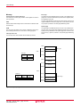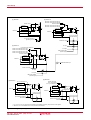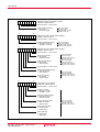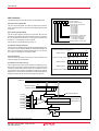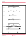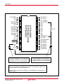
1
7534 Group
REJ03B0099-0300
Rev.3.00
Oct 23, 2006
SINGLE-CHIP 8-BIT CMOS MICROCOMPUTER
•
DESCRIPTION
The 7534 Group is the 8-bit microcomputer based on the 740 family
core technology.
The 7534 Group has a USB, 8-bit timers, and an A/D converter, and
is useful for an input device for personal computer peripherals.
FEATURES
•
•
•
•
•
•
Basic machine-language instructions ....................................... 69
The minimum instruction execution time .......................... 0.34 µs
(at 6 MHz oscillation frequency for the shortest instruction)
Memory size
ROM ............................................... 8K to 16K bytes
RAM .............................................. 256 to 384 bytes
Programmable I/O ports ...................................... 28 (36-pin type)
............................................................................ 24 (32-pin type)
............................................................................ 33 (42-pin type)
Interrupts .................................................... 14 sources, 8 vectors
Timers ............................................................................ 8-bit ✕ 3
•
•
•
•
•
•
•
Serial Interface
Serial I/O1 ................................ used only for Low Speed in USB
(based on Low-Speed USB2.0 specification)
(USB/UART)
Serial I/O2 ...................................................................... 8-bit ✕ 1
(Clock-synchronized)
A/D converter ................................................ 10-bit ✕ 8 channels
Clock generating circuit ............................................. Built-in type
(connect to external ceramic resonator or quartz-crystal oscillator )
Watchdog timer ............................................................ 16-bit ✕ 1
Power source voltage
At 6 MHz XIN oscillation frequency at ceramic resonator
................................ 4.1 to 5.5 V(4.4 to 5.25 V at USB operation)
Power dissipation ............................................ 30 mW (standard)
Operating temperature range ................................... –20 to 85 °C
(0 to 70 °C at USB operation)
Built-in USB 3.3 V Regulator + transceiver based on Low-Speed
USB2.0 specification
APPLICATION
Input device for personal computer peripherals
PIN CONFIGURATION (TOP VIEW)
P27/AN7
VREF
RESET
CNVSS
Vcc
XIN
XOUT
VSS
1
36
2
35
3
34
4
5
6
7
8
9
10
11
12
13
14
15
M37534M4-XXXFP
M37534E8FP
P12/SCLK
P13/SDATA
P14/CNTR0
P20/AN0
P21/AN1
P22/AN2
P23/AN3
P24/AN4
P25/AN5
P26/AN6
33
32
31
30
29
28
27
26
25
24
23
22
16
21
17
20
18
19
P11/TXD/D+
P10/RXD/DP07
P06
P05
P04
P03
P02
P01
P00
USBVREFOUT
P37/INT0
P35(LED5)
P34(LED4)
P33(LED3)
P32(LED2)
P31(LED1)
P30(LED0)
Package type: PRSP0036GA-A (36P2R-A )
Fig. 1 Pin configuration of M37534M4-XXXFP, M37534E8FP
Rev.3.00 Oct 23, 2006
REJ03B0099-0300
page 1 of 53
7534 Group
17
18
19
20
21
22
25
16
26
15
27
14
28
M37534M4-XXXGP
13
9
P34(LED4)
P33(LED3)
P32(LED2)
P31(LED1)
P30(LED0)
VSS
XOUT
XIN
P22/AN2
P23/AN3
P24/AN4
P25/AN5
VREF
RESET
CNVSS
VCC
8
32
7
10
6
31
5
11
4
30
3
12
2
29
1
P07
P10/RXD/DP11/TXD/D+
P12/SCLK
P13/SDATA
P14/CNTR0
P20/AN0
P21/AN1
23
24
P06
P05
P04
P03
P02
P01
P00
USBVREFOUT
PIN CONFIGURATION (TOP VIEW)
Outline PLQP0032GB-A (32P6U-A)
Fig. 2 Pin configuration of M37534M4-XXXGP
Rev.3.00 Oct 23, 2006
REJ03B0099-0300
page 2 of 53
7534 Group
PIN CONFIGURATION (TOP VIEW)
1
42
2
41
3
40
4
39
5
38
6
37
7
8
9
10
11
12
13
14
15
16
17
M37534RSS
M37534M4-XXXSP
M37534E8SP
P14/CNTR0
P15
P16
P20/AN0
P21/AN1
NC
P22/AN2
P23/AN3
P24/AN4
P25/AN5
P26/AN6
P27/AN7
P40
P41
VREF
RESET
CNVSS
Vcc
XIN
XOUT
VSS
36
35
34
33
32
31
30
29
28
27
26
18
25
19
24
20
23
21
22
P13/SDATA
P12/SCLK
P11/TXD/D+
P10/RXD/DP07
P06
P05
P04
P03
P02
P01
P00
USBVREFOUT
P37/INT0
P36(LED6)/INT1
P35(LED5)
P34(LED4)
P33(LED3)
P32(LED2)
P31(LED1)
P30(LED0)
Outline 42S1M, PRDP0042BA-A (42P4B)
Fig. 3 Pin configuration of M37534RSS, M37534M4-XXXSP, M37534E8SP
Rev.3.00 Oct 23, 2006
REJ03B0099-0300
page 3 of 53
Rev.3.00 Oct 23, 2006
REJ03B0099-0300
page 4 of 53
Fig. 4 Functional block diagram (PRSP0036GA-A package type)
VREF
12
A/D
converter
(1 0 )
Watchdog timer
Reset
Clock generating circuit
17
16
Clock output
XOUT
XIN
Clock input
0
PC H
I/O port P3
I/O port P2
11 10 9 8 7 6 5 4
25 24 23 22 21 20 19
PS
PC L
S
Y
X
A
SI/O1(8)
USB(LS)
26
USBVREFOUT
P2(8)
INT0
ROM
C P U
15
18
P3(7)
RAM
VCC
VSS
SI/O2(8)
I/O port P1
3 2 1 36 35
P1(5)
CNTR0
13
RESET
Reset input
P0(8)
Timer X (8)
Timer 2 (8)
Timer 1 (8)
I/O port P0
34 33 32 31 30 29 28 27
Prescaler X (8)
Prescaler 12 (8)
14
CNVSS
Key-on wake up
FUNCTIONAL BLOCK DIAGRAM (Package: PRSP0036GA-A)
7534 Group
FUNCTIONAL BLOCK
Rev.3.00 Oct 23, 2006
REJ03B0099-0300
page 5 of 53
Fig. 5 Functional block diagram (PLQP0032GB-A package type)
VREF
5
A/D
converter
(1 0 )
Watchdog timer
Reset
Clock generating circuit
10
9
Clock output
XOUT
XIN
Clock input
I/O port P3
16 15 14 13 12
P3(5)
RAM
ROM
0
PC H
I/O port P2
4 3 2 1 32 31
P2(6)
8
11
PS
PC L
S
Y
X
A
17
USBVREFOUT
SI/O1(8)
USB(LS)
C P U
VCC
VSS
SI/O2(8)
I/O port P1
30 29 28 27 26
P1(5)
CNTR0
6
RESET
Reset input
P0(8)
Timer X (8)
Timer 2 (8)
Timer 1 (8)
I/O port P0
25 24 23 22 21 20 19 18
Prescaler X (8)
Prescaler 12 (8)
7
CNVSS
Key-on wake up
FUNCTIONAL BLOCK DIAGRAM (Package: PLQP0032GB-A)
7534 Group
Rev.3.00 Oct 23, 2006
REJ03B0099-0300
20
page 6 of 53
Fig. 6 Functional block diagram (PRDP0042BA-A package type)
I/O port P4
I/O port P3
29 28 27 26 25 24 23 22
VREF
15
13 14
PC H
18
21
7 5 4
I/O port P2
12 11 10 9 8
P2(8)
0
C P U
VCC
VSS
INT0 INT1
ROM
P3(8)
A/D
converter
(1 0 )
Reset
RAM
P4(2)
Watchdog timer
Clock generating circuit
19
Clock input Clock output
X IN X OUT
PS
30
SI/O1(8)
USB(LS)
USBVREFOUT
PC L
S
Y
X
A
FUNCTIONAL BLOCK DIAGRAM (Package: PRDP0042BA-A)
SI/O2(8)
16
Reset input
RESET
3
CNTR0
1 42 41 40 39
I/O port P1
2
P1(7)
Prescaler X (8)
Prescaler 12 (8)
17
CNVSS
I/O port P0
38 37 36 35 34 33 32 31
P0(8)
Timer X (8)
Timer 2 (8)
Timer 1 (8)
7534 Group
Key-on wakeup
7534 Group
PIN DESCRIPTION
Table 1 Pin description
Pin
Name
Function
Function expect a port function
•Apply voltage of 4.1 to 5.5 V (4.4 to 5.25 V at USB operating) to Vcc, and 0 V to Vss.
Vcc, Vss
Power source
VREF
Analog reference
voltage
•Reference voltage input pin for A/D converter
USBVREFOUT
USB reference
voltage output
•Output pin for pulling up a D- line with 1.5 kΩ external resistor
CNVss
CNVss
•Chip operating mode control pin, which is always connected to Vss.
RESET
Reset input
•Reset input pin for active “L”
XIN
Clock input
•Input and output pins for main clock generating circuit
XOUT
Clock output
P00–P07
I/O port P0
•Connect a ceramic resonator or quartz crystal oscillator between the XIN and XOUT pins.
•If an external clock is used, connect the clock source to the XIN pin and leave the XOUT pin open.
•8-bit I/O port.
•I/O direction register allows each pin to be individually programmed as either input or output.
•Key-input (key-on wake up
interrupt input) pins
•CMOS compatible input level
•CMOS 3-state output structure
•Whether a built-in pull-up resistor is to be used or not can be
determined by program.
P10/RxD/D-
I/O port P1
P11/TxD/D+
•7-bit I/O port
P12/SCLK
•I/O direction register allows each pin to be individually programmed as either input or output.
P13/SDATA
•CMOS compatible input level
P14/CNTR0
•CMOS 3-state output structure
•Serial I/O1 function pin
•Serial I/O2 function pin
•Timer X function pin
•CMOS/TTL level can be switched for P10, P12, P13.
•When using the USB function, input level of ports P10 and
P11 becomes USB input level, and output level of them
becomes USB output level.
P15, P16
P20/AN0–
P27/AN7
I/O port P2
P30–P35
I/O port P3
•8-bit I/O port having almost the same function as P0
•Input pins for A/D converter
•CMOS compatible input level
•CMOS 3-state output structure
•8-bit I/O port
•I/O direction register allows each pin to be individually programmed as either input or output.
•CMOS compatible input level (CMOS/TTL level can be switched for P36, P37).
•CMOS 3-state output structure
•P30 to P36 can output a large current for driving LED.
•Whether a built-in pull-up resistor is to be used or not can be
determined by program.
P36/INT1
P37/INT0
P40, P41
I/O port P4
•Interrupt input pins
•2-bit I/O port
•I/O direction register allows each pin to be individually programmed as either input or output.
Rev.3.00 Oct 23, 2006
REJ03B0099-0300
page 7 of 53
7534 Group
GROUP EXPANSION
Renesas expands the 7534 group as follow:
Memory type
Support for Mask ROM version, One Time PROM version, and Emulator MCU .
Package
PRSP0036GA-A ......................... 0.8 mm-pitch plastic molded SOP
PLQP0032GB-A ........................ 0.8 mm-pitch plastic molded LQFP
PRDP0042BA-A .................................... 42 pin plastic molded SDIP
42SIM ...................................... 42 pin shrink ceramic PIGGY BACK
Memory size
ROM/PROM size .................................................. 8 K to 16 K bytes
RAM size ................................................................ 256 to 384 bytes
ROM size
(Byte)
16K
M37534E8
8K
M37534M4
M37534E4
128
0
256
RAM size
(Byte)
384
Fig. 7 Memory expansion
Currently supported products are listed below.
Table 2 List of supported products
(P) ROM size (bytes)
ROM size for User ()
RAM size
(bytes)
Package
M37534M4-XXXFP
8192 (8062)
256
PRSP0036GA-A
Mask ROM version
M37534M4-XXXGP
8192 (8062)
256
PLQP0032GB-A
Mask ROM version
M37534M4-XXXSP
8192 (8062)
256
PRDP0042BA-A
Mask ROM version
M37534E4GP
8192 (8062)
256
PLQP0032GB-A
One Time PROM version (blank)
M37534E8FP
16384 (16254)
384
PRSP0036GA-A
One Time PROM version (blank)
M37534E8SP
16384 (16254)
384
PRDP0042BA-A
One Time PROM version (blank)
384
42S1M
Part number
M37534RSS
Rev.3.00 Oct 23, 2006
REJ03B0099-0300
page 8 of 53
Remarks
Emulator MCU
7534 Group
FUNCTIONAL DESCRIPTION
[CPU Mode Register] CPUM
The CPU mode register contains the stack page selection bit.
This register is allocated at address 003B16.
Central Processing Unit (CPU)
The 7534 Group uses the standard 740 family instruction set. Refer
to the table of 740 family addressing modes and machine-language
instructions or the 740 Family Software Manual for details on each
instruction set.
Machine-resident 740 family instructions are as follows:
1. The FST and SLW instructions cannot be used.
2. The MUL and DIV instructions cannot be used.
3. The WIT instruction can be used.
4. The STP instruction can be used.
b7
Note on stack page
When 1 page is used as stack area by the stack page selection bit,
the area which can be used as stack depends on RAM size. Especially, be careful that the RAM area varies in Mask ROM version,
One Time PROM version and Emulator MCU.
b0
CPU mode register
(CPUM: address 003B16)
Processor mode bits
b1 b0
0 0 Single-chip mode
0 1
1 0
Not available
1 1
Stack page selection bit
0 : 0 page
1 : 1 page
Not used (returns “0” when read)
(Do not write “1” to these bits )
Main clock division ratio selection bits
b7 b6
0 0 : f(φ) = f(XIN)/2 (High-speed mode)
0 1 : f(φ) = f(XIN)/8 (Middle-speed mode)
1 0 : applied from on-chip oscillator
1 1 : f(φ) = f(XIN) (Double-speed mode)
Fig. 8 Structure of CPU mode register
Switching method of CPU mode register
Switch the CPU mode register (CPUM) at the head of program after
releasing Reset in the following method.
After releasing reset
Start with an on-chip oscillator (Note)
Wait until establish ceramic oscillator
clock.
Switch the clock division ratio
selection bits (bits 6 and 7 of CPUM)
Switch to other mode except an on-chip oscillator
(Select one of 1/1, 1/2, and 1/8)
Main routine
Note. After releasing reset the operation starts by starting an on-chip oscillator automatically.
Do not use an on-chip oscillator at ordinary operation.
Fig. 9 Switching method of CPU mode register
Rev.3.00 Oct 23, 2006
REJ03B0099-0300
page 9 of 53
7534 Group
Memory
Special function register (SFR) area
The SFR area in the zero page contains control registers such as I/O
ports and timers.
RAM
RAM is used for data storage and for a stack area of subroutine calls
and interrupts.
ROM
The first 128 bytes and the last 2 bytes of ROM are reserved for
device testing and the rest is a user area for storing programs.
Interrupt vector area
The interrupt vector area contains reset and interrupt vectors.
Zero page
The 256 bytes from addresses 000016 to 00FF16 are called the zero
page area. The internal RAM and the special function registers (SFR)
are allocated to this area.
The zero page addressing mode can be used to specify memory and
register addresses in the zero page area. Access to this area with
only 2 bytes is possible in the zero page addressing mode.
Special page
The 256 bytes from addresses FF0016 to FFFF16 are called the special page area. The special page addressing mode can be used to
specify memory addresses in the special page area. Access to this
area with only 2 bytes is possible in the special page addressing
mode.
000016
SFR area
Zero page
004016
RAM
010016
RAM area
RAM capacity
(bytes)
address
XXXX16
256
384
013F16
01BF16
XXXX16
Reserved area
044016
Not used
YYYY16
Reserved ROM area
(128 bytes)
ZZZZ16
ROM
FF0016
ROM area
ROM capacity
(bytes)
address
YYYY16
address
ZZZZ16
8192
16384
E00016
C00016
E08016
C08016
Fig. 10 Memory map diagram
Rev.3.00 Oct 23, 2006
REJ03B0099-0300
page 10 of 53
Special page
FFEC16
Interrupt vector area
FFFE16
FFFF16
Reserved ROM area
7534 Group
000016
Port P0 (P0)
002016
USB interrupt control register (USBICON)
000116
Port P0 direction register (P0D)
002116
USB transmit data byte number set register 0 (EP0BYTE)
000216
Port P1 (P1)
002216
USB transmit data byte number set register 1 (EP1BYTE)
000316
Port P1 direction register (P1D)
002316
USBPID control register 0 (EP0PID)
000416
Port P2 (P2)
002416
USBPID control register 1 (EP1PID)
000516
Port P2 direction register (P2D)
002516
USB address register (USBA)
000616
Port P3 (P3)
002616
USB sequence bit initialization register (INISQ1)
000716
Port P3 direction register (P3D)
002716
USB control register (USBCON)
000816
Port P4 (P4)
002816
Prescaler 12 (PRE12)
000916
Port P4 direction register (P4D)
002916
Timer 1 (T1)
000A16
002A16
Timer 2 (T2)
000B16
002B16
Timer X mode register (TM)
000C16
002C16
Prescaler X (PREX)
000D16
002D16
Timer X (TX)
000E16
002E16
Timer count source set register (TCSS)
000F16
002F16
001016
003016
Serial I/O2 control register (SIO2CON)
001116
003116
Serial I/O2 register (SIO2)
001216
003216
001316
003316
001416
003416
A/D control register (ADCON)
001516
003516
A/D conversion register (low-order) (ADL)
A/D conversion register (high-order) (ADH)
001616
Pull-up control register (PULL)
003616
001716
Port P1P3 control register (P1P3C)
003716
001816
Transmit/Receive buffer register (TB/RB)
003816
MISRG
001916
USB status register (USBSTS)/UART status register (UARTSTS)
003916
Watchdog timer control register (WDTCON)
001A16
Serial I/O1 control register (SIO1CON)
003A16
Interrupt edge selection register (INTEDGE)
001B16
UART control register (UARTCON)
003B16
CPU mode register (CPUM)
001C16
Baud rate generator (BRG)
003C16
Interrupt request register 1 (IREQ1)
001D16
USB data toggle synchronization register ( TRSYNC)
003D16
001E16
USB interrupt source discrimination register 1 (USBIR1)
003E16
001F16
USB interrupt source discrimination register 2 (USBIR2)
003F16
Fig. 11 Memory map of special function register (SFR)
Rev.3.00 Oct 23, 2006
REJ03B0099-0300
page 11 of 53
Interrupt control register 1 (ICON1)
7534 Group
I/O Ports
[Direction registers] PiD
The I/O ports have direction registers which determine the input/output direction of each pin. Each bit in a direction register corresponds
to one pin, and each pin can be set to be input or output.
When “1” is set to the bit corresponding to a pin, this pin becomes an
output port. When “0” is set to the bit, the pin becomes an input port.
When data is read from a pin set to output, not the value of the pin
itself but the value of port latch is read. Pins set to input are floating,
and permit reading pin values.
If a pin set to input is written to, only the port latch is written to and the
pin remains floating.
b7
[Pull-up control] PULL
By setting the pull-up control register (address 001616), ports P0 and
P3 can exert pull-up control by program. However, pins set to output
are disconnected from this control and cannot exert pull-up control.
[Port P1P3 control] P1P3C
By setting the port P1P3 control register (address 001716), a CMOS
input level or a TTL input level can be selected for ports P10, P12,
P13, P36 and P37 by program.
Then, as for the 36-pin version, set “1” to each bit 6 of the port P3
direction register and port P3 register.
As for the 32-pin version, set “1” to respective bits 5, 6, 7 of the port
P3 direction register and port P3 register.
b0
Pull-up control register
(PULL: address 0016 16)
P00 pull-up control bit
P01 pull-up control bit
P02, P03 pull-up control bit
P04 – P07 pull-up control bit
P30 – P33 pull-up control bit
P34 pull-up control bit
P35, P36 pull-up control bit
P37 pull-up control bit
Note : Pins set to output ports are disconnected from pull-up control.
Fig. 12 Structure of pull-up control register
b7
b0
Port P1P3 control register
(P1P3C: address 0017 16)
P37/INT 0 input level selection bit
0 : CMOS level
1 : TTL level
P36/INT 1 input level selection bit
0 : CMOS level
1 : TTL leve
P10,P1 2,P13 input level selection bit
0 : CMOS level
1 : TTL level
Not used
Fig. 13 Structure of port P1P3 control register
Rev.3.00 Oct 23, 2006
REJ03B0099-0300
page 12 of 53
0: Pull-up off
1: Pull-up on
Initial value: FF16
7534 Group
Table 3 I/O port function table
Pin
Name
Input/output
P00–P07
P10/RxD/DP11/TxD/D+
I/O format
Non-port function
Related SFRs
Diagram No.
Pull-up control register
(1)
I/O port P0 I/O individual •CMOS compatible input level Key input interrupt
bits
•CMOS 3-state output
I/O port P1
•USB input/output level when Serial I/O1 function input/ Serial I/O1 control
selecting USB function
output
register
P12/SCLK
•CMOS compatible input level Serial I/O2 function input/ Serial I/O2 control
register
output
•CMOS 3-state output
P13/SDATA
P14/CNTR0
(Note)
Timer X function input/output Timer X mode register
(2)
(3)
(4)
(5)
(6)
(10)
P15, P16
P20/AN0–
P27/AN7
I/O port P2
P30–P35
I/O port P3
A/D conversion input
(7)
(8)
P36/INT1
External interrupt input
P37/INT0
P40, P41
I/O port P4
Note: Port P10, P12, P13, P36, P37 is CMOS/TTL level.
Rev.3.00 Oct 23, 2006
REJ03B0099-0300
A/D control register
page 13 of 53
Interrupt edge selection
register
(9)
(10)
7534 Group
(2) Port P10
(1) Port P0
Serial I/O1 mode selection bit (b7)
Serial I/O1 mode selection bit (b6)
Receive enable bit
Pull-up control
Direction
register
Data bus
Serial I/O1 mode selection bit (b7)
Serial I/O1 mode selection bit (b6)
Direction
register
Port latch
Data bus
Port latch
P10,P12,P13 input
level selection bit
To key input interrupt
generating circuit
Serial I/O1 input
*
(3) Port P11
D- input
P-channel output disable bit
D- output
Serial I/O1 mode selection bit (b7)
Serial I/O1 mode selection bit (b6)
USB output enable
(internal signal)
Serial I/O1 mode selection bit (b7)
Serial I/O1 mode selection bit (b6)
Transmit enable bit
Direction
register
Data bus
Port latch
+
USB differential input
Serial I/O1 output
D+ input
D+ output
USB output enable
(internal signal)
(5) Port P13
(4) Port P12
Signals during the
SDATA output action
SDATA pin selection bit
SCLK pin selection bit
Direction
register
Direction
register
Data bus
Port latch
Data bus
Port latch
SDATA pin
selection bit
P10,P12,P13 input
level selection bit
P10,P12,P13 input
level selection bit
Serial I/O2 clock output
Serial I/O2 clock input
Serial I/O2 clock output
*
Serial I/O2 clock input
*
P10, P12, P13, P36, P37 input levels are switched to the CMOS/TTL level by the port P1P3 control register.
* : When
the TTL level is selected, there is no hysteresis characteristics.
Fig. 14 Block diagram of ports (1)
Rev.3.00 Oct 23, 2006
REJ03B0099-0300
page 14 of 53
7534 Group
(7) Ports P20–P27
(6) Ports P14
Direction register
Direction register
Port latch
Data bus
Data bus
Port latch
Pulse output mode
Timer output
A/D converter input
Analog input pin selection bit
CNTR0 interrupt input
(9) Ports P36, P37
(8) Ports P30–P35
Pull-up control
Pull-up control
Direction register
Direction register
Data bus
Data bus
Port latch
Port latch
P37/INT0 input
level selection bit
INT interrupt input
*
(10) Ports P15, P16, P40, P41
Direction register
Data bus
Port latch
* : P10, P12, P13, P36, P37 input levels are switched to the CMOS/TTL level by the port P1P3 control register.
When the TTL level is selected, there is no hysteresis characteristics.
Fig. 15 Block diagram of ports (2)
Rev.3.00 Oct 23, 2006
REJ03B0099-0300
page 15 of 53
7534 Group
Interrupts
Interrupts occur by 14 different sources : 4 external sources, 9 internal sources and 1 software source.
Interrupt control
All interrupts except the BRK instruction interrupt have an interrupt
request bit and an interrupt enable bit, and they are controlled by the
interrupt disable flag. When the interrupt enable bit and the interrupt
request bit are set to “1” and the interrupt disable flag is set to “0”, an
interrupt is accepted.
The interrupt request bit can be cleared by program but not be set.
The interrupt enable bit can be set and cleared by program.
It becomes usable by switching CNTR0 and A/D interrupt sources
with bit 7 of the interrupt edge selection register, timer 2 and serial I/
O2 interrupt sources with bit 6, timer X and key-on wake-up interrupt
sources with bit 5, and serial I/O transmit and INT1 interrupt sources
with bit 4.
The reset and BRK instruction interrupt can never be disabled with
any flag or bit. All interrupts except these are disabled when the interrupt disable flag is set.
When several interrupts occur at the same time, the interrupts are
received according to priority.
Interrupt operation
Upon acceptance of an interrupt the following operations are automatically performed:
1. The processing being executed is stopped.
2. The contents of the program counter and processor status register are automatically pushed onto the stack.
3. The interrupt disable flag is set and the corresponding interrupt
request bit is cleared.
4. Concurrently with the push operation, the interrupt destination
address is read from the vector table into the program counter.
Notes on use
When the active edge of an external interrupt (INT0, INT1, CNTR0) is
set, the interrupt request bit may be set.
Therefore, please take following sequence:
1. Disable the external interrupt which is selected.
2. Change the active edge in interrupt edge selection register. (in
case of CNTR0: Timer X mode register)
3. Clear the set interrupt request bit to “0”.
4. Enable the external interrupt which is selected.
Table 6 Interrupt vector address and priority
Interrupt source
Vector addresses (Note 1)
Priority
High-order
Low-order
Interrupt request generating conditions
Remarks
Reset (Note 2)
1
FFFD16
FFFC16
At reset input
Non-maskable
UART receive
2
FFFB16
FFFA16
At completion of UART data receive
Valid in UART mode
At detection of IN token
Valid in USB mode
3
FFF916
FFF816
At completion of UART transmit shift or
when transmit buffer is empty
Valid in UART mode
USB SETUP/OUT token
Reset/Suspend/Resume
At detection of SETUP/OUT token or
At detection of Reset/ Suspend/ Resume
Valid in USB mode
INT1
At detection of either rising or falling edge
of INT1 input
External interrupt
(active edge selectable)
External interrupt
(active edge selectable)
USB IN token
UART transmit
INT0
4
FFF716
FFF616
At detection of either rising or falling edge
of INT0 input
Timer X
5
FFF516
FFF416
At timer X underflow
Key-on wake-up
At falling of conjunction of input logical
level for port P0 (at input)
External interrupt (valid at falling)
STP release timer underflow
Timer 1
6
FFF316
FFF216
At timer 1 underflow
Timer 2
7
FFF116
FFF016
At timer 2 underflow
Serial I/O2
CNTR0
At completion of transmit/receive shift
8
FFEF16
A/D conversion
FFEE16
At detection of either rising or falling edge
of CNTR0 input
At completion of A/D conversion
BRK instruction
At BRK instruction execution
9
FFED16
FFEC16
Note 1: Vector addressed contain internal jump destination addresses.
2: Reset function in the same way as an interrupt with the highest priority.
Rev.3.00 Oct 23, 2006
REJ03B0099-0300
External interrupt (active edge
selectable)
page 16 of 53
Non-maskable software interrupt
7534 Group
Interrupt request bit
Interrupt enable bit
Interrupt disable flag I
BRK instruction
Reset
Fig. 16 Interrupt control
b7
b0 Interrupt edge selection register
(INTEDGE : address 003A16)
INT0 interrupt edge selection bit
0 : Falling edge active
1 : Rising edge active
INT1 interrupt edge selection bit
0 : Falling edge active
1 : Rising edge active
Not used (returns “0” when read)
Serial I/O1 or INT1 interrupt selection bit
0 : Serial I/O1
1 : INT1
Timer X or key-on wake up interrupt selection bit
0 : Timer X
1 : Key-on wake up
Timer 2 or serial I/O2 interrupt selection bit
0 : Timer 2
1 : Serial I/O2
CNTR0 or AD converter interrupt selection bit
0 : CNTR0
1 : AD converter
b7
b0 Interrupt request register 1
(IREQ1 : address 003C16)
UART receive/USB IN token interrupt request bit
UART transmit/USB SETUP/OUT token/ Reset/Suspend/Resume/INT1 interrupt request bit
INT0 interrupt request bit
Timer X or key-on wake up interrupt request bit
Timer 1 interrupt request bit
Timer 2 or serial I/O2 interrupt request bit
CNTR0 or AD converter interrupt request bit
0 : No interrupt request issued
Not used (returns “0” when read)
1 : Interrupt request issued
b7
b0 Interrupt control register 1
(ICON1 : address 003E16)
UART receive/USB IN token interrupt enable bit
UART transmit/USB SETUP/OUT token/ Reset/Suspend/Resume/INT1 interrupt enable bit
INT0 interrupt enable bit
Timer X or key-on wake up interrupt enable bit
Timer 1 interrupt enable bit
Timer 2 or serial I/O2 interrupt enable bit
CNTR0 or AD converter interrupt enable bit
Not used (returns “0” when read)
0 : Interrupts disabled
(Do not write “1” to this bit)
1 : Interrupts enabled
Fig. 17 Structure of Interrupt-related registers
Rev.3.00 Oct 23, 2006
REJ03B0099-0300
page 17 of 53
Interrupt request
7534 Group
Key Input Interrupt (Key-On Wake-Up)
A key-on wake-up interrupt request is generated by applying “L” level
to any pin of port P0 that has been set to input mode.
In other words, it is generated when the AND of input level goes from
“1” to “0”. An example of using a key input interrupt is shown in Figure 18, where an interrupt request is generated by pressing one of
the keys provided as an active-low key matrix which uses ports P00
to P03 as input ports.
Port PXx
“L” level output
PULL register
bit 3 = “0”
*
**
P07 output
Port P07
Direction register = “1”
Key input interrupt request
Port P07
latch
Falling edge
detection
PULL register
bit 3 = “0”
*
**
P06 output
Port P06
Direction register = “1”
Port P06
latch
Falling edge
detection
PULL register
bit 3 = “0”
*
**
P05 output
Port P05
Direction register = “1”
Port P05
latch
Falling edge
detection
PULL register
bit 3 = “0”
*
**
P04 output
Port P04
Direction register = “1”
Port P04
latch
PULL register
bit 2 = “1”
*
**
P03 input
Port P03
Direction register = “0”
Port P03
latch
PULL register
bit 2 = “1”
*
**
P02 input
Falling edge
detection
Falling edge
detection
Port P02
Direction register = “0”
Port P02
latch
Falling edge
detection
PULL register
bit 1 = “1”
*
**
P01 input
Port P01
Direction register = “0”
Port P01
latch
Falling edge
detection
PULL register
bit 0 = “1”
*
P00 input
**
Port P00
Direction register = “0”
Port P00
latch
Falling edge
detection
* P-channel transistor for pull-up
** CMOS output buffer
Fig. 18 Connection example when using key input interrupt and port P0 block diagram
Rev.3.00 Oct 23, 2006
REJ03B0099-0300
page 18 of 53
Port P0
Input read circuit
7534 Group
Timers
The 7534 Group has 3 timers: timer X, timer 1 and timer 2.
The division ratio of every timer and prescaler is 1/(n+1) provided
that the value of the timer latch or prescaler is n.
All the timers are down count timers. When a timer reaches “0”, an
underflow occurs at the next count pulse, and the corresponding timer
latch is reloaded into the timer. When a timer underflows, the interrupt request bit corresponding to each timer is set to “1”.
b7
b0
Timer X mode register
(TM : Address 002B 16)
Timer X operating mode bits
b1 b0
0 0 : Timer mode
0 1 : Pulse output mode
1 0 : Event counter mode
1 1 : Pulse width measurement mode
CNTR0 active edge switch bit
0 : Interrupt at falling edge
Count at rising edge
(in event counter mode)
1 : Interrupt at rising edge
Count at falling edge
(in event counter mode)
●Timer 1, Timer 2
Prescaler 12 always counts f(XIN)/16. Timer 1 and timer 2 always
count the prescaler output and periodically sets the interrupt request
bit.
Timer X count stop bit
0 : Count start
1 : Count stop
●Timer X
Timer X can be selected in one of 4 operating modes by setting the
timer X mode register.
• Timer Mode
The timer counts the signal selected by the timer X count source
selection bit.
• Pulse Output Mode
The timer counts the signal selected by the timer X count source
selection bit, and outputs a signal whose polarity is inverted each
time the timer value reaches “0”, from the CNTR0 pin.
When the CNTR0 active edge switch bit is “0”, the output of the
CNTR0 pin is started with an “H” output.
At “1”, this output is started with an “L” output. When using a timer in
this mode, set the port P14 direction register to output mode.
• Event Counter Mode
The operation in the event counter mode is the same as that in the
timer mode except that the timer counts the input signal from the
CNTR0 pin.
When the CNTR0 active edge switch bit is “0”, the timer counts
the rising edge of the CNTR0 pin. When this bit is “1”, the timer
counts the falling edge of the CNTR0 pin.
• Pulse Width Measurement Mode
When the CNTR0 active edge switch bit is “0”, the timer counts the
signal selected by the timer X count source selection bit while the
CNTR0 pin is “H”. When this bit is “1”, the timer counts the signal
while the CNTR0 pin is “L”.
In any mode, the timer count can be stopped by setting the timer X
count stop bit to “1”. Each time the timer overflows, the interrupt
request bit is set.
Rev.3.00 Oct 23, 2006
REJ03B0099-0300
page 19 of 53
Not used (return “0” when read)
Fig. 19 Structure of timer X mode register
b7
b0
Timer count source set register
(TCSS : Address 002E 16)
Timer X count source selection bit (Note)
0 : f(X IN)/16
1 : f(X IN)/2
Not used (return “0” when read)
Note : To switch the timer X count source selection bit ,
stop the timer X count operation.
Fig. 20 Timer count source set register
7534 Group
Data bus
f(XIN)/16
f(XIN)/2
Prescaler X latch (8)
Timer X count
source selection bit
Pulse width
measurement
mode
CNTR0 active
edge switch bit
“0”
P14/CNTR0
Prescaler X (8)
Event
counter
mode
Timer X latch (8)
Timer mode
pulse output mode
Timer X (8)
To timer X
interrupt
request bit
Timer X count stop bit
To CNTR0
interrupt
request bit
“1”
CNTR0 active
edge switch bit
“1”
Q
Q
“0”
Toggle
flip-flop
R
T
Timer X latch write
Pulse output mode
Port P14 latch
Port P14 direction
register
Pulse output mode
Data bus
f(XIN)/16
Prescaler 12 latch (8)
Timer 1 latch (8)
Timer 2 latch (8)
Prescaler 12 (8)
Timer 1 (8)
Timer 2 (8)
To timer 2
interrupt
request bit
To timer 1
interrupt
request bit
Fig. 21 Block diagram of timer X, timer 1 and timer 2
Rev.3.00 Oct 23, 2006
REJ03B0099-0300
page 20 of 53
7534 Group
Serial Interface
●Serial I/O1
• Asynchronous serial I/O (UART) mode
Serial I/O1 can be used as an asynchronous (UART) serial I/O. A
dedicated timer (baud rate generator) is also provided for baud rate
generation when serial I/O1 is in operation.
Eight serial data transfer formats can be selected, and the transfer
formats to be used by a transmitter and a receiver must be identical.
Each of the transmit and receive shift registers has a buffer register
(the same address on memory). Since the shift register cannot be
written to or read from directly, transmit data is written to the transmit buffer, and receive data is read from the respective buffer registers. These buffer registers can also hold the next data to be transmitted and receive 2-byte receive data in succession.
By selecting “1” for continuous transmit valid bit (bit 2 of SIO1CON),
continuous transmission of the same data is made possible.
This can be used as a simplified PWM.
Data bus
Address
(001816)
Serial I/O1 control register Address (001A 16)
Receive buffer full flag (RBF)
Receive Buffer Register
OE
Receive interrupt request (RI)
Character length selection bit
P10/RXD
ST Detector
7-bit
Receive Shift Register
1/16
8-bit
PE FE
UART Control Register
Address (001B 16)
SP Detector
Clock Control Circuit
BRG count source selection bit
Division ratio 1/(n+1)
XIN
Baud Rate Generator
Address (001C 16)
1/4
ST/SP/PA Generator
Transmit shift register shift
completion flag (TSC)
1/16
P11/TXD
Transmit Shift Register
Transmit interrupt source selection bit
Transmit interrupt request (TI)
Character length selection bit
Transmit buffer empty flag (TBE)
Transmit Buffer Register
Address
(001816)
Continuous transmit valid bit
Serial I/O1 status register Address (0019 16)
Data bus
Fig. 22 Block diagram of UART serial I/O
Transmit/Receive Clock
Transmit Buffer Register
Write Signal
TBE=0
TSC=0
TBE=1
Serial Output T XD
TBE=0
TBE=1
ST
D0
D1
SP
TSC=1*
ST
D0
D1
1 Start Bit
7 or 8 Data Bit
1 or 0 Parity Bit
1 or 2 Stop Bit
Receive Buffer Register
Read Signal
SP
* Generated at second bit in 2-stop -bit
mode
RBF=0
RBF=1
Serial Input RXD
ST
D0
D1
SP
RBF=1
ST
D0
D1
SP
Notes 1 : Error flag detection occurs at the same time that the RBF flag becomes “1” (at 1st stop bit, during reception).
2 : The transmit interrupt (TI) can be selected to occur when either the TBE or TSC flag becomes “1”, depending on the setting of the transmit
interrupt source selection bit (TIC) of the serial I/O1 control register.
3 : The receive interrupt (RI) is set when the RBF flag becomes “1”.
4 : After data is written to the transmit buffer when TSC = 1, 0.5 to 1.5 cycles of the data shift cycle is necessary until changing to TSC = 0.
Fig. 23 Operation of UART serial I/O function
Rev.3.00 Oct 23, 2006
REJ03B0099-0300
page 21 of 53
7534 Group
[Serial I/O1 control register] SIO1CON
The serial I/O1 control register consists of eight control bits for the
serial I/O1 function.
[Baud Rate Generator] BRG
The baud rate generator determines the baud rate for serial transfer.
The baud rate generator divides the frequency of the count source
by 1/(n + 1), where n is the value written to the baud rate generator.
[UART control register] UARTCON
The UART control register consists of four control bits (bits 0 to 3)
which are valid when asynchronous serial I/O is selected and set the
data format of an data transfer. One bit in this register (bit 4) is always valid and sets the output structure of the P11/TxD pin.
[UART status register] UARTSTS
The read-only UART status register consists of seven flags (bits 0 to
6) which indicate the operating status of the UART function and various errors. This register functions as the UART status register
(UARTSTS) when selecting the UART.
The receive buffer full flag (bit 1) is cleared to “0” when the receive
buffer is read.
If there is an error, it is detected at the same time that data is transferred from the receive shift register to the receive buffer, and the
receive buffer full flag is set. A write to the UART status register clears
all the error flags OE, PE, FE, and SE (bit 3 to bit 6, respectively).
Writing “0” to the serial I/O1 mode selection bits MOD1 and MOD0
(bit 7 and 6 of the Serial I/O1 control register ) also clears all the
status flags, including the error flags.
All bits of the serial I/O1 status register are initialized to “8116” at
reset, but if the transmit enable bit (bit 4) of the serial I/O1 control
register has been set to “1”, the continuous transmit valid bit (bit 2)
becomes “1”.
[Transmit/Receive buffer register] TB/RB
The transmit buffer and the receive buffer are located at the same
address. The transmit buffer is write-only and the receive buffer is
read-only. If a character bit length is 7-bit, the MSB of data stored in
the receive buffer is “0”.
Transmit/Receive Clock
Transmit Buffer Register
Write Signal
TBE=0
TSC=0
TBE=1
Serial Output T XD
ST
D0
D1
SP
ST
D0
D1
SP
ST
1 Start Bit
7 or 8 Data Bit
1 or 0 Parity Bit
1 or 2 Stop Bit
Notes 1 : When the serial I/O1 mode selection bits (b7, b6) is “10”, the transmit enable bit is “1”, and continuous transmit valid bit is “1”, writing on the
transmit buffer initiates continuous transmission of the same data.
2 : Select 0 for continuous transmit valid bit to stop continuous transmission.
The T XD pin will stop at high level after completing transmission of 1 byte.
3 : If the transmit buffer contents are rewritten during a continuous transmission, transmission of the rewritten data will be started after
completing transmission of 1 byte.
Fig. 24 Continuous transmission operation of UART serial I/O
Rev.3.00 Oct 23, 2006
REJ03B0099-0300
page 22 of 53
7534 Group
USB status/UART status register functions as the USB status register
(USBSTS).There is the USBVREFOUT pin for the USB reference
voltage output, and a D-line with 1.5 kΩ external resistor can be pull
up. USB mode block and USB transceiver block shown in figures
25 and 26.
• Universal serial bus (USB) mode
By setting bits 7 and 6 of the serial I/O1 control register (address
001A16) to “11”, the USB mode is selected.
This mode conforms to Low-Speed USB2.0 specification. In this
mode serial I/O1 interrupt have 6 sources; USB in and out token
receive, setup token receive, USB reset, suspend, and resume. The
Data bus
Address 001816
1.5 MHz
6 MHz
XIN
RxRDY
Receive buffer register
NRZI,
bit stuffing decoder
Digital
PLL
Receive shift register
SYNC decoder
BSTFE
EOP
Differential input and
Single end input
PID decoder
Bus state
detection
Reset interrupt request
RxPID
OPID
PIDE
P10/DP11/D+
Suspend interrupt request
Address
comparative unit
USB
transceiver
Resume interrupt request
Token interrupt request
USBA
End pointer
decoder
RxEP
Output data and
I/O control
CRC check
CRCE
NRZI,
bit stuffing encoder
Transmit shift register
USB transmit unit
SYNC, PID
generating unit
CRC encoder
TxRDY
Transmit buffer register
EOP generating unit
EP0BYTE
EP1BYTE
Address 001816
EP0PID
EP1PID
Data bus
Fig. 25 USB mode block diagram
Serial I/O1 control register
MOD0
MOD1
USB control register
UVOE
(initial value “0”)
Output enable signal
USB reference
power source voltage
Voltage input
Voltage input
Internal D- output signal
Internal D+ output signal
Output amplifier
USBVREFOUT
D-
D+/Doutput amplifier
D+
Suspend
Signal for function stop
OE Output enable signal
(internal signal)
Differential input
Single end input
Single end input
Fig. 26 USB transceiver block diagram
Rev.3.00 Oct 23, 2006
REJ03B0099-0300
page 23 of 53
+
7534 Group
b7
b0
Transmit buffer register
(TB: address 0018 16)
After setting data to address 0018 16, a content of the
transmit buffer register transfers to the transmit shift
register automatically.
CPU read: Disabled
CPU write: Set/Clear
Hardware read: Used
Hardware write: Not used
b7
b0
Receive buffer register
(RB: address 0018 16)
By reading data from address 0018 16, a content of the
receive buffer register can be read out.
CPU read: Enabled
CPU write: Disabled
Hardware read: Not used
Hardware write: Set/Clear
b7
b0
USB status register
(USBSTS: address 0019 16)
Transmit buffer empty flag
0: Buffer full
1: Buffer empty
CPU read: Enabled
CPU write: Disabled
Hardware read: Not used
Hardware write: Set/Clear
EOP detection flag
0: Not detected
1: Detect
False EOP error flag
0: No error
1: False EOP error
CRC error flag
0: No error
1: CRC error
PID error flag
0: No error
1: PID error
CPU read: Enabled
CPU write: Clear
Hardware read: Not used
Hardware write: Set
Bit stuffing error flag
0: No error
1: Bit stuffing error
Summing error flag
0: No error
1: Summing error
Receive buffer full flag
0: Buffer empty
1: Buffer full
Fig. 27 Structure of serial I/O1-related registers (1)
Rev.3.00 Oct 23, 2006
REJ03B0099-0300
page 24 of 53
CPU read: Enabled
CPU write: Disabled
Hardware read: Not used
Hardware write: Set/Clear
7534 Group
b7
b0
USB data toggle synchronization register
(TRSYNC: address 001D 16)
Not used (return “1” when read)
Sequence bit toggle flag
0: No toggle
1: Sequence toggle
b7
CPU read: Enabled
CPU write: Clear
Hardware read: Not used
Hardware write: Set
b0
USB interrupt source discrimination register 1
(USBIR1: address 001E 16)
Not used (return “1” when read)
Endpoint determination flag
0: Endpoint 0 interrupt
1: Endpoint 1 interrupt
b7
CPU read: Enabled
CPU write: Disabled
Hardware read: Not used
Hardware write: Set/Clear
b0
USB interrupt source discrimination register 2
(USBIR2: address 001F 16)
Not used (return “1” when read)
Suspend request flag
0: No request
1: Suspend request
CPU read: Enabled
CPU write: Clear
Hardware read: Not used
Hardware write: Set
USB reset request flag
0: No request
1: Reset request
CPU read: Enabled
CPU write: Disabled
Hardware read: Not used
Hardware write: Set/Clear
Not used (return “1” when read)
Token PID determination flag
0: SETUP interrupt
1: OUT interrupt
Token interrupt flag
0: No request
1: Token request
b7
CPU read: Enabled
CPU write: Disabled
Hardware read: Not used
Hardware write: Set/Clear
b0
USB interrupt control register
(USBICON: address 0020 16)
Not used (return “1” when read)
Endpoint 1 enable
0: Endpoint 1 invalid
1: Endpoint 1 valid
USB reset interrupt enable
0: USB reset invalid
1: USB reset valid
Resume interrupt enable
0: Resume invalid
1: Resume valid
Token interrupt enable
0: Token invalid
1: Token valid
USB enable flag
0: USB invalid
1: USB valid
Fig. 28 Structure of serial I/O1-related registers (2)
Rev.3.00 Oct 23, 2006
REJ03B0099-0300
page 25 of 53
CPU read: Enabled
CPU write: Set/Clear
Hardware read: Used
Hardware write: Not used
7534 Group
b7
b0
USB transmit data byte number set register 0
(EP0BYTE: address 002116)
Set a number of data byte for transmitting with endpoint 0.
CPU read: Enabled
CPU write: Set/Clear
Hardware read: Used
Hardware write: Not used
Not used (return “0” when read)
b7
b0
USB transmit data byte number set register 1
(EP1BYTE: address 002216)
Set a number of data byte for transmitting with endpoint 1.
CPU read: Enabled
CPU write: Set/Clear
Hardware read: Used
Hardware write: Not used
Not used (return “0” when read)
b7
b0
USB PID control register 0
(EP0PID: address 002316)
Not used (return “1” when read)
Endpoint 0 enable flag
0: Endpoint 0 invalid
1: Endpoint 0 valid
CPU read: Enabled
CPU write: Set/Clear
Hardware read: Used
Hardware write: Not used
Endpoint 0 PID selection flag
1xxx: IN token interrupt of DATA0/1 is valid
01xx: STALL handshake is valid for IN token
00xx: NAK handshake is valid for IN token
xxx1: STALL handshake is valid for OUT token (Note)
xx10: ACK handshake is valid for OUT token
xx00: NAK handshake is valid for OUT token
b4, b5, b6
CPU read: Enabled
CPU write: Set/Clear
Hardware read: Used
Hardware write: Not used
x: any data
b7
CPU read: Enabled
CPU write: Set/Clear
Hardware read: Used
Hardware write: Clear
Note: In the status stage of the control read transfer, when PID
of data packet = DATA0 (incorrect PID), this bit is set forcibly
by hardware and STALL handshake is valid.
b7
b0
USB PID control register 1
(EP1PID: address 002416)
Not used (return “1” when read)
Endpoint 1 PID selection flag
1x: IN token interrupt of DATA0/1 is valid
01: STALL handshake is valid for IN token
00: NAK handshake is valid for IN token
x: any data
b7
b0
USB address register
(USBA: address 002516)
Set an address allocated by the USB host.
CPU read: Disabled
CPU write: Set/Clear
Hardware read: Used
Hardware write: Not used
Not used (returns “1” when read)
Fig. 29 Structure of serial I/O1-related registers (3)
Rev.3.00 Oct 23, 2006
REJ03B0099-0300
page 26 of 53
b6
CPU read: Enabled
CPU write: Set/Clear
Hardware read: Used
Hardware write: Not used
b7
CPU read: Enabled
CPU write: Set/Clear
Hardware read: Used
Hardware write: Clear
7534 Group
b7
b0
USB sequence bit initialization register
(INISQ1: address 0026 16)
A sequence bit of endpoint 1 is initialized.
CPU read: Disabled
CPU write: Dummy
Hardware read: Not used
Hardware write: Not used
b7
b0
USB control register
(USBCON: address 0027 16)
Not used (return “1” when read)
b7
USBVREFOUT output valid flag
0: Output off
1: Output on
CPU read: Disabled
CPU write: Set/Clear
Hardware read: Used
Hardware write: Not used
Remote wake up request flag
0: No request
1: Remote wake up request
CPU read: Disabled
CPU write: Set
Hardware read: Used
Hardware write: Clear
b0
UART status register
(UARTSTS: address 0019 16)
Transmit buffer empty flag
0: Buffer full
1: Buffer empty
Receive buffer full flag
0: Buffer empty
1: Buffer full
CPU read: Enabled
CPU write: Disabled
Hardware read: Not used
Hardware write: Set/Clear
Transmit shift register shift completion flag
0: Transmit shift in progress
1: Transmit shift completed
Overrun error flag
0: No error
1: Overrun error
Parity error flag
0: No error
1: Parity error
Framing error flag
0: No error
1: Framing error
CPU read: Enabled
CPU write: Clear
Hardware read: Not used
Hardware write: Set
Summing error flag
0: No error
1: Summing error
Not used (returns “1” when read)
b7
b0
Baud rate generator
(BRG: address 001C 16)
This register is valid only when selecting the UART mode.
A baud rate value is set.
CPU read: Disabled
CPU write: Set/Clear
Hardware read: Used
Hardware write: Not used
Fig. 30 Structure of serial I/O1-related registers (4)
Rev.3.00 Oct 23, 2006
REJ03B0099-0300
page 27 of 53
7534 Group
b7
b0
UART control register
(UARTCON: address 001B 16)
Character length selection bit
0: 8 bits
1: 7 bits
Parity enable bit
0: Parity checking disabled
1: Parity checking enabled
Parity selection bit
0: Even parity
1: Odd parity
CPU read: Disabled
CPU write: Set/Clear
Hardware read: Used
Hardware write: Not used
Stop bit length selection bit
0: 1 stop bit
1: 2 stop bits
P-channel output disable bit
0: CMOS output
1: N-channel open-drain output
Not used (returns “1” when read)
b7
b0
Serial I/O1 control register
(SIO1CON: address 001A 16)
BRG count source selection bit
0: f(XIN)
1: f(XIN)/4
CPU read: Disabled
CPU write: Set/Clear
Hardware read: Used
Hardware write: Not used
Not used (returns “1” when read)
Continuous transmit valid bit
0: Continuous transmit invalid
1: Continuous transmit valid
Transmit interrupt source selection bit
0: Interrupt when transmit buffer has
emptied
1: Interrupt when transmit shift
operation is completed
Transmit enable bit
0: Transmit disabled
1: Transmit enabled
Receive enable bit
0: Receive disabled
1: Receive enabled
Serial I/O1 mode selection bits
00: I/O port
01: Not available
10: UART mode
11: USB mode
Fig. 31 Structure of serial I/O1-related registers (5)
Rev.3.00 Oct 23, 2006
REJ03B0099-0300
page 28 of 53
CPU read: Disabled
CPU write: Set/Clear
Hardware read: Used
Hardware write: Not used
7534 Group
Note on using USB mode
Handling of SE0 signal in program (at receiving)
7534 group has the border line to detect as USB RESET or EOP
(End of Packet) on the width of SE0 (Single Ended 0).
A response apposite to a state of the device is expected.
The name of the following short words which is used in table 5 shows
as follow.
•TKNE: Token interrupt enable (bit 6 of address 2016)
•RSME: Resume interrupt enable (bit 5 of address 2016)
•RSTE: USB reset interrupt enable (bit 4 of address 2016)
•Spec: A response of the device requested by Low-Speed USB2.0
specification
•SIE: Hardware operation in 7534 group
•F/W: Recommendation process in the program
•FEOPE: False EOP error flag (bit 2 of address 1916)
•RxPID: Token interrupt flag (bit 7 of address 1F16)
Table 5 Relation of the width of SE0 and the state of the device
State of device
Idle state
Width of SE0
Spec
0µs
TKNE = X
TKNE = 1
RSME = 0
RSME = 0
RSTE =1
RSTE =1
RSME = 0
Ignore
Ignore
Not detected as EOP(in
case of no detection EOP,
SIE returns idle state as
time out. FEOPE flag is
set.)
Not detected as EOP(in
case of no detection EOP,
SIE returns idle state as
timeup. FEOPE flag is
set.)
F/W
Not acknowledge
Not acknowledge
Wait for the next EOP flag
Keep alive
EOP
EOP
Initialize suspend timer
count value
Token interrupt request
Set EOP flag
Not acknowledge
Token interrupt processing
execute
After checking the set of
EOP flag, go to the next
processing
Keep alive or Reset
EOP or Reset
EOP or Reset
may determine as keep
alive and Reset interrupt
may determine as EOP and
Reset interrupt
may determine as EOP
and Reset interrupt
Keep alive in case of no
interrupt request
RxPID = 1> Token interrupt
processing
Reset processing in case
of interrupt request
RxPID = 0> Reset interrupt
processing
Continue the processing
in case of no interrupt
request
Reset
Reset
Reset
SIE
Reset interrupt request
Reset interrupt request
Reset interrupt request
F/W
Reset processing
Reset processing
Reset processing
F/W
Spec
SIE
2.5 µ s
2.67 µ s
F/W
Spec
TKNE = 0
RSME = 1
RSTE = 0
RSTE = 0 or 1
Spec
SIE
Suspend state
TKNE = 0
Keep counting suspend
timer
SIE
2.5 µ s
2.67 µ s
End of data or handshake
in transaction
Ignore
0.5 µ s
0.5 µ s
End of Token in transaction
Reset processing in case
of interrupt request
Spec
SIE
F/W
Reset or resume
Reset interrupt
request
Reset interrupt
processing
Resume interrupt
processing
• Function of USBPID control register 0 (address 002316)
Bit 4 (STALL handshake control for OUT token) of this register is forcibly set by SIE under the special condition shown below.
Set condition; when PID of data packet = DATA0 (incorrect PID) in the status stage of the control read transfer.
• SYNC field at reception
Normally, the SYNC field consists of “KJKJKJKK” (8 bits). However, as for SIE of the 7534 Group, when the low-order 6 bits are “KJKJKK”, it is
determined as SYNC.
Rev.3.00 Oct 23, 2006
REJ03B0099-0300
page 29 of 53
7534 Group
●Serial I/O2
b7
The serial I/O2 function can be used only for clock synchronous serial I/O.
For clock synchronous serial I/O2 the transmitter and the receiver
must use the same clock. When the internal clock is used, transfer is
started by a write signal to the serial I/O2 register.
b0
Internal synchronous clock selection bits
000 : f(XIN)/8
001 : f(XIN)/16
010 : f(XIN)/32
011 : f(XIN)/64
110 : f(XIN)/128
111 : f(XIN)/256
SDATA pin selection bit (Note)
0 : I/O port/SDATA input
1 : SDATA output
[Serial I/O2 control register] SIO2CON
The serial I/O2 control register contains 8 bits which control various
serial I/O functions.
• For receiving, set “0” to bit 3.
• When receiving, bit 7 is cleared by writing dummy data to serial I/
O2 register after shift is completed.
• Bit 7 is set earlier a half cycle of shift clock than completion of shift
operation. Accordingly, when checking shift completion by using
this bit, the setting is as follows:
(1) check that this bit is set to “1”,
(2) wait a half cycle of shift clock,
(3) read/write to serial I/O2 register.
Serial I/O2 control register
(SIO2CON: address 003016)
Not used
(returns “0” when read)
Transfer direction selection bit
0 : LSB first
1 : MSB first
SCLK pin selection bit
0 : External clock (SCLK is an input)
1 : Internal clock (SCLK is an output)
Transmit / receive shift completion flag
0 : shift in progress
1 : shift completed
Note : When using it as an SDATA input, set the port P13
direction register to “0”.
Fig. 32 Structure of serial I/O2 control registers
Data bus
1/8
1/16
1/32
Divider
XIN
1/64
1/128
1/256
SCLK pin
selection bit
“1”
SCLK
“0”
Internal synchronous
clock selection bits
SCLK pin selection bit
“0”
P12/SCLK
P12 latch
Serial I/O counter 2 (3)
“1”
SDATA pin selection bit
“0”
P13/SDATA
P13 latch
“1”
SDATA pin selection bit
Serial I/O shift register 2 (8)
Fig. 33 Block diagram of serial I/O2
Rev.3.00 Oct 23, 2006
REJ03B0099-0300
page 30 of 53
Serial I/O2
interrupt request
7534 Group
Serial I/O2 operation
By writing to the serial I/O2 register(address 003116) the serial I/O2
counter is set to “7”.
After writing, the SDATA pin outputs data every time the transfer clock
shifts from a high to a low level. And, as the transfer clock shifts from
a low to a high, the SDATA pin reads data, and at the same time the
contents of the serial I/O2 register are shifted by 1 bit.
When the internal clock is selected as the transfer clock source, the
following operations execute as the transfer clock counts up to 8.
• Serial I/O2 counter is cleared to “0”.
• Transfer clock stops at an “H” level.
• Interrupt request bit is set.
• Shift completion flag is set.
Also, the SDATA pin is in a high impedance state after the data transfer is complete. Refer to Figure 34.
When the external clock is selected as the transfer clock source, the
interrupt request bit is set as the transfer clock counts up to 8, but
external control of the clock is required since it does not stop. Notice
that the SDATA pin is not in a high impedance state on the completion
of data transfer.
Synchronous clock
Transfer clock
Serial I/O2 register
write signal
(Note)
SDATA at serial I/O2
output transmit
D0
D1
D2
D3
D4
D5
D6
D7
SDATA at serial I/O2
input receive
Serial I/O2 interrupt request bit set
Note : When the internal clock is selected as the transfer and the direction register of P1 3/SDATA pin is set to the input mode,
the SDATA pin is in a high impedance state after the data transfer is completed.
Fig. 34 Serial I/O2 timing (LSB first)
Rev.3.00 Oct 23, 2006
REJ03B0099-0300
page 31 of 53
7534 Group
A/D Converter
b7
The functional blocks of the A/D converter are described below.
b0
A/D control register
(ADCON : address 003416)
[A/D conversion register] AD
The A/D conversion register is a read-only register that stores the
result of A/D conversion. Do not read out this register during an A/D
conversion.
Analog input pin selection bits
000 : P20/AN0
001 : P21/AN1
010 : P22/AN2
011 : P23/AN3
100 : P24/AN4
101 : P25/AN5
110 : P26/AN6
111 : P27/AN7
[A/D control register] ADCON
The A/D control register controls the A/D converter. Bit 2 to 0 are
analog input pin selection bits. Bit 4 is the AD conversion completion
bit. The value of this bit remains at “0” during A/D conversion, and
changes to “1” at completion of A/D conversion.
A/D conversion is started by setting this bit to “0”.
Not used (returns “0” when read)
AD conversion completion bit
0 : Conversion in progress
1 : Conversion completed
Not used (returns “0” when read)
Fig. 35 Structure of A/D control register
[Comparison voltage generator]
The comparison voltage generator divides the voltage between VSS
and VREF by 1024 by a resistor ladder, and outputs the divided voltages. Since the generator is disconnected from VREF pin and VSS
pin, current is not flowing into the resistor ladder.
Read 8-bit (Read only address 003516)
b7
(Address 003516)
[Channel Selector]
The channel selector selects one of ports P27/AN7 to P20/AN0, and
inputs the voltage to the comparator.
b9 b8
b7
b0
b6
b5
b4
Read 10-bit (read in order address 003616, 003516)
b7
b9
b7
(Address 003516)
b7 b6
b5
b4
b3
Fig. 36 Structure of A/D conversion register
Data bus
b0
A/D control register
(Address 003416)
3
Channel selector
A/D control circuit
Comparator
A/D conversion register (high-order)
(Address 003616)
(Address 003516)
Resistor ladder
VREF
Fig. 37 Block diagram of A/D converter
Rev.3.00 Oct 23, 2006
REJ03B0099-0300
page 32 of 53
A/D interrupt request
A/D conversion register (low-order)
10
VSS
b8
b0
b2
High-order 6-bit of address 003616 returns “0” when read.
b7
b2
b0
(Address 003616)
[Comparator and control circuit]
The comparator and control circuit compares an analog input voltage with the comparison voltage and stores its result into the A/D
conversion register. When A/D conversion is completed, the control
circuit sets the AD conversion completion bit and the AD interrupt
request bit to “1”. Because the comparator is constructed linked to a
capacitor, set f(XIN) to 500 kHz or more during A/D conversion.
P20/AN0
P21/AN1
P22/AN2
P23/AN3
P24/AN4
P25/AN5
P26/AN6
P27/AN7
b3
b1
b0
7534 Group
Watchdog Timer
The watchdog timer gives a means for returning to a reset status
when the program fails to run on its normal loop due to a runaway.
The watchdog timer consists of an 8-bit watchdog timer H and an 8bit watchdog timer L, being a 16-bit counter.
Standard operation of watchdog timer
The watchdog timer stops when the watchdog timer control register
(address 003916) is not set after reset. Writing an optional value to
the watchdog timer control register (address 003916) causes the
watchdog timer to start to count down. When the watchdog timer H
underflows, an internal reset occurs. Accordingly, it is programmed
that the watchdog timer control register (address 003916) can be set
before an underflow occurs.
When the watchdog timer control register (address 003916) is read,
the values of the high-order 6-bit of the watchdog timer H, STP instruction disable bit and watchdog timer H count source selection bit
are read.
Operation of watchdog timer H count source selection bit
A watchdog timer H count source can be selected by bit 7 of the
watchdog timer control register (address 003916). When this bit is
“0”, the count source becomes a watchdog timer L underflow signal.
The detection time is 174.763 ms at f(XIN)=6 MHz.
When this bit is “1”, the count source becomes f(XIN)/16. In this
case, the detection time is 683 µs at f(XIN)=6 MHz.
This bit is cleared to “0” after reset.
Operation of STP instruction disable bit
When the watchdog timer is in operation, the STP instruction can be
disabled by bit 6 of the watchdog timer control register (address
003916).
When this bit is “0”, the STP instruction is enabled.
When this bit is “1”, the STP instruction is disabled, and an internal
reset occurs if the STP instruction is executed.
Once this bit is set to “1”, it cannot be changed to “0” by program.
This bit is cleared to “0” after reset.
Initial value of watchdog timer
By a reset or writing to the watchdog timer control register (address
0039 16), the watchdog timer H is set to “FF16” and the watchdog
timer L is set to “FF16”.
Data bus
Write “FF16” to the
watchdog timer
control register
Watchdog timer L (8)
1/16
XIN
“0”
“1”
Watchdog timer H (8)
Write “FF16” to the
watchdog timer
control register
Watchdog timer H count
source selection bit
STP Instruction Disable Bit
STP Instruction
Reset
circuit
RESET
Internal reset
Fig. 38 Block diagram of watchdog timer
b7
b0
Watchdog timer control register(address 0039 16)
WDTCON
Watchdog timer H (read-only for high-order 6-bit)
STP instruction disable bit
0 : STP instruction enabled
1 : STP instruction disabled
Watchdog timer H count source selection bit
0 : Watchdog timer L underflow
1 : f(XIN)/16
Fig. 39 Structure of watchdog timer control register
Rev.3.00 Oct 23, 2006
REJ03B0099-0300
page 33 of 53
7534 Group
Reset Circuit
The microcomputer is put into a reset status by holding the RESET
pin at the “L” level for 15 µs or more when the power source voltage
is 4.1 to 5.5 V and XIN is in stable oscillation.
After that, this reset status is released by returning the RESET pin to
the “H” level. The program starts from the address having the contents of address FFFD16 as high-order address and the contents of
address FFFC16 as low-order address.
Note that the reset input voltage should be 0.82 V or less when the
power source voltage passes 4.1 V.
Poweron
RESET
VCC
Power source
voltage
0V
Reset input
voltage
0V
(Note)
0.2 VCC
Note : Reset release voltage Vcc = 4.1 V
RESET
VCC
Power source
voltage
detection circuit
Fig. 40 Example of reset circuit
Clock from on-chip
oscillator
φ
RESET
RESETOUT
SYNC
?
Address
?
?
Data
8-13 clock cycles
Fig. 41 Timing diagram at reset
Rev.3.00 Oct 23, 2006
REJ03B0099-0300
page 34 of 53
?
?
?
?
FFFC
?
?
?
FFFD
ADL
ADH,ADL
ADH
Reset address from the
vector table
Notes 1 : An on-chip oscillator applies about 250 kHz frequency as clock f at average of Vcc = 5 V.
2 : The mark “?” means that the address is changeable depending on the previous state.
3 : These are all internal signals except RESET
7534 Group
Address
Register contents
(1) Port P0 direction register
000116
(2) Port P1 direction register
000316
(3) Port P2 direction register
000516
0016
(4) Port P3 direction register
000716
0016
(5) Port P4 direction register
000916
(6) Pull-up control register
001616
(7) USB/UART status register
001916
(8) Serial I/O1 control register
001A16
(9) UART control register
001B16
1
1
1
0
(10) USB data toggle synchronization register
001D16
0
1
1
(11) USB interrupt source discrimination register 1
001E16
0
1
(12) USB interrupt source discrimination register 2
001F16
0
(13) USB interrupt control register
002016
0
(14) USB transmit data byte number set register 0
002116
0016
(15) USB transmit data byte number set register 1
002216
0016
(16) USBPID control register 0
002316
0
0
0
0
(17) USBPID control register 1
002416
0
0
1
(18) USB address register
002516
1
0
(19) USB sequence bit initialization register
002616
1
(20) USB control register
002716
0
(21) Prescaler 12
002816
FF16
(22) Timer 1
002916
0116
(23) Timer 2
002A16
0016
(24) Timer X mode register
002B16
0016
(25) Prescaler X
002C16
FF16
(26) Timer X
002D16
FF16
(27) Timer count source set register
002E16
0016
(28) Serial I/O2 control register
003016
0016
(29) A/D control register
003416
1016
(30) MISRG
003816
0016
(31) Watchdog timer control register
003916
(32) Interrupt edge selection register
003A16
(33) CPU mode register
003B16
(34) Interrupt request register 1
003C16
0016
(35) Interrupt control register 1
003E16
0016
(36) Processor status register
(37) Program counter
(PS)
0016
X
X
0
0
0
0
X
0
0
0
0
1
0
0
0
0
1
1
1
1
1
1
1
1
1
1
1
1
1
1
0
0
1
1
0
0
0
0
1
1
1
0
1
1
1
1
1
1
1
1
0
0
0
0
0
0
1
1
1
1
1
1
1
0
1
1
1
1
1
1
1
1
1
0
0
0
1
X
X
X
0
X
0
X
0
X
FF16
1
0
0
0
0
0216
0
0
1
1
1
0016
1
X
0
X
0
X
0
X
0
X
(PCH)
Contents of address FFFD16
(PCL)
Contents of address FFFC16
Note X : Undefined
Fig. 42 Internal status of microcomputer at reset
Rev.3.00 Oct 23, 2006
REJ03B0099-0300
page 35 of 53
7534 Group
Clock Generating Circuit
An oscillation circuit can be formed by connecting a resonator between XIN and XOUT.
Use the circuit constants in accordance with the resonator
manufacturer's recommended values. No external resistor is needed
between XIN and XOUT since a feed-back resistor exists on-chip. (An
external feed-back resistor may be needed depending on conditions.)
XIN
XOUT
Rd (Note)
●Oscillation control
• Stop mode
When the STP instruction is executed, the internal clock φ stops at
an “H” level and the XIN oscillator stops. At this time, timer 1 is set to
“01 16 ” and prescaler 12 is set to “FF 16” when the oscillation
stabilization time set bit after release of the STP instruction is “0”.
On the other hand, timer 1 and prescaler 12 are not set when the
above bit is “1”. Accordingly, set the wait time fit for the oscillation
stabilization time of the oscillator to be used.
f(XIN)/16 is forcibly connected to the input of prescaler 12.
When an external interrupt is accepted, oscillation is restarted but
the internal clock φ remains at “H” until timer 1 underflows. As soon
as timer 1 underflows, the internal clock φ is supplied. This is
because when a ceramic oscillator is used, some time is required
until a start of oscillation.
In case oscillation is restarted by reset, no wait time is generated.
______
So apply an “L” level to the RESET pin while oscillation becomes
stable.
COUT
CI N
Note : Insert a damping resistor if required.
The resistance will vary depending on the oscillator and the
oscillation drive capacity setting.
Use the value recommended by the maker of the oscillator.
Also, if the oscillator manufacturer's data sheet specifies that
a feedback resistor be added external to the chip though a
feedback resistor exists on-chip, insert a feedback resistor
between XIN and XOUT following the instruction.
Fig. 43 External circuit of ceramic resonator
XIN
• Wait mode
If the WIT instruction is executed, the internal clock φ stops at an
“H” level, but the oscillator does not stop. The internal clock restarts
if a reset occurs or when an interrupt is received.
Since the oscillator does not stop, normal operation can be started
immediately after the clock is restarted.
To ensure that interrupts will be received to release the STP or WIT
state, interrupt enable bits must be set to “1” before the STP or
WIT instruction is executed.
When the STP status is released, prescaler 12 and timer 1 will start
counting clock which is XIN divided by 16, so set the timer 1 interrupt enable bit to “0” before the STP instruction is executed.
External oscillation
circuit
• Clock mode
Operation is started by an on-chip oscillator after releasing reset.
A division ratio (1/1,1/2,1/8) is selected by setting bits 7 and 6 of the
CPU mode register after releasing it.
VSS
Fig. 44 External clock input circuit
b0
MISRG(Address 0038 16)
Oscillation stabilization time set bit after
release of the STP instruction
0: Set “0116” in timer1, and “FF 16”
in prescaler 12 automatically
1: Not set automatically
Reserved bits (return “0” when read)
(Do not write “1” to these bits)
Not used (return “0” when read)
Fig. 45 Structure of MISRG
Rev.3.00 Oct 23, 2006
REJ03B0099-0300
page 36 of 53
Open
VCC
b7
Note
For use with the oscillation stabilization set bit after release of the
STP instruction set to “1”, set values in timer 1 and prescaler
12 after fully appreciating the oscillation stabilization time of the
oscillator to be used.
XOUT
7534 Group
XIN
XOUT
(Note 2)
Rf
Rd
Clock division ratio selection bit
Middle-speed, High-speed, double -speed mode
1/2
1/2
1/4
Timer 1
Prescaler 12
On-chip oscillator
mode
Clock division ratio selection bit
Middle-speed mode
Timing φ
(Internal clock)
High-speed mode
Double-speed mode
On-chip oscillator
(Note 1)
1/8
On-chip oscillator mode
S
Q S
STP instruction
R
Reset
Interrupt disable flag l
Interrupt request
WIT
instruction
Q
R
page 37 of 53
S
R
STP instruction
Note 1: On-chip oscillator is used only for starting.
2: Although a feed-back resistor exists on-chip, an external feed-back
resistor may be needed depending on conditions.
Fig. 46 Block diagram of system clock generating circuit (for ceramic resonator)
Rev.3.00 Oct 23, 2006
REJ03B0099-0300
Q
7534 Group
NOTES ON PROGRAMMING
Processor Status Register
The contents of the processor status register (PS) after reset are
undefined except for the interrupt disable flag I which is “1”. After
reset, initialize flags which affect program execution. In particular, it
is essential to initialize the T flag and the D flag because of their
effect on calculations.
Interrupts
The contents of the interrupt request bit do not change even if the
BBC or BBS instruction is executed immediately after they are
changed by program because this instruction is executed for the previous contents. For executing the instruction for the changed contents, execute one instruction before executing the BBC or BBS instruction.
Decimal Calculations
• For calculations in decimal notation, set the decimal mode flag D to
“1”, then execute the ADC instruction or SBC instruction. In this
case, execute SEC instruction, CLC instruction or CLD instruction
after executing one instruction before the ADC instruction or SBC
instruction.
• In the decimal mode, the values of the N (negative), V (overflow)
and Z (zero) flags are invalid.
Watchdog Timer
The internal reset may not be generated correctly in the middle-speed
mode, depending on the underflow timing of the watchdog timer.
When using the watchdog timer, operate the MCU in any mode other
than the middle-speed mode (i.e., high-speed, low-speed or doublespeed mode).
Instruction Execution Timing
The instruction execution time can be obtained by multiplying the
frequency of the internal clock φ by the number of cycles mentioned
in the machine-language instruction table.
The frequency of the internal clock f is the same as that of the
XIN in double-speed mode, twice the XIN cycle in high-speed
mode and 8 times the XIN cycle in middle-speed mode.
Note on Stack Page
When 1 page is used as stack area by the stack page selection bit,
the area which can be used as stack depends on RAM size. Especially, be careful that the RAM area varies in Mask ROM version,
One Time PROM version and Emulator MCU.
NOTES ON USE
Handling of Power Source Pin
• When n (0 to 255) is written to a timer latch, the frequency division
ratio is 1/(n+1).
• When a count source of timer X is switched, stop a count of timer X.
In order to avoid a latch-up occurrence, connect a capacitor suitable
for high frequencies as bypass capacitor between power source pin
(Vcc pin) and GND pin (Vss pin). Besides, connect the capacitor to
as close as possible. For bypass capacitor which should not be located too far from the pins to be connected, an electrolytic or a ceramic capacitor of 1.0 µF is recommended.
Ports
Handling of USBVREFOUT Pin
• The values of the port direction registers cannot be read.
That is, it is impossible to use the LDA instruction, memory operation instruction when the T flag is “1”, addressing mode using direction register values as qualifiers, and bit test instructions such
as BBC and BBS.
It is also impossible to use bit operation instructions such as CLB
and SEB and read/modify/write instructions of direction registers
for calculations such as ROR.
For setting direction registers, use the LDM instruction, STA instruction, etc.
• As for the 36-pin version, set "1" to each bit 6 of the port P3 direction register and the port P3 register.
• As for the 32-pin version, set “1” to respective bits 5, 6, 7 of the port
P3 direction register and port P3 register.
In order to prevent the instability of the USBVREFOUT output due to
external noise, connect a capacitor as bypass capacitor between
USBVREFOUT pin and GND pin (VSS pin). Besides, connect the capacitor to as close as possible. For bypass capacitor, a ceramic or
electrolytic capacitor of 0.22 µF is recommended.
Timers
A/D Converter
The comparator uses internal capacitors whose charge will be lost if
the clock frequency is too low.
Make sure that f(XIN) is 500kHz or more during A/D conversion.
Do not execute the STP instruction during A/D conversion.
Rev.3.00 Oct 23, 2006
REJ03B0099-0300
page 38 of 53
USB Communication
• In applications requiring high-reliability, we recommend providing
the system with protective measures such as USB function initialization by software or USB reset by the host to prevent USB communication from being terminated unexpectedly, for example due
to external causes such as noise.
• When USB suspend mode with TTL level on P10, P12, P13 input
level selection bit (bit 3 of address 1716) set to “1”, suspend current
as ICC might be greater than 300 µA as a spec.
[Countermeasure]
There are two countermeasures by software to avoid it as follows.
(1) Change from TTL input level to CMOS input level for P10, P12,
P13 port input.
(2) Change from TTL input level to CMOS input level before STP
instruction in suspend routine;
then after RESUME or Remote wake up interrupt, return to TTL
input level from CMOS input level. That is shown in Figure 47.
7534 Group
Note on A/D Converter
SUSPEND Routine
Configuration to CMOS input
level for P10, P12, P13 input level.
P1P3C xxxxx0xx2
Configuration to CMOS
input level for P10, P12, P13
input level.
P1P3C xxxxx1xx2
Configuration to TTL input
level for P10, P12, P13 input
level.
STP
Method to stabilize A/D Converter is described below.
(a) A/D conversion accuracy could be affected for Bus Powered*1
USB devices, while the communicating.
Figure 48 shows the method to stabilize A/D conversion accuracy, inserting a capacitor between Vref and VSS.
*1: Power supplied by USB VCC BUS.
RESUME Routine
AN0 to AN7
Configuration to TTL input level
for P10, P12, P13 input level.
1.5 kΩ
Vcc
0.01 to 1 µF
Remote wake up Routine
D-
USBVREFOUT
0.22 µF
1 µF
7534 Group
CNVss
Configuration to TTL input level
for P10, P12, P13 input level.
P1P3C xxxxx1xx2
Vref
Configuration to TTL input
level for P10, P12, P13 input
level.
1 to 10 kΩ
Vss
Fig. 47 Countermeasure (2) by software
0.1 to 1 µF
One Time PROM Version
The CNVss pin is connected to the internal memory circuit block by a
low-ohmic resistance, since it has the multiplexed function to be a
programmable power source pin (VPP pin) as well.
To improve the noise reduction, connect a track between CNVss pin
and Vss pin with 1 to 10 kΩ resistance.
The mask ROM version track of CNVss pin has no operational interference even if it is connected via a resistor.
Electric Characteristic Differences Among
Mask ROM and One TIme PROM Version MCUs
There are differences in electric characteristics, operation margin,
noise immunity, and noise radiation among mask ROM and One
Time PROM version MCUs due to the differences in the manufacturing processes.
When manufacturing an application system with One Time PROM
version and then switching to use of the mask ROM version, perform sufficient evaluations for the commercial samples of the
mask ROM version.
Note on Power Source Voltage
When the power source voltage value of a microcomputer is less
than the value which is indicated as the recommended operating
conditions, the microcomputer does not operate normally and may
perform unstable operation.
In a system where the power source voltage drops slowly when
the power source voltage drops or the power supply is turned off,
reset a microcomputer when the supply voltage is less than the
recommended operating conditions and design a system not to
cause errors to the system by this unstable operation.
Rev.3.00 Oct 23, 2006
REJ03B0099-0300
page 39 of 53
: Recommends for A/D accuracy
Fig. 48 Method to stabilize A/D conversion accuracy
(b) It is recommended for A/D accuracy to avoid converting while
USB communication, and use average value of several converted values.
DATA REQUIRED FOR MASK ORDERS
The following are necessary when ordering a mask ROM production:
(1) Mask ROM Order Confirmation Form
(2) Mark Specification Form
(3) Data to be written to ROM, in EPROM form
................................... (three identical copies) or one floppy disk
* For the mask ROM confirmation and the mark specifications,
refer to the “Renesas Technology Corp.” Homepage
(http://www.renesas.com).
7534 Group
ROM PROGRAMMING METHOD
The built-in PROM of the blank One Time PROM version can be
read or programmed with a general-purpose PROM programmer using a special programming adapter. Set the address of PROM programmer in the user ROM area.
Table 6 Special programming adapter
Package
Name of Programming Adapter
PLQP0032GB-A
PCA7435GPG03
PRSP0036GA-A
PCA7435FP, PCA7435FPG02
PRDP0042BA-A
PCA7435SP, PCA7435SPG02
The PROM of the blank One Time PROM version is not tested or
screened in the assembly process and following processes. To ensure proper operation after programming, the procedure shown in
Figure 49 is recommended to verify programming.
Programming with
PROM programmer
Screening (Caution)
(150 °C for 40 hours)
Verification with PROM
programmer
Functional check in
target device
Caution: The screening temperature is far higher
than the storage temperature. Never
expose to 150 °C exceeding 100 hours.
Fig. 49 Programming and testing of One Time PROM version
Rev.3.00 Oct 23, 2006
REJ03B0099-0300
page 40 of 53
7534 Group
ELECTRICAL CHARACTERISTICS
Absolute Maximum Ratings
Table 7 Absolute maximum ratings
Parameter
Symbol
VCC
Power source voltage
VI
Input voltage
P00–P07, P10–P16, P20–P27, P30–
P37, VREF, P40, P41
VI
Input voltage
RESET, XIN
VI
Input voltage
CNVSS (Note 1)
Conditions
All voltages are
based on VSS.
Output transistors
are cut off.
Ratings
Unit
–0.3 to 7.0
V
–0.3 to VCC + 0.3
V
–0.3 to VCC + 0.3
V
–0.3 to 13
V
–0.3 to VCC + 0.3
V
1000 (Note 3)
mW
VO
Output voltage
P00–P07, P10–P16, P20–P27, P30–
P37, XOUT, USBVREFOUT, P40, P41
Pd
Power dissipation
(Note 2)
Topr
Operating temperature
–20 to 85
°C
Tstg
Storage temperature
–40 to 125
°C
Ta = 25°C
Notes 1: It is a rating only for the One Time PROM version. Connect to VSS for mask ROM version.
2: The rating value depends on packages.
3: This is the value for 42-pin version.
The value of the 36-pin version is 300 mW.
The value of the 32-pin version is 200 mW.
Rev.3.00 Oct 23, 2006
REJ03B0099-0300
page 41 of 53
7534 Group
Recommended Operating Conditions
Table 8 Recommended operating conditions
(VCC = 4.1 to 5.5 V, Ta = –20 to 85 °C, unless otherwise noted)
Symbol
Limits
Parameter
VCC
Power source voltage
VSS
Power source voltage
VREF
Analog reference voltage
VIH
“H” input voltage
P00–P07, P10–P16, P20–P27,
P30–P37, P40, P41
VIH
“H” input voltage (TTL input level selected)
P10, P12, P13, P36, P37
VIH
“H” input voltage
RESET, XIN
VIH
“H” input voltage
D+, D-
f(XIN) = 6 MHz
Min.
Typ.
Max.
4.1
5.0
5.5
0
Unit
V
V
2.0
VCC
V
0.8 VCC
VCC
V
2.0
VCC
V
0.8 VCC
VCC
V
2.0
3.6
V
P00–P07, P10–P16, P20–P27,
P30–P37, P40, P41
0
0.3 VCC
V
VIL
“L” input voltage
VIL
“L” input voltage (TTL input level selected)
P10, P12, P13, P36, P37
0
0.8
V
VIL
“L” input voltage
RESET, CNVSS
0
0.2 VCC
V
VIL
“L” input voltage
D+, D-
0
0.8
V
VIL
“L” input voltage
XIN
0
0.16VCC
V
I OH(peak)
“H” total peak output current (Note 1)
P00–P07, P10–P16, P20–P27,
P30–P37, P40, P41
–80
mA
I OL(peak)
“L” total peak output current (Note 1)
P00–P07, P10–P16, P20–P27,
P37, P40, P41
80
mA
I OL(peak)
“L” total peak output current (Note 1)
P30–P36
60
mA
I OH(avg)
“H” total average output current (Note 1)
P00–P07, P10–P16, P20–P27,
P30–P37, P40, P41
–40
mA
I OL(avg)
“L” total average output current (Note 1)
P00–P07, P10–P16, P20–P27,
P37, P40, P41
40
mA
I OL(avg)
“L” total average output current (Note 1)
P30–P36
30
mA
IOH(peak)
“H” peak output current (Note 2)
P00–P07, P10–P16, P20–P27,
P30–P37, P40, P41
–10
mA
IOL(peak)
“L” peak output current (Note 2)
P00–P07, P10–P16, P20–P27,
P37 , P40, P41
10
mA
IOL(peak)
“L” peak output current (Note 2)
P30–P36
30
mA
IOH(avg)
“H” average output current (Note 3)
P00–P07, P10–P16, P20–P27,
P30–P37, P40, P41
–5
mA
IOL(avg)
“L” average output current (Note 3)
P00–P07, P10–P16, P20–P27,
P37, P40, P41
5
mA
IOL(avg)
“L” average output current (Note 3)
P30–P36
15
mA
f(XIN)
Oscillation frequency (Note 4)
at ceramic oscillation or external clock input
6
MHz
VCC = 4.1 to 5.5 V
Double-speed mode
Note 1: The total output current is the sum of all the currents flowing through all the applicable ports. The total average current is an average
value measured over 100 ms. The total peak current is the peak value of all the currents.
2: The peak output current is the peak current flowing in each port.
3: The average output current IOL (avg), IOH (avg) in an average value measured over 100 ms.
4: When the oscillation frequency has a duty cycle of 50 %.
Rev.3.00 Oct 23, 2006
REJ03B0099-0300
page 42 of 53
7534 Group
Electrical Characteristics
Table 9 Electrical characteristics (1) (VCC = 4.1 to 5.5 V, VSS = 0 V, Ta = –20 to 85 °C, unless otherwise noted)
Symbol
VOH
Parameter
“H” output voltage P00–P07, P10–P16, P20–P27,
P30–P37, P40, P41 (Note 1)
Test conditions
Limits
Min.
Typ.
Max.
Unit
IOH = –5 mA
VCC = 4.1 to 5.5 V
VCC–1.5
V
IOH = –1.0 mA
VCC = 4.1 to 5.5 V
VCC–1.0
V
VOH
“H” output voltage D+, D-
VCC = 4.4 to 5.25 V
Pull-down through
15kΩ ±5 % for D+, DPull-up through 1.5kΩ
±5 % by USBVREFOUT
for D- (Ta = 0 to 70 °C)
VOL
“L” output voltage P00–P07, P10–P16, P20–P27,
P37, P40, P41
3.6
V
IOL = 5 mA
VCC = 4.1 to 5.5 V
1.5
V
IOL = 1.5 mA
VCC = 4.1 to 5.5 V
0.3
V
0.3
V
2.8
VOL
“L” output voltage D+, D-
VCC = 4.4 to 5.25 V
Pull-down through
15kΩ ±5 % for D+, DPull-up through 1.5kΩ
±5 % by USBVREFOUT
for D-(Ta = 0 to 70 °C)
VOL
“L” output voltage P30–P36
IOL = 15 mA
VCC = 4.1 to 5.5 V
2.0
V
IOL = 1.5 mA
VCC = 4.1 to 5.5 V
0.3
V
VT+–VT–
Hysteresis
D+, D-
0.15
V
VT+–VT–
Hysteresis
CNTR0, INT0, INT1 (Note 2),
P00–P07(Note 3)
0.4
V
VT+–VT–
Hysteresis
RXD, SCLK, SDATA (Note 2)
0.5
V
VT+–VT–
IIH
Hysteresis
RESET
“H” input current
P00–P07, P10–P16, P20–P27,
P30–P37, P40, P41
VI = VCC
(Pin floating. Pull-up
transistors “off”)
5.0
µA
IIH
“H” input current
RESET
VI = VCC
5.0
µA
IIH
“H” input current
XIN
VI = VCC
V
0.5
IIL
“L” input current
P00–P07, P10–P16, P20–P27,
P30–P37, P40, P41
VI = VSS
(Pin floating. Pull-up
transistors “off”)
IIL
“L” input current
RESET, CNVSS
VI = VSS
IIL
“L” input current
XIN
VI = VSS
IIL
“L” input current
P00–P07, P30–P37
VI = VSS
(Pull-up transistors“on”)
VRAM
RAM hold voltage
When clock stopped
4
µA
–5.0
µA
–5.0
µA
–4
–0.2
2.0
µA
–0.5
mA
5.5
V
Note 1: P11 is measured when the P-channel output disable bit of the UART control register (bit 4 of address 001B16) is “0”.
2: RXD, SCLK, SDATA, INT0 and INT1 have hystereses only when bits 0, 1 and 2 of the port P1P3 control register are set to “0” (CMOS
level).
3: It is available only when operating key-on wake-up.
Rev.3.00 Oct 23, 2006
REJ03B0099-0300
page 43 of 53
7534 Group
Table 10 Electrical characteristics (2)
(VCC = 4.1 to 5.5 V, VSS = 0 V, Ta = –20 to 85 °C, unless otherwise noted)
Symbol
Parameter
Power source current
ICC
Limits
Test conditions
Min.
Unit
Typ.
Max.
6
10
mA
f(XIN) = 6 MHz, (in WIT state)
Output transistors “off”
1.6
3.2
mA
Increment when A/D conversion is executed
f(XIN) = 6 MHz, VCC = 5 V
0.8
Double-speed mode, f(XIN) = 6 MHz,
Output transistors “off”
All oscillation stopped (in STP state)
Output transistors “off”
VCC = 4.4 V to 5.25 V
Oscillation stopped in USB mode
USB (SUSPEND), (pull-up resistor
output included) (Fig. 48)
0.1
Ta = 25 °C
Ta = 85 °C
mA
1.0
µA
10
µA
300
µA
Ta = 0 to 70 °C
A/D Converter Characteristics
Table 11 A/D Converter characteristics (1) (VCC = 4.1 to 5.5 V, VSS = 0 V, Ta = –20 to 85 °C, unless otherwise noted)
Symbol
Parameter
Test conditions
Limits
Min.
Typ.
Max.
Unit
—
Resolution
10
Bits
—
Linearity error
VCC = 4.1 to 5.5 V
Ta = 25 °C
±3
LSB
—
Differential nonlinear error
VCC = 4.1 to 5.5 V
Ta = 25 °C
±0.9
LSB
VOT
Zero transition voltage
VCC = VREF = 5.12 V
0
5
20
mV
VFST
Full scale transition voltage
VCC = VREF = 5.12 V
5105
5115
5125
mV
tCONV
Conversion time
122
tc(XIN)
RLADDER
Ladder resistor
IVREF
Reference power source input current
II(AD)
55
A/D port input current
ICC
VCC
USBVREFOUT
1.5 kΩ
D15 kΩ
IOUT
IOUT is included to this ratings.
Fig. 50 Power source current measurement circuit in USB mode
at oscillation stop
Rev.3.00 Oct 23, 2006
REJ03B0099-0300
VREF = 3.0 V
kΩ
50
150
200
30
70
120
5.0
VCC
VSS
VREF = 5.0 V
page 44 of 53
µA
µA
7534 Group
Timing Requirements
Table 12 Timing requirements (VCC = 4.1 to 5.5 V, VSS = 0 V, Ta = –20 to 85 °C, unless otherwise noted)
Symbol
Parameter
Limits
Min.
Typ.
Max.
Unit
tW(RESET)
Reset input “L” pulse width
15
µs
tC(XIN)
External clock input cycle time
166
ns
tWH(XIN)
External clock input “H” pulse width
70
ns
tWL(XIN)
External clock input “L” pulse width
70
ns
tC(CNTR)
CNTR0 input cycle time
200
ns
tWH(CNTR)
CNTR0, INT0, INT1 input “H” pulse width
80
ns
tWL(CNTR)
CNTR0, INT0, INT1 input “L” pulse width
80
ns
tC(SCLK)
Serial I/O2 clock input cycle time
1000
ns
ns
Serial I/O2 clock input “H” pulse width
400
tWL(SCLK)
Serial I/O2 clock input “L” pulse width
400
ns
tsu(SDATA–SCLK)
Serial I/O2 input set up time
200
ns
th(SCLK–SDATA)
Serial I/O2 input hold time
200
ns
tWH(SCLK)
Switching Characteristics
Table 13 Switching characteristics (VCC = 4.1 to 5.5 V, VSS = 0 V, Ta = –20 to 85 °C, unless otherwise noted)
Symbol
Parameter
Limits
Min.
tWH(SCLK)
Serial I/O2 clock output “H” pulse width
tC(SCLK)/2–30
tWL(SCLK)
Serial I/O2 clock output “L” pulse width
tC(SCLK)/2–30
td(SCLK–SDATA)
Serial I/O2 output delay time
tv(SCLK–SDATA)
Serial I/O2 output valid time
Typ.
Max.
Unit
ns
ns
140
ns
ns
0
tr(SCLK)
Serial I/O2 clock output rising time
30
ns
tf(SCLK)
Serial I/O2 clock output falling time
30
ns
tr(CMOS)
CMOS output rising time (Note)
10
30
ns
tf(CMOS)
CMOS output falling time (Note)
10
30
ns
tr(D+), tr(D-)
USB output rising time, CL = 200 to 450 pF, Ta = 0 to 70 °C, VCC =
4.4 to 5.25 V
75
150
300
ns
tf(D+), tf(D-)
USB output falling time, CL = 200 to 450 pF, Ta = 0 to 70 °C, VCC =
4.4 to 5.25 V
75
150
300
ns
Notes: XOUT pin is excluded.
Measured
output pin
100 pF
CMOS output
Fig. 51 Output switching characteristics measurement circuit
Rev.3.00 Oct 23, 2006
REJ03B0099-0300
page 45 of 53
7534 Group
tC(CNTR)
tWL(CNTR)
tWH(CNTR)
CNTR0
0.8VCC
0.2VCC
tWL(INT)
tWH(INT)
0.8VCC
INT0/INT1
0.2VCC
tW(RESET)
RESET
0.8VCC
0.2VCC
tC(XIN)
tWL(XIN)
tWH(XIN)
0.8VCC
XIN
0.2VCC
tC(SCLK)
tf
SCLK
tWL(SCLK)
tr
tWH(SCLK)
0.8VCC
0.2VCC
tsu(SDATA-SCLK)
th(SCLK-SDATA)
0.8VCC
0.2VCC
SDATA(at receive)
td(SCLK-SDATA)
tv(SCLK-SDATA)
SDATA(at transmit)
tf
D+, D-
tr
0.1V0H
Fig. 52 Timing chart
Rev.3.00 Oct 23, 2006
REJ03B0099-0300
page 46 of 53
0.9V0H
7534 Group
Description of improved USB function for 7534
Group
Table 14 Description of improved USB function for 7534 Group
Parameter
No.
1 Response at Control transfer
7532/7536 Group
Not deal with the host which performs the Control
transfer in parallel to plural device.
USB function can be used only at the condition of
CL = 150 pF to 350 pF.
2 D+/D- transceiver circuit
3 Power dissipation at Suspend
4 STALL in Status stage
5 6-bit decode of SYNC field
7534 Group
Connectable to the host which performs the Control transfer in parallel to plural device.
Deal with the the following USB Spefification Rev.
1.1.
CL = 200 pF to 450 pF,
Trise and Tfall: 75 ns to 300 ns,
Tr/Tf: 80 % to 125 %,
Cross over Voltage: 1.3 V to 2.0 V.
Rating is Max. 300 µA not including the output cur- Rating is Max. 300 µA including the output current
rent of USBVREFOUT.
of USBVREFOUT, by low-power dissipation of D+/
D- input circuit and 3.3 V-regulator.
ACK is returned once to OUT (DATA0) to be valid STALL is set automaticcally by hardware when
in Status stage.
OUT (DATA0) is received in Status stage.
SYNC is detected only when 8-bit full code (8016) SYNC is detected only the low-order 6 bits even if
is complete.
the high-order 2 bits are corrupted.
Differences among 32-pin, 36-pin and 42-pin
The 7534 Group has three package types, and each of the number
of I/O ports are different. Accordingly, when the pins which have the
function except a port function are eliminated, be careful that the
functions are also eliminated.
Table 15 Differences among 32-pin, 36-pin and 42-pin
I/O port
42-pin SDIP
36-pin SSOP
32-pin LQFP
Port P1
P10–P16 (7-bit structure)
P10–P14 (5-bit structure)
P10–P14 (5-bit structure)
Port P2
P20–P27 (8-bit structure)
P20–P27 (8-bit structure)
P20–P25 (6-bit structure)
(A/D converter 8-channel)
(A/D converter 8-channel)
(A/D converter 6-channel)
P30–P37 (8-bit structure)
P30–P35, P37 (7-bit structure)
P30–P34 (5-bit structure)
(INT0, INT1 available)
(INT0 available)
(INT function not available)
P40, P41 (2-bit structure)
No port
No port
Port P3
Port P4
Rev.3.00 Oct 23, 2006
REJ03B0099-0300
page 47 of 53
7534 Group
Additionally, there are differences of SFR usage and functional definitions.
Table 16 Differences among 32-pin, 36-pin and 42-pin (SFR)
Register (Address)
36-pin SSOP
42-pin SDIP
32-pin LQFP
Bit 7 not available
Bits 5 to 7 not available
Bits 5 to 7 not available
All bits available
All bits available
Bits 6 and 7 not available
All bits available
Bit 6 not available
Bits 5 to 7 not available
Bits 2 to 7 not available
All bits not available
All bits not available
Pull-up control
Bit 6 definition:
Bit 6 definition:
Bits 6 and 7 not available
(1616)
“P35, P36 pull-up control”
“P35 pull-up control”
Bit 7 definition:
Bit 7 definition:
“P37 pull-up control”
“P37 pull-up control”
Port P1P3 control
Bit 0 definition:
Bit 0 definition:
(1716)
“P37/INT0 input level selection”
“P37/INT0 input level selection”
Bit 1 definition:
Bit 1 not available
Port P1/Direction
(0216/0316)
Port P2/Direction
(0416/0516)
Port P3/Direction
(0616/0716)
Port P4/Direction
(0816/0916)
Bits 0 and 1 not available
“P36/INT1 input level selection”
Bits 0 to 2
A/DControl
Bits 0 to 2
(3416)
“Input pins selected by setting these “Input pins selected by setting these
Bits 0 to 2
“Input pins selected by setting these
bits to 000 to 111”
bits to 000 to 111”
bits to 000 to 101”
Interrupt edge
Bit 0 definition
Bit 0 definition
Bits 0, 1 and 4 not available
selection
“INT0 interrupt edge selection”
“INT0 interrupt edge selection”
(3A16)
Bit 1 definition
Bits 1 and 4 not available
“INT1 interrupt edge selection”
Bit 4 definition
“Serial I/O1, INT1 interrupt selection”
Interrupt request
Bit 1 definition
(3C16)
“UART transmission, USB (except IN), “UART transmission, USB (except IN)” “UART transmission, USB (except IN)”
Bit 1 definition
INT1”
Bit 2 definition
Bit 2 definition
“INT0”
Bit 1 definition
Bit 2 not available
“INT0”
Bit 1 definition
Interrupt control
Bit 1 definition
(3E16)
“UART transmission, USB (except IN), “UART transmission, USB (except IN)” “UART transmission, USB (except IN)”
INT1”
Bit 2 definition
Bit 2 definition
“INT0”
“INT0”
Rev.3.00 Oct 23, 2006
REJ03B0099-0300
page 48 of 53
Bit 1 definition
Bit 2 not available
7534 Group
Description supplement for use of USB function stably
P27/AN7
VREF
RESET
CNVSS
Vcc
XIN
XOUT
VSS
1
36
2
35
3
34
4
33
5
6
7
8
9
10
11
12
13
14
15
M37534M4-XXXFP
M37534E8FP
P12/SCLK
P13/SDATA
P14/CNTR0
P20/AN0
P21/AN1
P22/AN2
P23/AN3
P24/AN4
P25/AN5
P26/AN6
32
31
30
29
28
27
26
25
24
23
22
16
21
17
20
18
19
P11/TXD/D+
P10/RXD/DP07
P06
P05
P04
P03
P02
P01
P00
USBVREFOUT
P37/INT0
P35(LED5)
P34(LED4)
P33(LED3)
P32(LED2)
P31(LED1)
P30(LED0)
1.5kΩ
Outline PRSP0036GA-A
➀ Connect a bypass capacitor to a device
as close as possible. For the capacitor,
a ceramic capacitor or an electrolytic
capacitor of 1.0 µF is recommended.
➁ Connect a capacitor to a device as
close as possible. For the capacitor,
a ceramic capacitor or an electrolytic
capacitor of 0.22 µF is recommended.
Reason of ➀ is to reduce the effect by switcing noise of microcomputer to the
analog circuit generating USBVREFOUT output. Use the bigger capacitor and
connect to device at the shortest distance.
Reason of ➁ is to prevent the instability of the USBVREFOUT output due to
external noise.
Fig. 53 Handling of VCC, USBVREFOUT pins of M37534M4-XXXFP, M37534E8FP
Rev.3.00 Oct 23, 2006
REJ03B0099-0300
page 49 of 53
7534 Group
➁ Connect a capacitor to a device as
close as possible. For the capacitor,
a ceramic capacitor or an electrolytic
capacitor of 0.22 µF is recommended.
17
18
19
20
22
21
25
16
26
15
27
14
28
M37534M4-XXXGP
13
P34(LED4)
P33(LED3)
P32(LED2)
P31(LED1)
P30(LED0)
VSS
XOUT
XIN
P22/AN2
P23/AN3
P24/AN4
P25/AN5
VREF
RESET
CNVSS
VCC
8
9
7
32
6
10
5
31
3
11
4
12
30
1
29
2
P07
P10/RXD/DP11/TXD/D+
P12/SCLK
P13/SDATA
P14/CNTR0
P20/AN0
P21/AN1
23
24
P06
P05
P04
P03
P02
P01
P00
USBVREFOUT
1.5kΩ
Outline PLQP0032GB-A
➀ Connect a bypass capacitor to a device
as close as possible. For the capacitor,
a ceramic capacitor or an electrolytic
capacitor of 1.0 µF is recommended.
Reason of ➀ is to reduce the effect by switcing noise of microcomputer to the
analog circuit generating USBVREFOUT output. Use the bigger capacitor and
connect to device at the shortest distance.
Reason of ➁ is to prevent the instability of the USBVREFOUT output due to
external noise.
Fig. 54 Handling of VCC, USBVREFOUT pins of M37534M4-XXXGP
Rev.3.00 Oct 23, 2006
REJ03B0099-0300
page 50 of 53
7534 Group
1
42
2
41
3
40
4
39
5
38
6
37
7
8
9
10
11
12
13
14
15
16
17
M37534E8SP
M37534M4-XXXSP
M37534RSS
P14/CNTR0
P15
P16
P20/AN0
P21/AN1
NC
P22/AN2
P23/AN3
P24/AN4
P25/AN5
P26/AN6
P27/AN7
P40
P41
VREF
RESET
CNVSS
Vcc
XIN
XOUT
VSS
36
35
34
33
32
31
30
29
28
27
26
18
25
19
24
20
23
21
22
P13/SDATA
P12/SCLK
P11/TXD/D+
P10/RXD/DP07
P06
P05
P04
P03
P02
P01
P00
USBVREFOUT
P37/INT0
P36(LED6)/INT1
P35(LED5)
P34(LED4)
P33(LED3)
P32(LED2)
P31(LED1)
P30(LED0)
Outline PRDP0042BA-A
➀ Connect a bypass capacitor to a device
as close as possible. For the capacitor,
a ceramic capacitor or an electrolytic
capacitor of 1.0 µF is recommended.
➁ Connect a capacitor to a device as
close as possible. For the capacitor,
a ceramic capacitor or an electrolytic
capacitor of 0.22 µF is recommended.
Reason of ➀ is to reduce the effect by switcing noise of microcomputer to the
analog circuit generating USBVREFOUT output. Use the bigger capacitor and
connect to device at the shortest distance.
Reason of ➁ is to prevent the instability of the USBVREFOUT output due to
external noise.
Fig. 55 Handling of VCC, USBVREFOUT pins of M37534E8SP, M37534M4-XXXSP, M37534RSS
Rev.3.00 Oct 23, 2006
REJ03B0099-0300
page 51 of 53
1.5kΩ
7534 Group
PACKAGE OUTLINE
PLQP0032GB-A
JEITA Package Code
P-LQFP32-7x7-0.80
RENESAS Code
PLQP0032GB-A
Previous Code
32P6U-A
MASS[Typ.]
0.2g
HD
*1
D
24
17
NOTE)
1.
*
*2"
*
INCLUDE TRIM OFFSET.
16
25
bp
c
HE
*2
E
b1
Reference Dimension in Millimeters
Symbol
D
E
A
HD
32
9
ZE
Terminal cross section
E
1
Min Nom Max
6.9 7.0 7.1
6.9 7.0 7.1
8.8
8.8
9.0
9.2
8
ZD
Index mark
A1
p
c
A1
A
A2
F
L
b1
c
c1
L1
y
*3
e
e
x
y
ZD
ZE
L
L1
Detail F
bp
0.1 0.2
0.42
0.35
0.09 0.145 0.20
0.125
0°
8°
0.8
0.20
0.10
0.7
0.7
0.3 0.5 0.7
1.0
0
0.32
PRSP0036GA-A
JEITA Package Code
P-SSOP36-8.4x15-0.80
RENESAS Code
PRSP0036GA-A
Previous Code
36P2R-A
MASS[Typ.]
0.5g
E
19
*1
HE
36
F
NOTE)
1. DIMENSIONS "*1" AND "*2"
2. DIMENSION "*3" DOES NOT
INCLUDE TRIM OFFSET.
1
18
Index mark
c
*2
D
A1
A
A2
*
y
bp
L
e
Detail F
Rev.3.00 Oct 23, 2006
REJ03B0099-0300
page 52 of 53
Reference
Symbol
D
E
A2
A
A1
bp
c
HE
e
y
L
Min Nom Max
14.8 15.0 15.2
8.2 8.4 8.6
2.0
2.4
0.05
0.35 0.4 0.5
0.13 0.15 0.2
0°
10°
11.63 11.93 12.23
0.65 0.8 0.95
0.15
0.3 0.5 0.7
7534 Group
PRDP0042BA-A
RENESAS Code
PRDP0042BA-A
Previous Code
42P4B
MASS[Typ.]
4.1g
22
1
21
*1
E
42
e1
JEITA Package Code
P-SDIP42-13x36.72-1.78
*2"
2.
INCLUDE TRIM OFFSET.
D
A
2
*2
c
NOTE)
1.
L
A1
Reference
Symbol
SEATING PLANE
e
Rev.3.00 Oct 23, 2006
REJ03B0099-0300
*3
b3
page 53 of 53
bp
*3
b2
Dimension in Millimeters
Min Nom Max
e1 14.94 15.24 15.54
D 36.5 36.7 36.9
E 12.85 13.0 13.15
A
5.5
A1 0.51
A2
3.8
bp 0.35 0.45 0.55
b2 0.63 0.73 1.03
b3
0.9 1.0 1.3
c
0.22 0.27 0.34
0°
15°
1.528 1.778 2.028
L
3.0
REVISION HISTORY
Rev.
7534 Group DATA SHEET
Date
Description
Summary
Page
1.00 Jan. 18, 2000
–
First edition issued
1.10 Jun. 14, 2000
2
5
8
34
43
44
48
49
50
51
package type revised; 32P6B-A → 32P6U-A
package type revised; 32P6B-A → 32P6U-A
package type revised;
32P6B-A → 32P6U-A
____________
Description revised; RESET “L” pulse width 2 µs → 15 µs
Table 11 revised; Absolute
accuracy (excluding quantization error) → Linearity error
____________
Table 12 revised; tw(RESET): 2 → 15
Fig. 51 Description ➀, ➁ revised
Fig. 52 Description ➀, ➁ and package type revised; 32P6B-A → 32P6U-A
Fig. 53 Description ➀, ➁ revised
Package outline revised; 32P6B-A → 32P6U-A
1.20 Sep. 5, 2000
34
Character fonts errors revised
1.30 Sep. 15, 2001 All pages The following caution is eliminated;
“PRELIMINARY Notice: This is not a final specification. Some parametric limits
are subject to change.”
Table 1 Function description of VSS, VCC revised.
7
Fig. 7 “M37534E4” added, “Under development” eliminated. Table 2 M37534E4GP
8
added.
“Note on stack page” added.
9
Fig. 15 Ports P36, P37 revised.
15
Description revised; 5 sources → 6 sources, “setup token receive” added.
23
µ sec. → µs
29
NOTES ON PROGRAMMING “Note on Stack Page” added.
38
Handling of Power Source Pin;
0.1 µF → 1.0 µF, a ceramic capacitor → an electrolytic or a ceramic capacitor
Handling of USBVREFOUT Pin; 0.1 µF → 0.22 µF
DATA REQUIRED FOR MASK ORDERS revised.
39
Table 6 32P6U-A added. Name of Programming Adapter revised.
Note 3 revised.
40
Table 14 7532 Group → 7532/7536 Group
46
2.00 Jun. 21, 2004 All pages Words standardized: On-chip oscillator, A/D converter
Electric Characteristic Difference Among Mask ROM and One Time PROM Ver38
sion MCUs added.
Note on Power Source Voltage added.
39
DATA REQUIRED FOR MASK ORDERS revised.
32P6U-A revised.
51
3.00 Oct. 23, 2006 All pages Package names “36P2R-A” → “PRSP0036GA-A” revised
Package names “32P6U-A” → “PLQP0032GB-A” revised
Package names “42P4B” → “PRDP0042BA-A” revised
“USB Spec. Rev.1.1” → “Low-Speed USB2.0 specification” revised
Clock Generating Circuit; “No external resistor is needed .... resistor exists on36
chip.” → “No external resistor is needed .... depending on conditions.)
Fig. 43; Pulled up added, NOTE added
Fig. 46; NOTE 2 added
NOTES ON PROGRAMMING; Watchdog Timer added
38
NOTES ON USE; USB Communication added
(1/2)
REVISION HISTORY
Rev.
7534 Group DATA SHEET
Date
Description
Summary
Page
3.00 Oct. 23, 2006
39
51, 52
NOTES ON USE; Note on A/D Converter added
PACKAGE OUTLINE revised
(2/2)
Sales Strategic Planning Div.
Nippon Bldg., 2-6-2, Ohte-machi, Chiyoda-ku, Tokyo 100-0004, Japan
Notes:
1. This document is provided for reference purposes only so that Renesas customers may select the appropriate Renesas products for their use. Renesas neither makes
warranties or representations with respect to the accuracy or completeness of the information contained in this document nor grants any license to any intellectual property
rights or any other rights of Renesas or any third party with respect to the information in this document.
2. Renesas shall have no liability for damages or infringement of any intellectual property or other rights arising out of the use of any information in this document, including,
but not limited to, product data, diagrams, charts, programs, algorithms, and application circuit examples.
3. You should not use the products or the technology described in this document for the purpose of military applications such as the development of weapons of mass
destruction or for the purpose of any other military use. When exporting the products or technology described herein, you should follow the applicable export control laws
and regulations, and procedures required by such laws and regulations.
4. All information included in this document such as product data, diagrams, charts, programs, algorithms, and application circuit examples, is current as of the date this
document is issued. Such information, however, is subject to change without any prior notice. Before purchasing or using any Renesas products listed in this document,
please confirm the latest product information with a Renesas sales office. Also, please pay regular and careful attention to additional and different information to be
disclosed by Renesas such as that disclosed through our website. (http://www.renesas.com )
5. Renesas has used reasonable care in compiling the information included in this document, but Renesas assumes no liability whatsoever for any damages incurred as a
result of errors or omissions in the information included in this document.
6. When using or otherwise relying on the information in this document, you should evaluate the information in light of the total system before deciding about the applicability
of such information to the intended application. Renesas makes no representations, warranties or guaranties regarding the suitability of its products for any particular
application and specifically disclaims any liability arising out of the application and use of the information in this document or Renesas products.
7. With the exception of products specified by Renesas as suitable for automobile applications, Renesas products are not designed, manufactured or tested for applications
or otherwise in systems the failure or malfunction of which may cause a direct threat to human life or create a risk of human injury or which require especially high quality
and reliability such as safety systems, or equipment or systems for transportation and traffic, healthcare, combustion control, aerospace and aeronautics, nuclear power, or
undersea communication transmission. If you are considering the use of our products for such purposes, please contact a Renesas sales office beforehand. Renesas shall
have no liability for damages arising out of the uses set forth above.
8. Notwithstanding the preceding paragraph, you should not use Renesas products for the purposes listed below:
(1) artificial life support devices or systems
(2) surgical implantations
(3) healthcare intervention (e.g., excision, administration of medication, etc.)
(4) any other purposes that pose a direct threat to human life
Renesas shall have no liability for damages arising out of the uses set forth in the above and purchasers who elect to use Renesas products in any of the foregoing
applications shall indemnify and hold harmless Renesas Technology Corp., its affiliated companies and their officers, directors, and employees against any and all
damages arising out of such applications.
9. You should use the products described herein within the range specified by Renesas, especially with respect to the maximum rating, operating supply voltage range,
movement power voltage range, heat radiation characteristics, installation and other product characteristics. Renesas shall have no liability for malfunctions or damages
arising out of the use of Renesas products beyond such specified ranges.
10. Although Renesas endeavors to improve the quality and reliability of its products, IC products have specific characteristics such as the occurrence of failure at a certain
rate and malfunctions under certain use conditions. Please be sure to implement safety measures to guard against the possibility of physical injury, and injury or damage
caused by fire in the event of the failure of a Renesas product, such as safety design for hardware and software including but not limited to redundancy, fire control and
malfunction prevention, appropriate treatment for aging degradation or any other applicable measures. Among others, since the evaluation of microcomputer software
alone is very difficult, please evaluate the safety of the final products or system manufactured by you.
11. In case Renesas products listed in this document are detached from the products to which the Renesas products are attached or affixed, the risk of accident such as
swallowing by infants and small children is very high. You should implement safety measures so that Renesas products may not be easily detached from your products.
Renesas shall have no liability for damages arising out of such detachment.
12. This document may not be reproduced or duplicated, in any form, in whole or in part, without prior written approval from Renesas.
13. Please contact a Renesas sales office if you have any questions regarding the information contained in this document, Renesas semiconductor products, or if you have
any other inquiries.
http://www.renesas.com
RENESAS SALES OFFICES
Refer to "http://www.renesas.com/en/network" for the latest and detailed information.
Renesas Technology America, Inc.
450 Holger Way, San Jose, CA 95134-1368, U.S.A
Tel: <1> (408) 382-7500, Fax: <1> (408) 382-7501
Renesas Technology Europe Limited
Dukes Meadow, Millboard Road, Bourne End, Buckinghamshire, SL8 5FH, U.K.
Tel: <44> (1628) 585-100, Fax: <44> (1628) 585-900
Renesas Technology (Shanghai) Co., Ltd.
Unit 204, 205, AZIACenter, No.1233 Lujiazui Ring Rd, Pudong District, Shanghai, China 200120
Tel: <86> (21) 5877-1818, Fax: <86> (21) 6887-7898
Renesas Technology Hong Kong Ltd.
7th Floor, North Tower, World Finance Centre, Harbour City, 1 Canton Road, Tsimshatsui, Kowloon, Hong Kong
Tel: <852> 2265-6688, Fax: <852> 2730-6071
Renesas Technology Taiwan Co., Ltd.
10th Floor, No.99, Fushing North Road, Taipei, Taiwan
Tel: <886> (2) 2715-2888, Fax: <886> (2) 2713-2999
Renesas Technology Singapore Pte. Ltd.
1 Harbour Front Avenue, #06-10, Keppel Bay Tower, Singapore 098632
Tel: <65> 6213-0200, Fax: <65> 6278-8001
Renesas Technology Korea Co., Ltd.
Kukje Center Bldg. 18th Fl., 191, 2-ka, Hangang-ro, Yongsan-ku, Seoul 140-702, Korea
Tel: <82> (2) 796-3115, Fax: <82> (2) 796-2145
Renesas Technology Malaysia Sdn. Bhd
Unit 906, Block B, Menara Amcorp, Amcorp Trade Centre, No.18, Jalan Persiaran Barat, 46050 Petaling Jaya, Selangor Darul Ehsan, Malaysia
Tel: <603> 7955-9390, Fax: <603> 7955-9510
© 2006. Renesas Technology Corp., All rights reserved. Printed in Japan.
Colophon .7.0