1
The AMBE-1000 is not recommended for new designs.
Please refer to the AMBE-2000/2020 product line.
AMBEAMBE-1000™
Vocoder Chip
User’s Manual
Version 3.1
The AMBE-1000 is not recommended for new designs.
Please refer to the AMBE-2000/2020 product line.
The AMBE-1000 is not recommended for new designs.
Please refer to the AMBE-2000/2020 product line.
AMBE-1000™ Vocoder Chip
User’s Manual
Version 3.1
April 1999
Copyright , 1999
Digital Voice Systems, Inc
234 Littleton Road
Westford, MA 01886
This document may not, in whole or in part be copied, photocopied, reproduced,
translated, or reduced to any electronic medium or machine readable form without
prior consent in writing from Digital Voice Systems, Incorporated.
Every effort has been made to ensure the accuracy of this manual. However, Digital
Voice Systems, Inc. makes no warranties with respect to the documentation and
disclaims any implied warranties of merchantability and fitness for a particular purpose.
Digital Voice Systems, Inc. shall not be liable for any errors or for incidental or
consequential damages in connection with the furnishing, performance, or use of this
manual or the examples herein. This includes business interruption and/or other loss
which may arise from the use of this product. The information in this document is
subject to change without notice.
Trademarks
AMBE-1000™ Vocoder Chip is a registered trademark of Digital Voice Systems, Inc.
Other product names mentioned may be trademarks or registered trademarks of their
respective companies and are the sole property of their respective manufacturers.
All Rights Reserved
Data subject to change
page 2
The AMBE-1000 is not recommended for new designs.
Please refer to the AMBE-2000/2020 product line.
Visit us at www.dvsinc.com
The AMBE-1000 is not recommended for new designs.
Please refer to the AMBE-2000/2020 product line.
1.0 Preliminary Statements and Definitions
4.1 This Agreement is effective upon initial delivery of the Voice
Codec and shall remain in effect until terminated in accordance with
this agreement.
1.1 “END USER” shall mean the person and/or
organization to whom the AMBE-1000™ Vocoder Chip
was delivered or provided to as specified in the
purchase order or other documentation. In the event
that the END USER transfers his rights under this
license to a third party as specified in section 2.2, then
this third party shall become an “END USER”.
4.2 This Agreement shall terminate automatically without notice
from DVSI if END USER fails to comply with any of the material
terms and conditions herein.
END USER may terminate this
Agreement at any time upon written notice to DVSI certifying that
END USER has complied with the provisions of Section 3.3.
1.2 Digital Voice Systems, Inc. (DVSI) has developed a
voice coding method and algorithm (the “Technology”)
based on the Advanced Multi-Band Excitation (“AMBE”)
voice coder. The technology codes speech at bit rates
of 2.4 to 9.6 kilobits per second (kbps) including error
correction bits.
4.3 Upon termination of this Agreement for any reason, END USER
shall:
(i) return all AMBE-1000™ Vocoder Chip purchased or
acquired, or in Licensee’s possession, to DVSI; (ii) have no further
rights to any AMBE® Voice Compression Software or the Technology
without a separate written license from DVSI; (iii) discontinue all use
of the AMBE-1000™ Vocoder Chip;
1.3 "AMBE Voice Compression Software" shall mean
the speech coding software and/or firmware integrated
into the AMBE-1000™ Vocoder chip integrated circuit.
5.0 Payments
5.1 In consideration of the materials provided as part of the Voice
Codec, and in consideration of the license and rights in the AMBE
Voice Compression Software granted by DVSI, and in consideration
of DVSI's performance of its obligations hereunder, END USER
agrees to pay to DVSI the fee specified in DVSI's invoice.
1.4 "Voice Codec" shall mean the AMBE-1000™ Vocoder
Chip integrated circuit, the AMBE Voice Compression
Software, firmware and associated documentation,
including modifications, enhancements and extensions
made by or for Digital Voice Systems, Inc. (DVSI) and
including circuit diagrams, timing diagrams, logic
diagrams, layouts, operating instructions and user
manuals.
6.0 Proprietary Notices
6.1 END USER shall not remove any copyright or proprietary notice
on the AMBE-1000™ Vocoder Chip or on the AMBE Voice
Compression Software.
1.5 DVSI represents that it owns certain “Proprietary
Rights” in the Technology and the AMBE Voice
Compression Software, including patent rights in the
Technology, and patent rights, copyrights, and trade
secrets in the AMBE Voice Compression Software.
7.0 Proprietary Information
7.1 The parties agree that the AMBE Voice Compression Software
shall be considered Proprietary Information.
7.2 Except as otherwise provided in this Agreement, END USER shall
not use, disclose, make, or have made any copies of the Proprietary
Information, in whole or in part, without the prior written consent of
DVSI.
2.0 License Granted
2.1 Subject to the conditions herein and upon initial use
of the AMBE-1000™ Vocoder Chip, DVSI hereby grants
to END USER a non-exclusive, limited license to use the
AMBE® Voice Compression Software in machine
readable form solely on the AMBE-1000™ Vocoder Chip.
Title to the AMBE® Voice Compression Software remains
with DVSI. No license is granted for use of the AMBE®
Voice Compression Software on other than the AMBE1000™ Vocoder Chip. No license, right or interest in
any trademark, trade name or service mark of DVSI is
granted under this Agreement.
8.0 Limited Warranty
8.1 DVSI warrants the Voice Codec to be free from defects in
materials and workmanship under normal use for a period of ninety
(90) days from the date of delivery.
8.2 Except as stated in Section 7.1, the Voice Codec is provided "as
is" without warranty of any kind. DVSI does not warrant, guarantee
or make any representations regarding the use, or the results of the
use, of the Voice Codec with respect to its correctness, accuracy,
reliability, correctness or otherwise. The entire risk as to the results
and performance of the Voice Codec is assumed by the END USER.
After expiration of the warranty period, END USER, and not DVSI or
its employees, assumes the entire cost of any servicing, repair,
replacement, or correction of the Voice Codec.
2.2 END USER shall not copy, extract, de-compile,
reverse engineer or disassemble the AMBE® Voice
Compression Software contained in the AMBE-1000™
Vocoder Chip.
3.0 Transfer of License
8.3 DVSI represents that, to the best of its knowledge, it has the
right to enter into this Agreement and to grant a license to use the
AMBE Voice Compression Software to END USER.
3.1 The END USER shall have the right to transfer the
AMBE-1000™ Vocoder Chip and all rights under this
Agreement to a third party by either (i) providing the
third party with a copy of this Agreement or (ii)
providing the third party with an agreement written by
the END USER ( hereinafter “END USER Agreement”) so
long as the END USER Agreement is approved in writing
by DVSI prior to transfer of the AMBE-1000™ Vocoder
Chip.
The END USER Agreement shall contain
comparable provisions to those contained herein for
protecting the Proprietary Information from disclosure
by such third party. Third parties shall agree to accept
all the terms and conditions under either Agreement or
the END USER Agreement.
8.4 Except as specifically set forth in this Section 7.0, DVSI makes
no express or implied warranties including, without limitation, the
warranties of merchantability or fitness for a particular purpose or
arising from a course of dealing, usage or trade practice, with
respect to the Voice Codec. Some states do not allow the exclusion
of implied warranties, so the above exclusion may not apply to END
USER. No oral or written information or advice given by DVSI or its
employees shall create a warranty or in any way increase the scope
of this warranty, and END USER may not rely on any such
information or advice. The limited warranties under this section 7.0
give END USER specific legal rights, and END USER may have other
rights which vary from state to state.
4.0 Term and Termination
9.0 Limitation of Liability
page 3
The AMBE-1000 is not recommended for new designs.
Please refer to the AMBE-2000/2020 product line.
Visit us at www.dvsinc.com
License
AMBE-1000™ Vocoder Chip END USER License Agreement
The AMBE-1000 is not recommended for new designs.
Please refer to the AMBE-2000/2020 product line.
9.1 In no event shall DVSI be liable for any special,
incidental, indirect or consequential damages resulting
from the use or performance of the Voice Codec
whether based on an action in contract, tort (including
negligence) or otherwise (including, without limitation,
damages for loss of business profits, business
interruption, and loss of business information), even if
DVSI or any DVSI representative has been advised of
the possibility of such damages.
11.1 United States export laws and regulations prohibit the
exportation of certain products or technical data received from DVSI
under this Agreement to certain countries except under a special
validated license. As of May 20, 1996 the restricted countries are:
Libya, Cuba, North Korea, Iraq, Serbia, Montenegro, and Iran. The
END USER hereby gives its assurance to DVSI that it will not
knowingly, unless prior authorization is obtained from the
appropriate U.S. export authority, export or re-export, directly or
indirectly to any of the restricted countries any products or technical
data received from DVSI under this Agreement in violation of said
United States Export Laws and Regulations.
DVSI neither
represents that a license is not required nor that, if required, it will
be issued by the U.S. Department of Commerce. Licensee shall
assume complete and sole responsibility for obtaining any licenses
required for export purposes.
9.2 Because some states do not allow the exclusion or
limitation of liability for consequential or incidental
damages, the above limitations may not apply to END
USER.
9.3 DVSI's maximum liability for damages arising under
this Agreement shall be limited to 20% (twenty percent)
of the fees paid by END USER for the particular Voice
Codec which caused the damages or that is the subject
matter of, or is directly related to, the cause of action.
12.0 Governing Law
12.1 This Agreement is made under and shall be governed by and
construed in accordance with the laws of the Commonwealth of
Massachusetts, except that body of law governing conflicts of law.
If any provision of this Agreement shall be held unenforceable by a
court of competent jurisdiction, that provision shall be enforced to
the maximum extent permissible, and the remaining provisions of
this Agreement shall remain in full force and effect.
10.0 Taxes
10.1 All payments required under Section 4.0 or
otherwise under this Agreement are exclusive of taxes
and END USER agrees to bear and be responsible for
the payment of all such taxes (except for taxes based
upon DVSI's income) including, but not limited to, all
sales, use, rental receipt, personal property or other
taxes which may be levied or assessed in connection
with this Agreement.
page 4
The AMBE-1000 is not recommended for new designs.
Please refer to the AMBE-2000/2020 product line.
Visit us at www.dvsinc.com
License
11.0 Export
1. Product Introduction
12
1.1
General Information
12
1.2
Advantages
12
1.3
Features
13
1.4
Typical Applications
13
2. AMBE™-1000 Application Design Overview
2.1
Basic Operation
14
14
2.2 Initial Design Considerations
2.2.1 A/D – D/A Overview
2.2.2 Channel Interface Overview
2.2.3 Speech and FEC Rate Selection Overview
3. Channel Interface
14
15
15
16
17
3.1
Overview
17
3.2
Parallel vs. Serial Configuration Selection
17
3.3 Parallel Mode
3.3.1 Low Level
3.3.2 Low Level
3.3.3 Low Level
3.3.4 Low Level
3.3.5 Expanded
3.3.6 Expanded
3.3.7 Expanded
3.3.8 Expanded
Timing
Timing
Timing
Timing
Timing
Timing
Timing
Timing
for
for
for
for
for
for
for
for
Active Parallel Mode Output
Active Parallel Mode Input
Passive Parallel Mode Output
Passive Parallel Mode Input
Active Parallel Mode Output
Active Parallel Mode Input
Passive Parallel Mode Output
Passive Parallel Mode Input
3.4 Serial Mode
3.4.1 Low Level Timing for Passive and Active Serial Mode
3.4.2 Expanded Timing for Active Serial Mode
3.4.3 Expanded Timing for Passive Serial Mode
19
20
21
22
23
24
24
25
26
27
29
30
31
4. Channel Data Format
32
4.1 Framed Format
4.1.1 Framed Output
4.1.2 Framed Output
4.1.3 Framed Output
4.1.4 Framed Output
4.1.5 Framed Output
4.1.6 Framed Output
32
32
33
33
33
34
34
Format
: Header
: ID
: Status_0
: Status_1
: Status_2
page 5
The AMBE-1000 is not recommended for new designs.
Please refer to the AMBE-2000/2020 product line.
Visit us at www.dvsinc.com
Table of Contents
The AMBE-1000 is not recommended for new designs.
Please refer to the AMBE-2000/2020 product line.
4.1.7 Framed Output : Status_3 : Bit Error Output
35
4.1.8 Framed Output : Voice Data Bits
35
4.1.9 Framed Input Format
36
4.1.10 Framed Input : Header
36
4.1.11 Framed Input : ID
36
4.1.12 Framed Input : Control_0
37
4.1.13 Framed Input : Control_1, Control_2 and Control_3
37
4.1.14 Framed Input : Description of ID Control Functions : Command Frames 37
4.1.14.1 Framed Input : ID = 0x00 : Voice Data
37
4.1.14.2 Framed Input : ID = 0x01 : Rate Configuration
38
4.1.14.3 Framed Input : ID = 0x02 : Input / Output Gain and Silence Threshold
Configuration
39
4.1.14.4 Framed Input : ID = 0x03 : A/D-D/A, VAD, Echo Canceller, Unframed Sync
Configuration
40
4.1.14.5 Framed Input : ID = 0x04 : Low Power Mode Command Frame Format 42
4.1.14.6 Framed Input : ID = 0x06 : Dual Tone Generation
43
4.1.14.7 Framed Input : ID = 0xFE : Wake Up Command Frame
44
4.2 Unframed Serial Format
4.2.1 Unframed Serial Output Format
4.2.2 Unframed Serial Input Format
4.2.3 Control Frame Input Procedure for Unframed Mode
5. A/D - D/A Interface
45
45
46
47
48
5.1 A/D-D/A Overview
5.1.1 Important Command Packet Note
48
48
5.2
Configuration of the A/D-D/A Interface using the Command Interface
48
5.3
Configuring the A/D-D/A Interface using C_SEL[2-0]
49
5.4 Low Level A/D–D/A Timing
5.4.1 Low Level Timing for A/D-D/A in Active Mode
5.4.2 Low Level A/D-D/A Timing in Passive Mode
6. Special Functions
51
51
52
53
6.1
Hardware vs. Software Selection Note
53
6.2
Coding Rate Selection
53
6.3
Echo Cancellation
53
6.4
Voice Activation Detection (VAD), Comfort Noise Insertion (CNI)
54
6.5
Dual Tone Multiple Frequency, Detection and Generation
55
6.6 Normal Power and Power Saving Modes
6.6.1 Standard Sleep Mode
6.6.2 Deep Sleep
6.6.3 Hardware Sleep
55
55
55
56
6.7
57
Slip Enable
page 6
The AMBE-1000 is not recommended for new designs.
Please refer to the AMBE-2000/2020 product line.
Visit us at www.dvsinc.com
Table of Contents
The AMBE-1000 is not recommended for new designs.
Please refer to the AMBE-2000/2020 product line.
The AMBE-1000 is not recommended for new designs.
Please refer to the AMBE-2000/2020 product line.
58
7.1 Special Handling Instructions
7.1.1 Storage
58
58
7.2
Pin Descriptions
59
7.3
Clock and Reset Timing
63
7.4 Crystal / Oscillator Usage
7.4.1 TTL Clock Source
7.4.2 CMOS/CMOS Oscillator Clock Source
7.4.3 Crystal Oscillator
64
64
65
65
7.5
Package Description
66
7.6
Normal Operating Conditions
67
7.7
Absolute Maximum Ratings
67
7.8
Electrical Characteristics and Requirements
68
8. Appendices
69
8.1 Example A/D-D/A Usage
8.1.1 Lucent CSP1027
8.1.2 Motorola MC14LC5480
8.1.3 TI TLC32046
69
69
70
71
page 7
The AMBE-1000 is not recommended for new designs.
Please refer to the AMBE-2000/2020 product line.
Visit us at www.dvsinc.com
Table of Contents
7. Hardware Information
The AMBE-1000 is not recommended for new designs.
Please refer to the AMBE-2000/2020 product line.
Table
Table
Table
Table
Table
Table
Table
Table
Table
Table
Table
Table
Table
Table
Table
Table
Table
Table
Table
Table
Table
Table
Table
Table
Table
Table
Table
Table
Table
Table
Table
Table
Table
Table
Table
Table
Table
Table
Table
Table
Table
Table
Table
Table
Table
Table
3-A Channel Interface Selection Table ........................................................................... 18
3-B Channel Parallel Interface Pin Descriptions............................................................... 19
3-C Low Level Timing Parameters for Active Parallel Mode Output .................................... 20
3-D Low Level Timing Parameters for Active Parallel Mode Input ...................................... 21
3-E Low Level Timing Parameters for Passive Parallel Mode Output ................................... 22
3-F Low Level Timing Parameters for Passive Parallel Mode Input ..................................... 23
3-G Channel Serial Interface Pin Descriptions................................................................. 28
3-H Low Level Timing Parameters for Passive Serial Mode................................................ 29
4-A Basic Framed Output Format .................................................................................. 32
4-B Status_0 Format ................................................................................................... 33
4-C DTMF Tone Detection Parameters............................................................................ 34
4-D Status_2 Format ................................................................................................... 34
4-E DTMF Codes.......................................................................................................... 35
4-F Framed Input : ID Values Summary ........................................................................ 36
4-G Control_0 Format .................................................................................................. 37
4-H Voice Data Input Frame Format .............................................................................. 37
4-I Rate Selection Frame Format .................................................................................. 38
4-J Rate Selection Using Control_1 and Control_2........................................................... 38
4-K Input / Output Gain and Silence Threshold Configuration Frame Format...................... 39
4-L Input / Output Gain Configuration ........................................................................... 39
4-M A/D-D/A, VAD, Echo Canceller Configuration Frame Format ....................................... 40
4-N ID = 0x03, Control_1 (SIOC Control Register) Field Format ....................................... 40
4-O ID = 0x03, Control_1 (SIOC Control Register) Field Values........................................ 41
4-P ID = 0x03, Control_2 Field Format .......................................................................... 41
4-Q ID = 0x03, Control_2 Field Values ......................................................................... 42
4-R Example Control Frame with ID=0x03 ..................................................................... 42
4-S Command Frame for Standard Sleep Mode ............................................................... 43
4-T Command Frame for Deep Sleep Mode..................................................................... 43
4-U DTMF Command Frame Format ............................................................................... 43
4-V Tone Amplitude with Examples ............................................................................... 43
4-W Generated Tone Values ......................................................................................... 44
4-X Wakeup Command Frame Format ........................................................................... 44
4-Y Unframed Serial Output Data Format....................................................................... 45
4-Z Unframed Serial Input Data Format......................................................................... 46
4-AA Example Control Frame in Unframed Serial Mode .................................................... 47
5-A C_SEL[2-0] : A/D-D/A Hardware Configuration Values .............................................. 49
5-B A/D-D/A Interface Preset Signal Directions............................................................... 50
5-C Low Level Timing Parameters for A/D-D/A in Active Mode .......................................... 51
5-D Low Level Timing Parameters for A/D-D/A in Passive Mode ........................................ 52
6-A Hardware Voice and FEC Rate Selection ................................................................... 53
6-B Summary of Power Saving Modes............................................................................ 56
7-A Pin Descriptions .................................................................................................... 59
7-B CLK_I and CLK_O Timing Parameters ...................................................................... 63
7-C Reset Timing Parameters ....................................................................................... 64
7-D Normal Operating Conditions .................................................................................. 67
7-E Absolute Maximum Ratings..................................................................................... 67
page 8
The AMBE-1000 is not recommended for new designs.
Please refer to the AMBE-2000/2020 product line.
Visit us at www.dvsinc.com
Table of Contents
List of Tables
The AMBE-1000 is not recommended for new designs.
Please refer to the AMBE-2000/2020 product line.
Table 7-F Electrical Characteristics and Requirements ..............................................................68
page 9
The AMBE-1000 is not recommended for new designs.
Please refer to the AMBE-2000/2020 product line.
Visit us at www.dvsinc.com
The AMBE-1000 is not recommended for new designs.
Please refer to the AMBE-2000/2020 product line.
Figure
Figure
Figure
Figure
Figure
Figure
Figure
Figure
Figure
Figure
Figure
Figure
Figure
Figure
Figure
Figure
Figure
Figure
Figure
Figure
Figure
Figure
Figure
Figure
Figure
Figure
Figure
Figure
Figure
Figure
Figure
2-A Basic Operation.................................................................................................... 14
3-A Channel Interface Overview .................................................................................. 17
3-B Low Level Timing for Active Parallel Mode Output .................................................... 20
3-C Low Level Timing for Active Parallel Mode Input ...................................................... 21
3-D Low Level Timing for Passive Parallel Mode Output .................................................. 22
3-E Low Level Timing for Passive Parallel Mode Input ..................................................... 23
3-F Expanded Timing for Active Parallel Mode Output..................................................... 24
3-G Expanded Timing for Active Parallel Mode Input ...................................................... 24
3-H Expanded Timing for Passive Parallel Mode Output .................................................. 25
3-I Expanded Timing for Passive Parallel Mode Input ..................................................... 26
3-J Low Level Timing for Passive and Active Serial Mode ................................................ 29
3-K Expanded Timing for Active Serial Mode ................................................................. 30
3-L Expanded Timing for Passive Serial Mode ................................................................ 31
4-A Basic Framed Input Format ................................................................................... 36
4-B Input / Output Gain Control Block Diagram ............................................................. 39
5-A Low Level Timing for A/D-D/A in Active Mode .......................................................... 51
5-B Low Level Timing for A/D-D/A in Passive Mode ........................................................ 52
6-A Typical Echo Path ................................................................................................. 54
6-B Response Time to EPR in Passive Parallel and Serial Mode ........................................ 57
7-A CLK_I and CLK_O Timing Diagram ......................................................................... 63
7-B Hardware Reset Timing Diagram............................................................................ 64
7-C CLK_I and CLK_I2 with TTL Clock Source................................................................ 64
7-D CLK_I and CLK_I2 with CMOS Clock Source or CMOS Oscillator................................. 65
7-E CLK_I and CLK_I2 with Crystal Oscillator ................................................................ 65
7-F Package Dimensions ............................................................................................. 66
8-A Digital Interfacing to the Lucent CSP1027.............................................................. 69
8-B CD_SADD Timing for CSP1027............................................................................... 69
8-C Digital Interfacing to the Motorola MC14LC5480 ...................................................... 70
8-D Timing Diagram for MC14LC5480 Interface............................................................. 70
8-E Digital Interfacing to the TI TLC32046.................................................................... 71
8-F Timing Diagram for TI TLC32046 Interface.............................................................. 71
page 10
The AMBE-1000 is not recommended for new designs.
Please refer to the AMBE-2000/2020 product line.
Visit us at www.dvsinc.com
Table of Contents
List of Figures
The AMBE-1000 is not recommended for new designs.
Please refer to the AMBE-2000/2020 product line.
page 11
The AMBE-1000 is not recommended for new designs.
Please refer to the AMBE-2000/2020 product line.
Visit us at www.dvsinc.com
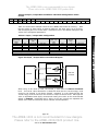
1.
Product Introduction
1.1
General Information
Digital Voice Systems Inc.’s AMBE-1000™ Vocoder Chip is an extremely flexible, highperformance, single chip, speech compression coder. It provides superior voice quality
at low data rates. It provides a real-time, full-duplex implementation of the standardsetting AMBE voice compression software algorithm. DVSI’s patented AMBE voice
compression technology has been proven to outperform CELP, RELP, VSELP, MELP,
ECELP, MP-MLQ, LPC-10, and other competitive technologies. Numerous evaluations
have shown its ability to provide performance equal to today’s digital cellular systems
at under half the data rate. The AMBE voice compression algorithm is used in
applications throughout the world, including the next generation of digital mobile
communication systems.
The AMBE-1000™ Vocoder chip provides a high degree of flexibility in selecting the
speech and FEC (Forward Error Correction) data rates. The user can separately select
these parameters in 50 bps increments for total rates from 2.4 kbps to 9.6 kbps.
Typically for higher error rate channels, the user will apportion a greater percentage of
the total bit rate to FEC coding.
The AMBE-1000™ voice coder maintains natural voice quality and speech intelligibility
at rates as low as 2.4 kbits/sec. The AMBE algorithm’s low complexity allows it to be
fully integrated into a low cost, low power integrated circuit, the AMBE-1000™ Vocoder
Chip.
1.2
Advantages
•
Superior Voice Quality
•
Low Cost
•
No External Memory Required
•
Robust to Bit Errors & Background Noise
•
Variable Data Rates - 2.4 kbps to 9.6 kbps
•
Variable FEC Rates - 50 bps to 7.2 kbps
•
Very Low Power (65mW @ 3.3V, 0.11mW Deep Sleep)
•
Compact Single Chip Solution: 100 pin TQFP
page 12
The AMBE-1000 is not recommended for new designs.
Please refer to the AMBE-2000/2020 product line.
Visit us at www.dvsinc.com
1 Introduction
The AMBE-1000 is not recommended for new designs.
Please refer to the AMBE-2000/2020 product line.
The AMBE-1000 is not recommended for new designs.
Please refer to the AMBE-2000/2020 product line.
1.4
Features
•
High Quality Low Data Rate Speech Coding
•
DVSI’s Full Duplex AMBE Voice Coder
•
Supports Data Rates of 2.4 kbps to 9.6 kbps in 50 bps increments
•
User Selectable Error Correction
•
Voice Activation / Comfort Noise Insertion
•
Selectable Serial or Parallel Channel Interface
•
Echo Cancellation
•
Single and Dual Tone (DTMF) Detection and Generation
•
3.3V or 5.0V supply
•
Power-Down Mode
Typical Applications
•
Cellular Telephony and PCS
•
Satellite Communications
•
Digital Mobile Radio
•
Secure Communications
•
Voice Multiplexing
•
Voice Mail
•
Multimedia Applications
•
Video Conferencing
page 13
The AMBE-1000 is not recommended for new designs.
Please refer to the AMBE-2000/2020 product line.
Visit us at www.dvsinc.com
1 Introduction
1.3
The AMBE-1000 is not recommended for new designs.
Please refer to the AMBE-2000/2020 product line.
2.
AMBE™-1000 Application Design Overview
2.1
Basic Operation
Figure 2-A Basic Operation
AMBE-1000
AMBE-1000
8kHz Speech Data
Encoder
Compressed Data @ 2400-9600bps
Decoder
8kHz Speech Data
8kHz Speech Data
Decoder
Compressed Data @ 2400-9600bps
Encoder
8kHz Speech Data
Typically the speech interface is an external A/D-D/A chip. The format of the incoming
and outgoing speech data streams are coupled, that is to say they must be the same
format (16-bit linear, 8-bit Alaw, or 8-bit µlaw). The channel interface is commonly (but
not limited to) an 8 or 16 bit microprocessor or other suitable ‘glue logic’ hardware
capable of performing the rudimentary formatting functions between the AMBE-1000™
channel format and the format of the system channel under design.
Optional functions of the chip, such as echo cancellation, voice activation/detection,
power mode control, data/FEC rate selection, etc. are controlled either through
hardware control pins (see Section 6) and/or through the decoder command interface
(see Section 4.1.14). Data sent into the decoder for function control purposes is
distinguished from the data to be decoded into speech through a channel format which
is described in Section 4.
2.2
Initial Design Considerations
Some of the initial design considerations the application engineer will face are the
following:
•
Choice of A/D-D/A chip.
•
Choice of Channel Interface.
•
Speech and FEC Rates.
page 14
The AMBE-1000 is not recommended for new designs.
Please refer to the AMBE-2000/2020 product line.
Visit us at www.dvsinc.com
2 Overview
In its simplest model, the AMBE-1000™ can be viewed as two separate components,
the Encoder and the Decoder. The Encoder receives an 8kHz. sampled stream of
speech data (16-bit linear, 8-bit Alaw, or 8-bit ulaw) and outputs a stream of channel
data at the desired rate. Conversely the Decoder receives a stream of channel data
and synthesizes a stream of speech data. The timing for the interfaces for the AMBE1000™ Encoder and Decoder are fully asynchronous.
The AMBE-1000 is not recommended for new designs.
Please refer to the AMBE-2000/2020 product line.
2.2.1
A/D – D/A Overview
The specifics of the hardware interface to the A/D-D/A data are flexible. Clocking and
strobe signals can be internal or external to the AMBE-1000™. Additionally, an
interface to send ‘control’ words to a programmable A/D-D/A is provided. For a full
description of the A/D-D/A interface see Section 5.
2.2.2
Channel Interface Overview
The channel interface is meant to be flexible to allow for easy integration with the
system under design. The basic hardware unit of the interface is either a parallel port
or a serial port. Both parallel and serial modes can run in passive or active modes.
Simply stated, the control signals for parallel and serial modes can be derived by the
AMBE-1000™ chip or they can be derived externally.
Under normal operation, every 20msec the encoder outputs a frame of coded bits, and
the decoder needs to be delivered a frame of coded bits. There is some formatting of
the data for both the encoder and the decoder. The primary purpose of the formatting
is to provide alignment information for the encoded bit stream. The data has two
formats, Framed and Unframed (in previous versions of this manual these modes
corresponded to packetized and unformatted modes respectively). Parallel mode runs
exclusively in Framed mode. Serial mode can run in either Framed or Unframed
mode.
The Framed and Unframed modes are explained in full detail in Section 4, but
essentially the two formats are trying to achieve the same function, to provide
positional information regarding the outgoing and incoming coded data streams. In
Framed mode each 20msecs of output data from the encoder is preceded by a known
structure. This structure also embeds some status type flags, meant for local control
purposes, within it. The only data from the Framed format that is typically sent across
the transmission channel under design are the actual encoded bits at the desired rate.
In Framed mode, it is the responsibility of the designed system to pass enough
information along with the encoded bits such that the Framed format needed by the
decoder can be reconstructed on the other side. This extra information, or overhead, is
going to be very specific to the system under design, but at a minimum needs to pass
enough information to reliably reconstruct the 20msec frame structure at the other end
for the decoder.
In Unframed mode the data coming out of the encoder can be thought of as a
continuous stream of voice data with the framing information embedded within the
encoded bits. One advantage of this type of set-up is that the system does not have to
add any bandwidth for overhead to the channel. The disadvantage is that the decoder
needs 10-12 incoming frames in order to gain synchronization with the data stream
before it can properly synthesize the speech waveform. Also, the Unframed mode
only commits a single bit per frame to maintaining data alignment. In higher error rate
channels the performance will be improved by adding more bits per frame to the
alignment information (which is more easily performed when using Framed mode)
page 15
The AMBE-1000 is not recommended for new designs.
Please refer to the AMBE-2000/2020 product line.
Visit us at www.dvsinc.com
2 Overview
The choice of the A/D-D/A chip is critical to designing a system with superior voice
quality. Given that Alaw and µlaw companding chips are already incorporating some
compression to reduce the number of bits per sample, it is recommended that, when
possible, a 16-bit linear device be used for maximum voice quality. When choosing a
device, pay particular attention to Signal to Noise ratios and Frequency Responses of
any filters that may be present on the analog front end of these chips. The Alaw and
µlaw interfaces are also provided for the design engineer who is trying to fit to preexisting conditions or is under other cost type restraints.
The AMBE-1000 is not recommended for new designs.
Please refer to the AMBE-2000/2020 product line.
When operating in Framed Mode the interface to the channel data can be either a
parallel or serial interface. The Unframed Mode is limited to the serial interface.
Additional flexibility is given to the channel interface to the encoder and decoder by
allowing the AMBE-1000™ Vocoder Chip to run in Passive or Active modes. In
Passive mode, data strobes are provided by an external source, while in Active mode,
data strobes are provided by the AMBE-1000™ Vocoder Chip. Both the parallel and
serial interfaces can be run in Passive or Active modes. See Section 4 for full details
and timing for both parallel and serial modes for Framed and Unframed data.
Speech and FEC Rate Selection Overview
The total coded bit rate is the sum of two components, the Speech Data and the
Forward Error Correction (FEC) Data. The addition of FEC data to the speech data
allows the decoder to be able to correct a limited amount of errors within each frame
should they arrive corrupted. If the channel is expected to have more errors then
more bits should be dedicated to FEC. At the same time, voice quality will increase if
the number of speech bits can be maximized.
page 16
The AMBE-1000 is not recommended for new designs.
Please refer to the AMBE-2000/2020 product line.
Visit us at www.dvsinc.com
2 Overview
2.2.3
3.
Channel Interface
3.1
Overview
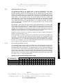
The Channel Interface is the general term used for the interface for the compressed
bits coming from the encoder and the compressed bits going to the decoder. This
same interface is also used to output status information from the encoder and decoder
such as whether a DTMF tone has just been detected in the speech input, or whether
the decoder has detected and synthesized a frame of silence. Additionally, this
interface is used to perform more complex control operations on both the encoder and
decoder (usually at start-up). These control functions include speech data/FEC rate
control as well as A/D-D/A chip configuration.
It is important to realize that not all data being output from the AMBE-1000 is intended
for transmission over the channel. Status type of data is typically only useful at the
‘local’ end. In most voice transmission systems, the actual encoded bits are extracted
from the channel formatting, combined into the systems transmission stream, sent
over the transmission path, extracted from the transmission path at the receiving end,
and reassembled into the AMBE-1000’s channel format for synthesis by the decoder.
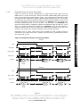
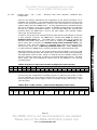
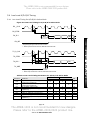
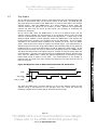
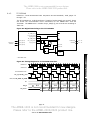
Figure 3-A Channel Interface Overview
Typical Voice Frame Output From Encoder
Overhead Data
Voice Data (48 to 192 bits)
(Header, Status)
Transmission Channel
System extracts
relevant Voice Data bits
and formats them for
transmission over
Channel
System Overhead
Voice Data (48 to 192 bits)
System extracts
relevant Voice Data bits
and formats them for
Input into the Decoder
adding Header and
Control Information
Typical Voice Frame Input to the Decoder
Overhead Data
Voice Data (48 to 192 bits)
(Header, Control)
This section will first outline the two main channel interfaces, parallel and serial and
their respective signals and timing. Section 4 will discuss the format of the data which
is transferred within these two configurations including the formatting of Command
Frames.
3.2
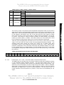
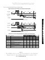
Parallel vs. Serial Configuration Selection
The hardware interface to the Channel Interface is configured as either a serial
interface or a parallel interface based exclusively on the hardware settings of
CH_SEL[2-0]. See Table 3-A.
page 17
The AMBE-1000 is not recommended for new designs.
Please refer to the AMBE-2000/2020 product line.
Visit us at www.dvsinc.com
3 Channel Interface
The AMBE-1000 is not recommended for new designs.
Please refer to the AMBE-2000/2020 product line.
The AMBE-1000 is not recommended for new designs.
Please refer to the AMBE-2000/2020 product line.
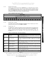
Table 3-A Channel Interface Selection Table
0
0
1
0
1
0
0
1
1
1
0
0
1
0
1
1
1
0
1
1
1
Parallel,
Passive Mode
Parallel,
Active Mode
Serial,
Active Mode
Serial,
Passive Mode
Serial,
Passive Mode
Serial,
Passive Mode
Serial,
Passive Mode
Serial,
Passive Mode
Framed
Input
Number of Voice
Data Bits per
Word
N/A
N/A
N/A
Framed
Output
N/A
N/A
N/A
Framed
N/A
Input
Output
N/A
Framed
N/A
Input
Input
N/A
N/A
Input
Input
1
N/A
Input
Input
2
N/A
Input
Input
3
N/A
Input
Input
4
Unframed
(Self Sync)
Unframed
(Self Sync)
Unframed
(Self Sync)
Unframed
(Self Sync)
Selection of one of the parallel modes allows all ‘channel data’ transfers (including the
control functions) to be performed on an 8-bit wide bus. The two modes within parallel
mode are active and passive, and simply refer to the directionality of the read and
write strobes. Parallel mode is always in framed mode. See section 3.3 for all the
details on the parallel interface. Selection of a serial mode restricts all transfers to
occur through a serial port. The serial port inputs and outputs a 16 bit word for every
write and read strobe signal respectively. Serial mode can be framed or unframed.
The serial framed mode can configure the direction of the output clock signal to be
input or output as shown in Table 3-A. Within the unframed mode, the data is input
and output in 16 bits words still but with only 1 to 4 voice data bits carried within each
word. These four configurations can be seen in Table 3-A. See section 3.4 for all the
details on the serial interface.
page 18
The AMBE-1000 is not recommended for new designs.
Please refer to the AMBE-2000/2020 product line.
Visit us at www.dvsinc.com
3 Channel Interface
0
Data
Format
CHS_OCLK
CH_ SEL0
(pin 2)
0
Port Type
CHS_ICLK
CH_ SEL1
(pin 99)
0
Direction of Control Signals
CHP_RDN
CHP_WRN
CH_ SEL2
(pin 98)
Interface
Select Pins
The AMBE-1000 is not recommended for new designs.
Please refer to the AMBE-2000/2020 product line.
3.3
Parallel Mode
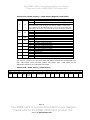
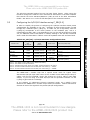
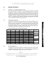
The signals in Table 3-B make up the parallel channel interface. Remember that in
parallel channel mode the only available data format is framed, as shown in Table 3-A.
The framed format consists of 272 bits being output from the encoder and input to the
decoder over each 20 milliseconds. This implies that in parallel mode, each 20
milliseconds the hardware interfacing to the AMBE-1000 has to perform 34 reads and
34 writes, regardless of the voice coding rate.
The parallel interface runs
asynchronously to any clocks.
Pin
Symbol
Pin
Direction
Pin
Number
EPR
Out
46
DPE
Out
47
CHP_RDN
Selectable
In/Out
(see Table 3-A)
64
CHP_WRN
Selectable
In/Out
(see Table 3-A)
65
CHP_OBE
Out
61
CHP_IBF
Out
63
CHP_SEL1
In
68
CHP_SEL2
In
69
CHP_D7
CHP_D6
CHP_D5
CHP_D4
CHP_D3
CHP_D2
CHP_D1
CHP_D0
Bi-directional
Bi-directional
Bi-directional
Bi-directional
Bi-directional
Bi-directional
Bi-directional
Bi-directional
52
53
54
55
57
58
59
60
Description
Encoder Packet Ready : This output signal will go high once
every 20 milliseconds to indicate that the encoder has a frame of
data to output.
It will return low some time after the first
CHP_RDN.
Decoder Packet Empty : This output signal will go high once
every 20 milliseconds to indicate that the decoder is ready to
accept another frame of data. It will return low some time after
the first CHP_WRN.
Read Data Strobe : In active mode, the rising edge of this output
indicates when the data coming from the AMBE-1000 should be
latched. In passive mode, the falling edge of this signal brings the
next data value to the bus.
Write Data Strobe : In active mode the falling edge of this signal;
indicates when the next data value should be driven on the bus by
external hardware. In both active and passive modes the rising
edge of this signal indicates when the AMBE-1000 latches the data.
Output Buffer Empty : This signal will go active high after each
read (CHP_RDN) of the parallel port. The port is ready to be read
again when this signal returns low. CHP_OBE can effectively be
ignored if the time between CHP_RDN pulses is at least 350
cycles of the input clock, CLK_I, at which time the output buffer is
guaranteed to be full again.
Input Buffer Full : This signal will go active high after each write
(CHP_WRN) to the parallel port. The port is ready to be written
to again when this signal returns low. CHP_IBF can effectively be
ignored if the time between CHP_WRN pulses is at least 350
cycles of the input clock, CLK_I, at which time the input buffer is
guaranteed to be empty again.
Select 1. In Passive mode, connect to ground through 10k ohm
resistor. In Active mode this pin is an output and can be left
unconnected.
Select 2 : In Passive mode, this pin becomes an active low enable
or chip select input for the parallel port. While CHP_SEL2 is high,
the AMBE-1000™ ignores any activity on the passive CHP_WRN
or CHP_RDN.
To continuously enable the passive strobes,
CHP_SEL2 should be tied to ground through a 10k ohm resistor.
In Active mode this pin is an output and can be left unconnected.
Data Bus bit 7
Data Bus bit 6
Data Bus bit 5
Data Bus bit 4
Data Bus bit 3
Data Bus bit 2
Data Bus bit 1
Data Bus bit 0
page 19
The AMBE-1000 is not recommended for new designs.
Please refer to the AMBE-2000/2020 product line.
Visit us at www.dvsinc.com
3 Channel Interface
Table 3-B Channel Parallel Interface Pin Descriptions
The AMBE-1000 is not recommended for new designs.
Please refer to the AMBE-2000/2020 product line.
3.3.1 Low Level Timing for Active Parallel Mode Output
Figure 3-B Low Level Timing for Active Parallel Mode Output
CLK_O
t33
t31
t32
t34
t35
CHP_D[7:0]
Table 3-C Low Level Timing Parameters for Active Parallel Mode Output
Reference
t31
t32
t33
t34
t35
5 Volts
Min
Max
Parameter
CLK_O Low to CHP_RDN Assertion (Low
12
to Low)
CHP_RDN Width (low to low)
4T-4
CLK_O Low to CHP_RDN Negation (Low
10
to High)
CHP_RDN Low to CHP_D Valid ( low to
12
valid)
CHP_D Hold (high to invalid [high
T/2-8
impedance])
T = Period of one clock cycle of CLK_O
Min
3 Volts
Max
16
4T-4
T/2-10
Units
ns
ns
18
ns
14
ns
ns
page 20
The AMBE-1000 is not recommended for new designs.
Please refer to the AMBE-2000/2020 product line.
Visit us at www.dvsinc.com
3 Channel Interface
CHP_RDN
The AMBE-1000 is not recommended for new designs.
Please refer to the AMBE-2000/2020 product line.
3.3.2
Low Level Timing for Active Parallel Mode Input
Figure 3-C Low Level Timing for Active Parallel Mode Input
CLK_O
t26
t28
t27
t29
CHP_D[7:0]
t30
Table 3-D Low Level Timing Parameters for Active Parallel Mode Input
Reference
t26
t27
t28
t29
t30
5 Volts
Min
Max
Parameter
CLK_O Low to CHP_WRN Assertion
12
(Low to Low)
CHP_WRN Width (Low to High)
4T-4
CLK_O Low to CHP_WRN Negation (Low
10
to High)
CHP_D[7:0] Setup Time (valid to high)
8
CHP_D[7:0] Hold Time (high to invalid
0
[high impedance])
T = Period of one clock cycle of CLK_O
Min
3 Volts
Max
16
4T-4
Units
ns
ns
18
ns
8
ns
0
ns
page 21
The AMBE-1000 is not recommended for new designs.
Please refer to the AMBE-2000/2020 product line.
Visit us at www.dvsinc.com
3 Channel Interface
CHP_WRN
The AMBE-1000 is not recommended for new designs.
Please refer to the AMBE-2000/2020 product line.
3.3.3 Low Level Timing for Passive Parallel Mode Output
Figure 3-D Low Level Timing for Passive Parallel Mode Output
t39
CHP_SEL2
t39
t41
t40
CHP_D[7:0]
t42
Table 3-E Low Level Timing Parameters for Passive Parallel Mode Output
Reference
t39
t40
t41
t42
5 Volts
Min
Max
Parameter
CHP_SEL2 or CHP_RDN
T
Pulse Width (Low to High)
CHP_RDN Low to
28
CHP_D[7:0] Valid
CHP_D[7:0] Hold Time (high
to invalid [high impedance]
6
)
CHP_WRN High to
CHP_D[7:0] 3-state (Low to
20
High)
T = Period of one clock cycle of CLK_O
Min
3 Volts
Max
T
Units
ns
34
6
ns
ns
37
ns
page 22
The AMBE-1000 is not recommended for new designs.
Please refer to the AMBE-2000/2020 product line.
Visit us at www.dvsinc.com
3 Channel Interface
CHP_RDN
The AMBE-1000 is not recommended for new designs.
Please refer to the AMBE-2000/2020 product line.
Low Level Timing for Passive Parallel Mode Input
Figure 3-E Low Level Timing for Passive Parallel Mode Input
t36
CHP_SEL2
t36
CHP_WRN
CHP_D[7:0]
t37
t38
Table 3-F Low Level Timing Parameters for Passive Parallel Mode Input
Reference
t36
t37
t38
5 Volts
Min
Max
Parameter
CHP_SEL2 or CHP_WRN
T
Pulse Width (Low to High)
CHP_D[7:0] Setup Time
8
(valid to high)
CHP_D[7:0] Hold Time (high
0
to invalid [high impedance])
T = Period of one clock cycle of CLK_O
Min
3 Volts
Max
Units
T
ns
8
ns
0
ns
page 23
The AMBE-1000 is not recommended for new designs.
Please refer to the AMBE-2000/2020 product line.
Visit us at www.dvsinc.com
3 Channel Interface
3.3.4
The AMBE-1000 is not recommended for new designs.
Please refer to the AMBE-2000/2020 product line.
3.3.5
Expanded Timing for Active Parallel Mode Output
Figure 3-F shows the expanded output timing for the active parallel mode. In this
configuration the AMBE-1000™ Vocoder Chip is in control of the interface. Every 20
milliseconds a series of CHP_RDN strobes will begin. There will be 34 CHP_RDN
corresponding to the 34 bytes that are output by the encoder each frame. See section
4 for details on the format of this data. Each CHP_RDN pulse width is 4 CLK_O cycles
in length and there will be a minimum delay of 350 CLK_I cycles between strobes.
Figure 3-F Expanded Timing for Active Parallel Mode Output
EPR
CLK_O
CHP_RDN
CHP_D
8 bits
1
2
34
There is a minimum of 350 CLK_O cycles
between CHP_RDN pulses.
3.3.6
Expanded Timing for Active Parallel Mode Input
Figure 3-G shows the expanded input timing for the active parallel mode. In this
configuration the AMBE-1000™ Vocoder Chip is in control of the interface. Every 20
milliseconds a series of CHP_WRN strobes will begin. There will be 34 CHP_WRN
corresponding to the 34 bytes that are input by the decoder each frame. See section 4
for details on the format of this data. Each CHP_WRN pulse width is 4 CLK_O cycles in
length and there will be a minimum delay of 350 CLK_I cycles between strobes.
Figure 3-G Expanded Timing for Active Parallel Mode Input
20 msecs
DPE
CLK_O
CHP_WRN
CHP_D
8 bits
1
2
34
There is a minimum of 350 CLK_O cycles
between CHP_WRN pulses.
page 24
The AMBE-1000 is not recommended for new designs.
Please refer to the AMBE-2000/2020 product line.
Visit us at www.dvsinc.com
3 Channel Interface
20 msecs
The AMBE-1000 is not recommended for new designs.
Please refer to the AMBE-2000/2020 product line.
3.3.7
Expanded Timing for Passive Parallel Mode Output
As each byte is extracted, the controller must wait for the CHP_OBE signal to return
low before attempting to extract the next byte. Alternatively, if the controller can
guarantee at least 350 CLK_I (or CLK_O) cycles between CHP_RDN pulses, then the
CHP_OBE signal can be ignored. The controller should always perform 34 reads for
each frame, even if lower bit rates are being used such that the data at the end of each
frame are unused zeros.
Figure 3-H Expanded Timing for Passive Parallel Mode Output
20 Msecs
EPR
CHP_RDN
8 bits
CHP_D[7:0]
1
2
High Byte
Low Byte
34
CHP_OBE
CHP_OBE returns low when the AMBE-1000
makes another byte available in the registter.
CHP_OBE can be ignored if a minimum of 350 clocks of
CLK_I can be guaranteed between CHP_RDN pulses.
page 25
The AMBE-1000 is not recommended for new designs.
Please refer to the AMBE-2000/2020 product line.
Visit us at www.dvsinc.com
3 Channel Interface
Figure 3-H shows the timing relationship for a single frame being output from the
AMBE-1000™ in passive parallel mode. When the Encoder Packet Ready (EPR) signal
goes high, this indicates that a coded frame is ready. The controller should then be
prepared to extract the 34 bytes (regardless of bit rate) of data that make up a single
frame over the following 20 milliseconds. See section 4 for the format of this data.
The AMBE-1000 is not recommended for new designs.
Please refer to the AMBE-2000/2020 product line.
3.3.8
Expanded Timing for Passive Parallel Mode Input
As each byte is input, the controller must wait for the CHP_IBF signal to return low
before attempting to input the next byte. Alternatively, if the controller can guarantee
at least 350 CLK_I (or CLK_O) cycles between CHP_WRN pulses, then the CHP_IBF
signal can be ignored. The controller should always perform 34 writes for each frame,
even if lower bit rates are being used such that the data at the end of each frame are
unused zeros.
Figure 3-I Expanded Timing for Passive Parallel Mode Input
20 Msecs
DPE
CHP_WRN
8 bits
CHP_D[7:0]
1
2
High Byte
Low Byte
34
CHP_IBF
CHP_IBF can be ignored if a minimum of 350 cycles of CLK_I can
be guaranteed between CHP_WRN pulses.
CHP_IBF returns low when AMBE-1000
reads parallel channel register
page 26
The AMBE-1000 is not recommended for new designs.
Please refer to the AMBE-2000/2020 product line.
Visit us at www.dvsinc.com
3 Channel Interface
Figure 3-I shows the timing relationship for a single frame being input to the AMBE1000™ in passive parallel mode. When the Decoder Packet Empty (DPE) signal goes
high, this indicates that the Decoder needs a coded frame of data. The controller
should then be prepared to input the 34 bytes (regardless of bit rate) of data that make
up a single frame over the following 20 milliseconds. See section 4 for the format of
this data.
The AMBE-1000 is not recommended for new designs.
Please refer to the AMBE-2000/2020 product line.
Serial Mode
The signals in Table 3-G make up the serial channel interface. The serial channel mode
transfers data in and out of the AMBE-1000™ using 16 bit words on the two data lines
CHS_DI and CHS_DO. The selection of the framed or unframed format of this data
is made using information in Table 3-A.
As described in section 4.1, the framed format consists of 272 bits being output from
the encoder and input to the decoder over each 20 milliseconds. This implies that in
serial mode, each 20 milliseconds the hardware interfacing to the AMBE-1000 will have
to perform 17 reads and 17 writes, each of 16 bits, regardless of the voice coding rate.
In unframed mode, the number of reads and writes is variable depending on the voice
coding bit rate selected and the number of voice data bits per word as seen in Table
3-A. In unframed mode, which is only selectable in passive mode, the minimum
number of reads and writes per frame would be 12 {(minimum bit rate) ÷ (maximum
voice data bits per word) ÷ (50 frames per second) = (2400) ÷ (4) ÷ (50) = 12 }. The
maximum number of reads and writes of 192 can be similarly calculated { (9600) ÷ (1)
÷ (50) = 192 }.
The limitations on how quickly the data can be transferred in and out of the AMBE1000™ during serial mode are governed by the requirement to allow CHS_IBF and
CHS_OBE to return low after the input buffer has been written to or the output buffer
has been read. See sections 3.4.2 and 3.4.3 for more details.
page 27
The AMBE-1000 is not recommended for new designs.
Please refer to the AMBE-2000/2020 product line.
Visit us at www.dvsinc.com
3 Channel Interface
3.4
The AMBE-1000 is not recommended for new designs.
Please refer to the AMBE-2000/2020 product line.
Table 3-G Channel Serial Interface Pin Descriptions
Pin
Symbol
Pin
Direction
Pin
Number
EPR
Out
46
Encoder Packet Ready : This output signal will go high once every 20
milliseconds to indicate that the encoder has a frame of data to output. It
will return low some time after the first CHS_O_STRB.
DPE
Out
47
Decoder Packet Empty : This output signal will go high once every 20
milliseconds to indicate that the decoder is ready to accept another frame of
data. It will return low some time after the first CHS_I_STRB.
CHS_DI
In
59
Serial Data Input : 16 bits of channel data are input on CHS_DI,
synchronous to CHS_I_CLK, with each CHS_I_STRB pulse.
60
Serial Input Clock : In coordination with CHS_I_STRB, CHS_DI is latched
by the AMBE-1000™ on the rising edges of CHS_I_CLK. In active mode
this input pin should be connected to CHS_O_CLK, which is running at
CLK_I ÷ 6. In passive mode the maximum frequency for this signal is
CLK_I ÷ 2.
65
Input (Write) Data Strobe : This signal indicates to the AMBE-1000™
when the data on CHS_DI will be latched by CHS_I_CLK. In passive
mode, following a falling edge of CHS_I_STRB, the MSB of CHS_DI will be
latched on the second rising edge of CHS_I_CLK. In active mode, following
a falling edge of CHS_I_STRB, the MSB of CHS_DI will be latched on the
first rising edge of CHS_I_CLK. In both active and passive modes, the
other 15 bits are latched on successive rising edges of CHS_I_CLK. In
active mode this signal should be tied to CHS_SYNC.
CHS_I_STRB
In
In
CHS_IBF
Out
63
Input Buffer Full : This signal will go active high after each write
(CHS_I_STRB) to the serial port. The port is ready to be written to again
when this signal returns low. CHS_IBF can effectively be ignored if the
time between CHS_I_STRB pulses is at least 350 cycles of the input clock,
CLK_I, at which time the input buffer is guaranteed to be empty again.
CHS_DO
Out
68
Serial Data Output : 16 bits of channel data are output on CHS_DO,
synchronous to CHS_O_CLK, with each CHS_O_STRB pulse.
CHS_O_CLK
Selectable
In/Out
(see Table
3-A)
69
Serial Output Clock : In coordination with CHS_O_STRB, the data on
CHS_DO is output by the AMBE-1000™ on the rising edges of CHS_O_CLK.
In active mode this output pin is running at CLK_I ÷ 6. In passive mode the
maximum frequency for this signal is CLK_I ÷ 2.
64
Output (Read) Data Strobe : This signal indicates to the AMBE-1000™
when to bring the data to the CHS_DO pin. Following a falling edge of
CHS_O_STRB, the MSB of CHS_DO comes out on the first rising edge of
CHS_O_CLK, with the other 15 bits following on successive rising edges of
CHS_O_CLK. In active mode this signal should be tied to CHS_SYNC.
61
Serial Output Buffer Empty : This signal will go active high after each
read (CHS_O_STRB) of the serial port. The port is ready to be read again
when this signal returns low. CHS_OBE can effectively be ignored if the
time between CHS_O_STRB pulses is at least 350 cycles of the input clock,
CLK_I, at which time the output buffer is guaranteed to be full again.
67
Serial Sync : This pin is only used in active mode as a source for
CHS_I_STRB and CHS_O_STRB. This signal is tied to these two strobe
inputs, and outputs the necessary 17 strobe pulses each of which is 64
cycles of CHS_O_CLK in length. See Figure 3-K. In passive mode this pin
is left unconnected.
CHS_O_STRB
CHS_OBE
CHS_SYNC
In
Out
Out
page 28
The AMBE-1000 is not recommended for new designs.
Please refer to the AMBE-2000/2020 product line.
Visit us at www.dvsinc.com
3 Channel Interface
CHS_I_CLK
Description
The AMBE-1000 is not recommended for new designs.
Please refer to the AMBE-2000/2020 product line.
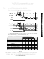
Low Level Timing for Passive and Active Serial Mode
Figure 3-J Low Level Timing for Passive and Active Serial Mode
t7
t8
t9
t12
t11
CHS_I_CLK
t10
t12
CHS_I_STRB
t13
t14
B15
CHS_DI
B0
t15
CHS_IBF
t7
t8
t9
t12
t11
CHS_O_CLK*
t10
t12
CHS_O_STRB
t16
t17
t17
B15
CHS_DO
B0
t15
CHS_OBE
* In Active mode, CHS_O_CLK is an output at (CLK_I ÷ 6). See Table 3-G. Remember
that in Active mode CHS_O_CLK must be tied to CHS_I_CLK.
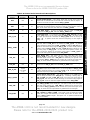
Table 3-H Low Level Timing Parameters for Passive Serial Mode
Reference
t7
t8
t9
t10
t11
t12
t13
t14
t15
t16
t17
Parameter
Clock Period (High to High)
Clock High Time (high to low)
Clock Low Time (low to high)
Load High Setup (high to high)
Load Low Setup (low to high)
Load High Hold (high to invalid [high
impedance])
CHS_DI Setup (valid to high)
CHS_DI Hold (high to invalid [high
impedance] )
CHS_IBF and CHS_OBE Delay
CHS_DO Delay (high to valid)
CHS_DO Hold (high to invalid [high
impedance] )
Min
60
27
27
5
5
5 Volts
Max
Min
66
30
30
5
5
4
4
5
4
4
5
35
35
5
3 Volts
Max
ns
ns
ns
ns
ns
ns
ns
ns
40
40
15
Units
ns
ns
ns
page 29
The AMBE-1000 is not recommended for new designs.
Please refer to the AMBE-2000/2020 product line.
Visit us at www.dvsinc.com
3 Channel Interface
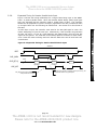
3.4.1
The AMBE-1000 is not recommended for new designs.
Please refer to the AMBE-2000/2020 product line.
Expanded Timing for Active Serial Mode
Figure 3-K shows the timing relationship for a single frame being output from the
AMBE-1000™ in active serial mode. When the Encoder Packet Ready (EPR) signal goes
high, this indicates that a coded frame is ready. Conversely when the decoder is ready
to accept the next coded frame, Decoder Packet Empty (DPE) will go high. The number
of words that the controller should be ready to read from the encoder or write to the
decoder is dependant on the data format selected. In framed mode, the number of 16
bit words transferred will be 17 (17 x 16 bits = 272 bits total). In unframed mode
each 16-bit word holds 1-4 data bits, based on the selection made in Table 3-A. Since
there is no overhead information transferred in unframed mode, the total number of
words transferred will be the voice data rate divided by the number of bits per word
selected. See section 4 for further information on the format of this data.
Remember that in active serial mode CHS_O_STRB and CHS_I_STRB should be
connected to the output CHS_SYNC. Similarly, the input CHS_I_CLK should be tied to
the output CHS_O_CLK.
Figure 3-K Expanded Timing for Active Serial Mode
20 msecs
EPR
64 cycles
CHS_SYNC
64 cycles
CHS_O_STRB
CHS_O_CLK
CHS_DO
B15
B14
B0
B15
B14
B0
B15
2nd Word
1st Word
Header
B14
B0
17th Word
20 msecs
DPE
CHS_I_STRB
CHS_I_CLK
CHS_DI
B15
B14
B0
B15
B14
2nd Word
1st Word
Header
B0
B15
B14
B0
17th Word
page 30
The AMBE-1000 is not recommended for new designs.
Please refer to the AMBE-2000/2020 product line.
Visit us at www.dvsinc.com
3 Channel Interface
3.4.2
The AMBE-1000 is not recommended for new designs.
Please refer to the AMBE-2000/2020 product line.
3.4.3
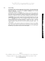
Expanded Timing for Passive Serial Mode
Figure 3-L shows the expanded timing for passive serial mode. In this mode both
strobe and clock signals are inputs. Once again EPR and DPE mark the beginnings of
the 20msec. frames. Unlike active mode, CHS_IBF and CHS_OBE must be monitored
between strobe pulses, unless there are at least 350 clock cycles of CLK_I between
strobe pulses, in which case CHS_IBF and CHS_OBE can be ignored. As in active mode
the number of words transferred per frame is dependant on the voice data rate and the
number of data bits per word selected in Table 3-A. See section 4 for the format of this
data.
20 msecs
EPR
CHS_O_STRB
CHS_IBF can be ignored if a minimum of 350 clocks of CLK_I can be
guaranteed between CHS_O_STRB pulses.
CHS_O_CLK
CHS_DO
B15
B14
B0
B15
B14
B0
B15
2nd Word
1st Word
B14
B0
Nth Word
CHS_IBF
20 msecs
DPE
CHS_I_STRB
CHS_OBF can be ignored if a minimum of 350 clocks of CLK_I can be
guaranteed between CHS_I_STRB pulses.
CHS_I_CLK
CHS_DI
B15
B14
B0
B15
B14
2nd Word
1st Word
B0
B15
B14
B0
Nth Word
CHS_OBF
page 31
The AMBE-1000 is not recommended for new designs.
Please refer to the AMBE-2000/2020 product line.
Visit us at www.dvsinc.com
3 Channel Interface
Figure 3-L Expanded Timing for Passive Serial Mode
The AMBE-1000 is not recommended for new designs.
Please refer to the AMBE-2000/2020 product line.
4.
Channel Data Format
The channel interface is responsible for outputting the compressed data from the
encoder and inputting compressed data to the decoder. In addition to these most
basic functions the channel interface is also capable of reporting certain events, such as
the detection of a DTMF tone. The channel interface can also control certain selectable
functions of the AMBE-1000™, such as the voice coding rate. This chapter will describe
how the AMBE-1000™ uses the channel interface to multiplex these capabilities.
4.1
4 Channel Data Format
There are two formats to the data, Framed which is available in both parallel and serial
modes, and Unframed, which is only available in serial mode. Generally speaking the
Unframed mode is used only when the connection between the AMBE-1000™ and the
channel under design is relatively direct, and the designer wants to simplify the
extraction of the relevant voice data. In most cases, when a controller is present
between the AMBE-1000™ and the channel, the system designer will find that using the
Framed format is more straight forward in implementing the system.
Framed Format
The Framed format is a 17 by sixteen-bit word format. Every 20 milliseconds the
encoder outputs 17 words, and likewise the decoder expects to receive 17 words. The
format of the input and output frames are detailed below. The first 5 sixteen bit words
are made up of header, ID and status or control information. The remaining 12 sixteen
bit words make up the encoded data bit field. These 12 words, or 192 bits, will be fully
populated with relevant voice data only when the AMBE-1000 is operating in a 9600bps
mode (9600 bits/sec ÷ 50 frames/sec = 192 bits/frame). Otherwise, when the data
rate is less than 9600bps, the coded voice bits are filled starting from the MSB of the
first word in the field, leaving any unused bits as zeros. It is important to note here
that even when the AMBE-1000 is operating at less than 9600bps, all 272 bits of the
Framed format (including any unused trailing zeros) must be transferred out of the
encoder and into the decoder.
4.1.1
Framed Output Format
In Table 4-A, we see the basic Framed data format. As diagramed in Figure 3-A, it is
only the bits in the Voice Data Bits field which are transmitted along with framing
information (data used to locate the start of each frame for proper reconstruction at
the decoder) over the channel. The first 80 bits provide overhead information which is
sometimes useful to the host but is generally not transmitted over the channel.
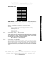
Table 4-A Basic Framed Output Format
20 ms frame
17 sixteen-bit words = 34 bytes = 272 bits
(5) 16 bits words of overhead (80 bits)
Header
ID
16 bits
8 bits
(12) 16 bits words of data (192 bits)
Status_0 Status_1 Status_2 Status_3
8 bits
16 bits
16 bits
16 bits
Voice Data Bits
16 bits
16 bits
16 bits
16 bits
16 bits
16 bits
16 bits
16 bits
16 bits
16 bits
16 bits
page 32
The AMBE-1000 is not recommended for new designs.
Please refer to the AMBE-2000/2020 product line.
Visit us at www.dvsinc.com
16 bits
The AMBE-1000 is not recommended for new designs.
Please refer to the AMBE-2000/2020 product line.
4.1.2
Framed Output : Header
The header is a 16 bit word that begins each valid frame corresponding to 20
milliseconds of speech. This field will always be 0x13EC.
4.1.3
Framed Output : ID
The encoder will always use 0x00 in the 8-bit ID field of an output frame.
4.1.4
Framed Output : Status_0
Table 4-B Status_0 Format
6
5
4
3
2
1
0 : LSB
Unused : 0
Unused : 0
Frame
Repeat
Decoder
Output
Silence
Unused : 0
Find Sync
Encoder
Silence
Detected
DTMF
Detected
Frame Repeat : The Frame Repeat Flag is set to a 1 when the AMBE-1000™ decoder
outputs a waveform corresponding to the parameters of the previous frame. A frame
repeat serves to mask from the listener the effects of receiving corrupted data. A
frame repeat will automatically be performed by the decoder if it deems that the
received frame has too many bit errors, or if the decoder has received a specific
command from the host to perform a frame repeat through the command interface as
described in section 4.1.12.
Decoder Output Silence : The Decoder Output Silence Flag is set to a 1 when the
previous frame that the decoder receives is a silence frame. When a silence frame is
received by the decoder a frame of ‘comfort noise’ is output. In order for the encoder
to output coded silence frames the VAD feature must be enabled (see Section 6.4) yet
the decoder will report the receipt of a silence frame regardless of the VAD being
enabled or disabled. This flag will also report the decoder outputting a silence frame as
a result of setting the Force Decoder Silence bit in the Control_0 field of an input frame
to the decoder (see section 4.1.12).
Find Sync : The Find Sync Flag only has relevance when operating in Unframed
(serial) mode. This flag is set to 1 during the period of time when the decoder is still
trying to synchronize with the embedded frame bit of the Unframed data format.
Once synchronization has occurred (normally takes 10-15 frames of uncorrupted data)
this flag will return to 0.
Encoder Silence Detected : The Encoder Silence Detected Flag is relevant only when
the VAD feature is enabled (see Section 6.4). This flag is set to 1 when the encoder
detects no voice activity in the speech data. The corresponding voice data bits will
contain a ‘silence frame’ which will convey (in-band) to the receiving decoder to insert
‘comfort noise’ during this frame.
DTMF Detected : The DTMF Detected Flag will be set to a 1 when the encoder detects
a DTMF tone according to the requirements in Table 4-C. When this flag is set to a 1
then a code corresponding to which DTMF tone has been detected will be output in
Status_2 along with amplitude information (see Section 4.1.6 below).
page 33
The AMBE-1000 is not recommended for new designs.
Please refer to the AMBE-2000/2020 product line.
Visit us at www.dvsinc.com
4 Channel Data Format
Status_0 (see Table 4-A)
7 : MSB
The AMBE-1000 is not recommended for new designs.
Please refer to the AMBE-2000/2020 product line.
Table 4-C DTMF Tone Detection Parameters
DTMF Tone
Detection
Requirement
Value
Minimum
Input Level
-25 dBm0
An input signal shall not be rejected as a DTMF tone if its amplitude is greater
than -25 dBm0 (maximum sinusoid dBm0 is defined as+3.17 dBm0).
Minimum
Signal to Noise
Distortion ratio
15 dB
In order for an input signal to correspond to a valid DTMF tone, the ratio of
inband to out-of-band energy must be greater than 15dB. Inband energy is
defined to be the energy in frequency components within ±3.5% of the two
frequencies defined by the DTMF frequencies. Out-of-band energy is defined to
be the total energy minus in the inband energy.
Minimum
Frequency
Tolerance
±1.5%
An input signal shall not be rejected as a DTMF tone if both of its principal
frequency components are within ±1.5% of the frequencies needed for the DTMF
tone.
Maximum
Frequency
Tolerance
±3.5%
An input signal shall not be rejected as a DTMF tone if either of its principal
frequency components are outside ±3.5% of the frequencies needed for the DTMF
tone.
8-10 dB
An input signal does not correspond to a valid DTMF tone if the energy contained
within the low frequency band is more than 10 dB greater than the energy
contained in the high frequency band. An input signal shall not be rejected as a
DTMF if energy contained within the low frequency band is less than 8 dB greater
than the energy contained in the high frequency band. Each low and high
frequency band is limited to ±3.5% of the frequencies needed for the DTMF tone.
Reverse Twist
Range
4-10 dB
An input signal does not correspond to a valid DTMF tone if the energy contained
within the high frequency band is more than 10 dB greater than the energy
contained in the low frequency band. An input signal shall not be rejected as a
DTMF if energy contained within the high frequency band is less than 4 dB
greater than the energy contained in the low frequency band. Each low and high
frequency band is limited to ±3.5% of the frequencies needed for the DTMF tone.
Minimum
Tone Duration
45 mS
An input signal shall not be rejected as a DTMF tone as long as its time duration
is greater than 45 mS. In addition a minimum of two frames will be transmitted
of the DTMF tone if a valid tone is detected. The duration of a tone is defined by
the points at which the envelope is 20 dB below its peak value.
4.1.5
Framed Output : Status_1
This 16 bit field is unused and is output as 0x0000.
4.1.6
Framed Output : Status_2
This 16 bit field is used only when a DTMF tone is detected. If the DTMF Detected Flag
is set in Status_0, then the DTMF Code and DTMF Amplitude fields in Status_2 will be
filled according to Table 4-D and Table 4-E.
Table 4-D Status_2 Format
Status_2 (see Table 4-A)
Bits 15:8
Bits 7:0
DTMF Code
DTMF Amplitude
page 34
The AMBE-1000 is not recommended for new designs.
Please refer to the AMBE-2000/2020 product line.
Visit us at www.dvsinc.com
4 Channel Data Format
Normal Twist
Range
Description
The AMBE-1000 is not recommended for new designs.
Please refer to the AMBE-2000/2020 product line.
DTMF Code
0x00
0x04
0x08
0x01
0x05
0x09
0x02
0x06
0x0A
0x07
0x03
0x0B
0x0C
0x0D
0x0E
0x0F
DTMF Digit
1
2
3
4
5
6
7
8
9
0
*
#
A
B
C
D
DTMF Amplitude = MIN(255, MAX(0, 1024*log2(a1*a1+a2*a2)+2048-23577)/32)
Where a1 and a2 are the sinusoid amplitudes (maximum non-clipping single sinusoid
amplitude = 32767) of the two tones.
MIN(a, b) = minimum of a and b, MAX(a, b) = maximum of a and b.
Examples :
For a1=a2=16383 (maximum non-clipping value for two sinusoids),
DTMF Amplitude = 255
For a1=a2=8192,
DTMF Amplitude = 191.
4.1.7
Framed Output : Status_3 : Bit Error Output
This status field is used for the decoder to report bit error information. The 16 bit
number output in this field is approximately the total number of bit errors detected
over the previous 100 frames. Therefore to translate this number into an actual Bit
Error Rate (BER) one must perform the following calculation.
BER = (Status_3) / (2 x Voice Coding Rate)
4.1.8
Framed Output : Voice Data Bits
This is the field that contains the actual coded bits. Output of the data begins with the
MSB of the first word in this field and continues through with the final bit output being
the LSB of the final word. If the data rate selected is less than 9600bps then the
unused bits in each frame are zero and populate the end of the field. As is noted in the
Channel Interface definitions, these unused bits must still be clocked out of the AMBE1000™.
page 35
The AMBE-1000 is not recommended for new designs.
Please refer to the AMBE-2000/2020 product line.
Visit us at www.dvsinc.com
4 Channel Data Format
Table 4-E DTMF Codes
The AMBE-1000 is not recommended for new designs.
Please refer to the AMBE-2000/2020 product line.
4.1.9
Framed Input Format
In Figure 4-A, we see the format of the Framed input. It is designed to be very similar
to the Framed output format, except that now instead of status information coming
out, we have control information going in. Keep in mind that even though the channel
data in this Framed input format is closely associated with the decoder, the control
information will apply to both encoder and decoder functions.
Figure 4-A Basic Framed Input Format
20 ms frame
17 sixteen-bit words = 34 bytes = 272 bits
(5) 16 bits words of overhead (80 bits)
ID
16 bits
8 bits
4.1.10
8 bits
16 bits
16 bits
16 bits
Voice Data Bits or Additional Control Information
16 bits
16 bits
16 bits
16 bits
16 bits
16 bits
16 bits
16 bits
16 bits
16 bits
16 bits
16 bits
Framed Input : Header
The decoder uses the header information to synchronize with the beginning of each 20
millisecond frame. this 16 bit word MUST be 0x13EC.
4.1.11
Framed Input : ID
The AMBE-1000™ Vocoder Chip performs various functions based on the value of the
ID field. The ID field is the upper 8 bits of the second word in the Framed format.
Table 4-F shows the various ID’s that are allowed and a brief description of each. The
ID value controls how the information in the Control and Voice Data fields are
interpreted.
Table 4-F Framed Input : ID Values Summary
ID
Type
Description
Voice Data
This ID value instructs the Decoder to process only the bits in Control_0
and the Voice Data bits field. Bits in Control Words 1-3 must be set to
0x0000. See section 4.1.14.1.
0x01
Rate Configuration
The data in Control_1 and Control_2 are used to select the voice and
FEC rates. Control_0 is still processed. Control_3 must be 0x0000.
Voice Data is processed at the newly selected rate.
See section
4.1.14.2.
0x02
Volume Configuration
Voice data with additional control information will be sent to the vocoder.
Control information consists of input /output volume and silence
threshold. See section 4.1.14.3.
0x03
A/D-D/A, VAD, Echo
Canceller Configuration
This ID value configures the serial port which connects to the A/D-D/A,
as well as selects the type of A/D-D/A being used. It also controls the
enabling/disabling of the VAD and Echo Canceller. See section 4.1.14.4.
0x04
Low Power Mode
When this mode is activated the AMBE-1000™ Vocoder Chip will go into
a mode which conserves power, where no voice packets are being
processed. See section 4.1.14.5.
0x06
Dual Tone Generation
Instructs the decoder to generate a DTMF Tone according to data in
Control_1-3. See section 4.1.14.6.
0xFE
Wake up Packet
Used to wake up the AMBE-1000™ Vocoder Chip from Standard Sleep
Mode. See section 4.1.14.7. Also see Section 6.6.1 for a detailed
0x00
page 36
The AMBE-1000 is not recommended for new designs.
Please refer to the AMBE-2000/2020 product line.
Visit us at www.dvsinc.com
4 Channel Data Format
Header
(12) 16 bits words of data (192 bits)
Control_0 Control_1 Control_2 Control_3
The AMBE-1000 is not recommended for new designs.
Please refer to the AMBE-2000/2020 product line.
description of Standard Sleep Mode.
4.1.12
Framed Input : Control_0
The Control_0 Field is recognized for ID values 0x00, 0x01, and 0x02. For ID values of
0x03, 0x04, 0x06 and 0xFE these controls have no relevance. Setting either of the
flags in Control_0 will cause the decoder to ignore the data in the Voice Data Bits field.
Table 4-G Control_0 Format
7 : MSB
Frame
Repeat
6
Unused : 0
5
4
Unused : 0
Unused : 0
3
Unused : 0
2
1
0 : LSB
Unused : 0
Force
Decoder
Silence
Unused : 0
Frame Repeat : Setting the Frame Repeat bit to a 1 will cause the AMBE-1000™
decoder to construct the voice frame using the parameters from the previous frame.
This is an effective way to mask the effects of short periods of data loss. Repeating
more than 1 or 2 consecutive frames or repeating at close intervals will begin to
become noticeable to the listener.
Force Decoder Silence : Setting the Force Decoder Silence bit will cause the decoder
to output a frame of comfort noise. This is usually the desired alternative to frame
repeats if longer periods of data corruption (typically greater than 3 frames) are
encountered on the incoming channel data.
4.1.13
Framed Input : Control_1, Control_2 and Control_3
The functions corresponding to the inputs Control_1, Control_2 and Control_3 are all
dependant upon the ID value being used, see function descriptions below.
4.1.14
Framed Input : Description of ID Control Functions : Command Frames
The ID field in the Framed format determines how the data within that 20 millisecond
frame is going to be interpreted. Only ID values in Table 4-F will be recognized.
4.1.14.1
Framed Input : ID = 0x00 : Voice Data
Table 4-H Voice Data Input Frame Format
Header
ID
0x13EC
0x00
Voice Data Bits
Control_0 Control_1 Control_2 Control_3
Table
4-G
0x0000 0x0000 0x0000 0xXXXX 0xXXXX 0xXXXX 0xXXXX 0xXXXX 0xXXXX 0xXXXX 0xXXXX 0xXXXX 0xXXXX 0xXXXX 0xXXXX
The most common ID value is 0x00. In this mode the Control_0 field is processed as
described in section 4.1.12. The Control_[1-3] fields have no function and must each
be set to 0x0000. The Voice Data Bits field is processed according to the Control_0
value and the selected coding rate. Remember that when using coding rates below
9600bps. even the trailing zeros in this field must be clocked into the AMBE-1000™.
page 37
The AMBE-1000 is not recommended for new designs.
Please refer to the AMBE-2000/2020 product line.
Visit us at www.dvsinc.com
4 Channel Data Format
Control_0
The AMBE-1000 is not recommended for new designs.
Please refer to the AMBE-2000/2020 product line.
4.1.14.2
Framed Input : ID = 0x01 : Rate Configuration
Table 4-I Rate Selection Frame Format
ID
0x01
Voice Data Bits (at newly selected coding rate)
Control_0 Control_1 Control_2 Control_3
Table
4-G
Table 4-J Table 4-J 0x0000 0xXXXX 0xXXXX 0xXXXX 0xXXXX 0xXXXX 0xXXXX 0xXXXX 0xXXXX 0xXXXX 0xXXXX 0xXXXX 0xXXXX
There are two ways to select the coding rate for the AMBE-1000™. One is through the
hardware pins BPS_SEL[3-0] (see Section 6.2 and Table 6-A) . Additionally, the coding
rate can be modified for both the encoder and the decoder through this software
interface. Any selection of the coding rate made through ID value 0x01 will override
the coding rate selected through the BPS_SEL[3-0] pins. The Control_0 field is
interpreted as in section 4.1.12. Control_1 and Conrol_2 determine the Speech coding
rate and the FEC rate according to Table 4-J. Control_3 has no function but must be
set to 0x0000. During the frame in which the rate changes are being made the data in
the Voice Data Bits field will be interpreted at the new coding rate.
Table 4-J Rate Selection Using Control_1 and Control_2
Control_1
Control_2
0x4130
0x4130
0x6148
0x5148
0x6150
0xA360
0xA360
0x6160
0x5160
0xA380
0xA390
0xE4A0
0xA3A0
0xE4C0
0xA3C0
0x0000
0x0001
0x0000
0x0020
0x0020
0x0000
0x0020
0x9006
0x9400
0x9600
0x9800
0x0020
0x9A00
0x0000
0xF200
Speech Rate
FEC Rate
2400
2350
3600
3350
3750
4800
4550
3600
2550
4150
4400
7750
4650
9600
4850
0
50 bps
0
250 bps
250 bps
0
250 bps
1200 bps
2250 bps
2250 bps
2800 bps
250 bps
3350 bps
0
4750 bps
bps
bps
bps
bps
bps
bps
bps
bps
bps
bps
bps
bps
bps
bps
bps
Total Rate
2400 bps
3600 bps
4000 bps
4800 bps
6400 bps
7200 bps
8000 bps
9600 bps
Although not listed in Table 4-J, coding rates between 2400 and 9600 with FEC rates
selectable in 50bps. increments can be achieved. Contact DVSI for the Control_1 and
Control_2 values for speech/FEC rate combinations not listed here.
4.1.14.3
Framed Input : ID = 0x02 : Input / Output Gain and Silence Threshold Configuration
The volume configuration frame allows the user to adjust the gains on the input and
output volumes. Adjustment from the default values is not necessary for ideal
response. For best results these settings should not be adjusted from the defaults. If
the encoder and decoder in the transmission path are kept at the default levels then
the system will maintain unity gain. Adjusting these gains above the default values
should be done knowing that clipping can result from higher gain values.
This control frame is used in conjunction with normal voice frame data in the Voice
Data Bits field.
page 38
The AMBE-1000 is not recommended for new designs.
Please refer to the AMBE-2000/2020 product line.
Visit us at www.dvsinc.com
4 Channel Data Format
Header
0x13EC
The AMBE-1000 is not recommended for new designs.
Please refer to the AMBE-2000/2020 product line.
Table 4-K Input / Output Gain and Silence Threshold Configuration Frame
Format
Header
ID
0x13EC
0x02
Voice Data Bits
Control_0 Control_1 Control_2 Control_3
Table
4-G
Table
4-L
0x01F4 0x0000 0xXXXX 0xXXXX 0xXXXX 0xXXXX 0xXXXX 0xXXXX 0xXXXX 0xXXXX 0xXXXX 0xXXXX 0xXXXX 0xXXXX
Table 4-L shows some example values for the 8 MSB’s and 8 LSB’s of Control_1. Note
that the scaling of these inputs is distinctly different, the Input gain is on a log scale,
and the Output gain is on a linear scale. Remember to fill in the default settings for the
values of the unadjusted parameters.
Table 4-L Input / Output Gain Configuration
A
Input Gain
(dB)
Notes
127
8
0
-8
-128
95.25 dB
6.00 dB
0.00 dB
-6.00 dB
-96.00 dB
MAX Gain
Gain = 2.0
Default Gain
Gain = 0.5
MIN Gain
Control_1
(bits 7-0)
LSB’s
0xFF
0xC0
0x80
0x40
0x00
Input Gain (dB) = A * 0.75dB
B
Output
Gain
255
192
128
64
0
1.99
1.50
1.00
0.50
0.00
Notes
MAX Gain
Default Gain
MIN Gain
Output Gain = B / 128
Figure 4-B Input / Output Gain Control Block Diagram
Encoder
Input Gain
Control
Channel
AMBE-1000
A/D -D/A
Converter
Decoder
Output Gain
Control
When using an ID value of 0x02, the Control_1 value sets the Silence Threshold
level. This 16-bit value determines a threshold value that the voiced energy must
exceed to be deemed a non-silence framed. Restated, it is the threshold that the
voiced energy must be below for the encoder to output a silence frame. Although this
value is adjustable DVSI highly recommends leaving this value at the recommended
default of 0x01F4. Remember that if either of the gain controls are adjusted this
default value must be inserted as well to maintain normal operation.
page 39
The AMBE-1000 is not recommended for new designs.
Please refer to the AMBE-2000/2020 product line.
Visit us at www.dvsinc.com
4 Channel Data Format
Control_1
(bits 15-8)
MSB’s
0x7F
0x08
0x00
0xF8
0x80
The AMBE-1000 is not recommended for new designs.
Please refer to the AMBE-2000/2020 product line.
4.1.14.4
Framed Input : ID = 0x03 : A/D-D/A, VAD, Echo Canceller, Unframed Sync
Configuration
In order to use the ID=0x03 command frame to alter the A/D-D/A interface or the VAD
or Echo Canceller functions, the AMBE-1000™ Vocoder Chip must be placed into
Standard Sleep Mode first. The AMBE-1000™ Vocoder Chip can be placed into
Standard Sleep Mode upon power up or reset by enabling the SLEEP_EN (pin 93,
active HIGH) OR by sending the Standard Sleep Mode Command Frame (see
section 4.1.14.5). Once the vocoder is in Standard Sleep mode, the Command Frame
with ID=0x03 can be sent. A Wake-up Command Frame (ID = 0xFE) must be sent
in order to place the AMBE-1000™ Vocoder Chip back into normal operating mode.
Although frequently only one or two of the functions require changes, if any one of the
fields within this control frame are changed, then all the other fields must be populated
with appropriate values as well. When it is desired that the hardware setting of the
A/D-D/A remain the same refer to Table 5-A to find the appropriate values. The SIOC
Value, Codec Type and Configuration Words must all be repeated in the A/D-D/A
Command frame.
Table 4-M A/D-D/A, VAD, Echo Canceller Configuration Frame Format
Header
ID
0x13EC
0x03
Optional Configuration Data, number of words based on 1 – Control_3
Control_0 Control_1 Control_2 Control_3
0x00
Table
4-N
Table
4-P
1-Data
Words
0xXXXX 0xXXXX 0xXXXX 0xXXXX 0xXXXX 0xXXXX 0xXXXX 0xXXXX 0xXXXX 0xXXXX 0xXXXX 0xXXXX
If none of the pin configurations selectable using the C_SEL[2-0] pins shown in Table
5-A are adequate for the A/D-D/A interface then a custom pin configuration can be
made using the SOIC control register which is accessible through the Control_1 word
(with ID=0x03).
Table 4-N ID = 0x03, Control_1 (SIOC Control Register) Field Format
Control_1 (SOIC Control Register)
Bit 15
14
13
12
11
10
Unused Unused Unused Unused Unused Unused
0
0
0
0
0
0
9
LD
8
7
CLK
6
5
4
3
2
1
0
MSB
OLD
ILD
OCK
ICK
OLEN
ILEN
page 40
The AMBE-1000 is not recommended for new designs.
Please refer to the AMBE-2000/2020 product line.
Visit us at www.dvsinc.com
4 Channel Data Format
There are two primary methods for the configuration of the A/D-D/A interface, one in
hardware one in software. The Command frame with ID=0x03 gives the user the most
control of the A/D-D/A interface as it gives the user direct access to the Serial I/O
register (SIOC) within the AMBE-1000™. In many applications this command interface
will not be necessary given that a number of standard configurations are supported
through the C_SEL[2-0] hardware interface. This Command frame also controls other
functions within the AMBE-1000™ such as the VAD enable, echo canceller enable,
codec type, and unframed sync.
The AMBE-1000 is not recommended for new designs.
Please refer to the AMBE-2000/2020 product line.
Table 4-O ID = 0x03, Control_1 (SIOC Control Register) Field Values
Bit
Field
Value
0
1
9
LD
8:7
CLK
6
MSB
5
OLD
4
ILD
3
OCK
2
ICK
1
OLEN
0
ILEN
Description
In active mode, RX_STRB and/or TX_STRB = RX_I_CLK/16
In active mode, RX_STRB and/or TX_STRB = TX_O_CLK/16.
note : Since RX_STRB and TX_STRB must be 8kHz, this implies that the
source clock (RX_I_CLK or TX_O_CLK) must be 128kHz. Furthermore,
since 128kHz is not derivable from CLK_I / 10 (or any of the active CLK
frequencies), this source clock must also be set up as an input (passive).
00
01
10
11
0
1
0
1
0
1
0
1
0
1
0
1
0
1
Active clock = CLK_I / 2
Active clock = CLK_I / 6
Active clock = CLK_I / 8
Active clock = CLK_I / 10
LSB First
MSB First
TX_STRB configured as INPUT
TX_STRB configured as OUTPUT
RX_STRB configured as INPUT
RX_STRB configured as OUTPUT
TX_O_CLK configured as INPUT
TX_O_CLK configured as OUTPUT
RX_I_CLK configured as INPUT
RX_I_CLK configured as OUTPUT
16-bit Output
8-bit Output
16-bit Input
8-bit Input
The Control_2 field in the ID=0x03 command frame controls the Unformatted Sync
flag, VAD enable, Echo Canceller enable, and Codec Type.
See Table 4-Q for
appropriate values for the sub-fields in this field.
Table 4-P ID = 0x03, Control_2 Field Format
Control_2
Bit 15
14
Unframed Unused
Sync
0
13
12
Unused
0
VAD
Enable
11
Echo
Canceller
Enable
10
Unused
0
9
8
Codec Type
7
6
5
4
3
2
1
0
Unused
0
Unused
0
Unused
0
Unused
0
Unused
0
Unused
0
Unused
0
Unused
0
page 41
The AMBE-1000 is not recommended for new designs.
Please refer to the AMBE-2000/2020 product line.
Visit us at www.dvsinc.com
The AMBE-1000 is not recommended for new designs.
Please refer to the AMBE-2000/2020 product line.
Table 4-Q ID = 0x03, Control_2 Field Values
Field
15
Unframed Sync
12
VAD Enable
11
Echo Canceller
Enable
9:8
Codec Type
Value
0
1
Description
This field must be 1 when operating in Unframed mode. Otherwise
it should be 0.
0
Disable Voice Activation Detection
1
Enable Voice Activation Detection
0
Disable Echo Canceller
1
Enable Echo Canceller
00
16 bit Linear A/D-D/A
01
TI Codec mode, 16 bit Linear A/D-D/A, with 2 LSB’s forced to 0
10
8 bit µlaw A/D-D/A
11
8 bit Alaw A/D-D/A
The Control_3 field, in conjunction with the Optional Configuration Data, can be used to
send control words to a programmable A/D-D/A chip such as the Lucent CSP1027. The
AMBE-1000™ has two hardware configurations which automatically send control words
to the CSP1027 (see Section 5.3), but in the case where the user wants to modify
these control words or send control words to a different A/D-D/A altogether, this is how
it is done. Set Control_3 equal to 0x0001-(number of control words), for example
0x0001-(4 control words) = 0xFFFD. Then that number of 16 bit words will be send
from the Optional Configuration Data area to the A/D-D/A being programmed.
Table 5-A gives the appropriate information to fill in for Control_1 and Control_2 (Codec
Type) if the user does not want to alter the preconfigured hardware settings. The
example frame below shows the values one would use to Enable VAD, Echo
Cancellation, with the Lucent CSP1027 AUX IN port (Codec type = 00b). Note that this
particular configuration can be achieved using solely the hardware settings, but is used
in this example purely as a demonstration. In this example the first four 16 bit words
in the Optional Configuration Data field would be sent to the A/D-D/A chip, in this case
the CSP1027.
Table 4-R Example Control Frame with ID=0x03
Header
ID
0x13EC
0x03
4.1.14.5
Control_0 Control_1 Control_2 Control_3
0x00
Optional Configuration Data, number of words based on 1 – Control_3
0x03C8 0x1800 0xFFFD 0x4020 0x800F 0xD000 0x1EA0 0x0000 0x0000 0x0000 0x0000 0x0000 0x0000 0x0000 0x0000
Framed Input : ID = 0x04 : Low Power Mode Command Frame Format
The AMBE-1000 can be placed into Low Power modes through either hardware settings
or the Command Frame software interface. The two sleep modes which can be
enabled via the Command Frame interface are Standard Sleep and Deep Sleep. See
Section 6.6 for full description of power usage during these modes. When in Standard
Sleep mode, three clock cycles of CLK_I after receiving a Wake-up Command Frame
(ID=0xFE), the AMBE-1000™ returns to normal operation. The only way to return to
normal operation from Deep Sleep is to perform a chip reset via the RESETN (pin 39)
signal.
page 42
The AMBE-1000 is not recommended for new designs.
Please refer to the AMBE-2000/2020 product line.
Visit us at www.dvsinc.com
4 Channel Data Format
Bit
The AMBE-1000 is not recommended for new designs.
Please refer to the AMBE-2000/2020 product line.
When in either Standard or Deep Sleep mode the AMBE-100™ will not respond to A/DD/A interrupts. Deep Sleep mode shuts down the channel signaling as well (until a chip
reset is performed).
Table 4-S Command Frame for Standard Sleep Mode
Header
ID
0x13EC
0x04
Configuration Data
Control_0 Control_1 Control_2 Control_3
0x00
0x0000 0x0000 0x0000 0x0000 0x0000 0x0000 0x0000 0x0000 0x0000 0x0000 0x0000 0x0000 0x0000 0x0000 0x0000
Table 4-T Command Frame for Deep Sleep Mode
ID
0x13EC
0x04
4.1.14.6
Configuration Data
Control_0 Control_1 Control_2 Control_3
0x00
0x0001 0x0000 0x4000 0xD000 0xF000 0x0000 0x4000 0x2710 0x0000 0x0000 0x0000 0x0000 0x0000 0x0000 0x0000
Framed Input : ID = 0x06 : Dual Tone Generation
The AMBE-1000™ Vocoder Chip can also generate Dual Tones. This is done by sending
a Command Frame with ID=0x06 and setting the amplitude and tone data within the
frame to appropriate values for the desired DTMF tone. Calculate the amplitude of the
tones using the formula in Table 4-V (some examples are given) and insert the values
into Control_1 and Control_2. Then using Table 4-W determine the values for the
desired DTMF tone and insert them into Control_3 and Control_4. The remainder of
the Command Frame is filled out with 0x0000 values. For single tone generation use
the amplitude value of 0xD800, the equivalent of a 0 amplitude to turn off one of the
tones, and set up the other tone normally.
Generation of tones is done in 40 millisecond intervals. That is, each Command Frame
with ID=0x06 will produce a tone of 40 milliseconds. After inputting this Command
Frame the DPE signal will return high after 40 milliseconds as opposed to the normal 20
millisecond period.
Table 4-U DTMF Command Frame Format
Header
0x13EC
ID
0x06
All Zeros
Control_0 Control_1 Control_2 Control_3 Control_4
0x00
Table
4-V
Table
4-V
Table
4-W
Table
4-W
0x0000 0x0000 0x0000 0x0000 0x0000 0x0000 0x0000 0x0000 0x0000 0x0000 0x0000
Table 4-V Tone Amplitude with Examples
Linear
Amplitude
* Value
(decimal)
Control_1,
Control_2
dBm0
(note 1)
0.065
-10240
0xD800
3370
21952
0x55C0
-117.56 dBm0
(silence)
-16.59 dBm0
5000
23117
0x5A4D
-13.16 dBm0
* Value = 2048 * log (base 2) [Linear Amplitude / 2]
note 1 : reference point 32768 (maximum Linear Amplitude) = 3.17 dBm0
page 43
The AMBE-1000 is not recommended for new designs.
Please refer to the AMBE-2000/2020 product line.
Visit us at www.dvsinc.com
4 Channel Data Format
Header
The AMBE-1000 is not recommended for new designs.
Please refer to the AMBE-2000/2020 product line.
Tone
DTMF Digit 1
Tone 1
1209 Hz
Control_3*
0x26B0
Tone 2
697 Hz
Control_4*
0x164D
DTMF Digit 2
1336 Hz
0x2AC0
697 Hz
0x164D
DTMF Digit 3
1477 Hz
0x2F43
697 Hz
0x164D
DTMF Digit 4
1209 Hz
0x26B0
770 Hz
0x18A3
DTMF Digit 5
1336 Hz
0x2AC0
770 Hz
0x18A3
DTMF Digit 6
1477 Hz
0x2F43
770 Hz
0x18A3
DTMF Digit 7
1209 Hz
0x26B0
852 Hz
0x1B43
DTMF Digit 8
1336 Hz
0x2AC0
852 Hz
0x1B43
DTMF Digit 9
1477 Hz
0x2F43
852 Hz
0x1B43
DTMF Digit 0
1336 Hz
0x2AC0
941 Hz
0x1E1C
DTMF Digit *
1209 Hz
0x26B0
941 Hz
0x1E1C
DTMF Digit #
1477 Hz
0x2F43
941 Hz
0x1E1C
DTMF Digit A
1633 Hz
0x3441
697 Hz
0x164D
DTMF Digit B
1633 Hz
0x3441
770 Hz
0x18A3
DTMF Digit C
1633 Hz
0x3441
852 Hz
0x1B43
DTMF Digit D
1633 Hz
0x3441
941 Hz
0x1E1C
Dial Tone
350 Hz
0x0B33
440 Hz
0x0E14
Busy
480 Hz
0x0F5C
620 Hz
0x13D7
Ring
440 Hz
0x0E14
480 Hz
0x0F5C
* value = (32768 * Desired Frequency)/4000
example : 0x26B0 = 9904 = (32768 * 1209Hz.)/4000
4.1.14.7
Framed Input : ID = 0xFE : Wake Up Command Frame
The Wakeup Command Frame (ID=0xFE) is sent to the AMBE-1000™ to return the chip
to normal operation from Standard Sleep Mode. Remember that Standard Sleep Mode
can be entered through hardware by resetting the AMBE-1000™ chip with the
SLEEP_EN (pin 93) held HIGH. Standard Sleep Mode can also be entered via the Low
Power Mode Command Frame (see section 4.1.14.5). Deep Sleep Mode will not
respond to a Wakeup Command Frame, which only returns to normal operation after a
hardware reset via the RESETN (pin 39) signal. See Section 6.6 for further information
regarding Low Power Modes.
Table 4-X Wakeup Command Frame Format
Header
ID
0x13EC
0xFE
Configuration Data
Control_0 Control_1 Control_2 Control_3
0x20
0x0000 0x0000 0x0000 0xD000 0x0000 0xD000 0x0000 0xD000 0x0000 0xD000 0x0000 0x0000 0x0000 0x0000 0x0000
page 44
The AMBE-1000 is not recommended for new designs.
Please refer to the AMBE-2000/2020 product line.
Visit us at www.dvsinc.com
4 Channel Data Format
Table 4-W Generated Tone Values
The AMBE-1000 is not recommended for new designs.
Please refer to the AMBE-2000/2020 product line.
4.2
Unframed Serial Format
The Unframed Format for the channel data is useful for applications which desire
minimal glue logic between the AMBE-1000™ and the channel hardware. The use of
minimal hardware in place of a microcontroller can be realized using this data format.
Another distinct difference in this data format is that framing information (data which
carries the positional information relating to the coded bits) is embedded into the data
stream itself. Using this data format, the system designer need only transfer the
coded data itself. A single bit each frame is ‘borrowed’ from the voice data to embed
the framing information. Keep in mind that this ‘borrowed’ bit reduces the effective
voice coding rate quality by 50 bits per second. For example, a system with no FEC
running at 2450 bps in Unframed mode will sound equivalent to one running at 2400
bps in Framed mode.
4 Channel Data Format
The designer should also be aware that it takes approximately 15 frames (300
milliseconds) for the decoder to attain synchronization with the incoming stream before
it can output synthesized speech. Systems which are attempting to save power by
shutting down transmission during periods of silence, and then resuming during periods
of speech can not handle this 300 millisecond delay for each synchronization, and thus
should use Framed mode with a more sophisticated framing method.
Unframed Format maintains the ability to input the Control Frames described in
sections 4.1.14.2 through 4.1.14.7.
Unframed format only exists in passive serial mode which inputs and output data in 16
bit words. The 16 bit per word format, pictured in Figure 3-L, is maintained in this
mode but only a fraction of the full 16 bits is used to transfer the coded data. The user
selects whether 1, 2, 3 or 4 bits will be transferred in each word based on the selection
in Table 3-A. Important : The voice coding data rate selected must be evenly divisible
by the number of voice data bits per word selected.
4.2.1
Unframed Serial Output Format
The Unframed output format contains 1 to 4 bits within each 16 bits serial output word.
For the formats which contain more than one bit each word the MSB of the data bits is
considered first in the transmission. In Unframed mode, only the coded voice data bits
are output. None of the superfluous information that exists in framed mode is available
in this mode. The number of words that need to be transferred out of the encoder for
each 20 millisecond frame will be the number of bits per frame divided by the number
of bits per word. So a system coding at 4800 bps with 3 bits per word will need to read
32 ( [4800 ÷50] ÷3 = 32) words each frame.
Table 4-Y Unframed Serial Output Data Format
Bits per Word
See Table 3-A
1 bit per Word Format
2 bits per Word Format
3 bits per Word Format
4 bits per Word Format
Data
Unused
15
14
13
12
11
10
9
8
7
6
5
4
3
2
1
0
D msb
D msb
D msb
D msb
0
D
D
D
0
0
D
D
0
0
0
D
0
0
0
0
0
0
0
0
0
0
0
0
0
0
0
0
0
0
0
0
0
0
0
0
0
0
0
0
0
0
0
0
0
0
0
0
0
0
0
0
0
0
0
0
0
0
0
0
page 45
The AMBE-1000 is not recommended for new designs.
Please refer to the AMBE-2000/2020 product line.
Visit us at www.dvsinc.com
The AMBE-1000 is not recommended for new designs.
Please refer to the AMBE-2000/2020 product line.
Unframed Serial Input Format
The Unframed Input format contains 1 to 4 bits within each 16 bits serial output word.
For the formats which contain more than one bit each word the MSB of the data bits is
considered first in the transmission. In Unframed mode, the header data from Framed
mode is dropped and each 16 bit write contains 1 to 4 coded voice data bits. The
number of words that need to be transferred into the decoder for each 20 millisecond
frame will be the number of bits per frame divided by the number of bits per word. So
a system coding at 4800 bps with 3 bits per word will need to write exactly 32 ( [4800
÷50] ÷3 = 32) words each frame. The procedure for inputting control frames is
described in the next section.
As long as the first three bits of the Control Offset field are zero the remaining bits are
ignored. As you will see in the next section, using Control Offset values of 0x2-0xf will
input the Control Data field information to the decoder to be used as Control Frame
information.
Table 4-Z Unframed Serial Input Data Format
Bits per Word
See Table 3-A
1 bit per Word Format
2 bits per Word Format
3 bits per Word Format
4 bits per Word Format
Data
Control Offset
Control Data
15
14
13
12
11
10
9
8
7
6
5
4
3
2
1
0
D msb
D msb
D msb
D msb
0
D
D
D
0
0
D
D
0
0
0
D
0
0
0
0
0
0
0
0
0
0
0
0
X
X
X
X
X
X
X
X
X
X
X
X
X
X
X
X
X
X
X
X
X
X
X
X
X
X
X
X
X
X
X
X
X
X
X
X
page 46
The AMBE-1000 is not recommended for new designs.
Please refer to the AMBE-2000/2020 product line.
Visit us at www.dvsinc.com
4 Channel Data Format
4.2.2
The AMBE-1000 is not recommended for new designs.
Please refer to the AMBE-2000/2020 product line.
4.2.3
Control Frame Input Procedure for Unframed Mode
To enter a Control Frame, the Control Data field, of the Unframed Serial Data Input
Format described in the previous section, is populated for 27 consecutive serial port
writes, along side of the normal voice data. The Control Offset field of these 27 words
must be populated with the following progression 0x2, 0x2, 0x3, 0x3, 0x4, 0x4, 0x5,…
0xE, 0xE, 0xF. That is the values 0x2-0xe each repeated twice and the value 0xF used
once to mark the end of the Control Frame Data. The Control Data for the first 26
words is taken from the first 26 bytes of data in a regular Control Frame after the
header. The final word with Control Offset = 0xF uses Control Data of 0x00. See the
following example.
Table 4-AA Example Control Frame in Unframed Serial Mode
Header
ID
0x13EC
0x03
Optional Configuration Data
Control_0 Control_1 Control_2 Control_3
Use these Bits (26 bytes) to Populate the Control Data Field of the Unformatted Input Format
0x00
0x03C8 0x1800 0xFFFD 0x4020 0x800F 0xD000 0x1EA0 0x0000 0x0000 0x0000 0x0000 0x0000
0x0000 0x0000 0x0000
The sequence of 27 consecutive words that would be sent to the decoder to input this
particular example Control Frame would be :
0xX203, 0xX200, 0xX303, 0xX3C8, 0xX418, 0xX400, 0xX5FF, 0xX5FD,
0xX640, 0xX620, 0xX780, 0xX70F, 0xX8D0, 0xX800, 0xX91E, 0xX9A0,
0xXA00, 0xXA00, 0xXB00, 0xXB00, 0xXC00, 0xXC00, 0xXD00, 0xXD00,
0xXE00, 0xXE00, 0xXF00
Where X in each word is the Voice Data (1-4 bits per word).
page 47
The AMBE-1000 is not recommended for new designs.
Please refer to the AMBE-2000/2020 product line.
Visit us at www.dvsinc.com
4 Channel Data Format
All of the control frames discussed in sections 4.1.14.2 through 4.1.14.7 can be input in
Unframed mode. The functionality of these Control Frames is identical in Unframed
mode as they are in Framed mode, though the method of entering them into the
decoder stream is different.
The AMBE-1000 is not recommended for new designs.
Please refer to the AMBE-2000/2020 product line.
5.
A/D - D/A Interface
5.1
A/D-D/A Overview
The AMBE-1000™ Vocoder Chip operates with a speech data sample rate of 8kHz for
both the A/D and D/A interfaces. This 8kHz data is input and output using a serial port
on the AMBE-1000™. The control signals of this serial port (clocks and framing
information) are fully configurable by the user. The maximum flexibility of these
signals can be achieved by sending a Command Frame with ID=0x03 to the decoder.
Using Command Frames, the user has complete access to the Serial Port I/O (SIOC)
Register. Additionally, if the A/D-D/A supports a programmable interface, such as the
Lucent CSP1027, the programming sequence can be controlled through this interface
as well.
In order to simplify the process of configuring the interface to the A/D-D/A chip, a
number of preset configurations can be chosen through the C_SEL[2-0] pins shown in
Table 5-A. These preset configurations control signal directions for the interface as well
as the sequence of programming words for the programmable devices, specifically the
CSP1027. If a programming sequence other than the one shown in Table 5-A is
desired then a Command Frame with ID=0x03 should be used. See Section 4.1.14.4
and Table 4-R for an example Command Frame.
5.1.1
Important Command Packet Note
If the preset hardware settings are used in the selection of the A/D-D/A interface, care
must be taken if Command Frames with ID=0x03 are subsequently sent to the
decoder, since the information in this control word will supercede any hardware
configuration settings. If one of the hardware configurations is used, and a Command
Frame with ID=0x03 is used later, simply insert the information given in Table 5-A
(SIOC Value, Codec type, Configuration words) into the appropriate fields within the
Command Frame. See Table 4-R for an example.
5.2 Configuration of the A/D-D/A Interface using the Command Interface
The A/D-D/A Command packet gives the user the most control of the A/D-D/A interface
as it gives direct control of the Serial I/O register (SIOC) within the AMBE-1000
In many applications this command interface will not be necessary given that a number
of standard configurations are supported through the C_SEL[2-0] hardware interface.
The A/D-D/A Command word also controls some other functions within the AMBE1000 such as the VAD enable and echo canceller enable. If these other functions are
accessed then the A/D-D/A serial port interface information must remain consistent.
That is to say, if using the hardware C_SEL[2-0] for interface selection, then the values
in Table 5-A (SIOC Value, Codec Type, Configuration Words) must be repeated in the
A/D-D/A Command frame described in section 4.1.14.4.
page 48
The AMBE-1000 is not recommended for new designs.
Please refer to the AMBE-2000/2020 product line.
Visit us at www.dvsinc.com
5 A/D-D/A Interface
The interface from the analog world of speech and the AMBE-1000™ is typically an
A/D-D/A chip. Selection of the A/D-D/A chip should be made carefully, with a
preference given to 16 bit linear devices. Additionally, consideration should be given
for signal to noise ratios and filtering characteristics typically built into many such
devices.
Generally speaking, the flatter the frequency response over the voice
spectrum (20-4000Hz) the better the overall system will sound.
The AMBE-1000 is not recommended for new designs.
Please refer to the AMBE-2000/2020 product line.
The A/D-D/A Command packet fits into the basic frame format. When using this
format to configure the codec the user must also be aware that it is the same interface
that controls the Voice Activation/Detection (VAD) as well as the Echo Cancellation
Enable. See section 4.1.14.4 for the full description of this command interface.
5.3
Configuring the A/D-D/A Interface using C_SEL[2-0]
In order to simplify the process of configuring the A/D-D/A interface certain preset
configurations are available to the user. Selection of these preset modes is made
through the 3 hardware pins C_SEL[2-0]. In Table 5-A, the 3 digit binary value for
C_SEL[2-0] corresponds to the levels present on the hardware pins, with a 0
corresponding to GND, and a 1 corresponding to VCC. For the A/D-D/A’s shown in Table
5-A, no additional control information is needed, although if the A/D-D/A Command
word is used the information in Table 5-A must be repeated within the command word.
C_SEL[2-0]
pins
90, 89, 88
000b
100b
Uses SIOC
Value
(note 1)
0x0040 (note 2)
0x0040 (note 2)
001b
0x03C8 (note 2)
Linear (00b)
101b
0x03C8 (note 2)
Linear (00b)
TI TLC32046
010b
0x0040 (note 2)
Linear (01b)
(note 3)
None sent (note 4)
Generic 16 bit
Linear
111b
0x0040 (note 2)
Linear (00b)
None sent (note 4)
A/D-D/A Type
Generic µlaw
Generic Alaw
Lucent CSP1027
(Mic In)
Lucent CSP1027
(Aux In)
note
note
note
note
note
1
2
3
4
5
:
:
:
:
:
Codec Type
µlaw (10b)
Alaw (11b)
Configuration Words
Sent to A/D-D/A Chip
None sent (note 4)
None sent (note 4)
0x4020, 0x800F, 0xD000, 0x1EC0
(note 5)
0x4020, 0x800F, 0xD000, 0x1EA0
(note 5)
See Table 4-N and Table 4-O for SOIC functionality.
See Table 5-B for pin directions.
Special Linear mode, zeros out 2 LSB’s, typical interface for TI codecs.
If Control Frame with ID=0x03 is used, then use Control_3 = 0x0001.
If Control Frame with ID=0x03 is used, then use Control_3 = 0xFFFD.
The AMBE-1000™ Vocoder Chip has a special Linear mode for typical Texas
Instruments A/D-D/A chips which zeros out the 2 LSB’s of each data sample. Many TI
codecs, such as the TLC32046, require the zeroing out of the 2 LSB’s in each data
sample. If you are using a TI linear A/D-D/A with an equivalent interface use the
C_SEL[2-0] pins with the TI settings.
In the absence of subsequent A/D-D/A Command words, the C_SEL[2-0] pins
determine the AMBE-1000™ Vocoder Chip’s serial I/O interface. Table 5-B shows the
direction of each of the signals for the preset A/D-D/A configurations.
page 49
The AMBE-1000 is not recommended for new designs.
Please refer to the AMBE-2000/2020 product line.
Visit us at www.dvsinc.com
5 A/D-D/A Interface
Table 5-A C_SEL[2-0] : A/D-D/A Hardware Configuration Values
The AMBE-1000 is not recommended for new designs.
Please refer to the AMBE-2000/2020 product line.
Table 5-B A/D-D/A Interface Preset Signal Directions
Pin
Symbol
Pin
Number
TX_DO
TX_STRB
TX_O_CLK
RX_I_CLK
RX_STRB
RX_DI
78
79
80
81
82
84
CD_SADD
74
Pin Directions for
SIOC Value*
0x0040
0x03C8
Out
Out
In
In
In
Out
In
In
In
In
In
In
N/A
Out
Pin Description
Data Output - (to A/D-D/A)
Data Output Strobe
Data Output Clock
Data Input Clock
Data Input Strobe
Data Input ( from A/D-D/A)
Data/Program Selection, used
only for CSP1027. See timing
in Figure 8-B.
5 A/D-D/A Interface
* Determine SIOC Value from Table 5-A
See Table 4-N and Table 4-O for SOIC functionality.
page 50
The AMBE-1000 is not recommended for new designs.
Please refer to the AMBE-2000/2020 product line.
Visit us at www.dvsinc.com
The AMBE-1000 is not recommended for new designs.
Please refer to the AMBE-2000/2020 product line.
5.4 Low Level A/D–D/A Timing
5.4.1 Low Level Timing for A/D-D/A in Active Mode
Figure 5-A Low Level Timing for A/D-D/A in Active Mode
RX_I_CLK
t18
RX_STRB
t19
*
t20
RX_DI **
t21
B15
B0
t22
* RX_STRB goes high at the end of bit 9 of 15:0
** When input is 8 bit uLaw or ALaw, data will be from B7 to B0.
TX_O_CLK
t18
TX_STRB
t19
t23
*
t24
t25
B15
TX_DO **
B0
t22
TX_OBE
* TX_STRB goes high at the end of bit 9 of 15:0
** When output is 8 bit uLaw or ALaw, data will be from B7 to B0.
Table 5-C Low Level Timing Parameters for A/D-D/A in Active Mode
Reference
t18
t19
t20
t21
t22
t23
t24
t25
Parameter
Min
RX_STRB or TX_STRB hold (high to
invalid [high impedance])
RX_STRB or TX_STRB Delay (high to
invalid [high impedance])
RX_DI Setup (valid to high)
RX_DI hold (high to invalid [high
impedance])
RX_IBF or TX_OBE Delay (high to high)
Enable TX_DO Delay (low to active)
TX_DO Delay (high to valid)
TX_DO Hold (high to invalid [high
impedance] )
5 Volts
Max
5
Min
3 Volts
Max
5
35
Units
ns
40
ns
5
4
ns
4
5
ns
35
35
35
5
40
40
40
5
ns
ns
ns
ns
page 51
The AMBE-1000 is not recommended for new designs.
Please refer to the AMBE-2000/2020 product line.
Visit us at www.dvsinc.com
5 A/D-D/A Interface
RX_IBF
The AMBE-1000 is not recommended for new designs.
Please refer to the AMBE-2000/2020 product line.
5.4.2 Low Level A/D-D/A Timing in Passive Mode
Figure 5-B Low Level Timing for A/D-D/A in Passive Mode
t7
t8
t9
t12
t11
RX_CLK
t10
t12
RX_STRB
t13
RX_DI *
t14
B15
B0
t15
RX_IBF
* When input is 8 bit uLaw or ALaw, data will be from B7 to B0.
t9
t12
t11
TX_CLK
t10
t12
TX_STRB
t17
t16
TX_DO *
t17
B15
B0
t15
TX_OBE
* When output is 8 bit uLaw or ALaw, data will be from B7 to B0.
Table 5-D Low Level Timing Parameters for A/D-D/A in Passive Mode
Reference
t7
t8
t9
t10
t11
t12
t13
t14
t15
t16
t17
Parameter
Clock Period (High to High)
Clock High Time (high to low)
Clock Low Time (low to high)
Load High Setup (high to high)
Load Low Setup (low to high)
Load High Hold (high to invalid [high
impedance])
CHS_DI Setup (valid to high)
CHS_DI Hold (high to invalid [high
impedance] )
CHS_IBF and CHS_OBE Delay
CHS_DO Delay (high to valid)
CHS_DO Hold (high to invalid [high
impedance] )
Min
60
27
27
5
5
5 Volts
Max
Min
66
30
30
5
5
3 Volts
Max
Units
ns
ns
ns
ns
ns
4
4
ns
5
4
ns
4
5
ns
35
35
5
40
40
15
ns
ns
ns
page 52
The AMBE-1000 is not recommended for new designs.
Please refer to the AMBE-2000/2020 product line.
Visit us at www.dvsinc.com
5 A/D-D/A Interface
t7
t8
The AMBE-1000 is not recommended for new designs.
Please refer to the AMBE-2000/2020 product line.
6.
Special Functions
6.1
Hardware vs. Software Selection Note
Many of the functions of the AMBE-1000™ can be accessed through both a hardware
and software interfaces to the device. The following hardware inputs, CH_SEL[2-0],
BPS_SEL[3-0], C_SEL[2-0], VAD_EN, ECHOCAN_EN, and SLEEP_EN, are only accessed
for input during the first 200 microseconds after a hardware reset on RESETN. For
predictable operation these signals must remain stable over this time period. After this
initialization period the functions that these pins access can only be reconfigured
through the Command Frame interface described in sections 4.1.14.2 through
4.1.14.7. Changes on these pins after the 200 microseconds initialization period after
reset are ignored, unless another reset is performed.
Coding Rate Selection
The Voice coding rate as well as the FEC coding rate can be selected individually on the
AMBE-1000™. These rates are selected by using a Command frame as described in
section 4.1.14.2, or through hardware pins BPS_SEL[3-0] (pins 3, 4, 5 and 6) subject
to the restrictions in section 6.1.
The four input pins BPS_SEL[3-0] give 15
preconfigured voice/FEC rates. The voice and FEC rates are individually configurable in
50 bit per second intervals. If rates other than those in Table 6-A are desired then the
Command Frame method of configuring the rates must be used.
Table 6-A Hardware Voice and FEC Rate Selection
6.3
BPS_SEL3
pin 3
BPS_SEL2
pin 4
BPS_SEL1
pin 5
BPS_SEL0
pin 6
0
0
0
1
1
0
0
0
1
1
1
1
1
0
0
0
1
0
0
1
0
1
0
0
0
0
1
1
1
1
0
0
0
1
1
1
1
1
0
1
0
0
0
0
1
0
1
1
1
0
1
1
0
0
0
1
0
1
0
0
Speech Rate
FEC Rate
2400
2350
3600
3350
3750
4800
4550
3600
2550
4150
4400
7750
4650
9600
4850
0
50 bps
0
250 bps
250 bps
0
250 bps
1200 bps
2250 bps
2250 bps
2800 bps
250 bps
3350 bps
0
4750 bps
bps
bps
bps
bps
bps
bps
bps
bps
bps
bps
bps
bps
bps
bps
bps
Total Rate
2400 bps
3600 bps
4000 bps
4800 bps
6400 bps
7200 bps
8000 bps
9600 bps
Echo Cancellation
The AMBE-1000™ Vocoder Chip provides a 5 millisecond echo canceller that is suitable
for canceling the local echo caused by a 2-to-4 wire hybrid and can achieve echo
cancellation of approximately 30dB or more. Only the linear portion of the echo is
cancelled, so circuits should be designed to minimize non-linearities.
page 53
The AMBE-1000 is not recommended for new designs.
Please refer to the AMBE-2000/2020 product line.
Visit us at www.dvsinc.com
6 Special Functions
6.2
The AMBE-1000 is not recommended for new designs.
Please refer to the AMBE-2000/2020 product line.
The AMBE-1000™ Vocoder Chip echo canceller operates by sending a 240 millisecond
audible training sequence to the A/D-D/A immediately following a reset. Best results
will be achieved if the analog circuit causing any echo is stable at this time. If the
analog circuit changes substantially following this training , the echo canceller must be
re-initialized, by resetting the AMBE-1000™ Vocoder Chip for optimum performance.
Figure 6-A Typical Echo Path
AMBE-1000
8kHz Speech Data
Echo Path A
A/D-D/A
Encoder
4 to 2 wire
Converter
Echo Path B
8kHz Speech Data
The Echo Return Loss (ERL) of the analog circuit must be 6dB or more (in diagram ERL
= Echo Path A – Echo Path B) for proper echo canceller operation. Linear A/D-D/A
chips will generally provide better echo cancellation performance than µlaw or Alaw
chips due to lower quantization noise.
The echo canceller can be activated either through the hardware pin 92, ECHOCAN_EN,
or through the Command Frame interface described in section 4.1.14.4. See section
6.1 for important note about the ECHOCAN_EN pin.
6.4
Voice Activation Detection (VAD), Comfort Noise Insertion (CNI)
The Voice Activation Detection (VAD) algorithm along with the Comfort Noise Insertion
(CNI) feature of the AMBE-1000™ chip performs useful functions in systems trying to
convert periods of silence, that exist in normal conversation, to savings in system
bandwidth or power.
With the VAD functions enabled, periods of silence will be denoted by the encoder in
two ways. First, the encoder will output a silence frame (in-band). This silence frame
contains information regarding the level of background noise which allows the
corresponding decoder to synthesize a “Comfort Noise” signal at the other end. The
comfort noise is intended to give the listener the feeling that the call is still connected,
as opposed to producing absolute silence which can give the impression that the call
has been “dropped”. Second, the Encoder Silence Detected flag is set in the Status_0
Field of the Framed Output format described in section 4.1.4.
VAD can be enabled in one of two ways. A high signal on the hardware pin VAD_EN
(pin 91), subject to the restrictions of section 6.1, enables VAD. The Control Frame
described in section 4.1.14.4 describes how to enable/disable the VAD algorithm once
the AMBE-1000™ has begun operating.
If the VAD features are being used to reduce transmit power during times of
conversational silence, DVSI recommends that a silence frame be transmitted at the
start of the period and approximately each 500-1000 milliseconds thereafter. This is to
ensure that the parameters regarding the levels of background noise are transmitted to
the decoder for the smoothest audible transitions between synthesized speech and
synthesized silence.
page 54
The AMBE-1000 is not recommended for new designs.
Please refer to the AMBE-2000/2020 product line.
Visit us at www.dvsinc.com
6 Special Functions
Decoder
The AMBE-1000 is not recommended for new designs.
Please refer to the AMBE-2000/2020 product line.
There is a silence threshold value which is involved in the VAD algorithm. DVSI highly
recommends that the default value be used for this threshold. Section 4.1.14.3
describes how to access the silence threshold value.
The synthesis of a Comfort Noise frame by the decoder is not dependant on VAD being
enabled. The decoder will produce a comfort noise frame if either it receives an inband silence frame (produced only by an encoder with VAD enabled) or the Force
Decoder Silence field of Control_0 described in section 4.1.12 is set.
6.5
Dual Tone Multiple Frequency, Detection and Generation
The AMBE-1000™ Vocoder Chip is capable of detecting, transmitting, and synthesizing
DTMF tones. DTMF features are always enabled. Detection of a DTMF tone by the
encoder sets the DTMF Detected flag in the Status_0 field of the Framed Output Format
described in section 4.1.4. Which DTMF tone is detected along with amplitude
information is placed in the Status_2 field described in section 4.1.6. Additionally, the
encoder passes the DTMF data in-band (within the regular voice data bits) so that
normal DTMF tones pass seamlessly from the encoder to the decoder for synthesis.
6.6
Normal Power and Power Saving Modes
Power savings can be achieved during times of longer inactivity of the AMBE-1000™
chip by placing it into one of three available Low Power Modes. The chip can be placed
into low-power and stand-by modes via hardware or software Command Frames. In
low power modes the A/D-D/A port will be disabled, concurrently halting any
processing of voice frames in either direction. Depending on the low power state
selected, either a Wake Up Command Frame or a hardware reset on RESETN is
necessary to return the AMBE-1000™ to normal operation.
6.6.1
Standard Sleep Mode
The standard sleep is the only low power mode that can be entered into either through
hardware or software. The AMBE-1000™ Chip can be placed into Standard Sleep mode
either by setting SLEEP_EN (pin 93) high, subject to the restrictions of section 6.1, or
through software by using a Command Frame with ID=0x04 as described in section
4.1.14.5.
SLEEP_EN should be tied high if you plan to configure the A/D-D/A chip from Standard
Sleep mode upon power-up or reset. Remember, in order to configure the A/D-D/A
chip using a Command Frame with ID=0x03 as described in section 4.1.14.4, the
AMBE-1000™ Chip must be placed into standard sleep mode.
To resume normal operation from standard sleep mode, send the AMBE-1000™ chip
Wake Up Command Frame as Described in section 4.1.14.7.
6.6.2
Deep Sleep
Deep Sleep provides the lowest power usage of the sleep modes, the only drawback to
this mode is the necessity of a hardware reset on RESETN (pin 39) to resume normal
operation. Deep sleep mode can only be entered using the Command Frame interface
as described in section 4.1.14.5.
page 55
The AMBE-1000 is not recommended for new designs.
Please refer to the AMBE-2000/2020 product line.
Visit us at www.dvsinc.com
6 Special Functions
The decoder synthesizes a DTMF tone in response to reception of an in-band DTMF tone
frame or by the explicit use of Tone Generation Command Frames described in section
4.1.14.6.
The AMBE-1000 is not recommended for new designs.
Please refer to the AMBE-2000/2020 product line.
6.6.3
Hardware Sleep
Hardware Sleep mode can be entered at any time via hardware control. Putting a low
signal on the H_STOPN (pin 76) signal sets the AMBE-1000™ into Hardware Sleep
Mode. Returning out of Hardware Sleep requires a hardware reset on the RESETN (pin
39) signal.
Table 6-B Summary of Power Saving Modes
Enter State via
Normal
Operation
N/A
Standard
Sleep
SLEEP_EN
at
reset
Command
Frame
Wake Up
Time
N/A
pin
OR
N/A
Wake Up
Command Frame
3 cycles of
CLK_I
Deep Sleep
Command
Frame
RESETN
200 µ secs.
Hardware
Sleep
H_STOPN pin
RESETN
200 µ secs.
Power Consumption
5V
Crystal
3V
CMOS
TTL
Approx. 180mW
CMOS
TTL
Crystal
Approx. 65mW
66 mW
36 mW
24 mW
36 mW
0.55 mW
0.55 mW
0.11 mW
0.11 mW
30 mW
0.55 mW
10.7 mW
0.11 mW
page 56
The AMBE-1000 is not recommended for new designs.
Please refer to the AMBE-2000/2020 product line.
Visit us at www.dvsinc.com
6 Special Functions
Sleep Mode
Return to Normal
Operation via
The AMBE-1000 is not recommended for new designs.
Please refer to the AMBE-2000/2020 product line.
Slip Enable
In any real time communication system, clock skew issues must be anticipated to keep
the flow of data smooth from one end of the system to the other. The SLIP_EN (pin
95) signal allows the encoder of the AMBE-1000™ to react to small slips in the encoder
channel signals. When the AMBE-1000™ is in active (parallel or serial) mode, the
channel produces the signals for the transfer of data. Because the transmission
channel will then likely be driven by this timing, the necessity of controlling slip
becomes a moot point.
On the other hand, when the AMBE-1000™ is set up in a passive mode, and the
channel clocking signals are asynchronous to the A/D-D/A timing, then the small
amount of skew between these clocks needs to be adjusted for. A high value on the
SLIP_EN signal enables a small algorithm within the AMBE-1000™ that adjusts this
timing based on the change in the response time to the EPR signal. As the controller
responds to the encoder frames needing to be clocked out of the chip, the AMBE1000™ looks at the time it takes to respond to the EPR signal. This response time is
defined as the time from the rising edge of EPR to the first falling edge of CHP_RDN (for
parallel mode) or to the first falling edge of CHS_O_STRB (for serial mode). If this
response time increases over time (it should only be slipping slowly) the AMBE-1000™
will adjust the EPR period to be slightly longer for a frame to bring the timing back into
synchronization. Likewise if the response time to the EPR signal tends to decrease over
time, then the AMBE-1000™ makes the opposite adjustment of decreasing a single
frames EPR period to adjust to the skew. The measurements of the change in
response time are made over many frames to average out any jitter that this time is
likely to encounter.
Figure 6-B Response Time to EPR in Passive Parallel and Serial Mode
20 Msecs
EPR
CHP_RDN
or
CHS_O_STRB
Response Time
Any time the AMBE-1000™ encoder channel is in one of the passive modes and the
channel timing is asynchronous to the A/D-D/A clock (very rarely are these two
interfaces coupled) then the SLIP_EN pin should be set active high.
page 57
The AMBE-1000 is not recommended for new designs.
Please refer to the AMBE-2000/2020 product line.
Visit us at www.dvsinc.com
6 Special Functions
6.7
The AMBE-1000 is not recommended for new designs.
Please refer to the AMBE-2000/2020 product line.
7.
Hardware Information
7.1
Special Handling Instructions
Although the AMBE-1000™ Vocoder Chip incorporates input protection circuitry, to
avoid damage from the accumulation of a static charge, industry standard electrostatic
discharge precautions and procedures must be employed during handling and
mounting.
The 100 pin TQFP package design of the AMBE-1000™ Vocoder Chip allows it to be
mounted by infrared reflow, vapor-phase reflow or equivalent processes. The peak
package body temperature must not exceed 220°C.
•
Humidity indicator card (included in packaging) shows exposure to > 20
% when read at 23°C + 5°C
•
Devices were not shipped in a package designated as “moisture
controlled.”
•
Not mounted within 168 hours of receipt, at factory conditions of <30°C
and <60% RH
•
If the device has not been stored at < 20% RH
DVSI’s recommended bake out procedures:
7.1.1
•
For low-temperature device containers: 192 hours at 40°C + 5°C / -0°C
and < 5% Relative Humidity
•
For high-temperature device containers : 24 hours at 125°C + 5°C.
Storage
To insure maximum shelf life in long term storage, AMBE-1000™ Vocoder Chips should
be kept in a moisture controlled package at <40°C and <90% Relative Humidity
page 58
The AMBE-1000 is not recommended for new designs.
Please refer to the AMBE-2000/2020 product line.
Visit us at www.dvsinc.com
7 Hardware Information
The AMBE-1000™ Vocoder Chip requires baking before mounting, if any of the following
conditions exist:
The AMBE-1000 is not recommended for new designs.
Please refer to the AMBE-2000/2020 product line.
7.2
Pin Descriptions
Table 7-A Pin Descriptions
Pin
Number
Pin Descriptive
Name
Pin Direction
98
CH_SEL2
Input
99
CH_SEL1
Input
2
CH_SEL0
Input
90
C_SEL2
Input
89
C_SEL1
Input
88
C_SEL0
Input
3
BPS_SEL3
Input
4
BPS_SEL2
Input
5
BPS_SEL1
Input
6
BPS_SEL0
Input
91
VAD_EN
Input
Voice Activation Detection Enable Pin. Active HIGH. See Section 6.4.
VAD can also be enabled/disabled using the Command Frame interface
as described in section 4.1.14.4.
92
ECHOCAN_EN
Input
Echo Canceller Enable Pin. Active HIGH. See Section 6.3. The Echo
Canceller can also be enabled/disabled using the Command Frame
interface as described in section 4.1.14.4.
93
SLEEP_EN
Input
Standard Sleep Enable Pin. Active HIGH. See Section 6.6.1.
95
SLIP_EN
Input
Slip Control Enable Pin. Active HIGH. See Section 6.7.
37
CLK_I
Input
Clock Input 1. 26-30Mhz input. See Section 7.4
38
CLK_I2
Input
Clock Input 2. See Section 7.4
40
CLK_O
Output
39
RESETN
Input
AMBE-1000 Reset pin. Active LOW. See Section 7.3
76
H_STOPN
Input
Hardware Sleep pin. Active LOW. See Section 6.6.3.
46
EPR
Output
Encode Packet Ready : During normal operation this active LOW signal
will go low once every 20 milliseconds to notify the controller that the
encoder has a coded frame to output. See section 3 for further details.
DPE
Output
Decoder Packet Empty : During normal operation this active LOW signal
will go low once every 20 milliseconds (see exception section 4.1.14.6)
to signify that the decoder is ready for another frame of data to be
input. See section 3 for further details.
CHP_D7
I/O
Parallel Interface : Data 7 ; MSB
N/A
I/O
Serial Interface : Unused I/O, see note 1. Ground through 10kOhm.
CHP_D6
I/O
Parallel Interface : Data 6
N/A
I/O
Serial Interface : Unused I/O, see note 1. Ground through 10kOhm.
CHP_D5
I/O
Parallel Interface : Data 5
47
52
53
54
Notes
Channel Interface Selection Pins : Use these bits to select the channel
interface type (parallel, serial, active, passive) according to Table 3-A.
See full description in section 3.2.
A/D-D/A Select Pins : If one of the 6 built in A/D-D/A interfaces is
compatible with the A/D-D/A chip in the design, then simply use Table
5-A to select the interface. Otherwise the Command Frame interface
described in section 4.1.14.4 should be used to configure this interface.
Coding Rate Select Pins : Use these bits to select the voice and FEC
rates according to Table 6-A. See full description in section 6.2. The
coding rates are also selectable using the Command Frame interface
described in section 4.1.14.2.
Buffered Clock Output. See Section 7.3
page 59
The AMBE-1000 is not recommended for new designs.
Please refer to the AMBE-2000/2020 product line.
Visit us at www.dvsinc.com
The AMBE-1000 is not recommended for new designs.
Please refer to the AMBE-2000/2020 product line.
I/O
Serial Interface : Unused I/O, see note 1. Ground through 10kOhm.
7 Hardware Information
N/A
page 60
The AMBE-1000 is not recommended for new designs.
Please refer to the AMBE-2000/2020 product line.
Visit us at www.dvsinc.com
The AMBE-1000 is not recommended for new designs.
Please refer to the AMBE-2000/2020 product line.
page 61
The AMBE-1000 is not recommended for new designs.
Please refer to the AMBE-2000/2020 product line.
Visit us at www.dvsinc.com
The AMBE-1000 is not recommended for new designs.
Please refer to the AMBE-2000/2020 product line.
Pin Descriptive
Name
Pin Direction
CHP_D4
I/O
Parallel Interface : Data 4
N/A
I/O
Serial Interface : Unused I/O, see note 1. Ground through 10kOhm.
CHP_D3
I/O
Parallel Interface : Data 3
N/A
I/O
Serial Interface : Unused I/O, see note 1. Ground through 10kOhm.
CHP_D2
I/O
Parallel Interface : Data 2
N/A
I/O
Serial Interface : Unused I/O, see note 1. Ground through 10kOhm.
CHP_D1
I/O
Parallel Interface : Data 1
CHS_DI
Input
CHP_D0
I/O
CHS_I_CLK
Input
CHP_OBE
Output
Parallel Interface : Output Buffer Empty
CHS_OBE
Output
Serial Interface : Output Buffer Empty
CHP_IBF
Output
Parallel Interface : Input Buffer Full
CHS_IBF
Output
Serial Interface : Input Buffer Full
CHP_RDN
I/O
CHS_O_STRB
Input
CHP_WRN
I/O
CHS_I_STRB
Input
Serial Interface : Input (Write) Data Strobe
N/A
N/A
Parallel Interface : Unused I/O, see note 1.
CHS_SYNC
Output
CHP_SEL1
Input
CHS_DO
Output
CHP_SEL2
Input
CHS_O_CLK
I/O
74
CD_SADD
Output
A/D-D/A : Serial Address, used only for interface to CSP1027 chip to
differentiate between configuration and voice data. See Section 5.
78
TX_DO
Output
A/D-D/A : Transmit Data. See Section 5.
79
TX_STRB
I/O
A/D-D/A : Transmit Strobe. See Section 5.
80
TX_O_CLK
I/O
A/D-D/A : Transmit Clock. See Section 5.
81
RX_I_CLK
I/O
A/D-D/A : Receive Clock. See Section 5.
82
RX_STRB
I/O
A/D-D/A : Receive Strobe. See Section 5.
84
RX_DI
Input
86
RX_IBF
Output
A/D-D/A : Receive Buffer Full. See Section 5.
87
TX_OBE
Output
A/D-D/A : Transmit Buffer Empty. See Section 5.
55
57
58
59
60
61
63
64
65
67
68
69
Notes
Serial Interface : Data Input
Parallel Interface : Data 0 ; LSB
Serial Interface : Input Clock
Parallel Interface : Read Data Strobe
Serial Interface : Output (Read) Data Strobe
Parallel Interface : Write Data Strobe
Serial Interface : Sync, used as source for serial port strobe signals.
See Section 3.4 and Table 3-G.
Parallel Interface : Select 1. See Section 19 and Table 3-B.
Serial Interface : Output Data. See Section 3.4 and Table 3-G.
Parallel Interface : Select 2. See Section 19 and Table 3-B.
Serial Interface : Output Clock. See Section 3.4 and Table 3-G.
A/D-D/A : Receive Data. See Section 5.
page 62
The AMBE-1000 is not recommended for new designs.
Please refer to the AMBE-2000/2020 product line.
Visit us at www.dvsinc.com
7 Hardware Information
Pin
Number
The AMBE-1000 is not recommended for new designs.
Please refer to the AMBE-2000/2020 product line.
Pin Number
Pin
Descriptive
Name
Pin Direction
7,19,26,50,56,
66,85,100
VDD
Power
Supply Voltage : 5.0 V or 3.3 V
1,13,15,25,32,
41,44,51,62,
73,75,83,94
GND
Power
Ground
36,43,45
N/A
Input
Unused Input. See note 1. Ground through 10kOhm Resistor.
70,71
N/A
Input
Unused Input. Leave unconnected, internal pull-up.
8,9,10,11,12,
14,16,17,18,20,
21,22,23,24,27,
28,29,30,31,33,
34,35,42,72
N/A
Output
48,49,77,96,97
N/A
I/O
Notes
Unused Outputs. Can be left unconnected
note 1: Power dissipation due to the input buffers is highly dependent on the input voltage level. At full CMOS levels,
essentially no DC current is drawn. However, for levels between the power supply rails, especially at or near the
threshold of VDD/2, high currents can flow. Therefore, all unused input pins should be tied to their inactive state,
either VDD or VSS. Although, I/O buffers may be left untied (since the input voltage levels of I/O buffers are designed
to remain at full CMOS levels when not driven by the DSP), it is still recommended that unused I/O pins be tied to VSS or
VDD through a 10kOhm resistor to avoid application ambiguities. Further, if I/O pins are tied high or low, they should be
pulled fully to VDD or VSS. (Taken from Reference : Lucent Wireless Products Data Book, Lucent Microelectronics
September 1995, page 5-66).
7.3
Clock and Reset Timing
Figure 7-A CLK_I and CLK_O Timing Diagram
t1
t2
t3
CLK_I
t4
t5
t6
CLK_O
Table 7-B CLK_I and CLK_O Timing Parameters
Reference
t1
t2
t3
t4
t5
t6
Parameter
Clock Period (High to High)
Clock High Time (high to low)
Clock Low Time (low to high)
CLK_O Low Delay (high to low)
CLK_O High Delay
CLK_0 Period (low to low)
Min
33.3
12
12
t1
Max
38.46
21
21
Units
ns
ns
ns
ns
ns
ns
page 63
The AMBE-1000 is not recommended for new designs.
Please refer to the AMBE-2000/2020 product line.
Visit us at www.dvsinc.com
7 Hardware Information
Unused I/O. See note 1. Ground through 10kOhm Resistor.
The AMBE-1000 is not recommended for new designs.
Please refer to the AMBE-2000/2020 product line.
Figure 7-B Hardware Reset Timing Diagram
t43
CLK_I
RESETN
Table 7-C Reset Timing Parameters
Reference
t43
Parameter
Reset Timing
Min
6T
Max
-
Units
ns
The device needs to be clocked for at least six CLK_I cycles during reset after
power-up. Otherwise, high currents may flow
7.4
Crystal / Oscillator Usage
The AMBE-1000™ Vocoder Chip has an input clock frequency range of 26 to 30 MHz.
Three options are outlined below in providing this signal.
7.4.1
•
Keep the crystal and external capacitors as close to the CLK_I and CLK_I2
pins as possible to minimize board stray capacitance.
•
Keep CLK_I and CLK_I2 away from high frequency digital traces (example
CLK_O) to avoid coupling.
TTL Clock Source
When using a TTL source as the clock input, connect CLK_I and CLK_I2 as follows:
Figure 7-C CLK_I and CLK_I2 with TTL Clock Source
TTL Clock Source
CLK_I (pin 37)
AMBE-1000
V
DD
CLK_I2 (pin 38)
page 64
The AMBE-1000 is not recommended for new designs.
Please refer to the AMBE-2000/2020 product line.
Visit us at www.dvsinc.com
7 Hardware Information
The following points should be noted when designing any printed circuit board layout:
The AMBE-1000 is not recommended for new designs.
Please refer to the AMBE-2000/2020 product line.
7.4.2
CMOS/CMOS Oscillator Clock Source
When using a CMOS source or a CMOS oscillator as the clock input, connect CLK_I and
CLK_I2 as follows:
Figure 7-D CLK_I and CLK_I2 with CMOS Clock Source or CMOS Oscillator
CMOS Clock Source
or
CMOS Oscillator
CLK_I (pin 37)
AMBE-1000
No Connection
Crystal Oscillator
To enable the crystal oscillator, connect the crystal across CLK_I and CLK_I2 along with
one external capacitor from each of these pins to ground. Recommended values for C1
and C2 is 10 pF.
Figure 7-E CLK_I and CLK_I2 with Crystal Oscillator
C1 = 10 pF
CLK_I (pin 37)
Crystal Oscillator
AMBE-1000
CLK_I2 (pin 38)
C2 = 10 pF
page 65
The AMBE-1000 is not recommended for new designs.
Please refer to the AMBE-2000/2020 product line.
Visit us at www.dvsinc.com
7 Hardware Information
7.4.3
CLK_I2 (pin 38)
The AMBE-1000 is not recommended for new designs.
Please refer to the AMBE-2000/2020 product line.
Package Description
100 pin TQFP (Thin Quad Flat Pack)
All Dimensions are in millimeters
Figure 7-F Package Dimensions
16.00 mm
14.00 mm
12.00 REF SQ
100
76
1
75
25
51
26
50
o
12 All Around
1.40/1.60 mm
0.5 mm
Detail
0.20 / 0.27 mm
1.35 /1.45
o
o
0 - 5 MAX
0.05 / 0.15
Not Drawn to Scale
0.45 / 0.75
page 66
The AMBE-1000 is not recommended for new designs.
Please refer to the AMBE-2000/2020 product line.
Visit us at www.dvsinc.com
7 Hardware Information
7.5
The AMBE-1000 is not recommended for new designs.
Please refer to the AMBE-2000/2020 product line.
7.6
Normal Operating Conditions
Table 7-D Normal Operating Conditions
Normal Operating Conditions
5V or 3.3V
Temperature Range
-40°C to 85°C
Absolute Maximum Ratings
Stresses in excess of the Absolute Maximum Ratings can cause permanent damage to
the device. These are absolute stress ratings only. Functional operation of the device
is not implied at these or any other conditions in excess of those given in the
operational sections of the data sheet. Exposure to Absolute Maximum Ratings for
extended periods can aversely affect device reliability.
Table 7-E Absolute Maximum Ratings
Absolute Maximum Ratings
Voltage Range on any Pin with Respect to Ground
-0.5V to 6V
Power Dissipation
1W
7 Hardware Information
7.7
Operating Voltage
page 67
The AMBE-1000 is not recommended for new designs.
Please refer to the AMBE-2000/2020 product line.
Visit us at www.dvsinc.com
The AMBE-1000 is not recommended for new designs.
Please refer to the AMBE-2000/2020 product line.
7.8
Electrical Characteristics and Requirements
Table 7-F Electrical Characteristics and Requirements
Parameter
Symbol
Min
Max
Unit
Low
VIL
-
0.3 * VDD
V
High
VIH
0.7 * VDD
-
V
Low (VIL=0V, VDD=5.25V)
IIL
-5
-
µA
High (VIH=5.25V, VDD=5.25V)
IIH
-
5
µA
Low (IOL=2.0mA)
VOL
-
0.4
V
Low (IOL=50µA)
VOL
-
0.2
V
High (IOH=-2.0mA)
VOH
VDD - 0.7
-
V
High (IOH=-50µA)
VOH
VDD - 0.2
-
V
Low (VDD=5.25V, VIL=0V)
IOZL
-10
-
µA
High (VDD=5.25V, VIH=5.25V)
IOZH
-
-10
µA
CI
-
10
pF
Input Voltage
Input Current
Output Low Voltage
Output High Voltage
Output 3-State Current
Input Capacitance
page 68
The AMBE-1000 is not recommended for new designs.
Please refer to the AMBE-2000/2020 product line.
Visit us at www.dvsinc.com
The AMBE-1000 is not recommended for new designs.
Please refer to the AMBE-2000/2020 product line.
8.
Appendices
8.1
Example A/D-D/A Usage
The following examples of A/D-D/A chips have been included to show connections
necessary for interfacing to a number of popular chips.
8.1.1
Lucent CSP1027
Reference: (2)
Lucent Wireless Products Data Book, Lucent Microelectronics
September 1995, pages 11-1 through 11-60
The AMBE-1000™ Vocoder Chip has a hardware setting using C_SEL[2-0] that allows
an easy connection to the Lucent CSP1027 as shown in Table 5-A. In this configuration
the AMBE-1000™ will automatically send out appropriate configuration words to the
CSP1027 as shown in Table 5-A. There is no need to put the AMBE-1000™ into sleep
mode for this configuration to take place.
Figure 8-A Digital Interfacing to the Lucent CSP1027
AMBE-1000
CSP1027
SYNC
TX_STRB (pin 79)
VDD
IOCK
TX_O_CLK (pin 80)
TX_DO (pin 78)
DI
RX_STRB (pin 82)
C_SEL2 (pin 90)
RX_I_CLK (pin 81)
C_SEL1 (pin 89)
RX_DI (pin 84)
C_SEL0 (pin 88)
CD_SADD (pin 74)
SMODE2
DO
SMODE1
SADD
SMODE0
CLK
CLK_O (pin 40)
*see Table 5-A
The CD_SADD pin is only used for this interface to distinguish the programming data
from regular sampled data. See Figure 8-B below.
Figure 8-B CD_SADD Timing for CSP1027
CD_SADD (Normal Operation)
CD_SADD (Sending Control)
TX_DO
B15
B14
B13
B12
B11
B10
B9
B8
B7
B6
B5
B4
B3
B2
Remember that if configuration words other than those shown in Table 5-A are desired,
then the AMBE-1000™ must be put into sleep mode and a Command Frame with
ID=0x03 must be sent as described in section 4.1.14.4.
page 69
The AMBE-1000 is not recommended for new designs.
Please refer to the AMBE-2000/2020 product line.
Visit us at www.dvsinc.com
B1
B0
8 Appendices
Selection
for
CSP1027*
The AMBE-1000 is not recommended for new designs.
Please refer to the AMBE-2000/2020 product line.
8.1.2
Motorola MC14LC5480
Reference : Motorola Communications Device Data, DL136/D REV 4 Q1/96, pages 21067 through 2-1088.
The Motorola MC14LC5480 can be used in either Alaw or µlaw mode. Figure 8-C shows
the recommended circuit which generates the clock and strobe signals for the AMBE1000™ and the MC14LC5480. The AMBE-1000™ Vocoder Chip C_SEL[2-0] pins must
be set according to Table 5-A.
Figure 8-C Digital Interfacing to the Motorola MC14LC5480
AMBE-1000
MC14LC5480
TX_STRB (pin 79)
FSR
TX_O_CLK (pin 80)
BCLKR
TX_DO (pin 78)
DR
RX_STRB (pin 82)
Selection for
MC14LC5480 *
C_SEL2 (pin 90)
RX_I_CLK (pin 81)
C_SEL1 (pin 89)
RX_DI (pin 84)
FST
BCLKT
C_SEL0 (pin 88)
DT
A
2.048 MHz
Clock
Divide by
256. RCO
Output
D Q
Q
D Q
8 Appendices
Q
* see Table 5-A.
Figure 8-D Timing Diagram for MC14LC5480 Interface
2.048 Clock ; RX_I_CLK
A: RCO Output, 8 kHz Pulse
TX_O_CLK, BCLKR, BCLKT
FSR, FST
RX_STRB
TX_STRB
TX_DO / DR
B7
B6
B5
B4
B3
DT / RX_DI
B7
B6
B5
B4
B3
page 70
The AMBE-1000 is not recommended for new designs.
Please refer to the AMBE-2000/2020 product line.
Visit us at www.dvsinc.com
The AMBE-1000 is not recommended for new designs.
Please refer to the AMBE-2000/2020 product line.
8.1.3
TI TLC32046
Reference : Texas Instruments Data Acquisition Circuits Data Book, 1995, pages 7-3
through 7-57.
The TI TLC32046 is a 14-bit linear device (2 LSB’s of 16-bit transfer are zeroed). Figure
8-E shows the recommended circuit connections for the AMBE-1000™ and the
TLC32046. The AMBE-1000™ Vocoder Chip C_SEL[2-0] pins must be set according to
Table 5-A.
Figure 8-E Digital Interfacing to the TI TLC32046
AMBE-1000
TLC32046
TX_STRB (pin 79)
FSX
TX_O_CLK (pin 80)
DX
TX_DO (pin 78)
RX_STRB (pin 82)
Selection for
TLC32046 *
C_SEL2 (pin 90)
RX_I_CLK (pin 81)
C_SEL1 (pin 89)
RX_DI (pin 84)
FSR
Q D
Q
C_SEL0 (pin 88)
DR
A
WORD-BYTE
Vcc+ : 5V
CONTROL
Vcc- : -5V
SHIFT CLK
MSTR CLK
Q D
Q
Master
Clock
* see Table 5-A.
MSTR CLK
SHIFT CLK
A: Inverted SHIFT CLK
TX_O_CLK, RX_I_CLK
FSR, FSX, RX_STRB, TX_STRB
B15
DR
RX_DI
TX_DO, DX
B15
B15
B15
B14
B14
B14
B13
B13
B13
B12
B12
B12
page 71
The AMBE-1000 is not recommended for new designs.
Please refer to the AMBE-2000/2020 product line.
Visit us at www.dvsinc.com
8 Appendices
Figure 8-F Timing Diagram for TI TLC32046 Interface