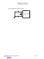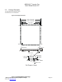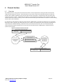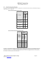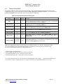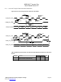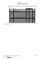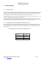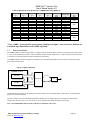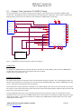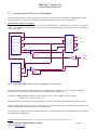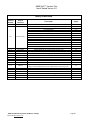
1
Digital Voice Systems, Inc. The Speech Compression Specialists AMBE-2000™ Vocoder Chip User’s Manual Version 4.9 September 2007 AMBE-2000™ Vocoder Chip User’s Manual Version 4.9 AMBE-2000™ Vocoder Chip User’s Manual Version 4.9 September, 2007 Copyright, 2006 Digital Voice Systems, Inc 234 Littleton Road Westford, MA 01886 This document may not, in whole or in part be copied, photocopied, reproduced, translated, or reduced to any electronic medium or machine readable form without prior consent in writing from Digital Voice Systems, Incorporated. Every effort has been made to ensure the accuracy of this manual. However, Digital Voice Systems, Inc. makes no warranties with respect to the documentation and disclaims any implied warranties of merchantability and fitness for a particular purpose. Digital Voice Systems, Inc. shall not be liable for any errors or for incidental or consequential damages in connection with the furnishing, performance, or use of this manual or the examples herein. This includes business interruption and/or other loss which may arise from the use of this product. The information in this document is subject to change without notice. Trademarks AMBE-2000™ Vocoder Chip is a registered trademark of Digital Voice Systems, Inc. Other product names mentioned may be trademarks or registered trademarks of their respective companies and are the sole property of their respective manufacturers. All Rights Reserved Data subject to change DVSI Confidential Proprietary, Subject to Change Visit us at www.dvsinc.com Page 2 AMBE-2000™ Vocoder Chip User’s Manual Version 4.9 AMBE-2000™ Vocoder Chip END USER License Agreement 1.0 Preliminary Statements and Definitions 1.1 “END USER” shall mean the person and/or organization to whom the AMBE-2000™ Vocoder Chip was delivered or provided to as specified in the purchase order or other documentation. In the event that the END USER transfers his rights under this license to a third party as specified in section 2.2, then this third party shall become an “END USER”. 1.2 Digital Voice Systems, Inc. (DVSI) has developed a voice coding method and algorithm (the “Technology”) based on the Advanced Multi-Band Excitation (“AMBE”) voice coder. The technology codes speech at bit rates of 2.4 to 9.6 kilobits per second (kbps) including error correction bits. 1.3 "AMBE Voice Compression Software" shall mean the speech coding software and/or firmware integrated into the AMBE-2000™ Vocoder chip integrated circuit. 1.4 "Voice Codec" shall mean the AMBE-2000™ Vocoder Chip integrated circuit, the AMBE Voice Compression Software, firmware and associated documentation, including modifications, enhancements and extensions made by or for Digital Voice Systems, Inc. (DVSI) and including circuit diagrams, timing diagrams, logic diagrams, layouts, operating instructions and user manuals. 1.5 DVSI represents that it owns certain “Proprietary Rights” in the Technology and the AMBE Voice Compression Software, including patent rights in the Technology, and patent rights, copyrights, and trade secrets in the AMBE Voice Compression Software. 2.0 License Granted 2.1 Subject to the conditions herein and upon initial use of the AMBE-2000™ Vocoder Chip, DVSI hereby grants to END USER a non-exclusive, limited license to use the AMBE® Voice Compression Software in machine readable form solely on the AMBE-2000™ Vocoder Chip. Title to the AMBE® Voice Compression Software remains with DVSI. No license is granted for use of the AMBE® Voice Compression Software on other than the AMBE-2000™ Vocoder Chip. No license, right or interest in any trademark, trade name or service mark of DVSI is granted under this Agreement. 2.2 END USER shall not copy, extract, de-compile, reverse engineer or disassemble the AMBE® Voice Compression Software contained in the AMBE-2000™ Vocoder Chip. 7.0 Proprietary Information 7.1 The parties agree that the AMBE Voice Compression Software shall be considered Proprietary Information. 7.2 Except as otherwise provided in this Agreement, END USER shall not use, disclose, make, or have made any copies of the Proprietary Information, in whole or in part, without the prior written consent of DVSI. 8.0 Limited Warranty 8.1 DVSI warrants the Voice Codec to be free from defects in materials and workmanship under normal use for a period of ninety (90) days from the date of delivery. 8.2 Except as stated in Section 7.1, the Voice Codec is provided "as is" without warranty of any kind. DVSI does not warrant, guarantee or make any representations regarding the use, or the results of the use, of the Voice Codec with respect to its correctness, accuracy, reliability, correctness or otherwise. The entire risk as to the results and performance of the Voice Codec is assumed by the END USER. After expiration of the warranty period, END USER, and not DVSI or its employees, assumes the entire cost of any servicing, repair, replacement, or correction of the Voice Codec. 8.3 DVSI represents that, to the best of its knowledge, it has the right to enter into this Agreement and to grant a license to use the AMBE Voice Compression Software to END USER. 8.4 Except as specifically set forth in this Section 7.0, DVSI makes no express or implied warranties including, without limitation, the warranties of merchantability or fitness for a particular purpose or arising from a course of dealing, usage or trade practice, with respect to the Voice Codec. Some states do not allow the exclusion of implied warranties, so the above exclusion may not apply to END USER. No oral or written information or advice given by DVSI or its employees shall create a warranty or in any way increase the scope of this warranty, and END USER may not rely on any such information or advice. The limited warranties under this section 7.0 give END USER specific legal rights, and END USER may have other rights which vary from state to state. 9.0 Limitation of Liability 3.0 Transfer of License 3.1 The END USER shall have the right to transfer the AMBE-2000™ Vocoder Chip and all rights under this Agreement to a third party by either (i) providing the third party with a copy of this Agreement or (ii) providing the third party with an agreement written by the END USER ( hereinafter “END USER Agreement”) so long as the END USER Agreement is approved in writing by DVSI prior to transfer of the AMBE-2000™ Vocoder Chip. The END USER Agreement shall contain comparable provisions to those contained herein for protecting the Proprietary Information from disclosure by such third party. Third parties shall agree to accept all the terms and conditions under either Agreement or the END USER Agreement. 9.1 In no event shall DVSI be liable for any special, incidental, indirect or consequential damages resulting from the use or performance of the Voice Codec whether based on an action in contract, tort (including negligence) or otherwise (including, without limitation, damages for loss of business profits, business interruption, and loss of business information), even if DVSI or any DVSI representative has been advised of the possibility of such damages. 9.2 Because some states do not allow the exclusion or limitation of liability for consequential or incidental damages, the above limitations may not apply to END USER. 9.3 DVSI's maximum liability for damages arising under this Agreement shall be limited to 20% (twenty percent) of the fees paid by END USER for the particular Voice Codec which caused the damages or that is the subject matter of, or is directly related to, the cause of action. 4.0 Term and Termination 10.0 Taxes 4.1 This Agreement is effective upon initial delivery of the Voice Codec and shall remain in effect until terminated in accordance with this agreement. 4.2 This Agreement shall terminate automatically without notice from DVSI if END USER fails to comply with any of the material terms and conditions herein. END USER may terminate this Agreement at any time upon written notice to DVSI certifying that END USER has complied with the provisions of Section 3.3. 4.3 Upon termination of this Agreement for any reason, END USER shall: (i) return all AMBE2000™ Vocoder Chip purchased or acquired, or in Licensee’s possession, to DVSI; (ii) have no further rights to any AMBE® Voice Compression Software or the Technology without a separate written license from DVSI; (iii) discontinue all use of the AMBE-2000™ Vocoder Chip; 5.0 Payments 5.1 In consideration of the materials provided as part of the Voice Codec, and in consideration of the license and rights in the AMBE Voice Compression Software granted by DVSI, and in consideration of DVSI's performance of its obligations hereunder, END USER agrees to pay to DVSI the fee specified in DVSI's invoice. 6.0 Proprietary Notices 6.1 END USER shall not remove any copyright or proprietary notice on the AMBE-2000™ Vocoder Chip or on the AMBE Voice Compression Software. 10.1 All payments required under Section 4.0 or otherwise under this Agreement are exclusive of taxes and END USER agrees to bear and be responsible for the payment of all such taxes (except for taxes based upon DVSI's income) including, but not limited to, all sales, use, rental receipt, personal property or other taxes which may be levied or assessed in connection with this Agreement. 11.0 Export 11.1 United States export laws and regulations prohibit the exportation of certain products or technical data received from DVSI under this Agreement to certain countries except under a special validated license. As of November 30, 1999 the restricted countries are: Libya, Cuba, North Korea, Iraq, Serbia, Taliban in Afghanistan, Sudan, Burma, Yugoslavia and Iran. The END USER hereby gives its assurance to DVSI that it will not knowingly, unless prior authorization is obtained from the appropriate U.S. export authority, export or re-export, directly or indirectly to any of the restricted countries any products or technical data received from DVSI under this Agreement in violation of said United States Export Laws and Regulations. DVSI neither represents that a license is not required nor that, if required, it will be issued by the U.S. Department of Commerce. Licensee shall assume complete and sole responsibility for obtaining any licenses required for export purposes. 12.0 Governing Law 12.1 This Agreement is made under and shall be governed by and construed in accordance with the laws of the Commonwealth of Massachusetts, except that body of law governing conflicts of law. If any provision of this Agreement shall be held unenforceable by a court of competent jurisdiction, that provision shall be enforced to the maximum extent permissible, and the remaining provisions of this Agreement shall remain in full force and effect. DVSI Confidential Proprietary, Subject to Change Visit us at www.dvsinc.com Page 3 AMBE-2000™ Vocoder Chip User’s Manual Version 4.9 6 1. Product Introduction 1.1 General Information 6 1.2 Advantages 6 1.3 Typical Applications 7 8 2. AMBE-2000™ Application Design Overview 2.1 Basic Operation 8 2.2 Initial Design Considerations 2.2.1 A/D – D/A Overview 2.2.2 Vocoder Front End Requirements 2.2.3 Channel Interface Overview 2.2.4 Speech and FEC Rate Selection Overview 3 4 8 8 8 10 11 12 Hardware Information 3.1 Special Handling Instructions 3.1.1 Storage 12 12 3.2 Pin Descriptions 13 3.3 Clock and Reset Timing 15 3.4 Associated Chip Delay 17 3.5 Crystal / Oscillator Usage 3.5.1 TTL Clock Source 3.5.2 Crystal Oscillator 17 17 17 3.6 Package Description 19 3.7 Normal Operating Conditions 20 3.8 Absolute Maximum Ratings 20 3.9 Electrical Characteristics and Requirements 21 3.10 Thermal Resistance Characteristics 21 22 Channel Interface 4.1 Overview 22 4.2 Serial Configuration Selection 23 4.3 Channel Serial Mode 4.3.1 Low Level Timing for Passive and Active Serial Mode 5 24 25 27 Channel Data Format 5.1 Framed Format 27 5.2 Framed Input 5.2.1 Framed Input: Word 0 : Header 5.2.2 Framed Input: Word 1 : Power Control ID 5.2.3 Framed Input: Word 1 : Control Word 1 5.2.4 Framed Input: Words 2-6 : Rate Information 5.2.5 Framed Input: Word 7 : Unused in Input 5.2.6 Framed Input: Word 8 : Unused in Input DVSI Confidential Proprietary, Subject to Change Visit us at www.dvsinc.com 27 28 28 28 28 29 29 Page 4 AMBE-2000™ Vocoder Chip User’s Manual Version 4.9 5.2.7 5.2.8 5.2.9 5.2.10 6 7 8 Framed Input: Word 9 : Unused in Input Framed Input: Word 10 : DTMF Control Framed Input: Word 11 : Control Word 2 Framed Input: Words 12-23 : Channel Data 29 30 31 31 5.3 Framed Output 5.3.1 Framed Output: Word 0 : Header 5.3.2 Framed Output: Word 1 : Power Control ID 5.3.3 Framed Output: Word 1 : Control Word 1 5.3.4 Framed Output: Words 2-6 : Rate Information 5.3.5 Framed Output: Word 7 : Bit Error Rate 5.3.6 Framed Output: Word 8 : Soft Decision Distance 5.3.7 Framed Output: Word 9 : Detected Bit Errors 5.3.8 Framed Output: Word 10 : DTMF Control 5.3.9 Framed Output: Word 11 : Control Word 2 5.3.10 Framed Output: Words 12-23 : Channel Data 32 32 32 32 33 33 33 33 34 35 36 5.4 Unframed Serial Format 5.4.1 Unframed Serial Output Format 5.4.2 Unframed Serial Input Format 36 36 36 38 A/D-D-A Interface 6.1 A/D-D/A Overview 38 6.2 Configuring the A/D-D/A Interface using CODEC_SEL [1-0] 38 6.3 Low Level A/D–D/A Timing 39 41 Special Functions 7.1 Hardware vs. Software Selection Note 41 7.2 Coding Rate Selection 41 7.3 Echo Cancellation 42 7.4 Voice Activation Detection (VAD), Comfort Noise Insertion (CNI) 43 7.5 Dual Tone Multiple Frequency, Detection and Generation 43 7.6 Normal Power and Power Saving Modes 7.6.1 Standard Sleep Mode 7.6.2 Power Down 43 43 44 7.7 45 Slip Enable 49 Appendices 8.1 Example A/D-D/A Usage 49 8.2 Example: Texas Instruments TLV320AIC10 Usage 50 8.3 Configuring the AD73311 for 3-Volt Operation 54 8.4 Interfacing to the Texas Instruments PCM3500 Codec 57 8.5 Expanded Tone Detection and Generation 60 8.6 Soft Decision Decoding 60 8.7 Special Rate 2350 bps Voice / 50 bps FEC AMBE-1000™ Vocoder Chip Compatible Mode 63 DVSI Confidential Proprietary, Subject to Change Visit us at www.dvsinc.com Page 5 AMBE-2000™ Vocoder Chip User’s Manual Version 4.9 1. Product Introduction 1.1 General Information Digital Voice Systems Inc.’s AMBE-2000™ Vocoder Chip is an extremely flexible, high-performance, single chip, speech compression coder. It provides superior voice quality at low data rates. It provides a real-time, full-duplex implementation of the standard-setting AMBE voice compression software algorithm. DVSI’s patented AMBE voice compression technology has been proven to outperform CELP, RELP, VSELP, MELP, ECELP, MP-MLQ, LPC-10, and other competitive technologies. Numerous evaluations have shown its ability to provide performance equal to today’s digital cellular systems at under half the data rate. The AMBE voice compression algorithm is used in applications throughout the world, including the next generation of digital mobile communication systems. The AMBE-2000™ Vocoder chip provides a high degree of flexibility in selecting the speech and FEC (Forward Error Correction) data rates. The user can separately select these parameters in 50 bps increments for total rates from 2.0 kbps to 9.6 kbps. Typically for higher error rate channels, the user will apportion a greater percentage of the total bit rate to FEC coding. The AMBE-2000™ voice coder maintains natural voice quality and speech intelligibility at rates as low as 2.0 kbits/sec. The AMBE algorithm’s low complexity allows it to be fully integrated into a low cost, low power integrated circuit, the AMBE2000™ Vocoder Chip. The AMBE-2000™ Vocoder Chip offers similar features to DVSI’s AMBE-1000™ Vocoder Chip allowing it to be incorporated into systems already designed for the AMBE-1000™ and is interoperable with other DVSI products. The AMBE-2000™ Vocoder Chip delivers improved performance and enhanced modes such as 4.0 kbps toll quality speech and convolutional FEC coding. Along with these enhancements the AMBE-2000™ Vocoder Chip employs a control interface along with the variable data rates and FEC selection. 1.2 Advantages • Superior Voice Quality • Low Cost • No External Memory Required • Robust to Bit Errors & Background Noise • Variable Data Rates - 2.0 kbps to 9.6 kbps • Variable FEC Rates - 50 bps to 7.2 kbps • Very Low Power (65mW @ 3.3V, 0.11mW Deep Sleep) • Compact Single Chip Solution: 100 pin TQFP • High Quality Low Data Rate Speech Coding • DVSI’s Full Duplex AMBE Voice Coder • Supports Data Rates of 2.0 kbps to 9.6 kbps in 50 bps increments • User Selectable Forward Error Correction rates • Viterbi Decoder (rate 1/4 or more) • 16 Level Soft Decision Decoding • Voice Activity Detection (VAD) / Comfort Noise Insertion • 16 ms Echo Cancellation • Single and Dual Tone (DTMF) Detection and Generation • Power-Down Mode • Minimal algorithmic processing delay Features DVSI Confidential Proprietary, Subject to Change Visit us at www.dvsinc.com Page 6 AMBE-2000™ Vocoder Chip User’s Manual Version 4.9 • 1.3 DTMF detection and regeneration with North American call progress tones Typical Applications • Satellite Communications • Digital Mobile Radio • Secure Communications • Cellular Telephony and PCS • Voice Multiplexing • Voice Mail • Multimedia Applications DVSI Confidential Proprietary, Subject to Change Visit us at www.dvsinc.com Page 7 AMBE-2000™ Vocoder Chip User’s Manual Version 4.9 2. AMBE-2000™ Application Design Overview 2.1 Basic Operation In its simplest model, the AMBE-2000™ can be viewed as two separate components, the Encoder and the Decoder. The Encoder receives an 8kHz sampled stream of speech data (16-bit linear, 8-bit Alaw, or 8-bit ulaw) and outputs a stream of channel data at the desired rate. Conversely the Decoder receives a stream of channel data and synthesizes a stream of speech data. The timing for the interfaces for the AMBE-2000™ Encoder and Decoder are fully asynchronous. AMBE-2000 AMBE-2000 8kHz Speech Data Encoder Compressed Data @ 2000-9600bps Decoder 8kHz Speech Data 8kHz Speech Data Decoder Compressed Data @ 2000-9600bps Encoder 8kHz Speech Data Figure 2 - A. Basic Operation Typically the speech interface is an external A/D-D/A chip. The format of the incoming and outgoing speech data streams are coupled, that is to say they must be the same format (16-bit linear, 8-bit Alaw, or 8-bit µlaw). The channel interface is commonly (but not limited to) an 8 or 16 bit microprocessor or other suitable ‘glue logic’ hardware capable of performing the rudimentary formatting functions between the AMBE-2000™ channel format and the format of the system channel under design. Optional functions of the chip, such as echo cancellation, voice activation/detection, power mode control, data/FEC rate selection, etc. are controlled either through hardware control pins (see Section 5) and/or through the decoder command interface (see Section 4) Data sent into the decoder for function control purposes is distinguished from the data to be decoded into speech through a channel format which is described in Section 4. 2.2 Initial Design Considerations Some of the initial design considerations the application engineer will face are the following: 2.2.1 • Choice of A/D-D/A chip. • Choice of Channel Interface. • Speech and FEC Rates. A/D – D/A Overview The choice of the A/D-D/A chip is critical to designing a system with superior voice quality. Given that Alaw and µlaw companding chips are already incorporating some compression to reduce the number of bits per sample, it is recommended that, when possible, a 16-bit linear device be used for maximum voice quality. When choosing a device, pay particular attention to Signal to Noise ratios and Frequency Responses of any filters that may be present on the analog front end of these chips. The Alaw and µlaw interfaces are also provided for the design engineer who is trying to fit to pre-existing conditions or is under other cost type restraints. 2.2.2 Vocoder Front End Requirements DVSI Confidential Proprietary, Subject to Change Visit us at www.dvsinc.com Page 8 AMBE-2000™ Vocoder Chip User’s Manual Version 4.9 In order to ensure proper performance from the voice coder, it is necessary for the vocoder front end to meet a set of minimum performance requirements. For the purposes of this section the vocoder front end is considered to be the total combined response between microphone/speaker and the digital PCM interface to the vocoder, as shown in Figure 2-B. This includes any analog electronics plus the A-to-D and D-to-A converters as well as any digital filtering performed prior to the voice encoder or after the voice decoder. Microphone Vocoder Front End Analog Input Reference Pt. Analog Input Gain Analog Input Filter A-to-D Convertor Digital Input Gain Analog Output Gain Analog Output Filter D-to-A Convertor Digital Output Gain Digital Output Reference Pt. AMBE+™ Voice Encoder Speaker Analog Output Reference Pt. Analog Speech Digital Input Reference Pt. AMBE+™ Voice Decoder Digital Speech (8 kHz sampling) Figure 2 - B. Vocoder Front End The AMBE+™ voice encoder and decoder operate with unity (i.e. 0 dB) gain. Consequently the analog input and output gain elements shown in Figure 2 are only used to match the sensitivity of the microphone and speaker with the A-to-D converters and D-to-A converters, respectively. It is recommended that the analog input gain be set such that the RMS speech level under nominal input conditions is 25 dB below the saturation point of the A-to-D converter (+3 dBm0). This level, which equates to -22 dBm0, is designed to provide sufficient margin to prevent the peaks of the speech waveform from being clipped by the Ato-D converter. +2 dB -1 dB -2 dB -18 dB -35 dB -40 dB 0 200 400 3000 3400 4000 4600 8000 freq (Hz) Figure 2 - C. Front End Input Filter Mask The voice coder interface requires the A-to-D and D-to-A converters to operate at an 8 kHz sampling rate (i.e. a sampling period of 125 microseconds) at the digital input/output reference points. This requirement necessitates the use of analog filters at both the input and output to eliminate any frequency components above the Nyquist frequency (4 kHz). The recommended input filter mask is shown in Figure 2 - C, and the recommended output filter mask is shown in Figure 2 - D. For proper operation, the shaded zone of the respective figure should bound the frequency response of the front-end input and output. DVSI Confidential Proprietary, Subject to Change Visit us at www.dvsinc.com Page 9 AMBE-2000™ Vocoder Chip User’s Manual Version 4.9 +2 dB -1 dB -2 dB -18 dB -40 dB -60 dB 0 200 3000 3400 4000 Figure 2 - D. 4600 8000 freq (Hz) Front End Output Filter Mask This document assumes that the A-to-D converter produces digital samples where the maximum digital input level (+3 dBm0) is defined to be +/- 32767, and similarly, that the maximum digital output level of the D-to-A converter occurs at the same digital level of +/- 32767. If a converter is used which does not meet these assumptions then the digital gain elements shown in Figure 2 should be adjusted appropriately. Note that these assumptions are automatically satisfied if 16 bit linear A-to-D and D-to-A converters are used, in which case the digital gain elements should be set to unity gain. An additional recommendation addresses the maximum noise level measured at the output reference points shown in Figure 2-B with the corresponding inputs set to zero. DVSI recommends that the noise level for both directions should not exceed -60 dBm0 with no corresponding input. In addition the isolation from cross talk (or echo) from the output to the input should exceed 45 dB which can be achieved via either passive (electrical and/or acoustic design) or active (echo cancellation and/or suppression) means. 2.2.3 Channel Interface Overview The channel interface is meant to be flexible to allow for easy integration with the system under design. The basic hardware unit of the interface is a serial port. The serial port can run in passive or active modes. In passive mode, all of the channel interface control signals are inputs to the AMBE-2000™ chip. In active mode, only the TX_DATA_STRB is an output from the AMBE-2000™ chip. All other signals are inputs. Under normal operation, every 20ms, the encoder outputs a frame of coded bits, and the decoder needs to be delivered a frame of coded bits. There is some formatting of the data for both the encoder and the decoder. The primary purpose of the formatting is to provide alignment information for the encoded bit stream. The data has two formats, Framed and Unframed. Serial mode can run in either Framed or Unframed mode. The Framed and UnFramed Modes are explained in full detail in Section 4, but essentially the two formats are trying to achieve the same function, to provide positional information regarding the outgoing and incoming coded data streams. In Framed mode each 20ms of output data from the encoder is preceded by a known structure (each packet corresponds to 20 ms of speech data input to the encoder). This structure also embeds some status type flags, meant for local control purposes, within it. The only data from the Framed format that is typically sent across the transmission channel under design are the actual encoded bits at the desired rate. In Framed mode, it is the responsibility of the designed system to pass enough information along with the encoded bits such that the Framed format needed by the decoder can be reconstructed on the other side. This extra information, or overhead, is going to be very specific to the system under design, but at a minimum needs to pass enough information to reliably reconstruct the 20msec frame structure at the other end for the decoder. In Unframed mode the data coming out of the encoder can be thought of as a continuous stream of voice data with the framing information embedded within the encoded bits. One advantage of this type of set-up is that the system does not have to add any bandwidth for overhead to the channel. The disadvantage is that the decoder needs 10-12 incoming frames in order to gain DVSI Confidential Proprietary, Subject to Change Visit us at www.dvsinc.com Page 10 AMBE-2000™ Vocoder Chip User’s Manual Version 4.9 synchronization with the data stream before it can properly synthesize the speech waveform. The Unframed mode only commits a single bit per frame to maintain data alignment. In higher error rate channels the performance will be improved by adding more bits per frame to the alignment information (which is more easily performed when using Framed mode). Additional flexibility is given to the channel interface to the encoder and decoder by allowing the AMBE-2000™ Vocoder Chip to run in Passive or Active modes. In Passive mode, data strobes are provided by an external source, while in Active mode, data strobes are provided by the AMBE-2000™ Vocoder Chip. The serial interfaces can be run in Passive or Active modes. See Section 4 for full details and timing for both Framed and Unframed data. 2.2.4 Speech and FEC Rate Selection Overview The total coded bit rate is the sum of two components, the Speech Data bit rate and the Forward Error Correction (FEC) Data bit rate. The addition of FEC data to the speech data allows the decoder to be able to correct a limited amount of errors within each frame should they arrive corrupted. If the channel is expected to have more errors then more bits should be dedicated to FEC. At the same time, voice quality will increase if the number of speech bits is increased. DVSI Confidential Proprietary, Subject to Change Visit us at www.dvsinc.com Page 11 AMBE-2000™ Vocoder Chip User’s Manual Version 4.9 3 Hardware Information 3.1 Special Handling Instructions The AMBE-2000™ uses the TM320LC541B-66 core. For more details on handling, electrical characteristics, packaging, or timing constraints please refer to the TMS320-C54x manual found at http://www-s.ti.com/sc/psheets/sprs039c/sprs039c.pdf (Adobe Acrobat). Although the AMBE-2000™ Vocoder Chip incorporates input protection circuitry, to avoid damage from the accumulation of a static charge, industry standard electrostatic discharge precautions and procedures must be employed during handling and mounting. The 100 pin TQFP package design of the AMBE-2000™ Vocoder Chip allows it to be mounted by infrared reflow, vaporphase reflow or equivalent processes. The peak package body temperature must not exceed 220°C. The AMBE-2000™ Vocoder Chip requires baking before mounting, if any of the following conditions exist: • Humidity indicator card (included in packaging) shows exposure to > 20 % when read at 23°C + 5°C • Devices were not shipped in a package designated as “moisture controlled.” • Not mounted within 168 hours of receipt, at factory conditions of <30°C and <60% RH • If the device has not been stored at < 20% RH DVSI’s recommended bake out procedures: 3.1.1 • For low-temperature device containers: 192 hours at 40°C + 5°C / -0°C and < 5% Relative Humidity • For high-temperature device containers: 24 hours at 125°C + 5°C. Storage To insure maximum shelf life in long term storage, AMBE-2000™ Vocoder Chips should be kept in a moisture controlled package at <40°C and <90% Relative Humidity DVSI Confidential Proprietary, Subject to Change Visit us at www.dvsinc.com Page 12 AMBE-2000™ Vocoder Chip User’s Manual Version 4.9 3.2 Pin Descriptions Pin Number Pin Descriptive Name Pin Direction Notes 77 CHAN_SEL1 Input Channel Interface Selection Pins: Use these bits to select the channel interface type (framed, unframed, active and passive) according to Table 4-A. See full description in section 4.2. 75 CHAN_SEL0 Input Used with CHAN_SEL1 to select channel operation mode 85 CODEC_SEL1 Input 84 CODEC_SEL0 Input 74 RATE_SEL4 Input 73 RATE_SEL3 Input 72 RATE_SEL2 Input 71 RATE_SEL1 Input 70 RATE_SEL0 Input 86 VAD_EN Input Voice Activation Detection Enable Pin. Active HIGH. See Section 7.4. VAD can also be enabled/disabled using the Control Word interface as described in section 5.2.9. 78 ECHOCAN_EN Input Echo Canceller Enable Pin. Active HIGH. See Section 7.3. The Echo Canceller can also be enabled/disabled using the Control Word interface as described in section 5.2.9. 83 SLEEP_EN Input Standard Sleep Enable Pin. Active HIGH. See Section 7.6.1. 82 SLIP_EN Input Slip Control Enable Pin. Active HIGH. See Section 7.7. 68 X2/CLKIN Input Clock Input 1. 16.384 Mhz input. See Section 3.3 67 X1 Input Output from internal oscillator for the crystal. If the internal oscillator is not used this pin should be unconnected. 69 RESETN Input AMBE-2000™ Reset pin. Active LOW. See Section 3.3 20 EPR Output A/D-D/A Select Pins see Table 6-A to select the interface. Coding Rate Select Pins: Use these bits to select the voice and FEC rates according to section 7.2. The coding rates are also selectable using the Control Word interface described in section 5.2.4. Encode Packet Ready: Following a reset, this signal will have a high to low transition to indicate the first packet is ready. The next packet will be ready approximately 20 msec later. See Note 1. 79 SOFT_EN Input 80 BAUD_SEL0 Input Soft decision decoding enable. Enables 4 bit soft decision error decoder. 81 BAUD_SEL1 Input 32 CHAN_RX_DATA Input 42 CHAN_TX_DATA Output 28 CHAN_RX_CLK Input Channel Receive Clock 34 CHAN_TX_CLK Input Channel Transmit Clock 38 CHAN_TX_STRB I/O Channel Transmit Data Strobe 30 CHAN_RX_STRB Input Channel Receive Data Strobe 29 CODEC_RX_STRB Input Frame synchronization pulse for A/D data. Should be connected to CODEC_TX_STRB 37 CODEC_TX_STRB Input Frame synchronization pulse for D/A data. Should be connected to CODEC_RX_STRB 31 CODEC_RX_DATA Input PCM Data from A/D Converter to AMBE-2000™ Pin Number Pin Descriptive Name Pin Direction Baud Rate Selector for unframed serial mode See Table 4-B. Channel Receive Data to AMBE-2000™ Channel Transmit Data from AMBE-2000™ Notes DVSI Confidential Proprietary, Subject to Change Visit us at www.dvsinc.com Page 13 AMBE-2000™ Vocoder Chip User’s Manual Version 4.9 41 CODEC_TX_DATA Output PCM Data from AMBE-2000™ to D/A Converter 27 CODEC_RX_CLK Input 33 CODEC_TX_CLK Input D/A Serial clock Should be connected to CODEC_RX_CLK A/D Serial clock. Should be connected to CODEC_TX_CLK 51 CLOCK_MODE Input If high enables crystal oscillator option for clock source. If low then external oscillator option is selected. See Section 3.5 for details. 8,11,12,23 36,39,44,45 46, 47,48 49,54,57,64 76,87,90 VDD Power Supply Voltage 1,9,10,25,26 35,40,50,52 53,56,63,65 88,89 GND Power Ground 2,3,4,5,6,7, 13,14,15,16 17,18,19,21 22,24,43,55 58,59,60,61 62,66,91,92 93,94,95,96 97,98,99 100 No Connection These pins must remain unconnected NOTE 1: The AMBE-2000™ expects an encoder packet to be read approximately every 20 msec. Following the initial reset, wait for EPR to go low and read the initial packet (t0). 20 msec later, the next packet (t1) should be ready. For packet t1 and all following packets use the procedure below: 1) Wait for slightly less than 20 msec. 2) Assert CHAN_TX_STB and read word on CHAN_TX_DATA. 3) If transmitted word not 0x13EC, discard it and repeat step 2. 4) If transmitted word 0x13EC, read 23 more words (rest of packet). The EPR signal should not be used as an interrupt. The EPR is only valid for the first high to low transition. A new packet should be ready every 20 msec after the initial EPR high to low transition. A packet read should take place every 20 msec. If there is a delay in the read (i.e. a packet is missed), it is recommended that the device be reset. NOTE 2: To prevent possible damage to the chip be sure that your circuit meets the following three requirements. 1) No signals should be applied to the device (this includes clocks) before the power is applied. 2) The clock and reset must be applied to the device during power up. If the clock and reset are not applied during power up, high currents may flow damaging the device. 3) All of the configuration I/O pins of the device should be pulled up or pulled down through individual 10 K ohm resistors to limit current flow through the I/O sections. See Table below for the affected pins. Descriptive Name CHAN_SEL1 CHAN_SEL0 CODEC_SEL1 CODEC_SEL0 RATE_SEL4 RATE_SEL3 RATE_SEL2 RATE_SEL1 RATE_SEL0 Pin Number 77 75 85 84 74 73 72 71 70 DVSI Confidential Proprietary, Subject to Change Visit us at www.dvsinc.com Descriptive Name VAD_EN ECHOCAN_EN SLEEP_EN SLIP_EN SPFT_EN BAUD_SEL0 BAUD_SEL1 Pin Number 86 78 83 82 79 80 81 Page 14 AMBE-2000™ Vocoder Chip User’s Manual Version 4.9 3.3 Clock and Reset Timing To reset the AMBE-2000 chip, the reset signal must be held low for a minimum of 50 µs. The recovery time from reset is approximately 95 ms. In other words, 95 ms after the rising edge of the reset signal the AMBE-2000™ starts processing PCM samples. The first packet will be ready after 252 PCM samples are read. Figure 3-A X2/CLKIN and CLKOUT Timing Diagram tw(CIH) tw(CIL) tf(CI) tr(CI) tc(CI) ~ ~ ~ ~ X2/CLKIN td(CIH-CO) tw(COH) ~ ~ ~ ~ ~ ~ CLKOUT tc(CO) tp tf(CO) tw(COL) tr(CO) Unstable DVSI Confidential Proprietary, Subject to Change Visit us at www.dvsinc.com Page 15 AMBE-2000™ Vocoder Chip User’s Manual Version 4.9 Table 3-A X2/CLKIN and CLKOUT Timing Parameters Reference • • Parameter Cycle time, X2/CLKIN Integer PLL multiplier N (N=4) tc(CI) Fall time, X2/CLKIN tf(CL) Rise time, X2/CLKIN tr(CL) Pulse duration, X2/CLKIN low tw(CIL) Pulse duration, X2/CLKIN high tw(CIH) Transitory phase, PLL lock-up time tp tc(CO) Cycle time, CLKOUT (typical is tc(CI)/4 Delay time, X2/CLKIN high/low to CLKOUT high/low td(CIH-CO) Fall/Rise time, CLKOUT (typical is 2 ns) tf(CO)/tr(CO) Pulse duration, CLKOUT low tw(COL) Pulse duration, CLKOUT high tw(COH) CLKOUT is shown for reference only. It is not to be connected in the circuit. Min 20 Max 400 4 4 15 4 16 Units ns ns ns ns ns µs ns ns H-4 H-4 H H ns ns Max Units ns µs ns ns 6 6 50 H = 7.629 ns Figure 3-B Hardware Reset Timing Diagram X2/CLKIN ~ tsu(RS) tw(RSL) RESETN ~ tsu(INT) th(RS) CLKOUT ~ Table 3-B Reset Timing Parameters Reference th(RS) tw(RSL) tsu(RS) tsu(INT) • Parameter Hold time, RS after CLKOUT low Pulse duration, RS low Setup time, RS before X2/CLKIN low Setup time, INTn, NMI, RS before CLKOUT low Min 0 50 5 10 CLKOUT is shown for reference only. It should not be connected in the circuit. DVSI Confidential Proprietary, Subject to Change Visit us at www.dvsinc.com Page 16 AMBE-2000™ Vocoder Chip User’s Manual Version 4.9 3.4 Associated Chip Delay The associated delay due to the coding/decoding algorithm is shown below Encoder Delay Algorithmic Delay = 32 ms Encoder Processing Delay = 11.5 ms Decoder Delay Algorithmic Delay = 10 ms Decoder Processing Delay = 7.5 ms Total Delay = 32 ms + 11.5 ms + 1 ms* +10 ms +7.5 ms = 62 ms Frame Processing Delay = 11.5 ms (encoder) + 1 ms* + 7.5 ms = 20 ms * 1ms of idle time between encode and decode sequence. 3.5 Crystal / Oscillator Usage The AMBE-2000™ Vocoder Chip has an input clock frequency of 16.384 MHz. Two options are outlined below in providing this signal. The CLOCK_MODE pin 51 must be set appropriately for the option used. The following points should be noted when designing any printed circuit board layout: 3.5.1 • Keep the crystal and external capacitors as close to the CLK_I and CLK_I2 pins as possible to minimize board stray capacitance. • Keep X2/CLKIN and X1 away from high frequency digital traces (example CLKOUT) to avoid coupling. TTL Clock Source If CLOCK_MODE pin is low then a TTL/CMOS source is used as the clock input. Connect X2/CLKIN and X1 as follows: Figure 3-C X2/CLKIN and X1 with TTL Clock Source 16.384 MHz TTL/CMOS Clock Source X2/CLKIN (pin 68) AMBE-2000 Unconnected X1 (pin 67) 3.5.2 Crystal Oscillator The Crystal Oscillator option is selected with CLOCK_MODE pin set to a high level. To use the crystal oscillator, connect the crystal across X2/CLKIN and X1 along with one external capacitor from each of these pins to ground. The recommended value for C1 and C2 is 10 pF. DVSI Confidential Proprietary, Subject to Change Visit us at www.dvsinc.com Page 17 AMBE-2000™ Vocoder Chip User’s Manual Version 4.9 Figure 3-D X2/CLKIN and X1 with Crystal Oscillator C1 = 10 pF X2/CLKIN (pin 68) 16.384 MHz AMBE-2000 X1 (pin 67) C2 = 10 pF DVSI Confidential Proprietary, Subject to Change Visit us at www.dvsinc.com Page 18 AMBE-2000™ Vocoder Chip User’s Manual Version 4.9 3.6 Package Description 100 pin TQFP (Thin Quad Flat Pack) All Dimensions are in millimeters Figure 3-E Package Dimensions 16.20 / 15.80 SQ 14.20 / 13.80 SQ 12.00 TYP 75 51 76 50 100 26 25 1.40/1.60 mm 1 o 12 All Around 0.5 mm Detail 0.17 / 0.27 Gage Plane 0.13NOM 1.35 /1.45 1.60 MAX 0.05 0 - 7 MAX 0.25 0.45 / 0.75 Not Drawn to Scale Figure 3-F AMBE-2000 Chip Markings DVSI Confidential Proprietary, Subject to Change Visit us at www.dvsinc.com Page 19 AMBE-2000™ Vocoder Chip User’s Manual Version 4.9 AMBE-2000-10 = The DVSI device part number. DVSI = Digital Voice Systems, Incorporated D16876PZ-66 = Internal Texas Instruments part number for the AMBE-2000 A = WF Code D = Die Rev Code W = Die Shrink Code 43AT3FW = Lot Trace Code 43 = 2 Digit YR/MO Code (Updated Monthly) AT3F = Assy Lot W = Assy Site Code 3.7 Normal Operating Conditions Table 3-C Normal Operating Conditions Normal Operating Conditions 3.8 Operating Voltage 3.3V Operating Case Temperature Range -40°C to 100°C Storage Temperature Range -55°C to 150°C Absolute Maximum Ratings Stresses in excess of the Absolute Maximum Ratings can cause permanent damage to the device. These are absolute stress ratings only. Functional operation of the device is not implied at these or any other conditions in excess of those given in the operational sections of the data sheet. Exposure to Absolute Maximum Ratings for extended periods can aversely affect device reliability. DVSI Confidential Proprietary, Subject to Change Visit us at www.dvsinc.com Page 20 AMBE-2000™ Vocoder Chip User’s Manual Version 4.9 Table 3-D Absolute Maximum Ratings Absolute Maximum Ratings Voltage Range on any Pin with Respect to Ground 3.9 -0.3V to 4.6V Electrical Characteristics and Requirements Table 3-E Recommended Operating Conditions Parameter Min Nom Max Unit DVDD Device Supply Voltage 3 3.3 3.6 V VSS Supply Voltage, GND - 0 - V - DVDD + 0.3 V VIH RESETN (pin 69), CLOCK_MODE (pin 51), X2/CLKIN (pin 68), pins 44,45,46,47,48,52,53,54 High-level input voltage, I/O 2.5 DVDD = 3.3 ±0.3 V 2.0 All other inputs VIL Low-level input voltage -0.3 - 0.8 V IOH High-level output current - - -300 µA IOL Low-level output current - - 1.5 mA Table 3-F Electrical Characteristics over Recommended Operating Case Temperature Range (Unless Otherwise Noted) Parameter Test Conditions VOH High-level output voltage‡ VDD = 3.3 ±V, IOH = MAX VOL Low-level output voltage‡ IOL = MAX II MIN TYP† MAX Unit 2.4 V 0.4 Input current in high impedance VDD = MAX, VI = VSS to VDD (VI = VSS to VDD) CI Input capacitance CO Output capacitance -10 10 pF 10 pF Thermal Resistance Characteristics Thermal Resistance Characteristics 58 °C/W RΘJA RΘJC 10 °C/W Table 3G Thermal Resistance Characteristics DVSI Confidential Proprietary, Subject to Change Visit us at www.dvsinc.com µA 10 † All values are typical unless otherwise specified. 3.10 V Page 21 AMBE-2000™ Vocoder Chip User’s Manual Version 4.9 4 4.1 Channel Interface Overview The Channel Interface is the general term used for the interface for the compressed bits coming from the encoder and the compressed bits going to the decoder. This same interface is also used to output status information from the encoder and decoder such as whether a DTMF tone has just been detected in the speech input, or whether the decoder has detected and synthesized a frame of silence. Additionally, this interface is used to perform more complex control operations on both the encoder and decoder (usually at start-up). These control functions include speech data and FEC rate control as well as enabling features such as echo cancellation. It is important to realize that not all data being output from the AMBE-2000™ is intended for transmission over the channel. Status type of data is typically only useful at the ‘local’ end. In most voice transmission systems, the actual encoded bits are extracted from the channel formatting, combined into the systems transmission stream, sent over the transmission path, extracted from the transmission path at the receiving end, and reassembled into the AMBE-2000™’s channel format for synthesis by the decoder. Figure 4-A Channel Interface Overview Typical Voice Frame Output From Encoder Overhead Data Voice Data (40 to 192 bits) (Header, Status) Transmission Channel System extracts relevant Voice Data bits and formats them for transmission over Channel System Overhead Voice Data (40 to 192 bits) System extracts relevant Voice Data bits and formats them for Input into the Decoder adding Header and Control Information Typical Voice Frame Input to the Decoder Overhead Data Voice Data (40 to 192 bits) (Header, Control) DVSI Confidential Proprietary, Subject to Change Visit us at www.dvsinc.com Page 22 AMBE-2000™ Vocoder Chip User’s Manual Version 4.9 4.2 Serial Configuration Selection The hardware interface to the Channel Interface is configured as a serial interface based exclusively on the hardware settings of CHAN_SEL [1-0]. See Table 4-A. Table 4-A Channel Interface Selection Table CHAN_SEL1 (pin 77) CHAN_SEL0 (pin 75) Interface Select Pins Active Framed 0 0 Active Unframed 0 1 Passive Framed 1 0 Passive Unframed 1 1 Port Type Table 4-B Unframed Bit per Word Selection Table BAUD_SEL0 (pin 80) Number of Voice Data Bits per Word BAUD_SEL1 (pin 81) Interface Select Pins 1 0 0 2 0 1 3 1 0 4 1 1 All transfers occur through a serial port. The serial port inputs and outputs a 16 bit word for every write and read strobe signal respectively. Serial mode can be framed or unframed. Within the unframed mode, the data is input and output in 16 bits words still but with only 1 to 4 voice data bits carried within each word. These four configurations can be seen in Table 4-B. See section 4.3 for all the details on the serial interface. DVSI Confidential Proprietary, Subject to Change Visit us at www.dvsinc.com Page 23 AMBE-2000™ Vocoder Chip User’s Manual Version 4.9 4.3 Channel Serial Mode The signals in Table 4-C make up the serial channel interface. The serial channel mode transfers data in and out of the AMBE-2000™ using 16 bit words on the two data lines CHAN_RX_DATA and CHAN_TX_DATA. The selection of the framed or unframed format of this data is made using information in Table 4-A. Table 4-C Channel Serial Interface Pin Descriptions Pin Symbol Pin Direction Pin Number EPR Out 20 Encoder Packet Ready: Following a reset, this output signal will have a high to low transition to indicate that the encoder has a frame of data to output. The next packet will be ready approximately 20 msec later. See Note 1. CHAN_RX_DATA In 32 Serial Data Input: 16 bits of channel data are input on CHAN_RX_DATA, synchronous to CHAN_RX_CLK, with each CHAN_RX_STRB pulse. CHAN_RX_CLK In 28 Serial Input Clock: In coordination with CHAN_RX_STRB, CHAN_RX_DATA is latched by the AMBE-2000™ on the falling edges of CHAN_RX_CLK. CHAN_RX_STRB In 30 Input (Write) Data Strobe: This signal indicates to the AMBE-2000™ when the data on CHAN_RX_DATA will be latched by CHAN_RX_CLK. See Figure 4-B. CHAN_TX_DATA Out 42 Serial Data Output: 16 bits of channel data are output on CHAN_TX_DATA, synchronous to CHAN_TX_CLK, with each CHAN_TX_STRB pulse. CHAN_TX_CLK In 34 Serial Output Clock: In coordination with CHAN_TX_STRB, the data on CHAN_TX_DATA is output by the AMBE-2000™ on the rising edges of CHAN_TX_CLK. CHAN_TX_STRB Active Output/ Passive Input 38 Output (Read) Data Strobe: This signal indicates to the AMBE-2000™ when to bring the data to the CHAN_TX_DATA pin. See Figure 4-B. Description Note 1:The AMBE-2000 expects an encoder packet to be read approximately every 20 msec. Following the initial reset, wait for EPR to go low and read the initial packet (t0). 20 msec later, the next packet (t1) should be ready. For packet t1 and all following packets use the procedure below: 1) Wait for slightly less than 20 msec. 2) Assert CHAN_TX_STB and read word on CHAN_TX_DATA. 3) If transmitted word not 0x13EC, discard it and repeat step 2. 4) If transmitted word 0x13EC, read 23 more words (rest of packet). A new packet should be ready every 20 msec after the initial EPR high to low transition. A packet read should take place every 20 msec. If there is a delay in the read (i.e. a packet is missed), it is recommended that the device be reset. DVSI Confidential Proprietary, Subject to Change Visit us at www.dvsinc.com Page 24 AMBE-2000™ Vocoder Chip User’s Manual Version 4.9 4.3.1 Low Level Timing for Passive and Active Serial Mode Figure 4-B Low Level Timing for Passive and Active Serial Mode tc(SCK) tf(SCK) ~ ~ tw(SCK) CHAN_RX_CLK th(FSR) tsu(FSR) tw(SCK) tsu(DR) ~ ~ CHAN_RX_STRB tr(SCK) CHAN_RX_DATA MSB 1 ~ ~ ~ th(DR) 2 LSB 16 15 tc(SCK) tf(SCK) ~ ~ tw(SCK) CHAN_TX_CLK td(FSX) th(FSX) th(FSX)H tw(SCK) td(DX) tdis(DX) ~ CHAN_TX_STRB tr(SCK) CHAN_TX_DATA MSB 1 2 ~ ~ th(DX) 15 LSB 16 Table 4-D Switching Characteristics Over Recommended Operating Conditions for Serial Port Receive Reference th(FSR) th(DR) Parameter Hold time, FSR after CLKR falling edge Hold time, DR after CLKR falling edge DVSI Confidential Proprietary, Subject to Change Visit us at www.dvsinc.com 3.3 Volts Min Max 6 6 Units ns ns Page 25 AMBE-2000™ Vocoder Chip User’s Manual Version 4.9 Table 4-E Switching Characteristics Over Recommended Operating Conditions for Serial Port Receive Reference td(SCK) tc(SCK) tf(SCK) tr(SCK) tw(SCK) tsu(FSR) tsu(DR) td(FSX) td(DX) th(FSX) th(FSX)H tdis(DX) th(DX) Parameter Delay time, DX valid after CLKX rising (Passive Mode) Cycle time, serial port clock 3.3 Volts Min Max 25 6H Units ns ns Fall time, serial port clock 6 ns Rise time, serial port clock 6 ns Pulse duration, serial port clock low/ high 3H ns Setup time, FSR before CLKR falling edge 6 ns Setup time, DR before CLKR falling edge 6 ns Delay time, CLKX rising to FSX 15 ns Delay time, CLKX rising to DX (Active Mode) 15 ns Hold time, FSX after CLKX falling edge 6 Hold time, FSX after CLKX rising edge Disable time, CLKX rising to DX Hold time, DX valid after CLKX rising edge -5 ns 2H-5 ns 20 ns ns • Note: H = 7.629 ns; however, do not operate serial clocks any faster than 2.048 MHz. Thus tc(SCK) should be a minimum of 488.3 nsec. DVSI Confidential Proprietary, Subject to Change Visit us at www.dvsinc.com Page 26 AMBE-2000™ Vocoder Chip User’s Manual Version 4.9 5 Channel Data Format The channel interface is responsible for outputting the compressed data from the encoder and inputting compressed data to the decoder. In addition to these most basic functions the channel interface is also capable of reporting certain events, such as the detection of a DTMF tone. The channel interface can also control certain selectable functions of the AMBE-2000™, such as the voice coding rate. This chapter will describe how the AMBE-2000™ uses the channel interface to multiplex these capabilities. There are two formats to the data, Framed and Unframed, both of which operate in serial mode. Generally speaking the Unframed mode is used only when the connection between the AMBE-2000™ and the channel under design is relatively direct, and the designer wants to simplify the extraction of the relevant voice data. In this mode configuration is accomplished using hardwired pins. In most cases, when a controller is present between the AMBE-2000™ and the channel, the system designer will find that using the Framed format is more flexible. 5.1 Framed Format The Framed format is a 24 by sixteen-bit word format for a total of 48 bytes or 384 bits. Every 20 milliseconds the encoder outputs 24 sixteen-bit words, and likewise the decoder expects to receive 24 words. The format of the input and output frames are detailed below. The first 12 sixteen bit words are made up of header, ID and status or control information. The remaining 12 sixteen bit words make up the encoded data bit field. These 12 words, or 192 bits, will be fully populated with relevant voice data only when the AMBE-2000™ is operating in a 9600bps mode (9600 bits/sec ÷ 50 frames/sec = 192 bits/frame). Otherwise, when the data rate is less than 9600bps, the coded voice bits are filled starting from the MSB of the first word in the field, leaving any unused bits as zeros. It is important to note here that even when the AMBE-2000™ is operating at less than 9600bps, all 384 bits of the Framed format (including any unused trailing zeros) must be transferred out of the encoder and into the decoder. 5.2 Framed Input The format of the Framed input is shown in Figure 5-A. Keep in mind that even though the channel data in this Framed input is closely associated with the decoder, the control information will apply to both encoder and decoder functions. Figure 5-A Basic Framed Input (12) 16 bit words of overhead (192 bits) (12) 16 bit words of data (192 bits) 24 sixteen-bit words = 48 bytes = 384 bits 20 ms frame Word # 0 1 2 3 4 5 6 7 8 9 10 11 12 13 14 15 16 17 18 19 20 21 22 23 Description Header always set to 0x13EC Power Control ID (8bits) Control Word 1 (8 bits) – see Table 5-B Rate info 0 Rate info 1 See Tables 5-C and 5-D Rate info 2 Rate info 3 Rate info 4 Unused in Input Unused in Input Unused in Input DTMF Control – see Tables 5-E and 5-F Control Word 2 – see Table 5-G Channel Data Channel Data Channel Data Channel Data Channel Data Channel Data Channel Data Channel Data Channel Data Channel Data Channel Data Channel Data DVSI Confidential Proprietary, Subject to Change Visit us at www.dvsinc.com Page 27 AMBE-2000™ Vocoder Chip User’s Manual Version 4.9 5.2.1 Framed Input: Word 0 : Header The decoder uses the header information to synchronize with the beginning of each 20 millisecond frame. This 16-bit word MUST be 0x13EC. 5.2.2 Framed Input: Word 1 : Power Control ID Set the 8-bit Power Control ID field to 0x00 for normal use. For Power Down Mode, set this value to 0x55. This causes the AMBE-2000™ to enter low power mode. To exit low power mode, the device must be reset through the hardware. Table 5-A Framed Input: Power Control ID Values Summary 5.2.3 ID Type Description 0x00 Voice Data 0x55 Low Power Mode This ID value instructs AMBE-2000™ to operate in normal fashion When this mode is activated the AMBE-2000™ Vocoder Chip will go into a mode, which conserves power, where no voice packets are being processed. Framed Input: Word 1 : Control Word 1 Use the 8-bit control word to set various functions. Table 5-B Control Word 1 Format Control Word 1 – 8-bits (See Table 1-F) 4 3 2 7: MSB 6 5 Lost Frame Indicator Unused Unused Unused Unused Unused 1 0 : LSB CNI Unused Lost Frame Indicator: Setting the Lost Frame Indicator bit to a 1 will cause the AMBE-2000™ decoder to construct the voice frame using the parameters from the previous frame. This is an effective way to mask the effects of short periods of data loss. The user should set this bit when channel data is lost or corrupted. It works by replacing the frame of corrupted data with the previous, intact, frame. Comfort Noise Insertion (CNI): Setting the CNI bit will cause the decoder to output a frame of comfort noise. This bit is used with systems that are capable of discontinuous transmission (DTX). 5.2.4 Framed Input: Words 2-6 : Rate Information Rate Info 0, Rate Info 1, Rate Info 2, Rate Info 3, Rate Info 4 The initial rate of the AMBE-2000™ is set through the hardware pins RATE_SEL [4-0] (see Section 7.2 and Tables 7-A and 7B). After resetting the device, the coding rate can be modified for both the encoder and the decoder by sending a framed packet to the input channel interface. The Rate Selector control field (described in section 5.2.9) determines where to apply the rate change. The AMBE-2000™ uses these five words to set the source and FEC coding rates. Tables 5-C and 5-D list predefined values for various source and FEC rates. These are only a representation of the most common rates that are requested. Please contact DVSI for additional rate information if the desired rates are not listed. The software configurations in Table 5-C are compatible for use with the AMBE-1000™ (using AMBE™ technology). If compatibility is not an issue, use the software codes in Table 5-D to select speech and FEC rates to optimize use of the AMBE-2000™ (using AMBE+™ technology). DVSI Confidential Proprietary, Subject to Change Visit us at www.dvsinc.com Page 28 AMBE-2000™ Vocoder Chip User’s Manual Version 4.9 Table 5-C Rate Selection Using Rate Info 0-4, compatible w/ AMBE-1000™ (AMBE™) Rate Info 0 Rate Info 1 Rate Info 2 Rate Info 3 Rate Info 4 0x9030 0x902f 0x9348 0x9243 0xab50 0x934b 0xab60 0xab5b 0x9348 0x923e 0xab53 0xab58 0xbf9b 0xab5d 0xbfc0 0xab16 0x0000 0x0000 0x0000 0x0080 0x0000 0x0080 0x0000 0x0080 0x2030 0x2800 0x2c00 0x3000 0x0080 0x3400 0x0000 0xe400 0x0000 0x0000 0x0000 0x0000 0x0000 0x0000 0x0000 0x0000 0x0000 0x0000 0x0000 0x0000 0x0000 0x0000 0x0000 0x0000 0x0000 0x0000 0x0000 0x0000 0x0000 0x0000 0x0000 0x0000 0x0000 0x0000 0x0000 0x0000 0x0000 0x0000 0x0000 0x0000 0x4330 0x6930 0x6f48 0x5348 0x3950 0x3950 0x7960 0x6860 0x7060 0x7460 0x5680 0x4490 0x49a0 0x31a0 0x72c0 0x67c0 Speech Rate (bps) 2400 2350 3600 3350 4000 3750 4800 4550 3600 3100 4150 4400 7750 4650 9600 4850 FEC Rate (bps) 0 50 0 250 0 250 0 250 1200 1700 2250 2800 250 3350 0 4750 Total Rate (bps) 2400 3600 4000 4800 6400 7200 8000 9600 Table 5-D Rate Selection Using Rate Info 0-4, AMBE-2000™ only (AMBE+™) Rate Info 0 Rate Info 1 Rate Info 2 Rate Info 3 Rate Info 4 Speech Rate (bps) FEC Rate (bps) Total Rate (bps) 0x0028 0x5048 0x1030 0x1030 0x5250 0x1030 0x5360 0x5250 0x5048 0x1030 0x6b80 0x5250 0x5258 0x7fa0 0x5250 0x7fc0 0x5048 0x1030 0x0000 0x0000 0x0001 0x4000 0x0000 0x0001 0x0000 0x2010 0x0001 0x0005 0x0000 0x0001 0x0009 0x0000 0x0005 0x0000 0x000e 0x000e 0x0000 0x0000 0x0000 0x0000 0x0000 0x0000 0x0000 0x0000 0x0000 0x180c 0x0000 0x0000 0x1e0c 0x0000 0x2010 0x0000 0x4010 0x681a 0x0000 0x0000 0x4230 0x0000 0x0000 0x341a 0x0000 0x0000 0x2412 0x3018 0x0000 0x542a 0x4127 0x0000 0x6834 0x0000 0x6a2e 0x511b 0x6428 0x3948 0x0048 0x0048 0x4150 0x6750 0x6c60 0x7460 0x6860 0x7360 0x6c80 0x5280 0x7390 0x52a0 0x72a0 0x69c0 0x65c0 0x76c0 2000 3600 2400 2400 4000 2400 4800 4000 3600 2400 6400 4000 4400 8000 4000 9600 3600 2400 0 0 1200* 1200** 0 1600 0 800 1200 2400 0 2400 2800 0 4000 0 6000 7200 2000 3600 4000 4800 6400 7200 8000 9600 * FEC is a convolutional code ** FEC is a block code 5.2.5 Framed Input: Word 7 : Unused in Input Should be set to 0x0000 5.2.6 Framed Input: Word 8 : Unused in Input Should be set to 0x0000 5.2.7 Framed Input: Word 9 : Unused in Input Should be set to 0x0000 DVSI Confidential Proprietary, Subject to Change Visit us at www.dvsinc.com Page 29 AMBE-2000™ Vocoder Chip User’s Manual Version 4.9 5.2.8 Framed Input: Word 10 : DTMF Control Use this word to set DTMF tones. See Table 5-F for a list of tones and their corresponding values. . An expanded list of tones and values can be found in the Appendices, Section 8.4. Table 5-E DTMF Control Format DTMF Control – 16-bits 15: MSB 14 13 12 11 10 9 8 DTMF Amplitude 7 6 5 4 3 2 1 0: LSB DTMF Digit Detect/ Generate Table 5-F DTMF Codes for Digit Detect/ Generate DTMF Code DTMF Digit 0x80 0x84 0x88 0x81 0x85 0x89 0x82 0x86 0x8A 0x87 0x83 0x8B 0x8C 0x8D 0x8E 0x8F 0x90 0x91 0x92 0xff 1 2 3 4 5 6 7 8 9 0 * # A B C D Dial Tone Ring Tone Busy Tone Inactive Frequency 1 (Hz) 1209 1336 1477 1209 1336 1477 1209 1336 1477 1336 1209 1477 1633 1633 1633 1633 440 480 620 N/A Frequency 2 (Hz) 697 697 697 770 770 770 852 852 852 941 941 941 697 770 852 941 350 440 480 N/A To generate no tones, set the DTMF Code to 0xff. Dial, ring, and busy tones are standard North American call progress tones. DTMF Amplitude The DTMF Amplitude runs from 3 to –60 dBm0. This value is a signed byte (example: 0x03 = 3, 0x00 = 0, 0xC4 = -60). DVSI Confidential Proprietary, Subject to Change Visit us at www.dvsinc.com Page 30 AMBE-2000™ Vocoder Chip User’s Manual Version 4.9 5.2.9 Framed Input: Word 11 : Control Word 2 Table 5-G Control Word 2 Format Control Word 2 – 16-bits Bit 15 14 13 12 11 10 9 Decoder Output Volume Control 8 7 6 Unused 0 Unused 0 5 4 3 2 VAD Unused 0 SL EC 1 0 RIS Decoder output volume control The default gain value is set to 0x80h Rate Information Selector (RIS): Use these 2 bits to select which part(s) of the vocoder will be affected by the rate selection words. Table 5-H Rate Information Selection Codes Value 0x0 0x1 0x2 0x3 Area Controlled Encoder and Decoder Encoder only Decoder only Neither Encoder nor Decoder Echo Canceller (EC): Set this bit to 1 to enable the echo cancel function on a frame-by-frame basis. This must be set to 1 in every packet sent to continue use. Sleep (SL): Set this bit to 1 to enter Sleep mode on a frame-by-frame basis. Sleep is a low power mode, not to be confused with Power Down Mode. The sleep function must be enabled in every packet to continue in sleep mode. Set this bit to 0 to exit Sleep mode. VAD: In order to set the Voice Activity Detector on, set the VAD bit to 1. To disable Voice Activity Detection, set the VAD bit to 0. 5.2.10 Framed Input: Words 12-23 : Channel Data This is the field that contains the actual coded bits. Input of the data begins with the MSB of the first word in this field and continues through with the final bit output being the LSB of the final word. If the data rate selected is less than 9600bps then the unused bits in each frame are zero and populate the end of the field. As is noted in the Channel Interface definitions, these unused bits must still be clocked out of the AMBE-2000™. The packet must always consist of 24 words. DVSI Confidential Proprietary, Subject to Change Visit us at www.dvsinc.com Page 31 AMBE-2000™ Vocoder Chip User’s Manual Version 4.9 5.3 Framed Output The format for Framed output data is shown in Figure 5-B. Only the bits in the Channel Data Bits are transmitted along with framing information (data used to locate the start of each frame for proper reconstruction at the decoder) over the channel. The first 192 bits provide overhead information, which is sometimes useful to the host but is generally not transmitted over the channel. Figure 5-B Basic Framed Output 5.3.1 (12) 16 bit words of overhead (192 bits) (12) 16 bit words of data (192 bits) 24 sixteen-bit words = 48 bytes = 384 bits 20 ms frame Word # 0 1 2 3 4 5 6 7 8 9 10 11 12 13 14 15 16 17 18 19 20 21 22 23 Description Header always set to 0x13ec Power Control ID (8bits) Control Word 1 (8 bits) – see Table 5-J Rate info 0 Rate info 1 Rate info 2 Rate info 3 Rate info 4 Bit Error Rate Soft Decision Distance Detected Bit Errors in Current Frame DTMF Control – see Table 5-L Control Word 2 – see Table 5-N Channel Data Channel Data Channel Data Channel Data Channel Data Channel Data Channel Data Channel Data Channel Data Channel Data Channel Data Channel Data Framed Output: Word 0 : Header The header is a 16-bit word that begins each valid frame corresponding to 20 milliseconds of speech. This field will always be 0x13EC. 5.3.2 Framed Output: Word 1 : Power Control ID The encoder will always use 0x00 in the 8-bit field of an output frame. 5.3.3 Framed Output: Word 1 : Control Word 1 This 8-bit control word indicates the activity of various functions. Table 5-J Control Word 1 Format 7: MSB Unused Control Word 1 – 8-bits (See Table 1-A) 4 3 2 6 5 Unused Decoder Frame Repeat Decoder Silence Detect Unused Unused 1 0: LSB Encoder Silence Detect Encoder DTMF Detect Decoder Frame Repeat: When the Decoder Frame Repeat flag is set to 1, the decoder is reporting that the last frame decoded was a repeat of the previous frame. DVSI Confidential Proprietary, Subject to Change Visit us at www.dvsinc.com Page 32 AMBE-2000™ Vocoder Chip User’s Manual Version 4.9 Decoder Silence Detect: When the Decoder Silence Detect flag is set to 1, the decoder is reporting that the last frame decoded was a comfort noise frame. Encoder DTMF Detect: The Encoder DTMF Detected Flag will be set to a 1 when the encoder detects a DTMF tone. Encoder Silence Detect: The Encoder Silence Detected Flag will be set to 1 when no voice activity is detected. The Silence Detect option is controlled by and can be disabled by the VAD as described in section 5.2.9. 5.3.4 Framed Output: Words 2-6 : Rate Information Rate Info 0, Rate Info 1, Rate Info 2, Rate Info 3, Rate Info 4. Words 2-6 in the packet indicate the rate at which the AMBE-2000™ encoder is operating. These words are output. See tables 5-C and 5-D for corresponding values. 5.3.5 Framed Output: Word 7 : Bit Error Rate This status field is used for the decoder to report bit error information. The 16 bit number output is used to compute the BER using the following calculation % BER = (Word 7) / (32768) x 100 This status field works in conjunction with the RIS bits in control word 2. Every time the RIS bits are set to any value other than 0x3, this field is reset. The BER is calculated only when using FEC provided by the AMBE-2000™. 5.3.6 Framed Output: Word 8 : Soft Decision Distance This status field is used in conjunction with hardware pin 79 SOFT_EN. This field is used to report the soft decision distance for the most recent decoded frame. This status field works in conjunction with the RIS bits in control word 2. Every time the RIS bits are set to any value other than 0x3, this field is reset. The Soft Decision Distance is calculated only when using Soft Decision decoding provided by the AMBE-2000™. 5.3.7 Framed Output: Word 9 : Detected Bit Errors This status field is used to report the number of detected bit errors in the most recent decoded frame. This status field works in conjunction with the RIS bits in control word 2. Every time the RIS bits are set to any value other than 0x3, this field is reset. The number of bit errors is calculated only when using FEC provided by the AMBE-2000™. DVSI Confidential Proprietary, Subject to Change Visit us at www.dvsinc.com Page 33 AMBE-2000™ Vocoder Chip User’s Manual Version 4.9 5.3.8 Framed Output: Word 10 : DTMF Control This word corresponds to the DTMF Detection capabilities of the vocoder. It uniquely identifies specific tones recognized by the encoder. See table 5-M for a list of tones and their corresponding values. Table 5-K DTMF Tone Detection Parameters DTMF Tone Detection Requirement Value Minimum Input Level -25 dBm0 An input signal shall not be rejected as a DTMF tone if its amplitude is greater than -25 dBm0 (maximum sinusoid dBm0 is defined as+3.17 dBm0). Minimum Signal to Noise Distortion ratio 15 dB In order for an input signal to correspond to a valid DTMF tone, the ratio of in-band to out-ofband energy must be greater than 15dB. In-band energy is defined to be the energy in frequency components within ±3.5% of the two frequencies defined by the DTMF frequencies. Out-of-band energy is defined to be the total energy minus in the in-band energy. Minimum Frequency Tolerance ±1.5% An input signal shall not be rejected as a DTMF tone if both of its principal frequency components are within ±1.5% of the frequencies needed for the DTMF tone. Maximum Frequency Tolerance ±3.5% An input signal shall be rejected as a DTMF tone if either of its principal frequency components are outside ±3.5% of the frequencies needed for the DTMF tone. 8-10 dB An input signal does not correspond to a valid DTMF tone if the energy contained within the low frequency band is more than 10 dB greater than the energy contained in the high frequency band. An input signal shall not be rejected as a DTMF if energy contained within the low frequency band is less than 8 dB greater than the energy contained in the high frequency band. Each low and high frequency band is limited to ±3.5% of the frequencies needed for the DTMF tone. 4-10 dB An input signal does not correspond to a valid DTMF tone if the energy contained within the high frequency band is more than 10 dB greater than the energy contained in the low frequency band. An input signal shall not be rejected as a DTMF if energy contained within the high frequency band is less than 4 dB greater than the energy contained in the low frequency band. Each low and high frequency band is limited to ±3.5% of the frequencies needed for the DTMF tone. 45 ms An input signal shall not be rejected as a DTMF tone as long as its time duration is greater than 45 ms. In addition a minimum of two frames will be transmitted of the DTMF tone if a valid tone is detected. The duration of a tone is defined by the points at which the envelope is 20 dB below its peak value. Normal Twist Range Reverse Twist Range Minimum Tone Duration Description Table 5-L DTMF Control Format DTMF Control – 8-bits (See Table 1-F) 15: MSB 14 13 12 11 10 9 DTMF Amplitude DVSI Confidential Proprietary, Subject to Change Visit us at www.dvsinc.com 8 7 6 5 4 3 2 1 0: LSB DTMF Digit Detect/ Generate Page 34 AMBE-2000™ Vocoder Chip User’s Manual Version 4.9 Table 5-M DTMF Codes for Digit Detect/ Generate DTMF Code DTMF Digit 0x80 0x84 0x88 0x81 0x85 0x89 0x82 0x86 0x8A 0x87 0x83 0x8B 0x8C 0x8D 0x8E 0x8F 0x90 0x91 0x92 0xff 1 2 3 4 5 6 7 8 9 0 * # A B C D Dial Tone Ring Tone Busy Tone No Tone Frequency 1 (Hz) 1209 1336 1477 1209 1336 1477 1209 1336 1477 1336 1209 1477 1633 1633 1633 1633 440 480 620 N/A Frequency 2 (Hz) 697 697 697 770 770 770 852 852 852 941 941 941 697 770 852 941 350 440 480 N/A If no tones are detected, the DTMF Code is set to 0xff. Dial, ring and busy tones are standard North American call progress tones. An expanded list of tones and values can be found in the Appendices, Section 8.4. DTMF Amplitude The DTMF Amplitude runs from 3 to –60 dBm0. This value is a signed byte (example: 0x03 = 3, 0x00 = 0, 0xC4 = -60). 5.3.9 Framed Output: Word 11 : Control Word 2 Table 5-N Control Word 2 Format Control Word 2 – 16-bits Bit 15 14 13 12 11 10 9 Decoder Output Volume Control 8 7 6 5 4 3 2 Unused 0 Unused 0 Unused 0 Unused 0 SL EC 1 Rate Information Selector (RIS): This field is used to indicate which part of the device is affected by words 2-6, the rate control words. Table 5-O Rate Information Selection Codes value 0x0 0x1 0x2 0x3 Area Controlled Encoder and Decoder Encoder only Decoder only Neither Encoder nor Decoder Echo Canceller (EC): A 1 in this output field indicates that the echo canceller has been enabled. DVSI Confidential Proprietary, Subject to Change Visit us at www.dvsinc.com Page 35 0 RIS AMBE-2000™ Vocoder Chip User’s Manual Version 4.9 Sleep (SL): A 1 in this field indicates the device has been put into sleep mode. Decoder Output Volume Control: Indicates the current decoder volume. 5.3.10 Framed Output: Words 12-23 : Channel Data This is the field that contains the actual coded bits. Output of the data begins with the MSB of the first word in this field and continues through with the final bit output being the LSB of the final word. If the data rate selected is less than 9600bps then the unused bits in each frame are zero and populate the end of the field. As is noted in the Channel Interface definitions, these unused bits must still be clocked out of the AMBE-2000™. The packet must always consist of 24 words. 5.4 Unframed Serial Format The Unframed Format for the channel data is useful for applications which desire minimal glue logic between the AMBE2000™ and the channel hardware. The use of minimal hardware in place of a microcontroller can be realized using this data format. Another distinct difference in this data format is that framing information (data which carries the positional information relating to the coded bits) is embedded into the data stream itself. Using this data format, the system designer need only transfer the coded data itself. A single bit from each frame is ‘borrowed’ from the voice data to embed the framing information. Keep in mind that this ‘borrowed’ bit reduces the effective voice coding rate quality by 50 bits per second. For example, a system with no FEC running at 2450 bps in Unframed mode will sound equivalent to one running at 2400 bps in Framed mode. The designer should also be aware that it takes approximately 15 frames (300 milliseconds) for the decoder to attain synchronization with the incoming stream before it can output synthesized speech. Systems which are attempting to save power by shutting down transmission during periods of silence, and then resuming during periods of speech can not handle this 300 millisecond delay for each synchronization, and thus should use Framed mode with a more sophisticated framing method. The 16 bit per word format, pictured in Section 5.2, is maintained in this mode but only a fraction of the full 16 bits is used to transfer the coded data. The user selects whether 1, 2, 3 or 4 bits will be transferred in each word based on pins BAUD_SEL [0:1] and Table 4-B. IMPORTANT: The voice coding data rate selected must be evenly divisible by the number of voice data bits per word selected. 5.4.1 Unframed Serial Output Format The Unframed output format contains 1 to 4 bits within each 16-bit serial output word. The formats that contain more than one bit for each word require the MSB of the data bits to be considered first in the transmission. In Unframed mode, only the coded voice data bits are output. None of the superfluous information that exists in framed mode is available in this mode. The number of words that need to be transferred out of the encoder for each 20-millisecond frame will be the number of bits per frame divided by the number of bits per word. So a system coding at 4800 bps with 3 bits per word will need to read 32 ( [4800 ÷50] ÷3 = 32) words each frame. The serial clock rate is computed by1/ [20 msec /(32 x 16)] = 25.6 kHz. If passive unframed mode is selected, the data strobe will be computed by 1/[20msec / 32] = 1.6 kHz. Table 5-P Unframed Serial Output Data Format 5.4.2 Bits per Word See Table 4-A 15 14 13 12 11 10 9 8 7 6 5 4 3 2 1 0 1 bit per Word Format 2 bits per Word Format 3 bits per Word Format 4 bits per Word Format D msb D msb D msb D msb 0 D D D 0 0 D D 0 0 0 D 0 0 0 0 0 0 0 0 0 0 0 0 0 0 0 0 0 0 0 0 0 0 0 0 0 0 0 0 0 0 0 0 0 0 0 0 0 0 0 0 0 0 0 0 0 0 0 0 Data Unused Unframed Serial Input Format The Unframed Input format contains 1 to 4 bits within each 16 bits serial output word. For the formats that contain more than one bit in each word, the MSB of the data bits is considered first in the transmission. In Unframed mode, the header data from Framed mode is dropped and each 16-bit write contains 1 to 4 coded voice data bits. The number of words that need to be DVSI Confidential Proprietary, Subject to Change Visit us at www.dvsinc.com Page 36 AMBE-2000™ Vocoder Chip User’s Manual Version 4.9 transferred into the decoder for each 20-millisecond frame will be the number of bits per frame divided by the number of bits per word. So a system coding at 4800 bps with 3 bits per word will need to write exactly 32 ([4800 ÷50] ÷3 = 32) words each frame. Table 5-Q Unframed Serial Input Data Format Bits per Word See Table 4-A 15 14 13 12 11 10 9 8 7 6 5 4 3 2 1 0 1 bit per Word Format 2 bits per Word Format 3 bits per Word Format 4 bits per Word Format D msb D msb D msb D msb 0 D D D 0 0 D D 0 0 0 D 0 0 0 0 0 0 0 0 0 0 0 0 X X X X X X X X X X X X X X X X X X X X X X X X X X X X X X X X X X X X Data Control Offset DVSI Confidential Proprietary, Subject to Change Visit us at www.dvsinc.com Control Data Page 37 AMBE-2000™ Vocoder Chip User’s Manual Version 4.9 6 6.1 A/D-D-A Interface A/D-D/A Overview The interface from the analog world of speech to the AMBE-2000™ is typically an A/D-D/A chip. Selection of the A/D-D/A chip should be made carefully, with a preference given to 16 bit linear devices. Additionally, consideration should be given for signal to noise ratios and filtering characteristics typically built into many such devices. Generally speaking, the flatter the frequency response over the voice spectrum (20-4000Hz) the better the overall system will sound. The AMBE-2000™ Vocoder Chip operates with a speech data sample rate of 8kHz for both the A/D and D/A interfaces. This 8kHz data is input and output using a serial port on the AMBE-2000™. In order to simplify the process of configuring the interface to the A/D-D/A chip, a number of preset configurations can be chosen through the CODEC_SEL [1-0] pins shown in Table 6-A. These preset configurations companding and sampling rates as well as the sequence of programming words for the programmable devices, specifically the AD73311. 6.2 Configuring the A/D-D/A Interface using CODEC_SEL [1-0] In order to simplify the process of configuring the A/D-D/A interface certain preset configurations are available to the user. Selection of these preset modes is made through the 2 hardware pins CODEC_SEL [1-0]. In Table 6-A, the 2 digit binary value for CODEC_SEL [1-0] corresponds to the levels present on the hardware pins, with a 0 corresponding to GND, and a 1 corresponding to VCC. Table 6-A CODEC_SEL [1-0]: A/D-D/A Hardware Configuration Values A/D-D/A Type Generic 16 bit Linear 8Khz Analog Devices 73311 32kHz Generic µlaw 8kHz Generic Alaw 8kHz DVSI Confidential Proprietary, Subject to Change Visit us at www.dvsinc.com CODEC_SEL[1-0] pins 85,84 00b 01b 10b 11b Page 38 AMBE-2000™ Vocoder Chip User’s Manual Version 4.9 6.3 Low Level A/D–D/A Timing Low Level Timing for A/D-D/A Figure 6-A Low Level Timing for A/D-D/A tc(SCK) tf(SCK) ~ tw(SCK) CODEC_RX_CLK th(FSR) tsu(FSR) tw(SCK) tr(SCK) tsu(DR) ~ CODEC_RX_STRB CODEC_RX_DATA MSB 1 ~ ~ th(DR) 2 LSB 8/16 7/15 tc(SCK) tf(SCK) ~ ~ tw(SCK) CODEC_TX_CLK td(FSX) th(FSX) th(FSX)H tr(SCK) td(DX) tdis(DX) ~ CODEC_TX_STRB tw(SCK) CODEC_TX_DATA MSB 1 2 ~ ~ th(DX) 7/15 LSB 8/16 Table 6-B Switching Characteristics Over Recommended Operating Conditions for Serial Port Receive Reference th(FSR) th(DR) Parameter Hold time, FSR after CLKR falling edge Hold time, DR after CLKR falling edge DVSI Confidential Proprietary, Subject to Change Visit us at www.dvsinc.com 3.3 Volts Min Max 6 6 Units ns ns Page 39 AMBE-2000™ Vocoder Chip User’s Manual Version 4.9 Table 6-E Switching Characteristics Over Recommended Operating Conditions for Serial Port Receive Reference td(SCK) tc(SCK) tf(SCK) tr(SCK) tw(SCK) tsu(FSR) tsu(DR) td(FSX) th(FSX) th(FSX)H tdis(DX) th(DX) Delay time, DX valid after CLKX rising 3.3 Volts Min Max 25 Cycle time, serial port clock 6H Parameter Units ns ns Fall time, serial port clock 6 ns Rise time, serial port clock 6 ns Pulse duration, serial port clock low/ high 3H ns Setup time, FSR before CLKR falling edge 6 ns Setup time, DR before CLKR falling edge 6 Delay time, CLKX rising to FSX Hold time, FSX after CLKX falling edge 6 Hold time, FSX after CLKX rising edge Disable time, CLKX rising to DX Hold time, DX valid after CLKX rising edge ns 15 -5 ns ns 2H-5 ns 20 ns ns • Note: H = 7.629 ns; however, do not operate serial clocks any faster than 2.048 MHz. Thus tc(SCK) should be a minimum of 488.3 nsec. DVSI Confidential Proprietary, Subject to Change Visit us at www.dvsinc.com Page 40 AMBE-2000™ Vocoder Chip User’s Manual Version 4.9 7 7.1 Special Functions Hardware vs. Software Selection Note Many of the functions of the AMBE-2000™ can be accessed through both hardware and software interfaces to the device. The following hardware inputs, CHANN_SEL [1-0], RATE_SEL [4-0], CODEC_SEL [1-0], VAD_EN, ECHOCAN_EN, and SLEEP_EN, are only accessed for input during the first 200 microseconds after a hardware reset on RESETN. For predictable operation these signals must remain stable over this time period. After this initialization period the functions that these pins access can only be reconfigured through the channel interface described in section 5.2. Changes on these pins after the 200 microseconds initialization period after reset are ignored, unless another reset is performed. 7.2 Coding Rate Selection The Voice coding rate as well as the FEC coding rate can be selected individually on the AMBE-2000™. These rates are selected by using the Rate Info Words as described in section 5.2.4, or through hardware pins RATE_SEL [4-0] subject to the restrictions in section 7.1. The five input pins RATE_SEL [4-0] give 32 pre-configured voice/FEC rates. If rates other than these are desired then the Rate Info Words (in the Framed channel interface) can be used to configure voice and FEC rates in 50 bps increments. Table 7-A Rate Selection Using Rate Info 0-4, compatible w/ AMBE-1000™ (AMBE™) RATE_SEL4 Pin RATE_SEL3 Pin RATE_SEL2 Pin RATE_SEL1 Pin RATE_SEL0 Pin Speech Rate (bps) FEC Rate (bps) 0 0 0 0 0 0 0 0 0 0 0 0 0 0 0 0 0 0 0 1 1 1 0 0 0 1 1 1 1 1 0 0 0 1 0 0 1 1 0 1 0 0 0 0 1 1 1 1 0 0 0 1 1 1 1 1 1 0 1 0 0 0 0 1 0 1 1 1 1 0 1 1 0 0 0 1 0 1 0 0 2400 2350 3600 3350 4000 3750 4800 4550 3600 3100 4150 4400 7750 4650 9600 4850 0 50 0 250 0 250 0 250 1200 1700 2250 2800 250 3350 0 4750 DVSI Confidential Proprietary, Subject to Change Visit us at www.dvsinc.com Total Rate (bps) 2400 3600 4000 4800 6400 7200 8000 9600 Page 41 AMBE-2000™ Vocoder Chip User’s Manual Version 4.9 Table 7-B Rate Selection Using Rate Info 0-4, AMBE-2000™ only (AMBE+™)* RATE_SEL4 Pin RATE_SEL3 Pin RATE_SEL2 Pin RATE_SEL1 Pin RATE_SEL0 Pin Speech Rate (bps) FEC Rate (bps) 1 1 1 1 1 1 1 1 1 1 1 1 1 1 1 1 1 0 0 0 0 1 0 1 0 1 1 0 1 0 1 1 1 0 0 1 0 0 1 0 0 0 0 1 1 1 1 1 1 0 0 1 1 0 1 0 1 1 1 0 0 0 0 1 1 0 1 0 0 0 1 1 1 0 1 0 0 1 1 0 2000* 3600 4000 2400 4800 4000 3600 2400 6400 4000 4400 8000 4000 9600 3600 2400 0 0 0 1600 0 800 1200 2400 0 2400 2800 0 4000 0 6000 7200 Total Rate (bps) 2000 3600 4000 4800 6400 7200 8000 9600 *Note: AMBE+ is only used for speech rates at 3600 bps and higher. Any rates below 3600 bps use a modified algorithm similar to the AMBE algorithm. 7.3 Echo Cancellation The AMBE-2000™ Vocoder Chip provides a 16-millisecond echo canceller that is suitable for canceling the local echo caused by a 2-to-4 wire hybrid and can achieve echo cancellation of approximately 30dB or more. Only the linear portion of the echo is cancelled, so circuits should be designed to minimize non-linearities. The AMBE-2000™ Vocoder Chip employs an adaptive echo cancellation algorithm to cancel echoes of the decoder output present at the encoder input. Figure 7-A Typical Echo Path AMBE-2000 Decoder 8kHz Speech Data Echo Path A 4 to 2 wire Converter A/D-D/A Encoder Echo Path B 8kHz Speech Data The Echo Return Loss (ERL) of the analog circuit must be 6dB or more (in diagram ERL = Echo Path A – Echo Path B) for proper echo canceller operation. The echo canceller can be activated either through the hardware pin 78, ECHOCAN_EN, or through the Control Word interface described in section 5.2.9. See section 7.1 for an important note about the ECHOCAN_EN pin. Note: The AMBE-2000™ Echo Canceller will operate with linear codecs only. DVSI Confidential Proprietary, Subject to Change Visit us at www.dvsinc.com Page 42 7.4 AMBE-2000™ Vocoder Chip User’s Manual Version 4.9 Voice Activation Detection (VAD), Comfort Noise Insertion (CNI) The Voice Activation Detection (VAD) algorithm along with the Comfort Noise Insertion (CNI) feature of the AMBE-2000™ chip performs useful functions in systems trying to convert periods of silence, that exist in normal conversation, to savings in system bandwidth or power. With the VAD functions enabled, periods of silence will be denoted by the encoder in two ways. First, the encoder will output a silence frame (in-band). This silence frame contains information regarding the level of background noise, which allows the corresponding decoder to synthesize a “Comfort Noise” signal at the other end. The comfort noise is intended to give the listener the feeling that the call is still connected, as opposed to producing absolute silence, which can give the impression that, the call has been “dropped”. Second, the Encoder Silence Detected flag is set in Control Word 1 of the Framed Output format described in section 5.3.3. VAD can be enabled in one of two ways. A logic high on the hardware pin VAD_EN (pin 86), subject to the restrictions of section 7.1, enables the VAD function. Once the AMBE-2000™ has begun operating, control word 2 is used to enable/disable VAD as described in section 5.2.9. If the VAD features are being used to reduce transmit power during times of conversational silence, DVSI recommends that a silence frame be transmitted at the start of the period and approximately each 500-1000 milliseconds thereafter. This is to ensure that the parameters regarding the levels of background noise are transmitted to the decoder for the smoothest audible transitions between synthesized speech and synthesized silence. The silence threshold value is -25 dBm0 in the VAD algorithm. Each frame that exceeds this level will be classified as voice. If the frame level is less than -25 dBm0 the voice/silence decision will be determined based upon various adaptive thresholds. The synthesis of a Comfort Noise frame by the decoder is not dependant on VAD being enabled. The decoder will produce a comfort noise frame if it receives an in-band silence frame (produced only by an encoder with VAD enabled). 7.5 Dual Tone Multiple Frequency, Detection and Generation The AMBE-2000™ Vocoder Chip is capable of detecting, transmitting, and synthesizing DTMF tones. DTMF features are always enabled. Detection of a DTMF tone by the encoder sets the Encoder DTMF Detect flag described in section 5.3.3. The DTMF tone detected along with amplitude information is placed in the DTMF control word as described in section 5.3.8. Additionally, the encoder passes the DTMF data in-band (within the regular voice data bits) so that normal DTMF tones pass seamlessly from the encoder to the decoder for synthesis. The decoder synthesizes a DTMF tone in response to reception of an in-band DTMF tone frame or by setting the DTMF control word as described in section 5.2.8. 7.6 Normal Power and Power Saving Modes Power savings can be achieved during times of longer inactivity of the AMBE-2000™ chip by placing it into one of three available Low Power Modes. The chip can be placed into low-power and stand-by modes via hardware or software Control Words. In low power modes the A/D-D/A port will be disabled, concurrently halting any processing of voice frames in either direction. Depending on the low power state selected, either a Wake Up Control Word or a hardware reset on RESETN is necessary to return the AMBE-2000™ to normal operation. 7.6.1 Standard Sleep Mode The standard sleep is the only low power mode that can be entered into either through hardware or software. The AMBE2000™ Chip can be placed into Standard Sleep mode either by setting SLEEP_EN (pin 83) high, subject to the restrictions of section 7.1, or through software by using Control Word 2 with bit 3 set to 1 as described in section 5.2.9. SLEEP_EN should be tied high if you plan to configure the A/D-D/A chip from Standard Sleep mode upon power-up or reset. When using software SLEEP_EN with A-law or µ-law codecs, it is important to note that if packets are sent to the decoder while it is in sleep mode, noise will be heard at the output. It is recommended that no packets be sent to the decoder until it is commanded to wake up. DVSI Confidential Proprietary, Subject to Change Visit us at www.dvsinc.com Page 43 AMBE-2000™ Vocoder Chip User’s Manual Version 4.9 7.6.2 Power Down Power Down provides the lowest power usage of the sleep modes, the only drawback to this mode is the necessity of a hardware reset on RESETN (pin 69) to resume normal operation. Table 7-C Summary of Power Saving Modes Power Consumption Sleep Mode Enter State via Return to Normal Operation via Wake Up Time 3V CMOS TTL Crystal Approx. 65mW Normal Operation N/A N/A N/A Standard Sleep SLEEP_EN pin at reset OR Control Word Control Word N/A 24 mW 36 mW Power Down Control Word RESETN 95 ms. 0.11 mW 0.11 mW DVSI Confidential Proprietary, Subject to Change Visit us at www.dvsinc.com Page 44 AMBE-2000™ Vocoder Chip User’s Manual Version 4.9 7.7 Slip Enable In any real time communication system, clock skew issues must be anticipated to keep the flow of data smooth from one end of the system to the other. The SLIP_EN (pin 82) signal allows the encoder of the AMBE-2000™ to react to small slips in the encoder channel signals. When the AMBE-2000™ is in active mode, the chip produces the signals internally for the transfer of data. Because this timing will then likely drive the transmission channel, the necessity of controlling slip becomes a moot point. Any time the AMBE-2000™ encoder channel is in one of the passive modes and the channel timing is asynchronous to the A/D-D/A clock (very rarely are these two interfaces coupled) then the SLIP_EN pin should be set active high. The AMBE-2000™ Vocoder chip processes speech in voice frames that are approximately 20 ms in duration. When configured appropriately the chip provides a slip control feature that automatically adjusts the frame size to either 160 or 161 speech samples per frame. This slip control feature allows the vocoder chip to compensate for drift between the frame and sample rate clocks on the order of approximately 0.6% (6,000 ppm.) The vocoder chip also accepts Slip Control Packets that extend the range of allowable frame sizes to be between 159 and 161 samples per voice frame. When properly used these Slip Control Packets provide the designer with additional flexibility in dealing with clock drift. There are three recommended methods for using slip control on the AMBE-2000™ Vocoder Chips, which are described below. The system designer should select the method that best meets the needs of their system configuration. Also included is some background information on the operation of the AMBE-2000™ in passive mode In order to help understand the Slip control feature here is a brief description on reading encoder packets from the AMBE2000™ in passive framed mode. When transmitting a packet, the AMBE-2000™ writes a Header = 0x13ec followed by 23 words of data, followed by 0xfffe into the transmit (i.e. output) buffer. The terminating word 0xfffe is written into the transmit buffer by the AMBE-2000™ at the end of each encoder packet. Normally in passive mode this terminating word is in the transmit buffer at the beginning of each transmission cycle (from the previous frame) and so it is the first word output whenever a packet is transmitted. If the encoder packet is ready, then the second output word will be the packet Header=0x13ec followed by 23 words of data. However if the packet is not ready then the AMBE-2000™ will continue to output the terminating word (0xfffe) until the packet is ready and placed in the transmit buffer. At this point the full 24-word packet beginning with the Header will be output on subsequent transmissions. This process continues for each packet transmission, which occurs nominally every 20 ms, provided that each 24-word packet (Header + 23 data words) is read in full. If the full 24 words of the packet are not read from the AMBE-2000™, then the chip’s transmit buffer will contain some words left over from a previous packet. Generally these words would be 0x0000 for lower data rates, which don't use the last words of the packet. This case should be avoided. It is recommended that in passive framed mode the system always read packets by requesting words from the AMBE-2000™ until a packet Header is received and then continuing to request 23 additional output words from the AMBE-2000™ until a total of 24 words beginning with the Header word = 0x13ec are received. Any words output by the AMBE-2000™ prior to the Header should be ignored by the system (except for monitoring as discussed in Method 3 below). DVSI Confidential Proprietary, Subject to Change Visit us at www.dvsinc.com Page 45 AMBE-2000™ Vocoder Chip User’s Manual Version 4.9 Word # 0 1 2 3 4 5 6 7 8 9 10 11 12-23 Value 0x13ec 0x07xx 0x1355 0x009f 0x0000 0x0000 0x0000 0x0000 0x0000 0x0000 0x0000 0x0000 Description Header Slip Control Packet ID, xx=CWD1 (See Table 5-B) Typical value xx=00 Slip Control indicator for AMBE-2000™ Slip Control data Must be 0x0000 Must be 0x0000 Must be 0x0000 Must be 0x0000 Must be 0x0000 Must be 0x0000 Must be 0x0000 Must be 0x0000 Channel Data for AMBE® voice decoder Table 7D: Slip Control Packet Method 1 - Internal Slip Control This is the simplest method of slip control and is the default method provided slip control is enabled (SLIP_EN is high) on the chip. In this method the vocoder chip’s internal slip adjustment of 160 to 161 sample per frame is used. In order to work properly, the system designer must set-up the sample rate and packet timing so that the following constraint is met: 160 < Average-Frame-Interval * (1 +/- Frame-Drift) * Sample-Rate * (1 +/- Sample-Drift) < 161 For example using an Average-Frame-Interval = 20 ms, and assuming 100 parts per million oscillator accuracy (i.e Frame-Drift = Sample-Drift = .0001), then the above constraint requires: 8002 Hz < Sample-Rate < 8048 Hz. In practice Sample-Rate=8002 Hz would be preferred since it is closer to the nominal value of 8000 Hz. In another example the Sample-Rate = 8000 Hz. as provided by a PCM source. Again assuming 100 parts per million oscillator accuracy for both clocks (i.e. Frame-Drift = Sample-Drift = .0001), then the above constraint requires: 20.0041 ms. < Average-Frame–Interval < 20.1209 ms. This can be achieved by slightly decreasing the channel bit rate or adding an extra bit into the channel bit stream every several voice frames. Method 2 - Extended Slip Control with Periodic Slip Control Packets The AMBE-2000™ can provide extended slip compensation through the insertion of Slip Control Packets. One method of using this capability is for the system to periodically insert these Slip Control Packets into the data stream sent to the AMBE2000™. Note that for this method slip control must be enabled (SLIP_EN is high) on the chip. This approach gives the designer a way to accommodate clock drift while providing very flexible frame-interval and sample-rate timing. Furthermore minimal system overhead is required. In this method a Slip Control Packet is generated by the system by setting the Control Words as shown in Table 7D above, where the Channel Data is the compressed voice data being sent to the AMBE™ decoder. In the Periodic Slip Control method such a Slip Control Packet is input into the vocoder chip every N frames. The value of N must be selected by the design engineer to meet the following constraint: 0.25 > (1/N) > Average-Frame-Interval * Sample-Rate * (Frame-Drift + Sample-Drift) DVSI Confidential Proprietary, Subject to Change Visit us at www.dvsinc.com Page 46 AMBE-2000™ Vocoder Chip User’s Manual Version 4.9 For example with an Average-Frame-Interval = .02 (i.e. 20 ms) and a Sample-Rate = 8000, then with 100 parts per million oscillator accuracy (i.e. Frame-Drift = Sample-Drift = .0001), then above constraint equates to 4 < N < 31.25, and N=30 would be a reasonable selection. In this case the system would input the specified Slip Control Packet into the AMBE-20X0 vocoder chip every 30’th frame enabling the vocoder chip to adjust for the actual clock drift. ***RECOMMENDED*** Method 3 - Extended Slip Control with as needed Slip Control Packets The preferred method for using Slip Control Packets is to monitor the availability of data from the AMBE-2000™ vocoder chip and to only input Slip Control Packets into the data stream sent to the AMBE-2000™ as needed. Note that for this method slip control must be enabled (SLIP_EN is high) on the chip. This method provides compensation for the widest range of clock drift (1.2% or 12000 ppm), with the greatest flexibility in frame-interval and sample-rate timing. In this method the same Slip Control Packets shown in Table 7D are inserted into the data stream going to the AMBE-2000™. However, unlike in the Periodic method, the packets are not input at regular intervals but are instead only input to the chip when needed. The recommended procedure for this Method of Slip Control is for the system to read a packet from the AMBE-2000™ at regular fixed frame intervals where the fixed interval must be within the range [19.875 – 20.125] ms for a sample rate = 8000 Hz. The system application should check each word output by the AMBE-2000™ and should continue requesting words from the chip until the packet Header followed by 23 data words are received. If the words received before the Header word consist of only a single termination word (0xfffe) then no further action is required. However if two or more termination words are received prior to the Header then the system should input a Slip Control Packet to the AMBE-2000™ on the next available transmission into the chip (i.e. the next packet going into the AMBE-2000™ decoder should be a Slip Control Packet). Once this Slip Control Packet is input into the AMBE-2000™ it will respond within 1-2 frames by advancing the time when packets are ready for transmission by 125 microseconds. Note that this procedure also may require a small amount of buffering in the system to account for the fact that the packet my not be ready for some small time (< 125 microseconds) after it is first requested. DVSI Confidential Proprietary, Subject to Change Visit us at www.dvsinc.com Page 47 AMBE-2000™ Vocoder Chip User’s Manual Version 4.9 DVSI Confidential Proprietary, Subject to Change Visit us at www.dvsinc.com Page 48 AMBE-2000™ Vocoder Chip User’s Manual Version 4.9 8 Appendices 8.1 Example A/D-D/A Usage The following examples of A/D-D/A chips have been included to show connections necessary for interfacing to a number of popular chips. U1 CODEC_RX_CLK CODEC_TX_CLK CODEC_TX_STRB CODEC_RX_STRB CODEC_RX_DATA CODEC_TX_DATA 27 U2 33 14 37 17 29 18 31 16 41 19 SCLK SE SDOFS MCLK SDIFS AVDD1 SDO AVDD2 SDI DVDD 20 15 SERIAL PORT ENABLE (HIGH) 16.384 MHz 3 9 5V 12 3.3 V AD73311 AMBE-2000 REFERENCE DATA The AMBE-2000™ sends the following configuration sequence to the AD73311 when CODEC_SEL [1-0]=01b: 0x8113, // write 13 to CRB of AD73311, MCD=1 (DMCLK=MCLK/2),SCD=0(SCLK=DMCLK/8) 0x82f9, // write f9 to CRC of AD73311, 5VEN, REFOUT, all Power ON 0x8300, // write 0 to CRD of AD73311 0x8001 // write 1 to CRA of AD73311 (Enters Data Mode) DVSI Confidential Proprietary, Subject to Change Visit us at www.dvsinc.com Page 49 AMBE-2000™ Vocoder Chip User’s Manual Version 4.9 8.2 Example: Texas Instruments TLV320AIC10 Usage The Texas Instruments’ TLV320AIC10 codec presents a simple low cost solution for use with DVSI’s AMBE-2000™ vocoder chip. This application note provides information on interfacing these components. Figure 1 shows a sample block diagram interface, between the TLV320AIC10 codec and DVSI’s AMBE-2000™ vocoder chip. U1 VDD 37 22 23 AMBE-2000 24 25 26 VDD 27 10 11 VDD 13 34 AVDD2 45 AVDD1 30 DVDD2 15 INM FSD INP FS OUTM FLAG OUTP FC VMID DCSI FILT ALTIN DTXIM DTXIP M/*S M0 DTXOM M1 DTXOP 2 1 48 47 9 8 43 38 7 6 5 4 *PWRDWN *RESET 29 VOICE_*RESET 12 MCLK 3 AVSS 21 AURXM AURXFP 46 20 DIN SCLK AVSS 16.384 MHz 29 AURXCP 42 19 AVSS CODEC_TX_STRB 27 DOUT 40 CODEC_RX_STRB 17 AVSS CODEC_RX_CLK 33 33 CODEC_TX_CLK DVSS 16 DVDD1 U27 41 DVSS CODEC_TX_DATA AVDD 31 14 CODEC_RX_DATA TLV320AIC10 CODEC Configuration SERIAL DATA SCLK *SEE DETAIL BELOW Figure 1: AMBE-2000™ and TLV320AIC10 sample block diagram Configuration: To configure the AMBE-2000™ for operation with the TLV320AIC10, set the CODEC_SEL pins on the AMBE-2000™ vocoder chip to work with a generic 16 bit linear 8 kHz codec as follows: CODEC_SEL [1-0] (pins 85,84) = 00b Initialization Procedure: The control registers in the TLV320AIC10 codec must be initialized for proper operation. The recommended procedure is to initialize the TLV320AIC10 by writing data to its 4 control registers through the DCSI port, while the AMBE-2000™ is held in reset. The timing for the DCSI port is shown in Figure 2. Note that the Device Address (D14-D12) is normally set to 0 unless multiple codec devices are used in cascade. Be sure that the stop bit is at least 2 clock pulses long between data words as shown in the timing diagram. Shift the control words into the device 1 bit at a time at the rate of SCLK. Various configuration data can be used to control the operation of the TLV320AIC10 codec (see the data sheet for more information), however for reference the AMBE-2000™ has been tested with the TLV320AIC10 configured using the register values shown in Table 1. Once the TLV320AIC10 is configured, the AMBE-2000™ should be taken out of reset to begin communication with the codec. DVSI Confidential Proprietary, Subject to Change Visit us at www.dvsinc.com Page 50 AMBE-2000™ Vocoder Chip User’s Manual Version 4.9 The logic connected to the DCSI port does not have to be disabled. The user can make adjustments to the configuration as needed (for example ADC and DAC gain). A reset to the TLV320AIC10 codec will reset all of the internal registers. As a result, the TLV320AIC10 must be reconfigured following a reset. Figure 2: TLV320AIC10 configuration timing via DCSI port Register Address (D11-D9) Configuration Data (D7-D0) 0x1 0x11 0x2 0x08 0x3 0x01 0x4 0x00 Notes: D4=1: select AUXP AND AUXM for ADC (Handset) D5=0: enable antialiasing filter D0=1: select 16 BIT data Format for DAC D7=0: select normal Operation D4-D0=8: set Frequency Divider N=8 D7-D6=0: default operation D0=1: 16-Bit data format for ADC D7-D4=0: ADC input gain = 0 dB D3-D0=0: DAC output gain = 0 dB Gain values can be adjusted as needed. Table 1: Recommended TLV320AIC10 Configuration Data DVSI Confidential Proprietary, Subject to Change Visit us at www.dvsinc.com Page 51 AMBE-2000™ Vocoder Chip User’s Manual Version 4.9 VDD SHIFT D_IN [15:0] CNTL_DATA [15:0] AIC_CTRL Serial Out LOAD AIC_LOAD LS_IN CLK_EN SCLK CLK COUNT U5A 1 2 1 U6A 2 Q0 Q1 2 3 U9 1 1 U8A 2 4 5 AIC_LOAD AND4 Q2 U7A CE Q3 1 2 CLK CLR Figure 3: TLV320AIC10 Codec Configuration Detail Reference Materials: AMBE-2000™ Vocoder chips Users Manual: http://www.dvsinc.com/literature.htm TLV320AIC10 Data Sheet: http://www-s.ti.com/sc/ds/tlv320aic10.pdf TLV320AIC10 EVM User’s Guide: http://www-s.ti.com/sc/psheets/slwu003d/slwu003d.pdf Application Report – Understanding Data Converters: http://www-s.ti.com/sc/psheets/slaa013/slaa013.pdf DVSI Confidential Proprietary, Subject to Change Visit us at www.dvsinc.com Page 52 AMBE-2000™ Vocoder Chip User’s Manual Version 4.9 TLV320AIC10 Reference Schematic (Analog Section) C1 820pF R1 10K VOICEOUTP R3 100K 7 C2 10uF + R2 20K 3.3VA 3.3VA + 5 - 6 U1B R4 100K U1A AD8544 R5 10K 4 1 C4 2 nF C3 200pF + 3 - 2 R6 20K VOICEOUTM 11 3.3VA R7 220 R8 R9 10K J1 2 3 1 4 10K 2 3 1 4 + R10 10K C5 10uF Handset AURXM C6 0.1uF R11 10K R12 220K AURXFP + 3VA R13 5.6K C7 10uF R15 10K VMID R14 4.7K + AURXCP C8 10uF + C9 10uF Title: Analog Document Number: DVSI Confidential Proprietary, Subject to Change Visit us at www.dvsinc.com TLV320AIC10 Page 53 Rev: 1 AMBE-2000™ Vocoder Chip User’s Manual Version 4.9 8.3 Configuring the AD73311 for 3-Volt Operation The Analog Devices AD73311 codec chip presents a simple low cost solution for use with DVSI’s AMBE-2000™ Vocoder chip. This application note provides information on alternative methods of interfacing these components. AD73311 Codec (using a 3 volt supply) It may be desirable for the AD73311 AD/DA converter to be configured for a 3-volt supply voltage instead of a 5-volt supply voltage. The diagram and configuration procedure below outline the details necessary in order to send alternate configuration words to the CODEC. U2 U1 CODEC_RX_CLK CODEC_TX_CLK CODEC_TX_STRB CODEC_RX_STRB CODEC_RX_DATA CODEC_TX_DATA 27 14 33 17 37 18 29 16 31 19 41 2 SCLK SDOFS SE MCLK SDIFS AVDD1 SDO AVDD2 SDI DVDD 20 High 15 16.384 MHz 3 3.3 Volts 9 12 3.3 Volts 3 AD73311AR U4A SN74AHC125 SDI CONTROL U8A 1 AMBE-2000 2 1 0/DSP 1/AMBE-2000 U3 FS 2 3 1 SCLK U5A SN74AHC125 SDO DSP/Microcontroller Figure 2: The AMBE-2000™ with the AD73311 Configured for 3-volt operation. The objective of this circuit is to tri-state the output of the AMBE-2000™ CODEC_TX_DATA. This allows the DSP or Microcontroller to communicate with the AD73311 to send it the desired configuration. Configure the AMBE-2000™ for operation with the AD73311 Codec. Set the CODEC_SEL pins as shown. CODEC_SEL [1-0] (pins 85,84) = 01,b Hold the CODEC_TX_DATA lines on the AMBE-2000™ in tri-state (in the circuit set the SDI bit to 0,b) during power up. While the AMBE-2000™ lines are in tri-state, send the desired configuration words from the DSP/Microcontroller/logic to the AD73311 (Reset timing constraints for the AD73311 must be met). After sending the configuration words set the SDI Control bit to 1,b (SEE NOTE). This sets the CODEC SDI line for normal operation with the AMBE-2000™. NOTE: The SDI Control bit must be set to 0 for approximately 365 msec following a hardware reset. DVSI Confidential Proprietary, Subject to Change Visit us at www.dvsinc.com Page 54 AMBE-2000™ Vocoder Chip User’s Manual Version 4.9 Register Address (D10-D8) CRB 0x1 CRC 0x2 CRD 0x3 CRA 0x0 Configuration Data (D7-D0) 0x13 0x79 Notes: MCD = 1 Sets DMCLK=MCLK/2 SCD = 0 Sets SCLK=DMCLK/8 D6 = 1 Reference Out Enabled D5 = 1 Reference Power On D4 = 1 DAC Power On D3 = 1 ADC Power On D0 = 1 Power On 0x00 Gain set to 0 0x01 D0 = 1 Puts CODEC in Data Mode Table 2: Alternate Configuration Data for the AD73311 AD73311L codec (3 volt supply) The Analog Devices AD73311L is a low power 3 volt version of the AD73311. It is possible to use this part with the AMBE2000™ or AMBE-2020™ vocoder chip utilizing the method described above for sending alternate configuration words to the AD73311 CODEC. Table 3 lists alternate control words for configuring the AD73311L for use with the AMBE-2000™ or AMBE-2020™. Register Address (D10-D8) CRB 0x1 CRC 0x2 CRD 0x3 CRA 0x0 Configuration Data (D7-D0) 0x13 0x79 Notes: MCD = 1 Sets DMCLK=MCLK/2 SCD = 0 Sets SCLK=DMCLK/8 D6 = 1 Reference Out Enabled D5 = 1 Reference Power On D4 = 1 DAC Power On D3 = 1 ADC Power On D0 = 1 Power On 0x00 Gain set to 0 0x01 D0 = 1 Puts CODEC in Data Mode Table 3: Configuration Data for the AD73311L Additional Reference Material AMBE-2000™ vocoder chip Users Manual http://www.dvsinc.com/literature.htm Application Report – Understanding Data Converters: http://www-s.ti.com/sc/psheets/slaa013/slaa013.pdf DVSI Confidential Proprietary, Subject to Change Visit us at www.dvsinc.com Page 55 AMBE-2000™ Vocoder Chip User’s Manual Version 4.9 AD73311 - Data Sheet http://www.analog.com/productSelection/pdf/AD73311_b.pdf AD73311L - Data Sheet http://www.analog.com/productSelection/pdf/AD73311L_a.pdf DVSI Confidential Proprietary, Subject to Change Visit us at www.dvsinc.com Page 56 AMBE-2000™ Vocoder Chip User’s Manual Version 4.9 8.4 Interfacing to the Texas Instruments PCM3500 Codec The Texas Instruments PCM3500 codec chip presents a simple low cost solution for use with DVSI’s AMBE-2000™ or AMBE-2020™ vocoder chips. This application note provides information on alternative methods of interfacing these components. PCM3500 The block diagram in Figure 1 shows a sample interface between the PCM3500 codec and DVSI’s AMBE-2000™ vocoder chip. The AMBE-2000™ or AMBE-2020™ CODEC_SEL bits (see AMBE-2000™ or AMBE-2020™ users manual) must be set for use with a generic 16 bit linear codec (CODEC_SEL1,0 – 00). U1 CODEC_RX_CLCK CODEC_TX_CLCK CODEC_TX_STRB CODEC_RX_STRB CODEC_RX_DATA CODEC_TX_DATA 27 U2 33 8 37 9 /BCK 11 41 10 6 Master/Slave FS 29 31 M/S DOUT Vdd 13 Vcc 24 3.3V DIN PCM3500 AMBE-2000 Figure 1: The AMBE-2000™ Vocoder with the PCM3500 CODEC There are two advantages to using the PCM3500 codec. The first is the single supply design. The PCM3500 supports a single power supply design from +2.7 v to +3.6 v. The second advantage lies in its simplicity. There are no complicated configuration schemes associated with the codec. For configuration information, please see the PCM3500 data sheet and the reference circuit in Figure 2. Notes On Analog Circuit Design The example circuit assumes that a telephone handset is going to be used in the circuit. Typically, handset microphones have a very small gain and the output is at moderately low levels (on the order of 50 millivolts peak to peak). The PCM3500 Voice Codec is designed for an analog input voltage of 2 volts peak to peak. The analog input in the reference design is amplified (Gain = 22) in order to bring the handset voltage to the level expected by the ADC. The output section is designed using a low pass filter design with a gain of 1. The filter is designed to allow the maximum amount of the voice signal to pass unimpeded. The output of the PCM3500 should be filtered for maximum voice quality. Capacitors C13 and C14 are for creating a very low noise DC bias signal. If a low noise DC bias is available elsewhere in the circuit, they are not needed. For optimum performance, the analog circuit should be adjusted for whatever input (and output) device is used. Please reference the PCM3500 data sheet for the analog requirements. DVSI Confidential Proprietary, Subject to Change Visit us at www.dvsinc.com Page 57 C1 47nF 3.3VA 1 C2 2.2uF R1 20K 4 1 C4 10uF + + 3 - 2 R2 2.1K 2 R3 887 U2 1 2 C3 4.7uF 11 U1A C7 100nF C6 1nF 1 2 1 2 C5 4.7uF Analog In R4 220 4 5 J1 3.3 V 2 3 1 4 3 2 3 1 4 6 7 R5 220K CODEC_TX/RX_CLK 2 1 8 CODEC_TX/RX_STRB 9 Handset C10 0.2uF U1B 3.3VA R6 10K 10 CODEC_RX_DATA 11 12 6 5 + 7 3.3VA Vcc Vref1 AGND Vref2 Vout Vin AGND AGND /PDWN M/S Loop TSC HPFD BCK XTI FS XT0 DIN DOUT FSO SCKIO DGND Vdd PCM3500 24 3.3 V 23 22 Analog Out 21 20 3.3 V 19 18 Y1 4.096 MHz 17 16 1 1 15 2 2 1 C8 22pf C9 22pf 2 14 13 1 C11 0.1uF2 3.3 V 1 2 C12 4.7uF 3.3VA R7 5.6K R9 4.7K CODEC_TX_DATA Vcom R8 10K + + C14 10uF 10K R10 C13 10uF Title PCM3500 Size B Date: Document Number 1 Monday, February 03, 2003 Rev 1 Sheet Figure 2 Page 58 of 66 AMBE-2000™ and AMBE-2020™ Vocoder Chip Interface Applications Note Jan 03 1 of 1 Application Information It is strongly recommended that the user review the Application Information provided in the Texas Instruments PCM3500 data sheet before finalizing any design. Additional Reference Material AMBE-2000™ or AMBE-2020™ vocoder chip Users Manual http://www.dvsinc.com/literature.htm Application Report – Understanding Data Converters: http://www-s.ti.com/sc/psheets/slaa013/slaa013.pdf PCM3500 Data Sheet http://www-s.ti.com/sc/ds/pcm3500.pdf PCM3500 Evaluation Board http://www-s.ti.com/sc/psheets/sbau028/sbau028.pdf Page 59 of 66 AMBE-2000™ and AMBE-2020™ Vocoder Chip Interface Applications Note Jan 03 AMBE-2000™ Vocoder Chip User’s Manual Version 4.9 8.5 Expanded Tone Detection and Generation The AMBE-2000™ is capable of detecting and generating single tones as well as dual tones. The single tones span from 156.25 Hz to 3812.5 Hz in 31.25 Hz steps. 8.6 Tone Index (Decimal) Tone Type Freq #2 (Hz) Freq #1 (Hz) 0-4 Invalid N/A N/A 5 Single N/A 156.25 6 Single N/A 187.5 7 Single N/A 218.75 ……… …………. ………… …………… 122 Single N/A 3812.5 123-127 Invalid N/A N/A 128 DTMF “1” 1209 697 …………. ………….. …………. ………… 143 DTMF “D” 1633 941 144 Call Progress 440 350 145 Call Progress 480 440 146 Call Progress 620 480 147-254 Invalid N/A N/A 255 No Tone N/A N/A Soft Decision Decoding In modern communication systems the transmitter transmits information in the form of symbols. The demodulator takes the received signal and tries to decide which symbol was transmitted. In other words, the demodulator is making a decision based on the received signal. For instance, in a binary system, the symbols could be represented by a 1 and a 0. Because of interference and many other factors, these signals can be misinterpreted because of channel degradation. Significant improvement in FEC performance can be added by setting up the receiver so that the demodulator is making a finer estimation of the received energy prior to the decoder, this is called soft-decision decoding. The link below describes this in more detail. http://www.mathworks.com/access/helpdesk/help/toolbox/commblks/usersguide/tutor135.shtml The AMBE-2000™/2020 utilizes a 4-bit soft decision decoder. The bits are defined as follows: Decision Value (Binary) Interpretation 0000 Most confident 0 0111 Least confident 0 1000 Least confident 1 DVSI Confidential Proprietary, Subject to Change Visit us at www.dvsinc.com Page 60 AMBE-2000™ Vocoder Chip User’s Manual Version 4.9 1111 Most confident 1 Placing a logic high on pin 79 of either the AMBE-2000™ or AMBE-2020™ vocoder chips enables the soft decision error correction on the decoder. Enabling the soft-decision does nothing to the encoder packet. The packet will look like a normal encoded packet. The user must implement circuitry at the receive end of the channel for making a finer (4 bit) estimation of the received energy (see above link for an explanation of how this can be done). The AMBE-2000™/2020 decoder packet structure is altered. The decoder expects each voice data bit of the encoded packet to be represented by 4 soft decision (SD) bits. The decoder will make the decision of whether or not a 1 or a 0 is represented by the SD bits. Table 1 is an example of a soft-decision decoder packet. DVSI Confidential Proprietary, Subject to Change Visit us at www.dvsinc.com Page 61 AMBE-2000™ Vocoder Chip User’s Manual Version 4.9 Table 1. Soft-Decision Decoder Packet SD = 4 bits x 4 per word = 16 bit words of data x 48 words = 768 bits 60 sixteen-bit words = 120 bytes = 960 bits 20 ms frame (12) 16 bit words of overhead (192 bits) Word # 0 1 2 3 4 5 6 7 8 9 10 11 12 13 14 15 16 17 18 19 20 21 22 23 24 25 26 27 28 29 30 31 32 33 34 35 36 37 38 39 40 41 42 43 44 45 46 47 48 49 50 51 52 53 54 55 56 57 58 59 Description Power Control (8 bits) SD0 SD4 SD8 SD12 SD16 SD20 SD24 SD28 SD32 SD36 SD40 SD44 SD48 SD52 SD56 SD60 SD64 SD68 SD72 SD76 SD80 SD84 SD88 SD92 SD96 SD100 SD104 SD108 SD112 SD116 SD120 SD124 SD128 Sd132 SD136 SD140 SD144 SD148 SD152 SD156 SD160 SD164 SD168 SD172 SD176 SD180 SD184 SD188 DVSI Confidential Proprietary, Subject to Change Visit us at www.dvsinc.com Header always set to 0x13EC Control Word 1 (8 bits) Rate info 0 Rate info 1 Rate info 2 Rate info 3 Rate info 4 Unused in Input Unused in Input Unused in Input DTMF Control Control Word 2 SD1 SD2 SD5 SD6 SD9 SD10 SD13 SD14 SD17 SD18 SD21 SD22 SD25 SD26 SD29 SD30 SD33 SD34 SD37 SD38 SD41 SD42 SD45 SD46 SD49 SD50 SD53 SD54 SD57 SD58 SD61 SD62 SD65 SD66 SD69 SD70 SD73 SD74 SD77 SD78 SD81 SD82 SD85 SD86 SD89 SD90 SD93 SD44 SD97 SD98 SD101 SD102 SD105 SD106 SD109 SD110 SD113 SD114 SD117 SD118 SD121 SD122 SD125 SD126 SD129 SD130 SD133 SD134 SD137 SD138 SD141 SD142 SD145 SD146 SD149 SD150 SD153 SD154 SD157 SD158 SD161 SD162 SD165 SD166 SD169 SD170 SD173 SD174 SD177 SD178 SD181 SD182 SD185 SD186 SD189 SD190 SD3 SD7 SD11 SD15 SD19 SD23 SD27 SD31 SD35 SD39 SD43 SD47 SD51 SD55 SD59 SD63 SD67 SD71 SD75 SD79 SD33 SD87 SD91 SD95 SD99 SD103 SD107 SD111 SD115 SD119 SD123 SD127 SD131 SD135 SD139 SD143 SD147 SD151 SD155 SD159 SD163 SD167 SD171 SD175 Sd179 SD183 SD187 SD191 Page 62 8.7 AMBE-2000™ Vocoder Chip User’s Manual Version 4.9 Special Rate 2350 bps Voice / 50 bps FEC AMBE-1000™ Vocoder Chip Compatible Mode The following procedure is for implementing the AMBE-2000/2020™ in a special mode that is compatible to AMBE-1000™ Vocoder Chip at 2350 bps voice and 50 bps FEC. This procedure is ONLY required when interoperating with the AMBE-1000™ Vocoder Chip at this specific rate (2350 voice + 50 bps FEC). All other rate configurations function as described in the AMBE-2000/2020™ Vocoder Chip Manual. When implementing this compatible mode on the AMBE-2000/2020™ Vocoder Chip if the data rate is fixed and does not change, it is recommended to set the rate via the Rate_Sel configuration pins (Pins 74, 73 72, 71, 70) as shown in Table 1. By hardwiring these pins the procedure outlined below can be avoided. AMBE-2000/2020™ Rate Selection Using Hardwired Rate Info 0-4, compatible w/ AMBE-1000™ RATE_SEL4 Pin 74 RATE_SEL3 Pin 73 RATE_SEL2 Pin 72 RATE_SEL1 Pin 71 RATE_SEL0 Pin 70 Speech Rate (bps) FEC Rate (bps) Total Rate (bps) 0 0 1 0 1 2350 50 2400 Table 1. Compatible Mode Procedure Step 1. To enable the AMBE-2000/2020™ to interoperate with the AMBE-1000™ Vocoder Chip at the rate of 2350 bps voice + 50 bps FEC, first send the packet described in Table 2. First Packet Word # 0 1 2 3 4 5 6 7 8 9 10 11 12-23 Value 0x13ec 0x0002 0x902f 0x0000 0x0000 0x0000 0x6930 0x0000 0x0000 0x0000 0x0000 0x0000 Description Header Power Control ID/Control Word 1 Rate 0 Rate 1 Rate 2 Rate 3 Rate 4 Unused Unused Unused DTMF Control Control Word 2 Channel Data for AMBE® voice decoder Table 2. DVSI Confidential Proprietary, Subject to Change Visit us at www.dvsinc.com Page 63 AMBE-2000™ Vocoder Chip User’s Manual Version 4.9 Compatible Mode Procedure Step 2. The next packet should be identical to the packet described in Table 3. Special Control Packet Word # 0 1 2 3 4 5 6 7 8 9 10 11 12-23 Table 3. Value 0x13ec 0x0700 0x0834 0x0005 0x11bf 0x0005 0x0000 0x0000 0x0000 0x0000 0x0000 0x0000 Description Header Special Control packet Special control data Special control data Special control data Special control data Must be 0x0000 Must be 0x0000 Must be 0x0000 Must be 0x0000 Must be 0x0000 Must be 0x0000 Channel Data for AMBE® voice decoder Compatible Mode Procedure Step 3. After the packets detailed in Table 2 and Table 3 are sent into the AMBE-2000/2020™ Vocoder Chip the RIS bits in Control Word 2 must be set to 0x3 for each subsequent packet. If the rate is changed or the device is reset, the above procedure (steps 1, 2 and 3) must be repeated. Control Word 2 – (16-bits) Bit 15 14 13 12 11 10 9 Decoder Output Volume Control 8 7 6 Unused 0 Unused 0 5 4 3 2 VAD Unused 0 SL EC 1 Table 4. DVSI Confidential Proprietary, Subject to Change Visit us at www.dvsinc.com Page 64 0 RIS AMBE-2000™ Vocoder Chip User’s Manual Version 4.9 History of Revisions Revision Number Date of Revision Description 1.0 November 1999 Initial Version April 2000 Pin descriptions Serial Configuration Selection Channel Serial Interface Pin Descriptions 11-12 19 20 Table 6-A CODEC_SEL[1-0]: A/D- D/A Hardware Configuration Values 35 1.1 Pages 1.2 May 2000 Deleted the word parallel Table 5-N Control Word Format: Removed VAD in bit 5. This is not used as an output. 1.3 August 2000 Added Application note for AD 73311AR 43 Clarification on VAD 28 Expanded Description of Control Word 1 29 Table 5-M added DTMF Code 0xff 32 Channel and Codec Timing Diagrams and Tables 21, 22, 36, 37 Added Note describing H 22, 37 1.4 1.5 October 2000 November 2000 9 32 2.0 January 2001 Clarified/corrected the following pages. 10, 11, 13, 14, 16,17, 18, 20, 21, 22, 23, 27, 28, 29, 32, 34, 35, 36, 40 2.1 February 2001 Updated Timing Diagrams and Tables for Channel and Codec 21, 22, 36, 37 Changed Pin Description CLK_I to X2/CLKIN and CLK_I2 to X1 Updated timing diagram and table for X2/CLKIN and RESETN 11 13, 14 Replaced …set the DTMF Code to 0x00 to … set the DTMF Code to 0xff 27 Company address updated Removed description of Decoder Output Volume Control Modified SLEEP_EN Section 7.6.1 Modified description of EPR Added Detailed Explination of Slip Enable Control 2 28 40 11, 12, 21 43, 44 Added description of Decoder Silence Detect, Decoder Frame Repeat and Encoder DTMF Detect bits 30 2.2 3.0 February 2001 August 2001 3.3 February 2005 3.4 April 2005 Added Decoder output volume control description section 5.2.9 Removed blank section 5.2.10 Added Figure 3-F and text to section 3.6 DVSI Confidential Proprietary, Subject to Change Visit us at www.dvsinc.com 31 20 Page 65 AMBE-2000™ Vocoder Chip User’s Manual Version 4.9 History of Revisions Revision Number Date of Revision Description Pages 4.0 January 2003 Various Grammer Changes Vad Threshold Explination Associated Delay Front End Requirements Added AD73311AR Configuration Words Change to Echo Cancellor Description Added Tech Note 8.2 Expanded DTMF Tone Chart Soft Decision White Paper Added BER Information TLV320AIC10 Application Note. Configuring the AD73311 For 3-Volt Operation 42 16 9 47 41 48 30, 34 51, 52 34, 35 4.1 April 2004 Added additional rate control words in Table 5-D 28 4.2 June 2004 Added tech note to Appendices section 8.7 63 4.5 Sept. 2006 Added Note 2 in Section 3.2 14 4.6 Dec. 06 Revised High-level input voltage, I/O values in Table 3e 21 4.7 May 07 Configuration Pin I/O Table Removed ENCODER_EN (pin 24) added ECHOCAN_EN (pin 78) 14 4.8 May 07 Added Table 3G Section 3.10 Thermal Resistance Characteristics 21 4.9 Sept 07 Edited Table in Note 2 on page 14 14 DVSI Confidential Proprietary, Subject to Change Visit us at www.dvsinc.com Page 66