1
QT-CD250
SERVICE MANUAL
No. S2014QTCD250/
QT-CD250
• In the interests of user-safety the set should be restored to its
original condition and only parts identical to those specified should
be used.
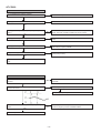
CONTENTS
Page
IMPORTANT SERVICE NOTEST (FOR U.S.A. ONLY) .................................................................................................... 2
SPECIFICATIONS ............................................................................................................................................................. 2
NAMES OF PARTS ........................................................................................................................................................... 3
OPERATION MANUAL ...................................................................................................................................................... 4
DISASSEMBLY .................................................................................................................................................................. 5
REMOVING AND REINSTALLING THE MAIN PARTS ..................................................................................................... 5
ADJUSTMENT ................................................................................................................................................................... 7
NOTES ON SCHEMATIC DIAGRAM .............................................................................................................................. 11
TYPES OF TRANSISTOR ............................................................................................................................................... 11
SCHEMATIC DIAGRAM .................................................................................................................................................. 12
WIRING SIDE OF P.W.BOARD ....................................................................................................................................... 14
WAVEFORMS OF CD CIRCUIT ...................................................................................................................................... 16
TROUBLESHOOTING (CD SECTION) ........................................................................................................................... 17
FUNCTION TABLE OF IC ................................................................................................................................................ 21
PARTS GUIDE/EXPLODED VIEW
PACKING OF THE SET (FOR U.S.A. ONLY)
SHARP CORPORATION
This document has been published to be used
for after sales service only.
The contents are subject to change without notice.
QT-CD250
FOR A COMPLETE DESCRIPTION OF THE OPERATION OF THIS UNIT, PLEASE REFER
TO THE OPERATION MANUAL.
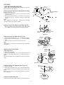
IMPORTANT SERVICE NOTES (FOR U.S.A. ONLY)
BEFORE RETURNING THE AUDIO PRODUCT
(Fire & Shock Hazard)
Before returning the audio product to the user, perform the
following safety checks.
1. Inspect all lead dress to make certain that leads are not
pinched or that hardware is not lodged between the chassis
and other metal parts in the audio product.
2. Inspect all protective devices such as insulating materials,
cabinet, terminal board, adjustment and compartment
covers or shields, mechanical insulators etc.
3. To be sure that no shock hazard exists, check for leakage
current in the following manner.
* Plug the AC line cord directly into a 120 volt AC outlet.
* Using two clip leads, connect a 1.5k ohm, 10 watt resistor
paralleled by a 0.15µF capacitor in series with all exposed
metal cabinet parts and a known earth ground, such as
conduit or electrical ground connected to earth ground.
* Use a VTVM or VOM with 1000 ohm per volt, or higher,
sensitivity to measure the AC voltage drop across the
resistor (See diagram).
* Connect the resistor connection to all exposed metal parts
having a return path to the chassis (antenna, metal cabinet,
screw heads, knobs and control shafts, escutcheon, etc.)
and measure the AC voltage drop across the resistor.
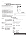
VTVM
AC SCALE
1.5k ohms
10W
0.15 µ F
TO EXPOSED
METAL PARTS
TEST PROBE
CONNECT TO
KNOWN EARTH
GROUND
All check must be repeated with the AC line cord plug connection
reversed.
Any reading of 0.3 volt RMS (this corresponds to 0.2 milliamp.
AC.) or more is excessive and indicates a potential shock
hazard which must be corrected before returning the audio
product to the owner.
SPECIFICATIONS
● General
Power source: AC 120 V, 60 Hz
DC 9 V [ "D" size (UM/SUM-1, R20
or HP-2) battery × 6]
DC 4.5 V [ "AA" size (UM/SUM-3,
R6 or HP-7) battery × 3 for backup
memory]
Power
consumption: 12 W
Output power: FTC; 2.0 W min. RMS per channel
into 4 ohms from 150 Hz to 20
kHz, with no more than 10 % total
harmonic distortion.
RMS; 2.3 W/CH
(DC operation, 10 % T.H.D.)
Speakers:
4" (10 cm) full-range speaker x 2
Output
Headphones; 16-50 ohms
terminals:
(recommended; 32 ohms)
Dimensions: Width; 15-3/4" (400 mm)
Height; 6-1/4" (158 mm)
Depth; 8-3/8" (212 mm)
Weight:
6.0 lbs. (2.7 kg) without batteries
● Compact disc player
Type:
Compact disc
Signal
Non-contact, 3-beam semi-conducreadout:
tor laser pickup
Audio
channels:
2
Quantization: 16-bit linear quantization
Filter:
8-times oversampling digital filter
D/A converter: 1-bit D/A converter
Wow and
Unmeasurable
flutter:
(less than 0.001% W. peak)
● Radio
Frequency
range:
FM; 87.5 - 108 MHz
AM; 530 - 1,720 kHz
● Tape recorder
Frequency
response:
50 - 14,000 Hz (Normal tape)
Signal/noise
ratio:
50 dB
Wow and
flutter:
0.25 % (WRMS)
Motor:
DC 9 V electric governor
Bias system: AC bias
Erase
system:
Magnet erase
Specifications for this model are subject to change without
prior notice.
–2–
QT-CD250
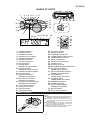
NAMES OF PARTS
1
2 3 4 5 6
7
8
9
13
14
15
10
11
25 26
27 28
29
16
12
17
18 19 20 21 22 23
11.
12.
13.
14.
15.
16.
17.
18.
19.
3
10.
3
11.
12.
13.
3
14.
3
15.
3
16.
17.
18.
19.
24
20.
21.
22.
23.
24.
25.
26.
27.
28.
29.
30.
3
31.
3
32.
3
33.
3
34.
35.
36.
3
37.
38.
(TAPE) Record Button
(TAPE) Play Button
(TAPE) Rewind Button
(TAPE) Fast Forward Button
(TAPE) Stop/Eject Button
(TAPE) Pause Button
Cassette Compartment
CD Compartment
(CD) Stop Button
(TUNER) Tuning Down Button
(CD) Repeat Button
(TUNER) Band Selector Button
(TUNER) Preset Memory Button
Extra Bass Button
(CD) Play/Pause Button
(TUNER) Tuning Up Button
(CD) Track Up/Cue Button
(TUNER) Preset Up Button
(CD) Track Down/Review Button
(TUNER) Preset Down Button
Volume Up/Down Buttons
Power/Function Switch
(CD) Play Indicator
(CD) Repeat Indicator
31
32
34
35
36
37
33
38
30
(CD) Pause Indicator
Extra Bass Indicator
(TUNER) Memory Indicator
(TUNER) FM Stereo Mode Indicator
(TUNER) FM Stereo Indicator
Battery Compartment
FM Telescopic Rod Antenna
Headphone Jack
AC Power Input Jack
Backup Memory Battery Compartment
(CD) Play/Pause Button
(TUNER) Tuning Up Button
(CD) Track Down/Review Button
(TUNER) Preset Down Button
(CD) Stop Button
(TUNER) Tuning Down Button
(CD) Repeat Button
(TUNER) Band Selector Button
(TUNER) Memory Button
(TUNER) Clear Button
(CD) Track Up/Cue Button
(TUNER) Preset Up Button
Extra Bass Button
Volume Up/Down Buttons
REMOTE CONTROL
Remote Sensor
15
15
8" - 20'
(0.2 m - 6 m)
Notes:
● Replace the batteries if the operating distance is
reduced or if the operation becomes erratic.
● Periodically clean the transmitter LED on the
remote control and the sensor on the main unit
with a soft cloth.
● Exposing the sensor on the main unit to strong
light may interfere with operation. Change the
lighting or the direction of the unit.
● Keep the remote control away from moisture,
excessive heat, shock, and vibrations.
–3–
–4–
TUNER
OFF
1
TUNER
POWER
2
● Label side up.
● Con el lado de
la etiqueta
encarada hacia
arriba.
3
6
5
POWER
■ Volume control
■ Control del volumen
● Batteries are not included.
● Las pians no están incluidas.
■ Turning the power ON
and to OFF
■ Conexión(ON) y
desconexión(OFF) de la
alimentación
OFF
4
2
● 6 “D” size batteries
(UM/SUM-1, R20, HP-2 or similar)
● 6 pilas del tamaño “D”
(UM/SUM-1,R20,HP-2 o similares)
1
3
■ Battery power
■ Funccionamiento con pilas
4
PLAY / PAUSE
TUNING
Pulse el botón ■ .
Para detener la
reproducción
Press the ■ button.
To stop the playback
5
2 Listening to a CD / Audictión de discos CD
■ Headphones
■ Auriculares
To an AC socket
A un tomacorriente de CA
AC 120 V, 60 Hz
120 V de CA, 60 Hz
To AC INPUT
A la toma AC INPUT
■ AC power
■ Funccionamiento con corriente alterna
1 Preparation for use / Preparación para su uso
Quick Guide / Guía rápida
TUNER
POWER
2
3
Pulse el botón
.
button.
Para detener la
reproducción
Press the
To stop the playback
OFF
TUNER
POWER
2
REPEAT
BAND
STOP
TUNING
3
PLAY / PAUSE
TUNING
TUNER
POWER
● Load the disc to be
recorded.
● Introduzca el disco que
va a grabar.
OFF
1
2
3
PLAY / PAUSE
TUNING
Pulse el botón
.
button.
Para detener la
grabación
Press the
To stop the recording
4
5 Recording from CDs / Grabaciones de discos CD
1
4 Listening to the radio / Audictión de la radio
OFF
1
3 Listening to a tape / Audictión de una cinta
QT-CD250
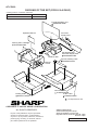
OPERATION MANUAL
QT-CD250
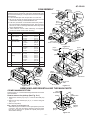
DISASSEMBLY
Caution on Disassembly
Follow the below-mentioned notes when disassembling the
unit and reassembling it, to keep it safe and ensure excellent
performance:
1. Take cassette tape and compact disc out of the unit.
2. Be sure to remove the power supply plug from the wall
outlet before starting to disassemble the unit.
3. Take off nylon bands or wire holders where they need to
be removed when disassembling the unit. After servicing
the unit, be sure to rearrange the leads where they were
before disassembling.
4. Take sufficient care on static electricity of integrated
circuits and other circuits when servicing.
STEP
REMOVAL
PROCEDURE
FIGURE
1
Top Cabinet/
Front Cabinet
1. Screw ................... (A1) x7
2. Socket .................. (A2) x1
3. Screw ................... (A3) x1
5-1
2
Power PWB/
Terminal PWB
1. Screw ................... (B1) x2
2. Hook ..................... (B2) x2
3. Socket .................. (B3) x1
4. Hook ..................... (B4) x2
5-2
1. Screw ................... (C1) x2
2. Socket .................. (C2) x1
3. Hook ..................... (C3) x2
4. Screw ................... (C4) x4
5-2
1. Socket .................. (D1) x1
2. Screw ................... (D2) x7
3. Screw ................... (D3) x1
4. Solder ................... (D4) x3
5. Socket .................. (D5) x3
6. Screw ................... (D6) x6
7. Hook ..................... (D7) x2
5-2
3
4
Switch PWB
Main PWB/
CD Control PWB
(Note)
(C4)x4
ø3x10mm
(C1)x2
ø3x12mm
(C3)x2
Switch PWB
(D3)x1
ø2.5x8mm
CD Lid
Switch
(C2)x1
(D2)x7
ø3x12mm
(B3)x1
(D1)x1
Main PWB
(D4)x3
(B4)x2
Terminal
PWB
(B2)x2
Top Cabinet
Power PWB
Power Transformer
AC Socket
(B1)x2
ø3x12mm
Figure 5-2
(E1)x3
ø2.5x10mm
CD Mechanism
(D5)x2
(F1)x4
ø3x10mm
Washer
(D5)x1
5-3
5
CD Mechanism
1. Screw ................... (E1) x3
5-3
6
Tape Mechanism
1. Screw ................... (F1) x4
5-3
Tape
Mechanism
Top Cabinet
SP202
R-CH
(D6)x6
ø3x8mm
(A3)x1
ø3x10mm
(D7)x2
Top Cabinet
Front Cabinet
Main
PWB
(A2)x1
(A1)x4
ø3x12mm
CD Control
PWB
(A1)x3
ø3x12mm
Figure 5-1
Figure 5-3
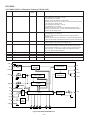
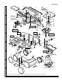
REMOVING AND REINSTALLING THE MAIN PARTS
CD MECHANISM SECTION
(A1) x2
ø2.6 x6mm
Perform steps 1 to 4 of the disassembly method to remove the
CD mechanism.
CD
Mechanism
Pickup
How to remove the pickup (See Fig. 5-4.)
1. Remove the screws (A1) x 2 pcs., to remove the shaft (A2)
x1 pc.
2. Remove the stop washer (A3) x1 pc., to remove the gear
(A4) x 1 pc.
3. Remove the pickup.
Note : (Figure 5-3 and Figure 5-4)
After removing the connector for the optical pickup from the
connector, wrap the conductive aluminium foil around the
front end of connector to protect the optical pickup from
electrostatic damage.
Shaft
(A2) x1
Gear
(A4) x1
Figure 5-4
–5–
Stop
Washer
(A3) x1
QT-CD250
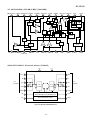
TAPE MECHANISM SECTION
(A1) x1
ø2x7mm
(A1) x1
ø2x3mm
Hook
(A2)x2
Perform steps 1 to 6 of the disassembly method to remove the
tape mechanism. (See page 5.)
How to remove the record / playback and erase
heads (See Fig. 6-1.)
Record/Playback
Head
Erase Head
1. Remove the screws (A1) x 2 pcs., to remove the record/
playback head.
2. Remove the hooks (A2) x 2 pcs., toward the center position
as shown in Fig. 6-1. and then extract the erase head
upward.
Note:
After replacing the heads and performing the azimuth
adjustment, be sure to apply screwlock.
Figure 6-1
How to remove the pinch roller (See Fig. 6-2.)
1. Carefully bend the pinch roller pawl in the direction of the
arrow <A>, and remove the pinch roller (B1) upwards.
<A>
Pinch Roller
Pawl
Pinch Roller
(B1)x1
Figure 6-2
How to remove the belts (See Fig. 6-3.)
Main Belt
(C1)x1
1. Remove the main belt (C1) x 1 pc., from the motor pulley.
2. Remove the FF/REW belt (C2) x 1 pc., from the REW/FF
roller.
3. Put on the belts in the reverse order of removal.
Note:
When putting on the belt, ascertain that the belt is not twisted,
and clean it.
Motor
Flywheel
REW/FF
Clutch Ass'y
FF/REW Belt
(C2)x1
Figure 6-3
How to remove the motor
(See Figs. 6-4.)
(D2)x2
Special
Screw
1. Remove the mainbelt.
2. Remove the screw (D1) x 1 pc., to remove the motor mount.
3. Remove the screws (D2) x 2 pcs., to remove the motor.
Note:
When mounting the motor, pay attention to the motor mounting
angle.
Motor
Mount
(D1)x1
Special
Screw
Motor
Motor
Motor Mount
Figure 6-4
How to remove the flywheel (See Fig. 6-5.)
(E1) x 1
Stop Washer
1. Remove the belt.
2. Remove the stop washer (E1) x 1 pc., with a small precision
screwdriver to extract the flywheel from the capstan metal.
Note:
When the stop washer is deformed or damaged, replace it
with a new one.
Washer
Flywheel
How to reinstall the parts
Install each part in the reverse order of the removal with care.
Figure 6-5
–6–
QT-CD250
ADJUSTMENT
• AM IF/RF
Signal generator: 400 Hz, 30%, AM modulated
MECHANISM SECTION
• Driving Force Check
Torque Meter
PLAY: TW-2412
Frequency
Frequency
Display
AM IF
450 kHz
1,720 kHz
T3
AM Band
Coverage
—
530 kHz
(fL): L4
*3
1.0 ±0.05V
600 kHz
1,400 kHz
(fL): L3
(fH): TC1
Test Stage
Specified Value
Over 120 g
• Torque Check
Torque Meter
Specified Value
Play: TW-2111
25 to 65 g.cm
Fast Forward: TW-2231
60 to 130 g.cm
Rewind: TW-2231
60 to 130 g.cm
AM Tracking 600 kHz
1,400 kHz
Torque Meter
Specified Value
MTT-114
Output: Speaker Terminal
(CNP201 Load resistance: 4 ohms)
4 3 21
L301
MTT-111 Variable
resistor in
motor. (M601)
Specified
Value
Instrument
Connection
3,000 ± 90 Hz
Output: Speaker
Teaminal
(CNP201 Load
resistance: 4 ohms)
SW102
IC101
1
11
12
2
CNP201
CNP602
HPJ201
HEADPHONE
321
3
2
1
TAPE SECTION
Position of each switch or control
Volume control
Function switch
X-BASS
Max
Tape/Power Off
On
MAIN PWB
• Bias Oscillation
Adjustment Point
Specified Value
82 kHz ± 6 kHz
- 6 kHz
L301
Instrument
Connection
Pin 2 of CNP201
• Playback Amplifier Sensitivity Check
Test Tape
Specified Value
MTT-118
1.1 V ± 3 dB
Instrument Connection
Speaker Terminal
(Load resistance: 4 ohms)
TUNER SECTION
fL: Low-range frequency
fH: High-range frequency
• FM RF
Signal generator: 1 kHz, 75 kHz dev., FM modulated
FM Band
Coverage
—
87.5 MHz
FM RF
98.0 MHz 98.0 MHz
(10-30 dB)
Serring/
Adjusting
Point
Instrument
Connection
(fL): L2
1.7 V ± 0.05V
*1
L1
*2
AM
TRACKING fH
L3
AM BAR
ANTENNA
TC1
FM IF
L1
AM IF
T3
24
1
12
*1. Input: Antenna, Output: TP1
*2. Input: Antenna, Output: Speaker terminal
R7
L4
TP1
L2
IC1
Test Stage Frequency Frequency
Display
*2
CNP101
BIAS OSC.
• Tape Speed
Adjusting
Point
*1
*1. Input: Antenna, Output: Pin 16 of IC1
*2. Input: Antenna, Output: Speaker Terminal
*3. Input: Input is not connected, Output: TP1
• Head Azimuth
Test
Tape
Setting/ Instrument
Adjusting Connection
Parts
AM BAND
COVERAGE fL
16 FM BAND
COVERAGE fL
13
AM
TRACKING fL
Figure 7 ADJUSTMENT POINTS
–7–
QT-CD250
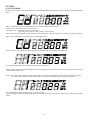
A. CD TEST MODE
Set the function switch to "CD" when pressing the "REVIEW(PRESET DOWN )" button together with "STOP(TUNING DOWN)"
button.
Step-1. CD Pickup can be move when press the "CUE" button either "REVIEW" button.
"CUE" button : CD Pickup move to out side of disc.
"REVIEW" button : CD Pickup move to in side of disc.
(CD Pickup can't move any more, if reach to most in side.)
Note: If the CD Lid open (SW810 open), the unit can be operate Step-1 only and the unit can't operate from Step-2 to Step-5.
Step-2. The LASER light up when press the "PLAY/PAUSE" button.
Step-3. CD disc can be playing mode when press the "PLAY/PAUSE" button during the LASER ON.
The LCD displays indicate the "Track Number" and the "Playing Time".
Step-4. CD disc will be stop and the LASER goes out when pressing the "STOP" button, and return back to Step-1. (CD Pickup
position keeps at that point).
Step-5. It can be control to ON/OFF of the Tracking Servo when press the "MEMORY" button during the CD playing mode.
(The Servo will be ON when playing mode again, if to make stop mode during the Servo OFF condition.)
The LCD displays indicate the playing time of CD Pickup point.
(The LCD displays indicate the playing time at that point when Pickup moving, if press the "CUE" button or press the "REVIEW"
button.)
–8–
QT-CD250
B. TUNER TEST MODE
Set the function switch to "TUNER" when pressing the "REVIEW(PRESET DOWN )" button together with "BAND(REPEAT)"
button.
The LCD displays indicate the "TunEr" for several seconds. after that, the LCD displays indicate to the normal frequency.
PRESET.
NO
U.S.A.
FM MODE
P-01
FM 87.5 MHz
STEREO
P-02
FM 108.0 MHz
STEREO
P-03
FM 98.0 MHz
STEREO
P-04
FM 90.0 MHz
STEREO
P-05
FM 106.0 MHz
STEREO
P-06
AM 530 KHz
P-07
AM 1720 KHz
P-08
AM 990 KHz
P-09
AM 600 KHz
P-10
AM 1400 KHz
P-11
FM 106.0 MHz
MONO
P-12
FM 90.0 MHz
MONO
P-13
FM 98.0 MHz
MONO
P-14
FM 108.0 MHz
MONO
P-15
FM 87.5 MHz
MONO
Note:
1. The Preset Channel can be change when press the "PRESET UP (CUE) button either "PRESET DOWN (REVIEW)" button.
PRESET UP button is pressed : P-01 -> P-02 -> > > > > P-15 -> P-01
PRESET DOWN button is pressed : P-15 -> P-14 -> > > > > P-01 -> P-15
2. The Tuner Mode can be change when press the "BAND (REPEAT)" button.
BAND button is pressed : FM stereo -> FM mono -> AM -> FM stereo
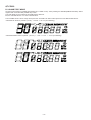
C. LCD TEST MODE
Set the function switch to "TUNER (or CD)" when pressing the "REVIEW(PRESET DOWN )" button together with "MEMORY"
button.
All of the segments will light up.
–9–
QT-CD250
D. VOLUME TEST MODE
Set the function switch to "POWER ON (TAPE PLAY, TUNER or CD)" when pressing the "REVIEW(PRESET DOWN )" button
together with "PLAY/PAUSE (TUNING UP)" button.
The LCD display do not indicate the VOLUME level at this time.
But, the VOLUME level is "12" which is defaults level.
The VOLUME LEVEL can be change when press the "VOLUME UP" button either press the "VOLUME DOWN" button.
"VOLUME UP" button is pressed : (12 VoL) -> 30 VoL -> 30 VoL (30 is flashing)
"VOLUME DOWN" button is pressed : (12 VoL) -> 1 VoL-> 0 VoL -> 0 VoL (0 is flashing)
– 10 –
QT-CD250
NOTES ON SCHEMATIC DIAGRAM
• Resistor:
To differentiate the units of resistors, the symbol as K and M
are used: the symbol K means 1000 ohm and the symbol M
means 1000 kohm and the resistor without any symbol is an
ohm resistor. The resistor designated "Fusible" is a fuse type
resistor
• Capacitor:
To indicate the unit of capacitor, a symbol P is used: this
symbol P means micro-micro-farad and the unit of the capacitor
without such a symbol is microfarad. As to electrolytic capacitor,
the expression “capacitance/withstand voltage” is used.
(CH), (TH), (RH), (UJ): Temperature compensation
(ML): Mylar type
(P.P.): Polypropylene type
• The indicated voltage in each section is the one measured by
Digital Multimeter between such a section and the chassis
with no signal given.
REF. NO
DESCRIPTION
1. Tuner
( ): AM mode
Marking except for ( ): FM mode
2. CD
( ): Play mode
Marking except for ( ): Stop state
3. Deck section
( ): Record mode
Marking except for ( ): Playback mode
Display / Control section:
( ): Active state
Marking except for ( ): CD Function mode at stop state
• Schematic diagram and Wiring Side of P.W.Board for this
model are subject to change for improvement without prior
notice.
• Parts marked with “
”(
) are important for
maintaining the safety of the set. Be sure to replace these
parts with specified ones for maintaining the safety and
performance of the set.
POSITION
SW102
RECODE/PLAYBACK
REC—P.B.
SW201
FUNCTION SELECTOR
TAPE/OFF—
TUNER/ON—CD/ON
SW601
TAPE MAIN
OFF—ON
SW702
PICKUP IN
OFF—ON
SW801
PLAY/PAUSE/
TUNING UP
OFF—ON
SW802
STOP/TUNING DOWN
OFF—ON
SW803
REPEAT/BAND
OFF—ON
SW804
TUNER/MEMORY
OFF—ON
SW805
CUE/PRESET UP
OFF—ON
SW806
REVIEW/
PRESET DOWN
OFF—ON
SW807
VOLUME UP
OFF—ON
SW808
VOLUME DOWN
OFF—ON
SW809
X-BASS
OFF—ON
SW810
CD LID
OFF—ON
FRONT
VIEW
E C B
(S) (G) (D)
(1) (2) (3)
KRA102 M
KRC107 M
KTA1046 Y
KTA1266 GR
KTA1273 Y
KTC3199 GR
Figure 11 TYPES OF TRANSISTOR
– 11 –
QT-CD250
SW810
1.9V
F
0.5V
8
9
10
11
SEL
0V
2200P
3.8V
R826
220K
C807
0.047
IC101
BA3311L
0V
IN2
NF2
0.6V 11
9
C112
330P
C108
820P
9 8 7
R
P
SW102-C
16 17 18
R
P
SW102-G
R108 R110
1K
120
C106
0.0018
C110
270P
NC
4
GND
6
4.4V
R879
4.7K
R865
47K
R62
1K
R60
1K
R61
1K
3.2V
C118
10/16
R114
8.2K
R116
3.9K
R118
3.9K
XOUT XIN
GND(AUDIO)
CE
AOUT
AIN
PD
R53
4.7K
VSSA VSSX
DI
CL
DO
C56
0.022
C59
0.01
R77
3.3K
C54
0.022
BO1
FMIN
MONO/
AMIN
ST
BO2
IO1
FM/AM
VSSD BO3
C53
100/10
GND 5.0V
(CD: OPEN)
L-CH(CD)
R-CH(CD)
R59
1K
R58
1K
12
7
C114
47/16
C116
0.018
(ML)
FILTER 10
7.3V
ALC T 2
OUT2 0V
C121
0.01
R119
3.3K
PRE AMP
1 3.1V
OUT1
8
VOLTAGE:
VCC 7.3V
PLAY and REC.
SW102-E
P
R
22 23 24
+B
R122
2.7K
R240
2.2K
C242
1/50 R244
560K
Q211,Q212
LINE AMP
2
3
C245
1/50
C243 0.8V
330P
0.2V
2.0V
R246
5.6K
R249
220
+B
+B
SW102-D
SW102
P RECORD/
R
12 11 10 NC PLAYBACK
BIAS OSC.
L301
R351
100
C354
0.022(ML)
BIAS OSC.
Q351
KTC3199 GR
0V
R353(REC: 0.4V)
33K
R352
150
C352
100/10
C353
0.0056
(ML)
M601
TAPE
MOTOR
R354
4.7
SW601
TAPE
MAIN
• The numbers 1 to 17 are waveform numbers shown in page 16.
1
C244
R248 330P R247
560
560
0V
C223
0.1/50
GND GND
R242
10K
0V(OFF:0.6V)
Q210
KTC3199 GR
R238
2.7K
0.2V
R235
47K
C224
0.1/50
R241
10K
IC101
REC./P.B.EQUALIZER AMP.
BA3311L
R126
100
NC
13 14 15
R
P
SW102-H
SW102
RECORD/
PLAYBACK
R106
15K
SW102
RECORD/
PLAYBACK
C123
220/10
R125
680K
R239
2.2K
C241
R237
1/50
2.7K
Q209
KTC3199 GR
0V(OFF:0.6V)
R234
2.2K
R123
3.3K
3
NF1
IN1
C119
2.2/50
5
0V
SW102
RECORD/
PLAYBACK
H
0.6V
D101
1N4148
C107
820P C111
330P
6 5 4
P
R
SW102-B
R-CH SW201-C
14
CD
TU
11
13
TA
12
R117
3.9K
R115
3.9K
R243
560K
0V
(REC: 4.0V)
4
Q209,Q210
X-BASS ON/OFF
Speaker Case
R124
3.3K
3
ERASE HEAD
R107
1K
R113
8.2K
C113
47/16
C120
47/16
R-CH
1
2
3
4
R101
330
SW102-F
C109
270P
D102
1N4148
2
R109
120
C122
0.01
1
C115
0.018(ML)
C105
0.0018
R
P
19 20 21
3 2 1
SW201
FUNCTION
SELECTOR
COR1
R74
3.3K
10
SW201-B
R121
2.7K
R120
3.3K
L-CH
CNP101
RECORD/
PLAYBACK HEAD
CNS101
SW102-A
R
P
SW102
RECORD/
PLAYBACK
BO4
R73
3.3K
R72
4.7K
C117
10/16
G
R103
12K
IO2
IFIN
R233
2.2K
R105
15K
R104
SW102
12K
RECORD/
PLAYBACK
R102
330
R245
5.6K
L-CH
CD 7
TU 8
TA 9
C29
100P
L-CH
CF4
FM DET
R51
150
R71
4.7K
C71
0.022(ML)
1
3
Q2
KRA102 M
TUNER
SWITHCING
0V
3
C73
1/50
C74
1/50
AM IF
+B
0V
1
C24
0.1
R16
3.3K
C26
0.1
C22
1/50
R-CH
2
C75
100P
R455
15K
R457
1K
1
3
R236
47K
CF1
NC
IC1
FM/AM IF MPX.,
TA2104BN
12
FM IF
5.0V
(CD: 0.4V)
2
R76
820
R18
100
C72
0.022
(ML)
CF3 2
L51
100µH
C60
0.0022
R458
1K
C52
12P
(CH)
20 21 22
R52
2.2K
C55
2.2/50
C61
100/10
13
10 11
C16
4.7/50
C15
220/10
AM IF
T3
MPX
IN
7 8 9
14
LPF1
VCO
DET
OUT
6
15
QUAD
IF
REQ
OSC
OUT
GND
AM
OSC
C25 D1
0.047 1N4148
FM IF
IN
AM RF
IN
FM
OSC
R10
330
C13
0.47/50
C14
0.047
AM IF
IN
19 18 17 16
FM RF
VCC
20
IC51 LC72121
R456
15K
X51
4.5MHz
R54
10K
C23
10/16
23 22 21
IC1
TA2104BN
C68
220P
C34
220P
R5
22K
VD2
KV1370NT
C21
10/16
C7
FM BAND
0.001 COVERAGE fL L2
24
VCC
RF
GND
R4
10
R17
47K
R13
10K
C51
15P
(CH)
7 6 5 4 3 2 1
12 13 14 15 16 17 18 19
0.001
100P
100P
R14
2.2K
R12
10
L2
L1
C2
FM RF
0.001
C6
22P(CH)
C5
0.1
FM OSC
C32
0.1
1 2 3 4 5
F
R20
470
R6
15K
NC
11 10 9 8
C19
2.2/50
C18
C57
C58
R862
47K
Q804
KTA12
SWITC
GND
+B
R15
39K
LPF2
FM/AM
R8
220K
C10
8P
C12
1/50
C8
0.001
C33
220P
GND
R55
56K
C351
0.0022(ML)
TC1
C9
0.022
Q1
KTC3199 GR
GND
0V
TUNER
MUTE
NC
0V
F1
+7.5V(CD)
1
SWITCHING
IC51
LC72121
ELECTRONIC
TUNING
NC
AM TRACKING fH
1 2 3
3
D806
1N4148 1
3
VDD
AM BAND
COVERAGE fL
L4
C11
360P AM OSC.
VD3
KV1520NT
FM BAND
PASS
FILTER
2
0V
(TUN:7.5V)
+B
0V
Q805
(TUN:7.5V)
SWITCHING KRC107 M
4.4V
2
R861
10K
+B
+B
R7
10K
C3
0.01
R850
1.5K
D804
1N4148
C805
0.022
C806
330/10
AM TRACKING fL
L3
AM BAR ANTENNA
C845
0.047
R854
100
0.8V
R852
2.2K
FMO
+B
FM
ROD
ANTENNA
TAPE
Q802
Q803
KTA1273 Y
7.5V KRC107 M
SWITCHING
DMO
AM
2V
GND
0.V
0V
0V
4.9V
0.7V
0V
0V
5.0V
0V
0.9V
GND
2.0V
0V
4.2V
0.9V
0.9V
1.0V
GND
2.6V
R
1
D802
1N4148
7.5V(TUN:0V)
GND
GND
3.4V
3.4V
1.9V
1.9V
7.5V
R851
2.2K
C839
0.047(ML)
R845
22K
R866
3.3K
1 2 3 4 5 6 7 8 9 10 11 12 13 14 15
NC
5.0V
4.5V
(TUN:
0.5V)
2
6.9V
(TUN:7.5V)
GND
3
VCC
VO1-
VG1
VIN1
MT
VCC
VO1+
IC803
LA6541D
5.0V
(TUN:0V)
4.3V
(TUN:5.0V)
X801
16.93MHz
R853
2.2K
30 29 28 27 26 25 24 23 22 21 20 19 18 17 16
C835
470P
C836
0.047(ML)
C837
0.047(ML)
C838
0.047(ML)
C843
47/16
SWITCHING
Q806
KTA1273 Y
NC NC
NC
VOLTAGE
VD1
KV1370NT
E
FM ST
1.6V
GND
0.V
0V
0V
4.9V
3.1V
2.9V
0V
5.0V
0V
0.9V
GND
0V
1.5V
3.2V
0.9V
0.9V
1.7V
GND
1.6V
+B
2.9V(0V)
3.1V
0.7V
1.0V
0.9V
5.0V
3.6V(4.0V)
3.7V(4.1V)
3.7V(4.1V)
3.7V(4.1V)
3.7V(4.1V)
3.7V(4.1V)
( ): AM
IC51
VOLTAGE
FM MONO
1.6V
GND
0.V
0V
0V
4.9V
0V
2.9V
0V
5.0V
0V
0.9V
GND
0V
1.5V
3.2V
0.9V
0.9V
1.7V
GND
1.6V
C834
470P
COR801
SLT-
MIX
OUT
D
PIN
NO.
1
2
3
4
5
6
7
8
9
10
11
12
13
14
15
16
17
18
19
20
21
22
IC1
PIN
NO.
13
14
15
16
17
18
19
20
21
22
23
24
VOLTAGE
0.82V(0V)
0V(0V)
0.V
3.5V(4.1V)
3.7V(4.1V)
3.2V(4.1V)
3.7V(4.1V)
GND
0.4V(0.1V)
3.0V(3.6V)
1.2V
1.2V
C842
0.047
TRO
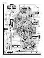
SLT+
AM LOW
CUT
PIN
NO.
1
2
3
4
5
6
7
8
9
10
11
12
FM-
VCC
1.9V
VREF
1.9V
VIN4
VG4
3.4V
VO4+
3.4V
VO4GND
CD MOTOR PWB-B
FM+
C1
15P(CH)
C
R832
3.3K
R833
3.3K
R834
3.3K
RES
SW702
PICKUP IN
R831
3.3K
DM-
REG IN
GND
R829
3.3K
R830
10K
FOO
NC
PU-IN
R812
1K
C854
0.0068
C841
0.047
C20
330P
SL-
C833
0.033(ML)
C822
0.047
C863
47/16
AGC
SL+
-
14
0.8V
13
DM+
R2
C27
0.001 100K
+
M
SBAD
C814
0.047
C813
47/16
IC803
FOCUS/
TRACKING/
SPIN/
SLED DRIVER
LA6541D
R1
3.3K
M701
SLED
MOTOR
6
5
4
3
2
1
1.9V
FEO
TEO
+B
R828
10K
LD
7.5V
SP-
6
5
4
3
2
1
TEN
L803
220µH
R803
82K
C821
100/10
C828
0.0027
C829
0.0047
+B
C856
100P
6
5
4
3
2
1
BI803
SP+
CNS803
-
10
1.9V
12
+
M
CNP803
M702
SPINDLE
MOTOR
VR
2VRO
C832
47/16
C819
0.1(ML)
NC
CNS801
LD
1.9V
PD
R3
100K
TR-
GND
TEB
1.9V
VR
3.7V
9
C830
0.01(ML)
21
0.5V
RFGC 20
1.9V
RFGO 19
1.9V
RFIS 18
0.9V
RFRP 17
1.9V
VRO 16
1.9V
FEN 15
1.9V
PD
0V
FC-
LDO
C827
0.015(M
C818
56P
AGCI
ST
IND
G
FO-
B
FC+
MDI
1.9V
C820
0.1(ML)
GND
3.4V
VO33.4V
VO3+
1.9V
VG2
VG3
1.9V
VIN2
VIN3
REG OUT
CD
F+
F-
0V
TNI
R806
2.7K
22
RFO
FM RF FM RF
OUT
IN
FO+
TR-
TPI
R827
15K
0.1V
VO2+
R+
1
2
3
4
5
6
7
8
1
2
3
4
5
6
7
8
R811
22K
1
2
3
4
5
6
7
8
BI801
TR+
TR+
FPI
C826
47P
R807
1K
4
Figure 12 SCHEMATIC DIAGRAM (1/2)
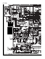
– 12 –
2.0V
Q211
KTC3199 GR
B
FNI
23
GND
8
2
3
4
5
6
7
0.5V
R-
GND
R805
39K
C247
220/10
1.9V
1M
1M
R804
68K
Q212
KTC3199 GR
A
GND
LTOH30P1
E
3.4V
F
5
4
3
2
1
1.9V
24
RFN
VCC
VO2-
B
5
4
3
2
1
C825
47/16
4.4V
3.4V
A
2200P
1
C801
0.01
GND
5
4
3
2
1
E
A
F
C
R802
2.2K
+B
K
C816
0.022
IC801
SERVO PRE AMP.
TA2109F
GND
K
C802
0.022
BI802
CNS802
A
3.7V(ON:2.1V)
PICK-UP UNIT
LD
MON
K
E
B
+B
+B
C815
47/16
C817
100/10
R801
22
R820
47K
LASER DRIVER
Q801
KTA1266 GR 4.4V(ON:2.8V)
C804
2P(CH)
1.4V(ON:1.9V)
IC801
TA2109F
CD LID
OPEN/CLOSE
5
6
M
+
QT-CD250
FM SIGNAL
SEG7
2.5V
SEG6
2.5V
SEG5
2.3V
2.3V
GND
5.0V
5V
2.5V
2.4V
5V
5V
GND
GND
GND
SEG4
2.5V
SEG3
2.5V
SEG2
SEG1
2.5V
2.3V
2.3V
DVSR
GND 81 82 83 84 85 86 87 88 89 90 91 92 93 94 95 96 97 98 99 100
NC
R825
10K
R882
47K
11
10
9
9
7
7
6
6
5
5
4
4
1
1
2
2
R899
47K
3
8
8
1
1
2
2
3
3
4
4
5
5
6
6
7
7
8
+B
10
11
11
FW802
9
10
CNP801
1
2
3
4
R856
15K
+B
+B
8
9
X802
4.19MHz
C851
3.3/50
12
11
10
3
R901
47K
R863
1.8K
R860
4.7K
R835
270
1 2 3 4 5 6 7 8 9 10 1112 1314 1516 171819 20
12
R883
47K
R884
47K
R885
47K
R886
47K
R887
47K
R888
47K
R889
47K
R890
47K
R891
47K
R892
47K
R893
47K
R894
47K
R895
47K
R896
47K
R897
47K
R898
47K
MHz
FW801
C864
0.1
ST
KHz
+B
R864
1M
R839
47K
C850 C849
0.0022 0.0022
C852
3.3/50
+B
C862
0.1
C846
1/50
C848
22/16
L801
220µH
C847
22/16
C853
0.022
C872
0.0047
C844
100/10
R836
270
+B
R876
10K
19
18
17 NC
16
15
14
13
12
11
10
9
8
7
6
5
4
3
2
1
R847
5.6K
SW801
SW802
PLAY/PAUSE/
STOP/
TUNING UP TUNING
DOWN
R808
100
M
C810
10/16
SW809
X-BASS
2
SW806
REVIEW/
PRESET
DOWN
R857
47K
SW808
VOLUME DOWN
R855
18K
SW807
VOLUME UP
D803
1N4148
-
8.6V8.0V 10
5
-
0.6V
+
6
0V
8.2V8.4V
1
4.5V4.2V
2
12 9.0V
C201
100/16
R201
1.2K
1
2
3
SP201
L-CH
4 OHM
SPEAKERS
+
SP202
R-CH
4 OHM
C226
0.022
POWER PWB-A3
T651
POWER TRANSFORMER
C651
0.022
D651
1N4004
C652
0.022
D652
1N4004
SO651
AC INLET
SOCKET
AC 120V,60Hz
C654
0.022
D654
1N4004
D653
1N4004
AC INPUT
3
2
1
C653
0.022
CNP602
3
2
1
SW201
FUNCTION
SELECTOR
Q204,Q205:5V
REGULATOR
+
1
2
3
C234
470/10
CNS602
R206
560
MAIN PWB-A1
C240
0.1(ML)
R204
2.2K
C206
47/16
0V
7.0V
HPJ201
HEADPHONES
C239
0.1(ML)
GND
3
R205
4.7K
C209 D204
0.01 1N4148
8.4V
ZD202
DZ7.5BSB
Q207
KTC3199 GR
8.4V C212
0.047
GND
13
14
8.6V8.0V
2
3
1
6
7
4
5
CNP201
R232
120
5.0V4.6V
C227
4700/16
C220
1/50
GND
R228
120
C237
100/10
CNS201
C235
100/10
4
R227
120
C238
100/10
R211
47K
C221
0.001
9
C225
100/10
GND
8
R231
120
C236
100/10
GND
Q202
KTC3199 GR
0V
0.6V
C222
0.001
VSS VDD
GND
D201
1N4148
C214
1/50
R212
47K
4.6V
2.5V
2.5V
2.5V
C218 2.5V
0.0015(ML)
R218
8.2K
7.5V
REGULATOR
D205
1N4148
R203
270
199 GR
4.9V
Q205
KTC3199 GR
0V
(REC: 4.0V)
+B
7.0V
4.4V
ZD201
DZ5.1BSB
C249
100P
C204
0.022
7.0V
D203
1N4148 R202
10K
+B
Q201
KTC3199 GR
0.V
R253
3.9K
C217
0.0015(ML)
C215
0.1(ML)
R217
8.2K
2.5V
GND
C216
0.1(ML)
R214
1K
2.5V
CK
2.5V
CS R216
1K
0V
0V
0V
0V
R222
4.7K
C208
0.022
C205
47/16
Q204
C211
KTA1273Y
7.5V 0.047
5V 5.0V
SW805
CUE/
PRESET
UP
1
11
+
Q206
KTA1046 Y 7.5V REGULATOR
9V
+B
7.5V
+B
D202
1N4148
TAPE 2
NC
M601
TAPE
MOTOR
R207
560
+B
C232
1/50
SW201
FUNCTION
SELECTOR
0V
C207
470/10
R249
220
R354
4.7
R225
100K
R224
4.7K
0V(ON:0.6V)
MUTE
C247
220/10
7.5V
SW201-A
CD 4
1
TUN 3
0.4V)
R220
220K
ZD203
ZD2.4BSB
R213
100
+B
OSC.
STB
DATA
2.0V
Q211
KTC3199 GR
C245
1/50
C243 0.8V
330P
0.2V
R252
22K
R246
5.6K
R AMP.
4 3 2 1
C203
0.01
Q211,Q212
LINE AMP
2.0V
C230
1/50
C210
0.022
C242
1/50 R244
560K
C244
R248 330P R247
560
560
0V
R240
2.2K
0.2V
R242
10K
0V(OFF:0.6V)
Q210
KTC3199 GR
R238
2.7K
0.8V
GND GND
R241
10K
IC202
0V(ON:0.6V)
C246
10/16
R210
1K
Q212
KTC3199 GR
0V
C241
R237
1/50
2.7K
Q209
KTC3199 GR
0V(OFF:0.6V)
R251
22K
R223
4.7K
13 14 15 16
8 7 6 5
C231
1/50
C213
1/50
MUTE
R219
220K
9 10 11 12
R245
5.6K
R243
560K
2.5V
+5V(u COM)
+4.5V(BACK UP)
+5V(CD)
GND(POWER)
GND(CD)
GND(AUDIO)
C229
1/50
SW804
TUNER/
MEMORY
3
C233
470/10
4.5V4.2V
0V
7
R215
1K
+B
Q2
A102 M
UNER
THCING
R239
2.2K
R250
470K
C219
1/50
R221
4.7K
R209
1K
SW803
REPEAT/
BAND
SWITCH PWB-A4
IC201
TA8227P
POWER AMP.
R457
1K
1
3
Q203 SWITCHING MUTE
KTA1266 GR
4.8V(ON:4.4V)
4.4V(ON:3.8V)
IC202
ELECTRONIC
VOLUME
0V
TC9260P(ON:4.4V)
R455
15K
R849
18K
+B
D805
1N4148
R458
1K
GND 5.0V
(CD: OPEN)
L-CH(CD)
R-CH(CD)
0.4V)
2
R837
10K
R841
5.6K
R848
10K
UN801
REMOTO SENSOR
N64H380A
1
2
3
4
+B
+B
R838
10K
R456
15K
51
5MHz
LCD801 LCD DISPLAY
X-BASS MEMORY
R900
47K
+B
D801
1N4148
5.0V
4.4V
+B
CD CONTROL PWB-A2
CNS801
2.5V
+B
0V
Q805
(TUN:7.5V)
SWITCHING KRC107 M
4.4V
2
3
R862
D806
5.0V
47K
1N4148 1
Q804
KTA1266 GR
SWITCHING
GND
R842
22K
R844
22K
SEG8
COM3
COM1
COM2
MVDD
2.2V(TUN:0V)
SEG9
2.5V
COM4
MVSS
MXI
HOLD
MXO
REMO-IN
NC
2.1V(TUN:0V)
2.5V
2.5V
RESET
LO
4.4V
(TUN:0V)
16
DVSL
RO
DVDD
17
DVRR
80 XVDD
R846
4.7K
R878
10K
R877
10K
R875
10K
C865
100/10
0V
4
DVRL
2.2V
(TUN:0V)
2.1V
(TUN:0V)
4.2V(TUN:0V)
78 XI 2.0V(TUN:0V)
79 XO (TUN:0V)
L807
0.82µH
GND
GND
0V
0V(TUN:5.0V)
2.5V SEG10
NC
X801
16.93MHz
GND
GND R869
4.7K
GND
GND
NC
R868
4.7K
R870
4.7K
0V(X-BASS OFF:4.9V)
R826
220K
GND
R820
47K
1.5V
(TUN:0V)
1.9V
(TUN:0V)
3.7V
(TUN:0V)
4.4V(TUN:0V)
15
75 VDD2 4.4V(TUN:0V)
R821
1K
DO
CL
TEST0
TEST1
TEST2
TEST3
TEST4
CE_(PLL)
2.5V SEG14
2.5V SEG13
14
76 VSS2 GND
77 XVSS GND
C845
0.047
2.5V SEG15
2.5V SEG11
74 SEL 0V
R840
10
2.5V SEG16
2.5V SEG12
71 FMO 1.9V(TUN:0V)
ML)
NC
SEG17
70 TEBC 0V
72 DMO 1.9V(TUN:0V)
C840
0.1
MVDD1
69 RFGC 0.5V(TUN:0V)
73 2VREF 3.7V(TUN:0V)
R854
100
STB_(VOL)
R834
3.3K
ML)
TEST5
11
68 VREF 1.9V(TUN:0V)
R832
3.3K
R833
3.3K
IC802
SERVO/
SIGNAL
CONTROL
TC9457F2
1
66 FOO 1.9V(TUN:0V)
67 TRO 1.9V(TUN:0V)
R831
3.3K
KEY1 26
CD
POWER 25
PU IN 24
5.0V
7
6
65 TEZI 1.9V(TUN:0V)
ML)
5.0V
4.9V(TUN: 0V)
R843
4.7K
+B
5.0V KEY2 27
GND MVSS1 20
63 SBAD 0.7V(TUN:0V)
64 TEI 1.9V(TUN:0V)
R829
3.3K
R873
4.7K
DOOR IN 23
TUNER- 22
5.0V(TUN:0V)
FUNC
0V(TUN: 5.0V) CD-FUNC 21
5
RECORD SIGNAL
GND
28
0V
61 RFRP 0.9V(TUN:0V)
62 FEI 1.9V(TUN:0V)
R830
10K
5.0V
(TUN:0V)
DI 30
0V(TUN: 4.9V)
NC 29
0.6V(TUN: 5.0V)
CD SIGNAL
PLAYBACK SIGNAL
R872
4.7K
ADIN3
59 RFCT 1.9V(TUN:0V)
60 RFZI 1.9V(TUN:0V)
R812
1K
R871
4.7K
C870
100P
58 AVDD 4.4V(TUN:0V)
C833
0.033(ML)
C854
0.0068
P_MUTE
56 SLCO 1.9V(TUN:0V)
57 RFI 1.9V(TUN:0V)
+B
R828
10K
13
X-BASS
(TUN:0V)
54 VCOF 1.7V
(TUN:0V)
55 AVSS GND
DOUT
(TUN:0V)
C828
0.0027
C829
0.0047
SBSY
52 LPFO 3.7V
53 PVREF 1.9V
C830
0.01(ML)
SBOK
VDD1
VSS1
P2VREF
51 LPFN
C827
0.015(ML)
PDO
12
+B
50 49 48 47 46 45 44 43 42 41 40 39 38 37 36 35 34 33 32 31
TMAX
R827
15K
0V
R824
10K
C826
47P
C824
NC 47/16
NC R867
4.7K
C823
0.022
+B
0V
C825
47/16
AM SIGNAL
+B
+B
SW201-D
19 CD
18 TUN
17 TAPE
AC/DC
SELECTOR
16
C302
0.022
BATTERY
DC 9V ["D" size (UM/SUM-1,R20 or
HP-2) battery x 6]
C202
47/16
TERMINAL A PWB-A5/
TERMINAL B PWB-A6
+
R230
2.7
SW601
TAPE
MAIN
+B
BATTERY
DC 4.5V ["AA" size (UM/SUM-3,R6 or
HP-7) battery x 3 for backup memory]
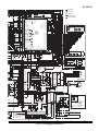
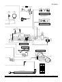
• NOTES ON SCHEMATIC DIAGRAM can be found on page 11.
7
8
9
10
Figure 13 SCHEMATIC DIAGRAM (2/2)
– 13 –
11
12
QT-CD250
SPEAKERS
R-CH
1 2 3 4 CNP101
R354
Q351
R351
R107
C107
C112 C108
C110R108
C119
R110
R102
R118
R120
C114
C118
C122
R116
R114
C106
R122
C116
R106
C352
R228
C233
C249
3
2
1
C237
C234
B
C
E
Q204
C851
R860
R850
R811
IC801
BI802
R802
BI801
R805
C804
R853
C839
C838
C835
C834
R820
IC803
R852
CNS801
1
20
Q802
C807
25
30
E
C
B
WH
GY
GY
GY
GY
GY
D804
R851
1
8
7
6
5
4
3
2
1
COR1
C821
R806
R828
C827
R827
C826
5
6
1
10
WH
WH
WH
WH
WH
WH
WH
BK
C806
C856
R865
R877
R845
D802
BI803
5
Q806
CNS802
1
2
3
4
5
16
15
L803
E C B
1
F
C842
BK
WH
WH
WH
WH
1
8
R801
C805
R875
LCD801
C843
1
2
3
1
C816
R804 C801
C817
R866
R861
R843
24
C820
R821
C870
R876
5
5
Q801 B C E
R824
C824
C823
10
C802
L807
R836
30 31
C865
SW810
CD LID
R812
R832
C833
R826
R870
OPEN/CLOSE
SW804
TUNER/
MEMORY
C864
20
C815
10
8
12
15
C830
R869
Q803
R888
R848
R849
C841
R868
R867
R893
R887
R886
R885
R884
R883
R882
R846
R807
C819
C829
C828
R871
17
16
C814
13
C863
51
50
5
C813
C818
C836
R830
R829
8180
85 75
90
70
65
95
60
5
10 IC802 55
15
45
20
40
25 35
100
1
R833
R831
C840
X801
R872
R892
R891
R890
R889
C848
R835
C847
R895
R894
1
C832
C822
R803
R834
COR801
1
C845
R864
R863
C837
C854
C872
R840
R897
R896
BK
SW802
STOP/TUNING
C844
R879
E
C825
C853
C846
R839
X802
R901
R900
R899 C862
R898
BK
C850 R854
R825
11
7
R837
C849
R878
12
3
2
1
B
C
E
R873
SW803
REPEAT/
BAND
15
14
4
POWER ON
CD
SW201
FUNCTION
SELECTOR
TUNER
SWITCH
PWB-A4
Q805
TAPE
OFF
R856
Q804
L801
D
R842
R844
A
D806
R862
R838
D
BK
TO
SP202
(R-CH)
(245)
R3
R1
C27
C2
TC1
R2
C1
C3
C14
15
10
C20
C71
R10
C15
C25
C24
C26
C22
CF4
C16
C72
R72
R16
R71
1 2 3
CF1
CF3
VD2
C23
BK
3 2 1
C34
Q1
B
C
E
T3
5
13 12
C19
CD CONTROL
PWB-A2
C12
C8
C53
L51
R18
C51
1
IC1
20
R20
C60
R52
C55
C52
X51
1
C59
22
D1
C33
24
R4
R12
C58
F1
1
2
3
C32
C7
C57
R53
20
1
R5
R14
L2
R17
5
15
R77
IC51
R59
C56
C18
11 12
10
R60
R61
R62
FW801
C6
L4
R15
R13
R55
R58
12
FW802
C13
C68
1
H
C5
C54
SW801
PLAY/PAUSE/
TUNIG UP
VD1
L1
R6
R54
R76
L3
AM BAR ANTENNA
R847
SW805
CUE/
PRESET UP
R8
C11
C61
G
11
C10
C21
Q2
SW806
DOWN/
REVIEW/
PRESE
20
VD3
R51
3
2
1
C29
R7
C9
BK
15
C73
C74
MAIN PWB-A1
• The numbers 1 to 17 are waveform numbers shown in page 16.
1
2
3
9
2
3
12
13
C75
10
R841
C202
E
C
B
R203
R205
R204
C852
Q205
C204
D801
E
C
B
D204
D205
B
C
E
C212
D803
C302
C227
R456
R455
11
D805
Q206
Q207
R201
D203
ZD201
D202 C203
R254
C206
R206
B C E
ZD202
C210
C220
C209
1 6
C222
4
5
6
C211
R202
C225
9
8
7
C238
14
R232
13
C221
R212
1
2
3
IC201
R211 C213
C219
12
11
10
R231
Q201
D201
C235
B
C
E
R230
C201
E
C
B
Q203
R253
R250
R214
C245
R74
R73
IC202
C207
R216
R215
ZD203
Q209
CNS801
1
R808
2
3
4
SW809
X-BASS
1
2
3
4
5
C216
6 R223
7 C246
8 R224
R225
C214
R457
R242
SW201
B
C
HPJ201
HEADPHONES
R227
C240
Q202
C247
R251
C208
Q211
C810
C226
R221
R210
R222
R218
C218
R220
C229
E C B
R458
C
CNP801
4
3
2
1
R809
C205
R353
C353
R126
C123
C230
R252
16
R209
C231
15
R217
R244
R247
C217 14
C244
12
E C B
R219
R240
R243
C215 13
C242
C243
11
R236
R239 R207
10
R234
R238
C241
9
C224
R235
R233
R237
C223
Q210 B C E
B C E
R241
Q212
1
2
3
R245
R248
R857
C232
E
C
B
R352
R249
R246
UN801
C354
C239
SW807
VOLUME
UP
H
IC101
CNP201
1 2 3
SW808
VOLUME
DOWN
L301
2 4 6 8 10 12
C120
R855
R213
B
C351
D
1 3 5 7 9 11
D102
R125
R124
G
R115
R117
CNS201
F
C121
3
R105
R119 D101
2
R123
1
C105
WH
BK
RD
R121
E
C109
R104
C
C111
R103
BK
B
C117
A
REC A
C115
R113
C113
R101
R109
PLAY
SW102
RECORD/
PLAYBACK
CNP602
SP202
C236
L-CH
SP201
4
Figure 14 WIRING OF P.W.BOARD (1/2)
– 14 –
5
6
QT-CD250
TAPE
ERASE HEAD
(240-5)
M601
TAPE MOTOR
(240-6)
(241)
(241)
WH
RD
BK
SW601
TAPE MAIN
(240-7)
RECORD/PLAYBACK
HEAD(240-4)
TERMINAL B PWB-A6
BK
BATTERYS
DC4.5V ["AA" SIZE(UM/SUM-3,
R6 or HP7)battery x 3]
CNS101
WH
1 BK
2
3 RD
4 BK
BR
YL
BK
(241)
BK
RD
TERMINAL A PWB-A5
(230)
(229)
T651
POWER
TRANSFORMER
BATTERYS
DC9 V [ "D" size(UM/SUM-1,
R20 or HP2) battery x 6 ]
OR
YL
C652
C653
YL
RD
D653
BK
OR
OR
OR
D652
C651
D654
D651
RD
1
2
3
RD
CNS602
SO651
AC INLET
SOCKET
AC 120V,
60Hz
C654
POWER PWB-A3
OR
OR
PICK UP UNIT
CD MOTOR PWB-B
+
M701
SLED MOTOR
5 4 3 2 1
CNP803
1
2
3
4
5
6
CNS803
1
2
3
4
5
6
F3895AF
M702
SPENDLE MOTOR
SW702
PICKUP IN
+
-
WH
GY
GY
GY
GY
GY
-
8 7 6 5 4 3 2 1
(233)
COLOR TABLE
BR
FM ROD ANTENNA(237)
7
8
9
BROWN
RD(R)
RED
OR
ORANGE
YL
YELLOW
GR
GREEN
BL
BLUE
VL
VIOLET
GY
GRAY
WH(W)
WHITE
BK
BLACK
PK
PINK
10
Figure 15 WIRING OF P.W.BOARD (2/2)
– 15 –
11
12
QT-CD250
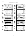
WAVEFORMS OF CD CIRCUIT
NO DISC FOCUS SEARCH
1
STOP
FO+
FO-
SEL
TRO
2
FMO
3
PLAY
CUE
6
1
TEI
1
TRO
2
FMO
3
IC802 64pin
SBAD
11
2
IC802 67pin
RFO
15
3
IC802 71pin
IC801 22pin
STOP
PLAY
REVIEW
6
1
FEI
TEI
1
TRO
2
FMO
3
IC802 64pin
IC802 62pin
RFGO
11
2
IC801 19pin
IC802 67pin
RFRP
15
3
IC801 17pin
IC802 71pin
STOP
TEI
PLAY
TCD-782 TNO-02 PLAYBACK
16
1
IC802 64pin
LO
1
RO
2
IC802 86pin
TRO
2
SBAD
3
IC802 67pin
7
1
IC802 71pin
IC802 63pin
11
15
3
FEI
6
TEI
IC802 67pin
IC802 62pin
10
11
2
STOP
9
PLAY
IC802 64pin
TEI
5
6
1
FEI
8
3
STOP
IC802 64pin
7
DMO
TOC IL
IC802 62pin
5
2
IC802 72pin
IC802 74pin
6
SBOK
14
3
FOCUS SEARCH
5
1
IC802 45pin
IC803 21pin
4
13
2
IC803 20pin
3
TMAX
IC802 50pin
IC802 66pin
2
12
1
FOO
PLAY
17
IC802 82pin
IC802 63pin
– 16 –
QT-CD250
TROUBLESHOOTING (CD SECTION)
When the CD does not function
When the CD section does not operate when the objective lens of the optical pickup is dirty, this section may not operate. Clean
the objective lens, and check the playback operation. When this section does not operate even after the above step is taken,check
the following items.
Remove the cabinet and follow the troubleshooting instructions.
"Track skipping and/or no TOC (Table Of Contents) may be caused by build up of dust other foreign matter on the laser pickup
lens. Before attempting any adjustment make certain that the lens is clean. If not, clean it as mentioned below."
Turn the power off.
Gently clean the lens with a lens cleaning tissue and a small amount of isopropyl alcohol.
Do not touch the lens with the bare hand.
Dust gradually accumulates on the objective lens during use, and it may degrade performance.
To avoid this problem, use a cleaning disc designed for CD optical pickup lenses.
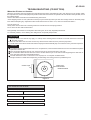
HOW TO USE
1. Using the brush in the cleaner cap, apply 1 or 2 drops of the cleaning fluid to the brush on the CD cleaner disc which has
the mark next to it.
2. Place the CD cleaner disc onto the CD disc tray with the brush side down, then press the play button.
3. You will hear music for about 20 seconds and the CD player will automatically stop. If it continues to turn, press the stop button.
CAUTION
The CD lens cleaner should be effective for 30 - 50 operations, however if the brushes become worn out earlier then please
replace the cleaner disc.
If the CD cleaner brushes become very wet then wipe off any excess fluid with a soft cloth.
Do not drink the cleaner fluid or allow it to come in contact with the eyes. In the event of this happening then drink and / or
rinse with clean water and seek medical advice.
The CD cleaner disc must not be used on car CD player or on computer CD ROM drives.
All rights reserved. Unauthorized duplicating, broadcasting and renting product is prohibited by law.
Cleaning Disc
PARTS CODE:
UDSKA0004AFZZ
Cleaner Liquid
Figure 17
• The CD function will not work.
The CD operating keys don't work.
Yes
Check the power supply, 16.93 MHz clock, and reset terminal.
Yes
Check the pickup-in switch (SW702) position.
Yes
Check the Focus system.
– 17 –
QT-CD250
• Laser failure.
Is +7.5V applied to the Collector of Q206 ?
Check the PWB pattern of Q206.
No
Yes
Is +5V applied to the collector of Q204 and Q806 ?
Check the PWB Patten of IC204 and Q806.
No
Yes
Is +5V applied to the pin 75 (VDD) and pin 96 (MVDD) of
IC802 ?
Yes
No
Check the PWB pattern between collector of Q806 and pin 75 of
IC802, and emiter of Q806 and Q804 and pin 96 of IC802.
No
Check the PWB pattern between collector of Q204 and pin 1 of
IC801.
No
Check the laser come on when pattern cut between pin 8 (SEL) of
IC801 and pin 74 (SEL) of IC802.
No
Check the peripheral parts of IC801 and Q801. If it is normal, the
optical pickup is faulty.
No
Check as stated in item "FOCUS SERVO SAWTOOTH WAVE
FAILURE".
Is +5V applied to the pin 1 (VCC) of IC801 ?
Yes
Is +0V applied to the pin 74 (SEL) of IC802 ?
Yes
Is approx. 1.8V applied to the collector of Q801.
Yes
Check BI801/CNS801. If it is normal, the optical pickup is
faulty.
• Focus failure.
Does the optical pickup move up and down when the disc is
removed?
Yes
Is the following waveform ouput at the pin 62 (FEI) of IC802
when the disc is set?
Check the periphery of IC801 and BI801/CNS801. Is it normal?
No
Yes
Yes
pin 62
The optical pickup is faulty.
(FEI)
pin 86
(FOO)
pin 63
(SBAD)
Is the waveform shown above input at the pin 63 (SBAD) of
IC802?
No
Yes
IC801 is faulty.
– 18 –
Check the pattern between pin 13 of IC801 and pin 63 of IC802.
Check the periphery of IC801 and BI801/CNS801.
QT-CD250
• Focus servo sawtooth wave failure.
Is sawtooh wave output to the pin 66 (FOO) of IC802 ?
No
IC802 is faulty.
Yes
1.5~2.5sec
Check the PWB pattern of IC803.
Is +7.5V applied to the pins 1 and 30 (VCC) of IC803 ?
No
Yes
Check the PWB pattern of IC803.
Is sawtooth wave obtained between pins 20 and 21 of IC803 ?
No
Yes
1.5~2.5sec
Is sawtooth wave obtained between pins 3 and 4 of BI801/
CNS801 ? (as shown above)
Check the PWB pattern between BI801/CNS801 and IC803.
No
Yes
BI801/CNS801 connection failure or optical pickup failure.
• Spindle motor clv servo failure.
Is following wave output to the pin 72 (DMO) of IC802 when
the Function is changed to "PLAY" from "STOP" ?
No
Check the procedure in "HF ERROR".
If OK. IC802 is faulty.
No
Check the PWB pattern between pin 72 (DMO) of IC802 and pins
5 and 6 of IC803. If OK. IC803 is faulty.
Yes
DMO
Is above wave obtained between pins 5 and 6 of IC803 ?
Yes
Is above wave obtained between pins 5 and 6 of BI803/
CNS803 ?
Check the PWB pattern between BI803/CNS803 and IC803.
No
Yes
BI803/CNS803 connection failure or optical pickup failure.
– 19 –
QT-CD250
• Track search failure
Does the sled motor run in FF/REW state when the CD
TEST MODE is set?
No
Check as stated in item "SLED MOTOR OPERATION FAILURE".
Yes
Is the following wave output to the pin 67 (TRO) of IC802
during track search in normal playback?
No
IC802 failure.
Yes
TRO
Is the following wave output to the pins 12 (TEO) of IC801
during track search in normal playback?
No
Yes
TEO
TEI
Check the PWB pattern between pin 67 (TRO) of IC802 and pin
28 of IC803.
Check the PWB pattern between pins 25 and 26 of IC803 and
Optical pickup.
If OK. Optical pickup failure.
TEZI
Is the above wave output to the pins 64 (TEI) and 65 (TEZI)
of IC802 during track serch in normal playback?
No
Check the PWB pattern between pin 12 (TEO) of IC801 and pins 64
(TEI) and 65 (TEZI) of IC802. If OK. IC801 failure.
No
Check the PWB pattern between pin 22 (RFO) and 18 (RFIS), 17
(RFRP) of IC801 and pins 60 and 61 of IC802. If OK. IC801 failure.
Yes
Is the following wave output to the pin 60 (RFZI) and 61
(RFRP) of IC802 during track search in normal playback?
Yes
RFRP
RFZI
Normal.
• Sled motor operation failure.
Is following sled feed signal output the pin 71 (FMO) of IC802
when FF/REW key is pressed after the CD TEST MODE is
seted?
Yes
FF
IC802 is faulty.
No
REW
FMO
Is following sled feed signal input the pins 12 and 13 of IC803
when FF/REW key is pressed after the CD TEST MODE is
seted?
FF
Yes
No
Check the PWB pattern between pin 71 of IC802 and pins 12 and
13 of IC803.
REW
SL ±
Is sled feed signal output the pins 10 and 11 of IC803?
No
Check the peripheral parts of IC803. If OK, IC803 is faulty.
Yes
Is sled feed voltage applied between both terminals of sled
motor?
Yes
No
Check the BI803/CNS803.
Check the CD mechanism (periphery of sled motor).
If the sled motor does not run when DC2.0V is applied to
both terminals of sled motor, the sled motor is faulty.
• Sled servo failure.
Is following sled signal output the pin 71 (FMO) of IC802
during playback?
IC802 is faulty.
No
Yes
FMO
Normal.
– 20 –
QT-CD250
FUNCTION TABLE OF IC
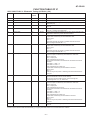
IC51 VHiLC72121/-1: Electronic Tuning (LC72121) (1/2)
Pin No.
Port Name
Terminal
Name
Input/Output
Function
1
Xtal
XIN
Output
Crystal oscillator connection.(4.5 MHz/7.2 MHz)
2
Ground
VSSX
Output
Ground terminal for the crystal oscillation circuit system of LC72121.
3
Chip enable
CE
Output
High level when inputting serial data (DI) to LC72121 or sending
serial data (DO).
4
Input data
DI
Input
5
Clock
CL
Output
Clock that synchronizes data when inputting serial data (DI) to
LC72121 or sending serial data (DO).
6
Output data
DO
Output
Output terminal that sends data from LC72121 to the controller. The
output data is defined by serial data DOC0-DOC2.
7*
Output port
BO1
Output
Output dedicated terminal.
Output state is defined by the serial data BO1-BO4.
Data 0: Open
Data 1: L
Time base signal (8 Hz) output is possible from BO1 terminal.
(When setting serial data TBC = 1.)
8-10
Output port
BO2-BO4
Output
Output dedicated terminal.
Output state is defined by the serial data BO1-BO4.
Data 0: Open
Data 1: L
Time base signal (8 Hz) output is possible from BO1 terminal.
(When setting serial data TBC = 1.)
11
Input/output port
IO1
12
IF counter
IF IN
13
Input/output port
IO2
14
Ground
VSSD
Input terminal for serial data that is transferred from the controller to
LC72121.
Input/Output Terminal for both input and output.
Input and output are defined by serial data IDC1 and IOC2.
Data 0: Input port
Data 1: Output port
When specified as the input port.
The input terminal state is transferred from the DO terminal to the
controller.
Input state "L": Data -> 0
Input state "H": Data -> 1
When specified as the output port.
Output state is defined by the serial data IO1 and IO2.
Data 0: Open
Data 1: L
When turning on the power or resetting, the terminal becomes the
input port.
Input
Input frequency is 0.4-12 MHz.
Signal is transferred to the IF counter directly.
The result is sent from M5B of the IF counter through DO.
4 measuring times: 4, 8, 32, and 64 ms
Input/Output Terminal for both input and output.
Input and output are defined by serial data IDC1 and IOC2.
Data 0: Input port
Data 1: Output port
When specified as the input port.
The input terminal state is transferred from the DO terminal to the
controller.
Input state "L": Data -> 0
Input state "H": Data -> 1
When specified as the output port.
Output state is defined by the serial data IO1 and IO2.
Data 0: Open
Data 1: L
When turning on the power or resetting, the terminal becomes the
input port.
—
Ground terminal for the digital system other than VSSA and VSSX of
LC72121.
In this unit, the terminal with asterisk mark (*) is (open) terminal which is not connected to the outside.
– 21 –
QT-CD250
IC51 VHiLC72121/-1: Electronic Tuning (LC72121) (2/2)
Pin No.
Terminal
Name
Port Name
Input/Output
Function
15
Local oscillation, Signal input
AMIN
Input
Serial data input: AMIN is selected when DVS = 0 is set.
When serial data input SNS = 1 is set:
Input frequency is 2-40 MHz.
Signal is sent to the swallow counter directly.
Dividing number to be set is 272- 65535. The actual dividing number
is the same as the setting value.
When serial data input SNS = 0 is set.
Input frequency is 0.5-10 MHz.
Signal is transferred to the 12-bit programmable divider directly.
Dividing number to be set is 4-4095. The actual dividing number is
the same as the setting value.
16
Local oscillation, Signal input
FMIN
Input
Serial data input: FMIN is selected when DVS = 1 is set.
Input frequency is 10-160 MHz.
Signal is transferred to the swallow counter through the built-in
prescaler (1/2).
Dividing number to be set is 272-65535. The actual dividing number
is twice as the setting value because there is a built-in prescaler(1/2).
17
Power supply
VDD
—
18
Charge pump output
PD
19
L.P.F. Amplifier transistor
AIN
20
L.P.F. Amplifier transistor
AOUT
Output
21
Ground
VSSA
—
22
Xtal
XOUT
Output
VSSx
2
XIN
1
XOUT
22
FMIN
16
AMIN
15
CE
3
DI
4
CL
5
DO
6
VDD
17
VSSd
14
Power supply terminal for LC72121 (VDD = 2.7-3.5 V).
Power on reset circuit works when POWER ON.
Output
Charge pump output terminal for PLL.
When the local oscillation signal frequency divided by N is higher
then the refernce frequency, "H" level is sent from the PD terminal.
When it is lower, "L" level is sent. When the frequencies are the
same, they become high impedance.
Input
L.P.F. Amplifier transistor
L.P.F. Amplifier transistor
Ground terminal for the low-pass filter MOS transistor of LC72121.
Crystal oscillator connection.(4.5 MHz/7.2 MHz)
PHASE DETECTOR
CHARCE PUMP
REFERENCE
DIVIDER
UNLOCK
DETECTOR
SWALLOW COUNTER
1/16, 1/17 4bits
1/2
18
PD
19
AIN
20
AOUT
21
VSSa
12
IFIN
12bits PROGRAMMABLE
DIVIDER
UNIVERSAL
COUNTER
DATA SHIFT REGISTER
LATCH
CCB
I/F
POWER
ON
RESET
7
8
9
10
BO1 BO2 BO3 BO4
11
13
IO1
IO2
Figure 22 BLOCK DIAGRAM OF IC
– 22 –
QT-CD250
IC1 VHiTA2104BN-1: FM /AM IF MPX. (TA2104BN)
FM RF OUT
24
FM RF AM RF IN FM OSC
23
22
21
AM OSC OSC OUT ST IND
20
19
18
AM
OSC
DET OUT MPX IN
17
FW
ST
FM
OSC
IFREQ
16
15
LPF1
LPF2
14
13
AF
IF
REQ
AF
BUFF
VCC
DECODE
DIYIDE
BUFF
IF
BUFF
LEVEL
DET
BUFF
1/8
AN
DET
FM
DET
ST/MO
FM/AM
AM
MIX
1
AGC
FM
MIX
FMRE
2
3
AM
RF GND FM RF ON
LOW OUT
4
MIX OUT
AMIF
5
6
Vcc
MUTE
FMIF
7
AM IF IN
8
FM IF IN
GND
9
10
11
12
AGC
QUAD
R-OUT
L-OUT
IC202 VHiTC9260P/-1: Electronic Volume (TC9260P)
L-ch
VOLUME
Vss
VDD
1
16
OUT
2
15 OUT
IN
3
14
IN
LD1
4
13
LD1
LD2
5
12
LD2
A-GND
6
CS
7
DATA DECODER, STB GENERATOR
10
STB
CK
8
SHIFT REGRATER (13bit)
9
DATA
L-ch
LATCH
R-ch
LATCH
11 A-GND
Figure 23 BLOCK DIAGRAM OF IC
– 23 –
R-ch
VOLUME
QT-CD250
IC802 VHiTC9457F2-1: Servo/Signal Control (TC9457F2) (1/4)
Pin No.
Port Name
1*
2
3
4
5
6*
7*
8*
9*
10*
11*
(OT5)S1
(OT6)S2
(OT7)S3
(OT8)S4
(OT9)S5
(OT10)S6
(OT11)S7
(OT12)S8
(OT13)S9
(OT14)S10
(CLCK/OT15)
S11
(DATA/OT16)
S12
(SFSY/OT17)
S13
(LRCK/OT18)
S14
(BCK/S15)
P8-0
(AOUT/S16)
P8-1
(MBOV/S17)
P8-2
(IPF/S18)
P8-3
12*
13*
14*
15
16
17
18
Input/Output
Function
SEG1
SEG2
SEG3
SEG4
SEG5
SEG6
SEG7
SEG8
SEG9
SEG10
SEG11
Terminal Name
Output
Output
Output
Output
Output
Output
Output
Output
Output
Output
Output
SEG12
Output
SEG13
Output
SEG14
Output
SEG15
Output
Segment signal output to the LCD panel.
Up to 72 segments in a matrix with COM1 to COM4 can be displayed.
All of the S1 to S18 pins can be switched for output ports by a program.
Also, the S15 to S18 pins each can be switched for I/O ports individually.
When set for I/O ports, these pins become Nch open-drain output.
Furthermore, the S11 to S14 and the P8-0 to P8-3 pins can be switched for
use as CD signal (CLCK to IPF) input/output pins by a program.
• CLCK: Subcodes P thru W data readout clock input/output.
Selected between input and output by a command.
• DATA: Subcodes P thru W data output.
• SFSY: Playback system frame sync signal output.
• LRCK: Channel clock (44.1kHz) output.
It outputs a low for L channel and a high for R channel.
Polarity can be inverted by a command.
• BCK : Bit clock (1.4122MHz) output.
• AOUT: Audio data output.
• MBOV: Buffer memory-over signal output.
It outputs a high when buffer overflows.
• IPF : Correction flag output. When AOUT is C2 correction output, it
outputs a high indicating that correction is impossible.
SEG16
Output
SEG17
Output
NC
Output
19
20
MVDD
MVSS
MVDD1
MVSS1
21*
22*
23
24
(K0)P1-0
(K1)P1-1
(K2)P1-2
(K3)P1-3
CD-FUNC
TUNER-FUNC
DOOR IN
PU IN
25
26
27
28
29
(DCREF)P3-0
(ADin1)P3-1
(ADin2)P3-2
(ADin3)P3-3
(BUZR/
ADin4)P4-0
CD POWER
KEY 1
KEY 2
ADIN 3
NC
Input/Output
Input/Output
Power supply pins.
Normally, apply a voltage of 4.5 to 5.5V to VDD.
In a backup state (when the CKSTP instruction executed), the device's
current consumption is reduced to 1µA or less, allowing for the supply
voltage to be lowered to 2.0V.
The device is reset and the program starts from address 0 when a voltage
of 2.7V or more is applied to this pin when it is at 0V (power-on reset).
Input
Input
Input
Input
4-bit CMOS I/O ports.
These ports can be set for input or output bit for bit by a program.
These pins can be pulled up to VDD or down to GND by program.
Therefore, they can be used as key input pins. Also, when they are set for
I/O port, a change of state in this input can be used to clear the clock stop
or wait mode.
Output
Input
Input
Input
Input
5-bit CMOS I/O ports.
These ports can be set for input or output bit for bit by a program.
The P3-0 to P4-0 pins serve dual purposes as analog inputs for the internal
6-bit 4-channel A/D converters.
The internal A/D converters can complete conversion in 6 instruction cycles
using a successive approximation method. The required pins can be set for
A/D analog input bit for bit by a program. P3-0 can be set for reference
voltage input, and the internal power supply (MVDD) can be used for this
reference voltage.
The P4-0 pin serves dual purposes as a buzzer output pin.
The buzzer output can be selected from 8 frequencies, 0.625 to 3kHz.
Each selected frequency can be output in one of four modes: continuous,
single, 10Hz intermittent, and 10Hz intermittent at 1Hz interval.
Whether or not to use and how to control the A/D converter and buzzer all
can be set by a prograam.
In this unit, the terminal with asterisk mark (*) is (open) terminal which is not connected to the outside.
– 24 –
QT-CD250
IC802 VHiTC9457F2-1: Servo/Signal Control (TC9457F2) (2/4)
Pin No.
Port Name
30
31*
(S12)P4-1
(SO/S11/
SDA)P4-2
(SCK/SCL)
P4-3
DI
DO
Input
Output
CL
Output
33
34
35
36
37
38
TEST0
TEST1
TEST2
TEST3
TEST4
TEST5
TEST0
TEST1
TEST2
TEST3
TEST4
TEST5
39*
40*
41*
42*
(OT19)/HSO
(OT20)SPCK
(OT21)SPDA
(OT22)COFS
CE_(PLL)
STB_(VOL)
P_MUTE
X-BASS
43*
DOUT
(N/C)
Input/Output
Digital output pin.
44*
SBSY
(N/C)
Input/Output
Subcode block sync output pin. It outputs a high at the S1 position when
subcode sync is detected.
45*
SBOK
(N/C)
Input/Output
Subcode Q data CRCC determination result output pin. It outputs a high
when CRCC check is found OK.
46
47
VDD
VSS
VDD1
VSS1
Input/Output
Input/Output
CD unit's digital block power supply pins.
Normally, apply 5V to VDD.
When not using a CD (CD off), this power supply can be turned off, with
only the controller power supply kept active, so that the contrller alone is
operating. In this case, the CD off bit must be set to 1. When this bit is set
to 1, pins 11 through 18 and pins 39 through 42 all are changed for output
ports if they have been set for CD control signal input/output pins.
48
P2VREF
P2VREF
Input/Output
PLL block-2 VREF pin.
49
PDO
PDO
Input/Output
This pin outputs a phase error between EFM and PLCK signals.
50
TMAX
TMAX
Input/Output
TMAX detection result output pin.
Selected by command bit TMPS.
Longer than preset period: Outputs P2VREF.
Shorter than preset period: Low level (Vss).
Within preset period: High impedance.
51
LPFN
LPFN
Input/Output
Inverted input of low-pass filter amp.
52
LPFO
LPFO
Input/Output
Output of low-pass filter amp.
53
PVREF
PVREF
Input/Output
PLL block VREF pin.
54
VCOF
VCOF
Input/Output
VCO filter pin.
55
AVSS
AVSS
Input/Output
Analog block ground pin.
56
SLCO
SLCO
Input/Output
DAC output pin for data slice level generation.
57
RFI
RFI
Input/Output
RF signal input pin.
58
AVDD
AVDD
Input/Output
Analog block power supply pin.
59
RFCT
RFCT
Input/Output
RFRP signal center level input pin.
60
RFZI
RFZI
Input/Output
RFRP zero-cross input pin.
61
RFRP
RFRP
Input/Output
RF ripple signal input pin.
62
FEI
FEI
Input/Output
Focus error signal input pin.
32*
Terminal Name
Input/Output
Input
Input
Input
Input
Input
Input
Output
Output
Output
Output
Function
3-bit CMOS I/O ports.
DI: Tuner Data Input pin.
DO: Tuner Data Output pin.
CL: Tuner/Volume Clock Output pin.
These ports can be set for input or output bit for bit by a program.
These pins serve dual purposes as input or output pins for the serial
interface circuit (SIO).
The SIO is a 2-wire/3-wire compatible serial interface. 4 or 8 bits of serial
data, beginning with the MSB or LSB, are serially output from the SO/SDA,
pin at each clock edge on the SCK/SCL pin, and the data on S11 or S12
pin is serially input to the device.
The serial clock (SCK/SCL) allows selection between the internal (450/225/
150/75 kHz) and external sources and a selection of the active edge, rise or
fall. Moreover, since the clock and data can be output via Nch open-drain
outputs, variouts, device controls and communication between controllers
can be greatly facilitated.
When an SIO interrupt is enabled, an interrupt is generated at completion
of SIO execution and the program jumps to address 4.
All inputs to SIO contain a Schmitt trigger circuit.
Test mode control input pins.
The test mode is selected when these pins are set high and normal
operation is selected when they are low.
CE_(PLL): Tuner Chip Enable Input pin.
STB_(VOL): Volume Storobe Input pin.
P_MUTE: MUTE ON/OFF Output pin.
X-BASS: X-BASS ON/OFF Output pin.
In this unit, the terminal with asterisk mark (*) is (open) terminal which is not connected to the outside.
– 25 –
QT-CD250
IC802 VHiTC9457F2-1: Servo/Signal Control (TC9457F2) (3/4)
Pin No.
Port Name
63
SBAD
SBAD
Terminal Name
Input/Output
Input/Output
Subbeam add signal input pin.
64
TEI
TEI
Input/Output
Tracking error input pin.
This input is read when tracking servo is on.
65
TEZI
TEZI
Input/Output
Tracking error zero-cross input pin.
66
FOO
FOO
Input/Output
Focus equalizer output pin.
67
TRO
TRO
Input/Output
Tracking equalizer output pin.
68
VREF
VREF
Input/Output
Analog reference power supply pin.
69
RFGC
RFGC
Input/Output
RF amplitude adjusting control signal output pin. It outputs 3-level PWM
signals. (PWM carrier = 88.2kHz)
70
TEBC
TEBC
Input/Output
Tracking balance control signal output pin. It outputs 3-level PWM signals.
(PWM carrier = 88.2kHz)
71
FMO
FMO
Input/Output
Focus equalizer output pin. It outputs 3-level PWM signals.
(PWM carrier = 88.2kHz)
72
DMO
DMO
Input/Output
Disc equalizer output pin. It outputs 3-level PWM signals.
(PWM carrier = DSP block 88.2kHz, synchronized to PXO)
73
2VREF
2VREF
Input/Output
Analog reference power supply pin. (2 x VREF)
74
SEL
SEL
Input/Output
APC circuit on/off signal output pin.
When laser is on, this pin goes to a high-impedance state when UHS = low
and outputs a high when UHS = high
75
76
VDD
VDD
VDD2
VSS2
Input/Output
Input/Output
CD unit's digital block power supply pins.
Normally, apply 5V to VDD.
When not using a CD (CD off), this power supply can be turned off, with
only the controller power supply kept active, so that the contrller alone is
operating. In this case, the CD off bit must be set to 1. When this bit is set
to 1, pins 11 through 18 and pins 39 through 42 all are changed for output
ports if they have been set for CD control signal input/output pins.
77
XVSS
XVSS
Input/Output
CD's crystal oscillator power supply pins.
Normally, connect these pins to the power supply lines that are used in
common for the VDD and VSS pins.
78
79
XI
XO
XI
XO
Input/Output
Input/Output
CD's crystal oscillator input/output pins.
Normally, connect 16.934MHz here. This clock is used as the system clock
for the CD. After a system reset, it also is used as the system clock on the
controller side.
80
XVDD
XVDD
Input/Output
CD's crystal oscillator input/output pins.
Normally, connect these pins to the power supply lines that are used in
common for the VDD and VSS pins.
81
DVSR
DVSR
Input/Output
R-channel D/A converter unit ground pin.
82
RO
RO
Input/Output
R-channel data forward output pin.
83
DVRR
DVRR
Input/Output
R-channel reference voltage pin.
84
DVDD
DVDD
Input/Output
D/A converter unit power supply pin.
85
DVRL
DVRL
Input/Output
L-channel reference voltage pin.
86
LO
LO
Input/Output
L-channel data forward output pin.
87
DVSL
DVSL
Input/Output
L-channel D/A converter unit ground pin.
88
89*
NC
NC/VPP
NC
NC
Input/Output
Input/Output
NC pins. Normally, connect these pins to ground or leave them open.
90
/RST
RESET
Input
Function
Device's system reset signal input pin.
The device remains reset while RESET is held low and when RESET is
released back high, the CD unit becomes operational and the program
starts from address 0. Normally, a system reset is asserted when a voltage
of 2.7V or more is applied to VDD when it is at 0V (power-on reset).
Therefore, this pin must be pulled high when used for this purpose.
In this unit, the terminal with asterisk mark (*) is (open) terminal which is not connected to the outside.
– 26 –
QT-CD250
IC802 VHiTC9457F2-1: Servo/Signal Control (TC9457F2) (4/4)
Pin No.
Port Name
91
/HOLD
92
Terminal Name
Input/Output
Function
HOLD
Input
This pin is used to input a signal that requests or clears the hold mode.
Normally, use this pin for CD mode select signal input or battery detection
signal input.
There are two hold modes: clock stop mode (crystal oscillator turned off)
and a wait mode (CPU stopped). These modes are entered by executing
the CKSTP and WAIT instructions, respectively.
The clock stop mode can be requested by a programmed input: low level
detection on HOLD pin or forced execution, and can be cleared by
detecting a high on the HOLD pin or a change of state in its input signal.
When the CKSTP instruction is executed, the clock generator and the CPU
stop operating and the device is placed in a memory backup state. During
this state, the device's current consumption is reduced to 1µA or less.
At the same time, the display output and CMOS output ports are
automatically set low, and the Nch open-drain outputs are turned off.
The wait mode is executed regardles of the input state on the HOLD pin,
with the device's current consumption reduced.
This mode is cleared by a change of state in the HOLD input.
INTR
REMO-IN
Input
External interrupt input pin.
When the interrupt facility is enabled and a pulse of 1.11 to 2.22µs in
duration is applied to this pin, an interrupt is generated and the program
jumps to address 1. Input logic and the active edge (rise or fall) can be
selected for each interrupt input.
Also, the internal 8-bit time clock can be chosen for this interrupt input, in
which case it is possible to count pulses or generate an interrupt at a given
pulse count (address 3).
93*
94*
MXO
MXI
MXO
MXI
Input/Output
Input/Output
Crystal oscillator pins for the controller.
The oscillator clock is used as the timebase for the clock facility or as the
controller's system clock. Connect a 4.5MHz or 75kHz crystal resonator to
the MXO and MXI pins. Since these pins do not contain internal feedback
resistors, etc, an amp resistor or output resistor must be added external to
the chip.
When using the clock generated by the CD unit's crystal oscillator for
clocking the entire device operation, fix the MXI pin to the GND level.
Oscillation is stopped by executing a CKSTP instruction.
Select the crystal oscillator and control its operation by a program.
95
96
MVSS
MVDD
MVSS
MVDD
Input/Output
Input/Output
Power supply pins.
Normally, apply a voltage of 4.5 to 5.5V to VDD.
In a backup state (when the CKSTP instruction executed), the device's
current consumption is reduced to 1µA or less, allowing for the supply
voltage to be lowered to 2.0V.
The device is reset and the program starts from address 0 when a voltage
of 2.7V or more is applied to this pin when it is at 0V (power-on reset).
97
98
99
100
OT1
OT2
OT3
OT4
COM1
COM2
COM3
COM4
Output
Output
Output
Output
Common signal outputs to the LCD panel.
Up to 72 segments in a matrix with S1 to S18 can be displayed.
Three voltage levels MVDD, VEE (1/2 MVDD), and GND are output for
83Hz period at 2ms intervals.
After a system reset and after deassertion of a clock stop instruction, the
VEE voltage is output and the DISP OFF bit is set to 0 before common
signals are output.
In this unit, the terminal with asterisk mark (*) is (open) terminal which is not connected to the outside.
– 27 –
QT-CD250
—MEMO—
– 28 –
QT-CD250
PARTS GUIDE
MODEL
QT-CD250
“HOW TO ORDER REPLACEMENT PARTS”
To have your order filled promptly and correctly, please furnish the
following information.
1. MODEL NUMBER
2. REF. No.
3. PART NO.
4. DESCRIPTION
For U.S.A. only
Contact your nearest SHARP Parts Distributor to order.
For location of SHARP Parts Distributor,
Please call Toll-Free;
1-800-BE-SHARP
MARK: SPARE PARTS-DELIVERY SECTION
Explanation of capacitors/resistors parts codes
Capacitors
Resistors
VCC ....................... Ceramic type
VCK ........................ Ceramic type
VCT ........................ Semiconductor type
VC • • MF ............... Cylindrical type (without lead wire)
VC • • MN ............... Cylindrical type (without lead wire)
VC • • TV ................ Square type (without lead wire)
VC • • TQ ............... Square type (without lead wire)
VC • • CY ............... Square type (without lead wire)
VC • • CZ ............... Square type (without lead wire)
VC • • • • • • • • • J .. The 13th character represents capacity difference.
("J" ±5%, "K" ±10%, "M" ±20%, "N" ±30%,
"C" ±0.25 pF, "D" ±0.5 pF, "Z" +80-20%.)
VRD ....................... Carbon-film type
VRS ........................ Carbon-film type
VRN ....................... Metal-film type
VR • • MF ............... Cylindrical type (without lead wire)
VR • • MN ............... Cylindrical type (without lead wire)
VR • • TV ................ Square type (without lead wire)
VR • • TQ ............... Square type (without lead wire)
VR • • CY ............... Square type (without lead wire)
VR • • CZ ............... Square type (without lead wire)
VR • • • • • • • • • J .. The 13th character represents error.
("J" ±5%, "F" ±1%, "D" ±0.5%.)
If there are no indications for the electrolytic capacitors, error is ±20%.
If there are no indications for other parts, the resistors are ±5%
carbon-film type.
NOTE:
Parts marked with “
” are important for maintaining the safety of the set.
Be sure to replace parts with specified ones for maintaining the safety and performance of the set.
QT-CD250
NO.
PRICE
RANK
PARTS CODE
DESCRIPTION
X801
X802
INTEGRATED CIRCUITS
IC1
IC51
IC101
VHITA2104BN-1
VHILC72121/-1
VHIBA3311L/-1
J
J
J
IC201
IC202
IC801
IC802
IC803
VHITA8227P/-1
VHITC9260P/-1
VHITA2109F/-1
VHITC9457F2-1
VHILA6541D/-1
J
J
J
J
J
AQ FM/AM IF MPX.,TA2104BN
AN Electronic Tuning,LC72121
AK REC./P.B.Equalizer Amp.,
BA3311L
AH Power Amp.,TA8227P
AN Electronic Volume,TC9260P
AL Servo Pre Amp.,TA2109F
AZ Servo/Signal Control,TC9457F2
AW Focus/Tracking/Spin/Sled Driver,
LA6541D
TRANSISTORS
Q1
Q2
Q201,202
Q203
Q204
Q205
Q206
Q207
Q209~212
Q351
Q801
Q802
Q803
Q804
Q805
Q806
VSKTC3199GR-1
VSKRA102M//-1
VSKTC3199GR-1
VSKTA1266GR-1
VSKTA1273Y/-1
VSKTC3199GR-1
VSKTA1046Y/-1
VSKTC3199GR-1
VSKTC3199GR-1
VSKTC3199GR-1
VSKTA1266GR-1
VSKTA1273Y/-1
VSKRC107M//-1
VSKTA1266GR-1
VSKRC107M//-1
VSKTA1273Y/-1
J
J
J
J
J
J
J
J
J
J
J
J
J
J
J
J
AB
AC
AB
AB
AE
AB
AC
AB
AB
AB
AB
AE
AC
AB
AC
AE
Silicon,NPN,KTC3199 GR
Digital,PNP,KRA102 M
Silicon,NPN,KTC3199 GR
Silicon,PNP,KTA1266 GR
Silicon,PNP,KTA1273 Y
Silicon,NPN,KTC3199 GR
Sillicon,PNP,KTA1046 Y
Silicon,NPN,KTC3199 GR
Silicon,NPN,KTC3199 GR
Silicon,NPN,KTC3199 GR
Silicon,PNP,KTA1266 GR
Silicon,PNP,KTA1273 Y
Digital,NPN,KRC107 M
Silicon,PNP,KTA1266 GR
Digital,NPN,KRC107 M
Silicon,PNP,KTA1273 Y
VHD1N4148//-1
VHD1N4148//-1
VHD1N4148//-1
VHD1N4004//-1
VHD1N4148//-1
VHCKV1370NT-1
VHCKV1520NT-1
VHEDZ5R1BSB-1
VHEDZ7R5BSB-1
VHEDZ2R4BSB-1
J
J
J
J
J
J
J
J
J
J
AA
AA
AA
AB
AA
AG
AK
AC
AB
AB
Silicon,1N4148
Silicon,1N4148
Silicon,1N4148
Silicon,1N4004
Silicon,1N4148
Variable Capacitance,KV1370NT
Variable Capacitance,KV1520NT
Zener,5.1V,DZ5.1BSB
Zener,7.5V,DZ7.5BSB
Zener,2.4V,DZ2.4BSB
RFILF0006SJZZ
RFILA0003SJZZ
RFILF0005SJZZ
RFILR0001SJZZ
J
J
J
J
AE
AF
AF
AD
FM IF
AM IF
FM Detection
FM Band Pass Filter
RCILI0008SJZZ
RTRNP0036SJZZ
J
J
AC AM IF
AQ Power
RCORF0005SJZZ
RCORF0005SJZZ
RCILR0004SJZZ
RCILB0015SJZZ
RCILA0011SJZZ
RCILB0014SJZZ
VP-DH101K0000
RCILB0003SJZZ
VP-DH221K0000
VP-DH221K0000
VP-DHR82K0000
J
J
J
J
J
J
J
J
J
J
J
AB
AB
AE
AC
AC
AC
AB
AD
AB
AB
AE
J
AG Trimmer
J
AL
DIODES
D1
D101,102
D201~205
D651~654
D801~806
VD1,2
VD3
ZD201
ZD202
ZD203
FILTERS
CF1
CF3
CF4
F1
TRANSFORMERS
!
T3
T651
COILS
COR1
COR801
L1
L2
L3
L4
L51
L301
L801
L803
L807
Core
Core
FM RF
FM Oscillation
AM Bar Antenna
AM Oscillation
100 µH,Choke
Bias Oscillation
220 µH,Choke
220 µH,Choke
0.82 µH,Choke
VARIABLE CAPACITOR
TC1
RTO-H1003SJZZ
VIBRATORS
X51
RCRSP0003SJZZ
NO.
Crystal,4.5 MHz
PRICE
RANK
PARTS CODE
RCRM-0002SJZZ
RCRM-0003SJZZ
DESCRIPTION
J
J
AE Ceramic,16.93 MHz
AK Ceramic,4.19 MHz
J
J
J
J
J
J
J
J
J
J
J
J
J
J
J
J
J
J
J
J
J
J
J
J
J
J
J
J
J
J
J
J
J
J
J
J
J
J
J
J
J
J
J
J
J
J
J
J
J
J
J
J
J
J
J
J
J
J
J
J
J
J
J
J
J
J
J
J
J
J
J
J
J
J
J
J
AA
AA
AA
AA
AA
AA
AA
AA
AA
AB
AA
AA
AB
AB
AA
AB
AA
AB
AB
AB
AB
AA
AB
AA
AA
AA
AA
AA
AA
AB
AA
AB
AA
AA
AA
AA
AB
AA
AB
AB
AA
AB
AA
AA
AA
AB
AB
AB
AB
AB
AA
AB
AB
AB
AA
AA
AB
AC
AA
AA
AA
AA
AB
AB
AB
AB
AA
AB
AB
AA
AF
AB
AC
AB
AB
AB
CAPACITORS
C1
C2
C3
C5
C6
C7,8
C9
C10
C11
C12
C13
C14
C15
C16
C18
C19
C20
C21
C22
C23
C24
C25
C26
C27
C29
C32
C33,34
C51
C52
C53
C54
C55
C56
C57,58
C59
C60
C61
C68
C71,72
C73,74
C75
C105,106
C107,108
C109,110
C111,112
C113,114
C115,116
C117,118
C119
C120
C121,122
C123
C201
C202
C203
C204
C205,206
C207
C208
C209
C210
C211,212
C213,214
C215,216
C217,218
C219,220
C221,222
C223,224
C225
C226
C227
C229~232
C233,234
C235~238
C239,240
C241,242
–1–
VCCCPA1HH150J
VCKYPA1HB102K
VCKZPA1HF103Z
VCKYTV1EF104Z
VCCCPA1HH220J
VCKYPA1HB102K
VCKZPA1HF223Z
VCCUPA1HJ8R0D
VCCSPA1HL361J
RC-GZA105AF1H
RC-GZA474AF1H
VCKZPA1HF473Z
RC-GZA227AF1A
RC-GZA475AF1H
VCKYTV1HB102K
RC-GZA225AF1H
VCKYPA1HB331K
RC-GZA106AF1C
RC-GZA105AF1H
RC-GZA106AF1C
VCTYPA1CU104M
VCKZPA1HF473Z
VCTYPA1CU104M
VCKYPA1HB102K
VCKYPA1HB101K
VCKYTV1EF104Z
VCKYTV1HB221K
VCCCPA1HH150J
VCCCPA1HH120J
RC-GZA107AF1A
VCKZPA1HF223Z
RC-GZA225AF1H
VCKZPA1HF223Z
VCKYTV1HB101K
VCKZPA1HF103Z
VCKYPA1HB222K
RC-GZA107AF1A
VCKYTV1HB221K
VCQYKA1HM223K
RC-GZA105AF1H
VCKYPA1HB101K
VCKYPA1HB182K
VCKYPA1HB821K
VCKYPA1HB271K
VCKYPA1HB331K
RC-GZA476AF1C
VCQYKA1HM183K
RC-GZA106AF1C
RC-GZA225AF1H
RC-GZA476AF1C
VCKZPA1HF103Z
RC-GZA227AF1A
RC-GZA107AF1C
RC-GZA476AF1C
VCKZPA1HF103Z
VCKZPA1HF223Z
RC-GZA476AF1C
RC-GZA477AF1A
VCKZPA1HF223Z
VCKZPA1HF103Z
VCKZPA1HF223Z
VCKZPA1HF473Z
RC-GZA105AF1H
VCQYKA1HM104K
VCQYKA1HM152K
RC-GZA105AF1H
VCKYPA1HB102K
RC-GZA104AF1H
RC-GZA107AF1A
VCKZPA1HF223Z
RC-GZW478AF1C
RC-GZA105AF1H
RC-GZA477AF1A
RC-GZA107AF1A
VCQYKA1HM104K
RC-GZA105AF1H
15 pF (CH),50V
0.001 µF,50V
0.01 µF,50V
0.1 µF,25V
22 pF (CH),50V
0.001 µF,50V
0.022 µF,50V
8 pF,50V
360 pF,50V
1 µF,50V,Electrolytic
0.47 µF,50V,Electrolytic
0.047 µF,50V
220 µF,10V,Electrolytic
4.7 µF,50V,Electrolytic
0.001 µF,50V
2.2 µF,50V,Electrolytic
330 pF,50V
10 µF,16V,Electrolytic
1 µF,50V,Electrolytic
10 µF,16V,Electrolytic
0.1 µF,16V
0.047 µF,50V
0.1 µF,16V
0.001 µF,50V
100 pF,50V
0.1 µF,25V
220 pF,50V
15 pF (CH),50V
12 pF (CH),50V
100 µF,10V,Electrolytic
0.022 µF,50V
2.2 µF,50V,Electrolytic
0.022 µF,50V
100 pF,50V
0.01 µF,50V
0.0022 µF,50V
100 µF,10V,Electrolytic
220 pF,50V
0.022 µF,50V,Mylar
1 µF,50V,Electrolytic
100 pF,50V
0.0018µF,50V
820 pF,50V
270 pF,50V
330 pF,50V
47 µF,16V,Electrolytic
0.018 µF,50V,Mylar
10 µF,16V,Electrolytic
2.2 µF,50V,Electrolytic
47 µF,16V,Electrolytic
0.01 µF,50V
220 µF,10V,Electrolytic
100 µF,16V,Electrolytic
47 µF,16V,Electrolytic
0.01 µF,50V
0.022 µF,50V
47 µF,16V,Electrolytic
470 µF,10V,Electrolytic
0.022 µF,50V
0.01 µF,50V
0.022 µF,50V
0.047 µF,50V
1 µF,50V,Electrolytic
0.1 µF,50V,Mylar
0.0015 µF,50V,Mylar
1 µF,50V,Electrolytic
0.001 µF,50V
0.1 µF,50V,Electrolytic
100 µF,10V,Electrolytic
0.022 µF,50V
4700 µF,16V,Electrolytic
1 µF,50V,Electrolytic
470 µF,10V,Electrolytic
100 µF,10V,Electrolytic
0.1 µF,50V,Mylar
1 µF,50V,Electrolytic
QT-CD250
NO.
C243,244
C245
C246
C247
C249
C302
C351
C352
C353
C354
C651~654
C801
C802
C804
C805
C806
C807
C810
C813
C814
C815
C816
C817
C818
C819,820
C821
C822
C823
C824,825
C826
C827
C828
C829
C830
C832
C833
C834,835
C836~839
C840
C841,842
C843
C844
C845
C846
C847,848
C849,850
C851,852
C853
C854
C856
C862
C863
C864
C865
C870
C872
PRICE
RANK
PARTS CODE
VCKYPA1HB331K
RC-GZA105AF1H
RC-GZA106AF1C
RC-GZA227AF1A
VCKYPA1HB101K
VCKZPA1HF223Z
VCQYKA1HM222K
RC-GZA107AF1A
VCQYKA1HM562K
VCQYKA1HM223K
VCKZPA1HF223Z
VCKZPA1HF103Z
VCKZPA1HF223Z
VCCCPA1HH2R0C
VCKYTV1EF223Z
RC-GZA337AF1A
VCKZPA1HF473Z
RC-GZA106AF1C
RC-GZA476AF1C
VCKZPA1HF473Z
RC-GZA476AF1C
VCKZPA1HF223Z
RC-GZA107AF1A
VCCSPA1HL560J
VCQYKA1HM104K
RC-GZA107AF1A
VCKZPA1HF473Z
VCKYTV1EF223Z
RC-GZA476AF1C
VCCSPA1HL470J
VCQYKA1HM153K
VCKYPA1HB272K
VCKYPA1HB472K
VCQYKA1HM103K
RC-GZA476AF1C
VCQYKA1HM333K
VCKYPA1HB471K
VCQYKA1HM473K
VCKYTV1EF104Z
VCKZPA1HF473Z
RC-GZA476AF1C
RC-GZA107AF1A
VCKZPA1HF473Z
RC-GZA105AF1H
RC-GZA226AF1C
VCKYPA1HB222K
RC-GZA335AF1H
VCKZPA1HF223Z
VCKYPA1HB682K
VCKYPA1HB101K
VCKYTV1EF104Z
RC-GZA476AF1C
VCKYTV1EF104Z
RC-GZA107AF1A
VCKYTV1HB101K
VCKYTV1HB472K
DESCRIPTION
J
J
J
J
J
J
J
J
J
J
J
J
J
J
J
J
J
J
J
J
J
J
J
J
J
J
J
J
J
J
J
J
J
J
J
J
J
J
J
J
J
J
J
J
J
J
J
J
J
J
J
J
J
J
J
J
AA
AB
AB
AB
AA
AA
AA
AB
AA
AB
AA
AA
AA
AA
AA
AB
AA
AB
AB
AA
AB
AA
AB
AA
AB
AB
AA
AA
AB
AA
AB
AA
AB
AA
AB
AB
AA
AB
AA
AA
AB
AB
AA
AB
AB
AA
AB
AA
AB
AA
AA
AB
AA
AB
AA
AA
330 pF,50V
1 µF,50V,Electrolytic
10 µF,16V,Electrolytic
220 µF,10V,Electrolytic
100 pF,50V
0.022 µF,50V
0.0022 µF,50V,Mylar
100 µF,10V,Electrolytic
0.0056 µF,50V,Mylar
0.022 µF,50V,Mylar
0.022 µF,50V
0.01 µF,50V
0.022 µF,50V
2 pF (CH),50V
0.022 µF,25V
330 µF,10V,Electrolytic
0.047 µF,50V
10 µF,16V,Electrolytic
47 µF,16V,Electrolytic
0.047 µF,50V
47 µF,16V,Electrolytic
0.022 µF,50V
100 µF,10V,Electrolytic
56 pF,50V
0.1 µF,50V,Mylar
100 µF,10V,Electrolytic
0.047 µF,50V
0.022 µF,25V
47 µF,16V,Electrolytic
47 pF,50V
0.015 µF,50V,Mylar
0.0027 µF,50V
0.0047 µF,50V
0.01 µF,50V,Mylar
47 µF,16V,Electrolytic
0.033 µF,50V,Mylar
470 pF,50V
0.047 µF,50V,Mylar
0.1 µF,25V
0.047 µF,50V
47 µF,16V,Electrolytic
100 µF,10V,Electrolytic
0.047 µF,50V
1 µF,50V,Electrolytic
22 µF,16V,Electrolytic
0.0022 µF,50V
3.3 µF,50V,Electrolytic
0.022 µF,50V
0.0068 µF,50V
100 pF,50V
0.1 µF,25V
47 µF,16V,Electrolytic
0.1 µF,25V
100 µF,10V,Electrolytic
100 pF,50V
0.0047 µF,50V
J
J
J
J
J
J
J
J
J
J
J
J
J
J
J
J
J
J
J
J
J
J
AA
AA
AA
AA
AA
AA
AA
AA
AA
AA
AA
AA
AA
AA
AA
AA
AA
AA
AA
AA
AA
AA
3.3 kohms,1/6W
100 kohm,1/6W
10 ohm,1/6W
22 kohms,1/6W
15 kohms,1/6W
10 kohm,1/6W
220 kohms,1/6W
330 ohms,1/6W
10 ohm,1/6W
10 kohm,1/6W
2.2 kohms,1/10W
39 kohms,1/6W
3.3 kohms,1/6W
47 kohms,1/6W
100 ohm,1/6W
470 ohms,1/10W
150 ohms,1/6W
2.2 kohms,1/6W
4.7 kohms,1/6W
10 kohm,1/6W
56 kohms,1/6W
1 kohm,1/6W
NO.
R71,72
R73,74
R76
R77
R101,102
R103,104
R105,106
R107,108
R109,110
R113,114
R115~118
R119,120
R121,122
R123,124
R125
R126
R201
R202
R203
R204
R205
R206,207
R209,210
R211,212
R213
R214~216
R217,218
R219,220
R221~224
R225
R227,228
R230
R231,232
R233,234
R235,236
R237,238
R239,240
R241,242
R243,244
R245,246
R247,248
R249
R250
R251,252
R253
R351
R352
R353
R354
R455,456
R457,458
R801
R802
R803
R804
R805
R806
R807
R808
R811
R812
R820
R821
R824,825
R826
R827
R828
R829
R830
R831~834
R835,836
R837,838
R839
R840
R841
R842
R843
R844,845
R846
R847
R848
R849
RESISTORS
R1
R2,3
R4
R5
R6
R7
R8
R10
R12
R13
R14
R15
R16
R17
R18
R20
R51
R52
R53
R54
R55
R58~62
VRD-ST2CD332J
VRD-ST2CD104J
VRD-ST2CD100J
VRD-ST2CD223J
VRD-ST2CD153J
VRD-ST2CD103J
VRD-ST2CD224J
VRD-ST2CD331J
VRD-ST2CD100J
VRD-ST2CD103J
VRS-TV2AB222J
VRD-ST2CD393J
VRD-ST2CD332J
VRD-ST2CD473J
VRD-ST2CD101J
VRS-TV2AB471J
VRD-ST2CD151J
VRD-ST2CD222J
VRD-ST2CD472J
VRD-ST2CD103J
VRD-ST2CD563J
VRD-ST2CD102J
–2–
PRICE
RANK
PARTS CODE
VRD-ST2CD472J
VRD-ST2CD332J
VRD-ST2CD821J
VRS-TV2AB332J
VRD-ST2CD331J
VRD-ST2CD123J
VRD-ST2CD153J
VRD-ST2CD102J
VRD-ST2CD121J
VRD-ST2CD822J
VRD-ST2CD392J
VRD-ST2CD332J
VRD-ST2CD272J
VRD-ST2CD332J
VRD-ST2CD684J
VRD-ST2CD101J
VRD-ST2CD122J
VRD-ST2CD103J
VRD-ST2CD271J
VRD-ST2CD222J
VRD-ST2CD472J
VRD-ST2CD561J
VRD-ST2CD102J
VRD-ST2CD473J
VRD-ST2CD101J
VRD-ST2CD102J
VRD-ST2CD822J
VRD-ST2CD224J
VRD-ST2CD472J
VRD-ST2CD104J
VRD-ST2CD121J
VRD-ST2EE2R7J
VRD-ST2CD121J
VRD-ST2CD222J
VRD-ST2CD473J
VRD-ST2CD272J
VRD-ST2CD222J
VRD-ST2CD103J
VRD-ST2CD564J
VRD-ST2CD562J
VRD-ST2CD561J
VRD-ST2CD221J
VRD-ST2CD474J
VRD-ST2CD223J
VRD-ST2CD392J
VRD-ST2CD101J
VRD-ST2CD151J
VRD-ST2CD333J
VRD-ST2CD4R7J
VRD-ST2CD153J
VRD-ST2CD102J
VRD-ST2EE220J
VRD-ST2CD222J
VRD-ST2CD823J
VRD-ST2CD683J
VRD-ST2CD393J
VRD-ST2CD272J
VRD-ST2CD102J
VRD-ST2CD101J
VRD-ST2CD223J
VRD-ST2CD102J
VRD-ST2CD473J
VRS-TV2AB102J
VRD-ST2CD103J
VRD-ST2CD224J
VRD-ST2CD153J
VRD-ST2CD103J
VRD-ST2CD332J
VRD-ST2CD103J
VRD-ST2CD332J
VRD-ST2CD271J
VRD-ST2CD103J
VRD-ST2CD473J
VRD-ST2EE100J
VRD-ST2CD562J
VRD-ST2CD223J
VRD-ST2CD472J
VRD-ST2CD223J
VRD-ST2CD472J
VRD-ST2CD562J
VRD-ST2CD103J
VRD-ST2CD183J
J
J
J
J
J
J
J
J
J
J
J
J
J
J
J
J
J
J
J
J
J
J
J
J
J
J
J
J
J
J
J
J
J
J
J
J
J
J
J
J
J
J
J
J
J
J
J
J
J
J
J
J
J
J
J
J
J
J
J
J
J
J
J
J
J
J
J
J
J
J
J
J
J
J
J
J
J
J
J
J
J
J
AA
AA
AA
AA
AA
AA
AA
AA
AA
AA
AA
AA
AA
AA
AA
AA
AA
AA
AA
AA
AA
AA
AA
AA
AA
AA
AA
AA
AA
AA
AA
AA
AA
AA
AA
AA
AA
AA
AA
AA
AA
AA
AA
AA
AA
AA
AA
AA
AA
AA
AA
AA
AA
AA
AA
AA
AA
AA
AA
AA
AA
AA
AA
AA
AA
AA
AA
AA
AA
AA
AA
AA
AA
AA
AA
AA
AA
AA
AA
AA
AA
AA
DESCRIPTION
4.7 kohms,1/6W
3.3 kohms,1/6W
820 ohms,1/6W
3.3 kohms,1/10W
330 ohms,1/6W
12 kohms,1/6W
15 kohms,1/6W
1 kohm,1/6W
120 ohms,1/6W
8.2 kohms,1/6W
3.9 kohms,1/6W
3.3 kohms,1/6W
2.7 kohms,1/6W
3.3 kohms,1/6W
680 kohms,1/6W
100 ohm,1/6W
1.2 kohms,1/6W
10 kohm,1/6W
270 ohms,1/6W
2.2 kohms,1/6W
4.7 kohms,1/6W
560 ohms,1/6W
1 kohm,1/6W
47 kohms,1/6W
100 ohm,1/6W
1 kohm,1/6W
8.2 kohms,1/6W
220 kohms,1/6W
4.7 kohms,1/6W
100 kohm,1/6W
120 ohms,1/6W
2.7 ohms,1/4W
120 ohms,1/6W
2.2 kohms,1/6W
47 kohms,1/6W
2.7 kohms,1/6W
2.2 kohms,1/6W
10 kohm,1/6W
560 kohms,1/6W
5.6 kohms,1/6W
560 ohms,1/6W
220 ohms,1/6W
470 kohms,1/6W
22 kohms,1/6W
3.9 kohms,1/6W
100 ohm,1/6W
150 ohms,1/6W
33 kohms,1/6W
4.7 ohms,1/6W
15 kohms,1/6W
1 kohm,1/6W
22 ohms,1/4W
2.2 kohms,1/6W
82 kohms,1/6W
68 kohms,1/6W
39 kohms,1/6W
2.7 kohms,1/6W
1 kohm,1/6W
100 ohm,1/6W
22 kohms,1/6W
1 kohm,1/6W
47 kohms,1/6W
1 kohm,1/10W
10 kohm,1/6W
220 kohms,1/6W
15 kohms,1/6W
10 kohm,1/6W
3.3 kohms,1/6W
10 kohm,1/6W
3.3 kohms,1/6W
270 ohms,1/6W
10 kohm,1/6W
47 kohms,1/6W
10 ohm,1/4W
5.6 kohms,1/6W
22 kohms,1/6W
4.7 kohms,1/6W
22 kohms,1/6W
4.7 kohms,1/6W
5.6 kohms,1/6W
10 kohm,1/6W
18 kohms,1/6W
QT-CD250
NO.
R850
R851~853
R854
R855
R856
R857
R860
R861
R862
R863
R864
R865
R866
R867~873
R875~878
R879
R882~895
R896,897
R898~901
PRICE
RANK
PARTS CODE
VRD-ST2CD152J
VRD-ST2CD222J
VRD-ST2CD101J
VRD-ST2CD183J
VRD-ST2CD153J
VRD-ST2CD473J
VRD-ST2CD472J
VRD-ST2CD103J
VRD-ST2CD473J
VRS-TV2AB182J
VRS-TV2AB105J
VRD-ST2CD473J
VRD-ST2CD332J
VRD-ST2CD472J
VRD-ST2CD103J
VRD-ST2CD472J
VRD-ST2CD473J
VRS-TV2AB473J
VRD-ST2CD473J
J
J
J
J
J
J
J
J
J
J
J
J
J
J
J
J
J
J
J
DESCRIPTION
AA
AA
AA
AA
AA
AA
AA
AA
AA
AA
AA
AA
AA
AA
AA
AA
AA
AA
AA
1.5 kohms,1/6W
2.2 kohms,1/6W
100 ohm,1/6W
18 kohms,1/6W
15 kohms,1/6W
47 kohms,1/6W
4.7 kohms,1/6W
10 kohm,1/6W
47 kohms,1/6W
1.8 kohms,1/10W
1 Mohm,1/10W
47 kohms,1/6W
3.3 kohms,1/6W
4.7 kohms,1/6W
10 kohm,1/6W
4.7 kohms,1/6W
47 kohms,1/6W
47 kohms,1/10W
47 kohms,1/6W
AF
AD
AE
AC
AC
AD
Connector Ass’y,8/8Pin
Connector Ass’y,5/5Pin
Connector Ass’y,6/6Pin
Plug,4Pin
Plug,3Pin
Plug,3Pin
Plug,4Pin
Plug,6Pin
Connector Ass’y,4Pin
Connector Ass’y,3Pin
Connector Ass’y,3Pin
Connector Ass’y,4Pin
Flat Wire,12Pin
Flat Wire,11Pin
Jack,Headphone
LCD Display
Motor with Pulley [Tape]
Motor with Gear [Sled]
Motor with Chassis [Spindle]
AC Inlet Socket
OTHER CIRCUITRY PARTS
!
!
BI801/CNS801
BI802/CNS802
BI803/CNS803
CNP101
CNP201
CNP602
CNP801
CNP803
CNS101
CNS201
CNS602
CNS801
FW801
FW802
HPJ201
LCD801
M601(240-6)
M701
M702
SO651
J
J
J
J
J
J
J
J
J
J
J
J
J
J
J
J
J
J
J
J
SO651
SP201,202
SW102
QCNWN0158SJZZ
QCNWN0159SJZZ
QCNWN0115SJZZ
QCNCW001DSJZZ
QCNCW001CSJZZ
QCNCW002CSJZZ
QCNCM010DAWZZ
QCNCM932FAFZZ
QCNWN0010SJZZ
QCNWN0157SJZZ
QCNWN0165SJZZ
QCNCW010DAWZZ
QCNWN0166SJZZ
QCNWN0167SJZZ
QJAKM0001SJZZ
RV-LX0009SJZZ
9GD192112346
RMOTV0409AFM1
RMOTV0408AFM3
QSOCA0001SJZZ
or
QSOCA0005SJZZ
RSPA10001SJ4P
QSW-S0001SJZZ
SW201
QSW-S0008SJZZ
J
J
J
J
AC
AG
AC
AC
AD
AD
AG
AM
AX
AN
AN
AE
SW601(240-7) 9GD640101149
SW702
QSW-F9001AWZZ
SW801
QSW-K0001SJZZ
J
J
J
SW802
QSW-K0001SJZZ
J
SW803
SW804
QSW-K0001SJZZ
QSW-K0001SJZZ
J
J
SW805
QSW-K0001SJZZ
J
SW806
QSW-K0001SJZZ
J
SW807
SW808
SW809
SW810
UN801
QSW-K0001SJZZ
QSW-K0001SJZZ
QSW-K0001SJZZ
QSW-F0001SJZZ
VHLN64H380A-1
J
J
J
J
J
AE AC Inlet Socket
Speaker,Woofer
AD Switch,Slide Type
[Record/Playback]
AG Switch,Slide Type
[Function Selector]
Switch,Leaf Type [Tape Main]
AE Switch,Push Type [Pickup In]
AC Switch,Key Type
[Play/Pause/Tuning Up]
AC Switch,Key Type
[Stop/Tuning Down]
AC Switch,Key Type [Repeat/Band]
AC Switch,Key Type
[Tuner/Memory]
AC Switch,Key Type
[Cue/Preset Up]
AC Switch,Key Type
[Review/Preset Down]
AC Switch,Key Type [Volume Up]
AC Switch,Key Type [Volume Down]
AC Switch,Key Type [X-BASS]
AD Switch,Leaf [CD Lid]
AK Remote Sensor,N64H380A
J
J
J
J
J
J
J
J
J
J
J
AC
AC
AC
AD
AC
BC
AA
AA
AA
AA
AN
CD MECHANISM PARTS
!
301
302
303
304
305
306
701
702
703
704
M701
NGERH0586AFZZ
NGERH0587AFZZ
MLEVP1054AFZZ
NSFTM0291AFFW
PCUSG0613AFZZ
DCTRH8003SJ01
XBSSD26P06000
XHBSD20P05000
XBBSD20P03000
LX-WZ1070AFZZ
RMOTV0409AFM1
Gear,Middle
Gear,Drive
Rail,Guide
Shaft,Guide
Cushion
Pickup Unit Ass’y
Screw,ø2.6×6mm
Screw,ø2×5mm
Screw,ø2×3mm
Washer,ø1.5×ø3.8×0.25mm
Motor with Gear [Sled]
NO.
M702
SW702
PRICE
RANK
PARTS CODE
RMOTV0408AFM3 J
QSW-F9001AWZZ J
DESCRIPTION
AN Motor with Chassis [Spindle]
AE Switch,Push Type [Pickup In]
CABINET PARTS
201
202
203
204
204- 1
204- 2
204- 3
205
206
207
208
209
210
211
212
213
214
215
216
217
218
219
220
221
222
223
224
225
226
227
228
229
230
231
232
233
234
235
236
237
238
239
240
240- 1
240- 2
240- 3
240- 4
240- 5
240- 5
240- 6(M601)
240- 7(SW601)
241
242
243
244
245
601
602
603
604
605
606
607
610
GCABA1045SJM1
GCABB1045SJSA
GFTAT1004SJSB
CHLDM1001SJ01
PMAGF0002AWZZ
LHLDM1001SJZZ
PSHEZ0003SJZZ
GFTAB1009SJSB
GFTAC0004SJSB
GCOVA1002SJSA
HPNLC1052SJSA
HDECQ0038SJSA
LHLDZ1028SJZZ
JBTN-0013SJSB
JBTN-0014SJSB
JBTN-0015SJSB
JBTN-0016SJSB
JBTN-0017SJSB
JBTN-0018SJSB
JHNDP1003SJSB
JKNBK0026SJSA
JKNBZ0043SJSA
JKNBZ0044SJSA
JKNBZ0045SJSA
CGERH0001SJ01
LANGK0001SJFW
LANGZ0004SJZA
LHLDA1001SJZZ
LHLDW1001SJZZ
RCORF0002SJZZ
LHLDZ1027SJZZ
MSPRC0004SJFN
MSPRC0005SJFD
MSPRD0002SJFD
MSPRD0009SJFD
MSPRZ0002SJFD
LHLDZ1029SJZZ
PGUMS0001SJZZ
PSLDM3003SJFW
QANTR0003SJZZ
MSPRP0002SJFW
HDECQ0039SJSA
CMECB0003SJ01
9GD192104309
9GD19210703
9GD19210938
9GD62140116
9GD62071008
9GD62091010
9GD192112346
9GD640101149
MSPRC0003SJFE
PRDAR0029SJZZ
PRDAR0030SJZZ
GFTAB1010SJSA
QCNWN0222SJZZ
XUBSD30P18000
XUBSD25P10000
XUPSD25P08000
XUBSD30P10000
XUBSD30P12000
XUPSD25P08000
XWHSD28-08120
XHPSD20P03000
J
J
J
J
J
J
J
J
J
J
J
J
J
J
J
J
J
J
J
J
J
J
J
J
J
J
J
J
J
J
J
J
J
J
J
J
J
J
J
J
J
J
J
J
J
J
J
J
J
J
J
J
J
J
J
J
J
J
J
J
J
J
J
J
AR
AR
AD
AG
AE
AC
AG
AD
AB
AB
AD
AC
AB
AB
AB
AB
AB
AB
AG
AB
AD
AB
AC
AF
AC
AC
AD
AC
AB
AB
AB
AC
AB
AB
AD
AB
AB
AL
AC
AD
AZ
AR
AE
AT
AQ
AM
AX
AF
AC
AD
AB
AB
AA
AA
AB
AB
AA
Front Cabinet
Top Cabinet
CD Lid
Stabilizer Ass’y
Magnet
Holder,Stabilizer
Sheet,Stabilizer Holder
Battery Compartment Lid,Rear
Cassette Holder
Cover,Remote Sensor
Panel,Control
Ring,Speaker
Holder,CD Control PWB
Button,Pause
Button,Stop/Eject
Button,Fast Forward
Button,Rewind
Button,Play
Button,Record
Handle
Knob,X-BASS/Volume
Knob,Function
Button,CD Stop
Button,CD Play/Pause
Damper Gear Ass’y
Bracket,Button
Bracket,Battery
Holder,AM Bar Antenna
Nylon Band
Core
Holder,LCD
Spring,Battery,Spring,Battery,+/Spring,CD Lid
Spring,Cassette Holder Up
Spring,Rod Antenna
Holder,CD Switch PWB
Cushion,CD Lid
Bracket,Shield
Rod Antenna
Bracket,Record
Decoration Plate,LCD Display
Tape Mechanism Ass’y
Pinch Roller Arm Ass’y
Belt,REW/FF
Belt,Main
Head,Record/Playback
Head,Erase
Head,Erase
Motor with Pulley [Tape]
Switch,Leaf Type [Tape Main]
Spring,Battery,Heat Sink,Q206
Heat Sink,IC201
Battery Compartment Lid,Bottom
Lead Wire with Lug
Screw,ø3×18mm
Screw,ø2.5×10mm
Screw,ø2.5×8mm
Screw,ø3×10mm
Screw,ø3×12mm
Screw,ø2.5×8mm
Washer,ø2.8×ø12×0.8mm
Screw,ø2×3mm
PACKING PARTS (For Central America)
–3–
SPAKA0036SJZZ
SPAKC0112SJZZ
SPAKZ0013SJZZ
SSAKH0001SJZZ
SSAKK0002SJZZ
J
J
J
J
J
TLABR1098SJZZ
TLABZ0015SJZZ
J
J
AG Packing Add.,Left/Right
Packing Case
AB Top Pad,Packing Case
AC Polyethylene Bag,Unit
AC Polyethylene Bag,
AC Power Supply Cord
Label,Bar Code,Packing Case
AC Label,VJ No.,Packing Case
QT-CD250
NO.
PRICE
RANK
PARTS CODE
DESCRIPTION
ACCESSORIES
QACCU0001SJ00
TINSE0040SJZZ
TLABZ
SJZZ
RRMCG0023SJSA
!
J
J
J
J
J
AR AC Power Supply Cord
AC Operation Manual
Label,Feature
AU Remoto Control
Battery Lid,Remoto Control
P.W.B. ASSEMBLY (Not Replacement Item)
PWB-A1~7
DCEK-0008SJ03
J
—
PWB-B
QPWBF3895AFZZ
J
Main/CD Control/Power/Switch/
Terminal A/Terminal B/Washer
(Combined Ass’y)
AC CD Motor (PWB Only)
J
AZ
OTHER SERVICE PART
UDSKA0004AFZZ
CD Pickup Lens Cleaner
–4–
QT-CD250
306
701
A
304
701
B
704
302
702
C
301
303
D
703x2
E
M702
F
305
M701
305x2
G
SW702
H
PWB-B
1
2
3
4
Figure 5 CD MECHANISM EXPLODED VIEW
–5–
5
6
QT-CD250
217
206
205
237
235
216 215214
213
212
211
A
223
605x2
203
222
202
235 231
604
240(240-1,
240-2, 240-3,
240-4, 240-5
240-6(M601),
240-7(SW601))
B
603x2
204
605x2
204-1
204-2
238
204-3
232
239
610
C
D
Silicon
Grease
PWB-A1
Q206
243
210
PWB-A2
CD
MECHANISM
607x3
603
602x3
603x6
604
242
LCD801
606
233
606
TAPE
MECHANISM
Silicon
Grease
SW810
PWB-A7
604x4
605x2
605x2
236
SO651
208
603x4
245
220
234
E
PWB-A4
219
207
604x7
601x2
SP201
604x4
PWB-A5
201
F
224
227
218
221
T651
225
228
241x3
PWB-A6
230
209
229
604x4
PWB-A3
BELT CONNECTION
Main Belt
244
G
SP202
Flywheel
605x3
226
209
FF/REW Belt
Motor
M601
REW/FF
Clutch
H
Note: Only the unit and consumale parts are supplied as parts supply for the Tape mechanism.
1
2
3
4
Figure 6 CABINET EXPLODED VIEW
–6–
5
6
QT-CD250
PACKING OF THE SET (FOR U.S.A ONLY)
• Setting position of switches and knobs
Tape Mechanism Control
STOP STATE
FUNCTION SELECTOR
OFF/TAPE
Polyethylene Bag, Unit
SSAKH0001SJZZ
Operation Manual
AC Power
Supply Cord
Packing Add., Left/Right
SPAKA0036SJZZ
L
Feature Label
Polyethylene Bag,
AC Power Supply Cord
SSAKK0002SJZZ
Top Pad, Packing Case
SPAKZ0013SJZZ
FR
ON
T
Remote
Control
R
FR
ON
T
FR
ON
T
Packing Case
SPAKC0112SJZZ
Bar Code Label
TLABR1098SJZZ
VJ No. Label
TLABZ0015SJZZ
: Not Replacement Item
COPYRIGHT © 2000 BY SHARP CORPORATION
ALL RIGHTS RESERVED.
No part of this publication may be reproduced,
stored in a retrieval system, or transmitted in
any form or by any means, electronic, mechanical,
photocopying, recording, or otherwise, without
prior written permission of the publisher.
SHARP CORPORATION
Communication Systems Group
Quality & Reliability Control Center
Higashihiroshima, Hiroshima 739-0192, Japan
Printed in Japan
A0003-????NS•HA•C
SC • LAG