1
Orange Tree Technologies
ZestSC1
User Guide
Author
Charles Sweeney and Matt Bowen
Version
1.06
Date
4th December 2007
Orange Tree Technologies
Version
1.00
1.01
1.02
1.03
1.04
1.05
1.06
Date
02/11/04
01/02/05
17/02/05
07/03/05
28/04/05
14/03/06
04/12/07
Comment
First Version
Clarifications for power supply and clocks
Resettable fuse ratings
Added 512 byte transfer restriction
Added Verilog support
Updated for LP USB interface
Added contents of shipping package
Rubber feet supplied separately
© 2007 Orange Tree Technologies Ltd. All rights reserved. All trademarks and registered
trademarks are the property of their respective owners. All specifications are subject to
change without notice.
Disclaimer
This document provides outline information only. Orange Tree Technologies reserves the
right to change this document without notice. Orange Tree Technologies makes no
warranty of any kind, expressed or implied, with regard to any information contained in
this document, including, but not limited to, the implied warranties of merchantability or
fitness for any particular purpose. Further, Orange Tree Technologies does not warrant
the accuracy or completeness of the information, text, graphics, or other items contained
in this document. Orange Tree technologies cannot accept any liability for loss or
damages arising from the use of this manual or the use of products described in it.
Orange Tree Technologies products are not designed for use in life-support equipment or
applications that would cause a life-threatening situation if any such products failed. Do
not use Orange Tree Technologies products in these types of equipment or applications.
For all restrictions on use of Orange Tree Technologies products see Orange Tree
Technologies Terms and Conditions of Sale.
Page 2 of 57
ZestSC1 User Guide
1 Contents
1
CONTENTS.......................................................................................................................................................... 3
2
GLOSSARY.......................................................................................................................................................... 4
3
REFERENCES..................................................................................................................................................... 4
4
INTRODUCTION................................................................................................................................................ 5
5
SYSTEM REQUIREMENTS ............................................................................................................................ 5
6
INSTALLATION................................................................................................................................................. 6
6.1
INTRODUCTION .................................................................................... ERROR! BOOKMARK NOT DEFINED.
6.2
HARDWARE .................................................................................................................................................... 6
6.2.1 Headers...................................................................................................................................................... 7
6.3
SOFTWARE .................................................................................................................................................... 10
7
DESCRIPTION.................................................................................................................................................. 11
7.1
USB .............................................................................................................................................................. 11
7.1.1 Communications with Host..................................................................................................................... 13
7.2
FPGA............................................................................................................................................................ 17
7.3
MEMORY....................................................................................................................................................... 18
7.4
IO.................................................................................................................................................................. 20
7.5
LEDS ............................................................................................................................................................ 21
7.6
CLOCKS ......................................................................................................................................................... 22
7.7
POWER .......................................................................................................................................................... 22
7.8
BUILD OPTIONS ............................................................................................................................................ 24
8
USING THE HOST LIBRARY....................................................................................................................... 25
9
HOST UTILITIES ............................................................................................................................................. 26
9.1
9.2
BIT2C............................................................................................................................................................ 26
SETID............................................................................................................................................................ 26
10
EXAMPLES ................................................................................................................................................... 27
11
HOST LIBRARY FUNCTION REFERENCE ........................................................................................ 28
CONFIDENTIAL
Page 3 of 57
Orange Tree Technologies
2 Glossary
DCI
Digitally Controlled Impedance
DCM
Digital Clock Manager
Endpoint
A USB endpoint is the source or destination of a USB transfer
GPIF
General Programmable Interface of the USB controller
SIE
Serial Interface Engine for USB
UCF
User Constraints File
USB
Universal Serial Bus
3 References
1. Cypress Semiconductor Corporation, CY7C68013 EZ-USB FX2 USB Microcontroller
High-speed USB Peripheral Controller, Rev C, 19th December 2002.
2. Cypress Semiconductor Corporation, GPIF Designer, Version 1.0.0.6, 2003.
3. Cypress Semiconductor Corporation, EZ-USB FX2 Technical Reference Manual,
Version 2.2, 2003.
4. Cypress Semiconductor Corporation, EZ-USB FX2 GPIF Primer, 29th April 2003.
5. Cypress Semiconductor Corporation, Introduction to the EZ-USB FX2 GPIF
Engine, 29th May 2002.
6. Cypress Semiconductor Corporation, CY7C1356B 512K x 18 Pipelined SRAM with
NoBL Architecture, Rev A, 27th August 2003.
7. Cypress Semiconductor Corporation, CY7C1472V33 4M x 18 Pipelined SRAM with
NoBL Architecture, Rev C, 16th June 2004.
8. Xilinx Inc., Synthesisable 200MHz ZBT SRAM Interface, XAPP136 V2.0, 10th
January 2000.
Page 4 of 57
ZestSC1 User Guide
4 Introduction
Thank you for purchasing a ZestSC1. This user guide explains how to install the ZestSC1
and how to start using it with some examples. Please read this guide fully before starting
to use the ZestSC1.
5 System Requirements
1. A host computer or USB hub with an available USB port. The USB port may be either
Full Speed 12Mbps (USB V1.1 or 2.0) or High Speed 480Mbps (USB V2.0).
2. Windows 2000 or Windows XP operating system.
3. Space about 150 x 150 mm on a desk or bench near the host computer for placing
the board.
4. Operating ambient temperature range 0 to +40 deg C.
Storage ambient temperature range -40 to +85 deg C.
5. ZestSC1 can be either bus-powered (power is drawn from the USB port) or selfpowered (power is drawn from either a PC hard disk power connector or a mains
power wall adapter (not supplied unless ordered separately)).
a) If the USB port is to be used to supply power (ZestSC1 is bus-powered)
then it must be a high power (500mA) port. Most computer USB ports are
high power but see paragraph i) below for how to determine the power rating of a
USB port. For USB hubs see paragraph ii) below. A high power USB port provides
2.5W. The quiescent power of ZestSC1 is given in the section titled Power.
i)
To determine the power rating of a computer USB port, do the following:
(1) Go to Control Panel -> System -> Hardware -> Device Manager ->
Universal Serial Bus Controllers.
(2) Right click a USB Root Hub, then go to Properties -> Power.
(3) Under Hub information, Total power available should be 500mA per port.
(4) Repeat for all USB Root Hubs.
ii) If ZestSC1 is to be bus-powered use only self-powered USB hubs with
high power (500mA) ports. Bus-powered USB hubs generally have only
low power (100mA) ports and should be used only if ZestSC1 is self-powered.
The documentation for your USB hub should give the power rating of the
ports.
b) If more than 2.5W of power is required then a PC hard disk power connector or a
mains power wall adapter can be used to make the board self-powered. The wall
adapter should be switch mode with low ripple and have an output voltage
between 3.5V and 5.5V (nominally 4.5V or 5.0V), an output current of at least
1A, and a female plug inner diameter of 2.5mm. The plug from the wall
adapter should have +5V power on the outside of the pin and ground on
the inside of the pin.
CONFIDENTIAL
Page 5 of 57
Orange Tree Technologies
6 Installation
6.1 Packing List
Please check that the following items are in the package sent to you and contact Orange
Tree Technologies if any are missing:
1.
2.
3.
4.
5.
6.
7.
ZestSC1 card in anti-static bag
Four self-adhesive rubber feet in the same anti-static bag as the card
ZestSC1 Support Software CD
USB cable
Installation Instructions printed sheet
Known Issues printed sheet
Power supply wall adapter, if ordered
Please read fully and then follow these installation instructions.
6.2 Hardware
1. Check that your target system in which ZestSC1 will be used meets the system
requirements of the previous section.
2. Ideally all these installation operations should be performed in an anti-static
environment with an anti-static workbench and anti-static wrist-straps.
Alternatively if this is not possible you should earth yourself regularly during
installation by touching an unpainted earthed metal surface.
3. If required, stick the self-adhesive rubber feet in the four corners of the board.
4. Place the board on a flat surface close enough to the host PC so that the USB cable
reaches between them.
5. Set the jumpers as required – see the Headers section. The board is supplied with the
default settings, which should be sufficient for getting going initially.
6. If the board is to be self-powered then one of the following two options should be
used:
a) Optional. If a mains power wall adapter is to be used, plug it into the board with
the adapter switched off and then switch on the adapter. This prevents voltage
ringing in the cable. The plug from the mains power adapter should have
+5V power on the outside of the pin and ground on the inside of the pin.
When the plug is inserted in the jack, power from USB is disconnected by the
jack.
b) Optional. If a PC hard disk power connector is to be used, plug it into the board
with the power source switched off and then switch on the power source. The PC
hard disk drive power connector is intended for use of the board inside a PC and
the board should be mounted securely using the four corner holes and insulating
Page 6 of 57
ZestSC1 User Guide
standoffs in a position where it cannot touch any other items such as chassis,
boards or cables.
7. Plug the USB cable into ZestSC1 and the host computer or USB hub. It does not
matter whether the host computer is switched on or off. The cable has different
connectors at each end to ensure it is plugged in the correct way round.
8. If the host computer is switched off then switch it on now.
9. The host computer will detect a new USB device and request the software driver.
10. Install the software driver – see section 6.2 Software.
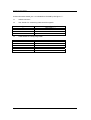
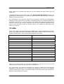
6.2.1 Headers
The connectors and headers on the board are listed below. Their approximate positions
are shown in Figure 1.
J5
J6
J2
J7
J1
J3
J4
Figure 1. Approximate Positions of Connectors and Headers
Pin numbers zig-zag along the two-row header as shown in Figure 2.
1
2
3
4
Figure 2. Zig-Zag Pin Numbering of Two-Row Header
CONFIDENTIAL
Page 7 of 57
Orange Tree Technologies
Unless otherwise stated, pin 1 is indicated on the PCB by the figure ‘1’.
J1
USB B connector
J2
Test header for monitoring USB controller signals:
Pin
1
2
3
4
J3
USB Controller Signal
Port E bit 0
Port E bit 1
Port E bit 2
BreakPoint
JTAG header for configuring FPGA:
Pin
1
2
3
4
5
6
Page 8 of 57
FPGA JTAG Pin
VCC 2.5V
Ground
TCK
TDO
TDI
TMS
ZestSC1 User Guide
J4
User I/O Header
IO pins are connected directly to the FPGA. See UCF for FPGA pin connections.
Signal
5V
Ground
Ground
Ground
IO0
IO2
IO4
IO6
IO8
IO10
IO12
IO14
IO16
IO18
IO20
IO22
IO24
IO26
IO28
IO30
IO32
IO34
IO36
IO38
IO40
IO42
IO44
CLK_IO_P
IO46
Ground
Ground
Ground
J5
Pin
1
3
5
7
9
11
13
15
17
19
21
23
25
27
29
31
33
35
37
39
41
43
45
47
49
51
53
55
57
59
61
63
Pin
2
4
6
8
10
12
14
16
18
20
22
24
26
28
30
32
34
36
38
40
42
44
46
48
50
52
54
56
58
60
62
64
Signal
3.3V
Ground
Ground
Ground
IO1
IO3
IO5
IO7
IO9
IO11
IO13
IO15
IO17
IO19
IO21
IO23
IO25
IO27
IO29
IO31
IO33
IO35
IO37
IO39
IO41
IO43
IO45
CLK_IO_N
Ground
Ground
Ground
Ground
2.5 mm power jack for mains adapter
Pin
Centre socket contact - 1
Switched input pin - 2
Outer socket contact - 3
Signal
Ground
VBUS (5V from USB)
3.5V to 5.5V POWER IN
When a plug is not inserted, pin 2 VBUS is connected to the jack output pin 3.
When a plug is inserted, the outer contact is isolated from pin 2 and connects the plug
outer contact to the jack output pin 3.
CONFIDENTIAL
Page 9 of 57
Orange Tree Technologies
J6
Power source
Connect Pins
1-2
2-3
J7
Power Source
Power jack J5 or USB
Hard disk drive connector J7
PC hard disk power connector
Pin
1
2
3
4
Signal
No connect
Ground
Ground
5V
6.3 Software
The software driver package includes a Windows Installer utility to perform the
installation. To install the software, run the setup.exe utility from the CD and follow the
on-screen instructions. The software will be installed in the following directory structure:
Directory
Docs
Driver
Examples
Inc
Lib
Utils
Verilog
VHDL
Page 10 of 57
Contents
Product documentation including the User Guide (this document)
Driver binary and installation (INF) files
Examples for host and FPGA code showing how to use various
features of the ZestSC1
Host support library C include file
Host support library C static library file
Contains utilities to set the card ID on a board (setid.exe) and
convert FPGA configuration files to C header files (Bit2C.exe)
Verilog FPGA files for interfacing to the USB controller and SRAM
VHDL FPGA files for interfacing to the USB controller and SRAM
ZestSC1 User Guide
7 Description
The block diagram of ZestSC1 is shown in Figure 3. It is a desktop board with a Xilinx
Spartan-3 FPGA with up to one million system gates. The FPGA is connected to a host
computer over High Speed USB (12 or 480Mbits/sec) for configuration and data
communication. A synchronous SRAM of either 1 or 8 MBytes stores application data, and
a 32x2 0.1” pitch header can be used for I/O.
USB
USB
Controller
Streaming
16
Registers
8
Flags
8
FPGA
Spartan-3
1000
18
ZBT SRAM
8MBytes
Interrupt
49
8
8 LEDs
49 pins of user I/O on 0.1” header
Figure 3. ZestSC1 Block Diagram
7.1 USB
ZestSC1 is a USB device and needs to be connected to a USB host computer. It can draw
power from the USB cable or from a mains power adapter, according to the position of
J6. The USB port may be either Full speed 12Mbps (USB V1.1 or 2.0) or High speed
480Mbps (USB V2.0).
The USB controller is the Cypress EZ-USB FX2 USB Microcontroller [1]. It includes an
8051 microcontroller that is used for enumeration and board management firmware. The
8051 address and data buses are connected to the FPGA. The USB controller is
implemented entirely in hardware. The ZestSC1 comes fitted with an EEPROM containing
firmware to communicate with the supplied host driver. It is strongly recommended that
this firmware is not modified and that the supplied host driver and FPGA cores are used
for all designs. Failure to do so may result in damage to the hardware.
The main method for data communication between the FPGA and USB is by the FX2’s
FIFO interface. This can operate with its data bus 8 or 16 bits wide and at a frequency of
48MHz giving a maximum burst data rate of 96 MBytes/sec.. It is used for configuring
the FPGA from the host computer and for data communications between the FPGA and
host computer. The FX2 Serial Interface Engine SIE, which controls USB transfers, uses
CONFIDENTIAL
Page 11 of 57
Orange Tree Technologies
the FIFO interface. The FIFO interface can be controlled by either an internal master in
the FX2 or an external master in the FPGA. The internal master is a programmable state
machine called the General Programmable Interface or GPIF. Conversely, when the FIFO
interface is controlled by the FPGA it is in Slave FIFO mode.
There are also general purpose data ports connected between the FX2 and the FPGA.
These are available for general communications (flags) or for specific purposes as
described below. For more detailed descriptions of signals see [1].
FX2 Port
Port signal
number
Function or Signal Name
A
0
FPGA configuration CS_n
1
FPGA configuration WRITE_n
2
C_PA2/SLOE – slave output enable
3
C_PA3/WU2 – 8051 wakeup
4
C_PA4/FIFOADR0 - slave FIFO address bit 0
5
C_PA5/FIFOADR1 – slave FIFO address bit 1
6
C_PA6/PKTEND – slave packet end
7
C_PA7/FLAGD/SLCS_n – slave FIFO output status flag/slave
chip select
B
0-7
FIFO interface data bits 0-7
C
0-7
General purpose bi-directional pins
D
0-7
FIFO interface data bits 8-15
E
0
Enable Power – active low power-on for FPGA, SRAM , etc,
which are powered off during USB enumeration
(enumeration is the USB initialisation following connection to
a computer)
1
Enable SRAM – active low chip enable for SRAM, can be
disabled to conserve power if SRAM is not used
2
VBUS monitor – monitors VBUS (5V from USB) so 8051 can
remove internal pull-up on D+ when VBUS is removed in
Full Speed mode (the pull-up is permanently removed in
High Speed mode anyway) and the board is powered from
J5 or J7
3
C_PE3
4
C_PE4
5
FPGA configuration PROG_n
6
FPGA configuration INIT_n
7
FPGA configuration DONE
Page 12 of 57
ZestSC1 User Guide
The GPIF also has 6 Ready input signals and 6 Control output signals for general purpose
use, and these are all connected to the FPGA. CTL3 and 4 are connected to FPGA
configuration CS_n and WRITE_n. These configuration signals are also connected to Port
C bits 0 & 1, but for high speed configuration the GPIF Control signals are used. In Slave
FIFO mode some of the Ready and Control signals become FIFO control signals. See table
above for Port A signals and table below for Ready and Control signals that are used in
Slave FIFO mode.
GPIF Mode
Slave FIFO Mode
RDY0 (I)
SLRD – slave read (I)
RDY1 (I)
SLWR – slave write (I)
RDY2 (I)
RDY3 (I)
RDY4 (I)
RDY5 (I)
CTL0 (O)
FLAG A (O)
CTL1 (O)
FLAG B (O)
CTL2 (O)
FLAG C (O)
CTL3 (O)
CTL4 (O)
CTL5 (O)
(I) means FX2 input and (O) means FX2 output
7.1.1 Communications with Host
The FPGA uses five means of communication with the FX2 and hence the host computer.
•
GPIF mode is used for bulk transfers of FPGA configuration/readback data.
Configuration/readback transfers require two endpoints, one for writing and one
for reading, making a total of two endpoints. The GPIF has a maximum of four
programmable waveforms in its state machine.
•
Slave FIFO mode is used for bulk transfers of application data. Application data
transfers require two endpoints, one for writing and one for reading, making a
total of two endpoints. Transfers using the slave FIFO must be a multiple of 512
bytes in length.
•
The 8051 external memory interface is used for access to application registers
within the FPGA.
•
The 8 bits of Port C of the 8051 are used as general purpose, bi-directional pins.
The use of these pins is determined by the user application. They can be used as
a simple handshaking protocol, state reporting to the host, control from the host
or for any other purpose.
•
There is a single interrupt line from the FPGA to the FX2 to allow the FPGA to
interrupt the host PC.
See the references [1], [2], [3], [4] and [5] for details on GPIF mode and Slave FIFO
mode.
CONFIDENTIAL
Page 13 of 57
Orange Tree Technologies
7.1.1.1 FPGA Configuration
The GPIF mode is used for configuring the FPGA using the SelectMap port. The FX2 acts
as a master driving the FPGA CS_n, WRITE_n and data ports. Data is transferred directly
from the USB port to the GPIF master and on to the FPGA using the Auto Out method
detailed in [3].
7.1.1.2 Streaming Data Transfer
The slave FIFO mode is used to stream data between the host and FPGA. The supplied
FPGA files include a reference design to illustrate use of the slave FIFO interface to
achieve peak transfer rates of 96Mbytes/s and sustained transfer rates only limited by
the host PC. The reference design exposes the following signals:
User_CLK
User_RST
User_StreamBusGrantLength
User_StreamDataIn
User_StreamDataInWE
User_StreamDataInBusy
User_StreamDataOut
User_StreamDataOutWE
User_StreamDataOutBusy
:
:
:
:
:
:
:
:
:
out std_logic;
out std_logic;
in std_logic_vector(11 downto 0);
out std_logic_vector(15 downto 0);
out std_logic;
in std_logic;
in std_logic_vector(15 downto 0);
in std_logic;
out std_logic;
Or, in Verilog:
output
output
input
output
output
input
input
input
output
User_CLK,
User_RST,
[11:0] User_StreamBusGrantLength,
User_StreamDataIn,
User_StreamDataInWE,
User_StreamDataInBusy,
[15:0] User_StreamDataOut,
User_StreamDataOutWE,
User_StreamDataOutBusy,
User_CLK is a clock output from the core. All signals from the core are synchronous to
this clock. All signals to the core should also be synchronous to this clock.
User_RST is an active high global reset output from the core. The user design should
use this to reset its state.
User_StreamBusGrantLength is used by the core to fairly arbitrate between transfers to
and from the host. The bus between the FX and the FPGA is a 16 bit bidirectional
interface and transfers take place in 512 byte blocks (256 sixteen bit words). The FPGA
grants the bus to reads or writes for the number of cycles specified by this input before
reversing the direction. This is done to avoid deadlock where the host wishes to write to
the FPGA and the FPGA wishes to write to the host and to fairly balance reads and writes.
Since a bus turnaround takes a number of cycles, this value is a trade-off between peak
bandwidth (higher with a larger grant length) and turnaround latency (lower with a lower
value). Therefore, for applications which transfer large blocks in one direction before
Page 14 of 57
ZestSC1 User Guide
reversing the data flow, select a large value (256 or greater). For applications which
alternate transferring short blocks in either direction, select a short value (such as 16).
User_StreamDataIn is the data stream from the host to the FPGA. The active high
User_StreamDataInWE signal indicates when the data is valid. If the user application
sets User_StreamDataInBusy high then the host will be blocked and no data will be sent
to the user application.
User_StreamDataOut is the data stream from the FPGA to the host.
The
User_StreamDataOutWE signal should be set high in the same cycle as the valid data. If
the User_StreamDataOutBusy signal is high then the user application should not attempt
to transfer any more data. The core contains a short FIFO which can accept 4 transfers
after User_StreamDataOutBusy goes high allowing time for the user application to
respond.
USER CLK
USER StreamDataIn
D0
D1
D2
USER StreamDataInWE
USER StreamDataInBusy
Figure 4. Host to FPGA Streaming Cycles
USER CLK
USER StreamDataOut
D0
D1
D2
USER StreamDataOutWE
USER StreamDataOutBusy
Figure 5. FPGA to Host Streaming Cycles
CONFIDENTIAL
Page 15 of 57
Orange Tree Technologies
7.1.1.3 Register Reads and Writes
The FX2 external bus is connected to the FPGA allowing memory mapped accesses to
registers implemented inside the FPGA. The supplied FPGA files include a reference
design to illustrate use of registers. The reference design exposes the following signals:
User_CLK
User_RST
User_RegAddr
User_RegDataIn
User_RegDataOut
User_RegWE
User_RegRE
:
:
:
:
:
:
:
out std_logic;
out std_logic;
out std_logic_vector(15 downto 0);
out std_logic_vector(7 downto 0);
in std_logic_vector(7 downto 0);
out std_logic;
out std_logic;
Or, in Verilog:
output User_CLK,
output User_RST,
output [15:0] User_RegAddr,
output [7:0] User_RegDataIn,
input [7:0] User_RegDataOut,
output User_RegWE,
output User_RegRE
User_CLK is a clock output from the core. All signals from the core are synchronous to
this clock. All signals to the core should also be synchronous to this clock.
User_RST is an active high global reset output from the core. The user design should
use this to reset its state.
User_RegAddr is the zero based address of the read or write access. Note that registers
between 0x0000 and 0x2000 are not available on boards fitted with the Cypress FX2LP
USB controller (part number CY68013A).
User_RegDataIn is the data from the host to the FPGA during a register write.
User_RegDataOut is the data from the FPGA to the host during a register read.
User_RegWE is an active high write strobe. This strobe will be high for a single cycle
simultaneously with the address and data.
User_RegRE is an active high read strobe. The user application should return the data on
the rising edge of the clock when this strobe is high.
Page 16 of 57
ZestSC1 User Guide
USER CLK
USER RegAddr
A0
USER RegDataIn
D0
A1
USER RegWE
D1
USER RegDataOut
USER RegRE
Figure 6. Register read and write accesses
7.1.1.4 User Signals
The 8 user signals between the FPGA and FX2 can be used for any application defined
purpose. However, care must be taken to set the direction of the FX2 Port C signals such
that the FX2 and FPGA do not drive against each other at any time. Failure to do so may
result in damage to the hardware.
7.1.1.5 Host Interrupt
The user core exposes a single signal to interrupt the host.
User_Interrupt
: in std_logic;
Or, in Verilog:
input User_Interrupt
Setting User_Interrupt high for a single cycle will cause an interrupt on the host which
can be trapped by the user application (ZestSC1WaitForInterrupt() function).
7.2 FPGA
The FPGA is from the Xilinx Spartan-3 family and is either the XC3S1000-4 or XC3S4004, according to which was ordered. The package is the FT256 256-pin fine pitch thin BGA.
There are three main devices attached to the FPGA:
•
USB controller
•
SRAM – 512K x 18 or 4M x 18 of synchronous SRAM
CONFIDENTIAL
Page 17 of 57
Orange Tree Technologies
•
I/O – 49 I/O signals, 2 of which can be a differential pair clock input. The I/O
signals FPGA banks have 51 ohm impedance reference resistors for Spartan DCI
buffers.
There are also 8 LEDs D2-9 that share IO signals 0, 1, & 41-46 respectively. These are
driven active low.
For signal allocations to FPGA pins, see the UCF supplied with the board.
The FPGA is configured from the USB in Slave Parallel mode. Alternatively it can be
configured using JTAG via header J3. The JTAG header on the board is 0.1 inch pitch with
pins assigned to align with the Xilinx Parallel Cable Fly Leads. The download cable should
be the Xilinx Parallel Cable IV with Parallel Cable Flying Leads. Note that the JTAG
reference voltage on pin 1 of J3 is 2.5V.
When using the Xilinx Synthesis Tools XST, the following XST synthesis and
implementation properties should be set.
Synthesis Properties – Xilinx Specific Options
Pack I/O Registers into IOBs
YES
Translate Properties
Allow Unmatched LOC Constraints
YES
Map Properties
Allow Logic Optimisation Across Hierarchy
Perform Timing Driven Packing and Placement
YES
YES
Generate Programming File Properties – Configuration Options
Unused IOB Pins
Pull Up
Generate Programming File Properties – Startup Options
Drive Done Pin High
YES
7.3 Memory
The memory is NoBL (No Bus Latency, the same as ZBT or Zero Bus Turnaround)
pipelined synchronous SRAM from Cypress. The device may be either the 512k x 18 or
4M x 18, according to which was ordered. These devices are respectively the
CY7C1356B-166AC [6] and CY7C1472V33-167AC [7].
The SRAM chip enable pin CE1_n is connected to the FX2 Port E bit 1 so that the FX2 can
control whether the SRAM is enabled to minimise power consumption. The pin CE1_n has
a pull-up so that the SRAM is disabled unless the FX2 enables it by driving this pin low.
MODE, ZZ, CEN_n and CE3_n are all pulled low permanently. CE2 is pulled high
permanently.
All other signals are connected to the FPGA, see the UCF for pin connections. The logic
core supplied with the board includes interface logic for the SRAM. The user interface is
as below.
Page 18 of 57
ZestSC1 User Guide
USER_SRAM_A: in std_logic_vector(22 downto 0);
USER_SRAM_W: in std_logic;
USER_SRAM_R: in std_logic;
USER_SRAM_DR_VALID: out std_logic;
USER_SRAM_DW: in std_logic_vector(17 downto 0);
USER_SRAM_DR: out std_logic_vector(17 downto 0);
------------
23-bit address
write strobe active
high
read strobe active
high
read data valid strobe
active high
18-bit data bus for
writing to SRAM
18-bit data bus for
reading from SRAM
//
//
//
//
//
//
//
//
//
//
//
23-bit address
write strobe active
high
read strobe active
high
read data valid strobe
active high
18-bit data bus for
writing to SRAM
18-bit data bus for
reading from SRAM
Or, in Verilog:
input [22:0] USER_SRAM_A,
input USER_SRAM_W,
input USER_SRAM_R,
output USER_SRAM_DR_VALID,
input [17:0] USER_SRAM_DW,
output [17:0] USER_SRAM_DR
The Pipelined ZBT SRAM device takes 2 clock cycles for a write and 2 clock cycles for a
read. This logic core has one extra pipeline stage in the write path (giving 3 clock cycles)
and two extra pipeline stages in the read path (giving 4 clock cycles). Figure 7 shows the
signal waveforms at the user interface.
USER CLK
USER SRAM A
WRITE
USER SRAM DW
DATA
READ
USER SRAM W
USER SRAM R
USER SRAM DR VALID
USER SRAM DR
DATA
Figure 7. ZBT SRAM Write and Read Cycles
For write cycles the user logic drives the write strobe high and the write address and data
in the same clock cycle. The logic core registers all command and data signals and delays
CONFIDENTIAL
Page 19 of 57
Orange Tree Technologies
the data by 2 further clocks as required by the ZBT SRAM. Byte write strobes are not
implemented.
For read cycles the user logic drives the read strobe high and the read address in the
same clock cycle, and the logic core registers all these signals. Valid data is returned to
the user code 4 clocks after the user code drives the read strobe high. The valid data is
accompanied by the active high data valid strobe. When the data valid strobe is high then
the read data should be registered by the user code.
All accesses are single accesses requiring a valid address with each access, burst
accesses are not implemented. There is no difference in bandwidth between single and
burst accesses.
The SRAM clock is driven from the FPGA to the SRAM. This must arrive at the SRAM
before the command and write data by the SRAM hold time of at least 0.5nS. This is
achieved by using a DCM to generate an SRAM clock about 2nS in advance of the User
clock and clocking all signals in IOB's. The SRAM clock is used only as an output to the
SRAM (via FDDR in IOB) and does not clock any signals in the FPGA.
The data tri-state signal flip-flop is placed in each data IOB to minimize bus contention
when changing from write to read or vice versa (see next paragraph). This is achieved by
setting the Synthesis property “Pack I/O Registers into IOBs” to YES.
ZBT Zero Bus Turnaround means that there does not have to be an idle cycle between
different types of cycles (i.e. writes and reads). The direction of the data bus therefore
needs to be able to change just after the start of a clock cycle from one device (e.g.
SRAM) driving it to the other device (e.g. FPGA) driving it. Because of differences in turn
on and turn off times of the different devices' data bus drivers there will inevitably be
some bus contention. However, as [8] shows, bus contention of a few nS is easily
tolerable.
7.4 IO
J4 provides user I/O from the FPGA, see the Headers section for the names of signals
connected to the pins and the UCF for connections to the FPGA. J4 is a 32 pins x 2 rows
0.1 inch pitch header.
49 pins are connected directly to the FPGA for user I/O. Two of these signals (CLK_IO_P
and CLK_IO_N) are connected to clock input pins on the FPGA. They can have a 100 ohm
parallel termination resistor across them at the FPGA for a differential clock – see section
Build Options. Also signals IO2-45 may be used as differential pairs IO2 & 3, IO4 & 5, …,
IO44 & 45, but they do not have termination resistors on the board.
IO0, 1, 41-46 are also connected to LED’s D2 to D9 respectively – see section LED’s. An
LED is switched on when the IO line is low, and requires 2mA to be drawn by the IO line
for full brightness.
There are 6 ground pins at one end of J4 and 7 ground pins at the other end. Pin 1 is 5V
power output and pin 2 is 3.3V power output, both via resettable 1.5A fuses. This power
can be used for example to power a daughter card plugged onto J4. The 3V3 is from the
Page 20 of 57
ZestSC1 User Guide
power switch so is available only after the FX2 has enabled the power switch using its
Port E bit 0.
The FPGA I/O banks connected to J4 are 3V3. They are NOT 5V tolerant. However 5V
signals can be connected to J4 via 180 ohm series resistors to limit the current into each
FPGA pin to less than 10mA.
As a build option, DCI reference resistors can be fitted for matching the characteristic
impedance of the IO lines for DCI buffers. The FPGA pins for the reference resistors are
the same as IO pins 2, 3, 44 & 45. Hence if the resistors are fitted then these IO pins
cannot be used for I/O. Also the FPGA pins for two of the reference resistors are the
same as pins connected to LED’s D7 and D8. Hence if the resistors are fitted then these
LED’s are removed.
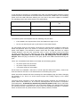
7.5 LEDs
There is one LED for the FPGA configuration DONE signal, 4 LEDs indicating power supply
status, and 8 LEDs connected to the FPGA. These latter 8 LEDs are also connected to IO
signals as shown below. Figure 8 shows the positions of the LEDs.
LED
Signal
1
DONE
2
IO0
3
IO1
4
IO41
5
IO42
6
IO43
7
IO44
8
IO45
9
IO46
10
5V
11
3.3V
12
Switched 3.3V
13
2.5V
LED’s 2-9 are driven active low. An LED is switched on when the IO line is low, and
requires 2mA to be drawn by the IO line for full brightness.
As a build option, DCI reference resistors can be fitted for matching the characteristic
impedance of the IO lines for DCI buffers. The FPGA pins for two of the reference
resistors are the same as pins connected to LED’s D7 and D8. Hence if the resistors are
fitted then these LED’s are removed.
CONFIDENTIAL
Page 21 of 57
Orange Tree Technologies
J5
D10 D11 D12 D13
J7
D1
J1
D4 D5 D6 D7 D8 D9
D2 D3
J4
Figure 8. Approximate Positions of LEDs
7.6 Clocks
The FPGA has two fixed frequency clock inputs of 48MHz each and one clock input from
the IO header. The FPGA’s internal DCM’s can be used to synthesise other clock
frequencies from 1.5MHz to 280MHz.
The 48MHz clock for the Slave FIFO Interface connecting the USB controller and the FPGA
is driven on separate PCB tracks from a crystal oscillator to the USB controller and to the
FPGA. It is connected to FPGA global clock pin GCLK0. It is also used for the FPGA
configuration clock CCLK.
The USB controller 8051 clock is output from the USB controller to the FPGA global clock
pin GCLK1. The frequency can be set to 12MHz, 24MHz or 48MHz by the 8051, and the
8051 firmware supplied with the ZestSC1 sets it to 48MHz. The logic cores supplied with
the board use this USB controller 8051 clock as the main clock. Note this is a separate
clock to the 48MHz GPIF clock described in the paragraph above. The host interface logic
core includes FIFO’s to interface between the two clock domains of the USB controller
8051 clock and the Slave FIFO Interface clock.
The IO clock signals CLK_IO_P and CLK_IO_N are connected to FPGA global clock pins
GCLK6 and GCLK7 respectively. They can be configured as single-ended or differential
clock inputs.
7.7 Power
The board can be either bus-powered or self-powered. Bus-powered means powered
entirely from the USB cable connected to the host computer. If the board is to be buspowered then the USB port must be a high power (500mA) port. The DC/DC
converters on the board have been chosen for their very high efficiency of approximately
90%, even at low currents. This is important when the board is bus-powered as only
Page 22 of 57
ZestSC1 User Guide
2.5W (500mA @ nominal 5V) is available from USB. The following table shows the typical
quiescent power consumption of the board when connected to a USB host. The remaining
power from the USB 2.5W after allowing for 10% loss in the power supplies is available
for operating power and is also shown in the table below.
FPGA and Memory
Quiescent Power (W)
Available Operating Power
(W)
400 and 1MB
1.35
1.0
1000 and 1MB
1.40
1.0
1000 and 8MB*
1.80
0.6
To minimise power consumption then the following may be done:
•
If the SRAM is not required then drive the SRAM clock high or low.
•
Do not use internal pull-ups or pull-downs on the FPGA IO pins.
For extra power there are two power connectors for external power supplies to make the
board self-powered. One is J5, which is a 2.5mm power jack for connection to a mains
power wall adapter. This should be switch mode with low ripple and have an output
voltage between 3.5V and 5.5V (nominally 4.5V or 5.0V), an output current of at least
1A, and a female plug inner diameter of 2.5mm. The plug from the wall adapter
should have +5V power on the outside of the pin and ground on the inside of
the pin. When the plug is inserted in the jack, power from USB is disconnected by the
jack.
There are 3 resettable fuses fitted to the board at the following points:
•
•
•
5V power input from all sources
5V power output to I/O header
3.3V power output to I/O header
All the fuses are resettable 1.5A fuses. If a fuse trips then disconnect power, remove the
fault and wait for the fuse to cool down before reconnecting the power.
Power should be switched off when inserting the mains adapter plug and when changing
the position of J6. This is to avoid current surges and voltage ringing in the mains
adapter wire.
The other power connector is a PC hard disk drive power connector for connecting to a
power cable found inside a PC. J6 is used for selecting either this connector or the power
jack/USB power. J6 should be moved only when all power is off. The PC hard disk
drive power connector is intended for use of the board inside a PC and the board should
be mounted securely using the four corner holes and insulating standoffs in a position
where it cannot touch any other items such as chassis, boards or cables.
CONFIDENTIAL
Page 23 of 57
Orange Tree Technologies
7.8 Build Options
The following modifications can be made to the board by arrangement with Orange Tree
Technologies.
1. DCI reference resistors for the IO lines. DCI buffers require reference
resistors for matching to the characteristic impedance of the IO lines. On ZestSC1
the IO lines are about 50 ohms impedance so the reference resistors are 51
ohms, being the closest standard value. The resistors are connected to the FPGA
pins connected to IO2, 3, 44 & 45, so these IO pins cannot be used if the
reference resistors are fitted. Also LED’s D7 and D8 are connected to IO44 & 45
so these LED’s are removed if the reference resistors are fitted. For the standard
build the reference resistors are not fitted (so DCI cannot be used) and LED’s D7
and D8 are fitted.
2. IO differential clock input. IO pins CLK_IO_P and CLK_IO_N are both
connected to FPGA clock input pins. They can be used either as separate single
ended clocks or general purpose IO or as one differential clock input. A 100 ohm
resistor can be fitted at the FPGA pins to terminate a differential clock input. For
the standard build this resistor is not fitted.
Page 24 of 57
ZestSC1 User Guide
8 Using the Host Library
The ZestSC1 host support software consists of a system driver and a host library to allow
access to the board. The system driver is installed automatically during installation of the
ZestSC1 support package. The host library consists of a static C library file (.lib file) and
an associated C header file (.h file).
To use the ZestSC1 support library in your own code, you must include the header file at
the start of your program. For example:
#include <zestsc1.h>
The header file must be in your compiler include path. For details of how to set the
include path, refer to your compiler manuals.
Your program must then be linked with the ZestSC1.lib library file. For details of how to
link additional static libraries, refer to your compiler manuals. You must also link in the
standard library ‘setupapi.lib’ (available in the Windows Platform SDK from Microsoft)
which is used by the ZestSC1 host library internal code.
CONFIDENTIAL
Page 25 of 57
Orange Tree Technologies
9 Host Utilities
A number of utilities are provided with the ZestSC1 support library. These can be found
in the Utils sub-directory of the support package installation.
9.1 Bit2C
Bit2C.exe converts Xilinx .bit FPGA configuration files to C header files. The C header file
contains a static array definition with the raw data from the .bit file. This array can be
passed to the ZestSC1RegisterImage function to obtain a handle suitable for the
ZestSC1Configure function. In this way, .bit files can be linked into your application
executable to avoid having multiple files.
For example:
Bit2C config.bit array.c
This will convert the config.bit file generated by the Xilinx place and route tools into a
file called array.c which contains definitions of the variables arrayLength and
arrayImage. You can then configure the FPGA by calling the following functions:
extern void *arrayImage;
extern unsigned long arrayLength;
ZESTSC1_IMAGE Image;
ZESTSC1_HANDLE Handle;
/* Register the FPGA configuration image */
ZestSC1RegisterImage(arrayImage, arrayLength, &Image);
/* Open a card with ID of 1 */
ZestSC1OpenCard(1, &Handle);
/* Configure the FPGA from the image */
ZestSC1Configure(Handle, Image);
9.2 SetID
Each ZestSC1 card contains a non-volatile ID to allow identification of the card in a
system with multiple ZestSC1’s attached. The ID is passed to the ZestSC1OpenCard
function to obtain a handle to the card.
For example, a system may consist of a ZestSC1 card attached to a camera and a second
ZestSC1 connected to a monitor. Setting the ID of the first card to 1 and the second
card to 2 will allow the host program to distinguish between the two cards.
SetID.exe programs the ID of a card from the command line. Run SetID.exe from a
command prompt and follow the on-screen instructions.
Page 26 of 57
ZestSC1 User Guide
10 Examples
The ZestSC1 Support package contains a number of examples to illustrate the use of the
ZestSC1 and its Host Support Library. The examples are located in the Examples subdirectory of the ZestSC1 installation directory. Each example consists of a host program
and a Xilinx XST VHDL or Verilog project.
Examples 2 and 4 also contain ModelSim testbenches to illustrate how the various
interfaces can be simulated before implementation.
Example1 shows how to configure the FPGA from a .bit file generated by the Xilinx place
and route tools. The .bit file flashes the LEDs on the board in sequence.
Example2 shows how to use the high-speed streaming interface on the ZestSC1 by
measuring data transfer rates between the FPGA and the host in either direction. The
VHDL/Verilog code implements an infinite data sink and an infinite data source to
illustrate use of the VHDL/Verilog support library.
Example3 shows how to use the low-speed control interface on the ZestSC1 by reading
and writing a memory-mapped register and reading and writing the single bit signals.
The VHDL/Verilog code implements a number of read/write registers and a loop-back of 4
input signals to 4 output signals.
Example4 shows how to use the SRAM on the ZestSC1. The VHDL/Verilog code
implements a DMA engine between the USB streaming port and the SRAM allowing the
host to read and write blocks of data.
CONFIDENTIAL
Page 27 of 57
Orange Tree Technologies
11 Host Library Function Reference
ZestSC1CountCards
ZESTSC1_STATUS ZestSC1CountCards( unsigned long *NumCards,
unsigned long *CardIDs,
unsigned long *SerialNumbers,
ZESTSC1_FPGA_TYPE *FPGATypes);
Parameters
NumCards
CardIDs
SerialNumbers
FPGATypes
Pointer to location to receive total number of ZestSC1 cards in
the system.
Pointer to buffer to receive list of card IDs in the system. May
be NULL.
Pointer to buffer to receive list of card serial numbers in the
system. May be NULL.
Pointer to buffer to receive list of FPGA types fitted to cards in
the system. May be NULL.
Return Value
ZESTSC1_SUCCESS
ZESTSC1_INTERNAL_ERROR
Function succeeded
An unspecified internal error occurred while
communicating with the driver
Description
ZestSC1CountCards can be used to determine the number and types of cards fitted in a
system. Each card can be identified in 3 ways: by a user-programmable card ID, by a
factory set unique serial number and by the type of FPGA fitted to the card.
CardIDs should point to the start of an array which will be filled in with the user
programmable card IDs. See ZestSC1SetCardID for details of how to set this ID. This
ID should be passed to ZestSC1OpenCard to obtain a handle for accessing the selected
ZestSC1 card.
SerialNumbers should point to the start of an array which will be filled in with the factory
set, unique serial number of the cards in the system.
FPGATypes should point to the start of an array which will be filled in with the type of
FPGA fitted.
Each of these arrays should be large enough to receive values for each of the cards in the
system. Any or all of them can be NULL if the information is not required. A call to
ZestSC1CountCards can be made with NULL pointers to determine the size of the
required array as follows:
Page 28 of 57
ZestSC1 User Guide
unsigned long NumCards;
unsigned long *CardIDs;
/* Get the number of cards in the system */
ZestSC1CountCards(&NumCards, NULL, NULL, NULL);
/* Allocate a buffer to receive the card IDs */
CardIDs = malloc(sizeof(unsigned long) * NumCards);
/* Fill in the buffer with the card IDs */
ZestSC1CountCards(&NumCards, CardIDs, NULL, NULL);
CONFIDENTIAL
Page 29 of 57
Orange Tree Technologies
ZestSC1OpenCard
ZESTSC1_STATUS ZestSC1OpenCard(
unsigned long CardID,
ZESTSC1_HANDLE *Handle);
Parameters
CardId
Handle
ID of card to open. See ZestSC1CountCards.
Pointer to receive the handle of the open card. This handle is
used to identify the card in future calls to the ZestSC1 library.
Return Value
ZESTSC1_SUCCESS
ZESTSC1_INTERNAL_ERROR
ZESTSC1_OUT_OF_MEMORY
ZESTSC1_ILLEGAL_CARD_ID
Function succeeded
An unspecified internal error occurred while
communicating with the driver
Not enough memory to complete the
requested operation
The requested card ID does not correspond
to any devices in the system
Description
ZestSC1OpenCard is used to obtain a handle to a card in the system for future calls to
ZestSC1 library functions. The card is identified by a user-programmable ID. See
ZestSC1CountCards for details of how to find the IDs of cards in the system and
ZestSC1SetCardID for details of how to set this ID.
For example:
ZESTSC1_HANDLE Handle;
/* Open a card with ID of 1 */
ZestSC1OpenCard(1, &Handle);
/* Configure the FPGA on the open card */
ZestSC1ConfigureFromFile(Handle, “test.bit”);
ZestSC1CloseCard should be called to free the card before the program exits.
Page 30 of 57
ZestSC1 User Guide
ZestSC1GetCardInfo
ZESTSC1_STATUS ZestSC1GetCardInfo( ZESTSC1_HANDLE Handle,
ZESTSC1_CARD_INFO *Info);
Parameters
Handle
Info
Handle of open ZestSC1 card. See ZestSC1OpenCard.
Pointer to structure to receive information about the card.
Return Value
ZESTSC1_SUCCESS
ZESTSC1_INTERNAL_ERROR
ZESTSC1_ILLEGAL_HANDLE
ZESTSC1_TIMEOUT
Function succeeded
An unspecified internal error occurred while
communicating with the driver
Attempt to use illegal card handle
Operation timed out
Description
ZestSC1GetCardInfo can be used to obtain information about an open card.
ZESTSC1_CARD_INFO structure is defined as follows:
The
typedef struct
{
unsigned long CardID;
unsigned long SerialNumber;
ZESTSC1_FPGA_TYPE FPGAType;
Unsigned long MemorySize;
unsigned long TimeOut;
} ZESTSC1_CARD_INFO;
CardID is a user-programmable ID for the card. See ZestSC1CountCards for details of
how to find the IDs of cards in the system and ZestSC1SetCardID for details of how to
set this ID.
SerialNumber is a unique, factory-set serial number for the card.
FPGAType gives the type of FPGA fitted to the card.
MemorySize gives the number of bytes of SRAM fitted to the card.
TimeOut is the length of time, in milliseconds, that blocking operations should wait for
before returning ZESTSC1_TIMEOUT. Time outs allow the user program to recover
cleanly when communication with the card fails. See ZestSC1SetTimeOut for details of
how to set this time.
For example:
ZESTSC1_HANDLE Handle;
CONFIDENTIAL
Page 31 of 57
Orange Tree Technologies
ZESTSC1_CARD_INFO Info;
/* Open a card with ID of 1 */
ZestSC1OpenCard(1, &Handle);
/* Obtain information about the card */
ZestSC1GetCardInfo(Handle, &Info);
/* Perform action based on FPGAType */
if (Info.FPGAType==ZESTSC1_XC3S400)
ZestSC1ConfigureFromFile(Handle, “file400.bit”);
else if (Info.FPGAType== ZESTSC1_XC3S1000)
ZestSC1ConfigureFromFile(Handle, “file1000.bit”);
else
printf(Illegal FPGA type\n”);
Page 32 of 57
ZestSC1 User Guide
ZestSC1SetTimeOut
ZESTSC1_STATUS ZestSC1SetTimeOut( ZESTSC1_HANDLE Handle,
unsigned long MilliSeconds);
Parameters
Handle
MilliSeconds
Handle of open ZestSC1 card. See ZestSC1OpenCard.
Length to required timeout in milliseconds.
Return Value
ZESTSC1_SUCCESS
ZESTSC1_ILLEGAL_HANDLE
Function succeeded
Attempt to use illegal card handle
Description
ZestSC1SetTimeOut can be used to set the length of time, in milliseconds, that
blocking operations should wait for before returning ZESTSC1_TIMEOUT. Time outs
allow the user program to recover cleanly when communication with the card fails. The
default length of the time out is 10 seconds.
For example:
ZESTSC1_HANDLE Handle;
/* Open a card with ID of 1 */
ZestSC1OpenCard(1, &Handle);
/* Set the time out to 20 seconds */
ZestSC1SetTimeOut(Handle, 20000);
/* Perform action and time out if card doesn’t
respond within 20 seconds */
if (ZestSC1ConfigureFromFile(Handle, “test.bit”)==ZESTSC1_TIMEOUT)
printf(“Failed to configure FPGA – time out\n”);
CONFIDENTIAL
Page 33 of 57
Orange Tree Technologies
ZestSC1SetCardID
ZESTSC1_STATUS ZestSC1SetCardID(
ZESTSC1_HANDLE Handle,
unsigned long CardID);
Parameters
Handle
CardID
Handle of open ZestSC1 card. See ZestSC1OpenCard.
Value of new card ID.
Return Value
ZESTSC1_SUCCESS
ZESTSC1_ILLEGAL_HANDLE
ZESTSC1_INTERNAL_ERROR
ZESTSC1_TIMEOUT
Function succeeded
Attempt to use illegal card handle
An unspecified internal error occurred while
communicating with the driver
Operation timed out
Description
ZestSC1SetCardID can be used to set the user-programmable ID of a card in the
system. This ID is then used to identify the card in future calls to ZestSC1OpenCard.
The card ID is a useful way to allow software to be written in a platform independent
way. For example, suppose a system has 3 cards with different peripherals attached to
the front panel connector. The card ID can be set on each card to allow the software to
identify the cards based on the attached peripherals. A second copy of the system can
be constructed with the same set if card IDs so the software can be written so that it runs
on either copy of the system.
For example:
ZESTSC1_HANDLE Handle;
/* Open a card with ID of 1 */
ZestSC1OpenCard(1, &Handle);
/* Set card ID to 23 */
ZestSC1SetCardID(Handle, 23);
/* Close the card */
ZestSC1CloseCard(Handle);
/* Re-open the card but with ID of 23 */
ZestSC1OpenCard(23, &Handle);
Page 34 of 57
ZestSC1 User Guide
ZestSC1CloseCard
ZESTSC1_STATUS ZestSC1CloseCard(ZESTSC1_HANDLE Handle);
Parameters
Handle
Handle
of
open
ZestSC1OpenCard.
ZestSC1
card
to
close.
See
Return Value
ZESTSC1_SUCCESS
ZESTSC1_ILLEGAL_HANDLE
ZESTSC1_TIMEOUT
Function succeeded
Attempt to use illegal card handle
Operation timed out
Description
ZestSC1CloseCard should be called when the specified card is finished with. It frees
resources and allows other applications to access the card.
For example:
ZESTSC1_HANDLE Handle;
/* Open a card with ID of 1 */
ZestSC1OpenCard(1, &Handle);
/* Other calls to ZestSC1 library here */
/* Close the card */
ZestSC1CloseCard(Handle);
CONFIDENTIAL
Page 35 of 57
Orange Tree Technologies
ZestSC1RegisterErrorHandler
ZESTSC1_STATUS ZestSC1RegisterErrorHandler(
ZESTSC1_ERROR_FUNC Function);
Parameters
Function
Pointer to error handler function
notifications for this application.
to
receive
all
error
Return Value
ZESTSC1_SUCCESS
Function succeeded
Description
ZestSC1RegisterErrorHandler can be called to install a central error handling routine
for a user program. If any of the following ZestSC1 library function calls fail, the user
error handler will be called giving details of the failure. This mechanism means that
status codes need not be checked for every library call which simplifies code
considerably.
ZESTSC1_ERROR_FUNC is a function declared as follows:
typedef void (*ZESTSC1_ERROR_FUNC)(const char *Function,
ZESTSC1_HANDLE Handle,
ZESTSC1_STATUS Status,
const char *Msg);
Function is a string containing the name of the function that failed. Handle is the handle
of the card being accessed at the time of the failure. This may be NULL for functions that
do not take a card handle. Status is the status code describing the failure and Msg is a
string describing the failure.
For example:
/* Error handler function */
void ErrorHandler(const char *Function,
ZESTSC1_HANDLE Handle,
ZESTSC1_STATUS Status,
const char *Msg)
{
printf(“**** Function %s returned an error\n”, Function);
printf(“**** 0x%08lx : \"%s\"\n\n", Status, Msg);
exit(1);
}
void main(void)
{
ZestSC1RegisterErrorHandler(ErrorHandler);
Page 36 of 57
ZestSC1 User Guide
/* Other calls to ZestSC1 library here */
/* Note that the return code need not be checked
as ErrorHandler will be called for any return values
not equal to ZESTSC1_SUCCESS */
}
CONFIDENTIAL
Page 37 of 57
Orange Tree Technologies
ZestSC1GetErrorMessage
ZESTSC1_STATUS ZestSC1GetErrorMessage(ZESTSC1_STATUS Status,
char **Buffer);
Parameters
Status
Buffer
ZestSC1 error code for which description is required.
Pointer to location to receive error code description string.
Return Value
ZESTSC1_SUCCESS
ZESTSC1_ILLEGAL_STATUS_CODE
Function succeeded
Status code is out of range
Description
ZestSC1GetErrorMessage can be called to obtain a descriptive message for a return
status from a ZestSC1 library function. On return, the string pointed to by Buffer will be
a description of the Status return code. This is a static string and so does not need to be
freed.
For example:
ZESTSC1_HANDLE Handle;
ZESTSC1_STATUS Status;
/* Open a card with ID of 1 */
Status = ZestSC1OpenCard(1, &Handle);
if (Status!=ZESTSC1_SUCCESS)
{
char *Buffer;
ZestSC1GetErrorMessage(Status, &Buffer);
printf(“Error : %s\n”, Buffer);
}
Page 38 of 57
ZestSC1 User Guide
ZestSC1ConfigureFromFile
ZESTSC1_STATUS ZestSC1ConfigureFromFile(ZESTSC1_HANDLE Handle,
char *FileName);
Parameters
Handle
FileName
Handle of open ZestSC1 card. See ZestSC1OpenCard.
Name of .bit file to use to configure the FPGA.
Return Value
ZESTSC1_SUCCESS
ZESTSC1_ILLEGAL_HANDLE
ZESTSC1_NULL_PARAMETER
Function succeeded
Attempt to use illegal card handle
NULL was used illegally as one of the
parameter values
File not found
Error while reading file
Not enough memory to complete the
requested operation
File format is not recognised
Illegal FPGA part type
An unspecified internal error occurred while
communicating with the driver
Operation timed out
ZESTSC1_FILE_NOT_FOUND
ZESTSC1_FILE_ERROR
ZESTSC1_OUT_OF_MEMORY
ZESTSC1_ILLEGAL_FILE
ZESTSC1_INVALID_PART_TYPE
ZESTSC1_INTERNAL_ERROR
ZESTSC1_TIMEOUT
Description
ZestSC1ConfigureFromFile can be used to configure the FPGA on the ZestSC1 card
from a .bit file generated by the Xilinx place and route software. It configures the FPGA
directly from the file on disk. Refer to ZestSC1RegisterImage and ZestSC1Configure
for details of how to configure the FPGA from configuration data in memory.
For example:
ZESTSC1_HANDLE Handle;
/* Open a card with ID of 1 */
ZestSC1OpenCard(1, &Handle);
/* Configure the FPGA from a .bit file */
ZestSC1ConfigureFromFile(Handle, “test.bit”);
CONFIDENTIAL
Page 39 of 57
Orange Tree Technologies
!
Page 40 of 57
Configuring the FPGA with an incorrect BIT file can damage
your hardware. Ensure that FPGA pins are connected
correctly and do not drive against peripherals on the board.
ZestSC1 User Guide
ZestSC1LoadFile
ZESTSC1_STATUS ZestSC1LoadFile(
char *FileName,
ZESTSC1_IMAGE *Image);
Parameters
FileName
Image
Name of .bit file to use to configure the FPGA.
Pointer to location to receive FPGA configuration image.
Return Value
ZESTSC1_SUCCESS
ZESTSC1_NULL_PARAMETER
Function succeeded
NULL was used illegally as one of the
parameter values
File not found
Error while reading file
Not enough memory to complete the
requested operation
File format is not recognised
Illegal FPGA part type
ZESTSC1_FILE_NOT_FOUND
ZESTSC1_FILE_ERROR
ZESTSC1_OUT_OF_MEMORY
ZESTSC1_ILLEGAL_FILE
ZESTSC1_INVALID_PART_TYPE
Description
ZestSC1LoadFile can be used to load a .bit file generated by the Xilinx place and route
software into memory for future configuration of the FPGA on the ZestSC1 card. It is
possible to load many configuration files during initialization and select the correct FPGA
image to use during execution of the program. This reduces overhead at configuration
time.
Image is a pointer to a location to receive the configuration image handle. This handle
can be used in future calls to ZestSC1Configure. The handle should be freed by calling
ZestSC1FreeImage when the configuration image is no longer needed.
ZestSC1LoadFile and ZestSC1Configure allow decoupled loading of the bit file and
configuration of the FPGA. Refer to ZestSC1RegisterImage and ZestSC1Configure
for details of how to configure the FPGA from configuration data in memory.
For example:
ZESTSC1_IMAGE Image;
ZESTSC1_HANDLE Handle;
/* Load the .bit file */
ZestSC1LoadImage(“test.bit”, &Image);
/* Other initialization operations here */
/* Open a card with ID of 1 */
ZestSC1OpenCard(1, &Handle);
CONFIDENTIAL
Page 41 of 57
Orange Tree Technologies
/* Other execution operations here */
/* Configure the FPGA from the image */
ZestSC1Configure(Handle, Image);
Page 42 of 57
ZestSC1 User Guide
ZestSC1Configure
ZESTSC1_STATUS ZestSC1Configure(
ZESTSC1_HANDLE Handle,
ZESTSC1_IMAGE Image);
Parameters
Handle
Image
Handle of open ZestSC1 card. See ZestSC1OpenCard.
FPGA configuration image to use to configure the FPGA.
Return Value
ZESTSC1_SUCCESS
ZESTSC1_ILLEGAL_HANDLE
ZESTSC1_ILLEGAL_IMAGE_HANDLE
ZESTSC1_INTERNAL_ERROR
ZESTSC1_TIMEOUT
Function succeeded
Attempt to use illegal card handle
Attempt to use illegal configuration image
handle
An unspecified internal error occurred while
communicating with the driver
Operation timed out
Description
ZestSC1Configure configures the FPGA on the ZestSC1 card from a configuration
image.
The configuration image can be created from a .bit file by calling
ZestSC1LoadImage or from data in memory by calling ZestSC1RegisterImage.
Example creating the image from .bit file on disk:
ZESTSC1_IMAGE Image;
ZESTSC1_HANDLE Handle;
/* Load the .bit file */
ZestSC1LoadImage(“test.bit”, &Image);
/* Other initialization operations here */
/* Open a card with ID of 1 */
ZestSC1OpenCard(1, &Handle);
/* Other execution operations here */
/* Configure the FPGA from the image */
ZestSC1Configure(Handle, Image);
Example creating the image from buffer in memory:
extern void *Buffer;
extern unsigned long Length;
ZESTSC1_IMAGE Image;
ZESTSC1_HANDLE Handle;
CONFIDENTIAL
Page 43 of 57
Orange Tree Technologies
/* Register the FPGA configuration image */
ZestSC1RegisterImage(Buffer, Length, &Image);
/* Other initialization operations here */
/* Open a card with ID of 1 */
ZestSC1OpenCard(1, &Handle);
/* Other execution operations here */
/* Configure the FPGA from the image */
ZestSC1Configure(Handle, Image);
!
Page 44 of 57
Configuring the FPGA with an incorrect BIT file can damage
your hardware. Ensure that FPGA pins are connected
correctly and do not drive against peripherals on the board.
ZestSC1 User Guide
ZestSC1RegisterImage
ZESTSC1_STATUS ZestSC1RegisterImage(void *Buffer,
unsigned long BufferLength,
ZESTSC1_IMAGE *Image);
Parameters
Buffer
BufferLength
Image
Buffer containing FPGA configuration data.
Normally
generated by Bit2C utility.
Length, in bytes, of the configuration data.
Pointer to location to receive FPGA configuration image.
Return Value
ZESTSC1_SUCCESS
ZESTSC1_OUT_OF_MEMORY
Function succeeded
Not enough memory
requested operation
Illegal FPGA part type
ZESTSC1_INVALID_PART_TYPE
to
complete
the
Description
ZestSC1RegisterImage creates an FPGA configuration image from an array of raw
configuration data.
The FPGA can be configured from this image by calling
ZestSC1Configure.
Buffer points to the start of the raw configuration data and BufferLength is the number of
bytes of configuration data to use. The Bit2C utility supplied on the ZestSC1 installation
disk provides a simple way to generate compatible C arrays from .bit files.
Image is a pointer to a location to receive the configuration image handle. This handle
can be used in future calls to ZestSC1Configure. The handle should be freed by calling
ZestSC1FreeImage when the configuration image is no longer needed.
ZestSC1RegisterImage and ZestSC1Configure allow .bit files to be linked into host
executables to reduce the number of host files required.
Refer to
ZestSC1ConfigureFromFile, ZestSC1LoadImage and ZestSC1Configure for details
of how to configure the FPGA from configuration data in a file.
For example:
extern void *Buffer;
extern unsigned long Length;
ZESTSC1_IMAGE Image;
ZESTSC1_HANDLE Handle;
/* Register the FPGA configuration image */
ZestSC1RegisterImage(Buffer, Length, &Image);
/* Other initialization operations here */
CONFIDENTIAL
Page 45 of 57
Orange Tree Technologies
/* Open a card with ID of 1 */
ZestSC1OpenCard(1, &Handle);
/* Other execution operations here */
/* Configure the FPGA from the image */
ZestSC1Configure(Handle, Image);
Page 46 of 57
ZestSC1 User Guide
ZestSC1FreeImage
ZESTSC1_STATUS ZestSC1FreeImage(ZESTSC1_IMAGE Image);
Parameters
Image
FPGA configuration image to free.
Return Value
ZESTSC1_SUCCESS
ZESTSC1_ILLEGAL_IMAGE_HANDLE
Function succeeded
Attempt to use illegal configuration image
handle
Description
ZestSC1FreeImage should be called when a configuration image handle is no longer
needed.
It is used to free resources allocated during ZestSC1LoadImage and
ZestSC1RegisterImage functions.
For example:
extern void *Buffer;
extern unsigned long Length;
ZESTSC1_IMAGE Image;
ZESTSC1_HANDLE Handle;
/* Register the FPGA configuration image */
ZestSC1RegisterImage(Buffer, Length, &Image);
/* Other initialization operations here */
/* Open a card with ID of 1 */
ZestSC1OpenCard(1, &Handle);
/* Other execution operations here */
/* Configure the FPGA from the image */
ZestSC1Configure(Handle, Image);
/* Free resources associated with the handle */
ZestSC1FreeImage(Image);
CONFIDENTIAL
Page 47 of 57
Orange Tree Technologies
ZestSC1ReadRegister
ZESTSC1_STATUS ZestSC1ReadRegister(
ZESTSC1_HANDLE Handle,
unsigned long Offset,
unsigned char *Value);
Parameters
Handle
Offset
Value
Handle of open ZestSC1 card. See ZestSC1OpenCard.
Address of register in FPGA.
Pointer to location to receive register value.
Return Value
ZESTSC1_SUCCESS
ZESTSC1_ILLEGAL_HANDLE
ZESTSC1_NULL_PARAMETER
ZESTSC1_INTERNAL_ERROR
ZESTSC1_TIMEOUT
Function succeeded
Attempt to use illegal card handle
NULL was used illegally as one of the
parameter values
An unspecified internal error occurred while
communicating with the driver
Operation timed out
Description
ZestSC1ReadRegister returns the value of a register from the memory-mapped
interface on the ZestSC1 card FPGA.
Boards fitted with the Cypress FX2 USB controller chip (part number CY7C68013) allow
an offset of 0x0000 to 0x8000. Boards fitted with the Cypress FX2LP USB controller chip
(part number CY7C68013A) allow an offset of 0x2000 to 0x6000.
For example:
ZESTSC1_HANDLE Handle;
char Value;
/* Open a card with ID of 1 */
ZestSC1OpenCard(1, &Handle);
/* Get value of register 0 from board */
ZestSC1ReadRegister(Handle, 0, &Value);
/* Close the card */
ZestSC1CloseCard(Handle);
!
Page 48 of 57
Attempting to transfer data to/from the FPGA without a
suitable slave interface configured may result in the ZestSC1
‘hanging’.
ZestSC1 User Guide
ZestSC1WriteRegister
ZESTSC1_STATUS ZestSC1WriteRegister(
ZESTSC1_HANDLE Handle,
unsigned long Offset,
unsigned char Value);
Parameters
Handle
Offset
Value
Handle of open ZestSC1 card. See ZestSC1OpenCard.
Address of register in FPGA.
Value to write to register.
Return Value
ZESTSC1_SUCCESS
ZESTSC1_ILLEGAL_HANDLE
ZESTSC1_INTERNAL_ERROR
Function succeeded
Attempt to use illegal card handle
An unspecified internal error occurred while
communicating with the driver
Operation timed out
ZESTSC1_TIMEOUT
Description
ZestSC1WriteRegister sets the value of a register in the memory-mapped interface on
the ZestSC1 card FPGA.
Boards fitted with the Cypress FX2 USB controller chip (part number CY7C68013) allow
an offset of 0x0000 to 0x8000. Boards fitted with the Cypress FX2LP USB controller chip
(part number CY7C68013A) allow an offset of 0x2000 to 0x6000.
For example:
ZESTSC1_HANDLE Handle;
/* Open a card with ID of 1 */
ZestSC1OpenCard(1, &Handle);
/* Set register 0 to value 0x12 */
ZestSC1WriteRegsiter(Handle, 0, 0x12);
/* Close the card */
ZestSC1CloseCard(Handle);
!
Attempting to transfer data to/from the FPGA without a
suitable slave interface configured may result in the ZestSC1
‘hanging’.
CONFIDENTIAL
Page 49 of 57
Orange Tree Technologies
ZestSC1ReadData
ZESTSC1_STATUS ZestSC1ReadData(
ZESTSC1_HANDLE Handle,
void *Buffer,
unsigned long Length);
Parameters
Handle
Buffer
Length
Handle of open ZestSC1 card. See ZestSC1OpenCard.
Buffer to receive the data.
Number of bytes to transfer. Must be a multiple of 512.
Return Value
ZESTSC1_SUCCESS
ZESTSC1_ILLEGAL_HANDLE
ZESTSC1_NULL_PARAMETER
ZESTSC1_INTERNAL_ERROR
ZESTSC1_TIMEOUT
Function succeeded
Attempt to use illegal card handle
NULL was used illegally as one of the
parameter values
An unspecified internal error occurred while
communicating with the driver
Operation timed out
Description
ZestSC1ReadData transfers data from the ZestSC1 card streaming interface to the
Host. Data transfers over the streaming interface must be a multiple of 512 bytes in
length.
For example:
ZESTSC1_HANDLE Handle;
char Buffer[1024];
/* Open a card with ID of 1 */
ZestSC1OpenCard(1, &Handle);
/* Transfer 1k from board to host */
ZestSC1ReadData(Handle, Buffer, 1024);
/* Close the card */
ZestSC1CloseCard(Handle);
!
Page 50 of 57
Attempting to transfer data to/from the FPGA without a
suitable slave interface configured may result in the ZestSC1
‘hanging’.
ZestSC1 User Guide
ZestSC1WriteData
ZESTSC1_STATUS ZestSC1WriteData(
ZESTSC1_HANDLE Handle,
void *Buffer,
unsigned long Length);
Parameters
Handle
Buffer
Length
Handle of open ZestSC1 card. See ZestSC1OpenCard.
Buffer of data to write.
Number of bytes to transfer. Must be a multiple of 512.
Return Value
ZESTSC1_SUCCESS
ZESTSC1_ILLEGAL_HANDLE
ZESTSC1_NULL_PARAMETER
Function succeeded
Attempt to use illegal card handle
NULL was used illegally as one of the
parameter values
An unspecified internal error occurred while
communicating with the driver
Operation timed out
ZESTSC1_INTERNAL_ERROR
ZESTSC1_TIMEOUT
Description
ZestSC1WriteData transfers data from the Host to the ZestSC1 card streaming
interface. Data transfers over the streaming interface must be a multiple of 512 bytes in
length.
For example:
ZESTSC1_HANDLE Handle;
char Buffer[1024];
/* Open a card with ID of 1 */
ZestSC1OpenCard(1, &Handle);
/* Transfer 1k from host to board */
ZestSC1WriteData(Handle, Buffer, 1024);
/* Close the card */
ZestSC1CloseCard(Handle);
!
Attempting to transfer data to/from the FPGA without a
suitable slave interface configured may result in the ZestSC1
‘hanging’.
CONFIDENTIAL
Page 51 of 57
Orange Tree Technologies
ZestSC1SetSignalDirection
ZESTSC1_STATUS ZestSC1SetSignalDirection(ZESTSC1_HANDLE Handle,
unsigned char Direction);
Parameters
Handle
Direction
Handle of open ZestSC1 card. See ZestSC1OpenCard.
Mask of bits for signal direction. A 1 bit indicates a signal from
host to FPGA.
Return Value
ZESTSC1_SUCCESS
ZESTSC1_ILLEGAL_HANDLE
ZESTSC1_INTERNAL_ERROR
ZESTSC1_TIMEOUT
ZESTSC1_ILLEGAL_SIGNAL_MASK
Function succeeded
Attempt to use illegal card handle
An unspecified internal error occurred while
communicating with the driver
Operation timed out
The requested mask specifies signals not
available on this card
Description
The ZestSC1 card has 8 general purpose signals routed between host and FPGA. Each of
these signals can be either a general signal from host to FPGA or from FPGA to host.
ZestSC1SetSignalDirection controls which of these functions is assigned to each of the
8 signals.
Direction is an 8 bit mask where bit 0 controls GPP0, bit 1 controls GPP1, bit 2 controls
GPP2 and so on. Each bit should be set to 1 for the signal to be host to FPGA and 0 for
the signal to be FPGA to host. Signals from host to FPGA can be controlled by calling
ZestSC1SetSignals.
The host can read signals from the FPGA by calling
ZestSC1ReadSignals.
Since the 8 general purpose signals are connected to pins on the FPGA, it is important
that conflicts do not arise where both the USB interface chip and the FPGA are driving the
same wire. To prevent damage to the ZestSC1 card, it is crucial that signals set to the
host to FPGA direction (1 in the Direction bit mask) are never driven by the FPGA. Note
that all FPGA pins are tri-stated when the FPGA is unconfigured so it is safe to set the
signal direction before configuration.
For example:
ZESTSC1_HANDLE Handle;
/* Open a card with ID of 1 */
ZestSC1OpenCard(1, &Handle);
/* Set GPP0 to be host to FPGA */
ZestSC1SetSignalDirecion(Handle, 1);
Page 52 of 57
ZestSC1 User Guide
/* Configure the FPGA */
ZestSC1ConfigureFromFile(Handle, “example.bit”);
/* Set the signal to ‘active’ */
ZestSC1SetSignals(Handle, 1);
/* Set the signal to ‘inactive’ */
ZestSC1SetSignals(Handle, 0);
/* Close the card */
ZestSC1CloseCard(Handle);
!
Driving a signal from both the host and FPGA may damage
the ZestSC1 hardware.
CONFIDENTIAL
Page 53 of 57
Orange Tree Technologies
ZestSC1SetSignals
ZESTSC1_STATUS ZestSC1SetSignals(
ZESTSC1_HANDLE Handle,
unsigned char Value);
Parameters
Handle
Value
Handle of open ZestSC1 card. See ZestSC1OpenCard.
Mask of bits to set.
Return Value
ZESTSC1_SUCCESS
ZESTSC1_ILLEGAL_HANDLE
ZESTSC1_INTERNAL_ERROR
ZESTSC1_TIMEOUT
ZESTSC1_ILLEGAL_SIGNAL_MASK
ZESTSC1_SIGNAL_IS_INPUT
Function succeeded
Attempt to use illegal card handle
An unspecified internal error occurred while
communicating with the driver
Operation timed out
The requested mask specifies signals not
available on this card
One of the requested signals is an input and
cannot be set
Description
ZestSC1SetSignals controls the value of general purpose signals from host to FPGA.
Value is an 8 bit mask where bit 0 controls GPP0, bit 1 controls GPP1, bit 2 controls GPP2
and so on.
Each signal asserted by this function must have been set up as a host to FPGA signal by
ZestSC1SetSignalDirection prior to calling ZestSC1SetSignals.
Since the 8 general purpose signals are connected to pins on the FPGA, it is important
that conflicts do not arise where both the USB interface chip and the FPGA are driving the
same wire. To prevent damage to the ZestSC1 card, it is crucial that signals set to the
host to FPGA direction (1 in the Direction bit mask) are never driven by the FPGA. Note
that all FPGA pins are tri-stated when the FPGA is unconfigured so it is safe to set the
signal direction before configuration.
For example:
ZESTSC1_HANDLE Handle;
/* Open a card with ID of 1 */
ZestSC1OpenCard(1, &Handle);
/* Set GPP0 to be host to FPGA */
ZestSC1SetSignalDirecion(Handle, 1);
/* Configure the FPGA */
ZestSC1ConfigureFromFile(Handle, “example.bit”);
Page 54 of 57
ZestSC1 User Guide
/* Set the signal to ‘active’ */
ZestSC1SetSignals(Handle, 1);
/* Set the signal to ‘inactive’ */
ZestSC1SetSignals(Handle, 0);
/* Close the card */
ZestSC1CloseCard(Handle);
!
Driving a signal from both the host and FPGA may damage
the ZestSC1 hardware.
CONFIDENTIAL
Page 55 of 57
Orange Tree Technologies
ZestSC1ReadSignals
ZESTSC1_STATUS ZestSC1ReadSignals( ZESTSC1_HANDLE Handle,
unsigned char *Value);
Parameters
Handle
Value
Handle of open ZestSC1 card. See ZestSC1OpenCard.
Pointer to location to receive active signals.
Return Value
ZESTSC1_SUCCESS
ZESTSC1_ILLEGAL_HANDLE
ZESTSC1_INTERNAL_ERROR
ZESTSC1_TIMEOUT
ZESTSC1_ILLEGAL_SIGNAL_MASK
ZESTSC1_SIGNAL_IS_OUTPUT
Function succeeded
Attempt to use illegal card handle
An unspecified internal error occurred while
communicating with the driver
Operation timed out
The requested mask specifies signals not
available on this card
One of the requested signals is an output and
cannot be read
Description
ZestSC1ReadSignals can be used to read the value of signals from FPGA to host. Value
is an 8 bit mask of the signal values where bit 0 is GPP0, bit 1 is GPP1, bit 2 is GPP2 and
so on. All signals of interest should be configured as FPGA to host signals by
ZestSC1SetSignalDirection.
For example:
ZESTSC1_HANDLE Handle;
unsigned long Value;
/* Open a card with ID of 1 */
ZestSC1OpenCard(1, &Handle);
/* Set GPP0 to be FPGA to host */
ZestSC1SetSignalDirecion(Handle, 0);
/* Configure the FPGA */
ZestSC1ConfigureFromFile(Handle, “example.bit”);
/* Wait for the signal to become ‘active’ */
do
{
ZestSC1ReadSignals(Handle, 1, &Value);
} while ((Value&1)==0);
/* Close the card */
ZestSC1CloseCard(Handle);
Page 56 of 57
ZestSC1 User Guide
ZestSC1WaitForInterrupt
ZESTSC1_STATUS ZestSC1WaitForInterrupt(ZESTSC1_HANDLE Handle);
Parameters
Handle
Handle of open ZestSC1 card. See ZestSC1OpenCard.
Return Value
ZESTSC1_SUCCESS
ZESTSC1_ILLEGAL_HANDLE
ZESTSC1_INTERNAL_ERROR
Function succeeded
Attempt to use illegal card handle
An unspecified internal error occurred while
communicating with the driver
Operation timed out
ZESTSC1_TIMEOUT
Description
ZestSC1WaitForInterrupt can be used to wait for the FPGA to interrupt the host.
Interrupts could be used to indicate the FPGA is ready for data or has completed an
operation or any other event that the host must wait for. The FPGA raises an interrupt
by asserting the User_Interrupt signal (see section 7.1.1.5).
For example:
ZESTSC1_HANDLE Handle;
/* Open a card with ID of 1 */
ZestSC1OpenCard(1, &Handle);
/* Configure the FPGA */
ZestSC1ConfigureFromFile(Handle, “example.bit”);
/* Wait for interrupt */
ZestSC1WaitForInterrupt(Handle);
/* Close the card */
ZestSC1CloseCard(Handle);
CONFIDENTIAL
Page 57 of 57