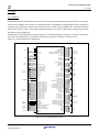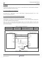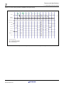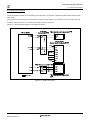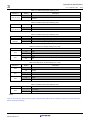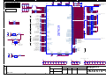
1
To our customers,
Old Company Name in Catalogs and Other Documents
On April 1st, 2010, NEC Electronics Corporation merged with Renesas Technology
Corporation, and Renesas Electronics Corporation took over all the business of both
companies. Therefore, although the old company name remains in this document, it is a valid
Renesas Electronics document. We appreciate your understanding.
Renesas Electronics website: http://www.renesas.com
April 1st, 2010
Renesas Electronics Corporation
Issued by: Renesas Electronics Corporation (http://www.renesas.com)
Send any inquiries to http://www.renesas.com/inquiry.
Notice
1.
2.
3.
4.
5.
6.
7.
All information included in this document is current as of the date this document is issued. Such information, however, is
subject to change without any prior notice. Before purchasing or using any Renesas Electronics products listed herein, please
confirm the latest product information with a Renesas Electronics sales office. Also, please pay regular and careful attention to
additional and different information to be disclosed by Renesas Electronics such as that disclosed through our website.
Renesas Electronics does not assume any liability for infringement of patents, copyrights, or other intellectual property rights
of third parties by or arising from the use of Renesas Electronics products or technical information described in this document.
No license, express, implied or otherwise, is granted hereby under any patents, copyrights or other intellectual property rights
of Renesas Electronics or others.
You should not alter, modify, copy, or otherwise misappropriate any Renesas Electronics product, whether in whole or in part.
Descriptions of circuits, software and other related information in this document are provided only to illustrate the operation of
semiconductor products and application examples. You are fully responsible for the incorporation of these circuits, software,
and information in the design of your equipment. Renesas Electronics assumes no responsibility for any losses incurred by
you or third parties arising from the use of these circuits, software, or information.
When exporting the products or technology described in this document, you should comply with the applicable export control
laws and regulations and follow the procedures required by such laws and regulations. You should not use Renesas
Electronics products or the technology described in this document for any purpose relating to military applications or use by
the military, including but not limited to the development of weapons of mass destruction. Renesas Electronics products and
technology may not be used for or incorporated into any products or systems whose manufacture, use, or sale is prohibited
under any applicable domestic or foreign laws or regulations.
Renesas Electronics has used reasonable care in preparing the information included in this document, but Renesas Electronics
does not warrant that such information is error free. Renesas Electronics assumes no liability whatsoever for any damages
incurred by you resulting from errors in or omissions from the information included herein.
Renesas Electronics products are classified according to the following three quality grades: “Standard”, “High Quality”, and
“Specific”. The recommended applications for each Renesas Electronics product depends on the product’s quality grade, as
indicated below. You must check the quality grade of each Renesas Electronics product before using it in a particular
application. You may not use any Renesas Electronics product for any application categorized as “Specific” without the prior
written consent of Renesas Electronics. Further, you may not use any Renesas Electronics product for any application for
which it is not intended without the prior written consent of Renesas Electronics. Renesas Electronics shall not be in any way
liable for any damages or losses incurred by you or third parties arising from the use of any Renesas Electronics product for an
application categorized as “Specific” or for which the product is not intended where you have failed to obtain the prior written
consent of Renesas Electronics. The quality grade of each Renesas Electronics product is “Standard” unless otherwise
expressly specified in a Renesas Electronics data sheets or data books, etc.
“Standard”:
8.
9.
10.
11.
12.
Computers; office equipment; communications equipment; test and measurement equipment; audio and visual
equipment; home electronic appliances; machine tools; personal electronic equipment; and industrial robots.
“High Quality”: Transportation equipment (automobiles, trains, ships, etc.); traffic control systems; anti-disaster systems; anticrime systems; safety equipment; and medical equipment not specifically designed for life support.
“Specific”:
Aircraft; aerospace equipment; submersible repeaters; nuclear reactor control systems; medical equipment or
systems for life support (e.g. artificial life support devices or systems), surgical implantations, or healthcare
intervention (e.g. excision, etc.), and any other applications or purposes that pose a direct threat to human life.
You should use the Renesas Electronics products described in this document within the range specified by Renesas Electronics,
especially with respect to the maximum rating, operating supply voltage range, movement power voltage range, heat radiation
characteristics, installation and other product characteristics. Renesas Electronics shall have no liability for malfunctions or
damages arising out of the use of Renesas Electronics products beyond such specified ranges.
Although Renesas Electronics endeavors to improve the quality and reliability of its products, semiconductor products have
specific characteristics such as the occurrence of failure at a certain rate and malfunctions under certain use conditions. Further,
Renesas Electronics products are not subject to radiation resistance design. Please be sure to implement safety measures to
guard them against the possibility of physical injury, and injury or damage caused by fire in the event of the failure of a
Renesas Electronics product, such as safety design for hardware and software including but not limited to redundancy, fire
control and malfunction prevention, appropriate treatment for aging degradation or any other appropriate measures. Because
the evaluation of microcomputer software alone is very difficult, please evaluate the safety of the final products or system
manufactured by you.
Please contact a Renesas Electronics sales office for details as to environmental matters such as the environmental
compatibility of each Renesas Electronics product. Please use Renesas Electronics products in compliance with all applicable
laws and regulations that regulate the inclusion or use of controlled substances, including without limitation, the EU RoHS
Directive. Renesas Electronics assumes no liability for damages or losses occurring as a result of your noncompliance with
applicable laws and regulations.
This document may not be reproduced or duplicated, in any form, in whole or in part, without prior written consent of Renesas
Electronics.
Please contact a Renesas Electronics sales office if you have any questions regarding the information contained in this
document or Renesas Electronics products, or if you have any other inquiries.
(Note 1) “Renesas Electronics” as used in this document means Renesas Electronics Corporation and also includes its majorityowned subsidiaries.
(Note 2) “Renesas Electronics product(s)” means any product developed or manufactured by or for Renesas Electronics.
User’s Manual
SH7619 CPU Board
M3A-HS19
User’s Manual
Renesas 32-Bit RISC Microcomputers
SuperH™ RISC engine Family/SH7619 Group
Rev.1.01 2008.10
Notes regarding these materials
1. This document is provided for reference purposes only so that Renesas customers may select the appropriate
Renesas products for their use. Renesas neither makes warranties or representations with respect to the
accuracy or completeness of the information contained in this document nor grants any license to any
intellectual property rights or any other rights of Renesas or any third party with respect to the information in
this document.
2. Renesas shall have no liability for damages or infringement of any intellectual property or other rights arising
out of the use of any information in this document, including, but not limited to, product data, diagrams, charts,
programs, algorithms, and application circuit examples.
3. You should not use the products or the technology described in this document for the purpose of military
applications such as the development of weapons of mass destruction or for the purpose of any other military
use. When exporting the products or technology described herein, you should follow the applicable export
control laws and regulations, and procedures required by such laws and regulations.
4. All information included in this document such as product data, diagrams, charts, programs, algorithms, and
application circuit examples, is current as of the date this document is issued. Such information, however, is
subject to change without any prior notice. Before purchasing or using any Renesas products listed in this
document, please confirm the latest product information with a Renesas sales office. Also, please pay regular
and careful attention to additional and different information to be disclosed by Renesas such as that disclosed
through our website. (http://www.renesas.com )
5. Renesas has used reasonable care in compiling the information included in this document, but Renesas
assumes no liability whatsoever for any damages incurred as a result of errors or omissions in the information
included in this document.
6. When using or otherwise relying on the information in this document, you should evaluate the information in
light of the total system before deciding about the applicability of such information to the intended application.
Renesas makes no representations, warranties or guaranties regarding the suitability of its products for any
particular application and specifically disclaims any liability arising out of the application and use of the
information in this document or Renesas products.
7. With the exception of products specified by Renesas as suitable for automobile applications, Renesas
products are not designed, manufactured or tested for applications or otherwise in systems the failure or
malfunction of which may cause a direct threat to human life or create a risk of human injury or which require
especially high quality and reliability such as safety systems, or equipment or systems for transportation and
traffic, healthcare, combustion control, aerospace and aeronautics, nuclear power, or undersea communication
transmission. If you are considering the use of our products for such purposes, please contact a Renesas
sales office beforehand. Renesas shall have no liability for damages arising out of the uses set forth above.
8. Notwithstanding the preceding paragraph, you should not use Renesas products for the purposes listed below:
(1) artificial life support devices or systems
(2) surgical implantations
(3) healthcare intervention (e.g., excision, administration of medication, etc.)
(4) any other purposes that pose a direct threat to human life
Renesas shall have no liability for damages arising out of the uses set forth in the above and purchasers who
elect to use Renesas products in any of the foregoing applications shall indemnify and hold harmless Renesas
Technology Corp., its affiliated companies and their officers, directors, and employees against any and all
damages arising out of such applications.
9. You should use the products described herein within the range specified by Renesas, especially with respect
to the maximum rating, operating supply voltage range, movement power voltage range, heat radiation
characteristics, installation and other product characteristics. Renesas shall have no liability for malfunctions or
damages arising out of the use of Renesas products beyond such specified ranges.
10. Although Renesas endeavors to improve the quality and reliability of its products, IC products have specific
characteristics such as the occurrence of failure at a certain rate and malfunctions under certain use
conditions. Please be sure to implement safety measures to guard against the possibility of physical injury, and
injury or damage caused by fire in the event of the failure of a Renesas product, such as safety design for
hardware and software including but not limited to redundancy, fire control and malfunction prevention,
appropriate treatment for aging degradation or any other applicable measures. Among others, since the
evaluation of microcomputer software alone is very difficult, please evaluate the safety of the final products or
system manufactured by you.
11. In case Renesas products listed in this document are detached from the products to which the Renesas
products are attached or affixed, the risk of accident such as swallowing by infants and small children is very
high. You should implement safety measures so that Renesas products may not be easily detached from your
products. Renesas shall have no liability for damages arising out of such detachment.
12. This document may not be reproduced or duplicated, in any form, in whole or in part, without prior written
approval from Renesas.
13. Please contact a Renesas sales office if you have any questions regarding the information contained in this
document, Renesas semiconductor products, or if you have any other inquiries.
Table of Contents
Chapter1 Overview .............................................................................................................................. 1-1
1.1 Overview .................................................................................................................................................................... 1-2
1.2 Configuration .............................................................................................................................................................. 1-2
1.3 External Specifications ............................................................................................................................................... 1-3
1.4 Appearance ................................................................................................................................................................ 1-4
1.5 M3A-HS19 Block Diagrams........................................................................................................................................ 1-5
1.6 M3A-HS19 Board Overview ....................................................................................................................................... 1-6
1.7 M3A-HS19 Memory Mapping ..................................................................................................................................... 1-9
1.8 Absolute Maximum Ratings...................................................................................................................................... 1-10
1.9 Recommended Operating Conditions ...................................................................................................................... 1-10
Chapter2 Features and Specifications................................................................................................. 2-1
2.1 Features ..................................................................................................................................................................... 2-2
2.2 CPU............................................................................................................................................................................ 2-3
2.2.1 SH7619 ............................................................................................................................................................. 2-3
2.3 Memory ...................................................................................................................................................................... 2-4
2.3.1 SH7619 U Memory and Cache Memory ........................................................................................................... 2-4
2.3.2 Flash Memory S29GL032A90TFIR4 (Standard component)............................................................................. 2-4
2.3.3 External Synchronous DRAM (SDRAM) ........................................................................................................... 2-6
2.3.4 External EEPROM .......................................................................................................................................... 2-11
2.4 Serial Port Interface.................................................................................................................................................. 2-13
2.5 PCMCIA Card Interface............................................................................................................................................ 2-14
2.6 LAN Port Interface .................................................................................................................................................... 2-15
2.7 I/O Port ..................................................................................................................................................................... 2-16
2.8 Power Supply Circuit ................................................................................................................................................ 2-19
2.9 Clock Module............................................................................................................................................................ 2-20
2.10 Reset Module ......................................................................................................................................................... 2-21
2.11 Interrupt Switch ...................................................................................................................................................... 2-22
2.12 E10A-USB Interface ............................................................................................................................................... 2-23
Chapter3 Operational Specifications ................................................................................................... 3-1
3.1 M3A-HS19 Connectors............................................................................................................................................... 3-2
3.1.1 UART Connector Pin (J1).................................................................................................................................. 3-3
3.1.2 UART Connector (J2)........................................................................................................................................ 3-4
3.1.3 RS-422 Connector Pin (J3) ............................................................................................................................... 3-5
3.1.4 PCMCIA Connector (J4).................................................................................................................................... 3-6
3.1.5 LAN Connector (J5) .......................................................................................................................................... 3-8
3.1.6 H-UDI Connector (J6) ....................................................................................................................................... 3-9
3.1.7 Power Supply Connector (J7) ......................................................................................................................... 3-10
3.1.8 External Power Supply Connector (J8) ........................................................................................................... 3-11
3.1.9 Expansion Connectors (J9-J13) .................................................................. 3-12
3.2 Switches and LEDs .................................................................................................................................................. 3-15
3.2.1 Jumpers (JP1 - JP9) ....................................................................................................................................... 3-16
Rev. 1.01 Oct 28, 2008
REJ10J1351-0101
(i)
3.2.2 Features of Switches and LEDs ...................................................................................................................... 3-18
3.3 Dimensions............................................................................................................................................................... 3-20
Appendix..............................................................................................................................................A-1
M3A-HS19 SCHEMATICS
Rev. 1.01 Oct 28, 2008
REJ10J1351-0101
(ii)
Chapter1
1-1
Overview
Chapter1
Overview
Overview
1
1.1 Overview
1.1 Overview
The M3A-HS19 is a CPU board designed to evaluate the feature and performance of the SH7619 Group of Renesas Technology
original MCU, as well as developing and evaluating the application software for the MCUs.
SH7619 data bus, address bus and on-chip peripheral pins are all connected to expansion connectors and appropriate connectors
to allow for the timing evaluation with peripherals using measurement instruments, and the development of the optional boards
according to its application. Furthermore, it can be connected with an RS-232C connector and a LAN connector, and a PC card
can be mounted on the board.
Renesas Technology E10A-USB on-chip emulator can also be connected to the M3A-HS19.
1.2 Configuration
Figure 1.2.1 shows an example of system configuration using the M3A-HS19.
SH7619 CPU board
M3A-HS19
Expansion
connector
5V DC output
regulated PS
(1.5A min.)
Serial port connector
PCMCIA
connector
SH7619
H-UDI connector
LAN port connector
PC card*
High-performance *
Embedded Workshop
E10A-USB *
Debugger
SuperH RISC engine *
C/C++ Compiler Package
USB
Host computer*
* These items should be prepared by user.
Figure 1.2.1 M3A-HS19 System Configuration
Rev.1.01 Oct 28, 2008
REJ10J1351-0101
1-2
Overview
1
1.3 External Specification
1.3 External Specifications
Table 1.3.1 lists external specifications.
Table 1.3.1 External Specifications
No.
1
2
Items
Description
CPU
SH7619
Memories
• Input (XIN) clock: 15.625 MHz
• Bus clock: 62.5 MHz at maximum
• CPU clock: 125 MHz at maximum
• SDRAM (16-bit data bus)
• EDS1216AATA-75E: 1 (16 MB)
• Flash memory (16-bit data bus)
• S29GL032A90TFIR4: 1 (4 MB)
• EEPROM (Serial)
• S93C76AFT-V-G: 1 (8 KB, 512 x 16)
3
Connectors
4
LEDs
5
Switches
6
Dimensions
Rev.1.01 Oct 28, 2008
REJ10J1351-0101
• Expansion Connector (Bus, I/O, VCC, GND: 140 pins in total: Through-hole)
• Channel 1 serial port connector (2-pin: Through-hole)
• Channel 2 serial port connector (D-sub 9-pin)
• RS-422 serial connector (4-pin: Through-hole)
• RJ-45 LAN connector (8-pin, RJ-45)
• PC card connector (68-pin)
• H-UDI connector (14-pin)
• Power connector (2-pin: 5 V)
• External power connector (2-pin: 1.8 V: Through-hole)
• Power LED: 1
• User LEDs: 4
• Power switch: 1
• Reset push-button switch: 1
• NMI push-button switch: 1
• IRQ0 push-button switch: 1
• User DIP switches: 4/package
• Mode DIP switches: 4/package
• 1.8 V external switch jumper: 1
• PCMCIA power switch jumper: 1
• PCMCIA bus switch enable jumper: 1
• Expansion connector signal select jumpers: 5
• Dimensions: 100 mm x 100 mm
• Mounting form:6 layers, double-sided
• Board configuration:1 board
1-3
Overview
1
1.4
1.4 Appearance
Figure 1.4.1
shows the appearance of the M3A-HS19.
Figure 1.4.1 M3A-HS19 Appearance
Rev.1.01 Oct 28, 2008
REJ10J1351-0101
1-4
Overview
1
1.5 M3A-HS19 Block Diagram
1.5 M3A-HS19 Block Diagrams
Figure 1.5.1 shows the system block diagram.
Serial port connector
(RS-232C x 2, RS-422 x 1)
H-UDI (14-pin)
16-bit
H-UDI
LAN
connector
SCIF
/SCI
HIF
Expansion connector
(HIF bus)
GPIO/
EtherC
SH7619
Other
Peripheral
Functions
Expansion connector
(CPU bus)
BSC
16-bit
16-bit
16-bit
Bus switch
PCMCIA
connector
SDRAM
SDRAM
(16MB)
(16MB)
Flash Memory
(4MB)
(4MB)
SH7619 CPU Board
M3A-HS19
Figure 1.5.1 System Block Diagram
Rev.1.01 Oct 28, 2008
REJ10J1351-0101
1-5
Overview
1
1.6 M3A-HS19 Board Overview
1.6 M3A-HS19 Board Overview
Figure 1.6.1 shows the M3A-HS19 board overview.
Top view of the component side
SW1
Power switch
LED5
Power LED
U5
PCMCIA
power control IC
U7,U8,U9
Bus switch
LED1-4
User LED
J7
Power connector
J6
H-UDI connector
(14-pin)
JP9
Power switching
jumper
U6
RS-232C
driver
J14
AC adaptor jack
J2
RS-232C
serial connector
U12, U16
3.3V/1.8V
regulator IC
X3
25MHz oscillator
U1
SH7619
X1
15.625MHz oscillator
J5
RJ-45
LAN connector
SW2
Reset switch
SW6
IRQ0 switch
SW5
NMI switch
SW4
Mode DIP
switch
SW3
User DIP switch
Top view of the solder side
J4
PC card
connector
(68-pin)
J12
Expansion
connector
J10
Extension
connector
U2
Flash
memory
U14
Logic IC
U10
RS-422
driver
J9, J11, J13
Expansion connector
U13
Reset IC
U4
EEPROM
Figure 1.6.1 M3A-HS19 Board External View
Rev.1.01 Oct 28, 2008
REJ10J1351-0101
1-6
Overview
1
1.6 M3A-HS19 Board Overview
Table 1.6.1 lists major components mounted on the M3A-HS19
Table 1.6.1 Major Components
Part
Number
Name
Remarks
(By manufacturer)
U1
CPU
R4S76190W125BGV (Renesas)
U2
Flash memory
S29GL032A90TFIR4 (Spansion)
U3
SDRAM
EDS1216AATA-75E (Elpida)
U4
EEPROM
S93C76AFT-V-G (SII)
U5
PCMCIA power control IC
LTC1470CS8#PBF (Linear)
U6
RS-232C driver
SP3222ECY (Sipex)
U7,U8,U9
Bus switch
SN74CBTLV16210GR (TI)
U10
RS-422 driver
SP3077EEN-L (Sipex)
U11,U15
Logic IC
TC7S08FU (TOSHIBA)
U12,U16
Regulator IC
LMS1587CSX-ADJ (NS)
U13
Reset IC
M51957BFP (Renesas)
U14
Logic IC
SN74LVC14APWR (TI)
X1
Oscillator
SG-8002JF_15.625 MHz (Epson)
X2
Ceramic resonator
Optional, 15.625 MHz
X3
Oscillator
J1
Serial port connector (Ch1)
J2
J3
Serial port connector (Ch2)
RS-422 serial connector
SG-8002JF_25.000 MHz (Epson)
Optional,
2-pin MIL standard connector
XM2C-0912-112 (OMRON)
Optional
J4
PC card connector
ICM-C68H-S112-400R1 (J.S.T.)
J5
RJ-45 LAN connector
TLA-6T718 (TDK)
J6
H-UDI connector
7614-6002 (Sumitomo 3M)
J7
J14
J15
Power supply connector
S2B-XH-A (J.S.T.)
1.8 V External power supply Optional,
2-pin MIL standard connector
connector
Optional,
Expansion connector
20-pin MIL pitch connector
Optional,
Expansion connector
40-pin MIL pitch connector
HEC0470-01-630 (Hoshiden)
AC adapter jack
XG8V-0331 (OMRON)
3-pin connector
JP1-8
Jumper
HW-3P-G (MAC8)
JP9
Jumper
XG8V-0334 (OMRON)
LED1-4
User LED
Yellow, SML-311YT (ROHM)
LED5
Power LED
Blue, UB1114C (STANLEY)
SW1
Power switch
MS-12AAH1 (Nikkai)
SW2
Reset switch (MRES)
B3SN-3012 (OMRON)
SW3
User DIP switch
A6S-4104-H (OMRON)
SW4
Mode DIP switch
A6S-4101-H (OMRON)
SW5
NMI switch
B3SN-3012 (OMRON)
SW6
IRQ0 switch
B3SN-3012 (OMRON)
J8
J9,J11-J13
J10
Rev.1.01 Oct 28, 2008
REJ10J1351-0101
Recommended Optional Parts
(By manufacturer)
CSTCE15M7 (Murata)
A2-2PA-2.54DSA (Hirose)
A2-4PA-2.54DSA (Hirose)
A2-2PA-2.54DSA
(Hirose)
XG4C-2031 (OMRON)
XG4C-4031 (OMRON)
1-7
Overview
1
1.7 M3A-HS19 Memory Mapping
1.7 M3A-HS19 Memory Mapping
Area 0 bus width: (Default)
MD3 = 0
•••16-bit
Data alignment:
MD5 = 0(ON)
•••Big endian
MD5 = 1(OFF)
•••Little endian
(SW4-1)
Figure 1.7.1 show the memory mapping examples of the SH7619 on the M3A-HS19.
Logical Address [31~29]
Area
Cacheable/Non-cacheable
000~011
P0
Cacheable
100~
P1
Cacheable
101~
P2
Non cacheable
110~
P3
Cacheable
111~
P4
Non-cacheable (on-chip I/O) etc.
(P0 and shadow area (P1, P2, P3))
Address [28~0]
H'0000 0000
Area
Area 0
MAP = 0
Flash Memory (4 MB)
H’0000 0000~H’003F FFFF
MAP = 1
Flash Memory (4 MB)
H’0000 0000~H’003F FFFF
64 MB
User Area
User Area
Area 1
64 MB
Reserved *
(Do not use)
Reserved *
(Do not use)
Area 2
64 MB
Reserved *
(Do not use)
Reserved *
(Do not use)
SDRAM (16 MB)
H’0C00 0000~H’0CFF FFFF
SDRAM (16 MB)
H’0C00 0000~H’0CFF FFFF
User Area
User Area
Area 4
64 MB
User Area
User Area
Area 5A
32 MB
Reserved
(Do not use)
User Area
Area 5B
32 MB
User Area
Area 6A
32 MB
Reserved
(Do not use)
Area 6B
32 MB
User Area
Area 7
64 MB
Reserved *
(Do not use)
H'0400 0000
H'0800 0000
H'0C00 0000
Area 3
64 MB
H'1000 0000
H'1400 0000
H'1600 0000
H'1800 0000
H'1A00 0000
H'1C00 0000
H'1FFF FFFF
PCMCIA
User Area
PCMCIA
Reserved
(Do not use)
Note: H'0000 0000 to H'1FFF FFFF are the cache-enabled area.
Figure 1.7.1 SH7619 Memory Mapping Examples
Rev.1.01 Oct 28, 2008
REJ10J1351-0101
1-8
Overview
1
1.8 Absolute Maximum Ratings
1.8 Absolute Maximum Ratings
Table 1.8.1 lists the absolute maximum ratings.
Table 1.8.1 Absolute Maximum Ratings
Symbol
Parameter
Value
Remarks
VCC
5 V system power supply voltage
-0.3 to 6.0 V
Relative to VSS
3VCC
3.3 V system power supply voltage
-0.3 to 3.8 V
Relative to VSS
1.8VCC
1.8 V system power supply voltage
-0.3 to 2.1 V
Relative to VSS
Topr
Operating temperature
-5 to 55°C
No condensation, no corrosion gas allowed.
Tstr
Storage temperature
-10 to 60°C
No condensation, no corrosion gas allowed.
Note: Temperature refers to the air temperature in the vicinity of the board.
1.9 Recommended Operating Conditions
Table 1.9.1 lists the recommended operating conditions.
Table 1.9.1 Recommended Operating Conditions
Symbol
Parameter
VCC
5 V power supply voltage
3VCC
3.3 V power supply voltage
Value
Remarks
4.75 to 5.25 V
Relative to VSS
3.0 to 3.6 V
Relative to VSS
(Always supplied by regulator)
1.8VCC
1.8 V power supply voltage
1.71 to 1.89 V
Relative to VSS
(Normally supplied by regulator)
-
Maximum current consumption
1 A max.
on the board
Topr
Operating temperature
Rev.1.01 Oct 28, 2008
REJ10J1351-0101
0 to 50°C
No condensation, no corrosion gas allowed.
1-9
Overview
1
1.8 Absolute Maximum Ratings
This page intentionally left blank
Rev.1.01 Oct 28, 2008
REJ10J1351-0101
1-10
Chapter2Features and Specifications
Chapter2
Features and Specifications
2-1
Features and Specifications
2
2.1 Features
2.1 Features
Table 2.1.1 lists the functional modules.
Table 2.1.1 Functional Modules
Section
2.2
2.3
Features
Description
CPU
SH7619, clock mode 1
Memories
• Input (XIN) clock: 15.625 MHz
• Bus clock: 62.5 MHz, max.
• CPU clock: 125 MHz, max.
• U Memory (CPU)
• 16-KB memory
• Flash Memory
• S29GL032A90TFIR4: 1 (4 MB)
• SDRAM
• EDS1216AATA-75E: 1 (16 MB)
• EEPROM
• S-93C76AFT-V-G: 1 (8 KB, 512 x 16)
2.4
Serial Port Interface
Connects SCIF2 of the SH7619 to a serial port connector
2.5
PCMCIA Card Interface
Connects PCMCIA control signal and bus of the SH7619 to the
PCMCIA connector
2.6
LAN Port Interface
Connects the SH7619 Ether I/O to an RJ-45 connector
2.7
I/O Ports
Connects the SH7619 I/O port to an expansion connector
2.8
Power Supply Circuit
Controls the system power supply of the M3A-HS19
2.9
Clock Module
Controls the clock
2.10
Reset Module
Reset control of device mounted on the M3A-HS19
2.11
Interrupt Switches
Connects to the NMI pin and IRQ0 pin
2.12
E10A-USB Interface
SH7619 H-UDI/AUD interface
Operational specifications
Connectors, switches, jumpers, LEDs
-
• Expansion connector, H-UDI connector
• PCMCIA, ETHER, RS-232C connector
• Switches and LEDs
Refer to Chapter 3 for details
Rev.1.01 Oct 28, .2008
REJ10J1351-0101
2-2
Features and Specifications
2
2.2 CPU
2.2 CPU
2.2.1 SH7619
The M3A-HS19 CPU board includes the SH7619, the 32-bit RISC MCU operates with a maximum frequency of 125 MHz.
The SH7619 is equipped with an Ethernet controller that includes an IEEE802.3u compliant Media Access Controller and
a Physical Layer Transceiver. Moreover, the SH7619 has both a 16-KB U memory (RAM) and a 16-KB instruction/data
unified cache memory. These on-chip modules enable the SH7619 to be used in a wide range of applications from data
processing to control equipments.
The M3A-HS19 can be operated at a maximum frequency of 125 MHz (external bus: 62.5 MHz, max) using a 15.625 MHz
input clock. The dedicated clock of 25.000 MHz input from CK_PHY pin is used as an on-chip PHY clock.
Figure 2.2.1 shows the SH7619 pin assignments.
SH7619
Mode
SW4-1 "H/L"
"H"
"L"
"L"
"L"
"H"
PB13/BS#
RD#
RD/WR#
MD0
MD1
MD2
MD3
MD5
TESTMD#
TESTOUT#
WE0#/DQMLL
WE1#/DQMLU/WE#
PB05/WE2(BE2)#/DQMUL/ICIORD#
PB06/WE3(BE3)#/DQMUU/ICIOWR#
15.625MHz
EXTAL
XTAL
CKI0
Clock
25.000MHz
CS0#
PB12/CS3#
PB02/CKE
PB03/CAS#
PB04/RAS#
Bus Control
(SDRAM)
CK_PHY
RES#
NMI
PD0/IRQ0/-/TEND0
System
Control
Bus Control
(All,FLASH
SDRAM,PCMCIA)
PB10/CS5B#/CE1A#
PB09/CE2A#
PB00/WAIT#
PB01/IOIS16#
Bus Control
(PCMCIA)
PA25/A25/SIOFSYNCO
PA24/A24/TXD_SIO0
PA23/A23/RXD_SIO0
PA22/A22/SIOMCLK0
PA21/A21/SCK_SIO0
CPU
Address Bus
16
Lower
Data Bus
16
PA20/A20
PA19/A19
PA18/A18
PA17/A17
PA16/A16
A15-A0
D15-D0
PE24/HIFD15/CTS1/D31
PE23/HIFD14/RTS1/D30
PE22/HIFD13/CTS1/D29
PE21/HIFD12/RTS0/D28
PE20/HIFD11/SCK0/D27
PE19/HIFD10/RXD0/D26
PE18/HIFD09/TXD1/D25
HIF-D/Upper
Data bus
Serial Channel 0
PE17/HIFD08/SCK0/D24
PE16/HIFD07/RXD0/D23
PE15/HIFD06/TXD0/D22
PE14/HIFD05/-/D21
PE13/HIFD04/-/D20
PE12/HIFD03/-/D19
PE11/HIFD02/-/D18
PE10/HIFD01/-/D17
PE09/HIFD00/-/D16
SW3
User port
(Ether)
PC16/MDIO
PC17/MDC
PC18/LINKSTA
PC19/EXOUT
LED
User port
(Ether)
PC04/MII_TXD0/-/SPEED100#
PC05/MII_TXD1/-/LINK#
PC06/MII_TXD2/-/CRS#
PC07/MII_TXD3/-/DUPLEX#
Ether.ref
EXRES1
TSTBUSA
RXM
RXP
Ether
Interface
TXM
TXP
PC00/MII_RXD0
PC01/MII_RXD1
EEPROM
Extension
Connector
PC02/MII_RXD2
PC03/MII_RXD3
PE08/HIFCS#
PE07/HIFRS
PE06/HIFWR#/SIOFSYNC0
PE05/HIFRD
PE03/HIFMD
PE00/HIFEBL/SCK_SIO0
PE04/HIFINT#/TXD_SIO0
PE02/HIFDREQ/RXD_SIO0
PE01/HIFRDY/SIOMCLK0
PC09/RX_ER
PC14/COL
PC15/CRS
PC20/WOL
PC08/RX_DV
PC10/RX_CLK
PC11/TX_ER
PC12/TX_EN
PC13/TX_CLK
PD2/IRQ2/TXD1/DREQ0
PD3/IRQ3/RXD1/DACK0
PD5/IRQ5/TXD2/DREQ1
PD6/IRQ6/RXD2/DACK1
SW4-3
SW4-2
HIF
Interface
RESET#
REG#
CD#
PCMCIA
Interface
EN#
Other Extension
Bus Interface
RS-422,RS-232C
Interface
ASEMD#
TRST#
TDO
TDI
TMS
TCK
H-UDI
Interface
Figure 2.2.1 Pin Assignments by function
Rev.1.01 Oct 28, .2008
REJ10J1351-0101
2-3
Features and Specifications
2
2.3 Memory
2.3 Memory
The M3A-HS19 includes the SH7619 on-chip U memory, an external flash memory, external SDRAM and EEPROM.
Details are described below (Except the PC card).
2.3.1 SH7619 U Memory and Cache Memory
The SH7619 has a 16-KB (RAM) U memory module (address: H’E55FC000~H’E55FFFFF) and a 16-KB
instruction/data-unified cache memory.
2.3.2 Flash Memory S29GL032A90TFIR4 (Standard component)
The M3A-HS19 comes standard with a flash memory listed in Table 2.3.1 to store a user program.
The flash memory is an external bus 16-bit mode fixed and operates at 3.3 V single. The write-protection of flash memory
can be enabled or disabled by DIP switches (SW4-4).
Figure 2.3.1 shows the Flash Memory Block Diagram. Table 2.3.2 lists setting examples of the bus state
controller(write/read) when the SH7619 bus clock operates at 62.5 MHz (clock mode 1), and Figure 2.3.2 shows read and
write access timing example.
Table 2.3.1 Flash Memory Specifications
Part Number
Bus Size
Capacity
S29GL032A90TFIR4
16-bit mode
4 MB (16 bits x 2 Mwords x 1)
90 ns
S29GL032A90TFIR4 (U2)
(2 Mwords x 16 bits)
SH7619 (U1)
3.3 V
21
A21-A1
A20-A0
16
D15-D0
DQ15-DQ0
3.3 V
RD#
Access Time
BYTE#
OE#
3.3 V
3.3 V
WE#
WE0#
CS0#
CE#
RESET#
Reset Signal
NC
RY/BY#
3.3 V
DIP Switch
( SW4-4)
WP#
Figure 2.3.1 Flash Memory Block Diagram
Rev.1.01 Oct 28, .2008
REJ10J1351-0101
2-4
Features and Specifications
2
2.3.2 Flash Memory S29GL032A90TFIR4 (Standard component)
Table 2.3.2 Setting Example of Bus State Controller (Flash Memory Write and Read)
User Area
Applicable Device
CS0
Settings for Bus State Controller
S29GL032A90TFIR4
CS0 Space Bus Control Register: CS0BCR
Initial value: H'36DB 0400 (MD3 = "L")
Recommended value: H'1000 0400
• Idle Cycles between Write-Read Cycles and
Write-Write Cycles
IWW[1:0] = B'01: 1 idle cycle inserted
• Data bus width
BSZ[1:0] = B’10: *Shall be ignored.
CS0 space wait control register: CS0WCR
Initial value: H'0000 0500
Recommended value: H'0000 0AC1
• Number of Delay Cycles from address, CS0#
Assertion to RD#, WEn#
SW[1:0] = B'01; 1.5 cycles
• Number of Access Wait Cycles
WR[3:0] = B'0101; 5 cycles
• Ignore external WAIT input
WM = B’1;
• Number of Delay Cycles from RD#, WEn# negation
to address, CS0# negation
HW[1:0] = B'01; 1.5 cycles
<Write/Read Timing>
Write1
Th
T1
Tw 1
Tw 2
Tw 3
Write2
Tw 4
Tw 5
T2
Tf
Taw 1
Th
T1
Tw 1
Tw 2
Tw 3
Read1
Tw 4
Tw 5
T2
Tf
Taw 1
Th
T1
Tw 1
Tw 2
Tw 3
Tw 4
Tw 5
T2
Tf
CKIO
tWC
tAD1
tAD1
tAD1
tCSD1
tCSD1
tAD1
tAD1
tRC
tAD1
A21-A1
tCSD1
tCSD1
tCSD1
tCSD1
CS0#
tRSD
tRSD
RD#
tWED1
tCS
tAS
tWED1
tCH
tAH
tWP
tWED1
tWPH
tWED1
tCH
tAH
tWP
tOEH
WE0#
tDS
tWDD1
tDH
tWDD1
D15-D0
DATA
tWDH1
tDS
tDH
DATA
tWDH1
ta(OE)
ta(AD)
ta(CE1)
tRDS1
DATA
tDF(CE)
tRDH1
tDF(OE)
Figure 2.3.2 Flash Memory Read and Write Access Timing Example
Rev.1.01 Oct 28, .2008
REJ10J1351-0101
2-5
Features and Specifications
2
2.3.3 External Synchronous DRAM
2.3.3 External Synchronous DRAM (SDRAM)
The M3A-HS19 is provided with a 16-MB synchronous DRAM (SDRAM) as an external main memory. The SDRAM is
controlled by the SH7619 on-chip bus state controller. The SDRAM is accessed in 16-bit bus.
Table 2.3.3 lists SDRAM specifications used on the M3A-HS19, and Figure 2.3.3 shows its block diagram.
Table 2.3.3 SDRAM Specifications
Items
Description
Part Number
EDS1216AATA-75E
Configuration
16 MB (16-bit bus width) x 1
Capacity
16 MB
Access Time
5.4 ns
CAS Latency
2 (at 62.5 MHz bus clock)
Refresh Interval
4,096 refresh cycles in every 64 ms
Row Address
A11- A0
Column Address
A8 - A0
Number of Banks
4-banks controlled by BA0, BA1
3.3V
EDS1216AATA-75(U3)
(2 Mx 16 bits x 4-bank)
SH7619(U1)
2
A14-13
11
A12-1
BA1-0
A11-0
CS3#
CS#
CKIO
CLK
CKE
CKE
RD/WR#
WE#
RAS#
RAS#
CAS#
CAS#
DQMLU
DQMU
DQMLL
DQML
16
D15-0
DQ15-DQ0
x 16
Figure 2.3.3 External SDRAM Block Diagram
Rev.1.01 Oct 28, .2008
REJ10J1351-0101
2-6
Features and Specifications
2
2.3.3 External Synchronous DRAM
A power-on sequence is required to use a SDRAM. Power-on sequence is to initialize the pin function controller (PFC),
set registers in the bus state controller and write data in the SDRAM mode register.
Table 2.3.4 lists the access address when writing in the SDRAM mode register on the CS3 space.
Table 2.3.4 Access Address for SDRAM Mode Register Write (CS3 Space)
Data bus
CAS
width
latency
16 bits
2
Burst read/single write (burst length 1)
Burst read/burst write (burst length 1)
Access Address
External Address Pin
Access Address
External Address Pin
H'F8FD 5440
H'0000 0440
H'F8FD 5040
H'0000 0040
Execute following settings to the M3A-HS19 SDRAM mode register.
• Burst length: Burst read/single write (burst length 1)
• Wrap type: Sequential
• CAS latency: 2 cycles
To write data in the SDRAM mode register as shown in Table 2.3.4, write the arbitrary data in words to the address of
H'F8FD 5440 (the data in this case is ignored). Following commands are sequentially issued to the SDRAM by the word
writing.
1.All banks precharge command (PALL)
Idle cycles (Tpw), of which number is specified by bits WTRP1 and WTRP0 in CS3WCR, are inserted between the PALL
and the first REF commands.
2. Auto-refreshing command (REF) for eight times
Idle cycles (Trc), of which number is specified by bits WTRP1 and WTRP0 in CS3WCR are inserted after issuing REF
command
3. Mode register write command (MRS)
Rev.1.01 Oct 28, .2008
REJ10J1351-0101
2-7
Features and Specifications
2
2.3.3 External Synchronous DRAM
Figure 2.3.4 shows a timing example of SDRAM mode register writing.
tRP
Tp
Tpw
tRC
Trr
Trc
Trc
Trc
Trc
Trc
Trr
Trr
Trc
Tmw
Tnop
REF
DESL
MRS
DESL
CKIO
REF command is issued 8 times
SDRAM
Command
PALL
DESL
REF
DESL
DESL
DESL
DESL
DESL
REF
A11-A1(A9-A0)
A12(A10/AP)
CS3#
RASL#
CASL#
RD/WR#
DQMUU-LL
(High)
Hi-Z
D15-0
[Symbols Descriptions]
PALL : All bank precharge command
REF : Auto-refreshing command
MRS : Mode register write commamd
DESL : Deselect command
Figure 2.3.4 Timing Example of SDRAM Mode Register Writing
Rev.1.01 Oct 28, .2008
REJ10J1351-0101
2-8
Features and Specifications
2
2.3.3 External Synchronous DRAM
Table2.3.5 lists setting examples of the bus state controller with SH7619 bus clock at 62.5 MHz.
Figure 2.3.5 shows the SDRAM single read/write timing example.
Table2.3.5 Setting Example of Bus State Controller (SDRAM Read/Write)
User Area
CS3
Applicable Device
EDS1216AATA-75E
Rev.1.01 Oct 28, .2008
REJ10J1351-0101
Settings for Bus State Controller
CS3 Space Bus Control Register: CS3BCR
Initial value: H'36DB 0600
Recommended value: H'0000 4400 (in 16-bit bus width)
• Memory specification
TYPE[3:0] = B'0100; SDRAM
• Data bus specification
BSZ[1:0] = B'10; 16-bit bus width
CS3 Space Wait Control Register: CS3WCR
Initial value: H'0000 0500, recommended value: H'0000 2892
• Wait Cycle Number for Precharge Completion
WTRP[1:0] = B'01; 1 cycle
• Wait Cycle Number from ACTV command to READA WRITA
command
WTRCD[1:0] = B'10; 2 cycles
• Cas Latency for Area 3
A3CL[1:0] = B'01; 2 cycles
• Wait Cycle Number for Precharge Start Wait
TRWL[1:0] = B'10; 2 cycles
• Idle Cycle Number from REF/Self-Refreshing Release to
ACTV/REF/MRS Command
WTRC[1:0] = B'10; 5 cycles
SDRAM Control Register: SDCR
Initial value: H'0000 0000,
Recommended value: H'0000 0809
• Refresh Control
RFSH = B'1; Refreshing is performed
• Refresh Control
RMODE = B'0; Auto-Refreshing is not performed
• Bank active mode
BACTV = B'0; Auto-precharge mode
• Number of Bits of Row Address for Area 3
A3ROW[1:0] = B'01; 12 bits
• Number of Bits of Column Address for Area 3
A3COL[1:0] = B'01; 9 bits
Refresh Timer Control / Status Register: RTCSR
Initial value: H'0000 0000,
Recommended value: H'A55A 0010
• Clock Select
CKS[2:0] = B'010; Bφ/16
• Refresh Count
RRC[2:0] = B'000 ; Once
Refresh Time Constant Register: RTCOR
Initial value: H'0000 0000,
Recommended value: H'A55A 003D
*The refresh request interval when clock select is set to Bφ/16 is as
follows.
1 cycle: 256 nsec (62.5 MHz/16 = 3.90625 MHz)
Refresh request interval in this SDRAM: 15.625 μsec/time
15.625 usec/256 nsec = 61 (0x3D) cycles/refresh counts
2-9
Features and Specifications
2
2.3.3 External Synchronous DRAM
SDRAM SINGLE READ
SDRAM SINGLE WRITE
tRC
tRC
tRAS
tRP
tRAS
tRCD
tRP
tDPL
tDAL
AC T
Tr
Trw1
READ A
Tc1
Tcw
Td1
Tde
Tap
ACT
Tr
Trw1
W RITEA
Tc1
Trwl1
Trwl2
Tap
AC T
Tr
CKIO
CKE
tSI
tSI
tHI
tCSD1
tHI
tCSD1
tCSD1
tCSD1
CS3#
tRASD1
tHI
tSI
tRASD1
tRASD1
tRASD1
RAS#
tHI
tSI
tCASD1
tCASD1
tCASD1
tCASD1
CAS#
tRWD1
tRWD1
RD/WR#
tDQMD1
tDQMD1
tDQMD1
tDQMD1
DQMUU-LL
tAD1
tAD1
tAD1
tAD1
tAD1
tAD1
tAD1
tAD1
tAD1
tAD1
tAD1
tAD1
tAD1
tAD1
tAD1
tAD1
tAD1
tAD1
A11-A1(A9-A0)
A12(A10/AP)
A14,A13(BA1,0)
tLZ
D15-0
tAC
Data
tRDS2
tRDH2
tOH
tOHZ
tHI
tSI
tWDD2
tWDH2
Figure 2.3.5 SDRAM Single Read/Write Timing
Rev.1.01 Oct 28, .2008
REJ10J1351-0101
2-10
Features and Specifications
2
2.3.4 External EEPROM
2.3.4 External EEPROM
The M3A-HS19 is provided with an EEPROM for storing MAC address.
Access to the EEPROM is enabled by using the SH7261 I/O ports (PC03, PC02, PC01 and PC00). A MAC address
consists of 48-bit numbers.
Table 2.3.6 lists instruction sets, and Figure 2.3.6 shows the block diagram of CPU and EEPROM connection.
Figure 2.3.7 shows the EEPROM-AC timing and Figure 2.3.8 shows EEPROM-read/write timing.
Settings for following instruction sets are not required;
-
A7 to A0 for WRAL, ERAL, EWEN, and EWDS instructions
-
Data for ERASE, ERAL, EWEN and EWDS instructions
Table 2.3.6 Instruction Sets (S-93C76AFT)
Start Bit
Command
1
Operation
Code
2
3
4
5
6~13
1
1
1
1
1
1
1
1
0
1
0
0
0
0
0
1
1
0
A8
A8
A8
1
0
1
0
A7~A0
A7~A0
A7~A0
-
SK
READ
WRITE
ERASE
WRAL
ERAL
EWEN
EWDS
0
1
1
0
0
0
0
Address
Data
14~29
D15~D0 (OUT)
D15~D0 (IN)
D15~D0(IN)
-
3.3 V
SH7619 (U1)
PC03/MII_RXD3
PC02/MII_RXD2
PC01/MII_RXD1
PC00/MII_RXD0
EEPROM
S-93C76AFT(U4)
CS
SK
DI
DO
Vcc
TEST
NC
GND
Figure 2.3.6 CPU and EEPROM Connection
Rev.1.01 Oct 28, .2008
REJ10J1351-0101
2-11
Features and Specifications
2
2.3.4 External EEPROM
AC characteristics
Clock pulse width
SK
1 μsec
or more
0 sec or more
1 μsec or more
Writing
Enabled Data
CS
Deselect
CS setup
400 nsec or more
200 nsec or more
DI
Setup
200 nsec or more
Hold
200 nsec or more
Hi-Z
Hi-Z
DO
Within
Within 800 nsec
800 nsec
Output delay time
Output disabled time
Within 500 nsec
Output Enabled Data
Figure 2.3.7 EEPROM-AC Timing
READ
Dummy SK
SK
1
2
3
4
5
6
7
CS
DI
8
9
10
11 12 13 14 15 16
27 28 29 30 31 32
43 44 45 46 47 48
Setting Address
"0"
"1" "1" "0" "x" A8 A7 A6 A5 A4 A3 A2 A1 A0 "x"
Hi-Z
Hi-Z
DO
"0"
D15 D14 D13
D2
D1
D0 D15 D14 D13
(Setting Address)Data0
D2
D1
D0 D15 D14 D13
(Setting Address+1)Data1 (Setting Address+2)Data2
WRITE
Dummy SK
SK
1
CS
DI
2
3
4
5
6
7
8
9
10
11 12 13 14 15 16
27 28 29 30 31 32
Verify
Writing Instruction, Address, Writing Data Input
"0"
"1"
DO
"0"
"1"
"x"
A8
A7
A6
A5
A4
A3
A2
A1
A0
D15 D14 D13
D2
D1
Standby
D0
Hi-Z
"0"
Start writing
Hi-Z
"1"
End of writing
Figure 2.3.8 EEPROM-Read/Write Timing
Rev.1.01 Oct 28, .2008
REJ10J1351-0101
2-12
Features and Specifications
2
2.4 Serial Port Interface
2.4 Serial Port Interface
The SH7619 MCU mounted on the M3A-HS19 is provided with a 3 channel’s of the Serial Communication Interface with
FIFO (SCIF).
SCIF channel 0 is connected to the 2-pin serial port connector, SCIF channel 2 is connected to the D-sub 9-pin serial port
connector, and SCIF channel 1 is connected to the 4-pin serial port connector.
Figure 2.4.1 shows the block diagram of the serial port interface.
Figure 2.4.1 Serial Port Interface
Rev.1.01 Oct 28, .2008
REJ10J1351-0101
2-13
Features and Specifications
2
2.5 PCMCIA Card Interface
2.5 PCMCIA Card Interface
The SH7619 MCU mounted on the M3A-HS19 is compliant with the JEIDA 4.2 (PCMCIA2.1 Rev.2.1). However, only
3.3 V interface PC card is supported. An on-chip bus state controller (BSC) and a PFC control the PC card.
High byte and low byte of the data is switched at the bus switch on the M3A-HS19. When the byte order of the SH7619 is
big-endian, the order of the PC card connector is little-endian (IOIS16#: ”L”).
The M3A-HS19 is provided with a PCMCIA card slot in area 5, allowing both IC memory card and I/O card to be mounted.
Figure 2.5.1 shows the block diagram of PCMCIA card interface.
SH7619 (U1)
PC card connector (J4)
20-bit bus switch
D15-D6
10
1B[9:0]
1A[9:0]
10
6
2B[9:0]
2A[9:0]
6
D5-D0
D7-D0, D15, D14
D13-D8
1OE#
2OE#
20-bit bus switch
A25-A16
A15-A6
10
1B[9:0]
1A[9:0]
10
10
2B[9:0]
2A[9:0]
10
A25-A16
A15-A6
A5-A0
A5-A0
1OE#
2OE#
6
RESET
CE1#
CE2#
REG#
OE#
WE#
IORD#
IOWR#
CD1#
CD2#
WAIT#
IOIS16#
IREQ#
20-bit bus switch
4
1B[9:0]
1A[9:0]
10
4
4
2B[9:0]
2A[9:0]
8
4
3.3 V
x3
1OE#
4
2OE#
2
PCVCC
x5
VS1#
VS2#
INPACK#
SPKR#
STSCHG#
VCC
6
PC09/RX_ER(GPIO)
CE2A#
CE1A#
PC14/COL
RD#
WE#
PB05/ICIORD#
PB06/ICIOWR#
PC15/CRS
PB0/WAIT#
PB1/IOIS16#
PD7/IRQ7
JP2
5.0 V
PC20/WOL
3.3 V
PB13/BS#
PCMCIA
Power supply
circuit
JP1
PCVCC
Figure 2.5.1 PCMCIA Card Interface
Rev.1.01 Oct 28, .2008
REJ10J1351-0101
2-14
Features and Specifications
2
2.6 LAN Port Interface
2.6 LAN Port Interface
An IEEE 802.3 compliant (MAC layer) Ethernet controller and an IEEE802.3/802.3u compliant (10/100 Mbps Ethernet
PHY) physical layer transceiver are embedded in the SH7619 MCU.
Figure 2.6.1 shows the block diagram of LAN port interface.
3.3 V
SH7619 (U1)
LED1
Yellow
LED2
Yellow
LED3
Yellow
LED4
Yellow
SPEED100#
LINK#
CRS#
3.3 VA
DUPLEX#
RJ-45 (J5)
(MII)
ETC
TxP
1
TxM
2
TX +
TX −
3
PHY
TCT
RxP
4
RxM
5
RX +
RX −
6
RCT
EXRES1
7
TSTBUSA
8
12.4 K(1%)
CK_PHY
25.000 MHz-OSC
3 VAGND
MII-compliant signal
Figure 2.6.1 LAN Port Interface
Rev.1.01 Oct 28, .2008
REJ10J1351-0101
2-15
Features and Specifications
2
2.7 I/O Port
2.7 I/O Port
Following I/O ports on the M3A-HS19 can be configured by the SH7619 MCU. These ports are multiplexed pins with up to
four features. Some pins have several initial features for normal mode and HIF (Host Interface) boot mode. Features can
be controlled by PFC (pin function controller).
• PA16 - PA25
• PB00 - PB13
• PC00 - PC20
• PD0 - PD7
• PE00 - PE24
The M3A-HS19 is connected with a memory, expansion connectors, a PCMCIA connector, a LAN connector, an RS-232C
connector, an RS-422 connector and other control ICs. Some I/O ports are connected to DIP switches and LEDs, which
can be used in the port mode as intended use. LED shows status in the PHY mode.
Table 2.7.1 lists Mode DIP Switch (SW4) Features. The state will be loaded when the board is reset and started.
Table 2.7.1 Mode DIP Switch (SW4) Features
Description
SW4-No.
1
ON: Big-endian
OFF: Little-endian
2
ON: Host interface (HIF) is NOT operating OFF: Host interface (HIF) is operating
3
ON: Normal boot mode
OFF: HIF boot mode
4
ON: Flash ROM is write-protected
OFF: Write-enabled
Figure 2.7.1 shows the block diagram of I/O port connections to switches and LEDs.
Table 2.7.2 and Table 2.7.3 list I/O port features.
Figure 2.7.1 I/O Port Connection to Switches and LEDs
Rev.1.01 Oct 28, .2008
REJ10J1351-0101
2-16
Features and Specifications
2
2.7 I/O Port
Table 2.7.2 I/O Port Features (1/2)
Port Name
(SH7619)
PA16~PA20
Signal Name and Connection (M3A-HS19)
A16~A20: Flash ROM, PCMCIA, expansion connector
PA21
A21/SCK_SIO0: Flash ROM, PCMCIA, expansion connector
PA22
A22/SIOMCLK0: Flash ROM, PCMCIA, expansion connector
PA23
A23/RxD_SIO0: Flash ROM, PCMCIA, expansion connector
PA24
A24/TxD_SIO0: PCMCIA, expansion connector
PA25
A25/SIOFSYNC0: PCMCIA, expansion connector
PB0
WAIT#: PCMCIA
PB1
IOIS16#: PCMCIA
PB2
CKE: SDRAM
PB3
CAS#: SDRAM
PB4
RAS#: SDRAM
PB5
WE2#/DQMUL/ICIORD#: PCMCIA, expansion connector
PB6
WE3#/DQMUU/ICIOWR#: PCMCIA, expansion connector
PB7
CE2B#: Expansion connector
PB8
CS6B#/CE1B#: Expansion connector
PB9
CE2A#: PCMCIA
PB10
CS5B#/CE1A#: PCMCIA
PB11
CS4#: Expansion connector
PB12
CS3#: SDRAM, expansion connector
PB13
BS#: PCMCIA-PW control, expansion connector
PC0~PC3
MII_RxD0~MII_RxD3: EEPROM, expansion connector
PC4
MII_TxD0/SPEED100#: LED1
PC5
MII_TxD1/LINK#: LED2
PC6
MII_TxD2/CRS#: LED3
PC7
MII_TxD3/DUPLEX#: LED4
PC8
RX_DV: Expansion connector
PC9
RX_ER: PCMCIA
PC10
RX_CLK: Expansion connector
PC11
TX_ER: Expansion connector
PC12
TX_EN: Expansion connector
PC13
TX_CLK: Expansion connector
PC14
COL: PCMCIA
PC15
CRS: PCMCIA, expansion connector
PC16
MDIO: SW3-1 (Port IN)
PC17
MDC: SW3-2 (Port IN)
PC18
LNKSTA: SW3-3 (Port IN)
PC19
EXOUT: SW3-4 (Port IN)
PC20
WOL: PCMCIA (Bus DIR) , expansion connector
PD0
IRQ0/TEND0: SW6(IRQ0)
PD1
IRQ1/TEND1: Expansion connector
Rev.1.01 Oct 28, .2008
REJ10J1351-0101
2-17
Features and Specifications
2
2.7 I/O Port
Table 2.7.3 I/O Port Features (2/2)
Port Name
Signal Name and Connection (M3A-HS19)
(SH7619)
PD2
IRQ2/TxD1/DREQ0: RS-422
PD3
IRQ3/RxD1/DACK0: RS-422
PD4
IRQ4/SCK1: Expansion connector
PD5
IRQ5/TxD2/DREQ1: RS-232C
PD6
IRQ6/RxD2/DACK1: RS-232C
PD7
IRQ7/SCK2: PCMCIA, expansion connector
PE0
HIFEBL/SCK_SIO0: SW4-2, expansion connector
PE1
HIFRDY/SIOMCLK0: Expansion connector
PE2
HIFDREQ/RxD_SIO0: Expansion connector
PE3
HIFMD: SW4-3
PE4
HIFINT#/TxD_SIO0: Expansion connector
PE5
HIFRD#: Expansion connector
PE6
HIFWR#/SIOFSYNC: Expansion connector
PE7
HIFRS: Expansion connector
PE8
HIFCS#: Expansion connector
PE9~PE14
HIFD0~HIFD5/D16~D21: Expansion connector
PE15
HIFD6/TxD0/D22: Expansion connector, 3-wire RS-232C
PE16
HIFD7/RxD0/D23: Expansion connector, 3-wire RS-232C
PE17
HIFD8/SCK0/D24: Expansion connector
PE18
HIFD9/TxD1/D25: Expansion connector
PE19
HIFD10/RxD1/D26: Expansion connector
PE20
HIFD11/SCK1/D27: Expansion connector
PE21
HIFD12/RTS0/D28: Expansion connector
PE22
HIFD13/CTS0/D29: Expansion connector
PE23
HIFD14/RTS1/D30: Expansion connector
PE24
HIFD15/CTS1/D31: Expansion connector
Rev.1.01 Oct 28, .2008
REJ10J1351-0101
2-18
Features and Specifications
2
2.8 Power Supply Circuit
2.8 Power Supply Circuit
The main power supply input 5 V DC to the M3A-HS19 and it generates 3.3 V and 1.8 V using a regulator.
It is an adjustable output voltage regulator to generate a desired voltage by changing resistance values.
A through-hole is provided with the M3A-HS19 to input 1.8 V DC from an external power supply. The PC card power
supply is controlled by software.
Figure 2.8.1 shows the schematic diagram of the power supply circuit.
5V
Expansion connector (J12)
1
2
Regulator (U12)
5 V-IN
(J7)
Flash
memory
(U2)
SDRAM
(U3)
Other
logic IC
Expansion connector
(J10)
SW1
5V
1
3.3 V
SH7619
(U1)
2
GND
PB13/BS#
Regulator (U16)
JP3
5V
1.8 V-IN
(J8)
EN1
JP1
EN0
1.8 V
LTC1470
(U5) PCMCIA connector
(J4)
1
2
GND
Figure 2.8.1 Power Supply Circuit
Rev.1.01 Oct 28, .2008
REJ10J1351-0101
2-19
Features and Specifications
2
2.9 Clock Module
2.9 Clock Module
The clock module on the M3A-HS19 consists of following three blocks;
•
•
•
A block connecting X1 (oscillator) output to SH7619 EXTAL
A block connecting X2 (ceramic resonator) to EXTAL and XTAL (Optional)
A block connecting X3 (oscillator) to CK-PHY
An on-chip oscillator (15.625 MHz) is connected to the SH7619 MCU to provide an operating clock. Another on-chip
oscillator (25.000 MHz) is also connected to the MCU to provide clock to physical layer. Bus clock output is connected to
a SDRAM and expansion connectors via damping resisters respectively.
Figure 2.9.1 shows the block diagram of clock module.
* : To mount a ceramic resonator,remove the resistance R13 and mount the resistance R14.
:Optional
SH7619(U1)
R98
R13
CLK
EXTAL
R14
Oscillator(X1)
15.625MHz
CKIO
XTAL
EXCLK expansion
connector(J10-36)
R117
CLK SDRAM(U3)
Ceramic
resonator*(X2)
Optional
CSTCE-G15M7
(Murata)
CLK
R18
CK-PHY
Oscillator(X3)
25.000MHz
Figure 2.9.1 Clock Module
Rev.1.01 Oct 28, .2008
REJ10J1351-0101
2-20
Features and Specifications
2
2.10 Reset Module
2.10 Reset Module
Reset module controls reset signals connected to the SH7619 MCU, a flash memory and connectors. Software controls to
reset PCMCIA connector.
Figure 2.10.1 shows the schematic diagram of resets.
H-UDI connector
RESET#
Reset IC output delay time: td = 0.34×Cd(pF)µsec = 34 ms
)
)
Reset IC output detect voltage: Vs = 1.25× Ra+Rb = 2.5 V
Rb
Expansion connector
RESET#
3.3 V
3.3 V
Flash memory
*Open collector output
Ra
10 KΩ
Reset IC
M51957BFP(U13)
Input
Rb
10 KΩ
Output
RESET#
LVC14(U14)
SH7619
*
RES#
100 Ω
Delay capacitor
S08(U15)
Cd
0.1 µF
PC09/RX_ER
PC20/WOL
RESET_IN(J9-1)
SW2
Reset switch
RESET
PCMCIA(J4)
JP2
1OE#
2OE#
Bus switch (U9)
Figure 2.10.1 M3A-HS19 Reset System
Rev.1.01 Oct 28, .2008
REJ10J1351-0101
2-21
Features and Specifications
2
2.11 Interrupt Switch
2.11 Interrupt Switch
Push-button switches are connected to the SH7619 NMI pin and IRQ0 pin.
Interrupts are connected to IRQ7 from an expansion connector and a PCMCIA connector.
Figure 2.11.1 shows the schematic diagram of interrupts.
3.3 V
SH7619 (U1)
NMI
SW 5
LVC14(U14)
NMI switch
3.3 V
PD0/IRQ0/-/TEND0
SW 6
LVC14(U14)
IRQ0 switch
PC20/WOL
IREQ#
16
PD7/IRQ7/SCK2
PCMCIA(J4)
JP2
Expansion connector (J11)
18
R106
1OE#
2OE#
Bus switch (U9)
Figure 2.11.1 Interrupts
Rev.1.01 Oct 28, .2008
REJ10J1351-0101
2-22
Features and Specifications
2
2.12 E10A-USB Interface
2.12 E10A-USB Interface
The M3A-HS19 is provided with a 14-pin H-UDI connector to embed the E10A-USB emulator.
Figure 2.12.1 shows the block diagram of the E10A-USB interface.
3.3 V
3.3 V
H-UDI connector (J6)
SH7619 (U1)
UVCC
TCK
8
10
12
NC
11
TCK
1
TRST#
TRST#
TDO
GND
NC
GND
TMS
13
GND
14
GND
TDI
(GND)
3
TDO
4
5
TMS
6
TDI
9
ASEMD#
7
RES#
RES#
Reset
Figure 2.12.1 E10A-USB Interface
Rev.1.01 Oct 28, .2008
REJ10J1351-0101
2-23
Features and Specifications
2
2.12 E10A-USB Interface
This page intentionally left blank.
Rev.1.01 Oct 28, .2008
REJ10J1351-0101
2-24
Chapter3Operational Specifications
Chapter3
Operational Specifications
3-1
Operational Specifications
3
3.1 M3A-HS19 Connector
3.1 M3A-HS19 Connectors
Figure 3.1.1 shows the connector assignments on the M3A-HS19.
Top view of the component side
J6
H-UDI
connector
J7
Power
supply
connector
J1
RS-232C (ch1)
serial connector
(optional)
J14
AC adapter
jack
J2
RS-232C (ch2)
serial connector
J15
GND pin
for test
J8
1.8 V External
power supply
connector (optional)
J3
RS-422
serial
connector
(optional)
J5
RJ-45 LAN
connector
Top view of the solder side
J4
PC card
connector
J10, J12
Expansion
connectors
J9, J11, J13
Expansion
connectors
Figure 3.1.1 M3A-HS19 Connector Assignments
Rev.1.01 Oct.28.2008
REJ10J1351-0101
3-2
Operational Specifications
3
3.1.1 UART Connector Pin (J1)
3.1.1 UART Connector Pin (J1)
The M3A-HS19 is provided with an UART connector pin (J1).
Figure 3.1.2 shows the pin assignment for the UART connector (J1).
Top view of the component side
1
2
J1
UART
Board Edge
Figure 3.1.2 Pin assignment for UART Connector (J1)
Table 3.1.1 lists the pin assignment for the UART connector (J1).
Table 3.1.1 Pin assignment for UART Connector (J1)
Pin no.
1
Signal Name
RXD (PE16/HIFD07/RXD0/D23)
Rev.1.01 Oct.28.2008
REJ10J1351-0101
Pin no.
2
Signal Name
TXD (PE15/HIFD06/TXD0/D22)
3-3
Operational Specifications
3
3.1.2 UART Connector (J2)
3.1.2 UART Connector (J2)
The M3A-HS19 is provided with an UART connector (J2).
Figure 3.1.3 shows the pin assignment for the UART connector (J2).
1
6
5
9
Top view of the
component side
Board edge
J2
1
6
5
9
Board edge
Side view
Figure 3.1.3 Pin assignment for UART Connector (J2)
Table 3.1.2 lists the pin assignment for the UART connector (J2).
Table 3.1.2 Pin assignment for UART Connector (J2)
Pin no.
Signal Name
Pin no.
Signal Name
1
NC
6
DSR#
2
RXD (PD6/IRQ6/RXD2/DACK1)
7
RTS#
3
TXD (PD5/IRQ5/TXD2/DREQ1)
8
CTS#
4
DTR#
9
NC
5
GND
Pins 4-6 and 7-8 are loopback-connected, respectively.
Rev.1.01 Oct.28.2008
REJ10J1351-0101
3-4
Operational Specifications
3
3.1.3 RS-422 Connector Pin (J3)
3.1.3 RS-422 Connector Pin (J3)
The M3A-HS19 is provided with an RS-422 connector pin (J3).
Figure 3.1.4 shows the pin assignment for the RS-422 connector pin (J3).
Top view of the
solder side
Top view of the
component side
J3
1
2
3
4
1
2
3 RS-422
4
Board edge
Board edge
Figure 3.1.4 Pin assignment for RS-422 Connector Pin (J3)
Table 3.1.3 lists the pin assignment for the RS-422 connector pin (J3).
Table 3.1.3 Pin assignment for RS-422 Connector Pin (J3)
Pin no.
Signal Name
Pin no.
Signal Name
1
RXD-a (PD3/IRQ3/RXD1/DACK0)
3
TXD-z (PD2/IRQ23/TXD1/DREQ0)
2
RXD-b (PD3/IRQ3/RXD1/DACK0)
4
TXD-y (PD2/IRQ23/TXD1/DREQ0)
Rev.1.01 Oct.28.2008
REJ10J1351-0101
3-5
Operational Specifications
3
3.1.4 PCMCIA Connector (J4)
3.1.4 PCMCIA Connector (J4)
The M3A-HS19 is provided with a PCMCIA connector (J4).
Figure 3.1.5 shows the pin assignment for the PCMCIA connector (J4).
68
34
Top view of
the solder side
35
1
J4
3.3V PCMCIA ONLY
Board Edge
Figure 3.1.5 Pin assignment for PCMCIA Connector (J4)
Rev.1.01 Oct.28.2008
REJ10J1351-0101
3-6
Operational Specifications
3
3.1.4 PCMCIA Connector (J4)
Table 3.1.4 lists the pin assignment for the PCMCIA connector (J4).
Table 3.1.4 Pin assignment for PCMCIA Connector (J4)
Pin no.
Signal Name
Pin no.
Signal Name
1
GND
35
GND
2
D3
36
CD1# (PC15/CRS)
3
D4
37
D11
4
D5
38
D12
5
D6
39
D13
6
D7
40
D14
7
CE1# (CE2A#)
41
D15
8
A10
42
CE2# (CE1A#)
9
OE# (RD#)
43
VS1# (Pulled up to the PCMCIA power supply)
10
A11
44
IORD# (PB05/WE2#/DQMUL/ICIORD#)
11
A9
45
IOWR# (PB06/WE3#/DQMUU/ICIOWR#)
12
A8
46
A17
13
A13
47
A18
14
A14
48
A19
15
WE# (WE1#/DQMLU/WE#)
49
A20
16
IREQ# (PD7/IRQ7/SCK2)
50
A21
17
VCC
51
VCC
18
VPP1
52
VPP2
19
A16
53
A22
20
A15
54
A23
21
A12
55
A24
22
A7
56
A25
23
A6
57
VS2# (Pulled up to the PCMCIA power supply)
24
A5
58
RESET (PC09/RX_ER)
25
A4
59
WAIT# (PB00/WAIT#)
26
A3
60
INPACK# (Pulled up to the PCMCIA power supply)
27
A2
61
REG# (PC14/COL)
28
A1
62
SPKR# (Pulled up to the PCMCIA power supply)
29
A0
63
STSCHG# (Pulled up to the PCMCIA power supply)
30
D0
64
D8
31
D1
65
D9
32
D2
66
D10
33
IOIS16# (PB01/IOIS16#)
67
CD2# (PC15/CRS)
34
GND
68
GND
Rev.1.01 Oct.28.2008
REJ10J1351-0101
3-7
Operational Specifications
3
3.1.5 LAN Connector (J5)
3.1.5 LAN Connector (J5)
The M3A-HS19 is provided with a LAN connector (J5).
Figure 3.1.6 shows the pin assignment for the LAN connector (J5).
Top view of
the solder side
Top view of the
component side
J5
8
6
4
2
7
5
3
1
7
5
3
1
8
6
4
2
Board Edge
Board Edge
Figure 3.1.6 Pin assignment for LAN Connector (J5)
Table 3.1.5 lists the pin assignment for the LAN connector (J5).
Table 3.1.5 Pin assignment for LAN Connector (J5)
Pin no.
Signal Name
Pin no.
Signal Name
1
TD+
5
RD-
2
TD-
6
RCT
3
TCT
7
NC
4
RD+
8
NC
Rev.1.01 Oct.28.2008
REJ10J1351-0101
3-8
Operational Specifications
3
3.1.6 H-UDI Connector (J6)
3.1.6 H-UDI Connector (J6)
The M3A-HS19 is provided with an H-UDI (J6) connector to connect the E10A-USB emulator.
Figure 3.1.7 shows the pin assignment for the H-UDI connector (J6).
Top view the
component side
J6
1 8
7 14
H-UDI
Figure 3.1.7 Pin assignment for H-UDI Connector (J6)
Table 3.1.6 lists the pin assignment for the H-UDI connector (J6).
Table 3.1.6 Pin assignment for H-UDI Connector (J6)
Pin no.
Signal Name
Pin no.
Signal Name
1
TCK
8
N.C.
2
TRST#
9
(GND) ASEMD#
3
TDO
10
GND
N.C.
11
UVCC
GND
4
5
TMS
12
6
TDI
13
GND
7
RESET#
14
GND
Rev.1.01 Oct.28.2008
REJ10J1351-0101
3-9
Operational Specifications
3
3.1.7 Power Supply Connector (J7)
3.1.7 Power Supply Connector (J7)
The M3A-HS19 is provided with a connector for power supply.
Figure 3.1.8 shows the pin assignment for the power supply connector (J7).
Top view of the
component side
Board Edge
J7
Board Edge
Side view
Figure 3.1.8 Pin assignment for Power Supply Connector (J7)
Table 3.1.7 lists the pin assignment for the power supply connector (J7).
Table 3.1.7 Pin assignment for Power Supply Connector (J7)
Pin no.
1
Signal Name
+5 V
Rev.1.01 Oct.28.2008
REJ10J1351-0101
Pin no.
2
Signal Name
GND
3-10
Operational Specifications
3
3.1.8 External Power Supply Connector (J8)
3.1.8 External Power Supply Connector (J8)
The M3A-HS19 is provided with a through-hole for the SH7619 external power supply connector (J8: Supplies 1.8 V).
Figure 3.1.9 shows the pin assignment for the external power supply connector (J8).
Top view of the
component side
Top view of
the solder side
1
2
1
2
J8
Board Edge
Board Edge
Figure 3.1.9 Pin assignment for External Power Supply Connector (J8)
Table 3.1.8 lists the pin assignment for the external power supply connector (J8).
Table 3.1.8 Pin assignment for External Power Supply Connector (J8)
Pin no.
1
Signal Name
+1.8 V
Rev.1.01 Oct.28.2008
REJ10J1351-0101
Pin no.
2
Signal Name
GND
3-11
Operational Specifications
3
3.1.9 Expansion Connectors (J9-J13)
3.1.9 Expansion Connectors (J9-J13)
The M3A-HS19 is provided with through-holes for expansion connectors. The Through-holes are connected to the
SH7619 I/O pins. Expansion connectors (J9 - J13) can be connected to the MIL STD connector to mount expansion
boards or to monitor the SH7619 bus signals.
Figure 3.1.10 shows the pin assignment for expansion connectors.
Figure 3.1.10 Pin assignment for Expansion Connectors
Table 3.1.9 lists the pin assignment for the expansion connector (J9).
Table 3.1.9 Pin assignment for Expansion Connector (J9)
Pin no.
Signal Name
Pin no.
Signal Name
1
RESET_IN#
2
PB00/WAIT#
3
PB13/BS#
4
PA25/SIOFSYNC0
PC01/MII_RXD1
6
PD3/IRQ3/RXD1/DACK0
PC00/MII_RXD0
8
PD2/IRQ2/TXD1/DREQ0
PE07/HIFRS
5
7
PC03/MII_RXD3
10
11
PC02/MII_RXD2
12
PE01/HIFRDY
13
PC20/WOL
14
NC
15
PC15/CRS
16
PE04/HIFINT#
17
NC
18
NC
19
GND
20
GND
9
Rev.1.01 Oct.28.2008
REJ10J1351-0101
3-12
Operational Specifications
3
3.1.9 Expansion Connectors (J9-J13)
Table 3.1.10 Pin assignment for Expansion Connector (J10)
Pin no.
Signal Name
Pin no.
Signal Name
1
+3.3 V
2
+3.3 V
3
GND
4
GND
5
NC
6
PA23/A23/RXD_SIO0, PE18/HIFD09/TxD1/D25
PA22/A22/SIOMCLK0, PD4/IRQ4/SCK1
8
PA22/A22/SIOMCLK0
PA21/A21/SCK_SIO0
10
PA20/A20
PA18/A18
Jumper select
7
Jumper select
9
11
PA19/A19
12
13
PA17/A17
14
PA16/A16
15
A15
16
A14
17
A13
18
A12
19
A11
20
A10
21
A9
22
A8
A7
24
A6
A5
26
A4
A2
23
25
27
A3
28
29
A1
30
A0
31
PC13/TX_CLK
32
PB07/CE2B#
33
PC12/TX_EN
34
GND
35
PB11/CS4#
36
CKIO
37
PC08/RX_DV
38
CS0#
RES#
40
GND
39
Table 3.1.11 Pin assignment for Expansion Connector (J13)
Pin no.
Signal Name
Pin no.
Signal Name
1
PE24/HIFD15/CTS1/D31
2
PE23/HIFD14/RTS1/D30
3
PE22/HIFD13/CTS0/D29
4
PE21/HIFD12/RTS0/D28
5
PE20/HIFD11/SCK1/D27
6
PE19/HIFD10/RXD1/D26
PE18/HIFD09/TXD1/D25
8
PE17/HIFD08/SCK0/D24
PE16/HIFD07/RXD0/D23
10
PE15/HIFD06/TXD0/D22
PE13/HIFD04/-/D20
7
9
11
PE14/HIFD05/-/D21
12
13
PE12/HIFD03/-/D19
14
PE11/HIFD02/-/D18
15
PE10/HIFD01/-/D17
16
PE09/HIFD00/-/D16
17
PE06/HIFWR#/SIOFSYNC0
18
PE08/HIFCS#
19
PE05/HIFRD#
20
GND
Rev.1.01 Oct.28.2008
REJ10J1351-0101
3-13
Operational Specifications
3
3.1.9 Expansion Connectors (J9-J13)
Table 3.1.12 Pin assignment for Expansion Connector (J12)
Pin no.
Signal Name
Pin no.
Signal Name
1
+5 V
2
+5 V
3
RD#
4
DD15
5
DD14
6
DD13
DD12
8
DD11
DD10
10
DD9
DD7
7
9
11
DD8
12
13
DD6
14
DD5
15
DD4
16
DD3
17
DD2
18
DD1
19
DD0
20
GND
Table 3.1.13 Pin assignment for Expansion Connector (J11)
Pin no.
Signal Name
Pin no.
Signal Name
1
PD0/IRQ0/-/TEND0
2
PD1/IRQ1/-/TEND1
3
PB12/CS3#
WE0#/DQMLL , PE06/HIFWR#/SIOFSYNC0
4
RD/WR#
6
WE1#/DQMLU/WE# (connected by on-chip
5
Jumper select
resistor) Optional
7
PB05/WE2#(BE2)/DQMUL/ICIORD#
8
PB06/WE3#(BE3)/DQMUU/ICIOWR#
9
NC
10
NC
11
NC
12
PE19/HIFD10/RxD1/D26 ,PE08/HIFCS#
PA24/A24/TXD_SIO0
PB08/CS6B#/CE1B#, PE02/HIFDREQ/RXD_SIO0
13
(Jumper select)
NC
14
15
PE00/HIFEBL/SCK_SIO0
16
17
PC11/TX_ER
18
PD7/IRQ7/SCK2
19
PC10/RX_CLK
20
GND
Rev.1.01 Oct.28.2008
REJ10J1351-0101
(Jumper select)
3-14
Operational Specifications
3
3.2 Switches and LEDs
3.2 Switches and LEDs
The M3A-HS19 is provided with switches and LEDs as its operational components. Figure 3.2.1 shows the assignment of
operational components.
Top view of the
component side
SW1
Power switch
JP4 JP5
LED5
Power LED
JP2
JP1
LED1-4
User LED
JP9
Power switching
jumper
JP8
JP7
JP6
SW6
IRQ0
switch
SW5
NMI
switch
SW2
Reset
switch
JP3
SW4
Mode
Dip switch
SW3
User
Dip switch
Figure 3.2.1 M3A-HS19 Operational Components Assignment
Rev.1.01 Oct.28.2008
REJ10J1351-0101
3-15
Operational Specifications
3
3.2.1 Jumpers (JP1 - JP9)
3.2.1 Jumpers (JP1 - JP9)
The M3A-HS19 is provided with nine jumpers.
Figure 3.2.2 shows the jumper assignments (JP1 - JP9), and Table 3.2.1 through Table 3.2.6 list the jumper settings (JP1
- JP9).
Figure 3.2.2 M3A-HS19 Jumpers Assignments (JP1 - JP9)
Rev.1.01 Oct.28.2008
REJ10J1351-0101
3-16
Operational Specifications
3
3.2.1 Jumpers (JP1 - JP9)
Table 3.2.1 M3A-HS19 Jumper Settings (JP1)
Jumper no.
Setting
Description
JP1
1-2
PW EN
PCMCIAPWSEL
2-3
PW PIO
Table 3.2.2 M3A-HS19 Jumper Settings (JP2)
Jumper no.
Setting
Description
JP2
1-2
BUF OE
PCMCIABUFOE
2-3
BUF PIO
Table 3.2.3 M3A-HS19 Jumper Settings (JP3)
Jumper no.
Setting
Description
JP3
1-2
1.8 V-fixed power supply voltage (supplied from regulator)
PWRSEL
2-3
External power supply voltage (supplied from J8)
Table 3.2.4 M3A-HS19 Jumper Settings (JP4, JP5)
Jumper no.
Setting
JP4
JP5
Description
1-2
TxD1
2-3
A23
1-2
SCK1
2-3
A22
Table 3.2.5 M3A-HS19 Jumper Settings (JP6 - JP8)
Jumper no.
Setting
JP6
JP7
JP8
Description
1-2
WE0
2-3
HIFWR
1-2
PE19
2-3
HIFCS
1-2
CE1B
2-3
HIFDREQ
Table 3.2.6 M3A-HS19 Jumper Settings (JP9)
Jumper no.
Setting
JP9
Description
1-2
AC adapter
2-3
Power supply connector
indicates the default setting.
Note: Do not make any change with the jumper settings while the M3A-HS19 is operating. Ensure to turn the power OFF
before changing the settings.
Rev.1.01 Oct.28.2008
REJ10J1351-0101
3-17
Operational Specifications
3
3.2.2 Features of Switches and LED
3.2.2 Features of Switches and LEDs
The M3A-HS19 is provided with six switches and five LEDs. Figure 3.2.3 shows the pin assignment for switches and
LEDs. Table 3.2.7 lists the switches mounted on the M3A-HS19.
Top view of the
component side
LED5
Power LED
SW1
Power switch
LED1 PC04/SPEED100#
LED2 PC05/LINK#
LED3
PC06/MII_TXD2/_CRS#
LED4 PC07/DUPLEX#
SW6
IRQ0
switch
SW5
NMI
switch
SW4
1: MD5: L/H
2: HIFEBL: L/H SW3
3: HIFMD: L/H User
DIP switch
4: FLWP: L/H
SW2
Reset
switch
ON
1234
ON
1234
Figure 3.2.3 Pin assignment for Switches and LEDs
Table 3.2.7 Switches on the M3A-HS19
No.
Description
Remarks
SW1
System power on/off switch
-
SW2
System reset input switch
See section 2.10 for details.
SW3
User DIP switches (4/package)
PC16, PC17, PC18, and PC19 are pulled up.
SW3-1 OFF: PC16 = "H" ON: PC16 = "L"
See section 2.7 for details.
SW3-2 OFF: PC17 = "H" ON: PC17 = "L"
SW3-3 OFF: PC18 = "H" ON: PC18 = "L"
SW3-4 OFF: PC19 = "H" ON: PC19 = "L"
SW4
Mode DIP switches (4/package)
See Table 3.2.8 for features.
SW5
NMI interrupt switch
See section 2.11 for details.
SW6
IRQ0 switch
See section 2.11 for details.
Rev.1.01 Oct.28.2008
REJ10J1351-0101
3-18
Operational Specifications
3
3.2.2 Features of Switches and LED
Table 3.2.8 lists the SW4 features.
Indicates the default setting.
Table 3.2.8 SW4 Features
No.
Setting
Description
SW4-1
OFF
MD5 = "H"
Little endian
MD5
ON
MD5 = "L"
Big endian
Data alignment setting
SW4-2
OFF
HIFEBL = "H"
HIF pin is activated
HIFEBL
ON
HIFEBL = "L"
HIF pin is released to activate
Starts up from the host interface (HIF)
SW4-3
OFF
HIFMD = "H"
HIFMD
ON
HIFMD = "L"
SW4-4
OFF
FLASH_WP# = "H"
Flash memory is write-enabled
FLASH_WP#
ON
FLASH_WP# = "L"
Flash memory is write-protected
Not start up from the host interface (HIF)
Table 3.2.9 lists the LEDs on the M3A-HS19.
Table 3.2.9 LEDs
No.
Color
LED1
Yellow
User LED (LED1 lights when PC04/SPEED100# outputs "L")
LED2
Yellow
User LED (LED2 lights when PC05/LINK# outputs "L")
LED3
Yellow
User LED (LED3 lights when PC06/MII_TXD2/-/CRS# outputs "L")
LED4
Yellow
LED5
Blue
Rev.1.01 Oct.28.2008
REJ10J1351-0101
Description
User LED (LED4 lights when PC07/DUPLEX# outputs "L")
Power LED (LED5 lights when 3.3 V power is supplied)
3-19
Operational Specifications
3
3.3 Dimensions
3.3 Dimensions
Figure 3.3.1 shows the M3A-HS19 dimensions. Connectors can be mounted on J9 through J13 to simplify to mount an
expansion board.
<Top view of the component side>
<Transparent view of the component side>
Figure 3.3.1 M3A-HS19 Dimensions
Rev.1.01 Oct.28.2008
REJ10J1351-0101
3-20
Appendix
M3A-HS19 SCHEMATICS
A-1
This page intentionally left blank.
A-2
1
2
3
4
5
SH-2 SH7619 CPU BOARD M3A-HS19 Rev.C SCHEMATICS
A
A
B
TITLE
PAGE
INDEX
CPU SH7619
FLASH MEMORY/SDRAM/EEPROM
UART/ETHER/PCMCIA
H-UDI/RESET/POWER
BUS CONNECTORS/PUSH SW
OTHERS
1
2
3
4
5
6
7
B
Note:
VCC = 5V
3VCC = 3.3V
1.8VCC = 1.8V
C
R
RA
C
CE
CP
[Note]
D
=
=
=
=
=
C
Fixed Resistors
Resistor Array
Ceramic Caps
Tantalum Electrolytic Caps
Decoupling Caps
:not mounted
CHANGE
RENESAS SOLUTIONS CORPORATION
DRAWN
SCALE
Ver.1.01
2
DESIGNED
3
APPROVED
M3A-HS19
INDEX
( 1
/ 7
)
DK30575-C
08-08-19
DATE
1
CHECKED
D
4
5
1
2
3
4
3AVCC
R1
[4,5] MD5
[6] NMI
[6] PD0/IRQ0/-/TEND0
3VCC
R11
R12
4.7KΩ
4.7KΩ
R17
12.4KΩ[1%]
CK_PHY
R127
4.7KΩ
CS4
R128
4.7KΩ
A8
D8
D15
_RD
_CS0
_WE0/DQMLL
[3,6] PB12/_CS3
[3] PB04/_RAS
[3] PB03/_CAS
[3,6] RD/_WR
[3,4,6] _WE1/DQMLU/_WE
[3,6] CKIO
[3] PB02/CKE
A15
C14
D12
D13
D14
K15
C15
PB12/_CS3
PB04/_RAS
PB03/_CAS
RD/_WR
_WE1/DQMLU/_WE
CKIO
PB02/CKE
[4] _CE2A
[4] _CE1A
[4,6] PB00/_WAIT
[4,6] PB06/_WE3/DQMUU/_ICIOWR
[4] PB01/_IOIS16
[4,6] PB05/_WE2/DQMUL/_ICIORD
[4] PC14/COL
[4,6] PC15/CRS
[4] PC09/RX_ER
[4,6] PB13/_BS
[4,6] PC20/WOL
A6
C6
B8
C7
D6
D7
R10
P1
M6
C9
P10
PB09/_CE2A
PB10/_CS5B/_CE1A
PB00/_WAIT
PB06/_WE3(BE3)/DQMUU/_ICIOWR
PB01/_IOIS16
PB05/_WE2(BE2)/DQMUL/_ICIORD
PC14/COL
PC15/CRS
PC09/RX_ER
PB13/_BS
PC20/WOL
CS6B/CE1B
RXM
RXP
TXM
TXP
R3
R4
R1
R2
RXM
RXP
TXM
TXP
PC03/MII_RXD3
PC02/MII_RXD2
PC01/MII_RXD1
PC00/MII_RXD0
N7
P6
M7
R6
PC03/MII_RXD3
PC02/MII_RXD2
PC01/MII_RXD1
PC00/MII_RXD0
[5] PC16/MDIO
[5] PC17/MDC
[5] PC19/EXOUT
[5] PC18/LNKSTA
N2
M4
N11
P2
Ether
B
3VCC
X1
4
CP1
0.1µF
2
VCC OUT
3
GND OE
1
R13
EXTAL
18Ω
[4]
[4]
[4]
[4]
EEPROM
3VCC
[3,6]
[3,6]
[3,6]
[3,6]
SG8002JF_15.625MHz
R14
_1MΩ
Serial
XTAL
SW
15.625MHz
X2
1
_CSTCE15M7
LED
2
3
15.625MHz
CERALOCK
C
XTAL
EXTAL
[3,4,6] _RD
[3,6] _CS0
[3,6] _WE0/DQMLL
FLASH
CE2B
R14
R13
SDRAM
3VCC
_TESTMD
CK_PHY
_TESTOUT
EXRES1
TSTBUSA
PCMCIA
XTAL
EXTAL
L14
P11
R11
N5
M5
[6]
[4,6]
[4,6]
[4]
[4]
[4,6]
[4,6]
PE20/HIFD11/SCK1/D27
PD2/IRQ2/TXD1/DREQ0
PD3/IRQ3/RXD1/DACK0
PD5/IRQ5/TXD2/DREQ1
PD6/IRQ6/RXD2/DACK1
PE15/HIFD06/TXD0/D22
PE16/HIFD07/RXD0/D23
SCK1
TXD1
RXD1
TXD2
RXD2
TXD0
RXD0
PC16/MDIO
PC17/MDC
PC19/EXOUT
PC18/LNKSTA
D2
D3
C2
C3
PD2/IRQ2/TXD1/DREQ0
PD3/IRQ3/RXD1/DACK0
PD5/IRQ5/TXD2/DREQ1
PD6/IRQ6/RXD2/DACK1
[4] PC04/_SPEED100
[4] PC05/_LINK
[4] PC06/MII_TXD2/-/_CRS
[4] PC07/_DUPLEX
P8
M9
R9
N9
PC04/MII_TXD0/-/_SPEED100
PC05/MII_TXD1/-/_LINK
PC06/MII_TXD2/-/_CRS
PC07/MII_TXD3/-/_DUPLEX
[6] PC08/RX_DV
N6
PC08/RX_DV
[6] PC10/RX_CLK
[6] PC11/TX_ER
[6] PB07/_CE2B
[6] PB11/_CS4
R8
N8
B6
C8
PC10/RX_CLK
PC11/TX_ER
PB07/_CE2B
PB11/_CS4
E4
C1
B2
C5
PD1/IRQ1/-/TEND1
PD4/IRQ4/SCK1
PD7/IRQ7/SCK2
PB08/_CS6B/_CE1B
CE2B
CS4
CS6B/CE1B
X3
CP2
0.1µF
4
VCC OUT
3
2
GND OE
1
R18
18Ω
H2
AVCC
A7
E2
E13
H4
K12
M10
N15
R15
VCC
VCC
VCC
VCC
VCC
VCC
VCC(PLL1)
VCC(PLL2)
A00
A01
A02
A03
A04
A05
A06
A07
A08
A09
A10
A11
A12
A13
A14
A15
PA16/A16
PA17/A17
PA18/A18
PA19/A19
PA20/A20
PA21/A21/SCK_SIO0
PA22/A22/SIOMCLK0
PA23/A23/RXD_SIO0
PA24/A24/TXD_SIO0
PA25/A25/SIOFSYNC0
C13
A14
B13
A13
C12
B12
D11
A12
C11
B11
D10
A11
C10
A10
D9
B10
A5
B5
A4
D5
B4
C4
A3
D4
B3
A2
A0
A1
A2
A3
A4
A5
A6
A7
A8
A9
A10
A11
A12
A13
A14
A15
A16
A17
A18
A19
A20
A21
A22
A23
A24
A25
D00
D01
D02
D03
D04
D05
D06
D07
D08
D09
D10
D11
D12
D13
D14
D15
K14
J13
J15
H12
J14
H13
G12
G15
E15
E14
F14
F13
F15
F12
G14
G13
D0
D1
D2
D3
D4
D5
D6
D7
D8
D9
D10
D11
D12
D13
D14
D15
PE09/HIFD00/-/D16
PE10/HIFD01/-/D17
PE11/HIFD02/-/D18
PE12/HIFD03/-/D19
PE13/HIFD04/-/D20
PE14/HIFD05/-/D21
PE15/HIFD06/TXD0/D22
PE16/HIFD07/RXD0/D23
PE17/HIFD08/SCK0/D24
PE18/HIFD09/TXD1/D25
PE19/HIFD10/RXD1/D26
PE20/HIFD11/SCK1/D27
PE21/HIFD12/RTS0/D28
PE22/HIFD13/CTS0/D29
PE23/HIFD14/RTS1/D30
PE24/HIFD15/CTS1/D31
K3
K4
J2
J3
J1
J4
H2
H1
G2
G1
G3
F2
G4
F1
F3
F4
PE09/HIFD00
PE10/HIFD01
PE11/HIFD02
PE12/HIFD03
PE13/HIFD04
PE14/HIFD05
PE15/HIFD06
PE16/HIFD07
PE17/HIFD08
PE18/HIFD09
PE19/HIFD10
PE20/HIFD11
PE21/HIFD12
PE22/HIFD13
PE23/HIFD14
PE24/HIFD15
PE08/_HIFCS
PE07/HIFRS
PE06/_HIFWR/SIOFSYNC0
PE05/_HIFRD
PE04/_HIFINT/TXD_SIO0
PE03/HIFMD
PE02/HIFDREQ/RXD_SIO0
PE01/HIFRDY/SIOMCLK0
PE00/HIFEBL/SCK_SIO0
E3
L3
L1
L2
M1
L4
M2
M3
N1
PE08/_HIFCS [6]
PE07/HIFRS [6]
PE06/_HIFWR [6]
PE05/_HIFRD [6]
PE04/_HIFINT [6]
PE03/HIFMD [5]
PE02/HIFDREQ [6]
PE01/HIFRDY [6]
PE00/HIFEBL/SCK_SIO0
PC12/TX_EN
PC13/TX_CLK
P9
M8
PC12/TX_EN [6]
PC13/TX_CLK [6]
_RES
TCK
TMS
TDI
TDO
_TRST
_ASEMD
B7
E1
E12
H3
K13
N10
N14
P15
3VCC
1
PA24/TXD_SIO0
PA25/SIOFSYNC0
PA24/A24/TXD_SIO0 [4,6]
PA25/SIOFSYNC0 [4,6]
A[0:25]
A[0:25] [3,4,6]
A25
A24
A23
A22
A20
A21
A19
A18
9
8
7
6
4
3
2
1
A17
A16
R15
R16
D0
D1
D2
D3
D4
D5
D6
D7
1
2
3
4
5
6
7
8
D15
D14
D13
D12
D11
D10
D9
D8
1
2
3
4
5
6
7
8
D3
D2
D1
D0
D7
D6
D5
D4
1
2
3
4
6
7
8
9
5
10
D8
D9
D10
D11
D12
D13
D14
D15
1
2
3
4
6
7
8
9
5
10
RA3
A4.7KΩ
A
10
5
4.7KΩ
4.7KΩ
DD[0:15]
PA19
PA21/SCK_SIO0
PA22/SIOMCLK0
PA23/RXD_SIO0
PA24/TXD_SIO0
PA25/SIOFSYNC0
RA4
D[0:15]
16
15
14
13
12
11
10
9
DD0
DD1
DD2
DD3
DD4
DD5
DD6
DD7
16
15
14
13
12
11
10
9
DD15
DD14
DD13
DD12
DD11
DD10
DD9
DD8
N0Ω
RA5
3VCC
N0Ω
HIFD0
HIFD1
HIFD2
HIFD3
HIFD4
HIFD5
HIFD6
HIFD7
HIFD8
HIFD9
HIFD10
HIFD11
HIFD12
HIFD13
HIFD14
HIFD15
TXD0
RXD0
[3,4,6]
RA1
A4.7KΩ
B
RA2
A4.7KΩ
SCK1
HIFD[0:15]
[4,6]
[5,6]
C
R125
4.7KΩ
N3
P3
P5
3VCC
0Ω
3VCC
VSS1A
VSS1A
VSS2A
[6] PD1/IRQ1/-/TEND1
[6] PD4/IRQ4/SCK1
[4,6] PD7/IRQ7/SCK2
[6] PB08/_CS6B/_CE1B
R2
Serial
R10
_0Ω
MD0
MD1
MD2
MD3
MD5
NMI
PD0/IRQ0/-/TEND0
H1
3VCCQ
M15
P12
M13
M12
N12
M14
L13
_RES [3,4,5,6]
TCK [5]
TMS [5]
TDI [5]
TDO [5]
_TRST [5]
_ASEMD [5]
H-UDI
R9
0Ω
N13
L15
J12
R12
M11
L12
D1
1
3AVCC
VSSQ
VSSQ
VSSQ
VSSQ
VSSQ
VSSQ
VSSQ
R8
0Ω
MD0
MD1
MD2
MD3
0Ω
B1
B9
B14
H15
K2
P7
P14
MD0
MD1
MD2
MD3
SH7619
MD[0:3]
R6
0Ω
A1
A9
B15
H14
K1
P13
R7
R5
_0Ω
VCCQ
VCCQ
VCCQ
VCCQ
VCCQ
VCCQ
VCCQ
R4
_0Ω
U1
SH7619
N4
P4
R5
R3
_0Ω
R7
0Ω
4.7KΩ
3VCCQ
3VCC
MD3="L":16bit Bus
MD3="H":8bit Bus
R126
5
3VCC
1.8VCC
VSS
VSS
VSS
VSS
VSS
VSS
VSS(PLL1)
VSS(PLL2)
A
MD0
"1"
"0"
"1"
"0"
MD1
"0"
"1"
"0"
"1"
VCC1A
VCC2A
VCC3A
MD2
"0"
"0"
"1"
"1"
CLOCK MODE
1
2
5
6
3VCCQ
CK_PHY
SG8002JF_25.000MHz
25MHz
Decoupling Caps
1.8VCC
CP3
0.1µF
3AVCC
CP4
0.1µF
CP5
0.1µF
CP6
0.1µF
CP7
0.1µF
CP8
0.1µF
CP41
0.1µF
CP42
0.1µF
CP9
0.1µF
+
CE13
4.7µF
3VCCQ
CP10
0.1µF
CP11
0.1µF
CP12
0.1µF
+
CE14
4.7µF
CP13
0.1µF
CP14
0.1µF
CP15
0.1µF
CP16
0.1µF
CP17
0.1µF
CP18
0.1µF
CP19
0.1µF
CP20
0.1µF
+
CE1
4.7µF
D
D
CHANGE
RENESAS SOLUTIONS CORPORATION
DRAWN
CHECKED
APPROVED
DESIGNED
SCALE
DATE
Ver.1.01
1
2
08-08-19
3
4
M3A-HS19
CPU SH7619
( 2
/ 7
)
DK30575-C
5
1
2
3
4
5
SDRAM
FLASH MEMORY
A
A
[2,4,6] DD[0:15]
[2,4,6] A[0:25]
SVDD
FLASH CSC CHANNEL 0
16bit access = 4MB
H3
SVDD
3VCC
R19
SVDDQ
1
H4
SVDDQ
1
3VCC
0Ω
R20
0Ω
[2,6] _CS0
[2,4,6] _RD
[2,6] _WE0/DQMLL
CE
OE
WE
14
WP
R27
4.7KΩ
3VCC
R28
4.7KΩ
R30
4.7KΩ
FVDD
[2,4,5,6]
_WE0/DQMLL
[5] FLASH_WP
VDD
VDD
VDD
VDDQ
VDDQ
VDDQ
VDDQ
DD15
DD14
DD13
DD12
DD11
DD10
DD9
DD8
DD7
DD6
DD5
DD4
DD3
DD2
DD1
DD0
3VCC
R23
4.7KΩ
[2,6]
[2]
[2]
[2,6]
R24
R25
R26
R29
PB12/_CS3
PB04/_RAS
PB03/_CAS
RD/_WR
[2,4,6] _WE1/DQMLU/_WE
A14
A13
21
20
BA1
BA0
A12
A11
A10
A9
A8
A7
A6
A5
A4
A3
A2
A1
35
22
34
33
32
31
30
29
26
25
24
23
A11
A10
A9
A8
A7
A6
A5
A4
A3
A2
A1
A0
19
18
17
16
CS
RAS
CAS
WE
0Ω
0Ω
0Ω
0Ω
_WE0/DQMLL
[2] PB02/CKE
[2,6] CKIO
EDS1216AATA
BYTE
RESET
26
28
11
3VCC
45
43
41
39
36
34
32
30
44
42
40
38
35
33
31
29
R31
R32
0Ω
0Ω
39
15
DQMU
DQML
R33
R117
0Ω
22Ω
37
38
CKE
CLK
DQ15
DQ14
DQ13
DQ12
DQ11
DQ10
DQ9
DQ8
DQ7
DQ6
DQ5
DQ4
DQ3
DQ2
DQ1
DQ0
53
51
50
48
47
45
44
42
13
11
10
8
7
5
4
2
NC
NC
40
36
DD15
DD14
DD13
DD12
DD11
DD10
DD9
DD8
DD7
DD6
DD5
DD4
DD3
DD2
DD1
DD0
B
VSS
VSS
VSS
VSSQ
VSSQ
VSSQ
VSSQ
47
12
3VCC
DQ15/A-1
DQ14
DQ13
DQ12
DQ11
DQ10
DQ9
DQ8
DQ7
DQ6
DQ5
DQ4
DQ3
DQ2
DQ1
DQ0
EDS1216AATA
S29GL032A
28
41
54
6
12
46
52
_RES
B
U3
37
RY/BY
NC
A20
A19
A18
A17
A16
A15
A14
A13
A12
A11
A10
A9
A8
A7
A6
A5
A4
A3
A2
A1
A0
3VCC
15
13
10
9
16
17
48
1
2
3
4
5
6
7
8
18
19
20
21
22
23
24
25
S29GL032A
_0Ω
_0Ω
U2
H5
FVDD
GND
GND
R22
R120
1
27
46
A23
A22
A21
A20
A19
A18
A17
A16
A15
A14
A13
A12
A11
A10
A9
A8
A7
A6
A5
A4
A3
A2
A1
R21 0Ω
1
14
27
3
9
43
49
FVDD
3VCC
Decoupling Caps
Decoupling Caps
FVDD
SVDDQ
SVDD
CP21
0.1µF
CP22
0.1µF
C
CP23
0.1µF
CP44
0.1µF
CP45
0.1µF
+
CE15
4.7µF
CP24
0.1µF
CP25
0.1µF
CP46
0.1µF
C
EEPROM
Decoupling Caps
U4
[2,6]
[2,6]
[2,6]
[2,6]
1
2
3
4
PC03/MII_RXD3
PC02/MII_RXD2
PC01/MII_RXD1
PC00/MII_RXD0
R34
7.5KΩ
R35
7.5KΩ
R36
7.5KΩ
CS
SK
DI
DO
3VCC
NC
TEST
S93C76AFT
3VCC
7
6
CP26
0.1µF
CP27
0.1µF
D
D
CHANGE
RENESAS SOLUTIONS CORPORATION
DRAWN
CHECKED
APPROVED
DESIGNED
SCALE
DATE
Ver.1.01
1
2
08-08-19
3
4
M3A-HS19
FLASH MEMORY/SDRAM/EEPROM
( 3
/ 7
)
DK30575-C
5
1
2
3
SERIAL CONNECTOR(RS232C)
A
R37
R39
R40
R41
R42
R43
RxD0
TxD0
RXD0
RXD2
TXD0
TXD2
R45
R48
R46
R47
0Ω
0Ω
0Ω
0Ω
3VCC
C4
0.1µF
[2,3,5,6]
R124
_RES
R123
4.7KΩ
0Ω
5
9
4
8
3
7
2
6
1
RS-232
R1OUT
R2OUT
T1IN
T2IN
2
C1+
4
5
C1C2+
6
C2-
16
9
17
8
R1IN
R2IN
T1OUT
T2OUT
TxD2
RxD2
V+
3
C2
V-
7
C3
U5
2
3
4
EN1
EN0
HW-3P
6
7
3VIN
3VIN
2
5VIN
3
0.1µF
0.1µF
EN
SHDN
CP28
0.1µF
18
GND
Hot-Plug buffer
J3
1
2
3
4
Decoupling Caps
3VCC
A2-4PA-2.54DSA
Decoupling Caps
R116
120Ω(1/10W)
3VCC
U7
DD15
DD14
DD13
DD12
DD11
DD10
DD9
DD8
DD7
DD6
2
3
4
5
6
7
9
10
11
12
1A1
1A2
1A3
1A4
1A5
1A6
1A7
1A8
1A9
1A10
DD5
DD4
DD3
DD2
DD1
DD0
13
14
16
18
19
20
21
22
23
24
CP34
0.1µF
CP33
0.1µF
48
47
Decoupling Caps
ETHER(RJ-45) CONNECTOR
3VCC
3AVCC
CP35
0.1µF
R54
49.9Ω
R55
10Ω(1/10W)
Decoupling Caps
J5
1
2
3
4
5
6
7
8
[2] TXP
[2] TXM
C5
[2] RXP
[2] RXM
R56
82Ω
6.8nF
C
TD+
TDTCT
RD+
RDRCT
N.C.
N.C.
3VCC
FG
FG
9
10
C8
22nF
R130
4.7KΩ
1
1
1
35
34
33
31
30
29
28
27
26
25
BPCD13
BPCD12
BPCD11
BPCD10
BPCD9
BPCD8
1OE#
2OE#
NC
[2,3,6] _RD
[2,3,6] _WE1/DQMLU/_WE
[2,6] PB05/_WE2/DQMUL/_ICIORD
[2,6] PB06/_WE3/DQMUU/_ICIOWR
R63
1.5KΩ
R64
1.5KΩ
R65
1.5KΩ
R66
1.5KΩ
LED1
SML-311YT
LED2
SML-311YT
LED3
SML-311YT
LED4
SML-311YT
YELLOW
YELLOW
YELLOW
YELLOW
[2] PB01/_IOIS16
13
14
16
18
19
20
21
22
23
24
48
47
R129
4.7KΩ
R122
4.7KΩ
R60
4.7KΩ
A5
A4
A3
A2
A1
A0
[2] PC04/_SPEED100
[2] PC05/_LINK
[2] PC06/MII_TXD2/-/_CRS
[2] PC07/_DUPLEX
D
R118
[2,6] PC15/CRS
[2,6] PB00/_WAIT
0Ω
[2,6] PD7/IRQ7/SCK2
[2,5] MD5
Registor
Endian
Big
Little
R119
0Ω
3VCC
Mounting Table
R118 R119
No
Yes
Yes
No
R59
4.7KΩ
JP2
[2,6] PC20/WOL
R50
4.7KΩ
PCMCIA Slot
PCVCC
J4
CP43
0.1µF
BPCA[0:25]
1B1
1B2
1B3
1B4
1B5
1B6
1B7
1B8
1B9
1B10
46
45
44
43
42
40
39
38
37
36
BPCA25
BPCA24
BPCA23
BPCA22
BPCA21
BPCA20
BPCA19
BPCA18
BPCA17
BPCA16
2A1
2A2
2A3
2A4
2A5
2A6
2A7
2A8
2A9
2A10
2B1
2B2
2B3
2B4
2B5
2B6
2B7
2B8
2B9
2B10
35
34
33
31
30
29
28
27
26
25
BPCA15
BPCA14
BPCA13
BPCA12
BPCA11
BPCA10
BPCA9
BPCA8
BPCA7
BPCA6
1OE#
2OE#
NC
1
3
U9
2
3
4
5
6
7
9
10
11
12
1A1
1A2
1A3
1A4
1A5
1A6
1A7
1A8
1A9
1A10
1B1
1B2
1B3
1B4
1B5
1B6
1B7
1B8
1B9
1B10
46
45
44
43
42
40
39
38
37
36
35
34
33
31
30
29
28
27
26
25
13
14
16
18
19
20
21
22
23
24
2A1
2A2
2A3
2A4
2A5
2A6
2A7
2A8
2A9
2A10
2B1
2B2
2B3
2B4
2B5
2B6
2B7
2B8
2B9
2B10
48
47
1OE#
2OE#
NC
BPCA5
BPCA4
BPCA3
BPCA2
BPCA1
BPCA0
17
51
18
52
VCC
VCC
VPP1
VPP2
BPCD15
BPCD14
BPCD13
BPCD12
BPCD11
BPCD10
BPCD9
BPCD8
BPCD7
BPCD6
BPCD5
BPCD4
BPCD3
BPCD2
BPCD1
BPCD0
41
40
39
38
37
66
65
64
6
5
4
3
2
32
31
30
D15
D14
D13
D12
D11
D10
D9
D8
D7
D6
D5
D4
D3
D2
D1
D0
BPCA25
BPCA24
BPCA23
BPCA22
BPCA21
BPCA20
BPCA19
BPCA18
BPCA17
BPCA16
BPCA15
BPCA14
BPCA13
BPCA12
BPCA11
BPCA10
BPCA9
BPCA8
BPCA7
BPCA6
BPCA5
BPCA4
BPCA3
BPCA2
BPCA1
BPCA0
56
55
54
53
50
49
48
47
46
19
20
14
13
21
10
8
11
12
22
23
24
25
26
27
28
29
A25
A24
A23
A22
A21
A20
A19
A18
A17
A16
A15
A14
A13
A12
A11
A10
A9
A8
A7
A6
A5
A4
A3
A2
A1
A0
58
RESET
7
42
61
9
15
44
45
_CE1
_CE2
_REG
_OE
_WE
_IORD
_IOWR
36
67
_CD1
_CD2
BPCVS1
59
33
43
16
_WAIT
_IOIS16
_VS1
_IREQ
BPCVS2
BPCINPACK
BPCSPKR
BPCSTCHG
57
60
62
63
_VS2
_INPACK
_SPKR
_STSCHG
1
34
35
68
GND
GND
GND
GND
BPCCE1
BPCCE2
BPCREG
BPCOE
BPCWE
BPCIORD
BPCIOWR
_BPCCD2
1
_BPCCD1
2
U11 TC7S08
4
R121
4.7KΩ
1
3VCC
SN74CBTLV16210
2
C
ICM-C68H-S112-400R1
CP37
0.1µF
D
CHECKED
APPROVED
DESIGNED
SCALE
DATE
B
HW-3P
DRAWN
2
100Ω
100Ω
Decoupling Caps
RENESAS SOLUTIONS CORPORATION
Ver.1.01
R61
R62
PBCCD
1
R63, R64, R65, R66 360R-> 1.5KR
R55, R115, R116
1/16W -> 1/10W
1
4.7KΩ
CP32
0.1µF
1
U8
A15
A14
A13
A12
A11
A10
A9
A8
A7
A6
[2] PC09/RX_ER
[2] _CE2A
[2] _CE1A
[2] PC14/COL
Ether/User LED
3VCC
A
R49
SN74CBTLV16210
3VCC
C7
10nF
1
2B1
2B2
2B3
2B4
2B5
2B6
2B7
2B8
2B9
2B10
1A1
1A2
1A3
1A4
1A5
1A6
1A7
1A8
1A9
1A10
CP36
0.1µF
6.8nF
CHANGE
2A1
2A2
2A3
2A4
2A5
2A6
2A7
2A8
2A9
2A10
2
3
4
5
6
7
9
10
11
12
C6
H6 H7 H8 H9
1B1
1B2
1B3
1B4
1B5
1B6
1B7
1B8
1B9
1B10
BPCD7
BPCD6
BPCD5
BPCD4
BPCD3
BPCD2
BPCD1
BPCD0
BPCD15
BPCD14
A25
A24
A23
A22
A21
A20
A19
A18
A17
A16
R58 TLA-6T718
0Ω
R57
82Ω
RA6
A4.7KΩ
BPCD[0:15]
46
45
44
43
42
40
39
38
37
36
SN74CBTLV16210
[2,3,6] A[0:25]
R53
49.9Ω
5
10
3VCC
CE2
4.7µF
RXD-a
RXD-b
TXD-z
TXD-y
8
7
6
5
1
9
2
8
3
4
6
7
3VCC
_BPCCD2
_BPCCD1
10
11
R115
120Ω(1/10W)
A
B
Z
Y
BPCSTCHG
BPCSPKR
Decoupling Caps
FG
[2,3,6] DD[0:15]
RO
DI
R44
10KΩ
CP30
0.1µF
CP31
0.1µF
+
SP3077EEN-L
B
BPCINPACK
CE3
1µF
+
19
U10
2
3
BPCVS1
BPCVS2
LTC1470CS8
CP29
0.1µF
SP3222E
0Ω
0Ω
PCVCC
OUT
OUT
1
8
3VCC
VCC
1
20
R51
R52
PCVCC
JP1
J2
XM2C-0912-112
SERIAL CONNECTOR(RS422)
RXD1
TXD1
3VCC
1
C10
0.1µF
[2,6] PD3/IRQ3/RXD1/DACK0
[2,6] PD2/IRQ2/TXD1/DREQ0
R38
4.7KΩ
[2,6] PB13/_BS
A2-2PA-2.54DSA
15
10
13
12
C1
0.1µF
VCC
UART connector
mount hole = GND
2
1
4.7KΩ
4.7KΩ
4.7KΩ
4.7KΩ
4.7KΩ
4.7KΩ
U6
TTL
[2,6] PE16/HIFD07/RXD0/D23
[2] PD6/IRQ6/RXD2/DACK1
[2,6] PE15/HIFD06/TXD0/D22
[2] PD5/IRQ5/TXD2/DREQ1
J1
5
PCMCIA power control
3VCC
3VCC
TXD0
RXD0
TXD1
RXD1
TXD2
RXD2
4
08-08-19
3
4
M3A-HS19
UART/ETHER/PCMCIA
( 4
/ 7
)
DK30575-C
5
1
2
3
4
5
H-UDI INTERFACE
3VCC
5
10
3VCC
RA7
A4.7KΩ
1
2
3
4
6
7
8
9
5V TO 3.3V LINEAR REGULATOR
1-2 Power On
2-3 Power Off
[2] TMS
[2] TDI
8
11
R69
1KΩ
TCK
(GND)
_TRST
GND
TDO
N.C.
TMS
GND
TDI
GND
_RESET
GND
9
10
J14
HEC0470-01-630
1
3
2
_ASEMD [2]
12
13
14
JP9
SW1
2
1
3
2
XG8V-0334
3VCC
U12
LMS1587CS-ADJ
3
IN
1
3
MS-12AAH1
Power
Connector
N.C.
UVCC
A
VCC
+ CE4
10µF
ADJ/GND
J6
1
2
3
4
5
6
7
[2] TCK
[2] _TRST
[2] TDO
Power
Switch
OUT
TAB
2
4
Vout = 3.305V
Ra
+ CE5
22µF
Rb
IADJ = 55µA
7614-6002
J7
S2B-XH-A
R67
110Ω
1
A
+ CE6
22µF
R70
180Ω
1
2
Power On Reset
3VCC
VOUT = VREF * (1 + Rb/Ra) + IADJ * (Rb)
3VCC
R71
4.7KΩ
2
IN
4
3VCC
Rb
U14B
B
6
Cd
5
1
2
3
4
1
4
M51957BFP
R75
10KΩ
Cd
R74
100Ω
C9
0.1µF
LVC14
LVC14
SW2
B3N-3012
3VCC
_RES [2,3,4,6]
2
U15
[6] _RESET_IN
2
1
CP38
0.1µF
U14A
OUT
4
3
U13
Decoupling Caps
All regulator TABs are VOUT.
R73
4.7KΩ
GND
VCC
B
R72
10KΩ
7
Ra
CP39
0.1µF
Decoupling Caps
for LVC14
TC7S08
3VCC
CP40
0.1µF
Decoupling Caps
for TC7S08FU
td = 34ms[0.34*Cd(pF)usec]
Vs = 2.5V[1.25*((Ra+Rb)/Rb)]
RESET
SWITCH
POWER LED VCC
User Port
3VCC
R77
4.7KΩ
SW3
1
2
3
4
C
VCC
R78
4.7KΩ
R79
4.7KΩ
R80
4.7KΩ
R68
1kΩ
ON 8
7
6
5
PC16/MDIO [2]
PC17/MDC [2]
PC18/LNKSTA [2]
PC19/EXOUT [2]
VCC
1.8VCC_IN
3
IN
Mode Switch
R82
4.7KΩ
ON 8
7
6
5
+ CE8
10µF
R83
4.7KΩ
R84
4.7KΩ
R85
4.7KΩ
R86
MD5 [2,4]
PE00/HIFEBL/SCK_SIO0
PE03/HIFMD [2]
FLASH_WP [3]
0Ω
[2,6]
A6S-4101
R87
_4.7KΩ
1:ON
1:OFF
2:ON
2:OFF
3:ON
3:OFF
4:ON
4:OFF
BIG ENDIAN (MSB FIRST)
LITTLE ENDIAN (LSB FIRST)
NOT HIF ACTIVE
HIF ACTIVE
NORMAL BOOT
HIF BOOT
FLASH WRITE PROTECT
FLASH UNLOCK
OUT
TAB
2
4
IADJ = 55µA
J8
1
2
Vout = 1.799V
+
A2-2PA-2.54DSA
Ra
CE7
10µF
R76
300Ω
1
3VCC
ADJ/GND
U16
LMS1587CS-ADJ
SW4
C
BLUE
1.8VCC_EX
A6S-4104
1
2
3
4
LED5
UB1114C
1.8V EXTERNAL
5V TO 1.8V LINEAR REGULATOR
+ CE9
22µF
Rb
+ CE10
22µF
1.8VCC_EX
R81
130Ω
1.8VCC_IN
1.8VCC
JP3
1
3
2
HW-3P
1-2 Fixed 1.8V
2-3 External 1.8V
D
D
CHANGE
RENESAS SOLUTIONS CORPORATION
DRAWN
CHECKED
APPROVED
DESIGNED
SCALE
DATE
Ver.1.01
1
2
H-UDI/RESET/POWER
( 5
/ 7
)
DK30575-C
08-08-19
3
M3A-HS19
4
5
1
2
3
4
5
Extension Bus Connector
3VCC
[2,3,4] A[0:25]
A
PE18/HIFD09/TXD1
A23
PA23/RXD_SIO0
J9
[5] _RESET_IN
[2,4] PB00/_WAIT
[2,4] PB13/_BS
[2,4] PA25/SIOFSYNC0
[2,3] PC01/MII_RXD1
[2,4] PD3/IRQ3/RXD1/DACK0
[2,3] PC00/MII_RXD0
[2,4] PD2/IRQ2/TXD1/DREQ0
[2,3] PC03/MII_RXD3
[2] PE07/HIFRS
[2,3] PC02/MII_RXD2
[2] PE01/HIFRDY
[2,4] PC20/WOL
PB00/_WAIT
PA25/SIOFSYNC0
PE07/_HIFRS
[2,4] PC15/CRS
[2] PE04/_HIFINT
R97
0Ω
R94
0Ω
R91
0Ω
R90
0Ω
R93
0Ω
R92
0Ω
R95
0Ω
R96
0Ω
JP4
1
R88
R89
0Ω
0Ω
A
2
3
HW-3P
1
2
3
4
5
6
7
8
9
10
11
12
13
14
15
16
17
18
19
20
J10
1
2
3
4
5
6
7
8
9
10
11
12
13
14
15
16
17
18
19
20
21
22
23
24
25
26
27
28
29
30
31
32
33
34
35
36
37
38
39
40
JP5
[2] PD4/IRQ4/SCK1
A22
PA22/SIOMCLK0
1
3
2
HW-3P
PA22/SIOMCLK0
XG4C-2031
A22
A21
A20
A19
A18
A17
A16
A15
A14
A13
A12
A11
A10
A9
A8
A7
A6
A5
A4
A3
A2
A1
A0
R102
0Ω
[2] PC13/TX_CLK
[2] PB07/_CE2B
[2] PC12/TX_EN
B
[2]
[2,3]
[2]
[2,3]
[2,3,4,5]
PB11/_CS4
CKIO
PC08/RX_DV
_CS0
_RES
PB11/_CS4
R98
R105
22Ω
22Ω
J11
PD0/IRQ0/-/TEND0
[2] PD1/IRQ1/-/TEND1
[2,3] PB12/_CS3
[2,3] RD/_WR
JP6
[2,3] _WE0/DQMLL
1
PE06/_HIFWR
[2] PE06/_HIFWR
3
2
[2,3,4] _WE1/DQMLU/_WE
[2,4] PB05/_WE2/DQMUL/_ICIORD
[2,4] PB06/_WE3/DQMUU/_ICIOWR
HW-3P
R101
R103
R104
0Ω
0Ω
0Ω
R106
0Ω
1
2
3
4
5
6
7
8
9
10
11
12
13
14
15
16
17
18
19
20
1
2
PE08/_HIFCS
[2] PE08/_HIFCS
0Ω
0Ω
JP7
PE19/HIFD10
XG4C-4031
R99
R100
3
[2,4] PA24/A24/TXD_SIO0
[2,5] PE00/HIFEBL/SCK_SIO0
HW-3P
JP8
[2] PB08/_CS6B/_CE1B
[2] PC11/TX_ER
[2,4] PD7/IRQ7/SCK2
[2] PC10/RX_CLK
1
2
[2] PE02/HIFDREQ
3
HW-3P
B
XG4C-2031
NMI SWITCH CIRCUIT
[2,4] HIFD[0:15]
[2] PE05/_HIFRD
3VCC
J13
1
2
3
4
5
6
7
8
9
10
11
12
13
14
15
16
17
18
19
20
R109
10KΩ
U14D
U14C
VCC
100Ω
R110
0Ω
9
8
5
6
NMI [2]
1
2
R111
R107
0Ω
NMI
SWITCH
SW5
B3N-3012
R108
0Ω
LVC14
+ CE11
4.7µF
C
LVC14
3
4
C
HIFD15
HIFD14
HIFD13
HIFD12
HIFD11
HIFD10
HIFD9
HIFD8
HIFD7
HIFD6
HIFD5
HIFD4
HIFD3
HIFD2
HIFD1
HIFD0
SIOFSYNC0
J12
1
2
3
4
5
6
7
8
9
10
11
12
13
14
15
16
17
18
19
20
[2,3,4] DD[0:15]
[2,3,4] _RD
XG4C-2031
_RD
DD15
DD14
DD13
DD12
DD11
DD10
DD9
DD8
DD7
DD6
DD5
DD4
DD3
DD2
DD1
DD0
IRQ0 SWITCH CIRCUIT
3VCC
R112
10KΩ
R113
100Ω
R114
U14E
0Ω
11
U14F
10
13
12
PD0/IRQ0/-/TEND0
[2]
1
2
PE24/HIFD15
PE23/HIFD14
PE22/HIFD13
PE21/HIFD12
PE20/HIFD11
PE19/HIFD10
PE18/HIFD09/TXD1
PE17/HIFD08
PE16/HIFD07
PE15/HIFD06
PE14/HIFD05
PE13/HIFD04
PE12/HIFD03
PE11/HIFD02
PE10/HIFD01
PE09/HIFD00
PE06/_HIFWR
PE08/_HIFCS
PE05/_HIFRD
IRQ0
SWITCH
SW6
B3N-3012
+ CE12
4.7µF
LVC14
LVC14
3
4
XG4C-2031
D
D
RENESAS SOLUTIONS CORPORATION
0R -> 22R
CHANGE
R98
DRAWN
CHECKED
APPROVED
DESIGNED
SCALE
DATE
Ver.1.01
1
2
08-08-19
3
4
M3A-HS19
BUS CONNECTORS/PUSH SW ( 6 / 7 )
DK30575-C
5
1
2
3
4
5
TEST PIN
VCC
A
3VCC
MH1
1.8VCC
A
H10
H11
H12
H13
1
1
1
1
VCC
3VCC
1.8VCC
GND
J15
1
2
3
1
1
XG8S-0331
MOUNT-HOLE
AGND-GND
MH2
L1
1
1
BLM18PG330SN1
B
B
MOUNT-HOLE
MH3
VCC
1
1
CQ1
0.1µF
CQ2
0.1µF
CQ3
0.1µF
CQ5
0.1µF
CQ12
0.1µF
CQ13
0.1µF
MOUNT-HOLE
MH4
3VCC
C
CQ4
0.1µF
CQ6
0.1µF
CQ7
0.1µF
CQ9
0.1µF
CQ10
0.1µF
C
1
1
CQ11
0.1µF
MOUNT-HOLE
PCVCC
CQ8
0.1µF
D
CHANGE
RENESAS SOLUTIONS CORPORATION
DRAWN
SCALE
Ver.1.01
DATE
1
2
CHECKED
DESIGNED
M3A-HS19
OTHERS
( 7
/ 7
)
DK30575-C
08-08-19
3
APPROVED
D
4
5
This page intentionally left blank.
Revision History
Rev.
SH7619 CPU Board M3A-HS19User's Manual
Date
Description
Page
Summary
1.00
Aug 28, 2008
-
First edition issued.
1.01
Oct 28, 2008
-
Errors corrected.
This page intentionally left blank.
SH7619 CPU Board
M3A-HS19
User's Manual
Publication Date
Oct 28, 2008
Rev. 1.01
Published by
Renesas Technology Corp.
Renesas Solutions Corp.
© 2008. Renesas Technology Corp., All rights reserved. Printed in Japan.
SH7619 CPU Board
M3A-HS19
User’s Manual
1753, Shimonumabe, Nakahara-ku, Kawasaki-shi, Kanagawa 211-8668 Japan
REJ10J1351-0101