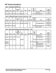
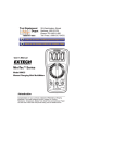
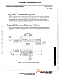
1
Communication Circuits In Brief . . . RF Radio communication has greatly expanded its scope in the past several years. Once dominated by public safety radio, the 30 to 1000 MHz spectrum is now packed with personal and low cost business radio systems. The vast majority of this equipment uses FM or FSK modulation and is targeted at short range applications. From mobile phones and VHF marine radios to garage door openers and radio controlled toys, these new systems have become a part of our lifestyle. Motorola Analog has focused on this technology, adding a wide array of new products including complete receivers processed in our exclusive 3.0 GHz MOSAIC 1.5 process. New surface mount packages for high density assembly are available for all of these products, as well as a growing family of supporting application notes and development kits. Telephone & Voice/Data Traditionally, an office environment has utilized two distinctly separate wired communications systems: telecommunications and data communications. Each had its individual hardware components complement, and each required its own independent transmission line system: twisted wire pairs for Telecom and relatively high priced coaxial cable for Datacom. But times have changed. Today, Telecom and Datacom coexist comfortably on inexpensive twisted wire pairs and use a significant number of components in common. This has led to the development and enhancement of PBX (Private Branch Exchanges) to the point where the long heralded “office of the future,” with simultaneous voice and data communications capability at each station, is no longer of the future at all. The capability is here today! Motorola Semiconductor serves a wide range of requirements for the voice/data marketplace. We offer both CMOS and Analog technologies, each to its best advantage, to upgrade the conventional analog voice systems and establish new capabilities in digital communications. Early products, such as the solid–state single–chip crosspoint switch, the more recent monolithic Subscriber–Loop– Interface Circuit (SLIC), a single–chip Codec/Filter (Mono– Circuit), the Universal Digital Loop Transceivers (UDLT), basic rate ISDN (Integrated Services Digital Network), and single–chip telephone circuits are just a few examples of Motorola leadership in the voice/data area. Motorola Master Selection Guide 4.7–1 Page RF Communications . . . . . . . . . . . . . . . . . . . . . . . . . . . . . . . . . . . 4.7–2 RF Front End ICs . . . . . . . . . . . . . . . . . . . . . . . . . . . . . . . . . . . 4.7–2 Wideband IFs . . . . . . . . . . . . . . . . . . . . . . . . . . . . . . . . . . . . . . 4.7–2 Wideband Single Conversion Receivers . . . . . . . . . . . . . . . 4.7–2 Narrowband Single Conversion Receivers . . . . . . . . . . . . . 4.7–2 Narrowband Dual Conversion Receivers . . . . . . . . . . . . . . . 4.7–3 Universal Cordless Phone Subsystem ICs . . . . . . . . . . . . . 4.7–3 Transmitters . . . . . . . . . . . . . . . . . . . . . . . . . . . . . . . . . . . . . . . 4.7–3 Balanced Modulator/Demodulator . . . . . . . . . . . . . . . . . . . . . 4.7–4 Infrared Transceiver . . . . . . . . . . . . . . . . . . . . . . . . . . . . . . . . 4.7–4 Telecommunications . . . . . . . . . . . . . . . . . . . . . . . . . . . . . . . . . . 4.7–11 Subscriber Loop Interface Circuit . . . . . . . . . . . . . . . . . . . . 4.7–11 PBX Architecture (Analog Transmission) . . . . . . . . . . . . . . 4.7–12 PCM Monocircuits . . . . . . . . . . . . . . . . . . . . . . . . . . . . . . 4.7–12 Dual Tone Multiple Frequency Receiver . . . . . . . . . . . . 4.7–15 ISDN Voice/Data Circuits . . . . . . . . . . . . . . . . . . . . . . . . . . . 4.7–15 Integrated Services Digital Network . . . . . . . . . . . . . . . 4.7–15 Second Generation U–Interface Transceivers . . . . . . 4.7–16 Second Generation S/T–Interface Transceivers . . . . . 4.7–16 Dual Data Link Controller . . . . . . . . . . . . . . . . . . . . . . . . 4.7–17 Voice/Data Communication (Digital Transmission) . . . . . . 4.7–18 Universal Digital Loop Transceiver . . . . . . . . . . . . . . . . 4.7–18 ISDN Universal Digital Loop Transceiver II . . . . . . . . . 4.7–19 Electronic Telephone Circuit . . . . . . . . . . . . . . . . . . . . . . . . . 4.7–19 Tone Ringers . . . . . . . . . . . . . . . . . . . . . . . . . . . . . . . . . . . . . 4.7–20 Speech Networks . . . . . . . . . . . . . . . . . . . . . . . . . . . . . . . . . 4.7–21 Speakerphones . . . . . . . . . . . . . . . . . . . . . . . . . . . . . . . . . . . 4.7–25 Voice Switched Speakerphone Circuit . . . . . . . . . . . . . 4.7–25 Voice Switched Speakerphone with µProcessor Interface . . . . . . . . . . . . . . . . . . . . . . . . . . . 4.7–27 Voice Switched Speakerphone Circuit . . . . . . . . . . . . . 4.7–28 Telephone Line Interface and Speakerphone Circuit . 4.7–29 Family of Speakerphone ICs . . . . . . . . . . . . . . . . . . . . . 4.7–30 Telephone Accessory Circuits . . . . . . . . . . . . . . . . . . . . . . . 4.7–32 Audio Amplifier . . . . . . . . . . . . . . . . . . . . . . . . . . . . . . . . . 4.7–32 Current Mode Switching Regulator . . . . . . . . . . . . . . . . 4.7–32 300 Baud FSK Modems . . . . . . . . . . . . . . . . . . . . . . . . . 4.7–33 ADPCM Transcoder . . . . . . . . . . . . . . . . . . . . . . . . . . . . 4.7–33 Calling Line Identification (CLID) Receiver . . . . . . . . . 4.7–34 CVSD Modulator/Demodulator . . . . . . . . . . . . . . . . . . . 4.7–35 Summary of Bipolar Telecommunications Circuits . . . 4.7–36 Phase–Locked Loop Components . . . . . . . . . . . . . . . . . . . . . . 4.7–39 PLL Frequency Synthesizers . . . . . . . . . . . . . . . . . . . . . . . . 4.7–39 Phase–Locked Loop Functions . . . . . . . . . . . . . . . . . . . . . . 4.7–40 Package Overview . . . . . . . . . . . . . . . . . . . . . . . . . . . . . . . . . . . 4.7–43 Analog and Interface Integrated Circuits RF Communications Table 1. RF Front End ICs Low Noise Amplifier Mixer D i Device Gain (dB) Noise Figure (dB) IIP3 (dBm) P1dB (dBm) Gain (dB) Noise Figure (dB) IIP3 (dBm) P1dB (dBm) Voltage V l Cont Osc VCC (V) ICC (mA) S ffi / Suffix/ Package MC13142 17 1.8 –5 –15 ±3 12 –3 to +21 3 Yes 2.7 to 6.5 13 D/751B, FTB/976 MC13143 – – – – ±3 12 –3 to +21 3 – 1.8 to 6.5 1 D/751 MC13144 13 to 19 1.4 –1 –7 – – – – – 1.8 to 6.5 2 to 9 D/751 NOTES: All devices operate over a wide range of RF input and IF frequencies, from dc to 2.0 GHz. Typical performance shown at 900 MHz. Table 2. Wideband (FM/FSK) IFs D i Device VCC ICC Sensitivity (Typ) MC13055 3–12 V 25 mA 20 µV 40 MHz MC13155 3–6 V 7.0 mA 100 µV 250 MHz IF M Mute Max Data Rate RSSI – N Notes Suffix/ Package 2.0 Mb Wideband Data IF, includes data shaper P/648, D/751B 10 Mb Video Speed FM IF D/751B Table 3. Wideband Single Conversion Receivers – VHF D i Device VCC ICC Sensitivity (Typ) RF Input IF MC3356 3–9 V 25 mA 30 µ µV 200 MHz 10.7 MHz MC13156 2–6 V 5.0 mA 2.0 µV 500 MHz 21.4 MHz MC13158 2–6 V 6.0 mA MC13159 2.7–5 V 5.5 mA M Mute RSSI Max Data Rate N Notes 500 kb Includes front end mixer/L.O. P/738, DW/751D CT–2 FM/Demodulator DW/751E, FB/873 – >1.2 Mb FM IF/Demodulator with split IF for DECT 600 MHz 500 kb FM IF for PHS Suffix/ Package FTB/873 DTB/948F Table 4. Narrowband Single Conversion Receivers – VHF D i Device VCC ICC 12 dB SINAD Sensitivity (Typ) MC3357 4–8 V 5.0 mA 5.0 µV µ MC3359 4–9 V 7.0 mA 2.0 µV MC3371 2–8 V 6.0 mA RF Input IF 45 MHz 455 kHz M Mute RSSI Max Data Rate – > 4.8 kb 60 MHz > 4.8 kb MC3372 MC13150 N Notes Ceramic Quad D t t /R Detector/Resonator t P/648, D/751B Scan output p option p P/707, DW/751D RSSI P/648, D/751B, D/751B DTB/948F RSSI, Ceramic Quad Detector/Resonator 3–6 V 1.8 mA 1.0 µV 500 MHz >9.6 kb S ffi / Suffix/ Package Coilless Detector with Adjustable Bandwidth FTB/873, FTA/977 110 dB Analog and Interface Integrated Circuits 4.7–2 Motorola Master Selection Guide RF Communications (continued) Table 5. Narrowband Dual Conversion Receivers – FM/FSK – VHF D i Device VCC ICC 12 dB SINAD Sensitivity (Typ) MC3362 2–7 V 3.0 mA 0.7 µV 4.0 mA RF Input IF1 180 MHz 10.7 MHz IF2 (Limiter In) M Mute 455 kHz – RSSI Data D Rate N Notes S ffi / Suffix/ Package Includes buffered VCO output P/724, DW/751E 0.4 µV Includes RF amp/mute DW/751F MC3335 0.7 µV Low cost version DW/751D, P/738 MC13135 1.0 µV Voltage buffered RSSI, LC Quad Detector DW/751E, P/724 MC3363 > 4.8 kb – MC13136 Voltage Buffered RSSI, Ceramic Quad Detector Table 6. Universal Cordless Phone Subsystem ICs Dual Conversion Receiver D i Device VCC ICC MC13109 2.0–5.5 V Active Mode 6.7 mA Inactive Mode 40 µA MC13110 2.7–5.5 V Active Mode 8.2 mA Inactive Mode 60 µA MC13111 2.7–5.5 V Active Mode 8.2 mA Inactive Mode 60 µA Universal U i l Dual PLL Compander and Audio Interface V i Voice Scrambler Low Battery Detect Programmable Rx, Tx Trim Gain and LBD Voltage Reference – 1 – – S ffi / Suffix/ Package FB/848B, FTA/932 2 FB/848B 2 FB/848B N Notes Suffix/ Package Table 7. Transmitters – AM/FM/FSK Max RF Freq Out Max Mod Freq D i Device VCC ICC Pout MC2833 3–8 V 10 mA –30 dBm to +10 dBm 150 MHz 50 kHz MC13175 2–5 V 40 mA 8.0 dBm 500 MHz 5.0 MHz MC13176 Motorola Master Selection Guide FM transmitter. Includes two frequency multiplier/amplifier transistors P/648, D/751B AM/FM transmitter. Single frequency PLL fout = 8 × fref, includes power down function D/751B fout = 32 × fref, includes power down function 1.0 GHz 4.7–3 Analog and Interface Integrated Circuits Table 8. Balanced Modulator/Demodulator D i Device VCC ICC MC1496 3–5 V 10 mA Suffix/ Package F Function i General purpose balanced modulator/demodulator for AM, SSB, FM detection with Carrier Balance >50 dB P/646, D/751A Table 9. Infrared Transceiver D i Device VCC ICC 12 dB SINAD Sensitivity (Typ) MC13173 3–5 V 6.5 mA 5.0 µV Max M IF Freq C Carr D Det RSSI 10.7 MHz Data D Rate Suffix/ S ffi / Package N Notes 200 kb Includes Single Frequency PLL for Tx Carrier and Rx LO FTB/873 Universal Cordless Telephone Subsystem IC MC13109FB, FTA TA = – 20° to +85°C, Case 848B, 932 The MC13109 integrates several of the functions required for a cordless telephone into a single integrated circuit. This significantly reduces component count, board space requirements, and external adjustments. It is designed for use in both the handset and the base. • Dual Conversion FM Receiver – Complete Dual Conversion Receiver – Antenna Input to Audio Output 80 MHz Maximum Carrier Frequency – RSSI Output – Carrier Detect Output with Programmable Threshold – Comparator for Data Recovery – Operates with Either a Quad Coil or Ceramic Discriminator • Compander – Expandor Includes Mute, Digital Volume Control and Speaker Driver – Compressor Includes Mute, ALC and Limiter Rx In 1st Mixer 2nd Mixer 1st LO PLL 2nd LO PLL • Dual Universal Programmable PLL – Supports New 25 Channel U.S. Standard with No External Switches – Universal Design for Domestic and Foreign CT–1 Standards – Digitally Controlled Via a Serial Interface Port – Receive Side Includes 1st LO VCO, Phase Detector, and 14–Bit Programmable Counter and 2nd LO with 12–Bit Counter – Transmit Section Contains Phase Detector and 14–Bit Counter – MPU Clock Output Eliminates Need for MPU Crystal • Supply Voltage Monitor – Externally Adjustable Trip Point • 2.0 to 5.5 V Operation with One–Third the Power Consumption of Competing Devices Limiting IF Amplifier RSSI Detector Mute Expander Rx Out Carrier Detect Tx In Data Out Mute Compressor µP Serial Interface Tx Phase Detector Low Battery Detect SPI Tx Out Tx VCO Analog and Interface Integrated Circuits 4.7–4 Low Battery Indicator Motorola Master Selection Guide Universal Cordless Telephone Subsystem IC with Scrambler MC13110FB TA = –40° to +85°C, Case 848B The MC13110 integrates several of the functions required for a cordless telephone into a single integrated circuit. This significantly reduces component count, board space requirements, and external adjustments. It is designed for use in both the handset and the base. • Dual Conversion FM Receiver – Complete Dual Conversion Receiver – Antenna In to Audio Out 80 MHz Maximum Carrier Frequency – RSSI Output – Carrier Detect Output with Programmable Threshold – Comparator for Data Recovery – Operates with Either a Quad Coil or Ceramic Discriminator • Dual Universal Programmable PLL – Supports New 25 Channel U.S. Standard with New External Switches – Universal Design for Domestic and Foreign CT–1 Standards – Digitally Controlled Via a Serial Interface Port – Receive Side Includes 1st LO VCO, Phase Detector, and 14–Bit Programmable Counter and 2nd LO with 12–Bit Counter – Transmit Section Contains Phase Detector and 14–Bit Counter – MPU Clock Outputs Eliminates Need for MPU Crystal • Supply Voltage Monitor – Provides Two Levels of Monitoring with Separate Outputs – Separate, Adjustable Trip Points • Compander – Expandor Includes Mute, Digital Volume Control, Speaker Driver, 3.5 kHz Low Pass Filter, and Programmable Gain Block – Compressor Includes Mute, 3.5 kHz Low Pass Filter, Limiter, and Programmable Gain Block • Frequency Inversion Scrambler/Descrambler – Can Be Enabled/Disabled Via MPU Interface – Programmable Carrier Modulation Frequency • 2.7 to 5.5 V Operation with One–Third the Power Consumption of Competing Devices Rx In Rx PD Out 1st Mixer 2nd Mixer 1st LO PLL 2nd LO PLL Limiting IF Amplifier Detector Rx PD Rx PD In RSSI Filter/Mute Descrambler Expandor Rx Out Carrier Detect Tx In Data Out Filter/Mute Scrambler Compressor µP Serial Interface Tx Phase Detector Low Battery Detect SPI Tx Out Tx VCO Motorola Master Selection Guide 4.7–5 Low Battery Indicator Analog and Interface Integrated Circuits Narrowband FM Receiver MC13135/136P, DW TA = –40° to +85°C, Case 724, 751E The MC13135 is a full dual conversion receiver with oscillators, mixers, Limiting IF Amplifier, Quadrature Discriminator, and RSSI circuitry. It is designed for use in security systems, cordless phones, and VHF mobile and portable radios. Its wide operating supply voltage range and low current make it ideal for battery applications. The Received Signal Strength Indicator (RSSI) has 65 dB of dynamic range with a voltage output, and an operational amplifier is included for a dc buffered output. Also, an improved mixer third order intercept enables the MC13135 to accommodate larger input signal levels. • Complete Dual Conversion Circuitry • Low Voltage: 2.0 to 6.0 Vdc • RSSI with Op Amp: 65 dB Range • Low Drain Current: 3.5 mA Typical • Improved First and Second Mixer 3rd Order Intercept • Detector Output Impedance: 25 Ω Typically VCC 0.1 0.84 mH 0.01 1 30 p 2 1.0 k 39.0 MHz Xtal 1ST LO 24 Varicap 23 5p 0.01 22 3 VCC1 RFin 21 4 0.01 20 0.1 5 120 p VCC2 50 p 6 10.245 MHz Xtal Ceramic Filter 10.7 MHz 19 0.1 7 Ceramic Filter 455 kHz 360 18 8 9 10 0.1 2nd LO 0.1 Demod AF 17 Audio Output 8.2 k 0.1 68 k 16 Limiter 11 15 20 k 10 k 12 RSSI Output 14 0.1 13 39 k 455 kHz Quad Coil Toko 7MC–8128Z Analog and Interface Integrated Circuits 4.7–6 Motorola Master Selection Guide Narrowband FM Coilless Detector IF Subsystem MC13150FTA, FTB TA = –40° to +85°C, Case 977, 873 Applications for the MC13150 include cellular, CT–1 900 MHz cordless telephone, data links and other radio systems utilizing narrowband FM modulation. • Linear Coilless Detector • Adjustable Demodulator Bandwidth • 2.5 to 6.0 Vdc Operation • Low Drain Current: < 2.0 mA • Typical Sensitivity of 2.0 µV for 12 dB SINAD • IIP3, Input Third Order Intercept Point of 0 dBm • RSSI Range of Greater Than 100 dB • Internal 1.4 kΩ Terminations for 455 kHz Filters • Split IF for Improved Filtering and Extended RSSI Range The MC13150 is a narrowband FM IF subsystem targeted at cellular and other analog applications. Excellent high frequency performance is achieved, with low cost, through use of Motorola’s MOSAIC 1.5 RF bipolar process. The MC13150 has an onboard Colpitts VCO for Crystal controlled second LO in dual conversion receivers. The mixer is a double balanced configuration with excellent third order intercept. It is useful to beyond 200 MHz. The IF amplifier is split to accommodate two low cost cascaded filters. RSSI output is derived by summing the output of both IF sections. The quadrature detector is a unique design eliminating the conventional tunable quadrature coil. LO Input VEE1 10 µ 220 n + 100 n 1:4 Z Xformer Mixer In Enable 49.9 RSSI 100 n 31 32 220 n Mixer Out 29 28 27 25 2 VCC1 Detector Output 23 Local Oscillator 100 p RSSI Buffer 22 220 n 49.9 RSSI Buffer Mixer 3 IF In 26 24 1 1.5 k 30 VEE1 4 VEE2 21 5 20 RL 100 k 220 n 220 n (6) IF 220 n 7 IF Amp Out 9 VCC2 10 11 12 220 n 13 14 220 n 220 n 220 n I15 15 10 µ + VEE2 18 17 8 Limiter In 220 n Limiter 220 n 1.5 k 19 Detector 6 RS 100 k 100 k V18–V17 = 0; fIF = 455 kHz 16 I16 49.9 Motorola Master Selection Guide 4.7–7 Analog and Interface Integrated Circuits Wideband FM IF System MC13156DW, FB TA = –40° to +85°C, Case 751E, 873 Applications for the MC13156 include CT–2, wideband data links, and other radio systems utilizing GMSK, FSK or FM modulation. • 2.0 to 6.0 Vdc Operation • Typical Sensitivity of 6.0 µV for 12 dB SINAD • RSSI Dynamic Range Typically 80 dB • High Performance Data Shaper for Enhanced CT–2 Operation • Internal 300 Ω and 1.4 kΩ Terminations for 10.7 MHz and 455 kHz Filters • Split IF for Improved Filtering and Extended RSSI Range The MC13156 is a wideband FM IF subsystem targeted at high performance data and analog applications. Excellent high frequency performance is achieved, with low cost, through use of Motorola’s MOSAIC 1.5 RF bipolar process. The MC13156 has an onboard Colpitts VCO for PLL controlled multichannel operation. The mixer is useful to beyond 200 MHz and may be used in a differential, balanced, or single–ended configuration. The IF amplifier is split to accommodate two low cost cascaded filters. RSSI output is derived by summing the output of both IF sections. A precision data shaper has a hold function to preset the shaper for fast recovery of new data. + 1.0 µ 0.146 µ MMBR5179 15 k 100 p MC13156 7.5 p 144.455 MHz RF Input 0.82 µ 68 p 50 p Mixer 1 24 5.6 k 470 43 p 3rd O.T. XTAL 0.1 µ SMA 133.755 MHz Osc/Tripler 23 2 10 n 1.0 k 10 n 3 10.7 MHz Ceramic Filter 4 22 VEE VCC 21 Bias 100 k 5 10 n 47 k IF Amp 6 VEE 430 19 10 n Data Slicer Hold 18 7 Data Slicer 10 k Bias 8 VCC RSSI Output 20 10 n 10 n Carrier Detect 17 Data Output 10.7 MHz Ceramic Filter 9 10 VCC VEE LIM Amp 16 100 n 15 180 p 10 n 100 k 11 14 100 k 430 10 n 13 12 5.0 p 150 p + Analog and Interface Integrated Circuits 4.7–8 10 k 1.5 µ VCC 1.0 µ Motorola Master Selection Guide Wideband FM IF Subsystem MC13158FTB TA = –40° to +85°C, Case 873 Applications include DECT, wideband wireless data links for personal and portable laptop computers and other battery operated radio systems which utilize GFSK, FSK or FM modulation. • Designed for DECT Applications • 1.8 to 6.0 Vdc Operating Voltage • Low Power Consumption in Active and Standby Mode • Greater than 600 kHz Detector Bandwidth • Data Slicer with Special Off Function • Enable Function for Power Down of Battery Operated Systems • RSSI Dynamic Range of 80 dB Minimum • Low External Component Count The MC13158 is a wideband IF subsystem that is designed for high performance data and analog applications. Excellent high frequency performance is achieved, with low cost, through the use of Motorola’s MOSAIC 1.5 RF bipolar process. The MC13158 has an on–board grounded collector VCO transistor that may be used with a fundamental or overtone crystal in single channel operation or with a PLL in multi–channel operation. The mixer is useful to 500 MHz and may be used in a balanced differential or single ended configuration. The IF amplifier is split to accommodate two low cost cascaded filters. RSSI output is derived by summing the output of both IF sections. A precision data shaper has an Off function to shut the output “off” to save current. An enable control is provided to power down the IC for power management in battery operated applications. Mix Out Mix In2 Mix In1 N/C 32 31 30 Osc Osc Emit Base N/C VEE1 Enable 29 28 27 26 25 1 24 RSSI 23 RSSI Buf VCC1 2 IF Amp IF In 3 IF Dec1 4 IF Dec2 5 IF Out 6 22 DS Gnd MC13158 LIM Amp 18 DS In1 17 Det Out 8 9 10 11 Lim Lim N/C Dec1 Dec2 Motorola Master Selection Guide 20 DS In2 19 DS “off” VCC2 7 Lim In 21 DS Out Data Slicer 5.0 p 12 13 14 Bias 15 16 Lim Quad N/C Det VEE2 Gain Out 4.7–9 Analog and Interface Integrated Circuits UHF, FM/AM Transmitter MC13175/176D TA = 0° to +70°C, Case 751B • • • • • The MC13175 and MC13176 are one chip FM/AM transmitter subsystems designed for AM/FM communication systems operating in the 260 to 470 MHz band covered by FCC Title 47; Part 15. They include a Colpitts crystal reference oscillator, UHF oscillator, ÷8 (MC13175) or ÷32 (MC13176) prescaler, and phase detector forming a versatile PLL system. Another application is as a local oscillator in a UHF or 900 MHz receiver. MC13175/176 offer the following features: • UHF Current Controlled Oscillator • Use Easily Available 3rd Overtone or Fundamental Crystals for Reference Low Number of External Parts Required Low Operating Supply Voltage (1.8 – 5 Vdc) Low Supply Drain Currents Power Output Adjustable (Up to +10 dBm) Differential Output for Loop Antenna or Balun Transformer Networks Power Down Feature ASK Modulated by Switching Output “On”/“Off” MC13175 – fo = 8 × fref MC13176 – fo = 32 × fref • • • • AM Modulator 1.3 k Osc Tank Coilcraft 150–05J08 1 16 2 15 3 14 0.01 µ 0.165 µ 150 p 100 p MC13176 30 p MC13175 13 f/N 12 VCC 27 k 6 11 7 10 8 9 1k MC13175–30 p MC13176–180 p VCC MC13175 Crystal 3rd Overtone 40.0000 MHz Analog and Interface Integrated Circuits BNC RFCI 5 0.1 µ 150 p RFout Z = 50 4 VEE S2 VEE VEE S1 0.01 µ 0.01 µ MC13176 Crystal Fundamental 10 MHz 0.82 µ VCC 1k 4.7–10 Motorola Master Selection Guide Telecommunications Subscriber Loop Interface Circuit (SLIC) MC33120/1P, FN TA = –40° to +85°C, Case 738, 776 With a guaranteed minimum longitudinal balance of 58 dB, the MC33120/1 is ideally suited for Central Office applications, as well as PBXs, and other related equipment. Protection and sensing components on the two–wire side can be non–precision while achieving required system performance. Most BORSHT functions are provided while maintaining low power consumption, and a cost effective design. Size and weight reduction over conventional transformer designs permit a higher density system. • All Key Parameters Externally Programmable with Resistors: • Transmit and Receive Gains • Transhybrid Loss • • • • • • • • • Return Loss • DC Loop Current Limit and Battery Feed Resistance • Longitudinal Impedance Single and Double Fault Sensing and Protection Minimum 58 dB Longitudinal Balance (2–wire and 4–wire) Guaranteed Digital Hook Status and Fault Outputs Power Down Input Loop Start or Ground Start Operation Size & Weight Reduction Over Conventional Approaches Available in 20 Pin DIP and 28 Pin PLCC Packages Battery Voltage: –42 to –58 V (for MC33120), –21.6 to –42 V (for MC33121) VCC EP Current Mirror * VDD (+5.0 V) VDG (Dig. Gnd) Current Mirror Current Mirror BP Tip PDI/ST2 – + CP VEE TSI ST1 * Hook Status and Fault Detection & Bias Control RSI VCC Ring * BN Current Mirror EN VEE Current Mirror Current Mirror VAG (Ana. Gnd) RXI Bias – + CN + – + – TXO RFO CF VQB * (Battery) * Indicates Trimmed Resistor Motorola Master Selection Guide 4.7–11 Analog and Interface Integrated Circuits PBX Architecture (Analog Transmission) PCM Monocircuits Codec–Filters (CMOS LSI) MC145500 Series MC145554/57/64/67 Case 648, 708, 751G, 776 The Monocircuits perform the digitizing and restoration of the analog signals. In addition to these important functions, Motorola’s family of pulse–code modulation monocircuits also provides the band–limiting filter functions – all on a single monolithic CMOS chip with extremely low power dissipation. The Monocircuits require no external components. They incorporate the bandpass filter required for antialiasing and 60 Hz rejection, the A/D–D/A conversion functions for either U.S. Mu–Law or European A–Law companding formats, the low–pass filter required for reconstruction smoothing, an on–board precision voltage reference, and a variety of options that lend flexibility to circuit implementations. Unique features of Motorola’s monocircuit family include wide power supply range (6.0 to 13 V), selectable on–board voltage reference (2.5, 3.1, or 3.8 V), and TTL or CMOS I/O interface. Motorola supplies three versions in this series. The MC145503 and MC145505 are general–purpose devices in 16 pin packages designed to operate in digital telephone or line card applications. The MC145502 is the full–feature device that presents all of the options available on the chip. This device is packaged in a 22 pin DIP and 28 pin chip carrier package. Case 648, 751D, 751G, 738 These per channel PCM Codec–Filters perform the voice digitization and reconstruction as well as the band limiting and smoothing required for PCM systems. They are designed to operate in both synchronous and asynchronous applications and contain an on–chip precision voltage reference. The MC145554 (Mu–Law) and MC145557 (A–Law) are general purpose devices that are offered in 16 pin packages. The MC145564 (Mu–Law) and MC145567 (A–Law), offered in 20 pin packages, add the capability of analog loop–back and push–pull power amplifiers with adjustable gain. All four devices include the transmit bandpass and receive lowpass filters on–chip, as well as active RC pre–filtering and post–filtering. Fully differential analog circuit design assures lowest noise. Performance is specified over the extended temperature range of –40° to +85°C. These PCM Codec–Filters accept both industry standard clock formats. They also maintain compatibility with Motorola’s family of MC3419/MC33120 SLIC products. Txl Analog to Digital Converter – Tx + Tx *VDD–VSS TDE TDD Filter VAG TDC Control Timing CCI MSI 2 Reference Voltage RXO RSI Vref RxG Digital to Analog Converter RxO Filter VSS VDD Analog and Interface Integrated Circuits RDD RCE RDC MC14LC5480P, DW, SD Case 738, 751D, 940C–02 This 5.0 V, general purpose per channel PCM Codec–Filter offers selectable Mu–Law or A–Law companding in 20 pin DIP, SOG and SSOP packages. It performs the voice digitization and reconstruction as well as the band limiting and smoothing required for PCM systems. It is designed to operate in both synchronous and asynchronous applications and contains an on–chip precision reference voltage (1.575 V). The transmit bandpass and receive lowpass filters, and the active RC pre–filtering and post–filtering are incorporated, as well as fully differential analog circuit design for lowest noise. Push–pull 300 Ω power drivers with external gain adjust are also included. The MC14LC5480 PCM Codec–Filter accepts a variety of clock formats, including short–frame sync, long–frame sync, IDL, and GCI timing environments. This device also maintains compatibility with Motorola’s family of Telecom products, including the MC145472 U–Interface Transceiver, MC145474/75 S/T–Interface Transceiver, MC145572 U–Interface Transceiver, MC145574 S/T–Interface Transceiver, MC145532 ADPCM Transcoder, MC145422/26 UDLT–I, MC145421/25 UDLT–II, and MC33120 SLIC. Replaces the MC145480P, DW, SD. PDI Mu/A VLS 4.7–12 Motorola Master Selection Guide PBX Architecture (continued) MC14LC5540P, DW, FU Case 710, 751F, 873 The MC14LC5540 ADPCM Codec is a single chip implementation of a PCM Codec–Filter and an ADPCM encoder/decoder, and therefore provides an efficient solution for applications requiring the digitization and compression of voiceband signals. This device is designed to operate over a wide voltage range, 2.7 V to 5.25 V, and as such is ideal for battery powered as well as ac powered applications. The MC14LC5540 ADPCM Codec also includes a serial control port and internal control and status registers that permit a microcomputer to exercise many built–in features. The ADPCM Codec is designed to meet the 32 kbps ADPCM conformance requirements of CCITT Recommendation G.721 (1988) and ANSI T1.301 (1987). It also meets ANSI T1.303 and CCITT Recommendation G.723 for 24 kbps ADPCM operation, and the 16 kbps ADPCM standard, CCITT Recommendation G.726. This device also meets the PCM conformance specification of the CCITT G.714 Recommendation. Figure 1. MC14LC5540 ADPCM Codec Block Diagram PO + Codec–Filter –1 DR + – PO – DSP Σ ADPCM Transcoder, Receive Gain and Dual Tone Generator PI RO Trim Gain and Filter AXO – FSR DAC BCLKR BCLKT FST DT AXO + Sidetone Gain TG TI – TI + Trim Gain and Filter – + VDSP ADC Sequence/ Control VDD VAG SPC Charge–Pump VSS C1 + C1 – VEXT PDI/RESET SCPEN SCP Rx SCPCLK Motorola Master Selection Guide 4.7–13 SCP Tx Analog and Interface Integrated Circuits PBX Architecture (continued) MC145537EVK ADPCM Codec Evaluation Kit • Easily Interfaced to Test Equipment, Customer System, Second MC145537EVK or MC145536EVK (5.0 V Only) for Full Duplex Operation • Convenient Access to Key Signals • Piezo Loudspeaker • EIA–232 Serial Computer Terminal Interface for Control of the MC14LC5540 ADPCM Codec Features • Compatible Handset Provided • Schematics, Data Sheets, and User’s Manual Included The MC145537EVK is the primary tool for evaluation and demonstration of the MC14LC5540 ADPCM Codec. It provides the necessary hardware and software interface to access the many features and operational modes of the MC14LC5540 ADPCM Codec. • Provides Stand Alone Evaluation on Single Board • The kit provides Analog–to–Analog, Analog–to–Digital or Digital–to–Analog Connections – with Digital Connections being 64 kbps PCM, 32 or 24 kbps ADPCM, or 16 kbps CCITT G.726 or Motorola Proprietary ADPCM • +5.0 V Only Power Supply, or 5.0 V Plus 2.7 to 5.25 V Supply Figure 2. MC145537EVK Block Diagram +5.0 V Gnd +3.0 V Piezo Speaker Clock Generation Circuitry 5.0 V/3.0 V Level Shift Clocks MC145407 EIA–232 Driver/Receiver EIA–232 SCI Analog Interface MC14LC5540 ADPCM Codec Analog and Interface Integrated Circuits 3.0 V/5.0 V Level Shift 5.0 V/3.0 V 4.7–14 MC68HC705C8 Microcontroller Motorola Master Selection Guide PBX Architecture (continued) MC145536EVK ISDN Voice/Data Circuits Codec–Filter/ADPCM Transcoder Evaluation Kit The MC145536EVK is the primary tool for evaluation and demonstration of the MC14LC5480 Single +5.0 V supply PCM Codec–Filter and the MC145532 ADPCM Transcoder (see ‘‘Telephone Accessory Circuits’’). The MC145536EVK provides the necessary hardware needed to evaluate the many separate operating modes under which the MC14LC5480 and MC145532 are intended to operate. • Provides Stand Alone Evaluation on a Single Board • Easily Interfaced to Test Equipment, Customer System, or Second MC145536EVK • Convenient Access to Key Signals • Generous Wire–Wrap Area for Application Development • The kit provides Analog–to–Analog, Analog–to–Digital, or Digital–to–Analog Connections – with Digital Connections Being 64 kbps PCM; 32, 24, or 16 kbps Motorola Proprietary ADPCM • Compatible Handset Included • Schematics, Data Sheets, and User’s Manual included Clock Generator Analog Interface MC14LC5480 Codec– Filter MC145532 ADPCM Transcoder Clocks Digital Interface Integrated Services Digital Network ISDN is the revolutionary concept of converting the present analog telephone networks to an end–to–end global digital network. ISDN standards make possible a wide variety of services and capabilities that are revolutionizing communications in virtually every industry. Motorola’s ISDN product family includes the MC14LC5472 and MC145572 U–Interface Transceivers, the MC145474/75 and MC145574 S/T–Interface Transceivers, MC145488 Dual Data Link Controller, and the MC68302 Integrated Multi–Protocol Processor. These are supported by a host of related devices including the MC14LC5480 +5.0 V PCM Codec–Filter, MC145532 ADPCM Transcoder, MC14LC5540 ADPCM Codec, MC145500 family of single–chip codec/filters, MC145436A DTMF Decoder, MC33120 Subscriber Loop Interface Circuit, MC34129 Switching Power Supply Controller, and the MC145406/07 CMOS EIA 232–E Driver/ Receiver family. Motorola’s key ISDN devices fit into four ISDN network applications: a digital subscriber line card, an NT1 network termination, an ISDN terminal adapter, and an ISDN terminal. Digital subscriber line cards are used in central offices, remote concentrators, channel banks, T1 multiplexers, and other switching equipment. The NT1 network termination block illustrates the simplicity of remote U– to S/T–interface conversion. The ISDN terminal adapter and ISDN terminal block show how Motorola ICs are used to combine voice and data in PC compatible boards, digital telephones, and other terminal equipment. Expanded applications such as a PBX may include these and other Motorola ISDN circuits. Many “non–ISDN” uses, such as pairgain applications, are appropriate for Motorola’s ISDN devices as well. MC145536EVK Dual Tone Multiple Frequency Receiver MC145436AP, DW Case 646, 751G This device contains the filter and decoder for detection of a pair of tones conforming to the DTMF standard with outputs in hexadecimal. Switched capacitor filter technology is used together with digital circuitry for the timing control and output circuits. The MC145436A provides excellent power–line noise and dial tone rejection. Replaces MC145436P, DW. Motorola Master Selection Guide 4.7–15 Analog and Interface Integrated Circuits ISDN Voice/Data Circuits (continued) standard maintenance channel functions. This flexible feature also allows for easy implementation of proprietary maintenance functions. Second Generation U–Interface Transceivers MC145572PB Second Generation S/T–Interface Transceivers Case 824D MC145572FN Case 777 MC145574PB The MC145572 fully conforms to ANSI T1.601–1992, the North American standard for ISDN Basic Access on a single twisted–wire pair. The transceiver achieves a remarkable 10 –7 bit error rate performance on all ANSI specified test loops with worst–case impairments present. The state–of–the–art 0.65 micron single–chip solution uses advanced design techniques to combine precision analog signal processing elements with three digital signal coprocessors to build an adaptively equalized echo cancelling receiver. Two modes of handling U–interface maintenance functions are provided on the MC145572. In the automatic maintenance mode the U–interface transceiver handles all ANSI specified maintenance and channel procedures internally to minimize your software development effort. Automatic procedures include generating and monitoring the cyclic redundancy check, reporting and counting far end block errors (near end block errors too), handling the ACT and DEA bits, as well as monitoring and appropriately responding to embedded operations channel messages. The MC145572 has 275 mW maximum power dissipation. It also has an enhanced TDM interface that supports an on–chip timeslot assigner, GCI and IDL modes of operation. The optional manual maintenance mode lets you choose an inexpensive microcontroller, such as a member of Motorola’s MC68HC05 family, to control and augment the Case 873A MC145488 DDLC TA MC145574 SCP IDL S/T Chip MC145574DW Case 751F The MC145574 S/T–Interface Transceivers provide a CCITT I.430 compatible interface for use in line card, network termination, and ISDN terminal equipment applications. Manufactured with Motorola’s advanced 0.65 micron CMOS mixed analog and digital process technology, the MC145574 is a physical layer device capable of operating in point–to–point or point–to–multipoint passive bus arrangements. In addition, the MC145574 implements the optional NT1 Star topology, NT terminal mode and TE slave mode. This device features outstanding transmission performance. It reliably transmits over 1 kilometer in a point–to–point application. Comparable performance is achieved in all other topologies as well. Other features include pin selectable terminal or network operating modes, industry standard microprocessor serial control port, full support of the multiframing S and Q channels, a full range of loopbacks, and low power CMOS operation, with a maximum power consumption of 90 mW. The MC145574 has an enhanced TDM interface that supports GCI, IDL and an on–chip timeslot assigner. NT1 MC145574 LT MC145572 MC145572 GCI S/T S/T Chip U Chip U IDL U Chip SCP MC14LC5480 MPU System NT1/TA Codec MC145574 IDL Host Bus TE1 MC68302 MC145574 SCP Imp IDL S/T S/T Chip SCP MC68302 S/T Chip Imp RS232 LT MC145572 MC145572 IDL U Chip UART U U Chip C e n t r a l O f f i c e SCP MC14LC5480 RAM ROM Codec Analog and Interface Integrated Circuits SLIC Codec MC33121 MC14LC5480 4.7–16 Motorola Master Selection Guide ISDN Voice/Data Circuits (continued) Dual Data Link Controller MC14LC5494EVK U–Interface Transceiver Evaluation Kit discontinued MC145488FN Case 779 The MC145488 features two full–duplex serial HDLC channels with an on–chip Direct Memory Access (DMA) controller. The DMA controller minimizes the number of microprocessor interrupts from the communications channels, freeing the microprocessor’s resources for other tasks. The DMA controller can access up to 64 kbytes of memory, and transfers either 8–bit bytes or 16–bit words to or from memory. The MC145488 DDLC is compatible with Motorola’s MC68000 and other microprocessors. In a typical ISDN terminal application, one DDLC communications channel supports the D–channel (LAPD) while the other supports the B–channel (LAPB). While the DDLC is ideally suited for ISDN applications, it can support many other HDLC protocol applications as well. Some of the powerful extras found on the DDLC include automatic abort and retransmit of D–channel collisions in S/T–interface applications, address recognition, automatic recovery mechanisms for faulty frame correction, and several system test modes. Address recognition provides a reduction in the host microprocessor load by filtering data frames not addressed to the host. The DDLC can compare either SAPI or TEI fields of LAPD frames. For LAPD (Q.921) applications, both A and B addresses may be checked. MC145572EVK U–Interface Transceiver Evaluation Kit This kit provides the hardware and software to evaluate the many configurations under which the MC145572EVK is able to operate. Used as a whole, it operates as both ends of the two–wire U interface that extends from the customer premises (NT1) to the switch line card (LT). The two halves of the board can be physically and functionally separated, providing independent NT1 and LT evaluation capability. The kit provides the ability to interactively manipulate status registers in the MC145572EVK U–Interface transceiver or in the MC145474/75 S/T–Interface transceiver with the aid of an external terminal. The device can also be controlled using the MC68302 Integrated Multiprotocol Processor application development system to complete a total Basic Rate ISDN evaluation solution. 2B1Q U–Interface NT1 Side S/T Interface LT Side IDL S/T–Interface Transceiver MC145474 SCP U–Interface Transceiver U–Interface Transceiver MC145572FN MC145572FN IDL SCP SCP MC68HC705 MC68HC705 Gated Clocks IDL Frequency Reference Gated Clocks IDL Clock Generator SCP MC145407 MC145407 5PPM System Clock MC145572EVK Motorola Master Selection Guide 4.7–17 Analog and Interface Integrated Circuits UDLTs utilize a 256 kilobaud Modified Differential Phase Shift Keyed (MDPSK) burst modulation technique for transmission to minimize radio frequency, electromagnetic, and crosstalk interference. Implementation through CMOS technology takes advantage of low–power operation, increased reliability, and the proven capabilities to perform complex telecommunications functions. Voice/Data Communication (Digital Transmission) 2–Wire Universal Digital Loop Transceiver (UDLT) MC145422P, DW Master Station Functional Features • Provides Synchronous Duplex 64 kbits/Second Voice/Data Channel and Two 8 kbits/Second Signaling Data Channels Over One 26 AWG Wire Pair Up to 2 km. • Compatible with Existing and Evolving Telephone Switch Architectures and Call Signaling Schemes • Automatic Detection Threshold Adjustment for Optimum Performance Over Varying Signal Attenuations • Protocol Independent • Single 5.0 V to 8.0 V Power Supply Case 708, 751E MC145426P, DW Slave Station Case 708, 751E The UDLT family of transceivers allows the use of existing twisted–pair telephone lines (between conventional telephones and a PBX) for the transmission of digital data. With the UDLT, every voice–only telephone station in a PBX system can be upgraded to a digital telephone station that handles the complex voice/data communications with no increase in cabling costs. In implementing a UDLT–based system the A/D to D/A conversion function associated with each telset is relocated from the PBX directly to the telset. The SLIC (or its equivalent circuit) is eliminated since its signaling information is transmitted digitally between two UDLTs. The UDLT master–slave system incorporates the modulation/demodulation functions that permit data communications over a distance up to 2 kilometers. It also provides the sequence control that governs the exchange of information between master and slave. Specifically, the master resides on the PBX line card where it transmits and receives data over the wire pair to the telset. The slave is located in the telset and interfaces the monocircuit to the wire pair. Data transfer occurs in 10–bit bursts (8 bits of data and 2 signaling bits), with the master transmitting first, and the slave responding in a synchronized half–duplex transmission format. MC145422 Master UDLT • 2.048 MHz Master Clock • Pin Controlled Power–Down and Loop–Back Features • Variable Data Clock – 64 kHz to 2.56 MHz • Pin Controlled Insertion/Extraction of 8 kbits/Seconds Channel into LSB of 64 kbits/Second Channel for Simultaneous Routing of Voice and Data Through PCM Voice Path of Telephone Switch MC145426 Slave UDLT • Compatible with MC145500 Series and Later PCM Codec–Filters • Automatic Power–Up/Down Feature • On–Chip Data Clock Recovery and Generation • Pin Controlled 500 Hz D3 or CCITT Format PCM Tone Generator for Audible Feedback Applications UDLT Signaling Input 1 Signaling Input 2 Line Driver Output Modulator Transmit Buffer Rx Register Receive Data Input Receive Enable Valid Data Loop Back Power Down T/R Data Clock Convert Clock Master Sync Signal Insert Enable Signal Enable Mu Law Tone Enable Sequence and Control Osc XTAL In XTAL Out Master Only Slave Only Transmit Enable Line Input Demodulator Receive Buffer Tx Register Transmit Data Signal Output 1 Signal Output 2 Analog and Interface Integrated Circuits 4.7–18 Motorola Master Selection Guide Voice/Data Communication (Digital Transmission) (continued) 2–Wire ISDN Universal Digital Loop Transceiver II (UDLT II) MC145421P, DW Master Similar to the MC145422/26 UDLT, but provide synchronous full duplex 160 kbps voice and data communication in a 2B + 2D format for ISDN compatibility on a single twisted pair up to 1 km. Single 5.0 V power supply, protocol independent. Case 709, 751E MC145425P, DW Slave Case 709, 751E Electronic Telephone The Complete Electronic Telephone Circuit MC34010P, FN TA = –20° to +60°C, Case 711, 777 • DTMF generator uses low cost ceramic resonator with accurate frequency synthesis technique • Tone ringer drives piezoelectric transducer and satisfies EIA–470 requirements • Speech network provides 2–to–4 wire conversion with adjustable sidetone utilizing an electret transmitter • On–chip regulator insures stable operation over wide range of loop lengths • I2L technology provides low 1.4 V operation and high static discharge immunity • Microprocessor interface port for automatic dialing features The conventional transformer–driven telephone handset is undergoing major innovations. The bulky transformer is disappearing. So are many of its discrete components, including the familiar telephone bell. They are being replaced with integrated circuits that perform all the major handset functions simply, reliably and inexpensively . . . functions such as 2–to–4 wire conversion, DTMF dialing, tone ringing, and a variety of related activities. The culmination of these capabilities is the Electronic Telephone Circuit, the MC34010. These ICs place all of the above mentioned functions on a single monolithic chip. These telephone circuits utilize advanced bipolar analog (I2L) technology and provide all the necessary elements of a modern tone–dialing telephone. The MC34010 even incorporates an MPU interface circuit for the inclusion of automatic dialing in the final system. Also Available A broad line of additional telephone components for customizing systems design. • Provides all basic telephone functions, including DTMF dialer, tone ringer, speech network and line voltage regulator Piezo Sound Element Hook Switch Ceramic Resonator 1 4 7 * 2 3 A 5 6 B 8 9 C 0 # D Keypad MPU Tip DTMF Tone Ringer Line Voltage Regulator MPU Interface Ring Speech Network Receiver MC34010 Electret Microphone Motorola Master Selection Guide 4.7–19 Analog and Interface Integrated Circuits Tone Ringers when a ringing signal is provided, and MUST NOT ring when other signals (speech, dialing, noise) are on the line. The tone ringers described below were designed to meet those requirements with a minimum of external components. The MC34017 Tone Ringer is designed to replace the bulky bell assembly of a telephone, while providing the same function and performance under a variety of conditions. The operational requirements spelled out by the FCC and EIA–470, simply stated, are that a ringer circuit MUST function MC34017P, D TA = –20° to +60°C, Case 626, 751 C4 RI 4 R1 Tip Diode Bridge AC1 1 C1 Input Current Mirror AC2 8 Ring SCR Transient Clamp RO1 2 22 V Oscillator Tone Frequency Divider B B Warble Frequency Divider RG 7 • • • • C3 8 Tip R1 Ring 3 R1 Diode Bridge AC1 C1 7 AC2 Input Current Mirror 16 V SCR Transient Clamp Bias Push–Pull Output Buffer RC 5 Oscillator R2 Tone Frequency Divider Ref Threshold Comparator RO1 • R3 Threshold Comparator C4 TA = –20° to +60°C, Case 626, 751 Complete Telephone Bell Replacement On–Chip Diode Bridge Internal Transient Protection Differential Output to Piezo Transducer for Louder Sound Input Impedance Signature Meets Bell and EIA Standards Rejects Rotary Dial and Hook Switch Transients Base Frequency and Warble Frequencies are Independently Adjustable Adjustable Base Frequency Reduced Number of Externals RS 5 Ref MC34217P, D • • • • 3 RO2 Push Pull Output Buffer RC 6 C2 R2 Piezo Sound Element Bias 1 RO2 • Complete Telephone Bell Replacement Circuit with Minimum External Components • On–Chip Diode Bridge and Transient Protection • Direct Drive for Piezoelectric Transducers • Push Pull Output Stage for Greater Output Power Capability • Base Frequency Options – MC34017–1: 1.0 kHz – MC34017–2: 2.0 kHz – MC34017–3: 500 Hz • Input Impedance Signature Meets Bell and EIA Standards • Rejects Rotary Dial Transients 2 Piezo Sound Element RS 4 C3 C2 Warble Frequency Divider R3 RG 6 Analog and Interface Integrated Circuits 4.7–20 Motorola Master Selection Guide Speech Networks Telephone Speech Network with Dialer Interface MC34114P, DW TA = –20° to +70°C, Case 707, 751D • • • • • Operation Down to 1.2 V • Adjustable Transmit, Receive, and Sidetone Gains by External Resistors • Differential Microphone Amplifier Input Minimizes RFI • Transmit, Receive, and Sidetone Equalization on both Voice and DTMF Signals Regulated 1.7 V Output for Biasing Microphone Regulated 3.3 V Output for Powering External Dialer Microphone and Receive Amplifiers Muted During Dialing Differential Receive Amplifier Output Eliminates Coupling Capacitor • Operates with Receiver Impedances of 150 Ω and Higher Tip Zbal Receiver Ring AGC DC Level 1 Mute AGC Reg 1.7 V Mute AGC Mike Mute DTMF In Motorola Master Selection Guide 4.7–21 VDD (3.3 V) Reg Logic Mute MS Analog and Interface Integrated Circuits Speech Networks (continued) Cordless Universal Telephone Interface MC34016DW, P TA = –20° to +70°C, Case 751D, 738 • Double Wheatstone Bridge Architecture • Automatic Gain Control Function The MC34016 is a telephone line interface meant for use in cordless telephone base stations for CT0, CT1, CT2 and DECT. The circuit forms the interface towards the telephone line and performs all speech and line interface functions like dc and ac line termination, 2–4 wire conversion, automatic gain control and hookswitch control. Adjustment of transmission parameters is accomplished by two 8 bit registers accessible via the integrated serial bus interface and by external components. • DC Masks for Voltage and Current Regulation • Supports Passive or Active AC Set Impedance Applications • Double Wheatstone Bridge Sidetone Architecture • Symmetrical Inputs and Outputs with Large Signal Swing Capability • Gain Setting and Mute Function for Tx and Rx Amplifiers • Very Low Noise Performance • Serial Bus Interface SPI Compatible • Operation from 3.0 to 5.5 V Transmit Channel • Symmetrical Inputs Capable of Handling Large Voltage Swing • Gain Select Option via Serial Bus Interface • Transmit Mute Function, Programmable via Bus • Large Voltage Swing Capability at the Telephone Line Receive Channel • Double Sidetone Architecture for Optimum Line Matching • Symmetrical Outputs Capable of Producing High Voltage Swing • Gain Select Option via Serial Bus Interface • Receive Mute Function, Programmable via Serial Bus Serial Bus Interface • 3–Wire Connection to Microcontroller • One Programmable Output Meant for Driving a Hookswitch • Two Programmable Outputs Capable of Driving Low Ohmic Loads • Two 8–Bit Registers for Parameter Adjustment FEATURES Line Driver Architecture • Two DC Masks for Voltage Regulation • Two DC Masks for Current Regulation • Passive or Active Set Impedance Adjustment Rx1 HYS HYL Rx Outputs Rx Tx Inputs Tx2 SRF IBG Rx2 Tx1 LAI Line Driver MC34016 LAO VBG Tx Hook Switch GND + Supply Serial Bus Interface AGC A (Tip) – VCC Iref CLK DATA BEN OUT1 OUT2 HKSW AGC B (Ring) +5.0 V Serial Bus Inputs Analog and Interface Integrated Circuits Logic Outputs 4.7–22 Motorola Master Selection Guide Speech Networks (continued) Programmable Telephone Line Interface Circuit with Loudspeaker Amplifier MC34216DW TA = 0° to +70°C, Case 751F The MC34216 is developed for use in telephone applications where besides the standard telephone functions also the group listening–in feature is required. In cooperation with a microcontroller, the circuit performs all basic telephone functions including DTMF generation and pulse–dialing. The listening–in part includes a loudspeaker amplifier, an anti–howling circuit and a strong supply. In combination with the TCA3385, the ringing is performed via the loudspeaker. FEATURES Line Driver and Supply • • • • DC and AC Termination of the Line Selectable Masks: France, U.K., Low Voltage Current Protection Adjustable Set Impedance for Resistive and Complex Termination • Efficient Supply Point for Loudspeaker Amplifier and Peripherals Dialing and Ringing • • • • • • Generates DTMF, Pilot Tones and Ring Signal Interrupter Driver for Pulse–Dialing Low Current While Pulse–Dialing Optimized for Ringing via Loudspeaker Programmable Ring Melodies Uses Inexpensive 500 kHz Resonator Loudspeaking Facility • • • • • Integrated Loudspeaker Amplifier Peak–to–Peak Limiter Prevents Distortion Programmable Volume Anti–Howling Circuitry for Group Listening–In Interfacing for Handsfree Conversation Application Areas Handset Operation • • • • • Earpiece Gain Increase Switch • Microphone Squelch Function • Transmit Amplifier Soft Clipping • • • • Transmit and Receive Amplifiers Adjustable Sidetone Network Line Length AGC Microphone and Earpiece Mute Corded Telephony with Group Listening–In Cordless Telephony Base Station with Group Listening–In Telephones with Answering Machines Fax, Intercom, Modem Line + DC and AC Termination Handset Earpiece Handset MIcrophone Ear DC Mask Generation AC Termination 2–4 Wire Conversion Supply Stabilizer Mic Line Driver Anti– Howling Base Loudspeaker DTMF and Ring Generator LSP Microcontroller Interface Line – Motorola Master Selection Guide 4.7–23 Analog and Interface Integrated Circuits Speech Networks (continued) Telephone Line Interface TCA3388DP, FP TA = 0° to +70°C, Case 738, 751D • Line Length AGC • Microphone and Earpiece Mute • Transmit Amplifier Soft Clipping The TCA3388 is a telephone line interface circuit which performs the basic functions of a telephone set in combination with a microcontroller and a ringer. It includes dc and ac line termination, the hybrid function with 2 adjustable sidetone networks, handset connections and an efficient supply point. Dialing and Ringing • • • • FEATURES Line Driver and Supply • • • • DC and AC Termination of the Telephone Line Selectable DC Mask: France, U.K., Low Voltage Current Protection Adjustable Set Impedance for Resistive and Complex Termination • Efficient Supply Point for Peripherals • Hook Status Detection Interrupter Driver for Pulse–Dialing Reduced Current Consumption During Pulse–Dialing DTMF Interfacing Ringing via External Ringer Application Areas • • • • • • Handset Operation Corded Telephony Cordless Telephony Base Station Answering Machines Fax Intercom Modem • Transmit and Receive Amplifiers • Double Anti–Sidetone Network Line + DC and AC Termination Handset Earpiece Handset MIcrophone Ear DC Mask Generation AC Termination 2–4 Wire Conversion Supply Stabilizer Line Driver Mic Microcontroller Interface Line – Analog and Interface Integrated Circuits 4.7–24 Motorola Master Selection Guide Speakerphones Voice Switched Speakerphone Circuit MC34018P, DW TA = –20° to +60°C, Case 710, 751F • All Necessary Level Detection and Attenuation Controls for a Hands–Free Telephone in a Single Integrated Circuit • Background Noise Level Monitoring with Long Time Constant • Wide Operating Dynamic Range Through Signal Compression • On–Chip Supply and Reference Voltage Regulation • Typical 100 mW Output Power (into 25 Ω) with Peak Limiting to Minimize Distortion • Chip Select Pin for Active/Standby Operation • Linear Volume Control Function The MC34018 Speakerphone integrated circuit incorporates the necessary amplifiers, attenuators, and control functions to produce a high quality hands–free speakerphone system. Included are a microphone amplifier, a power audio amplifier for the speaker, transmit and receive attenuators, a monitoring system for background sound level, and an attenuation control system which responds to the relative transmit and receive levels as well as the background level. Also included are all necessary regulated voltages for both internal and external circuitry, allowing line–powered operation (no additional power supplies required). A Chip Select pin allows the chip to be powered down when not in use. A volume control function may be implemented with an external potentiometer. MC34018 applications include speakerphones for household and business uses, intercom systems, automotive telephones, and others. Electret Microphone Transmit Output Transmit Channel Mic Amp Transmit Attenuator Transmit Level Detector Signal Noise Detector Transmit Receive Comparator Attenuator Control Peak Limiter Sidetone Network Receive Level Detector Speaker Amp Speaker Sidetone Receive Attenuator VCC Regulator Receive Channel Speakerphone IC System MC34018 Receive Input DC Input Telephone Line Enable Input Receive Volume Control Motorola Master Selection Guide 4.7–25 Analog and Interface Integrated Circuits Speakerphones (continued) Voice Switched Speakerphone Circuit MC34118P, DW TA = – 20° to +60°C, Case 710, 751F 5.0 mA. The MC34118 can be interfaced directly to Tip and Ring (through a coupling transformer) for stand–alone operation, or it can be used in conjunction with a handset speech network and/or other features of a featurephone. • Improved Attenuator Gain Range: 52 dB Between Transmit and Receive • Low Voltage Operation for Line–Powered Applications (3.0 to 6.5 V) • 4–Point Signal Sensing for Improved Sensitivity • Background Noise Monitors for Both Transmit and Receive Paths • Microphone Amplifier Gain Set by External Resistors – Mute Function Included • Chip Disable for Active/Standby Operation • On Board Filter Pinned–Out for User Defined Function • Dial Tone Detector Inhibits Receive Idle Mode During Dial Tone Presence • Compatible with MC34119 Speaker Amplifier The MC34118 Voice Switched Speakerphone circuit incorporates the necessary amplifiers, attenuators, level detectors, and control algorithm to form the heart of a high quality hands–free speakerphone system. Included are a microphone amplifier with adjustable gain and mute control, Transmit and Receive attenuators which operate in a complementary manner, level detectors at input and output of both attenuators,and background noise monitors for both the transmit and receive channels. A dial tone detector prevents the dial tone from being attenuated by the Receive background noise monitor circuit. Also included are two line driver amplifiers which can be used to form a hybrid network in conjunction with an external coupling transformer. A high–pass filter can be used to filter out 60 Hz noise in the receive channel, or for other filtering functions. A Chip Disable pin permits powering down the entire circuit to conserve power on long loops where loop current is at a minimum. The MC34118 may be operated from a power supply, or it can be powered from the telephone line, requiring typically Tip Mute Tx Attenuator Mike ZB 1.0 AGC Level Detectors Background Noise Monitor Ring Attenuator Control Volume Control Background Noise Monitor Level Detectors Dial Tone Detector BIAS Bias Speaker Rx Attenuator VCC Chip Disable Filter Power Amp (External) Analog and Interface Integrated Circuits 4.7–26 Motorola Master Selection Guide Speakerphones (continued) Voice Switched Speakerphone with µProcessor Interface MC33218AP, DW TA = –40° to +85°C, Case 724, 751E • • • • Low Voltage Operation: 2.5 to 6.0 V 2–Point Sensing, Background Noise Monitor in Each Path Chip Disable Pin for Active/Standby Operation Microphone Amplifier Gain Set by External Resistors – Mute Function Included • Dial Tone Detector to Inhibit Receive Idle Mode During Dial Tone Presence • Microprocessor port for controlling: • Receive Volume Level (16 Steps) • Attenuator Range (26 or 52 dB, Selectable) • Microphone Mute • Force to Transmit, Receive, Idle or Normal Voice Switched Operation • Compatible with MC34119 Speaker Amplifier The MC33218A, Voice Switched Speakerphone circuit incorporates the necessary amplifiers, attenuators, level detectors, and control algorithm to form the heart of a high quality hands–free speakerphone system. Included are a microphone amplifier with adjustable gain, and mute control, transmit and receive attenuators which operate in a complementary manner, and level detectors and background noise monitors for both paths. A dial tone detector prevents dial tone from being attenuated by the receive background noise monitor. A Chip Disable pin permits powering down the entire circuit to conserve power. Also included is an 8–bit serial µprocessor port for controlling the receive volume, microphone mute, attenuator gain, and operation mode (force to transmit, force to receive, etc.). Data rate can be up to 1.0 MHz. The MC33218A can be operated from a power supply, or from the telephone line, requiring typically 3.8 mA. It can also be used in intercoms and other voice–activated applications. Tx Attenuator Tx Output Mike Attenuator Control Speaker Rx Attenuator Data Clock Data Ready Motorola Master Selection Guide Serial Port Rx Input Bias 4.7–27 VCC Chip Disable Analog and Interface Integrated Circuits Speakerphones (continued) Voice Switched Speakerphone Circuit MC33219AP, ADW TA = –40° to +85°C, Case 724, 751E The MC33219A Voice Switched Speakerphone Circuit incorporates the necessary amplifiers, attenuators, level detectors, and control algorithm to form the heart of a high quality hands–free speakerphone system. Included are a microphone amplifier with adjustable gain, and mute control, transmit and receive attenuators which operate in a complementary manner, and level detectors and background noise monitors. A dial tone detector prevents dial tone from being attenuated by the receive background noise monitor. A Chip Disable pin permits powering down the entire circuit to conserve power. The MC33219A may be operated from a power supply, or it can be powered from the telephone line requiring typically 4.0 mA. The MC33219A can be interfaced directly to Tip and Ring (through a coupling transformer for stand–alone operation, or it can be used in conjuction with a handset speech network and/or other features of a featurephone. • Low Voltage Operation: 2.7 to 6.0 V • 2–Point Sensing, Background Noise Monitor in Each Path • Chip Disable Pin for Active/Standby Operation • Microphone Amplifier Gain Set by External Resistors – Mute Function Included • Dial Tone Detector to Inhibit Receive Idle Mode During Dial Tone Presence • Volume Control Range: 34 dB • Compatible with MC34119 Speaker Amplifier Mute Tx Attenuator Tx Output Mike Attenuator Control Rx Attenuator Speaker Speaker Amp Rx Input Bias VCC Chip Disable Volume Control Analog and Interface Integrated Circuits 4.7–28 Motorola Master Selection Guide Speakerphones (continued) Telephone Line Interface and Speakerphone Circuit MC33215B, FB TA = –20° to +70°C, Case 858, 848B The MC33215 is developed for use in fully electronic telephone sets with speakerphone functions. The circuit performs the ac and dc line termination, 2–4 wire conversion, line length AGC and DTMF transmission. The speakerphone part includes a half duplex controller with signal and noise monitoring, base microphone and loudspeaker amplifiers and an efficient supply. The circuit is designed to operate at low line currents down to 4.0 mA enabling parallel operation with a classical telephone set. Handset Operation • • • • • • • Transmit and Receive Amplifiers Differential Microphone Inputs Sidetone Cancellation Network Line Length AGC Microphone and Earpiece Mute Separate Input for DTMF and Auxiliary Signals Parallel Operation Down to 4.0 mA of Line Current Speakerphone Operation FEATURES • Handsfree Operation via Loudspeaker and Base Microphone • Integrated Microphone and Loudspeaker Amplifiers • Differential Microphone Inputs • Loudspeaker Amplifier can be Powered and Used Separately from the Rest of the Circuit • Integrated Switches for Smooth Switch–Over from Handset to Speakerphone Operation • Signal and Background Noise Monitoring in Both Channels • Adjustable Switching Depth for Handsfree Operation • Switch–Over • Dial Tone Detector in the Receive Channel Line Driver and Supply • AC and DC Termination of Telephone Line • Adjustable Set Impedance for Real and Complex Termination • Efficient Supply Point for Loudspeaker Amplifier and Peripherals • Two Stabilized Supply Points for Handset and Base Microphones • Separate Supply Arrangement for Handset and Speakerphone Operation AC Impedance DC Offset Line Current Telephone Line DTMF MF Handset Microphone HM Base Microphone BM VCC Supply Attenuator Line Driver Duplex Controller VCC or External Supply Base Loudspeaker Current Splitter 1:10 LS Attenuator DC Slope Receive Signal Rx Handset Earpiece Auxiliary Input Motorola Master Selection Guide 4.7–29 Analog and Interface Integrated Circuits Speakerphones (continued) Table 10. The Motorola Family of Speakerphone Integrated Circuits MC34018 MC34118 MC33218A Two point sensing with slow idle, background noise monitor in Tx path only Four point sensing with both fast and slow idle modes, background noise monitors in both Rx and Tx paths Two point sensing with slow idle, background noise monitors in both Rx and Tx paths No dial tone detector in receive path Receive path has dial tone detector Receive path has dial tone detector Attenuator Characteristics: • Range: 44 dB • Tolerance: ±4.0 dB • Gain tracking not specified • White noise is constant Attenuator Characteristics: • Range: 52 dB • Tolerance: ±2.0 dB • Gain Tracking: <1.0 dB • White noise reduces with volume Attenuator Characteristics: • Range: 52 or 26 dB (selectable) • Tolerance: ±3.0 dB • Gain Tracking: <1.0 <1 0 dB • White noise reduces with volume External hybrid required Hybrid amplifiers on board External hybrid required Speaker amplifier is on board (34 dB, 100 mW) External speaker amplifier required (MC34119) External speaker amplifier required (MC34119) Filtering is external Configurable filter on board Filtering is external Microphone amplifier has fixed gain and no muting Microphone amplifier has adjustable gain and mute input Microphone amplifier has adjustable gain, and can be muted through µP port Supply Voltage: 4.0 V to 11 V Supply Voltage: 2.8 V to 6.5 V Supply Voltage: 2.5 V to 6.5 V Supply Current: 6.5 mA typ., 9.0 mA max Supply Current: 5.5 mA typ., 8.0 mA max Supply Current: 4.0 mA typ., 5.0 mA max Speaker amplifier reduces gain to prevent clipping Receive gain is reduced as supply voltage falls to prevent clipping Receive gain is reduced as supply voltage falls to prevent clipping Volume control is linear. Cannot override voice switched operation except through additional circuitry. Attenuator gain is fixed at 44 dB (slightly variable). variable) No microphone mute. Volume control is linear, and microphone mute has separate pin. Cannot override voice switched operation except through additional circuitry. circuitry Attenuator gain is fixed at 52 dB. 8–bit µP serial port controls: • Volume control (16 steps) • Microphone mute • Range selection ((26 dB or 52 dB)) • Force to transmit, idle, receive, or normal voice switched operation 28 Pin DIP and SOIC packages 28 Pin DIP and SOIC packages 24 Pin narrow DIP and SOIC packages External Required: q • 12 Resistors • 11 C Capacitors i ((≤1.0 µF) F) • 8C Capacitors it ((>1.0 1 0 µF) F) External Required: q • 14 Resistors • 12 Capacitors C i (≤1.0 ( µF) F) • 9C Capacitors it ((>1.0 1 0 µF) F) External Required: q • 12 Resistors • 11 C Capacitors i ((≤1.0 µF) F) • 4C Capacitors it ((>1.0 1 0 µF) F) Temperature Range: –20° to +60°C Temperature Range: –20° to +60°C Temperature Range: –40° to +85°C Analog and Interface Integrated Circuits 4.7–30 Motorola Master Selection Guide Speakerphones (continued) Table 10. The Motorola Family of Speakerphone Integrated Circuits (continued) MC33219A MC33215 Two point sensing with slow idle, background noise monitors in both Rx and Tx paths Speech network + speakerphone. Two point sensing with slow idle, background noise monitors in both Rx & Tx paths Receive path has dial tone detector Receive path dial tone detector Attenuator Characteristics: • R Range: 52 dB l ±3 0 dB • T Tolerance: ±3.0 • Gain Tracking: <1.0 1 0 dB • White noise reduces with volume Attenuator Characteristics: • R Range: 50 dB (Adj (Adjustable) t bl ) l ±4 0 dB • T Tolerance: ±4.0 • Gain Tracking: <1.0 1 0 dB • White noise reduces with gain External hybrid required Includes speech network, and AGC External speaker amplifier required (MC34119) Includes speaker amplifier with separate supply and mute Filtering is external Filtering is external Microphone amplifier has adjustable gain and a mute input Microphone paths have fixed gain, and mute control Supply Voltage: 2.7 V to 6.5 V Line Powered, 2.4 V to 10 V Supply Current: 3.0 mA typ., 5.0 mA max Total internal supply current ≈5.0 mA Receive gain is reduced as supply voltage falls to prevent clipping Speaker amplifier reduces gain to prevent clipping Volume control is linear, and microphone p mute has h separate pin. i Attenuator A range fi d att 52 dB. fixed dB C Cannott override id voice i switched operation except through additional circuitry circuitry. Volume control is linear. Logic g inputs p control mute based b d on operating i mode. d Standard S d d di l interface. dialer i t f Cannot C t override id voice i switched operation except through additional circuitry circuitry. 24 Pin narrow DIP and SOIC packages 42 Pin Shrink DIP, 52 Pin QFP External Required: • 12 Resistors • 11 Capacitors (≤1.0 µF) • 4 Capacitors (>1.0 µF) p ( µ ) External Required: • 30 Resistors • 19 Capacitors (≤1.0 µF) • 11 Capacitors (>1.0 µF) p ( µ ) • Dialer + Hookswitch Temperature Range: –40° to +85°C Temperature Range: –20° to +70 °C Motorola Master Selection Guide 4.7–31 Analog and Interface Integrated Circuits Telephone Accessory Circuits Audio Amplifier MC34119P, D Audio Input CI 0.1 Differential Gain = 2 x TA = 0° to +70°C, Case 626, 751 A low power audio amplifier circuit intended (primarily) for telephone applications, such as speakerphones. Provides differential speaker outputs to maximize output swing at low supply voltages (2.0 V min.). Coupling capacitors to the speaker, and snubbers, are not required. Overall gain is externally adjustable from 0 to 46 dB. A Chip Disable pin permits powering–down to mute the audio signal and reduce power consumption. Ri 6.0 k Rf Ri Rf 150 k VCC Vin FC1 V01 Speaker (32 Ω) 4.0 k 4.0 k C1 1.0 µF C2 5.0 µF • • • • Drives a Wide Range of Speaker Loads (16 to 100 Ω) Output Power Exceeds 250 mW with 32 Ω Speaker Low Distortion (THD = 0.4% Typical) Wide Operating Supply Voltage (2.0 V to 16 V) – Allows Telephone Line Powered Applications. • Low Quiescent Supply Current (2.5 mA Typical) • Low Power–Down Quiescent Current (60 µA Typical) 50 k 125 k * V02 FC2 50 k Bias Circuit CD Chip Disable MC34119 Gnd * Optional Current Mode Switching Regulator MC34129P, D High performance current mode switching regulator for low–power digital telephones. Unique internal fault timer provides automatic restart for overload recovery. A start/run comparator is included to implement bootstrapped operation of VCC. Although primarily intended for digital telephone systems, these devices can be used cost effectively in many other applications. On–chip functions and features include: • • • • • • • Current Mode Operation to 300 kHz Automatic Feed Forward Compensation Latching PWM for Cycle–By–Cycle Current Limiting Latched–Off or Continuous Retry after Fault Timeout Soft–Start with Maximum Peak Switch Current Clamp Internally Trimmed 2% Bandgap Reference Input Undervoltage Lockout Analog and Interface Integrated Circuits 13 Start/Run Output Start/Run TA = 0° to +70°C, Case 646, 751A C Soft–Start 12 Soft–Start and Fault Timer Gnd 7 Vref 2.5 V RT/CT 6 5 Sync/Inhibit 4 Input 4.7–32 X2 Oscillator Undervoltage Lockout 14 1.25 V References 8 Error Amp Latching PWM + – VCC Vref 1.25 V 9 Noninverting Input Inverting Input 11 Feedback/ PWM Input 1 Drive Out 2 Drive Gnd 3 Ramp Input 10 Motorola Master Selection Guide (continued) full–duplex, half–duplex, or simplex 300 baud data communication over a pair of telephone lines. It is intended for use with telemeter system or remote control system applications. The differential line driver is capable of driving 0 dBm into a 600 Ω load. The transmit attenuator is programmable in 1.0 dB steps. Tip Rx RxD Tx TxD Ring CDA CD DTMF In CDA Carrier Detect Adjust 3.579545 MHz MC145444H, DW – CCITT V.21 Case 804, 751D This device is a silicon gate CMOS single–chip 300 baud modem. It is compatible with CCITT V.21 and contains the entire circuit that provides a full–duplex or half–duplex 300 baud data communication over a twisted pair. The MC145444 is capable of driving 0 dBm into a 600 Ω load with a single 5.0 V power supply. In addition, this device features an on–board DTMF generator, call progress detector, and 2100 Hz answer tone generator. This device also features a three–wire serial interface for a microcontroller. DDO DOE DDC DDI DIE MODE MC145446AFW – CCITT V.21 Case 751M EDO I/O Data Bus S Reg +5.0 V • Complies with CCITT Recommendation G.721 (1988) • Complies with the American National Standard (T1.301–1987) • Full–Duplex, Single–Channel Operation • Mu–Law or A–Law Coding is Pin Selectable • Synchronous or Asynchronous Operation • Easily Interfaces with any Member of Motorola’s PCM Codec–Filter Monocircuit Family or Other Industry Standard Codecs • Serial PCM and ADPCM Data Transfer Rate from 64 kbps to 5.12 Mbps • Power Down Capability for Low Cost Consumption • The Reset State is Automatically Initiated when the Reset Pin is Released. • Simple Time Slot Assignment Timing for Transcoder Applications • Single 5.0 V Power Supply • Evaluation Kit MC145536 EVK Supports the MC145532 as well as the MC14LC5480 PCM Codec–Filter. (See PBX Architecture Pages for More Information.) EOE EDC EDI S Reg MC145443 The MC145532 Adaptive Differential Pulse Code Modulation (ADPCM) Transcoder provides a low cost, full–duplex, single–channel transcoder to (from) a 64 kbps PCM channel from (to) either a 16 kbps, 24 kbps, 32 kbps, or 64 kbps channel. Latch +5.0 V MC145532DW, L Case 751G, 620 Reg MC145407 ADPCM Transcoder Digital Signal Processor This powerful modem combines a complete FSK modulator/demodulator and an accompanying transmit/receive filter system on a single silicon chip. Designed for bidirectional transmission over the telephone network, the modem operates at 300 baud and can be obtained for compatibility with CCITT V.21 and Bell 103 specifications. The modem contains an on–board carrier–detect circuit that allows direct operation on a telephone line (through a simple transformer), providing simplex, half–duplex, and full–duplex data communications. A built–in power amplifier is capable of driving –9.0 dBm onto a 600 Ω line in the transmit mode. CMOS processing keeps power dissipation to a very low 45 mW, with a power–down dissipation of only 1.0 mW . . . from a single 5.0 V power supply. Available in a 20 pin dual–in–line P suffix, and a wide body surface mount DW suffix. Reg MC145443P, DW Modem – Bell 103 Case 738, 751D Latch MC145442P, DW Modem – CCITT V.21 Case 738, 751D S Reg 300 Baud FSK Modems S Reg Telephone Accessory Circuits EIE Reset APD SPC VSS VDD This device includes the DTMF generator and call progress tone detector (CPTD) as well as the other circuitry needed for Motorola Master Selection Guide 4.7–33 Analog and Interface Integrated Circuits Telephone Accessory Circuits (continued) Calling Line Identification (CLID) Receiver with Ring Detector MC14LC5447P, DW Case 648, 751G The MC14LC5447 is designed to demodulate Bell 202 1200 baud FSK asynchronous data. Its primary application is in products that will be used to receive and display the calling number, or the message waiting indicator sent to subscribers from participating central office facilities of the public switched telephone network. The device also contains a carrier detect circuit and telephone ring detector which may be used to power up the device. Applications include adjunct boxes, answering machines, feature phones, fax machines, and computer interface products. Replaces MC145447P, DW. Tip BPF Ring Ring Det. In (1) Ring Det. In (2) Ring Time Ring Detector On–Chip Ring Detect Output for MCU Interrupt Power–Down Mode Less Than 1.0 µA Single Supply: 3.5 V to 6.0 V Pin Selectable Clock Frequencies: 3.68 MHz, 3.58 MHz, or 455 kHz • Two–Stage Power–Up for Power Management Control VAG Raw Data Out Cooked Data Out Ring Detect Circuit Carrier Detect Valid Data Detect Ring Detect Out Internal Power Up PWR Up • • • • • 202 Demod Clock Gen OSCin OSCout Clock Select 3.58 MHz, 3.68 MHz, OR 455 kHz VDD VSS Calling Line ID Receiver Evaluation Kit MC145460EVK The MC145460EVK is a low cost evaluation platform for the MC14LC5447. The MC145460EVK facilitates development and testing of products that support the Bellcore customer premises equipment (CPE) data interface, which enables services such as Calling Number Delivery (CND). The MC14LC5447 can be easily incorporated into any telephone, FAX, PBX, key system, answering machine, CND adjunct box or other telephone equipment with the help of the MC145460EVK development kit. • Easy Clip–On Access to Key MC14LC5447 Signals • Generous Prototype Area • Configurable for MC14LC5447 Automatic or External Power Up Control • EIA–232 and Logic Level Ports for Connection to any PC or MCU Development Platform • Carrier Detect, Ring Detect and Data Status LEDs • Optional Tip and Ring Input Protection Network • MC145460EVK User Guide, MC14LC5447 Data Sheet, and Additional MC14LC5447 Sample Included MC145407 EIA–232 Driver/Receiver Input Protection Circuit Demodulator Input Circuit Ring Detector Input Circuit MC145460EVK Analog and Interface Integrated Circuits MC14LC5447 Calling Line ID Receiver/ Ring Detector Crystal Network 4.7–34 EIA–232 Level Output CD, RD, Data Logic Level Output CD, RD, Data Automatic Power Up Circuit Motorola Master Selection Guide Telephone Accessory Circuits (continued) Continuously Variable Slope Delta (CVSD) Modulator/Demodulator MC34115P, DW TA = 0° to +70°C, Case 648, 751G MC3418P, DW TA = 0° to +70°C, Case 648, 751G • CMOS Compatible Digital Output • Digital Input Threshold Selectable (VCC/2 reference provided on Chip) • MC34115 Has a 3–Bit Algorithm (General Communications) • MC3418 Has a 4–Bit Algorithm (Commercial Telephone) Provides the A/D–D/A function of voice communications by digital transmission. Designed for speech synthesis and commercial telephone applications. A single IC provides both encoding and decoding. • Encode and Decode Functions on the Same Chip with a Digital Input Encode Decode Clock 15 14 Dual Input Analog Input Analog Feedback Digital Data Input Digital Threshold 1 Comparator 2 13 12 Q 3 or 4–Bit Shift Register Q Q Q Q Q Q Q VTH Logic Digital Output 9 10 IInt IO 7 Analog Output Motorola Master Selection Guide Slope Polarity Switch Amplifier VCC/2 Ref 5 Reference Input (+) 4.7–35 Coincidence Output 3 Syllablic Filter VI Converter Integrator VCC/2 Reference 11 4 Gain Control IGC 6 Filter Input (–) Analog and Interface Integrated Circuits Telephone Accessory Circuits (continued) Table 11. Summary of Bipolar Telecommunication Circuits F Function i F Features Suffix/ Package D i Device Subscriber Loop Interface Circuits (SLICs) Central Office, Remote Terminals, PBX Applications All gains externally programmable, most BORSHT functions, current limit adjustable to 50 mA, 58 dB Longitudinal Balance, –21.6 V to –42 V. P/738, FN/776 MC33121 Central Office, Remote Terminals, PBX Applications All gains externally programmable, most BORSHT functions, current limit adjustable to 50 mA, 58 dB Longitudinal Balance, –42 V to –58 V. P/738, FN/776 MC33120 Speech network, tone ringer, dc loop current interface, DTMF dialer with serial port control. P/711, FN/777 MC34010 Adjustable Tone Ringer Single–ended output, meets FCC requirements, adjustable REN, different warble rates. P/626, D/751 MC34012–1, 2, 3 Adjustable Tone Ringer Differential output, meets FCC requirements, adjustable REN, different warble rates. P/626, D/751 MC34017–1, 2, 3 Adjustable Tone Ringer Differential output, meets FCC requirements, adjustable REN, single warble rates. P/626, D/751 MC34217 Ring Signal Converter Switching regulator to convert ringing voltage to regulated dc output. Provides ring detect output. DP/626, FP/751 TCA3385 Speech Network + Speakerphone Line powered IC provides handset and speakerphone modes, dialer interface, ac/dc terminations, and AGC. Efficient supply design provides 90% of loop current to the speaker amplifier. Speaker amplifier may be used independently. Handset operation to 4.0 mA. B/858, FB/848B MC33215 Basic Phone Line Interface Loop current interface, speech network, line length compensation, speech/dialing modes, Bell System compliant. P/707, DW/751D MC34014 Cordless Universal Telephone Interface For cordless telephone base for CT0, CT1, CT2 and DECT. European dc masks, double wheatstone bridge sidetone circuit. SPI port for masks, AGC hookswitch, mute and gain settings. Requires 5.0 V and µP. P/738, DW/751D MC34016 Basic Phone Line Interface Loop current interface, speech network, line length compensation, speech/dialing modes, Bell System and foreign countries. P/707, DW/751D MC34114 Programmable Telephone Line Interface Circuit with Loudspeaker Amplifier Group listening–in, DTMF and tones generator, ring generator, country programmable, SPI interface. DW/751F MC34216 European Speech Network, Programmable Speaker Amplifier Line powered. European dc masks, DTMF and pilot tone generator, listening–in mode with anti–howling. 2–wire bus control masks, DTMF tones, speaker gain, pulse dialing, mute, AGC. Requires MCU. DW/751 MC34216A European Speech Network Loop current interface, speech network, line length compensation, speech/dialing modes, programmable masks for French, U.K., low voltage and PABX systems. DP/738, FP/751 TCA3388 Complete Telephone Circuit POTS Circuit + MPU Dialing Tone Ringers Speech Networks Analog and Interface Integrated Circuits 4.7–36 Motorola Master Selection Guide Telephone Accessory Circuits (continued) Summary of Bipolar Telecommunications Circuits (continued) Function F i Suffix/ Package Features F Device D i Speakerphone Circuits Speech Network + Speakerphone Line powered IC provides handset and speakerphone modes, dialer interface, ac/dc terminations, and AGC. Efficient supply design provides 90% of loop current to the speaker amplifier. Speaker amplifier may be used independently. Handset operation to 4.0 mA. B/858, FB/848B MC33215 Complete Speaker Phone with Speaker Amplifier All level detection (2 pt.), attenuators, and switching controls, mike and speaker amp. P/710, DW/751F MC34018 Complete Speaker Phone with Hybrid, Filter All level detection (4 pt.), attenuators, and switching controls, mike amp with mute, hybrid, and filter. P/710, DW/751F MC34118 Complete Speaker Phone with MPU Interface All level detection, attenuators, and switching controls, mike amp, MPU interface for: volume control, mode selection, mike mute. P/724, DW/751E MC33218A Basic Low Cost Speakerphone All level detection, attenuators and switching controls, Mike amplifier with Mute, low voltage operation. P/724, DW/751E MC33219A Audio Amplifiers 1 Watt Audio Amp 1.0 W output power into 16 Ω, 35 V maximum. D/751 MC13060 Low Voltage Audio Amp 400 mW, 8.0 to 100 Ω, 2.0 to 16 V, differential outputs, chip–disable input pin. P/626, D/751 MC34119 Basic Compander 2.1 V to 7.0 V, no precision externals, 80 dB range, –40° to +85°C, independent compressor and expander. P/646, D/751A MC33110 Compander with Features 3.0 V to 7.0 V, no precision externals, 80 dB range, –40° to +85°C, independent compressor and expander, pass through and mute functions, two op amps. P/648, D/751B MC33111 For phone line power applications, soft–start, current limiting, 2% accuracy. P/646, D/751A MC34129 Telephone quality voice encoding/decoding, variable clock rate, 3–bit coding, for secure communications, voice storage/retrieval, answering machines, 0° to 70°C. P/738, DW/751G MC34115 Same as above except 4–bit coding. P/738, DW751G MC3418 Companders Switching Regulator Current Mode Regulator Voice Encoder/Decoders Continuously Variable Slope Modulator/Demodulator (CVSD) Motorola Master Selection Guide 4.7–37 Analog and Interface Integrated Circuits Figure 3. The Motorola Family of Handset Telecom Integrated Circuits MC34018 MC34010 Speakerphone w/Speaker Amp MC34118 Speakerphone w/Hybrid Amps MC33218A Microprocessor Interface Speakerphone w/MPU Interface MC34014 MC34114 Speech Network Speech Network Speech Network DC Interface DC Interface DC Interface DTMF Generator Dialer Interface Dialer Interface Tone Ringer MC34012 MC34017 Tone Ringer (Single–Ended Output) Tone Ringer (Push–Pull Output) MC33219A Basic Low Cost Speakerphone MC34119 400 mW Speaker Amplifier Analog and Interface Integrated Circuits MC33110 MC33111 Low Voltage Compander (Basic Compander) Low Voltage Compander (w/Mute & Passthrough, Op Amps) 4.7–38 MC34217 Tone Ringer (Push–Pull Output) Motorola Master Selection Guide Phase–Locked Loop Components Motorola offers a choice of phase–locked loop components ranging from complete functional frequency synthesizers for dedicated applications to a wide selection of general purpose PLL circuit elements. Technologies include CMOS for lowest power consumption and bipolar for high speed operation. Typical applications include TV, CATV, radios, scanners, WLANs, cordless telephones plus home and personal computers. Table 12. PLL Frequency Synthesizers Frequency (MHz) Supply Voltage (V) Nominal Supply Current (mA) 4@5V 4.5 to 12 6@5V 15 @ 5 V 3 to 9 – 20 @ 5 V 3 to 9 Phase Detector Single–ended 3–state Interface Device No Parallel MC145106 P/707, DW/751D Serial MC145149* P/738, DW/751D MC145159–1 P/738, DW/751D MC145145–2 P/707, DW/751D MC145146–2 P/738, DW/751D MC145151–2 P/710, DW/751F MC145152–2 P/710, DW/751F MC145155–2 P/707, DW/751D MC145156–2 P/707, DW/751D MC145157–2 P/648, DW/751G MC145158–2 P/648, DW/751G MC145162* P/648, DW/751G MC145165* P/648, D/751B Parallel MC145166* P/648, DW/751G Serial MC145167* Parallel MC145168* P/648, DW/751G Serial MC145169* Two single–ended 3–state 7.5 @ 5 V Analog 7.5 @ 5 V Single–ended 3–state, double–ended 4–Bit Parallel Double–ended Single–ended 3–state, double–ended 60 @ 3 V 2.5 to 5.5 3@3V 60 @ 2 V 1.8 to 3.6 1.5 @ 1.8 V 60 @ 3 V 2.5 to 5.5 3@3V 85 @ 3 V 2.5 to 5.5 3@3V 40/130 @ 5V 4.5 to 5.5 9@5V 100 @ 3 V 185 @ 5 V 2.5 to 5.5 2@3V 6@5V Two single–ended 3–state Suffix/ Case Standby Serial Yes Single–ended 3–state, Current source/sink No MC145162–1* P/648, DW/751G MC145173 DW/751E MC145170–1 P/648, D/751B, DT/948C * Dual PLL Motorola Master Selection Guide 4.7–39 Analog and Interface Integrated Circuits Phase–Locked Loop Components (continued) PLL Frequency Synthesizers (continued) Frequency (MHz) Supply Voltage (V) Nominal Supply Current (mA) 1100 4.5 to 5.5 7@5V Phase Detector Current source/sink, double–ended Suffix/ Case Standby Interface Device Yes Serial MC145190 F/751J, DT/948D MC145191 F/751J, DT/948D MC145192 F/751J, DT/948D 1100 2.7 to 5 6 @ 2.7 V 1100 2.7 to 5.5 12 Two current source/sink, double–ended MC145220* F/803C, DT/948D 1200, 400 1.8 to 3.6 5 Loop 1 = Current source/sink Loop 2 = Three–state MC145225* FTA/873C 2000 4.5 to 5.5 12 @ 5 V Current source/sink, double–ended MC145200 F/751J, DT/948D 2000 4.5 to 5.5 12 @ 5 V MC145201 F/751J, DT/948D 2000 2.7 to 5.5 4@3V MC145202 F/751J, DT/948D 2600, 400 1.8 to 3.6 7 MC145230* FTA/873C Loop 1 = Current source/sink Loop 2 = Three–state * Dual PLL NOTE: Evaluation kits available for the MC145190, MC145191, MC145192, MC145200, MC145201, MC145202, and MC145220. Order part number MC145_ _ _EVK. Table 13. Phase–Locked Loop Functions Pins DIP SM MC1648 Device Voltage Controlled Oscillator Function 14 P,L D,FN MC1658 Voltage Controlled Multivibrator 16 P,L D,FN MC12002 Analog Mixer 14 P,L – MC12009 480 MHz ÷5/6 Dual Modulus Prescaler 16 P,L – MC12011 550 MHz ÷8/9 Dual Modulus Prescaler 16 P,L – MC12013 550 MHz ÷10/11 Dual Modulus Prescaler 16 P,L – MC12015 225 MHz ÷32/33 Dual Modulus Prescaler 8 P D MC12016 225 MHz ÷40/41 Dual Modulus Prescaler 8 P D MC12017 225 MHz ÷64/65 Dual Modulus Prescaler 8 P D MC12018 520 MHz ÷128/129 Dual Modulus Prescaler 8 P D MC12019 225 MHz ÷20/21 Dual Modulus Prescaler 8 P D MC12022A 1.1 GHz ÷64/65, ÷128/129 Dual Modulus Prescaler 8 P D MC12022B 1.1 GHz ÷64/65, ÷128/129 Dual Modulus Prescaler 8 P D MC12022LVA 1.1 GHz ÷64/65, ÷128/129 Low Voltage Dual Modulus Prescaler 8 P D MC12022LVB 1.1 GHz ÷64/65, ÷128/129 Low Voltage Dual Modulus Prescaler 8 P D MC12022SLA 1.1 GHz ÷64/65, ÷128/129 Low Power Dual Modulus Prescaler 8 P D MC12022SLB 1.1 GHz ÷64/65, ÷128/129 Low Power Dual Modulus Prescaler 8 P D MC12022TSA 1.1 GHz ÷64/65, ÷128/129 Low Power Dual Modulus Prescaler With On–Chip Output Termination 8 P D Analog and Interface Integrated Circuits 4.7–40 Motorola Master Selection Guide Phase–Locked Loop Components (continued) Phase–Locked Loop Functions (continued) Device Function Pins DIP SM MC12022TSB 1.1 GHz ÷64/65, ÷128/129 Low Power Dual Modulus Prescaler With On–Chip Output Termination 8 P D MC12022TVA 1.1 GHz ÷64/65, ÷128/129 Low Voltage, Low Power Dual Modulus Prescaler With On–Chip Output Termination 8 P D MC12022TVB 1.1 GHz ÷64/65, ÷128/129 Low Voltage, Low Power Dual Modulus Prescaler With On–Chip Output Termination 8 P D MC12023 225 MHz ÷64 Prescaler 8 P D MC12025 520 MHz ÷64/65 Dual Modulus Prescaler 8 P D MC12026A 1.1 GHz ÷8/9, ÷16/17 Dual Modulus Prescaler 8 P D MC12026B 1.1 GHz ÷8/9, ÷16/17 Dual Modulus Prescaler 8 P D MC12028A 1.1 GHz ÷32/33, ÷64/65 Dual Modulus Prescaler 8 P D MC12028B 1.1 GHz ÷32/33, ÷64/65 Dual Modulus Prescaler 8 P D MC12031A 2.0 GHz ÷64/65, ÷128/129 Low Voltage Dual Modulus Prescaler 8 P D MC12031B 2.0 GHz ÷64/65, ÷128/129 Low Voltage Dual Modulus Prescaler 8 P D MC12032A 2.0 GHz ÷64/65, ÷128/129 Dual Modulus Prescaler 8 P D MC12032B 2.0 GHz ÷64/65, ÷128/129 Dual Modulus Prescaler 8 P D MC12033A 2.0 GHz ÷32/33, ÷64/65 Low Voltage Dual Modulus Prescaler 8 P D MC12033B 2.0 GHz ÷32/33, ÷64/65 Low Voltage Dual Modulus Prescaler 8 P D MC12034A 2.0 GHz ÷32/33, ÷64/65 Dual Modulus Prescaler 8 P D MC12034B 2.0 GHz ÷32/33, ÷64/65 Dual Modulus Prescaler 8 P D MC12036A 1.1 GHz ÷64/65, ÷128/129 Dual Modulus Prescaler With Stand-By Mode 8 P D MC12036B 1.1 GHz ÷64/65, ÷128/129 Dual Modulus Prescaler With Stand-By Mode 8 P D MC12038A 1.1 GHz ÷64/65, ÷127/128, ÷255/256 Low Power Dual Modulus Prescaler 8 P D MC12040 Phase-Frequency Detector 14,20 P,L FN MC12052A 1.1 GHz ÷64/65, ÷128/129 Super Low Power Dual Modulus Prescaler 8 – D, SD MC12053A 1.1 GHz ÷64/65, ÷128/129 Super Low Power Dual Modulus Prescaler With Stand-By Mode 8 – D, SD MC12054A 2.0 GHz ÷64/65, ÷128/129 Super Low Power Dual Modulus Prescaler 8 – D, SD MC12058 1.1 GHz ÷126/128. ÷254/256 Low Power Dual Modulus Prescaler 8 – D, SD MC12061 Crystal Oscillator 16 P,L – MC12066 1.3 GHz ÷64/256 Prescaler 8 – D MC12073 1.1 GHz ÷64 Prescaler 8 P D MC12074 1.1 GHz ÷256 Low-Power Prescaler 8 P D MC12075 1.3 GHz ÷64 Prescaler 8 P D MC12076 1.3 GHz ÷256 Prescaler 8 P D MC12078 1.3 GHz ÷256 Prescaler 8 P D MC12079 2.8 GHz ÷64/128/256 Prescaler 8 P D MC12080 1.1 GHz ÷10/20/40/80 Prescaler 8 P D MC12083 1.1 GHz ÷2 Low Power Prescaler With Stand-By Mode 8 P D MC12089 2.8 GHz ÷64/128 Prescaler 8 P D MC12090 750 MHz ÷2 UHF Prescaler 16 P,L – MC12093 1.1 GHz ÷2/4/8 Low Power Prescaler With Stand-By Mode 8 – D, SD Motorola Master Selection Guide 4.7–41 Analog and Interface Integrated Circuits Phase–Locked Loop Components (continued) Phase–Locked Loop Functions (continued) Device Function Pins DIP SM MC12095 2.5 GHz ÷2/4 Low Power Prescaler With Stand-By Mode 8 – D, SD MC12098 2.5 GHz ÷8192 Prescaler 8 – D MC12100 200 MHz Voltage Controlled Multivibrator 20 P DW, M, FN MC12101 130 MHz Voltage Controlled Multivibrator 20 P DW, M, FN MCH/K12140 Phase-Frequency Detector 8 – D MC12147 Low Power Voltage Controlled Oscillator Buffer 8 – D, SD MC12148 Low Power Voltage Controlled Oscillator 8 – D, SD MC12149 Ultra Low Power Voltage Controlled Oscillator 8 – D, SD MC12179 500–2800 MHz Single Channel Frequency Synthesizer 8 – D MC12181 125–1000 MHz Frequency Synthesizer 16 – D MC12202 1.1 GHz Serial Input Synthesizer 16,20 – D, DT MC12206 2.0 GHz Serial Input Synthesizer 16,20 – D, DT MC12210 2.5 GHz Serial Input Synthesizer 16,20 – D, DT Analog and Interface Integrated Circuits 4.7–42 Motorola Master Selection Guide Communications Circuits Package Overview CASE 620 L SUFFIX CASE 646 P SUFFIX CASE 626 P SUFFIX CASE 707 P SUFFIX CASE 726 L SUFFIX CASE 751B D SUFFIX Motorola Master Selection Guide CASE 709 P SUFFIX CASE 708 P SUFFIX CASE 710 P SUFFIX CASE 648 P SUFFIX CASE 724 P SUFFIX CASE 711 P SUFFIX CASE 738 DP, P SUFFIX CASE 751 D SUFFIX CASE 751A D SUFFIX CASE 751D DW, FP SUFFIX CASE 751E DW SUFFIX CASE 751F DW SUFFIX 4.7–43 Analog and Interface Integrated Circuits Communications Circuits Package Overview CASE 751G DW SUFFIX CASE 751J F SUFFIX CASE 777 FN SUFFIX CASE 804 H SUFFIX (continued) CASE 751M FW SUFFIX CASE 779 FN SUFFIX CASE 776 FN SUFFIX CASE 803C F SUFFIX CASE 848B FB SUFFIX CASE 824D PB SUFFIX CASE 858 B SUFFIX CASE 873 FB, FTB, FU SUFFIX CASE 873A PB SUFFIX CASE 873C FTA SUFFIX CASE 932 FTA SUFFIX CASE 940C SD SUFFIX CASE 948C DT SUFFIX CASE 948D DT SUFFIX Analog and Interface Integrated Circuits CASE 948F DTB SUFFIX CASE 976 FTB SUFFIX 4.7–44 CASE 977 FTA SUFFIX Motorola Master Selection Guide