1
Freescale Semiconductor
Chip Errata
MPC8641DCE
Rev. 2, 12/2011
MPC8641 Chip Errata
This document details all known silicon errata for the MPC8641 and MPC8641D devices. The following table
provides a revision history for this document.
NOTE
Errata in this document also apply to the MPC8640 and MPC8640D.
Table 1. Revision History
Revision
2
Date
12/2011
Substantive Changes
Added eTSEC-A001, eTSEC-A002, eTSEC-A004, SRIO-A002, SRIO-A004, PCIe-A001,
eTSEC 78
Updated eTSEC 77
Removed PEX 12
1
07/2009
Added eTSEC 77
Updated JTAG 3
Updated disposition of e600 5
Updated Table 2 and Table 3 to include silicon revision 3.0.
0
03/2009
Initial public release.
The following table provides a cross-reference to match the revision code in the processor version register to the
revision level marked on the device.
Table 2. Revision Level to Part Marking Cross-Reference
Part
Revision
e600 Core
Revision
Device Marking
Processor Version
Register Value
System Version
Register Value
MPC8641
2.0
2.2
B
0x8004_0202
0x8090_0020
MPC8641D
2.0
2.2
B
0x8004_0202
0x8090_0120
MPC8641
2.1
2.2
C
0x8004_0202
0x8090_0021
MPC8641D
2.1
2.2
C
0x8004_0202
0x8090_0121
Table continues on the next page...
© 2011 Freescale Semiconductor, Inc.
Table 2. Revision Level to Part Marking Cross-Reference (continued)
Part
Revision
e600 Core
Revision
Device Marking
Processor Version
Register Value
System Version
Register Value
MPC8641
3.0
2.2
E
0x8004_0202
0x8090_0030
MPC8641D
3.0
2.2
E
0x8004_0202
0x8090_0130
The items listed as ‘IM’ indicate improvements have been made.
Some noted differences between the revisions of silicon are related to enhancements added to subsequent
revisions of silicon. In this case, an ‘E’ annotation implies that the enhancement is present in that revision of
silicon, and an ‘NE’ annotation indicates that the noted enhancement is not present.
Table 3. Summary of Silicon Errata and Applicable Revision
Errata
Name
Projected
Solution
Silicon Rev.
2.0
2.1
3.0
DDR
DDR 2
DDR controller automatic CAS to preamble calibration
inoperable
No plans to fix
Yes
Yes
Yes
DDR 4
Automatic calibration hardware may calibrate to an invalid
driver impedance
Fixed in Rev 2.1
Yes
No
No
DDR 5
On-die termination at the DDR IOs has been measured 75
Ω too high
Improvements
made
Yes
IM
IM
DDR 6
Memory contents may not be retained during HRESET
sequence
No plans to fix
Yes
Yes
Yes
DDR 7
Automatic data initialization and DLL resets to DRAM are
not performed correctly if CS2 and CS3 are interleaved
No plans to fix
Yes
Yes
Yes
DDR 8
Some clock adjust delays may result in longer delays than
programmed
Fixed in Rev 2.1
Yes
No
No
DDR 9
Some Clock Adjust delays will not produce a MCK/MCK
clock
Fixed in Rev 2.1
Yes
No
No
DDR 10
DDR IOs default receiver biasing may not work across
voltage and temperature
Fixed in Rev 2.1
Yes
No
No
DDR 11
Incorrect impedance controls are connected to the MCKE
IOs
No plans to fix
Yes
Yes
Yes
DDR 12
MCKE signal may not function correctly at assertion of
HRESET
No plans to fix
Yes
Yes
Yes
DMA 2
DMA_DACK bus timing violation when operating in external No plans to fix
DMA master mode
Yes
Yes
Yes
DMA 3
Transfer error reported for wrong channel
Yes
Yes
Yes
DMA
No plans to fix
DUART
Table continues on the next page...
MPC8641 Chip Errata, Rev. 2, 12/2011
2
Freescale Semiconductor, Inc.
Table 3. Summary of Silicon Errata and Applicable Revision (continued)
Errata
DUART 1
Name
Projected
Solution
BREAK detection triggered multiple times for a single break No plans to fix
assertion
Silicon Rev.
2.0
2.1
3.0
Yes
Yes
Yes
e600
e600 1
Unexpected instruction fetch may occur when mtmsr/isync No plans to fix
transitions MSR[IR] from 1→0 and isync instruction resides
in unmapped page
Yes
Yes
Yes
e600 3
core_mcp or core_sreset signal assertion during transition
to Nap may hang processor
No plans to fix
Yes
Yes
Yes
e600 4
Unpaired stwcx. may hang processor
No plans to fix
Yes
Yes
Yes
e600 5
Cache failures may occur due to mis-sampled repair fuse
information
Fixed in Rev 3.0
Yes
Yes
No
eTSEC
eTSEC 10
WWR bit Anomaly
No plans to fix
Yes
Yes
Yes
eTSEC 11
eTSEC Parser does not properly parse L3 fields
Fixed in Rev 2.1
Yes
No
No
eTSEC 12
Frame is dropped with collision and HALFDUP[Excess
Defer] = 0
No plans to fix
Yes
Yes
Yes
eTSEC 14
Transmit frames aborted under 16-bit FIFO GMII-style
mode
No plans to fix
Yes
Yes
Yes
eTSEC 15
Magic packet does not wake device from a SLEEP state
No plans to fix
Yes
Yes
Yes
eTSEC 16
FIFO8, FIFO16 TX hang
Fixed in Rev 2.1
Yes
No
No
eTSEC 17
Tx data corruption or hang in FIFO16 mode
Fixed in Rev 2.1
Yes
No
No
eTSEC 18
Parsing of tunneled IP packets not supported
Improvements
made
Yes
IM
IM
eTSEC 20
RSTAT[RXF0] set regardless of destination ring if WWR=0
Fixed in Rev 2.1
Yes
No
No
eTSEC 23
Tx IP and TCP/UDP Checksum Generation not supported
for some Tx FCB offsets
Fixed in Rev 2.1
Yes
No
No
eTSEC 25
Missing basic integrity check for parsing Tunneled IP
packets
No plans to fix
Yes
Yes
Yes
eTSEC 26
Error in arbitrary extraction offset
Fixed in Rev 2.1
Yes
No
No
eTSEC 27
Parser continues parsing L4 fields when RCTRL[PRSDEP]
set for L2 and L3 fields only
No plans to fix
Yes
Yes
Yes
eTSEC 29
Transmit jumbo frames greater than 2400 bytes may cause Fixed in Rev 2.1
lost data, loss of BD synchronization, or false underrun
error
Yes
No
No
eTSEC 30
Parser results may be lost if TCP/UDP checksum checking
is enabled
Fixed in Rev 2.1
Yes
No
No
eTSEC 31
Parsing of MPLS label stack or non-IPv4/IPv6 label not
supported
No plans to fix
Yes
Yes
Yes
eTSEC 32
Arbitrary extraction on short frames uses data from
previous frame
No plans to fix
Yes
Yes
Yes
Table continues on the next page...
MPC8641 Chip Errata, Rev. 2, 12/2011
Freescale Semiconductor, Inc.
3
Table 3. Summary of Silicon Errata and Applicable Revision (continued)
Errata
Name
Projected
Solution
Silicon Rev.
2.0
2.1
3.0
eTSEC 33
Some combinations of Tx packets may trigger a false Data
Parity Error (DPE)
Fixed in Rev 2.1
Yes
No
No
eTSEC 34
eTSEC Data Parity Error (DPE) does not abort transmit
frames
Improvements
made
Yes
IM
IM
eTSEC 35
eTSEC half duplex receiver packet corruption
No plans to fix
Yes
Yes
Yes
eTSEC 36
Back-to-back IPv6 routing headers not supported by parser No plans to fix
Yes
Yes
Yes
eTSEC 37
RxBD[TR] not asserted during truncation when last 4 bytes
match CRC
No plans to fix
Yes
Yes
Yes
eTSEC 38
eTSEC may stop transmitting packets without setting
IEVENT[EBERR] if a buffer descriptor fetch has an
uncorrectable error
No plans to fix
Yes
Yes
Yes
eTSEC 39
Rx TCP/UDP checksum checking may be incorrect while
operating at low frequencies in FIFO mode
No plans to fix
Yes
Yes
Yes
eTSEC 40
Filer does not support matching against broadcast address
flag PID1[EBC]
No plans to fix
Yes
Yes
Yes
eTSEC 41
eTSEC does not support parsing of LLC/SNAP/VLAN
packets
No plans to fix
Yes
Yes
Yes
eTSEC 42
eTSEC filer reports incorrect Ether-types with certain MPLS No plans to fix
frames
Yes
Yes
Yes
eTSEC 43
Compound filer rules do not roll back the mask
No plans to fix
Yes
Yes
Yes
eTSEC 44
Incomplete frame with error causes false CR error on next
frame
No plans to fix
Yes
Yes
Yes
eTSEC 45
Parser does not check VER/TYPE of PPPoE packets
No plans to fix
Yes
Yes
Yes
eTSEC 46
Back-to-back Rx frames may lose parser results of second
frame
Fixed in Rev 2.1
Yes
No
No
eTSEC 47
RMCA, RBCA counters do not correctly count valid VLAN
tagged frames
No plans to fix
Yes
Yes
Yes
eTSEC 48
Tx errors truncate packets without error in 8-bit Encoded
FIFO mode
No plans to fix
Yes
Yes
Yes
eTSEC 49
No parser error for packets containing invalid IPv6 routing
header packet
No plans to fix
Yes
Yes
Yes
eTSEC 50
Transmitting PAUSE flow control frame may cause transmit Improvements
lockup
made
Yes
IM
IM
eTSEC 51
eTSEC parser does not perform length integrity checks
No plans to fix
Yes
Yes
Yes
eTSEC 52
eTSEC does not verify IPv6 routing header type field
No plans to fix
Yes
Yes
Yes
eTSEC 53
Transmission of truncated frames may cause hang or lost
data
No plans to fix
Yes
Yes
Yes
eTSEC 54
L3 fragment frame files on non-existent source/destination
ports
No plans to fix
Yes
Yes
Yes
eTSEC 55
Multiple BD frame may cause hang
No plans to fix
Yes
Yes
Yes
Table continues on the next page...
MPC8641 Chip Errata, Rev. 2, 12/2011
4
Freescale Semiconductor, Inc.
Table 3. Summary of Silicon Errata and Applicable Revision (continued)
Errata
Name
Projected
Solution
Silicon Rev.
2.0
2.1
3.0
eTSEC 56
TxBD[TC] is not reliable in 16-bit FIFO modes
No plans to fix
Yes
Yes
Yes
eTSEC 57
eTSEC receivers may not be properly initialized
Fixed in Rev 2.1
Yes
No
No
eTSEC 58
Arbitrary Extraction cannot extract last data bytes of frame
No plans to fix
Yes
Yes
Yes
eTSEC 59
False TCP/UDP and IP checksum error in FIFO mode
without CRC appending
No plans to fix
Yes
Yes
Yes
eTSEC 60
Frames greater than 9600 bytes with TOE = 1 will hang
controller
No plans to fix
Yes
Yes
Yes
eTSEC 61
False parity error at Tx startup
No plans to fix
Yes
Yes
Yes
eTSEC 62
VLAN Insertion corrupts frame if user-defined Tx preamble
enabled
No plans to fix
Yes
Yes
Yes
eTSEC 63
User-defined Tx preamble incompatible with Tx Checksum
No plans to fix
Yes
Yes
Yes
eTSEC 64
Rx packet padding limitations at low clock ratios
No plans to fix
Yes
Yes
Yes
eTSEC 65
False TCP/UDP checksum error for some values of pseudo No plans to fix
header Source Address
Yes
Yes
Yes
eTSEC 66
Transmit fails to utilize 100% of line bandwidth
No plans to fix
Yes
Yes
Yes
eTSEC 67
Unexpected babbling receive error in FIFO modes
No plans to fix
Yes
Yes
Yes
eTSEC 68
FIFO16 interface encoded mode maximum frequency is
1/4.2 platform clock
No plans to fix
Yes
Yes
Yes
eTSEC 69
ECNTRL[AUTOZ] not guaranteed if reading MIB counters
with software
No plans to fix
Yes
Yes
Yes
eTSEC 70
Magic Packet Sequence Embedded in Partial Sequence
Not Recognized
No plans to fix
Yes
Yes
Yes
eTSEC 71
Half-duplex collision on FCS of Short Frame may cause Tx
lockup
No plans to fix
Yes
Yes
Yes
eTSEC 72
MAC: Malformed Magic Packet Triggers Magic Packet Exit
No plans to fix
Yes
Yes
Yes
eTSEC 73
Receive pause frame with PTV = 0 does not resume
transmission
No plans to fix
Yes
Yes
Yes
eTSEC 74
Rx may hang if RxFIFO overflows
No plans to fix
Yes
Yes
Yes
eTSEC 75
May drop Rx packets in non-FIFO modes with lossless flow No plans to fix
control enabled
Yes
Yes
Yes
eTSEC 76
Setting RCTRL[LFC] = 0 may not immediately disable LFC
No plans to fix
Yes
Yes
Yes
eTSEC 77
Excess delays when transmitting TOE=1 large frames
No plans to fix
Yes
Yes
Yes
eTSEC 78
Controller may not be able to transmit pause frame during
pause state
No plans to fix
Yes
Yes
Yes
eTSEC-A001
MAC: Pause time may be shorter than specified if transmit
in progress
No plans to fix
Yes
Yes
Yes
eTSEC-A002
Incomplete GRS or invalid parser state after receiving a 1or 2-byte frame
No plans to fix
Yes
Yes
Yes
eTSEC-A004
User-defined preamble not supported at low clock ratios
No plans to fix
Yes
Yes
Yes
Table continues on the next page...
MPC8641 Chip Errata, Rev. 2, 12/2011
Freescale Semiconductor, Inc.
5
Table 3. Summary of Silicon Errata and Applicable Revision (continued)
Errata
Name
Projected
Solution
Silicon Rev.
2.0
2.1
3.0
GEN
GEN 8
Some pins do not meet ±500 V CDM ESD criteria
No plans to fix
Yes
Yes
Yes
GEN 9
PCI Express 2 and SRIO report same source ID
No plans to fix
Yes
Yes
Yes
No plans to fix
Yes
Yes
Yes
I2C
I2C 1
Enabling I2C could cause I2C bus freeze when other I2C
devices communicate
JTAG
JTAG 1
Device may fail DDR pins during IEEE 1149.1 EXTEST
mode
Fixed in Rev 2.1
Yes
No
No
JTAG 2
TMS requires hold time beyond the fall of TCK
Fixed in Rev 2.1
Yes
No
No
JTAG 3
Debug visibility unattainable without COP warm-up clock bit No plans to fix
set during HRESET assertion
Yes
Yes
Yes
JTAG 4
Store-type operations during COP softstop debug mode
may hang processor; Machine check error limitations
No plans to fix
Yes
Yes
Yes
JTAG 5
Boundary scan test on SerDes transmitter pins needs
special requirement incompliant to IEEE 1149.1
specification
No plans to fix
Yes
Yes
Yes
LB
LB 2
LGTA/LUPWAIT assertion in PLL-bypass mode
misrepresented
No plans to fix
Yes
Yes
Yes
LB 3
UPM does not have indication of completion of a RUN
PATTERN special operation
No plans to fix
Yes
Yes
Yes
No plans to fix
Yes
Yes
Yes
MCM
MCM 9
Unmapped tlbie EA causes local access window error
PIC
PIC 3
MER, Interrupt will not be forwarded to destination
No plans to fix
Yes
Yes
Yes
PIC 4
PIC soft reset does not clear MSIRn registers correctly
No plans to fix
Yes
Yes
Yes
PIC 5
PIC soft reset clears vector/priority registers
No plans to fix
Yes
Yes
Yes
PIC 6
PCI Express MSI other than interrupt 0 not supported via
hardware
Fixed in Rev. 2.1
Yes
No
No
PEX
PEX 16
INTX is not cleared when PCI Express link transitions to
DL_Down
Fixed in Rev 2.1
Yes
No
No
PEX 17
End-to-End CRC generation not supported
Fixed in Rev 2.1
Yes
No
No
PEX 18
PCI Express LTSSM may fail to properly train with a link
partner following HRESET
No plans to fix
Yes
Yes
Yes
PEX 19
Completion Timeout error disable corrupts CRS threshold
error data
No plans to fix
Yes
Yes
Yes
Table continues on the next page...
MPC8641 Chip Errata, Rev. 2, 12/2011
6
Freescale Semiconductor, Inc.
Table 3. Summary of Silicon Errata and Applicable Revision (continued)
Errata
Name
Projected
Solution
Silicon Rev.
2.0
2.1
3.0
PEX 20
No mechanism for recovery from hang after access to
down link
No plans to fix
Yes
Yes
Yes
PEX 21
Reads to PCI Express CCSRs or local config space
temporarily return all Fs
No plans to fix
Yes
Yes
Yes
PEX 22
PCI Express x8 mode is not supported at platform
frequencies of 500-527 MHz
No plans to fix
Yes
Yes
Yes
PCI Express Hot Reset event may cause data corruption
No plans to fix
Yes
Yes
Yes
PCIe-A001
SRIO
SRIO 7
Serial RapidIO atomic operation erratum
No plans to fix
Yes
Yes
Yes
SRIO 8
Serial RapidIO Packets with errors are not ignored by the
controller while in input-retry-stopped state
No plans to fix
Yes
Yes
Yes
SRIO 9
Message unit cannot generate messages with priority 0
No plans to fix
Yes
Yes
Yes
SRIO reset command does not result in device reset
No plans to fix
Yes
Yes
Yes
SRIO-A002
PMON
PMON 1
Some local bus events are not counted correctly in the
performance monitor
No plans to fix
Yes
Yes
Yes
PMON 2
Behavior of some DDR events has been updated to only
count transactions from Core 0
No plans to fix
Yes
Yes
Yes
PMON 3
MCM “dispatch to” events are defeatured
No plans to fix
Yes
Yes
Yes
MPC8641 Chip Errata, Rev. 2, 12/2011
Freescale Semiconductor, Inc.
7
DDR 2: DDR controller automatic CAS to preamble calibration inoperable
Description: The automatic CAS to preamble calibration was added to simplify programming the memory
controller. TIMING_CFG_2[CPO] with a value of 0b11111 sets the automatic calibration mode.
Calibration fails at all frequencies and CAS latencies.
Impact:
If this mode is used, the DDR controller can fail the calibration, which would lead to DDR
failures.
Workaround: The automatic CAS to preamble calculation should not be used.
Fix plan:
No plans to fix
Automatic CAS-to-preamble calibration (formerly available by setting TIMING_CFG_2[CPO] =
11111) is no longer supported on this device. Supported CPO settings are now correctly
described in the latest device reference manual.
MPC8641 Chip Errata, Rev. 2, 12/2011
8
Freescale Semiconductor, Inc.
DDR 4: Automatic calibration hardware may calibrate to an invalid driver impedance
Description: The DDR controller will typically calibrate to half-strength drive mode (highest impedance
setting) when calibrating the DDR IO drive strength. This same issue has been observed when
calibrating the drive strength via software. Since this calibration uses an 18 Ω resistor on the
board, it is not expected to resolve to the highest impedance setting.
Impact:
This calibration was only intended for use with full-strength drivers. There was not a calibration
option for half-strength drive mode. Therefore, applications using half-strength drive mode are
not affected.
Workaround: The automatic driver calibration should not be used: DDRCDR_1[DHC_EN] should be cleared.
• For Full-strength Mode, the default driver impedance setting used by the controller will
force the nominal 18 Ω setting.
• Half-strength mode can also be enabled via setting the DDR_SDRAM_CFG[HSE] bit in
the DDR controller's memory mapped space, forcing a nominal 36 Ω setting.
Customers should not need to write the impedance overrides in DDRCDR_1 register.
Fix plan:
Fixed in Rev 2.1
MPC8641 Chip Errata, Rev. 2, 12/2011
Freescale Semiconductor, Inc.
9
DDR 5: On-die termination at the DDR IOs has been measured 75 Ω too high
Description: The DDR IOs provide termination options of 75 Ω and 150 Ω. Silicon measurements show
about 150 Ω and 225 Ω, respectively.
Impact:
The termination at the DDR IOs will be inaccurate. By setting the 75 Ω option, one can still get
termination of about 150 Ω. However, there is no way to get 75 Ω.
Workaround: When trying to obtain 150 Ω termination, the 75 Ω termination option can be set by clearing
DDRCDR[ODT]. However, there is no workaround to obtain 75 Ω termination. Note that this
issue has been present on all previous revisions of the device and using the IBIS model 150 Ω
ODT results in simulating a 150 Ω ODT value. That value would be present on silicon when
DDRCDR[ODT] is cleared..
Fix plan:
Improvements made
Revision 2.1 silicon ODT measurements will show about 102.5 Ω and 175.5 Ω. Clearing
DDRCDR[ODT] will result in 102.5 Ω and setting DDRCDR[ODT] will result in 175.5 Ω. Note
that a new IBIS model for revision 2.1 silicon will be available to simulate the new 102.5 Ω and
175.5 Ω ODT measurements.
MPC8641 Chip Errata, Rev. 2, 12/2011
10
Freescale Semiconductor, Inc.
DDR 6: Memory contents may not be retained during HRESET sequence
Description: It may be desirable for customers to have the DDR controller enter self refresh mode and
HRESET the part shortly after, while retaining contents of memory. However, it is possible that
CKE will not be driven active low during HRESET, bringing the DRAM out of self refresh.
There are POR configuration signals sampled during HRESET that do not quickly achieve
correct values using their internal pull-ups that may erroneously place the chip into a test mode
temporarily. The DDR controller should drive the MCKE[0:3] pins active low throughout and
after HRESET. However, when the DDR controller enters a test mode, the DDR MCKE driver
will be released to high impedance or driven high, preventing the MCKE[0:3] pins from being
driven low immediately after HRESET.
This test mode will be entered if a value of 0xf is presented on LA[28:31] during HRESET, a
value of 0x0 is presented on TSEC2_TXD[4] and TSEC2_TX_ER, or if a value of 0x0 is
presented on D1_MSRCID[2] during HRESET. The MCKE[0:3] pins will remain released to
high impedance or driven high until LA[28:31], TSEC2_TXD[4], TSEC2_TX_ER and
D1_MSRCID[2] are set correctly for pin sampling.
Impact:
The DRAMs may erroneously exit self refresh mode if MCKE is released to high impedance
and transitions above the minimum AC switching voltage level.
Workaround: Depending upon the board application, it may be possible to use active components during
HRESET to ensure that MCKE[0:3] will remain low throughout HRESET.
Fix plan:
No plans to fix
MPC8641 Chip Errata, Rev. 2, 12/2011
Freescale Semiconductor, Inc.
11
DDR 7: Automatic data initialization and DLL resets to DRAM are not performed
correctly if CS2 and CS3 are interleaved
Description: CS2 and CS3 can be interleaved together by setting DDR_SDRAM_CFG[BA_INTLV_CTL] to
7'bx1xx0x0. In this mode, the DDR controller may operate incorrectly for 2 different features.
First, the DDR controller will not initialize DRAM data properly if
DDR_SDRAM_CFG_2[D_INIT] is set. If D_INIT is set with CS2 and CS3 interleaved together,
then the memory spaced defined by CS2 and CS3 will not be initialized.
Second, the DDR controller may not issue DLL reset commands to CS2 and CS3 when exiting
self refresh.
Note that this feature is typically enabled when DDR_SDRAM_CFG_2[DLL_RST_DIS] is
cleared. If CS0 and CS1 are both disabled via CSn_CONFIG[CS_n_EN] (and CS2 and CS3
are interleaved together), then only CS3 will receive the DLL reset command when self refresh
is exited.
Note that neither of these issues will be present if all chip selects are enabled and CS0-CS3
are interleaved together.
Impact:
There are 2 results that can be observed from this erratum. If the first scenario listed above is
present, then the memory space defined by CS2 and CS3 will not be initialized properly when
DDR_SDRAM_CFG_2[D_INIT] is set. If the second scenario listed above is present, then the
DLL reset command will not be issued as expected to CS2. It is not expected that this will
cause any issues with DDR2 memories. DDR2 JEDEC specifications state that the DRAM's
DLL is automatically disabled when entering self refresh, and the DLL is automatically
reenabled when exiting self refresh. Although it would be possible for some vendors to vary,
the DLL reset should not be required by the DRAMs when exiting self refresh. The DLL reset
feature was originally added to support DDR1 memories. It appears that DDR1 memories will
typically only require the DLL reset when the frequency is changed, but this scenario should
still be avoided if possible to prevent any potential issues.
Workaround: There are several workarounds for this erratum. The preferred workaround will be to disable
interleaving between CS2 and CS3. CS0 and CS1 can still be interleaved together. In addition,
CS0 and CS3 could still be interleaved together without any issues.
If it is still preferred to interleave CS2 and CS3 together, then one of two workarounds can be
used for initializing memory. First, software could be used to initialize memory (i.e., via the
DMA) instead of using DDR_SDRAM_CFG_2[D_INIT]. In addition, the memory controller
could be enabled without CS2 and CS3 interleaved while DDR_SDRAM_CFG_2[D_INIT] is
set. After D_INIT is cleared by the hardware, CS2 and CS3 could then be programmed to be
interleaved together (via DDR_SDRAM_CFG[BA_INTLV_CTL]). The memory space defined
by the CS2_BNDS register would then need to be updated to include the entire memory space
for CS2 and CS3. During this entire sequence, software would need to guarantee that no other
transactions are issued to memory.
Other than disabling interleaving between CS2 and CS3, the only other way to workaround the
DLL reset issue is to ensure that either CS0 or CS1 is also enabled (via
CSn_CONFIG[CS_n_EN]).
Fix plan:
No plans to fix
MPC8641 Chip Errata, Rev. 2, 12/2011
12
Freescale Semiconductor, Inc.
DDR 8: Some clock adjust delays may result in longer delays than programmed
Description: When programming the MCK/MCK clock delay in the DDR_SDRAM_CLK_CNTL register the
actual delay obtained may be more than the programmed cycle delay.
The affected clock adjusts and their estimated delays are:
• DDR_SDRAM_CLK_CNTL[CLK_ADJUST] = 0001 (MCK/MCK clock will be launched
with a 1/8 cycle delay after the address/command signals)
• DDR_SDRAM_CLK_CNTL[CLK_ADJUST] = 0011 (MCK/MCK clock will be launched
with a 3/8 cycle delay after the address/command signals)
• DDR_SDRAM_CLK_CNTL[CLK_ADJUST] = 0101 (MCK/MCK clock will be launched
with a 5/8 cycle delay after the address/command signals)
• DDR_SDRAM_CLK_CNTL[CLK_ADJUST] = 0111 (MCK/MCK clock will be launched
with a 7/8 cycle delay after the address/command signals)
The actual delay may be more than 1/8, 3/8, 5/8, or 7/8 cycle by:
•
•
•
•
•
•
•
•
•
•
•
•
Impact:
D1_MCK/MCK[0] 209-502ps
D1_MCK/MCK[1] 283-616ps
D1_MCK/MCK[2] 302-661ps
D1_MCK/MCK[3] 258-597ps
D1_MCK/MCK[4] 285-620ps
D1_MCK/MCK[5] 288-631ps
D2_MCK/MCK[0] 278-538ps
D2_MCK/MCK[1] 313-595ps
D2_MCK/MCK[2] 346-648ps
D2_MCK/MCK[3] 287-544ps
D2_MCK/MCK[4] 314-593ps
D2_MCK/MCK[5] 351-657ps
MCK/MCK delays of 1/8, 3/8, 5/8, and 7/8 are not accurate by the amounts shown above.
Workaround: None.
Fix plan:
Fixed in Rev 2.1
MPC8641 Chip Errata, Rev. 2, 12/2011
Freescale Semiconductor, Inc.
13
DDR 9: Some Clock Adjust delays will not produce a MCK/MCK clock
Description: Programming the DDR_SDRAM_CLK_CNTL[CLK_ADJUST] = 0010 (MCK/MCK clock will be
launched with a ¼-cycle delay after the address/command signals) and
DDR_SDRAM_CLK_CNTL[CLK_ADJUST] = 0110 (MCK/MCK clock will be launched with a ¾cycle delay after the address/command signals) will not produce the SDRAM clock outputs
(Dn_MCK[0:5] = 0 and Dn_MCK[0:5] = 1).
Impact:
MCK/MCK delays of ¼ and ¾ are not available.
Workaround: For systems that need a ¼ delay, a 1/8 or 3/8 delay may be programmed to achieve as similar
a delay as possible to ¼ delay. Note that a 1/8 cycle delay may be preferred due to DDR 8.
For systems that need a ¾ delay, a 5/8 or 7/8 delay may be programmed to achieve as similar
a delay as possible to ¾ delay. Note that a 5/8 cycle delay may be preferred due to DDR 8.
Fix plan:
Fixed in Rev 2.1
MPC8641 Chip Errata, Rev. 2, 12/2011
14
Freescale Semiconductor, Inc.
DDR 10: DDR IOs default receiver biasing may not work across voltage and
temperature
Description: The DDR IO receiver biasing is controlled through settings in an engineering use only register.
The current default settings may not work at cold temperature. The worst case condition for
this erratum is Tj = 0 degC, Dn_GVDD = Dn_GVDD(min), VDD_Coren = VDD_Coren(max).
When a failure occurs, a DDR input latched an incorrect value.
Impact:
The DDR interface may fail if the default receiver biasing value is not overridden.
Workaround: Write register at CCSRBAR offset 0xE_0F24 with a value of 0x9000_0000 for DDR2 and a
value of 0xA800_0000 for DDR1 before enabling the DDR controller. This will set the receiver
to an acceptable bias point.
Fix plan:
Fixed in Rev 2.1
MPC8641 Chip Errata, Rev. 2, 12/2011
Freescale Semiconductor, Inc.
15
DDR 11: Incorrect impedance controls are connected to the MCKE IOs
Description: The MCKE[0:3] IOs for the DDR controller should use the same impedance controls as the
other address/command IOs. However, they are incorrectly connected to the same impedance
controls as the MCK[0:5]/MCK[0:5] IOs. Therefore, the driver impedance observed on the
MCKE[0:3] IOs will erroneously be the impedance that is programmed for the MCK[0:5]/
MCK[0:5] IOs.
Impact:
If MCKE[0:3] is driven with an incorrect impedance, setup and hold violations could be
observed on these signals at the DRAM.
Workaround: If setup and hold margins are acceptable for the system topology, no workaround is needed.
If additional margin is needed, program the DDRCDR_1 and DDRCDR_2 registers to use the
same driver impedance. This will set the MCKE[0:3] IOs to the same drive strengths as the
rest of the address/command IOs.
Fix plan:
No plans to fix
MPC8641 Chip Errata, Rev. 2, 12/2011
16
Freescale Semiconductor, Inc.
DDR 12: MCKE signal may not function correctly at assertion of HRESET
Description: During the assertion of HRESET (excluding the initial power-on-reset) the device may
erroneously drive the state of MCKE to the incorrect level or release it to high impedance after
removing the clocks from the DRAM. This could place the DRAMs into an undefined state
causing future operations to fail. The primary fail mechanism is for the device to incorrectly
train its I/O receivers during DDR initialization.
There are power on reset configuration signals sampled during HRESET that do not quickly
achieve correct values using their internal pull-ups. As a result, the device may be temporarily
placed into a test mode.
The DDR controller should drive the MCKE[0:3] pins active low throughout and after HRESET
assertion. However, when the DDR controller enters a test mode, the DDR MCKE driver is
released to high impedance or driven high, preventing the MCKE pins from being driven low
immediately after HRESET assertion.
Impact:
The DRAMs may erroneously enter an undefined state preventing the completion of read
operations during DRAM initialization sequence. This may result in an auto calibration error
(ERR_DETECT[ACE]) or improper training during the initialization sequence. A failure to train
properly may result in corrupted data transfers to and from DDR.
Workaround: There are several possible workarounds. Depending on the application, select one of the
following options:
Option 1
At assertion of HRESET perform an alternative DDR controller initialization sequence for each
utilized controller. This clears the DRAM state machines and allows them to operate properly.
Before this sequence is implemented do not enable any DDR LAWBAR entries. Details of
alternative sequence are as follows:
1. Configure DDR registers as is done in normal DDR configuration. Do not set
DDR_SDRAM_CFG[MEM_EN].
2. Set reserved bit ABCR[3] at offset 0x1000.
3. Before DDR_SDRAM_CFG[MEM_EN] is set, write DDR_SDRAM_CFG_2[D_INIT].
4. Before DDR_SDRAM_CFG[MEM_EN] is set, write D3[21] to disable data training.
5. Wait 200 μs (as described in section “DDR SDRAM Initialization Sequence,” of the
applicable device reference manual)
6. Set DDR_SDRAM_CFG[MEM_EN].
7. Poll DDR_SDRAM_CFG_2[D_INIT] until it is cleared by hardware.
8. Clear D3[21] to re-enable training.
9. Set D2[21] to force the data training to run.
10. Poll on D2[21] until it is cleared by hardware.
After this step there are two options that can be followed if ECC is enabled before
continuing on to step 11 . If DDR ECC is not utilized, enable the DDR LAWBARs and
continue to step 11 . Sub-Option 1 requires a calculated delay. Sub-Option 2 does not
require the delay, but it is not supported for applications with DDR interleaving enabled.
Sub-Option 1:
a. Wait calculated delay
Required delay for 64-bit DDR2 can be calculated as follows:
Delay = 400 ms/Gbytes × max DDR1 or DDR2 controller memory size
For 32-bit data buses, multiply this number by 2.
MPC8641 Chip Errata, Rev. 2, 12/2011
Freescale Semiconductor, Inc.
17
Example: assume 64-bit DDR2, 1 Gbyte on DDR1 controller, 1 Gbyte on DDR2
controller.
Delay = 400 ms/Gbytes × 1 Gbyte = 400 ms
b. Set DDR_SDRAM_CFG_2[D_INIT]
c. Poll on DDR_SDRAM_CFG_2[D_INIT] until it is cleared by hardware, then the
system can proceed.
d. Enable any DDR LAWBAR entries and proceed to step 11 .
Sub-Option 2:
a. Enable any DDR LAWBAR entries.
b. Set ERR_DISABLE[MBED] and ERR_DISABLE[SBED] to disable SBE and MBE
detection.
c. Complete a 32-byte non-snoopable DMA transaction with the source and
destination address equal to the DDR initialization address which is either the
starting address of CS0_BNDS by default or programmed in DDR_INIT_ADDR.
d. After the DMA transaction has completed clear ERR_DISABLE[MBED] and
ERR_DISABLE[SBED] to enable SBE and MBE detection as desired for specific
applications.
11. Clear reserved bit ABCR[3] at offset 0x1000.
Note the following DEBUG registers:
• D2 offset is CCSRBAR + DDR_OFFSET + 0xf04
• D3 offset is CCSRBAR + DDR_OFFSET + 0xf08
Contact Freescale for example code implementing this workaround.
Option 2
Use an active component (for example, CPLD) to drive MCKE signals to the DRAMs. For
example, a CPLD or FPGA can be used to generate a control signal based on HRESET_REQ
and HRESET signals. This control signal could then be applied to a high speed active
component (for example, FET) that is used on the MCKE signal to keep it low during assertion
of HRESET. The JEDEC defined tDelay parameter between the MCKE and MCK/MCK signals
must also be controlled by this workaround. In addition, note that MCKE must still meet all
JEDEC-defined ADDR/CMD setup/hold requirements when using the external components.
Option 3
Power cycle the DRAM during HRESET assertions.
Fix plan:
No plans to fix
MPC8641 Chip Errata, Rev. 2, 12/2011
18
Freescale Semiconductor, Inc.
DMA 2: DMA_DACK bus timing violation when operating in external DMA master mode
Description: The specification requires the external DMA master signal DMA_DACK to be held for at least
three system clocks. The DMA may violate this requirement, depending on the internal latency
of a transaction. The DMA asserts DMA_DACK based on an internal 'write done' signal, which
varies depending on the write target and whether it is the last write of a transaction.
For MPX/platform to SYSCLK ratios of 9:1 or larger, in some cases, the 'write done' signal
asserts too quickly, causing the DMA_DACK to be held for too short a time. MPX/platform to
SYSYCLK ratios smaller than 9:1 are unaffected.
Impact:
DMA_DACK does not meet minimum hold specification of 3 SYSCLK cycles.
Workaround: Option 1: Run MPX:SYSCLK ratio of 8:1 or smaller.
Option 2: Program the descriptors so each link descriptor can be handled in one transaction.
The last write of a descriptor uses a write-with-response transaction, and therefore is delayed
enough to meet the DMA_DACK spec regardless of MPX:SYSCLK ratio.
Fix plan:
No plans to fix
MPC8641 Chip Errata, Rev. 2, 12/2011
Freescale Semiconductor, Inc.
19
DMA 3: Transfer error reported for wrong channel
Description: The DMA controller has resources that are shared between all channels. Each channel is
given a time period in the shared resources corresponding to the value of the bandwidth
control specified in MR[BWC]. The last write transaction corresponding to the transfer of a
block (specified by the byte count register in the channel) is a write that requires a response
from the target port (WRFTP). This type of write is referred to here as an WRFTP. While a
channel that sent its last write data is waiting for the write response, another channel is
allowed to start using the shared resources.
When the WRFTP gets an error response, it is the channel that is active in the shared
resources that will get the transfer error bit set, not the channel that is waiting for the response
of the WRFTP transaction. Sources of error responses for an WRFTP are:
• The write gets a translation error from an outbound ATMU translation window at the
target port (Serial RapidIO, PCI Express).
• The WRFTP translates to a non-posted write on PCI Express, and the non-posted write
receives an error response from the attached device (WRFTP translation is controlled by
ATMU configuration).
• The WRFTP translates to an NWRITE_R on Serial RapidIO and the write receives an
error response from the attached device (WRFTP translation is controlled by ATMU
configuration).
Note that an error response on a DMA read will set the transfer error bit in the correct channel.
This problem is limited to getting an error on WRFTP response.
Impact:
The wrong channel could have Transfer Error set. The actual failing channel will complete
normally, when data may not actually have been written to the destination successfully. When
the Transfer error bit is set for one channel, software will have to assume that it could be have
been caused by any other channel.
Workaround: A few work arounds have been identified with varying performance and software impact:
• Do not configure the ATMUs as described above, or
• When a channel completes a block transfer or descriptor chain, check that no other
channel has its transfer error set, or
• Use one channel at a time. Not very practical since it reduces the DMA to a one channel
DMA.
Fix plan:
No plans to fix
MPC8641 Chip Errata, Rev. 2, 12/2011
20
Freescale Semiconductor, Inc.
DUART 1: BREAK detection triggered multiple times for a single break assertion
Description: A UART break signal is defined as a logic zero being present on the UART data pin for a time
longer than (START bit + Data bits + Parity bit + Stop bits). The break signal persists until the
data signal rises to a logic one.
A received break is detected by reading the ULSR and checking for BI = 1. This read to ULSR
clears the BI bit. After the break is detected, the normal handling of the break condition is to
read the URBR to clear the ULSR[DR] bit. The expected behavior is that the ULSR[BI] and
ULSR[DR] bits do not get set again for the duration of the break signal assertion. However, the
ULSR[BI] and ULSR[DR] bits continue to get set each character period after they are cleared.
This continues for the entire duration of the break signal.
At the end of the break signal, a random character may be falsely detected and received in the
URBR, with the ULSR[DR] being set.
Impact:
The ULSR[BI] and ULSR[DR] bits get set multiple times, approximately once every character
period, for a single break signal. A random character may be mistakenly received at the end of
the break.
Workaround: The break is first detected when ULSR is read and ULSR[BI]=1. To prevent the problem from
occurring, perform the following sequence when a break is detected:
1. Read URBR, which returns a value of zero, and clears the ULSR[DR] bit
2. Delay at least 1 character period
3. Read URBR again, which return a value of zero, and clears the ULSR[DR] bit
ULSR[BI] remains asserted for the duration of the break. The UART block does not trigger any
additional interrupts for the duration of the break.
This workaround requires that the break signal be at least 2 character-lengths in duration.
This work around applies to both polling and interrupt-driven implementations.
Fix plan:
No plans to fix
MPC8641 Chip Errata, Rev. 2, 12/2011
Freescale Semiconductor, Inc.
21
e600 1:
Unexpected instruction fetch may occur when mtmsr/isync transitions
MSR[IR] from 1→0 and isync instruction resides in unmapped page
Description: If the mtmsr instruction is used to disable instruction translation, and the subsequent isync
instruction resides on a different page than the mtmsr instruction, and the isync instruction’s
page causes a page fault exception, the e600 core will hang before taking the page fault
exception. Once in the hang state, the e600 core will not recover and hard reset must be
asserted.
An alternate failing scenario can exist if the mtmsr and isync reside on the same page but in
different quadwords. If the mapping for that page exists in the iTLB, but not the page table, and
a tlbie snoop occurs between the mtmsr and isync that invalidates the iTLB entry, then the
processor will hang before taking the page fault exception.
If the isync instruction address is guaranteed to have a valid page table mapping resident in
the memory hierarchy, then neither scenario can occur.
Impact:
Any systems that disable instruction translation using mtmsr, and for which the required isync
may reside in a different page whose page table entry is not available in the memory hierarchy
may hang.
Any systems mapping the mtmsr/isync code with the IBATs will not fail due to this issue. Any
systems not demand-paging their supervisor-level code will not fail due to this issue.
Workaround: Any of the following work-arounds will avoid the e600 core from hanging:
• mtmsr/isync instruction pairs should reside within the same quadword.
• disable instruction translation by initializing SRR0/SRR1 and executing rfi.
• map code which disables instruction address translation with the IBATs.
Fix plan:
No plans to fix
MPC8641 Chip Errata, Rev. 2, 12/2011
22
Freescale Semiconductor, Inc.
e600 3:
coren_mcp or coren_sreset signal assertion during transition to Nap may hang
processor
Description: On the device, all internal interrupt signals to a processor core, excluding coren_smi, are
prioritized and delivered by the programmable interrupt controller (PIC). The coren_smi signal
is delivered to the processor via the global utilities block from the external SMI_n signal.
Please refer to the PIC chapter in the device reference manual for more information on these
internal signals.
If the machine check signal (coren_mcp) or soft reset signal (coren_sreset) are asserted in a
window after MSR[POW] has been set but before the processor has asserted the quiesce
request signal (qreq), then the processor may encounter a hang condition.
The nap entry sequence in the e600 Core User’s Manual is as follows:
loop: sync
mtmsr POW
isync
b loop
Legacy software entering nap using this entry sequence are not affected:
sync
mtmsr POW
isync
loop: b loop
The fail occurs when an outstanding out-of-order instruction fetch occurring before the mtmsr,
but not having received data and the results of which are no longer needed for execution,
extends the window between the setting of POW and the assertion of qreq by the processor. If
the Branch Target Instruction cache (BTIC) is enabled, and the Nap entry code is in the BTIC
due to a previous execution of this code, then the instructions from the sequence can be
loaded into the completion buffer the cycle after execution has halted. If the coren_mcp or
coren_sreset signals are asserted at this point, they will void the entry into Nap as architected.
However, both events require the completion buffer to be empty for their exceptions to be
processed. Completion is halted, though, so no exceptions are processed and the hang
occurs. The coren_smi and intn signal assertions do not require the completion buffer to be
empty and therefore do not cause a hang.
Impact:
Systems where coren_mcp or coren_sreset can be asserted during entry into Nap mode are at
risk. On the device, critical interrupts, including Message-Shared, Message, and External
interrupt sources, are mapped to the e600 coren_mcp input. Therefore, risk of failure is greater
than for devices with external interrupt signals to the processor cores.
Workaround: Systems can implement any one of the following changes to work around this issue:
• Use the legacy code entry sequence to enter Nap.
• Disable the BTIC before entering Nap.
• Invalidate the Nap entry code using an icbi instruction after taking the exception (a
decrementer exception for example) that awakens the processor from Nap state.
Fix plan:
No plans to fix
MPC8641 Chip Errata, Rev. 2, 12/2011
Freescale Semiconductor, Inc.
23
e600 4:
Unpaired stwcx. may hang processor
Description: In general, lwarx and stwcx. instructions should be paired, with the same effective address
used for both. The only exception is that an unpaired stwcx. instruction to any (scratch)
effective address can be used to clear any reservation held by the processor.
When a stwcx. is unpaired, the e600 core may encounter an unexpected hang condition if
each of the following is true:
1. Initial condition
RESERVE bit = 1 (due to previously executed lwarx)
Reservation = address A
Instruction executed = stwcx. to address B, resident in dL1 in Modified
or Exclusive state
dL1 modified entry = address C
2. An external snoop to address A of a type shown in the following table occurs while the
stwcx. is being processed by the Load/Store Unit.
Table 4. Snooped Store Types that Cancel a
Reservation
Command
TT
Write-with-flush
0x02
Write-with-kill
0x06
Kill block
0x0C
Read-with-intent-to-modify
0x0E
Read claim
0x0F
Read-with-intent-to-modify-atomic (stwcx.)
0x1E
3. An external snoop to address C follows the snoop to address A while the stwcx. is being
processed by the Load/Store Unit.
Normally, the snoop to address A would clear the RESERVE bit, and the snoop to address C
would initiate a snoop push of the modified line from the dL1. The stwcx. may succeed or fail
depending on when the snoop to A cleared the RESERVE bit, but the completion of the stwcx.
should be reported regardless.
A one cycle window exists wherein the above sequence will cause the Load/Store Unit to not
report the completion of the stwcx. to the Completion Unit. As a result, the processor will
hang. The hang can only be cleared by asserting hard reset.
Impact:
The processor will hang if the Load/Store Unit does not report the completion of the stwcx. to
the completion unit. Paired lwarx/stwcx. instructions are not affected by this erratum. Most
operating systems include an unpaired stwcx. at the end of exception handler code and
context switch code to clear the RESERVE bit before returning to normal execution. Note that
stwcx. is a user level instruction.
Non-SMP environments are less susceptible to this erratum due to the requirement of an
external snoop to address A which holds the reservation from a previous lwarx instruction.
Most operating systems do not allow a snoop to be initiated by an external peripheral to an
MPC8641 Chip Errata, Rev. 2, 12/2011
24
Freescale Semiconductor, Inc.
address that the core wants to reserve in a non-SMP environment. If the non-SMP
environment's operating system does not allow such snoops, then the environment will not be
affected by this erratum.
Workaround: Any one of the following individual steps can be taken to work around this issue:
• Place a lwarx instruction to the same scratch address as the stwcx. immediately before
the stwcx., or
• Place a dcbf instruction to the same scratch address as the stwcx. immediately before
the stwcx., or
• Do not permit an external snoop to the address of the reservation address.
Interrupts must be disabled (MSR[EE] = 0) during the instruction sequences for the first two
options. In most operating systems, interrupts are already disabled when an unpaired stwcx.
is executed.
Fix plan:
No plans to fix
MPC8641 Chip Errata, Rev. 2, 12/2011
Freescale Semiconductor, Inc.
25
e600 5:
Cache failures may occur due to mis-sampled repair fuse information
Description: The device design implements cache array “repair” after wafer fabrication by configuring fuses
to replace defective arrays in the L1, L2, L2 tag, and L2 status arrays in the event that a defect
is detected. This fuse array is read whenever the device is reset in order to determine which
cache addresses have been reassigned to a redundant array. Due to marginal timing on the
read logic on the fuse circuitry, the fuse data may not be read after negation of HRESET. If
bit(s) in this fuse array are not read, the redundant array will not replace the defective array.
Impact:
The system can experience L1 parity, L2 single-bit and multi-bit ECC, and L2 tag parity errors
(if these errors and their reporting are enabled); otherwise, the system can experience data
corruption and spurious exceptions.
Workaround: Option 1: Follow these steps:
1. Power up, observing the power sequencing requirements in the hardware specifications.
2. During initial HRESET assertion, configure the cfg_sys_pll[0:3] signals so that the resulting
platform frequency is between 200 and 300 MHz. Note that cfg_platform_freq does not have to
be pulled down at this time and cfg_core_pll can remain configured for normal operating
conditions.
3. Proceed through the reset sequence, observing requirements for the Power-On Reset
Sequence stipulated in the device reference manual. At this time, the processor will have
latched the fuse values.
4. After HRESET is negated, wait for ONE of the following:
• Wait for falling edge of ASLEEP (ASLEEP pin).
• Wait for rising edge of READY (TRIG_OUT/READY pin).
• Wait for 100,000 Platform clock cycles. Note that waiting for a certain number of clock
cycles presents the possibility that the device may start accessing externally connected
devices before being reset for the second time. Freescale cannot guarantee the impact to
the external devices of resetting the device in the middle of accessing the externally
connected devices. A possible workaround is to hold the external devices in reset during
steps 1-6 of this erratum.
5. Upon completing step 4, immediately assert HRESET to the part. Doing so immediately will
reset the processor before it has executed any code and prevent the possibility of it leaving the
system in a bad state (for example, due to a partially configured device or incomplete bus
transaction) as a result of this reset. Note that the device itself has no specific requirements in
this regard, and HRESET may be asserted anytime after step 4 above is completed, if the
system can tolerate the device going into reset asynchronously.
6. Configure the cfg_sys_pll[0:3] signals for the full platform frequency to be used for normal
operation. The cfg_platform_freq signal must also be configured at this time.
7. Proceed through the reset sequence as normal, observing requirements for the Power-On
Reset Sequence stipulated in the device reference manual.
8. Proceed with normal system operation.
The recommended procedure is illustrated in Figure 1 .
MPC8641 Chip Errata, Rev. 2, 12/2011
26
Freescale Semiconductor, Inc.
Normal
Operation.
Power Up.
HRESET
SYSCLK
config_sys_pll[0:3]
Reduced Frequency
ASLEEP
READY1
1
Normal Operating Frequency
(High Impedance)
(High Impedance)
(High Impedance)
(High Impedance)
Multiplexed with TRIG_OUT.
Figure 1. e600 Work Around Timing Diagram
Note that this work around is required only during power-up. Once the processor has
successfully read the fuse values at the lower platform frequency used in step 2, the values
are latched and subsequent resets (with power maintained) at the higher platform frequency
used in step 6 will not result in failures.
Option 2: For dual core devices, once Core0 has come out of POR or HRESET, Core0 should
immediately bring Core1 out of boot holdoff mode. Core1 should then enable the MMU and L1
I-cache only (leaving L1 D-cache and L2 cache disabled) and preload code that performs the
following steps into L1 I-cache and lock L1 I-cache. This code resets Core0 20 times before
allowing Core0 to enter the normal boot up process. Note that allowing Core1 to enable the
caches and putting Core0 asleep is to make sure the MCM bus is quiesced during resets.Also
note that this workaround only applies when cfg_core_pll[0:4] = 01100 to set the core:platform
ratio to 2.5:1.
Loop 20 times:
1. Core0 enters sleep mode.
2. Once Core0 is asleep, Core1 asserts PRR[P0] to reset Core0.
3. Core1 waits correct amount of time for core0_hreset from the PIC to be asserted to
properly reset Core0. Note that minimum assertion time for HRESET is 100 us.
4. Core1 deasserts PRR[P0].
5. Core1 waits for Core0 to come out of the reset sequence.
Once Core1 loops through this sequence 20 times, Core1 should disable the caches and MMU
before entering sleep mode. Core0 then puts Core1 back into boot holdoff mode before
resetting Core1. Then Core0 is allowed to continue through the normal boot sequence.
Contact Freescale for example code implementing this workaround.
Fix plan:
Fixed in Rev 3.0
MPC8641 Chip Errata, Rev. 2, 12/2011
Freescale Semiconductor, Inc.
27
eTSEC 10: WWR bit Anomaly
Description: DMACTRL[WWR] is intended to delay setting of IEVENT bits TXB, TXF, XFUN, LC, CRL,
RXB, RXF until the system acknowledges that the buffer descriptor write data is actually in
memory (L2 cache or DDR SDRAM), and not in flight in the system. There are certain cases
when there are multiple outstanding BD updates, particularly in high latency memory
scenarios, where an IEVENT can be lost when using DMACTRL[WWR] = 1.
Impact:
If DMACTRL[WWR] = 1, then there is on occasion a missed IEVENT, or possibly an incorrect
IEVENT assertion. This means that the interrupt could be missed altogether (BD still correctly
updated in memory), or the IEVENT could be incorrect. In the case of it being incorrect, the
IEVENT would not correspond to the BD at the head of the list, but would correspond to the
BD second or third in the list.
Workaround: Set DMACTRL[WWR] = 0. The effect of setting DMACTRL[WWR] = 0 is that the interrupt may
arrive at the processor before the update to the BD for the received packet that caused the
interrupt has been completed in memory. This may or may not have any impact on the system
depending on how packets are processed.
If the CPU reads the BD immediately after the interrupt, then in heavily congested systems it is
possible that the CPU completes a read of the BD before the BD is closed by the eTSEC so
that the BD's Empty bit is still set. In this case, software can either exit the packet processing
routine and service the packet upon receiving the next interrupt, or it can schedule another
interrupt to process the packet later.
Use of Rx interrupt coalescing of even a few packets reduce the chance of the CPU reading a
BD whose update is still in flight to virtually zero, though it is still possible if multiple receive
rings are in use.
Fix plan:
No plans to fix
MPC8641 Chip Errata, Rev. 2, 12/2011
28
Freescale Semiconductor, Inc.
eTSEC 11: eTSEC Parser does not properly parse L3 fields
Description: The eTSEC parser does not properly process tunneled IP frames, resulting in loss of parser
synchronization.
Impact:
Tunneled IP frames received on the eTSEC Ethernet MAC and FIFO interfaces cannot be
properly parsed and filed into receive queues.
Workaround: Do not enable parser recognition for L3 field, PRSDEP = 00 or 01 in Receive Control Register
(RCTRL). Parsing and filling on L2 fields continues to be supported.
Fix plan:
Fixed in Rev 2.1
MPC8641 Chip Errata, Rev. 2, 12/2011
Freescale Semiconductor, Inc.
29
eTSEC 12: Frame is dropped with collision and HALFDUP[Excess Defer] = 0
Description: eTSEC drops excessively deferred frames without reporting error status when
HALFDUP[Excess Defer] = 0. This erratum affects 10/100 Half Duplex modes only.
Impact:
The eTSEC does not correctly abort frames that are excessively deferred. Instead it closes the
BD as if the frame is transmitted successfully. This results in the frame being dropped
(because it is never transmitted) without any error status being reported to software.
Workaround: Do not change HALFDUP[Excess Defer] from its default of 1.Thus eTSEC always tries to
transmit frames regardless of the length of time the transmitter defers to carrier.
Fix plan:
No plans to fix
MPC8641 Chip Errata, Rev. 2, 12/2011
30
Freescale Semiconductor, Inc.
eTSEC 14: Transmit frames aborted under 16-bit FIFO GMII-style mode
Description: If the eTSEC is connected via a 16-bit FIFO packet interface with GMII signaling, and the CCB
(platform) clock to Tx clock ratio is less than 4.2:1, transmit packets may be lost due to
underrun. For example, for CCB (platform) clock of 533 MHz, the maximum speed of the Tx
clock is 125 MHz. Also the minimum Inter Packet Gap (IPG) between packets at this ratio is 8
cycles. The logic in the transmit synchronizer needs the extra timing margin to recover
between data beats when in 16-bit FIFO mode. This limitation is restricted to the FIFO16 GMII
transmit path only. The receive path will operate with the CCB clock: Tx clock ratios as low as
3.2:1. FIFO8 and FIFO16 encoded modes can also operate at 3.2:1.
Impact:
FIFO16 GMII is limited to a maximum transmit clock frequency of 125 MHz with platform clock
at 533 MHz and a maximum transmit clock frequency of 155 MHz with platform clock at 667
MHz in Rev 2.0 silicon.
Workaround: Use of encoded mode for any 16 bit FIFO packet interface instead of GMII style signaling is
recommended. The FIFO Encoded mode will not abort packets if underrun occurs; instead, it
will assert idle bytes during the data stream.
Fix plan:
No plans to fix
MPC8641 Chip Errata, Rev. 2, 12/2011
Freescale Semiconductor, Inc.
31
eTSEC 15: Magic packet does not wake device from a SLEEP state
Description: There is a problem waking the device from a SLEEP state with a magic packet. When a magic
packet is received on an eTSEC which is configured to come out of a low-power state (DOZE,
NAP, SLEEP), the device is supposed to generate an interrupt to the interrupt controller which
in turn gets the chip out of the low power state. Current versions of the device perform the
correct action for DOZE and NAP, but not for SLEEP.
Impact:
Magic packet cannot be used to get the device out of a SLEEP state.
Workaround: There is no work around for this erratum. Use DOZE or NAP low-power states for applications
that use the magic packet to get the device out of a low-power state.
Fix plan:
No plans to fix
MPC8641 Chip Errata, Rev. 2, 12/2011
32
Freescale Semiconductor, Inc.
eTSEC 16: FIFO8, FIFO16 TX hang
Description: The transmit state machine can hang in FIFO8 or FIFO16 mode.
Impact:
Both encoded- and GMII-type FIFO8 and FIFO16 modes are non-functional in silicon revision
2.0.
Workaround: None.
Fix plan:
Fixed in Rev 2.1
MPC8641 Chip Errata, Rev. 2, 12/2011
Freescale Semiconductor, Inc.
33
eTSEC 17: Tx data corruption or hang in FIFO16 mode
Description: The ethernet controller may corrupt data or hang on transmit in FIFO16 encoded mode if the
FIFO interface is run faster than 1/4.2 of the platform frequency. FIFO encoded mode is
documented as functioning up to 1/3.2 of the platform frequency.
Impact:
If the platform frequency is less than 4.2 times the GTX_CLK, the ethernet controller may
corrupt Tx data, or hang without halt due to a false underrun.
Workaround: Run the FIFO interface slower than 1/4.2 the platform frequency
Fix plan:
Fixed in Rev 2.1
Due to erratum eTSEC 68 the FIFO interface must continue to run slower than 1/4.2 of the
platform frequency.
MPC8641 Chip Errata, Rev. 2, 12/2011
34
Freescale Semiconductor, Inc.
eTSEC 18: Parsing of tunneled IP packets not supported
Description: Encapsulation of IP in IP in either TCP or UDP packets is not supported by eTSEC parser.
This applies to both IPv4 and IPv6.
A tunneled IP packet is an IP/TCP or IP/UDP packet and one of the following:
1. IPv4 header with a value of either 4 or 41 in the Protocol field, indicating that the next
header is either another IPv4 header or IPv6 header, respectively
2. IPv6 header with a value of either 4 or 41 in the Next Header field, indicating that the next
header is either a IPv4 header or another IPv6 header, respectively
Impact:
Validly encapsulated tunneled IP packets may cause a false parser error or false TCP/UDP
checksum error.
Malformed tunneled packets may be received without a parser error.
Tunneled packets with an actual TCP/UDP checksum error may fail to report a checksum
error.
Workaround: If L3 or L4 parsing is enabled and tunneled packets are expected, software must examine
each packet header to see if it is a tunneled IP packet. If the packet is a tunneled IP packet,
software should ignore any parser or checksum error.
Fix plan:
Improvements made
MPC8641/D revision 2.1 will continue to not support parsing of tunneled IP packets. However,
false checksum and parser errors on tunneled IP packets will not occur. The inner header of
those packets will not be parsed. The FCB will contain the correct parser information for the
outer header and the next header field will correctly indicate the tunneled type. If tunneled
packets are expected, software will need to check the FCB and flag any IP packets with the
next header field = IP for further processing. Software will no longer need to check every
packet.
MPC8641 Chip Errata, Rev. 2, 12/2011
Freescale Semiconductor, Inc.
35
eTSEC 20: RSTAT[RXF0] set regardless of destination ring if WWR=0
Description: If WWR=0, RSTAT[RXF0] may be set when a receive frame event occurs, even if the event
actually occurs on a different RxBD ring.
Impact:
Software cannot rely on RSTAT[RXF0] to indicate that a ring-0 receive-frame event occurred,
or that receive-frame events on other RxBD rings will set the correct RSTAT[RXFn] bit.
Workaround: When RSTAT[RXF0] is set, software should check all active rings for the updated RxBD. If
RSTAT[RXF1:RXF7] is set, only the corresponding ring needs to be checked.
See also eTSEC 10 (WWR Bit Anomaly) for a description of other software requirements when
WWR=0.
Fix plan:
Fixed in Rev 2.1
MPC8641 Chip Errata, Rev. 2, 12/2011
36
Freescale Semiconductor, Inc.
eTSEC 23: Tx IP and TCP/UDP Checksum Generation not supported for some Tx FCB
offsets
Description: If the Tx FCB (Frame Control Block) 32-byte offset is 0x19, 0x1A, 0x1B, 0x1C, 0x1D, 0x1E or
0x1F, IP and TCP/UDP header checksum generation do not function properly. The checksum
value may be inserted in the wrong location or not inserted at all.
Impact:
IP and TCP/UDP header checksum generation is not supported in LINUX and other systems in
which headers are prepended to pre-aligned packet data, or where the alignment of the Tx
FCB cannot be controlled.
This behavior applies to pseudo-header checksum insertion as well as checksum generation.
Workaround: Align Tx FCB to a 16 or 32-byte boundary.
If the alignment of TxFCB is not controllable, set TCTRL[TUCSEN]=0 and TCTRL[IPCSEN]=0
to disable IP and TCP/UDP header checksum generation.
Fix plan:
Fixed in Rev 2.1
MPC8641 Chip Errata, Rev. 2, 12/2011
Freescale Semiconductor, Inc.
37
eTSEC 25: Missing basic integrity check for parsing Tunneled IP packets
Description: eTSEC verifies basic integrity in outer IP headers, but not inner ones. It is good practice to
verify packet header integrity on fields that are defined to contain certain values.
Two basic integrity checks involve the following:
• Ensuring that the version field of the IP header is a 4 or a 6, and corresponds to the
previous headers encoding. Else, this is a parse error. For non-tunneled packets eTSEC
perform this functionality properly.
• In the case of IPv4, the minimum header length allowed by the standard is 20 bytes,
encoded as 0x5 in the header length field. Values less that 5 should be considered parse
error. For non-tunneled packets eTSEC perform this functionality properly.
Impact:
eTSEC will parse and file these irregular packets as valid encodings.
Workaround: If L3 or L4 parsing is enabled and tunneled packets are expected, software should perform
basic checking on receive packets to see if they are tunneled IP packets. If so, the software
should perform these checks.
Fix plan:
No plans to fix
MPC8641 Chip Errata, Rev. 2, 12/2011
38
Freescale Semiconductor, Inc.
eTSEC 26: Error in arbitrary extraction offset
Description: The byte offset for the arbitrary extraction filer feature is shifted such that the wrong bytes are
extracted in some cases and some byte offsets cannot be extracted. The problem only applies
to L2 extraction.
Impact:
The following bytes cannot be extracted:
• With no VLAN/MPLS/SNAP/PPOE tag: Packet bytes 20-21 and 54-55 cannot be
extracted.
• With 1 tag: Packet bytes 24-25 and 58-59 cannot be extracted.
• With 2 tags: Packet bytes 28-29 and 62-63 cannot be extracted.
Note that PPOE and SNAP count as two tags each.
L2 extraction of bytes other than the above requires software assistance as described in the
workaround.
Workaround: Software must understand the shifting of bytes described below and compensate accordingly.
With no tag (VLAN/MPLS/PPOE):
•
•
•
•
BxFFSET=0-7 extract preamble bytes 0-7.
BxFFSET=8-23 extract bytes 0-15 of packet. Byte 0 is the first byte of the DA.
BxFFSET=24-29 extract bytes 14-19 of packet.
Beginning at offset 30, the pattern is criss-crossed within a 4-byte granularity and is
repeated after every 4 bytes. For example:
• BxFFSET=30 extract byte 24 of packet.
• BxFFSET=31 extract byte 25 of packet.
• BxFFSET=32 extract byte 22 of packet.
• BxFFSET=33 extract byte 23 of packet.
• BxFFSET=34 extract byte 28 of packet.
• BxFFSET=35 extract byte 29 of packet.
• BxFFSET=36 extract byte 26 of packet.
• BxFFSET=37 extract byte 27 of packet.
With one tag (VLAN/MPLS/PPOE):
•
•
•
•
BxFFSET=0-7 extract preamble bytes 0-7.
BxFFSET=8-27 extract bytes 0-19 of packet. Byte 0 is the first byte of the DA.
BxFFSET=28-33 extract bytes 18-23 of packet.
Beginning at offset 34, the pattern is criss-crossed within a 4-byte granularity and is
repeated after every 4 bytes. For example:
• BxFFSET=34 extract byte 28 of packet.
• BxFFSET=35 extract byte 29 of packet.
• BxFFSET=36 extract byte 26 of packet.
• BxFFSET=37 extract byte 27 of packet.
• BxFFSET=38 extract byte 32 of packet.
• BxFFSET=39 extract byte 33 of packet.
• BxFFSET=40 extract byte 30 of packet.
• BxFFSET=41 extract byte 31 of packet.
With 2 tags (VLAN/MPLS/PPOE):
• BxFFSET=0-7 extract preamble bytes 0-7.
• BxFFSET=8-31 extract bytes 0-23 of packet. Byte 0 is the first byte of the DA.
MPC8641 Chip Errata, Rev. 2, 12/2011
Freescale Semiconductor, Inc.
39
• BxFFSET=32-37 extract bytes 18-27 of packet.
• Beginning at offset 38, the pattern is criss-crossed within a 4-byte granularity and is
repeated after every 4 bytes. For example:
• BxFFSET=38 extract byte 32 of packet.
• BxFFSET=39 extract byte 33 of packet.
• BxFFSET=40 extract byte 30 of packet.
• BxFFSET=41 extract byte 31 of packet.
• BxFFSET=42 extract byte 36 of packet.
• BxFFSET=43 extract byte 37 of packet.
• BxFFSET=44 extract byte 34 of packet.
• BxFFSET=45 extract byte 35 of packet.
Fix plan:
Fixed in Rev 2.1
MPC8641 Chip Errata, Rev. 2, 12/2011
40
Freescale Semiconductor, Inc.
eTSEC 27: Parser continues parsing L4 fields when RCTRL[PRSDEP] set for L2 and L3
fields only
Description: RCTRL[PRSDEP] has encodings for the following:
•
•
•
•
Disabling the parser (b00)
Enabling parsing for L2 fields only (b01)
Enabling parsing for L2 and L3 fields only (b10)
Enabling parsing for L2, L3 and L4 fields (b11)
In the case of setting RCTRL[PRSDEP] = b10, the eTSEC does not stop its parsing activity
after the L3 fields have been identified. Instead, it continues to parse the L4 fields, attempting
to identify any supported L4 protocols and updating the RxFCB and filer PID = 1 fields TCP
and UDP.
Impact:
L4 protocols are parsed and status bits are set when the eTSEC is programmed to not include
L4 parsing.
Workaround: Knowing this behavior, the user can simply ignore the information associated with L4
protocols. In the case of filer PID = 1, the user must mask bits associated with TCP and UDP.
Fix plan:
No plans to fix
MPC8641 Chip Errata, Rev. 2, 12/2011
Freescale Semiconductor, Inc.
41
eTSEC 29: Transmit jumbo frames greater than 2400 bytes may cause lost data, loss of
BD synchronization, or false underrun error
Description: If the transmit processes a combination of up to four active frames which together exceed
9600 bytes, the Tx FIFO may overflow. When the TxFIFO overflows, one of several error
conditions may occur. The scenarios below are representative, and may occur singly or in
combination:
Scenario 1 (Lost data): The eTSEC overwrites part of a frame that has already started
transmitting. The controller terminates the transmitting frame early without signaling an error
condition or aborting the frame with bad CRC. In this scenario, the frame being loaded into the
TxFIFO has TOE=1. [original eTSEC-55]
Scenario 2 (Lost BD synchronization): The eTSEC overwrites part of a frame that has already
started transmitting. The controller transmits parts of two frames as a single frame with good
CRC. Only the first frame's BD is closed. As each subsequent frame is transmitted, the BD of
the previous frame is closed. The controller never recovers synchronization of BD to
transmitted frame. This can occur with TOE=1 or TOE=0.
Scenario 3 (False underrun error): The eTSEC overwrites part of a frame that has already
started transmitting. The controller terminates the transmitting frame with invalid CRC and
halts (TSTAT[THLTn]=1). In addition, a transmit underrun error is falsely reported
(IEVENT[XFUN]=1 and TxBD[UN]=1). This can occur with TOE=1 or TOE=0.
Impact:
Combinations of frames that include jumbo frames greater than 2400 bytes may cause lost
data, lost frames or false underrun indication in systems where the transmit throughput can fall
behind the memory fetch throughput. This can occur with a fast memory subsystem, a slow
interface, or collisions on the interface.
Workaround: Option 1: Limit jumbo frames to 2400 bytes maximum size on transmit.
Option 2: If using jumbo frames larger than 2400 bytes, limit the active TxBDs so no
combination of up to four frames exceeds 9600 bytes.
Fix plan:
Fixed in Rev 2.1
MPC8641 Chip Errata, Rev. 2, 12/2011
42
Freescale Semiconductor, Inc.
eTSEC 30: Parser results may be lost if TCP/UDP checksum checking is enabled
Description: When the parser is enabled and RCTRL[TUCSEN]=1, if the first RxBD data arrives from
memory the same cycle that parsing of the packet completes, all the fields of the RxFCB
except the receive queue index will be written with zeroes instead of the parser results.
Impact:
When a single-cycle collision of first RxBD prefetch and parsing complete occurs, the parser
results other than receive queue index are lost and the VLN, IP, IP6, TUP, CIP, CTU, EIP,
ETU, PERR, PRO, VLCTL bits of the RxFCB are set to all zeroes.
If VLAN extraction is enabled (RCTRL[VLEX]), the VLAN ID is lost.
Workaround: Option 1: Disable TCP/UDP checksum checking by setting RCTRL[TUCSEN]=0.
Option 2: Disable VLAN extraction by setting RCTRL[VLEX] and check the contents of the
RxFCB. If the contents are zero, replicate the parser algorithm in software to determine the
correct parser results.
Fix plan:
Fixed in Rev 2.1
MPC8641 Chip Errata, Rev. 2, 12/2011
Freescale Semiconductor, Inc.
43
eTSEC 31: Parsing of MPLS label stack or non-IPv4/IPv6 label not supported
Description: The parser does not continue parsing beyond multi-label stack, or MPLS frame with a label
other than IPv4 or IPv6. The RxFCB is written as 0x0000_00ff_0000_0000 (no layer 3 header
recognized).
Impact:
The eTSEC cannot parse beyond an MPLS stack of greater than depth 1. It also cannot parse
beyond an MPLS header with label other than IPv4 or IPv6.
Workaround: Limit MPLS Ether-type packets to MPLS label stack depth = 1 with IPv4 or IPv6 label.
Fix plan:
No plans to fix
MPC8641 Chip Errata, Rev. 2, 12/2011
44
Freescale Semiconductor, Inc.
eTSEC 32: Arbitrary extraction on short frames uses data from previous frame
Description: If the Ethernet controller receives a frame which is smaller than one of the defined offsets for
arbitrary extraction (RBIFX), it should set the corresponding byte of the ARB property sent to
the filer to 0. Instead it returns the corresponding byte extracted from the previous frame.
Impact:
If filing based on arbitrary extraction of bytes, frames shorter than the byte offset may be
improperly filed: filed to the wrong queue, rejected when they should be accepted, or accepted
when they should be rejected.
Workaround: Option 1: Use only RBIFX[BnCTL]=01 (extract from offset of DA-8 bytes). For valid Ethernet
frames (minimum length 64 bytes), the 6-bit offset cannot go beyond the end of the frame.
Option 2: Do not use the ARB filer property to reject frames if the controller may receive
frames shorter than the location of any arbitrary extraction byte offset. Software must handle
short frames which may be filed in the wrong queue
Fix plan:
No plans to fix
MPC8641 Chip Errata, Rev. 2, 12/2011
Freescale Semiconductor, Inc.
45
eTSEC 33: Some combinations of Tx packets may trigger a false Data Parity Error
(DPE)
Description: Some combinations of Tx packets may incorrectly generate a parity error. Parity is calculated
and stored with the packet data in the Tx_FIFO. When the data is transmitted out of the
Tx_FIFO this parity is checked against the stored packet data, and if parity detection is
enabled (EDIS[DPEDIS]=0), a false parity error may be flagged (IEVENT[DPE]).
Packet combinations which match all of the following criteria 1-4 concurrently will generate a
false parity error (DPE):
1. An initial frame (X) which is not a multiple of 8 bytes in size, and
2. A subsequent shorter frame (Y) which is not a multiple of 8 bytes in size, and
3. A specific relationship between the (internal)TxFIFO write pointer used for frame (Y)
relative to frame (X) just prior to EOF (which cannot be controlled by the user), and
4. A data dependency between frames (X) and (Y) - on average only 50% of the scenarios
matching (1)–(3) result in a false DPE being reported.
Impact:
Systems which transmit packet combinations that trigger this false parity error may see some
performance degradation due to false parity error interrupt service processing. No actual data
corruption occurs as a result of the false parity error.
Workaround: Although it is possible to prevent false parity error indications by disabling Tx_FIFO parity
detection (accomplished by setting EDIS[DPEDIS] = 1), this can have the undesirable effect of
masking indications of real parity errors. Unless the specific application is experiencing a
significant number of false parity errors that are resulting in unsatisfactory performance
degradation, it is recommended that Tx_FIFO parity detection remain enabled. Please refer to
eTSEC 34 for more information. If systems are able to control the size of the packet sent,
padding can be added to frames to make sure they are a multiple of 8 bytes in size, therefore
avoiding this erratum. The length of the frame does not include the CRC, as the CRC is
inserted after data passes through the FIFO. Note the TxBuffers must be 8 byte aligned.
Fix plan:
Fixed in Rev 2.1
MPC8641 Chip Errata, Rev. 2, 12/2011
46
Freescale Semiconductor, Inc.
eTSEC 34: eTSEC Data Parity Error (DPE) does not abort transmit frames
Description: eTSEC supports parity protection on its TX and RX FIFO's to protect against memory errors of
two types: soft errors (a RAM bit cell temporarily lost its value - generally due to alpha particles
- but will hold next write), and hard errors (a RAM bit cell no longer reliably holding a 0 and/or 1
written to it). In either case, the parity error indicates that either at least one bit in a 16-bit word
of the frame data to be transmitted is incorrect, or that the parity bit itself is incorrect. In order
to ensure that corrupted data is not transmitted by the MAC without any indication that the
frame has been corrupted, the parity error indication should force the FCS calculation for the
affected frame to be incorrect. This provides an immediate indication of the frame data
corruption to any receiving link peers. The erratum is that the eTSEC does not do this, but
instead disregards the transmit parity error indication and sends a possibly corrupted packet
with a correctly computed FCS, effectively masking the parity error. The controller does assert
a local error event (IEVENT[DPE]), but does not give the link peer any error indication.
In 8-bit and 16-bit GMII-style packet FIFO mode the TSECn_TX_ER signal should be asserted
to indicate there was an error. However, due to this erratum a parity error will not cause the
eTSEC to assert this signal.
In 8-bit encoded packet FIFO mode, due to the limited number of pins, the device is not
designed to signal a packet was sent with errors. Therefore, this erratum does not apply when
operating in this mode.
In 16-bit encoded packet FIFO mode TXC[2:0] = 011 indicates a packet was sent with an error,
where TXC[2:0] = {TX_ENn+1, TX_ERn, TX_ENn}. However, due to this erratum a parity error
will not set TXC[2:0] = 011 to indicate an error.
Impact:
If a parity error occurs on a data bit, the corrupted packet is transmitted masked as a good
packet with good FCS.
Higher layer protocols that have additional error checking such as TCP/UDP checksums may
detect the corrupted data, depending on the location of the bad bit.
Workaround: None
Fix plan:
Improvements made
Silicon revision 2.1 performs as follows:
On detecting a Tx parity error, the controller does the following:
1. Abort the transmitting packet with a DPE error, and
In FIFO mode
a. Truncate frame without CRC appended
b. Assert TX_ER in GMII style FIFO modes, and 16-bit encoded FIFO mode
In MAC mode
a. Generate bad FCS
b. Assert TX_ER
2. Flush all active frames in the Tx FIFO and close all open BDs with an underrun error
(TxBD[UN]=1). The controller may have up to 3 frames active in the Tx FIFO in addition
to the frame with the parity error. The transmit buffer descriptor pointers (TBPTRn) may
end up pointing to any of the up to 4 BDs open at the time the error occurred.
3. Halt all Tx queues
4. Set the TXE, DPE, and EBERR bits of the EVENT register. May also set IEVENT[XFUN].
MPC8641 Chip Errata, Rev. 2, 12/2011
Freescale Semiconductor, Inc.
47
Note: if the parity error occurs near the beginning of the frame, before frame transmission
starts, the entire frame is discarded without being transmitted, and the TxBD closed with an
underrun error.
In order to recover normal operation, software must do the following:
1. Clear the DPE, EBERR, XFUN and TXE bits in IEVENT
2. For each enabled ring, if the BD that the TBPTRn points to has the underrun bit set,
rewind the TBPTRn back to the first BD with the underrun bit set.
3. Set each “rewound” BD with underrun back to ready state, including clearing the
underrun and any other bits written by the controller.
4. Do an abbreviated soft reset of the controller.
In MAC modes:
a.
b.
c.
d.
e.
Clear MACCFG1[Tx_Flow]
Wait 256 TX_CLK cycles
Clear MACCFG1[Tx_EN]
Wait 3 TX_CLK cycles
Set MACCFG1[TX_EN] and, if desired, MACCFG1[Tx_Flow]
In FIFO modes:
a. Clear FIFOCFG[TXE]
b. Set FIFOCFG[TXE]
5. Clear all TSTAT[THLTn] bits
MPC8641 Chip Errata, Rev. 2, 12/2011
48
Freescale Semiconductor, Inc.
eTSEC 35: eTSEC half duplex receiver packet corruption
Description: When eTSEC is configured to run in half-duplex configuration, it relies on the PHY to isolate its
receiver from receive data during packet transmission. If the eTSEC receives data (RX_DV=1)
on a port while eTSEC is simultaneously transmitting (TX_EN=1) on that same port, it will
receive the corrupted packet data. If the receive port is operating in promiscuous mode where
no frame filtering is done at the MAC, corrupted packet data may be written to system memory.
This issue may arise from the transmit data being wrapped at the PHY and sent to the eTSEC
receiver. This issue impacts running internal and external loopback while the eTSEC is
configured for half-duplex operation.
Impact:
Receive data corruption occurs during simultaneous packet transmission and reception in halfduplex. Additionally, the corruption ends up with various receive MIB counters counting invalid
errors depending upon the original packet size and the type of corruption (RFCS, RXCF,
RXPF, RXUO, RALN, RFLR, ROVR, RJBR). Also, the receive byte counters indicate packets
larger than those transmitted were received.
Workaround: The eTSEC can be configured through either the MAC address filter or the filer to discard such
packets that are received in this manner through the use of MAC addresses filtering match and
drop. The receive MIB counters may still incorrectly count packet errors.
Use eTSEC loopback mode configuration for full-duplex operation.
Fix plan:
No plans to fix
MPC8641 Chip Errata, Rev. 2, 12/2011
Freescale Semiconductor, Inc.
49
eTSEC 36: Back-to-back IPv6 routing headers not supported by parser
Description: Upon encountering back to back IPv6 routing extension headers following an IPv6 header, the
eTSEC stops further parsing, and place 0xFF in the RxFCB[PRO], and RQFPR,pid =
0xB[L4P]. If there are 2 or more IPv6 routing extension headers, and there is either an IPv6
hop-by-hop extension header (see reference to RFC2460 below) or an IPv6 destination
options header or both between the routing headers, then the eTSEC continues to parse the
sequence.
According to RFC2460 (current version of IPv6 specification), “Each extension header should
occur at most once, except for the Destination Options header which should occur at most
twice (once before a Routing header and once before the upper-layer header).” However, it
goes on further to state, “IPv6 nodes must accept and attempt to process extension headers in
any order and occurring any number of times in the same packet, except for the Hop-by-Hop
Options header which is restricted to appear immediately after an IPv6 header only.”
Impact:
Upon encountering a packet with 2 or more IPv6 routing extension headers that are back to
back, the eTSEC parser indicates RxFCB[IP] = 1, RxFCB[IP6] = 1, and RxFCB[PRO] = 0xFF.
All layer 4 related information is zero (TUP, CIP, CTU, ETU), even if there is a recognizable L4
protocol field following the extension headers.
Workaround: Software must parse the L4 information out of packets that indicate PRO = 0xFF.
Fix plan:
No plans to fix
MPC8641 Chip Errata, Rev. 2, 12/2011
50
Freescale Semiconductor, Inc.
eTSEC 37: RxBD[TR] not asserted during truncation when last 4 bytes match CRC
Description: The eTSEC truncates any receive frame larger than MAXFRM, unless Huge Frame Enable is
set (MACCFG2[Huge Frame] = 1). The proper behavior for the controller is to set the
RxBD[TR] bit (and RxBD[LG], if RxBD[L] = 1) for any truncated frame. If the last 4 data bytes
received before truncation happens to match the running CRC (a 1:232 probability), then
RxBD[TR] (and RxBD[LG]) is not set even though the frame has been truncated.
Impact:
If the 4 data bytes just before MAXFRM bytes into the frame match the running CRC for the
frame, the packet is silently truncated (no error indication via RxBD[TR]).
Workaround: None
Fix plan:
No plans to fix
MPC8641 Chip Errata, Rev. 2, 12/2011
Freescale Semiconductor, Inc.
51
eTSEC 38: eTSEC may stop transmitting packets without setting IEVENT[EBERR] if a
buffer descriptor fetch has an uncorrectable error
Description: The error management in the Ethernet controller does not properly handle all scenarios for
buffer descriptor fetches which encounter invalid address errors or multi-bit ECC data errors.
The three cases which are not properly handled are:
Scenario 1
First TxBD fetch for a packet in queue 0 with polling enabled (DMACTRL[WOP]=0)
–OR–
Any TxBD fetch if EDIS[EBERRDIS]=1
• In this case the eTSEC will continue re-fetching the same address without setting
IEVENT[EBERR], resulting in a livelock of the eTSEC transmit state machine as long as
the error condition persists. The Ethernet controller should have set IEVENT[EBERR]
and halted all Tx queues (TSTAT[THLTn]=1, n=0-7]).
Scenario 2
First TxBD fetch for queue 0 with polling disabled
• In this case the eTSEC will halt all Tx queues (TSTAT[THLTn]=1, n=0-7), but will not set
IEVENT[EBERR].
Scenario 3
Tx data fetch
• In this case the eTSEC will not detect errors on Tx data fetches. The IEVENT[EBERR] is
not set for an address or data error on Tx data fetches, and the queues are not halted.
Impact:
The eTSEC may stop transmitting packets without setting IEVENT[EBERR] if a buffer
descriptor or data fetch has an uncorrectable error.
The Tx scheduler may halt queues without setting IEVENT[EBERR] if a buffer descriptor fetch
has an uncorrectable error.
The Ethernet controller does not detect errors on Tx data fetches and will transmit corrupted
data without an error indicator.
Workaround: The following workarounds can ensure that the eTSEC does not encounter an uncorrectable
error without an exception being signaled for all three scenarios.
Option 1: Ensure EDIS[EBERRDIS]=0.
Option 2: Ensure all eTSEC BD’s map to valid regions of memory to prevent invalid address
errors.
The following workarounds apply to scenario 1 only.
Option 1. Enable interrupts at the source (for example, ECC errors in DDR controller), so that
the interrupt handler can resolve the error. The eTSEC transmit state machine will resume its
normal function when it receives the TxBD fetch without an error.
Option 2. Disabling polling (DMACTRL[WOP] = 1) will prevent the eTSEC from endlessly
polling the TxBD address as described in scenario 1. The Tx queues will still halt without an
error indicator, but livelock of the eTSEC state machine will not occur.
MPC8641 Chip Errata, Rev. 2, 12/2011
52
Freescale Semiconductor, Inc.
The following workaround for the second scenario can determine if the halted queues is from
an error rather than processing completion.
Option 1. The eTSEC halts as it normally does upon system error. Software can determine that
the halt was due to an error rather than processing complete by examining the rings for ready
TxBDs. That is read the memory addressed by the value in the eTSEC TBPTRn when eTSEC
is halted. Note, EDIS[EBERRDIS] must be 0.
The following workaround applies to scenario 3 only.
Option 1. Enable interrupts at the source, so that the interrupt handler can resolve the errors
on a Tx data fetch.
If error interrupt handlers cannot resolve address or data errors, execute a Tx reset to recover
from the Tx livelock condition.
The Tx reset sequence is:
1.
2.
3.
4.
5.
6.
7.
8.
9.
10.
11.
12.
Fix plan:
Set DMACTRL[GTS]
Poll IEVENT[GTSC] until set or 10,000 byte times elapse
Clear MACCFG1[Tx_Flow]
Wait 256 TX_CLK cycles
Clear MACCFG1[Tx_EN]
Wait 3 TX_CLK cycles
Set MACCFG1[Reset Tx MC] and MACCFG1[Reset Tx fun]
Wait 3 TX_CLK cycles
Clear MACCFG1[Reset Tx MC] and MACCFG1[Reset Tx fun]
Set TBPTRn to next available BD in the TX ring
Set MACCFG1[Tx_EN] and, if desired, MACCFG1[Tx_Flow]
Clear DMACTRL[GTSC]
No plans to fix
MPC8641 Chip Errata, Rev. 2, 12/2011
Freescale Semiconductor, Inc.
53
eTSEC 39: Rx TCP/UDP checksum checking may be incorrect while operating at low
frequencies in FIFO mode
Description: In FIFO mode operation, a portion of the Rx TCP/UDP checksum checking state machine
assumes that the controller has two cycles to respond to certain events on the Rx interface. If
the controller runs slower than twice the Rx clock frequency, it may be unable to respond to an
event and could either report a false Rx TCP/UDP checksum error (RxFCB[ETU] = 1) for a
good packet, or fail to report a true TCP/UDP checksum error (RxFCB[ETU] = 0).
The false or missing checksum errors only occur on frames of size 4n + 1 byte (8-bit FIFO) or
4n + 2 bytes (16-bit FIFO), and the last byte(s) of data are to be included in the checksum
calculation (note that frames truncated due to size>MAXFRM may not report a checksum
error).
Impact:
Rx TCP/UDP checksum checking is not supported for low clock ratios in FIFO modes (both
GMII-style and encoded). Truncated frames may fail to report a checksum error.
Workaround: Option 1: Turn off Rx checksum checking by setting RCTRL[TUCSEN] = 0.
Option 2: Ensure that the minimum platform frequency to eTSEC Rx_CLK ratio with Rx
checksum checking enabled in FIFO mode is greater than or equal to 4.2:1 (for example, 500
MHz platform frequency with 119 MHz Rx_CLK).
Option 3: Make sure that packets that are being checksummed have at least 4 bytes of data at
the end of the packet that is not to be included in the checksum (such as a CRC)
Fix plan:
No plans to fix
MPC8641 Chip Errata, Rev. 2, 12/2011
54
Freescale Semiconductor, Inc.
eTSEC 40: Filer does not support matching against broadcast address flag PID1[EBC]
Description: The controller clears its copy of the Ethernet broadcast address before extracting filer
properties, so the filer cannot correctly match based on broadcast address (PID1[EBC] in the
RQFPR register). The frame itself is not affected.
Impact:
If broadcast address matching is enabled, frames may be incorrectly filed or rejected.
Workaround: Mask off matching on broadcast address flag (PID1[EBC] = 1) by clearing the bit 16 of the
mask_register. If the rule needs to be able to distinguish broadcast addresses as defined by
IEEE Std 802.3™-2005 is all 1’s in the destination address field, then use a filer rule with PID3
and PID4 (destination MAC address) to match on broadcast Ethernet frames.
Fix plan:
No plans to fix
MPC8641 Chip Errata, Rev. 2, 12/2011
Freescale Semiconductor, Inc.
55
eTSEC 41: eTSEC does not support parsing of LLC/SNAP/VLAN packets
Description: eTSEC supports parsing of LLC/SNAP headers following the Ethernet 802.3 length field
interpretation. It also supports 802.1p VLAN tags. However, it does not support the
encapsulation defined as Ethernet length, followed by LLC/SNAP, followed by VLAN. The
parser prematurely completes “normally” upon encountering the VLAN Ether-type at the end of
the LLC/SNAP encoding. The erratum is that no layer 3, layer 4, or VLAN information is
submitted to the filer or reported in the RxFCB.
Impact:
This unique packet type is not parsed beyond layer 2, including any VLAN processing,
because the parser terminated before the VLAN tag was found.
Workaround: Software running on the host has to parse these packets because they indicate no parsing
functions performed by eTSEC.
Fix plan:
No plans to fix
MPC8641 Chip Errata, Rev. 2, 12/2011
56
Freescale Semiconductor, Inc.
eTSEC 42: eTSEC filer reports incorrect Ether-types with certain MPLS frames
Description: The eTSEC filer gets a property under PID = 7 called ETY. This usually corresponds to the last
Ether-type that was encountered in a packet as it was parsed. In the case that there is an
MPLS label in the packet, then the Ether-type is incorrectly returned as the last 2 bytes of the
MPLS label. The last 2 bytes correspond to the LSB 4 bits of the label, the EXP field, the S
field, and the TTL field. The eTSEC does not know of any header types that follow other than
IPv4 or IPv6 through the use of reserved label values “IPv4 Explicit Null” and “IPv6 Explicit
Null.” Hence the Ether-type is always left as the last 2 bytes of the MPLS label.
Impact:
MPLS tagged packets report the incorrect Ether-type (8847 for MPLS unicast or 8848 for
MPLS multicast).
Workaround: Use arbitrary extraction bytes to compare to the actual Ether-type if a filer rule is intending to
file based on an MPLS label existence.
Fix plan:
No plans to fix
MPC8641 Chip Errata, Rev. 2, 12/2011
Freescale Semiconductor, Inc.
57
eTSEC 43: Compound filer rules do not roll back the mask
Description: The eTSEC filer has associated with it a mask value that is used when rules are comparing
fields of the packet against properties of the RQFPR (which is accessed to read or write the
RQPROP words) in entries of the receive queue filer table. By default, the mask_register is
initialized to 0xFFFF_FFFF before each frame is processed which ensures that all property IDs
will be masked with “don’t cares” before comparison against RQPROP. When building a
compound rule through the use of the AND bit either in or outside of a cluster guard rule
(CLE=1) you can set masks other than 0xFFFF_FFFF as appropriate for the subsequent rule
by setting CMP=00/01, PID=0, and RQPROP=“desired mask.” If however the chained rule fails
for any single rule, the mask should revert back to what it was prior to entering the rule chain.
The prior mask could have been the default of 0xFFFF_FFFF or some other mask value that
was set up before by a previous rule. The erratum is that the mask does not revert back and
the resulting mask can be unknown.
Impact:
Some rules may falsely match or not match causing the filing of a frame to the wrong queue or
incorrectly rejecting the frame in the case of an assumption of the mask being a certain value.
Workaround: When using a compound rule that consists of SETMASK rules, the user must put another
SETMASK rule after the last rule in the chain that resets the mask to the value it was prior to
entering the chain. The following table shows a compound rule example for work arounds.
Table 5. Compound Rule Example for Work Arounds
Table
Entry
Fix plan:
RQCTRL
CLE
REJ
AND
Q
CMP
PID
RQPROP
Comment
0
0
0
1
0
0
7
0x0000_0800
—
1
0
0
1
0
0
0
0xFFFF_0000
Setmask
2
0
0
1
0
0
12
0xC054_1200
—
3
0
0
1
0
0
0
0xFF00_0000
Setmask
4
0
0
0
5
0
13
0xC055_0000
—
5
0
0
0
0
0
0
0xFFFF_FFFF
Work
around
No plans to fix
MPC8641 Chip Errata, Rev. 2, 12/2011
58
Freescale Semiconductor, Inc.
eTSEC 44: Incomplete frame with error causes false CR error on next frame
Description: If a receive error (RX_ER = 1) occurs on an incomplete Ethernet frame which is truncated
before start of frame, the error indicator persists and is reported on the following frame by
setting RxBD[CR] = 1.
The incomplete frames that can trigger the error are:
1. A junk frame (random data with arbitrary # of beats and no start-of-frame found)
2. A frame with preamble, start-of-frame and with no data after the start-of-frame
3. A frame with preamble-only (no start-of-frame)
Incomplete frames can occur due to collisions in half-duplex mode, or during recovery after a
link down condition.
Impact:
An incomplete frame with error causes a false CR (code group or CRC) error on the next
frame.
Workaround: To work around this problem when the link is down, typically the PHY generates a link down
interrupt. When this link down interrupt is detected, software should
1. Perform a soft_reset (MACCFG1[Soft_Reset] = 1) or a receiver reset (MACCFG1[Reset
Rx Func] = 1)
2. Keep the MAC in reset until the link is up again.
3. Discard any frames received during link down.
4. Re-enable the receiver once the link is up.
Fix plan:
No plans to fix
MPC8641 Chip Errata, Rev. 2, 12/2011
Freescale Semiconductor, Inc.
59
eTSEC 45: Parser does not check VER/TYPE of PPPoE packets
Description: The Ethernet controller supports PPPoE VER/TYPE = 1 packets. For PPPoE packets with
VER/TYPE not equal to 1, the controller should stop Ethernet parsing and treat it as an
unrecognized PPPoE packet. Instead, the controller does not check the VER/TYPE field, and
assumes it is 1.
Impact:
PPPoE packets with VER/TYPE that are not type 1 are parsed as if they are type 1 PPPoE.
Workaround: None
Fix plan:
No plans to fix
MPC8641 Chip Errata, Rev. 2, 12/2011
60
Freescale Semiconductor, Inc.
eTSEC 46: Back-to-back Rx frames may lose parser results of second frame
Description: In some circumstances, the parser results for a frame may be calculated when the controller is
still processing the previous frame. If this scenario occurs, the parser results for the second
frame are discarded, and the preloaded all zeroes value of RxFCB is returned instead. The
circumstances are related to format of the two frames, but are not controllable by the receiver
or the user.
Impact:
Under some conditions that are not controllable by the receiver or user, parser results for the
second of a back-to-back frame may be lost. If VLAN extraction is enabled, the VLAN ID is
lost.
Workaround: Option 1: Disable all parsing functions (RCTRL[PRSDEP] = 00.
Option 2: Because this erratum impacts the RxFCB only, the filer still gets the correct
information and be able to file to the appropriate queue or reject. If software now finds RxFCB
all zeros, it must assume that it encountered this error. The only other time the RxFCB is all
zeros is when the eTSEC didn’t find any L2–L4 information that is recognized.
Fix plan:
Fixed in Rev 2.1
MPC8641 Chip Errata, Rev. 2, 12/2011
Freescale Semiconductor, Inc.
61
eTSEC 47: RMCA, RBCA counters do not correctly count valid VLAN tagged frames
Description: According to the reference manual, RMCA increments for each multicast frame with valid CRC
and a length between 64 and 1518 (non-VLAN tagged frames) or 1522 (single VLAN tagged
frames) excluding broadcast frames. RBCA is the same definition except it counts broadcast
frames and not multicast frames. The erratum is that for a valid VLAN tagged frame greater
than 1518 the eTSEC does not increment these registers.
Impact:
RBCA and RMCA do not increment for validly VLAN tagged Ethernet frames greater than
1518.
Workaround: There is currently no work around for counting these packets other than software running on
the core.
Fix plan:
No plans to fix
MPC8641 Chip Errata, Rev. 2, 12/2011
62
Freescale Semiconductor, Inc.
eTSEC 48: Tx errors truncate packets without error in 8-bit Encoded FIFO mode
Description: In 8-bit encoded FIFO mode, there is no error code group or error signal to indicate a Tx error.
If FIFOCFG[CRCAPP] = 1, a Tx error should corrupt the appended CRC to indicate the error.
The documentation of 8-bit encoded FIFO mode states that Tx FIFO under-runs cause the
controller to transmit a stream of invalid bytes rather than causing an underrun error. Instead,
the Tx simply truncates the frame without appending the CRC at all.
Impact:
Transmit under-run, bus error (invalid address or data error on Tx BD or data fetch) and Tx
FIFO data parity errors (see also eTSEC 34 concerning data parity errors) cause truncated
frames without CRC corruption or transmission of invalid bytes.
Workaround: Enable CRC append on Tx by setting FIFOCFG[CRCAPP] = 1 and CRC checking on Rx by
setting FIFOCFG[CRCCHK] = 1. The truncation of the packet at the error presents a smaller
than 1 in 4 billion chance that the last four bytes of the packet match the running CRC32
calculation, ensuring that the packet is still seen as an error.
Fix plan:
No plans to fix
MPC8641 Chip Errata, Rev. 2, 12/2011
Freescale Semiconductor, Inc.
63
eTSEC 49: No parser error for packets containing invalid IPv6 routing header packet
Description: If a packet with an IPv6 routing header has the “segments left” field greater than the actual
number of Destination Addresses (DA) contained in the routing header, then this is an invalid
packet. The erratum is that the eTSEC uses the last destination address from the routing
header as part of the pseudo-header calculation for the L4 checksum Because this is really an
invalid packet, the checksum should not be checked and a parse error should be flagged.
Impact:
An IPv6 routing header with segments left greater than number of DAs is not flagged as an
invalid packet.
Workaround: Consistency checks for IPv6 routing header packets must be performed in software, or
skipped.
Fix plan:
No plans to fix
MPC8641 Chip Errata, Rev. 2, 12/2011
64
Freescale Semiconductor, Inc.
eTSEC 50: Transmitting PAUSE flow control frame may cause transmit lockup
Description: The process of generating a PAUSE control frame may cause the controller to stop
transmitting (Tx lockup). After the controller enters a Tx lockup state, only a reset of the
eTSEC and associated software allow it to start transmitting frames again.
In addition to locking up, the controller may transmit two pause control frames instead of one. If
this occurs, the controller erroneously sees the second pause frame as a transmitted data
frame, closes the next TxBD and decrements the running counter of frames in the TxFIFO.
The controller can continue operating after this error, but with side-effects: a frame may still
reside in the TxFIFO after its TxBD is closed, errors (for example, DPE) on a transmitting
frame may be recorded in the wrong TxBD, and a frame in the TxFIFO will only be transmitted
if a second frame is also in the TxFIFO. This appears on the external interface as the controller
being 'behind' on transmit, as the frame marked as transmitted in the closed TxBD is actually
still in the FIFO waiting to transmit.
These side-effects are cumulative. Therefore, the second instance of a pause frame error will
cause the controller to be out of sync on TxBDs by two, and the TxFIFO will require three
frames in the FIFO in order to transmit one. Ultimately, the controller locks up, as it runs out of
room in the TxFIFO to hold enough frames to trigger transmit of the next frame.
Once the controller 'falls behind', only a reset of the eTSEC and associated software will allow
it to start transmitting normally again.
Pause flow control frame generation can be triggered by reaching the Rx FIFO threshold
(basic flow control: MACCFG1[Tx_Flow]), running out of Rx buffer descriptors (lossless flow
control: RCTRL[LFC]), or direct software control (TCTRL[TFC_PAUSE]).
Impact:
Transmit flow control, lossless flow control, and software generation of pause flow control
frames may cause the Ethernet controller to stop transmitting and falsely close a TxBD for an
un-transmitted frame, requiring a reset of the controller.
Workaround: Option 1: Disable transmit flow control by setting MACCFG1[Tx_flow]=0. This option will
ensure all three symptoms of this erratum will not occur.
Option 2: Run with a minimum platform (MPX) frequency of 500 MHz to insure correct Ethernet
operation at gigabit data rates. This option will ensure false closure of TxBD’s and falling
behind in transmission will not occur. However, Tx lockup can still occur. The only way to
workaround Tx lockup is to follow option 1.
Fix plan:
Improvements made
Generating a pause control frame will no longer cause the eTSEC controller to stop
transmitting resulting in Tx lockup on MPC8641/D revision 2.1 silicon. However, the controller
may transmit two pause control frames resulting in a falsely closed TxBD and the controller
falling behind in transmitting frames. These symptoms can be avoided by operating the
platform frequency at a minimum of 500 MHz (Option 2 above).
MPC8641 Chip Errata, Rev. 2, 12/2011
Freescale Semiconductor, Inc.
65
eTSEC 51: eTSEC parser does not perform length integrity checks
Description: The eTSEC currently only uses the total length reported in the IPv4 or IPv6 header when
calculating checksums. This checksum calculation includes the length used in the
pseudoheader, and the actual length of the data in the payload. Proper operation when parsing
a subsequent L4 header that has a length field (be it payload and/or header) should be to
check for consistency against what is reported in the outer IP header. If there is a mismatch,
the eTSEC should signal a parse error and not perform the UDP or TCP payload checksum
check (for example, RxFCB[PERR] = 10 and RxFCB[CTU] = 0).
One simple example of this is that UDP has its own payload length. If eTSEC encounters a
simple IPv4/UDP packet it should take the IP total length field, subtract IP header length and
that should equal the UDP payload length. If it doesn't then this packet is malformed.
Impact:
Could get false checksum failures or false checksum passes.
Workaround: False checksum fails can be worked around by rechecking them in software running on the
host.
Fix plan:
No plans to fix
MPC8641 Chip Errata, Rev. 2, 12/2011
66
Freescale Semiconductor, Inc.
eTSEC 52: eTSEC does not verify IPv6 routing header type field
Description: The RFC2460 (current referenced standard for IPv6 operation) states that when encountering
a packet with an unrecognized Routing Type Value, and the field “segments left” is non-zero,
the node must discard the packet and return an ICMP Parameter problem, Code 0, message
to the packet’s source address. The eTSEC only recognizes type0 routing headers, but
incorrectly interprets all Routing Type fields as type0 (for example, ignores the type field and
continues parsing the packet including upper layer protocol checksums). The correct behavior
is to signal parser error, and not check upper layer checksums
Impact:
eTSEC parser/checksum engine incorrectly interprets non-type0 IPv6 routing headers.
Functionally, this is a future-proof issue because there are currently no other type-fields
defined.
Workaround: If this device is operating in a network that is using non-type0 IPv6 routing headers, then the
upper layer processing (IPv6 extension headers, and payload checksumming operations) must
be performed in software.
Fix plan:
No plans to fix
MPC8641 Chip Errata, Rev. 2, 12/2011
Freescale Semiconductor, Inc.
67
eTSEC 53: Transmission of truncated frames may cause hang or lost data
Description: If all three of the following conditions are concurrently met the controller may hang, or drop
some bytes from the second frame without any error indication:
1. The Ethernet controller truncates a transmitted frame which is larger than MAXFRM
2. The following frame has TOE = 1
3. The two frames together are large enough to fill the 10-Kbyte Tx FIFO without truncation
See also eTSEC 29.
Impact:
Workaround:
Fix plan:
Truncating frames larger than MAXFRM may cause a transmit hang or lost data if combined
with TOE = 1 frames.
• Option 1: Disable truncation by setting MACCFG2[Huge Frame] = 1.
• Option 2: Turn off TCP/IP offload enable by setting TxBD[TOE] = 0.
No plans to fix
MPC8641 Chip Errata, Rev. 2, 12/2011
68
Freescale Semiconductor, Inc.
eTSEC 54: L3 fragment frame files on non-existent source/destination ports
Description: If the controller detects a L3 fragment, it should terminate parsing. Instead, it continues to the
end of the header looking for a L4 header, extracts non-existent source and destination ports,
and may file the fragment based on port match.
Impact:
Workaround:
Fix plan:
L3 fragment frames may be parsed and filed incorrectly.
• Option 1: Include a filer rule to reject on PID1[IPF] at the beginning of the table.
• Option 2: Limit parsing to L2 by setting RCTRL[PRSDEP] = 01. Note that limiting parsing
to L3 by setting RCTRL[PRSDEP] = 10 is not a valid work around (refer to eTSEC 27) .
No plans to fix
MPC8641 Chip Errata, Rev. 2, 12/2011
Freescale Semiconductor, Inc.
69
eTSEC 55: Multiple BD frame may cause hang
Description: Software must expect eTSEC to prefetch multiple TxBDs, and for TCP/IP checksumming an
entire frame must be read from memory before a checksum can be computed. Accordingly, the
R bit of the first TxBD in a frame must not be set until at least one entire frame can be fetched
from this TxBD onwards. If eTSEC prefetches TxBDs and fails to reach a last TxBD (with bit L
set), it halts further transmission from the current TxBD ring and report an underrun error as
IEVENT[XFUN]; this indicates that an incomplete frame was fetched, but remained
unprocessed.
If software sets up a frame with multiple BDs, and sets the first BD READY bit before the
remaining BDs are marked ready, and if the controller happens to prefetch the BDs when
some are marked ready and some marked unready, the controller may not halt or set
IEVENT[XFUN], hanging the transmit.
Impact:
If software does not follow the guidelines for setting the ready bit of the first BD of a multiple
TxBD frame, the Ethernet controller may hang.
Workaround: Software must ensure that the ready bit of the first BD in a multiple TxBD frame is not set until
after the remaining BDs of the frame are set ready.
Fix plan:
No plans to fix
MPC8641 Chip Errata, Rev. 2, 12/2011
70
Freescale Semiconductor, Inc.
eTSEC 56: TxBD[TC] is not reliable in 16-bit FIFO modes
Description: CRC append can be done in hardware, in software, or not at all in FIFO modes. If some
frames have software CRC append, and some do not, customers may enable hardware-based
CRC append on a frame-by-frame basis by setting TxBD[TC] = 1. In 16-bit FIFO modes (GMIIstyle or encoded), the TxBD[TC] setting for a frame is not properly pipelined, so some frames
with TxBD[TC] = 1 end up transmitting without CRC appended and some frames with
TxBD[TC] = 0 end up with CRC appended by the controller.
Impact:
Workaround:
Fix plan:
The Ethernet controller does not reliably append CRC based on TxBD[TC] in 16-bit FIFO
modes.
• Option 1: Set FIFOCFG[CRCAPP] = 1 in 16-bit FIFO modes to force hardware append of
CRC on all frames, regardless of TxBD[TC] state.
• Option 2: Set all TxBD[TC] = 0.
No plans to fix
MPC8641 Chip Errata, Rev. 2, 12/2011
Freescale Semiconductor, Inc.
71
eTSEC 57: eTSEC receivers may not be properly initialized
Description: When MACCFG1[Rx_EN] is enabled (transitions from 0 to 1) during system boot as part of the
eTSEC port initialization sequence, the eTSEC Rx logic may not be properly initialized.
Impact:
When the eTSEC Rx logic is not properly initialized, packet data may be incorrectly received
and/or misfiled to the wrong queue if the filer is enabled. When this occurs, the first packet
received (and subsequent packets) will be affected. Failure modes can include eTSEC Rx
logic “deadlock”.
Workaround: During system boot, prior to setting MACCFG1[Rx_EN] in each eTSEC, perform the following:
1. Configure the eTSEC for the expected operation (for example, if use of MAC address
filtering is intended, then enable address filtering; if use of the filer is intended, then
enable the filer), but do not set MACCFG1[Tx_EN] and MACCFG1[Rx_EN].
2. Set MACCFG1[Loop Back].
3. Set MACCFG1[Tx_EN] and MACCFG1[Rx_EN]
4. Set RQUEUE=0x0 (disables the RxBD rings).
5. Transmit two (2) packets and check the RxBD[E] Empty field which indicates if the RxBD
has been filled with received data or is still empty. If RxBD[E] = 1, indicating both packets
have not been received the eTSEC Rx logic is initialized properly. Go to step 7.
6. If RxBD[E] = 0, indicating either of the packets have been received, toggle
MACCFG1[Rx_EN] and repeat step 5 to re-initialize the eTSEC Rx logic. Note that the
eTSEC DMA engine must be reset to point back to the first RxBD and the RxBDn[E]
Empty bits must be set to indicate an empty BD before repeating step 5.
7. Set RQUEUE to enable the appropriate RxBD rings.
8. Clear MACCFG1[Loop Back] for the eTSEC.
NOTE
While in Loop Back mode, the controller must also be in FullDuplex mode.
Fix plan:
Fixed in Rev 2.1
MPC8641 Chip Errata, Rev. 2, 12/2011
72
Freescale Semiconductor, Inc.
eTSEC 58: Arbitrary Extraction cannot extract last data bytes of frame
Description: If the arbitrary extraction offset defined in the RBIFX register points to data in the last beat of a
frame, the associated ARB property sent to the filer may be zero instead of the data at the
designated offset, depending on packet type and length.
The following packet and extraction types are affected:
• L2, L3 or L4 extraction of packets with frame length 4n or 4n + 3
• L4 extraction of TCP/UDP packets with IP total length 4n + 1, 4n + 2, or 4n + 3.
Impact:
The following conditions apply to any type of frame and L2, L3 or L4 extraction:
• For frame length of 4n, the last 2 bytes of the frame are not extractable. This applies to
L2, L3 or L4 extraction in MAC or FIFO modes.
• For frame length of 4n + 3, the last 1 byte of the frame is not extractable. This applies to
L2, L3 or L4 extraction in MAC or FIFO modes.
The following conditions apply to L4 extraction from a packet with TCP/UDP data (when
RCTRL[PRSDEP] = 11, RCTRL[TUCSEN] = 1):
• For IP total length of 4n + 1, the L4 byte offsets 4n + m - <IP header length> are not
extractable, for m = 1, 2, or 3.
• For IP total length of 4n + 2, the L4 byte offsets 4n + m - <IP header length> are not
extractable, for m = 2 or 3.
• For IP total length of 4n + 3, the L4 byte offset 4n + 3 - <IP header length> is not
extractable
Workaround: None
Fix plan:
No plans to fix
MPC8641 Chip Errata, Rev. 2, 12/2011
Freescale Semiconductor, Inc.
73
eTSEC 59: False TCP/UDP and IP checksum error in FIFO mode without CRC
appending
Description: Running the Ethernet controller in 8- or 16-bit FIFO mode (GMII-style or encoded) with CRC
appending and checking disabled (FIFOCFG[CRCAPP] = 0 for Tx and FIFOCFG[CRCCHK] =
0 for Rx) may cause the IP or TCP/UDP checksum parsing to skip the last two bytes of the
frame. This results in a false IP or TCP/UDP header checksum error because the parser may
not read the data in the frame properly.
Impact:
IP or TCP/UDP checksum checking, enabled through RCTRL[IPCSEN] and RCTRL[TUCSEN],
may generate false errors reported in the RxFCB in FIFO modes when a CRC is not appended
to the frame.
Workaround: Set FIFOCFG[CRCCHK] = 1 to enable CRC checking on Rx and enable CRC append on the
corresponding Tx on the link (by setting the equivalent of FIFOCFG[CRCAPP] = 1). Having
CRC in the frame ensures that the last data beat is properly aligned for IP or TCP/UDP
checksum checking.
Fix plan:
No plans to fix
MPC8641 Chip Errata, Rev. 2, 12/2011
74
Freescale Semiconductor, Inc.
eTSEC 60: Frames greater than 9600 bytes with TOE = 1 will hang controller
Description: The eTSEC supports frames up to 9600 bytes (huge or jumbo frame). If a frame has TOE = 1,
it must be no more than 9600 bytes to fit entirely into the Tx FIFO. If the frame is larger, the
controller hangs, because it must have the last byte of data in the FIFO to calculate the
checksum and allow the frame to start transmission.
Impact:
A frame larger than 9600 bytes with TOE = 1 hangs the Ethernet controller.
Workaround: For frames larger than 9600 bytes, set TxBD[TOE] = 0. For frames with TxBD[TOE] = 1,
ensure Tx frame length ≤ 9600 bytes.
Fix plan:
No plans to fix
MPC8641 Chip Errata, Rev. 2, 12/2011
Freescale Semiconductor, Inc.
75
eTSEC 61: False parity error at Tx startup
Description: The 10 KB TxFIFO comes out of reset in an unitialized state. Each FIFO entry is initialized as
Tx frame data is written to it. Under certain internal resource contention conditions that can
happen before the Tx FIFO is fully initialized, the controller may read uninitialized data and
falsely signal a parity error in IEVENT.
Impact:
If parity errors are enabled before the first 10KB of Tx frame data is written to the TxFIFO,
pause frames or Tx frames may trigger a false data parity error event.
On silicon version 2.1 only, the false parity error may cause FCS corruption on the transmitting
frame, if there is one.
Workaround: Disable parity error detection by setting EDIS[DPEDIS]=1 until at least 10 KB of Tx data has
been transmitted.
Fix plan:
No plans to fix
MPC8641 Chip Errata, Rev. 2, 12/2011
76
Freescale Semiconductor, Inc.
eTSEC 62: VLAN Insertion corrupts frame if user-defined Tx preamble enabled
Description: When TCTRL[VLINS] = 1, the VLAN is supposed to be inserted into the Tx frame 12 bytes
after start of the Destination Address (after DA and SA). If user-defined Tx preamble is
enabled (MACCFG2[PreAmTxEn] = 1), the VLAN ID is inserted 12 bytes after the start of the
preamble (4 bytes after start of DA), thus overwriting part of DA and SA.
Impact:
If VLAN insertion is enabled with user-defined Tx preamble, the VLAN ID corrupts the Tx frame
destination and source addresses.
Workaround: Use one of the following workarounds:
• Disable user-defined Tx preamble by setting MACCFG2[PreAmTxEn] = 0.
• Disable VLAN insertion by setting TCTRL[VLINS] = 0.
Fix plan:
No plans to fix
MPC8641 Chip Errata, Rev. 2, 12/2011
Freescale Semiconductor, Inc.
77
eTSEC 63: User-defined Tx preamble incompatible with Tx Checksum
Description: If user-defined Tx preamble is enabled (by setting MACCFG2[PreAmTxEn]=1), an extra 8
bytes of data is added to the frame in the Tx data FIFO. IP and TCP/UDP checksum
generation do not take these extra bytes into account and write to the wrong locations in the
frame.
Impact:
Enabling both user-defined Tx preamble and IP or TCP/UDP checksum causes corruption of
part of the corresponding header.
Workaround: Use one of the following workarounds:
• Disable user-defined Tx preamble by setting MACCFG2[PreAmTxEn] = 0.
• Disable IP and TCP/UDP checksum generation by setting TCTRL[IPCSEN]=0 and
TCTRL[TUCSEN] = 0.
Fix plan:
No plans to fix
MPC8641 Chip Errata, Rev. 2, 12/2011
78
Freescale Semiconductor, Inc.
eTSEC 64: Rx packet padding limitations at low clock ratios
Description: There are two mechanisms that cause extra bytes to be inserted in front of the data in a
received frame:
1. RCTRL[PAL] - packet alignment padding. A programmable mechanism for padding a
frame with zeroes to achieve a particular alignment of data.
2. MACCFG2[PreamRxEn] – enables inserting the 8-byte preamble in front of the Rx frame
data within the data buffer. These bytes are not accounted for in the value of
RCTRL[PAL] setting.
At low clock ratios (less than 4:1 Platform clock to TSECn_TX_CLK), it is possible to overflow
the receive buffer where the extra bytes are inserted before data is written to the 2-Kbyte Rx
FIFO. When this Rx buffer overflow occurs, the current Rx frame will be dropped and the
subsequent frame may be passed to memory without the expected padding bytes inserted.
Impact:
If the eTSEC is running at less than 2:1 eTSEC system clock to TSECn_TX_CLK ratio, the
controller cannot support inserting 24 or more total bytes (from padding, and the preamble) in
front of the frame data
Workaround: Limit total receive packet byte insertion via RCTRL[PAL] and Rx preamble enable to less than
24 bytes total when running at less than 2:1 eTSEC system clock:TSECn_TX_CLK ratio.
Fix plan:
No plans to fix
MPC8641 Chip Errata, Rev. 2, 12/2011
Freescale Semiconductor, Inc.
79
eTSEC 65: False TCP/UDP checksum error for some values of pseudo header Source
Address
Description: The Ethernet controller calculates the pseudo header checksum by first calculating the
checksum for the individual fields of the pseudo header, then merging the checksums and
carry bits. If the checksum for the Source Address (SA) field of the pseudo header is 0x1_0000
(16-bit checksum=0 with carry out=1), the carry bit is not included in the combined checksum,
resulting in a false checksum error (RxFCB[ETU]=1). A pseudo header SA checksum of
0x1_0000 is only possible for IPv6frames, not IPv4.
Impact:
False ETU indication when check sum for pseudo header SA is 0x1_0000 for IPv6 frames.
Workaround: If RxFCB[CTU]=1, RxFCB[ETU]=1 and RxFCB[IP6]=1, calculate the checksum for the SA field
from the pseudo header. If this checksum equals 0x1_0000, then proceed to calculate the
entire TCP checksum to be sure the checksum error is valid. If the SA checksum is not
0x1_0000, then the ETU is a valid checksum error indication.
Fix plan:
No plans to fix
MPC8641 Chip Errata, Rev. 2, 12/2011
80
Freescale Semiconductor, Inc.
eTSEC 66: Transmit fails to utilize 100% of line bandwidth
Description: The minimum interpacket gap (IPG) between back-to-back frames is 96 bit times. To ensure
100% utilization of an interface, the maximum gap between back-to-back streaming frames
should also be 96 bit times (12 cycles). The Tx portion of the Ethernet controller may fail to
meet that requirement, depending on mode, clock ratio, and internal resource contention.
• For single-queue operation, IPG varies between 12–15 cycles.
• For multiple queue operation with fixed priority scheduling, IPG for back-to-back frames
from different queues varies between 70–140 cycles for a 4:1 Platform clock to
TSECn_TX_CLK ratio and twice as many cycles for a 2:1 clock ratio..
• For multiple queue operation with round-robin scheduling, IPG for back-to-back frames
from different queues varies between 20–40 cycles longer than multiple queue operation
with fixed priority.
In all cases, the impact of longer IPG is greater for smaller frames. With multiple queue
operation, small frames may also increase the gap, as the buffer descriptor (BD) prefetching
may fall behind the data rate, especially at lower clock ratios.
Impact:
Tx bandwidth cannot achieve 100% line rate, especially for multiple queue operation or
relatively small frames.
Workaround: The following options maximize the bandwidth utilized by the Ethernet controller.
• If multiple Tx queue operation is not required, use single Tx queue operation (thus
eliminating the extra gap caused by switching queues) and use frames larger than 64
bytes (thus reducing the IPG as a portion of total bandwidth).
• If multiple Tx queue operation is required, use priority arbitration by setting
TCTRL[TXSCHED]=2'b01 and maximize the number of BDs enabled per ring to minimize
switching between rings. Also, minimize use of small frames, thus reducing IPG as a
portion of total bandwidth.
Fix plan:
No plans to fix
MPC8641 Chip Errata, Rev. 2, 12/2011
Freescale Semiconductor, Inc.
81
eTSEC 67: Unexpected babbling receive error in FIFO modes
Description: In MAC modes, a babbling receive error occurs if MACCFG2[Huge Frame]=1 and a receive
frame exceeds MAXFRM. There is no MAXFRM in FIFO modes, so there should be no
babbling receive errors. However, the Ethernet controller does not qualify the babbling receive
error with interface mode, so a babbling receive error will be reported if a receive frame on a
FIFO interface exceeds the value of MAXFRM.
Impact:
The controller may erroneously report babbling receive errors in FIFO mode.
Workaround: In FIFO modes, disable interrupts for babbling receive errors by setting IMASK[BREN]=0, and
ignore any setting of IEVENT[BABR].
Fix plan:
No plans to fix
MPC8641 Chip Errata, Rev. 2, 12/2011
82
Freescale Semiconductor, Inc.
eTSEC 68: FIFO16 interface encoded mode maximum frequency is 1/4.2 platform clock
Description: The current specification for eTSEC running in FIFO16 encoded mode allows the FIFO
interface to run as fast as 1/3.2 of the platform clock. For example, for a device running
platform at 533 MHz, the maximum supported FIFO16 interface frequency would be 166 MHz.
At FIFO16 interface frequencies faster than 1/4.2, the Ethernet controller may fail to process
incoming frames properly, leading to corrupted frame data, parser results, or controller state.
Note that GMII-style FIFO interfaces already specify a maximum interface frequency of 1/4.2
the platform clock.
Impact:
The maximum interface frequency for either encoded or GMII-style mode is 1/4.2 the platform
frequency, as shown in the following table:
Platform Frequency
Max FIFO16 Interface Frequency
600 MHz
142 MHz
533 MHz
126 MHz
500 MHz
119 MHz
Workaround: Run the FIFO16 interface no faster than 1/4.2 the platform clock.
NOTE
This erratum is similar to eTSEC 17.
Fix plan:
No plans to fix
MPC8641 Chip Errata, Rev. 2, 12/2011
Freescale Semiconductor, Inc.
83
eTSEC 69: ECNTRL[AUTOZ] not guaranteed if reading MIB counters with software
Description: The MIB function of the Ethernet controller has a feature to automatically zero out the registers
when reading them if ECNTRL[AUTOZ] = 1. If the register read occurs in the same cycle as a
hardware update of the register, then the register clear will not occur. Any software periodically
reading MIB registers would expect to read A the first time, B the second, and C the third, with
each value representing only the events that occurred in the interval between reads. If the first
read collides with a hardware update, the second read would return A + B instead of B.
Hardware updates for MIB registers occur once per frame. For streaming 64-byte frames, the
update would be every 84 Rx or Tx clocks (8 bytes of preamble, 64 bytes of data and 12
cycles of IPG).
Impact:
Software polling of MIB counters with ECNTRL[AUTOZ] = 1 will over an extended period read
a larger number of events than actually seen by the controller.
Workaround: Disable automatic clearing of the MIB counters by writing ECNTRL[AUTOZ] = 0. Software
routines which periodically read MIB counters and accumulate the results should accumulate
only when an MIB counter overflows, as in the description that follows: Assuming a 32-bit MIB
counter (MIB_VALUE), a 64-bit accumulator consisting of two 32-bit registers (ACCUM_HI,
ACCUM_LO), and a Carry Out bit (ACCUM_LO_CO), change the 64-bit accumulator update
as follows:
Previous accumulate method (with ECNTRL[AUTOZ] = 1):
// Accumulate the MIB_VALUE into the lower half of the accumulator
{ACCUM_LO_CO,ACCUM_LO} = {1'b0,ACCUM_LO} + {1'b0,MIB_VALUE};
// Accumulate the Carry Out from the step above, as well as the MIB register
OVFRFLW, which is detected through the CARn register.
{ACCUM_HI_CO,ACCUM_HI} = {1'b0,ACCUM_HI} + ACCUM_LO_CO + OVRFLW;
New accumulate method (with ECNTRL[AUTOZ]=0):
// Read instead of accumulate since we are not clearing MIB_VALUE
ACCUM_LO = MIB_VALUE;
// Accumulate the MIB register OVRFLW, which is detected through the CARn
register
{ACCUM_HI_CO,ACCUM_HI} = {1'b0,ACCUM_HI} + OVRFLW;
Fix plan:
No plans to fix
MPC8641 Chip Errata, Rev. 2, 12/2011
84
Freescale Semiconductor, Inc.
eTSEC 70: Magic Packet Sequence Embedded in Partial Sequence Not Recognized
Description: The Ethernet MAC should recognize Magic Packet sequences as follows:
Any Ethernet frame containing a valid Ethernet header (Destination and Source Addresses)
and valid FCS (CRC-32), and whose payload includes the specific Magic Packet byte
sequence at any offset from the start of data payload. The specific byte sequence comprises
an unbroken stream of 102 bytes, the first 6 bytes of which are 0xFFs, followed by 16 copies of
the MAC's unique IEEE station address in the normal byte order for Ethernet addresses.
If a complete Magic Packet sequence (including 6 bytes of 0xFF) immediately follows a partial
Magic Packet sequence, however, the complete sequence will not be recognized and the MAC
will not exit Magic Packet mode.
The following are example partial sequences followed by the start of a complete sequence for
station address 01_02_03_04_05_06:
• FF_FF_FF_FF_FF_FF_FF_01_02_03_04_05_06_01...
Seventh byte of 0xFF does not match next expected byte of Magic Packet Sequence
(01). Pattern search restarts looking for 6 bytes of FF at byte 01.
• FF_FF_FF_FF_FF_FF_01_FF_FF_FF_FF_FF_FF_01_02_03_04_05_06_01...
First FF byte following 01 does not match Magic Packet sequence.
Pattern search restarts looking for 6 bytes of FF at second byte of FF following 01.
The following is an example partial sequence followed by the start of a complete sequence that
is erroneously not recognized for station address 01_02_03_04_FF_06:
• FF_FF_FF_FF_FF_FF_01_02_03_04_FF_FF_FF_FF_FF_FF_01...
11th byte (0xFF) is seen as the 11 byte of the partial pattern and is not recognized as the
start of a complete sequence.
Pattern search restarts looking for 6 bytes of 0xFF at 12th byte, but sees only 5.
Impact:
The Ethernet controller will not exit Magic Packet mode if the Magic Packet sequence is placed
immediately after other frame data which partially matches the Magic Packet Sequence.
Workaround: Place 1 byte of data that is not 0xFF and does not match any bytes of DA before the start of
the Magic Packet sequence in the frame.
Because the Magic Packet sequence pattern search starts at the 3rd byte after DA, the Magic
Packet Sequence can be placed at the start of the data payload as long as the second byte of
the length/type field follows the above rule.
Fix plan:
No plans to fix
MPC8641 Chip Errata, Rev. 2, 12/2011
Freescale Semiconductor, Inc.
85
eTSEC 71: Half-duplex collision on FCS of Short Frame may cause Tx lockup
Description: In half-duplex mode, if a collision occurs in the FCS bytes of a short (fewer than 64 bytes)
frame, then the Ethernet MAC may lock up and stop transmitting data or control frames. Only a
reset of the controller can restore proper operation once it is locked up.
Impact:
A collision on hardware-generated FCS bytes of a short frame in half-duplex mode may cause
a Tx lockup.
Workaround: Option 1:
Set MACCFG2[PAD/CRC] = 1, which pads all short Tx frames to 64 bytes.
Option 2:
Use software-generated CRC (MACCFG2[PAD/CRC] = 0, MACCFG2[CRC EN] = 0 and
TxBD[TC] = 0)
Fix plan:
No plans to fix
The reference manual will be updated to require padding of all short Tx frames when in halfduplex mode (MACCFG2[Full Duplex] = 0).
MPC8641 Chip Errata, Rev. 2, 12/2011
86
Freescale Semiconductor, Inc.
eTSEC 72: MAC: Malformed Magic Packet Triggers Magic Packet Exit
Description: The Ethernet MAC should recognize Magic Packet sequences as follows:
Any Ethernet frame containing a valid Ethernet header DA/SA (Destination and Source
Addresses) and valid FCS (CRC-32), and whose payload includes the specific Magic Packet
byte sequence at any offset from the start of data payload. The specific byte sequence
comprises an unbroken stream of 102 bytes, the first 6 bytes of which are 0xFFs, followed by
16 copies of the MAC’s unique IEEE station address in the normal byte order for Ethernet
addresses.
Once the Ethernet MAC has recognized a valid DA for one frame, it continues searching for
valid 102-byte Magic Packet sequences through multiple frames without checking for valid DA
on each frame. Therefore, a frame without a valid DA could erroneously cause the ethernet
controller to exit Magic Packet mode. The only events that cause the MAC to go back to check
for valid DA before checking for a Magic Packet sequence on new frames are:
1. A frame containing a recognized full Magic Packet sequence (with valid or invalid FCS)
2. Software disable of Magic Packet mode (MACCFG2[MPEN]=0)
3. MAC soft reset (MACCFG1[Soft_Reset]=1)
The Ethernet controller may exit Magic Packet mode if it receives a frame with DA not
matching station address, or invalid unicast or broadcast address, but a valid Magic Packet
sequence for the device.
Impact:
A packet with a non-matching Destination Address may be incorrectly recognized as a Magic
Packet.
Workaround: None
Fix plan:
No plans to fix
MPC8641 Chip Errata, Rev. 2, 12/2011
Freescale Semiconductor, Inc.
87
eTSEC 73: Receive pause frame with PTV = 0 does not resume transmission
Description: The Ethernet controller supports receive flow control using pause frames. If a pause frame is
received, the controller sets a pause time counter to the control frame's pause time value, and
stops transmitting frames as long as the counter is non-zero. The counter decrements once for
every 512 bit-times. If a pause frame is received while the transmitter is still in pause state, the
control frame's pause time value replaces the current value of the pause time counter, with the
special case that if the pause control frame's pause time value is 0, the transmitter should exit
pause state immediately. The controller does use the frame's pause time value to set the
current pause time counter, but it then decrements the pause time counter before performing
the compare to zero. As a result an XON (pause frame with PTV = 0), actually causes the
transmitter to continue in pause state for 65,535 pause quanta, or 33,553,920 bit times.
Impact:
A received pause frame with PTV = 0 causes the transmitter to pause for 65,535
pause_quanta. The expected behavior is for the controller to continue, or resume, transmission
immediately. Note that the Ethernet controller always uses the value of the PTV register when
generating pause frames. It never automatically generates a pause frame with pause time
value of 0 when the receiver recovers from being above the RxFIFO threshold or below the
free RxBDs threshold.
Workaround: To force an exit of pause state, use a pause frame with PTV value of 1 instead of 0.
Fix plan:
No plans to fix
MPC8641 Chip Errata, Rev. 2, 12/2011
88
Freescale Semiconductor, Inc.
eTSEC 74: Rx may hang if RxFIFO overflows
Description: If the memory subsystem is unable to keep up with incoming traffic, the Rx FIFO may fill up
and overflow. If the RxFIFO fills up, the controller should gracefully drop packets. Instead,
under certain conditions on the interface between the controller and the memory subsystem,
the Rx will lock up and stop receiving without any error indication.
Impact:
For low ratios from platform to Rx_clk and slow memory systems, the Rx FIFO may overflow
and hang the Rx controller.
Workaround: To reduce the probability of an RxFIFO overflow, enable flow control by setting
MACCFG1[Tx Flow] = 1.
Statistical lockup detection and recovery:
Lockup detection:
1. Enable debug mode in the controller by writing 0x00E00C00 to offset 0x000 (TSEC_ID).
2. Periodically poll the state of the Ethernet controller by reading RPKT, RSTAT, and the
register at offset 0xD1C. If RPKT has changed, the RSTAT[QHLTn] bits are clear, and
the value of register offset 0xD1C has not changed, wait X*16 bit times, where X is the
largest frame expected to be received on this interface, then read the value of register
offset 0xD1C again. If it still has not changed, and RPKT has changed again, then the Rx
controller may be locked up. If promiscuous mode is disabled (RCTRL[PROM] = 0), or if
the controller is likely to receive and discard fragmentary packets (both of which may
cause RPKT to increment for packets which are discarded before the RxFIFO) additional
iterations may be required to reduce the probability of a false lockup detect.
There is no guaranteed algorithm to detect Rx lockup with zero false positives.
Lockup recovery:
1. Perform a graceful receive stop by setting DMACTL[GRS] = 1, and wait to ensure any
outstanding prefetches are cleared. The wait time is system and memory dependent, but
a reasonable worst-case time is the receive time for a 9.6 KB frame at 10/100/1000
Mbps). Note that if the Rx is truly locked up, IEVENT[GRSC] will never be set. The
graceful receive stop also ensures that data and state are not corrupted during a soft
reset if the lockup detection falsely detects a lockup due to rejected packets.
2. Toggle MACCFG1[Rx En] (set to 0, then set to 1).
3. Clear the graceful receive stop by setting DMACTL[GRS] = 0.
Fix plan:
No plans to fix
MPC8641 Chip Errata, Rev. 2, 12/2011
Freescale Semiconductor, Inc.
89
eTSEC 75: May drop Rx packets in non-FIFO modes with lossless flow control enabled
Description: Lossless Flow Control (enabled by setting RCTRL[LFC] = 1, is intended to ensure zero packet
loss of receive packets due to lack of RxBDs. This is done by applying back pressure when the
number of free RxBDs drops below a critical threshold set by software. In FIFO modes (both
GMII-style and encoded), the back pressure is applied by asserting receive flow control (CRS
pin) until the number of RxBDs exceeds the critical threshold.
In non-FIFO modes, the back pressure is applied by transmitting a pause control frame with
the pause time as in PTV[PT]. If the number of free RxBDs is still below the critical threshold
when half the pause time has expired, the controller sends another pause frame and resets the
counter.
If another pause frame is transmitted during the critical window when the 1/2 PTV pause
counter expires, either due to software setting TCTRL[TFC_PAUSE] or through basic flow
control when the data in the RxFIFO exceeds its threshold, then the 1/2 PTV pause counter
may stop counting and the state machine may cease generating automated pause extensions.
If the pause time associated with the last pause control frame expires with the number of free
BDs still below the critical threshold, then frames may be dropped with the IEVENT[BSY] bit
set indicating frame loss due to lack of buffer descriptors.
Only the transmission of another pause frame due to TCTRL[TFC_PAUSE] or data in RxFIFO
exceeding threshold restarts the 1/2 PTV counter and state machine for lossless flow control.
Impact:
Workaround:
The Ethernet controller may run out of RxBDs and drop receive packets even if lossless flow
control is enabled, in a MAC mode (GMII, RGMII, MII, RMII, TBI, RTBI).
• Option 1:
Enable interrupts on transmit of pause frames (IMASK[TXCEN] = 1). For every interrupt
due to pause frame transmission (IEVENT[TXC] = 1), enable a counter such as a cycle
count in the Performance Monitor block which would overflow and generate an interrupt
after 2/3 of PVT time. If the counter is already enabled, reset the count to 2/3 of PTV
time. In the overflow event interrupt handler, check the current number of free receive
buffer descriptors versus the threshold. If the number of free BDs are below the
threshold, manually transmit a pause frame by setting TCTRL[TFC_PAUSE] = 1. This
also restarts the lossless flow control state machine. In either case (free BDs above or
below threshold), disable the counter until the next transmit control frame event.
• Option 2:
Enable interrupts on dropped packets due to lack of RxBDs (EDIS[BSYDIS] = 0,
IMASK[BSYEN] = 1). On detecting a busy dropped packet event (IEVENT[BSY] = 1),
manually transmit a pause frame by setting TCTRL[TFC_PAUSE] to restart the lossless
flow control state machine.
NOTE
The probability of packet loss in MAC modes can be reduced by increasing the pause time
value in PTV[PT], or increasing the critical RxBD threshold in RQPRMn[PBTHR], or both.
Fix plan:
No plans to fix
MPC8641 Chip Errata, Rev. 2, 12/2011
90
Freescale Semiconductor, Inc.
eTSEC 76: Setting RCTRL[LFC] = 0 may not immediately disable LFC
Description: Lossless flow control is controlled by RCTRL[LFC]. Setting RCTRL[LFC] = 0 should
immediately disable the lossless flow control state machine and stop the sending of pause
frames based on number of free RxBDs. The controller instead waits until the state machine is
idle before disabling it. If the state machine has been triggered by the number of free RxBDs
falling below the threshold, the controller continues counting PVT/2 and sending pause frame
extensions until the number of free RxBDs exceeds the threshold.
Impact:
Generation of pause frames due to lack of free RxBDs may continue for a time after setting
RCTRL[LFC] = 0.
Workaround: When disabling LFC in order to reprogram the PTV value or thresholds, first set RCTRL[LFC]
= 0, then poll the number of free RxBDs until it exceeds the threshold. Once the number of free
RxBDs exceeds the threshold, the configuration for LFC may be safely modified.
Fix plan:
No plans to fix
MPC8641 Chip Errata, Rev. 2, 12/2011
Freescale Semiconductor, Inc.
91
eTSEC 77: Excess delays when transmitting TOE=1 large frames
Description: The Ethernet controller supports generation of TCP or IP checksum in frames of all sizes. If
TxBD[TOE]=1 and TCTRL[TUCSEN]=1 or TCTRL[IPCSEN]=1, the controller holds the frame
in the TxFIFO while it fetches the data necessary to calculate the enabled checksum(s).
Because the checksums are inserted near the beginning of the frame, transmission cannot
start on a TOE=1 frame until the checksum calculation and insertion are complete.
For TOE=1 huge or jumbo frames, the data required to generate the checksum may exceed
the 2500-byte threshold beyond which the controller constrains itself to one memory fetch
every 256 eTSEC system clocks. This throttling threshold is supposed to trigger only when the
controller has sufficient data to keep transmit active for the duration of the memory fetches.
The state machine handling this threshold, however, fails to take large TOE frames into
account. As a result, TOE=1 frames larger than 2500 bytes often see excess delays before
start of transmission.
Impact:
TOE=1 frames larger than 2500 bytes may see excess delays before start of transmission.
Workaround: Limit TOE=1 frames to less than 2500 bytes to avoid excess delays due to memory throttling.
Fix plan:
No plans to fix
MPC8641 Chip Errata, Rev. 2, 12/2011
92
Freescale Semiconductor, Inc.
eTSEC 78: Controller may not be able to transmit pause frame during pause state
Description: When the Ethernet controller pauses transmit of normal frames after receiving a pause control
frame with PTV!=0, it should still be able to transmit pause control frames. The Ethernet
controller, however, does not check whether the MAC is paused before initiating a start-offrame request to the MAC. Once it has initiated a start-of-frame request, the Ethernet controller
cannot initiate a pause control frame request until the normal frame completes transmission.
Since the MAC will not transmit the normal frame until the pause time expires, this means the
controller may be unable to transmit a pause frame while it is in pause state if there is a normal
frame ready to transmit.
Impact:
The Ethernet controller may be unable to transmit a pause frame during pause state if a
normal frame is ready to transmit.
Workaround: None
Fix plan:
No plans to fix
MPC8641 Chip Errata, Rev. 2, 12/2011
Freescale Semiconductor, Inc.
93
eTSEC-A001:
MAC: Pause time may be shorter than specified if transmit in progress
Description: When the Ethernet controller receives a pause frame with PTV!=0, and MACCFG1[Rx
Flow]=1, it completes transmitting any current frame in progress, then should pause for
PTV*512 bit times. The MAC, however, does not take the full transmission time of the current
frame into account when calculating the Tx pause time, and may pause for 1-2 pause quanta
(512-1024 bit times) less than the PTV value.
Impact:
The eTSEC transmitter may pause transmission for up to 1024 bit times less than requested in
a receive pause frame. If the PTV value does not contain at least 2 pause quanta worth of
margin, this may lead to receive buffer overflows in the link partner.
Since the transmit pause does not take effect until after the current frame completes
transmitting, the link partner's pause frame generator must already include the maximum
frame size as margin when calculating the pause time value to use to prevent overflow of the
receiver's buffers.
Workaround: Add 2 pause quanta to the pause time value used when generating pause frames to prevent
receive buffer overflow.
Fix plan:
No plans to fix
MPC8641 Chip Errata, Rev. 2, 12/2011
94
Freescale Semiconductor, Inc.
eTSEC-A002:
Incomplete GRS or invalid parser state after receiving a 1- or 2-byte
frame
Description: Ethernet standards define the minimum frame size as 64 bytes. The eTSEC controller also
supports receiving short frames less than 64B, and can accept frames more than 16B and less
than 64B if RCTRL[RSF] = 1. Frames shorter than 17 bytes are supposed to be silently
dropped with no side-effects. There are, however, two scenarios in which receiving frames <=
2B cause erroneous behavior in the controller.
In the first scenario, if the last frame (such as an illegal runt packet or a packet with RX_ER
asserted) received prior to asserting graceful receive stop (DMACTRL[GRS]=1) is <= 2 bytes,
then the controller will fail to signal graceful receive stop complete (IEVENT[GRSC]) even
though the GRS has successfully executed and the receive logic is completely idle. Any
subsequent receive frame which is larger than 2 bytes will reset the state so the graceful stop
can complete. An Rx reset will also reset the state.
In the second scenario, the parser and filer are enabled (RCTRL[PRSDEP] = 01,10,11). If a 1
or 1.5B frame is received, the controller will carry over some state from that frame to the next,
causing the next frame to be parsed incorrectly. This in turn may cause incorrect parser results
in RxFCB and incorrect filing (accept versus reject, or accept to wrong queue) for that following
frame. The parser state recovers itself after receiving any frame >= 2B in length.
Impact:
If software initiates a graceful receive stop after a 1- or 2-byte frame is received, the stop may
not complete until another frame has been received.
A frame following a 1 or 1.5B frame may be parsed and filed incorrectly.
Workaround: For GRS scenario:
After asserting graceful receive stop (DMACTRL[GRS] = 1), initiate a timeout counter. The wait
time is system and memory dependent, but a reasonable worst-case time is the receive time
for a 9.6 Kbyte frame at 10/100/1000 Mbps. If IEVENT[GRSC] is still not set after the timeout,
read the eTSEC register at offset 0xD1C. If bits 7-14 are the same as bits 23-30, the eTSEC
Rx is assumed to be idle and the Rx can be safely reset. If the register fields are not equal,
wait for another timeout period and check again.
MAX Rx reset procedure:
1) Clear MACCFG[RX_EN].
2) Wait three Rx clocks.
3) Execute workaround for the following eTSEC erratum: eTSEC receivers may not be
properly initialized.
Fix plan:
No plans to fix
MPC8641 Chip Errata, Rev. 2, 12/2011
Freescale Semiconductor, Inc.
95
eTSEC-A004:
User-defined preamble not supported at low clock ratios
Description: The Ethernet controller is not designed to inject user-defined preambles into Tx frames at
eTSEC system clock to Tx clock ratios of less than 1.8:1. If the controller is run with a slower
eTSEC system clock, the eTSEC may hang, underrun, or corrupt the transmitting frame.
Note that the eTSEC system clock is 1/2 the platform clock.
Impact:
User-defined Tx preamble may cause hang, underrun, or corrupted frames.
Workaround: Disable user-defined preamble Tx injection by setting MACCFG2[PreAmTxEn]=0.
Fix plan:
No plans to fix
MPC8641 Chip Errata, Rev. 2, 12/2011
96
Freescale Semiconductor, Inc.
GEN 8: Some pins do not meet ±500 V CDM ESD criteria
Description: CDM (Charged Device Model) ESD (Electro Static Discharge) testing has shown that these
SerDes pins do not meet the ±500 V CDM ESD criteria. CDM stress-tests indicate the
following pins are impacted:
SDn_TX[0:7], SDn_TX[0:7], SDn_RX[0:7], SDn_RX[0:7], SDn_REF_CLK, SDn_REF_CLK,
SDn_PLL_TPD, SDn_PLL_TPA, SDn_DLL_TPD, SDn_DLL_TPA, SVDD, XVDD_SRDSn,
AVDD_SRDSn, SDn_IMP_CAL_TX, SDn_IMP_CAL_RX, AGND_SRDSn, SGND, XGND
All other pins meet the ±500 V CDM ESD criteria.
All pins on the device meet the ±200 V CDM ESD criteria.
Impact:
Some SerDes pins do not meet the ±500 V CDM ESD criteria.
Workaround: Ensure equipment used in handling of the device is properly grounded. Ensure parts are
handled in an environment that is compliant with current ESD standards.
Fix plan:
No plans to fix
MPC8641 Chip Errata, Rev. 2, 12/2011
Freescale Semiconductor, Inc.
97
GEN 9: PCI Express 2 and SRIO report same source ID
Description: PCI Express 2 and SRIO report the same source ID (5b'00001), when SRIO is supposed to
report 5b'01100. The SRIO source ID will show up as 5b'00001 in any error capture register.
Impact:
Systems expecting a source ID of 5'b01100 for SRIO transactions will see a source ID of
5'b00001 instead. Since SRIO and PCI Express 2 cannot be active at the same time on
SerDes port2 a reported source ID of 5'b00001 can easily be interpreted depending on which
mode is enabled for the SerDes port2.
Workaround: None
Fix plan:
No plans to fix
The device reference manual Rev. 2 states a source ID of 5'b00001 represents both PCI
Express 2 and SRIO depending on which interface is enabled for SerDes port2.
MPC8641 Chip Errata, Rev. 2, 12/2011
98
Freescale Semiconductor, Inc.
I2C 1: Enabling I2C could cause I2C bus freeze when other I2C devices communicate
Description: When the I2C controller is enabled by software, if the signal SCL is high, the signal SDA is low,
and the I2C address matches the data pattern on the SDA bus right after enabling, an ACK is
issued on the bus. The ACK is issued because the I2C controller detects a START condition
due to the nature of the SCL and SDA signals at the point of enablement. When this occurs, it
may cause the I2C bus to freeze. However, it happens very rarely due to the need for two
conditions to occur at the same time.
Impact:
Enabling the I2C controller may cause the I2C bus to freeze while other I2C devices
communicate on the bus.
Workaround: Use one of the following workarounds:
• Enable the I2C controller before starting any I2C communications on the bus. This is the
preferred solution.
• If the I2C controller is configured as a slave, implement the following steps:
a. Software enables the device by setting I2CnCR[MEN] = 1 and starts a timer.
b. Delay for 4 I2C bus clocks.
c. Check Bus Busy bit (I2CnSR[MBB])
if MBB == 0
jump to Step f; (Good condition. Go to Normal operation)
else
Disable Device (I2CnCR[MEN] = 0)
d. Reconfigure all I2C registers if necessary.
e. Go back to Step a.
f. Normal operation.
Fix plan:
No plans to fix
MPC8641 Chip Errata, Rev. 2, 12/2011
Freescale Semiconductor, Inc.
99
JTAG 1: Device may fail DDR pins during IEEE 1149.1 EXTEST mode
Description: During IEEE 1149.1 EXTEST mode, the DDR I/O drivers may be disabled due to un-initialized
logic. These controls are correctly configured during functional POR, which is not a
requirement for EXTEST testing.
Impact:
For version 2.0 using the EXTEST mode the DDR drivers may be randomly disabled. This may
affect customer's manufacturing board tests, causing false failures on the DDR interconnect
tests, while the MPC8641/D DDR pins are driving.
Workaround: For version 2.0 we will provide an updated BSDL definition. The BSDL will be modified to
define HRESET as a compliance pin. This removes the HRESET pin from the interconnect
testing, but will allow all the DDR signals to be correctly tested.
Fix plan:
Fixed in Rev 2.1
MPC8641 Chip Errata, Rev. 2, 12/2011
100
Freescale Semiconductor, Inc.
JTAG 2: TMS requires hold time beyond the fall of TCK
Description: If the SAMPLE/PRELOAD or EXTEST instruction is the current instruction in the JTAG TAP,
and the JTAG state machine is moving into the UPDATE-DR state, TMS must be held past the
falling edge of TCK.
Impact:
This requirement violates the IEEE 1149.1 spec which only requires TMS to be valid at the rise
of TCK.
The boundary scan update register will not update, and interconnect testing will fail.
This primarily affects 3rd party JTAG and hardware tool vendors because this only affects the
SAMPLE/PRELOAD and EXTEST JTAG instructions, as these are the only ones required to
update the boundary register.
Workaround: Option 1: Hold the TMS signal 2ns past the falling edge of TCK.
Option 2: If the SAMPLE/PRELOAD or EXTEST instruction is the current instruction in the
JTAG TAP, and the JTAG state machine is in the UPDATE-DR state, move to the SELECTDR state instead of to RUN-TEST-IDLE.
Moving from UPDATE-DR to RUN-TEST-IDLE requires TMS to change from a ‘1’ to a ‘0’. In
this case, care must be taken to ensure that TMS is held at ‘1’ for 2 ns past the falling edge of
TCK before changing to the ‘0’ value.
If the JTAG tool has the option to move to the SELECT-DR state instead of the RUN-TESTIDLE state from the UPDATEDR state, then the value on the TMS pin does not change,
because TMS will be a ‘1’ moving into the UPDATE-DR state and a ‘1’ moving into the
SELECT-DR state. Keeping TMS at a ‘1’ value will satisfy the hold time requirement. Then, go
through the IR route to go back to the RUN-TEST-IDLE state.
Fix plan:
Fixed in Rev 2.1
MPC8641 Chip Errata, Rev. 2, 12/2011
Freescale Semiconductor, Inc.
101
JTAG 3: Debug visibility unattainable without COP warm-up clock bit set during
HRESET assertion
Description: There is no debug visibility unless the warm-up clock bit, only accessible through the COP, is
set during HRESET assertion.
Impact:
An HRESET assertion on the board is required to gain debug visibility because the warm-up
clock bit must be set during HRESET assertion. Debug of the device is not obtainable until the
warm-up bit is set during HRESET assertion. All systems in development and in production will
be affected including the following systems:
•
•
•
•
Systems with the MPC8641/D on a daughter card
Systems in the field
Systems in test before final production
Systems in hardware and software debug labs
Note that this erratum does not affect boundary scan operations.
Workaround: Set the warm-up clock bit via the COP tool during HRESET assertion. This temporary solution
will allow for debug visibility on lab and testing systems that can afford to be reset while
debugging. However, for systems in the field this may not be an option because a reset will
cause all error data to be lost.
For systems where the MPC8641/D is on a daughter card, the above workaround will not solve
the issue. A reset of the daughter card will set the warm-up clock bit, but the card itself will not
be reliable for several reasons (i.e. it will not be synchronized with the motherboard and may
not be able to be reset without a reset from the motherboard) There is not workaround for this
type of system.
Fix plan:
No plans to fix
MPC8641 Chip Errata, Rev. 2, 12/2011
102
Freescale Semiconductor, Inc.
JTAG 4: Store-type operations during COP softstop debug mode may hang processor;
Machine check error limitations
Description: During softstop debug mode, the processor may incorrectly disable internal clocks before a
store type operation has accessed the Platform/MPX bus. Softstop debug mode is accessible
via the common on-chip processor (COP) and is used by emulator tools for debugging. The
store type operations affected are:
CI store
WT store
eieio
tlbsync
tlbie
dcbf
dcbf w/ data
castout
dcbi
icbi
ecowx
The store type operation would be retained in the bus store queue while the clocks were
frozen. The retained store may cause the processor to violate the bus protocol either before
entering or after resuming from softstop. The resulting protocol violation may hang the system,
and require a hard reset to recover.
Possible protocol violations include but are not limited to:
1. A multi-cycle assertion of TS as softstop is entered.
2. A TS assertion after resuming from softstop that may not meet proper setup time.
3. A TS assertion after resuming from softstop that is not preceded by a qualified BG
assertion.
4. A missed AACK assertion.
Softstop debug mode via the COP is affected. Using the IABR/DABR and taking a trace or
performance monitor interrupt during functional mode works as expected. The QREQ/QACK
nap/sleep protocol also works as expected.
The COP softstop operations affected are those triggered by:
1.
2.
3.
4.
A direct COP softstop request.
An IABR or DABR match event.
An MSR[SE] or MSE[BE] event.
A performance monitor event.
The issue also affects functional operation mode. Normally, when a machine check exception
occurs, any store type operations in the pipeline of the processor are required to complete to
memory before the machine check exception is taken. Due to the erratum, the machine check
exception may be taken while a solitary store type operation is present in the bus store queue.
The only known impact of this behavior occurs if the solitary store type operation encounters a
parity error or TEA error on the Platform/MPX bus, then the processor would checkstop due to
taking a machine check exception while in the machine check exception handler.
Impact:
Emulators that utilize the COP softstop feature may not work as intended since the processor’s
violation of the system bus protocol may cause unexpected behavior on the part of the system
controller.
Extra delay is added between entry into softstop and the disabling of clocks on the MPC8641/
D. Due to this characteristic the failure is very unlikely. This erratum has not been observed on
the MPC8641/D, but the possibility still exists.
Workaround: Customers may be able to find Core:MPX multiplier ratios that do not result in the processor
hanging the system when this erratum is encountered; the address and address transfer
attributes may have a modified output valid timing but may be sufficient to meet the receiving
device’s input setup times. If this erratum is encountered, debugging software at another
MPC8641 Chip Errata, Rev. 2, 12/2011
Freescale Semiconductor, Inc.
103
Core:MPX ratio is possible. The store type operations will not complete until resuming from
softstop state or single-stepping beyond the store type operation. Enabling address bus
parking with the processor will reduce the chance of incurring this erratum.
Fix plan:
No plans to fix
MPC8641 Chip Errata, Rev. 2, 12/2011
104
Freescale Semiconductor, Inc.
JTAG 5: Boundary scan test on SerDes transmitter pins needs special requirement
incompliant to IEEE 1149.1 specification
Description: The IEEE 1149.1 EXTEST or CLAMP specification requires to drive all output/bidirectional pins
to a logical 1 at the same time. However, if this requirement is followed when executing the
1149.1 EXTEST or CLAMP command to drive SerDes transmitter pins, incorrect data will be
present on SerDes pins during the boundary scan test.
Impact:
A user will have to scan in all zeroes to the boundary cells associated with non-SerDes pins
when testing the SerDes pins. There is no requirement in regards to testing all other pins.
Workaround: When executing the 1149.1 EXTEST or CLAMP command to drive SerDes transmitter pins,
the user must scan in logic 0 to the boundary cells associated with non-SerDes pins, or
configure all non-SerDes pins as inputs.
Fix plan:
No plans to fix
MPC8641 Chip Errata, Rev. 2, 12/2011
Freescale Semiconductor, Inc.
105
LB 2: LGTA/LUPWAIT assertion in PLL-bypass mode misrepresented
Description: In the Local Bus section of the Hardware Specification document, the timing diagram figures
for PLL-bypass mode show that the LGTA/LUPWAIT signal is latched on the falling edge of the
internal launch/capture clock signal. This is a misrepresentation of the device functionality as
LGTA/LUPWAIT is actually latched on the subsequent rising edge of the internal launch/
capture clock signal.
Impact:
Asserting LGTA/LUPWAIT for only the falling edge of the internal launch/capture clock signal
in PLL-bypass mode will result in the local bus controller not registering the LGTA/LUPWAIT
input.
Workaround: Option 1: Asserting the LGTA/LUPWAIT signal for an additional LCLK cycle in PLL-bypass
mode will guarantee the local bus controller registering the LGTA/LUPWAIT input correctly.
OR
Option 2: Assert the LGTA/LUPWAIT signal for only the rising edge of the internal launch/
capture clock signal in PLL-bypass mode.
Fix plan:
No plans to fix
The Hardware Specification will be updated to show that the LGTA/LUPWAIT signal is latched
1/2 LCLK cycle later on the rising edge of the internal launch/capture clock signal.
MPC8641 Chip Errata, Rev. 2, 12/2011
106
Freescale Semiconductor, Inc.
LB 3: UPM does not have indication of completion of a RUN PATTERN special
operation
Description: A UPM special operation is initiated by writing to MxMR[OP] and then triggering the special
operation by performing a dummy access to the bank.
The UPM is expected to have an indication of when a special operation is completed. The
UPM will see MxMR[MAD] increment when a write to or read from UPM array special
operation completes. However, the UPM does not have any status indication of completion of
the Run Pattern special operation.
The following scenario could be affected by this erratum:
• A UPM Run Pattern special operation is initiated and a second UPM command is issued
before the Run Pattern is completed.
If the above scenario occurs the programmed mode registers could be altered according to the
second operation and cause the current/first operation to encounter errors due to mode
changes in the middle of the operation. Note that if a second command issued is a Run Pattern
operation and it does not change the mode registers, the first operation should not encounter
errors.
The behavior of the LBIU is unpredictable if the Run Pattern special operation mode is altered
between initiation of the operation and the relevant memory controller completing the
operation.
Impact:
Because of this erratum, when a UPM Run Pattern special operation is to be followed by any
other UPM command for which MxMR needs to be changed, the run pattern operation may not
be handled properly. Software does not have any means to confirm when the current Run
Pattern special operation has completed so that register programming for the next operation
can be done safely.
Workaround: None
Fix plan:
No plans to fix
MPC8641 Chip Errata, Rev. 2, 12/2011
Freescale Semiconductor, Inc.
107
MCM 9: Unmapped tlbie EA causes local access window error
Description: A tlbie transaction uses an effective address rather than a real address, and should not
participate in system address mapping in the MCM because tlbie is an address only
transaction. However, if the effective address in a tlbie transaction does not match any local
access window (LAW) in the MCM, it will trigger a local access error by setting EDR[LAE] = 1
and an interrupt when EER[LAEE] = 1.
Impact:
A tlbie transaction may cause a local access error.
Workaround: Option 1: Enable local access error interrupts by EER[LAEE] = 1. When the MCM reports
detected errors as interrupts, clear EDR[LAE] bit by writing a b'1 to EDR[LAE] if the following
conditions are all true:
1. EDR[LAE] is set.
2. EATR[SRC_ID] is one of the following:
a. 10000 (core 0 instruction)
b. 10010 (core 1 instruction)
3. EATR[TTYPE] is 1010
Option 2: If core 0 and core 1 do not share code, set HID1[ABE] = 0 for each core. This will
prevent the broadcasting of tlbie, as well as other cache operations (dcbf, dcbst, dcbi, icbi)
and tlbsync.
Fix plan:
No plans to fix
MPC8641 Chip Errata, Rev. 2, 12/2011
108
Freescale Semiconductor, Inc.
PIC 3: MER, Interrupt will not be forwarded to destination
Description: Interrupt will not be forwarded to its destination when masked using the MER register. When a
message interrupt is asserted while masked using the MER register the respective interrupt
will not be forwarded when subsequently unmasked.
Impact:
Interrupt will not be forwarded to its destination.
Workaround: No workaround. In order to mask the interrupt without loss, use the MSK bit in the MIVPRn.
Note that the MER register defaults out of the reset to zeros which is disabled. Therefore,
during the initialization, set certain MER bit(s) to enable desired message interrupts.
Fix plan:
No plans to fix
MPC8641 Chip Errata, Rev. 2, 12/2011
Freescale Semiconductor, Inc.
109
PIC 4: PIC soft reset does not clear MSIRn registers correctly
Description: The MSIRn registers are not cleared by writing to the GCR[RST].
Impact:
It is possible to falsely detect an interrupt after writing to the GCR[RST] bit to clear the PIC.
Workaround: To perform a reset command, software should set the GCR[RST] bit and immediately follow
this with reads to each of the MSIRn registers. Reads to the MSIRn registers will automatically
clear the register contents. Data from each of the MSIRn reads should be discarded.
Fix plan:
No plans to fix
MPC8641 Chip Errata, Rev. 2, 12/2011
110
Freescale Semiconductor, Inc.
PIC 5: PIC soft reset clears vector/priority registers
Description: Writing to the GCR[RST] clears the vector/priority registers, other than the Timer Group B
vector/priority registers.
Impact:
Vector and priority register state is not retained after a PIC soft reset. This applies to: MIVPRn,
IPIVPRn, GTVPRn, EIVPRn, IIVPRn, MSIVPRn.
Workaround: Before performing a reset command using the GCR[RST] bit software should save the state of
the vector and priority registers to memory, then restore the state after the reset completes.
Fix plan:
No plans to fix
MPC8641 Chip Errata, Rev. 2, 12/2011
Freescale Semiconductor, Inc.
111
PIC 6: PCI Express MSI other than interrupt 0 not supported via hardware
Description: PCI Express MSI memory write is defined as a 32-bit write to the address location in the
Message Address Register of the MSI Capability Register. The (little-endian) data format of the
write is 31:16 - all zeroes, 15:0 from the Message Data Register of the MSI Capability
Register, with lower bits modified as necessary to indicate the particular message.
The MPIC implements MSI via the Message Shared Interrupt Index Register (MSIIR), which is
big-endian with two fields: Shared Interrupt Register Select (SRS - bits 0:2) and Interrupt Bit
Select (IBS - bits 3:7). However, due to this erratum, the MPIC incorrectly implements the MSI
logic at MSIIR [24:31] instead of MSIIR [0:7].
The PCI Express Root Complex logic swaps the bytes of inbound writes to big-endian memory
space, so the msi_data[31:24] is written to MSIIR[24:31], msi_data[23:16] to MSIIR[16:23],
msi_data[15:8] to MSIIR[8:15], and msi_data[7:0] to MSIIR[0:7]. Since msi_data[31:16] are
defined as all zeroes and the MPIC incorrectly implements the SRS at bits 24:26 and IBS at
bits 27:31, MSIIR[SRS] and MSIIR[IBS] are always set to zero on an MSI write, and all
standard MSIs trigger interrupt 0 (MSIR0[SH0]=1, MSISR[S0]=1). The contents of
msi_data[15:0] are lost.
Impact:
The only MSI that can be triggered through the standard PCI Express hardware mechanism
and configuration is interrupt 0.
Workaround: Option 1: If no other devices or mechanisms write to the 1 MB memory-mapped register
region defined by CCSRBAR through PCI Express, use an inbound ATMU window with the
attributes set as follows:
1. Set PEXIWBAR0 to some memory region unused by PCI Express
2. Enable an inbound ATMU (example using window 1):
a. PEXIWBAR1 = previous value of PEXIWBAR0
b. PEXIWTAR1[8:31] = CCSRBAR[8:23]||8'b0
c. PEXIWAR1[0:31] = 0xC0F4_4013 (Enable, No prefetch, Local Memory No snoop, 1
MB window)
Please notice that workaround option 1 might not be compatible with future versions of the IP.
Option 2: Use a software or other programmable mechanism to generate the 32-bit MSI
memory write with MSI[31:24] set to the value of MSI[7:0]. Duplicating the MSI data in the LSB
and MSB allows the workaround to be compatible with future versions of the IP which correct
the definition and implementation of MSIIR.
Fix plan:
Fixed in Rev. 2.1
MPC8641 Chip Errata, Rev. 2, 12/2011
112
Freescale Semiconductor, Inc.
PEX 16: INTX is not cleared when PCI Express link transitions to DL_Down
Description: According to the RC Compliance Checklist 1.0a, TXN.02.13.20, if a Downstream Port of the
RC goes to DL_Down status, the INTx virtual wires associated with that port must be
deasserted, and any associated system interrupt resource request(s) must be discarded.
Currently the INTx virtual wires will not clear, if previously asserted, when a link a transition to
DL_Down occurs.
Impact:
If the virtual INTx wires are asserted when the link goes down, then it is possible that the INTx
wire will remain asserted when the link comes back up again, thus creating a false interrupt.
Workaround: Currently no way to deassert INTx wires without assistance from the EP. It is possible for
system software to inform EP to create a INTx message that could clear previous assertions.
Fix plan:
Fixed in Rev 2.1
MPC8641 Chip Errata, Rev. 2, 12/2011
Freescale Semiconductor, Inc.
113
PEX 17: End-to-End CRC generation not supported
Description: PCI Express includes end-to-end CRC generation and checking as an optional feature. On the
device, ECRC generation does not match the TLP assembly pipeline and may not put the
correct data into the TLP.
Impact:
End-to-end CRC generation is not supported.
Workaround: Disable End-to-End CRC generation by clearing the ECRCGE bit in the PCI Express
Advanced Error Capabilities and Control Register (offset 0x118).
Fix plan:
Fixed in Rev 2.1
MPC8641 Chip Errata, Rev. 2, 12/2011
114
Freescale Semiconductor, Inc.
PEX 18: PCI Express LTSSM may fail to properly train with a link partner following
HRESET
Description: Following HRESET, the PCI Express controller will enter the internal LTSSM (link training and
status state machine), and may fail to properly detect a receiver as defined in the PCI Express
Base Specification. Failing to properly detect a receiver can be determined by reading the
LTSSM state status registers (offset 0x404) in the PCI Express extended configuration space.
When this failure has occurred the status code can be either 0 or 1h, indicating that it is still in
a detect state. If the link has properly trained, the status code will read 0x16h.
Impact:
Following HRESET, (or a hot swap and/or dynamic power up/down on the link partner) the PCI
Express controller may fail to properly train with an active link partner, causing the PCI
Express controller to hang.
Workaround: Option 1 (for applications not booting from PCI Express)
If the link partner is not recognized, the PCI Express controller may be reset by performing the
following procedure for both root complex and endpoint applications:
1. Set bit 4 of the reserved 32-bit register at CCSRBAR offset 0x0_8F00(for PEX controller
1) or 0x0_9F00 (for PEX controller 2) while preserving the values of the other bits in the
register. This can be done by ORing the contents of the reserved register with
0x0800_0000.
2. Wait 1 ms.
3. Clear bit 4 of the reserved 32-bit register at CCSRBAR offset 0x0_8F00(for PEX
controller 1) or 0x0_9F00 (for PEX controller 2) while preserving the values of the other
bits in the register. This can be done by ANDing the contents of the register with
0xF7FF_FFFF.
This sequence resets the PCI Express controller only. Note that resetting the PCI Express
controller resets the memory mapped and configuration space registers of the specific PCI
Express port that is subjected to the workaround. Software must allow time for the link training
to complete before checking the LTSSM register to confirm successful link training. In RC
mode, the Link Status register[LT] at offset 0x5E can be polled to determine when the link
training has completed before accessing the link. This bit is set to 1 while the link is training
and automatically cleared when the training is complete.
Option 2 (for applications booting from PCI Express)
In order to boot from PCI Express, the PCI Express controller must be reset during boot up
using the boot sequencer, which is selected through the cfg_boot_seq[0:1] reset configuration
signals. The boot sequencer should load configuration data to set and clear the above
specified bit to reset the PCI Express controller before the host tries to configure the device.
The following Configuration Preload Commands for the EEPROM data can be used.
register
Fix plan:
7C 23 C0 88 40 00 00 //Sets the bit for PEX controller 1
7C 27 C0 88 40 00 00 //Sets the bit for PEX controller 2
7C 20 00 00 00 00 00 //Writes the reset value to PEX_CONFIG_ADDR
7C
7C
7C
7C
20
20
23
27
00
00
C0
C0
00
00
80
80
00
00
40
40
00
00
00
00
00
00
00
00
//Same as above to create 1 ms delay
//Same as above
//Clears the bit for the PEX controller 1
//Clears the bit for the PEX controller 2
No plans to fix
MPC8641 Chip Errata, Rev. 2, 12/2011
Freescale Semiconductor, Inc.
115
PEX 19: Completion Timeout error disable corrupts CRS threshold error data
Description: Several attributes of enabled error conditions are written to the PEX Error Capture Status
register (offset 0xE20) when an error condition is detected. If PEX_ERR_DISR[PCTD]=1
(disable detection of Completion Timeout threshold errors), then the global source ID attribute
(PEX_ERR_CAP_R2[19:24]) for CRS Threshold errors will be incorrect.
Impact:
An incorrect global source ID is captured in PEX Error Capture Status register for CRS
Threshold errors if Completion Timeout errors are disabled.
Workaround: Enable Completion Timeout and CRS threshold error detection by keeping the default setting
of PEX_ERR_DISR[PCTD]=0 and PEX_ERR_DISR[CRSTD] = 0.
Fix plan:
No plans to fix
MPC8641 Chip Errata, Rev. 2, 12/2011
116
Freescale Semiconductor, Inc.
PEX 20: No mechanism for recovery from hang after access to down link
Description: When its link goes down, the PCI Express controller clears all outstanding transactions with an
error indicator and sends a link down exception to the interrupt controller if
PEX_PME_MES_DISR[LDDD] = 0. If, however, any transactions are sent to the controller
after the link down event, they will be accepted by the controller and wait for the link to come
back up before starting any timeout counters (e.g. completion timeout). There is no mechanism
to cancel the new transactions short of a device HRESET.
Impact:
New transactions sent to a PCI Express link which is down will not complete or invoke a
recoverable time out until the link recovers. The outstanding transactions may cause a core or
other master (e.g. DMA) hang.
Workaround: The problem can be mitigated by ensuring that link down exceptions are enabled
(PEX_PME_MES_DISR[LDDD] = 0), and cause access to the PCI Express interface to be
disabled for the duration of the link down. Note that PCI Express controller access can be via
normal reads and writes (LAW/ATMU target) or by reads or writes to CONFIG_DATA in the
PCI Express controller memory-mapped register space. Both types of access must be
prevented.
This does not completely eliminate the problem, because there could be accesses to the PCI
Express interface between the time the link goes down and the time the interrupt handler
disables access to the interface. In this instance device HRESET is required.
Fix plan:
No plans to fix
MPC8641 Chip Errata, Rev. 2, 12/2011
Freescale Semiconductor, Inc.
117
PEX 21: Reads to PCI Express CCSRs or local config space temporarily return all Fs
Description: When its link goes down the PCI Express controller clears all outstanding transactions and, if
PEX_PME_MES_DISR[LDDD]=0 and PEX_PME_MES_IER[LDDIE]=1, sends a link down
exception to the interrupt controller. Read transactions are cleared with an error indicator
(transaction error to source for memory reads, return data all Fs for config reads). Write
transactions are silently dropped.
The canceling of config read or write transactions should not apply to accesses to
configuration, control and status registers in memory-mapped space or local PCI Express
config space. Writes to memory-mapped or local PCI Express config registers are handled
normally. However, due to this erratum, reads return all Fs for the duration of the link down
cleanup.
If the controller is configured as an endpoint and receives a hot reset request, it also brings the
link down and follows the same cleanup procedures as in an externally detected link down.
Note that reads to PCI Express memory-mapped registers or config registers will return all Fs
for the duration of the hot reset event, as well.
Impact:
Reads to configuration, control and status registers in the memory-mapped or config space of
PCI Express return all Fs during link down cleanup or hot reset event.
During this time, writes are handled normally, though the results of the write are not verifiable.
The duration of the link down cleanup varies depending on the number and type of pending
transactions. Cleanup for pending outbound transactions takes just a few cycles, regardless of
the source. Pending inbound transactions wait for all responses from targets (data response
for reads, or successful arbitration to the target queue for writes) before completing cleanup.
Once all pending transactions have been cleared, new CCSR accesses and local config return
to normal operation.
Note that because of PEX 20, any new accesses to PCI Express, including config reads to offchip registers, will wait until the link resumes normal operation to complete. The config access
state machine is serialized, so a config read to an off-chip register will prevent access to local
CCSRs or local config operations while the link remains down.
Workaround: If the configuration, control or status register cannot return all Fs as a legal value, but does,
keep polling the register value until it is not all Fs. Note that PEX_PME_MES_DR, the detect
register containing the link down detect bit, cannot return all Fs in normal operation.
If the configuration, control or status register can return all Fs as a legal value, and does, read
another register which is known not to contain all Fs (e.g. PEX_IP_BLK_REV1) to confirm that
the link is not in hot reset or link down cleanup, then reread the original register.
Fix plan:
No plans to fix
MPC8641 Chip Errata, Rev. 2, 12/2011
118
Freescale Semiconductor, Inc.
PEX 22: PCI Express x8 mode is not supported at platform frequencies of 500-527 MHz
Description: Due to bandwidth requirements of the PCI Express port, the platform must run at 400 MHz or
527-600 MHz for proper PEX x8 operation. The following equation can be found in the device
hardware specification.
For proper PCI Express operation, the MPX clock frequency must be greater than or equal to:
[527 MHz x (PCI-Express link width)] / [16 / (1 + cfg_plat_freq)]
Note that, cfg_plat_freq=
• 0, if MPX platform bus frequency = 400 MHz
• 1, if MPX platform bus frequency > 400 MHz
Therefore, due to this erratum, and based on the above equation, when operating PCI Express
in x8 link width, the MPX platform clock frequency must be set to:
• either 400 MHz,
• or greater than or equal to 527 MHz.
If the MPX platform clock frequency is set between 500 and 527 MHz when the PCI Express
interface operates in x8 link width, many correctable errors can occur. It is possible for these
correctable errors to cause the link to go down and require it to re-train. The possibility of this
occurring increases with lower platform frequencies and higher throughput in PCI Express
traffic.
NOTE
Transaction layer data corruption is not a symptom of this erratum.
Impact:
PCI Express will not operate reliably in x8 mode when the platform frequency is between
500-527 MHz.
Workaround: Operate the platform frequency at the required frequency calculated in the above updated
equation.
For proper PEX x8 operation, run the platform frequency at either 400 MHz, or 527-600 MHz.
Section 4.4, "Platform Frequency Requirements for PCI-Express and Serial RapidIO," can be
found in the device hardware specification. This section includes the equation to calculate the
required minimum platform frequency.
The following devices have more specific requirements for MPX platform clock frequency,
which must run at 400 MHz to ensure proper PCI Express operation with x8 link width.
• MC8641Dxx1250HX
• MC8641Dxx1000NX
• MC8641xx1250HX
• MC8641xx1000NX
Fix plan:
No plans to fix
MPC8641 Chip Errata, Rev. 2, 12/2011
Freescale Semiconductor, Inc.
119
PCIe-A001:
PCI Express Hot Reset event may cause data corruption
Description: When the PCI Express controller is configured in EP Mode, if the controller detects an in-band
Hot Reset event from its upstream device (either RC or Switch) before it finishes processing an
inbound memory write TLP, the following may occur.
• TLP received right before the Hot Reset event may be discarded
• Data corruption may occur on the first inbound memory transaction received after the Hot
Reset event.
Depending on the type of the first inbound memory transaction received after Hot Reset, data
corruption may occur as below:
• If it is a memory write, the transaction may finish with data corruption at the target.
• If it is a memory read, the transaction may be decoded incorrectly and the return data
might be incorrect.
Impact:
This only affects devices with PCI Express controller configured in EP Mode.
An inbound memory write TLP received by the PCI Express controller in EP Mode may be
discarded, if a Hot Reset event is detected while the controller is still in the middle of moving
the payload data of this memory write TLP from its receiver buffer toward the packet
destination. As a consequence, data corruption may also occur on the first inbound memory
transaction received right after this “inbound memory write followed immediately by a Hot
Reset event” sequence.
Note that after the data corruption occurs, the system will return to normal operating condition.
If the first inbound transaction received is a configuration cycle, after the above mentioned
“inbound memory write followed immediately by Hot Reset event” sequence, the configuration
cycle will finish normally, with no error. Since a Hot Reset event resets all the configuration
space registers in any PCI Express EP controller, per PCI Express base specification
requirements, the upstream RC must re-configure all these registers after the Hot Reset event.
Therefore, with the normal PCI Express programming model, there are always configuration
cycles before the upstream device can send memory transactions to downstream EP
controllers, which means the data corruption scenario after the Hot Reset event might not
happen for most applications. However, the Memory Write TLP received immediately before
the Hot Reset event might still be discarded. End product designers must check against their
application programming model and determine the actual impact and appropriate workaround
adoption.
The above described error will not occur in any of the following conditions:
• If the last inbound memory transaction received immediately before the Hot Reset event
is a memory read, or,
• If the system (PCI Express controller) is idle in its inbound path when the Hot Reset event
occurs.
Workaround: When possible, before issuing the Hot Reset, the upstream RC or Switch should quiesce the
system first to ensure no inbound traffic is flowing into the Freescale PCI Express EP
controller. This prevents the above mentioned “inbound memory write followed immediately by
Hot Reset event” sequence from occurring. The exact requirement and action required to
quiesce the system is dependent on system, application and software used. For example,
some requirements may include, but not be limited to, using a software semaphore at the RC
system side to stop the new memory requests targeting the downstream Freescale PCI
Express EP controller from the RC system’s software API layer or DMA controller.
MPC8641 Chip Errata, Rev. 2, 12/2011
120
Freescale Semiconductor, Inc.
Once such “quiescing system” actions have been finished, the RC system can send a
configuration write cycle to clear the Memory Space bit in the Freescale PCI Express EP
controller’s Command Register, followed by a several micro-second delay to allow all
previously received inbound memory writes to propagate through the EP controller. A Hot
Reset command can then be applied.
If an “inbound memory write followed immediately by Hot Reset event” sequence cannot be
avoided, do the following. Right after the Hot Reset event, the upstream RC can issue a
dummy memory write followed by another write or read to the read-only PEX_IP_BLK_REV1
memory-mapped register in the downstream Freescale device with PCI Express controller
configured in EP Mode. The RC can then re-transfer the last memory write TLP that occurred
right before the Hot Reset event and resume other normal traffic.
Fix plan:
No plans to fix
MPC8641 Chip Errata, Rev. 2, 12/2011
Freescale Semiconductor, Inc.
121
SRIO 7: Serial RapidIO atomic operation erratum
Description: Applications using lwarx/stwcx instructions in the core to compete for a software lock or
semaphore with a device on RapidIO using read atomic set, clr, inc, or dec in a similar manner
may falsely result in both masters seeing the lock as “available.” This could result in data
corruption as both masters try to modify the same piece of data protected by the lock.
It is possible that a read atomic set, clr, inc, or dec from a RapidIO master may be bypassed
by a read transaction on behalf of a lwarx instruction from the core. This can result in the core
seeing the lock “not set”, while allowing the read atomic operation to complete and report
success back to the RapidIO master. It also never clears the reservation made by the core just
prior to issuing the read transaction on behalf of its lwarx instruction. The reason for this lack of
ordering between the two read transactions is that the transactions may queue in either of two
separate read command queues of the memory scheduling block. Ordering is not enforced
between each of the read queues. Note that ordering in both read queues is enforced with
respect to the write queue.
Impact:
Both the core and Rapid IO master may attempt to modify a data structure at the same time
that is protected by a software lock/semaphore. This can only occur if the core is using lwarx/
stwcx instructions and the RapidIO master is using read atomic set, clr, inc, or dec transactions
to check and obtain ownership of the lock, and at least one of the four eTSEC is enabled at the
same time.
Workaround: For any application where the core is issuing lwarx/stwcx instructions to the same cacheline
address that a RapidIO master is sending read atomic set, clr, inc, or dec transactions and at
least one of the four eTSEC is enabled at the same time, one of two software solutions below
should be followed. The first solution retains maximum performance of the memory subsystem
by temporarily disabling one of the read command queues during the lock sequence. The
second solution doesn't require the core to precede its lwarx/stwcx routine with any special
code sequence but requires permanently disabling one of the read command queues. The
third solution does not require the core to include any special code sequence but does require
that eTSEC is not being used.
First Solution—code sequence to be run:
1.
2.
3.
4.
5.
6.
7.
8.
9.
10.
11.
12.
13.
14.
15.
16.
17.
18.
19.
Read CCSR offset 0x01010 (PCR register of the MCM) into GPR A
Bit-wise OR GPR A with 0x0080_0000
Write the result back to CCSR offset 0x01010
Read CCSR offset 0xE0F14 into GPR A
Bit-wise AND GPR A with 0xF1FF_ E3FF
Write the result back to CCSR offset 0xE0F14
Read CCSR offset 0xE0F18 into GPR A
Bit-wise OR GPR A with 0x4000_0000
Write the result back to CCSR offset 0xE0F18
Read CCSR offset 0xE0F4C into GPR A
Bit-wise AND GPR A with 0xF1FF_ E3FF
Write the result back to CCSR offset 0xE0F4C
Read CCSR offset 0xE0F50 into GPR A
Bit-wise OR GPR A with 0x4000_0000
Write the result back to CCSR offset 0xE0F50
Read CCSRBAR
SYNC
Run a loop for 5 microseconds
Read CCSR offset 0xE0F14 into GPR A
MPC8641 Chip Errata, Rev. 2, 12/2011
122
Freescale Semiconductor, Inc.
20.
21.
22.
23.
24.
25.
26.
27.
28.
29.
30.
31.
32.
33.
34.
Bit-wise OR GPR A with 0x0600_0C00
Write the result back to CCSR offset 0xE0F14
Read CCSR offset 0xE0F18 into GPR A
Bit-wise AND GPR A with 0xBFFF_FFFF
Write the result back to CCSR offset 0xE0F18
Read CCSR offset 0xE0F4C into GPR A
Bit-wise OR GPR A with 0x0600_0C00
Write the result back to CCSR offset 0xE0F4C
Read CCSR offset 0xE0F50 into GPR A
Bit-wise AND GPR A with 0xBFFF_FFFF
Write the result back to CCSR offset 0xE0F50
Enter the lwarx/stwcx routine...
Read CCSR offset 0x01010 into GPR A
Bit-wise AND GPR A with 0xFF7F_FFFF
Write the result back to CCSR offset 0x01010
If the core ever attempts to take ownership of this lock again, the same sequence must be
repeated.
Second Solution:
A second software solution is to simply set bits 8 of CCSR offset 0x01010 (PCR register of the
MCM) during initialization and leave them set indefinitely. This may slightly degrade overall
system performance.
Third Solution:
If the eTSEC block is not being used, this problem does not exist.
Fix plan:
No plans to fix
MPC8641 Chip Errata, Rev. 2, 12/2011
Freescale Semiconductor, Inc.
123
SRIO 8: Serial RapidIO Packets with errors are not ignored by the controller while in
input-retry-stopped state
Description: The RapidIO 1.2 specification states, in part 6, section 5.6.2.1 “Input Retry-Stopped Recovery
Process” that the input side of a port which retries a packet must immediately enter the inputretry-stopped state and while in this state it must discard the rejected packet without reporting
a packet error and ignore all subsequently received packets.
All packet errors received after the RapidIO controller enters input-retry-stopped state but
before it sees a restart-from-retry control symbol should be ignored, but are not. Since the
packets with errors are not ignored, the controller enters an input-error-stopped state.
Note that some RapidIO switches have been observed to transmit a packet with an out-oforder AckID after receiving a packet-retry. Before the switch sends restart from-retry, a
transmission of this out-of-order AckID causes frequent “packet with unexpected AckID” errors
in devices which have entered an input-retry-stopped state due to a loaded system.
A loaded system is defined as one that has its RapidIO input buffers filled with outstanding
transactions. An example to this is a system in which 5 initiators across a switch make
constant back-to-back NREAD requests into the receiving device without waiting for ACKs
from the RapidIO controller. This will eventually fill the input buffers and cause the receiving
device to enter input-retry-stopped state.
Impact:
Packets with errors which should be ignored in input-retry-stopped state are not ignored and
reported as errors. This causes the controller to enter an input-error-stopped state that needs
hardware error recovery procedures, triggers error counting, and generates error interrupts.
Workaround: For systems using affected switches the preferred workaround is to disable error rate counting
for packets with unexpected AckIDs. This leaves the hardware error recovery sequence in
place for all errors, as well as error counting for the most common events associated with link
degradation (CRC or invalid characters). The system will still enter the input-error-stopped
state and the input-error-stopped recovery process will still need to be done, but no error
counting will occur, and no error interrupt will be generated by the controller.
To disable error rate counting for unexpected AckIDs clear PnERECSR[UA] (Port n Error Rate
Enable Command and Status Register - Unexpected AckID).
Fix plan:
No plans to fix
MPC8641 Chip Errata, Rev. 2, 12/2011
124
Freescale Semiconductor, Inc.
SRIO 9: Message unit cannot generate messages with priority 0
Description: The priority of outbound messages is controlled by the DTFLOWLVL field of the outbound
message destination attributes register (OMnDATR). If the DTFLOWLVL field is set to 0,
however, the RMU generates a message of priority 1 instead of priority 0. The priority of
outbound message transactions is set as follows:
OMnDATR[DTFLOWLVL]
00 SRIO transaction priority of 1
01 SRIO transaction priority of 1
10 SRIO transaction priority of 2
11 Reserved
Note that OMnDATR is set by a register write in direct mode, or by programming the
Destination Attributes bits in the buffer descriptor in chaining mode.
Impact:
Outbound messages have a higher priority than expected if the programmed flow level is 00.
Workaround: If the system requires all request packets to be of the same priority, use a flow level of 01 in all
outbound ATMUs and destination attributes registers.
Fix plan:
No plans to fix
MPC8641 Chip Errata, Rev. 2, 12/2011
Freescale Semiconductor, Inc.
125
SRIO-A002:
SRIO reset command does not result in device reset
Description: The RapidIO (SRIO) Interconnect Specification specifies the following (e.g. in Part 6 section
3.5.5.1):
“ The reset-device command causes the receiving device to go through its reset or power-up
sequence. All state machines and the configuration registers reset to the original power on
states. ”
The affected Freescale devices implement this specification by asserting the HRESET_REQ
output when a reset command is received over SRIO. Unfortunately, the HRESET_REQ
output is not asserted long enough for the external reset circuit to assert the HRESET input.
The net effect is that the SRIO reset command does not result in a device reset.
The failure is only applicable when the product is configured as an agent.
Impact:
A SRIO master attempts to reset an SRIO agent by sending four consecutive maintenance
reset control packets to the SRIO endpoint. The HRESET_REQ signal should be asserted long
enough for an external device to detect the request and respond with HRESET. On the
affected Freescale devices the HRESET_REQ signal is asserted only for one SRIO clock
period and can be missed by the external reset logic.
Workaround: The external SRIO device can write to the Global Utilities register RSTRSCR[SW_RR], which
causes the HRESET_REQ output to assert, resulting in a device hard reset.
Fix plan:
No plans to fix
MPC8641 Chip Errata, Rev. 2, 12/2011
126
Freescale Semiconductor, Inc.
SRIO-A004:
SRIO controller may incorrectly transmit or block responses when
PmCCSR[OPE] = 0
Description: The output port enable [OPE] field of the SRIO port m control command and status register
(PmCCSR) is defined as follows:
Output port transmit enable:
• 0 - port is stopped and not enabled to issue any packets except to route or respond to I/O
logical MAINTENANCE packets. Control symbols are not affected and are sent normally.
This is the recommended state after device reset.
• 1 - port is enabled to issue any packets
When PmCCSR[OPE] = 0, the SRIO controller does not follow the expected behavior. Instead,
the controller behaves as follows:
- Outbound request packets will not be transmitted (maintenance request packets should be
sent).
- As long as no outbound request packets are pending (sent to SRIO, but not to the link), then
all response packets (format type 8 and 13) will be transmitted (only responses for
maintenance packets should be sent).
- Any pending outbound request packets may prevent response packets from being
transmitted, too (responses for maintenance packets should be sent).
Examples of non-compliant scenarios:
1. An inbound IO read request packet (format type 2), packet 'B', arrives from a remote
device. If there are no pending outbound request packets, the outbound response packet
(format type 13), generated from packet 'B', will be transmitted. SRIO should only
response to inbound maintenance request packets (format type 8).
2. An outbound maintenance request packet (format type 8) will not be transmitted. SRIO
should transmit maintenance request packets (format type 8).
3. An outbound read request packet (format type 2), packet 'C', is pending in SRIO.
Afterwards, an inbound maintenance request packet (format type 8), packet 'D', arrives
from a remote device. There is one pending outbound request packet (packet 'C'), which
blocks later responses, so the outbound maintenance response packet (format type 8),
generated from packet 'D', will not be transmitted until software sets OPE=1. SRIO
should be able to respond to inbound maintenance request packets (format type 8) while
OPE=0.
Impact:
When PmCCSR[OPE] = 0
- Inbound non-maintenance request packets may be responded to.
- If the device configuration allows outbound requests to be pending in the controller, inbound
maintenance request packets may not be responded to.
- Outbound maintenance request packets will not be transmitted.
Workaround: Set PmCCSR[OPE]=1 to allow transmission of any request or response packets.
To allow responding to inbound maintenance requests when PmCCSR[OPE] = 0, prevent
outbound request packets from being sent to the SRIO controller by, for example, disabling
any LAWs with SRIO target.
Fix plan:
No plans to fix
MPC8641 Chip Errata, Rev. 2, 12/2011
Freescale Semiconductor, Inc.
127
PMON 1: Some local bus events are not counted correctly in the performance monitor
Description: The "Number of accesses hitting banks (chip-selects) 1-8" events for the LBIU are not counted
correctly.
Impact:
These local bus events can not be used in the performance monitor.
Workaround: None
Fix plan:
No plans to fix
MPC8641 Chip Errata, Rev. 2, 12/2011
128
Freescale Semiconductor, Inc.
PMON 2: Behavior of some DDR events has been updated to only count transactions
from Core 0
Description: DDR Controller 1 Ref:13 counts the total number of reads or writes from Core 0 only. DDR
Controller 1 Ref:14 counts the total number of Row Open Table hits for reads or writes from
Core 0 only.
DDR Controller 2 Ref:24 counts the total number of reads or writes from Core 0 only. DDR
Controller 2 Ref:25 counts the total number of Row Open Table hits for reads or writes from
Core 0 only.
All of these DDR Controller events require memory select errors to be enabled
(ERR_DISABLE[MSED] = 0) for accurate counting.
Impact:
DDR Controller events Ref:13, Ref:14, Ref:24 and Ref:25 only count transactions from Core 0
instead of both Core 0 and Core 1.
Workaround: None.
Fix plan:
No plans to fix
The device reference manual will reflect these changes.
MPC8641 Chip Errata, Rev. 2, 12/2011
Freescale Semiconductor, Inc.
129
PMON 3: MCM “dispatch to” events are defeatured
Description: All MCM “dispatch to” events do not count the events correctly. Therefore, these events have
been defeatured. This includes C6:17, C8:15, C4:22, C7:17, C6:18 and C7:15 events.
Impact:
All MCM “dispatch to” events do not accurately count events.
Workaround: None.
Fix plan:
No plans to fix
These events are removed from the device reference manual.
MPC8641 Chip Errata, Rev. 2, 12/2011
130
Freescale Semiconductor, Inc.
How to Reach Us:
Home Page:
www.freescale.com
Web Support:
http://www.freescale.com/support
USA/Europe or Locations Not Listed:
Freescale Semiconductor, Inc.
Technical Information Center, EL516
2100 East Elliot Road
Tempe, Arizona 85284
1-800-521-6274 or
+1-480-768-2130
www.freescale.com/support
Europe, Middle East, and Africa:
Freescale Halbleiter Deutschland GmbH
Technical Information Center
Schatzbogen 7
81829 Muenchen, Germany
+44 1296 380 456 (English)
+46 8 52200080 (English)
+49 89 92103 559 (German)
+33 1 69 35 48 48 (French)
www.freescale.com/support
Information in this document is provided solely to enable system and software
implementers to use Freescale Semiconductor products. There are no express or
implied copyright licenses granted hereunder to design or fabricate any integrated
circuits or integrated circuits based on the information in this document.
Freescale Semiconductor reserves the right to make changes without further notice to
any products herein. Freescale Semiconductor makes no warranty, representation or
guarantee regarding the suitability of its products for any particular purpose, nor does
Freescale Semiconductor assume any liability arising out of the application or use of
any product or circuit, and specifically disclaims any and all liability, including without
limitation consequential or incidental damages. “Typical” parameters which may be
provided in Freescale Semiconductor data sheets and/or specifications can and do
vary in different applications and actual performance may vary over time. All operating
parameters, including “Typicals” must be validated for each customer application by
customer’s technical experts. Freescale Semiconductor does not convey any license
Japan:
Freescale Semiconductor Japan Ltd.
Headquarters
ARCO Tower 15F
1-8-1, Shimo-Meguro, Meguro-ku
Tokyo 153-0064
Japan
0120 191014 or
+81 3 5437 9125
[email protected]
under its patent rights nor the rights of others. Freescale Semiconductor products are
Asia/Pacific:
Freescale Semiconductor China Ltd.
Exchange Building 23F
No. 118 Jianguo Road
Chaoyang District
Beijing 100022
China
+86 10 5879 8000
[email protected]
claims, costs, damages, and expenses, and reasonable attorney fees arising out of,
Document Number: MPC8641DCE
Rev. 2
12/2011
not designed, intended, or authorized for use as components in systems intended for
surgical implant into the body, or other applications intended to support or sustain life,
or for any other application in which the failure of the Freescale Semiconductor product
could create a situation where personal injury or death may occur. Should Buyer
purchase or use Freescale Semiconductor products for any such unintended or
unauthorized application, Buyer shall indemnify and hold Freescale Semiconductor
and its officers, employees, subsidiaries, affiliates, and distributors harmless against all
directly or indirectly, any claim of personal injury or death associated with such
unintended or unauthorized use, even if such claim alleges that Freescale
Semiconductor was negligent regarding the design or manufacture of the part.
Freescale, the Freescale logo, and PowerQUICC are trademarks of
Freescale Semiconductor, Inc., Reg. U.S. Pat. & Tm. Off. All other product
or service names are the property of their respective owners. The Power
Architecture and Power.org word marks and the Power and Power.org logos
and related marks are trademarks and service marks licensed by
Power.org.
© 2009-2011 Freescale Semiconductor, Inc.

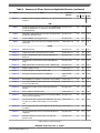
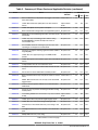
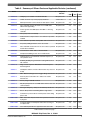
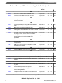

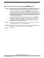
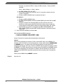


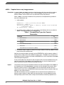


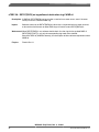

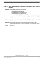
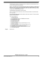

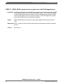


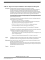
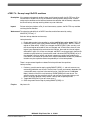

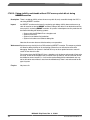


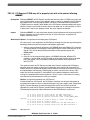

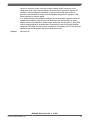
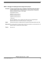


![LMD Martian Mesoscale Model [LMD-MMM] User Manual](http://vs1.manualzilla.com/store/data/006911548_1-e4280765449b25ef8991a0e08e28e935-150x150.png)