Download Rev. G - Analog Devices
Transcript
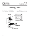
a AD5232 Non-Volatile Memory Digital Potentiometers Evaluation Board User Manual Rev. G 10/7/02 7 STEPS TO SETUP THE EVALUATION BOARD 1. 2. Install AD5232 s/w from CD ROM Download NTPORT.OCX from web 6. Open AD5232 Rev G.exe and program resistance settings 4. Connect JP14 on Eval Board 3. Connect Parallel Port Cable W1 B1 +5V GND 7. Measure Result on Meter 5. Provide Power Supply Figure 1. Evaluation Kit Setup No Programming Skill or Programming Language Required! 1 a STEPS FOR OPERATING AD5232 EVALUATION KIT 1. Installing AD5232 Rev G Evaluation Software a. Run setup.exe under D:\AD5232 Evaluation Software Package b. During the installation, hit ignore or yes to bypass error messages if they occur. (Users may need to install the s/w few times to get successful installation) 2. Enabling PC Parallel Port Communications (In addition to installing AD5232 Rev G, users need to install a 3rd party driver, NTPORT.OCX from UCT, to gain access of the PC parallel port. UCT offers a free trial of such driver) a. Unzip ntport.zip from the CD Rom. If ntport.zip cannot be found, download it from http://www.uct.on.ca/. Click Download NTPORT.OCX, Click NTPORT free trial (user is obligated to pay a nominal license fee after 30 days free trial) b. Save ntport.zip in default or specified directory c. unzip and extract all to the specified directory d. Run setup.exe e. If it prompts file violations during installation, hit Ignore to bypass it. f. The following instructions are for users running Windows 2000 and XP (For Win NT, skip and jump to step g) Users must ensure the file DLPORTIO.SYS is placed in Winnt\system32\drivers or Windows\system32\drivers directory. 1. Run LOADDRV.EXE under c:\program files\project1 or the specified directory. A dialog box will appear as (Error Message: if windows prompts you some error messages such as ‘Can’t connect to service control manager’, you need to contact the IS department to grant you an authority for further installation) 2. Change pathname to c:\winnt\system32\drivers\dlportio.sys (For Windows 2000) c:\windows\system32\drivers\dlportio.sys (For Windows XP) 3. Hit Install button, then Start button. If the status message states successful, the driver is installed and operating. Click OK button. 4. Go to Device Manager (For Win 2000, go to Control Panel – Systems – Hardware – Device Manager, For Win XP, go to System Properties – Hardware – Device Manager) 2 a 5. The “Non-Plug and Play Divers“ entry may not be visible at first. If not, click on the View menu item in Device Manager and click on View Hidden Devices to make sure that hidden driver files are listed. Then it should be visible. (Note: If you do not see dlportio, reboot windows or redo LOADDRV.EXE and then reboot windows.) 6. From the non-plug and play drivers list in Device Manager locate the dlportio device and double-click. 3 a 7. The dlportio properties page for the driver will be shown. At Driver tab, select Current Status as Start and Startup Type as AUTOMATIC. (Note: If Startup is not active and you cannot change Type, your computer may be administered by your IS department. You may need to consult them to change your PC administrative setting) 4 a g. The following instructions are for users running Windows NT only Users must ensure that the file: DLPORTIO.SYS is placed in the Winnt\system32\drivers directory. In order to load the DLPORTIO.SYS driver; use the driver loader program LOADDVR.EXE 1. Open c:\program files\project1\loaddrv.exe A dialog box will be appear as (Error Message: if windows prompts you some error messages such as ‘Can’t connect to service control manager’, you need to contact the IS department to grant you an authority for further installation) 2. The pathname for DLPORTIO.SYS must be changed accordingly to the following operating systems: c:\winnt\system32\drivers\dlportio.sys 3. Hit Install button, then Start button. If the status message states successful, the driver is installed and operating. Click OK button. 4. Automatic Driver Loading Under Windows NT Once the DLPORTIO.SYS driver has been installed and run on an NT system it can be made to start automatically every time NT is started. To place the driver into this mode select the DEVICES icon from the Windows NT Control Panel. From “Devices” dialog box that will appear select dlportio and click on the Startup... button 5 a 5. The device Startup Type dialog box will be shown as illustrated below. From the option buttons select Automatic. The driver will now automatically start each time that Windows NT is restarted. Note Due to the large variations in computer platforms and configurations, Analog Devices, Inc. cannot guarantee this software to work on all systems. Should you encounter problem, you may consult [email protected] or call 1-408-382-3082 for application support. Uninstall To uninstall AD5232 and NTPORT, use Add/Remove Programs in Control Panel 6 a 3. Connect Parallel Port Cable to LPT1 4. Evaluation Board Configuration 1. For single supply, connect JP14 and JP13 to ground Vss of U1 and U3, apply 5V to pin +5V (Some boards do not come with jumper caps. Users should get suitable caps or simply short the jumpers for proper operations) 2. For dual supplies, connect JP15 and JP12 to provide –2.5V to Vss of U1 and U3, apply +2.5V to pin +5V and –2.5V to pin –5V 3. The states of PR, WP, and RDY can be selected from the DIP switches provided. 4. SDO can be monitored TPSDO. 1k to 10kohm pull-up resistors are needed for both SDO and RDY pins. 5. Apply Power Supply according Step 4.1 and 4.2. 6. How to Use The Evaluation Board 1. Open AD5232 Rev G.exe from Windows Start - Programs - AD5232 Rev G, the program is shown in Figure 2. 2. Users can use Direct Control such as moving the scroll bars or pressing the buttons to control the devices. Users can also adjust the Bit Pattern and then hit Run to program the device. Their operations are selfexplanatory. 3. User can also approximate RWA and RWB by first entering the measured RAB after power is applied. Figure 2. AD5232 Software Graphical Interface 7. Measure Result 7 a Evaluation Board Schematic General purpose opamp AD820, U3A can be configured as various building block circuits in conjunction with AD5235 for various circuit evaluations, see appendix. Other opamps in P-DIP can replace AD820. For single supply, 2.5V Voltage reference AD1582 can be used to offset opamp bias point for AC operation. AD5232/AD5235 Main Circuit +5 (Lower to +2.5 if Dual Supplies) +5V 1 J1 1 2 1 2 1 2 1 2 9 2 8 2 7 1 6 1 5 1 4 1 3 1 2 1 1 R R R 10 10 10 DGND U1A TPSDO 1 2 3 4 TP/CS TPCLK +5 TPSDI R1 1k 16 151413 SDI CS CLK RDY SDO PR GND WP VSS VDD A2 A1 C10 C11 4.7u 0.1u High TPRDY TP/PR TP/WP 1 2 3 4 12 11 10 9 S1 R_SDI100 100 DB25 JP14 Note Header 1. Signal Ground with Net DGND JP15 2. Power Ground with Net AGND U1B 16 1 CLK RDY 15 2 SDI CS 14 3 SDO PR 4 13 GND WP 5 VSS VDD 12 6 11 A1 A2 7 W1 W2 910 8 B1 B2 AD5232/AD5235TSSOP GND 1 C13 C12 4.7u 0.1u 8 7 6 5 SW- W1 B1 B2W2 5 6 7 8 AD5235CSP R_/CS R_CLK100 Low 1 A1 1 W1 1 B1 1 A2 1 W2 1 B2 -5V 1 Header -5 (Lower to -2.5V if Dual Supplies) Additional Opamp For General Purpose V+ V1 JP5 Header JP7 Vo 1 JP6 JP8 JP4 +5 C5 0.1 7 1,5, Header Vi_DC 1 JP2 JP3 Vi_AC 1 U2 GND 3 Vi VOUT 0.1u AD1582 +5 C7 C9 Header 1 2.5VR 2 3 JP1 6 U3 AD820AR Vo JP10 JP11 4 Header -5 2 1 JP9 JP12 JP13 Head C6 Head +5 0.1u 2 C8 1u 3 1 7 U3 8 6 5 4AD820 Replacable Opamp in Figure 3. Evaluation Board Schematic Note Should you encounter problem, you may consult [email protected] or call 1-408-3823082 for application support. If you are interested of the source code, you may contact [email protected] for further information. 8 a Table 1. AD5232 16-bit Serial Data Word MSB C3 C2 C1 C0 A3 A2 A1 A0 D7 D6 D5 D4 D3 D2 D1 L SB D0 Command bits are identified as Cx, address bits are Ax, and data bits are Dx. Command instruction codes are defined in table 2. Table 2. AD5232 Dual 8-bit Instruction/Operation Truth Table Inst No. Instruction Byte 1 B15 •••••••••••••••• B8 Data Byte 0 B7 •••••••••••••••••••• B0 0 C3 C2 C1 C0 A3 A2 A1 A0 0 0 0 0 X X X X D7 D6 D5 D4 D3 D3 D2 D1 D0 X X X X X X X X X NOP: Do nothing 1 0 0 0 1 << ADDR >> X X X X X X X X X Write contents of EEMEM to RDAC Register 2 0 0 1 0 << ADDR >> X X X X X X X X X SAVE WIPER SETTING: Write contents of RDAC to EEMEM 3 0 0 1 1 << ADDR >> D7 D6 D5 D4 D3 D3 D2 D1 D0 Write contents of Serial Register Data Byte 0 to EEMEM 4 0 1 0 0 << ADDR >> X X X X X X X X X DEC 6dB: Right Shift contents of RDAC, LSB rolls over to MSB position 5 0 1 0 1 X X X X X X X X X X X DEC All 6dB: Right Shift contents of all RDAC Registers, LSB rolls over to MSB position 6 0 1 1 0 << ADDR >> X X X X X X X X X Decrement contents of RDAC by One, does not rollover at zero-scale 7 0 1 1 1 X X X X X X X X X X X X X Decrement contents of all RDAC Registers by One, does not rollover at zero-scale 8 1 0 0 0 0 0 0 0 X X X X X X X X X RESET: Load all RDACs with their corresponding EEMEM previously-saved values 9 1 0 0 1 << ADDR >> X X X X X X X X X Write contents of EEMEM to Serial Register Data Byte 0. SDO activated 10 1 0 1 0 << ADDR >> X X X X X X X X X Write contents of RDAC to Serial Register Data Byte 0. SDO activated 11 1 0 1 1 << ADDR >> D7 D6 D5 D4 D3 D3 D2 D1 D0 Write contents of Serial Register Data Byte 0 to RDAC 12 1 1 0 0 << ADDR >> X X X X X X X X X INC 6dB: Left Shift contents of RDAC, stops at all ones 13 1 1 0 1 X X X X X X X X X X X INC All 6dB: Left Shift contents of all RDAC Registers, stops at all ones 14 1 1 1 0 << ADDR >> X X X X X X X X X Increment contents of RDAC by One, does not rollover at full-scale 15 1 1 1 1 X X X X X X X X X X Increment contents of all RDAC Registers by One, does not rollover at full-scale X X X X X X X Operation NOTES: 1. The SDO output shifts-out the last 16-bits of data clocked into the serial register for daisy chain operation. Exception, following Instruction #9 or #10 the selected internal register data will be present in data byte 0 & 1. Instructions following #9 & #10 must be a full 24-bit data word to completely clock out the contents of the serial register. 2. The RDAC register is a volatile scratch pad register that is refreshed at power ON from the corresponding non-volatile EEMEM register. 3. The increment, decrement and shift commands ignore the contents of the shift register Data Byte 0. 4. Execution of the Operation column noted in the table takes place when the CS strobe returns to logic high. 9 a APPLICATION PROGRAMMING EXAMPLES PCB setting: Tie WP to GND [prevents changes in PCB wiper set position] Power VDD & VSS with respect to GND Optional: Strobe PR pin [insures full power ON preset of wiper register with EEMEM contents in unpredictable supply sequencing environments] The following command sequence examples have been developed to illustrate a typical sequence of events for the various features of the AD5232 nonvolatile digital potentiometer. [PCB = Printed Circuit Board containing the AD523X part]. Instruction numbers (Commands), addresses and data appearing at SDI and SDO pins are listed in hexadecimal. SDI SDO Action B140H XXXXH Loads 40H data into RDAC2 register, Wiper W2 moves to 1/4 full-scale position B080H B140H Loads 80H data into RDAC1 register, Wiper W1 moves to 1/2 full-scale position Table 5 Equipment customer startup sequence for a PCB calibrated unit with protected settings SDI SDO Action C1XXH XXXXH Moves wiper W2 to double the present data value contained in RDAC2 register, in the direction of the A terminal C1XXH XXXXH Moves wiper W2 to double the present data value contained in RDAC2 register, in the direction of the A terminal Table 3. Set two digital POTs to independent data values SDI SDO Action B040H XXXXH Loads 40H data into RDAC1 register, Wiper W1 moves to 1/4 full-scale position E0XXH E0XXH B040H E0XXH Table 6. Using Left shift by one to change circuit gain in 6dB steps Increments RDAC1 register by one to 41H, Wiper W1 moves one resistor segment away from terminal B. Increments RDAC1 register by one to 42H, Wiper W1 moves one more resistor segment away from terminal B. E0XXH SDO Action 3280H XXXXH Stores 80H data into spare EEMEM location USER1 3340H XXXXH Stores 40H data into spare EEMEM location USER2 Table 7. Storing additional data in nonvolatile memory Continue until desired wiper position reached 20XXH SDI Saves RDAC1 register data into corresponding nonvolatile EEMEM1 memory ADDR=0H SDI SDO Action 94XXH XXXXH Prepares data read from USER3 location. Assumption USER3 previously loaded with 80H NOP instruction #0 sends 16-bit word out of SDO where the last 8 bits contain the contents of USER3 location. NOP command insures device returns to idle power dissipation state. Table 8. Reading back data from various memory locations 00XXH Table 4. Active trimming of one POT followed by a save to nonvolatile memory (PCB calibrate) 10 XX80H a APPENDIX APPLICATIONS AD5232/AD5235/ADN2850 1 16 CLK RDY 2 15 SDI CS 3 14 SDO PR 4 13 GND WP 5 12 VSS VDD 6 11 A1* A2* 7 10 W1 W2 8 9 B1 B2 JP15 RDAC A R2 B external U1 +5 (+2.5V) 7 R1 external R2 -INPUT -5 (-2.5V) Vi_DC Vo 1,5,8 2 1 Vo AD820AR JP1 4 JP3 6 U3 3 1 Vi_AC JP12 C9 1 - R2/(R1+RAB)*Vi < Vo < -(R2+RAB)/R1*Vi -5 (-2.5V) 1 Bipolar Unity Gain Amplifier 1 1 A2* (Input Signal Here) AD5232/AD5235/ADN2850 1 16 CLK RDY -INPUT 2 15 SDI CS FB 3 14 SDO PR 4 13 GND WP 5 12 VSS VDD R R Vo 6 11 A1* A2* 7 10 external JP8 W1 W2 +5 (+2.5V) 8 9 B1 B2 JP4 U1 1,5,8 2 6 U3 JP2 3 AD820AR R R 7 Vi A Vo RDAC Vo 4 B JP12 -1 < Vo/Vi < 1 -5 (-2.5V) R R1 A iS JP15 Vo JP7 R JP6 U1 +5 (+2.5V) 7 RDAC Vi_DC B Vo D1 -5 (-2.5V) 1,5,8 2 1 3 6 U3 AD820AR JP1 4 D1 R1 1 High Sensitivity I-V Converter -INPUT 1 FB AD5232/AD5235/ADN2850 1 16 CLK RDY 2 15 SDI CS 3 14 SDO PR 4 13 GND WP 5 12 VSS VDD 6 11 A1* A2* 7 10 W1 W2 8 9 B1 B2 1 Vi Vo R1 1 Inverting Gain & Attentuator JP12 Vo = -k*R*iS k = 1 + RWB/R1 + RWB/R -5 (-2.5V) 11 Vo a A D 5232/A D 5235/A D N 2850 1 CLKRD Y 2 SD I CS 3 SD O PR 4 G N D W P 5 V SSV D D 6 A 1* A 2* 7 W 1 W 2 8 B1 B2 BuferedV o Buffered Voltage Output V i JP14 A 16 15 14 13 12 11 10 9 V i_A C FB (D on'tuseV i_D C) 1 JP8 1 +5 JP4 U 1 1,5,8 7 2 V o JP2 RD A C 4 U 3 3 6 V o A D 820A R B JP13 R1 Vi A RDAC B -INPUT Vo 1 1 Inverting Linear Gain & Attentuator AD5232/AD5235/ADN2850 1 16 CLK RDY 2 15 SDI CS 3 14 SDO PR 4 13 GND WP 5 12 VSS VDD 6 11 A1* A2* 7 10 W1 W2 8 9 B1 B2 +5 (+2.5V) U1 7 JP15 R1 Vo 6 U3 3 Vo AD820AR JP1 Vi_DC 4 -5 (-2.5V) 1,5,8 2 JP4 JP6 1 JP12 G = - RWB/R1 Vo=-Vi*(D*RAB)/(2^n*R1) -5 (-2.5V) A RDAC U1 B +5 (+2.5V) JP4 JP15 7 Vi Vi_DC Vo Vo 1 Inverting Quasi Log Gain & Attentuator -INPUT 1 1 AD5232/AD5235/ADN2850 1 16 CLK RDY 2 15 FB SDI CS 3 14 SDO PR 4 13 GND WP 5 12 VSS VDD 6 11 A1* A2* 7 10 W1 W2 8 9 B1 B2 1,5,8 2 1 3 JP3 Vo AD820AR JP1 4 -5 (-2.5V) 6 U3 Vi_AC C9 JP12 1 G = - RWB/RWA Vo=-Vi*(D/2^n-1) -5 (-2.5V) 1 FB AD5232/AD5235/ADN2850 1 16 CLK RDY 2 15 -INPUT SDI CS 3 14 SDO PR 4 13 GND WP 5 12 VSS VDD R2 6 11 A1* A2* 7 10 JP8 W1 W2 +5 (+2.5V) 8 9 B1 B2 JP4 U1 RDAC B R2 7 A JP15 2 Vi_DC Vo 3 1 AD820AR JP3 JP1 -5 (-2.5V) G = - R2/RWA Vo=-Vi*(2^n*R2)/((2^n-D)*RAB) Vi_AC C9 JP12 1 -5 (-2.5V) 12 1,5,8 6 U3 4 Vi 1 Vo 1 Inverting Exponential Gain & Attentuator Vo a AD5232/AD5235/ADN2850 1 16 CLK RDY 2 15 SDI CS 3 14 SDO PR 4 13 GND WP 5 12 VSS VDD 6 11 A1* A2* 7 10 W1 W2 8 9 B1 B2 R1 A RDAC B U1 JP14 JP5 -INPUT Vo 1 1 Non-Inverting Linear Gain +5 R1 7 JP6 1,5,8 2 Vi_DC Vo Vi 1 JP2 3 6 U3 Vo 4 AD820AR JP13 G = 1 + RWB/R1 Vo=Vi*(1+D*RAB/(2^nR1)) RDAC B 1 Vo U1 JP14 +5 7 A -INPUT 1 Non-Inverting Quasi Log Gain 1 GND AD5232/AD5235/ADN2850 1 16 CLK RDY 2 15 SDI CS 3 14 SDO PR 4 13 GND WP 5 12 VSS VDD 6 11 A1* A2* 7 10 W1 W2 8 9 B1 B2 1,5,8 2 Vi_DC Vo Vi JP2 1 3 6 U3 Vo AD820AR 4 JP3 Vi_AC G = 1 + RWB/RWA Vo=Vi*(1+D/(2^n-D)) JP13 C9 1 A RDAC B R2 R2 JP8 +5 U1 7 JP14 Vo 1 -INPUT 1 Non-Inverting Exponential Gain 1 GND AD5232/AD5235/ADN2850 1 16 CLK RDY 2 15 SDI CS 3 14 SDO PR 4 13 GND WP 5 12 VSS VDD 6 11 A1* A2* 7 10 W1 W2 8 9 B1 B2 2 Vi Vo Vi_DC JP2 1 3 U3 1,5,8 6 AD820AR 4 JP3 G = 1 + R2/RWA Vo=Vi*(1+2^nR2/((2^n-D)RAB)) Vi_AC JP13 C9 1 13 Vo a +5 (+2.5V) AD5232/AD5235/ADN2850 1 16 CLK RDY 2 15 SDI CS 3 14 SDO PR 4 13 GND WP 5 12 VSS VDD 6 11 A1* A2* JP15 7 10 W1 W2 8 9 B1 B2 +2.5 R1 1M, 0.1% R1 external -INPUT JP8 U1 R2 external A -5 (-2.5V) 1,5,8 2 Vo RDAC Vo +5 (+2.5V) 7 Ultra Fine Adjustment 3 6 U3 Vo AD820AR B 4 -5 (-2.5V) JP1 JP12 R2 1M, 0.1% -5 (-2.5V) -2.5 VW = V+*(RWB/(R2+RAB) -V-*(RWA/(R1+RAB)) AD5232/AD5235/ADN2850 1 16 CLK RDY 2 15 SDI CS 3 14 SDO PR 4 13 GND WP 5 12 VSS VDD 6 11 A1* A2* JP15 7 10 W1 W2 8 9 B1 B2 R1 Vi R2 R1 FB R2 -INPUT external JP4 U1 Vo JP8 +5 (+2.5V) 7 Phase Shifter 1,5,8 2 B RDAC -5 (-2.5V) JP2 3 C1 C1 JP1 Vi_AC 6 U3 Vo AD820AR 4 A Vo 1 JP12 G = 180 - 2tan^-1wRC -5 (-2.5V) Level Detector VA A RDAC JP2 -5 (-2.5V) JP8 +5 (+2.5V) 7 AD5232/AD5235/ADN2850 1 16 CLK RDY 2 15 SDI CS 3 14 SDO PR 4 13 GND WP 5 12 +5 (+2.5V) VSS VDD 6 11 A1* A2* JP15 7 10 W1 W2 8 9 B1 B2 JP4 U1 2 3 U3 Vo 6 AD820AR 4 B 1,5,8 Vref JP13 VB 14 Vo a PCB LAYOUT Figure 4. Evaluation Board Layout PCB LAYOUT CONSIDERATION To stabilize voltage supplies, bypassed +5V and –5V with a 4.7u or 10uF capacitor with proper polarities. Add 0.1uF decoupling capacitors, very close to the supply pins of active component, can minimize high frequency noise as well. 15 a AD5232 Parallel Port Connection (For Visual Basic Program Developer Only. Users Can Ignore) /PR (not used) /CS CLK SDI GND SDO http://www.doc.ic.ac.uk/~ih/doc/par/ 8 output pins accessed via the DATA Port 5 input pins (one inverted) accessed via the STATUS Port 4 output pins (three inverted) accessed via the CONTROL Port The remaining 8 pins are grounded (NTPORT1.Address = 888) (NTPORT1.Address = 889) (NTPORT1.Address = 890) TIMING DEFINATION IN VISUAL BASIC SOURCE CODE cmdRUN (For Visual Basic Program Developer Only. Users Can Ignore) bit 3 (Pin 5) bit 2 (Pin 4) bit 1 (Pin 3) bit 0 (Pin 2) /PR /CS CLK SDI Binary Code 1100 1001 1011 1000 1010 Decimal Code 12 No Activity 9 11 Send out BIT_TOGO=1 8 10 Send out BIT_TOGO=0 16 1100 12 Latch Data


