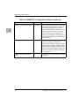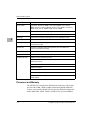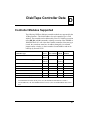
1
MVME167P Single-Board Computer
Installation and Use
V167PA/IH2
December 2001 Edition
© Copyright 2001 Motorola Inc.
All rights reserved.
Printed in the United States of America.
Motorola® and the Motorola logo are registered trademarks of Motorola, Inc.
MC68040™ and MC68060™ are trademarks of Motorola, Inc.
All other products mentioned in this document are trademarks or registered trademarks of
their respective holders.
Safety Summary
The following general safety precautions must be observed during all phases of operation, service, and repair of
this equipment. Failure to comply with these precautions or with specific warnings elsewhere in this manual
could result in personal injury or damage to the equipment.
The safety precautions listed below represent warnings of certain dangers of which Motorola is aware. You, as
the user of the product, should follow these warnings and all other safety precautions necessary for the safe
operation of the equipment in your operating environment.
Ground the Instrument.
To minimize shock hazard, the equipment chassis and enclosure must be connected to an electrical ground. If the
equipment is supplied with a three-conductor AC power cable, the power cable must be plugged into an approved
three-contact electrical outlet, with the grounding wire (green/yellow) reliably connected to an electrical ground
(safety ground) at the power outlet. The power jack and mating plug of the power cable meet International
Electrotechnical Commission (IEC) safety standards and local electrical regulatory codes.
Do Not Operate in an Explosive Atmosphere.
Do not operate the equipment in any explosive atmosphere such as in the presence of flammable gases or fumes.
Operation of any electrical equipment in such an environment could result in an explosion and cause injury or
damage.
Keep Away From Live Circuits Inside the Equipment.
Operating personnel must not remove equipment covers. Only Factory Authorized Service Personnel or other
qualified service personnel may remove equipment covers for internal subassembly or component replacement
or any internal adjustment. Service personnel should not replace components with power cable connected. Under
certain conditions, dangerous voltages may exist even with the power cable removed. To avoid injuries, such
personnel should always disconnect power and discharge circuits before touching components.
Use Caution When Exposing or Handling a CRT.
Breakage of a Cathode-Ray Tube (CRT) causes a high-velocity scattering of glass fragments (implosion). To
prevent CRT implosion, do not handle the CRT and avoid rough handling or jarring of the equipment. Handling
of a CRT should be done only by qualified service personnel using approved safety mask and gloves.
Do Not Substitute Parts or Modify Equipment.
Do not install substitute parts or perform any unauthorized modification of the equipment. Contact your local
Motorola representative for service and repair to ensure that all safety features are maintained.
Observe Warnings in Manual.
Warnings, such as the example below, precede potentially dangerous procedures throughout this manual.
Instructions contained in the warnings must be followed. You should also employ all other safety precautions
which you deem necessary for the operation of the equipment in your operating environment.
Warning
Warning
To prevent serious injury or death from dangerous voltages, use extreme
caution when handling, testing, and adjusting this equipment and its
components.
Flammability
All Motorola PWBs (printed wiring boards) are manufactured with a flammability rating
of 94V-0 by UL-recognized manufacturers.
EMI Caution
Caution
!
Caution
This equipment generates, uses and can radiate electromagnetic energy. It
may cause or be susceptible to electromagnetic interference (EMI) if not
installed and used with adequate EMI protection.
Lithium Battery Caution
This product contains a lithium battery to power the clock and calendar circuitry.
Caution
!
Caution
Caution
!
Attention
Caution
!
Vorsicht
Danger of explosion if battery is replaced incorrectly. Replace battery only
with the same or equivalent type recommended by the equipment
manufacturer. Dispose of used batteries according to the manufacturer’s
instructions.
Il y a danger d’explosion s’il y a remplacement incorrect de la batterie.
Remplacer uniquement avec une batterie du même type ou d’un type
équivalent recommandé par le constructeur. Mettre au rebut les batteries
usagées conformément aux instructions du fabricant.
Explosionsgefahr bei unsachgemäßem Austausch der Batterie. Ersatz nur
durch denselben oder einen vom Hersteller empfohlenen Typ. Entsorgung
gebrauchter Batterien nach Angaben des Herstellers.
CE Notice (European Community)
Motorola Computer Group products with the CE marking comply with the EMC Directive
(89/336/EEC). Compliance with this directive implies conformity to the following
European Norms:
EN55022 “Limits and Methods of Measurement of Radio Interference Characteristics
of Information Technology Equipment”; this product is tested to Equipment Class B
EN55024 “Information technology equipment—Immunity characteristics—Limits and
methods of measurement”
Board products are tested in a representative system to show compliance with the above
mentioned requirements. A proper installation in a CE-marked system will maintain the
required EMC/safety performance.
In accordance with European Community directives, a “Declaration of Conformity” has
been made and is available on request. Please contact your sales representative.
Notice
While reasonable efforts have been made to assure the accuracy of this document,
Motorola, Inc. assumes no liability resulting from any omissions in this document, or from
the use of the information obtained therein. Motorola reserves the right to revise this
document and to make changes from time to time in the content hereof without obligation
of Motorola to notify any person of such revision or changes.
Electronic versions of this material may be read online, downloaded for personal use, or
referenced in another document as a URL to the Motorola Computer Group Web site. The
text itself may not be published commercially in print or electronic form, edited, translated,
or otherwise altered without the permission of Motorola, Inc.
It is possible that this publication may contain reference to or information about Motorola
products (machines and programs), programming, or services that are not available in your
country. Such references or information must not be construed to mean that Motorola
intends to announce such Motorola products, programming, or services in your country.
Limited and Restricted Rights Legend
If the documentation contained herein is supplied, directly or indirectly, to the U.S.
Government, the following notice shall apply unless otherwise agreed to in writing by
Motorola, Inc.
Use, duplication, or disclosure by the Government is subject to restrictions as set forth in
subparagraph (b)(3) of the Rights in Technical Data clause at DFARS 252.227-7013 (Nov.
1995) and of the Rights in Noncommercial Computer Software and Documentation clause
at DFARS 252.227-7014 (Jun. 1995).
Motorola, Inc.
Computer Group
2900 South Diablo Way
Tempe, Arizona 85282
Contents
About This Manual
Summary of Changes ................................................................................................xvi
Overview of Contents ...............................................................................................xvi
Comments and Suggestions .....................................................................................xvii
Terminology ........................................................................................................... xviii
Conventions Used in This Manual ......................................................................... xviii
CHAPTER 1
Hardware Preparation and Installation
Introduction .............................................................................................................. 1-1
Equipment Required ................................................................................................. 1-1
Overview of Installation Procedure ......................................................................... 1-3
Guidelines for Unpacking ........................................................................................ 1-4
Installation Preliminaries ......................................................................................... 1-4
Preparing the Board .................................................................................................. 1-5
Switches and Jumpers ....................................................................................... 1-6
General-Purpose Readable Jumpers (J1) .......................................................... 1-7
VME System Controller (J6) ............................................................................ 1-7
SRAM Backup Power Source (J9) ................................................................... 1-8
Serial Port 4 Clock Configuration (J10 and J11) .............................................. 1-9
Petra SDRAM Size (S3) ................................................................................... 1-9
Board EPROM/Flash Mode (S4) .....................................................................1-11
Preparing the Transition Module .............................................................................1-11
Installation Instructions .......................................................................................... 1-12
MVME167P and Transition Module Installation ........................................... 1-12
System Considerations .................................................................................... 1-14
CHAPTER 2
Startup and Operation
Introduction .............................................................................................................. 2-1
Front Panel Switches and Indicators ................................................................. 2-1
Pre-Startup Check ............................................................................................. 2-3
Initial Conditions .............................................................................................. 2-3
Applying Power ................................................................................................ 2-4
Bringing up the Board .............................................................................................. 2-4
vii
Booting the System ................................................................................................... 2-7
Autoboot ............................................................................................................ 2-8
ROMboot ........................................................................................................... 2-9
Network Boot .................................................................................................. 2-10
Restarting the System ............................................................................................. 2-10
Reset ................................................................................................................ 2-11
Abort ................................................................................................................ 2-12
Break ............................................................................................................... 2-12
Diagnostic Facilities ............................................................................................... 2-12
CHAPTER 3
167Bug Firmware
Introduction .............................................................................................................. 3-1
167Bug Overview .............................................................................................. 3-1
Components of the Firmware ................................................................................... 3-2
Memory Requirements ............................................................................................. 3-2
Implementation ......................................................................................................... 3-3
Using the Debugger .................................................................................................. 3-3
Debugger Commands ............................................................................................... 3-5
CHAPTER 4
Modifying the Environment
Overview .................................................................................................................. 4-1
CNFG - Configure Board Information Block ........................................................... 4-2
ENV - Set Environment ............................................................................................ 4-3
CHAPTER 5
Functional Description
Introduction .............................................................................................................. 5-1
Summary of Features ................................................................................................ 5-1
Processor and Memory ...................................................................................... 5-2
I/O Implementation ........................................................................................... 5-3
ASICs ................................................................................................................ 5-3
Block Diagram .......................................................................................................... 5-4
Data Bus Structure ............................................................................................. 5-4
Microprocessor .................................................................................................. 5-4
Memory Options ................................................................................................ 5-5
DRAM ........................................................................................................ 5-6
SRAM ........................................................................................................ 5-6
EPROM ...................................................................................................... 5-6
Battery-Backed-Up RAM and Clock ................................................................ 5-7
viii
VMEbus Interface and VMEchip2 ................................................................... 5-7
I/O Interfaces .................................................................................................... 5-7
Serial Port Interface ................................................................................... 5-7
Parallel Port Interface ................................................................................ 5-9
Ethernet Interface ....................................................................................... 5-9
SCSI Interface .......................................................................................... 5-10
SCSI Termination .................................................................................... 5-10
Local Resources ...............................................................................................5-11
Programmable Tick Timers ..................................................................... 5-11
Watchdog Timer ...................................................................................... 5-11
Software-Programmable Hardware Interrupts ......................................... 5-11
Local Bus Timeout ................................................................................... 5-12
Local Bus Arbiter ............................................................................................ 5-12
Connectors ...................................................................................................... 5-12
Remote Status and Control ...................................................................... 5-13
CHAPTER 6
Connector Pin Assignments
MVME167P Connectors .......................................................................................... 6-1
Remote Reset Connector ................................................................................... 6-2
VMEbus Connectors ......................................................................................... 6-2
APPENDIX A
Specifications
Introduction ..............................................................................................................A-1
Board Specifications .........................................................................................A-1
Cooling Requirements ......................................................................................A-2
EMC Compliance ..............................................................................................A-3
APPENDIX B
Troubleshooting
Solving Startup Problems .........................................................................................B-1
APPENDIX C
Network Controller Data
Network Controller Modules Supported ..................................................................C-1
APPENDIX D
Disk/Tape Controller Data
Controller Modules Supported .................................................................................D-1
Default Configurations ......................................................................................D-2
ix
IOT Command Parameters ............................................................................... D-4
APPENDIX E
Related Documentation
MCG Documents ......................................................................................................E-1
Manufacturers’ Documents ......................................................................................E-2
Related Specifications ..............................................................................................E-3
GLOSSARY
x
List of Figures
Figure 1-1. MVME167P Board Layout .................................................................. 1-2
Figure 2-1. MVME167P/Firmware System Startup ............................................... 2-4
Figure 5-1. MVME167P Block Diagram ................................................................ 5-5
xi
List of Tables
Table 1-1. Startup Overview ................................................................................... 1-3
Table 1-2. MVME167P Configuration Settings ...................................................... 1-6
Table 1-3. Petra SDRAM Size Settings ................................................................ 1-10
Table 2-1. MVME167P Front Panel Controls ......................................................... 2-2
Table 2-2. General-Purpose Configuration Bits (J1) ............................................... 2-7
Table 3-1. Memory Offsets with 167Bug ................................................................ 3-2
Table 3-2. 167Bug Commands ................................................................................ 3-5
Table 4-1. MVME167P Configuration Settings ...................................................... 4-3
Table 5-1. Local Bus Arbitration Priority ............................................................. 5-12
Table 6-1. Remote Reset Connector J3 ................................................................... 6-2
Table 6-2. VMEbus Connector P1 .......................................................................... 6-3
Table 6-3. VMEbus Connector P2 .......................................................................... 6-4
Table A-1. MVME167P Specifications ..................................................................A-1
Table B-1. Troubleshooting MVME167P Boards ...................................................B-1
Table E-1. Motorola Computer Group Documents ................................................. E-1
Table E-2. Manufacturers’ Documents ................................................................... E-2
Table E-3. Related Specifications ........................................................................... E-3
xiii
About This Manual
MVME167P Single-Board Computer Installation and Use provides
general information, instructions for hardware preparation and installation,
operating instructions, and a functional description for the MVME167P
series of Single Board Computers (referred to as the MVME167P
throughout this manual).
The “Petra” chip that distinguishes MVME167P single-board computers is
an application-specific integrated circuit (ASIC) used on various Motorola
VME boards which combines a variety of functions previously
implemented in other ASICs (among them the MC2 chip, the IP2 chip, and
the MCECC chip) in a single ASIC. On the MVME167P, the “Petra” chip
replaces the MCECC ASIC. As of the publication date, the information
presented in this manual applies to the following MVME167P models.
Model Number
Characteristics
MVME167PA-24SE
25MHz, 16MB SDRAM
MVME167PA-25SE
25MHz, 32MB SDRAM
MVME167PA-34SE
33MHz, 16MB SDRAM
MVME167PA-35SE
33MHz, 32MB SDRAM
MVME167PA-35SEB
33MHz, 32MB SDRAM, battery backup
MVME167PA-36SE
33MHz, 64MB SDRAM
Note: All models contain an MC68040 processor, SCSI, and Ethernet.
This manual is intended for anyone who designs OEM systems, desires to
add capability to an existing compatible system, or works in a lab
environment for experimental purposes. A basic knowledge of computers
and digital logic is assumed. To use this manual, you may also wish to
become familiar with the publications listed in Appendix E, Related
Documentation.
xv
Summary of Changes
This is the second edition of MVME167P Single-Board Computer
Installation and Use. It supersedes the October 2000 edition and
incorporates the following updates.
Date
Changes
December 2001
Entries on the functionality of jumper header J9 were added in the Preparing
the Board section in Chapter 1.
December 2001
A note on the functionality of jumper headers J2 and J7 was added to the
section Switches and Jumpers on page 1-6, explaining that these are not for
customer use.
December 2001
Errors in pin assignments were corrected in Table 6-3, VMEbus Connector P2.
December 2001
In Appendix A, Specifications, the operating temperature range was corrected
to read 0° C to 55° C in Table A-1.
December 2001
Some chapters and appendices were reorganized to reflect current MCG
practice in the structuring of documentation.
Overview of Contents
This manual is divided into the chapters and appendices listed below.
❏ Chapter 1, Hardware Preparation and Installation: Guidelines for
preparation and installation of the MVME167P single-board
computer
❏ Chapter 2, Startup and Operation: Procedures for bringing up the
board; descriptions of the functionality of the switches, status
indicators, and I/O ports
❏ Chapter 3, 167Bug Firmware: An overview of the board firmware,
with a detailed description of the monitor (interactive command
portion of the firmware) as well as information on using the
debugger
xvi
❏ Chapter 4, Modifying the Environment: A description of the
CNFG and ENV firmware commands used to view and modify
board configuration parameters
❏ Chapter 5, Functional Description: An overview of the main
board components
❏ Chapter 6, Connector Pin Assignments: A tabulation of board
connector pin assignments
❏ Appendix A, Specifications: A summary of board specifications.
Subsequent sections of the appendix detail cooling requirements
and EMC regulatory compliance
❏ Appendix B, Troubleshooting: Simple troubleshooting steps to
follow in the event that you experience difficulty with your
MVME167P single-board computer
❏ Appendix C, Network Controller Data: A description of the
VMEbus network controller modules that are supported by the
167Bug firmware
❏ Appendix D, Disk/Tape Controller Data: A description of the
VMEbus disk/tape controller modules that are supported by the
167Bug firmware
❏ Appendix E, Related Documentation: A listing of other
publications that may be helpful in using the MVME167P
Comments and Suggestions
Motorola welcomes and appreciates your comments on its documentation.
We want to know what you think about our manuals and how we can make
them better. Mail comments to:
Motorola Computer Group
Reader Comments DW164
2900 S. Diablo Way
Tempe, Arizona 85282
xvii
You can also submit comments to the following e-mail address:
[email protected]
In all your correspondence, please list your name, position, and company.
Be sure to include the title and part number of the manual and tell how you
used it. Then tell us your feelings about its strengths and weaknesses and
any recommendations for improvements.
Terminology
An asterisk (*) following the signal name for signals which are level
significant denotes that the signal is true or valid when the signal is low.
An asterisk (*) following the signal name for signals which are edge
significant denotes that the actions initiated by that signal occur on highto-low transitions.
Data and address sizes for MVME167P chips are defined as follows:
❏ A byte is eight bits, numbered 0 through 7, with bit 0 being the
most significant.
❏ A half-word is 16 bits, numbered 0 through 15, with bit 0 being the
most significant.
❏ A word or single word is 32 bits, numbered 0 through 31, with bit
0 being the most significant.
❏ A double word is 64 bits, numbered 0 through 63, with bit 0 being
the most significant.
Conventions Used in This Manual
The following typographical conventions are used in this document:
bold
is used for user input that you type just as it appears; it is also used for
commands, options and arguments to commands, and names of
programs, directories and files.
xviii
italic
is used for names of variables to which you assign values, for function
parameters, and for structure names and fields. Italic is also used for
comments in screen displays and examples, and to introduce new
terms.
courier
is used for system output (for example, screen displays, reports),
examples, and system prompts.
<Enter>, <Return> or <CR>
represents the carriage return or Enter key.
Ctrl
represents the Control key. Execute control characters by pressing the
Ctrl key and the letter simultaneously, for example, Ctrl-d.
xix
1Hardware Preparation and
Installation
1
Introduction
This chapter describes the equipment you need and the tasks you will
perform to set up the MVME167P Single Board Computer.
Equipment Required
To complete an MVME167P-based system, you need the following
equipment:
❏ VME system enclosure with power supply and system backplane
❏ Display console
❏ Operating system (and / or application software)
❏ Disk drives (and / or other I/O) and controllers
❏ MVME712 series transition module, connecting cables and P2 or
LCP2 adapter
Figure 1-1 illustrates the MVME167P Single Board Computer with its
major components.
1-1
1
Hardware Preparation and Installation
1
15
MVME
167P-36SE
2
16
9
A1
B1
C1
J1
10
XU4
XU3
J2
1
2
DS4
2
2
1
3
J7
J6
DS6
1
DS5
XU2
VME
J9
DS3
SCSI
5
+12V
6
LAN
1
SCON
XU1
RUN
DS2
STAT
DS1
FAIL
P1
DS8
20
DS7
BT1
19
J3
O
N
N
1
2
S4
O
A32
B32
C32
1234
1
2
S1
L1
ABORT
RESET
S2
60
59
L2
J4
A1
B1
C1
2 60
1 59
P2
J5
2
1
1
1
3
3
A32
B32
C32
J11
J10
2817 0800
Figure 1-1. MVME167P Board Layout
1-2
Computer Group Literature Center Web Site
Overview of Installation Procedure
Overview of Installation Procedure
The following table lists the things you will need to do to use this board
and tells where to find the information you need to perform each step. Be
sure to read this entire chapter, including all Cautions and Warnings,
before you begin.
Table 1-1. Startup Overview
What you need to do...
Refer to...
Unpack the hardware.
Guidelines for Unpacking on page 1-4.
Reconfigure jumpers or switches on
the MVME167P board as necessary.
Preparing the Board on page 1-5.
Reconfigure jumpers or switches on
the MVME712 series transition
module as necessary.
Preparing the Transition Module on page 1-11.
Install the board and transition
module in a chassis.
MVME167P and Transition Module Installation on
page 1-12.
Connect a display terminal.
MVME167P and Transition Module Installation on
page 1-12.
Connect any other equipment you will
be using.
Chapter 6, Connector Pin Assignments.
For more information on optional devices and
equipment, refer to the documentation provided with
the equipment.
Chapter 2, Startup and Operation.
Power up the system.
Solving Startup Problems on page B-1.
Note that the firmware initializes and
tests the board.
Applying Power on page 2-3.
You may also wish to obtain the 167Bug Firmware
User’s Manual, listed in Appendix E, Related
Documentation.
http://www.motorola.com/computer/literature
1-3
1
1
Hardware Preparation and Installation
Table 1-1. Startup Overview (continued)
What you need to do...
Refer to...
Initialize the system clock.
Debugger Commands on page 3-5.
Examine and/or change
environmental parameters.
CNFG and ENV command descriptions in Chapter 4,
Modifying the Environment.
Program the board as needed for your
applications.
MVME1XP Single Board Computers Programmer’s
Reference Guide, listed in Appendix E, Related
Documentation.
Guidelines for Unpacking
If the shipping carton is damaged upon receipt, request that the carrier’s
agent be present during the unpacking and inspection of the equipment.
When unpacking, avoid touching areas of integrated circuitry; static
discharge can damage circuits.
Caution
Caution
Refer to the packing list and verify that all items are present. Save the
packing material for storing and reshipping of equipment.
Installation Preliminaries
This section applies to all hardware installations you may perform that
involve the MVME167P board.
ESD
Use ESD
Wrist Strap
1-4
Motorola strongly recommends the use of an antistatic wrist strap and a
conductive foam pad when you install or upgrade the board. Electronic
components can be extremely sensitive to ESD. After removing the board
from the chassis or from its protective wrapper, place the board flat on a
grounded, static-free surface, component side up. Do not slide the board
over any surface.
Computer Group Literature Center Web Site
Preparing the Board
If no ESD station is available, you can avoid damage resulting from ESD
by wearing an antistatic wrist strap (available at electronics stores). Place
the strap around your wrist and attach the grounding end (usually a piece
of copper foil or an alligator clip) to an electrical ground. An electrical
ground can be a piece of metal that literally runs into the ground (such as
an unpainted metal pipe) or a metal part of a grounded electrical appliance.
An appliance is grounded if it has a three-prong plug and is plugged into a
three-prong grounded outlet. You cannot use the chassis in which you are
installing the MVME167P itself as a ground, because the enclosure is
unplugged while you work on it.
Warning
!
Warning
Turn the system’s power off before you perform these procedures. Failure
to turn the power off before opening the enclosure can result in personal
injury or damage to the equipment. Hazardous voltage, current, and energy
levels are present in the chassis. Hazardous voltages may be present on
power switch terminals even when the power switch is off. Never operate
the system with the cover removed. Always replace the cover before
powering up the system.
Preparing the Board
To produce the desired configuration and ensure proper operation of the
MVME167P, you may need to reconfigure hardware to some extent before
installating the board.
Most options on the MVME167P are under software control: By setting
bits in control registers after installing the module in a system, you can
modify its configuration. (The MVME167P registers are described in
Chapter 3 under ENV – Set Environment, and/or in the Programmer's
Reference Guide listed in Appendix E, Related Documentation.)
Some options, though, are not software-programmable. Such options are
either set by configuration switches or are controlled through physical
installation or removal of header jumpers on the base board.
http://www.motorola.com/computer/literature
1-5
1
1
Hardware Preparation and Installation
Switches and Jumpers
Figure 1-1 on page 1-2 illustrates the placement of the jumper headers,
connectors, configuration switches, and various other components on the
MVME167P. Manually configurable jumper headers and configuration
switches on the MVME167P are listed in the following table.
When setting jumpers, avoid touching areas of integrated circuitry; static
discharge can damage circuits.
Caution
Caution
Table 1-2. MVME167P Configuration Settings
Function
Factory Default
General-Purpose Readable Jumpers (J1)
All Jumpers On
VME System Controller (J6)
1-2
SRAM Backup Power Source (J9)
1-3, 2-4
Serial Port 4 Clock Configuration (J10 and J11)
2-3, 2-3
Petra SDRAM Size (S3)
Varies
Board EPROM/Flash Mode (S4)
Off-Off
Note
1-6
Headers J2 and J7 are for factory use; they are not available to
customer applications. J2 is used during board manufacture in
programming on-board logic devices. J7 is a thermal sensing
header. It is not used on the MVME167P.
Computer Group Literature Center Web Site
General-Purpose Readable Jumpers (J1)
General-Purpose Readable Jumpers (J1)
Each MVME167P may be configured with readable jumpers. These
jumpers can be read as a register (at address $FFF4 0088) in the
VMEchip2 Local Control/Status register (refer to the Programmer’s
Reference Guide for details). The bit values are read as a 1 when the
jumper is off, and as a 0 when the jumper is on. The MVME167P is
shipped from the factory with all jumpers installed, as diagrammed below.
J1
16
2
15
1
GPI0 GPI1 GPI2 GPI3 GPI4 GPI5 GPI6 GPI7
All Zeros (Factory Configuration)
VME System Controller (J6)
The MVME167P can operate as VMEbus system controller. The system
controller function is enabled/disabled by jumpers on header J6. When the
MVME167P is system controller, the SCON LED is turned on. The
VMEchip2 may be configured as a system controller as shown below.
J6
J6
1
1
J6
1
3
3
Auto System Controller
Not System Controller
3
System Controller
(Factory Configurations)
http://www.motorola.com/computer/literature
1-7
1
1
Hardware Preparation and Installation
SRAM Backup Power Source (J9)
Header J9 determines the source for onboard static RAM backup power on
MVME167P boards if equipped with battery backup. In the factory
configuration, VMEbus +5V standby voltage serves as primary and
secondary power source (the onboard battery is disconnected). The backup
power configurations available for onboard SRAM through header J9 are
illustrated in the following diagram.
J9
J9
2
6
2
6
1
5
1
5
Primary VMEbus +5V STBY
Secondary VMEbus +5V STBY
(Factory Configuration)
Primary Onboard Battery
Secondary Onboard Battery
J9
J9
2
6
2
6
1
5
1
5
Primary VMEbus +5V STBY
Secondary Onboard Battery
1-8
Primary Onboard Battery
Secondary VMEbus +5V STBY
Computer Group Literature Center Web Site
Serial Port 4 Clock Configuration (J10 and J11)
Serial Port 4 Clock Configuration (J10 and J11)
Serial port 4 can be configured to use clock signals provided by the RTXC4
and TRXC4 signal lines. Headers J10 and J11 on the MVME167P
configure serial port 4 to drive or receive TRXC4 and RTXC4,
respectively. The factory configuration has port 4 set to receive both
signals.
J10
J11
1
1
3
3
Receive TRXC4
Receive RTXC4
(Factory Configurations)
J10
J11
1
1
3
3
Drive TRXC4
Drive RTXC4
Petra SDRAM Size (S3)
MVME167P boards use SDRAM (Synchronous DRAM) in place of
DRAM. For compatibility with user applications, the MVME167P’s
SDRAM is configurable to emulate 4MB, 8MB, 16MB, 32MB, or 64MB
ECC-protected DRAM. Board configuration is a function of switch
settings and resistor population options.
http://www.motorola.com/computer/literature
1-9
1
1
Hardware Preparation and Installation
S3 is a four-segment slide switch whose lower three segments establish the
size of the ECC DRAM memory model (segment 4 is not used.) Refer to
the illustration and table below for specifics.
S3
ON
OFF
4
PETRA SDRAM SIZE
1
32MB
(typical configuration)
2734 0004
Table 1-3. Petra SDRAM Size Settings
S3
Segment 1
Note
1-10
S3
Segment 2
S3
Segment 3
MCECC
DRAM Size
ON
ON
ON
4MB
ON
ON
OFF
8MB
ON
OFF
ON
16MB
ON
OFF
OFF
32MB
OFF
ON
ON
64MB
As shown in the preceding table, the MVME167P Petra/MCECC
interface supports on-board ECC DRAM emulations up to
64MB. For sizes beyond 64MB, the MVME167P accommodates
memory mezzanines of the types used on previous MVME167
boards. One additional mezzanine can be plugged in to provide
up to 128MB of supplementary DRAM.
Computer Group Literature Center Web Site
Board EPROM/Flash Mode (S4)
Board EPROM/Flash Mode (S4)
The MVME167P and MVME177P single-board computers share a
common board artwork. The two segments of switch S4 jointly define the
board EPROM controller model (MVME167 EPROM-only or MVME177
EPROM/Flash) to be emulated when the board initializes.
With S4 segment 1 set to OFF (factory configuration in the MVME167P
case), firmware recognizes the board as an MVME167P. Setting S4
segment 1 to ON initializes the board in MVME177P mode.
S4
ON
2
OFF
MVME167 EPROM-only mode
(factory configuration)
1
2736 0004 (3-3)
Preparing the Transition Module
The MVME167P supports the MVME712B transition module, which (in
conjunction with an LCP2 adapter board) supplies SCSI and Ethernet
connections. It also supports the MVME712M transition module, which
(in conjunction with a P2 adapter board) supplies serial and parallel I/O in
addition to SCSI and Ethernet connections.
For details on configuring an MVME712B or MVME712M for use with
the MVME167P, refer to the transition module documentation listed in
Appendix E, Related Documentation.
http://www.motorola.com/computer/literature
1-11
1
1
Hardware Preparation and Installation
Installation Instructions
This section covers:
❏ Installation of the MVME167P in a VME chassis
❏ Installation of the transition module and P2/LCP2 adapter
❏ System considerations relevant to the installation
Before proceeding, ensure that EPROM devices are installed as needed.
The factory configuration has two EPROMs installed in sockets XU1 and
XU2 for the MVME167Bug debug firmware.
MVME167P and Transition Module Installation
With EPROMs installed and jumpers or switches configured as
appropriate, proceed as follows to install the MVME167P board in a VME
chassis:
1. Attach an ESD strap to your wrist. Attach the other end of the ESD
strap to a suitable ground as described under Installation Preliminaries
on page 1-4. The ESD strap must be secured to your wrist and to
ground throughout the procedure.
2. Turn all equipment power OFF and disconnect the power cable from
the AC power source.
Inserting or removing modules while power is applied could result in
damage to module components.
Caution
Caution
Warning
!
Warning
Dangerous voltages, capable of causing death, are present in this
equipment. Use extreme caution when handling, testing, and
adjusting.
3. Remove the chassis cover as instructed in the user’s manual for the
equipment.
1-12
Computer Group Literature Center Web Site
MVME167P and Transition Module Installation
4. Remove the filler panel from the card slot where you are going to
install the MVME167P.
✓ If you intend to use the MVME167P as system controller, it
must occupy the leftmost card slot (slot 1). The system
controller must be in slot 1 to correctly initiate the bus-grant
daisy-chain and to ensure proper operation of the IACK daisychain driver.
✓ If you do not intend to use the MVME167P as system
controller, it can occupy any unused double-height card slot.
5. Slide the MVME167P into the selected card slot. Be sure the module
is seated properly in the P1 and P2 connectors on the backplane. Do
not damage or bend connector pins.
6. Secure the MVME167P in the chassis with the screws provided,
making good contact with the transverse mounting rails to minimize
RF emissions.
7. Install the MVME712 series transition module in the front or the rear
of the VME chassis. (To install an MVME712M, which has a doublewide front panel, you may need to shift other modules in the chassis.)
8. On the chassis backplane, remove the INTERRUPT ACKNOWLEDGE
(IACK) and BUS GRANT (BG) jumpers from the header for the card slot
occupied by the MVME167P.
Note
Some VME backplanes (e.g., those used in Motorola
"Modular Chassis" systems) have an autojumpering feature
for automatic propagation of the IACK and BG signals. Step
8 does not apply to such backplane designs.
9. Connect the P2 adapter board or LCP2 adapter board and cable(s) to
MVME167P backplane connector P2. This provides a connection
point for terminals or other peripherals at the EIA-232-D serial ports,
parallel port, SCSI port, or LAN Ethernet port. For information on
installing the P2 or LCP2 Adapter Board and the MVME712 series
transition module(s), refer to the corresponding user’s manuals (the
Programmer’s Reference Guide provides some connection diagrams).
http://www.motorola.com/computer/literature
1-13
1
1
Hardware Preparation and Installation
10. Connect the appropriate cable(s) to the panel connectors for the serial
and parallel ports, SCSI port, and LAN Ethernet port.
Note
Some cables are not provided with the MVME712 series
module; they must be made or purchased by the user.
(Motorola recommends shielded cable for all peripheral
connections to minimize radiation.)
11. Connect the peripheral(s) to the cable(s).
12. Install any other required VMEmodules in the system.
13. Replace the chassis cover.
14. Connect the power cable to the AC power source and turn the
equipment power ON.
System Considerations
The MVME167P draws power from VMEbus backplane connectors P1
and P2. P2 is also used for the upper 16 bits of data in 32-bit transfers, and
for the upper 8 address lines in extended addressing mode. The
MVME167P may not operate properly without its main board connected
to VMEbus backplane connectors P1 and P2.
Whether the MVME167P operates as a VMEbus master or VMEbus slave,
it is configured for 32 bits of address and 32 bits of data (A32/D32).
However, it handles A16 or A24 devices in the address ranges indicated in
the VMEchip2 chapter of the Programmer’s Reference Guide. D8 and/or
D16 devices in the system must be handled by the MC68040 software. For
specifics, refer to the memory maps in the Programmer’s Reference Guide.
The MVME167P contains shared onboard DRAM whose base address is
software-selectable. Both the onboard processor and offboard VMEbus
devices see this local DRAM at base physical address $0000 0000, as
programmed by the MVME167Bug firmware. This may be changed via
software to any other base address. Refer to the MVME1X7P Single Board
Computers Programmer’s Reference Guide for more information.
If the MVME167P tries to access offboard resources in a nonexistent
location and is not system controller, and if the system does not have a
1-14
Computer Group Literature Center Web Site
System Considerations
global bus timeout, the MVME167P waits forever for the VMEbus cycle
to complete. This will cause the system to lock up. There is only one
situation in which the system might lack this global bus timeout: when the
MVME167P is not the system controller and there is no global bus timeout
elsewhere in the system.
Multiple MVME167Ps may be installed in a single VME chassis. In
general, hardware multiprocessor features are supported.
Other MPUs on the VMEbus can interrupt, disable, communicate with,
and determine the operational status of the processor(s). One register of the
GCSR (global control/status register) set in the VMEchip2 ASIC includes
four bits that function as location monitors to allow one MVME167P
processor to broadcast a signal to any other MVME167P processors. All
eight registers of the GCSR set are accessible from any local processor as
well as from the VMEbus.
The MVME167P provides +12Vdc power to the Ethernet LAN transceiver
interface through a 1A solid-state fuse (R24) located on the MVME167P
module. The +12V LED illuminates when +12Vdc is available. If the
Ethernet transceiver fails to operate, check the status of R24.
The MVME167P provides SCSI terminator power through a 1A fuse (F1)
located on the LCP2 adapter board. The fuse is socketed. If the fuse is
blown, the SCSI device(s) may function erratically or not at all.
If a solid-state fuse opens, you will need to remove power for several
minutes to let the fuse reset to a closed or shorted condition.
http://www.motorola.com/computer/literature
1-15
1
2Startup and Operation
2
Introduction
This chapter describes the functionality of the switches, status indicators,
and I/O ports on MVME167P Single-Board Computer and summarizes the
process of powering up the board after its installation in a system.
For programming information, consult the MVME1X7P Single Board
Computers Programmer’s Reference Guide, listed in Appendix E, Related
Documentation.
Front Panel Switches and Indicators
There are two switches (ABORT and RESET) and eight LEDs (FAIL,
STAT, RUN, SCON, LAN, +12V [LAN power], SCSI, and VME) located
on the MVME167P front panel.
Table 2-1. MVME167P Front Panel Controls
Control/Indicator
Function
Abort Switch (ABORT)
Sends an interrupt signal to the processor. The interrupt is
normally used to abort program execution and return control to
the debugger firmware located in the MVME167P EPROMs.
The interrupter connected to the Abort switch is an edgesensitive circuit, filtered to remove switch bounce.
Reset Switch (RESET)
Resets all onboard devices. Also drives a SYSRESET* signal if
the MVME167P is system controller. SYSRESET* signals may
be generated by the Reset switch, a power-up reset, a watchdog
timeout, or by a control bit in the Local Control/Status Register
(LCSR) in the VMEchip2 ASIC. For further details, refer to
Chapter 5, Functional Description.
FAIL LED (DS1, red)
Board failure. Lights if a fault occurs on the MVME167P board.
STAT LED (DS2, amber)
CPU status. Lights if the processor enters a halt condition.
2-1
Startup and Operation
Table 2-1. MVME167P Front Panel Controls (continued)
2
Control/Indicator
Function
RUN LED (DS3, green)
CPU activity. Indicates that one of the local bus masters is
executing a local bus cycle.
SCON LED (DS4, green)
System controller. Lights when the VMEchip2 ASIC is
functioning as VMEbus system controller.
LAN LED (DS5, green)
LAN activity. Lights when the LAN controller is functioning as
local bus master.
+12V LED (DS6, green)
Fuse OK. Indicates that +12Vdc power is available to the LAN
interface.
SCSI LED (DS7, green)
SCSI activity. Lights when the SCSI controller is functioning as
local bus master.
VME LED (DS8, green)
VME activity. Lights when the board is using the VMEbus or
being accessed from the VMEbus.
Pre-Startup Check
Before you power up the MVME167P system, be sure that the following
conditions exist:
1. Jumpers and/or configuration switches on the MVME167P SingleBoard Computer and associated equipment are set as required for your
particular application.
2. The MVME167P board is installed and cabled up as appropriate for
your particular chassis or system, as outlined in Chapter 1.
3. The terminal that you plan to use as the system console is connected to
the console port (serial port 1) on the MVME167P module.
4. The terminal is set up as follows:
❏ Eight bits per character
❏ One stop bit per character
2-2
Computer Group Literature Center Web Site
Initial Conditions
❏ Parity disabled (no parity protection)
2
❏ Baud rate 9600 baud
5. Any other device that you wish to use, such as a host computer system
and/or peripheral equipment, is cabled to the appropriate connectors.
After you complete the steps listed above, you are ready to power up the
system.
Initial Conditions
After you have verified that all necessary hardware preparation has been
done, that all connections have been made correctly, and that the
installation is complete, you can power up the system. Applying power to
the system (as well as resetting it) triggers an initialization of the
MVME167P’s MPU, hardware, and firmware along with the rest of the
system.
The EPROM-resident firmware initializes the devices on the MVME167P
board in preparation for booting the operating system. The firmware is
shipped from the factory with a set of defaults appropriate to the board. In
most cases there is no need to modify the firmware configuration before
you boot the operating system. For specifics in this regard, refer to Chapter
3 and to the user documentation for the MVME167Bug firmware.
Applying Power
When you power up (or when you reset) the system, the firmware executes
some self-checks and proceeds to the hardware initialization. The system
startup occurs in a predetermined sequence, following the hierarchy
inherent in the processor and the MVME167P hardware. The figure below
charts the flow of the basic initialization sequence that takes place during
system startup.
http://www.motorola.com/computer/literature
2-3
Startup and Operation
2
STARTUP
INITIALIZATION
POST
Power-up/reset initialization
Initialization of devices on the MVME167P
module/system
Power-On Self-Test diagnostics
BOOTING
Firmware-configured boot mechanism,
if so configured. Default is no boot.
MONITOR
Interactive, command-driven on-line
debugger, when terminal connected.
Figure 2-1. MVME167P/Firmware System Startup
Bringing up the Board
This section summarizes the configuration guidelines presented in Chapter
1 and describes the process of putting the MVME167P board into service.
The MVME167P comes with MVME167Bug firmware installed. To
ensure that the firmware operates properly with the board, follow the steps
listed below.
Turn all equipment power OFF. Refer to Preparing the Board on page 1-5
and verify that jumpers and switches are configured as necessary for your
particular application.
Caution
!
Inserting or removing boards with power applied may damage board
components.
Caution
1. Jumper header J1 on the MVME167P contains eight segments,
which all affect the operation of the firmware. They are read as a
register (at location $FFF40088) in the VMEchip2 Local
2-4
Computer Group Literature Center Web Site
Bringing up the Board
Control/Status register. (The MVME1X7P Single Board
Computers Programmer’s Reference Guide has additional
information.) The bit values are read as a 0 when the jumper is on,
or as a 1 when the jumper is off.
The default configuration has J1 set to all 0s (all jumpers
installed). The 167Bug firmware reserves/defines the four lower
order bits (GPI0 to GPI3, pins 1-2 to 7-8). Table 2-2 describes the
bit assignments on J1.
2. Configure header J6 as appropriate for the desired system
controller functionality (always system controller, never system
controller, or self-regulating) on the MVME167P.
3. The jumpers on header J9 establish the SRAM backup power
source on the MVME167P. The factory configuration uses
VMEbus +5V standby voltage as the primary and secondary
power source (the onboard battery is disconnected). Verify that
this configuration is appropriate for your application.
4. Headers J10 and J11 configure serial port 4 to drive or receive
clock signals provided by the RTXC and TRXC signal lines. The
MVME167P factory configuration has port 4 set to receive both
signals. Refer to the instructions in Chapter 1 if your application
requires reconfiguring port 4.
5. Verify that the settings of configuration switches S3 (Petra
SDRAM size) and S4 (board EPROM/Flash mode) are
appropriate for your memory controller emulation.
6. Refer to the setup procedure for your particular chassis or system
for details concerning the installation of the MVME167P.
7. Connect the terminal to be used as the 167Bug system console to
the default EIA-232-D port at MVME167P Serial Port 1 (Serial
Port 2 on the MVME712M transition module). Set the terminal up
as follows:
❏ Eight bits per character
❏ One stop bit per character
http://www.motorola.com/computer/literature
2-5
2
Startup and Operation
❏ Parity disabled (no parity protection)
2
❏ Baud rate 9600 baud (the power-up default)
After power-up, you can reconfigure the baud rate of the debug
port by using the 167Bug Port Format (PF) command.
Note
Whatever the baud rate, some form of hardware
handshaking — either XON/XOFF or via the RTS/CST
line — is desirable if the system supports it. If you get
garbled messages and missing characters, you should
check the terminal to make sure that handshaking is
enabled.
8. If you have other equipment to attach to the MVME712 series
transition module, connect the appropriate cables. After power-up,
you can reconfigure the port(s) by programming the MVME167P
CD2401 Serial Communications Controller (SCC) or by using the
167Bug PF command.
9. Power up the system. 167Bug executes some self-checks and
displays the debugger prompt 167-Bug> if the firmware is in
Board mode.
However, if the ENV command has placed 167Bug in System
mode, the system performs a self-test and tries to autoboot. Refer
to the ENV and MENU commands (Table 3-2).
If the confidence test fails, the test is aborted when the first fault is
encountered. If possible, an appropriate message is displayed, and
control then returns to the menu.
10. Before using the MVME167P after the initial installation, set the
date and time using the following command line structure:
167-Bug> SET [mmddyyhhmm]|[<+/-CAL>;C]
For example, the following command line starts the real-time
clock and sets the date and time to 10:37 a.m., January 7, 2002:
2-6
Computer Group Literature Center Web Site
Booting the System
167-Bug> SET 0107021037
The board’s self-tests and operating systems require that the realtime clock be running.
Table 2-2. General-Purpose Configuration Bits (J1)
Bit No.
J1 Segment
Function
GPI0
1-2
When set to 1 (high), instructs the debugger to use local static RAM
for its work page (variables, stack, vector tables, etc.).
GPI1
3-4
When set to 1 (high), instructs the debugger to use the default
setup/operation parameters in ROM instead of the user
setup/operation parameters in NVRAM. The effect is the same as
pressing the RESET and ABORT switches simultaneously.
This feature can be helpful in the event the user setup is corrupted or
does not meet a sanity check. Refer to the ENV command description
for the Flash/ROM defaults.
GPI2
5-6
Reserved for future use.
GPI3
7-8
When set to 0 (low), informs the debugger that it is executing out of
EPROM. When set to 1 (high), informs the debugger that it is
executing from Flash memory (not applicable for the MVME167).
GPI4
9-10
Open to your application.
GPI5
11-12
Open to your application.
GPI6
13-14
Open to your application.
GPI7
15-16
Open to your application.
Booting the System
You can configure the MVME167P to boot the operating system in one of
three different ways when bringing up the board: via Autoboot, ROMboot,
or Network Boot.
For details on resetting the MVME167P board through software, refer to
the MVME1X7P Single Board Computers Programmer’s Reference Guide
listed in Appendix E, Related Documentation.
http://www.motorola.com/computer/literature
2-7
2
Startup and Operation
2
Autoboot
Autoboot is a software routine included in the 167Bug EPROM to provide
an independent mechanism for booting operating systems. The autoboot
routine automatically scans for controllers and devices in a specified
sequence until a valid bootable device containing a boot media is found or
the list is exhausted. If a valid bootable device is found, a boot from that
device is started. The controller scanning sequence goes from the lowest
controller Logical Unit Number (LUN) detected to the highest LUN
detected. Controllers, devices, and their LUNs are listed in Appendix D.
At power-up, Autoboot is enabled and (provided that the drive and
controller numbers encountered are valid) the following message is
displayed upon the system console:
Autoboot in progress... To abort hit <BREAK>
A delay follows this message so that you can abort the Autoboot process if
you wish. Then the actual I/O begins: the program designated within the
volume ID of the media specified is loaded into RAM and control passes
to it. If you want to gain control without Autoboot during this time,
however, you can press the <Break> key or use the ABORT or RESET
switches on the front panel.
The Autoboot process is controlled by parameters contained in the ENV
command. These parameters allow the selection of specific boot devices
and files, and allow programming of the Boot delay. Refer to the ENV
command description in Chapter 3 for more details.
Caution
!
Caution
Although you can use streaming tape to autoboot, the same power supply
must be connected to the tape drive, the controller, and the MVME167P.
At power-up, the tape controller will position the streaming tape to the load
point where the volume ID can correctly be read and used.
However, if the MVME167P loses power but the controller does not, and
the tape happens to be at load point, the necessary command sequences
(Attach and Rewind) cannot be given to the controller and the autoboot
will not succeed.
2-8
Computer Group Literature Center Web Site
ROMboot
ROMboot
2
As shipped from the factory, 167Bug occupies the first quarter of the
EPROM in sockets XU1 and XU2. This leaves the remainder of XU1 and
XU2 storage and EPROMs XU3 and XU4 available for your use.
Note
You may wish to contact your Motorola sales office for
assistance in using these resources.
The ROMboot function is configured/enabled via the ENV command
(refer to Chapter 3) and is executed at power-up (optionally also at reset).
You can also execute the ROMboot function via the RB command,
assuming there is valid code in the memory devices (or optionally
elsewhere on the board or VMEbus) to support it. If ROMboot code is
installed, a user-written routine is given control (if the routine meets the
format requirements).
One use of ROMboot might be resetting the SYSFAIL∗ line on an
unintelligent controller module. The NORB command disables the
function.
For a user’s ROMboot module to gain control through the ROMboot
linkage, four conditions must exist:
1. Power has just been applied (but the ENV command can change
this to also respond to any reset).
2. Your routine is located within the MVME167P EPROM memory
map (but the ENV command can change this to any other portion
of the onboard memory, or even offboard VMEbus memory).
3. The ASCII string "BOOT" is found in the specified memory
range.
4. Your routine passes a checksum test, which ensures that this
routine was really intended to receive control at power-up.
For complete details on using the ROMboot function, refer to the
Debugging Package for Motorola 68K CISC CPUs User’s Manual listed
in Appendix E, Related Documentation.
http://www.motorola.com/computer/literature
2-9
Startup and Operation
2
Network Boot
Network Auto Boot is a software routine in the 167Bug EPROM which
provides a mechanism for booting an operating system using a network
(local Ethernet interface) as the boot device. The Network Auto Boot
routine automatically scans for controllers and devices in a specified
sequence until a valid bootable device containing boot media is found or
until the list is exhausted. If a valid bootable device is found, a boot from
that device is started. The controller scanning sequence goes from the
lowest controller Logical Unit Number (LUN) detected to the highest LUN
detected. (For default LUNs, refer to Appendix C, Network Controller
Data.)
At power-up, Network Boot is enabled and (provided that the drive and
controller numbers encountered are valid) the following message is
displayed upon the system console:
Network Boot in progress... To abort hit <BREAK>
After this message, there is a delay to let you abort the Auto Boot process
if you wish. Then the actual I/O is begun: the program designated within
the volume ID of the media specified is loaded into RAM and control
passes to it. If you want to gain control without Network Boot during this
time, however, you can press the <Break> key or use the software ABORT
or RESET switches.
Network Auto Boot is controlled by parameters contained in the NIOT
and ENV commands. These parameters allow the selection of specific
boot devices, systems, and files, and allow programming of the Boot delay.
Refer to the ENV command description in Chapter 3 for more details.
Restarting the System
You can initialize the system to a known state in three different ways:
Reset, Abort, and Break. Each method has characteristics which make it
more suitable than the others in certain situations.
A special debugger function is accessible during resets. This feature
instructs the debugger to use the default setup/operation parameters in
ROM instead of your own setup/operation parameters in NVRAM. To
2-10
Computer Group Literature Center Web Site
Reset
activate this function, you press the RESET and ABORT switches at the
same time. This feature can be helpful in the event that your
setup/operation parameters are corrupted or do not meet a sanity check.
For the ROM defaults, refer to the ENV command description in Chapter
4, Modifying the Environment.
Reset
Powering up the MVME167P initiates a system reset. You can also initiate
a reset by pressing and quickly releasing the RESET switch on the
MVME167P front panel, or you can reset the board in software.
For details on resetting the MVME167P board through software, refer to
the MVME1X7P Single Board Computers Programmer’s Reference Guide,
listed in Appendix E, Related Documentation.
Both “cold” and “warm” reset modes are available. By default, 167Bug is
in “cold” mode. During cold resets, a total system initialization takes place,
as if the MVME167P had just been powered up. All static variables
(including disk device and controller parameters) are restored to their
default states. The breakpoint table and offset registers are cleared. The
target registers are invalidated. Input and output character queues are
cleared. Onboard devices (timer, serial ports, etc.) are reset, and the two
serial ports are reconfigured to their default state.
During warm resets, the 167Bug variables and tables are preserved, as well
as the target state registers and breakpoints.
Note that when the MVME167P comes up in a cold reset, 167Bug runs in
Board mode. Using the Environment (ENV) or MENU commands can
make 167Bug run in System mode. Refer to Chapter 3, 167Bug Firmware
for specifics.
You will need to reset your system if the processor ever halts, or if the
167Bug environment is ever lost (vector table is destroyed, stack
corrupted, etc.).
http://www.motorola.com/computer/literature
2-11
2
Startup and Operation
2
Abort
Aborts are invoked by pressing and releasing the ABORT switch on the
MVME167P front panel. When you invoke an abort while executing a user
program (running target code), a snapshot of the processor state is stored
in the target registers. This characteristic makes aborts most appropriate
for terminating user programs that are being debugged.
If a program gets caught in a loop, for instance, aborts should be used to
regain control. The target PC, register contents, etc., help to pinpoint the
malfunction.
Pressing and releasing the ABORT switch generates a local board
condition which may interrupt the processor if enabled. The target
registers, reflecting the machine state at the time the ABORT switch was
pressed, are displayed on the screen. Any breakpoints installed in your
code are removed and the breakpoint table remains intact. Control returns
to the debugger.
Break
Pressing and releasing the <Break> key on the terminal keyboard
generates a ‘‘power break’’. Breaks do not produce interrupts. The only
time that breaks are recognized is while characters are being sent or
received by the console port. A break removes any breakpoints in your
code and keeps the breakpoint table intact. If the function was entered
using SYSCALL, Break also takes a snapshot of the machine state. This
machine state is then accessible to you for diagnostic purposes.
In many cases, you may wish to terminate a debugger command before its
completion (for example, during the display of a large block of memory).
Break allows you to terminate the command.
Diagnostic Facilities
The 167Bug package includes a set of hardware diagnostics for testing and
troubleshooting the MVME167P. To use the diagnostics, switch directories
to the diagnostic directory.
2-12
Computer Group Literature Center Web Site
Diagnostic Facilities
If you are in the debugger directory, you can switch to the diagnostic
directory with the debugger command Switch Directories (SD). The
diagnostic prompt 167-Diag> appears. Refer to the Debugging Package
for Motorola 68K CISC CPUs User’s Manual for complete descriptions of
the diagnostic routines available and instructions on how to invoke them.
Note that some diagnostics depend on restart defaults that are set up only
in a particular restart mode. The documentation for such diagnostics
includes restart information.
http://www.motorola.com/computer/literature
2-13
2
3167Bug Firmware
3
Introduction
The 167Bug firmware is the layer of software just above the hardware. The
firmware supplies the appropriate initialization for devices on the
MVME167P board upon power-up or reset.
This chapter describes the basics of 167Bug and its architecture, describes
the monitor (interactive command portion of the firmware) in detail, and
gives information on using the debugger and special commands. A list of
167Bug commands appears at the end of the chapter.
For complete user information about 167Bug, refer to the Debugging
Package for Motorola 68K CISC CPUs User’s Manual and to the
MVME167Bug Diagnostics User’s Manual, listed in Appendix E, Related
Documentation.
167Bug Overview
The firmware for the M68000-based (68K) series of board and system
level products has a common genealogy, deriving from the Bug firmware
currently used on all Motorola M68000-based CPUs. The M68000
firmware version implemented on the MVME167P MC68040-based
single-boare computer is known as MVME167Bug, or 167Bug. It includes
diagnostics for testing and configuring IndustryPack modules.
167Bug is a powerful evaluation and debugging tool for systems built
around MVME167P CISC-based microcomputers. Facilities are available
for loading and executing user programs under complete operator control
for system evaluation. The 167Bug firmware provides a high degree of
functionality, user friendliness, portability, and ease of maintenance.
3-1
167Bug Firmware
Components of the Firmware
The 167Bug firmware is organized in the following parts:
3
❏ A command-driven user-interactive software debugger. It is
referred to here as “the debugger“ or “167Bug.“
❏ A set of command-driven diagnostics, referred to here as “the
diagnostics.”
❏ A user interface which accepts commands from the system
console terminal.
167Bug includes commands for display and modification of memory,
breakpoint and tracing capabilities, a powerful assembler and disassembler
useful for patching programs, and a “self-test at power-up“ feature which
verifies the integrity of the board. Various 167Bug routines that handle
I/O, data conversion, and string functions are available to user programs
through the System Call handler.
Memory Requirements
The program portion of 167Bug is approximately 512KB of code,
consisting of download, debugger, and diagnostic packages contained
entirely in EPROM.
The 167Bug firmware executes from address $FF80 0000 in EPROM. The
167Bug initial stack completely changes 8KB of SRAM memory at
addresses $FFE0 C000 through $FFE0 DFFF, at power-up or reset.
Table 3-1. Memory Offsets with 167Bug
Type of Memory Present
4/8/16/32/64MB shared DRAM (SDRAM)
with ECC protection
3-2
Default DRAM
Base Address
Default SRAM
Base Address
$0000 0000
$FFE0 0000
(onboard SRAM)
Computer Group Literature Center Web Site
Implementation
The 167Bug firmware requires 2KB of NVRAM for storage of board
configuration, communication, and booting parameters. This storage area
begins at $FFFC 16F8 and ends at $FFFC 1EF7.
167Bug requires a minimum of 64KB of contiguous read/write memory to
operate. The ENV command controls where this block of memory is
located. Regardless of where the onboard RAM is located, the first 64KB
is used for 167Bug stack and static variable space and the rest is reserved
as user space. Whenever the MVME167P is reset, the target Program
Counter (PC) is initialized to the address corresponding to the beginning
of the user space, and the target stack pointers are initialized to addresses
within the user space, with the target Interrupt Stack Pointer (ISP) set to
the top of the user space.
Implementation
167Bug is written largely in the C programming language, providing
benefits of portability and maintainability. Where necessary, assembly
language has been used in the form of separately compiled program
modules containing only assembler code. No mixed-language modules are
used.
Physically, 167Bug is stored in two 27D4002 44-pin EPROMs installed in
sockets XU1 and XU2. The executable code is checksummed at every
power-on or reset firmware entry, and the result (which includes a
precalculated checksum contained in the memory devices) is tested for an
expected zero. Modifying the contents of the memory devices is
discouraged, unless you take precautions to re-checksum.
Using the Debugger
167Bug is command-driven; it performs its various operations in response
to commands that you enter at the keyboard. When the 167-Bug prompt
appears on the screen, the firmware is ready to accept debugger
commands. When the 167-Diag prompt appears on the screen, the
firmware is ready to accept diagnostics commands. To switch from one
mode to the other, enter SD.
http://www.motorola.com/computer/literature
3-3
3
167Bug Firmware
After the debugger executes the command, the prompt reappears.
However, if the command causes execution of user target code (for
example GO) then control may or may not return to the debugger,
depending on what the user program does. For example, if a breakpoint has
been specified, then control returns to the debugger when the breakpoint is
encountered during execution of the user program. Alternatively, the user
program could return to the debugger by means of the System Call Handler
routine RETURN (described in Chapter 5 of the Debugging Package for
Motorola 68K CISC CPUs User’s Manual).
3
What you key in is stored in an internal buffer. Execution begins only after
you press the <Return> or <Enter> key.
A debugger command is made up of the following parts:
❏ The command name, either uppercase or lowercase (e.g., MD or
md).
❏ A port number (if the command is set up to work with more than
one port).
❏ Any required arguments, as specified by command.
❏ At least one space before the first argument. Precede all other
arguments with either a space or comma.
❏ One or more options. Precede an option or a string of options with
a semicolon (;). If no option is entered, the command’s default
option conditions are used.
3-4
Computer Group Literature Center Web Site
Debugger Commands
Debugger Commands
The commands and test programs available in 167Bug are listed in the
following table. The commands are described in detail in the Debugging
Package for Motorola 68K CISC CPUs User’s Manual.
Table 3-2. 167Bug Commands
Command
Description
AB/NOAB
Operating System Autoboot/No Autoboot
AS
One-Line Assembler
BC
Block of Memory Compare
BF
Block of Memory Fill
BH
Bootstrap Operating System and Halt
BI
Block of Memory Initialize
BM
Block of Memory Move
BO
Bootstrap Operating System
BR/NOBR
Breakpoint Insert/Delete
BS
Block of Memory Search
BV
Block of Memory Verify
CM/NOCM
Concurrent Mode/No Concurrent Mode
CNFG
Configure Board Information Block
CS
Checksum
DC
Data Conversion (decimal/hexadecimal display of expression)
DMA
DMA Block of Memory Move
DS
One-Line Disassembler
DU
Dump S-Records
ECHO
Echo String
ENV
Set Environment
GD
Go Direct (Ignore Breakpoints)
http://www.motorola.com/computer/literature
3-5
3
167Bug Firmware
Table 3-2. 167Bug Commands (continued)
3
3-6
Command
Description
GN
Go to Next Instruction
GO
Go Execute User Program
GT
Go to Temporary Breakpoint
HE(LP) or ?
Display Help messages
IOC
I/O Control for Disk
IOI
I/O Inquiry
IOP
I/O Physical (Direct Disk Access)
IOT
I/O "Teach" for Configuring Disk Controller
IRQM
Interrupt Request Mask
LO
Load S-Records from Host
MA/NOMA
Macro Define/Display/Delete
MAE
Macro Edit
MAL/NOMAL
Enable/Disable Macro Listing
MAW
Save Macros
MAR
Load Macros
MD
Memory Display
MENU
Menu
MM
Modify memory
MMD
Memory Map Diagnostic
MS
Memory Set
MW
Memory Write
NAB
Network Automatic Boot Operating System
NBH
Network Boot Operating System and Halt
NBO
Network Boot Operating System
NIOC
Network I/O Control
Computer Group Literature Center Web Site
Debugger Commands
Table 3-2. 167Bug Commands (continued)
Command
Description
NIOP
Network I/O Control
NIOT
Network I/O Teach (Configuration)
NPING
Network Ping
OF
Offset Registers Display/Modify
PA/NOPA
Printer Attach/Detach
PF/NOPF
Port Format/Detach
PS
Put RTC Into Power Save Mode for Storage
RB/NORB
ROMboot Enable/Disable
RD
Register Display (user registers)
REMOTE
Connect the Remote Modem to CSO
RESET
Cold/Warm Reset
RL
Read Loop
RM
Register Modify (user registers)
RS
Register Set (set user register(s) to specified value)
SD
Switch Directories
SET
Set Time and Date
SYM/NOSYM
Symbol Table Attach/Detach
SYMS
Symbol Table Display/Search
T
Trace
TA
Terminal Attach
TC
Trace on Change of Control Flow
TIME
Display Time and Date
TM
Transparent Mode
http://www.motorola.com/computer/literature
3
3-7
167Bug Firmware
Table 3-2. 167Bug Commands (continued)
3
Command
Description
TT
Trace to Temporary Breakpoint
VE
Verify S-Records Against Memory
VER
Revision/Version Display
WL
Write Loop
Note
3-8
You can list all the available debugger commands by entering the
Help (HE) command alone. You can view the syntax for a
particular command by entering HE and the command
mnemonic.
Computer Group Literature Center Web Site
4Modifying the Environment
4
Overview
The factory-installed debug monitor, 167Bug, enables you to view and
modify certain MVME167P hardware configuration parameters after the
board has been installed in a system. For this purpose, the following two
commands are available:
❏ CNFG, used to modify the Board Information Block, an NVRAM
structure which contains various entries that define operating
parameters of the board hardware.
❏ ENV, used to edit configurable 167Bug parameters in the
MVME167P board’s NVRAM.
The CNFG and ENV commands are both described in the Debugging
Package for Motorola 68K CISC CPUs User’s Manual (listed in Appendix
E, Related Documentation). Refer to that manual for general information
about their use and capabilities.
The configuration parameters are stored in the MVME167P’s NonVolatile RAM (NVRAM), also known as Battery Backed-Up RAM
(BBRAM).
The following sections present additional, MVME167P-specific
information about CNFG and ENV, and describe the 167Bug parameters
that you can modify with the ENV command.
4-1
Modifying the Environment
CNFG - Configure Board Information Block
Use this command to display and configure the Board Information Block
which resides within the NVRAM. The board information block contains
various elements that correspond to specific operational parameters of the
MVME167P board. The following example shows the board structure for
the MVME167P:
4
167-Bug> cnfg
Board (PWA) Serial Number = "
"
Board Identifier = "
"
Artwork (PWA) Identifier = "
"
MPU Clock Speed = "
"
Ethernet Address = 08003E200000
Local SCSI Identifier = "
"
Optional Board 1 Artwork (PWA) Identifier = "
Optional Board 1 (PWA) Serial Number = "
"
Optional Board 2 Artwork (PWA) Identifier = "
Optional Board 2 (PWA) Serial Number = "
"
167-Bug>
"
"
The parameters that are quoted are left-justified character (ASCII) strings
padded with space characters, and the quotes (") are displayed to indicate
the size of the string. Parameters that are not quoted are considered data
strings, and data strings are right-justified. The data strings are padded
with zeros if the length is not met.
The Board Information Block is factory-configured before shipment.
There is no need to modify block parameters unless the NVRAM is
corrupted.
Refer to the MVME1X7P Single Board Computers Programmer’s
Reference Guide (listed in Appendix E, Related Documentation) for the
actual location and other information about the Board Information Block.
Refer to the Debugging Package for Motorola 68K CISC CPUs User's
Manual for a CNFG description and examples.
4-2
Computer Group Literature Center Web Site
ENV - Set Environment
ENV - Set Environment
Use the ENV command to view and/or configure interactively all 167Bug
operational parameters that are kept in Non-Volatile RAM (NVRAM).
Refer to the Debugging Package for Motorola 68K CISC CPUs User’s
Manual (listed in Appendix E, Related Documentation) for a description
of the use of ENV. Additional information on registers in the MVME167P
that affect these parameters appears in your MVME1X7P Single Board
Computers Programmer's Reference Guide.
Listed and described below are the parameters that you can configure
using ENV. The default values shown are those that were in effect when
this document was published.
Note
In the event of difficulty with the MVME167P, you may wish to
use env;d <CR> to restore the factory defaults as a
troubleshooting aid (see Appendix B, Troubleshooting).
Table 4-1. MVME167P Configuration Settings
ENV Parameter and Options
Default
Meaning of Default
Bug or System environment [B/S]
B
Bug mode.
Field Service Menu Enable [Y/N]
N
Do not display field service menu.
Remote Start Method Switch
[G/M/B/N]
B
Use both methods [Global Control and Status
Register (GCSR) in the VMEchip2, and
Multiprocessor Control Register (MPCR) in
shared RAM] to pass and execute crossloaded programs.
Probe System for Supported I/O
Controllers [Y/N]
N
Accesses will be made to the appropriate
system buses (e.g., VMEbus, local MPU bus)
to determine presence of supported
controllers.
Negate VMEbus SYSFAIL∗
Always [Y/N]
N
Negate VMEbus SYSFAIL∗ after successful
completion or entrance into the bug
command monitor.
Local SCSI Bus Reset on
Debugger Startup [Y/N]
N
No local SCSI bus reset on debugger startup.
http://www.motorola.com/computer/literature
4-3
4
Modifying the Environment
Table 4-1. MVME167P Configuration Settings (continued)
4
ENV Parameter and Options
Default
Meaning of Default
Local SCSI Bus Negotiations Type
[A/S/N]
A
Asynchronous negotiations.
Ignore CFGA Block on a Hard
Disk Boot [Y/N]
Y
Configuration Area (CFGA) Block contents
are disregarded at boot (hard disk only).
Auto Boot Enable [Y/N]
N
Auto Boot function is disabled.
Auto Boot at power-up only [Y/N]
Y
Auto Boot is attempted at power-up reset
only.
Auto Boot Controller LUN
00
Specifies LUN of disk/tape controller
module currently supported by the Bug.
Default is $0.
Auto Boot Device LUN
00
Specifies LUN of disk/tape device currently
supported by the Bug. Default is $0.
Auto Boot Abort Delay
15
The time in seconds that the Auto Boot
sequence will delay before starting the boot.
The delay gives you the option of stopping
the boot by use of the <Break> key. The time
span is 0-255 seconds.
Auto Boot Default String
[Y(NULL String)/(String)]
ROM Boot Enable [Y/N]
You may specify a string (filename) to pass
on to the code being booted. Maximum
length is 16 characters. Default is the null
string.
N
ROMboot function is disabled.
ROM Boot at power-up only [Y/N] Y
ROMboot is attempted at power-up only.
ROM Boot Enable search of
VMEbus [Y/N]
N
VMEbus address space will not be accessed
by ROMboot.
ROM Boot Abort Delay
00
The time in seconds that the ROMboot
sequence will delay before starting the boot.
The delay gives you the option of stopping
the boot by use of the <Break> key. The time
span is 0-255 seconds.
ROM Boot Direct Starting Address FF80 0000
4-4
First location tested when the Bug searches
for a ROMboot module.
Computer Group Literature Center Web Site
ENV - Set Environment
Table 4-1. MVME167P Configuration Settings (continued)
ENV Parameter and Options
Default
Meaning of Default
ROM Boot Direct Ending Address
FFDF FFFC
Last location tested when the Bug searches
for a ROMboot module.
Network Auto Boot Enable [Y/N]
N
Network Auto Boot function is disabled.
Network Auto Boot at power-up
only [Y/N]
Y
Network Auto Boot is attempted at power-up
reset only.
Network Auto Boot Controller
LUN
00
Specifies LUN of a disk/tape controller
module currently supported by the Bug.
Default is $0.
Network Auto Boot Device LUN
00
Specifies LUN of a disk/tape device
currently supported by the Bug. Default is
$0.
Network Auto Boot Abort Delay
5
The time in seconds that the Network Boot
sequence will delay before starting the boot.
The delay gives you the option of stopping
the boot by use of the <Break> key. The time
span is 0-255 seconds.
Network Autoboot Configuration
Parameters Pointer (NVRAM)
0000 0000
The address where the network interface
configuration parameters are to be saved in
NVRAM; these are the parameters necessary
to perform an unattended network boot.
Memory Search Starting Address
0000 0000
Where the Bug begins to search for a work
page (a 64KB block of memory) to use for
vector table, stack, and variables. This must
be a multiple of the debugger work page,
modulo $10000 (64KB). In a multicontroller environment, each MVME167P
board could be set to start its work page at a
unique address to allow multiple debuggers
to operate simultaneously.
http://www.motorola.com/computer/literature
4
4-5
Modifying the Environment
Table 4-1. MVME167P Configuration Settings (continued)
ENV Parameter and Options
Default
Meaning of Default
Memory Search Ending Address
0010 0000
Top limit of the Bug’s search for a work page.
If no 64KB contiguous block of memory is
found in the range specified by Memory
Search Starting Address and Memory Search
Ending Address parameters, the bug will
place its work page in the onboard static
RAM on the MVME167P. Default Memory
Search Ending Address is the calculated size
of local memory.
Memory Search Increment Size
0001 0000
Multi-CPU feature used to offset the location
of the Bug work page. This must be a
multiple of the debugger work page, modulo
$10000 (64KB). Typically, Memory Search
Increment Size is the product of CPU number
and size of the Bug work page. Example: first
CPU $0 (0 x $10000), second CPU $10000
(1 x $10000), etc.
Memory Search Delay Enable
[Y/N]
N
No delay before the Bug begins its search for
a work page.
4
4-6
Computer Group Literature Center Web Site
ENV - Set Environment
Table 4-1. MVME167P Configuration Settings (continued)
ENV Parameter and Options
Default
Meaning of Default
Memory Search Delay Address
FFFF D20F
Default address is $FFFF D20F. This is the
MVME167P GCSR GPCSR0 as accessed
through VMEbus A16 space; it assumes the
MVME167P GRPAD (group address) and
BDAD (board address within group)
switches are set to "on". This byte-wide value
is initialized to $FF by MVME167P
hardware after a System or Power-On reset.
In a multi-167P environment, where the
work pages of several Bugs reside in the
memory of the primary (first) MVME167P,
the non-primary CPUs will wait for the data
at the Memory Search Delay Address to be
set to $00, $01, or $02 (refer to the Memory
Requirements section in Chapter 3 for the
definition of these values) before attempting
to locate their work page in the memory of
the primary CPU.
Memory Size Enable [Y/N]
Y
Memory is sized for Self-Test diagnostics.
Memory Size Starting Address
0000 0000
Default Starting Address is $0.
Memory Size Ending Address
0010 0000
Default Ending Address is the calculated size
of local memory.
Memory Configuration Defaults.
The default configuration for Dynamic RAM mezzanine boards will position the mezzanine with
the largest memory size to start at the address selected with the ENV parameter "Base Address of
Dynamic Memory". The Base Address parameter defaults to 0. The smaller sized mezzanine will
follow immediately above the larger in the memory map. If mezzanines of the same size and type
are present, the first (closest to the board) is mapped to the selected base address. If mezzanines of
the same size but different type (parity and ECC) are present, the parity type will be mapped to the
selected base address and the ECC type mezzanine will follow. The SRAM does not default to a
location in the memory map that is contiguous with Dynamic RAM.
Base Address of Local Memory
0000 0000
http://www.motorola.com/computer/literature
Beginning address of Local Memory (ECC
type memory on the MVME167P). Must be a
multiple of the Local Memory board size,
starting with 0. Default is $0.
4-7
4
Modifying the Environment
Table 4-1. MVME167P Configuration Settings (continued)
ENV Parameter and Options
Default
Meaning of Default
Size of Local Memory Board 0
0000 0000
Size of Local Memory Board 1
0000 0000
You are prompted twice, once for each
possible MVME167P memory board. The
default is the calculated size of the memory
board.
4
ENV asks the following series of questions to set up the VMEbus interface for the MVME167P
modules. You should have a working knowledge of the VMEchip2 as described in the
MVME1X7P Single Board Computers Programmer’s Reference Guide in order to perform this
configuration.
The slave address decoders are used to allow another VMEbus master to access a local resource
of the MVME167P. There are two slave address decoders set. They are set up as follows:
Slave Enable #1 [Y/N]
Y
Yes, set up and enable Slave Address
Decoder #1.
Slave Starting Address #1
0000 0000
Base address of the local resource that is
accessible by the VMEbus. Default is the
base of local memory, $0.
Slave Ending Address #1
000F FFFF
Ending address of the local resource that is
accessible by the VMEbus. Default is the end
of calculated memory.
Slave Address Translation Address
#1
0000 0000
This register allows the VMEbus address and
the local address to differ. The value in this
register is the base address of the local
resource that is associated with the starting
and ending address selection from the
previous questions. Default is 0.
Slave Address Translation Select
#1
0000 0000
This register defines which bits of the
address are significant. A logical "1"
indicates significant address bits, logical "0"
is non-significant. Default is 0.
Slave Control #1
03FF
Defines the access restriction for the address
space defined with this slave address
decoder. Default is $03FF.
Slave Enable #2 [Y/N]
N
Do not set up and enable Slave Address
Decoder #2.
4-8
Computer Group Literature Center Web Site
ENV - Set Environment
Table 4-1. MVME167P Configuration Settings (continued)
ENV Parameter and Options
Default
Meaning of Default
Slave Starting Address #2
0000 0000
Base address of the local resource that is
accessible by the VMEbus. Default is 0.
Slave Ending Address #2
0000 0000
Ending address of the local resource that is
accessible by the VMEbus. Default is 0.
Slave Address Translation Address
#2
0000 0000
Works the same as Slave Address Translation
Address #1. Default is 0.
Slave Address Translation Select
#2
0000 0000
Works the same as Slave Address Translation
Select #1. Default is 0.
Slave Control #2
0000
Defines the access restriction for the address
space defined with this slave address
decoder. Default is $0000.
Master Enable #1 [Y/N]
Y
Yes, set up and enable Master Address
Decoder #1.
Master Starting Address #1
0200 0000
Base address of the VMEbus resource that is
accessible from the local bus. Default is the
end of calculated local memory (unless
memory is less than 16MB; then this register
is always set to 01000000).
Master Ending Address #1
EFFF FFFF
Ending address of the VMEbus resource that
is accessible from the local bus. Default is the
end of calculated memory.
Master Control #1
0D
Defines the access characteristics for the
address space defined with this master
address decoder. Default is $0D.
Master Enable #2 [Y/N]
N
Do not set up and enable Master Address
Decoder #2.
Master Starting Address #2
0000 0000
Base address of the VMEbus resource that is
accessible from the local bus. Default is
$0000 0000.
Master Ending Address #2
0000 0000
Ending address of the VMEbus resource that
is accessible from the local bus. Default is
$0000 0000.
http://www.motorola.com/computer/literature
4-9
4
Modifying the Environment
Table 4-1. MVME167P Configuration Settings (continued)
4
ENV Parameter and Options
Default
Meaning of Default
Master Control #2
00
Defines the access characteristics for the
address space defined with this master
address decoder. Default is $00.
Master Enable #3 [Y/N]
Depends on
calculated
size of local
RAM
Yes, set up and enable Master Address
Decoder #3. This is the default if the board
contains less than 16MB of calculated RAM.
Master Starting Address #3
0000 0000
Base address of the VMEbus resource that is
accessible from the local bus. If enabled, the
value is calculated as one more than the
calculated size of memory. If not enabled, the
default is $0000 0000.
Master Ending Address #3
0000 0000
Ending address of the VMEbus resource that
is accessible from the local bus. If enabled,
the default is $00FF FFFF, otherwise
$0000 0000.
Master Control #3
00
Defines the access characteristics for the
address space defined with this master
address decoder. If enabled, the default is
$3D, otherwise $00.
Master Enable #4 [Y/N]
N
Do not set up and enable Master Address
Decoder #4.
Master Starting Address #4
0000 0000
Base address of the VMEbus resource that is
accessible from the local bus. Default is $0.
Master Ending Address #4
0000 0000
Ending address of the VMEbus resource that
is accessible from the local bus. Default is $0.
Master Address Translation
Address #4
0000 0000
This register allows the VMEbus address and
the local address to differ. The value in this
register is the base address of the VMEbus
resource that is associated with the starting
and ending address selection from the
previous questions. Default is 0.
4-10
Do not set up and enable the Master Address
Decoder #3. This is the default for boards
containing at least 16MB of calculated RAM.
Computer Group Literature Center Web Site
ENV - Set Environment
Table 4-1. MVME167P Configuration Settings (continued)
ENV Parameter and Options
Default
Meaning of Default
Master Address Translation Select
#4
0000 0000
This register defines which bits of the
address are significant. A logical "1"
indicates significant address bits, logical "0"
is non-significant. Default is 0.
Master Control #4
00
Defines the access characteristics for the
address space defined with this master
address decoder. Default is $00.
Short I/O (VMEbus A16) Enable
[Y/N]
Y
Yes, Enable the Short I/O Address Decoder.
Short I/O (VMEbus A16) Control
01
Defines the access characteristics for the
address space defined with the Short I/O
address decoder. Default is $01.
F-Page (VMEbus A24) Enable
[Y/N]
Y
Yes, Enable the F-Page Address Decoder.
F-Page (VMEbus A24) Control
02
Defines the access characteristics for the
address space defined with the F-Page
address decoder. Default is $02.
ROM Speed Bank A Code
04
ROM Speed Bank B Code
04
Defines the ROM access time. The default is
$04, which sets an access time of five clock
cycles of the local bus.
Static RAM Speed Code
02
Defines the SRAM access time. Default is
$02.
PCC2 Vector Base
VMEC2 Vector Base #1
VMEC2 Vector Base #2
05
06
07
Base interrupt vector for the component
specified. Default: PCCchip2 = $05,
VMEchip2 Vector 1 = $06, VMEchip2
Vector 2 = $07.
VMEC2 GCSR Group Base
Address
D2
Specifies group address ($FFFFXX00) in
Short I/O for this board. Default = $D2.
http://www.motorola.com/computer/literature
4-11
4
Modifying the Environment
Table 4-1. MVME167P Configuration Settings (continued)
4
ENV Parameter and Options
Default
Meaning of Default
VMEC2 GCSR Board Base
Address
00
Specifies base address ($FFFFD2XX) in
Short I/O for this board. Default = $00.
VMEbus Global Time Out Code
01
Controls VMEbus timeout when the
MVME167P is system controller. Default
$01 = 64 µs.
Local Bus Time Out Code
02
Controls local bus timeout. Default $02 =
256 µs.
VMEbus Access Time Out Code
02
Controls the local-bus-to-VMEbus access
timeout. Default $02 = 32 ms.
4-12
Computer Group Literature Center Web Site
5Functional Description
5
Introduction
This chapter describes the MVME167P Single-Board Computer on a
block diagram level. The Summary of Features provides an overview of
the MVME167P, followed by a detailed description of several blocks of
circuitry. Figure 5-1 on page 5-5 shows a block diagram of the overall
board architecture.
Detailed descriptions of other MVME167P blocks, including
programmable registers in the ASICs and peripheral chips, can be found in
the MVME1X7P Single Board Computers Programmer’s Reference Guide
(listed in Appendix E, Related Documentation). Refer to that manual for a
functional description of the MVME167P in greater depth.
Summary of Features
The following table summarizes the features of the MVME167P SingleBoard Computer:
Feature
Description
Microprocessor
25MHz or 33MHz MC68040 processor
Form factor
6U VMEbus
Memory
16/32/64MB synchronous DRAM (SDRAM), configurable to emulate
4/8/16/32/64MB ECC-protected DRAM
128KB SRAM with battery backup
EPROM
Four 44-pin JEDEC standard PLCC EPROM sockets with 256Kb x 16
density
Real-time clock
8KB NVRAM with RTC, battery backup, and watchdog function (SGSThomson M48T58)
Switches
RESET and ABORT switches on front panel
5-1
Functional Description
Feature
Description
Status LEDs
Eight LEDs: Board Fail (FAIL), CPU Status (STAT), CPU Activity
(RUN), System Controller (SCON), LAN Activity (LAN), LAN Power
(+12V), SCSI Activity (SCSI), VME Activity (VME)
Timers
Four 32-bit tick timers and watchdog timer in Petra ASIC
Two 32-bit tick timers and watchdog timer in VMEchip2 ASIC
5
Interrupts
Eight software interrupts (including those in the VMEchip2 ASIC)
VME I/O
VMEbus P2 connector
Serial I/O
Four EIA-232-D DTE configurable serial ports via VMEbus P2 connector
and transition module
Parallel I/O
Centronics-compatible bidirectional parallel port via VMEbus P2
connector and transition module
Ethernet I/O
Ethernet transceiver interface via DB15 connector on transition module
SCSI I/O
SCSI interface with DMA via LCP2 adapter board
VMEbus interface
VMEbus system controller functions
VMEbus-to-local-bus interface (A24/A32, D8/D16/D32/block transfer
[D8/D16/D32/D64])
Local-bus-to-VMEbus interface (A16/A24/A32, D8/D16/D32)
VMEbus interrupter
VMEbus interrupt handler
Global Control/Status Register (GCSR) for interprocessor communications
DMA for fast local memory/VMEbus transfers (A16/A24/A32,
D16/D32/D64)
Processor and Memory
The MVME167P is based on the MC68040 microprocessor. The boards
are built with 16MB, 32MB or 64MB synchronous DRAM (SDRAM).
Various versions of the MVME167P may have the SDRAM configured to
model 4MB, 8MB, 16MB, 32MB or 64 MB of ECC-protected DRAM.
5-2
Computer Group Literature Center Web Site
I/O Implementation
All boards are available with 128KB of SRAM (with battery backup);
time-of-day clock (with battery backup); an Ethernet transceiver interface;
four serial ports with EIA-232-D DTE interface; bidirectional parallel
port; four tick timers with watchdog timer(s); four EPROM sockets; SCSI
bus interface with DMA; and a VMEbus interface (local bus to
VMEbus/VMEbus to local bus, with A16/A24/A32, D8/D16/D32 bus
widths and a VMEbus system controller).
I/O Implementation
5
Input/Output (I/O) signals on the MVME167P are routed to the VMEbus
P2 connector. The main board is connected through a P2/LCP2 adapter
board and cables to the transition board. The MVME167P supports the
MVME712B and MVME712M transition boards. It also accommodates
older MVME712 series transition modules, which provide configuration
headers, serial port drivers, and industry-standard connectors for various
I/O devices.
ASICs
The following ASICs are used on the MVME167P:
❏ VMEchip2 ASIC (VMEbus interface). Provides two tick timers,
a watchdog timer, programmable map decoders for the master and
slave interfaces, and a VMEbus to/from local bus DMA controller
as well as a VMEbus to/from local bus non-DMA programmed
access interface, a VMEbus interrupter, a VMEbus system
controller, a VMEbus interrupt handler, and a VMEbus requester.
Processor-to-VMEbus transfers are D8, D16, or D32. VMEchip2
DMA transfers to the VMEbus, however, are D16, D32, D16/BLT,
D32/BLT, or D64/MBLT.
❏ Petra ASIC. Supplants the MCECC chip used on previous
versions of the MVME167; provides an ECC DRAM emulation.
❏ PCCchip2 ASIC. Provides an eight-bit bidirectional parallel port.
http://www.motorola.com/computer/literature
5-3
Functional Description
Block Diagram
The block diagram in Figure 5-1 on page 5-5 illustrates the MVME167P’s
overall architecture. The following sections describe the major functional
blocks of the MVME167P.
Data Bus Structure
The local data bus on the MVME167P is a 32-bit synchronous bus that is
based on the MC68040 bus, and which supports burst transfers and
snooping. The various local bus master and slave devices use the local bus
to communicate. The local bus is arbitrated by priority type; the priority of
the local bus masters from highest to lowest is: 82596CA LAN, CD2401
serial (through the PCCchip2), 53C710 SCSI, VMEbus, and MPU. In the
general case, any master can access any slave; not all combinations pass
the common sense test, however. Refer to the MVME1X7P Single Board
Computers Programmer’s Reference Guide and to the user's guide for each
device to determine its port size, data bus connection, and any restrictions
that apply when accessing the device.
5
Microprocessor
The MC68040 processor is used on the MVME167P. The MC68040 has
on-chip instruction and data caches and a floating-point processor. Refer
to the MC68040 user's manual for more information.
5-4
Computer Group Literature Center Web Site
Memory Options
VMEchip2
VMEbus
Interface
4MB FLASH
EPROM
4 44-pin
PLCC
82596CA33
Ethernet
Controller
25/33MHz
MC68040
MPU
53C710
SCSI
Coprocessor
PETRA
16-64MB
ECC SDRAM
Memory Array
P2
Centronics
Compatible
Parallel I/O
Port
M48T58
Battery Backed
8KB RAM/Clock
PCCchip2
CD2401
Quad Serial
I/O Controller
Mezzanine
Connectors
Up to 128MB ECC DRAM
5-5
http://www.motorola.com/computer/literature
P1
128KB
SRAM
Battery Option
5
2816 0800
Figure 5-1. MVME167P Block Diagram
Memory Options
The following memory options are available on the different versions of
MVME167P boards.
Functional Description
DRAM
MVME167P boards are built with 16MB, 32MB or 64MB synchronous
DRAM (SDRAM). The MVME167P have the SDRAM configured to
model 4MB, 8MB, 16MB, 32MB, or 64MB of ECC-protected DRAM.
The SDRAM memory array itself is always a single-bit error correcting
and multi-bit error detection memory, irrespective of which interface
model you use to access the SDRAM.
5
For specifics on SDRAM performance and for detailed programming
information, refer to the chapters on MCECC memory controller
emulations in the MVME1X7P Single Board Computers Programmer’s
Reference Guide.
SRAM
The MVME167P implementation includes 128KB SRAM (static RAM).
SRAM architecture is single non-interleaved.
SRAM performance is described in the section on the SRAM memory
interface in the MVME1X7P Single Board Computers Programmer’s
Reference Guide. Battery backup options are selected via jumper header
J9.
EPROM
There are four 44-pin PLCC/CLCC EPROM sockets for 27C102JK or
27C202JK type EPROMs. They are organized as two 32-bit wide banks
that support 8-, 16-, and 32-bit read accesses. The EPROMs are mapped to
local bus address 0 following a local bus reset. This allows the MC68040
to access the stack pointer and execution address following a reset.
The EPROMs are controlled by the VMEchip2 ASIC. The map decoder,
the access time, and the time when they appear at address 0 are
programmable. For more detail, refer to the VMEchip2 description in the
MVME1X7P Single Board Computers Programmer’s Reference Guide.
5-6
Computer Group Literature Center Web Site
Battery-Backed-Up RAM and Clock
Battery-Backed-Up RAM and Clock
An M48T58 RAM and clock chip is used on the MVME167P. This chip
provides a time-of-day clock, oscillator, crystal, power fail detection,
memory write protection, 8KB of RAM, and a battery in one 28-pin
package. The clock provides seconds, minutes, hours, day, date, month,
and year in BCD 24-hour format. Corrections for 28-, 29- (leap year), and
30-day months are made automatically. No interrupts are generated by the
clock. Although the M48T58 is an 8-bit device, the interface provided by
the PCCchip2 ASIC supports 8-, 16-, and 32-bit accesses to the M48T58.
Refer to the PCCchip2 description in the MVME1X7P Single Board
Computers Programmer’s Reference Guide and to the M48T58 data sheet
for detailed programming guidance and battery life information.
VMEbus Interface and VMEchip2
The VMEchip2 ASIC provides the local-bus-to-VMEbus interface, the
VMEbus-to-local-bus interface, and the DMA controller functions of the
local VMEbus. The VMEchip2 also provides the VMEbus system
controller functions.
Refer to the VMEchip2 description in the MVME1X7P Single Board
Computers Programmer’s Reference Guide for detailed programming
information.
I/O Interfaces
The MVME167P provides onboard I/O for many system applications. The
I/O functions include serial ports, printer port, Ethernet transceiver
interface, and SCSI mass storage interface.
Serial Port Interface
The CD2401 serial controller chip (SCC) is used to implement the four
serial ports. The serial ports support standard baud rates (110 to 38.4K
http://www.motorola.com/computer/literature
5-7
5
Functional Description
baud). The four serial ports differ functionally because of the limited
number of pins on the P2 I/O connector.
❏ Serial port 1 is a minimum-function asynchronous port. It uses the
RXD, CTS, TXD, and RTS signals.
❏ Serial ports 2 and 3 are full-function asynchronous ports. They use
the RXD, CTS, DCD, TXD, RTS, and DTR signals.
❏ Serial port 4 is a full-function synchronous or asynchronous port
which can operate at synchronous bit rates up to 64K bits per
second. It uses the RXD, CTS, DCD, TXD, RTS, and DTR
signals. It also interfaces to the synchronous clock signal lines.
5
All four serial ports use EIA-232-D drivers and receivers located on the
main board, and all the signal lines are routed to the P2 I/O connector. The
configuration headers are located on the main board and may be present on
some transition boards. An external I/O transition board is necessary to
convert the I/O connector pinout to industry-standard connectors. For
drawings of the serial port interface connections, refer to the MVME1X7P
Single Board Computers Programmer’s Reference Guide.
Note
The MVME167P board hardware ties the DTR signal from the
CD2401 to the pin labeled RTS at connector P2. Likewise, RTS
from the CD2401 is tied to DTR on P2. Therefore, when
programming the CD2401, assert DTR when you want RTS, and
RTS when you want DTR.
The interface provided by the PCCchip2 ASIC allows the 16-bit CD2401
to appear at contiguous addresses; however, accesses to the CD2401 must
be 8 or 16 bits. 32-bit accesses are not permitted. Refer to the CD2401 data
sheet and to the PCCchip2 description in the Programmer’s Reference
Guide for detailed programming information.
The CD2401 supports DMA operations to local memory. Because the
CD2401 does not support a retry operation necessary to break VMEbus
lockup conditions, the CD2401 DMA controllers should not be
programmed to access the VMEbus. The hardware does not restrict the
CD2401 to onboard DRAM.
5-8
Computer Group Literature Center Web Site
I/O Interfaces
Parallel Port Interface
The PCCchip2 ASIC provides an 8-bit bidirectional parallel port. All eight
bits of the port must be either inputs or outputs (no individual selection).
In addition to the 8 bits of data, there are two control pins and five status
pins. Each of the status pins can generate an interrupt to the MPU in any
of the following programmable conditions: high level, low level,
high-to-low transition, or low-to-high transition. This port may be used as
a Centronics-compatible parallel printer port or as a general parallel I/O
port.
When used as a parallel printer port, the five status pins function as: Printer
Acknowledge (ACK), Printer Fault (FAULT∗), Printer Busy (BSY),
Printer Select (SELECT), and Printer Paper Error (PE); while the control
pins act as Printer Strobe (STROBE∗), and Input Prime (INP∗).
The PCCchip2 provides an auto-strobe feature similar to that of the
MVME147 PCC. In auto-strobe mode, after a write to the Printer Data
Register, the PCCchip2 automatically asserts the STROBE∗ pin for a
selected time specified by the Printer Fast Strobe control bit. In manual
mode, the Printer Strobe control bit directly controls the state of the
STROBE∗ pin.
Refer to the MVME1X7P Single Board Computers Programmer’s
Reference Guide for drawings of the printer port interface connections.
Ethernet Interface
The MVME167P uses the Intel 82596CA LAN coprocessor to implement
the optional Ethernet transceiver interface. The 82596CA accesses local
RAM using DMA operations to perform its normal functions. Because the
82596CA has small internal buffers and the VMEbus has an undefined
latency period, buffer overrun may occur if the DMA is programmed to
access the VMEbus. Therefore, the 82596CA should not be programmed
to access the VMEbus.
Every MVME167P that is built with an Ethernet interface is assigned an
Ethernet Station Address. The address is $0001AFxxxxxx where xxxxxx is
the unique 6-nibble number assigned to the board (i.e., every MVME167P
has a different value for xxxxxx).
http://www.motorola.com/computer/literature
5-9
5
Functional Description
Each board has an Ethernet Station Address displayed on a label attached
to the VMEbus P2 connector. In addition, the six bytes including the
Ethernet address are stored in the BBRAM configuration area. That is,
0001AFxxxxxx is stored in the BBRAM. The upper four bytes (0001AFxx)
are read at $FFFC1F2C; the lower two bytes (xxxx) are read at
$FFFC1F30.
The MVME167P debugger has the capability to retrieve or set the Ethernet
address. If the data in BBRAM is lost, use the number on the label on
backplane connector P2 to restore it.
5
The Ethernet transceiver interface is located on the MVME167P main
board, and the industry-standard DB15 connector is located on the
MVME712 series transition board.
Support functions for the 82596CA LAN coprocessor are provided by the
PCCchip2 ASIC. Refer to the 82596CA user’s guide and to the
MVME1X7P Single Board Computers Programmer’s Reference Guide for
detailed programming information.
SCSI Interface
The MVME167P has provision for mass storage subsystems through the
industry-standard SCSI bus. These subsystems may include hard and
floppy disk drives, streaming tape drives, and other mass storage devices.
The SCSI interface is implemented using the NCR 53C710 SCSI I/O
controller.
Support functions for the 53C710 are provided by the PCCchip2 ASIC.
Refer to the NCR 53C710 user’s guide and to the PCCchip2 description in
the MVME1X7P Single Board Computers Programmer’s Reference Guide
for detailed programming information.
SCSI Termination
It is important that the SCSI bus be properly terminated at both ends.
In the case of the MVME167P, sockets are provided for terminators on the
P2 or LCP2 adapter board. If the SCSI bus ends at the adapter board,
termination resistors must be installed on the adapter board. +5V power to
5-10
Computer Group Literature Center Web Site
Local Resources
the SCSI bus TERM power line and termination resistors is supplied
through a fuse located on the adapter board.
Local Resources
The MVME167P includes many resources for the local processor. These
include tick timers, software-programmable hardware interrupts, a
watchdog timer, and a local bus timeout.
5
Programmable Tick Timers
Four 32-bit programmable tick timers with 1ms resolution are available:
two in the VMEchip2 ASIC and two in the PCCchip2 ASIC. The tick
timers may be programmed to generate periodic interrupts to the processor.
Refer to the VMEchip2 and PCCchip2 descriptions in the Programmer’s
Reference Guide for detailed programming information.
Watchdog Timer
A watchdog timer function is provided in the VMEchip2 ASIC. When the
watchdog timer is enabled, it must be reset by software within the
programmed interval or it times out. The watchdog timer can be
programmed to generate a SYSRESET signal, a local reset signal, or a
board fail signal if it times out.
Refer to the VMEchip2 description in the Programmer’s Reference Guide
for detailed programming information.
Software-Programmable Hardware Interrupts
The VMEchip2 ASIC supplies eight software-programmable hardware
interrupts. These interrupts allow software to create a hardware interrupt.
Refer to the VMEchip2 description in the Programmer’s Reference Guide
for detailed programming information.
http://www.motorola.com/computer/literature
5-11
Functional Description
Local Bus Timeout
The MVME167P provides a timeout function in the VMEchip2 ASIC for
the local bus. When the timer is enabled and a local bus access times out,
a Transfer Error Acknowledge (TEA) signal is sent to the local bus master.
The timeout value is selectable by software for 8 µsec, 64 µsec, 256 µsec,
or infinity. The local bus timer does not operate during VMEbus bound
cycles. VMEbus bound cycles are timed by the VMEbus access timer and
the VMEbus global timer.
5
Refer to the VMEchip2 description in the MVME1X7P Single Board
Computers Programmer’s Reference Guide for detailed programming
information.
Local Bus Arbiter
The local bus arbiter implements a fixed priority. The order of priority is
shown in Table 5-1.
Table 5-1. Local Bus Arbitration Priority
Device
Priority
Note
LAN
0
Highest
Serial I/O
1
SCSI
2
...
VMEbus
3
Next Lowest
MC68040 MPU
4
Lowest
Connectors
The MVME167P has two 96-position DIN connectors: P1 and P2. P1 rows
A, B, C, and P2 row B provide the VMEbus interconnection. P2 rows A
and C provide the connection to the SCSI bus, serial ports, and Ethernet.
Pin assignments for the VME connectors on the MVME167P are listed in
Chapter 6, Connector Pin Assignments.
5-12
Computer Group Literature Center Web Site
Connectors
Remote Status and Control
The remote status and control connector, J3, is a 20-pin connector located
behind the front panel of the MVME167P. It provides system designers
with flexibility in accessing critical indicator and reset functions.
When the board is enclosed in a chassis and the front panel is not visible,
this connector allows the Reset, Abort, and LED functions to be extended
to the control panel of the system, where they are visible. Alternatively,
this allows a system designer to construct a RESET/ABORT/LED panel
that can be located remotely from the MVME167P.
http://www.motorola.com/computer/literature
5-13
5
6Connector Pin Assignments
6
MVME167P Connectors
This chapter summarizes the pin assignments for the following groups of
interconnect signals on the MVME167P:
Connector
Location
Table
Remote Reset connector
J3
Table 6-1
VMEbus connector P1
P1
Table 6-2
VMEbus connector P2
P2
Table 6-3
The tables in this chapter furnish pin assignments only. For detailed
descriptions of the interconnect signals, consult the support information
for the MVME167P board (available through your Motorola sales office).
For the placement of the principal connectors on the MVME167P (J1 and
P1/P2), see Figure 1-1.
6-1
Connector Pin Assignments
Remote Reset Connector
The MVME167P has a 20-pin connector (J3) mounted behind the front
panel. When the MVME167P board is enclosed in a chassis and the front
panel is not visible, this connector enables you to extend the Reset, Abort
and LED functions to the control panel of the system, where they remain
accessible. The pin assignments for J3 are listed in Table 6-1.
Table 6-1. Remote Reset Connector J3
6
1
+5V Fused
LANLED∗
2
3
+12VLED∗
SCSILED∗
4
5
VMELED∗
Pullup
6
7
RUNLED∗
STSLED∗
8
9
FAILSTAT∗
No connection
10
11
SCONLED∗
ABORTSW∗
12
13
RESETSW∗
GND
14
15
GND
Pullup
16
17
No connection
Pullup
18
19
PCCGPIO1
GND
20
VMEbus Connectors
Two three-row 96-pin DIN type connectors, P1 and P2, supply the
interface between the base board and the VMEbus. P1 provides power and
VME signals for 24-bit addressing and 16-bit data. Its pin assignments are
set by the IEEE P1014-1987 VMEbus Specification. P2 Row B supplies
the base board with power, with the upper eight VMEbus address lines,
and with an additional 16 VMEbus data lines. P2 rows A and C are not
used in the MVME167P implementation.
6-2
Computer Group Literature Center Web Site
VMEbus Connectors
The pin assignments for P1and P2 are listed in Table 6-2 and Table 6-3
respectively.
Table 6-2. VMEbus Connector P1
Row A
Row B
Row C
1
VD0
VBBSY*
VD8
1
2
VD1
VBCLR*
VD9
2
3
VD2
VACFAIL*
VD10
3
4
VD3
VBGIN0*
VD11
4
5
VD4
VBGOUT0*
VD12
5
6
VD5
VBGIN1*
VD13
6
7
VD6
VBGOUT1*
VD14
7
8
VD7
VBGIN2*
VD15
8
9
GND
VBGOUT2*
GND
9
10
VSYSCLK
VBGIN3*
VSYSFAIL*
10
11
GND
VBGOUT3*
VBERR*
11
12
VDS1*
VBR0*
VSYSRESET*
12
13
VDS0*
VBR1*
VLWORD*
13
14
VWRITE*
VBR2*
VAM5
14
15
GND
VBR3*
VA23
15
16
VDTACK*
VAM0
VA22
16
17
GND
VAM1
VA21
17
18
VAS*
VAM2
VA20
18
19
GND
VAM3
VA19
19
20
VIACK*
GND
VA18
20
21
VIACKIN*
Not Used
VA17
21
22
VIACKOUT*
Not Used
VA16
22
23
VAM4
GND
VA15
23
http://www.motorola.com/computer/literature
6
6-3
Connector Pin Assignments
Table 6-2. VMEbus Connector P1 (continued)
6
24
VA7
VIRQ7*
VA14
24
25
VA6
VIRQ6*
VA13
25
26
VA5
VIRQ5*
VA12
26
27
VA4
VIRQ4*
VA11
27
28
VA3
VIRQ3*
VA10
28
29
VA2
VIRQ2*
VA9
29
30
VA1
VIRQ1*
VA8
30
31
–12V
P5VSTDBY
+12V
31
32
+5V
+5V
+5V
32
Table 6-3. VMEbus Connector P2
6-4
Row A
Row B
Row C
1
SCSI_DB0*
+5V
C–
1
2
SCSI_DB1*
GND
C+
2
3
SCSI_DB2*
Not Used
T–
3
4
SCSI_DB3*
VA24
T+
4
5
SCSI_DB4*
VA25
R–
5
6
SCSI_DB5*
VA26
R+
6
7
SCSI_DB6*
VA27
+12VLAN
7
8
SCSI_DB7*
VA28
PRSTB*
8
9
SCSI_DBP*
VA29
PRD0
9
10
SCSI_ATN*
VA30
PRD1
10
11
SCSI_BSY*
VA31
PRD2
11
12
SCSI_ACK*
GND
PRD3
12
13
SCSI_RST*
+5V
PRD4
13
14
SCSI_MSG*
VD16
PRD5
14
Computer Group Literature Center Web Site
VMEbus Connectors
Table 6-3. VMEbus Connector P2 (continued)
15
SCSI_SEL*
VD17
PRD6
15
16
SCSI_DC*
VD18
PRD7
16
17
SCSI_REQ*
VD19
PRACK*
17
18
SCSI_OI*
VD20
PRBSY
18
19
TXD3
VD21
PRPE
19
20
RXD3
VD22
PRSEL
20
21
RTS3
VD23
INPRIME*
21
22
CTS3
GND
PRFAULT*
22
23
DTR3
VD24
TXD1
23
24
DCD3
VD25
RXD1
24
25
TXD4
VD26
RTS1
25
26
RXD4
VD27
CTS1
26
27
RTS4
VD28
TXD2
27
28
TRXC4
VD29
RXD2
28
29
CTS4
VD30
RTS2
29
30
DTR4
VD31
CTS2
30
31
DCD4
GND
DTR2
31
32
RTXC4
+5V
DCD2
32
http://www.motorola.com/computer/literature
6
6-5
ASpecifications
A
Introduction
Listed in the following table are the general specifications for the
MVME167P VME single-board computer. Subsequent sections detail
cooling requirements and EMC regulatory compliance.
Board Specifications
Table A-1 lists the general specifications for the MVME167P family of
VME single-board computers. A description of the board functionality on
a block diagram level appears in Chapter 5, Functional Description.
Table A-1. MVME167P Specifications
Characteristics
Specifications
Power Requirements
MC68040 processor at 25MHz or
33MHz
+5Vdc (±5%), 2.25A typical, 2.5A maximum
+12Vdc (±5%), 1A maximum
−12Vdc (±5%), 100mA typical
Environmental Parameters
Temperature
Altitude
Relative humidity
Vibration
Operating
0° C to 55° C (32-130° F) at exit point of forced air
cooling
Non-operating
−40° C to 85° C (−40-143° F)
Operating
−500 to 5,000 meters (−1640 to 16,405 feet)
Non-operating
−500 to 15,000 meters (−1640 to 49,215 feet)
Operating
10% to 80% (non-condensing)
Non-operating
10% to 90% (non-condensing)
Operating
2G RMS (20-200Hz random)
Non-operating
8G RMS (20-200Hz random)
A-1
A
Specifications
Table A-1. MVME167P Specifications (continued)
Characteristics
Specifications
Physical Dimensions
Height
Double-high VME board, 233 mm (9.2 in.)
Front panel width
20 mm (0.8 in.)
Front panel height
262 mm (10.3 in.)
Depth
160 mm (6.3 in.)
Base board
Cooling Requirements
The Motorola MVME167P VME single-board computer is specified,
designed, and tested to operate reliably within an incoming air temperature
range of from 0° C to 55° C (32° to 130° F) with forced air cooling of the
entire assembly (base board and mezzanine, if present) at a velocity
typically achievable by using a 100 CFM axial fan. Temperature
qualification was performed in a standard Motorola VME system chassis.
Twenty-five-watt load boards are inserted in two card slots, one on each
side, adjacent to the board under test, to simulate a high power density
system configuration. An assembly of three axial fans, rated at 100 CFM
per fan, is placed directly under the VME card cage. The incoming air
temperature is measured between the fan assembly and the card cage,
where the incoming airstream first encounters the module under test. Test
software is executed as the module is subjected to ambient temperature
variations. Case temperatures of critical, high power density integrated
circuits are monitored to ensure component vendors’ specifications are not
exceeded.
While the exact amount of airflow required for cooling depends on the
ambient air temperature and the type, number, and location of boards and
other heat sources, adequate cooling can usually be achieved with 10 CFM
(490 LFM) flowing over the module. Less airflow is required to cool the
module in environments having lower maximum ambients. Under more
favorable thermal conditions, it may be possible to operate the module
reliably at higher than 55° C with increased airflow. It is important to note
that there are several factors, in addition to the rated CFM of the air mover,
A-2
Computer Group Literature Center Web Site
EMC Compliance
which determine the actual volume and speed of air flowing over a
module.
EMC Compliance
The Motorola MVME167P family of VME single-board computers were
tested in a CE-marked EMC-compliant chassis and meet the requirements
for Class B equipment. Compliance was achieved under the following
conditions:
❏ Shielded cables on all external I/O ports.
❏ Cable shields connected to earth ground.
❏ Conductive chassis rails connected to earth ground.
❏ Front panel screws properly tightened.
For minimum RF emissions, it is essential that the conditions above be
implemented. Failure to do so could compromise the CE compliance of the
equipment containing the module.
http://www.motorola.com/computer/literature
A-3
A
BTroubleshooting
B
Solving Startup Problems
In the event of difficulty with your MVME167P VME single-board
computer, try the simple troubleshooting steps on the following pages
before calling for help or sending the board back for repair. Some of the
procedures will return the board to the factory debugger environment. (The
board was tested under these conditions before it left the factory.) The selftests may not run in all user-customized environments.
Table B-1. Troubleshooting MVME167P Boards
Condition
Possible Problem
I. Nothing works,
no display on
the terminal.
A. If the RUN (or
+12V) LED is
not lit, the
board may not
be getting
correct power.
Try This:
1. Make sure the system is plugged in.
2. Check that the board is securely installed in its
backplane or chassis.
3. Check that all necessary cables are connected to
the board, per this manual.
4. Check for compliance with System
Considerations, as described in this manual.
5. Review the Installation and Startup procedures,
as described in this manual. They include a stepby-step powerup routine. Try it.
B. If the LEDs are
lit, the board
may be in the
wrong slot.
1. For VMEmodules, the processor module
(controller) should be in the first (leftmost) slot.
C. The “system
console”
terminal may
be configured
incorrectly.
Configure the system console terminal as described in
this manual.
2. Also check that the “system controller” function
on the board is enabled, per this manual.
B-1
Troubleshooting
Table B-1. Troubleshooting MVME167P Boards (continued)
B
Condition
Possible Problem
Try This:
II. There is a
display on the
terminal, but
input from the
keyboard has
no effect.
A. The keyboard
may be
connected
incorrectly.
Recheck the keyboard connections and power.
B. Board jumpers
or switches
may be
configured
incorrectly.
Verify the settings of the board jumpers and
configuration switches as described in this manual.
C. You may have
invoked flow
control by
pressing a
<HOLD> or
<PAUSE> key,
or by typing:
<CTRL>-S.
Press the <HOLD> or <PAUSE> key again. If this
does not free up the keyboard, type in: <CTRL>-Q.
III. Debug prompt
167-Bug>
does not
appear at
powerup, and
the board does
not autoboot.
A. Debugger
EPROM/Flash
may be
missing.
B. The board may
need to be
reset.
1. Disconnect all power from your system.
2. Check that the proper debugger device is
installed.
3. Set J1 segment 5 to OFF (remove the jumper).
This enables use of the secondary EPROM.
4. Reconnect power.
5. Restart the system by “double-button reset”:
press the RESET and ABORT switches at the
same time; release RESET first, wait seven
seconds, then release ABORT.
6. If the debug prompt appears, go to step IV or step
V, as indicated. If the debug prompt does not
appear, go to step VI.
B-2
Computer Group Literature Center Web Site
Solving Startup Problems
Table B-1. Troubleshooting MVME167P Boards (continued)
Condition
Possible Problem
IV. Debug prompt
167-Bug>
appears at
powerup, but
the board does
not autoboot.
A. The initial
debugger
environment
parameters may
be set
incorrectly.
B. There may be
some fault in
the board
hardware.
B
Try This:
1. Start the onboard calendar clock and timer. Type:
set mmddyyhhmm <CR>
where the characters indicate the month, day,
year, hour, and minute. The date and time will be
displayed.
Caution: Performing the next step (env;d) will
change some parameters that may affect your
system’s operation.
2. At the command line prompt, type in:
env;d <CR>
This restores the default parameters for the
debugger environment.
3. When prompted to Update Non-Volatile RAM,
type in:
y <CR>
4. When prompted to Reset Local System, type in:
y <CR>
5. After the clock speed is displayed, immediately
(within five seconds) press the Return key:
<CR>
or
<Break>
to exit to the System Menu. Then enter a 3 for
“Go to System Debugger” and press the Return
key:
3 <CR>
Now the prompt should be:
167-Diag>
6. You may need to use the cnfg command (see
your board Debugger Manual) to change clock
speed and/or Ethernet Address, and then later
return to:
env <CR>
and step 3.
http://www.motorola.com/computer/literature
B-3
Troubleshooting
Table B-1. Troubleshooting MVME167P Boards (continued)
B
Condition
Possible Problem
IV. Continued
Try This:
7. Run the selftests by typing in:
st <CR>
The tests take as long as 10 minutes, depending on
RAM size. They are complete when the prompt
returns. (The onboard self-test is a valuable tool in
isolating defects.)
8. The system may indicate that it has passed all the
self-tests. Or, it may indicate a test that failed. If
neither happens, enter:
de <CR>
Any errors should now be displayed. If there are
any errors, go to step VI. If there are no errors, go
to step V.
V. The debugger is
in system
mode and the
board
autoboots, or
the board has
passed selftests.
A. No apparent
problems —
troubleshooting
is done.
VI. The board has
failed one or
more of the
tests listed
above, and
cannot be
corrected
using the steps
given.
A. There may be
some fault in
the board
hardware or the
on-board
debugging and
diagnostic
firmware.
No further troubleshooting steps are required.
1. Document the problem and return the board for
service.
2. Phone 1-800-222-5640.
TROUBLESHOOTING PROCEDURE COMPLETE.
B-4
Computer Group Literature Center Web Site
CNetwork Controller Data
C
Network Controller Modules Supported
The 167Bug firmware supports the following VMEbus network controller
modules. The default address for each module type and position is shown
to indicate where the controller must reside to be supported by 167Bug.
The controllers are accessed via the specified CLUN and DLUNs listed
here. The CLUN and DLUNs are used in conjunction with the debugger
commands NBH, NBO, NIOP, NIOC, NIOT, NPING, and NAB; they
are also used with the debugger system calls .NETRD, .NETWR,
.NETFOPN, .NETFRD, .NETCFIG, and .NETCTRL.
Controller Type
CLUN
DLUN
Address
Interface Type
MVME167
$00
$00
$FFF4 6000
Ethernet
MVME376
$02
$00
$FFFF 1200
Ethernet
MVME376
$03
$00
$FFFF 1400
Ethernet
MVME376
$04
$00
$FFFF 1600
Ethernet
MVME376
$05
$00
$FFFF 5400
Ethernet
MVME376
$06
$00
$FFFF 5600
Ethernet
MVME376
$07
$00
$FFFF A400 Ethernet
MVME374
$10
$00
$FF00 0000
Ethernet
MVME374
$11
$00
$FF10 0000
Ethernet
MVME374
$12
$00
$FF20 0000
Ethernet
MVME374
$13
$00
$FF30 0000
Ethernet
MVME374
$14
$00
$FF40 0000
Ethernet
MVME374
$15
$00
$FF50 0000
Ethernet
C-1
DDisk/Tape Controller Data
D
Controller Modules Supported
The following VMEbus disk/tape controller modules are supported by the
167Bug firmware. The default address for each controller type is First
Address. The controller can be addressed by First CLUN during execution
of the BH, BO, or IOP commands, or during execution of the .DSKRD or
.DSKWR TRAP #15 calls. Note that if another controller of the same type
is used, the second one must have its address changed by its onboard
jumpers and/or switches, so that it matches Second Address and can be
called up by Second CLUN.
Controller Type
CISC Embedded Controller
First
CLUN
Second Second
First Address CLUN Address
$00
—
(Note 1)
MVME320 – Winchester/Floppy Controller $11
$FFFF B000
(Note 2)
—
—
$12
$FFFF AC00
(Note 2)
MVME323 – ESDI Winchester Controller
$08
$FFFF A000
$09
$FFFF A200
MVME327A – SCSI Controller
$02
$FFFF A600
$03
$FFFF A700
MVME328 – SCSI Controller
$06
$FFFF 9000
$07
$FFFF 9800
MVME328 – SCSI Controller
$16
$FFFF 4800
$17
$FFFF 5800
MVME328 – SCSI Controller
$18
$FFFF 7000
$19
$FFFF 7800
MVME350 – Streaming Tape Controller
$04
$FFFF 5000
$05
$FFFF 5100
Notes
1.
If an MVME167P with an SCSI port is used, the MVME167P module has CLUN 0.
2.
For MVME167Ps, the first MVME320 has CLUN $11; the second MVME320 has CLUN
$12.
D-1
Disk/Tape Controller Data
Default Configurations
The following tables list the factory default configurations established for
the disk/tape controller modules supported by the MVME167P singleboard computer.
CISC Embedded Controllers — 7 Devices.
D
Controller LUN
0
Address
$XXXX XXXX
Device LUN
00
10
SCSI Common Command Set (CCS),
which may be any of these:
20
❏
Fixed direct access
30
❏
Removable flexible direct access
(TEAC style)
❏
CD-ROM
❏
Sequential access
40
50
60
Note
Device Type
SCSI Common Command Set (CCS) devices are the only ones
tested by Motorola Computer Group.
MVME320 Winchester/Floppy Controller — 4 Devices.
Controller LUN
11
Address
$FFFF B000
$FFFF AC00
12
Device LUN
Device Type
0
Winchester hard drive
1
Winchester hard drive
2
5 1/4” DS/DD 96 TPI floppy drive
3
5 1/4” DS/DD 96 TPI floppy drive
MVME323 ESDI Winchester Controller — 4 Devices.
Controller LUN
D-2
Address
Device LUN
Device Type
8
$FFFF A000
0
ESDI Winchester hard drive
1
ESDI Winchester hard drive
9
$FFFF A200
2
ESDI Winchester hard drive
3
ESDI Winchester hard drive
Computer Group Literature Center Web Site
Default Configurations
MVME327A SCSI Controller — 9 Devices.
Controller LUN
2
Address
Device LUN
$FFFF A600
00
$FFFF A700
3
Device Type
10
SCSI Common Command Set (CCS),
which may be any of these:
20
❏
Fixed direct access
30
❏
Removable flexible direct access
(TEAC style)
❏
CD-ROM
❏
Sequential access
40
50
60
80
Local floppy drive
81
Local floppy drive
D
MVME328 SCSI Controller — 14 Devices.
Controller LUN
6
7
16
Address
Device LUN
$FFFF 9000
$FFFF 9800
$FFFF 4800
00
08
SCSI Common Command Set (CCS),
which may be any of these:
10
❏
Fixed direct access
18
❏
Removable flexible direct access
(TEAC style)
❏
CD-ROM
❏
Sequential access
20
28
17
$FFFF 5800
30
40
18
$FFFF 7000
48
50
19
$FFFF 7800
Device Type
Same as above, but these will only be
available if the daughter card for the
second SCSI channel is present.
58
60
68
70
http://www.motorola.com/computer/literature
D-3
Disk/Tape Controller Data
MVME350 Streaming Tape Controller — 1 Device
Controller LUN
D
Address
Device LUN
4
$FFFF 5000
5
$FFFF 5100
0
Device Type
QIC-02 streaming tape drive
IOT Command Parameters
The following table lists the proper IOT command parameters for floppies
used with boards such as the MVME328 and MVME167P.
IOT Parameter
Floppy Types and Formats
DSDD5
PCXT8 PCXT9
PCXT9_3 PCAT
PS2
SHD
Sector Size
[ 0:128–1: 256–
2: 512– 3:1024–
4: 2048 – 5:4096 ]
1
2
2
2
2
2
2
Block Size
[ 0:128–1: 256–
2: 512– 3:1024–
4: 2048– 5: 4096 ]
1
1
1
1
1
1
1
Sectors/Track
10
8
9
9
F
12
24
Number of Heads
2
2
2
2
2
2
2
Number of Cylinders 50
28
28
50
50
50
50
Precomp. Cylinder
50
28
28
50
50
50
50
Reduced Write
Current Cylinder
50
28
28
50
50
50
50
Step Rate Code
0
0
0
0
0
0
0
Single/Double DATA D
Density
D
D
D
D
D
D
Single/Double
TRACK Density
D
D
D
D
D
D
D
Single/Equal_in_all
Track Zero Density
S
E
E
E
E
E
E
Slow/Fast Data Rate
S
S
S
S
F
F
F
D-4
Computer Group Literature Center Web Site
IOT Command Parameters
IOT Parameter
Floppy Types and Formats
DSDD5
PCXT8 PCXT9
PCXT9_3 PCAT
PS2
SHD
Number of Physical
Sectors
0A00
0280
02D0
05A0
0960
0B40
1680
Number of Logical
Blocks (100 in size)
09F8
0500
05A0
0B40
12C0
1680
2D00
Number of Bytes in
Decimal
653312
327680
368460
737280
1228800 1474560 2949120
Media Size/Density
5.25/DD 5.25/DD 5.25/DD
3.5/DD
5.25/HD 3.5/HD
Other Characteristics
3.5/ED
Notes
1.
All numerical parameters are in hexadecimal unless otherwise noted.
2.
The DSDD5 type floppy is the default setting for the debugger.
http://www.motorola.com/computer/literature
D-5
D
ERelated Documentation
E
MCG Documents
The Motorola Computer Group publications listed below are referenced in
this manual. You can obtain paper or electronic copies of MCG
publications by:
❏ Contacting your local Motorola sales office
❏ Visiting MCG’s World Wide Web literature site,
http://www.motorola.com/computer/literature
Table E-1. Motorola Computer Group Documents
Document Title
Publication
Number
MVME1X7P Single Board Computers Programmer’s Reference Guide
V1X7PA/PG
MVME167Bug Debugging Package User's Manual
MVME167BUG
Debugging Package for Motorola 68K CISC CPUs User’s Manual (Parts 1
and 2)
68KBUG1/D
68KBUG2/D
Single Board Computers SCSI Software User’s Manual
SBCSCSI/D
MVME712M Transition Module and P2 Adapter Board Installation and Use
VME712MA/IH
MVME712-12, MVME712-13, MVME712A, MVME712AM, and
MVME712B Transition Modules and LCP2 Adapter Board User’s Manual
MVME712A/D
To locate and view the most up-to-date product information in PDF or
HTML format, visit http://www.motorola.com/computer/literature.
E-1
Related Documentation
Manufacturers’ Documents
For additional information, refer to the following table for manufacturers’
data sheets or user’s manuals. As a further help, a source for the listed
document is also provided. Please note that in many cases, the information
is preliminary and the revision levels of the documents are subject to
change without notice.
E
Table E-2. Manufacturers’ Documents
Document Title and Source
Publication Number
M68000 Family Reference Manual
M68000FR
MC68040 Microprocessor User’s Manual
M68040UM
Literature Distribution Center for Motorola
Telephone: 1-800-441-2447
FAX: (602) 994-6430 or (303) 675-2150
E-mail: [email protected]
Web: http://www.mot.com
82596CA Local Area Network Coprocessor Data Sheet
290218
82596CA Local Area Network Coprocessor User’s Manual
296853
Intel Corporation
Web: http://developer.intel.com/design
SYM 53C710 (was NCR 53C710) SCSI I/O Processor Data Manual
NCR53C710DM
SYM 53C710 (was NCR 53C710) SCSI I/O Processor Programmer’s
Guide
NCR53C710PG
Symbios Logic Inc.
1731 Technology Drive, Suite 600
San Jose, CA 95110
1NCR Managed Services Center — Telephone: 1-800-262-7782
Web: http://www.lsilogic.com/products/symbios
E-2
Computer Group Literature Center Web Site
Related Specifications
Table E-2. Manufacturers’ Documents (continued)
Document Title and Source
Publication Number
M48T58(B) TIMEKEEPER™ and 8K x 8 Zeropower™ RAM
Data Sheet
M48T58
SGS-Thomson Microelectronics Group
Marketing Headquarters (or nearest Sales Office)
1000 East Bell Road
Phoenix, Arizona 85022
Web: http://www.st.com/stonline/books
Z85230 Serial Communications Controller Product Brief
E
Z85230pb.pdf
Zilog Inc.
210 Hacienda Avenue
Campbell, CA 95008-6609
Web: http://http://www.zilog.com/products
Related Specifications
The related specifications listed in the following table are a source of
additional information. As a further aid, sources for the listed documents
are also supplied. Please note that in some cases, the information is
preliminary and the revision levels of the documents are subject to change
without notice.
Table E-3. Related Specifications
Document Title and Source
Publication
Number
VME64 Specification
ANSI/VITA 1-1994
VITA (VMEbus International Trade Association)
7825 E. Gelding Drive, Suite 104
Scottsdale, AZ 85260
Telephone: (602) 951-8866
Web: http://www.vita.com
http://www.motorola.com/computer/literature
E-3
Related Documentation
Table E-3. Related Specifications (continued)
Publication
Number
Document Title and Source
NOTE: An earlier version of the VME specification is available as:
Versatile Backplane Bus: VMEbus
Institute of Electrical and Electronics Engineers, Inc.
Publication and Sales Department
345 East 47th Street
New York, New York 10017-21633
Telephone: 1-800-678-4333
E
ANSI/IEEE
Standard 10141987
OR as:
IEC 821 BUS
Microprocessor system bus for 1 to 4 byte data
Bureau Central de la Commission Electrotechnique Internationale
3, rue de Varembé
Geneva, Switzerland
ANSI Small Computer System Interface-2 (SCSI-2), Draft Document
X3.131-198X, Revision 10c
X3.131-198X Rev.
10c
Interface Between Data Terminal Equipment and Data CircuitTerminating Equipment Employing Serial Binary Data Interchange (EIA232-D)
ANSI/EIA-232-D
Standard
Global Engineering Documents
Suite 400
1991 M Street, NW
Washington, DC 20036
Telephone: 1-800-854-7179
Telephone: (303) 397-7956
Web: http://global.ihs.com
E-4
Computer Group Literature Center Web Site
Glossary
ACK
Acknowledgement (signal).
ANSI
American National Standards Institute.
ASIC
Application-Specific Integrated Circuit.
BBRAM
Battery-Backed-up RAM.
BDM
Background Debug Mode.
Big-Endian
Byte-ordering method in memory whereby bytes are ordered 0, 1,
2, 3 (left to right) with 0 being the most significant byte. See also
Little-Endian.
BIST
Built-In Self-Test.
COP
Common On-chip Processor test interface.
cPCI
Compact PCI.
CPLD
Complex Programmable Logic Device.
GL-1
Glossary
CPM
Communication Processor Module.
CPU
Central Processor Unit.
CPM
Communication Processor Module.
DMA
Direct Memory Access.
DRAM
Dynamic Random-Access Memory.
ECC
Error Checking and Correction.
EEPROM
G
L
O
S
S
A
R
Y
Electrically Erasable PROM.
EIA
Electronic Industries Association.
EMI
Electromagnetic Interference.
ESD
Electrostatic Discharge.
FCC
Fast Communications Controller.
HDLC
High-level Data Link Control.
GL-2
Computer Group Literature Center Web Site
Hz
Hertz.
IEEE
Institute of Electrical and Electronics Engineers.
I 2C
Inter-IC.
I/O
Input/Output.
JTAG
Joint Test Action Group.
Kb
Kilobit (1024 bits).
KB
G
L
O
S
S
A
R
Y
Kilobyte (1024 bytes).
LAN
Local Area Network.
LAPD
Link Access Procedure D.
Little-Endian
Byte-ordering method in memory whereby bytes are ordered 3, 2,
1, 0 (left to right) with 3 being the most significant byte. See also
Big-Endian.
Mb
Megabit (1024 Kb).
http://www.motorola.com/computer/literature
GL-3
Glossary
MB
Megabyte (1024 KB).
Mbps
Megabits per second.
MCC
Multi-Channel Controller.
MHz
Megahertz.
msec
Millisecond.
NVRAM
Non-Volatile RAM.
PCI
G
L
O
S
S
A
R
Y
Peripheral Component Interconnect.
PIM
Peripheral Interface Module.
PLL
Phase Lock Loop.
PMC
PCI Mezzanine Card (IEEE P1386.1).
RAM
Random-Access Memory.
ROM
Read-Only Memory.
GL-4
Computer Group Literature Center Web Site
RTC
Real-Time Clock.
SCC
Serial Communication Controller.
SDRAM
Synchronous DRAM.
SRAM
Static RAM.
SS7
Signaling System 7.
TDM
Time Division Multiplexed.
VME
G
L
O
S
S
A
R
Y
VersaModule Eurocard (VMEbus).
VPD
Vital Product Data.
WAN
Wide-Area Network.
http://www.motorola.com/computer/literature
GL-5
Index
Numerics
C
167Bug
disk/tape controller data D-1
network controller data C-1
stack space 3-3
27D4002 EPROMs 3-3
cable connections 1-14
cable recommendations A-3
CD2401 serial communications controller
(SCC) 2-6
CISC embedded controller(s) D-1
CLUN (controller LUN) D-1
commands, debugger 3-5
comments, sending xvii
configuration switches
S3 (Petra SDRAM size) 1-10, 2-5
S4 (EPROM/Flash mode) 1-11, 2-5
configuring
hardware 2-5
VMEbus interface 4-8
connector pin assignments 6-1
connectors 5-12
console port 2-5
control/status registers 1-15
controller LUN (CLUN) D-1
controller modules (disk/tape) D-1
conventions used in the manual xviii
cooling requirements A-2
A
ABORT switch 5-13
aborting program execution 2-2, 2-7
address/data configurations 1-14
addressing modes 1-14
air temperature A-2
assembly language used in firmware 3-3
autoboot process 2-8
autojumpering (VME backplane) 1-13
B
backplane jumpers 1-13
baud rate, default 2-6
BBRAM (battery-backed-up RAM)
and clock 4-1, 5-7
BG (bus grant) signal 1-13
board
architecture 5-1
configuration data, display/update 4-1,
4-3
connectors 5-12
cooling requirements A-2
features 5-1
firmware 3-2
specifications A-1
booting the system 2-8
BREAK key 2-12
bus grant (BG) signal 1-13
byte, defined xviii
D
date and time, setting 2-6, B-3
debugger commands 3-5
default baud rate 2-6
definitions xviii
diagnostics 3-2
directories, switching 2-12
disk/tape controller data
IOT parameters D-4
disk/tape controllers
167Bug firmware support D-1
factory default settings D-2
IN-1
DMA functionality 5-8
double word, defined xviii
double-button reset B-2
DRAM (dynamic RAM)
base address 1-14
E
ECC DRAM emulations 1-10
EIA-232-D ports 2-5
EMC compliance, MVME167P A-3
ENV (Set Environment) command 4-3
environmental parameters 4-1
EPROM/Flash mode (S4) 1-11, 2-5
EPROMs 3-3
equipment required 1-1
ESD (electrostatic discharge), precautions
against 1-5
Ethernet
controller modules supported C-1
station address 5-10
extended addressing 1-14
F
features, hardware 5-1
firmware
command line interface 3-3
elements of 3-2
initialization 2-3
modifying parameters 4-1
forced air cooling A-2
functional description 5-1
G
I
N
D
E
X
GCSR (global control/status registers) 1-15
general-purpose readable header J1 2-5
global bus timeout 1-15
global control/status registers (GCSR) 1-15
grounding strap 1-5
H
half-word, defined xviii
handshaking, hardware 2-6
IN-2
hardware
features 5-1
initialization 2-4
I
IACK (interrupt acknowledge) signal 1-13
initial conditions 2-3
installation
considerations 1-15
transition modules 1-13
interconnect signals 6-1
interrupt acknowledge signal (IACK) 1-13
Interrupt Stack Pointer (ISP) 3-3
interrupts, hardware 5-11
IOT command parameters D-4
ISP (Interrupt Stack Pointer) 3-3
J
J3 connector 5-13
jumper headers
J1 (general-purpose readable
jumpers) 2-5
J10/J11 (serial port 4 clock
configuration) 1-9, 2-5
J6 (system controller selection) 1-7, 2-5
J9 (SRAM backup power selection) 1-8
jumpers, backplane 1-13
jumpers, board 1-6
L
LAN
controller modules supported C-1
transceiver 1-15
LCSR (Local Control and Status registers)
(see VMEchip2 LCSR) 1-7, 2-5
LEDs (light-emitting diodes) 2-1, 5-13
Local Control and Status registers (LCSR)
(see VMEchip2 LCSR) 1-7, 2-5
location monitors, processor 1-15
logical unit number (LUN) (see CLUN
or DLUN)
Computer Group Literature Center Web Site
LUN (logical unit number) (see CLUN
or DLUN)
M
manual conventions xviii
manual terminology xviii
manufacturers’ documents E-2
MC68040 MPU 5-4
MCECC memory model 1-10
MVME712B transition module 1-11
MVME712M transition module 1-11
installation 1-13
N
network controller modules
167Bug firmware support C-1
non-volatile RAM (NVRAM) 4-1, 4-3
O
operating parameters 4-1
P
P1 and P2 connectors 6-2
P2 adapter board 1-15
parallel printer port 5-9
PCCchip2 ASIC
control of BBRAM and clock 5-7
LAN coprocessor support 5-10
SCSI controller support 5-10
tick timer support 5-11
Petra SDRAM size switch (S3) 1-10, 2-5
pin assignments, connector 6-1
port number(s), debugger command 3-4
powering up the board 2-1
printer interface 5-9
printer port 5-9
processor location monitors 1-15
R
related specifications E-3
remote control/status connector (J3) 5-13,
6-2
required equipment 1-1
http://www.mcg.mot.com/literature
RESET switch 5-13
resetting the system 2-11, B-2
RF emissions A-3
RF emissions, minimizing 1-13
RTXC4 signal (Receive Transmit Clock
4) 1-9
S
safety procedures 1-5
SCC (serial communications controller) 2-6
SCSI
terminator configuration 5-10
terminator power 1-15
SD command 2-12
serial
communications controller (SCC) 2-6
port 4 clock configuration
(J10/J11) 1-9, 2-5
ports 2-5
setting date and time 2-6, B-3
shielded cables A-3
single word, defined xviii
slave address decoders, VMEbus 4-8
specifications
MVME167P series board A-1
SRAM (static RAM)
backup power selection (J9) 1-8
startup overview 1-3
startup problems, solving B-1
static variable space (firmware) 3-3
suggestions, submitting xvii
switching directories 2-12
symbols, meaning of xviii
system
initialization 2-7, 2-10
startup 2-4
system console setup 2-5
system controller function 1-7, 2-5
system controller selection (J6) 1-7
system reset 2-11
IN-3
I
N
D
E
X
T
temperature, operating A-2
terminal setup 2-3, 2-6
terminology xviii
timeout
global bus 1-15
transition modules
and serial I/O 5-8
MVME712B 1-11
MVME712M 1-11
troubleshooting procedures B-1
TRXC4 signal (Transmit Receive Clock
4) 1-9
typeface, meaning of xviii
types of reset 2-11
U
using the board 1-3
V
VMEbus
connectors 5-12
interface 5-7
signals 6-2
VMEchip2 ASIC 5-7
VMEchip2 LCSR (Local Control and Status
registers) 1-7, 2-5
X
XON/XOFF handshaking 2-6
word, defined xvii
I
N
D
E
X
IN-4
Computer Group Literature Center Web Site