1
Freescale
Semiconductor,
Configuration, Clocking, Low
Power Modes, and
Internal Memory Map
Inc.
2.4.3.4.1 Low Power PLL Clock Divider. The output of the IMP VCO is sent to a low
power divider block. The clock divider can divide the output frequency of the VCO before it
generates the system clock. The clock for the baud rate generators (BRGs) bypasses this
clock divider.
The purpose of the clock divider is to allow the user to reduce and restore the operating frequency of the IMP without losing the IMP’s PLL lock. Using the clock divider, the user can
still obtain full IMP operation, but at a slower frequency. The BRG is not affected by the low
power divider circuitry so previous BRG divider settings will not have to be changed when
the divide factors are changed.
Freescale Semiconductor, Inc...
When the PLL low power divider bits (DF0–3) are programmed to a non-zero value, the IMP
is in SLOW_GO mode. The selection and speed of the SLOW_GO mode may be changed
at any time, with changes occurring immediately.
NOTE
The IMP low power clock divider is active only if the IMP PLL is
active.
The low-power divider block is controlled in the IOMCR. The default state of the low-power
divider is to divide all clocks by 1.
If the low-power divider block is not used and the user is concerned that errant software
could accidentally write the IOMCR, the user may set a write protection bit in IOMCR to prevent further writes to the register.
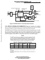
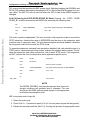
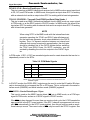
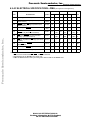
2.4.3.4.2 IMP PLL and Clock Control Register (IPLCR). IPLCR is a 16-bit read/write register used to control the IMP’s PLL, multiplication factor and CLKO drive strength. This register is mapped in the 68000 bus space at address $0F8. If the 68000 bus is set to 8 bits
(BUSW grounded at reset), during 8-bit accesses, changes to the IPLCR will take effect in
the IMP PLL after loading the high byte of IPLCR (the low byte is written first). The WP bit
in IPLCR is used as a protect mechanism to prevent erroneous writing. When this bit is set
further accesses to the IPLCR will be blocked.
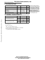
IMP PLL and Clock Control Register (IPLCR)
15
IPLWP
RESET
0
14
13
CLKOMOD0–1
$0F8
12
PEN
11
MF11
10
MF10
9
MF9
8
MF8
0
0
VCCSYN
0
0
0
VCCSYN/MODCLK
7
MF7
6
MF6
5
MF5
4
MF4
3
MF3
2
MF2
1
MF1
0
MF0
RESET
VCCSYN/MODCLK1
0
0
VCCSYN/MODCLK
0
0
MODCLK
MODCLK
Read/Write
MC68LC302 REFERENCE MANUAL
For More Information On This Product,
Go to: www.freescale.com