1
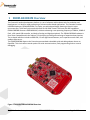
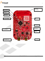
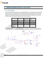
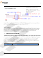
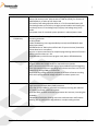
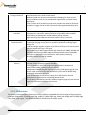
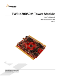
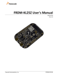
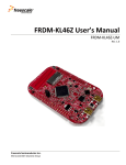
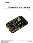
FRDM-K20D50M User’s Manual FRDM-K20D50M-UM Rev. 1.0 Freescale Semiconductor Inc. Microcontroller Solutions Group | Table of Contents 1 FRDM-K20D50M Overview ..................................................................................................................3 2 References documents ..........................................................................................................................4 3 Getting started ..........................................................................................................................................4 4 FRDM-K20D50M Hardwar Overview ...............................................................................................4 5 FRDM-K20D50M Hardware Description .........................................................................................8 5.1.1 Power Supply ....................................................................................................................................................................................... 8 5.1.2 Serial and Debug Adapter (OpenSDA) ................................................................................................................................... 10 5.1.3 Clock source ....................................................................................................................................................................................... 13 5.1.4 USB Interface ..................................................................................................................................................................................... 14 5.1.5 Serial Port ........................................................................................................................................................................................... 14 5.1.6 Reset...................................................................................................................................................................................................... 14 5.1.7 Debug .................................................................................................................................................................................................... 14 5.1.8 Capacitive Touch Slider ................................................................................................................................................................ 14 5.1.9 3-axis Accelerometer ..................................................................................................................................................................... 14 5.1.10 RGB LED ............................................................................................................................................................................................ 15 5.1.11 Visible light sensor ....................................................................................................................................................................... 16 5.1.1 Temperature sensor ..................................................................................................................................................................... 16 5.1.2 Input/Output Connectors ............................................................................................................................................................ 17 5.1.3 Arduino Compatibility .................................................................................................................................................................. 18 Freescale Semiconductor, Inc FRDM-K20D50MUM Page 2 of 18 | 1 FRDM-K20D50M Overview The Freescale Freedom development platform is a set of software and hardware tools for evaluation and development. It is ideal for rapid prototyping of microcontroller-based applications. The Freescale Freedom K20D50M hardware, FRDM-K20D50M, is a simple, yet sophisticated design featuring a Kinetis K series microcontroller, The K family microcontroller built on the ARM® Cortex™-M4 core with DSP capabilities. FRDM-K20D50M features a K20DX128VLH5, this device boasting a max operating frequency of 50MHz, 128KB of flash, a full-speed USB controller, and loads of analog and digital peripherals. The FRDM-K20D50M hardware is form-factor compatible with the Arduino™ R3 pin layout, providing a broad range of expansion board options. The on-board interfaces include an RGB LED, a 3-axis digital accelerometer, and a capacitive touch slider, and ambient light sensor. The FRDM-K20D50M features the Freescale open standard embedded serial and debug adapter known as OpenSDA. This circuit offers several options for serial communications, flash programming and run-control debugging. Figure 1 Freescale FRDM-K20D50M Overview Freescale Semiconductor, Inc FRDM-K20D50MUM Page 3 of 18 | Contents The TWR-K20D50M contents include: 2 TWR-K20D50M board assembly 3ft A to mini-B USB cable for debug interface, serial communication and power Quick Reference card. References documents The table below provides a list of reference documents for the FRDM-K20D50M hardware. All of these documents are available online at www.freescale.com/ FRDM-K20D50M. Table 1. FRDM-K20D50M Reference Documents Filename Description FRDM-K20D50M Quick Start Quick Start Guide and supporting files for getting started with Package the FRDM-K20D50M. FRDM-K20D50M User’s Manual This document—overview and detailed information for the FRDM-K20D50M hardware. FRDM-K20D50M Pinouts Spreadsheet of pin connections for all MCU pins. Includes pinout for the I/O headers, Arduino R3 compatibility chart, and OpenSDA MCU pinout. FRDM-K20D50M Schematics PDF schematics for the FRDM-K20D50M hardware FRDM-K20D50M Design Package Zip file containing all design source files for the FRDMK20D50M hardware OpenSDA User’s Guide Overview and instructions for use of the OpenSDA embedded 3 Getting started Refer to the FRDM-K20D50M Quick Start Package for step-by-step instructions for getting started with the FRDM-K20D50M. See the Jump Start Your Design section onwww.freescale.com/FRDM-K20D50M for the Quick Start Package and software lab guides. 4 FRDM-K20D50M Hardwar Overview Arduino R3 compatibility Dual role USB interface with mini-B USB connector Open SDA MK20DX128VLH5 MCU (50 MHz, 128KB Flash, 16 KB RAM, 32 KB FlexNVM, Low power, 64LQFP package Freescale Semiconductor, Inc FRDM-K20D50MUM Page 4 of 18 | Capacitive touch slider Ambient light sensor MMA8451Q accelerometer Tri-color (RGB) LED Flexible power supply options – USB, coin cell battery, external source Battery-ready, power-measurement access points Easy access to MCU I/O via Arduino ™ R3 compatible I/O connectors Programmable OpenSDA debug interface with multiple applications available including: o Mass storage device flash programming interface o P&E Debug interface provides run-control debugging and compatibility with IDE tools o CMSIS-DAP interface: new ARM standard for embedded debug interface o Data logging application Freescale Semiconductor, Inc FRDM-K20D50MUM Page 5 of 18 | Figure 1 shows a block diagram of the FRDM-K20D50M design. The primary components and their placement on the hardware assembly are pointed out in Figure 2. Freescale Semiconductor, Inc FRDM-K20D50MUM Page 6 of 18 | Capacitive Touch Slider Light Sensor RGB LED K20D50M J19 I/O Header J10 J9 Accelerometer MMA8451Q J2 I/O Header Reset OpenSDA K20D50M USB Freescale Semiconductor, Inc FRDM-K20D50MUM Page 7 of 18 | 5 FRDM-K20D50M Hardware Description 5.1.1 Power Supply There are multiple power supply options on the FRDM-K20D50M. It can be powered from either of the USB connectors, the VIN pin on the I/O header, an on-board coin cell battery, or an off-board 1.71-3.6V supply from the 3.3V pin on the I/O header. The USB and VIN supplies are regulated on-board using a 3.3V linear regulator to produce the main power supply. The other two sources are not regulated on-board. Table 2 provides the operational details and requirements for the power supplies. Supply Source Valid Range OpenSDA USB K20 USB VIN Pin 3.3V Pin Coin Cell Battery 5V 5V 4.3-9V 1.71-3.6V 1.71-3.6V OpenSDA Operational? Yes No No No No Regulated onboard? Yes Yes Yes No No Note that the OpenSDA circuit is only operational when a USB cable is connected and supplying power to OpenSDA USB. However, protection circuitry is in place to allow multiple sources to be powered at once. Freescale Semiconductor, Inc FRDM-K20D50MUM Page 8 of 18 | FRDM-K20D50M Power Supplies Power Supply Name P5-9V_VIN P5V_SDA P5V_K20D50M P3V3_VREG P3V3_BATT P3V3 P3V3_K20D50M P3V3_SDA P5V_USB Description Power supplied from the VIN pin of the I/O headers (J9 pin 16). A Schottky diode provides back drive protection. Power supplied from the OpenSDA USB connector A Schottky diode provides back drive protection. Power supplied from the K20D50M USB connector A Schottky diode provides back drive protection. Regulated 3.3V supply. Sources power to the P3V3 supply rail through a back drive protection Schottky diode. 1 Coin cell battery supply voltage. Sources power to the P3V3 supply rail through a back drive protection Schottky diode. Main supply rail for FRDM-K20D50M assembly. May be sourced from P3V3_VREG, P3V3_BATT, or directly from the I/O headers (J9 pin 8) K20D50M MCU supply. Header J4 provides a convenient means for energy consumption measurements. 2 OpenSDA circuit supply. Header J3 provides a convenient means for energy consumption measurements. 2 Nominal 5V supplied to the I/O headers (J9 pin 10). Sourced from either the P5V_K20D50M or P5V_OSDA supply through a back drive protection Schottky diode. NOTES: 1) By default the linear regulator, U1, is a 3.3V output regulator. However, this is a common footprint that would allow the user to modify the assembly to utilize an alternative device such as a 1.8V or 2.5V regulator. The K20 microcontroller has an operating range of 1.71V to 3.6V 2) J3 and J4 are not populated by default. The two pins of these headers are shorted together by a trace on the bottom layer of the PCB. To measure the energy consumption of either the K20 or the OpenSDA MCU, the trace between these pins must first be cut. A current probe or a shunt resistor and voltage meter can then be applied to measure the energy consumption on these rails. Freescale Semiconductor, Inc FRDM-K20D50MUM Page 9 of 18 | 5.1.2 Serial and Debug Adapter (OpenSDA) OpenSDA is an open-standard serial and debug adapter. It bridges serial and debug communications between a USB host and an embedded target processor as shown in Figure 4. The hardware circuit is based on a Freescale Kinetis K20 family microcontroller (MCU) with 128 KB of embedded flash and an integrated USB controller. OpenSDA features a mass storage device (MSD) bootloader, which provides a quick and easy mechanism for loading different OpenSDA Applications such as flash programmers, run-control debug interfaces, serial-to-USB converters, and more. Refer to the OpenSDA User’s Guide for more details. OpenSDA High-Level Block Diagram OpenSDA is managed by another Kinetis K20 MCU built on the ARM® Cortex™-M4 core. The OpenSDA circuit includes a status LED (D4) and a pushbutton (SW1). The pushbutton asserts the Reset signal to the K20D128 target MCU. It can also be used to place the OpenSDA circuit into Bootloader mode. SPI and GPIO signals provide an interface to either the SWD debug port of the K20. Additionally, signal connections are available to implement a UART serial channel. The OpenSDA circuit receives power when the USB connector J7 is plugged into a USB host. Debug Interface Signals with SPI and GPIO capability are used to connect directly to the SWD of the K20. These signals are also brought out to a standard 10-pin (0.05”) Cortex Debug connector (J6). It is possible to isolate the K20 MCU from the OpenSDA circuit and use J6 to connect to an off-board MCU. To Signals with SPI and GPIO capability are used to connect directly to the SWD of the K20. These signals are also brought out to a standard 10-pin (0.05”) Cortex Debug connector (J6). It is possible to isolate the K20 MCU from the OpenSDA circuit and use J6 to connect to an off-board MCU. To accomplish this, cut the trace on the bottom side of the PCB that connects J11 pin 1 to J11 pin 2. This will disconnect the SWD_CLK pin to the K20 so that it will not interfere with the communications to an off-board MCU connected to J6. Freescale Semiconductor, Inc FRDM-K20D50MUM Page 10 of 18 | Note that J6 is not-populated by default. A Samtec FTSH-105-02-F-D or compatible connector can be added to the J6 through-hole connector. A mating cable, such as a Samtec FFSD IDC cable, can then be used to connect from the OpenSDA of the FRDM-K20D50M to an off-board SWD connector. Virtual Serial Port A serial port connection is available between the OpenSDA MCU and pins PTA1 and PTA2 of the K20. Several of the default OpenSDA Applications provided by Freescale, including the MSD Flash Programmer and the P&E Debug Application, provide a USB Communications Device Class (CDC) interface that bridges serial communications between the USB host and this serial interface on the K20. 5.3 K20D50M Microcontroller The target microcontroller of the FRDM-K20D50M is the MK20DX128VLH5, this is 50 MHz entry-level K20 USB microcontrollers (MCUs) are the lowest power Kinetis ARM® Cortex™-M4 devices with high feature integration in a small form factor, making them ideal for space- and cost-constrained applications. These MCUs offer 32 KB to 128 KB of flash memory and optional 32 KB of FlexNVM in 32-pin QFN (5 mm x 5 mm) to 64-pin LQFP packages. Peripheral options include full-speed USB Device/Host/On-The-Go with device charge detect capability, a 16-bit analog-to-digital converter (ADC), low-power touch-sensing interface and several general timing, communication and control peripherals. Feature Description Freescale Semiconductor, Inc FRDM-K20D50MUM Page 11 of 18 | Ultra low power -11 low-power modes with power and clock gating for optimal peripheral activity and recovery times. Stop currents of <190 nA (VLLS0), run currents of <280 uA/MHz, 4 µs wake-up from Stop mode -Full memory and analog operation down to 1.71V for extended battery life -Low-leakage wake-up unit with up to eight internal modules and sixteen pins as wake-up sources in low-leakage stop (LLS)/very low-leakage stop (VLLS) modes -Low-power timer for continual system operation in reduced power states Flash, SRAM and FlexMemory -32 KB-128 KB flash featuring fast access times, high reliability, and four levels of security protection -16 KB of SRAM -2 KB of FlexMemory (user-segmentable byte write/erase EEPROM for data tables/system data) -EEPROM with over 10M cycles and flash with 70 µsec write time (brownouts without data loss or corruption) -No user or system intervention to complete programming and erase functions and full operation down to 1.71V -FlexNVM adds up 32 KB for extra program code, data or EEPROM backup Mixed-signal capability -High-speed 16-bit ADC with configurable resolution -Single or differential output modes for improved noise rejection -500 ns conversion time achievable with programmable delay block triggering -Two high-speed comparators providing fast and accurate motor over-current protection by driving PWMs to a safe state -Optional analog voltage reference provides an accurate reference to analog blocks and replaces external voltage references to reduce system cost Performance -50 MHz ARM Cortex-M4 core with DSP instruction set, single cycle MAC, and single instruction multiple data (SIMD) extensions -Up to four channel DMA for peripheral and memory servicing with reduced CPU loading and faster system throughput -Cross bar switch enables concurrent multi-master bus accesses, increasing bus bandwidth -Independent flash banks allowing concurrent code execution and firmware updating with no performance degradation or complex coding routines Freescale Semiconductor, Inc FRDM-K20D50MUM Page 12 of 18 | Timing and Control -Two FlexTimers with a total of 10 channels -Hardware dead-time insertion and quadrature decoding for motor control -Carrier modulator timer for infrared waveform generation in remote control applications - Four-channel 32-bit periodic interrupt timer provides time base for RTOS task scheduler or trigger source for ADC conversion and programmable delay block Human-Machine Interface -Hardware touch-sensing interface (TSI) with up to 16 inputs -TSI operates in low power modes (minimum current adder when enabled) -TSI hardware implementation avoids software polling methods -High sensitivity level allows use of overlay surfaces up to 5 mm thick. Connectivity and Communications -Full-Speed USB Device/Host/On-The-Go with device charge detect capability - Optimized charging current/time for portable USB devices, enabling longer battery life - USB low-voltage regulator supplies up to 120 mA off chip at 3.3 volts to power external components from 5-volt input -Three UARTs (one UART supports RS232 with flow control, RS485, ISO7816 and IrDA while the other two UARTS support RS232 with flow control and RS485) -One Inter-IC Sound (I2S) serial interface for audio system interfacing -One DSPI module and one I2C module Reliability, Safety and Security -Memory protection unit provides memory protection for all masters on the cross bar switch, increasing software reliability -Cyclic redundancy check (CRC) engine validates memory contents and communication data, increasing system reliability -Independent-clocked computer operating properly (COP) guards against clock skew or code runaway for fail-safe applications such as the IEC 60730 safety standard for household appliances -External watchdog monitor drives output pin to safe state for external components in the event that a watchdog timeout occurs -This product is included in Freescale’s product longevity program, with assured supply for a minimum of 10 years after launch 5.1.3 Clock source The Kinetis K microcontrollers feature an on-chip oscillator compatible with three ranges of input crystal or resonator frequencies: 32-40 kHz (low freq. mode), 3-8 MHz (high freq. mode, low range) and 8-32 MHz (high freq. mode, high range). The FRDM-K20D50M is clocked from an 8 MHz crystal. Freescale Semiconductor, Inc FRDM-K20D50MUM Page 13 of 18 | 5.1.4 USB Interface The Kinetis K microcontrollers feature a dual-role USB controller with on-chip full-speed and low-speed transceivers. The USB interface on the FRDM-K20D50M is configured as a full-speed USB device. VREGIN must be powered to enable the internal circuitry of USB (by jumper J7) 5.1.5 Serial Port The primary serial port interface signals are PTB0 UART0 RX and PTB17 UART0_TX. These signals are connected the OpenSDA 5.1.6 Reset The RESET signal on the K20 is connected externally to a pushbutton, SW1, and also to the OpenSDA circuit. The reset button can be used to force an external reset event in the target MCU. The reset button can also be used to force the OpenSDA circuit into bootloader mode. Please refer to section 5.2, Serial and Debug Adapter (OpenSDA), for more details. 5.1.7 Debug The MK20DX128VLH5 supports JTAG and SWD debug interface however only SWD debug interface is available on FRM-K20D50M board. However, an unpopulated 10-pin (0.05”) Cortex Debug connector, J6, provides access to the SWD signals. The Samtec FTSH-105-02-F-D or compatible connectors can be added to the J6 through-hole debug connector to allow for an external debug cable to be connected. 5.1.8 Capacitive Touch Slider Two Touch Sense Input (TSI) signals, TSI0_CH11/PTB18, and , TSI0_CH12/PTB19 are connected to capacitive electrodes configured as a touch slider. Freescale’s Touch Sense Software (TSS) provides a software library for implementing the capacitive touch slider. 5.1.9 3-axis Accelerometer A Freescale MMA8451Q low-power, three-axis accelerometer is interfaced through an I2C bus and two GPIO signals as shown in Table 4 below. By default, the I2C address is 0x1D (SA0 pulled high). Freescale Semiconductor, Inc FRDM-K20D50MUM Page 14 of 18 | Table 4. Accelerometer Signal Connections MMA8451Q K20D50M SCL PTB0 SDA PTB1 INT1 PTC11 INT2 PTC6 5.1.10 RGB LED Three PWM-capable signals are connected to a red, green, blue LED, D3. The signal connections are shown in Table 5 below. Table 5. RGB LED Signal Connections RGB LED K20 Red Cathode D6 –PTC3 FTM0_CH2 Green Cathode D3 – PTD4 FTM0 CH4 Blue Cathode D9 - PTA2 FTM0-CH7 Freescale Semiconductor, Inc FRDM-K20D50MUM Page 15 of 18 | 5.1.11 Visible light sensor The FRDM-K20D50M has a visible light sensor that is connected to ADC0_DM0 5.1.1 Temperature sensor FRDM-K20D50M is prepared for an external temperature sensor BD1020HFV-TR connected to ADC0-DM3. Note: this sensor is not populated on the board. Freescale Semiconductor, Inc FRDM-K20D50MUM Page 16 of 18 | 5.1.2 Input/Output Connectors The K20DX128VLH5 microcontroller is packaged in an 64-pin LQFP. Some pins are utilized in on-board circuitry, but many are directly connected to one of four I/O headers. The pins on the K20 microcontroller are named for their general purpose input/output port pin function. For example, the 1st pin on Port A is referred to as PTA1. The I/O connector pin names are given the same name as the K20 pin connected to it, where applicable. J19 PTE1 PTE0 PTA5 PTD4 PTC8 PTA1 PTC3 PTC4 J10 2 4 6 8 10 12 14 16 1 3 5 7 9 11 13 15 PTD0 PTC11 PTC5 PTC6 PTC7 PTA4 PTD7 PTC9 J2 PTA12 PTA2 PTC2 PTD2 PTD3 PTD1 GND VREFH PTB3 PTB2 2 4 6 8 10 12 14 16 18 20 1 PTA13 3 PTC10 5 7 9 11 13 15 17 19 Freescale Semiconductor, Inc ADC0_DM0 ADC0_DP0 ADC0_DM3 ADC0_DP3 CMP1_IN3 CMP0_IN5 11 9 7 5 3 1 12 10 8 6 4 2 PTB0 PTB1 PTD5 PTD6 PTC1 PTC0 15 13 11 9 7 5 3 1 16 14 12 10 8 6 4 2 P5-9V_VIN GND GND P5V_USB P3V3 RST_TGTMCU P3V3 SDA_PTD5 J9 FRDM-K20D50MUM Page 17 of 18 | 5.1.3 Arduino Compatibility The I/O headers on the FRDM-K20D50M are arranged to allow compatibility with peripheral boards (known as shields) that connect to Arduino™ and Arduino-compatible microcontroller boards. The outer rows of pins (the even numbered pins) on the headers share the same mechanical spacing and placement as the I/O headers on the Arduino Revision 3 (R3) standard. Freescale Semiconductor, Inc FRDM-K20D50MUM Page 18 of 18