1
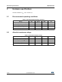
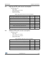
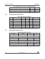
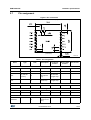
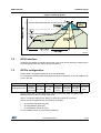
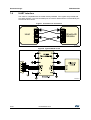
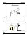
SPBT2632C2A
Bluetooth® technology class-2 module
Datasheet - production data
Features
• Bluetooth® radio
– Fully embedded Bluetooth® v3.0 with
profiles
– Class 2 module
– Complete RF ready module
– 128-bit encryption security
– Integrated antenna
– Multipoint capability
• ST micro Cortex-M3 microprocessor up to
72 MHz (256 kb Flash, 48 kb RAM memory)
• Modem transmitter speed
– Supported transmission speed with SPP
service active: 560kbps
• General I/O
– 7 general purpose I/Os
– 1 LPO input
• User interface
– AT2 command set (abSerial)
– Firmware upgrade over UART
• FCC and Bluetooth® qualified
• Single voltage supply: 2.5 V typical
• Micro-sized form factor: 11.6 x 13.5 x 2.9 mm
• Operating temperature range: -40 °C to 85 °C.
June 2014
This is information on a product in full production.
DocID022833 Rev 6
1/30
www.st.com
Contents
SPBT2632C2A
Contents
1
Description . . . . . . . . . . . . . . . . . . . . . . . . . . . . . . . . . . . . . . . . . . . . . . . . . 6
2
RoHS compliance . . . . . . . . . . . . . . . . . . . . . . . . . . . . . . . . . . . . . . . . . . . 7
3
Applications . . . . . . . . . . . . . . . . . . . . . . . . . . . . . . . . . . . . . . . . . . . . . . . . 7
4
Software architecture . . . . . . . . . . . . . . . . . . . . . . . . . . . . . . . . . . . . . . . . 8
5
4.1
Lower layer stack . . . . . . . . . . . . . . . . . . . . . . . . . . . . . . . . . . . . . . . . . . . . 8
4.2
Upper layer stack: Amp'ed UP . . . . . . . . . . . . . . . . . . . . . . . . . . . . . . . . . . 8
4.3
AT command set: abSerial . . . . . . . . . . . . . . . . . . . . . . . . . . . . . . . . . . . . . 8
4.4
Bluetooth firmware implementation . . . . . . . . . . . . . . . . . . . . . . . . . . . . . . 9
Hardware specifications . . . . . . . . . . . . . . . . . . . . . . . . . . . . . . . . . . . . . 10
5.1
Recommended operating conditions . . . . . . . . . . . . . . . . . . . . . . . . . . . . 10
5.2
Absolute maximum ratings . . . . . . . . . . . . . . . . . . . . . . . . . . . . . . . . . . . . 10
5.3
High speed CPU mode current consumption . . . . . . . . . . . . . . . . . . . . . . .11
5.4
Standard CPU mode current consumption . . . . . . . . . . . . . . . . . . . . . . . . .11
5.5
I/O operating characteristics . . . . . . . . . . . . . . . . . . . . . . . . . . . . . . . . . . . 12
5.6
Selected RF characteristics . . . . . . . . . . . . . . . . . . . . . . . . . . . . . . . . . . . 12
5.7
Pin assignment . . . . . . . . . . . . . . . . . . . . . . . . . . . . . . . . . . . . . . . . . . . . . 13
5.8
Mechanical dimensions . . . . . . . . . . . . . . . . . . . . . . . . . . . . . . . . . . . . . . 15
6
Hardware block diagram . . . . . . . . . . . . . . . . . . . . . . . . . . . . . . . . . . . . . 17
7
Hardware design . . . . . . . . . . . . . . . . . . . . . . . . . . . . . . . . . . . . . . . . . . . 18
2/30
7.1
Module reflow installation . . . . . . . . . . . . . . . . . . . . . . . . . . . . . . . . . . . . . 18
7.2
GPIO interface . . . . . . . . . . . . . . . . . . . . . . . . . . . . . . . . . . . . . . . . . . . . . 19
7.3
GPIOs configuration . . . . . . . . . . . . . . . . . . . . . . . . . . . . . . . . . . . . . . . . . 19
7.4
UART interface . . . . . . . . . . . . . . . . . . . . . . . . . . . . . . . . . . . . . . . . . . . . . 20
7.5
PCB layout guidelines . . . . . . . . . . . . . . . . . . . . . . . . . . . . . . . . . . . . . . . 21
7.6
Reset circuit . . . . . . . . . . . . . . . . . . . . . . . . . . . . . . . . . . . . . . . . . . . . . . . 21
7.6.1
External reset circuit . . . . . . . . . . . . . . . . . . . . . . . . . . . . . . . . . . . . . . . 21
7.6.2
Internal reset circuit . . . . . . . . . . . . . . . . . . . . . . . . . . . . . . . . . . . . . . . . 22
DocID022833 Rev 6
SPBT2632C2A
8
Contents
7.7
External LPO input circuit . . . . . . . . . . . . . . . . . . . . . . . . . . . . . . . . . . . . . 22
7.8
Apple iOS CP reference design . . . . . . . . . . . . . . . . . . . . . . . . . . . . . . . . 23
Regulatory compliance . . . . . . . . . . . . . . . . . . . . . . . . . . . . . . . . . . . . . . 25
8.1
FCC and IC certification . . . . . . . . . . . . . . . . . . . . . . . . . . . . . . . . . . . . . . 25
8.2
TELEC certification . . . . . . . . . . . . . . . . . . . . . . . . . . . . . . . . . . . . . . . . . . 25
8.3
Bluetooth certification . . . . . . . . . . . . . . . . . . . . . . . . . . . . . . . . . . . . . . . . 26
8.4
CE certification . . . . . . . . . . . . . . . . . . . . . . . . . . . . . . . . . . . . . . . . . . . . . 26
9
Traceability . . . . . . . . . . . . . . . . . . . . . . . . . . . . . . . . . . . . . . . . . . . . . . . . 27
10
Ordering information . . . . . . . . . . . . . . . . . . . . . . . . . . . . . . . . . . . . . . . 28
11
Revision history . . . . . . . . . . . . . . . . . . . . . . . . . . . . . . . . . . . . . . . . . . . 29
DocID022833 Rev 6
3/30
30
List of tables
SPBT2632C2A
List of tables
Table 1.
Table 2.
Table 3.
Table 4.
Table 5.
Table 6.
Table 7.
Table 8.
Table 9.
Table 10.
Table 11.
4/30
Recommended operating conditions . . . . . . . . . . . . . . . . . . . . . . . . . . . . . . . . . . . . . . . . . 10
Absolute maximum ratings . . . . . . . . . . . . . . . . . . . . . . . . . . . . . . . . . . . . . . . . . . . . . . . . . 10
High speed CPU mode current consumption . . . . . . . . . . . . . . . . . . . . . . . . . . . . . . . . . . . 11
Standard CPU mode current consumption . . . . . . . . . . . . . . . . . . . . . . . . . . . . . . . . . . . . . 11
I/O operating characteristics . . . . . . . . . . . . . . . . . . . . . . . . . . . . . . . . . . . . . . . . . . . . . . . . 12
Selected RF characteristics . . . . . . . . . . . . . . . . . . . . . . . . . . . . . . . . . . . . . . . . . . . . . . . . 12
Pin assignment . . . . . . . . . . . . . . . . . . . . . . . . . . . . . . . . . . . . . . . . . . . . . . . . . . . . . . . . . . 13
Soldering. . . . . . . . . . . . . . . . . . . . . . . . . . . . . . . . . . . . . . . . . . . . . . . . . . . . . . . . . . . . . . . 18
System configuration variables . . . . . . . . . . . . . . . . . . . . . . . . . . . . . . . . . . . . . . . . . . . . . . 22
Ordering information . . . . . . . . . . . . . . . . . . . . . . . . . . . . . . . . . . . . . . . . . . . . . . . . . . . . . . 28
Document revision history . . . . . . . . . . . . . . . . . . . . . . . . . . . . . . . . . . . . . . . . . . . . . . . . . 29
DocID022833 Rev 6
SPBT2632C2A
List of figures
List of figures
Figure 1.
Figure 2.
Figure 3.
Figure 4.
Figure 5.
Figure 6.
Figure 7.
Figure 8.
Figure 9.
Figure 10.
Figure 11.
Figure 12.
Figure 13.
Figure 14.
Figure 15.
FW architecture . . . . . . . . . . . . . . . . . . . . . . . . . . . . . . . . . . . . . . . . . . . . . . . . . . . . . . . . . . 9
Pin connection . . . . . . . . . . . . . . . . . . . . . . . . . . . . . . . . . . . . . . . . . . . . . . . . . . . . . . . . . . 13
Mechanical dimensions . . . . . . . . . . . . . . . . . . . . . . . . . . . . . . . . . . . . . . . . . . . . . . . . . . . 15
Recommend land pattern top view . . . . . . . . . . . . . . . . . . . . . . . . . . . . . . . . . . . . . . . . . . 16
SPBT2632C2A.AT2 module block diagram . . . . . . . . . . . . . . . . . . . . . . . . . . . . . . . . . . . . 17
Soldering profile . . . . . . . . . . . . . . . . . . . . . . . . . . . . . . . . . . . . . . . . . . . . . . . . . . . . . . . . . 19
Connection to host device . . . . . . . . . . . . . . . . . . . . . . . . . . . . . . . . . . . . . . . . . . . . . . . . . 20
Typical RS232 circuit . . . . . . . . . . . . . . . . . . . . . . . . . . . . . . . . . . . . . . . . . . . . . . . . . . . . . 20
PCB layout guidelines. . . . . . . . . . . . . . . . . . . . . . . . . . . . . . . . . . . . . . . . . . . . . . . . . . . . . 21
External reset circuit . . . . . . . . . . . . . . . . . . . . . . . . . . . . . . . . . . . . . . . . . . . . . . . . . . . . . . 21
Internal reset circuit . . . . . . . . . . . . . . . . . . . . . . . . . . . . . . . . . . . . . . . . . . . . . . . . . . . . . . 22
External LPO circuit . . . . . . . . . . . . . . . . . . . . . . . . . . . . . . . . . . . . . . . . . . . . . . . . . . . . . . 23
BT module . . . . . . . . . . . . . . . . . . . . . . . . . . . . . . . . . . . . . . . . . . . . . . . . . . . . . . . . . . . . . 23
Co-processor . . . . . . . . . . . . . . . . . . . . . . . . . . . . . . . . . . . . . . . . . . . . . . . . . . . . . . . . . . . 24
Power switch. . . . . . . . . . . . . . . . . . . . . . . . . . . . . . . . . . . . . . . . . . . . . . . . . . . . . . . . . . . . 24
DocID022833 Rev 6
5/30
30
Description
1
SPBT2632C2A
Description
The SPBT2632C2A.AT2 is an easy to use Bluetooth module, compliant with Bluetooth v3.0.
The module is the smallest form factor available which provides a complete RF platform.
The SPBT2632C2A.AT2 enables electronic devices with wireless connectivity, not requiring
any RF experience or expertise for integration into the final product. The
SPBT2632C2A.AT2 module, being a certified solution, optimizes the time to market of the
final applications.
The module is designed for maximum performance in a minimal space including fast speed
UART and 7 general purpose I/O lines, several serial interface options, and up to 560 kbps
transmission speed with SPP service active, 250kbps with iAP service active.
Optimized design allows the integration of a complete working Bluetooth modem, including
antenna, in the minimum possible size; only an additional external LPO (low power
oscillator) is required to enable low power mode capability.
The SPBT2632C2A.AT2 is a surface mount PCB module that provides fully embedded,
ready to use Bluetooth wireless technology. The reprogrammable Flash memory contains
embedded firmware for serial cable replacement using the Bluetooth SPP profile.
Embedded Bluetooth AT2 command firmware is a friendly interface, which realizes a simple
control for cable replacement, enabling communication with most Bluetooth enabled
devices, provided that the devices support the SPP profile. The SPBT2632C2A.AT2,
supporting iAP profile, provides communication with Android, smartphone, and Apple® iOS
Bluetooth enabled devices.
An Apple authentication IC is required to exchange data with an Apple device or access an
Apple device application. The AT2 FW includes the Bluetooth SPP profile capable of
recognizing the Apple authentication chip.
Customers using the Apple authentication IC must register as developers to become an
Apple certified MFI member. License fees may apply, for additional information visit:
http://developer.apple.com/programs/which-program/index.html.
Certified MFI developers developing electronic accessories that connect to the iPod®,
iPhone®, and iPad® gain access to technical documentation, hardware components,
technical support and certification logos.
Customized firmware for peripheral device interaction, power optimization, security, and
other proprietary features may be supported and can be ordered pre-loaded and configured.
6/30
DocID022833 Rev 6
SPBT2632C2A
2
RoHS compliance
RoHS compliance
ST Bluetooth modules comply with the ECOPACK2 level of RoHS compliance grade.
The material declaration file is available from www.st.com at the following URL:
http://www.st.com/web/catalog/sense_power/FM1968/CL1976/SC1324/PF253470#
3
Applications
•
Serial cable replacement
•
M2M industrial control
•
Service diagnostic
•
Data acquisition equipment
•
Machine control
•
Sensor monitoring
•
Security system
•
Mobile health.
DocID022833 Rev 6
7/30
30
Software architecture
SPBT2632C2A
4
Software architecture
4.1
Lower layer stack
4.2
4.3
•
Bluetooth v3.0
•
Device power modes: active, sleep and deep sleep
•
Wake on Bluetooth feature optimized power consumption of host CPU
•
Authentication and encryption
•
Encryption key length from 8 bits to 128 bits
•
Persistent Flash memory for BD address and user parameter storage
•
All ACL (asynchronous connection less) packet types
•
Multipoint capability
•
Sniff mode: fully supported to maximum allowed intervals
•
Master slave switch supported during connection and post connection
•
Dedicated inquiry access code for improved inquiry scan performance
•
Dynamic packet selection channel quality driven data rate to optimize link performance
•
Dynamic power control
•
Bluetooth radio natively supports 802.11b co-existence AFH
Upper layer stack: Amp'ed UP
•
SPP, IAP, SDAP and GAP protocols
•
RFComm, SDP, and L2CAP supported
•
Multipoint with simultaneous slaves.
AT command set: abSerial
The complete command list including the iAP commands is reported in the user manual
UM1547.
8/30
DocID022833 Rev 6
SPBT2632C2A
4.4
Software architecture
Bluetooth firmware implementation
Figure 1. FW architecture
L$3
$0Y
DocID022833 Rev 6
9/30
30
Hardware specifications
5
SPBT2632C2A
Hardware specifications
General conditions (VIN = 2.5 V and 25 °C).
5.1
Recommended operating conditions
Table 1. Recommended operating conditions
5.2
Rating
Min.
Typical
Max.
Unit
Operating temperature range
-40
-
85
°C
Supply voltage VIN
2.1
2.5
3.6
V
Signal pin voltage
-
2.1
-
V
RF frequency
2400
-
2483.5
MHz
Absolute maximum ratings
Table 2. Absolute maximum ratings
10/30
Rating
Min.
Typical
Max.
Unit
Storage temperature range
-55
-
+105
°C
Supply voltage, VIN
-0.3
-
+ 5.0
V
I/O pin voltage, VIO
-0.3
-
+ 5.5
V
RF input power
-
-
-5
dBm
DocID022833 Rev 6
SPBT2632C2A
5.3
Hardware specifications
High speed CPU mode current consumption
•
High speed CPU mode
–
CPU 32 MHz
–
UART supports up to 921 Kbps
–
Max data throughput
–
Shallow sleep enabled.
Table 3. High speed CPU mode current consumption
Modes (typical power consumption)
5.4
Avg.
Unit
ACL data 115 K baud UART at max. throughput (master)
23
mA
ACL data 115 K baud UART at max. throughput (slave)
27.5
mA
Connection, no data traffic, master
9.1
mA
Connection, no data traffic, slave
11.2
mA
Connection 375 ms sniff (external LPO required)
490
µA
Standby, without deep sleep
8.6
mA
Standby, with deep sleep, no external LPO
1.7
mA
Standby, with deep sleep, with external LPO
70
µA
Page/inquiry scan, with deep sleep, no external LPO
2.7
mA
Page/inquiry scan, with deep sleep, with external LPO
520
µA
Standard CPU mode current consumption
•
Standard CPU mode
–
CPU 8 MHz
–
UART supports up to 115 Kbps
–
Data throughput up to 200 Kbps
–
Shallow sleep enabled.
Table 4. Standard CPU mode current consumption
Modes (typical power consumption)
Avg.
Unit
ACL data 115 K baud UART at max. throughput (master)
16.7
mA
ACL data 115 K baud UART at max. throughput (slave)
18
mA
Connection, no data traffic, master
4.9
mA
Connection, no data traffic, slave
7.0
mA
Connection 375 ms sniff (external LPO required)
490
µA
Standby, without deep sleep
4.2
mA
Standby, with deep sleep, no external LPO
1.7
mA
DocID022833 Rev 6
11/30
30
Hardware specifications
SPBT2632C2A
Table 4. Standard CPU mode current consumption (continued)
Modes (typical power consumption)
5.5
Avg.
Unit
Standby, with deep sleep, with external LPO
70
µA
Page/inquiry scan, with deep sleep, no external LPO
2.6
mA
Page/inquiry scan, with deep sleep, with external LPO
520
µA
I/O operating characteristics
Table 5. I/O operating characteristics
5.6
Symbol
Parameter
Min.
Max.
Unit
Conditions
VIL
Low-level input voltage
-
0.6
V
VIN, 2.1 V
VIH
High-level input voltage
1.4
-
V
VIN, 2.1 V
VOL
Low-level output voltage
-
0.4
V
VIN, 2.1 V
VOH
High-level output voltage
1.8
-
V
VIN, 2.1 V
IOL
Low -level output current
-
4.0
mA
VOL = 0.4 V
IOH
High-level output current
-
4.0
mA
VOH = 1.8 V
RPU
Pull-up resistor
80
120
kΩ
Resistor turned on
RPD
Pull-down resistor
80
120
kΩ
Resistor turned on
Selected RF characteristics
Table 6. Selected RF characteristics
Parameters
Conditions
Antenna load
Typical(1)
Unit
50
ohm
Radio receiver
Sensitivity level
BER < .001 with DH5
-86
dBm
Maximum usable level
BER < .001 with DH1
0
dBm
Input VSWR
2.5:1
Radio transmitter
Maximum output power
50 Ω load
0
dBm
Initial carrier frequency tolerance
0
kHz
20 dB bandwidth for modulated carrier
935
kHz
1. RF characteristics can be influenced by physical characteristics of final application.
12/30
DocID022833 Rev 6
SPBT2632C2A
5.7
Hardware specifications
Pin assignment
Figure 2. Pin connection
6L]HPP[PP[PPKHLJKWWROHUDQFHPP
PLOOLPHWHUV
$0Y
Table 7. Pin assignment
Name
Type
Pin#
Alt default
function
Description
Alt full UART
function
5 V tolerant
UART interface
RXD
I
13
Receive data
Y
TXD
O
14
Transmit data
Y
RTS
O (I with Alt
function)
12
Request to
send (active
low)
I2C SDA line
for apple chip
Y
CTS
I
11
Clear to send
(active low)
I2C SCL line
for apple chip
Y
Boot loader
Boot 0
I
9
Boot 0
Power and ground
Vin
8
Vin
GND
7
GND
Reset
RESEETN
I
10
Reset input
(active low for
5ms)
DocID022833 Rev 6
13/30
30
Hardware specifications
SPBT2632C2A
Table 7. Pin assignment (continued)
Name
Type
Pin#
Alt default
function
Description
Alt full UART
function
5 V tolerant
LPO
LPO
I
15
LPO input
2.5 V max
GPIO – general purpose input/output
GPIO1
I/O
1
general
purpose
input/output
GPIO2
I/O
2
general
purpose
input/output
I2S_SD
I2S_SD
Y
GPIO3
I/O
3
general
purpose
input/output
I2S_CK
I2S_CK
Y
GPIO4
I/O
4
general
purpose
input/output
I2S_WS
I2S_WS
Y
GPIO5
I/O
5
general
purpose
input/output
I2C SDA line
for apple chip
Y
GPIO6
I/O
(only O with Alt 6
function)
general
purpose
input/output
I2C SCL line
for apple chip
Y
GPIO7
I/O
general
purpose
input/output
16
Y
Y
1. Please note that the usage of ALT function is dependent upon the firmware that is loaded into the module,
and is beyond the scope of this document. The AT command interface uses the main UART by default.
2. Alt default function is selected setting var 56 =false while setting var56=true the Alt full UART function is
selected. For details about variable pls refer to the UM1547.
14/30
DocID022833 Rev 6
SPBT2632C2A
5.8
Hardware specifications
Mechanical dimensions
Figure 3. Mechanical dimensions
GSPG0710DI1630
DocID022833 Rev 6
15/30
30
Hardware specifications
SPBT2632C2A
Figure 4. Recommend land pattern top view
GSPG0710DI1635
16/30
DocID022833 Rev 6
SPBT2632C2A
6
Hardware block diagram
Hardware block diagram
Figure 5. SPBT2632C2A.AT2 module block diagram
%DWWHU\RU6XSSO\
$50&RUWH[0&8
670
5HJXODWRU
$QWHQQD
.)ODVK
%3
)LOWHU
+RVW&RQWUROOHU
,QWHUIDFH
67/&
8$57
*3,2
.5$0
8$57
,6
3&0
&ORFN
/32
$0Y
DocID022833 Rev 6
17/30
30
Hardware design
7
SPBT2632C2A
Hardware design
The SPBT2632C2A module without AT2 command embedded FW supports UART, I2C and
GPIO hardware interfaces. Note that the usage of these interfaces is dependent upon the
firmware that is loaded into the module, and is beyond the scope of this document. The AT2
command interface uses the main UART by default.
Note:
7.1
1
All unused pins should be left floating; do not ground.
2
All GND pins must be well grounded.
3
The area around the module should be free of any ground planes, power planes, trace
routings, or metal for 6 mm from the antenna in all directions.
4
Traces should not be routed underneath the module.
Module reflow installation
The SPB2632C2A is a high temperature strength surface mount Bluetooth module supplied
on a 16-pin, 6-layer PCB. The final assembly recommended reflow profiles are indicated
here below.
The soldering phase must be executed with care: In order to avoid undesired melting
phenomenon, particular attention must be paid to the setup of the peak temperature.
The following are some suggestions for the temperature profile based on IPC/JEDEC JSTD-020C, July 2004 recommendations.
Table 8. Soldering
Profile feature
Average ramp-up rate (TSMAX to TP)
3 °C/sec max
Preheat:
– Temperature min. (TS min.)
– Temperature max. (TS max.)
– Time (ts min. to ts max.)(ts)
150 °C
200 °C
60-100 sec
Time maintained above:
– Temperature TL
– Temperature TL
217 °C
60-70 sec
Peak temperature (TP)
240 + 0 °C
Time within 5 °C of actual peak temperature (TP)
10-20 sec
Ramp-down rate
6 °C/sec
Time from 25 °C to peak temperature
18/30
PB-free assembly
DocID022833 Rev 6
8 minutes max.
SPBT2632C2A
Hardware design
Figure 6. Soldering profile
$0Y
7.2
GPIO interface
All GPIOs are capable of sinking and sourcing 4 mA of I/O current. GPIO [1] to GPIO [7] are
internally pulled down with 100 kΩ (nominal) resistors.
7.3
GPIOs configuration
Module GPIO configuration depends on the FW embedded.
For example the following table summarize the GPIO configuration set by the standard FW
version the.AT2
GPIO1
SPBT2632C2A.AT2
GPIO2
GPIO3
GPIO4
GPIO5
GPIO6
GPIO7
Output / Input/ pulled- Input/ pulledOutput /
Input/ pulledInput/ pulled- Input/ pulledactive status down (MFI down (MFI
connection
down
down BOOT
down
probe
chip SDA) chip SCL)
status probe
GPIO4: active status probe (MCU RUN): always on when the radio is in active mode;
Blinking when the radio is in deep sleep mode
GPIO1: connection status probe: always on when the module is connected
GPIOs can be reconfigured with the following commands
•
At+ab gpioconfig [GPIO pin] [I/O]
•
At+ab gpioRead [GPIO pin]
•
At+ab gpioWrite [GPIO pin] [1/0]
For more details refer to the User Manual UM1547.
DocID022833 Rev 6
19/30
30
Hardware design
7.4
SPBT2632C2A
UART interface
The UART is compatible with the 16550 industry standard. Four signals are provided with
the UART interface. The TXD and RXD pins are used for data while the CTS and RTS pins
are used for flow control.
Figure 7. Connection to host device
%OXHWRRWK
0RGXOH
+RVW
$0Y
Figure 8. Typical RS232 circuit
$0Y
20/30
DocID022833 Rev 6
SPBT2632C2A
7.5
Hardware design
PCB layout guidelines
Figure 9. PCB layout guidelines
VXUURXQGLQJ
$0Y
7.6
Reset circuit
Two types of system reset circuits are detailed below.The maximum voltage that can be
supplied to the RESET pin is 2.5 V. As shown in Figure 10 and Figure 11 the RESET is
active low, in absence of a reset circuit the pin is internally pulled up and therefore inactive.
7.6.1
External reset circuit
Figure 10. External reset circuit
5(6(7
$0Y
Note:
RPU ranges from 30 kΩ to 50 kΩ internally.
DocID022833 Rev 6
21/30
30
Hardware design
7.6.2
SPBT2632C2A
Internal reset circuit
Figure 11. Internal reset circuit
5(6(7
$0Y
Note:
7.7
1
RPU ranges from 30 kΩ to 50 kΩ internally.
2
RRST should be from 1 kΩ to 10 kΩ.
External LPO input circuit
An optional low power oscillator input may be added to allow Deep sleep and Sniff modes.
•
•
LPO parameters:
–
Frequency: 32.768 kHz
–
Tolerance: +/- 150 ppm typical, +/- 250 maximum
–
Absolute maximum supplied voltage at LPO pin: +1.8V
–
VIL min/max = 0V/+0.5V
–
VIH min/max = +1.47V/+1.8
–
Input capacitance: 2.5 pF maximum
Configurations:
–
Use two configuration variables: UseExtLPO and AllowSniff.
Table 9. System configuration variables
22/30
Variable
Name
Default
Description
Var37
UseExtLPO
True
True when a 32.768 kHz low power oscillator is present, and false
if not present
Var43
AllowSniff
True
Enables Sniff mode.
DocID022833 Rev 6
SPBT2632C2A
Hardware design
Figure 12. External LPO circuit
8
* 3,2
* 3,2
/32
7;'
* 3,2
5;'
* 3,2
576
* 3,2
& 76
* 3,2
5(6( 7
* 3,2
%227
* 1'
9 ,1
.+]
RVFLOODWRU
63%7&$$7
$0Y
7.8
Apple iOS CP reference design
The figures below give an indicative overview of what the hardware concept looks like. A
specific MFI co-processor layout is available for licensed MFI developers from the MFI
program.
The MFI co-processor can be connected to the module through the pins 11 and 12 if the
UART flow control is not required, or through the pins 5 and 6 if the full UART is needed.
As indicated at Table 7: Pin assignment on page 13 the choice between the supported
connection is made setting a FW variable. for more details on FW setting pls refer to the
UM1547.
Figure 13. BT module
I2C data full UART
I2C clock full UART
DocID022833 Rev 6
23/30
30
Hardware design
SPBT2632C2A
Figure 14. Co-processor
1.8V
Apple MFI
CO-Processor 2.0c
R?
10k
U?
1.8V
1
2
3
4
VSS
I2C_SDA
NC
NC
VCC
RST
I2C_SCL
NC
8
7
6
5
C?
100n
C?
100n
1.8V
R?
10k
SDA
R?
10k
SCL
Figure 15. Power switch
$0Y
24/30
DocID022833 Rev 6
SPBT2632C2A
Regulatory compliance
8
Regulatory compliance
8.1
FCC and IC certification
This module has been tested and found to comply with the FCC part 15 and IC RSS-210
rules. These limits are designed to provide reasonable protection against harmful
interference in approved installations. This equipment generates, uses, and can radiate
radio frequency energy and, if not installed and used in accordance with the instructions,
may cause harmful interference to radio communications.
However, there is no guarantee that interference may not occur in a particular installation.
This device complies with part 15 of the FCC rules. Operation is subject to the following two
conditions: (1) This device may not cause harmful interference, and (2) this device must
accept any interference received, including interference that may cause undesired
operation.
Modifications or changes to this equipment not expressly approved by the part responsible
for compliance may render void the user's authority to operate this equipment.
–
Modular approval, FCC and IC
FCC ID: X3ZBTMOD5
IC: 8828A-MOD4
In accordance with FCC part 15, the SPBT2632C2A.AT2 is listed above as a modular
transmitter device.
–
Label instructions
When integrating the SPBT2632C2A.AT2 into the final product, it must be ensured that the
FCC labelling requirements, as specified below, are satisfied. Based on the Public Notice
from FCC, the product into which the ST transmitter module is
installed must display a label referring to the enclosed module. The label should use
wording such as the following:
Contains Transmitter Module
FCC ID: X3ZBTMOD5
IC: 8828A-MOD4
Any similar wording that expresses the same meaning may be used.
8.2
TELEC certification
Module has been tested according to following TELEC certification rules:
Type of specified radio equipment
–
Radio equipment according to Certification Ordinance Article 2-1-19 /
Sophisticated low power radio data communication system in 2.4GHz band.
Class of emissions, Assigned frequency, and Antenna power
–
F1D, G1D 2441MHz 0.00001 – 0.00004W/MHz
Certification number
–
006-000095
DocID022833 Rev 6
25/30
30
Regulatory compliance
8.3
SPBT2632C2A
Bluetooth certification
Module with embedded stack and profile has been qualified according to SIG qualification
rules:
8.4
–
Bluetooth SIG Qualified Design, QD ID: B019224
–
Product type: End Product
–
TGP version: Core 3.0
–
Core spec version: 3.0
–
Product descriptions: Bluetooth module, spec V3.0
CE certification
Module has been certified according to following certification rules:
–
CE Expert opinion: 0448-ARSO00049
–
Measurements have been performed in accordance with (report available on
request):
–
EN 300 328 V 1.8.1 (2012 06) (a)
–
EN 301 489-17 V 2.2.1 (2012 09) (b)
–
EN 301 489 -1 V 1.9.2 (2011 09) (c)
–
EN60950-1:2006 +A11:2009+A1:2010 (d)
CE certified:
a. EN 300 328 V 1.8.1 (2012 06): “electromagnetic compatibility and radio spectrum Matters (ERM); Wideband
transmission systems; data transmission equipment operating in the 2.4 GHZ ISM band and using wideband
modulation techniques; harmonized EN covering essential requirements under article 3.2 of the R&TTE
directive”.
b. EN 301 489-17 V 2.2.1 (2012 09): “electromagnetic compatibility and radio spectrum Matters (ERM);
electromagnetic compatibility (EMC) standard for radio equipment and services; part 17: specific condition for
2.4 GHz wideband transmission systems and 5 GHz high performance RLAN equipment”.
c. EN301 489-1 V 1.9.2 (2011 09): “electromagnetic compatibility and radio spectrum Matters (ERM);
electromagnetic compatibility (EMC) standard for radio equipment and services; part 1: Common technical
requirements”.
d. EN60950-1:2006 +A11:2009+A1:2010: “Information technology equipment - safety”.
26/30
DocID022833 Rev 6
SPBT2632C2A
9
Traceability
Traceability
Each module is univocally identified by serial number stored in a 2D data matrix laser
marked on the bottom side of the module itself.
The serial number has the following format:
WW YY D FF NNN
where
WW = week
YY = year
D = product ID family
FF = production panel coordinate identification
NNN = progressive serial number.
Each module bulk is identified by a bulk ID.
BULK ID and module 2D data matrix are linked by a reciprocal traceability link.
The module 2D data matrix traces the lot number of any raw material used.
DocID022833 Rev 6
27/30
30
Ordering information
10
SPBT2632C2A
Ordering information
Table 10. Ordering information
28/30
Order code
Description
Packing
MOQ
SPBT2632C2A.AT2
Class 2 OEM Bluetooth antenna module
Jedec tray
2448 pcs
DocID022833 Rev 6
SPBT2632C2A
11
Revision history
Revision history
Table 11. Document revision history
Date
Revision
Changes
03-Apr-2012
1
First release.
16-Apr-2012
2
Modified: Section 8
12-Jun-2012
3
– Document status promoted from preliminary data to
production data
– Modified: Figure 1
07-Aug-2012
4
– Added: notes in Table 6 and 7
– Modified: Section 7
21-Oct-2013
5
Added new section: Section 5.8, Section 7.3 and Section 9
Modified: Figure 13
06-Jun-2014
6
Modified: Section 8.4
DocID022833 Rev 6
29/30
30
SPBT2632C2A
Please Read Carefully:
Information in this document is provided solely in connection with ST products. STMicroelectronics NV and its subsidiaries (“ST”) reserve the
right to make changes, corrections, modifications or improvements, to this document, and the products and services described herein at any
time, without notice.
All ST products are sold pursuant to ST’s terms and conditions of sale.
Purchasers are solely responsible for the choice, selection and use of the ST products and services described herein, and ST assumes no
liability whatsoever relating to the choice, selection or use of the ST products and services described herein.
No license, express or implied, by estoppel or otherwise, to any intellectual property rights is granted under this document. If any part of this
document refers to any third party products or services it shall not be deemed a license grant by ST for the use of such third party products
or services, or any intellectual property contained therein or considered as a warranty covering the use in any manner whatsoever of such
third party products or services or any intellectual property contained therein.
UNLESS OTHERWISE SET FORTH IN ST’S TERMS AND CONDITIONS OF SALE ST DISCLAIMS ANY EXPRESS OR IMPLIED
WARRANTY WITH RESPECT TO THE USE AND/OR SALE OF ST PRODUCTS INCLUDING WITHOUT LIMITATION IMPLIED
WARRANTIES OF MERCHANTABILITY, FITNESS FOR A PARTICULAR PURPOSE (AND THEIR EQUIVALENTS UNDER THE LAWS
OF ANY JURISDICTION), OR INFRINGEMENT OF ANY PATENT, COPYRIGHT OR OTHER INTELLECTUAL PROPERTY RIGHT.
ST PRODUCTS ARE NOT DESIGNED OR AUTHORIZED FOR USE IN: (A) SAFETY CRITICAL APPLICATIONS SUCH AS LIFE
SUPPORTING, ACTIVE IMPLANTED DEVICES OR SYSTEMS WITH PRODUCT FUNCTIONAL SAFETY REQUIREMENTS; (B)
AERONAUTIC APPLICATIONS; (C) AUTOMOTIVE APPLICATIONS OR ENVIRONMENTS, AND/OR (D) AEROSPACE APPLICATIONS
OR ENVIRONMENTS. WHERE ST PRODUCTS ARE NOT DESIGNED FOR SUCH USE, THE PURCHASER SHALL USE PRODUCTS AT
PURCHASER’S SOLE RISK, EVEN IF ST HAS BEEN INFORMED IN WRITING OF SUCH USAGE, UNLESS A PRODUCT IS
EXPRESSLY DESIGNATED BY ST AS BEING INTENDED FOR “AUTOMOTIVE, AUTOMOTIVE SAFETY OR MEDICAL” INDUSTRY
DOMAINS ACCORDING TO ST PRODUCT DESIGN SPECIFICATIONS. PRODUCTS FORMALLY ESCC, QML OR JAN QUALIFIED ARE
DEEMED SUITABLE FOR USE IN AEROSPACE BY THE CORRESPONDING GOVERNMENTAL AGENCY.
Resale of ST products with provisions different from the statements and/or technical features set forth in this document shall immediately void
any warranty granted by ST for the ST product or service described herein and shall not create or extend in any manner whatsoever, any
liability of ST.
ST and the ST logo are trademarks or registered trademarks of ST in various countries.
Information in this document supersedes and replaces all information previously supplied.
The ST logo is a registered trademark of STMicroelectronics. All other names are the property of their respective owners.
© 2014 STMicroelectronics - All rights reserved
STMicroelectronics group of companies
Australia - Belgium - Brazil - Canada - China - Czech Republic - Finland - France - Germany - Hong Kong - India - Israel - Italy - Japan Malaysia - Malta - Morocco - Philippines - Singapore - Spain - Sweden - Switzerland - United Kingdom - United States of America
www.st.com
30/30
DocID022833 Rev 6