1
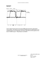
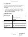
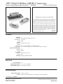
Channel Link Evaluation Kit User Manual Channel Link Demonstration Kit User Manual P/N CLINK3V28BT-85 Rev 2.1 Interface Products National Semiconductor Corporation Interface Products LIT# CLINK3V28BT-85-UM Rev 2.1 Date: 10/12/2005 Page 1 of 28 Channel Link Evaluation Kit User Manual Table of Contents INTRODUCTION ............................................................................................................ 3 CONTENTS OF DEMO KIT............................................................................................ 4 APPLICATIONS ............................................................................................................. 4 FEATURES AND EXPLANATIONS................................................................................. TRANSMITTER................................................................................................................ 6 RECEIVER ................................................................................................................... 11 HOW TO HOOK UP THE DEMO BOARDS (OVERVIEW) ............................................ 5 TRANSMITTER BOARD ................................................................................................ 6 SELECTABLE JUMPER SETTINGS FOR THE TX BOARD ........................................................ 6 LVDS MAPPING BY IDC CONNECTOR ............................................................................. 6 TX OPTIONAL: PARALLEL TERMINATION FOR TXIN........................................................... 9 BOM (BILL OF MATERIALS) .......................................................................................... 10 RECEIVER BOARD ..................................................................................................... 11 SELECTABLE JUMPER SETTINGS FOR THE RX BOARD ..................................................... 12 LVDS MAPPING BY IDC CONNECTOR ........................................................................... 13 RX OPTIONAL: SERIES TERMINATION FOR RXOUT ......................................................... 14 BOM (BILL OF MATERIALS) .......................................................................................... 15 TROUBLESHOOTING ................................................................................................. 19 ADDITIONAL INFORMATION...................................................................................... 20 APPLICATION NOTES .................................................................................................... 20 APPENDIX ................................................................................................................... 21 26-MINI D CABLE AND CONNECTOR ............................................................................... 21 TRANSMITTER AND RECEIVER SCHEMATICS ................................................................... 28 National Semiconductor Corporation Interface Products LIT# CLINK3V28BT-85-UM Rev 2.1 Date: 10/12/2005 Page 2 of 28 Channel Link Evaluation Kit User Manual Introduction: National Semiconductor - Interface Products Group Channel Link evaluation kit contains a Transmitter (Tx) board, a Receiver (Rx) board along with interfacing cables. This kit will demonstrate the Channel Link chipset transmitting data streams using Low Voltage Differential Signaling (LVDS). The Transmitter board accepts LVTTL/LVCMOS data signals from an incoming data source along with the clock signal. The LVDS Transmitter converts the LVTTL/LVCMOS parallel lines into four serialized LVDS data pairs plus a LVDS clock. The serial data streams toggle at 3.5 times the clock rate. The Receiver board accepts the LVDS serialized data streams plus clock and converts the data back into parallel LVTTL/LVCMOS data signals and clock. The user simply needs to provide the proper LVTTL/LVCMOS data input and clock to the Transmitter and the chipset will serialize, transmit, and deserialize the data converting it back into the LVTTL/LVCMOS parallel bus plus clock. A power down feature is also provided that reduces current draw when the link is not required. National Semiconductor Corporation Interface Products LIT# CLINK3V28BT-85-UM Rev 2.1 Date: 10/12/2005 Page 3 of 28 Channel Link Evaluation Kit User Manual Contents of the Evaluation Kit: 1) One Transmitter board with the DS90CR287MTD - 28 bit Transmitter 2) One Receiver board with the DS90CR288AMTD - 28 bit Receiver 3) One 2-meter Amphenol Spectra Strip Cable interface 4) One 60-pin IDC Flat Ribbon Cable 5) Evaluation Kit Documentation (this manual) 6) DS90CR287/288A Datasheet 7) Channel Link Application Notes AN-1041 and AN-1108 Channel Link Typical Application: TX DS90CR287 TxIN RX LVDS Cable DS90CR288A (media dependent) RxOUT 0 0 1 1 2 2 LVCMOS/ LVTTL 25 25 26 26 27 27 /PD /PD TxCLK RxCLK GND PCB PCB SHIELD The diagram above illustrates the use of the Channel Link chipset (Tx/Rx). This chipset is able to transmit 28 bits of LVTTL/LVCMOS data using four LVDS channels for a total throughput of 2.38 Gbps (297.5 Mbytes/s). Input clock rate is specified to be between 20 MHz to 85 MHz maximum. The interconnect between the two devices may be a variety of media including: twisted pair cables, twin-ax cables, and / or backplanes for example. Driving between the two devices is a function of interconnect skew and clock rate. Distances up to ten meters are possible at the lower clock rates and distances of 1 to 2 meters is possible at the higher clock rates. Please refer to the chipset datasheet for more information and parametric tables. National Semiconductor Corporation Interface Products LIT# CLINK3V28BT-85-UM Rev 2.1 Date: 10/12/2005 Page 4 of 28 Channel Link Evaluation Kit User Manual How to set up the Evaluation Kit: The PCB routing for the Tx input pins (TxIN) have been laid out to accept incoming data from a 60-pin IDC connector. The TxOUT/RxIN interface uses the 3M MDR connector and Spectra Strip cable. This typical cable provides minimal skew between LVDS channels and can typically support longer lengths than atwisted pair cable. Please follow these steps to set up the evaluation kit for bench testing and performance measurements: 1) Connect one end of the Spectra Strip cable to the transmitter board and the other end to the receiver board. This is a standard pinout cable, longer lengths are available for purchase from Alliance Technology – see www.alliancet.com 2) Jumpers have been configured at the factory, they should not require any changes for operation of the chipset. See text on Jumper settings for more details. 3) For the incoming data, connect a flat (ribbon) cable to the transmitter board to a data source (signal generator, pattern generator, BERT tester, etc). Connect the 60-pin flat cable from the receiver board to the receiver load (BERT or other equipment). Scope probes may also be connected directly to the pins if desired. Mini-coax cable with headers on one end may also be used. This type of cable is supplied with some test equipment. The 60-pin IDC equipment interface cable is supplied with this kit which can be used to build custom cables. 4) Power for the Tx and Rx boards must be supplied externally through TP1 (Vcc). Grounds for both boards are connected through TP2 (GND) (see section below). 5) Data applied to the inputs is now serialized, transmitted, deserialized and redriven at the receiver outputs. This evaluation kit can also be used to evaluate the performance of other National Semiconductor’s 28-bit and 21-bit Channel Link Serdes chipset. Simply replace the existing DS90CR287/288A devices with a different 28-bit or 21-bit device chipset and follow the above procedure. For evaluation of 21-bit device chipset, user needs to pull TxIN[21:27] high or low. Power Connection: The Transmitter and Receiver boards must be powered by supplying power externally through TP1 (Vcc) and TP2 (GND) on EACH board. Information on maximum supply voltage can be found on device datasheet’s Absolute Maximum Ratings section. The maximum voltage that should ever be applied to the Channel Link Transmitter (DS90CR287) or Receiver (DS90CR288A) Vcc terminal is +4V MAXIMUM. National Semiconductor Corporation Interface Products LIT# CLINK3V28BT-85-UM Rev 2.1 Date: 10/12/2005 Page 5 of 28 Channel Link Evaluation Kit User Manual Channel Link Transmitter Board Description: J1 (60 position) accepts 28 bit LVTTL/LVCMOS data, clock and also the PD* control signal. The Channel Link Transmitter board is powered externally. For the transmitter to be operational, the Power Down pin must be set HIGH with a jumper. The 3M MDR connector (J2) provides the interface for LVDS signals for the Receiver board. 60-pin IDC Connector 1 2 GND GND GND GND GND GND GND GND GND GND GND GND GND GND GND GND GND GND GND GND GND GND GND GND GND GND GND GND GND GND TXIN0 TXIN1 TXIN2 TXIN3 TXIN4 TXIN5 TXIN6 TXIN7 TXIN8 TXIN9 TXIN10 TXIN11 TXIN12 TXIN13 TXIN14 TXIN15 TXIN16 TXIN17 TXIN18 TXIN19 TXIN20 TXIN21 TXIN22 TXIN23 TXIN24 TXIN25 TXIN26 TXIN27 Vcc and Gnd MUST be applied externally here TxOUT LVDS signals 3M MDR connector Pin 14 Pin 1 NC OUT0- GND OUT0+ NC NC OUT1- GND OUT1+ NC OUT2- GND OUT2+ NC NC NC NC CLK- GND CLK+ NC NC OUT3- GND OUT3+ NC Pin 13 Pin 26 J2 TXCLKIN GND 59 60 /PD J1 Note: JP1 is not used National Semiconductor Corporation Interface Products LIT# CLINK3V28BT-85-UM Rev 2.1 Date: 10/12/2005 Page 6 of 28 Channel Link Evaluation Kit User Manual Jumper Settings for the Tx Board Jumper Purpose /PD (JP2) PowerDown Settings = ON Vcc GND (ON: Tx is operational; = OFF Vcc GND OFF: Tx powers down) Default setting is JP2 set HIGH (to Vcc), operational mode. National Semiconductor Corporation Interface Products LIT# CLINK3V28BT-85-UM Rev 2.1 Date: 10/12/2005 Page 7 of 28 Channel Link Evaluation Kit User Manual Tx LVDS Mapping by IDC Connector The following two figures illustrate how the Tx inputs are mapped to the IDC connector (J1) (Note – labels are also printed on the demo boards). The 26-pin MDR connector pinout is also shown. (Transmitter Board) 60-pin IDC Connector Pin 1 59 GND GND GND GND GND GND GND GND GND GND GND GND GND GND GND GND GND GND GND GND GND GND GND GND GND GND GND GND GND GND TXIN0 TXIN1 TXIN2 TXIN3 TXIN4 TXIN5 TXIN6 TXIN7 TXIN8 TXIN9 TXIN10 TXIN11 TXIN12 TXIN13 TXIN14 TXIN15 TXIN16 TXIN17 TXIN18 TXIN19 TXIN20 TXIN21 TXIN22 TXIN23 TXIN24 TXIN25 TXIN26 TXIN27 TxOUT LVDS signals 3M MDR connector 2 PIN # 1 2 3 4 5 6 7 8 9 10 11 12 13 14 15 16 17 18 19 20 21 22 23 24 25 26 TXOUT0 TXOUT0 TXOUT1 TXOUT1 TXOUT3 TXOUT1 TXOUT2 TXOUT2 TXCLKIN GND NAME NC GND NC OUT1OUT1+ OUT2OUT2+ NC NC GND NC OUT3OUT3+ OUT0OUT0+ NC GND NC GND NC NC CLKCLK+ NC GND NC J2 60 J1 TXCLKOUT Previous Cycle Next Cycle TXOUT3 TXIN23 TXIN17 TXIN16 TXIN11 TXIN10 TXIN5 TXIN27 TXOUT2 TXIN26 TXIN25 TXIN24 TXIN22 TXIN21 TXIN20 TXIN19 TXOUT1 TXIN18 TXIN15 TXIN14 TXIN13 TXIN12 TXIN9 TXIN8 TXOUT0 TXIN7 TXIN6 TXIN4 TXIN3 TXIN2 TXIN1 TXIN0 Parallel LVTTL/LVCMOS Data Inputs Mapped to LVDS Outputs National Semiconductor Corporation Interface Products LIT# CLINK3V28BT-85-UM Rev 2.1 Date: 10/12/2005 Page 8 of 28 Channel Link Evaluation Kit User Manual Tx Board Options: 50 Ohm Termination for TxIN On the Tx demo board, the 29 inputs have an option for 50 Ohm terminations. There are 0402 pads for this purpose. One side is connected to the signal line and the other side is tied to ground. These pads are unpopulated from the factory but are provided if the user needs to install a 50 Ohm termination. R1 TO R28 are associated with the Tx data input lines. R29 is associated with CLKIN. Some test equipment may require a 50 Ohm load. Mapping of Transmitter Inputs for the Optional Termination Resistors is shown below: Tx Pin Names TxIN0 TxIN1 TxIN2 TxIN3 TxIN4 TxIN5 TxIN6 TxIN7 TxIN8 TxIN9 TxIN10 TxIN11 TxIN12 TxIN13 TxIN14 TxIN15 TxIN16 TxIN17 TxIN18 TxIN19 TxIN20 TxIN21 TxIN22 TxIN23 TxIN24 TxIN25 TxIN26 TxIN27 Tx Pin Number 51 52 54 55 56 2 3 4 6 7 8 10 11 12 14 15 16 18 19 20 22 23 24 25 27 28 30 50 Termination Resistor R1 R2 R3 R4 R5 R6 R7 R8 R9 R10 R11 R12 R13 R14 R15 R16 R17 R18 R19 R20 R21 R22 R23 R24 R25 R26 R27 R28 TxCLKIN 31 R29 National Semiconductor Corporation Interface Products TX 50 Ohm Termination (Optional) LIT# CLINK3V28BT-85-UM Rev 2.1 Date: 10/12/2005 Page 9 of 28 Channel Link Evaluation Kit User Manual BOM (Bill of Materials) Transmitter PCB: HSL Demo Board Schematic REV1 HSL8TXR1 Revision: 1 Channel Link Item Qty Reference Part Pkg Size 1 1 C1 10 µF CASE D 2 4 C2,C6,C10,C14 0.1 µF 1206 (3216) 3 4 C3,C7,C11,C15 22 µF 7343 (D) 4 3 C4,C8,C12 0.001 µF 0805 (2012) 5 3 C5,C9,C13 0.01 µF 0805 (2012) 6 2 JP2 3_PIN_HEADER 0.1" spacing 7 1 J1 IDC30X2 IDC60 8 1 J2 3M_MDR 26MDR 9 29 R1,R2,R3,R4,R5,R6,R7,R8, Optional R9,R10,R11,R12,R13,R14, R15,R16,R17,R18,R19,R20, R21,R22,R23,R24,R25,R26, R27,R28,R29 0402 PAD 10 8 R30,R32,R33,R34,R35, R36,R37 0 Ohm 0402 11 2 TP1,TP2 N/A TP_.2"X.2" 12 1 U1 DS90CR287MTD 56-pin TSSOP National Semiconductor Corporation Interface Products LIT# CLINK3V28BT-85-UM Rev 2.1 Date: 10/12/2005 Page 10 of 28 Channel Link Evaluation Kit User Manual Rx Channel Link Receiver Board: J1 (60 position) provides access to the 28 bit LVTTL/LVCMOS, clock outputs. The Channel Link Receiver board is powered from the pads show below. For the receiver to be operational, the Power Down pin must be set HIGH with the jumper. The 3M MDR connector (J2) provides the interface for LVDS signals for the Receiver board. RxIN LVDS signals 3M MDR26-7 connector Vcc and Gnd MUST be applied externally here 60 Pin 13 Pin 26 NC IN0- GND IN0+ NC NC IN1- GND IN1+ NC IN2- GND IN2+ NC NC NC NC CLK- GND CLK+ NC NC IN3- GND IN3+ NC Pin 14 59 RXOUT27 RXOUT26 RXOUT25 RXOUT24 RXOUT23 RXOUT22 RXOUT21 RXOUT20 RXOUT19 RXOUT18 RXOUT17 RXOUT16 RXOUT15 RXOUT14 RXOUT13 RXOUT12 RXOUT11 RXOUT10 RXOUT9 RXOUT8 RXOUT7 RXOUT6 RXOUT5 RXOUT4 RXOUT3 RXOUT2 RXOUT1 RXOUT0 Pin 1 J2 RXCLKOUT GND /PD National Semiconductor Corporation Interface Products GND GND GND GND GND GND GND GND GND GND GND GND GND GND GND GND GND GND GND GND GND GND GND GND GND GND GND GND GND GND 2 1 J1 LIT# CLINK3V28BT-85-UM Rev 2.1 Date: 10/12/2005 Page 11 of 28 Channel Link Evaluation Kit User Manual Selectable Jumper Settings for the Rx Board Jumper Purpose /PD (JP1) PowerDown Settings = ON Vcc GND (ON: Rx is operational; = OFF Vcc GND OFF: Rx powers down) Default setting is JP1 set HIGH (to Vcc), operational mode. National Semiconductor Corporation Interface Products LIT# CLINK3V28BT-85-UM Rev 2.1 Date: 10/12/2005 Page 12 of 28 Channel Link Evaluation Kit User Manual LVDS Mapping by IDC Connector The following two figures illustrate how the Rx outputs are mapped to the IDC connector (J1) (Note – labels are also printed on the demo boards). The 26-pin MDR connector pinout is also shown. (Receiver Board) 60-pin IDC Connector 60 RXIN2 RXIN2 RXIN1 RXIN3 RXIN1 RXIN1 RXIN0 RXIN0 RXOUT27 RXOUT26 RXOUT25 RXOUT24 RXOUT23 RXOUT22 RXOUT21 RXOUT20 RXOUT19 RXOUT18 RXOUT17 RXOUT16 RXOUT15 RXOUT14 RXOUT13 RXOUT12 RXOUT11 RXOUT10 RXOUT9 RXOUT8 RXOUT7 RXOUT6 RXOUT5 RXOUT4 RXOUT3 RXOUT2 RXOUT1 RXOUT0 RXCLKOUT 2 GND GND GND GND GND GND GND GND GND GND GND GND GND GND GND GND GND GND GND GND GND GND GND GND GND GND GND GND GND GND GND J1 RxIN LVDS signals 3M MDR connector 59 PIN # 1 2 3 4 5 6 7 8 9 10 11 12 13 14 15 16 17 18 19 20 21 22 23 24 25 26 NAME NC GND NC CLK+ CLKNC NC GND NC GND NC IN0+ IN0IN3+ IN3NC GND NC NC IN2+ IN2IN1+ IN1NC GND NC J2 Pin 1 RXCLKIN Previous Cycle Next Cycle RXIN3 RXOUT23 RXOUT17 RXOUT16 RXOUT11 RXOUT10 RXOUT5 RXOUT27 RXIN2 RXOUT26 RXOUT25 RXOUT24 RXOUT22 RXOUT21 RXOUT20 RXOUT19 RXIN1 RXOUT18 RXOUT15 RXOUT14 RXOUT13 RXOUT12 RXOUT9 RXOUT8 RXIN0 RXOUT7 RXOUT6 RXOUT4 RXOUT3 RXOUT2 RXOUT1 RXOUT0 LVDS Data Inputs Mapped to LVTTL/LVCMOS Outputs National Semiconductor Corporation Interface Products LIT# CLINK3V28BT-85-UM Rev 2.1 Date: 10/12/2005 Page 13 of 28 Channel Link Evaluation Kit User Manual Rx Optional: Series Termination for RxOut On the Rx demo board, there are 29 outputs that have an 0402 pad in series (which are shorted out). These pads are unpopulated from the factory but are provided if the user needs to install a 450 Ohm series resistors. This is required if directly connecting to 50 Ohm inputs on a scope. To use this option the user must cut the signal line between the pads before installing the 450 Ohm series resistors. R1 to R28 are associated with the DATA output lines. R29 is associated with CLKOUT. The total load presented to the receiver output is 500 Ohms (450 + 50). The waveform on the scope is 1/10 of the signal due to the resulting voltage divider (50 / (450 + 50)). Optional Series Termination Resistor mapping is shown below: Rx Pin Names Rx Pin Number RxOUT0 RxOUT1 RxOUT2 RxOUT3 RxOUT4 RxOUT5 RxOUT6 RxOUT7 RxOUT8 RxOUT9 RxOUT10 RxOUT11 RxOUT12 RxOUT13 RxOUT14 RxOUT15 RxOUT16 RxOUT17 RxOUT18 RxOUT19 RxOUT20 RxOUT21 RxOUT22 RxOUT23 RxOUT24 RxOUT25 RxOUT26 RxOUT27 27 29 30 32 33 34 35 37 38 39 41 42 43 45 46 47 49 50 51 53 54 55 1 2 3 5 6 7 Series Termination Resistor R28 R27 R26 R25 R24 R23 R22 R21 R20 R19 R18 R17 R16 R15 R14 R13 R12 R11 R10 R9 R8 R7 R6 R5 R4 R3 R2 R1 RxCLKOUT 26 R29 National Semiconductor Corporation Interface Products RX Series Termination (Optional) LIT# CLINK3V28BT-85-UM Rev 2.1 Date: 10/12/2005 Page 14 of 28 Channel Link Evaluation Kit User Manual BOM (Bill of Materials) Receiver PCB: HSL Demo Board Schematic REV1 HSL8RXR1 Revision: 1 Channel Link Item Qty Reference Part Pkg Size 1 1 C1 10 µF CASE D 2 4 C2,C6,C10,C14 0.1 µF 1206 (3216) 3 4 C3,C7,C11,C15 22 µF 7343 (D) 4 3 C4,C8,C12 0.001 µF 0805 (2012) 5 3 C5,C9,C13 0.01 µF 0805 (2012) 6 1 JP1 3_PIN_HEADER 0.1" spacing 7 1 J1 IDC30X2 IDC60 8 1 J2 3M_MDR 26MDR 9 29 R1,R2,R3,R4,R5,R6,R7,R8, Optional 0402 PAD R9,R10,R11,R12,R13,R14, (See previous page) R15,R16,R17,R18,R19,R20, R21,R22,R23,R24,R25,R26, R27,R28,R29 6 R35,R36,R37,R38,R39,R40 0 Ohm 0402 10 5 R30,R31,R32,R33,R34 100 Ohm 0402 11 2 TP1,TP2 N/A TP_.2"X.2" 12 1 U1 DS90CR288AMTD 56-pin TSSOP National Semiconductor Corporation Interface Products LIT# CLINK3V28BT-85-UM Rev 2.1 Date: 10/12/2005 Page 15 of 28 Channel Link Evaluation Kit User Manual Typical Connection / Test Equipment The following is a list of typical test equipment that may be used to generate signals for the TX inputs: 1) TEK HFS9009 - This pattern generator along with 9DG2 Cards may be used to generate input signals and also the clock signal. 2) TEK DG2020 - This generator may also be used to generate data and clock signals. 3) TEK MB100 BERT - This bit error rate tester may be used for both signal source and receiver. 4) Any other signal / pattern generator that generates the correct input levels as specified in the datasheet. The following is a list of typically test equipment that may be used to monitor the output signals from the RX: 1) TEK MB100 BERT - Receiver. 2) Any SCOPE with 50 Ohm inputs or high impedance probes. LVDS signals may be easily measured with high impedance / high bandwidth differential probes such as the TEK P6247 or P6248 differential probes. The picture below shows a typical test set up using a generator and scope. Signal/Pattern Generator, BERT Tester Optional Termination Transmitter Board Receiver Board 50 ohm 50 ohm 450 ohm 50 ohm LVDS Interface Cable 50 ohm Optional Termination Oscilloscope, BERT Tester Typical Connection / Test Equipment Setup National Semiconductor Corporation Interface Products LIT# CLINK3V28BT-85-UM Rev 2.1 Date: 10/12/2005 Page 16 of 28 Channel Link Evaluation Kit User Manual Typical Waveshapes LVDS The plot above shows both the LVDS Data channel with PRBS data and also the LVDS Clock over laid. Note that the clock pattern is 4 bit times HIGH and 3 bit times LOW. The differential signal should be typically +/-300mV. These waveforms were acquired using the TEK P6248 Probes. Clock rate is 85MHz. National Semiconductor Corporation Interface Products LIT# CLINK3V28BT-85-UM Rev 2.1 Date: 10/12/2005 Page 17 of 28 Channel Link Evaluation Kit User Manual RxOUT The plot above shows both the recovered PRBS data and also the regenerated Clock overlaid. Note that the clock transitions slightly before the data transition and strobes the data on the rising edge of the clock. The data and clock signals are low drive 3V CMOS outputs. The plot above is at 85MHz. National Semiconductor Corporation Interface Products LIT# CLINK3V28BT-85-UM Rev 2.1 Date: 10/12/2005 Page 18 of 28 Channel Link Evaluation Kit User Manual Troubleshooting If the demo boards are not performing properly, use the following as a guide for quick solutions to potential problems. If the problem persists, please contact the Interface Applications hotline number (+1 408 721 8500) for assistance. QUICK CHECKS: 1. Check that Power and Ground are connected to both Tx AND Rx boards. 2. Check the supply voltage (typical 3.3V) and also current draw with both Tx and Rx boards (should be about 200mA with clock and one data bit at 66MHz). 3. Verify input clock and input data signals meet requirements (VIL, VIH, tset, thold), Also verify that data is strobed on the rising edge of the clock. 4. Check that the Jumpers are set correctly. 5. Check that the 2 meter cable is properly connected. TROUBLESHOOTING CHART Problem… There is only the output clock. There is no output data. Solution… Make sure the data is applied to the correct input pin. Make sure data is valid at the input. No output data and clock. Make sure Power is on. Input data and clock are active and connected correctly. Power, ground, input data and input clock are connected correctly, but no outputs. Make sure that the 2 meter cable is secured to both demo boards. Check the Power Down pins of both boards and make sure that the devices are enabled (/PD=Vcc) for operation. The devices are pulling more than 1A of current. Check for shorts in the cables connecting the TX and RX boards. After powering up the demo boards, the power supply reads less than 3V when it is set to 3.3V. Use a larger power supply that will provide enough current for the demo boards, a 500mA power supply is recommended. National Semiconductor Corporation Interface Products LIT# CLINK3V28BT-85-UM Rev 2.1 Date: 10/12/2005 Page 19 of 28 Channel Link Evaluation Kit User Manual Additional Information For more information on Channel Link Transmitters/Receivers, refer to the National’s LVDS website at: www.national.com/appinfo/lvds Application Notes • • • • • AN-1041 Channel Link Moving and Shaping Information in Point-to-Point Applications AN-971 An Overview of LVDS technology AN-977 LVDS Signal Quality: Jitter Measurement Using Eye Pattern AN-1059 High Speed Transmission with LVDS Devices AN-1108 Channel-Link PCB and Interconnect Design-In Guidelines Interface Applications Hotline: The Interface Hotline number is: +1 408 721-8500 National Semiconductor Corporation Interface Products LIT# CLINK3V28BT-85-UM Rev 2.1 Date: 10/12/2005 Page 20 of 28 Channel Link Evaluation Kit User Manual Appendix Cable and connector The next few pages provide a full description of the cable and connector. For product request please contact 3M and Alliance Technology Enterprise. 3M Connector Data is available at: www.mmm.com/Interconnects Spectra Strip Cable Data is available at: www.alliancet.com Tx PCB Schematic Transmitter Board: HSL Demo Board Schematic Document Number: HSL8TX Rev: 1.0 Rx PCB Schematic Receiver Board: HSL Demo Board Schematic Document Number: HSL8RX Rev: 1.0 National Semiconductor Corporation Interface Products LIT# CLINK3V28BT-85-UM Rev 2.1 Date: 10/12/2005 Page 21 of 28 .050″ Mini D Ribbon (MDR) Connectors Surface Mount Right Angle Receptacle — Shielded 102XX-1210VE Series IMPORTANT NOTICE TO PURCHASER ALL STATEMENTS, TECHNICAL INFORMATION AND RECOMMENDATIONS CONTAINED HEREIN ARE BASED ON TESTS WE BELIEVE TO BE RELIABLE, BUT THE ACCURACY OR COMPLETENESS THEREOF IS NOT GUARANTEED, AND THE FOLLOWING IS MADE IN LIEU OF ALL WARRANTIES, EXPRESSED OR IMPLIED: SELLER’S AND MANUFACTURER’S ONLY OBLIGATION SHALL BE TO REPLACE SUCH QUANTITY OF THE PRODUCT PROVED TO BE DEFECTIVE. NEITHER SELLER NOR MANUFACTURER SHALL BE LIABLE FOR ANY INJURY, LOSS OR DAMAGE, DIRECT OR CONSEQUENTIAL, ARISING OUT OF THE USE OF OR THE INABILITY TO USE THE PRODUCT. BEFORE USING, USER SHALL DETERMINE THE SUITABILITY OF THE PRODUCT FOR HIS INTENDED USE, AND USER ASSUMES ALL RISK AND LIABILITY WHATSOEVER IN CONNECTION THEREWITH. NO STATEMENT OR RECOMMENDATION NOT CONTAINED HEREIN SHALL HAVE ANY FORCE OR EFFECT UNLESS IN AN AGREEMENT SIGNED BY OFFICERS OR SELLER AND MANUFACTURER. Date Issued: February 5, 1998 TS-0755-05 Sheet 1 of 3 140 Physical Insulation Material: Flammability: Color: Contact Material: Plating Underplate: Wiping Area: Shroud and Latch Hook Material: Plating: Screw Lock Material: Plating: Marking: Glass Reinforced Polyester (PCT) UL 94V-0 Beige Copper Alloy (C521) 80 µ″ [2.0 µm] Nickel — QQ-N-290, Class 2 20 µ″ [0.50 µm] Min Gold — MIL-G-45204, Type II, Grade C Steel Nickel Copper Alloy (C521) Tin 3M Logo and Part Number Electrical Current Rating: 1 A Insulation Resistance: > 5 × 10⁸Ω at 500 VDC Withstanding Voltage: 500 Vrms for 1 Minute Environmental Temperature Rating: –55°C to +105°C Process: Surface mount compatible up to 240°C peak for short durations. UL File No.: E68080 3M Electronic Products Division 6801 River Place Blvd. Austin, TX 78726-9000 For technical, sales or ordering information call 800-225-5373 .050″ Mini D Ribbon (MDR) Connectors Surface Mount Right Angle Receptacle — Shielded 102XX-1210VE Series Dimensions Contact Quantity 3M Part Number A.008 B.006 C.006 D.006 E.006 20 10220-1210 VE 1.32 [ 33.4 ] 1.081 [ 27.45 ] .650 [ 16.51 ] .475 [ 12.07 ] .646 [ 16.4 ] 26 10226-1210 VE 10240-1210 VE 1.50 [ 38.2 ] 1.231 [ 31.26 ] .800 [ 20.32 ] .625 [ 15.88 ] .795 [ 20.2 ] 1.85 [ 47.1 ] 1.581 [ 40.15 ] 1.150 [ 29.21 ] .975 [ 24.77 ] 1.150 [ 29.2 ] 40 A position above last position last position 2X M2.5 Thread position below pos. 1 D .025 [ 0.635 ] position 2 .368 [ 9.35 ] position 1 .047 [ 1.20 ] .010 nom. [ 0.25 ] .394 [ 10.00 ] .187 [ 4.75 ] .19 [ 4.8 ] .203 [ 5.15 ] .138 [ 3.5 ] E B 2X M2.5 Thread (see note in ordering info) Position 1 .248 [ 6.30 ] .189 [ 4.80 ] Inch Position [mm] last position C Positioning Boss (2x) Tolerance Unless Noted Inch .0 .00 ± .1 ± .01 ± .005 .000 [ ] Dimensions for Reference only Ordering Information 102XX-1210VE Contact Quantity (See Table) Note: Use (M2.5x8mm) screws to mount to panel with max. thickness of 2.0 mm. TS-0755-05 Sheet 2 of 3 3M Electronic Products Division 6801 River Place Blvd. Austin, TX 78726-9000 For technical, sales or ordering information call 800-225-5373 .050″ Mini D Ribbon (MDR) Connectors Surface Mount Right Angle Receptacle — Shielded Dimensions A ± .002 B ± .002 Contact Quantity 102XX-1210VE Series Recommended Board Layout C ± .002 20 1.081 [ 27.45 ] .650 [ 16.51 ] .475 [ 12.07 ] 26 1.230 [ 31.26 ] .800 [ 20.32 ] .625 [ 15.88 ] 40 1.581 [ 40.15 ] 1.150 [ 29.21 ] .975 [ 24.77 ] (viewed from connector side) Solder Pads for Solder Tail (See below for more detail) center spacing C .165 [ 4.2 ] center spacing .025 ± .0008 .016 ± .0004 .093 ± .0004 .118 [ 3.0 ] .122 [ 3.1 ] .110 ± .004 (2X) Screw Lock (see notes below) .138 [ 3.5 ] .256 [ 6.5 ] Lockstand Solder Pad Outline .187 max. [ 4.75 ] .088 [ 2.223 ] PCB Ref. Edge .079 + .004 (2X) – .000 Positioning Hole B A Solder Tail Layout Detail (#’s Correspond to Connector Contact # Shown on Previous Page) 10 9 8 7 6 5 4 3 2 1 Connector Position (Top Row) 20 Pos. Last Pos. 20 19 18 17 16 15 14 13 12 11 Position (Bottom Row) PCB Ref. Edge 13 12 11 10 9 8 7 6 5 4 3 2 Connector Position (Top Row) 1 26 Pos. Last Pos. 26 25 24 23 22 21 20 19 18 17 16 15 14 Position (Bottom Row) PCB Ref. Edge Connector Position 20 19 18 17 16 15 14 13 11 12 10 9 8 7 6 5 4 3 2 1 40 Pos. Last Pos. 40 39 38 37 36 35 34 33 32 31 30 29 28 27 26 25 24 23 22 21 PCB Ref. Edge Position (Bottom Row) Contact Quantity Recommended Panel Cut-out Dimensions D E 20 .94 [ 23.8 ] 1.081 [ 27.45 ] 26 1.09 [ 27.6 ] 1.231 [ 31.26 ] 40 1.44 [ 36.5 ] 1.581 [ 40.15 ] **Notes: 1. Plated through holes for .062″ board thickness. 2. Use mounting screws ( M2.5 ) to fasten to board. Note: Panel thickness .079 [ 2.00 ] Max. .319 ± .004 [ 8.1 ] R .060 [ 1.50 ] D ± .004 E ± .004 TS-0755-05 Sheet 3 of 3 3M Electronic Products Division 6801 River Place Blvd. Austin, TX 78726-9000 For technical, sales or ordering information call 800-225-5373 Cable Assembly Part number MDR26-5-6.5 3M mdr 10126-6000 3Mmdr 10126-6000 2 meters Spectra Strip cable Skew Clear twin ax Part number MDR26-5-6.5 Cable length 6.5 Ft Connector type 2 meter Number of twin-Ax pairs 5 Connector number of positions 26 Cable assemby ordering information. Alliance Technology Enterprise 521 Central Ave Suite B Menlo Park CA 94025 650 329 8554 [email protected] www.AllianceT.com National Semiconductor Channel Link Cable Assembley Pinout Alliance Technology part number MDR26-5-6.5C Pin Assignment Side A 1 2 3 4 5 6 7 8 9 10 11 12 13 14 15 16 17 18 19 20 21 22 23 24 25 26 Pin Assignment Side B 3M Mdr Part 3M Mdr Part 10126-6000 10126-6000 No Connect TxOut0Gnd+ No Connect TxOut1TxOut1+ TxOut2TxOut2+ Reserved No Connect TxClkoutGnd No Connect TxOut3Txout3+ TxOut0TxOut0+ No Connect TxOut1Gnd No Connect TxOut2gnd Reserved Reserved TxClkOutTxClkOut+ No Connect TxOut3Gnd No Connect 26 25 24 23 22 21 20 19 18 17 16 15 14 13 12 11 10 9 8 7 6 5 4 3 2 1 Pin 1 No Connect TxOutGndNo Connect RxIn1 RxIn1 + RxIn2 RxIn2 + Reserved No Connect RxInClkGnd No Connect RxIn3 Rxin3 + RxIn0 Rxin0 + No Connect RxIn1Gnd No Connect Rxin2Gnd Reserved Reserved RxClkIn RxClkIn + No Connect RxIn3Gnd No Connect Pin 13 Cable assembly Pin 14 Pin 26 +3.6V MAX VCC J1 1 3 5 7 9 11 13 15 17 19 21 23 25 27 29 31 33 35 37 39 41 43 45 47 49 51 53 55 57 59 2 4 6 8 10 12 14 16 18 20 22 24 26 28 30 32 34 36 38 40 42 44 46 48 50 52 54 56 58 60 R1 R2 R3 R4 R5 TXIN0 TXIN1 TXIN2 TXIN3 TXIN4 TXIN5 TXIN6 TXIN7 TXIN8 TXIN9 TXIN10 TXIN11 TXIN12 TXIN13 TXIN14 TXIN15 TXIN16 TXIN17 TXIN18 TXIN19 TXIN20 TXIN21 TXIN22 TXIN23 TXIN24 TXIN25 TXIN26 TXIN27 TXCLKIN TXIN0 TXIN1 TXIN2 TXIN3 TXIN4 U1 R6 R7 R8 TXIN5 TXIN6 TXIN7 R9 R10 R11 TXIN8 TXIN9 TXIN10 R12 R13 R14 TXIN11 TXIN12 TXIN13 R15 R16 R17 TXIN14 TXIN15 TXIN16 R18 R19 R20 TXIN17 TXIN18 TXIN19 R21 R22 R23 R24 TXIN20 TXIN21 TXIN22 TXIN23 R25 R26 TXIN24 TXIN25 R30 IDC30X2 1 2 3 4 5 6 7 8 9 10 11 12 13 14 15 16 17 18 19 20 21 22 23 24 25 26 27 28 VCC TXIN5 TXIN6 TXIN7 GND TXIN8 TXIN9 TXIN10 VCC TXIN11 TXIN12 TXIN13 GND TXIN14 TXIN15 TXIN16 VCC TXIN17 TXIN18 TXIN19 GND TXIN20 TXIN21 TXIN22 TXIN23 VCC TXIN24 TXIN25 TXIN4 TXIN3 TXIN2 GND TXIN1 TXIN0 TXIN27 LVDS GND TXOUT0TXOUT0+ TXOUT1TXOUT1+ LVDS VCC LVDS GND TXOUT2TXOUT2+ TXCLK OUTTXCLK OUT+ TXOUT3TXOUT3+ LVDS GND PLL GND PLL VCC PLL GND /PWR DWN TXCLK IN TXIN26 GND 56 55 54 53 52 51 50 49 48 47 46 45 44 43 42 41 40 39 38 37 36 35 34 33 32 31 30 29 J2 1 14 2 15 3 16 4 17 5 18 6 19 7 20 8 21 9 22 10 23 11 24 12 25 13 26 27 28 TXOUT0TXOUT0+ TXOUT1TXOUT1+ LVDS_VCC LVDS_GND TXOUT2TXOUT2+ TXCLKOUTTXCLKOUT+ TXOUT3TXOUT3+ PLL_GND PLL_VCC DS90CR287 R27 R28 R29 TXIN26 TXIN27 TXCLKIN NC TXOUT0TXOUT0GND TXOUT0+ NC NC TXOUT1TXOUT1GND TXOUT1+ NC TXOUT2TXOUT2GND TXOUT2+ NC NC NC NC TXCLKOUTTXCLKOUTGND TXCLKOUT+ NC NC TXOUT3TXOUT3GND TXOUT3+ NC MOUNTING MOUNTING 3M_MDR_EZ8B VCC VCC1 R32 R33 R34 VCC VCC LVDS_VCC PLL_VCC JP2 /PD 3_PIN_HEADER GND1 R35 R36 R37 PLL_GND LVDS_GND GND TP1 +3.6V MAX VCC1 VCC C3 C4 C5 C6 C7 0.1uF 22uF TP_.2"X.2" GND22uF 0.001uF 0.01uF LVDS_VCC C8 LVDS_GND C9 C10 C11 0.001uF 0.01uF 0.1uF 22uF C12 C14 C15 0.1uF 22uF C1 10uF + C2 0.1uF GND1 TP_.2"X.2" Title PLL_VCC PLL_GND + TP2 C13 0.001uF 0.01uF HSL Demo Board Schematic Size Date: Document Number HSL8TX Monday, August 21, 2000 Rev 1 Sheet 1 of 1 +3.6V MAX VCC J1 R1 R2 R3 R4 R5 R6 RXOUT27 RXOUT26 RXOUT25 RXOUT24 RXOUT23 RXOUT22 R7 R8 R9 RXOUT21 RXOUT20 RXOUT19 R10 R11 R12 RXOUT18 RXOUT17 RXOUT16 R13 R14 R15 RXOUT15 RXOUT14 RXOUT13 R16 R17 R18 RXOUT12 RXOUT11 RXOUT10 R19 R20 R21 RXOUT9 RXOUT8 RXOUT7 R22 R23 R24 R25 RXOUT6 RXOUT5 RXOUT4 RXOUT3 R26 R27 RXOUT2 RXOUT1 R28 R29 RXOUT0 RXCLKOUT U1 J2 NC RXIN0RXIN0GND RXIN0+ NC NC RXIN1RXIN1GND RXIN1+ NC RXIN2RXIN2GND RXIN2+ NC NC NC NC RXCLKINRXCLKINGND RXCLKIN+ NC NC RXIN3RXIN3GND RXIN3+ NC MOUNTING MOUNTING 26 13 25 12 24 11 23 10 22 9 21 8 20 7 19 6 18 5 17 4 16 3 15 2 14 1 27 28 LVDS_GND RXIN0R30 100 RXIN0+ RXIN1RXIN1+ RXIN2- R31 100 RXIN2+ RXCLKINRXCLKIN+ RXIN3RXIN3+ LVDS_VCC R34 100 R33 100 R32 100 PLL_VCC PLL_GND VCC JP1 /PD 1 2 3 4 5 6 7 8 9 10 11 12 13 14 15 16 17 18 19 20 21 22 23 24 25 26 27 28 RXOUT22 RXOUT23 RXOUT24 GND RXOUT25 RXOUT26 RXOUT27 LVDS GND RXIN0RXIN0+ RXIN1RXIN1+ LVDS VCC LVDS GND RXIN2RXIN2+ RXCLK INRXCLK IN+ RXIN3RXIN3+ LVDS GND PLL GND PLL VCC PLL GND /PWR DWN RXCLK OUT RXOUT0 GND VCC RXOUT21 RXOUT20 RXOUT19 GND RXOUT18 RXOUT17 RXOUT16 VCC RXOUT15 RXOUT14 RXOUT13 GND RXOUT12 RXOUT11 RXOUT10 VCC RXOUT9 RXOUT8 RXOUT7 GND RXOUT6 RXOUT5 RXOUT4 RXOUT3 VCC RXOUT2 RXOUT1 56 55 54 53 52 51 50 49 48 47 46 45 44 43 42 41 40 39 38 37 36 35 34 33 32 31 30 29 59 57 55 53 51 49 47 45 43 41 39 37 35 33 31 29 27 25 23 21 19 17 15 13 11 9 7 5 3 1 IDC30X2 DS90CR288 VCC1 R35 R36 R37 VCC VCC LVDS_VCC PLL_VCC GND1 R38 R39 R40 PLL_GND LVDS_GND GND TP1 +3.6V MAX VCC1 VCC C4 60 58 56 54 52 50 48 46 44 42 40 38 36 34 32 30 28 26 24 22 20 18 16 14 12 10 8 6 4 2 3_PIN_HEADER 3M_MDR_EZ8B C3 RXOUT27 RXOUT26 RXOUT25 RXOUT24 RXOUT23 RXOUT22 RXOUT21 RXOUT20 RXOUT19 RXOUT18 RXOUT17 RXOUT16 RXOUT15 RXOUT14 RXOUT13 RXOUT12 RXOUT11 RXOUT10 RXOUT9 RXOUT8 RXOUT7 RXOUT6 RXOUT5 RXOUT4 RXOUT3 RXOUT2 RXOUT1 RXOUT0 RXCLKOUT C5 C6 C7 0.1uF 22uF TP_.2"X.2" GND22uF 0.001uF 0.01uF LVDS_VCC C8 LVDS_GND C9 C10 C11 0.001uF 0.01uF 0.1uF 22uF C12 C14 C15 0.1uF 22uF PLL_VCC PLL_GND + TP2 C1 10uF + C2 0.1uF GND1 TP_.2"X.2" Title C13 0.001uF 0.01uF HSL Demo Board Schematic Size Date: Document Number HSL8RX Monday, August 21, 2000 Rev 1 Sheet 1 of 1 IMPORTANT NOTICE Texas Instruments Incorporated and its subsidiaries (TI) reserve the right to make corrections, modifications, enhancements, improvements, and other changes to its products and services at any time and to discontinue any product or service without notice. Customers should obtain the latest relevant information before placing orders and should verify that such information is current and complete. All products are sold subject to TI’s terms and conditions of sale supplied at the time of order acknowledgment. TI warrants performance of its hardware products to the specifications applicable at the time of sale in accordance with TI’s standard warranty. Testing and other quality control techniques are used to the extent TI deems necessary to support this warranty. Except where mandated by government requirements, testing of all parameters of each product is not necessarily performed. TI assumes no liability for applications assistance or customer product design. Customers are responsible for their products and applications using TI components. To minimize the risks associated with customer products and applications, customers should provide adequate design and operating safeguards. TI does not warrant or represent that any license, either express or implied, is granted under any TI patent right, copyright, mask work right, or other TI intellectual property right relating to any combination, machine, or process in which TI products or services are used. Information published by TI regarding third-party products or services does not constitute a license from TI to use such products or services or a warranty or endorsement thereof. Use of such information may require a license from a third party under the patents or other intellectual property of the third party, or a license from TI under the patents or other intellectual property of TI. Reproduction of TI information in TI data books or data sheets is permissible only if reproduction is without alteration and is accompanied by all associated warranties, conditions, limitations, and notices. Reproduction of this information with alteration is an unfair and deceptive business practice. TI is not responsible or liable for such altered documentation. Information of third parties may be subject to additional restrictions. Resale of TI products or services with statements different from or beyond the parameters stated by TI for that product or service voids all express and any implied warranties for the associated TI product or service and is an unfair and deceptive business practice. TI is not responsible or liable for any such statements. TI products are not authorized for use in safety-critical applications (such as life support) where a failure of the TI product would reasonably be expected to cause severe personal injury or death, unless officers of the parties have executed an agreement specifically governing such use. Buyers represent that they have all necessary expertise in the safety and regulatory ramifications of their applications, and acknowledge and agree that they are solely responsible for all legal, regulatory and safety-related requirements concerning their products and any use of TI products in such safety-critical applications, notwithstanding any applications-related information or support that may be provided by TI. Further, Buyers must fully indemnify TI and its representatives against any damages arising out of the use of TI products in such safety-critical applications. TI products are neither designed nor intended for use in military/aerospace applications or environments unless the TI products are specifically designated by TI as military-grade or "enhanced plastic." Only products designated by TI as military-grade meet military specifications. Buyers acknowledge and agree that any such use of TI products which TI has not designated as military-grade is solely at the Buyer's risk, and that they are solely responsible for compliance with all legal and regulatory requirements in connection with such use. TI products are neither designed nor intended for use in automotive applications or environments unless the specific TI products are designated by TI as compliant with ISO/TS 16949 requirements. Buyers acknowledge and agree that, if they use any non-designated products in automotive applications, TI will not be responsible for any failure to meet such requirements. Following are URLs where you can obtain information on other Texas Instruments products and application solutions: Products Applications Audio www.ti.com/audio Automotive and Transportation www.ti.com/automotive Amplifiers amplifier.ti.com Communications and Telecom www.ti.com/communications Data Converters dataconverter.ti.com Computers and Peripherals www.ti.com/computers DLP® Products www.dlp.com Consumer Electronics www.ti.com/consumer-apps DSP dsp.ti.com Energy and Lighting www.ti.com/energy Clocks and Timers www.ti.com/clocks Industrial www.ti.com/industrial Interface interface.ti.com Medical www.ti.com/medical Logic logic.ti.com Security www.ti.com/security Power Mgmt power.ti.com Space, Avionics and Defense www.ti.com/space-avionics-defense Microcontrollers microcontroller.ti.com Video and Imaging www.ti.com/video RFID www.ti-rfid.com OMAP Mobile Processors www.ti.com/omap Wireless Connectivity www.ti.com/wirelessconnectivity TI E2E Community Home Page e2e.ti.com Mailing Address: Texas Instruments, Post Office Box 655303, Dallas, Texas 75265 Copyright © 2012, Texas Instruments Incorporated