1
MITSUBISHI ELECTRIC
Programmable Controller
User's Manual
(Hardware)
Q2A(S1)/Q3A/Q4ACPU
01 12 2003
IB(NA)66607
Version D
MITSUBISHI ELECTRIC
INDUSTRIAL AUTOMATION
SAFETY PRECAUTIONS
(Read these precautions before using.)
When using Mitsubishi equipment, thoroughly read this manual and the
associated manuals introduced in this manual.
Also pay careful attention to safety and handle the module properly.
These SAFETY PRECAUTIONS classify the safety precautions into two
categories: "DANGER" and "CAUTION".
DANGER
Procedures which may lead to a dangerous condition and
cause death or serious injury if not carried out properly.
CAUTION
Procedures which may lead to a dangerous condition and
cause superficial to medium injury, or physical damage
only, if not carried out properly.
Depending on circumstances, procedures indicated by
CAUTION may also
be linked to serious results.
In any case, it is important to follow the directions for usage.
Store this manual in a safe place so that you can read it whenever necessary.
Always forward it to the end user.
[DESIGN PRECAUTIONS]
DANGER
Install a safety circuit external to the PC that keeps the entire system
safe even when there are problems with the external power supply or
the PC module. Otherwise, trouble could result from erroneous output
or erroneous operation.
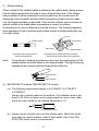
(1) Outside the PC, construct mechanical damage preventing interlock
circuits such as emergency stop, protective circuits, positioning upper
and lower limits switches and interlocking forward /reverse operations.
A-1
[DESIGN PRECAUTIONS]
DANGER
(2) When the PC detects the following problems, it will stop
calculation and turn off all output.
The power supply module has over current protection equipment
and over voltage protection equipment.
The PC CPUs self-diagnostic functions, such as the watchdog
timer error, detect problems. In addition, all output will be turned
on when there are problems that the PC CPU cannot detect, such
as in the I/O controller. Build a fail safe circuit exterior to the PC
that will make sure the equipment operates safely at such times.
See Section 4.2 of this user's manual for example fail safe
circuits.
See this user's manual for example fail safe circuits.
(3) Output could be left on or off when there is trouble in the outputs
module relay or transistor. So build an external monitoring circuit
that will monitor any single outputs that could cause serious
trouble.
Provide external safety circuits such as fuses to prevent smoking or
ignition that occurred if an overcurrent higher than the rating or caused
by a load short circuit, etc. flows in the output module continuously for
a long time.
Build a circuit that turns on the external power supply when the PC
main module power is turned on. If the external power supply is turned
on first, it could result in erroneous output or erroneous operation.
Refer to the manual of each data link for the action state of each station
caused by a communication error of the data link.
There is a risk of accidents due to erroneous outputs or erroneous
operation.
A-2
[DESIGN PRECAUTIONS]
DANGER
When connecting a peripheral device to the CPU module or a personal
computer, etc. to the special function module to perform control (data
change) for the operating PLC, configure an interlock circuit in the
sequence program to ensure that the whole system will always operate
safely.
When performing other control (program change, operating status
change (status control)) for the operating PLC, read the manual
carefully and ensure safety fully before starting the control.
In the above control performed especially for a remote PLC from an
external device, immediate response may not be made to PLC side
faults due to a data communication error.
Configure an interlock circuit in the sequence program, and also
determine between the external device and PLC CPU the corrective
action, etc. to be taken as a system at occurrence of a data
communication error.
CAUTION
Do not bunch the control wires or communication cables with the main
circuit or power wires, or install them close to each other. They should
be installed 100mm (3.94inch) or more from each other. Not doing so
could result in noise that would cause erroneous operation.
When controlling items like lamp load, heater or solenoid valve using
an output module, large current (approximately ten times greater than
that present in normal circumstances) may flow when the output is
→ON. Take measures such as replacing the module with
turned OFF→
one having sufficient rated current.
A-3
[INSTALLATION PRECAUTIONS]
DANGER
Use the PC in an environment that meets the general specifications
contained in this manual. Using this PC in an environment outside the
range of the general specifications could result in electric shock, fire,
erroneous operation, and damage to or deterioration of the product.
Install so that the pegs on the bottom of the module fit securely into the
base unit peg holes. Not installing the module correctly could result in
erroneous operation, damage, or pieces of the product falling.
When installing more cables, be sure that the base unit and the module
connectors are installed correctly. After installation, check them for
looseness. Poor connections could cause an input or output failure.
Correctly connect the extension cable securely to the connector of the
module mounted on the base unit. After installing, check.
A poor contact could cause an input or output failure.
Correctly connect the memory card installation connector to the
memory card. After installation, be sure that the connection is not
loose. A poor connection could cause an operation failure.
Always mount or dismount the module after switching off all phases of
the external power supply.
Not doing so may damage the product.
Do not directly touch the module's conductive parts or electronic
components. Touching the conductive parts could cause an operation
failure or give damage to the module.
[WIRING PRECAUTIONS]
DANGER
Completely turn off the external power supply when installing or
placing wiring. Not completely turning off all power could result in
electric shock or damage to the product.
When turning on the power supply or operating the module after
installation or wiring work, be sure that the module's terminal covers
are correctly attached. Not attaching the terminal cover could result in
electric shock.
A-4
[WIRING PRECAUTIONS]
CAUTION
Be sure to ground the FG terminals and LG terminals to the protective
ground conductor. Not doing so could result in electric shock or
erroneous operation.
When wiring in the PC, be sure that it is done correctly by checking the
product's rated voltage and the terminal layout. Connecting a power
supply that is different from the rating or incorrectly wiring the product
could result in fire or damage.
Do not connect multiple power supply modules in parallel. Doing so
could cause overheating, fire or damage to the power supply module. If
the terminal screws are too tight, it may cause falling, short circuit or
erroneous operation due to damage of the screws or module.
Crimp or pressure weld the external connection connector with a tool
designated by the manufacturer or solder it correctly.
Improper connection could cause a short circuit, fire or erroneous
operation.
Tighten the terminal screws with the specified torque. If the terminal
screws are loose, it could result in short circuits, fire, or erroneous
operation.
Tightening the terminal screws too far may cause damage to the
screws and/or the module, resulting in fallout, short circuits, or
malfunction.
Be sure there are no foreign substances such as sawdust or wiring
debris inside the module. Such debris could cause fires, damage, or
erroneous operation.
External connections shall be crimped or pressure welded with the
specified tools, or correctly soldered. For information regarding the
crimping and pressure welding tools, see the I/O module's user's
manual. Imperfect connections could result in short circuit, fires, or
erroneous operation.
A-5
[STARTUP AND MAINTENANCE PRECAUTIONS]
DANGER
Do not touch the terminals while power is on. Doing so could cause
shock or erroneous operation.
Correctly connect the battery. Also, do not charge, disassemble, heat,
place in fire, short circuit, or solder the battery. Mishandling of battery
can cause overheating or cracks which could result in injury and fires.
Switch all phases of the external power supply off when cleaning the
module or tightening the terminal screws. Not doing so could result in
electric shock.
CAUTION
The online operations conducted for the CPU module being operated,
connecting the peripheral device (especially, when changing data or
operation status), shall be conducted after the manual has been
carefully read and a sufficient check of safety has been conducted.
Operation mistakes could cause damage or problems with the module.
Do not disassemble or modify the modules. Doing so could cause
trouble, erroneous operation, injury, or fire.
Switch all phases of the external power supply off before mounting or
removing the module. If you do not switch all phases of the external
power supply, it will cause failure or malfunction of the module.
When using a radio communication device such as a cellular phone or
Personal Handy Phone system (PHS), use it at least 25cm away from
the PLC.
Not doing so can cause a malfunction.
Always make sure to touch the grounded metal to discharge the
electricity charged in the body, etc., before touching the module.
Failure to do so may cause a failure or malfunctions of the module.
Do not drop the battery fitted to the module, and do not give it impact.
Doing so may damage the battery, causing battery fluid to leak inside
the battery. Do not use the battery that has been dropped or given
impact, but dispose of it.
Before touching the module, be sure to touch a grounded metal or the
like to discharge static charge accumulated on your body.
If static charge is not discharged, failure or malfunction of the module
will be caused.
[DISPOSAL PRECAUTIONS]
CAUTION
When disposing of this product, treat it as industrial waste.
A-6
REVISIONS
*The manual number is given on the bottom right of the front cover.
Print Date
*Manual Number
Revision
Jun., 1996 IB(NA) 66607-A
First edition
Sep., 1998 IB(NA) 66607-B
Correction
Safety precautions, 4.5.2
Addition
Specifications, Performance specifications,
EMC standards, Low-Voltage instruction
Dec., 2002
IB(NA) 66607-C
Partial additions
5.1.1, 5.2.1
Partial corrections
Safety precautions, 1.1, 3.1.3, 3.1.4, 3.2.2,
4.2, 4.3.3, 4.5.1, 4.5.2, Chapter 6
Dec., 2003
IB(NA) 66607-D
Partial corrections
SAFETY PRECAUTIONS, Section 3.1,
3.1.3, 3.1.4, 3.1.5, 6.2
Japanese Manual Version F
This manual confers no industrial property rights or any rights of any other kind,
nor dose it confer any patent licenses. Mitsubishi Electric Corporation cannot be
held responsible for any problems involving industrial property rights which may
occur as a result of using the contents noted in this manual.
©1996 Mitsubishi Electric Corporation
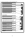
CONTENTS
1.SPECIFICATIONS......................................................................................................................... 1
1.1 SPECIFICATIONS................................................................................................................... 1
2.PERFORMANCE SPECIFICATIONS ....................................................................................... 2
2.1 QnACPU Module Performance Specifications.................................................................... 2
3.EMC DIRECTIVE AND LOW-VOLTAGE INSTRUCTION.................................................... 4
3.1 Requirements for Compliance to EMC Directive (89/336/EEC) ....................................... 4
3.1.1 EMC standards ................................................................................................................. 4
3.1.2 Installation inside the control cabinet.............................................................................. 5
3.1.3 Cables................................................................................................................................. 7
3.1.4 Power supply module.....................................................................................................11
3.1.5 Ferrite core.......................................................................................................................11
3.1.6 Noise filter (power supply line filter) ..............................................................................12
3.2 Requirement to Conform to the Low-Voltage Instruction .................................................13
3.2.1 Standard applied for MELSEC-QnA............................................................................13
3.2.2 Precautions when using the QnA series.....................................................................13
3.2.3 Power supply...................................................................................................................14
3.2.4 Control box.......................................................................................................................15
3.2.5 Module installation ..........................................................................................................16
3.2.6 Grounding ........................................................................................................................16
3.2.7 External wiring .................................................................................................................16
4.LOADING AND INSTALLATION..............................................................................................17
4.1 Installing modules ...................................................................................................................17
4.1.1 Precautions for handling of modules ...........................................................................17
4.1.2 Installation environment .................................................................................................17
4.1.3 Precautions relating to the installation of the unit........................................................18
4.2 The view of a fail-safe circuit..................................................................................................21
4.3 Power supply connection.......................................................................................................25
4.3.1 Performance Specifications for Power Supply Modules...........................................25
4.3.2 Part identification and setting of Power Supply Module............................................29
4.3.3 Power Supply Connection.............................................................................................34
4.4 Precaution when Connecting the Uninterruptive Power Supply (UPS) .........................38
4.5 Nomenclature and Settings...................................................................................................39
4.5.1 Nomenclature and settings ...........................................................................................39
4.5.2 Switch settings and corresponding LED displays......................................................42
5.I/O MODULE SPECIFICATIONS AND CONNECTIONS....................................................46
5.1 Input Modules..........................................................................................................................46
5.1.1 Input module specifications...........................................................................................46
5.1.2 Input module connections .............................................................................................50
5.2 Output Modules.......................................................................................................................56
5.2.1 Output module specifications........................................................................................56
5.2.2 Output module connections..........................................................................................62
5.3 Input/Output Combined Modules.........................................................................................72
5.3.1 Input/output combined module specifications ............................................................72
5.3.2 Input/output combined module connections...............................................................74
6.ERROR CODE.............................................................................................................................77
6.1 Error Code Readout Procedure ...........................................................................................77
6.2 Error Code List ........................................................................................................................78
This manual describes the operating precautions, input/output connections, and
error codes related to Q2ACPU , Q2ACPU-S1, Q3ACPU, and Q4ACPU
(hereafter, all are referred to simply as "QnACPU") operations.
About Manuals :
Other manuals related to QnACPU operation (shown below) are also available
if necessary.
Detailed manuals
Manual Name
Manual No.
Q2A(S1)/Q3A/Q4ACPU User's Manual
Discusses QnACPU performance, functions, and operation, and contains
the specifications for the power supply, memory card, and base unit.
(sold separately)
IB-66608
Q2A(S1)/Q3A/Q4ACPU, Q2AS(H)CPU(S1) User's Manual
Corresponding Additional Explanation
The functions and the instructions added for the version B functions of
QnACPU and Q2AS(H) CPU are explained.
(sold separately)
IB-66821
Related manuals
Manual Name
Manual No.
QnACPU Guidebook
This manual is designed for first-time users of the QnACPU. It explains the
procedures for all operations from program creation, to program writing to
the CPU, and program debugging. It also explains how to use the QnACPU
special features.
(sold separately)
IB-66606
QnACPU Programming Manual (Fundamentals)
This manual explains the programming procedures required for program
creation. It also explains the device names, parameters, and program types.
(sold separately)
IB-66614
QCPU(Q mode)/QnACPU Programming Manual (Common Instructions)
This manual explains how to use the sequence instructions, basic
instructions, and application instructions.
(sold separately)
SH-080039
QnACPU Programming Manual (Special Function Module)
This manual explains the dedicated instructions used with special function
modules at the Q2ACPU(S1), Q3ACPU, and Q4ACPU.
(sold separately)
IB-66616
QnACPU Programming Manual (AD57 Instructions)
This manual explains the dedicated instructions used to operate the
AD57(S1) CRT controller module at the Q2ACPU(S1), Q3ACPU, and
Q4ACPU.
(sold separately)
IB-66617
QCPU(Q mode)/QnACPU Programming Manual (PID Control Instructions)
This manual explains the dedicated instructions used to execute PID control
at the Q2ACPU(S1), Q3ACPU, and Q4ACPU.
(sold separately)
SH-080040
Manual Name
Manual No.
QCPU(Q mode)/QnACPU Programming module (SFC)
This manual explains the SW0IVD-SAP3 system configuration,
performance specifications, functions, programming, debugging, and error
codes.
(sold separately)
SH-080041
Building-Block Type Input/Output Module User's Manual
This manual gives the specifications for building- block type I/O modules.
(sold separately)
IB-66140
1. SPECIFICATIONS
1.1 SPECIFICATIONS
Table 1.1 General specification
Item
Specifications
Ambient operating
temperature
Ambient storage
temperature
Ambient operating
humidity
Ambient storage
humidity
0 to 50 °C
−20 to 75 °C
10 to 90 % RH, No-condensing
10 to 90 % RH, No-condensing
Frequency
Vibration
resistance
Shock resistance
Operating
ambience
Operating
elevation *3
Installation
location
Over voltage
category *1
Pollution level *2
Acceleration
Amplitude
No. of
sweeps
Under
0.075mm
10 to 57Hz
Conforming
10 times
intermittent
(0.003in.)
to JIS B 3502,
each in
vibration
57 to 150Hz
9.8m/s2
IEC 61131-2
X, Y, Z
Under
00.35mm
directions
10 to 57Hz
continuous
(0.001in.)
(for 80min.)
vibration
57 to 150Hz
4.9m/s2
Conforming to JIS B 3502, IEC 61131-2 (147 m/s2, 3 times in each of 3 directions X
Y Z)
No corrosive gases
2000m (6562ft.) max.
Control panel
II max.
2 max.
*1 : This indicates the section of the power supply to which the equipment is
assumed to be connected between the public electrical power distribution
network and the machinery within premises. Category II applies to equipment
for which electrical power is supplied from fixed facilities. The surge voltage
withstand level for up to the rated voltage of 300 V is 2500 V.
*2 : This index indicates the degree to which conductive material is generated in
terms of the environment in which the equipment is used. Pollution level 2 is
when only non-conductive pollution occurs. A temporary conductivity caused
by condensing must be expected occasionally.
*3 : Do not use or store the PC in the environment when the pressure is higher
than the atmospheric pressure at sea level. Otherwise, malfunction may result.
To use the PC in high-pressure environment, contact your nearest Mitsubishi
representative.
1
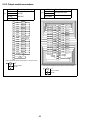
2. PERFORMANCE SPECIFICATIONS
2.1 QnACPU Module Performance Specifications
This section gives the Performance specifications of the QnACPU.
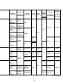
Table 2.1 Performance Specifications
Item
Control system
Model Name
Q2ACPU
Q2ACPU-S1
Q3ACPU
Q4ACPU
Remark
Repeated operation (using stored program)
I/O control method
Direct input
using device
names
possible
Refresh mode
Language dedicated to sequence control
Programming language
Relay symbol language, logic symbolic language,
MELSAP-3 (SFC)
Processing speed
LD
(sequence
instruction)
MOV
(µs/step)
Sequence
instructions
Basic Instructions
Number of
Applloation
instructions
instructions
Dedicated
instructions
Constant soan (ms)(program
started at fixed time Intervals)
Program
capacity
0.075
0.6
0.45
0.225
230
321
171
Set by
parameter
5 to 2000 (can be set in 5 ms units)
Capacity of the installed memory card
(max. 2036 k bytes)
Max. 28 k
Max. 60 k
Max. 92 k
Max. 124 k
28
60
92
124
Number of I/O device points
Number of I/O points
0.15
39
Memory capacity
Number of steps
(steps)
Number of files
(files)
0.2
8192 (X/Y0 to 1FFF)
512
(X/Y0 to
1FF)
1024
(X/Y0 to
3FF)
2
2048
(X/Y0 to
7FF)
4096
(X/Y0 to
FFF)
Number of
points that
can be used
in programs
Number of
points
actually
accessible
with I/O
modules
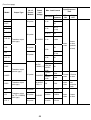
Table 2.1 Performance Specifications (Continued)
Item
Clock function
Allowable momentary power
interruption time
Internal current consumption for
5 VDC (A)
Weight kg
External dimensions mm (inch)
Model Name
Q2ACPU
Q2ACPU-S1
Q3ACPU
Q4ACPU
Remark
Year, month, date, hour, minute, second, day of
week (automatic recognition of leap years)
Accuracy −2.3 to +4.4 s (TYP. +1.8 s)/d at 0 °C
Accuracy −1.1 to +4.4 s (TYP. +2.2 s)/d at 25°C
Accuracy −9.6 to +2.7 s (TYP. -2.4 s)/d at 55 °C
Depends on the power supply module
0.3 (0.4)
0.3 (0.4)
0.3 (0.4)
0.6 (0.9)
The
numerical
value in
parentheses
represents
a function
version "B"
or later unit.
0.8
0.8
0.8
0.8
250(H) (9.84) × 79.5(W) (3.13) × 121(D) (4.76)
REMARK
Please check the ratings label of the CPU unit for the function version "B".
<QnACPU>
PROGRAMMABLE CONTROLLER
DATE
9707
B
MITSUBISHI ELECTRIC CORPORATION JAPAN
BD992D013H01
Manufacturing
date
3
Function
Version
3. EMC DIRECTIVE AND LOW-VOLTAGE INSTRUCTION
3.1 Requirements for Compliance to EMC Directive (89/336/EEC)
Compliance with the EMC directive, one of EU directives, is now compulsory.
The EMC directive is a directive requiring measures against "electromagnetic
emission" and for "electromagnetic immunity."
Sections 3.1.1 through 3.1.6 describe cautionary items of configuration of
mechanical equipment with MELSEC-QnA Series PLCs to meet requirements of
EMC directives.
Though we made our best efforts to prepare description based on the
requirements of the regulations and standards we have obtained, we do not
guarantee that the entire mechanical equipment manufactured according to the
description herein complies with the above-mentioned directives. Final judgment
of the method for complying with EMC directives and judgment of compliance are
up to the manufacturer of the applicable mechanical equipment.
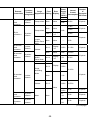
3.1.1 EMC standards
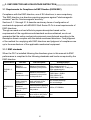
When the PLC is installed following the directions given in this manual its EMC
performance is compliant to the following standards and levels as required by the
EMC directive.
Specifications
Test Item
EN55011
Radiated noise
EN50081-2:
1995
prEN50082-2:
1991
Test Description
Measure the emission
released by the product.
Measure the emission
EN55011
released by the product
Conduction noise
to the power line.
IEC801-2
Static electricity
immunity *2
IEC801-3
Radiated
electromagnetic
field *2
IEC801-4
First transient
burst noise
Standard Values
30M-230 M Hz QP : 30dBµ V/m
(30m measurement) *1
230M-1000MHz QP : 37dBµ V/m
(30m measurement)
150k-500kHz QP :
79dB, Mean : 66dB*1
500k-30MHz QP :
73dB, Mean : 60dB
Immunity test by applying
static electricity to the
module enclosure.
4kV contact discharge
8kV air discharge
Immunity test by applying
aradiated electric field to
the product.
10V/m, 27-500MHz
Immunity test by applying
burst noise to the power
line and signal cable.
2kV
4
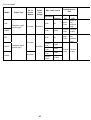
Specifications
Test Item
EN61000-4-2
Static electricity
immunity *2
EN61000-4-4
First transient
burst noise
EN50082-2 :
1995
ENV50140
Radiated
electromagnetic
field AM
modulation *2
ENV50204
Radiated
electromagnetic
field Pulse
modulation *2
Test Description
Immunity test by applying
static electricity to the
module enclosure.
Immunity test by applying
burst noise to the power
line and signal cable.,
2kV
Standard Values
4kV contact discharge
8kV air discharge
2kV
Immunity test by applying
aradiated electric field to
the product.
10V/m, 80-1000MHz, 80% AM
modulation@1kHz
Immunity test by applying
aradiated electric field to
the product.
10 V/m, 900MHz, 80% AM
modulation@1 k Hz
Immunity test by
inducting an
ENV50141
electromagnetic field in
Conduction noise
the power line signal
cable.
10 V/ms, 0.15-80MHZ, 80% AM
modulation@1kHz
(*1) QP: Quasi-peak value, Mean : Average value
(*2) The PLC is an open type device (device installed to another device) and must
be installed in a conductive control box.
The tests for the corresponding items were performed while the PLC was
installed to inside the control box.
3.1.2 Installation inside the control cabinet
Since the PLC is an open type device (device incorporated into another device), it
must be installed in the control cabinet. This has a good effect of not only for
assuring safety but also for shielding noise emitted from the PLC, by means of the
control cabinet.
(1) Control cabinet
(a) Use a conductive control cabinet.
(b) When attaching the control cabinet's top plate or base plate, mask
painting and weld so that good surface contact can be made between
the cabinet and plate.
(c) To ensure good electrical contact with the control cabinet, mask the
paint on the installation bolts of the inner plate in the control cabinet
so that contact between surfaces can be ensured over the widest
possible area.
5
(d) Earth the control cabinet with a thick wire so that a low impedance
connection to ground can be ensured even at high frequencies.
(22mm2 wire or thicker is recommended.)
(e) Holes made in the control cabinet must be 10cm (3.94in.) diameter or
less. If the holes are 10cm (3.94in.) or larger, radio frequency noise
may be emitted.
(2) Connection of power and ground wires
Earthing and power supply wires for the PLC system must be connected
as described below.
(a) Provide an earthing point near the power supply module. Earth the
power supply's LG and FG terminals (LG : Line Ground, FG : Frame
Ground) with the thickest and shortest wire possible. (The wire length
must be 30cm (11.18in.) or shorter.) The LG and FG terminals
function is to pass the noise generated in the PC system to the
ground, so an impedance that is as low as possible must be ensured.
As the wires are used to relieve the noise, the wire itself carries a
large noise content and thus short wiring means that the wire is
prevented from acting as an antenna.
Note)
A long conductor will become a more efficient antenna at high frequency.
(b) The earth wire led from the earthing point must be twisted with the
power supply wires. By twisting with the earthing wire, noise flowing
from the power supply wires can be relieved to the earthing. However,
if a filter is installed on the power supply wires, the wires and the
earthing wire may not need to be twisted.
6
3.1.3 Cables
The cables led from the control cabinet contain a high frequency noise element
and outside the control panel these cables act as antennae and radiate noise. The
cables connected to input/output modules or special modules which leave the
control panel must always be shielded cables.
Mounting of a ferrite core on the cables is not required (excluding some models)
but if a ferrite core is mounted, the noise radiated through the cable can be
suppressed further.
Use of a shielded cable is also effective for increasing the noise immunity level.
The PLC system's input/output and special function module provide a noise
immunity level of equivalent to that stated in IEC801-4 : 2 k V when a shielded
cable is used. If a shielded cable is not used or if the shield earthing treatment is
not suitable even when used (See Section 3.1.6), the noise immunity level is less
than 2 kV.
Note)
prEN50082-2 specifies the noise resistance level based on the signal
wire application.
Signals involved in process control :
2kV
Signals not involved in process control : 1kV
The meaning of "involved in process control" is not defined in prEN50082-2.
However, when the purposes of the EMC Directive are considered, the signals
that could cause personal injury or risks in the facility if a malfunction occurs
should be defined as "signals involved in process control". Thus, it is assumed
that a high noise immunity level is required.
7
(1) Shield earthing
When a shield of the shielded cable is earthed to the cabinet body, please ensure
that the shield contact with the body is over a large surface area. If the cabinet
body is painted it will be necessary to remove paint from the contact area. All
fastenings must be metallic and the shield and earthing contact must be made
over the largest available surface area. If the contact surfaces are too uneven for
optimal contact to be made either use washers to correct for surface
inconsistencies or use an abrasive to level the surfaces. The following diagrams
show examples of how to provide good surface contact of shield earthing by use
of a cable clamp.
Screw
Clamp fitting
Shield section
Paint mask
(a) Peal the cable insulation off and
expose the shield section
Note)
Shielded cable
(b) Sandwich the exposed shield section with the
and earth to the control cabinet over a wide area.
The method of earthing by soldering a wire onto the shield section of the
shielded cable as shown below is not recommended. The high frequency
impedance will increase and the shield will be ineffective.
Shielded cable
Wire
Crimp terminal
(2) MELSECNET/II module, MELSECNET/10 module
(a) The following requirements apply to AJ71QAR21, AJ71QLR21,
AJ71QBR11.
Always use a triaxial cable for the module. The radiated noise in the
band of 30 M Hz or higher can be suppressed by using a triax cable.
Earth the outer shield by the method described in (1).
Earth this section
(b) Always mount a ferrite core onto the triaxial cable. Mount the ferrite
core near the control cabinet outlet of each cable. Use of the TDK
ZCAT3035 ferrite core is recommended.
8
(3) Ethernet module
Precautions for the AUI cable, twisted pair cable and coaxial cable are described
below.
(a) Be sure to ground the AUI cable connected to the 10-BASE-5
connector. AUI is a shielded cable. Strip of a part of the sheath as
shown in the figure below, and ground the exposed shield in as wide
an area as possible.
AUI cable
Shield
For the shield grounding treatment, refer to (1).
(b) Use a shielded twisted pair cable for the twisted pair cable connected
to the 10-BASE-T connector. Strip of a part of the sheath of the
shielded twisted pair cable as shown in the figure below, and ground
the exposed shield in as wide an area as possible.
Shielded twisted pair cable
Shield
For the shield grounding treatment, refer to (1).
(c) Be sure to use double shielded coaxial cable for the coaxial cable
connected to the 10-BASE-2 connector. Ground the outer shield to
ground the double shielded coaxial cable.
Shield
Ground this shield.
For the shield grounding treatment, refer to (1).
Ethernet is a registered trademark of XEROX Co., Ltd. in the U.S.
(4) I/O and other communication cables
Always earth the shield section of the I/O signal cables and other
communication cables (RS-232-C, RS-422, etc.) in the same manner
as described in (1) if the cables go outside of the control cabinet.
9
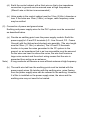
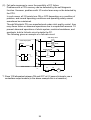
(5) Positioning Modules
AD75
module
CPU module
Power supply
module
(a) When wiring with a 2m (6.6ft.) or less cable
Ground the shield section of the external wiring cable with the cable
clamp.
(Ground the shield at the closest location to the AD75 external wiring
connector.)
Wire the external wiring cable to the drive unit and external device
with the shortest distance.
Install the drive unit in the same panel.
External wiring connector
Cable clamp
External wiring cable (within 2m (6.56 ft.))
Drive unit
External wiring connector
AD75
module
CPU module
Power supply
module
(b) When wiring with cable that exceeds 2m (6.6ft.), but is 10m (32.8ft.)
or less
Ground the shield section of the external wiring cable with the cable
clamp.
(Ground the shield at the closest location to the AD75 external wiring
connector.)
Install a ferrite core.
Wire the external wiring cable to the drive unit and external device
with the shortest distance.
Ferrite core
Cable clamp
External wiring cable (2m to 10m (6.56 ft. to 32.81 ft.))
Drive unit
10
(c) Ferrite core and cable clamp types and required quantities
1) Cable clamp
Type : AD75CK (Mitsubishi Electric)
2) Ferrite core
Type : ZCAT3035-1330 (TDK ferrite core)
3) Required quantity
Cable lenght
Within 2m (6.6ft.)
2m (6.6ft.) to 10m
(32.8ft.)
Prepared part
AD75CK
AD75CK
ZCAT3035-133
0
1 axis
1
1
Required Qty
2 axis
1
1
2 axis
1
1
1
2
3
3.1.4 Power supply module
The precautions required for each power supply module are described below.
Always observe the items noted as precautions.
Model
A61P, A62P
A63P
A61PEU, A62PEU
Precautions
Not used
Use the 24VDC panel power equipment
conforming to the EU Directive.
Always ground the LG and FG terminals
after short-circuiting them.
3.1.5 Ferrite core
The ferrite core effectively reduces radiation noise in a band between 30 and
100MHz. Though the ferrite core is not compulsory except for some models,
installation of the ferrite core is recommended if the shielding effect of the cable
routed outside the panel is insufficient. The ferrite core used for our tests is
ZCAT3035 made by TDK.
Install the ferrite core on the cable at a point just inside the panel that is routed
outside the panel. An improper installation position will eliminate the effect of the
ferrite core.
11
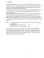
3.1.6 Noise filter (power supply line filter)
The noise filter (power supply line filter) is a device effective to reduce conducted
noise. Except some particular models described in Section 3.1.3 (5), installation of
a noise filter onto the power supply lines is not necessary. However conducted
noise can be reduced if it is installed. (The noise filter is generally effective for
reducing conducted noise in the band of 10 M Hz or less.) Usage of the following
filters is recommended.
Model name
FN343-3/01
FN660-6/06
ZHC2203-11
Manufacturer
Rated current
Rated voltage
SCHAFFNER
3A
SCHAFFNER
6A
250V
TDK
3A
The precautions required when installing a noise filter are described below.
(1) Do not bundle the wires on the input side and output side of the noise filter.
When bundled, the output side noise will be induced into the input side wires
from which the noise was filtered.
Input side
(power supply side)
Input side
(power supply side)
Induction
Filter
Filter
Output side
(device side)
(a) The noise will be included when the
input and output wires are bundled.
Output side
(device side)
(b) Separate and lay the inputand output
wires.
(2) Earth the noise filter earthing terminal to the control cabinet with the
shortest wire possible (approx. 10cm (3.94in.)).
12
3.2 Requirement to Conform to the Low-Voltage Instruction
The low-voltage instruction, one of the European Instructions, is now regulated.
The low-voltage instruction require each device which operates with power supply
ranging from 50 V AC to 1000 V and 75 V DC to 1500 V to satisfy necessary
safety items.
In the Sections from 3.2.1 to 3.2.7, cautions on installation and wiring of the
MELSEC-QnA series PC to conform to The Low Voltage Directive requires are
described.
We have put the maximum effort to develop this material based on the
requirements and standards of the regulation that we have collected. However,
compatibility of the devices which are fabricated according to the contents of this
manual to the above regulation is not guaranteed. Each manufacturer who
fabricates such device should make the final judgement about the application
method of the low-voltage instruction and the product compatibility.
3.2.1 Standard applied for MELSEC-QnA
The standard applied for MELSEC-QnA is EN61010-1 safety of devices used in
measurement rooms, control rooms, or laboratories.
For the modules which operate with the rated voltage of 50VAC/75VDC or above,
we have developed new models that conform to the above standard.
For the modules which operate with the rated voltage under 50VAC/75VDC, the
conventional models can be used, because they are out of the Low Voltage
Directive application range.
3.2.2 Precautions when using the QnA series
Module selection
(1) Power module
For a power module with rated input voltage of 100/200VAC, select a
model in which the internal part between the first order and second order
is intensively insulated, because it generates hazardous voltage (voltage
of 42.4V or more at the peak) area.
For a power module with 24VDC rated input, a conventional model can be
used.
(2) I/O module
For I/O module with rated input voltage of 100/200VAC, select a model in
which the internal area between the first order and second order is
intensively insulated, because it has hazardous voltage area.
For I/O module with 24VDC rated input, a conventional model can be
used.
13
(3) CPU module, memory cassette, base unit
Conventional models can be used for these modules, because they only
have a 5VDC circuit inside.
(4) Special module
Conventional models can be used for the special modules including
analog module, network module, and positioning module, because the
rated voltage is 24VDC or less.
(5) Display device
Use an A900 series GOT CE compatible model.
3.2.3 Power supply
The insulation specification of the power module was designed assuming
installation category II. Be sure to use the installation category II power supply to
the PC.
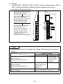
The installation category indicates the durability level against surge voltage
generated by lighening strike. Category I has the lowest durability; category IV has
the highest durability.
Category IV
Category III
Category II
Category I
Figure 1. : Installation Category
Category II indicates a power supply whose voltage has been reduced by two or
more levels of isolating transformers from the public power distribution.
14
3.2.4 Control box
Because the PLC is an open device (a device designed to be stored within
another module), be sure to use it after storing in the control box.
(1) Electrical shock prevention
In order to prevent persons who are not familiar with the electric facility
such as the operators from electric shocks, the control box must have the
following functions :
(a) The control box must be equipped with a lock so that only the
personnel who has studied about the electric facility and have enough
knowledge can open it.
(b) The control box must have a structure which automatically stops the
power supply when the box is opened.
(2) Dustproof and waterproof features
The control box also has the dustproof and waterproof functions.
Insufficient dustproof and waterproof features lower the insulation
withstand voltage, resulting in insulation destruction. The insulation in our
PLC is designed to cope with the pollution level 2, so use in an
environment with pollustion level 2 or below.
Pollution level 1 : An environment where the air is dry and conductive
dust does not exist.
Pollution level 2 : An environment where conductive dust does not
usually exist, but occasional temporary conductivity
occurs due to the accumulated dust. Generally, this
is the level for inside the control box equivalent to
IP54 in a control room or on the floor of a typical
factory.
Pollution level 3 : An environment where conductive dust exits and
conductivity may be generated due to the
accumulated dust.
An environment for a typical factory floor.
Pollution level 4 : Continuous conductivity may occur due to rain,
snow, etc. An outdoor environment.
As shown above, the PC can realize the pollution level 2 when stored in a
control cabinet equivalent to IP54.
15
3.2.5 Module installation
(1) Installing modules contiguously
In A series PCs, the left side of each I/O module is left open. When
installing an I/O module to the base, do not make any open slots between
any two modules. If there is an open slot on the left side of a module with
100/200VAC rating, the printed board which contains the hazardous
voltage circuit becomes bare. When it is unavoidable to leave an open slot,
be sure to install the blank module (AG60).
When using the A5 B expansion base with no power supply, attach the
cover packaged with the expansion base to the side of the leftmost
module.
3.2.6 Grounding
There are two kinds of grounding terminals as shown below. Either grounding
terminal must be used grounded.
Be sure to ground the protective grounding for the safety reasons.
: Maintains the safety of the PC and improves the noise
Protective grounding
resistance.
Functional grounding : Improves the noise resistance.
3.2.7 External wiring
(1) 24VDC external power supply
For special modules that require a 24 V DC I/O module or external power
supply, use a model whose 24 V DC circuit is intensively insulated from
the hazardous voltage circuit.
(2) External devices
When a device with a hazardous voltage circuit is externally connected to
the PLC, use a model whose circuit section of the interface to the PLC is
intensively insulated from the hazardous voltage circuit.
(3) Insulation requirements
Voltages are shown in Table 2.
Table 2 : Intensive Insulation Withstand Voltage
(Installation Category II, source : IEC664)
Rated voltage of hazardous voltage
area
Surge withstand voltage (1.2/50µ
µs)
150VAC or below
300VAC or below
2500V
4000V
16
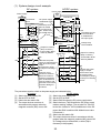
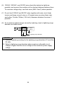
4. LOADING AND INSTALLATION
4.1 Installing modules
4.1.1 Precautions for handling of modules
This section describes the precautions that must be taken when handling the CPU,
I/O modules, special function modules, power supply module, base units, etc.
(1) Module enclosure, memory cassette, terminal block connectors and pin
connectors are made of resin; do not drop them or subject them to strong
impact.
(2) Do not remove modules' printed circuit boards from the plastic casing.
(3) During wiring, take care to ensure that wiring off cuts, etc. do not get
inside the case.
If anything does get inside the case, remove it.
(4) Tighten the module mounting (unnecessary in normal operating condition)
and terminal block screws as indicated below.
Screw
Module mounting screws (M4 screw) (optional)
Terminal block screws
Tightening Torque N cm
78 to 118
98 to 137
(5) To install a module, push it firmly into the base unit so that the latch
engages properly. To remove a module, press the latch to disengage it
from the base unit, then pull the module out (for details, refer to the
relevant PC CPU User's Manual).
4.1.2 Installation environment
The CPU system should not be installed under the following environmental
conditions:
(1) Places where ambient temperature is outside of 0 to 55°C range.
(2) Places where ambient humidity is outside of 10 to 90%RH range.
17
(3) Places where dewing (condensation) occurs due to sudden temperature
changes.
(4) Places where corrosive or inflammable gas exists.
(5) Places where a large amount of dust, iron powder and other conductive
powder, oil mist, salt or organic solvent exists.
(6) places exposed to direct sunlight.
(7) Places where a strong electric or magnetic field exists.
(8) Places where mechanical vibrations or impacts are transmitted directly to
the module body.
4.1.3 Precautions relating to the installation of the unit.
The following precautions must be observed when installing a PC to an operation
panel or other bases considering fully the operability, maintainability, and
resistance to the environment.
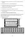
(1) Mounting dimension
Mounting dimensions of each base unit are as follows.
UNIT
I/O 0
I/O 1
I/O 2
I/O 3
I/O 4
I/O 5
I/O 6
I/O 7
H
CPU
Hs
POWER
A38B
Ws
W
W
Ws
H
Hs
A32B
A32B-S1
A35B
A38B
A38HB
247
(9.72)
227
(8.93)
268
(10.55)
248
(9.76)
382
(15.03)
362
(14.25)
480
(18.9)
460
(18.11)
A62B
A65B
238
352
(9.37) (13.86)
218
332
(8.58) (13.07)
250 (9.84)
200 (7.87)
A68B
A52B
A55B
A58B
466
(18.35)
446
(17.6)
183
(7.2)
163
(6.42)
297
(11.69)
277
(10.9)
411
(16.18)
391
(15.4)
Dimensions: mm (inch)
18
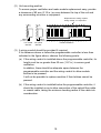
(2) Unit mounting position
To ensure proper ventilation and make module replacement easy, provide
a clearance of 80 mm (3.15 in.) or more between the top of the unit and
any surrounding structure or equipment.
Represents the ceiling of panel,
wiring conduit, or component.
Main base unit
28mm
(1.10 in.)
For coaxial
data link
Extension base unit
80mm (3.15 in.)
or more
*3
39mm
(1.54 in.)
For optical
data link
Parallel installation
(3) A wiring conduit should be provided if required.
If its clearance above or below the programmable controller is less than
indicated in the figure above, observe the following points:
(a) If the wiring conduit is installed above the programmable controller, its
height must be no greater than 50 mm (1.97 in.) to ensure good
ventilation.
In addition, there should be adequate space between the
programmable controller and the wiring conduit to allow module
latches to be pressed.
It will not be possible to replace modules if their latches cannot be
pressed.
(b) If the wiring conduit is installed below the programmable controller, it
should be installed so as to allow connection of the optical fiber cable
or coaxial cable, taking the minimum bending radius of the cable into
consideration.
19
Represents the ceiling of panel,
wiring conduit, or component.
80mm (3.15 in.) or more
Main base unit
*2
80mm (3.15 in.) or more
Conduit
(50mm
(1.97 in.)
or less)
*1
Extension base unit
Serial installation
*3
*1: These dimensions vary depending on the length of the
extension cable as follows:
AC06B cable ....................450mm (17.71 in.) or less
AC12B cable ....................1050mm (41.34 in.) or less
AC30B cable ....................2850mm (112.20 in.) or less
*2: When a link module is
not used ...........................50mm (1.97 in.) or more
When using φ4.5mm
optical fiber cable,
or coaxial cable ................100mm (3.94 in.) or more
When using φ8.5mm
optical fiber cable .............130mm (5.12 in.) or more
*3: When a link module is
not used ...........................50mm (1.97 in.) or more
When using φ4.5mm
optical fiber cable,
or coaxial cable ................100mm (3.94 in.) or more
When using φ8.5mm
optical fiber cable .............130mm (5.12 in.) or more
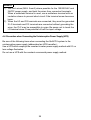
(4) Unit mounting orientation
(a) Since the PC generates heat, mount it in a well-ventilated location
and in the orientation shown below.
(b) Do not mount it in either of the orientations shown below.
Vertical
Flat
(5) Mount base unit on a flat surface.
If the mounting surface is uneven, this may strain the printed circuit boards
and cause malfunctions.
20
(6) Avoid mounting the base unit in proximity to vibration sources such as
large magnetic contractors and no-fuse circuit breakers; mount these on a
separate panel or at a distance.
(7) In order to avoid the effects of radiated noise and heat, provide the
clearances indicated below between the PC and devices that generate
noise or heat (contactors and relays).
•Required clearance in front of.......................... 100mm or more (3.94inch)
•Required clearance on the right and left of ...... 50mm or more (1.97inch)
100mm or more
(3.94 inch)
50mm or more
(1.97 inch)
50mm or more
(1.97 inch)
Contactor,
relay, etc.
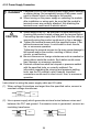
4.2 The view of a fail-safe circuit
When the programmable controller is switched ON/OFF, the outputs may
temporarily be incorrect due to the delay time and difference between the start-up
time of the programmable controller's power supply and that of the external power
supply for process control (especially if it is DC).
For example, if the power to the PC is turned ON after tuning ON the external
power supply used for the process control with the DC output module, the DC
output module may make an erroneous output for an instant.
There is a possibility of abnormal operation if the external power supply is
abnormal or a programmable controller fault occurs.
To prevent the abnormal operation of the whole system, machine breakdown, and
accidents, build a fail-safe circuit (emergency stop, protective circuit, interlocking
circuit, etc.) outside the PC.
21
An example system design circuit is shown on the following page.
DANGER
Install a safety circuit external to the PC that keeps the entire
system safe even when there are problems with the external
power supply or the PC module. Otherwise, trouble could
result from erroneous output or erroneous operation.
(1) Outside the PC, construct mechanical damage
preventing interlock circuits such as emergency stop,
protective circuits, positioning upper and lower limits
switches and interlocking forward /reverse operations.
(2) When the PC detects the following problems, it will stop
calculation and turn off all output.
The power supply module has over current protection
equipment and over voltage protection equipment.
The PC CPUs self-diagnostic functions, such as the
watchdog timer error, detect problems. In addition, all
output will be turned on when there are problems that
the PC CPU cannot detect, such as in the I/O
controller. Build a fail safe circuit exterior to the PC
that will make sure the equipment operates safely at
such times. See Section 4.2 of this user's manual for
example fail safe circuits.
See this user's manual for example fail safe circuits.
(3) Output could be left on or off when there is trouble in the
outputs module relay or transistor. So build an external
monitoring circuit that will monitor any single outputs that
could cause serious trouble.
Build a circuit that turns on the external power supply
when the PC main module power is turned on. If the
external power supply is turned on first, it could result in
erroneous output or erroneous operation.
22
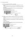
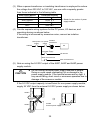
(1) System design circuit example
AC system
AC/DC system
Power supply
Power supply
Transformer
Fuse
CPU
SM52
Ym
SM403
Yn
Y1
XM
Start
switch
Transformer
DC power supply
established signal
input
Start/stop circuit
Can be started
by turning ON of
RA1, which is the
PC's RUN output.
Fuse
CPU
SM52
SM403
MC
MC Stop
switch
RA1
Input unit
XM
Output unit
Ym
L
Yn
RA1
TM
TM
MC1 N0 M10
Start N0 M10
Program
switch
RA1
MC
MC Stop
switch
Input unit
RA2
XM
Output for warning
(lamp or buzzer)
Turned ON in RUN
status by SM403
Yn
MC2
MC1
MC1
MC2
Y1
RA2
RA2
Voltage relay
recommended
Output for warning
(lamp or buzzer)
Output unit
Ym
MC
Fuse
The setting for TM
is the time taken
to establish the
DC input signal.
XM
MC
Output unit
(+)(−)
Yn
SM1084
Program
RA1
DC power
supply
Ym
L
RA1
Switches the power
supply to output devices
OFF when the system
Output module
stops:
At emergency stops
At stops on reaching a
limit
Interlock circuit
MC2
Constructs external
MC1
interlock circuits for
MC1
MC2
opposing operations
such as forward and
reverse rotation, and
parts that could cause
machine damage or
accidents.
Turned ON in RUN
status by SM403
MC MC
Switches the power
supply to output
devices OFF when
the system stops:
At emergency stops
At stops on reaching
a limit
The procedures used to switch on the power supply are indicated below.
AC/DC system
AC system
[1] Switch the power supply ON.
[1] Switch the power supply ON.
[2] Set the CPU to RUN.
[2] Set the CPU to RUN.
[3] Switch the start switch ON.
[3] Switch RA2 ON when the DC power supply starts.
[4] The output devices are driven in
[4] Switch the timer (TM) ON when the DC power supply
accordance with program when the
reaches working voltage. (The set value for TM must
magnetic contactor (MC) comes ON.
be the time it takes for 100% establishment of the DC
power after RA2 is switched ON. Make this set value
0.5 seconds.)
[5] Switch the start switch ON.
[6] The output devices are driven in accordance with the
program when the magnetic contactor (MC) comes ON.
(If a voltage relay is used at RA2, no timer (TM) is
necessary in the program.)
23
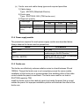
(2) Fail-safe measures to cover the possibility of PC failure
Problems with a CPU memory can be detected by the self diagnosis
function. However, problems with I/O control area may not be detected by
the CPU.
In such cases, all I/O points turn ON or OFF depending on a condition of
problem, and normal operating conditions and operating safety cannot
sometimes be maintained.
Though Mitsubishi PCs are manufactured under strict quality control, they
may cause failure or abnormal operations due to unspecified reasons. To
prevent abnormal operations of whole system, machine breakdown, and
accidents, build a fail-safe circuit outside the PC.
The following gives an example of a fail-safe circuit
ON delay timer
Internal program
Y00
T1
1 sec.
OFF delay timer
M9032
Y00
Y00
T2
Y01
External load
L
Y0F
L
1 sec.
MC
24V
0.5 sec. 0.5 sec.
– +
0V
CPU module
24 VDC
Output unit
*1
T1
T2
MC
*1 Since Y00 alternates between ON and OFF at 0.5 second intervals, use a
contactless output module (in the above example this is a transistor).
24
4.3 Power supply connection
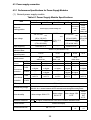
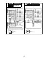
4.3.1 Performance Specifications for Power Supply Modules
(1) Normal power supply module
Table 4.1 Power Supply Module Specifications
Item
A61P
Specifications
A63P
A65P
A62P
I/O module
Base unit
loading position
Power supply module loading slot
24VDC +30%
+10%
+10 %
200-240 VAC -15 %
(170 to 264 VAC)
50/60 Hz ±5 %
*2
5 VDC
Overvoltage
protection
24 VDC
Noise durability
Insulation resistance
110 VA
65 W
20 A,
within 8 ms
8A
8.8 A
or higher
5.5
to 6.5 V
5A
0.8 A
5.5 A
or higher
1.2 A
or higher
5.5
to 6.5 V
module
loading slot
(170 to 264 VAC)
50/60 Hz ±5 %
100 A,
within 1 ms
8A
8.5 A
or higher
5.5
to 6.5 V
110 VA
95 VA
20 A,
within 8 ms
1.2 A
2A
1.5 A
2.2 A
or higher
2.3 A
1.7 A
or higher or higher
5.5
to 6.5 V
65 W
8A
8.5 A
or higher
5.5
to 6.5 V
65 % or higher
1500 VAC for 1 minute between all AC external terminals together and ground
500 VAC for 1 minute between all DC external terminals together and ground
Noise
Noise voltage Noise voltage 1500
voltage
Noise voltage 1500 V.P.P.
500 V.P.P.
V.P.P.
500
V.P.P.
10 M
or higher, measured with a 500 VDC insulation resistance tester
Power indicator
Terminal screw size
supply
+10%
Efficiency
Withstanding voltage
Power
Within 5% (See Section 4.4)
Inrush current
*1
5 VDC
Overcurrent
protection
24 VDC
A67P
100-120 VAC -15%
-35%
110 VDC
(85 to132 VAC)
(85 to 140
(15.6 to 31.2
+10 %
VDC)
200-240 VAC -15 %
VDC)
(85 to 132 VAC)
Input voltage
Rated output 5 VDC
current
24 VDC
loading
slot
100-120 VAC -15%
Input frequency
Input voltage
distortion factor.
Max. input
apparent power
A66P
Power LED display
M4 × 0.7 × 6
25
M3 × 0.5
×6
M4 × 0.7
×6
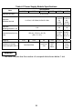
Table 4.1 Power Supply Module Specifications
Item
A61P
Specifications
A63P
A65P
A62P
0.75 to 2 mm
Applicable
solderless terminal
V1.25-3, V1.25-4,
V1.25-YS V1.25-YS
3A
4A,
V2-S3,
V2-S4,
V2-YS3A V2-YS4A
V1.25-4,V1.25-YS4A,V2-S4,V2-YS4A
Applicable
tightening torque: N cm
118
250 (H) × 55 (W)× 121 (D)
(9.8× 2.1× 4.7)
External dimensions mm
(inch)
Allowable momentary
power interruption time *3
A67P
2
Applicable wire size
Weight kg
A66P
0.98
0.94
Less than 20ms
0.8
0.94
Less than
1ms
Less
than
20ms
69
118
250 (H) ×
37.5 (W)×
121 (D)
(9.8× 1.5×
4.7)
0.75
250 (H) ×
55 (W)×
121 (D)
(9.8× 2.1×
4.7)
0.8
Less than
20ms
(at 100
VDC)
REMARK
The A66P module has the number of occupied slots shown below.1 slot
26
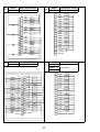
(2) Power supply module for CE marking
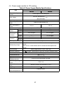
Table 4.2 Power Supply Module Specifications
Specifications
Item
A61PEU
Base unit loading
position
A62PEU
Power supply module loading slot
+10%
100-120 / 200-240 VAC -15%
(85 to 264 VAC)
50/60 Hz ±5 %
Input voltage
Input frequency
Input voltage distortion
factor.
Max. input apparent
power
Inrush current
Rated output
5 VDC
current
24 VDC
Within 5% (See Section 4.4)
130 VA
155 VA
20 A, within 8 ms
8A
5A
0.8 A
5 VDC
Overcurrent
protection *1 24 VDC
8.8 A or higher
5.5 A or higher
1.2 A or higher
Overvoltage
5 VDC
protection *2 24 VDC
5.5 to 6.5 V
Efficiency
65 % or higher
Noise durability
1500 VAC for 1 minute between all AC external terminals together and
ground
500 VAC for 1 minute between all DC external terminals together and
ground
Noise voltage IEC801-4; 2kV, 1500 V.p.p
Insulation resistance
10 M
Withstanding voltage
Power indicator
Terminal screw size
Applicable wire size
Applicable
solderless terminal
Applicable tightening
torque
External dimensions mm
(inch)
Weight kg
Allowable momentary
power interruption time *3
or higher, measured with a 500 VDC insulation resistance tester
Power LED display
M4 × 0.7 × 6
2
0.75 to 2 mm
V1.25-4,V1.25-YS4A,V2-S4,V2-YS4A
118 N cm
250 (H) × 55 (W)× 121 (D) (9.8× 2.1× 4.7)
0.8
0.9
Less than 20ms
27
POINTS
*1 : Overcurrent protection
(a) The overcurrent protection device shuts off the 5VDC, 24VDC
ladder and stops the system if the current flowing in the ladder
exceeds the specified value.
When this device is activated, the power supply module LED is
switched off or dimly lit.
(b) If this happens, eliminate the cause of the overcurrent for
example insufficient current capacity or short ladder then
start up the system.
When the current has returned to normal, the system
undergoes an initial start.
*2 : Overvoltage protection
The overvoltage protection device shuts off the 5VDC ladder and
stops the system if an excessive voltage in the range 5.5 to 6.5V is
applied to this ladder.
When this device is activated, the power supply module LED is
switched off. If this happens, switch the input power OFF, then
back ON to restart the system.
If the system is not booted and the LED remains off, the power
supply module must be changed.
*3 : Allowable momentary power interruption time
The PC CPU allowable momentary power interruption time varies
according to the type of power supply module.
In the case of the A63P module, the allowable momentary power
interruption time is defined as from when the 24VDC stabilized
primary supply is cut off until the 24VDC voltage drops to the
defined voltage (15.6VDC).
28
4.3.2 Part identification and setting of Power Supply Module
The names and descriptions of each of the parts of the power supply modules are
given below.
(1) Names and description of parts of the A61P, A61PEU module
Module fixing hook
Hook for fixing the module to the base unit.
61
"POWER" LED
LED for indicating 5 VDC power.
Power fuse, fuse holder
4 A cartridge fuse for AC input power is secured by the fuse
holder.
Spare fuse for power supply
Spare fuse for power supply, mounted on rear side of the
terminal cover.
Terminal block
For details, see below. (Located under the terminal cover)
Terminal cover
Cover for protection of terminal block. Remove during wiring.
Re-install after wiring.
Module fixing screw mounting hole
Allows the module to be secured with a screw in addition to
the module fixing hook. (For M4 screw)
Terminal details
Power input terminals
Power input terminals to which AC power of 100 VAC or 200
VAC.
Applied voltage select terminals
Terminals for selecting applied voltage. Use 100 VAC or 200
VAC as described below. When 100 VAC is input, connect
together the "SHORT AC100V" terminals with the jumper
provided. When 200 VAC is input, connect together the
"SHORT AC200V" terminals with the jumper provided.
LG terminal
Grounding of power filter. Has half the input potential.
FG terminal
Connection terminal connected to the shielding pattern on
printed circuit board.
Terminal screw
M4 × 0.7 × 6
29
(2) Names and description of parts of the A62P, A62PEU and A65P modules
Module fixing hook
Hook for fixing the module to the base unit.
"POWER" LED
LED for indicating 5 VDC power.
Power fuse, fuse holder
4 A cartridge fuse for AC input power is secured by the fuse
holder.
Spare fuse for power supply
Spare fuse for power supply, mounted on rear side of the
terminal cover.
Terminal block
For details, see below. (Located under the terminal cover)
Terminal cover
Cover for protection of terminal block. Remove during wiring.
Re-install after wiring.
Module fixing screw mounting hole
Allows the module to be secured with a screw in addition to
the module fixing hook. (For M4 screw)
Terminal details
Power input terminals
Power input terminals to which AC power of 100 VAC or 200
VAC.
Applied voltage select terminals
Terminals for selecting applied voltage. Use 100 VAC or 200
VAC as described below. When 100 VAC is input, connect
together the "SHORT AC100V" terminals with the jumper
provided. When 200 VAC is input, connect together the
"SHORT AC200V" terminals with the jumper provided.
LG terminal
Grounding of power filter. Has half the input potential.
FG terminal
Connection terminal connected to the shielding pattern on
printed circuit board.
24 VDC, 24 GDC terminals
For supply to output module which requires 24 V inside the
module. (Supplied to the module via external wiring)
Terminal screw
M4 × 0.7 × 6
30
(3) Names and description of parts of the A63P and A67P modules
Module fixing hook
Hook for fixing the module to the base unit.
"POWER" LED
LED for indicating 5 VDC power.
Power fuse, fuse holder
Cartridge fuse for DC input power is fixed by the fuse holder.
The rating for the fuses are as follows.
A63P: 6.3 A (SM6.3 A)
A67P: 4 A (GTH4)
Spare fuse for power supply
Spare fuse for power supply, mounted on rear side of the
terminal cover.
Terminal block
For details, see below. (Located under the terminal cover)
Terminal cover
Cover for protection of terminal block. Remove during wiring.
Re-install after wiring.
Module fixing screw mounting hole
Allows the module to be secured with a screw in addition to
the module fixing hook. (For M4 screw)
Terminal details
Power input terminals
Power input terminals for A63P: 24 VDC, A67P: 100 VDC.
The power fuse will be blown if the 24 VDC connection is
made with the wrong polarity.
LG terminal
Grounding of power filter.
FG terminal
Connection terminal connected to the shielding pattern on
printed circuit board.
Terminal screw
M4 × 0.7 × 6
31
(4) Names and description of parts of the A66P module
Module fixing hook
Hook for fixing the module to the base unit.
"POWER" LED
LED for indicating 5 VDC power.
Power fuse, fuse holder
4 A cartridge fuse for AC input power is secured by the fuse
holder.
Terminal block fixing screw
Screw for installing and fixing the terminal block to the module.
Terminal block
For details, see below. (Located under the terminal cover)
Module fixing screw mounting hole
Allows the module to be secured with a screw in addition to
the module fixing hook. (For M4 screw)
Terminal details
Power input terminals
Power input terminals to which AC power of 100 VAC or 200
VAC.
Applied voltage select terminals
Terminals for selecting applied voltage. Use 100 VAC or 200
VAC as described below. When 100 VAC is input, connect
together the "SHORT AC100V" terminals with the jumper
provided. When 200 VAC is input, connect together the
"SHORT AC200V" terminals with the jumper provided.
LG terminal
Grounding of power filter. Has half the input potential.
Power ON terminal
Contact terminal which conducts if the 24 VDC output is
normal when power input turns on.
FG terminal
Connection terminal connected to the shielding pattern on
printed circuit board.
24 VDC, 24 GDC terminals
For supply to output module which requires 24 V inside the
module. (Supplied to the module via external wiring)
Terminal screw
M3 × 0.5 × 6
32
(5) Setting
For A61P(EU), A62P(EU), A65P or A66P, the input voltage range, 100V or
200V, must be specified by placing a jumper (supplied) across two
terminals as described below:
Remove the terminal cover from
the power supply module.
Remove the pair of terminal
screw, (2) or (3), according to the
supply voltage range (1) used.
(2): For the 100 VAC range.
(3): For the 200 VAC range.
(1)
(4)
Fit the jumper (4) and secure it
with the terminal screw.
Fit the jumper in the direction
shown in the figure at right.
(The figure at right shows an
example when the supply line
voltage is 100 VAC.)
(2)
(3)
POINT
If the setting differs from the supply line voltage, the following occurs: do not
mis-set.
Supply Line Voltage
100VAC
200VAC
Setting to 100VAC
(jumper fitted as indicated at (2))
Setting to 200VAC
(jumper fitted as indicated at (3))
No setting
(jumper not fitted)
The power supply
module is damaged.
(The CPU is not
damaged.)
No error occurs in the
module. However, the
CPU does not
operate.
No error occurs in the module.
However, the CPU does not operate.
33
4.3.3 Power Supply Connection
DANGER
CAUTION
Completely turn off the external power supply when installing
or placing wiring. Not completely turning off all power could
result in electric shock or damage to the product.
When turning on the power supply or operating the module
after installation or wiring work, be sure that the module's
terminal covers are correctly attached. Not attaching the
terminal cover could result in electric shock.
When wiring in the PC, be sure that it is done correctly by
checking the product's rated voltage and the terminal layout.
Connecting a power supply that is different from the rating or
incorrectly wiring the product could result in fire or damage.
Tighten the terminal screws with the specified torque. If the
terminal screws are loose, it could result in short circuits,
fire, or erroneous operation.
Tightening the terminal screws too far may cause damage to
the screws and/or the module, resulting in fallout, short
circuits, or malfunction.
Be sure there are no foreign substances such as sawdust or
wiring debris inside the module. Such debris could cause
fires, damage, or erroneous operation.
External connections shall be crimped or pressure welded
with the specified tools, or correctly soldered. For
information regarding the crimping and pressure welding
tools, see the I/O module's user's manual. Imperfect
connections could result in short circuit, fires, or erroneous
operation.
Instructions for wiring the power supply cable and I/O cable.
(1) When voltage fluctuations are larger than the specified value, connect a
constant-voltage transformer.
Constant
voltage
transformer
PLC
(2) Use a power supply which generates minimal noise between wires and
between the PLC and ground. If excessive noise is generated, connect an
insulating transformer.
I/O
equipment
PLC
Insulating
transformer
Insulating
transformer
34
(3) When a power transformer or insulating transformer is employed to reduce
the voltage from 200 VAC to 100 VAC, use one with a capacity greater
than those indicated in the following table.
Power Supply Module
Transformer Capacity
A61P, A61PEU
110VA
n
A62P, A62PEU
110VA
n
A65P
110VA
n
A66P
95VA
n
n: Stands for the number of power
supply modules.
(4) Provide separate wiring systems for the PC power, I/O devices, and
operating devices as shown below.
If the wiring is influenced by excessive noise, connect an isolation
transformer.
Isolation
Main power PC power
transformer
supply
supply
PC
200VAC
T1
I/O power supply
I/O devices
Main circuit devices
Main circuit devices
(5) Note on using the 24 VDC output of the A62P, A65P and A66P power
supply module.
CAUTION
Do not connect multiple power supply modules in parallel.
Doing so could cause overheating, fire or damage to the
power supply module. If the terminal screws are too tight, it
may cause falling, short circuit or erroneous operation due to
damage of the screws or module.
24VDC
External power supply
35
I/O module
Power supply
unit
Power supply
unit
24VDC
I/O module
24VDC
Power supply
unit
If the 24 VDC output capacity is insufficient for one power supply module,
supply 24 VDC from the external 24 VDC power supply as shown below:
(6) 100VAC, 200VAC, and 24VDC wires should be twisted as tightly as
possible, and connect the modules at the shortest distance between them.
To minimize voltage drop, use thick wires (MAX. 2mm2) where possible.
(7) Do not bind 100VAC and 24VDC wires together with main circuit (high
tension and large current) wires or I/O signal wires nor place them near
each other. Provide 100mm (3.94 inch) clearance between the wires if
possible.
(8) As a measure against surges caused by lightning, insert a lightning surge
absorber as shown below.
PC/IO
device
AC
E2
Lightning surge absorber
E1
POINTS
(1) Provide separate grounding for the lightning surge absorber (E1) and the
PC (E2).
(2) Select a lightning surge absorber whose maximum allowable circuit
voltage is higher than the circuit voltage at the maximum power supply
voltage.
36
(9) The following is an example of wiring of power supply and grounding wires
to main base unit and extension base units.
Main base unit (A38B)
A62P
CPU
100/110 VAC
AC
100/200 VAC
SHORT
100 VAC
SHORT
200 VAC
LG
Fuse
FG
AC
DC
24 VDC
OUTPUT
24 GDC
24 VDC
24 VDC
Extension base unit (A58B)
I/O
I/O
Connect to the 24 VDC terminals
of an I/O module that requires 24
VDC internally.
5 VDC line
FG
Extension base (A68B)
A61P
100/110
VAC
5 VDC
line
100/200 VAC
SHORT
100 VAC
SHORT
200 VAC
LG
Grounding
line
FG
Ground
37
I/O
POINTS
(1) Use thick wires (MAX. 2mm2) where possible for the 100/200VAC and
24VDC power supply, and twist the wires from connected terminals.
When a solderless terminal is used, use a solderless terminal with an
insulation sleeve to prevent short-circuit if the terminal screw becomes
loose.
(2) When the LG and FG terminals are connected, they must be grounded.
If LG terminals and FG terminals are connected without grounding the
wires, the PLC may be susceptible to noise. Be aware not to touch the
LG terminal since it has potential of half the input voltage.
4.4 Precaution when Connecting the Uninterruptive Power Supply (UPS)
Be sure of the following items when connecting the QnACPU system to the
uninterruptive power supply (abbreviated as UPS hereafter) :
Use a UPS which employs the constant inverter power supply method with 5% or
less voltage fluctuation.
Do not use a UPS with the constant commercial power supply method.
38
4.5 Nomenclature and Settings
4.5.1 Nomenclature and settings
The programmable controller nomenclature and settings are explained in this
section.
(1) Q2AQPU, Q2ACPU-S1
(2) Q3ACPU, Q4ACPU
(1)(2)(3)(4) (5)
(1)
(2)
(7)
(3)
(4)
(8)
(5)
(6)
(11)
(6)
(11)
(10)
(10)
(9)
(9)
(14)
(12)
(14)
(12)
(16)
(16)
(17)
(17)
(11)
(11)
(15)
(15)
(13)
(13)
(18)
(18)
Appearance with front cover open
No.
Name
(1) RUN LED
(2) ERROR LED
Function
Indicates the CPU module operating Status.
Lamp ON
:When RUN/STOP key switch is set to RUN or STEP-RUN,
and operation is in progress.
Lamp OFF
:When RUN/STOP key switch is set to STOP, PAUSE or
STEP-RUN and operation is stopped. Or, when an error that
stops operation has been detected.
Lamp flashing :When a program is written during STOP and the
RUN/STOP key switch is moved from "STOP" to "RUN".
The CPU module is not in the RUN status. To put the CPU
module in the RUN status, move the RUN/STOP key switch
from "RUN" to "STOP" to "RUN" again. Alternatively,
perform reset operation with the RUN/STOP key switch.
(The Q3ACPU or Q4ACPU shows the "PRG. CHECK!!"
message on the display.)
Lamp ON
:When a self-diagnosis error (excluding battery error) which
does not stop operation has been detected. (When a
"continue operation at error detection" parameter setting has
been designated.)
Lamp OFF
:Normal
Lamp flashing :When an error that stops operation has been detected.
39
No.
(3)
(4)
(5)
(6)
(7)
(8)
(9)
(10)
(11)
(12)
(13)
(14)
(15)
Name
Function
Lamp ON
:An error has been detected by the CHK instruction, or an
annunciator F has come ON.
(With Q3ACPU or Q4ACPU, a message or the comment for
the annunciator is displayed on the LED indicator.)
USER LED
Lamp OFF
:Normal
Lamp flashing :Flashing when latch clear is performed.
(With Q3ACPU or Q4ACPU, the message "L. CLR RDY" is
displayed on the LED indicator.)
Lamp ON
:When a battery error is activated by a low voltage condition
BAT.ALARM LED
at the CPU module and memory card battery.
Lamp OFF
:Normal
Lamp ON
:When boot operation is completed.
BOOT LED
Lamp OFF
:When boot operation is not being executed.
RUN/STOP
:Sequence program operation EXECUTE/STOP.
L.CLR
:Sets all data in the latch area (designated by parameter) to
RUN/STOP key
"OFF" or "0". Also dears sampling trace and status latch
switch
registrations.
RESET
:Executes a hardware reset for operation error, and to
initialize operation, etc.
16-character display
LED display
Display content includes comments for self-diagnosis errors, comments for
(Q3A and Q4ACPU
LED display instructions, clock data for SET SM212, and annunciator F-No.
only)
comments for SET F,etc.
Display RESET
Clears the LED display content, displays the next data (when next data
switch (Q3A and
exists).
Q4ACPU only)
Battery (A6BAT)
Battery for internal memory and power failure backup.
For battery's lead wire connection. (To prevent wasted battery power
Battery connector
consumption, the lead wire is disconnected from the connector when shipped
pin
from the factory.)
Memory card
Ejects the memory card from the CPU module.
EJECT button
Memory card "A"
installation
connector
Connectors for installing memory cards in the CPU module.
Memory card "B"
installation
connector
Memory card "A"
in/out (with built in
LED)
This switch setting determines whether or not the memory card can be
inserted and ejected while power is ON. Factory set to OFF.
ON :Insertion/ejection prohibited (LED is ON)
Memory card "B"
OFF :Insertion/ejection permitted (LED is OFF)
in/out switch
(with built in LED)
40
No.
Name
Ejects the memory
card from the CPU
(16)
Function
Designates settings required for CPU module operation. All switches are
factory set to OFF.
SW1 :Boot setting. Designates the memory used for operation.
ON
:Boot operation
OFF
:Boot operation is not performed.
SW2 to SW4 : Parameter area. These switches designate the memory
where parameters are stored.
Internal Memory card A
Memory card B
RAM
RAM
ROM
RAM
ROM *SW2 to 4 are
valid if SW1 is
SW2
OFF
ON
OFF
ON
OFF
OFF.
SW3
OFF
OFF
ON
ON
OFF
SW4
OFF
OFF
OFF
OFF
ON
SW5 :System protect. Prevents all CPU module writing and control
operations.
ON
:System protect ON
OFF
:System protect OFF
Designates settings required for CPU module operation. All switches are
factory set to OFF.
System setting
switch 2
(17)
(18) RS-422 connector
SW1: For future expansion. Not used at present
SW2
: Peripheral protocol. Designates the types of peripheral devices
connected to the CPU module peripheral interface.
(Set to ON if another ACPU station is to be accessed from a
peripheral device. The ON or OFF setting becomes valid
immediately upon switching.)
ON
: ACPU peripheral device 1: For future expansion. Not used at
present
OFF
: QnACPU peripheral device
Connector for connection with peripheral devices.
41
4.5.2 Switch settings and corresponding LED displays
(1) Program writing when CPU module is stopped.
To execute program writing when the CPU module is stopped, follow the
key switch setting procedure shown below.
(a) RUN/STOP key switch
:STOP
RUN LED
:OFF
Q3ACPU, Q4ACPU display :OFF
program write
................................. CPU module STOP status
(b) RUN/STOP key switch
:RESET
RUN LED
:OFF
Q3ACPU, Q4ACPU display :"PRG.CHECK!" message is displayed
................................. CPU module STOP status
RUN
(c) RUN/STOP key switch
:STOP
RUN LED
:ON
Q3ACPU, Q4ACPU display :OFF
................................. CPU module STOP status
POINT
• After writing a program (except for online program write), perform reset
operation, and then place the CPU module in the RUN status.
• When remote STOP is switched to RUN, the CPU module is not put in
the "PROG CHECK" status but is placed in the RUN status.
(2) Latch CLEAR operation
To execute a "Latch CLEAR", follow the key switch setting procedure
shown below.
1) Turn the RUN/STOP key switch of the CPU module from the "STOP"
position to the "L. CLR" position several times to flicker the "USER
LED" on the CPU module front.
Normally, the LED flickers when the switch is turned several times
(three or four times).
When the "USER LED" flickers, it indicates that latch clear is ready.
2) After the "USER LED" has flickered, turning the RUN/STOP key
switch from the "STOP" position to the "L. CLR" position again
executes latch clear and lights up the "USER LED".
If the "USER LED" comes on for two seconds and then goes off, it
indicates that latch clear is completed normally.
3) To cancel latch clear midway, turn the RUN/STOP key switch to the
"RUN" position to place the CPU module in the RUN state, or turn it to
the "RESET" position to make a reset.
42
POINTS
• The devices where the "Latch CLEAR" occurs can be designated by the
"Latch CLEAR" enabled/disabled settings for each device made in device
setting in the parameter mode.
• In addition to the RUN/STOP key switch method, a remote "Latch
CLEAR" can also be executed from a GPP function peripheral device.
(Refer to the Q2A (S1)/Q3A/Q4ACPU User's Manual).
(3) Removing a memory card while PLC power is ON
To remove the memory card while the PLC power is ON, set the "memory
card in/out" switch as shown below. Removing a memory card while power
is ON:
(a) Switch ON (build-in LED ON)
............. Memory card insertion/ejection prohibited
(b) Switch OFF (build-in LED OFF)
............. Memory card insertion/ejection enabled
remove the memory card
POINTS
• The built-in LED at the "memory card in/out" switch may not go OFF if a
CPU module system function (sampling trace, status latch, etc.) is in
progress, or if the memory card is being used by the program. In such
cases, stop the system function or the program, then remove the memory
card after checking that the switch's built-in LED has turned OFF.
• Do not turn the "memory card in/out" switch ON after removing the
memory card. An error will occur if the switch is turned ON at this time.
• When there are parameter-set file registers, local devices or failure
history, the memory card cannot be the removed.
If the "memory card in/out" switch is turned OFF, the in/out switch built-in
LED does not go off.
For the file registers, the memory card can be removed when they are set
to be unused with the QDRSET(P) instruction.
(4) Inserting a memory card while PLC power is ON
To insert the memory card while the PLC power is ON, set the "memory
card in/out" switch as shown below.
(a) Insert the memory card.
(b) Turn the "memory card in/out" switch ON (built-in LED ON)
............. Memory card insertion/ejection prohibited
43
POINTS
• After inserting the memory card, turn the "memory card in/out" switch ON.
The memory card cannot be used until the switch is turned ON.
• Since mount processing is performed again after the memory card is
inserted, note that the scan time of one scan when mount processing is
performed increases by a maximum of 10ms.
44
MEMO
45
5. I/O MODULE SPECIFICATIONS AND CONNECTIONS
This section presents the specifications and wiring drawings for each of the A
series I/O modules.
5.1 Input Modules
5.1.1 Input module specifications
Model
Input Type
AX10
Number
of
Points/M
odule
Operating Voltage
Rated
Input
Voltage
Input
Current
OFF
Voltage
80VAC
or higher
40VAC
or lower
16 points
100%
100VAC
AX11
AX11EU
ON
Voltage
32 points
60%
10mA
AC input
AX20
16 points
100%
160VAC
or higher
200VAC
AX21
Maximum
Simultaneous ON
Input Point
(Percentage
Simultaneous ON)
70VAC
or lower
32 points
60%
16 points
100%
AX21EU
AX40
AX41
DC input (sink
type)
32 points
4/10mA
12/24
VDC
9.5VDC
or higher
6VDC
or lower
60%
AX41-S1
AX42 *1
AX50
AX50-S1
AX60
AX60-S1
64 points
DC input (sink type)
DC input
(sink/source
type)
DC input
(sink type)
DC input
(sink/source
type)
3/7mA
48VDC
Sensor input
(sink/source
type)
34VDC
or higher
10VDC
or lower
16 points
100%
100/110/
125VDC
5VDC
(SW
ON)
AX70
4mA
60% *3
16 points
12VDC
(SW
OFF)
24VDC
(SW
OFF)
2mA
3.5mA
(TYP)
5.5mA
(MAX)
2mA
(TYP)
3mA
(MAX)
4.5mA
(TYP)
6mA
(MAX)
46
80VDC
or higher
20VDC
or lower
3.5VDC
or higher
1.1VDC
or lower
100%
5VDC
or higher
2VDC
or lower
Input Response Time
OFF to ON
15msec or
less
10msec or
less
ON to OFF
25msec or
less
10msec or
less
10msec or
less
20msec or
less
1.5msec or
less
3msec or
less
Common
Terminal
Arrangement
Internal
Current
Consumption
16 points/
common
0.055A
16 points
32 points/
common
0.11A
32 points
16 points/
common
0.055A
16 points
32 points/
common
0.11A
32 points
0.055A
16 points
0.11A
32 points
32 points/
common
0.12A
64 point
20 terminal
block
connector
8 points/
common
0.055A
16 points
20 terminal
block
connector
8 points/
common
0.055A
16 points
External
Connections
20 terminal
block
connector
38 terminal
block
connector
20 terminal
block
connector
38 terminal
block
connector
20 terminal
block
connector
38 terminal
block
connector
40-pin
connector × 2
Number of
Occupied
I/O Points
8 points/
common
(To next page)
47
(From front page)
Model
Input Type
Number
of
Points/M
odule
Operating Voltage
Rated
Input
Voltage
5VDC
(SW
ON)
AX71
Sensor input
(sink/source type)
32 points
12VDC
(SW
OFF)
24VDC
(SW
OFF)
Input
Current
3.5mA
(TYP)
5.5mA
(MAX)
2mA
(TYP)
3mA
(MAX)
4.5mA
(TYP)
6mA
(MAX)
ON
Voltage
OFF
Voltage
3.5VDC
or higher
1.1VDC
or lower
5VDC
or higher
2VDC
or lower
Maximum
Simultaneous ON
Input Point
(Percentage
Simultaneous ON)
100%
AX80
AX80E
DC input
(source type)
16 points
12/24
VDC
4/10mA
9.5VDC
or higher
6VDC
or lower
AX81
AX81-S1
AX81-S2
AX81-S3
AX81B
AX82 *1
DC input
(sink/source type)
12/24
VDC
48/60
VDC
2.5/5m
A
24VDC
4/10mA
32 points
24VDC
7mA
64 points
12/24
VDC
3/7mA
9.5VDC
or higher
6VDC
or lower
8.5/4m
A
7VAC/
VDC or
higher
2.5VAC/
VDC or
100%
lower
8.5mA
16VDC
or higher
8VDC
or lower
32 points
DC input
(source type)
DC input
(sink/source type)
DC Input
(source type)
AX31
AC/DC input
32 points
12/24
VAC
12/24
VDC
AX31-S1
DC input
(sink/source type)
32 points
24VAC
3/4mA
48
5.6VDC
2.4VDC
or higher or lower
31VDC
10VDC
or higher or lower
9.5VDC
6VDC
or higher or lower
At normal input
21VDC
6VDC
or higher or lower
When disconnection
detected
1VDC
6VDC
or higher or lower
60%
60%
60%
Input Response Time
OFF to ON
ON to OFF
1.5msec or
less
3msec or
less
10msec or
10msec or
less
less
[TYP]
5.5msec
6.0msec
[High-speed mode]
0.5msec or 1.0msec or
less
less
External
Connections
38 terminal
block
connector
Number of
Occupied
I/O Points
32 points
16 points
0.055A
0.1msec or
less
0.1msec or
less
10msec or
less
10msec or
less
38 terminal
block
connector
10msec or
less
10msec or
less
37-pin D
subconnector
×2
10msec or
less
0.11A
20 terminal
block
connector
10msec or
less
20msec or
less
Internal
Current
Consumption
8points/
common
10msec or
less
25msec or
less
20msec or
less
10msec or
less
Common
Terminal
Arrangement
38 terminal
block
connector
32 points
0.11A
38 terminal
block
connector
8 points/
common
0.125A
64 points
0.12A
64 points
0.11A
32 points
32 points/
common
The following specifications apply to all modules:
Isolation method
: Photocoupler
Input indication
: LEDs
*1 :
The ON/OFF status of the first or latter half is indicated by the LEDs in accordance with the setting
of the selector switch on the front panel of the module:
FH setting: First half (X00 to X1F), LH setting: Latter half (X20 to X3F)
*2 :
It is possible to select high speed or low speed for the upper eight points only using the DIP switch:
HIGH setting: high-speed, LOW setting: low-speed
*3:
The number of simultaneous input points is 40% (13 inputs/common) simultaneously ON when the
unit is used adjacent to the power supply module.
49
5.1.2 Input module connections
Model
(1) AX10
AX20
Rated Input Voltage
100-120 VAC
200-240 VAC
X00
X01
X02
X03
X04
X05
X06
X07
COM
X08
X09
X0A
X0B
X0C
X0D
X0E
X0F
COM
Vacant
Vacant
*
9
and
18
Model
(2) AX11
AX21
Rated Input Voltage
100-120 VAC
200-240 VAC
X00
1
2
X02
3
4
X04
5
6
X06
7
8
COM
9
10
X09
11
12
X0B
13
14
X0D
15
16
X0F
17
18
X10
19
20
X12
21
22
X14
23
24
X16
25
26
COM
27
28
X19
29
30
X1B
31
32
X1D
33
34
X1F
35
36
37 Vacant
38
X01
X03
X05
X07
X08
X0A
X0C
X0E
COM
X11
X13
X15
X17
X18
X1A
X1C
X1E
COM
1
2
3
4
5
6
7
8
9
10
11
12
13
14
15
16
17
18
19
20
Vacant
are connected internally.
*
9
and
18
, and
27
and
36
are connected internally.
Model
(3) AX40
AX50
Rated Input Voltage
12/24 VDC
48 VDC
− +
− +
X00
X01
X02
X03
X04
X05
X06
X07
X08
X09
X0A
X0B
X0C
X0D
X0E
X0F
Vacant
Vacant
(4)
1
2
3
4
5
6
7
8
9
10
11
12
13
14
15
16
17
18
19
20
Model
AX41
− +
12/24 VDC
− +
12/24 VDC
50
Rated Input Voltage
12/24 VDC
X01
X03
X05
X07
X08
X0A
X0C
X0E
COM
X11
X13
X15
X17
X18
X1A
X1C
X1E
COM
Vacant
X00
1
2
X02
3
4
X04
5
6
X06
7
8
COM + −
9
12/24 VDC
10
X09
11
12
X0B
13
14
X0D
15
16
X0F
17
18
X10
19
20
X12
21
22
X14
23
24
X16
25
26
COM + − 12/24 VDC
27
28
X19
29
30
X1B
31
32
X1D
33
34
X1F
35
36
37 Vacant
38
(5)
Model
AX42
Rated Input Voltage
12/24 VDC
X00
B20 A20
X01
B19 A19
X02
B18 A18
X03
B17 A17
X04
B16 A16
X05
B15 A15
X06
B14 A14
X07
B13 A13
X08
B12 A12
X09
B11 A11
X0A
B10 A10
X0B
X14
X15
X16
X17
X18
X19
X1A
X1B
A8
B7
A7
B6
A6
B5
A5
Vacant
B4
A4
Vacant
Vacant
− + COM
B3
A3
Vacant
B2
A2
Vacant
B1
A1
Vacant
X0F
COM
* The figure above indicates
The connections for
and
X13
B8
X0E
B1
X12
A9
X0D
F
X11
B9
X0C
as for
X10
L
F
X1C
X1D
X1E
X1F
(the first half 32 points).
(the latter half 32 points) are the same
(regard X00 to X1F as X20 to X3F).
B2
are connected internally.
51
(6)
Model
AX50-S1
Rated Input Voltage
48 VDC
X00
X01
X02
X03
X04
X05
X06
X07
− + COM1
+ −
X08
X09
X0A
X0B
X0C
X0D
X0E
X0F
+ − COM2
− + Vacant
Vacant
(7)
Model
AX60
(8)
1
2
3
4
5
6
7
8
− +
− +
Vacant
Vacant
Rated Input Voltage
100/110/125 VAC
+ −
9
11
12
13
14
15
16
17
18
19
20
1
2
3
4
5
6
7
8
9
10
11
12
13
14
15
16
17
18
19
20
X00
X01
X02
X03
X04
X05
X06
X07
COM1
− +
X08
+ −
X09
X0A
X0B
X0C
X0D
X0E
X0F
COM2
10
− + Vacant
Vacant
Rated Input Voltage
100/110/125 VDC
X00
X01
X02
X03
X04
X05
X06
X07
COM
X08
X09
X0A
X0B
X0C
X0D
X0E
X0F
COM
Model
AX60-S1
(9)
Model
AX70
9
10
11
12
13
14
15
16
17
18
19
20
Rated Input Voltage
5/12/24 VDC
• Sensor (source)
+
12/24
−
VDC
5 VDC
1
2
3
4
5
6
7
8
+
−
• TTL
LS-TTL
C-MOS buffer (sink)
• Open collector
(sink)
X00
X01
X02
X03
X04
X05
X06
X07
− +
COM1
X08
12/24 VDC
X09
X0A
X0B
X0C
X0D
X0E
X0F
− +
COM2
1
2
3
4
5
6
7
8
9
10
11
12
13
14
15
16
17
18
• 5 VDC
Vacant 19
open collector
Vacant 20
(sink)
• Can be used in any combination in units of
8 points per common.
When using the COMS source type, only
CMOSs with a 5 VDC rating as shown
above can be used (e.g. HCMOS).
52
(10)
Model
AX71
Rated Input Voltage
5/12/24 VDC
Model
(11) AX80
AX80E
• Sensor (source)
12/24 VDC
X00
+
−
X01
X02
X03
X04
X05
X06
X07
COM1
X08
X09
X0A
X0B
X0C
X0D
X0E
X0F
COM2
X10
X11
X12
X13
X14
X15
X16
X17
COM3
X18
X19
X1A
X1B
X1C
X1D
X1E
X1F
COM4
• Open collector (sink)
12/24 VDC
−
+
• Open collector (sink)
5 VDC
• TTL, LS-TTL
C-MOS buffer
(sink)
5 VDC
−
+
+
−
Vacant
Vacant
1
2
3
4
5
6
7
8
9
10
11
12
13
14
15
16
17
18
19
20
21
22
23
24
25
26
27
28
29
30
31
32
33
34
35
36
37
38
Rated Input Voltage
12/24 VDC
+ −
12/24 VDC
+ −
12/24 VDC
Vacant
Vacant
• Can be used in any combination in units of
8 points per common.
When using the COMS source type, only
CMOSs with a 5 VDC rating as shown
above can be used (e.g. HCMOS).
Model
AX81
(12) AX81-S1
AX81-S2
AX81-S3
+ −
+ −
Rated Input Voltage
X00
X01
X02
X03
X04
X05
X06
X07
0V
X08
X09
X0A
X0B
X0C
X0D
X0E
X0F
0V
(13)
12/24 VDC
Model
AX81B
1
2
3
4
5
6
7
8
9
10
11
12
13
14
15
16
17
18
19
20
Rated Input Voltage
24 VDC
48/60 VDC
12/24 VDC
X01
X03
X05
X07
X08
X0A
X0C
X0E
COM
X11
X13
X15
X17
X18
X1A
X1C
X1E
COM
Vacant
X00
1
2
X02
3
4
X04
5
6
X06
7
8
COM − +
9
10
X09
11
12
X0B
13
14
X0D
15
16
X0F
17
18
X10
19
20
X12
21
22
X14
23
24
X16
25
26
COM − +
27
28
X19
29
30
X1B
31
32
X1D
33
34
X1F
35
36
37 Vacant
38
24 VDC + −
24 VDC − +
+ −
24 VDC
53
X01
X03
X05
X07
X08
X0A
X0C
X0E
DC2
X11
X13
X15
X17
X18
X1A
X1C
X1E
DC4
DC5
1
2
3
4
5
6
7
8
9
10
11
12
13
14
15
16
17
18
19
20
21
22
23
24
25
26
27
28
29
30
31
32
33
34
35
36
37
38
X00
X02
X04
X06
DC1
X09
X0B
X0D
X0F
X10
X12
X14
X16
DC3
X19
X1B
X1D
X1F
LED
− + 24 VDC
+ − 24 VDC
(14)
Model
AX82
Rated Input Voltage
12/24 VDC
X01
1
20
X03
21
X05
22
X07
23
X09
24
X0B
25
X0D
26
X0F
27
X11
28
X13
29
X15
30
X17
31
X19
32
X1B
33
X1D
34
X1F
35
COM
36
37
Vacant
2
3
4
5
6
7
8
9
10
11
12
13
14
15
16
17
18
19
* The figure above indicates
The connections for
as for
17
X02
X04
X06
X08
X0A
X0C
X0E
X10
X12
X14
X16
X18
X1A
X1C
X1E
COM − +
COM + −
Vacant
(the first half 35 points).
(the latter half 32 points) are the same
(regard X00 to X1F as X20 to X3F).
F
,
L
F
X00
18
, and
36
are connected internally.
54
Model
(15)
AX31
Rated Input Voltage
12/24 VAC 12/24
VDC
1
2
3
4
5
6
7
8
9
10
11
12
13
14
15
16
17
18
19
20
21
22
23
24
25
26
27
28
29
30
31
32
33
34
35
36
37
Vacant 38
X01
X03
X05
X07
X08
X0A
X0C
X0E
COM
X11
X13
X15
X17
X18
X1A
X1C
X1E
COM
+ −
X00
X02
X04
X06
COM
X09
X0B
X0D
X0F
X10
X12
X14
X16
COM
X19
X1B
X1D
X1F
Vacant
− +
* 9 and 18
internally.
(16)
Model
AX31-S1
, and
27
and
36
are connected
Rated Input Voltage
24 VDC
+ −
− +
* 9 and 18
internally.
, and
1
2
3
4
5
6
7
8
9
10
11
12
13
14
15
16
17
18
19
20
21
22
23
24
25
26
27
28
29
30
31
32
33
34
35
36
37
Vacant 38
X01
X03
X05
X07
X08
X0A
X0C
X0E
COM
X11
X13
X15
X17
X18
X1A
X1C
X1E
COM
27
and
55
X00
X02
X04
X06
COM
X09
X0B
X0D
X0F
X10
X12
X14
X16
COM
X19
X1B
X1D
X1F
Vacant
36
are connected
5.2 Output Modules
5.2.1 Output module specifications
Model
Output Type
No. of
Points/
Module
Rated
Load
Voltage
Max. Load Current
Per Point
Per
Common
AY10
Contact output
8A
AY10A
Contact output
(All points
independent)
16A/all
points
AY11
Contact output
AY11A
AY11AEU
16 points
OFF to
ON
ON to
OFF
10msec
or less
12msec
or less
1msec
or less
0.5Hz
+
1msec
or less
2msec
or less
2msec or
less
(resistive
load)
8A
240VAC
24VAC
Contact output
(All points
independent)
Input Response
Time
2A
16A/all
points
AY11E
8A
AY11EEU
AY13
AY13E
AY13EEU
AY15EU
Contact output
32 points
5A
24 points
8A
AY20EU
0.6A
1.9A
16 points
AY22
100 to 200
VAC
Triac output
AY23
32 points
AY40
Transistor output
(sink type)
AY40A
Transistor output
(all points
independent sink
type)
AY40P
Transistor output
(sink type)
16 points
12/24VDC
2A
3.3A
0.6A
2.4A *4
(1.05A)
0.1A
0.8A
0.3A
0.1A
56
0.8A
External
Connections
20 terminal
block
connector
38 terminal
block
connector
20 terminal
block
connector
38 terminal
block
connector
20 terminal
block
connector
38 terminal
block
connector
38 terminal
block
connector
20 terminal
block
connector
38 terminal
block
connector
20 terminal
block
connector
Common
Surge
Terminal
Suppression
Arrangement
Fuse
Rating
External
Number
Power
Internal
Error
of
Supply
Current
Display
Occupied
(TYP
Consumption
I/O Points
24VDC)
Current
8 points/
common
No common
(all points
independent)
None
None
8 points/
common
0.115A
16 points
0.23A
32 points
0.4A
16 points
0.305A
16 points
0.59A
32 points
0.15A
No common
Varistor
(all points
independent)
None
8A
8 points/
common
None
None
4 points/
common
8 points/
common
0.29A
8A
CR absorber 3.2A
Display
CR absorber
7A *6
varistor
Display
*10
Absorber
3.2A *6
Clamp diode
38 terminal
block
connector
No common Surge
(all points
absorbing
independent) diode
20 terminal
block
connector
8 points/
common
0.008A
0.115A
None
None
Cramp diode
0.015A
0.19A
16 points
0.115A
(To next page)
57
(From front page)
Model
Output Type
No. of
Points/
Module
Rated
Load
Voltage
Max. Load Current
Per Point
AY41
32 points
AY41P
AY42 *1
AY42-S1
*1
AY42-S3
*1
AY42-S4
*1
0.1A
64 points
Transistor output
(sink type)
AY50
12/24VDC
Per
Common
1.6A
OFF to
ON
2A *4
(1.6A)
0.1A *5
2A
0.1A
1.92A
2A
2msec
or less
0.5A
32 points
AY51-S1
0.3A
AY60E
Transistor output
(source type)
16 points
AY60EP
AY60S
Transistor output
(sink type)
AY70
AY71
AY72 *1
2A
12/24
24VDC
VDC 2A
(12/48V) *2
48VDC
0.8A
12VDC
2A
12/24VDC
24VDC
0.8A
24/48VDC
(12V) *3
16 points
Transistor output
(for TTL. COMOS)
(sink type)
32 points
2msec
or less
(resistiv
e load)
2A *4
(3.3A)
AY51
AY60
ON to
OFF
1A
0.1A
16 points
Input Response
Time
5/12VDC
64 points
58
2A
5A
3A
9.6A
3.8A
2A
6.4A
0.016A
0.128A
0.016A
0.256A
0.016A
0.512A
0.5msec 1.5msec
or less
or less
1msec
or less
3msec or
less
(resistive
load)
1msec
or less
1msec
or less
External
Connections
Common
Surge
Terminal
Suppression
Arrangement
38 terminal
block
connector
16 points/
common
Fuse
Rating
Cramp diode None
External
Number
Power
Internal
Error
of
Supply
Current
Display
Occupied
(TYP
Consumption
I/O
Points
24VDC)
Current
0.02A
None
0.23A
32 points
0.03A
0.34A
None
None
0.04A
Cramp diode
40-pin
connector ×
2
20 terminal
block
connector
38 terminal
block
connector
32 points/
common
8 points/
common
16 points/
common
1.6A *7
Photo
coupler
None
Built-in Zener
diode
20 terminal
block
connector
64 points
None
8 points/
common
0.115A
None
None
0.05A
0.023A
1A *8
Display
*10
0.1A
0.31A
3.2A *9
None
16 points
32 points
0.065A
Display
0.065A
0.115A
16 points
None
0.11A
5A *9
0.003A
0.075A
*12
0.055A
0.1A
16 points
*12
0.1A
0.2A
32 points
*12
0.3A
0.3A
64 points
None
16 points/
common
0.5A
0.065A
Surge
absorbing
diode
Varistor
38 terminal
block
connector
40-pin
connector
×2
Display
*10
5A *9
32 points
0.29A
2A *6
Varistor
Transistor
Built-in
Zener diode
Varistor
Display
*11
0.23A
None
32 points/
common
(To next page)
59
(From front page)
Model
Output Type
No. of
Points/
Module
Rated
Load
Voltage
AY80
Transistor output
(source type)
16 points
AY81
32 points
*1
AY82EP
Per Point
Per
Common
0.5A
2A
2msec
of less
0.8A
3.84A
0.5msec 1.5msec
or less
or less
0.5A
Transistor output
(source type)
Input Response
Time
OFF to
ON
12/24VDC
AY80EP
AY81EP
Max. Load Current
12/24VDC
64 points
60
12VDC
0.8A
24VDC
0.4A
12VDC
0.1A
24VDC
0.04A
4A
2msec
of less
ON to
OFF
2msec of
less
(resistive
load)
2msec of
less
(resistive
load)
7.68A
3.84A
1.92A
0.758A
0.5msec 1.5msec
or less
or less
External
Connections
20 terminal
block
connector
Common
Surge
Terminal
Suppression
Arrangement
Varistor
8 points/
common
Surge
absorbing
diode
Fuse
Rating
2A *6
None
External
Number
Power
Internal
Error
of
Supply
Current
Display
Occupied
(TYP
Consumption
I/O Points
24VDC)
Current
Display
*10
None
Varistor
38 terminal
block
connector
40-pin
connector
×2
16 points/
common
0.06A
0.115A
16 points
0.23A
32 points
0.29A
64 points
0.11A
0.05A
None
None
0.22A
Surge
absorbing
diode
32 points/
common
0.05A
The following specifications apply to all modules:
Isolation method
: Photocoupler
Input indication
: LEDs
*1 : The ON/OFF status of the first or latter half is indicated by the LEDs in accordance with the
setting of the selector switch on the front panel of the module:
FH setting: First half (X00 to X1F), LH setting: Latter half (X20 to X3F)
*2 : When 12/48 VDC is used as the load power supply, a separate 24 VDC power supply
must be used as an external power supply.
*3 : When 12 VDC is used as the load power supply, a separate 24/48 VDC power supply
must be used as an external power supply.
*4 : When the module is installed adjacent to the power supply module, the value indicated in
parentheses applies.
*5 : The maximum load current differs depending on the number of simultaneously ON points.
*6 : Fast-melting fuse (one per common)
*7 : Normal fuse (two per common)
*8 : Fast-melting fuse (two per 8-per-common unit)
*9 : Fast-melting fuse (two per common)
*10 : LED comes on when a fuse blows or the external power supply is turned off.
*11 : Since this is a built-in fuse directly fixed to the module, replace the entire module if it blows.
*12 : TYP. 12 VDC
61
5.2.2 Output module connections
Model
AY10
(1) AY11
AY11E
AY11EEU
1
2
3
4
5
6
7
8
9
10
11
12
13
14
15
16
17
18
19
20
Rated Input Voltage
Model
AY10A
(2)
AY11A
AY11AEU
24 VDC
240 VAC
Y00
L
Y01
L
Y02
L
Y03
L
Y04
L
Y05
L
Y06
L
Y07
L
COM1 External load *
power supply
Y08
L
Y09
L
Y0A
L
Y0B
L
Y0C
L
Y0D
L
Y0E
L
Y0F
L
COM2
100/200 VAC
+ −
Rated Input Voltage
24 VDC/240 VAC
External load * Y00
power supply
External load * Y01
power supply
External load * Y02
power supply
External load * Y03
power supply
External load *
power supply Y04
External load *
power supply Y05
External load * Y06
power supply
External load * Y07
power supply
External load * Y08
power supply
External load * Y09
power supply
External load * Y0A
power supply
External load * Y0B
power supply
External load * Y0C
power supply
External load * Y0D
power supply
External load * Y0E
power supply
External load * Y0F
power supply
1
2
3
4
5
6
7
8
9
10
11
12
13
14
15
16
17
18
19
20
21
22
23
24
25
26
27
28
29
30
31
32
33
Vacant 34
35
Vacant 36
37
0V
38
24 VDC
Y00
Y01
Y02
Y03
Y04
Y05
Y06
Y07
Y08
Y09
Y0A
Y0B
Y0C
Y0D
Y0E
Y0F
L
L
L
L
L
L
L
L
L
L
L
L
L
L
L
L
Vacant
Vacant
+ −
24 VDC
*: The external load power supply section is as shown below.
−
+
+
−
100 to 240VAC
24VDC
*: The external load power supply section is as shown below.
62
−
+
+
−
100 to 240VAC
24VDC
Model
AY13
(3)
AY13E
AY13EEU
L
L
L
L
L
L
L
L
External load
power supply
L
L
L
L
L
L
L
L
External load
power supply
Rated Input Voltage
(4)
Model
AY15EU
Rated Input Voltage
240 VAC/24 VDC
12 VDC/240 VAC
1
2
3
4
5
6
7
8
9
10
11
12
13
14
15
16
17
18
19
20
21
22
23
24
25
26
27
28
29
30
31
32
33
34
35
36
37
0V
38
Y01
Y03
Y05
Y07
Y08
Y0A
Y0C
Y0E
* COM2
Y11
Y13
Y15
Y17
Y18
Y1A
Y1C
Y1E
* COM4
Y00
Y02
Y04
Y06
COM1
Y09
Y0B
Y0D
Y0F
Y10
Y12
Y14
Y16
COM3
Y19
Y1B
Y1D
Y1F
L
L
L
L
L
L
L
External load
power supply
L
*
L
L
L
L
L
L
L
L
L
External load
power supply
L
L
L
L
External load
power supply
L
*
L
L
L
L
L
L
+ −
24 VDC
Y01
Y03
Y05
Y07
Y08
Y0A
Y0C
Y0E
*COM2
Y11
Y13
Y15
Y17
1
2
3
4
5
6
7
8
9
10
11
12
13
14
15
16
17
18
19
20
21
22
23
24
25
26
27
28
29
30
31
32
33
34
35
36
37
38
Y00
Y02
Y04
Y06
COM1
Y09
Y0B
Y0D
Y0F
Y10
Y12
Y14
Y16
COM3
L
L
L
L
External load
power supply
*
L
L
L
L
L
L
L
L
External load
power supply
*
*: The external load power supply section is as shown below.
*: The external load power supply section is as shown below.
−
+
+
−
100 to 240VAC
24VDC
63
−
+
+
−
100 to 240VAC
24VDC
(5)
Model
AY20EU
Rated Input Voltage
100/240 VAC
1
2
3
4
5
6
7
8
9
10
11
12
13
14
15
16
17
18
19
20
21
22
23
24
25
26
27
28
29
30
31
32
33
34
35
36
37
38
(7)
Model
AY23
L
L
L
L
L
L
L
L
100/200 VAC
L
L
L
L
L
L
L
L
100/200 VAC
Y00
Y01
Y02
Y03
Y04
Y05
Y06
Y07
Y00
Y09
Y0A
Y0B
Y0C
Y0D
Y0E
Y0F
(6)
1
2
3
4
5
6
7
8
9
10
11
12
13
14
15
16
17
18
19
20
L
L
L
L
L
L
L
L
L
L
L
L
L
L
L
L
Rated Input Voltage
100/240 VAC
1
2
3
4
5
6
7
8
9
10
11
12
13
14
15
16
17
18
19
20
21
22
23
24
25
26
27
28
29
30
31
32
33
34
35
36
37
Vacant 38
Y01
Y03
Y05
Y07
Y08
Y0A
Y0C
Y0E
COM2
Y11
Y13
Y15
Y17
Y18
Y1A
Y1C
Y1E
COM4
Y00
Y02
Y04
Y06
COM1
Y09
Y0B
Y0D
Y0F
Y10
Y12
Y14
Y16
COM3
Y19
Y1B
Y1D
Y1F
Model
AY22
Model
AY40
(8)
AY40P
AY50
1
2
3
4
5
6
7
8
9
10
11
12
13
14
15
16
17
18
19
20
L
L
L
L
100/200 VAC
L
L
L
L
L
L
L
L
100/200 VAC
L
L
L
L
Vacant
64
Rated Input Voltage
100/240 VAC
Y00
Y01
Y02
Y03
Y04
Y05
Y06
Y07
COM1
Y08
Y09
Y0A
Y0B
Y0C
Y0D
Y0E
Y0F
COM2
L
L
L
L
L
L
L
L
100/200 VAC
L
L
L
L
L
L
L
L
100/200 VAC
Vacant
Vacant
Rated Input Voltage
12/24 VDC
Y00
Y01
Y02
Y03
Y04
Y05
Y06
Y07
0V
Y08
Y09
Y0A
Y0B
Y0C
Y0D
Y0E
Y0F
0V
L
L
L
L
L
L
L
L
12/24 VDC
− +
L
L
L
L
L
L
L
L
12/24 VDC
− +
(9)
Model
AY40A
Rated Input Voltage
12/24 VDC
12/24 VDC
+
+
+
+
+
+
+
+
+
+
+
+
+
+
+
+
−
−
−
−
−
−
−
−
−
−
−
−
−
−
−
−
Y00
Y01
Y02
Y03
Y04
Y05
Y06
Y07
Y08
Y09
Y0A
Y0B
Y0C
Y0D
Y0E
Y0F
12/24 VDC
1
2
3
4
5
6
7
8
9
10
11
12
13
14
15
16
17
18
19
20
21
22
23
24
25
26
27
28
29
30
31
32
33
34
35
36
37
38
Y00
Y01
Y02
Y03
Y04
Y05
Y06
Y07
Y08
Y09
Y0A
Y0B
Y0C
Y0D
Y0E
Y0F
Model
(10) AY41
AY41P
L
L
L
L
L
L
L
L
L
L
L
L
L
L
L
L
+ −
L
L
12/24 VDC
L
L
L
L
L
L
L
L
L
L
L
L
L
L
+ −
12/24 VDC
65
Rated Input Voltage
12/24 VDC
Y01
Y03
Y05
Y07
Y09
Y0B
Y0D
Y0F
Y11
Y13
Y15
Y17
Y19
Y1B
Y1D
Y1F
Vacant
1
2
3
4
5
6
7
8
9
10
11
12
13
14
15
16
17
18
19
20
21
22
23
24
25
26
27
28
29
30
31
32
33
34
35
36
37
38
Y00
Y02
Y04
Y06
Y08
Y0A
Y0C
Y0E
Y10
Y12
Y14
Y16
Y18
Y1A
Y1C
Y1E
L
L
L
L
L
L
L
L
12/24 VDC
L
L
L
L
L
L
L
L
12/24 VDC
Vacant
Model
AY42
(11)
AY42-S1
AY42-S3
Rated Input Voltage
Vacant
Vacant
12/24 VDC
12/24 VDC
B20 A20
B19 A19
B18 A18
B17 A17
B16 A16
B15 A15
B14 A14
B13 A13
B12 A12
B11 A11
B10 A10
B9
A9
B8
A8
B7
A7
B6
A6
B5
A5
B4
A4
B3
A3
B2
A2
B1
A1
Y10
Y11
Y12
Y13
Y14
Y15
Y16
Y17
Y18
Y19
Y1A
Y1B
Y1C
Y1D
Y1E
Y1F
Vacant
Vacant
0V
0V −
* The figure above indicates
F
L
L
L
L
L
L
L
L
L
L
L
L
L
L
L
L
L
L
L
L
L
L
L
L
L
L
L
L
L
L
L
L
+
(the first
L
(the latter half 32
points) are the same as for
Vacant
Vacant
Vacant
Vacant
B20 A20
B19 A19
B18 A18
B17 A17
B16 A16
B15 A15
B14 A14
B13 A13
B12 A12
B11 A11
B10 A10
B9
A9
B8
A8
B7
A7
B6
A6
B5
A5
B4
A4
B3
A3
B2
A2
B1
A1
F
The connections for
(regard
Y10
Y11
Y12
Y13
Y14
Y15
Y16
Y17
Y18
Y19
Y1A
Y1B
Y1C
Y1D
Y1E
Y1F
Vacant
Vacant
COM1
COM1− +
F
, and
A1
and
L
L
L
L
L
L
L
L
L
L
L
L
L
L
L
L
L
(the first
(the latter half 32
points) are the same as for
Y00 to Y1F as Y20 to Y3F).
B2
Y00
Y01
Y02
Y03
Y04
Y05
Y06
Y07
Y08
Y09
Y0A
Y0B
Y0C
Y0D
Y0E
Y0F
half 32 points).
The connections for
and
Rated Input Voltage
12/24 VDC
* The figure above indicates
half 32 points).
B1
Model
AY42-S4
12/24 VDC
Y00
Y01
Y02
Y03
Y04
Y05
Y06
Y07
Y08
Y09
Y0A
Y0B
Y0C
Y0D
Y0E
Y0F
L
L
L
L
L
L
L
L
L
L
L
L
L
L
L
L
(12)
F
(regard
Y00 to Y1F as Y20 to Y3F).
Regard COM1 as COM2.
A2
B1
are connected internally.
and
B2
, and
are connected internally.
66
A1
and
A2
Model
(13) AY51
AY51-S1
Rated Input Voltage
12/24 VDC
Y01
Y03
Y05
Y07
Y09
Y0B
Y0D
Y0F
L
L
L
L
L
L
L
L
+ −
12/24 VDC
Y11
Y13
Y15
Y17
Y19
Y1B
Y1D
Y1F
L
L
L
L
L
L
L
L
+ −
12/24 VDC
Vacant
(15)
1
2
3
4
5
6
7
8
9
10
11
12
13
14
15
16
17
18
19
20
Model
AY60E
Y00
Y01
Y02
Y03
Y04
Y05
Y06
Y07
24 VDC
(14)
1
2
3
4
5
6
7
8
9
10
11
12
13
14
15
16
17
18
19
20
21
22
23
24
25
26
27
28
29
30
31
32
33
34
35
36
37
38
Y00
Y02
Y04
Y06
Y08
Y0A
Y0C
Y0E
Y10
Y12
Y14
Y16
Y18
Y1A
Y1C
Y1E
L
L
L
L
L
L
L
12/24 VDC
L
L
L
L
L
L
L
L
12/24 VDC
(16)
L
L
When load voltage
is 24 VDC
L
L
+ −
0V − +
L
L
L
L
L
Model
AY60EP
1
2
3
4
5
6
7
8
9
10
11
12
13
14
15
16
17
18
19
20
L
L
When load voltage
is 12/48 VDC
• When 12/48 VDC is used as the load power
supply, a separate 24 VDC power supply
must be used as an external power supply.
0V
Y08
Y09
Y0A
Y0B
Y0C
Y0D
Y0E
Y0F
When load voltage
is 24 VDC
12/48 VDC
Vacant
L
L
Rated Input Voltage
24 (12/48) VDC
Y00
L
1
Y01
L
2
Y02
L
3
Y03
L
4
Y04
L
5
Y05
L
6
Y06
L
7
Y07
L
8
24 VDC
9
− +
0V
10
Y08
L
11
Y09
L
12
Y0A
L
13
Y0B
L
14
Y0C
L
15
Y0D
L
16
Y0E
L
17
Y0F
18 24 VDC * L
19
− +
+ −
20 0V
L
Rated Input Voltage
24 (12/48) VDC
L
Model
AY60
When load voltage
is 12/48 VDC
L
L
+ −
12/48 VDC
24 VDC *
• When 12/48 VDC is used as the load
power supply, a separate 24 VDC power
supply must be used as an external power
supply.
67
Rated Input Voltage
12/24 VDC
Y00
Y01
Y02
Y03
Y04
Y05
Y06
Y07
12/24 VDC
0V
Y08
Y09
Y0A
Y0B
Y0C
Y0D
Y0E
Y0F
12/24 VDC
0V
L
L
L
L
L
L
L
L
+ −
L
L
L
L
L
L
L
L
+ −
(17)
Model
AY60S
Rated Input Voltage
24/48 (12) VDC
Y00
L
1
Y01
L
2
Y02
L
3
Y03
L
4
Y04
L
5
Y05
L
6
Y06
L
7
Y07
L
8
9 24 VDC 24/48 VDC
0V
10
− +
Y08
L
11
L
12 Y09
L
13 Y0A
Y0B
L
14
L
15 Y0C
L
16 Y0D
Y0E
L
17
Y0F
18 24/48 VDC * L
19
+ − − +
20
(18)
Model
AY70
Rated Input Voltage
5/12 VDC
Y00
L
1
Y01
L
2
Y02
L
3
Y03
L
4
Y04
L
5
Y05
L
6
Y06
L
7
Y07
L
8
5/12 VDC
9
− +
0V
10
Y08
11
Y09
12
Y0A
13
Y0B
14
Y0C
15
Y0D
16
Y0E
17
Y0F
18
5/12 VDC
19
0V − +
20
When load voltage
is 24/48 VDC
When load voltage
is 12 VDC
TTL, CMOS
logic
12 VDC
• When 12 VDC is used as the load power
supply, a separate 24/48 VDC power
supply must be used as an external power
supply.
(19)
Model
AY71
TTL,
CMOS
logic
Rated Input Voltage
5/12 VDC
Model
(20) AY80
AY80EP
Rated Input Voltage
12/24 VDC
Y00
L
1
Y01
L
2
Y02
L
3
Y03
L
4
Y04
L
5
Y05
L
6
Y06
L
7
Y07
L
8
12/24 VDC + −
9
0V
10
Y08
L
11
Y09
L
12
Y0A
L
13
Y0B
L
14
Y0C
L
15
Y0D
L
16
Y0E
L
17
Y0F
L
18
12/24 VDC + −
19
0V
20
Y00
L
1
Y01
L
2
Y02
L
3
Y03
L
4
Y04
L
5
Y05
L
6
Y06
L
7
Y07
L
8
Y08
L
9
Y09
L
10
Y0A
L
11
Y0B
L
12
Y0C
L
13
Y0D
L
14
L
15 Y0E
Y0F
L
16
5/12 VDC
+ −
0V 18 17
Y10
Y11 20 19
Y12
21
Y13 22
Y14
Y15 24 23
TTL,
Y16
Y17 26 25
CMOS
Y18
Y19 28 27
logic
Y1A
Y1B 30 29
Y1C
Y1D 32 31
Y1E
Y1F 34 33
0V 36 35
37 Vacant
Vacant 38
− +
5/12 VDC
68
Model
(21) AY81
AY81EP
L
L
L
L
L
L
L
L
L
L
L
L
L
L
L
L
Rated Input Voltage
(22)
12/24 VDC
Y01
Y03
Y05
Y07
Y09
Y0B
Y0D
Y0F
0V
Y11
Y13
Y15
Y17
Y19
Y1B
Y1D
Y1F
0V
Vacant
1
2
3
4
5
6
7
8
9
10
11
12
13
14
15
16
17
18
19
20
21
22
23
24
25
26
27
28
29
30
31
32
33
34
35
36
37
38
Y00
Y02
Y04
Y06
Y08
Y0A
Y0C
Y0E
Y10
Y12
Y14
Y16
Y18
Y1A
Y1C
Y1E
Vacant
Model
AY82EP
L
L
L
L
L
L
L
L
L
L
L
L
L
L
L
L
L
L
L
L
L
L
L
L
+ −
12/24 VDC
L
L
L
L
L
L
Rated Input Voltage
12/24 VDC
Y01
Y03
Y05
Y07
Y09
Y0B
Y0D
Y0F
Y11
Y13
Y15
Y17
Y19
Y1B
Y1D
Y1F
COM
0V
L
Y00
L
Y02
L
Y04
L
Y06
L
Y08
L
Y0A
L
Y0C
L
Y0E
L
Y10
L
Y12
L
Y14
L
Y16
L
Y18
L
Y1A
L
Y1C
L
Y1E
L
COM + −
COM
0V
1
20
2
21
3
22
4
23
5
24
6
25
7
26
8
27
9
28
10
29
11
30
12
31
13
32
14
33
15
34
16
35
17
36
18
37
19
L
+ −
12/24 VDC
* The figure above indicates
half 32 points).
The connections for
L
(the first
F
(the latter half 32
points) are the same as for
F
(regard
Y00 to Y1F as Y20 to Y3F).
17
and
69
and
18
and
36
, and
37 are connected internally.
19
(23)
Model
AY72
Rated Input Voltage
5/12 VDC
Load connection
TTL, CMOS logic
L
Y00
B20 A20
Y10
L
Y00
B20 A20
Y10
L
Y01
B19 A19
Y11
L
Y01
B19 A19
Y11
L
Y02
B18 A18
Y12
L
Y02
B18 A18
Y12
L
Y03
B17 A17
Y13
L
Y03
B17 A17
Y13
L
Y04
B16 A16
Y14
L
Y04
B16 A16
Y14
L
Y05
B15 A15
Y15
L
Y05
B15 A15
Y15
L
Y06
B14 A14
Y16
L
Y06
B14 A14
Y16
L
Y07
B13 A13
Y17
L
Y07
B13 A13
Y17
L
Y08
B12 A12
Y18
L
Y08
B12 A12
Y18
L
Y09
B11 A11
Y19
L
Y09
B11 A11
Y19
L
Y0A
B10 A10
Y1A
L
Y0A
B10 A10
Y1A
L
Y0B
B9
A9
Y1B
L
Y0B
B9
A9
Y1B
L
Y0C
B8
A8
Y1C
L
Y0C
B8
A8
Y1C
L
Y0D
B7
A7
Y1D
L
Y0D
B7
A7
Y1D
L
Y0E
B6
A6
Y1E
L
Y0E
B6
A6
Y1E
L
Y0F
B5
A5
Y1F
L
Y0F
B5
A5
Y1F
Vacant
B4
A4
Vacant
Vacant
B4
A4
Vacant
Vacant
5/12 VDC
B3
A3
A3
A2
Vacant
5/12 VDC
B3
B2
Vacant
0V
0V − +
B2
A2
B1
A1
Vacant
0V
0V − +
5/12 VDC
B1
A1
5/12 VDC
5/12 VDC
5/12 VDC
* The figure above indicates F (the first
half 32 points).
The connections for L (the latter half
32 points) are the same as for F
(regard Y00 to Y1F as Y20 to Y3F).
B1 and B2 , and A1 and A2
are connected internally.
70
MEMO
71
5.3 Input/Output Combined Modules
5.3.1 Input/output combined module specifications
Model
A42XY
AH42
Model
Input
Type
Dynamic
scan
DC input
(sink type)
Output
Type
Number
of
Points/
Module
64 points
*1
32 points
No. of
Points/
Module
Operating Voltage
Rated
Input
Voltage
Isolation
Method
Photocoupler
12/24VDC
insulation
Rated
Load
Voltage
AH42
Dynamic
scan
Transistor
output
(sink type)
64 points
3/7mA
Max. Load Current
Per Point
A42XY
Input
Current
Per
Common
50mA
12/24VDC
32 points
0.1A
72
1A
ON
Voltage
7VDC or
higher
9.5VDC or
higher
OFF
Voltage
3VDC or
lower
6VDC or
lower
Input Response Time
OFF to
ON to
ON
OFF
16msec or 16msec or
less
less
2msec or
less
2msec or
less
Maximum
Simultaneous ON
Input Point
(Percentage
Simultaneous
ON)
60%
External
Connections
32-pin
connector
40-pin
connector
×2
Input Response Time
OFF to ON
16msec or
less
10msec or
less
ON to OFF
16msec or
less
10msec or
less
LED display
Common
Surge
Fuse
Error
Terminal
Suppression Ratting Display
Arrangement
32 points/
common
None
Clamp
diode
None
External
Connections
Common
Terminal
Arrangement
16-pin connector
Input
Display
40-pin connector
×2
External
Power
Supply
(TYP
24VDC)
Current
30 points/
common
Number
Internal
of
Current
Occupied
Consumption
I/O
Points
0.18A
0.11A
64 points
*1
0.04A
0.245A
64 points
*2
None
*1 : The same numbers are allocated to both input and output points. The
number of occupied I/O points is 64.
*2 : The first half 32 points are allocated to input and the latter half 32 points are
allocated to output. Thus, the number of occupied I/O points is 64. When I/O
allocation is carried out at a peripheral device, both modules should be set as
64-point output modules.
73
5.3.2 Input/output combined module connections
(1)
Model
A42XY
Input side
Rated Input Voltage
12/24 VDC
Input terminals
Rated Load Voltage
12/24 VDC
Pin Arrangement
Pin No.
X38 X30 X28 X20 X18 X10 X08 X00
X39 X31 X29 X21 X19 X11 X09 X01
X3A X32 X2A X22 X1A X12 X0A X02
X3B X33 X2B X23 X1B X13 X0B X03
X3C X34 X2C X24 X1C X14 X0C X04
X3D X35 X2D X25 X1D X15 X0D X05
X3E X36 X2E X26 X1E X16 X0E X06
X3F X37 X2F X27 X1F X17 X0F X07
1A
1B
2A
2B
3A
3B
4A
4B
XD0
5A
5B
6A
6B
7A
7B
8A
8B
XSCN0
1A
2A
3A
4A
5A
6A
7A
8A
RR
XD1
Internal
control
circuit
XD2
XD3
1B
2B
3B
4B
5B
6B
7B
8B
XD4
XD5
XD6
XD7
Seen from front
face of the module
R
XSCN1
Internal
control
circuit
XSCN2
XSCN3
XSCN4
XSCN5
Internal
scan at
1/8th duty
XSCN6
XSCN7
12/24 VDC
12/24 VDC
12/24 GDC
* If there will be cases wher two or more switches
are pressed simultaneously, install a diode at
each switch (see right)
74
Pin
Signal
Pin
Signal
No.
Name
No.
Name
1A
XD0
1B
XD1
2A
XD2
2B
XD3
3A
XD4
3B
XD5
4A
XD6
4B
XD7
5A
XSCN0
5B
XSCN1
6A
XSCN2
6B
XSCN3
7A
XSCN4
7B
XSCN5
8A
XSCN6
8B
XSCN7
(1)
Model
A42XY
Rated Input Voltage
12/24 VDC
Rated Load Voltage
12/24 VDC
Pin Arrangement
1A
2A
3A
4A
5A
6A
7A
8A
9A
10A
11A
12A
13A
14A
15A
16A
Output side
Pin No.
R
Y00 Y08 Y10 Y18 Y20 Y28 Y30 Y38
YD0
YD1
Internal
control
circuit
YD2
YD3
YD4
YD5
YD6
YD7
R
YSCN0
YSCN1
Internal
scan at
1/8th duty
Internal
control
circuit
Output terminals
YSCN2
YSCN3
YSCN4
YSCN5
YSCN6
YSCN7
1A
1B
2A
2B
3A
3B
4A
4B
5A
5B
6A
6B
7A
7B
8A
8B
Y01 Y09 Y11 Y19 Y21 Y29 Y31 Y39
Y02 Y0A Y12 Y1A Y22 Y2A Y32 Y3A
Y03 Y0B Y13 Y1B Y23 Y2B Y33 Y3B
Y04 Y0C Y14 Y1C Y24 Y2C Y34 Y3C
Y05 Y0D Y15 Y1D Y25 Y2D Y35 Y3D
Y06 Y0E Y16 Y1E Y26 Y2E Y36 Y3E
1B
2B
3B
4B
5B
6B
7B
8B
9B
10B
11B
12B
13B
14B
15B
16B
Y07 Y0F Y17 Y1F Y27 Y2F Y37 Y3F
Seen from front
face of the module
9A
9B
10A
10B
11A
11B
12A
12B
13A
13B
14A
14B
15A
15B
16A
16B
12/24 VDC
12/24 VDC
12/24 GDC
Pin
Signal
Pin
Signal
No.
Name
No.
Name
1A
YD0
1B
YD1
2A
YD1
2B
YD2
3A
YD2
3B
YD3
4A
YD3
4B
YD4
5A
YD4
5B
YD5
6A
YD5
6B
YD6
7A
YD6
7B
YD7
8A
YD7
8B
YD8
9A
YSCN0
9B
YSCN0
10A YSCN1 10B YSCN1
11A YSCN2 11B YSCN2
* The power supply voltage (12/24 VDC) is applied
in the LED’s reverse direction.
If the peak inverse voltage insufficient, connect
protective diodes in series with each of the LEDs.
(see right)
12A YSCN3 12B YSCN3
13A YSCN4 13B YSCN4
14A YSCN5 14B YSCN5
15A YSCN6 15B YSCN6
16A YSCN7 16B YSCN7
75
(2)
Model
AH42
Rated Input Voltage Rated Load Voltage
12/24 VDC
12/24 VDC
X00
X01
X02
X03
X04
X05
X06
X07
X08
X09
X0A
X0B
X0C
X0D
X0E
X0F
− +
1B18 1A18
1B17 1A17
1B16 1A16
1B15 1A15
1B14 1A14
1B13 1A13
1B12 1A12
1B11 1A11
1B10 1A10
1B9
1B8
1B7
1B6
1A9
1A8
1A7
1A6
X
and
1B2
1B2
1B1
1A2
1A1
Y28
L
X19
Y29
L
X1A
Y2A
L
X1B
Y2B
L
X1C
L
X1D
L
X1E
Y2C
Y2D
Y2E
L
X1F
Vacant
Y27
L
X18
1A3
Y26
L
X17
1B3
Y25
L
X16
Vacant
Y24
L
X15
Vacant
Y23
L
X14
1A5
Y22
L
X13
1B5
Y21
L
X12
Vacant
Y20
L
X11
1A4
12/24 VDC
1B1
1B19 1A19
X10
1B4
12/24 VDC
*
1B20 1A20
Y2F
L
2B1
2B16 2A16
2B15 2A15
2B14 2A14
2B13 2A13
2B12 2A12
2B11 2A11
2B10 2A10
2B9
2B8
2B7
2B6
2A9
2A8
2A7
2A6
L
Y34
L
Y35
L
Y36
L
Y37
L
Y38
L
Y39
L
Y3A
L
Y3B
L
Y3C
L
Y3D
L
Y3E
L
Y3F
L
2A4
Vacant
Vacant
2B3
2A3
2B2
2A2
Vacant
COM − +
2B1
2A1
and
2B2
COM
(Output side)
, and
are connected internally.
76
L
Y33
2B4
Y
*
2B17 2A17
L
Y32
Vacant
(Input side)
are connected internally.
2B18 2A18
L
Y31
2A5
12/24 VDC
Vacant
2B19 2A19
Y30
2B5
12/24 VDC
Vacant
2B20 2A20
2A1
and
2A2
6. ERROR CODE
When a programmable controller error occurs at power ON, when switched to the
RUN status, or during the RUN status, the self-diagnosis function displays the
error content (by LED indicator, or message display), and stores the error
information at a special replay (SM) and special register (SD).
QnACPU errors and corrective actions are described in this chapter.
REMARK
The error code of the error that occurred when a general data processing request
is made from the peripheral device, special function module or network system is
not stored into SD0 of the QnACPU.
The error code is returned to the source of the general data processing request.
6.1 Error Code Readout Procedure
When an error occurs, the error code or error message, etc., can be read out at
GPP function. For details regarding the GPP function operation procedure, refer
to the GX Developer OPERATING MANUAL or SW IVD-GPPQ OPERATING
MANUAL.
77
6.2 Error Code List
The following information deals with error codes and the meanings, causes, and corrective
measures of error messages.
" " in the Corresponding CPU column indicates that the error is applied to all types of
CPUs. "Rem" indicates compatibility with the remote I/O module. A CPU type name in the
column indicates that the error is applied only to the specific CPU type.
Common
Individual
Operating
LED Status
Error
Error Code
Diagnostic
Information
Information
Statuses
of
(SD0) 1 Messages
Timing
RUN ERROR
(SD5 to 15) 1 (SD16 to 26) 1
CPU
Flicker/
1000
Off
Stop
Always
On
1001
1002
1003
1004
1005
1006
1007
1008
MAIN CPU
DOWN
———
END NOT
EXECUTE
———
RAM
ERROR
———
———
Off
Flicker
Stop
Always
———
Off
Flicker
Stop
When an END
instruction is
executed.
———
Off
Flicker
Stop
At power
ON/At reset
1009
1010
1011
1012
1101
1102
1103
1104
1 Characters in parentheses ( ) indicate the special register numbers where individual information is
being stored.
2 The CPU MODULE operation status when an error occurs can be set at the parameters. (LED
display will change accordingly.)
78
Error
Code
(SD0) 1
Error Contents and Cause
Corrective Action
Corresponding
CPU
1000
1001
1002
1003
1004
1005
1006
1007
1008
• Measure noise level.
Run mode suspended or failure of main • Reset the CPU module and RUN it
CPU
again.
(1) Malfunctioning due to noise or other If the same error is displayed again,
reason
this suggests a CPU module hardware
(2) Hardware fault
error. Contact your nearest Mitsubishi
representative.
QCPU
QCPU
Rem
QCPU
Reset the CPU module and RUN it
again. If the same error is displayed
The fault of the power supply module,
Serial
again, the power supply module, CPU
CPU module, main base unit, extension
No.
1009
module, main base unit, extension base
base unit or extension cable was
04101
unit or extension cable is faulty.
detected.
or later
Contact your nearest Mitsubishi
representative.
1010 Entire program was executed without
• Measure noise level.
1011 the execution of an END instruction.
• Reset the CPU module and RUN it
(1) When the END instruction is
again.
executed it is read as another
If the same error is displayed again,
instruction code, e.g. due to noise.
this suggests a CPU module hardware
1012
(2) The END instruction has been
error. Contact your nearest Mitsubishi
changed to another instruction code
representative.
somehow.
Error in internal RAM/program memory
1101 where CPU module sequence program
is stored.
This suggests a CPU module hardware
Error in RAM used as CPU module
error. Contact your nearest Mitsubishi
1102
work area.
representative.
Internal CPU module device memory
1103
error.
1104 RAM Address error in the CPU module.
1 Characters in parentheses ( ) indicate the special register numbers where individual information is
being stored.
79
Error Code List (Continued)
Error
Error Code
(SD0) 1 Messages
1105
Individual
Common
LED Status
Operating
Information
Information
Statuses of
RUN ERROR
(SD5 to 15) 1 (SD16 to 26) 1
CPU
Diagnostic
Timing
RAM
ERROR
———
———
Off
Flicker
Stop
At power
ON/At reset
OPE.
CIRCUIT
ERR.
———
———
Off
Flicker
Stop
At power
ON/At reset
1200
1201
1202
1203
1204
1205
OPE.
CIRCUIT
ERR.
———
———
Off
Flicker
When
instruction
executed.
1206
1300
Stop
When an END
instruction
executed.
FUSE
BREAK
OFF
Unit No.
———
Off/ON
Flicker/
On
Stop/
When an END
Continue instruction is
2
executed.
1 Characters in parentheses ( ) indicate the special register numbers where individual information is
being stored.
2 The CPU MODULE operation status when an error occurs can be set at the parameters. (LED
display will change accordingly.)
80
Error
Code
(SD0) 1
Error Contents and Cause
System RAM fault in the CPU module
1105
CPU shared memory fault in the CPU
module
1200
1201
1202
1203
1204
1205
1206
Corrective Action
Corresponding
CPU
This suggests a CPU module hardware
error. Contact your nearest Mitsubishi
Q4AR
representative.
• Measure noise level.
• Reset the CPU module and RUN it
QCPU
again.
function
If the same error is displayed again,
Ver. B
this suggests a CPU module hardware
or later
error. Contact your nearest Mitsubishi
representative.
The circuit that performs CPU internal
index is not operating properly.
Internal CPU module hardware (logic) This suggests a CPU module hardware
error. Contact your nearest Mitsubishi
does not operate normally.
representative.
The circuit that executes sequence
processing in the CPU module does not
operate properly.
The operation circuit that conducts
index modification in the CPU module is
not operating properly.
The hardware (logic) in the CPU us not
operating properly.
This suggests a CPU module hardware
error. Contact your nearest Mitsubishi
The operation circuit that conducts
sequence processing in the CPU in not representative.
operating properly.
Q4AR
The DSP operation circuit in the CPU is
not operating properly.
• Check FUSE. LED of the output
modules and replace the module
whose LED is lit.
• Read the common information of the
error using the peripheral device and
replace the fuse at the output module
corresponding to the numerical value
(module No.) reading. Alternatively,
There is an output module with a blown
QCPU
1300
monitor special registers SD1300 to
fuse.
Rem
SD1331 with the peripheral device and
change the fuse of the output module
whose bit has a value of "1".
• When a display device is connected to
the main base unit or extension base
unit, check the connection status of the
extension cable and the earth status of
the display device.
1 Characters in parentheses ( ) indicate the special register numbers where individual information is
being stored.
81
Error Code List (Continued)
Error
Error Code
(SD0) 1 Messages
Individual
Common
LED Status
Operating
Information
Information
Statuses of
RUN ERROR
(SD5 to 15) 1 (SD16 to 26) 1
CPU
1300
FUSE
BREAK
OFF
Unit No.
———
Off/ON
Flicker/
On
1310
I/O INT
ERROR
———
———
Off
Flicker
Diagnostic
Timing
Stop/
When an END
Continue instruction is
2
executed.
Stop
During
interrupt
1 Characters in parentheses ( ) indicate the special register numbers where individual information is
being stored.
2 The CPU MODULE operation status when an error occurs can be set at the parameters. (LED
display will change accordingly.)
82
Error
Code
(SD0) 1
Error Contents and Cause
Corrective Action
Corresponding
CPU
• Check ERR. LED of the output
modules and replace the fuse of the
module whose LED is lit.
• Read the common information of the
error using the peripheral device and
replace the fuse at the output module
corresponding to the numerical value
(module No.) reading.
There is an output module with a blown Alternatively, monitor special registers
QnA
fuse.
SD1300 to SD1331 with the peripheral Q4AR
device and change the fuse of the
output module whose bit has a value of
"1".
• When a display device is connected to
the main base unit or extension base
unit, check the connection status of the
extension cable and the earth status of
the display device.
• Check ERR. LED of the output
1300
modules and replace the module
whose LED is lit.
• Read the common information of the
error using the peripheral device and
replace the fuse at the output module
corresponding to the numerical value
(module No.) reading.
(1) There is an output module with a
Alternatively, monitor special registers
blown fuse.
SD1300 to SD1331 with the peripheral
Q2AS
(2) External power supply for output
device and change the fuse of the
load is turned off or disconnected.
output module whose bit has a value of
"1".
• Check whether the external power supply
for output load is ON or OFF.
• When a display device is connected to
the main base unit or extension base
unit, check the connection status of the
extension cable and the earth status of
the display device.
One of the individual modules is
experiencing hardware problems, so
An interruption has occurred although check the modules. Contact your
1310
there is no interrupt module.
nearest Mitsubishi representative and
explain the problem with the defective
module.
1 Characters in parentheses ( ) indicate the special register numbers where individual information is
being stored.
83
Error Code List (Continued)
Error
Error Code
(SD0) 1 Messages
Individual
Operating
Common
LED Status
Information
Statuses of
Information
RUN ERROR
CPU
(SD5 to 15) 1 (SD16 to 26) 1
Diagnostic
Timing
At power ON/At
reset/
When intelligent
function module
is accessed.
1401
SP. UNIT
DOWN
Unit No.
———
Off/On
Flicker/
On
Stop/
Continue
At power
ON/At reset
When an
intelligent
function
module access
instruction is
executed.
Program error
location
1402
SP. UNIT
DOWN
Unit No.
Off/On
Flicker/
On
Stop/
During
Continue execution of
6
FROM/TO
instruction set.
1403
———
When an END
instruction is
executed.
1411
———
At power
ON/At reset
CONTROL
-BUS ERR.
1412
Unit No.
Off
Program error
location
Flicker
Stop
During
execution of
FROM/TO
instruction set.
1 Characters in parentheses ( ) indicate the special register numbers where individual information is
being stored.
6 Stop/continue operation is selectable for each module by setting parameters.
84
Error
Code
(SD0) 1
Error Contents and Cause
1401
(1) There was no response from the
intelligent function module during
initial communication stage.
(2) The size of the buffer memory of the
intelligent function module is wrong.
When parameter I/O allocation was
being made, there was no return signal
from the special function module during
initial processing stage.
When error is generated, the head I/O
number of the special function module
that corresponds to the common
information is stored.
Corrective Action
This suggests a CPU module hardware
error. Contact your nearest Mitsubishi
representative.
The special function module that was
being accessed is experiencing
hardware error. Contact your nearest
Mitsubishi representative.
The intelligent function module was
This suggests a CPU module hardware
accessed in the program, but there was error. Contact your nearest Mitsubishi
no response.
representative.
1402
Corresponding
CPU
QCPU
Rem
QnA
QCPU
Rem
The special function module was
accessed during the execution of a
The special function module that was
FROM/TO instruction set, but there was
being accessed is experiencing
no response.
QnA
hardware error. Contact your nearest
When an error is generated, the
Mitsubishi representative.
program error location corresponding to
the individual information is stored.
(1) There was no response from the
The intelligent function module that was
intelligent function module when the
being accessed is experiencing
QCPU
1403
END instruction is executed.
hardware error. Contact your nearest
Rem
(2) An error is detected at the intelligent
Mitsubishi representative.
function module.
When performing a parameter I/O
allocation a special function module
could not be accessed during initial
communications.
1411
Rem
On error occurring, the head I/O
Reset the CPU module and RUN it
number of the corresponding special
again. If the same error is displayed
function module is stored in the
again, the intelligent function
common information.
module/special function module, CPU
The FROM/TO instruction set could not module or base unit is faulty. Contact
be executed, due to a system bus error your nearest Mitsubishi representative.
with a special function module.
1412
On error occurring, the program error
location is stored in the individual
information.
1 Characters in parentheses ( ) indicate the special register numbers where individual information is
being stored.
85
Error Code List (Continued)
Error
Error Code
(SD0) 1 Messages
1413
CONTROL
-BUS.
ERR.
1414
CONTROL
-BUS.
ERR.
Individual
Operating
Common
LED Status
Information
Statuses of
Information
RUN ERROR
CPU
(SD5 to 15) 1 (SD16 to 26) 1
———
Diagnostic
Timing
———
Off
Flicker
Stop
Always
———
Off
Flicker
Stop
When an END
instruction is
executed.
Unit No.
———
1 Characters in parentheses ( ) indicate the special register numbers where individual information is
being stored.
86
Error
Code
(SD0) 1
Error Contents and Cause
Corrective Action
Corresponding
CPU
• Remove the High Performance model
QCPU of function version A from the
main base unit. Alternatively, replace
the High Performance model QCPU of
function version A with the High
Performance model QCPU of function QCPU
In a multiple CPU system configuration,
version B. lternatively, replace the High function
the High Performance model QCPU of
Performance model QCPU of function Ver. B
function version A was mounted.
version A with the High Performance
or later
model QCPU of function version B.
1413
• An intelligent function module, CPU
module or the base unit is experiencing
error. Contact your nearest Mitsubishi
representative.
Reset the CPU module and RUN it
An error is detected on the system bus.
again. If the same error is displayed
(1) Self-diagnosis error of the system
again, the intelligent function module,
QCPU
bus.
CPU module or base unit is faulty.
Rem
(2) Self-diagnosis error of the CPU
Contact your nearest Mitsubishi
module
representative.
• Remove the High Performance model
QCPU of function version A from the
main base unit. Alternatively, replace
the High Performance model QCPU of
function version A with the High
Performance model QCPU of function
(1) Fault of the loaded module was
version B.
detected.
QCPU
Alternatively, replace the High
(2) In a multiple PLC system
function
Performance model QCPU of function
configuration, the High Performance
Ver. B
version A with the High Performance
model QCPU of function version A
or later
1414
model QCPU of function version B.
was mounted.
• Reset the CPU module and RUN it
again. If the same error is displayed
again, the intelligent function module,
CPU module or base unit is faulty.
Contact your nearest Mitsubishi
representative.
A special function module, the CPU
module, or base unit is experiencing
QCPU
An error is detected on the system bus.
error. Contact your nearest Mitsubishi
Rem
representative.
1 Characters in parentheses ( ) indicate the special register numbers where individual information is
being stored.
87
Error Code List (Continued)
Error
Error Code
(SD0) 1 Messages
1415
1416
CONTROL
-BUS.
ERR.
LED Status
Individual
Operating
Common
Information
Statuses of
Information
CPU
(SD5 to 15) 1 (SD16 to 26) 1 RUN ERROR
Diagnostic
Timing
———
Off
Flicker
Stop
When an END
instruction is
executed
At power
ON/At reset
Stop
Always
Base No.
Unit No.
1421
SYS. UNIT
DOWN 3
———
———
Off
Flicker
1500
AC/DC
DOWN
———
———
On
Off
Continue Always
1510
DUAL DC
DOWN
5V 4
———
———
On
On
Continue Always
1520
DC DOWN
5V 5
———
———
Off
Flicker
1530
DC DOWN
24V 3
———
———
On
On
On
On
1600
BATTERY
ERROR
Drive Name
———
1601
Stop
Always
Continue Always
Continue Always
BAT.ALM LED
On
1602
1 Characters in parentheses ( ) indicate the special register numbers where individual information is
being stored.
3 This can only be detected in redundant systems. Detection is possible in either the control system
or the standby system.
4 This can only be detected in the redundant system control system.
5 This can be detected in either a standalone system or a redundant system. However, in a
redundant system it can only be detected in the control system.
88
Error
Code
(SD0) 1
Error Contents and Cause
Corrective Action
Corresponding
CPU
Fault of the main or extension base unit An intelligent function module, the CPU QCPU
module, or the base unit is experiencing function
was detected.
error. Contact your nearest Mitsubishi
Ver. B
System bus fault was detected at PLC representative.
or later
1416
power-on or CPU module reset.
• Since it suggests the hardware fault of
the system management module
Hardware fault at the system
1421
AS92R
Q4AR
management module AS92R.
Contact your nearest Mitsubishi
representative.
(1) A momentary power supply
1500
interruption has occurred.
Check the power supply.
Rem
(2) The power supply went off.
The power supply voltage (100 240VAC) of either of the two power
1510 supply modules on the power supply
Check the supply voltage of the power
duplexing extension base unit dropped
supply module. If the voltage is
to or below 85% of the rated voltage.
abnormal then replace the power supply
The power supply voltage(100 module.
Q4AR
240VAC) of the power supply module
1520
on the extension base unit dropped to
or below 85% of the rated voltage.
The 24 VDC power supplied to the
system management module AS92R
Check the 24VDC power supplied to the
1530
has dropped below 90% of the rated
system management module AS92R.
voltage.
• Change the battery.
(1) Voltage in the CPU module battery
• If the battery is for program memory,
has dropped below stipulated level.
1600
standard RAM or for the back-up
(2) The CPU module battery is not
power function, install a lead
connected.
connector.
Voltage of the battery on memory card
1601
Change the battery.
1 has dropped below stipulated level.
Voltage of the battery on memory card
1602
Change the battery.
QnA
2 has dropped below stipulated level.
1 Characters in parentheses ( ) indicate the special register numbers where individual information is
being stored.
1415
89
Error Code List (Continued)
Error
Error Code
(SD0) 1 Messages
Individual
Operating
Common
LED Status
Information
Statuses of
Information
RUN ERROR
CPU
(SD5 to 15) 1 (SD16 to 26) 1
2000
UNIT
VERIFY
ERR.
Unit No.
———
Off/On
Flicker/
On
2100
SP. UNIT
LAY ERR.
Unit No.
———
Off
Flicker
Diagnostic
Timing
When an END
Stop/
Continue instruction is
2
executed.
Stop
At power
ON/At reset
1 Characters in parentheses ( ) indicate the special register numbers where individual information is
being stored.
2 The CPU MODULE operation status when an error occurs can be set at the parameters. (LED
display will change accordingly.)
90
Corresponding
CPU
Change the High Performance model
QCPU
The High Performance model QCPU of
QCPU of function version A for the High function
function version A was loaded in a
Performance model QCPU of function
Ver. B
multiple CPU system configuration.
version B.
or later
• Read the common information of the
error using the peripheral device, and
check and/or change the module that
corresponds to the numerical value
(module number) there.
2000 I/O module information power ON is
• Alternatively, monitor the special
changed.
registers SD1400 to SD1431 at a
• I/O module (or special function
peripheral device, and change the fuse
Rem
module) not installed properly or
at the output module whose bit has a
installed on the base unit.
value of "1".
• When a display device is connected to
the main base unit or extension base
unit, check the connection status of the
extension cable and the earth status of
the display device.
Slot loaded with the QI60 is set to other
QCPU
Make setting again to match the
than the Inteli (intelligent function
function
parameter I/O assignment with the
module) or Interrupt (interrupt module)
Ver. B
actual loading status.
in the parameter I/O assignment.
or later
(1) In the parameter I/O allocation
settings, an Inteli (intelligent function
module) was allocated to a location
reserved for an I/O module or vice
• Reset the parameter I/O allocation
versa.
setting to conform to the actual status
(2) In the parameter I/O allocation
of the intelligent function module and
QCPU
settings, a module other than CPU
2100
the CPU module.
Rem
(or nothing) was allocated to a
• Delete the general-purpose switch
location reserved for a CPU module
settings.
or vice versa.
(3) A general-purpose switch was set to
the module with no general-purpose
switches.
In parameter I/O allocation settings, a
special function module was allocated Reset the parameter I/O allocation
to a location reserved for an I/O
setting to conform with the actual status
QnA
module. Or, the opposite has
of the special function modules.
happened.
1 Characters in parentheses ( ) indicate the special register numbers where individual information is
being stored.
Error
Code
(SD0) 1
Error Contents and Cause
Corrective Action
91
Error Code List (Continued)
Error
Error Code
(SD0) 1 Messages
Individual
Operating
Common
LED Status
Information
Statuses of
Information
RUN ERROR
CPU
(SD5 to 15) 1 (SD16 to 26) 1
Diagnostic
Timing
2101
SP. UNIT
LAY ERR.
Unit No.
———
Off
Flicker
Stop
At power
ON/At reset
SP. UNIT
LAY ERR.
Unit No.
———
Off
Flicker
Stop
At power
ON/At reset
2102
2103
2104
1 Characters in parentheses ( ) indicate the special register numbers where individual information is
being stored.
92
Error
Code
(SD0) 1
Error Contents and Cause
Corrective Action
13 or more A-series special function
modules (except for the A1SI61) that
can initiate an interrupt to the CPU
module have been installed.
13 or more special function modules
(not counting the A(1S)I61) capable of
sending an interrupt to the CPU module
have been installed.
7 or more A1SD51S have been
installed.
7 or more serial communication
modules (excludes A (1S) J71QC24)
have been installed.
Corresponding
CPU
Reduce the A series special function
modules (except the A1SI61) that can
QCPU
make an interrupt start to the CPU
module to 12 or less.
2101
Keep the number of special function
modules that can initiate an interrupt
QnA
(with the exception of the A(1S)I61
module) to 12 or fewer.
Keep the number of A1SD51S to 6 or
QCPU
fewer.
2102
Keep the number of serial
QnA
communication modules (excludes
Rem
A(1S)J71QU24) installed to 6 or fewer.
• Reduce the number of QI60/A1SI61
modules loaded in the single CPU
system to one.
• Change the number of QI60/A1SI61
(1) 2 or more QI60/A1SI61 modules are modules set to the same control CPU
loaded in a single CPU system.
to only one in the multiple CPU
QCPU
(2) 2 or more QI60/A1SI61 modules are system.
function
set to the same control CPU in a
• Reduce the number of A1SI61
Ver. B
multiple CPU system.
modules to only one in the multiple
or later
(3) 2 or more A1SI61 modules are
CPU system.
2103
loaded in a multiple CPU system.
When using an interrupt module with
each QCPU in a multiple CPU system,
change it for the QI60. (Use one
A1SI61 module + max. three QI60
modules or only the QI60 modules.)
2 or more QI60, A1SI61 interrupt
Install only 1 QI60, A(1S)I61 module.
QCPU
modules have been installed.
The QI60 is loaded.
Remove the QI60.
Rem
2 or more A1SI61 interrupt modules
Install only 1 AI61 module.
QnA
have been installed.
At the MELSECNET/MINI auto refresh Reset the parameter MELSECNET/MINI
parameter settings, the module
auto refresh unit module allocation
2104 allocation that was set is different from setting so that it conforms to the station
QnA
the actual module models at the station number of the module that is actually
numbers in the link system.
linked.
1 Characters in parentheses ( ) indicate the special register numbers where individual information is
being stored.
93
Error Code List (Continued)
Error
Error Code
(SD0) 1 Messages
Individual
Operating
Common
LED Status
Information
Statuses of
Information
RUN ERROR
CPU
(SD5 to 15) 1 (SD16 to 26) 1
Diagnostic
Timing
2105
SP. UNIT
LAY ERR.
Unit No.
———
Off
Flicker
Stop
At power
ON/At reset
2106
1 Characters in parentheses ( ) indicate the special register numbers where individual information is
being stored.
94
Error
Code
(SD0) 1
2105
Error Contents and Cause
Corrective Action
There are too many special function
modules that can use dedicated
instructions allocated (number of
modules installed).
(The total of the figures indicated below
is above 1344.)
(Number of AD59
modules installed × 5)
(Number of AD57 (S1)/AD58
modules installed × 8)
(Number of AJ71C24 (S3/S6/S8)
modules installed × 10)
Reduce the number of special function
(Number of AJ71UC24
modules installed.
modules installed × 10)
: When the expansion mode is used.
(Number of AJ71C21 (S1)
modules installed × 29)
(Number of AJ71PT32-S3/
AJ71T32-S3 modules installed × 125)
(Number of AJ71QC24 (R2, R4)
modules installed × 29)
(Number of AJ71ID1 (2)-R4
modules installed × 8)
(Number of AD75
modules installed × 12)
Total > 1344
Corresponding
CPU
QnA
(1) 5 or more MELSECNET/H modules • Reduce the MELSECNET/H modules
are loaded in a whole multiple CPU
to 4 or less in the whole multiple CPU
QCPU
system.
system.
function
(2) 5 or more Q series Ethernet
• Reduce the Q series Ethernet modules Ver. B
interface modules are loaded in a
to 4 or less in the whole multiple CPU or later
whole multiple CPU system.
system.
(1)
5
or
more
MELSECNET/H
modules
2106
have been installed.
• Reduce the MELSECNET/H modules
(2) 5 or more Q series Ethernet
to 4 or less.
interface modules have been
• Reduce the Q series Ethernet modules QCPU
installed.
to 4 or less.
Rem
(3) The same network numbers or
• Check the network numbers and
station numbers exist, in the
station numbers.
MELSECNET/10 network system.
1 Characters in parentheses ( ) indicate the special register numbers where individual information is
being stored.
95
Error Code List (Continued)
Error
Error Code
(SD0) 1 Messages
Individual
Operating
Common
LED Status
Information
Statuses of
Information
RUN ERROR
CPU
(SD5 to 15) 1 (SD16 to 26) 1
Diagnostic
Timing
2106
2107
SP. UNIT
LAY ERR.
Unit No.
———
Off
Flicker
Stop
At power
ON/At reset
2108
2109 6
1 Characters in parentheses ( ) indicate the special register numbers where individual information is
being stored.
6 Stop/continue operation is selectable for each module by setting parameters.
96
Error
Code
(SD0) 1
Error Contents and Cause
Corrective Action
Corresponding
CPU
(1) 5 or more AJ71QLP21 &
AJ71QBR11 modules are installed.
(2) 3 or more AJ71AP21/R21 &
• Reduce the AJ71QLP21 and
AJ71AT21B modules are installed.
AJ71QBR11 modules to 4 or less.
(3) The total number of installed
• Reduce the AJ71AP21/R21 and
AJ71QLP21, AJ71QBR11,
AJ71AT21B modules to 2 or less.
AJ71AP21/R21, and AJ71AT21B
• Reduce the AJ71QLP21, AJ71QBR11,
2106
modules exceeds 5.
QnA
AJ71AP21/R21 and AJ71AT21B
(4) The same network numbers or
modules to a total of 4 or less.
identical station numbers exist in the
• Check the network Nos. and station
MELSECNET/10 network system.
Nos.
(5) 2 or more master or load stations
• Check the station Nos.
exist simultaneously at the
MELSECNET(II) or MELSECNET/B
data link system.
Head X/Y set in the parameter I/O
Reset the parameter I/O allocation
2107 allocation settings is also the head X/Y setting to conform with the actual status
Rem
for another module.
of the special function modules.
(1) Network module A1SJ71LP21,
A1SJ71BR11, A1SJ71AP21,
A1SJ71AR21, or A1SJ71AT2B
dedicated for the A2USCPU has
Change network module to
QCPU
been installed.
MELSECNET/H module.
2108 (2) Network module A1SJ71QLP21 or
A1SJ71QBR11 dedicated for the
Q2AS has been installed.
A(1S)J71LP21 or A(1S)J71BR11 for
Change network module to
use with the AnUCPU network module
QnA
A(1S)J71QLP21 or A(1S)J71QBR11.
has been installed.
The control system and standby system
module configurations are different
Check the module configuration of the
2109
Q4AR
when a redundant system is in the
standby system.
backup mode.
1 Characters in parentheses ( ) indicate the special register numbers where individual information is
being stored.
97
Error Code List (Continued)
Error
Error Code
(SD0) 1 Messages
Individual
Common
LED Status
Operating
Information
Information
Statuses of
RUN ERROR
(SD5 to 15) 1 (SD16 to 26) 1
CPU
Diagnostic
Timing
2110
SP. UNIT
ERROR
Unit No.
Program error
location
Off/On
Flicker/
On
Stop/
When
Continue instruction
2
executed.
2111
SP. UNIT
ERROR
Unit No.
Program error
location
Off/On
Flicker/
On
Stop/
When
Continue instruction
2
executed.
Flicker/
On
When
Stop/
instruction
Continue executed/
2
STOP
RUN
2112
Unit No.
SP. UNIT
ERROR
2113
2114
Program error
location
Off/On
FFFFH (fixed)
SP. UNIT
ERROR
Unit No.
Program error
location
Flicker/
Off/On
On
When
Continue/
instruction is
Stop
executed
1 Characters in parentheses ( ) indicate the special register numbers where individual information is
being stored.
2 The CPU MODULE operation status when an error occurs can be set at the parameters. (LED
display will change accordingly.)
98
Error
Code
(SD0) 1
Error Contents and Cause
Corrective Action
Corresponding
CPU
Read the individual information of the
QCPU
Station not loaded was specified using error using the peripheral device, check
function
the instruction whose target was the
the program corresponding that value
Ver. B
CPU share memory.
(program error location), and make
or later
correction.
• Read the individual information of the
error using the peripheral device, then
2110 (1) The location designated by the
check and edit the FROM/TO
FROM/TO instruction set is not a
instruction set that corresponds to the
special function module.
numerical value there (Program error
(2) The special function module,
location).
Network module being accessed is • The special function module that is
faulty.
being accessed has a hardware error.
Consult your nearest MItsubishi
representative.
• Read the individual information of, then
check and edit the FROM/TO
instruction set that corresponds to the
numerical value there (Program error
The location designated by a link direct
2111
location).
device (J ¥ ) is not a network module.
• The special function module that is
being accessed has a hardware error.
Consult your nearest MItsubishi
representative.
(1) The module specified in the special
function module dedicated
instruction is not a special function
module.
Alternatively, it is not the
Read individual information of the error
corresponding special function
2112
using the peripheral device, then check
module.
Rem
and edit the special function module
(2) The network No. specified in the
network dedicated instruction does (Network module) dedicated instruction
not exist, or the relay target network that corresponds to the numerical value
there (program error location).
does not exist.
(3) Alternatively, it is not the relevant
special function module.
The one specified in the
2113 network-dedicated instruction is not a
network module.
An instruction, which on execution
Read the individual information of the
QCPU
specifies other stations, has been used error using the peripheral dervice, check
function
2114 for specifying the host CPU. (An
the program corresponding that value
Ver. B
instruction that does not allow the host (program error location), and make
or later
CPU to be specified).
correction.
1 Characters in parentheses ( ) indicate the special register numbers where individual information is
being stored.
99
Error Code List (Continued)
Error
Error Code
(SD0) 1 Messages
Individual
Common
LED Status
Operating
Information
Information
Statuses of
RUN ERROR
(SD5 to 15) 1 (SD16 to 26) 1
CPU
Diagnostic
Timing
2115
2116
SP. UNIT
ERROR
Unit No.
SP. UNIT
LAY ERR.
———
Program error
location
Off/On
Flicker/
On
Off
Flicker
When
Continue/
instruction is
Stop
executed
2117
2120
2121
2122
2124
———
Stop
At power
ON/At reset
2125
1 Characters in parentheses ( ) indicate the special register numbers where individual information is
being stored.
100
Error
Code
(SD0) 1
2115
2116
2117
2120
Error Contents and Cause
Corrective Action
An instruction, which on execution
specifies the host CPU, has been used
for specifying other CPUs. (An
instruction that does not allow other
stations to be specified).
(1) An instruction that does not allow
the under the control of another
CPU to be specified is being used
for a similar task.
(2) Instruction was executed for the A
or QnA module under control of
another CPU.
A CPU module that cannot be specified
in the instruction dedicated to the
multiple CPU system was specified.
The location of Q B and QA1S B is
improper.
The CPU module is installed at other
than the CPU slot or slots 0 to 2.
QA1S B is used to the main base unit.
Corresponding
CPU
Read the individual information of the
QCPU
error using the peripheral dervice, check
function
the program corresponding that value
Ver. B
(program error location), and make
or later
correction.
Check the location of the base unit.
Check the loading position of the CPU
module and reinstall it at the correct slot.
2122
Use Q3 B as the main base unit.
• Remove the module installed at 65th or
(1) A module is installed at 65th or
later slot.
higher slot.
• Remove the module installed at the
(2) A module is installed at the slot later
slot later than the number of slots
than the number of slots specified
specified with base allocation setting.
QCPU
2124
with base allocation setting.
• Remove the module installed at the I/O Rem
(3) A module is installed at the I/O
points later than the 4,096th point.
points later than the 4,096th point.
• Change the last module to a module
(4) A module installed at the 4,096th
which does not exceed the 4,096th
point occupies higher points.
point.
• Install a module which can be used
(1) A module which the QCPU cannot
with the CPU module.
recognise has been installed.
• The intelligent function module is
2125
(2) There was no response form the
experiencing hardware problems.
intelligent function module.
Contact your nearest Mitsubishi
representative.
1 Characters in parentheses ( ) indicate the special register numbers where individual information is
being stored.
2121
101
Error Code List (Continued)
Error
Error Code
(SD0) 1 Messages
Individual
Common
LED Status
Operating
Information
Information
Statuses of
RUN ERROR
(SD5 to 15) 1 (SD16 to 26) 1
CPU
Diagnostic
Timing
2126
SP. UNIT
LAY ERR.
Unit No.
———
Off
Flicker
Stop
At power
ON/At reset
2150
SP. UNIT
VER. ERR.
Unit No.
———
Off
Flicker
Stop
At power
ON/At reset
2200
MISSING
PARA.
File name/ drive
name
———
Off
Flicker
Stop
At power
ON/At reset
2210
BOOT
ERROR
File name/ drive
name
———
Off
Flicker
Stop
At power
ON/At reset
2300
ICM. OPE. File name/ drive
ERROR
name
———
Off/On
Flicker/
On
Stop/
When memory
Continue card is inserted
2
or removed
ICM. OPE. File name/ drive
ERROR
name
———
Off/On
Flicker/
On
Stop/
When memory
Continue card is inserted
2
or removed
2301
2302
1 Characters in parentheses ( ) indicate the special register numbers where individual information is
being stored.
2 The CPU operation status when an error occurs can be set at the parameters. (LED display will
change accordingly.)
102
Error
Code
(SD0) 1
Error Contents and Cause
Corrective Action
Corresponding
CPU
• Eliminate empty slots between the
CPU module locations in a multiple
CPU modules. (Set empty slots on the
CPU system are either of the following.
right side of the CPU modules.)
(1) There are empty slots between the
• Dismount the module other than the
QCPU and QCPU/motion controller.
QCPU mounted between the High
(2) A module other than the High
2126
Performance model QCPUs/Process
Performance model QCPU/Process
CPUs and replace it with the High
CPU (including the motion controller)
QCPU
Performance model QCPU/Process
is mounted on the left-hand side of
function
CPU.
the High Performance model
Load the motion controller on the right Ver. B
QCPU/Process CPU.
or later
side of the QCPUs.
• Change the intelligent function module
for the one compatible with the multiple
In a multiple CPU system, the control
CPU system (function version B).
CPU of the intelligent function module
2150
• Change the setting of the control CPU
incompatible with the multiple CPU
of the intelligent function module
system is set to other than CPU No.1.
incompatible with the multiple CPU
system to CPU No.1.
• Check and correct the setting of the
There is no parameter file at the drive
parameter enabled drive switch.
2200 designated by DIP switches as a valid • Put a parameter file in the drive
drive.
designated by the parameter enabled
drive switch.
The contents of the boot file are
Check the boot setting.
QCPU
incorrect.
• Check and correct the setting of the
2210 There is no boot file in the drive
designated by the parameter enabled
parameter enabled drive switch.
QnA
drive switch even though the Boot DIP • Put a boot file in the drive designated
switch is ON.
by the parameter enabled drive switch.
(1) A memory card was removed
without switching the memory card • Remove memory card after placing the
in/out switch OFF.
memory card in/out switch OFF.
2300
(2) The memory card in/out switch is
• Turn on the card insert switch after
turned ON although a memory card inserting a memory card.
is not actually installed.
(1) The memory card has not been
formatted.
2301
• Format memory card.
(2) Memory card format status is
• Reformat memory card.
incorrect.
• Check memory card.
A memory card that cannot be used
2302 with the CPU module has been
installed.
1 Characters in parentheses ( ) indicate the special register numbers where individual information is
being stored.
103
Error Code List (Continued)
Error
Error Code
(SD0) 1 Messages
2400
Individual
Operating
Common
LED Status
Information
Statuses of
Information
RUN ERROR
CPU
(SD5 to 15) 1 (SD16 to 26) 1
Diagnostic
Timing
FILE SET
ERROR
File name/ drive
name
Parameter
number
Off
Flicker
Stop
At power
ON/At reset
FILE SET
ERROR
File name/drive
name
Parameter
number
Off
Flicker
Stop
At power
ON/At reset
2401
2402
1 Characters in parentheses ( ) indicate the special register numbers where individual information is
being stored.
104
Error
Code
(SD0) 1
Error Contents and Cause
Corrective Action
Corresponding
CPU
• Execute automatic write to standard
ROM on the CPU module which is
Automatic write to standard ROM was
compatible with automatic write to
performed on the CPU module that is
standard ROM.
incompatible with automatic write to
QCPU
• Using GX Developer, perform write of
standard ROM.
function
parameters and programs to standard
(Memory card where automatic write to
Ver. B
ROM.
standard ROM was selected in the boot
or later
• Change the memory card for the one
file was fitted and the parameter enable
where automatic write to standard
drive was set to the memory card.)
ROM has not been set, and perform
boot operation from the memory card.
2400
Read the individual information of the
error using peripheral device, check to
be sure that the parameter drive name
The file designated at the PLC file
and file name correspond to the
settings in the parameters cannot be
numerical values there (parameter
found.
number), and correct.
Create a file created using parameters,
and load it to the CPU module.
The Ethernet parameter that was
Change to QnACPU with the function
added for QnACPU, with the function
version "B".
QnA
version "B," has been set to QnACPU
Delete the Ethernet parameter.
without the function version "B."
• Check and correct the parameters
(boot setting).
• Delete unnecessary files in the
QCPU
Program memory capacity was
program memory.
function
exceeded by performing boot operation
• Choose "Clear program memory" for
Ver. B
or automatic write to standard ROM.
boot in the parameter so that boot is
or later
started after the program memory is
cleared.
2401
Read the individual information of the
error using the peripheral device, check
to be sure that the parameter drive
The file designated at the parameter
name and file name correspond to the
PLC RAS settings fault history area has
numerical values there (parameter
not been created.
number), and correct.
Check the space remaining in the
memory card.
Though the file register has been set in
2402 the pairing setting/tracking setting, the Confirm the file register and parameter. Q4AR
file register does not exist.
1 Characters in parentheses ( ) indicate the special register numbers where individual information is
being stored.
105
Error Code List (Continued)
Error
Error Code
(SD0) 1 Messages
Individual
Operating
Common
LED Status
Information
Statuses of
Information
RUN ERROR
CPU
(SD5 to 15) 1 (SD16 to 26) 1
Diagnostic
Timing
2410
2411
FILE OPE. File name/drive
ERROR
name
Program error
location
Off/On
Flicker/
ON
CAN'T
File name/drive
EXE. PRG.
name
———
Off
Flicker
Stop/
When
Continue instruction is
2
executed
2412
2413
2500
2501
Stop
At power
ON/At reset
2502
2503
2504
1 Characters in parentheses ( ) indicate the special register numbers where individual information is
being stored.
2 The CPU MODULE operation status when an error occurs can be set at the parameters. (LED
display will change accordingly.)
106
Error
Code
(SD0) 1
Error Contents and Cause
Corrective Action
2410
The specified program does not exist in
the program memory.
This error may occur when the ECALL,
EFCALL, PSTOP, PSCAN, POFF or
PLOW instruction is executed.
Read the individual information of the
error using the peripheral device, check
to be sure that the program corresponds
to the numerical values there (program
location), and correct.
Create a file created using parameters,
and load it to the CPU module.
The specified program exists in the
program memory, but has not been
registered in the program setting of the
Parameter dialog box. This error may
occur when the ECALL, EFCALL,
PSTOP, PSCAN, POFF or PLOW
instruction is executed.
The SFC program file is one that
cannot be designated by the sequence
program.
Read the individual information of the
error using the peripheral device, check
to be sure that the program corresponds
to the numerical values there (program
location), and correct.
2411
2412
2413
No data has been written to the file
designated by the sequence program.
2500
There is a program file that uses a
device that exceeds the device
allocation range designated by the
parameter device settings.
2501
There are multiple program files
although "none" has been set at the
parameter program settings.
2502
The program file is incorrect.
Alternatively, the file contents are not
those of a sequence program.
Corresponding
CPU
Read the individual information of the
error using the peripheral device, check
to be sure that the program corresponds
to the numerical values there (program
location), and correct.
Check to ensure that the designated file
has not been write protected.
Read the common information of the
error using the peripheral device, check
to be sure that the parameter device
allocation setting and the program file
device allocation correspond to the
numerical values there (file name), and
correct if necessary.
Edit the parameter program setting to
"yes".
Alternatively, delete unneeded
programs.
Check whether the program version is
.QPG, and check the file contents
to be sure they are for a sequence
program.
2503
There are no program files at all.
• Check program configuration.
Two or more SFC normal programs or
• Check parameters and program
2504 control programs have been
configuration.
designated.
1 Characters in parentheses ( ) indicate the special register numbers where individual information is
being stored.
107
Error Code List (Continued)
Error
Error Code
(SD0) 1 Messages
Individual
Operating
Common
LED Status
Information
Statuses of
Information
RUN ERROR
CPU
(SD5 to 15) 1 (SD16 to 26) 1
Diagnostic
Timing
3000
PARAMET
File name/drive
ER
name
ERROR
Parameter
number
Off
Flicker
Stop
At power
ON/Reset/
STOP
RUN
PARAMET
File name/drive
ER
name
ERROR
Parameter
number
Off
Flicker
Stop
When an END
instruction is
executed.
Stop
At power
ON/Reset/
STOP
RUN
3001
3002
3003
PARAMET
File name/drive
ER
name
ERROR
Parameter
number
Off
Flicker
At power
ON/Reset/
3004
Off
Flicker
Stop
STOP
RUN
1 Characters in parentheses ( ) indicate the special register numbers where individual information is
being stored.
2 The CPU operation status when an error occurs can be set at the parameters. (LED display will
change accordingly.)
PARAMET
File name/drive
ER
name
ERROR
Parameter
number
108
Error
Code
(SD0) 1
Error Contents and Cause
Corrective Action
Corresponding
CPU
• Specify the head I/O number of the
In a multiple CPU system, the intelligent
QCPU
intelligent function module under
function module under control of
function
control of the host CPU.
another CPU is specified in the interrupt
Ver. B
• Delete the interrupt pointer setting of
pointer setting of the parameter.
or later
the parameter.
The
parameter
settings
for
timer
time
3000
• Read the detailed information of the
limit setting, the RUN-PAUSE contact,
error using the peripheral device,
the common pointer number, the
check the parameter items
general data processing, number of
corresponding to the numerical values
vacant slots, or system interrupt
Rem
(parameter numbers) there, and
settings are outside the range that can
correct when necessary.
be used by the CPU module.
• If the error is still generated following
Parameter contents have been
the correction of the parameter
3001
destroyed.
settings, it is likely that there is a
When "use the following files" is
memory error, either in the internal
selected for the file registers in the PLC CPU RAM/program memory or on the
3002 file setting parameter, the specified file
memory card. Contact your nearest
does not exist though the file register
Mitsubishi representative.
capacity has been set.
QCPU
The automatic refresh range of the
Change the file register file for the one
function
multiple CPU system exceeded the file
refresh-enabled in the whole range.
Ver. B
register capacity.
or later
• Read the detailed information of the
error using the peripheral device,
check the parameter items
corresponding to the numerical values
3003
(parameter numbers) there, and
The number of devices set at the
correct when necessary.
parameter device settings exceeds the • If the error is still generated following
possible CPU module range.
the correction of the parameter
settings, it is likely that there is a
memory error, either in the internal
CPU RAM/program memory or on the
memory card. Contact your nearest
Mitsubishi representative.
The parameter file is incorrect.
Check whether the parameter file
3004 Alternatively, the contents of the file are version is
.QPA, and check the file
not parameters.
contents to be sure they are parameters.
1 Characters in parentheses ( ) indicate the special register numbers where individual information is
being stored.
109
Error Code List (Continued)
Error
Error Code
(SD0) 1 Messages
Individual
Operating
Common
LED Status
Information
Statuses of
Information
RUN ERROR
CPU
(SD5 to 15) 1 (SD16 to 26) 1
Diagnostic
Timing
3006
3009
PARAMET
File name/drive
ER
name
ERROR
Parameter
number
Off
Flicker
Stop
At power
ON/Reset/
STOP
RUN
3010
3012
3013
1 Characters in parentheses ( ) indicate the special register numbers where individual information is
being stored.
110
Error
Code
(SD0) 1
Error Contents and Cause
Corrective Action
3006
(1) The high speed interrupt parameter
is set in a Q02CPU.
(2) The high speed parameter is set in
a multiple CPU system.
(3) The high speed interrupt parameter
is set when a QA1S B or QA B is
used.
(4) No module is installed at the I/O
address designated by the high
speed interrupt parameter.
3009
In a multiple CPU system, the modules
for AnS, A, Q2AS and QnA have been
set to multiple control CPUs.
3010
The parameter-set number of CPU
modules differs from the actual number
in a multiple CPU system.
3012
Multiple CPU setting or control CPU
setting differs from that of the reference
CPU in a multiple CPU system.
• Delete the setting of the Q02CPU’s
high speed interrupt parameter. To use
high speed interrupts, change the CPU
module to one of the
Q02H/Q06H/Q12H/Q25HCPU.
• To use a multiple CPU system, delete
the setting of the high-speed interrupt
parameter. To use high speed
interrupts, change the system to a
single CPU system.
• To use either the QA1S B or QA B,
delete the setting of the high speed
interrupt parameter. To use high speed
interrupts, do not use the
QA1S B/QA B.
• Re-examine the I/O address
designated by the high speed interrupt
parameter.
Re-set the parameter I/O assignment to
control them under one QCPU. (Change
the parameters of all CPUs in the
multiple CPU system.)
Match (preset count of multiple CPU
setting) - (CPU (empty) setting in I/O
assignment) with the actual number of
CPUs loaded.
Match the multiple CPU setting or
control CPU setting in the parameter
with that of the reference CPU (CPU
No.1).
Corresponding
CPU
QCPU
serial
No.
04012
or later
QCPU
function
Ver. B
or later
Multiple CPU automatic refresh setting
Check the following in the multiple CPU
is any of the followings in a multiple
automatic refresh parameters and make
CPU system.
correction.
(1) When a bit device is specified as a
• When specifying the bit device, specify
refresh device, a number other than
a multiple of 16 for the refresh starting
3013
a multiple of 16 is specified for the
device.
refresh-starting device.
• Specify the device that may be
(2) The device specified is other than
specified for the refresh device.
the one that may be specified.
• Set the number of send points to an
(3) The number of send points is an
even number.
odd number.
1 Characters in parentheses ( ) indicate the special register numbers where individual information is
being stored.
111
Error Code List (Continued)
Error
Error Code
(SD0) 1 Messages
3100
LINK
PARA.
ERROR
Individual
Operating
Common
LED Status
Information
Statuses of
Information
RUN ERROR
CPU
(SD5 to 15) 1 (SD16 to 26) 1
File name/drive
name
Parameter
number
Off
Flicker
Stop
Diagnostic
Timing
At power
ON/Reset/
STOP
RUN
1 Characters in parentheses ( ) indicate the special register numbers where individual information is
being stored.
112
Error
Code
(SD0) 1
Error Contents and Cause
In a multiple CPU system, the
MELSECNET/H under control of
another CPU is specified as the head
I/O number in the network setting
parameter of the MELSECNET/H.
Corrective Action
• Delete the MELSECNET/H network
parameter of the MELSECNET/H
under control of another CPU.
• Change the setting to the head I/O
number of the MELSECNET/H under
control of the host CPU.
Corresponding
CPU
QCPU
function
Ver. B
or later
The network parameters of the
MELSECNET/H operating in the
ordinary station were rewritten to the
control station, or the network
parameters of the MELSECNET/H
Reset the CPU module.
operating in the control station were
rewritten to the ordinary station.
(The network parameters are reflected
on the module side by making a reset.)
• Check the network parameters and
mounting status, and if they differ,
3100 (1) The number of actually installed
match the network parameters and
modules is different from that
mounting status.
designated in the number of
If any network parameter has been
modules setting parameter of
corrected, write it to the CPU module.
MELSECNET/H.
• Confirm the setting of the number of
(2) The head I/O number of actually
extension stages of the extension base
installed modules is different from
units.
that designated in the network
QCPU
• Check the connection status of the
parameter of MELSECNET/H.
extension base units and connectors.
(3) Some data in the parameter cannot
When a display device is connected to
be handled.
the main base unit or extension base
(4) The station type of MELSECNET/H
unit, check the connection status.
has been changed while the power
• If the error occurs after the above
RUN is required
is on. (RESET
checks have been made, it suggests a
to change the station type.)
hardware fault. Contact your nearest
Mitsubishi representative.
• Correct and write the network
Although the QnACPU is a control
parameters.
station or master station, the network
• If the error occurs after correction, it
QnA
parameters have not been written.
suggests a hardware fault. Contact
your nearest Mitsubishi representative.
1 Characters in parentheses ( ) indicate the special register numbers where individual information is
being stored.
113
Error Code List (Continued)
Error
Error Code
(SD0) 1 Messages
Individual
Operating
Common
LED Status
Information
Statuses of
Information
RUN ERROR
CPU
(SD5 to 15) 1 (SD16 to 26) 1
LINK
PARA.
ERROR
File name/drive
name
Parameter
number
LINK
PARA.
ERROR
File name/drive
name
Parameter
number
Off
Flicker
Diagnostic
Timing
Stop
When an END
instruction is
executed.
Stop
At power
ON/Reset/
STOP
RUN
3101
Off
Flicker
3102
1 Characters in parentheses ( ) indicate the special register numbers where individual information is
being stored.
114
Error
Code
(SD0) 1
Error Contents and Cause
Corrective Action
Corresponding
CPU
The link refresh range exceeded the file Change the file register file for the one
register capacity.
that enables entire range refresh.
(1) When the station number of the
QCPU
MELSECNET/H module is 0, the
function
inter-PLC network parameter setting
Correct the type or station number of the Ver. B
has been made.
or later
MELSECNET/H module in the
(2) When the station number of the
parameter to meet the used system.
MELSECNET/H module is other
than 0, the remote master
parameter setting has been made.
• Check the network parameters and
mounting status, and if they differ,
match the network parameters and
3101 (1) The network No. specified by a
mounting status.
parameter is different from that of
If any network parameter has been
the actually mounted network.
corrected, write it to the CPU module.
(2) The head I/O No. specified by a
• Confirm the setting of the number of
parameter is different from that of
extension stages of the extension base
the actually mounted I/O unit.
units.
(3) The network class specified by a
• Check the connection status of the
parameter is different from that of
extension base units and connectors.
the actually mounted network.
When a display device is connected to
(4) The network refresh parameter of
the main base unit or extension base
the MELSECNET/H,
unit, check the connection status.
MELSECNET/10 is out of the
• If the error occurs after the above
specified area.
checks have been made, it suggests a
hardware fault. Contact your nearest
Mitsubishi representative.
An error was discovered when the
• Write after correcting network
network parameter check was made at
parameters.
the network module.
3102
• If the error persists after corrections
The parameters specific to
have been made, contact your nearest
MELSECNET/H and MELSECNET/10
Mitsubishi representative.
are not normal.
1 Characters in parentheses ( ) indicate the special register numbers where individual information is
being stored.
115
Error Code List (Continued)
Error
Error Code
(SD0) 1 Messages
Individual
Operating
Common
LED Status
Information
Statuses of
Information
RUN ERROR
CPU
(SD5 to 15) 1 (SD16 to 26) 1
Diagnostic
Timing
3103
LINK
PARA.
ERROR
File name/drive
name
Parameter
number
Off
Flicker
Stop
At power
ON/Reset/
STOP
RUN
3104
1 Characters in parentheses ( ) indicate the special register numbers where individual information is
being stored.
116
Error
Code
(SD0) 1
Error Contents and Cause
Corrective Action
Corresponding
CPU
• Delete the Ethernet setting parameter
of the Q series Ethernet interface
In a multiple CPU system, the Q series
module under control of another
QCPU
Ethernet interface module under control
station.
function
of another station is specified as the
• Change the setting to the head I/O
Ver. B
head I/O number of the Ethernet setting
number of the Q series Ethernet
or later
parameter.
interface module under control of the
host station.
(1) Though the number of Ethernet
module is set to one or more in the
• Write after correcting network
parameter, the actually mounted
parameters.
number of units is zero.
•
If
the error persists after corrections
3103 (2) The head I/O number for the
Rem
have been made, contact your nearest
Ethernet module set parameter is
Mitsubishi representative.
different from that of the actually
mounted module.
(1) AJ71QE71 does not exist in the
position of I/O number set by the
parameter.
• Write after correcting network
(2) I/O number designation is
parameters.
overlapping.
• If the error persists after corrections
QnA
(3) Numbers of the parameter and
have been made, contact your nearest
loaded AJ71QE71 are different. (4)
Mitsubishi representative.
Ethernet (parameter + dedicated
instruction) is set to more than 5.
(1) Ethernet and MELSECNET/10 use
the same network number.
(2) Network number, station number or • Write after correcting network
group number set by the parameter parameters.
3104
is out of range.
• If the error persists after corrections
Rem
(3) The I/O No. is specified for the used have been made, contact your nearest
CPU module.
Mitsubishi representative.
(4) The Ethernet-specific parameter
setting is not normal.
1 Characters in parentheses ( ) indicate the special register numbers where individual information is
being stored.
117
Error Code List (Continued)
Error
Error Code
(SD0) 1 Messages
3105
Individual
Operating
Common
LED Status
Information
Statuses of
Information
RUN ERROR
CPU
(SD5 to 15) 1 (SD16 to 26) 1
File name/drive
name
Parameter
number
Off
Flicker
Stop
At power
ON/Reset/
STOP
RUN
LINK
PARA.
ERROR
File name/drive
name
Parameter
number
Off
Flicker
Stop
When an END
instruction is
executed.
LINK
PARA.
ERROR
File name/drive
name
Parameter
number
Off
Flicker
Stop
LINK
PARA.
ERROR
File name/drive
name
Parameter
number
Off
Flicker
Stop
SFC
PARA.
ERROR
File name/drive
name
Parameter
number
Off
Flicker
Stop
LINK
PARA.
ERROR
3106
3107
Diagnostic
Timing
At power
ON/Reset/
STOP
RUN
At power
ON/Reset/
STOP
RUN
3200
3201
3202
STOP
RUN
3203
1 Characters in parentheses ( ) indicate the special register numbers where individual information is
being stored.
118
Error
Code
(SD0) 1
3105
3106
Error Contents and Cause
Corresponding
CPU
• Delete the CC-Link setting parameter
In a multiple CPU system, the Q series of the Q series CC-Link module under
QCPU
CC-Link module under control of
control of another station.
function
another station is specified as the head • Change the setting to the head I/O
Ver. B
I/O number of the CC-Link setting
number of the Q series CC-Link
or later
parameter.
module under control of the host
station.
(1) Though the number of CC-Link
module set in the network
parameters is one or more, the
actually mounted number of units is
zero.
• Write after correcting network
(2) The head I/O number in the
parameters.
common parameters is different
• If the error persists after corrections
Rem
from that of the actually mounted
have been made, contact your nearest
module.
Mitsubishi representative.
(3) The station class for the CC-Link
module quantity set parameters is
different from that of the actually
mounted station.
The contents of the Ethernet parameter
Write after correcting parameters.
QnA
are incorrect.
QCPU
The CC-Link link refresh range
Change the file register file for the one
function
exceeded the file register capacity.
refresh-enabled in the whole range.
Ver. B
or later
The network refresh parameter for
CC-Link is out of range.
3107
Corrective Action
Check the parameter setting.
The contents of the CC-Link parameter
Check the parameter setting.
are incorrect.
QCPU
Rem
Rem
The parameter setting is illegal.
(1) Though Block 0 was set to
3200
"Automatic start" in the SFC setting
of the PLC parameter dialog box,
Read the common information of the
Block 0 does not exist.
error using the peripheral device, check
3201 The block parameter setting is illegal.
error step corresponding to its numerical
The number of step relays designated
value (program error location), and
3202 in the parameters is less than the
correct the problem.
number used by the program.
The execution type set for an SFC
3203 program in the parameters is other than
the scan execution type.
1 Characters in parentheses ( ) indicate the special register numbers where individual information is
being stored.
119
Error Code List (Continued)
Error
Error Code
(SD0) 1 Messages
Individual
Operating
Common
LED Status
Information
Statuses of
Information
RUN ERROR
CPU
(SD5 to 15) 1 (SD16 to 26) 1
Diagnostic
Timing
At power
ON/Reset/
STOP
RUN
3300
SP. PARA. File name/drive
ERROR
name
Parameter
number
Off
Flicker
Stop
3301
When an END
instruction is
executed.
At power
ON/Reset/
STOP
RUN
3302
3303
SP. PARA. File name/drive
ERROR
name
Parameter
number
Off
Flicker
Stop
At power
ON/Reset/
STOP
RUN
Stop
At power
ON/Reset/
STOP
RUN
3400
3401
REMOTE
PASS.
ERROR
———
———
Off
Flicker
1 Characters in parentheses ( ) indicate the special register numbers where individual information is
being stored.
120
Error
Code
(SD0) 1
3300
3301
Error Contents and Cause
Corrective Action
The head I/O number in the intelligent
function module parameter set on GX
Check the parameter setting.
Configurator differs from the actual I/O
number.
The refresh setting of the intelligent
function module exceeded the file
register capacity.
Corresponding
CPU
QCPU
Rem
QCPU
Change the file register file for the one
function
which allows refresh in the whole range. Ver. B
or later
The intelligent function module's refresh
QCPU
parameter setting is outside the
Check the parameter setting.
Rem
available range.
The intelligent function module's refresh
3302
Check the parameter setting.
QCPU
parameter are abnormal.
• Delete the automatic refresh setting or
similar parameter setting of the
In a multiple CPU system, automatic
intelligent function module under
refresh setting or similar parameter
control of another CPU.
3303 setting was made to the intelligent
• Change the setting to the automatic
function module under control of
refresh setting or similar parameter
another station.
setting of the intelligent function
module under control of the host CPU.
The head I/O number of the target
Change the head I/O number of the
3400 module in the remote password file is target module to within the 0H to 0FF0H
set to other than 0H to 0FF0H.
range.
Position specified as the head I/O
number of the remote password file is
incorrect due to one of the following
QCPU
reasons:
function
(1) Module is not loaded.
Ver. B
(2) Other than a Q-compatible
Mount the Q series serial
or later
intelligent function module (I/O, A, communication module, modem
QnA module)
interface module or Ethernet module of
(3) Intelligent function module other
function version B in the position
than the Q series serial
specified in the head I/O No. of the
3401
communication module, modem
remote password file.
interface module or Ethernet
module
(4) Q series serial communication
module or Ethernet module of
function version A
The Q series serial communication
• Change it for the Ethernet module of
module, modem interface module or
function version B connected by the
Ethernet module of function version B
host CPU.
controlled by another CPU was
• Delete the remote password setting.
specified in a multiple CPU system.
1 Characters in parentheses ( ) indicate the special register numbers where individual information is
being stored.
121
Error Code List (Continued)
Error
Error Code
(SD0) 1 Messages
Individual
Operating
Common
LED Status
Information
Statuses of
Information
RUN ERROR
CPU
(SD5 to 15) 1 (SD16 to 26) 1
Diagnostic
Timing
4000
4001
4002
INSTRCT
CODE
ERR.
Program error
location
———
Off
Flicker
Stop
MISSING
END INS.
Program error
location
———
Off
Flicker
Stop
At power
ON/Reset/
STOP
RUN
4003
4004
4010
4020
CAN'T
SET (P)
Program error
location
———
Off
Flicker
Stop
CAN'T
SET (I)
Program error
location
———
Off
Flicker
Stop
OPERATI
ON
ERROR
Program error
location
———
Off
Flicker
4021
4030
At power
ON/Reset/
STOP
RUN
4100
4101
Stop/
When
continue instruction is
2
executed
1 Characters in parentheses ( ) indicate the special register numbers where individual information is
being stored.
2 The CPU operation status when an error occurs can be set at the parameters. (LED display will
change accordingly.)
122
Error
Code
(SD0) 1
Error Contents and Cause
Corrective Action
Corresponding
CPU
(1) The program contains an instruction
code that cannot be decoded.
4000
(2) An unusable instruction is included
in the program.
The program contains a dedicated
4001 instruction for SFC although it is not an
SFC program.
(1) The extension instruction
designated by the program has an
incorrect instruction name.
4002
(2) The extension instruction specified
in the program cannot be executed
by the specified module.
Read the common information of the
Rem
The extension instruction designated by error using a peripheral device, check
4003 the program has an incorrect number of error step corresponding to its numerical
devices.
value (program error location), and
The extension instruction designated by correct the problem.
4004 the program a device which cannot be
used.
There is no END (FEND) instruction in
4010
the program.
The total number of internal file pointers
used by the program exceeds the
4020
number of internal file pointers set in
the parameters.
The common pointer numbers used by
4021
individual files overlap.
The allocation pointer numbers used by
4030
individual files are overlap.
The instruction cannot process the
4100
contained data.
(1) The designated device number for Read the common information of the
error using the peripheral device, check
data processed by the instruction
error step corresponding to its numerical
exceeds the usable range.
Rem
value (program error location), and
4101 (2) Alternatively, the stored data or
correct the problem.
constants for the devices
designated by the instruction
exceeds the usable range.
1 Characters in parentheses ( ) indicate the special register numbers where individual information is
being stored.
123
Error Code List (Continued)
Error
Error Code
(SD0) 1 Messages
Individual
Operating
Common
LED Status
Information
Statuses of
Information
RUN ERROR
CPU
(SD5 to 15) 1 (SD16 to 26) 1
Diagnostic
Timing
4102
4103
OPERATI
ON
ERROR
Program error
location
———
Off
Flicker
FOR NEXT Program error
ERROR
location
———
Off
Flicker
Stop/
When
continue instruction is
2
executed
4104
4107
4108
4109
4200
Stop
When
instruction is
executed
1 Characters in parentheses ( ) indicate the special register numbers where individual information is
being stored.
2 The CPU operation status when an error occurs can be set at the parameters. (LED display will
change accordingly.)
124
Error
Code
(SD0) 1
Error Contents and Cause
Corrective Action
Corresponding
CPU
(1) Delete from the program the link
direct device which specifies the
In a multiple CPU system, the link direct
QCPU
network module under control of
device (J ¥G ) was specified for the
function
another CPU.
network module under control of
Ver. B
(2) Using the link direct device, specify
another station.
or later
the network module under control of
the host CPU.
The network number and station
4102 number designated with a dedicated
network instruction are not correct.
¥W
) is
The link direct device (J
Read the common information of the
not set correctly.
error using the peripheral device, check
• The module No./network
Rem
error step corresponding to its numerical
No./character string count specified
by the extension instruction is outside value (program error location), and
correct the problem.
the setting range.
• The character string (" ") specified by
the extension instruction is unusable.
The configuration of the PID dedicated
4103
instruction is incorrect.
Read the common information of the
The number of settings is beyond the error using peripheral device, and check
4104
Q4AR
range.
and correct the program corresponding
to that value (program error location).
Using the multiple CPU dedicated
QCPU
33 or more multiple CPU dedicated
instruction completion bit, provide
function
instructions were executed from one
interlocks to prevent one CPU module
Ver. B
4107 CPU module.
from executing 32 or more multiple CPU
or later
dedicated instructions.
Numbers of execution to the CC-Link Set the numbers of execution to the
instruction are beyond 32.
CC-Link instruction to 32 or less.
QnA
The CC-Link parameter is not set when Execute the CC-Link instruction after
4108
the CC-Link instruction is executed.
setting the CC-Link parameter.
Delete the high-speed interrupt
With high speed interrupt setting
QCPU
parameter setting.
execute PR/PRC,UDCNT1, UDCONT2,
serial
When using high-speed interrupt, delete
4109 PLSY,
No.
the PR, PRC, UDCNT1, UDCNT2,
PWM,SPD,PLOADP,PUNLOADP,PAW
04012
PLSY, PWM, SPD, PLOAD, PUNLOAD
PP instruction.
or later
and PSWAP instructions.
No NEXT instruction was executed
Read the common information of the
following the execution of a FOR
error using the peripheral device, check
4200 instruction.
error step corresponding to its numerical
value (program error location), and
Alternatively, there are fewer NEXT
correct the problem.
instructions than FOR instructions.
1 Characters in parentheses ( ) indicate the special register numbers where individual information is
being stored.
125
Error Code List (Continued)
Error
Error Code
(SD0) 1 Messages
Common
Information
(SD5 to 15)
Operating
Individual
LED Status
Statuses of
Information
RUN ERROR
CPU
(SD16 to 26) 1
Diagnostic
Timing
4201
4202
FOR NEXT Program error
ERROR
location
———
Off
Flicker
Stop
When
instruction is
executed
CAN'T
EXECUTE
(P)
Program error
location
———
Off
Flicker
Stop
When
instruction is
executed
CAN'T
EXECUTE
(I)
Program error
location
———
Off
Flicker
Stop
When
instruction is
executed
INST.
FORMAT
ERR.
Program error
location
———
Off
Flicker
Stop
When
instruction is
executed
EXTEND
INST.
ERR.
Program error
location
———
Off/On
Flicker/
On
4203
4210
4211
4212
4213
4220
4221
4223
4230
4231
4235
4300
4301
Stop/
When
continue instruction is
2
executed
1 Characters in parentheses ( ) indicate the special register numbers where individual information is
being stored.
2 The CPU operation status when an error occurs can be set at the parameters. (LED display will
change accordingly.)
126
Error
Code
(SD0) 1
4201
4202
4203
Error Contents and Cause
A NEXT instruction was executed
although no FOR instruction has been
executed.
Alternatively, there are more NEXT
instructions than FOR instructions.
More than 16 nesting levels are
programmed.
A BREAK instruction was executed
although no FOR instruction has been
executed prior to that.
Corrective Action
Corresponding
CPU
Read the common information of the
error using the peripheral device, check
error step corresponding to its numerical
value (program error location), and
correct the problem.
Keep nesting levels at 16 or under.
Read the common information of the
error using the peripheral device, check
error step corresponding to its numerical
value (program error location), and
correct the problem.
The CALL instruction is executed, but
there is no subroutine at the specified Read the common information of the
pointer.
error using the peripheral device, check
error step corresponding to its numerical
There was no RET instruction in the
4211
value (program error location), and
executed sub-routine program.
correct the problem.
The RET instruction was before the
4212
FEND instruction in the main program.
More than 16 nesting levels are
4213
Keep nesting levels at 16 or under.
programmed.
Though an interrupt input occurred, the
4220 corresponding interrupt pointer does
not exist.
An IRET instruction does not exist in
4221
the executed interrupt program.
An IRET instruction exists before the
4223
FEND instruction of the main program. Read the common information of the
error using the peripheral device, check
The number of CHK and CHKEND
4230
error step corresponding to its numerical
instructions is not equal.
value (program error location), and
The number of IX and IXEND
4231
correct the problem.
instructions is not equal.
The configuration of the check
conditions for the CHK instruction is
incorrect.
4235
Alternatively, a CHK instruction has
been used in a low speed execution
type program.
The designation of a
Read the common information of the
4300 MELSECNET/MINI-S3 master module error using the peripheral device, check
control instruction was wrong.
error step corresponding to its numerical QnA
value (program error location), and
The designation of an AD57/AD58
4301
correct the problem.
control instruction was wrong.
1 Characters in parentheses ( ) indicate the special register numbers where individual information is
being stored.
4210
127
Error Code List (Continued)
Error
Error Code
(SD0) 1 Messages
4400
4410
4411
Common
Information
(SD5 to 15)
Operating
Individual
LED Status
Statuses of
Information
RUN ERROR
CPU
(SD16 to 26) 1
Diagnostic
Timing
SFCP.
CODE
ERROR
Program error
location
———
Off
Flicker
Stop
STOP
RUN
CAN'T
SET (BL)
Program error
location
———
Off
Flicker
Stop
STOP
RUN
CAN'T
SET (S)
Program error
location
———
Off
Flicker
Stop
STOP
RUN
SFCP.
FORMAT
ERR.
Program error
location
———
Off
Flicker
Stop
STOP
RUN
SFCP.
OPE.
ERROR
Program error
location
4420
4421
4422
4500
4501
4502
4503
4504
4600
4601
———
Flicker/
Off/On
On
Stop/
When
Continue instruction is
2
executed
4602
1 Characters in parentheses ( ) indicate the special register numbers where individual information is
being stored.
2 The CPU operation status when an error occurs can be set at the parameters. (LED display will
change accordingly.)
128
Error
Code
(SD0) 1
4400
4410
4411
4420
4421
4422
Error Contents and Cause
No SFCP or SFCPEND instruction in
SFC program.
The block number designated by the
SFC program exceeds the range.
Block number designations overlap in
SFC program.
A step number designated in an SFC
program exceeds 511.
Total number of steps in all SFC
programs exceed the range
Step number designations overlap in
SFC program.
Corrective Action
Corresponding
CPU
Read common information of the error
using the peripheral device, check error
step corresponding to its numerical
value (program error location), and
correct the problem.
Reduce total number of steps to below
the maximum.
Read common information of the error
using the peripheral device, check error
step corresponding to its numerical
value (program error location), and
correct the problem.
The numbers of BLOCK and BEND
4500 instructions in an SFC program are not
equal.
The configuration of the STEP to
4501 TRAN to TSET to SEND instructions
Read common information of the error
in the SFC program is incorrect.
using the peripheral device, check error
There was no STEPI instruction in
step corresponding to its numerical
4502
SFC program block.
value (program error location), and
The step designated by the TSET
correct the problem.
4503 instruction in the SFC program does
not exist.
The step designated by the TAND
4504 instruction in the SFC program does
not exist.
The SFC program contains data that
4600
cannot be processed.
Read common information of the error
using the peripheral device, check error
Exceeds device range that can be
4601
step corresponding to its numerical
designated by the SFC program.
value (program error location), and
The START instruction in an SFC
correct the problem.
4602 program is proceeded by an END
instruction.
1 Characters in parentheses ( ) indicate the special register numbers where individual information is
being stored.
129
Error Code List (Continued)
Error
Error Code
(SD0) 1 Messages
Individual
Operating
Common
LED Status
Information
Statuses of
Information
RUN ERROR
CPU
(SD5 to 15) 1 (SD16 to 26) 1
Diagnostic
Timing
4610
4611
SFCP.
EXE.
ERROR
Program error
location
———
On
On
BLOCK
EXE.
ERROR
Program error
location
———
Off
Flicker
Stop
When
instruction is
executed
STEP
EXE.
ERROR
Program error
location
———
Off
Flicker
Stop
When
instruction is
executed
WDT
ERROR
Time (value set)
Time (value
actually
measured)
Off
Flicker
Stop
Always
Continue STOP
RUN
4620
4621
4630
4631
4632
4633
5000
5001
1 Characters in parentheses ( ) indicate the special register numbers where individual information is
being stored.
130
Error
Code
(SD0) 1
Error Contents and Cause
Corrective Action
Corresponding
CPU
The active step information at
Read common information of the error
presumptive start of an SFC program is using the peripheral device, check error
incorrect.
step corresponding to its numerical
value (program error location), and
Key-switch was reset during RUN when
correct the problem.
4611 presumptive start was designated for
The program is automatically subjected
SFC program.
to an initial start.
Read common information of the error
Startup was executed at a block in the using the peripheral device, check error
4620 SFC program that was already started step corresponding to its numerical
up.
value (program error location), and
correct the problem.
Reset the CPU module and RUN it
again. If the same error is displayed
Startup was attempted at a block that again, the intelligent function module,
4621
does not exist in the SFC program.
CPU module or base unit is faulty.
Contact your nearest Mitsubishi
representative.
Read common information of the error
Startup was executed at a block in the using the peripheral device, check error
4630 SFC program that was already started step corresponding to its numerical
up.
value (program error location), and
correct the problem.
Reset the CPU module and RUN it
again. If the same error is displayed
Startup was attempted at a block that again, the intelligent function module,
4631
does not exist in an SFC program.
CPU module or base unit is faulty.
Contact your nearest Mitsubishi
representative.
There were too many simultaneous
Read common information of the error
4632 active steps in blocks that can be
using the peripheral device, check error
designated by the SFC program.
step corresponding to its numerical
There were too many simultaneous
value (program error location), and
4633 active steps in all blocks that can be
correct the problem.
designated.
Program scan time for initial execution
type programs exceeds the initial
Read the individual information of the
5000
execution WDT time setting designated
error using the peripheral device, check
in the PLC RAS parameter.
the numerical value (time) there, and
The program scan time goes over the
shorten scan time if necessary.
5001 WDT value set in the parameter PLC
RAS parameter.
1 Characters in parentheses ( ) indicate the special register numbers where individual information is
being stored.
4610
131
Error Code List (Continued)
Error
Error Code
(SD0) 1 Messages
Individual
Operating
Common
LED Status
Information
Statuses of
Information
RUN ERROR
CPU
(SD5 to 15) 1 (SD16 to 26) 1
Diagnostic
Timing
5010
Time (value
actually
measured)
On
On
File name
———
Off
Flicker
———
———
On
On
PRG. TIME
Time (value set)
OVER
Continue Always
5011
6000
6010
6100
PRG.
VERIFY
ERR. 5
MODE
VERIFY
ERR. 5
TRK.
MEMORY
ERR. 3
———
———
On
On
Stop
Always
Continue Always
Continue
At power on/
Reset/STOP
RUN
When END
instruction
executed
6101
6200
CONTROL
Cause of switch
EXE. 4
———
On
Off
Continue Always
6210
CONTROL
Cause of switch
WAIT. 5
———
On
Off
Continue Always
CAN'T
EXE
CHANGE
4
———
On
On
Continue
6220
Cause of switch
At switching
request
6221
1 Characters in parentheses ( ) indicate the special register numbers where individual information is
being stored.
3 Can only be detected in a redundant system. Can be detected either in the control system or the
standby system.
4 Can only be detected in the control system of a redundant system.
5 Can only be detected in the standby system of a redundant system.
132
Error
Code
(SD0) 1
5010
5011
6000
6010
Error Contents and Cause
Corrective Action
(1) The scan time of the program
exceeded the constant scan setting
time specified in the PLC RAS
setting parameter.
(2) The low speed program execution
time specified in the PC RAS setting
parameter exceeded the margin
time of constant scan.
Low speed execution type program
scan time goes over the low speed
execution WDT set in the parameter
PLC RAS settings.
The control system and standby system
in the redundant system do not have
the same programs and parameters.
The operational status of the control
system and standby system in the
redundant system is not the same.
Corresponding
CPU
• Review the constant scan setting time.
• Review the constant scan time and low
speed program execution time in the
parameter so that the margin time of
constant scan may be fully reserved.
Read the individual information of the
error using the peripheral device, check
the numerical value (time) there, and
shorten scan time if necessary.
Synchronise the programs and
parameters of the control system and
standby system.
Q4AR
Synchronise the operation statuses of
the control system and standby system.
6100
A CPU module tracking memory error
was detected during initial.
Because this is a CPU module hardware
error, contact your nearest Mitsubishi
representative.
To replace the module, replace the
Q4AR
standby system CPU first, then the
control system CPU.
6101
The CPU module detected an error
during the handshake for tracking.
Check the condition of the other
stations.
The standby system in a redundant
system is switched to the control
Check the control system condition.
system.
The control system in a redundant
6210 system is switched to the standby
Check the control system condition.
system.
(1) Because the standby system is in
an error or the like with a redundant
Q4AR
system, the control system does not
6220
switch to the standby system.
Check the standby system condition.
(2) Failure to switch to the standby
system due to a network error or the
like of the control system
Because this is a bus switching module
Switching is disabled because of a bus
6221
hardware error, contact your nearest
switching module error.
Mitsubishi representative.
1 Characters in parentheses ( ) indicate the special register numbers where individual information is
being stored.
6200
133
Error Code List (Continued)
Error
Error Code
(SD0) 1 Messages
6230
DUAL SYS
ERROR
Individual
Operating
Common
LED Status
Information
Statuses of
Information
RUN ERROR
CPU
(SD5 to 15) 1 (SD16 to 26) 1
———
———
On
On
Diagnostic
Timing
Continue Always
Always
7000
At power
ON/Reset
MULT CPU
DOWN
Unit No.
———
Off
Flicker
Stop
7002
At power
ON/Reset
7003
1 Characters in parentheses ( ) indicate the special register numbers where individual information is
being stored.
4 Can only be detected in the control system of a redundant system.
134
Error
Code
(SD0) 1
6230
7000
7002
7003
Error Contents and Cause
The link module mounted on the
standby type CPU is the remote master
station.
(1) In a multiple CPU system, at CPU
module fault occurred at a station
where "All station stop by stop error
of PLC " was selected in the
operating mode.
(2) High Performance model QCPU of
function version A was loaded in a
multiple CPU system.
In a multiple CPU system, station 1
resulted in stop error at power-on and
the other stations cannot start. (This
error occurred at stations 2 to 4)
Corrective Action
Check the system configuration status.
(1) Read the individual information of the
error using the peripheral device,
check the error of the PLC resulting
in CPU module fault, and remove the
error.
(2) Remove the High Performance
model QCPU of function version A
from the main base unit.
Read the individual information of the
error using the peripheral device, check
the error of the CPU module resulting in
CPU module fault, and remove the error.
(1) Reset the High Performance model
QCPU and run it again. If the same
error is displayed again, it is a
(1) There is no response from the
hardware fault of any CPU module.
target CPU module in a multiple
Consult your sales representative.
CPU system at initial
(2) Remove the High Performance
communication stage.
model QCPU of function version A
(2) High Performance model QCPU of
from the main base unit.
function version A was loaded in a
Alternatively, replace the High
multiple CPU system configuration.
Performance model QCPU of
function version A with the High
Performance model QCPU of
function version B.
Reset the High Performance model
There is no response from the target
QCPU and run it again. If the same error
CPU module in a multiple CPU system is displayed again, it is a hardware fault
at initial communication stage.
of any CPU module. Consult your sales
representative.
Corresponding
CPU
Q4AR
QCPU
function
Ver. B
or later
1 Characters in parentheses ( ) indicate the special register numbers where individual information is
being stored.
135
Error Code List (Continued)
Error
Error Code
(SD0) 1 Messages
Individual
Operating
Common
LED Status
Information
Statuses of
Information
RUN ERROR
CPU
(SD5 to 15) 1 (SD16 to 26) 1
7010
MULTI
EXE.
ERROR
Unit No.
———
Off
Flicker
7020
MULTI
CPU
ERROR
Unit/module No.
———
On
On
Program error
location
Annunciator
number
On
Off
9000
F
6
USER LED On
9010
<CHK>
ERR
-
Program error
location
Failure No.
7
On
Off
USER LED On
9020
BOOT OK
———
———
Off
Flicker
10000
CONT.
UNIT
ERROR
———
———
Off
Flicker
Stop
Diagnostic
Timing
At power
ON/Reset
Continue Always
When
Continue instruction is
executed
When
Continue instruction is
executed
Stop
At power
ON/Reset
Continue Always
1 Characters in parentheses ( ) indicate the special register numbers where individual information is
being stored.
6
indicates detected annunciator number.
7
indicates detected contact and coil number.
136
Error
Code
(SD0) 1
7010
7020
Error Contents and Cause
(1) Faulty CPU is loaded in a multiple
CPU system.
(2) High Performance model QCPU of
function version A is loaded in a
multiple CPU system configuration.
(An error is detected at the High
Performance model QCPU of
function version B.)
(3) In a multiple CPU system, any of
CPU No. 2 to 4 was reset during
power-on.
(This error occurs at only the CPU
module which was reset.)
In a multiple PLC system, a PLC fault
occurred at a CPU module where "All
station stop by stop error of PLC" was
not selected in the operation mode.
(The error is detected at the CPU
module of other than the station where
the CPU fault occurred.)
Corrective Action
Corresponding
CPU
(1) Read the individual information of the
error using the peripheral device, and
change the faulty station.
(2) Change the station of function
version A for function version B.
(3) Do not reset the CPU modules of
CPU No.2 to 4. Reset the High
QCPU
Performance model QCPU of CPU
function
No.1 and restart the multiple CPU
Ver. B
system.
or later
Read the individual information of the
error using the peripheral device, check
the error of the CPU module resulting in
CPU module fault, and remove the error.
Read the individual information of the
error using the peripheral device, and
9000 Annunciator (F) was set ON
check the program corresponding to the
numerical value (annunciator number).
Read the individual information of the
error using the peripheral device, and
9010 Error detected by the CHK instruction.
check the program corresponding to the
numerical value (error number) there.
Storage of data onto ROM was
Set the parameter enable drive to
QCPU
completed normally in automatic write standard ROM, switch power on again, function
9020
to standard ROM.
and perform boot operation from
Ver. B
(BOOT LED also flickers.)
standard ROM.
or later
In the multiple CPU system, an error
QCPU
Use the software package of the
occurred in the CPU module other than
function
10000
corresponding CPU module to check the
the Process CPU/High Performance
Ver. B
details of the error that occurred.
model QCPU.
or later
1 Characters in parentheses ( ) indicate the special register numbers where individual information is
being stored.
137
Warranty
Mitsubishi will not be held liable for damage caused by factors found not to be the cause of
Mitsubishi; machine damage or lost profits caused by faults in the Mitsubishi products;
damage, secondary damage, accident compensation caused by special factors
unpredictable by Mitsubishi; damages to products other than Mitsubishi products; and to
other duties.
For safe use
o This product has been manufactured as a general-purpose part for general industries,
and has not been designed or manufactured to be incorporated in a device or system
used in purposes related to human life.
o Before using the product for special purposes such as nuclear power, electric power,
aerospace, medicine or passenger movement vehicles, consult with Mitsubishi.
o This product has been manufactured under strict quality control. However, when
installing the product where major accidents or losses could occur if the product fails,
install appropriate backup or failsafe functions in the system.
Country/Region Sales office/Tel
U.S.A
Mitsubishi Electric Automation Inc.
500 Corporate Woods Parkway Vernon
Hills, IL 60061
Tel : +1-847-478-2100
Brazil
MELCO-TEC Rep. Com.e Assessoria
Tecnica Ltda.
AV. Paulista 1471, Conj. 308,
Sao Paulo City, Sao Paulo State,
Brazil
Tel : +55-11-283-2423
Germany
Mitsubishi Electric Europe B.V. German
Branch
Gothaer Strasse 8 D-40880 Ratingen,
GERMANY
Tel : +49-2102-486-0
U.K
Mitsubishi Electric Europe B.V. UK
Branch
Travellers Lane, Hatfield, Herts., AL10
8XB,UK
Tel : +44-1707-276100
Italy
Mitsubishi Electric Europe B.V. Italian
Branch
Centro Dir. Colleoni, Pal. Perseo-Ingr.2
Via Paracelso 12, 20041 Agrate B.,
Milano, Italy
Tel : +39-039-6053344
Spain
Mitsubishi Electric Europe B.V. Spanish
Branch
Carretera de Rubi 76-80
08190 - Sant Cugat del Valles,
Barcelona, Spain
Tel : +34-93-565-3131
France
Mitsubishi Electric Europe B.V. French
Branch
25 Boulevard des Bouvets, F-92741
Nanterre Cedex, France
TEL: +33-1-5568-5568
South Africa
Circuit Breaker Industries LTD.
Tripswitch Drive, Elandsfontein Gauteng,
South Africa
Tel : +27-11-928-2000
Country/Region Sales office/Tel
Hong Kong
Ryoden Automation Ltd.
10th Floor, Manulife Tower, 169 Electric
Road, North Point, HongKong
Tel : +852-2887-8870
China
Ryoden Automation Shanghai Ltd.
3F Block5 Building Automation
Instrumentation Plaza 103 Cao Bao Rd.
Shanghai 200233 China
Tel : +86-21-6475-3228
Taiwan
Setsuyo Enterprise Co., Ltd.
6F., No.105 Wu-Kung 3rd.RD, Wu-Ku
Hsiang, Taipei Hsine, Taiwan
Tel : +886-2-2299-2499
Korea
HAN NEUNG TECHNO CO.,LTD.
1F Dong Seo Game Channel Bldg.,
660-11, Deungchon-dong Kangsec-ku,
Seoul, Korea
Tel : +82-2-3660-9552
Singapore
Mitsubishi Electric Asia Pte, Ltd.
307 ALEXANDRA ROAD #05-01/02,
MITSUBISHI ELECTRIC BUILDING
SINGAPORE 159943
Tel : +65-6473-2308
Thailand
F. A. Tech Co.,Ltd.
898/28,29,30 S.V.City Building,Office
Tower 2,Floor 17-18 Rama 3 Road,
Bangkpongpang, Yannawa,
Bangkok 10120
Tel : +66-2-682-6522
Indonesia
P.T. Autoteknindo SUMBER MAKMUR
Jl. Muara Karang Selatan Block A Utara
No.1 Kav. No.11 Kawasan Industri/
Pergudangan Jakarta - Utara 14440
Tel : +62-21-663-0833
India
Messung Systems Put,Ltd.
Electronic Sadan NO:111 Unit No15,
M.I.D.C BHOSARI,PUNE-411026
Tel : +91-20-712-2807
Australia
Mitsubishi Electric Australia Pty. Ltd.
348 Victoria Road, PostalBag, No 2,
Rydalmere, N.S.W 2116, Australia
Tel : +61-2-9684-7777
HEAD OFFICE : 1-8-12, OFFICE TOWER Z 14F HARUMI CHUO-KU 104-6212, JAPAN
NAGOYA WORKS : 1-14, YADA-MINAMI 5-CHOME, HIGASHI-KU, NAGOYA, JAPAN
When exported from Japan, this manual does not require application to the Ministry
of Economy, Trade and Industry for service transaction permission.
Specifications subject to change without notice.
Printed in Japan on recycled paper.
MITSUBISHI ELECTRIC
HEADQUARTERS
EUROPEAN REPRESENTATIVES
EUROPEAN REPRESENTATIVES
MITSUBISHI ELECTRIC EUROPE B.V.
EUROPE
German Branch
Gothaer Straße 8
D-40880 Ratingen
Phone: +49 (0)2102 / 486-0
Fax: +49 (0)2102 / 486-1120
MITSUBISHIELECTRICEUROPEB.V.-org.sl. CZECH REP.
Czech Branch
Avenir Business Park, Radlická 714/113a
CZ-158 00 Praha 5
Phone: +420 - 251 551 470
Fax: +420 - 251-551-471
MITSUBISHI ELECTRIC EUROPE B.V.
FRANCE
French Branch
25, Boulevard des Bouvets
F-92741 Nanterre Cedex
Phone: +33 (0)1 / 55 68 55 68
Fax: +33 (0)1 / 55 68 57 57
MITSUBISHI ELECTRIC EUROPE B.V.
IRELAND
Irish Branch
Westgate Business Park, Ballymount
IRL-Dublin 24
Phone: +353 (0)1 4198800
Fax: +353 (0)1 4198890
MITSUBISHI ELECTRIC EUROPE B.V.
ITALY
Italian Branch
Viale Colleoni 7
I-20041 Agrate Brianza (MB)
Phone: +39 039 / 60 53 1
Fax: +39 039 / 60 53 312
MITSUBISHI ELECTRIC EUROPE B.V.
POLAND
Poland Branch
Krakowska 50
PL-32-083 Balice
Phone: +48 (0)12 / 630 47 00
Fax: +48 (0)12 / 630 47 01
MITSUBISHI ELECTRIC EUROPE B.V.
RUSSIA
52, bld. 3 Kosmodamianskaya nab 8 floor
RU-115054 Мoscow
Phone: +7 495 721-2070
Fax: +7 495 721-2071
MITSUBISHI ELECTRIC EUROPE B.V.
SPAIN
Spanish Branch
Carretera de Rubí 76-80
E-08190 Sant Cugat del Vallés (Barcelona)
Phone: 902 131121 // +34 935653131
Fax: +34 935891579
MITSUBISHI ELECTRIC EUROPE B.V.
UK
UK Branch
Travellers Lane
UK-Hatfield, Herts. AL10 8XB
Phone: +44 (0)1707 / 27 61 00
Fax: +44 (0)1707 / 27 86 95
MITSUBISHI ELECTRIC CORPORATION
JAPAN
Office Tower “Z” 14 F
8-12,1 chome, Harumi Chuo-Ku
Tokyo 104-6212
Phone: +81 3 622 160 60
Fax: +81 3 622 160 75
MITSUBISHI ELECTRIC AUTOMATION, Inc.
USA
500 Corporate Woods Parkway
Vernon Hills, IL 60061
Phone: +1 847 478 21 00
Fax: +1 847 478 22 53
GEVA
AUSTRIA
Wiener Straße 89
AT-2500 Baden
Phone: +43 (0)2252 / 85 55 20
Fax: +43 (0)2252 / 488 60
TEHNIKON
BELARUS
Oktyabrskaya 16/5, Off. 703-711
BY-220030 Minsk
Phone: +375 (0)17 / 210 46 26
Fax: +375 (0)17 / 210 46 26
ESCO DRIVES & AUTOMATION
BELGIUM
Culliganlaan 3
BE-1831 Diegem
Phone: +32 (0)2 / 717 64 30
Fax: +32 (0)2 / 717 64 31
Koning & Hartman b.v.
BELGIUM
Woluwelaan 31
BE-1800 Vilvoorde
Phone: +32 (0)2 / 257 02 40
Fax: +32 (0)2 / 257 02 49
INEA BH d.o.o.
BOSNIA AND HERZEGOVINA
Aleja Lipa 56
BA-71000 Sarajevo
Phone: +387 (0)33 / 921 164
Fax: +387 (0)33/ 524 539
AKHNATON
BULGARIA
4 Andrej Ljapchev Blvd. Pb 21
BG-1756 Sofia
Phone: +359 (0)2 / 817 6044
Fax: +359 (0)2 / 97 44 06 1
INEA CR d.o.o.
CROATIA
Losinjska 4 a
HR-10000 Zagreb
Phone: +385 (0)1 / 36 940 - 01/ -02/ -03
Fax: +385 (0)1 / 36 940 - 03
AutoCont C.S. s.r.o.
CZECH REPUBLIC
Technologická 374/6
CZ-708 00 Ostrava-Pustkovec
Phone: +420 595 691 150
Fax: +420 595 691 199
Beijer Electronics A/S
DENMARK
Lykkegårdsvej 17
DK-4000 Roskilde
Phone: +45 (0)46/ 75 76 66
Fax: +45 (0)46 / 75 56 26
Beijer Electronics Eesti OÜ
ESTONIA
Pärnu mnt.160i
EE-11317 Tallinn
Phone: +372 (0)6 / 51 81 40
Fax: +372 (0)6 / 51 81 49
Beijer Electronics OY
FINLAND
Peltoie 37
FIN-28400 Ulvila
Phone: +358 (0)207 / 463 540
Fax: +358 (0)207 / 463 541
UTECO
GREECE
5, Mavrogenous Str.
GR-18542 Piraeus
Phone: +30 211 / 1206 900
Fax: +30 211 / 1206 999
MELTRADE Kft.
HUNGARY
Fertő utca 14.
HU-1107 Budapest
Phone: +36 (0)1 / 431-9726
Fax: +36 (0)1 / 431-9727
Beijer Electronics SIA
LATVIA
Ritausmas iela 23
LV-1058 Riga
Phone: +371 (0)784 / 2280
Fax: +371 (0)784 / 2281
Beijer Electronics UAB
LITHUANIA
Savanoriu Pr. 187
LT-02300 Vilnius
Phone: +370 (0)5 / 232 3101
Fax: +370 (0)5 / 232 2980
ALFATRADE Ltd.
MALTA
99, Paola Hill
Malta- Paola PLA 1702
Phone: +356 (0)21 / 697 816
Fax: +356 (0)21 / 697 817
INTEHSIS srl
MOLDOVA
bld. Traian 23/1
MD-2060 Kishinev
Phone: +373 (0)22 / 66 4242
Fax: +373 (0)22 / 66 4280
HIFLEX AUTOM.TECHNIEK B.V.
NETHERLANDS
Wolweverstraat 22
NL-2984 CD Ridderkerk
Phone: +31 (0)180 – 46 60 04
Fax: +31 (0)180 – 44 23 55
Koning & Hartman b.v.
NETHERLANDS
Haarlerbergweg 21-23
NL-1101 CH Amsterdam
Phone: +31 (0)20 / 587 76 00
Fax: +31 (0)20 / 587 76 05
Beijer Electronics AS
NORWAY
Postboks 487
NO-3002 Drammen
Phone: +47 (0)32 / 24 30 00
Fax: +47 (0)32 / 84 85 77
Fonseca S.A.
PORTUGAL
R. João Francisco do Casal 87/89
PT - 3801-997 Aveiro, Esgueira
Phone: +351 (0)234 / 303 900
Fax: +351 (0)234 / 303 910
Sirius Trading & Services srl
ROMANIA
Aleea Lacul Morii Nr. 3
RO-060841 Bucuresti, Sector 6
Phone: +40 (0)21 / 430 40 06
Fax: +40 (0)21 / 430 40 02
Craft Con. & Engineering d.o.o.
SERBIA
Bulevar Svetog Cara Konstantina 80-86
SER-18106 Nis
Phone:+381 (0)18 / 292-24-4/5
Fax: +381 (0)18 / 292-24-4/5
INEA SR d.o.o.
SERBIA
Izletnicka 10
SER-113000 Smederevo
Phone: +381 (0)26 / 617 163
Fax: +381 (0)26 / 617 163
SIMAP s.r.o.
SLOVAKIA
Jána Derku 1671
SK-911 01 Trencín
Phone: +421 (0)32 743 04 72
Fax: +421 (0)32 743 75 20
PROCONT, spol. s r.o. Prešov
SLOVAKIA
Kúpelná 1/A
SK-080 01 Prešov
Phone: +421 (0)51 7580 611
Fax: +421 (0)51 7580 650
INEA d.o.o.
SLOVENIA
Stegne 11
SI-1000 Ljubljana
Phone: +386 (0)1 / 513 8100
Fax: +386 (0)1 / 513 8170
Beijer Electronics AB
SWEDEN
Box 426
SE-20124 Malmö
Phone: +46 (0)40 / 35 86 00
Fax: +46 (0)40 / 93 23 01
Omni Ray AG
SWITZERLAND
Im Schörli 5
CH-8600 Dübendorf
Phone: +41 (0)44 / 802 28 80
Fax: +41 (0)44 / 802 28 28
GTS
TURKEY
Bayraktar Bulvari Nutuk Sok. No:5
TR-34775 Yukarı Dudullu-Ümraniye-İSTANBUL
Phone: +90 (0)216 526 39 90
Fax: +90 (0)216 526 3995
CSC Automation Ltd.
UKRAINE
4-B, M. Raskovoyi St.
UA-02660 Kiev
Phone: +380 (0)44 / 494 33 55
Fax: +380 (0)44 / 494-33-66
EURASIAN REPRESENTATIVES
Kazpromautomatics Ltd.
Mustafina Str. 7/2
KAZ-470046 Karaganda
Phone: +7 7212 / 50 11 50
Fax: +7 7212 / 50 11 50
KAZAKHSTAN
MIDDLE EAST REPRESENTATIVES
ILAN & GAVISH Ltd.
ISRAEL
24 Shenkar St., Kiryat Arie
IL-49001 Petah-Tiqva
Phone: +972 (0)3 / 922 18 24
Fax: +972 (0)3 / 924 0761
TEXEL ELECTRONICS Ltd.
ISRAEL
2 Ha´umanut, P.O.B. 6272
IL-42160 Netanya
Phone: +972 (0)9 / 863 39 80
Fax: +972 (0)9 / 885 24 30
CEG INTERNATIONAL
LEBANON
Cebaco Center/Block A Autostrade DORA
Lebanon - Beirut
Phone: +961 (0)1 / 240 430
Fax: +961 (0)1 / 240 438
AFRICAN REPRESENTATIVE
CBI Ltd.
Private Bag 2016
ZA-1600 Isando
Phone: + 27 (0)11 / 977 0770
Fax: + 27 (0)11 / 977 0761
SOUTH AFRICA
Mitsubishi Electric Europe B.V. /// FA - European Business Group /// Gothaer Straße 8 /// D-40880 Ratingen /// Germany
Tel.: +49(0)2102-4860 /// Fax: +49(0)2102-4861120 /// [email protected] /// www.mitsubishi-automation.com