1
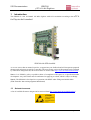
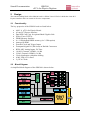
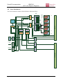
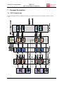
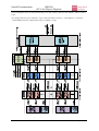
SIS Documentation
SIS8300
µTCA 16-bit Digitizer
SIS8300
µTCA FOR PHYSICS Digitizer
User Manual
SIS GmbH
Harksheider Str. 102A
22399 Hamburg
Germany
Phone: ++49 (0) 40 60 87 305 0
Fax:
++49 (0) 40 60 87 305 20
email: [email protected]
http://www.struck.de
Version: SIS8300-M-1402-1-V105.doc as of 17.10.2013
Page 1 of 67
SIS Documentation
SIS8300
uTCA for Physics
Digitizer
Revision Table:
Revision
1.00
Date
02.01.2012
1.01
1.02
1.03
13.01.2012
16.03.2012
28.09.2012
1.04
19.12.2012
1.05
17.10.2013
Page 2 of 67
Modification
Based on SIS8300-M-1102-2-V211
Firmware: V1400
- add „Firmware Option register“
- add Memory Histogramming Feature
- add Harlink Connector Output Test Mode
- add SIS8900 RTM LVDS Test I/O Control register
Added DMA register description, fixed reset register descr.
Fix of broken reference
FW: v1401
- add IRQ register description
- add DAQ done IRQ
- add DAQ done DMA start signal chain
- add RAM FIFO debug register
FW: v1402
- fixed MLVDS Bit7 Trigger enable bit
- added Register 0x205 bit0 for byte swapped sample
readout
Fixed Sample Length Register description
Added Firmware upgrade description
SIS Documentation
SIS8300
µTCA 16-bit Digitizer
- Table of contents
1
2
3
4
5
6
7
Table of contents....................................................................................................................................... 3
Introduction .............................................................................................................................................. 5
1.1
Related documents............................................................................................................................. 5
Design ...................................................................................................................................................... 6
2.1
Functionality ..................................................................................................................................... 6
2.2
Block Diagram .................................................................................................................................. 6
2.3
Platform Management........................................................................................................................ 7
2.4
Clock Distribution ............................................................................................................................. 8
Jumper/Connector Pin Assignments........................................................................................................... 9
3.1
CON100 JTAG.................................................................................................................................. 9
3.2
J604 Watchdog Reset......................................................................................................................... 9
3.3
J32 AVR JTAG ................................................................................................................................. 9
LEDs ...................................................................................................................................................... 10
4.1
AMC LEDs ..................................................................................................................................... 10
4.2
Front Panel LEDs ............................................................................................................................ 10
4.3
SMD LEDs...................................................................................................................................... 10
Front panel.............................................................................................................................................. 11
5.1
Harlink LVDS In-/Outputs............................................................................................................... 12
5.2
SMA Clock Input ........................................................................................................................... 12
5.3
SFP Card Cage ................................................................................................................................ 12
Board Layout .......................................................................................................................................... 13
Firmware Description.............................................................................................................................. 14
7.1
ADC Sample Logic ......................................................................................................................... 14
7.2
Memory Interface ............................................................................................................................ 16
7.2.1
Memory Write Interface ........................................................................................................... 17
7.2.2
Memory Histogram Interface.................................................................................................... 18
7.3
Memory buffer ................................................................................................................................ 19
7.4
Address Map ................................................................................................................................... 20
7.5
Register description ......................................................................................................................... 22
7.5.1
Module Id. and Firmware Revision register .............................................................................. 22
7.5.2
Serial Number register.............................................................................................................. 22
7.5.3
XILINX JTAG register ............................................................................................................ 23
7.5.4
XILINX Virtex5 Error Detection register.................................................................................. 23
7.5.5
User Control/Status register..................................................................................................... 24
7.5.6
Firmware Options register ........................................................................................................ 25
7.5.7
ADC Acquisition Control/Status register ................................................................................. 26
7.5.8
ADC Sample Control register................................................................................................... 27
7.5.9
MLVDS Input/Output Control register ..................................................................................... 28
7.5.10 Harlink Connector Input/Output Control register ...................................................................... 29
7.5.11 Clock Distribution Multiplexer control register......................................................................... 30
7.5.12 Clock Distribution AD9510 Serial Interface (SPI) interface register (0x41, read/write).............. 32
7.5.13 Clock Multiplier IC SI5326 SPI interface register .................................................................... 34
7.5.14 DAC Control register ............................................................................................................... 35
7.5.15 DAC Data register.................................................................................................................... 35
7.5.16 ADC Serial Interface (SPI) interface register ............................................................................ 36
7.5.17 ADC Input Tap delay registers (0x49) ...................................................................................... 37
7.5.18 Virtex 5 System Monitor registers ............................................................................................ 37
7.5.19 Trigger registers....................................................................................................................... 38
7.5.20 Memory Sample Start Address / Actual Sample Address registers............................................. 41
7.5.21 Sample Length register............................................................................................................. 42
7.5.22 Ringbuffer Delay register ......................................................................................................... 42
7.5.23 Test Histogram Pattern-Memory Address register..................................................................... 43
7.5.24 Test Histogram Pattern-Memory Data Write register................................................................. 43
7.5.25 Test Histogram Control register................................................................................................ 44
7.5.26 SIS8900 RTM LVDS Test Input/Output Control register .......................................................... 45
7.5.27 Read DMA System Destination address (lower 32bits) ............................................................. 46
Page 3 of 67
SIS Documentation
SIS8300
uTCA for Physics
Digitizer
7.5.28 Read DMA System Destination address (upper 32bits) ............................................................. 46
7.5.29 Read DMA Card Memory Source address ................................................................................ 46
7.5.30 Read DMA Transfer length ...................................................................................................... 47
7.5.31 Read DMA Control.................................................................................................................. 47
7.5.32 Readout DMA Sample byte swap ............................................................................................. 47
7.5.33 Write DMA System Source address (lower 32bits) ................................................................... 48
7.5.34 Write DMA System Source address (upper 32bits) ................................................................... 48
7.5.35 Write DMA Card Memory Destination address......................................................................... 48
7.5.36 Write DMA Transfer length ..................................................................................................... 49
7.5.37 Write DMA Control ................................................................................................................. 49
7.5.38 DAQ Done DMA Chain Control .............................................................................................. 50
7.5.39 IRQ Enable.............................................................................................................................. 50
7.5.40 IRQ Status ............................................................................................................................... 51
7.5.41 IRQ Clear ................................................................................................................................ 51
7.5.42 IRQ Refresh............................................................................................................................. 51
7.5.43 RAM FIFO debug register........................................................................................................ 52
7.6
External register interface ................................................................................................................ 53
7.7
User Blockram DMA Interface ........................................................................................................ 55
7.8
User Interrupt Interface.................................................................................................................... 55
8 RTM management................................................................................................................................... 56
9 Firmware upgrade ................................................................................................................................... 57
9.1
Create programming file .................................................................................................................. 57
9.2
Create PROM file............................................................................................................................ 58
9.3
Program FPGA................................................................................................................................ 59
10
Appendix ............................................................................................................................................ 61
10.1 Power Consumption......................................................................................................................... 61
10.2 Ordering options.............................................................................................................................. 61
10.3 RTM/Zone 3 connectors J75 and J76 ............................................................................................... 62
10.3.1 J75 connector pin assignments.................................................................................................. 62
10.3.2 J76 connector pin assignments.................................................................................................. 63
10.3.3 Note on AC/DC input stage selection........................................................................................ 63
10.4 RTM connector schematics.............................................................................................................. 65
11
Index................................................................................................................................................... 66
Page 4 of 67
SIS Documentation
1
SIS8300
µTCA 16-bit Digitizer
Introduction
The SIS8300 is a ten 10 channel 125 MS/s digitizer with 16-bit resolution according to the
for Physics draft standard.
uTCA
SIS8300 with SFPs installed
As we are aware, that no manual is perfect, we appreciate your feedback and will incorporate proposed
changes and corrections as quickly as possible. The most recent version of this manual can be obtained
by email from [email protected], the revision dates are online under http://www.struck.de/manuals.html .
Note 1: It is PICMG‘s policy to prohibit claims of compliance with respect to a specification under
development. Any such claims must be understood as applying to a draft, which is subject to change
Note 2: The SIS8300 is developed in co-operation with DESY under ZIM grant 2460101MS9
(ZIM: Zentrales Innovationsprogramm Mittelstand)
1.1 Related documents
A list of available firmware designs can be retrieved from http://www.struck.de/sis8300firm.html
Page 5 of 67
Struck Documentation
2
SIS8300
uTCA for Physics Digitizer
Design
The central building block of the SIS8300 card is a Xilinx Virtex 5 FPGA. It holds the 4 lane PCI
Express interface and is in control of all active components.
2.1 Functionality
The key properties of the SIS8300 card are listed below.
AMC .4 µTCA for Physics Board
4 Lane PCI Express Interface
Dual SFP Card Cage for optional Multi Gigabit Link
Xilinx Virtex 5 FPGA
DDR2 Memory Interface
4 x 1 GBit default DDR2 memory (4 x 2 GBit option)
Atmega128 IPMI
External Clock and Trigger Inputs
Frontpanel digital I/O (4in/4 out) on Harlink Connectors
RTM ADC Analog Inputs, I2C-Bus
10 ADC Channels 125MS/s, 16-Bit
2 DAC Channels 250MS/s, 16-Bit
Clock distribution with phase shifting
4 M-LVDS µTCA Ports
2 µTCA Clocks
2.2 Block Diagram
A simplified block diagram of the SIS8300 is shown below.
Page 6 of 67
Struck Documentation
2.3
SIS8300
uTCA for Physics Digitizer
Platform Management
The management code of the SIS8300 is implemented in an Atmel Atmega1281-16MU
microcontroller and can be upgrade in field over connector J32 (see section 3.3).
Page 7 of 67
Struck Documentation
SIS8300
uTCA for Physics Digitizer
2.4 Clock Distribution
The clock distribution scheme of the SIS8300 is illustrated below.
#2
2
0
MUX C
1
MUX E
1
3
3
2
0
ADCLK925
ADCLK925
MUX A
MUX B
1
2
0
3
1
2
Ch9
T
ADC
ADC
T
FPGA
CLK05
ADC
ADC
T
T
#1
3
ADC
ADC
µRTM
SI5324
AD9510
0
1
FPGA
CLK69
AD9510
MUX D
3
2
ADC
ADC
ADC
ADC
Ch1
Ch0
0
RTM_CLK0
RTM_CLK2
CLK1
CLK2
Backplane
ADCLK925
ADCLK946
ADCLK925
ADCLK925
ADCLK946
EXTCLKB
HARLINK
ADCLK925
Quartz
EXTCLKA
SMA
RTM_CLK1
Page 8 of 67
Struck Documentation
SIS8300
uTCA for Physics Digitizer
3 Jumper/Connector Pin Assignments
The following subsections describe the pin assignments of jumpers and connectors.
3.1 CON100 JTAG
The SIS8300’s on board logic can load its firmware from a serial PROM, via the JTAG port
on connector CON100, PCI Express or via the MMC.
Hardware like the XILINX HW-USB-JTAG in connection with the appropriate software will
be required for in field JTAG firmware upgrades.
CON100 is a 2mm (i.e. metric) 14 pin header that allows you to reprogram the firmware of
the SIS8300 board with a JTAG programmer. The pin out is shown in the schematic below. It
is compatible with the cable that comes with the XILINX HW-USB-II-G-JTAG platform
cable. CON100 can be found at the right bottom side of the board.
Note 1: The board has to be powered for reprogramming over JTAG
Note 2: The FPGA uses 8-bit parallel mode to load the firmware from the serial PROM.
Make sure to check the 'Parallel Load' box in Impact when specifying the programming
properties for the PROM.
3.2 J604 Watchdog Reset
J604 can be found next to the left upper edge of U500 (largest chip on the card). With J604
closed the boards watchdog reset is connected to the reset logic. J604 should be opened for
JTAG firmware programming.
3.3 J32 AVR JTAG
This 10-pin header is used to connect to the JTAG of the Atmel Atmega128 microcontroller
providing the IPMI/MCH functionality of the SIS8300.
Page 9 of 67
Struck Documentation
SIS8300
uTCA for Physics Digitizer
4 LEDs
4.1 AMC LEDs
The AMC LEDs are implemented according to the standard.
4.2 Front Panel LEDs
The SIS8300 in Gigalink stuffing option has 4 green front panel LEDs.
LED name
A
U
L1
L2
Function in Gigalink design
PCI Express Access
User LED
PCIe Link up
ADC Sampling active
4.3 SMD LEDs
A number of surface mount red LEDs are on the SIS8300 to visualize part of the board status.
LED designator
D20A
LED comment
S1
D20B
S2
D20C
D20D
D20E
D20F
D20G
D20H
D21D
D105A
D105B
D110A
D110B
S3
S4
S5
S6
S7
S8
READY
TX FAULT 1
RX LOS 1
TX FAULT 2
RX LOS 2
Page 10 of 67
Function
Firmware dependent
(Optical Link 1 up in 0x1102)
Firmware dependent
(Optical Link 2 up in 0x1102)
Firmware dependent
Firmware dependent
Firmware dependent
Firmware dependent
Firmware dependent
Firmware dependent
FPGA ready
Link 1 transmitter fault
Link 1 receiver loss of signal
Link 2 transmitter fault
Link 2 receiver loss of signal
Struck Documentation
SIS8300
uTCA for Physics Digitizer
5 Front panel
The SIS8300 is a µTCA for Physics board. A sketch of the front panel is shown below.
Page 11 of 67
Struck Documentation
SIS8300
uTCA for Physics Digitizer
5.1 Harlink LVDS In-/Outputs
The Harlink LVDS Output and Input connectors have 5 signals each. The Clock signal to the
left hand side is marked with C and the other 4 signals are labelled with 1-4.
Top
Bottom
Clock
P
N
1
P
N
2
P
N
3
P
N
4
P
N
5.2 SMA Clock Input
The front panel SMA clock input is designed to accept a maximum peak to peak signal level
of 3V into 50 Ohms. The clock input signal is coupled to the internal logic via a capacitor.
The schematic of the input stage is shown below.
5.3 SFP Card Cage
The dual card cage can host two SFP link media.
They can be enabled in the sis8300top.vhd VHDL code as shown below (and are active in the
0x1102 firmware design e.g.):
DUAL_OPTICAL_INTERFACE_EN
: integer := 1 ; --
Communication is handled through registers 0x14 to 0x17 (refer to the VHDL code)
Page 12 of 67
Struck Documentation
SIS8300
uTCA for Physics Digitizer
6 Board Layout
A print of the silk screen of the component side is shown below.
Connector types
The used connectors are listed in the table below.
Designator
CON100
CON200
CON301
CON302
CAGE105
J10
J32
J75
J76
J77
J209
J205
J604
Function
JTAG
Clock In
DAC 1 Out
DAC 2 Out
SFP Cage, 2 Ports
AdvancedMC
JTAG Atmega
RTM
RTM
RTM Keying
Trigger & Clock Out
Trigger & Clock In
Watchdog
Manufacturer
Molex
JYEBAO
JYEBAO
JYEBAO
TYCO
HARTING
SAMTEC
ERNI
ERNI
TYCO
HARTING
HARTING
SAMTEC
Part Number
87831-1420
SMA8400A1-9000
SMA8400A1-9000
SMA8400A1-9000
1761014-1
16211701301000
HTSW-105-26-G-D
ERmetZD-10x3P-FEM
ERmetZD-10x3P-FEM
(*)
27 21 121 8000
27 21 121 8000
HTSW-102-26-G-S
Note (*): The used Key may depend on the hardware configuration of the SIS8300
Page 13 of 67
Struck Documentation
SIS8300
uTCA for Physics Digitizer
7 Firmware Description
7.1 ADC Sample Logic
The block diagram shows the ADC data handling. Each ADC channel has its own Memory Address Control
Logic.
Page 14 of 67
Struck Documentation
SIS8300
uTCA for Physics Digitizer
The block diagram shows the ADC data handling. Two ADC channels share the same Memory Address Control
Logic.
The “Single-Channel Copy-To-Memory” Logic needs more FPGA resources ( +2500 Registers, +700 Slices,
+10 BlockRams) than the “Dual-Channel Copy-To-Memory” Logic.
Page 15 of 67
Struck Documentation
SIS8300
uTCA for Physics Digitizer
7.2 Memory Interface
The “sis_ddr2_interface_with_histogramming” provides the user logic with the possibility to
write to the Memory and to increment (histogram) the content of 32-bit memory values.
sis_ddr2_interface
DDR2 Memory
Read Interface
Data Fifo
512 x 128
PCIe DMA Interface
Address Fifo
512 x 32
Write Interface
sis_write_addr_fifo_wr_en
sis_write_64bit_addr_fifo_din
protocol
Address Fifo
512 x 32
sis_write_addr_fifo_wr_count
512 MByte
(64M x 64 bit)
or
addr
1 GByte
(128M x 64 bit)
sis_write_data_fifo_wr_en
sis_write_data_fifo_din
data
Data Fifo
1023 x 128
sis_write_data_fifo_wr_count
Histogram Interface
sis_write_histo_addr_fifo_wr_en
sis_write_histo_32bit_addr_fifo_din
Address Fifo
512 x 32
sis_write_histo_addr_fifo_wr_count
User Interface block diagram for Memory read, write and histogram operations.
Page 16 of 67
Struck Documentation
SIS8300
uTCA for Physics Digitizer
7.2.1 Memory Write Interface
The Write Interface consists of the following signals:
sis_write_fifo_wr_clk : in std_logic;
-- data: write fifo
sis_write_data_fifo_wr_en : in std_logic;
sis_write_data_fifo_din : in std_logic_vector(127 downto 0);
sis_write_data_fifo_wr_count : out std_logic_vector(9 downto 0);
-- address: write fifo
sis_write_addr_fifo_wr_en : in std_logic;
sis_write_64bit_addr_fifo_din : in std_logic_vector(31 downto 0);
sis_write_addr_fifo_wr_count : out std_logic_vector(9 downto 0) ;
A write cycle to the memory consists of one write command to the Address Fifo and two
write commands to the Data Fifo.
One write command to the Address FIFO:
a valid “sis_write_addr_fifo_wr_en” signal over one clock period
(sis_write_fifo_wr_clk) along with “sis_write_64bit_addr_fifo_din”.
Two write commands to the Data FIFO:
a valid “sis_write_data_fifo_wr_en” signal over two clock periods
(sis_write_fifo_wr_clk) along with “sis_write_data_fifo_din”.
When issuing a write command to the Address Fifo, the second write command to the Data
Fifo must be issued no more than one clock cycle later.
It is only allowed to write to the Address-FIFO, if “sis_write_addr_fifo_wr_count” is
lower than X”1FF” (not full).
It is only allowed to write to the Data-FIFO, if “sis_write_data_fifo_wr_count” is lower
than X”3FE” (not full).
The Memory Controller writes with one “write cycle” 256 bits (4 x 64 bits) to the Memory.
Therefore the lower 2 address bits of the written 64-bit address must be 0 and the “next
address” will be incremented by 4.
Page 17 of 67
Struck Documentation
SIS8300
uTCA for Physics Digitizer
7.2.2 Memory Histogram Interface
The Histogram Interface consists of the following signals:
-- Histogramming
-- address: write fifo
sis_write_histo_addr_fifo_clr: in std_logic;
sis_write_histo_addr_fifo_wr_clk: in std_logic;
sis_write_histo_addr_fifo_wr_en: in std_logic;
sis_write_histo_32bit_addr_fifo_din: in std_logic_vector(31 downto 0);
sis_write_histo_addr_fifo_wr_count: out std_logic_vector(9 downto 0) ;
A write command to the Histogram Address Fifo will increment by one the content of the 32bit Memory value addressed with the written 32-bit Memory Address.
It is only allowed to write to the Histo-Address-FIFO, if
“sis_write_histo_addr_fifo_wr_count” is lower than X”1FF” (not full).
The histogramming memory controller supports an update rate of 5MHz (20 MHz within one
2K memory page amid differing three lowest order bits).
Page 18 of 67
Struck Documentation
SIS8300
uTCA for Physics Digitizer
7.3 Memory buffer
The structure of the memory buffer with 512 MByte (i.e. 4 x 1 GBit memory chips) is
illustrated below.
512 MByte : 4 x 64M x 16bit = 256M x 16bit = 32M x 128bit = 16M x 256bit
Memory 256-bit
Block Addresses
0 x 00 0000
Memory 64-bit
Addresses
Memory 32-bit
Addresses
Memory 16-bit
Addresses
(4 x 256-bit Address)
(8 x 256-bit Address)
(16 x 256-bit Address)
(32 x 256-bit Address)
0 x 000 0000
0 x 000 0000
0 x 0000 0000
0 x 0000 0000
0 x 0000 0001
0 x 0000 0001
..
..
0 x 0000 000E
0 x 0000 001E
0 x 0000 000F
0 x 0000 001F
0 x 0800 0006
0 x 1000 000E
0 x 0800 0007
0 x 1000 000F
0 x 00 0001
0 x 000 0001
0 x 00 0002
0 x 000 0002
..
0 x 7F FFFF
0 x 80 0000
0 x 80 0001
0 x 80 0002
0 x 000 0003
..
0 x 200 0000
0 x FF FFFF
..
0 x 000 0006
0 x 000 0007
..
0 x 200 0001
0 x 400 0002
0 x 200 0002
0 x 400 0003
0 x 200 0003
..
..
0 x 000 0001
0 x 3FF FFFC
0 x 3FF FFFD
..
0 x 7FF FFF8
0 x 7FF FFF9
..
0 x 3FF FFFE
0 x 7FF FFFE
0 x 3FF FFFF
0 x 7FF FFFF
..
Memory 8-bit (byte)
Addresses
..
..
..
0 x 0FFF FFF0
0 x 1FFF FFE0
0 x 0FFF FFF1
0 x 1FFF FFE1
..
..
0 x 0FFF FFFE
0 x 1FFF FFFE
0 x 0FFF FFFF
0 x 1FFF FFFF
The structure of the memory buffer with 1 GByte (i.e. 4 x 2 GBit memory chips) is illustrated
below.
Page 19 of 67
Struck Documentation
SIS8300
uTCA for Physics Digitizer
7.4
Address Map
Following 32-bit addresses are implemented
Offset
0x00
0x01
0x02
0x03
Access
R
R
R/W
R
0x04
0x05
R/W
R
User Control/Status register (JK)
Firmware Options register
0x10
0x11
0x12
0x13
R/W
R/W
R/W
R/W
ADC Acquisition Control/Status register
ADC Sample Control register
MLVDS Input/Output Control register
Harlink Connector Input/Output Control register
0x14
0x15
0x16
0x17
R/W
R/W
R/W
R/W
Link 1 data FIFO (refer to VHDL code)
Link 1 set control (refer to VHDL code
Link 2 data FIFO (refer to VHDL code
Link 2 set control (refer to VHDL code
0x40
0x41
0x42
R/W
R/W
R/W
Clock Distribution Multiplexer control register
Clock Distribution IC AD9510 SPI interface register
Clock Multiplier IC SI5326 SPI interface register
0x44
0x45
0x46
R/W
R/W
R/W
reserved
DAC Control register
DAC Data register
0x48
0x49
R/W
R/W
ADC SPI Interface register
ADC Input Tap delay register
0x90
0x91
0x92
R/W
R/W
R/W
VIRTEX5_SYSTEM_MONITOR_DATA register
VIRTEX5_SYSTEM_MONITOR_ADDR register
VIRTEX5_SYSTEM_MONITOR_CTRL register
0xFF
0x100
0x101
..
..
0x109
W
R/W
R/W
Bit 0 = 1:
Master Reset (reset all registers)
ADC ch1 Trigger Setup register
ADC ch2 Trigger Setup register
..
..
ADC ch10 Trigger Setup register
0x110
0x111
..
0x119
R/W
R/W
0x120
Page 20 of 67
R/W
Function
Module Identifier/Firmware Version register
Serial number register
XILINX JTAG register
XILINX Virtex5 configuration memory Error Detection register
R/W
ADC ch1 Trigger Threshold register
ADC ch2 Trigger Threshold register
..
ADC ch10 Trigger Threshold register
R/W
ADC ch1 Memory Sample Start Address / Actual Address register
Struck Documentation
SIS8300
uTCA for Physics Digitizer
0x121
..
0x129
R/W
R/W
ADC ch2 Memory Sample Start Address / Actual Address register
..
ADC ch10 Memory Sample Start Address / Actual Address register
0x12A
0x12B
R/W
R/W
ADC chx Sample Length register
ADC chx Ringbuffer Delay register (0 to 2046)
0x12C
0x12D
0x12E
0x12F
R/W
R/W
R/W
R/W
Test Histogram Pattern-Memory Address register
Test Histogram Pattern-Memory Data Write register
Test Histogram Control register
SIS8900 RTM LVDS Test Input/Output Control register
0x200
0x201
0x202
0x203
0x204
0x205
R/W
R/W
R/W
R/W
R/W
R/W
DMA_READ_DST_ADR_LO32
DMA_READ_DST_ADR_HI32
DMA_READ_SRC_ADR_LO32
DMA_READ_LEN
DMA_READ_CTRL
DMA Readout Sample byte swap control
0x210
0x211
0x212
0x213
0x214
0x216
0x220
0x221
0x222
0x223
0x230
0x231
0x400
R/W
R/W
R/W
R/W
R/W
R/W
R/W
R
W
KA
R/W
R/W
R/W
DMA_WRITE_SRC_ADR_LO32
DMA_WRITE_SRC_ADR_HI32
DMA_WRITE_DST_ADR_LO32
DMA_WRITE_LEN
DMA_WRITE_CTRL
DAQ Auto DMA Chain Control
IRQ Enable
IRQ Status
IRQ Clear
IRQ Refresh
MEMORY test Mode register
RAM FIFO debug register
Mapped out of register bank to top level. May be used for user defined
register implementation. See Section 7.6.
...
...
0x4FF
R/W
Page 21 of 67
Struck Documentation
SIS8300
uTCA for Physics Digitizer
7.5 Register description
7.5.1 Module Id. and Firmware Revision register
#define SIS8300_IDENTIFIER_VERSION_REG
0x00
This register holds the module identifier (SIS8300) and the firmware version and revision.
BIT access Name
31-16 RO
Function
Module Identifier
0x8300
Firmware Version
1..255
Firmware Revision
1..255
FFFF0000
15-8 RO
0000FF00
7-0 RO
000000FF
Example: The initial version of the SIS8300 reads 0x83001400
7.5.2 Serial Number register
#define SIS8300_SERIAL_NUMBER_REG
0x01
This register holds the Serial Number of the module.
BIT access Name
31-16 RO
Function
reserved
FFFF0000
15-0 RO
0000FFFF
Page 22 of 67
Serial Number
1..65535
Struck Documentation
SIS8300
uTCA for Physics Digitizer
7.5.3 XILINX JTAG register
#define SIS8300_XILINX_JTAG_REG
0x02
This register is used in the firmware upgrade process over PCIe only. A TCK is generated
upon a write cycle to this register.
Bit
31
30
...
4
3
2
1
0
write Function
none
...
...
none
none
none
TMS
TDI
read Function
TDO
1 x Shifted TDO
30 x Shifted TDO
The read register function operates as a shift register for TDO. The content of the read register
is shifted to the right by one bit with every positive edge of TCK and the status of TDO is
transferred to Bit 30. Bit 31 reflects the current value of TDO during a read access.
7.5.4 XILINX Virtex5 Error Detection register
#define SIS8300_XILINX_ECC_REG
0x03
XILINX Virtex5 configuration memory error detection register.
Bit
31
30
...
16
15
14
13
12
11
..
1
0
read Function
0
0
0
Frame ECC output indicating a valid SYNDROME value
0
CRC Error
ECC Error
SYNDROME: Status bit 11
SYNDROME: Status bit 1
SYNDROME: Status bit 0
Page 23 of 67
Struck Documentation
SIS8300
uTCA for Physics Digitizer
7.5.5 User Control/Status register
#define SIS8300_USER_CONTROL_STATUS_REG
0x04
The control register is implemented as a selective J/K register, a specific function is enabled
by writing a 1 into the set/enable bit, the function is disabled by writing a 1 into the
clear/disable bit (which location is 16-bit higher in the register). An undefined toggle status
will result from setting both the enable and disable bits for a specific function at the same
time. The only function at this point in time is user LED on/off.
On read access the same register represents the status register.
Bit
31
30
29
28
27
26
25
24
23
22
21
20
19
18
17
16
15
14
13
12
11
10
9
8
7
6
5
4
3
2
1
0
write Function
Clear reserved 15 (*)
Clear reserved 14 (*)
Clear reserved 13 (*)
Clear reserved 12 (*)
Clear reserved 11 (*)
Clear reserved 10 (*)
Clear reserved 9 (*)
Clear reserved 8 (*)
Clear reserved 7 (*)
Clear reserved 6 (*)
Clear reserved 5 (*)
Clear reserved 4 (*)
Clear reserved 3 (*)
Clear reserved 2 (*)
Switch off LED test
Switch off user LED (*)
Set reserved 15
Set reserved 14
Set reserved 13
Set reserved 12
Set reserved 11
Set reserved 10
Set reserved 9
Set reserved 8
Set reserved 7
Set reserved 6
Set reserved 5
Set reserved 4
Set reserved 3
Set reserved 2
Switch on LED test
Switch on user LED
(*) denotes power up default setting
Page 24 of 67
read Function
0
0
0
0
0
0
0
0
0
0
0
0
0
0
0
0
Status reserved 15
Status reserved 14
Status reserved 13
Status reserved 12
Status reserved 11
Status reserved 10
Status reserved 9
Status reserved 8
Status reserved 7
Status reserved 6
Status reserved 5
Status reserved 4
Status reserved 3
Status reserved 2
Status LED test
Status User LED (1=LED on, 0=LED off)
Struck Documentation
SIS8300
uTCA for Physics Digitizer
7.5.6 Firmware Options register
#define SIS8300_FIRMWARE_OPTIONS_REG
0x05
This register holds the information of the Xilinx firmware option features.
Bit
31
30
...
16
15
14
13
12
11
10
9
8
7
6
5
4
3
2
1
0
read Function
reserved
...
...
reserved
reserved
reserved
reserved
reserved
reserved
reserved
reserved
FPGA_SX_1GByte Memory
reserved
DUAL_OPTICAL_INTERFACE_EN
DUAL_PORT14_15_INTERFACE_EN
DUAL_PORT12_13_INTERFACE_EN
none
DUAL_CHANNEL_SAMPLING
RINGBUFFER_DELAY_EN
TRIGGER_BLOCK_EN
FPGA_SX_1GByte Memory = 0 : Virtex 50LX50T and 512 MByte Memory
FPGA_SX_1GByte Memory = 1 : Virtex 50SX50T and 1 GByte Memory
Page 25 of 67
Struck Documentation
SIS8300
uTCA for Physics Digitizer
7.5.7 ADC Acquisition Control/Status register
#define SIS8300_ACQUISITION_CONTROL_STATUS_REG
Bit
31
..
..
8
7
6
5
4
3
2
1
0
write
‘1’ : Disable Sampling
(Reset Sample Logic)
‘1’ : Arm Sampling
(Start with next trigger)
‘1’ : Start Sampling immediately
(Arm and Start/Trigger)
The power up default value is 0x0
Page 26 of 67
0x10
read
0
0
0
0
Status: DDR2 Memory Init OK
0
Status: internal Sample Logic Buffer FIFO
Not Empty
Status: internal Sample Logic Busy
0
0
Status: Arm for trigger
(Wait for trigger)
Status: Sampling Busy
Struck Documentation
SIS8300
uTCA for Physics Digitizer
7.5.8 ADC Sample Control register
#define SIS8300_SAMPLE_CONTROL_REG
0x11
ADC channels can be disabled from storing data to memory by setting the corresponding
disable bit in this register.
Bit
31
...
...
12
11
10
9
8
7
6
5
4
3
2
1
0
write
Enable external Trigger
Enable internal Trigger
Disable Sampling Ch10
Disable Sampling Ch9
Disable Sampling Ch3
Disable Sampling Ch2
Disable Sampling Ch1
The power up default value is 0x0
Page 27 of 67
Struck Documentation
SIS8300
uTCA for Physics Digitizer
7.5.9 MLVDS Input/Output Control register
#define SIS8300_MLVDS_IO_CONTROL_REG
Bit
31
30
..
25
24
23
22
...
17
16
15
14
...
9
8
7
6
...
1
0
0x12
Write
Enable LVDS Output Bit 7
Enable LVDS Output Bit 6
Read
Enable LVDS Output Bit 7
Enable LVDS Output Bit 6
Enable LVDS Output Bit 1
Enable LVDS Output Bit 0
LVDS Output Bit 7
LVDS Output Bit 6
Enable LVDS Output Bit 1
Enable LVDS Output Bit 0
LVDS Output Bit 7
LVDS Output Bit 6
LVDS Output Bit 1
LVDS Output Bit 0
LVDS Input 7 External Trigger Enable
LVDS Input 6 External Trigger Enable
LVDS Output Bit 1
LVDS Output Bit 0
LVDS Input 7 External Trigger Enable
LVDS Input 6 External Trigger Enable
LVDS Input 1 External Trigger Enable
LVDS Input 0 External Trigger Enable
LVDS Input 7 External Trigger falling edge
LVDS Input 6 External Trigger falling edge
LVDS Input 1 External Trigger Enable
LVDS Input 0 External Trigger Enable
LVDS Input Bit 7
LVDS Input Bit 6
LVDS Input 1 External Trigger falling edge LVDS Input Bit 1
LVDS Input 0 External Trigger falling edge LVDS Input Bit 0
Note: external trigger in signals are synchronized with the FPGA CLK05
Page 28 of 67
Struck Documentation
SIS8300
uTCA for Physics Digitizer
7.5.10 Harlink Connector Input/Output Control register
#define SIS8300_HARLINK_IO_CONTROL_REG
Bit
31
30
..
21
20
19
18
17
16
15
14
13
12
11
10
9
8
7
6
5
4
3
2
1
0
0x13
Write
No function
No function
Read
0
0
No function
Harlink Test Output Enable
Harlink Test Output 4 (*)
Harlink Test Output 3 (*)
Harlink Test Output 2 (*)
Harlink Test Output 1 (*)
Harlink Input 4 External Trigger falling edge
Harlink Input 3 External Trigger falling edge
Harlink Input 2 External Trigger falling edge
Harlink Input 1 External Trigger falling edge
Harlink Input 4 External Trigger Enable
Harlink Input 3 External Trigger Enable
Harlink Input 2 External Trigger Enable
Harlink Input 1 External Trigger Enable
No function
No function
No function
No function
No function
No function
No function
No function
0
Harlink Test Output Enable
Harlink Test Output 4
Harlink Test Output 3
Harlink Test Output 2
Harlink Test Output 1
Harlink Input 4 External Trigger falling edge
Harlink Input 3 External Trigger falling edge
Harlink Input 2 External Trigger falling edge
Harlink Input 1 External Trigger falling edge
Harlink Input 4 External Trigger Enable
Harlink Input 3 External Trigger Enable
Harlink Input 2 External Trigger Enable
Harlink Input 1 External Trigger Enable
0
0
0
0
Harlink Input 4
Harlink Input 3
Harlink Input 2
Harlink Input 1
(*): only if “Harlink Test Output Enable” = 1
(**): only if “Harlink Test Output Enable” = 0
Harlink Connector Input(1) : external trigger In
Harlink Connector Output(1) : adc chx (or) trigger out (**)
Note: external trigger in signals are synchronized with the FPGA CLK05
Page 29 of 67
Struck Documentation
SIS8300
uTCA for Physics Digitizer
7.5.11 Clock Distribution Multiplexer control register
#define SIS8300_CLOCK_DISTRIBUTION_MUX_REG
0x40
The SIS8300 has 5 IDT ICS853S057 clock multiplexer chips, which are labelled A to E in the
clock distribution schematic in section 2.4. The multiplexer control register holds the two
select bits for the 5 multiplexer chips as shown in the table below.
The assignment of the inputs to the resources (i.e. clock inputs) is listed in subsection
7.5.11.1.
BIT access Name
31-12 R/W
Function
reserved
no
MUXE_SEL
Multiplexer E select bits
MUXD_SEL
Multiplexer D select bits
reserved
no
MUXC_SEL
Multiplexer C select bits
MUXB_SEL
Multiplexer B select bits
MUXA_SEL
Multiplexer A select bits
FFFFF000
11-10 R/W
00000C00
9-8 R/W
00000300
7-6 R/W
000000C0
5-4 R/W
00000030
3-2 R/W
0000000C
1-0 R/W
00000003
Page 30 of 67
Struck Documentation
7.5.11.1
SIS8300
uTCA for Physics Digitizer
Multiplexer A Input Signals:
U222 - Sel0 and Sel1 (MUX1A_SEL) = Multiplexer A select lines
Sel1
0
0
1
1
Sel0
0
1
0
1
7.5.11.2
Selected Input - Net Name
RTMCLK_0
TCLKB_0
TCLKA_0
OSC_CLK0
Clock source Description
Clock 2 from µRTM card
Clock 2 (Telecom Clock B) from AMC Connector (Backplane)
Clock 1 (Telecom Clock A) from AMC Connector (Backplane)
Onboard Clock chip (250MHz)
Multiplexer B Input Signals:
U223 - Sel0 and Sel1 (MUX1B_SEL) = Multiplexer B select lines
Sel1
0
0
1
1
Sel0
0
1
0
1
7.5.11.3
Selected Input - Net Name
RTMCLK_1
TCLKB_1
TCLKA_1
OSC_CLK1
Clock source Description
Clock 2 from µRTM card
Clock 2 (Telecom Clock B) from AMC Connector (Backplane)
Clock 1 (Telecom Clock A) from AMC Connector (Backplane)
Onboard Clock chip (250MHz)
Multiplexer C Input Signals:
U240 - Sel0 and Sel1 (MUXAB_SEL) = Multiplexer C select lines
Sel1
0
0
1
1
Sel0
0
1
0
1
7.5.11.4
Selected Input - Net Name
EXT_CLKB0
EXT_CLKA0
MUXA_CLK1
MUXB_CLK1
Clock source Description
Clock from Harlink Connector “CI1-4 IN” (frontpanel)
Clock from SMA Connector “CLK IN” (frontpanel)
Multiplexer A Output Signal
Multiplexer B Output Signal
Multiplexer D Input Signals:
U250 - Sel0 and Sel1 (MUX2A_SEL) = Multiplexer D select lines
Sel1
0
0
1
1
Sel0
0
1
0
1
7.5.11.5
Selected Input - Net Name
MUXA_CLK0
MUL_CLK1
EXT_CLKB1
EXT_CLKA1
Clock source Description
Multiplexer A Output Signal
Clock Multiplier (U242) Output 2 Signal
Clock from Harlink Connector “CI1-4 IN” (frontpanel)
Clock from SMA Connector “CLK IN” (frontpanel)
Multiplexer E Input Signals:
U251 - Sel0 and Sel1 (MUX2B_SEL) = Multiplexer E select lines
Sel1
0
0
1
1
Sel0
0
1
0
1
Selected Input - Net Name
MUXB_CLK0
MUL_CLK0
EXT_CLKB2
EXT_CLKA2
Clock source Description
Multiplexer B Output Signal
Clock Multiplier (U242) Output 1 Signal
Clock from Harlink Connector “CI1-4 IN” (frontpanel)
Clock from SMA Connector “CLK IN” (frontpanel)
Page 31 of 67
Struck Documentation
SIS8300
uTCA for Physics Digitizer
7.5.12 Clock Distribution AD9510 Serial Interface (SPI) interface register (0x41,
read/write)
#define SIS8300_AD9510_SPI_REG
0x41
The parameters of the Clock Distribution IC AD9510 chips can be configured with the SPI
(serial Peripheral Interface).
...
...
25
24
23
22
21
20
19
...
...
12
11
10
9
8
7
6
..
1
0
Write
Cmd Bit 1
Cmd Bit 0
Set “Function” Output Level
Select “Function”
synchronisation CLK
AD9510 #2 Select Bit
Read Cycle Bit
Address Bit 12
Address Bit 11
...
...
Address Bit 4
Address Bit 3
Address Bit 2
Address Bit 1
Address Bit 0
Write Data Bit 7 (MSB)
Write Data Bit 6
...
Write Data Bit 1
Write Data Bit 0 (LSB)
The power up default value is 0x20000000
Page 32 of 67
read
Write/Read Logic BUSY Flag
Status of Set “Function” Output Level
Status of Select “Function”
synchronisation CLK
Status AD9510 #2
Status AD9510 #1
RW CMD
Bit
31
30
29
28
Read Data Bit 7 (MSB)
Read Data Bit 6
Read Data Bit 1
Read Data Bit 0 (LSB)
Struck Documentation
SIS8300
uTCA for Physics Digitizer
Command Bit (31:30) Explanation:
Cmd Bit 1
0
0
1
Cmd Bit 0
0
1
0
1
1
Command
No Function
R/W CMD
Function CMD
Generates a pulse at the Function Input pin of the AD9510
which is synchronous to the selected clock. The clock
selection is done via Bit 28 (Function Syn CLK).
The actual function depends on the programming of the
selected AD9510
Reserved
Select “Function” synchronisation CLK Bit (28) Explanation:
Bit 28
0
1
Clock Source
PCI Clock
FPGA CLK 69
Note:
1. enable READ by writing 0x90 to addr 0x0
2. and set Read Cycle Bit
Note:
Please refer to the SIS8300_AD9510_SPI_Setup routine as illustration and to the AD9510
documentation for details.
Page 33 of 67
Struck Documentation
SIS8300
uTCA for Physics Digitizer
7.5.13 Clock Multiplier IC SI5326 SPI interface register
#define SIS8300_CLOCK_MULTIPLIER_SPI_REG
0x42
Several parameters of the Clock Multiplier SI5326 chip can be configured with the SPI
(serial Peripheral Interface).
Please refer to the documentation of the SI5326 chip for details.
Bit
31
30
29
...
17
16
15
..
..
8
7
..
..
0
Write
Cmd Bit 1
Cmd Bit 0
read
Write/Read Logic BUSY Flag
Reset, Decrement or Increment Cmd BUSY Flag
Si53xx LOL Status
Si53xx INT_C1B Status
Instruction Byte Bit 7
Instruction Byte Bit 0
Address/Data Byte Bit 7
Read Data Bit 7 (MSB)
..
Address/Data Byte Bit 0
Read Data Bit 1
Read Data Bit 0 (LSB)
The power up default value is 0x0
Cmd Bit 1
0
0
1
1
Cmd Bit 0
0
1
0
1
Command
Execute SPI Write/Read Cmd
Reset Cmd
Decrement Cmd
Increment Cmd
Reset Cmd:
generates an 1us reset pulse
Decrement Cmd:
Increment Cmd:
generates an 1us Skew Decrement pulse
generates an 1us Skew Increment pulse
Note: INC/DEC Time between consecutive pulses must be greater than 16ms !
Page 34 of 67
Struck Documentation
SIS8300
uTCA for Physics Digitizer
7.5.14 DAC Control register
#define SIS8300_DAC_CONTROL_REG
Bit
31
...
12
11
10
9
8
7
6
5
4
0x45
write
read
DAC DCM Reset pulse
Power Down
TORB
Two’s-Complement/Binary Select
0: power down, 1: power up
0: binary, 1: Two’s complement
..
1
Test Mode Bit 1
0
Test Mode Bit 0
The power up default value is 0x0
Test Mode Bit 1 Test Mode Bit 0 DAC Test Mode
0
0
Data from DAC Data register
0
1
Ramp Test Mode
1
0
ADC1/ADC2 -> DAC1/DAC2
1
1
reserved
Note: ADC 1 Clock is used as DAC clock
7.5.15 DAC Data register
#define SIS8300_DAC_DATA_REG
Bit
31
...
...
16
15
...
...
0
0x46
write
DAC2 Data 15
DAC2 Data 0
DAC1 Data 15
DAC1 Data 0
The power up default value is 0x0, data=0
TORB=1, i.e. in Two’s complement mode)
+1 V, data=0xFFFF
Note: The default DAC range is -1V,…,+1 V into a 50
- 1V output (with
load
Page 35 of 67
Struck Documentation
SIS8300
uTCA for Physics Digitizer
7.5.16 ADC Serial Interface (SPI) interface register
#define SIS8300_ADC_SERIAL_INTERFACE_REG
0x48
Several parameters of the ADC AD9268 chip can be configured with the SPI (serial
Peripheral Interface).
Please refer to the documentation of the ADC AD9268 chip for details.
Bit
31
...
...
26
25
24
23
22
21
20
19
write
ADC Synch cmd
read
Write/Read Logic BUSY Flag
12
11
10
9
8
7
6
..
1
0
Address Bit 4
Address Bit 3
Address Bit 2
Address Bit 1
Address Bit 0
Write Data Bit 7 (MSB)
Write Data Bit 6
Read Data Bit 7 (MSB)
Read Data Bit 6
Write Data Bit 1
Write Data Bit 0 (LSB)
Read Data Bit 1
Read Data Bit 0 (LSB)
ADC Select Mux Bit 2
ADC Select Mux Bit 1
ADC Select Mux Bit 0
Read Cmd
Address Bit 12
Address Bit 11
The power up default value is 0x0
ADC Synch Cmd : generates an synch pulse with AD9510 #1 FPGA clock
Page 36 of 67
Struck Documentation
SIS8300
uTCA for Physics Digitizer
7.5.17 ADC Input Tap delay registers (0x49)
#define SIS3305_ADC_INPUT_TAP_DELAY
0x49
The input tap delay registers are used to adjust the FPGA data strobe timing.
Bit
Function
Bit
31
...
..
..
12
11
10
9
8
7
6
..
1
0
31-13 12
11
None ADC 9/10 ADC 7/8
Select
Select
10
ADC 5/6
Select
write
9
ADC 3/4
Select
8
ADC 1/2
Select
7-6
5-0
None Tap delay value
( x 78ps)
read
Tap Delay Logic BUSY Flag
ADC 9/10 Select Bit
ADC 7/8 Select Bit
ADC 5/6 Select Bit
ADC 3/4 Select Bit
ADC 1/2 Select Bit
Tap delay value Bit 7
Tap delay value Bit 6
Tap delay value Bit 7
Tap delay value Bit 6
Tap delay value Bit 1
Tap delay value Bit 0
Tap delay value Bit 1
Tap delay value Bit 0
7.5.18 Virtex 5 System Monitor registers
#define SIS8300_VIRTEX5_SYSTEM_MONITOR_DATA_REG
#define SIS8300_VIRTEX5_SYSTEM_MONITOR_ADDR_REG
#define SIS8300_VIRTEX5_SYSTEM_MONITOR_CTRL_REG
0x90
0x91
0x92
The Virtex 5 system monitor registers give access to temperature and voltages of the FPGA on the SIS8300.
Refer to the sysmon.c routine and the Virtex 5 FPGA documentation for details.
Page 37 of 67
Struck Documentation
SIS8300
uTCA for Physics Digitizer
7.5.19 Trigger registers
The Trigger Block contains Logic to generate internal triggers (only implemented if the
Firmware Option register bit TRIGGER_BLOCK_EN = 1).
Two types are implemented: A “threshold trigger” and a “FIR trigger”.
7.5.19.1
Trigger setup registers
#define SIS8300_TRIGGER_SETUP_CH1_REG
0x100
..
#define SIS8300_TRIGGER_SETUP_CH10_REG
0x109
These read/write registers hold the 8-bit wide trigger pulse length (in sample clocks),
the Peaking and Gap Time of the trapezoidal FIR filter.
(Gap Time = SumG Time – Peaking Time)
Bit
31
..
26
25
24
23
22
21
20
19
18
17
16
15
14
13
12
11
10
9
8
7
6
5
4
3
2
1
0
Function
Reserved
..
Enable Trigger
GT trigger condition
FIR Trigger Mode (0: Threshold Trigger; 1: FIR Trigger)
Puls Length bit 7
Puls Length bit 6
Puls Length bit 5
Puls Length bit 4
Trigger Pulse Length
Puls Length bit 3
Puls Length bit 2
Puls Length bit 1
Puls Length bit 0
reserved
reserved
reserved
SumG time (only FIR trigger)
SumG bit 4
(time between both sums)
SumG bit 3
SumG bit 2
SumG bit 1
SumG bit 0
reserved
reserved
Peaking time P (only FIR trigger)
reserved
x+P
P bit 4
Si
P bit 3
i
=
x
P bit 2
P bit 1
P bit 0
The power up default value reads 0x 00000000
Si:
Sum of ADC input sample stream from x to x+P
Page 38 of 67
Struck Documentation
SIS8300
uTCA for Physics Digitizer
P:
Peaking time (number of values to sum)
SumG: SumGap time (distance in clock ticks of the two running sums)
The maximum SumG time:
The minimun SumG time:
Values > 16 will be set to 16
Value = 0 will be set to 1
16 (clocks)
1 (clocks)
The maximum Peaking time:
The minimun Peaking time:
Values > 16 will be set to 16
Value = 0 will be set to 1
16 (clocks)
1 (clocks)
7.5.19.2
Trigger Threshold registers
#define SIS8300_TRIGGER_THRESHOLD_CH1_REG
0x110
..
#define SIS8300_TRIGGER_THRESHOLD_CH10_REG
0x119
These read/write registers hold the threshold values for the 10 ADC channels.
7.5.19.2.1
Trigger Threshold
FIR Trigger Mode = 0
Bit
Function
31-16
Threshold value OFF
default after Reset:
15-0
Threshold value ON
0x0
A trigger output pulse is generated on two conditions:
GT is set (GT) in trigger setup register:
the trigger Out pulse will be issued if the actual sampled ADC value goes above the
threshold value ON and OFF. A new Trigger Out Pulse will be suppressed until the
ADC value goes below the threshold value OFF.
GT is cleared (LT) in trigger setup register:
the trigger Out pulse will be issued if the actual sampled ADC value goes below the
threshold value ON and OFF. A new trigger Out pulse will be suppressed until the ADC
value goes above the threshold value OFF.
the trigger Out pulse will be issued if the actual sampled ADC value goes below the
threshold value.
GT: greater than
LT: lower than
Page 39 of 67
Struck Documentation
7.5.19.2.2
SIS8300
uTCA for Physics Digitizer
FIR Trigger Threshold
FIR Trigger Mode = 1
Bit
Function
31-20
None
default after Reset:
19-0
Trapezoidal threshold value
0x0
The value of the Sum (trapezoidal value) depends on the peaking time P. Therefore the
selection of the value of the Trapezoidal threshold depends on P also.
Trapezoidal value calculation:
Trapezoidal value = (SUM2 – SUM1)
Where
x+P
Si
SUM1 =
i=x
x+P+sumG
SUM2 =
Sj
j = x+sumG
The FIR filter logic generates the Trapezoidal by subtraction of the two running sums.
This implies, that the internal value of the trapezoid is on average 0.
A trigger output pulse is generated:
GT is set (GT):
the Trigger Out Pulse will be issued if the actual trapezoidal value goes above the
programmable trapezoidal threshold value
GT is cleared (LT):
the Trigger Out Pulse will be issued if the actual trapezoidal value goes below the
negated programmable trapezoidal threshold value
Page 40 of 67
Struck Documentation
SIS8300
uTCA for Physics Digitizer
7.5.20 Memory Sample Start Address / Actual Sample Address registers
#define SIS8300_SAMPLE_START_ADDRESS_CH1_REG
..
#define SIS8300_SAMPLE_START_ADDRESS_CH10_REG
0x120
0x129
If the Firmware Option register bit DUAL_CHANNLE_SAMPLING = 0 then all 10 registers
are used.
If the Firmware Option register bit DUAL_CHANNLE_SAMPLING = 1 then only the first 5
registers are used.
The write function to these registers defines the memory start address.
The value is given in 256-bit blocks.
Write Function: ADC chx Memory Sample Start Address
Bit
31-24
23-0
reserved
Memory Sample Start Address (256-bit blocks)
(16-bit word address x 16)
default after Reset: 0x0
Explanation (memory sample start address)
The contents of the sample memory start address register is assigned as memory data
storage address with the arm command (key address arm sampling) or with the enable
command (key address enable sampling).
The read function from these registers give the information of the actual sampling address
for the given ADC channel.
(at the moment: only valid if the logic is not busy!)
Read Function : ADC chx Actual Sample Address
Bit
31-24
23-0
reserved
Actual Sample Address (in 256-bit Blocks)
(16-bit word address x 16)
The value is given in 256-bit Blocks (16bit word address x 16)
Page 41 of 67
Struck Documentation
SIS8300
uTCA for Physics Digitizer
7.5.21 Sample Length register
#define SIS8300_SAMPLE_LENGTH_REG
0x12A
This register defines the number of sample blocks of each ADC channel.
The register must be set to [number of sample blocks] -1.
The size of one sample block for each ADC channel is 256-bit (16 x 16-bit word).
Bit
Function
31-24
reserved
Default after Reset:
23-0
Sample Block Length - 1
0x0
7.5.22 Ringbuffer Delay register
#define SIS8300_PRETRIGGER_DELAY_REG
0x12B
This register defines the number of pre trigger delay samples for all channels.
The maximum pre trigger delay value is 2046.
Bit
Function
Page 42 of 67
31-12
reserved
11-0
Delay value
Struck Documentation
SIS8300
uTCA for Physics Digitizer
7.5.23 Test Histogram Pattern-Memory Address register
#define SIS8300_TEST_HISTO_MEM_ADDR
0x12C
This register defines the Write Address of the Test Histogram Pattern Memory (4Kx28).
Bit
Function
31-12
reserved
default after Reset:
11-0
Write Address
0x0
7.5.24 Test Histogram Pattern-Memory Data Write register
#define SIS8300_TEST_HISTO_MEM_DATA_WR
0x12D
The write function to this register writes the data to the Test Histogram Pattern Memory
(4Kx28).
Bit
Function
31-28
reserved
default after Reset:
27-0
Data (Histogram index)
0x0
Page 43 of 67
Struck Documentation
SIS8300
uTCA for Physics Digitizer
7.5.25 Test Histogram Control register
#define SIS8300_TEST_HISTO_CONTROL
Bit
31
30
29
28
...
17
16
15
..
1
0
Write
Test Histogram Control Bit 1
Test Histogram Control Bit 0
reserved
reserved
0x12E
Read
Test Histogram Control Bit 1
Test Histogram Control Bit 0
Copy Logic Busy Flag
reserved
reserved
Copy Length Bit 15
Read Copy Length Bit 15 (MSB)
Copy Length Bit 1
Copy Length Bit 0
Read Copy Length Bit 1
Read Copy Length Bit 0 (LSB)
The power up default value is 0x0
Control Bit 1 Control Bit 0 Command
0
0
Reset
0
1
Copy “Length-1” values from “Test Histogram Pattern-Memory”
(start with addr=0) to the Histogram-Fifo
1
0
Continuously histogramming of ADC channel 1 and 2
(average of 128 values, every (125/128) us )
- Histogram of Channel 1: Byte addr 0x0 – 0x3ffff (64K)
- Histogram of Channel 2: Byte addr 0x40000 – 0x7ffff (64K)
1
Page 44 of 67
1
Continuously histogramming of Coincidence channel 1 / channel 2
(average of 128 values, every (125/128) us )
- Coincidence Histogram 256 x 256 : Byte Addr 0x0 = 0x3 ffff
(64K)
Struck Documentation
SIS8300
uTCA for Physics Digitizer
7.5.26 SIS8900 RTM LVDS Test Input/Output Control register
#define SIS8300_RTM_LVDS_IO_CONTROL_REG
Bit
31
30
29
..
25
24
23
22
21
...
17
16
15
14
...
9
8
7
6
5
...
1
0
0x12F
Write
Enable RTM LVDS Output Bit 11
Read
0
0
Enable RTM LVDS Output Bit D 11
Enable RTM LVDS Output Bit 7
Enable RTM LVDS Output Bit 6
RTM LVDS Output Bit D 11
Enable RTM LVDS Output Bit D 7
Enable RTM LVDS Output Bit D 6
0
0
RTM LVDS Output Bit D 11
RTM LVDS Output Bit D 7
RTM LVDS Output Bit D 6
-
RTM LVDS Output Bit D 7
RTM LVDS Output Bit D 6
0
0
-
0
0
0
0
RTM LVDS Input Bit D5
-
RTM LVDS Input Bit D1
RTM LVDS Input Bit D0
Page 45 of 67
Struck Documentation
SIS8300
uTCA for Physics Digitizer
7.5.27 Read DMA System Destination address (lower 32bits)
#define DMA_READ_DST_ADR_LO32
0x200
This register holds the lower 32bits of the destination address in system memory into which
the card will transfer data.
Bit
Function
31-0
System memory address (lower 32bits)
7.5.28 Read DMA System Destination address (upper 32bits)
#define DMA_READ_DST_ADR_HI32
0x201
This register holds the upper 32bits of the destination address in system memory into which
the card will transfer data.
Bit
Function
31-0
System memory address (upper 32bits)
7.5.29 Read DMA Card Memory Source address
#define DMA_READ_SRC_ADR_LO32
0x202
This register holds the 32bit source address in the cards address space which is used to select
the data source which is read from.
Bit
Function
31-0
Card address space
The address layout is:
512MB Models:
Address 0x0 - 0x1FFFFFFF: DDR2 Memory readout
Address 0x80000000 - 0xAFFFFFFF: Repeated User DMA space
1GB Models:
Address 0x0 - 0x3FFFFFFF: DDR2 Memory readout
Address 0x80000000 - 0xAFFFFFFF: Repeated User DMA space
Page 46 of 67
Struck Documentation
SIS8300
uTCA for Physics Digitizer
7.5.30 Read DMA Transfer length
#define DMA_READ_LEN
0x203
This register holds the amount of data which is going to be transferred.
Bit
Function
31-0
DMA Transfer length
7.5.31 Read DMA Control
#define DMA_READ_CTRL
0x204
This register starts the Read DMA process and allows to poll the transfer status.
Bit
31
...
1
0
write
unused
read
0
0
0
DMA running
unused
Start DMA
7.5.32 Readout DMA Sample byte swap
#define DMA_READ_BYTESWAP
0x205
This register allows swapping each byte in a sample for optimizing data handling on big/little
endian machines.
Example for disabled swapping:
Byte address offset:
00
01
02
03
Sample value
Sample 0 lo byte (LSB)
Sample 0 hi byte (MSB)
Sample 1 lo byte (LSB)
Sample 1 hi byte (MSB)
Example for enabled swapping:
Byte address offset:
00
01
02
03
Sample value
Sample 0 hi byte (MSB)
Sample 0 lo byte (LSB)
Sample 1 hi byte (MSB)
Sample 1 lo byte (LSB)
Page 47 of 67
Struck Documentation
Bit
31
...
1
0
SIS8300
uTCA for Physics Digitizer
write
unused
unused
Byteswap enable
read
0
0
0
Byteswap enable status
7.5.33 Write DMA System Source address (lower 32bits)
#define DMA_WRITE_DST_ADR_LO32
0x210
This register holds the lower 32bits of the destination address in system memory from which
the card will transfer data.
Bit
Function
31-0
System memory address (lower 32bits)
7.5.34 Write DMA System Source address (upper 32bits)
#define DMA_WRITE_DST_ADR_HI32
0x211
This register holds the upper 32bits of the destination address in system memory from which
the card will transfer data.
Bit
Function
31-0
System memory address (upper 32bits)
7.5.35 Write DMA Card Memory Destination address
#define DMA_WRITE_DST_ADR_LO32
0x212
This register holds the 32bit destination address in the cards address space which is used to
select the data source which is written to.
Bit
Function
31-0
Card address space
Depending on the populated amount of dram on the module the address layout is:
512MB Models:
Address 0x0 - 0x1FFFFFFF: DDR2 Memory
Page 48 of 67
Struck Documentation
SIS8300
uTCA for Physics Digitizer
1GB Models:
Address 0x0 - 0x3FFFFFFF: DDR2 Memory
7.5.36 Write DMA Transfer length
#define DMA_WRITE_LEN
0x213
This register holds the amount of data which is going to be transferred.
Bit
Function
31-0
DMA Transfer length
7.5.37 Write DMA Control
#define DMA_WRITE_CTRL
0x214
This register starts the Write DMA process and allows to poll the transfer status.
Bit
31
...
1
0
write
unused
unused
Start DMA
read
0
0
0
DMA running
Page 49 of 67
Struck Documentation
SIS8300
uTCA for Physics Digitizer
7.5.38 DAQ Done DMA Chain Control
#define DAQ_DMA_CHAIN
0x216
This register allows the chaining of the DAQ Done Signal into the DMA Start Signal.
Bit
31
...
1
0
write
unused
unused
DAQ Done DMA Start Chain enable
read
0
0
0
Chain enabled
7.5.39 IRQ Enable
#define IRQ_ENABLE
0x220
This register enables each interrupt source for interrupt generation. The register is
implemented as a J-K register.
Bit
31
30
29
...
18
17
16
15
14
13
...
2
1
0
write
Disable User IRQ
Disable DAQ Done IRQ
unused
read
0
0
0
unused
Disable Write DMA Done IRQ
Disable Read DMA Done IRQ
Enable User IRQ
Enable DAQ Done IRQ
unused
0
0
0
User IRQ enabled status
DAQ Done IRQ enabled status
0
unused
Enable Write DMA Done IRQ
Enable Read DMA Done IRQ
0
Write DMA Done IRQ enabled status
Read DMA Done IRQ enabled status
Page 50 of 67
Struck Documentation
SIS8300
uTCA for Physics Digitizer
7.5.40 IRQ Status
#define IRQ_STATUS
0x221
This register lists the latched interrupt bits for which an interrupt has been generated.
Bit
31
...
16
15
14
13
...
2
1
0
write
unused
unused
unused
unused
unused
read
0
0
0
User IRQ happened
DAQ Done IRQ happened
0
unused
unused
unused
0
Write DMA Done IRQ happened
Read DMA Done IRQ happened
7.5.41 IRQ Clear
#define IRQ_CLEAR
0x222
This register clears any handled interrupts an allows the logic to generate new interrupts.
Bit
31
...
16
15
14
13
...
2
1
0
write
unused
unused
User IRQ clear
DAQ Done IRQ clear
unused
read
0
0
0
0
0
0
unused
Write DMA Done IRQ clear
Read DMA Done IRQ clear
0
0
0
7.5.42 IRQ Refresh
#define IRQ_REFRESH
0x223
This register refreshes the interrupt logic. This might be needed in the case an interrupt
happens while the software interrupt service routine was still handling the previous interrupt.
Bit
any
write
Refresh IRQ logic
read
0
Page 51 of 67
Struck Documentation
SIS8300
uTCA for Physics Digitizer
7.5.43 RAM FIFO debug register
#define RAM_FIFO_DEBUG
0x231
This register provides fifo information of internal read and write fifo pipes in the DDR2
memory controller. It also allows to selectively reset each data path.
Bit
31
30
29
28
27
...
0
write
Reset read address/data fifos
Reset write address/data fifos
Fifo count select bit 1
Fifo count select bit 0
unused
read
Reset status
Reset status
Fifo count select bit 1 status
Fifo count select bit 0 status
Selected fifo status bit 27
unused
Selected fifo status bit 0
Fifo 0 status bits:
Bit
27
...
12
11
10
9
...
0
write
unused
read
0
unused
unused
unused
unused
0
Read data fifo almost empty
Read data fifo empty
Read data fifo fill count bit 9
unused
Read data fifo fill count bit 0
Fifo 1 status bits:
Bit
27
...
10
9
...
0
write
unused
read
0
unused
unused
0
Read address fifo fill count bit 9
unused
Read address fifo fill count bit 0
Fifo 2 status bits:
Bit
27
...
10
9
...
0
write
unused
read
0
unused
unused
0
Write data fifo fill count bit 9
unused
Write data fifo fill count bit 0
Page 52 of 67
Struck Documentation
SIS8300
uTCA for Physics Digitizer
Fifo 3 status bits:
Bit
27
...
10
9
...
0
write
unused
read
0
unused
unused
0
Write address fifo fill count bit 9
unused
Write address fifo fill count bit 0
7.6
External register interface
The external register interface provides the user with the possibility to implement up to 256
32bit registers on the top level of the HDL design. The registers are embedded into the
devices regular register space from address 0x400 to 0x4FF.
The External register interface consists of the following signals:
reg_0x400_0x4FF_adr : out std_logic_vector(7 downto 0);
reg_0x400_0x4FF_wr_data : out std_logic_vector(31 downto 0);
reg_0x400_0x4FF_rd_data : in std_logic_vector(31 downto 0);
reg_0x400_0x4FF_wr_en : out std_logic;
reg_0x400_0x4FF_rd_en : out std_logic;
reg_0x400_0x4FF_adr:
8bit wide addressbus which selects the next register to be read from or written to.
reg_0x400_0x4FF_wr_data:
32bit wide databus which holds the data to be written to the addressed register.
reg_0x400_0x4FF_rd_data:
32bit wide databus to which the user logic must provide the read data from the
addressed register.
reg_0x400_0x4FF_wr_en:
Write enable pulse to indicate that a write request has been issued from the PCIe
interface.
reg_0x400_0x4FF_rd_en:
Read enable pulse to indicate to that a read request has been issued from the PCIe
interface.
The interface is synchronous to the User Blockram DMA interface clock. See 7.7.
See the following graphs on how the device expects user logic to interact with the interface.
Page 53 of 67
The signals from top to bottom are:
1. register read pulse
2. register write pulse
3. register address bus (8 bits wide)
4. register data write bus (32 bits wide)
5. register data read bus (32 bits wide from user
defined register logic)
The signals from top to bottom are:
1. register read pulse
2. register write pulse
3. register address bus (8 bits wide)
4. register data write bus (32 bits wide)
A read request from the external register space causes the signals to change as follows:
The address bus changes its value to the current selected register.
The read enable signal is pulsed for 1 clockperiod.
The user data from the external register is expected to be valid 1 clockperiod after the read pulse.
A write request to the external register space causes the signals to change as follows:
The address and write data bus change their values to the current selected register and the new
register data.
The write enable signal is pulsed for 1 clockperiod.
Page 54 of 67
SIS8300
uTCA for Physics Digitizer
Struck Documentation
Struck Documentation
SIS8300
uTCA for Physics Digitizer
7.7 User Blockram DMA Interface
The User Blockram DMA interface consists of the following signals:
bram_dma_clk : out std_logic;
bram_dma_adr : out std_logic_vector(31 downto 0);
bram_dma_rd_en : out std_logic;
bram_dma_rd_data : in std_logic_vector(63 downto 0);
bram_dma_clk:
Free running 125MHz clock to which the data and control signals are synchronous to
bram_dma_adr:
32bit wide addressbus which is mapped over the 512MB of onboard sample RAM.
The addresses ranges from 0x00000000 to 0x1FFFFFFF (512MB)
bram_dma_rd_en:
(Optional) Read enable pulse for connected logic. The read enable pulse is valid 1
clockperiod before the data is expected to be valid on the databus.
bram_dma_rd_data:
64bit wide (due to PCIe endpoint design) databus which holds the data to be
transmitted over PCIe. The data needs to be valid 1 clockperiod after ram_dma_rd_en
is valid.
Note:
This interface was built to be directly able to connect to a Xilinx CoreGen generated
blockram module with a 64bit wide read bus. Due to PCIe endpoint design constraints the
user has to read the blockram via DMA in 8byte steps.
7.8 User Interrupt Interface
The User Interrupt interface consists of the following signals.
user_irq : in std_logic;
user_irq_clear : out std_logic;
user_irq:
User interrupt pulse input to the PCIe endpoint. The connected logic has to supply a
pulse of at least 1 clockperiod in length to trigger the interrupt logic. If the driver/user
software has enabled the corresponding interrupt line, an interrupt is generated on the
PCIe interface.
user_irq_clear:
A 1 clock period wide pulse which is triggered, when the driver software has serviced
the issued interrupt in the interrupt service routine. This pulse may be used to reset any
logic that depends on user feedback through the software interface.
The interface is synchronous to the User Blockram DMA interface clock. See 7.7.
Page 55 of 67
Struck Documentation
SIS8300
uTCA for Physics Digitizer
8 RTM management
Connected RTMs shall be compliant to the PICMG MTCA.4 specification in a way that they
must have an on board I²C EEProm (on address 0x50) and a NXP PCF8574-compatible port
expander (on address 0x7C).
Required port expander connection map for normal operation:
Port pin
P0
P1
P2
P3
P4
P5
P6
P7
Function
HotSwap Switch (low active)
LED Blue (low active)
LED Red (low active)
LED Green (low active)
PowerGood (low active)
Reset (low active)
PowerEnable (low active)
EEprom Write Protect
The EEprom shall contain any relevant device information (FRU records) about the RTM
(refer to PICMG AMC.0). Additionally the EEprom shall contain the new record types
defined in PICMG MTCA.4.
In order to be able to decide whether a connected RTM is compatible to the SIS8300 the
RTM record shall contain one of the Zone 3 Identifier records listed in the table below.
Supported Zone 3 Identifier Records (Interface Identifier OEM):
IANA PEN (Private
enterprise number)
0x0092BD (37565)
Zone 3 OEM record
Descripton
0x83000001
0x00053F (1343)
0x08020000
SIS8300 Zone3 - v1
compatibility
DESY DWC Zone3
compatibility
Page 56 of 67
Struck Documentation
SIS8300
uTCA for Physics Digitizer
9 Firmware upgrade
Two files are needed for the updating process, the real firmware as a binary file and an
EPROM file. The FPGA is programmed with the Xilinx software iMPACT.
9.1
Create programming file
Before creating the programming file, the value of the Configuration Rate should be set to 42.
Page 57 of 67
Struck Documentation
SIS8300
uTCA for Physics Digitizer
9.2
Create PROM file
Select in the left iMPACT menu the item Create PROM File. The following picture shows
how to fill in the menu.
Select the created PROM file and click on Generate File.
Page 58 of 67
Struck Documentation
SIS8300
uTCA for Physics Digitizer
9.3
Program FPGA
After a Boundary Scan and the initialisation of the chain, select the created *.mcs file.
Right click on the selected component and open the Programming Property menu.
Page 59 of 67
Struck Documentation
SIS8300
uTCA for Physics Digitizer
Enable the property items verify and parallel Mode.
Finally the new firmware can be programmed into the select component (notice watchdog
settings 3.2).
Page 60 of 67
Struck Documentation
SIS8300
uTCA for Physics Digitizer
10 Appendix
10.1 Power Consumption
The currents drawn by the SIS8300 are listed in the table below.
Voltage
3,3 V
12 V
Current
100 mA
2A
These currents are typical values during normal operation. They can vary depending on the
loaded firmware design.
10.2 Ordering options
The available part numbers are listed in the table below.
Struck part number
04075
To be defined
FPGA
SIS8300 V2 with XC5VLX50T-3FFG1136C
XC5VLX110T-1/3FFG1136C
Memory
4 x 1 GBit
5 x 1 GBit
Note: The V1 and V2 preseries cards are stuffed with the fastest available speed grade -3. A
lower speed grade -1 version may be desirable for high volume applications when speed
considerations are not an issue.
Page 61 of 67
Struck Documentation
SIS8300
uTCA for Physics Digitizer
10.3 RTM/Zone 3 connectors J75 and J76
J75 and J76 are 90 pin right angle female connectors providing 30 contact pairs each (60
signal contacts and 30 ground contacts). Every contact pair is surrounded by a “L” shaped
male shield blade. The shielding contact is designated with the names of the corresponding
signal pair (signal pin a and b is affiliated with shielding contact ab e.g.). The picture below
shows the connector contact layout as seen from the rear side of the board.
10.3.1 J75 connector pin assignments
The J75 connector routes the differential analog input signals of the ADC channels and
ground to the RTM. The characters “TF” in signal names stand for signals to the AC coupled
transformer input stages. In same fashion “PA” stands for DC coupled preamplifier input
stage.
Col
Row
10
9
8
7
6
5
4
3
2
1
ef
f
e
cd
d
c
ab
b
a
GND
GND
GND
GND
GND
GND
GND
GND
GND
GND
CH9_PACH1_TFCH7_PACH3_TFCH5_PACH5_TFCH3_PACH7_TFCH1_PACH9_TF-
CH9_PA+
CH1_TF+
CH7_PA+
CH3_TF+
CH5_PA+
CH5_TF+
CH3_PA+
CH7_TF+
CH1_PA+
CH9_TF+
GND
GND
GND
GND
GND
GND
GND
GND
GND
GND
GND
GND
GND
GND
GND
GND
GND
GND
GND
GND
GND
GND
GND
GND
GND
GND
GND
GND
GND
GND
GND
GND
GND
GND
GND
GND
GND
GND
GND
GND
CH0_TFCH8_PACH2_TFCH6_PACH4_TFCH4_PACH6_TFCH2_PACH8_TFCH0_PA-
CH0_TF+
CH8_PA+
CH2_TF+
CH6_PA+
CH4_TF+
CH4_PA+
CH6_TF+
CH2_PA+
CH8_TF+
CH0_PA+
Page 62 of 67
Struck Documentation
SIS8300
uTCA for Physics Digitizer
10.3.2 J76 connector pin assignments
The J76 connector is used to route power, data and system management pins to the RTM
board.
Col
Row
10
9
8
7
6
5
4
3
2
1
ef
f
e
Cd
d
c
ab
b
a
GND
GND
GND
GND
GND
GND
GND
GND
GND
GND
GND
CLK1GND
GND
D11D8D5D2SCL_I
SDA_I
GND
CLK1+
GND
GND
D11+
D8+
D5+
D2+
SCL_E
SDA_E
GND
GND
GND
GND
GND
GND
GND
GND
GND
GND
GND
GND
CLK2GND
D10D7D4D1SCL
SDA
GND
GND
CLK2+
GND
D10+
D7+
D4+
D1+
MP+3.3V
PS#
GND
GND
GND
GND
GND
GND
GND
GND
GND
GND
GND
CLK0GND
GND
D9D6D3D0PWR+12V
PWR+12V
GND
CLK0+
GND
GND
D9+
D6+
D3+
D0+
PWR+12V
PWR+12V
10.3.3 Note on AC/DC input stage selection
The AC (transformer) or DC (operation amplifier Opamp) input path is selected on the
SIS8300 card via 0603 solder bridges as illustrated for channels 0 and 1 on the screenshot
below. The designators for all channels can be found in the table below.
Page 63 of 67
Struck Documentation
ADC Channel
0
0
1
1
2
2
3
3
4
4
5
5
6
6
7
7
8
8
9
9
Page 64 of 67
Designator
SW63A
SW63B
SW61A
SW61B
SW58A
SW58B
SW56A
SW56B
SW53A
SW53B
SW51A
SW51B
SW48A
SW48B
SW46A
SW46B
SW43A
SW43B
SW41A
SW41B
SIS8300
uTCA for Physics Digitizer
Input for ADC
ADC_CH0+
ADC_CH0ADC_CH1+
ADC_CH1ADC_CH2+
ADC_CH2ADC_CH3+
ADC_CH3ADC_CH4+
ADC_CH4ADC_CH5+
ADC_CH5ADC_CH6+
ADC_CH6ADC_CH7+
ADC_CH7ADC_CH8+
ADC_CH8ADC_CH9+
ADC_CH9-
Struck Documentation
SIS8300
uTCA for Physics Digitizer
10.4 RTM connector schematics
Page 65 of 67
Struck Documentation
SIS8300
uTCA for Physics Digitizer
11 Index
12 V 61
3,3 V 61
8-bit 9
A 10
AC 63
AD9268 36
AD9510 32
ADC Sample Logic 14
Address Map 20
AdvancedMC 6
AMC 6
AMC.0 56
Appendix 61
arm 41
Atmega 13
Atmega128 9
Atmel 7, 9
AVR JTAG 9
binary 35
Block diagram 6
board layout 13
clock
input 12
clock distribution 8
CON600 9
connector types 13
CRC 23
DAC 13
DAC
range 35
DAC
impedance 35
DC 63
design 6
DESY 5
ECC 23
ERNI 13
external register interface 53
FIFO
Link 1 20
Link 2 20
firmware
version 22
Firmware 14
Firmware Options
register 25
Firmware upgrade 57
FPGA 6
front panel 11
FRU 56
functionality 6
Harlink 12
HARTING 13
IANA 56
IANA PEN 56
ICS853S057 30
IDT 30
impact 9
iMPACT 57
introduction 5
IPMI 7, 9
J32 7, 9
J604 9
Page 66 of 67
J75 62, 63
JTAG 9, 13, 20
AVR 9
over PCIe 23
register 23
jumper 9
JYEBAO 13
L1 10, 12
L2 10, 12
LED 10
20A 10
A 10
D105A 10
D105B 10
D110A 10
D110B 10
D20B 10
D20C 10
D20D 10
D20E 10
D20F 10
D20G 10
D20H 10
D21D 10
L1 10
L2 10
test 24
U 10
user 24
LEDs
AMC 10
Front Panel 10
SMD 10
Link 1 20
Link 2 20
LVDS 12
M 38
MCH 9
memory buffer 19
memory histogram interface 18
memory interface 16
memory write interface 17
microcontroller 7, 9
MOLEX 13
MTCA.4 56
multiplexer A 31
multiplexer B 31
multiplexer C 31
multiplexer D 31
multiplexer E 31
NXP 56
ordering options 61
P 38
parallel load 9
PCF8574 56
PCI Express 6
PEN 56
PICMG 5
platform management 7
Power Consumption 61
PROM File 58
register
ADC Acquisition Control/Status 26
Struck Documentation
SIS8300
uTCA for Physics Digitizer
ADC IOB delay 37
ADC Sample Control 27
ADC serial interface 36
clock distribution AD9510 SPI interface 32
clock distribution multiplexer control 30
Clock Multiplier IC SI5326 SPI interface 34
control 22
DAC control 35
DAC Data 35
Firmware Options 25
firmware revision 22
Harlink Connector Input/Output Control 29
Memory Sample Start Address 41
MLVDS Input/Output Control 28
module Id. 22
ringbuffer delay 42
Sample Length 42
serial number 22
SIS8900 RTM LVDS Test Input/Output Control
register 45
Test Histogram Control 44
Test Histogram Pattern-Memory Address 43
Test Histogram Pattern-Memory Data Write 43
trigger setup 38, 39
trigger threshold 39
User Control/Status 24
XILINX JTAG 23
XILINX Virtex5 Error Detection 23
registers
Virtex 5 System Monitor 37
RTM 56
RTM connector schematics 65
RTM connectors 62
RTM management 56
SAMTEC 13
SFP 6, 12, 13
SI5326 34
SIS8300 5
SMA 12
SYNDROME 23
TDI 23
TDO 23
temperature 37
TMS 23
TORB 35
trigger threshold 39
Two's complement 35
TYCO 13
U 10
U222 31
U223 31
U240 31
U250 31
U251 31
U500 9
user
LED 24
user blockram dma interface 55
user interrupt interface 55
Virtex 5 6
Virtex5 Error Detection
register 23
watchdog reset 9
XC5VLX110T-1FFG1136C 61
XC5VLX50T-3FFG1136C 61
Xilinx 6
ZIM 5
Zone 3 62
Page 67 of 67