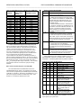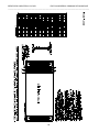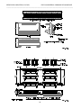
1
Series IP501-128 Industrial I/O Pack
Quad EIA/TIA-422B Communication Module
USER’S MANUAL
ACROMAG INCORPORATED
30765 South Wixom Road
P.O. BOX 437
Wixom, MI 48393-7037 U.S.A.
Tel: (248) 295-0310
Fax: (248) 624-9234
Copyright 1995, Acromag, Inc., Printed in the USA.
Data and specifications are subject to change without notice.
8500-683-C11M004
SERIES IP501 INDUSTRIAL I/O PACK
EIA/TIA-422B SERIAL COMMUNICATION MODULE
___________________________________________________________________________________________
The information contained in this manual is subject to change
without notice. Acromag, Inc. makes no warranty of any kind with
regard to this material, including, but not limited to, the implied
warranties of merchantability and fitness for a particular purpose.
Further, Acromag, Inc. assumes no responsibility for any errors
that may appear in this manual and makes no commitment to
update, or keep current, the information contained in this manual.
No part of this manual may be copied or reproduced in any form,
without the prior written consent of Acromag, Inc.
Table of Contents
1.0 GENERAL INFORMATION...........................................
KEY IP501 FEATURES................................................
INDUSTRIAL I/O PACK INTERFACE FEATURES.......
SIGNAL INTERFACE PRODUCTS..............................
INDUSTRIAL I/O PACK SOFTWARE LIBRARY..........
2.0 PREPARATION FOR USE...........................................
UNPACKING AND INSPECTION.................................
CARD CAGE CONSIDERATIONS...............................
BOARD CONFIGURATION..........................................
CONNECTORS............................................................
IP Field I/O Connector (P2)......................................
Noise and Grounding Considerations.......................
IP Logic Interface Connector (P1)............................
3.0 PROGRAMMING INFORMATION...............................
ADDRESS MAPS........................................................
IP Communication & Configuration Registers..........
IP Identification PROM............................................
THE EFFECT OF RESET...........................................
IP501 PROGRAMMING..............................................
FIFO Polled Mode...................................................
FIFO Interrupt Mode................................................
Loopback Mode Operation......................................
Interrupt Generation................................................
Software Flow Control………….…………………….
Hardware Flow Control………………………………
Programming Example...........................................
4.0 THEORY OF OPERATION.........................................
EIA/TIA-422B SERIAL INTERFACE...........................
IP501 OPERATION.....................................................
LOGIC/POWER INTERFACE.....................................
5.0 SERVICE AND REPAIR..............................................
SERVICE AND REPAIR ASSISTANCE......................
PRELIMINARY SERVICE PROCEDURE....................
6.0 SPECIFICATIONS......................................................
GENERAL SPECIFICATIONS....................................
EIA/TIA-422B PORTS.................................................
DRIVERS/RECEIVERS...............................................
INDUSTRIAL I/O PACK COMPLIANCE......................
APPENDIX.........................................................................
CABLE: MODEL 5025-550. & 5025-551.....................
CABLE: MODEL 5029-943..........................................
TERMINATION PANEL: MODEL 5025-552.................
TRANSITION MODULE: MODEL TRANS-GP.............
Page
2
2
3
3
3
4
4
4
4
4
4
5
6
6
6
9
17
18
18
18
19
19
19
20
20
20
21
21
22
23
23
23
23
23
23
24
24
24
24
24
25
25
25
DRAWINGS
Page
4501-434 IP MECHANICAL ASSEMBLY....................
26
4501-552 IP501 COMMUNICATION CONNECTIONS.
26
4501-554 IP501 INTERFACE DIAGRAM.....................
27
4501-555 IP501 TERM/BIAS RESISTOR LOCATION..
28
4501-553 IP501 BLOCK DIAGRAM..............................
29
4501-570 RS-422 INTERFACE LEVELS......................
30
4501-462 CABLE 5025-550 (NON-SHIELDED)............
31
4501-463 CABLE 5025-551 (SHIELDED).....................
31
4501-464 TERMINATION PANEL 5025-552................
32
4501-465 TRANSITION MODULE TRANS-GP.............
32
-2-
IMPORTANT SAFETY CONSIDERATIONS
It is very important for the user to consider the possible adverse
effects of power, wiring, component, sensor, or software failures in
designing any type of control or monitoring system. This is
especially important where economic property loss or human life is
involved. It is important that the user employ satisfactory overall
system design. It is agreed between the Buyer and Acromag, that
this is the Buyer's responsibility.
1.0 GENERAL INFORMATION
The Industrial I/O Pack (IP) Series IP501 module provides
four EIA/TIA-422B serial communication ports for interfacing to
the VMEbus or ISAbus, according to your carrier board. For halfduplex EIA-485 applications, the model IP502 is recommended,
but the model IP501 can be used to implement an EIA-485
interface operating in full-duplex. Full-duplex data paths for
Transmit (Tx), Receive (Rx), and the Request-to-Send (RTS) and
Clear-to-Send (CTS) handshake lines are included. Four units
may be mounted on a carrier board to provide up to 16
asynchronous serial ports per system slot.
The transmit and receive paths of each channel on
IP501units include generous 128-byte FIFO buffers to minimize
CPU interaction and include software flow controls. Full-duplex
EIA/TIA-422B and EIA-485 DB-9 signal support for the common
RTS and CTS handshake lines is included. Character size, stop
bits, parity, and baud rate are software configurable. Prioritized
interrupt generation is also supported for transmit, receive, linestatus, and data set conditions. The IP501 utilizes state of the art
Surface-Mounted Technology (SMT) to achieve its wide
functionality and is an ideal choice for a wide range of industrial
communication interface applications that require a highly
reliable, high-performance interface at a low cost. For isolated
interface requirements, refer to the Acromag Model IP511.
KEY IP501 FEATURES
High Density - Provides programmable control of four
EIA/TIA-422B serial ports. Four units mounted on a carrier
board provide 16 serial channels in a single VMEbus or
ISAbus (PC/AT) system slot.
Large FIFO Buffers - The transmit and receive channels of
each serial port provide generous 128-character data
buffering. This gives the host CPU additional time to
process other applications and reduces CPU interactions
and interrupts.
Programmable Character Size - Each serial port is
software programmable for 5, 6, 7, or 8 bit character sizes.
Programmable Stop Bits - Each serial port allows 1, 1-1/2,
or 2 stop-bits to be added to, or deleted from, the serial data
stream.
Programmable Parity Generation & Detection - Even,
Odd, or No Parity generation and detection is supported.
Line-Break Generation & Detection - provision for sending
and detecting the line break character is provided.
False Start Bit Detection - Prevents the receiver from
assembling false data characters due to low-going noise
spikes on the RxD input line.
SERIES IP501 INDUSTRIAL I/O PACK
EIA/TIA-422B SERIAL COMMUNICATION MODULE
___________________________________________________________________________________________
Programmable Baud Rate - The internal baud rate
generator allows the 8MHz clock to be divided by any divisor
between 1 and 2(16-1), providing support for any bit rate up to
512Kbps.
Interrupt Support - Individually controlled transmit, receive,
line status, data set, & flow control interrupts may be
generated and unique interrupt vectors assigned to each
port. Interrupts use a priority shifting scheme based on the
last interrupt serviced, preventing the continuous interrupts
of one port from blocking the interrupts of another port.
Flow Control - The IP501-128 includes support for software
and hardware flow control for more efficient data transfer.
Socketed Termination and Bias Resistors - The network
termination and bias resistors are installed in sockets on the
board and may be easily inserted or removed where
required.
Handshake/Modem Control Signals - Each serial channel
includes a modem-control and modem-status register that
provides handshake support for RTS & CTS.
Internal Diagnostic Capabilities - Loopback controls for
communication link fault isolation are included. Break,
parity, overrun, and framing error simulation is also possible.
Failsafe Receivers - The receivers employed in this model
include a fail-safe feature which guarantees a high output
state when the inputs are left open or floating.
Extended Temperature Performance Option - Model
IP501-128E units support operation from -40 C to +85 C.
Industry Standard 16550 Family UART w/16C450 Mode The UART of this device is a member of the industry
standard 16550 family of UART’s and remains software
compatible. Additionally, this device can operate in a
16C450 UART family software compatible mode. The
transmit and receive channels are double-buffered in this
mode. Hold and shift registers eliminate the need for
precise synchronization between the host CPU and the
serial data.
you should consult the documentation of your carrier board to
ensure compatibility with the following interface products.
Cables:
Model 5025-551-X (Shielded Cable), or Model 5025-550-X
(Non-Shielded Cable): A Flat 50-pin cable with female
connectors at both ends for connecting AVME9630/9660,
APC8610, or other compatible carrier boards, to Model 5025552 termination panels. The unshielded cable is
recommended for digital I/O, while the shielded cable is
recommended for optimum performance with precision
analog I/O applications. The “-X” suffix of the model is used
to specify the required length in feet.
Model 5029-943 IP500 Serial Communication Cable: A 5
foot long, flat 50-pin cable with a female connector on one
end (for connection to AVME9630/9660 or other compatible
carrier boards) and four DE-9P connectors (serial ports) on
the other end. Also used for interface with Acromag Model
IP501(RS-422) & IP502 (RS-485) serial communication
modules.
Termination Panels:
Model 5025-552: A DIN-rail mountable panel that provides 50
screw terminals for universal field I/O termination. Connects
to all Acromag carriers (or other compatible carrier boards)
via flat 50-pin ribbon cable (Model 5025-550-X or 5025-551X).
Transition Module:
Model TRANS-GP: This module repeats field I/O
connections of IP modules A through D for rear exit from a
VMEbus card cage. It is available for use in card cages
which provide rear exit for I/O connections via transition
modules (transition modules can only be used in card cages
specifically designed for them). It is a double-height (6U),
single-slot module with front panel hardware adhering to the
VMEbus mechanical dimensions, except for shorter printed
circuit board depth. It connects to Acromag Termination
Panel 5025-552 from the rear of the card cage, and to
AVME9630/9660 boards within the card cage, via flat 50-pin
ribbon cable (cable Model 5025-550 or 5025-551).
INDUSTRIAL I/O PACK INTERFACE FEATURES
High density - Single-size, industry standard, IP module
footprint. Four units mounted on a carrier board provide up
to 16 serial ports in a single system slot. Both VMEbus and
ISAbus (PC/AT) carriers are supported.
Local ID - Each IP module has its own 8-bit ID PROM which
is accessed via data transfers in the "ID Read" space.
8-bit I/O - Port register Read/Write is performed through 8bit data transfer cycles in the IP module I/O space.
High Speed - Access times for all data transfer cycles are
described in terms of "wait" states - 2 wait states are
required for reading and writing channel data and for
interrupt select cycles, 1 wait state for reading the ID PROM
(see the Specifications section for detailed information).
INDUSTRIAL I/O PACK SOFTWARE LIBRARY
Acromag provides an Industrial I/O Pack Software Library
diskette (Model IPSW-LIB-M03, MSDOS format) to simplify
communication with the board. Example software functions are
provided. All functions are written in the “C” programming
language and can be linked to your application. For more
details, refer to the “README.TXT” file in the root directory on
the diskette and the “INFO501.TXT” file in the appropriate “IP501”
subdirectory on the diskette for more details.
SIGNAL INTERFACE PRODUCTS
(See Appendix for more information on compatible products)
IP MODULE ActiveX CONTROL SOFTWARE
This IP module will mate directly to any industry standard IP
carrier board (including Acromag’s AVME967X &
AVME9630/9660 VMEbus, APC8610 ISA bus, APC8620/21 PCI
bus, and ACPC8625/30/35 Compact PCI bus non-intelligent
carrier boards). A wide range of other Acromag IP modules are
also available to serve your signal conditioning and interface
needs.
Acromag provides a software product (sold separately)
consisting of IP module ActiveX (Object Linking and Embedding)
controls for Windows 98, 95 , ME, 2000 and Windows NT
compatible application programs (Model IPSW-OLE-PCI,
MSDOS format). This software provides individual controls that
allow Acromag IP modules to be easily integrated into Windows
application programs, such as Visual C++ , Visual Basic ,
Microsoft Office 97 applications and others. The ActiveX
controls provide a high-level interface to IP modules, eliminating
Note: Since all connections to field signals are made through the
carrier board which passes them to the individual IP modules,
-3-
SERIES IP501 INDUSTRIAL I/O PACK
EIA/TIA-422B SERIAL COMMUNICATION MODULE
___________________________________________________________________________________________
the need to perform low-level reads/writes of registers, and the
writing of interrupt handlers—all the complicated details of
programming are handled by the ActiveX controls. These
functions are intended for use in conjunction with an Acromag
personal computer carrier and consist of an ActiveX Carrier
Control, and an ActiveX control for each Acromag IP module, as
well as, a generic control for non-Acromag IP modules.
The dense packing of the IP modules to the carrier board
restricts air flow within the card cage and is cause for concern.
Adequate air circulation must be provided to prevent a
temperature rise above the maximum operating temperature and
to prolong the life of the electronics. If the installation is in an
industrial environment and the board is exposed to environmental
air, careful consideration should be given to air-filtering.
IP MODULE VxWORKS SOFTWARE
BOARD CONFIGURATION
Acromag provides a software product (sold separately)
consisting of IP module VxWorks libraries. This software
(Model IPSW-API-VXW MSDOS format) is composed of
VxWorks (real time operating system) libraries for all Acromag
IP modules and carriers including the AVME9670,
AVME9660/9630, APC8620/21, ACPC8630/35, and ACPC8625.
The software is implemented as a library of “C” functions which
link with existing user code to make possible simple control of all
Acromag IP modules and carriers.
Remove power from the board when installing IP modules,
cables, termination panels, and field wiring. Refer to Mechanical
Assembly Drawing 4501-434 and your IP module documentation
for configuration and assembly instructions. Model IP501
communication boards have no hardware jumpers or switches to
configure. However, network termination and bias resistor SIPS
are installed in sockets on the board and can be easily removed
where required (refer to Drawing 4501-554 & 4501-555).
IMPORTANT: The IP501 comes with network termination (120 )
and bias (560 ) resistor SIP’s installed in sockets on the board.
You need to consider your network application carefully, and
remove some resistors where appropriate. Termination resistors
should only be installed at the ends of a network, and if the
transmitters are always enabled, then you should remove the
termination resistors from the transmitter side. Likewise, a
network channel only needs one set of bias resistors, usually on
the driving end. You should also remove redundant bias resistors
where appropriate. Failure to remove termination and bias
resistors where required will significantly increase current draw,
and in some cases, may affect performance. Refer to Drawing
4501-554 & 4501-555 for instructions.
2.0 PREPARATION FOR USE
UNPACKING AND INSPECTION
Upon receipt of this product, inspect the shipping carton for
evidence of mishandling during transit. If the shipping carton is
badly damaged or water stained, request that the carrier's agent
be present when the carton is opened. If the carrier's agent is
not present when the carton is opened and the contents of the
carton are damaged, keep the carton and packing material for the
agent's inspection.
CONNECTORS
For repairs to a product damaged in shipment, refer to the
Acromag Service Policy to obtain return instructions. It is
suggested that salvageable shipping cartons and packing
material be saved for future use in the event the product must be
shipped.
IP Field I/O Connector (P2)
P2 provides the field I/O interface connections for mating IP
modules to the carrier board. P2 is a 50-pin female receptacle
header (AMP 173279-3 or equivalent) which mates to the male
connector of the carrier board (AMP 173280-3 or equivalent).
This provides excellent connection integrity and utilizes goldplating in the mating area. Threaded metric M2 screws and
spacers are supplied with the module to provide additional
stability for harsh environments (see Mechanical Assembly
Drawing 4501-434). The field and logic side connectors are
keyed to avoid incorrect assembly. P2 pin assignments are
unique to each IP model (see Table 2.1) and normally correspond
to the pin numbers of the field I/O interface connector on the
carrier board (you should verify this for your carrier board).
This board is physically protected with
packing material and electrically
protected with an anti-static bag during
shipment. However, it is
recommended that the board be
visually inspected for evidence of
mishandling prior to applying power.
The board utilizes static sensitive
components and should only be
handled at a static-safe workstation.
CARD CAGE CONSIDERATIONS
Refer to the specifications for loading and power
requirements. Be sure that the system power supplies are able
to accommodate the power requirements of the carrier board,
plus the installed IP modules, within the voltage tolerances
specified.
IMPORTANT: Adequate air circulation must be provided to
prevent a temperature rise above the maximum operating
temperature.
-4-
SERIES IP501 INDUSTRIAL I/O PACK
EIA/TIA-422B SERIAL COMMUNICATION MODULE
___________________________________________________________________________________________
Table 2.1: IP501 Field I/O Pin Connections (P2)
Pin Description Number Pin Description
COMMON
1
COMMON
CTS+_A*
2
CTS+_C*
TXD+_A
3
TXD+_C
CTS-_A*
4
CTS-_C*
TXD-_A
5
TXD-_C
RTS-_A*
6
RTS-_C*
RXD-_A
7
RXD-_C
RTS+_A*
8
RTS+_C*
RXD+_A
9
RXD+_C
COMMON
10
COMMON
CTS+_B*
11
CTS+_D*
TXD+_B
12
TXD+_D
CTS-_B*
13
CTS-_D*
TXD-_B
14
TXD-_D
RTS-_B*
15
RTS-_D*
RXD-_B
16
RXD-_D
RTS+_B*
17
RTS+_D*
RXD+_B
18
RXD+_D
COMMON
19
COMMON
COMMON
20
COMMON
COMMON
21
COMMON
COMMON
22
COMMON
COMMON
23
COMMON
COMMON
24
COMMON
COMMON
25
COMMON
P2 Pin Signal Descriptions
SIGNAL
DESCRIPTION
RxD_A
Receive Data Line Input - This is the receive data
RxD_B
input line. During Loopback Mode, the RxD input
RxD_C
is disabled from the external connection and
RxD_D
connected to the TxD output internally. On this
model, the DTR bit of the Modem Control Register
is used to enable the RxD & CTS receivers.
TxD_A
Transmit Data Line Output - This is the transmit
TxD_B
output data line. In the idle state, this signal line
TxD_C
is held in the mark (logic 1) state. During
TxD_D
Loopback Mode, the TxD output is internally
connected to the RxD input.
RTS_A*
Request-to-Send Output - The RTS output is
RTS_B*
turned on to tell the modem it is ready to send
RTS_C*
data. This signal can be set low (active) by writing
RTS_D*
a 1 to the Modem Control Register. Normally, this
signal has no effect on the transmit or receive
operation, unless hardware flow control is
enabled. Likewise, on this model the RTS signal
is also used to enable the transmitters of the
channel (TxD & RTS) when the corresponding
Transmit Enable Always Register (TEA) bit is set
to 0.
CTS_A*
Clear-to-Send Input - Turned on by the receiving
CTS_B*
device to indicate it is ready to receive data. The
CTS_C*
input status of this signal can be read via bit 4 of
CTS_D*
the Modem Status Register. CTS has no effect
on the transmit or receive operation, unless
hardware flow control is enabled. On this model,
the DTR bit of the Modem Control Register is
used to enable the CTS & RxD receiver.
Number
26
27
28
29
30
31
32
33
34
35
36
37
38
39
40
41
42
43
44
45
46
47
48
49
50
An Asterisk (*) is used to indicate an active-low signal.
Note that the pin-wire assignments are arranged such that
IDC D-SUB ribbon cable connectors can be conveniently
attached to provide serial port A (pins 1-9), serial port B (pins 1018), serial port C (pins 26-34), & serial port D (pins 35-43)
connectivity. Plus (+) and minus (-) following the signal name
indicate differential signal polarity. In Table 2.1, a suffix of “_A”,
“_B”, “_C”, or “_D” is appended to each pin label to denote its port
association. A brief description of each of the serial port signals
at P2 is included below. A complete functional description of the
P2 pin functions is included in Section 4.0 (Theory Of Operation).
Be careful not to confuse the A-D port designations of the IP
module with the IP carrier board A-D slot designations.
Note that not all UART signal paths are used by this model
and their corresponding UART pins are tied high (+5V). This
includes, RI (Ring Indicator), DSR (Data Set Ready), and DCD
(Data Carrier Detect). In addition, the UART DTR (Data Terminal
Ready) signal path is used to control the receiver enables for the
port. The RTS signal is used in combination with the TEA
(Transmit Enable Always) register to control the transmitter
enables for the port.
Noise and Grounding Considerations
The serial channels of this module are non-isolated and
share a common signal ground connection. Further, the IP501 is
non-isolated between the logic and field I/O grounds since signal
common is electrically connected to the IP module ground.
Consequently, the field interface connections are not isolated
from the carrier board and backplane. Care should be taken in
designing installations without isolation to avoid noise pickup and
ground loops caused by multiple ground connections.
The signal ground connection at the communication ports are
common to the IP interface ground, which is typically common to
safety (chassis) ground when mounted on a carrier board and
inserted in a backplane. As such, be careful not to attach signal
ground to safety ground via any device connected to these ports,
or a ground loop will be produced, and this may adversely affect
operation.
-5-
SERIES IP501 INDUSTRIAL I/O PACK
EIA/TIA-422B SERIAL COMMUNICATION MODULE
___________________________________________________________________________________________
3.0 PROGRAMMING INFORMATION
The communication cabling of the P2 interface carries digital
data at a high transfer rate. For best performance, increased
signal integrity, and safety reasons, you should isolate these
connections away from power and other wiring to avoid noisecoupling and crosstalk interference. EIA/TIA-422B
communication distances are generally limited to less than 4000
feet. Always keep interface cabling and ground wiring as short as
possible for best performance. Please refer to Drawing 4501-552
for example connections and recommended grounding practices.
ADDRESS MAPS
This board is addressable in the Industrial Pack I/O space to
control the interface configuration, data transfer, and steering
logic of four EIA/TIA-422B serial ports. As such, three types of
information are stored in the I/O space: control, status, and data.
These registers are listed below along with their mnemonics used
throughout this manual.
IP Logic Interface Connector (P1)
SERIAL DATA REGISTERS (Per Serial Port):
RBR
Receive Buffer Register
THR
Transmitter Holding Register
SERIAL STATUS REGISTERS (Per Serial Port):
LSR
Line Status Register
MSR
Modem Status Register
SERIAL CONTROL REGISTERS (Per Serial Port):
LCR
Line Control Register
FCR
FIFO Control Register
MCR
Modem Control Register
DLL
Divisor Latch LSB
DLM
Divisor Latch MSB
IER
Interrupt Enable Register
SCR
Scratchpad/Interrupt Vector Register
TEA
Transmit Enable Always Register
EFR
Enhanced Feature Register
XON-1
XON-1 Word
XON-2
XON-2 Word
XOFF-1
XOFF-1 Word
XOFF-2
XOFF-2 Word
EMS
Enhanced Mode Select Register
FLVL
FIFO Level Byte Count Register
FCTR
Feature Control Register
TRG
FIFO Trigger Level
P1 of the IP module provides the logic interface to the mating
connector on the carrier board. This connector is a 50-pin female
receptacle header (AMP 173279-3 or equivalent) which mates to
the male connector of the carrier board (AMP 173280-3 or
equivalent). This provides excellent connection integrity and
utilizes gold-plating in the mating area. Threaded metric M2
screws and spacers are supplied with the IP module to provide
additional stability for harsh environments (see Drawing 4501-434
for assembly details). Field and logic side connectors are keyed
to avoid incorrect assembly. The pin assignments of P1 are
standard for all IP modules according to the Industrial I/O Pack
Specification (see Table 2.2).
Table 2.2: Standard Logic Interface Connections (P1)
Pin Description
GND
CLK
Reset*
D00
D01
D02
D03
D04
D05
D06
D07
D08
D09
D10
D11
D12
D13
D14
D15
BS0*
BS1*
-12V
+12V
+5V
GND
Number
1
2
3
4
5
6
7
8
9
10
11
12
13
14
15
16
17
18
19
20
21
22
23
24
25
Pin Description
GND
+5V
R/W*
IDSEL*
DMAReq0*
MEMSEL*
DMAReq1*
IntSel*
DMAck0*
IOSEL*
RESERVED
A1
DMAEnd*
A2
ERROR*
A3
INTReq0*
A4
INTReq1*
A5
STROBE*
A6
ACK*
RESERVED
GND
Number
26
27
28
29
30
31
32
33
34
35
36
37
38
39
40
41
42
43
44
45
46
47
48
49
50
The I/O space may be as large as 64, 16-bit words (128
bytes) using address lines A1..A6, but the IP501 uses only a
portion of this space. The I/O space address map for the IP501
is shown in Table 3.1. Note the base address for the IP module
I/O space (see your carrier board instructions) must be added to
the addresses shown to properly access the I/O space. All
accesses are performed on an 8-bit word basis (D0..D7).
This manual is presented using the “Big Endian” byte
ordering format. Big Endian is the convention used in the
Motorola 68000 microprocessor family and is the VMEbus
convention. In Big Endian, the lower-order byte is stored at oddbyte addresses. Thus, byte accesses are done on odd address
locations. The Intel x86 family of microprocessors use the
opposite convention, or “Little Endian” byte ordering. Little
Endian uses even-byte addresses to store the low-order byte. As
such, use of this module on PC carrier board will require the use
of the even address locations to access the 8-bit data, while a
VMEbus carrier will require the use of odd address locations.
An Asterisk (*) is used to indicate an active-low signal.
BOLD ITALIC Logic Lines are NOT USED by this IP Model.
Note that some functions share the same register address.
For these items, the address lines are used along with the setting
of the (LCR) Line Control Register or (FCTR) Feature Control
Register to select the required register.
-6-
SERIES IP501 INDUSTRIAL I/O PACK
EIA/TIA-422B SERIAL COMMUNICATION MODULE
___________________________________________________________________________________________
Table 3.1: IP501 I/O Space Memory Map Port B Registers
Base
MSB
LSB
Addr4
Base
Addr+
D15
D08 D07
D00
Select Addr+
10
READ - RBR
LCR
Not Driven1
Port B Receiver
Not
Buffer Register
0xBF
11
10
WRITE - THR
LCR
1
Not Driven
Port B Transmitter
Not
Holding Register
0xBF
11
10
R/W – DLL Port B
LCR
1
Not Driven
Divisor Latch LSB
Bit7=1
11
10
READ - FLVL
LCR =
Not Driven1
Port B FIFO
0xBF
Level Counter
11
10
WRITE - TRG
LCR =
Not Driven1
Port B FIFO
0xBF
Trigger Level
11
12
R/W - IER
LCR
Not Driven1
Port B Interrupt
Not
Enable Register
0xBF
13
12
R/W - DLM
LCR
Not Driven1
Port B Divisor
Bit7=1
Latch MSB
13
12
R/W
LCR =
Not Driven1
Port B Feature
0xBF
Control Register
13
14
READ - IIR
LCR
Not Driven1
Port B Interrupt
Not
Identification
0xBF
15
14
WRITE - FCR
LCR
Not Driven1
Port B FIFO
Not
Control Register
0xBF
15
14
R/W - EFR
LCR =
Not Driven1
Port B Enhanced
0xBF
Function Register
15
16
R/W - LCR
LCR
Not Driven1
Port B Line Control
Not
Register
0xBF
17
18
R/W - MCR
LCR
1
Not Driven
Port B Modem
Not
Control Register
0xBF
19
18
R/W- XON-1 Word
LCR =
1
Not Driven
Port B
0xBF
SW Flow Control
19
1A
R/W – LSR Port B
LCR
Not Driven1
Line Status
Not
1B
Register
0xBF
1A
R/W- XON-2 Word
LCR =
Not Driven1
SW Flow Control
0xBF
1B
1C
READ - MSR
LCR
1
Not Driven
Port B Modem
Not
Status Register
0xBF
1D
1C
R/W- XOFF-1 Word
LCR =
1
Not Driven
Port B
0xBF
SW Flow Control
1D
1E
R/W – SCR Port B
FCTR
Not Driven1
Scratch Pad
Bit6=0
Interrupt Vector
1F
1E
READ - FLVL
FCTR
Not Driven1
Port B FIFO Level
Bit6=1
Byte Count Register
1F
1E
WRITE EMSR
FCTR
Not Driven1
Port B Enhanced
Bit6=1
Mode Select Reg.
1F
1E
R/W- XOFF-2 Word
LCR =
Not Driven1
Port B
0xBF
SW Flow Control
1F
Table 3.1: IP501 I/O Space Memory Map Port A Registers
Base
MSB
LSB
Addr4
Base
Addr+
D15
D08 D07
D00
Select Addr+
00
READ - RBR
LCR
Not Driven1
Port A Receiver
Not
Buffer Register
0xBF
01
00
WRITE - THR
LCR
1
Not Driven
Port A Transmitter
Not
Holding Register
0xBF
01
00
R/W – DLL Port A
LCR
1
Not Driven
Divisor Latch LSB
Bit7=1
01
00
READ - FLVL
LCR =
Not Driven1
Port A FIFO
0xBF
Level Counter
01
00
WRITE - TRG
LCR =
Not Driven1
Port A FIFO
0xBF
Trigger Level
01
02
R/W - IER
LCR
Not Driven1
Port A Interrupt
Not
Enable Register
0xBF
03
02
R/W - DLM
LCR
Not Driven1
Port A Divisor
Bit7=1
Latch MSB
03
02
R/W
LCR =
Not Driven1
Port A Feature
0xBF
Control Register
03
04
READ - IIR
LCR
Not Driven1
Port A Interrupt
Not
Identification
0xBF
05
04
WRITE - FCR
LCR
Not Driven1
Port A FIFO
Not
Control Register
0xBF
05
04
R/W - EFR
LCR =
Not Driven1
Port A Enhanced
0xBF
Function Register
05
06
R/W - LCR
LCR
Not Driven1
Port A Line Control
Not
Register
0xBF
07
08
R/W - MCR
LCR
1
Not Driven
Port A Modem
Not
Control Register
0xBF
09
08
R/W- XON-1 Word
LCR =
1
Not Driven
Port A
0xBF
SW Flow Control
09
0A
R/W – LSR Port A
LCR
Not Driven1
Line Status
Not
0B
Register
0xBF
0A
R/W- XON-2 Word
LCR =
Not Driven1
SW Flow Control
0xBF
0B
0C
READ - MSR
LCR
1
Not Driven
Port A Modem
Not
Status Register
0xBF
0D
0C
R/W- XOFF-1
LCR =
1
Not Driven
Word
0xBF
Port A
0D
SW Flow Control
0E
R/W – SCR Port A
FCTR
Not Driven1
Scratch Pad
Bit6=0
Interrupt Vector
0F
0E
READ - FLVL
FCTR
Not Driven1
Port A FIFO Level
Bit6=1
Byte Count Register
0F
0E
WRITE EMSR
FCTR
Not Driven1
Port A Enhanced
Bit6=1
Mode Select Reg.
0F
0E
R/W- XOFF-2 Word
LCR =
Not Driven1
Port A
0xBF
SW Flow Control
0F
-7-
SERIES IP501 INDUSTRIAL I/O PACK
EIA/TIA-422B SERIAL COMMUNICATION MODULE
___________________________________________________________________________________________
Table 3.1: IP501 I/O Space Memory Map Port C Registers
Base
MSB
LSB
Addr4
Base
Addr+
D15
D08 D07
D00
Select Addr+
20
READ - RBR
LCR
Not Driven1
Port C Receiver
Not
Buffer Register
0xBF
21
20
WRITE - THR
LCR
1
Not Driven
Port C Transmitter
Not
Holding Register
0xBF
21
20
R/W – DLL Port C
LCR
1
Not Driven
Divisor Latch LSB
Bit7=1
21
20
READ - FLVL
LCR =
Not Driven1
Port C FIFO
0xBF
Level Counter
21
20
WRITE - TRG
LCR =
Not Driven1
Port C FIFO
0xBF
Trigger Level
21
22
R/W - IER
LCR
Not Driven1
Port C Interrupt
Not
Enable Register
0xBF
23
22
R/W - DLM
LCR
Not Driven1
Port C Divisor
Bit7=1
Latch MSB
23
22
R/W
LCR =
Not Driven1
Port C Feature
0xBF
Control Register
23
24
READ - IIR
LCR
Not Driven1
Port C Interrupt
Not
Identification
0xBF
25
24
WRITE - FCR
LCR
Not Driven1
Port C FIFO
Not
Control Register
0xBF
25
24
R/W - EFR
LCR =
Not Driven1
Port C Enhanced
0xBF
Function Register
25
26
R/W - LCR
LCR
Not Driven1
Port C Line Control
Not
Register
0xBF
27
28
R/W - MCR
LCR
Not Driven1
Port C Modem
Not
Control Register
0xBF
29
28
R/W- XON-1 Word
LCR =
1
Not Driven
Port C
0xBF
SW Flow Control
29
2A
R/W – LSR Port C
LCR
Not Driven1 Line Status Register
Not
0xBF
2B
2A
R/W- XON-2 Word
LCR =
Not Driven1
SW Flow Control
0xBF
2B
2C
READ - MSR
LCR
1
Not Driven
Port C Modem
Not
Status Register
0xBF
2D
2C
R/W- XOFF-1
LCR =
1
Not Driven
Word
0xBF
Port C
2D
SW Flow Control
2E
R/W – SCR Port C
FCTR
Not Driven1
Scratch Pad
Bit6=0
Interrupt Vector
2F
2E
READ - FLVL
FCTR
Not Driven1
Port C FIFO Level
Bit6=1
Byte Count
2F
Register
2E
WRITE EMSR
FCTR
Not Driven1
Port C Enhanced
Bit6=1
Mode Select Reg.
2F
2E
R/W- XOFF-2 Word
LCR =
Not Driven1
Port C
0xBF
SW Flow Control
2F
Table 31: IP501 I/O Space Memory Map Port D Registers
Base
MSB
LSB
Addr4
Base
Addr+
D15
D08 D07
D00
Select Addr+
30
READ - RBR
LCR
Not Driven1
Port D Receiver
Not
Buffer Register
0xBF
31
30
WRITE - THR
LCR
1
Not Driven
Port D Transmitter
Not
Holding Register
0xBF
31
30
R/W – DLL Port D
LCR
1
Not Driven
Divisor Latch LSB
Bit7=1
31
30
READ - FLVL
LCR =
Not Driven1
Port D FIFO
0xBF
Level Counter
31
30
WRITE - TRG
LCR =
Not Driven1
Port D FIFO
0xBF
Trigger Level
31
32
R/W - IER
LCR
Not Driven1
Port D Interrupt
Not
Enable Register
0xBF
33
32
R/W - DLM
LCR
Not Driven1
Port D Divisor
Bit7=1
Latch MSB
33
32
R/W
LCR =
Not Driven1
Port D Feature
0xBF
Control Register
33
34
READ - IIR
LCR
Not Driven1
Port D Interrupt
Not
Identification
0xBF
35
34
WRITE - FCR
LCR
Not Driven1
Port D FIFO
Not
Control Register
0xBF
35
34
R/W - EFR
LCR =
Not Driven1
Port D Enhanced
0xBF
Function Register
35
36
R/W - LCR
LCR
Not Driven1
Port D Line Control
Not
Register
0xBF
37
38
R/W - MCR
LCR
Not Driven1
Port D Modem
Not
Control Register
0xBF
39
38
R/W- XON-1 Word
LCR =
1
Not Driven
Port D
0xBF
SW Flow Control
39
3A
R/W – LSR Port D
LCR
Not Driven1
Line Status
Not
Register
0xBF
3B
3A
R/W- XON-2 Word
LCR =
Not Driven1
SW Flow Control
0xBF
3B
3C
READ - MSR
LCR
1
Not Driven
Port D Modem
Not
Status Register
0xBF
3D
3C
R/W- XOFF-1
LCR =
1
Not Driven
Word
0xBF
Port D
3D
SW Flow Control
3E
R/W – SCR Port D
FCTR
Not Driven1
Scratch Pad
Bit6=0
Interrupt Vector
3F
3E
READ - FLVL
FCTR
Not Driven1
Port D FIFO Level
Bit6=1
Byte Count Register
3F
3E
WRITE EMSR
FCTR
Not Driven1
Port D Enhanced
Bit6=1
Mode Select Reg.
3F
3E
R/W- XOFF-2 Word
LCR =
Not Driven1
Port D
0xBF
SW Flow Control
3F
-8-
SERIES IP501 INDUSTRIAL I/O PACK
EIA/TIA-422B SERIAL COMMUNICATION MODULE
___________________________________________________________________________________________
Notes (Table 3.1):
1. The upper 8 bits of these registers are not driven. Pullups
on the carrier board data bus will cause these bits to always
read high (1’s).
2. The IP will not respond to addresses that are "Not Used".
3. All Reads and writes are 2 wait states (except ID PROM
reads which are 1 wait state).
4. Address selection is completed with the setting of the LCR
(Line Control Register) and FCTR (Feature Control Register)
as shown in this column.
less than 8 bits are transmitted, then data is entered right-justified
to the LSB. This data is framed as required, then shifted to the
transmit data line (TxD). In the idle state, TxD is held high. In
Loopback Mode, this data is looped back into the Receiver Buffer
Register.
This board operates in two different modes. In one mode,
this device remains software compatible with the industry
standard 16C450 family of UARTS and provides double buffering
of data registers. In the FIFO Mode (enabled via bit 0 of the FCR
register), data registers are FIFO-buffered so that read and write
operations can be performed while the UART is performing serialto-parallel and parallel-to-serial conversions. Two FIFO modes
are possible: FIFO Interrupt Mode and FIFO Polled Mode. Some
registers operate differently between the available modes and this
is noted in the following paragraphs.
DLL & DLM - Divisor Latch Registers, Ports A-D (R/W)
For this model, note that the transmitters for a channel (TxD
& RTS) are enabled via the RTS asserted signal bit in the Modem
Control Register when the corresponding Transmit Enable
Always Register bit is set to 0.
The Divisor Latch Registers form the divisor used by the
internal baud-rate generator to divide the 8MHz system clock to
produce an internal sampling clock suitable for synchronization to
the desired baud rate. The output of the baud generator (RCLK)
is sixteen times the baud rate. Two 8-bit divisor latch registers
per port are used to store the divisors in 16-bit binary format. The
DLL register stores the low-order byte of the divisor, DLM stores
the high-order byte. These registers must be loaded during
initialization.
RBR - Receiver Buffer Register, Ports A-D (READ Only)
Note that bit 7 of the LCR register must first be set high to
access the divisor latch registers (DLL & DLM) during a read/write
operation.
The Receiver Buffer Register (RBR) is a serial port input data
register that receives the input data from the receiver shift
register and holds from 5 to 8 bits of data, as specified by the
character size programmed in the Line Control Register (LCR bits
0 & 1). If less than 8 bits are transmitted, then data is right
justified to the LSB. If parity is used, then LCR bit 3 (parity
enable) and LCR bit 4 (type of parity) are required. Status for the
receiver is provided via the Line-Status Register (LSR). When a
full character is received (including parity and stop bits), the datareceived indication bit (bit 0) of the LSR is set to 1. The host
CPU then reads the Receiver Buffer Register, which resets LSR
bit 0 low. If the character is not read prior to a new character
transfer between the receiver shift register and the receiver buffer
register, the overrun-error status indication is set in LSR bit 1. If
there is a parity error, the error is indicated in LSR bit 2. If a stop
bit is not detected, a framing error indication is set in bit 3 of the
LSR.
Upon loading either latch, a 16-bit baud counter is
immediately loaded (this prevents long counts on initial load).
The clock may be divided by any divisor from 1 to 2(16-1). The
output frequency of the baud rate generator (RCLK) is 16x the
data rate. The relationship between the output of the baud
generator (RCLK), the baud rate, the divisor, and the 8MHz
system clock can be summarized in the following equations:
DIVISOR = CLOCK FREQUENCY [BAUD RATE x 16];
RCLK
= 16 x BAUD RATE;
= 16 x [CLOCK (16 x DIVISOR)] = CLOCK
DIVISOR
The following table shows the correct divisor to use for
generation of some standard baud rates (based on the 8MHz
clock). Note that baud rates up to 512K may be configured.
Provisions for installation of an external crystal has been provided
on the circuit board (16MHz). With a 16MHz crystal, a 1Mbps
baud rate is possible--you may contact Acromag Applications
Engineering to explore options in this area.
Serial asynchronous data is input to the receiver shift register
via the receive data line (RxD). From the idle state, this line is
monitored for a high-to-low transition (start bit). When the start
bit is detected, a counter is reset and counts the 16x clock to 71/2 (which is the center of the start bit). The start bit is judged
valid if RxD is still low at this point. This is known as false startbit detection. By verifying the start bit in this manner, it helps to
prevent the receiver from assembling an invalid data character
due to a low-going noise spike on RxD. If the data on RxD is a
symmetrical square wave, the center of the data cells will occur
within 3.125% of the actual center (providing an error margin of
46.875%). Thus, the start bit can begin as much as one 16x
clock cycle prior to being detected.
With respect to this device, the baud rate may be considered
equal to the number of bits transmitted per second (bps). The bit
rate (bps), or baud rate, defines the bit time. This is the length of
time a bit will be held on before the next bit is transmitted. A
receiver and transmitter must be communicating at the same bit
rate, or data will be garbled. A receiver is alerted to an incoming
character by the start bit, which marks the beginning of the
character. It then times the incoming signal, sampling each bit as
near to the center of the bit time as possible.
Note that the receivers for the channel (RxD & CTS) are
enabled by asserting the DTR signal via the Modem Control
Register (MCR bit 0).
THR - Transmitter Holding Register, Ports A-D (WRITE Only)
The Transmitter Holding Register (THR) is a serial port output
data register that holds from 5 to 8 bits of data, as specified by
the character size programmed in the Line Control Register. If
-9-
SERIES IP501 INDUSTRIAL I/O PACK
EIA/TIA-422B SERIAL COMMUNICATION MODULE
___________________________________________________________________________________________
Enhanced Feature Register (EFR)
EFR BIT
FUNCTION
0-3
Allows combinations of software flow control to be
programmed (see table below).
4
Enhanced Features Enable bit.
0 = disable enhanced features controlled via IER
bits 4-7, IIR bits 4-5, FCR bits 4-5, and MCR bits 5-7
(Note that after reset, these bits are set to “0” to
maintain compatibility with the 16C550 standard
functionality mode).
1 = Enable all enhanced features. Allows IER bits
4-7, IIR bits 4-5, FCR bits 4-5, and MCR bits 5-7 to
be modified. Then after modification, EFR bit 4 can
be set to “0” to latch the contents, and prevent
existing software from overwriting the enhanced
functionality provided by these bits.
5
0 = Normal;
1 = Enable Special Character Detect. If enabled,
the UART will compare the received data with the
XOFF-2 data. Upon a correct match, the received
data will be transferred to the FIFO and IIR bit 4 will
be set to indicate the detection of the special
character.
6
Auto-RTS* - Hardware RTS flow Control Enable
0 = Normal (RTS flow control disabled);
1 = Enable RTS* pin to go high (deasserted) when
the receive FIFO has reached its programmed
trigger level.
7
Auto-CTS* - Hardware CTS flow Control Enable
0 = Normal (CTS flow control disabled);
1 = Resume transmission when a low input signal
(CTS* asserted) is detected on the CTS* pin.
Table 3.2: Baud Rate Divisors and Relative Error (8MHz Clk)
BAUD RATE
DIVISOR (N)
% ERROR DIFF BET
DESIRED
USED FOR 16x
DESIRED & ACTUAL
CLOCK
50
10000
2710H
0
75
6667
1A06H
0.005
110
4545
11C1H
0.010
134.5
3717
0E85H
0.013
150
3333
0D05H
0.010
300
1667
0683H
0.020
600
833
0341H
0.040
1200
417
01A1H
0.080
1800
277
0115H
0.080
2000
250
00FAH
0
2400
208
00D0H
0.160
3600
139
0086H
0.080
4800
104
0068H
0.160
7200
69
0045H
0.644
9600
52
0034H
0.160
19200
26
001AH
0.160
38400
13
000DH
0.160
56000
9
0009H
0.790
128000
4
0004H
2.344
256000
2
0002H
2.344
512000
1
0001H
2.400
To better understand the asynchronous timing used by this
device, note that the receive data line (RxD) is monitored for a
high-to-low transition (start bit). When the start bit is detected, a
counter is reset and counts the 16x-sampling clock to 7-1/2
(which is the center of the start bit). The receiver then counts
from 0 to 15 to sample the next bit near its center, and so on,
until a stop bit is detected, signaling the end of the data stream.
Use of a sampling rate 16x the baud rate reduces the
synchronization error that builds up in estimating the center of
each successive bit following the start bit. As such, if the data on
RxD is a symmetrical square wave, the center of each successive
data cell will occur within 3.125% of the actual center (this is
50% 16, providing an error margin of 46.875%). Thus, the start
bit can begin as much as one 16x clock cycle prior to being
detected.
Under software flow control, different conditions can be set to
detect XON/XOFF characters in the data stream, or start/stop
transmission. The following table lists all the possible conditions:
Software Flow Control Via EFR Bits 0-3
Bit3 Bit2 Bit1 Bit0
Tx/Rx Software Flow Controls
0
0
X
X
No Transmit Flow Control
1
0
X
X
Transmit XON1, XOFF1
0
1
X
X
Transmit XON2, XOFF2
1
1
X
X
Transmit XON1, XON2:
XOFF1, XOFF2
X
X
0
0
No Receive Flow Control
X
X
1
0
Receiver Compares
XON1,XOFF1
X
X
0
1
Receiver Compares
XON2,XOFF2
1
0
1
1
Transmit XON1, XOFF1.
Receiver Compares XON1 or
XON2, XOFF1 or XOFF2.
0
1
1
1
Transmit XON2, XOFF2.
Receiver Compares XON1 or
XON2, XOFF1 or XOFF2.
1
1
1
1
Transmit XON1 & XON2: XOFF1
& XOFF2. Receiver Compares
XON1 & XON2: XOFF1 &
XOFF2.
0
0
1
1
No Transmit Flow Control.
Receiver Compares XON1 &
XON2: XOFF1 and XOFF2.
Note that access to this register is granted only after writing
“BF” to the Line Control Register (LCR). EFR Bits 0-7 are set to
0 upon power-up or system reset.
EFR - Enhanced Feature Register, Ports A-D (R/W)
The enhanced features of the Model IP501-128 can be
enabled/disabled via this register. This register is also used to
unlock access to programming the extended register functionality
of IER bits 4-7, IIR bits 4-5, FCR bits 4-5, and MCR bits 5-7. It is
also used to program hardware or software flow control. Note
that bits 6 & 7 are used for hardware flow control.
- 10 -
SERIES IP501 INDUSTRIAL I/O PACK
EIA/TIA-422B SERIAL COMMUNICATION MODULE
___________________________________________________________________________________________
XON/XOFF-1,2 Registers, Ports A-D (R/W)
IIR - Interrupt Identification Register, Ports A-D (READ Only)
These registers hold the programmed XON and XOFF
characters for software flow control. XON or XOFF characters
may be 1 or 2 bytes long. The UART compares incoming data to
these values and restarts (XON) or suspends (XOFF) data
transmission when a match is detected. Note that access to
these registers are granted only after writing “BF” to the Line
Control Register (LCR). All XON/XOFF bits are set to 0 upon
power-up or system reset. Refer to “Software Flow Control” later
in this section for more information.
The Interrupt Identification Register (IIR) is used to indicate
that a prioritized interrupt is pending and the type of interrupt that
is pending. This register will indicate the highest-priority type of
interrupt pending for the channel. Individual serial channels
prioritize their interrupts into six levels. This helps minimize
software overhead during data character transfers. Additionally,
with respect to the four channels sharing interrupt request line 0
(IntReq0), interrupts are served according to a shifting priority
scheme that is a function of the last interrupting port served.
IER - Interrupt Enable Register, Ports A-D (R/W)
PRIORITY/LEVEL
1
2
The Interrupt Enable Register is used to independently
enable/ disable the four possible serial channel interrupt sources
that drive the INTREQ0* line (Ports A-D share this line).
Interrupts are disabled by resetting the corresponding IER bit low
(0), and enabled by setting the IER bit high (1). Disabling the
interrupt system (IER bits 0-3 low) also inhibits the Interrupt
Identification Register (IIR) and the interrupt request line
(INTREQ0*). All other functions operate in their normal manner,
including the setting of the Line Status Register (LSR) and the
Modem Status Register (MSR).
3
4
5
6
INTERRUPT
Receiver Line Status
Received Data Ready or Character Timeout
Transmitter Holding Register Empty
Modem Status
Software Flow Control Interrupt RxRDY*
(Received XOFF signal)/ Special
Character
CTS*, RTS* Change-of-State
The six lower order bits of this register are used to identify the
interrupt pending as shown below
Interrupt Enable Register
IER BIT INTERRUPT ACTION
0
Received Data Available Interrupt Enable and
Time-Out Interrupt (FIFO Mode) Enable
1
Transmitter Holding Register Empty Interrupt Enable
2
Receiver Line Status Interrupt Enable
3
Modem Status Interrupt Enable
4
0 = Disable Sleep Mode.
1 = Enable Sleep Mode - The UART will enter a
“sleep” power-down mode and the clock/oscillator
circuit is disabled. Any change of state on Rx, RI,
CTS, DSR, and DCD will wake-up the UART (note
that only the CTS* and RTS* handshake lines are
implemented on this model). The UART will not lose
the programmed bits when sleep mode is activated or
deactivated. The UART will not enter sleep mode if
any interrupt is pending.
5
0 = Disable the Received XOFF interrupt.
1 = Enable the Received XOFF interrupt. The UART
issues an interrupt when XOFF characters are
received and correctly matched against the preprogrammed XOFF-1,2 words.
6
0 = Disable the RTS* interrupt
1 = Enable the generation of an RTS* interrupt when
RTS* changes from a low to high state.
7
0 = Disable the CTS interrupt
1 = Enable the generation of the CTS interrupt when
CTS changes from a low to high state.
Interrupt Identification Register
BITS
INT
INTERRUPT
3-0
PRTY
TYPE
0001
-None
0110
1st
Receiver
Line Status
A power-up or system reset sets all IER bits to 0 (bits 0-3
forced low, bits 4-7 permanently low). For IP501-128 models,
program access to the enhanced functionality provided via bits 47 of this register is gained through setting EFR bit 4.
Programmed values for bits 4-7 cannot be overwritten via existing
software if EFR bit 4 is clear (these values are latched when EFR
bit 4 is cleared).
- 11 -
INTERRUPT
SOURCE
None
OE, PE, FE,
or BI (See
LSR Bits 1-4)
Receiver Data
Available or
Trigger Level
Reached
0100
2nd
Received
Data
Available
1100
2nd
Character
Time-out
Indication
0010
3rd
THRE (LSR
Bit 5)
No characters
have been removed from
or input to the
Rx FIFO
during last 4
character
times and
there is at
least 1
character in it
during this
time
THRE
(LSR Bit 5)
0000
4th
Modem
Status
CTS*
asserted
RESET
CONTROL
-LSR Read
RBR Read
till FIFO
below
trigger
level
RBR Read
IIR Read (if
LSR bit 5
is the
interrupt
source) or
a THR
Write
MSR Read
SERIES IP501 INDUSTRIAL I/O PACK
EIA/TIA-422B SERIAL COMMUNICATION MODULE
___________________________________________________________________________________________
7,6
Interrupt Identification Register
BITS
INT
5 - 4
PRTY
INTERRUPT SOURCE
0
1
5
Received XOFF Signal/Special
Character
1
0
6
CTS/RTS Change-of-State Detected
Table A
BIT 7-6
00
01
10
11
Table B
BIT 7-6
00
01
10
11
Table C
BIT 7-6
00
01
10
11
Table D
BIT 7-6
XX
Bits 6 and 7 are set to “1” when bit 0 of the FIFO Control
Register is set to “1. A power-up or system reset sets IIR bit 0 to
“1”, bits 1-7 to “0”.
FCR - FIFO Control Register, Ports A-D (WRITE Only)
This write-only register is used to enable and clear the FIFO
buffers, set the trigger level of the Rx FIFO and Tx FIFO, and
select the type of DMA signaling (DMA is NOT supported by this
model). A power-up or system reset will reset all FCR bits to “0”.
FIFO Control Register
FCR BIT
FUNCTION
0
When set to “1”, this bit enables both the Tx and Rx
FIFO’s. All bytes in both FIFO’s can be cleared by
resetting this bit to 0. Data is cleared automatically
from the FIFO’s when changing from FIFO mode to
the alternate 16C450 mode and visa-versa.
Programming of other FCR bits is enabled by
setting this bit to 1.
1
When set to “1”, this bit clears all bytes in the RxFIFO and resets the counter logic to 0 (this does
not clear the shift register).
2
When set to “1”, this bit clears all bytes in the TxFIFO and resets the counter logic to 0 (this does
not clear the shift register).
3
When set to “1”, this bit sets DMA Signal from
Mode 0 to Mode 1, if FIFO Control Register Bit 0 =
1 (DMA is Not Supported).
5,4
The FCTR Bits 4-5 are associated with these 2 bits
by selecting one of the four tables. Four user
selectable trigger levels in 4 tables are supported
for compatibility reasons. These bits set the trigger
level for the transmit FIFO interrupt. The IP501128 will issue a transmit empty interrupt when the
number of characters in the FIFO falls below the
selected trigger level, or when it gets empty in case
that the FIFO did not get filled over the trigger level.
Used for setting the trigger level of the Tx FIFO
interrupt as follows:
Table A
BIT 5-4
XX
Table B
BIT 5-4
00
01
10
11
Table C
BIT 5-4
00
01
10
11
Table D
BIT 5-4
XX
Used for setting the trigger level of the Rx FIFO
interrupt as follows:
Tx-FIFO TRIGGER LEVEL
Zero (default)
Tx-FIFO TRIGGER LEVEL
08 Bytes
16 Bytes
24 Bytes
30 Bytes
Tx-FIFO TRIGGER LEVEL
08 Bytes.
16 Bytes
32 Bytes
56 Bytes
Tx-FIFO TRIGGER LEVEL
User programmable Trigger level
- 12 -
Rx-FIFO TRIGGER LEVEL
1 (default)
04 Bytes
08 Bytes
14 Bytes
Rx-FIFO TRIGGER LEVEL
08 Bytes
16 Bytes
24 Bytes
28 Bytes
Rx-FIFO TRIGGER LEVEL
08 Bytes.
16 Bytes
56 Bytes
60 Bytes
Rx-FIFO TRIGGER LEVEL
User programmable Trigger level
SERIES IP501 INDUSTRIAL I/O PACK
EIA/TIA-422B SERIAL COMMUNICATION MODULE
___________________________________________________________________________________________
LCR - Line Control Register, Ports A-D (Read/Write)
MCR - Modem Control Register, Ports A-D (R/W)
The individual bits of this register control the format of the
data character as follows:
Line Control Register
LCR Bit FUNCTION
1 and 0
Word
Length
Select
2
Stop Bit
Select
3
4
5
6
7
Parity
Enable
Even-Parity
Select
Stick Parity
Break
Control
Divisor
Latch
Access Bit
PROGRAMMING
0 0 = 5 Data Bits
0 1 = 6 Data Bits
The Modem Control register controls the interface with the
modem or data set as described below. For this model, only the
RTS and CTS handshake lines are supported and DTR is used to
enable the receivers. The RTS output is directly controlled by its
control bit in this register (a high input asserts these signals).
1 0 = 7 Data Bits
1 1 = 8 Data Bits
A DTR data path is not provided by this model and this output
signal via this register (bit 0) is instead used to enable the RxD
and CTS receivers of the port. Additionally, asserting the RTS bit
will enable the TxD and RTS transmitters of the port if the
corresponding Transmit Enable Always Register (TEA) bit is not
set.
0 = 1 Stop Bit
1 = 1.5 Stop Bits if 5 data bits
selected,
2 Stop Bits if 6, 7, or 8 data bits
selected.
0 = Parity Disabled
1 = Parity Enabled
A parity bit is generated and checked
for between the last data word bit and
the stop bit.
0 = Odd Parity
1 = Even Parity
0 = Stick Parity Disabled
1 = Stick Parity Enabled
When parity is enabled, stick parity
causes the transmission and
reception of a parity bit to be in the
opposite state from the value
selected via bit 4. This is used as a
diagnostic tool to force parity to a
known state and allow the receiver to
check the parity bit in a known state.
0 = Break Disabled
1 = Break Enabled
When break is enabled, the serial
output line (TxD) is forced to the
space state (low). This bit acts only
on the serial output and does not
affect transmitter logic. For example,
if the following sequence is used, no
invalid characters are transmitted due
to the presence of the break.
1. Load a zero byte in response to
the Transmitter Holding Register
Empty
(THRE) status indication.
2. Set the break in response to the
next THRE status indication.
3. Wait for the transmitter to become
idle when the Transmitter Empty
status signal is set high (TEMT=1);
then clear the break when normal
transmission has to be restored.
0 = Access Receiver Buffer
1 = Allow Access to Divisor Latches
A power-up or system reset sets all MCR bits to 0 (bits 5-7
are permanently low on standard units).
Modem Control Register
MCR Bit
FUNCTION
0
Data Terminal
Ready Output
Signal (DTR)
1
2
3
Request to Send
Output Signal
(RTS)
Out1 (Internal)
Out2 (Internal)
4
Loop1
5
XON Enable2
6
7
Rx/Tx I/O Mode2
Clock Divide2
PROGRAMMING
0 = DTR* Not Asserted (Inactive)
1 = DTR* Asserted (Active)
A DTR signal path is NOT
SUPPORTED by this model.
Instead, this output is used to
enable the receivers of the port
(RxD & CTS receivers).
0 = RTS* Not Asserted (Inactive)
1 = RTS* Asserted (Active)
No Effect on External Operation
0 = External Serial Channel
Interrupt Disabled
1 = External Serial Channel
Interrupt Enabled
0 = Loop Disabled
1 = Loop Enabled
0 = Disable Any XON function
1 = Enable Any XON function
Not Used on IP501 (set to 0)
0 = Normal divide by 1 clock
(8MHz clock baud rates apply)
1 = Divide clock by 4
(2MHz baud rates apply)
Notes (Modem Control Register):
1. MCR Bit 4 provides a local loopback feature for diagnostic
testing of the UART channel. When set high, the UART
serial output (connected to the TXD driver) is set to the
marking (logic 1 state), and the UART receiver serial input is
disconnected from the RxD receiver path. The output of the
UART transmitter shift register is looped back into the
receiver shift register input. The four modem control inputs
(CTS,DSR, DCD, & RI) are disconnected from their receiver
input paths. The four modem control outputs (DTR, RTS,
OUT1, & OUT2) are internally connected to the four modem
control inputs (while their associated pins are forced to their
high/inactive state).
Note that bit 7 must be set high to access the divisor latch
registers of the baud rate generator (DLL & DLM) during a
read/write operation. Bit 7 must be low to access the Receiver
Buffer register (RBR), the Transmitter Holding Register (THR), or
the Interrupt-Enable Register (IER). Writing 0xBF to this register
allows access to the Enhanced Registers. The Enhanced
Registers are: FIFO Level Counter, FIFO Trigger Level., Feature
Control Register, Enhance Feature Register, XON and XOFF. A
power-up or system reset sets all LCR bits to 0.
2.
A detailed discussion of word length, stop bits, parity, and the
break signal is included in Section 4.0 (Theory of Operation).
- 13 -
Bits 5-7 are only programmable when the EFR bit 4 is set to
“1”. The programmed values for these bits are latched when
EFR bit 4 is cleared, preventing existing software from
inadvertently overwriting the extended functions. However,
these MCR bits cannot be set if the LCR is set to BF hex.
SERIES IP501 INDUSTRIAL I/O PACK
EIA/TIA-422B SERIAL COMMUNICATION MODULE
___________________________________________________________________________________________
3.
Line Status Register…continued
LSR Bit FUNCTION
PROGRAMMING
3
Framing
0 = No Error
Error (FE)
1 = Framing Error - Indicates that
the received character does not
have a valid stop bit (stop bit
following last data bit or parity
bit detected as a zero/space bit).
This bit is reset low when the
CPU reads the contents of the
LSR. In FIFO mode, the
framing error is associated with
a particular character in the FIFO
LSR Bit 3 reflects the error when
the character is at the top of the
FIFO).
4
Break
0 = No Break
Interrupt (BI)
1 = Break - the received data input
has been held in the space
(logic 0) state for more than a
full-word transmission time
(start bits + data + parity bit +
stop bits).
Reset upon read of LSR. In FIFO
mode, this bit is associated with
a particular character in the FIFO
and reflects the Break Interrupt
when the break character is at
the top of the FIFO. It is
detected by the host CPU
during the first LSR read. Only
one “0” character is loaded into
the FIFO when BI occurs.
5
Transmitter
0 = Not Empty
Holding
1 = Empty - indicates that the
Register
channel is ready to accept a
Empty
new character for transmission.
(THRE)
Set high when character is transferred from the THR into the
transmitter shift register. Reset
low by loading the THR (It is not
reset by a host CPU read of the
LSR). In FIFO mode, this bit is
set when the Tx FIFO is empty
and cleared when one byte is
written to the Tx FIFO. When a
Transmitter Holding Register
Empty interrupt is enabled by
IER bit 1, this signal causes a
priority 3 interrupt in the IIR.
If the IIR indicates that this
signal is causing the interrupt,
the interrupt s cleared by a read
of the IIR.
6
Transmitter
0 = Not Empty
Empty
1 = Transmitter Empty - set when
(TEMT)
both the Transmitter Holding
Register (THR) and the
Transmitter Shift Register
(TSR) are both empty. Reset
low when a character is loaded
into the THR and remains low
until the character is
transmitted (it is not reset low
by a read of the LSR). In FIFO
mode, this bit is set when both
the transmitter FIFO and shift
register are empty.
3Thus, in Loopback Mode, transmitted data is immediately
received permitting the host processor to verify the transmit
and receive data paths of the selected serial channel. In
Loopback Mode, interrupts are generated by controlling the
state of the four lower order MCR bits internally, instead of
by the external hardware paths. However, no interrupt
requests or interrupt vectors are served and interrupt
pending status is only reflected internally.
Note that bits 5-7 are programmable only when the EFR bit 4
is set to “1”. The programmed values for these bits are latched
when EFR bit 4 is cleared, preventing existing software from
inadvertantly overwriting the extended functions. A power-up or
system reset sets all MCR bits to “0”.
LSR - Line Status Register, Ports A-D (Read/Write-Restricted)
The Line Status Register (LSR) provides status indication
corresponding to the data transfer. LSR bits 1-4 are the error
conditions that produce receiver line-status interrupts (a priority 1
interrupt in the Interrupt Identification Register). The line status
register may be written, but this is intended for factory test and
should be considered read-only by the applications software.
Line Status Register
LSR Bit FUNCTION
0
Data Ready
(DR)
1
Overrun
Error (OE)
2
Parity Error
(PE)
PROGRAMMING
0 = Not Ready (reset low by CPU
Read of RBR or FIFO)
1 = Data Ready (set high when
character received and transferred into the RBR or FIFO).
0 = No Error
1 = Indicates that data in the RBR is
not being read before the next
character is transferred into the
RBR, overwriting the previous
character. In the FIFO mode, it
is set after the FIFO is filled and
the next character is received.
The overrun error is detected by
the CPU on the first LSR read
after it happens. The character in
the shift register is not transferred
into the FIFO, but is overwritten.
This bit is reset low when the
CPU reads the LSR.
0 = No Error
1 = Parity Error - the received
character does not have the
correct parity as configured via
LCR bits 3 & 4. This bit is set
high on detection of a parity error
and reset low when the host CPU
reads the contents of the LSR.
In the FIFO mode, the parity
error is associated with a
particular character in the FIFO
(LSR Bit 2 reflects the error when
the character is at the top of the
FIFO).
- 14 -
SERIES IP501 INDUSTRIAL I/O PACK
EIA/TIA-422B SERIAL COMMUNICATION MODULE
___________________________________________________________________________________________
Line Status Register...continued
LSR Bit FUNCTION
PROGRAMMING
7
Receiver
0 = No Error in FIFO
FIFO Error
1 = Error in FIFO - set when one of
the following data errors is
present in the FIFO: parity error,
framing error, or break interrupt
indication. Cleared by a host
CPU read of the LSR if there
are no subsequent errors in the
FIFO.
Note that reading MSR clears the delta-modem status
indication (bits 0-3), but has no effect on the other status bits.
For both the LSR & MSR, the setting of the status bit during a
status register read operation is inhibited (the status bit will not be
set until the trailing edge of the read). However, if the same
status condition occurs during a read operation, that status bit is
cleared on the trailing edge of the read instead of being set again.
In Loopback Mode, when the modem status interrupts are
enabled, the CTS* input is ignored. However, a modem status
interrupt can still be generated by writing to MCR bit 0 (see
Loopback Mode Operation section).
Note that LSR Bits 1-4 (OE, PE, FE, BI) are the error
conditions that produce a receiver-line-status interrupt (a priority 1
interrupt in the IIR register when any one of these conditions are
detected). This interrupt is enabled by setting IER bit 2 to 1.
Note that not all UART signal paths are used by this model
and their corresponding UART pins are tied high (+5V). This
includes, RI (Ring Indicator), DSR (Data Set Ready), and DCD
(Data Carrier Detect). In addition, the UART DTR (Data Terminal
Ready) signal path is used to control the receiver enables for the
port while the RTS signal is used in combination with the TEA
(Transmit Enable Always) register to control the transmitter
enables for the port.
A power-up or system reset sets all LSR bits to 0, except bits
5 and 6 which are high.
MSR - Modem Status Register, Ports A-D (READ Only)
The Modem Status Register (MSR) provides the host CPU
with an indication on the status of the modem input lines from a
modem or other peripheral device. This model only provides
support for the CTS and RTS handshake lines. As such, this
register allows the current state of CTS to be read (bit 4) and
provides indication on whether the state of this line has changed
since the last read of the MSR (bit 0 set high when the
corresponding control input from the modem changes state and
reset low when the CPU reads the MSR).
A power-up or system reset sets MSR bit 0 to 0 (bit 4 is
determined by input signal). Unused bits are always clear.
SCR - Scratch Pad/Interrupt Pointer Register, Ports A-D
(R/W)
This 8-bit read/write register has no effect on the operation of
either serial channel. It is provided as an aide to the programmer
to temporarily hold data. Alternately, if interrupt generation is
desired, then this port is used to store the interrupt vector for the
port. In response to an interrupt select cycle, the IP module will
execute a read of this register for the interrupting port (see
Interrupt Generation section for more details).
Modem Status Register
MSR BIT FUNCTION
0
CTS - Set if CTS has changed states since last
read of MSR
1
DSR - NOT SUPPORTED
2
RI - NOT SUPPORTED
3
DCD - NOT SUPPORTED
4
CTS - This bit is the complement of the CTS* input
from the modem indicating that the modem is
ready to receive data. This bit is equivalent to
RTS* in the MCR during local loopback mode. If
the channel is in the loopback mode (MCR bit 4 =
1), then the state of RTS in the MCR is reflected.
CTS* functions as a hardware flow control signal
input if it is enabled via EFR bit 7. The transmit
holding register is gated with this input to start/stop
the transmission. A high at this pin will stop the
transmission as soon as a complete character has
been transmitted.
5
DSR - NOT SUPPORTED
This bit is equivalent to DTR in the MCR during
local loopback mode.
6
RI - NOT SUPPORTED
This bit is equivalent to OP1 in the MCR during
local loopback mode.
7
DCD - NOT SUPPORTED
This bit is equivalent to OP2 in the MCR during
local loopback mode.
Note that whenever MSR bits 3-0 are set to “1”, a
modem status interrupt is generated.
An Asterisk (*) is used to indicate an active-low signal.
TEA - Transmit Enable Always Register (R/W)
The lower four bits of this register (Bits 0-3) are used to
permanently enable the transmitters (the line drivers for TxD and
RTS) of a port. Normally, these data paths are enabled via an
asserted Request-to-Send (RTS) signal, but may be permanently
enabled by setting the respective bit in this register high. Bit 0
controls port A, bit 1port B, bit 2 port C, and bit 3 port D. Do not
use this in conjunction with hardware flow control.
A power-up or system reset clears bits 0-3. The upper four
bits of this register are not used and will always read high (1’s).
Base
Addr+
MSB
D15 D08
40
Not
Driven1
LSB
D07
D00
R/W – TEA
Transmit Enable Always
Register
42
Base
Addr+
41
43
NOT USED2
7E
- 15 -
7F
SERIES IP501 INDUSTRIAL I/O PACK
EIA/TIA-422B SERIAL COMMUNICATION MODULE
___________________________________________________________________________________________
ESMR – Enhanced Mode Select Register (WRITE only)
This register provides the number of data bytes in the RX or
TX FIFO, which is determined by Enhanced Mode Select
Register (EMSR) bit-0 and 1. The returned byte count ranges
from 0 to 80H.
Transmit / receive FIFO level byte count. It gives an
indication of the number of characters present in transmit or
receive FIFO. A simpler way to read the FIFO level count is
through register FIFO level register (FLVL) instead.
TRG – Trigger Level Register (WRITE only)
This is a write only register and accessible only when bit-6 of
the Feature Control Register (FCTR) is set to a logic 1. EMSR
bit-0 and 1 select which FIFO byte count for FLVL register to
present when reading the byte count. It can be transmit only,
receive only, or alternate receive and transmit byte count after
each read operation. In the alternate mode, it presents the
receive count first and the transmit count on the second read
operation, and repeats thereafter. In this case, user’s software
must remember the state for the byte count.
This is the user programmable transmit/receive FIFO trigger
level register. The register is associated with the FCTR bit-7
which selects TX or RX FIFO trigger register.
The value written to this register sets the TX or RX FIFO
trigger level from 0 to 80H. The FIFO trigger level generates and
interrupt whenever the transmit FIFO level falls below its preset
trigger level while the RX FIFO generates an interrupt as soon as
incoming data fills up to its preset trigger level.
Enhanced Mode Select Register
MCR Bit
FUNCTION
PROGRAMMING
0 and 1
TX/RX/ALT
00 = Receive FIFO level count
FIFO Level
(default)
Count
01 = Transmit FIFO level count
10 = Receive FIFO level count
11 = Alternate RX/TX FIFO level
count
2 and 3
Not used
Bits set to logic 0
4 and 5
Write only
These bits select the auto RTS
Auto RTS Flow flow control hysteresis and are
Control
associated with FCTR bit 0 and
Hysteresis
1, and only valid when user
programmable trigger levels are
selected by setting bits 4 and 5
of the FIFO Control Register to
logic “ 1 1”. The RTS hysteresis
is reference to the RX FIFO
trigger level. See following table.
6 and 7
Not used
Bits set to logic 0
EMSR
Bit-5
0
0
0
0
0
0
0
0
1
1
1
1
1
1
1
1
EMSR
Bit-4
0
0
0
0
1
1
1
1
1
1
1
1
0
0
0
0
FCTR
Bit-1
0
0
1
1
0
0
1
1
0
0
1
1
0
0
1
1
FCTR
Bit-0
0
1
0
1
0
1
0
1
0
1
0
1
0
1
0
1
FCTR – Feature Control Register (R/W)
This is a read write register that is accessible only when the
LCR is set to 0xBF.
FCTR Bit
0 and 1
RTS Hysteresis
(characters)
Next level (default)
+/- 4
+/- 6
+/- 8
+/- 8
+/- 16
+/- 24
+/- 32
+/- 40
+/- 44
+/- 48
+/- 52
+/- 12
+/- 20
+/- 28
+/- 36
FLVL - FIFO Level Register (READ only)
The FIFO Level Byte Count Register is read only and
accessible only when bit-6 of the Feature Control Register
(FCTR) is set to a logic 1. The user can take advantage of the
FIFO level byte counter for faster data loading to the transmit
FIFO and unloading data from the receiver FIFO.
- 16 -
FUNCTION
RTS Trigger
Level Select
2
RX Input
Select
3
Auto RS485
Enable
4 and 5
TX and RX
FIFO Trigger
Table Select
PROGRAMMING
User selectable auto – RTS
trigger delay timer for hardware
flow control application. After
reset, these bits are set to logic
0 selecting the next FIFO trigger
level for hardware flow control.
These 2 bits are associated with
EMSR register bit 4 and 5 for
more level control, see EMSR bit
4 and 5 for complete detail.
0 = Select RX input as encoded
IrDA data
1 = Select RX input as active
high encoded IrDA data
Note Auto RS485
selects/changes the TX empty
interrupt from THR to TSR.
0 = Standard ST16C550 mode.
Transmitter generates
interrupt when transmit
holding register (THR)
become empty. Transmit
Shift
Register (TSR) may still be
shifting data bit out.
1 = Enable Auto RS485 half
duplex direction control and
change the transmit interrupt
to transmit shift register
(TSR) empty. Transmit empty
interrupt is generated when
the transmitter shift register
becomes empty.
These 2 bits select the transmit
and receive FIFO trigger table A,
B, C or D as listed in the FIFO
Control Register section. When
table A, B or C is selected the
auto RTS flow control trigger
level is set to “next level” for
compatibility to ST16C550/650
SERIES IP501 INDUSTRIAL I/O PACK
EIA/TIA-422B SERIAL COMMUNICATION MODULE
___________________________________________________________________________________________
6
Register
Address
Select
7
TX/RX FIFO
Trigger
Register
Select
series. –RTS triggers on the
next level of the RX FIFO trigger
level, in another word, one level
above and one level below.
00 = TX and RX Trigger Table- A
(default)
01 = TX and RX Trigger Table- B
10 = TX and RX Trigger Table- C
11 = TX and RX Trigger Table- D
Scratch Pad (SPR) register or
FLVL and EMSR registers
selected.
0 = Scratch Pad (SPR) is
selected as a general read
and write register, ST16C554
compatible mode.
1 = It switches to FIFO Level
Count (FLVL) Register for
bus read operation and
Enhanced Mode Select
Register for bus write
operation. The FLVL
indicates the number of data
bytes in the transmit or
receive data FIFO. The SPR
is not available when this bit
is set.
Programmable trigger register
select. This bit is associated
with the TRG register, which
actually sets the FIFO trigger
levels.
0 = Select programmable receive
FIFO trigger level register.
1 = Select programmable
transmit FIFO trigger level
register.
Table 3.2: IP501 ID Space Identification (ID) PROM
Hex Offset
From ID
ASCII
Numeric
PROM Base
Character
Value
Address
Equivalent
(Hex)
Field Description
01
I
49
All IP's have'IPAC'
03
P
50
05
A
41
07
C
43
09
A3
Acromag ID Code
0B
05
IP Model Code1
0D
00
Not Used
(Revision)
0F
00
Reserved
11
00
Not Used (Driver
ID Low Byte)
13
00
Not Used (Driver
ID High Byte)
15
0C
Total Number of
ID PROM Bytes
17
E7
CRC
19 to 3F
yy
Not Used
Notes (Table 3.2):
1. The IP model number is represented by a two-digit code
within the ID PROM (IP501 models are represented by 05 Hex).
THE EFFECT OF RESET
A software or hardware reset puts the serial channels into an
idle-mode until initialization (programming). A reset initializes the
receiver and transmitter clock counters. It also clears the LineStatus Register (LSR), except for the transmitter shift-register
empty (TEMT) and transmit holding-register empty (THRE) bits
which are set to 1 (note that when interrupts are subsequently
enabled, an interrupt will occur due to THRE being set). The
Modem Control Register (MCR) and the Transmitter Enable
Always Register (TEA) are also cleared. All of the discrete signal
lines, memory elements, and miscellaneous logic associated with
these register bits are cleared, de-asserted, or turned off.
However, the Line Control Register (LCR), divisor latches,
Receiver Buffer Register (RBR), and Transmitter Holding
Register (THR) are not affected. The following table summarizes
the effect of a reset on the various registers and internal and
external signals:
IP Identification PROM - (Read Only, 32 Odd-Byte Addresses)
Each IP module contains an identification (ID) PROM that
resides in the ID space per the IP module specification. This
area of memory contains 32 bytes of information at most. Both
fixed and variable information may be present within the ID
PROM. Fixed information includes the "IPAC" identifier, model
number, and manufacturer's identification codes. Variable
information includes unique information required for the module.
The IP501 ID PROM does not contain any variable (e.g. unique
calibration) information. ID PROM bytes are addressed using
only the odd addresses in a 64 byte block (on the “Big Endian”
VMEbus). Even addresses are used on the “Little Endian”
PC/ISA bus.
The Effect of Reset
REGISTER/
RESET
SIGNAL
CONTROL
REGISTERS:
IER
Reset
The IP501 ID PROM contents are shown in Table 3.2. Note that
the base-address for the IP module ID space (see your carrier
board instructions) must be added to the addresses shown to
properly access the ID PROM. Execution of an ID PROM Read
requires 1 wait state.
- 17 -
IIR
Reset
LCR
MCR
Reset
Reset
FCR
LSR
Reset
Reset
MSR
Reset
STATE/EFFECT
All Bits low (Bits 0-3
forced low, Bits 4-7
permanently low).
Bit 0 high, Bits 1,2,3,6,7
low, Bits 4 & 5
permanently low.
All bits low.
All bits low (bits 5-7
permanently low).
All bits low.
All bits low, except bits 5
& 6 which are high.
Bits 0-3 low, bits 4-7 per
SERIES IP501 INDUSTRIAL I/O PACK
EIA/TIA-422B SERIAL COMMUNICATION MODULE
___________________________________________________________________________________________
and write operations can be performed while the UART is
performing serial-to-parallel and parallel-to-serial conversions.
corresponding input signal.
TEA
Reset
Bits 0-3 low, bits 4-7 are
unused and always read
high.
EFR
Reset
All bits low.
XON-1,2
Reset
All bits low.
XOFF-1,2
Reset
All bits low.
SIGNALS (INTERNAL & EXTERNAL):
TxD
Reset
High
Interrupt
Read LSR/
Low
(RCVR errors)
Reset
Interrupt (RCVR
Read RCVR
Low
data ready)
Buffer Register/
Reset
Interrupt
Read IIR/Write
Low
(THRE)
THR/Reset
Interrupt
Read MSR/
Low
(Modem Status
Reset
Changes)
RTS*
Reset
High
DTR*
Reset
High
OUT1*
Reset
High
OUT2*
Reset
High
Two FIFO modes of operation are possible: FIFO Interrupt
Mode and FIFO Polled Mode. In FIFO Interrupt Mode, data
transfer is initiated by reaching a pre-determined trigger-level or
generating time-out conditions. In FIFO-Polled Mode, there is no
time-out condition indicated or trigger-level reached. The
transmit and receive FIFO’s simply hold characters and the Line
Status Register must be read to determine the channel status.
Acromag provides an Industrial I/O Pack Software Library
diskette (Model IPSW-LIB-M03, MSDOS format) to simplify
communication with the board. Example software functions are
provide. All functions are written in the “C” programming
language and can be linked to your application. For more details,
refer to the “README.TXT” file in the root directory on the
diskette and the “INFO501.TXT” file in the appropriate “IP501”
subdirectory.
FIFO Polled-Mode
Resetting Interrupt Enable Register Bit 0, Bit 1, Bit 2, Bit 3, or
all four to 0, with FIFO Control Register (FCR) Bit 0 =1, puts the
channel into the polled-mode of operation. The receiver and
transmitter are controlled separately and either one or both may
be in the polled mode. In FIFO-Polled Mode, there is no time-out
condition indicated or trigger-level reached, the transmit and the
receive FIFO’s simply hold characters and the Line Status
Register must be read to determine the channel status.
IP501 PROGRAMMING
Each serial channel of this module is programmed by the
control registers: LCR, IER, DLL, DLM, MCR, and FCR. These
control words define the character length, number of stop bits,
parity, baud rate, and modem interface. The control registers can
be written in any order, but the IER register should be written last
since it controls the interrupt enables. The contents of these
registers can be updated any time the serial channel is not
transmitting or receiving data.
FIFO-Interrupt Mode
In FIFO Interrupt Mode, data transfer is initiated by reaching
a pre-determined trigger-level or generating a time-out condition.
Please note the following with respect to this mode of operation.
The complete status of each channel can be read by the host
CPU at any time during operation. Two registers are used to
report the status of a particular channel: the Line Status Register
(LSR) and the Modem Status Register (MSR).
When the receiver FIFO and receiver interrupts are enabled, the
following receiver status conditions apply:
1. LSR Bit 0 is set to 1 when a character is transferred from the
shift register to the receiver FIFO. It is reset to 0 when the
FIFO is empty.
2. The receiver line-status interrupt (IIR=06) has a higher priority
than the received data-available interrupt (IIR=04).
3. The receive data-available interrupt is issued to the CPU
when the programmed trigger level is reached by the FIFO. It
is cleared when the FIFO drops below its programmed trigger
level. The receive data-available interrupt indication (IIR=04)
also occurs when the FIFO reaches its trigger level, and is
cleared when the FIFO drops below its trigger level.
Serial channel data is read from the Receiver Buffer Register
(RBR), and written to the Transmitter Holding Register (THR).
Writing data to the THR initiates the parallel-to-serial transmitter
shift register to the TxD line. Likewise, input data is shifted from
the RxD pin to the Receiver Buffer Register. The DTR bit of the
Modem Control Register (MCR bit 0) is used to enable the RxD
and CTS receivers of the port. Additionally, asserting the RTS bit
will enable the TxD and RTS transmitters of the port if the
corresponding Transmit Enable Always Register (TEA) bit is not
set.
The Scratchpad Register is used to store the interrupt vector
for the port. In response to an interrupt select cycle, the IP
module will provide a read of this port. As such, each port may
have a unique interrupt vector assigned. Interrupts are served in
a shifting-priority fashion that is a function of the last interrupting
port serviced. This prevents continuous interrupts from one
channel from freezing out service of another interrupting channel.
When the receiver FIFO and receiver interrupts are enabled, the
following receiver FIFO character time-out status conditions apply:
1. A FIFO character time-out interrupt occurs if:
A minimum of one character is in the FIFO.
The last received serial character is longer than four
continuous prior character times ago (if 2 stop bits are
programmed, the second one is included in the time
delay).
The last CPU read of the FIFO is more than four
continuous character times earlier. At 300 baud, and
with 12-bit characters, the FIFO time-out interrupt
causes a latency of 160ms maximum from received
character to interrupt issued.
This board operates in two different modes. In one mode,
this device remains software compatible with the industry
standard 16C450 family of UART’s, and provides doublebuffering of data registers. In the FIFO Mode (enabled via bit 0 of
the FCR register), data registers are FIFO-buffered so that read
- 18 -
SERIES IP501 INDUSTRIAL I/O PACK
EIA/TIA-422B SERIAL COMMUNICATION MODULE
___________________________________________________________________________________________
2. From the clock signal input, the character times can be
calculated. The delay is proportional to the baud rate.
3. The time-out timer is reset after the CPU reads the receiver
FIFO or after a new character is received when there has
been no time-out interrupt.
4. A time-out interrupt is cleared and the timer is reset when the
CPU reads a character from the receiver FIFO.
four channels. Each channel shares interrupt request line 0
(Intreq0) according to a unique priority shifting scheme that
prevents the continuous interrupts of one channel from freezing
out another channels’ interrupt requests.
After pulling the IntReq0 line low and in response to an
Interrupt Select cycle, the current highest priority interrupt
channel will serve up its interrupt vector first. Interrupt serving
priority will shift as a function of the last port served. A unique
interrupt vector may be assigned to each communication port and
is loaded into the Scratchpad Register (SCR) for the port. The IP
module will thus execute a read of the Scratchpad Register in
response to an interrupt select cycle. Two wait states are
required to complete this cycle.
When the transmit FIFO and transmit interrupts are enabled
(FCR Bit 0 = 1 and IER=01), a transmitter interrupt will occur as
follows:
1. When the transmitter FIFO is empty, the transmitter holding
register interrupt (IIR=02) occurs. The interrupt is cleared
when the Transmitter Holding Register (THR) is written to or
the Interrupt Identification Register (IIR) is read. One to
sixteen characters can be written to the transmit FIFO when
servicing this interrupt.
2. The transmit FIFO empty indications are delayed one
character time minus the last stop bit time when the following
occurs:
Bit 5 of the LSR (THRE) is 1 and there is not a minimum of
two bytes at the same time in the transmit FIFO since the last
time THRE=1. The first transmitter interrupt after changing
FCR Bit 0 is immediate, assuming it is enabled.
Interrupt priority is assigned as follows. Initially, with no prior
interrupt history, Port A has the highest priority and will be served
first, followed by port B, followed by port C, then followed by port
D. However, if port A was the last interrupt serviced, then port B
will have the highest priority, followed by port C, followed by port
D, then port A, in a last-serviced last-out fashion. Priority
continues to shift in the same fashion if port B or port C was the
last interrupt serviced. This is useful in preventing continuous
interrupts on one channel from freezing out interrupt service for
other channels.
The receiver FIFO trigger level and character time-out
interrupts have the same priority as the received data-available
interrupt. The Transmitter Holding-Register-Empty interrupt has
the same priority as the Transmitter FIFO-Empty interrupt.
Software Flow Control
Model IP501-128 modules include support for software flow
control. Software flow control utilizes special XON & XOFF
characters to control the flow of data, for more efficient data
transfer and to minimize overrun errors.
Loopback Mode Operation
This device can be operated in a “loopback mode”, useful for
troubleshooting a serial channel without physically wiring to the
channel. Bit 4 of the Modem Control Register (MCR) is used to
program the local loopback feature for the UART channel. When
set high, the UART channel’s serial output line (Transmit Data
Path) is set to the marking (logic 1 state), and the UART receiver
serial data input lines are disconnected from the RxD receiver
path. The output of the UART transmitter shift register is then
looped back into the receiver shift register input. Thus, a write to
the Transmitter Holding Register is automatically looped back to
the corresponding Receiver Buffer Register. Additionally, the four
modem control inputs (CTS, DSR, DCD, and RI) are
disconnected from their receiver input paths. With modem status
interrupts enabled in the Loopback Mode, the CTS*, DSR*, RI*,
and DCD* inputs are ignored. Instead, the four modem control
outputs (DTR, RTS, OUT1, and OUT2 of the MCR Register) are
internally connected to the corresponding four modem control
inputs (monitored via the Modem Status Register), while their
associated pins are forced to their high/ inactive state. Thus, in
the loopback diagnostic mode, transmitted data is immediately
received permitting the host processor to verify the transmit and
receive data paths of the selected serial channel. Further,
modem status interrupt generation is controlled manually in
loopback mode by controlling the state of the four lower order
MCR bits internally, instead of by the external hardware paths.
However, in loopback mode, no interrupt requests or interrupt
vectors will actually be served, the UART only reflects that an
interrupt is pending.
Software flow control (sometimes called XON/XOFF pacing)
sends a signal from one node to another by adding flow control
characters to the data stream. The receiving node will detect the
XON or XOFF character and respond by suspending
transmission of data (XOFF turns the data flow off), or resuming
transmission of data (XON turns the data flow on). Flow control
is used frequently in data communications to prevent overrun
errors or the loss of excess data. For example, a node might
transmit the XOFF character to the host computer if the host is
sending data too quickly to be processed or buffered, thus
preventing the loss of excess data.
The flow control characters are stored in the XON-1,2 and
XOFF-1,2 registers. Two XON & XOFF registers are provided
because the flow control character may be 1 or 2 bytes long. The
contents of the XON-1,2 and XOFF-1,2 registers are reset to “0”
upon power-up or system reset, and may be programmed to any
value for software flow control. Different conditions may be set to
detect the XON/XOFF characters or start/stop the transmission.
When software flow control is enabled, the UART of this
model will compare two sequential received data bytes with
preprogrammed XOFF-1,2 characters. When an XOFF match is
detected, the UART will halt transmission after completing the
transmission of the current character. The receive ready flag of
the Interrupt Identification register will be set (IIR bit 4 is set to “1”
when the XOFF character has been detected), only if enabled via
bit 5 of the Interrupt Enable register (IER bit 5 is used to enable
the received XOFF interrupt). An interrupt will then be generated.
After recognition of the XOFF characters, the UART will compare
the next two incoming characters with the preprogrammed XON1,2 characters. If a match is detected, the UART will resume
transmission and clear the received XOFF interrupt flag (Interrupt
Interrupt Generation
This model provides individual control for generation of
transmit, receive, line status, and data set interrupts on each of
- 19 -
SERIES IP501 INDUSTRIAL I/O PACK
EIA/TIA-422B SERIAL COMMUNICATION MODULE
___________________________________________________________________________________________
Identification Register bit 4). After more data has been received,
the UART will automatically send XOFF-1,2 characters as soon
as the received data passes the programmed FIFO trigger level,
causing the host to suspend transmission. The UART will then
transmit the programmed XON-1,2 characters as soon as the
received data reaches the next lowest trigger level, thus causing
the host to resume transmission (received data trigger levels are
8, 16, 56, and 60).
an RTS/CTS protocol. Both nodes will use the FIFO mode of
operation with a FIFO threshold set at 14 bytes. The data format
will use 8-bit characters, odd-parity, and 1 stop bit. Please refer
to Table 3.1 for address locations. The “H” following data below
refers to the Hexadecimal data format.
1. Write 80H to the Line Control Register (LCR).
This sets the Divisor Latch Access bit to permit access to the
two divisor latch bytes used to set the baud rate. These
bytes share addresses with the Receive and Transmit
buffers, and the Interrupt Enable Register (IER).
When single XON/XOFF characters are selected, the UART
compares the received data to these values and controls the
transmission accordingly (XON=restart transmission,
XOFF=suspend transmission). These characters are not stacked
in the data buffer or FIFO. When the ANY XON function is
enabled (MCR bit 5 is set), the UART will automatically resume
transmission after receiving ANY character after having
recognized XOFF and suspended transmission. Note that the
UART will automatically transmit the XON character(s) after the
flow control function is disabled, if the XOFF character(s) had
been sent prior to disabling the software flow control function.
Special cases are provided to detect the special character and
stack it into the data buffer or FIFO and these conditions are
configured via bits 0-3 of the Enhanced Feature Register (EFR).
2. Write 00H to the Divisor Latch MSB (DLM). Write 34H to the
Divisor Latch LSB (DLL).
This sets the divisor to 52 for 9600 baud (i.e. 9600 = 8MHz
[16*52] ).
3. Write 0BH to the Line Control Register (LCR).
This first turns off the Divisor Latch Access bit to cause
accesses to the Receiver and Transmit buffers and the
Interrupt Enable Register. It also sets the word length to 8
bits, the number of stop bits to one, and enables odd-parity.
Hardware Flow Control
4. (OPTIONAL) Write xxH to the Scratch Pad Register.
Model IP501-128 modules include support for hardware flow
control via the RTS & CTS signals. This is useful for increasing
the efficiency of the data transfer and for minimizing overrun
errors.
This has no effect on the operation, but is suggested to
illustrate that this register can be used as a 1-byte memory
cell. Alternately, the interrupt vector for the port may be
written to this register and a read will be performed on this
register in response to an interrupt select cycle.
Hardware flow control can be selected when either or both
bits 6 & 7 of the EFR register are set to “1”. Bit 6 is used to
select Auto-RTS, Bit 7 selects Auto-CTS*. With hardware flow
control enabled, the UART monitors the CTS* signal for transmit
operation and the receiver trigger level for RTS* operation.
When auto CTS is selected, the UART will automatically suspend
data transmission as soon as a complete character is transmitted
and the CTS input level changes from low to high (deasserted).
Additionally, ISR bit 5 will be set (if enabled via IER bits 6-7).
Transmission will resume as soon as the CTS* signal changes to
the low level (CTS* asserted).
5. Write 0FH to the Interrupt Enable Register (IER).
This enables the modem status interrupts and the receiver
line status interrupts. The modem status interrupt is used to
signal changes in CTS* to handle the protocol. The line
status interrupt is used to signal error cases, such as parity or
overrun errors. The modem status interrupts are expected,
but the line status interrupts are not. The received data
available and transmit holding buffer empty interrupts have
also been enabled to aide control by the host CPU in moving
data back and forth.
When Auto-RTS* is selected, the RTS* signal will be forced
to the high (deasserted) state when the receiver FIFO reaches a
programmed trigger level. RTS* will go low (asserted) when the
receiver holding register contents drops below the next-lower
trigger level (received data trigger levels are 8, 16, 56, and 60).
The UART will accept additional data when the transmission is
suspended during hardware flow control until all FIFO locations
are filled. Note that Auto-RTS* is functional only when MCR bit 1
is set to “1” (it is “AND-ed” with MCR bit 1). The RTS* signal can
change states by setting MCR bit 1 to “0” or “1”. This provides
additional flexibility for manual over-ride and to maintain the
hardware flow control functionality.
6. Write C7H to the FIFO Control Register (FCR).
This enables and initializes the transmit and receive FIFO’s,
and sets the trigger level of the receive FIFO interrupt to 14
bytes.
7. Read C1H from the Interrupt Identification Register (IIR).
This is done to check that the device has been programmed
correctly. The upper nibble “C” indicates that the FIFO’s
have been enabled and the lower nibble “1” indicates that no
interrupts are pending.
Both hardware and software flow controls can be enabled for
automatic operation. In this mode, the UART will accept
additional data to fill the unused transmit and receive FIFO
locations.
8. Write 02H to the Modem Control Register (MCR).
This sets the Request-To-Send bit and asserts the RTS*
signal line. It is used to signal a receiver that the device is
ready to transmit some data. Note the modem control lines,
either input or output, have no effect on the parallel-to-serial
output data or serial-to-parallel input data. These lines
interact only through CPU control to provide the handshaking
necessary for this data transfer protocol.
Programming Example
The following example will demonstrate data transfer
between one channel of the host IP501 and another node using
- 20 -
SERIES IP501 INDUSTRIAL I/O PACK
EIA/TIA-422B SERIAL COMMUNICATION MODULE
___________________________________________________________________________________________
9. Read 11H from the Modem Status Register (MSR)
are switched per signal and the logical state of the data is
referenced by the difference in potential between the two
conductors, not with respect to signal ground. The differential
method of data transmission makes EIA-422B ideal for noisy
environments since it minimizes the effects of coupled noise and
ground potential differences. That is, since these effects are
seen as common-mode voltages (common to both lines), not
differential, they are rejected by the receivers. Additionally,
balanced drivers have faster transition times and allow operation
at higher data rates over longer distances.
This is an indication from the receiver that the Clear-To-Send
signal has been asserted and that there has been a change
in the CTS* signal since the last read of the MSR.
Consequently, an interrupt will be generated on INTREQ0* to
signal the host CPU that it can begin loading data into the
transmit buffer.
10. The host should acknowledge the interrupt to clear it (execute
an interrupt select cycle), then begin writing data repeatedly
to the Transmitter Holding Register.
The EIA/TIA-422B standard defines a unidirectional,
terminated, single driver and multiple receiver configuration. By
providing a separate data path for transmit and receive, fullduplex operation is accomplished. The maximum data
transmission cable length is generally limited to 4000 feet without
a signal repeater installed.
This loads the transmit FIFO and initiates transmission of
serial data on the TxD line. The first serial byte will take
about 100us to transmit, so it is likely that the transmit FIFO
will fill before the first byte has been sent.
The receiving side may release CTS* if it cannot keep up with
the data stream. In this case, the host CPU would have to
pause in loading the data to prevent lost data.
EIA/TIA-422B is electrically similar to EIA-485, except that
EIA-485 supports multiple driver operation. Consequently, this
board may be used to implement a full-duplex EIA-485 interface
(see Drawing 4501-554). However, for true half-duplex EIA-485
operation, please see the Acromag Model IP502.
11. Stop loading the transmit buffer, then write 00H to the Modem
Control Register (MCR).
This clears the Request-To-Send bit and releases the RTS*
signal line, signifying that transmission is complete.
With respect to EIA/TIA-422B, logic states are represented
by differential voltages from 2V to 10V. The polarity of the
differential voltage determines the logical state. A logic 0 (the
‘space’ or ON state) is represented by a negative differential
voltage between the terminals (measured A to B, or + to -). A
logic 1 (the ‘mark’ or OFF state) is represented by a positive
differential voltage between the terminals (measured A to B, or +
to -). However, for the RTS and CTS lines of the IP501, a logic 0
is the ON state and this is generated by a positive differential
voltage. This is because the A & B lines for the RTS driver and
CTS receiver of the IP501 are flipped to provide the inversion
required by the UART for these handshake lines. The line
receivers convert the interface signals to the conventional TTL
level associations required by the UART. The line drivers convert
the TTL signals of the UART to the differential voltages required
at the interface (Refer to Drawing 4501-570).
12. Read 01H from the Modem Status Register (MSR).
This indicates that the receiving side has released its ClearTo-Send (CTS*) signal in response to the transmitting side
dropping its Request-To-Send signal (RTS*).
13. Read data repeatedly from the Receiver Buffer Register.
After 14 bytes have been received (or fewer bytes with a
timeout), an interrupt will be generated if the host CPU has
not unloaded the receive FIFO.
4.0 THEORY OF OPERATION
This section contains information regarding the TIA/EIA-422B
serial data interface. A description of the basic functionality of
the circuitry used on the board is also provided. Refer to Block
Diagram (Drawing 4501-553), Interface Diagram (Drawing 4501554), and Interface Levels (Drawing 4501-570), as you review this
material.
EIA/TIA-422B
SIGNAL A to B
(+) to (-)
BINARY 0
(SPACE/ON)
Negative
Differential Voltage
BINARY 1
(MARK/OFF)
Positive
Differential Voltage
Start and stop bits are used to synchronize the receiver
(DCE) to the asynchronous serial data of the transmitter (DTE).
The transmit data line is normally held in the mark state (logical
1). The transmission of a data byte requires that a start bit (a
logical 0 or a transition from mark to space) be sent first. This
tells the receiver that the next bit is a data bit. The data bits are
followed by a stop bit (a logical 1 or a return to the mark state).
The stop bit tells the receiver that a complete byte has been
received. Thus, 10 bits make up a data byte if the data character
is 8 bits long (and no parity is assumed). Nine bits are required if
only standard ASCII data is being transmitted (1 start bit + 7 data
bits + 1 stop bit). The character size for this module is
programmable from 5 to 8 bits.
EIA/TIA-422B SERIAL INTERFACE
The Electronic Industries Association (EIA) in conjunction
with the Telecommunication Industries Association (TIA)
introduced TIA/EIA-422B as a balanced (differential) serial data
transmission interface standard between Data Terminal
Equipment (DTE) and Data Communication Equipment (DCE).
By definition, DTE is commonly used to represent the data
source, data sink, or both. DCE is used to represent the devices
used to establish, maintain, and terminate a connection, and to
code/decode the signals between the DTE and the transmission
channel. Most computers are considered DTE devices, while
modems are DCE devices.
Parity is a method of judging the integrity of the data. Odd,
even, or no parity may be configured for this module. If parity is
selected, then the parity bit precedes transmission of the stop bit.
The parity bit is a 0 or 1 bit appended to the data to make the
total number of 1 bits in a byte even or odd. Parity is not
The EIA/TIA-422B interface is the second revision of this
standard and specifies a balanced driver with balanced receivers.
Balanced data transmission refers to the fact that two conductors
- 21 -
SERIES IP501 INDUSTRIAL I/O PACK
EIA/TIA-422B SERIAL COMMUNICATION MODULE
___________________________________________________________________________________________
Pins 1-18 and pins 26-43 of the field I/O connector P2
provide connectivity to serial Ports A-D of this module (Refer to
Table 2.1 for pin assignments). Note that a suffix of ‘_A’, ‘_B’,
‘_C’, or ‘_D’ is appended to the signal names to indicate their port
association. Each of these signals are described in detail below
assuming that a local DTE device (PC) is connected to a local
DCE device (modem) communicating over a telephone line to a
remote DCE device (remote modem) connected to a remote DTE
(another PC).
normally used with 8-bit data. Even parity specifies that an even
number of logical 1’s be transmitted. Thus, if the data byte has
an odd number of 1’s, then the parity bit is set to 1 to make the
parity of the entire character even. Likewise, if the transmitted
data has an even number of 1’s, then the parity bit is set to 0 to
maintain even parity. Odd parity works the same way using an
odd number of logical 1’s. Thus, both the transmitter and
receiver must have the same parity. If a byte is received that has
the wrong parity, an error is assumed and the sending system is
typically requested to retransmit the byte. Two other parity
formats not supported by this module are mark parity and space
parity. Mark parity specifies that the parity bit will always be a
logical 1, space parity requires that the parity bit will always be 0.
Note that not all UART signal paths are used by this model
and their corresponding UART pins are tied high (+5V). This
includes, RI (Ring Indicator), DSR (Data Set Ready), and DCD
(Data Carrier Detect). In addition, the UART DTR (Data Terminal
Ready) signal path is used to control the receiver enables for the
port. The RTS signal is used in combination with the TEA
(Transmit Enable Always) register to control the transmitter
enables for the port.
The most common asynchronous serial data format is 1 start
bit, 8 data bits, and 1 stop bit, with no parity. The following table
summarizes the available data formats:
START BIT
DATA BITS
PARITY
STOP BIT
Binary 0 (a shift from “Mark” to “Space”)
5,6,7, or 8 Bits
Odd, Even, or None
Binary 1 (1, 1-1/2, or 2 Bit times)
EIA/TIA-422B Signal Descriptions
SIGNAL
DESCRIPTION
RxD_A
Receive Data Path (DCE-to-DTE)- This is the
RxD_B
receive data path from the remote receiver to the
RxD_C
host transmitter. The signals on these lines are in
RxD_D
serial form. When DCD is held off, this line is
held in the mark state.
TxD_A
Transmit Data Path (DTE-to-DCE) - This is the
TxD_B
transmit data path from the DTE to the modem.
TxD_C
When no data is being transmitted, the signal
TxD_D
path is held in the mark state. Normally, for data
to be transmitted, DSR, DTR, RTS, and CTS
must all be in the on state (asserted). A DSR
data path is not provided by this model.
Additionally, a DTR data path is not available and
this output signal is instead used to enable the
RxD and CTS receivers of the port.
RTS_A*
Request-to-Send (DTE-to-DCE) - RTS is turned
RTS_B*
on by the DTE to tell the DCE it is ready to
RTS_C*
transmit data. This is also passed to the remote
RTS_D*
DCE. The DCE will turn CTS on in response to
tell the DTE it is ready to receive data. As such,
RTS acts to control the direction of data
transmission. It is turned ON in transmit mode
and turned OFF when transmission is completed
or in receive mode (the DCE will turn CTS off in
response).
CTS_A*
Clear-to-Send (DCE-to-DTE) - CTS is turned on
CTS_B*
by the DCE to indicate it is ready to receive data
CTS_C*
from the DTE and the local modem has control
CTS_D*
over the telephone line. CTS is turned on in
response to simultaneous on conditions of the
RTS, DSR, and DTR signals.
DTR_A*
Data Terminal Ready (DTE-to-DCE) - Normally,
DTR_B*
DTR is used in conjunction with DSR to indicate
DTR_C*
equipment readiness. DTR is turned on by the
DTR_D*
DTE to tell the DCE it is ready to receive or
transmit data.
However, a DTR data path is not provided by
this model and this output signal is instead
used to enable the RxD and CTS receivers of
the port.
An Asterisk (*) is used to indicate an active-low signal.
With start, stop, and parity in mind, for an asynchronous data
byte, note that at least one bit will be a 1 (the stop bit). This
defines the break signal (all 0 bits with a 1 stop bit lasting longer
than one character). A break signal is a transfer from “mark” to
“space” that lasts longer than the time it takes to transfer one
character. Because the break signal doesn’t contain any logical
1’s, it cannot be mistaken for data. Typically, whenever a break
signal is detected, the receiver will interpret whatever follows as a
command rather than data. The break signal is used whenever
normal signal processing must be interrupted. In the case of a
modem, it will usually precede a modem control command. Do
not confuse the break signal with the ASCII Null character, since
a break signal is longer than one character time. That is, it is any
“space” condition on the line that lasts longer than a single
character (including its framing bits) and is usually 1-1/2 to 2
character times long.
The baud rate is a unit of transmission speed equal to the
number of electrical signals (signal level changes) sent on a line
in one second. It is thus, the electrical signaling rate or frequency
at which electrical impulses are transmitted on a communication
line. The baud rate is commonly confused with the bit transfer
rate (bits-per-second), but baud rate does not equate to the
number of bits transmitted per second unless one bit is sent per
electrical signal. However, one electrical signal (change in signal
level) may contain more than one bit (as is the case with most
phone modems). While bits-per-second (bps) refers to the actual
number of bits transmitted in one second, the baud rate refers to
the number of signal level changes that may occur in one
second. Thus, 2400 baud does not equal 2400 bits per second
unless 1 bit is sent per electrical signal. Likewise, a 1200bps or
2400bps modem operates at a signalling rate of only 600 baud
since they encode 2 and 4 bits, respectively, in one electrical
impulse (through amplitude, phase, and frequency modulation
techniques). However, for this device, the baud rate is
considered equivalent to the bit rate.
This model includes a separate data path for Transmit and
Receive, providing full-duplex communication. Paths for the two
most common handshake signals, Request to Send (RTS) and
Clear to Send (CTS), are also included.
- 22 -
SERIES IP501 INDUSTRIAL I/O PACK
EIA/TIA-422B SERIAL COMMUNICATION MODULE
___________________________________________________________________________________________
IP501 OPERATION
PRELIMINARY SERVICE PROCEDURE
Connection to each serial port is provided through connector
P2 (refer to Table 2.1). These pins are tied to the inputs and
outputs of EIA/TIA-422B line receivers and drivers. The function
of the line receivers are to convert the required EIA/TIA-422B
voltage signals to the TTL levels required by the UART (Universal
Asynchronous Receiver/Transmitter). The line drivers convert
the UART TTL levels to the EIA/TIA-422B voltages. The UART
provides the necessary conversion from serial-to-parallel
(receive) and parallel-to-serial (transmit) for interfacing to the data
bus. Additionally, it provides data buffering and data formatting
capabilities.
A programmable logic device is used to control the interface
between the UART, the IP bus, the line drivers and receivers, and
the IDPROM.
Before beginning repair, be sure that all of the procedures in
Section 2, Preparation For Use, have been followed. Also, refer
to the documentation of your carrier board to verify that it is
correctly configured. Replacement of the module with one that is
known to work correctly is a good technique to isolate a faulty
module.
Note that the field serial interface to the carrier board
provided through connector P2 (refer to Table 2.1) is NONISOLATED. This means that the field signal return and logic
common have a direct electrical connection to each other. As
such, care must be taken to avoid ground loops (see Section 2
for connection recommendations). Ignoring this effect may cause
operation errors, and with extreme abuse, possible circuit
damage. Refer to Drawing 4501-552 for example communication
wiring and grounding connections.
6.0 SPECIFICATIONS
CAUTION: POWER MUST BE TURNED OFF BEFORE
REMOVING OR INSERTING BOARDS
Acromag’s Applications Engineers can provide further
technical assistance if required. When needed, complete repair
services are also available from Acromag.
GENERAL SPECIFICATIONS
UART.........................................EXAR/Startech XR16C854
Operating Temperature..............0 to +70 C (IP501-128);
-40 to +85 C (IP501-128E)
Relative Humidity.......................5-95% non-condensing.
Storage Temperature................-40 C to +125 C.
Physical Configuration..............Single Industrial I/O Pack Module.
Length............................. ...3.880 inches (98.5 mm).
Width...................................1.780 inches (45.2 mm).
Board Thickness..................0.062 inches (1.59 mm).
Max Component Height........0.314 inches (7.97 mm).
Connectors:
P1 (IP Logic Interface)..........50-pin female receptacle header
(AMP 173279-3 or equivalent).
P2 (Field I/O)........................50-pin female receptacle header
(AMP 173279-3 or equivalent).
Power:
+5 Volts ( 5%)......................300mA, Typical with transmitter
terminating resistors removed;
535mA, Typical with all
Termination & Bias Resistors
installed; 650mA, Maximum.
+12 Volts ( 5%) from P1.......0mA (Not Used).
-12 Volts ( 5%) from P1........0mA (Not Used).
Non-Isolated................................Logic and field commons have a
direct electrical connection.
Resistance to RFI........................No data upsets occur for field
strengths up to 10V per meter
at 27MHz, 151MHz, & 460MHz
LOGIC/POWER INTERFACE
The logic interface to the carrier board is made through
connector P1 (refer to Table 2.2). Not all of the IP logic P1 pin
functions are used. P1 also provides +5V to power the module
( 12V is not used).
A programmable logic device installed on the IP Module
provides the control signals required to operate the board. It
decodes the selected addresses in the I/O and ID spaces and
produces the chip selects, control signals, and timing required by
the communication registers and ID PROM, as well as, the
acknowledgement signal required by the carrier board per the IP
specification. It also prioritizes the interrupt requests coming
from the serial ports in a shifting priority fashion, based on the
last interrupt serviced.
The ID PROM (read only) installed on the IP module provides
the identification for the individual module per the IP specification.
The ID PROM, configuration control registers, and FIFO buffers
are all accessed through an 8-bit data bus interface to the carrier
board.
per SAMA PMC 33.1 test
procedures.
5.0 SERVICE AND REPAIR
Resistance to EMI........................Unit has been tested with no
data upsets under the
Influence of EMI from
switching solenoids,
SERVICE AND REPAIR ASSISTANCE
Surface-Mounted Technology (SMT) boards are generally
difficult to repair. It is highly recommended that a non-functioning
board be returned to Acromag for repair. The board can be easily
damaged unless special SMT repair and service tools are used.
Further, Acromag has automated test equipment that thoroughly
checks the performance of each board. When a board is first
produced and when any repair is made, it is tested, placed in a
burn-in room at elevated temperature, and retested before
shipment.
commutator motors, & drill motors.
Surge Withstand Capability..........Interface lines exhibit no
Damage when tested with a
standardized test waveform
representative of surges (high
frequency transient
electrical interference) per
ANSI/IEEE C37.90-1978.
ESD Protection.....................................EIA/TIA-422B lines are protected
from ESD voltages to
10KV.
Please refer to Acromag's Service Policy Bulletin or contact
Acromag for complete details on how to obtain parts and repair.
- 23 -
SERIES IP501 INDUSTRIAL I/O PACK
EIA/TIA-422B SERIAL COMMUNICATION MODULE
___________________________________________________________________________________________
RECEIVERS:
Termination Resistors................120 Termination Resistors
Installed in sockets on board (see
Drawing 4501-555 for location).
Line Receiver.............................Linear Technology LTC489CS or
equivalent.
Data Rate...................................Up to 512 Kbps.
Differential Input Threshold........-0.2V Minimum to +0.2V
Maximum.
Input Hysteresis..........................60mV (V CM=0V).
Input Resistance.........................12K
Propagation Delay (High-to-Low)..55ns Maximum (CL=15pF).
Propagation Delay (Low-to-High)..55ns Maximum (CL=15pF).
EIA/TIA-422B PORTS
Configuration.............................Four independent, non-isolated,
EIA/TIA-422B serial ports with a
common signal return connection.
Data Rate..................................Programmable to 512K bits/sec
using internal baud rate generator.
Interface....................................Asynchronous serial only.
Maximum Cable Length............1200M (4000 feet) typical. Use of
a signal repeater can extend
transmission distances beyond
this limit.
Character Size...........................Software programmable 5-8 bits.
Parity.........................................Software Programmable odd,
even, or no parity.
Stop Bits....................................Software programmable 1, 1-1/2,
or 2 bits.
Data Register Buffers................The data registers are doublebuffered (16C450 mode), or 128
byte FIFO buffered (FIFO mode).
Interrupts..................................Receiver Line Status Interrupt (i.e.
Overrun error, Parity error,
Framing error, or Break
Interrupt);
Received Data Available (FIFO
level reached) or Character TimeOut; Transmitter Holding Register
Empty; or Modem Status (CTS,
DSR, RI, or DCD). Multiple port
Interrupts share the IntReq0 line
according to a shifting-priority
scheme based on the last
interrupting port serviced.
IP501-128 units also include
interrupts for received XOFF
signal/special character.
DRIVERS:
Termination Resistors...............120 Termination Resistors are
installed in sockets on board and
may be removed if required (see
Drawing 4501-555 for location).
Install termination resistors at the
end of a network only.
Bias Resistors...........................560 pullup to +5V on (+) output
lines, 560 pull-down to COM on
(-) lines, installed in sockets on
board and may be removed if
required (see Drawing 4501-555
for location). Only one set of bias
resistors should be installed per
line pair.
Line Driver.................................Linear Technology LTC487CS, or
equivalent. Designed for EIA/TIA422B or EIA-485 applications.
Differential Output Voltage .......5V Maximum (Unloaded); 2V
Minimum (EIA/TIA-422B, 50
load); 1.5V Minimum (EIA-485,
27 load).
Common Mode Output Voltage..3V Maximum
Output Short Circuit Current.......250mA Maximum
Rise or Fall Time......................5ns Minimum, 20ns Typical, 71nS
Maximum (RDIFF = 54 , CL =
100pF).
High-Z State Output Current.... 200uA Maximum.
INDUSTRIAL I/O PACK COMPLIANCE
Specification.............................This module meets or exceeds all
written Industrial I/O Pack
specifications per revision 0.7.1.
Electrical/Mechanical Interface....Single-Size IP Module.
IP Data Transfer Cycle Types Supported:
Input/Output (IOSel*)............D16 or D08 least significant
read/write of data.
ID Read (IDSel*)...................32 x 8 ID PROM read on
D0..D7.
Interrupt Select (INTSel*)......8-bit word (D08) read of Scratch
Pad/Interrupt Vector Register
contents.
Access Times (8MHz Clock):
ID PROM Read.....................1 wait state (375ns cycle).
Channel Register Read.........2 wait states (500ns cycle).
Channel Register Write.........2 wait states (500ns cycle).
Interrupt Select Read.............2 wait states (500ns cycle).
APPENDIX
CABLE: MODEL 5025-550-x (Non-Shielded)
MODEL 5025-551-x (Shielded)
Type: Flat Ribbon Cable, 50-wires (female connectors at both
ends). The ‘-x’ suffix designates the length in feet (12 feet
maximum). Choose shielded or unshielded cable according
to model number. The unshielded cable is recommended for
digital I/O, while the shielded cable is recommended for
optimum performance with precision analog I/O applications.
Application: Used to connect a Model 5025-552 termination
panel to the AVME9630/9660 or APC8610 non-intelligent
carrier board A-D connectors (both have 50-pin connectors).
Length: Last field of part number designates length in feet (userspecified, 12 feet maximum). It is recommended that this
length be kept to a minimum to reduce noise and power loss.
Cable: 50-wire flat ribbon cable, 28 gage. Non-Shielded cable
model uses Acromag Part 2002-211 (3M Type C3365/50 or
equivalent). Shielded cable model uses Acromag Part 2002261 (3M Type 3476/50 or equivalent).
Headers (Both Ends): 50-pin female header with strain relief.
Header - Acromag Part 1004-512 (3M Type 3425-6600 or
equivalent). Strain Relief - Acromag Part 1004-534 (3M Type
3448-3050 or equivalent).
Keying: Headers at both ends have polarizing key to prevent
improper installation.
Schematic and Physical Attributes: For Non-Shielded cable
model, see Drawing 4501-462. For Shielded cable model,
see Drawing 4501-463.
Shipping Weight: 1.0 pound (0.5Kg) packaged.
- 24 -
SERIES IP501 INDUSTRIAL I/O PACK
EIA/TIA-422B SERIAL COMMUNICATION MODULE
___________________________________________________________________________________________
CABLE: MODEL 5029-943
TRANSITION MODULE: MODEL TRANS-GP
Type: Model 5029-943 IP500 Communication Cable: A five foot
long, flat 50-pin cable with a female connector on one end
(for connection to AVME9630/9660 or other compatible
carrier boards) and four DE-9P connectors (serial ports) on
the other end.
Application: Used to connect up to four DB-9 serial ports to
AVME9630/9660 non-intelligent carrier board A-D
connectors. It is used primarily with Acromag Model IP500,
IP501, & IP502 serial communication modules.
Length: 5 feet.
Cable: 50-wire flat ribbon cable, 28 gage. Non-Shielded cable
model uses Acromag Part 2002-211 (3M Type C3365/50 or
equivalent).
Headers: 50-pin female header with strain relief. Header Acromag Part 1004-512 (3M Type 3425-6600 or equivalent).
Strain Relief - Acromag Part 1004-534 (3M Type 3448-3050
or equivalent).
Port Connectors: Four DE-9P (9-pin, D-SUB, Male) connectors
with strain relief (3M connector U89809-9000 with 34488D09A strain relief, or equivalent).
Keying: 50-pin Header at one end has polarizing key to prevent
improper installation.
Schematic and Physical Attributes: See Drawing 4501-552.
Shipping Weight: 1.0 pound (0.5Kg) packaged.
Type: Transition module for AVME9630/9660 boards.
Application: To repeat field I/O signals of IP modules A through
D for rear exit from VME card cages. This module is
available for use in card cages which provide rear exit for I/O
connections via transition modules (transition modules can
only be used in card cages specifically designed for them). It
is a double-height (6U), single-slot module with front panel
hardware adhering to the VMEbus mechanical dimensions,
except for shorter printed circuit board depth. Connects to
Acromag termination panel 5025-552 from the rear of the
card cage, and to AVME9630/9660 boards within card cage,
via flat 50-pin ribbon cable (cable Model 5025-550-X or 5025551-X).
Schematic and Physical Attributes: See Drawing 4501-465.
Field Wiring: 100-pin header (male) connectors (3M 3433-D303
or equivalent) employing long ejector latches and 30 micron
gold in the mating area (per MIL-G-45204, Type II, Grade C).
Connects to Acromag termination panel 5025-552 from the
rear of the card cage via flat 50-pin ribbon cable (cable Model
5025-550-X or 5025-551-X).
Connections to AVME9630/9660: 50-pin header (male)
connectors (3M 3433-1302 or equivalent) employing long
ejector latches and 30 micron gold in the mating area (per
MIL-G-45204, Type II, Grade C). Connects to
AVME9630/9660 boards within the card cage via flat 50-pin
ribbon cable (cable Model 5025-550-X or 5025-551-X).
Mounting: Transition module is inserted into a 6U-size, singlewidth slot at the rear of the VMEbus card cage.
Printed Circuit Board: Six-layer, military-grade FR-4 epoxy glass
circuit board, 0.063 inches thick.
Operating Temperature: -40 C to +85 C.
Storage Temperature: -55 C to +105 C.
Shipping Weight: 1.25 pounds (0.6Kg) packaged.
TERMINATION PANEL: MODEL 5025-552
Type: Termination Panel For AVME9630/9660 Boards
Application: To connect field I/O signals to the Industrial I/O
Pack (IP). Termination Panel: Acromag Part 4001-040
(Phoenix Contact Type FLKM 50). The 5025-552 termination
panel facilitates the connection of up to 50 field I/O signals
and connects to the AVME9630/9660 3U/6U or APC8610
non-intelligent carrier boards (A-D connectors only) via a flat
ribbon cable (Model 5025-550-x or 5025-551-x). The A-D
connectors on the carrier board connect the field I/O signals
to the P2 connector on each of the Industrial I/O Pack
modules. Field signals are accessed via screw terminal
strips. The terminal strip markings on the termination panel
(1-50) correspond to P2 (pins 1-50) on the Industrial I/O Pack
(IP). Each Industrial I/O Pack (IP) has its own unique P2 pin
assignments. Refer to the IP module manual for correct
wiring connections to the termination panel.
Schematic and Physical Attributes: See Drawing 4501-464.
Field Wiring: 50-position terminal blocks with screw clamps.
Wire range 12 to 26 AWG.
Connections to AVME9630/9660 or APC8610: P1, 50-pin male
header with strain relief ejectors. Use Acromag 5025-550-x
or 5025-551-x cable to connect panel to VME board. Keep
cable as short as possible to reduce noise and power loss.
Mounting: Termination panel is snapped on the DIN mounting
rail.
Printed Circuit Board: Military grade FR-4 epoxy glass circuit
board, 0.063 inches thick.
Operating Temperature: -40 C to +100 C.
Storage Temperature: -40 C to +100 C.
Shipping Weight
: 1.25 pounds (0.6kg) packaged.
- 25 -
SERIES IP501 INDUSTRIAL I/O PACK
EIA/TIA-422B SERIAL COMMUNICATION MODULE
___________________________________________________________________________________________
ASSEMBLY PROCEDURE:
1. THREADED SPACERS ARE PROVIDED FOR USE WITH AVME 9630/9660 CARRIER
BOARDS (SHOWN). CHECK YOUR CARRIER BOARD TO DETERMINE ITS
REQUIREMENTS. MOUNTING HARDWARE PROVIDED MAY NOT BE
COMPATIBLE WITH ALL TYPES OF CARRIER BOARDS.
2. INSERT FLAT HEAD SCREWS (ITEM A) THROUGH SOLDER SIDE OF
IP MODULE AND INTO HEX SPACERS (ITEM B) AND TIGHTEN (4 PLACES)
UNTIL HEX SPACER IS COMPLETELY SEATED. THE RECOMMENDED TORQUE
IS 0.226 NEWTON METER OR 2 INCH POUNDS. OVER TIGHTENING MAY
DAMAGE CIRCUIT BOARD.
3. CAREFULLY ALIGN IP MODULE TO CARRIER BOARD AND PRESS
TOGETHER UNTIL CONNECTORS AND SPACERS ARE SEATED.
4. INSERT PAN HEAD SCREWS (ITEM C) THROUGH SOLDER SIDE
OF CARRIER BOARD AND INTO HEX SPACERS (ITEM B) AND
TIGHTEN (4 PLACES). THE RECOMMENDED TORQUE IS
0.226 NEWTON METER OR 2 INCH POUNDS. OVER TIGHTENING
MAY DAMAGE CIRCUIT BOARD.
- 26 -
SERIES IP501 INDUSTRIAL I/O PACK
EIA/TIA-422B SERIAL COMMUNICATION MODULE
___________________________________________________________________________________________
- 27 -
SERIES IP501 INDUSTRIAL I/O PACK
EIA/TIA-422B SERIAL COMMUNICATION MODULE
___________________________________________________________________________________________
- 28 -
SERIES IP501 INDUSTRIAL I/O PACK
EIA/TIA-422B SERIAL COMMUNICATION MODULE
___________________________________________________________________________________________
- 29 -
SERIES IP501 INDUSTRIAL I/O PACK
EIA/TIA-422B SERIAL COMMUNICATION MODULE
___________________________________________________________________________________________
- 30 -
SERIES IP501 INDUSTRIAL I/O PACK
EIA/TIA-422B SERIAL COMMUNICATION MODULE
___________________________________________________________________________________________
- 31 -
SERIES IP501 INDUSTRIAL I/O PACK
EIA/TIA-422B SERIAL COMMUNICATION MODULE
___________________________________________________________________________________________
- 32 -