1
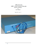
DPhy v1.2 Decoder MIPI 2.5Gb/s Protocol Decoder Hardware DataSheet & User Manual June 2015 - Rev 1.0 1 MIPI DPhy Decoder 1.0 General: The MIPI DPhy v1.2 Decoder (DPhyDkd) is the hardware probe that supports MIPI DPhy signal acquisition with protocol decode occuring on a host Windows PC. Users familiar with the predecessor product “DphyDecoder” will note a nearly complete overlap of function and look and feel. The DPhyDkd supports: sophisticated real-time triggering “Rx” mode and “Sniff” mode real-time status monitoring activity statistics status LED indicators “Sniff” mode: active probes, solder-down, for minimal loading of the device under test. “Rx” mode includes internal active termination and SMA connectors USB 3.0 for fast data transfer The control and decode software that is provided with DPhyDkd (DPhyDecoderCtl) interfaces to the hardware and provides the following features: Configuration control Disassembly of the captured information in a logic analyzer-like format. Reassembly and display of any video information captured Storage of captured video frame(s) to a file(s). Refer to the DPhyDecoderCtl document for a detailed treatment of all the software features. DPhyDkd support up to 4 data lanes and 1 clock lane. Data rate operation up to 2.5 Gb/s per lane is supported. Connection to the DUT is via 5 active solder-down probes (supplied), one per lane or via SMA for Rx mode. Power for the DPhyDkd comes from an external desktop universal power supply. It also features a “Trigger” output on an SMA connector that can drive into a 50 ohm termination. Configuration and control and PC acquisition of the captured data from the DPhyDkd is via a USB 3.0 connection to the PC-based software application DPhyDecoderCtl. Refer to the DPhyDecoderCtl manual for the details of operating this software. 2 2.0 Requirements: The DPhyDkd must be connected to a PC via USB 2.0/USB3.0. The PC must be running the DphyDecoderCtl application and must have the drivers (provided) installed correctly. This will require Admin privelages on the PC. The PC must be running Microsoft Windows Win7-32/64 bit or Win 8 The MIPI DPhy signals being monitored must be nearly within specification from both a protocol and an electrical point-of-view. This becomes more important as the link bitrate increases. 3 3 Connections and Indicators 3.1 USB The USB connection between the unit and the PC is made via the rear panel. The connector is labeled “USB”. It accepts the “B” end of a mini-USB 3.0 cable. The cable provided has enhanced retention features. 3.2 Power This is covered in the next section “Usage”. 3.3 Front Panel Indicator LEDs There are 8 front-panel indicators. Except as noted, they are “sticky” in that if an event occurs, the LED will light for a fixed period of time so that a human observer can see it happen. From left to right they are and indicate as follows: Idle Green. There is no traffic at the present time HSTraffic Green. There is High Speed traffic present. LP Traffic Green. There is Low Power traffic present. BTA Green. A Bus Turn Around cycle is in progress ULPS Green. Bus is in Ultra Low Power State. TriggerGreen. The trigger conditions specified via the GUI have been met. Errors Red, not sticky (the associated indicator in the GUI is sticky). CRC and/or Checksum errors have been detected. The reason this indicator is not sticky is so that a user can get a real-time feel for the error rate and feedback if the user is making an adjustment that may affect the error rate. Spare – Yellow, this is reserved for future use. Currently it comes on at power up and stays on. 4 3.4 Probe heads In “Sniff” mode, signal acquisition from the DUT is via 5 active, solder-down probe heads: one for the clock lane and one each for up to 4 data lanes. Lanes are labeled at the Decoder end of the cable. For the highest electrical performance, we recommend a small whisker of wire be soldered between the probe tip end and the circuit under test. This will give the system some mechanical flexibility and will help prevent damage to either the probe tip ends or the circuit under test. Unused probe heads should be wrapped up in an antistatic container such as a nickel bag. If a user expects to not use particular lanes long-term, the probe head and cable can be unplugged and removed from inside the unit. Removal will keep the probe head out of the user’s way and lessen the likelihood of damage (but remember where you put it; they are easy to lose and quite expensive to replace!). Probe polarity is identified in the following illustration. Probe + should connect to D-PHY lane Dp , with probe – connecting to D-PHY Dn. If the input resistors to the probe become damaged as a result of soldering/de-soldering, etc., they may be replaced with 1.33 K 1% 0603 resistors. All normal soldering and ESD precautions must be observed. Probe head tip resistors are user-replaceable. 10 spare resistors are provided for each probe head. Users are cautioned that probe tip resistor soldering replacement requires a fair bit of skill in order to avoid damage to the probe head circuit board. C O N N E C T O R o n b a c k + H E A T S H R IN K ( c o lo rv a rie s ,c le a rs h o w n ) When soldering the probe directly to traces or pads or vias, care must be taken to prevent mechanical stress to the probe head else circuit damage may result. 5 The colors on the end of the probes are meaningless. They are provided to help with probe logistics. When shipped, Data Lane one is Red, Data Lane two is Green, Clock is Clear, Data Lane three is Blue, and Data Lane 4 is White (following the resistor color code). The probes are all interchangeable, including the clock. However, calibration will be slightly affected by interchanging the probes. For usage information, see section 4 below. 3.5 SMA inputs In “Rx” mode, signal acquisition from the DUT is via 10 SMA connectors: two for the differential clock lane and two for each differential lane for up to 4 data lanes. Lanes are labeled at the Decoder end of the cable. In Rx mode, these signals are actively terminated by the unit in response to the protocol on the wires. 6 4 Operation 4.1 Modes: There are two modes of operation: “Sniff” mode and “Rx” mode. “Sniff” mode acquires the signal from the DUT via the active solder-down probe heads. This is generally used “mid-bus” when there is a DPhy Transmitter connected to a DPhy receiver and the user wants to monitor and/or decode the traffic on the bus. The active probes non-invasively allow the user to monitor the traffic. The unit does not interact with either the transmitter or the receiver. 4.2 Connections: 4.2.1 “Sniff” mode: Connect the USB cable to the PC, and the probe heads to the DUT. Make sure the black ground wire is attached to the DUT ground. We have found that the best way to connect the solder-down probes to the DUT is to solder short (~7mm) “whisker” wires to each of the probe tips then down to the DUT. Tie the probe head to the DUT with some electrical tape to stabilize the setup and strailrelieve the whisker wires. If short whisker wires cannot work for a particular setup, the user can extend the length to the probe head by soldering a 100-200 ohm resistor to the DUT then extending the other end to the probe head. This wire can be up to ~40mm before significant signal degradation occurs. Note that this additional resistance will cause some degradation of the DPhy signal amplitude. In critical applications, the probe tip resistors value should be reduced by the amount of the additional external resistance. 4.2.2 “Rx” Mode: Connect the DUT transmitter to the SMA connections via high-quality 50 ohm coaxial cables. We recommend the length not exceed 70cm. The limitation is not due to the high-speed nature of the signal; it is due to MIPI DPhy LP mode not being terminated at the receiver and yet having fairly fast risetimes. Longer connections result in many reflections during LP signals. After about 90cm of length, the decoder may get confused by the reflections. In Rx mode, the unit actively terminates the signals as required by the protocol. Further, it will also respond (as programmed by the user via the DphyDecoderCtl GUI) to BTA requests as a normal receiver would. This response is rudimentary and the unit does not have the capability to respond differently to different types of BTA requests. 7 Connect the external 24 volt power supply to DPhyDkd via the connector on the rear panel marked “24 Vdc”. Note that there is a LED visible through a hole next to the power connector. This LED will light with a green color when power is applied to the unit. Upon power-up, the left-most two leds (“Idle” and “HS Traffic”) will blink back and forth a few times to indicate that the internal boot process is complete. This system is intended to be operated in a lab environment where proper grounding of all equipment and surfaces is implemented. The system monitors very small signals across a very wide frequency range and is easily upset by large EM fields and static discharges. 8 4.3 Clock delay line setting The DPhyDkd was designed to operate with systems that may not be within spec, particularly with respect to the clock-to-data timing relationship. We have provided an adjustment available through the GUI so that a user can optimize the timing. As the user operates closer to the maximum clock rate limit for the DPhyDkd (the setting becomes more sensitive with number of lanes), this setting gets very critical, working over a ~400pS range typically at 1.5Gbps. A clue that the timing needs adjustment is that the DPhyDkd has no errors at lower frequencies. If it detects errors at the highest bit rates, the user should try changing this setting over a +/- 200pS range. The GUI has a button that automates the search for the best possible setting of this delay line. 4.4 Synchronization In MIPI DPhy v1.2 at bitrates greater than 1.5 Gbps, transmitters are required to send a training sequence periodically so that receivers can optimize their sampling phase. The DPhyDkd hardware has enough timing margin such that it does not actually need to train to recover the signal as long as it was transmitted within spec since the timing variation allowed in the spec is less than the acquisition setup and hold time required by the DPhyDkd. However, if the transmitter is out of spec, the signal can still be acquired by using the methods outlined in the paragraph above (4.3). 9 5.0 Electrical specification for the DPhyDkd Characteristic Maximum data rate Maximum clock rate Input Impedance, active probes Trigger Out, impedance Specification 2.5 Gb/s 1250 MHz 2.0k to ground in parallel with less than 1pF, each side of the Differential input ~50 ohms Notes per lane This will slightly reduce the LP voltage high signal depending on the output impedance of the source Trigger Out, amplitude ~3.3V open circuit 1.65V into 50 ohms Probe Head tip resistors 1.33k, 1% 0603 package style, lead-free Storage Capacity, video data 256MBytes 512Mbytes total vector storage (half is overhead). Clock delay range Logic low is ground. ~9 nS External Power Supply Operating Environment 24 Vdc, 50 watts max 20-30 degrees C Less than 15,000’ elevation No condensing humidity Universal, supplied Lab environment No strong, stray fields No static discharges Weight Weight, power supply and cord Overall Dimensions ~1170 grams ~475 grams 345mm x 195mm x 80mm approximate, without supply approximate Approximate, without supply Note that this product is RoHS compliant, even though it is currently exempt from RoHS requirements. 10 For more information contact: The Moving Pixel Company 4905 SW Griffith Drive Suite 106 Beaverton, Oregon 97005 www.movingpixel.com [email protected] +1.503.626.9663 phone PST 11