1
Rabbit® 3000 Microprocessor
User’s Manual
019–0108 •
070831–R
Rabbit 3000 Microprocessor User’s Manual
Part Number 019-0108 • 070831–R • Printed in U.S.A.
©2002–2007 Rabbit Semiconductor Inc. • All rights reserved.
No part of the contents of this manual may be reproduced or transmitted in any form or by any means
without the express written permission of Rabbit Semiconductor.
Permission is granted to make one or more copies as long as the copyright page contained therein is
included. These copies of the manuals may not be let or sold for any reason without the express written
permission of Rabbit Semiconductor.
Rabbit Semiconductor reserves the right to make changes and
improvements to its products without providing notice.
Trademarks
Rabbit and Dynamic C are registered trademarks of Rabbit Semiconductor Inc.
Rabbit 3000 is a trademark of Rabbit Semiconductor Inc.
The latest revision of this manual is available on the Rabbit Semiconductor Web site,
www.rabbit.com, for free, unregistered download.
Rabbit Semiconductor Inc.
www.rabbit.com
Rabbit 3000 Microprocessor User’s Manual
TABLE OF CONTENTS
Chapter 1. Introduction
1
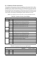
1.1 Features and Specifications Rabbit 3000..............................................................................................2
1.2 Summary of Rabbit 3000 Advantages ..................................................................................................6
1.3 Differences Rabbit 3000 vs. Rabbit 2000 .............................................................................................7
Chapter 2. Rabbit 3000 Design Features
9
2.1 The Rabbit 8-bit Processor vs. Other Processors................................................................................10
2.2 Overview of On-Chip Peripherals and Features .................................................................................11
2.2.1 5 V Tolerant Inputs ....................................................................................................................11
2.2.2 Serial Ports .................................................................................................................................11
2.2.3 System Clock .............................................................................................................................12
2.2.4 32.768 kHz Oscillator Input .......................................................................................................12
2.2.5 Parallel I/O .................................................................................................................................13
2.2.6 Slave Port ...................................................................................................................................14
2.2.7 Auxiliary I/O Bus .......................................................................................................................15
2.2.8 Timers ........................................................................................................................................15
2.2.9 Input Capture Channels ..............................................................................................................16
2.2.10 Quadrature Decoder Inputs ......................................................................................................17
2.2.11 Pulse Width Modulation Outputs .............................................................................................17
2.2.12 Spread Spectrum Clock ............................................................................................................18
2.2.13 Separate Core and I/O Power Pins ...........................................................................................18
2.3 Design Standards ................................................................................................................................18
2.3.1 Programming Port ......................................................................................................................18
2.3.2 Standard BIOS ...........................................................................................................................19
2.4 Dynamic C Support for the Rabbit .....................................................................................................19
Chapter 3. Details on Rabbit
Microprocessor Features
21
3.1 Processor Registers .............................................................................................................................21
3.2 Memory Mapping ...............................................................................................................................23
3.2.1 Extended Code Space .................................................................................................................26
3.2.2 Separate I and D Space - Extending Data Memory ...................................................................27
3.2.3 Using the Stack Segment for Data Storage ................................................................................29
3.2.4 Practical Memory Considerations ..............................................................................................30
3.3 Instruction Set Outline ........................................................................................................................32
3.3.1 Load Immediate Data to a Register ............................................................................................33
3.3.2 Load or Store Data from or to a Constant Address ....................................................................33
3.3.3 Load or Store Data Using an Index Register .............................................................................34
3.3.4 Register-to-Register Move .........................................................................................................35
3.3.5 Register Exchanges ....................................................................................................................35
3.3.6 Push and Pop Instructions ..........................................................................................................36
3.3.7 16-bit Arithmetic and Logical Ops ............................................................................................36
3.3.8 Input/Output Instructions ...........................................................................................................39
3.4 How to Do It in Assembly Language—Tips and Tricks ....................................................................40
3.4.1 Zero HL in 4 Clocks ...................................................................................................................40
3.4.2 Exchanges Not Directly Implemented .......................................................................................40
3.4.3 Manipulation of Boolean Variables ...........................................................................................40
3.4.4 Comparisons of Integers ............................................................................................................41
Table of Contents
3.4.5 Atomic Moves from Memory to I/O Space ............................................................................... 43
3.5 Interrupt Structure .............................................................................................................................. 44
3.5.1 Interrupt Priority ........................................................................................................................ 44
3.5.2 Multiple External Interrupting Devices ..................................................................................... 46
3.5.3 Privileged Instructions, Critical Sections and Semaphores ....................................................... 46
3.5.4 Critical Sections ......................................................................................................................... 47
3.5.5 Semaphores Using Bit B,(HL) .................................................................................................. 47
3.5.6 Computed Long Calls and Jumps .............................................................................................. 48
Chapter 4. Rabbit Capabilities
49
4.1 Precisely Timed Output Pulses .......................................................................................................... 49
4.1.1 Pulse Width Modulation to Reduce Relay Power ..................................................................... 50
4.2 Open-Drain Outputs Used for Key Scan............................................................................................ 51
4.3 Cold Boot ........................................................................................................................................... 52
4.4 The Slave Port .................................................................................................................................... 53
4.4.1 Slave Rabbit As A Protocol UART ........................................................................................... 54
Chapter 5. Pin Assignments and Functions
55
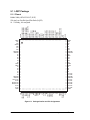
5.1 LQFP Package.................................................................................................................................... 56
5.1.1 Pinout ......................................................................................................................................... 56
5.1.2 Mechanical Dimensions and Land Pattern ................................................................................ 57
5.2 Ball Grid Array Package ................................................................................................................... 59
5.2.1 Pinout ......................................................................................................................................... 59
5.2.2 Mechanical Dimensions and Land Pattern ................................................................................ 60
5.3 Rabbit Pin Descriptions...................................................................................................................... 62
5.4 Bus Timing......................................................................................................................................... 64
5.5 Description of Pins with Alternate Functions .................................................................................... 65
5.6 DC Characteristics.............................................................................................................................. 68
5.7 I/O Buffer Sourcing and Sinking Limit.............................................................................................. 69
Chapter 6. Rabbit Internal I/O Registers
71
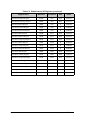
6.1 Default Values for all the Peripheral Control Registers..................................................................... 73
Chapter 7. Miscellaneous Functions
79
7.1 Processor Identification...................................................................................................................... 79
7.2 Rabbit Oscillators and Clocks ............................................................................................................ 80
7.3 Clock Doubler .................................................................................................................................... 83
7.4 Clock Spectrum Spreader................................................................................................................... 86
7.5 Chip Select Options for Low Power .................................................................................................. 87
7.6 Output Pins CLK, STATUS, /WDTOUT, /BUFEN .......................................................................... 90
7.7 Time/Date Clock (Real-Time Clock) ................................................................................................. 91
7.8 Watchdog Timer................................................................................................................................. 93
7.9 System Reset ...................................................................................................................................... 95
7.10 Rabbit Interrupt Structure................................................................................................................. 97
7.10.1 External Interrupts ................................................................................................................... 99
7.10.2 Interrupt Vectors: INT0 - EIR,0x00/INT1 - EIR,0x08 .......................................................... 100
7.11 Bootstrap Operation ....................................................................................................................... 101
7.12 Pulse Width Modulator .................................................................................................................. 103
7.13 Input Capture.................................................................................................................................. 105
7.14 Quadrature Decoder ....................................................................................................................... 110
Chapter 8. Memory Interface and Mapping
115
8.1 Interface for Static Memory Chips................................................................................................... 115
8.2 Memory Mapping Overview............................................................................................................ 117
8.3 Memory-Mapping Unit .................................................................................................................... 117
Rabbit 3000 Microprocessor User’s Manual
8.4 Memory Interface Unit .....................................................................................................................119
8.5 Memory Bank Control Registers ......................................................................................................120
8.5.1 Optional A16, A19 Inversions by Segment (/CS1 Enable) .....................................................121
8.6 Allocation of Extended Code and Data ............................................................................................124
8.7 Instruction and Data Space Support..................................................................................................125
8.8 How the Compiler Compiles to Memory .........................................................................................128
Chapter 9. Parallel Ports
129
9.1 Parallel Port A...................................................................................................................................130
9.2 Parallel Port B ...................................................................................................................................131
9.3 Parallel Port C ...................................................................................................................................132
9.4 Parallel Port D...................................................................................................................................133
9.5 Parallel Port E ...................................................................................................................................137
9.6 Parallel Port F ...................................................................................................................................140
9.6.1 Using Parallel Port A and Parallel Port F ................................................................................141
9.7 Parallel Port G...................................................................................................................................143
Chapter 10. I/O Bank Control Registers
145
Chapter 11. Timers
149
11.1 Timer A...........................................................................................................................................150
11.1.1 Timer A I/O Registers ............................................................................................................151
11.1.2 Practical Use of Timer A .......................................................................................................155
11.2 Timer B ...........................................................................................................................................156
11.2.1 Using Timer B ........................................................................................................................159
Chapter 12. Rabbit Serial Ports
161
12.1 Serial Port Register Layout.............................................................................................................164
12.2 Serial Port Registers........................................................................................................................166
12.3 Serial Port Interrupt ........................................................................................................................179
12.4 Transmit Serial Data Timing ..........................................................................................................180
12.5 Receive Serial Data Timing ............................................................................................................181
12.6 Clocked Serial Ports........................................................................................................................182
12.7 Clocked Serial Timing ....................................................................................................................185
12.7.1 Clocked Serial Timing With Internal Clock ..........................................................................185
12.7.2 Clocked Serial Timing with External Clock ..........................................................................185
12.8 Synchronous Communications on Ports E and F............................................................................187
12.9 Serial Port Software Suggestions....................................................................................................192
12.9.1 Controlling an RS-485 Driver and Receiver ..........................................................................193
12.9.2 Transmitting Dummy Characters ...........................................................................................193
12.9.3 Transmitting and Detecting a Break ......................................................................................194
12.9.4 Using A Serial Port to Generate a Periodic Interrupt .............................................................194
12.9.5 Extra Stop Bits, Sending Parity, 9th Bit Communication Schemes .......................................194
12.9.6 Parity, Extra Stop Bits with 7-Data-Bit Characters ...............................................................195
12.9.7 Parity, Extra Stop Bits with 8-Data-Bit Characters ...............................................................195
12.9.8 Supporting 9th Bit Communication Protocols .......................................................................196
12.9.9 Rabbit-Only Master/Slave Protocol .......................................................................................196
12.9.10 Data Framing/Modbus .........................................................................................................196
Chapter 13. Rabbit Slave Port
199
13.1 Hardware Design of Slave Port Interconnection ............................................................................204
13.2 Slave Port Registers ........................................................................................................................205
13.3 Applications and Communications Protocols for Slaves................................................................208
13.3.1 Slave Applications .................................................................................................................208
13.3.2 Master-Slave Messaging Protocol .........................................................................................208
Table of Contents
Chapter 14. Rabbit 3000 Clocks
211
14.1 Low-Power Design......................................................................................................................... 212
Chapter 15. EMI Control
213
15.1 Power Supply Connections and Board Layout .............................................................................. 214
15.2 Using the Clock Spectrum Spreader .............................................................................................. 214
Chapter 16. AC Timing Specifications
217
16.1 Memory Access Time .................................................................................................................... 217
16.2 I/O Access Time............................................................................................................................. 225
16.3 Further Discussion of Bus and Clock Timing ................................................................................ 227
16.4 Maximum Clock Speeds ................................................................................................................ 229
16.5 Power and Current Consumption ................................................................................................... 231
16.6 Current Consumption Mechanisms................................................................................................ 234
16.7 Sleepy Mode Current Consumption ............................................................................................... 235
16.8 Memory Current Consumption ...................................................................................................... 236
16.9 Battery-Backed Clock Current Consumption ................................................................................ 237
16.10 Reduced-Power External Main Oscillator.................................................................................... 238
Chapter 17. Rabbit BIOS and Virtual Driver
239
17.1 The BIOS........................................................................................................................................ 239
17.1.1 BIOS Services ....................................................................................................................... 239
17.1.2 BIOS Assumptions ................................................................................................................ 240
17.2 Virtual Driver ................................................................................................................................. 240
17.2.1 Periodic Interrupt ................................................................................................................... 240
17.2.2 Watchdog Timer Support ...................................................................................................... 240
Chapter 18. Other Rabbit Software
243
18.1 Power Management Support .......................................................................................................... 243
18.2 Reading and Writing I/O Registers ................................................................................................ 244
18.2.1 Using Assembly Language .................................................................................................... 244
18.2.2 Using Library Functions ........................................................................................................ 244
18.3 Shadow Registers ........................................................................................................................... 245
18.3.1 Updating Shadow Registers .................................................................................................. 245
18.3.2 Interrupt While Updating Registers ....................................................................................... 245
18.3.3 Write-only Registers Without Shadow Registers .................................................................. 246
18.4 Timer and Clock Usage.................................................................................................................. 246
Chapter 19. Rabbit Instructions
249
19.1 Load Immediate Data ..................................................................................................................... 252
19.2 Load & Store to Immediate Address.............................................................................................. 252
19.3 8-bit Indexed Load and Store ......................................................................................................... 252
19.4 16-bit Indexed Loads and Stores .................................................................................................... 252
19.5 16-bit Load and Store 20-bit Address ............................................................................................ 253
19.6 Register to Register Moves ............................................................................................................ 253
19.7 Exchange Instructions .................................................................................................................... 254
19.8 Stack Manipulation Instructions..................................................................................................... 254
19.9 16-bit Arithmetic and Logical Ops................................................................................................. 254
19.10 8-bit Arithmetic and Logical Ops................................................................................................. 255
19.11 8-bit Bit Set, Reset and Test......................................................................................................... 256
19.12 8-bit Increment and Decrement.................................................................................................... 256
19.13 8-bit Fast A Register Operations .................................................................................................. 257
19.14 8-bit Shifts and Rotates ................................................................................................................ 257
19.15 Instruction Prefixes ...................................................................................................................... 258
Rabbit 3000 Microprocessor User’s Manual
19.16
19.17
19.18
19.19
Block Move Instructions...............................................................................................................258
Control Instructions - Jumps and Calls.........................................................................................259
Miscellaneous Instructions ...........................................................................................................259
Privileged Instructions ..................................................................................................................260
Chapter 20. Differences Rabbit vs. Z80/Z180 Instructions
261
Chapter 21. Instructions in Alphabetical Order
With Binary Encoding
263
Appendix A.
The Rabbit Programming Port
271
A.1 Use of the Programming Port as a Diagnostic/Setup Port ...............................................................272
A.2 Alternate Programming Port ............................................................................................................272
A.3 Suggested Rabbit Crystal Frequencies.............................................................................................273
Appendix B. Rabbit 3000 Revisions
275
B.1 Discussion of Fixes and Improvements ...........................................................................................278
B.1.1 Rabbit Internal I/O Registers ...................................................................................................279
B.1.2 Peripheral and ISR Address ....................................................................................................282
B.1.3 Revision-Level ID Register .....................................................................................................284
B.1.4 System/User Mode ..................................................................................................................285
B.1.5 Memory Protection ..................................................................................................................286
B.1.6 Stack Protection .......................................................................................................................291
B.1.7 RAM Segment Relocation .......................................................................................................293
B.1.8 Secondary Watchdog Timer ....................................................................................................294
B.1.9 New Opcodes ..........................................................................................................................295
B.1.10 Expanded I/O Memory Addressing .......................................................................................297
B.1.11 External I/O Improvements ...................................................................................................298
B.1.12 Short Chip Select Timing for Writes .....................................................................................299
B.1.13 Pulse Width Modulator Improvements .................................................................................313
B.1.14 Quadrature Decoder Improvements ......................................................................................316
B.2 Pins with Alternate Functions ..........................................................................................................318
Appendix C. System/User Mode
319
C.1 System/User Mode Opcodes ............................................................................................................320
C.2 System/User Mode Registers ...........................................................................................................321
C.3 Interrupts ..........................................................................................................................................323
C.3.1 Peripheral Interrupt Prioritization ...........................................................................................324
C.4 Using the System/User Mode...........................................................................................................326
C.4.1 Memory Protection Only .........................................................................................................326
C.4.2 Mixed System/User Mode Operation ......................................................................................327
C.4.3 Complete Operating System ....................................................................................................328
Appendix D.
Rabbit 3000A Internal I/O Registers
Index
Table of Contents
329
337
Rabbit 3000 Microprocessor User’s Manual
1. INTRODUCTION
Rabbit Semiconductor was formed expressly to design a a better microprocessor for use in
small and medium-scale controllers. The first microprocessor was the Rabbit 2000. The
second microprocessor, now available, is the Rabbit 3000. Rabbit microprocessor designers have had years of experience using Z80, Z180, and HD64180 microprocessors in small
controllers. The Rabbit shares a similar architecture and a high degree of compatibility
with these microprocessors, but it is a vast improvement.
The Rabbit 3000 has been designed in close cooperation with Z-World, Inc., a long-time
manufacturer of low-cost single-board computers. Z-World and Rabbit Semiconductor
products are supported by an innovative C-language development system (Dynamic C).
The Rabbit 3000 is easy to use. Hardware and software interfaces are as uncluttered and
are as foolproof as possible. The Rabbit has outstanding computation speed for a microprocessor with an 8-bit bus. This is because the Z80-derived instruction set is very compact, and the timing of the memory interface allows higher clock speeds for a given
memory speed.
Microprocessor hardware and software development is easy for Rabbit users. In-circuit
emulators are not needed and will not be missed by the Rabbit developer. Software development is accomplished by connecting a simple interface cable from a PC serial port to the
Rabbit-based target system or by performing software development and debugging over a
network or the Internet using interfaces and tools provided by Rabbit Semiconductor.
Chapter 1 Introduction
1
1.1 Features and Specifications Rabbit 3000
• 128-pin LQFP package. Operating voltage 1.8 V to 3.6 V. Clock speed to 54+ MHz. All
specifications are given for both industrial and commercial temperature and voltage
ranges. Rabbit microprocessors are low-cost.
• Industrial specifications are for 3.3 V ±10% and a temperature range from -40°C to
+85°C. Modified commercial specifications are for a voltage variation of 5% and a
temperature range from -40°C to 70°C.
• 1-megabyte code-data space allows C programs with 50,000+ lines of code. The
extended Z80-style instruction set is C-friendly, with short and fast opcodes for the
most important C operations.
• Four levels of interrupt priority make a fast interrupt response practical for critical
applications. The maximum time to the first instruction of an interrupt routine is about
0.5 µs at a clock speed of 50 MHz.
• Access to I/O devices is accomplished by using memory access instructions with an I/O
prefix. Access to I/O devices is thus faster and easier compared to processors with a
distinct and narrow I/O instruction set. As an option the auxiliary I/O bus can be
enabled to use separate pins for address and data, allowing the I/O bus to have a greater
physical extent with less EMI and less conflict with the requirements of the fast memory bus.(Further described below.)
• Hardware design is simple. Up to six static memory chips (such as RAM and flash
memory) connect directly to the microprocessor with no glue logic. A memory-access
time of 55 ns suffices to support up to a 30 MHz clock with no wait states; with a 30 ns
memory-access time, a clock speed of up to 50 MHz is possible with no wait states.
Most I/O devices may be connected without glue logic.
The memory read cycle is two clocks long. The write cycle is 3 clocks long. A clean
memory and I/O cycle completely avoid the possibility of bus fights. Peripheral I/O
devices can usually be interfaced in a glueless fashion using the common /IORD and
/IOWR strobes in addition to the user-configurable IO strobes on Parallel Port E. The
Parallel Port E pins can be configured as I/O read, write, read/write, or chip select when
they are used as I/O strobes.
• EMI reduction features reduce EMI levels by as much as 25 dB compared to other similar microprocessors. Separate power pins for the on-chip I/O buffers prevent high-frequency noise generated in the processor core from propagating to the signal output
pins. A built-in clock spectrum spreader reduces electromagnetic interference and facilitates passing EMI tests to prove compliance with government regulatory requirements.
As a consequence, the designer of a Rabbit-3000-based system can be assured of passing FCC or CE EMI tests as long as minimal design precautions are followed.
• The Rabbit may be cold-booted via a serial port or the parallel access slave port. This
means that flash program memory may be soldered in unprogrammed, and can be
reprogrammed at any time without any assumption of an existing program or BIOS.
2
Rabbit 3000 Microprocessor User’s Manual
A Rabbit that is slaved to a master processor can operate entirely with volatile RAM,
depending on the master for a cold program boot.
• There are 56 parallel I/O lines (shared with serial ports). Some I/O lines are timer synchronized, which permits precisely timed edges and pulses to be generated under combined hardware and software control. Pulse-width modulation outputs are implemented
in addition to the timer-synchronization feature (see below).
• Four pulse width modulated (PWM) outputs are implemented by special hardware. The
repetition frequency and the duty cycle can be varied over a wide range. The resolution
of the duty cycle is 1 part in 1024.
• There are six serial ports. All six serial ports can operate asynchronously in a variety of
commonly used operating modes. Four of the six ports (designated A, B, C, D) support
clocked serial communications suitable for interfacing with “SPI” devices and various
similar devices such as A/D converters and memories that use a clocked serial protocol.
Two of the ports, E and F, support HDLC/SDLC synchronous communication. These
ports have a 4-byte FIFO and can operate at a high data rate. Ports E and F also have a
digital phase-locked loop for clock recovery, and support popular data-encoding methods. High data rates are supported by all six serial ports. The asynchronous ports also
support the 9th bit network scheme as well as infrared transmission using the IRDA protocol. The IRDA protocol is also supported in SDLC format by the two ports that support SDLC.
• A slave port allows the Rabbit to be used as an intelligent peripheral device slaved to a
master processor. The 8-bit slave port has six 8-bit registers, 3 for each direction of
communication. Independent strobes and interrupts are used to control the slave port in
both directions. Only a Rabbit and a RAM chip are needed to construct a complete
slave system, if the clock and reset control are shared with the master processor
• There is an option to enable an auxiliary I/O bus that is separate from the memory bus.
The auxiliary I/O bus toggles only on I/O instructions. It reduces EMI and speeds the
operation of the memory bus, which only has to connect to memory chips when the
auxiliary I/O bus is used to connect I/O devices. This important feature makes memory
design easy and allows a more relaxed approach to interfacing I/O devices.
• The built-in battery-backable time/date clock uses an external 32.768 kHz crystal oscillator. The suggested model circuit for the external oscillator utilizes a single “tiny
logic” active component. The time/date clock can be used to provide periodic interrupts
every 488 µs. Typical battery current consumption is about 3 µA.
• Numerous timers and counters can be used to generate interrupts, baud rate clocks, and
timing for pulse generation.
• Two input-capture channels can be used to measure the width of pulses or to record the
times at which a series of events take place. Each capture channel has a 16-bit counter
and can take input from one or two pins selected from any of 16 pins.
• Two quadrature decoder units accept input from incremental optical shaft encoders.
These units can be used to track the motion of a rotating shaft or similar device.
Chapter 1 Introduction
3
• A built-in clock doubler allows ½-frequency crystals to be used.
• The built-in main clock oscillator uses an external crystal or a ceramic resonator. Typical
crystal or resonator frequencies are in the range of 1.8 MHz to 30 MHz. Since precision
timing is available from the separate 32.768 kHz oscillator, a low-cost ceramic resonator
with ½ percent error is generally satisfactory. The clock can be doubled or divided down
to modify speed and power dynamically. The I/O clock, which clocks the serial ports, is
divided separately so as not to affect baud rates and timers when the processor clock is
divided or multiplied. For ultra low power operation, the processor clock can be driven
from the separate 32.768 kHz oscillator and the main oscillator can be powered down.
This allows the processor to operate at approximately between 20 and 100 µA and still
execute instructions at the rate of up to 10,000 instructions per second. The 32.768 kHz
clock can also be divided by 2, 4, 8 or 16 to reduce power. This “sleepy mode” is a powerful alternative to sleep modes of operation used by other processors.
• Processor current requirement is approximately 65 mA at 30 MHz and 3.3 V. The current is proportional to voltage and clock speed—at 1.8 V and 3.84 MHz the current
would be about 5 mA, and at 1 MHz the current is reduced to about 1 mA.
• To allow extreme low power operation there are options to reduce the duty cycle of
memories when running at low clock speeds by only enabling the chip select for a brief
period, long enough to complete a read. This greatly reduces the power used by flash
memory when operating at low clock speeds.
• The excellent floating-point performance is due to a tightly coded library and powerful
processing capability. For example, a 50 MHz clock takes 7 µs for a floating add, 7 µs
for a multiply, and 20 µs for a square root. In comparison, a 386EX processor running
with an 8-bit bus at 25 MHz and using Borland C is about 20 times slower.
• There is a built-in watchdog timer.
• The standard 10-pin programming port eliminates the need for in-circuit emulators. A
very simple 10-pin connector can be used to download and debug software using
Rabbit Semiconductor’s Dynamic C and a simple connection to a PC serial port. The
incremental cost of the programming port is extremely small.
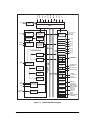
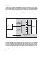
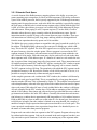
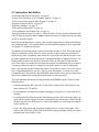
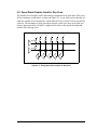
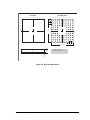
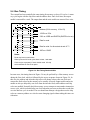
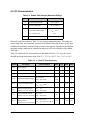
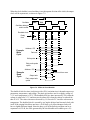
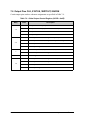
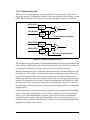
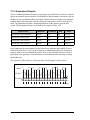
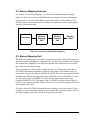
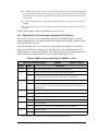
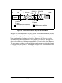
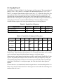
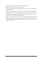
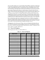
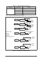
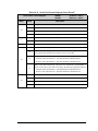
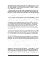
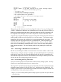
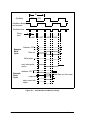
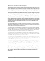
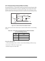
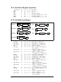
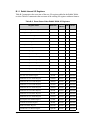
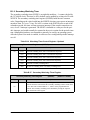
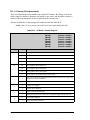
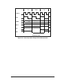
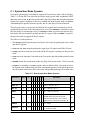
Figure 1-1 shows a block diagram of the Rabbit.
4
Rabbit 3000 Microprocessor User’s Manual
Data
Buffer
CLK
/WDTOUT
STATUS
SMODE1
SMODE0
/BUFEN
/IORD
/IOWR
/RESET
RESOUT
D[7:0]
External Interface
CPU
XTALA1
XTALA2
Memory
Management/
Control
Spectrum
Spreader
Clock
Doubler
Fast
Oscillator
Global Power
Save & Clock
Distribution
(8 bits)
Address
Buffer
ADDRESS BUS
A[19:0]
Timer A
Memory Chip
Interface
/CS2, /CS1, /CS0
/OE1, /OE0
/WE1, /WE0
Parallel Ports
Port A
PA [7:0]
Port B
PB[7:0]
Port C
PC[7:0]
Port D
PD[7:0]
Port E
PE[7:0]
Port F
PF[7:0]
Port G
PG[7:0]
Serial Port A
Asynch
Synch
Serial
Serial
Asynch
Synch
Bootstrap Bootstrap
Timer B
Asynch Serial IrDA
32.768 kHz
Clock Input
IrDA Bootstrap
Watchdog
Timer
(8 bits)
Real-Time
Clock
Serial Ports
B,C,D
DATA BUS
CLK32K
Asynch
Serial
Periodic
Interrupt
IA[5:0]
I[7:0]
External I/O
Chip Interface
INT0A, INT1A
INT0B, INT1B
External
Interrupts
Synch
Serial
Asynch Serial IrDA
Serial Ports
E, F
Asynch
Serial
ID[7:0]
TXA, RXA, CLKA,
ATXA, ARXA
HDLC
SDLC
Asynch Serial IrDA
HDLC/SDLC IrDA
TXB, RXB, CLKB,
ATXB, ARXB
TXC, RXC, CLKC
TXD, RXD, CLKD
TXE, RXE
TCLKE, RCLKE
TXF, RXF
TCLKF, RCLKF
Pulse Width
Modulation
PWM[3:0]
Quadrature
Decoder
QD1A, QD1B
QD2A, QD2B
AQD1A, AQD1B
AQD2A, AQD2B
Input
Capture
Slave Port
Slave Interface
Bootstrap Interface
PC[7,5,3,1]
PD[7,5,3,1]
PF[7,5,3,1]
PG[7,5,3,1]
SD[7:0]
SA[1:0],
/SCS, /SRD, /SWR,
/SLAVEATTN
Figure 1-1. Rabbit 3000 Block Diagram
Chapter 1 Introduction
5
1.2 Summary of Rabbit 3000 Advantages
• The glueless architecture makes it is easy to design the hardware system.
• There are a lot of serial ports and they can communicate very fast.
• Precision pulse and edge generation is a standard feature.
• EMI is at extremely low levels.
• Interrupts can have multiple priorities.
• Processor speed and power consumption are under program control.
• The ultra low power mode can perform computations and execute logical tests since the
processor continues to execute, albeit at 32 kHz or even as slow as 2 kHz.
• The Rabbit may be used to create an intelligent peripheral or a slave processor. For
example, protocol stacks can be off loaded to a Rabbit slave. The master can be any
processor.
• The Rabbit can be cold-booted so unprogrammed flash memory can be soldered in
place.
• You can write serious software, be it 1,000 or 50,000 lines of C code. The tools are
there and they are low in cost.
• If you know the Z80 or Z180, you know most of the Rabbit.
• A simple 10-pin programming interface replaces in-circuit emulators and PROM programmers.
• The battery-backable time/date clock is included.
• The standard Rabbit chip is made to industrial temperature and voltage specifications.
• The Rabbit 3000 is backed by extensive software development tools and libraries, especially in the area of networking and embedded Internet.
6
Rabbit 3000 Microprocessor User’s Manual
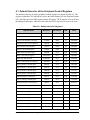
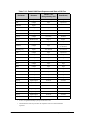
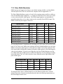
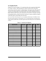
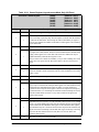
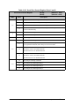
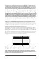
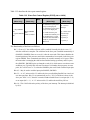
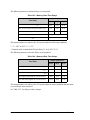
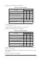
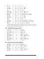
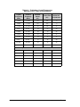
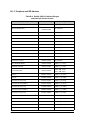
1.3 Differences Rabbit 3000 vs. Rabbit 2000
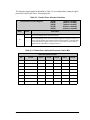
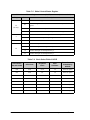
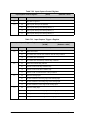
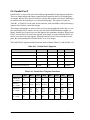
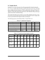
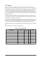
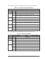
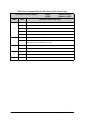
For the benefit of readers who are familiar with the Rabbit 2000 microprocessor the Rabbit 3000 is contrasted with the Rabbit 2000 in the table below.
Feature
Rabbit 3000
Rabbit 2000
Maximum clock speed
54 MHz
30 MHz
Maximum crystal frequency main oscillator (may be
doubled internally)
30 MHz
32 MHz
32.768 kHz crystal oscillator
External
Internal
Maximum operating voltage
3.6 V
5.5 V
Maximum I/O input voltage
5.5 V
5.5 V
2 mA/MHz @ 3.3 V
4 mA/MHz @5 V
128
100
Size of package
16 × 16 × 1.5 mm LQFP
10 × 10 × 1.2 mm
TFBGA
24 × 18 × 3 mm PQFP
Spacing between package pins
0.4 mm (16 mils) LQFP
0.65 mm (26 mils) PQFP
0.8 mm TFBGA
Current consumption
Number of package pins
Separate power and ground for I/O buffers (EMI
reduction)
Yes
No
Clock Spectrum Spreader (EMI reduction)
Yes
Rabbit 2000B and
Rabbit 2000C versions.
1x, 2x, /2, /3, /4, /6, /8
1x, 2x, /4, /8
Sleepy (32 kHz)
Ultra-Sleepy
(16, 8, 2 kHz)
Sleepy (32 kHz)
Short CS (CLK /4 /6 /8)
Self Timed
(32,16,8,2 kHz)
None
Yes
No
7
5
Yes
None
6
4
4 (A, B, C, D)
2 (A, B)
2 (E, F)
None
6
None
Clock Modes
Power Down Modes
Low Power Memory Control (Chip Select)
Extended memory timing for high freq. operation
Number of 8-bit I/O ports
Auxiliary I/O Data/Address bus
Number of serial ports
Serial ports capable of SPI/clocked serial
Serial ports capable of SDLC/HDLC
Asynch serial ports with support for IrDA
communications
Chapter 1 Introduction
7
Feature
Serial ports with support for SDLC/HDLC IrDA
communications
Maximum asynchronous baud rate
Input capture unit
8
Rabbit 3000
Rabbit 2000
2
None
clock speed/8
clock speed/32
2
None
Rabbit 3000 Microprocessor User’s Manual
2. RABBIT 3000 DESIGN FEATURES
The Rabbit 3000 is an evolutionary design. The processor and instruction set are nearly
identical to the immediate predecessor processor, the Rabbit 2000. Both the Rabbit 3000
and the Rabbit 2000 follow in broad outline the instruction set and the register layout of
the Z80 and Z180. Compared to the Z180 the instruction set has been augmented by a substantial number of new instructions. Some obsolete or redundant Z180 instructions have
been dropped to make available efficient 1-byte opcodes for important new instructions.
(see Chapter 20, “Differences Rabbit vs. Z80/Z180 Instructions,”.) The advantage of this
evolutionary approach is that users familiar with the Z80 or Z180 can immediately understand Rabbit assembly language. Existing Z80 or Z180 source code can be assembled or
compiled for the Rabbit with minimal changes.
Changing technology has made some features of the Z80/Z180 family obsolete, and these
features have been dropped in the Rabbit. For example, the Rabbit has no special support
for dynamic RAM but it has extensive support for static memory. This is because the price
of static memory has decreased to the point that it has become the preferred choice for
medium-scale embedded systems. The Rabbit has no support for DMA (direct memory
access) because most of the uses for which DMA is traditionally used do not apply to
embedded systems, or they can be accomplished better in other ways, such as fast interrupt routines, external state machines or slave processors.
Our experience in writing C compilers has revealed the shortcomings of the Z80 instruction set for executing the C language. The main problem is the lack of instructions for handling 16-bit words and for accessing data at a computed address, especially when the stack
contains that data. New instructions correct these problems.
Another problem with many 8-bit processors is their slow execution and a lack of numbercrunching ability. Good floating-point arithmetic is an important productivity feature in
smaller systems. It is easy to solve many programming problems if an adequate floatingpoint capability is available. The Rabbit’s improved instruction set provides fast floatingpoint and fast integer math capabilities.
The Rabbit supports four levels of interrupt priorities. This is an important feature that
allows the effective use of fast interrupt routines for real-time tasks.
Chapter 2 Rabbit 3000 Design Features
9
2.1 The Rabbit 8-bit Processor vs. Other Processors
The Rabbit 3000 processor has been designed with the objective of creating practical systems to solve real world problems in an economical fashion. A cursory comparison of the
Rabbit 3000 compared to other processors with similar capabilities may miss certain Rabbit strong points.
• The Rabbit is a processor that can be used to build a system in which EMI is nearly
absent, even at clock frequencies in excess of 40 MHz. This is due to the split power
supply, the clock doubler, the clock spectrum spreader and the PC board layout advice
(or processor core modules) that we provide. Low EMI is a huge timesaver for the
designer pressed to meet schedules and pass government EMI tests of the final product.
• Execution speed with the Rabbit is usually a pleasant surprise compared to other processors. This is due to the well-chosen and compact instruction set partnered with and
excellent compiler and library. We have many benchmarks, comparing the Rabbit to
186, 386, 8051, Z180 and ez80 families of processors that prove the point.
• The Rabbit memory bus is an exceptionally efficient and very clean design. No external
logic is required to support static memory chips. Battery-backed external memory is
supported by built-in functionality. During reduced-power slow-clock operation the
memory duty cycle can be correspondingly reduced using built-in hardware, resulting
in low power consumption by the memories.
The Rabbit external bus uses 2 clocks for read cycles and 3 clocks for write cycles. This
has many advantages compared to a single-clock design, and on closer examination the
advantages of the single-clock system turn out to be mostly chimerical. The advantages
include: easy design to avoid bus fights, clean write cycles with solid data and address
hold times, flexibility to have memory output enable access times greater than ½ of the
bus cycle, and the ability to use an asymmetric clock generated by a clock doubler. The
supposed advantage that single-clock systems have of double-speed bus operation is
not possible with real-world memories unless the memory is backed with fast-cache
RAM.
• The Rabbit 3000 operates at 3.6 V or less, but it has 5 V tolerant inputs and has a second complete bus for I/O operations that is separate from the memory bus. This second
auxiliary bus can be enabled by the application as a designer option. These features
make it easy to design systems that mix 3 V and 5 V components, and avoid the loading
problems and the EMI problems that result if the memory bus is extended to connect
with many I/O devices.
• The Rabbit may be remotely programmed, including complete cold-boot, via a serial
link, Ethernet, or even via a network or the Internet using built in capabilities and/or the
RabbitLink ethernet network accessory device. These capabilities proven and inexpensive to implement.
• The Rabbit 3000 on-chip peripheral complement is huge compared to competitive processors.
10
Rabbit 3000 Microprocessor User’s Manual
The Rabbit is an 8-bit processor with an 8-bit external data bus and an 8-bit internal data
bus. Because the Rabbit makes the most of its external 8-bit bus and because it has a compact instruction set, its performance is as good as many 16-bit processors.
We hesitate to compare the Rabbit to 32-bit processors, but there are undoubtedly occasions where the user can use a Rabbit instead of a 32-bit processor and save a vast amount
of money. Many Rabbit instructions are 1 byte long. In contrast, the minimum instruction
length on most 32-bit RISC processors is 32 bits.
2.2 Overview of On-Chip Peripherals and Features
The on-chip peripherals were chosen based on our experience as to what types of peripheral devices are most useful in small embedded systems. The major on-chip peripherals
are the serial ports, system clock, time/date oscillator, parallel I/O, slave port, motion
encoders, pulse width modulators, pulse measurement, and timers. These and other features are described below.
2.2.1 5 V Tolerant Inputs
The Rabbit 3000 operates on a voltage in the range of 1.8 V to 3.6 V, but most Rabbit 3000
input pins are 5 V tolerant. The exceptions are the power supply pins, and the oscillator
buffer pins. When a 5 V signal is applied to 5 V tolerant pins, they present a high impedance
even if the Rabbit power is off. The 5 V tolerant feature allows 5 V devices that have a
suitable switching threshold to be directly connected to the Rabbit. This includes HCT
family parts operated at 5 V that have an input threshold between 0.8 and 2 V.
NOTE: CMOS devices operated at 5 V that have a threshold at 2.5 V are not suitable for
direct connection because the Rabbit outputs do not rise above VDD, which cannot
exceed 3.6 V, and is often specified as 3.3 V. Although a CMOS input with a 2.5 V
threshold may switch at 3.3 V, it will consume excessive current and switch slowly.
In order to translate between 5 V and 3.3 V, HCT family parts powered from 5 V can be
used, and are often the best solution. There is also the “LVT” family of parts that operate
from 2.0 V to 3.3 V, but that have 5 V tolerant inputs and are available from many suppliers. True level-translating parts are available with separate 3.3 V and 5 V supply pins, but
these parts are not usually needed, and have design traps involving power sequencing.
Many charge pump chips that perform DC to DC voltage conversion at low cost have been
introduced in recent years. These are convenient for systems with dual voltage requirements.
2.2.2 Serial Ports
There are six serial ports designated ports A, B, C, D, E, and F. All six serial ports can
operate in an asynchronous mode up to a baud rate equal to the system clock divided by 8.
The asynchronous ports use 7-bit or 8-bit data formats, with or without parity. A 9th bit
address scheme, where an additional bit is set or cleared to mark the first byte of a message, is also supported.
The serial port software driver can tell when the last byte of a message has finished transmitting from the output shift register - correcting an important defect of the Z180. This is
Chapter 2 Rabbit 3000 Design Features
11
important for RS-485 communication because a half duplex line driver cannot have the
direction of transmission reversed until the last data bit has been sent. In many UARTs,
including those on the Z180, it is difficult to generate an interrupt after the last bit is sent.
A so called address bit can be transmitted as either high or low after the last data bit. The
address bit, if used, is followed by a high stop bit. This facility can be used to transmit 2
stop bits or a parity bit if desired. The ability to directly transmit a high voltage level
address bit was not included in the original revision of the Rabbit 2000 processor.
Serial Ports A, B, C and D can be operated in the clocked serial mode. In this mode, a
clock line synchronously clocks the data in or out. Either the Rabbit serial port or the
remote device can supply the clock. When the Rabbit provides the clock, the baud rate can
be up to one half of the system clock frequency. When the clock is provided by another
device, the maximum data rate is the system clock divided by 6 because of the need to
synchronize the externally supplied clock with the internal clock. The clocked serial mode
may be used to support “SPI” bus devices.
Serial Port A has special features. It can be used to cold-boot the system after reset. Serial
Port A is the normal port that is used for software development under Dynamic C.
All the serial ports have a special timing mode that supports infrared data communications
standards.
2.2.3 System Clock
The main oscillator uses an external crystal with a frequency typically in the range from
1.8 MHz to 26 MHz. The processor clock is derived from the oscillator output by either
doubling the frequency, using the frequency directly, or dividing the frequency by 2, 4, 6,
or 8. The processor clock can also be driven by the 32.768 kHz real-time clock oscillator
for very low power operation, in which case the main oscillator can be shut down under
software control.
2.2.4 32.768 kHz Oscillator Input
The 32.768 kHz oscillator input is designed to accept a 32.768 kHz clock. A suggested lowpower clock circuit using “tiny logic” parts is documented and low in cost. The 32.768 kHz
clock is used to drive a battery-backable (there is a separate power pin) internal 48-bit
counter that serves as a real-time clock (RTC). The counter can be set and read by software
and is intended for keeping the date and time. There are enough bits to keep the date for
more than 100 years. The 32.768 kHz oscillator input is also used to drive the watchdog
timer and to generate the baud clock for Serial Port A during the cold-boot sequence.
12
Rabbit 3000 Microprocessor User’s Manual
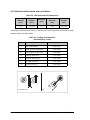
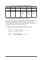
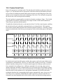
2.2.5 Parallel I/O
There are 56 parallel input/output lines divided among seven 8-bit ports designated A
through G. Most of the port lines have alternate functions, such as serial data or chip select
strobes. Parallel Ports D, E, F, and G have the capability of timer-synchronized outputs.
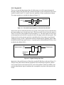
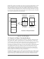
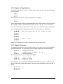
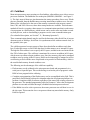
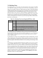
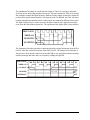
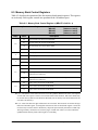
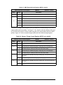
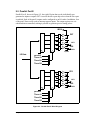
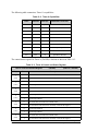
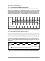
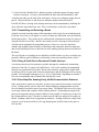
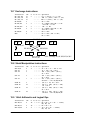
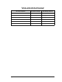
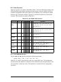
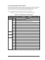
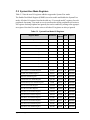
The output registers are cascaded as shown in Figure 2-1.
Output Port
Load Data
Load Clock
Timer Clock
Figure 2-1. Cascaded Output Registers for Parallel Ports D and E
Stores to the port are loaded in the first-level register. That register in turn is transferred to
the output register on a selected timer clock. The clock can be selected to be the output of
Timer A1, B1, B2 or the peripheral clock (divided by 2?). The timer signal can also cause
an interrupt that can be used to set up the next bit to be output on the next timer pulse. This
feature can be used to generate precisely controlled pulses whose edges are positioned
with high accuracy in time. Applications include communications signaling, pulse width
modulation and driving stepper motors. (A separate pulse width modulation facility is also
included in the Rabbit 3000.)
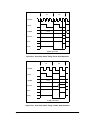
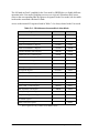
External Input
D Q
D Q
Filtered Input
Peripheral
Clock
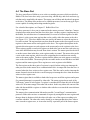
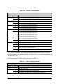
Figure 2-2. Digital Filtering Input Pins
Input pins to the parallel ports are filtered by cascaded D flip flops as shown in Figure 2-2.
This prevents pulses shorter then the peripheral clock from being recognized, synchronizes external pulses to the internal clock, and avoids problems with meta stability (temporarily indeterminate logical conditions due to marginal set up time with respect to the
clock).
Chapter 2 Rabbit 3000 Design Features
13
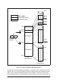
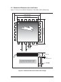
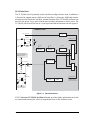
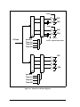
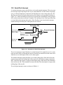
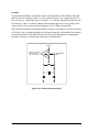
2.2.6 Slave Port
The slave port is designed to allow the Rabbit to be a slave to another processor, which
could be another Rabbit. The port is shared with Parallel Port A and is a bidirectional data
port. The master can read any of three registers selected via two select lines that form the
register address and a read strobe that causes the register contents to be output by the port.
These same registers can be written as I/O registers by the Rabbit slave. Three additional
registers transmit data in the opposite direction. They are written by the master by means
of the two select lines and a write strobe.
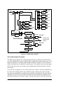
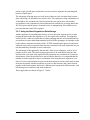
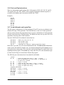
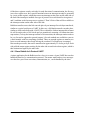
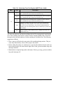
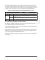
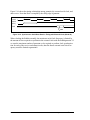
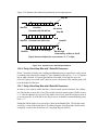
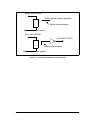
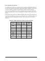
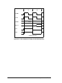
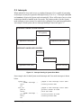
Figure 2-3 shows the data paths in the slave port.
RABBIT 3000
Input
Registers
Master
Processor
CPU
Output
Registers
Control
Slave Interface
Registers
Figure 2-3. Slave-Port Data Paths
The slave Rabbit can read the same registers as I/O registers. When incoming data bits are
written into one of the registers, status bits indicate which registers have been written, and
an optional interrupt can be programmed to take place when the write occurs. When the
slave writes to one of the registers carrying data bits outward, an attention line is enabled
so that the master can detect the data change and be interrupted if desired. One line tells
the master that the slave has read all the incoming data. Another line tells the master that
new outgoing data bits are available and have not yet been read by the master. The slave
port can be used to signal the master to perform tasks using a variety of communication
protocols over the slave port.
14
Rabbit 3000 Microprocessor User’s Manual
2.2.7 Auxiliary I/O Bus
The Rabbit 3000 instruction set supports memory access and I/O access. Memory access
takes place in a 1 megabyte memory space. I/O access takes place in a 64K I/O space. In a
traditional microprocessor design the same address and data lines are used for both memory and I/O spaces. Sharing address and data lines in this manner often forces compromises
or makes design more complicated. Generally the memory bus has more critical timing and
less tolerant of additional capacitive loading imposed by sharing it with an I/O bus.
With the Rabbit 3000, the designer has the option of enabling completely separate buses
for I/O and memory. The auxiliary I/O bus uses many of the same pins used by the slave
port, so its operation is mutually exclusive from operation of the slave port. Parallel Port A
is used to provide 8 bidirectional data lines. Parallel Port B bits 2:7 provide 6 address
lines, the least significant 6 lines of the 16 lines that define the full I/O space. The auxiliary bus is only active on I/O bus cycles. The address lines remain in the same state
assumed at the end of the previous I/O cycle until another I/O cycle takes place. I/O chip
selects as well as read and write strobes are available at various other pins so that the 64
byte space defined by the 6 address lines may be easily expanded. I/O cycles also execute
in parallel on the main (memory) bus when they take place on the auxiliary bus, so additional address lines can be buffered and provided if needed.
By connecting I/O devices to the auxiliary bus, the fast memory bus is relieved of the
capacitive load that would otherwise slow the memory. For core modules based on the
Rabbit 3000, fewer pins are required to exit the core module since the slave port and the
I/O bus can share the same pins and the memory bus no longer needs to exit the module to
provide I/O capability. Because the I/O bus has less activity and is slower than the memory
bus, it can be run further physically without EMI and ground bounce problems. 5 V signals
can appear on the I/O bus since the Rabbit 3000 inputs are 5 V tolerant. 5 V signals could
easily cause problems on the main bus if non 5 V tolerant 3.3 V memories are connected.
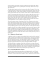
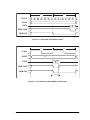
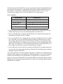
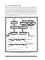
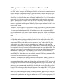
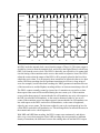
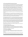
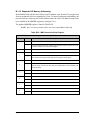
2.2.8 Timers
The Rabbit has several timer systems. The periodic interrupt is driven by the 32.768 kHz
oscillator divided by 16, giving an interrupt every 488 µs if enabled. This is intended to be
used as a general-purpose clock interrupt. Timer A consists of ten 8-bit countdown and
reload registers that can be cascaded up to two levels deep. Each countdown register can be
set to divide by any number between 1 and 256. The output of six of the timers is used to
provide baud clocks for the serial ports. Any of these registers can also cause interrupts and
clock the timer-synchronized parallel output ports. Timer B consists of a 10-bit counter that
can be read but not written. There are two 10-bit match registers and comparators. If the
match register matches the counter, a pulse is output. Thus the timer can be programmed to
output a pulse at a predetermined count in the future. This pulse can be used to clock the
timer-synchronized parallel-port output registers as well as cause an interrupt. Timer B is
convenient for creating an event at a precise time in the future under program control.
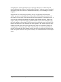
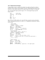
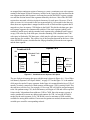
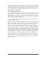
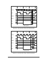
Figure 2-4 illustrates the Rabbit timers.
Chapter 2 Rabbit 3000 Design Features
15
Timer A System
perclk
perclk
A1
A2
Serial E
Serial F
perclk/2
A3
Serial A
A4
A8
Serial B
Input
Capture
A5
Serial C
A9
A10
PWM
Quadrature
Decode
A6
A7
Serial D
Timer A1
perclk/2
10-bit counter
compare
perclk/8
10 bits
Timer B System
Timer B1
match reg
Control Timer
Synchronized
outputs
match preload
Timer B2
match reg
match preload
Figure 2-4. Rabbit Timers A and B
2.2.9 Input Capture Channels
The input capture channels are used to determine the time at which an event takes place.
An event is signaled by a rising or falling edge (or optionally by either edge) on one of 16
input pins that can be selected as input for either of the two channels. A 16 bit counter is
used to record the time at which the event takes place. The counter is driven by the output
of Timer A8 and can be set to count at a rate ranging from full clock speed to 1/256 the
clock speed.
Two events are recognized: a start condition and a stop condition. The start condition may
be used to start counting and the stop condition to stop counting. However the counter
may also run continuously or run until a stop condition is encountered. The start and stop
conditions may also be used to latch the current time at the instant the condition occurs
rather than actually start or stop the counter. The same pin may be used to detect the start
16
Rabbit 3000 Microprocessor User’s Manual
and stop condition, for example a rising edge could be the start condition and a falling
edge the stop condition. However, optionally, the start and stop condition can be input
from separate pins.
The input capture channels can be used to measure the width of fast pulses. This is done
by starting the counter on the first edge of the pulse and capturing the counter value on the
second edge of the pulse. In this case the maximum error in the measurement is approximately 2 periods of the clock used to count the counter. If there is sufficient time between
events for an interrupt to take place the unit can be set up to capture the counter value on
either start or stop conditions or both and cause an interrupt each time the count is captured. In this case the start and stop conditions lose the connection with starting or stopping the counter and simply become capture conditions that may be specified for 2
independent edge detectors. The counter can also be cleared and started under software
control and then have its value captured in response to an input.
If desired the capture counter can synchronized with Timer B outputs used to synchronously load parallel port output registers. This makes it possible to generate an output signal precisely synchronized with an input signal. Usually it will be desired to synchronize
one of the input capture counters with the Timer B counter. The count offset can be measured by outputting a pulse at a precise time using Timer B to set the output time and capturing the same pulse. Once the phase relationship is known between the counters it is then
possible to output pulses a precise time delay after an input pulse is captured, provided
that the time delay is great enough for the interrupt routine to processes the capture event
and set up the output pulse synchronized by Timer B. The minimum time delay needed is
probably less than 10 microseconds if the software is done carefully the clock speed is reasonably high.
2.2.10 Quadrature Decoder Inputs
A quadrature encoder is a common electromechanical device used to track the rotation of
a shaft, or in some cases to track the motion of a linear follower. These devices are usually
implemented by the use of a disk or a strip with alternate opaque and transparent bands
that excite dual optical detectors. The output signals are square waves 90 degrees out of
phase also called being in quadrature with each other. By having quadrature signals, the
direction of rotation can be detected by noting which signal leads the other signal.
The Rabbit 3000 has two quadrature decoder units. Each unit has two inputs, the normal
input and the 90 degree or quadrature input. An 8-bit up/down counter counts encoder steps
in the forward and backward directions. The count can be extended beyond eight bits by an
interrupt that takes place each time the count overflows or underflows. The external signals
are synchronized with an internal clock provided by the output of Timer A10.
2.2.11 Pulse Width Modulation Outputs
The pulse width modulated output generates a train of pulses periodic on a 1024 pulse
frame with a duty cycle that varies from 1/1024 to 1024/1024. There are 4 independent
PWM units. The units are driven by the output of Timer A9 which may be used to vary the
Chapter 2 Rabbit 3000 Design Features
17
length of the pulses. When the duty cycle is greater then 1/1024 the pulses are spread into
groups distributed 256 counts apart in the 1024 frame. The pulse width modulation outputs
can be passed through a filter and used as a 10-bit D/A converter. The outputs can also be
used to directly drive devices that have intrinsic filtering such as motors or solenoids.
2.2.12 Spread Spectrum Clock
The main system clock, which is generated by the crystal oscillator or input from an external oscillator, can be modified by a clock spectrum spreader internal to the Rabbit 3000
chip. When the spectrum spreader is engaged, the clock is alternately speeded up and
slowed down, thus spreading the spectrum of the clock harmonics in the frequency
domain. This reduces EMI and improves the results of official radiated-emissions tests
typically by 15–20 dB at critical frequencies. The spectrum spreader has 3 modes of operation: off, normal, and strong. Slightly faster memory access time is required when the
spectrum spreader is used: 2–3 ns for the normal setting when the clock doubler is
enabled, and 6–9 ns for the strong setting when the clock doubler is used. The spreader
slightly influences baud rates and other timings because it introduces clock jitter, but the
effect is usually small enough to be negligible.
2.2.13 Separate Core and I/O Power Pins
The silicon die that constitutes the Rabbit 3000 processor is divided into the core logic and
the I/O ring. The I/O ring located on the 4 edges of the die holds the bonding pads and the
large transistors used to create the I/O buffers that drive signals to the external world. The
core section, inside the I/O ring contains the main processor and peripheral logic. The
clock and clock edges in the core are very fast with large transient currents that create a lot
of noise that is communicated to the outside of the package via the power pins. The I/O
buffers have slower switching times and mostly operate at much lower frequencies than
the core logic. The Rabbit has separate power and ground pins for the core and I/O ring.
This allows the designer to feed clean power to the I/O ring filtered to be free of the noise
generated by the core switching. This minimizes high frequency noise that would otherwise appear on output pins driven by buffers in the I/O ring. The result is lower EMI.
2.3 Design Standards
The same functionality can often be accomplished in more than one way with the Rabbit
3000. By publishing design standards, or standard ways to accomplish common objectives, software and hardware support become easier.
Refer to the Rabbit 3000 Microprocessor Designer’s Handbook for additional information.
2.3.1 Programming Port
Rabbit Semiconductor publishes a specification for a standard programming port (see
Appendix A, “The Rabbit Programming Port,”) and provides a converter cable that may
be used to connect a PC serial port to the standard programming interface. The interface is
implemented using a 10-pin connector with two rows of pins on 2 mm centers. The port is
connected to Rabbit Serial Port A, to the startup mode pins on the Rabbit, to the Rabbit
18
Rabbit 3000 Microprocessor User’s Manual
reset pin, and to a programmable output pin that is used to signal the PC that attention is
needed. With proper precautions in design and software, it is possible to use Serial Port A
as both a programming port and as a user-defined serial port, although this will not be necessary in most cases.
Rabbit Semiconductor supports the use of the standard programming port and the standard
programming cable as a diagnostic and setup port to diagnosis problems or set up systems
in the field.
2.3.2 Standard BIOS
Rabbit Semiconductor provides a standard BIOS for the Rabbit. The BIOS is a software
program that manages startup and shutdown, and provides basic services for software running on the Rabbit.
2.4 Dynamic C Support for the Rabbit
Dynamic C is Rabbit Semiconductor’s interactive C language development system.
Dynamic C runs on a PC under Windows 32-bit operating systems. Dynamic C provides a
combined compiler, editor, and debugger. The usual method for debugging a target system
based on the Rabbit is to implement the 10-pin programming connector that connects to
the PC serial port via a standard converter cable. Dynamic C libraries contain highly perfected software to control the Rabbit. These includes drivers, utility and math routines and
the debugging BIOS for Dynamic C.
In addition, the internationally known real-time operating system, uC/OS-II, has been
ported to the Rabbit, and is available with Dynamic C on a license-free, royalty-free basis
for use in Rabbit-based products..
Chapter 2 Rabbit 3000 Design Features
19
20
Rabbit 3000 Microprocessor User’s Manual
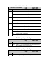
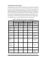
3. DETAILS ON RABBIT
MICROPROCESSOR FEATURES
3.1 Processor Registers
The Rabbit’s registers are nearly identical to those of the Z180 or the Z80. The figure
below shows the register layout. The XPC and IP registers are new. The EIR register is the
same as the Z80 I register, and is used to point to a table of interrupt vectors for the externally generated interrupts. The IIR register occupies the same logical position in the
instruction set as the Z80 R register, but its function is to point to an interrupt vector table
for internally generated interrupts.
A
F
H
L
D
E
B
C
IP
IX
8/16-bit
registers
IY
IIR
SP
PC
XPC
A'
F'
H'
L'
D'
E'
B'
C'
Alternate Registers
S Z x x
x V x C
F – flag register layout
S–sign, Z–zero, V–overflow, C–carry
Bits marked "x" are read/write.
EIR
A – 8-bit accumulator
F – flags register
HL – 16-bit accumulator
IX, IY – index registers/alt accum’s
SP – stack pointer
PC – program counter
XPC – extension of program counter
IIR – internal interrupt register
EIR– external interrupt register
IP – interrupt priority register
Figure 3-1. Rabbit Registers
Chapter 3 Details on Rabbit Microprocessor Features
21
The Rabbit (and the Z80/Z180) processor has two accumulators—the A register serves as
an 8-bit accumulator for 8-bit operations such as ADD or AND. The 16-bit register HL register serves as an accumulator for 16-bit operations such as ADD HL,DE, which adds the 16bit register DE to the 16-bit accumulator HL. For many operations IX or IY can substitute
for HL as accumulators.
The register marked F is the flags register or status register. It holds a number of flags that
provide information about the last operation performed. The flag register cannot be
accessed directly except by using the POP AF and PUSH AF instructions. Normally the
flags are tested by conditional jump instructions. The flags are set to mark the results of
arithmetic and logic operations according to rules that are specified for each instruction.
There are four unused read/write bits in the flag register that are available to the user via
the PUSH AF and POP AF instructions. These bits should be used with caution since newgeneration Rabbit processors could use these bits for new purposes.
The registers IX, IY and HL can also serve as index registers. They point to memory
addresses from which data bits are fetched or stored. Although the Rabbit can address a
megabyte or more of memory, the index registers can only directly address 64K of memory (except for certain extended addressing LDP instructions). The addressing range is
expanded by means of the memory mapping hardware (see “Memory Mapping” on
page 23) and by special instructions. For most embedded applications, 64K of data memory (as opposed to code memory) is sufficient. The Rabbit can efficiently handle a megabyte of program space.
The register SP points to the stack that is used for subroutine and interrupt linkage as well
as general-purpose storage.
A feature of the Rabbit (and the Z80/Z180) is the alternate register set. Two special
instructions swap the alternate registers with the regular registers. The instruction EX AF,AF’
exchanges the contents of AF with AF'. The instruction EXX exchanges HL, DE, and BC
with HL', DE', and BC'. Communication between the regular and alternate register set in
the original Z80 architecture was difficult because the exchange instructions provided the
only means of communication between the regular and alternate register sets. The Rabbit
has new instructions that greatly improve communication between the regular and alternate register set. This effectively doubles the number of registers that are easily available
for the programmer’s use. It is not intended that the alternate register set be used to provide a separate set of registers for an interrupt routine, and Dynamic C does not support
this usage because it uses both registers sets freely.
The IP register is the interrupt priority register. It contains four 2-bit fields that hold a history of the processor’s interrupt priority. The Rabbit supports four levels of processor priority, something that exists only in a very restricted form in the Z80 or Z180.
22
Rabbit 3000 Microprocessor User’s Manual
3.2 Memory Mapping
Although the Rabbit memory mapping scheme is fairly complex, the user rarely needs to
worry about it because the details are handled by the Dynamic C development system.
Except for a handful of special instructions (see Section 19.5, “16-bit Load and Store 20bit Address”), the Rabbit instructions directly address a 64K data memory space. This
means that the address fields in the instructions are 16 bits long and that the registers that
may be used as pointers to memory addresses (index registers (IX, IY), program counter
and stack pointer (SP)) are also 16 bits long.
Because Rabbit instructions use 16-bit addresses, the instructions are shorter and can execute much faster than if, for example, 32-bit addresses were used. The executable code is
very compact.
The Rabbit memory-mapping unit is similar to, but more powerful than, the Z180 memory-mapping unit. Figure 3-2 illustrates the relationship among the major components
related to addressing memory.
Processor
16
bits
Memory
Mapping
Unit
20
bits
Memory
Interface
Unit
Memory
Chips
20 bits plus control
Figure 3-2. Addressing Memory Components
The memory-mapping unit receives 16-bit addresses as input and outputs 20-bit addresses.
The processor (except for certain LDP instructions) sees only a 16-bit address space. That
is, it sees 65536 distinctly addressable bytes that its instructions can manipulate. Three
segment registers are used to map this 16-bit space into a 1-megabyte space. The 16-bit
space is divided into four separate zones. Each zone, except the first or root zone, has a
segment register that is added to the 16-bit address within the zone to create a 20-bit
address. The segment register has eight bits and those eight bits are added to the upper
four bits of the 16-bit address, creating a 20-bit address. Thus, each separate zone in the
16-bit memory becomes a window to a segment of memory in the 20-bit address space.
The relative size of the four segments in the 16-bit space is controlled by the SEGSIZE
register. This is an 8-bit register that contains two 4-bit registers. This controls the boundary between the first and the second segment and the boundary between the second and
the third segment. The location of the two movable segment boundaries is determined by a
4-bit value that specifies the upper four bits of the address where the boundary is located.
These relationships are illustrated in Figure 3-3.
Chapter 3 Details on Rabbit Microprocessor Features
23
10000
85
XPC register
80
STACKSEG register
79
DATASEG register
0E000
85
93000
0D000
80
8D000
10000
XPC Segment
E000
D000
D
Stack Segment
Data Segment
7
SEGSIZE
Register
07000
79
80000
7000
07000
Root Segment
0000
16-bit
address space
00000
20-bit
address space
Figure 3-3. Example of Memory Mapping Operation
The names given to the segments in the figure are evocative of the common uses for each
segment. The root segment is mapped to the base of flash memory and contains the startup
code as well as other code that may happen to be stored there. The data segment usage
varies depending on the overall strategy for setting up memory. It may be an extension of
24
Rabbit 3000 Microprocessor User’s Manual
the root segment or it may contain data variables. The stack segment is normally 4K long
and it holds the system stack. The XPC segment is normally used to execute code that is
not stored in the root segment or the data segment. Special instructions support executing
code that is visible in the XPC segment.
The memory interface unit receives the 20-bit addresses generated by the memory-mapping unit. The memory interface unit conditionally modifies address lines A16, A18 and
A19. The other address lines of the 20-bit address are passed unconditionally. The memory interface unit provides control signals for external memory chips. These interface signals are chip selects (/CS0, /CS1, /CS2), output enables (/OE0, /OE1), and write enables
(/WE0, /WE1). These signals correspond to the normal control lines found on static memory chips (chip select or /CS, output enable or /OE, and write enable or /WE). In order to
generate these memory control signals, the 20-bit address space is divided into four quadrants of 256K each. A bank control register for each quadrant determines which of the
chip selects and which pair of output enables, and write enables (if any) is enabled when a
memory read or write to that quadrant takes place. For example, if a 512K x 8 flash memory is to be accessed in the first 512K of the 20-bit address space, then /CS0, /WE0, /OE0
could be enabled in both quadrants.
Figure 3-4 shows a memory interface unit.
Axxin—from processor
Axx—out from memory
control unit
Address lines not shown
are passed directly.
A19in
A19in
A19
A18in
A18
A18, A19 invertible
by quadrant
/CS0
A19in'
/CS1
A18in
/CS2
Optional A19 inversion
Memory
Control
Read/Write
Synchronization
Memory
Control
Lines
/OE0
/WE0
/OE1
/WE1
Figure 3-4. Memory Interface Unit
Chapter 3 Details on Rabbit Microprocessor Features
25
3.2.1 Extended Code Space
A crucial element of the Rabbit memory mapping scheme is the ability to execute programs containing up to a megabyte of code in an efficient manner. This ability is absent in
a pure 16-bit address processor, and it is poorly supported by the Z180 through its memory
mapping unit. On paged processors, such as the 8086, this capability is provided by paging
the code space so that the code is stored in many separate pages. On the 8086 the page size
is 64K, so all the code within a given page is accessible using 16-bit addressing for jumps,
calls and returns. When paging is used, a separate register (CS on the 8086) is used to
determine where the active page currently resides in the total memory space. Special
instructions make it possible to jump, call or return from one page to another. These special instructions are called long calls, long jumps and long returns to distinguish them
from the same operations that only operate on 16-bit variables.
The Rabbit also uses a paging scheme to expand the code space beyond the reach of a 16bit address. The Rabbit paging scheme uses the concept of a sliding page, which is 8K
long. This is the XPC segment. The 8-bit XPC register serves as a page register to specify
the part of memory where the window points. When a program is executed in the XPC
segment, normal 16-bit jumps, calls and returns are used for most jumps within the window. Normal 16-bit jumps, calls and returns may also be used to access code in the other
three segments in the 16-bit address space. If a transfer of control to code outside the window is required, then a long jump, long call or long return is used. These instructions modify both the program counter (PC) and the XPC register, causing the XPC window to point
to a different part of memory where the target of the long jump, call or return is located.
The XPC segment is always 8K long. The granularity with which the XPC segment can be
positioned in memory is 4K. Because the window can be slid by one-half of its size, it is
possible to compile continuously without unused gaps in memory.
As the compiler generates code resident in the XPC window, the window is slid down by
4K when the code goes beyond F000. This is accomplished by a long jump that repositions the window 4K lower. This is illustrated by Figure 3-5. The compiler is not presented
with a sharp boundary at the end of the page because the window does not run out of space
when code passes F000 unless 4K more of code is added before the window is slid down.
All code compiled for the XPC window has a 24-bit address consisting of the 8-bit XPC
and the 16-bit address. Short jumps and calls can be used, provided that the source and target instructions both have the same XPC address. Generally this means that each instruction belongs to a window that is approximately 4K long and has a 16-bit address between
E000+n and F000+m, where n and m are on the order of a few dozen bytes, but can be up
to 4096 bytes in length. Since the window is limited to no more than 8K, the compiler is
unable to compile a single expression that requires more than 8K or so of code space. This
is not a practical consideration since expressions longer than a few hundred bytes are in
the nature of stunts rather than practical programs.
Program code can reside in the root segment or the XPC segment. Program code may also
be resident in the data segment. Code can be executed in the stack segment, but this is usually restricted to special situations. Code in the root, meaning any of the segments other
26
Rabbit 3000 Microprocessor User’s Manual
than the XPC segment, can call other code in the root using short jumps and calls. Code in
the XPC segment can also call code in the root using short jumps and calls. However, a
long call must be used when code in the XPC segment is called. Functions located in the
root have an efficiency advantage because a long call and a long return require 32 clocks
to execute, but a short call and a short return require only 20 clocks to execute. The difference is small, but significant for short subroutines.
Compiler notices
that code has
passed F000.
10000
E000
D000
Compiler inserts
long jump in code.
XPC Segment
Stack Segment
Data Segment
F000
short
calls
returns
E000
XPC = N
PC = F000 + K
XPC = N + 1
PC = E000 + K + 4
Root Segment
Illustration of Sliding XPC Window
Figure 3-5. Use of XPC Segment
3.2.2 Separate I and D Space - Extending Data Memory
In the normal memory model, the data space must share a 64K space with root code, the
stack, and the XPC window. Typically, this leaves a potential data space of 40K or less.
The XPC requires 8K, the stack requires 4K, and most systems will require at least 12K of
root code. This amount of data space is sufficient for many embedded applications.
One approach to getting more data space is to place data in RAM or in flash memory that
is not mapped into the 64K space, and then access this data using function calls or in
assembly language using the LDP instructions that can access memory using a 20-bit
address. This greatly expands the data space, but the instructions are less efficient than
instructions that access the 64k space using 16 bit addresses.
The Rabbit 3000 supports separate I and D or Instruction and Data spaces. When separate
I and D space is enabled it applies only to addresses in the root segment or data segment.
Separate I and D spaces mean that instruction execution makes a distinction between
Chapter 3 Details on Rabbit Microprocessor Features
27
fetching an instruction from memory and fetching or storing data in memory. When
enabled separate I and D space make available the combined root and data segment, typically 52k bytes for root code in the I space. In the D space, the root code segment part of
the D space is typically used for constant data mapped to flash memory while the data segment part of the D space is used for variable data mapped to RAM. Separate I and D space
increases the amount of both root code and root data because they no longer have to share
the same memory, even though they share the same addresses.
20-bit Memory Space
RAM
64k
56k
52k
XPC
window
stack
512k
D Space
Flash
I space
Data
Segment
Variable
D Space
128k
Root
Code
64k
Root
Segment
Constant
D Space
Figure 3-6. Separate I and D Space
Normally separate I and D space is implemented as shown in Figure 3-6. In the I space the
root segment and the data segment are combined into a single root code segment. In the D
space the segments are separately mapped to flash and RAM to provide storage for constant data and variable data. The hardware method to achieve separate 20 bit addresses for
the D space is to invert either A16 or A19 for data accesses. The inversion may be specified separately for the root segment and the data segment. Normally A16 is inverted for
data accesses in the root segment. This causes data accesses to the root segment to be
moved 64k higher to a section of flash starting at 20 bit address 64k that is reserved for
constant data. A19 is normally inverted for data accesses to the data segment, causing the
data accesses in the data segment to be moved to an address 512k higher in the 20 bit
space, an address normally mapped to RAM. The stack segment and the XPC segment do
28
Rabbit 3000 Microprocessor User’s Manual
not have split I and D space and memory accesses to these segments do not distinguish
between I and D space.
The advantage of having more root code space is that root code executes faster because
short calls using a 16 bit address are used to call it. This compares to long calls that have a
20 bit address for extended code. Data located in the root can be more conveniently
accessed due to the comparatively limited instructions available for accessing data in the
full 20 bit space and the greater overhead involve in manipulating 20 bit addresses in a
processor that has 8 and 16 bit registers.
3.2.3 Using the Stack Segment for Data Storage
Another approach to extending data memory is to use the stack segment to access data,
placing the stack in the data segment so as to free up the stack segment. This approach
works well for a software system that uses data groupings that are self-contained and are
accessed one at a time rather than randomly between all the groupings. An example would
be the software structures associated with a TCP/IP communication protocol connection
where the same code accesses the data structures associated with each connection in a pattern determined by the traffic on each connection.
The advantage of this approach is that normal C data access techniques, such as 16-bit
pointers, may be used. The stack segment register has to be modified to bring the data
structure into view in the stack segment before operations are performed on a particular
data structure. Since the stack has to be moved into the data area, it is important that the
number of stacks required be kept to a minimum when using the stack segment to view
data. Of course, tasks that don’t need to see the data structures can have their stack located
in the stack segment. Another possibility is to have a data structure and a stack located
together in the stack segment, and to use a different stack segment for different tasks, each
task having its own data area and stack bound to it.
These approaches are shown in Figure 3-7 below.
Chapter 3 Details on Rabbit Microprocessor Features
29
Stack Segment
used as data
window
Stack Segment
used for stack
Data Segment
used as data
window
Stacks in data
segment
Data
(RAM)
Root Segment
mapped to
RAM has both
root code and
data.
Root
Code
(flash)
Using Stack Segment
for a Data Window
Data
(RAM)
Root
Code
(RAM)
Using Data Segment for
a Data Window (Code must
be copied to RAM on startup.)
Figure 3-7. Schemes for Data Memory Windows
A third approach is to place the data and root code in RAM in the root segment, freeing the
data segment to be a window to extended memory. This requires copying the root code to
RAM at startup time. Copying root code to RAM is not necessarily that burdensome since
the amount of RAM required can be quite small, say 12K for example.
The XPC segment at the top of the memory can also be used as a data segment by programs that are compiled into root memory. This is handy for small programs that need to
access a lot of data.
3.2.4 Practical Memory Considerations
The simplest Rabbit configurations have one flash memory chip interfaced using /CS0 and
one RAM memory chip interfaced using /CS1. Typical Rabbit-based systems use 256K of
flash and 128 K of RAM, but smaller or larger memories may be used.
Although the Rabbit can support code size approaching a megabyte, it is anticipated that
the majority of applications will use less than 250K of code, equivalent to approximately
10,000–20,000 C statements. This reflects both the compact nature of Rabbit code and the
typical size of embedded applications.
Directly accessible C variables are limited to approximately 44K of memory, split
between data stored in flash and RAM. This will be more than adequate for many embed30
Rabbit 3000 Microprocessor User’s Manual
ded applications. Some applications may require large data arrays or tables that will
require additional data memory. For this purpose Dynamic C supports a type of extended
data memory that allows the use of additional data memory, even extending far beyond a
megabyte.
Requirements for stack memory depend on the type of application and particularly
whether preemptive multitasking is used. If preemptive multitasking is used, then each
task requires its own stack. Since the stack has its own segment in 16-bit address space, it
is easy to use available RAM memory to support a large number of stacks. When a preemptive change of context takes place, the STACKSEG register can be changed to map
the stack segment to the portion of RAM memory that contains the stack associated with
the new task that is to be run. Normally the stack segment is 4K, which is typically large
enough to provide space for several (typically four) stacks. It is possible to enlarge the
stack segment if stacks larger than 4K are needed. If only one stack is needed, then it is
possible to eliminate the stack segment entirely and place the single stack in the data segment. This option is attractive for systems with only 32K of RAM that don’t need multiple
stacks.
Chapter 3 Details on Rabbit Microprocessor Features
31
3.3 Instruction Set Outline
“Load Immediate Data to a Register” on page 33
“Load or Store Data from or to a Constant Address” on page 33
“Load or Store Data Using an Index Register” on page 34
“Register-to-Register Move” on page 35
“Register Exchanges” on page 35
“Push and Pop Instructions” on page 36
“16-bit Arithmetic and Logical Ops” on page 36
“Input/Output Instructions” on page 39—these include a fix for a bug that manifests itself
if an I/O instruction (prefix IOI or IOE) is followed by one of 12 single-byte op codes that
use HL as an index register.
In the discussion that follows, we give a few example instructions in each general category
and contrast the Z80/ Z180 with the Rabbit. For a detailed description of every instruction,
see Chapter 19, “Rabbit Instructions,”
The Rabbit executes instructions in fewer clocks then the Z80 or Z180. The Z180 usually
requires a minimum of four clocks for 1-byte opcodes or three clocks for each byte for
multi-byte op codes. In addition, three clocks are required for each data byte read or written. Many instructions in the Z180 require a substantial number of additional clocks. The
Rabbit usually requires two clocks for each byte of the op code and for each data byte
read. Three clocks are needed for each data byte written. One additional clock is required
if a memory address needs to be computed or an index register is used for addressing.
Only a few instructions don’t follow this pattern. An example is mul, a 16 x 16 bit signed
two’s complement multiply. mul is a 1-byte op code, but requires 12 clocks to execute.
Compared to the Z180, not only does the Rabbit require fewer clocks, but in a typical situation it has a higher clock speed and its instructions are more powerful.
The most important instruction set improvements in the Rabbit over the Z180 are in the
following areas.
• Fetching and storing data, especially 16-bit words, relative to the stack pointer or the
index registers IX, IY, and HL.
• 16-bit arithmetic and logical operations, including 16-bit and’s, or’s, shifts and 16-bit
multiply.
• Communication between the regular and alternate registers and between the index registers and the regular registers is greatly facilitated by new instructions. In the Z180 the
alternate register set is difficult to use, while in the Rabbit it is well integrated with the
regular register set.
• Long calls, long returns and long jumps facilitate the use of 1M of code space. This
removes the need in the Z180 to utilize inefficient memory banking schemes for larger
programs that exceed 64K of code.
32
Rabbit 3000 Microprocessor User’s Manual
• Input/output instructions are now accomplished by normal memory access instructions
prefixed by an op code byte to indicate access to an I/O space. There are two I/O
spaces, internal peripherals and external I/O devices.
Some Z80 and Z180 instructions have been deleted and are not supported by the Rabbit
(see Chapter 20, “Differences Rabbit vs. Z80/Z180 Instructions,”). Most of the deleted
instructions are obsolete or are little-used instructions that can be emulated by several
Rabbit instructions. It was necessary to remove some instructions to free up 1-byte op
codes needed to implement new instructions efficiently. The instructions were not reimplemented as 2-byte op codes so as not to waste on-chip resources on unimportant
instructions. Except for the instruction EX (SP),HL, the original Z180 binary encoding
of op codes is retained for all Z180 instructions that are retained.
3.3.1 Load Immediate Data to a Register
A constant that follows the op code in the instruction stream can generally be loaded to
any register, except PC, IP, and F. (Load to the PC is a jump instruction.) This includes the
alternate registers on the Rabbit, but not on the Z180. Some example instructions appear
below.
LD
LD
LD
LD
LD
LD
A,3
HL,456
BC',3567
H',0x4A
IX,1234
C,54
; not possible on Z180
; not possible on Z180
Byte loads require four clocks, word loads require six clocks. Loads to IX, IY or the alternate registers generally require two extra clocks because the op code has a 1-byte prefix.
3.3.2 Load or Store Data from or to a Constant Address
LD
LD
LD
LD
LD
LD
A,(mn)
A',(mn)
(mn),A
HL,(mn)
HL',(mn)
(mn),HL
; loads 8 bits from address mn
; not possible on Z180
; load 16 bits from the address specified by mn
; to alternate register, not possible Z180
Similar 16-bit loads and stores exist for DE, BC, SP, IX and IY.
It is possible to load data to the alternate registers, but it is not possible to store the data in
the alternate register directly to memory.
LD A’,(mn)
; allowed
** LD (mn),D’ ; **** not a legal instruction!
** LD (mn),DE’ ; **** not a legal instruction!
Chapter 3 Details on Rabbit Microprocessor Features
33
3.3.3 Load or Store Data Using an Index Register
An index register is a 16-bit register, usually IX, IY, SP or HL, that is used for the address
of a byte or word to be fetched from or stored to memory. Sometimes an 8-bit offset is
added to the address either as a signed or unsigned number. The 8-bit offset is a byte in the
instruction word. BC and DE can serve as index registers only for the special cases below.
LD
LD
LD
LD
LD
LD
A,(BC)
A’,(BC)
(BC),A
A,(DE)
A’,(DE)
(DE),A
Other 8-bit loads and stores are the following.
LD r,(HL)
LD r’,(HL)
LD (HL),r
**
LD
LD
LD
LD
;
;
;
;
LD (HL),r’ ;
r,(IX+d)
;
r’,(IX+d) ;
(IX+d),r
;
(IY+d),r
;
r is any of 7 registers A, B, C, D, E, H, L
same but alternate register destination
r is any of the 7 registers above
or an immediate data byte
**** not a legal instruction!
r is any of 7 registers, d is -128 to +127 offset
same but alternate destination
r is any of 7 registers or an immediate data byte
IX or IY can have offset d
The following are 16-bit indexed loads and stores. None of these instructions exists on the
Z180 or Z80. The only source for a store is HL. The only destination for a load is HL or HL'.
LD HL,(SP+d)
LD (SP+d),HL
LD HL,(HL+d)
LD HL’,(HL+d)
LD (HL+d),HL
LD (IX+d),HL
LD HL,(IX+d)
LD HL’,(IX+d)
LD (IY+d),HL
;
;
;
;
;
;
d is an offset from 0 to 255.
16-bits are fetched to HL or HL’
corresponding store
d is an offset from -128 to +127,
uses original HL value for addressing
l=(HL+d), h=(HL+d+1)
; store HL at address pointed to
; by IX plus -128 to +127 offset
; store HL at address pointed to
; by IY plus -128 to +127 offset
LD HL,(IY+d)
LD HL’,(IY+d)
34
Rabbit 3000 Microprocessor User’s Manual
3.3.4 Register-to-Register Move
Any of the 8-bit registers, A, B, C, D, E, H, and L, can be moved to any other 8-bit register, for example:
LD A,c
LD d,b
LD e,l
The alternate 8-bit registers can be a destination, for example:
LD a’,c
LD d’,b
These instructions are unique to the Rabbit and require 2 bytes and four clocks because of
the required prefix byte. Instructions such as LD A,d’ or LD d’,e’ are not allowed.
Several 16-bit register-to-register move instructions are available. Except as noted, these
instructions all require 2 bytes and four clocks. The instructions are listed below.
LD
LD
LD
LD
LD
LD
LD
LD
LD
dd’,BC
dd’,DE
IX,HL
IY,HL
HL,IY
HL,IX
SP,HL
SP,IX
SP,IY
; where dd’ is any of HL’, DE’, BC’ (2 bytes, 4 clocks)
; 1-byte, 2 clocks
Other 16-bit register moves can be constructed by using 2-byte moves.
3.3.5 Register Exchanges
Exchange instructions are very powerful because two (or more) moves are accomplished
with one instruction. The following register exchange instructions are implemented.
EX af,af’
EXX
EX DE,HL
; exchange af with af’
; exchange HL, DE, BC with HL’, DE’, BC’
; exchange DE and HL
The following instructions are unique to the Rabbit.
EX DE’,HL
EX DE, HL’
EX DE’, HL’
; 1 byte, 2 clocks
; 2 bytes, 4 clocks
; 2 bytes, 4 clocks
The following special instructions (Rabbit and Z180/Z80) exchange the 16-bit word on
the top of the stack with the HL register. These three instructions are each 2 bytes and 15
clocks.
EX (SP),HL
EX (SP),IX
EX (SP),IY
Chapter 3 Details on Rabbit Microprocessor Features
35
3.3.6 Push and Pop Instructions
There are instructions to push and pop the 16-bit registers AF, HL, DC, BC, IX, and IY.
The registers AF', HL', DE', and BC' can be popped. Popping the alternate registers is
exclusive to the Rabbit, and is not allowed on the Z80 / Z180.
Examples
POP HL
PUSH BC
PUSH IX
PUSH af
POP DE
POP DE’
POP HL’
3.3.7 16-bit Arithmetic and Logical Ops
The HL register is the primary 16-bit accumulator. IX and IY can serve as alternate accumulators for many 16-bit operations. The Z180/Z80 has a weak set of 16-bit operations,
and as a practical matter the programmer has to resort to combinations of 8-bit operations
in order to perform many 16-bit operations. The Rabbit has many new op codes for 16-bit
operations, removing some of this weakness.
The basic Z80/Z180 16-bit arithmetic instructions are
ADD
ADC
SBC
INC
HL,ww
HL,ww
HL,ww
ww
;
;
;
;
where ww is HL, DE, BC, SP
ADD and ADD carry
sub and sub carry
increment the register (without affecting flags)
In the above op codes, IX or IY can be substituted for HL. The ADD and ADC instructions
can be used to left-shift HL with the carry. An alternate destination prefix (ALTD) may be
used on the above instructions. This causes the result and its flags to be stored in the corresponding alternate register. If the ALTD flag is used when IX or IY is the destination register, then only the flags are stored in the alternate flag register.
The following new instructions have been added for the Rabbit.
;Shifts
RR HL
RR
RL
RR
RR
DE
DE
IX
IY
;
;
;
;
;
;
;
rotate HL right with carry, 1 byte, 2 clocks
note use ADC HL,HL for left rotate, or add HL,HL if
no carry in is needed.
1 byte, 2 clocks
rotate DE left with carry, 1-byte, 2 clocks
rotate IX right with carry, 2 bytes, 4 clocks
rotate IY right with carry
;Logical Operations
AND HL,DE ; 1 byte, 2 clocks
AND IX,DE ; 2 bytes, 4 clocks
AND IY,DE
OR HL,DE
; 1 byte, 2 clocks
OR IX,DE
; 2 bytes, 4 clocks
OR IY,DE
36
Rabbit 3000 Microprocessor User’s Manual
The BOOL instruction is a special instruction designed to help test the HL register. BOOL
sets HL to the value 1 if HL is non zero, otherwise, if HL is zero its value is not changed.
The flags are set according to the result. BOOL can also operate on IX and IY.
BOOL HL
BOOL IX
BOOL IY
ALTD BOOL HL
ALTD BOOL IY
; set HL to 1 if non- zero, set flags to match HL
; set HL’ an f’ according to HL
; modify IY and set f’ with flags of result
The SBC instruction can be used in conjunction with the BOOL instruction for performing
comparisions. The SBC instruction subtracts one register from another and also subtracts
the carry bit. The carry out is inverted compared to the carry that would be expected if the
number subtracted was negated and added. The following examples illustrate the use of
the SBC and BOOL instructions.
; Test if HL>=DE - HL and DE unsigned numbers 0-65535
OR A
; clear carry
SBC HL,DE ; if C==0 then HL>=DE else if C==1 then HL<DE
;
;
SBC HL,HL ;
BOOL HL
;
;
;
SBC HL,HL ;
INC HL
;
;
convert the carry bit into a boolean variable in HL
sets HL==0 if C==0, sets HL==0ffffh if C==1
HL==1 if C was set, otherwise HL==0
convert not carry bit into boolean variable in HL
HL==0 if C==0 else HL==ffff if C=1
HL==1 if C==0 else HL==0 if C==1
note carry flag set, but zero / sign flags reversed
In order to compare signed numbers using the SBC instruction, the programmer can map
the numbers into an equivalent set of unsigned numbers by inverting the sign bit of each
number before performing the comparison. This maps the most negative number 0x08000
to the smallest unsigned number 0x0000, and the most positive signed number 0x07FFF to
the largest unsigned number 0x0FFFF. Once the numbers have been converted, the comparision can be done as for unsigned numbers. This procedure is faster than using a jump
tree that requires testing the sign and overflow bits.
; example - test for HL>=DE where HL and DE are signed numbers
; invert sign bits on both
ADD HL,HL ; shift left
CCF
; invert carry
RR HL
; rotate right
RL DE
CCF
RR DE
; invert DE sign
SBC HL,DE ; no carry if HL>=DE
; generate boolean variable true if HL>=DE
SBC HL,HL ; zero if no carry else -1
INC HL
; 1 if no carry, else zero
BOOL
; use this instruction to set flags if needed
Chapter 3 Details on Rabbit Microprocessor Features
37
The SBC instruction can also be used to perform a sign extension.
; extend sign of l to HL
LD A,l
rla
SBC A,a
LD h,a
; sign to carry
; a is all 1’s if sign negative
; sign extended
The multiply instruction performs a signed multiply that generates a 32-bit signed result.
MUL
; signed multiply of BC and DE,
; result in HL:BC - 1 byte, 12 clocks
If a 16-bit by 16-bit multiply with a 16-bit result is performed, then only the low part of
the 32-bit result (BC) is used. This (counter intuitively) is the correct answer whether the
terms are signed or unsigned integers. The following method can be used to perform a 16
x 16 bit multiply of two unsigned integers and get an unsigned 32-bit result. This uses the
fact that if a negative number is multiplied the sign causes the other multiplier to be subtracted from the product. The method shown below adds double the number subtracted so
that the effect is reversed and the sign bit is treated as a positive bit that causes an addition.
LD BC,n1
LD HL’,BC
LD DE,n2
LD A,b
MUL
OR A
JR p,x1
ADD HL,DE
x1:
RL DE
JR nc,x2
; save BC in HL’
;
;
;
;
;
save sign of BC
form product in HL:BC
test sign of BC multiplier
if plus continue
adjust for negative sign in BC
; test sign of DE
; if not negative
; subtract other multiplier from HL
EX DE,HL’
ADD HL,DE
x2:
; final unsigned 32 bit result in HL:BC
This method can be modified to multiply a signed number by an unsigned number. In that
case only the unsigned number has to be tested to see if the sign is on, and in that case the
signed number is added to the upper part of the product.
The multiply instruction can also be used to perform left or right shifts. A left shift of n
positions can be accomplished by multiplying by the unsigned number 2^^n. This works
for n # 15, and it doesn’t matter if the numbers are signed or unsigned. In order to do a
right shift by n (0 < n < 16), the number should be multiplied by the unsigned number
2^^(16 – n), and the upper part of the product taken. If the number is signed, then a signed
by unsigned multiply must be performed. If the number is unsigned or is to be treated as
unsigned for a logical right shift, then an unsigned by unsigned multiply must be performed. The problem can be simplified by excluding the case where the multiplier is
2^^15.
38
Rabbit 3000 Microprocessor User’s Manual
3.3.8 Input/Output Instructions
The Rabbit uses an entirely different scheme for accessing input/output devices. Any
memory access instruction may be prefixed by one of two prefixes, one for internal I/O
space and one for external I/O space. When so prefixed, the memory instruction is turned
into an I/O instruction that accesses that I/O space at the I/O address specified by the 16bit memory address used. For example
IOI LD A,(0x85)
LD IY,0x4000
IOE LD HL,(IY+5)
; loads A register with contents
; of internal I/O register at location 0x85.
; get word from external I/O location 0x4005
By using the prefix approach, all the 16-bit memory access instructions are available for
reading and writing I/O locations. The memory mapping is bypassed when I/O operations
are executed.
I/O writes to the internal I/O registers require only two clocks, rather than the minimum of
three clocks required for writes to memory or external I/O devices.
Chapter 3 Details on Rabbit Microprocessor Features
39
3.4 How to Do It in Assembly Language—Tips and Tricks
3.4.1 Zero HL in 4 Clocks
BOOL HL
RR HL
; 2 clocks, clears carry, HL is 1 or 0
; 2 clocks, 4 total - get rid of possible 1
This sequence requires four clocks compared to six clocks for LD HL,0.
3.4.2 Exchanges Not Directly Implemented
HL<->HL' - eight clocks
EX DE’,HL
EX DE’,HL’
EX DE’,HL
; 2 clocks
; 4 clocks
; 2 clocks, 8 total
DE<->DE' - six clocks
EX DE’,HL
EX DE,HL
EX DE’,HL
; 2 clocks
; 2 clocks
; 2 clocks, 6 total
BC<->BC' - 12 clocks
EX DE’,HL
EX DE,HL’
EX DE,HL
EXX
EX DE,HL
;
;
;
;
;
2 clocks
4
2
2
2
Move between IX, IY and DE, DE'
IX/IY->DE / DE->IX/IY
;IX, IX --> DE
EX DE,HL
LD HL,IX/IY / LD IX/IY,HL
EX DE,HL
; 8 clocks total
; DE --> IX/ IY
EX DE,HL
LD IX/IY,HL
EX DE,HL
; 8 clocks total
3.4.3 Manipulation of Boolean Variables
The following examples show logical operations involving HL when HL is a logical variable
with a value of 1 or 0. Such operations are important for the C language where the least bit
of a 16-bit integer is used to represent a logical result in HL
Logical not operator—invert bit 0 of HL in four clocks (also works for IX, IY in eight
clocks)
DEC HL
BOOL HL
; 1 goes to zero, zero goes to -1
; -1 to 1, zero to zero. 4 clocks total
Logical xor operator—xor HL,DE when HL/DE are 1 or 0.
ADD HL,DE
RES 0x1,L
40
; 6 clocks total, clear bit 1 result of if 1+L=2
Rabbit 3000 Microprocessor User’s Manual
3.4.4 Comparisons of Integers
Unsigned integers may be compared by testing the zero and carry flags after a subtract
operation. The zero flag is set if the numbers are equal. With the SBC instruction the carry
cleared is set if the number subtracted is less than or equal to the number it is subtracted
from. 8-bit unsigned integers span the range 0–255. 16-bit unsigned integers span the
range 0–65535.
OR A
SBC HL,DE
A>=B
A<B
A==B
A>B
A<=B
; clear carry
; HL=A and DE=B
!C
C
Z
!C & !Z
C v Z
If the value ss is in HL and the value tt is in DE, these operations can be performed as
follows assuming that the object is to set HL to 1 or 0 depending on whether the compare
is true or false.
; compute HL<DE
; unsigned integers
; EX DE,HL ; uncomment for DE<HL
OR A
; clear carry
SBC HL,DE
; C set if HL<DE
SBC HL,HL
; HL-HL-C -- -1 if carry set
BOOL HL
; set to 1 if carry, else zero
; else result == 0
;unsigned integers
; compute HL>=DE or DE>=HL - check for !C
; EX DE,HL ; uncomment for DE<=HL
OR A
; clear carry
SBC HL,DE
; !C if HL>=DE
SBC HL,HL
; HL-HL-C - zero if no carry, -1 if C
INC HL
; 14 / 16 clocks total -if C after first SBC result 1,
; else 0
; 0 if C , 1 if !C
;
: compute HL==DE
OR A
; clear carry
SBC HL,DE ; zero is equal
BOOL HL
; force to zero, 1
DEC HL
; invert logic
BOOL HL
; 12 clocks total -logical not, 1 for inputs equal
;
Chapter 3 Details on Rabbit Microprocessor Features
41
Some simplifications are possible if one of the unsigned numbers being compared is a
constant. Note that the carry has a reverse sense from SBC. In the following examples, the
pseudo-code in the form LD DE,(65535-tt) does not indicate a load of DE with the
address pointed to by 65535-tt, but simply indicates the difference between 65535 and
the 16-bit unsigned integer tt.
;test for HL>tt tt is constant
LD DE,(65535-tt)
ADD HL,DE
; carry set if HL>tt
SBC HL,HL
; HL-HL-C - result -1 if carry set, else zero
BOOL HL
; 14 total clocks - true if HL>tt
; HL>=tt
tt is constant not zero
LD DE,(65536-tt)
ADD HL,DE
SBC HL,HL
BOOL HL
; 14 clocks
; HL>=tt and tt is zero
LD HL,0x1
; 6 clocks
; HL<tt tt is a constant, not zero (if tt==0 always false)
LD DE,(65536-tt)
ADD HL,DE
; not carry if HL<tt
SBC HL,HL
; -1 if carry, else 0
INC HL
; 14 clocks --0 if carry, else 1 if no carry
;
; HL <= tt tt is constant not zero
LD DE,(65535-tt)
ADD HL,DE
; ~C if HL<=tt
CCF
; C if true
SBC HL,HL
; if C -1 else 0
INC HL
; 16 clocks -- 1 if true, else 0
;
; HL <= tt tt is zero - true if HL==0
BOOL HL
; result in HL
;
; HL==tt and tt is a constant not zero
LD DE,(65536-tt)
ADD HL,DE
; zero if equal
BOOL HL
INC HL
RES 0x1,L
; 16 clocks
; HL==tt and tt==0
BOOL HL
INC HL
RES 0x1,L
; 8 clocks
For signed integers the conventional method is to look at the zero flag, the minus flag, and
the overflow flag. Signed 8-bit integers span the range –128 to +127 (0x80 to 0x7F).
Signed 16-bit integers span the range –32768 to + 32767 (0x8000 to 0x7FFF). The sign
and zero flag tell which is the larger number after the subtraction unless the overflow is
set, in which case the sign flag needs to be inverted in the logic, that is, it is wrong.
42
Rabbit 3000 Microprocessor User’s Manual
ss>tt
ss<tt
ss==tt
ss>=tt
ss<=tt
(!S & !V & !Z) v (S & V)
(S & !V) v (!S & V & !Z)
Another method of doing signed compare is to first map the signed integers onto unsigned
integers by inverting bit 15. This is shown in Figure 3-8. Once the mapping has been performed by inverting bit 15 on both numbers, the comparisions can be done as if the numbers were unsigned integers. This avoids having to construct a jump tree to test the
overflow and sign flags. An example is shown below.
; test HL>5 for signed integers
LD DE,65535-(5+0x08000) ; 5 mapped to unsigned integers
LD BC,0x08000
ADD HL,BC
; invert high bit
ADD HL,DE
; 16 clocks to here
; carry now set if HL>5 - opportunity to jump on carry
SUBC HL,HL ; HL-HL-C
; if C on result is -1, else zero
BOOL HL
; 22 clocks total - true if HL>5 else false
0111...
1111...
000...
111...
100...
011...
100...
000...
Figure 3-8. Mapping Signed Integers to Unsigned Integers by Inverting Bit 15
3.4.5 Atomic Moves from Memory to I/O Space
To avoid disabling interrupts while copying a shadow register to its target register, it is
desirable to have an atomic move from memory to I/O space. This can be done using LDD
or LDI instructions.
LD HL,sh_PDDDR
LD DE,PDDDR
SET 5,(HL)
IOI ldd
;
;
;
;
;
point to shadow register
set DE to point to I/O reg
set bit 5 of shadow register
use ldd instruction for atomic transfer
(io DE)<-(HL) HL--, DE--
When the LDD instruction is prefixed with an I/O prefix, the destination becomes the I/O
address specified by DE. The decrementing of HL and DE is a side effect. If the repeating
instructions LDIR and LDDR are used, interrupts can take place between successive iterations. Word stores to I/O space can be used to set two I/O registers at adjacent addresses
with a single noninterruptable instruction.
Chapter 3 Details on Rabbit Microprocessor Features
43
3.5 Interrupt Structure
When an interrupt occurs on the Rabbit, the return address is pushed on the stack, and control is transferred to the address of the interrupt service routine. The address of the interrupt service routine has two parts: the upper byte of the address comes from a special
register and the lower byte is fixed by hardware for each interrupt, as shown in Table 6-1.
There are separate registers for internal interrupts (IIR) and external interrupts (EIR) to
specify the high byte of the interrupt service routine address. These registers are accessed
by special instructions.
LD
LD
LD
LD
A,IIR
IIR,A
A,EIR
EIR,A
Interrupts are initiated by hardware devices or by certain 1-byte instructions called reset
instructions.
RST
RST
RST
RST
RST
10
18
20
28
38
The RST instructions are similar to those on the Z80 and Z180, but certain ones have been
removed from the instruction set (00, 08, 30). The RST interrupts are not inhibited regardless of the processor priority. The user is advised to exercise caution when using these
instructions as they are mostly reserved for the use of Dynamic C for debugging. Unlike
the Z80 or Z180, the IIR register contributes the upper byte of the service routine address
for RST interrupts.
Since interrupt routines do not affect the XPC, interrupt routines must be located in the
root code space. However, they can jump to the extended code space after saving the XPC
on the stack.
3.5.1 Interrupt Priority
The Z80 and Z180 have two levels of interrupt priority: maskable and nonmaskable. The
nonmaskable interrupt cannot be disabled and has a fixed interrupt service routine address
of 0x66. The Rabbit, in contrast, has three levels of interrupt priority and four priority levels at which the processor can operate. If an interrupt is requested, and the priority of the
interrupt is higher than that of the processor, the interrupt will take place after the execution of the current instruction is complete (except for privileged instructions)
Multiple interrupt priorities have been established to make it feasible for the embedded
systems programmer to have extremely fast interrupts available. Interrupt latency refers to
the time required for an interrupt to take place after it has been requested. Generally, interrupts of the same priority are disabled when an interrupt service routine is entered. Sometimes interrupts must stay disabled until the interrupt service routine is completed, other
times the interrupts can be re-enabled once the interrupt service routine has at least disabled its own cause of interrupt. In any case, if several interrupt routines are operating at
44
Rabbit 3000 Microprocessor User’s Manual
the same priority, this introduces interrupt latency while the next routine is waiting for the
previous routine to allow more interrupts to take place. If a number of devices have interrupt service routines, and all interrupts are of the same priority, then pending interrupts
can not take place until at least the interrupt service routine in progress is finished, or at
least until it changes the interrupt priority. As a rule of thumb, Rabbit Semiconductor
usually suggests that 100 µs be allowed for interrupt latency on Z180- or Rabbit-based
controllers. This can result if, for example, there are five active interrupt routines, and
each turns off the interrupts for at most 20 µs.
The intention in the Rabbit is that most interrupting devices will use priority 1 level interrupts. Devices that need extremely fast response to interrupts will use priority level 2 or 3
interrupts. Since code that runs at priority level 0 or 1 never disables level 2 and level 3
interrupts, these interrupts will take place within about 20 clocks, the length of the longest
instruction or longest sensible sequence of privileged instructions followed by an unprivileged instruction. It is important that the user be careful not to overdisable interrupts in
critical code sections. The processor priority should not be raised above level 1 except in
carefully considered situations.
The effect of the processor priority on interrupts is shown in Table 3-1. The priority of the
interrupt is usually established by bits in an I/O control register associated with the hardware that creates the interrupt. The 8-bit interrupt register (IP) holds the processor priority
in the least significant 2 bits. When an interrupt takes place, the IP register is shifted left 2
positions and the lower 2 bits are set to equal the priority of the interrupt that just took
place. This means that an interrupt service request (ISR) can only be interrupted by an
interrupt of higher priority (unless the priority is explicitly set lower by the programmer).
The IP register serves as a 4-word stack of 2-bit words to save and restore interrupt priorities. It can be shifted right, restoring the previous priority by a special instruction (IPRES).
Since only the current processor priority and 3 previous priorities can be saved in the interrupt register, instructions are also provided to PUSH and POP IP using the regular stack. A
new priority can be “pushed” into the IP register with special instructions (IPSET 0,
IPSET 1, IPSET 2, IPSET 3).
Table 3-1. Effect of Processor Priorities on Interrupts
Processor
Priority
Effect on Interrupts
0
All interrupts, priority 1,2 and 3 take place after
execution of current non privileged instruction.
1
Only interrupts of priority 2 and 3 take place.
2
Only interrupts of priority 3 take place.
3
All interrupt are suppressed (except RST instruction).
Chapter 3 Details on Rabbit Microprocessor Features
45
3.5.2 Multiple External Interrupting Devices
The Rabbit 3000 has two distinct external interrupt request lines. If there are more than
two external causes of interrupts, then these lines must be shared between multiple
devices. The interrupt line is edge-sensitive, meaning that it requests an interrupt only
when a rising or falling edge, whichever is specified in the setup registers, takes place. The
state of the interrupt line(s) can always be read by reading Parallel Port E since they share
pins with Parallel Port E.
If several lines are to share interrupts with the same port, the individual interrupt requests
would normally be or’ed together so that any device can cause an interrupt. If several
devices are requesting an interrupt at the same time, only one interrupt results because
there will be only one transition of the interrupt request line. To resolve the situation and
make sure that the separate interrupt routines for the different devices are called, a good
method is to have a interrupt dispatcher in software that is aided by providing separate
attention request lines for each device. The attention request lines are basically the interrupt request lines for the separate devices before they are or’ed together. The interrupt dispatcher calls the interrupt routines for all devices requesting interrupts in priority order so
that all interrupts are serviced.
3.5.3 Privileged Instructions, Critical Sections and Semaphores
Normally an interrupt happens at the end of the instruction currently executing. However,
if the instruction executing is privileged, the interrupt cannot take place at the end of the
instruction and is deferred until a non privileged instruction is executed, usually the next
instruction. Privileged instructions are provided as a handy way of making a certain operation atomic because there would be a software problem if an interrupt took place after the
instruction. Turning off the interrupts explicitly may be too time consuming or not possible because the purpose of the privileged instruction is to manipulate the interrupt controls. For additional information on privileged instructions, see Section 19.19, “Privileged
Instructions”.
The privileged instructions to load the stack are listed below.
LD SP,HL
LD SP,IY
LD SP,IX
The following instructions to load SP are privileged because they are frequently followed
by an instruction to change the stack segment register. If an interrupt occurs between these
two instructions and the following instruction, the stack will be ill-defined.
LD SP,HL
IOI LD sseg,a
46
Rabbit 3000 Microprocessor User’s Manual
The privileged instructions to manipulate the IP register are listed below.
IPSET 0
IPSET 1
IPSET 2
IPSET 3
IPRES
RETI
POP IP
; shift IP left and set priority 00 in bits 1,0
; rotate IP right 2 bits, restoring previous priority
; pops IP from stack and then pops return address
; pop IP register from stack
3.5.4 Critical Sections
Certain library routines may need to disable interrupts during a critical section of code.
Generally these routines are only legal to call if the processor priority is either 0 or 1. A
priority higher than this implies custom hand-coded assembly routines that do not call
general-purpose libraries. The following code can be used to disable priority 1 interrupts.
IPSET 1 ; save previous priority and set priority to 1
....critical section...
IPRES
; restore previous priority
This code is safe if it is known that the code in the critical section does not have an embedded critical section. If this code is nested, there is the danger of overflowing the IP register.
A different version that can be nested is the following.
PUSH IP
IPSET 1
; save previous priority and set priority to 1
....critical section...
POP IP
; restore previous priority
The following instructions are also privileged.
LD A,xpc
LD xpc,a
BIT B,(HL)
3.5.5 Semaphores Using Bit B,(HL)
The bit B,(HL) instruction is privileged to allow the construction of a semaphore by the
following code.
BIT B,(HL)
; test a bit in the byte at (HL)
SET B,(HL)
; make sure bit set, does not affect flag
; if zero flag set the semaphore belongs to us;
; otherwise someone else has it
A semaphore is used to gain control of a resource that can only belong to one task or program at a time. This is done by testing a bit to see if it is on, in which case someone else is
using the resource, otherwise setting the bit to indicate ownership of the resource. No
interrupt can be allowed between the test of the bit and the setting of the bit as this might
allow two different program to both think they own the resource.
Chapter 3 Details on Rabbit Microprocessor Features
47
3.5.6 Computed Long Calls and Jumps
The instruction to set the XPC is privileged to so that a computed long call or jump can be
made. This would be done by the following sequence.
LD xpc,a
JP (HL)
In this case, A has the new XPC, and HL has the new PC. This code should normally be
executed in the root segment so as not to pull the memory out from under the JP (HL)
instruction.
A call to a computed address can be performed by the following code.
; A=xpc, IY=address
;
LD A,newxpc
LD IY,newaddress
LCALL DOCALL
; call utility routine in the root
;
; The DOCALL routine
DOCALL:
LD xpc,a
; SET xpc
JP (IY)
; go to the routine
48
Rabbit 3000 Microprocessor User’s Manual
4. RABBIT CAPABILITIES
This chapter describes the various capabilities of the Rabbit that
may not be obvious from the technical description.
4.1 Precisely Timed Output Pulses
The Rabbit can output precise pulses under software control. The effect of interrupt latency
is avoided because the interrupt always prepares a future pulse edge that is clocked into
the output registers on the next clock. This is shown in Figure 4-1.
Timer Output
A
B
C
Latency
Parallel Port Output
Parallel Port Output
Interrupt
routine sets
up B edge
Setup Register
Timer Output
Figure 4-1. Timed Output Pulses
The timer output in Figure 4-1 is periodic. As long as the interrupt routine can be completed during one timer period, an arbitrary pattern of synchronous pulses can be output
from the parallel port.
The interrupt latency depends on the priority of the interrupt and the amount of time that
other interrupt routines of the same or higher priority inhibit interrupts. The first instruction of the interrupt routine will start executing within 30 clocks of the interrupt request
for the highest priority interrupt routine. This includes 19 clocks for the longest instruction
to complete execution and 10 clocks for the interrupt to execute. Pushing registers requires
10–12 clocks per 16-bit register. Popping registers requires 7–9 clocks. Return from interrupt requires 7 clocks. If three registers are saved and restored, and 20 instructions averaging 5 clocks are executed, an entire interrupt routine will require about 200 clocks, or 10
µs with a 20 MHz clock. Given this timing, the following capabilities become possible.
Chapter 4 Rabbit Capabilities
49
Pulse width modulated outputs—The minimum pulse width is 10 µs. If the repetition rate
is 10 ms, then a new pulse with 1000 different widths can be generated at the rate of 100
times per second.
Asynchronous communications serial output—Asynchronous output data can be generated with a new pulse every 10 µs. This corresponds to a baud rate of 100,000 bps.
Asynchronous communications serial input—To capture asynchronous serial input, the
input must be polled faster than the baud rate, a minimum of three times faster, with five
times being better. If five times polling is used, then asynchronous input at 20,000 bps
could be received.
Generating pulses with precise timing relationships—The relationship between two events
can be controlled to within 10 µs to 20 µs.
Using a timer to generate a periodic clock allows events to be controlled to a precision of
approximately 10 µs. However, if Timer B is used to control the output registers, a precision approximately 100 times better can be achieved. This is because Timer B has a match
register that can be programmed to generate a pulse at a specified future time. The match
register has two cascaded registers, the match register and the next match register. The
match register is loaded with the contents of the next match register when a pulse is generated. This allows events to be very close together, one count of Timer B. Timer B can be
clocked by sysclk/2 divided by a number in the range of 1–256. Timer B can count as fast
as 10 MHz with a 20 MHz system clock, allowing events to be separated by as little as 100
ns. Timer B and the match registers have 10 bits.
Using Timer B, output pulses can be positioned to an accuracy of clk/2. Timer B can also
be used to capture the time at which an external event takes place in conjunction with the
external interrupt line. The interrupt line can be programmed to interrupt on either rising,
falling or both edges. To capture the time of the edge, the interrupt routine can read the
Timer B counter. The execution time of the interrupt routine up to the point where the
timer is read can be subtracted from the timer value. If no other interrupt is of the same or
higher priority, then the uncertainty in the position of the edge is reduced to the variable
time of the interrupt latency, or about one-half the execution time of the longest instruction. This uncertainty is approximately 10 clocks, or 0.5 µs for a 20 MHz clock. This
enables pulse width measurements for pulses of any length, with a precision of about 1 µs.
If multiple pulses need to be measured simultaneously, then the precision will be reduced,
but this reduction can be minimized by careful programming.
4.1.1 Pulse Width Modulation to Reduce Relay Power
Typically relays need far less current to hold them closed than is needed to initially close
them. For example, if the driver is switched to a 75% duty cycle using pulse width modulation after the initial period when the relay armature is picked, the holding current will be
approximately 75% of the full duty-cycle current and the power consumption will be
about 56% as great.
50
Rabbit 3000 Microprocessor User’s Manual
4.2 Open-Drain Outputs Used for Key Scan
The Parallel Port D outputs can be individually programmed to be open drain. This is useful for scanning a switch matrix, as shown in Figure 4-2. A row is driven low, then the columns are scanned for a low input line, which indicates a key is closed. This is repeated for
each row. The advantage of using open-drain outputs is that if two keys in the same column are depressed, there will not be a fight between a driver driving the line high and
another driver driving it low.
+
+
+
+
+
+
o.d.
+
o.d.
Figure 4-2. Using Open-Drain Outputs for Key Scan
Chapter 4 Rabbit Capabilities
51
4.3 Cold Boot
Most microprocessors start executing at a fixed address, often address zero, after a reset or
power-on condition. The Rabbit has two mode pins (SMODE0, SMODE1—see Figure 51). The logic state of these two pins determines the startup procedure after a reset. If both
pins are grounded, then the Rabbit starts executing instructions at address zero. On reset,
address zero is defined to be the start of the memory connected to the memory control
lines /CS0, and /OE0. However, three other startup modes are available. These alternate
methods all involve accepting a data stream via a communications port that is used to store
a boot program in a RAM memory, which in turn can be used to start any further secondary boot process, such as downloading a program over the same communications port.
(For a detailed description, see Section 7.11, “Bootstrap Operation”)
Three communication channels may be used for the bootstrap, either Serial Port A in asynchronous mode at 2400 bps, Serial Port A in synchronous mode with an external clock, or
the (parallel) slave port.
The cold-boot protocol accepts groups of three bytes that define an address and a data
byte. Each triplet causes a write of the data byte to either memory or to internal I/O space.
The high bit of the address is set to specify the I/O space, and thus writes are limited to the
first 32K of either space. The cold boot is terminated by a store to an address in I/O space,
which causes execution to begin at address zero. Since any memory chip can be remapped
to address zero by storing in the I/O space, RAM can be temporarily be mapped to zero to
avoid having to deal with the more complicated write protocol of flash memory, which is
the usual default memory located at address zero.
The following are the advantages of the cold-boot capability.
• Flash memory can be soldered to the microprocessor board and programmed via a
serial port or a parallel port. This avoids having to socket the part or program it with a
BIOS or boot program before soldering.
• Complete reprogramming of the flash memory can be accomplished in the field. This is
particularly useful during software development when the development platform can
perform a complete reload of software regardless of the state of the existing software in
the processor. The standard programming cable for Dynamic C allows the development
platform to reset and cold boot the target, a Rabbit-based microprocessor board.
• If the Rabbit is used as a slave processor, the master processor can cold boot it over via
the slave port. This means the slave can operate without any nonvolatile memory. Only
RAM is required.
52
Rabbit 3000 Microprocessor User’s Manual
4.4 The Slave Port
The slave port allows a Rabbit to act as a slave to another processor, which can also be a
Rabbit. The slave has to have only a processor chip, a RAM chip, and clock and reset signals that can be supplied by the master. The master can cold boot and download a program
to the slave. The master does not have to be a Rabbit processor, but can be any type of processor capable of reading and writing standard registers.
For a detailed description, see Chapter 13 Rabbit Slave Port
The slave processor’s slave port is connected to the master processor’s data bus. Communication between the master and the slave takes place via three registers, implemented in
the Rabbit, for each direction of communication, for a total of six data registers. In addition, there is a slave port status register that can be read by either the master or the slave
(see Figure 13-1). Two slave address lines are used by the master to select the register to
be read or written. The registers that carry data from the master to the slave appear as write
registers to the master and as read registers to the slave. The registers that operate in the
opposite direction appear as read registers to the master and as write registers to the slave.
These registers appear as read-write registers on both sides, but are not true read-write registers since different data may be read from what is written. The master provides the clock
or strobe to store data in the three write registers under its control. The master also can do
a write to the status register, which is used as a signaling device and does not actually
write to the status register. The three registers that the master can write appear as read registers to the slave Rabbit. The master provides an enable strobe to read the three read data
registers and the status register. These registers are write registers to the Rabbit.
The first register or the three pairs of registers is special in that writing can interrupt the
other processor in the master-slave communications link. An output line from the slave is
asserted when the slave writes to slave register zero. This line can be used to interrupt the
master. Internal circuits in the slave can be setup up to interrupt the slave when the master
writes to slave register zero.
The status register that is available to both sides keeps score on all the registers and reports
if a potential interrupt is requested by either side. The status register keeps track of the
"full-empty" status of each register. A register is considered full when one side of the link
writes to it. It becomes empty if the other side reads it. In this way either side can test if the
other side has modified a register or whether either side has even stored the same information to a register.
The master-slave communication link makes possible "set and forget" communication
protocols. Either side can issue a command or request by storing data in some register and
then go about its business while the other side takes care of the request according to its
own time schedule. The other side can be alerted by an interrupt that takes place when a
store is made to register zero, or it can alert itself by a periodic poll of the status register.
Chapter 4 Rabbit Capabilities
53
Of the three registers seen by each side for each direction of communication, the first register, slave register zero, has a special function because an interrupt can only be generated
by a write to this register, which then causes an interrupt to take place on the other side of
the link if the interrupt is enabled. One type of protocol is to store data first in registers 1
and 2, and then as the last step store to register 0. Then 24 bits of data will be available to
the interrupt routine on the other side of the link.
Bulk data transfers across the link can take place by an interrupt for each byte transferred,
similar to a typical serial port or UART. In this case, a full-duplex transfer can take place,
similar to what can be done with a UART. The overhead for such an interrupt-driven transfer will be on the order of 100 clocks per byte transferred, assuming a 20-instruction interrupt routine. (To keep the interrupt routine to 20 instructions, the interrupt routine needs to
be very focused as opposed to general purpose.) Several methods are available to cater to
a faster transfer with less computing overhead. There are enough registers to transfer two
bytes on each interrupt, thus nearly halving the overhead. If a rendezvous is arranged
between the processors, data can be transferred at approximately 25 clocks per byte. Each
side polls the status register waiting for the other side to read/write a data register, which is
then written/read again by the other side.
4.4.1 Slave Rabbit As A Protocol UART
A prime application for the Rabbit used as a slave is to create a 4-port UART that can also
handle the details of a communication protocol. The master sends and receives messages
over the slave port. Error correction, retransmission, etc., can be handled by the slave.
54
Rabbit 3000 Microprocessor User’s Manual
5. PIN ASSIGNMENTS AND FUNCTIONS
Chapter 5 Pin Assignments and Functions
55
56
PD0
RXF, PG3
TXF, PG2
RCLKF, PG1
TCLKF, PG0
VSSIO
ARXA, PD7
ATXA, PD6
ARXB, PD5
ATXB, PD4
PD3
PD2
PD1
95
3
94
4
93
5
92
6
91
7
90
8
89
9
88
10
87
11
86
12
85
13
84
14
83
15
82
16
81
17
80
18
79
19
78
20
77
21
76
A2
A3
VDDCORE
VSSCORE
22
75
23
74
24
73
25
72
/SCS, I7, PE7
I6, PE6
INT1B, I5, PE5
26
71
27
70
28
69
INT0B, I4, PE4
I3, PE3
I2, PE2
29
68
30
67
31
66
VSSIO
32
65
64
63
62
61
60
59
58
57
56
55
54
53
52
51
50
49
48
47
46
45
44
43
42
41
40
39
38
37
36
35
34
PF0, QD1B, CLKD
/WE1
100
97
98
99
101
102
103
104
A19
VDDIO
PA1, ID1, SD1
PA0, ID0, SD0
PF3, QD2A
PF2, QD2B
PF1, QD1A, CLKC
105
106
107
108
109
110
111
VSSIO
PA7, ID7, SD7
PA6, ID6, SD6
PA5, ID5, SD5
PA4, ID4, SD4
PA3, ID3, SD3
PA2, ID2, SD2
VSSIO
PF7, AQD2A, PWM3
PF6, AQD2B, PWM2
PF5, AQD1A, PWM1
PF4, AQD1B, PWM0
PB7, IA5, /SLAVEATTN
PB6, IA4
PB5, IA3, SA1
PB4, IA2, SA0
PB3, IA1, /SRD
PB2, IA0, /SWR
PB1, CLKA
PB0, CLKB
VDDIO
XTALA2
XTALA1
112
113
114
115
116
117
118
119
120
121
122
123
124
125
126
127
128
1
33
2
VDDIO
CLK
/CS2
STATUS
/OE0
A10
/CS0
VDDCORE
VSSCORE
D7
D6
D5
D4
D3
D2
VSSIO
VDDIO
D1
D0
A0
A1
SMODE0
/RESET
/CS1
VSSIO
CLK32K
RESOUT
VBAT
VDDIO,
INT1A, I1, PE1
INT0A, I0, PE0
RXE, PG7
TXE, PG6
RCLKE, PG5
TCLKE, PG4
/IOWR
/IORD
/BUFEN
/WDIOUT
SMODE1
5.1 LQFP Package
5.1.1 Pinout
Rabbit 3000 (AT56C55-IL1T, IL2T)
128-pin Low-Profile Quad Flat Pack (LQFP)
14 × 14 Body, 0.4 mm pitch
96
VSSIO
/OE1
A11
A9
A8
A13
A14
VSSCORE
VDDCORE
A17
/WE0
A18
A16
A15
A12
VDDIO
VSSIO
A7
A6
A5
A4
PC0, TXD
PC1, RXD
VSSCORE
VDDCORE
PC2, TXC
PC3, RXC
PC4, TXB
PC5, RXB
PC6, TXA
PC7, RXA
VDDIO
Figure 5-1. Package Outline and Pin Assignments
Rabbit 3000 Microprocessor User’s Manual
5.1.2 Mechanical Dimensions and Land Pattern
Figure 5-2 shows the mechanical dimensions of the Rabbit 3000 LQFP package.
16.00 ± 0.25 mm
14.00 ± 0.10 mm
96
32
65
14.00 ± 0.10 mm
1
16.00 ± 0.25 mm
97
128
64
33
0.18 ± 0.05 mm
0.40 mm
1.40 ± 0.05 mm
0.10 ± 0.05 mm
The same pin dimensions apply
along the x axis and the y axis.
0.60 + 0.10 mm
0.15 mm
1.00 mm
Figure 5-2. Mechanical Dimensions Rabbit LQFP Package
Chapter 5 Pin Assignments and Functions
57
Figure 5-3 shows the PC board land pattern for the Rabbit 3000 chip in a 128-pin LQFP
package. This land pattern is based on the IPC-SM-782 standard developed by the Surface
Mount Land Patterns Committee and specified in Surface Mount Design and Land Pattern Standard, IPC, Northbrook, IL, 1999.
16.85 mm (max.)
0.40 mm
16.85 mm (max.)
13.75 mm (min.)
12.4 mm
15.3 mm
13.75 mm (min.)
0.28 mm (max.)
1.55 mm
12.4 mm
15.3 mm
TOLERANCE AND SOLDER JOINT ANALYSIS
JT: 0.290.55 mm
JH: 0.290.604 mm
Lmin
T
J:
L:
S:
T:
W:
Smax
Gmin: 13.75 mm
Zmax: 16.85 mm
Toe Fillet
JS: -0.010.077 mm
Heel Fillet
Wmin
X: 0.28 mm
(max.)
Side Fillet
Solder fillet min/max (toe, heel, and side respectively)
Toe-to-toe distance across chip
Heel-to-heel distance across chip
Toe-to-heel distance on pin
Width of pin
Figure 5-3. PC Board Land Pattern for Rabbit 3000 128-pin LQFP
58
Rabbit 3000 Microprocessor User’s Manual
5.2 Ball Grid Array Package
5.2.1 Pinout
Rabbit 3000 (AT56C55-IZ1T, IZ2T)
128-pin Thin Map Ball Grid Array (TFBGA)
10 × 10 Body, 0.8 mm pitch
A
B
C
D
E
F
G
H
J
K
L
M
10 11 12
1
2
3
4
5
6
7
8
9
VDDIO
VSSIO
PF7
PF5
PB6
PB2
XTALA2
PA6
PA2
PF3
PF1
PF0
CLK
/CS2
PF6
PF4
PB5
PB1
XTALA1
PA5
PA1
PF2
/WE1
A19
STATUS
/OE0
A10
PB7
PB4
PB0
VSSIO
PA4
PA0
VDDIO
VSSIO
/OE1
D7
PB3
VDDIO
PA7
PA3
A11
A9
A8
A13
/CS0
VDDCORE VSSCORE
D6
D5
D4
D3
A14
D2
VSSIO
VDDIO
D1
/WE0
A18
A16
A15
D0
A0
A1
A2
A12
VDDIO
VSSIO
A7
PE7
A6
A5
A4
PC0
A3
VDDCORE VSSCORE
PE6
PE5
PE4
PE2
VSSIO
VDDIO
PE1
PE0
PG5
PG7
PG6
PG4
PE3
/WDTOUT
/CS1
VSSCORE VDDCORE
A17
VBAT
PD4
PD0
PC1
VSSCORE VDDCORE
/IOWR SMODE1 VSSIO
PD7
PD3
PG3
PG0
PC2
PC3
/IORD
SMODE0 CLK32K
PD6
PD2
PG2
VSSIO
PC7
PC4
/BUFEN /RESET RESOUT
PD5
PD1
PG1
VDDIO
PC6
PC5
Figure 5-4. Ball Grid Array Pinout Looking Through the Top of Package
Chapter 5 Pin Assignments and Functions
59
5.2.2 Mechanical Dimensions and Land Pattern
Table 5-2. Ball and Land Size Dimensions
Nominal Ball
Diameter
(mm)
Tolerance
Variation
(mm)
Ball Pitch
(mm)
Nominal Land
Diameter
(mm)
Land
Variation
(mm)
0.3
0.35–0.25
0.8
0.25
0.25–0.20
The design considerations in Table 5-3 are based on 5 mil design rules and assume a single
conductor between solder lands.
Table 5-3. Design Considerations
(all dimensions in mm)
Key
Feature
Recommendation
A
Solder Land Diameter
0.254 (0.010)
B
NSMD Defined Land Diameter
0.406 (0.016)
C
Land to Mask Clearance (min.)
0.050 (0.002)
D
Conductor Width (max.)
0.127 (0.005)
E
Conductor Spacing (typ.)
0.127 (0.005)
F
Via Capture Pad (max.)
0.406 (0.016)
G
Via Drill Size (max.)
0.254 (0.010)
D
A
C
B
G
E
Land and Trace
60
F
Via
Rabbit 3000 Microprocessor User’s Manual
TOP VIEW
1
2
3
4
5
6
7
8
BOTTOM VIEW
9
12 11 10
10 11 12
9
8
7
6
5
4
3
2
1
A
B
B
0.80
A
C
C
D
E
E
10.00 ± 0.05
D
F
G
H
F
G
H
J
J
K
K
L
L
M
M
0.80
Ball Pitch: 0.80 mm
Ball Diameter: 0.3 mm (0.25~0.35)
0.20~0.30
1.20
(max.)
10.00 ± 0.05
Figure 5-5. BGA Package Outline
Chapter 5 Pin Assignments and Functions
61
5.3 Rabbit Pin Descriptions
Table 5-1 lists all the pins on the device, along with their direction, function, and pin number on the package.
Table 5-1. Rabbit Pin Descriptions
Pin Group
Hardware
Pin Name
Direction
Function
Pin
Numbers
LQFP
Pin
Numbers
TFBGA
CLK
Output
Internal Clock
2
B1
CLK32K
Input
32 kHz Oscillator In
49
L6
/RESET
Input
Master Reset
46
M5
RESOUT
Output
Reset Output
50
M6
XTALA1
Input
Main Oscillator In—if an
external clock is used, this
pin should be driven by
113
the external clock; see
Technical Note TN235 for
more information on
external oscillator circuits
B7
XTALA2
Output
Main Oscillator Out
114
A7
ADDR[19:0]
Output
Address Bus
various
DATA[7:0]
Bidirectional
Data Bus
10–15, 18– D4, E1–E4,
19
F1, F4, G0
Output
WDT Time-Out
43
J5
STATUS
Output
Instruction Fetch First
Byte
4
C1
SMODE[1:0]
Input
Bootstrap Mode Select
44, 45
K5, L5
/CS0
Memory Chip
/CS1
Selects
/CS2
Output
Memory Chip Select 0
7
D1
Output
Memory Chip Select 1
47
J6
Output
Memory Chip Select 2
3
B2
Memory
Output
Enables
/OE0
Output
Memory Output Enable 0 5
C2
/OE1
Output
Memory Output Enable 1 95
C12
/WE0
Memory
Write Enables /WE1
Output
Memory Write Enable 0
86
F9
Output
Memory Write Enable 1
99
B11
I/O Control
/BUFEN
Output
I/O Buffer Enable
42
M4
/IORD
Output
I/O Read Enable
41
L4
/IOWR
Output
I/O Write Enable
40
K4
CPU Buses
Status/Control /WDTOUT
62
Rabbit 3000 Microprocessor User’s Manual
Table 5-1. Rabbit Pin Descriptions (continued)
Pin Group
Pin Name
Direction
Function
Pin
Numbers
LQFP
Pin
Numbers
TFBGA
I/O ports
PA[7:0]
Input / Output I/O Port A
111–104
D7, A8, B8,
C8, D8, A9,
B9, C9
I/O ports
(continued)
PB[7:0]
Input / Output I/O Port B
123–116
C4, A5, B5,
C5, D5, A6,
B6, C6
PC[7:0]
4 In / 4 Out
66–71, 74,
75
L11, M11,
M12, L12,
K12, K11,
J10, H12
PD[7:0]
Input / Output I/O Port D
52–59
K7, L7, M7,
J8, K8, L8,
M8, J9
PE[7:0]
Input / Output I/O Port E
26–31, 34,
35
H4, J1–J4,
K1, L1–L2
PF[7:0]
Input / Output I/O Port F
127–124,
103–100
A3, B3, A4,
B4, A10,
B10, A11,
A12
PG[7:0]
Input / Output I/O Port G
M1, M2, L3,
36–38, 60–
M3, K9, L9,
63
M9, K10
I/O Port C
Power,
VDDCORE
processor core
+3.3 V
8, 24, 72,
88
D2, E11, H2,
J12
Power
Processor I/O
Ring
+3.3 V
1, 17, 33,
65, 81, 97,
115
A1, C10, D6,
F3, G10, K3,
M10
Power Battery
VBAT
Backup
+3.3 V or battery
51
J7
Ground
Processor
Core
VSSCORE
Ground
9, 25, 73,
89
D3, E10, H3,
J11
Ground
Processor I/O
Ring
VSSIO
Ground
16, 32, 48,
64, 80, 96,
112, 128
A2, C7, C11,
F2, G11, K2,
K6, L10
VDDIO
Chapter 5 Pin Assignments and Functions
63
5.4 Bus Timing
The external bus has essentially the same timing for memory cycles or I/O cycles. A memory cycle begins with the chip select and the address lines. One clock later, the output
enable is asserted for a read. The output data and the write enable are asserted for a write.
T1
Tw
T2
Address (20 for memory, 16 for I/O)
/IOCSn or /CSn
/OEn or /IORD and /BUFEN (/BUFEN rd or wr)
Data for read
valid
Data for write 3-s drive starts at end of T1
/WEn or /IOWR
Notes:
Read may have no wait states.
Write cycles and I/O read cycles have at least 1 wait state.
Clock may be asymmetric if clock doubler used. I/O chip
select available on Port E as option.
Figure 5-6. Bus Timing Read and Write
In some cases, the timing shown in Figure 5-6 may be prefixed by a false memory access
during the first clock, which is followed by the access sequence shown in Figure 5-6. In
this case, the address and often the chip select will change values after one clock and
assume the final values for the memory to be actually accessed. Output enable and write
enable are always delayed by one clock from the time the final, stable address and chip
select are enabled. Normally the false memory access attempts to start another instruction
access cycle, which is aborted after one clock when the processor realizes that a read data
or write data bus cycle is needed. The user should not attempt a design that uses the chip
select or a memory address as a clock or state changing signal without taking this into consideration.
64
Rabbit 3000 Microprocessor User’s Manual
5.5 Description of Pins with Alternate Functions
Table 5-2. Pins With Alternate Functions
Pin Name
Output Function
Input Function
Input Capture Option
PA[7:0]
SLAVE D[7:0], ID[7:0]
SLAVE D[7:0], ID[7:0]
PB7
SLAVEATTN, IA5
PB6
IA4
/ASCS*
PB5
IA3
SD1
PB4
IA2
SD0
PB3
IA1
/SRD
PB2
IA0
/SWR
PB1
CLKA
CLKA
PB0
CLKB
CLKB
PC7
n/a
RXA
PC6
TXA
n/a
PC5
n/a
RXB
PC4
TXB
n/a
PC3
n/a
RXC
PC2
TXC
n/a
PC1
n/a
RXD
PC0
TXD
n/a
PD7
APWM3*
ARXA
yes
PD6
ATXA
PD5
APWM2*
ARXB
yes
PD4
ATXB
PD3
yes
yes
yes
yes
yes
PD2
PD1
yes
PD0
PE7
I7
PE6
I6
PE5
I5
INT1B
PE4
I4
INT0B
PE3
I3
PE2
I2
PE1
I1
INT1A
PE0
I0
INT0A
Chapter 5 Pin Assignments and Functions
/SCS (slave chip select)
65
Table 5-2. Pins With Alternate Functions (continued)
Pin Name
Output Function
Input Function
PF7
PWM3
AQD2A
PF6
PWM2
AQD2B
PF5
PWM1
AQD1A
PF4
PWM0
AQD1B
PF3
QD2A
PF2
QD2B
Input Capture Option
yes
yes
yes
PF1
CLKC
QD1A, CLKC
yes
PF0
CLKD
QD1B, CLKD
PG7
APWM1*
RXE
yes
PG6
TXE
PG5
RCLKE
RCLKE, ARXE*
yes
PG4
TCLKE
TCLKE, ARCLKE*
PG3
APWM0*
RXF
yes
PG2
TXF
PG1
RCLKF
RCLKF, ARXF*
yes
PG0
TCLKF
TCLKF, ARCLKF*
* Introduced with Rabbit 3000A chip
66
Rabbit 3000 Microprocessor User’s Manual
The alternate output functions identified in Table 5-2 are configured by setting the appropriate bits in the Paralle Port x Function Register.
Table 5-3. Parallel Port x Alternate Functions
Parallel Port x Function Register
Bit(s)
(PCFR)
(PDFR)
(PEFR)
(PFFR)
(PGFR)
Value
(Address = 0x0055)
(Address = 0x0065)
(Address = 0x0075)
(Address = 0x003D)
(Address = 0x004D)
Description
0
The corresponding port bit functions normally.
1
The corresponding port bit carries its alternate signal as an output. See Table 5-4
below. Only the bits that have alternate functions listed in Table 5-4 actually have
a control bit in these registers. That is, there are four in Port C, four in Port D,
eight in Port E, four in Port F, and eight in Port G.
7:0
Table 5-4. Parallel Port x Alternate Functions Control Bits
Alternate Output Function
Bit
Port B
7
/SLAVEATTN, IA5
6
IA4
5
IA3
4
IA2
3
IA1
2
IA0
1
CLKA
0
CLKB
Port C
TXA
TXB
TXC
TXD
Chapter 5 Pin Assignments and Functions
Port D
Port E
Port F
Port G
APWM3
I7
PWM3
APWM1
ATXA
I6
PWM2
TXE
APWM2
I5
PWM1
RCLKE
ATXB
I4
PWM0
TCLKE
I3
APWM0
I2
TXF
I1
CLKC
RCLKF
I0
CLKD
TCLKF
67
5.6 DC Characteristics
Table 5-5. Rabbit 3000 Absolute Maximum Ratings
Symbol
Parameter
Maximum Rating
TA
Operating Temperature
-55° to +85°C
TS
Storage Temperature
-65° to +150°C
Maximum Input Voltage:
• Oscillator Buffer Input
• 5-V-tolerant I/O
VDD
VDD + 0.5 V
5.5 V
Maximum Operating Voltage
3.6 V
Stresses beyond those listed in Table 5-5 may cause permanent damage. The ratings are
stress ratings only, and functional operation of the Rabbit 3000 chip at these or any other
conditions beyond those indicated in this section is not implied. Exposure to the absolute
maximum rating conditions for extended periods may affect the reliability of the Rabbit
3000 chip.
Table 5-6 outlines the DC characteristics for the Rabbit 3000 at 3.3 V over the recommended operating temperature range from TA = –55°C to +85°C, VDD = 3.0 V to 3.6 V.
Table 5-6. 3.3 Volt DC Characteristics
Symbol
Parameter
Min
Typ
Max
Units
3.3
3.6
V
VDD
Supply Voltage
3.0
VIH
High-Level Input Voltage
2.0
VIL
Low-Level Input Voltage
VOH
High-Level Output Voltage
IOH = 6.8 mA,
VDD = VDD (min)
VOL
Low-Level Output Voltage
IOL = 6.8 mA,
VDD = VDD (min)
0.4
V
IIH
High-Level Input Current
VIN = VDD,
(absolute worst case, all buffers) VDD = VDD (max)
10
µA
IIL
IOZ
0.7 ×
VDD
VIN = VSS,
(absolute worst case, all buffers) VDD = VDD (max)
High-Impedance State
Output Current
V
0.8
Low-Level Input Current
(absolute worst case, all buffers)
68
Test Conditions
V
-10
VIN = VDD or VSS,
VDD = VDD (max), no pull-up
-10
V
µA
10
µA
Rabbit 3000 Microprocessor User’s Manual
5.7 I/O Buffer Sourcing and Sinking Limit
Unless otherwise specified, the Rabbit I/O buffers are capable of sourcing and sinking
6.8 mA of current per pin at full AC switching speeds. The limits are related to the maximum sustained current permitted by the metallization on the die.
Chapter 5 Pin Assignments and Functions
69
70
Rabbit 3000 Microprocessor User’s Manual
6. RABBIT INTERNAL I/O REGISTERS
Chapter 6-2 Rabbit Internal I/O Registers
71
Table 6-1. Rabbit 3000 Peripherals and Interrupt Service Vectors
On-Chip Peripheral
72
ISR Starting Address
Periodic Interrupt (GCSR)
{IIR[7:1], 0, 0x00}
Memory Management
No interrupts
Slave Port
{IIR[7:1], 0, 0x80}
Parallel Port A
No interrupts
Parallel Port F
No interrupts
Parallel Port B
No interrupts
Parallel Port G
No interrupts
Parallel Port C
No interrupts
Input Capture
{IIR[7:1], 1, 0xA0}
Parallel Port D
No interrupts
Parallel Port E
No interrupts
External I/O Control
No interrupts
Pulse Width Modulator
No interrupts—Rabbit 3000
{IIR[7:1], 1, 0x70}—Rabbit 3000A
Quadrature Decoder
{IIR[7:1], 1, 0x90}
External Interrupts
INT0 {EIR, 0x00}
INT1 {EIR, 0x10}
Timer A
{IIR[7:1], 0, 0xA0}
Timer B
{IIR[7:1], 0, 0xB0}
Serial Port A (async/cks)
{IIR[7:1], 0, 0xC0}
Serial Port E (async/hdlc)
{IIR[7:1], 1, 0xC0}
Serial Port B (async/cks)
{IIR[7:1], 0, 0xD0}
Serial Port F (async/hdlc)
{IIR[7:1], 1, 0xD0}
Serial Port C (async/cks)
{IIR[7:1], 0, 0xE0}
Serial Port D (async/cks)
{IIR[7:1], 0, 0xF0}
RST 10 instruction
{IIR[7:1], 0, 0x20}
RST 18 instruction
{IIR[7:1], 0, 0x30}
RST 20 instruction
{IIR[7:1], 0, 0x40}
RST 28 instruction
{IIR[7:1], 0, 0x50}
RST 38 instruction
{IIR[7:1], 0, 0x70}
Rabbit 3000 Microprocessor User’s Manual
6.1 Default Values for all the Peripheral Control Registers
The default values for all of the peripheral control registers are shown in Table 6-2. The
registers within the CPU affected by reset are the Stack Pointer (SP), the Program Counter
(PC), the IIR register, the EIR register, and the IP register. The IP register is set to all ones
(disabling all interrupts), while all of the other listed CPU registers are reset to all zeros.
Table 6-2. Rabbit Internal I/O Registers
Register Name
Mnemonic
I/O Address
R/W
Reset
GCSR
0x00
R/W
11000000
Global Clock Modulator 0 Register
GCM0R
0x0A
W
00000000
Global Clock Modulator 1 Register
GCM1R
0x0B
W
00000000
Global Power Save Control Register
GPSCR
0x0D
W
0000x000
Global Output Control Register
GOCR
0x0E
W
00000000
Global Clock Double Register
GCDR
0x0F
W
00000000
MMU Instruction/Data Register
MMIDR
0x10
R/W
00000000
MMU Common Base Register
STACKSEG
0x11
R/W
00000000
MMU Bank Base Register
DATASEG
0x12
R/W
00000000
MMU Common Bank Area Register
SEGSIZE
0x13
R/W
11111111
Memory Bank 0 Control Register
MB0CR
0x14
W
00001000
Memory Bank 1 Control Register
MB1CR
0x15
W
xxxxxxxx
Memory Bank 2 Control Register
MB2CR
0x16
W
xxxxxxxx
Memory Bank 3 Control Register
MB3CR
0x17
W
xxxxxxxx
MMU Expanded Code Register
MECR
0x18
R/W
xxxxx000
Memory Timing Control Register
MTCR
0x19
W
xxxx0000
Breakpoint/Debug Control Register
BDCR
0x1C
W
0xxxxxxx
Slave Port Data 0 Register
SPD0R
0x20
R/W
xxxxxxxx
Slave Port Data 1 Register
SPD1R
0x21
R/W
xxxxxxxx
Slave Port Data 2 Register
SPD2R
0x22
R/W
xxxxxxxx
Slave Port Status Register
SPSR
0x23
R
00000000
Slave Port Control Register
SPCR
0x24
R/W
0xx00000
Global ROM Configuration Register
GROM
0x2C
R
0xx00000
Global RAM Configuration Register
GRAM
0x2D
R
0xx00000
Global CPU Configuration Register
GCPU
0x2E
R
0xx00001
Global Control/Status Register
Chapter 6-2 Rabbit Internal I/O Registers
73
Table 6-2. Rabbit Internal I/O Registers (continued)
Register Name
Mnemonic
I/O Address
R/W
Reset
Global Revision Register
GREV
0x2F
R
0xx00000
Port A Data Register
PADR
0x30
R/W
xxxxxxxx
Port B Data Register
PBDR
0x40
R/W
00xxxxxx
PBDDR
0x47
W
11000000
Port C Data Register
PCDR
0x50
R/W
x0x1x1x1
Port C Function Register
PCFR
0x55
W
x0x0x0x0
Port D Data Register
PDDR
0x60
R/W
xxxxxxxx
Port D Control Register
PDCR
0x64
W
xx00xx00
Port D Function Register
PDFR
0x65
W
xxxxxxxx
Port D Drive Control Register
PDDCR
0x66
W
xxxxxxxx
Port D Data Direction Register
PDDDR
0x67
W
00000000
Port D Bit 0 Register
PDB0R
0x68
W
xxxxxxxx
Port D Bit 1 Register
PDB1R
0x69
W
xxxxxxxx
Port D Bit 2 Register
PDB2R
0x6A
W
xxxxxxxx
Port D Bit 3 Register
PDB3R
0x6B
W
xxxxxxxx
Port D Bit 4 Register
PDB4R
0x6C
W
xxxxxxxx
Port D Bit 5 Register
PDB5R
0x6D
W
xxxxxxxx
Port D Bit 6 Register
PDB6R
0x6E
W
xxxxxxxx
Port D Bit 7 Register
PDB7R
0x6F
W
xxxxxxxx
Port E Data Register
PEDR
0x70
R/W
xxxxxxxx
Port E Control Register
PECR
0x74
W
xx00xx00
Port E Function Register
PEFR
0x75
W
00000000
Port E Data Direction Register
PEDDR
0x77
W
00000000
Port E Bit 0 Register
PEB0R
0x78
W
xxxxxxxx
Port E Bit 1 Register
PEB1R
0x79
W
xxxxxxxx
Port E Bit 2 Register
PEB2R
0x7A
W
xxxxxxxx
Port E Bit 3 Register
PEB3R
0x7B
W
xxxxxxxx
Port E Bit 4 Register
PEB4R
0x7C
W
xxxxxxxx
Port E Bit 5 Register
PEB5R
0x7D
W
xxxxxxxx
Port E Bit 6 Register
PEB6R
0x7E
W
xxxxxxxx
Port B Data Direction Register
74
Rabbit 3000 Microprocessor User’s Manual
Table 6-2. Rabbit Internal I/O Registers (continued)
Register Name
Mnemonic
I/O Address
R/W
Reset
Port E Bit 7 Register
PEB7R
0x7F
W
xxxxxxxx
Port F Data Register
PFDR
0x38
R/W
xxxxxxxx
Port F Control Register
PFCR
0x3C
W
xx00xx00
Port F Function Register
PFFR
0x3D
W
xxxxxxxx
Port F Drive Control Register
PFDCR
0x3E
W
xxxxxxxx
Port F Data Direction Register
PFDDR
0x3F
W
00000000
Port G Data Register
PGDR
0x48
R/W
xxxxxxxx
Port G Control Register
PGCR
0x4C
W
xx00xx00
Port G Function Register
PGFR
0x4D
W
xxxxxxxx
Port G Drive Control Register
PGDCR
0x4E
W
xxxxxxxx
Port G Data Direction Register
PGDDR
0x4F
W
00000000
Input Capture Ctrl/Status Register
ICCSR
0x56
R/W
00000000
Input Capture Control Register
ICCR
0x57
W
xxxxxx00
Input Capture Trigger 1 Register
ICT1R
0x58
W
00000000
Input Capture Source 1 Register
ICS1R
0x59
W
xxxxxxxx
Input Capture LSB 1 Register
ICL1R
0x5A
R
xxxxxxxx
Input Capture MSB 1 Register
ICM1R
0x5B
R
xxxxxxxx
Input Capture Trigger 2 Register
ICT2R
0x5C
W
00000000
Input Capture Source 2 Register
ICS2R
0x5D
W
xxxxxxxx
Input Capture LSB 2 Register
ICL2R
0x5E
R
xxxxxxxx
Input Capture MSB 2 Register
ICM2R
0x5F
R
xxxxxxxx
I/O Bank 0 Control Register
IB0CR
0x80
W
000000xx
I/O Bank 1 Control Register
IB1CR
0x81
W
000000xx
I/O Bank 2 Control Register
IB2CR
0x82
W
000000xx
I/O Bank 3 Control Register
IB3CR
0x83
W
000000xx
I/O Bank 4 Control Register
IB4CR
0x84
W
000000xx
I/O Bank 5 Control Register
IB5CR
0x85
W
000000xx
I/O Bank 6 Control Register
IB6CR
0x86
W
000000xx
I/O Bank 7 Control Register
IB7CR
0x87
W
000000xx
PWM LSB 0 Register
PWL0R
0x88
W
xxxxxxxx
Chapter 6-2 Rabbit Internal I/O Registers
75
Table 6-2. Rabbit Internal I/O Registers (continued)
Register Name
Mnemonic
I/O Address
R/W
Reset
PWM MSB 0 Register
PWM0R
0x89
W
xxxxxxxx
PWM LSB 1 Register
PWL1R
0x8A
W
xxxxxxxx
PWM MSB 1 Register
PWM1R
0x8B
W
xxxxxxxx
PWM LSB 2 Register
PWL2R
0x8C
W
xxxxxxxx
PWM MSB 2 Register
PWM2R
0x8D
W
xxxxxxxx
PWM LSB 3 Register
PWL3R
0x8E
W
xxxxxxxx
PWM MSB 3 Register
PWM3R
0x8F
W
xxxxxxxx
Quad Decode Ctrl/Status Register
QDCSR
0x90
R/W
xxxxxxxx
Quad Decode Control Register
QDCR
0x91
W
00xx0000
Quad Decode Count 1 Register
QDC1R
0x94
R
xxxxxxxx
Quad Decode Count 2 Register
QDC2R
0x96
R
xxxxxxxx
Interrupt 0 Control Register
I0CR
0x98
W
xx000000
Interrupt 1 Control Register
I1CR
0x99
W
xx000000
Real Time Clock Control Register
RTCCR
0x01
W
00000000
Real Time Clock Byte 0 Register
RTC0R
0x02
R/W
xxxxxxxx
Real Time Clock Byte 1 Register
RTC1R
0x03
R
xxxxxxxx
Real Time Clock Byte 2 Register
RTC2R
0x04
R
xxxxxxxx
Real Time Clock Byte 3 Register
RTC3R
0x05
R
xxxxxxxx
Real Time Clock Byte 4 Register
RTC4R
0x06
R
xxxxxxxx
Real Time Clock Byte 5 Register
RTC5R
0x07
R
xxxxxxxx
Timer A Control/Status Register
TACSR
0xA0
R/W
00000000
Timer A Prescale Register
TAPR
0xA1
W
xxxxxxx1
Timer A Time Constant 1 Register
TAT1R
0xA3
W
xxxxxxxx
Timer A Control Register
TACR
0xA4
W
00000000
Timer A Time Constant 2 Register
TAT2R
0xA5
W
xxxxxxxx
Timer A Time Constant 8 Register
TAT8R
0xA6
W
xxxxxxxx
Timer A Time Constant 3 Register
TAT3R
0xA7
W
xxxxxxxx
Timer A Time Constant 9 Register
TAT9R
0xA8
W
xxxxxxxx
Timer A Time Constant 4 Register
TAT4R
0xA9
W
xxxxxxxx
Timer A Time Constant 10 Register
TAT10R
0xAA
W
xxxxxxxx
76
Rabbit 3000 Microprocessor User’s Manual
Table 6-2. Rabbit Internal I/O Registers (continued)
Register Name
Mnemonic
I/O Address
R/W
Reset
Timer A Time Constant 5 Register
TAT5R
0xAB
W
xxxxxxxx
Timer A Time Constant 6 Register
TAT6R
0xAD
W
xxxxxxxx
Timer A Time Constant 7 Register
TAT7R
0xAF
W
xxxxxxxx
Timer B Control/Status Register
TBCSR
0xB0
R/W
xxxxx000
Timer B Control Register
TBCR
0xB1
W
xxxx0000
Timer B MSB 1 Register
TBM1R
0xB2
W
xxxxxxxx
Timer B LSB 1 Register
TBL1R
0xB3
W
xxxxxxxx
Timer B MSB 2 Register
TBM2R
0xB4
W
xxxxxxxx
Timer B LSB 2 Register
TBL2R
0xB5
W
xxxxxxxx
Timer B Count MSB Register
TBCMR
0xBE
R
xxxxxxxx
Timer B Count LSB Register
TBCLR
0xBF
R
xxxxxxxx
Serial Port A Data Register
SADR
0xC0
R/W
xxxxxxxx
Serial Port A Address Register
SAAR
0xC1
R/W
xxxxxxxx
Serial Port A Long Stop Register
SALR
0xC2
R/W
xxxxxxxx
Serial Port A Status Register
SASR
0xC3
R
0xx00000
Serial Port A Control Register
SACR
0xC4
W
xx000000
Serial Port A Extended Register
SAER
0xC5
W
00000000
Serial Port B Data Register
SBDR
0xD0
R/W
xxxxxxxx
Serial Port B Address Register
SBAR
0xD1
R/W
xxxxxxxx
Serial Port B Long Stop Register
SBLR
0xD2
R/W
xxxxxxxx
Serial Port B Status Register
SBSR
0xD3
R
0xx00000
Serial Port B Control Register
SBCR
0xD4
W
xx000000
Serial Port B Extended Register
SBER
0xD5
W
00000000
Serial Port C Data Register
SCDR
0xE0
R/W
xxxxxxxx
Serial Port C Address Register
SCAR
0xE1
R/W
xxxxxxxx
Serial Port C Long Stop Register
SCLR
0xE2
R/W
xxxxxxxx
Serial Port C Status Register
SCSR
0xE3
R
0xx00000
Serial Port C Control Register
SCCR
0xE4
W
xx000000
Serial Port C Extended Register
SCER
0xE5
W
00000000
Serial Port D Data Register
SDDR
0xF0
R/W
xxxxxxxx
Chapter 6-2 Rabbit Internal I/O Registers
77
Table 6-2. Rabbit Internal I/O Registers (continued)
Register Name
Mnemonic
I/O Address
R/W
Reset
Serial Port D Address Register
SDAR
0xF1
R/W
xxxxxxxx
Serial Port D Long Stop Register
SDLR
0xF2
R/W
xxxxxxxx
Serial Port D Status Register
SDSR
0xF3
R
0xx00000
Serial Port D Control Register
SDCR
0xF4
W
xx000000
Serial Port D Extended Register
SDER
0xF5
W
00000000
Serial Port E Data Register
SEDR
0xC8
R/W
xxxxxxxx
Serial Port E Address Register
SEAR
0xC9
R/W
xxxxxxxx
Serial Port E Long Stop Register
SELR
0xCA
R/W
xxxxxxxx
Serial Port E Status Register
SESR
0xCB
R
0xx00000
Serial Port E Control Register
SECR
0xCC
W
xx000000
Serial Port E Extended Register
SEER
0xCD
W
00000000
Serial Port F Data Register
SFDR
0xD8
R/W
xxxxxxxx
Serial Port F Address Register
SFAR
0xD9
R/W
xxxxxxxx
Serial Port F Long Stop Register
SFLR
0xDA
R/W
xxxxxxxx
Serial Port F Status Register
SFSR
0xDB
R
0xx00000
Serial Port F Control Register
SFCR
0xDC
W
xx000000
Serial Port F Extended Register
SFER
0xDD
W
00000000
Watchdog Timer Control Register
WDTCR
0x08
W
00000000
Watchdog Timer Test Register
WDTTR
0x09
W
00000000
78
Rabbit 3000 Microprocessor User’s Manual
7. MISCELLANEOUS FUNCTIONS
7.1 Processor Identification
Four read-only registers are provided to allow software to identify the Rabbit microprocessor and recognize the features and capabilities of the chip. Five bits in each of these
registers are unique to each version of the chip. One register is reserved for the on-chip
flash memory configuration (GROM), one register is reserved for the on-chip RAM memory configuration (GRAM), one register identifies the CPU (GCPU), and the final register
is reserved for revision identification (GREV). The Rabbit 3000 does not contain on-chip
SRAM or flash memories.
Table 7-1. Global ROM Configuration Register
Global ROM Configuration Register
(GROM)
Bit(s)
Value
7
0
Program fetch as a function of the SMODE pins.
(read only)
1
Ignore the SMODE pins program fetch function.
6:5
read
4:0
00000
(Address = 0x2C)
Description
These bits report the state of the SMODE pins.
ROM identifier for this version of the chip.
Table 7-2. Global RAM Configuration Register
Global RAM Configuration Register
(GRAM)
Bit(s)
Value
7
0
Program fetch as a function of the SMODE pins.
(read only)
1
Ignore the SMODE pins program fetch function.
6:5
read
4:0
00000
(Address = 0x2D)
Description
These bits report the state of the SMODE pins.
RAM identifier for this version of the chip.
Chapter 7 Miscellaneous Functions
79
Table 7-3. Global CPU Register
Global CPU Register
(GCPU)
Bit(s)
Value
7
0
Program fetch as a function of the SMODE pins.
(read only)
1
Ignore the SMODE pins program fetch function.
6:5
read
4:0
00001
(Address = 0x2E)
Description
These bits report the state of the SMODE pins.
CPU identifier for this version of the chip.
Table 7-4. Global Revision Register
Global Revision Register
(GREV)
Bit(s)
Value
7
0
Program fetch as a function of the SMODE pins.
(read only)
1
Ignore the SMODE pins program fetch function.
6:5
read
These bits report the state of the SMODE pins.
4:0
00000
Revision identifier for this version of the chip.
(Address = 0x2F)
Description
7.2 Rabbit Oscillators and Clocks
The Rabbit 3000 usually requires two separate clocks. The main clock normally drives the
processor core and most of the peripheral devices, and the 32.768 kHz clock drives the
battery-backable time-date clock and other circuitry.
Main Clock
An oscillator buffer is built into the Rabbit 3000 that may be used to implement the main
processor oscillator (Figure 7-1). For lowest power an external oscillator may be substituted for the built-in oscillator circuit. An oscillator implemented using the built in buffer
accepts crystals up to a frequency of 27 MHz (first overtone crystals only). This frequency
may be then doubled by the clock doubler. The component values shown in the figure for
the oscillator circuits are subject to adjustment depending on the crystal used and the operating frequency.
The Rabbit 3000 has a spectrum spreader unit that modifies the clock by shortening and
lengthening clock cycles. The effect of this is to spread the spectral energy of the clock
harmonics over a fairly wide range of frequencies. This limits the peak energy of the harmonics and reduces EMI that may interfere with other devices as well as reducing the
readings in government mandated EMI tests. The spectrum spreader has two operating
modes, normal spreading and strong spreading. The spreader can also be turned off.
80
Rabbit 3000 Microprocessor User’s Manual
32.768 kHz Clock
The 32.768 kHz clock is primarily used to clock the on-chip real-time clock. In addition, it
is also used to support remote cold boot via Serial Port A, driving the 2400 baud communications used to initiate the cold boot. Another function of the 32.768 kHz oscillator is to
drive the low power sleepy mode with the main oscillator shut down to reduce power. The
32.768 kHz clock can be left out of a system provided that its functions are not required.
Rabbit 3000
CLK
clock out
2
XTALB1
113
1 MW
2.5 kW
f/2
f/1
Processor clock
enb
114
enb
XTALB2
Spectrum
Spreader
enb
enb
Clock
Doubler
f/(8,6,4,2)
R1 and R2 control the
power consumed by the
unbuffered inverter.
VBAT
Divider
f/(1,2,4,8,16)
R1
SN74AHC1GU04
Cin
49
U1A
U2A
NC7SP14
R2
Rp
22 MW
CL = 7 pF
Rs
330 kW
Peripheral clock
Watchdog
Timer
32.768 kHz
C1
Real-Time
Clock
Note: Peripherals
cannot be clocked
slower than processor
C2
Reference design for
32.768 kHz oscillator
Figure 7-1. Clock Distribution
TN235, External 32.768 kHz Oscillator Circuits, provides further information on oscillator circuits and selecting the values of components to use in the oscillator circuit.
Chapter 7 Miscellaneous Functions
81
Table 7-5. Global Control/Status Register
Global Control/Status Register
Bit(s)
7:6
(rd-only)
(GCSR)
Value
(Address = 0x00)
Description
00
No Reset or Watchdog Timer time-out since the last read.
01
The Watchdog Timer timed out. These bits are cleared by a read of this
register.
10
This bit combination is not possible.
11
Reset occurred. These bits are cleared by a read of this register.
0
No effect on the Periodic interrupt. This bit will always be read as zero.
1
Force a Periodic interrupt to be pending.
xxx
See table below for decode of this field.
00
Periodic interrupts are disabled.
01
Periodic interrupts use Interrupt Priority 1.
10
Periodic interrupts use Interrupt Priority 2.
11
Periodic interrupts use Interrupt Priority 3.
5
4:2
1:0
Table 7-6. Clock Select Field of GCSR
Clock Select
Bits 4:2 GCSR
CPU Clock
Peripheral
Clock
Main
Oscillator
Power-Save CS
if Enabled by
GPSCR
000
osc/8
osc/8
on
short CS option
001
osc/8
osc
on
short CS option
010
osc
osc
on
none
011
osc/2
osc/2
on
none
100
32 kHz or fraction
32 kHz or fraction
on
self-timed option
101
32 kHz or fraction
32 kHz or fraction
off
self-timed option
110
osc/4
osc/4
on
short CS option
111
osc/6
osc/6
on
short CS option
82
Rabbit 3000 Microprocessor User’s Manual
7.3 Clock Doubler
The clock doubler is provided to allow a lower frequency crystal to be used for the main
oscillator and to provide an added range of clock frequency adjustability. The clock doubler is controlled via the Global Clock Double Register as shown in Table 7-7.
Table 7-7. Global Clock Double Register
Global Clock Double Register
(GCDR)
Bit(s)
Value
7:4
xxxx
Reserved
0000
The clock doubler circuit is disabled.
0001
6 ns nominal low time
0010
7 ns nominal low time
0011
8 ns nominal low time
0100
9 ns nominal low time
0101
10 ns nominal low time
0110
11 ns nominal low time
0111
12 ns nominal low time
1000
13 ns nominal low time
1001
14 ns nominal low time
1010
15 ns nominal low time
1011
16 ns nominal low time
1100
17 ns nominal low time
1101
18 ns nominal low time
1110
19 ns nominal low time.
1111
20 ns nominal low time
(Address = 0x0F)
Description
3:0
The clock doubler uses an on-chip delay circuit that must be programmed by the user at
startup if there is a need to double the clock. Table 7-8 lists the recommended delays for
the Global Clock Double Register for various oscillator frequencies.
Table 7-8. Recommended Delays Set In GCDR for Clock Doubler
Recommended GCDR Value
Frequency Range
15
≤7.3728 MHz
13
7.3728–11.0592 MHz
9
11.0592–16.5888 MHz
6
16.5888–20.2752 MHz
3
20.2752–52.8384 MHz
0
>52.8384 MHz
Chapter 7 Miscellaneous Functions
83
When the clock doubler is used and there is no subsequent division of the clock, the output
clock will be asymmetric, as shown in Figure 7-2.
P
Oscillator
48%
52%
0.48P
0.52P
Oscillator delayed
and inverted
Doubled clock
Delay
time
Example
Write
Cycle
0.48P
0.52P
Address / CS
Data out
Write pulse
Early write pulse
option
Address / CS
Example
Read
Cycle
Data out from mem
Output enb
Early output enb
option
Figure 7-2. Effect of Clock Doubler
The doubled-clock low time is subject to wide (50%) variation since it depends on process
parameters, temperature, and voltage. The times given above are for a supply voltage of
3.3 V and a temperature of 25°C. The doubled-clock low time increases by 20% when the
voltage is reduced to 2.5 V, and increases by about 40% when the voltage is reduced further to 2.0 V. The values increase or decrease by 1% for each 5°C increase or decrease in
temperature. The doubled clock is created by xor’ing the delayed and inverted clock with
itself. If the original clock does not have a 50-50 duty cycle, then alternate clocks will
have a slightly different length. Since the duty cycle of the built-in oscillator can be as
asymmetric as 52-48, the clock generated by the clock doubler will exhibit up to a 4%
84
Rabbit 3000 Microprocessor User’s Manual
variation in period on alternate clocks. This does not affect the no-wait states memory
access time since two adjacent clocks are always used. However, the maximum allowed
clock speed must be slightly reduced if the clock is supplied via the clock doubler. The
only signals clocked on the falling edge of the clock are the memory and I/O write pulses
and the early option memory output enable. See Chapter 8 for more information on the
early output enable and write enable options.
The spectrum spreader either stretches or shrinks the low plateau of the clock by a maximum of 3 ns for the normal spreading and 4.5 ns for the strong spreading. If the clock doubler is used this will cause an additional asymmetry between alternate clock cycles.
The power consumption is proportional to the clock frequency, and for this reason power
can be reduced by slowing the clock when less computing activity is taking place. The
clock doubler provides a convenient method of temporarily speeding up or slowing down
the clock as part of a power management scheme.
Chapter 7 Miscellaneous Functions
85
7.4 Clock Spectrum Spreader
When enabled the spectrum spreader stretches and compresses the clocks in a complex
pattern that results in spreading the energy in the clock harmonics over a wide range of
frequencies. The spectrum spreader has a normal and a strong setting. With either setting
the peak spectral strength of the clock harmonics is reduced by approximately 15 dB for
frequencies above 100 MHz. For lower frequencies the strong spreading has a greater
effect in reducing the peak spectral strength as shown in the figure below.
15 dB
Strong Spreading
10
Normal Spreading
5
50
100
150
200
250
300
350
MHz
Figure 7-3. Reduction in Peak Spectral Strength from Spectrum Spreader
In the normal spectrum spreading mode, the maximum shortening of the clock cycle is 3
nanoseconds at 3.3 V and 25°C. In the strong spreading mode the maximum shortening of
a clock cycle under the same conditions is 4.5 ns. The reduction in peak spectral strength
is roughly independent of the clock frequency. Special precautions must be followed in
setting the GCM0R and GCM1R registers (see Section 15.2, “Using the Clock Spectrum
Spreader”).
86
Rabbit 3000 Microprocessor User’s Manual
7.5 Chip Select Options for Low Power
Some types of flash memory and RAM consume power whenever the chip select is
enabled even if no signals are changing. The chip select behavior of the Rabbit 3000 can
be modified to reduce unnecessary power consumption when the Rabbit 3000 is running
at a reduced clock speed. The short chip select option can be enabled when the processor
clock is divided (by 4, 6, or 8) so as to run at a lower speed.
The short chip select option is exercised with clock select bits 4:2 of the GCSR register as
shown in Table 7-6. Whether the chip select is normal or short is then determined by
whether bit 4 in the GPSCR register is 0 or 1.
When the short chip select option is enabled, the chip select delays turning on until the end
of the of the memory cycle when it turns on for the last 2 undivided clocks. If the clock is
divided by 6, the memory read cycle with no wait states would normally be 12 undivided
clocks long. With the short chip select, the chip select is on for only 2/12 clocks for a
memory duty cycle of 1/6. If wait states are added, the duty cycle is reduced even more.
For example, if there is one wait state and the clock is divided by 6, the memory bus cycle
will be 18 undivided clocks long and the duty cycle will be 2/18 = 1/9 with the short chip
select option enabled.
When the short chip select option is enabled, the interrupt sequence will attempt to write
the return address to the stack if an interrupt takes place immediately after an internal or
an external I/O instruction. The chip select will be suppressed during the write cycle, and
the correct return address will not be stored on the stack. This happens only when an interrupt takes place immediately after an I/O instruction when the short chip select option is
enabled. Therefore, when using the short chip select option, ensure that interrupts are disabled during I/O instructions (or do not use short chip select). Interrupts can be disabled
for a single I/O instruction as shown in the following example.
PUSH IP
IPSET 3
IOE LD a,(hl)
POP IP
;
;
;
;
save interrupt state
interrupts off
typical I/O instruction
reenable interrupts
When the 32.768 kHz clock is used as the main processor clock (sleepy mode) the memory duty cycle can be reduced by enabling a self-timed chip select mode. When the
32.768 kHz clock is used, the clock period is approximately 32 µs, and a normal memory
read cycle without wait states will be approximately 64 µs. No more than a few hundred
nanoseconds are needed to read the memory. The main oscillator is normally shut down
when operating at 32 kHz, and no faster clock is available to time out a short chip select
cycle. To provide for a low-memory-duty cycle, a chip select and memory read can take
place under control of a delay timer that is on the chip. The cycle starts at the start of the
final 64 µs clock of the memory cycle and can be set to enable chip select for a period in
the range of 70 to 200 ns. The data are clocked in early at the end of the delay-driven
cycle. The chip select duty cycle is very small, about 0.2/128 = 1/600.
Chapter 7 Miscellaneous Functions
87
When operating in the 32 kHz mode, it is also possible to further divide the clock to a frequency as low as 2 kHz, further reducing execution speed and current consumption.
Global Power Save Control Register
Bit(s)
7:5
4
3
2:0
Value
(GPSCR)
(Address = 0x0D)
Description
000
Self-timed chip selects are disabled.
001
This bit combination is reserved and should not be used.
01x
This bit combination is reserved and should not be used.
100
296 ns self-timed chip selects (192 ns best case, 457 ns worst case).
101
234 ns self-timed chip selects (151 ns best case, 360 ns worst case).
110
171 ns self-timed chip selects (111 ns best case, 264 ns worst case).
111
109 ns self-timed chip selects (71 ns best case, 168 ns worst case).
0
Normal Chip Select operation.
1
Short Chip Select timing when dividing main oscillator by 4, 6, or 8.
x
This bit is reserved and should not be used.
000
The 32 kHz clock divider is disabled.
001
This bit combination is reserved and should not be used.
01x
This bit combination is reserved and should not be used.
100
32 kHz oscillator divided by two (16.384 kHz).
101
32 kHz oscillator divided by four (8.192 kHz).
110
32 kHz oscillator divided by eight (4.096 kHz).
111
32 kHz oscillator divided by sixteen (2.048 kHz).
It is anticipated that these measures would reduce operating current consumption to as low as
20 µA plus some additional leakage that would be significant at high operating temperatures.
88
Rabbit 3000 Microprocessor User’s Manual
T1
T2
CLOCK
ADDR
valid
DATA
MEM CSxB
MEM OxB
Figure 7-4. Short Chip Select Memory Read
T1
T2
32 kHz
ADDR
valid
DATA
valid
MEM CSxB
MEM OxB
~100 ns
Figure 7-5. Self-Timed Chip Select Memory Read Cycle
Chapter 7 Miscellaneous Functions
89
7.6 Output Pins CLK, STATUS, /WDTOUT, /BUFEN
Certain output pins can have alternate assignments as specified in Table 7-9.
Table 7-9. Global Output Control Register (GOCR = 0x0E)
Bit(s)
Value
Description
00
CLK pin is driven with peripheral clock.
01
CLK pin is driven with peripheral clock divided by 2.
10
CLK pin is low.
11
CLK pin is high.
00
STATUS pin is active (low) during a first opcode byte fetch.
01
STATUS pin is active (low) during an interrupt acknowledge.
10
STATUS pin is low.
11
STATUS pin is high.
1
WDTOUTB pin is low (1 cycle minimum, 2 cycles maximum, of 32 kHz).
0
WDTOUTB pin follows watchdog function.
x
This bit is ignored.
00
/BUFEN pin is active (low) during external I/O cycles.
01
/BUFEN pin is active (low) during data memory accesses.
10
/BUFEN pin is low.
11
/BUFEN pin is high.
7:6
5:4
3
2
1:0
90
Rabbit 3000 Microprocessor User’s Manual
7.7 Time/Date Clock (Real-Time Clock)
The time/date clock (RTC) is a 48-bit (ripple) counter that is driven by the 32.768 kHz
oscillator. The RTC is a modified ripple counter composed of six separate 8-bit counters.
The carries are fed into all six 8-bit counters at the same time and then ripple for 8 bits.
The time for this ripple to take place is a few nanoseconds per bit, and certainly should not
should not exceed 200 ns for all 8 bits, even when operating at low voltage.
The 48 bits are enough to count up 272 years at the 32 kHz clock frequency. By convention, 12 AM on January 1, 1980, is taken as time zero. Rabbit Semiconductor software
ignores the highest order bit, giving the counter a capacity of 136 years from January 1,
1980. To read the counter value, the value is first transferred to a 6-byte holding register.
Then the individual bytes may be read from the holding registers. To perform the transfer,
any data bits are written to RTC0R, the first holding register. The counter may then be
read as six 8-bit bytes at RTC0R through RTC5R. The counter and the 32 kHz oscillator
are powered from a separate power pin that can be provided with power while the remainder of the chip is powered down. This design makes battery backup possible. Since the
processor operates on a different clock than the RTC, there is the possibility of performing
a transfer to the holding registers while a carry is taking place, resulting in incorrect information. In order to prevent this, the processor should do the clock read twice and make
sure that the value is the same in both reads.
If the processor is itself operating at 32 kHz, the read-clock procedure must be modified
since a number of clock counts would take place in the time needed by the slow-clocked
processor to read the clock. An appropriate modification would be to ignore the lower
bytes and only read the upper 5 bytes, which are counted once every 256 clocks or every
1/128th of a second. If the read cannot be performed in this time, further low-order bits
can be ignored.
The RTC registers cannot be set by a write operation, but they can be cleared and counted
individually, or by subset. In this manner, any register or the entire 48-bit counter can be
set to any value with no more than 256 steps. If the 32 kHz crystal is not installed and the
input pin is grounded, no counting will take place and the six registers can be used as a
small battery-backed memory. Normally this would not be very productive since the circuitry needed to provide the power switchover could also be used to battery-back a regular
low-power static RAM.
Chapter 7 Miscellaneous Functions
91
Table 7-10. Real-Time Clock RTCxR Data Registers
Real-Time Clock x Holding Register
Bit(s)
7:0
Value
(RTC0R) R/W
(RTC1R)
(RTC2R)
(RTC3R)
(RTC4R)
(RTC5R)
(Address = 0x02)
(Address = 0x03)
(Address = 0x04)
(Address = 0x05)
(Address = 0x06)
(Address = 0x07)
Description
Read
The current value of the 48-bit RTC holding register is returned.
Write
Writing to the RTC0R transfers the current count of the RTC to six holding
registers while the RTC continues counting.
Table 7-11. Real-Time Clock Control Register (RTCCR adr = 0x01)
Bit(s)
Value
Description
0x00
Writing a 0x00 to the RTCCR has no effect on the RTC counter.
However, depending on what the previous command was, writing
a 0x00 may either
1. disable the byte increment function or
2. cancel the RTC reset command
If the 0xC0 command is followed by a 0x00 command, only the
byte increment function will be disabled. The RTC reset will still
take place.
0x40
Arm RTC for a reset with code 0x80 or reset and byte increment
function with code 0x0C0.
0x80
Resets all six bytes of the RTC counter to 0x00 if preceeded by
arm command 0x40.
0xC0
Resets all six bytes of the RTC counter to 0x00 and enters byte
increment mode—precede this command with 0x40 arm
command.
7:0
7:6
01
This bit combination must be used with every byte increment write
to increment clock(s) register corresponding to bit(s) set to "1".
Example: 01001101 increments registers: 0, 2,3. The byte
increment mode must be enabled. Storing 0x00 cancels the byte
increment mode.
0
No effect on the RTC counter.
1
Increment the corresponding byte of the RTC counter.
5:0
92
Rabbit 3000 Microprocessor User’s Manual
7.8 Watchdog Timer
The watchdog timer is a 17-bit counter. In normal operation it is driven by the 32.768 kHz
clock. When the watchdog timer reaches any of several values corresponding to a delay of
from 0.25 to 2 seconds, it “times out.” When it times out, it emits a 1-clock pulse from the
watchdog output pin and it resets the processor via an internal circuit. To prevent this timeout, the program must “hit” the watchdog timer before it times out. The hit is accomplished by storing a code in WDTCR. Note that although a watchdog timeout resets the
processor, it does not reset the timeout period stored in the WDTCR. This was done intentionally because an application may require the initialization of the processor resulting
from the watchdog timeout to be based on a specific timeout period that is different from
that of the reset initialization.
Table 7-12. Watchdog Timer Control Register (WDTCR adr = 0x08)
Bit(s)
Value
Description
7:0
0x5A
Restart (hit) the watchdog timer, with a 2-second timeout period.
0x57
Restart (hit) the watchdog timer, with a 1-second timeout period.
0x59
Restart (hit) the watchdog timer, with a 500 ms timeout period.
0x53
Restart (hit) the watchdog timer, with a 250 ms timeout period.
0x5F
Restart the secondary watchdog timer (starting with Rabbit 3000A chip).
other
No effect on watchdog timer.
The watchdog timer may be disabled by storing a special code in the WDTTR register.
Normally this should not be done unless an external watchdog device is used. The purpose
of the watchdog is to unhang the processor from an endless loop caused by a software
crash or a hardware upset.
It is important to use extreme care in writing software to hit the watchdog timer (or to turn
off the watchdog timer). The programmer should not sprinkle instructions to hit the watchdog timer throughout his program because such instructions can become part of an endless
loop if the program crashes and thus disable the recovery ability given by having a watchdog.
The following is a suggested method for hitting the watchdog. An array of up to 10 bytes
is set up in RAM. Each of these bytes is a virtual watchdog. To hit a virtual watchdog, a
number is stored in a byte. Every virtual watchdog is counted down by an interrupt routine
driven by a periodic interrupt. This can happen every 62.5 ms. If none of the virtual watchdogs has counted down to zero, the interrupt routine hits the hardware watchdog. If any
have counted down to zero, the interrupt routine disables interrupts, and then enters an
endless loop waiting for the reset. Hits of the virtual watchdogs are placed in the user’s
program at “must exercise” locations. The Dynamic C User’s Manual provides further
information on the use of virtual watchdogs.
Chapter 7 Miscellaneous Functions
93
Table 7-13. Watchdog Timer Test Register (WDTTR adr = 0x09)
Bit(s)
Value
Description
0x51
Clock the least significant byte of the watchdog timer from the peripheral
clock. (Intended for chip test and code 0x54 below only.)
0x52
Clock the most significant byte of the watchdog timer from the peripheral
clock. (Intended for chip test and code 0x54 below only.)
0x53
Clock both bytes of the watchdog timer, in parallel, from the peripheral
clock. (Intended for chip test and code 0x54 below only.)
0x54
Disable the watchdog timer. This value, by itself, does not disable the
watchdog timer. Only a sequence of two writes, where the first write is
0x51, 0x52, or 0x53, followed by a write of 0x54, actually disables the
watchdog timer. The watchdog timer will be re-enabled by any other write
to this register.
other
Normal clocking (32 kHz oscillator) for the watchdog timer. This is the
condition after reset.
7:0
The code to do this may also hit the watchdog with a 0.25-second period to speed up the
reset. Such watchdog code must be written so that it is highly unlikely that a crash will
incorporate the code and continue to hit the watchdog in an endless loop. The following
suggestions will help.
1. Place a jump to self before the entry point of the watchdog hitting routines. This prevents entry other than by a direct call or jump to the routine.
2. Before calling the routine, set a data byte to a special value and then check it in the routine to make sure the call came from the right caller. If not, go into an endless loop with
interrupts disabled.
3. Maintain data corruption flags and/or checksums. If these go wrong, go into an endless
loop with interrupts off.
94
Rabbit 3000 Microprocessor User’s Manual
7.9 System Reset
The Rabbit 3000 contains a master reset input (pin 46), which initializes everything in the
device except for the Real-Time Clock (RTC). This reset is delayed until the completion
of any write cycles in progress to prevent potential corruption of memory. If no write
cycles are in progress the reset takes effect immediately. The reset sequence requires a
minimum of 128 cycles of the fast oscillator to complete, even if no write cycles were in
progress at the start of the reset. Reset forces both the processor clock and the peripheral
clock in the divide-by-eight mode. Note that if the processor is being clocked from the 32
kHz clock, the 128 cycles of the fast oscillator will probably not be sufficient to allow any
writes in progress to be completed before the reset sequence completes and the clocks
switch to divide-by-eight mode.
During reset /CS1 is high impedance and all of the other memory and I/O control signals
are held inactive (High). After the /RESET signal becomes inactive (High) the processor
begins fetching instructions and the memory control signals begin normal operation. Note
that the default values in the Memory Bank Control Registers select four wait states per
access, so the initial program fetch memory reads are 48 clock cycles long (8 x (2 + 4)).
Software can immediately adjust the processor timing to whatever the system requires.
/CS1 is high-impedance during reset (and during power-down, when only VBAT is powered) to allow an external RAM connected to /CS1 to be powered by VBAT. This is possible because the /CS1 pin is powered by VBAT. In this case an external pull-up resistor (to
VBAT) is required on /CS1 to keep the RAM deselected during power-down. If the external RAM connected to /CS1 is not powered by VBAT, so that any information held within
it is lost during power-down, no pull-up resistor on /CS1 is appropriate, as this would add
leakage (through the protection diode) to drain VBAT. The RESOUT signal, which is
High during reset and power-down, can be used to control an external power switch to disconnect VDD from supplying VBAT.
The default selection for the memory control signals consists of /CS0 and /OE0, and
writes are disabled. This selection can also be immediately programmed to match the
hardware configuration. A typical sequence would be to speed up the clock to full speed,
followed by selection of the appropriate number of wait states and the chip select signals,
output enable signals and write enable signals. At this point software would usually check
the system status to determine what type of reset just occurred and begin normal operation.
The default values for all of the peripheral control registers are shown with the following
register listing. The registers within the CPU affected by reset are the Stack Pointer (SP),
the Program Counter (PC), the IIR register, the EIR register, and the IP register. The IP
register is set to all ones (disabling all interrupts), while all of the other listed CPU registers are reset to all zeros.
Table 7-14 describes the state of the I/O pins after an external reset is recognized by the
Rabbit CPU. Note that the /RESET signal must be held low for three clocks for the processor to begin the reset sequence. There is no facility to tri-state output lines such as the
address lines and the memory and I/O control lines.
Chapter 7 Miscellaneous Functions
95
Table 7-14. Rabbit 3000 Reset Sequence and State of I/O Pins
Direction
/RESET Low*
Recognized by CPU
Post-Reset†
Input
Low or High
High
Output
High
Operational
CLK32K
Input
Not Affected
Not Affected
RESOUT
Output
High
Low
XTALA1
Input
Not Affected
Not Affected
XTALA2
Output
Not Affected
Not Affected
A[19:0]
Output
Last Value
0x00000
D[7:0]
Bidirectional
High Z
High Z
/WDTOUT
Output
High
High
STATUS
Output
High
Operational
(as /IFTCH1)
Input
Not Affected
Not Affected
/CS0
Output
High
Operational
/CS1
Output
High Z
High
/CS2
Output
High
High
/OE0
Output
High
Operational
/OE1
Output
High
High
/WE0
Output
High
High
/WE1
Output
High
High
/BUFEN
Output
High
High
/IORD
Output
High
High
/IOWR
Output
High
High
PA[7:0]
Input/Output
zzzzzzzz
zzzzzzzz
PB[7:0]
Input/Output
00zzzzzz
00zzzzzz
PC[7:0]
4 In/4 Out
z0z1z1z1
z0z1z1z1
PD[7:0]
Input/Output
zzzzzzzz
zzzzzzzz
PE[7:0]
Input/Output
zzzzzzzz
zzzzzzzz
PF[7:0]
Input/Output
zzzzzzzz
zzzzzzzz
PG[7:0]
Input/Output
zzzzzzzz
zzzzzzzz
Pin Name
/RESET
CLK
SMODE[1:0]
* A low is recognized internally by the processor after a reset
† The default state of the I/O ports after the completion of the reset and initialization
sequences
96
Rabbit 3000 Microprocessor User’s Manual
7.10 Rabbit Interrupt Structure
An interrupt causes a call to be executed, pushing the PC on the stack and starting to execute code at the interrupt vector address. The interrupt vector addresses have a fixed lower
byte value for all interrupts. The upper byte is adjustable by setting the registers EIR and
IIR for external and internal interrupts respectively. There are only two external interrupts
generated by transitions on certain pins in Parallel Port E.
The interrupt vectors are shown in Table 6-2.
The interrupts differ from most Z80 or Z180 interrupts in that the 256-byte tables pointed
to EIR and IIR contain the actual instructions beginning the interrupt routines rather than a
16-bit pointer to the routine. The interrupt vectors are spaced 16 bytes apart so that the
entire code will fit in the table for very small interrupt routines.
Interrupts have priority 1, 2 or 3. The processor operates at priority 0, 1, 2 or 3. If an interrupt is being requested, and its priority is higher than the priority of the processor, the
interrupt will take place after then next instruction. The interrupt automatically raises the
processor’s priority to its own priority. The old processor priority is pushed into the 4position stack of priorities contained in the IP register. Multiple devices can be requesting
interrupts at the same time. In each case there is a latch set in the device that requests the
interrupt. If that latch is cleared before the interrupt is latched by the central interrupt
logic, then the interrupt request is lost and no interrupt takes place. This is shown in
Table 7-15. The priorities shown in this table apply only for interrupts of the same priority
level and are only meaningful if two interrupts are requested at the same time. Most of the
devices can be programmed to interrupt at priority level 1, 2 or 3.
Chapter 7 Miscellaneous Functions
97
Table 7-15. Interrupts—Priority and Action to Clear Requests
Priority
Highest
Lowest
Interrupt Source
Action Required to Clear the Interrupt
External 1
Automatically cleared by the interrupt acknowledge.
External 0
Automatically cleared by the interrupt acknowledge.
Periodic (2 kHz)
Read the status from the GCSR.
Quadrature Decoder
Read the status from the QDCSR.
Timer B
Read the status from the TBSR.
Timer A
Read the status from the TASR.
Input Capture
Read the status from the ICCSR.
Slave Port
Rd: Read the data from the SPD0R, SPD1R or SPD2R.
Wr: Write data to the SPD0R, SPD1R, SPD2R or write a
dummy byte to the SPSR.
Serial Port E
Rx: Read the data from the SEDR or SEAR.
Tx: Write data to the SEDR, SEAR, SELR or write a dummy
byte to the SESR.
Serial Port F
Rx: Read the data from the SFDR or SFAR.
Tx: Write data to the SFDR, SFAR, SFLR or write a dummy
byte to the SFSR.
Serial Port A
Rx: Read the data from the SADR or SAAR.
Tx: Write data to the SADR, SAAR, SALR or write a dummy
byte to the SASR.
Serial Port B
Rx: Read the data from the SBDR or SBAR.
Tx: Write data to the SBDR, SBAR, SBLR or write a dummy
byte to the SBSR.
Serial Port C
Rx: Read the data from the SCDR or SCAR.
Tx: Write data to the SCDR, SCAR, SCLR or write a dummy
byte to the SCSR.
Serial Port D
Rx: Read the data from the SDDR or SDAR
Tx: Write date to the SDDR, SDAR, SDLR or write a dummy
byte to the SDSR
In the case of the external interrupts the only action that will clear the interrupt request is
for the interrupt to take place, which automatically clears the request. A special action
must be taken in the interrupt service routine for the other interrupts.
98
Rabbit 3000 Microprocessor User’s Manual
7.10.1 External Interrupts
There are two external interrupts. Each interrupt has two input pins that can be used to
trigger the interrupt. The inputs have a pulse catcher that can detect rising, falling, or both
edges. The pulse needs to be present for a least three peripheral clocks to be detected.
INT1A [PE1]
INT1B [PE5]
pulse
catcher
pulse
catcher
#1 interrupt acknowledge
INT0A [PE0]
INT0B [PE4]
pulse
catcher
pulse
catcher
#0 interrupt acknowledge
Figure 7-6. External Interrupt Line Logic
The external interrupts take place on a transition of the input, which is programmable for
rising, falling, or both edges. Each of the interrupt pins has its own catcher device that can
be programmed separately to catch the edge transition and request the interrupt.
When the interrupt takes place, both pulse catchers associated with that interrupt are automatically reset. If both edges are detected before the corresponding interrupt takes place,
because the triggering edges occur nearly simultaneously or because the interrupts are
inhibited by the processor priority, then there will be only one interrupt for the two edges
detected. The interrupt service routine can read the interrupt pins via Parallel Port E and
determine which lines experienced a transition, provided that the transitions are not too
fast. Interrupts can also be generated by setting up the matching port E bit as an output and
toggling the bit.
External interrupts are cleared automatically during the processor Interrupt Acknowledge
cycle. The Interrupt Acknowledge cycle will always immediately follow an Instruction
Fetch 1 cycle. This instruction byte is ignored, and will be the first byte fetched upon
returning from the interrupt. Interrupt Acknowledge cycles are always followed by two
memory writes to push the contents of the PC onto the stack. Execution then begins at the
appropriate interrupt vector location.
Chapter 7 Miscellaneous Functions
99
Table 7-16. Control Registers for External Interrupts
Reg Name
Reg Address
Bits 7,6
Bits 5,4
Bits 3,2
Bits 1,0
I0CR
10011000
xx
INT0B PE4
INT0A PE0
Enb INT0
I1CR
10011001
xx
INT1B PE5
INT1A PE1
Enb INT1
edge triggered
00-disabled
10-rising
01-falling
11-both
edge triggered
00-disabled
10-rising
01-falling
11-both
interrupt
00-disable
01-pri 1
10-pri 2
11-pri 3
7.10.2 Interrupt Vectors: INT0 - EIR,0x00/INT1 - EIR,0x08
When it is desired to expand the number of interrupts for additional peripheral devices, the
user should use the interrupt routine to dispatch interrupts to other virtual interrupt routines. Each additional interrupting device will have to signal the processor that it is
requesting an interrupt. A separate signal line is needed for each device so that the processor can determine which devices are requesting an interrupt.
The following code shows how the interrupt service routines can be written.
; External interrupt Routine #0 (programmed priority could be 3)
int2:
PUSH IP ; save interrupt priority
IPSET 1 ; set to priority really desired (1, 2, etc.)
; insert body of interrupt routine here
;
OPP IP
; get back entry priority
IPRES
; restore interrupted routine’s priority
RET
; return from interrupt
100
Rabbit 3000 Microprocessor User’s Manual
7.11 Bootstrap Operation
The device provides the option of bootstrap from any of three sources: from the Slave
Port, from Serial Port A in clocked serial mode, or from Serial Port A in asynchronous
mode. This is controlled by the state of the SMODE pins after reset. Bootstrap operation is
disabled if (SMODE1, SMODE0) = (0, 0).
Bootstrap operation inhibits the normal fetch of code from memory, and instead substitutes the output of a small internal boot ROM for program fetches. This bootstrap program
reads groups of three bytes from the selected peripheral device. The first byte is the most
significant byte of a 16-bit address, followed by the least-significant byte of a 16-bit
address, followed by a byte of data. The bootstrap program then writes the byte of data to
the downloaded address and jumps back to the start of the bootstrap program. The most
significant bit of the address is used to determine the destination for the byte of data. If this
bit is zero, the byte is written to the memory location addressed by the downloaded
address. If this bit is one, the byte is written to the internal peripheral addressed by the
downloaded address. Note that all of the memory control signals continue to operate normally during bootstrap.
Execution of the bootstrap program automatically waits for data to become available from
the selected peripheral, and each byte transferred automatically resets the watchdog timer.
However, the watchdog timer still operates, and bytes must be transferred often enough to
prevent the watchdog timer from timing out.
Bootstrap operation is terminated when the SMODE pins are set to zero. The SMODE
pins are sampled just prior to fetching the first instruction of the bootstrap program. If the
SMODE pins are zero, instructions are fetched from normal memory starting at address
0x0000. The Slave Port Control register allows the bootstrap operation to be terminated
remotely. Writing a one to bit 7 of this register causes the bootstrap operation to terminate
immediately. So the sequence 0x80, 0x24, and 0x80 will terminate bootstrap operation.
Bootstrap operation is not restricted to the time immediately after reset because the boot
ROM is addressed by only the four least significant bits of the address. So any time that
the address ends in four zeros, if the SMODE pins are non-zero and bit 7 of the SPCR is
zero, the bootstrap program will begin execution. This allows in-line downloading from
the selected bootstrap port. Upon completion of the bootstrap operation, either by returning the SMODE pins to zero or setting the bit in the SPCR, execution will continue from
where it was interrupted for the bootstrap operation.
The Slave Port is selected for bootstrap operation when (SMODE1, SMODE0) = (0, 1). In
this case the pins of Parallel Port A are used for a byte-wide data bus, and selected pins of
Parallel Ports B and E are used for the Slave Port control signals. Only Slave Port Data
Register 0 is used for bootstrap operation, and any writes to the other data registers will be
ignored by the processor, and can actually interfere with the bootstrap operation by masking the Write Empty signal.
Chapter 7 Miscellaneous Functions
101
Serial Port A is selected for bootstrap operation as a clocked serial port when SMODE =
10. In this case bit 7 of Parallel Port C is used for the serial data and bit 1 of Parallel Port B
is used for the serial clock. Note that the serial clock must be externally supplied for bootstrap operation. This precludes the use of a serial EEPROM for bootstrap operation.
Serial Port A is selected for bootstrap operation as an asynchronous serial port when
SMODE = 11. In this case bit 7 of Parallel Port C is used for the serial data, and the
32 kHz oscillator is used to provide the serial clock. A dedicated divide circuit allows the
use of the 32 kHz signal to provide the timing reference for the 2400 bps asynchronous
transfer. Only 2400 bps is supported for bootstrap operation, and the serial data must be
eight bits for proper operation. In the case of asynchronous bootstrap, Serial Port A
accepts either regular NRZ data or IrDA-encoded data (RZI coding with 3/16ths bit cell)
automatically. The hardware contians a monostable multivibrator triggered by the falling
edge of serial data into the data path. The one shot stretches any IrDA-encoded pulses
enough to look like NRZ data, but not so much as to interfere with real NRZ data.
When the first phase of a bootstrap is performed using Serial Port A, the TXA signal is not
needed since the bootstrap is a one-way communication. After the reset ends and the bootstrap mode begins, TXA will be low, reflecting its function as a parallel port output bit that
is cleared by the reset. This may be interpreted as a break signal by some serial communication devices. TXA can be forced high by sending the triplet 0x80, 0x50, 0x40, which
stores 0x40 in Parallel Port C. An alternate approach is to send the triplet 0x80, 0x55,
0x40, which will enable the TXA output from bit 6 of Parallel Port C by writing to the
Parallel Port C function register (0x55).
NOTE: Although the TXA signal is not needed during the first phase of the boot
procedure, sending the “byte triplets,” two-way communication is required once
the cold loader has been loaded.
The transfer rate in any bootstrap operation must not be too fast for the processor to execute the instruction stream. The Write Empty signal acts as an interlock when using the
Slave Port for bootstrap operation, because the next byte should not be written to the Slave
Port until the Write Empty signal is active. No such interlock exists for the clocked serial
and asynchronous bootstrap operation. In these cases, remember that the processor clock
starts out in divide-by-eight mode with four wait states, and limit the transfer rate accordingly. In asynchronous mode at 2400 bps it takes about 4 ms to send each character, so no
problem is likely unless the system clock is extremely slow.
102
Rabbit 3000 Microprocessor User’s Manual
7.12 Pulse Width Modulator
PWM interrupt and suppression features were added, starting with Rev. A of the Rabbit
3000 microprocessor. These are described in complete detail in Appendix B.1.13.
The Pulse Width Modulator consists of a ten-bit free running counter, and four width registers. Each PWM output is High for n + 1 counts out of the 1024-clock count cycle, where
n is the value held in the width register. The PWM output high time can optionally be
spread throughout the cycle to reduce ripple on the externally filtered PWM output. The
PWM is clocked by the output of Timer A9.
Register Name
Mnemonic
I/O Address
R/W
Reset
PWM LSB 0 Register
PWL0R
0x88
W
xxxxxxxx
PWM MSB 0 Register
PWM0R
0x89
W
xxxxxxxx
PWM LSB 1 Register
PWL1R
0x8A
W
xxxxxxxx
PWM MSB 1 Register
PWM1R
0x8B
W
xxxxxxxx
PWM LSB 2 Register
PWL2R
0x8C
W
xxxxxxxx
PWM MSB 2 Register
PWM2R
0x8D
W
xxxxxxxx
PWM LSB 3 Register
PWL3R
0x8E
W
xxxxxxxx
PWM MSB 3 Register
PWM3R
0x8F
W
xxxxxxxx
The spreading function is implemented by dividing each 1024-clock cycle into four quadrants of 256 clocks each. Within each quadrant, the Pulse Width Modulator uses the eight
MSBs of each pulse-width register to select the base width in each of the quadrants. This
is the equivalent to dividing the contents of the pulse-width register by four and using this
value in each quadrant. To get the exact High time, the Pulse Width Modulator uses the
two LSBs of the pulse-width register to modify the High time in each quadrant according
to the table below. The "n/4" term is the base count, formed from the eight MSBs of the
pulse-width register.
Pulse Width LSBs
1st
2nd
3rd
4th
00
n/4 + 1
n/4
n/4
n/4
01
n/4 + 1
n/4
n/4 + 1
n/4
10
n/4 + 1
n/4 + 1
n/4 + 1
n/4
11
n/4 + 1
n/4 + 1
n/4 + 1
n/4 + 1
The diagram below shows a PWM output for several different width values, for both
modes of operation. Operation in the spread mode reduces the filtering requirements on
the PWM output in most cases.
Chapter 7 Miscellaneous Functions
103
n = 255, normal
(256 counts)
n = 255, spread
(64 counts)
(64 counts)
(64 counts)
(64 counts)
n = 256, spread
(65 counts)
(64 counts)
(64 counts)
(64 counts)
n = 257, spread
(65 counts)
(64 counts)
(65 counts)
(64 counts)
n = 258, spread
(65 counts)
(65 counts)
(65 counts)
(64 counts)
n = 259, spread
(65 counts)
(65 counts)
(65 counts)
(65 counts)
n = 259, normal
(260 counts)
Table 7-17. PWM LSB x Register
PWM LSB x Register
Bit(s)
Value
7:6
write
5:1*
0
(PWL0R)
(PWL1R)
(PWL2R)
(PWL3R)
(Address = 0x88)
(Address = 0x8A)
(Address = 0x8C)
(Address = 0x8E)
Description
The least significant two bits for the Pulse Width Modulator count are stored.
These bits are ignored.
0
PWM output High for single block.
1
Spread PWM output throughout the cycle.
* See Table B-25 to Table B-27 for configuration information involving bits 5:1 reflecting the additional
capabilities of Rev. A and later Rabbit 3000 microprocessors.
Table 7-18. PWM MSB x Register
PWM MSB x Register
Bit(s)
Value
7:0
write
104
(PWM0R)
(PWM1R)
(PWM2R)
(PWM3R)
(Address = 0x89)
(Address = 0x8B)
(Address = 0x8D)
(Address = 0x8F)
Description
The most significant eight bits for the Pulse Width Modulator count are stored.
With a count of "n", the PWM output will be High for "n + 1" clocks out of the
1024 clocks of the PWM counter.
Rabbit 3000 Microprocessor User’s Manual
7.13 Input Capture
The two-channel Input Capture can be used to time input signals from various port pins.
Each Input Capture channel consists of a sixteen-bit counter that is clocked by the output
of Timer A8, and can be connected to one or two out of sixteen parallel port pins. The
Input Capture channel captures the state of its counter upon either of two programmed
conditions and can then generate an interrupt. The programmed conditions can also be
used to start and stop the counter.
Register Name
Mnemonic
I/O Address
R/W
Reset
Input Capture Ctrl/Status Register
ICCSR
0x56
R/W
00000000
Input Capture Control Register
ICCR
0x57
W
xxxxxx00
Input Capture Trigger 1 Register
ICT1R
0x58
W
00000000
Input Capture Source 1 Register
ICS1R
0x59
W
xxxxxxxx
Input Capture LSB 1 Register
ICL1R
0x5A
R
xxxxxxxx
Input Capture MSB 1 Register
ICM1R
0x5B
R
xxxxxxxx
Input Capture Trigger 2 Register
ICT2R
0x5C
W
00000000
Input Capture Source 2 Register
ICS2R
0x5D
W
xxxxxxxx
Input Capture LSB 2 Register
ICL2R
0x5E
R
xxxxxxxx
Input Capture MSB 2 Register
ICM2R
0x5F
R
xxxxxxxx
Because the Input Capture channels synchronize their inputs to the peripheral clock (further divided by Timer A8), there is some delay between the input transition and when an
interrupt is requested, as shown below. The status bits in the ICSxR are set coincident with
the interrupt request and are reset when read from the ICSxR.
PERI CLOCK
TIMER A8
CPT INPUT
INTERRUPT
Each Input Capture channel has two inputs, called the Start condition and the Stop condition. Each of these two inputs can be programmed to come from one of four bits (bits 1, 3,
5 or 7) in Parallel Port C, D, F or G. The two inputs can come from the same or different
pins, and are edge-sensitive. Each input can be disabled, rising-edge-sensitive, fallingedge-sensitive or responsive to either edge polarity. Either or both inputs can generate an
Input Capture interrupt, and either or both inputs can cause the current count to be latched.
Chapter 7 Miscellaneous Functions
105
Each Input Capture counter operates in one of three modes, or can be disabled. The
counter is never automatically reset, but must be reset by a software command. Although
it does not generate an interrupt, there is a status bit which is set when the counter overflows (counts from 0xFFFF to 0x0000) so that software can recognize this condition. To
prevent potential stale-data problems, whenever the LSB of the latched count is read from
the ICLxR, the corresponding MSB of the latched count is transferred to a holding register
until read from the ICMxR.
In the first mode the counter starts counting at the Start condition and stops counting at the
Stop condition. This mode is useful for pulse width measurement if the Start condition and
Stop condition are assigned to the same pin. The Input Capture inputs were chosen to take
maximum advantage of this mode, to allow baud-rate detection for the serial ports and
rotational speed measurement for the Quadrature Decoder channels. Using this mode with
different inputs for the Start and Stop condition allows time-delay measurements between
two signals. This is the mode to use for high-speed pulse measurement, because only one
count latch is available, and it may be overwritten if the processor is not able to read the
latched value quickly enough. When the counter starts from a known count only the stop
count is necessary to determine the pulse width.
In the second mode the counter runs continuously and the Start and Stop conditions
merely latch the current count. This mode is useful for time-stamping the input conditions
against the time reference of the counter. If the time-stamp feature is not needed, this
mode gives the Rabbit 3000 up to four more external interrupt inputs. This mode works
well for slower-speed pulse measurement, where the processor has enough time to read
the count latched by the Start condition before the Stop condition occurs and latches a new
count.
In the third mode the counter runs continuously until the Stop condition occurs. This mode
measures the time from the software-defined counter start until the Stop condition occurs
on an input. Note that once the counter stops because of the Stop condition, it will not
resume counting until re-enabled by software.
106
Rabbit 3000 Microprocessor User’s Manual
Table 7-19. Input Capture Control/Status Register
Input Capture Control/Status Register
Bit(s)
(ICCSR)
Value
7:2
(read)
(Address = 0x56)
Description
These status bits (but not the interrupt enable bits) are cleared by the read of this
register, as is the Input Capture Interrupt.
7
0
The Input Capture 2 Start condition has not occurred.
(read)
1
The Input Capture 2 Start condition has occurred.
7
0
The corresponding Input Capture 2 Start interrupt is disabled.
(write)
1
The corresponding Input Capture 2 Start interrupt is enabled.
6
0
The Input Capture 2 Stop condition has not occurred.
(read)
1
The Input Capture 2 Stop condition has occurred.
6
0
The corresponding Input Capture 2 Stop interrupt is disabled.
(write)
1
The corresponding Input Capture 2 Stop interrupt is enabled.
5
0
The Input Capture 1 Start condition has not occurred.
(read)
1
The Input Capture 1 Start condition has occurred.
5
0
The corresponding Input Capture 1 Start interrupt is disabled.
(write)
1
The corresponding Input Capture 1 Start interrupt is enabled.
4
0
The Input Capture 1 Stop condition has not occurred.
(read)
1
The Input Capture 1 Stop condition has occurred.
4
0
The corresponding Input Capture 1 Stop interrupt is disabled.
(write)
1
The corresponding Input Capture 1 Stop interrupt is enabled.
3
0
The Input Capture 2 counter has not rolled over to all zeros.
(read)
1
The Input Capture 2 counter has rolled over to all zeros.
3
0
No effect on Input Capture 2 counter. This bit always reads as zero.
(write)
1
Reset Input Capture 2 counter to all zeros and clears the rollover latch.
2
0
The Input Capture 1 counter has not rolled over to all zeros.
(read)
1
The Input Capture 1 counter has rolled over to all zeros.
2
0
No effect on Input Capture 1 counter. This bit always reads as zero.
(write)
1
Reset Input Capture 1 counter to all zeros and clears the rollover latch.
1:0
0x
Normal Input Capture operation.
x0
Normal Input Capture operation.
11
Reserved for test. The Input Capture counter increments at both bit 0 and bit 8.
There is no carry from lower byte to higher byte.
Chapter 7 Miscellaneous Functions
107
Table 7-20. Input Capture Control Register
Input Capture Control Register
Bit(s)
(ICCR)
Value
7:2
(Address = 0x57)
Description
These bits are ignored.
1:0
00
Input Capture interrupts are disabled.
01
Input Capture interrupt use Interrupt Priority 1.
10
Input Capture interrupt use Interrupt Priority 2.
11
Input Capture interrupt use Interrupt Priority 3.
Table 7-21. Input Capture Trigger x Register
Input Capture Trigger x Register
(ICT1R)
(ICT2R)
(Address = 0x58)
(Address = 0x5C)
Bit(s)
Value
7:6
00
Disable the counter.
01
The counter runs from the Start condition until the Stop condition.
10
The counter runs continuously.
11
The counter runs continuously, until the Stop condition.
00
Disable the count latching function.
01
Latch the count on the Stop condition only.
10
Latch the count on the Start condition only.
11
Latch the count on either the Start or Stop condition.
00
Ignore the starting input.
01
The Start condition is the rising edge of the starting input.
10
The Start condition is the falling edge of the starting input.
11
The Start condition is either edge of the starting input.
00
Ignore the ending input.
01
The Stop condition is the rising edge of the ending input.
10
The Stop condition is the falling edge of the ending input.
11
The Stop condition is either edge of the ending input.
5:4
3:2
1:0
108
Description
Rabbit 3000 Microprocessor User’s Manual
Table 7-22. Input Capture Source x Register
Input Capture Source x Register
(ICS1R)
(ICS2R)
Bit(s)
Value
7:6
00
Parallel Port C used for Start condition input.
01
Parallel Port D used for Start condition input.
10
Parallel Port F used for Start condition input.
11
Parallel Port G used for Start condition input.
00
Use port bit 1 for Start condition input.
01
Use port bit 3 for Start condition input.
10
Use port bit 5 for Start condition input.
11
Use port bit 7 for Start condition input.
00
Parallel Port C used for Stop condition input.
01
Parallel Port D used for Stop condition input.
10
Parallel Port F used for Stop condition input.
11
Parallel Port G used for Stop condition input.
00
Use port bit 1 for Stop condition input.
01
Use port bit 3 for Stop condition input.
10
Use port bit 5 for Stop condition input.
11
Use port bit 7 for Stop condition input.
5:4
3:2
1:0
(Address = 0x59)
(Address = 0x5D)
Description
Table 7-23. Input Capture LSB x Register
Input Capture LSB x Register
Bit(s)
Value
7:0
read
(ICL1R)
(ICL2R)
(Address = 0x5A)
(Address = 0x5E)
Description
The least significant eight bits of the latched Input Capture count are returned.
Reading the lsb of the count latches the msb of the count to avoid reading stale
data. Reading the msb of the count opens the latches.
Table 7-24. Input Capture MSB x Register
Input Capture MSB x Register
Bit(s)
Value
7:0
read
(ICM1R)
(ICM2R)
(Address = 0x5B)
(Address = 0x5F)
Description
The most significant eight bits of the latched Input capture count are returned.
Chapter 7 Miscellaneous Functions
109
7.14 Quadrature Decoder
The two-channel Quadrature Decoder accepts inputs via Parallel Port F from two external
optical incremental encoder modules. Each channel of the Quadrature Decoder accepts an
in-phase (I) and a quadrature-phase (Q) signal, and provides 8-bit counters to track shaft
rotation and provide interrupts when the count goes from 0x00 to 0xFF or from 0xFF to
0x00. The Quadrature Decoder contains digital filters on the inputs to prevent false
counts. The Quadrature Decoder is clocked by the output of Timer A10.
Register Name
Mnemonic
I/O Address
R/W
Reset
Quad Decode Ctrl/Status Register
QDCSR
0x90
R/W
xxxxxxxx
Quad Decode Control Register
QDCR
0x91
W
00xx0000
Quad Decode Count 1 Register
QDC1R
0x94
R
xxxxxxxx
Quad Decode Count 2 Register
QDC2R
0x96
R
xxxxxxxx
Each Quadrature Decoder channel accepts inputs from either the upper nibble or lower
nibble of Parallel Port F. The I signal is input on an odd-numbered port bit, while the Q
signal is input on an even-numbered port bit. There is also a disable selection, which is
guaranteed not to generate a count increment or decrement on either entering or exiting
the disable state.
The operation of the counter as a function of the I and Q inputs is shown below.
I input
Q input
Counter 00 01 02 03 04 05 06 07 08 07 06 05 04 03 02 01 00 FF
Interrupt
110
Rabbit 3000 Microprocessor User’s Manual
The Quadrature Decoders are clocked by the output of Timer A10, giving a maximum
clock rate of one-half of the peripheral clock rate. The time constant of Timer A10 must be
fast enough to sample the inputs properly. Both the I and Q inputs go through a digital filter that rejects pulses shorter than two clock period wide. In addition, the clock rate must
be High enough that transitions on the I and Q inputs are sampled in different clock cycles.
The Input Capture may be used to measure the pulse width on the I inputs because they
come from the odd-numbered port bits. The operation of the digital filter is shown below.
PERI CLOCK
TIMER A10
REJECTED
ACCEPTED
The Quadrature Decoder generates an interrupt when the counter increments from 0xFF to
0x00 or when the counter decrements from 0x00 to 0xFF. The timing for the interrupt is
shown below. Note that the status bits in the QDCSR are set coincident with the interrupt,
and the interrupt (and status bits) are cleared by reading the QDCSR.
PERI CLOCK
TIMER A10
I or Q INPUT
COUNTER
0x00 or 0xFF
0xFF or
0x00
INTERRUPT
Chapter 7 Miscellaneous Functions
111
Table 7-25. Quadrature Decoder Control/Status Register
Quad Decode Control/Status Register
(QDCSR)
(Address = 0x90)
Bit(s)
Value
7
0
Quadrature Decoder 2 did not increment from 0xFF.
(read-only)
1
Quadrature Decoder 2 incremented from 0xFF to 0x00. This bit is cleared by a
read of his register.
6
0
Quadrature Decoder 2 did not decrement from 0x00.
(read-only)
1
Quadrature Decoder 2 decremented from 0x00 to 0xFF. This bit is cleared by a
read of this register.
5
Description
This bit always reads as zero.
4
0
No effect on the Quadrature Decoder 2.
(write-only)
1
Reset Quadrature Decoder 2 to 0x00 without causing an interrupt.
3
0
Quadrature Decoder 1 did not increment from 0xFF.
(read-only)
1
Quadrature Decoder 1 incremented from 0xFF to 0x00. This bit is cleared by a
read of this register.
2
0
Quadrature Decoder 1 did not decrement from 0x00.
(read-only)
1
Quadrature Decoder 1 decremented from 0x00 to 0xFF. This bit is cleared by a
read of this register.
1
This bit always reads as zero.
0
0
No effect on the Quadrature Decoder 1.
(write-only)
1
Reset Quadrature Decoder 1 to 0x00 without causing an interrupt.
112
Rabbit 3000 Microprocessor User’s Manual
Table 7-26. Quadrature Decoder Control Register
Quad Decode Control Register
Bit(s)
7:6
(Address = 0x91)
Value
Description
00
Disable Quadrature Decoder 2 inputs. Writing a new value to these bits will not
cause Quadrature Decoder 2 to increment or decrement.
01
This bit combination is reserved and should not be used.
10
Quadrature Decoder 2 inputs from Port F bits 3 and 2.
11
Quadrature Decoder 2 inputs from Port F bits 7 and 6.
5:4
3:2
(QDCR)
These bits are ignored.
00
Disable Quadrature Decoder 1 inputs. Writing a new value to these bits will not
cause Quadrature Decoder 1 to increment or decrement.
01
This bit combination is reserved and should not be used.
10
Quadrature Decoder 1 inputs from Port F bits 1 and 0.
11
Quadrature Decoder 1 inputs from Port F bits 5 and 4.
00
Quadrature Decoder interrupts are disabled.
01
Quadrature Decoder interrupt use Interrupt Priority 1.
10
Quadrature Decoder interrupt use Interrupt Priority 2.
11
Quadrature Decoder interrupt use Interrupt Priority 3.
1:0
Table 7-27. Quadrature Decoder Count Register
Quad Decode Count Register
Bit(s)
Value
7:0
read
(QDC1R)
(QDC2R)
(Address = 0x94)
(Address = 0x96)
Description
The current value of the Quadrature Decoder counter is reported.
Chapter 7 Miscellaneous Functions
113
114
Rabbit 3000 Microprocessor User’s Manual
8. MEMORY INTERFACE AND MAPPING
8.1 Interface for Static Memory Chips
Static memory chips generally have address lines, data line, a chip select line, an output
enable line and a write enable. The Rabbit 3000 has these same lines that can connect
directly to a number of static memory chips. The chip selects are not completely interchangeable because certain chip selects have special functions. When the processor starts
up, not in cold boot mode, execution starts at address zero in the memory attached to /CS0.
A static RAM should be connected to /CS1 because Dynamic C development tools
assume a static RAM connected to /CS1.
In addition /CS1 has special features that support battery backing of static RAM. When
the processor power is removed but battery power is supplied to the battery power pin
(VBAT) /CS1 is held in a high impedance state. This allows a pull up resistor to the battery backup power to hold /CS1 high and thus hold the static memory chip in standby
mode. The RESOUT pin is also held high while the processor is powered down and battery power is supplied to VBAT. This allows the RESOUT pin to be used to control power
to the processor and the static RAM chip via a transistor.
It is also possible to force /CS1 to be enabled at all times. This is convenient if an external
battery backup device is used that might slow down the transition of /CS1 during the
memory cycle. Most users will not use this feature.
3.3 V
FDV302P Main Power
(p channel)
5 kW
3V
100 kW
Rabbit 3000
/CS
/CS
SRAM
VDD
Rabbit 3000
VBAT
Rabbit 3000
RESOUT
Figure 8-1. Battery-Backup Circuit
Chapter 8 Memory Interface and Mapping
115
DATA LINES (8)
Rabbit 3000
ADDRESS LINES (20)
STATIC
MEMORY
FLASH
/CS
/CS0
/CS1
/CS2
/OE
/WE
/OE0
/OE1
/WE0
/WE1
STATIC
MEMORY
RAM
/CS
/OE
/WE
Figure 8-2. Typical Memory Chip Connection
116
Rabbit 3000 Microprocessor User’s Manual
8.2 Memory Mapping Overview
See Section 3.2, “Memory Mapping,” for a discussion of Rabbit memory mapping.
Figure 8-3 shows an overview of the Rabbit memory mapping. The task of the memory
mapping unit is to accept 16-bit addresses and translate them to 20-bit addresses. The
memory interface unit accepts the 20-bit addresses and generates control signals applied
directly to the memory chips.
Processor
Memory
Mapping
Unit
Memory
Interface
Unit
Memory
Chips
Figure 8-3. Overview of Rabbit Memory Mapping
8.3 Memory-Mapping Unit
The 64K 16-bit address space accessed by processor instructions is divided into segments.
Each segment has a length that is a multiple of 4K. Except for the extended code segment,
the segments have adjustable sizes and some segments can be reduced to zero size and
thus vanish from the memory map.
The four segments are shown in the example in Figure 8-4. The segment size register
(SEGSIZE) determines the boundaries marked in the diagram. The extended code segment always occupies the addresses 0x0E000–0x0FFFF. The stack segment stretches from
the address specified by the upper 4 bits of the SEGSIZE register to 0x0DFFF. For example, if the upper 4 bits of SEGSIZE are 0x0D, then the stack segment will occupy
0x0D000–0x0DFFF, or 4K. If the upper 4 bits of SEGSIZE are greater than or equal to
0x0E, the stack segment vanishes. If these bits are set to zero, the two segments below the
stack segment will vanish.
The lower 4 bits of SEGSIZE determine the lower boundary shown in the figure. If this
boundary is equal to the upper boundary or greater than 0x0E, the data segment will vanish. If this segment is placed at zero the code segment will vanish.
Chapter 8 Memory Interface and Mapping
117
64K
Extended code
XPC segment
(8K)
Boundary SEGSIZE[4..7]
Stack segment
(4K typ)
Boundary SEGSIZE[0..3]
Data segment
XPC
STACKSEG
DATASEG
00
+
Root segment
0K
16-bit address
20-bit address
Figure 8-4. Memory Segments
The memory management unit accepts a 16-bit address from the processor and translates
it into a 20-bit address. The procedure to do this works as follows.
1. It is determined which segment the 16-bit address belongs to by inspecting the upper 4
bits of the address. Every address must belong to one of the possible 4 segments.
2. Each segment has an 8-bit segment register. The 8-bit segment register is added to the
upper 4 bits of the 16-bit address to create a 20-bit address. Wraparound occurs if the
addition would result in an address that does not fit in 20 bits.
Table 8-1. Segment Registers
Segment Register
Function
XPC
Locates extended code segment in physical memory. Read and written by
processor instructions: ld a,xpc, ld xpc,a, lcall, lret, ljp
STACKSEG = 0x11
Locates stack segment in physical memory.
DATASEG = 0x12
Locates data segment in physical memory.
Table 8-2. Segment Size Register
Bits 7..4
SEGSIZE = 0x13
118
Bits 3..0
Boundary address stack segment.
Boundary address data segment.
Rabbit 3000 Microprocessor User’s Manual
8.4 Memory Interface Unit
The 20-bit memory addresses generated by the memory-mapping unit feed into the memory interface unit. The memory interface unit has a separate write-only control register for
each 256K quadrant of the 1M physical memory. This control register specifies how memory access requests to that quadrant are to be dispatched to the memory chips connected to
the Rabbit. There are three separate chip select output lines (/CS0, /CS1, and /CS2) that
can be used to select one of three different memory chips. A field in the control register
determines which chip select is selected for memory accesses to the quadrant. The same
chip select line may be accessed in more than one quadrant. For example, if a 512K RAM
is installed and is selected by /CS1, it would be appropriate to use /CS1 for accesses to the
3rd and 4th quadrants, thus mapping the RAM chip to addresses 0x80000 to 0x0FFFFF.
Chapter 8 Memory Interface and Mapping
119
8.5 Memory Bank Control Registers
Table 8-3 describes the operation of the four memory bank control registers. The registers
are write-only. Each register controls one quadrant in the 1M address space.
Table 8-3. Memory Bank Control Register x (MBxCR = 0x014 + x)
Memory Bank x Control Register
Bit(s)
Value
(MB0CR)
(MB1CR)
(MB2CR)
(MB3CR)
(Address = 0x014)
(Address = 0x015)
(Address = 0x016)
(Address = 0x017)
Description
00
Four wait states for accesses in this bank.
01
Two wait states for accesses in this bank.
10
One wait states for accesses in this bank.
11
Zero wait states for accesses in this bank.
0
Pass A[19] for accesses in this bank.
1
Invert A[19] for accesses in this bank.
0
Pass A[18] for accesses in this bank.
1
Invert A[18] for accesses in this bank.
00
/OE0 and /WE0 are active for accesses in this bank
01
/OE1 and /WE1 are active for accesses in this bank
10
/OE0 only is active for accesses in this bank (i.e. read-only). Transactions are
normal in every other way.
11
/OE1 only is active for accesses in this bank (i.e. read-only). Transactions are
normal in every other way.
00
/CS0 is active for accesses in this bank.
01
/CS1 is active for accesses in this bank.
1x
/CS2 is active for accesses in this bank.
7:6
5
4
3:2
1:0
Bits 7,6—The number of wait states used in access to this quadrant. Without wait states, read requires
2 clocks and write requires 3 clocks. The wait state adds to these numbers. Wait states should only
be used for memory data accesses (RAM or data flash), not for memory from which instructions are
executed (code memory).
Bits 5, 4—These bits allow the upper address lines to be inverted. This inversion occurs after the logic
that selects the bank register, so setting these lines has no effect on which bank register is used. The
inversion may be used to install a 1M memory chip in the space normally allocated to a 256K chip.
The larger memory can then be accessed as 4 pages of 256K each. There is no effect outside the
quadrant that the memory bank control register is controlling.
120
Rabbit 3000 Microprocessor User’s Manual
Bit 3—Inhibits the write pulse to memory accessed in this quadrant. Useful for protecting flash memory from an inadvertent write pulse, which will not actually write to the flash because it is protected
by lock codes, but will temporarily disable the flash memory and crash the system if the memory is
used for code.
Bit 2—Selects which set of the two lines /OEx and /WEx will be driven for memory accesses in this
quadrant.
Bits 1,0—Determines which of the three chip select lines will be driven for memory accesses to this
quadrant.
All bits of the control register are initialized to zero on reset.
8.5.1 Optional A16, A19 Inversions by Segment (/CS1 Enable)
The inversion of A19 or A16 controlled by the read/write MMIDR register is used to
redirect mapping of the root segment and the data segment by inverting certain bits when
these segments are accessed.
The optional enable of /CS1 is valuable for systems that are pushing the access time of
battery-backed RAM. By enabling /CS1, the delay time of the switch that forces /CS1
high when power is off can be bypassed. This feature increases power consumption since
the RAM is always enabled and its access is controlled normally by /OE1.
Table 8-4. MMU Instruction/Data Register (MMIDR = 0x010) *
MMU Instruction/Data Register
(MMIDR)
(Address = 0x010)
Bit(s)
Value
7:6
00
These bits are ignored and always return zeros when read.
0
Enable A16 and A19 inversion independent of instruction/data.
1
Enable A16 and A19 inversion (controlled by bits 0–3) for data accesses only.
This enables the instruction/data split. This is separate I and D space.
0
Normal /CS1 operation.
1
Force /CS1 always active. This will not cause any conflicts as long as the
memory using /CS1 does not also share an Output Enable or Write Enable with
another memory.
0
Normal operation.
1
For a DATASEG access, invert A19 before MBxCR (bank select) decision.
0
Normal operation.
1
For a DATASEG access: invert A16
0
Normal operation.
1
For root access, invert A19 before MBxCR (bank select) decision.
0
Normal operation.
1
For root access, invert A16
5
4
Description
3
2
1
0
* See Table B-20 for information on bit 7 for Rabbit 3000A and later versions.
Chapter 8 Memory Interface and Mapping
121
122
Rabbit 3000 Microprocessor User’s Manual
Table 8-5. MMU Expanded Code Register (MECR = 0x018)
MMU Expanded Code Register
Bit(s)
Value
7:3
2:0
(MECR)
(Address = 0x018)
Description
These bits are ignored for write, and return zeros when read.
0xx
Normal operation.
100
For an XPC access, use MB0CR independent of A19-A18.
101
For an XPC access, use MB1CR independent of A19-A18.
110
For an XPC access, use MB2CR independent of A19-A18.
111
For an XPC access, use MB3CR independent of A19-A18.
The Memory Timing Control Register (MTCR) enables the extended timing for the memory
output enables and write enables. See Figure 7-2 for details on how the timing of the memory read and write strobes is affected when using the early output enable and write enable
options. Figure 16-3 shows extended output enable and write enable timing diagrams.
Table 8-6. Memory Timing Control Register (MTCR, adr = 0x019)
Memory Timing Control Register
(MTCR)
(Address = 0x019)
Bit(s)
Value
7:4
xxxx
3
0
Normal timing for /OE1B (rising edge to rising edge, one clock minimum).
1
Extended timing for /OE1B (one-half clock earlier than normal).
0
Normal timing for /OE0B (rising edge to rising edge, one clock minimum).
1
Extended timing for /OE0B (one-half clock earlier than normal).
0
Normal timing for /WE1B (rising edge to falling edge, one and one-half clocks
minimum).
1
Extended timing for /WE1B (falling edge to falling edge, two clocks minimum).
0
Normal timing for /WE0B (rising edge to falling edge, one and one-half clocks
minimum).
1
Extended timing for /WE0B (falling edge to falling edge, two clocks minimum).
2
1
0
Description
These bits are reserved and should not be used.
Chapter 8 Memory Interface and Mapping
123
The Breakpoint/Debug controller allows the RST 28 instruction to be used as a software
breakpoint. Normally the RST 28 instruction causes a call to a particular location in memory, but the operation of this instruction is modified when the breakpoint/debug feature is
enabled. The RST 28 instruction is treated as a NOP in the breakpoint/debug mode.
Table 8-7. Breakpoint/Debug Control Register (BDCR, adr = 0x01C )
Breakpoint/Debug Control Register
Bit(s)
Value
7
0
Normal RST 28 operation.
1
RST 28 is NOP.
6:0
(BDCR)
(Address = 0x01C)
Description
These bits are reserved and should not be used.
8.6 Allocation of Extended Code and Data
The Dynamic C compiler compiles code to root code space or to extended code space.
Root code starts in low memory and compiles upward.
Allocation of extended code starts above the root code and data. Allocation normally continues to the end of the flash memory.
Data variables are allocated to RAM working backwards in memory. Allocation normally
starts at 52K in the 64K D space and continues. The 52K space must be shared with the
root code and data, and is allocated upward from zero.
Dynamic C also supports extended data constants. These are mixed in with the extended
code in flash.
124
Rabbit 3000 Microprocessor User’s Manual
8.7 Instruction and Data Space Support
Instruction and Data space (I and D space) support is accomplished by optionally inverting address lines A16 and/or A19 when the processor accesses D space, but not inverting
those lines when the processor accesses I space. The MMIDR register (see Table 8-8) is
used to control this inversion. It is important to understand that the bit inversion of A16
and A19 associated with I and D space occurs before the upper 2 bits of the 20-bit address
are used to determine the quadrant and thus the bank register that is going to control memory access. This contrasts with the optional address bit inversion of A19 and A18 controlled by the 4 memory bank control registers (see Table 8-3) that takes place after the
quadrant has been computed.
Table 8-8. Use of MMIDR Register to Control Inversion of Address Lines A16 and A19
Bits 7:5
000
Bit 4
1–force
/CS1
always
enabled
Bit 3
Bit 2
1–Invert A16 for
1–Invert A19 for
data accesses in data data accesses in
data segment
segment before
quadrant selection
Bit 1
Bit 0
1–Invert A16 for
1–Invert A19 for
data accesses in root data accesses in
root segment.
segment before
quadrant selection
To make this clear, let’s look at an example. Suppose a 1 megabyte flash memory is controlled by /CS0, /WE0, and /OE0. Suppose this memory is accessed as part of the first
quadrant and MB0CR is set up to enable /CS0 and /WE0 or /OE0 on accesses to this bank.
Then if A18 and A19 are zero, the first 256K of the flash memory will be visible in the
first 256K of the physical memory. If access is made to the second quadrant, the memory
will not be selected unless MB1CR is mapped to the flash memory. However, if A18 is
inverted by setting bit 4 in MB0CR to a 1, then the second 256K of the flash will be
mapped into the first quadrant. A18 will have been inverted, but he quadrant does not
change because this inversion occurs after the quadrant has been selected.
The inversion of A19 or A16 controlled by the MMIDR register on D space accesses is
used to separate I and D space to different memory locations. The separation of I and D
space can only occur for the first two memory zones in the64K space. For each zone, the
root code segment and the data segment either or both of A19 and A16 can be inverted.
The reasoning behind these choices is that a normal memory map places flash memory in
the lower 512K of the physical memory space. RAM memory begins at 512K. By inverting A19 on D space accesses, memory mapped to the lower 512K and held in flash will be
switched to RAM for D accesses. By inverting A16, D accesses will be switched to an
adjacent 64K page, which would normally still be in the lower 512K memory or flash. To
see how this works consider that data are of two different types—constants stored in flash
memory and variables, which must be stored in RAM. Because there are two types of data,
it is desirable to divide the D space into two zones, one for constants and one for variables,
as shown in Figure 8-5. In a combined I and D space model the root code segment holds
both code and data constants in flash memory. The data segment holds data variables in
RAM. In the separate I and D space model, the root code segment and the data segment
Chapter 8 Memory Interface and Mapping
125
are mapped into contiguous regions of memory to create a continuous root code segment
starting at the bottom of physical memory in flash. In the I space the division between the
root segment and the data segment is irrelevant because the DATASEG register contains
zero and the division between the segments defined by the lower 4 bits of the SEGSIZE
register does not mark a division in physical memory for code space. However, if for D
space accesses A16 is inverted for the root segment and A19 is inverted for the data segment, then root segment data is mapped to the next 64k of flash and data segment data is
mapped to a place in memory 512K higher in the RAM. This divides the data space into
two separate segments for constants and variables. If the stack segment (which is still
combined I and D space) and the extended code segment (also combined I and D space)
occupy 12K at the top of the 64K space, then the remaining 52K is doubled into a 52K
code space in flash and a 52K data space, which may be split into two parts, one for constants and one for variables. The relative size of the two parts depends on the lower 4 bits
of the SEGSIZE register, which define the 4K page boundary between the root segment
and the data segment.
Separate I & D
Combined I & D
64k
Extended Code
Stack
52k
RAM
Root
Code &
Data
(flash)
(4*n) k
Root
Code
I-Space
D-Space
Var
(RAM)
D-Space
Const
(flash)
Allocate
vars
Allocate
consts
Figure 8-5. Combined versus Separate I & D Space
The use of physical memory that goes with this map is shown in Figure 8-6, “Use of Physical Memory Separate I & D Space Model,” on page 127. In this figure "n" is the number
of 4k pages devoted to D space constants. In the figure it is assumed that the lower 512k of
memory is entirely composed of flash memory and the upper 512K is entirely RAM. This
does not have to be the case. For example, if a low-cost 32K x 8 RAM is used and mapped
to the 3rd quadrant using /CS1, the RAM memory will begin at 512K and will be repeated
8 times in the 3rd quadrant from addresses 512K to 768K. Since the memory repeats, it
can be considered to start at any address and continue for 32K. At least 4K of RAM is
needed for the stack segment, so if a 32K RAM is used, a maximum of 28K would be
available for storing data variables. If more stack segments are needed, the amount of data
variable space would be corresponding reduced.
126
Rabbit 3000 Microprocessor User’s Manual
64k
0k
52k
64k+4*n
alloc xcode 512k+4*n
xconsts
512k
512k+52k
1024k
alloc xdata vars
Root
I Space
allocate vars
alloc consts
Constant
D Space
Flash memory available for
extended code, constant data
Variable
D Space
RAM memory available
Figure 8-6. Use of Physical Memory Separate I & D Space Model
In Figure 8-6 arrows indicate the direction in which variables and constants are allocated
as the compile or assemble proceeds. Each of these arrows starts at a constant location in
physical memory. This is important because the Dynamic C debugging monitor needs to
keep a small number of constants and variable in data space and it needs to be able to
access these regardless of the state of the user program. The Dynamic C debugger variables are kept at the top of the data segment starting at 52k and working down in memory.
The user-program variables are allocated by the compiler starting just below the Dynamic
C debugger data. The Dynamic C constants start at address zero. User constants are allocated stating at a low address just above the Dynamic C constants.
Chapter 8 Memory Interface and Mapping
127
8.8 How the Compiler Compiles to Memory
The compiler actually generates code for root code and constants and extended code and
extended constants. It allocates space for data variables, but does not generate data bits to
be stored in memory.
In any but the smallest programs, most of the code is compiled to extended memory. This
code executes in the 8K window from E000 to FFFF. This 8K window uses paged access.
Instructions that use 16-bit addressing can jump within the page and also outside of the
page to the remainder of the 64K space. Special instructions, particularly long call, long
jump and long return, are used to access code outside of the 8K window. When one of
these transfer of control instructions is executed, both the address and the view through the
8K window or page are changed. This allows transfer to any instruction in the 1M memory
space. The 8-bit XPC register controls which of the 256 4K pages the 8K window aligns
with. The 16-bit PC controls the address of the instruction, usually in the region E000 to
FFFF. The advantage of paged access is that most instructions continue to use 16-bit
addressing. Only when an out-of-range transfer of control is made does a 20-bit transfer of
control need to be made. The beauty of having a 4K minimum step in page alignment
while the size of the page is 8K is that code can be compiled continuously without gaps
caused by change of page. When the page is moved by 4K, the previous end of code is still
visible in the window, provided that the midpoint of the page was crossed before moving
the page alignment.
As the compiler compiles code in the extended code window, it checks at opportune times
to see if the code has passed the midpoint of the window or F000. When the code passes
F000, the compiler slides the window down by 4K so that the code at F000+x becomes
resident at E000+x. This results in the code being divided into segments that are typically
4K long, but which can very short or as long as 8K. Transfer of control can be accomplished within each segment by 16-bit addressing; 20-bit addressing is required between
segments.
128
Rabbit 3000 Microprocessor User’s Manual
9. PARALLEL PORTS
The Rabbit has seven 8-bit parallel ports designated A, B, C, D, E, F, and G. The pins used
for the parallel ports are also shared with numerous other functions as shown in Table 5-2.
The important properties of the ports are summarized below.
• Port A—Shared with the slave port data interface and auxiliary I/O data bus.
• Port B—Shared with control lines for slave port, auxiliary I/O address bus, and clock
I/O for clocked serial mode option for Serial Ports A and B.
• Port C—Shared with serial port data I/O.
• Port D—4 bits shared with alternate I/O pins for Serial Ports A and B. 4 bits not shared.
Port D can be configured as open drain outputs. Port D also contains output preload
registers that can be clocked into the output registers under timer control for pulse generation.
• Port E—All bits of Port E can be configured as I/O strobes. 4 bits of port E can be used
as external interrupt inputs. One bit of port E is shared with the slave port chip select.
Port E has output preload registers that can be clocked into the output registers under
timer control for pulse generation.
• Port F— As outputs, Port F can be configured as open drain outputs. Alternatively, Parallel Port F outputs can carry the four Pulse-Width Modulator outputs. As inputs, Parallel Port F inputs can carry the inputs to the two channels of the quadrature decoders.
Port F pins can also be configured to be used as clock pins for clocked Serial Ports C
and D.
• Port G—As outputs, Port G can be configured as open drain outputs. Port G inputs and
outputs are also used for access to other serial peripherals on the chip such as those
used for asynchronous or SDLC/HDLC communication.
• Parallel Ports D–G behave in the same manner when used as digital I/O.
NOTE: There may be a conflict in using Parallel Port A and Parallel Port F. Either Parallel Port A can be used as inputs, in which case Parallel Port F has full function, or if
Parallel Port A cannot be used as inputs, use any pins on Parallel Port F not used for
PWM or serial clock outputs as inputs and take the precaution of setting up Parallel Port
F before the conflicting functionality of Parallel Port A is enabled. Refer to
Section 9.6.1, “Using Parallel Port A and Parallel Port F,” for more information.
Chapter 9 Parallel Ports
129
9.1 Parallel Port A
Parallel Port A has a single read/write register:
Table 9-1. Parallel Port A Registers
Register Name
Mnemonic
I/O address
R/W
Reset
Port A Data Register
PADR
0x30
R/W
xxxxxxxx
Slave Port Control Register
SPCR
0x24
R/W
0xx00000
Table 9-2. Parallel Port A Data Register Bit Functions
Bit 7
PADR (R/W)
adr = 0x030
PA7
Bit 6
PA6
Bit 5
PA5
Bit 4
PA4
Bit 3
PA3
Bit 2
PA2
Bit 1
PA1
Bit 0
PA0
This register should not be used if the slave port or auxiliary I/O bus is enabled.
The slave port control register is used to control whether Parallel Port A is configured as
slave databus, auxiliary I/O data bus, parallel Input or parallel output. To make the port an
input, store 0x080 in the SPCR (slave port control register). To make the port an output,
store 0x084 in SPCR. Parallel Port A is set up as an input port on reset.
When the port is read, the value read reflects the voltages on the pins, "1" for high and "0"
for low. This could be different than the value stored in the output register if the pin is
forced to a different state by an external voltage.
NOTE: Refer to Section 9.6.1, “Using Parallel Port A and Parallel Port F,” for more
information.
130
Rabbit 3000 Microprocessor User’s Manual
9.2 Parallel Port B
Parallel Port B, has eight pins that can programmed individually to be inputs and outputs.
After reset, Parallel Port B comes up as six inputs (PB[5:0]) and two outputs (PB7 and
PB6). The output value on pins PB6 and PB7 (package pins 99, 100) will be low.
Table 9-3. Parallel Port B Registers
Register Name
Mnemonic
I/O address
R/W
Reset
Port B Data Register
PBDR
0x40
R/W
00xxxxxx
Port B Data Direction Register
PBDDR
0x47
W
11000000
Table 9-4. Parallel Port B Register Bit Functions
Bit 7
Bit 6
Bit 5
Bit 4
Bit 3
Bit 2
Bit 1
Bit 0
PBDR
(R/W)
PB7
adr = 0x040
PB6
PB5
PB4
PB3
PB2
PB1
PB0
PBDDR
dir =
(W)
adr = 0x047 out
dir =
out
dir =
out
dir =
out
dir =
out
dir =
out
dir =
out
dir =
out
When the auxiliary I/O bus is enabled, Parallel Port B bits 2:7 provide 6 address lines, the
least significant 6 lines of the 16 lines that define the full I/O space.
When the slave port is enabled, parallel port lines PB2–PB7 are assigned to various slave
port functions. However, it is still possible to read PB0–PB5 using the Port B data register
even when lines PB2–PB7 are used for the slave port. It is also possible to read the signal
driving PB6 and PB7 (this signal is on the signaling lines from the slave port logic).
Regardless of whether the slave port is enabled, PB0 reflects the input of the pin unless
Serial Port B has its internal clock enabled, which causes this line to be driven by the serial
port clock. PB1 reflects the input of the pin unless Serial Port A has its internal clock
enabled.
• PBDR—Parallel Port B data register. Read/Write.
• PBDDR—Parallel Port B data direction register. A "1" makes the corresponding pin an
output. This register is write only.
Chapter 9 Parallel Ports
131
9.3 Parallel Port C
Parallel Port C, shown in Table 9-6, has four inputs and four outputs. The even-numbered
ports, PC0, PC2, PC4, and PC6, are outputs. The odd-numbered ports, PC1, PC3, PC5,
and PC7, are inputs. When the data register is read, bits 1,3,5,7 return the value of the voltage on the pin. Bits 0,2,4,6 return the value of the signal driving the output buffers. The
signal driving the output buffers and the value of the output pin are normally the same.
Either the Port C data register is driving these pins or one of the serial port transmit lines is
driving the pin. The bits set in the PCFR Parallel Port C Function Register identify
whether the data register or the serial port transmit lines were driving the pins.
Table 9-5. Parallel Port C Registers
Register Name
Mnemonic
I/O address
R/W
Reset
Port C Data Register
PCDR
0x50
R/W
x0x1x1x1
Port C Function Register
PCFR
0x55
W
x0x0x0x0
Table 9-6. Parallel Port C Register Bit Functions
Bit 7
Bit 6
Bit 5
Bit 4
Bit 3
Bit 2
Bit 1
Bit 0
PCDR (r)
adr = 0x050
PC7 in
Echo
drive
PC5 in
Echo
drive
PC3 in
Echo
drive
PC1 in
Echo
drive
PCDR (w)
adr = 0x050
x
PC6
x
PC4
x
PC2
x
PC0
PCFR (w)
adr = 0x055
x
Drive
TXA
x
Drive
TXB
x
Drive
TXC
x
Drive
TXD
Parallel Port C shares its pins with serial ports A-D. The parallel port inputs can be configured as serial port inputs while the dedicated outputs as serial port outputs.
When serving as serial inputs, the data lines can still be read from the Parallel Port C data
register. The parallel port outputs can be selected to be serial port outputs by setting the
corresponding bit positions in the Port C Function register (PCFR). When a parallel port
output pin is selected to be a serial port output, the value stored in the data register is
ignored.
On reset the active (even-numbered) function register bits are zeroed resulting in Port C to
behave as an I/O port. Bit 6 of the Port C data register is zeroed while the remaining even
numbered bits are set to 1.
132
Rabbit 3000 Microprocessor User’s Manual
9.4 Parallel Port D
Parallel Port D, shown in Figure 9-1, has eight pins that can be programmed individually
to be inputs or outputs. When programmed as outputs, the pins can be individually
selected to be open-drain outputs or standard outputs. Port D pins can be addressed by bit
if desired. The output registers are cascaded and timer-controlled, making it possible to
generate precise timing pulses. Port D bits 4 and 5 can be used as alternate bits for Serial
Port B, and bits 6 and 7 can be used as alternate bits for Serial Port A. Alternate serial port
bit assignments make it possible for the same serial port to connect to different communications lines that are not operating at the same time.
On reset, the data direction register is zeroed, making all pins inputs. In addition certain
bits in the control register are zeroed (bits 0,1,4,5) to ensure that data is clocked into the
output registers when loaded. All other registers associated with port D are not initialized
on reset.
Table 9-7. Parallel Port D Registers
Register Name
Mnemonic
I/O address
R/W
Reset
Port D Data Register
PDDR
0x60
R/W
xxxxxxxx
Port D Control Register
PDCR
0x64
W
xx00xx00
Port D Function Register
PDFR
0x65
W
xxxxxxxx
Port D Drive Control Register
PDDCR
0x66
W
xxxxxxxx
Port D Data Direction Register
PDDDR
0x67
W
00000000
Port D Bit 0 Register
PDB0R
0x68
W
xxxxxxxx
Port D Bit 1 Register
PDB1R
0x69
W
xxxxxxxx
Port D Bit 2 Register
PDB2R
0x6A
W
xxxxxxxx
Port D Bit 3 Register
PDB3R
0x6B
W
xxxxxxxx
Port D Bit 4 Register
PDB4R
0x6C
W
xxxxxxxx
Port D Bit 5 Register
PDB5R
0x6D
W
xxxxxxxx
Port D Bit 6 Register
PDB6R
0x6E
W
xxxxxxxx
Port D Bit 7 Register
PDB7R
0x6F
W
xxxxxxxx
Chapter 9 Parallel Ports
133
ARXA
PD7
PD6
ATXA
ARXB
PD5
PD4
ATXB
Inputs
I/O Data
perclk/2
Timer A1
Timer B1
Timer B2
Driver—optional open drain
PD3
PD0
perclk/2
Timer A1
Timer B1
Timer B2
Figure 9-1. Parallel Port D Block Diagram
134
Rabbit 3000 Microprocessor User’s Manual
Table 9-8. Parallel Port D Register functions
Bit 7
Bit 6
Bit 5
Bit 4
Bit 3
Bit 2
Bit 1
Bit 0
PDDR (R/W)
adr = 0x060
PD7
PD6
PD5
PD4
PD3
PD2
PD1
PD0
PDDCR (W)
adr = 0x066
out =
open
drain
out =
open
drain
out =
open
drain
out =
open
drain
out =
open
drain
out =
open
drain
out =
open
drain
out =
open
drain
PDFR (W)
adr = 0x065
x
alt TXA
x
alt TXB
x
x
x
x
PDDDR (W)
adr = 0x067
dir =
out
dir =
out
dir =
out
dir =
out
dir =
out
dir =
out
dir =
out
dir =
out
PDB0R (W)
adr = 0x068
x
x
x
x
x
x
x
PD0
PDB1R (W)
adr = 0x069
x
x
x
x
x
x
PD1
x
PDB2R (W)
adr =0x 06A
x
x
x
x
x
PD2
x
x
PDB3R (W)
adr = 0x06B
x
x
x
x
PD3
x
x
x
PDB4R (W)
adr = 0x06C
x
x
x
PD4
x
x
x
x
PDB5R (W)
adr = 0x06D
x
x
PD5
x
x
x
x
x
PDB6R (W)
adr = 0x06E
x
PD6
x
x
x
x
x
x
PDB7R (W)
adr = 0x06F
PD7
x
x
x
x
x
x
x
Table 9-9. Parallel Port D Control Register (adr = 0x064)
Bits 7, 6
x,x
Bits 5, 4
Bits 3, 2
00—clock upper nibble on pclk/2
01—clock on timer A1
x,x
10—clock on timer B1
11—clock on timer B2
Chapter 9 Parallel Ports
Bits 1, 0
00—clock lower nibble on pclk/2
01—clock on timer A1
10—clock on timer B1
11—clock on timer B2
135
The following registers are described in Table 9-8 and in Table 9-9.
• PDDR—Parallel Port D data register. Read/Write.
• PDDDR—Parallel Port D data direction register. A "1" makes the corresponding pin an
output. Write only.
• PDDCR—Parallel Port D drive control register. A "0" makes the corresponding pin a
regular output. A "1" makes the corresponding pin an open-drain output. Write only.
• PDFR—Parallel Port D function control register. This port may be used to make port
positions 4 and 6 be serial port outputs. Write only.
• PDBxR—These eight registers may be used to set outputs on individual port positions.
• PDCR—Parallel Port D control register. This register is used to control the clocking of
the upper and lower nibble of the final output register of the port. On reset, bits 0, 1, 4,
and 5 are reset to zero.
136
Rabbit 3000 Microprocessor User’s Manual
9.5 Parallel Port E
Parallel Port E, shown in Figure 9-2, has eight I/O pins that can be individually programmed as inputs or outputs. PE7 is used as the slave port chip select when the slave port
is enabled. Each of the port E outputs can be configured as an I/O strobe. In addition, four
of the port E lines can be used as interrupt request inputs. The output registers are cascaded and timer-controlled, making it possible to generate precise timing pulses.
/SCS
PE7
I7
I6
INT1
I5
PE4
I4
INT0
Inputs
I/O Data
perclk/2
Timer A1
Timer B1
Timer B2
PE3
I3
I2
INT1
I1
I0
PE0
INT0
perclk/2
Timer A1
Timer B1
Timer B2
Figure 9-2. Parallel Port E Block Diagram
Chapter 9 Parallel Ports
137
Table 9-10. Parallel Port E Registers
Register Name
Mnemonic
I/O address
R/W
Reset
Port E Data Register
PEDR
0x70
R/W
xxxxxxxx
Port E Control Register
PECR
0x74
W
xx00xx00
Port E Function Register
PEFR
0x75
W
00000000
Port E Data Direction Register
PEDDR
0x77
W
00000000
Port E Bit 0 Register
PEB0R
0x78
W
xxxxxxxx
Port E Bit 1 Register
PEB1R
0x79
W
xxxxxxxx
Port E Bit 2 Register
PEB2R
0x7A
W
xxxxxxxx
Port E Bit 3 Register
PEB3R
0x7B
W
xxxxxxxx
Port E Bit 4 Register
PEB4R
0x7C
W
xxxxxxxx
Port E Bit 5 Register
PEB5R
0x7D
W
xxxxxxxx
Port E Bit 6 Register
PEB6R
0x7E
W
xxxxxxxx
Port E Bit 7 Register
PEB7R
0x7F
W
xxxxxxxx
The following registers are described in Table 9-11 and in Table 9-12.
• PEDR—Port E data register. Reads value at pins. Writes to port E preload register.
• PEDDR—Port E data direction register. Set to "1" to make corresponding pin an output. This register is zeroed on reset.
• PEFR—Port E function register. Set bit to "1" to make corresponding output an I/O
strobe. The nature of the I/O strobe is controlled by the I/O bank control registers
(IBxCR). The data direction must be set to output for the I/O strobe to work.
• PEBxR—These are individual registers to set individual output bits on or off.
• PECR—Parallel Port E control register. This register is used to control the clocking of
the upper and lower nibble of the final output register of the port. On reset, bits 0, 1, 4,
and 5 are reset to zero.
On reset, the data direction register and function register are zeroed, making all pins
inputs, and disabling the alternate output functions. In addition certain bits in the control
register are zeroed (bits 0,1,4,5) to ensure that data is clocked into the output registers
when loaded. All other registers associated with Port E are not initialized on reset.
138
Rabbit 3000 Microprocessor User’s Manual
Table 9-11. Parallel Port E Register functions
Bit 7
Bit 6
Bit 5
Bit 4
Bit 3
Bit 2
Bit 1
Bit 0
PEDR (R/W)
adr = 0x070
PE7
PE6
PE5
PE4
PE3
PE2
PE1
PE0
PEFR (W)
adr = 0x075
alt /I7
alt /I6
alt /I5
alt /I4
alt /I3
alt /I2
alt /I1
alt /I0
PEDDR (W)
adr = 0x077
dir =
out
dir =
out
dir =
out
dir =
out
dir =
out
dir =
out
dir =
out
dir =
out
PEB0R (W)
adr = 0x078
x
x
x
x
x
x
x
PE0
PEB1R (W)
adr = 0x079
x
x
x
x
x
x
PE1
x
PEB2R (W)
adr = 0x07A
x
x
x
x
x
PE2
x
x
PEB3R (W)
adr = 0x07B
x
x
x
x
PE3
x
x
x
PEB4R (W)
adr = 0x07C
x
x
x
PE4
x
x
x
x
PEB5R (W)
adr = 0x07D
x
x
PE5
x
x
x
x
x
PEB6R (W)
adr = 0x07E
x
PE6
x
x
x
x
x
x
PEB7R (W)
adr = 0x07F
PE7
x
x
x
x
x
x
x
Table 9-12. Parallel Port E Control Register (adr = 0x074)
Bits 7, 6
x,x
Bits 5, 4
Bits 3, 2
00—clock upper nibble on pclk/2
01—clock on timer A1
x,x
10—clock on timer B1
11—clock on timer B2
Chapter 9 Parallel Ports
Bits 1, 0
00—clock lower nibble on pclk/2
01—clock on timer A1
10—clock on timer B1
11—clock on timer B2
139
9.6 Parallel Port F
Parallel Port F is a byte-wide port with each bit programmable for data direction and drive.
These are simple inputs and outputs controlled and reported in the Port F Data Register.
As outputs, the bits of the port are buffered, with the data written to the Port F Data Register transferred to the output pins on a selected timing edge. The outputs of Timer A1,
Timer B1, or Timer B2 can be used for this function, with each nibble of the port having a
separate select field to control this timing.
These inputs and outputs are also used for access to other peripherals on the chip. As outputs, the Parallel Port F outputs can carry the four Pulse-Width Modulator outputs. As
inputs, Parallel Port F inputs can carry the inputs to the quadrature decoders. When Serial
Port C or Serial Port D is used in the clocked serial mode, two pins of Parallel Port F are
used to carry the serial clock signals. When the internal clock is selected in these serial
ports, the corresponding bit of Parallel Port F is set as an output.
The Parallel Port F registers and their functions are described in Table 9-14 and in Table 9-15.
Table 9-13. Parallel Port F Registers
Register Name
Mnemonic
I/O address
R/W
Reset
Port F Data Register
PFDR
0x38
R/W
xxxxxxxx
Port F Control Register
PFCR
0x3C
W
xx00xx00
Port F Function Register
PFFR
0x3D
W
xxxxxxxx
Port F Drive Control Register
PFDCR
0x3E
W
xxxxxxxx
Port F Data Direction Register
PFDDR
0x3F
W
00000000
Table 9-14. Parallel Port F Register Functions
Bit 7
Bit 6
Bit 5
Bit 4
Bit 3
Bit 2
Bit 1
Bit 0
PFDR (R/W)
adr = 0x038
PF7
PF6
PF5
PF4
PF3
PF2
PF1
PF0
PFFR (W)
adr = 0x03D
pwm[3]
pwm[2]
pwm[1]
pwm[0]
x
x
sclk_c
sclk_d
PFDCR (W)
adr = 0x03E
out =
open
drain
out =
open
drain
out =
open
drain
out =
open
drain
out =
open
drain
out =
open
drain
out =
open
drain
out =
open
drain
PFDDR (W)
adr = 0x03F
dir =
out
dir =
out
dir =
out
dir =
out
dir =
out
dir =
out
dir =
out
dir =
out
140
Rabbit 3000 Microprocessor User’s Manual
Table 9-15. Parallel Port F Control Register (adr = 0x03C)
Bits 7, 6
x,x
Bits 5, 4
Bits 3, 2
00—clock upper nibble on pclk/2
01—clock on timer A1
x,x
10—clock on timer B1
11—clock on timer B2
Bits 1, 0
00—clock lower nibble on pclk/2
01—clock on timer A1
10—clock on timer B1
11—clock on timer B2
The following registers are described in Table 9-14 and in Table 9-15.
• PFDR—Port F data register. Reads value at pins. Writes to port F preload register.
• PFCR—Parallel Port F control register. This register is used to control the clocking of
the upper and lower nibble of the final output register of the port. On reset, bits 0, 1, 4,
and 5 are reset to zero.
• PFFR—Port F function register. Set bit to "1" to enable alternate output function. Bits
7-4 enable the PWM outputs and bits 1-0 enable synchronous serial ports C and D
clock outputs for when the serial port is configured for internal clock generation.
• PFDCR—Parallel Port F drive control register. A "0" makes the corresponding pin a
regular output. A "1" makes the corresponding pin an open-drain output. Write only.
• PFDDR—Port F data direction register. Set to "1" to make corresponding pin an output.
This register is zeroed on reset.
On reset, the data direction register is zeroed, making all pins inputs. In addition certain bits
in the control register are zeroed (bits 0,1,4,5) to ensure that data is clocked into the output
registers when loaded. All other registers associated with port F are not initialized on reset.
9.6.1 Using Parallel Port A and Parallel Port F
A bug has been discovered in the Rabbit 3000 that results in a conflict between Parallel
Port F and Parallel Port A under certain conditions. This bug has been corrected in versions of the Rabbit chip designated 3000A and later. See Appendix B for further details.
The bug is rooted in an incomplete address decode for the data output register for Parallel
Port A. This register responds to any of 16 addresses 30 to 3F (hex). When Parallel Port F
was added, the addresses 38 to 3F were used, and the decode for Parallel Port A was not
updated.
There are five registers in Parallel Port F at addresses in the range of 38 to 3F. Writing to
any of these registers will also cause a write to the Parallel Port A output register, which is
identical to the slave port number zero output register. If Parallel Port A is used as in input
register or if the auxiliary I/O bus (which uses the pins of Parallel Port A as a data bus) is
enabled, then the spurious write has no effect on operation because the Parallel Port A output register is not used. However if Parallel Port A is used as an output or is used as the
bidirectional bus of the slave port, then writing to any of the Parallel Port F registers will
cause a spurious write to the Parallel Port A register, which will have a spurious effect on
the operation of the Rabbit 3000 chip.
Chapter 9 Parallel Ports
141
The functionality of the Parallel Port F pins is not affected for pulse width modulation outputs and serial clock outputs, except that the Parallel Port F function and direction registers should be set up before a conflicting function on Parallel Port A is in use, since
writing to these registers also writes to the Parallel Port A output register.
9.6.1.1 Summary
Parallel Port A
Parallel Port F
• Parallel Inputs
• Full Functionality
• Parallel Outputs
• Parallel Inputs, PWM, Serial Port Clocks
• Slave Port
• Parallel Inputs, PWM, Serial Port Clocks
• Auxiliary I/O Bus
• Full Functionality
• If you enable the auxiliary I/O bus, which uses Parallel Port A, then the bug does not
manifest itself and you can use the full functionality of Parallel Port F.
• If you use Parallel Port A as inputs, then the bug does not manifest itself and the full
functionality of Parallel Port F is available.
• If you use Parallel Port A as outputs, then you cannot use Parallel Port F pins as outputs
too, except that you can use the PWM and clock outputs provided that you are aware
that writing to the control registers of Parallel Port F will also write to the data output
register of Parallel Port A. A simple way to resolve this is to leave Parallel Port A as an
input until you complete the setup of Parallel Port F and then switch Parallel Port A to
be an output. You can always use pins on Parallel Port F as inputs.
• If you enable the slave port, then you cannot use Parallel Port F as parallel outputs, but
you can still use the other output functions of Parallel Port F following the precautions
regarding setup described above.
The easiest approach to avoid any problem when there is a conflict is to assign inputs and
outputs in such a manner as to avoid the bug. Either Parallel Port A can be used as inputs,
in which case Parallel Port F has full function, or if Parallel Port A cannot be used as
inputs, use any pins on Parallel Port F not used for PWM or serial clock outputs as inputs
and take the precaution of setting up Parallel Port F before the conflicting functionality of
Parallel Port A is enabled.
142
Rabbit 3000 Microprocessor User’s Manual
9.7 Parallel Port G
Parallel Port G is a byte-wide port with each bit programmable for data direction and
drive. These are simple inputs and outputs controlled and reported in the Port G Data Register. As outputs, the bits of the port are buffered, with the data written to the Port G Data
Register transferred to the output pins on a selected timing edge. The outputs of Timer A1,
Timer B1, or Timer B2 can be used for this function, with each nibble of the port having a
separate select field to control this timing.
These inputs and outputs are also used for access to other peripherals on the chip. As outputs, Port G can carry the data and clock outputs from Serial Ports E and F. As inputs, Port
G can carry the data and clock inputs for these two serial ports.
The following registers are described in Table 9-17 and in Table 9-18.
Table 9-16. Parallel Port G Registers
Register Name
Mnemonic
I/O address
R/W
Reset
Port G Data Register
PGDR
0x48
R/W
xxxxxxxx
Port G Control Register
PGCR
0x4C
W
xx00xx00
Port G Function Register
PGFR
0x4D
W
xxxxxxxx
Port G Drive Control Register
PGDCR
0x4E
W
xxxxxxxx
Port G Data Direction Register
PGDDR
0x4F
W
00000000
Table 9-17. Parallel Port G Data Register Functions
Bit 7
Bit 6
Bit 5
Bit 4
Bit 3
Bit 2
Bit 1
Bit 0
PGDR (R/W)
adr = 0x048
PG7
PG6
PG5
PG4
PG3
PG2
PG1
PG0
PGFR (W)
adr = 0x04D
x
SOUT_E
RCLK_E
TCLK_E
x
SOUT_F
RCLK_F
TCLK_F
PGDCR (W)
adr = 0x04E
out =
open
drain
out =
open
drain
out =
open
drain
out =
open
drain
out =
open
drain
out =
open
drain
out =
open
drain
out =
open
drain
PGDDR (W)
adr = 0x04F
dir =
out
dir =
out
dir =
out
dir =
out
dir =
out
dir =
out
dir =
out
dir =
out
Chapter 9 Parallel Ports
143
Table 9-18. Parallel Port G Control Register (adr= 0x04C)
Bits 7, 6
x,x
Bits 5, 4
Bits 3, 2
00—clock upper nibble on pclk/2
01—clock on timer A1
x,x
10—clock on timer B1
11—clock on timer B2
Bits 1, 0
00—clock lower nibble on pclk/2
01—clock on timer A1
10—clock on timer B1
11—clock on timer B2
The following registers are described in Table 9-17 and in Table 9-18.
• PGDR—Port G data register. Reads value at pins. Writes to port G preload register.
• PGCR—Parallel Port G control register. This register is used to control the clocking of
the upper and lower nibble of the final output register of the port. On reset, bits 0, 1, 4,
and 5 are reset to zero.
• PGFR—Port G function register. Set bit to "1" to enable alternate output function. Bits
6 and 2 enable the asycnhronous or SDLC/HDLC serial ports E and F outputs. And
bits 5-4 and 1-0 enable the SDLC/HDLC transmit and receive clock outputs for serial
ports E and F.
• PGDCR—Parallel Port G drive control register. A "0" makes the corresponding pin a
regular output. A "1" makes the corresponding pin an open-drain output. Write only.
• PGDDR—Port G data direction register. Set to "1" to make corresponding pin an output. This register is zeroed on reset.
On reset, the data direction register is zeroed, making all pins inputs. In addition certain
bits in the control register are zeroed (bits 0,1,4,5) to ensure that data is clocked into the
output registers when loaded. All other registers associated with port G are not initialized
on reset.
144
Rabbit 3000 Microprocessor User’s Manual
10. I/O BANK CONTROL REGISTERS
The pins of Port E can be set individually to be I/O strobes. Each of the eight possible I/O
strobes has a control register that controls the nature of the strobe and the number of wait
states that will be inserted in the I/O bus cycle. Writes can also be suppressed for any of
the strobes. The types of strobes are shown in Figure 10-1. Each of the eight I/O strobes is
active for addresses occupying 1/8th of the 64K external I/O address space.
T1
Tw
T2
valid
ADDR
write data
valid
write strobe
read data
valid
read strobe
chip select strobe
External I/O Timing (with 1 wait state)
Figure 10-1. External I/O Bus Cycles
Chapter 10 I/O Bank Control Registers
145
Table 10-1 shows how the eight I/O bank control registers are organized.
Table 10-1. I/O Bank x Control Register
I/O Bank x Control Register
(IB0CR)
(IB1CR)
(IB2CR)
(IB3CR)
(IB4CR)
(IB5CR)
(IB6CR)
(IB7CR)
(Address = 0x0080)
(Address = 0x0081)
(Address = 0x0082)
(Address = 0x0083)
(Address = 0x0084)
(Address = 0x0085)
(Address = 0x0086)
(Address = 0x0087)
Bit(s)
Value
7:6
00
Fifteen wait states for accesses in this bank.
01
Seven wait states for accesses in this bank.
10
Three wait states for accesses in this bank.
11
One wait state for accesses in this bank.
00
The Ix signal is an I/O chip select.
01
The Ix signal is an I/O read strobe.
10
The Ix signal is an I/O write strobe.
11
The Ix signal is an I/O data (read or write) strobe.
0
Writes are not allowed to this bank. Transactions are normal in every other way;
only the write strobe is inhibited.
1
Writes are allowed to this bank.
0
I/O strobe (Ix) is active low.
1
I/O strobe (Ix) is active high.
5:4
3
2*
1:0
Description
These bits are ignored.
* Bit 2 is ignored in versions of the Rabbit 3000 before the Rabbit 3000A.
146
Rabbit 3000 Microprocessor User’s Manual
The eight I/O bank control registers determine the number of I/O wait states applied to an
external I/O access within the zone controlled by each register even if the associated
strobes are not enabled. Note that the /IORD and /IOWR signals reflect these registers as
well.
The control over the generation of wait states is independent of whether or not the associated strobe in Port E is enabled. The upper 2 bits of each register determine the number of
wait states. The four choices are 1, 3, 7, or 15 wait states. On reset, the bits are cleared,
resulting in 15 wait states. There is always at least one external I/O wait state, and thus the
minimum external I/O read cycle is three clocks long. The inhibit write function applies to
both the Port E write strobes and the /IOWR signal.
These control bits have no effect on the internal I/O space, which does not have wait states
associated with read or write access. Internal I/O read or write cycles are two clocks long.
The I/O strobes greatly simplify the interfacing of external devices. On reset, the upper 5
bits of each register are cleared. Parallel Port E will not output these signals unless the
data-direction register bits are set for the desired output positions. In addition, the Port E
function register must be set to "1" for each position.
Each I/O bank is selected by the three most significant bits of the 16-bit I/O address.
Table 10-2 shows the relationship between the I/O control register and its corresponding
space in the 64K address space.
Table 10-2. External I/O Register Address Range and Pin Mapping
Control Register
Port E I/O Address
Pin
A[15:13]
IB0CR
PE0
000
0x0000–0x1FFF
IB1CR
PE1
001
0x2000–0x3FFF
IB2CR
PE2
010
0x4000–0x5FFF
IB3CR
PE3
011
0x6000–0x7FFF
IB4CR
PE4
100
0x8000–0x9FFF
IB5CR
PE5
101
0xA000–0xBFFF
IB6CR
PE6
110
0xC000–0xDFFF
IB7CR
PE7
111
0xE000–0xFFFF
Chapter 10 I/O Bank Control Registers
I/O Address
Range
147
148
Rabbit 3000 Microprocessor User’s Manual
11. TIMERS
There are two timers—Timer A and Timer B. Timer A is intended mainly for generating
the clock for various peripherals, baud clock for the serial ports, a periodic clock for
clocking Parallel Ports D and E, or for generating periodic interrupts. Timers A1–A7 are
general-purpose timers, and Timers A8–A10 are dedicated to specific peripherals. Timer
B can be used for the same functions, but it cannot generate the baud clock. Timer B is
more flexible when it can be used because the program can read the time from a continuously running counter and events can be programmed to occur at a specified future time.
perclk
Timer A System
perclk
A1
A2
Serial E
Serial F
A3
perclk/2
Serial A
A4
A8
Serial B
Input
Capture
A5
Serial C
A9
A10
A6
PWM
Quadrature
Decode
A7
Serial D
Timer A1
perclk/2
/8
10-bit counter
perclk/16
10 bits
compare
Timer_B1
match reg
Control Timer
Synchronized
outputs
Timer B System
match preload
Timer_B2
match reg
match preload
Figure 11-1. Block Diagram of Timers A and B
Chapter 11 Timers
149
11.1 Timer A
Timer A consists of ten separate countdown timers A1–A10 as shown in Figure 11-1.
Timers A1 and A2–A10 are 8-bit countdown registers as shown in Figure 11-2. The reload
register can contain any number in the range from 0 to 255. The counter divides by (n+1).
For example, if the reload register contains 127, then 128 pulses enter on the left before a
pulse exits on the right. If the reload register contains zero, then each pulse on the left
results in a pulse on the right, that is, there is division by one.
8-bit reload register
Clock in
8-bit down counter
load
pulse on zero count out
Input clock
Count value
2 2
1
1 0
0
N
N-1
Output pulse
Figure 11-2. Reload Register Operation
The timer systems can be driven by the peripheral clock, or peripheral clock divided by
two. This clock is always the same as the processor clock, or it is faster than the processor
clock by a factor of eight. The output pulses are always one clock long. Clocking of the
counters takes place on the negative edge of this pulse. When the counter reaches zero, the
reload register is loaded on the next input pulse instead of a count being performed. The
reload registers may be reloaded at any time since the peripheral clock is synchronous
with the processor clock.
Timers A2, A3, A4, A5, A6 and A7 always provide the baud clock for Serial Ports E, F, A,
B, C, and D respectively. Except for very low baud rates, clock A1 does not need to be
used to prescale the input clock for timers A2–A7. For example, if the system clock is
11.0592 MHz, and the timer A4 divides by 144, an asynchronous baud rate of 2400 bps can
be achieved in one step (assuming that the timer is clocked by peripheral clock divided by
two). The clock input to the serial port can be 8 or 16 times the baud rate for asynchronous
mode and 8 times the baud rate for synchronous mode. The maximum asynchronous baud
rate with a 11.0592 MHz clock would be (11,059,200/(1*8) = 1,382,400.
150
Rabbit 3000 Microprocessor User’s Manual
For seven of the counters (A1–A7), the terminal count condition is reported in a status register and can be programmed to generate an interrupt. There is one interrupt vector for Timer
A and a common interrupt priority. A common status register (TACSR) has a bit for each
timer that indicates if the output pulse for that timer has taken place since the last read of the
status register. When the status register is read, these bits are cleared. No bit will be lost.
Either it will be read by the status register read or it will be set after the status register read is
complete. If a bit is on and the corresponding interrupt is enabled, an interrupt will occur
when priorities allow. However, a separate interrupt is not guaranteed for each bit with an
enabled interrupt. If the bit is read in the status register, it is cleared and no further interrupt
corresponding to that bit will be requested. It is possible that one bit will cause an interrupt,
and then one or more additional bits will be set before the status register is read. After these
bits are cleared, they cannot cause an interrupt. If any bits are on, and the corresponding
interrupt is enabled, then the interrupt will take place as soon as priorities allow. However, if
the bit is cleared before the interrupt is latched, the bit will not cause an interrupt. The proper
rule to follow is for the interrupt routine to handle all bits that it sees set.
Although timers A8–A10 are part of Timer A, they are dedicated to the input pulse capture, PWM, and quadrature decoder peripherals respectively. The peripherals clocked by
these timers can generate interrupts but the timers themselves cannot. Furthermore, these
timers cannot be cascaded with Timer A1.
11.1.1 Timer A I/O Registers
The I/O registers for Timer A are listed in Table 11-1.
Table 11-1. Timer A I/O Registers
Register Name
Mnemonic
I/O address
R/W
Reset
Timer A Control/Status Register
TACSR
0xA0
R/W
00000000
Timer A Prescale Register
TAPR
0xA1
W
xxxxxxx1
Timer A Time Constant 1 Register
TAT1R
0xA3
W
xxxxxxxx
Timer A Control Register
TACR
0xA4
W
00000000
Timer A Time Constant 2 Register
TAT2R
0xA5
W
xxxxxxxx
Timer A Time Constant 8 Register
TAT8R
0xA6
W
xxxxxxxx
Timer A Time Constant 3 Register
TAT3R
0xA7
W
xxxxxxxx
Timer A Time Constant 9 Register
TAT9R
0xA8
W
xxxxxxxx
Timer A Time Constant 4 Register
TAT4R
0xA9
W
xxxxxxxx
Timer A Time Constant 10 Register
TAT10R
0xAA
W
xxxxxxxx
Timer A Time Constant 5 Register
TAT5R
0xAB
W
xxxxxxxx
Timer A Time Constant 6 Register
TAT6R
0xAD
W
xxxxxxxx
Timer A Time Constant 7 Register
TAT7R
0xAF
W
xxxxxxxx
Chapter 11 Timers
151
The following table summarizes Timer A’s capabilities.
Table 11-2. Timer A Capabilities
Timer
Cascade
Interrupt
Dedicated Connection
A1
none
yes
Parallel Ports D-G, Timer B
A2
from A1
yes
Serial Port E
A3
from A1
yes
Serial Port F
A4
from A1
yes
Serial Port A
A5
from A1
yes
Serial Port B
A6
from A1
yes
Serial Port C
A7
from A1
yes
Serial Port D
A8
none
no
Input Capture
A9
none
no
Pulse Width Modulator
A10
none
no
Quadrature Decoder
The control/status register for Timer A (TACSR) is laid out as shown in Table 11-3.
Table 11-3. Timer A Control and Status Register
Timer A Control and Status Register
(TACSR)
(Address = 0x00A0)
Bit(s)
Value
7
(read)
0
A7 counter has not reached its terminal count.
1
A7 count done. This status bit is cleared by a read of this register.
7
(write)
0
A7 interrupt disabled.
1
A7 interrupt enabled.
6
(read)
0
A6 counter has not reached its terminal count.
1
A6 count done. This status bit is cleared by a read of this register.
6
(write)
0
A6 interrupt disabled.
1
A6 interrupt enabled.
5
(read)
0
A5 counter has not reached its terminal count.
1
A5 count done. This status bit is cleared by a read of this register.
5
(write)
0
A5 interrupt disabled.
1
A5 interrupt enabled.
4
(read)
0
A4 counter has not reached its terminal count.
1
A4 count done. This status bit is cleared by a read of this register.
152
Description
Rabbit 3000 Microprocessor User’s Manual
Table 11-3. Timer A Control and Status Register (continued)
Timer A Control and Status Register
(TACSR)
(Address = 0x00A0)
Bit(s)
Value
4
(write)
0
A4 interrupt disabled.
1
A4 interrupt enabled.
3
(read)
0
A3 counter has not reached its terminal count.
1
A3 count done. This status bit is cleared by a read of this register.
3
(write)
0
A3 interrupt disabled.
1
A3 interrupt enabled.
2
(read)
0
A2 counter has not reached its terminal count.
1
A2 count done. This status bit is cleared by a read of this register.
2
(write)
0
A2 interrupt disabled.
1
A2 interrupt enabled.
1
(read)
0
A1 counter has not reached its terminal count.
1
A1 count done. This status bit is cleared by a read of this register.
1
(write)
0
A1 interrupt disabled.
1
A1 interrupt enabled.
0
(write-only)
0
Disable Timer A main clock (perclk/2).
1
Enable Timer A main clock (perclk/2).
Chapter 11 Timers
Description
153
The control register (TACR) is laid out as shown in Table 11-4.
Table 11-4. Timer A Control Register
Timer A Control Register
Bit(s)
Value
(TACR)
(Address = 0x00A4)
Description
0
Timer A7 clocked by the main Timer A clock.
1
Timer A7 clocked by the output of Timer A1.
0
Timer A6 clocked by the main Timer A clock.
1
Timer A6 clocked by the output of Timer A1.
0
Timer A5 clocked by the main Timer A clock.
1
Timer A5 clocked by the output of Timer A1.
0
Timer A4 clocked by the main Timer A clock.
1
Timer A4 clocked by the output of Timer A1.
0
Timer A3 clocked by the main Timer A clock.
1
Timer A3 clocked by the output of Timer A1.
0
Timer A2 clocked by the main Timer A clock.
1
Timer A2 clocked by the output of Timer A1.
00
Timer A interrupts are disabled.
01
Timer A interrupts use Interrupt Priority 1.
10
Timer A interrupts use Interrupt Priority 2.
11
Timer A interrupts use Interrupt Priority 3.
7
6
5
4
3
2
1:0
The Timer A Prescale Register (TAPR) specifies the main clock for Timer A. This will
affect all of the timer A countdown timers. By default Timer A is clocked by peripheral
clock divided by two.
The prescale register (TAPR) is laid out as shown in Table 11-5.
Table 11-5. Timer A Prescale Register
Timer A Prescale Register
Bit(s)
Value
7:1
(TAPR)
(Address = 0x00A1)
Description
These bits are ignored.
0
The main clock for Timer A is the peripheral clock.
1
The main clock for Timer A is the peripheral clock divided by two.
0
154
Rabbit 3000 Microprocessor User’s Manual
The time constant register for each timer (TATxR) is simply an 8-bit data register holding
a number between 0 and 255. This time constant will take effect the next time that the
Timer A counter counts down to zero. The timer counts modulo (divide-by) n+1, where n
is the programmed time constant. The time constant registers are write only. The time
constant registers are listed in Table 11-1.
11.1.2 Practical Use of Timer A
Timer A is disabled (bit 0 in control and status register) on power-up. Timer A is normally
set up while the clock is disabled, but the timer setup can be changed while the timer is
running when there is a need to do so. Timers that are not used should be driven from the
output of A1 and the reload register should be set to 255. This will cause counting to be as
slow as possible and consume minimum power.
As for general-purpose timers, Timer A has seven separate subtimer units, A1 and A2–A7,
that are also referred to as timers.
Most likely, if a serial port is going to be used and a timer is needed to provide the baud clock,
that timer will be set up to be driven directly from the clock, and the interrupt associated with
that timer will be disabled. (Serial port interrupts are generated by the serial port logic.)
The value in the reload register can be changed while the timer is running to change the period
of the next timer cycle. When the reload register is initialized, the contents of the countdown counter may be unknown, for example, during power-up initialization. If interrupts
are enabled, then the first interrupt may take place at an unknown time. Similarly, if the timer
output is being used to drive the clock for a parallel port or serial port, the first clock may
come at a random time. If a periodic clock is desired, it is probably not important when the
first clock takes place unless a phase relationship is desired relative to a different timers.
A phase relationship between two timers can be obtained in several ways. One way is to
set both reload registers to zero and to wait long enough for both timers to reload (maximum 256 clocks). Then both timers’ reload registers can be set to new values before or
after both are clocked.
Chapter 11 Timers
155
11.2 Timer B
Figure 11-1 shows a block diagram of Timer B. The Timer B counter can be driven
directly by perclk/2, by that clock divided by 8, or by the output of Timer A1. Timer B has
a continuously running 10-bit counter. The counter is compared against two match registers, the B1 match register and the B2 match register. When the counter transitions to a
value equal to a match register, an internal pulse with a length of 1 peripheral clock is generated. The match pulse can be used to cause interrupts and/or clock the output registers of
Parallel Ports D and E.
The match registers are loaded from the match preload registers that are written to by an
I/O instruction. The data byte in the match preload register is advanced to the next match
register when the match pulse is generated.
Every time a match condition occurs, the processor sets an internal bit that marks the match
value in TBLxR as invalid. Reading TBCSR clears the interrupt condition. TBLxR must be
reloaded to re-enable the interrupt. TBMxR does not need to be reloaded every time.
If both match registers need to be changed, the most significant byte needs to be changed
first.
The I/O registers for Timer B are listed in Table 11-6.
Table 11-6. Timer B Registers
Register Name
Mnemonic
I/O
address
R/W
Reset
Timer B Control/Status Register
TBCSR
0xB0
R/W
xxxxx000
Timer B Control Register
TBCR
0xB1
W
xxxx0000
Timer B MSB 1 Register
TBM1R
0xB2
W
xxxxxxxx
Timer B LSB 1 Register
TBL1R
0xB3
W
xxxxxxxx
Timer B MSB 2 Register
TBM2R
0xB4
W
xxxxxxxx
Timer B LSB 2 Register
TBL2R
0xB5
W
xxxxxxxx
Timer B Count MSB Register
TBCMR
0xBE
R
xxxxxxxx
Timer B Count LSB Register
TBCLR
0xBF
R
xxxxxxxx
156
Rabbit 3000 Microprocessor User’s Manual
The control/status register for Timer B (TBCSR) is laid out as shown in Table 11-7.
Table 11-7. Timer B Control and Status Register
Timer B Control and Status Register
Bit(s)
Value
7:3
2
(read)
2
(write)
1
(read)
1
(write)
(TBCSR)
(Address = 0x00B0)
Description
These bits are always read as zero.
0
Timer B2 comparator has not encountered a match condition.
1
Timer B2 comparator has encountered a match condition. This status bit and the
Timer B2 interrupt (but not interrupt enable) are cleared by a read of this register.
0
Timer B2 interrupt disabled.
1
Timer B2 interrupt enabled.
0
Timer B1 comparator has not encountered a match condition.
1
Timer B1 comparator has encountered a match condition. This status bit and the
Timer B1 interrupt (but not interrupt enable) are cleared by a read of this register.
0
Timer B1 interrupt disabled.
1
Timer B1 interrupt enabled.
0
Disable the main clock for Timer B.
1
Enable the main clock for Timer B.
0
The control register for Timer B (TBCR) is laid out as shown in Table 11-8.
Table 11-8. Timer B Control Register
Timer B Control Register
Bit(s)
Value
7:4
3:2
(TBCR)
(Address = 0x00B1)
Description
These bits are reserved and should be written with zeroes.
00
Timer B clocked by the main Timer B clock (perclk/2).
01
Timer B clocked by the output of Timer A1.
1x
Timer B clocked by the main Timer B clock (perclk/2) divided by 8.
00
Timer B interrupts are disabled.
01
Timer B interrupts use Interrupt Priority 1.
10
Timer B interrupts use Interrupt Priority 2.
11
Timer B interrupts use Interrupt Priority 3.
1:0
Chapter 11 Timers
157
The MSB x registers for Timer B (TBM1R/TBM2R) are laid out as shown in Table 11-9.
Table 11-9. Timer B Count MSB x Registers
Timer B Count MSB x Register
Bit(s)
Value
7:6
Write
5:0
(TBM1R)
(TBM2R)
(Address = 0xB2)
(Address = 0xB4)
Description
The two MSBs of the comparae value for the Timer B comparator are stored.
This compare value will be loaded into the actual comparator when the current
compare detects a match.
These bits are always read as zeroes.
The LSB x registers for Timer B (TBL1R/TBL2R) are laid out as shown in Table 11-10.
Table 11-10. Timer B Count LSB x Registers
Timer B Count LSB x Register
Bit(s)
Value
7:0
Write
(TBL1R)
(TBL2R)
(Address = 0xB3)
(Address = 0xB5)
Description
The eight LSBs of the comparae value for the Timer B comparator are stored.
This compare value will be loaded into the actual comparator when the current
compare detects a match.
Table 11-11. Timer B Count MSB Register
Timer B Count MSB Register
Bit(s)
Value
7:6
Read
5:0
(TBCMR)
(Address = 0xBE)
Description
The current value of the two MSBs of the Timer B counter are reported.
These bits are always read as zeroes.
Table 11-12. Timer B Count LSB Register
Timer B Count LSB Register
Bit(s)
Value
7:0
Read
158
(TBCLR)
(Address = 0xBF)
Description
The current value of the eight LSBs of the Timer B counter are reported.
Rabbit 3000 Microprocessor User’s Manual
11.2.1 Using Timer B
Normally the prescaler is set to divide perclk/2 by a number that provides a counting rate
appropriate to the problem. For example, if the clock is 22.1184 MHz, then perclk/2 is
11.0592 MHz. A Timer B clock rate of 11.0592 MHz will cause a complete cycle of the
10-bit clock in 92.6 µs.
Normally an interrupt will occur when either of the comparators in Timer B generates a
pulse. The interrupt routine must detect which comparator is responsible for the interrupt
and dispatch the interrupt to a service routine. The service routine sets up the next match
value, which will become the match value after the next interrupt. If the clocked parallel
ports are being used, then a value will normally be loaded into some bits of the parallel
port register. These bits will become the output bits on the next match pulse. (It is necessary to keep a shadow register for the parallel port unless the bit-addressable feature of
Ports D and E is used.)
If you wish to read the time from the Timer B counter, either during an interrupt caused by
the match pulse or in some other interrupt routine asynchronous to the match pulse, you
will have to use a special procedure to read the counter because the upper 2 bits are in a
different register than the lower 8 bits. The following method is suggested.
1. Read the lower 8 bits (read TBCLR register).
2. Read the upper 2 bits (read TBCMR register)
3. Read the lower 8 bits again (read TBCLR register)
4. If bit 7 changed from 1 to 0 between the first and second read of the lower 8 bits, there
has been a carry to the upper 2 bits. In this case, read the upper 2 bits again and decrement those 2 bits to get the correct upper 2 bits. Use the first read of the lower 8 bits.
This procedure assumes that the time between reads can be guaranteed to be less than 256
counts. This can be guaranteed in most systems by disabling the priority 1 interrupts,
which will normally be disabled in any case in an interrupt routine.
It is inadvisable to disable the high-priority interrupts (levels 2 and 3) as that defeats their
purpose.
If speed is critical, the three reads of the registers can be performed without testing for the
carry. The three register values can be saved and the carry test can be performed by a
lower priority analysis routine. Since the upper 2 bits are in the TBCMR register at
address 0x0BE, and the lower 8 bits are in TBCLR at address 0x0BF, both registers can be
read with a single 16-bit I/O instruction. The following sequence illustrates how the registers could be captured.
; enter from external interrupt on pulse input transition
; 19 clocks latency plus 10 clocks interrupt execution
push af ; 7
push hl
ioi ld a,(TBCLR) ; 11 get lower 8 bits of counter
ioi ld hl,(TBCMR) ; 13 get l=upper, h=lower
Chapter 11 Timers
159
Timer B can be used for various purposes. The 10-bit counter can be read to record the
time at which an event takes place. If the event creates an interrupt, the timer can be read
in the interrupt routine. The known time of execution of the interrupt routine can be subtracted. The variable interrupt latency is then the uncertainty in the event time. This can be
as little 19 clocks if the interrupt is the highest priority interrupt. If the system clock is 20
MHz, the counter can count as fast as 10 MHz. The uncertainty in a pulse width measurement can be nearly as low as 38 clocks (2 x 19), or about 2 µs for a 20 MHz system clock.
Timer B can be used to change a parallel port output register at a particular specified time
in the future. A pulse train with edges at arbitrary times can be generated with the restriction that two adjacent edges cannot be too close to each other since an interrupt must be
serviced after each edge to set up the time for the next edge. This restriction limits the
minimum pulse width to about 5 µs, depending on the clock speed and interrupt priorities.
160
Rabbit 3000 Microprocessor User’s Manual
12. RABBIT SERIAL PORTS
The Rabbit 3000 has 6 on-chip serial ports designated A, B, C, D, E, and F. All the ports can perform asynchronous serial communications at high baud rates. Ports A-D can operate as clocked
ports. Ports A and B can be switched to alternate pins. Ports E and F support SDLC/HDLC synchronous communications in addition to standard asynchronous communications. Port A has the
special capability of being used to remote boot the microprocessor via asynchronous, synchronous, or IrDA (asynchronous serial).
Table 12-1 lists the synchronous serial port signals.
Table 12-1. Serial Port Signals
Serial Port
Serial Port A
Serial Port B
Serial Port C
Serial Port D
Serial Port E
Signal Name
Function
TXA
Serial Transmit Out
RXA
Serial Transmit In
CLKA
Clock for clocked mode (bidirectional)
ATXA
Alternate serial transmit out
ARXA
Alternate serial receive in
TXB
Serial Transmit Out
RXB
Serial Transmit In
CLKB
Clock for clocked mode (bidirectional)
ATXB
Alternate serial transmit out
ARXB
Alternate serial receive in
TXC
Serial Transmit Out
RXC
Serial Transmit In
CLKC
Clock for clocked mode (bidirectional)
TXD
Serial Transmit Out
RXD
Serial Transmit In
CLKD
Clock for clocked mode (bidirectional)
TXE
Serial Transmit Out
RXE
Serial Transmit In
TCLKE
Optional external transmit clock
RCLKE
Optional external receive clock
Chapter 12 Rabbit Serial Ports
161
Table 12-1. Serial Port Signals (continued)
Serial Port
Signal Name
Serial Port F
Function
TXF
Serial Transmit Out
RXF
Serial Transmit In
TCLKF
Optional external transmit clock
RCLKF
Optional external receive clock
Figure 12-1 shows a block diagram of the serial ports.
Timer A4
Serial Port A
Timer A5
Serial Port B
Timer A6
Serial Port C
CLKA
TXA
RXA ATXA
ARXA
CLKB
TXB
RXB ATXB
ARXB
CLKC
TXC
RXC
CLKD
Input to timers
Timer A7
perclk or
Serial Port D
TXD
RXD
perclk/2 or
prescaled (Timer A1)
RCLKE
TCLKE
Timer A2
Serial Port E
TXE
RXE
RCLKF
TCLKF
Timer A3
Serial Port F
TXF
RXF
Figure 12-1. Block Diagram of Rabbit Serial Ports
162
Rabbit 3000 Microprocessor User’s Manual
The individual serial ports are capable of operating at baud rates in excess of 500,000 bps
in the asynchronous mode, and 8 times faster than that in the synchronous mode. Either 7
or 8 data bits may be transmitted and received in the asynchronous mode. The so-called
“9th” bit or address bit mode of operation is also supported. The “9th” bit can be set high
or low by accessing the appropriate serial port register. Although Parity and multiple stop
bits are not directly supported by the hardware, the “9th” bit can be used to issue an extra
stop bit (9th-bit high) or toggled to indicate parity.
Chapter 12 Rabbit Serial Ports
163
12.1 Serial Port Register Layout
Figure 12-2 shows a functional block diagram of a serial port. Each serial port has a data
register, a control register and a status register. Writing to the data register starts transmission. The least significant bit (LSB) is always transmitted first. This is true for both asynchronous and synchronous communication. If the write is performed to an alternate data
register address, the extra address bit or 9th bit (8th bit if 7 data bits) is sent. When data
bits have been received, they are read from the data register (LSB first). The control register is used to set the transmit and receive parameters. The status register may be tested to
check on the operation of the serial port.
long stop register
Read Data
Write Data
Data In Reg
Data Out Reg
fifo ports E, F only
(4 bytes deep)
9th bit
zero
9th bit
one
alternate data out
registers
fifo ports E, F only
(4 bytes deep)
address register
Output Shift Reg
Input Shift Reg
Rx serial data in
LSB First
Tx serial data out
LSB First
Bit 0
1
2
3
4
5
6
7
stop
Transmitting 0x0D6
Tx
0
1
1
0
1
0
1
1
Bit 0
1
2
3
4
5
6
7
0
1
1
0
1
0
1
1
Stop Bit
Start Bit
A
Tx
stop
Transmitting 0x0D6
with 9th bit zero
Start Bit
9th bit
Stop Bit
Signals Shown at Microprocessor Tx Pin
Figure 12-2. Functional Block Diagram of a Serial Port
164
Rabbit 3000 Microprocessor User’s Manual
The clock input to the serial port unit must be 8 or 16 (selectable) times the baud rate in the
asynchronous mode and 2 times the baud rate for the clocked serial mode when the internal
clock is used. Timers A2–A7 supply the input clock for Serial Ports A–F. These timers can
divide the frequency by any number from 1 to 256 (see Chapter 11). The input frequency to
the timers can be selected in different ways described in the documentation for the timers.
One choice is the peripheral clock—with that choice and a well-chosen crystal frequency
for the main oscillator, the most commonly used baud rates can be obtained down to
approximately 2400 bps or lower by prescaling timer A0 at the highest Rabbit clock frequencies (see Section A.3 in Appendix A).
Chapter 12 Rabbit Serial Ports
165
12.2 Serial Port Registers
Each serial port has 6 registers shown in the tables below. The status, control and extended
registers may have somewhat different formats for different serial ports.
Table 12-2. Serial Port A Registers
Register Name
Mnemonic
I/O Address
R/W
Reset
Serial Port A Data Register
SADR
0xC0
R/W
xxxxxxxx
Serial Port A Address Register
SAAR
0xC1
W
xxxxxxxx
Serial Port A Long Stop Register
SALR
0xC2
W
xxxxxxxx
Serial Port A Status Register
SASR
0xC3
R
0xx00000
Serial Port A Control Register
SACR
0xC4
W
xx000000
Serial Port A Extended Register
SAER
0xC5
W
00000000
Table 12-3. Serial Port B Registers
Register Name
Mnemonic
I/O Address
R/W
Reset
Serial Port B Data Register
SBDR
0xD0
R/W
xxxxxxxx
Serial Port B Address Register
SBAR
0xD1
W
xxxxxxxx
Serial Port B Long Stop Register
SBLR
0xD2
W
xxxxxxxx
Serial Port B Status Register
SBSR
0xD3
R
0xx00000
Serial Port B Control Register
SBCR
0xD4
W
xx000000
Serial Port B Extended Register
SBER
0xD5
W
00000000
Table 12-4. Serial Port C Registers
Register Name
Mnemonic
I/O Address
R/W
Reset
Serial Port C Data Register
SCDR
0xE0
R/W
xxxxxxxx
Serial Port C Address Register
SCAR
0xE1
W
xxxxxxxx
Serial Port C Long Stop Register
SCLR
0xE2
W
xxxxxxxx
Serial Port C Status Register
SCSR
0xE3
R
0xx00000
Serial Port C Control Register
SCCR
0xE4
W
xx000000
Serial Port C Extended Register
SCER
0xE5
W
00000000
166
Rabbit 3000 Microprocessor User’s Manual
Table 12-5. Serial Port D Registers
Register Name
Mnemonic
I/O Address
R/W
Reset
Serial Port D Data Register
SDDR
0xF0
R/W
xxxxxxxx
Serial Port D Address Register
SDAR
0xF1
W
xxxxxxxx
Serial Port D Long Stop Register
SDLR
0xF2
W
xxxxxxxx
Serial Port D Status Register
SDSR
0xF3
R
0xx00000
Serial Port D Control Register
SDCR
0xF4
W
xx000000
Serial Port D Extended Register
SDER
0xF5
W
00000000
Table 12-6. Serial Port E Registers
Register Name
Mnemonic
I/O Address
R/W
Reset
Serial Port E Data Register
SEDR
0xC8
R/W
xxxxxxxx
Serial Port E Address Register
SEAR
0xC9
W
xxxxxxxx
Serial Port E Long Stop Register
SELR
0xCA
W
xxxxxxxx
Serial Port E Status Register
SESR
0xCB
R
0xx00000
Serial Port E Control Register
SECR
0xCC
W
xx000000
Serial Port E Extended Register
SEER
0xCD
W
000x000x
Table 12-7. Serial Port F Registers
Register Name
Mnemonic
I/O Address
R/W
Reset
Serial Port F Data Register
SFDR
0xD8
R/W
xxxxxxxx
Serial Port F Address Register
SFAR
0xD9
W
xxxxxxxx
Serial Port F Long Stop Register
SFLR
0xDA
W
xxxxxxxx
Serial Port F Status Register
SFSR
0xDB
R
0xx00000
Serial Port F Control Register
SFCR
0xDC
W
xx000000
Serial Port F Extended Register
SFER
0xDD
W
000x000x
Chapter 12 Rabbit Serial Ports
167
Table 12-8. Data Register All Ports
Serial Port x Data Register
Bit(s)
Value
(SADR)
(SBDR)
(SCDR)
(SDDR)
(SEDR)
(SFDR)
(Address = 0xC0)
(Address = 0xD0)
(Address = 0xE0)
(Address = 0xF0)
(Address = 0xC8)
(Address = 0xD8)
Description
Read
Returns the contents of the receive buffer.
Write
Loads the transmit buffer with a data byte for transmission.
7:0
Table 12-9. Address Register All Ports
Serial Port x Address Register
Bit(s)
Value
(Address = 0xC1)
(Address = 0xD1)
(Address = 0xE1)
(Address = 0xF1)
(Address = 0xC9)
(Address = 0xD9)
Description
Read
Returns the contents of the receive buffer. In Clocked Serial mode reading the
data from this register automatically causes the receiver to start a byte receive
operation (the current contents of the receive buffer are read first), eliminating
the need for software to issue the Start Receive command.
Write
Loads the transmit buffer with an address byte, marked with a “zero” address bit,
for transmission. In HDLC mode, the last byte of a frame must be written to this
register to enable subsequent CRC and closing Flag transmission. In Clocked
Serial mode writing the data to this register causes the transmitter to start a byte
transmit operation, eliminating the need for the software to issue the Start
Transmit command.
7:0
168
(SAAR)
(SBAR)
(SCAR)
(SDAR)
(SEAR)
(SFAR)
Rabbit 3000 Microprocessor User’s Manual
Table 12-10. Long Stop Register All Ports
Serial Port x Long Stop Register
Bit(s)
Value
(SALR)
(SBLR)
(SCLR)
(SDLR)
(SELR)
(SFLR)
(Address = 0xC2)
(Address = 0xD2)
(Address = 0xE2)
(Address = 0xF2)
(Address = 0xCA)
(Address = 0xDA)
Description
Read
Returns the contents of the receive buffer.
Write
Loads the transmit buffer with an address byte, marked with a “one” address bit,
for transmission. In HDLC mode the last byte of a frame is written to this register
to enable subsequent closing Flag transmission.
7:0
Chapter 12 Rabbit Serial Ports
169
Table 12-11. Status Register Asynchronous Mode Only (All Ports)
Serial Port x Status Register
Bit(s)
Value
1
There is a byte in the receive buffer. The transition from “0” to “1” sets the
receiver interrupt request flip-flop. The interrupt FF is cleared when the character
is read from the data buffer. The interrupt FF will be immediately set again if
there are more characters available in the FIFO or shift register to be transferred
into the data buffer.
0
The byte in the receive buffer is data, received with a valid Stop bit.
1
Address bit or 9th (8th) bit received. This bit is set if the character in the receiver
data register has a 9th (8th) bit. This bit is cleared and should be checked before
reading a data register since a new data value with a new address bit may be
loaded immediately when the data register is read.
The byte in the receive buffer is an address, or a byte with a framing error. If an
address bit is not expected. If the data in the buffer is all zeros, this may be a
Break.
0
The receive buffer was not overrun.
1
This bit is set if the receiver is overrun. This happens if the shift register and the data
register are full and a start bit is detected. This bit is cleared when the receiver data
register is read.
0
This bit is always zero in async mode.
0
The transmit buffer is empty.
1
Transmitter data buffer full. This bit is set when the transmit data register is full,
that is, a byte is written to the serial port data register. It is cleared when a byte is
transferred to the transmitter shift register or FIFO, or a write operation is
performed to the serial port status register. This bit will request an interrupt on
the transition from 1 to 0 if interrupts are enabled. Transmit interrupts are cleared
when the transmit buffer is written, or any value (which will be ignored) is
written to this register.
0
The transmitter is idle.
1
Transmitter busy bit. This bit is set if the transmitter shift register is busy sending
data. It is set on the falling edge of the start bit, which is also the clock edge that
transfers data from the transmitter data register to the transmitter shift register.
The transmitter busy bit is cleared at the end of the stop bit of the character sent.
This bit will cause an interrupt to be latched when it goes from busy to not busy
status after the last character has been sent (there are no more data in the
transmitter data register).
00
These bits are always zero in async mode.
5
3
2
170
Description (Async mode only)
The receive data register is empty—no input character is ready.
6
1:0
(Address = 0xC3)
(Address = 0xD3)
(Address = 0xE3)
(Address = 0xF3)
(Address = 0xCB)
(Address = 0xDB)
0
7
4
(SASR)
(SBSR)
(SCSR)
(SDSR)
(SESR)
(SFSR)
Rabbit 3000 Microprocessor User’s Manual
Table 12-12. Status Register Clocked Serial (Ports A-D only)
Serial Port x Status Register
Bit(s)
Value
(Address =
(Address =
(Address =
(Address =
0xC3)
0xD3)
0xE3)
0xF3)
Description (Clocked serial mode only)
0
The receive data register is empty
1
There is a byte in the receive buffer. The serial port will request an interrupt
while this bit is set. The interrupt is cleared when the receive buffer is empty.
0
This bit is always zero in clocked serial mode.
0
The receive buffer was not overrun.
1
The receive buffer was overrun. This bit is cleared by reading the receive buffer.
0
This bit is always zero in clocked serial mode.
0
The transmit buffer is empty.
1
The transmit buffer is not empty. The serial port will request an interrupt when
the transmitter takes a byte from the transmit buffer. Transmit interrupts are
cleared when the transmit buffer is written, or any value (which will be ignored)
is written to this register.
0
The transmitter is idle.
1
The transmitter is sending a byte. An interrupt is generated when the transmitter
clears this bit, which occurs only if the transmitter is ready to start sending
another byte but the transmit buffer is empty.
00
These bits are always zero in clocked serial mode.
7
6
(SASR)
(SBSR)
(SCSR)
(SDSR)
5
4
3
2
1:0
Chapter 12 Rabbit Serial Ports
171
Table 12-13. Status Register HDLC Mode (Ports E and F only)
Serial Port x Status Register
Bit(s)
Value
(SESR)
(SFSR)
(Address = 0xCB)
(Address = 0xD3)
Description (HDLC mode only)
0
The receive data register is empty
1
There is a byte in the receive buffer. The serial port will request an interrupt
while this bit is set. The interrupt is cleared when the receive buffer is empty.
00
The byte in the receive buffer is data.
01
The byte in the receive buffer was followed by an Abort.
10
The byte in the receive buffer is the last in the frame, with valid CRC.
11
The byte in the receive buffer is the last in the frame, with a CRC error.
0
The receive buffer was not overrun.
1
The receive buffer was overrun. This bit is cleared by reading the receive buffer.
0
The transmit buffer is empty.
1
The transmit buffer is not empty. The serial port will request an interrupt when
the transmitter takes a byte from the transmit buffer, unless the byte is marked as
the last in the frame. Transmit interrupts are cleared when the transmit buffer is
written, or any value (which will be ignored) is written to this register.
00
Transmit interrupt due to buffer empty condition.
01
Transmitter finished sending CRC. An interrupt is generated at the end of CRC
transmission. Data written in response to this interrupt will cause only one Flag
to be transmitted between frames, and no interrupt will be generated by this Flag.
10
Transmitter finished sending an Abort. An interrupt is generated at the end of an
Abort transmission.
11
The transmitter finished sending a closing Flag. Data written in response to this
interrupt will cause at least two Flags to be transmitted between frames.
0
The byte in the receiver buffer is 8 bits.
1
The byte in the receiver buffer is less than 8 bits.
7
6,4
5
3
2:1
0
172
Rabbit 3000 Microprocessor User’s Manual
Table 12-14. Serial Port Control Register Ports A and B
Serial Port x Control Register
(SACR)
(SBCR)
(Address = 0xC4)
(Address = 0xD4)
Bit(s)
Value
7:6
00
No operation. These bits are ignored in the Async mode.
01
In clocked serial mode, start a byte receive operation.
10
In clocked serial mode, start a byte transmit operation.
11
In clocked serial mode, start a byte transmit operation and a byte receive
operation simultaneously.
00
Parallel Port C is used for input.
01
Parallel Port D is used for input.
1x
Disable the receiver input.
00
Async mode with 8 bits per character.
01
Async mode with 7 bits per character. In this mode the most significant bit of a
byte is ignored for transmit, and is always zero in receive data.
10
Clocked serial mode with external clock.
Serial Port A clock is on Parallel Port PB1
Serial Port B clock is on Parallel Port PB0
11
Clocked serial mode with internal clock.
Serial Port A clock is on Parallel Port PB1
Serial Port B clock is on Parallel Port PB0
00
The Serial Port interrupt is disabled.
01
The Serial Port uses Interrupt Priority 1.
10
The Serial Port uses Interrupt Priority 2.
5:4
3:2
1:0
Description
Chapter 12 Rabbit Serial Ports
173
Table 12-15. Serial Port Control Register Ports C and D
Serial Port x Control Register
Bit(s)
7:6
Value
(SCCR)
(SDCR)
(Address = 0xE4)
(Address = 0xF4)
Description
00
No operation. These bits are ignored in the async mode.
01
In clocked serial mode, start a byte receive operation.
10
In clocked serial mode, start a byte transmit operation.
11
In clocked serial mode, start a byte transmit operation and a byte receive
operation simultaneously.
0
Enable the receiver input.
1
Disable the receiver input.
x
This bit is ignored.
00
Async mode with 8 bits per character.
01
Async mode with 7 bits per character. In this mode the most significant bit of a
byte is ignored for transmit, and is always zero in receive data.
10
Clocked serial mode with external clock.
Serial Port C clock is on Parallel Port PF1
Serial Port D clock is on Parallel Port PF0
11
Clocked serial mode with internal clock.
Serial Port C clock is on Parallel Port PF1
Serial Port D clock is on Parallel Port PF0
00
The serial port interrupt is disabled.
01
The serial port uses Interrupt Priority 1.
10
The serial port uses Interrupt Priority 2.
11
The serial port uses Interrupt Priority 3.
5
4
3:2
1:0
174
Rabbit 3000 Microprocessor User’s Manual
Table 12-16. Serial Port Control Register Ports E and F
Serial Port x Control Register
Bit(s)
Value
(SECR)
(SFCR)
(Address = 0xCC)
(Address = 0xDC)
Description
00
No operation. These bits are ignored in the Async mode.
01
In HDLC mode, force receiver in Flag Search mode.
10
No operation.
11
In HDLC mode, transmit an Abort pattern.
0
Enable the receiver input.
1
Disable the receiver input.
x
This bit is ignored.
00
Async mode with 8 bits per character.
01
Async mode with 7 bits per character. In this mode the most significant bit of a
byte is ignored for transmit, and is always zero in receive data.
7:6
5
4
HDLC mode with external clock. The external clocks are supplied as follows:
3:2
10
• Transmit clock (Serial Port F)—pins PG0 and PG1on Parallel Port G.
• Receive clock (Serial Port E)—pins PG4 and PG5 on Parallel Port G.
HDLC mode with internal clock. The clock is 16× the data rate, and the DPLL is
used to recover the receive clock. If necessary, the clocks are supplied as follows:
11
• Transmit clock (Serial Port F)—pins PG0 and PG1on Parallel Port G.
• Receive clock (Serial Port E)—pins PG4 and PG5 on Parallel Port G.
00
The serial port interrupt is disabled.
01
The serial port uses Interrupt Priority 1.
10
The serial port uses Interrupt Priority 2.
11
The serial port uses Interrupt Priority 3.
1:0
Chapter 12 Rabbit Serial Ports
175
Table 12-17. Extended Register Asynchronous Mode All Ports
Serial Port x Extended Register
Bit(s)
Value
7:5
xxx
(SAER)
(SBER)
(SCER)
(SDER)
(SEER)
(SFER)
(Address = 0xC5)
(Address = 0xD5)
(Address = 0xE5)
(Address = 0xF5)
(Address = 0xCD)
(Address = 0xDD)
Description (Async mode only)
These bits are ignored in async mode.
0
Normal async data encoding.
1
Enable RZI coding (3/16ths bit cell IrDA-compliant).
0
Normal Break operation. This option should be selected when address bits are
expected.
1
Fast Break termination. At the end of Break a dummy character is written to the
buffer, and the receiver can start character assembly after one bit time.
0
Async clock is 16X data rate.
1
Async clock is 8X data rate.
xx
These bits are ignored in async mode.
4
3
2
1:0
176
Rabbit 3000 Microprocessor User’s Manual
Table 12-18. Extended Register Clocked Serial Mode (Ports A-D only)
Serial Port x Extended Register
Bit(s)
Value
(SAER)
(SBER)
(SCER)
(SDER)
(Address = 0xC5)
(Address = 0xD5)
(Address = 0xE5)
(Address = 0xF5)
Description (Clocked serial mode only)
0
Normal clocked serial operation.
1
Timer synchronized clocked serial operation.
0
Timer-synchronized clocked serial uses Timer B1.
1
Timer-synchronized clocked serial uses Timer B2.
00
Normal clocked serial clock polarity, inactive High. Internal or external clock.
01
Normal clocked serial clock polarity, inactive Low. Internal clock only.
10
Inverted clocked serial clock polarity, inactive Low. Internal or external clock.
11
Inverted clocked serial clock polarity, inactive High. Internal clock only.
xx
These bits are ignored in clocked serial mode.
0
No effect on transmitter.
1
Terminate current clocked serial transmission. No effect on buffer.
0
No effect on receiver.
1
Terminate current clocked serial reception.
7
6
5:4
3:2
1
0
Chapter 12 Rabbit Serial Ports
177
Table 12-19. Extended Register HDLC Mode (Ports E and F only)
Serial Port x Extended Register
Bit(s)
7:5
Value
(SEER)
(SFER)
(Address = 0xCD)
(Address = 0xDD)
Description (HDLC mode only)
000
NRZ data encoding for HDLC receiver and transmitter.
010
NRZI data encoding for HDLC receiver and transmitter.
100
Biphase-Level (Manchester) data encoding for HDLC receiver and transmitter.
110
Biphase-Space data encoding for HDLC receiver and transmitter.
111
Biphase-Mark data encoding for HDLC receiver and transmitter.
0
Normal HDLC data encoding.
1
Enable RZI coding (1/4th bit cell IRDA-compliant). This mode can only be used
with internal clock and NRZ data encoding.
0
Idle line condition is Flags.
1
Idle line condition is all ones.
0
Transmit Flag on underrun.
1
Transmit Abort on underrun.
xx
These bits are ignored in HDLC mode.
4
3
2
1:0
178
Rabbit 3000 Microprocessor User’s Manual
12.3 Serial Port Interrupt
A common interrupt vector is used for the receive and transmit interrupts. There is a separate interrupt request flip-flop for the receiver and transmitter. If either of these flip-flops
is set, a serial port interrupt is requested. The flip-flops are set by a rising edge only. The
flip-flops are cleared by a pulse generated by an I/O read or write operation as shown in
Figure 12-3. When an interrupt is requested, it will take place immediately when priorities
allow and an instruction execution is complete. The interrupt is lost if the request flip-flop
is cleared before the interrupt takes place. If the flip-flop is not cleared in the interrupt,
another interrupt will take place when priorities are lowered.
Transmitter IRQ
Transmitter Data
Buffer Empty or Transmitter not Busy
Write Transmitter Data
Register or
Write Status Register
Request Interrupt
Receiver IRQ
Receiver Data
Buffer Full
Read Receiver
Data Register
Figure 12-3. Generation of Serial Port Interrupts
The receive interrupt request flip-flop is set after the stop bit is sampled on receive, nominally one half of the way through the stop bit. Data bits are transferred on this same clock
from the receive shift register to the receive data register.
The transmit interrupt request flip-flop is set on the leading edge of the start bit for data
register empty and at the trailing edge of the stop bit for shift register empty (transmitter
idle). Unless the data register is empty on this trailing edge of the stop bit, the transmitter
does not become idle. The transmitter becomes idle only if the data register is empty at the
trailing edge of the stop bit.
The serial port interrupt vectors are shown in Table 6-1.
Chapter 12 Rabbit Serial Ports
179
12.4 Transmit Serial Data Timing
On transmit, if the interrupts are enabled, an interrupt is requested when the transmit register becomes empty and, in addition, an interrupt occurs when the shift register and transmit register both become empty, that is, when the transmitter becomes idle. The shift
register is empty when the last bit is shifted out. When the transmit data register contains
data and the shift register finishes sending data, the data bits are clocked from the transmit
register to the shift register, and the shift register is never idle. The interrupt request is
cleared either by writing to the data register or by writing to the status register (which does
not affect the status register). The data register normally is clocked into the shift register
each time the shift register finishes sending data, leaving the data register empty. This
causes an interrupt request. The interrupt routine normally answers the interrupt before the
shift register runs dry (9 to 11 baud clocks, depending on the mode of operation). The
interrupt routine stores the next data item in the data register, clearing the interrupt request
and supplying the next data bits to be sent. When all the characters have been sent, the
interrupt service routine answers the interrupt once the data register becomes empty.
Since it has no more data, it clears the interrupt request by storing to the status register. At
this point the routine should check if the shift register is empty; normally it won’t be. If it
is, because the interrupt was answered late, the interrupt routine should do any final
cleanup and store to the status register again in case the shift register became empty after
the pending interrupt is cleared. Normally, though, the interrupt service routine will return
and there will be a final interrupt to give the routine a chance to disable the output buffers,
as in the case for RS-485 transmission.
180
Rabbit 3000 Microprocessor User’s Manual
12.5 Receive Serial Data Timing
When the receiver is ready to receive data, a falling edge indicates that a start bit must be
detected. The falling edge is detected as a different Rx input between two different clocks,
the clock being 8x or 16x the baud rate. Once the start bit has been detected, data bits are
sampled at the middle of each data bit and are shifted into the receive shift register. After
7 or 8 data bits have been received, the next bit will be either a 9th (8th) address bit, or a
stop bit will be sampled. If the Rx line is low, it is an address bit and the address bit
received bit in the status register will be enabled. If an address bit is detected, the receiver
will attempt to sample the stop bit. If the line is high when sampled, it is a stop bit and a
new scan for a new start bit will begin after the sample point. At the same time, the data
bits are transferred into the receive data register and an interrupt, if enabled, is requested.
On receive, an interrupt is requested when the receiver data register has data. This happens when data bits are transferred from the receive shift register to the data register. This
also sets bit 7 of the status register. The interrupt request and bit 7 are cleared when the
data register is read.
An interrupt is requested if bit 7 is high. The interrupt is requested on the edge of the
transmitter data register becoming empty or the transmitter shift register becoming empty.
The transmitter interrupt is cleared by writing to the status register or to the data register.
On receive, the scan for the next start bit starts immediately after the stop bit is detected.
The stop bit is normally detected at a sample clock that nominally occurs in the center of
the stop bit. If there is a 9th (8th) address bit, the stop bit follows that bit.
The serial clock can be configured to be either 16× the data rate or 8× the data rate.
Serial Port
Input Clock
8 clocks
Stop Bit
Start Bit
Sampling
Point
Receiver Data
Ready Bit
Asynchronous Receive
Transmitter Data Reg Full
Asynchronous Transmit
Figure 12-4. Serial Port Synchronization
Chapter 12 Rabbit Serial Ports
181
12.6 Clocked Serial Ports
Ports A–D can operate in clocked mode. The data line and clock line are driven as shown in
Figure 12-4. The data and clock are provided as 8-bit bursts with the LSB shifted out and/or
received first. By default the transmit shift register advances on the falling edge of the clock
and the receiver samples the data on the rising edge of the clock. The serial port can generate
the clock or the clock can be provided externally.
The clock polarity is programmable in clocked serial mode according to Figure . The clocked
serial transfer may also be synchronized to the output of either of the match conditions in
Timer B to give precisely timed transfers.
To enable the clocked serial mode, a code must be in bits (3,2) of the control register, enabling
the clocked serial mode with either an internal clock or an external clock. The transition
between the external and the internal clock should be performed with care. Normally a pullup
resistor is needed on the clock line to prevent spurious clocks while neither party is driving the
clock.
CLK (Mode 00)
CLK (Mode 01)
CLK (Mode 10)
CLK (Mode 11)
Tx
D0
D1
D2
D3
D4
D5
D6
D7
Rx
D0
D1
D2
D3
D4
D5
D6
D7
Figure 12-5. Clock Polarities Supported in Clocked Serial Mode
In clocked serial mode the shift register and the data register work in the same fashion as for
asynchronous communications. However, to initiate basic sending or receiving, a command
must be issued by writing to bits (7,6) of the control register for each byte sent or received.
One command is for sending a byte, a different command is for receiving a byte, and yet
another command can initiate a transmit and receive at the same time for full duplex communication. Alternatively, a read or write to the Serial Ports A-D Address registers (SxAR) eliminates the need to issue separate receive and transmit commands. In clocked serial mode,
reading the data from the corresponding SxAR register automatically causes the receiver to
start a byte receive operation, eliminating the need for software to issue the Start Receive
command. Any data contained in the receive buffer will be read first before being replaced
182
Rabbit 3000 Microprocessor User’s Manual
with new incoming data. Similarly, writing the data to the SxAR register causes the transmitter to start a byte transmit operation, eliminating the need for the software to issue the
Start Transmit command. The effect of these codes is different, depending on whether the
mode is internal clock or external clock.
To transmit in internal clock mode, the user must first load the data register (which must
be empty) and then store the send code. When the shift register finishes sending the current character, if any, the data register will be loaded into the shift register and transmitted
by an 8-clock burst. One character can be in the process of transmitting while another
character is waiting in the data register tagged with the send code. The send code is effectively double-buffered.
To receive a character in internal clock mode, the receive shift register should be idle. The
user then stores the receive code in the control register. A burst of 8 clocks will be generated and the sender must detect the clocks and shift output data to the data line on the falling edge of each clock. The receiver will sample the data on the rising edge of each clock
for clock modes 00 and 01 or the falling edge for clock modes 10 and 11. The receive
mode cannot double-buffer characters when using the internal clock. The shift register
must be idle before another character receive can be initiated. However, the interrupt
request and character ready takes place on the rising edge of the last clock pulse. If the
next receive code is stored before the natural location of the next falling edge, another
receive will be initiated without pausing the clock. To do this, the interrupt has to be serviced within 1/2 clock.
To transmit each byte in external clock mode, the user must load the data register and then
store the send code. When the shift register is idle and the receiver provides a clock burst,
the data bits are transferred to the shift register and are shifted out. Once the transfer is
made to the shift register, a new byte can be loaded into the transmit register and a new
send code can be stored.
To receive a byte in external clock mode, the user must set the receive code for the first
byte and then store the receive code for the next byte after each byte is removed from the
data register. Since the receive code must be stored before the transmitter sends the next
byte, the receiver must service the interrupt within 1/2 baud clock to maintain full-speed
transmission. This is usually not practical unless a flow control arrangement is made or
the transmitter inserts gaps between the clock bursts.
In order to carry on high-speed communication, the best arrangement will usually be for
the receiver to provide the clock. When the receiver provides the clock, the transmitter
should always be able to keep up because it is double-buffered and has a full character
time to answer the transmitter data register empty interrupt. The receiver will answer
interrupts that are generated on the last clock rising edge. If the interrupt can be serviced
within 1/2 clock, there will be no pause in the data rate. If it takes the receiver longer to
answer, then there will be a gap between bytes, the length of which depends on the interrupt latency. For example, if the baud rate is 400,000 bps, then up to 50,000 bytes per second could be transmitted, or a byte every 20 µs. No data will be lost if the transmitter can
Chapter 12 Rabbit Serial Ports
183
answer its interrupts within 20 µs. There will be no slow down if the receiver can answer
its interrupt within 1/2 clock or 1.25 µs. If it can answer within 1.5 clocks, or 2.75 µs, the
data rate will slow to 44,444 bytes per second. If it can answer in 2.5 clocks or 6.25 µs,
the data rate slows to 40,000 bytes per second. If it can answer in 3.5 clocks or 8.75 µs,
the data rate will slow to 36,363 bytes per second, and so forth.
If two-way half-duplex communication is desired, the clock can be turned around so that
the receiver always provides the clock. This is slightly more complicated since the
receiver cannot initiate a message. If the receiver attempts to receive a character and the
transmitter is not transmitting, the last bit sent will be received for all eight bits.
184
Rabbit 3000 Microprocessor User’s Manual
12.7 Clocked Serial Timing
12.7.1 Clocked Serial Timing With Internal Clock
For synchronous serial communication, the serial clock can be generated either by the
Rabbit or by an external device. The timing diagram in Figure 12-6 below can be applied
to both full-duplex and half-duplex clocked serial communication where the serial clock is
generated internally by the Rabbit. Other SPI-compatible clock modes supported by the
Rabbit 3000 are shown in Figure 12-5. With an internal clock, the maximum serial clock
rate is perclk/2.
CYCLE
1
2
3
4
5
6
7
LSB
BIT 1
BIT 2
BIT 3
BIT 4
BIT 5
BIT 6
BIT 1
BIT 2
BIT 3
BIT 4
BIT 5
BIT 6
8
CLKA
TxA
RxA
LSB
MSB
MSB
Rx Capture Strobe
Figure 12-6. Full-Duplex Clocked Serial Timing Diagram with Internal Clock (Mode 00)
12.7.2 Clocked Serial Timing with External Clock
In a system where the Rabbit serial clock is generated by an external device, the clock signal has to be synchronized with the internal peripheral clock (perclk) before data can be
transmitted or received by the Rabbit. Depending on when the external serial clock is generated, in relation to perclk, it may take anywhere from 2 to 3 clock cycles for the external clock to be synchronized with the internal clock before any data can be transferred.
Figure 12-7 shows the timing relationship among perclk, the external serial clock, and
data transmit.
perclk
CLKA
(ext.)
TxA
Figure 12-7. Synchronous Serial Data Transmit Timing with External Clock (Mode 00)
Chapter 12 Rabbit Serial Ports
185
Figure 12-8 shows the timing relationship among perclk, the external serial clock, and
data receive. Note that RxA is sampled by the rising edge of perclk.
perclk
CLKA
(Ext.)
RxA
Valid
Figure 12-8. Synchronous Serial Data Receive Timing with External Clock (Mode 00)
When clocking the Rabbit externally, the maximum serial clock frequency is limited by
the amount of time required to synchronize the external clock with the Rabbit perclk. If
we sum the maximum number of perclk cycles required to perform clock synchronization for each of the receive and transmit cases, then the fastest external serial clock frequency would be limited to perclk/6.
186
Rabbit 3000 Microprocessor User’s Manual
12.8 Synchronous Communications on Ports E and F
Serial Port E and F are a dual-function serial ports that can be used in either asynchronous
or HDLC mode. Four bytes of buffering are available for both receiver and transmitter to
reduce interrupt overhead. An interrupt is generated whenever at least one byte is available in the receiver buffer and every time a byte is removed from the transmitter buffer.
Serial Port E is clocked by the output of Timer A2 and Serial Port F by A3. In asynchronous mode this clock can be either sixteen (the default) or eight times the data rate. In
HDLC mode this clock is sixteen times the data rate. Note that the fastest output from
Timer A2 or A3 is the same frequency as the peripheral clock. Thus the maximum data
rate is the peripheral clock frequency divided by eight in async mode and divided by sixteen in HDLC mode.
The HDLC receiver employs a Digital Phase-Locked-Loop (DPLL) to generate a synchronized receive clock for the incoming data stream. HDLC mode also allows for an external
1x (same speed as the data rate) clock for both the receiver and the transmitter. HDLC
receive and transmit clocks can be input or output, as appropriate, via the specified pins.
When using an external clock, the maximum data rate is one-sixth of the peripheral clock
rate.
In asynchronous mode the port can send and receive seven or eight bits and has the option
of appending and recognizing an additional address bit. On transmit, the address bit is
automatically appended to the data when this data is written to the address register or long
stop register. Writing to the address register appends an “zero” address bit to the data,
while writing to the long stop register appends an “one” address bit to the data. The
address bit is followed by a normal stop bit. Normal data is written to the data register to
be transmitted. On receive, a status bit distinguishes normal data from “address” data. This
status bit is set to one if a “zero” address bit is received. In non-address bit applications,
this indicates a framing error. This status bit can also indicate a received break, if the
accompanying data is all zeros (this is the definition of break). Asynchronous mode operates full-duplex. Either the receive data available, transmit buffer empty or transmit idle
conditions can be programmed to generate an interrupt.
The HDLC mode allows full-duplex synchronous communication. Either an internal or
external clock may be selected for both the receiver and the transmitter. HDLC mode
encapsulates data within opening and closing Flags, and sixteen bits of CRC precedes the
closing Flag. All information between the opening and closing Flag is “zero-stuffed”. That
is, if five consecutive ones occur, independent of byte boundaries, a zero is automatically
inserted by the transmitter and automatically deleted by the receiver. This allows a Flag
byte (0x07E) to be unique within the serial bit stream. The standard CRC-CCITT polynomial (x16 + x12 + x5 + 1) is implemented, with the generator and checker preset to all ones.
Both receive and transmit operation are essentially automatic. In the receiver, each byte is
marked with status to indicate end-of-frame, short frame and CRC error. The receiver
automatically synchronizes on Flag bytes and presets the CRC checker appropriately. If
Chapter 12 Rabbit Serial Ports
187
the current receive frame is not needed (because it is addressed to a different station, for
example) a Flag Search command is available. This command forces the receiver to ignore
the incoming data stream until another Flag is received. In the transmitter, the CRC generator is preset and the opening Flag is transmitted automatically after the first byte is written to the transmitter buffer, and CRC and the closing flag are transmitted after the byte
that is written to the buffer through the Address Register. If no CRC is required, writing
the last byte of the frame to the Long Stop Register automatically appends a closing flag
after the last byte. If the transmitter underflows, either an Abort or a Flag will be transmitted, under program control. A command is available to send the Abort pattern (seven consecutive ones) if a transmit frame needs to be aborted prematurely. The Abort command
takes effect on the next byte boundary, and causes the transmission of an 0xFE (a zero followed by seven ones), after which the transmitter will send the idle line condition. The
Abort command also purges the transmit FIFO. The idle line condition may be either
Flags or all ones.
Both the receiver and transmitter contain four bytes of buffering for the data. Status bits
are buffered along with the data in both receiver and transmitter. The receiver automatically generates an interrupt at the end of a received frame, and the transmitter generates an
interrupt at the end of CRC transmission, at the end of the transmission of an Abort
sequence, and at the end of the transmission of a closing Flag.
The transmitter is not capable of sending an arbitrary number of bits, but only a multiple
of bytes. However, the receiver can receive frames of any bit length. If the last “byte” in
the frame is not eight bits, the receiver sets a status flag that is buffered along with this last
byte. Software can then use the table below to determine the number of valid data bits in
this last “byte.” Note that the receiver transfers all bits between the opening and closing
Flags, except for the inserted zeros, to the receiver data buffer.
Last Byte Bit Pattern
Valid Data Hits
bbbbbbb0
7
bbbbbb01
6
bbbbb011
5
bbbb0111
4
bbb01111
3
bb011111
2
b0111111
1
Several types of data encoding are available in the HDLC mode. In addition to the normal
NRZ, they are NRZI, Biphase-Level (Manchester), Biphase-Space (FM0) and BiphaseMark (FM1). Examples of these encodings are shown in the Figure below. Note that in
NRZI, Biphase-Space and Biphase-Mark the signal level does not convey information.
Rather it is the placement of the transitions that determine the data. In Biphase-Level it is
the polarity of the transition that determines the data.
188
Rabbit 3000 Microprocessor User’s Manual
Serial Clock
NRZ Data
NRZI
NRZI
Biphase-Level
Biphase-Space
Biphase-Space
Biphase-Mark
Biphase-Mark
data
"1"
"0"
"1"
"1"
"0"
"0"
"1"
"0"
In HDLC mode the internal clock comes from the output of Timer A2. This timer output is
divided by sixteen to form the transmit clock, and is fed to the Digital Phase-Locked Loop
(DPLL) to form the receive clock. The DPLL is basically just a divide-by-16 counter that
uses the timing of the transitions on the receive data stream to adjust its count. The DPLL
adjust the count so that the output of the DPLL will be properly placed in the bit cells to
sample the receive data. To work properly, then, transitions are required in the receive data
stream. NRZ data encoding does not guarantee transitions in all cases (a long string of
zeros for example), but the other data encodings do. NRZI guarantees transitions because
of the inserted zeros, and the Biphase encodings all have at least one transition per bit cell.
The DPLL counter normally counts by sixteen, but if a transition occurs earlier or later
than expected the count will be modified during the next count cycle. If the transition
occurs earlier than expected, it means that the bit cell boundaries are early with respect to
the DPLL-tracked bit cell boundaries, so the count is shortened, either by one or two
counts. If the transition occurs later than expected, it means that the bit cell boundaries are
late with respect to the DPLL-tracked bit cell boundaries, so the count is lengthened,
either by one or two counts. The decision to adjust by one or by two depends on how far
off the DPLL-tracked bit cell boundaries are. This tracking allows for minor differences in
the transmit and receive clock frequencies.
With NRZ and NRZI data encoding, the DPLL counter runs continuously, and adjusts
after every receive data transition. Since NRZ encoding does not guarantee a minimum
density of transitions, the difference between the sending data rate and the DPLL output
Chapter 12 Rabbit Serial Ports
189
clock rate must be very small, and depends on the longest possible run of zeros in the
received frame. NRZI encoding guarantees at least one transition every six bits (with the
inserted zeros). Since the DPLL can adjust by two counts every bit cell, the maximum difference between the sending data rate and the DPLL output clock rate is 1/48 (~2%).
With Biphase data encoding (either -Level, -Mark or -Space), the DPLL runs only as long
as transitions are present in the receive data stream. Two consecutive missed transitions
causes the DPLL to halt operation and wait for the next available transition. This mode of
operation is necessary because it is possible for the DPLL to lock onto the optional transitions in the receive data stream. Since they are optional, they will eventually not be
present and the DPLL can attempt to lock onto the required transitions. Since the DPLL
can adjust by one count every bit cell, the maximum difference between the sending data
rate and the DPLL output clock rate is 1/16 (~6%).
With Biphase data encoding the DPLL is designed to work in multiple-access conditions
where there may not be Flags on an idle line. The DPLL will properly generate an output
clock based on the first transition in the leading zero of an opening Flag. Similarly, only the
completion of the closing Flag is necessary for the DPLL to provide the extra two clocks to
the receiver to properly assemble the data. In Biphase-Level mode, this means the transition that defines the last zero of the closing Flag. In Biphase-Mark and Biphase-Space
modes this means the transition that defines the end of the last zero of the closing Flag.
The figure below shows the adjustment ranges and output clock for the different modes of
operation of the DPLL. Each mode of operation will be described in turn.
Bit cell
NRZI adj
none
add one
add two
subtract two
subtract one
none
NRZI Clock
Bi-L adj
ignore transitions
subtract one
none
add one
ignore transitions
Bi-L Clock
Bi-S adj
none
add one
ignore transitions
subtract one
none
none
add one
ignore transitions
subtract one
none
Bi-S Clock
Bi-M adj
Bi-M Clock
190
Rabbit 3000 Microprocessor User’s Manual
With NRZ and NRZI encoding all transitions occur on bit-cell boundaries and the data
should be sampled in the middle of the bit cell. If a transition occurs after the expected bitcell boundary (but before the midpoint) the DPLL needs to lengthen the count to line up
the bit-cell boundaries. This corresponds to the “add one” and “add two” regions shown. If
a transition occurs before the bit cell boundary (but after the midpoint) the DPLL needs to
shorten the count to line up the bit-cell boundaries. This corresponds to the “subtract one”
and “subtract two” regions shown. The DPLL makes no adjustment if the bit-cell boundaries are lined up within one count of the divide-by-sixteen counter. The regions that
adjust the count by two allow the DPLL to synchronize faster to the data stream when
starting up.
With Biphase-Level encoding there is a guaranteed “clock” transition at the center of
every bit cell and optional “data” transitions at the bit cell boundaries. The DPLL only
uses the clock transitions to track the bit cell boundaries, by ignoring all transitions occurring outside a window around the center of the bit cell. This window is half a bit-cell wide.
Additionally, because the clock transitions are guaranteed, the DPLL requires that they
always be present. If no transition is found in the window around the center of the bit cell
for two successive bit cells the DPLL is not in lock and immediately enters the search
mode. Search mode assumes that the next transition seen is a clock transition and immediately synchronizes to this transition. No clock output is provided to the receiver during the
search operation. Decoding Biphase-Level data requires that the data be sampled at either
the quarter or three-quarter point in the bit cell. The DPLL here uses the quarter point to
sample the data.
Biphase-Mark and Biphase space encoding are identical as far as the DPLL is concerned,
and are similar to Biphase-Level. The primary difference is the placement of the clock and
data transitions. With these encodings the clock transitions are at the bit-cell boundary and
the data transitions are at the center of the bit cell, and the DPLL operation is adjusted
accordingly. Decoding Biphase-Mark or Biphase-Space encoding requires that the data be
sampled by both edges of the recovered receive clock.
An optional IRDA (Infrared Data Association) -compliant encode and decode function is
available in both asynchronous mode and HDLC mode. The encoder sends an active-High
pulse for a zero and no pulse for a one. In the asynchronous 16x mode this pulse is 3/16ths
of a bit cell wide, while in the asynchronous 8x mode it is 1/8th of a bit cell wide. In
HDLC mode the pulse is 1/4th of a bit cell wide. In all modes the decoder watches for
active-Low pulses, which are stretched to one bit time wide to recreate the normal asynchronous waveform for the receiver. Enabling the IRDA-compliant encode/decode modifies the transmitter in HDLC mode so that there are always two opening Flags transmitted.
Chapter 12 Rabbit Serial Ports
191
12.9 Serial Port Software Suggestions
The receiver and transmitter share the same interrupt vector, but it is possible to make the
receive and transmit interrupt service routines (ISRs) separate by dispatching the interrupt
to either of two different routines. This is desirable to make the ISR less complex and to
reduce the interrupt off time. No interrupts will be lost since distinct interrupt flip-flops
exist for receive and transmit. The dispatcher can test the receiver data register full bit to
dispatch. If this bit is on, the interrupt is dispatched for receive, otherwise for transmit.
The receiver receives first consideration because it must be serviced attentively or data
could be lost.
The dispatcher might look as follows.
interrupt:
PUSH AF
IOI LD A,(SCSR)
JP m,receive
; 10
; 7 get status register serial port C
; 7 go service the receive interrupt
;
else service transmit interrupt
The individual interrupts would assume that register AF has been saved and the status register has been loaded into Register A.
The interrupt service routines can, as a matter of good practice and obtaining optimum
performance, remove the cause of the interrupt and re-enable the interrupts as soon as possible. This keeps the interrupt latency down and allows the fastest transmission speed on
all serial ports.
All the serial ports will normally generate priority level 1 interrupts. In exceptional circumstances, one or more serial ports can be configured to use a higher priority interrupt.
There is an exception to be aware of when a serial port has to operate at an extremely high
speed. At 115,200 bps, the highest speed of a PC serial port, the interrupts must be serviced
in 10 baud times, or 86 µs, in order not to lose the received characters. If all six serial ports
were operating at this receive speed, it would be necessary to service the interrupt in less
than 21.5 µs to assure no lost characters. In addition, the time taken by other interrupts of
equal or higher priority would have to be considered. A receiver service routine might
appear as follows below. The byte at bufptr is used to address the buffer where data bits
are stored. It is necessary to save and increment this byte because characters could be handled out of order if two receiver interrupts take place in quick succession.
receive:
PUSH HL
PUSH DE
LD HL,struct
LD A,(HL)
LD E,A
INC HL
CMP A,(HL)
JR Z,roverrun
INC A
AND A,mask
DEC HL
192
;
;
;
;
;
;
;
;
;
;
;
10 save HL
10 save DE
6
5 get in-pointer
2 save in pointer in E
2 point to out-pointer
5 see if in-pointer=out-pointer (buffer full)
5 go fix up receiver over run
2 incement the in pointer
4 mask such as 11110000 if 16 buffer locs
2
Rabbit 3000 Microprocessor User’s Manual
LD (HL),A
; 6 update the in pointer
IOI LD A,(SCDR) ; 11 get data register port C, clears interrupt request
IPRES
; 4 restore the interrupt priority
; 68 clocks to here
; to level before interrupt took place
; more interrupts could now take place,
; but receiver data is in registers
; now handle the rest of the receiver interrupt routine
LD HL,bufbase
; 6
LD D,0
; 6
ADD HL,DE
; 2 location to store data
LD (HL),A
; 6 put away the data byte
POP DE
; 7
POP HL
; 7
POP AF
; 7
RET
; 8 from interrupt
; 117 clocks to here
This routine gets the interrupts turned on in about 68 clocks or 3.5 µs at a clock speed of
20 MHz. Although two characters may be handled out of order, this will be invisible to a
higher level routine checking the status of the input buffer because all the interrupts will
be completed before the higher level routine can perform a check on the buffer status.
A typical way to organize the buffers is to have an in-pointer and an out-pointer that increment through the addresses in the data buffer in a circular manner. The interrupt routine
manipulates the in-pointer and the higher level routine manipulates the out-pointer. If the
in-pointer equals the out-pointer, the buffer is considered full. If the out-pointer plus 1
equals the in-pointer, the buffer is empty. All increments are done in a circular fashion,
most easily accomplished by making the buffer a power of two in length, then anding a
mask after the increment. The actual memory address is the pointer plus a buffer base
address.
12.9.1 Controlling an RS-485 Driver and Receiver
RS-485 uses a half-duplex method of communication. One station enables its driver and
sends a message. After the message is complete, the station disables the driver and listens
to the line for a reply. The driver must be enabled before the start bit is sent and not disabled until the stop bit has been sent. The transmitter idle interrupt is normally used to disable the RS-485 driver and possibly enable the receiver.
12.9.2 Transmitting Dummy Characters
It may be desired to operate the serial transmitter without actually sending any data. “Dummy”
characters are transmitted to pass time or to measure time.
The output of the transmitter may be disconnected from the transmitter output pin by manipulating the control registers for Parallel Port C or D, which are used as output pins. For
example, if Serial Port B is to be temporarily disconnected from its output pin, which is bit
4 of Parallel Port C, this can be done as follows.
1. Store a "1" in bit 4 of the parallel port data output register to provide the quiescent state
of the drive line.
Chapter 12 Rabbit Serial Ports
193
2. Clear bit 4 of the Parallel Port C function register so that the output no longer comes
from the serial port. Of course, this should not be done until the transmitter is idle.
A similar procedure can be used if the serial port is set up to use alternate output pins on
port D. Only Serial Ports A and B can use alternate outputs on Parallel Port D.
If an RS-485 driver is being used, dummy characters can be transmitted by disabling the
driver after the stop bit has been sent. This is an alternative to the above procedure.
12.9.3 Transmitting and Detecting a Break
A break is created when the output of the transmitter is driven low for an extended period.
If a break is received, it will appear as a series of characters filled with zeros and with the
9th bit detected low. This could only be confused with a legitimate message if a protocol
using the 9th bit was in effect. Break is not usually used as a message in such protocols.
A break can be transmitted by transmitting a byte of zeros at a very slow baud rate.
Another and probably better method is to disconnect the transmitter from the output pin,
and use the parallel port bit to set the line low while sending dummy characters to time out
the break.
The use of break as a signaling device should be avoided because it is slow, erratically supported by different types of hardware, and usually creates more problems than it solves.
12.9.4 Using A Serial Port to Generate a Periodic Interrupt
A serial port may be used to generate a periodic interrupt by continuously transmitting
characters. Since the Tx output via Parallel Port C or D can be disabled, the transmitted
characters are transmitted to nowhere. Because the character output path is double-buffered, there will be no gaps in the character transmission, and the interrupts will be exactly
periodic. The interrupts can happen every 9, 10 or 11 baud times, depending on whether 7
or 8 bits are transmitted and on whether the 9th (8th) bit is sent.
12.9.5 Extra Stop Bits, Sending Parity, 9th Bit Communication Schemes
Some systems may require two stop bits. In some cases, it may be necessary to send a parity bit. Certain systems, such as some 8051-based multidrop communications systems,
use a 9th data bit to mark the start of a message frame. The Rabbit 3000 can receive parity
or message formats that contain a 9th bit without problem. Transmitting messages with
parity or messages that always contain a 9th bit is also possible. It is quite easy to do so for
byte formats that use only 7 data bits, in which case the 9th bit or parity bit is actually an
8th bit. Sending a 9th low bit is supported by hardware. Sending a 9th bit as a high value
requires a write to the Serial Port A-F Long Stop Register (SxLR) which is the same as
two stop bits.
194
Rabbit 3000 Microprocessor User’s Manual
Figure 12-9 illustrates the standard asynchronous serial output patterns.
Stop Bit
0
7
Data Bits
Start Bit
9th bit low
Character with 9th bit low
0
Start Bit
7
Character w/o 9th bit low
0
Start Bit
Stop Bit
Stop Bit
7
Character w. 9th bit high
9th bit high
Generated by a Write to SxLR
Signal shown at output pin on processor. A “1” is high.
Figure 12-9. Asynchronous Serial Output Patterns
12.9.6 Parity, Extra Stop Bits with 7-Data-Bit Characters
If only 7 data bits are being sent, sending an additional parity or signal bit is easily solved
by sending 8 bits and always setting bit 7 (the eighth bit) of the byte to “1” or “0” depending on what is desired. No special precautions are needed if two stop bits are to be
received. If parity is received with 7 data bits, receive the data as 8 bits, and the parity will
be in the high bit of the byte.
12.9.7 Parity, Extra Stop Bits with 8-Data-Bit Characters
In order to receive parity with 8 data bits, a check is made on each character for a 9th bit
low. The 9th bit, or parity bit, is low if bit 6 of the serial port status register (SxSR) is set to
a “1” after the character is received. If the 9th bit is not a zero, then the serial port treats it
as an extra stop bit. So if the 9th bit low flag is not set, it should be assumed that the parity
bit is a “1.”
Setting the 9th bit high or low can easily be done in the Rabbit 3000. The 9th bit can be
set low by a write to the Serial Port A-F Address Register (SxAR) and the 9th bit can be
set high by a write to the Serial Port A-F Long Stop Register (SxLR).
Chapter 12 Rabbit Serial Ports
195
12.9.8 Supporting 9th Bit Communication Protocols
This section describes how 9th bit communication protocols work. 9th bit communication
protocols are supported by processors such as the 8051 and the Z180, and by companies
such as Cimentrics Technology. The data bytes have an extra 9th bit appended where a
parity bit would normally be placed. Requests from the network master to one of its slaves
consist of a frame of bytes—the first byte has the 9th bit set to "1" (as the signal is
observed at the Tx pin of the processor) and the following bytes have the 9th bit set to "0."
The first byte is identified as the address byte, which specifies the slave unit where the
message is directed. This enables a slave to find the start of a message, which is the byte
with the 9th bit set, and to determine if the message is directed to it. If the message is
directed to a particular slave, the slave will then read the characters in the rest of the message; otherwise the slave will continue to scan for a start of message character containing
its address.
Normally the 9th bit is set to "1" only on the first byte of a request transmitted by the network master. The subsequent bytes and the slave replies have the 9th bit set to zero. Since
the majority of the traffic has a 9th bit set low, it is only necessary to stretch the stop bit for
the first bytes or address bytes. This can be done without sacrificing performance by sending a dummy character (transmitter disconnected) after the address byte.
Some microprocessor serial ports have a “wake up” mode of operation. In this mode, characters without the 9th bit set to "1" are ignored, and no interrupt is generated. When the
start of a frame is detected, an interrupt takes place on that byte. If the byte contains the
address of the slave, then the “wake up” mode is turned off so that the remaining characters in the frame can be read. This scheme reduces the overhead associated with messages
directed to other slaves, but it does not really help with the worst-case load. In most cases,
the worst-case compute load is the governing factor for embedded systems. In addition, it
is quite easy for the interrupt driver to dismiss characters not directed to the system. For
these reasons, the “wake up” mode was not implemented for the Rabbit.
The 9th bit protocols suffer from a major problem that the IBM-PC uarts can support the
9th bit only by using special drivers.
12.9.9 Rabbit-Only Master/Slave Protocol
If only Rabbit microprocessors are connected, the 9th bit low can be set on the address
byte, and the remaining bytes can be transmitted in the normal 8-bit mode. This is more
efficient than other 9th bit protocols because only the first byte requires 11 baud times; the
remaining bytes are transmitted in 10 baud times.
12.9.10 Data Framing/Modbus
Some protocols, for example, Modbus, depend on a gap in the data frame to detect the
beginning of the next frame. The 9th bit protocol is another way to detect the start of a
data frame.
The Modbus protocol requires that data frames begin with a minimum 3.5-character quiet
time. The receiver uses this 3.5-character gap to detect the start of a frame. In order for
196
Rabbit 3000 Microprocessor User’s Manual
the receiving interrupt service routine to detect this gap, it is suggested that dummy characters be transmitted to help detect the gap. This can be done in the following manner.
The transmitter starts transmitting dummy characters when the first character interrupt is
received. Each time there is an interrupt, either receiver data register full or transmitter
data register empty, a dummy character is transmitted if the transmitter data register is
empty. Although the transmitter and receiver operate at approximately the same baud rate,
there can be a difference of up to about 5% between their baud rates. Thus the receiver
full and transmitter empty interrupts will become out of phase with each other, assuming
that the remote station transmits without gaps between characters. A counter is zeroed
each time a character is received, and the counter is incremented each time a character is
transmitted. If this counter holds (n), this indicates that a gap has been detected in the
frame; the length of the gap is (n - 1) to (n) characters. The start of frame could be marked
by (n) reaching 3, indicating that the existence of a gap at least two characters long.
Chapter 12 Rabbit Serial Ports
197
198
Rabbit 3000 Microprocessor User’s Manual
13. RABBIT SLAVE PORT
When a Rabbit microprocessor is configured as a slave, Parallel Port A and certain other
data lines are used as communication lines between the slave and the master. The slave
unit is a Rabbit configured as a slave. The master can be another Rabbit or any other type
of processor. Rabbits configured as slaves can themselves have slaves.
The master and slave communicate with each other via the slave port. The slave port is a
physical device that includes data registers, a data bus and various handshaking lines. The
slave port is a part of the slave Rabbit, but logically it is an independent device that is used
to communicate between the two processors. Figure 13-1 shows a diagram of the slave port.
SPD2R
8188
98
97
96
95
21
SD0SD7
SA1
SA0
SPD1R
/SRD
CPU
/SWR
/SCS
SPD0R
100
/SLAVEATTN
SPSR
Figure 13-1. Rabbit Slave Port
Chapter 13 Rabbit Slave Port
199
The slave port lines are shown in Figure 13-1. The function of these lines is described
below.
• SD0–SD7—These are bidirectional data lines, and are generally connected to the data
bus of the master processor. Multiple slaves can be connected to the data bus. The slave
drives the data lines only when /SCS and /SRD are both pulled low.
• SA1, SA0—These are address lines used to select one of the four data registers of the
slave interface. Normally these lines are connected to the low-order address lines of the
master. The master always drives these lines which are always inputs to the slave.
• /SCS—Input. Slave chip select. The slave ignores read or write requests unless the chip
select is low. If a Rabbit is used as a master, this line can be connected to one of the
master’s programmable chip select lines /I0–/I7.
• /SRD—Input. If /SCS is also low, this line pulled low causes the contents of the register
selected by the address lines to be driven on the data bus. If a Rabbit is used as a master,
this line is normally connected to the global I/O read strobe /IORD.
• /SWR—Input. If /SCS is also low, this line causes the data bits on the data bus to be
clocked into the register selected by the address lines on the rising edge of /SWR or
/SCS, whichever rises first. If a Rabbit is used as a master, this line is normally connected to the global I/O write strobe /IOWR.
• /SLAVEATTN—This line is set low (asserted) if the slave writes to the SPD0R register.
This line is set high if the master writes anything to the slave status register. This line is
usually connected to cause the master to be interrupted when it goes low.
The data lines of the slave port are shared with Parallel Port A that uses the same package
pins. The slave port can be enabled, and Parallel Port A be disabled, by storing an appropriate code in the slave port control register (SCR). After the processor is reset, all the pins
belonging to the slave interface are configured as parallel-port inputs unless (SMODE1,
SMODE0) are set to (0,1), in which case the slave port is enabled after reset and the slave
starts the cold-boot sequence using the slave port.
The slave port has three data registers for each direction of communication. Three registers, named SPD0R, SPD1R, and SPD2R, can be written by the master and read by the
slave. Three different registers, also named SPD0R, SPD1R, and SPD2R, can be written
by the slave and read by the master. The same names are used for different registers since
it is usually clear from the context which register is meant. If it is necessary to distinguish
between registers, we will refer to the registers as “SPD0R writable by the slave” or
“SPD0R writable by the master.”
A status register can be read by either the slave or the master. The status register has full/
empty bits for each of the six registers. A data register is considered full when it is written
to by whichever side is capable of writing to it. If the same register is then read by either
side it is considered to be empty. The flag for that register is thus set to a "1" when the register is written to, and the flag is set to a "0" when the register is read.
200
Rabbit 3000 Microprocessor User’s Manual
The registers appear to be internal I/O registers to the slave. To the master, at least for a
Rabbit master, the registers appear to be external I/O registers. The figure below shows the
sequence of events when the master reads/writes the slave port registers.
Slave Port Read Cycle
/SCS
Th(SCS)
Tsu(SCS)
SA1, SA0
Th(SA)
Tsu(SA)
/SRD
Tw(SRD)
SD[7:0]
Ten(SRD)
Tdis(SRD)
Ta(SRD)
/SWR
Tsu(SWR – SRD)
Slave Port Write Cycle
/SCS
Th(SCS)
Tsu(SCS)
SA1, SA0
Tsu(SA)
Th(SA)
/SWR
Tw(SWR)
SD[7:0]
Th(SD)
Tsu(SD)
/SRD
Tsu(SRD – SWR)
Figure 13-2. Slave Port R/W Sequencing
Chapter 13 Rabbit Slave Port
201
The following table explains the parameters used in Figure 13-2.
Symbol
Parameter
Minimum
(ns)
Maximum
(ns)
Tsu(SCS)
/SCS Setup Time
5
—
Th(SCS)
/SCS Hold Time
0
—
Tsu(SA)
SA Setup Time
5
—
Th(SA)
SA Hold Time
0
—
Tw(SRD)
/SRD Low Pulse Width
40
—
Ten(SRD)
/SRD to SD Enable Time
0
—
Ta(SRD)
/SRD to SD Access Time
—
30
Tdis(SRD)
/SRD to SD Disable Time
—
15
Tsu(SRW – SRD) /SWR High to /SRD Low Setup Time
40
—
Tw(SWR)
/SWR Low Pulse Width
40
—
Tsu(SD)
SD Setup Time
10
—
Th(SD)
SD Hold Time
5
—
40
—
Tsu(SRD – SWR) /SRD High to /SWR Low Setup Time
The two SPD0R registers have special functionality not shared by the other data registers.
If the master writes to SPD0R, an inbound interrupt flip-flop is set. If slave port interrupts
are enabled, the slave processor will take a slave port interrupt. If the slave writes to the
other SPD0R register, the slave attention line (/SLAVEATTN, pin 100) is asserted (driven
low) by the slave processor. This line can be used to create an interrupt in the master.
Either side that is interrupted can clear the signal that is causing an interrupt request by writing to the slave port status register. The data bits are ignored, but the flip-flop that is the
source of the interrupt request is cleared. Figure 13-3 shows a logical schematic of this functionality.
202
Rabbit 3000 Microprocessor User’s Manual
Master writes SPD0R
Slave inbound interrupt requested
Visible in status register
Slave writes status register
Slave writes SPD0R
/SLAVEATTN (PB7)
Visible in status register
Master writes status register
Figure 13-3. Slave Port Handshaking and Interrupts
Chapter 13 Rabbit Slave Port
203
Figure 13-4 shows a sample connection of two slave Rabbits to a master Rabbit. The master
drives the slave reset line for both slaves and provides the main processor clock from its
own clock. There is no requirement that the master and slave share a clock, but doing so
makes it unnecessary to connect a crystal to the slaves. Each Rabbit in Figure 13-4 has to
have RAM memory. The master must also have flash memory. However, the slaves do not
need nonvolatile memory since the master can cold boot them over the slave port and
download their program. In order for this to happen, the SMODE0 and SMODE1 pins
must be properly configured as shown in Figure 13-4 to begin a cold boot process at the
end of the slave reset.
Master Rabbit
D0–D7
/IORD
/IOWR
A0
A1
CLK
portout
INT0A
/I7
First Slave Rabbit
SD0–SD7
/SRD
/SWR
SA0
SA1
/XTALB1
/RESET
/SLAVEATTN
/SCS
+
SMODE0
SMODE1
INT1A
/I6
Second Slave Rabbit
+
Reset
Pulldown
/SLAVEATTN
/SCS
SMODE0
SMODE1
Figure 13-4. Typical Connection Slave Rabbit to Master Rabbit
13.1 Hardware Design of Slave Port Interconnection
The designer has the option of cold-booting the slave and downloading the program to
RAM on each cold start. Another option is to configure the slave with both RAM and flash
memory. In this case, the slave will only have the program downloaded for maintenance or
upgrades. Usually, the flash would not be written to on every startup because of the limited number of lifetime writes to flash memory. The slaves’ reset in Figure 13-4 is under
the program control of the master. If the master is reset, the slave will also be reset because
the master’s drive of the reset line will be lost on reset and the pulldown resistor will pull
the slaves’ resets low. This may be undesirable because it forces the slave to crash if the
master crashes and has a watchdog timeout.
204
Rabbit 3000 Microprocessor User’s Manual
13.2 Slave Port Registers
The slave port registers are listed in Table 13-1. These registers, each of which is actually
two separate registers, one for read and one for write, are accessible to the slave at the I/O
addresses shown in the table and they are accessible to the master at the external address
shown which specifies the value of the slave address (SA0, SA1) input to the slave when
the master reads or writes the registers. The register that can be written by the slave can
only be read by the master and vice versa. If one side were to attempt to read a register at
the same time that the other side attempted to write the register the result of the read could
be scrambled. However, the protocols and handshaking bits used in communication are
normally such that this never happens.
Table 13-1. Slave Port Registers
Register
Mnemonic
Internal
Address
External
Address
Slave Port Data 0 Register
SPD0R
0x20
0
Slave Port Data 1 Register
SPD1R
0x21
1
Slave Port Data 2 Register
SPD2R
0x22
2
Slave Port Status Register
SPSR
0x23
3
Slave Port Control Register
SPCR
0x24
N.A.
If the user for some reason wants to depart from the suggested protocols and poll a register
while waiting for the other side to write something to the register, the user should be aware
that all the bits might not change at the exact same time when the result changes, and a
transitional value could be read from the register where some bits have changed to the new
value and others have not. To avoid being confused by a transitional value, the user can
read the register twice and make sure both values are the same before accepting the value,
or the user can test only one bit for a change. The transitional value can only exist for one
read of the register, and each bit will have its old value change to the new value at some
point without wavering back and forth. The existence of a transitional value could be very
rare and has the potential to create a bug that happens often enough to be serious, but so
infrequently as to be difficult to diagnose. Thus, the user is cautioned to avoid this situation.
Chapter 13 Rabbit Slave Port
205
Table 13-2 describes the slave port control register.
Table 13-2. Slave Port Control Register (SPCR) (adr = 0x024)
Bit 7
Bits 6,5
(Write Only)
(Read Only)
0—obey SMODE
Reads SMODE
pins
pins
1—ignore SMODE
smode1,smode0
pins
Bit 4
x
Bit 3,2
Bits 1,0
(Write Only)
(Write Only)
00—disable slave port, port A
is a byte wide input port
01—disable slave port, port A
is a byte wide output port
10—enable the slave port
11—Enable the auxilliary I/O
bus. Parallel Port A is used
for the data bus and Parallel
Port B[7:2] is used for the
address bus.
00—no slave
interrupt
pp—enable slave
port interrupt
01 priority 1
10 priority 2
11 priority 3
The functionality of the bits is as follows:
Bit 7—If set to "0," the cold-boot feature will be enabled. Normally this bit is set to a "1"
after the cold boot is complete. The cold boot for the slave port is enabled automatically if
(SMODE1, SMODE0) lines are set to (0,1) after the reset ends. This features disables the
normal operation of the processor and causes commands to be accepted via the slave port
register SPD0R. These commands cause data to be stored in memory or I/O space. When
the master that is managing the cold boot has finished setting up memory and I/O space,
the (SMODE1, SMODE0) pins are changed to code (0,0), which causes execution to start
at address zero. Typically this will start execution of a secondary boot program. At some
point, bit 7 will be set to a "1" so that the SMODEx pins can be used as normal input pins.
Bits 6,5—May be used to read the input pins SMODE, SMODE0.
Bits 3,2—A “10” written to bits 3,2 enables the slave port disabling Parallel Port A and various other port lines. Bits 3,2 are automatically set to a "10" if a cold boot is done via the
slave port. If bit 3 is "0," then bit 2 controls whether Parallel Port A is an input (bit 2 = 0)
or an output (bit 2 = 1). A “11” written to bits 3,2 enables the Auxilliary I/O bus.
Bits 1,0—This 2-bit field sets the priority of the slave port interrupt. The interrupt is disabled
by (0,0).
206
Rabbit 3000 Microprocessor User’s Manual
Table 13-3 describes the slave port status register. The status register has 6 bits that are set if
the particular register is full. That means that the register has been written by the processor that
can write to it but it has not been read by the processor that can read it. The bits for SPD0R are
used to control the slave interrupt and the handshaking lines as shown in Figure 13-3.
Table 13-3. Slave Port Status Register (SPSR) (adr = 0x023)
Bit 7
Bit 6
Bit 5
Bit 4
Bit 3
Bit 2
Bit 1
1—set by
master
write to
SPD0R.
Cleared by
slave write
to SPSR.
1—set by
master
write to
SPD2R.
Cleared
when slave
reads
SPD2R
register.
1—set by
master
write to
SPD1R.
Cleared
when slave
reads
SPD1R
register.
1—set by
master
write to
SPD0R.
Cleared
when slave
reads
SPD0R
register.
1—set by
slave write
to SPD0R.
Cleared by
master
write to
SPSR.
1—set by
slave write
to SPD2R.
Cleared
when
master
reads
SPD2R
register.
1—set by
slave write
to SPD1R.
Cleared
when
master
reads
SPD1R
register.
Chapter 13 Rabbit Slave Port
Bit 0
1—set by
slave
write to
SPD0R.
Cleared
when
master
reads
SPD0R
register.
207
13.3 Applications and Communications Protocols for Slaves
The communications protocol used with the slave port depends on the application. A slave
processor may be used for various reasons. Some possible applications are listed below.
Keep in mind that the Rabbit can also be operated as a slave processor via a serial port and
some of the protocols will work well via a serial communications connection. If a serial
connection is used, the protocol becomes more complicated if errors in transmission need
to be taken into account. If the physical link can be controlled so that transmission errors
do not occur, a realistic possibility if the interconnection environment is controlled, the
serial protocol is simpler and faster than if error correction needs to be taken into account.
13.3.1 Slave Applications
• Motion Controller—Many types of motion control require fast action, may be compute-intensive or both. Traditional servo system solutions may be overly expensive or
not work very well because of system nonlinearities. The basic communications model
for a motion controller is for the master to send short messages—positioning commands—to the slave. The slave acknowledges execution of the commands and reports
exception conditions.
• Communications Protocol Processor—Communications protocols may be very complex, may require fast responses, or may be compute-intensive.
• Graphics Controller—The Rabbit can be used to perform operations such as drawing
geometric figures and generating characters.
• Digital Signal Processing—Although the Rabbit is not a speciality digital signal processor, it has enough compute speed to handle some types of jobs that might otherwise
require a speciality processor. The slave processor can process data to perform pattern
recognition or to extract a specific parameter from a data stream.
13.3.2 Master-Slave Messaging Protocol
In this protocol the master sends messages to the slave and receives an acknowledgement
message. The protocol can be polled or interrupt driven. Generally, the master sends a
message that has a message type code, perhaps a byte count, and the text of the message.
The slave responds with a similar message as an acknowledgement. Nothing happens
unless the master sends a message. The slave is not allowed to initiate a message, but the
slave could signal the master by using a parallel port line other than /SLAVEATN or by
placing data in one of the registers the master can read without interfering with the message protocol.
The master sends a message byte by storing it in SPD0R. The slave notices that SPD0R is
full and reads the byte. When the master notices that SPD0R is empty because the slave
read it, the master stores the next byte in SPD0R. Either side can tell if any register is
empty or full by reading the status register. When the slave acknowledges the message
with a reply message, the process is reversed. To perform the protocol with interrupts, a
slave interrupt can be generated each time the slave receives a character. The slave can
acknowledge the master by reading SPD0R if the master is polling for the slave response
208
Rabbit 3000 Microprocessor User’s Manual
to each character. If the master is to be interrupted to acknowledge each character, the
slave can create an interrupt in the master by storing a dummy character in SPD0R to create a master interrupt, assuming that the /SLAVEATTN line is wired to interrupt the master. The acknowledgement message works in a similar manner, except that the master
writes a dummy character to interrupt the slave to say that it has the character.
Several problems can arise if there are dual interrupts for each character transmitted. One
problem is that the message transmission rate will free run at a speed limited by the interrupt latency and compute speed of each processor. This could consume a high percentage
of the compute resources of one or both processors, starving other processes and especially interrupt routines, for compute time. If this is a problem, then a timed interrupt can
be used to drive the process on one side, thus limiting the data transmission rate.
Another solution, which may be better than limiting the transmission rate, is to use interrupts only for the first byte of the message on the slave side, and then lower the interrupt
priority and conduct the rest of the transaction as a polled transaction. On the master side
the entire transaction can be a polled transaction. In this case, the entire transaction takes
place in the interrupt routine on the slave, but other interrupts are not inhibited since the
priority has been lowered.
A typical slave system consists of a Rabbit microprocessor and a RAM memory connected to it. The clock can be provided either by connecting a crystal, or crystals to the
slave or by providing an external clock, which could be the master’s clock. The reset line
of the slave would normally be driven by the master. At system startup time the master
resets the slave and cold boots it via the slave port. (The SMODE pins must be configured
for this.) Once the software is loaded into the slave, the slave can begin to perform its
function.
As a simple example, suppose that the slave is to be used as a four-port UART. It has the
capability to send or receive characters on any of its four serial ports. Leaving aside the question of setting up parameters such as the baud rate, we could define a protocol as follows.
• SPD0R readable by master is a status register with bits indicating which of the four
receivers and four transmitters is ready, that is, has a character received or is ready to
send a character.
• SPD0R writable by the master is a control register used to send commands to the slave.
• SPD1R is used to send or receive data characters or control bytes.
• The line /SLAVEATTN is wired to the external interrupt request of the master so that
the master is interrupted when the slave writes to SPD0R. Typically the slave will write
to SPD0R when there is a change of status on one of the serial ports.
The slave can interrupt the master at any time by storing to SPD0R. It will do this every
time an enabled transmitter is ready to accept a character or every time an enabled receiver
receives a character. When it stores to SPD0R, it will store a code indicating the reason for
the interrupt, that is, receive or transmit and channel number. If the cause is receive, the
received character will also be placed in SPD1R writable by the slave. When the master is
Chapter 13 Rabbit Slave Port
209
interrupted for any reason, the master will sneak a peek at SPD0R by reading SPSR. If the
interrupt is caused by a receive character, it will remove the character from SPD1R and
read SPD0R to handshake with the slave.
If the master is interrupted for transmitter ready, as determined by the sneak peek, it will
place the outgoing character in SPD1R and write a code to SPD0R indicating transmit and
channel number. This will cause the slave to be interrupted, and the slave will take the
character and handshake by reading SPD0R. This handshake does not interrupt the master.
210
Rabbit 3000 Microprocessor User’s Manual
14. RABBIT 3000 CLOCKS
The Rabbit 3000 normally uses two clocks, the main clock and the 32.768 kHz clock. The
32.768 kHz clock is needed for the battery-backable clock, the watchdog timer, and the
cold-boot function. The main oscillator provides the run-time clock for the microprocessor. Figure 14-1 shows the main oscillator circuit. TN235, External 32.768 kHz Oscillator
Circuits, provides further information on the 32.768 kHz oscillator circuit and selecting
the values of components to use in the oscillator circuit.
2 kW
XTALB2
1 MW
XTALB1
33 pF
11.0592 MHz
33 pF
Main Oscillator Circuit
Figure 14-1. Rabbit 3000 Main Oscillator Circuit
NOTE: You may have to adjust resistors and capacitors for various frequencies and
crystal load capacitances.
The 32.768 kHz oscillator is slow to start oscillating after power-on. For this reason, a
wait loop in the BIOS waits until this oscillator is oscillating regularly before continuing
the startup procedure. If the clock is battery-backed, there will be no startup delay since
the oscillator is already oscillating. The startup delay may be as much as 5 seconds. Crystals with low series resistance (R < 35 kΩ) will start faster.
Chapter 14 Rabbit 3000 Clocks
211
14.1 Low-Power Design
The power consumption is proportional to the clock frequency and to the square of the
operating voltage. Thus, operating at 3.3 V instead of 5 V will reduce the power consumption by a factor of 10.9/25, or 43% of the power required at 5 V. The clock speed is
reduced proportionally to the voltage at the lower operating voltage. Thus the clock speed
at 3.3 V will be about 2/3 of the clock speed at 5 V. The operating current is reduced in
proportion to the operating voltage.
The Rabbit 3000 does not have a "standby" mode that some microprocessors have. Instead,
the Rabbit has the ability to switch its clock to the 32.768 kHz oscillator. This is called the
sleepy mode. When this is done, the power consumption is decreased dramatically. The
current consumption is often reduced to the region of 100 µA at this clock speed. The
Rabbit executes about 6 instructions per millisecond at this low clock speed. Generally,
when the speed is reduced to this extent, the Rabbit will be in a tight polling loop looking
for an event that will wake it up. The clock speed is increased to wake up the Rabbit.
212
Rabbit 3000 Microprocessor User’s Manual
15. EMI CONTROL
EMI or electromagnetic interference from unintentional radiation is of concern to the
microprocessor system designer.
One concern is passing the tests sometimes required by the U.S. Federal Communications
Commission (FCC) or by the European EMC Directive. For example, in the U.S. the FCC
requires that computing devices intended for use in the home or in office environments
(but not industrial or medical environments) not have unintentional electromagnetic radiation above certain limits of field strength that depend on frequency and whether the device
is intended for home or office use. This is verified by measuring radiation from the device
at a test site. The device under test (DUT) is operated in a typical fashion with a typical
mechanical and electrical configuration while the electromagnetic radiation is measured
by a calibrated antenna located either 3 or 10 m from the device. The output of the antenna
is connected to a spectrum analyzer. For the purposes of the test, the spectral power is
measured by using a filter with a bandwidth of 120 kHz. The peak power is measured by
using a “quasi peak” detector in the spectrum analyzer. The quasi peak detector has a
charge time constant of 1 ms and a discharge time constant of 550 ms. In this manner the
peak radiated signal strength is measured. The tests required by the FCC and the EC are
practically identical.
The Rabbit 3000 has important features that aid in the control if EMI.
• The power supply for the processor core is on separate pins from the power supply for
the I/O buffers associated with the processor and various peripheral devices.
• A spectrum spreader in the clock circuit can be enabled to spread the spectrum of the
clock by varying the clock frequency in a regular pattern.
• The built in clock doubler allows the external oscillator circuitry to operate at 1/2 the
ultimate clock frequency.
• In most cases it is not necessary to route the system clock outside the package, although
a pin is provided for this purpose in the unusual circumstances where it might be necessary. The high speed clock on PC board traces is a major cause of EMI.
If all the EMI suppression features of the Rabbit 3000 are properly utilized and low EMI
design techniques are used on the printed circuit board, system EMI will likely be reduced
to a very low level, probably much lower than is necessary to pass government tests.
Chapter 15 EMI Control
213
15.1 Power Supply Connections and Board Layout
Refer to Technical Note TN221, PC Board Layout Suggestions for the Rabbit 3000
Microprocessor, for recommendations on laying out a PC board to minmize EMI emsissions.
15.2 Using the Clock Spectrum Spreader
The spectrum spreader is very powerful for reducing EMI because it will reduce all sources
of EMI above 100 MHz that are related to the clock by about 15 dB. This is a very large
reduction since it is common to struggle to reduce EMI by 5 dB in order to pass government
tests.
15 dB
Strong Spreading
10
Normal Spreading
5
50
100
150
200
250
300
350
MHz
Figure 15-1. Peak Spectral Amplitude Reduction from Spectrum Spreader
The spectrum spreader modulates the clock so as to spread out the spectrum of the clock
and its harmonics. Since the government tests use a 120 kHz bandwidth to measure EMI,
spreading the energy of a given harmonic over a wider bandwidth will decrease the
amount of EMI measured for a given harmonic. The spectrum spreader not only reduces
the EMI measured in government tests, but it will also often reduce the interference created for radio and television reception.
The spectrum spreader has three settings under software control (see Table 15-1 and
Table 15-2): off, standard spreading and strong spreading.
Two registers control the clock spectrum spreader. These registers must be loaded in a specific manner with proper time delays. GCM0R is only read by the spectrum spreader at the
moment when the spectrum spreader is enabled by storing 0x080 in GCM1R. If GCM1R
is cleared (when disabling the spectrum spreader), there is up to a 500-clock delay before
the spectrum spreader is actually disabled. The proper procedure is to clear GCM1R, wait
for 500 clocks, set GCM0R, and then enable the spreader by storing 0x080 in GCM1R.
214
Rabbit 3000 Microprocessor User’s Manual
Table 15-1. Spread Spectrum Enable/Disable Register
Global Clock Modulator 0 Register
Bit(s)
Value
(GCM0R)
(Address = 0x0A)
Description
0
Enable normal spectrum spreading.
1
Enable strong spectrum spreading.
7
6:0
These bits are reserved.
Table 15-2. Spread Spectrum Mode Select
Global Clock Modulator 1 Register
Bit(s)
Value
(GCM1R)
(Address = 0x0B)
Description
0
Disable the spectrum spreader.
1
Enable the spectrum spreader.
7
6:0
These bits are reserved.
When the spectrum spreader is engaged, the frequency is modulated, and individual clock
cycles may be shortened or lengthened by an amount that depends on whether the clock
doubler is engaged and whether the spectrum spreader is set to the normal or strong setting. The frequency modulation amplitude and the change in clock cycle length is greater
at lower voltages or higher temperatures since it is sensitive to process parameters. The
spectrum spreader also introduces a time offset in the system clock edge and an equal offset in edges generated relative to the system clock. A feedback system limits the worst
case time error of any signal edge derived from the system clock to plus or minus 20 ns for
the normal setting and plus or minus 40 ns for the strong setting at 3.3 V. The maximum
time offset is inversely proportional to operating voltage. The time error will not usually
interfere with communications channels, except perhaps at the extreme upper data rates.
More details on dealing with the clock variation introduced are available elsewhere (see
Chapter 16, “AC Timing Specifications”).
If the input oscillator frequency is 4 MHz or less the spectrum spreader modulation of frequency will enter the audio range of 20 kHz or less and may generate an audible whistle in
FM stations. For this reason it may be desirable to disable the spreader for low speed oscillators (where it is probably unnecessary anyway). However, in practical cases the whistle
may not be audible due to the very low level of the interference from a system with low
oscillator frequency and the spectrum spreader engaged. Each halving of clock frequency
reduces the amplitude of the harmonics at a given frequency by 6 dB or more.
The effect of pure harmonic noise on an FM station is to either completely block out a station near the harmonic frequency or to disturb reception of that station. If the spectrum
spreader is engaged then interference will be spread across the band but will generally be
Chapter 15 EMI Control
215
so low as to be undetectable, except perhaps for extremely weak stations. The effect of a
pure harmonic on TV reception is to create a herringbone pattern created by a harmonic
falling within the station’s band. If the spreader is engaged the pattern will disappear
unless the station is very weak, in which case the interference will be seen as noise distributed over the screen.
216
Rabbit 3000 Microprocessor User’s Manual
16. AC TIMING SPECIFICATIONS
The Rabbit 3000 processor may be operated at voltages between 1.8 V and 3.6 V, and at
temperatures from –40°C to +85°C with use possible use over the extended range -55°C to
+105°C. For long life it is desirable not to exceed a die temperature of 125°C. Most users
will operate the Rabbit at 3.3 V.
16.1 Memory Access Time
Required memory address and output enable access time for some important typical cases
are given in the table below. It is assumed that the clock doubler is used, that the clock
spreader is enabled in the normal mode, that the memory early output enable is on, and
that the address bus has 60 pF load.
Table 16-1. Memory Requirements at 3.3 V, -40°C to +85°C, Adr Bus 60 pF
Clock
Frequency
(MHz)
Period
18.43
54
20
97
60
22.11
45
20
78
51
24.00
42
19
72
45
25.80
39
17
66
43
29.49
34
16
56
37
44.24
22.5
10
33.5
22
(ns)
Clock Doubler Memory Address Memory Output
Nominal Delay
Access
Enable Access
(ns)
(ns)
(ns)
All important signals on the Rabbit 3000 are output synchronized with the internal clock.
The internal clock is closely synchronized with the external clock (CLK) that may be
optionally output from pin 2 of the TQFP package. The delay in signal output depends on
the capacitive load on the output lines. In the case of the address lines, which are critically
important for establishing memory access time requirements, the capacitive loading is
usually in the range of 25–100 pF, and the load is due to the input capacitance of the memory devices and PC trace capacitance. Delays are expressed from the waveform midpoint
in keeping with the convention used by memory manufacturers.
Chapter 16 AC Timing Specifications
217
Figure 16-1 illustrates the parameters used to describe memory access time.
capacitive
loading
delay
setup time data to clock
Figure 16-1. Parameters Used to Describe Memory Access Time
Table 16-2 lists the delays in gross memory access time for several values of VDD.
Table 16-2. Data and Clock Delays VDD ±10%, Temp, -40°C–+85°C (maximum)
Clock to Address Output Delay
(ns)
30 pF
60 pF
90 pF
Data Setup
Time Delay
(ns)
3.3
6
8
11
2.7
7
10
2.5
8
1.8
18
VDD
Spectrum Spreader Delay
(ns)
Normal
Strong
no dbl/dbl
no dbl/dbl
1
3/4.5
4.5/9
13
1.5
3.5/5.5
5.5/11
11
15
1.5
4/6
6/12
24
33
3
8/12
11/22
When the spectrum spreader is enabled with the clock doubler, every other clock cycle is
shortened (sometimes lengthened) by a maximum amount given in the table above. The
shortening takes place by shortening the high part of the clock. If the doubler is not
enabled, then every clock is shortened during the low part of the clock period. The maximum shortening for a pair of clocks combined is shown in the table.
218
Rabbit 3000 Microprocessor User’s Manual
Figure 16-2 and Figure 16-3 illustrate the memory read and write cycles. The Rabbit 3000
operates at 2 clocks per bus cycle plus any wait states that might be specified.
Memory Read (no wait states)
T2
T1
CLK
A[19:0]
valid
Tadr
/CSx
TCSx
TCSx
/OEx
TOEx
D[7:0]
TOEx
Tsetup
valid
Thold
Memory Write (no extra wait states)
T1
Tw
T2
CLK
A[19:0]
/CSx
valid
Tadr
TCSx
/WEx
TCSx
TWEx
D[7:0]
TWEx
valid
TDHZV
TDVHZ
Figure 16-2. Memory Read and Write Cycles
Chapter 16 AC Timing Specifications
219
The following memory read time delays were measured.
Table 16-3. Memory Read Time Delays
Output Capacitance
Time Delay
30 pF
60 pF
90 pF
Max. clock to address delay (Tadr)
6 ns
8 ns
11 ns
Max. clock to memory chip select delay (TCSx)
6 ns
8 ns
11 ns
Max. clock to memory read strobe delay (TOEx)
6 ns
8 ns
11 ns
Min. data setup time (Tsetup)
1 ns
Min. data hold time (Thold)
0 ns
The measurements were taken at the 50% points under the following conditions.
• T = -40°C to 85°C, V = 3.3 V
• Internal clock to nonloaded CLK pin delay ≤ 1 ns @ 85°C/3.0 V
The following memory write time delays were measured.
Table 16-4. Memory Write Time Delays
Output Capacitance
Time Delay
30 pF
60 pF
90 pF
Max. clock to address delay (Tadr)
6 ns
8 ns
11 ns
Max. clock to memory chip select delay (TCSx)
6 ns
8 ns
11 ns
Max. clock to memory write strobe delay (TWEx)
6 ns
8 ns
11 ns
Max. high Z to data valid rel. to clock (TDHZV)
10 ns
12 ns
15 ns
Max. data valid to high Z rel. to clock (TDVHZ)
10 ns
12 ns
15 ns
The measurements were taken at the 50% points under the same conditions that the memory read delays were measured.
See Table 16-2 for delays at other voltages.
220
Rabbit 3000 Microprocessor User’s Manual
Memory Read (no wait states)
T2
T1
CLK
A[19:0]
valid
Tadr
/CSx
/OEx
TCSx
TCSx
TOEx
TOEx
Tsetup
D[7:0]
valid
Thold
Memory Write (no extra wait states)
T1
Tw
T2
CLK
A[19:0]
valid
Tadr
/CSx
/WEx
TCSx
TCSx
TWEx
TWEx
D[7:0]
valid
TDHZV
TDVHZ
Figure 16-3. Memory Read and Write Cycles—Early
Output Enable and Write Enable Timing
Chapter 16 AC Timing Specifications
221
Figure 16-4 illustrates the sources that create memory access time delays.
clock period shortening
due to spectrum spreader
Clock
address
data out
clock to
address
output
data in setup time
memory access
time
output enable(early)
memory output enable
time
Figure 16-4. Sources of Memory Access Time Delays
The gross memory access time is 2T, where T is the clock period. To calculate the actual
memory access time, subtract the clock to address output time, the data in setup time, and
the clock period shortening due to the clock spectrum spreader from 2T.
Example
• clock = 29.49 MHz,
• T = 34 ns,
• operating voltage is 3.3 V,
• bus loading is 60 pF,
• address to output time = 8 ns (see Table 16-2),
• data setup time = 1 ns,
• the spectrum spreader is on in normal mode, resulting in a loss of 3 ns.
The access time is given by
access time = 2T - (clock to address) - (data setup) - (spreader delay)
= 68 ns - 8 ns - 1 ns - 3 ns
= 56 ns
222
Rabbit 3000 Microprocessor User’s Manual
The required memory output enable access time is more complicated since it is affected by
the clock doubler delays. The clock doubler setup register creates a nominal delay time
ranging from 6 to 20 ns, resulting in a nominal clock low time ranging from 6 to 20 ns.
The clock low time depends on internal delays, and is subject to variation arising from
process variation, operating voltage and temperature. Minimum and maximum clock low
times for various doubler settings are given in the formulas and in the graph below.
Max. delay @ 3.3 V = 6.1 + 1.21(n - 6)
[n is the nominal delay, 6–20 ns)
Min. delay @ 3.3 V = 3.7 + 0.75(n - 6)
Max. delay @ 2.5 V = 7.6 + 1.67(n - 6)
Min. delay @ 2.5 V = 4.7 + 1.03(n - 6)
Max. delay @ 1.8 V = 12.2 + 2.7(n - 6)
Min. delay @ 1.8 V = 6.6 + 1.44(n - 6)
60.0
50.0
Delay (ns)
40.0
3.3 V
30.0
2.5 V
1.8 V
20.0
10.0
0.0
0
5
10
15
20
25
Nominal Delay (ns)
Figure 16-5. Clock Doubler Max-Min Clock Low Times
Chapter 16 AC Timing Specifications
223
The following factors have to be taken into account when calculating the output enable
access time required.
• The gross output enable access time is T + minimum clock low time (it is assumed that
the early output enable option is enabled) This is reduced by the spectrum spreader
loss, the time from clock to output for the output enable signal, the data setup time, and
a correction for the asymmetry of the original oscillator clock.
Example
• Clock = 29.49 MHz,
• T = 34 ns,
• operating voltage is 3.3 V,
• the clock doubler has a nominal delay of 16 ns, resulting in a minimum clock low time
of 12.8 ns,
• the spectrum spreader is on in normal mode, resulting in a loss of 3 ns,
• clock to output enable is 5 ns (assuming 20 pF load),
• the clock asymmetry is 52-48, resulting in a loss of 4% of the clock period, or 1.4 ns.
The output enable access time is given by
access time
= T + (min. clock low) - (clock to output enable) - (spreader delay) - (asymmetry delay)
- (data setup time)
= 34 ns + 12.8 ns - 5 ns - 3 ns - 1.36 ns - 1 ns
= 36.5 ns
224
Rabbit 3000 Microprocessor User’s Manual
16.2 I/O Access Time
Figure 16-6 illustrates the I/O read and write cycles.
External I/O Read (one programmed wait state)
T1
Tw
T2
CLK
A[15:0]
valid
Tadr
/CSx
/IOCSx
TCSx
TCSx
TIOCSx
TIOCSx
/IORD
TIORD
TIORD
/BUFEN
TBUFEN
Tsetup
TBUFEN
D[7:0]
valid
Thold
External I/O Write (one programmed wait state)
T1
Tw
T2
CLK
A[15:0]
valid
Tadr
/CSx
/IOCSx
TCSx
TCSx
TIOCSx
TIOCSx
/IOWR
/BUFEN
D[7:0]
TIOWR
TIOWR
TBUFEN
TBUFEN
valid
TDHZV
TDVHZ
Figure 16-6. I/O Read and Write Cycles—No Extra Wait States
NOTE: /IOCSx can be programmed to be active low (default) or active high.
Chapter 16 AC Timing Specifications
225
The following I/O read time delays were measured.
Table 16-5. I/O Read Time Delays
Output Capacitance
Time Delay
30 pF
60 pF
90 pF
Max. clock to address delay (Tadr)
6 ns
8 ns
11 ns
Max. clock to memory chip select delay (TCSx)
6 ns
8 ns
11 ns
Max. clock to I/O chip select delay (TIOCSx)
6 ns
8 ns
11 ns
Max. clock to I/O read strobe delay (TIORD)
6 ns
8 ns
11 ns
Max. clock to I/O buffer enable delay (TBUFEN)
6 ns
8 ns
11 ns
Min. data setup time (Tsetup)
1 ns
Min. data hold time (Thold)
0 ns
The measurements were taken at the 50% points under the following conditions.
• T = -40°C to 85°C, V = 3.3 V
• Internal clock to nonloaded CLK pin delay ≤ 1 ns @ 85°C/3.0 V
The following I/O write time delays were measured.
Table 16-6. I/O Write Time Delays
Output Capacitance
Time Delay
30 pF
60 pF
90 pF
Max. clock to address delay (Tadr)
6 ns
8 ns
11 ns
Max. clock to memory chip select delay (TCSx)
6 ns
8 ns
11 ns
Max. clock to I/O chip select delay (TIOCSx)
6 ns
8 ns
11 ns
Max. clock to I/O write strobe delay (TIOWR)
6 ns
8 ns
11 ns
Max. clock to I/O buffer enable delay (TBUFEN)
6 ns
8 ns
11 ns
Max. high Z to data valid rel. to clock (TDHZV)
10 ns
12 ns
15 ns
Max. data valid to high Z rel. to clock (TDVHZ)
10 ns
12 ns
15 ns
The measurements were taken at the 50% points under the same conditions that the I/O
read delays were measured.
I/O bus cycles have an automatic wait state and thus require 3 clocks plus any extra wait
states specified.
See Table 16-2 for delays at other voltages.
226
Rabbit 3000 Microprocessor User’s Manual
16.3 Further Discussion of Bus and Clock Timing
The clock doubler is normally used, except in situations where low-frequency systems are
specifically being used. The clock doubler works by oring the clock with a delayed version of itself. The nominal delay varies from 6 to 20 ns, and is settable under program control. Any asymmetry in the oscillator waveform before it is doubled will result in alternate
clocks having slightly different periods. Using the suggested oscillator circuit, the asymmetry is no worse than 52%–48%. This results in a given clock being shortened by the
ratio 50/52, or 4%. Memory access time is not affected because memory bus cycle is 2
clocks long and includes both a long and a short clock, resulting in no net change due to
asymmetry. However, if an odd number of wait states is used, then the memory access
time will be affected slightly.
When the clock spectrum spreader is enabled, clock periods are shortened by a small
amount depending on whether the “normal” or the “strong” spreader setting is used, and
depending on the operating voltage. If the clock doubler is used, the spectrum spreader
affects every other cycle and reduces the clock high time. If the doubler is not used, then
the spreader affects every clock cycle, and the clock low time is reduced. Of course, the
spectrum spreader also lengthens clock cycles, but only the worst case shortening is relevant for calculating worst case access times. The numbers given for clock shortening with
the doubler disabled are the combined shortening for 2 consecutive clock cycles, worst
case.
In computing memory requirements, the important considerations are address access time,
output enable access time, and minimum write pulse required. Increasing the clock doubler delay increases the output enable time, but decreases memory write pulse width. The
early write pulse option can be used to ensure a long-enough write pulse, but then it must
be ensured that the write pulse does not begin before the address lines have stabilized.
Chapter 16 AC Timing Specifications
227
P
Oscillator
48%
52%
Oscillator delayed
and inverted
Doubled clock
Delay
time
0.48P
0.52P
0.48P
0.52P
Address, /CS
Example
Write
Cycle
Data out
Write pulse
early write pulse
option
Address, /CS
Example
Read
Cycle
Valid data out from mem
output enb
early output enb
option
Figure 16-7. Clock Doubler and Memory Timing
228
Rabbit 3000 Microprocessor User’s Manual
16.4 Maximum Clock Speeds
The Rabbit 3000 is rated for a minimum clock period of 17 ns (commercial specifications)
and 18 ns (industrial specifications). The commercial rating calls for a ±5% voltage variation from 3.3 V and a temperature range from -40 to + 70°C. The industrial ratings stretch
the voltage variation to ±10% and a temperature range from -40 to + 85°C. This corresponds to maximum clock frequencies of 58.8 MHz (commercial) and 55.5 MHz (industrial). If the clock doubler or spectrum spreader is used, these maximum ratings must be
reduced as shown in the following table. When the doubler is used, the duty cycle of the
clock becomes a critical parameter. The duty cycle should be measured at the separate
clock output pin (pin 2). The minimum period must be increased by any amount that the
clock high time is greater or less than specified in the duty-cycle requirement.
Table 16-7. Maximum Clock Speeds at 3.3 V [Preliminary]
Commercial Ratings
Industrial Ratings
Duty Cycle
Requirements
(ns)
Minimum
Period
(ns)
Maximum
Frequency
(MHz)
Minimum
Period
(ns)
Maximum
Frequency
(MHz)
No doubler or
spreader
17
58.8
18
55.5
Spreader only
normal
20
50.0
21
47.6
Spreader only
strong
21
47.6
22
45.4
Doubler only
(8 ns delay)
19
52.6
20
50.0
1 > (clock low clock high) > 0
Doubler only
(internal 50%
clock)
20
50
21
47.6
1 > (clock low clock high) > -1
Spreader
normal with
doubler
(8 ns delay)
21
47.6
22
45.4
4 > (clock low clock high) > 2
Spreader
normal with
doubler (8 ns
delay), internal
50% clock
24
41.6
25
40.0
1 > (clock low clock high) > -1
Spreader only
strong
21.5
46.5
22.5
45.0
23
43.5
24
41.6
Conditions
Spreader strong
with doubler
(8 ns delay)
Chapter 16 AC Timing Specifications
8 > (clock low clock high) > 6
229
Example
The spreader and doubler are enabled, with 8 ns nominal delay in the doubler. The high
and low clock are equal to within 1 ns. This violates the duty cycle requirement by 3 ns
since (clock low - clock high) can be as small as -1 ns, but the requirement is that it not be
less than 2 ns. Thus, 3 ns must be added to the minimum period of 21 ns, giving a minimum period of 24 ns, and a maximum frequency of 41.6 MHz (commercial).
Since the built-in high-speed oscillator buffer generates a clock that is very close to having
a 50% duty cycle, to obtain the highest clock speeds using the clock doubler you must use
an external oscillator buffer that will allow for duty-cycle adjustment by changing the
resistance of the power and ground connections as shown below.
+3.3 V
Adjust the values of
these resistors to
vary the duty cycle
XTALA1
Figure 16-8. External Oscillator Buffer
230
Rabbit 3000 Microprocessor User’s Manual
16.5 Power and Current Consumption
With the Rabbit 3000 it is possible to design systems that perform their task with very low
power consumption. Unlike competitive processors, the Rabbit 3000 has short chip select
features designed to minimize power consumption by external memories, which can easily
become the dominant power consumers at low clock frequencies if not well handled.
The preferred configuration for a Rabbit-based system is to use an external crystal or resonator that has a frequency ½ of the maximum internal clock frequency. The oscillator frequency can be doubled or divided by 2, 4, 6, or 8, giving a variety of operating speeds
from the same crystal frequency. In addition, the 32.768 kHz oscillator the drives the battery-backable clock can be used as the main processor clock and, to save the substantial
power consumed by the fast oscillator, the fast oscillator can be turned off. This scenario
is called the sleepy mode with a clock speed in the range of 2 kHz to 32 kHz, and with an
operating system current consumption in the range of 10 to 120 µA depending on frequency and voltage.
Up to an operating speed of 29.5 MHz, a SST39LF512020 256K × 8, 45 ns access time
flash memory combined with any of several 55 ns low-power SRAMs is assumed for calculating the current consumption estimates below.
A crystal frequency of 3.6864 MHz is a good choice for a low-power system consuming
between 2 and 18 mA at 3.3 V as the clock frequency is throttled between 0.46 MHz and
7.37 MHz. The required memory access time is about 250 ns, however, a faster memory
may result in less power since a short chip select cycle can then be used.
A crystal frequency of 11.0592 MHz is a good choice for a medium-power system consuming between 5 and 50 mA at 3.3 V as the clock frequency is throttled between 1.4 MHz
and 22 MHz. The required memory access time is 70 ns.
A crystal frequency of 14.7456 MHz is a good choice for a faster medium-power system
consuming between 6 and 65 mA at 3.3 V as the clock frequency is throttled between 1.8
and 29.5 MHz. The required memory access time is 55 ns.
A maximum-speed system that will require fast RAM for program and data can be constructed using a 25.8048 MHz crystal. This system will consume between 12 and 112 mA
at 3.3V as the clock speed is throttled between 3 and 51.6 MHz. The required memory
access time is about 20 ns.
Typical system current consumptions are shown in the graphs below. These are for the
processor and oscillator only, and do not include current consumed by memory and other
devices. It is assumed that approximately 30 pF is connected to each address line, particularly A0 and A1, which account for three quarters of the charging current due to the
address lines.
Chapter 16 AC Timing Specifications
231
120
100
I (mA)
80
xtal=25.80
xtal=14.74
60
xtal=11.05
xtal=3.68
40
20
0
0
10
20
30
40
50
60
Clock Frequency (MHz)
Figure 16-9. Rabbit 3000 System Current vs. Frequency at 3.3 V
40
35
30
I (mA)
25
xtal=25.80
xtal=14.74
20
xtal=11.05
15
xtal=3.68
10
5
0
0
2
4
6
8
10
12
14
16
Clock Frequency (MHz)
Figure 16-10. Rabbit 3000 System Current vs. Frequency at 3.3 V
(enlarged view over 0–16 MHz range)
232
Rabbit 3000 Microprocessor User’s Manual
Lowering the operating voltage will greatly reduce current consumption and power. Dropping to 2.7 V from 3.3 V will result in 70% current consumption and 60% of the power.
Further dropping to 1.8 V will reduce current to 40% and power to 20% compared to 3.3 V.
Naturally this complicates the selection of memories, especially at 1.8 V.
It is important to know that the lowest speed crystal will not always give the lowest power
consumption because when the crystal is divided internally the short chip select option can
be used to reduce the chip select duty cycle of the flash memory or fast RAM, greatly
reducing the static current consumption associated with some memories.
In sleepy mode, power consumption consists of the processor core, the external recommended external tiny logic 32 kHz oscillator, and the memory. The oscillator consumes
17 µA at 3.3 V, and this drops rapidly to about 2 µA at 1.8 V. The processor core consumes between 3 and 50 µA at 3.3 V as the frequency is throttled from 2 kHz to 32 kHz,
and about 40% as much at 1.8 V. If the flash memory specified above is used for memory
and a self-timed 106 ns chip select is used, then the memory will consume 22 µA at
32 MHz and 1.4 µA at 2 kHz.
In addition to these items, a low-power reset controller may consume about 8 µA and
CMOS leakage may consume several µA, increasing with higher temperatures. The graph
below shows current consumption including the tiny logic core, but not including memory
or the reset controller.
80
70
60
1.8V
I (µA)
50
2.2V
2.7V
40
3.0V
30
3.3V
20
10
0
2.048
4.096
8.192
16.384
32.768
Clock Frequency (kHz)
Figure 16-11. Sleepy Mode Current Consumption
Chapter 16 AC Timing Specifications
233
16.6 Current Consumption Mechanisms
The following mechanisms contribute to the current consumption of the Rabbit 3000
while it is operating.
1. A current proportional to voltage and clock frequency that results from the charging of
internal and external capacitances. At 3.3 V (see (2) below) approximately 57% of the
current is due to charging and 43% is due to crossover current.
2. A crossover current that is proportional to clock frequency and to the overdrive voltage
Vc = V × [(V/2) – 0.7], where V is the operating voltage of the Rabbit 3000. The crossover current results from a brief short circuit when both the P and N transistors of a
CMOS buffer are turned on at the same time. This component drops as the voltage
drops, and becomes negligible at 1.4 V.
3. The current consumed by the built-in main oscillator when turned on. This current is
also proportional to Vc, and is equal to 1 mA at 3.3 V.
4. The current drawn by the logic that is driven at the oscillator (crystal frequency). This is
considered distinct because it varies with the crystal frequency, but is not reduced when
the clock frequency is divided. This current becomes zero when the main oscillator is
turned off, and is 2.5 mA at 3.3 V when the crystal frequency is 14.7 MHz. This current
is divided between capacitive and crossover components in the same manner as the currents in (1) and (2) above.
All of the above currents can be combined according to the following formula:
Itotal (mA) = 0.32 × V × f + 0.23 × Vc × f + 0.30 × Vc + 0.029 × V × fc + 0.025 × Vc × fc
where V = the operating voltage of the Rabbit 3000, Vc = V × [(V/2) – 0.7], fc = frequency
of crystal oscillator in MHz, and f = clock frequency in MHz.
234
Rabbit 3000 Microprocessor User’s Manual
16.7 Sleepy Mode Current Consumption
In sleepy mode the unit operates from the 32.768 kHz clock, which may be divided down
to as slow as 2.048 kHz. The current consumption is given by:
Itotal (µA) = 0.32 × V × f + 0.23 × Vc × f + 5 × Vc
where f is in kHz, V is the operating voltage, and Vc = V × [(V/2) - 0.7].
Leakage, the standby current of the reset generator, the current consumption of the oscillator and the real-time clock, and the current consumption of memories must be added to the
sleepy mode current consumption. Generally the self-timed chip select mode is used to
reduce memory current consumption.
Chapter 16 AC Timing Specifications
235
16.8 Memory Current Consumption
Since there are many different memories available, let’s look at an example using one of
the recommended flash and SRAM memories.
Flash memory—SST part SST39LF512020, 256K × 8, 45 ns access time. Standby
current: nil.
• Static Current (chip select low): 3.5 mA @ 3.3 V
• Dynamic Current: 7 mA at 14.7 MHz bus speed and 3.3 V
The total current is 10 mA at a clock speed of 29.49 MHz or a bus speed of 5 MHz.
The static part of the current is computed using
3.5 × (chip select duty cycle).
The dynamic part is computed using
0.5 × f in mA,
where f is the bus speed in MHz.
At 0.46 MHz (3.68 MHz/8), and using a short chip select, the duty cycle is about 10%,
giving a static current of about 0.35 mA. The dynamic current is 0.25 mA, for a total current of 0.6 mA. Added to the approximately 2.5 mA operating current gives a total current
of 3.1 mA at 0.46 MHz.
In sleepy mode with a self-timed chip select of 106 ns and a clock speed of 32 kHz, the
duty cycle will be 0.106/66 = 1/600, and the static current will be 3.5/600= 6 µA. If the
clock is divided down by a factor of 2, then the static current is reduced to 3 µA. The
dynamic current will be 16 µA at 32 kHz (1000×0.5×f) and 8 µA at 16 kHz.
236
Rabbit 3000 Microprocessor User’s Manual
16.9 Battery-Backed Clock Current Consumption
When using the suggested tiny logic oscillator, the oscillator and clock consume current as
shown in Figure 16-12 below. Normally a resistor is placed in the battery circuit to limit
the current to about 3 µA, which results in a voltage setpoint of about 1.7 V. When operating at 3.3 V in sleepy mode, the current of the oscillator and the real-time clock—about
12 µA—must be added.
Using the suggested tiny logic oscillator circuit, the external 32.768 kHz oscillator consumes the following current in µA, where V is the operating voltage.
Iosc (µA) = 0.35 × V2 + 0.31 × V
Generally the oscillator will not start unless the voltage is about 1.4 V. However, the oscillator will continue to run until the voltage drops to about 0.8 V. If the oscillator stops, the
current draw is very much lower than when it is running. Below about 1.4 V most of the
current draw is used to charge and discharge the capacitive load.
The current consumed by the battery-backed portion of the Rabbit 3000, which is driven
by the 32.768 kHz oscillator, is given by
Irab (µA) = 0.91 × V2 - 1.04 × V
(V > 1.14 V)
The current is negligible for V < 1.14 V.
Total Battery Backed
Rabbit 3000 Real-Time Clock
Tiny Logic 32 kHz Osc
12.00
Current (µA)
10.00
8.00
6.00
4.00
2.00
3.
2
3
2.
8
2.
6
2.
4
2.
2
2
1.
8
1.
6
1.
4
1.
2
1
0.00
Battery-Backup Voltage (V)
Figure 16-12. Current Consumption—Real-Time Clock and 32 kHz Oscillator Circuit
Chapter 16 AC Timing Specifications
237
16.10 Reduced-Power External Main Oscillator
The circuit in Figure 16-13 can be used to generate the main clock using less power than
with the built-in oscillator buffer. The power consumption is less because of the currentlimiting resistors that cannot be used with the built-in buffer. The 2.2 kΩ series resistor
must be reduced as the clock frequency increases, as must be the current-limiting resistors.
To Rabbit 3000
XTALA1
+3.3 V
2.2 kW
33 pF
SN74HCT1G04DBVR
1 MW
3.68 MHz
(CL = 20 pF)
33 pF
Optional current-reducing
resistors
Figure 16-13. Reduced-Power External Main Oscillator
Table 16-8 lists results for the reduced-power external oscillator with no current-limiting
resistors.
Table 16-8. Current Draw Using Reduced-Power External Oscillator
(0 Ω current-limiting resistors)
Voltage
(V)
Current (incl built-in buffer)
(mA)
3.3
0.635
2.5
0.380
1.8
0.252
Design Recommendations
• Add current-limiting resistors to reduce current without inhibiting oscillator start-up
• Increase the 1 MΩ resistor to improve gain
• Minimize loop area to reduce EMI
238
Rabbit 3000 Microprocessor User’s Manual
17. RABBIT BIOS AND VIRTUAL DRIVER
When a program is compiled by Dynamic C for a Rabbit target, the Virtual Driver is automatically incorporated into the program. Virtual Driver is the name given to some initialization routines and a group of services performed by the periodic interrupt. The Rabbit
BIOS, software that handles startup, shutdown and various basic features of the Rabbit, is
compiled to the target along with the application program.
Rabbit Semiconductor provides the full source code for the BIOS and Virtual Driver so
the user can modify them and examine details of the operation that are not apparent from
the documentation.
More details on the BIOS and Virtual Driver software can be found in the Dynamic C
User’s Manual, the Rabbit 3000 Designer’s Handbook, and the source code in the
Dynamic C libraries.
17.1 The BIOS
The BIOS provided with Dynamic C will work with all Rabbit board products.
The BIOS is compiled separately from the user’s application. It occupies space at the bottom of the root code segment. When execution of the user’s program starts at address zero
on power-up or reset, it starts in the BIOS. When Dynamic C cold-boots the target and
downloads the binary image of the BIOS, the BIOS symbol table is retained to make its
entry points and global data available to the user application. Board specific drivers are
compiled with the user’s program after the BIOS is compiled.
17.1.1 BIOS Services
The BIOS includes support for the following services.
• System startup: including setup of memory, wait states and clock speed.
• Writing to flash. Writes to the primary code memory require turning off interrupts for
up to 20 ms or so. To protect the System Identification Block (see the Rabbit 3000
Designer’s Handbook for more information on the System ID Block), the flash driver
will not write to that block. A routine that can actually write this block is not included
in the BIOS to make it hard to accidently corrupt this block.
• Run-time exception handling and logging to handle fatal errors and watchdog time-outs
(error logging not implemented in older versions).
• Debugging and PC-target communication
Chapter 17 Rabbit BIOS and Virtual Driver
239
17.1.2 BIOS Assumptions
The BIOS makes certain assumptions concerning the physical configuration of the processor. Processors are expected to have RAM connected to /CS1, /WE1, and /OE1. Flash is
expected to be connected to /CS0, /WE0, and /OE0. (See the Rabbit 3000 Designer’s
Handbook Memory Planning chapter if you want to design a board with RAM only.) The
crystal frequency is expected to be n*1.8432 MHz.
The Rabbit 3000 Designer’s Handbook has a chapter on the Rabbit BIOS with more
details.
17.2 Virtual Driver
The Virtual Driver is compiled with the user’s application. It includes support for the following services.
• Hitting the hardware watchdog timer.
• Decrementing software watchdog timers.
• Synchronizing the system timer variables with the real-time clock and keeping them
updated.
• Driving uC/OS-II multi-tasking.
• Driving slice statement multi-tasking.
17.2.1 Periodic Interrupt
The periodic interrupt that drives the Virtual Driver occurs every 16 clocks or every 488
µs. If the 32.768 kHz oscillator is absent, it is possible to substitute a different periodic
interrupt. This alternative is not supported by Rabbit Semiconductor since the cost of connecting a crystal is very small. The periodic interrupt keeps the interrupts turned off (that
is, the processor priority is raised to 1 from zero) for about 75 clocks, so it contributes little to interrupt latency.
The periodic interrupt is turned on by default before main() is called. It can be disabled if
needed. The Dynamic C Users’s Manual chapter on the Virtual Driver provides more
details on the periodic interrupt.
The Rabbit 3000 microprocessor requires the 32 kHz oscillator in order to boot via
Dynamic C, unless a custom loader and BIOS are used.
17.2.2 Watchdog Timer Support
A microprocessor system can crash for a variety of reasons. A software bug or an electrical upset are common reasons. When the system crashes the program will typically settle
into an endless loop because parameters that govern looping behavior have been corrupted. Typically, the stack becomes corrupted and returns are made to random addresses.
The usual corrective action taken in response to a crash is to reset the microprocessor and
reboot the system. The crash can be detected either because an anomaly is detected by pro240
Rabbit 3000 Microprocessor User’s Manual
gram consistency checking or because a part of the program that should be executing periodically is not executing and the watchdog times out.
The Virtual Driver’s periodic interrupt hits the hardware watchdog timer with a 2 second
time-out. If the periodic interrupt stops working, then the watchdog will time out after 2
seconds. The Virtual Driver provides a number of additional “virtual” watchdog timers for
use in other parts of the code that must be entered periodically. The user program must hit
each virtual watchdog periodically.
The best practice is to let the periodic interrupt hit the hardware watchdog exclusively, and
use virtual watchdogs for other code that must be run periodically. If hits to the hardware
watchdog are scattered through a program, then it may be possible for the code to enter an
endless loop where the watchdog is hit, and therefore rendered useless for detecting the
endless loop condition. If no virtual watchdogs are used, an undetected endless loop condition could still occur since the periodic interrupt can still hit the hardware watchdog.
If any of the virtual watchdogs times out, then hits are withheld from the hardware watchdog and it times out, resulting in a hardware reset. Virtual watchdogs may be allocated,
deallocated, enabled and disabled. The advantage of the virtual watchdogs is that if any of
them fail an error is detected.
The Dynamic C Users’s Manual chapter on the Virtual Driver provides more details on
virtual watchdogs.
Chapter 17 Rabbit BIOS and Virtual Driver
241
242
Rabbit 3000 Microprocessor User’s Manual
18. OTHER RABBIT SOFTWARE
18.1 Power Management Support
The power consumption and speed of operation can be throttled up and down with rough
synchronism. This is done by changing the clock speed or the clock doubler. The range of
control is quite wide: the speed can vary by a factor of 16 when the main clock is driving
the processor. In addition, the main clock can be switched to the 32.768 kHz clock. In this
case, the slowdown is very dramatic, a factor of perhaps 500. In this ultra slow mode, each
clock takes about 30 µs, and a typical instruction takes 150 µs to execute. At this speed,
the periodic interrupt cannot operate because the interrupt routine would execute too
slowly to keep up with an interrupt every 16 clocks. Only about 3 instructions could be
executed between ticks.
A different set of rules applies in the ultra slow or “sleepy” mode. The Rabbit 3000 automatically disables periodic interrupts when the clock mode is switched to 32 kHz or one of
the multiples of 32 kHz. This means that the periodic-interrupt hardware does not function
when running at any of these 32 kHz clock speeds simply because there are not enough
clock cycles available to service the interrupt. Hence virtual watchdogs (which depend on
the periodic interrupt) cannot be used in the sleepy mode. The user must set up an endless
loop to determine when to exit sleepy mode. A routine, updateTimers(), is provided to
update the system timer variables by directly reading the real-time clock and to hit the
watchdog while in sleepy mode. If the user’s routine cannot get around the loop in the
maximum watchdog timer time-out time, the user should put several calls to
updateTimers() in the loop. The user should avoid indiscriminate direct access to the
watchdog timer and real-time clock. The least significant bits of the real-time clock cannot
be read in ultra slow mode because they count fast compared to the instruction execution
time. To reduce bus activity and thus power consumption, it is useful to multiply zero by
zero. This requires 12 clocks for one memory cycle and reduces power consumption. Typically a number of mul instructions can be executed between each test of the condition
being waited for.
Dynamic C libraries also provide functions to change clock speeds to enter and exit sleepy
mode. See the Rabbit 3000 Designer’s Handbook chapter Low Power Design and Support for more details.
Chapter 18 Other Rabbit Software
243
18.2 Reading and Writing I/O Registers
The Rabbit has two I/O spaces: internal I/O registers and external I/O registers.
18.2.1 Using Assembly Language
The fastest way to read and write I/O registers in Dynamic C is to use a short segment of
assembly language inserted in the C program. Access is the same as for accessing data
memory except that the instruction is preceded by a prefix (IOI or IOE) to indicate the
internal or external I/O space. For example:
// compute value and write to Port A Data Register
value=x+y
#asm
ld a,(value)
ioi ld (PADR),a
#endasm
; value to write
; write value to PADR
In the example above the IOI prefix changes a store to memory to a store to an internal
I/O port. The prefix ioe is used for writes to external I/O ports.
18.2.2 Using Library Functions
Dynamic C functions are available to read and write I/O registers. These functions are provided for convenience. For speed, assembly code is recommended. For a complete
description of the functions noted in this section, refer to the Dynamic C User’s Manual
or from the Help menu in Dynamic C, access the HTML Function Reference or Function
Lookup options.
To read internal I/O registers, there are two functions.
int RdPortI(int PORT)
; // returns PORT, high byte zero
int BitRdPortI(int PORT, int bitcode); // bit code 0-7
To write internal I/O registers, there are two functions.
void WrPortI(int PORT, char *PORTShadow, int value);
void BitWrPortI(int PORT, char *PORTShadow, int value, int bitcode);
The external registers are also accessible with Dynamic C functions.
int
int
int
int
RdPortE(int PORT)
; // returns PORT, high byte zero
BitRdPortE(int PORT, int bitcode); // bit code 0-7
WrPortE(int PORT, char *PORTShadow, int value);
BitWrPortE(int PORT, char *PORTShadow, int value, int bitcode);
In order to read a port the following code could be used:
k=RdPortI(PADR); // returns Port A Data Register
244
Rabbit 3000 Microprocessor User’s Manual
18.3 Shadow Registers
Many of the registers of the Rabbit’s internal I/O devices are write-only. This saves gates
on the chip, making possible greater capability at lower cost. Write-only registers are easier to use if a memory location, called a shadow register, is associated with each writeonly register. To make shadow register names easy to remember, the word shadow is
appended to the register name. For example the register GOCR (Global Output Control
register) has the shadow GOCRShadow. Some shadow registers are defined in the BIOS
source code as shown below.
char GCSRShadow; // Global Control Status Register
char GOCRShadow; // Global Output Control Register
char GCDRShadow; // Global Clock Doubler Register
If the port is a write-only port, the shadow register can be used to find out the port’s contents. For example GCSR has a number of write-only bits. These can be read by consulting the shadow, provided that the shadow register is always updated when writing to the
register.
k=GCSRShadow;
18.3.1 Updating Shadow Registers
If the address of a shadow register is passed as an argument to one of the functions that
write to the internal or external I/O registers, then the shadow register will be updated as
well as the specified I/O register.
A NULL pointer may replace the pointer to a shadow register as an argument to WrPortI()
and WrPortE(); the shadow register associated with the port will not be updated. A pointer
to the shadow register is mandatory for BitWrPortI() and BitWrPortE().
18.3.2 Interrupt While Updating Registers
When manipulating I/O registers and shadow registers, the programmer must keep in
mind that an interrupt can take place in the middle of the sequence of operations, and then
the interrupt routine may manipulate the same registers. If this possibility exists, then a
solution must be crafted for the particular situation. Usually it is not necessary to disable
the interrupts while manipulating registers and their associated shadow registers.
18.3.2.1 Atomic Instruction
As an example, consider the Parallel Port D data direction register (PDDDR). This register
is write only, and it contains 8 bits corresponding to the 8 I/O pins of Parallel Port D. If a
bit in this register is a “1,” the corresponding port pin is an output, otherwise it is an input.
It is easy to imagine a situation where different parts of the application, such as an interrupt routine and a background routine, need to be in charge of different bits in the PDDDR
register. The following code sets a bit in the shadow and then sets the I/O register. If an
interrupt takes place between the set and the LDD, and changes the shadow register and
PDDDR, the correct value will still be set in PDDDR.
Chapter 18 Other Rabbit Software
245
ld hl,PDDDRShadow
; point to shadow register
ld de,PDDDR
; set de to point to I/O reg
set 5,(hl)
; set bit 5 of shadow register
; use ldd instruction for atomic transfer
ioi ldd
; (io de)<-(hl) side effect: hl--, de--
In this case, the ldd instruction when used with an I/O prefix provides a convenient data
move from a memory location to an I/O location. Importantly, the ldd instruction is an
atomic operation so there is no danger that an interrupt routine could change the shadow
register during the move to the PDDDR register.
18.3.2.2 Non-atomic Instructions
If the following two instructions were used instead of the ldd instruction,
ld a,(hl)
ld (PDDDR),a
; output to PDDDR
then an interrupt could take place after the first instruction, change the shadow register and
the PDDDR register, and then after a return from the interrupt, the second instruction
would execute and store an obsolete copy of the shadow register in the PDDDR, setting it
to a wrong value.
18.3.3 Write-only Registers Without Shadow Registers
Shadow register are not needed for many of the registers that can be written to. In some
cases, writing to registers is used as a handy way of changing a peripheral’s state, and the
data bits written are ignored. For example, a write to the status register in the Rabbit serial
ports is used to clear the transmitter interrupt request, but the data bits are ignored, and the
status register is actually a read-only register except for the special functionality attached
to the act of writing the register. An illustration of a write-only register for which a shadow
is unnecessary is the transmitter data register in the Rabbit serial port. The transmitter data
register is a write-only register, but there is little reason to have a shadow register since
any data bits stored are transmitted promptly on the serial port.
18.4 Timer and Clock Usage
The battery-backable real-time clock is a 48 bit counter that counts at 32768 counts per
second. The counting frequency comes from the 32.768 kHz oscillator which is separate
from the main oscillator. Two other important devices are also powered from the 32.768
kHz oscillator: the periodic interrupt and the watchdog timer. It is assumed that all measurements of time will derive from the real-time clock and not the main processor clock
which operates at a much higher frequency (e.g. 22.1184 MHz). This allows the main processor oscillator to use less expensive ceramic resonators rather than quartz crystals.
Ceramic resonators typically have an error of 5 parts in 1000, while crystals are much
more accurate, to a few seconds per day.
246
Rabbit 3000 Microprocessor User’s Manual
Two library functions are provided to read and write the real-time clock:
unsigned long int read_rtc(void)
; // read bits 15-46 rtc
void write_rtc(unsigned long int time) ; // write bits 15-46
// note: bits 0-14 and bit 47 are zeroed
However, it is not intended that the real-time clock be read and written frequently. The
procedure to read it is lengthy and has an uncertain execution time. The procedure for
writing the clock is even more complicated. Instead, Dynamic C software maintains a long
variable SEC_TIMER in memory. SEC_TIMER is synchronized with the real-time clock
when the Virtual Driver starts, and updated every second by the periodic interrupt. It may
be read or written directly by the user’s programs. Since SEC_TIMER is driven by the
same oscillator as the real-time clock there is no relative gain or loss of time between the
two. A millisecond timer variable, MS_TIMER, is also maintained by the Virtual Driver.
Two utility routines are provided that can be used to convert times between the traditional
format (10-Jan-2000 17:34:12) and the seconds since 1-Jan-1980 format.
// converts time structure to seconds
unsigned long mktime(struct tm *timeptr);
// seconds to structure
unsigned int mktm(struct tm *timeptr, unsigned long time);
The format of the structure used is the following
struct tm {
char tm_sec;
char tm_min;
char tm_hour;
char tm_mday;
char tm_mon;
char tm_year;
char tm_wday;
};
//
//
//
//
//
//
//
seconds 0-59
0-59
0-59
1-31
1-12
00-150 (1900-2050)
0-6 0==sunday
The day of the week is not used to compute the long seconds, but it is generated when
computing from long seconds to the structure. A utility program, setclock.c, is available to set the date and time in the real-time clock from the Dynamic C STDIO console.
Chapter 18 Other Rabbit Software
247
248
Rabbit 3000 Microprocessor User’s Manual
19. RABBIT INSTRUCTIONS
Summary
“Load Immediate Data” on page 252
“Load & Store to Immediate Address” on page 252
“8-bit Indexed Load and Store” on page 252
“16-bit Indexed Loads and Stores” on page 252
“16-bit Load and Store 20-bit Address” on page 253
“Register to Register Moves” on page 253
“Exchange Instructions” on page 254
“Stack Manipulation Instructions” on page 254
“16-bit Arithmetic and Logical Ops” on page 254
“8-bit Arithmetic and Logical Ops” on page 255
“8-bit Bit Set, Reset and Test” on page 256
“8-bit Increment and Decrement” on page 256
“8-bit Fast A Register Operations” on page 257
“8-bit Shifts and Rotates” on page 257
“Instruction Prefixes” on page 258
“Block Move Instructions” on page 258
“Control Instructions - Jumps and Calls” on page 259
“Miscellaneous Instructions” on page 259
“Privileged Instructions” on page 260
“Instructions in Alphabetical Order With Binary Encoding” on page 263
Chapter 19 Rabbit Instructions
249
Spreadsheet Conventions
ALTD (“A” Column) Symbol Key
Flag
Description
ALTD selects alternate flags
f
ALTD selects alternate flags and register
fr
r
ALTD selects alternate register
s
ALTD operation is a special case
IOI and IOE (“I” Column) Symbol Key
Flag
Description
b
IOI and IOE affect source and destination
d
IOI and IOE affect destination
s
IOI and IOE affect source
Flag Register Key
S
Z L/V* C
Description
*
Sign flag affected
-
Sign flag not affected
*
Zero flag affected
-
Zero flag not affected
L
LV flag contains logical check result
V
LV flag contains arithmetic overflow result
0
LV flag is cleared
*
LV flag is affected
*
Carry flag is affected
-
Carry flag is not affected
0
Carry flag is cleared
1
Carry flag is set
* The L/V (logical/overflow) flag serves a dual purpose—
L/V is set to 1 for logical operations if any of the four
most significant bits of the result are 1, and L/V is reset to
0 if all four of the most significant bits of the result are 0.
250
Rabbit 3000 Microprocessor User’s Manual
Symbols
Rabbit
Z180
Meaning
b
b
Bit select:
000 = bit 0, 001 = bit 1,
010 = bit 2, 011 = bit 3,
100 = bit 4, 101 = bit 5,
110 = bit 6, 111 = bit 7
cc
cc
Condition code select:
00 = NZ, 01 = Z,
10 = NC, 11 = C
d
d
7-bit (signed) displacement. Expressed in two’s complement.
dd
ww
Word register select destination: 00 = BC, 01 = DE, 10 = HL, 11 = SP
Word register select alternate: 00 = BC’, 01 = DE’, 10 = HL’
dd’
j
8-bit (signed) displacement added to PC.
f
f
Condition code select:
000 = NZ (non zero),001 = Z (zero),
010 = NC (non carry), 011 = C (carry),
100 = LZ* (logical zero), 101 = LO† (logical one),
110 = P (sign plus), 111 = M (sign minus)
m
m
MSB of a 16-bit constant.
mn
mn
16-bit constant.
n
n
8-bit constant or LSB of a 16-bit constant.
e
Byte register select:
000 = B, 001 = C,
010 = D, 011 = E,
100 = H, 101 = L,
111 = A
r, g
g, g’
ss
ww
Word register select (source): 00 = BC, 01 = DE, 10 = HL, 11 = SP
v
v
Restart address select:
010 = 0x0020, 011 = 0x0030,
100 = 0x0040, 101 = 0x0050,
111 = 0x0070
xx
xx
Word register select: 00 = BC, 01 = DE, 10 = IX, 11 = SP
yy
yy
Word register select: 00 = BC, 01 = DE, 10 = IY, 11 = SP
zz
zz
Word register select: 00 = BC, 01 = DE, 10 = HL, 11 = AF
* Logical zero if all four of the most significant bits of the result are 0.
† Logical one if any of the four most significant bits of the result are 1.
Chapter 19 Rabbit Instructions
251
19.1 Load Immediate Data
Instruction
LD IX,mn
LD IY,mn
LD dd,mn
LD r,n
clk
8
8
6
4
A
r
r
I S
-
Z
-
V
-
C
-
Operation
IX = mn
IY = mn
dd = mn
r = n
19.2 Load & Store to Immediate Address
Instruction
LD (mn),A
LD A,(mn)
LD (mn),HL
LD (mn),IX
LD (mn),IY
LD (mn),ss
LD HL,(mn)
LD IX,(mn)
LD IY,(mn)
LD dd,(mn)
clk
10
9
13
15
15
15
11
13
13
13
A
r
r
r
I
d
s
d
d
d
d
s
s
s
s
S
-
Z
-
V
-
C
-
Operation
(mn) = A
A = (mn)
(mn) = L; (mn+1) = H
(mn) = IXL; (mn+1) = IXH
(mn) = IYL; (mn+1) = IYH
(mn) = ssl; (mn+1) = ssh
L = (mn); H = (mn+1)
IXL = (mn); IXH = (mn+1)
IYL = (mn); IYH = (mn+1)
ddl = (mn); ddh = (mn+1)
19.3 8-bit Indexed Load and Store
Instruction
LD A,(BC)
LD A,(DE)
LD (BC),A
LD (DE),A
LD (HL),n
LD (HL),r
LD r,(HL)
LD (IX+d),n
LD (IX+d),r
LD r,(IX+d)
LD (IY+d),n
LD (IY+d),r
LD r,(IY+d)
clk
6
6
7
7
7
6
5
11
10
9
11
10
9
A
r
r
r
r
r
I
s
s
d
d
d
d
s
d
d
s
d
d
s
S
-
Z
-
V
-
C
-
Operation
A = (BC)
A = (DE)
(BC) = A
(DE) = A
(HL) = n
(HL) = r = B, C, D, E, H, L, A
r = (HL)
(IX+d) = n
(IX+d) = r
r = (IX+d)
(IY+d) = n
(Iy+d) = r
r = (IY+d)
19.4 16-bit Indexed Loads and Stores
Instruction
LD (HL+d),HL
LD HL,(HL+d)
LD (SP+n),HL
LD (SP+n),IX
LD (SP+n),IY
LD HL,(SP+n)
LD IX,(SP+n)
LD IY,(SP+n)
LD (IX+d),HL
LD HL,(IX+d)
LD (IY+d),HL
LD HL,(IY+d)
252
clk
13
11
11
13
13
9
11
11
11
9
13
11
A
I S Z V C Operation
d - - - - (HL+d) = L; (HL+d+1) = H
r s - - - - L = (HL+d); H = (HL+d+1)
- - - - (SP+n) = L; (SP+n+1) = H
- - - - (SP+n) = IXL; (SP+n+1) = IXH
- - - - (SP+n) = IYL; (SP+n+1) = IYH
r
- - - - L = (SP+n); H = (SP+n+1)
- - - - IXL = (SP+n); IXH = (SP+n+1)
- - - - IYL = (SP+n); IYH = (SP+n+1)
d - - - - (IX+d) = L; (IX+d+1) = H
r s - - - - L = (IX+d); H = (IX+d+1)
d - - - - (IY+d) = L; (IY+d+1) = H
r s - - - - L = (IY+d); H = (IY+d+1)
Rabbit 3000 Microprocessor User’s Manual
19.5 16-bit Load and Store 20-bit Address
Instruction
LDP (HL),HL
clk
12
A
I S Z V C
- - - -
LDP (IX),HL
12
- - - -
LDP (IY),HL
12
- - - -
LDP HL,(HL)
10
- - - -
LDP HL,(IX)
10
- - - -
LDP HL,(IY)
10
- - - -
LDP (mn),HL
15
- - - -
LDP (mn),IX
15
- - - -
LDP (mn),IY
15
- - - -
LDP HL,(mn)
13
- - - -
LDP IX,(mn)
13
- - - -
LDP IY,(mn)
13
- - - -
Operation
(HL) = L; (HL+1) = H.
(Adr[19:16] = A[3:0])
(IX) = L; (IX+1) = H.
(Adr[19:16] = A[3:0])
(IY) = L; (IY+1) = H.
(Adr[19:16] = A[3:0])
L = (HL); H = (HL+1).
(Adr[19:16] = A[3:0])
L = (IX); H = (IX+1).
(Adr[19:16] = A[3:0])
L = (IY); H = (IY+1).
(Adr[19:16] = A[3:0])
(mn) = L; (mn+1) = H.
(Adr[19:16] = A[3:0])
(mn) = IXL; (mn+1) = IXH.
(Adr[19:16] = A[3:0])
(mn) = IYL; (mn+1) = IYH.
(Adr[19:16] = A[3:0])
L = (mn); H = (mn+1).
(Adr[19:16] = A[3:0])
IXL = (mn); IXH = (mn+1).
(Adr[19:16] = A[3:0])
IYL = (mn); IYH = (mn+1).
(Adr[19:16] = A[3:0])
Note that the LDP instructions wrap around on a 64K page boundary. Since the LDP instruction operates on two-byte values, the second byte will wrap around and be written at the
start of the page if you try to read or write across a page boundary. Thus, if you fetch or
store at address 0xn,0xFFFF, you will get the bytes located at 0xn,0xFFFF and
0xn,0x0000 instead of 0xn,0xFFFFand 0x(n+1),0x0000 as you might expect. Therefore,
do not use LDP at any physical address ending in 0xFFFF.
19.6 Register to Register Moves
Instruction
LD r,g
LD A,EIR
LD A,IIR
LD A,XPC
LD EIR,A
LD IIR,A
LD XPC,A
LD HL,IX
LD HL,IY
LD IX,HL
LD IY,HL
LD SP,HL
LD SP,IX
LD SP,IY
LD dd’,BC
LD dd’,DE
clk
2
4
4
4
4
4
4
4
4
4
4
2
4
4
4
4
Chapter 19 Rabbit Instructions
A I S Z V C
r
- - - fr
* * - fr
* * - r
- - - - - - - - - - - - r
- - - r
- - - - - - - - - - - - - - - - - - - - - - - - -
Operation
r = g, r, g any of B, C, D, E, H, L, A
A = EIR
A = IIR
A = MMU
EIR = A
IIR = A
XPC = A
HL = IX
HL = IY
IX = HL
IY = HL
SP = HL
SP = IX
SP = IY
dd’ = BC (dd’: 00-BC’, 01-DE’, 10-HL’)
dd’ = DE (dd’: 00-BC’, 01-DE’, 10-HL’)
253
19.7 Exchange Instructions
Instruction
EX (SP),HL
EX (SP),IX
EX (SP),IY
EX AF,AF’
EX DE’,HL
clk
15
15
15
2
2
A
r
EX DE’,HL’
EX DE,HL
4
2
s
s
EX DE,HL’
EXX
4
2
s
I S Z V C Operation
- - - - H <-> (SP+1); L <-> (SP)
- - - - IXH <-> (SP+1); IXL <-> (SP)
- - - - IYH <-> (SP+1); IYL <-> (SP)
- - - - AF <-> AF’
- - - - if (!ALTD) then DE’ <-> HL
else DE’ <-> HL’
- - - DE’ <-> HL’
- - - - if (!ALTD) then DE <-> HL
else DE <-> HL’
- - - - DE <-> HL’
- - - - BC <-> BC’; DE <-> DE’;
HL <-> HL’
s
EX DE,HL
A
F
H
L
D
EX AF,AF’
EX DE,HL’
A’
F’
H’
E
B
C
B’
C’
EX DE’,HL
L’
D’
E’
EXX - exchange HL,HL’,DE,DE’,BC,BC’
EX DE’,HL’
19.8 Stack Manipulation Instructions
Instruction
ADD SP,d
POP IP
POP IX
clk
4
7
9
A
f
I S
-
Z
-
V
-
C
*
-
POP IY
9
POP zz
7
PUSH IP
PUSH IX
9
12
- - - - - - -
PUSH IY
12
- - - -
PUSH zz
10
- - - -
- - - r
- - - -
Operation
SP = SP + d -- d=0 to 255
IP = (SP); SP = SP+1
IXL = (SP); IXH = (SP+1);
SP = SP+2
IYL = (SP); IYH = (SP+1);
SP = SP+2
zzl = (SP); zzh = (SP+1);
SP=SP+2 -- zz= BC,DE,HL,AF
(SP-1) = IP; SP = SP-1
(SP-1) = IXH; (SP-2) = IXL;
SP = SP-2
(SP-1) = IYH; (SP-2) = IYL;
SP = SP-2
(SP-1) = zzh; (SP-2) = zzl;
SP=SP-2 --zz= BC,DE,HL,AF
19.9 16-bit Arithmetic and Logical Ops
254
Instruction
ADC HL,ss
clk
4
A I S Z V C
fr
* * V *
ADD HL,ss
ADD IX,xx
2
4
fr
f
- - - *
- - - *
Operation
HL = HL + ss + CF -- ss=BC,
DE, HL, SP
HL = HL + ss
IX = IX + xx -- xx=BC,
DE, IX, SP
Rabbit 3000 Microprocessor User’s Manual
ADD IY,yy
4
f
- - - *
ADD SP,d
AND HL,DE
AND IX,DE
AND IY,DE
BOOL HL
4
2
4
4
2
f
fr
f
f
fr
*
*
*
*
*
*
*
*
L
L
L
0
*
0
0
0
0
BOOL IX
BOOL IY
DEC IX
DEC IY
DEC ss
4
4
4
4
2
f
f
r
*
*
-
*
*
-
0
0
-
0
0
-
INC IX
INC IY
INC ss
4
4
2
r
- - - - - - - - - -
MUL
12
OR
OR
OR
RL
2
4
4
2
fr
f
f
fr
*
*
*
*
*
*
*
*
L
L
L
L
0
0
0
*
2
2
4
4
4
fr
fr
f
f
fr
*
*
*
*
*
*
*
*
*
*
L
L
L
L
V
*
*
*
*
*
HL,DE
IX,DE
IY,DE
DE
RR DE
RR HL
RR IX
RR IY
SBC HL,ss
- - - -
IY = IY + yy -- yy=BC,
DE, IY, SP
SP = SP + d -- d=0 to 255
HL = HL & DE
IX = IX & DE
IY = IY & DE
if (HL != 0) HL = 1,
set flags to match HL
if (IX != 0) IX = 1
if (IY != 0) IY = 1
IX = IX - 1
IY = IY - 1
ss = ss - 1 -- ss= BC,
DE, HL, SP
IX = IX + 1
IY = IY + 1
ss = ss + 1 -- ss= BC,
DE, HL, SP
HL:BC = BC * DE, signed
32 bit result. DE unchanged
HL = HL | DE -- bitwise or
IX = IX | DE
IY = IY | DE
{CY,DE} = {DE,CY} -left shift with CF
{DE,CY} = {CY,DE}
{HL,CY} = {CY,HL}
{IX,CY} = {CY,IX}
{IY,CY} = {CY,IY}
HL=HL-ss-CY
(cout if (ss-CY)>hl)
19.10 8-bit Arithmetic and Logical Ops
Instruction
ADC A,(HL)
ADC A,(IX+d)
ADC A,(IY+d)
ADC A,n
ADC A,r
ADD A,(HL)
ADD A,(IX+d)
ADD A,(IY+d)
ADD A,n
ADD A,r
AND (HL)
AND (IX+d)
AND (IY+d)
AND n
AND r
CP* (HL)
CP* (IX+d)
CP* (IY+d)
clk
5
9
9
4
2
5
9
9
4
2
5
9
9
4
2
5
9
9
Chapter 19 Rabbit Instructions
A
fr
fr
fr
fr
fr
fr
fr
fr
fr
fr
fr
fr
fr
fr
fr
f
f
f
I
s
s
s
s
s
s
s
s
s
s
s
s
S
*
*
*
*
*
*
*
*
*
*
*
*
*
*
*
*
*
*
Z
*
*
*
*
*
*
*
*
*
*
*
*
*
*
*
*
*
*
V
V
V
V
V
V
V
V
V
V
V
L
L
L
L
L
V
V
V
C
*
*
*
*
*
*
*
*
*
*
0
0
0
0
0
*
*
*
Operation
A = A + (HL) + CF
A = A + (IX+d) + CF
A = A + (IY+d) + CF
A = A + n + CF
A = A + r + CF
A = A + (HL)
A = A + (IX+d)
A = A + (IY+d)
A = A + n
A = A + r
A = A & (HL)
A = A & (IX+d)
A = A & (IY+d)
A = A & n
A = A & r
A - (HL)
A - (IX+d)
A - (IY+d)
255
CP* n
CP* r
OR (HL)
OR (IX+d)
OR (IY+d)
OR n
OR r
SBC* (IX+d)
SBC* (IY+d)
SBC* A,(HL)
SBC* A,n
SBC* A,r
SUB (HL)
SUB (IX+d)
SUB (IY+d)
SUB n
SUB r
XOR (HL)
XOR (IX+d)
XOR (IY+d)
XOR n
XOR r
4
2
5
9
9
4
2
9
9
5
4
2
5
9
9
4
2
5
9
9
4
2
f
* * V *
f
* * V *
fr s * * L 0
fr s * * L 0
fr s * * L 0
fr
* * L 0
fr
* * L 0
fr s * * V *
fr s * * V *
fr s * * V *
fr
* * V *
fr
* * V *
fr s * * V *
fr s * * V *
fr s * * V *
fr
* * V *
fr
* * V *
fr s * * L 0
fr s * * L 0
fr s * * L 0
fr
* * L 0
fr
* * L 0
A
A
A
A
A
A
A
A
A
A
A
A
A
A
A
A
A
A
=
=
=
=
=
=
=
=
=
=
=
=
=
=
=
=
n
r
A | (HL)
A | (IX+d)
A | (IY+d)
A | n
A | r
A - (IX+d) - CY
A - (IY+d) - CY
A - (HL) - CY
A-n-CY (cout if (r-CY)>A)
A-r-CY (cout if (r-CY)>A)
A - (HL)
A - (IX+d)
A - (IY+d)
A - n
A - r
[A & ~(HL)] | [~A & (HL)]
A = [A & ~(IX+d)] | [~A & (IX+d)]
A = [A & ~(IY+d)] | [~A & (IY+d)]
A = [A & ~n] | [~A & n]
A = [A & ~r] | [~A & r]
* SBC and CP instruction output inverted carry. C is set if A<B if the operation or virtual operation is (A-B). Carry is cleared if A>=B. SUB outputs
carry in opposite sense from SBC and CP.
19.11 8-bit Bit Set, Reset and Test
Instruction
BIT b,(HL)
BIT b,(IX+d))
BIT b,(IY+d))
BIT b,r
RES b,(HL)
RES b,(IX+d)
RES b,(IY+d)
RES b,r
SET b,(HL)
SET b,(IX+d)
SET b,(IY+d)
SET b,r
clk
7
10
10
4
10
13
13
4
10
13
13
4
A
f
f
f
f
I
s
s
s
d
d
d
S
-
r
b
b
b
r
Z
*
*
*
*
-
V
-
C
-
- - - -
Operation
(HL) & bit
(IX+d) & bit
(IY+d) & bit
r & bit
(HL) = (HL) & ~bit
(IX+d) = (IX+d) & ~bit
(IY+d) = (IY+d) & ~bit
r = r & ~bit
(HL) = (HL) | bit
(IX+d) = (IX+d) | bit
(IY+d) = (IY+d) | bit
r = r | bit
19.12 8-bit Increment and Decrement
Instruction
DEC (HL)
DEC (IX+d)
DEC (IY+d)
DEC r
INC (HL)
INC (IX+d)
INC (IY+d)
INC r
256
clk
8
12
12
2
8
12
12
2
A
f
f
f
fr
f
f
f
fr
I
b
b
b
S
*
*
*
*
b *
b *
b *
*
Z
*
*
*
*
*
*
*
*
V
V
V
V
V
V
V
V
V
C
-
Operation
(HL) = (HL) - 1
(IX+d) = (IX+d)
(IY+d) = (IY+d)
r = r - 1
(HL) = (HL) + 1
(IX+d) = (IX+d)
(IY+d) = (IY+d)
r = r + 1
-1
-1
+ 1
+ 1
Rabbit 3000 Microprocessor User’s Manual
19.13 8-bit Fast A Register Operations
Instruction
CPL
NEG
RLA
RLCA
RRA
RRCA
clk
2
4
2
2
2
2
A I S Z V C
r
- - - fr
* * V *
fr
- - - *
fr
- - - *
fr
- - - *
fr
- - - *
Operation
A = ~A
A = 0 - A
{CY,A} = {A,CY}
A = {A[6,0],A[7]}; CY = A[7]
{A,CY} = {CY,A}
A = {A[0],A[7,1]}; CY = A[0]
19.14 8-bit Shifts and Rotates
RL, RLA
C
SLA
RLC, RLCA
C
SRA
RR, RRA
C
RRC, RRCA
C
Instruction
RL (HL)
RL (IX+d)
RL (IY+d)
RL r
RLC (HL)
clk
10
13
13
4
10
A
f
f
f
fr
f
I
b
b
b
RLC (IX+d)
13
f
b * * L *
RLC (IY+d)
13
f
b * * L *
RLC r
RR (HL)
RR (IX+d)
RR (IY+d)
RR r
RRC (HL)
4
10
13
13
4
10
fr
f
f
f
fr
f
* * L
b * * L
b * * L
b * * L
* * L
b * * L
RRC (IX+d)
13
f
b * * L *
RRC (IY+d)
13
f
b * * L *
RRC r
SLA (HL)
4
10
fr
* * L *
f b * * L *
SLA (IX+d)
13
f
b * * L *
SLA (IY+d)
13
f
b * * L *
Chapter 19 Rabbit Instructions
S
*
*
*
*
b *
SRL
Z
*
*
*
*
*
V
L
L
L
L
L
C
*
*
*
*
*
*
*
*
*
*
*
C
0
C
0
C
Operation
{CY,(HL)} = {(HL),CY}
{CY,(IX+d)} = {(IX+d),CY}
{CY,(IY+d)} = {(IY+d),CY}
{CY,r} = {r,CY}
(HL) = {(HL)[6,0],(HL)[7]};
CY = (HL)[7]
(IX+d) = {(IX+d)[6,0],
(IX+d)[7]}; CY = (IX+d)[7]
(IY+d) = {(IY+d)[6,0],
(IY+d)[7]}; CY = (IY+d)[7]
r = {r[6,0],r[7]}; CY = r[7]
{(HL),CY} = {CY,(HL)}
{(IX+d),CY} = {CY,(IX+d)}
{(IY+d),CY} = {CY,(IY+d)}
{r,CY} = {CY,r}
(HL) = {(HL)[0],(HL)[7,1]};
CY = (HL)[0]
(IX+d) = {(IX+d)[0],
(IX+d)[7,1]}; CY = (IX+d)[0]
(IY+d) = {(IY+d)[0],(
IY+d)[7,1]}; CY = (IY+d)[0]
r = {r[0],r[7,1]}; CY = r[0]
(HL) = {(HL)[6,0],0}; CY =
(HL)[7]
(IX+d) = {(IX+d)[6,0],0};
CY = (IX+d)[7]
(IY+d) = {(IY+d)[6,0],0};
CY = (IY+d)[7]
257
SLA r
SRA (HL)
4
10
fr
* * L *
f b * * L *
SRA (IX+d)
13
f
b * * L *
SRA (IY+d)
13
f
b * * L *
SRA r
SRL (HL)
4
10
fr
* * L *
f b * * L *
SRL (IX+d)
13
f
b * * L *
SRL (IY+d)
13
f
b * * L *
SRL r
4
fr
* * L *
r = {r[6,0],0}; CY = r[7]
(HL) = {(HL)[7],(HL)[7,1]};
CY = (HL)[0]
(IX+d) = {(IX+d)[7],
(IX+d)[7,1]}; CY = (IX+d)[0]
(IY+d) = {(IY+d)[7],
(IY+d)[7,1]}; CY = (IY+d)[0]
r = {r[7],r[7,1]}; CY = r[0]
(HL) = {0,(HL)[7,1]};
CY = (HL)[0]
(IX+d) = {0,(IX+d)[7,1]};
CY = (IX+d)[0]
(IY+d) = {0,(IY+d)[7,1]};
CY = (IY+d)[0]
r = {0,r[7,1]};
CY = r[0]
19.15 Instruction Prefixes
Instruction
ALTD
IOE
IOI
clk
2
A
2
2
I S Z V C Operation
- - - - alternate register destinatIn
for next Instruction
- - - - I/O external prefix
- - - - I/O internal prefix
19.16 Block Move Instructions
Instruction
LDD
clk
10
A
I S Z V C
d - - * -
LDDR
LDI
6+7i
10
d - - * d - - * -
LDIR
6+7i
d - - * -
Operation
(DE) = (HL); BC = BC-1;
DE = DE-1; HL = HL-1
if {BC != 0} repeat:
(DE) = (HL); BC = BC-1;
DE = DE+1; HL = HL+1
if {BC != 0} repeat:
If any of the block move instructions are prefixed by an I/O prefix, the destination will be
in the specified I/O space. Add 1 clock for each iteration for the prefix if the prefix is IOI
(internal I/O). If the prefix is IOE, add 2 clocks plus the number of I/O wait states enabled.
The V flag is set when BC transitions from 1 to 0. If the V flag is not set another step is
performed for the repeating versions of the instructions. Interrupts can occur between different repeats, but not within an iteration equivalent to LDD or LDI. Return from the interrupt is to the first byte of the instruction which is the I/O prefix byte if there is one.
A new LDIR/LDDR bug was discovered in September, 2002. The problem has to do with
wait states and the block move operations. With this problem, the first iteration of
LDIR/LDDR uses the correct number of wait states for both the read and the write. However, all subsequent iterations use the number of waits programmed for the memory
located at the write address for both the read and the write cycles. This becomes a problem
when moving a block of data from a slow memory device requiring wait states to a fast
memory device requiring no wait states. With respect to external I/O operations, the LDIR
or LDDR performs reads with zero wait states independent of the waits programmed for the
I/O for all but the first iteration. The first iteration is correct. This bug is automatically corrected by Dynamic C, and will be fixed in future generations of the chip.
258
Rabbit 3000 Microprocessor User’s Manual
19.17 Control Instructions - Jumps and Calls
Instruction
CALL mn
clk
12
A
I S Z V C
- - - -
DJNZ j
JP (HL)
JP (IX)
JP (IY)
JP f,mn
JP mn
JR cc,e
JR e
5
4
6
6
7
7
5
5
r
LCALL xpc,mn
19
- - - -
LJP xpc,mn
LRET
10
13
- - - - - - -
RET
8
- - - -
RET f
8/2
RETI
12
- - - -
RST v
10
- - - -
-
-
-
-
- - - -
Operation
(SP-1) = PCH; (SP-2) = PCL;
PC = mn; SP = SP-2
B = B-1; if {B != 0} PC = PC + j
PC = HL
PC = IX
PC = IY
if {f} PC = mn
PC = mn
if {cc} PC = PC + e
PC = PC + e (if e==0 next
seq inst is executed)
(SP-1) = XPC; (SP-2) = PCH;
(SP-3) = PCL; XPC=xpc;
PC = mn; SP = (SP-3)
XPC=xpc; PC = mn
PCL = (SP); PCH = (SP+1);
XPC = (SP+2); SP = SP+3
PCL = (SP); PCH = (SP+1);
SP = SP+2
if {f} PCL = (SP); PCH =
(SP+1); SP = SP+2
IP = (SP); PCL = (SP+1);
PCH = (SP+2);
SP = SP+3
(SP-1) = PCH; (SP-2) = PCL;
SP = SP - 2; PC = {R,v)
v=10,18,20,28,38 only
19.18 Miscellaneous Instructions
Instruction
CCF
IPSET 0
IPSET 1
IPSET 2
IPSET 3
IPRES
LD A,EIR
LD A,IIR
LD A,XPC
LD EIR,A
LD IIR,A
LD XPC,A
NOP
POP IP
PUSH IP
SCF
clk
2
4
4
4
4
4
4
4
4
4
4
4
2
7
9
2
Chapter 19 Rabbit Instructions
A
f
I S
fr
*
fr
*
r
f
-
Z
*
*
-
V
-
C
*
1
Operation
CF = ~CF
IP = {IP[5:0], 00}
IP = {IP[5:0], 01}
IP = {IP[5:0], 10}
IP = {IP[5:0], 11}
IP = {IP[1:0], IP[7:2]}
A = EIR
A = IIR
A = MMU
EIR = A
IIR = A
XPC = A
No Operation
IP = (SP); SP = SP+1
(SP-1) = IP; SP = SP-1
CF = 1
259
19.19 Privileged Instructions
The privileged instructions are described in this section. Privilege means that an interrupt
cannot take place between the privileged instruction and the following instruction.
The three instructions below are privileged.
LD SP,HL
LD SP,IY
LD SP,IX
; load the stack pointer
The instructions to load the stack are privileged so that they can be followed by an instruction to load the stack segment (SSEG) register without the danger of an interrupt taking
place with and incorrect association between the stack pointer and the stack segment register. For example,
LD SP,HL
IOI LD (STACKSEG),A
The following instructions are privileged.
IPSET 0
IPSET 1
IPSET 2
IPSET 3
IPRES
POP IP
; shift IP left and set priority 00 in bits 1,0
; rotate IP right 2 bits, restoring previous priority
; pop IP register from stack
The instructions to modify the IP register are privileged so that they can be followed by a
return instructions that is guaranteed to execute before another interrupt takes place. This
avoids the possibility of an ever-growing stack.
RETI
; pops IP from stack and then pops return address
The instruction reti can be used to set both the return address and the IP in a single
instruction. If preceded by a LD XPC, a complete jump or call to a computed address can
be done with no possible interrupt.
LD A,XPC ; get and set the XPC
LD XPC,A
The instruction LD XPC,A is privileged so that it can be followed by other code setting
interrupt priority or program counter without an intervening interrupt.
BIT B,(HL) ; test a bit in memory
The instruction bit B,(HL) is privileged to make it possible to implement a semaphore
without disabling interrupts. The following sequence is used. A bit is a semaphore, and the
first task to set the bit owns the semaphore and has a right to manipulate the resources
associated with the semaphore.
BIT B,(HL)
SET B,(HL)
JP z,ihaveit
; here I don’t have it
The SET instruction has no effect on the flags. Since no interrupt takes place after the BIT
instruction, if the flag is zero that means that the semaphore was not set when tested by the
bit instruction and that the set instruction has set the semaphore. If an interrupt was
allowed between the BIT and set instructions, another routine could set the semaphore and
two routines could think that they both owned the semaphore.
260
Rabbit 3000 Microprocessor User’s Manual
20. DIFFERENCES RABBIT VS. Z80/Z180
INSTRUCTIONS
The Rabbit is highly code compatible with the Z80 and Z180, and it is easy to port non I/O
dependent code. The main areas of incompatibility are instructions that are concerned with
I/O or particular hardware implementations. The more important instructions that were
dropped from the Z80/Z180 are automatically simulated by an instruction sequence in the
Dynamic C assembler. A few fairly useless instructions have been dropped and cannot be
easily simulated. Code using these instructions should be rewritten.
The following Z80/Z180 instructions have been dropped and there are no exact substitutes.
DAA, HALT, DI, EI, IM 0, IM 1, IM 2, OUT, IN, OUT0, IN0, SLP, OUTI,
IND, OUTD, INIR, OTIR, INDR, OTDR, TESTIO, MLT SP, RRD, RLD, CPI,
CPIR, CPD, CPDR
Most of these op codes deal with I/O devices and thus do not represent transportable code.
The only opcodes that are not processor I/O related are MLT SP, DAA, RRD, RLD, CPI,
CPIR, CPD, and CPDR. MLT SP is not a practical op code. The codes that are concerned
with decimal arithmetic, DAA, RRD, and RLD, could be simulated, but the simulation is very
inefficient. (The bit in the status register used for half carry is available and can be set and
cleared using the PUSH AF and POP AF instructions to gain access.) Usually code that
uses these instructions should be rewritten. The instructions CPI, CPIR, CPD, and CPDR
are repeating compare instructions. These instructions are not very useful because the scan
stops when equal compare is detected. Unequal compare would be more useful. They are
difficult to simulate efficiently, so it is suggested that code using these instructions be
rewritten, which in most cases should be quite easy.
The following op codes are dropped.
RST 0, RST 8, RST 0x30
The remaining RST instructions are kept, but the interrupt vector is relocated to a variable
location the base of which is established by the IIR register. RST can be simulated by a call
instruction, but this is not done automatically by the assembler since most of these instructions are used for debugging by Dynamic C.
The following instruction has had its op code changed.
EX (SP),HL
- old opcode
0x0E3,
new opcode - 0x0ED-0x054
Chapter 20 Differences Rabbit vs. Z80/Z180 Instructions
261
The following instructions use different register names.
LD
LD
LD
LD
A,EIR
EIR,A
IIR,A
A,IIR
; was I register
; was R register
The following Z80/Z180 instructions have been dropped and are not supported. Alternative Rabbit instructions are provided.
Z80/Z180 Instructions Dropped
262
Rabbit Instructions to Use
CALL CC,ADR
JR (JP)
CALL ADR
xxx:
ncc,xxx ; reverse condition
TST R ((HL),n)
PUSH DE
PUSH AF
AND r ((HL), n)
POP DE ; get a in h
LD A,d
POP DE
Rabbit 3000 Microprocessor User’s Manual
21. INSTRUCTIONS IN ALPHABETICAL ORDER
WITH BINARY ENCODING
Spreadsheet Conventions
ALTD (“A” Column) Symbol Key
Flag
Description
ALTD selects alternate flags
f
ALTD selects alternate flags and register
fr
r
ALTD selects alternate register
s
ALTD operation is a special case
IOI and IOE (“I” Column) Symbol Key
Flag
Description
b
IOI and IOE affect source and destination
d
IOI and IOE affect destination
s
IOI and IOE affect source
Flag Register Key
S
Z L/V *
C
Description
*
Sign flag affected
-
Sign flag not affected
*
Zero flag affected
-
Zero flag not affected
L
L/V flag contains logical check result
V
L/V flag contains arithmetic overflow result
0
L/V flag is cleared
*
L/V flag is affected
*
Carry flag is affected
-
Carry flag is not affected
0
Carry flag is cleared
1
Carry flag is set
Chapter 21 Instructions in Alphabetical Order With Binary Encoding
263
*
The L/V (logical/overflow) flag serves a dual purpose—L/V
is set to 1 for logical operations if any of the four most significant bits of the result are 1, and L/V is reset to 0 if all four of
the most significant bits of the result are 0.
Symbols
Rabbit
Z180
b
b
cc
cc
d
d
dd
ww
Bit select:
000 = bit 0,
010 = bit 2,
100 = bit 4,
110 = bit 6,
001 = bit 1,
011 = bit 3,
101 = bit 5,
111 = bit 7
Condition code select:
00 = NZ, 01 = Z,
10 = NC, 11 = C
7-bit (signed) displacement. Expressed in two’s complement.
Word register select destination: 00 = BC, 01 = DE, 10 = HL, 11 = SP
Word register select alternate: 00 = BC ', 01 = DE ', 10 = HL '
dd'
j
8-bit (signed) displacement added to PC.
f
f
Condition code select:
000 = NZ (non zero),
010 = NC (non carry),
100 = LZ* (logical zero),
110 = P (sign plus),
m
m
MSB of a 16-bit constant.
mn
mn
n
n
e
r, g
ss
264
Meaning
001 = Z (zero),
011 = C (carry),
101 = LO† (logical one),
111 = M (sign minus)
16-bit constant.
8-bit constant or LSB of a 16-bit constant.
Byte register select:
000 = B,
001 = C,
g, g' 010 = D,
011 = E,
100 = H,
101 = L,
111 = A
ww
v
v
xx
xx
Word register select (source): 00 = BC, 01 = DE, 10 = HL, 11 = SP
Restart address select:
010 = 0x0020, 011 = 0x0030,
100 = 0x0040, 101 = 0x0050,
111 = 0x0070
Word register select: 00 = BC, 01 = DE, 10 = IX, 11 = SP
Rabbit 3000 Microprocessor User’s Manual
Rabbit
Z180
Meaning
yy
yy
Word register select: 00 = BC, 01 = DE, 10 = IY, 11 = SP
zz
zz
Word register select: 00 = BC, 01 = DE, 10 = HL, 11 = AF
*
Logical zero if all four of the most significant bits of the result are 0.
†
Logical one if any of the four most significant bits of the result are 1.
Chapter 21 Instructions in Alphabetical Order With Binary Encoding
265
Instruction
Byte 1
Byte 2
ADC A,(HL)
10001110
ADC A,(IX+d) 11011101 10001110
ADC A,(IY+d) 11111101 10001110
ADC A,n
11001110 ----n--ADC A,r
10001-rADC HL,ss
11101101 01ss1010
ADD A,(HL)
10000110
ADD A,(IX+d) 11011101 10000110
ADD A,(IY+d) 11111101 10000110
ADD A,n
11000110 ----n--ADD A,r
10000-rADD HL,ss
00ss1001
ADD IX,xx
11011101 00xx1001
ADD IY,yy
11111101 00yy1001
ADD SP,d
00100111 ----d--ALTD
01110110
AND (HL)
10100110
AND (IX+d)
11011101 10100110
AND (IY+d)
11111101 10100110
AND HL,DE
11011100
AND IX,DE
11011101 11011100
AND IY,DE
11111101 11011100
AND n
11100110 ----n--AND r
10100-rBIT b,(HL)
11001011 01-b-110
BIT b,(IX+d)) 11011101 11001011
BIT b,(IY+d)) 11111101 11001011
BIT b,r
11001011 01-b--rBOOL HL
11001100
BOOL IX
11011101 11001100
BOOL IY
11111101 11001100
CALL mn
11001101 ----n--CCF
00111111
CP (HL)
10111110
CP (IX+d)
11011101 10111110
CP (IY+d)
11111101 10111110
CP n
11111110 ----n--CP r
10111-rCPL
00101111
DEC (HL)
00110101
DEC (IX+d)
11011101 00110101
DEC (IY+d)
11111101 00110101
DEC IX
11011101 00101011
DEC IY
11111101 00101011
DEC r
00-r-101
DEC ss
00ss1011
ss= 00-BC, 01-DE, 10-HL, 11-SP
DJNZ j
00010000 --(j-2)EX (SP),HL
11101101 01010100
EX (SP),IX
11011101 11100011
EX (SP),IY
11111101 11100011
266
Byte 3
Byte 4
----d------d---
----d------d---
----d------d---
----d------d---
----m---
----d------d---
----d------d---
01-b-110
01-b-110
clk
A
5
9
9
4
2
4
5
9
9
4
2
2
4
4
4
2
5
9
9
2
4
4
4
2
7
10
10
4
2
4
4
12
2
5
9
9
4
2
2
8
12
12
4
4
2
2
fr
fr
fr
fr
fr
fr
fr
fr
fr
fr
fr
fr
f
f
f
5
15
15
15
r
r
fr
fr
fr
fr
f
f
fr
fr
f
f
f
f
fr
f
f
f
f
f
f
f
f
r
f
f
f
fr
r
I S Z V C
s * * V
s * * V
s * * V
* * V
* * V
* * V
s * * V
s * * V
s * * V
* * V
* * V
- - - - - - - - - - s * * L
s * * L
s * * L
* * L
* * L
* * L
* * L
* * L
s - * s - * s - * - * * * 0
* * 0
* * 0
- - - - s * * V
s * * V
s * * V
* * V
* * V
- - b * * V
b * * V
b * * V
- - - - * * V
- - -
-
-
*
*
*
*
*
*
*
*
*
*
*
*
*
*
*
0
0
0
0
0
0
0
0
0
0
0
*
*
*
*
*
*
-
Rabbit 3000 Microprocessor User’s Manual
Instruction
Byte 1
Byte 2
Byte 3
EX AF,AF'
00001000
EX DE,HL
11101011
EX DE',HL
11100011
EX DE,HL'
01110110 11100011
EX DE',HL'
01110110 11100011
EXX
11011001
INC (HL)
00110100
INC (IX+d)
11011101 00110100 ----d--INC (IY+d)
11111101 00110100 ----d--INC IX
11011101 00100011
INC IY
11111101 00100011
INC r
00-r-100
INC ss
00ss0011
ss= 00-BC, 01-DE, 10-HL, 11-SP
IOE
11011011
IOI
11010011
IPSET 0
11101101 01000110
IPSET 1
11101101 01010110
IPSET 2
11101101 01001110
IPSET 3
11101101 01011110
IPRES
11101101 01011101
JP (HL)
11101001
JP (IX)
11011101 11101001
JP (IY)
11111101 11101001
JP f,mn
11-f-010 ----n--- ----m--JP mn
11000011 ----n--- ----m--JR cc,e
001cc000 --(e-2)JR e
00011000 --(e-2)Note: If byte following op code is zero,
is executed. If byte is -2 (11111110) jr
LCALL xpc,mn 11001111 ----n--- ----m--LD (BC),A
00000010
LD (DE),A
00010010
LD (HL),n
00110110 ----n--LD (HL),r
01110-rLD (HL+d),HL 11011101 11110100 ----d--LD (IX+d),HL 11110100 ----d--LD (IX+d),n
11011101 00110110 ----d--LD (IX+d),r
11011101 01110-r- ----d--LD (IY+d),HL 11111101 11110100 ----d--LD (IY+d),n
11111101 00110110 ----d--LD (IY+d),r
11111101 01110-r- ----d--LD (mn),A
00110010 ----n--- ----m--LD (mn),HL
00100010 ----n--- ----m--LD (mn),IX
11011101 00100010 ----n--LD (mn),IY
11111101 00100010 ----n--LD (mn),ss
11101101 01ss0011 ----n--LD (SP+n),HL 11010100 ----n--LD (SP+n),IX 11011101 11010100 ----n--LD (SP+n),IY 11111101 11010100 ----n---
Byte 4
clk
A
2
2
s
2
s
4
s
4
s
2
8
f
12 f
12 f
4
4
2 fr
2
r
I S Z V C
b *
b *
b *
*
-
*
*
*
*
-
V
V
V
V
-
-
2
- - - 2
- - - 4
- - - 4
- - - 4
- - - 4
- - - 4
- - - 4
- - - 6
- - - 6
- - - 7
- - - 7
- - - 5
- - - 5
- - - next sequential instruction
is to itself.
--xpc--- 19
- - - 7
d - - - 7
d - - - 7
d - - - 6
d - - - 13
d - - - 11
d - - - ----n--11
d - - - 10
d - - - 13
d - - - ----n--11
d - - - 10
d - - - 10
d - - - 13
d - - - ----m--15
d - - - ----m--15
d - - - ----m--15
d - - - 11
- - - 13
- - - 13
- - - -
Chapter 21 Instructions in Alphabetical Order With Binary Encoding
267
Instruction
Byte 1
LD A,(BC)
LD A,(DE)
LD A,(mn)
00001010
00011010
00111010
LD A,EIR
LD A,IIR
LD A,XPC
LD dd,(mn)
LD dd',BC
LD dd',DE
LD dd,mn
LD bc,mn
LD de,mn
LD hl,mn
LD sp,mn
LD EIR,A
LD HL,(HL+d)
LD HL,(IX+d)
LD HL,(IY+d)
LD HL,(mn)
LD HL,(SP+n)
LD HL,IX
LD HL,IY
LD IIR,A
LD IX,(mn)
LD IX,(SP+n)
LD IX,HL
LD IX,mn
LD IY,(mn)
LD IY,(SP+n)
LD IY,HL
LD IY,mn
LD r,(HL)
LD r,(IX+d)
LD r,(IY+d)
LD r,g
LD r,n
LD SP,HL
LD SP,IX
LD SP,IY
LD XPC,A
LDD
LDDR
LDI
LDIR
LDP (HL),HL
LDP (IX),HL
LDP (IY),HL
LDP (mn),HL
LDP (mn),IX
LDP (mn),IY
11101101
11101101
11101101
11101101
11101101
11101101
00dd0001
00000001
00010001
00100001
00110001
11101101
11011101
11100100
11111101
00101010
11000100
11011101
11111101
11101101
11011101
11011101
11011101
11011101
11111101
11111101
11111101
11111101
01-r-110
11011101
11111101
01-r---g
00-r-110
11111001
11011101
11111101
11101101
11101101
11101101
11101101
11101101
11101101
11011101
11111101
11101101
11011101
11111101
268
Byte 2
Byte 3
Byte 4
----n--- ----m--01010111
01011111
01110111
01dd1011
01dd1001
01dd0001
----n--...
...
...
...
01000111
11100100
----d--11100100
----n------n--01111100
01111100
01001111
00101010
11000100
01111101
00100001
00101010
11000100
01111101
00100001
----n---
----m---
----m---
----d------d------m---
----n------n---
----m---
----n------n------n---
----m------m---
----n---
----m---
01-r-110 ----d--01-r-110 ----d------n--11111001
11111001
01100111
10101000
10111000
10100000
10110000
01100100
01100100
01100100
01100101 ----n--01100101 ----n--01100101 ----n---
----m------m------m---
clk
A
I S Z V C
6
6
9
r
r
r
s - - - s - - - s - - - -
4 fr
4 fr
4
r
13 r
4
4
6
r
4
11
9
11
11
9
4
4
4
13
11
4
8
13
11
4
8
5
9
9
2
4
2
4
4
4
10
6+7i
10
6+7i
12
12
12
15
15
15
r
r
r
r
r
r
r
*
*
s -
*
*
-
-
-
-
-
*
*
*
*
-
-
s
s
s
s
s
s
r
r
r
r
r
s
s
s
d
d
d
d
Rabbit 3000 Microprocessor User’s Manual
Instruction
Byte 1
Byte 2
LDP HL,(HL)
LDP HL,(IX)
LDP HL,(IY)
LDP HL,(mn)
LDP IX,(mn)
LDP IY,(mn)
LJP nbr,mn
LRET
MUL
NEG
NOP
OR (HL)
OR (IX+d)
OR (IY+d)
OR HL,DE
OR IX,DE
OR IY,DE
OR n
OR r
POP IP
POP IX
POP IY
POP zz
PUSH IP
PUSH IX
PUSH IY
PUSH zz
RES b,(HL)
RES b,(IX+d)
RES b,(IY+d)
RES b,r
RET
RET f
RETI
RL (HL)
RL (IX+d)
RL (IY+d)
RL DE
RL r
RLA
RLC (HL)
RLC (IX+d)
RLC (IY+d)
RLC r
RLCA
RR (HL)
RR (IX+d)
RR (IY+d)
RR DE
RR HL
RR IX
RR IY
11101101
11011101
11111101
11101101
11011101
11111101
11000111
11101101
11110111
11101101
00000000
10110110
11011101
11111101
11101100
11011101
11111101
11110110
10110-r11101101
11011101
11111101
11zz0001
11101101
11011101
11111101
11zz0101
11001011
11011101
11111101
11001011
11001001
11-f-000
11101101
11001011
11011101
11111101
11110011
11001011
00010111
11001011
11011101
11111101
11001011
00000111
11001011
11011101
11111101
11111011
11111100
11011101
11111101
01101100
01101100
01101100
01101101
01101101
01101101
----n--01000101
Byte 3
----n------n------n------m---
Byte 4
----m------m------m----nbr---
01000100
10110110 ----d--10110110 ----d--11101100
11101100
----n--01111110
11100001
11100001
01110110
11100101
11100101
10-b-110
11001011 ----d--11001011 ----d--10-b--r-
01001101
00010110
11001011 ----d--11001011 ----d---
10-b-110
10-b-110
00010110
00010110
00010-r00000110
11001011 ----d--11001011 ----d--00000-r00011110
11001011 ----d--11001011 ----d---
00000110
00000110
00011110
00011110
11111100
11111100
Chapter 21 Instructions in Alphabetical Order With Binary Encoding
clk
A
10
10
10
13
13
13
10
13
12
4 fr
2
5 fr
9 fr
9 fr
2 fr
4
f
4
f
4 fr
2 fr
7
9
9
7
r
9
12
12
10
10
13
13
4
r
8
8/2
12
10 f
13 f
13 f
2 fr
4 fr
2 fr
10 f
13 f
13 f
4 fr
2 fr
10 f
13 f
13 f
2 fr
2 fr
4
f
4
f
I S Z V C
s
s
s
d
d
d
b
b
b
b
b
b
b
b
b
*
*
*
*
*
*
*
*
*
*
*
*
*
*
*
*
*
*
*
*
*
*
*
*
*
*
*
*
*
*
*
*
*
*
*
*
*
*
*
*
*
*
*
*
*
*
*
*
*
*
V
L
L
L
L
L
L
L
L
L
L
L
L
L
L
L
L
L
L
L
L
L
L
L
L
*
0
0
0
0
0
0
0
0
*
*
*
*
*
*
*
*
*
*
*
*
*
*
*
*
*
*
269
Instruction
Byte 1
RR r
11001011
RRA
00011111
RRC (HL)
11001011
RRC (IX+d)
11011101
RRC (IY+d)
11111101
RRC r
11001011
RRCA
00001111
RST v
11-v-111
SBC (IX+d)
11011101
SBC (IY+d)
11111101
SBC A,(HL)
10011110
SBC A,n
11011110
SBC A,r
10011-rSBC HL,ss
11101101
SCF
00110111
SET b,(HL)
11001011
SET b,(IX+d) 11011101
SET b,(IY+d) 11111101
SET b,r
11001011
SLA (HL)
11001011
SLA (IX+d)
11011101
SLA (IY+d)
11111101
SLA r
11001011
SRA (HL)
11001011
SRA (IX+d)
11011101
SRA (IY+d)
11111101
SRA r
11001011
SRL (HL)
11001011
SRL (IX+d)
11011101
SRL (IY+d)
11111101
SRL r
11001011
SUB (HL)
10010110
SUB (IX+d)
11011101
SUB (IY+d)
11111101
SUB n
11010110
SUB r
10010-rXOR (HL)
10101110
XOR (IX+d)
11011101
XOR (IY+d)
11111101
XOR n
11101110
XOR r
10101-rZINTACK
(interrupt)
270
Byte 2
Byte 3
Byte 4
00011-r00001110
11001011 ----d--11001011 ----d--00001-r-
00001110
00001110
[v=2,3,4,5,7 only]
10011110 ----d--10011110 ----d------n--01ss0010
11-b-110
11001011
11001011
11-b--r00100110
11001011
11001011
00100-r00101110
11001011
11001011
00101-r00111110
11001011
11001011
00111-r-
----d------d---
11-b-110
11-b-110
----d------d---
00100110
00100110
----d------d---
00101110
00101110
----d------d---
00111110
00111110
10010110 ----d--10010110 ----d------n---
10101110 ----d--10101110 ----d------n---
clk
A
4
2
10
13
13
4
2
8
9
9
5
4
2
4
2
10
13
13
4
10
13
13
4
10
13
13
4
10
13
13
4
5
9
9
4
2
5
9
9
4
2
10
fr
fr
f
f
f
fr
fr
fr
fr
fr
fr
fr
fr
f
I S Z V C
b
b
b
s
s
s
b
b
b
r
f
f
f
fr
f
f
f
fr
f
f
f
fr
fr
fr
fr
fr
fr
fr
fr
fr
fr
fr
b
b
b
b
b
b
b
b
b
s
s
s
s
s
s
*
*
*
*
*
*
*
*
*
*
*
*
*
*
*
*
*
*
*
*
*
*
*
*
*
*
*
*
*
*
*
*
*
-
*
*
*
*
*
*
*
*
*
*
*
*
*
*
*
*
*
*
*
*
*
*
*
*
*
*
*
*
*
*
*
*
*
-
L
L
L
L
L
V
V
V
V
V
V
L
L
L
L
L
L
L
L
L
L
L
L
V
V
V
V
V
L
L
L
L
L
-
*
*
*
*
*
*
*
*
*
*
*
*
*
1
*
*
*
*
*
*
*
*
*
*
*
*
*
*
*
*
*
0
0
0
0
0
-
Rabbit 3000 Microprocessor User’s Manual
APPENDIX A.
THE RABBIT PROGRAMMING PORT
The programming port provides a standard physical and electrical interface between a
Rabbit-based system and the Dynamic C programming platform. A special interface cable
and converter—the programming cable— connects a PC serial port to the programming
port. The programming port is usually implemented with a standard 2 mm or 1.27 mm 10pin connector. With this setup the PC can communicate with the target, reset it, and reboot
it. The DTR line on the PC serial interface is used to drive the target reset line, which
should be drivable by an external CMOS driver. The STATUS pin is used to by the Rabbitbased target to respond to Dynamic C before the pilot BIOS and the cold loader binary
files are first transmitted to the target system—Dynamic C will return the "No Rabbit
Processor Detected" error message when there is a problem with detecting the Rabbit
microprocessor. The SMODE pins are pulled up by the +5 V/+3.3 V supplied from the
target system through the programming cable. The SMODE pins should be pulled down to
ground on the board with ~ 5 kΩ resistors when the interface is not in use. The target
board provides the +5 V or +3.3 V to the programming cable to power the RS-232 driver
and receiver.
PROGRAMMING PORT PIN ASSIGNMENTS
(Rabbit LQFP pins are shown in parenthesis)
1
2
3
4
5
6
7
8
9
10
Programming Port
Pin Numbers
1.
2.
3.
4.
5.
6.
7.
8.
9.
RXA (66)
GND
CKLKA (117)
+5 V/+3.3 V
/RESET
TXA (67)
n.c.
STATUS (output) (4)
SMODE0 (45)
10. SMODE1 (44)
~50 kW
~50 kW
~10 kW
~50 kW
~50 kW
+
+
+
GND
GND
Figure A-1. Rabbit Programming Port
Appendix A The Rabbit Programming Port
271
A.1 Use of the Programming Port as a Diagnostic/Setup Port
The programming port, which is already in place, can serve as a convenient communications port for field setup, diagnosis or other occasional communication need (for example,
as a diagnostic port). There are several ways that the port can be automatically integrated
into the user’s software scheme. If the purpose of the port is simply to perform a setup
function, that is, write setup information to flash memory, then the controller can be reset
through the programming port, followed by a cold boot to start execution of a special program dedicated to this functionality.
The standard programming cable connects the programming interface to a PC programming port. The /RESET line can be asserted by manipulating DTR on the PC serial port
and the STATUS line can be read by the PC as DSR on the serial port. The PC can restart
the target by pulsing reset and then, after a short delay, sending a special character string at
2400 bps. To simply restart the BIOS, the string 0x80, 0x24, 0x80 can be sent. When the
BIOS is started, it can tell whether the PROG connector on the programming cable is connected because the SMODE1, SMODE0 pins are sensed as high. This will cause the BIOS
to think that it should enter programming mode. The Dynamic C programming mode then
can have an escape message that will enable the diagnostic serial port function.
Another approach to enabling the diagnostic port is to poll the serial port periodically to
see if communication needs to begin or to enable the port and wait for interrupts. The
SMODE pins can be used for signaling and can be detected by a poll. However, recall that
the SMODE pins have a special function after reset and will inhibit normal reset behavior
if not held low. The pull-up resistors on RXA and CLKA prevent spurious data reception
that might take place if the pins floated.
If the clocked serial mode is used, the serial port can be driven by having two toggling
lines that can be driven and one line that can be sensed. This allows a conversation with a
device that does not have an asynchronous serial port but that has two output signal lines
and one input signal line.
The line TXA (also called PC6) is zero after reset if cold boot mode is not enabled. A possible way to detect the presence of a cable on the programming port is for the cable to connect TXA to one of the SMODE pins and then test for the connection by raising PC6 and
reading the SMODE pin after the cold boot mode has been disabled.
A.2 Alternate Programming Port
The programming port uses Serial Port A. If the user needs to use Serial Port A in an
application, an alternate method of programming is possible using the same 10-pin programming port. For his own application the user should use the alternate I/O pins for port
A that share pins with Parallel Port D. The TXA and RXA pins on the 10-pin programming port are then a parallel port output and parallel port input using pins 6 and 7 on Parallel Port C. Using these two ports plus the STATUS pin as an output clock, the user can
create a synchronous clocked communication port using instructions to toggle the clock
and data. Another Rabbit-based board can be used to translate the clocked serial signal to
272
Rabbit 3000 Microprocessor User’s Manual
an asynchronous signal suitable for the PC. Since the target controls the clock for both
send and receive, the data transmission proceeds at a rate controlled by the target board
under development.
This scheme does not allow for an interrupt, and it is not desirable to use up an external
interrupt for this purpose. The serial port may be used, if desired, During program load
because there is no conflict with the user’s program at compile load time. However, the
user’s program will conflict during debugging. The nature of the transmissions during
debugging is such that the user program starts at a break point or otherwise wants to get
the attention of the PC. The other type of message is when the PC wants to read or write
target memory while the target is running.
The target toggling the clock can simply send a clocked serial message to get the attention
of the PC. The intermediate communications board can accept these unsolicited messages
using its clocked serial port. To prevent overrunning the receiver, the target can wait for a
handshake signal on one of the SMODE lines or there can be suitable pre-arranged delays.
If the PC wants attention from the target it can set a line to request attention (SMODE).
The target will detect this line in the periodic interrupt routine and handle the complete
message in the periodic interrupt routine. This may slow down target execution, but the
interrupts will be enabled on the target while the message is read. The intermediate board
could split long messages into a series of shorter messages if this is a problem.
A.3 Suggested Rabbit Crystal Frequencies
Table A-1 provides a list of suggested Rabbit operating frequencies. The numbers in
Table A-1 are based on the following assumptions:
• spectrum spreader set to normal,
• doubler in use (52/48 duty cycle), and
• a combined 6 ns for clock to address and data setup times.
The crystal can be half the operating frequency if the clock doubler is used up to 27 MHz.
Beyond this operating clock speed, it is necessary to use an X1 crystal or an external oscillator because asymmetry in the waveform generated by the oscillator becomes a variation
in the clock speed if the clock speed is doubled.
Appendix A The Rabbit Programming Port
273
Table A-1. Preliminary Crystal Frequencies,
Memory Access Times, and Baud Rates
Crystal
Frequency
(MHz)
Doubled
Frequency
(MHz)
Doubled
Period
(ns)
Access Time
(ns)
1.8432
3.6864
271
522
4
3.6864
7.3728
136
257
8
7.3728
14.7456
68
124
16
9.216
18.432
54
97
20
11.0592
22.1184
45
79
24
12.9024
25.8048
39
67
28
14.7456
29.4912
34
57
32
18.432
36.864
27
44
40
22.1184
44.2368
23
35
48
25.8048
51.6096
19
29
56
Divisor for
115,200 baud
Non-Stock Crystals
274
20.2752
40.5504
25
39
44
21.1968
42.3936
24
37
46
23.04
46.08
22
33
50
23.9616
47.9232
21
32
52
24.8832
49.7664
20
30
54
26.7264
53.4528
19
27
58
Rabbit 3000 Microprocessor User’s Manual
APPENDIX B. RABBIT 3000 REVISIONS
Since its release, the Rabbit 3000 microprocessor has gone through one revision. The revision reflects bug fixes, improvements, and the introduction of new features. All Rabbit
3000 revisions are pin-compatible, and transparently replace previous versions of the chip.
The Rabbit 3000 has been supplied in the following versions.
1. Original Rabbit 3000—Available in two packages and identified by IL1T for the
LQFP package and IZ1T for the TFBGA package. The LQFP package began shipping
in March 2002, and the TFBGA package began shipping in January 2003. There were
several bugs:
(a) Port A decode bug—This bug is documented in TN228, Rabbit 3000 Parallel
Port F Bug. The problem involves an incomplete address decode of the data
output register for Parallel Port A. If Parallel Port A is used as an output or is
used as the bidirectional bus for the slave port, then writing to any of the Parallel Port F registers will cause a spurious write to the Parallel Port A register.
(b) LDIR/LDDR with wait states—This bug is documented in Section 19.16. The
nature of the problem is such that first iteration of LDIR/LDDR uses the correct number of wait states for both the read and the write. However, all subsequent iterations use the number of waits programmed for the memory located
at the write address for both the read and the write cycles. This becomes a
problem when moving a block of data from a slow memory device requiring
wait states to a fast memory device requiring no wait states.
(c) Interrupt after I/O with Short /CSx enabled—This bug is documented in
Section 7.5. When the short chip select option is enabled, the interrupt
sequence will attempt to write the return address to the stack if an interrupt
takes place immediately after an internal or an external I/O instruction. The
chip select will be suppressed during the write cycle, and the correct return
address will not be stored on the stack. This happens only when an interrupt
takes place immediately after an I/O instruction when the short chip select
option is enabled.
(d) IrDA bug—This bug is documented in TN236, Rabbit 3000 IrDA Bug. When
configured to operate in the IrDA mode, the serial port may at times generate
an extra pulse before the start bit is transmitted. This pulse may appear either
before a multi-character transmission or before a single-character transmission.
If the beginning of the start bit coincides with when the IrDA pulse generator
output is high, there will be a spurious 1/16th-bit cell pulse on the transmit
output.
Appendix B Rabbit 3000 Revisions
275
2. First revision (Rabbit 3000A)—Available in two packages and identified by IL2T for
the LQFP package and IZ2T for the TFBGA package. This version began shipping in
August 2003. All the bugs in the original Rabbit 3000 were fixed. The Rabbit 3000A
contains a number of new features and improvements.
(a) A new mode of operation known as System/User mode was added. This mode
provides a framework for separating application code from system-critical
code, which helps prevent application code from crashing the entire device.
System/User mode is described in detail in Appendix C.
(b) The ability to write-protect 64 KB physical memory blocks was added, with
the option of further protecting two of the 64 KB blocks in 4 KB segments.
Attempts to write to a protected block triggers a Priority 3 write-protection
interrupt.
(c) Stack protection was added. Writing outside set stack boundaries triggers a
Priority 3 stack violation interrupt.
(d) RAM segment relocation was added. This feature allows a 1, 2, or 4 KB
segment of the logical memory space to be mapped as data (or for program
execution) when separate I/D space is enabled.
(e) Secondary watchdog timer added. The secondary watchdog timer was added to
function as a safety net for the periodic interrupt.
(f) Two new opcodes were added to support multiply-and-add and multiply-andsubtract operations on large unsigned integers. These operations can be used to
speed up public-key calculations.
(g) Six new opcodes were added to support block-copy operations from I/O
addresses to memory addresses and vice-versa.
(h) The I/O address space has been expanded to 16 bits to make room for new
peripherals.
(i) Two new features were added to further expand the external I/O interface
capabilities of the processor. First, an option was added to enable or disable the
auxiliary I/O bus interface for a given I/O bank. If the auxiliary I/O bus is disabled for a given external I/O bank, the processor uses the memory bus for
external I/O transactions. The second feature is the addition of an option for
enabling hold time for external I/O read operations. The option shortens the
read strobes by one clock cycle.
(j) The low-power capability of the processor was further expanded with the addition of short chip select timing for all clock modes (except for divide-by-one
mode) and for reads, writes, or both.
(k) The PWM outputs can now trigger a PWM interrupt each cycle or every
other/fourth/eighth cycle. In addition, the PWM output can be suppressed
every other cycle, three out of every four cycles, or seven out of every eight
cycles. These options were added to provide support for driving servos in addition to generating audio using the Rabbit 3000A.
276
Rabbit 3000 Microprocessor User’s Manual
(l) The quadrature decoder hardware can be configured to use a 10-bit counter in
place of the existing 8-bit counter.
(m)An option was added to alternatively multiplex PWM outputs, slave chip select
(/SCS), and Serial Ports E and F transmit and receive clocks on other pins.
(n) The Schmitt trigger IC normally required for the low power 32.768 kHz oscillator circuit is now integrated inside the Rabbit 3000A.
NOTE: Based on this modification, a new low-power oscillator circuit is recommended
for use with Rabbit 3000A-based systems. Please refer to TN235, External 32.768 kHz
Oscillator Circuits, for more information on the circuit.
Rabbit 3000 chips identified by UL2T for the LQFP package and DZ2J for the TFBGA
package are RoHS-compliant. The UL2T and DZ2J RoHS versions were introduced in
mid-2007, and the IL2T and IZ2T non-RoHS versions are no longer avaialble.
Appendix B Rabbit 3000 Revisions
277
B.1 Discussion of Fixes and Improvements
Table B-1 lists the bug fixes, improvements, and additions for the various revisions of the
Rabbit 3000.
Table B-1. Summary of Rabbit 3000 Improvements and Fixes
Rabbit
3000
Description
Rabbit
3000A
(IL1T/IZ1T) (IL2T/IZ2T)
ID Registers for version/revision identification.
278
X
X
System/User mode.
X
Memory protection scheme.
X
Stack protection.
X
RAM segment relocation.
X
Secondary watchdog timer.
X
Multiply-add and multiply-subtract.
X
Variants of block move opcodes.
X
16-bit internal I/O address space.
X
External I/O interface enhancements.
X
Expanded low-power capability.
X
PWM improvements.
X
Quadrature decoder improvements.
X
Integrated Schmitt trigger for 32 kHz oscillator input.
X
Alternate output port connection for numerous peripherals.
X
Port A decode bug fix.
X
LDIR/LDDR with wait states bug fix.
X
Interrupt after I/O with short /CSx enabled bug fix.
X
IrDA bug fix.
X
Rabbit 3000 Microprocessor User’s Manual
B.1.1 Rabbit Internal I/O Registers
Table B-2 summarizes the reset state of the new I/O registers added in the Rabbit 3000A
revision. Table B-3 summarizes the reset state of the existing I/O registers with new features.
Table B-2. Reset State of New Rabbit 3000A I/O Registers
Register Name
Mnemonic
I/O
R/W
Address
Reset
Secondary Watchdog Timer Register
SWDTR
0x000C
W
11111111
RAM Segment Register
RAMSR
0x0448
W
00000000
Write Protect Control Register
WPCR
0x0440
W
00000000
Stack Limit Control Register
STKCR
0x0444
W
00000000
Stack Low Limit Register
STKLLR
0x0445
W
xxxxxxxx
Stack High Limit Register
STKHLR
0x0446
W
xxxxxxxx
Write Protect Low Register
WPLR
0x0460
W
00000000
Write Protect High Register
WPHR
0x0461
W
00000000
Write Protect Segment A Register
WPSAR
0x0480
W
00000000
Write Protect Segment A Low Register
WPSALR
0x0481
W
00000000
Write Protect Segment A High Register
WPSAHR
0x0482
W
00000000
WPSBR
0x0484
W
00000000
Write Protect Segment B Low Register
WPSBLR
0x0485
W
00000000
Write Protect Segment B High Register
WPSBHR
0x0486
W
00000000
Real Time Clock User Enable Register
RTUER
0x0300
W
00000000
Slave Port User Enable Register
SPUER
0x0320
W
00000000
Parallel Port A User Enable Register
PAUER
0x0330
W
00000000
Parallel Port B User Enable Register
PBUER
0x0340
W
00000000
Parallel Port C User Enable Register
PCUER
0x0350
W
00000000
Parallel Port D User Enable Register
PDUER
0x0360
W
00000000
Parallel Port E User Enable Register
PEUER
0x0370
W
00000000
Parallel Port F User Enable Register
PFUER
0x0338
W
00000000
Parallel Port G User Enable Register
PGUER
0x0348
W
00000000
Input Capture User Enable Register
ICUER
0x0358
W
00000000
I/O Bank User Enable Register
IBUER
0x0380
W
00000000
PWM User Enable Register
PWUER
0x0388
W
00000000
Quad Decode User Enable Register
QDUER
0x0390
W
00000000
Write Protect Segment B Register
Appendix B Rabbit 3000 Revisions
279
Table B-2. Reset State of New Rabbit 3000A I/O Registers (continued)
Register Name
External Interrupt User Enable Register
280
Mnemonic
I/O
R/W
Address
Reset
IUER
0x0398
W
00000000
Timer A User Enable Register
TAUER
0x03A0
W
00000000
Timer B User Enable Register
TBUER
0x03B0
W
00000000
Serial Port A User Enable Register
SAUER
0x03C0
W
00000000
Serial Port B User Enable Register
SBUER
0x03D0
W
00000000
Serial Port C User Enable Register
SCUER
0x03E0
W
00000000
Serial Port D User Enable Register
SDUER
0x03F0
W
00000000
Serial Port E User Enable Register
SEUER
0x03C8
W
00000000
Serial Port F User Enable Register
SFUER
0x03D8
W
00000000
Enable Dual-Mode Register
EDMR
0x0420
W
00000000
Quad Decode Count1 High Register
QDC1HR
0x0095
R
xxxxxxxx
Quad Decode Count 2 High Register
QDC2HR
0x0097
R
xxxxxxxx
Rabbit 3000 Microprocessor User’s Manual
Table B-3. Reset State of I/O Registers Modified in Rabbit 3000A
Register Name
Mnemonic
I/O
R/W
Address
Rabbit
3000
Reset
Rabbit
3000A
Reset
Global Power Save Control Register
GPSCR
0x000D
W
0000x000
00000000
Global Revision Register
GREV
0x002F
R
0xx00000
0xx00001
MMU Expanded Code Register
MECR
0x0018
R/W
xxxxx000
00000000
Memory Timing Control Register
MTCR
0x0019
W
xxxx0000
00000000
Breakpoint/Debug Control Register
BDCR
0x001C
W
0xxxxxxx
00000000
I/O Bank 0 Control Register
IB0CR
0x0080
W
000000xx
00000000
I/O Bank 1 Control Register
IB1CR
0x0081
W
000000xx
00000000
I/O Bank 2 Control Register
IB2CR
0x0082
W
000000xx
00000000
I/O Bank 3 Control Register
IB3CR
0x0083
W
000000xx
00000000
I/O Bank 4 Control Register
IB4CR
0x0084
W
000000xx
00000000
I/O Bank 5 Control Register
IB5CR
0x0085
W
000000xx
00000000
I/O Bank 6 Control Register
IB6CR
0x0086
W
000000xx
00000000
I/O Bank 7 Control Register
IB7CR
0x0087
W
000000xx
00000000
PWM LSB 0 Register
PWL0R
0x0088
W
xxxxxxxx
xxxxx00x
PWM LSB 1 Register
PWL1R
0x008A
W
xxxxxxxx
xxxxx00x
PWM LSB 2 Register
PWL2R
0x008C
W
xxxxxxxx
xxxxx00x
PWM LSB 3 Register
PWL3R
0x008E
W
xxxxxxxx
xxxxx00x
Quad Decode Control Register
QDCR
0x0091
W
00xx0000
00000000
Appendix B Rabbit 3000 Revisions
281
B.1.2 Peripheral and ISR Address
Table B-4. Rabbit 3000 I/O Address Ranges
and Interrupt Service Vectors
On-Chip Peripheral
I/O Address Range
System Management
0x0000–0x000F
Memory Management
0x0010–0x001F and
0x0400–0x04FF
ISR Starting Address
{R[7:1], 0, 0x00}
No interrupts
Slave Port
0x0020–0x002F
{IIR[7:1], 0, 0x80}
Parallel Port A
0x0030–0x0037
No interrupts
Parallel Port F
0x0038–0x003F
No interrupts
Parallel Port B
0x0040–0x0047
No interrupts
Parallel Port G
0x0048–0x004F
No interrupts
Parallel Port C
0x0050–0x0055
No interrupts
Input Capture
0x0056–0x005F
{IIR[7:1], 1, 0xA0}
Parallel Port D
0x0060–0x006F
No interrupts
Parallel Port E
0x0070–0x007F
No interrupts
External I/O Control
0x0080–0x0087
No interrupts
Pulse Width Modulator
0x0088–0x008F
{IIR[7:1], 1, 0x70}
Quadrature Decoder
0x0090–0x0097
{IIR[7:1], 1, 0x90}
External Interrupts
0x0098–0x009F
INT0 {EIR, 0x00}
INT1 {EIR, 0x10}
Timer A
0x00A0–0x00AF
{IIR[7:1], 0, 0xA0}
Timer B
0x00B0–0x00BF
{IIR[7:1], 0, 0xB0}
Serial Port A (async/cks)
0x00C0–0x00C7
{IIR[7:1], 0, 0xC0}
Serial Port E (async/HDLC)
0x00C8–0x00CF
{IIR[7:1], 1, 0xC0}
Serial Port B (async/cks)
0x00D0–0x00D7
{IIR[7:1], 0, 0xD0}
Serial Port F (async/HDLC)
0x00D8–0x00DF
{IIR[7:1], 1, 0xD0}
Serial Port C (async/cks)
0x00E0–0x00E7
{IIR[7:1], 0, 0xE0}
Serial Port D (async/cks)
0x00F0–0x00F7
{IIR[7:1], 0, 0xF0}
RST 10 instruction
n/a
{IIR[7:1], 0, 0x20}
RST 18 instruction
n/a
{IIR[7:1], 0, 0x30}
RST 20 instruction
n/a
{IIR[7:1], 0, 0x40}
RST 28 instruction
n/a
{IIR[7:1], 0, 0x50}
282
Rabbit 3000 Microprocessor User’s Manual
Table B-4. Rabbit 3000 I/O Address Ranges
and Interrupt Service Vectors (continued)
On-Chip Peripheral
I/O Address Range
ISR Starting Address
SYSCALL instruction
n/a
{IIR[7:1], 0, 0x60}
RST 38 instruction
n/a
{IIR[7:1], 0, 0x70}
Secondary Watchdog
0x000C
{IIR[7:1], 0, 0x10}
Stack Limit Violation
n/a
{IIR[7:1], 1, 0xB0}
Write Protection Violation
n/a
{IIR[7:1], 0, 0x90}
System Mode Violation
n/a
{IIR[7:1], 1, 0x80}
Appendix B Rabbit 3000 Revisions
283
B.1.3 Revision-Level ID Register
Two read-only registers are provided to allow software to identify the Rabbit microprocessor and recognize the features and capabilities of the chip. Five bits in each of these registers are unique to each version of the chip. One register identifies the CPU (GCPU), and
the other register is reserved for revision identification (GREV). The CPU identification
(GCPU) of all revisions of the Rabbit 3000 microprocessor is the same. Rabbit 3000 revisions are differentiated by the value in the GREV register.
Table B-5 summarizes the processor identification information for the different Rabbit
3000 versions.
Table B-5. Rabbit 3000 Revision Identification Information
Processor Revision
284
Package
Identifier
GCPU
[4:0]
GREV
[4:0]
Rabbit 3000
IL1T, IZ1T
00001
00000
Rabbit 3000A
IL2T, IZ2T
00001
00001
Rabbit 3000 Microprocessor User’s Manual
B.1.4 System/User Mode
By default, all of the hardware is accessible by the programmer. However, if a control bit
in the Enable Dual Mode Register (EDMR) is set to one, two operating modes, System
and User, become available. The System mode is just like the normal operating mode, but
the User mode restricts program access to the hardware and to the System mode. Individual peripherals may be enabled for User mode access in the User Enable registers listed
below. When enabled for User mode access, a peripheral interrupt (if it is capable of generating an interrupt) can only be requested at interrupt priority level -2 or -1, and it is
assumed that the interrupt service routine will be executed by User mode code. Note that
the processor automatically enters the System mode when entering the ISR area in
response to an interrupt, and the User mode must be specifically entered before continuing
with the interrupt service routine. The System/User mode is discussed in great detail in
Appendix C.
Appendix B Rabbit 3000 Revisions
285
B.1.5 Memory Protection
The ability to inhibit writes to physical memory was added. The sixteen 64 KB physical
memory blocks can be individually protected, and two of those blocks can additionally be
subdivided and protected at a granularity of 4 KB. When a write is attempted, a new
Priority 3 write-protection interrupt request is generated.
The write-protection can be enabled for the User mode only or for all modes (see
Appendix C for more information).
WPHR = 0x85
WPLR = 0x6C
WPSAR = 0x04
WPSAHR = 0x07
WPSALR = 0xCC
0xFFFFF
0x4FFFF
0x48000
0x00000
0x40000
Figure B-1. Sample Memory Protection Layout
The new memory-protection registers are listed in Table B-6 through Table B-11.
Table B-6. Write Protect Control Register
Write Protect Control Register
Bit(s)
Value
7:1
(WPCR)
(Address = 0x0440)
Description
These bits are reserved and should be written with zeros.
0
write-protection in User mode only.
1
write-protection in System and User modes.
0
286
Rabbit 3000 Microprocessor User’s Manual
Table B-7. Write Protect Low Register
Write Protect Low Register
Bit(s)
Value
(WPLR)
(Address = 0x0460)
Description
0
Disable 64K write-protect for physical address 0x70000–0x7FFFF.
1
Enable 64K write-protect for physical address 0x70000–0x7FFFF.
0
Disable 64K write-protect for physical address 0x60000–0x6FFFF.
1
Enable 64K write-protect for physical address 0x60000–0x6FFFF.
0
Disable 64K write-protect for physical address 0x50000–0x5FFFF.
1
Enable 64K write-protect for physical address 0x50000–0x5FFFF.
0
Disable 64Kwrite-protect for physical address 0x40000–0x4FFFF.
1
Enable 64K write-protect for physical address 0x40000–0x4FFFF.
0
Disable 64K write-protect for physical address 0x30000–0x3FFFF.
1
Enable 64Kwrite-protect for physical address 0x30000–0x3FFFF.
0
Disable 64K write-protect for physical address 0x20000–0x2FFFF.
1
Enable 64K write-protect for physical address 0x20000–0x2FFFF.
0
Disable 64K write-protect for physical address 0x10000–0x1FFFF.
1
Enable 64K write-protect for physical address 0x10000–0x1FFFF.
0
Disable 64K write-protect for physical address 0x00000–0x0FFFF.
1
Enable 64K write-protect for physical address 0x00000–0x0FFFF.
7
6
5
4
3
2
1
0
Appendix B Rabbit 3000 Revisions
287
Table B-8. Write Protect High Register
Write Protect High Register
Bit(s)
Value
(WPHR)
(Address = 0x0461)
Description
0
Disable 64K write-protect for physical address 0xF0000–0xFFFFF.
1
Enable 64K write-protect for physical address 0xF0000–0xFFFFF.
0
Disable 64K write-protect for physical address 0xE0000–0xEFFFF.
1
Enable 64K write-protect for physical address 0xE0000–0xEFFFF.
0
Disable 64K write-protect for physical address 0xD0000–0xDFFFF.
1
Enable 64K write-protect for physical address 0xD0000–0xDFFFF.
0
Disable 64K write-protect for physical address 0xC0000–0xCFFFF.
1
Enable 64K write-protect for physical address 0xC0000–0xCFFFF.
0
Disable 64K write-protect for physical address 0xB0000–0xBFFFF.
1
Enable 64K write-protect for physical address 0xB0000–0xBFFFF.
0
Disable 64K write-protect for physical address 0xA0000–0xAFFFF.
1
Enable 64K write-protect for physical address 0xA0000–0xAFFFF.
0
Disable 64K write-protect for physical address 0x90000–0x9FFFF.
1
Enable 64K write-protect for physical address 0x90000–0x9FFFF.
0
Disable 64K write-protect for physical address 0x80000–0x8FFFF.
1
Enable 64K write-protect for physical address 0x80000–0x8FFFF.
7
6
5
4
3
2
1
0
Table B-9. Write Protect Segment x Register
Write Protect Segment x Register
Bit(s)
288
Value
(WPSAR)
(Address = 0x0480)
(WPSBR)
(Address = 0x0484)
Description
7:4
These bits are reserved and should be written with all zeros.
3:0
When these four bits match bits [19:16] of the physical address, write-protect
that 64K range in 4K increments using WPSxLR and WPSxHR.
Rabbit 3000 Microprocessor User’s Manual
Table B-10. Write Protect Segment x Low Register
Write Protect Segment x Low Register
Bit(s)
Value
(WPSALR)
(Address = 0x0481)
(WPSBLR)
(Address = 0x0485)
Description
0
Disable 4K write-protect for address offset 0x7000–0x7FFF in WP Segment x
1
Enable 4K write-protect for address offset 0x7000–0x7FFF in WP Segment x
0
Disable 4K write-protect for address offset 0x6000–0x6FFF in WP Segment x
1
Enable 4K write-protect for address offset 0x6000–0x6FFF in WP Segment x
0
Disable 4K write-protect for address offset 0x5000–0x5FFF in WP Segment x
1
Enable 4K write-protect for address offset 0x5000–0x5FFF in WP Segment x
0
Disable 4K write-protect for address offset 0x4000–0x4FFF in WP Segment x
1
Enable 4K write-protect for address offset 0x4000–0x4FFF in WP Segment x
0
Disable 4K write-protect for address offset 0x3000–0x3FFF in WP Segment x
1
Enable 4K write-protect for address offset 0x3000–0x3FFF in WP Segment x
0
Disable 4K write-protect for address offset 0x2000–0x2FFF in WP Segment x
1
Enable 4K write-protect for address offset 0x2000–0x2FFF in WP Segment x
0
Disable 4K write-protect for address offset 0x1000–0x1FFF in WP Segment x
1
Enable 4K write-protect for address offset 0x1000–0x1FFF in WP Segment x
0
Disable 4K write-protect for address offset 0x0000–0x0FFF in WP Segment x
1
Enable 4K write-protect for address offset 0x0000–0x0FFF in WP Segment x
7
6
5
4
3
2
1
0
Appendix B Rabbit 3000 Revisions
289
Table B-11. Write Protect Segment x High Register
Write Protect Segment x High Register
Bit(s)
Value
(WPSAHR)
(Address = 0x0482)
(WPSBHR)
(Address = 0x0486)
Description
0
Disable 4K write-protect for address offset 0xF000–0xFFFF in WP Segment x
1
Enable 4K write-protect for address offset 0xF000–0xFFFF in WP Segment x
0
Disable 4K write-protect for address offset 0xE000–0xEFFF in WP Segment x
1
Enable 4K write-protect for address offset 0xE000–0xEFFF in WP Segment x
0
Disable 4K write-protect for address offset 0xD000–0xDFFF in WP Segment x
1
Enable 4K write-protect for address offset 0xD000–0xDFFF in WP Segment x
0
Disable 4K write-protect for address offset 0xC000–0xCFFF in WP Segment x
1
Enable 4K write-protect for address offset 0xC000–0xCFFF in WP Segment x
0
Disable 4K write-protect for address offset 0xB000–0xBFFF in WP Segment x
1
Enable 4K write-protect for address offset 0xB000–0xBFFF in WP Segment x
0
Disable 4K write-protect for address offset 0xA000–0xAFFF in WP Segment x
1
Enable 4K write-protect for address offset 0xA000–0xAFFF in WP Segment x
0
Disable 4K write-protect for address offset 0x9000–0x9FFF in WP Segment x
1
Enable 4K write-protect for address offset 0x9000–0x9FFF in WP Segment x
0
Disable 4Kwrite-protect for address offset 0x8000–0x8FFF in WP Segment x
1
Enable 4K write-protect for address offset 0x8000–0x8FFF in WP Segment x
7
6
5
4
3
2
1
0
290
Rabbit 3000 Microprocessor User’s Manual
B.1.6 Stack Protection
Stack overflow and underflow can now be detected. Low and high stack limits can be set
on 256-byte boundaries. When a stack-relative memory access occurs within 16 bytes of
these limits (or outside of them), a new Priority 3 stack violation interrupt occurs. The 16byte buffer exists to allow stack protection even if the stack is placed against a memory
segment boundary.
Figure B-2 shows one possible stack layout. A 2048-byte stack is set up by setting
STKHLR to 0xE0, STKLLR to 0xD8, and SP to 0xDFF0. Any stack-relative memory
accesses above 0xDFEF (i.e., stack underflow) or below 0xD810 (i.e., overflow) would
trigger the stack violation interrupt.
TKHLR = 0xE0
0xE000
Stack access in this
region triggers an
interrupt
0xDFF0
0xDFEF
Stack access in this
region is allowed
0xD810
0xD80F
0xD800
TKLLR = 0xD8
Stack access in this
region triggers an
interrupt
Figure B-2. Simple Stack Protection Layout
Appendix B Rabbit 3000 Revisions
291
The stack protection registers are listed in Table B-12, Table B-13, and Table B-14.
Table B-12. Stack Limit Control Register
Stack Limit Control Register
Bit(s)
Value
7:1
(STKCR)
(Address = 0x0444)
Description
These bits are reserved and should be written with zeros.
0
Disable stack-limit checking.
1
Enable stack-limit checking.
0
Table B-13. Stack Low Limit Register
Stack Low Limit Register
Bit(s)
Value
(STKLLR)
(Address = 0x0445)
Description
Lower limit for stack limit checking. If a stack operation or stack-relative
memory access is attempted at an address less than {STKLLR, 0x10} a stack
limit violation interrupt is generated.
7:0
Table B-14. Stack High Limit Register
Stack High Limit Register
Bit(s)
7:0
292
Value
(STKHLR)
(Address = 0x0446)
Description
Upper limit for stack limit checking. If a stack operation or stack-relative
memory access is attempted at an address greater than {STKHLR, 0x0EF} a
stack limit violation interrupt is generated.
Rabbit 3000 Microprocessor User’s Manual
B.1.7 RAM Segment Relocation
Normally when instruction/data separation is enabled, instructions are stored in flash
memory and data are stored in RAM memory. This can present a problem for the Interrupt
Service Routine area, which often requires run-time modification. The RAM Segment
Register (RAMSR) allows a 1, 2, or 4 KB segment of the logical memory space to be
mapped as data would be mapped, even for program execution.
Table B-15. RAM Segment Register
RAM Segment Register
Bit(s)
Value
7:2
1:0
(RAMSR)
(Address = 0x0448)
Description
Compare value for RAM segment limit checking.
00
Disable RAM segment limit checking.
01
Select data-type MMU translation if PC[15:10] is equal to RAMSR[7:2].
10
Select data-type MMU translation if PC[15:11] is equal to RAMSR[7:3].
11
Select data-type MMU translation if PC[15:12] is equal to RAMSR[7:4].
Appendix B Rabbit 3000 Revisions
293
B.1.8 Secondary Watchdog Timer
The secondary watchdog timer (SWDT) is an eight-bit modulo n + 1 counter clocked by
the 32.768 kHz clock. The timer is off by default, and is enabled by writing a 0x5F to the
WDTCR. The secondary watchdog timer register (SWDTR) holds the time constant
value. Depending on the value loaded into the SWDTR, the timer can request an interrupt
anywhere from 30.5 µs to 7.8 ms. If a 0x5F is written to the WDTCR prior to end of the
countdown period, the timer will not request an interrupt. If the counter counts down to
zero, a level-3 interrupt is generated. The SWDT is intended as a safety net for the periodic interrupt, and would normally be restarted in the service routine for the periodic interrupt. Although the hardware was intended to primarily be used by an operating system
when the System/User mode is enabled, it can be used as a configurable periodic interrupt
as well.
Table B-16. Watchdog Timer Control Register—Updated
Watchdog Timer Control Register
(WDTCR)
Address = 0x0008)
Bit(s)
Value
Description
7:0
0x5A
Restart the watchdog timer, with a 2-second time-out period.
0x57
Restart the watchdog timer, with a 1-second time-out period.
0x59
Restart the watchdog timer, with a 500 ms time-out period.
0x53
Restart the watchdog timer, with a 250 ms time-out period.
0x5F
Restart the secondary watchdog timer.
other
No effect on watchdog timer or secondary watchdog timer.
Table B-17. Secondary Watchdog Timer Register
Secondary Watchdog Timer Register
Bit(s)
7:0
294
Value
(SWDTR)
(Address = 0x000C)
Description
The time constant for the secondary watchdog timer is stored. This time constant
will take effect the next time that the secondary watchdog counter counts down
to zero. The timer counts modulo n + 1, where n is the programmed time
constant. The secondary watchdog can be disabled by writing the sequence
0x5A-0x52-0x44 to this register.
Rabbit 3000 Microprocessor User’s Manual
B.1.9 New Opcodes
Eight new opcodes were added to the Rabbit 3000A. UMA and UMS allow multiply-andadd and multiply-and-subtract operations on large integers, and were added to speed up
common cryptographic math used in public-key calculations. The remaining six expand
the block copy operations available, especially to and from I/O addresses (internal and
external). These opcodes are listed in Table B-18.
Table B-18. New Rabbit 3000 Opcodes
Instruction Bytes Clks A I S Z V C
Operation
UMA
2
8+8i
-
-
-
-
{CY:DE':(HL) = (IX) + [(IY) * DE + DE' + CY];
* BC = BC-1; IX = IX+1; IY = IY+1; HL = HL+1;
repeat while BC !=0
UMS
2
8+8i
-
-
-
-
{CY:DE:(HL) = (IX) - [(IY) * DE + DE' + CY];
* BC = BC-1; IX = IX+1; IY = IY+1; HL = HL+1;
repeat while BC !=0
LDDSR
2
6+7i
d
-
-
*
-
(DE) = (HL); BC = BC - 1; HL = HL - 1;
repeat while BC != 0
LDISR
2
6+7i
d
-
-
*
-
(DE) = (HL); BC = BC - 1; HL = HL + 1;
repeat while BC != 0
LSDR
2
6+7i
s
-
-
*
-
(DE) = (HL); BC = BC - 1; DE = DE - 1;
HL = HL - 1; repeat while BC != 0
LSIR
2
6+7i
s
-
-
*
-
(DE) = (HL); BC = BC - 1; DE = DE + 1;
HL = HL + 1; repeat while BC != 0
LSDDR
2
6+7i
s
-
-
*
-
(DE) = (HL); BC = BC - 1; DE = DE - 1;
repeat while BC != 0
LSIDR
2
6+7i
s
-
-
*
-
(DE) = (HL); BC = BC - 1; DE = DE + 1;
repeat while BC != 0
B.1.9.1 New UMA/UMS Opcodes
The new UMA and UMS opcodes perform the following operation:
{CY:DE':(HL)} = (IX) ± [(IY) * DE + DE' + CY];
where HL, IX, and IY increment after each byte, repeated BC times. This fundamental
operation allows the addition or subtraction of two arbitrarily-long unsigned integers after
one is scaled by a single-byte value. This operation is common in many cryptographic
operations.
Appendix B Rabbit 3000 Revisions
295
B.1.9.2 New Block Copy Opcodes
The LDxR family of block move opcodes has been expanded. In the Rabbit 3000 processor, block copy operations could only be done between memory addresses, or from memory to an I/O address. In addition, the destination I/O address would increment (or
decrement if using LDDR) after each byte, making the block copy opcodes effectively
useless for repeated reads or writes to a peripheral (for example, a device on the external
I/P bus).
Six new block copy opcodes were added to the Rabbit 3000 revision. These opcodes can
copy from an I/O address as well as to one, and either the source or destination address can
remain fixed instead of changing after each byte. The new opcodes are described in
Table B-19.
Table B-19. Rabbit 3000 Revision Block Copy Opcode Effects
296
Opcode
Source
Address
Change
Destination
Address
Change
IOI/IOE
Affects
LDDR
-
-
destination
LDIR
+
+
destination
LDDSR
-
none
destination
LDISR
+
none
destination
LSDR
-
-
source
LSIR
+
+
source
LSDDR
none
-
source
LSIDR
none
+
source
Rabbit 3000 Microprocessor User’s Manual
B.1.10 Expanded I/O Memory Addressing
In the Rabbit 3000, only the lower 8 bits of an I/O address were decoded. To provide room
for new peripherals, this was expanded to 16 bits. To ensure backwards compatibility, the
processor always comes up in 8-bit I/O address mode; the 16-bit I/O address mode needs
to be enabled in the MMIDR register by setting bit 7 to 1.
The updated MMIDR register is listed in Table B-20.
NOTE: Bits 7 was always written with a zero in the original Rabbit 3000 chip.
Table B-20. MMU Instruction/Data Register
MMU Instruction/Data Register
Bit(s)
Value
(Address = 0x010)
Description
0
8-bit internal I/O addresses (address range 0x0000–0x00FF).
1
15-bit internal I/O addresses (address range 0x0000–0x7FFF, required to access
internal I/O addresses of 0x0100 and higher).
0
This bit is ignored and will always return zero when read.
0
Enable A16 and A19 inversion independent of instruction/data.
1
Enable A16 and A19 inversion (controlled by bits 0-3) for data accesses only.
This enables the instruction/data split for the separate I and D space.
0
Normal /CS1 operation.
1
Force /CS1 always active. This will not cause any conflicts as long as the
memory using /CS1 does not also share an Output Enable or Write Enable with
another memory.
0
Normal operation.
1
For a DATASEG access, invert A19 before MBxCR (bank select) decision.
0
Normal operation.
1
For a DATASEG access: invert A16
0
Normal operation.
1
For root access, invert A19 before MBxCR (bank select) decision.
0
Normal operation.
1
For root access, invert A16
7
6
(MMIDR)
5
4
3
2
1
0
Appendix B Rabbit 3000 Revisions
297
B.1.11 External I/O Improvements
Three new features have been added to the external I/O strobes: the ability to invert the
strobe signal, the ability to shorten a read strobe by one clock, and the ability to direct a
strobe to either the alternate I/O bus (if enabled) or the memory bus.
The new control bits for the external I/O strobes are listed in Table B-21.
NOTE: Bits [1:0] were always written with zero in the original Rabbit 3000 chip.
Table B-21. I/O Bank x Control Register
I/O Bank x Control Register
(IB0CR)
(IB1CR)
(IB2CR)
(IB3CR)
(IB4CR)
(IB5CR)
(IB6CR)
(IB7CR)
(Address = 0x0080)
(Address = 0x0081)
(Address = 0x0082)
(Address = 0x0083)
(Address = 0x0084)
(Address = 0x0085)
(Address = 0x0086)
(Address = 0x0087)
Bit(s)
Value
7:6
00
Fifteen wait states for accesses in this bank.
01
Seven wait states for accesses in this bank.
10
Three wait states for accesses in this bank.
11
One wait state for accesses in this bank.
00
The Ix signal is an I/O chip select.
01
The Ix signal is an I/O read strobe.
10
The Ix signal is an I/O write strobe.
11
The Ix signal is an I/O data (read or write) strobe.
0
Writes are not allowed to this bank. Transactions are normal in every other way;
only the write strobe is inhibited.
1
Writes are allowed to this bank.
0
Active-Low Ix signal.
1
Inverted (active-High) Ix.
0
Normal I/O Transaction timing.
1
Shorten read strobe by one clock cycle. Transaction length remains the same.
0
Use I/O bus if enabled.
1
Always use memory data bus.
5:4
3
Description
2
1
0
298
Rabbit 3000 Microprocessor User’s Manual
B.1.12 Short Chip Select Timing for Writes
The Rabbit 3000 provided the ability to produce shorter chip select strobes for reads when
in a reduced-speed mode. A new feature has been added to produce short chip select
strobes for writes as well, and can be controlled by the GPCSR register.
The new control bit for the short chip selects are listed in Table B-22.
NOTE: Bit 3 was always written with zero in the original Rabbit 3000 chip.
Table B-22. Global Power Save Control Register
Global Power Save Control Register
(GPSCR)
(Address = 0x000D)
Bit(s)
Value
Description
7:5
000
Self-timed chip selects are disabled.
001
This bit combination is reserved and should not be used.
010
This bit combination is reserved and should not be used.
011
This bit combination is reserved and should not be used.
100
296 ns self-timed chip selects (192 ns best case, 457 ns worst case).
101
234 ns self-timed chip selects (151 ns best case, 360 ns worst case).
110
171 ns self-timed chip selects (111 ns best case, 264 ns worst case).
111
109 ns self-timed chip selects (71 ns best case, 168 ns worst case).
0
Normal Chip Select timing for read cycles.
1
Short Chip Select timing for read cycles (not available in full speed).
0
Normal Chip Select timing for write cycles
1
Short Chip Select timing for write cycles (not available in full speed).
4
3
2:0
000
The 32 kHz clock divider is disabled.
001
This bit combination is reserved and should not be used.
010
This bit combination is reserved and should not be used.
011
This bit combination is reserved and should not be used.
100
32 kHz oscillator divided by two (16.384 kHz).
101
32 kHz oscillator divided by four (8.192 kHz).
110
32 kHz oscillator divided by eight (4.096 kHz).
111
32 kHz oscillator divided by sixteen (2.048 kHz).
Appendix B Rabbit 3000 Revisions
299
B.1.12.1 Clock Select and Power Save Modes
Table B-24 outlines the power save modes available in the Rabbit 3000A. The GCSR is
shown in Table B-23 for reference.
Table B-23. Global Control/Status Register
Global Control/Status Register
Bit(s)
7:6
(rd-only)
(GCSR)
Value
(Address = 0x00)
Description
00
No reset or watchdog timer time-out since the last read.
01
The watchdog timer timed out. These bits are cleared by a read of this
register.
10
This bit combination is not possible.
11
Reset occurred. These bits are cleared by a read of this register.
0
No effect on the periodic interrupt. This bit will always be read as zero.
1
Force a periodic interrupt to be pending.
xxx
See table below for decode of this field.
00
Periodic interrupts are disabled.
01
Periodic interrupts use Interrupt Priority 1.
10
Periodic interrupts use Interrupt Priority 2.
11
Periodic interrupts use Interrupt Priority 3.
5
4:2
1:0
Table B-24. Clock Select Field of GCSR
Power-Save CS
if Enabled by
GPSCR
Clock Select
Bits 4:2 GCSR
CPU Clock
Peripheral
Clock
Main
Oscillator
000
osc/8
osc/8
on
short CS option
001
osc/8
osc
on
short CS option
010
osc
osc
on
none
011
osc/2
osc/2
on
short CS option
100
32 kHz or fraction
32 kHz or fraction
on
self-timed option
short CS option
101
32 kHz or fraction
32KHz or fraction
off
self-timed option
short CS option
110
osc/4
osc/4
on
short CS option
111
osc/6
osc/6
on
short CS option
300
Rabbit 3000 Microprocessor User’s Manual
B.1.12.2 Short Chip Select Timing
When short chip selects are enabled for read cycles, the chip select signals are active only
for the last part of the bus cycle. Wait states are inserted between T1 and T2, so this will
have no effect on the duration of the chip select signals in this mode. The timing diagrams
below illustrate the actual timing for the different divided cases. In these cases the chip
selects are two clock cycles (of the fast oscillator) long.
T1
T2
oscillator
clock
ADDR
Valid
DATA
/CSx
/OEx
divide -by-8 mode
Figure B-3. Short Chip Select Timing: CLK/8, Read Operation
Appendix B Rabbit 3000 Revisions
301
T1
T2
o s c illa t o r
c lo c k
ADD R
Valid
DAT A
/C S x
/O E x
d iv i de - by - 6 m o de
Figure B-4. Short Chip Select Timing: CLK/6, Read Operation
T1
T2
oscillator
clock
ADDR
Valid
DATA
/CSx
/OEx
divide-by-4 mode
Figure B-5. Short Chip Select Timing: CLK/4, Read Operation
302
Rabbit 3000 Microprocessor User’s Manual
T1
T2
oscillato r
clock
ADD R
Valid
DATA
/CSx
/OEx
divide -by-2 mo de
Figure B-6. Short Chip Select Timing: CLK/2, Read Operation
Appendix B Rabbit 3000 Revisions
303
When operating from the 32 kHz oscillator, the same options are available, but the timing
is somewhat different. This is illustrated in the diagrams below for the four different cases.
In these case the chip selects are one clock cycle (of the 32 kHz clock) long.
T1
T2
32KHz
32
kHz
clock
ADDR
Valid
DATA
MEMCSxB
/CSx
MEMOExB
/OEx
22KHz
kHz operation
Figure B-7. Short Chip Select Timing: 2 kHz, Read Operation
T1
T2
32 kHz
clock
ADDR
Valid
DATA
/CSx
/OEx
4 kHz operation
Figure B-8. Short Chip Select Timing: 4 kHz, Read Operation
304
Rabbit 3000 Microprocessor User’s Manual
T1
T2
32 kHz
clock
ADD R
Valid
DAT A
/CSx
/O Ex
8 kHz ope ratio n
Figure B-9. Short Chip Select Timing: 8 kHz, Read Operation
T1
T2
32 kHz
clock
ADD R
Valid
DATA
/CSx
/OEx
16 kHz operatio n
Figure B-10. Short Chip Select Timing: 16 kHz, Read Operation
Appendix B Rabbit 3000 Revisions
305
T1
T2
32 kHz
clock
ADD R
Valid
DATA
/CSx
/OEx
32 kHz operatio n
Figure B-11. Short Chip Select Timing: 32 kHz, Read Operation
306
Rabbit 3000 Microprocessor User’s Manual
In the case of write cycles, the chip select signals are active only around the trailing edge
of the write signal. Wait states are inserted between T1 and T2, and this will have no effect
on the duration of the chip select signals in this mode. The timing diagrams below illustrate the actual timing for the different divided cases. In these cases the chip selects are
active for two clock cycles before and two clock cycles after the trailing edge of the write
signal.
T1
TWA
T2
oscillator
clock
ADDR
Valid
DATA
/CSx
/WEx
divide-by-8 mode
Figure B-12. Short Chip Select Timing: CLK/8, Write Operation
Appendix B Rabbit 3000 Revisions
307
T1
TWA
T2
oscillator
clock
ADDR
Valid
DATA
/CSx
/WEx
divide-by-6 mode
Figure B-13. Short Chip Select Timing: CLK/6, Write Operation
T1
TW A
T2
o s c illa t o r
c lo c k
ADD R
V a li d
DATA
/C S x
/W E x
d iv ide - by - 4 m o de
Figure B-14. Short Chip Select Timing: CLK/4, Write Operation
308
Rabbit 3000 Microprocessor User’s Manual
T1
TWA
T2
oscillator
clock
ADDR
Valid
DATA
/CSx
/WEx
divide-by-2 mode
Figure B-15. Short Chip Select Timing: CLK/2, Write Operation
Appendix B Rabbit 3000 Revisions
309
The timing diagrams below illustrate the actual timing for the 32KHz cases of write
cycles. In these cases the chip selects are active for one clock cycle before and one clock
cycle after the trailing edge of the write signal.
T1
TWA
T2
32
32KHz
kHz
clock
ADDR
Valid
DATA
/CSx
MEMCSxB
/WEx
MEMWExB
2 kHz operation
2KHz operation
Figure B-16. Short Chip Select Timing: 2 kHz, Write Operation
T1
TWA
T2
32 kHz
clock
ADDR
Valid
DATA
/CSx
/WEx
4 kHz operation
Figure B-17. Short Chip Select Timing: 4 kHz, Write Operation
310
Rabbit 3000 Microprocessor User’s Manual
T1
TWA
T2
32 kHz
clock
ADDR
Valid
DATA
/CSx
/WEx
8 kHz operation
Figure B-18. Short Chip Select Timing: 8 kHz, Write Operation
T1
TWA
T2
32 kHz
clock
ADDR
Valid
DATA
/CSx
/WEx
16 kHz operation
Figure B-19. Short Chip Select Timing: 16 kHz, Write Operation
Appendix B Rabbit 3000 Revisions
311
T1
TWA
T2
32 kHz
clock
ADDR
Valid
DATA
/CSx
/WEx
32 kHz operation
Figure B-20. Short Chip Select Timing: 32 kHz, Write Operation
312
Rabbit 3000 Microprocessor User’s Manual
B.1.13 Pulse Width Modulator Improvements
Several new features have been added to the pulse width modulator. First, a new PWM
interrupt can be set up to be requested on every PWM cycle, every other cycle, every
fourth cycle, or every eighth cycle. The setup for this interrupt is done in the PWL0R and
PWL1R registers, listed in Table B-25 and Table B-26.
Options are available to suppress the PWM output for seven-of-eight, three-of-four and
one-of-two iterations of the PWM counter The one-of-eight option works nicely with R/C
servos, which require a 1 ms to 2 ms pulse width and a 20 ms period. This option gives the
full resolution for the pulse width while still meeting the period requirements. The one-offour and one-of-two options can be used to create more virtual PWM channels using software to multiplex the PWM outputs. There is a separate option to only generate an interrupt during the active iteration of the PWM count. The timing is shown below.
iteration
0
1
2
3
4
5
6
7
1/8 output
1/4 output
1/2 output
1/8 interrupt
1/4 interrupt
1/2 interrupt
Figure B-21. PWM Interrupt and Output Timing
Appendix B Rabbit 3000 Revisions
313
Table B-25. PWM LSB 0 Register
PWM LSB 0 Register
(PWL0R)
(Address = 0x0088)
Bit(s)
Value
7:6
write
5:4
00
Normal PWM operation.
01
Suppress PWM output seven out of eight iterations of PWM counter.
10
Suppress PWM output three out of four iterations of PWM counter.
11
Suppress PWM output one out of two iterations of PWM counter.
3
2:1
Description
The least significant two bits for the Pulse Width Modulator count are stored.
This bit is ignored and should be written with zero.
00
Pulse Width Modulator interrupts are disabled.
01
Pulse Width Modulator interrupts use Interrupt Priority 1.
10
Pulse Width Modulator interrupts use Interrupt Priority 2.
11
Pulse Width Modulator interrupts use Interrupt Priority 3.
0
PWM output High for single block.
1
Spread PWM output throughout the cycle.
0
Table B-26. PWM LSB 1 Register
PWM LSB 1 Register
(PWL1R)
(Address = 0x008A)
Bit(s)
Value
7:6
write
5:4
00
Normal PWM operation.
01
Suppress PWM output seven out of eight iterations of PWM counter.
10
Suppress PWM output three out of four iterations of PWM counter.
11
Suppress PWM output one out of two iterations of PWM counter.
3
2:1
Description
The least significant two bits for the Pulse Width Modulator count are stored.
This bit is ignored and should be written with zero.
00
Normal PWM interrupt operation.
01
Suppress PWM interrupts seven out of eight iterations of PWM counter.
10
Suppress PWM interrupts three out of four iterations of PWM counter.
11
Suppress PWM interrupts one out of two iterations of PWM counter.
0
PWM output High for single block.
1
Spread PWM output throughout the cycle.
0
314
Rabbit 3000 Microprocessor User’s Manual
Table B-27. PWM LSB 2 and 3 Registers
PWM LSB x Register
(PWL2R)
(Address = 0x008C)
(PWL3R)
(Address = 0x008E)
Bit(s)
Value
7:6
write
5:4
00
Normal PWM operation.
01
Suppress PWM output seven out of eight iterations of PWM counter.
10
Suppress PWM output three out of four iterations of PWM counter.
11
Suppress PWM output one out of two iterations of PWM counter.
3:1
Description
The least significant two bits for the Pulse Width Modulator count are stored.
These bits are ignored and should be written with zero.
0
PWM output High for single block.
1
Spread PWM output throughout the cycle.
0
Appendix B Rabbit 3000 Revisions
315
B.1.14 Quadrature Decoder Improvements
The Quadrature Decoder counters can now be expanded to 10 bits instead of 8 bits. This is
controlled by bit 5 in QDCR, listed in Table B-28. The additional two bits can be read in the
QDCxHR registers, listed in Table B-29. Reading the lower 8 bits of the Quadrature Decoder
latches the upper 2 bits, which can then be read at any time afterwards. The latch is cleared
when the upper 2 bits are read, and subsequent reads of these upper two bits will return the
current counter value until they are latched again by another read of the lower 8 bits.
NOTE: Bit 5 of QDCR was always written with a zero in the original Rabbit 3000 chip.
Table B-28. Quadrature Decoder Control Register
Quadrature Decoder Control Register
(QDCR)
(Address = 0x0091)
Bit(s)
Value
Description
7:6
00
Disable Quadrature Decoder 2 inputs. Writing a new value to these bits will not
cause Quadrature Decoder 2 to increment or decrement.
01
This bit combination is reserved and should not be used.
10
Quadrature Decoder 2 inputs from Port F bits 3 and 2.
11
Quadrature Decoder 2 inputs from Port F bits 7 and 6.
0
Eight bit quadrature decoder counters.
1
Ten bit quadrature decoder counters.
5
4
3:2
1:0
This bit is reserved and should be written as zero.
00
Disable Quadrature Decoder 1 inputs. Writing a new value to these bits will not
cause Quadrature Decoder 1 to increment or decrement.
01
This bit combination is reserved and should not be used.
10
Quadrature Decoder 1 inputs from Port F bits 1 and 0.
11
Quadrature Decoder 1 inputs from Port F bits 5 and 4.
00
Quadrature Decoder interrupts are disabled.
01
Quadrature Decoder interrupt use Interrupt Priority 1.
10
Quadrature Decoder interrupt use Interrupt Priority 2.
11
Quadrature Decoder interrupt use Interrupt Priority 3.
Table B-29. Quadrature Decoder Count High Register
Quadrature Decoder Count High Register
(QDC1HR)
(Address = 0x0095)
(QDC2HR)
(Address = 0x0097)
Bit(s)
Value
7:2
read
These bits are reserved and will always read as zeros.
1:0
read
The current value of bits 9-8 of the Quadrature Decoder counter is reported.
316
Description
Rabbit 3000 Microprocessor User’s Manual
I input
Q input
Cnt (8 bit)
FF 00
01
02
03
04
05
06
07
08
07
06
05
04
03
02
01
00
FF
Cnt (10 bit) 3FF 000 001 002 003 004 005 006 007 008 007 006 005 004 003 002 001 000 3FF
Interrupt
Figure B-22. Quadrature Decode, 8-bit and 10-bit Counter Timing
Appendix B Rabbit 3000 Revisions
317
B.2 Pins with Alternate Functions
The Rabbit 3000A provides greater flexibility for multiplexing I/O functions to other pins.
The following alternate connections were introduced in the Rabbit 3000A for these
peripherals, and are indicated by an asterisk in Table 5-2.
• Slave port CS
/ASCS: Alternate slave port chip select input
• Serial Ports E/F
ARXE: Alternate Serial Port E receive
ARCLKE: Alternate Serial Port E receive clock (HDLC)
ARXF: Alternate Serial Port F receive
ARCLKF: Alternate Serial Port F receive clock (HDLC)
• PWM outputs
APWM3: Alternate PWM output, bit 3
APWM2: Alternate PWM output, bit 2
APWM1: Alternate PWM output, bit 1
APWM0: Alternate PWM output, bit 0
318
Rabbit 3000 Microprocessor User’s Manual
APPENDIX C. SYSTEM/USER MODE
The Rabbit 3000A is the first Rabbit microprocessor to incorporate a “system/user mode.”
The purpose of the System/User mode is to provide two tiers of control in the CPU: system, which provides full access to all processor resources; and user, a more restricted
mode.
Table C-1 describes the essential differences between the System mode and the User
mode. The System mode is essentially the same as the normal operation of the Rabbit
3000 and earlier processors.
Table C-1. Differences Between System and User Modes
System Mode
User Mode
All peripherals accessible.
No peripherals accessible by default.
All processor control registers available.
No processor control registers available.
All interrupt priorities available.
Interrupt Priority 3 not allowed.
IDET opcode has no effect.
IDET opcode causes Priority 3 “system mode
violation” interrupt.
No write protection when 0x00 is written to
WPCR (write protection in User mode only)
Write to protected segment causes Priority 3
“write protection violation” interrupt.
Easy to enter user mode (SETUSR opcode).
Difficult to enter system mode (requires
interrupt, SYSCALL, or RST opcode).
The main intent of the System/User mode is to protect critical code (for example, code that
performs remote firmware updates), data, and the current processor state (memory setup,
peripheral control, etc.) from inadvertent changes by the user’s standard code. By removing access to the processor’s I/O registers and preventing memory writes to critical
regions, the user’s code can run without the danger of locking up the processor to the point
where it cannot be restarted remotely and/or new code uploaded.
Appendix C System/User Mode
319
C.1 System/User Mode Opcodes
Seven new opcodes have been added to support the System/User mode, and are listed in
Table C-2. All but IDET are placed in previously empty opcode table assignments. IDET
shares the value of LD E,E in the opcode table, and will perform that operation when the
System/User mode is disabled, or when it is enabled and in the System mode. In addition,
if the ALTD prefix appears before the opcode, LD E’,E is always executed instead.
The processor keeps a one-byte stack (called the SU register) that is analogous to the IP
register that keeps track of the interrupt priority. Every time SETUSR is executed (to enter
the User mode), or an interrupt occurs, or SYSCALL or RST is executed (to enter the System mode), the current mode is pushed onto the SU register. When a SURES is executed,
the previous mode is popped off the SU register.
The effects of each opcode are:
• The SETUSR opcode puts the processor into the User mode by pushing the correct value
into the SU register.
• PUSH SU and POP SU push and pop the single-byte SU register on/off the SP stack.
• SURES pops the current processor mode off the SU register, returning it to the previous
mode.
• IDET causes an interrupt if executed in the User mode, and does nothing in the System
mode.
• RDMODE returns the current mode in the carry flag (0 for System mode, 1 for User mode).
• SYSCALL is essentially a new RST opcode, and was added to allow User mode access to
the System mode without using one of the existing RST opcodes. It will put the processor
into the System mode and execute code in the corresponding interrupt-vector table entry.
Table C-2. New System/User Mode Opcodes
Instruction
A I S Z V C
Operation
Priv
?
Bytes
clk
SETUSR
2
4
-
-
-
-
- SU = {SU[5:0], 0x01}
Yes
PUSH SU
2
9
-
-
-
-
- (SP-1) = SU; SP = SP - 1
Yes
POP SU
2
7
-
-
-
-
- SU = (SP); SP = SP + 1
Yes
SURES
2
4
-
-
-
-
- SU = {SU[1:0], SU[7:2]}
Yes
No
Yes
IDET
1
2
-
-
-
-
Performs LD E,E, but if
(EDMF && SU[0]) then the System
Violation interrupt flag is set; if ALTD
appears before it always does LD E’,E
RDMODE
2
4
-
-
-
-
* CF = SU[0]
SYSCALL
2
10
-
-
-
-
-
320
SP = SP - 2; PC = {R,v} where
v = SYSCALL offset
No
Rabbit 3000 Microprocessor User’s Manual
C.2 System/User Mode Registers
Table C-3 lists the new I/O registers added to support the System/User mode.
The Enable Dual Mode Register (EDMR) is used to enable and disable the System/User
mode. All other I/O registers listed in the table are “User mode enable” registers for each
peripheral. On startup, User mode access is not allowed to all the peripherals (all writes to
I/O registers for that peripheral are ignored), but can be enabled by writing to the appropriate register. Note that User mode writes to all other I/O registers are always ignored.
Table C-3. System/User Mode I/O Registers
Register Name
Mnemonic
I/O
R/W
Address
Reset
Enable Dual-Mode Register
EDMR
0x0420
W
00000000
Real Time Clock User Enable Register
RTUER
0x0300
W
00000000
Slave Port User Enable Register
SPUER
0x0320
W
00000000
Parallel Port A User Enable Register
PAUER
0x0330
W
00000000
Parallel Port B User Enable Register
PBUER
0x0340
W
00000000
Parallel Port C User Enable Register
PCUER
0x0350
W
00000000
Parallel Port D User Enable Register
PDUER
0x0360
W
00000000
Parallel Port E User Enable Register
PEUER
0x0370
W
00000000
Parallel Port F User Enable Register
PFUER
0x0338
W
00000000
Parallel Port G User Enable Register
PGUER
0x0348
W
00000000
Input Capture User Enable Register
ICUER
0x0358
W
00000000
I/O Bank User Enable Register
IBUER
0x0380
W
00000000
PWM User Enable Register
PWUER
0x0388
W
00000000
Quad Decode User Enable Register
QDUER
0x0390
W
00000000
IUER
0x0398
W
00000000
Timer A User Enable Register
TAUER
0x03A0
W
00000000
Timer B User Enable Register
TBUER
0x03B0
W
00000000
Serial Port A User Enable Register
SAUER
0x03C0
W
00000000
Serial Port B User Enable Register
SBUER
0x3D0
W
00000000
Serial Port C User Enable Register
SCUER
0x3E0
W
00000000
Serial Port D User Enable Register
SDUER
0x3F0
W
00000000
Serial Port E User Enable Register
SEUER
0x03C8
W
00000000
Serial Port F User Enable Register
SFUER
0x3D8
W
00000000
External Interrupt User Enable Register
Appendix C System/User Mode
321
The I/O banks on Port E (enabled for the User mode by IBUER) have a slightly different
operation in the User mode. Disabling user access to a given I/O bank not only causes
writes to the corresponding IBxCR register to be ignored in the User mode, but also inhibits the strobe associated with that I/O bank.
Access to the internal I/O registers listed in Table C-4 is always denied in the User mode.
Table C-4. I/O Addresses Inaccessible in User Mode
Register Name
Mnemonic
I/O Address
GCSR
0x0000
Watchdog Timer Control Register
WDTCR
0x0008
Watchdog Timer Test Register
WDTTR
0x0009
Global Clock Modulator 0 Register
GCM0R
0x000A
Global Clock Modulator 1 Register
GCM1R
0x000B
Secondary Watchdog Timer Register*
SWDTR
0x000C
Global Power Save Control Register
GPSCR
0x000D
Global Output Control Register
GOCR
0x000E
Global Clock Double Register
GCDR
0x000F
MMIDR
0x0010
Stack Segment Register
STACKSEG
0x0011
Data Segment Register
DATASEG
0x0012
Segment Size Register
SEGSIZE
0x0013
Memory Bank 0 Control Register
MB0CR
0x0014
Memory Bank 1 Control Register
MB1CR
0x0015
Memory Bank 2 Control Register
MB2CR
0x0016
Memory Bank 3 Control Register
MB3CR
0x0017
MMU Expanded Code Register
MECR
0x0018
Memory Timing Control Register
MTCR
0x0019
Breakpoint/Debug Control Register
BDCR
0x001C
Global Control/Status Register
MMU Instruction/Data Register
User Enable registers*
0x03xx
Memory Protection registers*
0x04xx
* These registers are only available on the Rabbit 3000A.
322
Rabbit 3000 Microprocessor User’s Manual
C.3 Interrupts
When enabled for User mode access, a peripheral interrupt (if it is capable of generating
an interrupt) can only be requested at Interrupt Priority Level -2 or -1. Interrupts (and RSTs
and SYSCALL) all enter the System mode automatically. There will be times, however, that
an interrupt should be handled in the User mode. The solution to this is for the System
mode interrupt vector to reenter User mode before calling the User mode interrupt handler.
An example of both system and user interrupt handling is shown in Figure C-1.
INTERRUPT UNDER SYSTEM CONTROL
ISR (system)
Application code (user)
Application code (user)
INTERRUPT UNDER USER CONTROL
ISR (system)
Application ISR (user)
Application code (user)
Application code (user)
Figure C-1. Interrupt Handing in System/User Mode
Some sample code for both System mode interrupts and User mode interrupts is shown
below.
system_isr:
... handle interrupt ...
sures
ret
; jumped to from interrupt vector table
user_isr:
push su
setusr
... handle interrupt ...
pop su
sures
ret
; jumped to from interrupt vector table
; preserve current SU stack
; enter user mode
Appendix C System/User Mode
; reenter previous mode
; restore previous SU stack
; reenter previous mode
323
C.3.1 Peripheral Interrupt Prioritization
Most interrupts can be programmed to occur at any of three priority levels, but several are
restricted to Level 3 (the highest priority) only. The interrupts restricted to Level 3 are system mode violation, stack limit violation, write protection violation, and the secondary
watchdog. In addition, any interrupt assigned to User mode is prevented (by hardware)
from requesting a Level 3 interrupt. If a user-assigned interrupt is programmed to occur at
Level 3, the hardware will automatically modify the request to occur at Level 2. Within a
given interrupt priority level, the interrupts are prioritized according to Table C-5.
324
Rabbit 3000 Microprocessor User’s Manual
Table C-5. Interrupts—Priority and Action to Clear Requests
Priority
Highest
Lowest
Interrupt Source
Action required to clear the interrupt
System Mode Violation
Automatically cleared by the interrupt acknowledge.
Stack Limit Violation
Automatically cleared by the interrupt acknowledge.
Write Protection Violation
Automatically cleared by the interrupt acknowledge.
Secondary Watchdog
Restart the Secondary Watchdog by writing to WDTCR.
External 1
Automatically cleared by the interrupt acknowledge.
External 0
Automatically cleared by the interrupt acknowledge.
Periodic (2 kHz)
Read the status from the GCSR.
Quadrature Decoder
Read the status from the QDSR.
Timer B
Read the status from the TBSR.
Timer A
Read the status from the TASR.
Input Capture
Read the status from the ICCSR.
PWM
Write any PWM register.
Slave Port
Rd: Read the data from the SPD0R, SPD1R or SPD2R.
Wr: Write data to the SPD0R, SPD1R, SPD2R or write a
dummy byte to the SPSR.
Serial Port E
Rx: Read the data from the SEDR or SEAR.
Tx: Write data to the SEDR, SEAR, SELR or write a dummy
byte to the SESR.
Serial Port F
Rx: Read the data from the SFDR or SFAR.
Tx: Write data to the SFDR, SFAR, SFLR or write a dummy
byte to the SFSR.
Serial Port A
Rx: Read the data from the SADR or SAAR.
Tx: Write data to the SADR, SAAR, SALR or write a dummy
byte to the SASR.
Serial Port B
Rx: Read the data from the SBDR or SBAR.
Tx: Write data to the SBDR, SBAR, SBLR or write a dummy
byte to the SBSR.
Serial Port C
Rx: Read the data from the SCDR or SCAR.
Tx: Write data to the SCDR, SCAR, SCLR or write a dummy
byte to the SCSR.
Serial Port D
Rx: Read the data from the SDDR or SDAR.
Tx: Write data to the SDDR, SDAR, SDLR or write a dummy
byte to the SDSR.
Appendix C System/User Mode
325
C.4 Using the System/User Mode
The System/User mode is designed to work with new features in the Rabbit 3000A
(memory protection, stack protection, etc.) to provide a seamless framework for protection
of critical code. However, there are many levels at which the System/User mode can be
used; some examples are described here.
C.4.1 Memory Protection Only
At the beginning of the user program, all necessary peripherals are enabled, all peripheral
interrupts to be used are set up for the User mode, critical memory regions are protected,
stack limits are set, and the various system/memory/stack violation interrupts are enabled.
The processor then enters the User mode and remains in the User mode for all operations
(interrupts can be handled however the user desires). Obviously the critical interrupts can
be handled in the System mode, but at that point the device is typically reset and the error
is logged. An overview of this level of operation is shown in Figure C-2.
System Mode
User Mode
Application
code
Critical
interrupts
Critical
Interrupts
Interrupts
Figure C-2. System/User Mode Setup for Memory Protection Only
326
Rabbit 3000 Microprocessor User’s Manual
C.4.2 Mixed System/User Mode Operation
This mode is similar to the previous mode, but with some portions of the program written
for the System mode—for example, peripheral interrupts where latency is critical. By
keeping the System mode code sections small, potential system crashes are still minimized. An overview of this level of operation is shown in Figure C-3.
System Mode
User Mode
Return from interrupts
Application
code
Critical
interrupts
User-defined
interrupts
Time-critical
interrupts
Critical
Interrupts
Figure C-3. System/User Mode Setup for Mixed Operation
Appendix C System/User Mode
327
C.4.3 Complete Operating System
This section describes a “full” use of the System/User mode—separating all common
functions into a System mode “operating system” while letting the application-specific
code run in the User mode.By default, the System mode handles all peripherals and interrupts, as well as high-level interfaces such as a flash file system. However, the processor
will be running the application code in the User mode most of the time.
The application code can request direct access to a peripheral and/or interrupt from the
System mode. If allowed, the System mode can create an interrupt vector as described in
Section C.3 that will execute the user code interrupt handler.
When the application code wants to perform an action that is controlled by the System
mode, it can request the particular action by loading the appropriate value into HL and
executing SYSCALL. This requires generating a list of all the actions that the application
code would want to do, assigning values to each action, and implementing a SYSCALL
handler in the System mode that parses the value passed to it and calls the appropriate
function.
Write protection should be enabled (User mode only) for all blocks containing system
code and data as well as any critical memory regions.
If any critical interrupts occur (stack limit violation, system mode violation, write protection violation), the System mode handlers can perform any of a number of operations:
restart the application code, signal another device, halt operation, and so on.
An overview of this level of operation is shown in Figure C-4.
System Mode
User Mode
Return from interrupts
Interrupt
handlers
Application
code
Flash file
system
User-defined
interrupts
SYSCALL
handler
Interrupts,
SYSCALL, RST
Figure C-4. System/User Mode Setup for Operating System
328
Rabbit 3000 Microprocessor User’s Manual
APPENDIX D.
RABBIT 3000A INTERNAL I/O REGISTERS
Table D-1 provides a list of all the Rabbit 3000A internal I/O registers.
Table D-1. Rabbit 3000A Internal I/O Registers
Register Name
Mnemonic
I/O Address
R/W
Reset
Global Control/Status Register
GCSR
0x0000
R/W
11000000
Real Time Clock Control Register
RTCCR
0x0001
W
00000000
Real Time Clock Byte 0 Register
RTC0R
0x0002
R/W
xxxxxxxx
Real Time Clock Byte 1 Register
RTC1R
0x0003
R
xxxxxxxx
Real Time Clock Byte 2 Register
RTC2R
0x0004
R
xxxxxxxx
Real Time Clock Byte 3 Register
RTC3R
0x0005
R
xxxxxxxx
Real Time Clock Byte 4 Register
RTC4R
0x0006
R
xxxxxxxx
Real Time Clock Byte 5 Register
RTC5R
0x0007
R
xxxxxxxx
Watchdog Timer Control Register
WDTCR
0x0008
W
00000000
Watchdog Timer Test Register
WDTTR
0x0009
W
00000000
Global Clock Modulator 0 Register
GCM0R
0x000A
W
00000000
Global Clock Modulator 1 Register
GCM1R
0x000B
W
00000000
Secondary Watchdog Timer Register
SWDTR
0x000C
W
11111111
Global Power Save Control Register
GPSCR
0x000D
W
00000000
Global Output Control Register
GOCR
0x000E
W
00000000
Global Clock Double Register
GCDR
0x000F
W
00000000
Global ROM Configuration Register
GROM
0x002C
R
0xx00000
Global RAM Configuration Register
GRAM
0x002D
R
0xx00000
Global CPU Configuration Register
GCPU
0x002E
R
0xx00001
Global Revision Register
GREV
0x002F
R
0xx00001
MMIDR
0x0010
R/W
00000000
MMU Instruction/Data Register
Appendix D Rabbit 3000A Internal I/O Registers
329
Table D-1. Rabbit 3000A Internal I/O Registers (continued)
Register Name
Mnemonic
I/O Address
R/W
Reset
Memory Bank 0 Control Register
MB0CR
0x0014
W
00001000
Memory Bank 1 Control Register
MB1CR
0x0015
W
xxxxxxxx
Memory Bank 2 Control Register
MB2CR
0x0016
W
xxxxxxxx
Memory Bank 3 Control Register
MB3CR
0x0017
W
xxxxxxxx
MMU Expanded Code Register
MECR
0x0018
R/W
00000000
Memory Timing Control Register
MTCR
0x0019
W
00000000
Breakpoint/Debug Control Register
BDCR
0x001C
W
00000000
RAMSR
0x0448
W
00000000
Write Protect Control Register
WPCR
0x0440
W
00000000
Stack Limit Control Register
STKCR
0x0444
W
00000000
Stack Low Limit Register
STKLLR
0x0445
W
xxxxxxxx
Stack High Limit Register
STKHLR
0x0446
W
xxxxxxxx
Write Protect Low Register
WPLR
0x0460
W
00000000
Write Protect High Register
WPHR
0x0461
W
00000000
Write Protect Segment A Register
WPSAR
0x0480
W
00000000
Write Protect Segment A Low Register
WPSALR
0x0481
W
00000000
Write Protect Segment A High Register
WPSAHR
0x0482
W
00000000
WPSBR
0x0484
W
00000000
Write Protect Segment B Low Register
WPSBLR
0x0485
W
00000000
Write Protect Segment B High Register
WPSBHR
0x0486
W
00000000
Real Time Clock User Enable Register
RTUER
0x0300
W
00000000
Slave Port User Enable Register
SPUER
0x0320
W
00000000
Parallel Port A User Enable Register
PAUER
0x0330
W
00000000
Parallel Port F User Enable Register
PFUER
0x0338
W
00000000
Parallel Port B User Enable Register
PBUER
0x0340
W
00000000
Parallel Port G User Enable Register
PGUER
0x0348
W
00000000
Parallel Port C User Enable Register
PCUER
0x0350
W
00000000
Input Capture User Enable Register
ICUER
0x0358
W
00000000
Parallel Port D User Enable Register
PDUER
0x0360
W
00000000
Parallel Port E User Enable Register
PEUER
0x0370
W
00000000
RAM Segment Register
Write Protect Segment B Register
330
Rabbit 3000 Microprocessor User’s Manual
Table D-1. Rabbit 3000A Internal I/O Registers (continued)
Register Name
Mnemonic
I/O Address
R/W
Reset
I/O Bank User Enable Register
IBUER
0x0380
W
00000000
PWM User Enable Register
PWUER
0x0388
W
00000000
Quad Decode User Enable Register
QDUER
0x0390
W
00000000
IUER
0x0398
W
00000000
Timer A User Enable Register
TAUER
0x03A0
W
00000000
Timer B User Enable Register
TBUER
0x03B0
W
00000000
Serial Port A User Enable Register
SAUER
0x03C0
W
00000000
Serial Port E User Enable Register
SEUER
0x03C8
W
00000000
Serial Port B User Enable Register
SBUER
0x03D0
W
00000000
Serial Port F User Enable Register
SFUER
0x03D8
W
00000000
Serial Port C User Enable Register
SCUER
0x03E0
W
00000000
Serial Port D User Enable Register
SDUER
0x03F0
W
00000000
Enable Dual Mode Register
EDMR
0x0420
W
00000000
Slave Port Data 0 Register
SPD0R
0x0020
R/W
xxxxxxxx
Slave Port Data 1 Register
SPD1R
0x0021
R/W
xxxxxxxx
Slave Port Data 2 Register
SPD2R
0x0022
R/W
xxxxxxxx
Slave Port Status Register
SPSR
0x0023
R
00000000
Slave Port Control Register
SPCR
0x0024
R/W
0xx00000
Port A Data Register
PADR
0x0030
R/W
xxxxxxxx
Port B Data Register
PBDR
0x0040
R/W
00xxxxxx
PBDDR
0x0047
W
11000000
Port C Data Register
PCDR
0x0050
R/W
x0x1x1x1
Port C Function Register
PCFR
0x0055
W
x0x0x0x0
Port D Data Register
PDDR
0x0060
R/W
xxxxxxxx
Port D Control Register
PDCR
0x0064
W
xx00xx00
Port D Function Register
PDFR
0x0065
W
xxxxxxxx
Port D Drive Control Register
PDDCR
0x0066
W
xxxxxxxx
Port D Data Direction Register
PDDDR
0x0067
W
00000000
Port D Bit 0 Register
PDB0R
0x0068
W
xxxxxxxx
Port D Bit 1 Register
PDB1R
0x0069
W
xxxxxxxx
External Interrupt User Enable Register
Port B Data Direction Register
Appendix D Rabbit 3000A Internal I/O Registers
331
Table D-1. Rabbit 3000A Internal I/O Registers (continued)
Register Name
Mnemonic
I/O Address
R/W
Reset
Port D Bit 2 Register
PDB2R
0x006A
W
xxxxxxxx
Port D Bit 3 Register
PDB3R
0x006B
W
xxxxxxxx
Port D Bit 4 Register
PDB4R
0x006C
W
xxxxxxxx
Port D Bit 5 Register
PDB5R
0x006D
W
xxxxxxxx
Port D Bit 6 Register
PDB6R
0x006E
W
xxxxxxxx
Port D Bit 7 Register
PDB7R
0x006F
W
xxxxxxxx
Port E Data Register
PEDR
0x0070
R/W
xxxxxxxx
Port E Control Register
PECR
0x0074
W
xx00xx00
Port E Function Register
PEFR
0x0075
W
00000000
Port E Data Direction Register
PEDDR
0x0077
W
00000000
Port E Bit 0 Register
PEB0R
0x0078
W
xxxxxxxx
Port E Bit 1 Register
PEB1R
0x0079
W
xxxxxxxx
Port E Bit 2 Register
PEB2R
0x007A
W
xxxxxxxx
Port E Bit 3 Register
PEB3R
0x007B
W
xxxxxxxx
Port E Bit 4 Register
PEB4R
0x007C
W
xxxxxxxx
Port E Bit 5 Register
PEB5R
0x007D
W
xxxxxxxx
Port E Bit 6 Register
PEB6R
0x007E
W
xxxxxxxx
Port E Bit 7 Register
PEB7R
0x007F
W
xxxxxxxx
Port F Data Register
PFDR
0x0038
R/W
xxxxxxxx
Port F Control Register
PFCR
0x003C
W
xx00xx00
Port F Function Register
PFFR
0x003D
W
xxxxxxxx
Port F Drive Control Register
PFDCR
0x003E
W
xxxxxxxx
Port F Data Direction Register
PFDDR
0x003F
W
00000000
Port G Data Register
PGDR
0x0048
R/W
xxxxxxxx
Port G Control Register
PGCR
0x004C
W
xx00xx00
Port G Function Register
PGFR
0x004D
W
xxxxxxxx
Port G Drive Control Register
PGDCR
0x004E
W
xxxxxxxx
Port G Data Direction Register
PGDDR
0x004F
W
00000000
I/O Bank 0 Control Register
IB0CR
0x0080
W
00000000
I/O Bank 1 Control Register
IB1CR
0x0081
W
00000000
332
Rabbit 3000 Microprocessor User’s Manual
Table D-1. Rabbit 3000A Internal I/O Registers (continued)
Register Name
Mnemonic
I/O Address
R/W
Reset
I/O Bank 2 Control Register
IB2CR
0x0082
W
00000000
I/O Bank 3 Control Register
IB3CR
0x0083
W
00000000
I/O Bank 4 Control Register
IB4CR
0x0084
W
00000000
I/O Bank 5 Control Register
IB5CR
0x0085
W
00000000
I/O Bank 6 Control Register
IB6CR
0x0086
W
00000000
I/O Bank 7 Control Register
IB7CR
0x0087
W
00000000
PWM LSB 0 Register
PWL0R
0x0088
W
xxxxx00x
PWM MSB 0 Register
PWM0R
0x0089
W
xxxxxxxx
PWM LSB 1 Register
PWL1R
0x008A
W
xxxxx00x
PWM MSB 1 Register
PWM1R
0x008B
W
xxxxxxxx
PWM LSB 2 Register
PWL2R
0x008C
W
xxxxx00x
PWM MSB 2 Register
PWM2R
0x008D
W
xxxxxxxx
PWM LSB 3 Register
PWL3R
0x008E
W
xxxxx00x
PWM MSB 3 Register
PWM3R
0x008F
W
xxxxxxxx
Input Capture Ctrl/Status Register
ICCSR
0x0056
R/W
00000000
Input Capture Control Register
ICCR
0x0057
W
xxxxxx00
Input Capture Trigger 1 Register
ICT1R
0x0058
W
00000000
Input Capture Source 1 Register
ICS1R
0x0059
W
xxxxxxxx
Input Capture LSB 1 Register
ICL1R
0x005A
R
xxxxxxxx
Input Capture MSB 1 Register
ICM1R
0x005B
R
xxxxxxxx
Input Capture Trigger 2 Register
ICT2R
0x005C
W
00000000
Input Capture Source 2 Register
ICS2R
0x005D
W
xxxxxxxx
Input Capture LSB 2 Register
ICL2R
0x005E
R
xxxxxxxx
Input Capture MSB 2 Register
ICM2R
0x005F
R
xxxxxxxx
Quad Decode Ctrl/Status Register
QDCSR
0x0090
R/W
xxxxxxxx
Quad Decode Control Register
QDCR
0x0091
W
00000000
Quad Decode Count 1 Register
QDC1R
0x0094
R
xxxxxxxx
QDC1HR
0x0095
R
xxxxxxxx
QDC2R
0x0096
R
xxxxxxxx
QDC2HR
0x0097
R
xxxxxxxx
Quad Decode Count1 High Register
Quad Decode Count 2 Register
Quad Decode Count 2 High Register
Appendix D Rabbit 3000A Internal I/O Registers
333
Table D-1. Rabbit 3000A Internal I/O Registers (continued)
Register Name
Mnemonic
I/O Address
R/W
Reset
Interrupt 0 Control Register
I0CR
0x0098
W
xx000000
Interrupt 1 Control Register
I1CR
0x0099
W
xx000000
TACSR
0x00A0
R/W
00000000
Timer A Prescale Register
TAPR
0x00A1
W
xxxxxxx1
Timer A Time Constant 1 Register
TAT1R
0x00A3
W
xxxxxxxx
Timer A Control Register
TACR
0x00A4
W
00000000
Timer A Time Constant 2 Register
TAT2R
0x00A5
W
xxxxxxxx
Timer A Time Constant 8 Register
TAT8R
0x00A6
W
xxxxxxxx
Timer A Time Constant 3 Register
TAT3R
0x00A7
W
xxxxxxxx
Timer A Time Constant 9 Register
TAT9R
0x00A8
W
xxxxxxxx
Timer A Time Constant 4 Register
TAT4R
0x00A9
W
xxxxxxxx
Timer A Time Constant 10 Register
TAT10R
0x00AA
W
xxxxxxxx
Timer A Time Constant 5 Register
TAT5R
0x00AB
W
xxxxxxxx
Timer A Time Constant 6 Register
TAT6R
0x00AD
W
xxxxxxxx
Timer A Time Constant 7 Register
TAT7R
0x00AF
W
xxxxxxxx
Timer B Control/Status Register
TBCSR
0x00B0
R/W
xxxxx000
Timer B Control Register
TBCR
0x00B1
W
xxxx0000
Timer B MSB 1 Register
TBM1R
0x00B2
W
xxxxxxxx
Timer B LSB 1 Register
TBL1R
0x00B3
W
xxxxxxxx
Timer B MSB 2 Register
TBM2R
0x00B4
W
xxxxxxxx
Timer B LSB 2 Register
TBL2R
0x00B5
W
xxxxxxxx
Timer B Count MSB Register
TBCMR
0x00BE
R
xxxxxxxx
Timer B Count LSB Register
TBCLR
0x00BF
R
xxxxxxxx
Serial Port A Data Register
SADR
0x00C0
R/W
xxxxxxxx
Serial Port A Address Register
SAAR
0x00C1
W
xxxxxxxx
Serial Port A Long Stop Register
SALR
0x00C2
W
xxxxxxxx
Serial Port A Status Register
SASR
0x00C3
R
0xx00000
Serial Port A Control Register
SACR
0x00C4
W
xx000000
Serial Port A Extended Register
SAER
0x00C5
W
00000000
Serial Port B Data Register
SBDR
0x00D0
R/W
xxxxxxxx
Timer A Control/Status Register
334
Rabbit 3000 Microprocessor User’s Manual
Table D-1. Rabbit 3000A Internal I/O Registers (continued)
Register Name
Mnemonic
I/O Address
R/W
Reset
Serial Port B Address Register
SBAR
0x00D1
W
xxxxxxxx
Serial Port B Long Stop Register
SBLR
0x00D2
W
xxxxxxxx
Serial Port B Status Register
SBSR
0x00D3
R
0xx00000
Serial Port B Control Register
SBCR
0x00D4
W
xx000000
Serial Port B Extended Register
SBER
0x00D5
W
00000000
Serial Port C Data Register
SCDR
0x00E0
R/W
xxxxxxxx
Serial Port C Address Register
SCAR
0x00E1
W
xxxxxxxx
Serial Port C Long Stop Register
SCLR
0x00E2
W
xxxxxxxx
Serial Port C Status Register
SCSR
0x00E3
R
0xx00000
Serial Port C Control Register
SCCR
0x00E4
W
xx000000
Serial Port C Extended Register
SCER
0x00E5
W
00000000
Serial Port D Data Register
SDDR
0x00F0
R/W
xxxxxxxx
Serial Port D Address Register
SDAR
0x00F1
W
xxxxxxxx
Serial Port D Long Stop Register
SDLR
0x00F2
W
xxxxxxxx
Serial Port D Status Register
SDSR
0x00F3
R
0xx00000
Serial Port D Control Register
SDCR
0x00F4
W
xx000000
Serial Port D Extended Register
SDER
0x00F5
W
00000000
Serial Port E Data Register
SEDR
0x00C8
R/W
xxxxxxxx
Serial Port E Address Register
SEAR
0x00C9
W
xxxxxxxx
Serial Port E Long Stop Register
SELR
0x00CA
W
xxxxxxxx
Serial Port E Status Register
SESR
0x00CB
R
0xx00000
Serial Port E Control Register
SECR
0x00CC
W
xx000000
Serial Port E Extended Register
SEER
0x00CD
W
00000000
Serial Port F Data Register
SFDR
0x00D8
R/W
xxxxxxxx
Serial Port F Address Register
SFAR
0x00D9
W
xxxxxxxx
Serial Port F Long Stop Register
SFLR
0x00DA
W
xxxxxxxx
Serial Port F Status Register
SFSR
0x00DB
R
0xx00000
Serial Port F Control Register
SFCR
0x00DC
W
xx000000
Serial Port F Extended Register
SFER
0x00DD
W
00000000
Appendix D Rabbit 3000A Internal I/O Registers
335
336
Rabbit 3000 Microprocessor User’s Manual
INDEX
Numerics
D
G
5 V tolerant inputs ................ 11
design features ........................ 9
5 V tolerant inputs ............. 11
BIOS ................................. 19
clock spectrum spreader .... 18
cold boot ........................... 52
input capture channels ...... 16
instruction set ...................... 9
interrupt priorities ............... 9
memory support .................. 9
parallel I/O ........................ 13
PWM outputs .................... 17
quadrature encoder inputs . 17
separate core and I/O power
pins ............................... 18
serial ports ......................... 11
slave port ..................... 14, 53
system clock ...................... 12
time/date clock .................. 12
timed output pulses ........... 49
timers ................................ 15
design standards
programming port ............. 18
Dynamic C ........................ 1, 19
BIOS ............................... 239
library functions .............. 244
periodic interrupts ........... 240
power consumption ......... 243
virtual drivers .................. 240
watchdog ......................... 240
generating pulses .................. 50
A
assembly language
instructions ...... 40, 41, 42, 43
reading/writing to I/O registers .............................. 244
asynchronous I/O .................. 50
B
BGA package
mechanical dimensions ..... 60
outline ............................... 61
bootstrap operation ..... 101, 102
C
clocks ............................ 80, 211
32.768 kHz oscillator
................... 12, 80, 81, 211
clock doubler ....... 83, 84, 227
clock speeds .................... 229
distribution ........................ 81
low-power design ............ 212
main clock ........... 80, 91, 211
oscillator circuits ............. 211
power consumption
....................... 85, 237, 238
spectrum spreader
................. 80, 86, 214, 227
time/date clock .............. 3, 91
timer and clock use ......... 246
timing issues ........... 227, 228
cold boot ............................... 52
comparison Rabbit 3000 vs.
Rabbit 2000 ................ 261
compiler .............................. 128
crystal frequencies .............. 273
Index
E
EMI mitigation ................... 213
PCB layout ...................... 214
spectrum spreader ........... 214
extended memory
I and D space ............... 27, 28
practical considerations ..... 30
stack segment .................... 29
external bus
read and write timing ........ 64
I
input capture ....................... 105
instructions .................... 32, 249
alphabetic order .............. 263
arithmetic and logical ops . 36
I/O instructions ................. 39
load to constant address .... 33
load to register .................. 33
load using index register ... 34
push and pop ..................... 36
register exchanges ............. 35
register-to-register move ... 35
interrupts ............. 44, 48, 72, 97
Dynamic C ...................... 240
external interrupts ............. 99
interrupt latency ................ 49
interrupt service vector addresses .......................... 72
interrupt vectors .............. 100
multiple interrupts ............. 46
on-chip peripherals . 282, 284
periodic ........................ 3, 72,
82, 93, 149, 194, 240, 243,
273, 276, 294, 300
priorities ................ 44, 45, 97
priviliged instructions and
semaphores ................... 46
semaphores ....................... 47
serial port ........................ 179
System/User mode .......... 323
updating registers ............ 245
L
low-power design ............... 212
low-power options ................ 87
LQFP package
LAND pattern ................... 58
mechanical dimensions ..... 57
pinout ................................ 56
337
M
P
R
memory
A16, A19 inversions (/CS1
enable) .........................121
access time .......................217
access time delays ...........222
access times with clock
doubler ........................223
allocation of extended code
and data space .............124
breakpoint/debug controller ..
124
compiler operation ...........128
data and clock delays .......218
I and D space ...................126
I/O access time ................225
I/O read time delays ........226
I/O write time delays .......226
instruction and data space
support .........................125
power consumption .........236
read and write cycles (no wait
states) ..................219, 221
read time delays ...............220
write time delays .............220
memory interface ..........25, 119
battery backup .................115
SRAM ..............................115
typical connections ..........116
memory mapping ................117
memory mapping unit .....23, 24
memory protection ..............286
memory timing ....................123
memory-mapping unit .........117
Modbus ................................196
Parallel Port D
open-drain outputs .............51
parallel ports ........................129
conflict between Port A and
Port F ...................129, 141
Parallel Port A .................130
Parallel Port B .................131
Parallel Port C .................132
Parallel Port D .................133
Parallel Port E .................137
Parallel Port F ..................140
Parallel Port G .................143
periodic interrupts ............3, 72,
82, 93, 149, 194, 240, 243,
273, 276, 294, 300
pin descriptions .....................62
alternate functions .............65
pinout
BGA package ....................59
LQFP package ...................56
ports
Rabbit slave port .............199
slave port lines .................200
slave port registers ...........205
power consumption .......85, 231
clock ........................237, 238
Dynamic C ......................243
mechanisms .....................234
memory ...........................236
sleepy mode .............233, 235
power management .............243
power usage, standby mode 212
programming cable .............271
programming port ...............271
/RESET line ....................272
alternate programming port
.....................................272
pin assignments ...............271
programming cable ..........271
SMODE pins ...................271
STATUS pin ....................271
use as diagnostic port ......272
PWM modulator ..........103, 313
PWM outputs ..................17, 50
Rabbit 3000
block diagram ......................5
comparison with Rabbit 2000
.....................................261
crystal frequencies ...........273
design features .....................9
features ................................1
list of advantages .................6
on-chip peripherals ............11
programing port ...............271
revision history ........275, 278
specifications ...................2, 4
Rabbit 3000A
internal I/O registers ........329
opcodes ............................295
Rabbit Semiconductor
history ..................................1
RAM segment relocation ....293
registers .................................21
accumulators .....................22
alternate registers ..............22
BDCR ..............................124
clocked serial port status
registers .......................171
default values ....................73
GCDR ................................83
GCMxR ...................215, 321
GCPU ................80, 284, 321
GCSR ................................82
GOCR ................................90
GPSCR ......................88, 299
GRAM configuration ........79
GREV ........................80, 284
GROM configuration ........79
GSCR ..............................300
I/O bank control ..............145
IBxCR 146, 152, 154, 157, 298
ICCR .......................105, 108
ICCSR .....................105, 107
ICLxR ......................105, 109
ICMxR .....................105, 109
ICSxR ......................105, 109
ICTxR ......................105, 108
index registers ...................22
internal I/O registers ........279
interrupt priority register ...22
interrupts ...........................44
MB0CR ...........................321
MBxCR ...........................120
MECR .............................123
memory bank control ......120
O
opcodes ................................295
revision block effects ......296
System/User mode ...........320
open-drain outputs .................51
oscillator ..............................211
main oscillator .................211
oscillators
32.768 kHz ..........80, 81, 211
main clock .................80, 211
output pins
alternate assignment ..........90
338
Q
quadrature decoder ..............110
quadrature encoder inputs .....17
Rabbit 3000 Microprocessor User’s Manual
memory-mapping segments
..................................... 118
MMIDR .................. 121, 297
MTCR ..................... 123, 321
PADR .............................. 130
parallel port alternate functions .............................. 67
PBDDR ........................... 131
PBDR .............................. 131
PCDR .............................. 132
PCFR ............................... 132
PDBxR ............................ 133
PDCR ...................... 133, 135
PDDCR ........................... 133
PDDDR ........................... 133
PDDR ...................... 133, 135
PDFR .............................. 133
PEBxR ............................ 138
PECR ...................... 138, 139
PEDDR ........................... 138
PEDR ...................... 138, 139
PEFR ............................... 138
PFCR ....................... 140, 141
PFDCR ............................ 140
PFDDR ............................ 140
PFDR .............................. 140
PFFR ............................... 140
PGCR ...................... 143, 144
PGDCR ........................... 143
PGDDR ........................... 143
PGDR .............................. 143
PGFR .............................. 143
PWL0R ........................... 314
PWL1R ........................... 314
PWL2R, PWL3R ............ 314
PWLxR ........................... 103
PWMxR .......................... 103
PxFR ................................. 67
QDCR ............. 110, 113, 316
QDCSR ................... 110, 112
QDCxHR ........................ 316
QDCxR ................... 110, 113
Rabbit 3000A internal I/O 329
RAMSR .......................... 293
reading/writing to I/O registers
..................................... 244
revision-level ID ............. 284
RTCxR .............................. 92
SAAR .............................. 166
SACR .............................. 166
SADR .............................. 166
SAER .............................. 166
SALR .............................. 166
SASR .............................. 166
Index
SBAR .............................. 166
SBCR .............................. 166
SBDR .............................. 166
SBER ...................... 166, 167
SBLR .............................. 166
SBSR ............................... 166
SCAR .............................. 166
SCCR .............................. 166
SCDR .............................. 166
SCER .............................. 166
SCLR .............................. 166
SCSR ............................... 166
SDAR .............................. 167
SDCR .............................. 167
SDDR .............................. 167
SDLR .............................. 167
SDSR .............................. 167
SEAR .............................. 167
SECR .............................. 167
SEDR .............................. 167
SELR ............................... 167
serial port address registers ...
168
serial port control registers ...
173, 174, 175
serial port data registers .. 168
serial port extended asynchronous registers .............. 176
serial port extended registers
clocked serial mode .... 177
serial port HDLC mode extended registers ........... 178
serial port HDLC mode status
registers ....................... 172
serial port long stop registers
169
serial port status registers 170
SESR ............................... 167
SFAR .............................. 167
SFCR ............................... 167
SFDR .............................. 167
SFER ............................... 167
SFLR ............................... 167
SFSR ............................... 167
shadow registers .............. 245
SPCR ............... 130, 205, 206
SPDxR ............................ 205
SPSR ....................... 205, 207
stack pointer ...................... 22
status register .................... 22
STKCR ............................ 292
STKHLR ......................... 292
STKLLR ......................... 292
SWDTR .......................... 294
System/User mode .......... 321
TACR ...................... 151, 154
TACSR ................... 151, 152
TAPR ...................... 151, 154
TATxR ............................ 151
TBCLR ................... 156, 158
TBCMR .......................... 156
TBCR ...................... 156, 157
TBCSR .................... 156, 157
TBLxR .................... 156, 158
TBMxR ................... 156, 158
WDTCR .................... 93, 294
WDTTR ............................ 94
WPCR ............................. 286
WPHR ............................. 287
WPLR ............................. 286
WPSxR ........................... 288
WPxHR ........................... 289
WPxLR ........................... 288
XPC register ................ 26, 27
reset ................................. 95, 96
revision history ........... 275, 278
alternate output port connection for numerous peripherals ................................ 278
expanded low-power capability ................................. 278
external I/O interface enhancements .......................... 278
ID registers for version ... 278
integrated Schmitt trigger 278
internal I/O address space 278
interrupt after I/O with short
/CSx enabled bug fix .. 278
IrDA bug fix ................... 278
LDIR/LDDR with wait states
bug fix ......................... 278
memory protection .......... 278
multiply-add and multiplysubtract ....................... 278
parallel port alternate functions ............................ 318
Port A decode bug fix ..... 278
PWM improvements ....... 278
quadrature decoder improvements .......................... 278
RAM segment relocation 278
RoHS ............................... 277
secondary watchdog timer 278
stack protection ............... 278
System/User mode .......... 278
variants of block move opcodes ........................... 278
339
S
secondary watchdog timer ..294
serial ports .....................11, 161
9th bit protocols ...............196
address registers ..............168
baud rates .........................163
breaks ..............................194
clocked serial ports
(Ports A–D) .................182
clocked serial timing .......185
control registers (Ports A–B)
......................................173
control registers (Ports C–D)
......................................174
control registers (Ports E–F)
......................................175
controlling RS-485 driver and
receiver ........................193
data and parity bits ..........163
data registers ....................168
dummy characters ...........193
extended asynchronous mode
registers .......................176
extended registers clocked serial mode (Ports A–D) .177
extra stop bits, parity .......194
HDLC mode extended registers (Ports E–F) ...........178
HDLC mode status registers
(Ports E–F) ..................172
interrupt service routines .192
interrupts ..........................179
long stop registers ............169
master/slave protocol .......196
Modbus ............................196
periodic interrupts ...........194
Ports E–F synchronous communication ...................187
receive serial data timing .181
registers ...........................164
status registers .................170
status registers clock serial
ports (A–D) .................171
transmit serial data timing 180
use to generate periodic interrupt ..............................194
340
slave port .......................53, 199
applications .....................208
hardware design ..............204
messaging protocol ..........208
protocols ..........................208
R/W cycles ......................201
registers ...........................205
typical connections ..........204
sleepy mode .................233, 235
specifications
DC characteristics .............68
I/O buffer sinking and sourcing limits .......................69
power consumption .........231
spectrum spreader ...........80, 86
EMI mitigation ................214
registers ...........................215
stack protection ...................291
system clock ..........................12
system management ............282
System/User mode ......285, 319
I/O addresses ...................322
interrupts .........................323
interrupt prioritization .324
registers ...........................321
use ...................................326
complete operating system
...................................328
memory protection ......326
mixed operation ...........327
W
watchdog timer ......................93
secondary watchdog timer 294
writes
short chip select timing ...299
X
XPC register ..........................26
T
time/date clock ..................3, 91
timers ...................................149
Timer A ...................150, 151
Timer B ...........................156
timing
quadrature decoder ..........317
short chip select ..............301,
302, 303, 304, 305, 306
writes ..........................307,
308, 309, 310, 311, 312
Rabbit 3000 Microprocessor User’s Manual