1
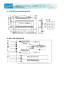
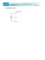
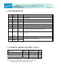
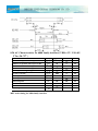
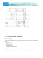
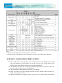
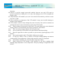
S12232A
LCD MODULE USER MANUAL
Address: ZhaoFuDa Industry Park, SongGang ,BaoAn Districtÿ Shenzhen
Tel :0755-83418186
http://www.sinco-display.com
E-mail :[email protected]
1. FUNCTIONS & FEATURES
Features
一 Dot Matrix: 122×32 Dots
一 LCD Mode: STN
一 Controller IC: SED1520 or Equivalent
一 Driving Method: 1/32 Duty; 1/9 Bias
一 Viewing Angie: 6 O’clock direction
一 6800 serial 8-Bit MPU Interface
一 Backlight: LED
一 Operating Temperature Range: -20 to 70℃;
一 Storage Temperature Range : -30 to 80℃;
Note: Color tone is slightly changed by temperature and driving voltage.
2. MECHANICAL SPECIFICATIONS
ITEM
Module Size
View
Area
SPECIFICATIONS
84.0L×44.0W×12.8
max)H
UNIT
mm
60.0×18.0
mm
Effective Area
122×32
dots
Dot Size
0.35×0.40
mm
Dot Pitch
0.40×0.45
mm
76.0± 0.2
2.54*19=48.26
10.2
4.0
2.5
4.0
9.6
14.5
3. EXTERNAL DIMENSIONS
4-? 2.50
44.0± 0.3
36.0± 0.2
27.8± 0.2
V.A.18.0± 0.2
A.A.14.35
0.40
0.35
0.45
0.40
122×32dots
A.A.48.75
V.A.60.0± 0.2
66.3± 0.2
79.0± 0.2
84.0± 0.3
12.0
8.85
2.5
1.6
8.7
12.8
4. BLOCK DIAGRAM
CS1
RST
RS
R/W
DB0
---DB7
E
CL
CS2
SED1520
61SEG
OR EQV.
16COM
----
16COM
SED1520
OR EQV.
LCD PANEL
122×32dots
61SEG
VDD
VSS
V0
Power Circuit
A
K
LED Backlight
5. POWER SUPPLY
6. PIN DESCRIPTION
ITEM
SYMBOL
I/O
FUNCTION
1
VDD
5.0V
2
VSS
0V
Power Ground
3
V0
Input
Contrast Adjust
4
RS
Input
H:DB0-DB7=Data
5
CS1
Input
Chip selection signal for IC1,
6
CS2
Input
Chip selection signal for IC2
7
CL
Input
System clock input
8
E*
Input
Enable signal for 6800 family interface
9
R/W*
Input
Write Read/Write signal for 6800 family interface
H:Read L:Write
10
~
17
DB0
~
DB7
I/O
18
RST
Input
19
LEDA
5.0V
Power Supply For Logic
L:DB0-DB7=Command
Data Bus
Reset Signal
Power Supply For LED Backlight
20
LEDK
0V
Note: E signal should be used as /RD signal for 8080 family interface, ; R/W should be used as /WR
signal for 8080 family interface.
7. MAXIMUM ABSOLUTE LIMIT (T=25°C)
Items
Symbol
Standard Value
Unit
Supply Voltage
Vdd
-0.3~7.0
V
Input Voltage
Vin
Vss~Vdd
V
Operating Temperature
Top
-20~70
℃
Storage Temperature
Tst
-30~80
℃
Note: Voltage greater than above may damage the module
All voltages are specified relative to VSS=0V
8. ELECTRICAL CHARACTERISTICS
8.1 DC Characteristics (VDD=+5V, VSS=0V, Ta=-0~+50°C)
Items
Symbol
Min
TYP
Max
Unit
Condition
Operating Voltage
Vdd
4.8
5.0
5.2
V
Supply Current
Idd
—
5
10
mA
Input High Voltage
Vin
Vdd-2.2
—
Vdd
V
Input Low Voltage
Vil
0
—
0.8
V
Output High Voltage
Voh
Vdd-0.3
—
Vdd
V
Ioh=-0.1mA,DB0-DB7
Output Low Voltage
Vol
0
—
0.3
V
Iol=0.1mA,DB0-DB7
LCD Driving Voltage
Vlcd
4.7
4.8
5.0
V
Vdd-V0
Vdd
except LED backlight
RS,RW,E,DB0-DB7
8.2 a AC Characteristics for 8080 family interface (VDD=+5V, VSS=0V,
TTa=-20~75°)
Items
Symbol
Min
Max
Unit
Address set-up time
tAS
20
—
nS
Address hold time
tAH
10
—
nS
Read / Write pulse falling/rising time
tF ,tR
—
15
nS
Read / Write pulse width
tRWPW
200
System cycle time
tCYC
1000
—
nS
Data setup time
tDS
80
—
nS
Data hold time
tDH
10
—
nS
Data access time
tACC
—
90
nS
Data output hold time
tOH
10
60
nS
MPU write timing for 8080 family interface
8.2 b AC Characteristics for 6800 family interface (VDD=+5V, VSS=0V,
TTa=-20~75°)
Items
Symbol
Min
Max
Unit
Address set-up time with respect to R/W
tAS1
20
—
nS
Address set-up time with respect to RS
tAS2
20
—
nS
Address hold time with respect to R/W
tAH1
10
—
nS
Address hold time with respect to RS
tAH2
10
—
nS
Enable pulse falling/rising time
tF ,tR
—
15
nS
System cycle time
tCYC
1000
—
nS
Enable pulse width for READ
tEWR
100
—
nS
Enable pulse width for WRITE
tEWW
80
—
nS
Data setup time
tDS
80
—
nS
Data hold time
tDH
10
—
nS
Data access time
tACC
—
90
nS
Data output hold time
tOH
10
60
nS
MPU write timing for 6800 family interface
9. FUNCTION SPECIFICATIONS
9.1. Basic Setting
To drive the LCD module correctly and provide normally display, please use the following
setting:
一 Select duty=1/32;
一 ADC=0;
一 Display start line=0;
一 LCD display=ON;
一 READ-MODIFY-WRITE=OFF.
Note:
一 These setting/commands should issue to both controllers while start up;
一 See the Display control instructions section for details.
9.2. Adjusting The LCD Display Contrast
A Variable-Resistor must be connected to the LCD module for providing a reference to V0.The
recommended value of the Variable-Resistor is 20K to 50K.
9.3. Resetting Signal
The LCD module can be reset or initialized by setting /RST to low level(if it is interfaced
with a 6800 MPU) or high level(if it is interfaced with a 8080 family MPU). This reset
operation occurs when an edge of the /RST signal is sensed. The level input selects the type of
interface with the 6800 family or 8080 family MPU.
High level: Interface with 6800 family MPU
Low level: Interface with 8080 family MPU
9.4. Display Memory Map
Page address
Data
0
DB7
|
DB0
1
DB7
|
DB0
2
DB7
|
DB0
3
DB7
LCD Display(font view)
|
DB0
Column driver
Y1
Y2
···
Y60
Y61
Y1
Y2
···
Column address
00h—3Ch
00h—3Ch
Total
61×32dots
61×32dots
Drive(accessed by)
E1
E2
Note:
一 Display start line=0;
一 ADC=0.
9.5. Display Control Instructions
Y60
Y61
Note:
1*. Only one section(driver) could be read at the same time.
2*. For the details of the display control instructions, please refer to SBN1661G datasheet.
10. DESIGN AND HANDING PRECAUTION
10.1.The LCD panel is made by glass. Any mechanical shock (eg. Dropping form high
place) will damage the LCD module. Do not add excessive force on the surface of the
display, which may cause the Display color change abnormally.
10.2.The polarizer on the LCD is easily get scratched. If possible, do not remove the LCD
protective film until the last step of installation.
10.3.Never attempt to disassemble or rework the LCD module.
10.4.Only Clean the LCD with Isopropyl Alcohol or Ethyl Alcohol. Other solvents (eg.
water) may damage the LCD.
10.5.When mounting the LCD module, make sure that it is free form twisting, warping and
distortion.
10.6.Ensure to provide enough space(with cushion) between case and LCD panel to
prevent external force adding on it, or it may cause damage to the LCD or degrade the
display result
10.7.Only hold the LCD module by its side. Never hold LCD module by add force on the
heat seal or TAB.
10.8.Never add force to component of the LCD module. It may cause invisible damage or
degrade of the reliability.
10.9.LCD module could be easily damaged by static electricity. Be careful to maintain an
optimum anti-static work environment to protect the LCD module.
10.10. When peeling of the protective film form LCD, static charge may cause abnormal
display pattern. It is normal and will resume to normal in a short while.
10.11. Take care and prevent get hurt by the LCD panel edge.
10.12. Never operate the LCD module exceed the absolute maximum ratings.
10.13. Keep the signal line as short as possible to prevent noisy signal applying to LCD
module.
10.14. Never apply signal to the LCD module without power supply.
10.15. IC chip (eg. TAB or COG) is sensitive to the light. Strong lighting environment
could possibly cause malfunction. Light sealing structure casing is recommend.
10.16. LCD module reliability may be reduced by temperature shock.
10.17. When storing the LCD module, avoid exposure to the direct sunlight, high
humidity, high temperature or low temperature. They may damage or degrade the LCD
module