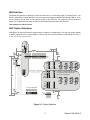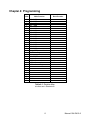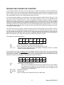
1
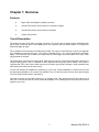
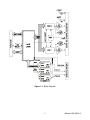
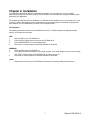
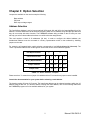
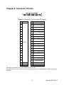
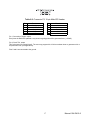
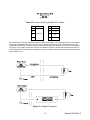
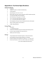
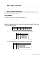
10623 Roselle Street, San Diego, CA 92121 • (858) 550-9559 • FAX (858) 550-7322
[email protected] • www.accesio.com
MODEL 104-DA12-8
Analog Output Board
USER MANUAL
FILE: M104-DA12-8.A1e
Notice
The information in this document is provided for reference only. ACCES does not assume any liability arising
out of the application or use of the information or products described herein. This document may contain or
reference information and products protected by copyrights or patents and does not convey any license under
the patent rights of ACCES, nor the rights of others.
IBM PC, PC/XT, and PC/AT are registered trademarks of the International Business Machines Corporation.
Printed in USA. Copyright 2001, 2007 by ACCES I/O Products, Inc. 10623 Roselle Street, San Diego, CA
92121. All rights reserved.
WARNING!!
ALWAYS CONNECT AND DISCONNECT YOUR FIELD CABLING WITH
THE COMPUTER POWER OFF. ALWAYS TURN COMPUTER POWER OFF
BEFORE INSTALLING A BOARD. CONNECTING AND DISCONNECTING
CABLES, OR INSTALLING BOARDS INTO A SYSTEM WITH THE
COMPUTER OR FIELD POWER ON MAY CAUSE DAMAGE TO THE I/O
BOARD AND WILL VOID ALL WARRANTIES, IMPLIED OR EXPRESSED.
2
Manual 104-DA12-8
Warranty
Prior to shipment, ACCES equipment is thoroughly inspected and tested to applicable specifications.
However, should equipment failure occur, ACCES assures its customers that prompt service and support will
be available. All equipment originally manufactured by ACCES which is found to be defective will be repaired
or replaced subject to the following considerations.
Terms and Conditions
If a unit is suspected of failure, contact ACCES' Customer Service department. Be prepared to give the unit
model number, serial number, and a description of the failure symptom(s). We may suggest some simple
tests to confirm the failure. We will assign a Return Material Authorization (RMA) number which must appear
on the outer label of the return package. All units/components should be properly packed for handling and
returned with freight prepaid to the ACCES designated Service Center, and will be returned to the
customer's/user's site freight prepaid and invoiced.
Coverage
First Three Years: Returned unit/part will be repaired and/or replaced at ACCES option with no charge for
labor or parts not excluded by warranty. Warranty commences with equipment shipment.
Following Years: Throughout your equipment's lifetime, ACCES stands ready to provide on-site or in-plant
service at reasonable rates similar to those of other manufacturers in the industry.
Equipment Not Manufactured by ACCES
Equipment provided but not manufactured by ACCES is warranted and will be repaired according to the terms
and conditions of the respective equipment manufacturer's warranty.
General
Under this Warranty, liability of ACCES is limited to replacing, repairing or issuing credit (at ACCES
discretion) for any products which are proved to be defective during the warranty period. In no case is ACCES
liable for consequential or special damage arriving from use or misuse of our product. The customer is
responsible for all charges caused by modifications or additions to ACCES equipment not approved in writing
by ACCES or, if in ACCES opinion the equipment has been subjected to abnormal use. "Abnormal use" for
purposes of this warranty is defined as any use to which the equipment is exposed other than that use
specified or intended as evidenced by purchase or sales representation. Other than the above, no other
warranty, expressed or implied, shall apply to any and all such equipment furnished or sold by ACCES.
3
Manual 104-DA12-8
Table of Contents
Chapter 1: Overview ...........................................................................................................5
Figure 1-1: Block Diagram ............................................................................................6
Chapter 2: Installation ........................................................................................................7
Figure 2-1: PC/104 Key Information .............................................................................8
Chapter 3: Option Selection...............................................................................................9
Table 3-1: Base Address Jumpers ................................................................................9
Table 3-2: Standard Address Assignments .................................................................10
Figure 3-1: Option Selection .......................................................................................11
Chapter 4: Programming ..................................................................................................12
Table 4-1: Register Map..............................................................................................12
Chapter 5: Software ..........................................................................................................15
Chapter 6: Connector Pinouts .........................................................................................16
Table 6-1: Connector P1, 40-pin Male IDC Header.....................................................16
Table 6-2: Connector P2, 10-pin Male IDC Header.....................................................17
Table 6-3: Connector P4, 8-pin Male IDC Header.......................................................18
Figure 6-1: Signal Connection ....................................................................................18
Appendix A: Technical Specifications ............................................................................19
Appendix B: 82C54 Counter Timer Operation ................................................................20
4
Manual 104-DA12-8
Chapter 1: Overview
Features
●
Eight 12-Bit 10uS Digital to Analog Converters
●
Counter/Timer with a 32-bit Divisor for Conversion Triggers
●
Counter/Timer with a 16-bit Divisor for Interrupts
●
4-20mA Current Sink
Circuit Description
The board has eight 12-bit digital to analog converters. The circuit uses an Analog Devices AD5348 which
has a single 12-bit input port, a 3-bit address port, and a shared 'start conversion' signal. The outputs are
buffered by eight op-amps.
Two countdown timers (based on an i8254) are provided. The output of Counter/Timer 0 (16 bit, see appendix
B) is available at connector P2 pin 4. The output of chained timers 1 & 2 (32 bit) provide the conversion
trigger. The 16-bit timer has a 10MHz clock input while the 32-bit trigger timer has a 2MHz clock input, either
may generate an interrupt.
The board has a 4-20mA current sink outputs. Each DAC may drive a 4-20mA sink with digital values from 0
(4mA) to 4095 (20mA). This is in addition to and in parallel with the op-amp driven outputs. The current is
regulated with FETs, each source lead connects to the card's ground plane through a small resistance and
each drain lead connects to the user's circuit.
A 4.096 volt reference is available at a connector pin (J1 Pin 35). Fused (resettable) +5 volts from the PC/104
bus and fused (resettable) +12 volts are also available. The +12 volts may come from the user's power supply
if the PC/104 bus doesn't have it (some don't).
Note that on power-up the 4.096V reference is in standby mode. This ensures that all D/AC outputs are at
zero volts. The user must set bit 6 at the card’s base address +10h. Clearing this bit at any time will cause all
outputs to go to zero.
5
Manual 104-DA12-8
Figure 1-1: Block Diagram
6
Manual 104-DA12-8
Chapter 2: Installation
A printed Quick-Start Guide (QSG) is packed with the board for your convenience. If you’ve already
performed the steps from the QSG, you may find this chapter to be redundant and may skip forward to begin
developing your application.
The software provided with this PC/104 Board is on CD and must be installed onto your hard disk prior to use.
To do this, perform the following steps as appropriate for your operating system. Substitute the appropriate
drive letter for your CD-ROM where you see d: in the examples below.
CD Installation
The following instructions assume the CD-ROM drive is drive “D”. Please substitute the appropriate drive
letter for your system as necessary.
DOS
1.
Place the CD into your CD-ROM drive.
2.
Type B- to change the active drive to the CD-ROM drive.
3.
4.
Type GLQR?JJ- to run the install program.
Follow the on-screen prompts to install the software for this board.
WINDOWS
1.
Place the CD into your CD-ROM drive.
2.
The system should automatically run the install program. If the install program does not run promptly,
click START | RUN and type BGLQR?JJ, click OK or press -.
3.
Follow the on-screen prompts to install the software for this board.
LINUX
1.
Please refer to linux.htm on the CD-ROM for information on installing serial ports under linux.
7
Manual 104-DA12-8
Installing the Hardware
Before installing the board, carefully read Chapter 3 and Chapter 4 of this manual and configure the board
according to your requirements. The SETUP Program can be used to assist in configuring jumpers on the
board. Be especially careful with Address Selection. If the addresses of two installed functions overlap, you
will experience unpredictable computer behavior. To help avoid this problem, refer to the FINDBASE.EXE
program installed from the CD. The setup program does not set the options on the board, these must be set
by jumpers.
To Install the Board
1.
2.
3.
4.
5.
6.
7.
Install jumpers for selected options and base address according to your application
requirements, as mentioned above.
Remove power from the PC/104 stack.
Assemble standoff hardware for stacking and securing the boards.
Carefully plug the board onto the PC/104 connector on the CPU or onto the stack, ensuring
proper alignment of the pins before completely seating the connectors together.
Install I/O cables onto the board’s I/O connectors and proceed to secure the stack together or
repeat steps 3-5 until all boards are installed using the selected mounting hardware.
Check that all connections in your PC/104 stack are correct and secure then power up the
system.
Run one of the provided sample programs appropriate for your operating system that was
installed from the CD to test and validate your installation.
Figure 2-1: PC/104 Key Information
8
Manual 104-DA12-8
Chapter 3: Option Selection
Jumpers are available on the card to setup the following:
Base address
IRQ level
DAC output voltage ranges
Address Selection
The Card’s Base Address is set by jumpers marked /A5 through /A9, and /A5 is the least significant bit of the
address. The base addresses can be selected anywhere within the I/O address range 000-3E0 provided that
they do not overlap with other functions. The FINDBASE software utility provided on the CD with your card
will help you select a base address that does not conflict with other assignments.
This card requires a block of 32 addresses (20 hex). In order to configure the desired address, the
hexadecimal address must be converted to a binary representation which is then selected by installing
jumpers on the card.
For example, as illustrated below, switch selection corresponds to hex 2C0 (or binary 10 110x xxxx). The
"xxxxx" represents address lines A4 through A0 used on the card to select individual registers.
2
Hex Representation
C
Conversion Factors
2
1
8
4
2
Binary Representation
1
0
1
1
0
Jumper Installed
NO
NO
YES
Jumper Label
A9
A6
A5
YES NO
A8
A7
Table 3-1: Base Address Jumpers
Please note that "1" means that no jumper is installed and that "0" means that a jumper must be installed.
Consult the documentation for your system before selecting a card address.
The board occupies 32 bytes of I/O space. The board base address can be selected anywhere within the I/O
address range 0-3E0 hex. If in doubt of where to assign the base address, refer to the following tables and
the FINDBASE program to find an available address for your system.
9
Manual 104-DA12-8
HEX RANGE
000-00F
020-021
040-043
060-06F
070-07F
080-09F
0A0-0BF
0C0-0DF
0F0-0F1
0F8-0FF
170-177
1F0-1F8
200-207
238-23B
23C-23F
278-27F
2B0-2BF
2C0-2CF
2D0-2DF
2E0-2E7
2E8-2EF
2F8-2FF
300-30F
310-31F
320-32F
370-377
378-37F
380-38F
3A0-3AF
3B0-3BB
3BC-3BF
3C0-3CF
3D0-3DF
3E8-3EF
3F0-3F7
3F8-3FF
USAGE
8237 DMA Controller 1
8259 Interrupt
8253 Timer
8042 Keyboard Controller
CMOS RAM, NMI Mask Reg, RT Clock
DMA Page Register
8259 Slave Interrupt Controller
8237 DMA Controller 2
Math Coprocessor
Math Coprocessor
Fixed Disk Controller 2
Fixed Disk Controller 1
Game Port
Bus Mouse
Alt. Bus Mouse
Parallel Printer
EGA
EGA
EGA
GPIB (AT)
Serial Port
Serial Port
reserved
reserved
Hard Disk (XT)
Floppy Controller 2
Parallel Printer
SDLC
SDLC
MDA
Parallel Printer
VGA EGA
CGA
Serial Port
Floppy Controller 1
Serial Port
Table 3-2: Standard Address Assignments
10
Manual 104-DA12-8
IRQ Selection
The board can generate an interrupt on the DAC conversion or on the falling edge of Counter/Timer 0. The
IRQ # is selected by a jumper placed on one pair of pins from the group labeled 'IRQ3' through 'IRQ15'. If you
do not intend to use the IRQ, do not install a jumper on any IRQ pins. The locations of these jumpers is
shown in the Option Selection map, as well as in the Setup Program provided with the card.
This interrupt can not be shared.
DAC Option Selections
ADDRESS 0x300
Each DAC's op-amp circuit has two jumpers which configure it's voltage range. The user may select unipolar
or bipolar outputs and 5 or 10 max voltage. In other words, the user may select four output ranges: 0 to 5V, 0
to 10V, -5V to +5V, -10V to +10V.
Pin 1
DAC 8 DAC 4 DAC 3
3
4
5
6
7
10
11
12
14
15
± 10V
A PAIR OF JUMPERS SELECTS THE
VOLTAGE OUTPUT RANGE FOR
EACH DAC AS SHOWN.
5V
10V
UNI
BIP
±10V
5V
10V
UNI
BIP
IRQ
IRQ
IRQ
IRQ
IRQ
IRQ
IRQ
IRQ
IRQ
IRQ
0-10V
DAC 2 DAC 1
0-10V
A5
A6
A7
A8
A9
±5V
5V
10V
EXT/LCL
0-5V
UNI
BIP
± 5V
P1
P4
0-5V
Pin 1
DAC 7 DAC 6 DAC 5
Pin 1
P2
Figure 3-1: Option Selection
11
Manual 104-DA12-8
Chapter 4: Programming
Offset
0
1
2
3
4
5
6
7
8
9
A
B
C
D
E
F
10
11
12
13
14
15
16
17
18
19
1A
1B
1C
1D
1E
1F
Write Function
DAC 0 LSB
DAC 0 MSB
DAC 1 LSB
DAC 1 MSB
DAC 2 LSB
DAC 2 MSB
DAC 3 LSB
DAC 3 MSB
DAC 4 LSB
DAC 4 MSB
DAC 5 LSB
DAC 5 MSB
DAC 6 LSB
DAC 6 MSB
DAC 7 LSB
DAC 7 MSB
Voltage REFerence Control
IRQ Enable Register
DAC RESET
Program Counter 0
Program Counter 1
Program Counter 2
Counter Control Register
Read Function
IRQ Enable Readback
Read Counter 0
Read Counter 1
Read Counter 2
IRQ Clear
Not used
Table 4-1: Register Map
All offsets are in hexadecimal.
12
Manual 104-DA12-8
Register Descriptions
The card is controlled by reading and writing 8- or 16-bit registers in I/O Memory. The registers are described
below. Please note, all offsets are hexadecimal.
Base+ 0 through Base + E, DACs 0-7 Direct Control Registers
D15
D14
D13
D12
D11
D10
D9
D8
D7
D6
X
X
X
X
D11
D10
D9
D8
D7
D6
D5
D5
D4
D4
D3
D3
D2
D2
D1
D1
D0
D0
These 8 word-sized registers allow you to update the DACs from software. If you’re interested in simple DC
voltage or current outputs you can ignore all the rest of the registers and just use these to control the outputs
of the DACs.
Write a word to an even address in the range of (base +) 0 through 0xE to update the DAC with a new count
value. Data is offset Binary: 0x0000 is the minimum value (in unipolar modes, 0Volts, in bipolar modes, the
most-negative value possible). 0x0800 is the “middle” of the range (0V when in Bipolar modes), and 0x0FFF
is the maximum positive voltage.
Bits D15 through D12 are unused and should be set to zero for future compatibility.
To calculate the counts for any given Desired Output Voltage use the following equation:
Given: SpanVolts is equal to the highest positive voltage minus the most negative voltage the range supports
(ex: +5V is “5" - “-5" which is “5+5" or “10")
Unipolar:
Counts = (DesiredVolts / SpanVolts) * 4096
Bipolar:
Counts = (DesiredVolts / SpanVolts) * 2048 + 2048
Base + 10 Write, Reference Control
D7
D6
D5
REF
D4
D3
D2
D1
D0
Bit D6 REF: Set/clear to enable/disable the 4.096 DAC REFerence. While this bit is set DACs can
generate signals, and P1 Pin 35 will have 4.096 volts output. At power-up this bit is cleared and all
outputs are 0V.
Bits D0 through D5 and D7 are unused.
Reading this register will return the current state of the Reference Control bit.
All bits in this register power-on or reset to “zero”
13
Manual 104-DA12-8
Base + 11 Write, Interrupt Enable Register
D7
D6
D5
D4
D3
D2
D1
EICTR0
D0
Set/clear bits D0 through D7 to enable/disable an irq from each bit’s IRQ source.
Bit D1 EICTR0: Enables IRQs from the output of CounTeR 0. Each time the output of Counter 0 goes
low and this bit is set an IRQ will be generated. This counter, and its IRQ and output on the P2
connector (pin 4), are solely for use by the customer.
Reading this register will return the current state of these bits.
All bits in this register power-on or reset to “zero.”
Base + 13, DAC Reset
Write any value to this register to clear the DACs and set all outputs to their most negative value. For
example, if the range is -10V to +10V on DAC 1 it will go to -10V. If the range on channel 2 is 0V to 5V it will
go to zero volts.
Base + 14, Program Counter/Timer 0 - (see Appendix B)
This is a 16-bit timer used as a timer-tick for external hardware. Its 10MHz input clock is divided by a load 16bit value and output on P2 pin 4. This counter output can also generate an IRQ, if enabled (see base + 10.)
Base + 17, Counter/Timer Control Register - (see Appendix B)
Use this register to configure the 8254.
Base + 1E, IRQ Clear
Write any value to this address to clear a pending interrupt. Once the card generates an IRQ, no further IRQs
will be requested until the pending IRQ has been cleared by writing to this address.
14
Manual 104-DA12-8
Chapter 5: Software
Software Driven DC DAC Mode:
There are two broad categories of software driven DAC usage: synchronous, or simultaneous, and
asynchronous, or “automatic.” Simultaneous mode is so named because all DACs will switch from their old
voltage (or current) output levels to their newly programmed levels simultaneously, and synchronously with an
event.
Asynchronous:
To use the DACs simply write desired count values to the DACs themselves, via Base + 0 through Base + E.
The card powers up in this mode, so no other registers need to be manipulated.
15
Manual 104-DA12-8
Chapter 6: Connector Pinouts
Table 6-1: Connector P1, 40-pin Male IDC Header
Pin
1
Pin
2
Function
DAC 0 Voltage Output
3
4
DAC 0 4-20mA Output
5
6
DAC 1 Voltage Output
7
8
DAC 1 4-20mA Output
9
10
DAC 2 Voltage Output
11
12
DAC 2 4-20mA Output
13
14
DAC 3 Voltage Output
15
16
DAC 3 4-20mA Output
18
DAC 4 Voltage Output
19
20
DAC 4 4-20mA Output
21
22
DAC 5 Voltage Output
23
24
DAC 5 4-20mA Output
25
26
DAC 6 Voltage Output
27
28
DAC 6 4-20mA Output
29
30
DAC 7 Voltage Output
31
32
DAC 7 4-20mA Output
33
34
+12 Volts Fused
36
38
40
+5 Volts Fused
n.c.
n.c.
17
35
37
39
Function
Ground
4.096V
Ground
n.c.
Note that pin 35 will be 0V if bit 6 of Control Register 2 is LOW.
Note also that pins 38, 39, and 40 are unused, such that connection via a standard 37-Pin DSub connector is
simplified.
16
Manual 104-DA12-8
Table 6-2: Connector P2, 10-pin Male IDC Header
Pin
1
3
5
7
9
Function
Load DAC (output)
N/C
Ground
N/C
N/C
Pin
2
4
6
8
10
Function
N/C
Counter 0 Output
Ground
N/C
N/C
Pin 1, Conversion Trigger, output
Every time the DACs are updated a very short low-going pulse will be generated here. (<100nS).
Pin 4, Clock Tick, output
This is the output of counter/timer 0. The user may program this 16-bit count-down timer to generate a tick or
a square wave etc. (see appendix B).
Pins 5 and 6 are connected to the ground.
17
Manual 104-DA12-8
Table 6-3: Connector P4, 8-pin Male IDC Header
Pin
1
Signal
3
5
Ground
7
Pin
2
Signal
n.c.
4
+12V
6
n.c.
8
n.c.
The board does not require +12V but the user’s 4-20mA circuit might. +12V is brought to pin 34 of connector
P1 through a resettable fuse. This +12V may come from the PC/104 bus or from an external source. If the
voltage comes from the PC/104 bus then a jumper should be placed on the pins of JP32 (next to P4) labeled
LCL (local). If the voltage comes from a source connected to P4 then a jumper should be placed on the pins
of JP32 labeled EXT. Note that if the voltage for the user’s 4-20mA circuit comes from an external source that
it isn’t limited to 12V.
Figure 6-1: Signal Connection
18
Manual 104-DA12-8
Appendix A: Technical Specifications
ANALOG OUTPUTS
●
8 Channels
●
10μS per conversion, all channels simultaneously
●
12 Bit Resolution
●
Output Ranges, 0-5V 0-10V +5V +10V
●
Eight 4-20mA current sink outputs (external 8 to 36VDC excitation required)
●
+2 counts D/AC Relative Accuracy (typical)
●
8uS D/AC Settling Time (typical, to 3/4 scale)
●
+0.4 % of Full Scale D/AC Offset Error (typical)
●
+0.1 % of Full Scale D/AC Gain Error (typical)
●
Drive Capability of 5mA per channel, Outputs are Short-Circuit Protected
●
30mA cumulative total drive from all D/ACs
●
4.096V Voltage Reference
Counter/Timer
●
Type 82C54
●
3 x 16-Bit Down-Counters
●
Counter 0 is an IRQ source (clock-tick interrupt) and frequency source
(counter 0 output is available at P2 connector pin 4)
●
10MHz Input Clock Frequency
General
●
+5V @ 210mA Power Consumption (typical, no load on the outputs)
●
On-board DC/DC Converter allows operation on +5V Power
●
Interrupt requests may be generated on channels 3-7, 10-12 and 14-15
●
Environment Tolerance: 0-70C, 5% to 95% Humidity (non-condensing)
(-40 to +85C available with special order)
19
Manual 104-DA12-8
Appendix B: 82C54 Counter Timer Operation
The board contains one type 8254 programmable counter/timer. The 8254 consists of three independent, 16bit, presettable down-counters. Each counter can be programmed to any count between 2 and 65,535 in
binary format, depending on the mode chosen. The programmed value is a divisor, the output frequency
equals the input frequency divided by the programmed value.
In this manual these three counter/timers are designated Counter/Timer 0, Counter/Timer 1, and
Counter/Timer 2.
Counter/Timer 0 is a 16-bit counter with a 10MHz input clock. The output of Counter/Timer 0 is available at
connector P2 pin 4. The gate signal for counters 1 & 2 is controlled via software at bit 1 (HIGH = off, LOW =
count enabled = power-on default) of the register at Base + 10h. Counter/Timers 1 and 2 are concatenated by
the card to form a single 32-bit counter. The input of the counter is fixed at 2MHz. The output of is available at
connector P2 pin 1.
OPERATIONAL MODES
The 8254 modes of operation are described in the following paragraphs to familiarize you with the versatility
and power of this device. For those interested in more detailed information, a full description of the 8254
programmable interval timer can be found in the Intel (or equivalent manufacturers) data sheets. The
following conventions apply for use in describing operation of the 8254 :
Clock:
Trigger:
Counter Loading:
A positive pulse into the counter's clock input.
A rising edge input to the counter's gate input.
Programming of a binary count into the counter.
Mode 0: Pulse on Terminal Count
After the counter is loaded, the output is set low and will remain low until the counter decrements to zero. The
output then goes high and remains high until a new count is loaded into the counter. A trigger enables the
counter to start decrementing.
Mode 1: Retriggerable One-Shot
The output goes low on the clock pulse following a trigger to begin the one-shot pulse and goes high when
the counter reaches zero. Additional triggers result in reloading the count and starting the cycle over. If a
trigger occurs before the counter decrements to zero, a new count is loaded. Thus, this forms a re-triggerable
one-shot. In mode 1, a low output pulse is provided with a period equal to the counter count-down time.
Mode 2: Rate Generator
This mode provides a divide-by-N capability where N is the count loaded into the counter. When triggered, the
counter output goes low for one clock period after N counts, reloads the initial count, and the cycle starts over.
This mode is periodic, the same sequence is repeated indefinitely until the gate input is brought low.
Mode 3: Square Wave Generator
This mode operates periodically like mode 2. The output is high for half of the count and low for the other half.
If the count is even, then the output is a symmetrical square wave. If the count is odd, then the output is high
for (N+1)/2 counts and low for (N-1)/2 counts. Periodic triggering or frequency synthesis are two possible
applications for this mode. Note that in this mode, to achieve the square wave, the counter decrements by two
for the total loaded count, then reloads and decrements by two for the second part of the wave form.
20
Manual 104-DA12-8
Mode 4: Software Triggered Strobe
This mode sets the output high and, when the count is loaded, the counter begins to count down. When the
counter reaches zero, the output will go low for one input period. The counter must be reloaded to repeat the
cycle. A low gate input will inhibit the counter. This mode can be used to provide a delayed software trigger
for initiating A/D conversions.
Mode 5: Hardware Triggered Strobe
In this mode, the counter will start counting after the rising edge of the trigger input and will go low for one
clock period when the terminal count is reached. The counter is retriggerable. The output will not go low until
the full count after the rising edge of the trigger.
PROGRAMMING
On this card the 8254 counters occupy the following addresses (hex):
Base Address + 14:
Base Address + 15:
Base Address + 16:
Base Address + 17:
Read/Write Counter 0
Read/Write Counter 1
Read/Write Counter 2
Write to Counter Control register
The counters are programmed by writing a control byte into a counter control register. The control byte
specifies the counter to be programmed, the counter mode, the type of read/write operation, and the modulus.
The control byte format is as follows:
SC0-SC1:
B7
B6
B5
B4
B3
B2
B1
B0
SC1
SC0
RW1
RW0
M2
M1
M0
BCD
These bits select the counter that the control byte is destined for.
SC1
SC0
Function
0
0
1
1
0
1
0
1
Program Counter 0
Program Counter 1
Program Counter 2
Read/Write Cmd.*
* See Chapter on READING AND LOADING THE COUNTERS.
RW0-RW1:These bits select the read/write mode of the selected counter.
RW1
RW0
0
0
1
1
0
1
0
1
Counter Read/Write Function
Counter Latch Command
Read/Write LS Byte
Read/Write MS Byte
Read/Write LS Byte, then MS Byte
21
Manual 104-DA12-8
M0-M2:
BCD:
These bits set the operational mode of the selected counter.
MODE
M2
M1
M0
0
1
2
3
4
5
0
0
X
X
1
1
0
0
1
1
0
0
0
1
0
1
0
1
Set the selected counter to count in binary (BCD = 0) or BCD (BCD = 1).
22
Manual 104-DA12-8
READING AND LOADING THE COUNTERS
If you attempt to read the counters on the fly when there is a high input frequency, you will most likely get
erroneous data. This is partly caused by carries rippling through the counter during the read operation. Also,
the low and high bytes are read sequentially rather than simultaneously and, thus, it is possible that carries
will be propagated from the low to the high byte during the read cycle.
To circumvent these problems, you can perform a counter-latch operation in advance of the read cycle. To do
this, load the RW1 and RW2 bits with zeroes. This instantly latches the count of the selected counter
(selected via the SC1 and SC0 bits) in a 16-bit hold register. (An alternative method of latching counter(s)
which has an additional advantage of operating simultaneously on several counters is by use of a readback
command to be discussed later.) A subsequent read operation on the selected counter returns the held value.
Latching is the best way to read a counter on the fly without disturbing the counting process. You can only
rely on directly read counter data if the counting process is suspended while reading, by bringing the gate low,
or by halting the input pulses.
For each counter you must specify in advance the type of read or write operation that you intend to perform.
You have a choice of loading/reading (a) the high byte of the count, or (b) the low byte of the count, or (c) the
low byte followed by the high byte. This last is of the most general use and is selected for each counter by
setting the RW1 and RW0 bits to ones. Of course, subsequent read/load operations must be performed in
pairs in this sequence or the sequencing flip-flop in the 8254 chip will get out of step.
The readback command byte format is:
CNT:
STA:
C0, C1, C2:
B7
B6
B5
B4
B3
B2
B1
B0
1
1
CNT
STA
C2
C1
C0
0
When is 0, latches the counters selected by bits C0-C2.
When is 0, returns the status byte of counters selected by C0-C2.
When high, select a particular counter for readback. C0 selects Counter 0, C1 selects
Counter 1, and C2 selects Counter 2.
You can perform two types of operations with the readback command. When CNT=0, the counters selected
by C0 through C2 are latched simultaneously. When STA=0, the counter status byte is read when the counter
I/O location is accessed. The counter status byte provides information about the current output state of the
selected counter and its configuration. The status byte returned if STA=0 is:
OUT:
NC:
RW1, RW0:
M2, M1, M0:
BCD:
B7
B6
B5
B4
B3
B2
B1
B0
OUT
NC
RW1
RW2
M2
M1
M0
BCD
Current state of counter output pin.
Null count. This indicates when the last count loaded into the counter register
has actually been loaded into the counter itself. The exact time of load
depends on the configuration selected. Until the count is loaded into the
counter itself, it cannot be read.
Read/Write command.
Counter mode.
BCD = 0 is binary mode, otherwise counter is in BCD mode.
23
Manual 104-DA12-8
If both STA and CNT bits in the readback command byte are set low and the RW1 and RW0 bits have both
been previously set high in the counter control register (thus selecting two-byte reads), then reading a
selected counter address location will yield:
1st Read:
2nd Read:
3rd Read:
Status byte
Low byte of latched data
High byte of latched data
After any latching operation of a counter, the contents of its hold register must be read before any subsequent
latches of that counter will have any effect. If a status latch command is issued before the hold register is
read, then the first read will read the status, not the latched value.
24
Manual 104-DA12-8
Customer Comments
If you experience any problems with this manual or just want to give us some feedback, please email us at:
[email protected]. Please detail any errors you find and include your mailing address so that we can
send you any manual updates.
10623 Roselle Street, San Diego CA 92121
Tel. (858)550-9559 FAX (858)550-7322
www.accesio.com
25
Manual 104-DA12-8