1
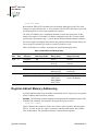
High-Performance 16-Bit Microcontrollers
ZNEO® CPU Core
User Manual
UM018809-0611
Copyright ©2011 Zilog®, Inc. All rights reserved.
www.zilog.com
ZNEO® CPU Core
User Manual
ii
This publication is subject to replacement by a later edition. To determine whether a later edition exists, or
to request copies of publications, visit www.zilog.com.
Warning: DO NOT USE THIS PRODUCT IN LIFE SUPPORT SYSTEMS.
LIFE SUPPORT POLICY
ZILOG'S PRODUCTS ARE NOT AUTHORIZED FOR USE AS CRITICAL COMPONENTS IN LIFE
SUPPORT DEVICES OR SYSTEMS WITHOUT THE EXPRESS PRIOR WRITTEN APPROVAL OF
THE PRESIDENT AND GENERAL COUNSEL OF ZILOG CORPORATION.
As used herein
Life support devices or systems are devices which (a) are intended for surgical implant into the body, or (b)
support or sustain life and whose failure to perform when properly used in accordance with instructions for
use provided in the labeling can be reasonably expected to result in a significant injury to the user. A critical component is any component in a life support device or system whose failure to perform can be reasonably expected to cause the failure of the life support device or system or to affect its safety or effectiveness.
Document Disclaimer
©2011 Zilog, Inc. All rights reserved. Information in this publication concerning the devices, applications,
or technology described is intended to suggest possible uses and may be superseded. ZILOG, INC. DOES
NOT ASSUME LIABILITY FOR OR PROVIDE A REPRESENTATION OF ACCURACY OF THE
INFORMATION, DEVICES, OR TECHNOLOGY DESCRIBED IN THIS DOCUMENT. ZILOG ALSO
DOES NOT ASSUME LIABILITY FOR INTELLECTUAL PROPERTY INFRINGEMENT RELATED
IN ANY MANNER TO USE OF INFORMATION, DEVICES, OR TECHNOLOGY DESCRIBED
HEREIN OR OTHERWISE. The information contained within this document has been verified according
to the general principles of electrical and mechanical engineering.
Z8, Z8 Encore!, Z8 Encore! XP, Z8 Encore! MC, eZ80, and ZNEO are trademarks or registered trademarks
of Zilog, Inc. All other product or service names are the property of their respective owners.
UM018809-0611
ZNEO® CPU Core
User Manual
iii
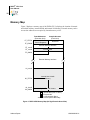
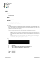
Revision History
Each instance in the Revision History table below reflects a change to this document from
its previous version. For more details, click the appropriate links in the table.
Date
May
2011
Revision
Level Section
09
All
Description
Page
Updated for style.
All
Using the Program Counter as Added note.
a Base Address
34
LEA
Added addressing mode offset description.
122
SDIV
Corrected After address in Example.
152
68, 71
Aug
2010
08
ADC, ADD
Updated Syntax and Opcodes table.
Feb
2008
07
Flags Register (FLAGS)
Updated User Flag description.
9
Loading an Effective Address
Updated example.
33
System Exceptions
Updated first paragraph.
49
Stack Overflow
Updated second step for Stack Overflow
protection.
50
Sep
2007
06
Instruction Set Reference
Updated Examples for DEC Instruction.
65
Mar
2007
05
Loading an Effective Address
Change in instruction.
33
May
2006
04
Flags Register (FLAGS), Vec- Updated with CIRQE bit.
tored Interrupts, Instruction Set
Reference
UM018809-0611
9, 41, 65
Multiple
Updated ZNEO trademark issues. Applied
current publications template.
Features, Control Registers,
Address Space, I/O Memory,
Direct Memory Addressing
Clarified size of address space.
CPU Control Register
(CPUCTL)
Clarified section.
All
1, 8, 15,
18, 29
13
Memory Map, Jump Addressing Jump addresses FF_E000H and above
are reserved.
16, 39
Internal Nonvolatile Memory,
Internal RAM
Clarified use of assembler address
ranges.
17, 17
Direct Memory Addressing
16-bit address range is in highest and lowest 32K blocks, not 8K blocks.
29
Revision History
ZNEO® CPU Core
User Manual
iv
Date
Jan
2006
Revision
Level Section
Description
Page
03
Multiple
Updated ZNEO trademark.
All
02
Instruction Opcodes
Moved opcodes beginning 0000 1011
and 0001 001+ to correct listing order.
(Opcode-to-instruction relationship is not
changed); corrected sequence of unimplemented opcodes and removed duplicate
row.
55
UDIV64
Corrected “After” register in example.
182
Revision History
UM018809-0611
ZNEO® CPU Core
User Manual
v
Table of Contents
Revision History . . . . . . . . . . . . . . . . . . . . . . . . . . . . . . . . . . . . . . . . . . . . . . . . . . . . . . . . . . . . .iii
List of Figures . . . . . . . . . . . . . . . . . . . . . . . . . . . . . . . . . . . . . . . . . . . . . . . . . . . . . . . . . . . . . . . ix
List of Tables. . . . . . . . . . . . . . . . . . . . . . . . . . . . . . . . . . . . . . . . . . . . . . . . . . . . . . . . . . . . . . . . xi
Manual Objectives . . . . . . . . . . . . . . . . . . . . . . . . . . . . . . . . . . . . . . . . . . . . . . . . . . . . . . . . . .xiii
About This Manual . . . . . . . . . . . . . . . . . . . . . . . . . . . . . . . . . . . . . . . . . . . . . . . . . . . . .xiii
Intended Audience . . . . . . . . . . . . . . . . . . . . . . . . . . . . . . . . . . . . . . . . . . . . . . . . . . . . . .xiii
Manual Organization . . . . . . . . . . . . . . . . . . . . . . . . . . . . . . . . . . . . . . . . . . . . . . . . . . . .xiii
Manual Conventions . . . . . . . . . . . . . . . . . . . . . . . . . . . . . . . . . . . . . . . . . . . . . . . . . xiv
Safeguards . . . . . . . . . . . . . . . . . . . . . . . . . . . . . . . . . . . . . . . . . . . . . . . . . . . . . . . . . . . . xvi
Architectural Overview . . . . . . . . . . . . . . . . . . . . . . . . . . . . . . . . . . . . . . . . . . . . . . . . . . . . . . . . 1
Features . . . . . . . . . . . . . . . . . . . . . . . . . . . . . . . . . . . . . . . . . . . . . . . . . . . . . . . . . . . . . . . 1
Program Control . . . . . . . . . . . . . . . . . . . . . . . . . . . . . . . . . . . . . . . . . . . . . . . . . . . . . . . . 2
Processor Block Diagram . . . . . . . . . . . . . . . . . . . . . . . . . . . . . . . . . . . . . . . . . . . . . . . . . 2
Fetch Unit . . . . . . . . . . . . . . . . . . . . . . . . . . . . . . . . . . . . . . . . . . . . . . . . . . . . . . . . . . 3
Execution Unit . . . . . . . . . . . . . . . . . . . . . . . . . . . . . . . . . . . . . . . . . . . . . . . . . . . . . . 4
Instruction Cycle Time . . . . . . . . . . . . . . . . . . . . . . . . . . . . . . . . . . . . . . . . . . . . . . . . . . . 5
Instruction Fetch Cycles . . . . . . . . . . . . . . . . . . . . . . . . . . . . . . . . . . . . . . . . . . . . . . . 5
Execution Cycles . . . . . . . . . . . . . . . . . . . . . . . . . . . . . . . . . . . . . . . . . . . . . . . . . . . . 6
Control Registers . . . . . . . . . . . . . . . . . . . . . . . . . . . . . . . . . . . . . . . . . . . . . . . . . . . . . . . . 8
Program Counter Overflow Register . . . . . . . . . . . . . . . . . . . . . . . . . . . . . . . . . . . . . 9
Stack Pointer Overflow . . . . . . . . . . . . . . . . . . . . . . . . . . . . . . . . . . . . . . . . . . . . . . . . 9
Flags Register (FLAGS) . . . . . . . . . . . . . . . . . . . . . . . . . . . . . . . . . . . . . . . . . . . . . . . 9
CPU Control Register (CPUCTL) . . . . . . . . . . . . . . . . . . . . . . . . . . . . . . . . . . . . . . 13
Address Space . . . . . . . . . . . . . . . . . . . . . . . . . . . . . . . . . . . . . . . . . . . . . . . . . . . . . . . . . . . . . .
Memory Map . . . . . . . . . . . . . . . . . . . . . . . . . . . . . . . . . . . . . . . . . . . . . . . . . . . . . . . . . .
Internal Nonvolatile Memory . . . . . . . . . . . . . . . . . . . . . . . . . . . . . . . . . . . . . . . . . . . . .
Internal RAM . . . . . . . . . . . . . . . . . . . . . . . . . . . . . . . . . . . . . . . . . . . . . . . . . . . . . . . . . .
I/O Memory . . . . . . . . . . . . . . . . . . . . . . . . . . . . . . . . . . . . . . . . . . . . . . . . . . . . . . . . . . .
I/O Memory Precautions . . . . . . . . . . . . . . . . . . . . . . . . . . . . . . . . . . . . . . . . . . . . . .
External Memory . . . . . . . . . . . . . . . . . . . . . . . . . . . . . . . . . . . . . . . . . . . . . . . . . . . . . . .
Endianness . . . . . . . . . . . . . . . . . . . . . . . . . . . . . . . . . . . . . . . . . . . . . . . . . . . . . . . . . . . .
Bus Widths . . . . . . . . . . . . . . . . . . . . . . . . . . . . . . . . . . . . . . . . . . . . . . . . . . . . . . . . . . .
15
16
17
17
18
18
18
19
19
Assembly Language Introduction . . . . . . . . . . . . . . . . . . . . . . . . . . . . . . . . . . . . . . . . . . . . . . . 21
ZNEO CPU Instruction Classes . . . . . . . . . . . . . . . . . . . . . . . . . . . . . . . . . . . . . . . . . . . 22
UM018809-0611
Table of Contents
ZNEO® CPU Core
User Manual
vi
Operand Addressing . . . . . . . . . . . . . . . . . . . . . . . . . . . . . . . . . . . . . . . . . . . . . . . . . . . . . . . . .
Immediate Data . . . . . . . . . . . . . . . . . . . . . . . . . . . . . . . . . . . . . . . . . . . . . . . . . . . . . . . .
Register Addressing . . . . . . . . . . . . . . . . . . . . . . . . . . . . . . . . . . . . . . . . . . . . . . . . . . . . .
Direct Memory Addressing . . . . . . . . . . . . . . . . . . . . . . . . . . . . . . . . . . . . . . . . . . . . . . .
Memory Data Size . . . . . . . . . . . . . . . . . . . . . . . . . . . . . . . . . . . . . . . . . . . . . . . . . .
Resizing Data . . . . . . . . . . . . . . . . . . . . . . . . . . . . . . . . . . . . . . . . . . . . . . . . . . . . . .
Register-Indirect Memory Addressing . . . . . . . . . . . . . . . . . . . . . . . . . . . . . . . . . . . . . .
Loading an Effective Address . . . . . . . . . . . . . . . . . . . . . . . . . . . . . . . . . . . . . . . . . .
Using the Program Counter as a Base Address . . . . . . . . . . . . . . . . . . . . . . . . . . . .
Memory Address Decrement and Increment . . . . . . . . . . . . . . . . . . . . . . . . . . . . . .
Using the Stack Pointer (R15) . . . . . . . . . . . . . . . . . . . . . . . . . . . . . . . . . . . . . . . . .
Using the Frame Pointer (R14) . . . . . . . . . . . . . . . . . . . . . . . . . . . . . . . . . . . . . . . . .
Bit Manipulation . . . . . . . . . . . . . . . . . . . . . . . . . . . . . . . . . . . . . . . . . . . . . . . . . . . . . . .
Clearing Bits (Masked AND) . . . . . . . . . . . . . . . . . . . . . . . . . . . . . . . . . . . . . . . . . .
Setting Bits (Masked OR) . . . . . . . . . . . . . . . . . . . . . . . . . . . . . . . . . . . . . . . . . . . . .
Testing Bits (TM and TCM) . . . . . . . . . . . . . . . . . . . . . . . . . . . . . . . . . . . . . . . . . . .
Jump Addressing . . . . . . . . . . . . . . . . . . . . . . . . . . . . . . . . . . . . . . . . . . . . . . . . . . . . . . .
27
28
28
29
30
31
32
33
34
35
36
37
37
37
38
38
39
Interrupts . . . . . . . . . . . . . . . . . . . . . . . . . . . . . . . . . . . . . . . . . . . . . . . . . . . . . . . . . . . . . . . . . .
Vectored Interrupts . . . . . . . . . . . . . . . . . . . . . . . . . . . . . . . . . . . . . . . . . . . . . . . . . . . . .
Interrupt Enable and Disable . . . . . . . . . . . . . . . . . . . . . . . . . . . . . . . . . . . . . . . . . .
Interrupt Processing . . . . . . . . . . . . . . . . . . . . . . . . . . . . . . . . . . . . . . . . . . . . . . . . .
Returning From a Vectored Interrupt . . . . . . . . . . . . . . . . . . . . . . . . . . . . . . . . . . . .
Interrupt Priority and Nesting . . . . . . . . . . . . . . . . . . . . . . . . . . . . . . . . . . . . . . . . . .
Software Interrupt Generation . . . . . . . . . . . . . . . . . . . . . . . . . . . . . . . . . . . . . . . . .
Polled Interrupts . . . . . . . . . . . . . . . . . . . . . . . . . . . . . . . . . . . . . . . . . . . . . . . . . . . . . . .
41
41
41
42
44
45
46
46
System Exceptions . . . . . . . . . . . . . . . . . . . . . . . . . . . . . . . . . . . . . . . . . . . . . . . . . . . . . . . . . .
Program Counter Overflow . . . . . . . . . . . . . . . . . . . . . . . . . . . . . . . . . . . . . . . . . . . . . . .
Stack Overflow . . . . . . . . . . . . . . . . . . . . . . . . . . . . . . . . . . . . . . . . . . . . . . . . . . . . . . . .
Divide-by-Zero . . . . . . . . . . . . . . . . . . . . . . . . . . . . . . . . . . . . . . . . . . . . . . . . . . . . . . . .
Divide Overflow . . . . . . . . . . . . . . . . . . . . . . . . . . . . . . . . . . . . . . . . . . . . . . . . . . . . . . .
Illegal Instruction . . . . . . . . . . . . . . . . . . . . . . . . . . . . . . . . . . . . . . . . . . . . . . . . . . . . . . .
49
50
50
51
51
52
Software Traps . . . . . . . . . . . . . . . . . . . . . . . . . . . . . . . . . . . . . . . . . . . . . . . . . . . . . . . . . . . . . 53
Instruction Opcodes . . . . . . . . . . . . . . . . . . . . . . . . . . . . . . . . . . . . . . . . . . . . . . . . . . . . . . . . . 55
Instruction Set Reference . . . . . . . . . . . . . . . . . . . . . . . . . . . . . . . . . . . . . . . . . . . . . . . . . . . . .
Instruction Notation . . . . . . . . . . . . . . . . . . . . . . . . . . . . . . . . . . . . . . . . . . . . . . . . . . . . .
Numerical and Expression Notation . . . . . . . . . . . . . . . . . . . . . . . . . . . . . . . . . . . . .
Miscellaneous Abbreviations . . . . . . . . . . . . . . . . . . . . . . . . . . . . . . . . . . . . . . . . . .
Example Description . . . . . . . . . . . . . . . . . . . . . . . . . . . . . . . . . . . . . . . . . . . . . . . . . . . .
Mnemonic . . . . . . . . . . . . . . . . . . . . . . . . . . . . . . . . . . . . . . . . . . . . . . . . . . . . . . . . .
Table of Contents
65
65
65
66
67
67
UM018809-0611
ZNEO® CPU Core
User Manual
vii
ADC . . . . . . . . . . . . . . . . . . . . . . . . . . . . . . . . . . . . . . . . . . . . . . . . . . . . . . . . . . . . . 68
ADD . . . . . . . . . . . . . . . . . . . . . . . . . . . . . . . . . . . . . . . . . . . . . . . . . . . . . . . . . . . . . 71
AND . . . . . . . . . . . . . . . . . . . . . . . . . . . . . . . . . . . . . . . . . . . . . . . . . . . . . . . . . . . . . 74
ATM . . . . . . . . . . . . . . . . . . . . . . . . . . . . . . . . . . . . . . . . . . . . . . . . . . . . . . . . . . . . . 77
BRK . . . . . . . . . . . . . . . . . . . . . . . . . . . . . . . . . . . . . . . . . . . . . . . . . . . . . . . . . . . . . 78
CALL . . . . . . . . . . . . . . . . . . . . . . . . . . . . . . . . . . . . . . . . . . . . . . . . . . . . . . . . . . . . 79
CALLA . . . . . . . . . . . . . . . . . . . . . . . . . . . . . . . . . . . . . . . . . . . . . . . . . . . . . . . . . . . 81
CLR . . . . . . . . . . . . . . . . . . . . . . . . . . . . . . . . . . . . . . . . . . . . . . . . . . . . . . . . . . . . . . 82
COM . . . . . . . . . . . . . . . . . . . . . . . . . . . . . . . . . . . . . . . . . . . . . . . . . . . . . . . . . . . . . 84
CP . . . . . . . . . . . . . . . . . . . . . . . . . . . . . . . . . . . . . . . . . . . . . . . . . . . . . . . . . . . . . . . 86
CPC . . . . . . . . . . . . . . . . . . . . . . . . . . . . . . . . . . . . . . . . . . . . . . . . . . . . . . . . . . . . . . 89
CPCZ . . . . . . . . . . . . . . . . . . . . . . . . . . . . . . . . . . . . . . . . . . . . . . . . . . . . . . . . . . . . . 92
CPZ . . . . . . . . . . . . . . . . . . . . . . . . . . . . . . . . . . . . . . . . . . . . . . . . . . . . . . . . . . . . . . 94
DEC . . . . . . . . . . . . . . . . . . . . . . . . . . . . . . . . . . . . . . . . . . . . . . . . . . . . . . . . . . . . . . 96
DI . . . . . . . . . . . . . . . . . . . . . . . . . . . . . . . . . . . . . . . . . . . . . . . . . . . . . . . . . . . . . . . 98
DJNZ . . . . . . . . . . . . . . . . . . . . . . . . . . . . . . . . . . . . . . . . . . . . . . . . . . . . . . . . . . . . 100
EI . . . . . . . . . . . . . . . . . . . . . . . . . . . . . . . . . . . . . . . . . . . . . . . . . . . . . . . . . . . . . . . 102
EXT . . . . . . . . . . . . . . . . . . . . . . . . . . . . . . . . . . . . . . . . . . . . . . . . . . . . . . . . . . . . . 103
HALT . . . . . . . . . . . . . . . . . . . . . . . . . . . . . . . . . . . . . . . . . . . . . . . . . . . . . . . . . . . 105
ILL . . . . . . . . . . . . . . . . . . . . . . . . . . . . . . . . . . . . . . . . . . . . . . . . . . . . . . . . . . . . . 106
INC . . . . . . . . . . . . . . . . . . . . . . . . . . . . . . . . . . . . . . . . . . . . . . . . . . . . . . . . . . . . . 108
IRET . . . . . . . . . . . . . . . . . . . . . . . . . . . . . . . . . . . . . . . . . . . . . . . . . . . . . . . . . . . . 110
JP . . . . . . . . . . . . . . . . . . . . . . . . . . . . . . . . . . . . . . . . . . . . . . . . . . . . . . . . . . . . . . . 112
JPA . . . . . . . . . . . . . . . . . . . . . . . . . . . . . . . . . . . . . . . . . . . . . . . . . . . . . . . . . . . . . 113
JP cc . . . . . . . . . . . . . . . . . . . . . . . . . . . . . . . . . . . . . . . . . . . . . . . . . . . . . . . . . . . . 114
LD . . . . . . . . . . . . . . . . . . . . . . . . . . . . . . . . . . . . . . . . . . . . . . . . . . . . . . . . . . . . . . 115
LD cc . . . . . . . . . . . . . . . . . . . . . . . . . . . . . . . . . . . . . . . . . . . . . . . . . . . . . . . . . . . . 120
LDES . . . . . . . . . . . . . . . . . . . . . . . . . . . . . . . . . . . . . . . . . . . . . . . . . . . . . . . . . . . . 121
LEA . . . . . . . . . . . . . . . . . . . . . . . . . . . . . . . . . . . . . . . . . . . . . . . . . . . . . . . . . . . . . 122
LINK . . . . . . . . . . . . . . . . . . . . . . . . . . . . . . . . . . . . . . . . . . . . . . . . . . . . . . . . . . . . 124
MUL . . . . . . . . . . . . . . . . . . . . . . . . . . . . . . . . . . . . . . . . . . . . . . . . . . . . . . . . . . . . 125
NEG . . . . . . . . . . . . . . . . . . . . . . . . . . . . . . . . . . . . . . . . . . . . . . . . . . . . . . . . . . . . 127
NOFLAGS . . . . . . . . . . . . . . . . . . . . . . . . . . . . . . . . . . . . . . . . . . . . . . . . . . . . . . . 129
NOP . . . . . . . . . . . . . . . . . . . . . . . . . . . . . . . . . . . . . . . . . . . . . . . . . . . . . . . . . . . . . 130
OR . . . . . . . . . . . . . . . . . . . . . . . . . . . . . . . . . . . . . . . . . . . . . . . . . . . . . . . . . . . . . . 131
POP . . . . . . . . . . . . . . . . . . . . . . . . . . . . . . . . . . . . . . . . . . . . . . . . . . . . . . . . . . . . . 134
POPF . . . . . . . . . . . . . . . . . . . . . . . . . . . . . . . . . . . . . . . . . . . . . . . . . . . . . . . . . . . . 136
POPMLO . . . . . . . . . . . . . . . . . . . . . . . . . . . . . . . . . . . . . . . . . . . . . . . . . . . . . . . . 137
POPMHI . . . . . . . . . . . . . . . . . . . . . . . . . . . . . . . . . . . . . . . . . . . . . . . . . . . . . . . . . 138
PUSH . . . . . . . . . . . . . . . . . . . . . . . . . . . . . . . . . . . . . . . . . . . . . . . . . . . . . . . . . . . 140
PUSHF . . . . . . . . . . . . . . . . . . . . . . . . . . . . . . . . . . . . . . . . . . . . . . . . . . . . . . . . . . 142
UM018809-0611
Table of Contents
ZNEO® CPU Core
User Manual
viii
PUSHMHI . . . . . . . . . . . . . . . . . . . . . . . . . . . . . . . . . . . . . . . . . . . . . . . . . . . . . . . .
PUSHMLO . . . . . . . . . . . . . . . . . . . . . . . . . . . . . . . . . . . . . . . . . . . . . . . . . . . . . . .
RET . . . . . . . . . . . . . . . . . . . . . . . . . . . . . . . . . . . . . . . . . . . . . . . . . . . . . . . . . . . . .
RL . . . . . . . . . . . . . . . . . . . . . . . . . . . . . . . . . . . . . . . . . . . . . . . . . . . . . . . . . . . . . .
SBC . . . . . . . . . . . . . . . . . . . . . . . . . . . . . . . . . . . . . . . . . . . . . . . . . . . . . . . . . . . . .
SDIV . . . . . . . . . . . . . . . . . . . . . . . . . . . . . . . . . . . . . . . . . . . . . . . . . . . . . . . . . . . .
SLL . . . . . . . . . . . . . . . . . . . . . . . . . . . . . . . . . . . . . . . . . . . . . . . . . . . . . . . . . . . . .
SLLX . . . . . . . . . . . . . . . . . . . . . . . . . . . . . . . . . . . . . . . . . . . . . . . . . . . . . . . . . . . .
SMUL . . . . . . . . . . . . . . . . . . . . . . . . . . . . . . . . . . . . . . . . . . . . . . . . . . . . . . . . . . .
SRA . . . . . . . . . . . . . . . . . . . . . . . . . . . . . . . . . . . . . . . . . . . . . . . . . . . . . . . . . . . . .
SRAX . . . . . . . . . . . . . . . . . . . . . . . . . . . . . . . . . . . . . . . . . . . . . . . . . . . . . . . . . . .
SRL . . . . . . . . . . . . . . . . . . . . . . . . . . . . . . . . . . . . . . . . . . . . . . . . . . . . . . . . . . . . .
SRLX . . . . . . . . . . . . . . . . . . . . . . . . . . . . . . . . . . . . . . . . . . . . . . . . . . . . . . . . . . .
STOP . . . . . . . . . . . . . . . . . . . . . . . . . . . . . . . . . . . . . . . . . . . . . . . . . . . . . . . . . . . .
SUB . . . . . . . . . . . . . . . . . . . . . . . . . . . . . . . . . . . . . . . . . . . . . . . . . . . . . . . . . . . . .
TCM . . . . . . . . . . . . . . . . . . . . . . . . . . . . . . . . . . . . . . . . . . . . . . . . . . . . . . . . . . . .
TM . . . . . . . . . . . . . . . . . . . . . . . . . . . . . . . . . . . . . . . . . . . . . . . . . . . . . . . . . . . . . .
TRAP . . . . . . . . . . . . . . . . . . . . . . . . . . . . . . . . . . . . . . . . . . . . . . . . . . . . . . . . . . .
UDIV . . . . . . . . . . . . . . . . . . . . . . . . . . . . . . . . . . . . . . . . . . . . . . . . . . . . . . . . . . . .
UDIV64 . . . . . . . . . . . . . . . . . . . . . . . . . . . . . . . . . . . . . . . . . . . . . . . . . . . . . . . . . .
UMUL . . . . . . . . . . . . . . . . . . . . . . . . . . . . . . . . . . . . . . . . . . . . . . . . . . . . . . . . . . .
UNLINK . . . . . . . . . . . . . . . . . . . . . . . . . . . . . . . . . . . . . . . . . . . . . . . . . . . . . . . . .
WDT . . . . . . . . . . . . . . . . . . . . . . . . . . . . . . . . . . . . . . . . . . . . . . . . . . . . . . . . . . . .
XOR . . . . . . . . . . . . . . . . . . . . . . . . . . . . . . . . . . . . . . . . . . . . . . . . . . . . . . . . . . . .
143
144
146
147
149
152
154
156
158
160
162
164
166
168
169
172
175
178
180
182
184
186
187
188
Index . . . . . . . . . . . . . . . . . . . . . . . . . . . . . . . . . . . . . . . . . . . . . . . . . . . . . . . . . . . . . . . . . . . . 191
Customer Support . . . . . . . . . . . . . . . . . . . . . . . . . . . . . . . . . . . . . . . . . . . . . . . . . . . . . . . . . . 199
Table of Contents
UM018809-0611
ZNEO® CPU Core
User Manual
ix
List of Figures
Figure 1.
ZNEO CPU Block Diagram . . . . . . . . . . . . . . . . . . . . . . . . . . . . . . . . . . . . . 3
Figure 2.
Flags Register . . . . . . . . . . . . . . . . . . . . . . . . . . . . . . . . . . . . . . . . . . . . . . . . 9
Figure 3.
ZNEO CPU Memory Map (24 Significant Address Bits) . . . . . . . . . . . . . . 16
Figure 4.
Endianness of Words and Quads . . . . . . . . . . . . . . . . . . . . . . . . . . . . . . . . . 19
Figure 5.
Alignment of 16-Bit and 32-Bit Operations on 16-Bit Memories . . . . . . . . 20
Figure 6.
Example Assembly Language Statement . . . . . . . . . . . . . . . . . . . . . . . . . . 21
Figure 7.
Mapping of Register to Memory Bytes . . . . . . . . . . . . . . . . . . . . . . . . . . . . 31
Figure 8.
Register-Indirect Memory Addressing Example . . . . . . . . . . . . . . . . . . . . . 33
Figure 9.
Masked Logic Example: Clearing a Bit . . . . . . . . . . . . . . . . . . . . . . . . . . . . 38
Figure 10. Effects of an Interrupt on the Stack . . . . . . . . . . . . . . . . . . . . . . . . . . . . . . . 43
Figure 11. Interrupt Vectoring Example . . . . . . . . . . . . . . . . . . . . . . . . . . . . . . . . . . . . 44
UM018809-0611
List of Figures
ZNEO® CPU Core
User Manual
x
List of Figures
UM018809-0611
ZNEO® CPU Core
User Manual
xi
List of Tables
Table 1.
Table 2.
Table 3.
Table 4.
Table 5.
Table 6.
Table 7.
Table 8.
Table 9.
Table 10.
Table 11.
Table 12.
Table 13.
Table 14.
Table 15.
Table 16.
Table 17.
Table 18.
Table 19.
Table 20.
Table 21.
Table 22.
Table 23.
UM018809-0611
Instruction Execution Cycles . . . . . . . . . . . . . . . . . . . . . . . . . . . . . . . . . . . . . 6
Control Registers . . . . . . . . . . . . . . . . . . . . . . . . . . . . . . . . . . . . . . . . . . . . . . 8
Condition Codes . . . . . . . . . . . . . . . . . . . . . . . . . . . . . . . . . . . . . . . . . . . . . 12
CPU Control Register . . . . . . . . . . . . . . . . . . . . . . . . . . . . . . . . . . . . . . . . . 13
Reserved Memory Map Example . . . . . . . . . . . . . . . . . . . . . . . . . . . . . . . . 17
Arithmetic Instructions . . . . . . . . . . . . . . . . . . . . . . . . . . . . . . . . . . . . . . . . 23
Logical Instructions . . . . . . . . . . . . . . . . . . . . . . . . . . . . . . . . . . . . . . . . . . . 23
Bit Manipulation Instructions . . . . . . . . . . . . . . . . . . . . . . . . . . . . . . . . . . . 24
Rotate and Shift Instructions . . . . . . . . . . . . . . . . . . . . . . . . . . . . . . . . . . . . 24
Load Instructions . . . . . . . . . . . . . . . . . . . . . . . . . . . . . . . . . . . . . . . . . . . . . 24
CPU Control Instructions . . . . . . . . . . . . . . . . . . . . . . . . . . . . . . . . . . . . . . . 25
Program Control Instructions . . . . . . . . . . . . . . . . . . . . . . . . . . . . . . . . . . . . 25
16-Bit Addressing (Object Code Only) . . . . . . . . . . . . . . . . . . . . . . . . . . . . 29
Data Sizes for Memory Read . . . . . . . . . . . . . . . . . . . . . . . . . . . . . . . . . . . . 32
Relative Jump Offset Ranges . . . . . . . . . . . . . . . . . . . . . . . . . . . . . . . . . . . . 40
Bit Field Symbols . . . . . . . . . . . . . . . . . . . . . . . . . . . . . . . . . . . . . . . . . . . . 55
Operand Symbols . . . . . . . . . . . . . . . . . . . . . . . . . . . . . . . . . . . . . . . . . . . . . 56
ZNEO CPU Instructions Listed by Opcode . . . . . . . . . . . . . . . . . . . . . . . . . 56
Symbols Used in Expressions . . . . . . . . . . . . . . . . . . . . . . . . . . . . . . . . . . . 65
Abbreviations Used in Text and Tables . . . . . . . . . . . . . . . . . . . . . . . . . . . . 66
Truth Table for AND . . . . . . . . . . . . . . . . . . . . . . . . . . . . . . . . . . . . . . . . . . 74
Truth Table for OR . . . . . . . . . . . . . . . . . . . . . . . . . . . . . . . . . . . . . . . . . . 131
Truth Table for XOR . . . . . . . . . . . . . . . . . . . . . . . . . . . . . . . . . . . . . . . . . 188
List of Tables
ZNEO® CPU Core
User Manual
xii
List of Tables
UM018809-0611
ZNEO® CPU Core
User Manual
xiii
Manual Objectives
This user manual describes the CPU architecture and instruction set common to all Zilog
devices that incorporate the ZNEO® CPU. For complete information about interfaces,
internal peripherals and memory, and I/O registers for each device, refer to the device-specific Product Specification.
About This Manual
Zilog® recommends you to read and understand everything in this manual before setting
up and using the product. We have designed this manual to be used either as an instructional manual or a reference guide to important data.
Intended Audience
This document is written for Zilog customers with experience in writing microprocessor,
assembly code, and compilers. Some introductory material is included to help new customers who are less familiar with this device.
Manual Organization
This user manual is divided into nine chapters to describe the following device characteristics:
Architectural Overview
Describes the ZNEO CPU’s features and benefits, architecture, and control registers.
Address Space
Introduces the ZNEO CPU’s unified memory address space, with a memory map illustrating how the available memory areas are addressed.
Assembly Language Introduction
Briefly introduces some of the assembly language terminology used in the following chapters and lists ZNEO CPU instructions in functional groups.
Operand Addressing
Explains ZNEO CPU operand addressing and data sizes.
UM018809-0611
Manual Objectives
ZNEO® CPU Core
User Manual
xiv
Interrupts
Introduces the use of vectored and polled interrupts to service interrupt requests from
peripherals or external devices.
System Exceptions
Explains system exceptions and the events which cause the processor overflow, stack
overflow, divide-by-zero, divide overflow, and illegal instruction.
Software Traps
Explains the software trap instruction.
Instruction Opcodes
Numerical list of ZNEO CPU instruction opcodes and syntax.
Instruction Set Reference
Alphabetical list of ZNEO CPU instruction descriptions, with syntax and opcodes.
Manual Conventions
The following manual conventions provide clarity and ease of use.
Notations specific to assembly language, address operands, opcodes, and instruction
descriptions are explained in the chapters discussing those topics.
Courier Typeface
User-typed commands, code lines and fragments, bit names, equations, hexadecimal
addresses, and executable items are distinguished from general text by the use
of the Courier typeface. Where the use of the font is not indicated (for example, Index)
the name of the entity is presented in upper case.
For example, Internal RAM begins at FFFF_0000H.
Binary Values
Binary values are designated by an uppercase ‘B’ suffix. For readability, underscore ‘_’
characters separate large values into four-digit groups, except in program statements.
For example, 8-bit binary value 0100_0010B.
Hexadecimal Values
Hexadecimal values are designated by an uppercase ‘H’ and appear in the Courier typeface. For readability, underscore ‘_’ characters separate large values into four-digit groups,
except in program statements as illustrated in the below examples:
Manual Objectives
UM018809-0611
ZNEO® CPU Core
User Manual
xv
Example 1: R1 is set to F8H.
Example 2: 32-bit hexadecimal value 1234_5678H
Bit Numbering
Bits are numbered in order of significance, from 0 to n–1 where 0 indicates the least significant bit and n indicates the total number of bits.
For example, 8 bits of a memory byte are numbered from 0 to 7.
Registers, memory bytes, and binary values are illustrated with the highest-numbered bit
on the left and the lowest-numbered bit on the right.
For example, Bit 6 of the value 0100_0000B is 1.
Brackets
In text, square brackets, [ ], indicate one or more bits of a register, memory location, or
bus. A colon between bit numbers indicates a range of bits. A comma between bit numbers
indicates individual bits as given below:
Example 1: ADDR[31:0] refers to bit 31 through bit 0 of the ADDR bus or memory location. ADDR[31] is the most significant bit (msb), and ADDR[0] is the least significant bit
(lsb). ADDR[31:24] is the most significant byte (MSB), and ADDR[7:0] is the least significant byte (LSB).
Example 2: If the value of R1[7:0] is 0100_0010B, the bits R1[6,2] are both 1.
Braces
The curly braces, { }, indicate a single register, memory address or bus created by concatenating combination of smaller registers, addresses, buses or individual bits.
For example, the 32-bit effective address {FFFFH, ADDR[15:0]} consists of a 16-bit
hexadecimal value (FFFFH) and a 16-bit direct address. FFFFH is the most significant
word (16 bits) and ADDR[16:0] is the least significant word of the resulting 32-bit
address.
Use of the Words Set, Reset and Clear
The word set indicates a 1 is stored in a register or memory bit or flag. The words reset or
clear indicates a 0 is stored in a register or memory bit or flag.
Use of the Terms LSB, MSB, lsb and msb
In this document, the terms LSB and MSB, when appearing in upper case, mean least significant byte and most significant byte, respectively. The lowercase forms (lsb and msb)
mean least significant bit and most significant bit, respectively.
UM018809-0611
Manual Objectives
ZNEO® CPU Core
User Manual
xvi
Use of Initial Uppercase Letters
Initial uppercase letters designate settings, modes, and conditions in general text:
Example 1: Stop mode.
Example 2: The receiver forces the SCL line to Low.
Example 3: The Master can generate a Stop condition to abort the transfer.
Use of All Uppercase Letters
The use of all uppercase letters designates assembly mnemonics or the names of states and
hardware commands.
Example 1: The bus is considered BUSY after the Start condition.
Example 2: A START command triggers the processing of the initialization sequence.
Safeguards
It is important to understand the following safety terms:
Caution: Indicates that a procedure or file may become corrupted if you do not follow directions.
Warning: Indicates that you are in a situation that could cause bodily injury. Before you work on
any equipment, be aware of the hazards involved with electrical circuitry and be familiar with standard practices for preventing accidents.
Manual Objectives
UM018809-0611
ZNEO® CPU Core
User Manual
1
Architectural Overview
Zilog’s ZNEO CPU meets the continuing demand for faster and more code-efficient
microcontrollers. ZNEO CPU’s architecture greatly improves the execution efficiency of
code developed using higher-level programming languages like ‘C’ language.
Features
The key features of ZNEO CPU architecture include:
•
Highly efficient register-based architecture with sixteen 32-bit registers. All register
operations are 32 bits wide
•
Up to 4 GB linear address space (16 MB on current devices) with multiple internal
and external memory and I/O buses
•
•
•
•
•
Short 16-bit addressing for internal RAM, I/O, and 32K of nonvolatile memory
Instructions using memory can operate on 8-bit, 16-bit, or 32-bit values
Support for 16-bit memory paths (internal and external)
Pipelined instruction fetch, decode, and execution
Bus arbiter supports simultaneous instruction and memory access (when possible)
Other features of the ZNEO CPU include:
•
Direct register-to-register architecture allows each 32-bit register to function as an
accumulator. This improves the execution time and decreases the memory required for
programs.
•
Expanded stack support:
– Push/Pop instructions use one 32-bit register as Stack Pointer
– Single-instruction push and pop of multiple registers
– Stack Pointer overflow protection
– Predecrement/postincrement Load instructions simplify the use of multiple stacks
– Link and Unlink operations with enhanced Frame Pointer-based instructions for
efficient access to arguments and local variables in subroutines
•
•
Program Counter overflow protection
UM018809-0611
User-selectable bus bandwidth control for DMA and CPU sharing
Architectural Overview
ZNEO® CPU Core
User Manual
2
Program Control
ZNEO CPU is controlled by a program stored in memory as object code. An object code is
a sequence of numerical opcode and operand bytes. An opcode specifies an instruction to
perform while operands specify the data addresses to be operated upon. Numerical object
code is rarely used to write programs. Instead, programs is written in a symbolic assembly
language using easily remembered (mnemonic) instructions. A program called an assembler translates assembly language into object code.
This user manual provides details about using ZNEO CPU instructions in both object code
and assembly language. Those interested in writing assembly language can skip object
code details handled by the assembler.
Programmers using high-level languages like ‘C’ require this manual while writing optimized routines in assembly language. Otherwise, the compiler or interpreter’s documentation should describe processor-specific details affecting program operation.
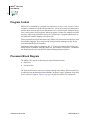
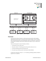
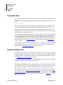
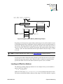
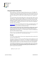
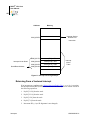
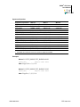
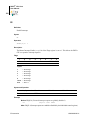
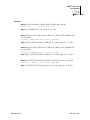
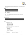
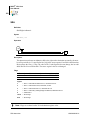
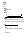
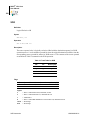
Processor Block Diagram
The ZNEO CPU consists of following two major functional blocks:
•
•
Fetch Unit
Execution Unit
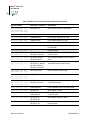
The Fetch and Execution units access memory through a bus arbiter. The Execution Unit
is subdivided into the Instruction State Machine, Program Counter, Arithmetic Logic Unit
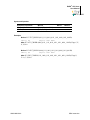
(ALU), and ALU registers. Figure 1 on page 3 displays the ZNEO CPU architecture.
Architectural Overview
UM018809-0611
ZNEO® CPU Core
User Manual
3
Fetch Unit
Execution Unit
Instruction State Machine
Program
Counter
Control
Registers
Instruction and
Operand Fetch
Arithmetic Logic Unit (ALU)
32-bit ALU Registers, R0-R15
Bus Arbiter
16
16
8/16
8/16
Internal
Non-volatile
Memory
Internal
RAM
Internal I/O
External
Memory
Interface
Figure 1. ZNEO CPU Block Diagram
Fetch Unit
The Fetch Unit’s primary function is to fetch opcodes and operand words (including
immediate data) from memory. The Fetch Unit also fetches interrupt vectors. The Fetch
Unit is pipelined and operates semi-independently from the execution unit. This Unit performs a partial decoding of the opcode to determine the number of bytes to fetch for the
operation.
The Fetch Unit operation sequence functions as follows:
1. Fetch the first 2-byte opcode word.
2. Determine number of remaining opcode and operand words (one or two).
3. Fetch the remaining opcode and operand words.
4. Present the opcode and operands to the Instruction State Machine.
A ZNEO CPU instruction is always 1, 2, or 3 words long, including operands, and must be
aligned on an even address.
UM018809-0611
Architectural Overview
ZNEO® CPU Core
User Manual
4
Execution Unit
The Execution Unit performs the processing functions required by the instruction opcodes
and operands which it receives from the Fetch Unit.
Instruction State Machine
The Instruction State Machine is the controller for the ZNEO CPU Execution Unit. After
the initial operation decode by the Fetch Unit, the Instruction State Machine takes over
and completes the instruction. The Instruction State Machine generates effective addresses
and controls memory read and write operations.
Program Counter
The Program Counter contains a counter and adder to monitor the address of the current
instruction and calculates the next instruction address. According to the number of bytes
fetched by the Fetch Unit, the Program Counter increments automatically. The adder
increments and handles Program Counter jumps for relative addressing. The initial value
of the program counter is programmable through the RESET vector.
Note: refer to the ZNEO product specification that is specific to your device for the RESET vector location.
Programs cannot address the Program Counter directly but the instruction
LEA Rd, 4(PC) can be used to load the current Program Counter value (the next instruc-
tion address) into an ALU Register. The JP, CALL, and related instructions are used to
alter the program counter value.
The I/O memory register described in Program Counter Overflow Register on page 9 provides access to the program counter overflow feature.
Arithmetic Logic Unit
The Arithmetic Logic Unit (ALU) performs arithmetic and logical operations on data.
arithmetic operations including addition, subtraction, and multiplication. Logical operations include binary logic operations, bit shifting, and bit rotation.
ALU Registers
The ZNEO CPU provides 16 highly efficient 32-bit registers associated with the ALU.
The 16 ALU registers are named from R0 to R15.
These registers have the following characteristics:
•
The CPU can access ALU registers more quickly than ordinary internal or external
memory.
Architectural Overview
UM018809-0611
ZNEO® CPU Core
User Manual
5
•
All 32 bits of a source or destination ALU Register are used for arithmetic and logical
operations.
•
When an 8-bit or 16-bit memory read is performed, the value is extended to 32-bits in
the destination register. Unsigned (zero) or Signed extension can be specified.
•
When an 8-bit or 16-bit memory write is performed, the source register’s value is truncated (only the least significant 8 or 16 bits are stored in memory.)
•
The CALL, IRET, LINK, POP, POPM, PUSH, PUSHM, RET, TRAP, and UNLINK
instructions; system interrupts; and exceptions use Register R15 as the Stack Pointer.
If not used, R15 behaves like any other ALU Register.
•
The LINK, UNLINK, and some LD operations use Register R14 as a Frame Pointer. If
not used, R14 behaves like any other ALU Register.
Instruction Cycle Time
Instruction cycle times vary from instruction to instruction. Instructions are pipelined
which means the current instruction executes while the next instruction is being fetched.
This allows higher performance at a specific clock speed.
Instruction Fetch Cycles
The following equation is used to calculate the minimum number of cycles required to
fetch an instruction into the CPU:
Fetch Cycles = (bus_wait_states + 1) opcode_bytes/bus_bytes
In the above equation, the following points are true:
•
Bus wait states is configured on a bus to accommodate memory specifications. The
number of wait states is added to each memory read or write on that bus.
Note: For details about wait states, refer to the ZNEO product specification that is specific to
your device .
•
The opcode bytes value can be 2, 4 or 6, depending on the instruction. Immediate
operands, if any, are included in the opcode fetch, so they do not affect execution
cycles.
•
The bus bytes value can be 1 or 2, for fetches from an 8-bit or 16-bit bus, respectively.
For more details, see the Bus Widths section on page 19.
UM018809-0611
Architectural Overview
ZNEO® CPU Core
User Manual
6
Note: Instructions always begin at an even address; therefore, instruction fetches are not subject
to uneven alignment delays.
An instruction fetch delay cycle can occur if the Fetch and Execution Units request access
to the same bus on the same cycle. In this case, the bus arbiter gives precedence to the
Execution Unit. This kind of delay can be avoided by storing instructions and data in different memory spaces; for example, instructions in ROM or Flash and data in RAM.
Execution Cycles
The minimum instruction execution time for most CPU instructions is one system clock
cycle. Additional cycles are required for shift, multiply, divide operations, and operations
which read or write memory locations. Table 1 lists minimum Execution Unit cycle times
for the various instructions. The symbol bus_time is described in the text following the
table, as other factors that affect execution of some instructions.
Table 1. Instruction Execution Cycles
Instruction
Operand Types
Minimum Execution Unit Cycles
LD, LEA
Immediate, Register-to-Reg- 1
ister
To or From Memory
1 bus_time
EXT, LDES, ATM, BRK, DI, DJNZ,
EI, HALT, IRET, NOP, RET, STOP
—
1
PUSH, POP,
PUSHF, POPF
—
1 bus_time
PUSHM, POPM
—
Variable
CLR
Register
1
Memory
1 bus_time
CP, CPZ, TM, TCM
Immediate, Register-to-Reg- 1
ister
To or From Memory
ADC, ADD, AND, COM, CPC,
CPCZ, DEC, INC, NEG, OR, SBC,
SUB, XOR
Architectural Overview
1 + bus_time
Immediate, Register-to-Reg- 1
ister
Memory to Register
1 + bus_time
Register to Memory
2 bus_time
UM018809-0611
ZNEO® CPU Core
User Manual
7
Table 1. Instruction Execution Cycles (Continued)
Instruction
Operand Types
Minimum Execution Unit Cycles
MUL, SMUL, UMUL
Operands 1_0000H
10
Operands
18
SDIV
UDIV
1_0000H
Destination 1_0000H
17 if result is positive, 18 if negative
Destination
33 if result is positive, 34 if negative
1_0000H
Destination 1_0000H
17
Destination
33
1_0000H
UDIV64
—
34
SRA, SRL, SLL, RL
—
(src/8) + (src % 8)
SRAX, SRLX, SLLX
—
src + 1
JP, JP cc, CALL, NOFLAGS, Extend —
Prefix
0
ILL, TRAP
1 + 4 IROM_bus_time
+ 6 stack_bus_time
—
+ next_instruction_words
LINK
—
2 + 4 stack_bus_time
UNLINK
—
1 + 4 stack_bus_time
Execution cycles can be affected by the following factors:
•
The symbol bus_time stands for the time to read or write a value to the addressed
memory bus, as given by the formula below:
(bus_wait_states + 1) ceiling(data_bytes/bus_bytes)
In the above equation, the following points can be considered:
– Bus wait states is configured for a bus to accommodate memory specifications.
The number of wait states is added to each memory read or write on that bus.
– The ceiling function rounds up to the nearest integer. This accounts for a 1-byte
access on a 2-byte bus, which takes a full memory access cycle, not 1/2 cycle.
– The data bytes value can be 1, 2 or 4, depending on the size of the addressed data
(for direct or register-indirect addressed memory).
– The bus bytes value can be 1 or 2, for fetches from an 8-bit or 16-bit bus, respectively.
An unaligned 16-bit or 32-bit read or write requires additional cycles. For more
details, see the Bus Widths section on page 19.
UM018809-0611
Architectural Overview
ZNEO® CPU Core
User Manual
8
•
For LD and LEA instructions, a delay cycle is inserted if a register is loaded immediately before it is used for the base address in a register-indirect instruction.
•
If execution of an instruction ends before all the next instruction words are fetched,
the Execution Unit delays for the number of cycles required by the Fetch unit to complete the instruction fetch. After an ILL or TRAP instruction executes, the entire next
instruction must be fetched.
Note: For details about wait states, refer to the ZNEO product specification that is specific to
your device .
Control Registers
The ZNEO CPU and internal peripheral control registers are accessed in the I/O memory
space starting at FF_E000H (24-bit address space devices). Table 2 lists control registers
common to all Zilog devices that incorporate the ZNEO CPU. In this table, “X” indicates
an undefined hex digit value.
Note: For complete information about peripheral control registers for a particular device, refer to
the device specific Product Specification.
Table 2. Control Registers
Address (Hex)
Register Description
Mnemonic
Reset Value
(Hex)
FF_E004–FF_E007
Program Counter Overflow
PCOV
FFFFFFFF
FF_E008–FF_E00B
Reserved
—
xxxxxxxx
FF_E00C–FF_E00F
Stack Pointer Overflow
SPOV
00000000
FF_E010
Flags
FLAGS
xx
FF_E011
Reserved
—
xx
FF_E012
CPU Control
CPUCTL
FF
Note: I/O memory locations can be accessed using a 16 bit address operand. For more details, see
the Direct Memory Addressing section on page 29.
Architectural Overview
UM018809-0611
ZNEO® CPU Core
User Manual
9
Program Counter Overflow Register
The Program Counter Overflow Register (PCOV) implements program counter overflow
protection. For more details, see the Program Counter Overflow section on page 50.
Stack Pointer Overflow
The Stack Pointer Overflow Register (SPOV) is used to provide stack pointer overflow
protection. For more details, see the Stack Overflow section on page 50. CALL, ILL,
IRET, POP, PUSH, RET and TRAP instructions, system interrupts and exceptions use the
ALU Register. R15 is used as the Stack Pointer.
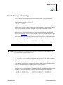
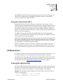
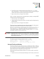
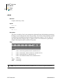
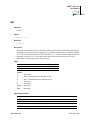
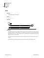
Flags Register (FLAGS)
This byte register contains the status information regarding the most recent arithmetic,
logical, bit manipulation or rotate and shift operation. The Flags Register contains six bits
of status information that are set or cleared by CPU operations. Five of the bits (C, Z, S, V
and B) can be tested with conditional jump instructions. The IRQE bit is the Master Interrupt Enable flag, and the CIRQE bit is the Chained Interrupt Enable flag. Figure 2 displays
the flags and their bit positions in the Flags Register.
Bit
7
Bit
0
C
Z
S
V
B
F1 CIRQE IRQE
Flags Register
Master Interrupt Enable
Chained Interrupt Enable
User Flag 1
Blank Flag
Overflow Flag
Sign Flag
Zero Flag
Carry Flag
Figure 2. Flags Register
Interrupts, System Exceptions, and the software Trap (TRAP) instruction write the value
of the Flags Register to the stack. Executing an Interrupt Return (IRET) instruction
restores the value saved on the stack into the Flags Register.
UM018809-0611
Architectural Overview
ZNEO® CPU Core
User Manual
10
Flag settings depend on the data size of the result, which can be 8 bits (Byte), 16 bits
(Word), or 32 bits (Quad, the default). For instructions with destinations in memory, the
mnemonic suffix determines the destination size. If the destination is a register, Flags are
based on the 32-bit result. For more information, see the Memory Data Size section on
page 30.
Carry Flag
The Carry (C) flag is 1 when the result of an arithmetic operation generates a carry out of
or a borrow into the most significant bit (msb) of the data. Otherwise, the Carry flag is 0.
Some bit rotate or shift instructions also affect the Carry flag. Bit [31] is considered msb
for register destinations; the msb for a memory destination depends on the data size.
Zero Flag
For arithmetic and logical operations, Zero (Z) flag is 1 if the result is 0. Otherwise, the
Zero flag is 0. If the result of testing bits is 0, Zero flag is 1; otherwise, the Zero flag is 0.
Also, if the result of a rotate or shift operation is 0, the Zero flag is 1; otherwise, the Zero
flag is 0. The test considers 32 bits for a register destination or the destination size for a
memory destination.
Sign Flag
The Sign (S) flag stores the value of the most significant bit (msb) of a result following an
arithmetic, logical, rotate, or shift operation. For signed numbers, the ZNEO CPU uses
binary two’s complement to represent the data and perform the arithmetic operations. A 0
in the msb position identifies a positive number; therefore, the Sign flag is also 0. A 1 in
the most significant position identifies a negative number; therefore, the Sign flag is also
1. Bit [31] is considered msb for register destinations; the msb for a memory destination
depends on the data size.
Overflow Flag
For signed arithmetic, rotate or shift operations, the Overflow (V) flag is 1 when the result
is greater than the maximum possible number or less than the minimum possible number
which is represented with the specified data size in signed (two’s complement) form. For
signed data size ranges, see Table 14 on page 32. The Overflow flag is 0 if no overflow
occurs. Following logical operations, the Overflow flag is 0.
Following addition operations, the Overflow flag is 1 when the operands have the same
sign, but the result has the opposite sign. Following subtraction operations, the Overflow
flag is 1 if the two operands are of opposite sign and the sign of the result is same as the
sign of the source operand. Following shift/rotation operations, the Overflow flag is 1 if
the sign bit of the destination changed during the last bit shift iteration.
Architectural Overview
UM018809-0611
ZNEO® CPU Core
User Manual
11
Blank Flag
For some arithmetic, logical, and load operations, the Blank (B) flag is set to 1 if a tested
operand value is 0 before the operation. Otherwise, B is 0. Both source and destination
operands might be tested, but which operands are tested depends on the operation being
performed. See the instruction descriptions for details.
Unlike other flags, the B flag can be altered by POP and some LD instructions. 8-bit or 16bit memory operands are tested after unsigned or signed extension, depending on the
instruction. For more information, see the Resizing Data section on page 31.
The B flag is useful for operations involving a null-terminated strings. For example, after
the following statement executes, Z is set if the tested byte is a carriage return (0DH), or B
is set if the byte is zero.
CP.B (R6), #0DH
User Flag
The User Flag (F1) are available as general-purpose status bits. The User Flag is unaffected by arithmetic operations and must be set or cleared by instructions. The User Flag
must not be used with conditional Jumps. The User Flag is 0 after initial power-up or
Reset.
Chained Interrupt Enable Flag
The Chained Interrupt Enable flag (CIRQE) is used to enable or disable chained-interrupt
optimization, which allows program control to pass directly from one interrupt service
routine to another while omitting unneeded stack operations. For more information, see
the Returning From a Vectored Interrupt section on page 44.
Whenever a vectored interrupt or system exception occurs, the previous state of the IRQE
flag is copied to CIRQE after the Flags Register is pushed onto the stack. This disables
interrupt chaining if interrupts are globally disabled (IRQE=0) when a nonmaskable interrupt or system exception occurs.
The CIRQE flag is unaffected by other operations, but it may be set or cleared by instructions, if desired. The CIRQE flag cannot be used with conditional Jumps. The CIRQE flag
is 0 after initial power-up or Reset.
Master Interrupt Enable Flag
The Master Interrupt Enable bit (IRQE) globally enables or disables interrupts. For more
information, see the Interrupts chapter on page 41.
Condition Codes
The C, Z, S, V, and B flags control the operation of the conditional jump (JP cc) instructions. Sixteen frequently useful functions of the flag settings are encoded in a 4-bit field
UM018809-0611
Architectural Overview
ZNEO® CPU Core
User Manual
12
called the condition code (cc), which are assembled into each conditional jump opcode.
Table 3 summarizes condition codes and their assembly language mnemonics.
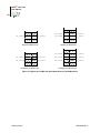
Note: Some binary condition codes are expressed by more than one mnemonic.
The result of the flag test operation determines if the conditional jump executes.
Table 3. Condition Codes
Assembly
Mnemonic
Definition
Flag Test Operation
(Jump if True)
0
B
Blank
B=1
0001
1
LT
Less Than
(S XOR V) = 1
0010
2
LE
Less Than or Equal
(Z OR (S XOR V)) = 1
0011
3
ULE
Unsigned Less Than or Equal
(C OR Z) = 1
0100
4
OV
Overflow
V=1
0101
5
MI
Minus
S=1
0110
6
Z
Zero
Z=1
0110
6
EQ
Equal
Z=1
0111
7
C
Carry
C=1
0111
7
ULT
Unsigned Less Than
C=1
1000
8
NB
Not Blank
B=0
1001
9
GE
Greater Than or Equal
(S XOR V) = 0
1010
A
GT
Greater Than
(Z OR (S XOR V)) = 0
1011
B
UGT
Unsigned Greater Than
(C OR Z) = 0
1100
C
NOV
No Overflow
V=0
1101
D
PL
Plus
S=0
1110
E
NZ
Non-Zero
Z=0
1110
E
NE
Not Equal
Z=0
1111
F
NC
No Carry
C=0
1111
F
UGE
Unsigned Greater Than or
Equal
C=0
Binary
Hex
0000
Architectural Overview
UM018809-0611
ZNEO® CPU Core
User Manual
13
CPU Control Register (CPUCTL)
Bits [1:0] of the CPU Control Register (see Table 4 on page 13) control access to the
ZNEO CPU buses through DMA bandwidth selection.
Note: For more details about the available peripheral control and data registers, and additional
information about DMA operation, refer to the device specific Product Specification.
Table 4. CPU Control Register
Bit
7
6
5
4
3
2
1
Reserved
Field
0
DMABW
Reset
1
1
1
1
1
1
1
1
R/W
R
R
R
R
R
R
R/W
R/W
FFFF_E012H
Address
Note: R = Read-only; R/W = Read/Write; R/W0 = Read/Write to 0.
Bit
Position Description
[7:2]
Reserved; must be zero.
[1:0]
DMA Bandwidth Selection (DMABW)
The ZNEO CPU can be configured to support four levels of Direct Memory Access (DMA) Controller bus bandwidth. Write one of the following values to DMABW[1:0] to select the portion of
bus bandwidth allocated to DMA operations:
00 = DMA can consume 100% of the bus bandwidth
01 = DMA is allowed one transaction for each CPU operation
10 = DMA is allowed one transaction for every two CPU operations
11 = DMA is allowed one transaction for every three CPU operations
UM018809-0611
Architectural Overview
ZNEO® CPU Core
User Manual
14
Architectural Overview
UM018809-0611
ZNEO® CPU Core
User Manual
15
Address Space
The ZNEO CPU has a unique memory architecture with a unified address space. It supports memory and I/O up to four buses:
•
•
•
•
Internal Non-Volatile Memory (Flash, EEPROM, EPROM, or ROM)
Internal RAM
Internal I/O Memory (internal peripherals)
External Memory (and/or memory-mapped peripherals)
The ZNEO CPU Fetch Unit and Execution Unit can access separate buses at the same
time. The CPU can access memories with either 8-bit or 16-bit bus widths. ZNEO CPU
uses 32-bit addressing internally. Therefore, the CPU is capable of addressing up to 4 GB
of addresses.
Current ZNEO CPU products ignore address bits [31:24], providing a 24-bit address space
with 16 MB (16,777,216 bytes) of unique memory addresses. Address bits [31:24] must
be written appropriately for the addressed space to allow for possible future expansion.
The CPU also provides instructions which use 16-bit addressing. 16-bit addresses are sign
extended by the CPU to access the highest and lowest 32 KB of the available address
space.
Example: The 16-bit address FEFFH resolves to FF_FEFFH in the 24-bit address space.
Most CPU instructions also use Arithmetic and Logic Unit (ALU) registers for either
source or destination data. See the ALU Registers section on page 4.
The ZNEO CPU address space includes the following features:
•
•
•
•
•
•
•
UM018809-0611
Memory Map
Internal Nonvolatile Memory
Internal RAM
I/O Memory
External Memory
Endianness
Bus Widths
Address Space
ZNEO® CPU Core
User Manual
16
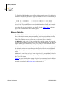
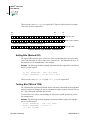
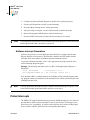
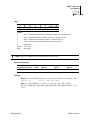
Memory Map
Figure 3 displays a memory map of the ZNEO CPU. It displays the location of internal
nonvolatile memory, internal RAM, and internal I/O Memory. External memory can be
accessed at addresses not occupied by internal memory or I/O.
Data Addresses
(Execution Unit)
FF_FFFFH
FF_E000H
Jump Addresses
(Fetch Unit)
Internal I/O &
Control Registers
Reserved
External Memory Interface
FF_xxxxH
FF_xxxxH
Internal RAM
FF_8000H
External Memory Interface
00_xxxxH
00_7FFFH
00_0xxxH
00_0000H
Internal Non-Volatile
Memory
Option Bits and Vectors
xxxxH
Internal Bus (One of Three)
External Bus
16-Bit Address Space
Device-Specific Boundary
Figure 3. ZNEO CPU Memory Map (24 Significant Address Bits)
Address Space
UM018809-0611
ZNEO® CPU Core
User Manual
17
Note:
To determine the amount of internal RAM and internal nonvolatile memory available for
the specific device and for details about the available option bits and vectors, refer to the
ZNEO product specification that is specific to your device .
Internal Nonvolatile Memory
Internal nonvolatile memory consists of executable program code, constants, and data.
The ZNEO CPU assembler provides configurable address range mnemonics (ROM and
EROM) that can be specified to locate data and program elements in nonvolatile memory.
ROM selects nonvolatile memory in the 16-bit address space, while EROM selects nonvolatile memory in the 32-bit address space. For more details about data space and segment definitions, refer to the assembler documentation.
For each product within the ZNEO CPU family, a block of memory beginning at address
00_0000H is reserved for option bits and system vectors (RESET, trap, interrupts, System
Exceptions; etc.). Table 5 provides an example reserved memory map for a ZNEO CPU
product with 24 interrupt vectors.
Table 5. Reserved Memory Map Example
Memory Address (Hex)
Description
00_0000–00_0003
Option Bits
00_0004–00_0007
RESET Vector
00_0008–00_000B
System Exception Vector
00_000C–00_000F
Reserved
00_0010–00_006F
Interrupt Vectors
Internal RAM
Internal RAM is employed for data and stacks. However, internal RAM can also contain
program code for execution. Most ZNEO CPU devices contain some internal RAM. The
base (lowest address) and top (highest address) of internal RAM are a function of the
amount of internal RAM available.
Note:
To determine the amount and location of internal RAM, refer to the ZNEO product specification that is specific to your device .
UM018809-0611
Address Space
ZNEO® CPU Core
User Manual
18
The ZNEO CPU assembler provides a configurable address range mnemonic (RAM) that
can be specified to locate data and (possibly) program elements in the RAM space
accessed using 16-bit addressing. For more details about data space and segment definitions, refer to the assembler documentation.
I/O Memory
ZNEO CPU supports 8 KB (8,192 bytes) of internal I/O Memory space located at
addresses FF_E000H through FF_FFFFH (in the 24-bit address space). The I/O Memory
addresses are reserved for control of the ZNEO CPU, the on-chip peripherals, and the I/O
ports.
Note:
For descriptions of the peripheral and I/O control registers, refer to the ZNEO product
specification that is specific to your device . Attempts to read from unavailable I/O Memory addresses return FFH. Attempts to write to unavailable I/O Memory addresses produce
no effect.
The ZNEO CPU assembler provides a configurable address range mnemonic, IODATA,
that can be specified to locate an address in the reserved I/O Memory space or (if present)
external I/O configured in the adjacent 16-bit addressable memory space. For more details
about data space and segment definitions, refer to the assembler documentation.
I/O Memory Precautions
Some control registers within the I/O Memory provide read-only or write-only access.
When accessing these read-only or write-only registers, ensure that the instructions do not
attempt to read from a write-only register or, conversely, write to a read-only register.
External Memory
ZNEO CPU products support external data and address buses for connecting to additional
external memories and/or memory-mapped peripherals. The external addresses can be
used for storing program code, data, constants, stack, etc. The results of reading from or
writing to unavailable external addresses are undefined.
The ZNEO CPU assembler’s EROM and ERAM address range mnemonics can be configured to include external memory configured in 32-bit addressed memory. These mnemonics can be used to locate data and program elements in nonvolatile or RAM memory, as
required. For more information about data space and segment definitions, refer to the
assembler documentation.
Address Space
UM018809-0611
ZNEO® CPU Core
User Manual
19
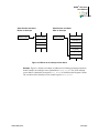
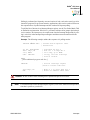
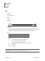
Endianness
The ZNEO CPU accesses data in Big Endian order; which means the address of a multibyte Word or Quad points to the most significant byte (MSB). Figure 4 displays the Endianness of the ZNEO CPU.
Address
of Word
LSB
FF_0081H
MSB
FF_0080H
LSB
FF_0083H
FF_0082H
FF_0081H
Address
of Quad
MSB
FF_0080H
Figure 4. Endianness of Words and Quads
Bus Widths
The ZNEO CPU can access 8-bit or 16-bit wide memories. The data buses of the internal
nonvolatile memory and internal RAM are 16-bits wide. The internal peripherals are a mix
of 8-bit and 16-bit peripherals. The external memory bus can be configured as an 8-bit or
16-bit memory bus.
If a 16-bit or 32-bit operation is performed on a 16-bit wide memory, the number of memory accesses depends on the alignment of the address. If the address is even, a 16-bit operation takes one memory access and a 32-bit operation takes two memory accesses. If the
address is odd (unaligned), a 16-bit operation takes two memory accesses and a 32-bit
operation takes three memory accesses. Figure 5 displays this behavior for 16-bit and 32bit access.
UM018809-0611
Address Space
ZNEO® CPU Core
User Manual
20
FF_0082H
FF_0080H
MSB
LSB
FF_0081H
Aligned 16-Bit Access
FF_0080H
FF_0080H
LSB
MSB
FF_0083H
FF_0081H
Aligned 32-Bit Access
FF_0084H
FF_0082H
LSB
LSB
FF_0085H
FF_0083H
FF_0082H
FF_0083H
MSB FF_0081H
FF_0080H
MSB FF_0081H
Unaligned 16-Bit Access
Unaligned 32-Bit Access
Figure 5. Alignment of 16-Bit and 32-Bit Operations on 16-Bit Memories
Address Space
UM018809-0611
ZNEO® CPU Core
User Manual
21
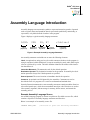
Assembly Language Introduction
Assembly language uses mnemonic symbols to represent instruction opcodes. Operands
such as register names and immediate data is represented symbolically, numerically, as
expressions, or by labels defined elsewhere in the program.
Figure 6 displays a typical assembly language statement.
LOOP:
Label
(Optional)
SUB
Instruction
Mnemonic
R5, R7
Destination
Operand
;Subtract
Source
Operand
Comment
(Optional)
Figure 6. Example Assembly Language Statement
An assembly statement can include one or more the following elements:
Label. An optional text string used to refer to this statement elsewhere in the program. A
string is considered a label definition if it is not an assembler keyword, and it either begins
a line or is followed by a colon. The label definition identifies the address of the instruction that follows it.
Instruction Mnemonic. The mnemonic code for the desired operation.
Destination Operand. The destination location for the operation. In assembly, the desti-
nation operand is always first if both operands are specified.
Source Operand. The source location or immediate data for the operation.
Comment. An optional text field ignored by the assembler. Comments are used to
describe the flow of a program so it is easier to understand and maintain later.
Instead of instruction mnemonics, some assembly statements contain assembler directives
(also called pseudo-ops), which are not translated into object code. Directives are used to
select memory segments, allocate storage in memory, define macros, and control the
assembly process.
Example Assembly Language Source
An assembly language program is written in a plain text file called as source file, which
contains a sequence of assembly language statements and directives.
Below is an example of an assembly source file:
SEGMENT NEAR_TEXT
UM018809-0611
; Directive to place the following statements
Assembly Language Introduction
ZNEO® CPU Core
User Manual
22
; in data (RAM space) memory
Str_Data:
DB "NEVAR"
; Make Str_Data label equal to current addr.
; Directive to allocate and initialize data
; bytes
Str_Length EQU $ - Str_Data ; Equate Str_Length to current
assembly
; address ("$") minus Str_Data address.
Blank_Data:
; Allocate an uninitialized data block
DS Str_Length
; that is the same size as the Str_Data block.
SEGMENT CODE
; Directive to put the following statements in
; instruction (ROM space) memory
REVERSE:
; Routine to reverse a block of data
LD R8, #Str_Data ; Load R8 with 1st address in Str_Data block
LD R12, #Blank_Data+Str_Length
;Next addr. after Blank_Data
LOOP:
; Start of loop
LD.UB R5,(R8++)
; Load byte pointed to by R8 into R5 LSB
; Increment R8 after load.
LD.B (--R12),R5
; Decrement R12, then
; Load byte pointed to by R12 with R5 LSB
CP R12, #Blank_Data ; Did we write all the bytes?
JP NZ,LOOP
; Repeat until Blank_Data block contains
; reversed copy of Str_Data bytes
For details about assembly instructions, see the Instruction Set Reference chapter on
page 65. For details about operand addressing and data sizes, see the Operand Addressing
chapter on page 27.
For information about how program flow can be interrupted, see the Interrupts chapter on
page 41, System Exceptions on page 49, and Software Traps on page 53.
For details about assembly language syntax, expressions, directives, and using the assembler, refer to the Zilog Developer Studio II – ZNEO User Manual (UM0171).
ZNEO CPU Instruction Classes
ZNEO CPU instructions can be divided functionally into the following groups:
•
•
•
•
Arithmetic
Logical
Bit Manipulation
Rotate and Shift
Assembly Language Introduction
UM018809-0611
ZNEO® CPU Core
User Manual
23
•
•
•
Load
CPU Control
Program Control
Tables 6 through 12 list the instructions for each of the above groups and the number of
operands required for each instruction. Some instructions appear in more than one table as
these instructions can be considered members of more than one category. The abbreviations dst and src refer to destination and source operands, respectively.
Table 6. Arithmetic Instructions
Mnemonic
Operands
Instruction
Page
ADC
dst, src
Add with Carry
68
ADD
dst, src
Add
71
CP
dst, src
Compare
86
CPC
dst, src
Compare with Carry
89
CPCZ
dst
Compare to Zero with Carry
92
CPZ
dst
Compare to Zero
94
DEC
dst
Decrement
96
INC
dst
Increment
108
MUL
dst, src
Multiply (32 bit)
125
NEG
dst
Negate
127
SBC
dst, src
Subtract with Carry
149
SDIV
dst, src
Signed Divide (32 bit)
152
SMUL
dst, src
Signed Multiply (64 bit)
158
SUB
dst, src
Subtract
169
UDIV
dst, src
Unsigned Divide (32 bit)
180
UDIV64
dst, src
Unsigned Divide (64 bit)
182
UMUL
dst, src
Unsigned Multiply (64 bit)
184
Table 7. Logical Instructions
Mnemonic
Operands
Instruction
Page
AND
dst, src
Logical AND
74
COM
dst
Complement
84
OR
dst, src
Logical OR
131
XOR
dst, src
Logical Exclusive OR
188
UM018809-0611
Assembly Language Introduction
ZNEO® CPU Core
User Manual
24
Table 8. Bit Manipulation Instructions
Mnemonic
Operands
Instruction
Page
TCM
dst, src
Test Complement Under Mask
172
TM
dst, src
Test Under Mask
175
Table 9. Rotate and Shift Instructions
Mnemonic
Operands
Instruction
Page
RL
dst
Rotate Left
147
SLL
dst, src
Shift Left Logical
154
SLLX
dst, src
Shift Left Logical, Extended
156
SRA
dst, src
Shift Right Arithmetic
160
SRAX
dst, src
Shift Right Arithmetic,
Extended
162
SRL
dst, src
Shift Right Logical
164
SRLX
dst, src
Shift Right Logical, Extended
166
Table 10. Load Instructions
Mnemonic
Operands
Instruction
Page
CLR
dst
Clear Value
82
EXT
dst, src
Extend Value
103
LD
dst, src
Load
115
LD cc
dst
Load Condition Code
120
LDES
dst
Load and Extend Sign Flag
121
LEA
dst
Load Effective Address
122
LINK
src
Link Frame Pointer
124
POP
dst
Pop
134
POPF
dst
Pop Flags
136
POPM
mask
Pop Multiple
137
PUSH
src
Push
140
PUSHF
src
Push Flags
142
PUSHM
mask
Push Multiple
143
Unlink Frame Pointer
186
UNLINK
Assembly Language Introduction
UM018809-0611
ZNEO® CPU Core
User Manual
25
Table 11. CPU Control Instructions
Mnemonic
Operands
Instruction
Page
ATM
—
Atomic Operation Modifier
77
DI
—
Disable Interrupts
98
EI
—
Enable Interrupts
102
HALT
—
Halt Mode
105
NOFLAGS
—
No Flags Modifier
129
NOP
—
No Operation
130
STOP
—
Stop Mode
168
Table 12. Program Control Instructions
Mnemonic
Operands
Instruction
BRK
—
On-Chip Debugger Break
78
CALL
dst
Call
79
CALLA
dst
Call Absolute
81
DJNZ
dst, src
Decrement, Jump if Nonzero
100
IRET
—
Interrupt Return
110
JP
dst
Jump
112
JPA
dst
Jump Absolute
113
JP cc
dst
Jump Conditional
114
RET
—
Return from Call
146
TRAP
vector
Software Trap
178
UM018809-0611
Page
Assembly Language Introduction
ZNEO® CPU Core
User Manual
26
Assembly Language Introduction
UM018809-0611
ZNEO® CPU Core
User Manual
27
Operand Addressing
Most ZNEO CPU instructions operate on one or two registers, or one register and one
memory address. Operands following the instruction specify which register or memory
address to use.
Example. The assembly language statement below loads one 32-bit register with data
from another:
LD R7, R8
The first operand almost always specifies the destination, and the second operand (if any)
specifies the source for the operation. In this example, the R7 register is loaded with the
value from R8 register.
There are four kinds of operand addressing, each of which is described in this chapter:
•
•
•
Immediate Data, in which the value specified by the operand is used for operation.
Register Addressing, in which the specified 32-bit register is used for operation.
Direct Memory Addressing, in which the value specified by the operand addresses a
memory location that is used for the operation. This section introduces the following
topics:
– Memory Data Size
– Resizing Data
These topics also apply to Register-Indirect memory addressing.
•
Register-Indirect Memory Addressing, in which the specified 32-bit register and
optional offset point to a memory location that is used for the operation. This section
covers the following topics specific to register-indirect addressing:
– Loading an Effective Address
– Using the Program Counter as a Base Address
– Memory Address Decrement and Increment
– Using the Stack Pointer (R15)
– Using the Frame Pointer (R14)
This chapter also describes Bit Manipulation (see page 37) and Jump Addressing (see
page 39).
UM018809-0611
Operand Addressing
ZNEO® CPU Core
User Manual
28
Immediate Data
An Immediate Data operand specifies a source value to be used directly by the instruction.
Example. The assembly language statement below loads ALU Register R7 with the value
42H:
LD R7, #42H
The hash mark prefix (#) on the second (source) operand indicates to the assembler that
the value is Immediate Data, so this example loads the R7 register with the value 42H.
Immediate data is stored as part of the instruction opcode. Depending on the opcode, an
immediate data value can be of the same size as the destination (8, 16 or 32 bits), or it may
contain fewer bits to shorten the opcode.
A destination-sized immediate operand (imm syntax symbol) is used directly by the operation. A shorter immediate operand must be considered signed (simm) or unsigned (uimm).
A signed immediate value is sign-extended to the destination size before it is used. An
unsigned immediate operand is zero-extended to the destination size before it is used. For
more information, see the Memory Data Size section on page 30 and the Resizing Data
section on page 31.
An immediate value does not address data memory, so it cannot be used as the destination
operand. Immediate data is read by the Fetch Unit, so it is not affected by the constraints
described in the I/O Memory Precautions section on page 18.
Register Addressing
A Register operand specifies a 32-bit Arithmetic and Logic Unit (ALU) register to be used
with the instruction. ALU registers are the CPU’s high-speed work space, much faster than
ordinary internal or external memory. There are 16 ALU registers, named R0 to R15. See
the ALU Registers section on page 4 for details.
As mentioned previously, the following assembly language statement loads the destination
register, R7, with data from the source register, R8:
LD R7, R8
Depending on the instruction, a register name can be used for either the source or destination operand, or both. Each register is 32-bits (four bytes) wide, and all 32 bits of a register
are used unless the register’s value is loaded into an 8-bit or 16-bit memory location.
The ZNEO CPU assembler recognizes FP as a synonym for R14 and SP as a synonym for
R15. For details, see the Using the Frame Pointer (R14) section on page 37 and the Using
the Stack Pointer (R15) section on page 36. The UDIV64 instruction uses a 64-bit RRd
register pair operand that employs two 32-bit ALU registers. See the UDIV64 section on
page 182 for details.
Operand Addressing
UM018809-0611
ZNEO® CPU Core
User Manual
29
Direct Memory Addressing
A Direct Memory operand specifies a memory address to be used by the instruction.
Example. The following assembly language statement loads ALU register R7 with the
value in memory address 0000_B002H:
LD.SB R7, B002H
Any data operand which does not contain an immediate value (#n) or register name (Rn) is
assumed to be a memory address. Depending on the instruction, a direct memory address
can be used in either the source or destination operand, but a destination’s effective
address must be a writable memory or I/O location.
ZNEO CPU uses 32-bit memory addresses, but it includes instruction opcodes which
accept 16-bit addresses. A 16-bit address operand in object code is sign-extended by the
CPU (see the Resizing Data section on page 31) to create the effective address used. This
feature splits the 16-bit address range between the highest and lowest 32K blocks of the 16
GB address space. Table 13 provides the 16-bit address ranges for object code.
Table 13. 16-Bit Addressing (Object Code Only)
16-Bit Address Range
32-Bit Effective Addresses
Memory Space
0000H to 7FFFH
0000_000H to 0000_7FFFH
ROM
8000H to FFFFH
FFFF_8000H to FFFF_FFFFH
RAM and I/O
Note: Effective addresses are expressed as 32-bit values. Current devices ignore address bits
[31:24], providing a 24-bit address space.
Internal RAM and I/O memory falls in the range FFFF_8000H to FFFF_FFFFH
(FF_8000H to FF_FFFFH on devices that ignore address bits [31:24]), so 16-bit addressing provides efficient access to internal RAM and I/O memory.
The ZNEO CPU assembler does not automatically use 16-bit addressing if an unmodified
16-bit address is specified, as in the previous example. In this case the assembler selects
16-bit or 32-bit addressing to ensure the address is used as specified.
However, you can append address range mnemonics to specify whether the assembler
should use 16-bit or 32-bit addressing. The RAM, IODATA, and ROM mnemonics tell the
assembler to use 16-bit addressing, as shown in the following example statements:
LD.SB R7, B002H:RAM
LD.SB R7, E002H:IODATA
LD.SB R7, 3002H:ROM
UM018809-0611
; Effective address is FFFF_B002H
; Effective address is FFFF_E002H
; Effective address is 0000_3002H
Operand Addressing
ZNEO® CPU Core
User Manual
30
The ERAM and EROM address space suffixes tell the assembler to use 32-bit addressing,
as shown in the following statements. A full 32-bit address can access external memory or
memory-mapped I/O anywhere in the 4 GB address space.
LD.SB R7, B002H:EROM
LD.SB R7, B002H:ERAM
; Effective address is 0000_B002H
; Effective address is 0000_B002H
The assembler uses memory space mnemonics only to select an appropriate address size
(16 or 32 bit). The assembler does not check an absolute address to make sure it actually
resides in the specified space, but the assembler generates a warning if a label is used in a
space other than the space in which it was declared. See the Address Space section on
page 15 for more information about memory spaces.
Memory Data Size
The ZNEO CPU’s default data size is 32 bits (Quad). Any instruction that addresses an 8bit or 16-bit value in memory must use a mnemonic suffix to specify the data size. The
previous examples use the ‘.B’ suffix to tell the CPU that only 8 bits (one byte) must be
loaded. The following data size suffixes can be used (using LD as an example):
LD (No Suffix). Read or write 32 bits (four bytes). In a read, for example, the byte at the
specified effective address loads into bits [31:24] of the destination register. The three subsequent memory bytes load into bits [23:16], [15:8], and [7:0] of the destination register,
in that order.
LD.W. Read or write 16 bits (two bytes). In an unsigned read, for example, bits [31:16] of
the destination register are cleared, the byte at the specified effective address loads into
bits [15:8] of the register, and the byte at the next (+1) address loads into bits [7:0] of the
register.
LD.B. Read or write 8 bits (one byte). In an unsigned read, for example, bits [31:8] of the
destination register are cleared, and the byte at the specified effective address loads into
bits [7:0] of the register.
Figure 7 on page 31 displays the mapping of register bytes to memory bytes for different
data sizes. When 8-bit or 16-bit memory is read or written, the high-order bits are filled or
truncated as described in the Resizing Data section on page 31.
Operand Addressing
UM018809-0611
ZNEO® CPU Core
User Manual
31
ALU Registers
Bits: 31:24 23:16 15:8
Memory Space
7:0
8-Bit
FFFF_700AH (Effective Address)
Bits: 31:24 23:16 15:8
7:0
16-Bit
FFFF_7009H
FFFF_7008H (Effective Address)
Bits: 31:24 23:16 15:8
7:0
32-Bit
FFFF_7007H
FFFF_7006H
FFFF_7005H
FFFF_7004H (Effective Address)
Figure 7. Mapping of Register to Memory Bytes
Resizing Data
When an 8-bit or 16-bit memory location is written, the value from the source register is
truncated, so only the least-significant 8 or 16 bits of the register value are written, respectively. The source register itself is not changed. When an 8-bit or 16-bit memory location
is read, the value from memory must be extended to a full 32 bits before it is used or stored
in a register.
One of the following two kinds of data extension must be used:
Unsigned (Zero) Extension. The upper bits of the new 32-bit value are filled with zeroes.
Unsigned extension is invoked by including a ‘U’ in the mnemonic suffix. For example,
the following instruction loads the byte at FFFF_7002H into R10[7:0] and fills R10[31:8]
with zeroes:
LD.UB R10,7002H
Signed Extension. The upper bits of the new 32-bit value are filled with ones or zeroes,
depending on the source value’s most-significant (sign) bit, to preserve the sign of the
loaded value. Signed extension is invoked by including an ‘S’ in the mnemonic suffix.
For example, the following instruction loads the byte at address FFFF_7002H into register
bits R10[7:0] and copies bit 7 of that byte into each bit of R10[31:8].
UM018809-0611
Operand Addressing
ZNEO® CPU Core
User Manual
32
LD.SB R10,7002H
By default, the ZNEO CPU assembler uses an unsigned instruction opcode if the extension type is not specified for an 8- or 16-bit memory read. The EXT instruction is provided
for extending 8-bit or 16-bit values contained in a register.
The CPU uses ordinary two’s complement notation to represent signed values. In this
notation, the negative of a number is its binary complement, plus one. The most significant bit (msb) represents the sign—a one in the msb indicates that the number is negative.
You can use signed or unsigned instructions with a particular memory location. Ensure the
correct usage of extension type whenever a memory location is read.
Table 14 lists data sizes, suffixes, and ranges for signed and unsigned values.
Table 14. Data Sizes for Memory Read
Size
Bits
Signed or
Unsigned
Mnemonic Suffix
Range (Hex)
Range (Decimal)
Byte
8
Unsigned
.UB
0 to FF
0 to 255
Signed
.SB
80 to FF,
00 to 7F
–128 to –1,
0 to 127
Unsigned
.UW
0 to FFFF
0 to 65,535
Signed
.SW
8000 to FFFF,
0000 to 7FFF
–32,768 to –1,
0 to 32,767
Unsigned
(none)
0 to FFFF_FFFF
0 to 4,294,967,295
Signed
(none)
8000_0000 to
FFFF_FFFF,
0000_0000 to
7FFF_FFFF
–2,147,483,648 to –1,
0 to 2,147,483,647
Word
Quad
16
32
Register-Indirect Memory Addressing
A register-indirect operand uses an address contained in an ALU register, plus an optional
offset, to address data in a memory location.
Example. The following assembly-language statement loads the destination register, R10,
with data from a memory byte pointed to by register R12, plus an offset.
LD.UB R10, 4(R12)
Figure 8 displays this example. It reads a base address value from R12, adds the signed
offset, 4, to create an effective address in memory, and then loads register R10 with the
value at that address. The parentheses indicate a register-indirect operand.
Operand Addressing
UM018809-0611
ZNEO® CPU Core
User Manual
33
LD.UB R10,4(R12)
32-Bit ALU Registers
4 + FFFF_7002H
—
FFFF_7002H
—
0000_0042H
Memory Space
FFFF_7006H
(Effective Address)
—
42H
—
R13
R12
R11
R10
Value Loaded: 42H
Figure 8. Register-Indirect Memory Addressing Example
Depending on the instruction, register-indirect addressing can be used for either the source
or destination operand, but a destination’s effective address must be a writable memory or
I/O location. The range allowed for the signed offset depends on the instruction used. For
the LD, CLR, CPZ, CPCZ, INC, and DEC instructions, the register-indirect offset range is
–4,096 to +4,095. For other instructions that accept an indirect offset, the range is –8,192
to +8,191.
Note: For allowed JP and CALL offsets, see the Jump Addressing section on page 39.
Several register-indirect instructions have alternate opcodes that do not accept an offset,
and therefore use fewer opcode words. When the offset is omitted in a register-indirect
operand, the ZNEO CPU uses the shorter instruction opcode if one is available.
Loading an Effective Address
The following assembly language statement is a an example of how you can initialize a
register with a base address:
LD R6, #FFFFB002H
Addresses in the range FFFF_8000H to FFFF_FFFFH are common because that is where
I/O memory and internal RAM are addressed, but using a 32-bit LD to initialize a register
UM018809-0611
Operand Addressing
ZNEO® CPU Core
User Manual
34
is not necessary. The ZNEO® CPU assembler automatically uses a shorter LD opcode if
possible.
The LEA mnemonic is provided as an alternative to the immediate LD instruction.
Example. The following statement performs the same initialization as in the previous
example:
LEA R6, FFFFB002H
LEA and LD accept the memory space notation described in Direct Memory Addressing
on page 29, so the following statements are equivalent to the two previous examples:
LEA
LEA
R6,B002H:RAM
R7,B002H:RAM
; Load address of FFFF_B002H
; Load address FFFF_B002H
Once a register is initialized with a base address, the LEA instruction can be used to generate a new effective address based on that register value.
Example. If the value in register R8 is FFFF_7002H, the following assembly language
statement loads register R7 with the value FFFF_7006H:
LEA R7, 4(R8)
This LEA operation loads the effective address indicated by the source operand, while a
similar LD instruction would load the contents of the address. The allowed offset range for
a register-based LEA operand is –8,192 to +8,191.
Using the Program Counter as a Base Address
Some LD and LEA instructions use the Program Counter (PC) as the base address for indirect addressing with an offset. Normally these instructions are used to access a data block
declared in line with the program.
For example, the following statements declare a variable and load it into register R7:
DATA: DB 00H, 00H, 00H, 42H
LD R7, DATA(PC)
The ZNEO CPU assembler automatically calculates the correct relative offset to access
the labeled address using PC as a base address. If a constant (non-label) offset is used with
PC in assembly language, the assembler measures the offset from the start of the current
instruction. The actual offset used in object code is a signed 14-bit value measured from
the end of the current instruction, but the assembler makes this adjustment automatically.
A program can use LEA to load the actual PC contents into a register. The following statements both load the PC value (the next instruction’s address) into register R5:
LEA R5, NEXT(PC)
NEXT: LEA R5, 4(PC)
A PC-based address cannot be used for the destination operand. The allowed offset range
for a PC-based LD or LEA operand is –8,192 to +8,191.
Operand Addressing
UM018809-0611
ZNEO® CPU Core
User Manual
35
Note: If the required offset for a PC-based instruction exceeds the allowed range, the assembler
may silently convert the instruction to use the 32-bit immediate addressing mode.
Memory Address Decrement and Increment
In certain circumstances, a register-indirect LD operation can automatically decrement or
increment the base address register. A decrement is selected by adding a ‘--’ (doubleminus) prefix to the destination register name. The decrement always takes place before
the load is performed. This is called predecrement.
Example. The following statement decrements the base address in register R5, then loads
the memory location pointed to by R5 with the 32-bit contents of R6:
LD (--R5), R6
Predecrement is supported only for destination operands. An LD store using predecrement
is similar to a PUSH, except the LD mnemonic allows a value in any register to be used as
the base address (See the Using the Stack Pointer (R15) section on page 36 for more information).
An increment is selected by adding a ‘++’ (double-plus) suffix to the source or destination
register name. The increment always takes place after the load is performed. This is called
postincrement.
Example. The following statement loads the memory location pointed to by register R5
with the contents of R6, then increments the base address in R5:
LD (R5++), R6
Postincrement can also be used for source operands. For example, the following statement
loads register R6 with the contents of the memory location pointed to by R5, then increments the base address in R5:
LD R6, (R5++)
An LD read using postincrement is similar to a POP, except the LD mnemonic allows a
value in any register to be used as the base address. The predecrement and postincrement
features can be used to implement high-level stack data structures independent of the
Stack Pointer. To help ensure that the next base address is valid, the increment or decrement amount varies with the size of the LD operation.
This is illustrated in the following example statements:
LD.B (--R5), R6
LD.W (--R5), R6
LD
(--R5), R6
; Decrement R5 by 1 and store 1 byte
; Decrement R5 by 2 and store 2 bytes
; Decrement R5 by 4 and store 4 bytes
Predecrement or postincrement operands cannot include an offset.
UM018809-0611
Operand Addressing
ZNEO® CPU Core
User Manual
36
Using the Stack Pointer (R15)
Stack operations are a special kind of register-indirect memory access. The ZNEO CPU
system stack is implemented using ALU Register R15 as the Stack Pointer (SP). R15 can
be addressed like any register, but because of its Stack Pointer role it would be awkward to
use for any other purpose. The ZNEO CPU assembler recognizes SP as a synonym for
R15.
The system program startup routine initializes R15 to point to the highest address in internal RAM, plus 1. Subsequent PUSH, PUSHM, CALL, and LINK instructions; interrupts,
system exceptions, and traps all decrement SP before they store data on the stack. POP,
POPM, RET, UNLINK, and IRET instructions all increment SP to release stack space as it
is no longer needed. A program can also allocate or release stack space by changing the
register R15 (SP) value directly.
A system exception is provided to help keep the stack from overwriting other data; see the
Stack Overflow section on page 50. Software can use the PUSH, POP, PUSHM, and
POPM instructions to store and retrieve data from the stack.
PUSH decrements SP and stores the source value onto the stack. POP loads the last value
on the stack into the specified register and increments SP. The assembler uses predecrement and postincrement LD opcodes to implement most PUSH and POP instructions.
PUSH and POP can be used with 8-, 16-, or 32-bit data sizes. 8-bit and 16-bit POP instructions can be either Unsigned or Signed.
When a 16-bit or 32-bit value is pushed onto the stack, the low-order bytes are pushed first
to store the value in the ZNEO CPU’s normal big-endian fashion.
Example
A 16-bit value is stored with bits [7:0] in the value’s higher-addressed byte, and bits [15:8]
in the value’s base address byte.
If the stack is located on a 16-bit bus, an assembly language program might improve stack
performance by maintaining an even SP value—for example, by avoiding the single-byte
PUSH.B and POP.B instructions. This may require some effort, especially if the program
includes compiled C routines or any other code that does not preserve stack alignment.
The PUSHM and POPM instructions push or pop multiple registers with a single instruction. For example, the following statements push R0, R5, R6, R7 and R13 onto the stack
(in reverse numerical order), and then pop the same registers (in numerical order, so
pushes and pops remain symmetrical):
PUSHM <R0, R5-R7, R13>
POPM <R0, R5-R7, R13>
Operand Addressing
UM018809-0611
ZNEO® CPU Core
User Manual
37
The PUSHM and POPM instructions always push or pop all 32 bits of each register. The
ZNEO CPU assembler uses the PUSHMHI, PUSHMLO, POPMLO, and POPMHI
opcodes to implement PUSHM and POPM.
Using the Frame Pointer (R14)
Subroutines often use the stack for temporary variable space. For example, a CALL
sequence begins by pushing arguments onto the stack before calling the subroutine. When
the subroutine starts, it stores a copy of SP in another register called the Frame Pointer
(FP) and decrements SP to create stack space for local variables. When the subroutine is
finished, it copies FP back into SP and returns. Finally, the calling routine deallocates the
stack space it used for arguments.
The ZNEO CPU provides the LINK and UNLINK instructions to help program this
sequence. These instructions use register R14 as the FP register. The ZNEO CPU assembler recognizes FP as a synonym for R14.
LINK is used at the beginning of a subroutine to copy the SP contents to FP and decrement
SP as needed. UNLINK copies FP back to SP, releasing the allocated space. LINK pushes
R14 on the stack before changing it, and UNLINK pops R14 after it is done, so routines
not using LINK or UNLINK can use R14 normally.
While the subroutine executes, it can access its arguments and variables using registerindirect addressing with the FP register. For constant (non-label) offsets in the range –32
to +31, the assembler uses special opcodes that make FP-based accesses more efficient.
Bit Manipulation
The ZNEO CPU does not provide any special instructions to address only one bit in memory, but individual bits are easily manipulated using masked logical instructions.
The following sections introduce the most basic bit manipulation techniques. The instructions used here are AND, OR, TM, and TCM. Other useful bit, logic and shift operations
are listed by groups in the ZNEO CPU Instruction Classes section on page 22.
Clearing Bits (Masked AND)
The logical AND instruction (discussed on page 74) stores a 1 bit only if the corresponding bit is set in both the source and destination. In effect, if the source (mask) bit is 0, the
destination bit is cleared. If the mask bit is 1, the destination bit is not changed.
Example. The following assembly language statements initialize register R15 and then
clear bit 5 of that register:
LD R15, #FFFFFF70H
AND R15, #FFFFFFDFH
UM018809-0611
; LSB = 0111_0000B
; Clear R15 bit 5
Operand Addressing
ZNEO® CPU Core
User Manual
38
This leaves the value FFFF_FF50H in register R15. Figure 9 displays how this example
clears only one bit of register R15.
Bit
32
Bit
0
Bit
5
1
1
1
1
1
1
1
1
1
1
1
1
1
1
1
1
1
1
1
1
1
1
1
1
0
1
1
1
0
0
0
0
R15[7:0] = 70H
1
1
1
1
1
1
1
1
1
1
1
1
1
1
1
1
1
1
1
1
1
1
1
1
1
1
0
1
1
1
1
1
MASK = FFFF_FFDFH
1
1
1
0
1
0
1
0
0
0
0
R15[7:0] = 50H
AND R15, #FFFFFFDFH
1
1
1
1
1
1
1
1
1
1
; Clear Bit 5 of Register 15
1
1
1
1
1
1
1
1
1
1
1
Figure 9. Masked Logic Example: Clearing a Bit
Setting Bits (Masked OR)
The logical OR instruction stores a 0 bit only if the corresponding bit is clear in both the
source and destination. In effect, if the source (mask) bit is 1, the destination bit is set. If
the mask bit is 0, the destination bit is not changed.
Example. The following assembly language statements initialize register R15 and then set
bits [2,1] of that register:
LD R15, #00000070H ; LSB = 0111_0000B
OR R15, #00000006H ; Set R15 bits 1 and 2
This leaves the value 0000_0076H (LSB = 0111_0110B) in register R15.
Testing Bits (TM and TCM)
The TM instruction performs an internal AND to test mask-selected bits in the destination
register, but does not changes the source or destination register contents. Instead, TM sets
the Z flag if the tested destination bits are all 0.
To select a bit to test, set the corresponding bit in the source (mask) operand as given in
the example below.
Example. The following assembly language statements initialize register R15 and then
test bit 2 of that register:
LD R15, #00000070H
TM R15, #00000004H
JP Z, BIT_IS_CLEAR
Operand Addressing
; LSB = 0111_0000B
; Test bit 2
UM018809-0611
ZNEO® CPU Core
User Manual
39
This leaves R15 unchanged, but sets the Z flag as R15[2] is clear.
The TCM instruction (Test Complement under Mask, discussed on page 172) complements the destination value before ANDing it to the mask. In effect, TCM is identical to
TM except it sets the Z flag if the tested destination bits are all 1.
Example . The following assembly language statements initialize register R15 and then
test bits [2,1] of that register:
LD R15, #00000070H
TCM R15, #00000006H
JP Z, BITS_ARE_ONES
; LSB = 0111_0000B
; Test bits 1 and 2
As a result, R15 remains unchanged but clears the Z flag because neither bit R15[2,1] is 1.
Jump Addressing
The ZNEO CPU jump instructions (JP and CALL), are used to alter the program flow.
These instructions alter the Program Counter, which indicates the next instruction to be
fetched. A few considerations are listed below.
•
•
•
Note:
All instructions must begin on an even address.
Instruction fetches bypass the internal I/O space. The result of an instruction fetch is
not defined in the range FFFF_E000H–FFFF_FFFFH (FF_E000H–FF_FFFFH on
devices that ignore address bits [31:24]).
A small device-specific address block starting at 0000_0000H is reserved for CPU
option bits and interrupt, trap, or exception vectors.
For details about option bits and vectors, refer to the ZNEO product specification that is
specific to your device .
Assembly language statements use a label, expression, or numeric value to indicate the 32bit jump destination. The ZNEO CPU assembler analyzes the address and determines the
best address mode to use in the assembled object code.
In object code, following two jump address modes are available:
Direct Address. The JP, JP cc, or CALL opcode includes four operand bytes containing
the 32-bit jump destination address. The destination address is written directly to the Program Counter to indicate the next instruction. Bit [0] of the operand is ignored.
UM018809-0611
Operand Addressing
ZNEO® CPU Core
User Manual
40
Relative Address. The JP, JP cc, or CALL opcode includes a signed relative offset field
of 8, 12, 16, or 24 bits, which is added to the Program Counter’s contents. Table 15 provides the relative address operand ranges. For jumps within the same module, the assembler uses the most efficient offset size. For relative jumps across modules, the assembler
uses a default offset size that can be configured at assembly time.
Table 15. Relative Jump Offset Ranges
Operand Addressing
Operand Bits
Offset Range
8
–128 to +127
12
–2,048 to +2,047
16
–32,768 to +32,767
24
–8,388,608 to +8,388,607
UM018809-0611
ZNEO® CPU Core
User Manual
41
Interrupts
Peripherals use an interrupt request (IRQ) signal to get the CPU’s attention when it needs
to perform some action, such as moving peripheral data or exchanging status and control
information.
There are two ways to handle interrupt requests:
Vectored Interrupts. Asserting the IRQ signal forces the CPU to execute the corresponding
interrupt service routine (ISR). The ISR must end with an Interrupt Return (IRET) instruction.
Polled Interrupts. Vectored interrupts are disabled (globally or only for the device), and
the software tests the device’s interrupt request bits periodically. If action is required, the
software uses CALL and RET to invoke the appropriate service routine.
Interrupts are generated by internal peripherals, external devices (through the port pins) or
software. The Interrupt Controller prioritizes and handles individual interrupt requests
before passing them to the ZNEO CPU. The interrupt sources and trigger conditions are
device dependent.
Note:
To determine available interrupt sources (internal and external), triggering edge options,
and exact programming details, refer to the ZNEO Product Specification that is specific to
your device.
Vectored Interrupts
Each ZNEO CPU interrupt is assigned an interrupt vector that points to the appropriate
service routine for that interrupt. Vectors are stored in a reserved block of 4-byte memory
quads in the nonvolatile memory space. Each interrupt vector is a 32-bit pointer (service
routine address) stored in a memory quad.
Note:
For interrupt vector locations, refer to the ZNEO Product Specification that is specific to
your device.
Interrupt Enable and Disable
Vectored interrupts are globally enabled and disabled by executing the Enable Interrupts
(EI) and Disable Interrupts (DI) instructions, respectively. These instructions affect the
UM018809-0611
Interrupts
ZNEO® CPU Core
User Manual
42
Master Interrupt Enable flag (IRQE) in the FLAGS register in I/O memory. It is possible to
enable or disable interrupts by writing to the Flags Register directly. You can enable or
disable the individual interrupts using control registers in the Interrupt Controller.
Note:
For information about the Interrupt Controller, refer to the ZNEO Product Specification
that is specific to your device.
Interrupt Processing
When an enabled interrupt occurs, the ZNEO CPU performs the following tasks to pass
control to the corresponding interrupt service routine:
1. Push the Flags Register, including the Master Interrupt Enable bit (IRQE), onto the
stack.
2. Push 00H (so SP alignment is not changed).
3. Push PC[7:0] (Program Counter bits [7:0]) onto the stack.
4. Copy the state of the IRQE flag into the Chained Interrupt Enable flag (CIRQE).
5. Push PC[15:8] onto the stack.
6. Push PC[23:16] onto the stack.
7. Push PC[31:24] onto the stack.
8. Disable interrupts (clear IRQE).
9. Fetch interrupt vector bits [31:24] into PC[31:24].
10. Fetch interrupt vector bits [23:16] into PC[23:16].
11. Fetch interrupt vector bits [15:8] into PC[15:8].
12. Fetch interrupt vector bits [7:0] into PC[7:0].
13. Begin execution at the new Program Counter address specified by the Interrupt Vector.
Figure 10 displays the effect of vectored interrupts on the Stack Pointer and the contents of
the stack.
Interrupts
UM018809-0611
ZNEO® CPU Core
User Manual
43
Stack Pointer and Stack
Before an Interrupt
Stack Pointer
Stack Pointer and Stack
After an Interrupt
Top of Stack
Stack Pointer
—
FLAGS[7:0]
00H
PC[7:0]
PC[15:8]
PC[23:16]
PC[31:24]
Figure 10. Effects of an Interrupt on the Stack
Example. Figure 11 displays an example of addresses used during an interrupt operation.
In this example, the interrupt vector quad address is 0000_0014H. The 32-bit interrupt
vector address contained by that quad (0023_4567H) is loaded into the Program Counter.
The execution of the interrupt service routine begins at 0023_4567H.
UM018809-0611
Interrupts
ZNEO® CPU Core
User Manual
44
Address
Memory
Interrupt Service
Routine First
Instruction
0023_4567H
Interrupt Vector Quad
Quad Base Address
0000_0017H
Vector[7:0] = 67H
0000_0016H
Vector[15:8] = 45H
0000_0015H
Vector[23:16] = 23H
0000_0014H
Vector[31:24] = 00H
Interrupt
Vector
Table
Figure 11. Interrupt Vectoring Example
Returning From a Vectored Interrupt
If no interrupts are pending or the Chained Interrupt Enable Flag (CIRQE) is 0, executing
the Interrupt Return (IRET) instruction at the end of an interrupt service routine results in
the following operations:
1. Pop PC[31:24] from the stack.
2. Pop PC[23:16] from the stack.
3. Pop PC[15:8] from the stack.
4. Pop PC[7:0] from the stack.
5. Increment SP by 1 (so SP alignment is not changed).
Interrupts
UM018809-0611
ZNEO® CPU Core
User Manual
45
6. Pop the Flags register, including the Master Interrupt Enable bit (IRQE), from the
stack. This returns the IRQE bit to its state before the interrupt occurred (assuming the
contents of the stack are not altered by the interrupt service routine).
7. Begin execution at the new Program Counter address.
If the CIRQE flag is 1 and one or more vectored interrupts are pending, executing the IRET
instruction results in the following operation:
1. Disable interrupts (clear the IRQE flag).
2. Load the Program Counter directly from the vector table quad for the highest-priority
pending interrupt.
3. Begin execution at the new Program Counter address.
This chained-interrupt optimization omits unneeded pop and push cycles when program
control passes directly from one interrupt service routine to another.
Whenever a vectored interrupt or system exception occurs, the previous state of the IRQE
flag is copied to the CIRQE flag after the Flags Register is pushed onto the stack. As a
result, interrupt chaining is disabled if interrupts are globally disabled (IRQE=0) when a
nonmaskable interrupt or system exception occurs.
Programs that branch to interrupt service routines directly—for example, by executing a
PUSHF followed by a CALL—must set or clear the CIRQE flag to enable or disable interrupt chaining, respectively. Otherwise, the IRET that ends the routine might chain to
another interrupt unexpectedly.
Caution:
The following assembly language statements clear the CIRQE flag:
LD.UB R5, FLAGS
AND R5, #11111101B
LD.B FLAGS, R5
;Read the current FLAGS value
;Clear bit 1 (CIRQE)
;Write back with CIRQE flag cleared
Interrupt Priority and Nesting
The Interrupt Controller assigns a specific priority to each IRQ signal. When two IRQ signals are asserted at the same time, the higher priority interrupt service routine is executed
first. An interrupt service routine enables the vectored interrupt nesting, which allows
higher priority requests to interrupt the request being serviced.
Observe the following steps during the interrupt service routine to enable vectored interrupt nesting:
1. Push the current value of the Interrupt Enable Registers in I/O memory onto the stack.
UM018809-0611
Interrupts
ZNEO® CPU Core
User Manual
46
2. Configure the Interrupt Enable Registers to disable lower priority interrupts.
3. Execute an EI instruction to enable vectored interrupts.
4. Proceed with the interrupt service routine processing.
5. After processing is complete, execute a DI instruction to disable interrupts.
6. Restore the Interrupt Enable Registers values from the stack.
7. Execute an IRET instruction to return from the interrupt service routine.
Note:
For information about Interrupt Priority and Interrupt Enable Registers, refer to the ZNEO
Product Specification that is specific to your device.
Software Interrupt Generation
Software can generate a vectored interrupt request directly by writing to the Interrupt
Request Registers in I/O memory. The Interrupt Controller and CPU handle software
interrupts in the same manner as hardware-generated interrupt requests.
To generate a Software Interrupt, write 1 to the appropriate interrupt request bit in the
selected Interrupt Request Register.
Example. The following instruction writes 1 to Bit 5 of Interrupt Request Register 1
(IRQ1SET):
LD R5, #00100000B
; Load mask for bit 5
OR.B IRQ1SET:IODATA, R5 ; Set interrupt request bit 5
If an interrupt at Bit 5 is enabled and there are no higher priority interrupt requests pending, program control gets transferred to the interrupt service routine specified by the corresponding interrupt vector.
Note:
For more information about the Interrupt Controller and Interrupt Request registers, refer
to the ZNEO Product Specification that is specific to your device.
Polled Interrupts
The ZNEO CPU supports polled interrupt processing. Polled interrupts are used when it is
not desirable to enable vectored interrupts for one or more devices. If interrupts are disabled for a device (or globally), no action is taken after the device asserts its IRQ signal
unless software explicitly polls (tests) the corresponding interrupt bit.
Interrupts
UM018809-0611
ZNEO® CPU Core
User Manual
47
Polling is performed in a frequently-executed section of code, such as the main loop of an
interactive program. For processor-intensive applications, there can be a trade-off between
the responsiveness of polled interrupts and the overhead of frequent polling.
To poll the bits of interest in an Interrupt Request register, use the Test Under Mask (TM)
or similar bit test instruction. If the bit is 1, perform a software call or jump to the interrupt
service routine. The interrupt service routine must clear the Interrupt Request Bit (by writing 1 to the bit) in the Interrupt Request Register and then return or branch back to the
main program.
Example. The following example outlines the sequence of a polling routine:
INCLUDE "device.INC"
LD R0, #00100000B
TM.B IRQ1, R0
JP Z, NEXT
CALL SERVICE
; Include device-specific label
; definitions
;
;
;
;
;
Load mask for bit 5
Test for 1 in IRQ1 Bit 5
If no IRQ, go to NEXT
If IRQ, call the interrupt
service routine.
NEXT:
;[Insert additional program code here.]
SERVICE:
LD.B IRQ1, R0
RET
; Process interrupt request
;Service routine code here.
; Write a 1 to clear IRQ1 bit 5
; Return to address after CALL
Caution: Do not use IRET when returning from a polled interrupt service routine.
Note:
For information about the Interrupt Request registers, refer to the ZNEO Product Specification that is specific to your device.
UM018809-0611
Interrupts
ZNEO® CPU Core
User Manual
48
Interrupts
UM018809-0611
ZNEO® CPU Core
User Manual
49
System Exceptions
System exceptions are similar to Vectored Interrupts; however, exceptions are generated
by the CPU and cannot be masked or disabled. There are five ZNEO CPU events that generate system exceptions; each is listed below and described in this chapter.
•
•
•
•
•
Program Counter Overflow
Stack Overflow
Divide-by-Zero
Divide Overflow
Illegal Instruction
It is possible for individual ZNEO CPU products to generate system exceptions in addition
to those listed above.
Note:
To determine if your device generates other system exceptions, refer to the ZNEO product
specification that is specific to your device .
Following a system exception, the Flags and Program Counter are pushed on the stack.
The Program Counter value that is pushed onto the stack points to the next instruction (not
the instruction that generated the system exception).
The system exception vector is stored in a reserved memory quad at 0000_0008H in the
nonvolatile memory space. The vector is a 32-bit pointer (service routine address) stored
in the 4-byte quad. When an exception occurs, the vector replaces the value in the Program
Counter (PC). Program execution continues with the instruction pointed to by the new PC
value.
Symbolic Operation of System Exception
A symbolic operation of system exceptions is exemplified below.
SP SP – 1
(SP) Flags
SP SP – 5
(SP) PC
PC Vector
UM018809-0611
System Exceptions
ZNEO® CPU Core
User Manual
50
Program Counter Overflow
The Program Counter Overflow exception can be used to restrict program execution to the
memory space below a certain address. On each instruction fetch, the 32-bit PC value is
compared to the value in the Program Counter Overflow register (PCOV) in I/O memory.
If the PC value is greater than the PCOV value, a Program Counter Overflow system
exception is generated after the instruction fetch completes. After a Program Counter
Overflow occurs, the PCOVF bit in the System Exception register in I/O memory (SYSEXCP) is set to 1. After the first PCOV exception has executed, no additional PCOV
exceptions are generated until the PCOVF bit is cleared. Writing 1 to the PCOVF bit clears
the bit to 0.
Note:
Caution:
For detailed information regarding the System Exception register (SYSEXCP), refer to the
ZNEO product specification that is specific to your device .
The IRET instruction must not be used to end a PCOV exception service routine. After
a PCOV exception occurs, the Program Counter value on the stack points to an address
following the presumably invalid instruction that was fetched.
To set up Program Counter Overflow Protection, initialize PCOV to the highest address
that you intend to use for program instructions.
Stack Overflow
The Stack Overflow exception can be used to help restrict stack growth to the memory
space above a certain address. Whenever the register R15 Stack Pointer (SP) is changed,
its value is compared to the value in the Stack Pointer Overflow register (SPOV) in I/O
memory. If the SP value is less than the SPOV value, a Stack Pointer Overflow system
exception is generated after the current instruction completes.
After a Stack Pointer Overflow occurs, the SPOVF bit in the System Exception register in
I/O memory (SYSEXCP) is set to 1. After the first SPOV exception has executed, no additional SPOV exceptions are generated until the SPOVF bit is cleared. Writing 1 to the
SPOVF bit clears the bit to 0.
Note: For more information about the System Exception register (SYSEXCP), refer to the ZNEO
product specification that is specific to your device .
System Exceptions
UM018809-0611
ZNEO® CPU Core
User Manual
51
Observe the following steps to set up Stack Overflow Protection.
1. Initialize the Stack Pointer (SP) to its starting location (the highest RAM address +1).
2. Initialize SPOV to the lowest address to which it is safe for the stack to extend, minus
at least 12 bytes to allow room for interrupt completion.
An SPOV exception does not block writes to the stack. When initializing the SPOV register, you must provide for at least 12 additional bytes of stack data that might be written
below the programmed address. This occurs if an interrupt generates a Stack Overflow on
the first byte it pushes. In this case the interrupt pushes 5 additional bytes and the exception itself must push six more before the exception handler can start.
Caution: The 11-byte allowance described here is not sufficient if user code manipulates the Stack
Pointer (register R15), either directly or by using the LINK instruction. The allowance
must be increased to accommodate the largest expected decrement of SP.
Divide-by-Zero
If the divisor is zero during execution of a divide instruction (UDIV or SDIV), the ZNEO
CPU generates a Divide-by-Zero system exception. After a Divide-by-Zero has occurred,
the DIV0 bit in the System Exception register in I/O memory (SYSEXCP) is set to 1. After
the first Divide-by-Zero system exception has executed, no additional Divide-by-Zero
system exceptions are generated until the DIV0 bit is cleared. Writing 1 to DIV0 clears the
bit to 0.
Note:
For more information about the System Exception register (SYSEXCP), refer to the ZNEO
product specification that is specific to your device .
Divide Overflow
If execution of a divide instruction (UDIV64) results in an overflow, the ZNEO CPU generates a Divide Overflow system exception. After a Divide Overflow has occurred, the
DIVOVF bit in the System Exception register in I/O memory (SYSEXCP) is set to 1. After
the first Divide Overflow system exception has executed, no additional Divide Overflow
system exceptions are generated until the DIVOVF bit is cleared. Writing 1 to DIVOVF
clears the bit to 0.
UM018809-0611
System Exceptions
ZNEO® CPU Core
User Manual
52
Note:
For more information about the System Exception register (SYSEXCP), refer to the ZNEO
product specification that is specific to your device .
Illegal Instruction
If the Program Counter addresses any unimplemented opcode, the ZNEO CPU generates
an Illegal Instruction system exception. FFFFH is the default value of an unprogrammed
memory word, so the FFFFH opcode is defined as the Illegal Instruction Exception (ILL)
instruction.
Note:
The Break opcode (BRK, 0000H) operates as an ILL exception if On-Chip Debugger
(OCD) breaks are disabled. For details about the OCD, refer to the ZNEO product specification that is specific to your device.
An illegal instruction invokes the System Exception vector at 0000_0008H in memory.
An ILL is similar to other system exceptions except the Program Counter does not increment before it is pushed onto the stack, so the Program Counter value on the stack points
to the instruction that caused the exception.
After an illegal instruction exception occurs, the ILL bit in the System Exception register
in I/O memory (SYSEXCP) is set to 1. After the first ILL exception has executed, additional ILL exceptions will not push the Program Counter again until the ILL bit is cleared.
Writing 1 to the ILL bit clears the bit to 0. For more information, see the description of the
ILL instruction on page 106.
Note:
For more information about the System Exception register (SYSEXCP), refer to the ZNEO
product specification that is specific to your device .
Caution: An IRET instruction must not be performed to end an illegal instruction exception service routine. As the stack contains the Program Counter value of the illegal instruction,
the IRET instruction returns the code execution to this illegal instruction.
System Exceptions
UM018809-0611
ZNEO® CPU Core
User Manual
53
Software Traps
The TRAP Vector instruction allows software to invoke any vectored service routine, particularly software-defined traps. The TRAP instruction executes the pointed service routine by the specified vector. Software traps use the same vector space as system exceptions
and interrupts. Like other vectors, the 32-bit trap vector value is stored in a memory quad.
Possible vectors are numbered from 0 to 255 (0H to FFH). The possible vector space
includes memory quads 0000_0000H to 0000_03FCH. Each vector quad’s physical
address is 4 Vector.
Example. The following instruction executes a software-defined service routine pointed
to by Vector 255 stored in quad 0000_03FCH:
TRAP #FFH
A software trap service routine must execute an IRET instruction to return from the trap.
Other vectors not used by the CPU or peripherals are available for software-defined traps.
For example, Vector 255 (vector quad 0000_03FCH) is initialized with a pointer to a userinput error handling routine, which is then invoked by a TRAP FFH instruction.
Note:
For a list of vectors used by the CPU and internal peripherals, refer to the ZNEO product
specification that is specific to your device .
A TRAP instruction is used with exception or interrupt vectors but the TRAP instruction
does not sets any register bits in I/O memory that the corresponding service routine is
likely to inspect. For more information, see the Software Interrupt Generation section on
page 46.
Some locations in the vector space may be reserved by the CPU for other uses. For example, a typical ZNEO CPU uses the memory quad at 0000_0000H for option bits; therefore, Vector 00 is not available for service routines. Software can use the instruction TRAP
#01 to invoke the RESET vector at 0000_0004H. For more information, see the TRAP
instruction on page 178.
UM018809-0611
Software Traps
ZNEO® CPU Core
User Manual
54
Software Traps
UM018809-0611
ZNEO® CPU Core
User Manual
55
Instruction Opcodes
This chapter provides a complete list of ZNEO CPU instruction opcodes.
Each instruction opcode listed in this chapter consists of one, two or three 16-bit words. To
abbreviate the listing, certain bit positions are represented symbolically by function.
Table 16 lists the bit field symbols used.
Table 16. Bit Field Symbols
Bit Character
Meaning
1
Literal 1 bit.
0
Literal 0 bit.
o
Binary operation (BOP) number: 000B=ADD, 001B=SUB, 010B=AND,
011B=OR, 100B=XOR, 101B=CP, 110B=TM, 111B=TCM.
Unary operation (UOP) number: 00B=CLR, 01B=CPZ, 10B=INC, 11B=DEC.
d
Destination register number.
s
Source register number.
m
Register mask for PUSHM, POPM.
i
Immediate operand bits.
c
Condition code.
r
Relative offset (in Words).
v
Vector number.
w
Select Word or Quad (0=16, 1=32 bits)
b
Select Byte or Word (0=8 bits, 1=16 bits)
z
Select extension (0=Unsigned, 1=Signed)
+
Select pointer predecrement or postincrement.
For a destination pointer: 0=predecrement, 1=postincrement.
For a source pointer: 0=no increment, 1=postincrement
x
Don't care digit (ignored by CPU).
Table 17 lists the abbreviations used in place of register names or explicit values in this
chapter. Normal assembly syntax for operands is described in the Operand Addressing
chapter on page 27.
UM018809-0611
Instruction Opcodes
ZNEO® CPU Core
User Manual
56
Table 17. Operand Symbols
Operand Abbreviation
Meaning
addr16, addr32
16- or 32-bit direct address.
cc4
4-bit condition code.
imm32
Immediate destination-sized operand with the specified number of bits.
uimm8
Unsigned immediate short operand with the specified number of bits.
simm16
Signed immediate short operand with the specified number of bits.
mask
Register mask (list of ALU registers).
vector8
8-bit vector number.
Rs
Source register name.
Rd
Destination register name.
src
Source operand.
dst
Destination operand.
soff14, soff13, soff6
Signed indirect address (pointer) offset.
rel
Relative jump offset.
Table 18 lists instructions by opcode. Unimplemented opcodes are shaded in grey.
Table 18. ZNEO CPU Instructions Listed by Opcode
Opcode Format
Instruction, Operands
Description
0000 0000 0000 0000
BRK
Debugger Break.
0000 0000 0000 0001
UNLINK
Unlink Frame
(LD R15, R14; POP R14).
0000 0000 0000 0010
PUSHF
Push Flags Register .
0000 0000 0000 0011
POPF
Pop Flags Register.
0000 0000 0000 0100
ATM
Disable Interrupts and DMA during next three
instructions.
0000 0000 0000 0101
NOFLAGS
Disable write to FLAGS on next instruction.
0000 0000 0000 0110
—
Unimplemented
0000 0000 0000 0111
—
Extend prefix used to select extended function
for next ADD, SUB, CP, CPZ, SRR, SRA, SLL,
or UDIV instruction.
0000 0000 0000 1xxx
—
Unimplemented
0000 0000 0001 xxxx
—
Unimplemented
Instruction Opcodes
UM018809-0611
ZNEO® CPU Core
User Manual
57
Table 18. ZNEO CPU Instructions Listed by Opcode (Continued)
Opcode Format
Instruction, Operands
Description
0000 0000 0010 dddd
0xrr rrrr rrrr rrrr
LD Rd, soff14(PC)
Load Quad pointed to by program counter plus
14-bit signed offset.
0000 0000 0010 dddd
1xrr rrrr rrrr rrrr
LEA Rd, soff14(PC)
Load register with PC-based effective address.
0000 0000 0011 dddd
zbrr rrrr rrrr rrrr
LD.UB Rd, soff14(PC)
LD.SB Rd, soff14(PC)
LD.UW Rd, soff14(PC)
LD.SW Rd, soff14(PC)
Load memory Byte or Word pointed to by program counter plus 14-bit signed offset with
Unsigned/Signed extension.
0000 0000 01xx xxxx
—
Unimplemented
0000 0000 1xxx xxxx
—
Unimplemented
0000 0001 cccc dddd
LD cc, Rd
Load register with condition code.
0000 0010 xxxx xxxx
—
Unimplemented
0000 0011 00bz dddd
aaaa aaaa aaaa aaaa
LD.UB Rd, addr16
LD.SB Rd, addr16
LD.UW Rd, addr16
LD.SW Rd, addr16
Load memory Byte or Word with Unsigned/
Signed extension; 16-bit address.
0000 0011 0100 dddd
aaaa aaaa aaaa aaaa
LD Rd, addr16
Load memory Quad; 16-bit address.
0000 0011 0101 ssss
aaaa aaaa aaaa aaaa
LD.B addr16, Rs
Store memory Byte; 16-bit address.
0000 0011 0110 ssss
aaaa aaaa aaaa aaaa
LD.W addr16, Rs
Store memory Word; 16-bit address.
0000 0011 0111 ssss
aaaa aaaa aaaa aaaa
LD addr16, Rs
Store memory Quad; 16-bit address.
0000 0011 10bz dddd
aaaa aaaa aaaa aaaa
aaaa aaaa aaaa aaaa
LD.UB Rd, addr32
LD.SB Rd, addr32
LD.UW Rd, addr32
LD.SW Rd, addr32
Load memory Byte or Word with Unsigned/
Signed extension; 32-bit address.
0000 0011 1100 dddd
aaaa aaaa aaaa aaaa
aaaa aaaa aaaa aaaa
LD Rd, addr32
Load memory Quad; 32-bit address.
0000 0011 1101 ssss
aaaa aaaa aaaa aaaa
aaaa aaaa aaaa aaaa
LD.B addr32, Rs
Store memory Byte; 32-bit address.
0000 0011 1110 ssss
aaaa aaaa aaaa aaaa
aaaa aaaa aaaa aaaa
LD.W addr32, Rs
Store memory Word; 32-bit address.
UM018809-0611
Instruction Opcodes
ZNEO® CPU Core
User Manual
58
Table 18. ZNEO CPU Instructions Listed by Opcode (Continued)
Opcode Format
Instruction, Operands
Description
0000 0011 1111 ssss
aaaa aaaa aaaa aaaa
aaaa aaaa aaaa aaaa
LD addr32, Rs
Store memory Quad; 32-bit address.
0000 0100 mmmm mmmm
PUSHMLO mask
Push multiple registers, R7–R0.
0000 0101 mmmm mmmm
PUSHMHI mask
Push multiple registers, R15–R8.
0000 0110 mmmm mmmm
POPMLO mask
Pop multiple registers, R7–R0.
0000 0111 mmmm mmmm
POPMHI mask
Pop multiple registers, R15–R8.
0000 1000 iiii iiii
LINK #uimm8
Link Frame (PUSH R14; LD R14,R15; SUB
R15,#uimm8).
0000 1001 00xx xxxx
—
Unimplemented
0000 1001 010+ dddd
xxxx xxxx iiii iiii
LD.B (--Rd), #imm8
LD.B (Rd++), #imm8
Store immediate 8 bits with Predecrement/
Postincrement.
0000 1001 011w dddd
iiii iiii iiii iiii
LD.W (Rd), #imm16
LD (Rd), #simm16
Store signed immediate 16 bits to Word or
Quad.
0000 1001 10+w dddd
iiii iiii iiii iiii
LD.W (--Rd), #imm16
LD.W (Rd++), #imm16
LD (--Rd), #simm16
LD (Rd++), #simm16
Store signed immediate 16 bits to Word or Quad
with Predecrement/Postincrement.
0000 1001 1100 dddd
xxxx xxxx iiii iiii
LD.B (Rd), #imm8
Store immediate 8 bits to Byte.
0000 1001 1101 dddd
iiii iiii iiii iiii
iiii iiii iiii iiii
LD (Rd), #imm32
Store immediate 32 bits to Quad.
0000 1001 111+ dddd
iiii iiii iiii iiii
iiii iiii iiii iiii
LD (--Rd), #imm32
LD (Rd++), #imm32
Store immediate 32 bits to Quad with Predecrement/Postincrement.
0000 1010 iiii iiii
PUSH.B #imm8
Push immediate 8 bits onto system stack.
0000 1011 ssss dddd
LD (Rd), Rs
Store register to Quad.
0000 110w iiii iiii
PUSH.W #simm8
PUSH #simm8
Push signed immediate 8 bits to Word or Quad
on system stack.
0000 111b ssss dddd
LD.B (Rd), Rs
LD.W (Rd), Rs
Store register to Byte or Word.
0001 000+ ssss dddd
LD (--Rd), Rs
LD (Rd++), Rs
Store register to Quad with Predecrement/
Postincrement.
Instruction Opcodes
UM018809-0611
ZNEO® CPU Core
User Manual
59
Table 18. ZNEO CPU Instructions Listed by Opcode (Continued)
Opcode Format
Instruction, Operands
Description
0001 001+ ssss dddd
LD Rd, (Rs)
LD Rd, (Rs++)
Load dst register from Quad with optional
Postincrement.
0001 01b+ ssss dddd
LD.B (--Rd), Rs
LD.B (Rd++), Rs
LD.W (--Rd), Rs
LD.W (Rd++), Rs
Store register to Byte or Word with Predecrement/Postincrement.
0001 1zb+ ssss dddd
LD.UB Rd, (Rs)
LD.SB Rd, (Rs)
LD.UB Rd, (Rs++)
LD.SB Rd, (Rs++)
LD.UW Rd, (Rs)
LD.SW Rd, (Rs)
LD.UW Rd, (Rs++)
LD.SW Rd, (Rs++)
Load dst register from Byte or Word with
optional Postincrement and Unsigned/Signed
extension.
0010 dddd ssss ssss
ADD Rd, Rs1+Rs2
Add using two src registers, one dst.
0011 dddd iiii iiii
LD Rd, #simm8
Load dst register from immediate 8 bits with
Signed extension.
0100 00zb ssss dddd
EXT.UB Rd, Rs
EXT.SB Rd, Rs
EXT.UW Rd, Rs
EXT.SW Rd, Rs
Load 8 or 16 bits to dst from src register with
Unsigned/Signed extension.
0100 0100 ssss dddd
LD Rd, Rs
Load dst from src register.
0100 0101 000z dddd
iiii iiii iiii iiii
LD Rd, #simm17
Load dst register from immediate 16 bits plus
sign bit z; Signed extension.
0100 0101 0010 dddd
iiii iiii iiii iiii
iiii iiii iiii iiii
LD Rd,#imm32
Load dst register from immediate 32 bits.
0100 0101 0011 dddd
LDES Rd
Fill dst from Sign bit.
0100 0101 0100 dddd
COM Rd
Complement destination.
0100 0101 0101 dddd
NEG Rd
Negate dst (subtract from zero).
0100 0101 011x xxxx
—
Unimplemented
0100 0101 1xxx xxxx
—
Unimplemented
0100 011x xxxx xxxx
—
Unimplemented
0100 1000 ssss dddd
0xrr rrrr rrrr rrrr
LD Rd, soff14(Rs)
Load dst from Quad pointed to by src plus
signed offset.
UM018809-0611
Instruction Opcodes
ZNEO® CPU Core
User Manual
60
Table 18. ZNEO CPU Instructions Listed by Opcode (Continued)
Opcode Format
Instruction, Operands
Description
0100 1000 ssss dddd
1xrr rrrr rrrr rrrr
LEA Rd, soff14(Rs)
Load dst with effective address of src operand.
0100 1001 ssss dddd
zbrr rrrr rrrr rrrr
LD.UB Rd, soff14(Rs)
LD.SB Rd, soff14(Rs)
LD.UW Rd, soff14(Rs)
LD.SW Rd, soff14(Rs)
Load dst from Byte or Word pointed to by src
plus signed offset, with Unsigned/Signed extension.
0100 1010 ssss dddd
xxrr rrrr rrrr rrrr
LD soff14(Rd), Rs
Load Quad, pointed to by dst plus signed offset,
from src register.
0100 1011 ssss dddd
xbrr rrrr rrrr rrrr
LD.B soff14(Rd), Rs
LD.W soff14(Rd), Rs
Load Byte or Word, pointed to by dst plus
signed offset, from src register.
0100 11rr rrrr dddd
LEA Rd, soff6(FP)
Load dst with FP-based effective address.
0101 0brr rrrr ssss
LD.B soff6(FP), Rs
LD.W soff6(FP), Rs
Load Byte or Word, pointed to by R14 plus
signed offset, from src register.
0101 10rr rrrr ssss
LD soff6(FP), Rs
Load Quad, pointed to by R14 plus signed offset, from src register.
0101 11rr rrrr dddd
LD Rd, soff6(FP)
Load dst from Quad pointed to by R14 plus
signed offset.
0110 zbrr rrrr dddd
LD.UB Rd, soff6(FP)
LD.SB Rd, soff6(FP)
LD.UW Rd, soff6(FP)
LD.SW Rd, soff6(FP)
Load dst from Byte or Word pointed to by R14
plus signed offset, with Unsigned/Signed extension.
0111 0ooo 00bz dddd
aaaa aaaa aaaa aaaa
BOP.UB Rd, addr16
BOP.SB Rd, addr16
BOP.UW Rd, addr16
BOP.SW Rd, addr16
Binary operation ‘ooo’ on dst using Byte or
Word with Unsigned/Signed extension; 16-bit
address.
0111 0ooo 0100 dddd
aaaa aaaa aaaa aaaa
BOP Rd, addr16
Binary operation ‘ooo’ on dst using Quad; 16-bit
address.
0111 0ooo 0101 ssss
aaaa aaaa aaaa aaaa
BOP.B addr16, Rs
Binary operation ‘ooo’ on Byte; 16-bit address.
0111 0ooo 0110 ssss
aaaa aaaa aaaa aaaa
BOP.W addr16, Rs
Binary operation ‘ooo’ on Word; 16-bit address.
0111 0ooo 0111 ssss
aaaa aaaa aaaa aaaa
BOP addr16, Rs
Binary operation ‘ooo’ on Quad; 16-bit address.
0111 0ooo 10bz dddd
aaaa aaaa aaaa aaaa
aaaa aaaa aaaa aaaa
BOP.UB Rd, addr32
BOP.SB Rd, addr32
BOP.UW Rd, addr32
BOP.SW Rd, addr32
Binary operation ‘ooo’ on dst using Byte or
Word with Unsigned/Signed extension; 32-bit
address.
Instruction Opcodes
UM018809-0611
ZNEO® CPU Core
User Manual
61
Table 18. ZNEO CPU Instructions Listed by Opcode (Continued)
Opcode Format
Instruction, Operands
Description
0111 0ooo 1100 dddd
aaaa aaaa aaaa aaaa
aaaa aaaa aaaa aaaa
BOP Rd, addr32
Binary operation ‘ooo’ on dst using Quad; 32-bit
address.
0111 0ooo 1101 ssss
aaaa aaaa aaaa aaaa
aaaa aaaa aaaa aaaa
BOP.B addr32, Rs
Binary operation ‘ooo’ on Byte; 32-bit address.
0111 0ooo 1110 ssss
aaaa aaaa aaaa aaaa
aaaa aaaa aaaa aaaa
BOP.W addr32, Rs
Binary operation ‘ooo’ on Word; 32-bit address.
0111 0ooo 1111 ssss
aaaa aaaa aaaa aaaa
aaaa aaaa aaaa aaaa
BOP addr32, Rs
Binary operation ‘ooo’ on Quad; 32-bit address.
0111 1ooo ssss dddd
0bzr rrrr rrrr rrrr
BOP.UB Rd, soff13(Rs)
BOP.SB Rd, soff13(Rs)
BOP.UW Rd, soff13(Rs)
BOP.SW Rd, soff13(Rs)
Binary operation ‘ooo’ on dst using Byte or
Word with Unsigned/Signed extension.
0111 1ooo ssss dddd
100r rrrr rrrr rrrr
BOP Rd, soff13(Rs)
Binary operation ‘ooo’ on dst using Quad.
0111 1ooo ssss dddd
101r rrrr rrrr rrrr
BOP.B soff13(Rd), Rs
Binary operation ‘ooo’ on Byte.
0111 1ooo ssss dddd
110r rrrr rrrr rrrr
BOP.W soff13(Rd), Rs
Binary operation ‘ooo’ on Word.
0111 1ooo ssss dddd
111r rrrr rrrr rrrr
BOP soff13(Rd), Rs
Binary operation ‘ooo’ on Quad.
1000 dddd iiii iiii
ADD Rd, #simm8
Add 8 signed immediate bits to dst.
1001 dddd iiii iiii
CP Rd, #simm8
Compare 8 signed immediate bits to dst.
1010 0ooo ssss dddd
BOP Rd, Rs
Binary operation ‘ooo’ on dst, src.
1010 100x xxxx xxxx
—
Unimplemented
1010 1010 0ooo dddd
iiii iiii iiii iiii
BOP Rd, #uimm16
Binary operation ‘ooo’ on dst using unsigned
immediate 16 bits.
1010 1010 1ooo dddd
iiii iiii iiii iiii
iiii iiii iiii iiii
BOP Rd, #imm32
Binary operation ‘ooo’ on dst using immediate
32 bits.
1010 1011 0ooo dddd
iiii iiii iiii iiii
BOP.W (Rd), #imm16
Binary operation ‘ooo’ on Word using immediate
Word.
UM018809-0611
Instruction Opcodes
ZNEO® CPU Core
User Manual
62
Table 18. ZNEO CPU Instructions Listed by Opcode (Continued)
Opcode Format
Instruction, Operands
Description
1010 1011 1ooo dddd
iiii iiii iiii iiii
iiii iiii iiii iiii
BOP (Rd), #imm32
Binary operation ‘ooo’ on Quad using immediate
Quad.
1010 1100 0boo dddd
UOP.B (Rd)
UOP.W (Rd)
Unary operation ‘oo’ on Byte or Word.
1010 1100 1xoo dddd
UOP (Rd)
Unary operation ‘oo’ on Quad.
1010 1101 0ooo dddd
iiii iiii iiii iiii
BOP (Rd), #simm16
Binary operation ‘ooo’ on Quad using signed
immediate Word.
1010 1101 1000 xxxx
—
Unimplemented
1010 1101 1001 dddd
xxxx xooo iiii iiii
BOP.B (Rd), #imm8
Binary operation ‘ooo’ on Byte using immediate
Byte.
1010 1101 1010 0boo
aaaa aaaa aaaa aaaa
UOP.B addr16
UOP.W addr16
Unary operation ‘oo’ on Byte or Word. 16-bit
address.
1010 1101 1010 1xoo
aaaa aaaa aaaa aaaa
UOP addr16
Unary operation ‘oo’ on Quad. 16-bit address.
1010 1101 1011 0boo
aaaa aaaa aaaa aaaa
aaaa aaaa aaaa aaaa
UOP.B addr32
UOP.W addr32
Unary operation ‘oo’ on Byte or Word. 32-bit
address.
1010 1101 1011 1xoo
aaaa aaaa aaaa aaaa
aaaa aaaa aaaa aaaa
UOP addr32
Unary operation ‘oo’ on Quad. 32-bit address.
1010 1101 11oo dddd
0brr rrrr rrrr rrrr
UOP.B soff14(Rd)
UOP.W soff14(Rd)
Unary operation ‘oo’ on Byte or Word.
1010 1101 11oo dddd
1xrr rrrr rrrr rrrr
UOP soff14(Rd)
Unary operation ‘oo’ on Quad.
1010 1110 ssss dddd
UDIV Rd, Rs
Unsigned Divide, 64-bit result.
1010 1111 ssss dddd
SDIV Rd, Rs
Signed Divide, 64-bit result.
1011 0000 ssss dddd
UMUL Rd, Rs
Unsigned Multiply, 64-bit result.
1011 0001 ssss dddd
SMUL Rd, Rs
Signed Multiply, 64-bit result.
1011 0010 ssss dddd
MUL Rd, Rs
Unsigned Multiply, 32-bit result.
1011 0011 xxxx xxxx
—
Unimplemented
1011 0100 ssss dddd
SRA Rd, Rs
Arithmetic shift right by src bits. Extend modifier
causes shifted-out bits to overwrite src.
1011 0101 ssss dddd
SRL Rd, Rs
Logical shift right by src bits. Extend modifier
causes shifted-out bits to overwrite src.
Instruction Opcodes
UM018809-0611
ZNEO® CPU Core
User Manual
63
Table 18. ZNEO CPU Instructions Listed by Opcode (Continued)
Opcode Format
Instruction, Operands
Description
1011 0110 ssss dddd
SLL Rd, Rs
Logical shift left by src bits. Extend modifier
causes shifted-out bits to overwrite src.
1011 0111 ssss dddd
RL Rd, Rs
Rotate left by src bits.
1011 100i iiii dddd
SRA Rd, #uimm5
Arithmetic shift right by uimm bits. Extend modifier causes shifted-out bits to overwrite src.
1011 101i iiii dddd
SRL Rd, #uimm5
Logical shift right by uimm bits. Extend modifier
causes shifted-out bits to overwrite src.
1011 110i iiii dddd
SLL Rd, #uimm5
Logical shift left by uimm bits. Extend modifier
causes shifted-out bits to overwrite src.
1011 111i iiii dddd
RL Rd, #uimm5
Rotate left by uimm bits.
1100 rrrr rrrr rrrr
JP rel12
Jump with 12-bit offset.
1101 rrrr rrrr rrrr
CALL rel12
Call with 12-bit offset.
1110 cccc rrrr rrrr
JP cc, rel8
Conditional Jump, signed 8-bit offset.
1111 0000 rrrr rrrr
rrrr rrrr rrrr rrrr
JP rel24
Jump with 24-bit offset.
1111 0001 rrrr rrrr
rrrr rrrr rrrr rrrr
CALL rel24
Call with 24-bit offset.
1111 0010 0000 ssss
JP (Rs)
Jump to address pointed to by src.
1111 0010 0001 ssss
CALL (Rs)
Call address pointed to by src.
1111 0010 0010 cccc
rrrr rrrr rrrr rrrr
JP cc,rel16
Conditional Jump, 16-bit offset.
1111 0010 0011 0000
iiii iiii iiii iiii
iiii iiii iiii iiix
JPA #imm32
Jump to immediate address.
1111 0010 0011 0001
iiii iiii iiii iiii
iiii iiii iiii iiix
CALLA #imm32
Call immediate address.
1111 0010 0011 001x
—
Unimplemented
1111 0010 0011 01xx
—
Unimplemented
1111 0010 0011 1xxx
—
Unimplemented
1111 0010 01xx xxxx
—
Unimplemented
1111 0010 1xxx xxxx
—
Unimplemented
1111 0011 xxxx xxxx
—
Unimplemented
UM018809-0611
Instruction Opcodes
ZNEO® CPU Core
User Manual
64
Table 18. ZNEO CPU Instructions Listed by Opcode (Continued)
Opcode Format
Instruction, Operands
Description
1111 01xx xxxx xxxx
—
Unimplemented
1111 10xx xxxx xxxx
—
Unimplemented
1111 1100 xxxx xxxx
—
Unimplemented
1111 1101 rrrr dddd
DJNZ Rd, urel4
Decrement dst and jump if nonzero.
1111 1110 vvvv vvvv
TRAP #vector8
Software trap.
1111 1111 0xxx xxxx
—
Unimplemented
1111 1111 10xx xxxx
—
Unimplemented
1111 1111 110x xxxx
—
Unimplemented
1111 1111 1110 xxxx
—
Unimplemented
1111 1111 1111 00xx
—
Unimplemented
1111 1111 1111 010x
—
Unimplemented
1111 1111 1111 0110
—
Unimplemented
1111 1111 1111 0111
WDT
Watchdog Timer Refresh.
1111 1111 1111 1000
STOP
Enter STOP.
1111 1111 1111 1001
HALT
Enter HALT.
1111 1111 1111 1010
EI
Enable Interrupts.
1111 1111 1111 1011
DI
Disable Interrupts.
1111 1111 1111 1100
RET
Return from subroutine.
1111 1111 1111 1101
IRET
Return from interrupt.
1111 1111 1111 1110
NOP
No operation.
1111 1111 1111 1111
ILL
Explicit illegal instruction.
Instruction Opcodes
UM018809-0611
ZNEO® CPU Core
User Manual
65
Instruction Set Reference
This chapter provides detailed description of the assembly language instructions available
with the ZNEO CPU.
Instruction Notation
Tables 19 and 20 list the symbolic notation for expressions and other miscellaneous symbols used to describe the operation of ZNEO CPU instructions. For general notation
details, see Manual Conventions on page xiv. For operand notation details, see the Operand Addressing section on page 27. The operand abbreviations are explained in Table 17
on page 56.
Numerical and Expression Notation
Table 19 lists symbols and operators used in expressions in this document. This is a subset
of operators recognized by the assembler. For more details, refer to the assembler documentation.
Table 19. Symbols Used in Expressions
Symbol
Definition
$
During assembly, returns the current address.
H
Hexadecimal number suffix.
B
Binary number suffix.
xB, xH
Binary or hexadecimal “don’t care” digit (ignored by CPU).
%
Alternate hexadecimal number prefix.
Modulus operator (remainder of division) when preceded and followed by spaces.
*
Multiplication operator (in assembly source).
/
Division operator.
+
Addition operator.
–
Subtraction operator. Minus sign or negation when used as unary prefix.
~
One’s complement unary operator.
!=
Not equal relational operator. True if terms are not equal.
UM018809-0611
Instruction Set Reference
ZNEO® CPU Core
User Manual
66
Miscellaneous Abbreviations
Table 20 lists additional symbols used in the instruction set descriptions.
Table 20. Abbreviations Used in Text and Tables
Symbol
Definition
dst
Destination Operand.
src
Source Operand.
Rd
Destination Register.
Rs
Source Register.
cc
Condition Code.
An arrow (indicates assignment of a value. For example,
dst dst + src indicates that sum of the operands is stored in the destination location.
A double arrow () indicates the exchange of two values.
Multiplication sign (arithmetic); repeated operation count.
FLAGS
Flags Register.
C
Carry Flag.
Z
Zero Flag.
S
Sign Flag.
V
Overflow Flag.
B
Blank Flag.
CIRQE
Chained Interrupt Enable.
IRQE
Master Interrupt Enable.
*
Flag bit state depends on result of operation.
–
Flag bit state is not affected by operation.
0
Flag bit is cleared to 0.
1
Flag bit is set to 1.
SP
Stack Pointer.
PC
Program Counter.
FP
Frame Pointer.
Instruction Set Reference
UM018809-0611
ZNEO® CPU Core
User Manual
67
Example Description
The instruction sets described on the following pages are organized alphabetically by
mnemonic abbreviation. An example instruction is provided below.
MNEMONIC
Definition
Definition of instruction mnemonic.
Syntax
Simplified description of assembly coding.
Operation
Symbolic description of the operation performed.
Description
Detailed description of the instruction operation.
Flags
Information about how the CPU flags are affected by instruction operation.
Syntax and Opcodes
A table providing assembly syntax and corresponding opcodes.
Example
A sample code example using the instruction.
UM018809-0611
Mnemonic
ZNEO® CPU Core
User Manual
68
ADC
Definition
Add with Carry
Syntax
ADC dst, src
Operation
dstdst + src + C
Description
The source operand and the Carry (C) flag are added to the destination operand using signed
(two’s-complement) addition. The sum is stored in the destination operand. The contents of the
source operand are not affected. This instruction is used in multiple-precision arithmetic to
include the carry from the addition of low-order operands into the addition of high-order operands.
The Zero (Z) flag is set only if the initial state of the Z flag is 1 and the result is 0. This instruction
is generated by using the Extend prefix, 0007H, with the ADD opcodes.
Flags
7
C
*
6
Z
*
5
S
*
4
V
*
3
B
*
2
–
1
0
CIRQE IRQE
–
–
Legend
C
= Set to 1 if the result generated a carry; otherwise set to 0.
Z
= Set to 1 if Z is initially 1 and the result is zero; otherwise set to 0.
S
= Set to 1 if the result msb is 1; otherwise set to 0.
V
= Set to 1 if an arithmetic overflow occurs; otherwise set to 0.
B
= Set to 1 if the initial destination or source value is 0; otherwise set to 0.
CIRQE = No change.
IRQE
= No change.
Note: Flags are set based on the memory destination size, or 32 bits for register destinations.
ADC Instruction
UM018809-0611
ZNEO® CPU Core
User Manual
69
Syntax and Opcodes
Instruction, Operands
Extend
Prefix
Word 0
Word 1
Word 2
ADC Rd, #imm32
0007H
{AA8H, Rd}
imm[31:16]
imm[15:0]
ADC Rd, #simm8
0007H
{8H, Rd, simm8}
ADC Rd, #uimm16
0007H
{AA0H, Rd}
ADC Rd, Rs
0007H
{A0H, Rs, Rd}
ADC Rd,Rs1,Rs2
0007H
{2H, Rd, Rs, Rs}
ADC Rd, addr16
0007H
{704H, Rd}
addr16
ADC Rd, addr32
0007H
{70CH, Rd}
addr[31:16]
uimm16
addr[15:0]
ADC Rd, soff13(Rs)
0007H
{78H, Rs, Rd}
{100B, soff13}
ADC addr16, Rs
0007H
{707H, Rs}
addr16
ADC addr32, Rs
0007H
{70FH, Rs}
addr[31:16]
addr[15:0]
ADC (Rd), #imm32
0007H
{AB8H, Rd}
imm[31:16]
imm[15:0]
ADC (Rd), #simm16
0007H
{AD0H, Rd}
simm16
ADC soff13(Rd), Rs
0007H
{78H, Rs, Rd}
{111B, soff13}
ADC.W addr16, Rs
0007H
{706H, Rs}
addr16
ADC.W addr32, Rs
0007H
{70EH, Rs}
addr[31:16]
ADC.W (Rd), #imm16
0007H
{AB0H, Rd}
imm16
ADC.W soff13(Rd), Rs
0007H
{78H, Rs, Rd}
{110B, soff13}
ADC.SW Rd, addr16
0007H
{703H, Rd}
addr16
ADC.SW Rd, addr32
0007H
{70BH, Rd}
addr[31:16]
ADC.SW Rd, soff13(Rs)
0007H
{78H, Rs, Rd}
{011B, soff13}
ADC.UW Rd, addr16
0007H
{702H, Rd}
addr16
ADC.UW Rd, addr32
0007H
{70AH, Rd}
addr[31:16]
ADC.UW Rd, soff13(Rs)
0007H
{78H, Rs, Rd}
{010B, soff13}
ADC.B addr16, Rs
0007H
{705H, Rs}
addr16
ADC.B addr32, Rs
0007H
{70DH, Rs}
addr[31:16]
ADC.B (Rd), #imm8
0007H
{AD9H, Rd}
{xH, x000B, imm8}
ADC.B soff13(Rd), Rs
0007H
{78H, Rs, Rd}
{101B, soff13}
ADC.SB Rd, addr16
0007H
{701H, Rd}
addr16
ADC.SB Rd, addr32
0007H
{709H, Rd}
addr[31:16]
ADC.SB Rd, soff13(Rs)
0007H
{78H, Rs, Rd}
{001B, soff13}
ADC.UB Rd, addr16
0007H
{700H, Rd}
addr16
ADC.UB Rd, addr32
0007H
{708H, Rd}
addr[31:16]
ADC.UB Rd, soff13(Rs)
0007H
{78H, Rs, Rd}
{000B, soff13}
UM018809-0611
addr[15:0]
addr[15:0]
addr[15:0]
addr[15:0]
addr[15:0]
addr[15:0]
ADC Instruction
ZNEO® CPU Core
User Manual
70
Examples
Before: R3=16H, R11=20H, Flag C=1
ADC R3, R11
;Object Code: 0007 A0B3
After: R3=37H, Flags C, Z, S, V, B = 0
Before: R3=16H, R11=20H, Flag C=0
ADC R3, R11
;Object Code: 0007 A0B3
After: R3=36H, Flags C, Z, S, V, B = 0
ADC Instruction
UM018809-0611
ZNEO® CPU Core
User Manual
71
ADD
Definition
Add
Syntax
ADD dst, src
Operation
dstdst + src
Description
Add the source operand to the destination operand. Perform signed (two’s-complement) addition.
Store the sum in the destination operand. The contents of the source operand are not affected.
Flags
7
C
*
6
Z
*
5
S
*
4
V
*
3
B
*
2
–
1
0
CIRQE IRQE
–
–
Legend
C
= Set to 1 if the result generated a carry; otherwise set to 0.
Z
= Set to 1 if the result is zero; otherwise, set to 0.
S
= Set to 1 if the result msb is 1; otherwise set to 0.
V
= Set to 1 if an arithmetic overflow occurs; otherwise set to 0.
B
= Set to 1 if the initial destination or source value is 0; otherwise set to 0.
CIRQE = No change.
IRQE
= No change.
Note: Flags are set based on the memory destination size, or 32 bits for register destinations.
UM018809-0611
ADD Instruction
ZNEO® CPU Core
User Manual
72
Syntax and Opcodes
Instruction, Operands
Word 0
Word 1
Word 2
ADD Rd, #imm32
{AA8H, Rd}
imm[31:16]
imm[15:0]
ADD Rd, #simm8
{8H, Rd, simm8}
ADD Rd, #uimm16
{AA0H, Rd}
ADD Rd, Rs
{A0H, Rs, Rd}
ADD Rd,Rs1,Rs2
{2H, Rd, Rs, Rs}
ADD Rd, addr16
{704H, Rd}
uimm16
addr16
ADD Rd, addr32
{70CH, Rd}
addr[31:16]
ADD Rd, soff13(Rs)
{78H, Rs, Rd}
{100B, soff13}
ADD addr16, Rs
{707H, Rs}
addr16
ADD addr32, Rs
{70FH, Rs}
addr[31:16]
addr[15:0]
imm[15:0]
ADD (Rd), #imm32
{AB8H, Rd}
imm[31:16]
ADD (Rd), #simm16
{AD0H, Rd}
simm16
ADD soff13(Rd), Rs
{78H, Rs, Rd}
{111B, soff13}
ADD.W addr16, Rs
{706H, Rs}
addr16
ADD.W addr32, Rs
{70EH, Rs}
addr[31:16]
ADD.W (Rd), #imm16
{AB0H, Rd}
imm16
ADD.W soff13(Rd), Rs
{78H, Rs, Rd}
{110B, soff13}
ADD.SW Rd, addr16
{703H, Rd}
addr16
ADD.SW Rd, addr32
{70BH, Rd}
addr[31:16]
ADD.SW Rd, soff13(Rs)
{78H, Rs, Rd}
{011B, soff13}
ADD.UW Rd, addr16
{702H, Rd}
addr16
ADD.UW Rd, addr32
{70AH, Rd}
addr[31:16]
ADD.UW Rd, soff13(Rs)
{78H, Rs, Rd}
{010B, soff13}
ADD.B addr16, Rs
{705H, Rs}
addr16
ADD.B addr32, Rs
{70DH, Rs}
addr[31:16]
ADD.B (Rd), #imm8
{AD9H, Rd}
{xH, x000B, imm8}
ADD.B soff13(Rd), Rs
{78H, Rs, Rd}
{101B, soff13}
ADD.SB Rd, addr16
{701H, Rd}
addr16
ADD.SB Rd, addr32
{709H, Rd}
addr[31:16]
ADD.SB Rd, soff13(Rs)
{78H, Rs, Rd}
{001B, soff13}
ADD.UB Rd, addr16
{700H, Rd}
addr16
ADD.UB Rd, addr32
{708H, Rd}
addr[31:16]
ADD.UB Rd, soff13(Rs)
{78H, Rs, Rd}
{000B, soff13}
ADD Instruction
addr[15:0]
addr[15:0]
addr[15:0]
addr[15:0]
addr[15:0]
addr[15:0]
addr[15:0]
UM018809-0611
ZNEO® CPU Core
User Manual
73
Examples
Before: R3=16H, R11=20H
ADD R3, R11
;Object Code: A0B3
After: R3=36H, Flags C, Z, S, V, B = 0
Before: R3=FFFF_B023H, FFFF_B023H=702EH
ADD.W (R3), #1055H
;Object Code: AB03 1055
After: FFFF_B023H=8083H, Flags S=1, C, Z, V, B=0
Before: R12=16H, R10=FFFF_B020H, FFFF_B020H=91H
ADD.UB R12, (R10)
;Object Code: 78AC 0000
After: R12=A7H, Flags C, Z, S, V, B = 0
Before: R12=16H, R10=FFFF_B020H, FFFF_B020H=91H
ADD.SB R12, (R10)
;Object Code: 78AC 2000
After: R12=FFFF_FFA7H, Flags S=1 C, Z, V, B = 0
Before: FFFF_B034H=2EH, R12=1BH
ADD.B B034H:RAM, R12;Object Code: 705C B034
After: FFFF_B034H = 49H, Flags C, Z, S, V, B =0
UM018809-0611
ADD Instruction
ZNEO® CPU Core
User Manual
74
AND
Definition
Logical AND
Syntax
AND dst, src
Operation
dstdst AND src
Description
The source operand is logically ANDed with the destination operand. An AND operation stores a
1 when the corresponding bits in the two operands are both 1; otherwise the operation stores a 0.
The result is written to the destination. The contents of the source are unaffected. Table 21 summarizes the AND operation.
Table 21. Truth Table for AND
dst
src
Result (dst)
0
0
0
1
0
0
0
1
0
1
1
1
Flags
7
C
–
6
Z
*
5
S
*
4
V
0
3
B
*
2
–
1
0
CIRQE IRQE
–
–
Legend
C
= No change.
Z
= Set to 1 if the result is zero; otherwise, set to 0.
S
= Set to 1 if the result msb is 1; otherwise set to 0.
V
= Cleared to 0.
B
= Set to 1 if the initial destination or source value is 0; otherwise set to 0.
CIRQE = No change.
IRQE
AND Instruction
= No change.
UM018809-0611
ZNEO® CPU Core
User Manual
75
Note: Flags are set based on the memory destination size, or 32 bits for register destinations.
Syntax and Opcodes
Instruction, Operands
Word 0
Word 1
Word 2
imm[15:0]
AND Rd, #imm32
{AAAH, Rd}
imm[31:16]
AND Rd, #uimm16
{AA2H, Rd}
uimm16
AND Rd, Rs
{A2H, Rs, Rd}
AND Rd, addr16
{724H, Rd}
addr16
AND Rd, addr32
{72CH, Rd}
addr[31:16]
AND Rd, soff13(Rs)
{7AH, Rs, Rd}
{100B, soff13}
AND addr16, Rs
{727H, Rs}
addr16
AND addr32, Rs
{72FH, Rs}
addr[31:16]
addr[15:0]
imm[15:0]
AND (Rd), #imm32
{ABAH, Rd}
imm[31:16]
AND (Rd), #simm16
{AD2H, Rd}
simm16
AND soff13(Rd), Rs
{7AH, Rs, Rd}
{111B, soff13}
AND.W addr16, Rs
{726H, Rs}
addr16
AND.W addr32, Rs
{72EH, Rs}
addr[31:16]
AND.W (Rd), #imm16
{AB2H, Rd}
imm16
AND.W soff13(Rd), Rs
{7AH, Rs, Rd}
{110B, soff13}
AND.SW Rd, addr16
{723H, Rd}
addr16
AND.SW Rd, addr32
{72BH, Rd}
addr[31:16]
AND.SW Rd, soff13(Rs)
{7AH, Rs, Rd}
{011B, soff13}
AND.UW Rd, addr16
{722H, Rd}
addr16
AND.UW Rd, addr32
{72AH, Rd}
addr[31:16]
AND.UW Rd, soff13(Rs)
{7AH, Rs, Rd}
{010B, soff13}
AND.B addr16, Rs
{725H, Rs}
addr16
AND.B addr32, Rs
{72DH, Rs}
addr[31:16]
AND.B (Rd), #imm8
{AD9H, Rd}
{xH, x010B, imm8}
AND.B soff13(Rd), Rs
{7AH, Rs, Rd}
{101B, soff13}
AND.SB Rd, addr16
{721H, Rd}
addr16
AND.SB Rd, addr32
{729H, Rd}
addr[31:16]
AND.SB Rd, soff13(Rs)
{7AH, Rs, Rd}
{001B, soff13}
AND.UB Rd, addr16
{720H, Rd}
addr16
AND.UB Rd, addr32
{728H, Rd}
addr[31:16]
AND.UB Rd, soff13(Rs)
{7AH, Rs, Rd}
{000B, soff13}
UM018809-0611
addr[15:0]
addr[15:0]
addr[15:0]
addr[15:0]
addr[15:0]
addr[15:0]
addr[15:0]
AND Instruction
ZNEO® CPU Core
User Manual
76
Examples
Before: R1[7:0]=38H (0011_1000B), R14[7:0]=8DH (1000_1101B)
AND R1, R14
;Object Code: A2E1
After: R1[7:0]=08H (0000_1000B), Flags Z, V, S, B=0
Before: R4[31:8]=FFFF_FFH, R4[7:0]=79H (0111_1001B), FFFF_B07BH=EAH
(1110_1010B)
AND.SB R4, B07BH:RAM;Object Code: 7214 B07B
After: R4[31:8]=FFFF_FFH, R4[7:0]=68H (0110_1000B), Flags S=1; Z, V, B=0
Before: R4[31:8]=FFFF_FFH, R4[7:0]=79H (0111_1001B), FFFF_B07BH=EAH
(1110_1010B)
AND.UB R4, B07BH:RAM;Object Code: 7204 B07B
After: R4[31:8]=0000_00H, R4[7:0]=68H (0110_1000B), Flags Z, V, S, B=0
Before: R13=FFFF_B07AH, FFFF_B07AH=C3F7H (1100_0011_1111_0111B)
AND.W (R13), #80F0H ;Object Code: AB2D 80F0
After: FFFF_B07AH=80F0H (1000_0000_1111_0000B), Flags S=1; Z, V, B=0
AND Instruction
UM018809-0611
ZNEO® CPU Core
User Manual
77
ATM
Definition
Atomic Execution
Syntax
ATM
Operation
Block all interrupt and DMA requests during execution of the next 3 instructions.
Description
The Atomic instruction forces the ZNEO CPU to execute the next three instructions as a single
block (that is, atom) of operations. During execution of these next three instructions, all interrupts and DMA requests are prevented. This allows operations to be performed on memory locations that might otherwise be changed or used during the operation by interrupts or DMA.
Flags
Flags are not affected by this instruction.
Syntax and Opcodes
Instruction, Operands
Word 0
ATM
0004H
Word 1
Word 2
Example
The following example tests a bit used to lock a resource, then sets the bit if it is clear. ATM
ensures that the tested bit can be set before another routine tests it.
LD R7, #00000010B
;Load mask for bit 1
ATM
;Block interrupt/DMA requests Object Code: 0004
TM.B B047H:RAM, R7
;Test semaphore with bit mask Object Code: 7657 B047
JP NZ, Msg1_In_Use
;JP if resource is in use
Object Code: EE xx
OR.B B047H:RAM, R7
;Else set masked bit
; to lock resource
Object Code: 7357 B047
UM018809-0611
Object Code: 3702
ATM Instruction
ZNEO® CPU Core
User Manual
78
BRK
Definition
On-Chip Debugger Break
Syntax
BRK
Operation
None
Description
If the Break capability is enabled, execution of the BRK instruction initiates an On-Chip Debugger break at this address. If the Break capability is not enabled, the BRK instruction operates as
an Illegal Instruction Exception (ILL).
Note: Refer to the ZNEO product specification that is specific to your device for information
regarding the On-Chip Debugger.
Flags
Flags are not affected by this instruction.
Syntax and Opcodes
Instruction, Operands
Word 0
BRK
0000H
BRK Instruction
Word 1
Word 2
UM018809-0611
ZNEO® CPU Core
User Manual
79
CALL
Definition
CALL Procedure
Syntax
CALL dst
Operation
SPSP4
(SP)PC
PCdestination address
Description
A CALL instruction decrements the Stack Pointer (R15) by four and stores the current Program
Counter value on the top of the stack. The pushed PC value points to the first instruction following the CALL instruction. Then the destination address is loaded into the Program Counter and
execution of the procedure begins. After the procedure completes, it uses a RET instruction to
pop the previous PC value and return from the procedure.
In assembly language, the destination is specified as a label or 32-bit address operand. When possible, the ZNEO CPU assembler automatically calculates a relative offset and generates relative
CALL opcodes to produce more efficient object code. For a relative CALL, the destination
address is the PC value plus two times the relative operand value.
In the CALL (Rs) syntax, if the contents of Rs are odd the least significant bit is discarded, so that
the call destination address is always an even number.
To invoke a 32-bit addressed call explicitly, use the CALLA instruction.
Flags
Flags are not affected by this instruction.
Syntax and Opcodes
Instruction, Operands
Word 0
CALL (Rs)
{F21H, Rs}
CALL rel12
{DH, rel12}
CALL rel24
{F1H, rel[23:16]}
UM018809-0611
Word 1
Word 2
rel[15:0]
CALL Instruction
ZNEO® CPU Core
User Manual
80
Example
Before: PC=0000_0472H, SP=FFFF_DE24H, R7=0000_3521H
CALL (R7)
;Object Code: F217
After: PC=0000_3520, SP=FFFF_DE20H, FFFF_DE20H=0000_0478H
CALL Instruction
UM018809-0611
ZNEO® CPU Core
User Manual
81
CALLA
Definition
CALL Absolute
Syntax
CALLA dst
Operation
SP SP – 4
(SP) PC
PC dst
Description
The CALLA instruction decrements the Stack Pointer (R15) by four and stores the current Program Counter value onto the top of the stack. The pushed PC value points to the first instruction
following the CALLA instruction. Then the 32-bit immediate operand is loaded into the Program
Counter and execution of the procedure begins. After the procedure completes, it uses a RET
instruction to pop the previous PC value and return from the procedure.
If the immediate operand is odd, the least significant bit is discarded so that the call destination
address is always an even number.
The CALLA instruction is used to explicitly invoke the 32-bit immediate call opcode in situations when a fixed opcode size is desired, such as a jump table.
Flags
Flags are not affected by this instruction.
Syntax and Opcodes
Instruction, Operands
Word 0
Word 1
Word 2
CALLA imm32
F231H
imm[31:16]
imm[15:0]
Example
Before: PC=0000_044EH, SP=FFFF_DB22H
CALLA 00352920H
;Object Code: F231 0035 2920
After: PC=0035_2920, SP=FFFF_DB1EH, FFFF_DB1EH=0000_0454H
UM018809-0611
CALLA Instruction
ZNEO® CPU Core
User Manual
82
CLR
Definition
Clear
Syntax
CLR dst
Operation
dst 0
Description
All bits of the destination operand are cleared to 0.
Flags
Flags are not affected by this instruction.
Syntax and Opcodes
Instruction, Operands
Word 0
Word 1
Word 2
1
CLR Rd
{3H, Rd, 00H}
CLR addr16
{ADAH, 1x00B}
addr16
CLR addr32
{ADBH, 1x00B}
addr[31:16]
CLR (Rd)
{ACH, 1x00B, Rd}
CLR soff14(Rd)
{ADCH, Rd}
{1xB, soff14}
CLR.W addr16
ADA4H
addr16
addr[31:16]
CLR.W addr32
ADB4H
CLR.W (Rd)
{AC4H, Rd}
CLR.W soff14(Rd)
{ADCH, Rd}
{01B, soff14}
CLR.B addr16
ADA0H
addr16
CLR.B addr32
ADB0H
addr[31:16]
CLR.B (Rd)
{AC0H, Rd}
CLR.B soff14(Rd)
{ADCH, Rd}
addr[15:0]
addr[15:0]
addr[15:0]
{00B, soff14}
Note:
1. The ZNEO CPU assembler uses an LD opcode to implement CLR Rd.
CLR Instruction
UM018809-0611
ZNEO® CPU Core
User Manual
83
Examples
Before: FFFF_B032H=8BF7_47AFH
CLR B032H:RAM
;Object code: ADA8 B032 or ADAE B032
After: FFFF_B032H=0000_0000H
Before: R7=FFFF_B023H, FFFF_B023H=FCH
CLR.B (R7)
;Object code: AC07
After: FFFF_B023H=00H
UM018809-0611
CLR Instruction
ZNEO® CPU Core
User Manual
84
COM
Definition
Complement
Syntax
COM dst
Operation
dst ~dst
Description
The contents of the destination operand are complemented (one’s complement). All 1 bits are
changed to 0 and all 0 bits are changed to 1.
Flags
7
C
0
6
Z
*
5
S
*
4
V
0
3
B
*
2
–
1
0
CIRQE IRQE
–
–
Legend
C
= Cleared to 0.
Z
= Set to 1 if the result is zero; otherwise, set to 0.
S
= Set to 1 if the result msb is 1; otherwise set to 0.
V
= Cleared to 0.
B
= Set to 1 if the initial destination value was 0; otherwise set to 0.
CIRQE = No change.
IRQE
= No change.
Note: Flags are set based on the 32-bit destination register value.
Syntax and Opcodes
Instruction, Operands
Word 0
COM Rd
{454H, Rd}
COM Instruction
Word 1
Word 2
UM018809-0611
ZNEO® CPU Core
User Manual
85
Example
Before: R7=7F37_B2D3H (0111_1111_0011_0111_1011_0010_1101_0011B)
COM R7
;Object code: 4547
After: R7=80C8_4D2CH (1000_0000_1100_1000_0100_1101_0010_1100B), Flags S=1;
C, Z, V, B=0
UM018809-0611
COM Instruction
ZNEO® CPU Core
User Manual
86
CP
Definition
Compare
Syntax
CP dst, src
Operation
dst – src
Description
The source operand is compared to (subtracted from) the destination operand and the flags are set
according to the results of the operation. The contents of both the source and destination operands are unaffected.
Flags
7
C
*
6
Z
*
5
S
*
4
V
*
3
B
*
2
–
1
0
CIRQE IRQE
–
–
Legend
C
= Set to 1 if the result generated a borrow; otherwise set to 0.
Z
= Set to 1 if the result is zero; otherwise, set to 0.
S
= Set to 1 if the result msb is 1; otherwise set to 0.
V
= Set to 1 if an arithmetic overflow occurs; otherwise set to 0.
B
= Set to 1 if the initial destination or source value is 0; otherwise set to 0.
CIRQE = No change.
IRQE
= No change.
Note: Flags are set based on the memory destination size, or 32 bits for register destinations.
CP Instruction
UM018809-0611
ZNEO® CPU Core
User Manual
87
Syntax and Opcodes
Instruction, Operands
Word 0
Word 1
Word 2
CP Rd, #imm32
{AADH, Rd}
imm[31:16]
imm[15:0]
CP Rd, #simm8
{9H, Rd, simm8}
CP Rd, #uimm16
{AA5H, Rd}
uimm16
CP Rd, Rs
{A5H, Rs, Rd}
CP Rd, addr16
{754H, Rd}
addr16
CP Rd, addr32
{75CH, Rd}
addr[31:16]
CP Rd, soff13(Rs)
{7DH, Rs, Rd}
{100B, soff13}
CP addr16, Rs
{757H, Rs}
addr16
CP addr32, Rs
{75FH, Rs}
addr[31:16]
addr[15:0]
CP (Rd), #imm32
{ABDH, Rd}
imm[31:16]
imm[15:0]
CP (Rd), #simm16
{AD5H, Rd}
simm16
CP soff13(Rd), Rs
{7DH, Rs, Rd}
{111B, soff13}
CP.W addr16, Rs
{756H, Rs}
addr16
CP.W addr32, Rs
{75EH, Rs}
addr[31:16]
CP.W (Rd), #imm16
{AB5H, Rd}
imm16
CP.W soff13(Rd), Rs
{7DH, Rs, Rd}
{110B, soff13}
CP.SW Rd, addr16
{753H, Rd}
addr16
CP.SW Rd, addr32
{75BH, Rd}
addr[31:16]
CP.SW Rd, soff13(Rs)
{7DH, Rs, Rd}
{011B, soff13}
CP.UW Rd, addr16
{752H, Rd}
addr16
CP.UW Rd, addr32
{75AH, Rd}
addr[31:16]
CP.UW Rd, soff13(Rs)
{7DH, Rs, Rd}
{010B, soff13}
CP.B addr16, Rs
{755H, Rs}
addr16
CP.B addr32, Rs
{75DH, Rs}
addr[31:16]
CP.B (Rd), #imm8
{AD9H, Rd}
{xH, x101B, imm8}
CP.B soff13(Rd), Rs
{7DH, Rs, Rd}
{101B, soff13}
CP.SB Rd, addr16
{751H, Rd}
addr16
CP.SB Rd, addr32
{759H, Rd}
addr[31:16]
CP.SB Rd, soff13(Rs)
{7DH, Rs, Rd}
{001B, soff13}
CP.UB Rd, addr16
{750H, Rd}
addr16
CP.UB Rd, addr32
{758H, Rd}
addr[31:16]
CP.UB Rd, soff13(Rs)
{7DH, Rs, Rd}
{000B, soff13}
UM018809-0611
addr[15:0]
addr[15:0]
addr[15:0]
addr[15:0]
addr[15:0]
addr[15:0]
addr[15:0]
CP Instruction
ZNEO® CPU Core
User Manual
88
Examples
Before: R3=16H, R11=20H
CP R3, R11
;Object code: A5B3
After: Flags C, S=1; Z, V, B=0
Before: R3=FFFF_B0D4H, FFFF_B0D4H=800FH
CP.W (R3), #FFFFH
;Object Code: AB53 FFFF
After: Flags C, S=1; Z, V, B=0
Before: R3=FFFF_B0D4H, FFFF_B0D4H=800FH
CP.W (R3), #800FH
;Object Code: AB53 800F
After: Flags Z=1; C, S, V, B=0
Before: R12=0DH, R10=FFFF_B020H, FFFF_B020H=00H
CP.UB R12, (R10)
;Object Code: 7DAC 0000
After: Flags B=1, C, Z, S, V = 0
Before: R12=16H, R10=FFFF_B020H, FFFF_B020H=91H
CP.SB R12, (R10)
;Object Code: 7DAC 2000
After: Flags S=1; C, Z, V, B = 0
Before: FFFF_B034H=2EH, R12=1BH
CP.B B034H:RAM, R12 ;Object Code: 755C B034
After: Flags C, Z, S, V, B =0
CP Instruction
UM018809-0611
ZNEO® CPU Core
User Manual
89
CPC
Definition
Compare with Carry
Syntax
CPC dst, src
Operation
dst – src – C
Description
The source operand with the C bit is compared to (subtracted from) the destination operand. The
contents of both operands are unaffected. Repeating this instruction enables multiregister compares. The Zero flag is set only if the initial state of the Zero flag is 1 and the result is 0. This
instruction is generated by using the Extend prefix, 0007H, with the CP opcodes.
Flags
7
C
*
6
Z
*
5
S
*
4
V
*
3
B
*
2
–
1
0
CIRQE IRQE
–
–
Legend
C
= Set to 1 if the result generated a borrow; otherwise set to 0.
Z
= Set to 1 if Z is initially 1 and the result is zero; otherwise set to 0.
S
= Set to 1 if the result msb is 1; otherwise set to 0.
V
= Set to 1 if an arithmetic overflow occurs; otherwise set to 0.
B
= Set to 1 if the initial destination or source value is 0; otherwise set to 0.
CIRQE = No change.
IRQE
= No change.
Note: Flags are set based on the memory destination size, or 32 bits for register destinations.
UM018809-0611
CPC Instruction
ZNEO® CPU Core
User Manual
90
Syntax and Opcodes
Instruction, Operands
Extend
Prefix
Word 0
Word 1
Word 2
CPC Rd, #imm32
0007H
{AADH, Rd}
imm[31:16]
imm[15:0]
CPC Rd, #simm8
0007H
{9H, Rd, simm8}
CPC Rd, #uimm16
0007H
{AA5H, Rd}
CPC Rd, Rs
0007H
{A5H, Rs, Rd}
CPC Rd, addr16
0007H
{754H, Rd}
addr16
CPC Rd, addr32
0007H
{75CH, Rd}
addr[31:16]
CPC Rd, soff13(Rs)
0007H
{7DH, Rs, Rd}
{100B, soff13}
uimm16
addr[15:0]
CPC addr16, Rs
0007H
{757H, Rs}
addr16
CPC addr32, Rs
0007H
{75FH, Rs}
addr[31:16]
addr[15:0]
CPC (Rd), #imm32
0007H
{ABDH, Rd}
imm[31:16]
imm[15:0]
CPC (Rd), #simm16
0007H
{AD5H, Rd}
simm16
CPC soff13(Rd), Rs
0007H
{7DH, Rs, Rd}
{111B, soff13}
CPC.W addr16, Rs
0007H
{756H, Rs}
addr16
CPC.W addr32, Rs
0007H
{75EH, Rs}
addr[31:16]
CPC.W (Rd), #imm16
0007H
{AB5H, Rd}
imm16
CPC.W soff13(Rd), Rs
0007H
{7DH, Rs, Rd}
{110B, soff13}
CPC.SW Rd, addr16
0007H
{753H, Rd}
addr16
CPC.SW Rd, addr32
0007H
{75BH, Rd}
addr[31:16]
CPC.SW Rd, soff13(Rs)
0007H
{7DH, Rs, Rd}
{011B, soff13}
CPC.UW Rd, addr16
0007H
{752H, Rd}
addr16
CPC.UW Rd, addr32
0007H
{75AH, Rd}
addr[31:16]
CPC.UW Rd, soff13(Rs)
0007H
{7DH, Rs, Rd}
{010B, soff13}
CPC.B addr16, Rs
0007H
{755H, Rs}
addr16
CPC.B addr32, Rs
0007H
{75DH, Rs}
addr[31:16]
CPC.B (Rd), #imm8
0007H
{AD9H, Rd}
{xH, x101B, imm8}
CPC.B soff13(Rd), Rs
0007H
{7DH, Rs, Rd}
{101B, soff13}
CPC.SB Rd, addr16
0007H
{751H, Rd}
addr16
CPC.SB Rd, addr32
0007H
{759H, Rd}
addr[31:16]
CPC.SB Rd, soff13(Rs)
0007H
{7DH, Rs, Rd}
{001B, soff13}
CPC.UB Rd, addr16
0007H
{750H, Rd}
addr16
CPC.UB Rd, addr32
0007H
{758H, Rd}
addr[31:16]
CPC.UB Rd, soff13(Rs)
0007H
{7DH, Rs, Rd}
{000B, soff13}
CPC Instruction
addr[15:0]
addr[15:0]
addr[15:0]
addr[15:0]
addr[15:0]
addr[15:0]
UM018809-0611
ZNEO® CPU Core
User Manual
91
Examples
Before: R3=16H, R11=16H, Z=1, C=0
CPC R3, R11
;Object code: 0007 A5B3
After: Flags Z=1; C, S, V, B=0
Before: R3=16H, R11=16H, C=1
CPC R3, R11
;Object code: 0007 A5B3
After: Flags C, S=1; Z, V, B=0
UM018809-0611
CPC Instruction
ZNEO® CPU Core
User Manual
92
CPCZ
Definition
Compare with Carry to Zero
Syntax
CPCZ dst
Operation
dst – 0 – C
Description
The value zero and the Carry bit are compared to (subtracted from) the destination operand and
the flags are set according to the results of the operation. The contents of the destination operand
are unaffected. Repeating this instruction enables multiregister compares. The Zero flag is set
only if the initial state of the Zero flag is 1 and the result is 0. This instruction is generated by
using the Extend prefix, 0007H, with the CPZ opcodes.
Flags
7
C
*
6
Z
*
5
S
*
4
V
*
3
B
1
2
–
1
0
CIRQE IRQE
–
–
Legend
C
= Set to 1 if the result generated a borrow; otherwise set to 0.
Z
= Set to 1 if Z is initially 1 and the result is zero; otherwise set to 0.
S
= Set to 1 if the result msb is 1; otherwise set to 0.
V
= Set to 1 if an arithmetic overflow occurs; otherwise set to 0.
B
= Set to 1.
CIRQE = No change.
IRQE
= No change.
Note: Flags are set based on the memory destination size, or 32 bits for register destinations.
CPCZ Instruction
UM018809-0611
ZNEO® CPU Core
User Manual
93
Syntax and Opcodes
Instruction, Operands
Extend
Prefix
Word 0
CPCZ Rd
0007H
{9H, Rd, 00H}1
CPCZ addr16
0007H
{ADAH, 1x01B}
addr16
CPCZ addr32
0007H
{ADBH, 1x01B}
addr[31:16]
CPCZ (Rd)
0007H
{ACH, 1x01B, Rd}
CPCZ soff14(Rd)
0007H
{ADDH, Rd}
{1xB, soff14}
CPCZ.W addr16
0007H
ADA5H
addr16
CPCZ.W addr32
0007H
ADB5H
addr[31:16]
Word 1
CPCZ.W (Rd)
0007H
{AC5H, Rd}
CPCZ.W soff14(Rd)
0007H
{ADDH, Rd}
{01B, soff14}
CPCZ.B addr16
0007H
ADA1H
addr16
CPCZ.B addr32
0007H
ADB1H
addr[31:16]
CPCZ.B (Rd)
0007H
{AC1H, Rd}
CPCZ.B soff14(Rd)
0007H
{ADDH, Rd}
Word 2
addr[15:0]
addr[15:0]
addr[15:0]
{00B, soff14}
Note:
1. The ZNEO CPU assembler uses a CPC opcode to implement CPCZ Rd.
Examples
Before: R3=FFFF_B0D4H, FFFF_B0D4H=0000H, Z=1, C=0
CPCZ.W (R3)
;Object Code: 0007 AC53
After: Flags Z, B=1; C, S, V=0
Before: R3=FFFF_B0D4H, FFFF_B0D4H=0000H, C=1
CPCZ.W (R3)
;Object Code: 0007 AC53
After: Flags C, S, B=1; Z, V=0
UM018809-0611
CPCZ Instruction
ZNEO® CPU Core
User Manual
94
CPZ
Definition
Compare to Zero
Syntax
CPZ dst
Operation
dst – 0
Description
The value zero is compared to (subtracted from) the destination operand and the flags are set
according to the results of the operation. The contents of the destination operand are unaffected.
Flags
7
C
*
6
Z
*
5
S
*
4
V
*
3
B
1
2
–
1
0
CIRQE IRQE
–
–
Legend
C
= Set to 1 if the result generated a borrow; otherwise set to 0.
Z
= Set to 1 if the result is zero; otherwise, set to 0.
S
= Set to 1 if the result msb is 1; otherwise set to 0.
V
= Set to 1 if an arithmetic overflow occurs; otherwise set to 0.
B
= Set to 1.
CIRQE = No change.
IRQE
= No change.
Note: Flags are set based on the memory destination size, or 32 bits for register destinations.
CPZ Instruction
UM018809-0611
ZNEO® CPU Core
User Manual
95
Syntax and Opcodes
Instruction, Operands
Word 0
CPZ Rd
{9H, Rd, 00H}1
Word 1
CPZ addr16
{ADAH, 1x01B}
addr16
CPZ addr32
{ADBH, 1x01B}
addr[31:16]
CPZ (Rd)
{ACH, 1x01B, Rd}
CPZ soff14(Rd)
{ADDH, Rd}
{1xB, soff14}
CPZ.W addr16
ADA5H
addr16
CPZ.W addr32
ADB5H
addr[31:16]
CPZ.W (Rd)
{AC5H, Rd}
CPZ.W soff14(Rd)
{ADDH, Rd}
{01B, soff14}
CPZ.B addr16
ADA1H
addr16
CPZ.B addr32
ADB1H
addr[31:16]
CPZ.B (Rd)
{AC1H, Rd}
CPZ.B soff14(Rd)
{ADDH, Rd}
Word 2
addr[15:0]
addr[15:0]
addr[15:0]
{00B, soff14}
Note:
1. The ZNEO CPU assembler uses a CP opcode to implement CPZ Rd.
Examples
Before: R3=FFFF_B0D4H, FFFF_B0D4H=0000H
CPZ.W (R3)
;Object Code: AC53
After: Flags Z, B=1; C, S, V=0
Before: R3=FFFF_B0D4H, FFFF_B0D4H=7042H
CPZ.W (R3)
;Object Code: AC53
After: Flags B=1, C, S, Z, V=0
UM018809-0611
CPZ Instruction
ZNEO® CPU Core
User Manual
96
DEC
Definition
Decrement
Syntax
DEC dst
Operation
dst dst – 1
Description
The contents of the destination operand are decremented by one.
Flags
7
C
*
6
Z
*
5
S
*
4
V
*
3
B
*
2
–
1
0
CIRQE IRQE
–
–
Legend
C
= Set to 1 if the result generated a borrow; otherwise set to 0.
Z
= Set to 1 if the result is zero; otherwise, set to 0.
S
= Set to 1 if the result msb is 1; otherwise set to 0.
V
= Set to 1 if an arithmetic overflow occurs; otherwise set to 0.
B
= Set to 1 if the initial destination value was 0; otherwise set to 0.
CIRQE = No change.
IRQE
= No change.
Note: Flags are set based on the memory destination size, or 32 bits for register destinations.
Syntax and Opcodes
Instruction, Operands
DEC
Rd1
Word 0
Word 1
{AA1H, Rd}
01H
DEC addr16
{ADAH, 1x11B}
addr16
DEC addr32
{ADBH, 1x11B}
addr[31:16]
DEC (Rd)
{ACH, 1x11B, Rd}
DEC Instruction
Word 2
addr[15:0]
UM018809-0611
ZNEO® CPU Core
User Manual
97
Instruction, Operands
Word 0
Word 1
DEC soff14(Rd)
{ADFH, Rd}
{1xB, soff14}
DEC.W addr16
ADA7H
addr16
DEC.W addr32
ADB7H
addr[31:16]
DEC.W (Rd)
{AC7H, Rd}
DEC.W soff14(Rd)
{ADFH, Rd}
{01B, soff14}
DEC.B addr16
ADA3H
addr16
DEC.B addr32
ADB3H
addr[31:16]
DEC.B (Rd)
{AC3H, Rd}
DEC.B soff14(Rd)
{ADFH, Rd}
Word 2
addr[15:0]
addr[15:0]
{00B, soff14}
Note:
1. The ZNEO CPU assembler uses a SUB opcode to implement DEC Rd. The one-word instruction
ADD Rd, #-1 can be used if ADD Flags behavior is acceptable.
Examples
Before: R3=FFFF_B024H, FFFF_B02CH=702EH
DEC.W 8(R3)
;Object Code: ADF3 4008
After: FFFF_B02CH=702CH, Flags C, S, Z, V, B=0
Before: FFFF_B034H=2EH
DEC.B B034H:RAM
;Object Code: ADA3 B034
After: FFFF_B034H = 2DH, Flags C, Z, S, V, B =0
UM018809-0611
DEC Instruction
ZNEO® CPU Core
User Manual
98
DI
Definition
Disable Interrupts
Syntax
DI
Operation
FLAGS[0] 0
Description
The Master Interrupt Enable (IRQE) bit in the Flags register is cleared to 0 to prevent the ZNEO
CPU from responding to interrupt requests.
Flags
7
C
–
6
Z
–
5
S
–
4
V
–
3
B
–
2
–
1
0
CIRQE IRQE
–
0
Legend
C
= No change.
Z
= No change.
S
= No change.
V
= No change.
B
= No change.
CIRQE = No change.
IRQE
= Cleared to 0.
Syntax and Opcodes
Instruction, Operands
Word 0
DI
FFFBH
Word 1
Word 2
Example
Before: IRQE=1 (Interrupt requests are enabled or disabled by their individual control
registers.)
DI
DI Instruction
;Object code: FFFB
UM018809-0611
ZNEO® CPU Core
User Manual
99
After: IRQE=0 (Vectored interrupt requests are globally disabled.)
UM018809-0611
DI Instruction
ZNEO® CPU Core
User Manual
100
DJNZ
Definition
Decrement and Jump if Non-Zero
Syntax
DJNZ dst, urel4
Operation
dst dst – 1
if dst 0 {
PC PC + {FFFF_FFH, 111B, urel4, 0B}
}
Description
This instruction decrements the destination register and then performs a conditional jump if the
result is nonzero. Otherwise, the instruction following the DJNZ instruction is executed.
In assembly language, the jump destination is typically specified as a label or 32-bit address
operand. The ZNEO CPU assembler automatically calculates a relative offset and generates the
appropriate DJNZ opcode. The jump destination address is the PC value plus the calculated offset.
In object code, the offset operand is a 4-bit unsigned value corresponding to bits [4:1] of a negative PC offset. In practical terms, if urel4=0, the offset is –16 words. If urel4=FH, the offset is –1
word. The offset is measured from the instruction following DJNZ.
Flags
7
C
*
6
Z
*
5
S
*
4
V
*
3
B
*
2
–
1
0
CIRQE IRQE
–
–
Legend
C
= Set to 1 if the result generated a borrow; otherwise set to 0.
Z
= Set to 1 if the result is zero; otherwise, set to 0.
S
= Set to 1 if the result msb is 1; otherwise set to 0.
V
= Set to 1 if an arithmetic overflow occurs; otherwise set to 0.
B
= Set to 1 if the initial destination value was 0; otherwise set to 0.
CIRQE = No change.
IRQE
DJNZ Instruction
= No change.
UM018809-0611
ZNEO® CPU Core
User Manual
101
Note: Flags are set based on the 32-bit decrement register value.
Syntax and Opcodes
Instruction, Operands
Word 0
DJNZ Rd, urel4
{FDH, urel4, Rd}
Word 1
Word 2
Example
DJNZ controls a loop of instructions. In the following example, 9 words (18 bytes) are moved
from one buffer area in memory to another.
LD R6, #9H
;Load word counter with 9H
Object Code: 3609
LEA R5, B024H:RAM
;Load source pointer
Object Code: 4515 B024
LEA R4, B036H:RAM
;Load destination pointer
Object Code: 4514 B036
;Load word and inc R5
Object Code: 1B53
LD.W (R4++), R3
;Write word and inc R4
Object Code: 1734
DJNZ R6, LOOP
;Dec R6 and loop until
count=0
Object Code: FDD6
LOOP: LD.UW R3, (R5++)
UM018809-0611
DJNZ Instruction
ZNEO® CPU Core
User Manual
102
EI
Definition
Enable Interrupts
Syntax
EI
Operation
FLAGS[0] 1
Description
The Master Interrupt Enable (IRQE) bit of the Flags register is set to 1. This allows the ZNEO
CPU to respond to interrupt requests.
Flags
7
C
–
6
Z
–
5
S
–
4
V
–
3
B
–
2
–
1
0
CIRQE IRQE
–
1
Legend
C
= No change.
Z
= No change.
S
= No change.
V
= No change.
B
= No change.
CIRQE = No change.
IRQE
= Set to 1.
Syntax and Opcodes
Instruction, Operands
Word 0
EI
FFFAH
Word 1
Word 2
Example
Before: IRQE=0 (Vectored interrupt requests are globally disabled.)
EI
;Object code: FFFA
After: IRQE=1 (Interrupt requests are enabled or disabled by their individual control registers.)
EI Instruction
UM018809-0611
ZNEO® CPU Core
User Manual
103
EXT
Definition
Extend
Syntax
EXT dst, src
Operation
dst src
Description
This instruction loads an 8-bit or 16-bit value from the source register into the destination register
with Signed or Unsigned extension. Byte (8-bit) or Word (16-bit) data size is selected by adding
a .B or .W, suffix, respectively, to the EXT mnemonic. A “U” in the mnemonic suffix selects zero
(unsigned) extension. An “S” in the mnemonic suffix selects signed extension. See LD for
instructions to read memory values with extension.
Flags
7
C
–
6
Z
*
5
S
*
4
V
–
3
B
*
2
–
1
0
CIRQE IRQE
–
–
Legend
C
= No change.
Z
= Set to 1 if the result is zero; otherwise, set to 0.
S
= Set to 1 if the result msb is 1; otherwise set to 0.
V
= No change.
B
= Cleared to 0.
CIRQE = No change.
IRQE
= No change.
Syntax and Opcodes
Instruction, Operands
Word 0
EXT.SW Rd, Rs
{43H, Rs, Rd}
EXT.UW Rd, Rs
{41H, Rs, Rd}
EXT.SB Rd, Rs
{42H, Rs, Rd}
EXT.UB Rd, Rs
{40H, Rs, Rd}
UM018809-0611
Word 1
Word 2
EXT Instruction
ZNEO® CPU Core
User Manual
104
Examples
Before: R11=xxxx_xx86H
EXT.SB R3, R11
;Object code: 42B3
After: R3=FFFF_FF86H, Flags S=1; Z, B=0
Before: R11=xxxx_xx76H
EXT.UB R3, R11
;Object code: 40B3
After: R3=0000_0076H, Flags S=1, Z, B=0
EXT Instruction
UM018809-0611
ZNEO® CPU Core
User Manual
105
HALT
Definition
Halt Mode
Syntax
HALT
Operation
Enter Halt mode.
Description
The HALT instruction places the ZNEO CPU into HALT mode.
Note: Refer to the ZNEO product specification that is specific to your device for information
about HALT mode operation.
Flags
Flags are not affected by this instruction.
Syntax and Opcodes
Instruction, Operands
Word 0
HALT
FFF9H
UM018809-0611
Word 1
Word 2
HALT Instruction
ZNEO® CPU Core
User Manual
106
ILL
Definition
Illegal Instruction
Operation
SP SP – 2
(SP) {00H, FLAGS[7:0]}
SP SP – 4
(SP) PC
PC (0000_0008H)
Description
This operation is performed whenever the CPU encounters an unimplemented instruction.
Because an unprogrammed memory element typically contains FFH, the opcode FFFFH (ILL) is
defined as an explicit Illegal Instruction Exception.
When the Program Counter encounters an illegal instruction, the Flags and Program Counter
value are pushed on the stack. The Program Counter does not increment, so the Program Counter
value that is pushed onto the stack points to the illegal instruction.
The ILL exception uses the System Exception vector quad at 0000_0008H in memory. The vector quad contains a 32-bit address (service routine pointer). When an exception occurs, the
address in the vector quad replaces the value in the Program Counter (PC). Program execution
continues with the instruction pointed to by the new PC value.
After an ILL exception occurs, the ILL bit in the System Exception register (SYSEXCP) is set to
1. After the first ILL exception has executed, additional ILL exceptions do not push the Stack
Pointer until the ILL bit is cleared. Writing a 1 to the ILL bit clears the bit to 0.
Note: Refer to the ZNEO product specification that is specific to your device for detailed information regarding the System Exception register (SYSEXCP).
Note: The Break opcode (BRK, 00H) operates as an ILL exception if On-Chip Debugger breaks
are disabled. For details about the On-Chip Debugger, see the device-specific Product
Specification.
ILL Instruction
UM018809-0611
ZNEO® CPU Core
User Manual
107
Caution: An IRET instruction must not be used to end an Illegal Instruction exception service routine. Because the stack contains the Program Counter value of the illegal instruction, an
IRET instruction returns code execution to this illegal instruction.
Flags
Flags are not affected by this instruction.
Syntax and Opcodes
Instruction, Operands
Word 0
ILL
FFFFH
Word 1
Word 2
Example
Before: PC=00FD_044EH, SP=FFFF_DB22H, 0000_0008H=0000_FE00H
ILL
;Object Code: FFFF
After: PC=0000_FE00H, SP=FFFF_DB1CH, FFFF_DB1CH=00FD_044EH,
FFFF_DB20H=00H, FFFF_DB21H=Flags[7:0]
UM018809-0611
ILL Instruction
ZNEO® CPU Core
User Manual
108
INC
Definition
Increment
Syntax
INC dst
Operation
dst dst + 1
Description
The contents of the destination operand are incremented by one.
Flags
7
C
*
6
Z
*
5
S
*
4
V
*
3
B
*
2
–
1
0
CIRQE IRQE
–
–
Legend
C
= Set to 1 if the result generated a carry; otherwise set to 0.
Z
= Set to 1 if the result is zero; otherwise, set to 0.
S
= Set to 1 if the result msb is 1; otherwise set to 0.
V
= Set to 1 if an arithmetic overflow occurs; otherwise set to 0.
B
= Set to 1 if the initial destination value was 0; otherwise set to 0.
CIRQE = No change.
IRQE
= No change.
Note: Flags are set based on the memory destination size, or 32 bits for register destinations.
Syntax and Opcodes
Instruction, Operands
Word 0
INC Rd
{8H, Rd, 01H}1
INC addr16
{ADAH, 1x10B}
addr16
INC addr32
{ADBH, 1x10B}
addr[31:16]
INC (Rd)
{ACH, 1x10B, Rd}
INC Instruction
Word 1
Word 2
addr[15:0]
UM018809-0611
ZNEO® CPU Core
User Manual
109
Instruction, Operands
Word 0
Word 1
INC soff14(Rd)
{ADEH, Rd}
{1xB, soff14}
INC.W addr16
ADA6H
addr16
INC.W addr32
ADB6H
addr[31:16]
INC.W (Rd)
{AC6H, Rd}
INC.W soff14(Rd)
{ADEH, Rd}
{01B, soff14}
INC.B addr16
ADA2H
addr16
INC.B addr32
ADB2H
addr[31:16]
INC.B (Rd)
{AC2H, Rd}
INC.B soff14(Rd)
{ADEH, Rd}
Word 2
addr[15:0]
addr[15:0]
{00B, soff14}
1
The ZNEO CPU assembler uses an ADD opcode to implement INC Rd.
Examples
Before: R3=FFFF_B024H, FFFF_B02CH=702EH
INC.W 8(R3)
;Object Code: ADE3 4008
After: FFFF_B02CH=702FH, Flags C, S, Z, V, B=0
Before: FFFF_B034H=2EH
INC.B B034H:RAM
;Object Code: ADA2 B034
After: FFFF_B034H = 2FH, Flags C, Z, S, V, B =0
UM018809-0611
INC Instruction
ZNEO® CPU Core
User Manual
110
IRET
Definition
Interrupt Return
Syntax
IRET
Operation
Normal IRET
PC (SP)
SP SP + 4
FLAGS[7:0] +1(SP)
SP SP + 2
Chained IRET
PC Pending Interrupt Vector
FLAGS[0] 0
Description
This instruction is issued at the end of an interrupt service routine. It performs one of the following two operations:
•
If no interrupts are pending or the Chained Interrupt Enable flag (CIRQE) is 0, execution of IRET restores the Program Counter and the Flags register from the stack.
•
If one or more vectored interrupts are pending and the CIRQE flag is 1, executing the
IRET instruction passes execution directly to the highest-priority pending interrupt
service routine. The contents of the stack are not changed.
For details about chained interrupts, see the Returning From a Vectored Interrupt section on
page 44.
Caution: Any Push or other instructions in the service routine that decrement the stack pointer
must be followed by matching Pop or increment instructions to ensure the Stack Pointer
is at the correct location when IRET is executed. Otherwise, the wrong address loads into
the Program Counter and the program cannot operate properly.
Flags
If IRET executes normally, it restores the Flags register to its state prior to the first interrupt in
the chain.
IRET Instruction
UM018809-0611
ZNEO® CPU Core
User Manual
111
If IRET chains to another interrupt service routine, it clears the IRQE flag and leaves all other
flags unchanged.
Syntax and Opcodes
Instruction, Operands
Word 0
IRET
FFFDH
Word 1
Word 2
Example
Before: PC=0035_292EH, SP=FFFF_DB1CH, FFFF_DB21H=Pre-interrupt Flags,
FFFF_DB20H=00H, FFFF_DB1CH=0000_0454H
IRET
;Object Code: FFFD
After: PC=0000_0454H, Flags=Pre-interrupt state, SP=FFFF_DB22H
UM018809-0611
IRET Instruction
ZNEO® CPU Core
User Manual
112
JP
Definition
Jump
Syntax
JP dst
Operation
PC destination address
Description
The unconditional jump replaces the contents of the Program Counter with the destination
address. Program control then passes to the instruction addressed by the Program Counter.
In assembly language, the destination is typically specified as a label or 32-bit address operand.
When possible, the ZNEO CPU assembler automatically calculates a relative offset and generates
relative JP opcodes to produce more efficient object code. For a relative JP, the destination
address is the PC value plus two times the relative operand value.
In the JP (Rs) syntax, if the contents of Rs are odd the least significant bit is discarded, so that the
call destination address is always an even number.
To invoke a 32-bit addressed jump explicitly, use the JPA instruction.
Flags
Flags are not affected by this instruction.
Syntax and Opcodes
Instruction, Operands
Word 0
JP (Rs)
{F20H, Rs}
JP rel12
{CH, rel12}
JP rel24
{F0H, rel[23:16]}
Word 1
Word 2
rel[15:0]
Example
Before: PC=0000_0472H, R7=0000_3521H
JP (R7)
;Object Code: F207
After: PC=0000_3520
JP Instruction
UM018809-0611
ZNEO® CPU Core
User Manual
113
JPA
Definition
Jump Absolute
Syntax
JP dst
Operation
PC dst
Description
JPA replaces the contents of the Program Counter with the 32-bit immediate operand. Program
control then passes to the instruction addressed by the Program Counter.
If the immediate operand is odd, the least significant bit is discarded so that the call destination
address is always an even number.
The JPA instruction is used to explicitly invoke the 32-bit immediate jump opcode in situations
when a fixed opcode size is desired, such as a jump table.
Flags
Flags are not affected by this instruction.
Syntax and Opcodes
Instruction, Operands
Word 0
Word 1
Word 2
JPA imm32
F230H
imm[31:16]
imm[15:0]
Example
Before: PC=0000_044EH
JPA 00352920H
;Object Code: F230 0035 2920
After: PC=0035_2920
UM018809-0611
JPA Instruction
ZNEO® CPU Core
User Manual
114
JP CC
Definition
Jump Conditionally
Syntax
JP cc, dst
Operation
if cc (condition code) is true (1){
PC destination address
}
Description
A conditional jump transfers program control to the destination address if the condition specified
by cc is true. Otherwise, the instruction following the JP instruction is executed. See the the Condition Codes section on page 11 for more information.
In assembly language, the destination is typically specified as a label or 32-bit address operand.
The ZNEO CPU assembler automatically calculates a relative offset and generates the appropriate JP cc opcode.
To specify an explicit relative offset, use the expression $+offset_in_bytes. The ‘$’ symbol
returns the address of the current instruction. The assembler converts this expression into the
appropriate object code operand.
Flags
Flags are not affected by this instruction.
Syntax and Opcodes
Instruction, Operands
Word 0
JP cc, rel8
{EH, cc4, rel8}
JP cc, rel16
{F22H, cc4}
Word 1
Word 2
rel[15:0]
Example
The following instructions loop through successive memory addresses (pointed to by register R2)
until the LD instruction loads an 00H value.
LOOP:
LD.UB R0, (R2++)
JP B, LOOP
JP cc Instruction
;Object Code: 1920
;Object Code: E0FE
UM018809-0611
ZNEO® CPU Core
User Manual
115
LD
Definition
Load
Syntax
LD dst, src
Operation
dst src
Description
The contents of the source operand are loaded into the destination operand. The contents of the
source operand are unaffected. The default data size is 32 bits. Byte (8-bit) or Word (16-bit) data
size can usually be selected by adding a .B or .W, suffix, respectively, to the LD mnemonic.
When a 32-bit value is loaded into an 8- or 16-bit memory location, the value is truncated to fit
the destination size.
When an 8- or 16-bit value is loaded into a larger location, it must be extended to fill all the destination bits. A “U” in the mnemonic suffix selects zero (unsigned) extension. An “S” in the mnemonic suffix selects signed extension. An immediate source operand is always sign extended.
A “--” prefix in a register-indirect operand indicates that the address register is decremented
before the operation. A “++” suffix indicates that the address register is incremented after the
operation. Register predecrement and postincrement do not affect flags. See EXT for instructions
to load register values with extension.
See LEA for synonyms to LD opcodes that are useful for loading an effective address.
See PUSH and POP for instructions that store and retrieve stack data.
UM018809-0611
LD Instruction
ZNEO® CPU Core
User Manual
116
Flags
7
C
–
6
Z
–
5
S
–
4
V
–
3
B
*
2
–
1
0
CIRQE IRQE
–
–
Legend
C
= No change.
Z
= No change.
S
= No change.
V
= No change.
B
= Set to one if the source is in memory and the source value is 0. Cleared to 0 if the source is in
memory and the source value is nonzero. No change if the source is a register or immediate value.
CIRQE = No change.
IRQE
= No change.
Syntax and Opcodes
Instruction, Operands
Word 0
Word 1
Word 2
LD Rd, #imm32
{452H, Rd}
imm[31:16]
imm[15:0]
LD Rd, #simm17
{45H, 000B,
simm[16], Rd}
simm[15:0]
LD Rd, #simm8
{3H, Rd, simm8}
LD Rd, Rs
{44H, Rs, Rd}
LD Rd, addr16
{034H, Rd}
addr16
LD Rd, addr32
{03CH, Rd}
addr[31:16]
LD Rd, (Rs)
{12H, Rs, Rd}
LD Rd, (Rs++)
{13H, Rs, Rd}
LD Rd, soff14(Rs)
{48H, Rs, Rd}
{0xB, soff14}
LD Rd, soff14(PC)
{002H, Rd}
{0xB, soff14}
LD Rd, soff6(FP)
{5H, 11B, soff6, Rd}
LD addr16, Rs
{037H, Rs}
addr16
LD addr32, Rs
{03FH, Rs}
addr[31:16]
addr[15:0]
LD (Rd), #imm32
{09DH, Rd}
imm[31:16]
imm[15:0]
LD (Rd), #simm16
{097H, Rd}
simm16
LD (Rd), Rs
{0BH, Rs, Rd}
LD soff14(Rd), Rs
{4AH, Rs, Rd}
LD soff6(FP), Rs
{5H, 10B, soff6, Rs}
{xxB, soff14}
LD (––Rd), #imm32
{09EH, Rd}
imm[31:16]
LD (––Rd), #simm16
{099H, Rd}
simm16
LD Instruction
addr[15:0]
imm[15:0]
UM018809-0611
ZNEO® CPU Core
User Manual
117
Instruction, Operands
Word 0
Word 1
Word 2
LD (––Rd), Rs
{10H, Rs, Rd}
LD (Rd++), #imm32
{09FH, Rd}
imm[31:16]
imm[15:0]
LD (Rd++), #simm16
{09BH, Rd}
simm16
LD (Rd++), Rs
{11H, Rs, Rd}
LD.W addr16, Rs
{036H, Rs}
addr16
LD.W addr32, Rs
{03EH, Rs}
addr[31:16]
LD.W (Rd), #imm16
{096H, Rd}
imm16
LD.W (Rd), Rs
{0FH, Rs, Rd}
LD.W soff14(Rd), Rs
{4BH, Rs, Rd}
LD.W soff6(FP), Rs
{5H, 01B, soff6, Rs}
LD.W (––Rd), #imm16
{098H, Rd}
LD.W (––Rd), Rs
{16H, Rs, Rd}
LD.W (Rd++), #imm16
{09AH, Rd}
LD.W (Rd++), Rs
{17H, Rs, Rd}
LD.SW Rd, addr16
{033H, Rd}
addr16
LD.SW Rd, addr32
{03BH, Rd}
addr[31:16]
LD.SW Rd, (Rs)
{1EH, Rs, Rd}
LD.SW Rd, (Rs++)
{1FH, Rs, Rd}
LD.SW Rd, soff14(Rs)
{49H, Rs, Rd}
{11B, soff14}
LD.SW Rd, soff14(PC)
{003H, Rd}
{11B, soff14}
LD.SW Rd, soff6(FP)
{6H, 11B, soff6, Rd}
LD.UW Rd, addr16
{032H, Rd}
addr16
LD.UW Rd, addr32
{03AH, Rd}
addr[31:16]
LD.UW Rd, (Rs)
{1AH, Rs, Rd}
LD.UW Rd, (Rs++)
{1BH, Rs, Rd}
LD.UW Rd, soff14(Rs)
{49H, Rs, Rd}
{01B, soff14}
LD.UW Rd, soff14(PC)
{003H, Rd}
{01B, soff14}
LD.UW Rd, soff6(FP)
{6H, 01B, soff6, Rd}
LD.B addr16, Rs
{035H, Rs}
addr16
LD.B addr32, Rs
{03DH, Rs}
addr[31:16]
LD.B (Rd), #imm8
{09CH, Rd}
{xxH, imm8}
LD.B (Rd), Rs
{0EH, Rs, Rd}
LD.B soff14(Rd), Rs
{4BH, Rs, Rd}
LD.B soff6(FP), Rs
{5H, 00B, soff6, Rs}
LD.B (––Rd), #imm8
{094H, Rd}
LD.B (––Rd), Rs
{14H, Rs, Rd}
LD.B (Rd++), #imm8
{095H, Rd}
UM018809-0611
addr[15:0]
{x1B, soff14}
imm16
imm16
addr[15:0]
addr[15:0]
addr[15:0]
{x0B, soff14}
{xxH, imm8}
{xxH, imm8}
LD Instruction
ZNEO® CPU Core
User Manual
118
Instruction, Operands
Word 0
Word 1
LD.B (Rd++), Rs
{15H, Rs, Rd}
LD.SB Rd, (Rs++)
{1DH, Rs, Rd}
LD.SB Rd, addr16
{031H, Rd}
addr16
LD.SB Rd, addr32
{039H, Rd}
addr[31:16]
LD.SB Rd, (Rs)
{1CH, Rs, Rd}
LD.SB Rd, soff14(Rs)
{49H, Rs, Rd}
{10B, soff14}
LD.SB Rd, soff14(PC)
{003H, Rd}
{10B, soff14}
LD.SB Rd, soff6(FP)
{6H, 10B, soff6, Rd}
LD.UB Rd, (Rs++)
{19H, Rs, Rd}
LD.UB Rd, addr16
{030H, Rd}
addr16
LD.UB Rd, addr32
{038H, Rd}
addr[31:16]
LD.UB Rd, (Rs)
{18H, Rs, Rd}
LD.UB Rd, soff14(Rs)
{49H, Rs, Rd}
{00B, soff14}
LD.UB Rd, soff14(PC)
{003H, Rd}
{00B, soff14}
LD.UB Rd, soff6(FP)
{6H, 00B, soff6, Rd}
Word 2
addr[15:0]
addr[15:0]
Examples
Before: R13=xxxx_xxxxH
LD R13, #34H
;Object Code: 3D34
After: R13=0000_0034H
Before: R13=xxxx_xxxxH
LD R13, #–4H
;Object Code: 3DFC
After: R13=FFFF_FFFCH
Before: FFFF_B034H=FCH
LD.UB R12, B034H:RAM;Object Code: 030C B034
After: R12= 0000_00FCH, Flag B=0
Before: R12=xxxx_xx45H
LD.B B034H:RAM, R12 ;Object Code: 035C B034
After: FFFF_B034H=45H
LD Instruction
UM018809-0611
ZNEO® CPU Core
User Manual
119
Before: R12=FFFF_B034H, FFFF_B034H=FFH
LD.SB R13, (R12)
;Object Code: 1CCD
After: R13=FFFF_FFFFH, Flag B=0
Before: R13=FFFF_B07FH
LD.W (R13), #00FCH
;Object Code: 096D 00FC
After: FFFF_B07FH=00FCH
Before: R13=FFFF_B07FH, FFFF_B079H=F723H
LD.SW R12, –6(R13)
;Object Code: 49DC FFFA
After: R12=FFFF_F723HH, Flag B=0
Before: PC=0000_B07FH, 0000_B079H=F723H
LD.SW R12, –6(PC)
;Object Code: 003C FFF6
After: R12=FFFF_F723HH, Flag B=0
Before: FP=FFFF_B07FH, FFFF_B079H=F723H
LD.SW R12, –6(FP)
;Object Code: 6FAC
After: R12=FFFF_F723HH, Flag B=0
Before: R13=FFFF_DB24H, R6=FFFF_8642
LD.W (––R13), R6
;Object Code: 166D
After: FFFF_DB22H=8642, R13=FFFF_DB22H
Before: R13=FFFF_DB22H
LD (––R13), #42H
;Object Code: 099D 0042
After: FFFF_DB1EH=0000_0042H, R13=FFFF_DB1EH
Before: R13=FFFF_DB22H, FFFF_DB22H=8642
LD.SW R6, (R13++)
;Object Code: 1FD6
After: R6=FFFF_8642, R13=FFFF_DB24H, Flag B=0
UM018809-0611
LD Instruction
ZNEO® CPU Core
User Manual
120
LD CC
Definition
Load Condition Code
Syntax
LD cc, dst
Operation
dst cc
Description
This instruction loads the destination register with a 1 if the specified condition is currently True.
Otherwise, it clears the destination register to 0.
Flags
Flags are not affected by this instruction.
Syntax and Opcodes
Instruction, Operands
Word 0
LD cc, Rd
{01H, cc4, Rd}
Word 1
Word 2
Examples
Before: S=1, V=0
LD GE, R13
;Object Code: 019D
After: R13=1
Before: S=1, V=1
LD GE, R13
;Object Code: 019D
After: R13=0
LD cc Instruction
UM018809-0611
ZNEO® CPU Core
User Manual
121
LDES
Definition
Load and Extend Sign
Syntax
LDES dst
Operation
dst[31:0] S
Description
This instruction loads the destination register with FFFF_FFFFH if the S flag is 1. Otherwise, it
clears the destination register to 0000_0000H. This instruction can be used in multiprecision
arithmetic to extend the sign of a low-order result into a register used for high-order values.
Flags
Flags are not affected by this instruction.
Syntax and Opcodes
Instruction, Operands
Word 0
LDES Rd
{453H, Rd}
Word 1
Word 2
Examples
Before: S=1
LDES R13
;Object Code: 453D
After: R13=FFFF_FFFFH
Before: S=0
LDES R13
;Object Code: 453D
After: R13=0000_0000H
UM018809-0611
LDES Instruction
ZNEO® CPU Core
User Manual
122
LEA
Definition
Load Effective address
Syntax
LEA dst, src
Operation
dst effective address
Description
The LEA instruction is used to load the destination register with a pointer to a memory location.
If an indirect-register source operand is used, the effective address pointed to by the operand is
loaded into the destination register.
The LEA opcodes that take an immediate source operand are assembler synonyms for LD
instructions with the same opcodes. Programs can use LEA with an address operand when the
intention is to load a base address into the destination register. For more information, see the
Loading an Effective Address section on page 33.
When the assembler encounters an LD instruction with an immediate source operand, it attempts
to use the shortest possible form, so it may be possible for some LD instructions to disassemble
as LEA.
If the offset required for the PC-based addressing mode exceeds the 14-bit signed range for that
addressing mode, the assembler may silently convert the instruction to use the 32-bit immediate
addressing mode.
Flags
Flags are not affected by this instruction.
Syntax and Opcodes
Instruction, Operands
Word 0
Word 1
LEA Rd, soff14(PC)
{002H, Rd}
{1xB, soff14}
LEA Rd, soff14(Rs)
{48H, Rs, Rd}
{1xB, soff14}
LEA Rd, soff6(FP)
{4H, 11B, soff6, Rd}
LEA Rd, imm32
{452H, Rd}
imm[31:16]
LEA Rd, simm17
{45H, 000B, simm[16], Rd}
simm[15:0]
LEA Instruction
Word 2
imm[15:0]
UM018809-0611
ZNEO® CPU Core
User Manual
123
Example
Before: FP=FFFF_B016H
LEA R11, 15H(FP)
;Object code: 4D5B
After: R11=FFFF_B02BH
UM018809-0611
LEA Instruction
ZNEO® CPU Core
User Manual
124
LINK
Definition
Link Frame Pointer
Syntax
LINK #uimm8
Operation
SP SP – 4
(SP) R14
R14 SP
SP SP– uimm8
Description
This instruction establishes an argument frame pointer in register R14 and allocates local variable
space on the stack. The FP register can then be used for efficient indirect access to subroutine
arguments and variables.
The LINK instruction performs the following steps:
1. Preserve the existing contents of R14 by pushing it onto the stack.
2. Load the contents of the stack pointer into R14.
3. Subtract the value contained in the source operand from the stack pointer.
Flags
Flags are not affected by this instruction.
Syntax and Opcodes
Instruction, Operands
Word 0
LINK #uimm8
{08H, uimm8}
LINK Instruction
Word 1
Word 2
UM018809-0611
ZNEO® CPU Core
User Manual
125
MUL
Definition
Multiply
Syntax
MUL dst, src
Operation
dst dst src
Description
This instruction performs a multiplication of two 32-bit values with an 32-bit result. The 32-bit
result is written to the destination register. The source register is not changed. Results larger than
FFFF_FFFFH are truncated to 32 bits. If a larger result is required, use SMUL or UMUL.
Flags
7
C
–
6
Z
*
5
S
*
4
V
0
3
B
0
2
–
1
0
CIRQE IRQE
–
–
Legend
C
= No change.
Z
= Set to 1 if the result is zero; otherwise, set to 0.
S
= Set to 1 if bit [31] of the result is 1; otherwise set to 0.
V
= Cleared to 0.
B
= Cleared to 0.
CIRQE = No change.
IRQE
= No change.
Note: Flags are set based on the 32-bit destination register value.
Syntax and Opcodes
Instruction, Operands
Word 0
MUL Rd, Rs
{B2H, Rs, Rd}
UM018809-0611
Word 1
Word 2
MUL Instruction
ZNEO® CPU Core
User Manual
126
Example
Before: R4=0000_0086H, R5=8000_0053H
MUL R4, R5
;Object Code: B254
After: R4=0000_2B72H, Flags Z, S, V, B=0
MUL Instruction
UM018809-0611
ZNEO® CPU Core
User Manual
127
NEG
Definition
Negate
Syntax
NEG dst
Operation
dst 0 – dst
Description
The contents of the destination operand are subtracted from zero, and the result is written to the
destination. This effectively performs a two’s complement negation.
Flags
7
C
*
6
Z
*
5
S
*
4
V
*
3
B
*
2
–
1
0
CIRQE IRQE
–
–
Legend
C
= Set to 1 if the result generated a borrow; otherwise set to 0.
Z
= Set to 1 if the result is zero; otherwise, set to 0.
S
= Set to 1 if the result msb is 1; otherwise set to 0.
V
= Set to 1 if an arithmetic overflow occurs; otherwise set to 0.
B
= Set to 1 if the initial destination value was 0; otherwise set to 0.
CIRQE = No change.
IRQE
= No change.
Note: Flags are set based on the 32-bit destination register value.
Syntax and Opcodes
Instruction, Operands
Word 0
NEG Rd
{455H, Rd}
UM018809-0611
Word 1
Word 2
NEG Instruction
ZNEO® CPU Core
User Manual
128
Example
Before: R7=7F37_B2D3H (0111_1111_0011_0111_1011_0010_1101_0011B)
NEG R7
;Object code: 4557
After: R7=80C8_4D2DH (1000_0000_1100_1000_0100_1101_0010_1101B), Flags S,
C=1; Z, V, B=0
NEG Instruction
UM018809-0611
ZNEO® CPU Core
User Manual
129
NOFLAGS
Definition
No Flags Modifier
Syntax
NFLAGS
Operation
Modify the next instruction to suppress setting flags as a result of the operation.
Description
This modifier prefix suppresses the setting of condition flags as a result of the next instruction.
The operation is performed and a result (if any) is written, but the result does not affect the Flags
register.
Note: The NOFLAGS modifier does not suppress IRET, POPF, or any LD or POP instruction that
overwrites the FLAGS register directly, for example, LD.B FLAGS:IODATA, R0.
Flags
Flags are not affected by this instruction or the next instruction, unless the next instruction overwrites the FLAGS register directly.
Syntax and Opcodes
Instruction, Operands
Word 0
NOFLAGS
0005H
Word 1
Word 2
Example
Before: R3=16H, R11=20H
NOFLAGS
SUB R3, R11
;Object Code: 0005
;Object code: A1B3
After: R3=FFFF_FFF6H, Flags unchanged
UM018809-0611
NOFLAGS Instruction
ZNEO® CPU Core
User Manual
130
NOP
Definition
No Operation
Syntax
NOP
Operation
None
Description
No action is performed by this instruction. It is typically used as a cycle timing delay.
Flags
Flags are not affected by this instruction.
Syntax and Opcodes
Instruction, Operands
Word 0
NOP
FFFEH
NOP Instruction
Word 1
Word 2
UM018809-0611
ZNEO® CPU Core
User Manual
131
OR
Definition
Logical OR
Syntax
OR dst, src
Operation
dst dst OR src
Description
The source operand is logically ORed with the destination operand and the destination operand
stores the result. The contents of the source operand are unaffected. An OR operation stores 1 in
the destination bit when either of the corresponding bits in the two operands is a 1. Otherwise, the
OR operation stores a 0 bit. Table 22 summarizes the OR operation.
Table 22. Truth Table for OR
dst
src
Result (dst)
0
0
0
1
0
1
0
1
1
1
1
1
Flags
7
C
–
6
Z
*
5
S
*
4
V
0
3
B
*
2
–
1
0
CIRQE IRQE
–
–
Legend
C
= No change.
Z
= Set to 1 if the result is zero; otherwise, set to 0.
S
= Set to 1 if the result msb is 1; otherwise set to 0.
V
= Cleared to 0.
B
= Set to 1 if the initial destination or source value is 0; otherwise set to 0.
CIRQE = No change.
IRQE
UM018809-0611
= No change.
OR Instruction
ZNEO® CPU Core
User Manual
132
Note: Flags are set based on the memory destination size, or 32 bits for register destinations.
Syntax and Opcodes
Instruction, Operands
Word 0
Word 1
Word 2
OR Rd, #imm32
{AABH, Rd}
imm[31:16]
imm[15:0]
OR Rd, #uimm16
{AA3H, Rd}
uimm16
OR Rd, Rs
{A3H, Rs, Rd}
OR Rd, addr16
{734H, Rd}
addr16
OR Rd, addr32
{73CH, Rd}
addr[31:16]
OR Rd, soff13(Rs)
{7BH, Rs, Rd}
{100B, soff13}
OR addr16, Rs
{737H, Rs}
addr16
OR addr32, Rs
{73FH, Rs}
addr[31:16]
addr[15:0]
OR (Rd), #imm32
{ABBH, Rd}
imm[31:16]
imm[15:0]
OR (Rd), #simm16
{AD3H, Rd}
simm16
OR soff13(Rd), Rs
{7BH, Rs, Rd}
{111B, soff13}
OR.W addr16, Rs
{736H, Rs}
addr16
OR.W addr32, Rs
{73EH, Rs}
addr[31:16]
OR.W (Rd), #imm16
{AB3H, Rd}
imm16
OR.W soff13(Rd), Rs
{7BH, Rs, Rd}
{110B, soff13}
OR.SW Rd, addr16
{733H, Rd}
addr16
OR.SW Rd, addr32
{73BH, Rd}
addr[31:16]
OR.SW Rd, soff13(Rs)
{7BH, Rs, Rd}
{011B, soff13}
OR.UW Rd, addr16
{732H, Rd}
addr16
OR.UW Rd, addr32
{73AH, Rd}
addr[31:16]
OR.UW Rd, soff13(Rs)
{7BH, Rs, Rd}
{010B, soff13}
OR.B addr16, Rs
{735H, Rs}
addr16
OR.B addr32, Rs
{73DH, Rs}
addr[31:16]
OR.B (Rd), #imm8
{AD9H, Rd}
{xH, x011B, imm8}
OR.B soff13(Rd), Rs
{7BH, Rs, Rd}
{101B, soff13}
OR.SB Rd, addr16
{731H, Rd}
addr16
OR.SB Rd, addr32
{739H, Rd}
addr[31:16]
OR.SB Rd, soff13(Rs)
{7BH, Rs, Rd}
{001B, soff13}
OR.UB Rd, addr16
{730H, Rd}
addr16
OR.UB Rd, addr32
{738H, Rd}
addr[31:16]
OR.UB Rd, soff13(Rs)
{7BH, Rs, Rd}
{000B, soff13}
OR Instruction
addr[15:0]
addr[15:0]
addr[15:0]
addr[15:0]
addr[15:0]
addr[15:0]
addr[15:0]
UM018809-0611
ZNEO® CPU Core
User Manual
133
Examples
Before: R1[7:0]=38H (0011_1000B), R14[7:0]=8DH (1000_1101B)
OR R1, R14
;Object Code: A3E1
After: R1[7:0]=BDH (1011_1101), Flags Z, V, S, B=0
Before: R4[31:8]=FFFF_FFH, R4[7:0]=79H (0111_1001B), FFFF_B07BH=EAH
(1110_1010B)
OR.SB R4, B07BH:RAM ;Object Code: 7314 B07B
After: R4[31:8]=FFFF_FFH, R4[7:0]=FBH (1111_1011B), Flags S=1; Z, V, B=0
Before: R4[31:8]=FFFF_FFH, R4[7:0]=79H (0111_1001B), FFFF_B07BH=EAH
(1110_1010B)
OR.UB R4, B07BH:RAM ;Object Code: 7304 B07B
After: R4[31:8]=FFFF_FFH, R4[7:0]=FBH (1111_1011B), Flags S=1; Z, V, B=0
Before: R13=FFFF_B07AH, FFFF_B07AH=C3F7H (1100_0011_1111_0111B)
OR.W (R13), #80F0H
;Object Code: AB3D 80F0
After: FFFF_B07AH=C3F7H (1100_0011_1111_0111B), Flags S=1; Z, V, B=0
UM018809-0611
OR Instruction
ZNEO® CPU Core
User Manual
134
POP
Definition
POP Value
Syntax
POP dst
Operation
POP:
POP.B:
POP.W:
dst (SP)
SP SP + 4
dst (SP)
SP SP + 1
dst (SP)
SP SP + 2
Description
The POP instruction loads the destination with the byte, word, or quad pointed to by the Stack
Pointer, and then increments the Stack Pointer (R15) by 1, 2, or 4.
The default data size is 32 bits. Byte (8-bit) or Word (16-bit) data size can be selected by adding
an .SB, .UB, .SW, or .UW suffix to the POP mnemonic. The “U” and “S” symbols in the suffix
select Unsigned or Signed extension, respectively.
POP is implemented using LD register-indirect opcodes with postincrement. See LD for more
instructions that load and store data.
Flags
7
C
–
6
Z
–
5
S
–
4
V
–
3
B
*
2
–
1
0
CIRQE IRQE
–
–
Legend
C
= No change.
Z
= No change.
S
= No change.
V
= No change.
B
= Set to 1 if the popped value is 0. Cleared to 0 if the popped value is nonzero.
CIRQE = No change.
IRQE
POP Instruction
= No change.
UM018809-0611
ZNEO® CPU Core
User Manual
135
Syntax and Opcodes
Instruction, Operands
Word 0
POP Rd
{13FH, Rd}
POP.SW Rd
{1FFH, Rd}
POP.UW Rd
{1BFH, Rd}
POP.SB Rd
{1DFH, Rd}
POP.UB Rd
{19FH, Rd}
Word 1
Word 2
Example
Before: SP=FFFF_DB22H, FFFF_DB22H=8642
POP.SW R6
;Object Code: 1FF6
After: R6=FFFF_8642, SP=FFFF_DB24H, Flag B=0
UM018809-0611
POP Instruction
ZNEO® CPU Core
User Manual
136
POPF
Definition
POP Flags
Syntax
POPF
Operation
FLAGS[7:0] + 1(SP)
SP SP + 2
Description
The POPF instruction increments the Stack Pointer (R15), loads the byte pointed to by the Stack
Pointer into the Flags register, and increments the Stack Pointer. POPF increments the Stack
Pointer twice so its alignment is not changed.
Flags
The Flags register is overwritten by the popped byte.
Syntax and Opcodes
Instruction, Operands
Word 0
POPF
0003H
Word 1
Word 2
Example
Before: SP=FFFF_DB22H, FFFF_DB22H=00H, FFFF_DB23H=B1H (1011_0001B)
POPF
;Object Code: 0003
After: SP=FFFF_DB24H, Flags=B1H (C, S, V, IRQE=1; Z, B=0)
POPF Instruction
UM018809-0611
ZNEO® CPU Core
User Manual
137
POPMLO
Definition
Syntax
Operation
Description
Flags
Syntax and Opcodes
Example
UM018809-0611
POPMLO Instruction
ZNEO® CPU Core
User Manual
138
POPMHI
Definition
POP Multiple
Syntax
POPMLO mask
POPMHI mask
Operation
POPMLO:
POPMHI:
for n=0 to 7
if mask[n]=1
SP) Rn
SP SP + 4
endif
endfor
for n=8 to 15
if mask[n–8]=1
(SP) Rn
SP SP + 4
endif
endfor
Description
Execution of the POPMLO or POPMHI instruction loads multiple 32-bit values from the stack to
the registers indicated by the 8-bit immediate mask operand. Each bit in the mask represents an
ALU register in the range R0–R7 or R8–R15, respectively, for POPMLO or POPMHI. Values are
popped to registers in numerical order to maintain symmetry with the PUSHM instructions.
The ZNEO CPU assembler allows mask bits for this instruction to be enumerated in a list delimited by angle brackets. The list can be in any order.
For example, the following statements pop the values of R0, R5, R6, R7, and R13 in numerical
order:
POPMLO <R5–R7, R0>
POPMHI <R13>
The assembler implements a combined POPM mnemonic that generates appropriate POPMLO
and POPMHI opcodes based on a single assembly language statement.
For example, the following statement produces the same object code as the previous two-line
example:
POPM <R5–R7, R0, R13>
POPMHI Instruction
UM018809-0611
ZNEO® CPU Core
User Manual
139
The assembler also accepts statements using the combined POPM mnemonic with an immediate
mask operand.
Flags
7
C
–
6
Z
–
5
S
–
4
V
–
3
B
*
2
–
1
0
CIRQE IRQE
–
–
Legend
Z
= No change.
S
= No change.
V
= No change.
B
= Set to 1 if the last value popped is 0. Cleared to 0 if the last value popped is nonzero.
CIRQE = No change.
IRQE
= No change.
Syntax and Opcodes
Instruction, Operands
Word 0
POPMLO mask
{06H, imm8}
POPMHI mask
{07H, imm8}
Word 1
Word 2
Example
Before: SP=FFFF_DB22H,
FFFF_DB22H=0000_1234,
FFFF_DB26H=0005_5678,
FFFF_DB2AH=0006_9ABC,
FFFF_DB2EH=0007_DEF0,
FFFF_DB34H=000D_4321
POPM <R0, R5–R7, R13>;Object Code: 06E1 0720
After: SP=FFFF_DB38H,
R0=0000_1234,
R5=0005_5678,
R6=0006_9ABC,
R7=0007_DEF0,
R13=000D_4321, Flag B=0
The following syntax produces the same object code as the previous example:
POPM #20E1H
UM018809-0611
;Object Code: 06E1 0720
POPMHI Instruction
ZNEO® CPU Core
User Manual
140
PUSH
Definition
PUSH Value
Syntax
PUSH src
Operation
PUSH:
SP SP – 4
(SP) src
PUSH.B:
SP SP – 1
(SP) src
PUSH.W:
SP SP – 2
(SP) src
Description
The PUSH instruction decrements the Stack Pointer (R15) by 1, 2, or 4 and loads the source
value into the byte, word, or quad pointed to by the Stack Pointer.
The default data size is 32 bits. Byte (8-bit) or Word (16-bit) data size can be selected by adding
a .B or .W, suffix, respectively, to the PUSH mnemonic.
When a 32-bit value is pushed into an 8- or 16-bit stack location, the value is truncated to fit the
destination size. When an 8- or 16-bit immediate value is pushed into a larger location, it is
always sign extended.
PUSH is implemented using LD register-indirect opcodes with predecrement. See LD for more
instructions that load and store data.
Flags
Flags are not affected by this instruction.
PUSH Instruction
UM018809-0611
ZNEO® CPU Core
User Manual
141
Syntax and Opcodes
Instruction, Operands
Word 0
Word 1
Word 2
PUSH #imm32
{09EFH}
imm[31:16]
imm[15:0]
PUSH #simm16
{099FH}
simm16
PUSH #simm8
{0DH, simm8}
PUSH Rs
{10H, Rs, FH}
PUSH.W #imm16
{098FH}
PUSH.W #simm8
{0CH, simm8}
PUSH.W Rs
{16H, Rs, FH}
PUSH.B #imm8
{0AH, imm8}
PUSH.B #imm8
{094FH}
PUSH.B Rs
{14H, Rs, FH}
imm16
{xxH, imm8}
Examples
Before: SP=FFFF_DB24H, R6=FFFF_8642
PUSH.W R6
;Object Code: 166F
After: FFFF_DB22H=8642, SP=FFFF_DB22H
Before: SP=FFFF_DB22H
PUSH #42H
;Object Code: 0D42
After: FFFF_DB20H=00H, FFFF_DB21H=42H, FFFF_DB1EH=00H,
FFFF_DB1FH=00H, SP=FFFF_DB1EH
Before: SP=FFFF_DB22H
PUSH.B #42H
;Object Code: 0A42
After: FFFF_DB21H=42H, SP=FFFF_DB21H
Before: SP=FFFF_DB22H
PUSH.W #42H
;Object Code: 0C42
After: FFFF_DB20H=00H, FFFF_DB21H=42H, SP=FFFF_DB20H
UM018809-0611
PUSH Instruction
ZNEO® CPU Core
User Manual
142
PUSHF
Definition
PUSH Flags
Syntax
PUSHF
Operation
SP SP – 2
(SP) {00H, FLAGS[7:0]}
Description
The PUSHF instruction decrements the Stack Pointer (R15), loads the Flags register into the byte
pointed to by the Stack Pointer, and then decrements the Stack Pointer again. PUSHF decrements
the Stack Pointer twice so its alignment is not changed.
Flags
Flags are not affected by this instruction.
Syntax and Opcodes
Instruction, Operands
Word 0
PUSHF
0002H
Word 1
Word 2
Example
Before: SP=FFFF_DB24H, Flags=B1H (C, S, V, IRQE=1; Z, B=0)
PUSHF
;Object Code: 0002
After: SP=FFFF_DB22H, FFFF_DB22H=00H, FFFF_DB23H=B1H (1011_0001B)
PUSHF Instruction
UM018809-0611
ZNEO® CPU Core
User Manual
143
PUSHMHI
Definition
Syntax
Operation
Description
Flags
Syntax and Opcodes
Example
UM018809-0611
PUSHMHI Instruction
ZNEO® CPU Core
User Manual
144
PUSHMLO
Definition
PUSH Multiple
Syntax
PUSHMHI mask
PUSHMLO mask
Operation (Assembly Language)
PUSHMHI:
PUSHMLO:
for n=15 to 8
if mask[n–8]=1
SP SP – 4
(SP) Rn
endif
endfor
for n=7 to 0
if mask[n]=1
SP SP – 4
(SP) Rn
endif
endfor
Description
Execution of the PUSHMHI or PUSHMLO instruction stores multiple 32-bit values to the stack
from the registers indicated by the 8-bit immediate mask operand.In assembly language, each bit
in the mask represents an ALU register in the range R8–R15 or R0–R7, respectively, for PUSHMHI or PUSHMLO. Values are pushed from registers in reverse-numerical order.
In object code, the PUSHMHI/LO operand mask bit positions are reversed from those of POPMHI/LO. The ZNEO CPU assembler reverses the PUSHM mask in object code so the same
mask operand can be used in assembly language for both PUSHM and POPM. The ZNEO CPU
assembler allows mask bits for this instruction to be enumerated in a list delimited by angle
brackets. The list can be in any order.
For example, the following statements push the values of R13, R7, R6, R5, and R0 in reversenumerical order:
PUSHMHI <R13>
PUSHMLO <R5–R7, R0>
The assembler also implements a combined PUSHM mnemonic that generates appropriate
PUSHMHI and PUSHMLO opcodes based on a single assembly language statement.
PUSHMLO Instruction
UM018809-0611
ZNEO® CPU Core
User Manual
145
For example, the following statement produces the same object code as the previous two-line
example:
PUSHM <R5–R7, R0, R13>
The assembler also accepts statements using the combined PUSHM mnemonic with an immediate mask operand.
Flags
Flags are not affected by this instruction.
Syntax and Opcodes
Instruction, Operands
Word 0
PUSHMLO mask
{04H, imm8}
PUSHMHI mask
{05H, imm8}
Word 1
Word 2
Example
Before: SP=FFFF_DB38H,
R13=000D_4321,
R7=0007_DEF0,
R6=0006_9ABC,
R5=0005_5678,
R0=0000_1234
PUSHM <R0, R5–R7, R13>;Object Code: 0504 0487
After: SP=FFFF_DB22H,
FFFF_DB34H=000D_4321,
FFFF_DB2EH=0007_DEF0,
FFFF_DB2AH=0006_9ABC,
FFFF_DB26H=0005_5678,
FFFF_DB22H=0000_1234
The following syntax produces the same object code as the previous example:
PUSHM #20E1H
UM018809-0611
;Object Code: 0504 0487
PUSHMLO Instruction
ZNEO® CPU Core
User Manual
146
RET
Definition
Return
Syntax
RET
Operation
PC (SP)
SP SP + 4
Description
This instruction returns from a procedure entered by a CALL instruction. The contents of the
location addressed by the Stack Pointer are loaded into the Program Counter. The next statement
executed is the one addressed by the new contents of the Program Counter. The Stack Pointer
also increments by four.
Caution: Any Push or other instructions in the subroutine that decrements the stack pointer must
be followed by matching Pop or increment instructions to ensure the Stack Pointer is at
the correct location when RET is executed. Otherwise, the wrong address loads into the
Program Counter and the program cannot operate properly.
Flags
Flags are not affected by this instruction.
Syntax and Opcodes
Instruction, Operands
Word 0
RET
FFFCH
Word 1
Word 2
Example
Before: PC=0035_292EH, SP=FFFF_DB1EH, FFFF_DB1CH=0000_0454H
RET
;Object Code: FFFC
After: PC=0000_0454H, SP=FFFF_DB22H
RET Instruction
UM018809-0611
ZNEO® CPU Core
User Manual
147
RL
Definition
Rotate Left
Syntax
RL dst, src
Operation
src
C
31
0
dst
Description
The destination operand contents rotate to the left by the number of bit positions (0–31) specified
in bits [4:0] of the source operand. On each bit rotate iteration, the value of Bit 31 is moved to Bit
0 and also into the Carry (C) flag. The source register value is not changed.
Flags
7
C
*
6
Z
*
5
S
*
4
V
*
3
B
0
2
–
1
0
CIRQE IRQE
–
–
Legend
C
= Set to 1 if the last bit shifted out is 1; otherwise set to 0.
Z
= Set to 1 if the result is zero; otherwise, set to 0.
S
= Set to 1 if the result msb is 1; otherwise set to 0.
V
= Set to 1 if the Carry and Sign flags are different; otherwise set to 0.
B
= Cleared to 0.
CIRQE = No change.
IRQE
= No change.
Note: Flags are set based on the 32-bit destination register value.
UM018809-0611
RL Instruction
ZNEO® CPU Core
User Manual
148
Syntax and Opcodes
Instruction, Operands
Word 0
RL Rd, #uimm5
{BH, 111B, uimm5, Rd}
RL Rd, Rs
{B7H, Rs, Rd}
Word 1
Word 2
Example
Before: R7=7F37_B2D3H (0111_1111_0011_0111_1011_0010_1101_0011B)
RL R7, #4
;Object code: BE47
After: R7=F37B_2D37H (1111_0011_0111_1011_0010_1101_0011_0111B), Flags C,
S=1; Z, V, B=0
RL Instruction
UM018809-0611
ZNEO® CPU Core
User Manual
149
SBC
Definition
Subtract with Carry
Syntax
SBC dst, src
Operation
dst dst – src – C
Description
This instruction subtracts the source operand and the Carry (C) flag from the destination. The
result is stored in the destination address or register. The contents of the source operand are unaffected. The ZNEO CPU performs subtraction by adding the two’s-complement of the source
operand to the destination operand. This instruction is used in multiple-precision arithmetic to
include the carry (borrow) from the subtraction of low-order operands into the subtraction of
high-order operands.
The Zero flag is set only if the initial state of the Zero flag is 1 and the result is 0.
This instruction is generated by using the Extend prefix, 0007H, with the SUB opcodes.
Flags
7
C
*
6
Z
*
5
S
*
4
V
*
3
B
*
2
–
1
0
CIRQE IRQE
–
–
Legend
C
= Set to 1 if the result generated a borrow; otherwise set to 0.
Z
= Set to 1 if Z is initially 1 and the result is zero; otherwise set to 0.
S
= Set to 1 if the result msb is 1; otherwise set to 0.
V
= Set to 1 if an arithmetic overflow occurs; otherwise set to 0.
B
= Set to 1 if the initial destination or source value is 0; otherwise set to 0.
CIRQE = No change.
IRQE
UM018809-0611
= No change.
SBC Instruction
ZNEO® CPU Core
User Manual
150
Note: Flags are set based on the memory destination size, or 32 bits for register destinations.
Syntax and Opcodes
Instruction, Operands
Extend
Prefix
Word 0
Word 1
Word 2
SBC Rd, #imm32
0007H
{AA9H, Rd}
imm[31:16]
imm[15:0]
SBC Rd, #uimm16
0007H
{AA1H, Rd}
uimm16
SBC Rd, Rs
0007H
{A1H, Rs, Rd}
SBC Rd, addr16
0007H
{714H, Rd}
addr16
SBC Rd, addr32
0007H
{71CH, Rd}
addr[31:16]
SBC Rd, soff13(Rs)
0007H
{79H, Rs, Rd}
{100B, soff13}
SBC addr16, Rs
0007H
{717H, Rs}
addr16
SBC addr32, Rs
0007H
{71FH, Rs}
addr[31:16]
addr[15:0]
SBC (Rd), #imm32
0007H
{AB9H, Rd}
imm[31:16]
imm[15:0]
SBC (Rd), #simm16
0007H
{AD1H, Rd}
simm16
SBC soff13(Rd), Rs
0007H
{79H, Rs, Rd}
{111B, soff13}
SBC.W addr16, Rs
0007H
{716H, Rs}
addr16
SBC.W addr32, Rs
0007H
{71EH, Rs}
addr[31:16]
SBC.W (Rd), #imm16
0007H
{AB1H, Rd}
imm16
SBC.W soff13(Rd), Rs
0007H
{79H, Rs, Rd}
{110B, soff13}
SBC.SW Rd, addr16
0007H
{713H, Rd}
addr16
SBC.SW Rd, addr32
0007H
{71BH, Rd}
addr[31:16]
SBC.SW Rd, soff13(Rs)
0007H
{79H, Rs, Rd}
{011B, soff13}
SBC.UW Rd, addr16
0007H
{712H, Rd}
addr16
SBC.UW Rd, addr32
0007H
{71AH, Rd}
addr[31:16]
SBC.UW Rd, soff13(Rs)
0007H
{79H, Rs, Rd}
{010B, soff13}
SBC.B addr16, Rs
0007H
{715H, Rs}
addr16
SBC.B addr32, Rs
0007H
{71DH, Rs}
addr[31:16]
SBC.B (Rd), #imm8
0007H
{AD9H, Rd}
{xH, x001B, imm8}
SBC.B soff13(Rd), Rs
0007H
{79H, Rs, Rd}
{101B, soff13}
SBC.SB Rd, addr16
0007H
{711H, Rd}
addr16
SBC.SB Rd, addr32
0007H
{719H, Rd}
addr[31:16]
SBC.SB Rd, soff13(Rs)
0007H
{79H, Rs, Rd}
{001B, soff13}
SBC.UB Rd, addr16
0007H
{710H, Rd}
addr16
SBC.UB Rd, addr32
0007H
{718H, Rd}
addr[31:16]
SBC.UB Rd, soff13(Rs)
0007H
{79H, Rs, Rd}
{000B, soff13}
SBC Instruction
addr[15:0]
addr[15:0]
addr[15:0]
addr[15:0]
addr[15:0]
addr[15:0]
addr[15:0]
UM018809-0611
ZNEO® CPU Core
User Manual
151
Examples
Before: R3=16H, R11=20H, C=0
SBC R3, R11
;Object code: 0007 A1B3
After: R3=FFFF_FFF6H, Flags C, S=1; Z, V, B=0
Before: R3=16H, R11=20H, C=1
SBC R3, R11
;Object code: 0007 A1B3
After: R3=FFFF_FFF5H, Flags C, S=1; Z, V, B=0
UM018809-0611
SBC Instruction
ZNEO® CPU Core
User Manual
152
SDIV
Definition
Signed Divide
Syntax
SDIV dst, src
Operation
src Remainder (dst/src)
dst Integer Part (dst/src)
Description
This instruction performs signed binary divide operation with a 32-bit dividend and 32-bit divisor. The 32-bit integer part is stored in the destination register. The 32-bit remainder is stored in
the source register with the same sign as the dividend.
There are 3 possible outcomes of the SDIV instruction, depending upon the divisor and the
resulting quotient:
Case 1: If the integer part is in the range –2,147,483,648 to +2,147,483,647, then the quo-
tient and remainder are written to the destination and source registers, respectively. Flags
are set according to the result of the operation.
Case 2: If the divisor is zero, the destination, source, and flags registers are unchanged,
and a Divide-by-Zero system exception is executed.
Case 3: If the initial destination value is –2,147,483,648 (8000_0000H) and the initial source
value is –1 (FFFF_FFFFH), the unsigned value 2,147,483,648 (8000_0000H) is written to
the destination register, the source register is cleared, and the Sign and Overflow flags are
set to 1. In this case the Sign flag is incorrect, but the result can be used as an unsigned
value. A Divide Overflow exception is not executed.
SDIV Instruction
UM018809-0611
ZNEO® CPU Core
User Manual
153
Flags
7
C
–
6
Z
*
5
S
*
4
V
*
3
B
0
2
–
1
0
CIRQE IRQE
–
–
Legend
C
= No change.
Z
= Set to 1 if bits [31:0] of the integer part are zero; otherwise set to 0.
S
= Set to 1 if bit [31] of the integer part is 1; otherwise set to 0.
V
= Set if an overflow causes the Sign flag to be incorrect. The result can still be used as an
unsigned value.
B
= Cleared to 0.
CIRQE = No change
IRQE
= No change.
Syntax and Opcodes
Instruction, Operands
Word 0
SDIV Rd, Rs
{AFH, Rs, Rd}
Word 1
Word 2
Example
Before: R4=FFFF_FFE5H (–27), R5=0000_0005H
SDIV R4, R5
;Object code AF54
After: R4=FFFF_FFFBH (–5), R5=FFFF_FFFEH, Flags S=1; Z, V, B=0
UM018809-0611
SDIV Instruction
ZNEO® CPU Core
User Manual
154
SLL
Definition
Shift Left Logical
Syntax
SLL dst, src
Operation
src
C
31
0
0
dst
Description
The destination operand contents shift left logical by the number of bit positions (0–31)
specified in bits [4:0] of the source operand. On each bit shift iteration, the value of the
most significant bit moves into the Carry (C) flag, and Bit 0 clears to 0. The source register
value is not changed.
Flags
7
C
*
6
Z
*
5
S
*
4
V
*
3
B
0
2
–
1
0
CIRQE IRQE
–
–
Legend
C
= Set to 1 if the last bit shifted out is 1; otherwise set to 0.
Z
= Set to 1 if the result is zero; otherwise, set to 0.
S
= Set to 1 if the result msb is 1; otherwise set to 0.
V
= Set to 1 if the Carry and Sign flags are different; otherwise set to 0.
B
= Cleared to 0.
CIRQE = No change.
IRQE
= No change.
Note: Flags are set based on the 32-bit destination register value.
SLL Instruction
UM018809-0611
ZNEO® CPU Core
User Manual
155
Syntax and Opcodes
Instruction, Operands
Word 0
SLL Rd, #uimm5
{BH, 110B, uimm5, Rd}
SLL Rd, Rs
{B6H, Rs, Rd}
Word 1
Word 2
Example
Before: R7=7F37_B2D3H (0111_1111_0011_0111_1011_0010_1101_0011B)
SLL R7, #4
;Object code: BC47
After: R7=F37B_2D30H (1111_0011_0111_1011_0010_1101_0011_0000B), Flags C,
S=1; Z, V, B=0
UM018809-0611
SLL Instruction
ZNEO® CPU Core
User Manual
156
SLLX
Definition
Shift Left Logical, Extended
Syntax
SLLX dst, src
Operation
src
C
31
dst
0
31
src
0
0
Description
The destination operand contents shift left logical by the number of bit positions (0–31) specified
in bits [4:0] of the source operand. On each bit shift iteration, the value of the most significant bit
moves into the Carry (C) flag, and Bit 0 clears to 0.
The source register is cleared, and bits shifted out of the destination are shifted into the source
register. This instruction is generated by using the Extend prefix, 0007H, with the SLL opcode.
Flags
7
C
*
6
Z
*
5
S
*
4
V
*
3
B
0
2
–
1
0
CIRQE IRQE
–
–
Legend
C
= Set to 1 if the last bit shifted out of the destination register is 1; otherwise set to 0.
Z
= Set to 1 if the 32-bit destination register contains zero; otherwise set to 0.
S
= Set to 1 if bit [31] of the destination register is 1; otherwise set to 0.
V
= Set to 1 if the Carry and Sign flags are different; otherwise set to 0.
B
= Cleared to 0.
CIRQE = No change.
IRQE
SLLX Instruction
= No change.
UM018809-0611
ZNEO® CPU Core
User Manual
157
Note: Flags are set based on the 32-bit destination register value.
Syntax and Opcodes
Instruction, Operands
Extend
Prefix
Word 0
SLLX Rd, Rs
0007H
{B6H, Rs, Rd}
Word 1
Word 2
Example
Before: R7=7F37_B2D3H (0111_1111_0011_0111_1011_0010_1101_0011B), R8=4
SLLX R7, R8
;Object code: 0007 B687
After: R7=F37B_2D30H (1111_0011_0111_1011_0010_1101_0011_0000B),
R8=0000_0007H (0000_0000_0000_0000_0000_0000_0000_0111B), Flags C, S=1; Z, V,
B=0
UM018809-0611
SLLX Instruction
ZNEO® CPU Core
User Manual
158
SMUL
Definition
Signed Multiply
Syntax
SMUL dst, src
Operation
dst (dst src)[31:0]
src (dst src)[63:32]
Description
This instruction performs a multiplication of two signed 32-bit values with a signed 64-bit result.
Result bits [31:0] are written to the destination register. Result bits [63:32] are written to the
source register.
Flags
7
C
–
6
Z
*
5
S
*
4
V
0
3
B
0
2
–
1
0
CIRQE IRQE
–
–
Legend
C
= No change.
Z
= Set to 1 if bits [63:0] of the result are zero; otherwise set to 0.
S
= Set to 1 if bit [63] of the result is 1; otherwise set to 0.
V
= Cleared to 0.
B
= Cleared to 0.
CIRQE = No change.
IRQE
= No change.
Syntax and Opcodes
Instruction, Operands
Word 0
SMUL Rd, Rs
{B1H, Rs, Rd}
SMUL Instruction
Word 1
Word 2
UM018809-0611
ZNEO® CPU Core
User Manual
159
Example
Before: R4=FFFF_FFE5H (–27), R5=0000_0005H
SMUL R4, R5
;Object code B154
After: R4=FFFF_FF79H (–135), R5=FFFF_FFFFH, Flags S=1; Z, V, B=0
UM018809-0611
SMUL Instruction
ZNEO® CPU Core
User Manual
160
SRA
Definition
Shift Right Arithmetic
Syntax
SRA dst, src
Operation
src
C
31 30
0
dst
Description
This instruction performs an arithmetic shift to the right on the destination operand by the number of bit positions (0–31) specified in bits [4:0] of the source operand. On each bit shift iteration,
Bit 0 replaces the Carry (C) flag. The value of Bit 31 (the Sign bit) does not change, but its value
shifts into Bit 30 on each iteration. The source register value is not changed.
Flags
7
C
*
6
Z
*
5
S
*
4
V
*
3
B
0
2
–
1
0
CIRQE IRQE
–
–
Legend
C
= Set to 1 if the last bit shifted out is 1; otherwise set to 0.
Z
= Set to 1 if the result is zero; otherwise, set to 0.
S
= Set to 1 if the result msb is 1; otherwise set to 0.
V
= Set to 1 if the Carry and Sign flags are different; otherwise set to 0.
B
= Cleared to 0.
CIRQE = No change.
IRQE
= No change.
Note: Flags are set based on the 32-bit destination register value.
SRA Instruction
UM018809-0611
ZNEO® CPU Core
User Manual
161
Syntax and Opcodes
Instruction, Operands
Word 0
SRA Rd, #uimm5
{BH, 100B, uimm5, Rd}
SRA Rd, Rs
{B4H, Rs, Rd}
Word 1
Word 2
Examples
Before: R7=7F37_B2D3H (0111_1111_0011_0111_1011_0010_1101_0011B)
SRA R7, #4
;Object code: B847
After: R7=07F3_7B2DH (0000_0111_1111_0011_0111_1011_0010_1101B), Flags C, Z,
S, V, B=0
Before: R7=8F37_B2D3H (1000_1111_0011_0111_1011_0010_1101_0011B)
SRA R7, #4
;Object code: B847
After: R7=F8F3_7B2DH (1111_1000_1111_0011_0111_1011_0010_1101B), Flags S,
V=1; C, Z, B=0
UM018809-0611
SRA Instruction
ZNEO® CPU Core
User Manual
162
SRAX
Definition
Shift Right Arithmetic, Extended
Syntax
SRAX dst, src
Operation
src
C
31 30
dst
0
31
src
0
Description
This instruction performs an arithmetic shift to the right on the destination operand by the number of bit positions (0–31) specified in bits [4:0] of the source operand. On each bit shift iteration,
Bit 0 replaces the Carry (C) flag. The value of Bit 31 (the Sign bit) does not change, but its value
shifts into Bit 30 on each iteration.
The source register is cleared, and bits shifted out of the destination are shifted into the source
register.
This instruction is generated by using the Extend prefix, 0007H, with the SRA opcode.
SRAX Instruction
UM018809-0611
ZNEO® CPU Core
User Manual
163
Flags
7
C
*
6
Z
*
5
S
*
4
V
*
3
B
0
2
–
1
0
CIRQE IRQE
–
–
Legend
C
= Set to 1 if the last bit shifted out of the destination register is 1; otherwise set to 0.
Z
= Set to 1 if the 32-bit destination register contains zero; otherwise set to 0.
S
= Set to 1 if bit [31] of the destination register is 1; otherwise set to 0.
V
= Set to 1 if the Carry and Sign flags are different; otherwise set to 0.
B
= Cleared to 0.
CIRQE = No change.
IRQE
= No change.
Note: Flags are set based on the 32-bit destination register value.
Syntax and Opcodes
Instruction, Operands
Extend
Prefix
Word 0
SRAX Rd, Rs
0007H
{B4H, Rs, Rd}
Word 1
Word 2
Example
Before: R7=8F37_B2D3H (1000_1111_0011_0111_1011_0010_1101_0011B), R8=4
SRAX R7, R8
;Object code: 0007 B487
After: R7=F8F3_7B2DH (1111_1000_1111_0011_0111_1011_0010_1101B),
R8=3000_0000H (0011_0000_0000_0000_0000_0000_0000_0000B), Flags S, V=1; C,
Z, B=0
UM018809-0611
SRAX Instruction
ZNEO® CPU Core
User Manual
164
SRL
Definition
Shift Right Logical
Syntax
SRL dst, src
Operation
src
0
C
31
0
dst
Description
The destination operand contents shift right logical by the number of bit positions (0–31) specified in bits [4:0] of the source operand. On each bit shift iteration, the value of Bit 0 moves into
the Carry (C) flag, and Bit 31 clears to 0. The source register value is not changed.
Flags
7
C
*
6
Z
*
5
S
*
4
V
*
3
B
0
2
–
1
0
CIRQE IRQE
–
–
Legend
C
= Set to 1 if the last bit shifted out is 1; otherwise set to 0.
Z
= Set to 1 if the result is zero; otherwise, set to 0.
S
= Set to 1 if the result msb is 1; otherwise set to 0.
V
= Set to 1 if the Carry and Sign flags are different; otherwise set to 0.
B
= Cleared to 0.
CIRQE = No change.
IRQE
= No change.
Note: Flags are set based on the 32-bit destination register value.
SRL Instruction
UM018809-0611
ZNEO® CPU Core
User Manual
165
Syntax and Opcodes
Instruction, Operands
Word 0
SRL Rd, #uimm5
{BH, 101B, uimm5, Rd}
SRL Rd, Rs
{B5H, Rs, Rd}
Word 1
Word 2
Example
Before: R7=8F37_B2D3H (1000_1111_0011_0111_1011_0010_1101_0011B)
SRL R7, #4
;Object code: BA47
After: R7=08F3_7B2DH (0000_1000_1111_0011_0111_1011_0010_1101B), Flags C, Z,
S, V, B=0
UM018809-0611
SRL Instruction
ZNEO® CPU Core
User Manual
166
SRLX
Definition
Shift Right Logical, Extended
Syntax
SRLX dst, src
Operation
src
0
C
31
dst
0
31
src
0
Description
The destination operand contents shift right logical by the number of bit positions (0–31) specified in bits [4:0] of the source operand. On each bit shift iteration, the value of Bit 0 moves into
the Carry (C) flag, and Bit 31 clears to 0.
The source register is cleared, and bits shifted out of the destination are shifted into the source
register.
This instruction is generated by using the Extend prefix, 0007H, with the SRL opcode.
Flags
7
C
*
6
Z
*
5
S
*
4
V
*
3
B
0
2
–
1
0
CIRQE IRQE
–
–
Legend
C
= Set to 1 if the last bit shifted out of the destination register is 1; otherwise set to 0.
Z
= Set to 1 if the 32-bit destination register contains zero; otherwise set to 0.
S
= Set to 1 if bit [31] of the destination register is 1; otherwise set to 0.
V
= Set to 1 if the Carry and Sign flags are different; otherwise set to 0.
B
= Cleared to 0.
CIRQE = No change.
IRQE
SRLX Instruction
= No change.
UM018809-0611
ZNEO® CPU Core
User Manual
167
Note: Flags are set based on the 32-bit destination register value.
Syntax and Opcodes
Instruction, Operands
Extend
Prefix
Word 0
SRLX Rd, Rs
0007H
{B5H, Rs, Rd}
Word 1
Word 2
Example
Before: R7=8F37_B2D3H (1000_1111_0011_0111_1011_0010_1101_0011B), R8=4
SRLX R7, R8
;Object code: 0007 B587
After: R7=08F3_7B2DH (0000_1000_1111_0011_0111_1011_0010_1101B),
R8=3000_0000H (0011_0000_0000_0000_0000_0000_0000_0000B), Flags C, Z, S, V,
B=0
UM018809-0611
SRLX Instruction
ZNEO® CPU Core
User Manual
168
STOP
Definition
STOP Mode
Syntax
STOP
Operation
Stop Mode
Description
This instruction puts the ZNEO CPU in Stop mode.
Note: Refer to the ZNEO product specification that is specific to your device for details about
Stop mode operation.
Flags
Flags are not affected by this instruction.
Syntax and Opcodes
Instruction, Operands
Word 0
STOP
FFF8H
STOP Instruction
Word 1
Word 2
UM018809-0611
ZNEO® CPU Core
User Manual
169
SUB
Definition
Subtract
Syntax
SUB dst, src
Operation
dst dst – src
Description
This instruction subtracts the source operand from the destination operand. The result is stored in
the destination address or register. The contents of the source operand are unaffected. The ZNEO
CPU performs subtraction by adding the two’s complement of the source operand to the destination operand.
Flags
7
C
*
6
Z
*
5
S
*
4
V
*
3
B
*
2
–
1
0
CIRQE IRQE
–
–
Legend
C
= Set to 1 if the result generated a borrow; otherwise set to 0.
Z
= Set to 1 if the result is zero; otherwise, set to 0.
S
= Set to 1 if the result msb is 1; otherwise set to 0.
V
= Set to 1 if an arithmetic overflow occurs; otherwise set to 0.
B
= Set to 1 if the initial destination or source value is 0; otherwise set to 0.
CIRQE = No change.
IRQE
= No change.
Note: Flags are set based on the memory destination size, or 32 bits for register destinations.
UM018809-0611
SUB Instruction
ZNEO® CPU Core
User Manual
170
Syntax and Opcodes
Instruction, Operands
Word 0
Word 1
Word 2
SUB Rd, #imm32
{AA9H, Rd}
imm[31:16]
imm[15:0]
SUB Rd, #uimm161
{AA1H, Rd}
uimm16
SUB Rd, Rs
{A1H, Rs, Rd}
SUB Rd, addr16
{714H, Rd}
addr16
SUB Rd, addr32
{71CH, Rd}
addr[31:16]
SUB Rd, soff13(Rs)
{79H, Rs, Rd}
{100B, soff13}
SUB addr16, Rs
{717H, Rs}
addr16
SUB addr32, Rs
{71FH, Rs}
addr[31:16]
addr[15:0]
SUB (Rd), #imm32
{AB9H, Rd}
imm[31:16]
imm[15:0]
SUB (Rd), #simm16
{AD1H, Rd}
simm16
SUB soff13(Rd), Rs
{79H, Rs, Rd}
{111B, soff13}
SUB.W addr16, Rs
{716H, Rs}
addr16
SUB.W addr32, Rs
{71EH, Rs}
addr[31:16]
SUB.W (Rd), #imm16
{AB1H, Rd}
imm16
SUB.W soff13(Rd), Rs
{79H, Rs, Rd}
{110B, soff13}
SUB.SW Rd, addr16
{713H, Rd}
addr16
SUB.SW Rd, addr32
{71BH, Rd}
addr[31:16]
SUB.SW Rd, soff13(Rs)
{79H, Rs, Rd}
{011B, soff13}
SUB.UW Rd, addr16
{712H, Rd}
addr16
SUB.UW Rd, addr32
{71AH, Rd}
addr[31:16]
SUB.UW Rd, soff13(Rs)
{79H, Rs, Rd}
{010B, soff13}
SUB.B addr16, Rs
{715H, Rs}
addr16
SUB.B addr32, Rs
{71DH, Rs}
addr[31:16]
SUB.B (Rd), #imm8
{AD9H, Rd}
{xH, x001B, imm8}
SUB.B soff13(Rd), Rs
{79H, Rs, Rd}
{101B, soff13}
SUB.SB Rd, addr16
{711H, Rd}
addr16
SUB.SB Rd, addr32
{719H, Rd}
addr[31:16]
SUB.SB Rd, soff13(Rs)
{79H, Rs, Rd}
{001B, soff13}
SUB.UB Rd, addr16
{710H, Rd}
addr16
SUB.UB Rd, addr32
{718H, Rd}
addr[31:16]
SUB.UB Rd, soff13(Rs)
{79H, Rs, Rd}
{000B, soff13}
addr[15:0]
addr[15:0]
addr[15:0]
addr[15:0]
addr[15:0]
addr[15:0]
addr[15:0]
Note:
1. The one-word instruction ADD Rd, #–simm8 can be used for 8-bit immediate-to-register subtraction if ADD Flags behavior is acceptable.
SUB Instruction
UM018809-0611
ZNEO® CPU Core
User Manual
171
Examples
Before: R3=16H, R11=20H
SUB R3, R11
;Object code: A1B3
After: R3=FFFF_FFF6H, Flags C, S=1; Z, V, B=0
Before: R3=FFFF_B0D4H, FFFF_B0D4H=800FH
SUB.W (R3), #FFFFH
;Object Code: AB13 FFFF
After: FFFF_B0D4H=8010H, Flags C, S=1; Z, V, B=0
Before: R3=FFFF_B0D4H, FFFF_B0D4H=800FH
SUB.W (R3), #800FH
;Object Code: AB13 800F
After: FFFF_B0D4H=0000H, Flags Z=1; C, S, V, B=0
Before: R12=16H, R10=FFFF_B020H, FFFF_B020H=91H
SUB.UB R12, (R10)
;Object Code: 79AC 0000
After: R12=FFFF_FF85H, Flags C, Z, S, V, B = 0
Before: R12=16H, R10=FFFF_B020H, FFFF_B020H=91H
SUB.SB R12, (R10)
;Object Code: 79AC 2000
After: R12=0000_0085H, Flags S=1; C, Z, V, B = 0
Before: FFFF_B034H=2EH, R12=1BH
SUB.B B034H:RAM, R12;Object Code: 715C B034
After: FFFF_B034H = 13H, Flags C, Z, S, V, B =0
UM018809-0611
SUB Instruction
ZNEO® CPU Core
User Manual
172
TCM
Definition
Test Complement Under Mask
Syntax
TCM dst, src
Operation
~dst AND src
Description
This instruction tests selected bits in the destination operand for a logical 1 value. Specify the bits
to be tested by setting a 1 bit in the corresponding bit position in the source operand (the mask).
The TCM instruction complements the value from the destination operand and ANDs it with the
source value (mask). Check the Zero flag to determine the result. If the Z flag is set, all of the
tested bits are 1. TCM does not alter the contents of the destination or source.
Flags
7
C
–
6
Z
*
5
S
*
4
V
0
3
B
*
2
–
1
0
CIRQE IRQE
–
–
Legend
C
= No change.
Z
= Set to 1 if the result is zero; otherwise, set to 0.
S
= Set to 1 if the result msb is 1; otherwise set to 0.
V
= Cleared to 0.
B
= Set to 1 if the initial destination or source value is 0; otherwise set to 0.
CIRQE = No change.
IRQE
= No change.
Note: Flags are set based on the memory destination size, or 32 bits for register destinations.
TCM Instruction
UM018809-0611
ZNEO® CPU Core
User Manual
173
Syntax and Opcodes
Instruction, Operands
Word 0
Word 1
Word 2
TCM Rd, #imm32
{AAFH, Rd}
imm[31:16]
imm[15:0]
TCM Rd, #uimm16
{AA7H, Rd}
uimm16
TCM Rd, Rs
{A7H, Rs, Rd}
TCM Rd, addr16
{774H, Rd}
addr16
TCM Rd, addr32
{77CH, Rd}
addr[31:16]
TCM Rd, soff13(Rs)
{7FH, Rs, Rd}
{100B, soff13}
TCM addr16, Rs
{777H, Rs}
addr16
TCM addr32, Rs
{77FH, Rs}
addr[31:16]
addr[15:0]
TCM (Rd), #imm32
{ABFH, Rd}
imm[31:16]
imm[15:0]
TCM (Rd), #simm16
{AD7H, Rd}
simm16
TCM soff13(Rd), Rs
{7FH, Rs, Rd}
{111B, soff13}
TCM.W addr16, Rs
{776H, Rs}
addr16
TCM.W addr32, Rs
{77EH, Rs}
addr[31:16]
TCM.W (Rd), #imm16
{AB7H, Rd}
imm16
TCM.W soff13(Rd), Rs
{7FH, Rs, Rd}
{110B, soff13}
TCM.SW Rd, addr16
{773H, Rd}
addr16
TCM.SW Rd, addr32
{77BH, Rd}
addr[31:16]
TCM.SW Rd, soff13(Rs)
{7FH, Rs, Rd}
{011B, soff13}
TCM.UW Rd, addr16
{772H, Rd}
addr16
TCM.UW Rd, addr32
{77AH, Rd}
addr[31:16]
TCM.UW Rd, soff13(Rs)
{7FH, Rs, Rd}
{010B, soff13}
TCM.B addr16, Rs
{775H, Rs}
addr16
TCM.B addr32, Rs
{77DH, Rs}
addr[31:16]
TCM.B (Rd), #imm8
{AD9H, Rd}
{xH, x111B, imm8}
TCM.B soff13(Rd), Rs
{7FH, Rs, Rd}
{101B, soff13}
TCM.SB Rd, addr16
{771H, Rd}
addr16
TCM.SB Rd, addr32
{779H, Rd}
addr[31:16]
TCM.SB Rd, soff13(Rs)
{7FH, Rs, Rd}
{001B, soff13}
TCM.UB Rd, addr16
{770H, Rd}
addr16
TCM.UB Rd, addr32
{778H, Rd}
addr[31:16]
TCM.UB Rd, soff13(Rs)
{7FH, Rs, Rd}
{000B, soff13}
UM018809-0611
addr[15:0]
addr[15:0]
addr[15:0]
addr[15:0]
addr[15:0]
addr[15:0]
addr[15:0]
TCM Instruction
ZNEO® CPU Core
User Manual
174
Examples
Before: R1[7:0]=38H (0011_1000B), R14[31:8]=0000_00H, R14[7:0]=08H
(0000_1000B)
TCM R1, R14
;Object Code: A7E1
After: Flags Z=1; V, S, B=0; R1 bit 3 tests as a 1.
Before: R4[31:8]=0000_00H, R4[7:0]=79H (0111_1001B), FFFF_B07BH=12H
(0001_0010B)
TCM.UB R4, B07BH:RAM;Object Code: 7704 B07B
After: Flags Z, S, V, B=0; R4 bit 1 or bit 4 tests as a 0.
Before: R13=FFFF_B07AH, FFFF_B07AH=C3F7H (1100_0011_1111_0111B)
TCM.W (R13), #0001000000000000B;Object Code: AB7D 1000
After: Flags Z, S, V, B=0, Bit 12 of the addressed word tests as a 0.
TCM Instruction
UM018809-0611
ZNEO® CPU Core
User Manual
175
TM
Definition
Test Under Mask
Syntax
TM dst, src
Operation
dst AND src
Description
This instruction tests selected bits in the destination operand for a 0 logical value. Specify the bits
to be tested by setting a 1 bit in the corresponding bit position in the source operand (the mask).
The TM instruction ANDs the value from the destination operand with the source value (mask).
Check the Zero flag can to determine the result. If the Z flag is set, all of the tested bits are 0. TM
does not alter the contents of the destination or source.
Flags
7
C
–
6
Z
*
5
S
*
4
V
0
3
B
*
2
–
1
0
CIRQE IRQE
–
–
Legend
C
= No change.
Z
= Set to 1 if the result is zero; otherwise, set to 0.
S
= Set to 1 if the result msb is 1; otherwise set to 0.
V
= Cleared to 0.
B
= Set to 1 if the initial destination or source value is 0; otherwise set to 0.
CIRQE = No change.
IRQE
= No change.
Note: Flags are set based on the memory destination size, or 32 bits for register destinations.
UM018809-0611
TM Instruction
ZNEO® CPU Core
User Manual
176
Syntax and Opcodes
Instruction, Operands
Word 0
Word 1
Word 2
TM Rd, #imm32
{AAEH, Rd}
imm[31:16]
imm[15:0]
TM Rd, #uimm16
{AA6H, Rd}
uimm16
TM Rd, Rs
{A6H, Rs, Rd}
TM Rd, addr16
{764H, Rd}
addr16
TM Rd, addr32
{76CH, Rd}
addr[31:16]
TM Rd, soff13(Rs)
{7EH, Rs, Rd}
{100B, soff13}
TM addr16, Rs
{767H, Rs}
addr16
TM addr32, Rs
{76FH, Rs}
addr[31:16]
addr[15:0]
TM (Rd), #imm32
{ABEH, Rd}
imm[31:16]
imm[15:0]
TM (Rd), #simm16
{AD6H, Rd}
simm16
TM soff13(Rd), Rs
{7EH, Rs, Rd}
{111B, soff13}
TM.W addr16, Rs
{766H, Rs}
addr16
TM.W addr32, Rs
{76EH, Rs}
addr[31:16]
TM.W (Rd), #imm16
{AB6H, Rd}
imm16
TM.W soff13(Rd), Rs
{7EH, Rs, Rd}
{110B, soff13}
TM.SW Rd, addr16
{763H, Rd}
addr16
TM.SW Rd, addr32
{76BH, Rd}
addr[31:16]
TM.SW Rd, soff13(Rs)
{7EH, Rs, Rd}
{011B, soff13}
TM.UW Rd, addr16
{762H, Rd}
addr16
TM.UW Rd, addr32
{76AH, Rd}
addr[31:16]
TM.UW Rd, soff13(Rs)
{7EH, Rs, Rd}
{010B, soff13}
TM.B addr16, Rs
{765H, Rs}
addr16
TM.B addr32, Rs
{76DH, Rs}
addr[31:16]
TM.B (Rd), #imm8
{AD9H, Rd}
{xH, x110B, imm8}
TM.B soff13(Rd), Rs
{7EH, Rs, Rd}
{101B, soff13}
TM.SB Rd, addr16
{761H, Rd}
addr16
TM.SB Rd, addr32
{769H, Rd}
addr[31:16]
TM.SB Rd, soff13(Rs)
{7EH, Rs, Rd}
{001B, soff13}
TM.UB Rd, addr16
{760H, Rd}
addr16
TM.UB Rd, addr32
{768H, Rd}
addr[31:16]
TM.UB Rd, soff13(Rs)
{7EH, Rs, Rd}
{000B, soff13}
TM Instruction
addr[15:0]
addr[15:0]
addr[15:0]
addr[15:0]
addr[15:0]
addr[15:0]
addr[15:0]
UM018809-0611
ZNEO® CPU Core
User Manual
177
Examples
Before: R1[7:0]=38H (0011_1000B), R14[31:8]=0000_00H, R14[7:0]=08H
(0000_1000B)
TM R1, R14
;Object Code: A6E1
After: Flags Z, V, S, B=0; R1 bit 3 tests as nonzero.
Before: R4[31:8]=0000_00H, R4[7:0]=79H (0111_1001B), FFFF_B07BH=12H
(0001_0010B)
TM.UB R4, B07BH:RAM ;Object Code: 7604 B07B
After: Flags Z=1; V, S, B=0; R4 bit 1 or bit 4 tests as nonzero.
Before: R13=FFFF_B07AH, FFFF_B07AH=C3F7H (1100_0011_1111_0111B)
TM.W (R13), #0001000000000000B;Object Code: AB6D 1000
After: Flags Z=1, S, V, B=0, Bit 12 of the addressed word tests as a 0.
UM018809-0611
TM Instruction
ZNEO® CPU Core
User Manual
178
TRAP
Definition
Software Trap
Syntax
TRAP Vector
Operation
SP SP – 2
(SP) {00H, FLAGS[7:0]}
SP SP – 4
(SP) PC
PC (Vector)
Description
This instruction executes a software trap. The Flags and Program Counter are pushed onto the
stack. The ZNEO CPU loads the Program Counter with the value stored in the Trap Vector quad.
Execution begins from the new value in the Program Counter. Execute an IRET instruction to
return from a software trap.
There are 256 possible Trap Vector quads. The Trap Vector Quads are numbered from 0 to 255.
The base addresses of the Trap Vector Quads begin at 0000_0000H and end at 0000_03FCH.
The base address of the Trap Vector Quad is calculated by multiplying the vector by 4.
Note: Refer to the ZNEO product specification that is specific to your device for a list of vectors
used by the CPU and peripherals. A TRAP instruction can be used with these vectors, but
the TRAP does not set any of the exception or interrupt register bits that the corresponding
service routine is likely to inspect.
Flags
Flags are not affected by this instruction.
Syntax and Opcodes
Instruction, Operands
Word 0
TRAP #vector8
{FEH, vector8}
TRAP Instruction
Word 1
Word 2
UM018809-0611
ZNEO® CPU Core
User Manual
179
Example
Before: PC=0000_044EH, SP=FFFF_DB22H, 0000_03FCH=0000_EE00H
TRAP #FFH
;Object Code: FEFF
After: PC=0000_EE00H, SP=FFFF_DB1CH, FFFF_DB1CH=0000_0450H,
FFFF_DB20H=00H, FFFF_DB21H=Flags[7:0]
UM018809-0611
TRAP Instruction
ZNEO® CPU Core
User Manual
180
UDIV
Definition
Unsigned Divide
Syntax
UDIV dst, src
Operation
src Remainder (dst/src)
dst Integer Part (dst/src)
Description
This instruction performs an unsigned binary divide operation with a 32-bit dividend and 32-bit
divisor. The resulting 32-bit unsigned integer part is stored in the destination register. The 32-bit
remainder is stored in the source register.
There are 2 possible outcomes of the UDIV instruction, depending upon the divisor:
Case 1: If the divisor is nonzero, then the quotient and remainder are written to the desti-
nation and source registers, respectively. Flags are set according to the result of the operation.
Case 2: If the divisor is zero, the destination, source, and flags registers are unchanged,
and a Divide-by-Zero system exception is executed.
Flags
7
C
–
6
Z
*
5
S
*
4
V
0
3
B
0
2
–
1
0
CIRQE IRQE
–
–
Legend
C
= No change.
Z
= Set to 1 if bits [31:0] of the integer part are zero; otherwise set to 0.
S
= Set to 1 if bit [31] of the integer part is 1; otherwise set to 0.
V
= Cleared to 0.
B
= Cleared to 0.
CIRQE = No change.
IRQE
UDIV Instruction
= No change.
UM018809-0611
ZNEO® CPU Core
User Manual
181
Syntax and Opcodes
Instruction, Operands
Word 0
UDIV Rd, Rs
{AEH, Rs, Rd}
Word 1
Word 2
Example
Before: R4=FFFF_FFE5H, R5=0000_0005H
UDIV R4, R5
;Object code AE54
After: R4=3333_332DH, R5=0000_0004H, Flags Z, S, V, B=0
UM018809-0611
UDIV Instruction
ZNEO® CPU Core
User Manual
182
UDIV64
Definition
Unsigned 64-bit Divide
Syntax
UDIV dst, src
Operation
dst[63;32] Integer Part (dst/src)
dst[31:0]
Remainder (dst/src)
Description
This instruction performs an unsigned binary divide operation with a 64-bit dividend and 32-bit
divisor.
The destination operand is a 64-bit register pair, RRd, where d is 0 to 15. Register pair RR0 comprises ALU registers {R0, R1}, pair RR1 comprises {R1, R2}, and so on up to RR15, which
comprises {R15, R0}. The first register in each pair contains the high-order quad and the second
register contains the low-order quad of the 64-bit value.
Note: The use of register pair RR14 or RR15 conflicts with the Stack Pointer Register R15 and is
not recommended. The use of register pair RR13 or RR14 conflicts with the Frame Pointer
Register R14 if it is in use.
Before the operation, RRd should contain the 64-bit dividend and the src register Rs should contain the 32-bit divisor.
The operation stores the result’s 32-bit unsigned integer part in the high-order quad of the RRd
register pair, and the 32-bit remainder in the low-order quad.
The source register, Rs, is not changed.
There are 3 possible outcomes of the UDIV64 instruction, depending upon the divisor and the
resulting quotient:
Case 1: If the result’s unsigned integer part is less than 4,294,967,296, then the quotient is
written to RRd[63:32] and remainder is written to RRd[31:0]. Flags are set according to
the result of the operation.
UDIV64 Instruction
UM018809-0611
ZNEO® CPU Core
User Manual
183
Case 2: If the divisor is zero, the destination, source, and flags registers are unchanged,
and a Divide-by-Zero system exception is executed.
Case 3: If the integer part is greater than or equal to 4,294,967,296, the destination, source,
and flags registers are unchanged, and a Divide Overflow system exception is executed.
This instruction is generated by using the Extend prefix, 0007H, with the UDIV opcode.
Flags
7
C
–
6
Z
*
5
S
*
4
V
0
3
B
0
2
–
1
0
CIRQE IRQE
–
–
Legend
C
= No change.
Z
= Set to 1 if bits [31:0] of the integer part are zero; otherwise set to 0.
S
= Set to 1 if the bit [31] of the integer part is 1; otherwise set to 0.
V
= Cleared to 0.
B
= Cleared to 0.
CIRQE = No change.
IRQE
= No change.
Syntax and Opcodes
Instruction, Operands
Extend
Prefix
Word 0
UDIV64 RRd, Rs
0007H
{AEH, Rs, RRd}
Word 1
Word 2
Example
Before: R3=0000_00FFH, R4=FFFF_FFE5H, R5=0000_0555H
UDIV64 RR3, R5
;Object code 0007 AE53
After: R3=3003_002F, R4=0000_054AH, Flags Z, S, V, B=0
UM018809-0611
UDIV64 Instruction
ZNEO® CPU Core
User Manual
184
UMUL
Definition
Unsigned Multiply
Syntax
UMUL dst, src
Operation
dst (dst src)[31:0]
src (dst src)[63:32]
Description
This instruction performs a multiplication of two unsigned 32-bit values with an unsigned 64-bit
result. Result bits [31:0] are written to the destination register. Result bits [63:32] are written to
the source register.
Flags
7
C
–
6
Z
*
5
S
*
4
V
0
3
B
0
2
–
1
0
CIRQE IRQE
–
–
Legend
C
= No change.
Z
= Set to 1 if bits [63:0] of the result are zero; otherwise set to 0.
S
= Set to 1 if bit [63] of the result is 1; otherwise set to 0.
V
= Cleared to 0.
B
= Cleared to 0.
CIRQE = No change.
IRQE
= No change.
Syntax and Opcodes
Instruction, Operands
Word 0
UMUL Rd, Rs
{B0H, Rs, Rd}
UMUL Instruction
Word 1
Word 2
UM018809-0611
ZNEO® CPU Core
User Manual
185
Example
Before: R4=FFFF_FFE5H, R5=0000_0005H
UMUL R4, R5
;Object code B054
After: R4=FFFF_FF79H, R5=0000_0004H, Flags Z, S, V, B=0
UM018809-0611
UMUL Instruction
ZNEO® CPU Core
User Manual
186
UNLINK
Definition
Unlink Frame Pointer
Syntax
UNLINK
Operation
SP R14
R14 (SP)
SP SP + 4
Description
This instruction releases variable space previously allocated on the stack by a LINK instruction
and restores the R14 register (frame pointer) to its state prior to the LINK. For more details, see
the LINK section on page 124.
Flags
Flags are not affected by this instruction.
Syntax and Opcodes
Instruction, Operands
Word 0
UNLINK
0001H
UNLINK Instruction
Word 1
Word 2
UM018809-0611
ZNEO® CPU Core
User Manual
187
WDT
Definition
Watchdog Timer Refresh
Syntax
WDT
Operation
None
Description
Enable the Watchdog Timer by executing the WDT instruction. Each subsequent execution of the
WDT instruction refreshes the timer and prevents the Watchdog Timer from timing out. For more
information about the Watchdog Timer, refer to the ZNEO product specification that is specific to
your device.
Flags
Flags are not affected by this instruction.
Syntax and Opcodes
Instruction, Operands
Word 0
WDT
FFF7H
Word 1
Word 2
Examples
Before: Watchdog Timer disabled.
WDT
;Object code FFF7
After: Watchdog Timer enabled.
Before: Watchdog Timer enabled.
WDT;Object code FFF7
After: Watchdog Timer still enabled. Time-out counter is reset.
UM018809-0611
WDT Instruction
ZNEO® CPU Core
User Manual
188
XOR
Definition
Logical Exclusive OR
Syntax
XOR dst, src
Operation
dst dst XOR src
Description
The source operand value is logically exclusive-ORed with the destination operand. An XOR
operation stores a 1 in a destination operand bit when the original destination bit differs from the
corresponding source operand bit; otherwise XOR stores a 0. The contents of the source operand
are unaffected. Table 23 summarizes the XOR operation.
Table 23. Truth Table for XOR
dst
src
Result (dst)
0
0
0
1
0
1
0
1
1
1
1
0
Flags
7
C
–
6
Z
*
5
S
*
4
V
0
3
B
*
2
–
1
0
CIRQE IRQE
–
–
Legend
Z
= Set to 1 if the result is zero; otherwise, set to 0.
S
= Set to 1 if the result msb is 1; otherwise set to 0.
V
= Cleared to 0.
B
= Set to 1 if the initial destination or source value is 0; otherwise set to 0.
CIRQE = No change.
IRQE
XOR Instruction
= No change.
UM018809-0611
ZNEO® CPU Core
User Manual
189
Note: Flags are set based on the memory destination size, or 32 bits for register destinations.
Syntax and Opcodes
Instruction, Operands
Word 0
Word 1
Word 2
XOR Rd, #imm32
{AACH, Rd}
imm[31:16]
imm[15:0]
XOR Rd, #uimm16
{AA4H, Rd}
uimm16
XOR Rd, Rs
{A4H, Rs, Rd}
XOR Rd, addr16
{744H, Rd}
addr16
XOR Rd, addr32
{74CH, Rd}
addr[31:16]
XOR Rd, soff13(Rs)
{7CH, Rs, Rd}
{100B, soff13}
XOR addr16, Rs
{747H, Rs}
addr16
XOR addr32, Rs
{74FH, Rs}
addr[31:16]
addr[15:0]
XOR (Rd), #imm32
{ABCH, Rd}
imm[31:16]
imm[15:0]
XOR (Rd), #simm16
{AD4H, Rd}
simm16
XOR soff13(Rd), Rs
{7CH, Rs, Rd}
{111B, soff13}
XOR.W addr16, Rs
{746H, Rs}
addr16
XOR.W addr32, Rs
{74EH, Rs}
addr[31:16]
XOR.W (Rd), #imm16
{AB4H, Rd}
imm16
XOR.W soff13(Rd), Rs
{7CH, Rs, Rd}
{110B, soff13}
XOR.SW Rd, addr16
{743H, Rd}
addr16
XOR.SW Rd, addr32
{74BH, Rd}
addr[31:16]
XOR.SW Rd, soff13(Rs)
{7CH, Rs, Rd}
{011B, soff13}
XOR.UW Rd, addr16
{742H, Rd}
addr16
XOR.UW Rd, addr32
{74AH, Rd}
addr[31:16]
XOR.UW Rd, soff13(Rs)
{7CH, Rs, Rd}
{010B, soff13}
XOR.B addr16, Rs
{745H, Rs}
addr16
XOR.B addr32, Rs
{74DH, Rs}
addr[31:16]
XOR.B (Rd), #imm8
{AD9H, Rd}
{xH, x100B, imm8}
XOR.B soff13(Rd), Rs
{7CH, Rs, Rd}
{101B, soff13}
XOR.SB Rd, addr16
{741H, Rd}
addr16
XOR.SB Rd, addr32
{749H, Rd}
addr[31:16]
XOR.SB Rd, soff13(Rs)
{7CH, Rs, Rd}
{001B, soff13}
XOR.UB Rd, addr16
{740H, Rd}
addr16
XOR.UB Rd, addr32
{748H, Rd}
addr[31:16]
XOR.UB Rd, soff13(Rs)
{7CH, Rs, Rd}
{000B, soff13}
UM018809-0611
addr[15:0]
addr[15:0]
addr[15:0]
addr[15:0]
addr[15:0]
addr[15:0]
addr[15:0]
XOR Instruction
ZNEO® CPU Core
User Manual
190
Examples
Before: R1[7:0]=38H (0011_1000B), R14[7:0]=8DH (1000_1101B)
XOR R1, R14
;Object Code: A4E1
After: R1[7:0]=B5H (1011_0101), Flags Z, V, S, B=0
Before: R4[31:8]=FFFF_FFH, R4[7:0]=79H (0111_1001B), FFFF_B07BH=EAH
(1110_1010B)
XOR.SB R4, B07BH:RAM;Object Code: 7414 B07B
After: R4[31:8]=FFFF_FFH, R4[7:0]=93H (1001_0011B), Flags S=1; Z, V, B=0
Before: R4[31:8]=FFFF_FFH, R4[7:0]=79H (0111_1001B), FFFF_B07BH=EAH
(1110_1010B)
XOR.UB R4, B07BH:RAM;Object Code: 7404 B07B
After: R4[31:8]=0000_00H, R4[7:0]=93H (1001_0011B), Flags Z, S, V, B=0
Before: R13=FFFF_B07AH, FFFF_B07AH=C3F7H (1100_0011_1111_0111B)
XOR.W (R13), #80F0H ;Object Code: AB4D 80F0
After: FFFF_B07AH=4307H (0100_0011_0000_0111B), Flags S=1; Z, V, B=0
XOR Instruction
UM018809-0611
ZNEO® CPU Core
User Manual
19
Index
Numerics
16-bit addressing 16, 29
32-bit addressing 29
A
abbreviations
miscellaneous 66
opcode 55
symbolic 66
syntax 66
ADC instruction 68
ADD instruction 71
addition instruction 71
addition with carry 68
address
effective 29, 32
map 16
offset 32
space 15
addressing
16-bit 29
32-bit 29
indirect 32
jump 39
memory 29
register 28
alignment
address 19
memory 20
stack 36
ALU
description 4
registers 4
AND instruction 37, 74
arbiter, bus 6
arguments, frame 37
arithmetic instruction class 23
arithmetic logic unit, ALU 4
arithmetic shift right 160, 162
UM018809-0611
assembler, meaning of 2
assembly language
example 21
introduction 21
meaning of 2
ATM instruction 77
atomic instruction 77
audience xiii
B
B condition code 12
B suffix 30, 32
base address register 32
big endian data order 19
binary notation xiv
bit field
concatenation xv
symbols 55
bit manipulation
instruction class 24
set, clear, test 37
bit numbering xv
bit range xv
blank flag 11
block diagram, CPU 2
braces, meaning of xv
brackets, meaning of xv
BRK instruction 78
bus arbiter 6
bus widths 19
bus_time symbol 7
byte data size 32
C
C condition code 12
CALL instruction 79
call subroutine
absolute 81
Index
ZNEO® CPU Core
User Manual
19
instruction 79
CALLA instruction 81
carry flag 10
caution, meaning of xvi
ceiling function 7
clear register instruction 82
clear, meaning of xv
clearing bits 37, 38
CLR instruction 82
COM instruction 84
comment, assembly language 21
compare instruction
description 86
to zero with carry 92
with carry 89
complement instruction 84
concatenation, bits xv
condition code
blank 12
carry 12
descriptions 11
equal 12
greater than 12
greater than or equal 12
less than 12
less than or equal 12
minus 12
no carry 12
no overflow 12
non-zero 12
not blank 12
not equal 12
overflow 12
plus 12
unsigned greater than 12
unsigned greater than or equal 12
unsigned less than 12
unsigned less than or equal 12
zero 12
control
program 2
registers 8
conventions, general xiv
counter, program 4
Index
courier typeface, meaning of xiv
CP instruction 86
CPC instruction 89
CPCZ instruction 92
CPU
block diagram 2
control instruction class 25
control register 13
CPUCTL register 13
CPZ instruction 94
Customer Support 199
cycles, execution 6
cycles, fetch 5
D
data bus width 19
data size 30, 31, 32
DEC instruction 96
decimal range 32
decoding, opcode 3
decrement
base address 35
instruction 96
delay cycle
execution 8
fetch 6
destination operand 21, 27
DI instruction 98
direct address
jump 39
memory 29
directive, assembly language 21
disable interrupts 41, 98
divide
by zero 51
overflow 51
signed 152
unsigned 180
unsigned 64-bit 182
DJNZ instruction 100
double-minus, meaning of 35
UM018809-0611
ZNEO® CPU Core
User Manual
19
E
effective address
16-bit 29
loading 33
register indirect 32
EI instruction 41, 102
enable interrupt 41, 102
endianness 19
EQ condition code 12
ERAM space mnemonic 18
EROM space mnemonic 17, 18
even address 19
exception
system 49
vector 49
exclusive-OR instruction 188
execution cycles 6
execution unit 2, 4
expression notation 65
EXT instruction 32, 103
extend register instruction 103
extended shift left 156
extended shift right 162, 166
extension
data 31, 32
signed 31
unsigned 31
external memory
description 18
map 16
F
features, CPU 1
fetch
cycles 5
opcode and operand 3
unit 2, 3
flags
blank 11
carry 10
IRQE 11
overflow 10
POPF instruction 136
UM018809-0611
PUSHF instruction 142
register 9
sign 10
zero 10
FP register 37
frame pointer 37
G
GE condition code 12
GT condition code 12
H
HALT instruction 105
hash mark, meaning of 28
hexadecimal values
notation xiv
range 32
I
I/O memory 18
ILL instruction 52, 106
illegal instruction 52, 106
immediate data
description 28
fetch 3
INC instruction 108
increment
base address 35
register 108
indirect addressing 32
instruction
classes 22
cycles 5
notation 65
set 65
internal memory 17
internal RAM
description 17
map 16
interrupt
disable 41, 98
Index
ZNEO® CPU Core
User Manual
19
enable 41
nesting 45
polled 46
priority 45
processing 42
return 44, 110
software 46
stack behavior 43
vectored 41
vectoring example 44
IODATA space mnemonic 18
IRET instruction 44, 110
IRQE flag 11
J
JP cc instruction 114
JP instruction 112
JPA instruction 113
jump
absolute 113
addressing 39
conditional 114
instruction 112
L
label, assembly language 21
LD instruction
delay cycle 8
description 115
LD cc 120
LDES instruction 121
LE condition code 12
LEA instruction
addressing 33
delay cycle 8
description 122
left rotate 147
LINK instruction
description 124
FP register use 37
load
condition code 120
Index
delay cycle 8
effective address 33, 122
instruction class 24
sign 121
value 115
with increment or decrement 35
local variables, frame 37
logical AND instruction 37, 74
logical instruction class 23
logical OR instruction 38, 131
logical shift
left 154
left, extended 156
right 164
right, extended 166
logical XOR instruction 188
LSB, meaning xv
lsb, meaning xv
LT condition code 12
M
map, memory 16
mapping, register to memory bytes 31
mask
AND 37
OR 38
POPM 137
PUSHM 144
TCM 39
TM 38
masked logic 38
master interrupt enable flag 11
memory
alignment 20
data size 30
external 18
internal 17
map 16
non-volatile 17
RAM 17
MI condition code 12
minus, double 35
mnemonic
UM018809-0611
ZNEO® CPU Core
User Manual
19
assembly language 21
meaning of 2
MSB, meaning xv
msb, meaning xv
MUL instruction 125
multiple pop instruction 137, 138
multiple push instruction 143, 144
multiply instruction
32-bit 125
signed 158
unsigned 184
N
NB condition code 12
NC condition code 12
NE condition code 12
NEG instruction 127
negate instruction 127
nesting interrupts 45
no suffix 30
NOFLAGS instruction 129
non-volatile memory
description 17
map 16
no-operation instruction 130
NOP instruction 130
notation
expression 65
instruction 65
numerical 65
operand 56
NOV condition code 12
numeric ranges 32
numerical notation 65
NZ condition code 12
O
object code, meaning of 2
odd address 19
offset
address 32
indirect, range 33
UM018809-0611
jump 40
LEA, range 34
PC, range 34
opcode list 56
operand
addressing 27
destination 21, 27
meaning of 2
source 21, 27
symbols 56
option bits 16, 17
OR instruction 38, 131
order, bit numbers xv
OV condition code 12
overflow
divide 51
flag 10
PC 50
stack 50
P
PC register 4, 34
PCOV register 9, 50
peripheral bus width 19
pipeline
fetch 3
meaning of 5
PL condition code 12
polled interrupt 46
POP instruction
description 134
postincrement 35
stack usage 36
POPF instruction 136
POPMHI instruction 138
POPMLO instruction 137
postincrement 35
pound sign, meaning of 28
predecrement 35
priority, interrupt 45
processing, interrupt 42
processor block diagram 2
program control instruction class 25
Index
ZNEO® CPU Core
User Manual
19
program counter
as base address 34
description 4
loading 34
overflow 50
program, processor 2
pseudo-op 21
PUSH instruction
description 140
predecrement 35
stack usage 36
PUSHF instruction 142
PUSHMHI instruction 143
PUSHMLO instruction 144
reserved memory 17
RESET vector
location 4
reserved 17
with TRAP 53
reset, meaning of xv
resizing data 31
RET instruction 44, 146
return from interrupt 44, 110
RL instruction 147
ROM space mnemonic 17
rotate instruction class 24
rotate left 147
S
Q
quad data size 32
R
RAM space 17
range
indirect offset 33
jump offset 40
LEA offset 34
numeric value 32
of bits xv
PC offset 34
reference, instruction 65
register-indirect addressing 32
registers
addressing 28
ALU 4
base address 32
control 8
CPUCTL 13
FLAGS 9
map 16
PCOV 9
SPOV 9
SYSEXCP 50
relative address, jump 40
relative jump ranges 40
Index
S suffix 31, 32
safeguards xvi
SBC instruction 149
SDIV instruction 152
semicolon, meaning of 21
set, meaning of xv
setting bits 38
shift
instruction class 24
left 154, 156
right 160, 164
right extended 162, 166
sign flag 10
signed
divide instruction 152
extension 31
multiply instruction 158
value 32
size
immediate data 28
memory data 32
SLL instruction 154
SLLX instruction 156
SMUL instruction 158
software interrupt 46
software trap 53, 178
source operand 21, 27
source, assembly language 21
UM018809-0611
ZNEO® CPU Core
User Manual
19
SP register 36
space, address 15
SPOV register 9, 50
SRA instruction 160
SRAX instruction 162
SRL instruction 164
SRLX instruction 166
stack
allocating space 37
interrupt effect 43
overflow 50
pointer (SP) 36
state machine 2, 4
statement, assembly language 21
STOP instruction 168
SUB instruction 169
subroutine call
absolute 81
instruction 79
subroutine link, unlink 37
subtract instruction 169
subtract with carry 149
suppressing flag changes 129
symbols
bit field 55
expression 65
instruction 65
operand 56
SYSEXCP register 50
system exceptions 49
T
TCM instruction 38, 172
test compliment under mask instruction 38, 172
test under mask instruction 38, 175
testing bits 38
time
execution 6
fetch 5
TM instruction 38, 175
TRAP instruction 53, 178
truncation, data 31
truth table
UM018809-0611
AND 74
OR 131
XOR 188
two’s complement notation 32
U
U suffix 31, 32
UDIV instruction 180
UDIV64 instruction 182
UGE condition code 12
UGT condition code 12
ULE condition code 12
ULT condition code 12
UMUL instruction 184
unaligned access time 7
unaligned address 19
underscore, meaning of xiv
UNLINK instruction 186
UNLINK, and FP register 37
unsigned
divide instruction 180
divide, 64-bit 182
extension 31
multiply instruction 184
uppercase letters, meaning xvi
user flags 11
V
V flag 10
variables, frame 37
vector
exception 49
interrupt 41, 44
map 16, 17
RESET 4, 17, 53
trap 53
W
W suffix 30, 32
wait states, bus 7
watch-dog timer instruction 187
Index
ZNEO® CPU Core
User Manual
19
WDT instruction 187
width, bus 19
word data size 32
X
XOR instruction 188
Z
Z condition code 12
zero extension 31
zero flag 10
Index
UM018809-0611
ZNEO® CPU Core
User Manual
199
Customer Support
To share comments, get your technical questions answered, or report issues you may be
experiencing with our products, please visit Zilog’s Technical Support page at
http://support.zilog.com.
To learn more about this product, find additional documentation, or to discover other facets about Zilog product offerings, please visit the Zilog Knowledge Base at http://
zilog.com/kb or consider participating in the Zilog Forum at http://zilog.com/forum.
This publication is subject to replacement by a later edition. To determine whether a later
edition exists, please visit the Zilog website at http://www.zilog.com.
UM018809-0611
Customer Support
ZNEO® CPU Core
User Manual
200
Customer Support
UM018809-0611