1
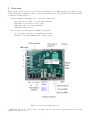
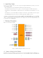
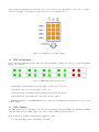
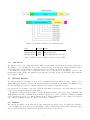
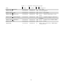
TTC/TTS Tester (TTT) Module
User Manual
Eric Hazen [email protected], Christopher Woodall [email protected], Charlie Hill [email protected]
June 3, 2013
1
Contents
1 Overview
3
2 Quick Start Guide
4
3 Hardware Description
3.1 Jumpers: Setting the Serial Number
3.2 LED Arrangement . . . . . . . . . .
3.3 NIM Outputs . . . . . . . . . . . . .
3.4 NIM Inputs . . . . . . . . . . . . . .
3.5 LHC Clock Input . . . . . . . . . . .
3.6 Optical Fiber Transceivers . . . . . .
3.6.1 TTC Protocol . . . . . . . . .
3.6.2 SFP Transmitter . . . . . . .
3.6.3 SFP Receiver . . . . . . . . .
3.7 Ethernet Interface . . . . . . . . . .
3.8 Buttons . . . . . . . . . . . . . . . .
3.9 JTAG Port . . . . . . . . . . . . . .
.
.
.
.
.
.
.
.
.
.
.
.
.
.
.
.
.
.
.
.
.
.
.
.
.
.
.
.
.
.
.
.
.
.
.
.
.
.
.
.
.
.
.
.
.
.
.
.
.
.
.
.
.
.
.
.
.
.
.
.
.
.
.
.
.
.
.
.
.
.
.
.
.
.
.
.
.
.
.
.
.
.
.
.
.
.
.
.
.
.
.
.
.
.
.
.
.
.
.
.
.
.
.
.
.
.
.
.
.
.
.
.
.
.
.
.
.
.
.
.
.
.
.
.
.
.
.
.
.
.
.
.
.
.
.
.
.
.
.
.
.
.
.
.
.
.
.
.
.
.
.
.
.
.
.
.
.
.
.
.
.
.
.
.
.
.
.
.
.
.
.
.
.
.
.
.
.
.
.
.
.
.
.
.
.
.
.
.
.
.
.
.
.
.
.
.
.
.
.
.
.
.
.
.
.
.
.
.
.
.
.
.
.
.
.
.
.
.
.
.
.
.
.
.
.
.
.
.
.
.
.
.
.
.
.
.
.
.
.
.
.
.
.
.
.
.
.
.
.
.
.
.
.
.
.
.
.
.
.
.
.
.
.
.
.
.
.
.
.
.
.
.
.
.
.
.
.
.
.
.
.
.
.
.
.
.
.
.
.
.
.
.
.
.
.
.
.
.
.
.
.
.
.
.
.
.
.
.
.
.
.
.
.
.
.
.
.
.
.
.
.
.
.
.
.
.
.
.
.
.
.
.
.
.
.
.
.
.
.
.
.
.
.
.
.
.
.
.
.
.
.
.
.
.
.
.
.
.
.
.
.
.
.
.
.
.
.
.
.
.
.
.
.
.
.
.
.
.
.
.
.
.
.
.
.
.
.
.
.
.
.
.
.
.
.
.
.
.
.
.
.
.
.
.
.
.
.
.
.
.
.
.
.
.
.
.
.
.
.
.
.
.
.
.
.
.
.
.
.
.
.
.
.
.
.
.
.
.
.
.
.
.
.
.
4
4
5
5
6
6
6
6
6
7
7
7
8
4 Software Configuration
8
5 IPBus Registers
8
2
1
Overview
This document describes a module developed at Boston University for use in CMS test stands, especially those based
on MicroTCA using the AMC13 module for clock/trigger/DAQ functions. The TTC/TTS Tester Module (TTT)
performs the following functions:
• Generate simulated TTC signals on two optical fiber outputs, with:
–
–
–
–
L1A generated periodically or at pseudo-random intervals
BC0 with correct spacing (every 3563 clocks)
CMS trigger rules observed (programmable)
TTS buffer status respected
• Receive and process TTS status from AMC13 on optical fiber
– Use to modulate trigger rate for internally-generated L1A
– Translate to legacy TTS (FMM) output on RJ-45 connector
Figure 1: Board Overview with Connectors
Illustration 1 shows an overview of the board with connectors and controls. Detailed information is in the
Hardware Description section.
3
2
Quick Start Guide
Connect a 5V power supply to the power connector (J9). Use the supplied wall transformer (or make your own cable;
center terminal is positive).
The board should provide the following functions without any software intervention:
• The BC0 nim output should provide a 75ns (three clock cycles) wide pulse at the LHC orbit frequency.
• Both TTC fiber outputs (transmitter on SFP) should provide a valid TTC bit stream with BC0 encoded every
88µs.
• The TTS state received from the AMC13 on the SFP receivers should be output as LVDS on the RJ-45 outputs.
• The NIM0 input should generate a L1A on both TTC outputs when a falling edge is seen.
In order, to use the board in “receiver” mode, where the Channel A and Channel B SFP connectors output BC0’s
and take the received messages and output the L1A’s and BC0’s on the associated NIM outputs, you need to write
“0x10” to the TTTControlReg (Address: 0x2). Please, refer to Figure 1 for location. More detailed information can
be found in the section “NIM Outputs”.
3
Hardware Description
Figure 2 is a basic interface diagram.
Figure 2: TTT Block Diagram, with all connectors noted.
3.1
Jumpers: Setting the Serial Number
The TTT board provides 4 GPIO pins on J14, surrounded by 3.3V (J3) and GND (J17). These 4 GPIO pins go to
pins P35, P32, P30 and P39 on the Spartan-6 and are used to set the serial number. Each board is assigned and
4
shipped with a serial number in a 4-bit number space, where each bit of the serial number corresponds to one jumper
as indicated in Figure 3. The jumper setting of 0 is reserved for verification mode.
Figure 3: Configuration for Settings Jumpers
3.2
LED Arrangement
Figure 4 shows the LED arrangement on the front of the TTT. In the default power-on mode of operation the LEDs
indicate the following:
Figure 4: LED Arrangement and Association
• When R0 is solid the DCM is locked and reliable operation can be expected.
• R1 indicates that power is being applied to the board.
• G0-3 indicate the Serial Number (IP and MAC address) that is currently set.
• G4-7 indicate the current TTS state being sent to the Ch. A Fiber.
LED Functions inside of the VERIFY firmware are described in the TTT Hardware Verification Procedure section
of this document.
3.3
NIM Outputs
The NIM outputs can be seen in Figure 1 and are labeled as BC0 (J5), L1A (J4), NIM0 (J18, aux. BC0) and NIM1
(J19, aux. L1A). Modes for NIM outputs can be selected using TTTControlRegister bits 4 to 7.
In the default mode (TTTControlRegisters[7..4] (0x2) set to 0x0):
• J5 will output BC0 generated internally on the TTT.
5
• J4 will output the L1As being generated by the TTT as setup by the software (see the Software Configuration
Section).
In the receiver mode (TTTControlRegisters[7..4] (0x2) set to 0x1):
• J5 and J4 will output the BC0s and L1As received on Fiber Channel A
• J18 and J19 will output the BC0s and L1As received on Fiber Channel B
3.4
NIM Inputs
The NIM inputs can be seen in Figure 1 and are labeled NIM IN0 (J20), NIM IN1 (J21), NIM IN2 (J22), and
NIM IN3 (J23). The default mode only utilizes NIM IN0 which looks for falling edges and generates a single L1A.
Currently no other features or configurations are available for the NIM Inputs, but a configuration register has been
made available for future modes (TTTNimInConfig).
3.5
LHC Clock Input
This input provides the option to substitute an external clock for the on-board 40.079 MHz crystal. It must be
selected by writing a “1” to bit 2 of register 0x2 (TTTControlReg).
3.6
Optical Fiber Transceivers
Two SFP cages are provided for optical fiber transceivers. For compatibility wit the TTC system it is recommended
to use SFP transcievers compatible with the ATM network protocol.
3.6.1
TTC Protocol
The SFP transceivers process biphase-mark encoded bit streams using the protocol specified for the CERN TTC
system[?]. The biphase-mark encoding scheme is illustrated in Figure 5. Two bits (called channels A, B) are
transmitted each clock cycle. Channel A indicates that an L1A is present, while channel B is used to carry serial
data as detailed in Figure 6. Channel B sends 1’s continuously when idle, with a 1→0 transition representing the
start of a frame. Various types of frames are documented for the TTC system, but the only type used by this board
is the “Broadcast Command” frame. An 8-bit command is transmitted, with the values of the bits shown in Fig. 6.
Figure 5: TTC Low-Level Encoding
3.6.2
SFP Transmitter
The transmitters simulate the output of the TTC system. The A channel is used to carry L1A generated internally or
received from the NIM0 input. The B channel sends broadcast commands such as those shown in Table 1. BCR/BC0
is sent every orbit (3563 clocks).
Other broadcast commands may be sent under software control. Typically to start a data collection run on a test
stand the sequence OCR, ECR would be sent with L1A disabled before the start of data taking.
6
Figure 6: TTC Frame and Broadcast Command Format
.
Value
00101000 (0x28)
00000010 (0x02)
00000001 (0x01)
Acronym
OCR
ECR
BCR
Name
Orbit Count Reset
Event Count Reset
(a.k.a. BC0) Bunch Count Reset
Table 1: TTC Broadcast Commands Send/Processed by TTT
3.6.3
SFP Receiver
The SFP Receiver receives a bitstream from the AMC13 module which carries TTS and local trigger information.
The TTC protocol is currently used. A broadcast command is sent periodically by the AMC13 in which the upper
4 bits represent the current TTS state. Channel A is used for local L1A generated in the AMC13.
The TTS state is output to the corresponding RJ-45 connector, and also used to modify the operation of the
internal L1A generator. If the TTS signals represent any state other than “Ready” the L1A will be halted until the
state returns to “Ready”.
3.7
Ethernet Interface
The ethernet interface seen in Figure 1 can be used to comunicate between the TTT board and a computer over an
100Mb Full Duplex ethernet connection. All ethernet transactions are handled by the IPBus (v1.3) Firmware Core.
For more information on software configuration please see the Software Configuration section.
I/P addresses are set by jumper on the PC board as shown in Table 2. For reference on how the jumpers are set up
see the section “Jumpers: Setting the Serial Number”.
In addition to being used by the software to configure the TTT the ethernet can be used to write to the flash on the
TTT. Writing to the flash over IPBus allows for firmware updates to be carried out without a JTAG programming
device. Information on how to do this is available in the Software Configuration section. This is only valid for
non-volatile programming and the old software version will be overwritten.
3.8
Buttons
Two buttons are available on the TTT and are appropriately labeled SW1 is a reset, and SW2 causes an L1A to
occur on a falling edge. Both buttons are pulled high (to 3.3V) by default through the Spartan 6’s internal resistors
and go low (0V) when pressed. Firmware debouncing is performed on both buttons.
7
Serial Number
000
001
002
003
004
005
006
007
008
009
010
MAC Address
08-00-30-F3-00-00
08-00-30-F3-00-01
08-00-30-F3-00-02
08-00-30-F3-00-03
08-00-30-F3-00-04
08-00-30-F3-00-05
08-00-30-F3-00-06
08-00-30-F3-00-07
08-00-30-F3-00-08
08-00-30-F3-00-09
08-00-30-F3-00-0a
IP Address
192.167.2.32
192.168.2.33
192.168.2.34
192.168.2.35
192.168.2.36
192.168.2.36
192.168.2.38
192.168.2.39
192.168.2.40
192.168.2.41
192.168.2.42
Table 2: IP and MAC Addresses
3.9
JTAG Port
A JTAG at site J1 is provided as a standard .1 inch header. The signal names are marked (TMS, TDI, etc) on the
TTT board. This particular JTAG pinout is meant for use with the Digilent HS-1 JTAG programmer for Xilinx
chips. However, another JTAG programmer which is compatible with the Xilinx ISE software, or known to be
compatible with Xilinx 6 series chips may also work, but will receive no user support. This port can be used for
both volatile (program to FPGA) and non-volatile (program to SPI Flash) programming using the provided “.bit”
and “.mcs” files.
4
Software Configuration
For now please referenc Charlie Hill’s TTT software documentation. A software quickstart guide is coming. As of
now, the supported release will by based on PyChips, not µHAL, due to problems with the 100Mbs TTT ethernet
connection.
5
IPBus Registers
Table 3 documents all of the registers in the TTT and a basic description, some registers have further documentation
sections when required.
Table 3:
TTT Register Table
Name
Address
Bit Mask
R/W
Description
VERSION
0x00000000
0xffffffff
R
Format: YYYYMMDD where [Y]ear,
[M]onth and [D]ay
FirmwareVersionID
0x00000000
0xffffffff
R
Firmware Version ID (same as
VERSION), maintains backwards
compatibility.
STATUS
0x00000001
0xffffffff
R
0x1 read/write
FLASH MemoryRead
0x00000001
0x00000004
R
Read to get Memory Read.
FLASH FIFOempty
0x00000001
0x00000002
R
Fifo Empty Status
FLASH BUSY
0x00000001
0x00000001
R
Flash Busy
FLASH CMD
0x00000001
0xffffffff
W
Flash command register
TTTControlReg
0x00000002
0xffffffff
R/W
Control Reg
TTTControlReg ClkSel
0x00000002
0x00000004
R/W
Write to ‘1’ to change clock source
to LHC Clock.
TTTControlReg DisableBC0
0x00000002
0x00000008
R/W
Write to ‘1’ to disable BC0’s on
all output streams.
Continued on next page
8
Table 3 -- continued from previous page
Name
Address
Bit Mask
R/W
Description
TTTControlReg NimModes
0x00000002
0x000000f0
R/W
Sets NIM modes the controls are
as follow. write ‘1’ to bit 0 to
switch to receiver mode.
TTTActionReg
0x00000003
0xffffffff
R/W
Action Register
TTTActionReg SendBcastCmd
0x00000003
0x00000002
R/W
Write ‘1’ to send Bcast Command,
must be manually reset to ‘0’.
TTTBcastCmd
0x00000004
0xffffffff
R/W
Load Broadcast command into the
lower 8 bits, the remaining
bits do not matter. Send using
TTTActionReg bit 1.
FLASH WBUF
FLASH RBUF
0x00001000
0x00001080
0xffffffff
0xffffffff
R/W
R/W
Write flash
Read flash
TTSOrbitLength
0x00000100
0xffffffff
R/W
BX per orbit (nom.
TTSTrigStart
0x00000101
0xffffffff
R/W
delay to first trigger
TTSOrbitMax
0x00000102
0xffffffff
R/W
number of orbits with triggers
TTSL1ASpacing
0x00000103
0xffffffff
R/W
spacing of L1A within orbit
TTSL1APerOrbit
0x00000104
0xffffffff
R/W
number of L1A per orbit
TTSRepeatPeriod
0x00000105
0xffffffff
R/W
time between repeats in orbits
TTSFifoByte
0x00000106
0xffffffff
R/W
Select byte to read:
TTSFifoByte FifoData
0x00000106
0x0000000f
R/W
Fifo data
TTSFifoByte FifoWordCnt
0x00000106
0x00000030
R/W
Fifo Word Count
TTSFifoByte TriggerCnt
0x00000106
0x000003c0
R/W
Trigger Count
TTSFifoByte CounterMux
0x00000106
0x00000400
R/W
Counter Mux
TTSCounterByte
0x00000107
0xffffffff
R/W
Select coutner to read:
violation 1-4
TTSRateSet
0x00000108
0xffffffff
R/W
random threshold
TTSRule1
0x00000109
0xffffffff
R/W
no more than 1 trig/N Bx
TTSRule2
0x0000010a
0xffffffff
R/W
no more than 2 trig/N Bx
TTSRule3
0x0000010b
0xffffffff
R/W
no more than 3 trig/N Bx
TTSRule4
0x0000010c
0xffffffff
R/W
no more than 4 trig/N Bx
TTSClkSel
0x0000010d
0xffffffff
R/W
select orbit signal clock phase
TTSSetBPDelay
0x0000010e
0xffffffff
R/W
delay responding to BSY, OFW
TTSBPSampleMask
0x0000010f
0xffffffff
R/W
sample TTS when (n and BcN) == 0
TTSTTCBxNum
0x00000110
0xffffffff
R/W
NIM TTS output at this BcN
TTSTTCCmdPrescale
0x00000111
0xffffffff
R/W
NIM TTS prescale (not impl yet)
TTSControlReg
0x00000112
0xffffffff
R/W
Control Register
TTSControlReg enBurt
0x00000112
0x00000001
R/W
enable burst (>1 trigger per orbit)
TTSControlReg enRepeats
0x00000112
0x00000002
R/W
enable repeats
TTSControlReg enBP
0x00000112
0x00000004
R/W
enable back pressure
TTSControlReg enRandTrig
0x00000112
0x00000008
R/W
enable random triggers
TTSControlReg disableBlanking
0x00000112
0x00000010
R/W
disable blankking of L1A in orbit
gap
TTSStatusReg
0x00000113
0xffffffff
R
Status Register
TTSStatusReg FifoEmpty
0x00000113
0x00000001
R
Fifo Empty
3563)
0-3 Rule
Continued on next page
9
Table 3 -- continued from previous page
Name
Address
Bit Mask
R/W
Description
TTSStatusReg FifoFull
0x00000113
0x00000002
R
Fifo Full
TTSActionReg
0x00000114
0xffffffff
R/W
Action Register
TTSActionReg L1Aen
0x00000114
0x00000001
R/W
bit 0 - L1A enable
TTSActionReg advanceFifo
0x00000114
0x00000002
R/W
bit 1 - advance TTS FIFO to next
word
TTSActionReg captureTrigCnt
0x00000114
0x00000004
R/W
bit 2 - capture trigger count for
readout
TTSActionReg genNewRand
0x00000114
0x00000008
R/W
bit 3 - generate new random number
TTSActionReg RST
0x00000114
0x00000080
R/W
bit 7 - reset
TTSDataReg
0x00000115
0xffffffff
R
Where data selected by TTSFifoByte
is presented.
10