1
Series 9420/9421/9422/9425/9426/9427
VME Isolated Digital Input Board
USER’S MANUAL
ACROMAG INCORPORATED
30765 South Wixom Road
P.O. BOX 437
Wixom, MI 48393-7037 U.S.A.
Tel: (248) 624-1541
Fax: (248) 624-9234
8500-333-C00M003
SERIES AVME9420/9421/9422/9425/9426/9427 ISOLATED DIGITAL INPUT BOARDS
___________________________________________________________________________
Manual No. 8500-333
The information in this manual is subject to change without notice. Acromag, Inc., makes no warranty
of any kind with regard to this material, including, but not limited to, the implied warranties of
merchantability and fitness for a particular purpose. Further, Acromag, Inc., assumes no responsibility
for any errors that may appear in this manual and makes no commitment to update, nor keep current,
the information contained in this manual.
No part of this manual may be copied or reproduced in any form, or by any means, without the prior
written consent of Acromag, Inc.
==================================
IMPORTANT SAFETY CONSIDERATIONS
==================================
It is very important for the user to consider the possible adverse effects of power, wiring, component,
sensor or software failures in designing any type of control or monitoring system. This is especially
important where economic property loss or human life is involved. It is important that the user employ
redundancy and comprehensive failure analysis to insure a safe and satisfactory overall system
design. It is agreed between the Buyer and Acromag, that this is the Buyer's responsibility.
Acromag, Inc.
30765 South Wixom Road
P.O. Box 437
Wixom, Michigan 48393-7037, USA
Tel: (248) 624-1541
Fax: (248) 624-9234
Copyright 1992 Acromag, Inc. Printed in USA
Data and specifications subject to change without notice
- 0.1 -
SERIES AVME9420/9421/9422/9425/9426/9427
CHAPTER 1
ISOLATED DIGITAL INPUT BOARDS
GENERAL INFORMATION
______________________________________________________________________
TABLE OF CONTENTS
CHAPTER
1.0
1.1
1.2
1.3
1.4
PAGE
GENERAL INFORMATION................................................................................................... 1.1
INTRODUCTION................................................................................................................... 1.1
DIGITAL DC INPUT FEATURES ......................................................................................... 1.2
VMEbus INTERFACE FEATURES........................................................................................ 1.2
FIELD COMPATIBILITY........................................................................................................ 1.3
1.4.1 Digital Inputs................................................................................................................. 1.3
2.0
2.1
2.2
2.3
PREPARATION FOR USE.................................................................................................... 2.1
UNPACKING AND INSPECTION.......................................................................................... 2.1
CARD CAGE CONSIDERATIONS ........................................................................................ 2.1
BOARD CONFIGURATION................................................................................................... 2.1
2.3.1 Default Jumper Configuration ....................................................................................... 2.4
2.3.1.1 Digital DC Input Default Configuration ....................................................................... 2.4
2.4 VMEbus CONFIGURATION.................................................................................................. 2.4
2.4.1 Address Decode Jumper Configuration ........................................................................ 2.4
2.4.2 Address Modifier Jumper Configuration........................................................................ 2.6
2.4.3 Interrupt Level Select Jumper Configuration................................................................. 2.6
2.4.4 SYSFAIL* Selection Jumper Configuration................................................................... 2.6
2.5 DIGITAL INPUT CONFIGURATION...................................................................................... 2.7
2.5.1 Digital DC Input Threshold Detection............................................................................ 2.7
2.5.2 Sensing Contact Closures and Switches ...................................................................... 2.7
2.5.3 Debounce Delay Selection ........................................................................................... 2.10
2.5.4 Interrupt and Debounce Port Selection......................................................................... 2.10
2.5.5 Digital Input Interface to TTL and CMOS Signals ......................................................... 2.11
2.6 CONNECTORS..................................................................................................................... 2.13
2.6.1 Digital Input Connector P3 (Port A & Port B) ................................................................ 2.13
2.6.2 Digital Input Connector P4 (Port C & Port D) ................................................................ 2.14
2.6.3 Digital Input Connector P2 (Port E & Port F) ................................................................ 2.15
2.6.4 VMEbus Connections ................................................................................................... 2.16
2.7 POWER-UP TIMING AND LOADING ................................................................................... 2.17
2.8 DATA TRANSFER TIMING ................................................................................................... 2.17
2.9 FIELD GROUNDING CONSIDERATIONS ............................................................................ 2.17
3.0 PROGRAMMING INFORMATION ........................................................................................ 3.1
3.1 MEMORY MAP ..................................................................................................................... 3.1
3.1.1 Board Identification PROM ........................................................................................... 3.2
3.1.2 Board Status Register .................................................................................................. 3.4
3.1.2.1 Status Bits Usage ................................................................................................ 3.5
3.1.3 Interrupt Vector Registers............................................................................................. 3.5
3.1.4 Digital Input Channel Interrupt Status Register............................................................. 3.6
3.1.5 Digital Input Channel Interrupt Enable Register............................................................ 3.6
3.1.6 Digital Input Channel Interrupt Polarity Register ........................................................... 3.7
- 0.3 -
SERIES AVME9420/9421/9422/9425/9426/9427
CHAPTER 1
ISOLATED DIGITAL INPUT BOARDS
GENERAL INFORMATION
______________________________________________________________________
CHAPTER
PAGE
3.1.7 Digital Input Channel Interrupt Type Select Register .................................................... 3.7
3.1.8 Digital Input Channel Interrupt Pattern Enable Register ............................................... 3.8
3.1.9 Port A Digital Input Channel Data Register................................................................... 3.8
3.1.10 Port B Digital Input Channel Data Register.................................................................. 3.9
3.1.11 Port C Digital Input Channel Data Register.................................................................. 3.9
3.1.12 Port D Digital Input Channel Data Register.................................................................. 3.9
3.1.13 Port E Digital Input Channel Data Register.................................................................. 3.9
3.1.14 Port F Digital Input Channel Data Register .................................................................. 3.10
3.2 GENERAL PROGRAMMING CONSIDERATIONS................................................................ 3.10
3.2.1 Board Diagnostics ........................................................................................................ 3.10
3.3 GENERATING INTERRUPTS............................................................................................... 3.11
3.3.1 Interrupt Example For Change Of State (COS) ............................................................ 3.14
3.3.2 Interrupt Example For Input Level (Polarity) Match....................................................... 3.14
3.3.3 Interrupt Example For Input Pattern Match ................................................................... 3.15
3.3.4 Sequence of Events For an Interrupt ............................................................................ 3.15
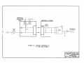
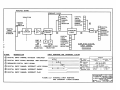
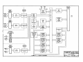
4.0 THEORY OF OPERATION ................................................................................................... 4.1
4.1 VMEbus INTERFACE ........................................................................................................... 4.1
4.1.1 VMEbus Control Logic .................................................................................................. 4.1
4.1.2 VME Interrupter. ........................................................................................................... 4.3
4.2 REGISTER LOCATION SUMMARY...................................................................................... 4.3
4.3 ISOLATION BARRIER .......................................................................................................... 4.4
4.4 DIGITAL INPUT SECTION.................................................................................................... 4.4
5.0
5.1
5.2
5.3
SERVICE AND REPAIR INFORMATION.............................................................................. 5.1
SERVICE AND REPAIR ASSISTANCE ................................................................................ 5.1
PRELIMINARY SERVICE PROCEDURE .............................................................................. 5.1
PARTS LISTS ....................................................................................................................... 5.1
6.0 SPECIFICATIONS ................................................................................................................ 6.1
7.0 SCHEMATIC AND PART LOCATION DRAWINGS .............................................................. 7.1
APPENDIX:
A.0
A.1
A.2
A.3
CABLE AND TERMINATION PANELS ................................................................................ A.1
CABLE: MODEL 9944-x........................................................................................................ A.1
CABLE: MODEL 9948-x........................................................................................................ A.3
TERMINATION PANEL: MODEL 6985-32DI ........................................................................ A.5
- 0.4 -
SERIES AVME9420/9421/9422/9425/9426/9427
CHAPTER 1
ISOLATED DIGITAL INPUT BOARDS
GENERAL INFORMATION
______________________________________________________________________
TABLES:
2.1
2.2
2.3
2.4
PAGE
P3 CONNECTOR (PORT A & PORT B)................................................................................ 2.13
P4 CONNECTOR (PORT C & PORT D) ............................................................................... 2.14
P2 CONNECTOR (PORT E & PORT F)................................................................................ 2.15
P1 BUS CONNECTIONS ...................................................................................................... 2.16
5.1A PARTS LIST FOR MODEL AVME942x-I (MAIN BOARD - PARTS COMMON) ................... 5.2
5.1B PARTS LIST FOR MODEL AVME9420-I (MAIN BOARD - PARTS UNIQUE)...................... 5.3
5.1C PARTS LIST FOR MODEL AVME9421-I (MAIN BOARD - PARTS UNIQUE)...................... 5.3
5.1D PARTS LIST FOR MODEL AVME9422-I (MAIN BOARD - PARTS UNIQUE)...................... 5.4
5.1E PARTS LIST FOR MODEL AVME9425-I (MAIN BOARD - PARTS UNIQUE)...................... 5.4
5.1F PARTS LIST FOR MODEL AVME9426-I (MAIN BOARD - PARTS UNIQUE) ...................... 5.5
5.1G PARTS LIST FOR MODEL AVME9427-I (MAIN BOARD - PARTS UNIQUE) ..................... 5.5
5.2 PARTS LIST FOR MODEL AVME942x-I-L (LED EXPANSION BOARD) .............................. 5.6
FIGURES:
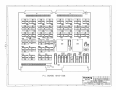
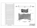
2.1 AVME942x JUMPER LOCATION DRAWING (4501-281) ..................................................... 2.2
2.2 AVME942x-I-L LED EXPANSION BOARD ASSEMBLY (4501-282)...................................... 2.3
2.3 AVME942x SIMPLIFIED DIGITAL DC INPUT CHANNEL SCHEMATIC (4501-283) ............. 2.8
2.4 AVME942x DIGITAL DC INPUT CHANNEL CONFIGURATIONS (4501-284)....................... 2.9
2.5 AVME942x INTERFACE TO TTL AND CMOS SIGNALS (4501-285) ................................... 2.12
3.1 BOARD MEMORY MAP........................................................................................................ 3.1
3.2 AVME9422-I-L BOARD IDENTIFICATION PROM ................................................................ 3.3
3.3 AVME942x INPUT RESPONSE AND INTERRUPT TIMING DIAGRAM (4501-286) ............. 3.13
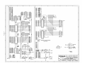
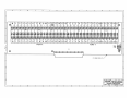
4.1 AVME942x BLOCK DIAGRAM (4501-287)............................................................................ 4.2
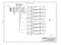
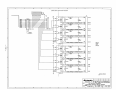
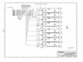
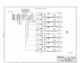
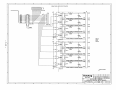
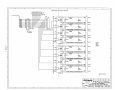
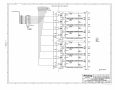
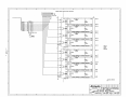
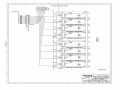
AVME942x SCHEMATIC & PART LOCATION DRAWING (4501-260) .................................. 7.2
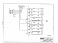
AVME942x LED EXP. BOARD SCH. & PART LOC. DRAWING (4501-259) .......................... 7.18
9944-X FLAT 64 PIN CABLE (4501-135) ............................................................................... A.2
9948-X FLAT 64 PIN CABLE (4501-291) ............................................................................... A.4
6985-32Dx SCHEMATIC & PART LOCATION DRAWING (4501-272)................................... A.7
6985-32DI MOUNTING CLEARANCE & ELECTRICAL CONNECTIONS (4501-274) ............ A.10
- 0.5 -
SERIES AVME9420/9421/9422/9425/9426/9427
CHAPTER 1
ISOLATED DIGITAL INPUT BOARDS
GENERAL INFORMATION
______________________________________________________________________
1.0 GENERAL INFORMATION
1.1 INTRODUCTION
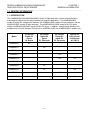
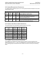
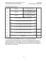
The AVME9420/9421/9422/9425/9426/9427 Series of VME cards offer a variety of features which
make them an ideal choice for many industrial and scientific applications. The AVME9420/9425
contain 32 digital DC voltage input channels, the AVME9421/9426 contain 64 input channels, and the
AVME9422/9427 contain 96 input channels. The AVME9420/9421/9422 accept 4-25V DC inputs,
while the AVME9425/9426/9427 accept 20-55V DC inputs. In addition, channel status indicators are
available on the first 64 channels (P3 and P4) for AVME9421/9426 and AVME9422/9427 models, only.
Model
AVME9420-I
32 Channel
Digital DC
Inputs
P2 Access
64 Channel
Digital DC
Inputs
P3, P4 access
96 Channel
Digital DC
Inputs P2,
P3, P4 access
XX
AVME9421-I
XX
AVME9421-I-L
XX
XX
AVME9422-I
XX
AVME9422-I-L
XX
AVME9425-I
Channel On
LEDs (Green)
64 Channels
at P3 & P4
XX
XX
AVME9426-I
XX
AVME9426-I-L
XX
XX
AVME9427-I
XX
AVME9427-I-L
XX
- 1.1 -
XX
SERIES AVME9420/9421/9422/9425/9426/9427
CHAPTER 1
ISOLATED DIGITAL INPUT BOARDS
GENERAL INFORMATION
______________________________________________________________________
GENERAL FEATURES
•
All Digital DC Inputs are isolated from the VMEbus for up to 250V AC, or 354V DC on a continuous
basis (will withstand 1500V AC dielectric strength test for one minute without breakdown).
•
All Digital DC Inputs are isolated from each other for up to 125V AC, or 125V DC on a continuous
basis (will withstand 1250V AC dielectric strength test for one minute without breakdown).
•
PASS/FAIL status indicator LEDs on the front panel.
•
Input channel ON indicating green LEDs (with -L option).
•
Field connections accessible through connectors P3 and P4 mounted on the front panel
(AVME9421/9426 and AVME9422/9427).
•
Field connections accessible through connectors mounted on the rear panel (AVME9420/9425 and
AVME9422/9427).
•
Optional Termination Panel.
1.2 DIGITAL DC INPUT FEATURES
•
32 input channels configured as two 16 bit words (AVME9420/9425).
•
64 input channels configured as four 16 bit words (AVME9421/9426).
•
96 input channels configured as six 16 bit words (AVME9422/9427).
•
4 to 25V DC or 20 to 55V DC range boards are available.
•
Bidirectional inputs (polarity can be +/- or -/+ at either input of each channel).
•
Buffers on all channels contain hysteresis for noise immunity.
•
Adjustable debounce circuitry on eight front Port B or eight rear Port F (jumper selectable)
channels 0 through 7.
•
Generation of interrupts for Port B or Port F (jumper selectable) channels 0 through 7: input
Change Of State (COS), input level (polarity) match, or input pattern detection.
•
Can be interfaced to TTL & CMOS logic.
•
Input channels contain capacitors for transient voltage suppression.
•
Input channels contain LED bypass resistors for faster turn-off response.
- 1.2 -
SERIES AVME9420/9421/9422/9425/9426/9427
CHAPTER 1
ISOLATED DIGITAL INPUT BOARDS
GENERAL INFORMATION
______________________________________________________________________
1.3 VMEBUS INTERFACE FEATURES
•
Slave module A24/A16, D16/D08 (EO).
•
Short I/O Address Modifiers 29H, 2DH (H = Hex).
•
Standard Address Modifiers 39H, 3DH (H = Hex).
•
I(1-7) interrupter D08 (O), jumper programmable interrupt level, software programmable interrupt
vectors (for Port B or Port F digital input channels 0-7), interrupt release mechanism is Release On
Register Access (RORA) type.
•
Decode on 1K byte boundaries.
1.4 FIELD COMPATIBILITY
See APPENDIX A for more information on compatible products.
1.4.1 DIGITAL INPUTS
Directly compatible with Acromag input termination panel.
Cable:
Model 9944-X: Flat 64 pin cable (female connectors at both ends) for connecting the
AVME9421/9422/9426/9427 (P3 or P4 connector) to the 6985-32DI termination panel.
Model 9948-X: Flat 64 pin cable (female connectors at both ends) for connecting the
AVME9420/9422/9425/9427 (P2 connector) to the 6985-32DI termination panel.
Termination Panel:
Model 6985-32DI: 32 channel input digital termination panel.
- 1.3 -
SERIES AVME9420/9421/9422/9425/9426/9427
CHAPTER 2
ISOLATED DIGITAL INPUT BOARDS
PREPARATION FOR USE
___________________________________________________________________
2.0 PREPARATION FOR USE
This chapter provides information about preparing the Isolated Digital Input Board for system
operation.
2.1 UNPACKING AND INSPECTION
Inspect the shipping carton immediately upon receipt for evidence of mishandling during transit. If
the shipping carton is severely damaged or water stained, request that the carrier's agent be
present when the carton is opened. If the carrier's agent is absent when the carton is opened and
the contents of the carton are damaged, keep the carton and packing material for the agent's
inspection.
For repairs to a product damaged in shipment, refer to the Acromag Service Policy to obtain return
instructions. It is suggested that salvageable shipping cartons and packing material be saved for
future use in the event the product must be shipped.
The board is physically protected with foam and electrically protected with
an antistatic bag during shipment. It is advisable to visually inspect the
board for evidence of mishandling prior to applying power.
The board utilizes static sensitive components and should only be handled
at a static safe work station.
2.2 CARD CAGE CONSIDERATIONS
Refer to the specifications for bus loading and power requirements. Be sure that the system power
supplies are able to accommodate the additional requirements within the voltage tolerances
specified.
IMPORTANT
Adequate air circulation must be provided to prevent a
temperature rise above the maximum operating temperature
Adequate air circulation must be provided to prevent a temperature rise above the maximum
operating temperature. Large and continuing fluctuations in ambient air temperature should be
avoided. If the installation is in an industrial environment and the board is exposed to
environmental air, careful consideration should be given to air filtering.
2.3 BOARD CONFIGURATION
The board may be configured in a variety of ways for many different applications. Each possible
jumper setting will be discussed in the following
sections. The jumper locations are shown in Figure 2.1.
- 2.1 -
SERIES AVME9420/9421/9422/9425/9426/9427
CHAPTER 2
ISOLATED DIGITAL INPUT BOARDS
PREPARATION FOR USE
___________________________________________________________________
2.3.1 DEFAULT JUMPER CONFIGURATION
VMEbus INTERFACE CONFIGURATION
When a board is shipped from the factory, it is configured as follows:
• VMEbus Short I/O Address of 0000H.
•
Set to respond to both Address Modifiers 29H and 2DH.
•
Sysfail* enabled to respond to a system failure.
•
Interrupt Level: none. Therefore, even if interrupts are enabled, no interrupts will be caused.
2.3.1.1 DIGITAL DC VOLTAGE INPUT DEFAULT CONFIGURATION
•
32, 64 or 96 dedicated digital DC input channels (Port A numbered 0 through 15, Port B
numbered 0 through 15, Port C numbered 0 through 15, Port D numbered 0 through 15, Port E
numbered 0 through 15 and Port F numbered 0 through 15).
•
All channels are board specific for 4-25V DC or 20-55V DC input range.
•
Port B channels 0 through 7 are selected for interrupt and debounce on models
AVME9421/9422/9426/9427.
•
Port F channels 0 through 7 are selected for interrupt and debounce on models
AVME9420/9425.
•
Minimum input debounce selected.
2.4 VMEBUS CONFIGURATION
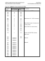
2.4.1 Address Decode Jumper Configuration
The board interfaces with the VMEbus as a 1K block of address locations in the VMEbus Short I/O
Address Space or Standard Address Space. J2 and J1 decode the fourteen most significant
address lines A10 through A23 to provide segments of 1K address space. The configuration of the
jumpers for different base address locations is shown below. "IN" means that the pins are shorted
together with a shorting clip. "OUT" indicates that the clip has been removed. J2 decodes address
lines A10 through A15 and J1 decodes Address lines A16 through A23. Therefore, when
configured for the Short I/O Address space, only J2 needs to be configured.
-
2.4 -–
SERIES AVME9420/9421/9422/9425/9426/9427
CHAPTER 2
ISOLATED DIGITAL INPUT BOARDS
PREPARATION FOR USE
___________________________________________________________________
Pins of J2
Base
Address
00000000H
00000400H
00000800H
00000C00H
00001000H
A15
11 & 12
OUT
OUT
OUT
OUT
OUT
A14
9 & 10
OUT
OUT
OUT
OUT
OUT
A13
7&8
OUT
OUT
OUT
OUT
OUT
A12
5&6
OUT
OUT
OUT
OUT
IN
A11
3&4
OUT
OUT
IN
IN
OUT
A10
1&2
OUT
IN
OUT
IN
OUT
0000EC00H
0000F000H
0000F400H
0000F800H
0000FC00H
IN
IN
IN
IN
IN
IN
IN
IN
IN
IN
IN
IN
IN
IN
IN
OUT
IN
IN
IN
IN
IN
OUT
OUT
IN
IN
IN
OUT
IN
OUT
IN
Pins of J1
Base
Address
00000000H
00010000H
00020000H
00030000H
A23
15&16
OUT
OUT
OUT
OUT
A22
13 & 14
OUT
OUT
OUT
OUT
A21
11 & 12
OUT
OUT
OUT
OUT
A20
9 & 10
OUT
OUT
OUT
OUT
A19
7&8
OUT
OUT
OUT
OUT
A18
5&6
OUT
OUT
OUT
OUT
A17
3&4
OUT
OUT
IN
IN
A16
1&2
OUT
IN
OUT
IN
00FC0000H
00FD0000H
00FE0000H
00FF0000H
IN
IN
IN
IN
IN
IN
IN
IN
IN
IN
IN
IN
IN
IN
IN
IN
IN
IN
IN
IN
IN
IN
IN
IN
OUT
OUT
IN
IN
OUT
IN
OUT
IN
- 2.5 -
SERIES AVME9420/9421/9422/9425/9426/9427
CHAPTER 2
ISOLATED DIGITAL INPUT BOARDS
PREPARATION FOR USE
___________________________________________________________________
2.4.2 ADDRESS MODIFIER JUMPER CONFIGURATION
The VMEbus Address Modifier jumpers (J3, J5, and J6) permit the board to respond to the various
Address Modifier Codes.
Pins of J3, J5, J6
J3
1&2
OUT
OUT
J3
2&3
IN
IN
J5
1&2
OUT
IN
J6
1&2
IN
IN
IN
IN
OUT
OUT
OUT
IN
OUT
OUT
Address Modifier Code/Function
2DH Only Short Supervisory Access
2DH & 29H Short Supervisory Access and
Short Non-privileged Access
3DH Only Standard Supervisory Data Access
3DH & 39H Standard Supervisory Data Access and
Standard Non-privileged Data Access
2.4.3 INTERRUPT LEVEL SELECT JUMPER CONFIGURATION
The board Interrupt Level is selected by configuring jumper J4 as follows:
Interrupt
level
None
1
2
3
4
5
6
7
J4
5&6
OUT
OUT
OUT
OUT
IN
IN
IN
IN
J4
3&4
OUT
OUT
IN
IN
OUT
OUT
IN
IN
J4
1&2
OUT
IN
OUT
IN
OUT
IN
OUT
IN
2.4.4 SYSFAIL* SELECTION JUMPER CONFIGURATION
The AVME942x non-intelligent slave boards assert the SYSFAIL* signal as described in the
VMEbus Specification Rev. C.1, when J9 is installed (the pins are shorted together with a shorting
clip). Removing jumper J9 will disconnect the SYSFAIL* line from the circuitry on the Acromag
board.
- 2.6 -
SERIES AVME9420/9421/9422/9425/9426/9427
CHAPTER 2
ISOLATED DIGITAL INPUT BOARDS
PREPARATION FOR USE
___________________________________________________________________
2.5 DIGITAL INPUT CONFIGURATION
Board specific, low range or high range, input threshold voltages make the digital input channels
adaptable to almost any application. The inputs are designed for use with contact closures,
switches, alarm trips, and power supply ON/OFF monitoring. Input channels are optically isolated
from each other and from the VMEbus. See Figure 2.3 for the simplified schematic of a digital DC
input channel for the AVME942x.
Input channel debounce circuitry with selectable delay is provided for Port B or Port F (jumper
selectable) channels 0 through 7 to eliminate glitches from the input signals. These glitches are
frequently caused by contact bounce in mechanical relays and switches.
Input channel interrupt functions are provided for Port B or Port F (jumper selectable) channels 0
through 7. Each selected channel can be programmed to interrupt for Change Of State (COS),
input level (polarity) match, or input pattern match of the input levels.
2.5.1 DIGITAL DC INPUT THRESHOLD SELECTION
Two input threshold voltages are available, 4-25V DC or 20-55V DC, on a per board basis, as
shown in the following table:
Module
AVME9420/9421/9422
AVME9425/9426/9427
Channel Range
4-25V DC
20-55V DC
Positive Threshold Voltage
(Maximum)
4V DC
20V DC
2.5.2 SENSING CONTACT CLOSURES AND SWITCHES
The DC input voltage should be within the range listed in the previous table. See Figure 2.4: Digital
DC Input Channel Configurations, for connections for
different input types.
- 2.7 -
SERIES AVME9420/9421/9422/9425/9426/9427
CHAPTER 2
ISOLATED DIGITAL INPUT BOARDS
PREPARATION FOR USE
___________________________________________________________________
2.5.3 DEBOUNCE DELAY SELECTION
If mechanical relay contacts (or switches) are used as inputs, then the Port B or Port F channels 0
through 7 should be selected to take advantage of the debounce circuitry on the port. Also, it is
strongly recommended that a debounce delay longer than the maximum expected bounce time be
used. If the bounce time cannot be determined, then the maximum debounce delay should be
selected.
The debounce delay time is jumper programmable (J7) on a global basis for all Port B or Port F
input channels 0 through 7 (i.e. all selected input channels will have the same delay), as shown in
the following table:
Debounce
Delay Time (uS)
7 to 8
336 to 384
672 to 768
1344 to 1536
J7
1&2
OUT
OUT
OUT
IN
J7
3&4
OUT
OUT
IN
OUT
J7
5&6
OUT
IN
OUT
OUT
J7
7&8
IN
OUT
OUT
OUT
NOTE: One of the debounce delay times must be selected. If none or more than one delay time is
selected, the Port B or Port F channels 0 through 7 input signals will not pass through the
debounce circuit.
2.5.4 INTERRUPT AND DEBOUNCE PORT SELECTION
The interrupt and debounce port is jumper selectable (J8) on a global basis for all Port B or Port F
input channels 0 through 7 (i.e. all port selected input channels will be able to cause interrupts and
will have the same delay), as shown in the following table:
Channels
(0-7)
Port B
Port F
J8
1&2
IN
OUT
J8
2&3
OUT
IN
NOTE: One of the interrupt and debounce ports must be selected. If none is selected, the Port B
or Port F channels 0 through 7 input signals may not pass through the interrupt and debounce
circuit.
- 2.10 -
SERIES AVME9420/9421/9422/9425/9426/9427
CHAPTER 2
ISOLATED DIGITAL INPUT BOARDS
PREPARATION FOR USE
___________________________________________________________________
2.5.5 DIGITAL INPUT INTERFACE TO TTL AND CMOS SIGNALS
Logic level inputs can be interfaced to the board by the use of common logic elements such as the
74LS05 (or 74HC05) open collector (or drain) inverter gates. See Figure 2.5: AVME942x Interface
to TTL and CMOS Signals, for connection information. Applying a logic "1" to the input of the
inverter gate sinks the current required to turn the opto-coupler ON (using the lowest input voltage
range) and yields a logic "1" for the corresponding input channel register bit position.
- 2.11 -
SERIES AVME9420/9421/9422/9425/9426/9427
CHAPTER 2
ISOLATED DIGITAL INPUT BOARDS
PREPARATION FOR USE
___________________________________________________________________
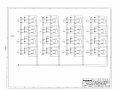
2.6 CONNECTORS
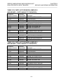
2.6.1 DIGITAL INPUT CONNECTOR (PORT A & PORT B)
The first group of 32 digital inputs (Port A channels 0 through 15 and Port B channels 0 through
15) are connected to the AVME9421/9422/9426/9427 board via connector P3 (upper connector as
viewed from the front). Table 2.1 defines the assignment. These connections are easily
accommodated through the use of Acromag termination panels and flat cable assemblies or
through the use of a user defined termination panel.
P3: DIN 41612 Type B Level II, 64 Pin Male Connector. Panduit No. 100-064-033B or equiv.
Table 2.1: P3 CONNECTOR (PORT A & B)
Port
Pin Number
32A
31A
Mnemonic
CH0 +/CH1+/-
Pin Number
32B
31B
Mnemonic
CH0-/+
CH1-/+
30A
29A
28A
27A
CH2+/CH3+/CH4+/CH5+/-
30B
29B
28B
27B
CH2-/+
CH3-/+
CH4-/+
CH5-/+
26A
25A
24A
23A
22A
CH6+/CH7+/CH8+/CH9+/CH10+/-
26B
25B
24B
23B
22B
CH6-/+
CH7-/+
CH8-/+
CH9-/+
CH10-/+
21A
20A
19A
18A
17A
CH11+/CH12+/CH13+/CH14+/CH15+/-
21B
20B
19B
18B
17B
CH11-/+
CH12-/+
CH13-/+
CH14-/+
CH15-/+
16A
15A
14A
13A
CH0+/CH1+/CH2+/CH3+/-
16B
15B
14B
13B
CH0-/+
CH1-/+
CH2-/+
CH3-/+
P
12A
11A
CH4+/CH5+/-
12B
11B
CH4-/+
CH5-/+
O
R
10A
9A
CH6+/CH7+/-
10B
9B
CH6-/+
CH7-/+
T
8A
7A
CH8+/CH9+/-
8B
7B
CH8-/+
CH9-/+
B
6A
CH10+/-
6B
CH10-/+
5A
4A
3A
CH11+/CH12+/CH13+/-
5B
4B
3B
CH11-/+
CH12-/+
CH13-/+
2A
1A
CH14+/CH15+/-
2B
1B
CH14-/+
CH15-/+
P
O
R
T
A
SERIES AVME9420/9421/9422/9425/9426/9427
CHAPTER 2
ISOLATED DIGITAL INPUT BOARDS
PREPARATION FOR USE
___________________________________________________________________
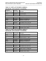
2.6.2 DIGITAL INPUT CONNECTOR (PORT C & PORT D)
The second group of 32 digital inputs (Port C channels 0 through 15 and Port D channels 0
through 15) are connected to the AVME9421/9422/9426/9427 board via connector P4 (lower
connector as viewed from the front). Table 2.2 defines the assignment. These connections are
easily accommodated through the use of Acromag termination panels and flat cable assemblies or
through the use of a user defined termination panel.
P4: DIN 41612 Type B Level II, 64 Pin Male Connector. Panduit No. 100-064-033B or equiv.
Table 2.2: P4 CONNECTOR (PORT C & D)
Port
Pin Number
Mnemonic
Pin Number
Mnemonic
32A
CH0+/-
32B
CH0-/+
31A
30A
CH1+/CH2+/-
31B
30B
CH1-/+
CH2-/+
29A
28A
27A
26A
25A
24A
CH3+/CH4+/CH5+/CH6+/CH7+/CH8+/-
29B
28B
27B
26B
25B
24B
CH3-/+
CH4-/+
CH5-/+
CH6-/+
CH7-/+
CH8-/+
23A
22A
21A
20A
19A
CH9+/CH10+/CH11+/CH12+/CH13+/-
23B
22B
21B
20B
19B
CH9-/+
CH10-/+
CH11-/+
CH12-/+
CH13-/+
18A
17A
16A
15A
14A
CH14+/CH15+/CH0+/CH1+/CH2+/-
18B
17B
16B
15B
14B
CH14-/+
CH15-/+
CH0-/+
CH1-/+
CH2-/+
P
13A
12A
11A
CH3+/CH4+/CH5+/-
13B
12B
11B
CH3-/+
CH4-/+
CH5-/+
O
10A
CH6+/-
10B
CH6-/+
R
T
9A
8A
7A
CH7+/CH8+/CH9+/-
9B
8B
7B
CH7-/+
CH8-/+
CH9-/+
D
6A
5A
CH10+/CH11+/-
6B
5B
CH10-/+
CH11-/+
4A
3A
CH12+/CH13+/-
4B
3B
CH12-/+
CH13-/+
2A
1A
CH14+/CH15+/-
2B
1B
CH14-/+
CH15-/+
P
O
R
T
C
- 2.14 -
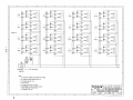
SERIES AVME9420/9421/9422/9425/9426/9427
CHAPTER 2
ISOLATED DIGITAL INPUT BOARDS
PREPARATION FOR USE
___________________________________________________________________
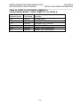
2.6.3 DIGITAL INPUT CONNECTOR (PORT E & PORT F)
The third group of digital inputs (Port E channels 0 through 15 and Port F channels 0 through 15)
are connected to the AVME9420/9422/9425/9427 board via connector P2 (lower rear connector
as viewed from the front). Table 2.3 defines the assignment. These connections are easily
accommodated through the use of Acromag termination panels and flat cable assemblies or
through the use of a user defined termination panel.
P2:
DIN 41612 Type C Level II, 64 Pin Male Connector. Panduit No. 100-964-033B or equiv.
Table 2.3: P2 CONNECTOR (PORT E & F)
Port
Pin Number
Mnemonic
Pin Number
Mnemonic
32A
31A
CH0+/CH1+/-
32C
31C
CH0-/+
CH1-/+
30A
CH2+/-
30C
CH2-/+
29A
28A
27A
26A
25A
24A
23A
22A
CH3+/CH4+/CH5+/CH6+/CH7+/CH8+/CH9+/CH10+/-
29C
28C
27C
26C
25C
24C
23C
22C
CH3-/+
CH4-/+
CH5-/+
CH6-/+
CH7-/+
CH8-/+
CH9-/+
CH10-/+
21A
20A
19A
18A
17A
CH11+/CH12+/CH13+/CH14+/CH15+/-
21C
20C
19C
18C
17C
CH11-/+
CH12-/+
CH13-/+
CH14-/+
CH15-/+
16A
15A
14A
CH0+/CH1+/CH2+/-
16C
15C
14C
CH0-/+
CH1-/+
CH2-/+
13A
12A
CH3+/CH4+/-
13C
12C
CH3-/+
CH4-/+
P
O
R
11A
10A
9A
CH5+/CH6+/CH7+/-
11C
10C
9C
CH5-/+
CH6-/+
CH7-/+
T
8A
CH8+/-
8C
CH8-/+
F
7A
6A
5A
CH9+/CH10+/CH11+/-
7C
6C
5C
CH9-/+
CH10-/+
CH11-/+
4A
3A
CH12+/CH13+/-
4C
3C
CH12-/+
CH13-/+
2A
1A
CH14+/CH15+/-
2C
1C
CH14-/+
CH15-/+
P
O
R
T
E
- 2.15 -
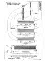
SERIES AVME9420/9421/9422/9425/9426/9427
CHAPTER 2
ISOLATED DIGITAL INPUT BOARDS
PREPARATION FOR USE
___________________________________________________________________
2.6.4 VMEBUS CONNECTIONS
Table 2.4 indicates pin assignments for the VMEbus signals at the P1 connector. The P1
connector is the upper rear connector on the AVME942x board as viewed from the front. The
connector consists of 32 rows of three pins labeled A, B, and C. Pin A1 is located at the upper left
hand corner of the connector.
TABLE 2.4: P1 BUS CONNECTIONS
PIN NUMBER
MNEMONIC
PIN NUMBER
MNEMONIC
PIN NUMBER
MNEMONIC
1A
2A
D00
D01
1B
2B
BBSY*
BCLR*
1C
2C
D08
D09
3A
4A
D02
D03
3B
4B
ACFAIL*
BGOIN*
3C
4C
D10
D11
5A
6A
7A
8A
D04
D05
D06
D07
5B
6B
7B
8B
BG0OUT*
GB1IN*
BG1OUT*
BG2IN*
5C
6C
7C
8C
D12
D13
D14
D15
9A
10A
11A
12A
13A
GND
SYSCLK
GND
DS1*
DS0*
9B
10B
11B
12B
13B
BG2OUT*
BG3IN*
BG3OUT*
BRO*
BR1*
9C
10C
11C
12C
13C
GND
SYSFAIL*
BERR*
SYSRESET*
LWORD*
14A
15A
16A
17A
18A
WRITE*
GND
DTACK*
GND
AS*
14B
15B
16B
17B
18B
BR2*
BR3*
AM0
AM1
AM2
14C
15C
16C
17C
18C
AM5
A23
A22
A21
A20
19A
20A
21A
GND
IACK*
IACKIN*
19B
20B
21B
AM3
GND
SERCLK
19C
20C
21C
A19
A18
A17
22A
IACKOUT*
22B
SERDAT*
22C
A16
23A
24A
25A
AM4
A07
A06
23B
24B
25B
GND
IRQ7*
IRQ6*
23C
24C
25C
A15
A14
A13
26A
A05
26B
IRQ5*
26C
A12
27A
28A
29A
A04
A03
A02
27B
28B
29B
IRQ4*
IRQ3*
IRQ2*
27C
28C
29C
A11
A10
A09
30A
31A
A01
-12V
30B
31B
IRQ1*
+5V STDBY
30C
31C
A08
+12V
+5V
32C
+5V
•
32A
+5V
32B
Indicates that the signal is active low.
- 2.16 -
SERIES AVME9420/9421/9422/9425/9426/9427
CHAPTER 2
ISOLATED DIGITAL INPUT BOARDS
PREPARATION FOR USE
___________________________________________________________________
Refer to the VMEbus specification for additional information on the VMEbus signals.
2.7 POWER-UP TIMING AND LOADING
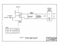
The AVME942x board uses a Logic Cell Array to handle the bus interface and control logic timing.
Upon power-up, the Logic Cell Array automatically clocks in configuration vectors from a local
PROM to initialize the logic circuitry for normal operation. This time is measured as the first 145
mS (typical) after the +5 Volt supply raises to +2.5 Volts at power-up. If a data transfer is
attempted during this time, it will simply be ignored and the board will not respond. This should not
be a problem because the VME specification requires that the bus master drive the system reset
for the first 200 mS after power-up, thus inhibiting any data transfers from taking place.
Port A, Port B, Port C, Port D, Port E and Port F Digital input channels are reset to the OFF state
following a power-up sequence. External input signals above threshold levels can then drive
inputs ON.
2.8 DATA TRANSFER TIMING
Data transfer time is measured from the falling edge of DSx* to the falling edge of DTACK* during
a normal data transfer cycle.
REGISTER
DATA TRANSFER TIME
All Registers
600nS, typical
2.9 FIELD GROUNDING CONSIDERATIONS
The board is designed to isolate every input channel from each other as well as from the VMEbus.
This is intended to protect each channel and the VMEbus from voltage spikes and transients such
as those caused by ground currents and "pick-up". The isolation provides the ability to earth
ground the field wiring without the concern of ground currents damaging the card cage electronics.
- 2.17 -
SERIES AVME9420/9421/9422/9425/9426/9427
CHAPTER 3
ISOLATED DIGITAL INPUT BOARDS
PROGRAMMING INFORMATION
_________________________________________________________________________________
3.0 PROGRAMMING INFORMATION
This chapter provides the specific information necessary to operate the AVME942x Isolated Digital
Input Board.
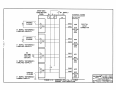
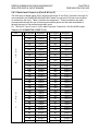
3.1 MEMORY MAP
The board is addressable on 1K byte boundaries in the Short I/O Address Space or Standard
Address Space. All Acromag VMEbus non-intelligent slaves have a standard interface configuration
which consists of a 32 byte board ID PROM and a Board Status register. The rest of the 1K byte
address space contains registers or memory specific to the function of the board. The memory map
is shown in Figure 3.1 (Addresses in Hex).
Figure 3.1: Board Memory Map
Address
Base +
D15
Even
00
Undefined
3E
40
D8
D7
Odd
D0
R – Board ID PROM
Undefined
7F
7E
80
Address
Base +
01
3F
41
Undefined
R/W – Board Status
82
81
83
Undefined
9E
A0
A2
R/W –Int Vector Port B&F CHO
R/W –Int Vector Port B&F CH1
9F
A1
A3
A4
A6
A8
AA
R/W
R/W
R/W
R/W
–Int Vector Port B&F CH2
–Int Vector Port B&F CH3
–Int Vector Port B&F CH4
–Int Vector Port B&F CH5
A5
A7
A9
AB
AC
R/W –Int Vector Port B&F CH6
AD
AE
B0
BE
R/W –Int Vector Port B&F CH7
AF
B1
BF
Undefined
Undefined
C0
Undefined
C2
Undefined
R/W – Digital Input Channel
Interrupt Status Register
CH7
Port B & Port F
CH0
R/W – Digital Input Channel
Interrupt Enable Register
CH7
Port B & Port F
CH0
Board Memory Map continued on page 3.2
- 3.1 -
C1
C3
SERIES AVME9420/9421/9422/9425/9426/9427
CHAPTER 3
ISOLATED DIGITAL INPUT BOARDS
PROGRAMMING INFORMATION
_________________________________________________________________________________
Board Memory Map continued
R/W – Digital Input Channel
Interrupt Polarity Register
CH7
Port B & Port F
CH0
R/W – Digital Input Channel
Interrupt Type Select Register
CH7 Port B & Port F
Ch0
R/W – Digital Input Channel
Int. Pattern Enable Register
CH7 Port B & Port F
Ch0
C4
Undefined
C6
Undefined
C8
Undefined
CA
R – Port A Digital Input Channel Data Register
CH15
CC
CD
CH0
R – Port C Digital Input Channel Data Register
CH15
CF
CH0
R – Port D Digital Input Channel Data Register
CH15
D2
D1
CH0
R – Port E Digital Input Channel Data Register
CH15
D4
D3
CH0
R – Port F Digital Input Channel Data Register
CH15
D5
CH0
D6
3EF
C9
CH0
CH15
D0
C7
CB
R – Port B Digital Input Channel Data Register
CE
C5
D7
Undefined
3FF
3.1.1 BOARD IDENTIFICATION PROM - (READ ONLY) - 01H THROUGH 3FH (ODD)
The board contains an identification section. This section of data describes the board model
number, the manufacturer, and the product revision level. The identification section starts at the
board's base address plus 1 and is 32 bytes in length. Bytes are addressed using only the odd
addresses between 1 and 63. The PROM contents are shown in Figure 3.2 for an AVME9422-I-L
(each model has a unique PROM).
- 3.2 -
SERIES AVME9420/9421/9422/9425/9426/9427
CHAPTER 3
ISOLATED DIGITAL INPUT BOARDS
PROGRAMMING INFORMATION
_________________________________________________________________________________
Figure 3.2: AVME9422-I-L Board Identification PROM
Value
Offset From
Board Base
Descriptions
ASCII Character Numeric
Address
01H
V
56H
All Boards have “VMEID”
03H
M
4DH
05H
E
45H
07H
I
49H
09H
D
44H
0BH
0DH
0FH
A
C
R
41H
43H
52H
Manufacturer’s I.D., “ACR” for Acromag
11H
13H
15H
17H
19H
1BH
1DH
9
4
2
2
I
L
39H
34H
32H
32H
49H
4CH
20H
Board Model Number (6 characters and
1 trailing “blank”)
1FH
1
31H
21H
23H
25H
27H
Undefined
Undefined
Undefined
29H
2BH
2DH
2FH
31H
33H
35H
37H
39H
3BH
3DH
3FH
Undefined
Undefined
Undefined
Undefined
Undefined
Undefined
Undefined
Undefined
Undefined
Undefined
Undefined
Undefined
20H
41H
(Each model has a unique number)
Number of KILOBYTES of address
Space used.
Reserved
Reserved
SERIES AVME9420/9421/9422/9425/9426/9427
CHAPTER 3
ISOLATED DIGITAL INPUT BOARDS
PROGRAMMING INFORMATION
_________________________________________________________________________________
3.1.2 BOARD STATUS REGISTER - (READ/WRITE) - 81H
The Board Status Register reflects and controls functions globally on the board.
MSB
7
6
5
4
3
2
1
Reserved
Software
Global Int. Global Int. Green
Reset
Enable
Pending
LED
0
Red
LED
Where:
Bits 7,6,5: Reserved for future use - equal "0" if read.
Bit 4: Software Reset (W) - writing a "1" to this bit causes a software reset. Writing "0" or reading
the bit has no effect. The effect of a software reset on the various registers is described in
the description of each register.
Reset Condition: Set to "0".
Bit 3: Global Interrupt Enable (R/W) - writing a "1" to this bit enables interrupts to be serviced,
provided the interrupt level (IRQx*) is selected. A "0" disables servicing interrupts.
Reset Condition: Set to "0", interrupts disabled.
Bit 2: Global Interrupt Pending (R) - this bit will be a "1" when there is an interrupt pending. This
bit will be "0" when there is no interrupt pending. Polling this bit will reflect the board's
pending interrupt status, even if the Global Interrupt Enable bit is set to "0".
Reset condition: Set to "0".
Bit 1: Green LED (R/W) - when written, this bit will control the state of the green LED on the front
panel. A "1" will turn it on, a "0" will turn it off. Reading it will reflect its current state.
Reset Condition: Set to "0", green LED off.
Bit 0: Red LED (R/W) - when written, this bit will control the state of the red LED on the front panel
and the state of the VMEbus SYSFAIL* signal. A "1" will turn the LED off and set SYSFAIL*
high, a "0" will turn the LED on and set SYSFAIL* low. Reading it will reflect its current state.
(See Section 5.2 for additional information on using SYSFAIL*.)
Reset Condition: Set to "0", red LED lit, and SYSFAIL* is set low.
-
3.4 –
SERIES AVME9420/9421/9422/9425/9426/9427
CHAPTER 3
ISOLATED DIGITAL INPUT BOARDS
PROGRAMMING INFORMATION
_________________________________________________________________________________
3.1.2.1 STATUS BITS USAGE
The status register bits 1 and 0 along with the green and red LEDs provide the user with a means of
keeping track of a board's functionality in the system. Since there is no intelligence on the board,
the host computer controls these bits. The following paragraphs and summary table describe
possible uses of the bits in the status register and the LEDs on the front panel.
On power-up the bits in the status register read low, with the green LED off, the red LED lit, and
SYSFAIL* low. This indicates that the board has failed or that it has not been tested yet.
If the status register bit 1 reads low and Bit 0 reads high, the LEDs will both be off and SYSFAIL*
high. This indicates an inactive board.
If the status register bit 1 reads high and Bit 0 reads low, the LEDs will both be lit and SYSFAIL* low.
This indicates the board is undergoing a diagnostic checkout.
If the status register bits 1 and 0 read high, the green LED will be lit with the red LED off and
SYSFAIL* high. This indicates the board is fully functional.
Status Bits - Possible Usage
Bit 0
Bit 1
(Red LED)
(Green LED)
0, (on)
0, (off)
1, (off)
0, (off)
0, (on)
1, (on)
1, (off)
1, (on)
SYSFAIL *
Low
High
Low
High
Description
Failed or reset condition
Inactive board
Diagnostics are running
Normal operation
3.1.3 INTERRUPT VECTOR REGISTERS - (READ/WRITE) - A1H TO AFH (ODD ADDRESSES)
The interrupt vector registers maintain the 8 bit interrupt vector numbers for each of the 8 digital
input channel interrupt lines. Note that interrupts can only be generated for Port B or Port F digital
input channels 0-7. Also note that Port B and Port F of the same channel would use the same
interrupt vector register. The appropriate vector is provided to the VMEbus Interrupt Handler when
an interrupt is being serviced. This allows each digital input channel interrupt (Port B ch. 0-7 or Port
F ch. 0-7) to be serviced by its own software handler. If desired, a single handler can be used by
making all of the vectors the same. In this case, the handler will have to determine the interrupting
channel by examining the interrupt status register.
The register content is undefined upon reset.
- 3.5 -
SERIES AVME9420/9421/9422/9425/9426/9427
CHAPTER 3
ISOLATED DIGITAL INPUT BOARDS
PROGRAMMING INFORMATION
_________________________________________________________________________________
3.1.4 Digital Input Channel Interrupt Status Register (read/write) - C1H
The digital input channel interrupt status register reflects the status of the 8 input channels (Port B
or Port F ch. 0-7). A "1" in a bit position indicates an interrupt is pending for the corresponding
channel. Each bit is derived from the logical AND of its associated interrupt input and enable bits.
Hence, an input channel that does not have interrupts enabled will never have its interrupt pending
bit set to a "1".
An individual channel's interrupt can be cleared by writing a "1" to its bit position in the interrupt
status register. However, if the condition which caused the interrupt remains or reappears, a new
interrupt will be generated. To permanently disable a channel's interrupt, the corresponding bit in
the channel interrupt enable register must be cleared, followed by writing a "1" to the channel's bit
position in the channel interrupt status register (to clear the interrupt). This is known as the
"Release On Register Access" (RORA) method as defined in the VME system architecture.
Bit 7 of this register has a dual purpose. In addition to indicating an interrupt for channel 7, it is also
used to indicate an input channel bit pattern match (see the digital input channel interrupt pattern
enable register).
MSB
7
CH7
6
CH6
5
CH5
4
CH4
3
CH3
2
CH2
1
CH1
LSB
0
CH0
All interrupts are cleared following a reset.
NOTE: Interrupts are prioritized via hardware within the card. Channel 7 is the highest priority and
channel 0 is the lowest. If multiple input channel interrupts become pending simultaneously, the
vector corresponding to the highest numbered channel will be delivered first. After the highest
channel's interrupt is serviced and cleared, an additional interrupt will be generated for the next
highest priority interrupt (pending) channel.
NOTE: Input channel bandwidth should be limited to reduce the possibility of missing channel
interrupts. For a specific input channel this could happen if multiple changes occur before the
channel's interrupt is serviced.
3.1.5 DIGITAL INPUT CHANNEL INTERRUPT ENABLE REGISTER (READ/WRITE) - C3H
The digital input channel interrupt enable register provides a mask bit for each of the 8 input
channels (Port B or Port F ch. 0-7). A "0" in a bit position will prevent the corresponding input
channel from causing an external interrupt. A "1" will allow the input channel to cause an interrupt.
- 3.6 -
SERIES AVME9420/9421/9422/9425/9426/9427
CHAPTER 3
ISOLATED DIGITAL INPUT BOARDS
PROGRAMMING INFORMATION
_________________________________________________________________________________
MSB
7
CH7
6
CH6
5
CH5
4
CH4
3
CH3
2
CH2
1
CH1
LSB
0
CH0
All input channel interrupts are masked ("0") following a reset.
3.1.6 DIGITAL INPUT CHANNEL INTERRUPT POLARITY REGISTER (READ/WRITE) - C5H
The digital input channel interrupt polarity register determines the level that will cause a channel
interrupt for each of the 8 input channels (Port B or Port F ch. 0-7). A "0" in a bit position means an
interrupt will occur when the input channel is below threshold (i.e. a "0" in the digital input channel
data register). A "1" in a bit position means an interrupt will occur when the input channel is above
threshold (i.e. a "1" in the digital input channel data register).
Note that interrupts will not occur unless they are enabled. The interrupt polarity register will have
no effect if Change Of State (COS) interrupts are selected (see the digital input channel interrupt
type select register).
MSB
7
CH7
6
CH6
5
CH5
4
CH4
3
CH3
2
CH2
1
CH1
LSB
0
CH0
All bits are set to "0" following a reset which means that the inputs will cause interrupts when they
are below threshold.
3.1.7 DIGITAL INPUT CHANNEL INTERRUPT TYPE SELECT REGISTER (READ/WRITE) - C7H
The digital input channel interrupt type select register determines the type of input channel behavior
that will cause a channel interrupt for each of the 8 input channels (Port B or Port F ch. 0-7). A "0"
in a bit position means an interrupt will be generated when the input channel level specified by the
digital input channel interrupt polarity register occurs. A "1" in a bit position means an interrupt will
occur when a Change Of State (COS) occurs at the input channel (either low to high, or high to low).
Note that interrupts will not occur unless they are enabled.
MSB
7
CH7
6
CH6
5
CH5
4
CH4
3
CH3
2
CH2
1
CH1
LSB
0
CH0
- 3.7 -
SERIES AVME9420/9421/9422/9425/9426/9427
CHAPTER 3
ISOLATED DIGITAL INPUT BOARDS
PROGRAMMING INFORMATION
_________________________________________________________________________________
All bits are set to "0" following a reset which means that the inputs will cause interrupts for the input
channel levels specified by the digital input channel interrupt polarity register.
3.1.8 DIGITAL INPUT CHANNEL INTERRUPT PATTERN ENABLE REG. (READ/WRITE) - C9H
The digital input channel interrupt pattern enable register provides a mask bit for each of the 8 input
channels (Port B or Port F ch. 0-7). A "0" in a bit position will prevent the corresponding input
channel from being part of a pattern of channels (bits) which can cause an interrupt. A "1" will allow
the input channel to be a component of a pattern which can cause an interrupt. Note that an
interrupt will only be generated if all enabled channels (at least 1 and up to 8 channels) forming the
pattern meet the level requirements specified in the digital input channel interrupt polarity register.
Note that when pattern interrupts are desired, the digital input channel interrupt type select register
bits must be set to "0" (interrupt on input level, not on change of state).
Note also that the interrupt generated will result in setting the status bit in the digital input channel
interrupt status register which corresponds to channel 7 (i.e. the highest priority channel).
MSB
7
CH7
6
CH6
5
CH5
4
CH4
3
CH3
2
CH2
1
CH1
LSB
0
CH0
All input channel pattern enable bits are masked ("0") following a reset.
3.1.9 PORT A DIGITAL INPUT CHANNEL DATA REGISTER (READ) - CAH & CBH
The Port A digital input channel data register represents the actual state of the 16 Port A digital
input channels at the time the register is read (note that the debounce circuit is not available for Port
A, and consequently does not introduce any additional delay). A "0" means that the signal across
the board's input channel connector is below threshold. A "1" means that the signal is above
threshold. Note that the threshold voltage (i.e. range) is not user selectable.
MSB
LSB
15
14
13
12
11
10
9
8
7
6
5
4
3
2
1
0
CH15 CH14 CH13 CH12 CH11 CH10 CH9 CH8 CH7 CH6 CH5 CH4 CH3 CH2 CH1 CH0
- 3.8 -
SERIES AVME9420/9421/9422/9425/9426/9427
CHAPTER 3
ISOLATED DIGITAL INPUT BOARDS
PROGRAMMING INFORMATION
_________________________________________________________________________________
3.1.10 PORT B DIGITAL INPUT CHANNEL DATA REGISTER (READ) - CCH & CDH
The Port B digital input channel data register represents the actual state of the 16 Port B digital
input channels at the time the register is read (note that the debounce circuit will insert a delay,
channel 0-7 only, dependent on the degree of debounce selected). A "0" means that the signal
across the board's input channel connector is below threshold. A "1" means that the signal is above
threshold. Note that the threshold voltage (i.e. range) is not user selectable.
MSB
LSB
15
14
13
12
11
10
9
8
7
6
5
4
3
2
1
0
CH15 CH14 CH13 CH12 CH11 CH10 CH9 CH8 CH7 CH6 CH5 CH4 CH3 CH2 CH1 CH0
3.1.11 PORT C DIGITAL INPUT CHANNEL DATA REGISTER (READ) - CEH & CFH
The Port C digital input channel data register represents the actual state of the 16 Port C digital
input channels at the time the register is read (note that the debounce circuit is not available for Port
C, and consequently does not introduce any additional delay). A "0" means that the signal across
the board's input channel connector is below threshold. A "1" means that the signal is above
threshold. Note that the threshold voltage (i.e. range) is not user selectable.
MSB
LSB
15
14
13
12
11
10
9
8
7
6
5
4
3
2
1
0
CH15 CH14 CH13 CH12 CH11 CH10 CH9 CH8 CH7 CH6 CH5 CH4 CH3 CH2 CH1 CH0
3.1.12 PORT D DIGITAL INPUT CHANNEL DATA REGISTER (READ) - D0H & D1H
The Port D digital input channel data register represents the actual state of the 16 Port D digital
input channels at the time the register is read (note that the debounce circuit is not available for Port
D, and consequently does not introduce any additional delay). A "0" means that the signal across
the board's input channel connector is below threshold. A "1" means that the signal is above
threshold. Note that the threshold voltage (i.e. range) is not user selectable.
MSB
LSB
15
14
13
12
11
10
9
8
7
6
5
4
3
2
1
0
CH15 CH14 CH13 CH12 CH11 CH10 CH9 CH8 CH7 CH6 CH5 CH4 CH3 CH2 CH1 CH0
3.1.13 PORT E DIGITAL INPUT CHANNEL DATA REGISTER (READ) - D2H & D3H
The Port E digital input channel data register represents the actual state of the 16 Port E digital
input channels at the time the register is read (note that the debounce circuit is not available for Port
E, and consequently does
-
3.9 –
SERIES AVME9420/9421/9422/9425/9426/9427
CHAPTER 3
ISOLATED DIGITAL INPUT BOARDS
PROGRAMMING INFORMATION
_________________________________________________________________________________
not introduce any additional delay). A "0" means that the signal across the board's input channel
connector is below threshold. A "1" means that the signal is above threshold. Note that the
threshold voltage (i.e. range) is not user selectable.
MSB
LSB
15
14
13
12
11
10
9
8
7
6
5
4
3
2
1
0
CH15 CH14 CH13 CH12 CH11 CH10 CH9 CH8 CH7 CH6 CH5 CH4 CH3 CH2 CH1 CH0
-
3.1.14 PORT F DIGITAL INPUT CHANNEL DATA REGISTER (READ) - D4H & D5H
The Port F digital input channel data register represents the actual state of the 16 Port F digital input
channels at the time the register is read (note that the debounce circuit will insert a delay, channel 07 only, dependent on the degree of debounce selected). A "0" means that the signal across the
board's input channel connector is below threshold. A "1" means that the signal is above threshold.
Note that the threshold voltage (i.e. range) is not user selectable.
MSB
LSB
15
14
13
12
11
10
9
8
7
6
5
4
3
2
1
0
CH15 CH14 CH13 CH12 CH11 CH10 CH9 CH8 CH7 CH6 CH5 CH4 CH3 CH2 CH1 CH0
3.2 GENERAL PROGRAMMING CONSIDERATIONS
3.2.1 BOARD DIAGNOSTICS
The board is a non-intelligent slave and does not perform self diagnostics. It does, however,
provide a standard interface architecture which includes a Board Status Register useful in system
diagnostics.
Status bits, control of front panel LEDs, and control of the SYSFAIL* signal are provided through the
Board Status Register. Bits 0 and 1 may be used as follows:
Board Status Register
Bit 1
Bit 0
0
0
1
1
0
0
1
1
Leds
Green
Red
Off
On
On
On
Off
On
Off
Off
SYSFAIL*
SIGNAL
On
On
Off
Off
- 3.10 -
Condition
Board failed test or has
not been tested.
Board is being tested.
Board has passed test.
Board is inactive.
SERIES AVME9420/9421/9422/9425/9426/9427
CHAPTER 3
ISOLATED DIGITAL INPUT BOARDS
PROGRAMMING INFORMATION
_________________________________________________________________________________
At power up, the system diagnostic software can test each non-intelligent Slave, sequencing the
status bits to indicate "undergoing test" and then to "passed" or "failed".
After testing each board, the system software records which boards have failed and sets their status
to indicate "inactive". By setting the board's status to inactive, the SYSFAIL* signal is released and
may then be useful for an on-line indication of failure by other boards.
Alternatively, the system software could simply set the bits and therefore front panel LEDs, to
"passed test" as a visual indication that the presence of the board is recognized.
3.3 GENERATING INTERRUPTS
Port B or Port F Digital input channels 0-7 can cause interrupts (for the jumper selected port only) to
be generated for a wide variety of conditions. These include interrupts for:
•
Change Of State (COS) of selected input channels.
•
Input level (polarity) match of selected input channels.
•
Input pattern match of the levels of multiple input channels.
The interrupt level (IRQx*) associated with the card is programmable via a jumper on the board.
The interrupt release mechanism is the Release On Register Access (RORA) type. This means that
the interrupter will release the interrupt request line (IRQx*) after the interrupt has been cleared by
writing a "1" to the appropriate bit position in the input channel interrupt status register.
The user has the option of having a single interrupt handler for the entire board or having each
channel serviced by a separate software handler. This is determined by what is written into the
interrupt vector registers. There is a unique register for each Port B or Port F digital input channel
(0-7). Note that Port B and Port F of the same channel would use the same interrupt vector register.
However, if the user programs the same vector into all of the vector registers, then the board will
have a single interrupt handler.
The digital input channels are prioritized with respect to their interrupts. Channel 7 is the highest
priority and channel 0 is the lowest. If multiple input channel interrupts become pending
simultaneously, the vector corresponding to the highest numbered channel will be delivered first.
After the highest channel's interrupt is serviced and cleared, an additional interrupt will be generated
for the next highest priority interrupt (pending) channel. If an input channel pattern match is
generated, the interrupt will appear in the channel 7 (i.e. the highest priority) position in the interrupt
status register.
- 3.11 -
SERIES AVME9420/9421/9422/9425/9426/9427
CHAPTER 3
ISOLATED DIGITAL INPUT BOARDS
PROGRAMMING INFORMATION
_________________________________________________________________________________
Input channel bandwidth should be limited to reduce the possibility of missing channel interrupts.
For a specific input channel this could happen if multiple changes occur before the channel's
interrupt is serviced.
When configuring and enabling interrupts, the response time of Port B or Port F input channels 0
through 7 should be considered. The digital input channel response time is the sum of the response
times of the optocoupler (Turn-ON time of 6uS. typical and Turn-OFF time of 60uS. typical at 25
deg. C), the debounce circuit (7uS. to 1.54mS., user selected), and the interrupt logic circuit (1uS. to
192uS., follows debounce selection) as illustrated in Figure 3.3. The total response time must pass
before an input channel stimulus (matching an interrupt condition) will be recognized.
Likewise, if an input channel stimulus is programmed to the polarity (level) which should not cause
an interrupt, the board user should wait for the response time to pass before enabling interrupts
from the channel (see Figure 3.3). To do otherwise will capture an "old" signal which has not
completely propagated through the circuit and cause an unwanted interrupt.
- 3.12 -
SERIES AVME9420/9421/9422/9425/9426/9427
CHAPTER 3
ISOLATED DIGITAL INPUT BOARDS
PROGRAMMING INFORMATION
_________________________________________________________________________________
3.3.1 INTERRUPT EXAMPLE FOR CHANGE OF STATE (COS)
1. Set interrupt level (IRQx*) associated with the board via jumper (J4), and select interrupt
Port B or Port F via jumper (J8).
2. Clear the global interrupt enable bit in the Board Status Register by writing a "0" to bit 3.
3. Write vectors into the Digital Input Channel Interrupt Vector Registers.
4. Select COS interrupts for channels by writing "1" to each channel's associated bit in the
Digital Input Channel Interrupt Type Select Register.
5. Disable input pattern detection interrupts by writing "0" to each channel's associated bit in
the Digital Input Channel Interrupt Pattern Enable Register.
6. Enable individual input channel interrupts by writing "1" to each channel's associated bit
in the Digital Input Channel Interrupt Enable Register.
7. Clear pending interrupt inputs by writing "1" to each channel's associated bit in the Digital
Input Channel Interrupt Status Register.
8. Enable interrupts from the board by writing a "1" to bit 3 (the global interrupt enable bit) in
the Board Status Register.
Interrupts may now occur from the selected port from the board.
3.3.2 INTERRUPT EXAMPLE FOR INPUT LEVEL (POLARITY) MATCH
1. Set interrupt level (IRQx*) associated with the board via jumper (J4), and select interrupt
Port B or Port F via jumper (J8).
2. Clear the global interrupt enable bit in the Board Status Register by writing a "0" to bit 3.
3. Write vectors into the Digital Input Channel Interrupt Vector Registers.
4. Select polarity (level) interrupts for channels by writing "0" to each channel's associated
bit in the Digital Input Channel Interrupt Type Select Register.
5. Select the desired polarity (level) for input channel interrupts by writing "0" or "1" to each
channel's associated bit in the Digital Input Channel Interrupt Polarity Register.
6. Disable input pattern detection interrupts by writing "0" to each channel's associated bit in
the Digital Input Channel Interrupt Pattern Enable Register.
7. Enable individual input channel interrupts by writing "1" to each channel's associated bit
in the Digital Input Channel Interrupt Enable Register.
8. Clear pending interrupt inputs by writing "1" to each channel's associated bit in the Digital
Input Channel Interrupt Status Register.
9. Enable interrupts from the board by writing a "1" to bit 3 (the global interrupt enable bit) in
the Board Status Register.
Interrupts may now occur from the selected port from the board.
- 3.14 -
SERIES AVME9420/9421/9422/9425/9426/9427
CHAPTER 3
ISOLATED DIGITAL INPUT BOARDS
PROGRAMMING INFORMATION
_________________________________________________________________________________
3.3.3 INTERRUPT EXAMPLE FOR INPUT PATTERN MATCH (OF MULTIPLE CHANNEL LEVELS)
1. Set interrupt level (IRQx*) associated with the board via jumper (J4), and select interrupt
Port B or Port F via jumper (J8).
2. Clear the global interrupt enable bit in the Board Status Register by writing a "0" to bit 3.
3. Write vector into the Digital Input Channel Interrupt Vector Register associated with
channel 7.
4. Select polarity (level) interrupts for channels by writing "0" to each channel's associated
bit in the Digital Input Channel Interrupt Type Select Register.
5. Select the desired polarity (level) for input channel interrupts by writing "0" or "1" to each
channel's associated bit in the Digital Input Channel Interrupt Polarity Register.
6. Disable individual input channel interrupts by writing "0" to each channel's associated bit
in the Digital Input Channel Interrupt Enable Register.
7. Enable input pattern detection interrupts by writing "1" to each channel's associated bit in
the Digital Input Channel Interrupt Pattern Enable Register.
8. Clear pending interrupt inputs by writing "1" to each channel's associated bit in the Digital
Input Channel Interrupt Status Register.
9. Enable interrupts from the board by writing a "1" to bit 3 (the global interrupt enable bit) in
the Board Status Register.
Interrupts may now occur from the selected port from the board.
3.3.4 SEQUENCE OF EVENTS FOR AN INTERRUPT
1. The AVME942x (interrupter) board makes an interrupt request (asserts IRQx*).
2. The host (interrupt handler) asserts IACK* and the level of the interrupt it is seeking on
A01-A03.
3. When the asserted IACKIN* signal (daisy chained) is passed to the AVME942x, the
board will put the appropriate interrupt vector on the bus (D00-D07), if the level of the
interrupt matches that sought by the host. Note that IRQx* remains asserted.
4. The host uses the vector to point at which interrupt handler to execute and begins its
execution.
5. Example of Generic Interrupt Handler Actions:
A. Disable the interrupting channel(s) by writing a "0" to the appropriate bits in the
interrupt enable register.
B. Clear the interrupting channel(s) by writing a "1" to the appropriate bits in the interrupt
status register.
C. Enable the interrupting channel(s) by writing a "1" to the appropriate bits in the
interrupt enable register.
- 3.15 -
SERIES AVME9420/9421/9422/9425/9426/9427
CHAPTER 3
ISOLATED DIGITAL INPUT BOARDS
PROGRAMMING INFORMATION
_________________________________________________________________________________
6. If the input stimulus has been removed and no other channels have interrupts pending,
the interrupt cycle is completed (i.e. the board negates its interrupt request, IRQx*).
A. If the input stimulus remains, a new interrupt request will immediately follow. If the
stimulus cannot be removed, then the channel should be disabled or reconfigured (e.g.
for the opposite polarity).
B. If other channels have interrupts pending, then the interrupt request (IRQx*) will
remain asserted. This will start a new interrupt cycle.
- 3.16 -
SERIES AVME9420/9421/9422/9425/9426/9427
CHAPTER 4
ISOLATED DIGITAL INPUT BOARDS
THEORY OF OPERATION
____________________________________________________________________
4.0 THEORY OF OPERATION
This chapter describes the circuitry that is used on the board. A block diagram is shown in Figure
4.1. Parts lists are in chapter 5, and the schematic & part location drawings are in Chapter 7.
4.1 VMEBUS INTERFACE
The VMEbus interface is composed of three functional circuit areas.
•
Data buffers (U38, U39)
•
Interrupter (U40, U42, U47, U48, U49)
•
Address decode and bus control logic (U43, U44, U45, U47)
4.1.1 VMEBUS CONTROL LOGIC
The Data Transfer Acknowledge (DTACK*) signal is generated by the logic/timing circuitry (U45,
U47) on the board for handshaking with the bus master during data transfer cycles. The DTACK*
signal will be asserted after the card address has been properly decoded and either of the data
strobes (DS1*, DS0*) is asserted. The amount of delay before DTACK* is asserted is controlled by
circuitry within U47 which uses the SYSCLK (16MHz.) provided on the VMEbus to derive a fixed
time delay.
The AVME942x does not use (assert) the VME BERR* signal (as permitted in the VMEbus
specification). If the bus master improperly addresses the board, it will not get a response, however
the VMEbus Bus Timer located in the System Controller will time-out and cause an end to the cycle.
- 4.1 -
SERIES AVME9420/9421/9422/9425/9426/9427
CHAPTER 4
ISOLATED DIGITAL INPUT BOARDS
THEORY OF OPERATION
____________________________________________________________________
4.1.2 VME INTERRUPTER
The interrupt level (IRQx*) associated with the card is programmable via a jumper on the board.
The card will return an 8-bit interrupt vector during the interrupt acknowledge cycle. Each
interrupting channel can have its own interrupt vector. The interrupt release mechanism is the
Release On Register Access (RORA) type. This means that an interrupter will release the interrupt
request line (IRQx*) after the interrupt has been cleared by writing a "1" to the appropriate bit
position in the input channel interrupt status register.
Interrupts can be generated by any of 8 digital inputs (Port B or Port F channels 0-7). Interrupt on
selected input channel COS or polarity (level) match can be selected. Alternatively, interrupts on a
pattern match of selected input channel polarities (levels) can be programmed. Interrupts occur on
a first come first served basis, unless they occur at the same time. If two or more interrupts occur at
the same time, then channel 7 has the highest priority (channel 0 has the lowest). If an input
channel pattern match is generated, the interrupt will appear in the channel 7 (highest priority)
position.
Input channel bandwidth should be limited to reduce the possibility of missing channel interrupts.
For a specific input channel this could happen if multiple changes occur before the channel's
interrupt is serviced.
When an input channel interrupt condition is satisfied, the interrupter logic will assert the preprogrammed interrupt request level (IRQ7* - IRQ1*) and then monitor the Interrupt Acknowledge
Input (IACKIN*) signal. When IACKIN* is asserted the logic compares the VMEbus address lines
(A1 - A3) to the pre-programmed board interrupt level. If the lines are not equal, it will pass the
signal along by asserting IACKOUT*. If the lines are equal, it will then drive the data bus D08(O)
with the vector associated with the interrupting channel and assert the DTACK* signal.
The interrupt vector registers are contained in U49. Both U47 and U48 control the addressing of the
vector registers. The board status register is in U47. All other interrupt configuration and status
registers, as well as input channel interrupt logic and priority encoding, are in U48. U40 performs
the board interrupt level decoding, and U42 checks for a match of the bus interrupt level to the
board interrupt level. The IACKIN* signal is monitored by U47, which controls both IACKOUT* and
DTACK* signals.
4.2 REGISTER LOCATION SUMMARY
Local memory locations are implemented in various data registers on board. The registers are
located in the following devices:
•
Board Identification PROM (U41)
•
Board Status Register (U47)
•
Interrupt Vector Registers (U49)
•
Digital Input Channel Interrupt Status Register (U48)
•
Digital Input Channel Interrupt Enable Register (U48)
•
Digital Input Channel Interrupt Polarity Register (U48)
- 4.3 -
SERIES AVME9420/9421/9422/9425/9426/9427
CHAPTER 4
ISOLATED DIGITAL INPUT BOARDS
THEORY OF OPERATION
____________________________________________________________________
•
Digital Input Channel Interrupt Pattern Enable Register (U48)
•
Digital Input Channel Interrupt Type Select Register (U48)
•
Port A Digital Input Channel Data Control Buffer (U25, U26)
•
Port B Digital Input Channel Data Control Buffer (U48, U28)
•
Port C Digital Input Channel Data Control Buffer (U29, U30)
•
Port D Digital Input Channel Data Control Buffer (U31, U32)
•
Port E Digital Input Channel Data Control Buffer (U33, U34)
•
Port F Digital Input Channel Data Control Buffer (U48, U36)
4.3 ISOLATION BARRIER
Optical isolation is used to isolate all digital input channels from each other (channel to channel) and
from the logic and VMEbus circuits.
4.4 DIGITAL INPUT SECTION
There are 32, 64, or 96 digital input channels (16-Port A, 16-Port B, 16-Port C, 16-Port D, 16-Port E
and 16-Port F) available on the board. All channels contain input capacitors to suppress transient
overvoltages. The AVME9420/1/2 models provide an input voltage range of 4 to 25V DC for each
channel. The AVME9425/6/7 models provide an input voltage range of 20 to 55V DC for each
channel. Input channel optocouplers (U1-U24) detect the input state providing data directly to Port
A, Port B, Port C, Port D, Port E, and Port F Digital Input Channel Data Buffers. The interrupt
selected port, Port B (ch 0-7) or Port F (ch 0-7), input data is indirectly (through the debounce
circuitry) provided to the interrupt selected Port B or Port F Digital Input Channel Data Buffer.
Input channel debounce circuitry (U48) is jumper selectable (J8) for Port B or Port F channels 0-7 to
eliminate glitches from the input signals. These glitches are frequently caused by contact bounce in
mechanical relays and switches. Eliminating these glitches is desirable to prevent erroneous
channel data and spurious interrupts. The debounce delay time is jumper programmable (J7) on a
global basis for Port B or Port F input channels 0-7 (i.e. selected Port B or Port F input channels 0-7
will have the same delay).
Note that the jumper selection (J8) for the interrupt and debounce circuitry, for Port B (ch 0-7) or
Port F (ch 0-7), are selected together.
- 4.4 -
SERIES AVME9420/9421/9422/9425/9426/9427
CHAPTER 5
ISOLATED DIGITAL INPUT BOARDS
SERVICE AND REPAIR INFORMATION
________________________________________________________________________
5.0 SERVICE AND REPAIR INFORMATION
This chapter provides instructions on how to obtain service and repair assistance, service
procedures, and component parts lists.
5.1 SERVICE AND REPAIR ASSISTANCE
It is highly recommended that a non-functioning board be returned to Acromag for repair.
Acromag uses tested and burned-in parts, and in some cases, parts that have been selected
for characteristics beyond that specified by the manufacturer. Acromag has automated test
equipment that thoroughly checks the performance of each board. When a board is first
produced and when any repair is made, it is tested, placed in a burn-in room at elevated
temperature, and retested before shipment.
Please refer to Acromag's Service Policy Bulletin or contact Acromag for complete details on
how to obtain parts and repair.
5.2 PRELIMINARY SERVICE PROCEDURE
Before beginning repair, be sure that all of the procedures in Chapter 2, Preparation For Use,
have been followed. The procedures are necessary since the board has jumpers that must be
properly configured.
CAUTION
POWER MUST BE OFF BEFORE REMOVING OR INSERTING BOARDS
Note: It has been observed that on occasion, a "boot" program for a disk operating system will
"hang" waiting for the VMEbus SYSFAIL* signal to be released by an intelligent disk controller
board. Acromag's non-intelligent slave boards assert the SYSFAIL* signal as described in the
VMEbus Specification Rev. C.1 and therefore, the disk operating system will remain "hung".
The best solution to this problem is to correct the boot program so that it is no longer dependent
upon the SYSFAIL* signal. When this solution is not practical, it is possible to disconnect the
SYSFAIL* from the circuitry on the AVME942x Acromag board by removing the SYSFAIL*
selection jumper at J9. If further assistance is needed, call Acromag's Applications Engineering
Department.
5.3 PARTS LISTS
Parts Lists are provided as an aid to the user in troubleshooting the Board (also reference the
schematic and part location drawings of chapter 7). Tables 5.1A to 5.1G list the parts installed
on the main board for the various models; similarly Table 5.2 lists parts for the LED expansion
board. Replacement parts and repair services are available from Acromag.
- 5.1 -
SERIES AVME9420/9421/9422/9425/9426/9427
CHAPTER 5
ISOLATED DIGITAL INPUT BOARDS
SERVICE AND REPAIR INFORMATION
________________________________________________________________________
Changes are sometimes made to improve the product, to facilitate delivery, or to control cost. It
is therefore important to include the Component Reference Number, the Acromag Part Number,
the Board Model Number, and the Board Serial Number when providing information to order
parts.
TABLE 5.1A: PARTS LIST FOR MODEL AVME942X-I
(MAIN BOARD – PARTS COMMON TO ALL MODELS)
Component
Reference Number
U37
U38, 39
U40
U42
U43, 44
U45
U46
U47
U48
U49
R65, 66
R67
R68
R69, 70
R71
R72, 73
R74
C121
C134-146
D1
D2
X1-2
P1
J1
J2
J3, 8
J4
J5, 6, 9, & P13
J7
ITEM
Acromag
Part Number
1033-670
1033-627
1033-048
1033-719
1033-626
1033-623
5025-121
1033-578
1033-577
1033-417
1100-630
1100-268
1000-822
1100-494
1000-825
1000-839
1000-836
1002-314
1002-530
1001-197
1001-113
1004-606
1004-733
1004-379
1004-383
1004-333
1004-374
1004-410
1004-377
1004-332
Description
IC 74LS174N
IC 74LS645-1ND
IC 7445N
IC 74LS136N3
IC AM25LS2521PCB
IC 74F38N
Programmed part
IC XC3030-70PC84C
IC XC3042-70PC84C
IC TMM2015AP-15
RES NET 2% 9-COM 10K
RES NET 2% 9-COM 4.7K
RES FILM 5% .25W 180 OHM
RES NET 2% 7-COM 1K
RES FILM 5% .25W 330 OHM
RES FILM 5% .25W 4.7K
RES FILM 5% .25W 2.7K
CAP TAN 15OUF 15V
CAP MONO 0.1UF 100V Z5U
LED BILEVEL RED/GRN
DIODE IN914B
CHIP CARRIER, 84 PIN
CONN. C/96P/A,B,C HARPOON
HEADER 16 POST 2 ROW
POST 2 ROW 12 POSITION
HEADER 3 PIN POST
HEADER 6 POST 2 ROW
POSTS 1 ROW 2 POS
HEADER 8 POST 2 ROW
CLIP BUCK SHORTING
-
5.2 -–
SERIES AVME9420/9421/9422/9425/9426/9427
CHAPTER 5
ISOLATED DIGITAL INPUT BOARDS
SERVICE AND REPAIR INFORMATION
________________________________________________________________________
TABLE 5.1B: PARTS LIST FOR MODEL AVME9420-I
(MAIN BOARD – PARTS UNIQUE TO THIS MODEL)
Component
Reference Number
U17-24
U33-36
U41
Acromag
Part Number
1033-617
1033-814
5025-110
Description
IC TLP626 OPTOCOUPLER
IC SN74LS541N
Programmed part
R17-24
R33-36
R57-64
1100-801
1100-640
1100-390
RES NET 2% 4-ISO HP 1.5K
RES NET 2% 9-COM 1.2K
RES NET 2% 4-ISO 4.7K
C65-96
C113-120, 130-133
1002-442
1002-530
CAP MONO 0.01UF 100V Z5U
CAP MONO 0.1UF 100V Z5U
P2
1004-732
CONN. C/64P/A,C HARPOON
TABLE 5.1C: PARTS LIST FOR MODEL AVME9421-I
(MAIN BOARD – PARTS UNIQUE TO THIS MODEL)
Component
Reference Number
U1-16
U25-32
U41
Acromag
Part Number
1033-617
1033-814
5025-111 (-112)
Description
IC TLP626 OPTOCOUPLER
IC SN74LS541N
Programmed part (-L option)
R1-16
R25-32
R41-56
1100-801
1100-640
1100-390
RES NET 2% 4-ISO HP 1.5K
RES NET 2% 9-COM 1.2K
RES NET 2% 4-ISO 4.7K
C1-64
C97-112, 122-129
1002-442
1002-530
CAP MONO 0.01UF 100V Z5U
CAP MONO 0.1UF 100V Z5U
P3, 4
P5-12
1004-734
1004-626
CONN. B/64P/A, B HARPOON
HEADER 9 POST SHORT
- 5.3 -
SERIES AVME9420/9421/9422/9425/9426/9427
CHAPTER 5
ISOLATED DIGITAL INPUT BOARDS
SERVICE AND REPAIR INFORMATION
________________________________________________________________________
TABLE 5.1D: PARTS LIST FOR MODEL AVME9422-I
(MAIN BOARD – PARTS UNIQUE TO THIS MODEL)
Component
Reference Number
U1-24
U25-36
U41
Acromag
Part Number
1033-617
1033-814
5025-113 (-114)
Description
IC TLP626 OPTOCOUPLER
IC SN74LS541N
Programmed part (-L option)
R1-24
R25-36
R41-64
1100-801
1100-640
1100-390
RES NET 2% 4-ISO HP 1.5K
RES NET 2% 9-COM 1.2K
RES NET 2% 4-ISO 4.7K
C1-96
C97-120, 122-133
1002-442
1002-530
CAP MONO 0.01UF 100V Z5U
CAP MONO 0.1UF 100V Z5U
P2
P3, 4
P5-12
1004-732
1004-734
1004-626
CONN. C/64P/A,C HARPOON
CONN. B/64P/A,B HARPOON
HEADER 9 POST SHORT
TABLE 5.1E: PARTS LIST FOR MODEL AVME9425-I
(MAIN BOARD – PARTS UNIQUE TO THIS MODEL)
Component
Reference Number
U17-24
U33-36
U41
Acromag
Part Number
1033-617
1033-814
5025-115
Description
IC TLP626 OPTOCOUPLER
IC SN74LS541N
Programmed part
R17-24
R33-36
R57-64
1100-802
1100-640
1100-547
RES NET 2% 4-ISO HP 8.2K
RES NET 2% 9-COM 1.2K
RES NET 2% 4-ISO 1.2K
C65-96
C113-120, 130-133
1002-442
1002-530
CAP MONO 0.01UF 100V Z5U
CAP MONO 0.1UF 100V Z5U
P2
1004-732
CONN. C/64P/A, C HARPOON
- 5.4 -
SERIES AVME9420/9421/9422/9425/9426/9427
CHAPTER 5
ISOLATED DIGITAL INPUT BOARDS
SERVICE AND REPAIR INFORMATION
________________________________________________________________________
TABLE 5.1F: PARTS LIST FOR MODEL AVME9426-I
(MAIN BOARD –PARTS UNIQUE TO THIS MODEL)
Component
Reference Number
U1-16
U25-32
U41
Acromag
Part Number
1033-617
1033-814
5025-116 (-117)
Description
IC TLP626 OPTOCOUPLER
IC SN74LS541N
Programmed part (-L option)
R1-16
R25-32
R41-56
1100-802
1100-640
1100-547
RES NET 2% 4-ISO HP 8.2K
RES NET 2% 9-COM 1.2K
RES NET 2% 4-ISO 1.2K
C1-64
C97-112, 122-129
1002-442
1002-530
CAP MONO 0.01UF 100V Z5U
CAP MONO 0.1UF 100V Z5U
P3, 4
P5-12
1004-734
1004-626
CONN. B/64P/A, B HARPOON
HEADER 9 POST SHORT
TABLE 5.1G: PARTS LIST FOR MODEL AVME9427-I
(MAIN BOARD –PARTS UNIQUE TO THIS MODEL)
Component
Reference Number
U1-24
U25-36
U41
Acromag
Part Number
1033-617
1033-814
5025-118 (-119)
Description
IC TLP626 OPTOCOUPLER
IC SN74LS541N
Programmed part (-L option)
R1-24
R25-36
R41-64
1100-802
1100-640
1100-547
RES NET 2% 4-ISO HP 8.2K
RES NET 2% 9-COM 1.2K
RES NET 2% 4-ISO 1.2K
C1-96
C97-120, 122-133
1002-442
1002-530
CAP MONO 0.01UF 100V Z5U
CAP MONO 0.1UF 100V Z5U
P2
P3, 4
P5-12
1004-732
1004-734
1004-626
CONN. C/64P/A, C HARPOON
CONN. B/64P/A, B HARPOON
HEADER 9 POST SHORT
-
5.5 -
SERIES AVME9420/9421/9422/9425/9426/9427
CHAPTER 5
ISOLATED DIGITAL INPUT BOARDS
SERVICE AND REPAIR INFORMATION
________________________________________________________________________
TABLE 5.2: PARTS LIST FOR MODEL AVME942X-I-L
(LED EXPANSION BOARD – PARTS COMMON TO ALL MODELS)
Component
Reference Number
U1-8
R1-8
C1-8
D1-8
X5-12
J1-3
Acromag
Part Number
1033-277
1100-490
1002-530
1001-209
1004-645
2002-232
Description
IC SN74LS640N
RES NET 2% 9-COM 1K
CAP MONO 0.1UF 100V Z5U
LED ARRAY GREEN
SOCKET 9-PIN SINGLE ROW
JUMPER, WHT TEFLON 0.50
- 5.6 -
SERIES AVME9420/9421/9422/9425/9426/9427
CHAPTER 6
ISOLATED DIGITAL INPUT BOARDS SPECIFICATIONS
________________________________________________________________________
6.0 SPECIFICATIONS
Operating Temperature
Relative Humidity
Storage Temperature
Physical Characteristics:
Length
Width
Board Thickness
Component Height
Recommended Card Spacing
0 to +70 deg. C
5-95% non-condensing
-25 to +85 deg. C
(Double Eurocard)
9.187 in. (233.3 mm)
6.299 in. (160.0 mm)
0.062 in. (1.59 mm)
0.550 in. (13.97 mm)
0.800 in. (20.32 mm)
Connectors:
P1
P2
P3, P4
DIN 41612 96 pin Type C, Level II
DIN 41612 64 pin Type C, Level II Rows A+C
DIN 41612 64 pin Type B, Level II
Power Requirements:
+ 5 Volts (+/-5%)
+ 12 Volts
ISOLATION VOLTAGE
1.0A typical (All channels OFF with LEDs)
2.0A maximum (All channels ON with LEDs)
0.0mA (no load)
Between all digital channels and the VMEbus:
250VAC or 354V DC on a continuous basis (will
withstand 1500V AC dielectric strength test for
one minute without breakdown). Complies with
test requirements outlined in ANSI/ISA-S82.011988 for the voltage rating specified.
Between all digital channels:
125VAC or 125V DC on a continuous basis (will
withstand 1250V AC dielectric strength test for
one minute without breakdown). Complies with
test requirements outlined in ANSI/ISA-S82.011988 for the voltage rating specified.
VME COMPLIANCE
Meets or exceeds all written VME specifications per revision C.1 dated October, 1985
and IEC 821-1987.
Data Transfer Bus
VMEbus Access Time
Address Modifier Codes
Memory Map
A24/A16:D16/D08 (EO) DTB slave
600nS typical (all registers) (Measured from the
falling edge of DSx* to the falling edge of
DTACK*.)
29H, 2DH, 39H, 3DH
Standard or short address space; Supervisory
or non-privileged access; Occupies 1K byte;
Base address jumper-selectable
SERIES AVME9420/9421/9422/9425/9426/9427
CHAPTER 6
ISOLATED DIGITAL INPUT BOARDS SPECIFICATIONS
________________________________________________________________________
Interrupts
I(1-7) request levels; single or multiple interrupt
vectors; D08 (O) interrupter; Release On
Register Access type (RORA); user control of
priority, sense and enable
DIGITAL DC VOLTAGE INPUTS
Input Channels per Card
Input Voltage Range (4-25V DC):
Input ON/OFF Threshold
Input Current
Input Voltage Range (20-55V DC):
Input ON/OFF Threshold
Input Current
Input Optocoupler Response Time
TURN-ON Time
TURN-OFF Time
Interrupt Channels with Debounce
Input Debounce Time (See Note 1)
Input Data Register Response Time
Total Input Channel Response Time
Logic Compatibility
Input "ON" Indicating LEDs
32 P2 only (AVME9420/AVME9425)
64 P3 and P4 (AVME9421/AVME9426)
96 P2, P3 and P4 (AVME9422/AVME9427)
(AVME9420/AVME9421/AVME9422)
2V DC typical, 4V DC maximum
15.8mA DC typical @ 25V DC
(AVME9425/AVME9426/AVME9427)
12V DC typical, 20V DC maximum
6.5mA DC typical @ 55V DC
(4-25V DC and 20-55V DC Voltage Ranges)
6uS. typical @ 25 deg. C
60uS. typical @ 25 deg. C
2 Selectable Ports (via jumper): Port B
channels 0 thru 7 or Port F channels 0 thru 7
4 Selectable Ranges (via jumper): 7-8uS. (1
MHz. debounce clock) 336 to 384uS.
(20.83KHz. clock) 672 to 768uS. (10.415KHz.
clock) 1.344 to 1.536mS. (5.208KHz. clock)
1uS. to 192uS. (See Note 2)
14uS. to 1.78mS. (See Note 3)
Can be interfaced to TTL and CMOS (See
Section 2.5.5)
64 green LEDs (front panel AVME9421/2/6/7)
(driven by the optocoupler outputs) (with -L
option only)
NOTE 1: Port B or Port F Input Debounce times are derived by multiplying the period of the
selected debounce clock by 7 to 8 (i.e. 1 tick of uncertainty).
NOTE 2: Port B or Port F Input Data Register Response time is derived by multiplying the period of
the selected debounce clock by one.
NOTE 3: Port B or Port F Total Input Channel Response time is calculated by summing the input
optocoupler, debounce, and data register response times for the debounce clock selected.
- 6.2 -
SERIES AVME9420/9421/9422/9425/9426/9427
CHAPTER 7
ISOLATED DIGITAL INPUT BOARDS SCHEMATIC AND PART LOCATION DRAWINGS
________________________________________________________________________
7.0 SCHEMATIC AND PART LOCATION DRAWINGS
The following sheets contain the schematic and part location drawings for both the AVME942x main
board and the optional LED expansion board.
- 7.1 -
SERIES AVME9420/9421/9422/9425/9426/9427
APPENDIX A
ISOLATED DIGITAL INPUT BOARDS
CABLE AND TERMINATION PANELS
________________________________________________________________________
A.0 CABLE AND TERMINATION PANELS
A.1 CABLE: MODEL 9944-X
Type: Ribbon Cable, 64 wire (Header - Header)
This cable connects the 6985-32DI termination panel to the AVME942x boards (P3 and/or P4
connectors only). The length of the cable in feet is indicated by the "x" in the model number (9944x), 12 feet maximum. It is recommended that this length be kept to a minimum to reduce noise
pickup and power loss.
Part numbers are given below for the various cable components. Use these references if you wish
to assemble your own cables.
MODEL: 9944-x
Application............................................................... Use to connect 6985-32DI termination panel to
the AVME942x boards P3 and/or P4 connectors.
(both have 64 pin connectors).
Cable .................................................................... 64 wire flat ribbon cable, 28 gauge. Acromag
Part 2002-210 (3M Type C3365/64 or
equivalent).
Length .................................................................... Last field in part number designates length in
feet, specified by user (12 feet maximum).
Headers (Both Ends)............................................... 64-pin header, female, includes strain relief.
Header: Acromag Part 1004-686 (Panduit Type
120-064-435 or equiv.).
Strain Relief: Acromag Part 1004-682 (Panduit
Type 120-000-032 or equiv.).
Keying .................................................................... Headers, both ends, have polarizing key to
prevent improper installation.
Schematic and Mech. Dimensions .......................... See Drawing 4501-135.
Shipping Weight...................................................... 1.0 pounds (0.5Kg) packed.
- A.1 -
SERIES AVME9420/9421/9422/9425/9426/9427
APPENDIX A
ISOLATED DIGITAL INPUT BOARDS
CABLE AND TERMINATION PANELS
________________________________________________________________________
A.2 CABLE: MODEL 9948-X
Type: Ribbon Cable, 64 wire (Header - Header)
This cable connects the 6985-32DI termination panel to the AVME942x boards (P2 connector only).
The length of the cable in feet is indicated by the "x" in the model number (9948-x), 12 feet
maximum. It is recommended that this length be kept to a minimum to reduce noise pickup and
power loss.
Part numbers are given below for the various cable components. Use these references if you wish
to assemble your own cables.
MODEL: 9948-x
Application............................................................... Use to connect 6985-32DI termination panel to
the AVME942x boards P2 connector. (both have
64 pin connectors).
Cable .................................................................... 64 wire flat ribbon cable, 28 gauge. Acromag
Part 2002-210 (3M Type C3365/64 or
equivalent).
Length .................................................................... Last field in part number designates length in
feet, specified by user (12 feet maximum).
Socket (AVME942x P2 END) .................................. 64-pin socket, female, includes strain relief.
Socket: Acromag Part 1004-735 (Panduit Type
120-964-435 or equiv.).
Strain Relief: Acromag Part 1004-682 (Panduit
Type 120-000-032 or equiv.).
Header (6985-32DI END) ........................................ 64-pin header, female, includes strain relief.
Header: Acromag Part 1004-686 (Panduit Type
120-064-435 or equiv.).
Strain Relief: Acromag Part 1004-682 (Panduit
Type 120-000-032 or equiv.).
Keying .................................................................... Headers, both ends, have polarizing key to
prevent improper installation.
Schematic and Mech. Dimensions .......................... See Drawing 4501-291.
Shipping Weight...................................................... 1.0 pounds (0.5Kg) packed.
- A.3 -
SERIES AVME9420/9421/9422/9425/9426/9427
APPENDIX A
ISOLATED DIGITAL INPUT BOARDS
CABLE AND TERMINATION PANELS
________________________________________________________________________
A.3 TERMINATION PANELS: MODELS 6985-32DI
Type: Termination Panels For AVME9420/9421/9422/9425/9426/9427 Boards
The 6985-32DI panel facilitates the connection of up to 32 field input signals and connects to the
AVME9420/9421/9422/9425/9426/9427 boards via a flat ribbon cable (Model 9944-x or Model 9948x). Field signals are accessed via screw terminal strips.
Optionally, the user may connect a +5 to +55V DC supply to the B+ and B- power (screw) terminals
to provide a common supply reference for input channels (e.g. a +5V DC supply would be useful for
interfacing to TTL signals as shown in Figure 2.5). The panels have slots to add pull-up/down
resistors (or jumpers) or protection diodes from each channel to the B+ and B- terminals. See
Drawing 4501-272: 6985-32Dx Schematic and Part Location Drawing for specifics. Typical input
channel configurations are shown in Figure 2.4. If the application requires that channel to channel
isolation be maintained, then do not compromise this by making connections to a common supply
(i.e. the B+ and B- terminals).
Before connecting the 6985-32DI termination panel to the AVME942x boards, connect a wire from
chassis ground to the ground (GND) screw terminal on the panel (see Drawing 4501-274: 698532DI Mounting, Clearance & Electrical Connections). This wire ties the input transient protection
circuitry to ground.
MODELS: 6985-32DI
FEATURES:
Digital Input Channels ............................................. Up to 32 channels with 6985-32DI.
Wiring Connections ................................................. See Drawing 4501-274.
Power .................................................................... Optional user supply terminals (B+ and B-); do
not use if channel to channel isolation is
required. Supply Range: +5 to +55V DC. (3
Amps maximum for pc board foil traces)
Power On LED ........................................................ Illuminates if a +5 to +55V DC supply is
connected to the B+ and B- power (screw)
terminals.
User Configurable Panel Circuits ............................ See Drawing 4501-272.
Slots to add pull-up/down resistors (or jumpers)
or protection diodes from each channel to the
B+ and B- terminals.
Isolation................................................................... Between individual digital channels and the
ground terminal: 250VAC or 354V DC on a
continuous basis (will withstand 1500V AC
dielectric strength test for one minute without
breakdown). Complies with test requirements
outlined in ANSI/ISA-S82.01-1988 for the
voltage rating specified. Between all digital
channels: 125VAC or 125V DC on a continuous
basis (will withstand 1250V AC dielectric
strength test for one minute without breakdown).
Complies with test requirements outlined in
ANSI/ISA-S82.01-1988 for the voltage rating
specified.
- A.5 -
SERIES AVME9420/9421/9422/9425/9426/9427
APPENDIX A
ISOLATED DIGITAL INPUT BOARDS
CABLE AND TERMINATION PANELS
________________________________________________________________________
Input Transient Protection ....................................... See Drawing 4501-274.
Connect a wire from chassis ground to the
ground (GND) screw terminal on the panel.
PHYSICAL CHARACTERISTICS:
Shipping Weight.....................1.25 pounds (0.6Kg) packed.
Mounting............................Surface mounting. Leave sufficient space
around the termination panel for wiring.
Mounting Hardware...................The termination panel is supplied with
0.375 inch standoffs. All standoffs
should be secured using No. 6 hardware
to provide maximum physical strength.
Field/Power Wiring..................Terminal blocks with screw clamps. Wire
range 14 to 26 AWG.
Connections to AVME942x.............P1; Panduit No. 100-064-033B; Type B Male
Connector, rows A & B equipped, (64 pins
total). Use Acromag 9944-x or 9948-x
cable (keyed) to connect panel to VME
board. Keep cable short to reduce power
loss and noise.
Mechanical Dimensions...............See Drawing 4501-274.
Printed Circuit Board...............Military grade FR-4 epoxy glass circuit
board. Thickness: 0.063 inches.
OPERATING CONDITIONS:
Operating Temperature...............0 to 70 deg. C.
Storage Temperature.................-25 to +85 deg. C.
-A.6 -