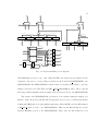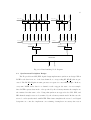
1
ii
Copyright
© Timothy B. Campbell 2006
All Rights Reserved
LOW-COST TELEMETRY ENCODER BACKPLANE COMMUNICATION
by
Timothy B. Campbell
A report submitted in partial fulfillment
of the requirements for the degree
of
MASTER OF SCIENCE
in
Electrical Engineering
Approved:
Dr. Charles M. Swenson
Major Professor
Dr. Jacob Gunther
Committee Member
Dr. Todd K. Moon
Committee Member
UTAH STATE UNIVERSITY
Logan, Utah
2006
iii
Abstract
Low-Cost Telemetry Encoder Backplane Communication
by
Timothy B. Campbell, Master of Science
Utah State University, 2006
Major Professor: Dr. Charles M. Swenson
Department: Electrical and Computer Engineering
The Low-Cost Telemetry Encoder (LCTE) was developed by the Space Dynamics
Laboratory under contract for the NASA Sounding Rocket Operations Contract. LCTE
performs data handling and telemetry encoding for sounding rocket missions. Using a
variety of data inputs, LCTE collects, formats, and encodes data. LCTE serializes the
encoded data and outputs the serial data stream to a transmitter on the rocket. A ground
station is then able to receive and process the collected data.
Thus far the LCTE design has undergone three phases. During phase one the original
LCTE system was developed. The system included a power board, a telemetry board, and
stackable aluminum enclosures for the boards. The telemetry board featured 32 analog
inputs, 32 digital inputs, and one asynchronous serial input. The system was programmed
to run a fixed telemetry matrix which read data from all these inputs. The phase two design
provided a PC-based Graphical User Interface which allowed users to easily reconfigure
the telemetry matrix as well as define the functions of the 32 digital lines. Finally, phase
three extended the LCTE design to include communication via the backplane connector.
This allowed LCTE to communicate directly with science or other boards included in the
hardware stack.
iv
The LCTE phase three design required additions and modifications to two parts of the
LCTE system: the PC Graphical User Interface and the Field-Programmable Gate Array
VHDL code. New VHDL code was also developed for a Sweeping Langmuir Probe/Floating
Potential Probe (SLP/FPP) science board which utilized the LCTE backplane communication. The backplane communication protocol is quite simple and allows maximum
flexibility when designing boards to be used in conjunction with LCTE.
This report describes the new additions to the phase two LCTE design in detail. It
also explains the details of the backplane sections of the SLP/FPP science board, as well
as includes other options which may be appropriate for future science boards targeted for
the LCTE backplane interface.
(63 pages)
v
Acknowledgments
I would like to thank the Tropical Storm team at the Space Dynamics Laboratory, Aroh
Barjatya, Jason Bingham, Chad Fish, Jessica Gregory, Mike Holt, Albert Hummel, and
Wayne Sanderson. I appreciate your help, ideas, and expertise which made the completion
of this project possible. Thank you to my family, and especially to my wife, for your
encouragement, love, and support. Without it, I never would have come this far. Finally,
thank you to the many professors who influenced my education and especially to Dr.
Charles Swenson for providing me this great opportunity to apply what I’ve learned.
Tim Campbell
vi
Contents
Page
Abstract . . . . . . . . . . . . . . . . . . . . . . . . . . . . . . . . . . . . . . . . . . . . . . . . . . . . . . . iii
Acknowledgments . . . . . . . . . . . . . . . . . . . . . . . . . . . . . . . . . . . . . . . . . . . . . . .
v
List of Tables . . . . . . . . . . . . . . . . . . . . . . . . . . . . . . . . . . . . . . . . . . . . . . . . . . viii
List of Figures . . . . . . . . . . . . . . . . . . . . . . . . . . . . . . . . . . . . . . . . . . . . . . . . . .
ix
1 Introduction . . . . . . . . . . . . . . . . . . . . . . . . . . .
1.1 Sounding Rockets and Telemetry Systems . .
1.2 The Low-Cost Telemetry Encoder . . . . . .
1.2.1 Development Overview . . . . . . . . .
1.2.2 Hardware . . . . . . . . . . . . . . . .
1.2.3 Software and Firmware . . . . . . . .
1.2.4 Tropical Storm Requirements . . . . .
1.3 Thesis Overview . . . . . . . . . . . . . . . .
....
. . .
. . .
. . .
. . .
. . .
. . .
. . .
.
.
.
.
.
.
.
.
1
1
4
4
5
6
9
10
2 Sampling LUT . . . . . . . . . . .
2.1 Problem Review . . . . .
2.2 Interrupt Execution Time
2.3 Interrupt Priority . . . . .
....
. . .
. . .
. . .
....
. . .
. . .
. . .
.
.
.
.
....
. . .
. . .
. . .
....
. . .
. . .
. . .
.....
. . . .
. . . .
. . . .
3 Backplane Interface . . . . . . . . . . . . . . . . . . . . . . . . .
3.1 Development Overview . . . . . . . . . . . . . . . .
3.2 Protocol Definition . . . . . . . . . . . . . . . . . .
3.3 LCTE FPGA Firmware . . . . . . . . . . . . . . .
3.3.1 Firmware Overview . . . . . . . . . . . . .
3.3.2 DATCONTROLLER Module Detail . . . .
3.3.3 BP REG Module . . . . . . . . . . . . . . .
3.3.4 BP REG State Machine . . . . . . . . . . .
3.4 SLP/FPP FPGA Firmware . . . . . . . . . . . . .
3.4.1 SLP/FPP Firmware Overview . . . . . . .
3.4.2 PARAM CONFIG Module . . . . . . . . .
3.4.3 BP INTERFACE Module . . . . . . . . . .
3.4.4 NEGOTIATOR Module . . . . . . . . . . .
3.5 Synchronous Backplane Design . . . . . . . . . . .
3.5.1 Single Address with Multiple Channels . . .
3.5.2 Single Channel with Multiple Addresses . .
3.5.3 Data Buffering and Sample Time . . . . . .
3.6 Asynchronous Backplane Design . . . . . . . . . .
.
.
.
.
.
.
.
.
.
.
.
.
.
.
.
.
.
.
....
. . .
. . .
. . .
. . .
. . .
. . .
. . .
....
. . .
. . .
. . .
. . .
. . .
. . .
. . .
....
. . .
. . .
. . .
. . .
. . .
. . .
. . .
.
.
.
.
.
.
.
.
....
. . .
. . .
. . .
. . .
. . .
. . .
. . .
.
.
.
.
....
. . .
. . .
. . .
....
. . .
. . .
. . .
....
. . .
. . .
. . .
....
. . .
. . .
. . .
. . .
. . .
. . .
. . .
. . .
. . .
. . .
. . .
. . .
. . .
. . .
. . .
. . .
. . .
....
. . .
. . .
. . .
. . .
. . .
. . .
. . .
. . .
. . .
. . .
. . .
. . .
. . .
. . .
. . .
. . .
. . .
.....
. . . .
. . . .
. . . .
. . . .
. . . .
. . . .
. . . .
. . . .
. . . .
. . . .
. . . .
. . . .
. . . .
. . . .
. . . .
. . . .
. . . .
. 12
. 12
. 13
. 15
. . . . 16
. . . 16
. . . 17
. . . 18
. . . 18
. . . 21
. . . 24
. . . 24
. . . 26
. . . 27
. . . 28
. . . 29
. . . 32
. . . 35
. . . 37
. . . 37
. . . 39
. . . 41
vii
4 Graphical User Interface . . . .
4.1 GUI Overview . . . . . . .
4.2 GUI BP Channels Tab . . .
4.3 GUI Operation . . . . . . .
.....
. . . .
. . . .
. . . .
....
. . .
. . .
. . .
....
. . .
. . .
. . .
.
.
.
.
....
. . .
. . .
. . .
....
. . .
. . .
. . .
....
. . .
. . .
. . .
.
.
.
.
....
. . .
. . .
. . .
....
. . .
. . .
. . .
44
44
45
46
5 Recapitulation . . . . . . . . . . . . . . . . . . . . . . . . . . . . . . . . . . . . . . . . . . . . . . . 49
5.1 Phase Three Results . . . . . . . . . . . . . . . . . . . . . . . . . . . . . . . 49
5.2 Next Steps . . . . . . . . . . . . . . . . . . . . . . . . . . . . . . . . . . . . 50
References . . . . . . . . . . . . . . . . . . . . . . . . . . . . . . . . . . . . . . . . . . . . . . . . . . . . . 53
viii
List of Tables
Table
Page
3.1
Channel select word format. . . . . . . . . . . . . . . . . . . . . . . . . . . .
22
3.2
Four-bit channel select codes. . . . . . . . . . . . . . . . . . . . . . . . . . .
22
3.3
Backplane multiplexer LUT. . . . . . . . . . . . . . . . . . . . . . . . . . . .
29
3.4
Housekeeping multiplexer LUT. . . . . . . . . . . . . . . . . . . . . . . . . .
30
ix
List of Figures
Figure
Page
1.1 Trajectory of a sounding rocket. . . . . . . . . . . . . . . . . . . . . . . . . .
2
1.2
Example telemetry matrix. . . . . . . . . . . . . . . . . . . . . . . . . . . .
3
1.3
LCTE system hardware. . . . . . . . . . . . . . . . . . . . . . . . . . . . . .
6
1.4
High-level telemetry board block diagram. . . . . . . . . . . . . . . . . . . .
7
1.5
Sampling LUT and FPGA memory block diagram. . . . . . . . . . . . . . .
9
2.1
Modified sampling LUT and FPGA memory block diagram. . . . . . . . . .
14
3.1
Backplane stack block diagram. . . . . . . . . . . . . . . . . . . . . . . . . .
16
3.2
Backplane timing diagram. . . . . . . . . . . . . . . . . . . . . . . . . . . .
17
3.3
FPGA high-level block diagram. . . . . . . . . . . . . . . . . . . . . . . . .
19
3.4
DATCONTROLLER block diagram. . . . . . . . . . . . . . . . . . . . . . .
20
3.5
BP REG state machine diagram. . . . . . . . . . . . . . . . . . . . . . . . .
25
3.6
SLP/FPP top-level block diagram. . . . . . . . . . . . . . . . . . . . . . . .
27
3.7
Backplane interface multiplexer.
. . . . . . . . . . . . . . . . . . . . . . . .
31
3.8
Backplane interface LUT and BP RD H signals. . . . . . . . . . . . . . . .
32
3.9
Request handling block diagram. . . . . . . . . . . . . . . . . . . . . . . . .
33
3.10 Data handling block diagram. . . . . . . . . . . . . . . . . . . . . . . . . . .
35
3.11 Concatenation to create the fifth FPP data channel. . . . . . . . . . . . . .
38
3.12 FPP sample timing without buffering. . . . . . . . . . . . . . . . . . . . . .
40
3.13 FPP sample timing with buffering. . . . . . . . . . . . . . . . . . . . . . . .
41
3.14 Asynchronous SLP/FPP system using three FIFOs. . . . . . . . . . . . . .
43
4.1
45
GUI Setup, Matrix, Format, and Readback tabs. . . . . . . . . . . . . . . .
x
4.2
GUI BP channels tab. . . . . . . . . . . . . . . . . . . . . . . . . . . . . . .
46
1
Chapter 1
Introduction
1.1
Sounding Rockets and Telemetry Systems
Sounding rockets are one method currently used to perform space research. Although
these rockets lack the ability to place experiments into an earth orbit, they are able to
launch payloads to altitudes of up to 1500 kilometers. The rockets are normally designed
to fly along a parabolic trajectory which includes an upleg, downleg, and apogee as seen
in fig. 1.1. When compared to satellite missions, sounding rockets offer a solution that is
cheaper and requires less time for payload integration. Sounding rocket flights generally
are only 5-20 minutes long, but this is adequate for a number of scientific experiments [1].
Rather than storing data during the flight and later recovering the data storage unit,
a telemetry system is often employed on sounding rockets. The telemetry system gathers
data from science experiments and sorts the data into an organized format. The system
uses radios to transmit formatted data from the rocket back to an earth-based station in
real-time. The base station receives and stores the data which is then made available to
scientists for analysis.
A telemetry matrix specifies how the system should format data. Common vocabulary
associated with telemetry matrices includes: major frame, minor frame, words, word size,
and bit rate. Figure 1.2 shows an example matrix and identifies some of the components
of a telemetry matrix. The complete two-dimensional matrix as seen in the figure is called
a major frame. Each row in the major frame is called a minor frame. The minor frames
are further divided into words. In this example there are eight words per minor frame and
16 minor frames per major frame. Word size specifies the number of bits in each word and
the bit rate specifies the number of bits transmitted per second.
The telemetry system transmits information beginning with the first word in the first
minor frame of the telemetry matrix. Each word from the first minor frame is transmitted
2
Apogee
leg
Upleg
n
Dow
Up to 1500 km
Ocean
Launch Facility
Land
Fig. 1.1: Trajectory of a sounding rocket.
in turn and when the end of the first minor frame is reached, the telemetry system moves
to the first word of the second minor frame. When the last word of the last minor frame
is transmitted, the system loops back and starts over, transmitting the first word of the
first minor frame again. Channels which appear more than once per minor frame are said
to be supercommutated. The A0 channel in the matrix shown in fig. 1.2 is an example
of supercommutation since it appears twice per minor frame. Channels appearing less
frequently than once per minor frame are called subcommutated channels. The P2 and P3
channels in column 5 of the matrix in fig. 1.2 are examples of subcommutation since each
appears only once every two minor frames.
Three different types of words exist in the telemetry matrix: Sub-Frame Identification
(SFID) words, Frame Synchronization (FS) words, and data words. SFID words are used
to indicate which minor frame is currently being transmitted. SFID words generally appear
3
Supercommutated
Data Channel
1
1
2
3
4
5
6
7
8
9
10
11
12
13
14
15
16
SFID
|
|
|
|
|
|
|
|
|
|
|
|
|
|
SFID
2
A0
|
|
|
|
|
|
|
|
|
|
|
|
|
|
A0
3
P0
|
|
|
|
|
|
|
|
|
|
|
|
|
|
P0
4
P1
|
|
|
|
|
|
|
|
|
|
|
|
|
|
P1
Sub-Frame
Identification
Frame Synchronization
Words
5
P2
P3
P2
P3
P2
P3
P2
P3
P2
P3
P2
P3
P2
P3
P2
P3
6
A0
|
|
|
|
|
|
|
|
|
|
|
|
|
|
A0
7
FS1
|
|
|
|
|
|
|
|
|
|
|
|
|
|
FS1
8
FS2
|
|
|
|
|
|
|
|
|
|
|
|
|
|
FS2
Subcommutated
Data Channels
Fig. 1.2: Example telemetry matrix.
before subcommutated words within a minor frame. This allows the telemetry receiver to
use the SFID value to determine exactly which subcommutated word is being transmitted
in a particular minor frame. FS words are words with a constant pre-determined value and
are used by the receiver for synchronization. Data words make up the bulk of a telemetry
matrix. They contain data sampled from the various inputs available to the telemetry
system. L-3 Communications has put together an educational tutorial which has more
information about telemetry systems [2].
The NASA Sounding Rocket Program (NSRP) (which is implemented under the
NASA Sounding Rocket Operations Contract (NSROC)) has been supplying sounding
rockets for space research since 1959. The program offers a low-cost, quick-response effort
4
that currently provides 20-30 flight opportunities per year to space scientists [3]. Previously the WFF-93 encoder has been the telemetry encoder system used for the sounding
rocket flights. This encoder has a cost of $6,500-$15,000 per unit. NSROC wanted a new
telemetry encoder solution that would be suitable for smaller payloads and cost around
$1,000 per unit [4]. Because of Utah State University’s past involvement with sounding
rocket experiments, NSROC selected the Space Dynamics Laboratory (SDL) to develop a
new lower cost encoder solution [5].
1.2
The Low-Cost Telemetry Encoder
1.2.1
Development Overview
The Low-Cost Telemetry Encoder (LCTE) developed by SDL has undergone three
design phases. The original design phase was accomplished by a team of professional
engineers and student employees. This design phase produced the LCTE system hardware.
The hardware includes a power board, a telemetry board, and mechanical enclosures for the
boards. Documentation for the main parts of the system include power board schematics
[6], telemetry board schematics [7], tray schematics [8], and top tray schematics [9]. These
schematics and other supporting documentation are maintained by SDL document control.
Mechanical analysis and system tests were completed to verify system performance and the
system was programmed to implement a fixed telemetry matrix utilizing analog, parallel
digital, and serial digital inputs.
The second design phase was completed by Jeff Henry while working as an intern for
NSROC. During this phase, new firmware was written for the system and a new PC-based
Graphical User Interface (GUI) was created. A user manual was compiled which provided
instructions for using the new firmware and software [10]. After the phase two design was
completed, telemetry matrices could be created using the PC GUI and then uploaded to
the telemetry board, thus allowing the telemetry system to be user-configurable.
5
The third design phase is the subject of this thesis. The primary goal of phase three
was to extend the LCTE system to enable backplane communications. Backplane communication allows LCTE to read data from other boards on the stack through the backplane
connector.
1.2.2
Hardware
The phase one LCTE system hardware is described in the thesis, “Implementation of a
User-Configurable Low-Cost Telemetry Encoder” by Jeff Henry [4]. A general description
of the hardware is included here for completeness. The LCTE hardware includes two
boards, the power board and the telemetry board, and mechanical tray enclosures. The
two boards can be installed in the trays and stacked together as shown in fig. 1.3. When
assembled, a backplane connection is made between the two boards. This connection
supplies power to the telemetry board from the power board.
The telemetry board features 32 analog inputs, 32 Digital Input/Output (DIO) lines,
and two asynchronous serial channels. A 110-pin connector on the front of the board
houses these data lines as well as ground lines and control lines for an optional digital potentiometer. The encoded, filtered telemetry stream is output through an SMA connector
which also resides on the front of the telemetry board.
A top-level block diagram of the telemetry board is shown in fig. 1.4. As illustrated
in the diagram, two key components of the telemetry board are the Microchip PIC18
microcontroller and the Altera ACEX1K Field-Programmable Gate Array (FPGA). The
microcontroller is used together with two RS-232/422 level shifters to create the two asynchronous serial channels. The FPGA is the heart of the telemetry board. It contains about
100,000 logic gates, 49,000 memory bits, and is contained in a 484-pin ball grid array package. The FPGA controls two 16-to-1 analog multiplexers, two 16-bit Analog-to-Digital
Converters (ADCs), controls the function (input or output) of the digital lines and reads
from, or writes to, the 32 digital lines. The FPGA also reads asynchronous serial data from
the microcontroller and formats, serializes, and encodes sampled data. Forty-one of the
FPGA Input/Output (IO) lines were also connected to pins in the backplane connector,
6
Fig. 1.3: LCTE system hardware.
but were not used in the phase one design. A four or six-pole Bessel filter is used to filter
the encoded serial data stream and a potentiometer is used to tune the level of the filter
output. The LCTE system hardware developed during phase one has remained unchanged
during subsequent design phases.
1.2.3
Software and Firmware
The phase one design implemented the telemetry matrix using a Look-Up Table (LUT)
structure that was coded into the FPGA firmware. A fixed 50-by-32 telemetry matrix was
implemented which utilized all 32 analog inputs, all 32 digital inputs, and one asynchronous
serial input. The FPGA firmware specified 16-bit words and transmitted data at 800 kbps.
Async 0
RS-232/422
Level Shifter
7
Altera
ACEX1K FPGA
16-bit
Analog-to-Digital
Converter
8-bit DIO
buffer
8
8-bit DIO
buffer
8
8
8
8
8
8
8
4 or 6 pole
Bessel Filter
Level
Shifter
Telemetry
Output
16
8-bit DIO
buffer
16-bit
Analog-to-Digital
Converter
16
8-bit DIO
buffer
16
16-to-1
Multiplexer
16
16-to-1
Multiplexer
Async 1
RS-232/422
Level Shifter
Microchip
PIC18 Microcontroller
41
Backplane Connector
Fig. 1.4: High-level telemetry board block diagram.
The phase two design introduced user configurability by adding the PC GUI software
and creating new firmware for the microcontroller and the FPGA. The phase two PC GUI
allows a user to configure the following matrix parameters:
• Word Size: 8-16 bits
• Bit Rate: 0.650-4000 kbps
• Matrix Size: Up to 3072 data words
• Matrix Dimensions: 1-255 rows and 2-255 columns
8
• Frame Sync Words: 1 or 2, 16-bit words
• Encoding: RNRZ-L or BiPhase-L
• ADC Acquisition: 2.75 µseconds or greater
• Asynchronous Serial Input: 2400-115200 baud
• Digital Line Direction: Input or output
• Digital Input Function: 8-bit parallel, Synchronous serial, or Time event
• Digital Output Function: Synchronous serial controls
The phase two design allows the user to create separate sampling and telemetry matrices. The sampling matrix defines the order in which data channels are to be sampled. It
also allows more than one input channel to be sampled during a single word period. The
telemetry matrix defines the order in which sampled data is inserted into the telemetry
stream. Using separate sampling and telemetry matrices is very useful because it is often
desirable for data channels to be sampled with a fixed sampling period. Some telemetry
matrices are difficult to arrange so that channels appear at regular intervals without adding
significant overhead to the matrix. Separate matrices allow a user to create a sampling
matrix where the channels are sampled at the correct fixed intervals, sampling multiple
words during one word period if necessary, and then create a different telemetry matrix
where the data can be serialized and transmitted efficiently.
Once the desired parameters are selected and matrices are constructed using the GUI,
the data is compiled into two LUTs. The first LUT is called the setup LUT and holds
all the necessary telemetry system parameters. The second LUT is called the sampling
LUT. Each entry in the sampling LUT contains the information necessary for sampling
during one word period. After the LUTs are compiled, they are then uploaded into the
microncontroller flash memory using one of the asynchronous serial inputs. Upon reset,
the setup LUT is read from the microcontroller and the setup parameters are passed to
9
Setup &
Sampling
Look-up Tables
Data Memory
Memory
Address
UART
Interrupt 0
LUT Read Subroutine
Data/Address
LUT Entry
Decode
From PC
Telemetry
Control
FPGA
Sampled Data
Initiate
Sampling
Data Sampling
Control
Microcontroller
Telemetry Out
Data Inputs
Fig. 1.5: Sampling LUT and FPGA memory block diagram.
the FPGA to configure it for the new matrix. Then, once every word period, an interrupt
is sent from the FPGA to the microcontroller. In the Interrupt Service Routine (ISR), the
next entry from the sampling LUT is read and passed to the FPGA. This entry contains
both a channel select code and a memory address. The channel select code indicates to the
FPGA which input channel is to be sampled next. The memory address specifies where
the sampled data should be stored in the FPGA memory. During the subsequent word
period the input channel is sampled and the data is stored in the FPGA memory while the
following sampling LUT entry is read from the microcontroller. Using this process, input
channels can be sampled in one order and the data can be stored in the FPGA memory in
a different order. The FPGA memory is read sequentially and inserted into the telemetry
stream. The GUI creates the sampling LUT according to the sampling matrix so that the
input channels are sampled in the correct order, but creates memory addresses so that the
sampled data is written to the FPGA memory ordered according to the telemetry matrix.
Figure 1.5 shows the structure of the microcontroller LUT and FPGA data memory.
1.2.4
Tropical Storm Requirements
The goal of the Tropical Storm mission is to measure plasma characteristics in the
ionosphere above a tropical storm. A thesis written by Albert Hummel [11] discusses the
purpose and science behind the Tropical Storm mission in greater detail. The Tropical
Storm project motivated the third phase of the LCTE system design. An instrument
suite, including a Plasma Impedance Probe (PIP), a Sweeping Langmuir Probe (SLP),
10
and Floating Potential Probes (FPP), was to be combined with the LCTE telemetry components to create one complete package. One Printed Circuit Board (PCB) was designed
to hold the electronics for the PIP, while a second PCB was designed to house the electronics for both the SLP and FPP instruments. Both science PCBs used the LCTE system
form factor, and were designed to mate to the LCTE backplane connector, creating a stack
with four levels: the power board, the telemetry board, the SLP/FPP board, and the PIP
board.
The telemetry requirements of the Tropical Storm project included a bit rate of 2.5
Mbps. Early tests using the LCTE phase two design exposed two main issues. First, whn
running at bit rates above 1 Mbps, the word period was shorter than the time required to
read an entry from the sampling LUT. Since the FPGA tried to read an entry from the
LUT once every word period, the system was not able to keep up. Second, the ISR to read
the sampling LUT had priority over the ISR used to read incoming data from the GUI.
This meant that once the system was programmed with a bit rate faster than 1 Mbps, the
system would always be stuck in the sampling LUT ISR and would no longer respond to
the PC GUI.
In order to use the LCTE system in the Tropical Storm mission, three main points
needed to be resolved. First, the microcontroller and FPGA firmware needed to be modified to allow the system to run at rates above 1 Mbps. Second, the LCTE backplane
communication needed to be developed. Third, the GUI needed to be updated to allow
backplane channels to be included in a telemetry matrix as well as to resolve some stability
issues.
1.3
Thesis Overview
The remainder of this report describes how the bugs resulting from the second design
phase were corrected and resolved as well as how the design was extended and modified
to include backplane communications. Chapter 2 continues to discuss the problem encountered when using bit rates higher than 1 Mbps. In order to resolve the problem, the
sampling LUT was moved from the microcontroller to the FPGA. This chapter explains
11
the details of moving the sampling LUT and the implications the move had on the rest
of the design. Chapter 3 describes the backplane interface. The chapter includes the protocol used in backplane communication as well as the additions and modifications made
to the LCTE firmware. Chapter 3 also discusses the sections of the firmware created for
the SLP/FPP science board that pertain to usage of the backplane. This includes unique
features of the SLP/FPP design as well as general ideas to consider when creating a digital
design that involves LCTE backplane communication. The firmware for the FPGA on the
PIP instrument is the main subject of a thesis written by Jason Bingham [12]. Chapter 4
of this thesis describes the additions and modifications made to the PC GUI which allow
backplane channels to be included in telemetry matrices. It also discusses changes made to
enhance program stability. Finally, Chapter 5 contains a summary of the work completed
during phase three and the current capabilities of the LCTE telemetry system. Chapter 5
also includes a few comments and ideas for future design efforts involving LCTE.
12
Chapter 2
Sampling LUT
2.1
Problem Review
The software GUI developed for LCTE during the second design phase allowed a user
to select telemetry matrix parameters, create sampling and telemetry matrices, and upload
the settings and matrices to the LCTE telemetry board. The firmware created for the
microcontroller and FPGA utilized a sampling LUT which was stored in the microcontroller
flash memory. An entry from the LUT was read by the microcontroller and written to the
FPGA during each word period to obtain sampling instructions for the following word
period. This architecture gave the LCTE telemetry system the flexibility of separate
sampling and telemetry matrices. However, a problem with this particular architecture
was soon discovered. When faster bit rates were used, multiple word periods were required
for the FPGA to obtain a single entry from the sampling LUT. Another problem also arose.
Since the microcontroller was continually executing the ISR to read sampling LUT entries,
the lower priority ISR used for GUI communication was never given any execution time.
There were two options available to resolve these problems. First, the system performance specifications could be altered, slowing the maximum bit rate from 4 Mbps to 1
Mbps. Alternatively, the microcontroller and FPGA firmware could be modified so that
the sampling LUT structure would be copied from the microcontroller to the FPGA memory on startup or reset. Copying the sampling LUT to the FPGA would allow the system
to run bit rates up to 4 Mbps, but it would remove the ability to have separate sampling
and telemetry matrices.
Due to system requirements imposed by the Tropical Storm mission, reducing the
maximum bit rate to 1 Mbps was not a viable solution. Instead, the microcontroller and
FPGA firmware was modified. The sampling LUT was moved to the FPGA and the feature
of separate sampling and telemetry matrices was discarded.
13
2.2
Interrupt Execution Time
The firmware developed during the second design phase included an ISR in the mi-
crocontroller. This ISR read an entry from the sampling LUT in the microcontroller flash
memory and then wrote the LUT entry to the FPGA. At the beginning of each word period, the FPGA would send an interrupt signal to the microcontroller causing the ISR to
execute. The time required for the microcontroller to execute the ISR was calculated, but
never verified. It was later discovered that reading from the microcontroller flash memory
took much longer than anticipated and the ISR was not able to execute within a single
word period when the system was running at bit rates above 1 Mbps.
In order to resolve this issue, allowing the system to run at up to 4 Mbps, the firmware
was changed for both the microcontroller and the FPGA. Rather than holding the sampling
LUT in the microcontroller and reading one entry every word period, the entire sampling
LUT is copied to the FPGA memory every time the board is turned on. With the sampling
LUT in the FPGA memory, the LUT entries are available to the FPGA without having to
execute the slow ISR in the microcontroller. Previously, the FPGA memory was used to
hold sampled data until it was inserted into the telemetry stream, allowing separate sampling and telemetry matrices. Since the FPGA memory is now occupied by the sampling
LUT, separate sampling and telemetry matrices are no longer allowed. Instead, sampling
is performed in the order specified by the telemetry matrix.
Since the sampling and telemetry matrices were reduced to one matrix and because
the FPGA memory is used to hold the sampling LUT, the memory addresses previously
included in the sampling LUT were no longer necessary. When using separate matrices,
these addresses specified where sampled data should be written within the FPGA memory.
This allowed the data to be sampled in a particular order and then written to the FPGA
memory in a different order. With the sampling LUT occupying the FPGA memory the
sampled data is no longer written to memory at all. This reduced the size of the sampling
LUT which in turn allowed the telemetry matrix to include 4096 data words rather than
the previously stated 3072 data words.
14
Telemetry Out
LUT Read on
Startup and Reset
Sampled
Data
Initiate
Sampling
Data Sampling
Control
UART
LUT Entry
Decode
From PC
Data Memory
Telemetry
Control
Setup &
Sampling
Look-up Tables
FPGA
Holding
Registers
Microcontroller
Data Inputs
Fig. 2.1: Modified sampling LUT and FPGA memory block diagram.
The telemetry matrix is used to determine the order in which the input channels are
sampled, but because some input channels, such as the synchronous serial inputs, require
more than one word period to sample, sampling is started three word periods ahead of the
telemetry stream. So, during the first word period, an entry containing a channel select
code is read from the sampling LUT. During the next word period, sampling begins on
the input channel indicated by the channel select code. When the data is obtained it is
written to one of four holding registers. Meanwhile, once every word period another entry
is read from the sampling LUT and another sample is started. This process continues
until the telemetry board is powered down. A counter is used to address one of the four
holding registers and the data is read from the register and inserted into the telemetry
stream. Figure 2.1 shows a block diagram depicting the modified microcontroller and
FPGA firmware.
As mentioned earlier, some input channels require more than one word period to
acquire sample data, yet others require only a few clock cycles of the FPGA. This means
that although sampling is started in order, sampling may not finish in order. Rather than
writing data to the four holding registers in the order it is obtained, a counter value is read
and temporarily stored when each sample is started. The sampled data is then written
to the holding register indicated by the stored counter value. This ensures that the data
is written to the holding registers in the correct order. A second counter is then be used
to read the four holding registers sequentially and the data is inserted into the telemetry
stream in the correct order corresponding to the telemetry matrix.
15
2.3
Interrupt Priority
The ISR previously used to read the sampling LUT had priority over the ISR used to
communicate with the GUI. Since the sampling LUT ISR executed continually when bit
rates above 1 Mbps were used, the telemetry board quit responding to the GUI. Moving
the sampling LUT to the FPGA on startup eliminated the need for the sampling LUT ISR.
In addition to removing the the sampling LUT ISR, the remaining interrupt priorities were
reevaluated giving priority to the most critical processes. Carefully reordering the interrupt
priorities has increased the stability of both the telemetry board operation as well as the
PC GUI.
16
Chapter 3
Backplane Interface
3.1
Development Overview
One goal of the Tropical Storm mission was to take the existing LCTE telemetry
system and combine it with new revisions of science instruments which SDL had used
before. New versions of the PIP, SLP, and FPP instruments were designed. The new
designs utilized PCBs which would be able to stack directly on top of the LCTE power
and telemetry boards. When completed the system included the LCTE power board and
telemetry board along with an SLP/FPP science board and a PIP science board, creating
a stack with 4 levels. A block diagram showing the connection between the four boards is
shown in fig. 3.1.
Before work on either end of the backplane interface began, the protocol for communication through the backplane was defined. A simple protocol utilizing an 8-bit address
bus, an output enable signal, and a 16-bit parallel data bus selected.
Once the backplane communication protocol was defined, the telemetry board FPGA
firmware was expanded. This first began with an in-depth review of the FPGA firmware
to understand how it currently obtained samples from the other input channels. Once the
Address
LCTE
8
Output Enable
Data
16
SLP/FPP
Fig. 3.1: Backplane stack block diagram.
PIP
17
Clk - 4
MHz
1
Address
2
3
Address 0
4
5
6
7
8
9
Address 1
OE
ZZZZZZZZZZZZZZZZ
Data
Data 1
ZZZZZZZZZZZZZZZZ
Fig. 3.2: Backplane timing diagram.
other inputs were understood, a backplane module was added which integrated seamlessly
into the firmware.
New FPGA firmware was developed for the SLP/FPP and PIP science boards while
the LCTE FPGA firmware was being modified. This chapter includes a description of
the parts of the SLP/FPP FPGA firmware which complete the other end of backplane
communication. Also discussed are ideas and options that should be considered when
creating a design using the backplane communication. Some of these ideas described are
implemented in the SLP/FPP design and some are not.
3.2
Protocol Definition
Before any work on the telemetry firmware began, the protocol for the backplane
interface was chosen. Eight pins in the backplane connector were set aside as address pins,
another pin is used for an output enable signal, and 16 others are used for a parallel data
bus. An address is placed on the the address (BP ADDR) bus, addressing one of the
boards on the stack. The output enable (BP OE) line is driven low, enabling data output
onto the backplane data (BP DATA) bus. The data is read by the telemetry board and
the process ends with the BP OE line being driven back high. This process is shown in
fig. 3.2.
The backplane address (BP ADDR) and output enable (BP OE) pins are always output from LCTE and read by other boards on the stack. The backplane data (BP DATA)
bus is configured as an input to LCTE and the other boards on the stack output to the
data bus. Five hundred nanoseconds after LCTE outputs an address on the BP ADDR
18
bus, the BP OE signal is driven low. Five hundred nanoseconds after the falling edge of
the BP OE signal, the telemetry board reads the data on the BP DATA bus. The BP OE
signal is driven back high after the data is read which completes process.
Science and other boards on the stack must be designed to control the status of the
BP DATA pins using only the BP ADDR and BP OE signals. Boards on the stack must
guarantee that, when addressed, valid data is output on the BP DATA bus at most 450
nanoseconds after the falling edge of the BP OE signal and is held until the rising edge of
the BP OE signal. If data is output to the BP DATA bus later than 450 nanoseconds after
the falling edge of the BP OE signal, or is not held until the rising edge of the BP OE
signal, correct data transfer from the board to LCTE is not guaranteed. Boards on the
stack must also always place the BP DATA pins in a high-impedance state whenever an
address other than their own is present on the BP ADDR bus, as well as whenever the
BP OE signal is high. The address zero is a reserved address and all boards should place
the BP DATA pins in a high-impedance state whenever the zero address is present on the
BP ADDR bus. Failure to place the BP DATA pins in a high-impedance state when the
BP OE signal is high or when another board’s address or the zero address is present on
the BP ADDR bus can damage FPGAs connected to the BP DATA bus.
3.3
LCTE FPGA Firmware
After the backplane communication protocol was defined, the next step was to extend
the telemetry board FPGA firmware to include support for backplane communication.
The first step involved to extend the telemetry board firmware was to understand how the
FPGA sampled data from the other input channels. Once the other input channels were
understood a backplane input module was added that functioned in an identical fashion.
This section includes an overview of the FPGA firmware and the backplane input module,
as well as a detailed description firmware and the new additions.
3.3.1
Firmware Overview
Understanding the workings of the phase two LCTE FPGA design required more effort than originally anticipated due to the relative complexity of the system. However,
19
System Clock
Reset_L
Clock and Reset
Condition
A/D_Controller_Load
UP_Addr
UP_Interrupts
Reset_H
UP_Data
UP_Control
UP_Addr/Data
CLK0
uP Controller
DIO_Controller_Load
Telemetry_Controller_Load
A/D_Control
DATController_Load
A/D_Controls
A/D Controllers
A/D_Data
A/D_Data
DIO_Control
DIO_Controls
Digital I/O Controllers
DIO_Data
DIO_Data
DATController
Bit_Clk
Telemetry Controller
Telemetry_In
Bit_Clk_2x
Word_Strobe
Telemetry_Out
BP_Address
BP_OE_L
Backplane Connector
BP_Data
Fig. 3.3: FPGA high-level block diagram.
once the design was understood, the additions necessary to extend the design to include
backplane communication were minimal. Figure 3.3 shows a high-level block diagram illustrating the layout of the FPGA. The CLK RESET module passes the clock and reset
signals through to the rest of the design. The UPCONTROLLER module handles communications with the microcontroller and passes data from the microcontroller to the rest
of the design. The ADCCONTROLLERS module handles the control signals for the two
16-bit ADCs and reads the converted input data and the DIOCONTROLLERS module
handles the digital input/output, synchronous serial, and time event control and sampling.
The TELEMETRY module takes the sampled data, serializes it and encodes the data,
creating the telemetry stream. The DATCONTROLLER module is the bulk of the design.
On reset, it receives the sampling LUT after it is passed through the UPCONTROLLER
module, and writes the LUT to the FPGA memory. Then during normal operation the
DATCONTROLLER reads the sampling LUT entries from memory and generates sample
requests for data. The DATCONTROLLER also temporarily stores sampled data until it
is passed to the TELEMETRY module.
20
SRAM
12x4096
ADC_READY
SMPL_ADDR
DATA_BUFF_SEL
ADC_DATA
ADC_REG
ADC_BUFF_SEL
ADC_DATA_IN
MEM_RD_DATA
MEM_RD_ADDR
MEM_WR_DATA
MEM_WR_EN_H
MEM_WR_ADDR
ADC_DATA_RDY
DIO_READY
SMPL_ADDR
DATA_BUFF_SEL
DIO_DATA
DIO_REG
DIO_BUFF_SEL
DIO_DATA_RDY
ADC_SMPL
SAMPLE_START
DIO_DATA_IN
DIO_SMPL
CHAN_SEL_CODE
UP_SMPL
MUX_SEL
SAMPLEDECODER
UP_READY
BP_SMPL
DATA_BUFF_SEL
FS1_SMPL
UP_DATA_IN
UP_REG
UP_DATA
Data_Arbiter
UP_BUFF_SEL
FS2_SMPL
SFID_SMPL
MEM_CONTROLLER
BP_READY
SMPL_ADDR
WORD_COUNT
DATA_BUFF_SEL
MAJ_STROBE
WR_ADDR
WR_DATA
Holding_Registers
TLM_DATA
WR_ENBL
BP_DATA
BP_REG
BP_BUFF_SEL
BP_DATA_IN
MIN_STROBE
DATA_BUFF_SEL
SMPL_ADDR
DATAMEM_RD_ADDR
FS1_REG
FS2_REG
SFID_REG
Fig. 3.4: DATCONTROLLER block diagram.
Additions to the FGPA firmware for the backplane functionality all took place within
the DATCONTROLLER module. A block diagram of the sub-level contained within the
DATCONTROLLER module is seen in fig. 3.4.
The MEM CONTROLLER module is one of the more complicated sections in the
FPGA firmware. It controls access to the FPGA memory, writing the sampling LUT
to memory on startup and then reading the LUT entries from memory during normal
operation. It also controls access to the four holding registers. The MEM CONTROLLER
uses matrix parameters from the setup LUT together with word and bit strobe signals
and internal counters to generate synchronization signals. In addition to these two tasks,
the MEM CONTROLLER parses out channel select codes and channel addresses from the
sampling LUT entries.
The SAMPLEDECODER module generates sample requests using the channel select
codes from the MEM CONTROLLER module, the MUX SEL signal, and the word strobe
signal. These sample requests trigger other sections of the design, eventually causing a
sample to be made.
The REG modules receive the sample requests from the SAMPLEDECODER block.
When samples are requested, the REG modules initiate a sampling and then, after new
data is obtained, pass sampled data to the DATA ARBITER module. The DATA ARBITER
21
module then writes the data into the holding register module. Later the data is moved
from the holding registers and passed to the TELEMETRY block where it is inserted into
the telemetry stream.
3.3.2
DATCONTROLLER Module Detail
From fig. 3.4 it is clear that a little more is going on inside the DATCONTROLLER
module than is described in the previous section. This section describes the details contained within the DATCONTROLLER module. Although the detail in this section is not
necessary to understand the backplane function of the telemetry board, this section is
included as a reference for possible future work with the telemetry board FPGA firmware.
As previously mentioned, the MEM CONTROLLER module controls access to the
FPGA memory. When the sampling LUT is passed to the DATCONTROLLER module
on reset the MEM CONTROLLER module uses a simple counter to write the LUT sequentially to the FPGA memory. During normal operation, the MEM CONTROLLER module
uses the WORD STROBE H signal from the TELEMETRY module, along with counters
and the PCM SIZE value, which contains the matrix dimensions, to generate the MINOR STROBE H and MAJOR STROBE H signals. These signals indicate the end of minor and major frames. It also uses the same counter to generate the MUX SEL signal which
indicates when Frame Sync (FS) words and the Sub-Frame Identification (SFID) word
should be inserted into the telemetry stream. Additionally, the MEM CONTROLLER
module generates the 13-bit WORD COUNT signal used for the time event sampling.
The 2-bit DATA BUFF SEL signal is passed to the different sampling modules and eventually to the DATA ARBITER to indicate which of the four registers sampled data should
be written to. The 2-bit DATAMEM RD ADDR signal controls the reads from the bank
of registers. The MEM CONTROLLER module also controls reading from the sampling
LUT contained in the FPGA memory and parses the channel select codes and address bits
out of each channel select word. Table 3.1 shows the structure of the channel select words
and table 3.2 shows the 4-bit channel select codes.
22
Table 3.1: Channel select word format.
Bit
15
14
13
12
11
10
9
8
7
6
5
4
3
2
1
0
Channel Select
NOT USED
NOT USED
NOT USED
NOT USED
ChSel3
ChSel2
ChSel1
ChSel0
BPAddr7
BPAddr6
BPAddr5
BPAddr4
BPAddr3 or
ADAddr3 or
BPAddr2 or
ADAddr2 or
BPAddr1 or
ADAddr1 or
SSAddr1
BPAddr0 or
ADAddr0 or
SSAddr0
Table 3.2: Four-bit channel select codes.
Channel
Analog to Digital Converter 0
Analog to Digital Converter 1
Digital Input 0
Digital Input 1
Digital Input 2
Digital Input 3
Asynchronous Serial
Synchronous Serial
Time Event
Backplane
Symbol
ADC0
ADC1
DI0
DI1
DI2
DI3
AS
SS
TE
BP
Code
0x0
0x1
0x2
0x3
0x4
0x5
0x6
0x7
0x8
0x9
23
The SAMPLEDECODER module uses the channel select codes obtained from the
MEM CONTROLLER module, together with the two-bit MUX SEL signal, to generate
sample request pulses. The MUX SEL signal determines whether the a sample request
is for a data word, a SFID word, or a FS word. If a data word sample is indicated by
the MUX SEL signal, the channel select code value, CHAN SEL CODE, further specifies
exactly which type of data input is to be sampled. As a result, a sample request pulse is
output on one of the SMPL H signals, either ADC0, ADC1, DIO0, DIO1, DIO2, DIO3,
TE, SS, UART, BP, SFID, FS1, or FS2.
The sample requests generated by the SAMPLEDECODER module initiate a sample
(the ADC0 and ADC1 REG modules also use the four least significant bits of the channel select word to select one of the 16 inputs to the ADC0 and ADC1 multiplexers, the
SS REG module uses the two least significant bits of the channel select word to specify
which of the four SS channels to sample, and BP REG module uses the eight least significant bits as the BP ADDR backplane address). The sample request pulses also cause
the REG modules to temporarily store the current DATA BUFF SEL value from the
MEM CONTROLLER module. When sample data is obtained, the corresponding REG
module signals the DATA ARBITER module and passes the sampled data and stored
DATA BUFF SEL value along. The DATA ARBITER module uses the DATA BUFF SEL
value to address the correct holding register and passes the data into the holding register
module. The DATA BUFF SEL addressing may seem redundant at first since the sampling LUT is read sequentially and the channel select words are stored in the sampling LUT
according to the order specified by the telemetry matrix, but some samples take longer
than one word period to obtain. The synchronous serial inputs, for instance, take two
word periods to obtain a sample. A parallel digital input, on the other hand, takes only a
few clock cycles to obtain a sample. Thus, even though samples are started in the correct
order, they may not finish in the correct order. By keeping track of the order in which the
samples were generated, using the DATA BUFF SEL value, the MEM CONTROLLER
module can simply use 2-bit counter DATAMEM RD ADDR to generate the address used
to read data out of the holding registers and pass it along to the TELEMETRY module.
24
3.3.3
BP REG Module
The BP REG module is the main addition to the FPGA firmware which allows backplane communications. This module operates similar to the other REG modules in that
it receives a sample request, initiates backplane channel sampling, and then forwards the
sampled data to the DATA ARBITER. A state machine within the BP REG module implements the backplane protocol described earlier in this chapter, addressing boards on
the stack and reading data from the backplane data bus.
In more detail, when a pulse is sent on the BP SMPL H signal, the SMPL ADDR value
from the MEM CONTROLLER module is read. This is the backplane address which was
contained in the lower eight bits of the channel select word from the sampling LUT. The
address value is passed through to the BP SMPL ADDR bus which is directly connected
to the backplane connector. The DATA BUFF SEL value is stored temporarily in the
BP REG module, which is used after the data is sampled to indicate which of the four
holding registers the data should be written to. A state machine then controls the timing
of the BP OE signal which is also output to the backplane connector. Data from the backplane connector is input on the BP DATA IN bus. The same state machine which controls
the BP OE signal, also determines when the BP DATA IN bus is read. When the backplane data has been acquired, the BP REG module outputs the sampled data on the internal BP DATA bus. The BP REG module also puts the DATA BUFF SEL value on the
BP DATA ADDR lines and signals to the DATA ARBITER, via the BP DATA RDY H
signal, that the value on the internal BP DATA bus is ready to be written to a holding
register. After that point the process is identical to any of the other types of samples. The
data is held in the holding register until the DATAMEM RD ADDR addresses the holding
register. The data is then read from the holding register and passed to the TELEMETRY
module where it is serialized, encoded, and inserted into the telemetry stream.
3.3.4
BP REG State Machine
The backplane interface timing is controlled by the state machine shown in fig. 3.5.
The state machine waits in an idle state most of the time. When a sample request is sent
25
BP_ADDR <= “00000000”;
TEMP_ADDR <= TEMP_ADDR;
BP_OE <= ‘1’;
BP_DATA <= BP_DATA;
BP_READY <= ‘0’;
BP_ENBL_WAIT
BP_SMPL
CLKBP_SYNC
BP_CNT = “100”
BP_ADDR <= “00000000”;
TEMP_ADDR <= SMPL_ADDR;
BP_OE <= ‘1’;
BP_DATA <= BP_DATA;
BP_READY <= ‘0’;
BP_CNT = “100”
ADDR_OUT
OE_OUT
BP_ADDR <= TEMP_ADDR;
TEMP_ADDR <= TEMP_ADDR;
BP_OE <= ‘0’;
BP_DATA <= BP_DATA;
BP_READY <= ‘0’;
BP_ADDR <= TEMP_ADDR;
TEMP_ADDR <= TEMP_ADDR;
BP_OE <= ‘1’;
BP_DATA <= BP_DATA;
BP_READY <= ‘0’;
WAIT2
BP_ADDR <= TEMP_ADDR;
TEMP_ADDR <= TEMP_ADDR;
BP_OE <= ‘0’;
BP_DATA <= BP_DATA;
BP_READY <= ‘0’;
BP_CNT = “100”
DATA_RD
BP_ADDR <= TEMP_ADDR;
TEMP_ADDR <= TEMP_ADDR;
BP_OE <= ‘1’;
BP_DATA <= BP_DATA_IN;
BP_READY <= ‘1’;
BP_CNT = “100”
WAIT1
BP_ADDR <= TEMP_ADDR;
TEMP_ADDR <= TEMP_ADDR;
BP_OE <= ‘1’;
BP_DATA <= BP_DATA;
BP_READY <= ‘0’;
BP_CNT = “100”
Fig. 3.5: BP REG state machine diagram.
to the BP REG module, the state machine is activated and moves to a new state where
the backplane address is output to the backplane address bus. After counters indicate that
sufficient time has passed, the state machine moves to a new state again where the address
continues to be held on the backplane address bus and the output enable signal is driven
low. This enables the addressed board on the stack to output data to the backplane data
bus. When the counters in the BP REG module indicate a second time that the correct
amount of time has passed, the state machine continues to the next state where the data
bus is read and the output enable line is driven back high, disabling the backplane data
bus. The data is then available to the rest of the BP REG module and the state machines
returns to the idle state where it awaits the next backplane sample request.
Specifically, the state machine idles in the BP ENBL WAIT state until the BP SMPL H
signal is pulsed. This pulse moves the state machine to the CLKBP SYNC state where
26
the backplane address from the SMPL ADDR bus is stored to a temporary register,
TEMP ADDR. The counter BP CNT is incremented on every cycle of the system’s 20
MHz clock. When the BP CNT value reaches four, it is reset back to zero and the counting starts over. Conditioning state transitions upon BP CNT value so that transitions
occur when the count equals four effectively slows the backplane interface and synchronizes it to a 4 MHz clock cycle. When the state machine is in the CLKBP SYNC state, it
waits for the BP CNT to reach a value of four and then moves on to the ADDR OUT state.
While in the ADDR OUT state the backplane address, TEMP ADDR, is output to the
backplane address bus. The state machine remains in this state until the BP CNT value
reaches four again. The state machine then moves to the WAIT1 state. In the WAIT1
state, the address is still output on the backplane address bus and again the state machine awaits for the BP CNT value of four. When the count is reached, the state machine
continues to the OE OUT state. In this state, the BP OE signal is dropped low, enabling
the addressed science board to output data to the backplane data bus, and then the state
machine again awaits the BP CNT value of four. When the count reaches four, the state
machine moves to the WAIT2 state where the backplane address is still held constant and
the BP OE signal is still driven low. Finally, when the BP CNT reaches the value of four
again, the state machine moves to the DATA RD state where the backplane data bus is
read and the BP OE signal is brought back high, disabling the data bus after the read.
The state machine then returns to the BP ENBL WAIT state, returning the backplane
address bus to the address 0 and awaiting the next BP SMPL H pulse.
3.4
SLP/FPP FPGA Firmware
The Tropical Storm SLP/FPP science board is a combination of two science instru-
ments fabricated onto one PCB. The SLP part of the board was designed to measure the
density and temperature of electrons and ions along the flight path of the instrument.
The FPP instrument measures the floating potential of the atmosphere relative to the
spacecraft. Although the science and exact function of the SLP/FPP science board is beyond the scope of this thesis, the SLP/FPP FPGA firmware serves as an example of how
SLP_DAC_CONTROLLER
SLP_ADC_MANAGER
HK_ADC_DATA[15:0]
HK_ADC_STATUS
HK_ADC_CONTROL
SLP_DATA[15:0]
SLP_ADC_STATUS
SLP_ADC_CONTROL
DAC_DATA[15:0]
DAC_CONTROL
MUX_ADDR[3:0]
HK_MUX_CONTROL
27
HK_ADC_MANAGER
HK_DATA[15:0]
HK_SMPL_RDY_H
LG_DATA[15:0]
HG_DATA[15:0]
LG_SMPL_RDY_H
HK_SMPL_RQST_H
SLP_CSMPL_CNT[2:0]
HG_SMPL_RDY_H
SLP_SMPL_RQST_H
SLP_STP_SZ
SLP_MX_SWP_CNT
SLP_MN_SWP_CNT
SLP_MUX_DEFAULTS
PARAM_CONFIG
FPP_SMPL_RQST_H
NXT_HK_MUX[3:0]
FPP0_SMPL_RDY_H
FPP0_DATA[19:0]
NEGOTIATOR
FPP1_DATA[19:0]
FPP2_DATA[19:0]
FPP_ADC_MANAGER
FPP_CSMPL_CNT[2:0]
NXT_HK_MUX_RQST_H
FPP_ADC_STATUS
FPP_ADC_CONTROL
FPP_DATA[17:0]
CAL_SER_DATA
CAL_DATA_RDY_H
CAL_MODE[4:0]
CAL_GO_L
CAL_ENABLE_L
BP_FPP4_DATA[15:0]
BP_FPP3_DATA[15:0]
BP_FPP2_DATA[15:0]
BP_FPP1_DATA[15:0]
BP_LG_DATA[15:0]
BP_HK_DATA[15:0]
BP_FPP0_DATA[15:0]
BP_HG_DATA[15:0]
BP_FPP4_RD_H
BP_FPP3_RD_H
BP_FPP2_RD_H
BP_FPP1_RD_H
BP_LG_RD_H
BP_HK_RD_H
CLK0
RESET_H
BP_FPP0_RD_H
BP_HG_RD_H
FPP3_DATA[19:0]
CLK_RESET_COND
BP_ADDR[7:0]
BP_DATA[15:0]
BP_INTERFACE
BP_OE_L
RESET_L
SYS_CLK
BP_MUX_SEL[3:0]
Fig. 3.6: SLP/FPP top-level block diagram.
to communicate with LCTE using the backplane connector. The design also highlights
a few key points to be considered when implementing a design which utilizes backplane
communications.
3.4.1
SLP/FPP Firmware Overview
Figure 3.6 shows a top-level block diagram of the SLP/FPP digital design. The
CLK RESET COND module passes the input clock and reset signals through to the rest
of the design. The SLP MUX DEFAULTS module provides the default settings for some
of the control lines of the housekeeping multiplexer. The SLP, Housekeeping (HK), and
FPP ADC MANAGER modules control the SLP, HK, and FPP ADCs, respectively. The
SLP DAC Controller module controls the SLP DAC which drives the voltage that is applied
to the SLP probe.
28
The three remaining modules in the design demonstrate the usage of backplane communication. These modules are the PARAM CONFIG, NEGOTIATOR, and BP INTERFACE modules. The PARAM CONFIG module houses parameters and configuration settings which may need to be modified for future SLP/FPP experiments or different telemetry matrices. The NEGOTIATOR module essentially acts as a multiplexer communicating
with the backplane connector during normal operation and responding to the calibration
port when the board is in calibration mode. Finally, the BP INTERFACE module multiplexes sampled SLP, FPP, and HK data onto the backplane data bus and controls the
high-impedance state of the data pins. The BP INTERFACE module also notifies the
NEGOTIATOR when a particular channel has been read by LCTE.
3.4.2
PARAM CONFIG Module
The PARAM CONFIG module provides a convenient location to hold variables that
may change between SLP/FPP experiments. Grouping these variables into one VHDL
file greatly simplifies changes that would need to be made in order to reuse the design in
future SLP/FPP experiments. One section of the PARAM CONFIG module is used to
decode the backplane address. When an address is present on the backplane address bus,
the PARAM CONFIG module decodes the address and outputs a corresponding BP MUX
value to the BP INTERFACE module. The BP MUX value then selects one of the SLP,
FPP, or Housekeeping (HK) data channels or it indicates that the address does not belong
to the SLP/FPP board and places the backplane data pins in a high-impedance state.
Table 3.3 shows how the backplane addresses and BP MUX values are set in the Tropical
Storm design.
In the Tropical Storm design all HK channels were assigned the same backplane address, yet there are 11 different HK data types. An analog multiplexer is used on the
SLP/FPP board to pass one HK channel at a time to the HK ADC. In order to use one
address to access all 11 HK data types, another LUT was created in the PARAM CONFIG
module. This LUT specifies the HK multiplexer select value which should be used next.
Each time data for a HK channel is read through the backplane, a counter is incremented
29
Table 3.3: Backplane multiplexer LUT.
Address
1
2
3
4
5
6
7
19
Others
BP MUX Select
1000
1001
1010
1011
1100
1101
1110
1111
0000
Data Channel
Housekeeping
SLP High Gain
SLP Low Gain
FPP0
FPP1
FPP2
FPP3
FPP4
High-Impedance
and the next HK multiplexer select value is pulled from the HK LUT. Table 3.4 shows how
the HK CNT counter value can be mapped to HK multiplexer select values and HK data
channels.
The housekeeping channels are an example of multiple channels that are addressed
using a single backplane address. Section 3.5.1 contains more detail regarding benefits of
using this approach and when it may be appropriate to use.
3.4.3
BP INTERFACE Module
The BP INTERFACE module is the gateway to the backplane data bus for the
SLP/FPP design. This interface controls the state of the backplane data pins, multiplexes the SLP, FPP, and HK data onto the backplane, and signals to the NEGOTIATOR
module when a particular channel has been read. Although the backplane data bus must
be controlled carefully to avoid damaging the FPGA, the BP INTERFACE module is fairly
straightforward.
The BP INTERFACE reads the BP MUX select value output from the PARAM CONFIG module and uses the value in three ways. First, the BP MUX value is used to control
the data multiplexer shown in fig. 3.7. This multiplexer selects which data input channel
to pass through to the backplane output register. Secondly, the BP MUX value is used in
a case statement, which forms the BP OUTPUT LUT, to drive enable lines corresponding
to the different data channels as seen in fig. 3.8. Finally, the BP MUX select value is
30
Table 3.4: Housekeeping multiplexer LUT.
HK CNT
0
1
2
3
4
5
6
7
8
9
10
11
12
13
14
Others
HK MUX Select
0000
0010
0011
0100
0001
0101
0110
0100
0000
0111
1000
1001
0001
1010
0100
0000
Housekeeping Channel
Temperature 1
1.5 VD
3.3 VD
5.0 VD
Temperature 2
+5 VA
-5 VA
5.0 VD
Temperature 1
+12 VA
-12 VA
SLP VRef
Temperature 2
FPP VRef
5.0 VD
Temperature 1
used together with the CAL ENABLE L, BP OE, and RESET H signals to enable output
from the output register onto the backplane data bus. If any of the four signals is not in
the correct state, the BP INTERFACE puts the backplane data lines in a high-impedance
state. This implementation cleanly avoids backplane data bus contentions.
Besides using the BP OE signal to control the state of the backplane data bus lines,
edge detection is performed on the signal. When a falling edge is detected, a pulse is
created on the BP OE FALL H signal. This signal is used with the BP EN H signals to
generate new sample requests which are passes to the NEGOTIATOR module when a data
channel has been read. The BP OE FALL H signal is also used to load the output register
with the data output from the multiplexer.
For clarification, an example of the BP INTERFACE operation is given. When the
housekeeping address is present on the backplane address bus, the BP MUX binary value
“1000” is read from the BP MUX LUT in the PARAM CONFIG module and output to
the BP INTERFACE. The binary value “1000” sets the multiplexer to pass the data on the
BP HK DATA bus through to the backplane output register. It also sets the BP HK EN H
7
BP_MUX_SEL[2:0]
6
5
4
3
2
1
BP_HK_DATA[15:0]
BP_HG_DATA[15:0]
BP_LG_DATA[15:0]
BP_FPP0_DATA[15:0]
BP_FPP1_DATA[15:0]
BP_FPP2_DATA[15:0]
BP_FPP3_DATA[15:0]
BP_FPP4_DATA[15:0]
31
0
S
Y
BP_OE_FALL_H
CE
D
Register
Q
BP_REG_DATA[15:0]
.
BP_DATA[15:0]
.
BP_OE_L
.
BP_MUX_SEL[3]
.
CAL_ENABLE_L
Fig. 3.7: Backplane interface multiplexer.
signal high. Next when the BP OE signal goes low, the BP OE FALL H signal is pulsed
which in turn causes a pulse on the BP HK RD H signal. The BP OE FALL H pulse also
causes the housekeeping data being output from the multiplexer to be registered in the
backplane output register. If the CAL ENABLE L signal is high, meaning the FPGA is not
in calibration mode, and the RESET H line is low, meaning the FPGA is not being reset,
the “1” in the upper bit of the BP MUX value is “anded” together with the correct states of
the other three signals, including the BP OE signal which is still low, and the housekeeping
data now held in the backplane output register is passed through to the backplane data
bus. Next, when the BP OE signal is driven back high by the LCTE telemetry board, the
output of the and gate goes back low and the backplane data bus pins are placed back into
a high-impedance state. The process then repeats during the next word period. When
an address for another board on the stack, or the reserved address 0, is present on the
D
Register
D
Register
D
Register
D
Register
D
Register
D
Register
D
Register
D
BP_LG_EN_H
Register
.
BP_HG_EN_H
Q
32
BP_HG_RD_H
BP_OUTPUT_LUT
.
BP_FPP0_EN_H
BP_MUX_SEL[3:0]
BP_FPP1_EN_H
Q
BP_HK_EN_H
BP_LG_RD_H
BP_FPP2_EN_H
D
Q
OE_REG2_L
.
Q
Q
Q
Q
BP_OE_FALL_H
.
Register
Q
D
BP_OE_L
Register
OE_REG1_L
BP_HK_RD_H
BP_FPP0_RD_H
BP_FPP1_RD_H
BP_FPP2_RD_H
BP_FPP3_RD_H
.
.
.
.
.
BP_FPP4_EN_H
Q
.
BP_FPP3_EN_H
Q
CAL_ENABLE_L
BP_FPP4_RD_H
Fig. 3.8: Backplane interface LUT and BP RD H signals.
backplane address bus, the BP MUX value selected from the BP MUX LUT is “0000”.
Since the BP MUX value does not match any entries in the BP OUTPUT LUT, none of
the BP EN H signals are driven high, so no BP RD H pulses will be generated. The most
significant bit of the BP MUX value is “0” so the backplane data pins will remain in a
high-impedance state, avoiding bus contentions.
3.4.4
NEGOTIATOR Module
The SLP/FPP board can be operated in a calibration mode, utilizing communications
through the calibration port, or normal mode where the board responds to requests from
the LCTE telemetry board coming through the backplane connector. The main function of the NEGOTIATOR module is to switch between the calibration and backplane
connections. When the module is in backplane mode it handles read acknowledges from
the BP INTERFACE in the Request Handling section (see fig. 3.9) and buffers data between the SLP and FPP ADC MANAGER modules and the BP INTERFACE in the
Y
SLP_SMPL_RQST_H
HK_SMPL_RQST_H
FPP_SMPL_RQST_H
33
Y
S
Y
S
1
0
S
1
0
1
0
BP_SLP_RQST_H
.
.
BP_FPP4_RQST_H
J
D
.
FPP_FREQ
FPP_NUM_OF_SMPL
FPP_CAL_CSMPL_CNT
CAL_GO_FALL_H
.
CAL_GO_REG1_L
.
Q
Register
Q
Register
J
Q
Register
K
J
BP_LG_RQST_H
Register
K
J
K
CAL_HK_RD_H
CAL_FPP_RD_H
CAL_STEP_H
CAL_SWP_RST_H
.
CAL_GO_REG1_L
D
Q
Register
CAL_GO_L
D
.
CAL_FPP_RD_H
Q
.
CAL_STEP_EN_H
CAL_SWP_RST_EN_H
CAL_FPP_PARAM_LUT
CAL_SLP_RD_H
BP_HG_RQST_H
Q
CAL_FPP_EN_H
Q
CAL_ENABLE_L
Q
Register
D
Register
D
Register
D
Register
D
CAL_HK_EN_H
Register
.
CAL_SLP_EN_H
CAL_MODE[4:0]
CAL_REQ_LUT
K
CAL_MUX_ADDR[3:0]
Q
CAL_MUX_LUT
Register
K
BP_HG_RD_H
J
HG_SMPL_RDY_H
K
INIT_SLP_RQST_H
Register
J
SLP_SWP_RST_H
Register
BP_FPP2_RD_H
K
BP_FPP1_RD_H
BP_FPP0_RD_H
J
MAJ_FRAME_SET_H
Q
Q
Register
K
Q
BP_FPP3_RD_H
Register
BP_FPP2_RQST_H
Q
BP_FPP4_RD_H
.
Q
BP_FPP3_RQST_H
.
Q
.
BP_FPP1_RQST_H
BP_LG_RD_H
BP_FPP0_RQST_H
J
CAL_SLP_RD_H
CAL_FPP_RD_H
BP_HK_RD_H
.
CAL_HK_RD_H
BP_FPP_RQST_H
CAL_ENABLE_L
Fig. 3.9: Request handling block diagram.
Data Handling section( see fig. 3.10). When LCTE reads data from any channel via the
backplane connection, a corresponding read pulse is sent from the BP INTERFACE to the
NEGOTIATOR. The NEGOTIATOR combines these read pulses as necessary to generate
sample requests for the SLP, FPP, and HK ADC MANAGER modules. These requests
then trigger ADC sampling and new sample data is presented back to the NEGOTIATOR.
The details of the NEGOTIATOR operation are best explained using an example. For
instance, in the Tropical Storm SLP/FPP design there are two types of SLP measurements.
A high gain (HG) and a low gain (LG) measurement. When LCTE reads the HG channel,
a HG RD H pulse is sent to the NEGOTIATOR. This sets the HG JK flip-flop in the
Request Handling section of the NEGOTIATOR. Then, after the LG channel is read,
34
a LG RD H pulse is sent, setting the LG JK flip-flop. The output of the two JK flipflops is “anded” together to create the SLP SMPL RQST H pulse which is sent to the
SLP ADC MANAGER. This pulse also resets both the HG and LG JK flip-flops. New
HG and LG data is then sampled by the SLP ADC MANAGER and the data is held
on the HG DATA and LG DATA busses. When the next SLP SMPL RQST H pulse is
generated, the values present on the HG DATA and LG DATA busses are registered in
the Data Handling section of the NEGOTIATOR and output on the BP HG DATA and
BP LG DATA busses. The next time LCTE addresses the HG and LG channels, the data
on the BP HG DATA and BP LG DATA busses are output on the backplane data bus
through the BP INTERFACE module. Similar processes take place when the HK and
FPP data channels are read by LCTE, however, HK data is not buffered in the Data
Handling section of the NEGOTIATOR.
The reasoning for implementing buffering within the NEGOTIATOR, as opposed to
sending data directly from the ADC MANAGER modules to the BP INTERFACE, is
discussed in section 3.5.3.
When the board is in Calibration mode, a five-bit CAL MODE value is read by the
calibration LUTs seen in the Request Handling block diagram. The CAL MUX LUT
outputs the correct HK MUX select value for the current mode, the CAL REQ LUT sets
the appropriate enable lines high, and the CAL FPP PARAM LUT selects the sampling
frequency, number of samples to be taken, and number of samples to use for co-adding
for the different FPP calibration modes. The output of the calibration LUTs is combined
with the falling edge of the CAL GO L signal to generate CAL RD H signals. Multiplexers
controlled by the CAL ENABLE L signal are used to select either the BP RD H signals
or the CAL RD H signals to pass on to the appropriate ADC MANAGER modules. The
majority of the Data Handling section consists of different registers and components which
are used to serialize the calibration data and send it to a PC via the calibration port.
EN
D
EN
D
EN
D
EN
D
EN
D
EN
Register
Register
Q
Q
Q
6
4
3
1
0
4
CAL_MODE[4:0]
BP_HK_DATA[15:0]
LG_SMPL_RDY_H
FPP0_SMPL_RDY_H
BP_HG_DATA[15:0]
HK_DATA[15:0]
CAL_FPPx_RD_H
BP_FPP4_DATA[15:0]
2
HG_DATA[15:0]
LG_DATA[15:0]
FPP0_DATA[19:4]
BP_FPP2_DATA[15:0]
FPP1_DATA[19:4]
FPP2_DATA[19:4]
5
BP_LG_DATA[15:0]
Register
Q
BP_FPP3_DATA[15:0]
Register
Q
BP_FPP1_DATA[15:0]
Register
Q
BP_FPP0_DATA[15:0]
Register
Q
S
Paper
Gate
D
Register
3
2
1
HK_SMPL_RDY_H
D
FPP3_DATA[19:4]
FPP4_DATA[15:0]
7
CAL_MODE[4:0]
HK_DATA[15:0]
SLP_SMPL_RQST_H
EN
HG_SMPL_RDY_H
FPP_SMPL_RQST_H
LG_DATA[15:0]
HG_DATA[15:0]
FPP4_DATA[15:0]
FPP3_DATA[19:4]
FPP2_DATA[19:4]
FPP1_DATA[19:4]
FPP0_DATA[19:4]
35
0
S
Y
Y
CAL_ENABLE_L
CAL_ENABLE_L
CE
D
Register
Q
Q
PAR_DATA_RDY
Register
PAR_DATA[15:0]
CE
D
CAL_DATA_RDY
CAL_SER_DATA
Data Serializer
Fig. 3.10: Data handling block diagram.
3.5
Synchronous Backplane Design
The Tropical Storm SLP/FPP digital design implements a synchronous design. When
LCTE reads data from one of the data channels, a corresponding BP RD H pulse is generated. The BP RD H pulse in turn generates a request for a new ADC sample. In short,
every time LCTE reads data for a channel, it also triggers the start of a new sample.
Since LCTE requests data in the order specified by the telemetry matrix, the samples are
also initiated in that same order. Using this synchronous approach, the SLP, FPP, and
HK channels sample rates are determined by the telemetry matrix itself. In this case the
science board is synchronized with LCTE. This feature simplifies the science board digital
design since no controls to implement correct timing of samples are necessary. One reason
36
for using a synchronous design is that it is not uncommon for the telemetry matrix to
change form part way through a project. This does not pose a problem for a synchronous
science board since the telemetry matrix itself is generating the sample requests. In this
case, no counters or timers need to be recalculated or updated.
Particular to the SLP/FPP board, if the number of points in the SLP sweep or range
of the sweep change, the new maximum, minimum, and step values will need to be modified. Also, if the order of the housekeeping channels or the number of housekeeping
samples changes, the HK MUX LUT would need to be updated. However, all of these
parameters, along with detailed notes on how to correctly change them, are contained in
the PARAM CONFIG module so only one VHDL file needs to be modified. This minimizes the effort required to update the science board. Once modified, the FPGA project
would need to be recompiled and the FPGA would need to be reprogrammed with the new
compilation using Altera’s Quartus II software.
When using the synchronous design approach, there are a few options for choosing
the way backplane addresses are assigned and how they are interpreted by boards on the
stack. First, each data channel can be addressed by a unique backplane address. This would
limit the number of data channels accessible by the LCTE board to 255 since the address
bus is 8 bits and address 0 is reserved. Also, each separate backplane address requires
a separate input into the data multiplexer in the BP INTEFACE as well as separate
BP EN H and BP RD H signals. So, if a board were to have 255 data channels, the
multiplexer would then also need 255 inputs and there would be 255 BP EN H signals
and 255 BP RD H signals. This requires writing VHDL code for a BP INTERFACE
module that has 255 16-bit data intputs, 255 BP RD H outputs, a LUT with 255 BP EN H
outputs, and a case statement with 255 cases to implement the data multiplexer. Although
this code would not be complicated, it is monotonous and would require attention to detail
while copying, pasting, and modifying 255 lines of code for each of the main sections of
the BP INTERFACE module. The following subsections discuss some of the backplane
addressing scheme alternatives.
37
3.5.1
Single Address with Multiple Channels
Using a single address to read data from multiple channels is a little confusing at
first, but in the end can save some coding hassle. In order to use one address for multiple
channels, the order of the channels as they appear in the telemetry matrix needs to be
programmed into the science board. This can be easily achieved using a LUT and a counter.
The counter is incremented every time LCTE reads data from the shared address. The
LUT indicates the next channel to be sampled using the value of the counter. This is
how the housekeeping channels work in the Tropical Storm SLP/FPP board. In this case
it is especially advantageous since all the housekeeping channels are multiplexed together
and share a single ADC. Whenever LCTE reads from the general housekeeping address, a
new sample request is generated and sent to the HK ADC Manager module. Then, after
the housekeeping ADC finishes sampling, the HK SMPL RDY H signal increments the
HK CNT value in the PARAM CONFIG module, and the next housekeeping multiplexer
select value is read from the HK MUX LUT. If separate backplane addresses were to be
used, no LUT would be necessary, but the SLP/FPP board would not have any prior
knowledge of the sampling order. This would require that the HK ADC MANAGER
module maintains a current sample of each of the 16 housekeeping channels at all times.
3.5.2
Single Channel with Multiple Addresses
The title Single Channel with Multiple Addresses may be a little misleading. The
concept is simply the compliment of the Single Address with Multiple Channels idea. In
some cases, it is easier to assign each channel in a group its own address for clarity, yet all
channels in the group may need to be sampled at the same time, or it may increase the
throughput or the simplicity of the digital design if all channels in the group are sampled
simultaneously. For instance, in the Tropical Storm SLP/FPP design, there are four FPP
channels, each with its own ADC. All four channels must be sampled simultaneously and
even share a single signal which starts the conversion on all four of the ADCs. In addition
to this, each FPP channel returns a 20-bit data word. Since LCTE can only handle up to
16-bit data words, the four least significant bits of each FPP channel are parsed and then
FPP4_LSB
38
FPP3_DATA_REG[3:0]
FPP2_DATA_REG[3:0]
FPP4_DATA[15:0]
FPP4_MSB
FPP1_DATA_REG[3:0]
FPP0_DATA_REG[3:0]
Fig. 3.11: Concatenation to create the fifth FPP data channel.
concatenated with the four bits from each of the other channels to create a fifth 16-bit FPP
word as seen in fig. 3.11. For these two reasons, a new sample only needs to be requested
when all five of the 16-bit FPP channels have been read by LCTE. To accomplish this,
the BP FPPx RD H pulses are still generated and sent to the Negotiator module just as
when LCTE reads data using any of the other backplane addresses, however each read
pulse sets a JK flip-flop in the Negotiator module. The outputs of all five JK flip-flops
are then “anded” together. The output of the and gate is registered to create the single
FPP SMPL RQST H pulse as well as to reset all five JK flip-flops.
In other cases, all channels in a group may need to be sampled before some other
event occurs. For example, the SLP instrument works by applying a voltage to a probe
using a DAC. After an appropriate settling time, both of the HG and LG SLP channels
can be sampled. Once both channels have been sampled, the probe voltage is incremented
and new HG and LG samples can be made. By combining the HG and LG RD H signals
into a single channel request, the SLP DAC CONTROLLER can wait until the sampling
of the single channel is finished and then apply a new voltage to the probe. In addition,
both the HG and LG ADCs require acquisition and conversion times. Sampling the two
channels at the same time allows both ADCs to work in parallel, performing conversions
at the same time. This reduces the time required between SLP samples.
39
3.5.3
Data Buffering and Sample Time
Another idea used in the Tropical Storm SLP/FPP instrument is a data buffer in the
NEGOTIATOR module. Each FPP channel, as well as the HG and LG SLP channels,
has a buffer that is one word deep. Adding this buffer delays the sampled data by one
word in the telemetry matrix. Following the process all the way through, LCTE first
reads a channel which generates a new sample request. New data is obtained and held
on the output of the ADC MANAGER module. LCTE then performs a second read on
the channel. This registers the data from the ADC MANAGER and places it on the
corresponding BP DATA bus. Finally, when LCTE reads the channel for the third time
the data is transferred through the backplane and inserted into the telemetry stream. So,
for instance, if a particular channel appears only once per minor frame, the data observed
in the third minor frame was actually sampled when the data was read for the first minor
frame. The advantage to adding the buffer is that it allows for faster sampling rates when
multiple addresses generate a single sample. Consider the FPP channels as an example.
When the FPP ADC MANAGER receives a pulse on the FPP SMPL RQST H signal, the
ADC sampling process begins. As soon as the ADC sampling finishes the data output on
the FPP DATA busses changes. The ADC conversion time, however, only has a guaranteed
maximum, assuring that the conversion will not take longer than a specified amount of
time. Since running a little fast is not usually a problem, a minimum conversion time
is not specified. This means there is no way to guarantee how long the old data will be
valid on the FPP DATA busses once a new sample is started. For this reason, it must be
assumed that once a sample request is generated, the old data on the FPP DATA busses is
invalidated. So, a new sample request cannot be sent to the FPP ADC MANAGER until
all five data words have been read by LCTE, but sampling must finish before LCTE tries
to read the first word again. Figure 3.12 illustrates a timing diagram without buffering
the data. The figure assumes 100 kilosamples/sec ADCs are used and that eight samples
are co-added to obtain the final data. As the figure illustrates, a minimum of 80 µseconds
is required from the time the last data word is read and the time the first data word of
40
0
1
2
3
4
5
6
7
8
9
10
11
12
13
14
15
16
17
18
19
20
21
22
23
24
25
26
27
28
29
30
27
28
29
30
SYS_CLK – 20 MHz
BP_FPP0_RD_H
BP_FPP1_RD_H
BP_FPP2_RD_H
BP_FPP3_RD_H
BP_FPP4_RD_H
FPP_SMPL_RQST_H
BP_FPP0_DATA
Previously Sampled FPP0 Data
Data Invalidated by next Sample Request
New FPP0 Data Valid
BP_FPP1_DATA
Previously Sampled FPP1 Data
Data Invalidated by next Sample Request
New FPP1 Data Valid
BP_FPP2_DATA
Previously Sampled FPP2 Data
Data Invalidated by next Sample Request
New FPP2 Data Valid
BP_FPP3_DATA
Previously Sampled FPP3 Data
Data Invalidated by next Sample Request
New FPP3 Data Valid
BP_FPP4_DATA
Previously Sampled FPP4 Data
Data Invalidated by next Sample Request
New FPP4 Data Valid
80 us
Fig. 3.12: FPP sample timing without buffering.
the newly sampled data is read. In this case the sampling period for the FPP channels is
divided into two sections. First, the 80 µseconds while the FPP ADCs are sampling and
co-adding, and second, the time period where LCTE reads the data for all five channels.
0
1
2
3
4
5
6
7
8
9
10
11
12
13
14
15
16
17
18
19
20
21
22
23
24
25
26
The amount of time it takes LCTE to read all five channels depends on the bit rate, number
of bits per word, and ordering of the FPP samples in the telemetry matrix. Assuming a
fastest-case scenario, all five words would appear back-to-back in the telemetry matrix and
the matrix would use 8-bit words and run at 4 Mbps. In this case it would take five word
periods, or 10 µseconds, to read all five FPP channels. This means the total sample period
for the FPP channels would be 90 µseconds which gives a maximum sample rate of 11.111
kHz. For the Tropical Storm project 16-bit words are used and a bit rate of 2.5 Mbps is
employed. This gives a maximum FPP sample rate of 8.928 kHz if no buffering is included
in the Data Handling section of the NEGOTIATOR.
If a buffer is included, the sample request not only starts a new sample, but also
registers the data from the previous sample present on the FPP DATA busses to the
BP FPP DATA busses. Now the FPP ADC sampling doesn’t need to finish until just
before the second read of the last BP FPP DATA word. After LCTE has read all five
BP FPP DATA words again, the five new FPP DATA words are registered in the NEGOTIATOR buffers, updating the BP FPP DATA busses. Figure 3.13 shows a timing
41
0
1
2
3
4
5
6
7
8
9
10
11
12
13
14
15
16
17
18
19
20
21
22
23
24
25
26
27
28
29
30
25
26
27
28
29
30
SYS_CLK – 20 MHz
BP_FPP0_RD_H
BP_FPP1_RD_H
BP_FPP2_RD_H
BP_FPP3_RD_H
BP_FPP4_RD_H
FPP_SMPL_RQST_H
FPP0_DATA
Previously Sampled FPP0 Data
Data Invalidated by next Sample Request
New FPP0 Data Valid
Data Invalid
FPP1_DATA
Previously Sampled FPP1 Data
Data Invalidated by next Sample Request
New FPP1 Data Valid
Data Invalid
FPP2_DATA
Previously Sampled FPP2 Data
Data Invalidated by next Sample Request
New FPP2 Data Valid
Data Invalid
FPP3_DATA
Previously Sampled FPP3 Data
Data Invalidated by next Sample Request
New FPP3 Data Valid
Data Invalid
FPP4_DATA
Previously Sampled FPP4 Data
Data Invalidated by next Sample Request
New FPP4 Data Valid
Data Invalid
BP_FPP0_DATA
2 Previously Sampled FPP0 Data
Previously Sampled FPP0 Data
Previously Sampled FPP0 Data
New FPP0 Data
BP_FPP1_DATA
2 Previously Sampled FPP1 Data
Previously Sampled FPP1 Data
Previously Sampled FPP1 Data
New FPP1 Data
BP_FPP2_DATA
2 Previously Sampled FPP2 Data
Previously Sampled FPP2 Data
Previously Sampled FPP2 Data
New FPP2 Data
BP_FPP3_DATA
2 Previously Sampled FPP3 Data
Previously Sampled FPP3 Data
Previously Sampled FPP3 Data
New FPP3 Data
BP_FPP4_DATA
2 Previously Sampled FPP4 Data
Previously Sampled FPP4 Data
Previously Sampled FPP4 Data
New FPP4 Data
80 us
Fig. 3.13: FPP sample timing with buffering.
0
1
2
3
4
5
6
7
8
9
10
11
12
13
14
15
16
17
18
19
20
21
22
23
24
diagram using the same ADCs and co-adding used in the unbuffered system, but with
buffering implemented. From the diagram it can be seen that instead of requiring 80
µseconds between the last read of the old data and the f irst read of the new data, 80
µseconds are required between the last read of the old data and the last read of the new
data. In this case, since the data is buffered in the NEGOTIATOR module, LCTE can
be reading the buffered FPP data at the same time new FPP data is being sampled. This
means that the sampling period becomes a function of the maximum FPP ADC sample
rate. It is no longer a function of the telemetry data rate, word size, or matrix ordering.
So, with buffering implemented, the maximum FPP sample rate is always 12.5 kHz.
3.6
Asynchronous Backplane Design
Because the synchronous design uses the telemetry matrix to control sampling, it may
not be practical for all projects. At times, telemetry matrices are constructed such that
data channel samples do not appear at fixed intervals, yet a fixed sampling rate may be
desired. In such a case, all data channels can be implemented similar to the Single Address
with Multiple Channels case. LUTs similar to the HK MUX LUT could be used to specify
42
the ordering of samples, and counters can be used to generate the sample requests rather
than using the LCTE backplane reads. When an asynchronous design is used, it is assumed
that the science board sampling and the telemetry matrix sampling are not aligned. Thus,
it is possible that LCTE has not read the first data sample from a particular channel before
the second data sample has been obtained. This requires the use of buffers to temporarily
store data until LCTE requests it. At that point the data is read from the buffer and
output on the backplane data bus. Although the immediate sample rates of the science
board and LCTE are not the same, the average sample rate of the two must be equal. If
the average sample rate of the science board does not match the average sample rate in
the telemetry matrix, the science board data buffers will either overflow or underflow.
For example, the SLP/FPP design could be implemented using an asynchronous approach. The design could include one housekeeping counter which would generate a sample
pulse at the desired housekeeping sample rate, one SLP counter generating a sample pulse
at the desired SLP sampling rate, and one FPP counter generating a sample pulse at the
desired FPP sampling rate. A housekeeping LUT would still need to be implemented which
would output the appropriate housekeeping multiplexer select value during each housekeeping sample, ordered according to the telemetry matrix. If the same SLP ADC MANAGER
module from the synchronous design was used to control the SLP ADCs in the asynchronous design, an SLP LUT would not be required since a single SLP sample request
generates new data for both the HG and LG channels. The FPP sampling would not require a LUT either if the FPP ADC MANAGER module from the synchronous design was
used. Again, in the synchronous design one FPP sample request results in new data for all
five FPP channels. A First-In-First-Out (FIFO) buffer for each of the three channel types
could be used to buffer the sampled data until LCTE could read it. Since each housekeeping request generates just one housekeeping sample and the samples were requested in the
order specified by the telemetry matrix, the data could be inserted into the housekeeping
FIFO in the exact order that the HK ADC MANAGER module obtained them. The SLP
HG and LG data would need to be inserted into the SLP FIFO in the same order it is read
43
HK_Counter
&
LUT
HK_MUX
HK_SMPL_H
HK_Sampling
SLP_Counter
SLP_Sampling
FPP_Counter
FPP_SMPL_H
FPP3_DATA
FPP2_DATA
FPP1_DATA
FPP State
Machine
FPP_DATA
FPP_WR
SLP_DATA
SLP_WR
HK_READ
FPP_FIFO
FPP_READ
BP_FPP_DATA
SLP_READ
BP_SLP_DATA
BP_HK_DATA
SLP_FIFO
FPP_RDY
SLP State
Macine
FPP_Sampling
FPP0_DATA
LG_DATA
SLP_RDY
HG_DATA
HK_RDY
HK_DATA
HK_FIFO
SLP_SMPL_H
BP_Interface
Fig. 3.14: Asynchronous SLP/FPP system using three FIFOs.
by LCTE (either HG first or LG first). The FPP data would also need to be written to
the FPP FIFO in the correct order. Two simple state machines could control writing to
the SLP and FPP FIFOs. The state machines could wait for a DATA RDY H signal and
then cycle through, writing each sample to the FIFO in the same order that the telemetry
matrix reads the channels. A BP INTERFACE module and PARAM CONFIG module
similar to those in the synchronous design could be used to decode backplane addressing
and multiplex data from the three FIFO sources onto the backplane data bus. In this
particular example, separate addresses for the HG, LG, FPP0, FPP1, FPP2, FPP3, and
FPP4 channels could be used, but both the HG and LG addresses would read from the
SLP FIFO and all FPP addresses would read from the FPP FIFO. Alternatively, the addressing could be reduced to just three addresses, a housekeeping address, an SLP address,
and an FPP address. Figure 3.14 shows a block diagram of a possible implementation of
an asynchronous SLP/FPP design.
44
Chapter 4
Graphical User Interface
Phase one of the LCTE design left the telemetry parameters such as bit rate, encoding
type, matrix dimensions, and others hard-coded into the LCTE FPGA firmware. The
telemetry matrix ordering was also built into the firmware. This required modifying and
recompiling the FPGA VHDL code and reprogramming the FPGA every time the telemetry
matrix changed. While this provides a usable telemetry system, it does not work well as
a reconfigurable system. Modifying the FPGA firmware to make changes to the telemetry
matrix also does not make for a very secure system. Changing any of the telemetry
parameters would require a thorough knowledge of the low-level telemetry board FPGA
firmware. Mistakes could easily be introduced into the system. In addition, these mistakes
might go unnoticed for some time, making the system very difficult to debug. The LCTE
phase two design identified the configurable system parameters, removed them from the
FPGA firmware, and placed them within the PC GUI. The GUI provides a more robust
method for correctly modifying the telemetry parameters and reconfiguring the telemetry
encoder system.
4.1
GUI Overview
The GUI allows a user to easily reconfigure the LCTE telemetry board. It primarily
consists of a few tabbed pages shown in fig. 4.1 and fig. 4.2. On the Setup tab, shown
in fig. 4.1 (a), matrix parameters can be input and the digital line functions can be set.
The Matrix tab, seen in fig. 4.1 (b), displays the formatted telemetry matrix. The Format
tab, as seen in fig. 4.1 (c), is where the user selects which channels to include and specifies
where they should appear in the matrix. Figure 4.1 (d), shows the Readback tab which
allows the user to read back sampled data from the telemetry board to the PC for a specific
channel. To program the telemetry board, the user first specifies the settings on the Setup
45
(a)
(b)
(c)
(d)
Fig. 4.1: GUI Setup, Matrix, Format, and Readback tabs.
tab. Next, the user selects the input channels to be used and specifies their ordering on the
Format tab. After data channels are selected and their ordering are specified, the Commit
button is clicked to create a matrix which is then displayed on the Matrix tab. Once the
settings are as desired and the correct matrix is displayed on the Matrix tab, the Compile
button is selected which creates the setup and sampling LUTs. Finally, the LUTs are
transferred to the telemetry board when the Program button is clicked.
4.2
GUI BP Channels Tab
The BP (Backplane) Channels tab in the GUI was added as part of the phase three
design efforts to allow backplane communication. The BP Channels tab allows users to
configure the backplane channel addressing. The BP Channel tab, shown in fig. 4.2,
46
Fig. 4.2: GUI BP channels tab.
includes two columns and the Save BP Channels button. To add a backplane channel to
the matrix the user types a name for the channel in the BPName column and then types
an integer address, 1 through 255 (address 0 is reserved), in the BPAddr column. Once all
the desired backplane channels have been added to the list, the Save BP Channels button
is clicked to add the channels to the list of available input channels on the Format tab.
4.3
GUI Operation
The Format Tab lists the available input channels and allows a user to specify which
channels are used and where they should appear in the telemetry matrix. When the
Commit button is clicked the software reads the “Enabled” checkbox for each data channel.
If a channel is selected, it is added to the matrix according to the Word, Word Int, Frame,
and Frame Int parameters. The SFID word is always included in the matrix whether the
enabled box is checked or not. The SFID is required for the telemetry board to operate
correctly. After the data channels and SFID words have been added to the matrix, the
program then fills the last one or two columns with the FS1 and/or FS2 words depending
on the number of FS words specified on the Setup Tab. If changes are to be made to the
47
matrix, the Edit button must be clicked first to allow the Format Tab to be edited. After
changes are made, the Commit button is clicked to add the changes to the matrix. The
Reset button can be clicked to reset the Enabled check boxes and the Word, Word Int,
Frame, and Frame Int values.
Once the system parameters have been selected and the correct telemetry matrix
is displayed on the Matrix tab, the new setup and sampling LUTs can be compiled by
clicking the Compile button. When this button is clicked the program reads the parameters
specified on the setup tab and compiles them into the setup LUT. The program then works
its way through the matrix displayed on the Matrix tab. The program starts with the first
cell in the matrix, reading the text and comparing it with the list of available channels.
When a match is found, the index of the matching item in the list is recorded. The index is
then used in a case statement which returns the correct channel select word. The analog,
parallel digital, synchronous serial, time event, and asynchronous serial channel select
words are hard-coded into the case statement. The backplane channels require one extra
step to add the backplane address to the channel select code. When the program determines
that a matrix cell contains a backplane channel, the program reads the backplane address
corresponding to the backplane channel from the table on the BP Channels tab. The
address is then combined with the channel select code from the case statement and the
completed channel select word is then added to the sampling LUT. These channel select
words and codes created by the matrix are the channel select words and codes that are
later used by the FPGA firmware, and are shown in table 3.1 and table 3.2.
One major issue with the GUI after the second design phase was that it suffered
from a number of unhandled exceptions. These unhandled exceptions occur when a user
attempts some action within the GUI, but no code has been written to define what that
action should do. For instance, if a user specifies that the telemetry matrix should have
eight words per minor frame, some code needs to include a check so that if the user then
tries to include a data channel in column 9, the data channel is either ignored or, better
yet, a warning is displayed notifying the user that column 9 does not exist. Unfortunately,
48
many instances such as this were not handled by the code in the phase two GUI. If the
GUI was not used just right, errors would occur and the user would have to start over.
Resolving the interrupt priorities in the microcontroller firmware helped to alleviate some
of these unhandled exceptions, but more fool-proofing and checking was added to the GUI
to attempt to catch mistakes before the program became unstable.
49
Chapter 5
Recapitulation
5.1
Phase Three Results
The completion of the phase three design efforts provided a flexible and easy-to-use
telemetry system. Although the convenience of separate sampling and telemetry matrices
was removed to resolve timing issues, the input capabilities were expanded and the maximum size of the telemetry matrix was increased. The end result of all three phases of the
design efforts truly is a low-cost telemetry solution. The following is a list of the current
features of LCTE after the completion of phase three.
• Word size: 8-16 bits
• Bit rate: .650-4000 kbps
• Matrix size: 0-4096 data words
• Matrix dimensions: 1-255 rows and 2-255 columns
• Frame sync words: 1 or 2, 16-bit words
• Encoding: RNRZ-L or BiPhase-L
• Analog inputs: 32
• Analog acquisition: adjustable, 2.75 µseconds or greater
• Digital lines: 32, configured as input or output in groups of 8
• Digital input function: 8-bit parallel, synchronous serial, or time event
• Digital output function: synchronous serial controls
• Asynchronous serial input: 2400-115200 baud
50
• Backplane input: 255 channels
The SLP/FPP FPGA design provides a template that could be used to speed the
development of future science boards to be used in conjunction with LCTE. Although
much of the FPGA design is specific to the SLP/FPP project, other designs could be
developed using the same backplane modules and ideas implemented in this design. A
great deal of effort was put into the Tropical Storm SLP/FPP design to simplify and
localize the changes necessary to use the design in future SLP/FPP experiments. In any
case, the methods used in this design to implement backplane communication have been
tested and found to function efficiently. Using these components in new science boards
could save days, or possibly even weeks, of design time.
5.2
Next Steps
When considering future possibilities for LCTE, there are countless modifications and
upgrades that could be made to make LCTE more suitable for different applications.
Thinking of different scenarios, there are three main points which I think would have the
greatest benefit for the system.
First, the sacrifice of separate sampling and telemetry matrices was a great one. Separate matrices further simplify LCTE operation by making it easy to setup sampling at
fixed rates (which is usually desirable) even when dealing with a difficult telemetry matrix.
Faster access speeds to more memory can provide a solution that offers separate matrices.
The ACEX1K FPGA currently used in the design has 49,152 memory bits. The phase
three design uses these all of these bits to hold a copy of the telemetry matrix within
the FPGA. The Cyclone FPGA used on the Tropical Storm SLP/FPP board has 239,616
memory bits, nearly five times the amount of the ACEX1K. Using a newer FPGA, such
as the Cyclone, in the design would provide sufficient memory with fast enough access
speeds to implement the separate matrices. Unfortunately, using a new FPGA would most
likely require a new PCB layout. Besides a new PCB layout, the PC GUI, the microcontroller firmware, and the FPGA firmware would need modifications. The original phase
51
two versions of these softwares which already implemented separate matrices would only
need slight modification to accomplish the new design. The only differences would be
that the sampling LUT would need to be copied from the microcontroller flash memory to
the extra memory in the newer FPGA on startup (just as it is in the phase three design
implementing a single telemetry matrix). Then, rather than sending an interrupt to the
microcontroller every word period to obtain the next entry in the sampling LUT, the entry
could be read directly from the FPGA memory.
Secondly, more options for the backplane itself still exist. One possible minor modification would be to combine the backplane address and data busses into a single bus.
This would increase complexity on both ends of the backplane communication but could
free seven backplane pins. Currently there are twelve unused pins in addition to five matrix synchronization signals available on the backplane. Using these available pins and
synchronization signals, other types of backplane communication could be developed that
may better suit other types of data acquisition boards. New types of backplane communication would require modification of the PC GUI to generate new channel select codes.
Also new modules would need to be added to the DATCONTROLLER block of the FPGA
design to control and read the additional backplane interfaces. It may also be beneficial
to set aside a few of the backplane lines as control signal lines. Any of the 32 digital
input/output lines can easily be connected to spare lines in the backplane by modifying
the LCTE FPGA firmware. Formal ways of making the connections using the PC GUI
could be developed. Specific to the Tropical Storm mission, two digital input lines are
forwarded to the backplane connector to indicate to the science boards when the rocket
motor and payload separation occur. Also specific to Tropical Storm, was the concern that
the FPGAs would overload the DC/DC convertors on the power board upon powering up
at the same time. Two more backplane lines were set aside so that LCTE could control
the power-up sequence of the science boards if needed. No modifications to LCTE have
been made to implement the power-up sequence, but as technology advances and parts
with higher power requirements are used, a power-up sequence may prove to be a very
useful feature.
52
Third, one option that has already been discussed is the ability to output the nonencoded telemetry stream through one of the digital output lines. This would allow any
digital input device with sufficient data rates to receive the telemetry stream. This is
a much more cost-effective solution allowing use of the telemetry stream for debugging
and calibration without purchasing bit-sync and decommutation equipment (Either standalone equipment or PCI equipment for a PC). Modifying the FPGA firmware would be a
quick way to patch the design, however that would require programming the FGPA with
the modified firmware, and then reprogramming with the released firmware when normal
operation was desired. A much better solution would include modifying the PC GUI to
include the telemetry stream as one of the selectable digital output options. This solution
would require a new revision of the FPGA firmware, but it would only be a slight variation
from the current firmware.
Currently the LCTE system offers a flexible and relatively cheap solution suitable for
many applications. The phase three design effort has successfully accomplished its goal
of extending the capability of LCTE to include backplane communication. During work
on the phase three design, the system was refined, reworked, and improved to provide a
reliable, expandable solution that continues to meet, and in some cases exceed, NSROC’s
expectations.
53
References
[1] Sounding Rocket Program Office, “Overview of NASA Sounding Rocket Program.”
[http://rscience.gsfc.nasa.gov/srrov.html], Mar. 2006.
[2] L-3
Communications,
“Telemetry
3com.com/tutorial/preface.html], 2000.
Tutorial.”
[http://www.tw.l-
[3] Sounding Rocket Program Office, “Sounding Rocket Program Handbook.”
[https://www.nsroc.com/front/srhb/prframe.html], July 2001.
[4] J. A. Henry, “Implementation of a User-Configurable Low-Cost Telemetry Encoder,”
Master’s thesis, Utah State University, Logan, UT, 2004.
[5] C. M. Swenson, “Private communication,” Mar. 2006.
[6] P. Mace, “Drawing number 49-0002.” [Space Dynamics Laboratory Document Control], 2003.
[7] C. Fish, “Drawing number 49-0001.” [Space Dynamics Laboratory Document Control],
2003.
[8] A. Spinner, “Drawing number 49-0004.” [Space Dynamics Laboratory Document Control], 2003.
[9] A. Spinner, “Drawing number 49-0008.” [Space Dynamics Laboratory Document Control], 2003.
[10] T. Campbell, “Document number SDL/03-173.” [Space Dynamics Laboratory Document Control], 2005.
[11] A. C. Hummel, “The Plasma Impedance Probe: A Quadrature Sampling Technique,”
Master’s thesis, Utah State University, Logan, UT, 2006.
[12] J. H. Bingham, “A Digital Design for a Plasma Impedance Probe,” Master’s thesis,
Utah State University, Logan, UT, 2006.
63