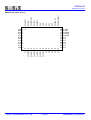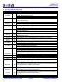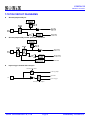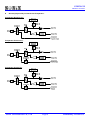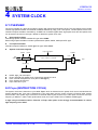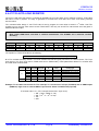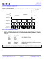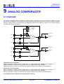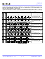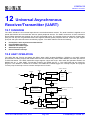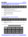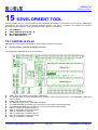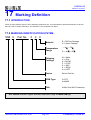
1
SN8P26L38
8-Bit Micro-Controller
SN8P26L38
USER’S MANUAL
Preliminary Specification Version 0.4
SN8P26L38
SONiX 8-Bit Micro-Controller
SONIX reserves the right to make change without further notice to any products herein to improve reliability, function or design. SONIX does not
assume any liability arising out of the application or use of any product or circuit described herein; neither does it convey any license under its patent
rights nor the rights of others. SONIX products are not designed, intended, or authorized for us as components in systems intended, for surgical
implant into the body, or other applications intended to support or sustain life, or for any other application in which the failure of the SONIX product
could create a situation where personal injury or death may occur. Should Buyer purchase or use SONIX products for any such unintended or
unauthorized application. Buyer shall indemnify and hold SONIX and its officers, employees, subsidiaries, affiliates and distributors harmless against
all claims, cost, damages, and expenses, and reasonable attorney fees arising out of, directly or indirectly, any claim of personal injury or death
associated with such unintended or unauthorized use even if such claim alleges that SONIX was negligent regarding the design or manufacture of
the part.
SONiX TECHNOLOGY CO., LTD
Page 1
Preliminary Version 0.4
SN8P26L38
8-Bit Micro-Controller
AMENDMENT HISTORY
Version
VER 0.1
VER 0.2
VER 0.3
VER 0.4
Date
Dec. 2007
Jan. 2008
Feb. 2008
Otc. 2008
Description
First Issue.
Modify system register table.
Modify internal low RC frequency to 10KHz.
Add SN8P26L38F LQFP package type.
SONiX TECHNOLOGY CO., LTD
Page 2
Preliminary Version 0.4
SN8P26L38
8-Bit Micro-Controller
Table of Content
AMENDMENT HISTORY ........................................................................................................................2
1 PRODUCT OVERVIEW..........................................................................................................................8
1.1 FEATURES..........................................................................................................................................8
1.2 SYSTEM BLOCK DIAGRAM.............................................................................................................9
1.3 PIN ASSIGNMENT ...........................................................................................................................10
1.4 PIN DESCRIPTIONS.........................................................................................................................12
1.5 PIN CIRCUIT DIAGRAMS ...............................................................................................................14
2 CENTRAL PROCESSOR UNIT (CPU) ................................................................................................17
2.1 PROGRAM MEMORY (ROM)..........................................................................................................17
2.1.1 RESET VECTOR (0000H) ...........................................................................................................18
2.1.2 INTERRUPT VECTOR (0008H) ..................................................................................................19
2.1.3 LOOK-UP TABLE DESCRIPTION..............................................................................................21
2.1.4 JUMP TABLE DESCRIPTION ....................................................................................................23
2.1.5 CHECKSUM CALCULATION.....................................................................................................25
2.2 DATA MEMORY (RAM) ..................................................................................................................26
2.2.1 SYSTEM REGISTER....................................................................................................................27
2.2.1.1 SYSTEM REGISTER TABLE .............................................................................................27
2.2.1.2 SYSTEM REGISTER DESCRIPTION.................................................................................27
2.2.1.3 BIT DEFINITION of SYSTEM REGISTER.........................................................................28
2.2.2 ACCUMULATOR ........................................................................................................................30
2.2.3 PROGRAM FLAG .......................................................................................................................31
2.2.4 PROGRAM COUNTER ...............................................................................................................32
2.2.5 H, L REGISTERS.........................................................................................................................35
2.2.6 Y, Z REGISTERS .........................................................................................................................36
2.2.7 R REGISTERS .............................................................................................................................37
2.3 ADDRESSING MODE.......................................................................................................................38
2.3.1 IMMEDIATE ADDRESSING MODE ...........................................................................................38
2.3.2 DIRECTLY ADDRESSING MODE ..............................................................................................38
2.3.3 INDIRECTLY ADDRESSING MODE ..........................................................................................38
2.4 STACK OPERATION........................................................................................................................39
2.4.1 OVERVIEW .................................................................................................................................39
2.4.2 STACK REGISTERS ....................................................................................................................40
2.4.3 STACK OPERATION EXAMPLE.................................................................................................41
2.5 CODE OPTION TABLE ....................................................................................................................42
2.5.1 RESET_PIN CODE OPTION.......................................................................................................42
2.5.2 SECURITY CODE OPTION ........................................................................................................42
SONiX TECHNOLOGY CO., LTD
Page 3
Preliminary Version 0.4
SN8P26L38
8-Bit Micro-Controller
3 RESET.....................................................................................................................................................43
3.1 OVERVIEW ......................................................................................................................................43
3.2 POWER ON RESET...........................................................................................................................44
3.3 WATCHDOG RESET ........................................................................................................................44
3.4 BROWN OUT RESET .......................................................................................................................45
3.4.1 THE SYSTEM OPERATING VOLTAGE ......................................................................................46
3.4.2 LOW VOLTAGE DETECTOR (LVD)...........................................................................................46
3.4.3 BROWN OUT RESET IMPROVEMENT ......................................................................................48
3.5 EXTERNAL RESET ..........................................................................................................................49
3.6 EXTERNAL RESET CIRCUIT ..........................................................................................................49
3.6.1 Simply RC Reset Circuit...............................................................................................................49
3.6.2 Diode & RC Reset Circuit............................................................................................................50
3.6.3 Zener Diode Reset Circuit............................................................................................................50
3.6.4 Voltage Bias Reset Circuit ...........................................................................................................51
3.6.5 External Reset IC.........................................................................................................................51
4 SYSTEM CLOCK...................................................................................................................................52
4.1 OVERVIEW ......................................................................................................................................52
4.2 FCPU (INSTRUCTION CYCLE).........................................................................................................52
4.3 SYSTEM HIGH-SPEED CLOCK.......................................................................................................53
4.3.1 HIGH_CLK CODE OPTION.......................................................................................................53
4.3.2 INTERNAL HIGH-SPEED OSCILLATOR RC TYPE (IHRC) .......................................................53
4.3.3 EXTERNAL HIGH-SPEED OSCILLATOR ..................................................................................54
4.3.4 EXTERNAL OSCILLATOR APPLICATION CIRCUIT .................................................................54
4.4 SYSTEM LOW-SPEED CLOCK .......................................................................................................55
4.5 OSCM REGISTER.............................................................................................................................56
4.6 SYSTEM CLOCK MEASUREMENT ................................................................................................56
5 SYSTEM OPERATION MODE.............................................................................................................57
5.1 OVERVIEW ......................................................................................................................................57
5.2 NORMAL MODE ..............................................................................................................................58
5.3 SLOW MODE ....................................................................................................................................58
5.4 POWER DOWN MDOE.....................................................................................................................58
5.5 GREEN MODE ..................................................................................................................................59
5.6 OPERATING MODE CONTROL MACRO .......................................................................................59
5.7 WAKEUP...........................................................................................................................................61
5.7.1 OVERVIEW .................................................................................................................................61
5.7.2 WAKEUP TIME...........................................................................................................................61
5.7.3 P1W WAKEUP CONTROL REGISTER .......................................................................................62
6 INTERRUPT...........................................................................................................................................63
SONiX TECHNOLOGY CO., LTD
Page 4
Preliminary Version 0.4
SN8P26L38
8-Bit Micro-Controller
6.1 OVERVIEW ......................................................................................................................................63
6.2 INTEN INTERRUPT ENABLE REGISTER ......................................................................................64
6.3 INTRQ INTERRUPT REQUEST REGISTER ....................................................................................65
6.4 GIE GLOBAL INTERRUPT OPERATION........................................................................................66
6.5 PUSH, POP ROUTINE.......................................................................................................................67
6.6 EXTERNAL INTERRUPT OPERATION (INT0)...............................................................................68
6.7 INT1 (P0.1) INTERRUPT OPERATION............................................................................................69
6.8 T0 INTERRUPT OPERATION ..........................................................................................................70
6.9 T1 INTERRUPT OPERATION ..........................................................................................................72
6.10 TC1 INTERRUPT OPERATION......................................................................................................73
6.11 COMPARATOR INTERRUPT OPERATION (CMP0, CMP1).........................................................74
6.12 SIO INTERRUPT OPERATION ......................................................................................................75
6.13 UART INTERRUPT OPERATION ..................................................................................................76
6.14 MULTI-INTERRUPT OPERATION................................................................................................77
7 I/O PORT ................................................................................................................................................78
7.1 OVERVIEW ......................................................................................................................................78
7.2 I/O PORT MODE ...............................................................................................................................79
7.3 I/O PULL UP REGISTER...................................................................................................................80
7.4 I/O OPEN-DRAIN REGISTER ..........................................................................................................81
7.5 I/O PORT DATA REGISTER.............................................................................................................83
8 TIMERS ..................................................................................................................................................84
8.1 WATCHDOG TIMER........................................................................................................................84
8.2 TIMER 0 (T0).....................................................................................................................................86
8.2.1 OVERVIEW .................................................................................................................................86
8.2.2 T0M MODE REGISTER ..............................................................................................................86
8.2.3 T0C COUNTING REGISTER.......................................................................................................87
8.2.4 T0 TIMER OPERATION SEQUENCE .........................................................................................88
8.3 TIMER 1 (T1).....................................................................................................................................89
8.3.1 OVERVIEW .................................................................................................................................89
8.3.2 T1M MODE REGISTER ..............................................................................................................89
8.3.3 T1CH, T1CL COUNTING REGISTER .........................................................................................90
8.3.4 T1 TIMER OPERATION SEQUENCE .........................................................................................92
8.4 TIMER/COUNTER 0 (TC1)...............................................................................................................93
8.4.1 OVERVIEW .................................................................................................................................93
8.4.2 TC1M MODE REGISTER............................................................................................................94
8.4.3 TC1C COUNTING REGISTER ....................................................................................................95
8.4.4 TC1R AUTO-LOAD REGISTER ..................................................................................................96
8.4.5 TC1 CLOCK FREQUENCY OUTPUT (BUZZER) .......................................................................97
SONiX TECHNOLOGY CO., LTD
Page 5
Preliminary Version 0.4
SN8P26L38
8-Bit Micro-Controller
8.4.6 TC1 TIMER OPERATION SEQUENCE.......................................................................................98
8.5 PWM1 MODE....................................................................................................................................99
8.5.1 OVERVIEW .................................................................................................................................99
8.5.2 TC1IRQ AND PWM DUTY........................................................................................................100
8.5.3 PWM PROGRAM EXAMPLE ....................................................................................................100
8.5.4 PWM1 DUTY CHANGING NOTICE .........................................................................................101
9 ANALOG COMPARAOTR .................................................................................................................104
9.1 OVERVIEW ....................................................................................................................................104
9.2 CMP0M REGISTER ........................................................................................................................106
9.3 CMP1M REGISTER ........................................................................................................................107
9.4 ANALOG COMPARATOR APPLICATION ...................................................................................108
10 IR OUTPUT ........................................................................................................................................110
10.1 OVERVIEW...................................................................................................................................110
10.2 IR CONTROL REGISTER .............................................................................................................111
10.2.1 TC0M MODE REGISTER........................................................................................................111
10.2.2 TC0C COUNTING REGISTER ................................................................................................111
10.2.3 TC0R AUTO-LOAD REGISTER ..............................................................................................112
10.2.4 TC0D IR DUTY CONTROL REGISTER...................................................................................113
10.2.5 IR OUTPUT OPERATION SEQUENCE ..................................................................................114
11 SERIAL INPUT/OUTPUT TRANSCEIVER (SIO) ..........................................................................115
11.1 OVERVIEW...................................................................................................................................115
11.2 SIO OPERATION ..........................................................................................................................115
11.3 SIOM MODE REGISTER ..............................................................................................................117
11.4 SIOB DATA BUFFER....................................................................................................................118
11.5 SIOR REGISTER DESCRIPTION .................................................................................................119
12 UNIVERSAL ASYNCHRONOUS RECEIVER/TRANSMITTER (UART) ....................................120
12.1 OVERVIEW...................................................................................................................................120
12.2 UART OPERATION ......................................................................................................................120
12.3 UART RECEIVER CONTROL REGISTER...................................................................................123
12.4 UART TRANSMITTER CONTROL REGISTER...........................................................................124
12.5 UART BAUD RATE CONTROL REGISTER ................................................................................124
12.6 UART DATA BUFFER..................................................................................................................125
13 INSTRUCTION TABLE ....................................................................................................................126
14 ELECTRICAL CHARACTERISTIC ................................................................................................127
14.1 ABSOLUTE MAXIMUM RATING ...............................................................................................127
14.2 ELECTRICAL CHARACTERISTIC..............................................................................................127
SONiX TECHNOLOGY CO., LTD
Page 6
Preliminary Version 0.4
SN8P26L38
8-Bit Micro-Controller
15 DEVELOPMENT TOOL ...................................................................................................................128
15.1 SN8P26L38 EV-KIT ........................................................................................................................128
15.2 ICE AND EV-KIT APPLICATION NOTIC .....................................................................................129
16 OTP PROGRAMMING PIN..............................................................................................................130
16.1 THE PIN ASSIGNMENT OF EASY WRITER TRANSITION BOARD SOCKET: ...............................................130
16.2 PROGRAMMING PIN MAPPING: .........................................................................................................131
17 MARKING DEFINITION ..................................................................................................................132
17.1 INTRODUCTION..........................................................................................................................132
17.2 MARKING INDETIFICATION SYSTEM .....................................................................................132
17.3 MARKING EXAMPLE..................................................................................................................133
17.4 DATECODE SYSTEM ..................................................................................................................133
18 PACKAGE INFORMATION.............................................................................................................134
18.1 P-DIP 48 PIN..................................................................................................................................134
18.2 SSOP 48 PIN ..................................................................................................................................135
18.3 LQFP 48 PIN ..................................................................................................................................136
SONiX TECHNOLOGY CO., LTD
Page 7
Preliminary Version 0.4
SN8P26L38
8-Bit Micro-Controller
1 PRODUCT OVERVIEW
1.1 FEATURES
♦ Memory configuration
OTP ROM size: 8K * 16 bits.
RAM size: 880 * 8 bits.
♦
Two 8-bit Timer/Counter
T0: Basic timer.
TC1: Auto-reload timer/counter.
♦ 8 levels stack buffer
♦
♦
♦
♦
One RTC timer (T0).
One channels PWM output.
One channels buzzer output.
One channel IR output (duty/cycle programmable
PWM, TC0).
On chip watchdog timer and clock source is internal
low clock RC type (about 10KHz @3V).
♦ I/O pin configuration
Bi-directional: P0, P1, P2, P3, P4, P5
Programmable open-drain: P1.0, P1.1, P5.0~P5.2,
P3.2, P3.3.
Wakeup:P0, P1 level change trigger.
P1 wake-up function controlled by P1W.
Pull-up resisters: P0, P1, P2, P3, P4, P5
External interrupt input: P0.0, P0.1
External Interrupt trigger edge:
P0.0 controlled by PEDGE register
♦
♦
♦
One channel SIO interface.
One channel UART interface.
♦
Four system clocks
External high clock: RC type up to 8 MHz
External high clock: Crystal type up to 8 MHz
Internal high clock: RC type 8MHz.
Internal low clock: RC type 10KHz(3V).
♦ 3-Level LVD.
Reset system and power monitor.
♦ 2-ch analog comparators with internal selectable
reference voltage 0.9V/1.0V/1.1V/1.2V and
♦
external reference input.
♦ 8 interrupt sources
6 internal interrupts: T0, TC1, CM0, CM1, SIO,
UART
2 external interrupts: INT0 INT1
♦ Powerful instructions
One clock per instruction cycle (1T)
All ROM area JMP instruction.
All ROM area CALL address instruction.
All ROM area lookup table function (MOVC)
SONiX TECHNOLOGY CO., LTD
♦
Four operating modes
Normal mode: Both high and low clock active
Slow mode: Low clock only
Sleep mode: Both high and low clock stop
Green mode: Periodical wakeup by timer
Package (Chip form support)
P-DIP 48 pins
SSOP 48 pins
LQFP 48 pins
Page 8
Preliminary Version 0.4
SN8P26L38
8-Bit Micro-Controller
1.2 SYSTEM BLOCK DIAGRAM
INTERNAL HIGH
RC 8MHz
PC
OTP
IR
ROM
EXTERNAL
HIGH OSC.
INTERNAL
LOW RC
FLAGS
LVD
(Low Voltage Detector)
WATCHDOG TIMER
CM0P
CM0N
CM0O
CM1P
CM1N
CM1O
TIMING GENERATOR
Comparator 0
Comparator 1
ALU
RAM
SIO
SI, SO, SCK
UART
ACC
UTX, URX
SYSTEM REGISTERS
INTERRUPT
CONTROL
IR OUT
IROUT
PWM 1
PWM1
TIMER & COUNTER
BZ1
BUZZER 1
P0
P1
SONiX TECHNOLOGY CO., LTD
P2
P3
Page 9
P4
P5
Preliminary Version 0.4
SN8P26L38
8-Bit Micro-Controller
1.3 PIN ASSIGNMENT
SN8P26L38P (P-DIP 48 pins)
SN8P26L38X (SSOP 48 pins)
VSS
P0.0/INT0
P0.1/INT1
P0.2/RST/VPP
P0.3/XIN
P0.4/XOUT
P0.5
P0.6
P0.7
P1.0
P1.1
P1.2
P1.3
P1.4
P1.5
P1.6
P1.7
P2.0
P2.1
P2.2/CM0N
P2.3/CM0P
P2.4/CM0O
P2.5/CM1N
P2.6/CM1P
SONiX TECHNOLOGY CO., LTD
1
U
48
2
47
3
46
4
45
5
44
6
43
7
42
8
41
9
40
10
39
11
38
12
37
13
36
14
35
15
34
16
33
17
32
18
31
19
30
20
29
21
28
22
27
23
26
24
25
SN8P26L38P
SN8P26L38X
Page 10
VDD
P5.7
P5.6
P5.5
P5.4/IROUT
P5.3/PWM1/BZ1
P5.2/SO
P5.1/SI
P5.0/SCK
P3.3/UTX
P3.2/URX
P3.1
P3.0
P4.7
P4.6
P4.5
P4.4
P4.3
P4.2
P4.1
P4.0
VDD
VSS
P2.7/CM1O
Preliminary Version 0.4
SN8P26L38
8-Bit Micro-Controller
P5.3/BZ1/PWM1
P5.4/IROUT
P5.5
P5.6
P5.7
VDD
VSS
P0.0/INT0
P0.1/INT1
P0.2/RST/VPP
SONiX TECHNOLOGY CO., LTD
Page 11
P4.2
P4.1
P4.0
VDD
VSS
P2.7/CM1O
P2.6/CM1P
P2.5/CM1N
P2.4/CM0O
P2.3/CM0P
P2.2/CM0N
48 47 46 45 44 43 42 41 40 39 38 37
1 O
36 P5.2/SO
2
35 P5.1/SI
3
34 P5.0/SCK
4
33 P3.3/UTX
5
32 P3.2/URX
6
31 P3.1
7
30 P3.0
8
29 P4.7
9
28 P4.6
10
27 P4.5
11
26 P4.4
12
25 P4.3
13 14 15 16 17 18 19 20 21 22 23 24
P2.1
P0.5
P0.6
P0.7
P1.0
P1.1
P1.2
P1.3
P1.4
P1.5
P1.6
P1.7
P2.0
P0.3/XIN
P0.4/XOUT
SN8P26L38F (LQFP 48 pins)
Preliminary Version 0.4
SN8P26L38
8-Bit Micro-Controller
1.4 PIN DESCRIPTIONS
PIN NAME
VDD, VSS
P0.2/RST/
VPP
XIN/P0.3
XOUT/P0.4
P0.0/INT0
P0.1/INT1
P0[7:5]
P1[1:0]
P1[7:0]
P2[1:0]
P2.2/CM0N
P2.3/CM0P
P2.4/CM0O
P2.5/CM1N
P2.6/CM1P
P2.7/CM1O
P3[1:0]
P3.2/URX
P3.3/UTX
P4[7:0]
P5.0/SCK
P5.1/SI
P5.2/SO
TYPE
DESCRIPTION
P
Power supply input pins for digital and analog circuit.
RST: System external reset input pin. Schmitt trigger structure, active “low”, normal stay
to “high”. Build-in wake-up function.
I, P
VPP: OTP power input pin in programming mode.
P0.2: Input only pin with Schmitt trigger structure and no pull-up resistor.
XIN: Oscillator input pin while external oscillator enable (crystal and RC).
I/O
P0.3: Bi-direction pin. Schmitt trigger structure as input mode. Built-in pull-up resisters.
Build-in wake-up function.
XOUT: Oscillator output pin while external crystal enable.
I/O
P0.4: Bi-direction pin. Schmitt trigger structure as input mode. Built-in pull-up resisters.
Build-in wake-up function.
P0.0: Bi-direction pin. Schmitt trigger structure as input mode. Built-in pull-up resisters.
I/O
Build-in wake-up function.
INT0: External interrupt 0 input pin.
P0.1: Bi-direction pin. Schmitt trigger structure as input mode. Built-in pull-up resisters.
Build-in wake-up function.
I/O
INT1: External interrupt 0 input pin.
TC1 event counter input pin.
P0[7:5]: Bi-direction pin. Schmitt trigger structure as input mode. Built-in pull-up resisters.
I/O
Build-in wake-up function.
P1[1:0]: Bi-direction pin. Schmitt trigger structure as input mode. Built-in pull-up resisters.
I/O
Build-in wake-up function. Open-drain structure controlled by P1OC register.
P1[7:2]: Bi-direction pin. Schmitt trigger structure as input mode. Built-in pull-up resisters.
I/O
Build-in wake-up function.
I/O
P2[1:0]: Bi-direction pin. Schmitt trigger structure as input mode. Built-in pull-up resisters.
P2.2: Bi-direction pin. Schmitt trigger structure as input mode. Built-in pull-up resisters.
I/O
CM0N: The negative input pin of comparator.
P2.3: Bi-direction pin. Schmitt trigger structure as input mode. Built-in pull-up resisters.
I/O
CM0P: The positive input pin of comparator.
BTO: Band-gap trimming mode output pin.
P2.4: Bi-direction pin. Schmitt trigger structure as input mode. Built-in pull-up resisters.
I/O
CM0O: The output pin of comparator.
P2.5: Bi-direction pin. Schmitt trigger structure as input mode. Built-in pull-up resisters.
I/O
CM1N: The negative input pin of comparator.
P2.6: Bi-direction pin. Schmitt trigger structure as input mode. Built-in pull-up resisters.
I/O
CM1P: The positive input pin of comparator.
P2.7: Bi-direction pin. Schmitt trigger structure as input mode. Built-in pull-up resisters.
I/O
CM1O: The output pin of comparator.
P3[1:0]: Bi-direction pin. Schmitt trigger structure as input mode. Built-in pull-up resisters.
I/O
Open-drain structure controlled by P1OC register.
P3.2: Bi-direction pin. Schmitt trigger structure as input mode. Built-in pull-up resisters.
I/O
Open-drain structure controlled by P1OC register.
URX: UART data receive pin.
P3.3: Bi-direction pin. Schmitt trigger structure as input mode. Built-in pull-up resisters.
I/O
Open-drain structure controlled by P1OC register.
UTX: UART data transmit pin.
I/O
P4[7:0]: Bi-direction pin. Schmitt trigger structure as input mode. Built-in pull-up resisters.
P5.0: Bi-direction pin. Schmitt trigger structure as input mode. Built-in pull-up resisters.
I/O
Open-drain structure controlled by P1OC register.
SCK: SIO clock pin.
P5.1: Bi-direction pin. Schmitt trigger structure as input mode. Built-in pull-up resisters.
I/O
Open-drain structure controlled by P1OC register.
SI: SIO data input pin.
I/O
P5.2: Bi-direction pin. Schmitt trigger structure as input mode. Built-in pull-up resisters.
SONiX TECHNOLOGY CO., LTD
Page 12
Preliminary Version 0.4
SN8P26L38
8-Bit Micro-Controller
P5.3/BZ1/PWM1
I/O
P5.4/IROUT
I/O
P5[7:5]
I/O
Open-drain structure controlled by P1OC register.
SO: SIO data output pin.
P5.3: Bi-direction pin. Schmitt trigger structure as input mode. Built-in pull-up resisters.
BZ1: Programmable buzzer output pin from TC1/2 signal.
PWM1: Programmable PWM output pin from TC1.
P5.4: Bi-direction pin. Schmitt trigger structure as input mode. Built-in pull-up resisters.
IROUT: IR signal output pin.
P5[7:5]: Bi-direction pin. Schmitt trigger structure as input mode. Built-in pull-up resisters.
SONiX TECHNOLOGY CO., LTD
Page 13
Preliminary Version 0.4
SN8P26L38
8-Bit Micro-Controller
1.5 PIN CIRCUIT DIAGRAMS
l
General purpose I/O pin:
l
General purpose I/O pin with open-drain structure:
l
Input only pin shared with reset pin:
OTP Program Mode
OTP Vpp Input
Input Bus
Pin
Reset Trigger
Reset Pin Code Option
SONiX TECHNOLOGY CO., LTD
Page 14
Preliminary Version 0.4
SN8P26L38
8-Bit Micro-Controller
l
General purpose I/O pin shared with Comparator:
Comparator Negative Pin:
Comparator Positive Pin:
Comparator Output Pin:
SONiX TECHNOLOGY CO., LTD
Page 15
Preliminary Version 0.4
SN8P26L38
8-Bit Micro-Controller
l
General purpose I/O pin shared with external oscillator:
SONiX TECHNOLOGY CO., LTD
Page 16
Preliminary Version 0.4
SN8P26L38
8-Bit Micro-Controller
2 CENTRAL PROCESSOR UNIT (CPU)
2.1 PROGRAM MEMORY (ROM)
F
8K words ROM
ROM
0000H
0001H
.
.
0007H
0008H
0009H
.
.
000FH
0010H
0011H
.
.
.
.
.
1FFCH
1FFDH
1FFEH
1FFFH
Reset vector
User reset vector
Jump to user start address
General purpose area
Interrupt vector
User interrupt vector
User program
General purpose area
End of user program
Reserved
The ROM includes Reset vector, Interrupt vector, General purpose area and Reserved area. The Reset vector is
program beginning address. The Interrupt vector is the head of interrupt service routine when any interrupt occurring.
The General purpose area is main program area including main loop, sub-routines and data table.
SONiX TECHNOLOGY CO., LTD
Page 17
Preliminary Version 0.4
SN8P26L38
8-Bit Micro-Controller
2.1.1 RESET VECTOR (0000H)
A one-word vector address area is used to execute system reset.
F
F
F
Power On Reset (NT0=1, NPD=0).
Watchdog Reset (NT0=0, NPD=0).
External Reset (NT0=1, NPD=1).
After power on reset, external reset or watchdog timer overflow reset, then the chip will restart the program from
address 0000h and all system registers will be set as default values. It is easy to know reset status from NT0, NPD
flags of PFLAG register. The following example shows the way to define the reset vector in the program memory.
Ø
Example: Defining Reset Vector
ORG
JMP
…
0
START
ORG
10H
START:
…
…
ENDP
SONiX TECHNOLOGY CO., LTD
; 0000H
; Jump to user program address.
; 0010H, The head of user program.
; User program
; End of program
Page 18
Preliminary Version 0.4
SN8P26L38
8-Bit Micro-Controller
2.1.2 INTERRUPT VECTOR (0008H)
A 1-word vector address area is used to execute interrupt request. If any interrupt service executes, the program
counter (PC) value is stored in stack buffer and jump to 0008h of program memory to execute the vectored interrupt.
Users have to define the interrupt vector. The following example shows the way to define the interrupt vector in the
program memory.
-
Note: ”PUSH”, “POP” instructions save and load ACC/PFLAG without (NT0, NPD). PUSH/POP buffer is a
unique buffer and only one level.
Ø
Example: Defining Interrupt Vector. The interrupt service routine is following ORG 8.
.CODE
ORG
JMP
…
0
START
; 0000H
; Jump to user program address.
ORG
PUSH
…
…
POP
RETI
…
8
; Interrupt vector.
; Save ACC and PFLAG register to buffers.
; Load ACC and PFLAG register from buffers.
; End of interrupt service routine
START:
…
…
JMP
…
; The head of user program.
; User program
START
ENDP
SONiX TECHNOLOGY CO., LTD
; End of user program
; End of program
Page 19
Preliminary Version 0.4
SN8P26L38
8-Bit Micro-Controller
Ø
Example: Defining Interrupt Vector. The interrupt service routine is following user program.
.CODE
ORG
JMP
…
ORG
JMP
0
START
; 0000H
; Jump to user program address.
8
MY_IRQ
; Interrupt vector.
; 0008H, Jump to interrupt service routine address.
ORG
10H
START:
…
…
…
JMP
…
; 0010H, The head of user program.
; User program.
START
MY_IRQ:
PUSH
…
…
POP
RETI
…
ENDP
-
; End of user program.
;The head of interrupt service routine.
; Save ACC and PFLAG register to buffers.
; Load ACC and PFLAG register from buffers.
; End of interrupt service routine.
; End of program.
Note: It is easy to understand the rules of SONIX program from demo programs given above. These
points are as following:
1. The address 0000H is a “JMP” instruction to make the program starts from the beginning.
2. The address 0008H is interrupt vector.
3. User’s program is a loop routine for main purpose application.
SONiX TECHNOLOGY CO., LTD
Page 20
Preliminary Version 0.4
SN8P26L38
8-Bit Micro-Controller
2.1.3 LOOK-UP TABLE DESCRIPTION
In the ROM’s data lookup function, Y register is pointed to middle byte address (bit 8~bit 15) and Z register is pointed
to low byte address (bit 0~bit 7) of ROM. After MOVC instruction executed, the low-byte data will be stored in ACC and
high-byte data stored in R register.
Ø
Example: To look up the ROM data located “TABLE1”.
@@:
TABLE1:
B0MOV
B0MOV
MOVC
Y, #TABLE1$M
Z, #TABLE1$L
INCMS
JMP
INCMS
NOP
Z
@F
Y
MOVC
…
DW
DW
DW
…
0035H
5105H
2012H
; To set lookup table1’s middle address
; To set lookup table1’s low address.
; To lookup data, R = 00H, ACC = 35H
; Increment the index address for next address.
; Z+1
; Z is not overflow.
; Z overflow (FFH à 00), à Y=Y+1
;
;
; To lookup data, R = 51H, ACC = 05H.
;
; To define a word (16 bits) data.
-
Note: The Y register will not increase automatically when Z register crosses boundary from 0xFF to
0x00. Therefore, user must take care such situation to avoid look-up table errors. If Z register is
overflow, Y register must be added one. The following INC_YZ macro shows a simple method to process
Y and Z registers automatically.
Ø
Example: INC_YZ macro.
INC_YZ
MACRO
INCMS
JMP
INCMS
NOP
Z
@F
; Z+1
; Not overflow
Y
; Y+1
; Not overflow
@@:
ENDM
SONiX TECHNOLOGY CO., LTD
Page 21
Preliminary Version 0.4
SN8P26L38
8-Bit Micro-Controller
Ø
Example: Modify above example by “INC_YZ” macro.
B0MOV
B0MOV
MOVC
Y, #TABLE1$M
Z, #TABLE1$L
INC_YZ
@@:
TABLE1:
MOVC
…
DW
DW
DW
…
0035H
5105H
2012H
; To set lookup table1’s middle address
; To set lookup table1’s low address.
; To lookup data, R = 00H, ACC = 35H
; Increment the index address for next address.
;
; To lookup data, R = 51H, ACC = 05H.
;
; To define a word (16 bits) data.
The other example of look-up table is to add Y or Z index register by accumulator. Please be careful if “carry” happen.
Ø
Example: Increase Y and Z register by B0ADD/ADD instruction.
B0MOV
B0MOV
Y, #TABLE1$M
Z, #TABLE1$L
; To set lookup table’s middle address.
; To set lookup table’s low address.
B0MOV
B0ADD
A, BUF
Z, A
; Z = Z + BUF.
B0BTS1
JMP
INCMS
NOP
FC
GETDATA
Y
; Check the carry flag.
; FC = 0
; FC = 1. Y+1.
GETDATA:
;
; To lookup data. If BUF = 0, data is 0x0035
; If BUF = 1, data is 0x5105
; If BUF = 2, data is 0x2012
MOVC
…
TABLE1:
DW
DW
DW
…
0035H
5105H
2012H
SONiX TECHNOLOGY CO., LTD
; To define a word (16 bits) data.
Page 22
Preliminary Version 0.4
SN8P26L38
8-Bit Micro-Controller
2.1.4 JUMP TABLE DESCRIPTION
The jump table operation is one of multi-address jumping function. Add low-byte program counter (PCL) and ACC
value to get one new PCL. If PCL is overflow after PCL+ACC, PCH adds one automatically. The new program counter
(PC) points to a series jump instructions as a listing table. It is easy to make a multi-jump program depends on the
value of the accumulator (A).
-
Note: PCH only support PC up counting result and doesn’t support PC down counting. When PCL is
carry after PCL+ACC, PCH adds one automatically. If PCL borrow after PCL–ACC, PCH keeps value and
not change.
Ø
Example: Jump table.
ORG
0X0100
; The jump table is from the head of the ROM boundary
B0ADD
JMP
JMP
JMP
JMP
PCL, A
A0POINT
A1POINT
A2POINT
A3POINT
; PCL = PCL + ACC, PCH + 1 when PCL overflow occurs.
; ACC = 0, jump to A0POINT
; ACC = 1, jump to A1POINT
; ACC = 2, jump to A2POINT
; ACC = 3, jump to A3POINT
SONIX provides a macro for safe jump table function. This macro will check the ROM boundary and move the jump
table to the right position automatically. The side effect of this macro maybe wastes some ROM size.
Ø
Example: If “jump table” crosses over ROM boundary will cause errors.
@JMP_A
-
MACRO
IF
JMP
ORG
ENDIF
ADD
ENDM
VAL
(($+1) !& 0XFF00) !!= (($+(VAL)) !& 0XFF00)
($ | 0XFF)
($ | 0XFF)
PCL, A
Note: “VAL” is the number of the jump table listing number.
SONiX TECHNOLOGY CO., LTD
Page 23
Preliminary Version 0.4
SN8P26L38
8-Bit Micro-Controller
Ø
Example: “@JMP_A” application in SONIX macro file called “MACRO3.H”.
B0MOV
@JMP_A
JMP
JMP
JMP
JMP
JMP
A, BUF0
5
A0POINT
A1POINT
A2POINT
A3POINT
A4POINT
; “BUF0” is from 0 to 4.
; The number of the jump table listing is five.
; ACC = 0, jump to A0POINT
; ACC = 1, jump to A1POINT
; ACC = 2, jump to A2POINT
; ACC = 3, jump to A3POINT
; ACC = 4, jump to A4POINT
If the jump table position is across a ROM boundary (0x00FF~0x0100), the “@JMP_A” macro will adjust the jump table
routine begin from next RAM boundary (0x0100).
Ø
Example: “@JMP_A” operation.
; Before compiling program.
ROM address
0X00FD
0X00FE
0X00FF
0X0100
0X0101
B0MOV
@JMP_A
JMP
JMP
JMP
JMP
JMP
A, BUF0
5
A0POINT
A1POINT
A2POINT
A3POINT
A4POINT
; “BUF0” is from 0 to 4.
; The number of the jump table listing is five.
; ACC = 0, jump to A0POINT
; ACC = 1, jump to A1POINT
; ACC = 2, jump to A2POINT
; ACC = 3, jump to A3POINT
; ACC = 4, jump to A4POINT
A, BUF0
5
A0POINT
A1POINT
A2POINT
A3POINT
A4POINT
; “BUF0” is from 0 to 4.
; The number of the jump table listing is five.
; ACC = 0, jump to A0POINT
; ACC = 1, jump to A1POINT
; ACC = 2, jump to A2POINT
; ACC = 3, jump to A3POINT
; ACC = 4, jump to A4POINT
; After compiling program.
ROM address
0X0100
0X0101
0X0102
0X0103
0X0104
B0MOV
@JMP_A
JMP
JMP
JMP
JMP
JMP
SONiX TECHNOLOGY CO., LTD
Page 24
Preliminary Version 0.4
SN8P26L38
8-Bit Micro-Controller
2.1.5 CHECKSUM CALCULATION
The last ROM address are reserved area. User should avoid these addresses (last address) when calculate the
Checksum value.
Ø
Example: The demo program shows how to calculated Checksum from 00H to the end of user’s code.
MOV
B0MOV
MOV
B0MOV
CLR
CLR
A,#END_USER_CODE$L
END_ADDR1, A
; Save low end address to end_addr1
A,#END_USER_CODE$M
END_ADDR2, A
; Save middle end address to end_addr2
Y
; Set Y to 00H
Z
; Set Z to 00H
MOVC
B0BSET
ADD
MOV
ADC
JMP
FC
DATA1, A
A, R
DATA2, A
END_CHECK
; Clear C flag
; Add A to Data1
INCMS
JMP
JMP
Z
@B
Y_ADD_1
; Z=Z+1
; If Z != 00H calculate to next address
; If Z = 00H increase Y
MOV
CMPRS
JMP
MOV
CMPRS
JMP
JMP
A, END_ADDR1
A, Z
AAA
A, END_ADDR2
A, Y
AAA
CHECKSUM_END
INCMS
NOP
JMP
Y
; Increase Y
@B
; Jump to checksum calculate
@@:
; Add R to Data2
; Check if the YZ address =
the end of code
AAA:
END_CHECK:
; Check if Z = low end address
; If Not jump to checksum calculate
; If Yes, check if Y = middle end address
; If Not jump to checksum calculate
; If Yes checksum calculated is done.
Y_ADD_1:
CHECKSUM_END:
…
…
END_USER_CODE:
SONiX TECHNOLOGY CO., LTD
; Label of program end
Page 25
Preliminary Version 0.4
SN8P26L38
8-Bit Micro-Controller
2.2 DATA MEMORY (RAM)
F
880 X 8-bit RAM
BANK
Bank 0
Address
000H
...
...
07FH
RAM Location
RAM Bank 0
General purpose area
080H
System Register
Bank 1
Bank 2
Bank 3
...
0FFH
100H
…
…
1FFH
200H
…
…
2FFH
300H
…
…
3EFH
80h~FFh of Bank 0 store
system registers (128
bytes).
End of Bank 0
RAM Bank 1
General purpose area
End of Bank 1
RAM Bank 2
General purpose area
End of Bank 2
RAM Bank 3
General purpose area
End of Bank 3
The 880-byte general purpose RAM is separated into Bank 0~Bank 3. Accessing the two banks’ RAM is controlled by
“RBANK” register. When RBANK = 0, the program controls Bank 0 RAM directly. When RBANK = 1, the program
controls Bank 1 RAM directly. Under one bank condition and need to access the other bank RAM, setup the RBANK
register is necessary. Sonix provides “Bank 0” type instructions (e.g. b0mov, b0add, b0bts1, b0bset…) to control Bank
0 RAM in non-zero RAM bank condition directly.
Ø
Example: Access Bank 0 RAM in Bank 1 condition. Move Bank 0 RAM (WK00) value to Bank 1 RAM
(WK01).
; Bank 1 (RBANK = 1)
B0MOV
MOV
-
A, WK00
WK01,A
; Use Bank 0 type instruction to access Bank 0 RAM.
Note: For multi-bank RAM program, it is not easy to control RAM Bank selection. Users have to take care
the RBANK condition very carefully, especially for interrupt service routine. The system won’t save the
RBANK and switch RAM bank to Bank 0, so these controls must be through program. It is a good to use
Bank 0 type instruction to process the situations.
SONiX TECHNOLOGY CO., LTD
Page 26
Preliminary Version 0.4
SN8P26L38
8-Bit Micro-Controller
2.2.1 SYSTEM REGISTER
2.2.1.1SYSTEM REGISTER TABLE
0
1
2
3
4
5
8
9
L
H
R
Z
Y
-
PFLAG RBANK
-
-
-
-
-
-
A
T1M
T1CL
T1CH
URTX
URTXD URTXD URRXD URRXD
1
2
1
2
SIOB
P0M
-
B
C
D
E
F
URRX URBRC
-
-
-
-
SIOM
SIOR
P1W
P1M
P2M
P3M
P4M
P5M
6
-
7
8
9
A
B
C
D
E
F
-
-
-
-
-
-
-
-
-
-
-
-
-
-
-
-
-
INTRQ
CMP0M CMP1M
-
-
-
-
-
-
-
PEDGE
INTEN
OSCM
-
WDTR
IRR
PCL
PCH
P0
P1
P2
P3
P4
P5
-
-
T0M
T0C
IRM
IRC
TC1M
TC1C
TC1R
STKP
P0UR
P1UR
P2UR
P3UR
P4UR
P5UR
@HL
@YZ
IRD
P1OC
-
-
-
-
-
-
STK7L STK7H STK6L STK6H STK5L STK5H STK4L STK4H STK3L STK3H STK2L STK2H STK1L STK1H STK0L STK0H
2.2.1.2SYSTEM REGISTER DESCRIPTION
PFLAG =
H, L =
P1W =
CMPnM =
PEDGE =
PnM =
P1OC =
INTRQ =
OSCM =
T0M =
TC1M =
TC1R =
T1CH,L =
IRC =
IRD =
URTX =
URTXD1,2 =
URBRC =
SIOR =
STKP =
ROM page and special flag register.
Working, @HL and ROM addressing register.
Port 1 wakeup register.
Comparator control register.
P0.0 edge direction register.
Port n input/output mode register.
Open-drain control register.
Interrupt request register.
Oscillator mode register.
T0 mode register.
TC1 mode control register.
TC1 auto-reload buffer.
T1 16-bit counter register.
IR cycle control register.
IR duty control register.
UART transmit control register.
UART transmit data buffers.
UART baud rate control register.
SIO clock rate control register.
Stack pointer buffer.
SONiX TECHNOLOGY CO., LTD
R=
Y, Z =
RBANK =
@HL =
@YZ =
Pn =
PnUR =
INTEN =
PCH, PCL =
T0C =
TC1C =
T1M =
IRM =
IRR =
WDTR =
URRX =
URRXD1,2 =
SIOM =
SIOB =
STK0~STK7 =
Page 27
Working register and ROM look-up data buffer.
Working, @YZ and ROM addressing register.
Ram bank selection register.
RAM HL indirect addressing index pointer.
RAM YZ indirect addressing index pointer.
Port n data buffer.
Port n pull-up resister control register.
Interrupt enable register.
Program counter.
T0 counting register.
TC1 counter register.
T1 mode register.
IR output control register.
IR auto-reload register.
Watchdog timer clear register.
UART receive control register.
UART receive data buffers.
SIO mode control register.
SIO data buffer.
Stack 0 ~ stack 7 buffer.
Preliminary Version 0.4
SN8P26L38
8-Bit Micro-Controller
2.2.1.3BIT DEFINITION of SYSTEM REGISTER
Address
080H
081H
082H
083H
084H
086H
087H
09CH
09DH
0A0H
0A1H
0A2H
0A4H
0A5H
0A6H
0A7H
0A8H
0A9H
0AAH
0B4H
0B5H
0B6H
0B4H
0BFH
0C0H
0C1H
0C2H
0C3H
0C4H
0C5H
0C8H
0C9H
0CAH
0CCH
0CDH
0CEH
0CFH
0D0H
0D1H
0D2H
0D3H
0D4H
0D5H
0D8H
0D9H
0DAH
0DBH
0DCH
0DDH
0DEH
0DFH
0E0H
0E1H
0E2H
0E3H
0E4H
0E5H
0E6H
0E7H
0E8H
0E9H
0F0H
0F1H
0F2H
0F3H
0F4H
Bit7
LBIT7
HBIT7
RBIT7
ZBIT7
YBIT7
NT0
CM0EN
CM1EN
T1ENB
T1CL7
T1CH7
Bit6
LBIT6
HBIT6
RBIT6
ZBIT6
YBIT6
NPD
CM0IEN
CM1IEN
T1rate2
T1CL6
T1CH6
Bit5
LBIT5
HBIT5
RBIT5
ZBIT5
YBIT5
LVD28
CM0IRQ
CM1IRQ
T1rate1
T1CL5
T1CH5
URXEN
UDIV4
UTXD17
UTXD27
URXD17
URXD27
SENB
SIOR7
SIOB7
P07M
P17W
P17M
P27M
P47M
P57M
SIOIRQ
SIOIEN
WDTR7
IRR7
PC7
P07
P17
P27
P47
P57
T0ENB
T0C7
IRC7
TC1ENB
TC1C7
TC1R7
GIE
P07R
P17R
P27R
P47R
P57R
@HL7
@YZ7
IRD7
P52OC
S7PC7
1
S6PC7
1
S5PC7
URXS1
UDIV3
UTXD16
UTXD26
URXD16
URXD26
START
SIOR6
SIOB6
P06M
P16W
P16M
P26M
P46M
P56M
TC1IRQ
TC1IEN
WDTR6
IRR6
PC6
P06
P16
P26
P46
P56
T0rate2
T0C6
IRC6
TC1rate2
TC1C6
TC1R6
P06R
P16R
P26R
P46R
P56R
@ HL 6
@YZ6
IRD6
P51OC
S7PC6
1
S6PC6
1
S5PC6
URXS0
UDIV2
UTXD15
UTXD25
URXD15
URXD25
SRATE1
SIOR5
SIOB5
P05M
P15W
P15M
P25M
P45M
P55M
T1IRQ
T1IEN
WDTR5
IRR5
PC5
P05
P15
P25
P45
P55
T0rate1
T0C5
IRC5
TC1rate1
TC1C5
TC1R5
P05R
P15R
P25R
P45R
P55R
@ HL5
@YZ5
IRD5
P50OC
S7PC5
1
S6PC5
1
S5PC5
SONiX TECHNOLOGY CO., LTD
Bit4
LBIT4
HBIT4
RBIT4
ZBIT4
YBIT4
LVD24
CM0OEN
CM1OEN
T1rate0
T1CL4
T1CH4
UTXEN
URXPEN
UDIV1
UTXD14
UTXD24
URXD14
URXD24
SRATE0
SIOR4
SIOB4
P04M
P00G1
P14W
P14M
P24M
P44M
P54M
T0IRQ
T0IEN
CPUM1
WDTR4
IRR4
PC4
PC12
P04
P14
P24
P44
P54
T0rate0
T0C4
IRC4
TC1rate0
TC1C4
TC1R4
P04R
P14R
P24R
P44R
P54R
@ HL4
@YZ4
IRD4
P33OC
S7PC4
S7PC12
S6PC4
S6PC12
S5PC4
Bit3
LBIT3
HBIT3
RBIT3
ZBIT3
YBIT3
CM0REF
CM1REF
Bit2
LBIT2
HBIT2
RBIT2
ZBIT2
YBIT2
C
RBANKS2
CM0OUT
CM1OUT
Bit1
LBIT1
HBIT1
RBIT1
ZBIT1
YBIT1
DC
RBANKS1
CMS1
-
Bit0
LBIT0
HBIT0
RBIT0
ZBIT0
YBIT0
Z
RBANKS0
CMS0
-
T1CL3
T1CH3
UTXPEN
URXPS
UDIV0
UTXD13
UTXD23
URXD13
URXD23
MLSB
SIOR3
SIOB3
P03M
P00G0
P13W
P13M
P23M
P33M
P43M
P53M
RXIRQ
RXIEN
CPUM0
WDTR3
IRR3
PC3
PC11
P03
P13
P23
P33
P43
P53
T0C3
IRC3
TC1CKS
TC1C3
TC1R3
P03R
P13R
P23R
P33R
P43R
P53R
@ HL3
@YZ3
IRD3
P32OC
S7PC3
S7PC11
S6PC3
S6PC11
S5PC3
T1CL2
T1CH2
UTXPS
URXPC
UPCS2
UTXD12
UTXD22
URXD12
URXD22
SCLKMD
SIOR2
SIOB2
P12W
P12M
P22M
P32M
P42M
P52M
TXIRQ
TXIEN
CLKMD
WDTR2
IRR2
PC2
PC10
P02
P12
P22
P32
P42
P52
T0C2
IRC2
ALOAD1
TC1C2
TC1R2
STKPB2
P12R
P22R
P32R
P42R
P52R
@ HL2
@YZ2
IRD2
S7PC2
S7PC10
S6PC2
S6PC10
S5PC2
T1CL1
T1CH1
UTXM
URXM
UPCS1
UTXD11
UTXD21
URXD11
URXD21
CPOL
SIOR1
SIOB1
P01M
P11W
P11M
P21M
P31M
P41M
P51M
P01IRQ
P01IEN
STPHX
WDTR1
IRR1
PC1
PC9
P01
P11
P21
P31
P41
P51
T0C1
IREN
IRC1
TC1OUT
TC1C1
TC1R1
STKPB1
P01R
P11R
P21R
P31R
P41R
P51R
@ HL1
@YZ1
IRD1
P11OC
S7PC1
S7PC9
S6PC1
S6PC9
S5PC1
T1CL0
T1CH0
Page 28
UPCS0
UTXD10
UTXD20
URXD10
URXD20
CPHA
SIOR0
SIOB0
P00M
P10W
P10M
P20M
P30M
P40M
P50M
P00IRQ
P00IEN
WDTR0
IRR0
PC0
PC8
P00
P10
P20
P30
P40
P50
T0TB
T0C0
CREN
IRC0
PWM1OUT
TC1C0
TC1R0
STKPB0
P00R
P10R
P20R
P30R
P40R
P50R
@ HL0
@YZ0
IRD0
P10OC
S7PC0
S7PC8
S6PC0
S6PC8
S5PC0
R/W
R/W
R/W
R/W
R/W
R/W
R/W
R/W
R/W
R/W
R/W
R/W
R/W
R/W
R/W
R/W
R/W
R/W
R/W
R/W
R/W
W
R/W
R/W
R/W
W
R/W
R/W
R/W
R/W
R/W
R/W
R/W
R/W
W
W
R/W
R/W
R/W
R/W
R/W
R/W
R/W
R/W
R/W
R/W
R/W
R/W
R/W
R/W
W
R/W
W
W
W
W
W
W
R/W
R/W
W
W
R/W
R/W
R/W
R/W
R/W
Remarks
L
H
R
Z
Y
PFLAG
RBANK
CMP0M
CMP1M
T1M
T1CL
T1CH
URTX
URRX
URBRC
URTXD1
URTXD2
URRXD1
URRXD2
SIOM
SIOR
SIOB
P0M
PEDGE
P1W wakeup register
P1M I/O direction
P2M I/O direction
P3M I/O direction
P4M I/O direction
P5M I/O direction
INTRQ
INTEN
OSCM
WDTR
IRR
PCL
PCH
P0 data buffer
P1 data buffer
P2 data buffer
P3 data buffer
P4 data buffer
P5 data buffer
T0M
T0C
IRM
IRC
TC1M
TC1C
TC1R
STKP stack pointer
P0 pull-up register
P1 pull-up register
P2 pull-up register
P3 pull-up register
P4 pull-up register
P5 pull-up register
@HL index pointer
@YZ index pointer
IRD
P1OC
STK7L
STK7H
STK6L
STK6H
STK5L
Preliminary Version 0.4
SN8P26L38
8-Bit Micro-Controller
0F5H
0F6H
0F7H
0F8H
0F9H
0FAH
0FBH
0FCH
0FDH
0FEH
0FFH
-
1
S4PC7
1
S3PC7
1
S2PC7
1
S1PC7
1
S0PC7
1
1
S4PC6
1
S3PC6
1
S2PC6
1
S1PC6
1
S0PC6
1
1
S4PC5
1
S3PC5
1
S2PC5
1
S1PC5
1
S0PC5
1
S5PC12
S4PC4
S4PC12
S3PC4
S3PC12
S2PC4
S2PC12
S1PC4
S1PC12
S0PC4
S0PC12
S5PC11
S4PC3
S4PC11
S3PC3
S3PC11
S2PC3
S2PC11
S1PC3
S1PC11
S0PC3
S0PC11
S5PC10
S4PC2
S4PC10
S3PC2
S3PC10
S2PC2
S2PC10
S1PC2
S1PC10
S0PC2
S0PC10
S5PC9
S4PC1
S4PC9
S3PC1
S3PC9
S2PC1
S2PC9
S1PC1
S1PC9
S0PC1
S0PC9
S5PC8
S4PC0
S4PC8
S3PC0
S3PC8
S2PC0
S2PC8
S1PC0
S1PC8
S0PC0
S0PC8
R/W
R/W
R/W
R/W
R/W
R/W
R/W
R/W
R/W
R/W
R/W
STK5H
STK4L
STK4H
STK3L
STK3H
STK2L
STK2H
STK1L
STK1H
STK0L
STK0H
Note:
1. To avoid system error, please be sure to put all the “0” and “1” as it indicates in the above
table.
2.
3.
4.
5.
All of register names had been declared in SN8ASM assembler.
One-bit name had been declared in SN8ASM assembler with “F” prefix code.
“b0bset”, “b0bclr”, ”bset”, ”bclr” instructions are only available to the “R/W” registers.
For detail description, please refer to the “System Register Quick Reference Table”.
SONiX TECHNOLOGY CO., LTD
Page 29
Preliminary Version 0.4
SN8P26L38
8-Bit Micro-Controller
2.2.2 ACCUMULATOR
The ACC is an 8-bit data register responsible for transferring or manipulating data between ALU and data memory. If
the result of operating is zero (Z) or there is carry (C or DC) occurrence, then these flags will be set to PFLAG register.
ACC is not in data memory (RAM), so ACC can’t be access by “B0MOV” instruction during the instant addressing
mode.
Ø
Example: Read and write ACC value.
; Read ACC data and store in BUF data memory.
MOV
BUF, A
; Write a immediate data into ACC.
MOV
A, #0FH
; Write ACC data from BUF data memory.
MOV
A, BUF
B0MOV
A, BUF
; or
The system doesn’t store ACC and PFLAG value when interrupt executed. ACC and PFLAG data must be saved to
other data memories. “PUSH”, “POP” save and load ACC, PFLAG data into buffers.
Ø
Example: Protect ACC and working registers.
INT_SERVICE:
PUSH
…
…
POP
; Save ACC and PFLAG to buffers.
.
RETI
SONiX TECHNOLOGY CO., LTD
; Load ACC and PFLAG from buffers.
; Exit interrupt service vector
Page 30
Preliminary Version 0.4
SN8P26L38
8-Bit Micro-Controller
2.2.3 PROGRAM FLAG
The PFLAG register contains the arithmetic status of ALU operation, system reset status and LVD detecting status.
NT0, NPD bits indicate system reset status including power on reset, LVD reset, reset by external pin active and
watchdog reset. C, DC, Z bits indicate the result status of ALU operation. LVD24, LVD28 bits indicate LVD detecting
power voltage status.
086H
Bit 7
Bit 6
Bit 5
Bit 4
Bit 3
Bit 2
Bit 1
Bit 0
PFLAG
NT0
NPD
LVD28
LVD24
C
DC
Z
Read/Write
R/W
R/W
R
R
R/W
R/W
R/W
After reset
0
0
0
0
0
Bit [7:6]
NT0, NPD: Reset status flag.
NT0
NPD
Reset Status
0
0
Watch-dog time out
0
1
Reserved
1
0
Reset by LVD
1
1
Reset by external Reset Pin
Bit 5
LVD30: LVD 2.8V operating flag and only support LVD code option is LVD_H.
0 = Inactive (VDD > 2.8V).
1 = Active (VDD ≦ 2.8V).
Bit 4
LVD24: LVD 2.4V operating flag and only support LVD code option is LVD_M.
0 = Inactive (VDD > 2.4V).
1 = Active (VDD ≦ 2.4V).
Bit 2
C: Carry flag
1 = Addition with carry, subtraction without borrowing, rotation with shifting out logic “1”, comparison result
≥ 0.
0 = Addition without carry, subtraction with borrowing signal, rotation with shifting out logic “0”, comparison
result < 0.
Bit 1
DC: Decimal carry flag
1 = Addition with carry from low nibble, subtraction without borrow from high nibble.
0 = Addition without carry from low nibble, subtraction with borrow from high nibble.
Bit 0
Z: Zero flag
1 = The result of an arithmetic/logic/branch operation is zero.
0 = The result of an arithmetic/logic/branch operation is not zero.
-
Note: Refer to instruction set table for detailed information of C, DC and Z flags.
SONiX TECHNOLOGY CO., LTD
Page 31
Preliminary Version 0.4
SN8P26L38
8-Bit Micro-Controller
2.2.4 PROGRAM COUNTER
The program counter (PC) is a 13-bit binary counter separated into the high-byte 5 and the low-byte 8 bits. This
counter is responsible for pointing a location in order to fetch an instruction for kernel circuit. Normally, the program
counter is automatically incremented with each instruction during program execution.
Besides, it can be replaced with specific address by executing CALL or JMP instruction. When JMP or CALL instruction
is executed, the destination address will be inserted to bit 0 ~ bit 12.
PC
After
reset
Bit 15 Bit 14 Bit 13 Bit 12 Bit 11 Bit 10 Bit 9
PC12 PC11 PC10 PC9
-
-
-
0
0
0
0
Bit 8
PC8
Bit 7
PC7
Bit 6
PC6
Bit 5
PC5
Bit 4
PC4
Bit 3
PC3
Bit 2
PC2
Bit 1
PC1
Bit 0
PC0
0
0
0
0
0
0
0
0
0
PCH
F
PCL
ONE ADDRESS SKIPPING
There are nine instructions (CMPRS, INCS, INCMS, DECS, DECMS, BTS0, BTS1, B0BTS0, B0BTS1) with one
address skipping function. If the result of these instructions is true, the PC will add 2 steps to skip next instruction.
If the condition of bit test instruction is true, the PC will add 2 steps to skip next instruction.
FC
C0STEP
; To skip, if Carry_flag = 1
; Else jump to C0STEP.
C0STEP:
B0BTS1
JMP
…
…
NOP
A, BUF0
FZ
C1STEP
; Move BUF0 value to ACC.
; To skip, if Zero flag = 0.
; Else jump to C1STEP.
C1STEP:
B0MOV
B0BTS0
JMP
…
…
NOP
If the ACC is equal to the immediate data or memory, the PC will add 2 steps to skip next instruction.
C0STEP:
CMPRS
JMP
…
…
NOP
A, #12H
C0STEP
SONiX TECHNOLOGY CO., LTD
; To skip, if ACC = 12H.
; Else jump to C0STEP.
Page 32
Preliminary Version 0.4
SN8P26L38
8-Bit Micro-Controller
If the destination increased by 1, which results overflow of 0xFF to 0x00, the PC will add 2 steps to skip next
instruction.
INCS instruction:
C0STEP:
INCS
JMP
…
…
NOP
BUF0
C0STEP
; Jump to C0STEP if ACC is not zero.
INCMS
JMP
…
…
NOP
BUF0
C0STEP
; Jump to C0STEP if BUF0 is not zero.
INCMS instruction:
C0STEP:
If the destination decreased by 1, which results underflow of 0x00 to 0xFF, the PC will add 2 steps to skip next
instruction.
DECS instruction:
C0STEP:
DECS
JMP
…
…
NOP
BUF0
C0STEP
; Jump to C0STEP if ACC is not zero.
DECMS
JMP
…
…
NOP
BUF0
C0STEP
; Jump to C0STEP if BUF0 is not zero.
DECMS instruction:
C0STEP:
SONiX TECHNOLOGY CO., LTD
Page 33
Preliminary Version 0.4
SN8P26L38
8-Bit Micro-Controller
F
MULTI-ADDRESS JUMPING
Users can jump around the multi-address by either JMP instruction or ADD M, A instruction (M = PCL) to activate
multi-address jumping function. Program Counter supports “ADD M,A”, ”ADC M,A” and “B0ADD M,A” instructions
for carry to PCH when PCL overflow automatically. For jump table or others applications, users can calculate PC value
by the three instructions and don’t care PCL overflow problem.
-
Note: PCH only support PC up counting result and doesn’t support PC down counting. When PCL is
carry after PCL+ACC, PCH adds one automatically. If PCL borrow after PCL–ACC, PCH keeps value and
not change.
Ø
Example: If PC = 0323H (PCH = 03H, PCL = 23H)
; PC = 0323H
MOV
B0MOV
…
A, #28H
PCL, A
; Jump to address 0328H
MOV
B0MOV
…
A, #00H
PCL, A
; Jump to address 0300H
; PC = 0328H
Ø
Example: If PC = 0323H (PCH = 03H, PCL = 23H)
; PC = 0323H
B0ADD
JMP
JMP
JMP
JMP
…
…
PCL, A
A0POINT
A1POINT
A2POINT
A3POINT
SONiX TECHNOLOGY CO., LTD
; PCL = PCL + ACC, the PCH cannot be changed.
; If ACC = 0, jump to A0POINT
; ACC = 1, jump to A1POINT
; ACC = 2, jump to A2POINT
; ACC = 3, jump to A3POINT
Page 34
Preliminary Version 0.4
SN8P26L38
8-Bit Micro-Controller
2.2.5 H, L REGISTERS
The H and L registers are the 8-bit buffers. There are two major functions of these registers.
l
l
can be used as general working registers
can be used as RAM data pointers with @HL register
081H
H
Read/Write
After reset
Bit 7
HBIT7
R/W
X
Bit 6
HBIT6
R/W
X
Bit 5
HBIT5
R/W
X
Bit 4
HBIT4
R/W
X
Bit 3
HBIT3
R/W
X
Bit 2
HBIT2
R/W
X
Bit 1
HBIT1
R/W
X
Bit 0
HBIT0
R/W
X
080H
L
Read/Write
After reset
Bit 7
LBIT7
R/W
X
Bit 6
LBIT6
R/W
X
Bit 5
LBIT5
R/W
X
Bit 4
LBIT4
R/W
X
Bit 3
LBIT3
R/W
X
Bit 2
LBIT2
R/W
X
Bit 1
LBIT1
R/W
X
Bit 0
LBIT0
R/W
X
Example: If want to read a data from RAM address 20H of bank_0, it can use indirectly addressing mode to
access data as following.
B0MOV
B0MOV
B0MOV
H, #00H
L, #20H
A, @HL
; To set RAM bank 0 for H register
; To set location 20H for L register
; To read a data into ACC
Example: Clear general-purpose data memory area of bank 0 using @HL register.
CLR
B0MOV
H
L, #07FH
; H = 0, bank 0
; L = 7FH, the last address of the data memory area
CLR
DECMS
JMP
@HL
L
CLR_HL_BUF
; Clear @HL to be zero
; L – 1, if L = 0, finish the routine
; Not zero
CLR
@HL
CLR_HL_BUF:
END_CLR:
; End of clear general purpose data memory area of bank 0
…
…
SONiX TECHNOLOGY CO., LTD
Page 35
Preliminary Version 0.4
SN8P26L38
8-Bit Micro-Controller
2.2.6 Y, Z REGISTERS
The Y and Z registers are the 8-bit buffers. There are three major functions of these registers.
l
can be used as general working registers
l
can be used as RAM data pointers with @YZ register
l
can be used as ROM data pointer with the MOVC instruction for look-up table
084H
Y
Read/Write
After reset
Bit 7
YBIT7
R/W
-
Bit 6
YBIT6
R/W
-
Bit 5
YBIT5
R/W
-
Bit 4
YBIT4
R/W
-
Bit 3
YBIT3
R/W
-
Bit 2
YBIT2
R/W
-
Bit 1
YBIT1
R/W
-
Bit 0
YBIT0
R/W
-
083H
Z
Read/Write
After reset
Bit 7
ZBIT7
R/W
-
Bit 6
ZBIT6
R/W
-
Bit 5
ZBIT5
R/W
-
Bit 4
ZBIT4
R/W
-
Bit 3
ZBIT3
R/W
-
Bit 2
ZBIT2
R/W
-
Bit 1
ZBIT1
R/W
-
Bit 0
ZBIT0
R/W
-
Example:
Uses Y, Z register as the data pointer to access data in the RAM address 025H of bank0.
B0MOV
B0MOV
B0MOV
Example:
Y, #00H
Z, #25H
A, @YZ
; To set RAM bank 0 for Y register
; To set location 25H for Z register
; To read a data into ACC
Uses the Y, Z register as data pointer to clear the RAM data.
B0MOV
B0MOV
Y, #0
Z, #07FH
; Y = 0, bank 0
; Z = 7FH, the last address of the data memory area
CLR
@YZ
; Clear @YZ to be zero
DECMS
JMP
Z
CLR_YZ_BUF
; Z – 1, if Z= 0, finish the routine
; Not zero
CLR
@YZ
CLR_YZ_BUF:
END_CLR:
; End of clear general purpose data memory area of bank 0
…
SONiX TECHNOLOGY CO., LTD
Page 36
Preliminary Version 0.4
SN8P26L38
8-Bit Micro-Controller
2.2.7 R REGISTERS
R register is an 8-bit buffer. There are two major functions of the register.
l
Can be used as working register
l
For store high-byte data of look-up table
(MOVC instruction executed, the high-byte data of specified ROM address will be stored in R register and the
low-byte data will be stored in ACC).
082H
R
Read/Write
After reset
-
Bit 7
RBIT7
R/W
-
Bit 6
RBIT6
R/W
-
Bit 5
RBIT5
R/W
-
Bit 4
RBIT4
R/W
-
Bit 3
RBIT3
R/W
-
Bit 2
RBIT2
R/W
-
Bit 1
RBIT1
R/W
-
Bit 0
RBIT0
R/W
-
Note: Please refer to the “LOOK-UP TABLE DESCRIPTION” about R register look-up table application.
SONiX TECHNOLOGY CO., LTD
Page 37
Preliminary Version 0.4
SN8P26L38
8-Bit Micro-Controller
2.3 ADDRESSING MODE
2.3.1 IMMEDIATE ADDRESSING MODE
The immediate addressing mode uses an immediate data to set up the location in ACC or specific RAM.
Ø
Example: Move the immediate data 12H to ACC.
MOV
Ø
; To set an immediate data 12H into ACC.
Example: Move the immediate data 12H to R register.
B0MOV
l
A, #12H
R, #12H
; To set an immediate data 12H into R register.
Note: In immediate addressing mode application, the specific RAM must be 0x80~0x87 working register.
2.3.2 DIRECTLY ADDRESSING MODE
The directly addressing mode moves the content of RAM location in or out of ACC.
Ø
Example: Move 0x12 RAM location data into ACC.
B0MOV
Ø
A, 12H
; To get a content of RAM location 0x12 of bank 0 and save in
ACC.
Example: Move ACC data into 0x12 RAM location.
B0MOV
12H, A
; To get a content of ACC and save in RAM location 12H of
bank 0.
2.3.3 INDIRECTLY ADDRESSING MODE
The indirectly addressing mode is to access the memory by the data pointer registers (Y/Z).
Ø
Example: Indirectly addressing mode with @YZ register.
B0MOV
B0MOV
B0MOV
Y, #0
Z, #12H
A, @YZ
SONiX TECHNOLOGY CO., LTD
; To clear Y register to access RAM bank 0.
; To set an immediate data 12H into Z register.
; Use data pointer @YZ reads a data from RAM location
; 012H into ACC.
Page 38
Preliminary Version 0.4
SN8P26L38
8-Bit Micro-Controller
2.4 STACK OPERATION
2.4.1 OVERVIEW
The stack buffer has 8-level. These buffers are designed to push and pop up program counter’s (PC) data when
interrupt service routine and “CALL” instruction are executed. The STKP register is a pointer designed to point active
level in order to push or pop up data from stack buffer. The STKnH and STKnL are the stack buffers to store program
counter (PC) data.
RET /
RETI
STKP + 1
CALL /
INTERRUPT
STKP - 1
PCH
PCL
STACK Level
STACK Buffer
High Byte
STACK Buffer
Low Byte
STKP = 7
STK7H
STK7L
STKP = 6
STK6H
STK6L
STKP = 5
STK5H
STKP
STK5L
STKP
STKP = 4
STK4H
STK4L
STKP = 3
STK3H
STK3L
STKP = 2
STK2H
STK2L
STKP = 1
STK1H
STK1L
STKP = 0
STK0H
STK0L
SONiX TECHNOLOGY CO., LTD
Page 39
Preliminary Version 0.4
SN8P26L38
8-Bit Micro-Controller
2.4.2 STACK REGISTERS
The stack pointer (STKP) is a 3-bit register to store the address used to access the stack buffer, 13-bit data memory
(STKnH and STKnL) set aside for temporary storage of stack addresses.
The two stack operations are writing to the top of the stack (push) and reading from the top of stack (pop). Push
operation decrements the STKP and the pop operation increments each time. That makes the STKP always point to
the top address of stack buffer and write the last program counter value (PC) into the stack buffer.
The program counter (PC) value is stored in the stack buffer before a CALL instruction executed or during interrupt
service routine. Stack operation is a LIFO type (Last in and first out). The stack pointer (STKP) and stack buffer
(STKnH and STKnL) are located in the system register area bank 0.
0DFH
STKP
Read/Write
After reset
Bit 7
GIE
R/W
0
Bit 6
-
Bit 5
-
Bit 4
-
Bit[2:0]
STKPBn: Stack pointer (n = 0 ~ 2)
Bit 7
GIE: Global interrupt control bit.
0 = Disable.
1 = Enable. Please refer to the interrupt chapter.
Ø
Bit 3
-
Bit 2
STKPB2
R/W
1
Bit 1
STKPB1
R/W
1
Bit 0
STKPB0
R/W
1
Example: Stack pointer (STKP) reset, we strongly recommended to clear the stack pointers in the
beginning of the program.
MOV
B0MOV
A, #00000111B
STKP, A
0F0H~0FFH
STKnH
Read/Write
After reset
Bit 7
-
Bit 6
-
Bit 5
-
Bit 4
SnPC12
R/W
0
Bit 3
SnPC11
R/W
0
Bit 2
SnPC10
R/W
0
Bit 1
SnPC9
R/W
0
Bit 0
SnPC8
R/W
0
0F0H~0FFH
STKnL
Read/Write
After reset
Bit 7
SnPC7
R/W
0
Bit 6
SnPC6
R/W
0
Bit 5
SnPC5
R/W
0
Bit 4
SnPC4
R/W
0
Bit 3
SnPC3
R/W
0
Bit 2
SnPC2
R/W
0
Bit 1
SnPC1
R/W
0
Bit 0
SnPC0
R/W
0
STKn = STKnH , STKnL (n = 7 ~ 0)
SONiX TECHNOLOGY CO., LTD
Page 40
Preliminary Version 0.4
SN8P26L38
8-Bit Micro-Controller
2.4.3 STACK OPERATION EXAMPLE
The two kinds of Stack-Save operations refer to the stack pointer (STKP) and write the content of program counter (PC)
to the stack buffer are CALL instruction and interrupt service. Under each condition, the STKP decreases and points to
the next available stack location. The stack buffer stores the program counter about the op-code address. The
Stack-Save operation is as the following table.
Stack Level
0
1
2
3
4
5
6
7
8
>8
STKPB2
1
1
1
1
0
0
0
0
1
1
STKP Register
STKPB1
STKPB0
1
1
0
0
1
1
0
0
1
1
1
0
1
0
1
0
1
0
1
0
Stack Buffer
High Byte Low Byte
Free
STK0H
STK1H
STK2H
STK3H
STK4H
STK5H
STK6H
STK7H
-
Free
STK0L
STK1L
STK2L
STK3L
STK4L
STK5L
STK6L
STK7L
-
Description
Stack Over, error
There are Stack-Restore operations correspond to each push operation to restore the program counter (PC). The RETI
instruction uses for interrupt service routine. The RET instruction is for CALL instruction. When a pop operation occurs,
the STKP is incremented and points to the next free stack location. The stack buffer restores the last program counter
(PC) to the program counter registers. The Stack-Restore operation is as the following table.
Stack Level
8
7
6
5
4
3
2
1
0
STKPB2
1
0
0
0
0
1
1
1
1
STKP Register
STKPB1
STKPB0
1
0
0
1
1
0
0
1
1
SONiX TECHNOLOGY CO., LTD
1
0
1
0
1
0
1
0
1
Stack Buffer
High Byte Low Byte
STK7H
STK6H
STK5H
STK4H
STK3H
STK2H
STK1H
STK0H
Free
Page 41
STK7L
STK6L
STK5L
STK4L
STK3L
STK2L
STK1L
STK0L
Free
Description
-
Preliminary Version 0.4
SN8P26L38
8-Bit Micro-Controller
2.5
CODE OPTION TABLE
The code option is the system hardware configurations including oscillator type, watchdog timer operation, LVD option,
reset pin option and OTP ROM security control. The code option items are as following table:
Code Option
Fcpu
Content
Fhosc/1
Fhosc/2
Fhosc/4
Fhosc/8
IHRC_8M
IHRC_RTC
High_Clk
RC
32K X’tal
8M X’tal
4M X’tal
Always_On
Watch_Dog
Reset_Pin
LVD
Enable
Disable
Reset
P02
LVD_L
LVD_M
LVD_H
Security
Enable
Disable
Function Description
Instruction cycle is oscillator clock.
Instruction cycle is 2 oscillator clocks.
Instruction cycle is 4 oscillator clocks.
Instruction cycle is 8 oscillator clocks.
High speed internal 8MHz RC. XIN/XOUT become to P0.3/P0.4
bi-direction I/O pins.
High speed internal 8MHz RC with 0.5sec RTC. XIN/XOUT become to
P0.3/P0.4 bit-direction I/O pins.
Low cost RC for external high clock oscillator and XOUT becomes to P0.4
bit-direction I/O pin.
Low frequency, power saving crystal (e.g. 32.768KHz) for external high
clock oscillator.
High speed crystal /resonator (e.g. 8MHz) for external high clock
oscillator.
Standard crystal /resonator (e.g. 4M) for external high clock oscillator.
Watchdog timer is always on enable even in power down and green
mode.
Enable watchdog timer. Watchdog timer stops in power down mode and
green mode.
Disable Watchdog function.
Enable External reset pin.
Enable P0.2 input only without pull-up resister.
LVD will reset chip if VDD is below 1.8V
LVD will reset chip if VDD is below 1.8V
Enable LVD24 bit of PFLAG register for 2.4V low voltage indicator.
LVD will reset chip if VDD is below 2.4V
Enable LVD28 bit of PFLAG register for 2.8V low voltage indicator.
Enable ROM code Security function.
Disable ROM code Security function.
2.5.1 RESET_PIN CODE OPTION
The reset pin is shared with general input only pin controlled by code option.
l
Reset: The reset pin external reset function. When falling edge trigger occurring, the system will be reset.
l
P02: Set reset pin to general purpose input only pin (P0.2). The external reset function is disable and the pin is
input pin.
2.5.2 SECURITY CODE OPTION
Security code option is OTP ROM protection. When enable security code option, the ROM code is secured and not
dumped complete ROM contents.
SONiX TECHNOLOGY CO., LTD
Page 42
Preliminary Version 0.4
SN8P26L38
8-Bit Micro-Controller
3 RESET
3.1 OVERVIEW
The system would be reset in three conditions as following.
l
l
l
l
Power on reset
Watchdog reset
Brown out reset
External reset (only supports external reset pin enable situation)
When any reset condition occurs, all system registers keep initial status, program stops and program counter is cleared.
After reset status released, the system boots up and program starts to execute from ORG 0. The NT0, NPD flags
indicate system reset status. The system can depend on NT0, NPD status and go to different paths by program.
086H
Bit 7
Bit 6
Bit 5
Bit 4
Bit 3
Bit 2
Bit 1
Bit 0
PFLAG
NT0
NPD
LVD28
LVD24
C
DC
Z
Read/Write
R/W
R/W
R
R
R/W
R/W
R/W
After reset
0
0
0
0
0
Bit [7:6]
NT0, NPD: Reset status flag.
NT0
NPD
Condition
0
0
Watchdog reset
0
1
Reserved
1
0
Power on reset and LVD reset.
1
1
External reset
Description
Watchdog timer overflow.
Power voltage is lower than LVD detecting level.
External reset pin detect low level status.
Finishing any reset sequence needs some time. The system provides complete procedures to make the power on reset
successful. For different oscillator types, the reset time is different. That causes the VDD rise rate and start-up time of
different oscillator is not fixed. RC type oscillator’s start-up time is very short, but the crystal type is longer. Under client
terminal application, users have to take care the power on reset time for the master terminal requirement. The reset
timing diagram is as following.
VDD
Power
LVD Detect Level
VSS
VDD
External Reset
VSS
External Reset
Low Detect
External Reset
High Detect
Watchdog
Overflow
Watchdog Normal Run
Watchdog Reset
Watchdog Stop
System Normal Run
System Status
System Stop
Power On
Delay Time
SONiX TECHNOLOGY CO., LTD
External
Reset Delay
Time
Page 43
Watchdog
Reset Delay
Time
Preliminary Version 0.4
SN8P26L38
8-Bit Micro-Controller
3.2 POWER ON RESET
The power on reset depend no LVD operation for most power-up situations. The power supplying to system is a rising
curve and needs some time to achieve the normal voltage. Power on reset sequence is as following.
l
l
l
l
l
Power-up: System detects the power voltage up and waits for power stable.
External reset (only external reset pin enable): System checks external reset pin status. If external reset pin is
not high level, the system keeps reset status and waits external reset pin released.
System initialization: All system registers is set as initial conditions and system is ready.
Oscillator warm up: Oscillator operation is successfully and supply to system clock.
Program executing: Power on sequence is finished and program executes from ORG 0.
3.3 WATCHDOG RESET
Watchdog reset is a system protection. In normal condition, system works well and clears watchdog timer by program.
Under error condition, system is in unknown situation and watchdog can’t be clear by program before watchdog timer
overflow. Watchdog timer overflow occurs and the system is reset. After watchdog reset, the system restarts and
returns normal mode. Watchdog reset sequence is as following.
l
l
l
l
Watchdog timer status: System checks watchdog timer overflow status. If watchdog timer overflow occurs, the
system is reset.
System initialization: All system registers is set as initial conditions and system is ready.
Oscillator warm up: Oscillator operation is successfully and supply to system clock.
Program executing: Power on sequence is finished and program executes from ORG 0.
Watchdog timer application note is as following.
l
l
l
Before clearing watchdog timer, check I/O status and check RAM contents can improve system error.
Don’t clear watchdog timer in interrupt vector and interrupt service routine. That can improve main routine fail.
Clearing watchdog timer program is only at one part of the program. This way is the best structure to enhance the
watchdog timer function.
-
Note: Please refer to the “WATCHDOG TIMER” about watchdog timer detail information.
SONiX TECHNOLOGY CO., LTD
Page 44
Preliminary Version 0.4
SN8P26L38
8-Bit Micro-Controller
3.4 BROWN OUT RESET
The brown out reset is a power dropping condition. The power drops from normal voltage to low voltage by external
factors (e.g. EFT interference or external loading changed). The brown out reset would make the system not work well
or executing program error.
VDD
System Work
Well Area
V1
V2
V3
System Work
Error Area
VSS
Brown Out Reset Diagram
The power dropping might through the voltage range that’s the system dead-band. The dead-band means the power
range can’t offer the system minimum operation power requirement. The above diagram is a typical brown out reset
diagram. There is a serious noise under the VDD, and VDD voltage drops very deep. There is a dotted line to separate
the system working area. The above area is the system work well area. The below area is the system work error area
called dead-band. V1 doesn’t touch the below area and not effect the system operation. But the V2 and V3 is under the
below area and may induce the system error occurrence. Let system under dead-band includes some conditions.
DC application:
The power source of DC application is usually using battery. When low battery condition and MCU drive any loading,
the power drops and keeps in dead-band. Under the situation, the power won’t drop deeper and not touch the system
reset voltage. That makes the system under dead-band.
AC application:
In AC power application, the DC power is regulated from AC power source. This kind of power usually couples with AC
noise that makes the DC power dirty. Or the external loading is very heavy, e.g. driving motor. The loading operating
induces noise and overlaps with the DC power. VDD drops by the noise, and the system works under unstable power
situation.
The power on duration and power down duration are longer in AC application. The system power on sequence protects
the power on successful, but the power down situation is like DC low battery condition. When turn off the AC power,
the VDD drops slowly and through the dead-band for a while.
SONiX TECHNOLOGY CO., LTD
Page 45
Preliminary Version 0.4
SN8P26L38
8-Bit Micro-Controller
3.4.1 THE SYSTEM OPERATING VOLTAGE
To improve the brown out reset needs to know the system minimum operating voltage which is depend on the system
executing rate and power level. Different system executing rates have different system minimum operating voltage.
The electrical characteristic section shows the system voltage to executing rate relationship.
System Mini.
Operating Voltage.
Vdd (V)
Normal Operating
Area
Dead-Band Area
Reset Area
System Reset
Voltage.
System Rate (Fcpu)
Normally the system operation voltage area is higher than the system reset voltage to VDD, and the reset voltage is
decided by LVD detect level. The system minimum operating voltage rises when the system executing rate upper even
higher than system reset voltage. The dead-band definition is the system minimum operating voltage above the system
reset voltage.
3.4.2 LOW VOLTAGE DETECTOR (LVD)
VDD
Power
LVD Detect Voltage
VSS
Power is below LVD Detect
Voltage and System Reset.
System Normal Run
System Status
System Stop
Power On
Delay Time
The LVD (low voltage detector) is built-in Sonix 8-bit MCU to be brown out reset protection. When the VDD drops and
is below LVD detect voltage, the LVD would be triggered, and the system is reset. The LVD detect level is different by
each MCU. The LVD voltage level is a point of voltage and not easy to cover all dead-band range. Using LVD to
improve brown out reset is depend on application requirement and environment. If the power variation is very deep,
violent and trigger the LVD, the LVD can be the protection. If the power variation can touch the LVD detect level and
make system work error, the LVD can’t be the protection and need to other reset methods. More detail LVD information
is in the electrical characteristic section.
The LVD is three levels design (1.8V/2.4V/2.8V) and controlled by LVD code option. The 1.8V LVD is always enable for
power on reset and Brown Out reset. The 2.4V LVD includes LVD reset function and flag function to indicate VDD
status function. The 2.8V includes flag function to indicate VDD status. LVD flag function can be an easy low battery
detector. LVD24, LVD28 flags indicate VDD voltage level. For low battery detect application, only checking LVD24,
LVD28 status to be battery status. This is a cheap and easy solution.
SONiX TECHNOLOGY CO., LTD
Page 46
Preliminary Version 0.4
SN8P26L38
8-Bit Micro-Controller
086H
PFLAG
Read/Write
After reset
Bit 7
NT0
R/W
-
Bit 6
NPD
R/W
-
Bit 5
LVD28
R
0
Bit 4
LVD24
R
0
Bit 3
-
Bit 2
C
R/W
0
Bit 5
LVD28: LVD 2.8V operating flag and only support LVD code option is LVD_H.
0 = Inactive (VDD > 2.8V).
1 = Active (VDD <= 2.8V).
Bit 4
LVD24: LVD 2.4V operating flag and only support LVD code option is LVD_M.
0 = Inactive (VDD > 2.4V).
1 = Active (VDD <= 2.4V).
LVD
1.8V Reset
2.4V Flag
2.4V Reset
2.8V Flag
LVD_L
Available
-
LVD Code Option
LVD_M
Available
Available
-
Bit 1
DC
R/W
0
Bit 0
Z
R/W
0
LVD_H
Available
Available
Available
LVD_L
If VDD < 1.8V, system will be reset.
Disable LVD24 and LVD28 bit of PFLAG register
LVD_M
If VDD < 1.8V, system will be reset.
Enable LVD24 bit of PFLAG register. If VDD > 2.4V, LVD24 is “0”. If VDD ≦ 2.4V, LVD24 flag is “1”
Disable LVD28 bit of PFLAG register
LVD2_H
If VDD < 2.4V, system will be reset.
Enable LVD24 bit of PFLAG register. If VDD > 2.4V, LVD24 is “0”. If VDD ≦ 2.4V, LVD24 flag is “1”
Enable LVD28 bit of PFLAG register. If VDD > 2.8V, LVD28 is “0”. If VDD ≦ 2.8V, LVD28 flag is “1”
-
Note:
1. After any LVD reset, LVD24, LVD28 flags are cleared.
2. The voltage level of LVD 2.4V or 2.8V is for design reference only. Don’t use the LVD indicator
as precision VDD measurement.
SONiX TECHNOLOGY CO., LTD
Page 47
Preliminary Version 0.4
SN8P26L38
8-Bit Micro-Controller
3.4.3 BROWN OUT RESET IMPROVEMENT
How to improve the brown reset condition? There are some methods to improve brown out reset as following.
l
l
l
l
LVD reset
Watchdog reset
Reduce the system executing rate
External reset circuit. (Zener diode reset circuit, Voltage bias reset circuit, External reset IC)
-
Note:
1. The “ Zener diode reset circuit”, “Voltage bias reset circuit” and “External reset IC” can
completely improve the brown out reset, DC low battery and AC slow power down conditions.
2. For AC power application and enhance EFT performance, the system clock is 4MHz/4 (1 mips)
and use external reset (“ Zener diode reset circuit”, “Voltage bias reset circuit”, “External reset
IC”). The structure can improve noise effective and get good EFT characteristic.
Watchdog reset:
The watchdog timer is a protection to make sure the system executes well. Normally the watchdog timer would be clear
at one point of program. Don’t clear the watchdog timer in several addresses. The system executes normally and the
watchdog won’t reset system. When the system is under dead-band and the execution error, the watchdog timer can’t
be clear by program. The watchdog is continuously counting until overflow occurrence. The overflow signal of
watchdog timer triggers the system to reset, and the system return to normal mode after reset sequence. This method
also can improve brown out reset condition and make sure the system to return normal mode.
If the system reset by watchdog and the power is still in dead-band, the system reset sequence won’t be successful
and the system stays in reset status until the power return to normal range. Watchdog timer application note is as
following.
Reduce the system executing rate:
If the system rate is fast and the dead-band exists, to reduce the system executing rate can improve the dead-band.
The lower system rate is with lower minimum operating voltage. Select the power voltage that’s no dead-band issue
and find out the mapping system rate. Adjust the system rate to the value and the system exits the dead-band issue.
This way needs to modify whole program timing to fit the application requirement.
External reset circuit:
The external reset methods also can improve brown out reset and is the complete solution. There are three external
reset circuits to improve brown out reset including “Zener diode reset circuit”, “Voltage bias reset circuit” and “External
reset IC”. These three reset structures use external reset signal and control to make sure the MCU be reset under
power dropping and under dead-band. The external reset information is described in the next section.
SONiX TECHNOLOGY CO., LTD
Page 48
Preliminary Version 0.4
SN8P26L38
8-Bit Micro-Controller
3.5 EXTERNAL RESET
External reset function is controlled by “Reset_Pin” code option. Set the code option as “Reset” option to enable
external reset function. External reset pin is Schmitt Trigger structure and low level active. The system is running when
reset pin is high level voltage input. The reset pin receives the low voltage and the system is reset. The external reset
operation actives in power on and normal running mode. During system power-up, the external reset pin must be high
level input, or the system keeps in reset status. External reset sequence is as following.
l
l
l
l
External reset (only external reset pin enable): System checks external reset pin status. If external reset pin is
not high level, the system keeps reset status and waits external reset pin released.
System initialization: All system registers is set as initial conditions and system is ready.
Oscillator warm up: Oscillator operation is successfully and supply to system clock.
Program executing: Power on sequence is finished and program executes from ORG 0.
The external reset can reset the system during power on duration, and good external reset circuit can protect the
system to avoid working at unusual power condition, e.g. brown out reset in AC power application…
3.6 EXTERNAL RESET CIRCUIT
3.6.1 Simply RC Reset Circuit
VDD
R1
47K ohm
R2
RST
100 ohm
MCU
C1
0.1uF
VSS
VCC
GND
This is the basic reset circuit, and only includes R1 and C1. The RC circuit operation makes a slow rising signal into
reset pin as power up. The reset signal is slower than VDD power up timing, and system occurs a power on signal from
the timing difference.
-
Note: The reset circuit is no any protection against unusual power or brown out reset.
SONiX TECHNOLOGY CO., LTD
Page 49
Preliminary Version 0.4
SN8P26L38
8-Bit Micro-Controller
3.6.2 Diode & RC Reset Circuit
VDD
R1
47K ohm
DIODE
R2
RST
MCU
100 ohm
C1
0.1uF
VSS
VCC
GND
This is the better reset circuit. The R1 and C1 circuit operation is like the simply reset circuit to make a power on signal.
The reset circuit has a simply protection against unusual power. The diode offers a power positive path to conduct
higher power to VDD. It is can make reset pin voltage level to synchronize with VDD voltage. The structure can
improve slight brown out reset condition.
-
Note: The R2 100 ohm resistor of “Simply reset circuit” and “Diode & RC reset circuit” is necessary to
limit any current flowing into reset pin from external capacitor C in the event of reset pin
breakdown due to Electrostatic Discharge (ESD) or Electrical Over-stress (EOS).
3.6.3 Zener Diode Reset Circuit
VDD
R1
33K ohm
E
R2
B
10K ohm
Vz
Q1
C
RST
MCU
R3
40K ohm
VSS
VCC
GND
The zener diode reset circuit is a simple low voltage detector and can improve brown out reset condition
completely. Use zener voltage to be the active level. When VDD voltage level is above “Vz + 0.7V”, the C terminal of
the PNP transistor outputs high voltage and MCU operates normally. When VDD is below “Vz + 0.7V”, the C terminal of
the PNP transistor outputs low voltage and MCU is in reset mode. Decide the reset detect voltage by zener
specification. Select the right zener voltage to conform the application.
SONiX TECHNOLOGY CO., LTD
Page 50
Preliminary Version 0.4
SN8P26L38
8-Bit Micro-Controller
3.6.4 Voltage Bias Reset Circuit
VDD
R1
47K ohm
E
B
Q1
C
R2
10K ohm
RST
MCU
R3
2K ohm
VSS
VCC
GND
The voltage bias reset circuit is a low cost voltage detector and can improve brown out reset condition completely.
The operating voltage is not accurate as zener diode reset circuit. Use R1, R2 bias voltage to be the active level. When
VDD voltage level is above or equal to “0.7V x (R1 + R2) / R1”, the C terminal of the PNP transistor outputs high
voltage and MCU operates normally. When VDD is below “0.7V x (R1 + R2) / R1”, the C terminal of the PNP transistor
outputs low voltage and MCU is in reset mode.
Decide the reset detect voltage by R1, R2 resistances. Select the right R1, R2 value to conform the application. In the
circuit diagram condition, the MCU’s reset pin level varies with VDD voltage variation, and the differential voltage is
0.7V. If the VDD drops and the voltage lower than reset pin detect level, the system would be reset. If want to make the
reset active earlier, set the R2 > R1 and the cap between VDD and C terminal voltage is larger than 0.7V. The external
reset circuit is with a stable current through R1 and R2. For power consumption issue application, e.g. DC power
system, the current must be considered to whole system power consumption.
-
Note: Under unstable power condition as brown out reset, “Zener diode rest circuit” and “Voltage bias
reset circuit” can protects system no any error occurrence as power dropping. When power drops
below the reset detect voltage, the system reset would be triggered, and then system executes
reset sequence. That makes sure the system work well under unstable power situation.
3.6.5 External Reset IC
VDD
VDD
Bypass
Capacitor
0.1uF
Reset
IC
RST
RST
MCU
VSS
VSS
VCC
GND
The external reset circuit also use external reset IC to enhance MCU reset performance. This is a high cost and good
effect solution. By different application and system requirement to select suitable reset IC. The reset circuit can
improve all power variation.
SONiX TECHNOLOGY CO., LTD
Page 51
Preliminary Version 0.4
SN8P26L38
8-Bit Micro-Controller
4 SYSTEM CLOCK
4.1 OVERVIEW
The micro-controller is a dual clock system including high-speed and low-speed clocks. The high-speed clock includes
internal high-speed oscillator and external oscillators selected by “High_CLK” code option. The low-speed clock is from
internal low-speed oscillator controlled by “CLKMD” bit of OSCM register. Both high-speed clock and low-speed clock
can be system clock source through a divider to decide the system clock rate.
l
High-speed oscillator
Internal high-speed oscillator is 8MHz RC type called “IHRC”.
External high-speed oscillator includes crystal/ceramic (4MHz, 8MHz, 32KHz) and RC type.
l
Low-speed oscillator
Internal low-speed oscillator is 10KHz @3V RC type called “ILRC”.
l
System clock block diagram
STPHX
XIN
XOUT
HOSC
Fcpu Code Option
CLKMD
Fosc
Fhosc.
Fcpu = Fhosc/1 ~ Fhosc/8
Fcpu
Fosc
CPUM[1:0]
Flosc.
l
l
l
l
l
Fcpu = Flosc/4
HOSC: High_Clk code option.
Fhosc: External high-speed clock / Internal high-speed RC clock.
Flosc: Internal low-speed RC clock (about 10KHz@3V).
Fosc: System clock source.
Fcpu: Instruction cycle.
4.2 Fcpu (INSTRUCTION CYCLE)
The system clock rate is instruction cycle called “Fcpu” which is divided from the system clock source and decides the
system operating rate. Fcpu rate is selected by Fcpu code option and the range is Fhosc/1~Fhosc/8 under system
normal mode. If the system high clock source is external 4MHz crystal, and the Fcpu code option is Fhosc/4, the Fcpu
frequency is 4MHz/4 = 1MHz. Under system slow mode, the Fcpu is fixed Flosc/4, 10KHz/4=2.5KHz @3V.
In high noisy environment, below “Fhosc/4” of Fcpu code option is the strongly recommendation to reduce
high frequency noise effect.
SONiX TECHNOLOGY CO., LTD
Page 52
Preliminary Version 0.4
SN8P26L38
8-Bit Micro-Controller
4.3 SYSTEM HIGH-SPEED CLOCK
The system high-speed clock has internal and external two-type. The external high-speed clock includes 4MHz, 8MHz,
32KHz crystal/ceramic and RC type. These high-speed oscillators are selected by “High_CLK” code option. The
internal high-speed clock supports real time clock (RTC) function. Under “IHRC_RTC” mode, the internal high-speed
clock and external 32KHz oscillator active. The internal high-speed clock is the system clock source, and the external
32KHz oscillator is the RTC clock source to supply a accurately real time clock rate.
4.3.1 HIGH_CLK CODE OPTION
For difference clock functions, Sonix provides multi-type system high clock options controlled by “High_CLK” code
option. The High_CLK code option defines the system oscillator types including IHRC_8M, IHRC_RTC, RC, 32K X’tal,
8M X’tal and 4M X’tal. These oscillator options support different bandwidth oscillator.
-
IHRC_8M: The system high-speed clock source is internal high-speed 8MHz RC type oscillator. In the mode, XIN
and XOUT pins are bi-direction GPIO mode, and not to connect any external oscillator device.
IHRC_RTC: The system high-speed clock source is internal high-speed 8MHz RC type oscillator. The RTC clock
source is external low-speed 32768Hz crystal. The XIN and XOUT pins are defined to drive external 32768Hz
crystal and disables GPIO function.
RC: The system high-speed clock source is external low cost RC type oscillator. The RC oscillator circuit only
connects to XIN pin, and the XOUT pin is bi-direction GPIO mode.
32K X’tal: The system high-speed clock source is external low-speed 32768Hz crystal. The option only supports
32768Hz crystal and the RTC function is workable.
8M X’tal: The system high-speed clock source is external high-speed crystal/ceramic. The oscillator bandwidth is
4MHz~8MHz.
4M X’tal: The system high-speed clock source is external high-speed crystal/resonator. The oscillator bandwidth
is 1MHz~4MHz.
For power consumption under “IHRC_RTC” mode, the internal high-speed oscillator and internal low–speed oscillator
stops and only external 32KHz crystal actives under green mode. The condition is the watchdog timer can’t be
“Always_On” option, or the internal low-speed oscillator actives.
4.3.2 INTERNAL HIGH-SPEED OSCILLATOR RC TYPE (IHRC)
The internal high-speed oscillator is 8MHz RC type. The accuracy is ±2% under commercial condition. When the
“High_CLK” code option is “IHRC_8M” or “IHRC_RTC”, the internal high-speed oscillator is enabled.
l
l
IHRC_8M: The system high-speed clock is internal 8MHz oscillator RC type. XIN/XOUT pins are general purpose
I/O pins.
IHRC_RTC: The system high-speed clock is internal 8MHz oscillator RC type, and the real time clock is external
32768Hz crystal. XIN/XOUT pins connect with external 32768Hz crystal.
SONiX TECHNOLOGY CO., LTD
Page 53
Preliminary Version 0.4
SN8P26L38
8-Bit Micro-Controller
4.3.3 EXTERNAL HIGH-SPEED OSCILLATOR
The external high-speed oscillator includes 4MHz, 8MHz, 32KHz and RC type. The 4MHz, 8MHz and 32KHz oscillators
support crystal and ceramic types connected to XIN/XOUT pins with 20pF capacitors to ground. The RC type is a low
cost RC circuit only connected to XIN pin. The capacitance is not below 100pF, and use the resistance to decide the
frequency.
The 4MHz, 8MHz, 32KHz oscillators’ oscillating includes start-up time and warm-up. The start-up time is depended on
oscillator’s material, factory and architecture. Normally, the low-speed oscillator’s start-up time is lower than high-speed
oscillator. The RC type oscillator’s start-up time is faster than crystal type oscillator.
4MHz Crystal
RC
32768Hz Crystal
4MHz Ceramic
4.3.4 EXTERNAL OSCILLATOR APPLICATION CIRCUIT
CRYSTAL/CERAMIC
RC Type
XOUT
XIN
XIN
CRYSTAL
C
20pF
X OUT
MCU
C
C
MCU
VDD
VSS
VDD
20pF
R
VS S
VCC
VCC
GND
GND
-
Note: Connect the Crystal/Ceramic and C as near as possible to the XIN/XOUT/VSS pins of
micro-controller. Connect the R and C as near as possible to the VDD pin of micro-controller.
SONiX TECHNOLOGY CO., LTD
Page 54
Preliminary Version 0.4
SN8P26L38
8-Bit Micro-Controller
4.4 SYSTEM LOW-SPEED CLOCK
The system low clock source is the internal low-speed oscillator built in the micro-controller. The low-speed oscillator
uses RC type oscillator circuit. The frequency is affected by the voltage and temperature of the system. In common
condition, the frequency of the RC oscillator is about 10KHz at 3V. The relation between the RC frequency and voltage
is as the following figure.
The internal low RC supports watchdog clock source and system slow mode controlled by “CLKMD” bit of OSCM
register.
l
l
Flosc = Internal low RC oscillator (about 10KHz @3V).
Slow mode Fcpu = Flosc / 4
There are two conditions to stop internal low RC. One is power down mode, and the other is green mode of 32K mode
and watchdog disable. If system is in 32K mode and watchdog disable, only 32K oscillator actives and system is under
low power consumption.
Ø
Example: Stop internal low-speed oscillator by power down mode.
B0BSET
-
FCPUM0
; To stop external high-speed oscillator and internal low-speed
; oscillator called power down mode (sleep mode).
Note: The internal low-speed clock can’t be turned off individually. It is controlled by CPUM0, CPUM1
(32K, watchdog disable) bits of OSCM register.
SONiX TECHNOLOGY CO., LTD
Page 55
Preliminary Version 0.4
SN8P26L38
8-Bit Micro-Controller
4.5 OSCM REGISTER
The OSCM register is an oscillator control register. It controls oscillator status, system mode.
0CAH
OSCM
Read/Write
After reset
Bit 7
0
-
Bit 6
0
-
Bit 5
0
-
Bit 4
CPUM1
R/W
0
Bit 3
CPUM0
R/W
0
Bit 2
CLKMD
R/W
0
Bit 1
STPHX
R/W
0
Bit 1
STPHX: External high-speed oscillator control bit.
0 = External high-speed oscillator free run.
1 = External high-speed oscillator free run stop. Internal low-speed RC oscillator is still running.
Bit 2
CLKMD: System high/Low clock mode control bit.
0 = Normal (dual) mode. System clock is high clock.
1 = Slow mode. System clock is internal low clock.
Bit[4:3]
CPUM[1:0]: CPU operating mode control bits.
00 = normal.
01 = sleep (power down) mode.
10 = green mode.
11 = reserved.
Bit 0
0
-
“STPHX” bit controls internal high speed RC type oscillator and external oscillator operations. When “STPHX=0”, the
external oscillator or internal high speed RC type oscillator active. When “STPHX=1”, the external oscillator or internal
high speed RC type oscillator are disabled. The STPHX function is depend on different high clock options to do
different controls.
l
l
l
IHRC_8M: “STPHX=1” disables internal high speed RC type oscillator.
IHRC_RTC: “STPHX=1” disables internal high speed RC type oscillator and external 32768Hz crystal.
RC, 4M, 8M, 32K: “STPHX=1” disables external oscillator.
4.6 SYSTEM CLOCK MEASUREMENT
Under design period, the users can measure system clock speed by software instruction cycle (Fcpu). This way is
useful in RC mode.
Ø
Example: Fcpu instruction cycle of external oscillator.
B0BSET
P0M.0
; Set P0.0 to be output mode for outputting Fcpu toggle signal.
B0BSET
B0BCLR
JMP
P0.0
P0.0
@B
; Output Fcpu toggle signal in low-speed clock mode.
; Measure the Fcpu frequency by oscilloscope.
@@:
-
Note: Do not measure the RC frequency directly from XIN; the probe impendence will affect the RC
frequency.
SONiX TECHNOLOGY CO., LTD
Page 56
Preliminary Version 0.4
SN8P26L38
8-Bit Micro-Controller
5 SYSTEM OPERATION MODE
5.1 OVERVIEW
The chip builds in four operating mode for difference clock rate and power saving reason. These modes control
oscillators, op-code operation and analog peripheral devices’ operation.
l
l
l
l
Normal mode: System high-speed operating mode.
Slow mode: System low-speed operating mode.
Power down mode: System power saving mode (Sleep mode).
Green mode: System ideal mode.
Operating Mode Control Block
Operating Mode Clock Control Table
Operating
Mode
Normal Mode
Slow Mode
Green Mode
EHOSC
IHRC
ILRC
EHOSC with RTC
IHRC with RTC
ILRC with RTC
CPU instruction
T0 timer
Running
Running
Running
Running
Running
Running
Executing
By T0ENB
By STPHX
By STPHX
Running
By STPHX
By STPHX
Running
Executing
By T0ENB
TC1 timer
By TC1ENB
By TC1ENB
By Watch_Dog
Code option
All active
All active
-
By Watch_Dog
Code option
All active
All active
-
By STPHX
By STPHX
Running
Running
Stop
Stop
Stop
By T0ENB
By TC1ENB
Only PWM/Buzzer
active.
By Watch_Dog
Code option
T0
All active
P0, P1, T0, Reset
Watchdog timer
Internal interrupt
External interrupt
Wakeup source
l
l
l
Power Down
Mode
Stop
Stop
Stop
Stop
Stop
Stop
Stop
Inactive
Inactive
By Watch_Dog
Code option
All inactive
All inactive
P0, P1, Reset
EHOSC: External high-speed oscillator (XIN/XOUT).
IHRC: Internal high-speed oscillator RC type.
ILRC: Internal low-speed oscillator RC type.
SONiX TECHNOLOGY CO., LTD
Page 57
Preliminary Version 0.4
SN8P26L38
8-Bit Micro-Controller
5.2 NORMAL MODE
The Normal Mode is system high clock operating mode. The system clock source is from high speed oscillator. The
program is executed. After power on and any reset trigger released, the system inserts into normal mode to execute
program. When the system is wake-up from power down mode, the system also inserts into normal mode. In normal
mode, the high speed oscillator actives, and the power consumption is largest of all operating modes.
l
l
l
l
l
l
l
The program is executed, and full functions are controllable.
The system rate is high speed.
The high speed oscillator and internal low speed RC type oscillator active.
Normal mode can be switched to other operating modes through OSCM register.
Power down mode is wake-up to normal mode.
Slow mode is switched to normal mode.
Green mode from normal mode is wake-up to normal mode.
5.3 SLOW MODE
The slow mode is system low clock operating mode. The system clock source is from internal low speed RC type
oscillator. The slow mode is controlled by CLKMD bit of OSCM register. When CLKMD=0, the system is in normal
mode. When CLKMD=1, the system inserts into slow mode. The high speed oscillator won’t be disabled automatically
after switching to slow mode, and must be disabled by SPTHX bit to reduce power consumption. In slow mode, the
system rate is fixed Flosc/4 (Flosc is internal low speed RC type oscillator frequency).
l
l
l
l
l
l
l
The program is executed, and full functions are controllable.
The system rate is low speed (Flosc/4).
The internal low speed RC type oscillator actives, and the high speed oscillator is controlled by STPHX=1. In slow
mode, to stop high speed oscillator is strongly recommendation.
Slow mode can be switched to other operating modes through OSCM register.
Power down mode from slow mode is wake-up to normal mode.
Normal mode is switched to slow mode.
Green mode from slow mode is wake-up to slow mode.
5.4 POWER DOWN MDOE
The power down mode is the system ideal status. No program execution and oscillator operation. Whole chip is under
low power consumption status under 1uA. The power down mode is waked up by P0, P1 hardware level change trigger.
P1 wake-up function is controlled by P1W register. Any operating modes into power down mode, the system is waked
up to normal mode. Inserting power down mode is controlled by CPUM0 bit of OSCM register. When CPUM0=1, the
system inserts into power down mode. After system wake-up from power down mode, the CPUM0 bit is disabled (zero
status) automatically.
l
l
l
l
l
-
The program stops executing, and full functions are disabled.
All oscillators including external high speed oscillator, internal high speed oscillator and internal low speed
oscillator stop.
The power consumption is under 1uA.
The system inserts into normal mode after wake-up from power down mode.
The power down mode wake-up source is P0 and P1 level change trigger.
Note: If the system is in normal mode, to set STPHX=1 to disable the high clock oscillator. The system is
under no system clock condition. This condition makes the system stay as power down mode, and can
be wake-up by P0, P1 level change trigger.
SONiX TECHNOLOGY CO., LTD
Page 58
Preliminary Version 0.4
SN8P26L38
8-Bit Micro-Controller
5.5 GREEN MODE
The green mode is another system ideal status not like power down mode. In power down mode, all functions and
hardware devices are disabled. But in green mode, the system clock source keeps running, so the power consumption
of green mode is larger than power down mode. In green mode, the program isn’t executed, but the timer with wake-up
function actives as enabled, and the timer clock source is the non-stop system clock. The green mode has 2 wake-up
sources. One is the P0, P1 level change trigger wake-up. The other one is internal timer with wake-up function
occurring overflow. That’s mean users can setup one fix period to timer, and the system is waked up until the time out.
Inserting green mode is controlled by CPUM1 bit of OSCM register. When CPUM1=1, the system inserts into green
mode. After system wake-up from green mode, the CPUM1 bit is disabled (zero status) automatically.
l
l
l
l
l
l
l
-
The program stops executing, and full functions are disabled.
Only the timer with wake-up function actives.
The oscillator to be the system clock source keeps running, and the other oscillators operation is depend on
system operation mode configuration.
If inserting green mode from normal mode, the system insets to normal mode after wake-up.
If inserting green mode from slow mode, the system insets to slow mode after wake-up.
The green mode wake-up sources are P0, P1 level change trigger and unique time overflow.
PWN and buzzer output functions active in green mode, but the timer can’t wake-up the system as overflow.
Note: Sonix provides “GreenMode” macro to control green mode operation. It is necessary to use
“GreenMode” macro to control system inserting green mode.
The macro includes three instructions. Please take care the macro length as using BRANCH type
instructions, e.g. bts0, bts1, b0bts0, b0bts1, ins, incms, decs, decms, cmprs, jmp, or the routine would
be error.
5.6 OPERATING MODE CONTROL MACRO
Sonix provides operating mode control macros to switch system operating mode easily.
Macro
Length
Description
SleepMode
1-word
The system insets into Sleep Mode (Power Down Mode).
GreenMode
3-word
The system inserts into Green Mode.
SlowMode
2-word
The system inserts into Slow Mode and stops high speed oscillator.
Slow2Normal
5-word
The system returns to Normal Mode from Slow Mode. The macro
includes operating mode switch, enable high speed oscillator, high
speed oscillator warm-up delay time.
Ø
Example: Switch normal/slow mode to power down (sleep) mode.
SleepMode
; Declare “SleepMode” macro directly.
Ø
Example: Switch normal mode to slow mode.
SlowMode
; Declare “SlowMode” macro directly.
Ø
Example: Switch slow mode to normal mode (The external high-speed oscillator stops).
Slow2Normal
; Declare “Slow2Normal” macro directly.
Ø
Example: Switch normal/slow mode to green mode.
GreenMode
; Declare “GreenMode” macro directly.
SONiX TECHNOLOGY CO., LTD
Page 59
Preliminary Version 0.4
SN8P26L38
8-Bit Micro-Controller
Ø
Example: Switch normal/slow mode to green mode and enable T0 wake-up function.
; Set T0 timer wakeup function.
B0BCLR
B0BCLR
MOV
B0MOV
MOV
B0MOV
B0BCLR
B0BCLR
B0BSET
FT0IEN
FT0ENB
A,#20H
T0M,A
A,#74H
T0C,A
FT0IEN
FT0IRQ
FT0ENB
; Go into green mode
GreenMode
Ø
; To disable T0 interrupt service
; To disable T0 timer
;
; To set T0 clock = Fcpu / 64
; To set T0C initial value = 74H (To set T0 interval = 10 ms)
; To disable T0 interrupt service
; To clear T0 interrupt request
; To enable T0 timer
; Declare “GreenMode” macro directly.
Example: Switch normal/slow mode to green mode and enable T0 wake-up function with RTC.
CLR
B0BSET
B0BSET
T0C
FT0TB
FT0ENB
; Go into green mode
GreenMode
SONiX TECHNOLOGY CO., LTD
; Clear T0 counter.
; Enable T0 RTC function.
; To enable T0 timer.
; Declare “GreenMode” macro directly.
Page 60
Preliminary Version 0.4
SN8P26L38
8-Bit Micro-Controller
5.7 WAKEUP
5.7.1 OVERVIEW
Under power down mode (sleep mode) or green mode, program doesn’t execute. The wakeup trigger can wake the
system up to normal mode or slow mode. The wakeup trigger sources are external trigger (P0, P1 level change) and
internal trigger (T0 timer overflow).
l
l
Power down mode is waked up to normal mode. The wakeup trigger is only external trigger (P0, P1 level change)
Green mode is waked up to last mode (normal mode or slow mode). The wakeup triggers are external trigger (P0,
P1 level change) and internal trigger (T0 timer overflow).
5.7.2 WAKEUP TIME
When the system is in power down mode (sleep mode), the high clock oscillator stops. When waked up from power
down mode, MCU waits for 2048 external high-speed oscillator clocks as the wakeup time to stable the oscillator circuit.
After the wakeup time, the system goes into the normal mode.
-
Note: Wakeup from green mode is no wakeup time because the clock doesn’t stop in green mode.
The value of the wakeup time is as the following.
The Wakeup time = 1/Fosc * 2048 (sec) + high clock start-up time
-
Note: The high clock start-up time is depended on the VDD and oscillator type of high clock.
Example: In power down mode (sleep mode), the system is waked up. After the wakeup time, the system goes
into normal mode. The wakeup time is as the following.
The wakeup time = 1/Fosc * 2048 = 0.512 ms (Fosc = 4MHz)
The total wakeup time = 0.512 ms + oscillator start-up time
SONiX TECHNOLOGY CO., LTD
Page 61
Preliminary Version 0.4
SN8P26L38
8-Bit Micro-Controller
5.7.3 P1W WAKEUP CONTROL REGISTER
Under power down mode (sleep mode) and green mode, the I/O ports with wakeup function are able to wake the
system up to normal mode. The wake-up trigger edge is level changing. When wake-up pin occurs rising edge or falling
edge, the system is waked up by the trigger edge. The Port 0 and Port 1 have wakeup function. Port 0 wakeup function
always enables, but the Port 1 is controlled by the P1W register.
0C0H
P1W
Read/Write
After reset
Bit[7:0]
Bit 7
P17W
W
0
Bit 6
P16W
W
0
Bit 5
P15W
W
0
Bit 4
P14W
W
0
Bit 3
P13W
W
0
Bit 2
P12W
W
0
Bit 1
P11W
W
0
Bit 0
P10W
W
0
P10W~P17W: Port 1 wakeup function control bits.
0 = Disable P1n wakeup function.
1 = Enable P1n wakeup function.
SONiX TECHNOLOGY CO., LTD
Page 62
Preliminary Version 0.4
SN8P26L38
8-Bit Micro-Controller
6 INTERRUPT
6.1 OVERVIEW
This MCU provides 10 interrupt sources, including 8 internal interrupt (T0/T1/TC1/CM0/CM1/SIO/URRX/URTX) and 2
external interrupt (INT0/INT1). The external interrupt can wakeup the chip while the system is switched from power
down mode to high-speed normal mode, and interrupt request is latched until return to normal mode. Once interrupt
service is executed, the GIE bit in STKP register will clear to “0” for stopping other interrupt request. On the contrast,
when interrupt service exits, the GIE bit will set to “1” to accept the next interrupts’ request. Most of the interrupt
request signals are stored in INTRQ register, but comparator interrupt request flags are stored in CMnM registers.
-
Note: The GIE bit must enable during all interrupt operation.
SONiX TECHNOLOGY CO., LTD
Page 63
Preliminary Version 0.4
SN8P26L38
8-Bit Micro-Controller
6.2 INTEN INTERRUPT ENABLE REGISTER
INTEN is the interrupt request control register including three internal interrupts, two external interrupts enable control
bits. One of the register to be set “1” is to enable the interrupt request function. Once of the interrupt occur, the stack is
incremented and program jump to ORG 8 to execute interrupt service routines. The program exits the interrupt service
routine when the returning interrupt service routine instruction (RETI) is executed.
0C9H
INTEN
Read/Write
After reset
Bit 7
SIOIEN
R/W
0
Bit 6
TC1IEN
R/W
0
Bit 5
T1IEN
R/W
0
Bit 4
T0IEN
R/W
0
Bit 0
P00IEN: External P0.0 interrupt (INT0) control bit.
0 = Disable INT0 interrupt function.
1 = Enable INT0 interrupt function.
Bit 1
P01IEN: External P0.1 interrupt (INT1) control bit.
0 = Disable INT1 interrupt function.
1 = Enable INT1 interrupt function.
Bit 2
TXIEN: UART transmit interrupt control bit.
0 = Disable UART transmit interrupt function.
1 = Enable UART transmit interrupt function.
Bit 3
RXIEN: UART receive interrupt control bit.
0 = Disable UART receive interrupt function.
1 = Enable UART receive interrupt function.
Bit 4
T0IEN: T0 timer interrupt control bit.
0 = Disable T0 interrupt function.
1 = Enable T0 interrupt function.
Bit 5
T1IEN: T1 timer interrupt control bit.
0 = Disable T1 interrupt function.
1 = Enable T1 interrupt function.
Bit 6
TC1IEN: TC1 timer interrupt control bit.
0 = Disable TC1 interrupt function.
1 = Enable TC1 interrupt function.
Bit 7
SIOIEN: SIO interrupt control bit.
0 = Disable SIO interrupt function.
1 = Enable SIO interrupt function.
Bit 3
RXIEN
R/W
0
Bit 2
TXIEN
R/W
0
Bit 1
P01IEN
R/W
0
Bit 0
P00IEN
R/W
0
CM0IEN (CM0M’s bit 6): Comparator 0 interrupt control bit.
0 = Disable comparator 0 interrupt function.
1 = Enable comparator 0 interrupt function.
CM1IEN (CM1M’s bit 6): Comparator 1 interrupt control bit.
0 = Disable comparator 1 interrupt function.
1 = Enable comparator 1 interrupt function.
SONiX TECHNOLOGY CO., LTD
Page 64
Preliminary Version 0.4
SN8P26L38
8-Bit Micro-Controller
6.3 INTRQ INTERRUPT REQUEST REGISTER
INTRQ is the interrupt request flag register. The register includes all interrupt request indication flags. Each one of the
interrupt requests occurs, the bit of the INTRQ register would be set “1”. The INTRQ value needs to be clear by
programming after detecting the flag. In the interrupt vector of program, users know the any interrupt requests
occurring by the register and do the routine corresponding of the interrupt request.
0C8H
INTRQ
Read/Write
After reset
Bit 7
SIOIRQ
R/W
0
Bit 6
TC1IRQ
R/W
0
Bit 5
T1IRQ
R/W
0
Bit 4
T0IRQ
R/W
0
Bit 0
P00IRQ: External P0.0 interrupt (INT0) request flag.
0 = None INT0 interrupt request.
1 = INT0 interrupt request.
Bit 1
P01IRQ: External P0.1 interrupt (INT1) request flag.
0 = None INT1 interrupt request.
1 = INT1 interrupt request.
Bit 2
TXIRQ: UART transmit interrupt request flag.
0 = None UART transmit interrupt request.
1 = UART transmit interrupt request.
Bit 3
RXIRQ: UART receive interrupt request flag.
0 = None UART receive interrupt request.
1 = UART receive interrupt request.
Bit 4
T0IRQ: T0 timer interrupt request flag.
0 = None T0 interrupt request.
1 = T0 interrupt request.
Bit 5
T1IRQ: T1 timer interrupt request flag.
0 = None T1 interrupt request.
1 = T1 interrupt request.
Bit 6
TC1IRQ: TC1 timer interrupt request flag.
0 = None TC1 interrupt request.
1 = TC1 interrupt request.
Bit 7
SIOIRQ: SIO interrupt request flag.
0 = None SIO interrupt request.
1 = SIO interrupt request.
Bit 3
RXIRQ
R/W
0
Bit 2
TXIRQ
R/W
0
Bit 1
P01IRQ
R/W
0
Bit 0
P00IRQ
R/W
0
CM0IRQ (CM0M’s bit 5): Comparator 0 interrupt request flag.
0 = None comparator 0 interrupt request.
1 = Comparator 0 interrupt request.
CM1IRQ (CM1M’s bit 5): Comparator 1 interrupt request flag.
0 = None comparator 1 interrupt request.
1 = Comparator 1 interrupt request.
SONiX TECHNOLOGY CO., LTD
Page 65
Preliminary Version 0.4
SN8P26L38
8-Bit Micro-Controller
6.4 GIE GLOBAL INTERRUPT OPERATION
GIE is the global interrupt control bit. All interrupts start work after the GIE = 1 It is necessary for interrupt service
request. One of the interrupt requests occurs, and the program counter (PC) points to the interrupt vector (ORG 8) and
the stack add 1 level.
0DFH
STKP
Read/Write
After reset
Bit 7
Bit 7
GIE
R/W
0
Bit 6
-
Bit 5
-
Bit 4
-
Bit 3
-
Bit 2
STKPB2
R/W
1
Bit 1
STKPB1
R/W
1
Bit 0
STKPB0
R/W
1
GIE: Global interrupt control bit.
0 = Disable global interrupt.
1 = Enable global interrupt.
Example: Set global interrupt control bit (GIE).
B0BSET
-
FGIE
; Enable GIE
Note: The GIE bit must enable during all interrupt operation.
SONiX TECHNOLOGY CO., LTD
Page 66
Preliminary Version 0.4
SN8P26L38
8-Bit Micro-Controller
6.5 PUSH, POP ROUTINE
When any interrupt occurs, system will jump to ORG 8 and execute interrupt service routine. It is necessary to save
ACC, PFLAG data. The chip includes “PUSH”, “POP” for in/out interrupt service routine. The two instructions save and
load ACC, PFLAG data into buffers and avoid main routine error after interrupt service routine finishing.
Ø
Note: ”PUSH”, “POP” instructions save and load ACC/PFLAG without (NT0, NPD). PUSH/POP buffer is
an unique buffer and only one level.
Example: Store ACC and PAFLG data by PUSH, POP instructions when interrupt service routine executed.
ORG
JMP
0
START
ORG
JMP
8
INT_SERVICE
ORG
10H
START:
…
INT_SERVICE:
PUSH
…
…
POP
; Save ACC and PFLAG to buffers.
RETI
…
ENDP
; Exit interrupt service vector
SONiX TECHNOLOGY CO., LTD
; Load ACC and PFLAG from buffers.
Page 67
Preliminary Version 0.4
SN8P26L38
8-Bit Micro-Controller
6.6 EXTERNAL INTERRUPT OPERATION (INT0)
Sonix provides 1 external interrupt sources in the micro-controller. INT0 is external interrupt trigger source and builds in
edge trigger configuration function. When the external edge trigger occurs, the external interrupt request flag will be set
to “1” no matter the external interrupt control bit enabled or disable. When external interrupt control bit is enabled and
external interrupt edge trigger is occurring, the program counter will jump to the interrupt vector (ORG 8) and execute
interrupt service routine.
The external interrupt builds in wake-up latch function. That means when the system is triggered wake-up from power
down mode, the wake-up source is external interrupt source (P0.0), and the trigger edge direction matches interrupt
edge configuration, the trigger edge will be latched, and the system executes interrupt service routine fist after
wake-up.
0BFH
PEDGE
Read/Write
After reset
Bit[4:3]
Bit 7
-
Bit 6
-
Bit 5
-
Bit 4
P00G1
R/W
0
Bit 3
P00G0
R/W
0
Bit 2
-
Bit 1
-
Bit 0
-
P00G[1:0]: INT0 edge trigger select bits.
00 = reserved,
01 = rising edge,
10 = falling edge,
11 = rising/falling bi-direction.
Example: Setup INT0 interrupt request and bi-direction edge trigger.
MOV
A, #98H
B0MOV
PEDGE, A
; Set INT0 interrupt trigger as bi-direction edge.
B0BSET
B0BCLR
B0BSET
FP00IEN
FP00IRQ
FGIE
Example: INT0 interrupt service routine.
ORG
8
JMP
INT_SERVICE
INT_SERVICE:
…
; Enable INT0 interrupt service
; Clear INT0 interrupt request flag
; Enable GIE
; Interrupt vector
; Push routine to save ACC and PFLAG to buffers.
B0BTS1
JMP
FP00IRQ
EXIT_INT
; Check P00IRQ
; P00IRQ = 0, exit interrupt vector
B0BCLR
…
FP00IRQ
; Reset P00IRQ
; INT0 interrupt service routine
EXIT_INT:
…
RETI
SONiX TECHNOLOGY CO., LTD
; Pop routine to load ACC and PFLAG from buffers.
; Exit interrupt vector
Page 68
Preliminary Version 0.4
SN8P26L38
8-Bit Micro-Controller
6.7 INT1 (P0.1) INTERRUPT OPERATION
When the INT1 trigger occurs, the P01IRQ will be set to “1” no matter the P01IEN is enable or disable. If the P01IEN =
1 and the trigger event P01IRQ is also set to be “1”. As the result, the system will execute the interrupt vector (ORG
8). If the P01IEN = 0 and the trigger event P01IRQ is still set to be “1”. Moreover, the system won’t execute interrupt
vector even when the P01IRQ is set to be “1”. Users need to be cautious with the operation under multi-interrupt
situation.
-
Note: The interrupt trigger direction of P0.1 is falling edge.
Example: INT1 interrupt request setup.
B0BSET
B0BCLR
B0BSET
FP01IEN
FP01IRQ
FGIE
; Enable INT1 interrupt service
; Clear INT1 interrupt request flag
; Enable GIE
Example: INT1 interrupt service routine.
ORG
JMP
8
INT_SERVICE
; Interrupt vector
INT_SERVICE:
…
; Push routine to save ACC and PFLAG to buffers.
B0BTS1
JMP
FP01IRQ
EXIT_INT
; Check P01IRQ
; P01IRQ = 0, exit interrupt vector
B0BCLR
…
…
FP01IRQ
; Reset P01IRQ
; INT1 interrupt service routine
EXIT_INT:
…
; Pop routine to load ACC and PFLAG from buffers.
RETI
; Exit interrupt vector
SONiX TECHNOLOGY CO., LTD
Page 69
Preliminary Version 0.4
SN8P26L38
8-Bit Micro-Controller
6.8 T0 INTERRUPT OPERATION
When the T0C counter occurs overflow, the T0IRQ will be set to “1” however the T0IEN is enable or disable. If the
T0IEN = 1, the trigger event will make the T0IRQ to be “1” and the system enter interrupt vector. If the T0IEN = 0, the
trigger event will make the T0IRQ to be “1” but the system will not enter interrupt vector. Users need to care for the
operation under multi-interrupt situation.
Ø
Example: T0 interrupt request setup.
B0BCLR
B0BCLR
MOV
B0MOV
MOV
B0MOV
FT0IEN
FT0ENB
A, #20H
T0M, A
A, #74H
T0C, A
; Disable T0 interrupt service
; Disable T0 timer
;
; Set T0 clock = Fcpu / 64
; Set T0C initial value = 74H
; Set T0 interval = 10 ms
B0BSET
B0BCLR
B0BSET
FT0IEN
FT0IRQ
FT0ENB
; Enable T0 interrupt service
; Clear T0 interrupt request flag
; Enable T0 timer
B0BSET
FGIE
; Enable GIE
Example: T0 interrupt service routine as no RTC function.
ORG
JMP
8
INT_SERVICE
; Interrupt vector
INT_SERVICE:
…
; Push routine to save ACC and PFLAG to buffers.
B0BTS1
JMP
FT0IRQ
EXIT_INT
; Check T0IRQ
; T0IRQ = 0, exit interrupt vector
B0BCLR
MOV
B0MOV
…
…
FT0IRQ
A, #74H
T0C, A
; Reset T0IRQ
; Reset T0C.
; T0 interrupt service routine
EXIT_INT:
…
; Pop routine to load ACC and PFLAG from buffers.
RETI
; Exit interrupt vector
SONiX TECHNOLOGY CO., LTD
Page 70
Preliminary Version 0.4
SN8P26L38
8-Bit Micro-Controller
-
Note: 1. In RTC mode, clear T0IRQ must be after 1/2 RTC clock source (32768Hz), or the RTC interval
time is error. The delay is about 16us and use T0 interrupt service routine executing time to be
the 16us delay time.
2. In RTC mode, don’t reset T0C in interrupt service routine.
Example: T0 interrupt service routine with RTC function.
ORG
JMP
8
INT_SERVICE
; Interrupt vector
INT_SERVICE:
…
> 16us
B0BTS1
JMP
…
…
B0BCLR
…
; Push routine to save ACC and PFLAG to buffers.
FT0IRQ
EXIT_INT
; Check T0IRQ
; T0IRQ = 0, exit interrupt vector
FT0IRQ
; T0 interrupt service routine
; The time must be longer than 16us.
; Reset T0IRQ
EXIT_INT:
…
; Pop routine to load ACC and PFLAG from buffers.
RETI
; Exit interrupt vector
SONiX TECHNOLOGY CO., LTD
Page 71
Preliminary Version 0.4
SN8P26L38
8-Bit Micro-Controller
6.9 T1 INTERRUPT OPERATION
When the T1C (T1CH, T1CL) counter occurs overflow, the T1IRQ will be set to “1” however the T1IEN is enable or
disable. If the T1IEN = 1, the trigger event will make the T1IRQ to be “1” and the system enter interrupt vector. If the
T1IEN = 0, the trigger event will make the T1IRQ to be “1” but the system will not enter interrupt vector. Users need to
care for the operation under multi-interrupt situation.
Ø
Example: T1 interrupt request setup.
B0BCLR
B0BCLR
MOV
B0MOV
CLR
FT1IEN
FT1ENB
A, #20H
T1M, A
T1C
; Disable T1 interrupt service
; Disable T1 timer
;
; Set T1 clock = Fcpu / 64 and falling edge trigger.
B0BSET
B0BCLR
B0BSET
FT1IEN
FT1IRQ
FT1ENB
; Enable T1 interrupt service
; Clear T1 interrupt request flag
; Enable T1 timer
B0BSET
FGIE
; Enable GIE
Example: T1 interrupt service routine.
ORG
JMP
8
INT_SERVICE
; Interrupt vector
INT_SERVICE:
PUSH
; Push routine to save ACC and PFLAG to buffers.
B0BTS1
JMP
FT1IRQ
EXIT_INT
; Check T1IRQ
; T1IRQ = 0, exit interrupt vector
B0BCLR
B0MOV
B0MOV
CLR
…
…
FT1IRQ
A, T1C
T1CBUF, A
T1C
; Reset T1IRQ
; Save pulse width.
; T1 interrupt service routine
EXIT_INT:
POP
; Pop routine to load ACC and PFLAG from buffers.
RETI
; Exit interrupt vector
SONiX TECHNOLOGY CO., LTD
Page 72
Preliminary Version 0.4
SN8P26L38
8-Bit Micro-Controller
6.10 TC1 INTERRUPT OPERATION
When the TC1C counter overflows, the TC1IRQ will be set to “1” no matter the TC1IEN is enable or disable. If the
TC1IEN and the trigger event TC1IRQ is set to be “1”. As the result, the system will execute the interrupt vector. If the
TC1IEN = 0, the trigger event TC1IRQ is still set to be “1”. Moreover, the system won’t execute interrupt vector even
when the TC1IEN is set to be “1”. Users need to be cautious with the operation under multi-interrupt situation.
Example: TC1 interrupt request setup.
B0BCLR
B0BCLR
MOV
B0MOV
MOV
B0MOV
FTC1IEN
FTC1ENB
A, #20H
TC1M, A
A, #74H
TC1C, A
; Disable TC1 interrupt service
; Disable TC1 timer
;
; Set TC1 clock = Fcpu / 64
; Set TC1C initial value = 74H
; Set TC1 interval = 10 ms
B0BSET
B0BCLR
B0BSET
FTC1IEN
FTC1IRQ
FTC1ENB
; Enable TC1 interrupt service
; Clear TC1 interrupt request flag
; Enable TC1 timer
B0BSET
FGIE
; Enable GIE
Example: TC1 interrupt service routine.
ORG
JMP
8
INT_SERVICE
; Interrupt vector
INT_SERVICE:
…
; Push routine to save ACC and PFLAG to buffers.
B0BTS1
JMP
FTC1IRQ
EXIT_INT
; Check TC1IRQ
; TC1IRQ = 0, exit interrupt vector
B0BCLR
MOV
B0MOV
…
…
FTC1IRQ
A, #74H
TC1C, A
; Reset TC1IRQ
; Reset TC1C.
; TC1 interrupt service routine
EXIT_INT:
…
; Pop routine to load ACC and PFLAG from buffers.
RETI
; Exit interrupt vector
SONiX TECHNOLOGY CO., LTD
Page 73
Preliminary Version 0.4
SN8P26L38
8-Bit Micro-Controller
6.11 COMPARATOR INTERRUPT OPERATION (CMP0, CMP1)
Sonix provides 2 sets comparator with interrupt function in the micro-controller. The comparator interrupt trigger edge
direction is the rising edge of comparator output . When the comparator output status transition occurs, the comparator
interrupt request flag will be set to “1” no matter the comparator interrupt control bit status. The comparator interrupt
flag doesn’t active only when comparator control bit is disabled. When comparator interrupt control bit is enabled and
comparator interrupt edge trigger is occurring, the program counter will jump to the interrupt vector (ORG 8) and
execute interrupt service routine.
09CH
Bit 7
Bit 6
Bit 5
Bit 4
CMP0M
CM0EN
CM0IEN
CM0IRQ
CM0OEN
Read/Write
R/W
R/W
R/W
R/W
After Reset
0
0
0
0
Bit 6
CM0IEN: Comparator 0 interrupt function control bit.
0 = Disable.
1 = Enable.
Bit 5
CM0IRQ: Comparator 0 interrupt request bit.
0 = Non comparator interrupt request.
1 = Announce comparator interrupt request.
Bit 3
CM0REF
R/W
0
Bit 2
CM0OUT
R
0
Bit 1
CMS1
R/W
0
Bit 0
CMS0
R/W
0
09DH
Bit 7
Bit 6
Bit 5
Bit 4
CMP1M
CM1EN
CM1IEN
CM1IRQ
CM1OEN
Read/Write
R/W
R/W
R/W
R/W
After Reset
0
0
0
0
Bit 6
CM1IEN: Comparator 1 interrupt function control bit.
0 = Disable.
1 = Enable.
Bit 5
CM1IRQ: Comparator 1 interrupt request bit.
0 = Non comparator interrupt request.
1 = Announce comparator interrupt request.
Bit 3
CM1REF
R/W
0
Bit 2
CM1OUT
R
0
Bit 1
-
Bit 0
-
Example: Setup comparator 0 interrupt request.
B0BSET
B0BCLR
B0BSET
B0BSET
FCM0IEN
FCM0IRQ
FCM0EN
FGIE
; Enable comparator 0 interrupt service
; Clear comparator 0 interrupt request flag
; Enable comparator 0.
; Enable GIE
Example: Comparator 0 interrupt service routine.
ORG
JMP
8
INT_SERVICE
; Interrupt vector
INT_SERVICE:
…
; Push routine to save ACC and PFLAG to buffers.
B0BTS1
JMP
FCM0IRQ
EXIT_INT
; Check CM0IRQ
; CM0IRQ = 0, exit interrupt vector
B0BCLR
…
FCM0IRQ
; Reset CM0IRQ
; Comparator 0 interrupt service routine
EXIT_INT:
…
RETI
SONiX TECHNOLOGY CO., LTD
; Pop routine to load ACC and PFLAG from buffers.
; Exit interrupt vector
Page 74
Preliminary Version 0.4
SN8P26L38
8-Bit Micro-Controller
6.12 SIO INTERRUPT OPERATION
When the SIO converting successfully, the SIOIRQ will be set to “1” no matter the SIOIEN is enable or disable. If the
SIOIEN and the trigger event SIOIRQ is set to be “1”. As the result, the system will execute the interrupt vector. If the
SIOIEN = 0, the trigger event SIOIRQ is still set to be “1”. Moreover, the system won’t execute interrupt vector even
when the SIOIEN is set to be “1”. Users need to be cautious with the operation under multi-interrupt situation.
Ø
Example: SIO interrupt request setup.
B0BSET
B0BCLR
B0BSET
Ø
FSIOIEN
FSIOIRQ
FGIE
; Enable SIO interrupt service
; Clear SIO interrupt request flag
; Enable GIE
Example: SIO interrupt service routine.
ORG
JMP
8
INT_SERVICE
; Interrupt vector
INT_SERVICE:
…
; Push routine to save ACC and PFLAG to buffers.
B0BTS1
JMP
FSIOIRQ
EXIT_INT
; Check SIOIRQ
; SIOIRQ = 0, exit interrupt vector
B0BCLR
…
…
FSIOIRQ
; Reset SIOIRQ
; SIO interrupt service routine
EXIT_INT:
…
; Pop routine to load ACC and PFLAG from buffers.
RETI
; Exit interrupt vector
SONiX TECHNOLOGY CO., LTD
Page 75
Preliminary Version 0.4
SN8P26L38
8-Bit Micro-Controller
6.13 UART INTERRUPT OPERATION
When the UART transmitter successfully, the RXIRQ/TXIRQ will be set to “1” no matter the RXIEN/TXIEN is enable or
disable. If the RXIEN/TXIEN and the trigger event RXIRQ/TXIRQ is set to be “1”. As the result, the system will
execute the interrupt vector. If the RXIEN/TXIEN = 0, the trigger event RXIRQ/TXIRQ is still set to be “1”. Moreover,
the system won’t execute interrupt vector even when the RXIEN/TXIEN is set to be “1”. Users need to be cautious with
the operation under multi-interrupt situation.
Ø
Ø
Example: UART receive and transmit interrupt request setup.
B0BSET
B0BCLR
FRXIEN
FRXIRQ
; Enable UART receive interrupt service
; Clear UART receive interrupt request flag
B0BSET
B0BCLR
B0BSET
FTXIEN
FTXIRQ
FGIE
; Enable UART transmit interrupt service
; Clear UART transmit interrupt request flag
; Enable GIE
Example: UART receive interrupt service routine.
ORG
JMP
8
INT_SERVICE
; Interrupt vector
INT_SERVICE:
…
; Push routine to save ACC and PFLAG to buffers.
B0BTS1
JMP
FRXIRQ
EXIT_INT
; Check RXIRQ
; RXIRQ = 0, exit interrupt vector
B0BCLR
…
…
FRXIRQ
; Reset RXIRQ
; UART receive interrupt service routine
EXIT_INT:
…
; Pop routine to load ACC and PFLAG from buffers.
RETI
; Exit interrupt vector
SONiX TECHNOLOGY CO., LTD
Page 76
Preliminary Version 0.4
SN8P26L38
8-Bit Micro-Controller
6.14 MULTI-INTERRUPT OPERATION
Under certain condition, the software designer uses more than one interrupt requests. Processing multi-interrupt
request requires setting the priority of the interrupt requests. The IRQ flags of interrupts are controlled by the interrupt
event. Nevertheless, the IRQ flag “1” doesn’t mean the system will execute the interrupt vector. In addition, which
means the IRQ flags can be set “1” by the events without enable the interrupt. Once the event occurs, the IRQ will be
logic “1”. The IRQ and its trigger event relationship is as the below table.
Interrupt Name
P00IRQ
P01IRQ
T0IRQ
T1IRQ
TC1IRQ
SIOIRQ
CM0IRQ
CM1IRQ
RXIRQ/TXIRQ
Trigger Event Description
P0.0 trigger controlled by PEDGE
P0.1 falling edge trigger.
T0C overflow
T1C overflow
TC1C overflow
SIO transmitter successfully.
Comparator 0 output level transition.
Comparator 1 output level transition.
UART transmitter successfully.
For multi-interrupt conditions, two things need to be taking care of. One is to set the priority for these interrupt requests.
Two is using IEN and IRQ flags to decide which interrupt to be executed. Users have to check interrupt control bit and
interrupt request flag in interrupt routine.
Ø
Example: Check the interrupt request under multi-interrupt operation
ORG
JMP
8
INT_SERVICE
; Interrupt vector
INT_SERVICE:
…
; Push routine to save ACC and PFLAG to buffers.
INTP00CHK:
B0BTS1
JMP
B0BTS0
JMP
FP00IEN
INTT0CHK
FP00IRQ
INTP00
B0BTS1
JMP
B0BTS0
JMP
FT0IEN
INTTC1CHK
FT0IRQ
INTT0
B0BTS1
JMP
B0BTS0
JMP
FTC1IEN
INTSIOHK
FTC1IRQ
INTTC1
B0BTS1
JMP
B0BTS0
JMP
…
…
FSIOIEN
…
FSIOIRQ
INTSIO
INTT0CHK:
INTTC1CHK:
INTSIOHK:
; Check INT0 interrupt request
; Check P00IEN
; Jump check to next interrupt
; Check P00IRQ
; Check T0 interrupt request
; Check T0IEN
; Jump check to next interrupt
; Check T0IRQ
; Jump to T0 interrupt service routine
; Check TC1 interrupt request
; Check TC1IEN
; Jump check to next interrupt
; Check TC1IRQ
; Jump to TC1 interrupt service routine
; Check SIO interrupt request
; Check SIOIEN
; Jump check to next interrupt
; Check SIOIRQ
; Jump to SIO interrupt service routine
INT_EXIT:
…
; Pop routine to load ACC and PFLAG from buffers.
RETI
; Exit interrupt vector
SONiX TECHNOLOGY CO., LTD
Page 77
Preliminary Version 0.3
SN8P26L38
8-Bit Micro-Controller
7 I/O PORT
7.1 OVERVIEW
The micro-controller builds in 26 pin I/O. Most of the I/O pins are mixed with analog pins and special function pins. The
I/O shared pin list is as following.
I/O Pin
Shared Pin
Shared Pin Control Condition
Name
Type
Name
Type
P0.0
P0.1
I/O
IO
P0.2
I
P0.3
P0.4
P2.2
P2.3
P2.4
P2.5
P2.6
P2.7
P3.2
P3.3
P5.0
P5.1
P5.2
P5.3
P5.4
I/O
I/O
I/O
I/O
I/O
I/O
I/O
I/O
I/O
I/O
I/O
I/O
I/O
I/O
I/O
INT0
INT1
RST
VPP
XIN
XOUT
CM0N
CM0P
CM0O
CM1N
CM1P
CM1O
URX
UTX
SCK
SI
SO
BZ1/PWM1
IROUT
DC
DC
DC
HV
AC
AC
AC
AC
AC
AC
AC
AC
DC
DC
DC
DC
DC
DC
DC
P00IEN=1
P01IEN=1
Reset_Pin code option = Reset
OTP Programming
High_CLK code option = IHRC_RTC, RC, 32K, 4M, 12M
High_CLK code option = IHRC_RTC, 32K, 4M, 12M
CM0EN=1
CM0EN=1, CM0REF=0
CM0EN=1, CM0OEN=1
CM1EN=1
CM1EN=1, CM1REF=0
CM1EN=1, CM1OEN=1
URXEN=1.
UTXEN=1.
SENB=1.
SENB=1.
SENB=1.
TC1ENB=1, TC1OUT=1 or PWM1OUT=1
IREN=1
* DC: Digital Characteristic. AC: Analog Characteristic. HV: High Voltage Characteristic.
SONiX TECHNOLOGY CO., LTD
Page 78
Preliminary Version 0.4
SN8P26L38
8-Bit Micro-Controller
7.2 I/O PORT MODE
The port direction is programmed by PnM register. All I/O ports can select input or output direction.
0B8H
Bit 7
Bit 6
Bit 5
Bit 4
Bit 3
Bit 2
Bit 1
P0M
P07M
P06M
P05M
P04M
P03M
P01M
Read/Write
R/W
R/W
R/W
R/W
R/W
R/W
After reset
0
0
0
0
0
0
Bit 0
P00M
R/W
0
0C1H
P1M
Read/Write
After reset
Bit 7
P17M
R/W
0
Bit 6
P16M
R/W
0
Bit 5
P15M
R/W
0
Bit 4
P14M
R/W
0
Bit 3
P13M
R/W
0
Bit 2
P12M
R/W
0
Bit 1
P11M
R/W
0
Bit 0
P10M
R/W
0
0C2H
P2M
Read/Write
After reset
Bit 7
P27M
R/W
0
Bit 6
P26M
R/W
0
Bit 5
P25M
R/W
0
Bit 4
P24M
R/W
0
Bit 3
P23M
R/W
0
Bit 2
P22M
R/W
0
Bit 1
P21M
R/W
0
Bit 0
P20M
R/W
0
0C3H
P3M
Read/Write
After reset
Bit 7
-
Bit 6
-
Bit 5
-
Bit 4
-
Bit 3
P33M
R/W
0
Bit 2
P32M
R/W
0
Bit 1
P31M
R/W
0
Bit 0
P30M
R/W
0
0C4H
P4M
Read/Write
After reset
Bit 7
P47M
R/W
0
Bit 6
P46M
R/W
0
Bit 5
P45M
R/W
0
Bit 4
P44M
R/W
0
Bit 3
P43M
R/W
0
Bit 2
P42M
R/W
0
Bit 1
P41M
R/W
0
Bit 0
P40M
R/W
0
0C5H
P5M
Read/Write
After reset
Bit 7
P57M
R/W
0
Bit 6
P56M
R/W
0
Bit 5
P55M
R/W
0
Bit 4
P54M
R/W
0
Bit 3
P53M
R/W
0
Bit 2
P52M
R/W
0
Bit 1
P51M
R/W
0
Bit 0
P50M
R/W
0
Bit[7:0]
-
PnM[7:0]: Pn mode control bits. (n = 0~5).
0 = Pn is input mode.
1 = Pn is output mode.
Note:
1. Users can program them by bit control instructions (B0BSET, B0BCLR).
2. P0.2 is input only pin, and the P0M.2 keeps “1”.
Ø
Example: I/O mode selecting
CLR
CLR
CLR
P0M
P1M
P5M
; Set all ports to be input mode.
MOV
B0MOV
B0MOV
B0MOV
A, #0FFH
P0M, A
P1M, A
P5M, A
; Set all ports to be output mode.
B0BCLR
P1M.2
; Set P1.2 to be input mode.
B0BSET
P1M.2
; Set P1.2 to be output mode.
SONiX TECHNOLOGY CO., LTD
Page 79
Preliminary Version 0.4
SN8P26L38
8-Bit Micro-Controller
7.3 I/O PULL UP REGISTER
0E0H
P0UR
Read/Write
After reset
Bit 7
P07R
W
0
Bit 6
P06R
W
0
Bit 5
P05R
W
0
Bit 4
P04R
W
0
Bit 3
P03R
W
0
Bit 2
-
Bit 1
P01R
W
0
Bit 0
P00R
W
0
0E1H
P1UR
Read/Write
After reset
Bit 7
P17R
W
0
Bit 6
P16R
W
0
Bit 5
P15R
W
0
Bit 4
P14R
W
0
Bit 3
P13R
W
0
Bit 2
P12R
W
0
Bit 1
P11R
W
0
Bit 0
P10R
W
0
0E2H
P2UR
Read/Write
After reset
Bit 7
P27R
W
0
Bit 6
P26R
W
0
Bit 5
P25R
W
0
Bit 4
P24R
W
0
Bit 3
P23R
W
0
Bit 2
P22R
W
0
Bit 1
P21R
W
0
Bit 0
P20R
W
0
0E3H
P3UR
Read/Write
After reset
Bit 7
-
Bit 6
-
Bit 5
-
Bit 4
-
Bit 3
P33R
W
0
Bit 2
P32R
W
0
Bit 1
P31R
W
0
Bit 0
P30R
W
0
0E4H
P4UR
Read/Write
After reset
Bit 7
P47R
W
0
Bit 6
P46R
W
0
Bit 5
P45R
W
0
Bit 4
P44R
W
0
Bit 3
P43R
W
0
Bit 2
P42R
W
0
Bit 1
P41R
W
0
Bit 0
P40R
W
0
0E5H
P5UR
Read/Write
After reset
Bit 7
P57R
W
0
Bit 6
P56R
W
0
Bit 5
P55R
W
0
Bit 4
P54R
W
0
Bit 3
P53R
W
0
Bit 2
P52R
W
0
Bit 1
P51R
W
0
Bit 0
P50R
W
0
-
Note: P0.2 is input only pin and without pull-up resister. The P0UR.2 keeps “1”.
Ø
Example: I/O Pull up Register
MOV
B0MOV
B0MOV
B0MOV
A, #0FFH
P0UR, A
P1UR, A
P5UR, A
SONiX TECHNOLOGY CO., LTD
; Enable Port0, 1, 5 Pull-up register,
;
Page 80
Preliminary Version 0.4
SN8P26L38
8-Bit Micro-Controller
7.4 I/O OPEN-DRAIN REGISTER
P1.0/P1.1/P3.2/P3.3/P5.0/P5.1/P5.2 built in open-drain function. P1.0/P1.1/P3.2/P3.3/P5.0/P5.1/P5.2 must be set as
output mode when enable open-drain function. Open-drain external circuit is as following.
MCU1
MCU2
U
U
VCC
Pull-up Resistor
Open-drain pin
Open-drain pin
The pull-up resistor is necessary. Open-drain output high is driven by pull-up resistor. Output low is sunken by MCU’s
pin.
0E9H
P1OC
Read/Write
After reset
Bit 7
P52OC
W
0
Bit 6
P51OC
W
0
Bit 5
P50OC
W
0
Bit 0
P10OC: P1.0 open-drain control bit
0 = Disable open-drain mode
1 = Enable open-drain mode
Bit 1
P11OC: P1.1 open-drain control bit
0 = Disable open-drain mode
1 = Enable open-drain mode
Bit 3
P32OC: P3.2 open-drain control bit
0 = Disable open-drain mode
1 = Enable open-drain mode
Bit 4
P33OC: P3.3 open-drain control bit
0 = Disable open-drain mode
1 = Enable open-drain mode
Bit 5
P50OC: P5.0 open-drain control bit
0 = Disable open-drain mode
1 = Enable open-drain mode
Bit 6
P51OC: P5.1 open-drain control bit
0 = Disable open-drain mode
1 = Enable open-drain mode
Bit 7
P52OC: P5.2 open-drain control bit
0 = Disable open-drain mode
1 = Enable open-drain mode
SONiX TECHNOLOGY CO., LTD
Bit 4
P33OC
W
0
Page 81
Bit 3
P32OC
W
0
Bit 2
-
Bit 1
P11OC
W
0
Bit 0
P10OC
W
0
Preliminary Version 0.4
SN8P26L38
8-Bit Micro-Controller
Ø
Example: Enable P1.0 to open-drain mode and output high.
B0BSET
P1.0
; Set P1.0 buffer high.
B0BSET
MOV
B0MOV
P10M
A, #01H
P1OC, A
; Enable P1.0 output mode.
; Enable P1.0 open-drain function.
-
Note: P1OC is write only register. Setting P10OC must be used “MOV” instructions.
Ø
Example: Disable P1.0 to open-drain mode and output low.
MOV
B0MOV
-
A, #0
P1OC, A
; Disable P1.0 open-drain function.
Note: After disable P1 open-drain function, P1 mode returns to last I/O mode.
SONiX TECHNOLOGY CO., LTD
Page 82
Preliminary Version 0.4
SN8P26L38
8-Bit Micro-Controller
7.5 I/O PORT DATA REGISTER
0D0H
P0
Read/Write
After reset
Bit 7
P07
R/W
0
Bit 6
P06
R/W
0
Bit 5
P05
R/W
0
Bit 4
P04
R/W
0
Bit 3
P03
R/W
0
Bit 2
P02
R
0
Bit 1
P01
R/W
0
Bit 0
P00
R/W
0
0D1H
P1
Read/Write
After reset
Bit 7
P17
R/W
0
Bit 6
P16
R/W
0
Bit 5
P15
R/W
0
Bit 4
P14
R/W
0
Bit 3
P13
R/W
0
Bit 2
P12
R/W
0
Bit 1
P11
R/W
0
Bit 0
P10
R/W
0
0D2H
P2
Read/Write
After reset
Bit 7
P27
R/W
0
Bit 6
P26
R/W
0
Bit 5
P25
R/W
0
Bit 4
P24
R/W
0
Bit 3
P23
R/W
0
Bit 2
P22
R/W
0
Bit 1
P21
R/W
0
Bit 0
P20
R/W
0
0D3H
P3
Read/Write
After reset
Bit 7
-
Bit 6
-
Bit 5
-
Bit 4
-
Bit 3
P33
R/W
0
Bit 2
P32
R/W
0
Bit 1
P31
R/W
0
Bit 0
P30
R/W
0
0D4H
P4
Read/Write
After reset
Bit 7
P47
R/W
0
Bit 6
P46
R/W
0
Bit 5
P45
R/W
0
Bit 4
P44
R/W
0
Bit 3
P43
R/W
0
Bit 2
P42
R/W
0
Bit 1
P41
R/W
0
Bit 0
P40
R/W
0
0D5H
P5
Read/Write
After reset
Bit 7
P57
R/W
0
Bit 6
P56
R/W
0
Bit 5
P55
R/W
0
Bit 4
P54
R/W
0
Bit 3
P53
R/W
0
Bit 2
P52
R/W
0
Bit 1
P51
R/W
0
Bit 0
P50
R/W
0
-
Note: The P02 keeps “1” when external reset enable by code option.
Ø
Example: Read data from input port.
B0MOV
A, P0
B0MOV
A, P1
B0MOV
A, P5
Ø
Ø
Example: Write data to output port.
MOV
A, #0FFH
B0MOV
P0, A
B0MOV
P1, A
B0MOV
P5, A
Example: Write one bit data to output port.
B0BSET
P1.3
B0BSET
P5.4
B0BCLR
B0BCLR
P1.3
P5.4
SONiX TECHNOLOGY CO., LTD
; Read data from Port 0
; Read data from Port 1
; Read data from Port 5
; Write data FFH to all Port.
; Set P1.3 and P5.4 to be “1”.
; Set P1.3 and P5.4 to be “0”.
Page 83
Preliminary Version 0.4
SN8P26L38
8-Bit Micro-Controller
8 TIMERS
8.1 WATCHDOG TIMER
The watchdog timer (WDT) is a binary up counter designed for monitoring program execution. If the program goes into
the unknown status by noise interference, WDT overflow signal raises and resets MCU. Watchdog clock controlled by
code option and the clock source is internal low-speed oscillator (10KHz @3V).
Watchdog overflow time = 8192 / Internal Low-Speed oscillator (sec).
VDD
3V
Internal Low RC Freq.
10KHz
Watchdog Overflow Time
819.2ms
The watchdog timer has three operating options controlled “WatchDog” code option.
l
l
l
Disable: Disable watchdog timer function.
Enable: Enable watchdog timer function. Watchdog timer actives in normal mode and slow mode. In power down
mode and green mode, the watchdog timer stops.
Always_On: Enable watchdog timer function. The watchdog timer actives and not stop in power down mode and
green mode.
In high noisy environment, the “Always_On” option of watchdog operations is the strongly recommendation
to make the system reset under error situations and re-start again.
Watchdog clear is controlled by WDTR register. Moving 0x5A data into WDTR is to reset watchdog timer.
0CCH
WDTR
Read/Write
After reset
Ø
Bit 7
WDTR7
W
0
Bit 6
WDTR6
W
0
Bit 5
WDTR5
W
0
Bit 4
WDTR4
W
0
Bit 3
WDTR3
W
0
Bit 2
WDTR2
W
0
Bit 1
WDTR1
W
0
Bit 0
WDTR0
W
0
Example: An operation of watchdog timer is as following. To clear the watchdog timer counter in the top
of the main routine of the program.
Main:
MOV
B0MOV
…
CALL
CALL
…
JMP
Ø
A, #5AH
WDTR, A
; Clear the watchdog timer.
SUB1
SUB2
MAIN
Example: Clear watchdog timer by “@RST_WDT” macro of Sonix IDE.
Main:
@RST_WDT
…
CALL
CALL
…
JMP
; Clear the watchdog timer.
SUB1
SUB2
MAIN
SONiX TECHNOLOGY CO., LTD
Page 84
Preliminary Version 0.4
SN8P26L38
8-Bit Micro-Controller
Watchdog timer application note is as following.
l
l
l
Before clearing watchdog timer, check I/O status and check RAM contents can improve system error.
Don’t clear watchdog timer in interrupt vector and interrupt service routine. That can improve main routine fail.
Clearing watchdog timer program is only at one part of the program. This way is the best structure to enhance the
watchdog timer function.
Example: An operation of watchdog timer is as following. To clear the watchdog timer counter in the top of the
main routine of the program.
Main:
Err:
…
…
JMP $
; Check I/O.
; Check RAM
; I/O or RAM error. Program jump here and don’t
; clear watchdog. Wait watchdog timer overflow to reset IC.
Correct:
MOV
B0MOV
…
CALL
CALL
…
…
…
JMP
A, #5AH
WDTR, A
; I/O and RAM are correct. Clear watchdog timer and
; execute program.
; Clear the watchdog timer.
SUB1
SUB2
MAIN
SONiX TECHNOLOGY CO., LTD
Page 85
Preliminary Version 0.4
SN8P26L38
8-Bit Micro-Controller
8.2 TIMER 0 (T0)
8.2.1 OVERVIEW
The T0 is an 8-bit binary up timer and event counter. If T0 timer occurs an overflow (from FFH to 00H), it will continue
counting and issue a time-out signal to trigger T0 interrupt to request interrupt service. The main purposes of the T0
timer is as following.
F
F
F
8-bit programmable up counting timer: Generates interrupts at specific time intervals based on the selected
clock frequency.
RTC timer: Generates interrupts at real time intervals based on the selected clock source. RTC function is only
available in High_Clk code option = "IHRC_RTC".
Green mode wakeup function: T0 can be green mode wake-up time as T0ENB = 1. System will be wake-up by
T0 time out.
T0 Rate
(Fcpu/2~Fcpu/256)
T0ENB
Internal Data Bus
Load
Fcpu
T0TB
T0C 8-Bit Binary Up Counting Counter
CPUM0,1
T0 Time Out
RTC
T0ENB
-
Note:1. In RTC mode, clear T0IRQ must be after 1/2 RTC clock source (32768Hz), or the RTC interval time
is error. The delay is about 16us and use T0 interrupt service routine executing time to be the
16us delay time.
2. In RTC mode, the T0 interval time is fixed at 0.5 sec and T0C is 256 counts.
8.2.2 T0M MODE REGISTER
0D8H
T0M
Read/Write
After reset
Bit 7
T0ENB
R/W
0
Bit 6
T0rate2
R/W
0
Bit 5
T0rate1
R/W
0
Bit 4
T0rate0
R/W
0
Bit 0
T0TB: RTC clock source control bit.
0 = Disable RTC (T0 clock source from Fcpu).
1 = Enable RTC.
Bit [6:4]
T0RATE[2:0]: T0 internal clock select bits.
000 = fcpu/256.
001 = fcpu/128.
…
110 = fcpu/4.
111 = fcpu/2.
Bit 7
T0ENB: T0 counter control bit.
0 = Disable T0 timer.
1 = Enable T0 timer.
SONiX TECHNOLOGY CO., LTD
Page 86
Bit 3
-
Bit 2
-
Bit 1
-
Bit 0
T0TB
R/W
0
Preliminary Version 0.4
SN8P26L38
8-Bit Micro-Controller
-
Note: T0RATE is not available in RTC mode. The T0 interval time is fixed at 0.5 sec.
8.2.3 T0C COUNTING REGISTER
T0C is an 8-bit counter register for T0 interval time control.
0D9H
Bit 7
Bit 6
Bit 5
Bit 4
T0C
T0C7
T0C6
T0C5
T0C4
Read/Write
R/W
R/W
R/W
R/W
After reset
0
0
0
0
Bit 3
T0C3
R/W
0
Bit 2
T0C2
R/W
0
Bit 1
T0C1
R/W
0
Bit 0
T0C0
R/W
0
The equation of T0C initial value is as following.
T0C initial value = 256 - (T0 interrupt interval time * input clock)
Example: To set 10ms interval time for T0 interrupt. High clock is external 4MHz. Fcpu=Fosc/4. Select
T0RATE=010 (Fcpu/64).
T0C initial value = 256 - (T0 interrupt interval time * input clock)
= 256 - (10ms * 4MHz / 4 / 64)
= 256 - (10-2 * 4 * 106 / 4 / 64)
= 100
= 64H
The basic timer table interval time of T0.
High speed mode (Fcpu = 4MHz / 4)
T0RATE T0CLOCK
Max overflow interval One step = max/256
000
Fcpu/256
65.536 ms
256 us
001
Fcpu/128
32.768 ms
128 us
010
Fcpu/64
16.384 ms
64 us
011
Fcpu/32
8.192 ms
32 us
100
Fcpu/16
4.096 ms
16 us
101
Fcpu/8
2.048 ms
8 us
110
Fcpu/4
1.024 ms
4 us
111
Fcpu/2
0.512 ms
2 us
-
Low speed mode (Fcpu = 32768Hz / 4)
Max overflow interval One step = max/256
8000 ms
31250 us
4000 ms
15625 us
2000 ms
7812.5 us
1000 ms
3906.25 us
500 ms
1953.125 us
250 ms
976.563 us
125 ms
488.281 us
62.5 ms
244.141 us
Note: In RTC mode, T0C is 256 counts and generatesT0 0.5 sec interval time. Don’t change T0C value in
RTC mode.
SONiX TECHNOLOGY CO., LTD
Page 87
Preliminary Version 0.4
SN8P26L38
8-Bit Micro-Controller
8.2.4 T0 TIMER OPERATION SEQUENCE
T0 timer operation sequence of setup T0 timer is as following.
Ø
Stop T0 timer counting, disable T0 interrupt function and clear T0 interrupt request flag.
B0BCLR
B0BCLR
B0BCLR
Ø
Ø
FT0ENB
FT0IEN
FT0IRQ
; T0 timer.
; T0 interrupt function is disabled.
; T0 interrupt request flag is cleared.
MOV
A, #0xxx0000b
B0MOV
T0M,A
;The T0 rate control bits exist in bit4~bit6 of T0M. The
; value is from x000xxxxb~x111xxxxb.
; T0 timer is disabled.
Set T0 timer rate.
Set T0 clock source from Fcpu or RTC.
B0BCLR
FT0TB
; Select T0 Fcpu clock source.
B0BSET
FT0TB
; Select T0 RTC clock source.
or
Ø
Set T0 interrupt interval time.
MOV
B0MOV
Ø
; Set T0C value.
FT0IEN
; Enable T0 interrupt function.
FT0ENB
; Enable T0 timer.
Set T0 timer function mode.
B0BSET
Ø
A,#7FH
T0C,A
Enable T0 timer.
B0BSET
SONiX TECHNOLOGY CO., LTD
Page 88
Preliminary Version 0.4
SN8P26L38
8-Bit Micro-Controller
8.3 TIMER 1 (T1)
8.3.1 OVERVIEW
The T1 is an 16-bit binary up timer. If T1 timer occurs an overflow (from FFFFH to 0000H), it will continue counting and
issue a time-out signal to trigger T1 interrupt to request interrupt service. The main purposes of the T1 timer is as
following.
F
16-bit programmable up counting timer: Generates interrupts at specific time intervals based on the selected
clock frequency.
T1CH
T1CL
T1ENB
T1 Rate
(Fcpu/2~Fcpu/256)
Read/Write T1CH Register
Fcpu
T1C
16-Bit Binary Up Counting Counter
T1 Time Out
CPUM0,1
8.3.2 T1M MODE REGISTER
0A0H
T1M
Read/Write
After reset
Bit 7
T1ENB
R/W
0
Bit 6
T1RATE2
R/W
0
Bit 5
T1RATE1
R/W
0
Bit 4
T1RATE0
R/W
0
Bit 7
T1ENB: T1 counter control bit.
0 = Disable T1 timer.
1 = Enable T1 timer.
Bit [6:4]
T1RATE[2:0]: T1 timer internal clock select bits.
000 = fcpu/256.
001 = fcpu/128.
…
110 = fcpu/4.
111 = fcpu/2.
SONiX TECHNOLOGY CO., LTD
Page 89
Bit 3
-
Bit 2
-
Bit 1
-
Bit 0
-
Preliminary Version 0.4
SN8P26L38
8-Bit Micro-Controller
8.3.3 T1CH, T1CL COUNTING REGISTER
T1C is an 16-bit counter register for T1 interval time control. T1CH is high byte of T1C. T1CL is low byte of T1C.
0A1H
T1CL
Read/Write
After reset
Bit 7
T1CL7
R/W
0
Bit 6
T1CL6
R/W
0
Bit 5
T1CL5
R/W
0
Bit 4
T1CL4
R/W
0
Bit 3
T1CL3
R/W
0
Bit 2
T1CL2
R/W
0
Bit 1
T1CL1
R/W
0
Bit 0
T1CL0
R/W
0
0A2H
T1CH
Read/Write
After reset
Bit 7
T1CH7
R/W
0
Bit 6
T1CH6
R/W
0
Bit 5
T1CH5
R/W
0
Bit 4
T1CH4
R/W
0
Bit 3
T1CH3
R/W
0
Bit 2
T1CH2
R/W
0
Bit 1
T1CH1
R/W
0
Bit 0
T1CH0
R/W
0
The equation of T1C [T1CH, T1CL] initial value is as following.
T1C initial value = 65536 - (T1 interrupt interval time * input clock)
Example: To set 10ms interval time for T1 interrupt. High clock is external 4MHz. Fcpu=Fosc/4. Select
T1RATE=010 (Fcpu/64).
T1C initial value = 65536 - (T1 interrupt interval time * input clock)
= 65536 - (10ms * 4MHz / 4 / 64)
= 65536 - (10-2 * 4 * 106 / 4 / 64)
= 65380
= FF64H ;T1CH=0xFF, T1CL=0x64
The basic timer table interval time of T1.
High speed mode (Fcpu = 4MHz / 4)
T1RATE T1CLOCK
Max overflow interval One step = max/256
000
Fcpu/256
16.777 s
256 us
001
Fcpu/128
8.388 s
128 us
010
Fcpu/64
4.194 s
64 us
011
Fcpu/32
2.097 s
32 us
100
Fcpu/16
1.048 s
16 us
101
Fcpu/8
524.288 ms
8 us
110
Fcpu/4
262.144 ms
4 us
111
Fcpu/2
131.072 ms
2 us
SONiX TECHNOLOGY CO., LTD
Page 90
Low speed mode (Fcpu = 32768Hz / 4)
Max overflow interval One step = max/256
2048 s
31250 us
1024 s
15625 us
512 s
7812.5 us
256 s
3906.25 us
128 s
1953.125 us
64 s
976.563 us
31 s
488.281 us
16 s
244.141 us
Preliminary Version 0.4
SN8P26L38
8-Bit Micro-Controller
The T1 16-bit counter buffer is T1CH and T1CL combination. System provides a routine to process the 16-bit data
buffer under 8-bit situation to make high/low bytes of 16-bit data processed at the same time. T1CH register is the key
to control the T1 16-bit counter buffer processed through T1CH, T1CL buffers. Export T1C 16-bit buffer data to T1CH,
T1CL registers is by reading T1CH register. Import T1C 16-bit buffer data from T1CH, T1CL registers is by writing
T1CH register after setting T1CL register data.
Example: Reading T1C 16-bit buffer data is controlled by reading T1CH register. Read T1CH register data and
low byte data of T1C 16-bit buffer exporting to T1CL register at the same time.
B0MOV
…
B0MOV
…
Ø
A, T1CH
; Read T1CH first and T1C low byte data exported to T1CL.
A, T1CL
; Read T1CL data from buffer.
Note: Read T1CH first when reading T1C 16-bit buffer.
Example: Writing and setting T1C 16-bit buffer data is controlled by writing data into T1CH register. When
writing T1CH register data, T1CH, T1CL data are imported into T1C 16-bit buffer at the same time. Setting
T1CL register data first is necessary, or the T1C low byte data would be error.
…
B0MOV
…
B0MOV
Ø
T1CL, A
; Write T1CL data into T1CL buffer first.
T1CH, A
; Write T1CH data and T1CH, T1CL are imported to T1C
; 16-bit buffer.
Note: Write T1CL first when writing T1C 16-bit buffer.
Example: Write T1CL is by write T1CH. Only executing “CLR T1CL” and no do any T1CH writing operation
can’t clear T1CL buffer. Clear T1CL must be using “MOV” instruction as following.
MOV
B0MOV
…
B0MOV
Ø
A, #0
T1CL, A
T1CH, A
; Write “0” into T1CL to clear T1CL.
; Write T1CH data and T1CH, T1CL are imported to T1C
; 16-bit buffer.
Note: Don’t clear T1CL by “CLR” instruction.
SONiX TECHNOLOGY CO., LTD
Page 91
Preliminary Version 0.4
SN8P26L38
8-Bit Micro-Controller
8.3.4 T1 TIMER OPERATION SEQUENCE
T1 timer operation sequence of setup T1 timer is as following.
F
Stop T1 timer counting, disable T1 interrupt function and clear T1 interrupt request flag.
B0BCLR
B0BCLR
B0BCLR
F
F
FT1ENB
FT1IEN
FT1IRQ
; T1 timer.
; T1 interrupt function is disabled.
; T1 interrupt request flag is cleared.
MOV
A, #0xxx0000b
B0MOV
T1M,A
;The T1 rate control bits exist in bit4~bit6 of T1M. The
; value is from x000xxxxb~x111xxxxb.
; T1 timer is disabled.
Set T1 timer rate.
Set T1 interrupt interval time.
MOV
B0MOV
MOV
B0MOV
F
; Set T1CL value.
; Set T1CH value.
Set T1 timer function mode.
B0BSET
F
A,#7FH
T1CL,A
A,#7FH
T1CH,A
FT1IEN
; Enable T1 interrupt function.
FT1ENB
; Enable T1 timer.
Enable T1 timer.
B0BSET
SONiX TECHNOLOGY CO., LTD
Page 92
Preliminary Version 0.4
SN8P26L38
8-Bit Micro-Controller
8.4 TIMER/COUNTER 0 (TC1)
8.4.1 OVERVIEW
The TC1 is an 8-bit binary up counting timer with double buffers. TC1 has two clock sources including internal clock
and external clock for counting a precision time. The internal clock source is from Fcpu. The external clock is INT1 from
P0.1 pin (Falling edge trigger). Using TC1M register selects TC1C’s clock source from internal or external. If TC1 timer
occurs an overflow, it will continue counting and issue a time-out signal to trigger TC1 interrupt to request interrupt
service. TC1 overflow time is 0xFF to 0X00 normally. Under PWM mode, TC1 overflow is decided by PWM cycle
controlled by ALOAD1 and TC1OUT bits.The main purposes of the TC1 timer is as following.
F
F
F
F
8-bit programmable up counting timer: Generates interrupts at specific time intervals based on the selected
clock frequency.
External event counter: Counts system “events” based on falling edge detection of external clock signals at the
INT1 input pin.
Buzzer output
PWM output
TC1OUT
Internal P5.3 I/O Circuit
Up Counting
Reload Value
ALOAD1
Buzzer
Auto. Reload
TC1 Time Out
TC1R Reload
Data Buffer
TC1 / 2
ALOAD1, TC1OUT
TC1 Rate
(Fcpu/2~Fcpu/256)
PWM1OUT
R
TC1CKS
PWM
Compare
TC1ENB
P5.3
S
Fcpu
Load
TC1C
8-Bit Binary Up
Counting Counter
TC1 Time Out
INT1
(Schmitter Trigger)
CPUM0,1
SONiX TECHNOLOGY CO., LTD
Page 93
Preliminary Version 0.4
SN8P26L38
8-Bit Micro-Controller
8.4.2 TC1M MODE REGISTER
0DCH
TC1M
Read/Write
After reset
Bit 7
TC1ENB
R/W
0
Bit 6
TC1rate2
R/W
0
Bit 5
TC1rate1
R/W
0
Bit 4
TC1rate0
R/W
0
Bit 3
TC1CKS
R/W
0
Bit 2
ALOAD1
R/W
0
Bit 1
TC1OUT
R/W
0
Bit 0
PWM1OUT: PWM output control bit.
0 = Disable PWM output.
1 = Enable PWM output. PWM duty controlled by TC1OUT, ALOAD1 bits.
Bit 1
TC1OUT: TC1 time out toggle signal output control bit. Only valid when PWM1OUT = 0.
0 = Disable, P5.3 is I/O function.
1 = Enable, P5.3 is output TC1OUT signal.
Bit 2
ALOAD1: Auto-reload control bit. Only valid when PWM1OUT = 0.
0 = Disable TC1 auto-reload function.
1 = Enable TC1 auto-reload function.
Bit 3
TC1CKS: TC1 clock source select bit.
0 = Internal clock (Fcpu or Fosc).
1 = External clock from P0.1/INT1 pin.
Bit [6:4]
TC1RATE[2:0]: TC1 internal clock select bits.
000 = fcpu/256.
001 = fcpu/128.
…
110 = fcpu/4.
111 = fcpu/2.
Bit 7
TC1ENB: TC1 counter control bit.
0 = Disable TC1 timer.
1 = Enable TC1 timer.
-
Bit 0
PWM1OUT
R/W
0
Note: When TC1CKS=1, TC1 became an external event counter and TC1RATE is useless. No more P0.1
interrupt request will be raised. (P0.1IRQ will be always 0).
SONiX TECHNOLOGY CO., LTD
Page 94
Preliminary Version 0.4
SN8P26L38
8-Bit Micro-Controller
8.4.3 TC1C COUNTING REGISTER
TC1C is an 8-bit counter register for TC1 interval time control.
0DDH
TC1C
Read/Write
After reset
Bit 7
TC1C7
R/W
0
Bit 6
TC1C6
R/W
0
Bit 5
TC1C5
R/W
0
Bit 4
TC1C4
R/W
0
Bit 3
TC1C3
R/W
0
Bit 2
TC1C2
R/W
0
Bit 1
TC1C1
R/W
0
Bit 0
TC1C0
R/W
0
The equation of TC1C initial value is as following.
TC1C initial value = N - (TC1 interrupt interval time * input clock)
N is TC1 overflow boundary number. TC1 timer overflow time has six types (TC1 timer, TC1 event counter, TC1 Fcpu
clock source, TC1 Fosc clock source, PWM mode and no PWM mode). These parameters decide TC1 overflow time
and valid value as follow table.
TC1CKS PWM1 ALOAD1 TC1OUT
0
1
0
1
1
1
1
-
x
0
0
1
1
-
x
0
1
0
1
-
N
256
256
64
32
16
256
TC1C valid
value
0x00~0xFF
0x00~0xFF
0x00~0x3F
0x00~0x1F
0x00~0x0F
0x00~0xFF
TC1C value
binary type
00000000b~11111111b
00000000b~11111111b
xx000000b~xx111111b
xxx00000b~xxx11111b
xxxx0000b~xxxx1111b
00000000b~11111111b
Remark
Overflow per 256 count
Overflow per 256 count
Overflow per 64 count
Overflow per 32 count
Overflow per 16 count
Overflow per 256 count
Example: To set 10ms interval time for TC1 interrupt. TC1 clock source is Fcpu (TC1KS=0) and no PWM output
(PWM1=0). High clock is external 4MHz. Fcpu=Fosc/4. Select TC1RATE=010 (Fcpu/64).
TC1C initial value = N - (TC1 interrupt interval time * input clock)
= 256 - (10ms * 4MHz / 4 / 64)
= 256 - (10-2 * 4 * 106 / 4 / 64)
= 100
= 64H
The basic timer table interval time of TC1.
High speed mode (Fcpu = 4MHz / 4)
TC1RATE TC1CLOCK
Max overflow interval One step = max/256
000
Fcpu/256
65.536 ms
256 us
001
Fcpu/128
32.768 ms
128 us
010
Fcpu/64
16.384 ms
64 us
011
Fcpu/32
8.192 ms
32 us
100
Fcpu/16
4.096 ms
16 us
101
Fcpu/8
2.048 ms
8 us
110
Fcpu/4
1.024 ms
4 us
111
Fcpu/2
0.512 ms
2 us
SONiX TECHNOLOGY CO., LTD
Page 95
Low speed mode (Fcpu = 32768Hz / 4)
Max overflow interval One step = max/256
8000 ms
31250 us
4000 ms
15625 us
2000 ms
7812.5 us
1000 ms
3906.25 us
500 ms
1953.125 us
250 ms
976.563 us
125 ms
488.281 us
62.5 ms
244.141 us
Preliminary Version 0.4
SN8P26L38
8-Bit Micro-Controller
8.4.4 TC1R AUTO-LOAD REGISTER
TC1 timer is with auto-load function controlled by ALOAD1 bit of TC1M. When TC1C overflow occurring, TC1R value
will load to TC1C by system. It is easy to generate an accurate time, and users don’t reset TC1C during interrupt
service routine.
TC1 is double buffer design. If new TC1R value is set by program, the new value is stored in 1st buffer. Until TC1
overflow occurs, the new value moves to real TC1R buffer. This way can avoid TC1 interval time error and glitch in
PWM and Buzzer output.
-
Note: Under PWM mode, auto-load is enabled automatically. The ALOAD1 bit is selecting overflow
boundary.
0DEH
TC1R
Read/Write
After reset
Bit 7
TC1R7
W
0
Bit 6
TC1R6
W
0
Bit 5
TC1R5
W
0
Bit 4
TC1R4
W
0
Bit 3
TC1R3
W
0
Bit 2
TC1R2
W
0
Bit 1
TC1R1
W
0
Bit 0
TC1R0
W
0
The equation of TC1R initial value is as following.
TC1R initial value = N - (TC1 interrupt interval time * input clock)
N is TC1 overflow boundary number. TC1 timer overflow time has six types (TC1 timer, TC1 event counter, TC1 Fcpu
clock source, TC1 Fosc clock source, PWM mode and no PWM mode). These parameters decide TC1 overflow time
and valid value as follow table.
TC1CKS PWM1 ALOAD1 TC1OUT
0
1
0
1
1
1
1
-
x
0
0
1
1
-
x
0
1
0
1
-
N
256
256
64
32
16
256
TC1R valid
value
0x00~0xFF
0x00~0xFF
0x00~0x3F
0x00~0x1F
0x00~0x0F
0x00~0xFF
TC1R value
binary type
00000000b~11111111b
00000000b~11111111b
xx000000b~xx111111b
xxx00000b~xxx11111b
xxxx0000b~xxxx1111b
00000000b~11111111b
Example: To set 10ms interval time for TC1 interrupt. TC1 clock source is Fcpu (TC1KS=0) and no PWM output
(PWM1=0). High clock is external 4MHz. Fcpu=Fosc/4. Select TC1RATE=010 (Fcpu/64).
TC1R initial value = N - (TC1 interrupt interval time * input clock)
= 256 - (10ms * 4MHz / 4 / 64)
= 256 - (10-2 * 4 * 106 / 4 / 64)
= 100
= 64H
SONiX TECHNOLOGY CO., LTD
Page 96
Preliminary Version 0.4
SN8P26L38
8-Bit Micro-Controller
8.4.5 TC1 CLOCK FREQUENCY OUTPUT (BUZZER)
Buzzer output (TC1OUT) is from TC1 timer/counter frequency output function. By setting the TC1 clock frequency, the
clock signal is output to P5.3 and the P5.3 general purpose I/O function is auto-disable. The TC1OUT frequency is
divided by 2 from TC1 interval time. TC1OUT frequency is 1/2 TC1 frequency. The TC1 clock has many combinations
and easily to make difference frequency. The TC1OUT frequency waveform is as following.
1-cycle
TC1 Timer Overflow
1-cycle
TC1OUT (Buzzer)
Output Signal
Ø
-
Example: Setup TC1OUT output from TC1 to TC1OUT (P5.3). The external high-speed clock Fhosc is
4MHz. the instruction cycle Fcpu is Fhosc/4. The TC1OUT frequency is 0.5KHz. Because the TC1OUT
signal is divided by 2, set the TC1 clock to 1KHz. The TC1 clock source is from external oscillator clock.
T0C rate is Fcpu/8. The TC1RATE2~TC1RATE1 = 101. TC1C = TC1R = 131.
MOV
B0MOV
A,#01010000B
TC1M,A
MOV
B0MOV
B0MOV
A,#131
TC1C,A
TC1R,A
; Set the auto-reload reference value
B0BSET
B0BSET
B0BSET
FTC1OUT
FALOAD1
FTC1ENB
; Enable TC1 output to P5.3 and disable P5.3 I/O function
; Enable TC1 auto-reload function
; Enable TC1 timer
; Set the TC1 rate to Fcpu/8
Note: Buzzer output is enable, and “PWM1OUT” must be “0”.
SONiX TECHNOLOGY CO., LTD
Page 97
Preliminary Version 0.4
SN8P26L38
8-Bit Micro-Controller
8.4.6 TC1 TIMER OPERATION SEQUENCE
TC1 timer operation includes timer interrupt, event counter, TC1OUT and PWM. The sequence of setup TC1 timer is
as following.
Ø
Stop TC1 timer counting, disable TC1 interrupt function and clear TC1 interrupt request flag.
B0BCLR
FTC1ENB
; TC1 timer, TC1OUT and PWM stop.
B0BCLR
FTC1IEN
; TC1 interrupt function is disabled.
B0BCLR
FTC1IRQ
; TC1 interrupt request flag is cleared.
Ø
Set TC1 timer rate. (Besides event counter mode.)
MOV
A, #0xxx0000b
;The TC1 rate control bits exist in bit4~bit6 of TC1M. The
; value is from x000xxxxb~x111xxxxb.
B0MOV
TC1M,A
; TC1 interrupt function is disabled.
Ø
Set TC1 timer clock source.
; Select TC1 internal / external clock source.
B0BCLR
FTC1CKS
or
B0BSET
FTC1CKS
Ø
Set TC1 timer auto-load mode.
B0BCLR
FALOAD1
; Select TC1 internal clock source.
; Select TC1 external clock source.
; Enable TC1 auto reload function.
or
B0BSET
FALOAD1
; Disable TC1 auto reload function.
Ø
Set TC1 interrupt interval time, TC1OUT (Buzzer) frequency or PWM duty cycle.
; Set TC1 interrupt interval time, TC1OUT (Buzzer) frequency or PWM duty.
MOV
A,#7FH
; TC1C and TC1R value is decided by TC1 mode.
B0MOV
TC1C,A
; Set TC1C value.
B0MOV
TC1R,A
; Set TC1R value under auto reload mode or PWM mode.
; In PWM mode, set PWM cycle.
B0BCLR
B0BCLR
or
B0BCLR
B0BSET
or
B0BSET
B0BCLR
or
B0BSET
B0BSET
Ø
FALOAD1
FTC1OUT
; ALOAD1, TC1OUT = 00, PWM cycle boundary is
; 0~255.
FALOAD1
FTC1OUT
; ALOAD1, TC1OUT = 01, PWM cycle boundary is
; 0~63.
FALOAD1
FTC1OUT
; ALOAD1, TC1OUT = 10, PWM cycle boundary is
; 0~31.
FALOAD1
FTC1OUT
; ALOAD1, TC1OUT = 11, PWM cycle boundary is
; 0~15.
Set TC1 timer function mode.
B0BSET
FTC1IEN
; Enable TC1 interrupt function.
or
B0BSET
FTC1OUT
; Enable TC1OUT (Buzzer) function.
B0BSET
FPWM1OUT
; Enable PWM function.
FTC1ENB
; Enable TC1 timer.
or
Ø
Enable TC1 timer.
B0BSET
SONiX TECHNOLOGY CO., LTD
Page 98
Preliminary Version 0.4
SN8P26L38
8-Bit Micro-Controller
8.5 PWM1 MODE
8.5.1 OVERVIEW
PWM function is generated by TC1 timer counter and output the PWM signal to PWM1OUT pin (P5.3). The 8-bit
counter counts modulus 256, 64, 32, 16 controlled by ALOAD1, TC1OUT bits. The value of the 8-bit counter (TC1C) is
compared to the contents of the reference register (TC1R). When the reference register value (TC1R) is equal to the
counter value (TC1C), the PWM output goes low. When the counter reaches zero, the PWM output is forced high. The
low-to-high ratio (duty) of the PWM1 output is TC1R/256, 64, 32, 16.
ALOAD1 TC1OUT PWM duty range
0
0
1
1
0
1
0
1
MAX. PWM
Frequency
(Fcpu = 4MHz)
7.8125K
31.25K
62.5K
125K
TC1C valid value TC1R valid bits value
0/256~255/256
0/64~63/64
0/32~31/32
0/16~15/16
0x00~0xFF
0x00~0x3F
0x00~0x1F
0x00~0x0F
0x00~0xFF
0x00~0x3F
0x00~0x1F
0x00~0x0F
Remark
Overflow per 256 count
Overflow per 64 count
Overflow per 32 count
Overflow per 16 count
The Output duty of PWM is with different TC1R. Duty range is from 0/256~255/256.
0
1
128
……
……
254
255
0
1
……
128
……
254
255
TC1 Clock
TC1R=00H
Low
High
TC1R=01H
Low
High
TC1R=80H
Low
High
TC1R=FFH
SONiX TECHNOLOGY CO., LTD
Low
Page 99
Preliminary Version 0.4
SN8P26L38
8-Bit Micro-Controller
8.5.2 TC1IRQ AND PWM DUTY
In PWM mode, the frequency of TC1IRQ is depended on PWM duty range. From following diagram, the TC1IRQ
frequency is related with PWM duty.
TC1 Overflow,
TC1IRQ = 1
0xFF
TC1C Value
0x00
PWM1 Output
(Duty Range 0~255)
PWM1 Output
(Duty Range 0~63)
PWM1 Output
(Duty Range 0~31)
PWM1 Output
(Duty Range 0~15)
8.5.3 PWM PROGRAM EXAMPLE
Ø
-
Example: Setup PWM1 output from TC1 to PWM1OUT (P5.3). The external high-speed oscillator clock is
4MHz. Fcpu = Fosc/4. The duty of PWM is 30/256. The PWM frequency is about 1KHz. The PWM clock
source is from external oscillator clock. TC1 rate is Fcpu/4. The TC1RATE2~TC1RATE1 = 110. TC1C =
TC1R = 30.
MOV
B0MOV
A,#01100000B
TC1M,A
MOV
B0MOV
B0MOV
A,#30
TC1C,A
TC1R,A
; Set the PWM duty to 30/256
B0BCLR
B0BCLR
B0BSET
B0BSET
FTC1OUT
FALOAD1
FPWM1OUT
FTC1ENB
; Set duty range as 0/256~255/256.
; Set the TC1 rate to Fcpu/4
; Enable PWM1 output to P5.3 and disable P5.3 I/O function
; Enable TC1 timer
Note: The TC1R is write-only register. Don’t process them using INCMS, DECMS instructions.
SONiX TECHNOLOGY CO., LTD
Page 100
Preliminary Version 0.4
SN8P26L38
8-Bit Micro-Controller
Ø
-
Example: Modify TC1R registers’ value.
MOV
B0MOV
A, #30H
TC1R, A
; Input a number using B0MOV instruction.
INCMS
NOP
B0MOV
B0MOV
BUF0
; Get the new TC1R value from the BUF0 buffer defined by
; programming.
A, BUF0
TC1R, A
Note: The PWM can work with interrupt request.
8.5.4 PWM1 DUTY CHANGING NOTICE
In PWM mode, the system will compare TC1C and TC1R all the time. When TC1C<TC1R, the PWM will output logic
“High”, when TC1C≧TC1R, the PWM will output logic “Low”. If TC1C is changed in certain period, the PWM duty will
change immediately. If TC1R is fixed all the time, the PWM waveform is also the same.
TC1C = TC1R
TC1C overflow
and TC1IRQ set
0xFF
TC1C Value
0x00
PWM1 Output
Period
1
2
3
4
5
6
7
Above diagram is shown the waveform with fixed TC1R. In every TC1C overflow PWM output “High, when TC1C≧
TC1R PWM output ”Low”.
-
Note: Setting PWM duty in program processing must be at the new cycle start.
If TC1R is changing in the program processing, the PWM waveform will became as following diagram.
SONiX TECHNOLOGY CO., LTD
Page 101
Preliminary Version 0.4
SN8P26L38
8-Bit Micro-Controller
TC1C < TC1R
PWM Low > High
TC1C > = TC1R
PWM High > Low
TC1C overflow
and TC1IRQ set
Update New TC1R!
Old TC1R < TC1C < New TC1R
Old TC1R
0xFF
Update New TC1R!
New TC1R < TC1C < Old TC1R
New TC1R
New TC1R
Old TC1R
TC1C Value
0x00
PWM1 Output
Period
1
1st PWM
2
Update PWM Duty
SONiX TECHNOLOGY CO., LTD
3
2nd PWM
Page 102
4
Update PWM Duty
5
3th PWM
Preliminary Version 0.4
SN8P26L38
8-Bit Micro-Controller
In period 2 and period 4, new Duty (TC1R) is set, but the PWM output waveform of period 2 and period 4 are wrong. In
period 2, the new TC1R value is greater than old TC1R value. If setting new TC1R is after PWM output “low”, system is
getting TC1C < TC1R result and making PWM output “high”. There are two high level periods in the cycle, and the
waveform is unexpected. Until next cycle, PWM outputs correct duty. In period 4, the new TC1R value is smaller than
the old TC1R value. If setting new TC1R is before PWM output “low”, system is getting TC1C≧TC1R result and
making PWM output “low”. In the cycle, the high duty is shorter than last cycle and longer than correct cycle. It is an
unexpected PWM output.
Though the wrong waveforms only exist in one cycle, it is still a problem for precise PWM application and might make
outside loading operations error. The solution is to load new TC1R after TC1 timer overflow. Using TC1IRQ status to
determine TC1 timer is overflow or not. When TC1IRQ becomes “1”, to set the new TC1R value into TC1R buffer, and
the unexpected PWM output is resolved.
Ø
Example: Using TC1 interrupt function to set new TC1R value for changing PWM duty.
MAIN:
…
B0MOV
…
…
TC1RBUF, A
; Load new PWM duty setting value into TC1RBUF.
INT_SER:
…
…
B0BTS1
JMP
B0MOV
B0MOV
…
…
; Push routine to save ACC and PFLAG to buffers.
FTC1IRQ
INT_SER90
A, TC1RBUF
TC1R, A
; When TC1 Interrupt occurs, update TC1R.
INT_SER90:
…
RETI
SONiX TECHNOLOGY CO., LTD
; Pop routine to load ACC and PFLAG from buffers.
Page 103
Preliminary Version 0.4
SN8P26L38
8-Bit Micro-Controller
9 ANALOG COMPARAOTR
9.1 OVERVIEW
The analog comparator function includes two channel analog comparators and internal reference voltage. The main
purpose of the comparator is to compare DC power voltage for low power indicator. The analog comparator negative
input pin, positive input pin and output pin are shared with GPIO and controlled by registers. The 2-channel analog
comparator structure is as following.
1.2V
1.1V
1.0V
Comparator
Reference
Voltage
0.9V
CMS1, CMS0
CM0OUT Flag
CM0IEN
CM0P
+
CM0EN
CM0REF
Comparator 0
CM0IRQ
Comparator 0
Interrupt
-
CM0N
CM0EN
CM0O
CM0OEN
CM1OUT Flag
CM1P
CM1IEN
+
CM1EN
CM1REF
Comparator 1
-
CM1N
CM1IRQ
Comparator 1
Interrupt
CM1EN
CM1O
CM1OEN
Comparator 0 Pin assignment:
CM0P: Comparator 0 positive input pin shared with P2.3. CM0P enables when CM0EN=1 and CM0REF=0.
CM0N: Comparator 0 positive input pin shared with P2.2. CM0N enables when CM0EN=1.
CM0O: Comparator 0 output pin shared with P2.4. CM0O enables when CM0EN=1 and CM0OEN = 1.
Comparator 1 Pin assignment:
CM1P: Comparator 1 positive input pin shared with P2.6. CM1P enables when CM1EN=1 and CM1REF=0.
CM1N: Comparator 1 positive input pin shared with P2.5. CM1N enables when CM1EN=1.
CM1O: Comparator 1 output pin shared with P2.7. CM1O enables when CM1EN=1 and CM1OEN = 1.
The comparator pins are GPIO mode except above conditions.
SONiX TECHNOLOGY CO., LTD
Page 104
Preliminary Version 0.4
SN8P26L38
8-Bit Micro-Controller
Internal Reference
Voltage
GPIO = CMnP
+
Comparator
CMnN
-
CMnP = GPIO
Comparator
Internal Logic
+
Comparator
CMnN
CMnO
-
Comparator
Internal Logic
CMnO
CMnEN = 1, CMnOEN = 1, CMnREF = 0
CMnEN = 1, CMnOEN = 1, CMnREF = 1
Internal Reference
Voltage
CMnP
+
Comparator
CMnN
-
CMnP = GPIO
Comparator
Internal Logic
Comparator
CMnN
CMnO = GPIO
-
Comparator
Internal Logic
CMnO = GPIO
CMnEN = 1, CMnOEN = 0, CMnREF = 0
-
+
CMnEN = 1, CMnOEN = 0, CMnREF = 1
Note:
1. The comparator output pin signal is through internal buffer and not pure analog comparator output.
2. The comparator negative input pin and positive input pin must be connected 0.1uF capacitor to
ground and closer to comparator pins.
SONiX TECHNOLOGY CO., LTD
Page 105
Preliminary Version 0.4
SN8P26L38
8-Bit Micro-Controller
9.2 CMP0M REGISTER
09CH
CMP0M
Read/Write
After reset
Bit 7
CM0EN
R/W
0
Bit 6
CM0IEN
R/W
0
Bit 5
CM0IRQ
R/W
0
Bit 4
CM0OEN
R/W
0
Bit 3
CM0REF
R/W
0
Bit 2
CM0OUT
R
0
Bit 1
CMS1
R/W
0
Bit 0
CMS0
R/W
0
Bit 7
CM0EN: Comparator 0 control bit.
0 = Disable. All comparator pins are GPIO.
1 = Enable. CM0N pin is analog input pin.
Bit 6
CM0IEN: Comparator 0 interrupt control bit.
0 = Disable.
1 = Enable.
Bit 5
CM0IRQ: Comparator 0 interrupt request flag. CM0IRQ is latched to “1” as occurring comparator interrupt
request, and it is cleared by program.
0 = No comparator interrupt request.
1 = Comparator interrupt request occurs when CM0P voltage or comparator 0 reference voltage is larger
than CM0N voltage.
Bit 4
CM0OEN: Comparator 0 output pin control bit.
0 = Disable. CM0O pin is GPIO.
1 = Enable. CM0O pin is comparator output pin.
Bit 3
CM0REF: Comparator 0 internal reference voltage control bit.
0 = Disable. CM0P pin is analog input pin.
1 = Enable. CM0P pin is GPIO.
Bit 2
CM0OUT: Comparator 0 raw output flag.
0 = CM0P voltage or comparator 0 reference voltage is less than CM0N voltage.
1 = CM0P voltage or comparator 0 reference voltage is larger than CM0N voltage.
Bit[1:0]
CMS[1:0]: Comparator internal reference voltage select bit.
00 = 0.9V, 01 = 1.0V, 10 = 1.1V, 11 = 1.2V
SONiX TECHNOLOGY CO., LTD
Page 106
Preliminary Version 0.4
SN8P26L38
8-Bit Micro-Controller
9.3 CMP1M REGISTER
09DH
CMP1M
Read/Write
After reset
Bit 7
CM1EN
R/W
0
Bit 6
CM1IEN
R/W
0
Bit 5
CM1IRQ
R/W
0
Bit 4
CM1OEN
R/W
0
Bit 3
CM1REF
R/W
0
Bit 2
CM1OUT
R
0
Bit 1
-
Bit 0
-
Bit 7
CM1EN: Comparator 1 control bit.
0 = Disable. All comparator pins are GPIO.
1 = Enable. CM1N pin is analog input pin.
Bit 6
CM1IEN: Comparator 1 interrupt control bit.
0 = Disable.
1 = Enable.
Bit 5
CM1IRQ: Comparator 1 interrupt request flag. CM1IRQ is latched to “1” as occurring comparator interrupt
request, and it is cleared by program.
0 = No comparator interrupt request.
1 = Comparator interrupt request occurs when CM1P voltage or comparator 1 reference voltage is larger
than CM1N voltage.
Bit 4
CM1OEN: Comparator 1 output pin control bit.
0 = Disable. CM1O pin is GPIO.
1 = Enable. CM1O pin is comparator output pin.
Bit 3
CM1REF: Comparator 1 internal reference voltage control bit.
0 = Disable. CM1P pin is analog input pin.
1 = Enable. CM1P pin is GPIO.
Bit 2
CM1OUT: Comparator 1 raw output flag.
0 = CM1P voltage or comparator 1 reference voltage is less than CM1N voltage.
1 = CM1P voltage or comparator 1 reference voltage is larger than CM1N voltage.
-
Note: CMnOUT is comparator raw output without latch. It varies depend on the comparator process
result. But the CMnIRQ is latch comparator output result. It must be cleared by program.
SONiX TECHNOLOGY CO., LTD
Page 107
Preliminary Version 0.4
SN8P26L38
8-Bit Micro-Controller
9.4 ANALOG COMPARATOR APPLICATION
This is a using the analog comparator to do two levels low battery detector. There are two low battery levels which are
2.2V and 2.0V. When the battery level is less than 2.2V, the system does low power process. When the battery level is
less than 2.0V, the system does no power process. The battery detect level is 1/2 bias voltage of battery power source.
The comparator positive voltage (reference voltage) is comparator internal reference voltage. The application circuit is
as following.
1M
ohm
CM0N
DC 3V
1M
ohm
VDD
0.1uF
0.1uF
VSS
CM1N
XIN
0.1uF
MCU
20pF
XOUT
20pF
The application circuit use internal reference and the comparator output process by internal flag, so the circuit only
uses CMnN pin to input battery 1/2 bias voltage to compare with internal reference voltage. Use comparator 0 to check
battery 2.2V and comparator 1 to check battery 2.0V.
Ø
Example: Use 2-ch comparators to detect battery status. The battery voltage less than 2.2V is low battery
status. The battery voltage less than 2.0V is no battery status. This case is polling CMnOUT flag to check
the battery voltage status and do difference processes. Users also can use the comparator interrupt
function to obtain immediately process.
; The comparator initialize.
MOV
B0MOV
B0MOV
B0BSET
B0BSET
; Check 2.2V battery voltage.
CMP0_CHK:
B0BSET
B0BCLR
NOP
NOP
B0BTS1
JMP
JMP
; Check 2.0V battery voltage.
CMP1_CHK:
B0BCLR
B0BSET
NOP
NOP
B0BTS1
A, #00001010b
CMP0M, A
CMP1M, A
; Enable internal reference 1.1V.
; Disable comparator output pin.
; Disable comparator interrupt.
FCM0EN
FCM1EN
; Enable comparator 0.
; Enable comparator 1.
FCMS1
FCMS0
; Set internal reference voltage = 1.1V.
; Delay 2 instructions cycle to be the internal band-gap
; setup time.
FCM0OUT
Main
CMP1_CHK
; Check comparator 0 status through CM0OUT flag.
; Not low battery, return to main loop.
; Is low battery status, go to check comparator 1.
FCMS1
FCMS0
; Set internal reference voltage = 1.0V.
; Delay 2 instructions cycle to be the internal band-gap
; setup time.
FCM1OUT
SONiX TECHNOLOGY CO., LTD
; Check comparator 1 status through CM1OUT flag.
Page 108
Preliminary Version 0.4
SN8P26L38
8-Bit Micro-Controller
JMP
JMP
LowBat
NoBat
; Is low battery status, go to low battery routine.
; Is no battery status, go to no battery routine.
; Low battery process.
LowBat:
…
…
JMP
Main
; Return to main loop.
; No battery process.
NoBat:
…
…
JMP
Main
; Return to main loop.
SONiX TECHNOLOGY CO., LTD
Page 109
Preliminary Version 0.4
SN8P26L38
8-Bit Micro-Controller
10 IR OUTPUT
10.1 OVERVIEW
IR signal is generated by TC0 timer. The IR output pin is IROUT pin. When IROUT bit of TC0M is logic “1”, IROUT pin
outputs IR signal. If IROUT = 0 or system is in power down mode, IRPUT pin is tied to low status. The TC0 is an 8-bit
binary up counting timer for IR signal generator. The IR signal is duty/cycle changeable type controlled by TC0R and
TC0D. TC0R decides IR cycle and TC0D decides IR duty. TC0 clock source is only from Fhosc (external high clock
source), eg. 4MHz crystal. If external oscillator is 4MHz, the TC0 clock rate is 4MHz. TC0 only generate IR output and
no interrupt function. When enable IR output function (IROUT=1), IR output status is high level. TC0C initial value is
TC0R and starts to count. When TC0C=TC0D, IR output status change to low level and finishes high duty operation.
When TC0C overflow occurs (TC0C changes from 0xFF to 0x00), IR output low duty operation stops. System loads
TC0R into TC0C automatically and next cycle starts.
Up Counting
Reload Value
Output Low
TC0R Reload
Data Buffer
IROUT
TC0D
Data Buffer
IROUT pin
R
Compare
IR Signal
S
IROUT
Load
TC0C
8-Bit Binary Up
Counting Counter
Fhosc
TC0C Overflow
CPUM0
SONiX TECHNOLOGY CO., LTD
Page 110
Preliminary Version 0.4
SN8P26L38
8-Bit Micro-Controller
10.2 IR CONTROL REGISTER
10.2.1 TC0M MODE REGISTER
0DAH
TC0M
Read/Write
After reset
Bit 7
-
Bit 6
-
Bit 5
-
Bit 4
-
Bit 1
IREN: IROUT pin control bit.
0 = Disable. IROUT pin is P5.4 GPIO mode.
1 = Enable. IROUT pin is output low status.
Bit 0
CREN: IR carry signal output control bit.
0 = Disable. IROUT pin is output low status.
1 = Enable. IROUT pin outputs IR carry signal.
-
Bit 3
-
Bit 2
-
Bit 1
IREN
R/W
0
Bit 0
CREN
R/W
0
Note: IR carry output condition is IREN=1 and CREN=1. If CREN=1 and IREN=0, the IROUT pin is P5.4
GPIO mode.
10.2.2 TC0C COUNTING REGISTER
TC0C is an 8-bit counter register for TC0 interval time control.
0DBH
TC0C
Read/Write
After reset
-
Bit 7
TC0C7
R/W
0
Bit 6
TC0C6
R/W
0
Bit 5
TC0C5
R/W
0
Bit 4
TC0C4
R/W
0
Bit 3
TC0C3
R/W
0
Bit 2
TC0C2
R/W
0
Bit 1
TC0C1
R/W
0
Bit 0
TC0C0
R/W
0
Note: Set TC0C=TC0R before IR output enable to make sure the first cycle correct.
SONiX TECHNOLOGY CO., LTD
Page 111
Preliminary Version 0.4
SN8P26L38
8-Bit Micro-Controller
10.2.3 TC0R AUTO-LOAD REGISTER
TC0R decides IR signal frequency. TC0 timer is with auto-load function. When TC0C overflow occurs, TC0R value
will load to TC0C. It is easy to generate an accurate time for IR signal cycle, and users don’t reset TC0C during
interrupt service routine.
TC0 is double buffer design. If new TC0R value is set by program, the new value is stored in 1st buffer. Until TC0
overflow occurs, the new value moves to real TC0R buffer.
0CDH
TC0R
Read/Write
After reset
Bit 7
TC0R7
W
0
Bit 6
TC0R6
W
0
Bit 5
TC0R5
W
0
Bit 4
TC0R4
W
0
Bit 3
TC0R3
W
0
Bit 2
TC0R2
W
0
Bit 1
TC0R1
W
0
Bit 0
TC0R0
W
0
The equation of TC0Rinitial value is as following.
TC0R initial value = 256 - (TC0 interrupt interval time * input clock)
-
Note: The input clock is 4MHz of external 4MHz oscillator.
Example: Set IR cycle frequency is 38KHz. Input clock is 4MHz.
TC0R initial value = 256 - (TC0 interrupt interval time * input clock)
TC0 interval time = 1/38KHz = 26.3us
Input clock = external oscillator 4MHz.
TC0R = 256 - (26.3us * 4MHz)
= 150.8
≈ 151
= 97h
SONiX TECHNOLOGY CO., LTD
Page 112
Preliminary Version 0.4
SN8P26L38
8-Bit Micro-Controller
10.2.4 TC0D IR DUTY CONTROL REGISTER
The IR signal is duty changeable by TC0D. TC0D decides the IR output signal high pulse width length. When
TC0C=TC0D, the IR signal changes from high pulse to low pulse. The low pulse stops when TC0C overflow. The high
pulse width is TC0D-TC0R, and the low pulse width is 256-TC0D. It is easy to modulate IR duty/cycle by TC0R and
TC0D registers.
0E8H
TC0D
Read/Write
After reset
Bit 7
TC0D7
W
0
Bit 6
TC0D6
W
0
Bit 5
TC0D5
W
0
Bit 4
TC0D4
W
0
Bit 3
TC0D3
W
0
Bit 2
TC0D2
W
0
Bit 1
TC0D1
W
0
Bit 0
TC0D0
W
0
The equation of TC0Dinitial value is as following.
TC0D initial value = TC0R + (256-TC0R) / (1/IR duty)
Example: Set TC0D for 38KHz IR and duty is 1/3. Input clock is 4MHz.
TC0D initial value = TC0R + (256-TC0R) / (1/IR duty)
TC0R of 38KHz = 151
TC0D = 151 + (256-151)/(1/ (1/3))
= 186
= BAh
Common IR signal table. System clock is 4MHz.
IR Freq.
(KHz)
TC0D
TC0C
TC0D
1/2 duty
1/3 duty
Freq. Error
Rate
1/4duty
DEC
HEX
DEC
HEX
DEC
HEX
DEC
HEX
32
131
83
193.50
C1
172.67
AC
162.25
A2
0.00%
36
145
91
200.50
C8
182.00
B6
172.75
AC
0.10%
38
151
97
203.50
CB
186.00
BA
177.25
B1
0.25%
39.2
154
9A
205.00
CD
188.00
BC
179.50
B3
0.04%
40
156
9C
206.00
CE
189.33
BD
181.00
B5
0.00%
56
185
B9
220.50
DC
208.67
D0
202.75
CA
0.60%
SONiX TECHNOLOGY CO., LTD
Page 113
Preliminary Version 0.4
SN8P26L38
8-Bit Micro-Controller
10.2.5 IR OUTPUT OPERATION SEQUENCE
Ø
Set TC0C and TC0R for IR cycle.
MOV
MOV
MOV
Ø
;TC0C, TC0R value for IR cycle.
A, #IRDUTYVAL
TC0D, A
;TC0D value for IR duty.
FIREN
FCREN
; Set IROUT pin to IR carry output function.
; Set IR carry signal output.
Set TC0D for IR duty.
MOV
MOV
Ø
A, #IRCYCVAL
TC0C, A
TC0R, A
Enable IR output.
BSET
BSET
SONiX TECHNOLOGY CO., LTD
Page 114
Preliminary Version 0.4
SN8P26L38
8-Bit Micro-Controller
11 SERIAL INPUT/OUTPUT
TRANSCEIVER (SIO)
11.1 OVERVIEW
The SIO (serial input/output) transceiver is a serial communicate interface for data exchanging from one MCU to one
MCU or other hardware peripherals. It is a simple 8-bit interface without a major definition of protocol, packet or control
bits. The SIO transceiver includes three pins, clock (SCK), data input (SI) and data output (SO) to send data between
master and slaver terminals. The SIO interface builds in 8-mode which are the clock idle status, the clock phases and
data fist bit direction. The 8-bit mode supports most of SIO/SPI communicate format.
The SIO features include the following:
l
Full-duplex, 3-wire synchronous data transfer.
l
Master (SCK is clock output) or Slave (SCK is clock input) operation.
l
MSB/LSB first data transfer.
l
The start phase of data sampling location selection is 1st-phase or 2nd-phase controlled register.
l
SCK, SI, SO are programmable open-drain output pin for multiple salve devices application.
l
Two programmable bit rates (Only in master mode).
l
End-of-Transfer interrupt.
11.2 SIO OPERATION
The SIOM register can control SIO operating function, such as: transmit/receive, clock rate, data transfer direction, SIO
clock idle status and clock control phase and starting this circuit. This SIO circuit will transmit or receive 8-bit data
automatically by setting SENB and START bits in SIOM register. The SIO data buffer is double buffer design. When
the SIO operating, the SIOB register stores transfer data and one internal buffer stores receive data. When SIO
operation is successfully, the internal buffer reloads into SIOB register automatically. The SIO 8-bit counter and SIOR
register are designed to generate SIO’s clock source with auto-reload function. The 3-bit I/O counter can monitor the
operation of SIO and announce an interrupt request after transmitting/ receiving 8-bit data. After transferring 8-bit data,
this circuit will be disabled automatically and re-transfer data by programming SIOM register. CPOL bit is designed to
control SIO clock idle status. CPHA bit is designed to control the clock edge direction of data receive. CPOL and CPHA
bits decide the SIO format. The SIO data transfer direction is controlled by MLSB bit to decide MSB first or LSB first.
SIO Interface Circuit Diagram
SONiX TECHNOLOGY CO., LTD
Page 115
Preliminary Version 0.4
SN8P26L38
8-Bit Micro-Controller
The SIO supports 8-mode format controlled by MLSB, CPOL and CPHA bits. The edge direction is “Data Transfer
Edge”. When setting rising edge, that means to receive and transmit one bit data at SCK rising edge, and data
transition is at SCK falling edge. When setting falling edge, that means to receive and transmit one bit data at SCK
falling edge, and data transition is at SCK rising edge.
“CPHA” is the clock phase bit controls the phase of the clock on which data is sampled. When CPHA=1, the SCK first
edge is for data transition, and receive and transmit data is at SCK 2nd edge. When CPHA=0, the 1st bit is fixed already,
and the SCK first edge is to receive and transmit data. The SIO data transfer timing as following figure:
M
L
S
B
0
0
C
P
O
L
0
1
C
P
H
A
SCK idle status = Low.
The transfer first bit = MSB.
SCK data transfer edge = Falling
edge.
SCK idle status = High.
The transfer first bit = MSB.
SCK data transfer edge = Rising
edge.
1
0
0
0
1
0
1
0
1
1
Description
1
0
1
Diagrams
SCK idle status = Low.
The transfer first bit = MSB.
SCK data transfer edge = Rising
edge.
SCK idle status = High.
The transfer first bit = MSB.
SCK data transfer edge = Falling
edge.
SCK idle status = Low.
The transfer first bit = LSB.
SCK data transfer edge = Falling
edge.
SCK idle status = High.
The transfer first bit = LSB.
SCK data transfer edge = Rising
edge.
1
1
0
0
1
1
0
SCK idle status = Low.
The transfer first bit = LSB.
SCK data transfer edge = Rising
edge.
SCK idle status = High.
The transfer first bit = LSB.
SCK data transfer edge = Falling
edge.
SIO Data Transfer Timing
SONiX TECHNOLOGY CO., LTD
Page 116
Preliminary Version 0.4
SN8P26L38
8-Bit Micro-Controller
The SIO supports interrupt function. SIOIEN is SIO interrupt function control bit. SIOIEN=0, disable SIO interrupt
function. SIOIEN=1, enable SIO interrupt function. When SIO interrupt function enable, the program counter points to
interrupt vector (ORG 8) to do SIO interrupt service routine after SIO operating. SIOIRQ is SIO interrupt request flag,
and also to be the SIO operating status indicator when SIOIEN = 0, but cleared by program. When SIO operation
finished, the SIOIRQ would be set to “1”, and the operation is the inverse status of SIO “START” control bit.
The SIOIRQ and SIO START bit indicating the end status of SIO operation is after one 8-bit data transferring. The
duration from SIO transfer end to SIOIRQ/START active is about “1/2*SIO clock”, means the SIO end indicator
doesn’t active immediately.
-
Note: The first step of SIO operation is to setup the SIO pins’ mode. Enable SENB, select CPOL and CPHA
bits. These bits control SIO pins’ mode.
11.3 SIOM MODE REGISTER
SIOM initial value = 0000 0000
0B4H
Bit 7
Bit 6
SIOM
SENB
START
Read/Write
R/W
R/W
After reset
0
0
Bit 5
SRATE1
R/W
0
Bit 4
SRATE0
R/W
0
Bit 3
MLSB
R/W
0
Bit 2
SCKMD
R/W
0
Bit 1
CPOL
R/W
0
Bit 0
CPHA
R/W
0
Bit 7
SENB: SIO function control bit.
0 = Disable SIO function. P5.0~P5.2 are GPIO.
1 = Enable SIO function. P5.0~P5.2 are SIO pins. SIO pin structure can be push-pull structure and
open-drain structure controlled by P1OC register.
Bit 6
START: SIO progress control bit.
0 = End of transfer.
1 = SIO transmitting.
Bit [5:4]
SRATE1,0: SIO’s transfer rate select bit. These 2-bits are workless when SCKMD=1.
00 = fcpu.
01 = fcpu/32
10 = fcpu/16
11 = fcpu/8.
Bit 3
MLSB: MSB/LSB transfer first.
0 = MSB transmit first.
1 = LSB transmit first.
Bit 2
SCKMD: SIO’s clock mode select bit.
0 = Internal. (Master mode)
1 = External. (Slave mode)
Bit 1
CPOL: SCK idle status control bit.
0 = SCK idle status is low status.
1 = SCK idle status is high status.
Bit 0
CPHA: The Clock Phase bit controls the phase of the clock on which data is sampled.
0 = Data receive at the first clock phase.
1 = Data receive at the second clock phase.
SONiX TECHNOLOGY CO., LTD
Page 117
Preliminary Version 0.4
SN8P26L38
8-Bit Micro-Controller
Because SIO function is shared with Port5 for P5.0 as SCK, P5.1 as SI and P5.2 as SO. The following table shows the
Port5[2:0] I/O mode behavior and setting when SIO function enable and disable.
SENB=1 (SIO Function Enable)
(SCKMD=1)
P5.0 will change to Input mode automatically, no matter what P5M
SIO source = External clock
setting.
P5.0/SCK
(SCKMD=0)
P5.0 will change to Output mode automatically, no matter what
SIO source = Internal clock
P5M setting.
P5.1/SI
P5.1 must be set as Input mode in P5M ,or the SIO function will be abnormal
SIO = Transmitter/Receiver
P5.2 will change to Output mode automatically, no matter what
P5.2/SO
P5M setting.
SENB=0 (SIO Function Disable)
P5.0/P5.1/P5.2 Port5[2:0] I/O mode are fully controlled by P5M when SIO function Disable
-
Note: 1. If SCKMD=1 for external clock, the SIO is in SLAVE mode. If SCKMD=0 for internal clock,
the SIO is in MASTER mode.
2. Don’t set SENB and START bits in the same time. That makes the SIO function error.
3. SIO pin can be push-pull structure and open-drain structure controlled by P1OC register.
11.4 SIOB DATA BUFFER
SIOB initial value = 0000 0000
0B6H
Bit 7
Bit 6
SIOB
SIOB7
SIOB6
Read/Write
R/W
R/W
After reset
0
0
Bit 5
SIOB5
R/W
0
Bit 4
SIOB4
R/W
0
Bit 3
SIOB3
R/W
0
Bit 2
SIOB2
R/W
0
Bit 1
SIOB1
R/W
0
Bit 0
SIOB0
R/W
0
SIOB is the SIO data buffer register. It stores serial I/O transmit and receive data. The system is single-buffered in the
transmit direction and double-buffered in the receive direction. This means that bytes to be transmitted cannot be
written to the SIOB Data Register before the entire shift cycle is completed. When receiving data, however, a received
byte must be read from the SIOB Data Register before the next byte has been completely shifted in. Otherwise, the
first byte is lost. Following figure shows a typical SIO transfer between two micro-controllers. Master MCU sends SCK
for initial the data transfer. Both master and slave MCU must work in the same clock edge direction, and then both
controllers would send and receive data at the same time.
SIO Master
SIO Slave
(SCKMD = 0)
(SCKMD = 1)
Read SIOB
SCK
SCK
SI
SO
2nd Receive Buffer
(Address = SIOB)
Shift Register
(SIOB)
Shift Register
(SIOB)
Write SIOB
Read SIOB
Write SIOB
SO
SI
Internal Bus
Internal Bus
2nd Receive Buffer
(Address = SIOB)
SIO Data Transfer Diagram
SONiX TECHNOLOGY CO., LTD
Page 118
Preliminary Version 0.4
SN8P26L38
8-Bit Micro-Controller
11.5 SIOR REGISTER DESCRIPTION
SIOR initial value = 0000 0000
0B5H
Bit 7
Bit 6
SIOR
SIOR7
SIOR6
Read/Write
W
W
After reset
0
0
Bit 5
SIOR5
W
0
Bit 4
SIOR4
W
0
Bit 3
SIOR3
W
0
Bit 2
SIOR2
W
0
Bit 1
SIOR1
W
0
Bit 0
SIOR0
W
0
The SIOR is designed for the SIO counter to reload the counted value when end of counting. It is like a post-scaler of
SIO clock source and let SIO has more flexible to setting SCK range. Users can set the SIOR value to setup SIO
transfer time. To setup SIOR value equation to desire transfer time is as following.
SCK frequency = SIO rate / (256 - SIOR)
SIOR = 256 - ( 1 / ( SCK frequency ) * SIO rate )
Example: Setup the SIO clock to be 5KHz. Fosc = 3.58MHz. SIO’s rate = Fcpu = Fosc/4.
SIOR = 256 – (1/(5KHz) * 3.58MHz/4)
= 256 – (0.0002*895000)
= 256 – 179
= 77
SONiX TECHNOLOGY CO., LTD
Page 119
Preliminary Version 0.4
SN8P26L38
8-Bit Micro-Controller
12 Universal Asynchronous
Receiver/Transmitter (UART)
12.1 OVERVIEW
The UART interface is an universal asynchronous receiver/transmitter method. The serial interface is applied to low
speed data transfer and communicate with low speed peripheral devices. The UART transceiver of Sonix 8-bit MCU
allows RS232 standard and supports one and two bytes data length. The transfer format has start bit, 8/16-bit data,
parity bit and stop bit. Programmable baud rate supports different speed peripheral devices. UART I/O pins support
push-pull and open-drain structures controlled by register. The UART features include the following:
l
l
l
l
l
Full-duplex, 2-wire asynchronous data transfer.
Programmable baud rate.
8-bit and 16-bit data length.
Odd and even parity bit.
End-of-Transfer interrupt.
12.2 UART OPERATION
The UART RX and TX pins are shared with GPIO. When UART enables (RXDEN=1, TXDEN=1), the UART shared
pins transfers to UART purpose and disable GPIO function automatically. When UART disables, the UART pins returns
to GPIO last status. The UART data buffer length supports 1-byte and 2-byte. After UART RX operation finished, the
RXIRQ sets as “1”. After UART TX operation finished, the TXIRQ sets as “1”. The UART IRQ bits are cleared by
program. If the RXIEN or TXIEN set to enable, the RXIRQ and TXIRQ triggers the interrupt request and program
counter jumps to interrupt vector to execute interrupt service routine.
URXPS URXPEN
URXM
CPUM1,0
URXPC
URRXD1 8-bit Buffer
Parity
URX
Check
URXEN
URRXD2 8-bit Buffer
URXEN
UART Baud Rate
Fhosc
Control Block
URXS1,0 and RX interrupt
UART I/O Counter
TX interrupt
(Pre-scaler and Divider)
UTXEN
UTXPS UTXPEN
UTXM
UTXEN
UTXPC
URTXD1 8-bit Buffer
Parity
UTX
Check
CPUM1,0
URTXD2 8-bit Buffer
UART Interface Circuit Diagram
SONiX TECHNOLOGY CO., LTD
Page 120
Preliminary Version 0.4
SN8P26L38
8-Bit Micro-Controller
The UART transfer format includes “Bus idle status”, “Start bit”, “8-bit Data”, “Parity bit” and “Stop bit” as following.
UART Transfer Format with Parity Bit
UART Transfer Format without Parity Bit
Bus Idle Status
The bus idle status is the bus non-operating status. The UART receiver bus idle status of MCU is floating status and
tied high by the transmitter device terminal. The UART transmitter bus idle status of MCU is high status. The UART bus
will be set when URXEN and UTXEN are enabled.
Start Bit
UART is a asynchronous type of communication and need a attention bit to offer receiver the transfer starting. The start
bit is a simple format which is high to low edge change and the duration is one bit period. The start bit is easily
recognized by the receiver.
8-bit Data
The data format is 8-bit length, and MSB transfers first following start bit. The one bit data duration is the unit of UART
baud rate controlled by register.
Parity Bit
The parity bit purpose is to detect data error condition. It is an extra bit following the data stream. The parity bit includes
odd and even check methods controlled by URXPS/UTXPS bits. After receiving data and parity bit, the parity check
executes automatically. The URXPC bit indicates the parity check result. The parity bit function is controlled by
URXPEN/UTXPEN bits. If the parity bit function is disabled, the UART transfer contents remove the parity bit and the
stop bit follows the data stream directly.
Stop Bit
The stop bit is like start bit using a simple format to indicate the end of UART transfer. The stop bit format is low to high
edge change and the duration is one bit period.
SONiX TECHNOLOGY CO., LTD
Page 121
Preliminary Version 0.4
SN8P26L38
8-Bit Micro-Controller
The UART communication supports 2-byte data length. The function is for continuous data streams and immediate
data request. The 2-byte data format is a continuously byte data form. The gap between the 2-byte data is unit baud
rate. The first byte data stores in URRXD1 (receiver) and URTXD1 (transmitter). The second byte data stores in
URRXD2 (receiver) and URTXD2 (transmitter).The 2-byte data format is as following.
2-Byte Transfer Format with Parity Bit
2-Byte Transfer Format without Parity Bit
The UART supports interrupt function. RXIEN/TXIEN are UART transfer interrupt function control bit. RXIEN=0, disable
UART receiver interrupt function. TXIEN=0, disable UART transmitter interrupt function. RXIEN=1, enable UART
receiver interrupt function. TXIEN=1, enable UART transmitter interrupt function. When UART interrupt function enable,
the program counter points to interrupt vector (ORG 8) to do UART interrupt service routine after UART operating.
TXIRQ/RXIQ are UART interrupt request flags, and also to be the UART operating status indicator when RXIEN=0 or
TXIEN=0, but cleared by program. When UART operation finished, the RXIRQ/TXIRQ would be set to “1”.
-
Note: The first step of UART operation is to setup the UART pins’ mode. Enable URXEN/UTXEN to control
UART pins’ mode.
SONiX TECHNOLOGY CO., LTD
Page 122
Preliminary Version 0.4
SN8P26L38
8-Bit Micro-Controller
12.3 UART RECEIVER CONTROL REGISTER
URRX initial value = xxx0000x
0A5H
Bit 7
Bit 6
URRX
URXEN
URXS1
Read/Write
R/W
R/W
After reset
0
0
Bit 5
URXS0
R/W
0
Bit 4
URXPEN
R/W
0
Bit 3
URXPS
R/W
0
Bit 2
URXPC
R/W
0
Bit 1
URXM
R/W
0
Bit 7
URXEN: UART RX control bit.
0 = Disable UART RX. URX pin keeps and returns to GPIO function.
1 = Enable UART RX. URX pin receives UART data.
Bit[6:5]
URXS1, URXS0: UART RX status indicator.
00 = No data received.
01 = Data received, but parity checking error occurrence.
10, 11 = Data received successfully.
Bit 4
URXPEN: UART RX parity bit check function control bit.
0 = Disable UART RX parity bit check function. The data stream doesn’t include parity bit.
1 = Enable UART RX parity bit check function. The data stream includes parity bit.
Bit 3
URXPS: UART RX parity bit format control bit.
0 = UART RX parity bit format is even parity.
1= UART RX parity bit format is odd parity.
Bit 2
URXPC: UART RX parity bit checking status bit.
0 = UART RX parity bit checking is error.
1 = UART RX parity bit checking is correct.
Bit 1
URXM: UART RX data buffer length control bit.
0 = 1-byte.
1 = 2-byte.
SONiX TECHNOLOGY CO., LTD
Page 123
Bit 0
-
Preliminary Version 0.4
SN8P26L38
8-Bit Micro-Controller
12.4 UART TRANSMITTER CONTROL REGISTER
URTX initial value = xxx0000x
0A4H
Bit 7
Bit 6
URTX
Read/Write
After reset
-
Bit 5
-
Bit 4
UTXEN
R/W
0
Bit 3
UTXPEN
R/W
0
Bit 2
UTXPS
R/W
0
Bit 1
UTXM
R/W
0
Bit 4
UTXEN: UART TX control bit.
0 = Disable UART TX. UTX pin keeps and returns to GPIO function.
1 = Enable UART TX. UTX pin transmits UART data.
Bit 3
UTXPEN: UART TX parity bit check function control bit.
0 = Disable UART TX parity bit check function. The data stream doesn’t include parity bit.
1 = Enable UART TX parity bit check function. The data stream includes parity bit.
Bit 2
UTXPS: UART TX parity bit format control bit.
0 = UART TX parity bit format is even parity.
1= UART TX parity bit format is odd parity.
Bit 1
UTXM: UART TX data buffer length control bit.
0 = 1-byte.
1 = 2-byte.
Bit 0
-
12.5 UART BAUD RATE CONTROL REGISTER
URBRC initial value = 11010101
0A6H
Bit 7
Bit 6
URBRC
UDIV4
UDIV3
Read/Write
R/W
R/W
After reset
1
1
Bit 5
UDIV2
R/W
0
Bit 4
UDIV1
R/W
1
Bit 3
UDIV0
R/W
0
Bit 2
UPCS2
R/W
1
Bit 1
UPCS1
R/W
0
Bit 0
UPCS0
R/W
1
Bit[7:3]
UDIV[4:0]: UART baud rate divider.
Bit[2:0]
UPCS[2:0]: UART baud rate pre-scalar.
000=Fhosc/2, 001=Fhosc/4, 010=Fhosc/8, 011=Fhosc/16, 100=Fhosc/32, 101=Fhosc/64, 110=Fhosc/128,
111=Fhosc/256
The UART baud rate clock source is Fhosc and divided by pre-scalar and divider. The equation is as following.
PreScaler
UART Baud Rate = Fhosc/2
Baud Rate
1200
2400
4800
9600
19200
38400
51200
57600
102400
115200
Fhosc = 16MHz
UPCS[2:0]
UDIV[4:0]
110
01100
101
01100
100
01100
011
01100
010
01100
001
01100
000
01100
000
10000
000
01001
000
01000
SONiX TECHNOLOGY CO., LTD
Page 124
/(Divider+1)/16
Fhosc = 4MHz
UPCS[2:0]
UDIV[4:0]
110
00010
101
00010
100
00010
011
00010
010
00010
000
00110
000
00100
-
Preliminary Version 0.4
SN8P26L38
8-Bit Micro-Controller
12.6 UART DATA BUFFER
URTXD1 initial value = 0000 0000
0A7H
Bit 7
Bit 6
Bit 5
Bit 4
URTXD1
UTXD17
UTXD16
UTXD15
UTXD14
Read/Write
R/W
R/W
R/W
R/W
After Reset
0
0
0
0
Bit[7:0]
URTXD1: UART transmitted data buffer byte 1.
Bit 3
UTXD13
R/W
0
Bit 2
UTXD12
R/W
0
Bit 1
UTXD11
R/W
0
Bit 0
UTXD10
R/W
0
URTXD2 initial value = 0000 0000
0A8H
Bit 7
Bit 6
Bit 5
Bit 4
URTXD2
UTXD27
UTXD26
UTXD25
UTXD24
Read/Write
R/W
R/W
R/W
R/W
After Reset
0
0
0
0
Bit[7:0]
URTXD2: UART transmitted data buffer byte 2.
Bit 3
UTXD23
R/W
0
Bit 2
UTXD22
R/W
0
Bit 1
UTXD21
R/W
0
Bit 0
UTXD20
R/W
0
URRXD1 initial value = 0000 0000
0A9H
Bit 7
Bit 6
Bit 5
Bit 4
URRXD1
URXD17
URXD16
URXD15
URXD14
Read/Write
R
R
R
R
After Reset
0
0
0
0
Bit[7:0]
URRXD1: UART received data buffer byte 1.
Bit 3
URXD13
R
0
Bit 2
URXD12
R
0
Bit 1
URXD11
R
0
Bit 0
URXD10
R
0
URRXD2 initial value = 0000 0000
0AAH
Bit 7
Bit 6
Bit 5
Bit 4
URRXD2
URXD27
URXD26
URXD25
URXD24
Read/Write
R
R
R
R
After Reset
0
0
0
0
Bit[7:0]
URRXD2: UART received data buffer byte 2.
Bit 3
URXD23
R
0
Bit 2
URXD22
R
0
Bit 1
URXD21
R
0
Bit 0
URXD20
R
0
UART Data Mode
1-byte
2-byte
URTXD2
0x00
High-byte data
SONiX TECHNOLOGY CO., LTD
URTXD1
1-byte data
Low-byte data
URRXD2
0x00
High-byte data
Page 125
URRXD1
1-byte data
Low-byte data
Preliminary Version 0.4
SN8P26L38
8-Bit Micro-Controller
13 INSTRUCTION TABLE
Field
M
O
V
E
A
R
I
T
H
M
E
T
I
C
L
O
G
I
C
P
R
O
C
E
S
S
Mnemonic
MOV
A,M
MOV
M,A
B0MOV
A,M
B0MOV
M,A
MOV
A,I
B0MOV
M,I
XCH
A,M
B0XCH
A,M
MOVC
Description
A←M
M←A
A ← M (bank 0)
M (bank 0) ← A
A←I
M ← I, “M” only supports 0x80~0x87 registers (e.g. PFLAG,R,Y,Z…)
A ←→M
A ←→M (bank 0)
R, A ← ROM [Y,Z]
C
-
DC
-
Z
√
√
-
Cycle
1
1
1
1
1
1
1+N
1+N
2
ADC
ADC
ADD
ADD
B0ADD
ADD
SBC
SBC
SUB
SUB
SUB
A,M
M,A
A,M
M,A
M,A
A,I
A,M
M,A
A,M
M,A
A,I
A ← A + M + C, if occur carry, then C=1, else C=0
M ← A + M + C, if occur carry, then C=1, else C=0
A ← A + M, if occur carry, then C=1, else C=0
M ← A + M, if occur carry, then C=1, else C=0
M (bank 0) ← M (bank 0) + A, if occur carry, then C=1, else C=0
A ← A + I, if occur carry, then C=1, else C=0
A ← A - M - /C, if occur borrow, then C=0, else C=1
M ← A - M - /C, if occur borrow, then C=0, else C=1
A ← A - M, if occur borrow, then C=0, else C=1
M ← A - M, if occur borrow, then C=0, else C=1
A ← A - I, if occur borrow, then C=0, else C=1
1
1+N
1
1+N
1+N
1
1
1+N
1
1+N
1
A,M
M,A
A,I
A,M
M,A
A,I
A,M
M,A
A,I
A ← A and M
M ← A and M
A ← A and I
A ← A or M
M ← A or M
A ← A or I
A ← A xor M
M ← A xor M
A ← A xor I
√
√
√
√
√
√
√
√
√
√
√
-
√
√
√
√
√
√
√
√
√
√
√
AND
AND
AND
OR
OR
OR
XOR
XOR
XOR
√
√
√
√
√
√
√
√
√
√
√
-
1
1+N
1
1
1+N
1
1
1+N
1
SWAP
SWAPM
RRC
RRCM
RLC
RLCM
CLR
BCLR
BSET
B0BCLR
B0BSET
M
M
M
M
M
M
M
M.b
M.b
M.b
M.b
A (b3~b0, b7~b4) ←M(b7~b4, b3~b0)
M(b3~b0, b7~b4) ← M(b7~b4, b3~b0)
A ← RRC M
M ← RRC M
A ← RLC M
M ← RLC M
M←0
M.b ← 0
M.b ← 1
M(bank 0).b ← 0
M(bank 0).b ← 1
√
√
√
√
-
-
√
√
√
√
√
√
√
√
√
-
√
√
√
-
√
-
√
√
√
-
1+S
1+S
1+ S
1+N+S
1+ S
1+N+S
1+S
1+S
1+S
1+S
2
2
2
2
1
1
1
CMPRS
A,I
ZF,C ← A - I, If A = I, then skip next instruction
CMPRS
A,M ZF,C ← A – M, If A = M, then skip next instruction
INCS
M
A ← M + 1, If A = 0, then skip next instruction
INCMS
M
M ← M + 1, If M = 0, then skip next instruction
DECS
M
A ← M - 1, If A = 0, then skip next instruction
DECMS
M
M ← M - 1, If M = 0, then skip next instruction
BTS0
M.b If M.b = 0, then skip next instruction
BTS1
M.b If M.b = 1, then skip next instruction
B0BTS0
M.b If M(bank 0).b = 0, then skip next instruction
B0BTS1
M.b If M(bank 0).b = 1, then skip next instruction
JMP
d
PC15/14 ← RomPages1/0, PC13~PC0 ← d
CALL
d
Stack ← PC15~PC0, PC15/14 ← RomPages1/0, PC13~PC0 ← d
M
RET
PC ← Stack
I
RETI
PC ← Stack, and to enable global interrupt
S
PUSH
To push ACC and PFLAG (except NT0, NPD bit) into buffers.
C
POP
To pop ACC and PFLAG (except NT0, NPD bit) from buffers.
NOP
No operation
Note: 1. “M” is system register or RAM. If “M” is system registers then “N” = 0, otherwise “N” = 1.
2. If branch condition is true then “S = 1”, otherwise “S = 0”.
B
R
A
N
C
H
SONiX TECHNOLOGY CO., LTD
Page 126
1
1+N
1
1+N
1
1+N
1
1+N
1+N
1+N
1+N
Preliminary Version 0.4
SN8P26L38
8-Bit Micro-Controller
14 ELECTRICAL CHARACTERISTIC
14.1 ABSOLUTE MAXIMUM RATING
Supply voltage (Vdd)…………………………………………………………………………………………………………………….……………… - 0.3V ~ 6.0V
Input in voltage (Vin)…………………………………………………………………………………………………………………….… Vss – 0.2V ~ Vdd + 0.2V
Operating ambient temperature (Topr)
SN8P26L38P, SN8P2L638X, SN8P26L38Q ……….……………………..…………………………………..……………………….….. 0°C ~ + 70°C
Storage ambient temperature (Tstor) ………………………………………………………………….………………………………………… –40°C ~ + 125°C
14.2 ELECTRICAL CHARACTERISTIC
(All of voltages refer to Vss, Vdd = 3.0V, fosc = 4MHz, Fcpu=1MHZ, ambient temperature is 25°C unless otherwise note.)
PARAMETER
SYM.
DESCRIPTION
MIN.
TYP.
MAX.
Operating voltage
Vdd
RAM Data Retention voltage
Vdd rise rate
Vdr
Vpor
ViL1
ViL2
ViH1
Input Low Voltage
Normal mode, Vpp = Vdd, 25℃, Fcpu = 2mips.
1.8
UNIT
3.0
3.6
V
Vdd rise rate to ensure internal power-on reset
All input ports
Reset pin
All input ports
1.5
0.05
Vss
Vss
0.7Vdd
-
0.3Vdd
0.2Vdd
Vdd
V
V/ms
V
V
V
Input High Voltage
ViH2
Reset pin
0.9Vdd
-
Vdd
V
Reset pin leakage current
I/O port pull-up resistor
I/O port input leakage current
I/O output source current
sink current
Ilekg
Rup
Ilekg
IoH
IoL
Vin = Vdd, 25°C
Vin = Vss , Vdd = 3V
Pull-up resistor disable, Vin = Vdd
Vop = Vdd – 0.5V
Vop = Vss + 0.5V
100
8
8
200
10
12
2
300
2
-
uA
KΩ
uA
INTn trigger pulse width
Tint0
INT0 interrupt request pulse width
2/fcpu
-
-
cycle
Vdd= 3V, 4Mhz
-
1
2
mA
Vdd=3V, ILRC 10Khz
-
5
10
uA
1
2
uA
Vdd= 3V, 4Mhz
-
0.25
0.5
mA
Vdd=3V, ILRC 10Khz
-
3
6
uA
7.84
8
8.16
Mhz
Idd1
Idd2
Supply Current
Idd3
Idd4
Internal High Oscillator Freq.
Band-gap Output Voltage
Comparator Current
Comparator Input Offset Voltage
LVD Voltage
Run Mode
(No loading,
Fcpu = Fosc/4)
Slow Mode
(Internal low RC, Stop
high clock)
Sleep Mode
Green Mode
(No loading,
Fcpu = Fosc/4,
Watchdog Disable)
Vdd= 3V, 25°C
mA
Vbd1
25°C,
Internal High RC (IHRC) Vdd= 3V,
Fcpu = 1MHz
CMS0, CMS1 = 00
-
0.9
-
Vbd2
CMS0, CMS1 = 01
-
1.0
-
Vbd3
CMS0, CMS1 = 10
-
1.1
-
Vbd4
CMS0, CMS1 = 11
-
1.2
-
Icm1
Fcpu = 1MHz, Vdd=3V. Disable internal reference.
-
50
-
Icm2
Fcpu = 1MHz, Vdd=3V. Enable internal reference.
-
150
-
-
±5
1.7
-
mV
V
-
2.4
-
V
-
2.8
-
V
Fihrc
Vcmoff Fcpu = 1MHz, Vdd=3V,
Vdet0 Low voltage reset level.
Low voltage reset level. Fcpu = 1 MHz.
Vdet1
Low voltage indicator level. Fcpu = 1 MHz.
Vdet2 Low voltage indicator level. Fcpu = 1 MHz
V
uA
*These parameters are for design reference, not tested.
SONiX TECHNOLOGY CO., LTD
Page 127
Preliminary Version 0.4
SN8P26L38
8-Bit Micro-Controller
15 DEVELOPMENT TOOL
SONIX provides ICE (in circuit emulation), IDE (Integrated Development Environment) and EV-kit for SN8P26L38
development. ICE and EV-kit are external hardware devices, and IDE is a friendly user interface for firmware
development and emulation. These development tools’ version is as following.
l
l
l
l
ICE: SN8ICE2K
EV-kit: SN8P26L38 EV-kit Rev. B.
IDE: SONiX IDE M2IDE_V115.
Writer: MPIII WRITE-LV.
15.1 SN8P26L38 EV-kit
SN8P26L38 EV-kit includes ICE interface, GPIO interface and EV-chip module.
l
EV-chip module: .Emulate comparator function.
The schematic of SN8P26L38 EV-kit is as following.
l
l
l
l
l
l
l
l
l
l
l
l
CON1, JP10: ICE interface connected to SN8ICE2K .
JP1: EV-Kit power connector between VCC and VDD. VCC is the power source from SN8ICE2K. VDD is the
power of KV-kit.
CON2: GPIO connector for test.
U2: SN8P26L34 EV-chip for comparator emulation.
U1: SN8P26L38 DIP and SSOP type connector for connecting to user’s target board.
U3: SN8P26L38 LQFP type connector for connecting with LQFP 48 pin socket.
CM0_P: Comparator 0 positive input pin.
CM0_N: Comparator 0 negative input pin.
CM0_O: Comparator 0 output pin.
CM1_P: Comparator 1 positive input pin.
CM1_N: Comparator 1 negative input pin.
CM1_O: Comparator 1 output pin.
SONiX TECHNOLOGY CO., LTD
Page 128
Preliminary Version 0.4
SN8P26L38
8-Bit Micro-Controller
l
SN8P26L38 EV-kit Circuit
15.2 ICE and EV-KIT APPLICATION NOTIC
SN8P26L38 EV-kit includes comparator emulation module. There is a SN8P26L38P chip programmed emulating code
to emulate comparator function. The SN8P26L38 comparator pins are shared with P2 GPIO pins. In ICE environment,
the comparator pins isn’t connected with GPIO pin.
l
l
l
The Comparator emulation is from the SN8P26L34 EV-chip of SN8P26L38 EV-kit. For comparator emulation,
input and output comparator signals from these pins.
The P2 comparator shared pin GPIO emulation is from P2 pins of SN8P26L38 EV-kit.
The SN8P26L38 EV-kit power level must be external 3V. Don’t using ICE internal_5V power. Disconnect
internal_5V pin of SN8ICE2K ICE and supply 3V power from external power source.
SONiX TECHNOLOGY CO., LTD
Page 129
Preliminary Version 0.4
SN8P26L38
8-Bit Micro-Controller
16 OTP PROGRAMMING PIN
16.1 The pin assignment of Easy Writer transition board socket:
Easy Writer JP1/JP2
VSS 2
1 VDD
CE 4
3 CLK/PGCLK
OE/ShiftDat 6
5 PGM/OTPCLK
D0 8
7 D1
D2 10
9 D3
D4 12
11 D5
D6 14
13 D7
VPP 16
15 VDD
RST 18
17 HLS
ALSB/PDB 20
19 JP1 for MP transition board
SONiX TECHNOLOGY CO., LTD
Easy Writer JP3 (Mapping to 48-pin text tool)
DIP1
1
48
DIP48
DIP2
2
47
DIP47
DIP3
3
46
DIP46
DIP4
4
45
DIP45
DIP5
5
44
DIP44
DIP6
6
43
DIP43
DIP7
7
42
DIP42
DIP8
8
41
DIP41
DIP9
9
40
DIP40
DIP10
10 39
DIP39
DIP11
11 38
DIP38
DIP12
12 37
DIP38
DIP13
13 36
DIP36
DIP14
14 35
DIP35
DIP15
15 34
DIP34
DIP16
16 33
DIP33
DIP17
17 32
DIP32
DIP18
18 31
DIP31
DIP19
19 30
DIP30
DIP20
20 29
DIP29
DIP21
21 28
DIP28
DIP22
22 27
DIP27
DIP23
23 26
DIP26
DIP24
24 25
DIP25
JP3 for MP transition board
Page 130
Preliminary Version 0.4
SN8P26L38
8-Bit Micro-Controller
16.2 Programming Pin Mapping:
Chip Name
EZ Writer
Connector
Number Name
1
VDD
2
GND
3
CLK
4
CE
5
PGM
6
OE
7
D1
8
D0
9
D3
10
D2
11
D5
12
D4
13
D7
14
D6
15
VDD
16
VPP
17
HLS
18
RST
19
20
ALSB/PDB
Programming Information of SN8P26L38
SN8P26L38P/X SN8P26L38F
OTP IC / JP3 Pin Assignment
Number
27,48
1,26
40
10
41
4
11,45
SONiX TECHNOLOGY CO., LTD
Pin Number Pin
VDD 21,42 VDD
VSS 20,43
VSS
P5.0
34
P5.0
P1.0
4
P1.0
P5.1
35
P5.1
RST
46
RST
P1.1,
P1.1,
5,39
P5.5
P5.5
Page 131
Number
Pin
Number
Pin
Preliminary Version 0.4
SN8P26L38
8-Bit Micro-Controller
17 Marking Definition
17.1 INTRODUCTION
There are many different types in Sonix 8-bit MCU production line. This note listed the production definition of all 8-bit
MCU for order or obtain information. This definition is only for Blank OTP MCU.
17.2 MARKING INDETIFICATION SYSTEM
SN8 X
Part No.
X X X
Material
Temperature
Range
-
B = PB-Free Package
G = Green Package
- = 0℃ ~ 70℃
D = -40℃ ~ 85℃
Shipping
Package
W = Wafer
H = Dice
K = SK-DIP
P = P-DIP
S = SOP
X = SSOP
Q = LQFP
Device
Device Part No.
ROM Type
P=OTP
A=MASK
Title
SONiX 8-bit MCU Production
Note: SN8P26L38 doesn’t support -40ºC~85ºC temperature range and MASK ROM type.
SONiX TECHNOLOGY CO., LTD
Page 132
Preliminary Version 0.4
SN8P26L38
8-Bit Micro-Controller
17.3 MARKING EXAMPLE
Name
SN8P26L38PB
SN8P26L38XB
SN8P26L38FB
SN8P26L38PG
SN8P26L38XG
SN8P26L38FG
SN8P26L38W
SN8P26L38H
ROM Type
OTP
OTP
OTP
OTP
OTP
OTP
OTP
OTP
Device
26L38
26L38
26L38
26L38
26L38
26L38
26L38
26L38
Package
PDIP
SSOP
LQFP
PDIP
SSOP
LQFP
Wafer
Dice
Temperature
0℃~70℃
0℃~70℃
0℃~70℃
0℃~70℃
0℃~70℃
0℃~70℃
0℃~70℃
0℃~70℃
Material
PB-Free Package
PB-Free Package
PB-Free Package
Green Package
Green Package
Green Package
-
17.4 DATECODE SYSTEM
X X X X XXXXX
SONiX Internal Use
1=01
2=02
....
9=09
A=10
B=11
....
Day
Month
Year
SONiX TECHNOLOGY CO., LTD
1=January
2=February
....
9=September
A=October
B=November
C=December
03= 2003
04= 2004
05= 2005
06= 2006
....
Page 133
Preliminary Version 0.4
SN8P26L38
8-Bit Micro-Controller
18 PACKAGE INFORMATION
18.1 P-DIP 48 PIN
SYMBOLS
MIN
NOR
MAX
MIN
(inch)
A
A1
A2
D
E
E1
L
0.015
0.150
2.400
eB
θ°
MAX
(mm)
0.220
0.160
2.550
0.381
3.810
60.960
0.540
0.115
0.155
2.450
0.600
0.545
0.130
0.550
0.150
0.630
0.650
0°
7°
SONiX TECHNOLOGY CO., LTD
NOR
5.588
4.064
64.770
13.716
2.921
3.937
62.230
15.240
13.843
3.302
0.067
16.002
16.510
1.702
15°
0°
7°
15°
Page 134
13.970
3.810
Preliminary Version 0.4
SN8P26L38
8-Bit Micro-Controller
18.2 SSOP 48 PIN
SYMBOLS
A
A1
A2
b
C
D
E
[e]
He
L
L1
Y
θ°
MIN
NOR
MAX
MIN
(inch)
0.095
0.008
0.089
0.008
0.620
0.291
0.396
0.020
0°
SONiX TECHNOLOGY CO., LTD
0.102
0.012
0.094
0.010
0.008
0.625
0.295
0.025
0.406
0.030
0.056
-
NOR
MAX
(mm)
0.110
0.016
0.099
0.030
0.630
0.299
0.416
0.040
0.003
8°
Page 135
2.413
0.203
2.261
0.203
15.748
7.391
10.058
0.508
0°
2.591
0.305
2.388
0.254
0.203
15.875
7.493
0.635
10.312
0.762
1.422
-
2.794
0.406
2.515
0.762
16.002
7.595
10.566
1.016
0.076
8°
Preliminary Version 0.4
SN8P26L38
8-Bit Micro-Controller
18.3 LQFP 48 PIN
SYMBOLS
A
A1
A2
c1
D
D1
E
E1
e
B
L
L1
MIN
NOR
MAX
MIN
(inch)
0.002
0.053
0.004
0.007
0.018
SONiX TECHNOLOGY CO., LTD
0.354 BSC
0.276 BSC
0.354 BSC
0.276 BSC
0.020 BSC
0.039 REF
NOR
MAX
(mm)
0.063
0.006
0.057
0.006
0.05
1.35
0.09
0.011
0.030
0.17
0.45
Page 136
9.00 BSC
7.00 BSC
9.00 BSC
7.00 BSC
0.5 BSC
1 REF
1.6
0.15
1.45
0.16
0.27
0.75
Preliminary Version 0.4
SN8P26L38
8-Bit Micro-Controller
SONIX reserves the right to make change without further notice to any products herein to improve reliability, function or
design. SONIX does not assume any liability arising out of the application or use of any product or circuit described herein;
neither does it convey any license under its patent rights nor the rights of others. SONIX products are not designed,
intended, or authorized for us as components in systems intended, for surgical implant into the body, or other applications
intended to support or sustain life, or for any other application in which the failure of the SONIX product could create a
situation where personal injury or death may occur. Should Buyer purchase or use SONIX products for any such
unintended or unauthorized application. Buyer shall indemnify and hold SONIX and its officers , employees, subsidiaries,
affiliates and distributors harmless against all claims, cost, damages, and expenses, and reasonable attorney fees arising
out of, directly or indirectly, any claim of personal injury or death associated with such unintended or unauthorized use
even if such claim alleges that SONIX was negligent regarding the design or manufacture of the part.
Main Office:
Address: 10F-1, NO. 36, Taiyuan Stree., Chupei City, Hsinchu, Taiwan R.O.C.
Tel: 886-3-5600 888
Fax: 886-3-5600 889
Taipei Office:
Address: 15F-2, NO. 171, Song Ted Road, Taipei, Taiwan R.O.C.
Tel: 886-2-2759 1980
Fax: 886-2-2759 8180
Hong Kong Office:
Unit No.705,Level 7 Tower 1,Grand Central Plaza 138 Shatin Rural Committee
Road,Shatin,New Territories,Hong Kong.
Tel: 852-2723-8086
Fax: 852-2723-9179
Technical Support by Email:
[email protected]
SONiX TECHNOLOGY CO., LTD
Page 137
Preliminary Version 0.4