1
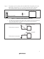
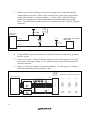
H8S Family E10A Emulator Additional Document for User’s Manual H8S/2339F E10A HS2339KCM01HE-U2 Renesas Microcomputer Development Environment System H8S Family / H8S/2300 Series Specific Guide for the H8S/2339EF, H8S/2329EF, H8S/2319EF E10A Emulator Rev.1.00 2003.10.6 Cautions Keep safety first in your circuit designs! 1. Renesas Technology Corp. puts the maximum effort into making semiconductor products better and more reliable, but there is always the possibility that trouble may occur with them. Trouble with semiconductors may lead to personal injury, fire or property damage. Remember to give due consideration to safety when making your circuit designs, with appropriate measures such as (i) placement of substitutive, auxiliary circuits, (ii) use of nonflammable material or (iii) prevention against any malfunction or mishap. Notes regarding these materials 1. These materials are intended as a reference to assist our customers in the selection of the Renesas Technology Corp. product best suited to the customer's application; they do not convey any license under any intellectual property rights, or any other rights, belonging to Renesas Technology Corp. or a third party. 2. Renesas Technology Corp. assumes no responsibility for any damage, or infringement of any third-party's rights, originating in the use of any product data, diagrams, charts, programs, algorithms, or circuit application examples contained in these materials. 3. All information contained in these materials, including product data, diagrams, charts, programs and algorithms represents information on products at the time of publication of these materials, and are subject to change by Renesas Technology Corp. without notice due to product improvements or other reasons. It is therefore recommended that customers contact Renesas Technology Corp. or an authorized Renesas Technology Corp. product distributor for the latest product information before purchasing a product listed herein. The information described here may contain technical inaccuracies or typographical errors. Renesas Technology Corp. assumes no responsibility for any damage, liability, or other loss rising from these inaccuracies or errors. Please also pay attention to information published by Renesas Technology Corp. by various means, including the Renesas Technology Corp. Semiconductor home page (http://www.renesas.com). 4. When using any or all of the information contained in these materials, including product data, diagrams, charts, programs, and algorithms, please be sure to evaluate all information as a total system before making a final decision on the applicability of the information and products. Renesas Technology Corp. assumes no responsibility for any damage, liability or other loss resulting from the information contained herein. 5. Renesas Technology Corp. semiconductors are not designed or manufactured for use in a device or system that is used under circumstances in which human life is potentially at stake. Please contact Renesas Technology Corp. or an authorized Renesas Technology Corp. product distributor when considering the use of a product contained herein for any specific purposes, such as apparatus or systems for transportation, vehicular, medical, aerospace, nuclear, or undersea repeater use. 6. The prior written approval of Renesas Technology Corp. is necessary to reprint or reproduce in whole or in part these materials. 7. If these products or technologies are subject to the Japanese export control restrictions, they must be exported under a license from the Japanese government and cannot be imported into a country other than the approved destination. Any diversion or reexport contrary to the export control laws and regulations of Japan and/or the country of destination is prohibited. 8. Please contact Renesas Technology Corp. for further details on these materials or the products contained therein. Contents Section 1 Connecting the Emulator with the User System ............................... 1 1.1 1.2 1.3 1.4 Components of the E10A Emulator ..................................................................................1 Connecting the E10A Emulator with the User System .....................................................2 Pin Assignments of the E10A Connector..........................................................................3 Example of E10A Emulator Connection...........................................................................4 Section 2 Specification of the E10A Emulator’s Software............................... 9 2.1 2.2 Differences between the H8S/2339EF, H8S/2329EF, H8S/2319EF, and the E10A Emulator............................................................................................................9 The H8S/2339F E10A Emulator Functions ......................................................................10 2.2.1 E10A Emulator Driver Selection .........................................................................10 2.2.2 Hardware Break Functions...................................................................................10 2.2.3 Notes on Setting the [Breakpoint] Dialog Box ....................................................12 2.2.4 Note on Using the JTAG Clock (TCK)................................................................12 2.2.5 Trace Function .....................................................................................................12 i ii Section 1 Connecting the Emulator with the User System 1.1 Components of the E10A Emulator The H8S/2339F E10A emulator supports the H8S/2339EF, H8S/2329EF, and H8S/2319EF. Table 1.1 lists the components of the H8S/2339F E10A emulator. Table 1.1 Components of the E10A Emulator (HS2339KCM01H or HS2339KCI01H) Classification Component Hardware Card emulator Appearance Quantity 1 PC PC Card HS2339KCM01H (Model: HS0005KCM05H), HS2339KCI01H (Model: HS0005KCI05H) (PCMCIA) or HS2339KCM01H (PCMCIA: 14-pin type): Depth: 85.6 mm, Width: 54.0 mm, Height: 5.0 mm, Mass: 30.0 g HS2339KCI01H (PCI: 14-pin type): Depth: 122.0 mm, Width: 96.0 mm, Mass: 80.0 g (PCI) User system interface cable Remarks 1 HS2339KCM01H (PCMCIA: 14-pin type): Length: 80.0 cm, Mass: 46.0 g HS2339KCI01H (PCI: 14-pin type): Length: 150.0 cm, Mass: 90.0 g Software H8S/2339F E10A emulator setup program, H8S Family E10A Emulator User’s Manual, 1 HS2339KCM01SR, HS0005KCM01HJ, HS0005KCM01HE, and Specific Guide for the H8S/2339EF, H8S/2329EF, H8S/2319EF E10A Emulator HS2339KCM01HJ-U2, and HS2339KCM01HE-U2 (provided on a CD-R) 1 1.2 Connecting the E10A Emulator with the User System Before connecting an E10A emulator with the user system, a connector must be installed in the user system so that an user system interface cable can be connected. When designing the user system, refer to the connector and recommended circuits shown in this manual. Before designing the user system, be sure to read the E10A emulator user’s manual and the hardware manual for related MCUs. Connect pins 8, 9, 10, 12, 13, and 14 of the user system connector to GND firmly on the PCB. These pins are used as electrical GND and to monitor the connection of the user system connector. Note the pin assignments of the user system connector. User system interface cable Tab GND line User system connector Pin 8 User system GND connection Pin 1 User system Figure 1.1 Connecting the User System Interface Cable to the User System Notes: 2 1. The pin number assignments of the 14-pin connector differ from those of the E10T emulator; however, the physical location is the same. 2. When the connector is used, do not install any components within 3 mm of the connector. 1.3 Pin Assignments of the E10A Connector Figure 1.2 shows the pin assignments of the H-UDI port connector. Signal Name Pin No. Pin 1 mark H-UDI port connector Pin 14 Pin 7 Pin 8 Pin 1 H8S/2339EF H8S/2329EF H8S/2319EF Input/Output *1 1 P82 P61 P35 Input 2 P34 P34 P21 Input 3 P83 P63 P31 Output 4 RES# *2 RES# *2 RES# *2 Input 5 P80 P60 P20 Input 6 P81 P62 P33 Input 7 RES# *2 RES# *2 RES# *2 Output 8 to 10 GND *3 GND *3 GND *3 Vcc *4 Vcc *4 Vcc *4 12 to 14 11 Top view Pin 1 mark Note: 1. Input or output from the user system. 2. The symbol (#) means that the signal is active-low. 3. By detecting GND on the user system side, the E10A emulator decides whether the user system is connected or not. 4. Connect Vcc with the Vcc of the MCU. Figure 1.2 Pin Assignments of the H-UDI Port Connector 3 1.4 Example of E10A Emulator Connection The figure shown below is an example of connecting the user system to the E10A emulator. 14-pin connector with a 2.54-mm pitch (3M Limited: 2514-6002) Vcc Pulled-up at 4.7 k H8S/2339EF H8S/2329EF H8S/2319EF 11 EMLE EMLE EMLE 1 P82 P61 P35 2 P34 P34 P21 3 P83 P63 P31 5 P80 P60 P20 6 P81 P62 P33 RES# RES# RES# 4 User logic 7 8 to 10 12 to 14 E10A pin No. User system · RES# of pin 4 of the H-UDI port connector is a signal line in which the emulator outputs signals to the MCU. Connect RES# of pin 4 and the user system reset circuit to the MCU, as shown above. · RES# of pin 7 of the H-UDI port connector is a signal line in which the emulator monitors the RES# signal of the MCU. The RES# must be pulled up before it is connected to pin 7 of the H-UDI port connector. Figure 1.3 Example of E10A Emulator Connection 4 Notes: 1. The emulator uses P34 and P80 to P83 in the H8S/2339EF, P34 and P60 to P63 in the H8S/2329EF, and P20 to P21, P31, P33, and P35 in the H8S/2319EF. Pull up the E10A emulator and MCU pins and connect them to the user system connector. H8S/2339EF, H8S/2329EF, H8S/2319EF H-UDI port connector Vcc 4.7 kΩ Pins 1, 2, 3, 5, and 6 Figure 1.4 Connection of E10A Emulator and the MCU 2. The EMLE pin in the H8S/2339EF, H8S/2329EF, and H8S/2319EF must be pulled up when connecting with the E10A emulator, and connected to ground when not connecting with the E10A emulator. Vcc E10A emulator is connected: H8S/2339EF, H8S/2329EF, H8S/2319EF 4.7 k EMLE H8S/2339EF, H8S/2329EF, H8S/2319EF EMLE E10A emulator is unconnected: Figure 1.5 EMLE Pin and E10A Emulator 5 3. RES# of pin 4 of the H-UDI port connector is a signal line in which the emulator outputs signals to the MCU. RES# of pin 4 and the user system reset circuit must be connected to the MCU, as shown in figure 1.6. RES# of pin 7 of the H-UDI port connector is a signal line in which the emulator monitors the RES# signal of the MCU. The RES# must be pulled up before it is connected to pin 7 of the H-UDI port connector. Vcc 4.7 k H-UDI port connector User logic H8S/2339EF, H8S/2329EF, H8S/2319EF Vcc Pin 4 4.7 k Pin 7 Figure 1.6 Connection of the RES# Pin 4. Connect GND of pins 8 to 10 and 12 to 14 in the H-UDI port connector to ground in the user system. 5. Connect Vcc, pin 11 of the H-UDI port connector, to the power supply (Vcc) in the user system. The input voltage, Vcc, is within the range of guaranteed operation of the microcomputer. 6. Figure 1.7 shows the interface circuit in the emulator. Use this figure as a reference when determining the pull-up resistance value. H-UDI port connector on the user sytem Emulator control circuit Vcc HD74LV125A Vcc 3.3V H8S/2339EF H8S/2329EF H8S/2319EF 11 Vcc Vcc Vcc 1 2 4 5 6 P82 P34 RES# P80 P81 P61 P34 RES# P60 P62 P35 P21 RES# P20 P33 3 7 P83 RES# P63 RES# P31 RES# 4.7 k x 7 22 k x 5 HD74LVTH244 Vcc 22 k x2 Figure 1.7 Interface Circuit in the Emulator (Reference) 6 7. In the H8S/2339, H8S/2329, and H8S/2319 series, only H8S/2339EF, H8S/2329EF, and H8S/2319EF can be connected to the E10A emulator. H8S/2339F, H8S/2329F, and H8S/2319F for general use cannot be used. 8. When H8S/2339EF and H8S/2329EF are connected to the E10A emulator, SCI0 (serial communication interface channel 0) cannot be used. 9. When H8S/2319EF is connected to the E10A emulator, SCI1 (serial communication interface channel 1) cannot be used. 10. When H8S/2339EF, H8S/2329EF, and H8S/2319EF are connected to the E10A emulator, the following pin functions cannot be used. Table 1.2 Unavailable Pin Functions H8S/2339EF H8S/2329EF H8S/2319EF P34 and P80 to P83 P34 and P60 to P63 P20, P21, P31, P33, and P35 FWE FWE FWE SCK0 SCK0 SCK1, TxD1, and RxD1 DREQ0# and DREQ1# DREQ0# and DREQ1# IRQ5# TEND0# TEND0# TIOCA3 and TIOCB3 − CS4# and CS5# − Note: The symbol “#” means that the signal is active-low. 7 8 Section 2 Specification of the E10A Emulator’s Software 2.1 Differences between the H8S/2339EF, H8S/2329EF, H8S/2319EF, and the E10A Emulator 1. When the E10A emulator system is initiated, it initializes the general registers and part of the control registers as shown in table 2.1. Table 2.1 Register Initial Values at E10A Emulator Power-On Register Initial Value PC Reset vector value in the vector address table ER0 to ER6 H’0 ER7 (SP) H'10 CCR 1 for I mask, and others undefined 2. System Control Register In the E10A emulator, the internal I/O registers can be accessed from the [IO] window. However, be careful when accessing the system control register. The E10A emulator saves the register value of the system control register at a break and returns the value when the user program is executed. Since this is done during a break, do not rewrite the system control register in the [IO] window. 3. Memory Access during Emulation If the memory contents are referenced or modified during emulation, realtime emulation cannot be performed because the user program is temporarily halted. 4. The E10A emulator communicates with the MCU by using the pins shown in figure 1.2 (section 1.3). These pins cannot be used. 5. The power consumed by the MCU can reach several mA. This is because the user power supply drives one HD74LV125A to make the communication signal level match the usersystem power-supply voltage. 6. Do not use an MCU that has been used for debugging. If the flash memory is rewritten many times, and the MCU is left for a few days, data may be lost due to retention problems. If the flash memory is rewritten many times, the data will not be erased. If an error message is displayed, exchange the MCU for a new one. 9 2.2 The H8S/2339F E10A Emulator Functions Notes: 1. Do not use an MCU that has been used for debugging. 2.2.1 2. If the flash memory is rewritten many times, and the E10A emulator is left for a few days, data may be lost due to retention problems. 3. If the flash memory is rewritten many times, the data will not be erased. If an error message is displayed, exchange the MCU for a new one. E10A Emulator Driver Selection Table 2.2 shows drivers which can be selected in the [E10A Driver Details] dialog box. Table 2.2 Type Name and Driver Type Name Driver HS2339KCM01H E10A PC Card Driver 5 HS2339KCI01H E10A PCI Card Driver 5 2.2.2 Hardware Break Functions Hardware Break Conditions: In the H8S/2339F E10A emulator, conditions of Break Condition 1,2 can be set. Table 2.3 lists the items that can be specified. Table 2.3 Hardware Break Condition Specification Items Items Description Address bus condition Breaks when the MCU address bus value matches the specified value. Data bus condition Breaks when the MCU data bus value matches the specified value. High or low byte or word can be specified as the access data size. Read or write condition Breaks in the read or write cycle. 10 Table 2.4 lists the combinations of conditions that can be set in the [Break condition] dialog box. Table 2.4 Conditions Set in [Break condition] Dialog Box Condition Dialog Box Address Bus Condition O O [Break condition 1] [Break condition 2] Data Condition O O Read or Write Condition O O Note: O: Can be set by checking the radio button in the dialog box. Table 2.5 lists the combinations of conditions that can be set by the BREAKCONDITION_SET command. Table 2.5 Conditions Set by BREAKCONDITION_SET Command Condition Channel Break condition 1 Break condition 2 Address Bus Condition (<addropt> option) O O Data Condition (<dataopt> option) O O Read or Write Condition (<r/wopt> option) O O Note: O: Can be set by the BREAKCONDITION_SET command. 11 Notes on Setting the Break Condition: 1. When [Go to cursor], [Step In], [Step Over], or [Step Out] is selected, the settings of Break Condition are disabled. 2. The settings of Break Condition are disabled when an instruction to which a BREAKPOINT has been set is executed. 3. When step over function is used, the settings of BREAKPOINT and Break Condition are disabled. 2.2.3 Notes on Setting the [Breakpoint] Dialog Box 1. When an odd address is set, the address is rounded down to an even address. 2. A BREAKPOINT is accomplished by replacing instructions. Accordingly, it can be set only to the flash memory or the RAM area. However, a BREAKPOINT cannot be set to the following addresses: • An area other than flash memory or RAM • An area occupied by the E10A emulator program • An instruction in which Break Condition is satisfied 3. During step execution, a BREAKPOINT is disabled. 4. A condition set at Break Condition is disabled immediately after starting execution when an instruction at a BREAKPOINT is executed. A break does not occur even if a condition of Break Condition is satisfied immediately after starting the execution. 5. When execution resumes from the breakpoint address after the program execution stops at the BREAKPOINT, single-step execution is performed at the address before execution resumes. Therefore, realtime operation cannot be performed. 6. Settings of BREAKPOINT and Break Condition are invalid while the STEP OVER function is being used. 2.2.4 Note on Using the JTAG Clock (TCK) When the JTAG clock (TCK) is used, set the frequency to lower than that of the system clock. 2.2.5 Trace Function The trace function in the H8S/2339F E10A emulator uses the branch-instruction trace function in the MCU. It displays the branch-source address or the mnemonic, and operand can be acquired in realtime. 12 H8S Family E10A Emulator Additional Document for User's Manual Specific Guide for the H8S/2339EF, H8S/2329EF, H8S/2319EF E10A Emulator Publication Date: Rev.1.00, October 6, 2003 Published by: Sales Strategic Planning Div. Renesas Technology Corp. Edited by: Technical Documentation & Information Department Renesas Kodaira Semiconductor Co., Ltd. 2003 Renesas Technology Corp. All rights reserved. Printed in Japan. H8S Family E10A Emulator Additional Document for User’s Manual REJ10B0033-0100H